WO2019211697A1 - 半導体装置 - Google Patents
半導体装置 Download PDFInfo
- Publication number
- WO2019211697A1 WO2019211697A1 PCT/IB2019/053299 IB2019053299W WO2019211697A1 WO 2019211697 A1 WO2019211697 A1 WO 2019211697A1 IB 2019053299 W IB2019053299 W IB 2019053299W WO 2019211697 A1 WO2019211697 A1 WO 2019211697A1
- Authority
- WO
- WIPO (PCT)
- Prior art keywords
- transistor
- insulator
- oxide
- circuit
- conductor
- Prior art date
Links
- 239000004065 semiconductor Substances 0.000 title claims abstract description 219
- 238000003860 storage Methods 0.000 claims abstract description 253
- 230000006870 function Effects 0.000 claims abstract description 197
- 239000000463 material Substances 0.000 claims description 80
- 239000003990 capacitor Substances 0.000 claims description 57
- 229910052782 aluminium Inorganic materials 0.000 claims description 38
- XAGFODPZIPBFFR-UHFFFAOYSA-N aluminium Chemical group [Al] XAGFODPZIPBFFR-UHFFFAOYSA-N 0.000 claims description 38
- 238000012937 correction Methods 0.000 claims description 23
- 238000001514 detection method Methods 0.000 claims description 23
- 239000011701 zinc Substances 0.000 claims description 14
- 229910052738 indium Inorganic materials 0.000 claims description 9
- APFVFJFRJDLVQX-UHFFFAOYSA-N indium atom Chemical compound [In] APFVFJFRJDLVQX-UHFFFAOYSA-N 0.000 claims description 9
- GYHNNYVSQQEPJS-UHFFFAOYSA-N Gallium Chemical group [Ga] GYHNNYVSQQEPJS-UHFFFAOYSA-N 0.000 claims description 8
- 229910052733 gallium Inorganic materials 0.000 claims description 8
- 229910052727 yttrium Inorganic materials 0.000 claims description 8
- VWQVUPCCIRVNHF-UHFFFAOYSA-N yttrium atom Chemical group [Y] VWQVUPCCIRVNHF-UHFFFAOYSA-N 0.000 claims description 8
- HCHKCACWOHOZIP-UHFFFAOYSA-N Zinc Chemical compound [Zn] HCHKCACWOHOZIP-UHFFFAOYSA-N 0.000 claims description 5
- 229910052725 zinc Inorganic materials 0.000 claims description 5
- ATJFFYVFTNAWJD-UHFFFAOYSA-N Tin Chemical group [Sn] ATJFFYVFTNAWJD-UHFFFAOYSA-N 0.000 claims description 3
- 229910052718 tin Chemical group 0.000 claims description 3
- 230000008859 change Effects 0.000 abstract description 11
- 239000004020 conductor Substances 0.000 description 446
- 239000012212 insulator Substances 0.000 description 439
- 239000010408 film Substances 0.000 description 134
- 239000010410 layer Substances 0.000 description 118
- 229910052760 oxygen Inorganic materials 0.000 description 104
- QVGXLLKOCUKJST-UHFFFAOYSA-N atomic oxygen Chemical compound [O] QVGXLLKOCUKJST-UHFFFAOYSA-N 0.000 description 103
- 239000001301 oxygen Substances 0.000 description 103
- 229910052739 hydrogen Inorganic materials 0.000 description 88
- 239000001257 hydrogen Substances 0.000 description 88
- 229910044991 metal oxide Inorganic materials 0.000 description 79
- UFHFLCQGNIYNRP-UHFFFAOYSA-N Hydrogen Chemical compound [H][H] UFHFLCQGNIYNRP-UHFFFAOYSA-N 0.000 description 73
- 150000004706 metal oxides Chemical class 0.000 description 69
- 239000012535 impurity Substances 0.000 description 68
- 230000004888 barrier function Effects 0.000 description 55
- 238000009792 diffusion process Methods 0.000 description 49
- 230000002829 reductive effect Effects 0.000 description 42
- IJGRMHOSHXDMSA-UHFFFAOYSA-N Atomic nitrogen Chemical compound N#N IJGRMHOSHXDMSA-UHFFFAOYSA-N 0.000 description 35
- VYPSYNLAJGMNEJ-UHFFFAOYSA-N Silicium dioxide Chemical compound O=[Si]=O VYPSYNLAJGMNEJ-UHFFFAOYSA-N 0.000 description 31
- XUIMIQQOPSSXEZ-UHFFFAOYSA-N Silicon Chemical compound [Si] XUIMIQQOPSSXEZ-UHFFFAOYSA-N 0.000 description 31
- 229910052710 silicon Inorganic materials 0.000 description 31
- 239000010703 silicon Substances 0.000 description 31
- 229910052814 silicon oxide Inorganic materials 0.000 description 31
- 229910052721 tungsten Inorganic materials 0.000 description 27
- 239000010937 tungsten Substances 0.000 description 27
- XLYOFNOQVPJJNP-UHFFFAOYSA-N water Substances O XLYOFNOQVPJJNP-UHFFFAOYSA-N 0.000 description 27
- 229910001868 water Inorganic materials 0.000 description 27
- WFKWXMTUELFFGS-UHFFFAOYSA-N tungsten Chemical compound [W] WFKWXMTUELFFGS-UHFFFAOYSA-N 0.000 description 25
- 238000000034 method Methods 0.000 description 24
- 229910052581 Si3N4 Inorganic materials 0.000 description 23
- HQVNEWCFYHHQES-UHFFFAOYSA-N silicon nitride Chemical compound N12[Si]34N5[Si]62N3[Si]51N64 HQVNEWCFYHHQES-UHFFFAOYSA-N 0.000 description 23
- RYGMFSIKBFXOCR-UHFFFAOYSA-N Copper Chemical compound [Cu] RYGMFSIKBFXOCR-UHFFFAOYSA-N 0.000 description 22
- 125000004429 atom Chemical group 0.000 description 22
- TWNQGVIAIRXVLR-UHFFFAOYSA-N oxo(oxoalumanyloxy)alumane Chemical compound O=[Al]O[Al]=O TWNQGVIAIRXVLR-UHFFFAOYSA-N 0.000 description 22
- 229910052751 metal Inorganic materials 0.000 description 21
- PXHVJJICTQNCMI-UHFFFAOYSA-N Nickel Chemical compound [Ni] PXHVJJICTQNCMI-UHFFFAOYSA-N 0.000 description 20
- 230000015572 biosynthetic process Effects 0.000 description 20
- 229910052735 hafnium Inorganic materials 0.000 description 19
- 150000002431 hydrogen Chemical class 0.000 description 19
- 239000002184 metal Substances 0.000 description 19
- RTAQQCXQSZGOHL-UHFFFAOYSA-N Titanium Chemical group [Ti] RTAQQCXQSZGOHL-UHFFFAOYSA-N 0.000 description 18
- 239000010949 copper Substances 0.000 description 18
- 238000010586 diagram Methods 0.000 description 18
- 229910052757 nitrogen Inorganic materials 0.000 description 18
- 229910052719 titanium Inorganic materials 0.000 description 18
- 239000010936 titanium Chemical group 0.000 description 18
- -1 and in particular Inorganic materials 0.000 description 17
- 229910052802 copper Inorganic materials 0.000 description 17
- 239000002356 single layer Substances 0.000 description 15
- 239000013078 crystal Substances 0.000 description 14
- 238000004519 manufacturing process Methods 0.000 description 14
- VBJZVLUMGGDVMO-UHFFFAOYSA-N hafnium atom Chemical compound [Hf] VBJZVLUMGGDVMO-UHFFFAOYSA-N 0.000 description 13
- 229910000449 hafnium oxide Inorganic materials 0.000 description 13
- WIHZLLGSGQNAGK-UHFFFAOYSA-N hafnium(4+);oxygen(2-) Chemical compound [O-2].[O-2].[Hf+4] WIHZLLGSGQNAGK-UHFFFAOYSA-N 0.000 description 13
- 230000005684 electric field Effects 0.000 description 12
- MZLGASXMSKOWSE-UHFFFAOYSA-N tantalum nitride Chemical compound [Ta]#N MZLGASXMSKOWSE-UHFFFAOYSA-N 0.000 description 12
- 101100437484 Arabidopsis thaliana BGLU18 gene Proteins 0.000 description 11
- 101100342633 Bos taurus LLGL1 gene Proteins 0.000 description 11
- OKTJSMMVPCPJKN-UHFFFAOYSA-N Carbon Chemical compound [C] OKTJSMMVPCPJKN-UHFFFAOYSA-N 0.000 description 11
- 101100065855 Saccharomyces cerevisiae (strain ATCC 204508 / S288c) EXG1 gene Proteins 0.000 description 11
- 101100058298 Saccharomycopsis fibuligera BGL1 gene Proteins 0.000 description 11
- NRTOMJZYCJJWKI-UHFFFAOYSA-N Titanium nitride Chemical compound [Ti]#N NRTOMJZYCJJWKI-UHFFFAOYSA-N 0.000 description 11
- 101150100570 bglA gene Proteins 0.000 description 11
- 229910052799 carbon Inorganic materials 0.000 description 11
- 230000003647 oxidation Effects 0.000 description 11
- 238000007254 oxidation reaction Methods 0.000 description 11
- 229920005989 resin Polymers 0.000 description 11
- 239000011347 resin Substances 0.000 description 11
- 229910052715 tantalum Inorganic materials 0.000 description 11
- GUVRBAGPIYLISA-UHFFFAOYSA-N tantalum atom Chemical compound [Ta] GUVRBAGPIYLISA-UHFFFAOYSA-N 0.000 description 11
- ZOKXTWBITQBERF-UHFFFAOYSA-N Molybdenum Chemical compound [Mo] ZOKXTWBITQBERF-UHFFFAOYSA-N 0.000 description 10
- 239000000969 carrier Substances 0.000 description 10
- 238000006243 chemical reaction Methods 0.000 description 10
- 230000007547 defect Effects 0.000 description 10
- 239000011229 interlayer Substances 0.000 description 10
- 229910052750 molybdenum Inorganic materials 0.000 description 10
- 239000011733 molybdenum Substances 0.000 description 10
- 229910052759 nickel Inorganic materials 0.000 description 10
- 101150046766 BGL2 gene Proteins 0.000 description 9
- 150000004767 nitrides Chemical class 0.000 description 9
- 230000002093 peripheral effect Effects 0.000 description 9
- 239000000758 substrate Substances 0.000 description 9
- 230000003247 decreasing effect Effects 0.000 description 8
- 238000010438 heat treatment Methods 0.000 description 8
- 230000014759 maintenance of location Effects 0.000 description 8
- 239000000203 mixture Substances 0.000 description 8
- 125000004430 oxygen atom Chemical group O* 0.000 description 8
- 230000003071 parasitic effect Effects 0.000 description 8
- ZOXJGFHDIHLPTG-UHFFFAOYSA-N Boron Chemical compound [B] ZOXJGFHDIHLPTG-UHFFFAOYSA-N 0.000 description 7
- 229910052784 alkaline earth metal Inorganic materials 0.000 description 7
- 239000000956 alloy Substances 0.000 description 7
- 229910052796 boron Inorganic materials 0.000 description 7
- 239000011810 insulating material Substances 0.000 description 7
- 239000007769 metal material Substances 0.000 description 7
- 229910052707 ruthenium Inorganic materials 0.000 description 7
- 238000001004 secondary ion mass spectrometry Methods 0.000 description 7
- 238000004544 sputter deposition Methods 0.000 description 7
- OAICVXFJPJFONN-UHFFFAOYSA-N Phosphorus Chemical compound [P] OAICVXFJPJFONN-UHFFFAOYSA-N 0.000 description 6
- QCWXUUIWCKQGHC-UHFFFAOYSA-N Zirconium Chemical group [Zr] QCWXUUIWCKQGHC-UHFFFAOYSA-N 0.000 description 6
- 230000007423 decrease Effects 0.000 description 6
- 238000003795 desorption Methods 0.000 description 6
- 125000004435 hydrogen atom Chemical group [H]* 0.000 description 6
- BPUBBGLMJRNUCC-UHFFFAOYSA-N oxygen(2-);tantalum(5+) Chemical compound [O-2].[O-2].[O-2].[O-2].[O-2].[Ta+5].[Ta+5] BPUBBGLMJRNUCC-UHFFFAOYSA-N 0.000 description 6
- RVTZCBVAJQQJTK-UHFFFAOYSA-N oxygen(2-);zirconium(4+) Chemical compound [O-2].[O-2].[Zr+4] RVTZCBVAJQQJTK-UHFFFAOYSA-N 0.000 description 6
- 229910052698 phosphorus Inorganic materials 0.000 description 6
- 239000011574 phosphorus Substances 0.000 description 6
- 239000000126 substance Substances 0.000 description 6
- 229910001936 tantalum oxide Inorganic materials 0.000 description 6
- OGIDPMRJRNCKJF-UHFFFAOYSA-N titanium oxide Inorganic materials [Ti]=O OGIDPMRJRNCKJF-UHFFFAOYSA-N 0.000 description 6
- 229910052726 zirconium Inorganic materials 0.000 description 6
- 229910001928 zirconium oxide Inorganic materials 0.000 description 6
- FYYHWMGAXLPEAU-UHFFFAOYSA-N Magnesium Chemical compound [Mg] FYYHWMGAXLPEAU-UHFFFAOYSA-N 0.000 description 5
- KJTLSVCANCCWHF-UHFFFAOYSA-N Ruthenium Chemical compound [Ru] KJTLSVCANCCWHF-UHFFFAOYSA-N 0.000 description 5
- 229910052783 alkali metal Inorganic materials 0.000 description 5
- 150000001340 alkali metals Chemical class 0.000 description 5
- 150000001342 alkaline earth metals Chemical class 0.000 description 5
- 239000002585 base Substances 0.000 description 5
- 239000000470 constituent Substances 0.000 description 5
- 229910052732 germanium Inorganic materials 0.000 description 5
- GNPVGFCGXDBREM-UHFFFAOYSA-N germanium atom Chemical compound [Ge] GNPVGFCGXDBREM-UHFFFAOYSA-N 0.000 description 5
- 229910052749 magnesium Inorganic materials 0.000 description 5
- 239000011777 magnesium Substances 0.000 description 5
- 230000008569 process Effects 0.000 description 5
- 229910052712 strontium Inorganic materials 0.000 description 5
- PXGOKWXKJXAPGV-UHFFFAOYSA-N Fluorine Chemical compound FF PXGOKWXKJXAPGV-UHFFFAOYSA-N 0.000 description 4
- XEEYBQQBJWHFJM-UHFFFAOYSA-N Iron Chemical group [Fe] XEEYBQQBJWHFJM-UHFFFAOYSA-N 0.000 description 4
- GWEVSGVZZGPLCZ-UHFFFAOYSA-N Titan oxide Chemical compound O=[Ti]=O GWEVSGVZZGPLCZ-UHFFFAOYSA-N 0.000 description 4
- 229910045601 alloy Inorganic materials 0.000 description 4
- 238000004458 analytical method Methods 0.000 description 4
- GPBUGPUPKAGMDK-UHFFFAOYSA-N azanylidynemolybdenum Chemical compound [Mo]#N GPBUGPUPKAGMDK-UHFFFAOYSA-N 0.000 description 4
- PMHQVHHXPFUNSP-UHFFFAOYSA-M copper(1+);methylsulfanylmethane;bromide Chemical compound Br[Cu].CSC PMHQVHHXPFUNSP-UHFFFAOYSA-M 0.000 description 4
- 238000013461 design Methods 0.000 description 4
- AJNVQOSZGJRYEI-UHFFFAOYSA-N digallium;oxygen(2-) Chemical compound [O-2].[O-2].[O-2].[Ga+3].[Ga+3] AJNVQOSZGJRYEI-UHFFFAOYSA-N 0.000 description 4
- 229910052731 fluorine Inorganic materials 0.000 description 4
- 239000011737 fluorine Substances 0.000 description 4
- 229910001195 gallium oxide Inorganic materials 0.000 description 4
- 239000007789 gas Substances 0.000 description 4
- YBMRDBCBODYGJE-UHFFFAOYSA-N germanium oxide Inorganic materials O=[Ge]=O YBMRDBCBODYGJE-UHFFFAOYSA-N 0.000 description 4
- 230000010354 integration Effects 0.000 description 4
- 238000005468 ion implantation Methods 0.000 description 4
- 229910052746 lanthanum Inorganic materials 0.000 description 4
- FZLIPJUXYLNCLC-UHFFFAOYSA-N lanthanum atom Chemical group [La] FZLIPJUXYLNCLC-UHFFFAOYSA-N 0.000 description 4
- MRELNEQAGSRDBK-UHFFFAOYSA-N lanthanum(3+);oxygen(2-) Chemical compound [O-2].[O-2].[O-2].[La+3].[La+3] MRELNEQAGSRDBK-UHFFFAOYSA-N 0.000 description 4
- 229910052451 lead zirconate titanate Inorganic materials 0.000 description 4
- 239000002159 nanocrystal Substances 0.000 description 4
- PLDDOISOJJCEMH-UHFFFAOYSA-N neodymium(3+);oxygen(2-) Chemical compound [O-2].[O-2].[O-2].[Nd+3].[Nd+3] PLDDOISOJJCEMH-UHFFFAOYSA-N 0.000 description 4
- QGLKJKCYBOYXKC-UHFFFAOYSA-N nonaoxidotritungsten Chemical compound O=[W]1(=O)O[W](=O)(=O)O[W](=O)(=O)O1 QGLKJKCYBOYXKC-UHFFFAOYSA-N 0.000 description 4
- SIWVEOZUMHYXCS-UHFFFAOYSA-N oxo(oxoyttriooxy)yttrium Chemical compound O=[Y]O[Y]=O SIWVEOZUMHYXCS-UHFFFAOYSA-N 0.000 description 4
- PVADDRMAFCOOPC-UHFFFAOYSA-N oxogermanium Chemical compound [Ge]=O PVADDRMAFCOOPC-UHFFFAOYSA-N 0.000 description 4
- BASFCYQUMIYNBI-UHFFFAOYSA-N platinum Chemical compound [Pt] BASFCYQUMIYNBI-UHFFFAOYSA-N 0.000 description 4
- 230000009467 reduction Effects 0.000 description 4
- 229910001925 ruthenium oxide Inorganic materials 0.000 description 4
- WOCIAKWEIIZHES-UHFFFAOYSA-N ruthenium(iv) oxide Chemical compound O=[Ru]=O WOCIAKWEIIZHES-UHFFFAOYSA-N 0.000 description 4
- 229910001930 tungsten oxide Inorganic materials 0.000 description 4
- JBRZTFJDHDCESZ-UHFFFAOYSA-N AsGa Chemical compound [As]#[Ga] JBRZTFJDHDCESZ-UHFFFAOYSA-N 0.000 description 3
- VYZAMTAEIAYCRO-UHFFFAOYSA-N Chromium Chemical compound [Cr] VYZAMTAEIAYCRO-UHFFFAOYSA-N 0.000 description 3
- 229910001218 Gallium arsenide Inorganic materials 0.000 description 3
- 238000003491 array Methods 0.000 description 3
- 238000005229 chemical vapour deposition Methods 0.000 description 3
- 229910052804 chromium Inorganic materials 0.000 description 3
- 239000011651 chromium Substances 0.000 description 3
- 230000000295 complement effect Effects 0.000 description 3
- 230000000694 effects Effects 0.000 description 3
- 229910003437 indium oxide Inorganic materials 0.000 description 3
- PJXISJQVUVHSOJ-UHFFFAOYSA-N indium(iii) oxide Chemical compound [O-2].[O-2].[O-2].[In+3].[In+3] PJXISJQVUVHSOJ-UHFFFAOYSA-N 0.000 description 3
- AMGQUBHHOARCQH-UHFFFAOYSA-N indium;oxotin Chemical compound [In].[Sn]=O AMGQUBHHOARCQH-UHFFFAOYSA-N 0.000 description 3
- 150000002500 ions Chemical class 0.000 description 3
- 239000011159 matrix material Substances 0.000 description 3
- 239000011156 metal matrix composite Substances 0.000 description 3
- 230000002441 reversible effect Effects 0.000 description 3
- CIOAGBVUUVVLOB-UHFFFAOYSA-N strontium atom Chemical compound [Sr] CIOAGBVUUVVLOB-UHFFFAOYSA-N 0.000 description 3
- XKRFYHLGVUSROY-UHFFFAOYSA-N Argon Chemical compound [Ar] XKRFYHLGVUSROY-UHFFFAOYSA-N 0.000 description 2
- 229910052779 Neodymium Inorganic materials 0.000 description 2
- MWUXSHHQAYIFBG-UHFFFAOYSA-N Nitric oxide Chemical compound O=[N] MWUXSHHQAYIFBG-UHFFFAOYSA-N 0.000 description 2
- 239000004695 Polyether sulfone Substances 0.000 description 2
- 239000004698 Polyethylene Substances 0.000 description 2
- 229910000577 Silicon-germanium Inorganic materials 0.000 description 2
- BQCADISMDOOEFD-UHFFFAOYSA-N Silver Chemical compound [Ag] BQCADISMDOOEFD-UHFFFAOYSA-N 0.000 description 2
- XLOMVQKBTHCTTD-UHFFFAOYSA-N Zinc monoxide Chemical compound [Zn]=O XLOMVQKBTHCTTD-UHFFFAOYSA-N 0.000 description 2
- 230000001133 acceleration Effects 0.000 description 2
- 229910052785 arsenic Inorganic materials 0.000 description 2
- RQNWIZPPADIBDY-UHFFFAOYSA-N arsenic atom Chemical compound [As] RQNWIZPPADIBDY-UHFFFAOYSA-N 0.000 description 2
- 229910052788 barium Inorganic materials 0.000 description 2
- 229910052790 beryllium Inorganic materials 0.000 description 2
- ATBAMAFKBVZNFJ-UHFFFAOYSA-N beryllium atom Chemical group [Be] ATBAMAFKBVZNFJ-UHFFFAOYSA-N 0.000 description 2
- 229910000416 bismuth oxide Inorganic materials 0.000 description 2
- 230000000903 blocking effect Effects 0.000 description 2
- 229910052795 boron group element Inorganic materials 0.000 description 2
- 229910052800 carbon group element Inorganic materials 0.000 description 2
- 239000002131 composite material Substances 0.000 description 2
- 238000000151 deposition Methods 0.000 description 2
- TYIXMATWDRGMPF-UHFFFAOYSA-N dibismuth;oxygen(2-) Chemical compound [O-2].[O-2].[O-2].[Bi+3].[Bi+3] TYIXMATWDRGMPF-UHFFFAOYSA-N 0.000 description 2
- 230000007613 environmental effect Effects 0.000 description 2
- 230000005669 field effect Effects 0.000 description 2
- 238000003384 imaging method Methods 0.000 description 2
- 238000007654 immersion Methods 0.000 description 2
- 229910052742 iron Inorganic materials 0.000 description 2
- HFGPZNIAWCZYJU-UHFFFAOYSA-N lead zirconate titanate Chemical compound [O-2].[O-2].[O-2].[O-2].[O-2].[Ti+4].[Zr+4].[Pb+2] HFGPZNIAWCZYJU-UHFFFAOYSA-N 0.000 description 2
- CPLXHLVBOLITMK-UHFFFAOYSA-N magnesium oxide Inorganic materials [Mg]=O CPLXHLVBOLITMK-UHFFFAOYSA-N 0.000 description 2
- 239000000395 magnesium oxide Substances 0.000 description 2
- AXZKOIWUVFPNLO-UHFFFAOYSA-N magnesium;oxygen(2-) Chemical compound [O-2].[Mg+2] AXZKOIWUVFPNLO-UHFFFAOYSA-N 0.000 description 2
- 230000004048 modification Effects 0.000 description 2
- 238000012986 modification Methods 0.000 description 2
- QEFYFXOXNSNQGX-UHFFFAOYSA-N neodymium atom Chemical group [Nd] QEFYFXOXNSNQGX-UHFFFAOYSA-N 0.000 description 2
- 229910000484 niobium oxide Inorganic materials 0.000 description 2
- URLJKFSTXLNXLG-UHFFFAOYSA-N niobium(5+);oxygen(2-) Chemical compound [O-2].[O-2].[O-2].[O-2].[O-2].[Nb+5].[Nb+5] URLJKFSTXLNXLG-UHFFFAOYSA-N 0.000 description 2
- 230000001151 other effect Effects 0.000 description 2
- 229910052697 platinum Inorganic materials 0.000 description 2
- 229910052696 pnictogen Inorganic materials 0.000 description 2
- 238000005498 polishing Methods 0.000 description 2
- 229920003207 poly(ethylene-2,6-naphthalate) Polymers 0.000 description 2
- 229920006393 polyether sulfone Polymers 0.000 description 2
- 239000011112 polyethylene naphthalate Substances 0.000 description 2
- 229920000139 polyethylene terephthalate Polymers 0.000 description 2
- 239000005020 polyethylene terephthalate Substances 0.000 description 2
- 238000012545 processing Methods 0.000 description 2
- 230000001681 protective effect Effects 0.000 description 2
- 230000000717 retained effect Effects 0.000 description 2
- 238000000926 separation method Methods 0.000 description 2
- 229910052709 silver Inorganic materials 0.000 description 2
- 239000004332 silver Substances 0.000 description 2
- VEALVRVVWBQVSL-UHFFFAOYSA-N strontium titanate Chemical compound [Sr+2].[O-][Ti]([O-])=O VEALVRVVWBQVSL-UHFFFAOYSA-N 0.000 description 2
- 229910052720 vanadium Inorganic materials 0.000 description 2
- LEONUFNNVUYDNQ-UHFFFAOYSA-N vanadium atom Chemical group [V] LEONUFNNVUYDNQ-UHFFFAOYSA-N 0.000 description 2
- YVTHLONGBIQYBO-UHFFFAOYSA-N zinc indium(3+) oxygen(2-) Chemical compound [O--].[Zn++].[In+3] YVTHLONGBIQYBO-UHFFFAOYSA-N 0.000 description 2
- VUFNLQXQSDUXKB-DOFZRALJSA-N 2-[4-[4-[bis(2-chloroethyl)amino]phenyl]butanoyloxy]ethyl (5z,8z,11z,14z)-icosa-5,8,11,14-tetraenoate Chemical compound CCCCC\C=C/C\C=C/C\C=C/C\C=C/CCCC(=O)OCCOC(=O)CCCC1=CC=C(N(CCCl)CCCl)C=C1 VUFNLQXQSDUXKB-DOFZRALJSA-N 0.000 description 1
- 229920000178 Acrylic resin Polymers 0.000 description 1
- 239000004925 Acrylic resin Substances 0.000 description 1
- 229910000838 Al alloy Inorganic materials 0.000 description 1
- 229910052684 Cerium Inorganic materials 0.000 description 1
- ZAMOUSCENKQFHK-UHFFFAOYSA-N Chlorine atom Chemical compound [Cl] ZAMOUSCENKQFHK-UHFFFAOYSA-N 0.000 description 1
- MYMOFIZGZYHOMD-UHFFFAOYSA-N Dioxygen Chemical compound O=O MYMOFIZGZYHOMD-UHFFFAOYSA-N 0.000 description 1
- DGAQECJNVWCQMB-PUAWFVPOSA-M Ilexoside XXIX Chemical compound C[C@@H]1CC[C@@]2(CC[C@@]3(C(=CC[C@H]4[C@]3(CC[C@@H]5[C@@]4(CC[C@@H](C5(C)C)OS(=O)(=O)[O-])C)C)[C@@H]2[C@]1(C)O)C)C(=O)O[C@H]6[C@@H]([C@H]([C@@H]([C@H](O6)CO)O)O)O.[Na+] DGAQECJNVWCQMB-PUAWFVPOSA-M 0.000 description 1
- WHXSMMKQMYFTQS-UHFFFAOYSA-N Lithium Chemical compound [Li] WHXSMMKQMYFTQS-UHFFFAOYSA-N 0.000 description 1
- 239000004962 Polyamide-imide Substances 0.000 description 1
- 239000004743 Polypropylene Substances 0.000 description 1
- 206010037660 Pyrexia Diseases 0.000 description 1
- NINIDFKCEFEMDL-UHFFFAOYSA-N Sulfur Chemical compound [S] NINIDFKCEFEMDL-UHFFFAOYSA-N 0.000 description 1
- LEVVHYCKPQWKOP-UHFFFAOYSA-N [Si].[Ge] Chemical compound [Si].[Ge] LEVVHYCKPQWKOP-UHFFFAOYSA-N 0.000 description 1
- UQZIWOQVLUASCR-UHFFFAOYSA-N alumane;titanium Chemical compound [AlH3].[Ti] UQZIWOQVLUASCR-UHFFFAOYSA-N 0.000 description 1
- MDPILPRLPQYEEN-UHFFFAOYSA-N aluminium arsenide Chemical compound [As]#[Al] MDPILPRLPQYEEN-UHFFFAOYSA-N 0.000 description 1
- 229910021417 amorphous silicon Inorganic materials 0.000 description 1
- 150000001450 anions Chemical class 0.000 description 1
- 239000004760 aramid Substances 0.000 description 1
- 229910052786 argon Inorganic materials 0.000 description 1
- 229920003235 aromatic polyamide Polymers 0.000 description 1
- 238000004364 calculation method Methods 0.000 description 1
- 150000001768 cations Chemical class 0.000 description 1
- 230000001413 cellular effect Effects 0.000 description 1
- GWXLDORMOJMVQZ-UHFFFAOYSA-N cerium Chemical group [Ce] GWXLDORMOJMVQZ-UHFFFAOYSA-N 0.000 description 1
- 229910052801 chlorine Inorganic materials 0.000 description 1
- 239000000460 chlorine Substances 0.000 description 1
- 230000008878 coupling Effects 0.000 description 1
- 238000010168 coupling process Methods 0.000 description 1
- 238000005859 coupling reaction Methods 0.000 description 1
- 229910021419 crystalline silicon Inorganic materials 0.000 description 1
- 230000008021 deposition Effects 0.000 description 1
- 238000006073 displacement reaction Methods 0.000 description 1
- 239000003792 electrolyte Substances 0.000 description 1
- 238000005516 engineering process Methods 0.000 description 1
- 239000003822 epoxy resin Substances 0.000 description 1
- 238000005530 etching Methods 0.000 description 1
- 239000000284 extract Substances 0.000 description 1
- 239000000446 fuel Substances 0.000 description 1
- 238000004868 gas analysis Methods 0.000 description 1
- 230000007274 generation of a signal involved in cell-cell signaling Effects 0.000 description 1
- PCHJSUWPFVWCPO-UHFFFAOYSA-N gold Chemical compound [Au] PCHJSUWPFVWCPO-UHFFFAOYSA-N 0.000 description 1
- 229910052737 gold Inorganic materials 0.000 description 1
- 239000010931 gold Substances 0.000 description 1
- 239000001307 helium Substances 0.000 description 1
- 229910052734 helium Inorganic materials 0.000 description 1
- SWQJXJOGLNCZEY-UHFFFAOYSA-N helium atom Chemical compound [He] SWQJXJOGLNCZEY-UHFFFAOYSA-N 0.000 description 1
- 230000006872 improvement Effects 0.000 description 1
- 230000010365 information processing Effects 0.000 description 1
- 238000012905 input function Methods 0.000 description 1
- 238000009413 insulation Methods 0.000 description 1
- 229910052741 iridium Inorganic materials 0.000 description 1
- GKOZUEZYRPOHIO-UHFFFAOYSA-N iridium atom Chemical compound [Ir] GKOZUEZYRPOHIO-UHFFFAOYSA-N 0.000 description 1
- 210000000554 iris Anatomy 0.000 description 1
- 229910052743 krypton Inorganic materials 0.000 description 1
- DNNSSWSSYDEUBZ-UHFFFAOYSA-N krypton atom Chemical compound [Kr] DNNSSWSSYDEUBZ-UHFFFAOYSA-N 0.000 description 1
- 239000007788 liquid Substances 0.000 description 1
- 229910052744 lithium Inorganic materials 0.000 description 1
- 230000005389 magnetism Effects 0.000 description 1
- WPBNNNQJVZRUHP-UHFFFAOYSA-L manganese(2+);methyl n-[[2-(methoxycarbonylcarbamothioylamino)phenyl]carbamothioyl]carbamate;n-[2-(sulfidocarbothioylamino)ethyl]carbamodithioate Chemical compound [Mn+2].[S-]C(=S)NCCNC([S-])=S.COC(=O)NC(=S)NC1=CC=CC=C1NC(=S)NC(=O)OC WPBNNNQJVZRUHP-UHFFFAOYSA-L 0.000 description 1
- 238000002844 melting Methods 0.000 description 1
- 230000008018 melting Effects 0.000 description 1
- 230000005055 memory storage Effects 0.000 description 1
- 150000002736 metal compounds Chemical class 0.000 description 1
- 238000002156 mixing Methods 0.000 description 1
- 239000002105 nanoparticle Substances 0.000 description 1
- 229910052754 neon Inorganic materials 0.000 description 1
- GKAOGPIIYCISHV-UHFFFAOYSA-N neon atom Chemical compound [Ne] GKAOGPIIYCISHV-UHFFFAOYSA-N 0.000 description 1
- 229910052758 niobium Inorganic materials 0.000 description 1
- 239000010955 niobium Substances 0.000 description 1
- GUCVJGMIXFAOAE-UHFFFAOYSA-N niobium atom Chemical compound [Nb] GUCVJGMIXFAOAE-UHFFFAOYSA-N 0.000 description 1
- 125000004433 nitrogen atom Chemical group N* 0.000 description 1
- 239000012466 permeate Substances 0.000 description 1
- 230000000704 physical effect Effects 0.000 description 1
- 238000009832 plasma treatment Methods 0.000 description 1
- 229920003229 poly(methyl methacrylate) Polymers 0.000 description 1
- 229920003050 poly-cycloolefin Polymers 0.000 description 1
- 229920006350 polyacrylonitrile resin Polymers 0.000 description 1
- 229920006122 polyamide resin Polymers 0.000 description 1
- 229920002312 polyamide-imide Polymers 0.000 description 1
- 229920005668 polycarbonate resin Polymers 0.000 description 1
- 239000004431 polycarbonate resin Substances 0.000 description 1
- 229910021420 polycrystalline silicon Inorganic materials 0.000 description 1
- 229920000647 polyepoxide Polymers 0.000 description 1
- 229920001225 polyester resin Polymers 0.000 description 1
- 239000004645 polyester resin Substances 0.000 description 1
- 229920001721 polyimide Polymers 0.000 description 1
- 239000009719 polyimide resin Substances 0.000 description 1
- 239000004926 polymethyl methacrylate Substances 0.000 description 1
- 229920001155 polypropylene Polymers 0.000 description 1
- 229920005591 polysilicon Polymers 0.000 description 1
- 229920005990 polystyrene resin Polymers 0.000 description 1
- 229920001291 polyvinyl halide Polymers 0.000 description 1
- 239000000047 product Substances 0.000 description 1
- 230000005855 radiation Effects 0.000 description 1
- 230000004044 response Effects 0.000 description 1
- 229910052706 scandium Inorganic materials 0.000 description 1
- SIXSYDAISGFNSX-UHFFFAOYSA-N scandium atom Chemical compound [Sc] SIXSYDAISGFNSX-UHFFFAOYSA-N 0.000 description 1
- 238000004904 shortening Methods 0.000 description 1
- 229910052708 sodium Inorganic materials 0.000 description 1
- 239000011734 sodium Substances 0.000 description 1
- 239000007787 solid Substances 0.000 description 1
- 238000004611 spectroscopical analysis Methods 0.000 description 1
- 230000003068 static effect Effects 0.000 description 1
- 238000006467 substitution reaction Methods 0.000 description 1
- 229910052717 sulfur Inorganic materials 0.000 description 1
- 239000011593 sulfur Substances 0.000 description 1
- 230000003746 surface roughness Effects 0.000 description 1
- 239000010409 thin film Substances 0.000 description 1
- XOLBLPGZBRYERU-UHFFFAOYSA-N tin dioxide Chemical compound O=[Sn]=O XOLBLPGZBRYERU-UHFFFAOYSA-N 0.000 description 1
- 229910001887 tin oxide Inorganic materials 0.000 description 1
- 238000012546 transfer Methods 0.000 description 1
- 229910052723 transition metal Inorganic materials 0.000 description 1
- 150000003624 transition metals Chemical class 0.000 description 1
- 210000003462 vein Anatomy 0.000 description 1
- 239000011800 void material Substances 0.000 description 1
- 230000003313 weakening effect Effects 0.000 description 1
- 229910052724 xenon Inorganic materials 0.000 description 1
- FHNFHKCVQCLJFQ-UHFFFAOYSA-N xenon atom Chemical compound [Xe] FHNFHKCVQCLJFQ-UHFFFAOYSA-N 0.000 description 1
- 239000011787 zinc oxide Substances 0.000 description 1
Images


Classifications
-
- H—ELECTRICITY
- H01—ELECTRIC ELEMENTS
- H01L—SEMICONDUCTOR DEVICES NOT COVERED BY CLASS H10
- H01L29/00—Semiconductor devices adapted for rectifying, amplifying, oscillating or switching, or capacitors or resistors with at least one potential-jump barrier or surface barrier, e.g. PN junction depletion layer or carrier concentration layer; Details of semiconductor bodies or of electrodes thereof ; Multistep manufacturing processes therefor
- H01L29/66—Types of semiconductor device ; Multistep manufacturing processes therefor
- H01L29/68—Types of semiconductor device ; Multistep manufacturing processes therefor controllable by only the electric current supplied, or only the electric potential applied, to an electrode which does not carry the current to be rectified, amplified or switched
- H01L29/76—Unipolar devices, e.g. field effect transistors
- H01L29/772—Field effect transistors
- H01L29/78—Field effect transistors with field effect produced by an insulated gate
- H01L29/786—Thin film transistors, i.e. transistors with a channel being at least partly a thin film
- H01L29/7869—Thin film transistors, i.e. transistors with a channel being at least partly a thin film having a semiconductor body comprising an oxide semiconductor material, e.g. zinc oxide, copper aluminium oxide, cadmium stannate
-
- G—PHYSICS
- G06—COMPUTING; CALCULATING OR COUNTING
- G06F—ELECTRIC DIGITAL DATA PROCESSING
- G06F12/00—Accessing, addressing or allocating within memory systems or architectures
- G06F12/02—Addressing or allocation; Relocation
- G06F12/08—Addressing or allocation; Relocation in hierarchically structured memory systems, e.g. virtual memory systems
- G06F12/0802—Addressing of a memory level in which the access to the desired data or data block requires associative addressing means, e.g. caches
- G06F12/0893—Caches characterised by their organisation or structure
-
- G—PHYSICS
- G11—INFORMATION STORAGE
- G11C—STATIC STORES
- G11C11/00—Digital stores characterised by the use of particular electric or magnetic storage elements; Storage elements therefor
- G11C11/21—Digital stores characterised by the use of particular electric or magnetic storage elements; Storage elements therefor using electric elements
- G11C11/34—Digital stores characterised by the use of particular electric or magnetic storage elements; Storage elements therefor using electric elements using semiconductor devices
- G11C11/40—Digital stores characterised by the use of particular electric or magnetic storage elements; Storage elements therefor using electric elements using semiconductor devices using transistors
- G11C11/401—Digital stores characterised by the use of particular electric or magnetic storage elements; Storage elements therefor using electric elements using semiconductor devices using transistors forming cells needing refreshing or charge regeneration, i.e. dynamic cells
- G11C11/403—Digital stores characterised by the use of particular electric or magnetic storage elements; Storage elements therefor using electric elements using semiconductor devices using transistors forming cells needing refreshing or charge regeneration, i.e. dynamic cells with charge regeneration common to a multiplicity of memory cells, i.e. external refresh
- G11C11/405—Digital stores characterised by the use of particular electric or magnetic storage elements; Storage elements therefor using electric elements using semiconductor devices using transistors forming cells needing refreshing or charge regeneration, i.e. dynamic cells with charge regeneration common to a multiplicity of memory cells, i.e. external refresh with three charge-transfer gates, e.g. MOS transistors, per cell
-
- G—PHYSICS
- G11—INFORMATION STORAGE
- G11C—STATIC STORES
- G11C5/00—Details of stores covered by group G11C11/00
- G11C5/14—Power supply arrangements, e.g. power down, chip selection or deselection, layout of wirings or power grids, or multiple supply levels
-
- G—PHYSICS
- G11—INFORMATION STORAGE
- G11C—STATIC STORES
- G11C7/00—Arrangements for writing information into, or reading information out from, a digital store
- G11C7/04—Arrangements for writing information into, or reading information out from, a digital store with means for avoiding disturbances due to temperature effects
-
- H—ELECTRICITY
- H01—ELECTRIC ELEMENTS
- H01L—SEMICONDUCTOR DEVICES NOT COVERED BY CLASS H10
- H01L29/00—Semiconductor devices adapted for rectifying, amplifying, oscillating or switching, or capacitors or resistors with at least one potential-jump barrier or surface barrier, e.g. PN junction depletion layer or carrier concentration layer; Details of semiconductor bodies or of electrodes thereof ; Multistep manufacturing processes therefor
- H01L29/66—Types of semiconductor device ; Multistep manufacturing processes therefor
- H01L29/68—Types of semiconductor device ; Multistep manufacturing processes therefor controllable by only the electric current supplied, or only the electric potential applied, to an electrode which does not carry the current to be rectified, amplified or switched
- H01L29/76—Unipolar devices, e.g. field effect transistors
- H01L29/772—Field effect transistors
- H01L29/78—Field effect transistors with field effect produced by an insulated gate
- H01L29/786—Thin film transistors, i.e. transistors with a channel being at least partly a thin film
- H01L29/78645—Thin film transistors, i.e. transistors with a channel being at least partly a thin film with multiple gate
- H01L29/78648—Thin film transistors, i.e. transistors with a channel being at least partly a thin film with multiple gate arranged on opposing sides of the channel
-
- H—ELECTRICITY
- H01—ELECTRIC ELEMENTS
- H01L—SEMICONDUCTOR DEVICES NOT COVERED BY CLASS H10
- H01L29/00—Semiconductor devices adapted for rectifying, amplifying, oscillating or switching, or capacitors or resistors with at least one potential-jump barrier or surface barrier, e.g. PN junction depletion layer or carrier concentration layer; Details of semiconductor bodies or of electrodes thereof ; Multistep manufacturing processes therefor
- H01L29/66—Types of semiconductor device ; Multistep manufacturing processes therefor
- H01L29/68—Types of semiconductor device ; Multistep manufacturing processes therefor controllable by only the electric current supplied, or only the electric potential applied, to an electrode which does not carry the current to be rectified, amplified or switched
- H01L29/76—Unipolar devices, e.g. field effect transistors
- H01L29/772—Field effect transistors
- H01L29/78—Field effect transistors with field effect produced by an insulated gate
- H01L29/786—Thin film transistors, i.e. transistors with a channel being at least partly a thin film
- H01L29/78696—Thin film transistors, i.e. transistors with a channel being at least partly a thin film characterised by the structure of the channel, e.g. multichannel, transverse or longitudinal shape, length or width, doping structure, or the overlap or alignment between the channel and the gate, the source or the drain, or the contacting structure of the channel
-
- G—PHYSICS
- G11—INFORMATION STORAGE
- G11C—STATIC STORES
- G11C11/00—Digital stores characterised by the use of particular electric or magnetic storage elements; Storage elements therefor
- G11C11/21—Digital stores characterised by the use of particular electric or magnetic storage elements; Storage elements therefor using electric elements
- G11C11/34—Digital stores characterised by the use of particular electric or magnetic storage elements; Storage elements therefor using electric elements using semiconductor devices
- G11C11/40—Digital stores characterised by the use of particular electric or magnetic storage elements; Storage elements therefor using electric elements using semiconductor devices using transistors
- G11C11/401—Digital stores characterised by the use of particular electric or magnetic storage elements; Storage elements therefor using electric elements using semiconductor devices using transistors forming cells needing refreshing or charge regeneration, i.e. dynamic cells
- G11C11/4063—Auxiliary circuits, e.g. for addressing, decoding, driving, writing, sensing or timing
- G11C11/407—Auxiliary circuits, e.g. for addressing, decoding, driving, writing, sensing or timing for memory cells of the field-effect type
- G11C11/4074—Power supply or voltage generation circuits, e.g. bias voltage generators, substrate voltage generators, back-up power, power control circuits
-
- H—ELECTRICITY
- H01—ELECTRIC ELEMENTS
- H01L—SEMICONDUCTOR DEVICES NOT COVERED BY CLASS H10
- H01L21/00—Processes or apparatus adapted for the manufacture or treatment of semiconductor or solid state devices or of parts thereof
- H01L21/70—Manufacture or treatment of devices consisting of a plurality of solid state components formed in or on a common substrate or of parts thereof; Manufacture of integrated circuit devices or of parts thereof
- H01L21/77—Manufacture or treatment of devices consisting of a plurality of solid state components or integrated circuits formed in, or on, a common substrate
- H01L21/78—Manufacture or treatment of devices consisting of a plurality of solid state components or integrated circuits formed in, or on, a common substrate with subsequent division of the substrate into plural individual devices
- H01L21/82—Manufacture or treatment of devices consisting of a plurality of solid state components or integrated circuits formed in, or on, a common substrate with subsequent division of the substrate into plural individual devices to produce devices, e.g. integrated circuits, each consisting of a plurality of components
- H01L21/8258—Manufacture or treatment of devices consisting of a plurality of solid state components or integrated circuits formed in, or on, a common substrate with subsequent division of the substrate into plural individual devices to produce devices, e.g. integrated circuits, each consisting of a plurality of components the substrate being a semiconductor, using a combination of technologies covered by H01L21/8206, H01L21/8213, H01L21/822, H01L21/8252, H01L21/8254 or H01L21/8256
-
- H—ELECTRICITY
- H01—ELECTRIC ELEMENTS
- H01L—SEMICONDUCTOR DEVICES NOT COVERED BY CLASS H10
- H01L27/00—Devices consisting of a plurality of semiconductor or other solid-state components formed in or on a common substrate
- H01L27/02—Devices consisting of a plurality of semiconductor or other solid-state components formed in or on a common substrate including semiconductor components specially adapted for rectifying, oscillating, amplifying or switching and having at least one potential-jump barrier or surface barrier; including integrated passive circuit elements with at least one potential-jump barrier or surface barrier
- H01L27/04—Devices consisting of a plurality of semiconductor or other solid-state components formed in or on a common substrate including semiconductor components specially adapted for rectifying, oscillating, amplifying or switching and having at least one potential-jump barrier or surface barrier; including integrated passive circuit elements with at least one potential-jump barrier or surface barrier the substrate being a semiconductor body
- H01L27/06—Devices consisting of a plurality of semiconductor or other solid-state components formed in or on a common substrate including semiconductor components specially adapted for rectifying, oscillating, amplifying or switching and having at least one potential-jump barrier or surface barrier; including integrated passive circuit elements with at least one potential-jump barrier or surface barrier the substrate being a semiconductor body including a plurality of individual components in a non-repetitive configuration
- H01L27/0688—Integrated circuits having a three-dimensional layout
-
- H—ELECTRICITY
- H01—ELECTRIC ELEMENTS
- H01L—SEMICONDUCTOR DEVICES NOT COVERED BY CLASS H10
- H01L27/00—Devices consisting of a plurality of semiconductor or other solid-state components formed in or on a common substrate
- H01L27/02—Devices consisting of a plurality of semiconductor or other solid-state components formed in or on a common substrate including semiconductor components specially adapted for rectifying, oscillating, amplifying or switching and having at least one potential-jump barrier or surface barrier; including integrated passive circuit elements with at least one potential-jump barrier or surface barrier
- H01L27/12—Devices consisting of a plurality of semiconductor or other solid-state components formed in or on a common substrate including semiconductor components specially adapted for rectifying, oscillating, amplifying or switching and having at least one potential-jump barrier or surface barrier; including integrated passive circuit elements with at least one potential-jump barrier or surface barrier the substrate being other than a semiconductor body, e.g. an insulating body
- H01L27/1214—Devices consisting of a plurality of semiconductor or other solid-state components formed in or on a common substrate including semiconductor components specially adapted for rectifying, oscillating, amplifying or switching and having at least one potential-jump barrier or surface barrier; including integrated passive circuit elements with at least one potential-jump barrier or surface barrier the substrate being other than a semiconductor body, e.g. an insulating body comprising a plurality of TFTs formed on a non-semiconducting substrate, e.g. driving circuits for AMLCDs
- H01L27/1222—Devices consisting of a plurality of semiconductor or other solid-state components formed in or on a common substrate including semiconductor components specially adapted for rectifying, oscillating, amplifying or switching and having at least one potential-jump barrier or surface barrier; including integrated passive circuit elements with at least one potential-jump barrier or surface barrier the substrate being other than a semiconductor body, e.g. an insulating body comprising a plurality of TFTs formed on a non-semiconducting substrate, e.g. driving circuits for AMLCDs with a particular composition, shape or crystalline structure of the active layer
- H01L27/1225—Devices consisting of a plurality of semiconductor or other solid-state components formed in or on a common substrate including semiconductor components specially adapted for rectifying, oscillating, amplifying or switching and having at least one potential-jump barrier or surface barrier; including integrated passive circuit elements with at least one potential-jump barrier or surface barrier the substrate being other than a semiconductor body, e.g. an insulating body comprising a plurality of TFTs formed on a non-semiconducting substrate, e.g. driving circuits for AMLCDs with a particular composition, shape or crystalline structure of the active layer with semiconductor materials not belonging to the group IV of the periodic table, e.g. InGaZnO
-
- H—ELECTRICITY
- H10—SEMICONDUCTOR DEVICES; ELECTRIC SOLID-STATE DEVICES NOT OTHERWISE PROVIDED FOR
- H10B—ELECTRONIC MEMORY DEVICES
- H10B12/00—Dynamic random access memory [DRAM] devices
-
- H—ELECTRICITY
- H10—SEMICONDUCTOR DEVICES; ELECTRIC SOLID-STATE DEVICES NOT OTHERWISE PROVIDED FOR
- H10B—ELECTRONIC MEMORY DEVICES
- H10B12/00—Dynamic random access memory [DRAM] devices
- H10B12/50—Peripheral circuit region structures
-
- Y—GENERAL TAGGING OF NEW TECHNOLOGICAL DEVELOPMENTS; GENERAL TAGGING OF CROSS-SECTIONAL TECHNOLOGIES SPANNING OVER SEVERAL SECTIONS OF THE IPC; TECHNICAL SUBJECTS COVERED BY FORMER USPC CROSS-REFERENCE ART COLLECTIONS [XRACs] AND DIGESTS
- Y02—TECHNOLOGIES OR APPLICATIONS FOR MITIGATION OR ADAPTATION AGAINST CLIMATE CHANGE
- Y02D—CLIMATE CHANGE MITIGATION TECHNOLOGIES IN INFORMATION AND COMMUNICATION TECHNOLOGIES [ICT], I.E. INFORMATION AND COMMUNICATION TECHNOLOGIES AIMING AT THE REDUCTION OF THEIR OWN ENERGY USE
- Y02D10/00—Energy efficient computing, e.g. low power processors, power management or thermal management
Definitions
- One embodiment of the present invention relates to a semiconductor device.
- one embodiment of the present invention is not limited to the above technical field.
- the technical field of one embodiment of the invention disclosed in this specification and the like relates to an object, a method, or a manufacturing method.
- one embodiment of the present invention relates to a process, a machine, a manufacture, or a composition (composition of matter).
- One embodiment of the present invention relates to a semiconductor device, a display device, a light-emitting device, a power storage device, a memory device, a driving method thereof, or a manufacturing method thereof.
- a variety of configurations have been proposed for computer systems that perform information processing.
- memory units are divided into multiple layers, and storage devices with different performance are assigned to each layer.
- Architecture is adopted.
- a structure including a storage device such as a register, a cache memory, a main storage device, and an auxiliary storage device is widely known.
- Patent Document 1 discloses an invention in which a memory circuit using a transistor including an oxide semiconductor in a semiconductor layer is applied to a register, a cache memory, and a main memory device. Since an oxide semiconductor has a wider band gap than silicon or the like and has a low intrinsic carrier concentration, a transistor including an oxide semiconductor in a semiconductor layer has characteristics with extremely low off-state current. Therefore, stored data can be held for a long time by using the transistor in the memory circuit.
- Each storage device of register, cache memory, and main storage device has different required performance. For this reason, it is difficult to share a storage area with each other. Specifically, for example, when the storage capacity of the cache memory becomes insufficient, it is difficult to compensate for the shortage by the main storage device.
- An object of one embodiment of the present invention is to provide a novel semiconductor device. Another object of one embodiment of the present invention is to provide a semiconductor device capable of reducing power consumption. Another object of one embodiment of the present invention is to provide a semiconductor device whose area can be reduced. Another object of one embodiment of the present invention is to provide a semiconductor device capable of increasing the capacity of a memory device.
- one embodiment of the present invention does not necessarily have to solve all of the problems described above, and may be any that can solve at least one problem. Further, the description of the above problem does not disturb the existence of other problems. Issues other than these will be apparent from the description of the specification, drawings, claims, etc., and it is possible to extract other issues from the description of the specification, drawings, claims, etc. .
- One embodiment of the present invention includes a memory device and a control circuit, and the memory device includes a first memory circuit that operates in a first memory hierarchy and a second memory circuit that operates in a second memory hierarchy.
- the first storage hierarchy has a higher access speed than the second storage hierarchy, and the first storage circuit has a function of holding the first capacitor element and the charge held in the first capacitor element.
- the second memory circuit includes a second transistor, a second capacitor element electrically connected to the gate of the second transistor, and a function of holding charge held in the second capacitor element
- the first transistor and the third transistor each include a semiconductor layer including an oxide semiconductor, a first gate, and a second gate
- the control circuit includes: By applying a voltage to the second gate, The second memory circuit is changed from the second memory hierarchy to the first memory hierarchy by inputting the voltage to the second gate of the third transistor and the function of changing the circuit from the first memory hierarchy to the second memory hierarchy.
- a semiconductor device having a function.
- the control circuit includes a temperature detection circuit, and the temperature detection circuit has a function of outputting a correction voltage corresponding to the temperature around the storage device.
- the control circuit is a semiconductor device having a function of changing the voltage applied to the second gate of each of the first and third transistors in accordance with the correction voltage.
- Another embodiment of the present invention includes a memory device and a control circuit, and the memory device includes a first memory circuit that operates in a first memory hierarchy and a second memory circuit that operates in a second memory hierarchy.
- the first storage hierarchy has a higher access speed than the second storage hierarchy, and the first storage circuit has a function of holding the first capacitor element and the charge held in the first capacitor element.
- the first transistor and the third transistor each include a semiconductor layer including an oxide semiconductor, a first gate, and a second gate
- the control circuit includes: By inputting a voltage to the second gate of the transistor, The function of changing one memory circuit from the first memory hierarchy to the second memory hierarchy, and inputting a voltage to the second gate of the third transistor allows the second memory circuit to be changed from the second memory hierarchy to the first memory hierarchy.
- the control circuit has a controller, a plurality of voltage generation circuits, and a switching circuit, and the storage device has a use status of the storage capacity of the storage device with respect to the controller.
- the controller has a function of outputting a signal, and the controller applies a voltage output from any one of the plurality of voltage generation circuits to the second gates of the first and third transistors in accordance with the signal.
- a semiconductor device having a function of controlling a switching circuit.
- control circuit includes a temperature detection circuit, and the temperature detection circuit has a function of outputting a correction voltage corresponding to the temperature around the storage device.
- the control circuit is a semiconductor device having a function of changing the voltage applied to the second gate of each of the first and third transistors in accordance with the correction voltage.
- Another embodiment of the present invention includes a memory device and a control circuit, and the memory device includes a first memory circuit that operates in a first memory hierarchy and a second memory circuit that operates in a second memory hierarchy.
- the first storage hierarchy has a higher access speed than the second storage hierarchy, and the first storage circuit has a function of holding the first capacitor element and the charge held in the first capacitor element.
- the first transistor and the third transistor each include a semiconductor layer including an oxide semiconductor, a first gate, and a second gate
- the control circuit includes: By inputting a voltage to the second gate of the transistor, The function of changing one memory circuit from the first memory hierarchy to the second memory hierarchy, and inputting a voltage to the second gate of the third transistor allows the second memory circuit to be changed from the second memory hierarchy to the first memory hierarchy.
- the control circuit has a controller, a plurality of voltage generation circuits, and a switching circuit, and the storage device has a use status of the storage capacity of the storage device with respect to the controller.
- the controller has a function of outputting a signal, and the controller applies a voltage output from any one of the plurality of voltage generation circuits to the second gates of the first and third transistors in accordance with the signal.
- the semiconductor device has a function of controlling the switching circuit, and the first memory circuit has a region overlapping with the second memory circuit.
- control circuit includes a temperature detection circuit, and the temperature detection circuit has a function of outputting a correction voltage corresponding to the temperature around the storage device.
- the control circuit is a semiconductor device having a function of changing the voltage applied to the second gate of each of the first and third transistors in accordance with the correction voltage.
- the oxide semiconductor is made of indium, an element M (the element M is aluminum, gallium, yttrium, or tin), or zinc.
- a semiconductor device having one or more selected materials.
- a semiconductor device refers to a device using semiconductor characteristics, such as a circuit including a semiconductor element (a transistor, a diode, a photodiode, or the like), a device including the circuit, or the like. In addition, it refers to all devices that can function by utilizing semiconductor characteristics. For example, an integrated circuit, a chip including the integrated circuit, and an electronic component in which the chip is housed in a package are examples of the semiconductor device.
- a memory device, a display device, a light-emitting device, a lighting device, an electronic device, and the like are themselves semiconductor devices and may include a semiconductor device.
- X and Y are connected, X and Y are electrically connected, and X and Y are functionally connected. And the case where X and Y are directly connected are disclosed in this specification and the like. Therefore, it is not limited to a predetermined connection relationship, for example, the connection relationship shown in the figure or text, and things other than the connection relation shown in the figure or text are also disclosed in the figure or text.
- X and Y are objects (for example, devices, elements, circuits, wirings, electrodes, terminals, conductive films, layers, etc.).
- an element for example, a switch, a transistor, a capacitive element, an inductor, a resistance element, a diode, a display, etc.
- the switch has a function of controlling on / off. That is, the switch is in a conductive state (on state) or a non-conductive state (off state), and has a function of controlling whether or not to pass a current.
- a circuit for example, a logic circuit (an inverter, a NAND circuit, a NOR circuit, etc.) that enables a functional connection between X and Y, signal conversion, etc.
- Circuit (DA conversion circuit, AD conversion circuit, gamma correction circuit, etc.), potential level conversion circuit (power supply circuit (boost circuit, step-down circuit, etc.), level shifter circuit that changes signal potential level, etc.), voltage source, current source, switching Circuit, amplifier circuit (circuit that can increase signal amplitude or current amount, operational amplifier, differential amplifier circuit, source follower circuit, buffer circuit, etc.), signal generation circuit, memory circuit, control circuit, etc.)
- One or more can be connected between them.
- a circuit for example, a logic circuit (an inverter, a NAND circuit, a NOR circuit, etc.) that enables a functional connection between X and Y, signal conversion, etc.
- Circuit (DA conversion circuit, AD conversion circuit, gamma correction circuit, etc.), potential level conversion circuit (power
- X and Y, the source (or the first terminal) and the drain (or the second terminal) of the transistor are electrically connected to each other, and X and the source (or the first terminal of the transistor). 1 ”, the drain of the transistor (or the second terminal, and the like) and the Y are connected in this order.” Or “the source (or the first terminal, etc.) of the transistor is electrically connected to X, the drain (or the second terminal, etc.) of the transistor is electrically connected to Y, and X, the source of the transistor ( Or the first terminal or the like, the drain of the transistor (or the second terminal, or the like) and Y are electrically connected in this order.
- X is electrically connected to Y through the source (or the first terminal) and the drain (or the second terminal) of the transistor, and X is the source of the transistor (or the first terminal). Terminal, etc.), the drain of the transistor (or the second terminal, etc.), and Y are provided in this connection order.
- the source (or the first terminal, etc.) and the drain (or the second terminal, etc.) of the transistor are separated. Apart from that, the technical scope can be determined.
- these expression methods are examples, and are not limited to these expression methods.
- X, Y, Z1, and Z2 are objects (for example, devices, elements, circuits, wirings, electrodes, terminals, conductive films, layers, and the like).
- the term “electrically connected” in this specification includes in its category such a case where one conductive film has functions of a plurality of components.
- a transistor has three terminals called a gate, a source, and a drain.
- the gate is a control terminal that controls the conduction state of the transistor.
- Two terminals functioning as a source or a drain are input / output terminals of the transistor.
- One of the two input / output terminals serves as a source and the other serves as a drain depending on the conductivity type (n-channel type and p-channel type) of the transistor and the potential applied to the three terminals of the transistor.
- the terms source and drain can be paraphrased.
- a node can be restated as a terminal, a wiring, an electrode, a conductive layer, a conductor, an impurity region, or the like depending on a circuit configuration, a device structure, or the like. Further, a terminal, a wiring, or the like can be referred to as a node.
- Voltage is a potential difference from a reference potential.
- the reference potential is a ground potential (ground potential)
- “voltage” can be rephrased as “potential”.
- the ground potential does not necessarily mean 0V. Note that the potential is relative, and the potential applied to the wiring or the like may be changed depending on the reference potential.
- “current” is defined as a charge transfer phenomenon (electric conduction) associated with the movement of a positive charged body, but the description “electric conduction of a positive charged body” In other words, “negatively charged electric conduction occurs in the opposite direction”. Therefore, in this specification and the like, “current” refers to a charge movement phenomenon (electric conduction) accompanying the movement of carriers unless otherwise specified. Examples of the carrier here include electrons, holes, anions, cations, complex ions, and the like, and the carriers differ depending on the system in which current flows (for example, semiconductor, metal, electrolyte, vacuum, etc.).
- the “current direction” in the wiring or the like is a direction in which positive carriers move, and is described as a positive current amount.
- the direction in which the negative carriers move is opposite to the direction of the current, and is expressed by a negative current amount. Therefore, in this specification and the like, when there is no notice about the positive / negative of the current (or the direction of the current), a description such as “current flows from element A to element B” is “current flows from element B to element A” or the like In other words. In addition, a description such as “current is input to element A” can be restated as “current is output from element A” or the like.
- the ordinal numbers “first”, “second”, and “third” are given to avoid confusion between components. Therefore, the number of components is not limited. Further, the order of the components is not limited. For example, a component referred to as “first” in one embodiment of the present specification is assumed to be a component referred to as “second” in another embodiment or in the claims. There is also a possibility. In addition, for example, the constituent elements referred to as “first” in one embodiment of the present specification and the like may be omitted in other embodiments or in the claims.
- the terms “upper” and “lower” do not limit that the positional relationship between the constituent elements is directly above or directly below and in direct contact with each other.
- the expression “electrode B on the insulating layer A” does not require the electrode B to be formed in direct contact with the insulating layer A, and another configuration between the insulating layer A and the electrode B. Do not exclude things that contain elements.
- conductive layer may be changed to the term “conductive film”.
- insulating film may be changed to the term “insulating layer”.
- the term “conductive layer” or “conductive film” may be changed to the term “conductor” in some cases.
- the terms “insulating layer” and “insulating film” may be changed to the term “insulator”.
- Electrode and “wiring” do not functionally limit these components.
- an “electrode” may be used as part of a “wiring” and vice versa.
- the terms “electrode” and “wiring” include a case where a plurality of “electrodes” and “wirings” are integrally formed.
- wiring in this specification and the like, terms such as “wiring”, “signal line”, and “power supply line” can be interchanged with each other depending on circumstances or circumstances.
- the term “wiring” may be changed to a term such as “power supply line”.
- the reverse is also true, and there are cases where terms such as “signal line” and “power supply line” can be changed to the term “wiring”.
- a term such as “power line” may be changed to a term such as “signal line”.
- a term such as “signal line” may be changed to a term such as “power line”.
- the term “potential” applied to the wiring may be changed to a term “signal” or the like depending on circumstances or circumstances. The reverse is also true, and a term such as “signal” may be changed to a term “potential”.
- a semiconductor impurity means, for example, a component other than the main component constituting a semiconductor layer.
- an element having a concentration of less than 0.1 atomic% is an impurity.
- impurities for example, DOS (Density of States) may be formed in the semiconductor, carrier mobility may be reduced, and crystallinity may be reduced.
- examples of impurities that change the characteristics of the semiconductor include Group 1 elements, Group 2 elements, Group 13 elements, Group 14 elements, Group 15 elements, and components other than main components Examples include transition metals, and in particular, hydrogen (also included in water), lithium, sodium, silicon, boron, phosphorus, carbon, nitrogen, and the like.
- oxygen vacancies may be formed by mixing impurities such as hydrogen, for example.
- impurities such as hydrogen, for example.
- examples of impurities that change the characteristics of the semiconductor include group 1 elements, group 2 elements, group 13 elements, and group 15 elements excluding oxygen and hydrogen.
- a switch refers to a switch that is in a conductive state (on state) or a non-conductive state (off state) and has a function of controlling whether or not to pass a current.
- the switch refers to a switch having a function of selecting and switching a current flow path.
- an electrical switch, a mechanical switch, or the like can be used. That is, the switch is not limited to a specific one as long as it can control the current.
- Examples of electrical switches include transistors (eg, bipolar transistors, MOS transistors, etc.), diodes (eg, PN diodes, PIN diodes, Schottky diodes, MIM (Metal Insulator Metal) diodes, MIS (Metal Insulator Semiconductor) diodes. , Diode-connected transistors, etc.), or a logic circuit combining these.
- transistors eg, bipolar transistors, MOS transistors, etc.
- diodes eg, PN diodes, PIN diodes, Schottky diodes, MIM (Metal Insulator Metal) diodes, MIS (Metal Insulator Semiconductor) diodes. , Diode-connected transistors, etc.
- the “conducting state” of the transistor means a state in which the source electrode and the drain electrode of the transistor can be regarded as being electrically short-circuited.
- non-conducting state of a transistor refers to a state where the source electrode and the drain electrode of the transistor can be regarded as being electrically disconnected. Note that when a transistor is operated as a simple switch, the polarity (conductivity type) of the transistor is not particularly limited.
- a mechanical switch is a switch using MEMS (micro electro mechanical system) technology such as a digital micromirror device (DMD).
- MEMS micro electro mechanical system
- DMD digital micromirror device
- the switch has an electrode that can be moved mechanically, and operates by controlling conduction and non-conduction by moving the electrode.
- a novel device can be provided.
- a semiconductor device capable of reducing power consumption can be provided.
- a semiconductor device whose area can be reduced can be provided.
- a semiconductor device capable of increasing the capacity of a memory device can be provided.
- FIG. 1A is a block diagram illustrating an example of a structure of a storage device.
- FIG. 1B illustrates an example of a storage area hierarchy in a storage device.
- FIG. 2 is a diagram illustrating an example of a storage area hierarchy in the storage device.
- 3A, 3B, and 2B are circuit diagrams illustrating an example of a structure of a memory cell included in the memory device.
- 4A and 4B are diagrams illustrating an example of a storage area hierarchy in a storage device.
- FIG. 5 is a block diagram illustrating an example of the configuration of the storage device.
- FIG. 6 is a block diagram illustrating an example of the configuration of the storage device.
- FIG. 7 is a block diagram illustrating an example of the configuration of the storage device.
- FIG. 1A is a block diagram illustrating an example of a structure of a storage device.
- FIG. 1B illustrates an example of a storage area hierarchy in a storage device.
- FIG. 2 is a diagram illustrating an
- FIG. 8 is a block diagram illustrating an example of the configuration of the storage device.
- FIG. 9 is a block diagram illustrating an example of the configuration of the storage device.
- FIG. 10 is a block diagram illustrating an example of a configuration of a memory cell array included in the memory device.
- FIG. 11 is a block diagram illustrating an example of a configuration of a memory cell array included in the memory device.
- 12A and 12B illustrate an example of a structure of a memory cell array included in a memory device.
- FIG. 13 is a diagram illustrating an example of a configuration of a memory cell array included in the memory device.
- FIG. 14 is a cross-sectional view illustrating a configuration example of a semiconductor device.
- 15A, 15B, and 15C are cross-sectional views illustrating structural examples of transistors.
- FIG. 16A is a top view illustrating a structural example of a transistor
- FIGS. 16B and 16C are cross-sectional views illustrating structural examples of the transistor.
- FIG. 17A is a top view illustrating a structural example of a transistor
- FIGS. 17B and 17C are cross-sectional views illustrating structural examples of the transistor.
- 18A is a top view illustrating a structural example of a transistor
- FIGS. 18B and 18C are cross-sectional views illustrating structural examples of the transistor.
- FIG. 19A is a top view illustrating a structural example of a transistor
- FIGS. 19B and 19C are cross-sectional views illustrating structural examples of the transistor.
- 20A is a top view illustrating a structural example of a transistor
- FIGS. 16B and 16C are cross-sectional views illustrating structural examples of the transistor.
- FIG. 17A is a top view illustrating a structural example of a transistor
- FIGS. 17B and 17C are cross-section
- FIG. 20B and 20C are cross-sectional views illustrating structural examples of the transistor.
- FIG. 21A is a top view illustrating a structural example of a transistor
- FIG. 21B is a perspective view illustrating a structural example of the transistor.
- 22A and 22B are cross-sectional views illustrating structural examples of transistors.
- 23A, 23B, 23C, 23D, 23E, 23F, 23G, and 23H are perspective views illustrating examples of electronic devices.
- 24A and 24B are perspective views illustrating examples of electronic devices.
- a metal oxide is a metal oxide in a broad sense. Metal oxides are classified into oxide insulators, oxide conductors (including transparent oxide conductors), oxide semiconductors (also referred to as oxide semiconductors or simply OS), and the like. For example, when a metal oxide is used for an active layer of a transistor, the metal oxide may be referred to as an oxide semiconductor. In other words, in the case where a metal oxide can form a channel formation region of a transistor having at least one of an amplifying function, a rectifying function, and a switching function, the metal oxide is referred to as a metal oxide semiconductor. Can do. In addition, in the case of describing an OS FET or an OS transistor, it can be restated as a transistor including a metal oxide or an oxide semiconductor.
- metal oxides having nitrogen may be collectively referred to as metal oxides.
- a metal oxide containing nitrogen may be referred to as a metal oxynitride.
- the content described in one embodiment is different from the other content described in the embodiment (may be a part of content) and one or more other implementations. Can be applied to, combined with, or replaced with at least one of the contents (or a part of the contents) described in the above form (or one or a plurality of other embodiments).
- a drawing (or a part thereof) described in one embodiment may be different from another part of the drawing, another drawing (may be a part) described in the embodiment, or one or more different drawings.
- more drawings can be formed.
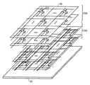
- FIG. 1A illustrates an example of a structure of the semiconductor device 11 of one embodiment of the present invention.
- the semiconductor device 11 includes a memory circuit 210, a memory circuit 220, a memory circuit 230, a memory circuit 240, and a control circuit 20 that constitute a memory device.
- the semiconductor device 11 includes an integrated circuit (eg, a CPU, a GPU, or the like), and the memory circuit 210 is included in the integrated circuit.
- the memory circuit 220 may be included in the integrated circuit.
- the memory circuit 220 can apply DOSRAM (Dynamic Oxide Semiconductor Random Access Memory) (registered trademark), and the memory circuit 230 can apply NOSRAM (Dynamic Oxide SemiconductorRandom registration). It can. Details of DOSRAM and NOSRAM will be described later.
- DOSRAM Dynamic Oxide Semiconductor Random Access Memory
- NOSRAM Dynamic Oxide SemiconductorRandom registration
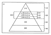
- FIG. 1B is an example of a memory circuit of the memory device included in the semiconductor device 11 illustrated in FIG.
- FIG. 1B is a diagram in which memory circuits of a memory device included in the semiconductor device 11 are hierarchized in order of access speed.
- the storage circuit 210 is shown as the highest hierarchy
- the storage circuit 220 is shown as a hierarchy below the storage circuit 210
- the storage circuit 230 is shown as a hierarchy below the storage circuit 220
- the storage circuit 240 is shown as the lowest hierarchy. .
- the memory circuit of the memory device included in the semiconductor device 11 includes the first memory area 110, the second memory area 120, the third memory area 130, and the fourth memory area in order from the highest hierarchy.
- the first storage area 110 is a storage area such as a register
- the second storage area 120 is a cache memory storage area
- the third storage area 130 is a main storage (main memory) storage area
- a fourth storage area. 140 is treated as a storage area of the auxiliary storage device.
- the storage circuit 210 in the first storage area 110 holds the result and state of arithmetic processing in an integrated circuit or the like. Therefore, the memory circuit 210 is electrically connected to the memory circuit 220 and the memory circuit 230 in order to transmit and receive data necessary for arithmetic processing.
- the storage circuit 210 applicable to the first storage area 110 includes, for example, a register, a flip-flop, an SRAM (Static Random Access Memory), and the like.
- the storage circuit 220 copies and stores a part of the data from the storage circuit 230 functioning as the main storage device which is the third storage area 130. Are electrically connected to the memory circuit 230.
- the second storage area 120 corresponds to the storage area of the cache memory
- the second storage area 120 can be further classified and provided in a plurality of hierarchies.
- FIG. 2 shows a case where the memory circuit 220 is further divided into three layers.
- the storage circuit 220 in FIG. 2 has storage areas of the cache 121 to the cache 123, and the cache 121 (primary cache, L1 cache) is provided in the lower hierarchy of the first storage area 110.
- a cache 122 (secondary cache, L2 cache) is provided in the hierarchy of FIG. 5, and a cache 123 (tertiary cache, L3 cache) is provided in the hierarchy lower than the cache 122.
- the number of layers in the second storage area 120 is not limited to this. That is, the second storage area 120 may be composed of only one layer, or may be composed of two layers, or four or more layers.
- the storage circuit 240 applicable to the fourth storage area 140 is electrically connected to the storage circuit 230 in order to store data input from the storage circuit 230 in the third storage area.
- a nonvolatile memory can be included.
- the non-volatile memory include a flash memory, a hard disk drive, and a solid state drive.
- the control circuit 20 is electrically connected to the memory circuit 220 and the memory circuit 230.
- the control circuit 20 has a function of changing the storage area of each layer of the second storage area 120 and the third storage area 130 in the semiconductor device 11.
- a storage device located in a lower hierarchy is required to have a large capacity and high density (or reduction in the area per bit).
- the first storage area 110 data used for calculation in an integrated circuit or the like is stored, so that a particularly high speed operation is required.
- the primary cache located in the highest hierarchy in the second storage area 120 is accessed most frequently, so that high speed operation is required.
- the secondary cache, the tertiary cache, and the like are not required to operate as fast as the primary cache, but are required to have a large capacity and a smaller area per bit than the primary cache.
- the number of data rewrites (or the number of refreshes) to the storage device increases, so that the data retention time can be shortened as a specification of the storage device.
- the number of data rewrites (or the number of refreshes) to the storage device decreases as the storage device is positioned at a lower level, it is necessary to increase the data retention time as the specification of the storage device. .
- One embodiment of the present invention increases or decreases the storage area of each layer by changing the data retention time of the storage device of each layer according to the usage state of the semiconductor device. That is, the storage device or the semiconductor device of one embodiment of the present invention can change the performance of each layer of the storage device in accordance with the usage situation.
- the low-level potential and the high-level potential used in the following description do not mean specific potentials, and the specific potential may be different if the wiring is different.
- the low level potential and the high level potential applied to the wiring WOL may be different from the low level potential and the high level potential applied to the wiring BIL.
- FIG. 3A shows an example of a circuit configuration of a DOSRAM memory cell.
- the memory cell 221 includes a transistor M1 and a capacitor element CA.
- the transistor M1 includes a front gate (sometimes simply referred to as a gate) and a back gate.
- the first terminal of the transistor M1 is connected to the first terminal of the capacitor CA, the second terminal of the transistor M1 is connected to the wiring BIL, the gate of the transistor M1 is connected to the wiring WOL, and the back gate of the transistor M1 Is connected to the wiring BGL.
- a second terminal of the capacitor element CA is connected to the wiring CAL.
- the transistor M1 functions as a write transistor in the memory cell 221.
- the writing transistor is preferably an OS transistor described later.
- the wiring BIL functions as a bit line
- the wiring WOL functions as a word line.
- the wiring CAL functions as a wiring for applying a predetermined potential to the second terminal of the capacitor CA. It is preferable to apply a low-level potential (sometimes referred to as a reference potential) to the wiring CAL during data writing and data reading.
- the wiring BGL functions as a wiring for applying a potential to the back gate of the transistor M1.
- the threshold voltage of the transistor M1 can be increased or decreased.
- Data writing and reading are performed by applying a high-level potential to the wiring WOL, turning on the transistor M1, and conducting between the wiring BIL and the first terminal of the capacitor CA.
- data is written by applying a potential corresponding to data to be written to the wiring BIL and writing the potential to the first terminal of the capacitor CA through the transistor M1.
- a low-level potential is applied to the wiring WOL so that the transistor M1 is turned off, so that the potential can be held in the memory cell 221.
- the wiring BIL is precharged to an appropriate potential, for example, an intermediate potential between a low level potential and a high level potential, and then the wiring BIL is electrically floated. After that, a high level potential is applied to the wiring WOL to turn on the transistor M1 and change the potential of the wiring BIL. Since the change in the potential of the wiring BIL is determined according to the potential written to the first terminal of the capacitor CA, data held in the memory cell 221 can be read from the changed potential of the wiring BIL.
- an appropriate potential for example, an intermediate potential between a low level potential and a high level potential
- a high level potential is applied to the wiring WOL to turn on the transistor M1 and change the potential of the wiring BIL. Since the change in the potential of the wiring BIL is determined according to the potential written to the first terminal of the capacitor CA, data held in the memory cell 221 can be read from the changed potential of the wiring BIL.
- the memory cell 221 described above is not limited to the circuit configuration illustrated in FIG. 3A, and the circuit configuration of the memory cell 221 may be changed as appropriate.
- FIG. 3 (B1) shows an example of the circuit configuration of a NOSRAM memory cell.
- the memory cell 231 includes a transistor M2, a transistor M3, and a capacitor CB.
- the transistor M2 includes a front gate (sometimes simply referred to as a gate) and a back gate.
- the transistor M2 functions as a write transistor in the memory cell 231.
- the writing transistor is preferably an OS transistor described later.
- the transistor M3 functions as a reading transistor in the memory cell 231.
- the read transistor is preferably an OS transistor described later or a transistor in which silicon is included in a semiconductor layer. Note that in this operation example, the transistor M3 operates in a saturation region unless otherwise specified. That is, it is assumed that the gate voltage, the source voltage, and the drain voltage of the transistor M3 are appropriately biased to voltages within a range where the transistor M3 operates in the saturation region.
- the first terminal of the transistor M2 is connected to the first terminal of the capacitor CB, the second terminal of the transistor M2 is connected to the wiring WBL, the gate of the transistor M2 is connected to the wiring WOL, and the back gate of the transistor M2 Is connected to the wiring BGL.
- a second terminal of the capacitor CB is connected to the wiring CAL.
- the first terminal of the transistor M3 is connected to the wiring RBL, the second terminal of the transistor M3 is connected to the wiring SL, and the gate of the transistor M3 is connected to the first terminal of the capacitor CB.
- the wiring WBL functions as a write bit line
- the wiring RBL functions as a read bit line
- the wiring WOL functions as a word line.
- the wiring CAL functions as a wiring for applying a predetermined potential to the second terminal of the capacitor CB. During data retention, it is preferable to apply a low level potential (sometimes referred to as a reference potential) to the wiring CAL. A high level potential is applied to the wiring CAL when data is written or read. Preferably applied
- the wiring BGL functions as a wiring for applying a potential to the back gate of the transistor M2.
- the threshold voltage of the transistor M2 can be increased or decreased.
- Data writing is performed by applying a high-level potential to the wiring WOL, turning on the transistor M2, and conducting between the wiring WBL and the first terminal of the capacitor CB. Specifically, when the transistor M2 is on, a potential corresponding to information recorded in the wiring WBL is applied, and the potential is written to the first terminal of the capacitor CB and the gate of the transistor M3. After that, by applying a low-level potential to the wiring WOL and turning off the transistor M2, the potential of the first terminal of the capacitor CB and the potential of the gate of the transistor M3 are held.
- Data reading is performed by applying a predetermined potential to the wiring SL. Since the current flowing between the source and drain of the transistor M3 and the potential of the first terminal of the transistor M3 are determined by the potential of the gate of the transistor M3 and the potential of the second terminal of the transistor M3, they are connected to the first terminal of the transistor M3. By reading the potential of the connected wiring RBL, the potential held in the first terminal of the capacitor CB (or the gate of the transistor M3) can be read. That is, information written in the memory cell can be read from the potential held at the first terminal of the capacitor CB (or the gate of the transistor M3).
- the memory cell 231 described above is not limited to the circuit configuration illustrated in FIG. 3B1, and the circuit configuration of the memory cell 231 may be changed as appropriate.
- the wiring WBL and the wiring RBL may be combined as a single wiring BIL.
- a circuit configuration example of the memory cell is illustrated in FIG.
- the memory cell 232 includes the wiring WBL and the wiring RBL of the memory cell 231 as one wiring BIL, and the second terminal of the transistor M2 and the first terminal of the transistor M3 are connected to the wiring BIL. . That is, the memory cell 232 has a configuration in which the write bit line and the read bit line operate as one wiring BIL.
- DOSRAM and NOSRAM are storage devices having OS transistors as write transistors, as described above.
- the semiconductor layer of the OS transistor includes a metal oxide described in Embodiment 3.
- the metal oxide for example, one or a plurality of materials selected from indium, element M (element M is aluminum, gallium, yttrium, or tin), and zinc can be used.
- the band gap of the semiconductor layer can be increased. Therefore, the off-state current of the OS transistor can be reduced.
- the OS transistor can have a back gate by applying the structure described in Embodiment 3.
- the threshold voltage of the OS transistor can be changed by applying a potential to the back gate.
- the threshold voltage of the OS transistor can be changed to the negative side by applying a positive potential to the back gate, and conversely, the negative potential is applied to the back gate.
- the threshold voltage of the OS transistor can be changed to the plus side.
- the off-state current of the OS transistor can be increased or decreased.
- the off-state current of the OS transistor is increased, the movement of the charge according to the data held between the source and the drain of the OS transistor is accelerated, so that the data holding time is shortened and the operating speed of the OS transistor is reduced. (Sometimes referred to as drive frequency).
- the off-state current of the OS transistor is reduced, the movement of charges according to the data held between the source and the drain of the OS transistor is slowed down, so that the data holding time becomes long, and the OS transistor The operating speed can be slowed down. That is, the data retention time and the operation speed can be adjusted by changing the threshold voltage of the OS transistor.
- the above-described DOSRAM is applied as the memory circuit 220 of the semiconductor device 11 and the above-described NOSRAM is applied as the memory circuit 230 is considered.
- the storage capacity of the storage circuit 210 used as the first storage area is insufficient, and the storage capacity of the storage circuit 220 used as the second storage area 120.
- the threshold voltage of the OS transistor included in the memory circuit 220a which is part of the memory circuit 220 is lowered, so that the data retention time of the memory circuit 220a is shortened.
- the storage circuit 220a can be used as the first storage area 110 by increasing the operation speed.
- the back gate of the transistor M1 includes, for example, ⁇
- the memory circuit 220 a can be used as the first memory area 110.
- the storage capacity of the storage circuit 230 used as the third storage area 130 is insufficient and the storage circuit 220 used as the second storage area 120 is used.
- the threshold voltage of the OS transistor included in the memory circuit 220b, which is part of the memory circuit 220 is increased to hold data in the memory circuit 220b, as shown in FIG.
- the storage circuit 220b can be used as the third storage area 130 by increasing the time and decreasing the operation speed.
- the back gate of the transistor M1 includes, for example, ⁇
- the memory circuit 220 a can be used as the third storage area 130.
- the storage circuit 220 when the storage area of the storage circuit 220 is not changed to another layer, that is, the storage circuit 220 is used as the second storage area 120 and is operated as usual.
- the range of the potential applied to the gate of the transistor M1 is set to ⁇ 0.8 V or more and 2.5 V or less, and for example, a voltage of ⁇ 4.5 V or more and less than ⁇ 1.5 V may be applied to the back gate of the transistor M1. .
- the storage capacity of the storage circuit 220 used as the second storage area 120 is insufficient, and the storage circuit 230 used as the third storage area 130. 4B, the threshold voltage of the OS transistor included in the memory circuit 230a which is a part of the memory circuit 230 is reduced so that the data in the memory circuit 230a is retained. By shortening the time, the memory circuit 230 a can be used as the second memory area 120.
- the back gate of the transistor M2 is used.
- the memory circuit 230 a can be used as the second memory area 120 by applying a voltage of ⁇ 4.5 V or more and less than ⁇ 1.5 V.
- the storage circuit 240 used as the fourth storage area 140 has insufficient storage capacity, and the storage circuit 230 used as the third storage area 130. 4B, the threshold voltage of the OS transistor included in the memory circuit 230b which is a part of the memory circuit 230 is increased so that the data in the memory circuit 230b is retained. By increasing the time, the storage circuit 230b can be used as the fourth storage area 140.
- the transistor M2 of the memory cell 231 (memory cell 232) of the memory circuit 230b is operated at a potential range of ⁇ 0.8 V or more and 2.5 V or less to the gate, the back gate of the transistor M2 is used.
- the memory circuit 230b can be used as the fourth memory area 140 by applying a voltage lower than ⁇ 7.5V.
- the storage circuit 230 when the storage area of the storage circuit 230 is not changed to another layer, that is, the storage circuit 230 is used as the third storage area 130 and is operated as usual.
- the range of the potential applied to the gate of the transistor M1 is set to ⁇ 0.8 V or more and 2.5 V or less, and for example, a voltage of ⁇ 7.5 V or more and less than ⁇ 4.5 V may be applied to the back gate of the transistor M1. .
- the voltage ranges applied to the gates of the transistor M1 of the memory cell 221 and the transistor M2 of the memory cell 231 can be made substantially the same.
- circuits that generate positive voltages (or negative voltages) to be applied to the gates of the transistors M1 and M2 can be the same circuit. Accordingly, it is not necessary to provide a large number of circuits for generating voltages to be applied to the gates of the transistors M1 and M2, and thus the power consumption of the semiconductor device 11 can be reduced.
- a negative voltage generation circuit for example, a negative voltage generation circuit for applying to the respective gates of the transistor M1 and the transistor M2) And charge pump circuits, etc.
- charge pump circuits, etc. are preferably used in common with each other.
- the range of the voltage applied to the gate and back gate of the transistor M1 (transistor M2) described above is an example.
- the characteristics of the transistor change depending on the material and structure of the semiconductor layer of the transistor included in the semiconductor device. Therefore, it is necessary to set a range of voltages applied to the gate and the back gate depending on the situation.
- transistor characteristics may change depending on the environment in which the semiconductor device is driven. Specifically, as the temperature of the environment in which the semiconductor device is driven increases, the drain current corresponding to the gate-source voltage of the transistor increases and the drive frequency of the transistor also increases. That is, depending on the temperature of the environment, the performance of the semiconductor device may change. Therefore, it is more preferable that the semiconductor device have a structure in which the characteristics of the transistor are appropriately adjusted by changing the voltage applied to the back gate of the OS transistor that is the writing transistor in accordance with the temperature of the environment.
- Each of 220 and the memory circuit 230 can perform an operation suitable for the temperature of the environment.
- FIG. 5 is a block diagram showing a control circuit 20 for controlling the threshold voltage of the write transistor. Note that FIG. 5 also illustrates the storage unit 30 including the storage circuit 220 and the storage circuit 230 in order to explain electrical connection with the storage device.
- the control circuit 20 includes a control unit 21, a voltage generation circuit 22 [1] to a voltage generation circuit 22 [P] (P is an integer of 1 or more), a circuit 23A, a circuit 23B, and a temperature detection circuit 25. And having. Note that in the case where the potential of the back gate is not changed according to the temperature of the environment, the control circuit 20 can be configured without the temperature detection circuit 25.
- the control unit 21 is electrically connected to the storage unit 30, the voltage generation circuit 22 [1] to the voltage generation circuit 22 [P], the circuit 23A, the circuit 23B, and the temperature detection circuit 25.
- Each of the voltage generation circuits 22 [1] to 22 [P] is electrically connected to the circuit 23A and the circuit 23B.
- the circuit 23A is electrically connected to the memory circuit 220 via a plurality of wirings BGL1, and the circuit 23B is electrically connected to the memory circuit 230 via a plurality of wirings BGL2.
- the storage unit 30 transmits to the control unit 21 a signal related to each usage state of the storage circuit 220 and the storage circuit 230 (for example, the ratio of the used storage capacity among all the storage capacities). It has a function.
- the control unit 21 receives the signal, and in accordance with the usage state, each level of the storage unit 30 (for example, the first storage area 110, the second storage area 120, and the third storage shown in FIG. 1B). In order to change the allocation of the area 130 and the fourth storage area 140), a signal is transmitted to each circuit included in the control circuit 20. Specifically, the control unit 21 transmits signals to the voltage generation circuits 22 [1] to 22 [P], the circuit 23A, and the circuit 23B.
- Each of the voltage generation circuits 22 [1] to 22 [P] has a function of generating a voltage to be applied to the back gate of the writing transistor. Further, the voltage generation circuit 22 [1] to the voltage generation circuit 22 [P] have a function of starting the generation of the voltage or stopping the generation of the voltage in accordance with a signal sent from the control unit 21. With this function, it is possible to drive only the voltage generation circuit that generates a necessary voltage in the allocation of each layer of the storage unit 30 and to stop the unnecessary voltage generation circuit. Therefore, only the necessary circuits among the voltage generation circuits 22 [1] to 22 [P] can be driven, and thus the power consumption of the control circuit 20 can be reduced.
- a circuit that generates a negative voltage can use, for example, a charge pump circuit.
- the circuit 23A has a function of selecting a voltage to be applied to each of the plurality of wirings BGL1 from voltages generated by the voltage generation circuits 22 [1] to 22 [P]. Note that which voltage is selected for each of the plurality of wirings BGL1 is determined according to a signal sent from the control unit 21. With this function, a predetermined voltage can be applied from the wiring BGL1 to the back gate of the writing transistor included in the memory circuit 220, and the memory circuit 220 can be divided into regions according to the layers to which the memory circuit 220 is assigned.
- the circuit 23A applies p kinds of voltages to the plurality of wirings BGL1, and the memory circuit 220 is increased to p. It can be divided into areas.
- the circuit 23B has a function of selecting a voltage to be applied to each of the plurality of wirings BGL2 from voltages generated by the voltage generation circuits 22 [1] to 22 [P]. Note that which voltage is selected for each of the plurality of wirings BGL ⁇ b> 2 is determined according to a signal sent from the control unit 21. With this function, a predetermined voltage can be applied from the wiring BGL ⁇ b> 2 to the back gate of the writing transistor included in the memory circuit 230, and the memory circuit 230 can be divided into regions according to the layers to which the memory circuit 230 is assigned.
- the entire storage capacity of the storage circuit 220 to which the second storage area 120 is allocated is used for data retention.
- the voltage generation circuit 22 [p1] (p1 is an integer greater than or equal to 1 and less than or equal to P) includes a write included in a memory cell used as the second storage region 120 among the memory cells of the storage circuit 220.
- a voltage to be applied to the back gate of the transistor is generated, and the voltage generation circuit 22 [p2] (p2 is an integer that is greater than or equal to 1 and less than or equal to P and is not p1) is a third storage area of the memory cells of the storage circuit 230 It is assumed that a voltage to be applied to the back gate of the write transistor included in the memory cell used as 130 is generated.
- the storage unit 30 determines that the storage capacity of the second storage area 120 is insufficient, the storage unit 30 uses all of the storage capacity of the storage circuit 220 and the storage capacity of the storage circuit 230 The fact that there is a vacancy is transmitted to the control unit 21 as a signal Sig1.
- the control unit 21 receives the signal and transmits the signal Sig2 to the voltage generation circuit 22 [1] to the voltage generation circuit 22 [P] and transmits the signal Sig3 to the circuit 23B.
- the signal Sig2 and the signal Sig3 are signals for allocating the second storage area 120 to the storage circuit 230.
- the signal Sig2 selects a circuit that generates a voltage to be applied to the back gate of the write transistor included in the area. It can be a signal.
- the voltage generation circuit 22 [p3] (p3 is an integer not less than 1 and not more than P and not p2) is selected as the circuit.
- the voltage generation circuit 22 [p3] may be the same as the voltage generation circuit 22 [p1] or may be a separate circuit.
- the voltage generation circuit that is not selected in the signal Sig2 can be configured to stop.
- the voltage generation circuit can be stopped by turning off electrical connection between the voltage generation circuit and a wiring for supplying a driving voltage by a switching element or the like. As a result, only the necessary voltage generation circuit can be driven, so that the power consumption of the control circuit 20 can be reduced.
- the signal Sig3 includes a signal including an instruction to apply the voltage generated by the voltage generation circuit 22 [p3] to BGL2 electrically connected to the back gate of the writing transistor in the predetermined region of the memory circuit 230. can do.
- the signal Sig3 may include a command for continuously applying the voltage generated by the voltage generation circuit 22 [p2] to the back gate of the write transistor included in the third storage region 130 of the storage circuit 230. .
- the voltage generated by the voltage generation circuit 22 [p3] can be supplied to the back gate of the write transistor in the area to which the second storage area 120 is newly allocated in the storage circuit 230. .
- the second storage area 120 can be allocated to a predetermined area of the storage circuit 230.
- the block diagram shown in FIG. 7 is a continuation of the block diagram shown in FIG. 6, and when the signal Sig3 is sent to the circuit 23B, the remaining storage capacity of the storage circuit 230 of the storage unit 30 is vacant. An example in which all of the above are assigned to the second storage area 120 is shown.
- the temperature detection circuit 25 can be configured as shown in FIG. 8 as an example.
- FIG. 8 also illustrates the control unit 21, the voltage generation circuit 22 [1], the voltage generation circuit 22 [P], the circuit 23A, and the wiring BGL1. Show. Note that the circuit 23B, the wiring BGL2, and the storage unit 30 are omitted.
- the temperature detection circuit 25 includes a temperature sensor 25a, an analog / digital conversion circuit 25b, and a voltage control circuit 25c.
- the temperature sensor 25a has a function of sensing the temperature around the semiconductor device 11 and outputting an analog signal corresponding to the temperature.
- the outputted analog signal is sent to the analog-digital conversion circuit 25b.
- a resistance temperature detector such as platinum, nickel, or copper, a thermistor, a thermocouple, an IC temperature sensor, or the like can be used.
- the analog-digital conversion circuit 25b has a function of converting an analog signal into a digital signal.
- the digital signal is sent to the voltage control circuit 25c.
- the voltage control circuit 25c has a function of generating a correction voltage according to the digital signal.
- the voltage control circuit 25c includes a storage device in which a correspondence table for associating digital signals and correction voltages is recorded, and a circuit that generates correction voltages. The height of the corresponding correction voltage is read out from the received digital signal. After reading out the height of the correction voltage, the correction voltage is generated by a circuit that generates the correction voltage, and is sent to the circuit 23A and the circuit 23B via the control unit 21. 5, 6, 7, and 8, the temperature detection circuit 25 is electrically connected to the control unit 21, but the temperature detection circuit 25 is directly connected to the circuit 23 ⁇ / b> A and the circuit 23 ⁇ / b> B. It may be connected to.
- the circuit 23A (circuit 23B) includes a plurality of capacitor elements CF, and one of the two pairs of electrodes of the plurality of capacitor elements CF is electrically connected to the plurality of wirings BGL1 (a plurality of wirings BGL2). It is assumed that The correction voltage sent to the circuit 23A (circuit 23B) is applied to the other of the two pairs of electrodes of the capacitive element CF.
- the circuit 23A (circuit 23B) has an internal circuit 23IN.
- the internal circuit 23IN receives a signal from the control unit 21, and in response to the signal, the internal circuit 23IN applies the voltage generation circuit 22 [1] to the voltage generation circuit 22 [P] to each of the plurality of wirings BGL1 (a plurality of wirings BGL2). It has a function of applying a plurality of generated voltages.
- the internal circuit 23IN applies a potential to the plurality of wirings BGL1 (a plurality of wirings BGL2), and then the two pairs of the capacitor elements A correction voltage is applied to the other electrode. Accordingly, the potentials of the plurality of wirings BGL1 (the plurality of wirings BGL2) vary according to the correction voltage due to the capacitive coupling of the capacitive elements CF connected thereto. As described above, since the semiconductor device 11 includes the temperature detection circuit 25, the characteristics of the write transistor of the storage unit 30 can be corrected in accordance with the temperature of the environment.
- Embodiment 2 In this embodiment, a configuration example of the memory cell array 40 and its peripheral circuits that constitute the DOSRAM, NOSRAM, and the like described in the above embodiment will be described.
- the memory cell array 40 and its peripheral circuits are collectively referred to as a storage device 200.
- FIG. 9 shows an example of the configuration of the storage device.
- the storage device 200 includes a peripheral circuit 50 and a memory cell array 40.
- the peripheral circuit 50 includes a row decoder 53, a word line driver circuit 51, a bit line driver circuit 52, an output circuit 54, and a control logic circuit 56.
- FIG. 9 also shows the control circuit 20 described in the first embodiment.
- the bit line driver circuit 52 includes a column decoder 52a, a precharge circuit 52b, a sense amplifier 52c, and a write circuit 52d.
- the precharge circuit 52b has a function of precharging the wiring SL, the wiring CAL, the wiring BIL, and the like.
- the sense amplifier 52c has a function of amplifying a data signal read from the wiring BIL and the wiring RBL. Note that the wiring SL, the wiring CAL, and the wiring RBL are wirings connected to the memory cells included in the memory cell array 40, and will be described in detail later.
- the amplified data signal is output to the outside of the storage device 200 as a digital data signal RDATA through the output circuit 54.
- the storage device 200 is supplied with a low power supply voltage (VSS), a high power supply voltage (VDD) for the peripheral circuit 50, and a high power supply voltage (VIL) for the memory cell array 40 as power supply voltages from the outside.
- VSS low power supply voltage
- VDD high power supply voltage
- VIL high power supply voltage
- control signals CE, WE, RE
- an address signal ADDR is input to the storage device 200 from the outside.
- the address signal ADDR is input to the row decoder 53 and the column decoder 52a, and WDATA is input to the write circuit 52d.
- the control logic circuit 56 processes external input signals (CE, WE, RE) to generate control signals for the row decoder 53 and the column decoder 52a.
- CE is a chip enable signal
- WE is a write enable signal
- RE is a read enable signal.
- the signal processed by the control logic circuit 56 is not limited to this, and other control signals may be input as necessary.
- each above-mentioned circuit or each signal can be suitably discarded as needed.
- the peripheral circuit 50 is composed of OS transistors. By doing so, the peripheral circuit 50 and the memory cell array 40 can be manufactured in the same manufacturing process, and the manufacturing cost of the memory device 200 can be kept low.
- FIG. 10 shows details of the memory cell array 40 when DOSRAM is applied as the memory cell.
- the memory cell array 40 has m ⁇ n memory cells 221 in total, where m (m is an integer of 1 or more) in a column and n (n is an integer of 1 or more) in a row.
- Memory cells 221 are arranged in a matrix.
- the address of the memory cell 221 is also shown, and [1,1], [m, 1], [i, j], [1, n], [m, n] (i is 1 is an integer from 1 to m, and j is an integer from 1 to n.)
- the memory cell is illustrated.
- the number of wirings WOL connecting the memory cell array 40 and the word line driver circuit 51 is m (in FIG. 10, wirings WOL [1], WOL [i], Only the wiring WOL [m] is shown), and the number of wirings BGL connecting the memory cell array 40 and the control circuit 20 is also m (in FIG. 10, the wiring BGL [1] and the wiring BGL [i] ], Only the wiring BGL [m] is shown. Further, the number of wirings BIL connecting the memory cell array 40 and the bit line driver circuit 52 is n (in FIG. 10, only the wiring BIL [1], the wiring BIL [j], and the wiring BIL [n] are illustrated. Is shown.)
- FIG. 11 shows details of the memory cell array 40 when NOSRAM is applied as the memory cell.
- the memory cell array 40 includes m (n is an integer equal to or greater than 1) m in one column and n (n is an integer equal to or greater than 1) in one row, a total of m ⁇ n memory cells 231.
- Memory cells 231 are arranged in a matrix. In FIG. 11, the address of the memory cell 231 is also shown, and [1,1], [m, 1], [i, j], [1, n], [m, n] (i is 1 is an integer from 1 to m, and j is an integer from 1 to n.) The memory cell is illustrated.
- the number of wirings WOL connecting the memory cell array 40 and the word line driver circuit 51 is m (in FIG. 11, the wirings WOL [1], WOL [i], Only the wiring WOL [m] is shown), and the number of wirings BGL connecting the memory cell array 40 and the control circuit 20 is also m (in FIG. 11, the wiring BGL [1] and the wiring BGL [i]. ], Only the wiring BGL [m] is shown. Note that although the number of wirings of the wiring CAL is m (in FIG. 11, only the wiring CAL [1], the wiring CAL [i], and the wiring CAL [m] are illustrated), the wiring CAL is used. Thus, the connection destination with the memory cell 231 is omitted.
- the number of wirings RBL, wirings WBL, and wirings SL that connect the memory cell array 40 and the bit line driver circuit 52 is n (in FIG. 11, wirings RBL [1] and RBL [j]). Only the wiring RBL [n], the wiring WBL [1], the wiring WBL [j], the wiring WBL [n], the wiring SL [1], the wiring SL [j], and the wiring SL [n] are illustrated.
- the regions of the layers of the memory device described in Embodiment 1 are provided. Changes are made on a line-by-line basis.
- the arrangement of the wiring BGL electrically connected to the back gate of the transistor M1 (transistor M2) of the memory cell 221 (memory cell 231) included in the memory cell array 40 is not limited to FIGS.
- a wiring BGL is provided for each of the transistors M1 (transistors M2) of the plurality of memory cells 221 (memory cells 231), and the region of each layer of the memory device is changed for each memory cell 221 (memory cell 231). Good.
- the memory cell 221 (memory cell 231) of the memory cell array 40 is divided into 2 ⁇ 2 and 2 ⁇ 3 regions, and different wirings BGL are provided for the respective regions, so that the regions of each layer of the memory device Changes may be made.
- the memory cell 221 and the memory cell 231 are arranged two-dimensionally. However, as shown in FIGS. It is good also as a structure arrange
- the wiring BIL provided in the memory cell array 40 is substantially perpendicular to the bit line driver circuit 52.
- the plurality of memory cell arrays 40 and the bit line driver circuit 52 are overlapped with each other.
- 12A and 12B illustrate the case of the memory cell 221, the memory cell 231 can be similarly arranged three-dimensionally.
- the bit line driver circuit 52 is illustrated in the lower layer. Instead of the bit line driver circuit 52, the word line driver circuit 51, the row decoder 53, or a plurality of these are selected and stacked. It may be a circuit.
- the circuit area can be reduced and the storage capacity can be increased.
- the memory cell array 40 shown in FIG. 10 is provided in a plurality, but the memory cell arrays 40 shown in FIGS. 10 and 11 are overlapped with each other as shown in FIG. It is good also as a structure. That is, the storage device 200 may have a configuration in which the DOSRAM and the NOSRAM overlap each other, that is, a configuration in which the storage circuit 220 and the storage circuit 230 overlap each other. In FIG. 13, the electrical connection between each memory cell array 40 and the bit line driver circuit 52 is omitted in order to clearly show the overlapping configuration. In FIG.
- the bit line driver circuit 52 is illustrated in the lower layer, but instead of the bit line driver circuit 52, a word line driver circuit 51, a row decoder 53, or a circuit in which a plurality of these are selected and stacked may be used. .
- a word line driver circuit 51 a word line driver circuit 51, a row decoder 53, or a circuit in which a plurality of these are selected and stacked may be used.
- the circuits can be shared with each other in the operations of the memory circuit 220 and the memory circuit 230.
- one embodiment of the present invention is not limited to the circuit structure described in this embodiment and can be changed as appropriate.
- the case where the memory cell 221 and the memory cell 231 are applied to the memory cell array 40 has been described, but another memory cell may be applied.
- a semiconductor device illustrated in FIG. 14 includes a transistor 300, a transistor 500, and a capacitor 600.
- 15A is a cross-sectional view of the transistor 500 in the channel length direction
- FIG. 15B is a cross-sectional view of the transistor 500 in the channel width direction
- FIG. 15C is a cross-sectional view of the transistor 300 in the channel width direction.
- the transistor 500 is a transistor (OS transistor) having a metal oxide in a channel formation region. Since the transistor 500 has a small off-state current, the transistor 500 can hold the first data for a long time by using it for a semiconductor device, particularly the transistor M2 of the memory cell 231. That is, since the frequency of the refresh operation is low or the refresh operation is not required, the power consumption of the semiconductor device can be reduced.
- OS transistor transistor having a metal oxide in a channel formation region. Since the transistor 500 has a small off-state current, the transistor 500 can hold the first data for a long time by using it for a semiconductor device, particularly the transistor M2 of the memory cell 231. That is, since the frequency of the refresh operation is low or the refresh operation is not required, the power consumption of the semiconductor device can be reduced.
- the transistor 500 is provided above the transistor 300, and the capacitor 600 is provided above the transistor 300 and the transistor 500. Note that the capacitor 600 can be the capacitor CB in the memory cell 231.
- the transistor 300 includes a conductor 316, an insulator 315, a semiconductor region 313 including a part of the substrate 311, a low resistance region 314a functioning as a source region or a drain region, and a low resistance region 314b. .
- the transistor 300 can be used, for example, as the transistor M3 in the above embodiment.
- the upper surface of the semiconductor region 313 and the side surface in the channel width direction are covered with a conductor 316 with an insulator 315 interposed therebetween.
- a conductor 316 with an insulator 315 interposed therebetween.
- the transistor 300 may be either a p-channel type or an n-channel type.
- the region in which the channel of the semiconductor region 313 is formed, the region in the vicinity thereof, the low resistance region 314a that serves as the source region or the drain region, the low resistance region 314b, and the like preferably include a semiconductor such as a silicon semiconductor. It preferably contains crystalline silicon. Alternatively, a material containing Ge (germanium), SiGe (silicon germanium), GaAs (gallium arsenide), GaAlAs (gallium aluminum arsenide), or the like may be used. A structure using silicon in which effective mass is controlled by applying stress to the crystal lattice and changing the lattice spacing may be employed. Alternatively, the transistor 300 may be a HEMT (High Electron Mobility Transistor) by using GaAs, GaAlAs, or the like.
- HEMT High Electron Mobility Transistor
- the low-resistance region 314a and the low-resistance region 314b provide an n-type conductivity element such as arsenic or phosphorus, or p-type conductivity such as boron, in addition to the semiconductor material used for the semiconductor region 313. Containing elements.
- the conductor 316 functioning as a gate electrode includes a semiconductor material such as silicon, a metal material, an alloy containing an element imparting n-type conductivity such as arsenic or phosphorus, or an element imparting p-type conductivity such as boron.
- a conductive material such as a material or a metal oxide material can be used.
- the threshold voltage of the transistor can be adjusted by selecting the material of the conductor. Specifically, it is preferable to use a material such as titanium nitride or tantalum nitride for the conductor. Further, in order to achieve both conductivity and embeddability, it is preferable to use a metal material such as tungsten or aluminum as a laminate for the conductor, and tungsten is particularly preferable from the viewpoint of heat resistance.
- the transistor 300 illustrated in FIGS. 14A and 14B is an example, and is not limited to the structure, and an appropriate transistor may be used depending on a circuit configuration or a driving method.
- the transistor 300 may have a structure similar to that of the transistor 500 including an oxide semiconductor (not illustrated). Note that details of the transistor 500 will be described later.
- An insulator 320, an insulator 322, an insulator 324, and an insulator 326 are stacked in this order so as to cover the transistor 300.
- the insulator 320, the insulator 322, the insulator 324, and the insulator 326 for example, silicon oxide, silicon oxynitride, silicon nitride oxide, silicon nitride, aluminum oxide, aluminum oxynitride, aluminum nitride oxide, aluminum nitride, or the like is used. That's fine.
- silicon oxynitride refers to a material having a higher oxygen content than nitrogen as its composition
- silicon nitride oxide refers to a material having a higher nitrogen content than oxygen as its composition.
- aluminum oxynitride refers to a material having a higher oxygen content than nitrogen as its composition
- aluminum nitride oxide refers to a material having a higher nitrogen content than oxygen as its composition.
- the insulator 322 may have a function as a planarization film for reducing a step generated by the transistor 300 or the like provided thereunder.
- the upper surface of the insulator 322 may be planarized by a planarization process using a chemical mechanical polishing (CMP) method or the like to improve planarity.
- CMP chemical mechanical polishing
- the insulator 324 is preferably formed using a film having a barrier property such that hydrogen and impurities do not diffuse from the substrate 311 or the transistor 300 into a region where the transistor 500 is provided.
- a film having a barrier property against hydrogen for example, silicon nitride formed by a CVD method can be used.
- silicon nitride formed by a CVD method when hydrogen diffuses into a semiconductor element including an oxide semiconductor such as the transistor 500, characteristics of the semiconductor element may be deteriorated. Therefore, a film for suppressing hydrogen diffusion is preferably used between the transistor 500 and the transistor 300.
- the film that suppresses the diffusion of hydrogen is a film with a small amount of hydrogen desorption.
- the amount of desorption of hydrogen can be analyzed using, for example, a temperature programmed desorption gas analysis method (TDS).
- TDS temperature programmed desorption gas analysis method
- the amount of hydrogen desorbed from the insulator 324 is calculated by converting the amount of desorption converted to hydrogen atoms per area of the insulator 324 in the range of the surface temperature of the film from 50 ° C. to 500 ° C. in TDS analysis. 10 ⁇ 10 15 atoms / cm 2 or less, preferably 5 ⁇ 10 15 atoms / cm 2 or less.
- the insulator 326 preferably has a lower relative dielectric constant than the insulator 324.
- the dielectric constant of the insulator 326 is preferably less than 4, and more preferably less than 3.
- the relative dielectric constant of the insulator 326 is preferably equal to or less than 0.7 times, more preferably equal to or less than 0.6 times that of the insulator 324.
- the insulator 320, the insulator 322, the insulator 324, and the insulator 326 are embedded with the capacitor 600 or the conductor 328 connected to the transistor 500, the conductor 330, and the like.
- the conductor 328 and the conductor 330 function as plugs or wirings.
- a conductor having a function as a plug or a wiring may be given the same reference numeral by collecting a plurality of structures.
- the wiring and the plug connected to the wiring may be integrated. That is, a part of the conductor may function as a wiring, and a part of the conductor may function as a plug.
- a conductive material such as a metal material, an alloy material, a metal nitride material, or a metal oxide material is used as a single layer or a stacked layer. be able to. It is preferable to use a high-melting-point material such as tungsten or molybdenum that has both heat resistance and conductivity, and it is particularly preferable to use tungsten. Or it is preferable to form with low resistance conductive materials, such as aluminum and copper. Wiring resistance can be lowered by using a low-resistance conductive material.
- a wiring layer may be provided over the insulator 326 and the conductor 330.
- an insulator 350, an insulator 352, and an insulator 354 are sequentially stacked.
- a conductor 356 is formed in the insulator 350, the insulator 352, and the insulator 354.
- the conductor 356 functions as a plug connected to the transistor 300 or a wiring. Note that the conductor 356 can be provided using a material similar to that of the conductor 328 and the conductor 330.
- the insulator 350 is preferably an insulator having a barrier property against hydrogen, similarly to the insulator 324.
- the conductor 356 preferably includes a conductor having a barrier property against hydrogen.
- a conductor having a barrier property against hydrogen is formed in an opening portion of the insulator 350 having a barrier property against hydrogen.
- tantalum nitride may be used as the conductor having a barrier property against hydrogen. Further, by stacking tantalum nitride and tungsten having high conductivity, diffusion of hydrogen from the transistor 300 can be suppressed while maintaining conductivity as a wiring. In this case, it is preferable that the tantalum nitride layer having a barrier property against hydrogen be in contact with the insulator 350 having a barrier property against hydrogen.
- a wiring layer may be provided over the insulator 354 and the conductor 356.
- an insulator 360, an insulator 362, and an insulator 364 are sequentially stacked.
- a conductor 366 is formed in the insulator 360, the insulator 362, and the insulator 364.
- the conductor 366 functions as a plug or a wiring. Note that the conductor 366 can be provided using a material similar to that of the conductor 328 and the conductor 330.
- an insulator having a barrier property against hydrogen is preferably used as the insulator 360.
- the conductor 366 preferably includes a conductor having a barrier property against hydrogen.
- a conductor having a barrier property against hydrogen is preferably formed in the opening of the insulator 360 having a barrier property against hydrogen.
- a wiring layer may be provided over the insulator 364 and the conductor 366.
- an insulator 370, an insulator 372, and an insulator 374 are sequentially stacked.
- a conductor 376 is formed in the insulator 370, the insulator 372, and the insulator 374.
- the conductor 376 functions as a plug or a wiring. Note that the conductor 376 can be provided using a material similar to that of the conductor 328 and the conductor 330.
- the insulator 370 is preferably an insulator having a barrier property against hydrogen, similarly to the insulator 324.
- the conductor 376 preferably includes a conductor having a barrier property against hydrogen.
- a conductor having a barrier property against hydrogen is preferably formed in the opening portion of the insulator 370 having a barrier property against hydrogen.
- a wiring layer may be provided over the insulator 374 and the conductor 376.
- an insulator 380, an insulator 382, and an insulator 384 are sequentially stacked.
- a conductor 386 is formed over the insulator 380, the insulator 382, and the insulator 384.
- the conductor 386 has a function as a plug or a wiring. Note that the conductor 386 can be provided using a material similar to that of the conductor 328 and the conductor 330.
- an insulator having a barrier property against hydrogen is preferably used as the insulator 380.
- the conductor 386 preferably includes a conductor having a barrier property against hydrogen.
- a conductor having a barrier property against hydrogen is preferably formed in the opening portion of the insulator 380 having a barrier property against hydrogen.
- the semiconductor device has been described above, the semiconductor device according to this embodiment It is not limited to this.
- the number of wiring layers similar to the wiring layer including the conductor 356 may be three or less, or the number of wiring layers similar to the wiring layer including the conductor 356 may be five or more.
- an insulator 510, an insulator 512, an insulator 514, and an insulator 516 are sequentially stacked.
- Any of the insulator 510, the insulator 512, the insulator 514, and the insulator 516 is preferably formed using a substance having a barrier property against oxygen or hydrogen.
- a film having a barrier property so that hydrogen and impurities do not diffuse from a region where the substrate 311 or the transistor 300 is provided to a region where the transistor 500 is provided for example.
- a material similar to that of the insulator 324 can be used.
- silicon nitride formed by a CVD method can be used as an example of a film having a barrier property against hydrogen.
- silicon nitride formed by a CVD method when hydrogen diffuses into a semiconductor element including an oxide semiconductor such as the transistor 500, characteristics of the semiconductor element may be deteriorated. Therefore, a film for suppressing hydrogen diffusion is preferably used between the transistor 500 and the transistor 300.
- the film that suppresses the diffusion of hydrogen is a film with a small amount of hydrogen desorption.
- a metal oxide such as aluminum oxide, hafnium oxide, or tantalum oxide is preferably used for the insulator 510 and the insulator 514.
- aluminum oxide has a high blocking effect that prevents the film from permeating both oxygen and impurities such as hydrogen and moisture, which cause fluctuations in the electrical characteristics of the transistor. Therefore, aluminum oxide can prevent impurities such as hydrogen and moisture from entering the transistor 500 during and after the manufacturing process of the transistor. In addition, release of oxygen from the oxide included in the transistor 500 can be suppressed. Therefore, it is suitable for use as a protective film for the transistor 500.
- the insulator 512 and the insulator 516 can be formed using the same material as the insulator 320.
- a material having a relatively low relative dielectric constant to these insulators, parasitic capacitance generated between wirings can be reduced.
- a silicon oxide film, a silicon oxynitride film, or the like can be used as the insulator 512 and the insulator 516.
- a conductor 518 In the insulator 510, the insulator 512, the insulator 514, and the insulator 516, a conductor 518, a conductor included in the transistor 500 (eg, the conductor 503), and the like are embedded. Note that the conductor 518 functions as a plug or a wiring connected to the capacitor 600 or the transistor 300.
- the conductor 518 can be provided using a material similar to that of the conductor 328 and the conductor 330.
- the insulator 510 and the conductor 518 in a region in contact with the insulator 514 are preferably conductors having a barrier property against oxygen, hydrogen, and water.
- the transistor 300 and the transistor 500 can be separated by a layer having a barrier property against oxygen, hydrogen, and water, and diffusion of hydrogen from the transistor 300 to the transistor 500 can be suppressed.
- a transistor 500 is provided above the insulator 516.
- the transistor 500 is provided over the insulator 514 and the insulator 516, and the conductor 503 which is embedded in the insulator 514 and the insulator 516.
- the insulator 544 is provided between the oxide 530a, the oxide 530b, the conductor 542a, the conductor 542b, and the insulator 580.
- a conductor 560 includes a conductor 560a provided inside the insulator 550 and a conductor provided so as to be embedded inside the conductor 560a. 560b.
- an insulator 574 is preferably provided over the insulator 580, the conductor 560, and the insulator 550.
- oxide 530a the oxide 530b, and the oxide 530c may be collectively referred to as an oxide 530.
- the transistor 500 a structure in which three layers of the oxide 530a, the oxide 530b, and the oxide 530c are stacked in the vicinity of the region where the channel is formed is described; however, the present invention is not limited thereto. It is not a thing. For example, a structure in which a single layer of the oxide 530b, a two-layer structure of the oxide 530b and the oxide 530a, a two-layer structure of the oxide 530b and the oxide 530c, or a stacked structure of four or more layers may be employed.
- the conductor 560 is illustrated as a two-layer structure; however, the present invention is not limited to this.
- the conductor 560 may have a single-layer structure or a stacked structure including three or more layers.
- the transistor 500 illustrated in FIGS. 14A, 14B, 15A, and 15B is an example and is not limited to the structure, and an appropriate transistor may be used depending on a circuit configuration or a driving method.
- the conductor 560 functions as a gate electrode of the transistor, and the conductor 542a and the conductor 542b function as a source electrode or a drain electrode, respectively.
- the conductor 560 is formed so as to be embedded in the opening of the insulator 580 and the region sandwiched between the conductors 542a and 542b.
- the arrangement of the conductor 560, the conductor 542a, and the conductor 542b is selected in a self-aligned manner with respect to the opening of the insulator 580. That is, in the transistor 500, the gate electrode can be disposed in a self-aligned manner between the source electrode and the drain electrode. Therefore, the conductor 560 can be formed without providing a margin for alignment, so that the area occupied by the transistor 500 can be reduced. Thereby, miniaturization and high integration of the semiconductor device can be achieved.
- the conductor 560 is formed in a self-aligned manner in a region between the conductors 542a and 542b, the conductor 560 does not have a region overlapping with the conductor 542a or the conductor 542b. Accordingly, parasitic capacitance formed between the conductor 560 and the conductors 542a and 542b can be reduced. Thus, the switching speed of the transistor 500 can be improved and high frequency characteristics can be obtained.
- the conductor 560 may function as a first gate (also referred to as a top gate) electrode.
- the conductor 503 may function as a second gate (also referred to as a bottom gate) electrode.
- the threshold voltage of the transistor 500 can be controlled by changing the potential applied to the conductor 503 independently of the potential applied to the conductor 560 without being linked.
- the threshold voltage of the transistor 500 can be higher than 0 V and the off-state current can be reduced. Therefore, when a negative potential is applied to the conductor 503, the drain current when the potential applied to the conductor 560 is 0 V can be made smaller than when a negative potential is not applied.
- the conductor 503 is disposed so as to overlap with the oxide 530 and the conductor 560. Accordingly, when a potential is applied to the conductor 560 and the conductor 503, the electric field generated from the conductor 560 and the electric field generated from the conductor 503 are connected to cover the channel formation region formed in the oxide 530. Can do.
- a transistor structure in which a channel formation region is electrically surrounded by an electric field of the first gate electrode and the second gate electrode is referred to as a surrounded channel (S-channel) structure.
- the conductor 503 has the same structure as that of the conductor 518, and a conductor 503a is formed in contact with the inner walls of the openings of the insulator 514 and the insulator 516, and a conductor 503b is further formed inside.
- the insulator 520, the insulator 522, the insulator 524, and the insulator 550 have a function as a gate insulating film.
- the insulator 524 in contact with the oxide 530 is preferably an insulator containing more oxygen than oxygen that satisfies the stoichiometric composition. That is, it is preferable that an excess oxygen region be formed in the insulator 524.
- an insulator containing excess oxygen in contact with the oxide 530 oxygen vacancies in the oxide 530 can be reduced and the reliability of the transistor 500 can be improved.
- an oxide material from which part of oxygen is released by heating is preferably used as the insulator having an excess oxygen region.
- the oxide that desorbs oxygen by heating means that the amount of desorbed oxygen in terms of oxygen atom is 1.0 ⁇ 10 18 atoms / cm 3 or more, preferably 1 in TDS (Thermal Desorption Spectroscopy) analysis.
- the oxide film has a thickness of 0.0 ⁇ 10 19 atoms / cm 3 or more, more preferably 2.0 ⁇ 10 19 atoms / cm 3 or more, or 3.0 ⁇ 10 20 atoms / cm 3 or more.
- the surface temperature of the film at the time of the TDS analysis is preferably in the range of 100 ° C. to 700 ° C., or 100 ° C. to 400 ° C.
- the insulator 522 preferably has a function of suppressing diffusion of oxygen (for example, oxygen atoms and oxygen molecules) (the oxygen hardly transmits).
- the insulator 522 have a function of suppressing diffusion of oxygen and impurities so that oxygen included in the oxide 530 does not diffuse to the insulator 520 side. Further, the conductor 503 can be prevented from reacting with the oxygen included in the insulator 524 and the oxide 530.
- the insulator 522 includes, for example, aluminum oxide, hafnium oxide, aluminum and an oxide containing hafnium (hafnium aluminate), tantalum oxide, zirconium oxide, lead zirconate titanate (PZT), strontium titanate (SrTiO 3 ), or An insulator containing a so-called high-k material such as (Ba, Sr) TiO 3 (BST) is preferably used in a single layer or a stacked layer. As transistor miniaturization and higher integration progress, problems such as leakage current may occur due to the thinning of the gate insulating film. By using a high-k material for the insulator functioning as a gate insulating film, the gate potential during transistor operation can be reduced while maintaining the physical film thickness.
- an insulator including one or both of oxides of aluminum and hafnium which is an insulating material having a function of suppressing diffusion of impurities and oxygen (the oxygen hardly transmits) may be used.
- the insulator containing one or both of aluminum and hafnium aluminum oxide, hafnium oxide, an oxide containing aluminum and hafnium (hafnium aluminate), or the like is preferably used.
- the insulator 522 is formed using such a material, the insulator 522 suppresses release of oxygen from the oxide 530 and entry of impurities such as hydrogen from the periphery of the transistor 500 to the oxide 530. Acts as a layer.
- aluminum oxide, bismuth oxide, germanium oxide, niobium oxide, silicon oxide, titanium oxide, tungsten oxide, yttrium oxide, or zirconium oxide may be added to these insulators.
- these insulators may be nitrided. Silicon insulator, silicon oxynitride, or silicon nitride may be stacked over the above insulator.
- the insulator 520 is preferably thermally stable.
- silicon oxide and silicon oxynitride are preferable because they are thermally stable.
- an insulator of a high-k material with silicon oxide or silicon oxynitride, an insulator 520 with a stacked structure that is thermally stable and has a high relative dielectric constant can be obtained.
- the insulator 520, the insulator 522, and the insulator 524 may have a stacked structure of two or more layers.
- the present invention is not limited to a laminated structure made of the same material, and may be a laminated structure made of different materials.
- the oxide 530 includes an In-M-Zn oxide (the element M is aluminum, gallium, yttrium, copper, vanadium, beryllium, boron, titanium, iron, nickel, germanium, zirconium, molybdenum, lanthanum, cerium, neodymium) It is preferable to use a metal oxide such as one or more selected from hafnium, tantalum, tungsten, or magnesium.
- the In-M-Zn oxide that can be used as the oxide 530 is preferably a CAAC-OS or a CAC-OS described in Embodiment 4.
- an In—Ga oxide or an In—Zn oxide may be used as the oxide 530.
- the metal oxide that functions as a channel formation region in the oxide 530 preferably has a band gap of 2 eV or more, preferably 2.5 eV or more. In this manner, off-state current of a transistor can be reduced by using a metal oxide having a large band gap.
- the oxide 530 includes the oxide 530a below the oxide 530b, diffusion of impurities from the structure formed below the oxide 530a to the oxide 530b can be suppressed. In addition, by including the oxide 530c over the oxide 530b, diffusion of impurities from the structure formed above the oxide 530c to the oxide 530b can be suppressed.
- the oxide 530 preferably has a stacked structure of oxides having different atomic ratios of metal atoms.
- the atomic ratio of the element M in the constituent element is larger than the atomic ratio of the element M in the constituent element in the metal oxide used for the oxide 530b. It is preferable.
- the atomic ratio of the element M to In is preferably larger than the atomic ratio of the element M to In in the metal oxide used for the oxide 530b.
- the atomic ratio of In to the element M is preferably larger than the atomic ratio of In to the element M in the metal oxide used for the oxide 530a.
- a metal oxide that can be used for the oxide 530a or the oxide 530b can be used.
- the energy at the lower end of the conduction band of the oxide 530a and the oxide 530c is higher than the energy at the lower end of the conduction band of the oxide 530b.
- the electron affinity of the oxide 530a and the oxide 530c is preferably smaller than the electron affinity of the oxide 530b.
- the energy level at the lower end of the conduction band changes gently.
- the energy level at the lower end of the conduction band at the junction of the oxide 530a, the oxide 530b, and the oxide 530c is continuously changed or continuously joined.
- the density of defect states in the mixed layer formed at the interface between the oxide 530a and the oxide 530b and the interface between the oxide 530b and the oxide 530c is preferably lowered.
- the oxide 530a and the oxide 530b, and the oxide 530b and the oxide 530c have a common element (main component) in addition to oxygen, so that a mixed layer with a low density of defect states is formed.
- the oxide 530b is an In—Ga—Zn oxide
- an In—Ga—Zn oxide, a Ga—Zn oxide, a gallium oxide, or the like may be used as the oxide 530a and the oxide 530c.
- the main path of the carrier is the oxide 530b.
- the oxide 530a and the oxide 530c have the above structures, the density of defect states at the interface between the oxide 530a and the oxide 530b and the interface between the oxide 530b and the oxide 530c can be reduced. Therefore, the influence on carrier conduction due to interface scattering is reduced, and the transistor 500 can obtain a high on-state current.
- a conductor 542a and a conductor 542b functioning as a source electrode and a drain electrode are provided over the oxide 530b.
- the conductor 542a and the conductor 542b aluminum, chromium, copper, silver, gold, platinum, tantalum, nickel, titanium, molybdenum, tungsten, hafnium, vanadium, niobium, manganese, magnesium, zirconium, beryllium, indium, ruthenium It is preferable to use a metal element selected from iridium, strontium, and lanthanum, an alloy containing the above-described metal element, or an alloy combining the above-described metal elements.
- a region 543a and a region 543b are formed as low resistance regions at and near the interface between the oxide 530 and the conductor 542a (conductor 542b). There is. At this time, the region 543a functions as one of a source region and a drain region, and the region 543b functions as the other of the source region and the drain region. In addition, a channel formation region is formed in a region between the region 543a and the region 543b.
- the oxygen concentration in the region 543a (region 543b) may be reduced in some cases.
- a metal compound layer including a metal contained in the conductor 542a (conductor 542b) and a component of the oxide 530 may be formed in the region 543a (region 543b). In such a case, the carrier concentration in the region 543a (region 543b) increases, and the region 543a (region 543b) becomes a low-resistance region.
- the insulator 544 is provided so as to cover the conductor 542a and the conductor 542b, and suppresses oxidation of the conductor 542a and the conductor 542b. At this time, the insulator 544 may be provided so as to cover a side surface of the oxide 530 and to be in contact with the insulator 524.
- a metal oxide containing one or more kinds selected from hafnium, aluminum, gallium, yttrium, zirconium, tungsten, titanium, tantalum, nickel, germanium, magnesium, and the like is used. it can.
- the insulator 544 it is preferable to use aluminum oxide, hafnium oxide, an oxide containing aluminum and hafnium (hafnium aluminate), which is an insulator containing one or both of aluminum and hafnium.
- hafnium aluminate has higher heat resistance than a hafnium oxide film. Therefore, it is preferable because it is difficult to crystallize in a heat treatment in a later step.
- the insulator 544 is not an essential component in the case where the conductors 542a and 542b are formed of a material having oxidation resistance or a material whose conductivity is not significantly reduced by absorbing oxygen. What is necessary is just to design suitably according to the transistor characteristic to request
- the insulator 550 functions as a gate insulating film.
- the insulator 550 is preferably provided in contact with the inside (upper surface and side surfaces) of the oxide 530c.
- the insulator 550 is preferably formed using an insulator that contains excess oxygen and from which oxygen is released by heating, like the insulator 524 described above.
- silicon oxide having excess oxygen silicon oxynitride, silicon nitride oxide, silicon nitride, silicon oxide to which fluorine is added, silicon oxide to which carbon is added, silicon oxide to which carbon and nitrogen are added, and voids Silicon oxide can be used.
- silicon oxide and silicon oxynitride are preferable because they are stable against heat.
- An insulator from which oxygen is released by heating is provided as the insulator 550 so as to be in contact with the top surface of the oxide 530c, so that oxygen can be effectively supplied from the insulator 550 to the channel formation region of the oxide 530b through the oxide 530c. Can be supplied.
- the concentration of impurities such as water or hydrogen in the insulator 550 is preferably reduced.
- the thickness of the insulator 550 is preferably greater than or equal to 1 nm and less than or equal to 20 nm.
- a metal oxide may be provided between the insulator 550 and the conductor 560 in order to efficiently supply excess oxygen included in the insulator 550 to the oxide 530.
- the metal oxide preferably suppresses oxygen diffusion from the insulator 550 to the conductor 560.
- diffusion of excess oxygen from the insulator 550 to the conductor 560 is suppressed. That is, a decrease in the amount of excess oxygen supplied to the oxide 530 can be suppressed. Further, oxidation of the conductor 560 due to excess oxygen can be suppressed.
- a material that can be used for the insulator 544 may be used.
- the conductor 560 functioning as the first gate electrode is illustrated as a two-layer structure in FIGS. 15A and 15B, but may have a single-layer structure or a stacked structure including three or more layers. .
- the conductor 560a has a function of suppressing diffusion of impurities such as a hydrogen atom, a hydrogen molecule, a water molecule, a nitrogen atom, a nitrogen molecule, a nitric oxide molecule (N 2 O, NO, NO 2, and the like) and a copper atom. It is preferable to use a material. Alternatively, a conductive material having a function of suppressing diffusion of oxygen (for example, at least one of oxygen atoms and oxygen molecules) is preferably used. When the conductor 560a has a function of suppressing the diffusion of oxygen, the conductivity of the conductor 560b can be suppressed from being oxidized by oxygen contained in the insulator 550 and thus reduced. For example, tantalum, tantalum nitride, ruthenium, or ruthenium oxide is preferably used as the conductive material having a function of suppressing oxygen diffusion.
- the conductor 560b is preferably formed using a conductive material containing tungsten, copper, or aluminum as a main component.
- the conductor 560b also functions as a wiring, and thus a conductor having high conductivity is preferably used.
- the conductor 560b may have a stacked structure, for example, a stacked structure of titanium, titanium nitride, and the above conductive material.
- the insulator 580 is provided over the conductor 542a and the conductor 542b with the insulator 544 provided therebetween.
- the insulator 580 preferably has an excess oxygen region.
- silicon oxide, silicon oxynitride, silicon nitride oxide, silicon nitride, silicon oxide to which fluorine is added, silicon oxide to which carbon is added, silicon oxide to which carbon and nitrogen are added, oxide having voids It is preferable to have silicon or resin.
- silicon oxide and silicon oxynitride are preferable because they are thermally stable.
- silicon oxide and silicon oxide having holes are preferable because an excess oxygen region can be easily formed in a later step.
- An insulator 580 that has an excess oxygen region and from which oxygen is released by heating is provided in contact with the oxide 530c, whereby oxygen in the insulator 580 can be supplied to the oxide 530a and the oxide 530b through the oxide 530c. Can be supplied efficiently. Note that the concentration of impurities such as water or hydrogen in the insulator 580 is preferably reduced.
- the opening of the insulator 580 is formed so as to overlap with a region between the conductor 542a and the conductor 542b.
- the conductor 560 is formed so as to be embedded in the opening of the insulator 580 and the region sandwiched between the conductors 542a and 542b.
- the conductor 560 can have a shape with a high aspect ratio.
- the conductor 560 since the conductor 560 is provided so as to be embedded in the opening of the insulator 580, the conductor 560 can be formed without collapsing during the process even when the conductor 560 has a high aspect ratio. Can do.
- the insulator 574 is preferably provided in contact with the upper surface of the insulator 580, the upper surface of the conductor 560, and the upper surface of the insulator 550.
- an excess oxygen region can be provided in the insulator 550 and the insulator 580. Accordingly, oxygen can be supplied into the oxide 530 from the excess oxygen region.
- a metal oxide containing one or more kinds selected from hafnium, aluminum, gallium, yttrium, zirconium, tungsten, titanium, tantalum, nickel, germanium, magnesium, and the like is used as the insulator 574. Can do.
- aluminum oxide has a high barrier property and can suppress diffusion of hydrogen and nitrogen even in a thin film of 0.5 nm to 3.0 nm. Therefore, aluminum oxide formed by a sputtering method can serve as an oxygen supply source and function as a barrier film for impurities such as hydrogen.
- an insulator 581 functioning as an interlayer film is preferably provided over the insulator 574.
- the insulator 581 preferably has reduced concentration of impurities such as water or hydrogen in the film.
- the conductor 540a and the conductor 540b are disposed in openings formed in the insulator 581, the insulator 574, the insulator 580, and the insulator 544.
- the conductors 540a and 540b are provided to face each other with the conductor 560 interposed therebetween.
- the conductor 540a and the conductor 540b have the same structure as a conductor 546 and a conductor 548 described later.
- An insulator 582 is provided on the insulator 581.
- the insulator 582 is preferably formed using a substance having a barrier property against oxygen or hydrogen. Therefore, the insulator 582 can be formed using a material similar to that of the insulator 514.
- the insulator 582 is preferably formed using a metal oxide such as aluminum oxide, hafnium oxide, or tantalum oxide.
- aluminum oxide has a high blocking effect that prevents the film from permeating both oxygen and impurities such as hydrogen and moisture, which cause fluctuations in the electrical characteristics of the transistor. Therefore, aluminum oxide can prevent impurities such as hydrogen and moisture from entering the transistor 500 during and after the manufacturing process of the transistor. In addition, release of oxygen from the oxide included in the transistor 500 can be suppressed. Therefore, it is suitable for use as a protective film for the transistor 500.
- an insulator 586 is provided on the insulator 582.
- the insulator 586 can be formed using a material similar to that of the insulator 320.
- parasitic capacitance generated between wirings can be reduced.
- a silicon oxide film, a silicon oxynitride film, or the like can be used as the insulator 586.
- the insulator 520, the insulator 522, the insulator 524, the insulator 544, the insulator 580, the insulator 574, the insulator 581, the insulator 582, and the insulator 586 include the conductor 546, the conductor 548, and the like. Is embedded.
- the conductor 546 and the conductor 548 function as a plug or a wiring connected to the capacitor 600, the transistor 500, or the transistor 300.
- the conductor 546 and the conductor 548 can be provided using a material similar to that of the conductor 328 and the conductor 330.
- the capacitor 600 includes a conductor 610, a conductor 620, and an insulator 630.
- the conductor 612 may be provided over the conductor 546 and the conductor 548.
- the conductor 612 functions as a plug connected to the transistor 500 or a wiring.
- the conductor 610 functions as an electrode of the capacitor 600. Note that the conductor 612 and the conductor 610 can be formed at the same time.
- the conductor 612 and the conductor 610 include a metal film containing an element selected from molybdenum, titanium, tantalum, tungsten, aluminum, copper, chromium, neodymium, and scandium, or a metal nitride film containing any of the above elements as a component (Tantalum nitride film, titanium nitride film, molybdenum nitride film, tungsten nitride film) or the like can be used.
- indium tin oxide indium oxide containing tungsten oxide, indium zinc oxide containing tungsten oxide, indium oxide containing titanium oxide, indium tin oxide containing titanium oxide, indium zinc oxide, silicon oxide added It is also possible to apply a conductive material such as indium tin oxide.
- the conductor 612 and the conductor 610 have a single-layer structure; however, the structure is not limited thereto, and a stacked structure of two or more layers may be used.
- a conductor having a high barrier property and a conductor having a high barrier property may be formed between a conductor having a barrier property and a conductor having a high conductivity.
- a conductor 620 is provided so as to overlap with the conductor 610 with the insulator 630 interposed therebetween.
- the conductor 620 can be formed using a conductive material such as a metal material, an alloy material, or a metal oxide material. It is preferable to use a high-melting-point material such as tungsten or molybdenum that has both heat resistance and conductivity, and it is particularly preferable to use tungsten. In the case of forming simultaneously with other structures such as a conductor, Cu (copper), Al (aluminum), or the like, which is a low resistance metal material, may be used.
- An insulator 650 is provided over the conductor 620 and the insulator 630.
- the insulator 650 can be provided using a material similar to that of the insulator 320.
- the insulator 650 may function as a planarization film that covers the concave and convex shapes below the insulator 650.
- the transistor 500 of the semiconductor device described in this embodiment is not limited to the above structure.
- structural examples that can be used for the transistor 500 will be described.
- the transistor described below is a modified example of the transistor described above. Therefore, in the following description, different points are mainly described, and the same points may be omitted.
- FIG. 16A is a top view of the transistor 500A.
- FIG. 16B is a cross-sectional view taken along dashed-dotted line L1-L2 in FIG.
- FIG. 16C is a cross-sectional view taken along dashed-dotted line W1-W2 in FIG. Note that in the top view of FIG. 16A, some elements are omitted for clarity.
- 16A, 16B, and 16C the transistor 500A, the insulator 511 functioning as an interlayer film, the insulator 512, the insulator 514, the insulator 516, the insulator 580, the insulator 574, and the insulator A body 581 is shown.
- 16A, 16B, and 16C illustrate a conductor 540a, a conductor 540b, and a conductor 505 which are electrically connected to the transistor 500A.
- the conductors 540a and 540b function as contact plugs
- the conductor 505 functions as a wiring.
- the transistor 500A includes a conductor 560 (a conductor 560a and a conductor 560b) that functions as a first gate electrode, a conductor 503 (a conductor 503a and a conductor 503b) that functions as a second gate electrode, An insulator 550 functioning as a first gate insulating film, an insulator 520 functioning as a second gate insulating film, an insulator 522, an insulator 524, and an oxide 530 having a region where a channel is formed (oxide) 530a, an oxide 530b, and an oxide 530c), a conductor 542a functioning as one of a source and a drain, a conductor 542b functioning as the other of a source and a drain, and an insulator 544.
- a conductor 560 a conductor 560a and a conductor 560b
- An insulator 550 functioning as a first gate insulating film
- an insulator 520 functioning as a second gate
- the oxide 530c, the insulator 550, and the conductor 560 are provided with the insulator 544 in an opening provided in the insulator 580. Arranged through. The oxide 530c, the insulator 550, and the conductor 560 are disposed between the conductor 542a and the conductor 542b.
- the insulator 511 and the insulator 512 function as an interlayer film.
- An insulator such as TiO 3 (BST) can be used in a single layer or a stacked layer.
- aluminum oxide, bismuth oxide, germanium oxide, niobium oxide, silicon oxide, titanium oxide, tungsten oxide, yttrium oxide, or zirconium oxide may be added to these insulators.
- these insulators may be nitrided. Silicon insulator, silicon oxynitride, or silicon nitride may be stacked over the above insulator.
- the insulator 511 preferably functions as a barrier film that suppresses impurities such as water or hydrogen from entering the transistor 500A from the substrate side. Therefore, the insulator 511 is preferably formed using an insulating material having a function of suppressing diffusion of impurities such as a hydrogen atom, a hydrogen molecule, a water molecule, and a copper atom (the impurity is difficult to transmit). Alternatively, it is preferable to use an insulating material having a function of suppressing the diffusion of oxygen (for example, at least one of oxygen atoms and oxygen molecules). For example, aluminum oxide, silicon nitride, or the like may be used as the insulator 511. With this structure, impurities such as hydrogen and water can be prevented from diffusing from the substrate side to the transistor 500A side with respect to the insulator 511.
- the insulator 512 preferably has a lower relative dielectric constant than the insulator 511.
- a material having a low relative dielectric constant as the interlayer film, it is possible to reduce the parasitic capacitance generated between the wirings.
- the conductor 505 is formed so as to be embedded in the insulator 512.
- the height of the upper surface of the conductor 505 and the height of the upper surface of the insulator 512 can be approximately the same.
- the conductor 505 has a single-layer structure, the present invention is not limited to this.
- the conductor 505 may have a multilayer film structure including two or more layers.
- the conductor 505 is preferably formed using a highly conductive material whose main component is tungsten, copper, or aluminum.
- the conductor 560 may function as a first gate (also referred to as a top gate) electrode.
- the conductor 503 may function as a second gate (also referred to as a bottom gate) electrode.
- the threshold voltage of the transistor 500A can be controlled by independently changing the potential applied to the conductor 503 without being linked to the potential applied to the conductor 560.
- the threshold voltage of the transistor 500A can be higher than 0 V and the off-state current can be reduced. Therefore, when a negative potential is applied to the conductor 503, the drain current when the potential applied to the conductor 560 is 0 V can be made smaller than when a negative potential is not applied.
- the conductor 560 and the conductor 503 when a potential is applied to the conductor 560 and the conductor 503 by overlapping the conductor 503 and the conductor 560, an electric field generated from the conductor 560 and an electric field generated from the conductor 503 are used. And the channel formation region formed in the oxide 530 can be covered.
- the channel formation region can be electrically surrounded by the electric field of the conductor 560 functioning as the first gate electrode and the electric field of the conductor 503 functioning as the second gate electrode.
- a transistor structure that electrically surrounds a channel formation region by an electric field of the first gate electrode and the second gate electrode is referred to as a surrounded channel (S-channel) structure.
- the insulator 514 and the insulator 516 function as interlayer films similarly to the insulator 511 or the insulator 512.
- the insulator 514 preferably functions as a barrier film that prevents impurities such as water or hydrogen from entering the transistor 500A from the substrate side. With this structure, diffusion of impurities such as hydrogen and water from the substrate side to the transistor 500A side than the insulator 514 can be suppressed.
- the insulator 516 preferably has a lower relative dielectric constant than the insulator 514. By using a material having a low relative dielectric constant as the interlayer film, it is possible to reduce the parasitic capacitance generated between the wirings.
- the conductor 503 functioning as the second gate, the conductor 503a is formed in contact with the inner walls of the openings of the insulator 514 and the insulator 516, and the conductor 503b is further formed inside.
- the height of the upper surfaces of the conductors 503a and 503b and the height of the upper surface of the insulator 516 can be approximately the same.
- the transistor 500A illustrates a structure in which the conductors 503a and 503b are stacked, the present invention is not limited thereto.
- the conductor 503 may be provided as a single layer or a stacked structure including three or more layers.
- the conductor 503a is preferably formed using a conductive material having a function of suppressing diffusion of impurities such as hydrogen atoms, hydrogen molecules, water molecules, and copper atoms (the impurities are difficult to permeate).
- a conductive material having a function of suppressing diffusion of oxygen for example, at least one of an oxygen atom and an oxygen molecule
- the oxygen hardly transmits.
- the function of suppressing diffusion of impurities or oxygen is a function of suppressing diffusion of any one or all of the impurities and oxygen.
- the conductor 503a since the conductor 503a has a function of suppressing the diffusion of oxygen, it can be suppressed that the conductor 503b is oxidized and the conductivity is lowered.
- the conductor 503b is preferably formed using a highly conductive material mainly containing tungsten, copper, or aluminum. In that case, the conductor 505 is not necessarily provided. Note that although the conductor 503b is illustrated as a single layer, it may have a stacked structure, for example, a stack of titanium, titanium nitride, and the above conductive material.
- the insulator 522 functioning as the second gate insulating film preferably has a barrier property.
- the insulator 522 functions as a layer that suppresses entry of impurities such as hydrogen from the peripheral portion of the transistor 500A to the transistor 500A.
- FIGS. 16B and 16C illustrate a three-layer structure as the second gate insulating film, a single-layer structure, a two-layer structure, or a four-layer structure or more may be used. In that case, the present invention is not limited to a laminated structure made of the same material, and may be a laminated structure made of different materials.
- the oxide 530 having a region functioning as a channel formation region includes an oxide 530a, an oxide 530b over the oxide 530a, and an oxide 530c over the oxide 530b.
- an oxide 530a below the oxide 530b, diffusion of impurities from the structure formed below the oxide 530a to the oxide 530b can be suppressed.
- the oxide 530c over the oxide 530b, diffusion of impurities from the structure formed above the oxide 530c to the oxide 530b can be suppressed.
- the oxide 530 an oxide semiconductor which is a kind of the metal oxide described above can be used.
- the oxide 530 c is preferably provided in the opening provided in the insulator 580 through the insulator 544. In the case where the insulator 544 has barrier properties, diffusion of impurities from the insulator 580 into the oxide 530 can be suppressed.
- the conductor 542a functioning as one of the source electrode or the drain electrode and the conductor 542b functioning as the other of the source electrode or the drain electrode are aluminum, titanium, chromium, nickel, copper, yttrium, zirconium, molybdenum, silver, and tantalum.
- a metal such as tungsten or an alloy containing the same as a main component can be used.
- a metal nitride film such as tantalum nitride is preferable because it has a barrier property against hydrogen or oxygen and has high oxidation resistance.
- a stacked structure of two or more layers may be used.
- a tantalum nitride film and a tungsten film are preferably stacked.
- a titanium film and an aluminum film may be stacked.
- a two-layer structure in which an aluminum film is stacked on a tungsten film a two-layer structure in which a copper film is stacked on a copper-magnesium-aluminum alloy film, a two-layer structure in which a copper film is stacked on a titanium film, and a tungsten film
- a two-layer structure in which copper films are stacked may be used.
- a titanium film or a titanium nitride film and a three-layer structure in which an aluminum film or a copper film is laminated on the titanium film or the titanium nitride film, and a titanium film or a titanium nitride film is further formed thereon, a molybdenum film or
- a transparent conductive material containing indium oxide, tin oxide, or zinc oxide may be used.
- a barrier layer may be provided over the conductor 542a and the conductor 542b.
- a substance having a barrier property against oxygen or hydrogen is preferably used. With this structure, oxidation of the conductors 542a and 542b can be suppressed when the insulator 544 is formed.
- a metal oxide for example, a metal oxide can be used.
- an insulating film having a barrier property against oxygen and hydrogen such as aluminum oxide, hafnium oxide, and gallium oxide, is preferably used.
- silicon nitride formed by a CVD method may be used.
- the material selection range of the conductor 542a and the conductor 542b can be widened.
- the conductor 542a and the conductor 542b can be formed using a material having low conductivity but high conductivity such as tungsten or aluminum.
- a conductor that can be easily formed or processed can be used.
- the insulator 550 functions as a first gate insulating film.
- the insulator 550 is preferably provided in the opening provided in the insulator 580 through the oxide 530c and the insulator 544.
- the insulator 550 may have a stacked layer structure like the second gate insulating film.
- the insulator that functions as a gate insulating film has a stacked structure of a high-k material and a thermally stable material, so that the gate potential during transistor operation can be reduced while maintaining the physical film thickness. It becomes. Moreover, it can be set as the laminated structure which is thermally stable and a high dielectric constant.
- the conductor 560 functioning as the first gate electrode includes a conductor 560a and a conductor 560b over the conductor 560a.
- the conductor 560a is preferably formed using a conductive material having a function of suppressing diffusion of impurities such as a hydrogen atom, a hydrogen molecule, a water molecule, and a copper atom, like the conductor 503a.
- a conductive material having a function of suppressing diffusion of oxygen for example, at least one of oxygen atoms and oxygen molecules is preferably used.
- the conductor 560a has a function of suppressing the diffusion of oxygen, the material selectivity of the conductor 560b can be improved. That is, by including the conductor 560a, oxidation of the conductor 560b can be suppressed and reduction in conductivity can be prevented.
- the conductive material having a function of suppressing oxygen diffusion for example, tantalum, tantalum nitride, ruthenium, or ruthenium oxide is preferably used.
- the conductor 560a an oxide semiconductor that can be used as the oxide 530 can be used. In that case, by forming the conductor 560b by a sputtering method, the electrical resistance value of the conductor 560a can be reduced to obtain a conductor. This can be called an OC (Oxide Conductor) electrode.
- the conductive material 560b is preferably formed using a conductive material mainly containing tungsten, copper, or aluminum. In addition, since the conductor 560 functions as a wiring, a conductor having high conductivity is preferably used.
- the conductor 560b may have a stacked structure, for example, a stack of titanium, titanium nitride, and the above conductive material.
- An insulator 544 is provided between the insulator 580 and the transistor 500A.
- an insulating material having a function of suppressing diffusion of impurities such as water or hydrogen and oxygen is preferably used.
- aluminum oxide or hafnium oxide is preferably used.
- metal oxide such as magnesium oxide, gallium oxide, germanium oxide, yttrium oxide, zirconium oxide, lanthanum oxide, neodymium oxide, or tantalum oxide, silicon nitride oxide, silicon nitride, or the like can be used.
- the insulator 544 By including the insulator 544, it is possible to suppress diffusion of impurities such as water and hydrogen contained in the insulator 580 into the oxide 530b through the oxide 530c and the insulator 550. Further, the conductor 560 can be prevented from being oxidized by excess oxygen which the insulator 580 has.
- the insulator 580, the insulator 574, and the insulator 581 function as an interlayer film.
- the insulator 574 preferably functions as a barrier insulating film that suppresses entry of impurities such as water or hydrogen into the transistor 500A from the outside.
- the insulator 580 and the insulator 581 preferably have a lower relative dielectric constant than the insulator 574, like the insulator 516.
- a material having a low relative dielectric constant as the interlayer film it is possible to reduce the parasitic capacitance generated between the wirings.
- the transistor 500A may be electrically connected to another structure through a plug or a wiring of the insulator 580, the insulator 574, and the conductor 540a and the conductor 540b embedded in the insulator 581. .
- a conductive material such as a metal material, an alloy material, a metal nitride material, or a metal oxide material is used as a single layer or a stacked layer.
- a high melting point material such as tungsten or molybdenum that has both heat resistance and conductivity.
- low resistance conductive materials such as aluminum and copper. Wiring resistance can be lowered by using a low-resistance conductive material.
- the conductor 540a and the conductor 540b for example, a stacked structure of tantalum nitride, which is a conductor having a barrier property against hydrogen and oxygen, and tungsten having high conductivity can be used. The diffusion of impurities from the outside can be suppressed while maintaining the electrical conductivity as described above.
- a semiconductor device including a transistor including an oxide semiconductor with high on-state current can be provided.
- a semiconductor device including a transistor including an oxide semiconductor with low off-state current can be provided.
- FIG. 17A is a top view of the transistor 500B.
- FIG. 17B is a cross-sectional view taken along dashed-dotted line L1-L2 in FIG.
- FIG. 17C is a cross-sectional view taken along dashed-dotted line W1-W2 in FIG. Note that in the top view of FIG. 17A, some elements are omitted for clarity.
- Transistor 500B is a modification of transistor 500A. Therefore, in order to prevent repeated description, differences from the transistor 500A are mainly described.
- the transistor 500B includes a region where the conductor 542a (conductor 542b), the oxide 530c, the insulator 550, and the conductor 560 overlap with each other. With such a structure, a transistor with high on-state current can be provided. In addition, a transistor with high controllability can be provided.
- the conductor 560 functioning as the first gate electrode includes a conductor 560a and a conductor 560b over the conductor 560a.
- the conductor 560a is preferably formed using a conductive material having a function of suppressing diffusion of impurities such as a hydrogen atom, a hydrogen molecule, a water molecule, and a copper atom, like the conductor 503a.
- a conductive material having a function of suppressing diffusion of oxygen for example, at least one of oxygen atoms and oxygen molecules is preferably used.
- the conductor 560a has a function of suppressing the diffusion of oxygen, the material selectivity of the conductor 560b can be improved. That is, by including the conductor 560a, oxidation of the conductor 560b can be suppressed and reduction in conductivity can be prevented.
- the insulator 544 is preferably provided so as to cover the top surface and the side surface of the conductor 560, the side surface of the insulator 550, and the side surface of the oxide 530c.
- the insulator 544 is preferably formed using an insulating material having a function of suppressing diffusion of impurities such as water or hydrogen and oxygen.
- aluminum oxide or hafnium oxide is preferably used.
- metal oxide such as magnesium oxide, gallium oxide, germanium oxide, yttrium oxide, zirconium oxide, lanthanum oxide, neodymium oxide, or tantalum oxide, silicon nitride oxide, silicon nitride, or the like can be used.
- oxidation of the conductor 560 can be suppressed.
- diffusion of water and impurities such as hydrogen included in the insulator 580 into the transistor 500B can be suppressed.
- the contact plug of the transistor 500B is different from the configuration of the contact plug of the transistor 500A.
- an insulator 576a (insulator 576b) having a barrier property is provided between the conductor 546a (conductor 546b) functioning as a contact plug and the insulator 580.
- oxygen in the insulator 580 can be prevented from reacting with the conductor 546 and the conductor 546 being oxidized.
- insulator 576a (insulator 576b) having a barrier property
- the range of selection of materials for conductors used for plugs and wirings can be widened.
- a low power consumption semiconductor device can be provided by using a metal material having high conductivity while absorbing oxygen for the conductor 546a (conductor 546b).
- a material having high conductivity while having low oxidation resistance such as tungsten or aluminum can be used.
- a conductor that can be easily formed or processed can be used.
- FIG. 18A is a top view of the transistor 500C.
- FIG. 18B is a cross-sectional view taken along dashed-dotted line L1-L2 in FIG.
- FIG. 18C is a cross-sectional view taken along dashed-dotted line W1-W2 in FIG. Note that in the top view of FIG. 18A, some elements are omitted for clarity.
- the transistor 500C is a modification of the transistor 500A. Therefore, in order to prevent repeated description, differences from the transistor 500A are mainly described.
- the conductor 547a is provided between the conductor 542a and the oxide 530b
- the conductor 547b is provided between the conductor 542b and the oxide 530b.
- the conductor 542a extends beyond the top surface of the conductor 547a (conductor 547b) and the side surface on the conductor 560 side, and has a region in contact with the top surface of the oxide 530b.
- a conductor that can be used for the conductor 542a and the conductor 542b may be used as the conductor 547a and the conductor 547b.
- the conductors 547a and 547b are preferably thicker than the conductors 542a and 542b.
- the transistor 500C illustrated in FIGS. 18A, 18B, and 18C has the above structure; thus, the conductor 542a and the conductor 542b can be closer to the conductor 560 than the transistor 500A. it can. Alternatively, the conductor 560 can overlap the end portion of the conductor 542a and the end portion of the conductor 542b. Accordingly, the substantial channel length of the transistor 500C can be shortened, and the on-current and the frequency characteristics can be improved.
- the conductor 547a (conductor 547b) is preferably provided so as to overlap with the conductor 542a (conductor 542b).
- the conductor 547a (conductor 547b) functions as a stopper, and the oxide 530b is over-etched. Can be prevented.
- the transistor 500C illustrated in FIGS. 18A, 18B, and 18C may have a structure in which the insulator 545 is provided in contact with the insulator 544.
- the insulator 544 preferably functions as a barrier insulating film which suppresses entry of impurities such as water or hydrogen and excess oxygen into the transistor 500C from the insulator 580 side.
- an insulator that can be used for the insulator 544 can be used.
- a nitride insulator such as aluminum nitride, aluminum titanium nitride, titanium nitride, silicon nitride, or silicon nitride oxide may be used.
- the transistor 500C illustrated in FIGS. 18A to 18C is provided with a conductor 503 with a single-layer structure. May be.
- an insulating film to be the insulator 516 is formed over the patterned conductor 503, and the upper portion of the insulating film is removed by a CMP method or the like until the upper surface of the conductor 503 is exposed.
- the flatness of the upper surface of the conductor 503 is preferably improved.
- the average surface roughness (Ra) of the upper surface of the conductor 503 may be 1 nm or less, preferably 0.5 nm or less, more preferably 0.3 nm or less. Accordingly, the flatness of the insulating layer formed over the conductor 503 can be improved, and the crystallinity of the oxide 530b and the oxide 530c can be improved.
- FIG. 19A is a top view of the transistor 500D.
- FIG. 19B is a cross-sectional view taken along dashed-dotted line L1-L2 in FIG.
- FIG. 19C is a cross-sectional view taken along dashed-dotted line W1-W2 in FIG. Note that in the top view of FIG. 19A, some elements are omitted for clarity.
- the transistor 500D has a different structure from the transistors 500A, 500B, and 500C. Therefore, in order to prevent the description from being repeated, description of the points that overlap mainly with the transistors 500A, 500B, and 500C will be omitted, and different points will be mainly described.
- the transistor 500D illustrated in FIGS. 19A to 19C does not include the conductor 505 and serves as a second gate.
- the conductor 503 having the above function is also functioned as a wiring.
- the insulator 550 is provided over the oxide 530c, and the metal oxide 552 is provided over the insulator 550.
- the conductor 560 is provided over the metal oxide 552 and the insulator 570 is provided over the conductor 560.
- the insulator 571 is provided over the insulator 570.
- the metal oxide 552 preferably has a function of suppressing oxygen diffusion.
- the metal oxide 552 that suppresses diffusion of oxygen between the insulator 550 and the conductor 560 diffusion of oxygen into the conductor 560 is suppressed. That is, a decrease in the amount of oxygen supplied to the oxide 530 can be suppressed. Further, oxidation of the conductor 560 due to oxygen can be suppressed.
- the metal oxide 552 may function as a part of the first gate.
- an oxide semiconductor that can be used as the oxide 530 can be used as the metal oxide 552.
- the conductor 560 by forming the conductor 560 by a sputtering method, the electric resistance value of the metal oxide 552 can be reduced to form a conductive layer. This can be called an OC (Oxide Conductor) electrode.
- the metal oxide 552 may function as a part of the gate insulating film. Therefore, in the case where silicon oxide, silicon oxynitride, or the like is used for the insulator 550, the metal oxide 552 is preferably a metal oxide that is a high-k material with a high relative dielectric constant. By setting it as the said laminated structure, it can be set as the laminated structure stable with respect to a heat
- EOT equivalent oxide thickness
- the metal oxide 552 is illustrated as a single layer; however, a stacked structure including two or more layers may be used.
- a metal oxide that functions as part of the gate electrode and a metal oxide that functions as part of the gate insulating film may be stacked.
- the on-state current of the transistor 500D can be improved without weakening the influence of the electric field from the conductor 560.
- the distance between the conductor 560 and the oxide 530 is maintained by the physical thickness of the insulator 550 and the metal oxide 552, so that the conductor 560 Leakage current with the oxide 530 can be suppressed. Therefore, by providing a stacked structure of the insulator 550 and the metal oxide 552, the physical distance between the conductor 560 and the oxide 530 and the electric field strength applied from the conductor 560 to the oxide 530 can be reduced. It can be easily adjusted as appropriate.
- an oxide semiconductor that can be used for the oxide 530 can be used as the metal oxide 552 by reducing resistance.
- a metal oxide containing one or more selected from hafnium, aluminum, gallium, yttrium, zirconium, tungsten, titanium, tantalum, nickel, germanium, magnesium, and the like can be used.
- hafnium oxide an oxide containing aluminum and hafnium (hafnium aluminate), which is an insulating layer containing one or both of aluminum and hafnium.
- hafnium aluminate has higher heat resistance than a hafnium oxide film. Therefore, it is preferable because it is difficult to crystallize in a heat treatment in a later step.
- the metal oxide 552 is not an essential component. What is necessary is just to design suitably according to the transistor characteristic to request
- an insulating material having a function of suppressing permeation of impurities such as water or hydrogen and oxygen may be used.
- impurities such as water or hydrogen and oxygen
- aluminum oxide or hafnium oxide is preferably used.
- impurities such as water or hydrogen from above the insulator 570 can be prevented from entering the oxide 530 through the conductor 560 and the insulator 550.
- the insulator 571 functions as a hard mask.
- the side surface of the conductor 560 is substantially vertical.
- the angle formed between the side surface of the conductor 560 and the substrate surface is 75 ° to 100 °, Preferably, it can be set to 80 degrees or more and 95 degrees or less.
- the insulator 571 may also function as a barrier layer by using an insulating material having a function of suppressing permeation of impurities such as water or hydrogen and oxygen. In that case, the insulator 570 is not necessarily provided.
- insulator 571 By using the insulator 571 as a hard mask, a part of the insulator 570, the conductor 560, the metal oxide 552, the insulator 550, and the oxide 530c is selectively removed, so that these side surfaces are substantially matched. In addition, a part of the surface of the oxide 530b can be exposed.
- the transistor 500D includes a region 531a and a region 531b in part of the exposed surface of the oxide 530b.
- One of the region 531a and the region 531b functions as a source region, and the other functions as a drain region.
- the formation of the region 531a and the region 531b is performed by introducing an impurity element such as phosphorus or boron into the exposed oxide 530b surface by using, for example, an ion implantation method, an ion doping method, a plasma immersion ion implantation method, or a plasma treatment. This can be achieved.
- an impurity element such as phosphorus or boron
- an ion implantation method an ion doping method
- a plasma immersion ion implantation method or a plasma treatment.
- the “impurity element” in this embodiment and the like refers to an element other than the main component elements.
- a metal film is formed after part of the surface of the oxide 530b is exposed, and then heat treatment is performed, whereby an element included in the metal film is diffused into the oxide 530b to form the region 531a and the region 531b.
- the region 531a and the region 531b may be referred to as “impurity region” or “low resistance region”.
- the region 531a and the region 531b can be formed in a self-alignment manner. Therefore, the region 531a and / or the region 531b does not overlap with the conductor 560, so that parasitic capacitance can be reduced. Further, no offset region is formed between the channel formation region and the source / drain region (the region 531a or the region 531b). By forming the region 531a and the region 531b in a self-alignment manner, an increase in on-state current, a reduction in threshold voltage, an improvement in operating frequency, and the like can be realized.
- an offset region may be provided between the channel formation region and the source / drain region in order to further reduce the off-state current.
- the offset region is a region having a high electrical resistivity and is a region where the impurity element is not introduced.
- the offset region can be formed by introducing the impurity element described above after the insulator 575 is formed.
- the insulator 575 functions as a mask similarly to the insulator 571 and the like. Therefore, the impurity element is not introduced into the region overlapping with the insulator 575 of the oxide 530b, and the electrical resistivity of the region can be kept high.
- the transistor 500D includes the insulator 575 on the side surfaces of the insulator 570, the conductor 560, the metal oxide 552, the insulator 550, and the oxide 530c.
- the insulator 575 is preferably an insulator having a low relative dielectric constant.
- silicon oxide, silicon oxynitride, silicon nitride oxide, or silicon oxide having a hole for the insulator 575 because an excess oxygen region can be easily formed in the insulator 575 in a later step.
- Silicon oxide and silicon oxynitride are preferable because they are thermally stable.
- the insulator 575 preferably has a function of diffusing oxygen.
- the transistor 500D includes the insulator 575 and the insulator 544 over the oxide 530.
- the insulator 544 is preferably formed by a sputtering method. By using a sputtering method, an insulator with few impurities such as water or hydrogen can be formed. For example, aluminum oxide may be used as the insulator 544.
- an oxide film formed by a sputtering method may extract hydrogen from a deposition target structure. Therefore, the insulator 544 absorbs hydrogen and water from the oxide 530 and the insulator 575, whereby the hydrogen concentration in the oxide 530 and the insulator 575 can be reduced.
- FIG. 20A is a top view of the transistor 500E.
- FIG. 20B is a cross-sectional view taken along dashed-dotted line L1-L2 in FIG.
- FIG. 20C is a cross-sectional view illustrating a portion indicated by dashed-dotted line W1-W2 in FIG. Note that in the top view of FIG. 20A, some elements are not illustrated for the sake of clarity.
- the transistor 500E has a different structure from the transistor 500A, the transistor 500B, the transistor 500C, and the transistor 500D. Therefore, in order to prevent the description from being repeated, the description of the same contents as those of the transistor 500A, the transistor 500B, the transistor 500C, and the transistor 500D is omitted, and different points are mainly described.
- a region 531a and a region 531b are provided in part of the exposed surface of the oxide 530b without providing the conductor 542a and the conductor 542b.
- One of the region 531a and the region 531b functions as a source region, and the other functions as a drain region.
- an insulator 573 is provided between the oxide 530b and the insulator 544.
- a region 531a and a region 531b are regions where the following element is added to the oxide 530b.
- the region 531a and the region 531b can be formed by using a dummy gate, for example.
- a dummy gate may be provided over the oxide 530b, and the dummy gate may be used as a mask, and an element for reducing the resistance of a part of the oxide 530b may be added. That is, the element is added to a region that does not overlap with the dummy gates of the oxide 530a and the oxide 530b, so that the region 531a and the region 531b are formed.
- an ion implantation method in which an ionized source gas is added by mass separation an ion doping method in which an ionized source gas is added without mass separation, a plasma immersion ion implantation method, or the like Can be used.
- boron or phosphorus is given as an element for reducing the resistance of part of the oxide 530b.
- hydrogen, carbon, nitrogen, fluorine, sulfur, chlorine, titanium, rare gas, or the like may be used.
- the rare gas include helium, neon, argon, krypton, and xenon. What is necessary is just to measure the density
- boron and phosphorus can be added to an Si transistor manufacturing line apparatus in which amorphous silicon, low-temperature polysilicon, or the like is contained in a semiconductor layer. Therefore, by using the manufacturing line apparatus, one of oxides 530b can be added. The resistance of the part can be reduced. That is, part of the Si transistor manufacturing line can be used for the manufacturing process of the transistor 500E.
- an insulating film to be the insulator 573 and an insulating film to be the insulator 544 may be formed over the oxide 530b and the dummy gate.
- a CMP (Chemical Mechanical Polishing) process is performed on the insulating film to be the insulator 580.
- a part of the insulating film is removed to expose the dummy gate.
- part of the insulator 573 in contact with the dummy gate may be removed. Therefore, the insulator 544 and the insulator 573 are exposed on the side surface of the opening provided in the insulator 580, and the region 531a and the region 531b provided in the oxide 530b are exposed on the bottom surface of the opening. Each part is exposed.
- an oxide film to be the oxide 530c, an insulating film to be the insulator 550, and a conductive film to be the conductor 560 are sequentially formed in the opening, CMP treatment or the like is performed until the insulator 580 is exposed.
- CMP treatment or the like is performed until the insulator 580 is exposed.
- the transistors shown in FIGS. 20A, 20B, and 20C are removed by removing part of the oxide film that becomes the oxide 530c, the insulating film that becomes the insulator 550, and the conductive film that becomes the conductor 560. Can be formed.
- the insulator 573 and the insulator 544 are not essential components. What is necessary is just to design suitably according to the transistor characteristic to request
- 20A, 20B, and 20C are not provided with the conductor 542a and the conductor 542b, the cost for manufacturing the transistor can be reduced.
- FIG. 21A is a top view of the transistor
- FIG. 21B is a perspective view of the transistor. Further, a cross-sectional view taken along line L1-L2 in FIG. 21A is shown in FIG. 22A, and a cross-sectional view taken along W1-W2 is shown in FIG.
- the transistors illustrated in FIGS. 21A and 21B and FIGS. 22A and 22B each include a conductor BGE having a function as a back gate, an insulator BGI having a function as a gate insulating film, and an oxide semiconductor.
- S an insulator FGI having a function as a gate insulating film
- a conductor FGE having a function as a front gate
- a conductor WE having a function as a wiring.
- the conductor PE has a function as a plug for connecting the conductor WE to the oxide S, the conductor BGE, or the conductor FGE.
- the oxide semiconductor S includes three layers of oxides S1, S2, and S3 is shown.
- CAC-OS metal-oxide composite oxide
- CAAC-OS c-axis aligned crystal semiconductor
- the CAC-OS or the CAC-metal oxide has a conductive function in part of the material and an insulating function in part of the material, and the whole material has a function as a semiconductor.
- the conductive function is a function of flowing electrons (or holes) serving as carriers
- the insulating function is an electron serving as carriers. It is a function that does not flow.
- the CAC-OS or the CAC-metal oxide has a conductive region and an insulating region.
- the conductive region has the above-described conductive function
- the insulating region has the above-described insulating function.
- the conductive region and the insulating region may be separated at the nanoparticle level.
- the conductive region and the insulating region may be unevenly distributed in the material, respectively.
- the conductive region may be observed with the periphery blurred and connected in a cloud shape.
- the conductive region and the insulating region are dispersed in the material with a size of 0.5 nm to 10 nm, preferably 0.5 nm to 3 nm, respectively. There is.
- CAC-OS or CAC-metal oxide is composed of components having different band gaps.
- CAC-OS or CAC-metal oxide includes a component having a wide gap caused by an insulating region and a component having a narrow gap caused by a conductive region.
- the carrier when the carrier flows, the carrier mainly flows in the component having the narrow gap.
- the component having a narrow gap acts in a complementary manner to the component having a wide gap, and the carrier flows through the component having the wide gap in conjunction with the component having the narrow gap. Therefore, when the CAC-OS or the CAC-metal oxide is used for a channel formation region of a transistor, high current driving force, that is, high on-state current and high field-effect mobility can be obtained in the on-state of the transistor.
- CAC-OS or CAC-metal oxide can also be called a matrix composite (metal matrix composite) or a metal matrix composite (metal matrix composite).
- An oxide semiconductor is classified into a single crystal oxide semiconductor and a non-single-crystal oxide semiconductor.
- the non-single-crystal oxide semiconductor include a CAAC-OS (c-axis aligned crystal oxide semiconductor), a polycrystalline oxide semiconductor, an nc-OS (nanocrystalline oxide semiconductor), and a pseudo-amorphous oxide semiconductor (a-like oxide semiconductor).
- OS amorphous-like oxide semiconductor) and amorphous oxide semiconductor.
- the CAAC-OS has a c-axis orientation and a crystal structure in which a plurality of nanocrystals are connected in the ab plane direction and has a strain.
- the strain refers to a portion where the orientation of the lattice arrangement changes between a region where the lattice arrangement is aligned and a region where another lattice arrangement is aligned in a region where a plurality of nanocrystals are connected.
- Nanocrystals are based on hexagons, but are not limited to regular hexagons and may be non-regular hexagons.
- a lattice arrangement such as a pentagon and a heptagon in terms of distortion.
- a clear crystal grain boundary also referred to as a grain boundary
- the formation of crystal grain boundaries is suppressed by the distortion of the lattice arrangement. This is because the CAAC-OS can tolerate distortion due to the fact that the arrangement of oxygen atoms is not dense in the ab plane direction and the bond distance between atoms changes due to substitution of metal elements. This is probably because of this.
- the CAAC-OS is a layered crystal in which a layer containing indium and oxygen (hereinafter referred to as an In layer) and a layer including elements M, zinc, and oxygen (hereinafter referred to as (M, Zn) layers) are stacked.
- In layer a layer containing indium and oxygen
- M, Zn elements M, zinc, and oxygen
- indium and the element M can be replaced with each other, and when the element M in the (M, Zn) layer is replaced with indium, it can also be expressed as an (In, M, Zn) layer. Further, when indium in the In layer is replaced with the element M, it can also be expressed as an (In, M) layer.
- CAAC-OS is an oxide semiconductor with high crystallinity.
- CAAC-OS cannot confirm a clear crystal grain boundary, it can be said that a decrease in electron mobility due to the crystal grain boundary hardly occurs.
- the CAAC-OS can be said to be an oxide semiconductor with few impurities and defects (such as oxygen vacancies). Therefore, the physical properties of the oxide semiconductor including a CAAC-OS are stable. Therefore, an oxide semiconductor including a CAAC-OS is resistant to heat and has high reliability.
- the CAAC-OS is stable even at a high temperature (so-called thermal budget) in the manufacturing process. Therefore, when a CAAC-OS is used for the OS transistor, the degree of freedom in the manufacturing process can be increased.
- Nc-OS has periodicity in atomic arrangement in a minute region (for example, a region of 1 nm to 10 nm, particularly a region of 1 nm to 3 nm).
- the nc-OS has no regularity in crystal orientation between different nanocrystals. Therefore, orientation is not seen in the whole film. Therefore, the nc-OS may not be distinguished from an a-like OS or an amorphous oxide semiconductor depending on an analysis method.
- the a-like OS is an oxide semiconductor having a structure between the nc-OS and the amorphous oxide semiconductor.
- the a-like OS has a void or a low density region. That is, the a-like OS has lower crystallinity than the nc-OS and the CAAC-OS.
- Oxide semiconductors have various structures and have different characteristics.
- the oxide semiconductor of one embodiment of the present invention may include two or more of an amorphous oxide semiconductor, a polycrystalline oxide semiconductor, an a-like OS, an nc-OS, and a CAAC-OS.
- a transistor with high field effect mobility can be realized by using the above oxide semiconductor for a transistor.
- a highly reliable transistor can be realized.
- an oxide semiconductor with low carrier concentration is preferably used.
- the impurity concentration in the oxide semiconductor film may be decreased and the defect state density may be decreased.
- a low impurity concentration and a low density of defect states are referred to as high purity intrinsic or substantially high purity intrinsic.
- the oxide semiconductor has a carrier concentration of less than 8 ⁇ 10 11 cm ⁇ 3 , preferably less than 1 ⁇ 10 11 cm ⁇ 3 , more preferably less than 1 ⁇ 10 10 cm ⁇ 3 , and 1 ⁇ 10 ⁇ 9 cm. -3 or more.
- a highly purified intrinsic or substantially highly purified intrinsic oxide semiconductor film has a low defect level density and thus may have a low trap level density.
- the charge trapped in the trap level of the oxide semiconductor takes a long time to disappear, and may behave as if it were a fixed charge. Therefore, a transistor in which a channel formation region is formed in an oxide semiconductor with a high trap state density may have unstable electrical characteristics.
- Impurities include hydrogen, nitrogen, alkali metal, alkaline earth metal, iron, nickel, silicon, and the like.
- the concentration of silicon or carbon in the oxide semiconductor and the concentration of silicon or carbon in the vicinity of the interface with the oxide semiconductor are 2 ⁇ 10 18 atoms / cm 3 or less, preferably 2 ⁇ 10 17 atoms / cm 3 or less.
- the oxide semiconductor contains an alkali metal or an alkaline earth metal
- a defect level may be formed and carriers may be generated. Therefore, a transistor including an oxide semiconductor containing an alkali metal or an alkaline earth metal is likely to be normally on. Therefore, it is preferable to reduce the concentration of alkali metal or alkaline earth metal in the oxide semiconductor.
- the concentration of an alkali metal or an alkaline earth metal in an oxide semiconductor obtained by SIMS is set to 1 ⁇ 10 18 atoms / cm 3 or less, preferably 2 ⁇ 10 16 atoms / cm 3 or less.
- the nitrogen in the oxide semiconductor is preferably reduced as much as possible.
- the nitrogen concentration in the oxide semiconductor is less than 5 ⁇ 10 19 atoms / cm 3 in SIMS, preferably 5 ⁇ 10 18. atoms / cm 3 or less, more preferably 1 ⁇ 10 18 atoms / cm 3 or less, and even more preferably 5 ⁇ 10 17 atoms / cm 3 or less.
- the oxide semiconductor reacts with oxygen bonded to a metal atom to become water, so that an oxygen vacancy may be formed in some cases.
- an oxygen vacancy may be formed in some cases.
- electrons serving as carriers may be generated.
- a part of hydrogen may be combined with oxygen bonded to a metal atom to generate electrons as carriers. Therefore, a transistor including an oxide semiconductor containing hydrogen is likely to be normally on. For this reason, it is preferable that hydrogen in the oxide semiconductor be reduced as much as possible.
- the hydrogen concentration obtained by SIMS is less than 1 ⁇ 10 20 atoms / cm 3 , preferably less than 1 ⁇ 10 19 atoms / cm 3 , more preferably 5 ⁇ 10 18 atoms / cm 3. Less than 3 , more preferably less than 1 ⁇ 10 18 atoms / cm 3 .
- Stable electrical characteristics can be provided by using an oxide semiconductor in which impurities are sufficiently reduced for a channel formation region of a transistor.
- FIG. 23A illustrates a laptop personal computer which is a kind of information terminal device, which includes a housing 5401, a display portion 5402, a keyboard 5403, a pointing device 5404, and the like.
- FIG. 23B illustrates a smart watch which is a kind of wearable terminal, which includes a housing 5901, a display portion 5902, operation buttons 5903, operation elements 5904, a band 5905, and the like.
- a display device to which a function as a position input device is added may be used for the display portion 5902.
- the function as a position input device can be added by providing a touch panel on the display device.
- the function as a position input device can be added by providing a photoelectric conversion element called a photosensor in a pixel portion of a display device.
- the operation button 5903 can be provided with any one of a power switch for starting a smart watch, a button for operating a smart watch application, a volume adjustment button, a switch for turning on or off the display portion 5902, and the like.
- a power switch for starting a smart watch a button for operating a smart watch application
- a volume adjustment button a switch for turning on or off the display portion 5902, and the like.
- the operation element 5904 functions as a crown for adjusting the time of the smart watch.
- the operation element 5904 may be used as an input interface for operating the smartwatch application in addition to the time adjustment.
- the smart watch illustrated in FIG. 23B includes the operation element 5904; however, the present invention is not limited to this and may have a structure without the operation element 5904.
- a video camera illustrated in FIG. 23C includes a first housing 5801, a second housing 5802, a display portion 5803, operation keys 5804, a lens 5805, a connection portion 5806, and the like.
- the operation key 5804 and the lens 5805 are provided in the first housing 5801
- the display portion 5803 is provided in the second housing 5802.
- the first housing 5801 and the second housing 5802 are connected by a connection portion 5806, and the angle between the first housing 5801 and the second housing 5802 can be changed by the connection portion 5806. is there.
- the video on the display portion 5803 may be switched in accordance with the angle between the first housing 5801 and the second housing 5802 in the connection portion 5806.
- FIG. 23D illustrates a cellular phone having an information terminal function, which includes a housing 5501, a display portion 5502, a microphone 5503, a speaker 5504, and operation buttons 5505.
- a display device to which a function as a position input device is added may be used for the display portion 5502.
- the function as a position input device can be added by providing a touch panel on the display device.
- the function as a position input device can be added by providing a photoelectric conversion element called a photosensor in a pixel portion of a display device.
- the operation button 5505 can be provided with any one of a power switch for starting a mobile phone, a button for operating a mobile phone application, a volume adjustment button, a switch for turning on or off the display portion 5502, and the like.
- the number of operation buttons 5505 is two, but the number of operation buttons included in the mobile phone is not limited to this.
- the mobile phone illustrated in FIG. 23D may have a light-emitting device for use in flashlight or lighting.
- FIG. 23E illustrates a game machine body 7520 and a controller 7522 as stationary game machines.
- a controller 7522 can be connected to the game machine body 7520 wirelessly or by wire.
- the controller 7522 can include a display unit for displaying game images, a touch panel and a stick serving as an input interface other than buttons, a rotary knob, a sliding knob, and the like.
- the controller 7522 is not limited to the shape shown in FIG. 23E, and the shape of the controller 7522 may be variously changed depending on the genre of the game.
- a controller having a shape imitating a gun with a trigger as a button can be used.
- a controller shaped like a musical instrument or music device can be used.
- the stationary game machine may be configured to use a game player's gesture and / or voice instead of using a controller, instead of including a camera, a depth sensor, a microphone, and the like.
- a portable game machine shown in FIG. 23F includes a housing 5201, a display portion 5202, a button 5203, and the like. Note that the portable game machine illustrated in FIG. 23F is an example, and the arrangement, shape, and number of display portions and buttons of the portable game machine to which the semiconductor device of one embodiment of the present invention is applied are illustrated in FIG. It is not limited to the configuration shown in F). Further, the shape of the housing of the portable game machine is not limited to the structure illustrated in FIG.
- a stationary game machine a portable game machine, and the like are given as examples of game machines.
- the semiconductor device of one embodiment of the present invention can be applied to an arcade game machine other than the above. can do.
- a television device illustrated in FIG. 23G includes a housing 9000, a display portion 9001, a speaker 9003, operation keys 9005 (including a power switch or an operation switch), a connection terminal 9006, and the like.
- the television device can incorporate a display portion 9001 having a large screen, for example, 50 inches or more, or 100 inches or more.
- the semiconductor device of one embodiment of the present invention can be applied to the vicinity of a driver's seat of an automobile that is a moving body.
- FIG. 23 (H) is a diagram showing the periphery of the windshield in the interior of an automobile.
- FIG. 23H illustrates a display panel 5704 attached to a pillar in addition to the display panel 5701, the display panel 5702, and the display panel 5703 attached to the dashboard.
- Display panels 5701 to 5703 can provide various kinds of information by displaying navigation information, speedometers and tachometers, travel distances, fuel gauges, gear states, air conditioner settings, and the like.
- the display items, layout, and the like displayed on the display panel can be changed as appropriate according to the user's preference, and the design can be improved.
- the display panels 5701 to 5703 can also be used as lighting devices.
- the display panel 5704 can complement the view (dead angle) obstructed by the pillar by projecting an image from the imaging means provided on the vehicle body. That is, by displaying an image from the imaging means provided outside the automobile, the blind spot can be compensated and safety can be improved. Also, by displaying a video that complements the invisible part, it is possible to confirm the safety more naturally and without a sense of incongruity.
- the display panel 5704 can also be used as a lighting device.
- FIG. 24A illustrates an example of a digital signage (digital signage) that can be attached to a wall.
- FIG. 24A shows a state where the electronic signboard 6200 is attached to the wall 6201.
- FIG. 24B illustrates a tablet information terminal having a structure that can be folded.
- the information terminal illustrated in FIG. 24B includes a housing 5321a, a housing 5321b, a display portion 5322, and operation buttons 5323.
- the display portion 5322 has a flexible base material, and a structure that can be folded by the base material can be realized.
- the housing 5321a and the housing 5321b are coupled by a hinge portion 5321c, and the hinge portion 5321c can be folded in half.
- the display portion 5322 is provided in the housing 5321a, the housing 5321b, and the hinge portion 5321c.
- the electronic devices shown in FIGS. 23A to 23C, 23E, 24A, and 24B may have a microphone and a speaker. With this configuration, for example, a voice input function can be added to the electronic device described above.
- the electronic devices shown in FIGS. 23A, 23B, 24D, 24A, and 24B may have a camera.
- the electronic devices illustrated in FIGS. 23A to 23G, 24A, and 24B include sensors (force, displacement, position, speed, and acceleration) inside the housing. Measure angular velocity, number of revolutions, distance, light, liquid, magnetism, temperature, chemical, sound, time, hardness, electric field, current, voltage, power, radiation, flow rate, humidity, gradient, vibration, smell or infrared It may be configured to have a function).
- sensors force, displacement, position, speed, and acceleration
- a detection device having a sensor that detects a tilt, such as a gyroscope or an acceleration sensor, so that the orientation of the mobile phone (which direction the mobile phone is relative to the vertical direction)
- the screen display of the display portion 5502 can be automatically switched according to the orientation of the mobile phone.
- the electronic devices illustrated in FIGS. 23A to 23G, 24A, and 24B are devices that acquire biological information such as fingerprints, veins, irises, or voiceprints.
- an electronic device having a biometric authentication function can be realized.
- a flexible base material may be used as the display portion of the electronic device shown in FIGS. 23 (A) to (G) and FIG. 24 (A).
- the display portion may have a structure in which a transistor, a capacitor element, a display element, and the like are provided over a flexible base material.
- a material having a property of transmitting visible light is used as an example.
- PET Polyethylene terephthalate resin
- PEN polyethylene naphthalate resin
- PES polyethersulfone resin
- acrylic resin acrylic resin
- polyimide resin polymethyl methacrylate resin
- polycarbonate resin polyamide resin
- polycycloolefin resin Polystyrene resin, polyamideimide resin, polypropylene resin, polyester resin, polyvinyl halide resin, aramid resin, epoxy resin, and the like can be used. These materials may be mixed or laminated.
Abstract
要約書 記憶装置の各階層の記憶領域の変更が可能な半導体装置を提供する。 第1および第2記憶回路を有する記憶装置と、制御回路と、を有する半導体装置で、第1記憶回路は、 第1容量素子と、 第1容量素子に保持される電荷を保持する機能を有する第1トランジスタと、 を有 し、 第2記憶回路は、 第2トランジスタと、 前記第2トランジスタのゲートに電気的に接続された第 2容量素子と、 第2容量素子に保持される電荷を保持する機能を有する第3トランジスタと、 を有す る。第1および第3トランジスタは、酸化物半導体を有する半導体層と、ゲートと、バックゲートと、 を有する。 第1又は第3トランジスタバックゲートに印加される電圧を調整することによって、 第1 又は第2記憶回路のそれぞれの記憶領域を変更する。
Description
本発明の一態様は、半導体装置に関する。
なお、本発明の一態様は、上記の技術分野に限定されない。本明細書等で開示する発明の一態様の技術分野は、物、方法、または、製造方法に関するものである。または、本発明の一態様は、プロセス、マシン、マニュファクチャ、または、組成物(コンポジション・オブ・マター)に関するものである。または、本発明の一態様は、半導体装置、表示装置、発光装置、蓄電装置、記憶装置、それらの駆動方法、または、それらの製造方法に関する。
情報処理を行うコンピュータシステムは、その用途に応じて多種多様な構成が提案されているが、多くのコンピュータシステムにおいて、メモリユニットを複数の階層に分割し、各階層に性能の異なる記憶装置を割り当てたアーキテクチャが採用されている。このようなコンピュータシステムにおいては、レジスタ、キャッシュメモリ、主記憶装置、補助記憶装置などの記憶装置を備えた構造が広く知られている。
特許文献1には、酸化物半導体を半導体層に含むトランジスタを用いた記憶回路をレジスタ、キャッシュメモリ、主記憶装置に適用した発明が開示されている。酸化物半導体はシリコン等よりも広いバンドギャップを有し、真性キャリア濃度が小さいため、酸化物半導体を半導体層に含むトランジスタは、オフ電流が極めて小さい特性を有する。そのため、当該トランジスタを記憶回路に用いることによって、格納されたデータを長時間保持することができる。
レジスタ、キャッシュメモリ、主記憶装置のそれぞれの記憶装置は、要求される性能が異なる。そのため、互いに記憶領域を共有して用いることが難しい。具体的には、例えば、キャッシュメモリの記憶容量が足りなくなった場合に、主記憶装置によってその不足分を補うことが難しい。
本発明の一態様は、新規な半導体装置の提供を課題の一つとする。また、本発明の一態様は、消費電力の低減が可能な半導体装置の提供を課題の一つとする。また、本発明の一態様は、面積の縮小が可能な半導体装置の提供を課題の一つとする。また、本発明の一態様は、記憶装置の大容量化が可能な半導体装置の提供を課題の一つとする。
なお、本発明の一態様は、必ずしも上記の課題の全てを解決する必要はなく、少なくとも一の課題を解決できるものであればよい。また、上記の課題の記載は、他の課題の存在を妨げるものではない。これら以外の課題は、明細書、図面、請求項などの記載から、自ずと明らかとなるものであり、明細書、図面、請求項などの記載から、これら以外の課題を抽出することが可能である。
(1)
本発明の一態様は、記憶装置と、制御回路と、を有し、記憶装置は、第1記憶階層で動作する第1記憶回路と、第2記憶階層で動作する第2記憶回路を有し、第1記憶階層は、第2記憶階層よりもアクセス速度が速い階層であって、第1記憶回路は、第1容量素子と、第1容量素子に保持される電荷を保持する機能を有する第1トランジスタと、を有し、第2記憶回路は、第2トランジスタと、第2トランジスタのゲートに電気的に接続された第2容量素子と、第2容量素子に保持される電荷を保持する機能を有する第3トランジスタと、を有し、第1および第3トランジスタは、酸化物半導体を有する半導体層と、第1ゲートと、第2ゲートと、を有し、制御回路は、第1トランジスタの第2ゲートに電圧を入力することによって、第1記憶回路を第1記憶階層から第2記憶階層に変更する機能と、第3のトランジスタの第2ゲートに電圧を入力することによって、第2記憶回路を第2記憶階層から第1記憶階層に変更する機能と、を有する、半導体装置である。
本発明の一態様は、記憶装置と、制御回路と、を有し、記憶装置は、第1記憶階層で動作する第1記憶回路と、第2記憶階層で動作する第2記憶回路を有し、第1記憶階層は、第2記憶階層よりもアクセス速度が速い階層であって、第1記憶回路は、第1容量素子と、第1容量素子に保持される電荷を保持する機能を有する第1トランジスタと、を有し、第2記憶回路は、第2トランジスタと、第2トランジスタのゲートに電気的に接続された第2容量素子と、第2容量素子に保持される電荷を保持する機能を有する第3トランジスタと、を有し、第1および第3トランジスタは、酸化物半導体を有する半導体層と、第1ゲートと、第2ゲートと、を有し、制御回路は、第1トランジスタの第2ゲートに電圧を入力することによって、第1記憶回路を第1記憶階層から第2記憶階層に変更する機能と、第3のトランジスタの第2ゲートに電圧を入力することによって、第2記憶回路を第2記憶階層から第1記憶階層に変更する機能と、を有する、半導体装置である。
(2)
また、本発明の一態様は、上記(1)の構成において、制御回路は、温度検知回路を有し、温度検知回路は、記憶装置の周辺の温度に応じた補正電圧を出力する機能を有し、制御回路は、第1及び第3トランジスタのそれぞれの第2ゲートに印加する電圧を、補正電圧に応じて、変動させる機能を有する、半導体装置である。
また、本発明の一態様は、上記(1)の構成において、制御回路は、温度検知回路を有し、温度検知回路は、記憶装置の周辺の温度に応じた補正電圧を出力する機能を有し、制御回路は、第1及び第3トランジスタのそれぞれの第2ゲートに印加する電圧を、補正電圧に応じて、変動させる機能を有する、半導体装置である。
(3)
また、本発明の一態様は、記憶装置と、制御回路と、を有し、記憶装置は、第1記憶階層で動作する第1記憶回路と、第2記憶階層で動作する第2記憶回路を有し、第1記憶階層は、第2記憶階層よりもアクセス速度が速い階層であって、第1記憶回路は、第1容量素子と、第1容量素子に保持される電荷を保持する機能を有する第1トランジスタと、を有し、第2記憶回路は、第2トランジスタと、第2トランジスタのゲートに電気的に接続された第2容量素子と、第2容量素子に保持される電荷を保持する機能を有する第3トランジスタと、を有し、第1および第3トランジスタは、酸化物半導体を有する半導体層と、第1ゲートと、第2ゲートと、を有し、制御回路は、第1トランジスタの第2ゲートに電圧を入力することによって、第1記憶回路を第1記憶階層から第2記憶階層に変更する機能と、第3のトランジスタの第2ゲートに電圧を入力することによって、第2記憶回路を第2記憶階層から第1記憶階層に変更する機能と、を有し、制御回路は、コントローラと、複数の電圧生成回路と、切り替え回路と、を有し、記憶装置は、コントローラに対して、記憶装置の記憶容量の使用状況を有する信号を出力する機能を有し、コントローラは、信号に応じて、複数の電圧生成回路のいずれか一から出力される電圧が第1および第3のトランジスタの第2ゲートに印加されるように、切り替え回路を制御する機能を有する、半導体装置である。
また、本発明の一態様は、記憶装置と、制御回路と、を有し、記憶装置は、第1記憶階層で動作する第1記憶回路と、第2記憶階層で動作する第2記憶回路を有し、第1記憶階層は、第2記憶階層よりもアクセス速度が速い階層であって、第1記憶回路は、第1容量素子と、第1容量素子に保持される電荷を保持する機能を有する第1トランジスタと、を有し、第2記憶回路は、第2トランジスタと、第2トランジスタのゲートに電気的に接続された第2容量素子と、第2容量素子に保持される電荷を保持する機能を有する第3トランジスタと、を有し、第1および第3トランジスタは、酸化物半導体を有する半導体層と、第1ゲートと、第2ゲートと、を有し、制御回路は、第1トランジスタの第2ゲートに電圧を入力することによって、第1記憶回路を第1記憶階層から第2記憶階層に変更する機能と、第3のトランジスタの第2ゲートに電圧を入力することによって、第2記憶回路を第2記憶階層から第1記憶階層に変更する機能と、を有し、制御回路は、コントローラと、複数の電圧生成回路と、切り替え回路と、を有し、記憶装置は、コントローラに対して、記憶装置の記憶容量の使用状況を有する信号を出力する機能を有し、コントローラは、信号に応じて、複数の電圧生成回路のいずれか一から出力される電圧が第1および第3のトランジスタの第2ゲートに印加されるように、切り替え回路を制御する機能を有する、半導体装置である。
(4)
また、本発明の一態様は、上記(3)の構成において、制御回路は、温度検知回路を有し、温度検知回路は、記憶装置の周辺の温度に応じた補正電圧を出力する機能を有し、制御回路は、第1及び第3トランジスタのそれぞれの第2ゲートに印加する電圧を、補正電圧に応じて、変動させる機能を有する、半導体装置である。
また、本発明の一態様は、上記(3)の構成において、制御回路は、温度検知回路を有し、温度検知回路は、記憶装置の周辺の温度に応じた補正電圧を出力する機能を有し、制御回路は、第1及び第3トランジスタのそれぞれの第2ゲートに印加する電圧を、補正電圧に応じて、変動させる機能を有する、半導体装置である。
(5)
また、本発明の一態様は、記憶装置と、制御回路と、を有し、記憶装置は、第1記憶階層で動作する第1記憶回路と、第2記憶階層で動作する第2記憶回路を有し、第1記憶階層は、第2記憶階層よりもアクセス速度が速い階層であって、第1記憶回路は、第1容量素子と、第1容量素子に保持される電荷を保持する機能を有する第1トランジスタと、を有し、第2記憶回路は、第2トランジスタと、第2トランジスタのゲートに電気的に接続された第2容量素子と、第2容量素子に保持される電荷を保持する機能を有する第3トランジスタと、を有し、第1および第3トランジスタは、酸化物半導体を有する半導体層と、第1ゲートと、第2ゲートと、を有し、制御回路は、第1トランジスタの第2ゲートに電圧を入力することによって、第1記憶回路を第1記憶階層から第2記憶階層に変更する機能と、第3のトランジスタの第2ゲートに電圧を入力することによって、第2記憶回路を第2記憶階層から第1記憶階層に変更する機能と、を有し、制御回路は、コントローラと、複数の電圧生成回路と、切り替え回路と、を有し、記憶装置は、コントローラに対して、記憶装置の記憶容量の使用状況を有する信号を出力する機能を有し、コントローラは、信号に応じて、複数の電圧生成回路のいずれか一から出力される電圧が第1および第3のトランジスタの第2ゲートに印加されるように、切り替え回路を制御する機能を有し、第1記憶回路は、第2記憶回路と重畳する領域を有する、半導体装置である。
また、本発明の一態様は、記憶装置と、制御回路と、を有し、記憶装置は、第1記憶階層で動作する第1記憶回路と、第2記憶階層で動作する第2記憶回路を有し、第1記憶階層は、第2記憶階層よりもアクセス速度が速い階層であって、第1記憶回路は、第1容量素子と、第1容量素子に保持される電荷を保持する機能を有する第1トランジスタと、を有し、第2記憶回路は、第2トランジスタと、第2トランジスタのゲートに電気的に接続された第2容量素子と、第2容量素子に保持される電荷を保持する機能を有する第3トランジスタと、を有し、第1および第3トランジスタは、酸化物半導体を有する半導体層と、第1ゲートと、第2ゲートと、を有し、制御回路は、第1トランジスタの第2ゲートに電圧を入力することによって、第1記憶回路を第1記憶階層から第2記憶階層に変更する機能と、第3のトランジスタの第2ゲートに電圧を入力することによって、第2記憶回路を第2記憶階層から第1記憶階層に変更する機能と、を有し、制御回路は、コントローラと、複数の電圧生成回路と、切り替え回路と、を有し、記憶装置は、コントローラに対して、記憶装置の記憶容量の使用状況を有する信号を出力する機能を有し、コントローラは、信号に応じて、複数の電圧生成回路のいずれか一から出力される電圧が第1および第3のトランジスタの第2ゲートに印加されるように、切り替え回路を制御する機能を有し、第1記憶回路は、第2記憶回路と重畳する領域を有する、半導体装置である。
(6)
また、本発明の一態様は、上記(5)の構成において、制御回路は、温度検知回路を有し、温度検知回路は、記憶装置の周辺の温度に応じた補正電圧を出力する機能を有し、制御回路は、第1及び第3トランジスタのそれぞれの第2ゲートに印加する電圧を、補正電圧に応じて、変動させる機能を有する、半導体装置である。
また、本発明の一態様は、上記(5)の構成において、制御回路は、温度検知回路を有し、温度検知回路は、記憶装置の周辺の温度に応じた補正電圧を出力する機能を有し、制御回路は、第1及び第3トランジスタのそれぞれの第2ゲートに印加する電圧を、補正電圧に応じて、変動させる機能を有する、半導体装置である。
(7)
また、本発明の一態様は、上記(1)乃至(6)のいずれか一の構成において、酸化物半導体は、インジウム、元素M(元素Mはアルミニウム、ガリウム、イットリウム、またはスズ)、亜鉛から一又は複数選ばれる材料を有する、半導体装置である。
また、本発明の一態様は、上記(1)乃至(6)のいずれか一の構成において、酸化物半導体は、インジウム、元素M(元素Mはアルミニウム、ガリウム、イットリウム、またはスズ)、亜鉛から一又は複数選ばれる材料を有する、半導体装置である。
なお、本明細書等において、半導体装置とは、半導体特性を利用した装置であり、半導体素子(トランジスタ、ダイオード、フォトダイオード等)を含む回路、同回路を有する装置等をいう。また、半導体特性を利用することで機能しうる装置全般をいう。例えば、集積回路、集積回路を備えたチップや、パッケージにチップを収納した電子部品は半導体装置の一例である。また、記憶装置、表示装置、発光装置、照明装置及び電子機器等は、それ自体が半導体装置であり、半導体装置を有している場合がある。
また、本明細書等において、XとYとが接続されていると記載されている場合は、XとYとが電気的に接続されている場合と、XとYとが機能的に接続されている場合と、XとYとが直接接続されている場合とが、本明細書等に開示されているものとする。したがって、所定の接続関係、例えば、図又は文章に示された接続関係に限定されず、図又は文章に示された接続関係以外のものも、図又は文章に開示されているものとする。X、Yは、対象物(例えば、装置、素子、回路、配線、電極、端子、導電膜、層など)であるとする。
XとYとが電気的に接続されている場合の一例としては、XとYとの電気的な接続を可能とする素子(例えば、スイッチ、トランジスタ、容量素子、インダクタ、抵抗素子、ダイオード、表示素子、発光素子、負荷など)が、XとYとの間に1個以上接続されることが可能である。なお、スイッチは、オンオフが制御される機能を有している。つまり、スイッチは、導通状態(オン状態)、又は、非導通状態(オフ状態)になり、電流を流すか流さないかを制御する機能を有している。
XとYとが機能的に接続されている場合の一例としては、XとYとの機能的な接続を可能とする回路(例えば、論理回路(インバータ、NAND回路、NOR回路など)、信号変換回路(DA変換回路、AD変換回路、ガンマ補正回路など)、電位レベル変換回路(電源回路(昇圧回路、降圧回路など)、信号の電位レベルを変えるレベルシフタ回路など)、電圧源、電流源、切り替え回路、増幅回路(信号振幅又は電流量などを大きく出来る回路、オペアンプ、差動増幅回路、ソースフォロワ回路、バッファ回路など)、信号生成回路、記憶回路、制御回路など)が、XとYとの間に1個以上接続されることが可能である。なお、一例として、XとYとの間に別の回路を挟んでいても、Xから出力された信号がYへ伝達される場合は、XとYとは機能的に接続されているものとする。
なお、XとYとが電気的に接続されている、と明示的に記載する場合は、XとYとが電気的に接続されている場合(つまり、XとYとの間に別の素子又は別の回路を挟んで接続されている場合)と、XとYとが機能的に接続されている場合(つまり、XとYとの間に別の回路を挟んで機能的に接続されている場合)と、XとYとが直接接続されている場合(つまり、XとYとの間に別の素子又は別の回路を挟まずに接続されている場合)とを含むものとする。つまり、電気的に接続されている、と明示的に記載する場合は、単に、接続されている、とのみ明示的に記載されている場合と同じであるとする。
また、例えば、「XとYとトランジスタのソース(又は第1の端子など)とドレイン(又は第2の端子など)とは、互いに電気的に接続されており、X、トランジスタのソース(又は第1の端子など)、トランジスタのドレイン(又は第2の端子など)、Yの順序で電気的に接続されている。」と表現することができる。又は、「トランジスタのソース(又は第1の端子など)は、Xと電気的に接続され、トランジスタのドレイン(又は第2の端子など)はYと電気的に接続され、X、トランジスタのソース(又は第1の端子など)、トランジスタのドレイン(又は第2の端子など)、Yは、この順序で電気的に接続されている」と表現することができる。又は、「Xは、トランジスタのソース(又は第1の端子など)とドレイン(又は第2の端子など)とを介して、Yと電気的に接続され、X、トランジスタのソース(又は第1の端子など)、トランジスタのドレイン(又は第2の端子など)、Yは、この接続順序で設けられている」と表現することができる。これらの例と同様な表現方法を用いて、回路構成における接続の順序について規定することにより、トランジスタのソース(又は第1の端子など)と、ドレイン(又は第2の端子など)とを、区別して、技術的範囲を決定することができる。なお、これらの表現方法は、一例であり、これらの表現方法に限定されない。ここで、X、Y、Z1、Z2は、対象物(例えば、装置、素子、回路、配線、電極、端子、導電膜、層、など)であるとする。
なお、回路図上は独立している構成要素同士が電気的に接続しているように図示されている場合であっても、1つの構成要素が、複数の構成要素の機能を併せ持っている場合もある。例えば配線の一部が電極としても機能する場合は、一の導電膜が、配線の機能、及び電極の機能の両方の構成要素の機能を併せ持っている。したがって、本明細書における電気的に接続とは、このような、一の導電膜が、複数の構成要素の機能を併せ持っている場合も、その範疇に含める。
また、本明細書等において、トランジスタは、ゲート、ソース、及びドレインと呼ばれる3つの端子を有する。ゲートは、トランジスタの導通状態を制御する制御端子である。ソース又はドレインとして機能する2つの端子は、トランジスタの入出力端子である。2つの入出力端子は、トランジスタの導電型(nチャネル型、pチャネル型)及びトランジスタの3つの端子に与えられる電位の高低によって、一方がソースとなり他方がドレインとなる。このため、本明細書等においては、ソースやドレインの用語は、言い換えることができるものとする。また、本明細書等では、トランジスタの接続関係を説明する際、「ソース又はドレインの一方」(又は第1電極、又は第1端子)、「ソース又はドレインの他方」(又は第2電極、又は第2端子)という表記を用いる。なお、トランジスタの構造によっては、上述した3つの端子に加えて、バックゲートを有する場合がある。
また、本明細書等において、ノードは、回路構成やデバイス構造等に応じて、端子、配線、電極、導電層、導電体、不純物領域等と言い換えることが可能である。また、端子、配線等をノードと言い換えることが可能である。
また、本明細書等において、「電圧」と「電位」は、適宜言い換えることができる。「電圧」は、基準となる電位からの電位差のことであり、例えば基準となる電位をグラウンド電位(接地電位)とすると、「電圧」を「電位」に言い換えることができる。グラウンド電位は必ずしも0Vを意味するとは限らない。なお電位は相対的なものであり、基準となる電位によっては、配線等に与える電位を変化させる場合がある。
一般的に、「電流」とは、正の荷電体の移動に伴う電荷の移動現象(電気伝導)として定義されているが、「正の荷電体の電気伝導が起きている」という記載は、「その逆向きに負の荷電体の電気伝導が起きている」と換言することができる。そのため、本明細書等において、「電流」とは、特に断らない限り、キャリアの移動に伴う電荷の移動現象(電気伝導)をいうものとする。ここでいうキャリアとは、電子、正孔、アニオン、カチオン、錯イオン等が挙げられ、電流の流れる系(例えば、半導体、金属、電解液、真空中など)によってキャリアが異なる。また、配線等における「電流の向き」は、正のキャリアが移動する方向とし、正の電流量で記載する。換言すると、負のキャリアが移動する方向は、電流の向きと逆の方向となり、負の電流量で表現される。そのため、本明細書等において、電流の正負(又は電流の向き)について断りがない場合、「素子Aから素子Bに電流が流れる」等の記載は「素子Bから素子Aに電流が流れる」等に言い換えることができるものとする。また、「素子Aに電流が入力される」等の記載は「素子Aから電流が出力される」等に言い換えることができるものとする。
また、本明細書等において、「第1」、「第2」、「第3」という序数詞は、構成要素の混同を避けるために付したものである。従って、構成要素の数を限定するものではない。また、構成要素の順序を限定するものではない。例えば、本明細書等の実施の形態の一において「第1」に言及された構成要素が、他の実施の形態、あるいは特許請求の範囲において「第2」に言及された構成要素とすることもありうる。また例えば、本明細書等の実施の形態の一において「第1」に言及された構成要素を、他の実施の形態、あるいは特許請求の範囲において省略することもありうる。
また、本明細書等において、「上に」、「下に」などの配置を示す語句は、構成同士の位置関係を、図面を参照して説明するために、便宜上用いている場合がある。また、構成同士の位置関係は、各構成を描写する方向に応じて適宜変化するものである。従って、明細書等で説明した語句に限定されず、状況に応じて適切に言い換えることができる。例えば、「導電体の上面に位置する絶縁体」の表現では、示している図面の向きを180度回転することによって、「導電体の下面に位置する絶縁体」と言い換えることができる。
また、「上」や「下」の用語は、構成要素の位置関係が直上又は直下で、かつ、直接接していることを限定するものではない。例えば、「絶縁層A上の電極B」の表現であれば、絶縁層Aの上に電極Bが直接接して形成されている必要はなく、絶縁層Aと電極Bとの間に他の構成要素を含むものを除外しない。
また、本明細書等において、「膜」、「層」などの語句は、状況に応じて、互いに入れ替えることが可能である。例えば、「導電層」という用語を、「導電膜」という用語に変更することが可能な場合がある。又は、例えば、「絶縁膜」という用語を、「絶縁層」という用語に変更することが可能な場合がある。又は、場合によっては、又は、状況に応じて、「膜」、「層」などの語句を使わずに、別の用語に入れ替えることが可能である。例えば、「導電層」又は「導電膜」という用語を、「導電体」という用語に変更することが可能な場合がある。又は、例えば、「絶縁層」「絶縁膜」という用語を、「絶縁体」という用語に変更することが可能な場合がある。
また、本明細書等において「電極」や「配線」の用語は、これらの構成要素を機能的に限定するものではない。例えば、「電極」は「配線」の一部として用いられることがあり、その逆もまた同様である。さらに、「電極」や「配線」の用語は、複数の「電極」や「配線」が一体となって形成されている場合なども含む。
また、本明細書等において、「配線」、「信号線」、「電源線」などの用語は、場合によっては、又は、状況に応じて、互いに入れ替えることが可能である。例えば、「配線」という用語を、「信号線」という用語に変更することが可能な場合がある。また、例えば、「配線」という用語を、「電源線」などの用語に変更することが可能な場合がある。また、その逆も同様で、「信号線」「電源線」などの用語を、「配線」という用語に変更することが可能な場合がある。「電源線」などの用語は、「信号線」などの用語に変更することが可能な場合がある。また、その逆も同様で「信号線」などの用語は、「電源線」などの用語に変更することが可能な場合がある。また、配線に印加されている「電位」という用語を、場合によっては、又は、状況に応じて、「信号」などという用語に変更することが可能な場合がある。また、その逆も同様で、「信号」などの用語は、「電位」という用語に変更することが可能な場合がある。
本明細書等において、半導体の不純物とは、例えば、半導体層を構成する主成分以外をいう。例えば、濃度が0.1原子%未満の元素は不純物である。不純物が含まれることにより、例えば、半導体にDOS(Density of States)が形成されることや、キャリア移動度が低下することや、結晶性が低下することなどが起こる場合がある。半導体が酸化物半導体である場合、半導体の特性を変化させる不純物としては、例えば、第1族元素、第2族元素、第13族元素、第14族元素、第15族元素、主成分以外の遷移金属などがあり、特に、例えば、水素(水にも含まれる)、リチウム、ナトリウム、シリコン、ホウ素、リン、炭素、窒素などがある。酸化物半導体の場合、例えば水素などの不純物の混入によって酸素欠損を形成する場合がある。また、半導体がシリコンである場合、半導体の特性を変化させる不純物としては、例えば、酸素、水素を除く第1族元素、第2族元素、第13族元素、第15族元素などがある。
本明細書等において、スイッチとは、導通状態(オン状態)、又は、非導通状態(オフ状態)になり、電流を流すか流さないかを制御する機能を有するものをいう。又は、スイッチとは、電流を流す経路を選択して切り替える機能を有するものをいう。一例としては、電気的なスイッチ、機械的なスイッチなどを用いることができる。つまり、スイッチは、電流を制御できるものであればよく、特定のものに限定されない。
電気的なスイッチの一例としては、トランジスタ(例えば、バイポーラトランジスタ、MOSトランジスタなど)、ダイオード(例えば、PNダイオード、PINダイオード、ショットキーダイオード、MIM(Metal Insulator Metal)ダイオード、MIS(Metal Insulator Semiconductor)ダイオード、ダイオード接続のトランジスタなど)、又はこれらを組み合わせた論理回路などがある。なお、スイッチとしてトランジスタを用いる場合、トランジスタの「導通状態」とは、トランジスタのソース電極とドレイン電極が電気的に短絡されているとみなせる状態をいう。また、トランジスタの「非導通状態」とは、トランジスタのソース電極とドレイン電極が電気的に遮断されているとみなせる状態をいう。なおトランジスタを単なるスイッチとして動作させる場合には、トランジスタの極性(導電型)は特に限定されない。
機械的なスイッチの一例としては、デジタルマイクロミラーデバイス(DMD)のように、MEMS(マイクロ・エレクトロ・メカニカル・システム)技術を用いたスイッチがある。そのスイッチは、機械的に動かすことが可能な電極を有し、その電極が動くことによって、導通と非導通とを制御して動作する。
本発明の一態様によって、新規な装置を提供することができる。又は、本発明の一態様によって、消費電力の低減が可能な半導体装置を提供することができる。又は、本発明の一態様によって、面積の縮小が可能な半導体装置を提供することができる。又は、本発明の一態様によって、記憶装置の大容量化が可能な半導体装置を提供することができる。
なお、これらの効果の記載は、他の効果の存在を妨げるものではない。なお、本発明の一態様は、必ずしも、これらの効果の全てを有する必要はない。なお、これら以外の効果は、明細書、図面、請求項などの記載から、自ずと明らかとなるものであり、明細書、図面、請求項などの記載から、これら以外の効果を抽出することが可能である。
本明細書等において、金属酸化物(metal oxide)とは、広い意味での金属の酸化物である。金属酸化物は、酸化物絶縁体、酸化物導電体(透明酸化物導電体を含む)、酸化物半導体(Oxide Semiconductor又は単にOSともいう)などに分類される。例えば、トランジスタの活性層に金属酸化物を用いた場合、当該金属酸化物を酸化物半導体と呼称する場合がある。つまり、金属酸化物が増幅作用、整流作用、及びスイッチング作用の少なくとも1つを有するトランジスタのチャネル形成領域を構成し得る場合、当該金属酸化物を、金属酸化物半導体(metal oxide semiconductor)と呼ぶことができる。また、OS FET、又はOSトランジスタと記載する場合においては、金属酸化物又は酸化物半導体を有するトランジスタと換言することができる。
また、本明細書等において、窒素を有する金属酸化物も金属酸化物(metal oxide)と総称する場合がある。また、窒素を有する金属酸化物を、金属酸窒化物(metal oxynitride)と呼称してもよい。
また、本明細書等において、各実施の形態に示す構成は、他の実施の形態に示す構成と適宜組み合わせて、本発明の一態様とすることができる。また、1つの実施の形態の中に、複数の構成例が示される場合は、互いに構成例を適宜組み合わせることが可能である。
なお、ある一つの実施の形態の中で述べる内容(一部の内容でもよい)は、その実施の形態で述べる別の内容(一部の内容でもよい)と、一つ若しくは複数の別の実施の形態(又は一つ若しくは複数の別の実施例)で述べる内容(一部の内容でもよい)との少なくとも一つの内容に対して、適用、組み合わせ、又は置き換えなどを行うことができる。
なお、実施の形態の中で述べる内容とは、各々の実施の形態(又は実施例)において、様々な図を用いて述べる内容、又は明細書に記載される文章を用いて述べる内容のことである。
なお、ある一つの実施の形態において述べる図(一部でもよい)は、その図の別の部分、その実施の形態において述べる別の図(一部でもよい)と、一つ若しくは複数の別の実施の形態において述べる図(一部でもよい)との少なくとも一つの図に対して、組み合わせることにより、さらに多くの図を構成させることができる。
本明細書に記載の実施の形態について図面を参照しながら説明している。但し、実施の形態は多くの異なる態様で実施することが可能であり、趣旨及びその範囲から逸脱することなく、その形態及び詳細を様々に変更し得ることは当業者であれば容易に理解される。従って、本発明は、実施の形態の記載内容に限定して解釈されるものではない。なお、実施の形態の発明の構成において、同一部分又は同様な機能を有する部分には同一の符号を異なる図面間で共通して用い、その繰り返しの説明は省略する場合がある。また、斜視図などにおいて、図面の明確性を期すために、一部の構成要素の記載を省略している場合がある。
また、本明細書の図面において、大きさ、層の厚さ、又は領域は、明瞭化のために誇張されている場合がある。よって、必ずしもそのスケールに限定されない。なお図面は、理想的な例を模式的に示したものであり、図面に示す形状又は値などに限定されない。例えば、ノイズによる信号、電圧、若しくは電流のばらつき、又は、タイミングのずれによる信号、電圧、若しくは電流のばらつきなどを含むことが可能である。
(実施の形態1)
本実施の形態では、本発明の一態様に係る構成の一例について説明する。
本実施の形態では、本発明の一態様に係る構成の一例について説明する。
<半導体装置の構成例>
図1(A)に、本発明の一態様の半導体装置11の構成の一例を示す。半導体装置11は、記憶装置を構成する記憶回路210、記憶回路220、記憶回路230、及び記憶回路240と、制御回路20と、を有する。
図1(A)に、本発明の一態様の半導体装置11の構成の一例を示す。半導体装置11は、記憶装置を構成する記憶回路210、記憶回路220、記憶回路230、及び記憶回路240と、制御回路20と、を有する。
なお、図1(A)に図示していないが、半導体装置11は集積回路(例えば、CPU、GPUなどが挙げられる。)を有し、記憶回路210は集積回路に含まれている構成としてもよく、更に記憶回路220も集積回路に含まれている構成としてもよい。
また、記憶回路220は、DOSRAM(Dynamic Oxide Semiconductor Random Access Memory)(登録商標)を適用することができ、記憶回路230は、NOSRAM(Dynamic Oxide Semiconductor Random Access Memory)(登録商標)を適用することができる。なお、DOSRAM、NOSRAMの詳細については後述する。
図1(B)は、図1(A)に示した半導体装置11に含まれる記憶装置の記憶回路を階層ごとに示した一例の図である。
図1(B)は、半導体装置11に含まれる記憶装置の記憶回路を、アクセス速度の順に階層化したものである。記憶回路210は最上位の階層とし、記憶回路220は記憶回路210の下位の階層とし、記憶回路230は記憶回路220の下位の階層とし、記憶回路240は、最下位の階層として図示している。
なお、本明細書等において、半導体装置11に含まれる記憶装置の記憶回路は、最上位の階層から順に、第1記憶領域110、第2記憶領域120、第3記憶領域130、第4記憶領域140と呼称する。特に、第1記憶領域110はレジスタなどの記憶領域とし、第2記憶領域120はキャッシュメモリの記憶領域とし、第3記憶領域130は主記憶装置(メインメモリ)の記憶領域とし、第4記憶領域140は補助記憶装置の記憶領域として扱われる。
第1記憶領域110の記憶回路210は、集積回路などにおける演算処理の結果や状態の保持などを行う。そのため、演算処理に必要データの送受信を行うため、記憶回路210は、記憶回路220と、記憶回路230と、に電気的に接続されている。
第1記憶領域110に適用できる記憶回路210は、例えば、レジスタ、フリップフロップ、SRAM(Static Random Access Memory)などを有する。
第2記憶領域120は、キャッシュメモリの記憶領域として扱われるため、記憶回路220は、第3記憶領域130である主記憶装置として機能する記憶回路230からデータの一部をコピーして格納するため、記憶回路230に電気的に接続されている。
また、第2記憶領域120はキャッシュメモリの記憶領域に相当するため、第2記憶領域120は更に複数の階層に分類して設けることができる。例えば、図2では、記憶回路220を更に3つの階層に分けた場合を示している。図2における記憶回路220は、キャッシュ121乃至キャッシュ123の記憶領域を有しており、第1記憶領域110の下位の階層にキャッシュ121(1次キャッシュ、L1キャッシュ)が設けられ、キャッシュ121の下位の階層にキャッシュ122(2次キャッシュ、L2キャッシュ)が設けられ、キャッシュ122の下位の階層にキャッシュ123(3次キャッシュ、L3キャッシュ)が設けられている。
なお、第2記憶領域120の階層の数はこれに限られない。すなわち、第2記憶領域120は、1つの階層のみから構成されていてもよいし、2つの階層、または4つ以上の階層から構成されていてもよい。
第4記憶領域140に適用できる記憶回路240は、第3記憶領域の記憶回路230から入力されたデータを格納するため、記憶回路230に電気的に接続されている。
第4記憶領域140に適用できる記憶回路240としては、例えば、不揮発性メモリなどを有することができる。不揮発性メモリとしては、例えば、フラッシュメモリ、ハードディスクドライブ、ソリッドステートドライブなどが挙げられる。
制御回路20は、記憶回路220、及び記憶回路230に電気的に接続されている。制御回路20は、半導体装置11における第2記憶領域120、第3記憶領域130のそれぞれの階層の記憶領域を変更する機能を有する。
記憶回路は、上位の階層に位置するほど高速動作が要求される。また、下位の階層に位置する記憶装置ほど、大容量および高密度化(或いは、ビット当たりの面積の縮小)が要求される。例えば、第1記憶領域110では、集積回路などにおける演算に用いるデータを記憶するため、特に高速な動作が要求される。また、例えば、第2記憶領域120の中で最上位の階層に位置する1次キャッシュは、アクセスされる頻度が最も高いため、高速な動作が要求される。一方、2次キャッシュ、3次キャッシュなどは、1次キャッシュほどの高速動作は要求されないものの、大容量および1次キャッシュよりもビット当たりの面積の縮小が要求される。
また、記憶回路が上位の階層に位置するほど、当該記憶装置へのデータの書き換え回数(又は、リフレッシュ回数)が多くなるため、当該記憶装置の仕様として、データの保持時間を短くすることができる。一方、記憶装置が下位の階層に位置するほど、当該記憶装置へのデータの書き換え回数(又は、リフレッシュ回数)が少なくなるため、当該記憶装置の仕様として、データの保持時間を長くする必要がある。
本発明の一態様は、半導体装置の使用状況に応じて、各階層の記憶装置のデータ保持時間を変更して、各階層の記憶領域を増減する。つまり、本発明の一態様の記憶装置、又は、半導体装置は、当該使用状況に合わせて、記憶装置の各階層の性能の変更を行うことができる。
<DOSRAM、及びNOSRAMの回路構成例>
次に、記憶回路220に適用できるDOSRAM、及び記憶回路230に適用できるNOSRAMのそれぞれのメモリセルの回路構成について説明する。
次に、記憶回路220に適用できるDOSRAM、及び記憶回路230に適用できるNOSRAMのそれぞれのメモリセルの回路構成について説明する。
なお、以下の説明で用いられる低レベル電位、高レベル電位は、特定の電位を意味するものではなく、配線が異なれば、具体的な電位も異なる場合がある。例えば、配線WOLに印加される低レベル電位、高レベル電位のそれぞれは、配線BILに印加される低レベル電位、高レベル電位と異なる電位であってもよい。
図3(A)には、DOSRAMのメモリセルの回路構成の例を示している。メモリセル221は、トランジスタM1と、容量素子CAと、を有する。なお、トランジスタM1は、フロントゲート(単にゲートと呼ぶ場合がある。)、及びバックゲートを有する。
トランジスタM1の第1端子は、容量素子CAの第1端子と接続され、トランジスタM1の第2端子は、配線BILと接続され、トランジスタM1のゲートは、配線WOLと接続され、トランジスタM1のバックゲートは、配線BGLと接続されている。容量素子CAの第2端子は、配線CALと接続されている。
トランジスタM1は、メモリセル221における書き込みトランジスタとして機能する。なお、当該書き込みトランジスタは、後述するOSトランジスタであることが好ましい。
配線BILは、ビット線として機能し、配線WOLは、ワード線として機能する。配線CALは、容量素子CAの第2端子に所定の電位を印加するための配線として機能する。データの書き込み時、及び読み出し時において、配線CALには、低レベル電位(基準電位という場合がある。)を印加するのが好ましい。
配線BGLは、トランジスタM1のバックゲートに電位を印加するための配線として機能する。配線BGLに任意の電位を印加することによって、トランジスタM1のしきい値電圧を増減することができる。
データの書き込み及び読み出しは、配線WOLに高レベル電位を印加し、トランジスタM1をオン状態にし、配線BILと容量素子CAの第1端子との間を導通状態にすることによって行われる。
具体的には、データの書き込みは、配線BILに書き込むデータに応じた電位を印加し、トランジスタM1を介して、容量素子CAの第1端子に当該電位を書き込むことで行われる。データの書き込み後は、配線WOLに低レベル電位を印加して、トランジスタM1をオフ状態にすることで、当該電位をメモリセル221に保持することができる。
また、データの読み出しは、初めに、配線BILを適当な電位、例えば、低レベル電位と高レベル電位の中間の電位にプリチャージして、次に配線BILを電気的に浮遊状態にする。そして、その後に、配線WOLに高レベル電位を印加して、トランジスタM1をオン状態にして、配線BILの電位を変化させる。配線BILの電位の変化は、容量素子CAの第1端子に書き込まれた電位に応じて決まるため、変化した配線BILの電位から、メモリセル221に保持されたデータを読み出すことができる。
また、上述したメモリセル221は、図3(A)に図示した回路構成に限定されず、メモリセル221の回路の構成を適宜変更してもよい。
図3(B1)には、NOSRAMのメモリセルの回路構成の例を示している。メモリセル231は、トランジスタM2と、トランジスタM3と、容量素子CBと、を有する。なお、トランジスタM2は、フロントゲート(単にゲートと呼ぶ場合がある。)、及びバックゲートを有する。
トランジスタM2は、メモリセル231における書き込みトランジスタとして機能する。なお、当該書き込みトランジスタは、後述するOSトランジスタであることが好ましい。
また、トランジスタM3は、メモリセル231における読み出しトランジスタとして機能する。当該読み出しトランジスタは、後述するOSトランジスタ、又は半導体層にシリコンが含まれるトランジスタであることが好ましい。なお、本動作例において、トランジスタM3は、特に断りのない場合は、飽和領域で動作するものとする。すなわち、トランジスタM3のゲート電圧、ソース電圧、及びドレイン電圧は、飽和領域で動作する範囲での電圧に適切にバイアスされているものとする。
トランジスタM2の第1端子は、容量素子CBの第1端子と接続され、トランジスタM2の第2端子は、配線WBLと接続され、トランジスタM2のゲートは、配線WOLと接続され、トランジスタM2のバックゲートは、配線BGLと接続されている。容量素子CBの第2端子は、配線CALと接続されている。トランジスタM3の第1端子は、配線RBLと接続され、トランジスタM3の第2端子は、配線SLと接続され、トランジスタM3のゲートは、容量素子CBの第1端子と接続されている。
配線WBLは、書き込みビット線として機能し、配線RBLは、読み出しビット線として機能し、配線WOLは、ワード線として機能する。配線CALは、容量素子CBの第2端子に所定の電位を印加するための配線として機能する。データ保持の最中において、配線CALには、低レベル電位(基準電位という場合がある)を印加するのが好ましく、データの書き込み時、データの読み出し時において、配線CALには、高レベル電位を印加するのが好ましい
配線BGLは、トランジスタM2のバックゲートに電位を印加するための配線として機能する。配線BGLに任意の電位を印加することによって、トランジスタM2のしきい値電圧を増減することができる。
データの書き込みは、配線WOLに高レベル電位を印加し、トランジスタM2をオン状態にし、配線WBLと容量素子CBの第1端子との間を導通状態にすることによって行われる。具体的には、トランジスタM2がオン状態のときに、配線WBLに記録する情報に対応する電位を印加し、容量素子CBの第1端子、及びトランジスタM3のゲートに該電位を書き込む。その後、配線WOLに低レベル電位を印加し、トランジスタM2をオフ状態にすることによって、容量素子CBの第1端子の電位、及びトランジスタM3のゲートの電位が保持される。
データの読み出しは、配線SLに所定の電位を印加することによって行われる。トランジスタM3のソース−ドレイン間に流れる電流、及びトランジスタM3の第1端子の電位は、トランジスタM3のゲートの電位、及びトランジスタM3の第2端子の電位によって決まるので、トランジスタM3の第1端子に接続されている配線RBLの電位を読み出すことによって、容量素子CBの第1端子(又はトランジスタM3のゲート)に保持されている電位を読み出すことができる。つまり、容量素子CBの第1端子(又はトランジスタM3のゲート)に保持されている電位から、このメモリセルに書き込まれている情報を読み出すことができる。
また、上述したメモリセル231は、図3(B1)に図示した回路構成に限定されず、メモリセル231の回路の構成を適宜変更してもよい。例えば、配線WBLと配線RBLを一本の配線BILとしてまとめた構成であってもよい。そのメモリセルの回路構成例を図3(B2)に示す。メモリセル232は、メモリセル231の配線WBLと配線RBLを一本の配線BILとして、トランジスタM2の第2端子、及びトランジスタM3の第1端子が、配線BILと接続されている構成となっている。つまり、メモリセル232は、書き込みビット線と、読み出しビット線と、を1本の配線BILとして動作する構成となっている。
DOSRAM、及びNOSRAMは、上述の通り、書き込みトランジスタとしてOSトランジスタを有する記憶装置である。OSトランジスタの半導体層は、実施の形態3で説明する金属酸化物を有する。金属酸化物としては、例えば、インジウム、元素M(元素Mはアルミニウム、ガリウム、イットリウム、またはスズ)、亜鉛から一又は複数選ばれる材料とすることができる。特に、インジウム、ガリウム、亜鉛からなる金属酸化物が、当該半導体層に含まれることによって、当該半導体層のバンドギャップを大きくすることができる。そのため、OSトランジスタのオフ電流を小さくすることができる。
<記憶装置の各階層の記憶領域の変更方法>
ところで、OSトランジスタは、実施の形態3で説明する構造を適用することによって、バックゲートを有することができる。バックゲートを有するOSトランジスタにおいて、バックゲートに電位を印加することによって、OSトランジスタのしきい値電圧を変動させることができる。例えば、OSトランジスタをnチャネル型トランジスタとした場合、バックゲートに正電位を印加することによって、そのOSトランジスタのしきい値電圧をマイナス側に変動させることができ、逆にバックゲートに負電位を印加することによって、そのOSトランジスタのしきい値電圧をプラス側に変動させることができる。
ところで、OSトランジスタは、実施の形態3で説明する構造を適用することによって、バックゲートを有することができる。バックゲートを有するOSトランジスタにおいて、バックゲートに電位を印加することによって、OSトランジスタのしきい値電圧を変動させることができる。例えば、OSトランジスタをnチャネル型トランジスタとした場合、バックゲートに正電位を印加することによって、そのOSトランジスタのしきい値電圧をマイナス側に変動させることができ、逆にバックゲートに負電位を印加することによって、そのOSトランジスタのしきい値電圧をプラス側に変動させることができる。
OSトランジスタのしきい値電圧を変動させることによって、そのOSトランジスタのオフ電流を増減することができる。OSトランジスタのオフ電流を増やした場合、OSトランジスタのソース−ドレイン間を介した、保持しているデータに応じた電荷の移動が早くなるため、データの保持時間が短くなり、OSトランジスタの動作速度(駆動周波数という場合がある。)を速くすることができる。また、OSトランジスタのオフ電流を減らした場合、OSトランジスタのソース−ドレイン間を介した、保持しているデータに応じた電荷の移動が遅くなるため、データの保持時間が長くなり、OSトランジスタの動作速度が遅くすることができる。つまり、OSトランジスタのしきい値電圧を変動させることによって、データの保持時間及び動作速度を調整することができる。
ここで、半導体装置11の記憶回路220として上述のDOSRAMを適用し、記憶回路230として上述のNOSRAMを適用した場合を考える。例えば、図1(A)(B)の半導体装置11において、第1記憶領域として用いている記憶回路210の記憶容量が不足し、かつ第2記憶領域120として用いている記憶回路220の記憶容量が余っている場合、図4(A)に示すとおり、記憶回路220の一部である記憶回路220aが有するOSトランジスタのしきい値電圧を低くして、記憶回路220aのデータの保持時間を短くし、かつ動作速度を速くすることによって、記憶回路220aを第1記憶領域110として活用することができる。
具体的には、記憶回路220aのメモリセル221のトランジスタM1を、ゲートに印加する電位の範囲として−0.8V以上2.5V以下で動作させる場合、トランジスタM1のバックゲートには、例えば、−1.5V以上1.5V未満の電圧を与えることによって、記憶回路220aを第1記憶領域110として活用することができる。
また、例えば、図1(A)(B)の半導体装置11において、第3記憶領域130として用いている記憶回路230の記憶容量が不足し、かつ第2記憶領域120として用いている記憶回路220の記憶容量が余っている場合、図4(A)に示すとおり、記憶回路220の一部である記憶回路220bが有するOSトランジスタのしきい値電圧を大きくして、記憶回路220bのデータの保持時間を長くし、かつ動作速度を遅くすることで、記憶回路220bを第3記憶領域130として活用することができる。
具体的には、記憶回路220bのメモリセル221のトランジスタM1を、ゲートに印加する電位の範囲として−0.8V以上2.5V以下で動作させる場合、トランジスタM1のバックゲートには、例えば、−7.5V以上−4.5V未満の電圧を与えることによって、記憶回路220aを第3記憶領域130として活用することができる。
なお、図1(A)(B)の半導体装置11において、記憶回路220の記憶領域を別の階層に変更しない場合、つまり、記憶回路220を第2記憶領域120として、通常通りに動作をさせる場合、トランジスタM1のゲートに印加する電位の範囲を−0.8V以上2.5V以下として、トランジスタM1のバックゲートには、例えば、−4.5V以上−1.5V未満の電圧を与えればよい。
また、例えば、図1(A)(B)の半導体装置11において、第2記憶領域120として用いている記憶回路220の記憶容量が不足し、かつ第3記憶領域130として用いている記憶回路230の記憶容量が余っている場合、図4(B)に示すとおり、記憶回路230の一部である記憶回路230aが有するOSトランジスタのしきい値電圧を小さくして、記憶回路230aのデータの保持時間を短くすることで、記憶回路230aを第2記憶領域120として活用することができる。
具体的には、記憶回路230aのメモリセル231(メモリセル232)のトランジスタM2を、ゲートに印加する電位の範囲として−0.8V以上2.5V以下で動作させる場合、トランジスタM2のバックゲートには、例えば、−4.5V以上−1.5V未満の電圧を与えることによって、記憶回路230aを第2記憶領域120として活用することができる。
また、例えば、図1(A)(B)の半導体装置11において、第4記憶領域140として用いている記憶回路240の記憶容量が不足し、かつ第3記憶領域130として用いている記憶回路230の記憶容量が余っている場合、図4(B)に示すとおり、記憶回路230の一部である記憶回路230bが有するOSトランジスタのしきい値電圧を大きくして、記憶回路230bのデータの保持時間を長くすることで、記憶回路230bを第4記憶領域140として活用することができる。
具体的には、記憶回路230bのメモリセル231(メモリセル232)のトランジスタM2を、ゲートに印加する電位の範囲として−0.8V以上2.5V以下で動作させる場合、トランジスタM2のバックゲートには、例えば、−7.5V未満の電圧を与えることによって、記憶回路230bを第4記憶領域140として活用することができる。
なお、図1(A)(B)の半導体装置11において、記憶回路230の記憶領域を別の階層に変更しない場合、つまり、記憶回路230を第3記憶領域130として、通常通りに動作をさせる場合、トランジスタM1のゲートに印加する電位の範囲を−0.8V以上2.5V以下として、トランジスタM1のバックゲートには、例えば、−7.5V以上−4.5V未満の電圧を与えればよい。
さらに、メモリセル221のトランジスタM1、メモリセル231(メモリセル232)のトランジスタM2のそれぞれのゲートに印加する電圧の範囲を互いにほぼ同じにすることができる。具体的には、トランジスタM1、及びトランジスタM2のそれぞれのゲートに印加するための正電圧(又は負電圧)を生成する回路は、互いに同じ回路を用いることができる。これにより、トランジスタM1、及びトランジスタM2のゲートに印加する電圧を生成する回路の数を多く設ける必要がなくなるため、半導体装置11の消費電力を低く抑えることができる。特にトランジスタのゲートに負電圧を印加する場合、その負電圧の生成に消費電力が大きくなることがあるため、トランジスタM1、及びトランジスタM2のそれぞれのゲートに印加するための負電圧の生成回路(例えば、チャージポンプ回路などが挙げられる。)は、互いに共有して用いられることが好ましい。
ところで、上述したトランジスタM1(トランジスタM2)のゲート及びバックゲートに与える電圧の範囲は、一例である。半導体装置全般において、当該半導体装置が有するトランジスタの半導体層の材料、構造などによって、トランジスタの特性が変化するため、状況に応じて、ゲート及びバックゲートに与える電圧の範囲を設定する必要がある。
また、半導体装置全般において、当該半導体装置が駆動する環境に応じて、トランジスタの特性が変化する場合がある。具体的には、当該半導体装置が駆動する環境の温度が高くなるほど、当該トランジスタのゲート−ソース間電圧に応じたドレイン電流は大きくなり、また、当該トランジスタの駆動周波数も高くなる。つまり、環境の温度によっては、半導体装置の性能が変化する場合がある。そのため、半導体装置は、環境の温度に応じて、書き込みトランジスタであるOSトランジスタのバックゲートに与える電圧を変化させることによって、トランジスタの特性を適切に調整する構成とするのがより好ましい。つまり、メモリセル221、メモリセル231(メモリセル232)が有するトランジスタM1、トランジスタM2のそれぞれのバックゲートに対して、半導体装置11が駆動する環境の温度に応じた電圧を与えることによって、記憶回路220及び記憶回路230のそれぞれは当該環境の温度に適した動作を行うことができる。
<制御回路20>
次に、記憶回路220及び記憶回路230のそれぞれが有する書き込みトランジスタ(図3(A)におけるトランジスタM1、図3(B1)(B2)におけるトランジスタM2に相当する。)のしきい値電圧を制御するための回路構成について説明する。
次に、記憶回路220及び記憶回路230のそれぞれが有する書き込みトランジスタ(図3(A)におけるトランジスタM1、図3(B1)(B2)におけるトランジスタM2に相当する。)のしきい値電圧を制御するための回路構成について説明する。
図5は、当該書き込みトランジスタのしきい値電圧を制御するための制御回路20を表したブロック図である。なお、図5には、記憶装置との電気的な接続も説明するため、記憶回路220と、記憶回路230と、を含む記憶部30も図示している。
制御回路20は、制御部21と、電圧生成回路22[1]乃至電圧生成回路22[P](Pは1以上の整数である。)と、回路23Aと、回路23Bと、温度検知回路25と、を有する。なお、環境の温度に応じてバックゲートの電位を変動させない場合、制御回路20は、温度検知回路25を除いた構成とすることができる。
制御部21は、記憶部30と、電圧生成回路22[1]乃至電圧生成回路22[P]と、回路23Aと、回路23Bと、温度検知回路25と、に電気的に接続されている。電圧生成回路22[1]乃至電圧生成回路22[P]のそれぞれは、回路23Aと回路23Bと、に電気的に接続されている。回路23Aは、複数の配線BGL1を介して、記憶回路220に電気的に接続され、回路23Bは、複数の配線BGL2を介して、記憶回路230に電気的に接続されている。
記憶部30は、記憶回路220及び記憶回路230のそれぞれの使用状態(例えば、全ての記憶容量のうち、使用されている記憶容量の割合など。)に関する信号を、制御部21に対して送信する機能を有する。制御部21は、当該信号を受け取ることによって、当該使用状態に応じて、記憶部30の各階層(例えば、図1(B)に示す第1記憶領域110、第2記憶領域120、第3記憶領域130、第4記憶領域140。)の割り当ての変更を行うために、制御回路20に含まれる各回路に信号を送信する。具体的には、制御部21は、電圧生成回路22[1]乃至電圧生成回路22[P]と、回路23Aと、回路23Bと、に信号の送信を行う。
電圧生成回路22[1]乃至電圧生成回路22[P]のそれぞれは、書き込みトランジスタのバックゲートに与える電圧を生成する機能を有する。また、電圧生成回路22[1]乃至電圧生成回路22[P]は、制御部21から送られる信号に応じて、当該電圧の生成を開始する、又は当該電圧の生成を停止する機能を有する。この機能によって、記憶部30の各階層の割り当てにおいて必要な電圧を生成する電圧生成回路のみ駆動し、必要の無い電圧生成回路を停止することができる。このため、電圧生成回路22[1]乃至電圧生成回路22[P]のうち、必要な回路のみを駆動することができるため、制御回路20の消費電力を低くすることができる。
また、電圧生成回路22[1]乃至電圧生成回路22[P]のうち、負電圧を生成する回路は、例えば、チャージポンプ回路を用いることができる。
回路23Aは、複数の配線BGL1のそれぞれに与える電圧を、電圧生成回路22[1]乃至電圧生成回路22[P]のそれぞれで生成された電圧から選択する機能を有する。なお、複数の配線BGL1のそれぞれに、どの電圧が選択されるかは、制御部21から送られる信号に応じて決められる。この機能により、記憶回路220に含まれる書き込みトランジスタのバックゲートに、配線BGL1から所定の電圧を印加することができ、記憶回路220を割り当てる階層ごとに応じた領域に分けることができる。例えば、記憶回路220をp個(pは2以上P以下の整数である。)の階層に分ける場合、回路23Aは、複数の配線BGL1にp種の電圧を与えて、記憶回路220をp個の領域に分ければよい。
同様に、回路23Bは、複数の配線BGL2のそれぞれに与える電圧を、電圧生成回路22[1]乃至電圧生成回路22[P]のそれぞれで生成された電圧から選択する機能を有する。なお、複数の配線BGL2のそれぞれに、どの電圧が選択されるかは、制御部21から送られる信号に応じて決められる。この機能により、記憶回路230に含まれる書き込みトランジスタのバックゲートに、配線BGL2から所定の電圧を印加することができ、記憶回路230を割り当てる階層ごとに応じた領域に分けることができる。
<動作例>
ここで、制御回路20の動作例について説明する。なお、本動作例では、環境の温度に応じてバックゲートの電位を変動させない場合について説明する。
ここで、制御回路20の動作例について説明する。なお、本動作例では、環境の温度に応じてバックゲートの電位を変動させない場合について説明する。
動作例の初期の段階として、例えば、記憶部30の使用状態として、図6に示すとおり、第2記憶領域120が割り当てられている記憶回路220の記憶容量の全てがデータの保持として使われ、第3記憶領域130が割り当てられている記憶回路230の記憶容量の一部がデータの保持として使われている場合を考える。なお、この時点では、電圧生成回路22[p1](p1は1以上P以下の整数である。)が、記憶回路220のメモリセルのうち第2記憶領域120として用いられるメモリセルに含まれる書き込みトランジスタのバックゲートに印加する電圧を生成し、電圧生成回路22[p2](p2は1以上P以下で、かつp1でない整数である。)が、記憶回路230のメモリセルのうち第3記憶領域130として用いられるメモリセルに含まれる書き込みトランジスタのバックゲートに印加する電圧を生成しているものとする。
この場合において、記憶部30が第2記憶領域120の記憶容量が足りないと判断したとき、記憶部30は、記憶回路220の記憶容量の全てが使用状態であり、記憶回路230の記憶容量の一部に空きがあることを、信号Sig1として制御部21に送信する。
制御部21は、当該信号を受信することによって、電圧生成回路22[1]乃至電圧生成回路22[P]に信号Sig2を送信し、回路23Bに信号Sig3を送信する。信号Sig2及び信号Sig3は、記憶回路230に第2記憶領域120を割り当てるための信号である。
具体的には、信号Sig2は、記憶回路230の所定の領域に第2記憶領域120を割り当てるために、当該領域に含まれる書き込みトランジスタのバックゲートに印加する電圧を生成する回路を選択するための信号とすることができる。なお、ここでは、当該回路として電圧生成回路22[p3](p3は1以上P以下で、かつp2でない整数である。)が選択されたものとする。電圧生成回路22[p3]は、電圧生成回路22[p1]と同一としてもよいし、別の回路としてもよい。
なお、信号Sig2において、選択されなかった電圧生成回路については、上述の通り、停止する構成とすることができる。例えば、電圧生成回路と、駆動電圧を供給する配線との間の電気的な接続をスイッチング素子などによって非導通状態にすることによって、当該電圧生成回路を停止することができる。これにより、必要な電圧生成回路のみを駆動することができるため、制御回路20の消費電力を低くすることができる。
また、信号Sig3は、記憶回路230の当該所定の領域の書き込みトランジスタのバックゲートに電気的に接続されているBGL2に、電圧生成回路22[p3]で生成した電圧を印加する命令を含む信号とすることができる。また、信号Sig3は、記憶回路230の第3記憶領域130の領域に含まれる書き込みトランジスタのバックゲートに、引き続き電圧生成回路22[p2]で生成された電圧を印加する命令を含んでいてもよい。
信号Sig3が回路23Bに送られることによって、電圧生成回路22[p3]で生成した電圧を、記憶回路230の、新たに第2記憶領域120を割り当てる領域の書き込みトランジスタのバックゲートに与えることができる。これにより、記憶回路230の所定の領域に第2記憶領域120を割り当てることができる。図7に示すブロック図は、図6に示すブロック図の続きを示したもので、信号Sig3が回路23Bに送られることによって、記憶部30の記憶回路230の残っている記憶容量の空いた領域の全てを第2記憶領域120に割り当てた例を示している。
<温度制御>
次に、環境の温度に応じて、記憶部30の書き込みトランジスタ(トランジスタM1、トランジスタM2)のバックゲートに与える電位を変化させる方法について説明する。
次に、環境の温度に応じて、記憶部30の書き込みトランジスタ(トランジスタM1、トランジスタM2)のバックゲートに与える電位を変化させる方法について説明する。
温度検知回路25は、一例として、図8に示す構成とすることができる。なお、温度検知回路25との電気的な接続構成を説明するため、図8には、制御部21、電圧生成回路22[1]、電圧生成回路22[P]、回路23A、配線BGL1も図示している。なお、回路23B、配線BGL2、記憶部30については省略している。
温度検知回路25は、温度センサ25aと、アナログデジタル変換回路25bと、電圧制御回路25cと、を有する。
温度センサ25aは、半導体装置11の周辺の温度をセンシングして、当該温度に応じたアナログ信号を出力する機能を有する。出力された当該アナログ信号は、アナログデジタル変換回路25bに対して送られる。温度センサ25aとしては、例えば、白金、ニッケルまたは銅などの測温抵抗体、サーミスタ、熱電対、IC温度センサなどを用いることができる。
アナログデジタル変換回路25bは、アナログ信号をデジタル信号に変換する機能を有する。当該デジタル信号は、電圧制御回路25cに対して送られる。
電圧制御回路25cは、当該デジタル信号に応じて、補正電圧を生成する機能を有する。例えば、電圧制御回路25cは、デジタル信号と補正電圧とを紐付けする対応表が記録されている記憶装置と、補正電圧を生成する回路と、を有しており、アナログデジタル変換回路25bから送られてきたデジタル信号から、該当する補正電圧の高さを読み出す。補正電圧の高さを読み出した後は、補正電圧を生成する回路によって該当する補正電圧を生成して、制御部21を介して、回路23A、回路23Bに対して送られる。なお、図5、図6、図7、図8では、温度検知回路25は、制御部21に電気的に接続されているが、温度検知回路25は、直接、回路23A、回路23Bに電気的に接続されていてもよい。
ここで、回路23A(回路23B)は複数の容量素子CFを有し、複数の容量素子CFのそれぞれの2対の電極の一方は、複数の配線BGL1(複数の配線BGL2)に電気的に接続されているものとする。回路23A(回路23B)に送られた補正電圧は、容量素子CFの2対の電極の他方に印加される。
ところで、回路23A(回路23B)は、内部回路23INを有する。内部回路23INは、制御部21から信号を受け取ることで、当該信号に応じて、複数の配線BGL1(複数の配線BGL2)のそれぞれに電圧生成回路22[1]乃至電圧生成回路22[P]で生成された複数種の電圧を印加する機能を有する。
環境の温度に応じて、バックゲートの電位を変化させる場合、初めに、内部回路23INによって複数の配線BGL1(複数の配線BGL2)に電位を印加して、その後に、当該容量素子の2対の電極の他方に補正電圧を印加する。これにより、それぞれに接続されている容量素子CFの容量結合によって、複数の配線BGL1(複数の配線BGL2)の電位が、補正電圧に応じて変動する。このように、半導体装置11は温度検知回路25を有することにより、環境の温度に応じて、記憶部30の書き込みトランジスタの特性を補正することができる。
なお、本発明の一態様は、本実施の形態で述べた回路の構成に限定されず、適宜変更することができる。
なお、本実施の形態は、本明細書で示す他の実施の形態と適宜組み合わせることができる。
(実施の形態2)
本実施の形態では、上記実施の形態で説明したDOSRAM、NOSRAMなどを構成するメモリセルアレイ40とその周辺回路の構成例について説明する。なお、本実施の形態では、メモリセルアレイ40とその周辺回路をまとめて記憶装置200と呼称する。
本実施の形態では、上記実施の形態で説明したDOSRAM、NOSRAMなどを構成するメモリセルアレイ40とその周辺回路の構成例について説明する。なお、本実施の形態では、メモリセルアレイ40とその周辺回路をまとめて記憶装置200と呼称する。
<記憶装置の構成例>
図9に記憶装置の構成の一例を示す。記憶装置200は、周辺回路50、およびメモリセルアレイ40を有する。周辺回路50は、ローデコーダ53、ワード線ドライバ回路51、ビット線ドライバ回路52、出力回路54、コントロールロジック回路56を有する。また、図9には、実施の形態1で説明した制御回路20も図示している。
図9に記憶装置の構成の一例を示す。記憶装置200は、周辺回路50、およびメモリセルアレイ40を有する。周辺回路50は、ローデコーダ53、ワード線ドライバ回路51、ビット線ドライバ回路52、出力回路54、コントロールロジック回路56を有する。また、図9には、実施の形態1で説明した制御回路20も図示している。
ビット線ドライバ回路52は、カラムデコーダ52a、プリチャージ回路52b、センスアンプ52c、および書き込み回路52dを有する。プリチャージ回路52bは、配線SL、配線CAL、配線BILなどをプリチャージする機能を有する。センスアンプ52cは、配線BIL、配線RBLから読み出されたデータ信号を増幅する機能を有する。なお、配線SL、配線CAL、及び配線RBLは、メモリセルアレイ40が有するメモリセルに接続されている配線であり、詳しくは後述する。増幅されたデータ信号は、出力回路54を介して、デジタルのデータ信号RDATAとして記憶装置200の外部に出力される。
記憶装置200には、外部から電源電圧として低電源電圧(VSS)、周辺回路50用の高電源電圧(VDD)、メモリセルアレイ40用の高電源電圧(VIL)が供給される。
また、記憶装置200には、制御信号(CE、WE、RE)、アドレス信号ADDR、データ信号WDATAが外部から入力される。アドレス信号ADDRは、ローデコーダ53およびカラムデコーダ52aに入力され、WDATAは書き込み回路52dに入力される。
コントロールロジック回路56は、外部からの入力信号(CE、WE、RE)を処理して、ローデコーダ53、カラムデコーダ52aの制御信号を生成する。CEは、チップイネーブル信号であり、WEは、書き込みイネーブル信号であり、REは、読み出しイネーブル信号である。コントロールロジック回路56が処理する信号は、これに限定されるものではなく、必要に応じて、他の制御信号を入力すればよい。
なお、上述の各回路あるいは各信号は、必要に応じて、適宜、取捨することができる。
メモリセルアレイ40だけでなく、周辺回路50もOSトランジスタで構成することが好ましい。そうすることで、周辺回路50とメモリセルアレイ40を、同一の製造工程で作製することが可能になり、記憶装置200の製造コストを低く抑えることができる。
<メモリセルアレイの構成例>
メモリセルとしてDOSRAMを適用した場合のメモリセルアレイ40の詳細を、図10に図示する。メモリセルアレイ40は、一列にm(mは1以上の整数である。)個、一行にn(nは1以上の整数である。)個、計m×n個のメモリセル221を有し、メモリセル221は行列状に配置されている。図10では、メモリセル221のアドレスも併せて表記しており、[1,1]、[m,1]、[i,j]、[1,n]、[m,n](iは、1以上m以下の整数であり、jは、1以上n以下の整数である。)のアドレスに位置しているメモリセルを図示している。なお、メモリセル221の構成の場合、メモリセルアレイ40とワード線ドライバ回路51とを接続している配線WOLの数はm本となり(図10では、配線WOL[1]、配線WOL[i]、配線WOL[m]のみ図示している。)、メモリセルアレイ40と制御回路20とを接続している配線BGLの数もm本となる(図10では、配線BGL[1]、配線BGL[i]、配線BGL[m]のみ図示している。)。また、メモリセルアレイ40とビット線ドライバ回路52とを接続している配線BILの数はn本となる(図10では、配線BIL[1]、配線BIL[j]、配線BIL[n]のみ図示している。)。
メモリセルとしてDOSRAMを適用した場合のメモリセルアレイ40の詳細を、図10に図示する。メモリセルアレイ40は、一列にm(mは1以上の整数である。)個、一行にn(nは1以上の整数である。)個、計m×n個のメモリセル221を有し、メモリセル221は行列状に配置されている。図10では、メモリセル221のアドレスも併せて表記しており、[1,1]、[m,1]、[i,j]、[1,n]、[m,n](iは、1以上m以下の整数であり、jは、1以上n以下の整数である。)のアドレスに位置しているメモリセルを図示している。なお、メモリセル221の構成の場合、メモリセルアレイ40とワード線ドライバ回路51とを接続している配線WOLの数はm本となり(図10では、配線WOL[1]、配線WOL[i]、配線WOL[m]のみ図示している。)、メモリセルアレイ40と制御回路20とを接続している配線BGLの数もm本となる(図10では、配線BGL[1]、配線BGL[i]、配線BGL[m]のみ図示している。)。また、メモリセルアレイ40とビット線ドライバ回路52とを接続している配線BILの数はn本となる(図10では、配線BIL[1]、配線BIL[j]、配線BIL[n]のみ図示している。)。
また、メモリセルとしてNOSRAMを適用した場合のメモリセルアレイ40の詳細を、図11に図示する。メモリセルアレイ40は、一列にm(mは1以上の整数である。)個、一行にn(nは1以上の整数である。)個、計m×n個のメモリセル231を有し、メモリセル231は行列状に配置されている。図11では、メモリセル231のアドレスも併せて表記しており、[1,1]、[m,1]、[i,j]、[1,n]、[m,n](iは、1以上m以下の整数であり、jは、1以上n以下の整数である。)のアドレスに位置しているメモリセルを図示している。なお、メモリセル231の構成の場合、メモリセルアレイ40とワード線ドライバ回路51とを接続している配線WOLの数はm本となり(図11では、配線WOL[1]、配線WOL[i]、配線WOL[m]のみ図示している。)、メモリセルアレイ40と制御回路20とを接続している配線BGLの数もm本となる(図11では、配線BGL[1]、配線BGL[i]、配線BGL[m]のみ図示している。)。なお、配線CALの配線の数もm本となっているが(図11では、配線CAL[1]、配線CAL[i]、配線CAL[m]のみ図示している。)、配線CALを介してメモリセル231と接続される先については省略している。また、メモリセルアレイ40とビット線ドライバ回路52とを接続している配線RBL、配線WBL、配線SLのそれぞれの数はn本となる(図11では、配線RBL[1]、配線RBL[j]、配線RBL[n]、配線WBL[1]、配線WBL[j]、配線WBL[n]、配線SL[1]、配線SL[j]、配線SL[n]のみ図示している。)。
図10、図11のそれぞれに図示したメモリセルアレイ40において、配線BGL[1]乃至配線BGL[m]は行ごとに設けられているため、実施の形態1で説明した記憶装置の各層の領域の変更は、行単位で行われる。なお、メモリセルアレイ40が有するメモリセル221(メモリセル231)のトランジスタM1(トランジスタM2)のバックゲートに電気的に接続される配線BGLの配置は、図10、図11に限定されない。例えば、複数のメモリセル221(メモリセル231)のトランジスタM1(トランジスタM2)のそれぞれに配線BGLを設けて、メモリセル221(メモリセル231)ごとに記憶装置の各層の領域の変更を行ってもよい。また、例えば、メモリセルアレイ40のメモリセル221(メモリセル231)を2×2や2×3などの領域に分割して、当該領域ごとにそれぞれ異なる配線BGLを設けて、記憶装置の各層の領域の変更を行ってもよい。
なお、図10、図11に示すメモリセルアレイ40のそれぞれでは、メモリセル221、メモリセル231を2次元に配置されている構成としているが、図12(A)(B)に示すように3次元で配置されている構成としてもよい。図12(A)では、メモリセルアレイ40内に設けられている配線BILは、ビット線ドライバ回路52に対して略垂直となっている。また、図12(B)では、複数のメモリセルアレイ40とビット線ドライバ回路52とのそれぞれが互いに重畳されている。なお、図12(A)(B)では、メモリセル221の場合を図示したが、メモリセル231でも同様に3次元に配置することができる。図12(A)(B)では、下層にビット線ドライバ回路52を図示したが、ビット線ドライバ回路52の代わりに、ワード線ドライバ回路51、ローデコーダ53、又はこれらから複数選択して積層した回路としてもよい。
図10、図11に示すとおり、記憶装置200を構成することによって、回路面積を小さくし、かつ記憶容量を大きくすることができる。
さらに、図12(A)(B)では、図10に示したメモリセルアレイ40を複数有する構成としたが、図13に示すように図10、図11に示すメモリセルアレイ40のそれぞれを互いに重畳した構成としてもよい。つまり、記憶装置200は、DOSRAMと、NOSRAMと、が互いに重畳している構成、つまり、記憶回路220と、記憶回路230と、が互いに重畳している構成としてもよい。なお、図13では、その重畳している構成を明瞭に示すため、それぞれのメモリセルアレイ40とビット線ドライバ回路52との電気的な接続を省略している。また、図13では、下層にビット線ドライバ回路52を図示したが、ビット線ドライバ回路52の代わりに、ワード線ドライバ回路51、ローデコーダ53、又はこれらから複数選択して積層した回路としてもよい。特に、下層に電圧生成回路、プリチャージ回路などの回路を設けることにより、記憶回路220、及び記憶回路230のそれぞれの動作において、当該回路を互いに共有することができる。
なお、本発明の一態様は、本実施の形態で述べた回路の構成に限定されず、適宜変更することができる。例えば、本実施の形態では、メモリセルアレイ40はメモリセル221、及びメモリセル231を適用した場合について説明したが、別のメモリセルを適用してもよい。
なお、本実施の形態は、本明細書で示す他の実施の形態と適宜組み合わせることができる。
(実施の形態3)
本実施の形態では、上記実施の形態で説明した半導体装置に適用可能なOSトランジスタの構成例について説明する。
本実施の形態では、上記実施の形態で説明した半導体装置に適用可能なOSトランジスタの構成例について説明する。
<半導体装置の構成例>
図14に示す半導体装置は、トランジスタ300と、トランジスタ500と、容量素子600と、を有している。図15(A)はトランジスタ500のチャネル長方向の断面図であり、図15(B)はトランジスタ500のチャネル幅方向の断面図であり、図15(C)はトランジスタ300のチャネル幅方向の断面図である。
図14に示す半導体装置は、トランジスタ300と、トランジスタ500と、容量素子600と、を有している。図15(A)はトランジスタ500のチャネル長方向の断面図であり、図15(B)はトランジスタ500のチャネル幅方向の断面図であり、図15(C)はトランジスタ300のチャネル幅方向の断面図である。
トランジスタ500は、チャネル形成領域に金属酸化物を有するトランジスタ(OSトランジスタ)である。トランジスタ500は、オフ電流が小さいため、これを半導体装置、特にメモリセル231のトランジスタM2に用いることにより、長期にわたり第1データを保持することが可能である。つまり、リフレッシュ動作の頻度が少ない、あるいは、リフレッシュ動作を必要としないため、半導体装置の消費電力を低減することができる。
トランジスタ500はトランジスタ300の上方に設けられ、容量素子600はトランジスタ300、及びトランジスタ500の上方に設けられている。なお、容量素子600は、メモリセル231における容量素子CBとすることができる。
トランジスタ300は、基板311上に設けられ、導電体316、絶縁体315、基板311の一部からなる半導体領域313、ソース領域又はドレイン領域として機能する低抵抗領域314a、及び低抵抗領域314bを有する。なお、トランジスタ300は、例えば、上記実施の形態におけるトランジスタM3に適用することができる。
トランジスタ300は、図15(C)に示すように、半導体領域313の上面及びチャネル幅方向の側面が絶縁体315を介して導電体316に覆われている。このように、トランジスタ300をFin型とすることにより、実効上のチャネル幅が増大することによりトランジスタ300のオン特性を向上させることができる。また、ゲート電極の電界の寄与を高くすることができるため、トランジスタ300のオフ特性を向上させることができる。
なお、トランジスタ300は、pチャネル型、あるいはnチャネル型のいずれでもよい。
半導体領域313のチャネルが形成される領域、その近傍の領域、ソース領域、又はドレイン領域となる低抵抗領域314a、及び低抵抗領域314bなどにおいて、シリコン系半導体などの半導体を含むことが好ましく、単結晶シリコンを含むことが好ましい。又は、Ge(ゲルマニウム)、SiGe(シリコンゲルマニウム)、GaAs(ガリウムヒ素)、GaAlAs(ガリウムアルミニウムヒ素)などを有する材料で形成してもよい。結晶格子に応力を与え、格子間隔を変化させることで有効質量を制御したシリコンを用いた構成としてもよい。又はGaAsとGaAlAs等を用いることで、トランジスタ300をHEMT(High Electron Mobility Transistor)としてもよい。
低抵抗領域314a、及び低抵抗領域314bは、半導体領域313に適用される半導体材料に加え、ヒ素、リンなどのn型の導電性を付与する元素、又はホウ素などのp型の導電性を付与する元素を含む。
ゲート電極として機能する導電体316は、ヒ素、リンなどのn型の導電性を付与する元素、もしくはホウ素などのp型の導電性を付与する元素を含むシリコンなどの半導体材料、金属材料、合金材料、又は金属酸化物材料などの導電性材料を用いることができる。
なお、導電体の材料によって仕事関数が決まるため、当該導電体の材料を選択することで、トランジスタのしきい値電圧を調整することができる。具体的には、導電体に窒化チタンや窒化タンタルなどの材料を用いることが好ましい。さらに導電性と埋め込み性を両立するために導電体にタングステンやアルミニウムなどの金属材料を積層として用いることが好ましく、特にタングステンを用いることが耐熱性の点で好ましい。
なお、図14に示すトランジスタ300は一例であり、その構造に限定されず、回路構成や駆動方法に応じて適切なトランジスタを用いればよい。例えば、トランジスタ300の構成を、酸化物半導体を用いているトランジスタ500と同様の構成にしてもよい(図示しない)。なお、トランジスタ500の詳細については後述する。
トランジスタ300を覆って、絶縁体320、絶縁体322、絶縁体324、及び絶縁体326が順に積層して設けられている。
絶縁体320、絶縁体322、絶縁体324、及び絶縁体326として、例えば、酸化シリコン、酸化窒化シリコン、窒化酸化シリコン、窒化シリコン、酸化アルミニウム、酸化窒化アルミニウム、窒化酸化アルミニウム、窒化アルミニウムなどを用いればよい。
なお、本明細書中において、酸化窒化シリコンとは、その組成として窒素よりも酸素の含有量が多い材料を指し、窒化酸化シリコンとは、その組成として、酸素よりも窒素の含有量が多い材料を示す。また、本明細書中において、酸化窒化アルミニウムとは、その組成として窒素よりも酸素の含有量が多い材料を指し、窒化酸化アルミニウムとは、その組成として、酸素よりも窒素の含有量が多い材料を示す。
絶縁体322は、その下方に設けられるトランジスタ300などによって生じる段差を低減するための平坦化膜としての機能を有していてもよい。例えば、絶縁体322の上面は、平坦性を高めるために化学機械研磨(CMP)法等を用いた平坦化処理により平坦化されていてもよい。
また、絶縁体324には、基板311、又はトランジスタ300などから、トランジスタ500が設けられる領域に、水素や不純物が拡散しないようなバリア性を有する膜を用いることが好ましい。
水素に対するバリア性を有する膜の一例として、例えば、CVD法で形成した窒化シリコンを用いることができる。ここで、トランジスタ500等の酸化物半導体を有する半導体素子に、水素が拡散することで、当該半導体素子の特性が低下する場合がある。したがって、トランジスタ500と、トランジスタ300との間に、水素の拡散を抑制する膜を用いることが好ましい。水素の拡散を抑制する膜とは、具体的には、水素の脱離量が少ない膜とする。
水素の脱離量は、例えば、昇温脱離ガス分析法(TDS)などを用いて分析することができる。例えば、絶縁体324の水素の脱離量は、TDS分析において、膜の表面温度が50℃から500℃の範囲において、水素原子に換算した脱離量が、絶縁体324の面積当たりに換算して、10×1015atoms/cm2以下、好ましくは5×1015atoms/cm2以下であればよい。
なお、絶縁体326は、絶縁体324よりも比誘電率が低いことが好ましい。例えば、絶縁体326の比誘電率は4未満が好ましく、3未満がより好ましい。また例えば、絶縁体326の比誘電率は、絶縁体324の比誘電率の0.7倍以下が好ましく、0.6倍以下がより好ましい。比誘電率が低い材料を層間膜とすることで、配線間に生じる寄生容量を低減することができる。
また、絶縁体320、絶縁体322、絶縁体324、及び絶縁体326には容量素子600、又はトランジスタ500と接続する導電体328、及び導電体330等が埋め込まれている。なお、導電体328、及び導電体330は、プラグ又は配線としての機能を有する。また、プラグ又は配線としての機能を有する導電体は、複数の構造をまとめて同一の符号を付与する場合がある。また、本明細書等において、配線と、配線と接続するプラグとが一体物であってもよい。すなわち、導電体の一部が配線として機能する場合、及び導電体の一部がプラグとして機能する場合もある。
各プラグ、及び配線(導電体328、導電体330等)の材料としては、金属材料、合金材料、金属窒化物材料、又は金属酸化物材料などの導電性材料を、単層又は積層して用いることができる。耐熱性と導電性を両立するタングステンやモリブデンなどの高融点材料を用いることが好ましく、特にタングステンを用いることが好ましい。又は、アルミニウムや銅などの低抵抗導電性材料で形成することが好ましい。低抵抗導電性材料を用いることで配線抵抗を低くすることができる。
絶縁体326、及び導電体330上に、配線層を設けてもよい。例えば、図14において、絶縁体350、絶縁体352、及び絶縁体354が順に積層して設けられている。また、絶縁体350、絶縁体352、及び絶縁体354には、導電体356が形成されている。導電体356は、トランジスタ300と接続するプラグ、又は配線としての機能を有する。なお導電体356は、導電体328、及び導電体330と同様の材料を用いて設けることができる。
なお、例えば、絶縁体350は、絶縁体324と同様に、水素に対するバリア性を有する絶縁体を用いることが好ましい。また、導電体356は、水素に対するバリア性を有する導電体を含むことが好ましい。特に、水素に対するバリア性を有する絶縁体350が有する開口部に、水素に対するバリア性を有する導電体が形成される。当該構成により、トランジスタ300とトランジスタ500とは、バリア層により分離することができ、トランジスタ300からトランジスタ500への水素の拡散を抑制することができる。
なお、水素に対するバリア性を有する導電体としては、例えば、窒化タンタル等を用いるとよい。また、窒化タンタルと導電性が高いタングステンを積層することで、配線としての導電性を保持したまま、トランジスタ300からの水素の拡散を抑制することができる。この場合、水素に対するバリア性を有する窒化タンタル層が、水素に対するバリア性を有する絶縁体350と接する構造であることが好ましい。
絶縁体354、及び導電体356上に、配線層を設けてもよい。例えば、図14において、絶縁体360、絶縁体362、及び絶縁体364が順に積層して設けられている。また、絶縁体360、絶縁体362、及び絶縁体364には、導電体366が形成されている。導電体366は、プラグ又は配線としての機能を有する。なお導電体366は、導電体328、及び導電体330と同様の材料を用いて設けることができる。
なお、例えば、絶縁体360は、絶縁体324と同様に、水素に対するバリア性を有する絶縁体を用いることが好ましい。また、導電体366は、水素に対するバリア性を有する導電体を含むことが好ましい。特に、水素に対するバリア性を有する絶縁体360が有する開口部に、水素に対するバリア性を有する導電体が形成されることが好ましい。当該構成により、トランジスタ300とトランジスタ500とは、バリア層により分離することができ、トランジスタ300からトランジスタ500への水素の拡散を抑制することができる。
絶縁体364、及び導電体366上に、配線層を設けてもよい。例えば、図14において、絶縁体370、絶縁体372、及び絶縁体374が順に積層して設けられている。また、絶縁体370、絶縁体372、及び絶縁体374には、導電体376が形成されている。導電体376は、プラグ又は配線としての機能を有する。なお導電体376は、導電体328、及び導電体330と同様の材料を用いて設けることができる。
なお、例えば、絶縁体370は、絶縁体324と同様に、水素に対するバリア性を有する絶縁体を用いることが好ましい。また、導電体376は、水素に対するバリア性を有する導電体を含むことが好ましい。特に、水素に対するバリア性を有する絶縁体370が有する開口部に、水素に対するバリア性を有する導電体が形成されることが好ましい。当該構成により、トランジスタ300とトランジスタ500とは、バリア層により分離することができ、トランジスタ300からトランジスタ500への水素の拡散を抑制することができる。
絶縁体374、及び導電体376上に、配線層を設けてもよい。例えば、図14において、絶縁体380、絶縁体382、及び絶縁体384が順に積層して設けられている。また、絶縁体380、絶縁体382、及び絶縁体384には、導電体386が形成されている。導電体386は、プラグ又は配線としての機能を有する。なお導電体386は、導電体328、及び導電体330と同様の材料を用いて設けることができる。
なお、例えば、絶縁体380は、絶縁体324と同様に、水素に対するバリア性を有する絶縁体を用いることが好ましい。また、導電体386は、水素に対するバリア性を有する導電体を含むことが好ましい。特に、水素に対するバリア性を有する絶縁体380が有する開口部に、水素に対するバリア性を有する導電体が形成されることが好ましい。当該構成により、トランジスタ300とトランジスタ500とは、バリア層により分離することができ、トランジスタ300からトランジスタ500への水素の拡散を抑制することができる。
上記において、導電体356を含む配線層、導電体366を含む配線層、導電体376を含む配線層、及び導電体386を含む配線層、について説明したが、本実施の形態に係る半導体装置はこれに限られるものではない。導電体356を含む配線層と同様の配線層を3層以下にしてもよいし、導電体356を含む配線層と同様の配線層を5層以上にしてもよい。
絶縁体384上には絶縁体510、絶縁体512、絶縁体514、及び絶縁体516が、順に積層して設けられている。絶縁体510、絶縁体512、絶縁体514、及び絶縁体516のいずれかは、酸素や水素に対してバリア性のある物質を用いることが好ましい。
例えば、絶縁体510、及び絶縁体514には、例えば、基板311、又はトランジスタ300を設ける領域などから、トランジスタ500を設ける領域に、水素や不純物が拡散しないようなバリア性を有する膜を用いることが好ましい。したがって、絶縁体324と同様の材料を用いることができる。
水素に対するバリア性を有する膜の一例として、CVD法で形成した窒化シリコンを用いることができる。ここで、トランジスタ500等の酸化物半導体を有する半導体素子に、水素が拡散することで、当該半導体素子の特性が低下する場合がある。したがって、トランジスタ500と、トランジスタ300との間に、水素の拡散を抑制する膜を用いることが好ましい。水素の拡散を抑制する膜とは、具体的には、水素の脱離量が少ない膜とする。
また、水素に対するバリア性を有する膜として、例えば、絶縁体510、及び絶縁体514には、酸化アルミニウム、酸化ハフニウム、酸化タンタルなどの金属酸化物を用いることが好ましい。
特に、酸化アルミニウムは、酸素、及びトランジスタの電気特性の変動要因となる水素、水分などの不純物、の両方に対して膜を透過させない遮断効果が高い。したがって、酸化アルミニウムは、トランジスタの作製工程中及び作製後において、水素、水分などの不純物のトランジスタ500への混入を防止することができる。また、トランジスタ500を構成する酸化物からの酸素の放出を抑制することができる。そのため、トランジスタ500に対する保護膜として用いることに適している。
また、例えば、絶縁体512、及び絶縁体516には、絶縁体320と同様の材料を用いることができる。また、これらの絶縁体に、比較的比誘電率が低い材料を適用することで、配線間に生じる寄生容量を低減することができる。例えば、絶縁体512、及び絶縁体516として、酸化シリコン膜や酸化窒化シリコン膜などを用いることができる。
また、絶縁体510、絶縁体512、絶縁体514、及び絶縁体516には、導電体518、及びトランジスタ500を構成する導電体(例えば、導電体503)等が埋め込まれている。なお、導電体518は、容量素子600、又はトランジスタ300と接続するプラグ、又は配線としての機能を有する。導電体518は、導電体328、及び導電体330と同様の材料を用いて設けることができる。
特に、絶縁体510、及び絶縁体514と接する領域の導電体518は、酸素、水素、及び水に対するバリア性を有する導電体であることが好ましい。当該構成により、トランジスタ300とトランジスタ500とは、酸素、水素、及び水に対するバリア性を有する層で、分離することができ、トランジスタ300からトランジスタ500への水素の拡散を抑制することができる。
絶縁体516の上方には、トランジスタ500が設けられている。
図15(A)、(B)に示すように、トランジスタ500は、絶縁体514及び絶縁体516に埋め込まれるように配置された導電体503と、絶縁体516及び導電体503の上に配置された絶縁体520と、絶縁体520の上に配置された絶縁体522と、絶縁体522の上に配置された絶縁体524と、絶縁体524の上に配置された酸化物530aと、酸化物530aの上に配置された酸化物530bと、酸化物530b上に互いに離れて配置された導電体542a及び導電体542bと、導電体542a及び導電体542b上に配置され、導電体542aと導電体542bの間に重畳して開口が形成された絶縁体580と、開口の底面及び側面に配置された酸化物530cと、酸化物530cの形成面に配置された絶縁体550と、絶縁体550の形成面に配置された導電体560と、を有する。
また、図15(A)、(B)に示すように、酸化物530a、酸化物530b、導電体542a、及び導電体542bと、絶縁体580との間に絶縁体544が配置されることが好ましい。また、図15(A)、(B)に示すように、導電体560は、絶縁体550の内側に設けられた導電体560aと、導電体560aの内側に埋め込まれるように設けられた導電体560bと、を有することが好ましい。また、図15(A)、(B)に示すように、絶縁体580、導電体560、及び絶縁体550の上に絶縁体574が配置されることが好ましい。
なお、以下において、酸化物530a、酸化物530b、及び酸化物530cをまとめて酸化物530という場合がある。
なお、トランジスタ500では、チャネルが形成される領域と、その近傍において、酸化物530a、酸化物530b、及び酸化物530cの3層を積層する構成について示しているが、本発明はこれに限られるものではない。例えば、酸化物530bの単層、酸化物530bと酸化物530aの2層構造、酸化物530bと酸化物530cの2層構造、又は4層以上の積層構造を設ける構成にしてもよい。また、トランジスタ500では、導電体560を2層の積層構造として示しているが、本発明はこれに限られるものではない。例えば、導電体560が、単層構造であってもよいし、3層以上の積層構造であってもよい。また、図14、図15(A)(B)に示すトランジスタ500は一例であり、その構造に限定されず、回路構成や駆動方法に応じて適切なトランジスタを用いればよい。
ここで、導電体560は、トランジスタのゲート電極として機能し、導電体542a及び導電体542bは、それぞれソース電極又はドレイン電極として機能する。上記のように、導電体560は、絶縁体580の開口、及び導電体542aと導電体542bに挟まれた領域に埋め込まれるように形成される。導電体560、導電体542a及び導電体542bの配置は、絶縁体580の開口に対して、自己整合的に選択される。つまり、トランジスタ500において、ゲート電極を、ソース電極とドレイン電極の間に、自己整合的に配置させることができる。よって、導電体560を位置合わせのマージンを設けることなく形成することができるので、トランジスタ500の占有面積の縮小を図ることができる。これにより、半導体装置の微細化、高集積化を図ることができる。
さらに、導電体560が、導電体542aと導電体542bの間の領域に自己整合的に形成されるので、導電体560は、導電体542a又は導電体542bと重畳する領域を有さない。これにより、導電体560と導電体542a及び導電体542bとの間に形成される寄生容量を低減することができる。よって、トランジスタ500のスイッチング速度を向上させ、高い周波数特性を有せしめることができる。
導電体560は、第1のゲート(トップゲートともいう)電極として機能する場合がある。また、導電体503は、第2のゲート(ボトムゲートともいう)電極として機能する場合がある。その場合、導電体503に印加する電位を、導電体560に印加する電位と、連動させず、独立して変化させることで、トランジスタ500のしきい値電圧を制御することができる。特に、導電体503に負の電位を印加することにより、トランジスタ500のしきい値電圧を0Vより大きくし、オフ電流を低減することが可能となる。したがって、導電体503に負の電位を印加したほうが、印加しない場合よりも、導電体560に印加する電位が0Vのときのドレイン電流を小さくすることができる。
導電体503は、酸化物530、及び導電体560と、重なるように配置する。これにより、導電体560、及び導電体503に電位を印加した場合、導電体560から生じる電界と、導電体503から生じる電界と、がつながり、酸化物530に形成されるチャネル形成領域を覆うことができる。本明細書等において、第1のゲート電極、及び第2のゲート電極の電界によって、チャネル形成領域を電気的に取り囲むトランジスタの構造を、surrounded channel(S−channel)構造とよぶ。
また、導電体503は、導電体518と同様の構成であり、絶縁体514及び絶縁体516の開口の内壁に接して導電体503aが形成され、さらに内側に導電体503bが形成されている。
絶縁体520、絶縁体522、絶縁体524、及び絶縁体550は、ゲート絶縁膜としての機能を有する。
ここで、酸化物530と接する絶縁体524は、化学量論的組成を満たす酸素よりも多くの酸素を含む絶縁体を用いることが好ましい。つまり、絶縁体524には、過剰酸素領域が形成されていることが好ましい。このような過剰酸素を含む絶縁体を酸化物530に接して設けることにより、酸化物530中の酸素欠損を低減し、トランジスタ500の信頼性を向上させることができる。
過剰酸素領域を有する絶縁体として、具体的には、加熱により一部の酸素が脱離する酸化物材料を用いることが好ましい。加熱により酸素を脱離する酸化物とは、TDS(Thermal Desorption Spectroscopy)分析にて、酸素原子に換算しての酸素の脱離量が1.0×10¹⁸atoms/cm3以上、好ましくは1.0×1019atoms/cm3以上、さらに好ましくは2.0×1019atoms/cm3以上、又は3.0×1020atoms/cm3以上である酸化物膜である。なお、上記TDS分析時における膜の表面温度としては100℃以上700℃以下、又は100℃以上400℃以下の範囲が好ましい。
また、絶縁体524が、過剰酸素領域を有する場合、絶縁体522は、酸素(例えば、酸素原子、酸素分子など)の拡散を抑制する機能を有する(上記酸素が透過しにくい)ことが好ましい。
絶縁体522が、酸素や不純物の拡散を抑制する機能を有することで、酸化物530が有する酸素は、絶縁体520側へ拡散することがなく、好ましい。また、導電体503が、絶縁体524や、酸化物530が有する酸素と反応することを抑制することができる。
絶縁体522は、例えば、酸化アルミニウム、酸化ハフニウム、アルミニウム及びハフニウムを含む酸化物(ハフニウムアルミネート)、酸化タンタル、酸化ジルコニウム、チタン酸ジルコン酸鉛(PZT)、チタン酸ストロンチウム(SrTiO3)、又は(Ba,Sr)TiO3(BST)などのいわゆるhigh−k材料を含む絶縁体を単層又は積層で用いることが好ましい。トランジスタの微細化、及び高集積化が進むと、ゲート絶縁膜の薄膜化により、リーク電流などの問題が生じる場合がある。ゲート絶縁膜として機能する絶縁体にhigh−k材料を用いることで、物理膜厚を保ちながら、トランジスタ動作時のゲート電位の低減が可能となる。
特に、不純物、及び酸素などの拡散を抑制する機能を有する(上記酸素が透過しにくい)絶縁性材料であるアルミニウム、ハフニウムの一方又は双方の酸化物を含む絶縁体を用いるとよい。アルミニウム、ハフニウムの一方又は双方の酸化物を含む絶縁体として、酸化アルミニウム、酸化ハフニウム、アルミニウム及びハフニウムを含む酸化物(ハフニウムアルミネート)などを用いることが好ましい。このような材料を用いて絶縁体522を形成した場合、絶縁体522は、酸化物530からの酸素の放出や、トランジスタ500の周辺部から酸化物530への水素等の不純物の混入を抑制する層として機能する。
又は、これらの絶縁体に、例えば、酸化アルミニウム、酸化ビスマス、酸化ゲルマニウム、酸化ニオブ、酸化シリコン、酸化チタン、酸化タングステン、酸化イットリウム、酸化ジルコニウムを添加してもよい。又はこれらの絶縁体を窒化処理してもよい。上記の絶縁体に酸化シリコン、酸化窒化シリコン又は窒化シリコンを積層して用いてもよい。
また、絶縁体520は、熱的に安定していることが好ましい。例えば、酸化シリコン及び酸化窒化シリコンは、熱的に安定であるため、好適である。また、high−k材料の絶縁体を酸化シリコン、または酸化窒化シリコンと組み合わせることで、熱的に安定かつ比誘電率の高い積層構造の絶縁体520を得ることができる。
なお、絶縁体520、絶縁体522、及び絶縁体524が、2層以上の積層構造を有していてもよい。その場合、同じ材料からなる積層構造に限定されず、異なる材料からなる積層構造でもよい。
トランジスタ500は、チャネル形成領域を含む酸化物530に、酸化物半導体として機能する金属酸化物を用いることが好ましい。例えば、酸化物530として、In−M−Zn酸化物(元素Mは、アルミニウム、ガリウム、イットリウム、銅、バナジウム、ベリリウム、ホウ素、チタン、鉄、ニッケル、ゲルマニウム、ジルコニウム、モリブデン、ランタン、セリウム、ネオジム、ハフニウム、タンタル、タングステン、又はマグネシウムなどから選ばれた一種、又は複数種)等の金属酸化物を用いるとよい。特に、酸化物530として適用できるIn−M−Zn酸化物は、実施の形態4で説明するCAAC−OS、CAC−OSであることが好ましい。また、酸化物530として、In−Ga酸化物、In−Zn酸化物を用いてもよい。
酸化物530においてチャネル形成領域として機能する金属酸化物は、バンドギャップが2eV以上、好ましくは2.5eV以上のものを用いることが好ましい。このように、バンドギャップの大きい金属酸化物を用いることで、トランジスタのオフ電流を低減することができる。
酸化物530は、酸化物530b下に酸化物530aを有することで、酸化物530aよりも下方に形成された構造物から、酸化物530bへの不純物の拡散を抑制することができる。また、酸化物530b上に酸化物530cを有することで、酸化物530cよりも上方に形成された構造物から、酸化物530bへの不純物の拡散を抑制することができる。
なお、酸化物530は、各金属原子の原子数比が異なる酸化物により、積層構造を有することが好ましい。具体的には、酸化物530aに用いる金属酸化物において、構成元素中の元素Mの原子数比が、酸化物530bに用いる金属酸化物における、構成元素中の元素Mの原子数比より、大きいことが好ましい。また、酸化物530aに用いる金属酸化物において、Inに対する元素Mの原子数比が、酸化物530bに用いる金属酸化物における、Inに対する元素Mの原子数比より大きいことが好ましい。また、酸化物530bに用いる金属酸化物において、元素Mに対するInの原子数比が、酸化物530aに用いる金属酸化物における、元素Mに対するInの原子数比より大きいことが好ましい。また、酸化物530cは、酸化物530a又は酸化物530bに用いることができる金属酸化物を、用いることができる。
また、酸化物530a及び酸化物530cの伝導帯下端のエネルギーが、酸化物530bの伝導帯下端のエネルギーより高くなることが好ましい。また、言い換えると、酸化物530a及び酸化物530cの電子親和力が、酸化物530bの電子親和力より小さいことが好ましい。
ここで、酸化物530a、酸化物530b、及び酸化物530cの接合部において、伝導帯下端のエネルギー準位はなだらかに変化する。換言すると、酸化物530a、酸化物530b、及び酸化物530cの接合部における伝導帯下端のエネルギー準位は、連続的に変化又は連続接合するともいうことができる。このようにするためには、酸化物530aと酸化物530bとの界面、及び酸化物530bと酸化物530cとの界面において形成される混合層の欠陥準位密度を低くするとよい。
具体的には、酸化物530aと酸化物530b、酸化物530bと酸化物530cが、酸素以外に共通の元素を有する(主成分とする)ことで、欠陥準位密度が低い混合層を形成することができる。例えば、酸化物530bがIn−Ga−Zn酸化物の場合、酸化物530a及び酸化物530cとして、In−Ga−Zn酸化物、Ga−Zn酸化物、酸化ガリウムなどを用いるとよい。
このとき、キャリアの主たる経路は酸化物530bとなる。酸化物530a、酸化物530cを上述の構成とすることで、酸化物530aと酸化物530bとの界面、及び酸化物530bと酸化物530cとの界面における欠陥準位密度を低くすることができる。そのため、界面散乱によるキャリア伝導への影響が小さくなり、トランジスタ500は高いオン電流を得られる。
酸化物530b上には、ソース電極、及びドレイン電極として機能する導電体542a、及び導電体542bが設けられる。導電体542a、及び導電体542bとしては、アルミニウム、クロム、銅、銀、金、白金、タンタル、ニッケル、チタン、モリブデン、タングステン、ハフニウム、バナジウム、ニオブ、マンガン、マグネシウム、ジルコニウム、ベリリウム、インジウム、ルテニウム、イリジウム、ストロンチウム、ランタンから選ばれた金属元素、又は上述した金属元素を成分とする合金か、上述した金属元素を組み合わせた合金等を用いることが好ましい。例えば、窒化タンタル、窒化チタン、窒化タングステン、チタンとアルミニウムを含む窒化物、タンタルとアルミニウムを含む窒化物、酸化ルテニウム、窒化ルテニウム、ストロンチウムとルテニウムを含む酸化物、ランタンとニッケルを含む酸化物などを用いることが好ましい。また、窒化タンタル、窒化チタン、チタンとアルミニウムを含む窒化物、タンタルとアルミニウムを含む窒化物、酸化ルテニウム、窒化ルテニウム、ストロンチウムとルテニウムを含む酸化物、ランタンとニッケルを含む酸化物は、酸化しにくい導電性材料、又は、酸素を吸収しても導電性を維持する材料であるため、好ましい。
また、図15(A)に示すように、酸化物530の、導電体542a(導電体542b)との界面とその近傍には、低抵抗領域として、領域543a、及び領域543bが形成される場合がある。このとき、領域543aはソース領域又はドレイン領域の一方として機能し、領域543bはソース領域又はドレイン領域の他方として機能する。また、領域543aと領域543bに挟まれる領域にチャネル形成領域が形成される。
酸化物530と接するように上記導電体542a(導電体542b)を設けることで、領域543a(領域543b)の酸素濃度が低減する場合がある。また、領域543a(領域543b)に導電体542a(導電体542b)に含まれる金属と、酸化物530の成分とを含む金属化合物層が形成される場合がある。このような場合、領域543a(領域543b)のキャリア濃度が増加し、領域543a(領域543b)は、低抵抗領域となる。
絶縁体544は、導電体542a、及び導電体542bを覆うように設けられ、導電体542a、及び導電体542bの酸化を抑制する。このとき、絶縁体544は、酸化物530の側面を覆い、絶縁体524と接するように設けられてもよい。
絶縁体544として、ハフニウム、アルミニウム、ガリウム、イットリウム、ジルコニウム、タングステン、チタン、タンタル、ニッケル、ゲルマニウム、又は、マグネシウムなどから選ばれた一種、又は二種以上が含まれた金属酸化物を用いることができる。
特に、絶縁体544として、アルミニウム、又はハフニウムの一方又は双方の酸化物を含む絶縁体である、酸化アルミニウム、酸化ハフニウム、アルミニウム及びハフニウムを含む酸化物(ハフニウムアルミネート)などを用いることが好ましい。特に、ハフニウムアルミネートは、酸化ハフニウム膜よりも、耐熱性が高い。そのため、後の工程での熱処理において、結晶化しにくいため好ましい。なお、導電体542a、及び導電体542bが耐酸化性を有する材料、又は、酸素を吸収しても著しく導電性が低下しない材料の場合、絶縁体544は、必須の構成ではない。求めるトランジスタ特性により、適宜設計すればよい。
絶縁体550は、ゲート絶縁膜として機能する。絶縁体550は、酸化物530cの内側(上面、及び側面)接して配置することが好ましい。絶縁体550は、上述した絶縁体524と同様に、過剰に酸素を含み、かつ加熱により酸素が放出される絶縁体を用いて形成することが好ましい。
具体的には、過剰酸素を有する酸化シリコン、酸化窒化シリコン、窒化酸化シリコン、窒化シリコン、フッ素を添加した酸化シリコン、炭素を添加した酸化シリコン、炭素及び窒素を添加した酸化シリコン、空孔を有する酸化シリコンを用いることができる。特に、酸化シリコン、及び酸化窒化シリコンは熱に対し安定であるため好ましい。
加熱により酸素が放出される絶縁体を、絶縁体550として、酸化物530cの上面に接して設けることにより、絶縁体550から、酸化物530cを通じて、酸化物530bのチャネル形成領域に効果的に酸素を供給することができる。また、絶縁体524と同様に、絶縁体550中の水又は水素などの不純物濃度が低減されていることが好ましい。絶縁体550の膜厚は、1nm以上20nm以下とするのが好ましい。
また、絶縁体550が有する過剰酸素を、効率的に酸化物530へ供給するために、絶縁体550と導電体560との間に金属酸化物を設けてもよい。当該金属酸化物は、絶縁体550から導電体560への酸素拡散を抑制することが好ましい。酸素の拡散を抑制する金属酸化物を設けることで、絶縁体550から導電体560への過剰酸素の拡散が抑制される。つまり、酸化物530へ供給する過剰酸素量の減少を抑制することができる。また、過剰酸素による導電体560の酸化を抑制することができる。当該金属酸化物としては、絶縁体544に用いることができる材料を用いればよい。
第1のゲート電極として機能する導電体560は、図15(A)、(B)では2層構造として示しているが、単層構造でもよいし、3層以上の積層構造であってもよい。
導電体560aは、水素原子、水素分子、水分子、窒素原子、窒素分子、酸化窒素分子(N2O、NO、NO2など)、銅原子などの不純物の拡散を抑制する機能を有する導電性材料を用いることが好ましい。又は、酸素(例えば、酸素原子、酸素分子などの少なくとも一)の拡散を抑制する機能を有する導電性材料を用いることが好ましい。導電体560aが酸素の拡散を抑制する機能を持つことにより、絶縁体550に含まれる酸素により、導電体560bが酸化して導電率が低下することを抑制することができる。酸素の拡散を抑制する機能を有する導電性材料としては、例えば、タンタル、窒化タンタル、ルテニウム、又は酸化ルテニウムなどを用いることが好ましい。
また、導電体560bは、タングステン、銅、又はアルミニウムを主成分とする導電性材料を用いることが好ましい。また、導電体560bは、配線としても機能するため、導電性が高い導電体を用いることが好ましい。また、導電体560bは積層構造としてもよく、例えば、チタン、窒化チタンと上記導電性材料との積層構造としてもよい。
絶縁体580は、絶縁体544を介して、導電体542a、及び導電体542b上に設けられる。絶縁体580は、過剰酸素領域を有することが好ましい。例えば、絶縁体580として、酸化シリコン、酸化窒化シリコン、窒化酸化シリコン、窒化シリコン、フッ素を添加した酸化シリコン、炭素を添加した酸化シリコン、炭素、及び窒素を添加した酸化シリコン、空孔を有する酸化シリコン、又は樹脂などを有することが好ましい。特に、酸化シリコン、及び酸化窒化シリコンは、熱的に安定であるため好ましい。特に、酸化シリコン、空孔を有する酸化シリコンは、後の工程で、容易に過剰酸素領域を形成することができるため好ましい。
過剰酸素領域を有し、かつ加熱により酸素が放出される絶縁体580を、酸化物530cと接して設けることで、絶縁体580中の酸素を、酸化物530cを通じて、酸化物530a、酸化物530bへと効率良く供給することができる。なお、絶縁体580中の水又は水素などの不純物濃度が低減されていることが好ましい。
絶縁体580の開口は、導電体542aと導電体542bの間の領域に重畳して形成される。これにより、導電体560は、絶縁体580の開口、及び導電体542aと導電体542bに挟まれた領域に、埋め込まれるように形成される。
半導体装置を微細化するに当たり、ゲート長を短くすることが求められるが、導電体560の導電性が下がらないようにする必要がある。そのために導電体560の膜厚を大きくすると、導電体560はアスペクト比が高い形状となりうる。本実施の形態では、導電体560を絶縁体580の開口に埋め込むように設けるため、導電体560をアスペクト比の高い形状にしても、工程中に導電体560を倒壊させることなく、形成することができる。
絶縁体574は、絶縁体580の上面、導電体560の上面、及び絶縁体550の上面に接して設けられることが好ましい。絶縁体574をスパッタリング法で成膜することで、絶縁体550、及び絶縁体580へ過剰酸素領域を設けることができる。これにより、当該過剰酸素領域から、酸化物530中に酸素を供給することができる。
例えば、絶縁体574として、ハフニウム、アルミニウム、ガリウム、イットリウム、ジルコニウム、タングステン、チタン、タンタル、ニッケル、ゲルマニウム、又はマグネシウムなどから選ばれた一種、又は二種以上が含まれた金属酸化物を用いることができる。
特に、酸化アルミニウムはバリア性が高く、0.5nm以上3.0nm以下の薄膜であっても、水素、及び窒素の拡散を抑制することができる。したがって、スパッタリング法で成膜した酸化アルミニウムは、酸素供給源であるとともに、水素などの不純物のバリア膜としての機能も有することができる。
また、絶縁体574の上に、層間膜として機能する絶縁体581を設けることが好ましい。絶縁体581は、絶縁体524などと同様に、膜中の水又は水素などの不純物濃度が低減されていることが好ましい。
また、絶縁体581、絶縁体574、絶縁体580、及び絶縁体544に形成された開口に、導電体540a、及び導電体540bを配置する。導電体540a及び導電体540bは、導電体560を挟んで対向して設ける。導電体540a及び導電体540bは、後述する導電体546、及び導電体548と同様の構成である。
絶縁体581上には、絶縁体582が設けられている。絶縁体582は、酸素や水素に対してバリア性のある物質を用いることが好ましい。したがって、絶縁体582には、絶縁体514と同様の材料を用いることができる。例えば、絶縁体582には、酸化アルミニウム、酸化ハフニウム、酸化タンタルなどの金属酸化物を用いることが好ましい。
特に、酸化アルミニウムは、酸素、及びトランジスタの電気特性の変動要因となる水素、水分などの不純物、の両方に対して膜を透過させない遮断効果が高い。したがって、酸化アルミニウムは、トランジスタの作製工程中及び作製後において、水素、水分などの不純物のトランジスタ500への混入を防止することができる。また、トランジスタ500を構成する酸化物からの酸素の放出を抑制することができる。そのため、トランジスタ500に対する保護膜として用いることに適している。
また、絶縁体582上には、絶縁体586が設けられている。絶縁体586は、絶縁体320と同様の材料を用いることができる。また、これらの絶縁体に、比較的比誘電率が低い材料を適用することで、配線間に生じる寄生容量を低減することができる。例えば、絶縁体586として、酸化シリコン膜や酸化窒化シリコン膜などを用いることができる。
また、絶縁体520、絶縁体522、絶縁体524、絶縁体544、絶縁体580、絶縁体574、絶縁体581、絶縁体582、及び絶縁体586には、導電体546、及び導電体548等が埋め込まれている。
導電体546、及び導電体548は、容量素子600、トランジスタ500、又はトランジスタ300と接続するプラグ、又は配線としての機能を有する。導電体546、及び導電体548は、導電体328、及び導電体330と同様の材料を用いて設けることができる。
続いて、トランジスタ500の上方には、容量素子600が設けられている。容量素子600は、導電体610と、導電体620、絶縁体630とを有する。
また、導電体546、及び導電体548上に、導電体612を設けてもよい。導電体612は、トランジスタ500と接続するプラグ、又は配線としての機能を有する。導電体610は、容量素子600の電極としての機能を有する。なお、導電体612、及び導電体610は、同時に形成することができる。
導電体612、及び導電体610には、モリブデン、チタン、タンタル、タングステン、アルミニウム、銅、クロム、ネオジム、スカンジウムから選ばれた元素を含む金属膜、又は上述した元素を成分とする金属窒化物膜(窒化タンタル膜、窒化チタン膜、窒化モリブデン膜、窒化タングステン膜)等を用いることができる。又は、インジウム錫酸化物、酸化タングステンを含むインジウム酸化物、酸化タングステンを含むインジウム亜鉛酸化物、酸化チタンを含むインジウム酸化物、酸化チタンを含むインジウム錫酸化物、インジウム亜鉛酸化物、酸化ケイ素を添加したインジウム錫酸化物などの導電性材料を適用することもできる。
図14では、導電体612、及び導電体610は単層構造を示したが、当該構成に限定されず、2層以上の積層構造でもよい。例えば、バリア性を有する導電体と導電性が高い導電体との間に、バリア性を有する導電体、及び導電性が高い導電体に対して密着性が高い導電体を形成してもよい。
絶縁体630を介して、導電体610と重畳するように、導電体620を設ける。なお、導電体620は、金属材料、合金材料、又は金属酸化物材料などの導電性材料を用いることができる。耐熱性と導電性を両立するタングステンやモリブデンなどの高融点材料を用いることが好ましく、特にタングステンを用いることが好ましい。また、導電体などの他の構造と同時に形成する場合は、低抵抗金属材料であるCu(銅)やAl(アルミニウム)等を用いればよい。
導電体620、及び絶縁体630上には、絶縁体650が設けられている。絶縁体650は、絶縁体320と同様の材料を用いて設けることができる。また、絶縁体650は、その下方の凹凸形状を被覆する平坦化膜として機能してもよい。
本構造を用いることで、酸化物半導体を有するトランジスタを用いた半導体装置において、電気特性の変動を抑制するとともに、信頼性を向上させることができる。又は、酸化物半導体を有するトランジスタを用いた半導体装置において、微細化又は高集積化を図ることができる。
<トランジスタの構造例>
なお、本実施の形態に示す半導体装置のトランジスタ500は、上記の構造に限られるものではない。以下、トランジスタ500に用いることができる構造例について説明する。なお、下記に説明するトランジスタは、上記に説明したトランジスタの変形例であるため、下記の説明では、異なる点を主に説明し、同一の点については省略することがある。
なお、本実施の形態に示す半導体装置のトランジスタ500は、上記の構造に限られるものではない。以下、トランジスタ500に用いることができる構造例について説明する。なお、下記に説明するトランジスタは、上記に説明したトランジスタの変形例であるため、下記の説明では、異なる点を主に説明し、同一の点については省略することがある。
<<トランジスタの構造例1>>
図16(A)、(B)及び(C)を用いてトランジスタ500Aの構造例を説明する。図16(A)はトランジスタ500Aの上面図である。図16(B)は、図16(A)に一点鎖線L1−L2で示す部位の断面図である。図16(C)は、図16(A)に一点鎖線W1−W2で示す部位の断面図である。なお、図16(A)の上面図では、図の明瞭化のために一部の要素を省いて図示している。
図16(A)、(B)及び(C)を用いてトランジスタ500Aの構造例を説明する。図16(A)はトランジスタ500Aの上面図である。図16(B)は、図16(A)に一点鎖線L1−L2で示す部位の断面図である。図16(C)は、図16(A)に一点鎖線W1−W2で示す部位の断面図である。なお、図16(A)の上面図では、図の明瞭化のために一部の要素を省いて図示している。
図16(A)、(B)及び(C)では、トランジスタ500Aと、層間膜として機能する絶縁体511、絶縁体512、絶縁体514、絶縁体516、絶縁体580、絶縁体574、及び絶縁体581を示している。また、図16(A)、(B)及び(C)には、トランジスタ500Aと電気的に接続されている、導電体540a、導電体540b、及び導電体505を示している。特に、導電体540a及び導電体540bはコンタクトプラグとして機能し、導電体505は配線として機能する。
トランジスタ500Aは、第1のゲート電極として機能する導電体560(導電体560a、及び導電体560b)と、第2のゲート電極として機能する導電体503(導電体503a、及び導電体503b)と、第1のゲート絶縁膜として機能する絶縁体550と、第2のゲート絶縁膜として機能する絶縁体520、絶縁体522、及び絶縁体524と、チャネルが形成される領域を有する酸化物530(酸化物530a、酸化物530b、及び酸化物530c)と、ソース又はドレインの一方として機能する導電体542aと、ソース又はドレインの他方として機能する導電体542bと、絶縁体544とを有する。
また、図16(A)、(B)及び(C)に示すトランジスタ500Aでは、酸化物530c、絶縁体550、及び導電体560が、絶縁体580に設けられた開口部内に、絶縁体544を介して配置される。また、酸化物530c、絶縁体550、及び導電体560は、導電体542a、及び導電体542bとの間に配置される。
絶縁体511、及び絶縁体512は、層間膜として機能する。
層間膜としては、酸化シリコン、酸化窒化シリコン、窒化酸化シリコン、酸化アルミニウム、酸化ハフニウム、酸化タンタル、酸化ジルコニウム、チタン酸ジルコソ酸鉛(PZT)、チタン酸ストロンチウム(SrTiO3)又は(Ba,Sr)TiO3(BST)などの絶縁体を単層又は積層で用いることができる。又はこれらの絶縁体に、例えば、酸化アルミニウム、酸化ビスマス、酸化ゲルマニウム、酸化ニオブ、酸化シリコン、酸化チタン、酸化タングステン、酸化イットリウム、酸化ジルコニウムを添加してもよい。又はこれらの絶縁体を窒化処理してもよい。上記の絶縁体に酸化シリコン、酸化窒化シリコン又は窒化シリコンを積層して用いてもよい。
例えば、絶縁体511は、水又は水素などの不純物が、基板側からトランジスタ500Aに混入するのを抑制するバリア膜として機能することが好ましい。したがって、絶縁体511は、水素原子、水素分子、水分子、銅原子などの不純物の拡散を抑制する機能を有する(上記不純物が透過しにくい。)絶縁性材料を用いることが好ましい。又は、酸素(例えば、酸素原子、酸素分子などの少なくとも一)の拡散を抑制する機能を有する(上記酸素が透過しにくい。)絶縁性材料を用いることが好ましい。また、例えば、絶縁体511として酸化アルミニウムや窒化シリコンなどを用いてもよい。当該構成により、水素、水などの不純物が絶縁体511よりも基板側からトランジスタ500A側に拡散するのを抑制することができる。
例えば、絶縁体512は、絶縁体511よりも比誘電率が低いことが好ましい。比誘電率が低い材料を層間膜とすることで、配線間に生じる寄生容量を低減することができる。
導電体505は、絶縁体512に埋め込まれるように形成される。ここで、導電体505の上面の高さと、絶縁体512の上面の高さは同程度にできる。なお導電体505は、単層とする構成について示しているが、本発明はこれに限られるものではない。例えば、導電体505を2層以上の多層膜構造としてもよい。なお、導電体505は、タングステン、銅、又はアルミニウムを主成分とする導電性が高い導電性材料を用いることが好ましい。
トランジスタ500Aにおいて、導電体560は、第1のゲート(トップゲートともいう。)電極として機能する場合がある。また、導電体503は、第2のゲート(ボトムゲートともいう。)電極として機能する場合がある。その場合、導電体503に印加する電位を、導電体560に印加する電位と連動させず、独立して変化させることで、トランジスタ500Aの閾値電圧を制御することができる。特に、導電体503に負の電位を印加することにより、トランジスタ500Aの閾値電圧を0Vより大きくし、オフ電流を低減することが可能となる。したがって、導電体503に負の電位を印加したほうが、印加しない場合よりも、導電体560に印加する電位が0Vのときのドレイン電流を小さくすることができる。
また、例えば、導電体503と、導電体560とを重畳して設けることで、導電体560、及び導電体503に電位を印加した場合、導電体560から生じる電界と、導電体503から生じる電界と、がつながり、酸化物530に形成されるチャネル形成領域を覆うことができる。
つまり、第1のゲート電極としての機能を有する導電体560の電界と、第2のゲート電極としての機能を有する導電体503の電界によって、チャネル形成領域を電気的に取り囲むことができる。本明細書において、第1のゲート電極、及び第2のゲート電極の電界によって、チャネル形成領域を電気的に取り囲むトランジスタの構造を、surrounded channel(S−channel)構造とよぶ。
絶縁体514、及び絶縁体516は、絶縁体511又は絶縁体512と同様に、層間膜として機能する。例えば、絶縁体514は、水又は水素などの不純物が、基板側からトランジスタ500Aに混入するのを抑制するバリア膜として機能することが好ましい。当該構成により、水素、水などの不純物が絶縁体514よりも基板側からトランジスタ500A側に拡散するのを抑制することができる。また、例えば、絶縁体516は、絶縁体514よりも比誘電率が低いことが好ましい。比誘電率が低い材料を層間膜とすることで、配線間に生じる寄生容量を低減することができる。
第2のゲートとして機能する導電体503は、絶縁体514及び絶縁体516の開口の内壁に接して導電体503aが形成され、さらに内側に導電体503bが形成されている。ここで、導電体503a及び導電体503bの上面の高さと、絶縁体516の上面の高さは同程度にできる。なお、トランジスタ500Aでは、導電体503a及び導電体503bを積層する構成について示しているが、本発明はこれに限られるものではない。例えば、導電体503は、単層、又は3層以上の積層構造として設ける構成にしてもよい。
ここで、導電体503aは、水素原子、水素分子、水分子、銅原子などの不純物の拡散を抑制する機能を有する(上記不純物が透過しにくい。)導電性材料を用いることが好ましい。又は、酸素(例えば、酸素原子、酸素分子などの少なくとも一)の拡散を抑制する機能を有する(上記酸素が透過しにくい。)導電性材料を用いることが好ましい。なお、本明細書において、不純物、又は酸素の拡散を抑制する機能とは、上記不純物、又は上記酸素のいずれか一又は、すべての拡散を抑制する機能とする。
例えば、導電体503aが酸素の拡散を抑制する機能を持つことにより、導電体503bが酸化して導電率が低下することを抑制することができる。
また、導電体503が配線の機能を兼ねる場合、導電体503bは、タングステン、銅、又はアルミニウムを主成分とする、導電性が高い導電性材料を用いることが好ましい。その場合、導電体505は、必ずしも設けなくともよい。なお、導電体503bを単層で図示したが、積層構造としてもよく、例えば、チタン、窒化チタンと上記導電性材料との積層としてもよい。
第2のゲート絶縁膜としての機能を有する絶縁体522は、バリア性を有することが好ましい。絶縁体522がバリア性を有することで、トランジスタ500Aの周辺部からトランジスタ500Aへの水素等の不純物の混入を抑制する層として機能する。
なお、図16(B)及び(C)には、第2のゲート絶縁膜として、3層の積層構造を示したが、単層、2層、又は4層以上の積層構造としてもよい。その場合、同じ材料からなる積層構造に限定されず、異なる材料からなる積層構造でもよい。
チャネル形成領域として機能する領域を有する酸化物530は、酸化物530aと、酸化物530a上の酸化物530bと、酸化物530b上の酸化物530cと、を有する。酸化物530b下に酸化物530aを有することで、酸化物530aよりも下方に形成された構造物から、酸化物530bへの不純物の拡散を抑制することができる。また、酸化物530b上に酸化物530cを有することで、酸化物530cよりも上方に形成された構造物から、酸化物530bへの不純物の拡散を抑制することができる。酸化物530として、上述した金属酸化物の一種である酸化物半導体を用いることができる。
なお、酸化物530cは、絶縁体580に設けられた開口部内に、絶縁体544を介して設けられることが好ましい。絶縁体544がバリア性を有する場合、絶縁体580からの不純物が酸化物530へと拡散することを抑制することができる。
ソース電極又はドレイン電極の一方として機能する導電体542aと、ソース電極又はドレイン電極の他方として機能する導電体542bとは、アルミニウム、チタン、クロム、ニッケル、銅、イットリウム、ジルコニウム、モリブデン、銀、タンタル、又はタングステンなどの金属、又はこれを主成分とする合金を用いることができる。特に、窒化タンタルなどの金属窒化物膜は、水素又は酸素に対するバリア性があり、また、耐酸化性が高いため、好ましい。
また、図16(B)では単層構造を示したが、2層以上の積層構造としてもよい。例えば、窒化タンタル膜とタングステン膜を積層するとよい。また、チタン膜とアルミニウム膜を積層してもよい。また、タングステン膜上にアルミニウム膜を積層する二層構造、銅−マグネシウム−アルミニウム合金膜上に銅膜を積層する二層構造、チタン膜上に銅膜を積層する二層構造、タングステン膜上に銅膜を積層する二層構造としてもよい。
また、チタン膜又は窒化チタン膜と、そのチタン膜又は窒化チタン膜上に重ねてアルミニウム膜又は銅膜を積層し、さらにその上にチタン膜又は窒化チタン膜を形成する三層構造、モリブデン膜又は窒化モリブデン膜と、そのモリブデン膜又は窒化モリブデン膜上に重ねてアルミニウム膜又は銅膜を積層し、さらにその上にモリブデン膜又は窒化モリブデン膜を形成する三層構造等がある。なお、酸化インジウム、酸化錫又は酸化亜鉛を含む透明導電材料を用いてもよい。
また、導電体542a、及び導電体542b上に、バリア層を設けてもよい。バリア層は、酸素、又は水素に対してバリア性を有する物質を用いることが好ましい。当該構成により、絶縁体544を成膜する際に、導電体542a、及び導電体542bが酸化することを抑制することができる。
バリア層には、例えば、金属酸化物を用いることができる。特に、酸化アルミニウム、酸化ハフニウム、酸化ガリウムなどの、酸素や水素に対してバリア性のある絶縁膜を用いることが好ましい。また、CVD法で形成した窒化シリコンを用いてもよい。
バリア層を有することで、導電体542a、及び導電体542bの材料選択の幅を広げることができる。例えば、導電体542a、及び導電体542bに、タングステンや、アルミニウムなどの耐酸化性が低い一方で導電性が高い材料を用いることができる。また、例えば、成膜、又は加工がしやすい導電体を用いることができる。
絶縁体550は、第1のゲート絶縁膜として機能する。絶縁体550は、絶縁体580に設けられた開口部内に、酸化物530c、及び絶縁体544を介して設けられることが好ましい。
トランジスタの微細化、及び高集積化が進むと、ゲート絶縁膜の薄膜化により、リーク電流などの問題が生じる場合がある。その場合、絶縁体550は、第2のゲート絶縁膜と同様に、積層構造としてもよい。ゲート絶縁膜として機能する絶縁体を、high−k材料と、熱的に安定している材料との積層構造とすることで、物理膜厚を保ちながら、トランジスタ動作時のゲート電位の低減が可能となる。また、熱的に安定かつ比誘電率の高い積層構造とすることができる。
第1のゲート電極として機能する導電体560は、導電体560a、及び導電体560a上の導電体560bを有する。導電体560aは、導電体503aと同様に、水素原子、水素分子、水分子、銅原子などの不純物の拡散を抑制する機能を有する導電性材料を用いることが好ましい。又は、酸素(例えば、酸素原子、酸素分子などの少なくとも一)の拡散を抑制する機能を有する導電性材料を用いることが好ましい。
導電体560aが酸素の拡散を抑制する機能を持つことにより、導電体560bの材料選択性を向上することができる。つまり、導電体560aを有することで、導電体560bの酸化が抑制され、導電率が低下することを防止することができる。
酸素の拡散を抑制する機能を有する導電性材料としては、例えば、タンタル、窒化タンタル、ルテニウム又は酸化ルテニウムなどを用いることが好ましい。また、導電体560aとして、酸化物530として用いることができる酸化物半導体を用いることができる。その場合、導電体560bをスパッタリング法で成膜することで、導電体560aの電気抵抗値を低下させて導電体とすることができる。これをOC(Oxide Conductor)電極と呼ぶことができる。
導電体560bは、タングステン、銅、又はアルミニウムを主成分とする導電性材料を用いることが好ましい。また、導電体560は、配線として機能するため、導電性が高い導電体を用いることが好ましい。また、導電体560bは積層構造としてもよく、例えば、チタン、窒化チタンと上記導電性材料との積層としてもよい。
絶縁体580と、トランジスタ500Aとの間に絶縁体544を配置する。絶縁体544は、水又は水素などの不純物、及び酸素の拡散を抑制する機能を有する絶縁性材料を用いるとよい。例えば、酸化アルミニウム又は酸化ハフニウムなどを用いることが好ましい。また、他にも、例えば、酸化マグネシウム、酸化ガリウム、酸化ゲルマニウム、酸化イットリウム、酸化ジルコニウム、酸化ランタン、酸化ネオジム又は酸化タンタルなどの金属酸化物、窒化酸化シリコン又は窒化シリコンなどを用いることができる。
絶縁体544を有することで、絶縁体580に含まれる水、及び水素などの不純物が酸化物530c、絶縁体550を介して、酸化物530bに拡散することを抑制することができる。また、絶縁体580が有する過剰酸素により、導電体560が酸化するのを抑制することができる。
絶縁体580、絶縁体574、及び絶縁体581は、層間膜として機能する。
絶縁体574は、絶縁体514と同様に、水又は水素などの不純物が、外部からトランジスタ500Aに混入するのを抑制するバリア絶縁膜として機能することが好ましい。
また、絶縁体580、及び絶縁体581は、絶縁体516と同様に、絶縁体574よりも比誘電率が低いことが好ましい。比誘電率が低い材料を層間膜とすることで、配線間に生じる寄生容量を低減することができる。
また、トランジスタ500Aは、絶縁体580、絶縁体574、及び絶縁体581に埋め込まれた導電体540a、導電体540bなどのプラグや配線を介して、他の構造と電気的に接続してもよい。
また、導電体540a、及び導電体540bの材料としては、導電体503と同様に、金属材料、合金材料、金属窒化物材料、又は金属酸化物材料などの導電性材料を、単層又は積層して用いることができる。例えば、耐熱性と導電性を両立するタングステンやモリブデンなどの高融点材料を用いることが好ましい。又は、アルミニウムや銅などの低抵抗導電性材料で形成することが好ましい。低抵抗導電性材料を用いることで配線抵抗を低くすることができる。
例えば、導電体540a、及び導電体540bとしては、例えば、水素、及び酸素に対してバリア性を有する導電体である窒化タンタル等と、導電性が高いタングステンとの積層構造を用いることで、配線としての導電性を保持したまま、外部からの不純物の拡散を抑制することができる。
上記構造を有することで、オン電流が大きい酸化物半導体を有するトランジスタを有する半導体装置を提供することができる。又は、オフ電流が小さい酸化物半導体を有するトランジスタを有する半導体装置を提供することができる。又は、電気特性の変動を抑制し、安定した電気特性を有すると共に、信頼性を向上させた半導体装置を提供することができる。
<<トランジスタの構造例2>>
図17(A)、(B)及び(C)を用いてトランジスタ500Bの構造例を説明する。図17(A)はトランジスタ500Bの上面図である。図17(B)は、図17(A)に一点鎖線L1−L2で示す部位の断面図である。図17(C)は、図17(A)に一点鎖線W1−W2で示す部位の断面図である。なお、図17(A)の上面図では、図の明瞭化のために一部の要素を省いて図示している。
図17(A)、(B)及び(C)を用いてトランジスタ500Bの構造例を説明する。図17(A)はトランジスタ500Bの上面図である。図17(B)は、図17(A)に一点鎖線L1−L2で示す部位の断面図である。図17(C)は、図17(A)に一点鎖線W1−W2で示す部位の断面図である。なお、図17(A)の上面図では、図の明瞭化のために一部の要素を省いて図示している。
トランジスタ500Bはトランジスタ500Aの変形例である。よって、説明の繰り返しを防ぐため、主にトランジスタ500Aと異なる点について説明する。
トランジスタ500Bは、導電体542a(導電体542b)と、酸化物530cと、絶縁体550と、導電体560と、が重畳する領域を有する。当該構造とすることで、オン電流が高いトランジスタを提供することができる。また、制御性が高いトランジスタを提供することができる。
第1のゲート電極として機能する導電体560は、導電体560a、及び導電体560a上の導電体560bを有する。導電体560aは、導電体503aと同様に、水素原子、水素分子、水分子、銅原子などの不純物の拡散を抑制する機能を有する導電性材料を用いることが好ましい。又は、酸素(例えば、酸素原子、酸素分子などの少なくとも一)の拡散を抑制する機能を有する導電性材料を用いることが好ましい。
導電体560aが酸素の拡散を抑制する機能を持つことにより、導電体560bの材料選択性を向上することができる。つまり、導電体560aを有することで、導電体560bの酸化が抑制され、導電率が低下することを防止することができる。
また、導電体560の上面及び側面と、絶縁体550の側面と、酸化物530cの側面と、を覆うように、絶縁体544を設けることが好ましい。なお、絶縁体544は、水又は水素などの不純物、及び酸素の拡散を抑制する機能を有する絶縁性材料を用いるとよい。例えば、酸化アルミニウム又は酸化ハフニウムなどを用いることが好ましい。また、他にも、例えば、酸化マグネシウム、酸化ガリウム、酸化ゲルマニウム、酸化イットリウム、酸化ジルコニウム、酸化ランタン、酸化ネオジム又は酸化タンタルなどの金属酸化物、窒化酸化シリコン又は窒化シリコンなどを用いることができる。
絶縁体544を設けることで、導電体560の酸化を抑制することができる。また、絶縁体544を有することで、絶縁体580が有する水、及び水素などの不純物がトランジスタ500Bへ拡散することを抑制することができる。
また、トランジスタ500Bのコンタクトプラグは、トランジスタ500Aのコンタクトプラグの構成と異なっている。トランジスタ500Bでは、コンタクトプラグとして機能する導電体546a(導電体546b)と、絶縁体580との間に、バリア性を有する絶縁体576a(絶縁体576b)が配置されている。絶縁体576a(絶縁体576b)を設けることで、絶縁体580の酸素が導電体546と反応し、導電体546が酸化することを抑制することができる。
また、バリア性を有する絶縁体576a(絶縁体576b)を設けることで、プラグや配線に用いられる導電体の材料選択の幅を広げることができる。例えば、導電体546a(導電体546b)に、酸素を吸収する性質を持つ一方で、導電性が高い金属材料を用いることで、低消費電力の半導体装置を提供することができる。具体的には、タングステンや、アルミニウムなどの耐酸化性が低い一方で導電性が高い材料を用いることができる。また、例えば、成膜、又は加工がしやすい導電体を用いることができる。
<<トランジスタの構造例3>>
図18(A)、(B)及び(C)を用いてトランジスタ500Cの構造例を説明する。図18(A)はトランジスタ500Cの上面図である。図18(B)は、図18(A)に一点鎖線L1−L2で示す部位の断面図である。図18(C)は、図18(A)に一点鎖線W1−W2で示す部位の断面図である。なお、図18(A)の上面図では、図の明瞭化のために一部の要素を省いて図示している。
図18(A)、(B)及び(C)を用いてトランジスタ500Cの構造例を説明する。図18(A)はトランジスタ500Cの上面図である。図18(B)は、図18(A)に一点鎖線L1−L2で示す部位の断面図である。図18(C)は、図18(A)に一点鎖線W1−W2で示す部位の断面図である。なお、図18(A)の上面図では、図の明瞭化のために一部の要素を省いて図示している。
トランジスタ500Cはトランジスタ500Aの変形例である。よって、説明の繰り返しを防ぐため、主にトランジスタ500Aと異なる点について説明する。
図18(A)、(B)及び(C)に示すトランジスタ500Cは、導電体542aと酸化物530bの間に導電体547aが配置され、導電体542bと酸化物530bの間に導電体547bが配置されている。ここで、導電体542a(導電体542b)は、導電体547a(導電体547b)の上面及び導電体560側の側面を越えて延在し、酸化物530bの上面に接する領域を有する。ここで、導電体547a、及び導電体547bは、導電体542a、及び導電体542bに用いることができる導電体を用いればよい。さらに、導電体547a、及び導電体547bの膜厚は、少なくとも導電体542a、及び導電体542bより厚いことが好ましい。
図18(A)、(B)及び(C)に示すトランジスタ500Cは、上記のような構成を有することにより、トランジスタ500Aよりも、導電体542a、及び導電体542bを導電体560に近づけることができる。又は、導電体542aの端部及び導電体542bの端部と、導電体560を重ねることができる。これにより、トランジスタ500Cの実質的なチャネル長を短くし、オン電流の向上と、周波数特性の向上と、を図ることができる。
また、導電体547a(導電体547b)は、導電体542a(導電体542b)と重畳して設けられることが好ましい。このような構成にすることで、導電体540a(導電体540b)を埋め込む開口を形成するエッチングにおいて、導電体547a(導電体547b)がストッパとして機能し、酸化物530bがオーバーエッチングされるのを防ぐことができる。
また、図18(A)、(B)及び(C)に示すトランジスタ500Cは、絶縁体544の上に接して絶縁体545を配置する構成にしてもよい。絶縁体544としては、水又は水素などの不純物や、過剰な酸素が、絶縁体580側からトランジスタ500Cに混入するのを抑制するバリア絶縁膜として機能することが好ましい。絶縁体545としては、絶縁体544に用いることができる絶縁体を用いることができる。また、絶縁体544としては、例えば、窒化アルミニウム、窒化アルミニウムチタン、窒化チタン、窒化シリコン又は窒化酸化シリコンなどの、窒化物絶縁体を用いてもよい。
また、図18(A)、(B)及び(C)に示すトランジスタ500Cは、図16(A)、(B)及び(C)に示すトランジスタ500Aと異なり、導電体503を単層構造で設けてもよい。この場合、パターン形成された導電体503の上に絶縁体516となる絶縁膜を成膜し、当該絶縁膜の上部を、導電体503の上面が露出するまでCMP法などを用いて除去すればよい。ここで、導電体503の上面の平坦性を良好にすることが好ましい。例えば、導電体503上面の平均面粗さ(Ra)を1nm以下、好ましくは0.5nm以下、より好ましくは0.3nm以下にすればよい。これにより、導電体503の上に形成される、絶縁層の平坦性を良好にし、酸化物530b及び酸化物530cの結晶性の向上を図ることができる。
<<トランジスタの構造例4>>
図19(A)、(B)及び(C)を用いてトランジスタ500Dの構造例を説明する。図19(A)はトランジスタ500Dの上面図である。図19(B)は、図19(A)に一点鎖線L1−L2で示す部位の断面図である。図19(C)は、図19(A)に一点鎖線W1−W2で示す部位の断面図である。なお、図19(A)の上面図では、図の明瞭化のために一部の要素を省いて図示している。
図19(A)、(B)及び(C)を用いてトランジスタ500Dの構造例を説明する。図19(A)はトランジスタ500Dの上面図である。図19(B)は、図19(A)に一点鎖線L1−L2で示す部位の断面図である。図19(C)は、図19(A)に一点鎖線W1−W2で示す部位の断面図である。なお、図19(A)の上面図では、図の明瞭化のために一部の要素を省いて図示している。
トランジスタ500Dはトランジスタ500A、トランジスタ500B、トランジスタ500Cとは異なる構造となっている。そのため、説明の繰り返しを防ぐため、主にトランジスタ500A、トランジスタ500B、トランジスタ500Cと内容が重複する点については説明を省略し、主に異なる点について説明する。
図19(A)乃至(C)に示すトランジスタ500Dは、図18(A)、(B)及び(C)に示したトランジスタ500Cと同様に、導電体505を設けずに、第2のゲートとしての機能を有する導電体503を配線としても機能させている。また、酸化物530c上に絶縁体550を有し、絶縁体550上に金属酸化物552を有する。また、金属酸化物552上に導電体560を有し、導電体560上に絶縁体570を有する。また、絶縁体570上に絶縁体571を有する。
金属酸化物552は、酸素拡散を抑制する機能を有することが好ましい。絶縁体550と、導電体560との間に、酸素の拡散を抑制する金属酸化物552を設けることで、導電体560への酸素の拡散が抑制される。つまり、酸化物530へ供給する酸素量の減少を抑制することができる。また、酸素による導電体560の酸化を抑制することができる。
なお、金属酸化物552は、第1のゲートの一部としての機能を有してもよい。例えば、酸化物530として用いることができる酸化物半導体を、金属酸化物552として用いることができる。その場合、導電体560をスパッタリング法で成膜することで、金属酸化物552の電気抵抗値を低下させて導電層とすることができる。これをOC(Oxide Conductor)電極と呼ぶことができる。
また、金属酸化物552は、ゲート絶縁膜の一部としての機能を有する場合がある。したがって、絶縁体550に酸化シリコンや酸化窒化シリコンなどを用いる場合、金属酸化物552は、比誘電率が高いhigh−k材料である金属酸化物を用いることが好ましい。当該積層構造とすることで、熱に対して安定、かつ比誘電率の高い積層構造とすることができる。したがって、物理膜厚を保持したまま、トランジスタ動作時に印加するゲート電位の低減化が可能となる。また、ゲート絶縁膜として機能する絶縁層の等価酸化膜厚(EOT)の薄膜化が可能となる。
トランジスタ500Dにおいて、金属酸化物552を単層で示したが、2層以上の積層構造としてもよい。例えば、ゲート電極の一部として機能する金属酸化物と、ゲート絶縁膜の一部として機能する金属酸化物とを積層して設けてもよい。
金属酸化物552を有することで、ゲート電極として機能する場合は、導電体560からの電界の影響を弱めることなく、トランジスタ500Dのオン電流の向上を図ることができる。又は、ゲート絶縁膜として機能する場合は、絶縁体550と、金属酸化物552との物理的な厚みにより、導電体560と、酸化物530との間の距離を保つことで、導電体560と酸化物530との間のリーク電流を抑制することができる。従って、絶縁体550、及び金属酸化物552との積層構造を設けることで、導電体560と酸化物530との間の物理的な距離、及び導電体560から酸化物530へかかる電界強度を、容易に適宜調整することができる。
具体的には、酸化物530に用いることができる酸化物半導体を低抵抗化することで、金属酸化物552として用いることができる。又は、ハフニウム、アルミニウム、ガリウム、イットリウム、ジルコニウム、タングステン、チタン、タンタル、ニッケル、ゲルマニウム、又は、マグネシウムなどから選ばれた一種、又は二種以上が含まれた金属酸化物を用いることができる。
特に、アルミニウム、又はハフニウムの一方又は双方の酸化物を含む絶縁層である、酸化アルミニウム、酸化ハフニウム、アルミニウム及びハフニウムを含む酸化物(ハフニウムアルミネート)などを用いることが好ましい。特に、ハフニウムアルミネートは、酸化ハフニウム膜よりも、耐熱性が高い。そのため、後の工程での熱処理において、結晶化しにくいため好ましい。なお、金属酸化物552は、必須の構成ではない。求めるトランジスタ特性により、適宜設計すればよい。
絶縁体570は、水又は水素などの不純物、及び酸素の透過を抑制する機能を有する絶縁性材料を用いるとよい。例えば、酸化アルミニウム又は酸化ハフニウムなどを用いることが好ましい。これにより、絶縁体570よりも上方からの酸素で導電体560が酸化するのを抑制することができる。また、絶縁体570よりも上方からの水又は水素などの不純物が、導電体560、及び絶縁体550を介して、酸化物530に混入することを抑制することができる。
絶縁体571はハードマスクとして機能する。絶縁体571を設けることで、導電体560の加工の際、導電体560の側面が概略垂直、具体的には、導電体560の側面と基板表面のなす角を、75度以上100度以下、好ましくは80度以上95度以下とすることができる。
なお、絶縁体571に、水又は水素などの不純物、及び酸素の透過を抑制する機能を有する絶縁性材料を用いることで、バリア層としての機能を兼ねさせてもよい。その場合、絶縁体570は設けなくともよい。
絶縁体571をハードマスクとして用いて、絶縁体570、導電体560、金属酸化物552、絶縁体550、及び酸化物530cの一部を選択的に除去することで、これらの側面を略一致させて、かつ、酸化物530b表面の一部を露出させることができる。
また、トランジスタ500Dは、露出した酸化物530b表面の一部に領域531a及び領域531bを有する。領域531a又は領域531bの一方はソース領域として機能し、他方はドレイン領域として機能する。
領域531a及び領域531bの形成は、例えば、イオン注入法、イオンドーピング法、プラズマイマージョンイオン注入法、又はプラズマ処理などを用いて、露出した酸化物530b表面にリン又はボロンなどの不純物元素を導入することで実現できる。なお、本実施の形態などにおいて「不純物元素」とは、主成分元素以外の元素のことをいう。
また、酸化物530b表面の一部を露出させた後に金属膜を成膜し、その後加熱処理することにより、該金属膜に含まれる元素を酸化物530bに拡散させて領域531a及び領域531bを形成することもできる。
酸化物530bの不純物元素が導入された領域は、電気抵抗率が低下する。このため、領域531a及び領域531bを「不純物領域」又は「低抵抗領域」という場合がある。
絶縁体571及び/又は導電体560をマスクとして用いることで、領域531a及び領域531bを自己整合(セルフアライメント)的に形成することができる。よって、領域531a及び/又は領域531bと、導電体560が重ならず、寄生容量を低減することができる。また、チャネル形成領域とソースドレイン領域(領域531a又は領域531b)の間にオフセット領域が形成されない。領域531a及び領域531bを自己整合(セルフアライメント)的に形成することにより、オン電流の増加、しきい値電圧の低減、動作周波数の向上などを実現できる。
なお、オフ電流を更に低減するため、チャネル形成領域とソースドレイン領域の間にオフセット領域を設けてもよい。オフセット領域とは、電気抵抗率が高い領域であり、前述した不純物元素の導入が行なわれない領域である。オフセット領域の形成は、絶縁体575の形成後に前述した不純物元素の導入を行なうことで実現できる。この場合、絶縁体575も絶縁体571などと同様にマスクとして機能する。よって、酸化物530bの絶縁体575と重なる領域に不純物元素が導入されず、該領域の電気抵抗率を高いままとすることができる。
また、トランジスタ500Dは、絶縁体570、導電体560、金属酸化物552、絶縁体550、及び酸化物530cの側面に絶縁体575を有する。絶縁体575は、比誘電率の低い絶縁体であることが好ましい。例えば、酸化シリコン、酸化窒化シリコン、窒化酸化シリコン、窒化シリコン、フッ素を添加した酸化シリコン、炭素を添加した酸化シリコン、炭素、及び窒素を添加した酸化シリコン、空孔を有する酸化シリコン、又は樹脂などであることが好ましい。特に、酸化シリコン、酸化窒化シリコン、窒化酸化シリコン、空孔を有する酸化シリコンを絶縁体575に用いると、後の工程で絶縁体575中に過剰酸素領域を容易に形成できるため好ましい。また、酸化シリコン、及び酸化窒化シリコンは、熱的に安定であるため好ましい。また、絶縁体575は、酸素を拡散する機能を有することが好ましい。
また、トランジスタ500Dは、絶縁体575、酸化物530上に絶縁体544を有する。絶縁体544は、スパッタリング法を用いて成膜することが好ましい。スパッタリング法を用いることにより、水又は水素などの不純物の少ない絶縁体を成膜することができる。例えば、絶縁体544として、酸化アルミニウムを用いるとよい。
なお、スパッタリング法を用いて形成された酸化膜は、被成膜構造体から水素を引き抜く場合がある。従って、絶縁体544が酸化物530及び絶縁体575から水素及び水を吸収することで、酸化物530及び絶縁体575の水素濃度を低減することができる。
<<トランジスタの構造例5>>
図20(A)乃至図20(C)を用いてトランジスタ500Eの構造例を説明する。図20(A)はトランジスタ500Eの上面図である。図20(B)は、図20(A)に一点鎖線L1−L2で示す部位の断面図である。図20(C)は、図20(A)に一点鎖線W1−W2で示す部位の断面図である。なお、図20(A)の上面図では、図の明瞭化のために一部の要素を省いて図示している。
図20(A)乃至図20(C)を用いてトランジスタ500Eの構造例を説明する。図20(A)はトランジスタ500Eの上面図である。図20(B)は、図20(A)に一点鎖線L1−L2で示す部位の断面図である。図20(C)は、図20(A)に一点鎖線W1−W2で示す部位の断面図である。なお、図20(A)の上面図では、図の明瞭化のために一部の要素を省いて図示している。
トランジスタ500Eはトランジスタ500A、トランジスタ500B、トランジスタ500C、トランジスタ500D、とは異なる構造となっている。そのため、説明の繰り返しを防ぐため、トランジスタ500A、トランジスタ500B、トランジスタ500C、トランジスタ500Dと内容が重複する点については説明を省略し、主に異なる点について説明する。
図20(A)、(B)、及び(C)では、導電体542a、及び導電体542bを設けずに、露出した酸化物530b表面の一部に領域531a及び領域531bを有する。領域531a又は領域531bの一方はソース領域として機能し、他方はドレイン領域として機能する。また、酸化物530bと、絶縁体544の間に、絶縁体573を有する。
図20(B)に示す、領域531a、及び領域531bは、酸化物530bに下記の元素が添加された領域である。領域531a、及び領域531bは、例えば、ダミーゲートを用いることで形成することができる。
具体的には、酸化物530b上にダミーゲートを設け、当該ダミーゲートをマスクとして用い、酸化物530bの一部の領域を低抵抗化する元素を添加するとよい。つまり、酸化物530a及び酸化物530bのダミーゲートと重畳していない領域に、当該元素が添加され、領域531a及び領域531bが形成される。なお、当該元素の添加方法としては、イオン化された原料ガスを質量分離して添加するイオン注入法、イオン化された原料ガスを質量分離せずに添加するイオンドーピング法、プラズマイマージョンイオンインプランテーション法などを用いることができる。
なお、酸化物530bの一部の領域を低抵抗化する元素としては、代表的には、ホウ素、又はリンが挙げられる。また、水素、炭素、窒素、フッ素、硫黄、塩素、チタン、希ガス等を用いてもよい。希ガスの代表例としては、ヘリウム、ネオン、アルゴン、クリプトン、及びキセノン等がある。当該元素の濃度は、二次イオン質量分析法(SIMS:Secondary Ion Mass Spectrometry)などを用いて測定すればよい。
特に、アモルファスシリコン、低温ポリシリコンなどが半導体層に含まれるSiトランジスタの製造ラインの装置において、ホウ素、及びリンを添加することができるため、当該製造ラインの装置を用いることにより酸化物530bの一部を低抵抗化することができる。つまり、Siトランジスタの製造ラインの一部を、トランジスタ500Eの作製工程に用いることができる。
続いて、酸化物530b、及びダミーゲート上に、絶縁体573となる絶縁膜、及び絶縁体544となる絶縁膜を成膜してもよい。絶縁体573となる絶縁膜、及び絶縁体544となる絶縁膜を積層して設けることで、領域531a又は領域531bと、酸化物530cと、絶縁体550と、が重畳する領域を設けることができる。
具体的には、絶縁体544となる絶縁膜上に絶縁体580となる絶縁膜を設けた後、絶縁体580となる絶縁膜にCMP(Chemical Mechanical Polishing)処理を行うことで、絶縁体580となる絶縁膜の一部を除去し、ダミーゲートを露出する。続いて、ダミーゲートを除去する際に、ダミーゲートと接する絶縁体573の一部も除去するとよい。従って、絶縁体580に設けられた開口部の側面には、絶縁体544、及び絶縁体573が露出し、当該開口部の底面には、酸化物530bに設けられた領域531a、及び領域531bのそれぞれの一部が露出する。次に、当該開口部に酸化物530cとなる酸化膜、絶縁体550となる絶縁膜、及び導電体560となる導電膜を順に成膜した後、絶縁体580が露出するまでCMP処理などにより、酸化物530cとなる酸化膜、絶縁体550となる絶縁膜、及び導電体560となる導電膜の一部を除去することで、図20(A)、(B)、及び(C)に示すトランジスタを形成することができる。
なお、絶縁体573、及び絶縁体544は必須の構成ではない。求めるトランジスタ特性により、適宜設計すればよい。
図20(A)、(B)、及び(C)に示すトランジスタは、導電体542a、及び導電体542bを設けないため、当該トランジスタを作製するためのコストの低減を図ることができる。
<<トランジスタの構造例6>>
また、図15(A)(B)では、ゲートとしての機能を機能する導電体560が、絶縁体580の開口の内部に形成されている構造例について説明したが、例えば、当該導電体の上方に、当該絶縁体が設けられた構造を用いることもできる。このようなトランジスタの構造例を、図21(A)(B)、図22(A)(B)に示す。
また、図15(A)(B)では、ゲートとしての機能を機能する導電体560が、絶縁体580の開口の内部に形成されている構造例について説明したが、例えば、当該導電体の上方に、当該絶縁体が設けられた構造を用いることもできる。このようなトランジスタの構造例を、図21(A)(B)、図22(A)(B)に示す。
図21(A)はトランジスタの上面図であり、図21(B)はトランジスタの斜視図である。また、図21(A)におけるL1−L2の断面図を図22(A)に示し、W1−W2の断面図を図22(B)に示す。
図21(A)(B)、図22(A)(B)に示すトランジスタは、バックゲートとしての機能を有する導電体BGEと、ゲート絶縁膜としての機能を有する絶縁体BGIと、酸化物半導体Sと、ゲート絶縁膜としての機能を有する絶縁体FGIと、フロントゲートとしての機能を有する導電体FGEと、配線としての機能を有する導電体WEと、を有する。また、導電体PEは、導電体WEと、酸化物S、導電体BGE、又は導電体FGEと、を接続するためのプラグとしての機能を有する。なお、ここでは、酸化物半導体Sが、3層の酸化物S1、S2、S3によって構成されている例を示している。
なお、本実施の形態は、本明細書で示す他の実施の形態と適宜組み合わせることができる。
(実施の形態4)
本実施の形態では、上記の実施の形態で説明したOSトランジスタに用いることができる金属酸化物であるCAC−OS(Cloud−Aligned Composite Oxide Semiconductor)、及びCAAC−OS(c−axis Aligned Crystalline Oxide Semiconductor)の構成について説明する。なお、明細書等において、CACは機能、又は材料の構成の一例を表し、CAACは結晶構造の一例を表す。
本実施の形態では、上記の実施の形態で説明したOSトランジスタに用いることができる金属酸化物であるCAC−OS(Cloud−Aligned Composite Oxide Semiconductor)、及びCAAC−OS(c−axis Aligned Crystalline Oxide Semiconductor)の構成について説明する。なお、明細書等において、CACは機能、又は材料の構成の一例を表し、CAACは結晶構造の一例を表す。
<金属酸化物の構成>
CAC−OS又はCAC−metal oxideとは、材料の一部では導電性の機能と、材料の一部では絶縁性の機能とを有し、材料の全体では半導体としての機能を有する。なお、CAC−OS又はCAC−metal oxideを、トランジスタの活性層に用いる場合、導電性の機能は、キャリアとなる電子(又はホール)を流す機能であり、絶縁性の機能は、キャリアとなる電子を流さない機能である。導電性の機能と、絶縁性の機能とを、それぞれ相補的に作用させることで、スイッチングさせる機能(On/Offさせる機能)をCAC−OS又はCAC−metal oxideに付与することができる。CAC−OS又はCAC−metal oxideにおいて、それぞれの機能を分離させることで、双方の機能を最大限に高めることができる。
CAC−OS又はCAC−metal oxideとは、材料の一部では導電性の機能と、材料の一部では絶縁性の機能とを有し、材料の全体では半導体としての機能を有する。なお、CAC−OS又はCAC−metal oxideを、トランジスタの活性層に用いる場合、導電性の機能は、キャリアとなる電子(又はホール)を流す機能であり、絶縁性の機能は、キャリアとなる電子を流さない機能である。導電性の機能と、絶縁性の機能とを、それぞれ相補的に作用させることで、スイッチングさせる機能(On/Offさせる機能)をCAC−OS又はCAC−metal oxideに付与することができる。CAC−OS又はCAC−metal oxideにおいて、それぞれの機能を分離させることで、双方の機能を最大限に高めることができる。
また、CAC−OS又はCAC−metal oxideは、導電性領域、及び絶縁性領域を有する。導電性領域は、上述の導電性の機能を有し、絶縁性領域は、上述の絶縁性の機能を有する。また、材料中において、導電性領域と、絶縁性領域とは、ナノ粒子レベルで分離している場合がある。また、導電性領域と、絶縁性領域とは、それぞれ材料中に偏在する場合がある。また、導電性領域は、周辺がぼけてクラウド状に連結して観察される場合がある。
また、CAC−OS又はCAC−metal oxideにおいて、導電性領域と、絶縁性領域とは、それぞれ0.5nm以上10nm以下、好ましくは0.5nm以上3nm以下のサイズで材料中に分散している場合がある。
また、CAC−OS又はCAC−metal oxideは、異なるバンドギャップを有する成分により構成される。例えば、CAC−OS又はCAC−metal oxideは、絶縁性領域に起因するワイドギャップを有する成分と、導電性領域に起因するナローギャップを有する成分と、により構成される。当該構成の場合、キャリアを流す際に、ナローギャップを有する成分において、主にキャリアが流れる。また、ナローギャップを有する成分が、ワイドギャップを有する成分に相補的に作用し、ナローギャップを有する成分に連動してワイドギャップを有する成分にもキャリアが流れる。このため、上記CAC−OS又はCAC−metal oxideをトランジスタのチャネル形成領域に用いる場合、トランジスタのオン状態において高い電流駆動力、つまり大きなオン電流、及び高い電界効果移動度を得ることができる。
すなわち、CAC−OS又はCAC−metal oxideは、マトリックス複合材(matrix composite)、又は金属マトリックス複合材(metal matrix composite)と呼称することもできる。
<金属酸化物の構造>
酸化物半導体は、単結晶酸化物半導体と、それ以外の非単結晶酸化物半導体と、に分けられる。非単結晶酸化物半導体としては、例えば、CAAC−OS(c−axis aligned crystalline oxide semiconductor)、多結晶酸化物半導体、nc−OS(nanocrystalline oxide semiconductor)、擬似非晶質酸化物半導体(a−like OS:amorphous−like oxide semiconductor)及び非晶質酸化物半導体などがある。
酸化物半導体は、単結晶酸化物半導体と、それ以外の非単結晶酸化物半導体と、に分けられる。非単結晶酸化物半導体としては、例えば、CAAC−OS(c−axis aligned crystalline oxide semiconductor)、多結晶酸化物半導体、nc−OS(nanocrystalline oxide semiconductor)、擬似非晶質酸化物半導体(a−like OS:amorphous−like oxide semiconductor)及び非晶質酸化物半導体などがある。
CAAC−OSは、c軸配向性を有し、かつa−b面方向において複数のナノ結晶が連結し、歪みを有した結晶構造となっている。なお、歪みとは、複数のナノ結晶が連結する領域において、格子配列の揃った領域と、別の格子配列の揃った領域と、の間で格子配列の向きが変化している箇所を指す。
ナノ結晶は、六角形を基本とするが、正六角形状とは限らず、非正六角形状である場合がある。また、歪みにおいて、五角形、及び七角形などの格子配列を有する場合がある。なお、CAAC−OSにおいて、歪み近傍においても、明確な結晶粒界(グレインバウンダリーともいう)を確認することはできない。即ち、格子配列の歪みによって、結晶粒界の形成が抑制されていることがわかる。これは、CAAC−OSが、a−b面方向において酸素原子の配列が稠密でないことや、金属元素が置換することで原子間の結合距離が変化することなどによって、歪みを許容することができるためと考えられる。
また、CAAC−OSは、インジウム、及び酸素を有する層(以下、In層)と、元素M、亜鉛、及び酸素を有する層(以下、(M,Zn)層)とが積層した、層状の結晶構造(層状構造ともいう)を有する傾向がある。なお、インジウムと元素Mは、互いに置換可能であり、(M,Zn)層の元素Mがインジウムと置換した場合、(In,M,Zn)層と表すこともできる。また、In層のインジウムが元素Mと置換した場合、(In,M)層と表すこともできる。
CAAC−OSは結晶性の高い酸化物半導体である。一方、CAAC−OSは、明確な結晶粒界を確認することはできないため、結晶粒界に起因する電子移動度の低下が起こりにくいといえる。また、酸化物半導体の結晶性は不純物の混入や欠陥の生成などによって低下する場合があるため、CAAC−OSは不純物や欠陥(酸素欠損など)の少ない酸化物半導体ともいえる。従って、CAAC−OSを有する酸化物半導体は、物理的性質が安定する。そのため、CAAC−OSを有する酸化物半導体は熱に強く、信頼性が高い。また、CAAC−OSは、製造工程における高い温度(所謂サーマルバジェット)に対しても安定である。したがって、OSトランジスタにCAAC−OSを用いると、製造工程の自由度を広げることが可能となる。
nc−OSは、微小な領域(例えば、1nm以上10nm以下の領域、特に1nm以上3nm以下の領域)において原子配列に周期性を有する。また、nc−OSは、異なるナノ結晶間で結晶方位に規則性が見られない。そのため、膜全体で配向性が見られない。したがって、nc−OSは、分析方法によっては、a−like OSや非晶質酸化物半導体と区別が付かない場合がある。
a−like OSは、nc−OSと非晶質酸化物半導体との間の構造を有する酸化物半導体である。a−like OSは、鬆又は低密度領域を有する。即ち、a−like OSは、nc−OS及びCAAC−OSと比べて、結晶性が低い。
酸化物半導体は、多様な構造をとり、それぞれが異なる特性を有する。本発明の一態様の酸化物半導体は、非晶質酸化物半導体、多結晶酸化物半導体、a−like OS、nc−OS、CAAC−OSのうち、二種以上を有していてもよい。
<酸化物半導体を有するトランジスタ>
続いて、上記酸化物半導体をトランジスタに用いる場合について説明する。
続いて、上記酸化物半導体をトランジスタに用いる場合について説明する。
上記酸化物半導体をトランジスタに用いることで、高い電界効果移動度のトランジスタを実現することができる。また、信頼性の高いトランジスタを実現することができる。
また、トランジスタには、キャリア濃度の低い酸化物半導体を用いることが好ましい。酸化物半導体膜のキャリア濃度を低くする場合においては、酸化物半導体膜中の不純物濃度を低くし、欠陥準位密度を低くすればよい。本明細書等において、不純物濃度が低く、欠陥準位密度の低いことを高純度真性又は実質的に高純度真性と言う。例えば、酸化物半導体は、キャリア濃度が8×1011cm−3未満、好ましくは1×1011cm−3未満、さらに好ましくは1×1010cm−3未満であり、1×10⁻⁹cm−3以上とすればよい。
また、高純度真性又は実質的に高純度真性である酸化物半導体膜は、欠陥準位密度が低いため、トラップ準位密度も低くなる場合がある。
また、酸化物半導体のトラップ準位に捕獲された電荷は、消失するまでに要する時間が長く、あたかも固定電荷のように振る舞うことがある。そのため、トラップ準位密度の高い酸化物半導体にチャネル形成領域が形成されるトランジスタは、電気特性が不安定となる場合がある。
従って、トランジスタの電気特性を安定にするためには、酸化物半導体中の不純物濃度を低減することが有効である。また、酸化物半導体中の不純物濃度を低減するためには、近接する膜中の不純物濃度も低減することが好ましい。不純物としては、水素、窒素、アルカリ金属、アルカリ土類金属、鉄、ニッケル、シリコン等がある。
<不純物>
ここで、酸化物半導体中における各不純物の影響について説明する。
ここで、酸化物半導体中における各不純物の影響について説明する。
酸化物半導体において、第14族元素の一つであるシリコンや炭素が含まれると、酸化物半導体において欠陥準位が形成される。このため、酸化物半導体におけるシリコンや炭素の濃度と、酸化物半導体との界面近傍のシリコンや炭素の濃度(二次イオン質量分析法(SIMS:Secondary Ion Mass Spectrometry)により得られる濃度)を、2×10¹⁸atoms/cm3以下、好ましくは2×1017atoms/cm3以下とする。
また、酸化物半導体にアルカリ金属又はアルカリ土類金属が含まれると、欠陥準位を形成し、キャリアを生成する場合がある。従って、アルカリ金属又はアルカリ土類金属が含まれている酸化物半導体を用いたトランジスタはノーマリーオン特性となりやすい。このため、酸化物半導体中のアルカリ金属又はアルカリ土類金属の濃度を低減することが好ましい。具体的には、SIMSにより得られる酸化物半導体中のアルカリ金属又はアルカリ土類金属の濃度を、1×10¹⁸atoms/cm3以下、好ましくは2×1016atoms/cm3以下にする。
また、酸化物半導体において、窒素が含まれると、キャリアである電子が生じ、キャリア濃度が増加し、n型化しやすい。この結果、窒素が含まれている酸化物半導体を半導体に用いたトランジスタはノーマリーオン特性となりやすい。従って、該酸化物半導体において、窒素はできる限り低減されていることが好ましい、例えば、酸化物半導体中の窒素濃度は、SIMSにおいて、5×10¹⁹atoms/cm3未満、好ましくは5×1018atoms/cm3以下、より好ましくは1×1018atoms/cm3以下、さらに好ましくは5×1017atoms/cm3以下とする。
また、酸化物半導体に含まれる水素は、金属原子と結合する酸素と反応して水になるため、酸素欠損を形成する場合がある。該酸素欠損に水素が入ることで、キャリアである電子が生成される場合がある。また、水素の一部が金属原子と結合する酸素と結合して、キャリアである電子を生成することがある。従って、水素が含まれている酸化物半導体を用いたトランジスタはノーマリーオン特性となりやすい。このため、酸化物半導体中の水素はできる限り低減されていることが好ましい。具体的には、酸化物半導体において、SIMSにより得られる水素濃度を、1×10²⁰atoms/cm3未満、好ましくは1×1019atoms/cm3未満、より好ましくは5×1018atoms/cm3未満、さらに好ましくは1×1018atoms/cm3未満とする。
不純物が十分に低減された酸化物半導体をトランジスタのチャネル形成領域に用いることで、安定した電気特性を付与することができる。
なお、本実施の形態は、本明細書で示す他の実施の形態と適宜組み合わせることができる。
(実施の形態5)
本実施の形態では、上述の実施の形態で説明した半導体装置を電子機器に適用した製品例について説明する。
本実施の形態では、上述の実施の形態で説明した半導体装置を電子機器に適用した製品例について説明する。
<ノート型パーソナルコンピュータ>
本発明の一態様の半導体装置は、情報端末装置に備えられるディスプレイに適用することができる。図23(A)は、情報端末装置の一種であるノート型パーソナルコンピュータであり、筐体5401、表示部5402、キーボード5403、ポインティングデバイス5404等を有する。
本発明の一態様の半導体装置は、情報端末装置に備えられるディスプレイに適用することができる。図23(A)は、情報端末装置の一種であるノート型パーソナルコンピュータであり、筐体5401、表示部5402、キーボード5403、ポインティングデバイス5404等を有する。
<スマートウォッチ>
本発明の一態様の半導体装置は、ウェアラブル端末に適用することができる。図23(B)はウェアラブル端末の一種であるスマートウォッチであり、筐体5901、表示部5902、操作ボタン5903、操作子5904、バンド5905などを有する。また、表示部5902に、位置入力装置としての機能が付加された表示装置を用いるようにしてもよい。また、位置入力装置としての機能は、表示装置にタッチパネルを設けることで付加することができる。あるいは、位置入力装置としての機能は、フォトセンサとも呼ばれる光電変換素子を表示装置の画素部に設けることでも、付加することができる。また、操作ボタン5903にスマートウォッチを起動する電源スイッチ、スマートウォッチのアプリケーションを操作するボタン、音量調整ボタン、又は表示部5902を点灯、あるいは消灯するスイッチなどのいずれかを備えることができる。また、図23(B)に示したスマートウォッチでは、操作ボタン5903の数を2個示しているが、スマートウォッチの有する操作ボタンの数は、これに限定されない。また、操作子5904は、スマートウォッチの時刻合わせを行うリューズとして機能する。また、操作子5904は、時刻合わせ以外に、スマートウォッチのアプリケーションを操作する入力インターフェースとして、用いるようにしてもよい。なお、図23(B)に示したスマートウォッチでは、操作子5904を有する構成となっているが、これに限定されず、操作子5904を有さない構成であってもよい。
本発明の一態様の半導体装置は、ウェアラブル端末に適用することができる。図23(B)はウェアラブル端末の一種であるスマートウォッチであり、筐体5901、表示部5902、操作ボタン5903、操作子5904、バンド5905などを有する。また、表示部5902に、位置入力装置としての機能が付加された表示装置を用いるようにしてもよい。また、位置入力装置としての機能は、表示装置にタッチパネルを設けることで付加することができる。あるいは、位置入力装置としての機能は、フォトセンサとも呼ばれる光電変換素子を表示装置の画素部に設けることでも、付加することができる。また、操作ボタン5903にスマートウォッチを起動する電源スイッチ、スマートウォッチのアプリケーションを操作するボタン、音量調整ボタン、又は表示部5902を点灯、あるいは消灯するスイッチなどのいずれかを備えることができる。また、図23(B)に示したスマートウォッチでは、操作ボタン5903の数を2個示しているが、スマートウォッチの有する操作ボタンの数は、これに限定されない。また、操作子5904は、スマートウォッチの時刻合わせを行うリューズとして機能する。また、操作子5904は、時刻合わせ以外に、スマートウォッチのアプリケーションを操作する入力インターフェースとして、用いるようにしてもよい。なお、図23(B)に示したスマートウォッチでは、操作子5904を有する構成となっているが、これに限定されず、操作子5904を有さない構成であってもよい。
<ビデオカメラ>
本発明の一態様の半導体装置は、ビデオカメラに適用することができる。図23(C)に示すビデオカメラは、第1筐体5801、第2筐体5802、表示部5803、操作キー5804、レンズ5805、接続部5806等を有する。操作キー5804及びレンズ5805は第1筐体5801に設けられており、表示部5803は第2筐体5802に設けられている。そして、第1筐体5801と第2筐体5802とは、接続部5806により接続されており、第1筐体5801と第2筐体5802の間の角度は、接続部5806により変更が可能である。表示部5803における映像を、接続部5806における第1筐体5801と第2筐体5802との間の角度に従って切り替える構成としてもよい。
本発明の一態様の半導体装置は、ビデオカメラに適用することができる。図23(C)に示すビデオカメラは、第1筐体5801、第2筐体5802、表示部5803、操作キー5804、レンズ5805、接続部5806等を有する。操作キー5804及びレンズ5805は第1筐体5801に設けられており、表示部5803は第2筐体5802に設けられている。そして、第1筐体5801と第2筐体5802とは、接続部5806により接続されており、第1筐体5801と第2筐体5802の間の角度は、接続部5806により変更が可能である。表示部5803における映像を、接続部5806における第1筐体5801と第2筐体5802との間の角度に従って切り替える構成としてもよい。
<携帯電話>
本発明の一態様の半導体装置は、携帯電話に適用することができる。図23(D)は、情報端末の機能を有する携帯電話であり、筐体5501、表示部5502、マイク5503、スピーカ5504、操作ボタン5505を有する。また、表示部5502に、位置入力装置としての機能が付加された表示装置を用いるようにしてもよい。また、位置入力装置としての機能は、表示装置にタッチパネルを設けることで付加することができる。あるいは、位置入力装置としての機能は、フォトセンサとも呼ばれる光電変換素子を表示装置の画素部に設けることでも、付加することができる。また、操作ボタン5505に携帯電話を起動する電源スイッチ、携帯電話のアプリケーションを操作するボタン、音量調整ボタン、又は表示部5502を点灯、あるいは消灯するスイッチなどのいずれかを備えることができる。
本発明の一態様の半導体装置は、携帯電話に適用することができる。図23(D)は、情報端末の機能を有する携帯電話であり、筐体5501、表示部5502、マイク5503、スピーカ5504、操作ボタン5505を有する。また、表示部5502に、位置入力装置としての機能が付加された表示装置を用いるようにしてもよい。また、位置入力装置としての機能は、表示装置にタッチパネルを設けることで付加することができる。あるいは、位置入力装置としての機能は、フォトセンサとも呼ばれる光電変換素子を表示装置の画素部に設けることでも、付加することができる。また、操作ボタン5505に携帯電話を起動する電源スイッチ、携帯電話のアプリケーションを操作するボタン、音量調整ボタン、又は表示部5502を点灯、あるいは消灯するスイッチなどのいずれかを備えることができる。
また、図23(D)に示した携帯電話では、操作ボタン5505の数を2個示しているが、携帯電話の有する操作ボタンの数は、これに限定されない。また、図示していないが、図23(D)に示した携帯電話は、フラッシュライト、又は照明の用途として発光装置を有する構成であってもよい。
<据え置き型ゲーム機>
本発明の一態様の半導体装置は、ゲーム機の一例である据え置き型ゲーム機に適用することができる。図23(E)では、据え置き型ゲーム機として、ゲーム機本体7520と、コントローラ7522を示している。なお、ゲーム機本体7520には、無線または有線によってコントローラ7522を接続することができる。また、図23(E)に示していないが、コントローラ7522は、ゲームの画像を表示する表示部、ボタン以外の入力インターフェースとなるタッチパネルやスティック、回転式つまみ、スライド式つまみなどを備えることができる。また、コントローラ7522は、図23(E)に示す形状に限定されず、ゲームのジャンルに応じて、コントローラ7522の形状を様々に変更してもよい。例えば、FPS(First Person Shooter)などのシューティングゲームでは、トリガーをボタンとし、銃を模した形状のコントローラを用いることができる。また、例えば、音楽ゲームなどでは、楽器、音楽機器などを模した形状のコントローラを用いることができる。更に、据え置き型ゲーム機は、コントローラを使わず、代わりにカメラ、深度センサ、マイクロフォンなどを備えて、ゲームプレイヤーのジェスチャー、及び/又は音声によって操作する形式としてもよい。
本発明の一態様の半導体装置は、ゲーム機の一例である据え置き型ゲーム機に適用することができる。図23(E)では、据え置き型ゲーム機として、ゲーム機本体7520と、コントローラ7522を示している。なお、ゲーム機本体7520には、無線または有線によってコントローラ7522を接続することができる。また、図23(E)に示していないが、コントローラ7522は、ゲームの画像を表示する表示部、ボタン以外の入力インターフェースとなるタッチパネルやスティック、回転式つまみ、スライド式つまみなどを備えることができる。また、コントローラ7522は、図23(E)に示す形状に限定されず、ゲームのジャンルに応じて、コントローラ7522の形状を様々に変更してもよい。例えば、FPS(First Person Shooter)などのシューティングゲームでは、トリガーをボタンとし、銃を模した形状のコントローラを用いることができる。また、例えば、音楽ゲームなどでは、楽器、音楽機器などを模した形状のコントローラを用いることができる。更に、据え置き型ゲーム機は、コントローラを使わず、代わりにカメラ、深度センサ、マイクロフォンなどを備えて、ゲームプレイヤーのジェスチャー、及び/又は音声によって操作する形式としてもよい。
<携帯型ゲーム機>
本発明の一態様の半導体装置は、ゲーム機の一例である携帯ゲーム機に適用することができる。図23(F)に示す携帯ゲーム機は、筐体5201、表示部5202、ボタン5203等を有する。なお、図23(F)に示す携帯ゲーム機は一例であり、本発明の一態様の半導体装置が適用された携帯ゲーム機の表示部、ボタンなどの配置、形状や数、は、図23(F)に示す構成に限定されない。また、携帯ゲーム機の筐体の形状は、図23(F)に示す構成に限定されない。
本発明の一態様の半導体装置は、ゲーム機の一例である携帯ゲーム機に適用することができる。図23(F)に示す携帯ゲーム機は、筐体5201、表示部5202、ボタン5203等を有する。なお、図23(F)に示す携帯ゲーム機は一例であり、本発明の一態様の半導体装置が適用された携帯ゲーム機の表示部、ボタンなどの配置、形状や数、は、図23(F)に示す構成に限定されない。また、携帯ゲーム機の筐体の形状は、図23(F)に示す構成に限定されない。
上述では、ゲーム機の一例として、据え置き型ゲーム機、携帯ゲーム機などを挙げたが、本発明の一態様の半導体装置は、上述した以外に業務用ゲーム機(アーケードゲーム機)などにも適用することができる。
<テレビジョン装置>
本発明の一態様の半導体装置は、テレビジョン装置に適用することができる。図23(G)に示すテレビジョン装置は、筐体9000、表示部9001、スピーカ9003、操作キー9005(電源スイッチ、又は操作スイッチを含む)、接続端子9006などを有する。テレビジョン装置は、大画面、例えば、50インチ以上、又は100インチ以上の表示部9001を組み込むことが可能である。
本発明の一態様の半導体装置は、テレビジョン装置に適用することができる。図23(G)に示すテレビジョン装置は、筐体9000、表示部9001、スピーカ9003、操作キー9005(電源スイッチ、又は操作スイッチを含む)、接続端子9006などを有する。テレビジョン装置は、大画面、例えば、50インチ以上、又は100インチ以上の表示部9001を組み込むことが可能である。
<移動体>
本発明の一態様の半導体装置は、移動体である自動車の運転席周辺に適用することができる。
本発明の一態様の半導体装置は、移動体である自動車の運転席周辺に適用することができる。
例えば、図23(H)は、自動車の室内におけるフロントガラス周辺を表す図である。図23(H)では、ダッシュボードに取り付けられた表示パネル5701、表示パネル5702、表示パネル5703の他、ピラーに取り付けられた表示パネル5704を図示している。
表示パネル5701乃至表示パネル5703は、ナビゲーション情報、スピードメーターやタコメーター、走行距離、燃料計、ギア状態、エアコンの設定などを表示することによって、様々な情報を提供することができる。また、表示パネルに表示される表示項目やレイアウトなどは、ユーザの好みに合わせて適宜変更することができ、デザイン性を高めることが可能である。表示パネル5701乃至表示パネル5703は、照明装置として用いることも可能である。
表示パネル5704には、車体に設けられた撮像手段からの映像を映し出すことによって、ピラーで遮られた視界(死角)を補完することができる。すなわち、自動車の外側に設けられた撮像手段からの画像を表示することによって、死角を補い、安全性を高めることができる。また、見えない部分を補完する映像を映すことによって、より自然に違和感なく安全確認を行うことができる。表示パネル5704は、照明装置として用いることもできる。
<電子広告用の電子機器>
本発明の一態様の半導体装置は、電子広告を用途とするディスプレイに適用することができる。図24(A)は、壁に取り付けが可能な電子看板(デジタルサイネージ)の例を示している。図24(A)は、電子看板6200が壁6201に取り付けられている様子を示している。
本発明の一態様の半導体装置は、電子広告を用途とするディスプレイに適用することができる。図24(A)は、壁に取り付けが可能な電子看板(デジタルサイネージ)の例を示している。図24(A)は、電子看板6200が壁6201に取り付けられている様子を示している。
<折り畳み式のタブレット型情報端末>
本発明の一態様の半導体装置は、タブレット型の情報端末に適用することができる。図24(B)には、折り畳むことができる構造を有するタブレット型の情報端末を示している。図24(B)に示す情報端末は、筐体5321aと、筐体5321bと、表示部5322と、操作ボタン5323と、を有している。特に、表示部5322は可撓性を有する基材を有しており、当該基材によって折り畳むことができる構造を実現できる。
本発明の一態様の半導体装置は、タブレット型の情報端末に適用することができる。図24(B)には、折り畳むことができる構造を有するタブレット型の情報端末を示している。図24(B)に示す情報端末は、筐体5321aと、筐体5321bと、表示部5322と、操作ボタン5323と、を有している。特に、表示部5322は可撓性を有する基材を有しており、当該基材によって折り畳むことができる構造を実現できる。
また、筐体5321aと筐体5321bと、は、ヒンジ部5321cにより結合されており、ヒンジ部5321cによって、2つ折りが可能となっている。また、表示部5322は、筐体5321a、筐体5321b、及びヒンジ部5321cに設けられている。
また、図示していないが、図23(A)乃至(C)、(E)、図24(A)、(B)に示した電子機器は、マイク及びスピーカを有する構成であってもよい。この構成により、例えば、上述した電子機器に音声入力機能を付することができる。
また、図示していないが、図23(A)、(B)、(D)、図24(A)、(B)に示した電子機器は、カメラを有する構成であってもよい。
また、図示していないが、図23(A)乃至(G)、図24(A)、(B)に示した電子機器は、筐体の内部にセンサ(力、変位、位置、速度、加速度、角速度、回転数、距離、光、液、磁気、温度、化学物質、音声、時間、硬度、電場、電流、電圧、電力、放射線、流量、湿度、傾度、振動、におい又は赤外線などを測定する機能を含むもの)を有する構成であってもよい。特に、図23(D)に示す携帯電話に、ジャイロ、加速度センサなどの傾きを検出するセンサを有する検出装置を設けることで、該携帯電話の向き(鉛直方向に対して該携帯電話がどの向きに向いているか)を判断して、表示部5502の画面表示を、該携帯電話の向きに応じて自動的に切り替えるようにすることができる。
また、図示していないが、図23(A)乃至(G)、図24(A)、(B)に示した電子機器は、指紋、静脈、虹彩、又は声紋など生体情報を取得する装置を有する構成であってもよい。この構成を適用することによって、生体認証機能を有する電子機器を実現することができる。
また、図23(A)乃至(G)、図24(A)に示した電子機器の表示部として、可撓性を有する基材を用いてもよい。具体的には、該表示部は、可撓性を有する基材上にトランジスタ、容量素子、及び表示素子などを設けた構成としてもよい。この構成を適用することによって、図23(A)乃至(G)、図24(A)に示した電子機器のように平らな面を有する筐体だけでなく、図23(H)に示したダッシュボード、ピラーのように、曲面を有するような筐体の電子機器を実現することができる。
図23(A)乃至(G)、図24(A)、(B)の表示部に適用できる、可撓性を有する基材としては、可視光に対する透光性を有する材料を例に挙げると、ポリエチレンテレフタレート樹脂(PET)、ポリエチレンナフタレート樹脂(PEN)、ポリエーテルサルフォン樹脂(PES)、ポリアクリロニトリル樹脂、アクリル樹脂、ポリイミド樹脂、ポリメチルメタクリレート樹脂、ポリカーボネート樹脂、ポリアミド樹脂、ポリシクロオレフィン樹脂、ポリスチレン樹脂、ポリアミドイミド樹脂、ポリプロピレン樹脂、ポリエステル樹脂、ポリハロゲン化ビニル樹脂、アラミド樹脂、エポキシ樹脂などを用いることができる。また、これらの材料を混合又は積層して用いてもよい。
なお、本実施の形態は、本明細書で示す他の実施の形態と適宜組み合わせることができる。
M1:トランジスタ、M2:トランジスタ、M3:トランジスタ、CA:容量素子、CB:容量素子、CF:容量素子、BIL:配線、RBL:配線、WBL:配線、WOL:配線、SL:配線、CAL:配線、BGL:配線、BGL1:配線、BGL2:配線、BGI:絶縁体、FGI:絶縁体、BGE:導電体、FGE:導電体、PE:導電体、WE:導電体、11:半導体装置、20:制御回路、21:制御部、22[1]:電圧生成回路、22[P]:電圧生成回路、22[p1]:電圧生成回路、22[p2]:電圧生成回路、22[p3]:電圧生成回路、23A:回路、23B:回路、23IN:内部回路、25:温度検知回路、25a:温度センサ、25b:アナログデジタル変換回路、25c:電圧制御回路、30:記憶部、40:メモリセルアレイ、50:周辺回路、51:ワード線ドライバ回路、52:ビット線ドライバ回路、52a:カラムデコーダ、52b:プリチャージ回路、52c:センスアンプ、52d:書き込み回路、53:ローデコーダ、54:出力回路、56:コントロールロジック回路、110:第1記憶領域、120:第2記憶領域、121:キャッシュ、122:キャッシュ、123:キャッシュ、130:第3記憶領域、140:第4記憶領域、200:記憶装置、210:記憶回路、220:記憶回路、220a:記憶回路、220b:記憶回路、221:メモリセル、230:記憶回路、230a:記憶回路、230b:記憶回路、231:メモリセル、232:メモリセル、240:記憶回路、300:トランジスタ、311:基板、313:半導体領域、314a:低抵抗領域、314b:低抵抗領域、315:絶縁体、316:導電体、320:絶縁体、322:絶縁体、324:絶縁体、326:絶縁体、328:導電体、330:導電体、350:絶縁体、352:絶縁体、354:絶縁体、356:導電体、360:絶縁体、362:絶縁体、364:絶縁体、366:導電体、370:絶縁体、372:絶縁体、374:絶縁体、376:導電体、380:絶縁体、382:絶縁体、384:絶縁体、386:導電体、500:トランジスタ、500A:トランジスタ、500B:トランジスタ、500C:トランジスタ、500D:トランジスタ、500E:トランジスタ、503:導電体、503a:導電体、503b:導電体、505:導電体、510:絶縁体、511:絶縁体、512:絶縁体、514:絶縁体、516:絶縁体、518:導電体、520:絶縁体、522:絶縁体、524:絶縁体、530:酸化物、530a:酸化物、530b:酸化物、530c:酸化物、531a:領域、531b:領域、540a:導電体、540b:導電体、542a:導電体、542b:導電体、543a:領域、543b:領域、544:絶縁体、545:絶縁体、546:導電体、546a:導電体、546b:導電体、547a:導電体、547b:導電体、548:導電体、550:絶縁体、552:金属酸化物、560:導電体、560a:導電体、560b:導電体、570:絶縁体、571:絶縁体、573:絶縁体、574:絶縁体、575:絶縁体、576a:絶縁体、576b:絶縁体、580:絶縁体、581:絶縁体、582:絶縁体、586:絶縁体、600:容量素子、610:導電体、612:導電体、620:導電体、630:絶縁体、650:絶縁体、5201:筐体、5202:表示部、5203:ボタン、5321a:筐体、5321b:筐体、5321c:ヒンジ部、5322:表示部、5323:操作ボタン、5401:筐体、5402:表示部、5403:キーボード、5404:ポインティングデバイス、5501:筐体、5502:表示部、5503:マイク、5504:スピーカ、5505:操作ボタン、5701:表示パネル、5702:表示パネル、5703:表示パネル、5704:表示パネル、5801:第1筐体、5802:第2筐体、5803:表示部、5804:操作キー、5805:レンズ、5806:接続部、5901:筐体、5902:表示部、5903:操作ボタン、5904:操作子、5905:バンド、6200:電子看板、6201:壁、7520:ゲーム機本体、7522:コントローラ、9000:筐体、9001:表示部、9003:スピーカ、9005:操作キー、9006:接続端子
Claims (7)
- 記憶装置と、制御回路と、を有し、
前記記憶装置は、第1記憶階層で動作する第1記憶回路と、第2記憶階層で動作する前記第2記憶回路を有し、
前記第1記憶階層は、前記第2記憶階層よりもアクセス速度が速い階層であって、
前記第1記憶回路は、第1容量素子と、前記第1容量素子に保持される電荷を保持する機能を有する第1トランジスタと、を有し、
前記第2記憶回路は、第2トランジスタと、前記第2トランジスタのゲートに電気的に接続された第2容量素子と、前記第2容量素子に保持される電荷を保持する機能を有する第3トランジスタと、を有し、
前記第1および第3トランジスタは、酸化物半導体を有する半導体層と、第1ゲートと、第2ゲートと、を有し、
前記制御回路は、
前記第1トランジスタの前記第2ゲートに電圧を入力することによって、前記第1記憶回路を前記第1記憶階層から前記第2記憶階層に変更する機能と、
前記第3のトランジスタの前記第2ゲートに電圧を入力することによって、前記第2記憶回路を前記第2記憶階層から前記第1記憶階層に変更する機能と、を有する、
半導体装置。 - 請求項1において、
前記制御回路は、温度検知回路を有し、
前記温度検知回路は、前記記憶装置の周辺の温度に応じた補正電圧を出力する機能を有し、
前記制御回路は、前記第1及び前記第3トランジスタのそれぞれの前記第2ゲートに印加する電圧を、前記補正電圧に応じて、変動させる機能を有する、
半導体装置。 - 記憶装置と、制御回路と、を有し、
前記記憶装置は、第1記憶階層で動作する第1記憶回路と、第2記憶階層で動作する前記第2記憶回路を有し、
前記第1記憶階層は、前記第2記憶階層よりもアクセス速度が速い階層であって、
前記第1記憶回路は、第1容量素子と、前記第1容量素子に保持される電荷を保持する機能を有する第1トランジスタと、を有し、
前記第2記憶回路は、第2トランジスタと、前記第2トランジスタのゲートに電気的に接続された第2容量素子と、前記第2容量素子に保持される電荷を保持する機能を有する第3トランジスタと、を有し、
前記第1および第3トランジスタは、酸化物半導体を有する半導体層と、第1ゲートと、第2ゲートと、を有し、
前記制御回路は、
前記第1トランジスタの前記第2ゲートに電圧を入力することによって、前記第1記憶回路を前記第1記憶階層から前記第2記憶階層に変更する機能と、
前記第3のトランジスタの前記第2ゲートに電圧を入力することによって、前記第2記憶回路を前記第2記憶階層から前記第1記憶階層に変更する機能と、を有し、
前記制御回路は、コントローラと、複数の電圧生成回路と、切り替え回路と、を有し、
前記記憶装置は、前記コントローラに対して、前記記憶装置の記憶容量の使用状況を有する信号を出力する機能を有し、
前記コントローラは、前記信号に応じて、複数の前記電圧生成回路のいずれか一から出力される電圧が前記第1および第3のトランジスタの前記第2ゲートに印加されるように、前記切り替え回路を制御する機能を有する、
半導体装置。 - 請求項3において、
前記制御回路は、温度検知回路を有し、
前記温度検知回路は、前記記憶装置の周辺の温度に応じた補正電圧を出力する機能を有し、
前記制御回路は、前記第1及び前記第3トランジスタのそれぞれの前記第2ゲートに印加する電圧を、前記補正電圧に応じて、変動させる機能を有する、
半導体装置。 - 記憶装置と、制御回路と、を有し、
前記記憶装置は、第1記憶階層で動作する第1記憶回路と、第2記憶階層で動作する前記第2記憶回路を有し、
前記第1記憶階層は、前記第2記憶階層よりもアクセス速度が速い階層であって、
前記第1記憶回路は、第1容量素子と、前記第1容量素子に保持される電荷を保持する機能を有する第1トランジスタと、を有し、
前記第2記憶回路は、第2トランジスタと、前記第2トランジスタのゲートに電気的に接続された第2容量素子と、前記第2容量素子に保持される電荷を保持する機能を有する第3トランジスタと、を有し、
前記第1および第3トランジスタは、酸化物半導体を有する半導体層と、第1ゲートと、第2ゲートと、を有し、
前記制御回路は、
前記第1トランジスタの前記第2ゲートに電圧を入力することによって、前記第1記憶回路を前記第1記憶階層から前記第2記憶階層に変更する機能と、
前記第3のトランジスタの前記第2ゲートに電圧を入力することによって、前記第2記憶回路を前記第2記憶階層から前記第1記憶階層に変更する機能と、を有し、
前記制御回路は、コントローラと、複数の電圧生成回路と、切り替え回路と、を有し、
前記記憶装置は、前記コントローラに対して、前記記憶装置の記憶容量の使用状況を有する信号を出力する機能を有し、
前記コントローラは、前記信号に応じて、複数の前記電圧生成回路のいずれか一から出力される電圧が前記第1および第3のトランジスタの前記第2ゲートに印加されるように、前記切り替え回路を制御する機能を有し、
前記第1記憶回路は、前記第2記憶回路と重畳する領域を有する、
半導体装置。 - 請求項5において、
前記制御回路は、温度検知回路を有し、
前記温度検知回路は、前記記憶装置の周辺の温度に応じた補正電圧を出力する機能を有し、
前記制御回路は、前記第1及び前記第3トランジスタのそれぞれの前記第2ゲートに印加する電圧を、前記補正電圧に応じて、変動させる機能を有する、
半導体装置。 - 請求項1乃至請求項6のいずれか一において、
前記酸化物半導体は、インジウム、元素M(元素Mはアルミニウム、ガリウム、イットリウム、またはスズ)、亜鉛から一又は複数選ばれる材料を有する、
半導体装置。
Priority Applications (7)
| Application Number | Priority Date | Filing Date | Title |
|---|---|---|---|
| JP2020516973A JP7241068B2 (ja) | 2018-05-02 | 2019-04-22 | 半導体装置 |
| US17/048,330 US11355176B2 (en) | 2018-05-02 | 2019-04-22 | Semiconductor device |
| CN201980027282.5A CN112041825A (zh) | 2018-05-02 | 2019-04-22 | 半导体装置 |
| US17/829,579 US11742014B2 (en) | 2018-05-02 | 2022-06-01 | Semiconductor device |
| JP2023033390A JP7434629B2 (ja) | 2018-05-02 | 2023-03-06 | 半導体装置 |
| US18/233,349 US20230402084A1 (en) | 2018-05-02 | 2023-08-14 | Semiconductor device |
| JP2024016811A JP2024052754A (ja) | 2018-05-02 | 2024-02-07 | 半導体装置 |
Applications Claiming Priority (2)
| Application Number | Priority Date | Filing Date | Title |
|---|---|---|---|
| JP2018-088846 | 2018-05-02 | ||
| JP2018088846 | 2018-05-02 |
Related Child Applications (2)
| Application Number | Title | Priority Date | Filing Date |
|---|---|---|---|
| US17/048,330 A-371-Of-International US11355176B2 (en) | 2018-05-02 | 2019-04-22 | Semiconductor device |
| US17/829,579 Continuation US11742014B2 (en) | 2018-05-02 | 2022-06-01 | Semiconductor device |
Publications (1)
| Publication Number | Publication Date |
|---|---|
| WO2019211697A1 true WO2019211697A1 (ja) | 2019-11-07 |
Family
ID=68386448
Family Applications (1)
| Application Number | Title | Priority Date | Filing Date |
|---|---|---|---|
| PCT/IB2019/053299 WO2019211697A1 (ja) | 2018-05-02 | 2019-04-22 | 半導体装置 |
Country Status (4)
| Country | Link |
|---|---|
| US (3) | US11355176B2 (ja) |
| JP (3) | JP7241068B2 (ja) |
| CN (1) | CN112041825A (ja) |
| WO (1) | WO2019211697A1 (ja) |
Cited By (1)
| Publication number | Priority date | Publication date | Assignee | Title |
|---|---|---|---|---|
| WO2023242665A1 (ja) * | 2022-06-16 | 2023-12-21 | 株式会社半導体エネルギー研究所 | 半導体装置 |
Families Citing this family (2)
| Publication number | Priority date | Publication date | Assignee | Title |
|---|---|---|---|---|
| KR102658571B1 (ko) * | 2019-06-11 | 2024-04-19 | 에스케이하이닉스 주식회사 | 이미지 센싱 장치 및 그 제조 방법 |
| CN116347889B (zh) * | 2023-03-14 | 2024-01-12 | 北京超弦存储器研究院 | 存储单元、存储器、存储器的制备方法及电子设备 |
Citations (6)
| Publication number | Priority date | Publication date | Assignee | Title |
|---|---|---|---|---|
| JP2012069932A (ja) * | 2010-08-27 | 2012-04-05 | Semiconductor Energy Lab Co Ltd | 記憶装置、半導体装置 |
| JP2015180994A (ja) * | 2014-03-06 | 2015-10-15 | 株式会社半導体エネルギー研究所 | 半導体装置 |
| JP2016170729A (ja) * | 2015-03-13 | 2016-09-23 | 株式会社東芝 | メモリシステム |
| JP2016177689A (ja) * | 2015-03-20 | 2016-10-06 | 株式会社東芝 | メモリシステム |
| JP2018056558A (ja) * | 2016-09-23 | 2018-04-05 | 株式会社半導体エネルギー研究所 | 半導体装置 |
| JP2019036280A (ja) * | 2017-08-11 | 2019-03-07 | 株式会社半導体エネルギー研究所 | グラフィックスプロセッシングユニット、コンピュータ、電子機器及び並列計算機 |
Family Cites Families (45)
| Publication number | Priority date | Publication date | Assignee | Title |
|---|---|---|---|---|
| JP3666705B2 (ja) * | 1996-12-24 | 2005-06-29 | 株式会社ルネサステクノロジ | 半導体装置 |
| TWI233691B (en) * | 2004-05-12 | 2005-06-01 | Powerchip Semiconductor Corp | Nonvolatile memory, nonvolatile memory array and manufacturing method thereof |
| US8341353B2 (en) | 2010-01-14 | 2012-12-25 | Qualcomm Incorporated | System and method to access a portion of a level two memory and a level one memory |
| KR101686089B1 (ko) * | 2010-02-19 | 2016-12-28 | 가부시키가이샤 한도오따이 에네루기 켄큐쇼 | 반도체 장치 |
| JP6013682B2 (ja) * | 2011-05-20 | 2016-10-25 | 株式会社半導体エネルギー研究所 | 半導体装置の駆動方法 |
| CN103946811B (zh) * | 2011-09-30 | 2017-08-11 | 英特尔公司 | 用于实现具有不同操作模式的多级存储器分级结构的设备和方法 |
| KR20130044711A (ko) * | 2011-10-24 | 2013-05-03 | 에스케이하이닉스 주식회사 | 3차원 불휘발성 메모리 소자와, 이를 포함하는 메모리 시스템과, 그 제조방법 |
| JP2013109804A (ja) * | 2011-11-21 | 2013-06-06 | Toshiba Corp | 半導体記憶装置 |
| US8822319B2 (en) * | 2012-09-12 | 2014-09-02 | Ememory Technology Inc. | Method of manufacturing non-volatile memory |
| JP2014175348A (ja) * | 2013-03-06 | 2014-09-22 | Toshiba Corp | 不揮発性半導体記憶装置 |
| JP5492324B1 (ja) | 2013-03-15 | 2014-05-14 | 株式会社東芝 | プロセッサシステム |
| TWI529724B (zh) * | 2013-03-25 | 2016-04-11 | 群聯電子股份有限公司 | Nand快閃記憶單元、操作方法與讀取方法 |
| US8778742B1 (en) * | 2013-04-26 | 2014-07-15 | Freescale Semiconductor, Inc. | Methods and systems for gate dimension control in multi-gate structures for semiconductor devices |
| US8945997B2 (en) * | 2013-06-27 | 2015-02-03 | Globalfoundries Singapore Pte. Ltd. | Integrated circuits having improved split-gate nonvolatile memory devices and methods for fabrication of same |
| US11276088B1 (en) * | 2013-08-16 | 2022-03-15 | OpenX Technologies, Inc. | System architecture and methods for online real-time auctions of advertising inventory |
| WO2015053009A1 (ja) * | 2013-10-11 | 2015-04-16 | シャープ株式会社 | 半導体装置 |
| JP6607681B2 (ja) * | 2014-03-07 | 2019-11-20 | 株式会社半導体エネルギー研究所 | 半導体装置 |
| WO2016055894A1 (en) * | 2014-10-06 | 2016-04-14 | Semiconductor Energy Laboratory Co., Ltd. | Semiconductor device and electronic device |
| US9576673B2 (en) * | 2014-10-07 | 2017-02-21 | Sandisk Technologies Llc | Sensing multiple reference levels in non-volatile storage elements |
| JP6384375B2 (ja) * | 2015-03-23 | 2018-09-05 | 富士通株式会社 | 情報処理装置、記憶装置制御方法、記憶装置制御プログラム及び情報処理システム |
| US10061511B2 (en) * | 2015-09-23 | 2018-08-28 | Hanan Potash | Computing device with frames/bins structure, mentor layer and plural operand processing |
| US10580798B2 (en) * | 2016-01-15 | 2020-03-03 | Semiconductor Energy Laboratory Co., Ltd. | Semiconductor device |
| CN108604437A (zh) * | 2016-01-28 | 2018-09-28 | 夏普株式会社 | 显示装置 |
| JP2017139336A (ja) * | 2016-02-03 | 2017-08-10 | 渡辺 浩志 | フラッシュメモリの構造とその動作法 |
| KR20180127332A (ko) * | 2016-04-01 | 2018-11-28 | 인텔 코포레이션 | 분극 게이트 스택 sram |
| US10504204B2 (en) * | 2016-07-13 | 2019-12-10 | Semiconductor Energy Laboratory Co., Ltd. | Electronic device |
| US10034407B2 (en) * | 2016-07-22 | 2018-07-24 | Intel Corporation | Storage sled for a data center |
| US11382203B2 (en) * | 2016-09-05 | 2022-07-05 | Signify Holding B.V. | Systems, methods, and apparatuses for distributing computational resources over a network of luminaires |
| KR102421299B1 (ko) * | 2016-09-12 | 2022-07-18 | 가부시키가이샤 한도오따이 에네루기 켄큐쇼 | 기억 장치, 이의 구동 방법, 반도체 장치, 전자 부품, 및 전자 기기 |
| BR112019003016B1 (pt) * | 2016-09-20 | 2022-09-27 | Halliburton Energy Services, Inc | Ferramenta de perfilagem de ressonância magnética nuclear, e, métodos de perfilagem de ressonância magnética nuclear |
| US11348973B2 (en) * | 2016-09-23 | 2022-05-31 | Intel Corporation | Threshold switching selector based memory |
| WO2018089559A1 (en) * | 2016-11-08 | 2018-05-17 | Kilopass Technology, Inc. | Vertical thyristor cell and memory array with silicon germanium base regions |
| CN108288616B (zh) * | 2016-12-14 | 2023-04-07 | 成真股份有限公司 | 芯片封装 |
| US20180166460A1 (en) * | 2016-12-14 | 2018-06-14 | Toshiba Memory Corporation | Semiconductor device and method for manufacturing same |
| US10319743B2 (en) * | 2016-12-16 | 2019-06-11 | Semiconductor Energy Laboratory Co., Ltd. | Semiconductor device, display system, and electronic device |
| US9959932B1 (en) * | 2017-02-21 | 2018-05-01 | Sandisk Technologies Llc | Grouping memory cells into sub-blocks for program speed uniformity |
| WO2018231234A1 (en) * | 2017-06-15 | 2018-12-20 | Halliburton Energy Services, Inc. | Enhanced waveform analysis for target modes of borehole waves |
| US11423259B1 (en) * | 2017-12-12 | 2022-08-23 | Amazon Technologies, Inc. | Trained model approximation |
| US10643672B2 (en) * | 2018-03-23 | 2020-05-05 | Micron Technology, Inc. | Memory with non-volatile configurations for efficient power management and operation of the same |
| US10847225B2 (en) * | 2018-06-20 | 2020-11-24 | Microchip Technology Incorporated | Split-gate flash memory cell with improved read performance |
| US10998080B2 (en) * | 2019-09-24 | 2021-05-04 | Micron Technology, Inc. | Imprint recovery for memory cells |
| KR20220092517A (ko) * | 2019-11-01 | 2022-07-01 | 가부시키가이샤 한도오따이 에네루기 켄큐쇼 | 반도체 장치 |
| US11621036B2 (en) * | 2020-07-14 | 2023-04-04 | Taiwan Semiconductor Manufacturing Company, Ltd. | Method of operating an integrated circuit and integrated circuit |
| US20220406365A1 (en) * | 2021-06-18 | 2022-12-22 | Micron Technology, Inc. | Write Timing Compensation |
| KR20230021199A (ko) * | 2021-08-04 | 2023-02-14 | 삼성전자주식회사 | 모드 설정을 지원하는 니어-메모리를 포함하는 전자 장치, 및 이의 동작 방법 |
-
2019
- 2019-04-22 JP JP2020516973A patent/JP7241068B2/ja active Active
- 2019-04-22 WO PCT/IB2019/053299 patent/WO2019211697A1/ja active Application Filing
- 2019-04-22 US US17/048,330 patent/US11355176B2/en active Active
- 2019-04-22 CN CN201980027282.5A patent/CN112041825A/zh active Pending
-
2022
- 2022-06-01 US US17/829,579 patent/US11742014B2/en active Active
-
2023
- 2023-03-06 JP JP2023033390A patent/JP7434629B2/ja active Active
- 2023-08-14 US US18/233,349 patent/US20230402084A1/en active Pending
-
2024
- 2024-02-07 JP JP2024016811A patent/JP2024052754A/ja active Pending
Patent Citations (6)
| Publication number | Priority date | Publication date | Assignee | Title |
|---|---|---|---|---|
| JP2012069932A (ja) * | 2010-08-27 | 2012-04-05 | Semiconductor Energy Lab Co Ltd | 記憶装置、半導体装置 |
| JP2015180994A (ja) * | 2014-03-06 | 2015-10-15 | 株式会社半導体エネルギー研究所 | 半導体装置 |
| JP2016170729A (ja) * | 2015-03-13 | 2016-09-23 | 株式会社東芝 | メモリシステム |
| JP2016177689A (ja) * | 2015-03-20 | 2016-10-06 | 株式会社東芝 | メモリシステム |
| JP2018056558A (ja) * | 2016-09-23 | 2018-04-05 | 株式会社半導体エネルギー研究所 | 半導体装置 |
| JP2019036280A (ja) * | 2017-08-11 | 2019-03-07 | 株式会社半導体エネルギー研究所 | グラフィックスプロセッシングユニット、コンピュータ、電子機器及び並列計算機 |
Cited By (1)
| Publication number | Priority date | Publication date | Assignee | Title |
|---|---|---|---|---|
| WO2023242665A1 (ja) * | 2022-06-16 | 2023-12-21 | 株式会社半導体エネルギー研究所 | 半導体装置 |
Also Published As
| Publication number | Publication date |
|---|---|
| JP7241068B2 (ja) | 2023-03-16 |
| JPWO2019211697A1 (ja) | 2021-06-17 |
| JP7434629B2 (ja) | 2024-02-20 |
| JP2024052754A (ja) | 2024-04-12 |
| JP2023067965A (ja) | 2023-05-16 |
| CN112041825A (zh) | 2020-12-04 |
| US11355176B2 (en) | 2022-06-07 |
| US20230402084A1 (en) | 2023-12-14 |
| US20220293159A1 (en) | 2022-09-15 |
| US11742014B2 (en) | 2023-08-29 |
| US20210174857A1 (en) | 2021-06-10 |
Similar Documents
| Publication | Publication Date | Title |
|---|---|---|
| JP7434629B2 (ja) | 半導体装置 | |
| WO2019220259A1 (ja) | 記憶装置、半導体装置、および電子機器 | |
| JP7221215B2 (ja) | 記憶装置 | |
| WO2020201865A1 (ja) | 半導体装置 | |
| TW201810540A (zh) | 半導體裝置、電子構件及電子裝置 | |
| WO2020152522A1 (ja) | 半導体装置および当該半導体装置を有する電気機器 | |
| JP7080231B2 (ja) | 半導体装置 | |
| WO2019186323A1 (ja) | 記憶装置、および電子機器 | |
| JP7480113B2 (ja) | 半導体装置および当該半導体装置を有する電気機器 | |
| US11335813B2 (en) | Semiconductor device | |
| WO2018220471A1 (ja) | 記憶装置及びその動作方法 | |
| JP2018085357A (ja) | 記憶装置、及び電子機器 | |
| JP7083727B2 (ja) | 半導体装置 | |
| WO2019145814A1 (ja) | 記憶装置、半導体装置、および電子機器 | |
| TWI835759B (zh) | 記憶體裝置及電子裝置 | |
| WO2023199182A1 (ja) | 半導体装置 | |
| JP7163065B2 (ja) | 半導体装置及び電子機器 | |
| JP2019185833A (ja) | 記憶装置、記憶装置の動作方法、および電子機器 | |
| JP2019016681A (ja) | 記憶装置 | |
| JP2019008855A (ja) | 半導体装置 | |
| JP2018200933A (ja) | 半導体装置、及び半導体装置の動作方法 |
Legal Events
| Date | Code | Title | Description |
|---|---|---|---|
| 121 | Ep: the epo has been informed by wipo that ep was designated in this application |
Ref document number: 19796740 Country of ref document: EP Kind code of ref document: A1 |
|
| ENP | Entry into the national phase |
Ref document number: 2020516973 Country of ref document: JP Kind code of ref document: A |
|
| NENP | Non-entry into the national phase |
Ref country code: DE |
|
| 122 | Ep: pct application non-entry in european phase |
Ref document number: 19796740 Country of ref document: EP Kind code of ref document: A1 |