WO2023199182A1 - 半導体装置 - Google Patents
半導体装置 Download PDFInfo
- Publication number
- WO2023199182A1 WO2023199182A1 PCT/IB2023/053511 IB2023053511W WO2023199182A1 WO 2023199182 A1 WO2023199182 A1 WO 2023199182A1 IB 2023053511 W IB2023053511 W IB 2023053511W WO 2023199182 A1 WO2023199182 A1 WO 2023199182A1
- Authority
- WO
- WIPO (PCT)
- Prior art keywords
- transistor
- cache
- conductor
- insulator
- oxide
- Prior art date
Links
- 239000004065 semiconductor Substances 0.000 title claims abstract description 239
- 239000000758 substrate Substances 0.000 claims description 119
- 238000005304 joining Methods 0.000 claims description 3
- 239000004020 conductor Substances 0.000 description 336
- 239000012212 insulator Substances 0.000 description 311
- 239000010410 layer Substances 0.000 description 163
- 230000015654 memory Effects 0.000 description 133
- 230000006870 function Effects 0.000 description 132
- 239000010408 film Substances 0.000 description 106
- 229910052760 oxygen Inorganic materials 0.000 description 95
- 239000001301 oxygen Substances 0.000 description 94
- QVGXLLKOCUKJST-UHFFFAOYSA-N atomic oxygen Chemical compound [O] QVGXLLKOCUKJST-UHFFFAOYSA-N 0.000 description 91
- 239000001257 hydrogen Substances 0.000 description 76
- 229910052739 hydrogen Inorganic materials 0.000 description 76
- 239000000463 material Substances 0.000 description 65
- 238000000034 method Methods 0.000 description 61
- UFHFLCQGNIYNRP-UHFFFAOYSA-N Hydrogen Chemical compound [H][H] UFHFLCQGNIYNRP-UHFFFAOYSA-N 0.000 description 59
- 230000004888 barrier function Effects 0.000 description 42
- 239000003990 capacitor Substances 0.000 description 40
- 238000010586 diagram Methods 0.000 description 40
- 229910044991 metal oxide Inorganic materials 0.000 description 39
- 150000004706 metal oxides Chemical class 0.000 description 39
- XUIMIQQOPSSXEZ-UHFFFAOYSA-N Silicon Chemical compound [Si] XUIMIQQOPSSXEZ-UHFFFAOYSA-N 0.000 description 37
- 229910052710 silicon Inorganic materials 0.000 description 37
- 239000010703 silicon Substances 0.000 description 37
- 229910052782 aluminium Inorganic materials 0.000 description 35
- XAGFODPZIPBFFR-UHFFFAOYSA-N aluminium Chemical group [Al] XAGFODPZIPBFFR-UHFFFAOYSA-N 0.000 description 35
- 238000003860 storage Methods 0.000 description 33
- 239000012535 impurity Substances 0.000 description 29
- 229910052721 tungsten Inorganic materials 0.000 description 29
- 239000010937 tungsten Substances 0.000 description 29
- 230000008569 process Effects 0.000 description 28
- 238000009792 diffusion process Methods 0.000 description 27
- 230000002829 reductive effect Effects 0.000 description 27
- WFKWXMTUELFFGS-UHFFFAOYSA-N tungsten Chemical compound [W] WFKWXMTUELFFGS-UHFFFAOYSA-N 0.000 description 27
- 239000011701 zinc Substances 0.000 description 27
- IJGRMHOSHXDMSA-UHFFFAOYSA-N Atomic nitrogen Chemical compound N#N IJGRMHOSHXDMSA-UHFFFAOYSA-N 0.000 description 25
- VYPSYNLAJGMNEJ-UHFFFAOYSA-N Silicium dioxide Chemical compound O=[Si]=O VYPSYNLAJGMNEJ-UHFFFAOYSA-N 0.000 description 25
- 229910052814 silicon oxide Inorganic materials 0.000 description 24
- 230000015572 biosynthetic process Effects 0.000 description 22
- 229910052735 hafnium Inorganic materials 0.000 description 22
- 229910052751 metal Inorganic materials 0.000 description 22
- TWNQGVIAIRXVLR-UHFFFAOYSA-N oxo(oxoalumanyloxy)alumane Chemical compound O=[Al]O[Al]=O TWNQGVIAIRXVLR-UHFFFAOYSA-N 0.000 description 22
- 239000000203 mixture Substances 0.000 description 21
- RYGMFSIKBFXOCR-UHFFFAOYSA-N Copper Chemical group [Cu] RYGMFSIKBFXOCR-UHFFFAOYSA-N 0.000 description 20
- 239000010949 copper Chemical group 0.000 description 20
- 238000013021 overheating Methods 0.000 description 19
- 229910052802 copper Inorganic materials 0.000 description 18
- VBJZVLUMGGDVMO-UHFFFAOYSA-N hafnium atom Chemical compound [Hf] VBJZVLUMGGDVMO-UHFFFAOYSA-N 0.000 description 18
- 238000010438 heat treatment Methods 0.000 description 18
- 150000002431 hydrogen Chemical class 0.000 description 17
- 239000002184 metal Substances 0.000 description 17
- -1 tungsten nitride Chemical class 0.000 description 17
- PXHVJJICTQNCMI-UHFFFAOYSA-N Nickel Chemical group [Ni] PXHVJJICTQNCMI-UHFFFAOYSA-N 0.000 description 16
- 238000001514 detection method Methods 0.000 description 16
- 238000012545 processing Methods 0.000 description 15
- RTAQQCXQSZGOHL-UHFFFAOYSA-N Titanium Chemical group [Ti] RTAQQCXQSZGOHL-UHFFFAOYSA-N 0.000 description 14
- 229910052719 titanium Inorganic materials 0.000 description 14
- 239000010936 titanium Chemical group 0.000 description 14
- 230000007423 decrease Effects 0.000 description 13
- 238000004519 manufacturing process Methods 0.000 description 13
- XLYOFNOQVPJJNP-UHFFFAOYSA-N water Substances O XLYOFNOQVPJJNP-UHFFFAOYSA-N 0.000 description 13
- 229910001868 water Inorganic materials 0.000 description 13
- 229910052581 Si3N4 Inorganic materials 0.000 description 12
- 150000004767 nitrides Chemical class 0.000 description 12
- HQVNEWCFYHHQES-UHFFFAOYSA-N silicon nitride Chemical compound N12[Si]34N5[Si]62N3[Si]51N64 HQVNEWCFYHHQES-UHFFFAOYSA-N 0.000 description 12
- 239000002356 single layer Substances 0.000 description 12
- 239000000470 constituent Substances 0.000 description 11
- 230000000694 effects Effects 0.000 description 11
- 230000002093 peripheral effect Effects 0.000 description 11
- MZLGASXMSKOWSE-UHFFFAOYSA-N tantalum nitride Chemical compound [Ta]#N MZLGASXMSKOWSE-UHFFFAOYSA-N 0.000 description 11
- NRTOMJZYCJJWKI-UHFFFAOYSA-N Titanium nitride Chemical compound [Ti]#N NRTOMJZYCJJWKI-UHFFFAOYSA-N 0.000 description 10
- QCWXUUIWCKQGHC-UHFFFAOYSA-N Zirconium Chemical group [Zr] QCWXUUIWCKQGHC-UHFFFAOYSA-N 0.000 description 10
- 229910052757 nitrogen Inorganic materials 0.000 description 10
- 229910052715 tantalum Inorganic materials 0.000 description 10
- GUVRBAGPIYLISA-UHFFFAOYSA-N tantalum atom Chemical compound [Ta] GUVRBAGPIYLISA-UHFFFAOYSA-N 0.000 description 10
- 229910052726 zirconium Inorganic materials 0.000 description 10
- ZOKXTWBITQBERF-UHFFFAOYSA-N Molybdenum Chemical group [Mo] ZOKXTWBITQBERF-UHFFFAOYSA-N 0.000 description 9
- 125000004429 atom Chemical group 0.000 description 9
- 229910052750 molybdenum Inorganic materials 0.000 description 9
- 239000011733 molybdenum Chemical group 0.000 description 9
- GYHNNYVSQQEPJS-UHFFFAOYSA-N Gallium Chemical group [Ga] GYHNNYVSQQEPJS-UHFFFAOYSA-N 0.000 description 8
- 238000006243 chemical reaction Methods 0.000 description 8
- 229910052733 gallium Inorganic materials 0.000 description 8
- 229910052738 indium Inorganic materials 0.000 description 8
- APFVFJFRJDLVQX-UHFFFAOYSA-N indium atom Chemical compound [In] APFVFJFRJDLVQX-UHFFFAOYSA-N 0.000 description 8
- 229910052759 nickel Inorganic materials 0.000 description 8
- 230000003071 parasitic effect Effects 0.000 description 8
- 239000000969 carrier Substances 0.000 description 7
- 229910000449 hafnium oxide Inorganic materials 0.000 description 7
- WIHZLLGSGQNAGK-UHFFFAOYSA-N hafnium(4+);oxygen(2-) Chemical compound [O-2].[O-2].[Hf+4] WIHZLLGSGQNAGK-UHFFFAOYSA-N 0.000 description 7
- RVTZCBVAJQQJTK-UHFFFAOYSA-N oxygen(2-);zirconium(4+) Chemical compound [O-2].[O-2].[Zr+4] RVTZCBVAJQQJTK-UHFFFAOYSA-N 0.000 description 7
- 230000007704 transition Effects 0.000 description 7
- 229910001928 zirconium oxide Inorganic materials 0.000 description 7
- 230000007547 defect Effects 0.000 description 6
- 229910052746 lanthanum Inorganic materials 0.000 description 6
- FZLIPJUXYLNCLC-UHFFFAOYSA-N lanthanum atom Chemical group [La] FZLIPJUXYLNCLC-UHFFFAOYSA-N 0.000 description 6
- 239000012528 membrane Substances 0.000 description 6
- BASFCYQUMIYNBI-UHFFFAOYSA-N platinum Chemical compound [Pt] BASFCYQUMIYNBI-UHFFFAOYSA-N 0.000 description 6
- 229910052707 ruthenium Inorganic materials 0.000 description 6
- ZOXJGFHDIHLPTG-UHFFFAOYSA-N Boron Chemical compound [B] ZOXJGFHDIHLPTG-UHFFFAOYSA-N 0.000 description 5
- OKTJSMMVPCPJKN-UHFFFAOYSA-N Carbon Chemical compound [C] OKTJSMMVPCPJKN-UHFFFAOYSA-N 0.000 description 5
- 101001094647 Homo sapiens Serum paraoxonase/arylesterase 1 Proteins 0.000 description 5
- 101000621061 Homo sapiens Serum paraoxonase/arylesterase 2 Proteins 0.000 description 5
- FYYHWMGAXLPEAU-UHFFFAOYSA-N Magnesium Chemical compound [Mg] FYYHWMGAXLPEAU-UHFFFAOYSA-N 0.000 description 5
- 102100035476 Serum paraoxonase/arylesterase 1 Human genes 0.000 description 5
- 102100022824 Serum paraoxonase/arylesterase 2 Human genes 0.000 description 5
- 239000000956 alloy Substances 0.000 description 5
- 238000000231 atomic layer deposition Methods 0.000 description 5
- 229910052796 boron Inorganic materials 0.000 description 5
- 229910052799 carbon Inorganic materials 0.000 description 5
- 238000005229 chemical vapour deposition Methods 0.000 description 5
- 239000013078 crystal Substances 0.000 description 5
- 230000005684 electric field Effects 0.000 description 5
- 239000007789 gas Substances 0.000 description 5
- 229910052732 germanium Inorganic materials 0.000 description 5
- GNPVGFCGXDBREM-UHFFFAOYSA-N germanium atom Chemical group [Ge] GNPVGFCGXDBREM-UHFFFAOYSA-N 0.000 description 5
- 239000011229 interlayer Substances 0.000 description 5
- 229910052749 magnesium Inorganic materials 0.000 description 5
- 239000011777 magnesium Substances 0.000 description 5
- 239000007769 metal material Substances 0.000 description 5
- 230000003647 oxidation Effects 0.000 description 5
- 238000007254 oxidation reaction Methods 0.000 description 5
- 239000000126 substance Substances 0.000 description 5
- 229910052727 yttrium Inorganic materials 0.000 description 5
- VWQVUPCCIRVNHF-UHFFFAOYSA-N yttrium atom Chemical group [Y] VWQVUPCCIRVNHF-UHFFFAOYSA-N 0.000 description 5
- XEEYBQQBJWHFJM-UHFFFAOYSA-N Iron Chemical group [Fe] XEEYBQQBJWHFJM-UHFFFAOYSA-N 0.000 description 4
- 229910052779 Neodymium Inorganic materials 0.000 description 4
- MWUXSHHQAYIFBG-UHFFFAOYSA-N Nitric oxide Chemical compound O=[N] MWUXSHHQAYIFBG-UHFFFAOYSA-N 0.000 description 4
- KJTLSVCANCCWHF-UHFFFAOYSA-N Ruthenium Chemical compound [Ru] KJTLSVCANCCWHF-UHFFFAOYSA-N 0.000 description 4
- ATJFFYVFTNAWJD-UHFFFAOYSA-N Tin Chemical group [Sn] ATJFFYVFTNAWJD-UHFFFAOYSA-N 0.000 description 4
- HCHKCACWOHOZIP-UHFFFAOYSA-N Zinc Chemical compound [Zn] HCHKCACWOHOZIP-UHFFFAOYSA-N 0.000 description 4
- GPBUGPUPKAGMDK-UHFFFAOYSA-N azanylidynemolybdenum Chemical compound [Mo]#N GPBUGPUPKAGMDK-UHFFFAOYSA-N 0.000 description 4
- 230000000903 blocking effect Effects 0.000 description 4
- 239000011521 glass Substances 0.000 description 4
- 230000004048 modification Effects 0.000 description 4
- 238000012986 modification Methods 0.000 description 4
- QEFYFXOXNSNQGX-UHFFFAOYSA-N neodymium atom Chemical compound [Nd] QEFYFXOXNSNQGX-UHFFFAOYSA-N 0.000 description 4
- 125000004430 oxygen atom Chemical group O* 0.000 description 4
- 229920005989 resin Polymers 0.000 description 4
- 239000011347 resin Substances 0.000 description 4
- 230000002441 reversible effect Effects 0.000 description 4
- 238000004544 sputter deposition Methods 0.000 description 4
- 229910052718 tin Inorganic materials 0.000 description 4
- 238000012546 transfer Methods 0.000 description 4
- 229910052725 zinc Inorganic materials 0.000 description 4
- JBRZTFJDHDCESZ-UHFFFAOYSA-N AsGa Chemical compound [As]#[Ga] JBRZTFJDHDCESZ-UHFFFAOYSA-N 0.000 description 3
- VYZAMTAEIAYCRO-UHFFFAOYSA-N Chromium Chemical compound [Cr] VYZAMTAEIAYCRO-UHFFFAOYSA-N 0.000 description 3
- 229910001218 Gallium arsenide Inorganic materials 0.000 description 3
- OAICVXFJPJFONN-UHFFFAOYSA-N Phosphorus Chemical compound [P] OAICVXFJPJFONN-UHFFFAOYSA-N 0.000 description 3
- GWEVSGVZZGPLCZ-UHFFFAOYSA-N Titan oxide Chemical compound O=[Ti]=O GWEVSGVZZGPLCZ-UHFFFAOYSA-N 0.000 description 3
- 238000004458 analytical method Methods 0.000 description 3
- 229910052790 beryllium Inorganic materials 0.000 description 3
- ATBAMAFKBVZNFJ-UHFFFAOYSA-N beryllium atom Chemical group [Be] ATBAMAFKBVZNFJ-UHFFFAOYSA-N 0.000 description 3
- 229910052804 chromium Inorganic materials 0.000 description 3
- 239000011651 chromium Substances 0.000 description 3
- PMHQVHHXPFUNSP-UHFFFAOYSA-M copper(1+);methylsulfanylmethane;bromide Chemical compound Br[Cu].CSC PMHQVHHXPFUNSP-UHFFFAOYSA-M 0.000 description 3
- 238000006356 dehydrogenation reaction Methods 0.000 description 3
- 229910001873 dinitrogen Inorganic materials 0.000 description 3
- 125000004435 hydrogen atom Chemical group [H]* 0.000 description 3
- 229910003437 indium oxide Inorganic materials 0.000 description 3
- PJXISJQVUVHSOJ-UHFFFAOYSA-N indium(iii) oxide Chemical compound [O-2].[O-2].[O-2].[In+3].[In+3] PJXISJQVUVHSOJ-UHFFFAOYSA-N 0.000 description 3
- 239000011261 inert gas Substances 0.000 description 3
- 239000011159 matrix material Substances 0.000 description 3
- QGLKJKCYBOYXKC-UHFFFAOYSA-N nonaoxidotritungsten Chemical compound O=[W]1(=O)O[W](=O)(=O)O[W](=O)(=O)O1 QGLKJKCYBOYXKC-UHFFFAOYSA-N 0.000 description 3
- 230000001590 oxidative effect Effects 0.000 description 3
- BPUBBGLMJRNUCC-UHFFFAOYSA-N oxygen(2-);tantalum(5+) Chemical compound [O-2].[O-2].[O-2].[O-2].[O-2].[Ta+5].[Ta+5] BPUBBGLMJRNUCC-UHFFFAOYSA-N 0.000 description 3
- 239000012466 permeate Substances 0.000 description 3
- 229910052698 phosphorus Inorganic materials 0.000 description 3
- 239000011574 phosphorus Substances 0.000 description 3
- 229910052697 platinum Inorganic materials 0.000 description 3
- 229920000728 polyester Polymers 0.000 description 3
- 229920001721 polyimide Polymers 0.000 description 3
- 229910001925 ruthenium oxide Inorganic materials 0.000 description 3
- WOCIAKWEIIZHES-UHFFFAOYSA-N ruthenium(iv) oxide Chemical compound O=[Ru]=O WOCIAKWEIIZHES-UHFFFAOYSA-N 0.000 description 3
- 230000003068 static effect Effects 0.000 description 3
- 229910052712 strontium Inorganic materials 0.000 description 3
- CIOAGBVUUVVLOB-UHFFFAOYSA-N strontium atom Chemical compound [Sr] CIOAGBVUUVVLOB-UHFFFAOYSA-N 0.000 description 3
- 229910001936 tantalum oxide Inorganic materials 0.000 description 3
- JBQYATWDVHIOAR-UHFFFAOYSA-N tellanylidenegermanium Chemical compound [Te]=[Ge] JBQYATWDVHIOAR-UHFFFAOYSA-N 0.000 description 3
- 239000010409 thin film Substances 0.000 description 3
- OGIDPMRJRNCKJF-UHFFFAOYSA-N titanium oxide Inorganic materials [Ti]=O OGIDPMRJRNCKJF-UHFFFAOYSA-N 0.000 description 3
- 229910001930 tungsten oxide Inorganic materials 0.000 description 3
- 229910052720 vanadium Inorganic materials 0.000 description 3
- GPPXJZIENCGNKB-UHFFFAOYSA-N vanadium Chemical group [V]#[V] GPPXJZIENCGNKB-UHFFFAOYSA-N 0.000 description 3
- XKRFYHLGVUSROY-UHFFFAOYSA-N Argon Chemical compound [Ar] XKRFYHLGVUSROY-UHFFFAOYSA-N 0.000 description 2
- 229910052684 Cerium Inorganic materials 0.000 description 2
- YCKRFDGAMUMZLT-UHFFFAOYSA-N Fluorine atom Chemical compound [F] YCKRFDGAMUMZLT-UHFFFAOYSA-N 0.000 description 2
- JMASRVWKEDWRBT-UHFFFAOYSA-N Gallium nitride Chemical compound [Ga]#N JMASRVWKEDWRBT-UHFFFAOYSA-N 0.000 description 2
- 239000004642 Polyimide Substances 0.000 description 2
- 229910000577 Silicon-germanium Inorganic materials 0.000 description 2
- BQCADISMDOOEFD-UHFFFAOYSA-N Silver Chemical compound [Ag] BQCADISMDOOEFD-UHFFFAOYSA-N 0.000 description 2
- XLOMVQKBTHCTTD-UHFFFAOYSA-N Zinc monoxide Chemical compound [Zn]=O XLOMVQKBTHCTTD-UHFFFAOYSA-N 0.000 description 2
- 229910045601 alloy Inorganic materials 0.000 description 2
- 239000004760 aramid Substances 0.000 description 2
- 229920003235 aromatic polyamide Polymers 0.000 description 2
- 229910052785 arsenic Inorganic materials 0.000 description 2
- RQNWIZPPADIBDY-UHFFFAOYSA-N arsenic atom Chemical compound [As] RQNWIZPPADIBDY-UHFFFAOYSA-N 0.000 description 2
- 230000015556 catabolic process Effects 0.000 description 2
- ZMIGMASIKSOYAM-UHFFFAOYSA-N cerium Chemical compound [Ce][Ce][Ce][Ce][Ce][Ce][Ce][Ce][Ce][Ce][Ce][Ce][Ce][Ce][Ce][Ce][Ce][Ce][Ce][Ce][Ce][Ce][Ce][Ce][Ce][Ce][Ce][Ce][Ce][Ce][Ce][Ce][Ce][Ce][Ce][Ce][Ce][Ce] ZMIGMASIKSOYAM-UHFFFAOYSA-N 0.000 description 2
- 230000008859 change Effects 0.000 description 2
- 229910017052 cobalt Inorganic materials 0.000 description 2
- 239000010941 cobalt Substances 0.000 description 2
- GUTLYIVDDKVIGB-UHFFFAOYSA-N cobalt atom Chemical compound [Co] GUTLYIVDDKVIGB-UHFFFAOYSA-N 0.000 description 2
- 150000001875 compounds Chemical class 0.000 description 2
- 230000003247 decreasing effect Effects 0.000 description 2
- 238000003795 desorption Methods 0.000 description 2
- 230000007613 environmental effect Effects 0.000 description 2
- 239000000835 fiber Substances 0.000 description 2
- 229910052731 fluorine Inorganic materials 0.000 description 2
- 239000011737 fluorine Substances 0.000 description 2
- 239000011888 foil Substances 0.000 description 2
- PCHJSUWPFVWCPO-UHFFFAOYSA-N gold Chemical compound [Au] PCHJSUWPFVWCPO-UHFFFAOYSA-N 0.000 description 2
- 229910052737 gold Inorganic materials 0.000 description 2
- 239000010931 gold Substances 0.000 description 2
- KQHQLIAOAVMAOW-UHFFFAOYSA-N hafnium(4+) oxygen(2-) zirconium(4+) Chemical compound [O--].[O--].[O--].[O--].[Zr+4].[Hf+4] KQHQLIAOAVMAOW-UHFFFAOYSA-N 0.000 description 2
- 230000012447 hatching Effects 0.000 description 2
- 238000003384 imaging method Methods 0.000 description 2
- AMGQUBHHOARCQH-UHFFFAOYSA-N indium;oxotin Chemical compound [In].[Sn]=O AMGQUBHHOARCQH-UHFFFAOYSA-N 0.000 description 2
- 239000011810 insulating material Substances 0.000 description 2
- 230000010354 integration Effects 0.000 description 2
- 229910052742 iron Inorganic materials 0.000 description 2
- 229910052451 lead zirconate titanate Inorganic materials 0.000 description 2
- 230000014759 maintenance of location Effects 0.000 description 2
- 238000002844 melting Methods 0.000 description 2
- 230000008018 melting Effects 0.000 description 2
- 238000002156 mixing Methods 0.000 description 2
- 238000006213 oxygenation reaction Methods 0.000 description 2
- 239000004033 plastic Substances 0.000 description 2
- 229920003023 plastic Polymers 0.000 description 2
- 238000005498 polishing Methods 0.000 description 2
- 229920000139 polyethylene terephthalate Polymers 0.000 description 2
- 239000005020 polyethylene terephthalate Substances 0.000 description 2
- 229920001343 polytetrafluoroethylene Polymers 0.000 description 2
- 239000004810 polytetrafluoroethylene Substances 0.000 description 2
- 230000001681 protective effect Effects 0.000 description 2
- HBMJWWWQQXIZIP-UHFFFAOYSA-N silicon carbide Chemical compound [Si+]#[C-] HBMJWWWQQXIZIP-UHFFFAOYSA-N 0.000 description 2
- 229910052709 silver Inorganic materials 0.000 description 2
- 239000004332 silver Substances 0.000 description 2
- 239000010935 stainless steel Substances 0.000 description 2
- 229910001220 stainless steel Inorganic materials 0.000 description 2
- XOLBLPGZBRYERU-UHFFFAOYSA-N tin dioxide Chemical compound O=[Sn]=O XOLBLPGZBRYERU-UHFFFAOYSA-N 0.000 description 2
- 229910001887 tin oxide Inorganic materials 0.000 description 2
- YVTHLONGBIQYBO-UHFFFAOYSA-N zinc indium(3+) oxygen(2-) Chemical compound [O--].[Zn++].[In+3] YVTHLONGBIQYBO-UHFFFAOYSA-N 0.000 description 2
- 229910019311 (Ba,Sr)TiO Inorganic materials 0.000 description 1
- QTBSBXVTEAMEQO-UHFFFAOYSA-M Acetate Chemical compound CC([O-])=O QTBSBXVTEAMEQO-UHFFFAOYSA-M 0.000 description 1
- 229910000838 Al alloy Inorganic materials 0.000 description 1
- 229920000298 Cellophane Polymers 0.000 description 1
- 229920000742 Cotton Polymers 0.000 description 1
- 229910002601 GaN Inorganic materials 0.000 description 1
- DGAQECJNVWCQMB-PUAWFVPOSA-M Ilexoside XXIX Chemical compound C[C@@H]1CC[C@@]2(CC[C@@]3(C(=CC[C@H]4[C@]3(CC[C@@H]5[C@@]4(CC[C@@H](C5(C)C)OS(=O)(=O)[O-])C)C)[C@@H]2[C@]1(C)O)C)C(=O)O[C@H]6[C@@H]([C@H]([C@@H]([C@H](O6)CO)O)O)O.[Na+] DGAQECJNVWCQMB-PUAWFVPOSA-M 0.000 description 1
- WHXSMMKQMYFTQS-UHFFFAOYSA-N Lithium Chemical compound [Li] WHXSMMKQMYFTQS-UHFFFAOYSA-N 0.000 description 1
- 239000004677 Nylon Substances 0.000 description 1
- 229920012266 Poly(ether sulfone) PES Polymers 0.000 description 1
- 239000004952 Polyamide Substances 0.000 description 1
- 239000004743 Polypropylene Substances 0.000 description 1
- 229920000297 Rayon Polymers 0.000 description 1
- LEVVHYCKPQWKOP-UHFFFAOYSA-N [Si].[Ge] Chemical compound [Si].[Ge] LEVVHYCKPQWKOP-UHFFFAOYSA-N 0.000 description 1
- NIXOWILDQLNWCW-UHFFFAOYSA-N acrylic acid group Chemical group C(C=C)(=O)O NIXOWILDQLNWCW-UHFFFAOYSA-N 0.000 description 1
- 229910052784 alkaline earth metal Inorganic materials 0.000 description 1
- MDPILPRLPQYEEN-UHFFFAOYSA-N aluminium arsenide Chemical compound [As]#[Al] MDPILPRLPQYEEN-UHFFFAOYSA-N 0.000 description 1
- 239000005407 aluminoborosilicate glass Substances 0.000 description 1
- 239000005354 aluminosilicate glass Substances 0.000 description 1
- 230000003321 amplification Effects 0.000 description 1
- 150000001450 anions Chemical class 0.000 description 1
- 229910052786 argon Inorganic materials 0.000 description 1
- 238000003491 array Methods 0.000 description 1
- 229910052788 barium Inorganic materials 0.000 description 1
- DSAJWYNOEDNPEQ-UHFFFAOYSA-N barium atom Chemical compound [Ba] DSAJWYNOEDNPEQ-UHFFFAOYSA-N 0.000 description 1
- 230000005540 biological transmission Effects 0.000 description 1
- 229910000416 bismuth oxide Inorganic materials 0.000 description 1
- 229910052795 boron group element Inorganic materials 0.000 description 1
- 239000005388 borosilicate glass Substances 0.000 description 1
- 229910052800 carbon group element Inorganic materials 0.000 description 1
- 150000001768 cations Chemical class 0.000 description 1
- 239000000919 ceramic Substances 0.000 description 1
- 230000000295 complement effect Effects 0.000 description 1
- 238000012937 correction Methods 0.000 description 1
- 238000005520 cutting process Methods 0.000 description 1
- 230000018044 dehydration Effects 0.000 description 1
- 238000006297 dehydration reaction Methods 0.000 description 1
- 230000003111 delayed effect Effects 0.000 description 1
- 238000013461 design Methods 0.000 description 1
- 238000011161 development Methods 0.000 description 1
- 230000018109 developmental process Effects 0.000 description 1
- TYIXMATWDRGMPF-UHFFFAOYSA-N dibismuth;oxygen(2-) Chemical compound [O-2].[O-2].[O-2].[Bi+3].[Bi+3] TYIXMATWDRGMPF-UHFFFAOYSA-N 0.000 description 1
- 239000003989 dielectric material Substances 0.000 description 1
- AJNVQOSZGJRYEI-UHFFFAOYSA-N digallium;oxygen(2-) Chemical compound [O-2].[O-2].[O-2].[Ga+3].[Ga+3] AJNVQOSZGJRYEI-UHFFFAOYSA-N 0.000 description 1
- 229920001971 elastomer Polymers 0.000 description 1
- 239000003792 electrolyte Substances 0.000 description 1
- 238000005516 engineering process Methods 0.000 description 1
- 239000003822 epoxy resin Substances 0.000 description 1
- 238000005530 etching Methods 0.000 description 1
- 239000004744 fabric Substances 0.000 description 1
- 239000002657 fibrous material Substances 0.000 description 1
- 230000005669 field effect Effects 0.000 description 1
- 229910001195 gallium oxide Inorganic materials 0.000 description 1
- 238000004868 gas analysis Methods 0.000 description 1
- YBMRDBCBODYGJE-UHFFFAOYSA-N germanium oxide Inorganic materials O=[Ge]=O YBMRDBCBODYGJE-UHFFFAOYSA-N 0.000 description 1
- GPRLSGONYQIRFK-UHFFFAOYSA-N hydron Chemical compound [H+] GPRLSGONYQIRFK-UHFFFAOYSA-N 0.000 description 1
- 238000005468 ion implantation Methods 0.000 description 1
- 150000002500 ions Chemical class 0.000 description 1
- 229910052741 iridium Inorganic materials 0.000 description 1
- GKOZUEZYRPOHIO-UHFFFAOYSA-N iridium atom Chemical compound [Ir] GKOZUEZYRPOHIO-UHFFFAOYSA-N 0.000 description 1
- HFGPZNIAWCZYJU-UHFFFAOYSA-N lead zirconate titanate Chemical compound [O-2].[O-2].[O-2].[O-2].[O-2].[Ti+4].[Zr+4].[Pb+2] HFGPZNIAWCZYJU-UHFFFAOYSA-N 0.000 description 1
- 239000010985 leather Substances 0.000 description 1
- 229910052744 lithium Inorganic materials 0.000 description 1
- WPBNNNQJVZRUHP-UHFFFAOYSA-L manganese(2+);methyl n-[[2-(methoxycarbonylcarbamothioylamino)phenyl]carbamothioyl]carbamate;n-[2-(sulfidocarbothioylamino)ethyl]carbamodithioate Chemical compound [Mn+2].[S-]C(=S)NCCNC([S-])=S.COC(=O)NC(=S)NC1=CC=CC=C1NC(=S)NC(=O)OC WPBNNNQJVZRUHP-UHFFFAOYSA-L 0.000 description 1
- 150000002736 metal compounds Chemical class 0.000 description 1
- 229910021421 monocrystalline silicon Inorganic materials 0.000 description 1
- 238000000465 moulding Methods 0.000 description 1
- 229910052758 niobium Inorganic materials 0.000 description 1
- 239000010955 niobium Substances 0.000 description 1
- GUCVJGMIXFAOAE-UHFFFAOYSA-N niobium atom Chemical compound [Nb] GUCVJGMIXFAOAE-UHFFFAOYSA-N 0.000 description 1
- 229910000484 niobium oxide Inorganic materials 0.000 description 1
- URLJKFSTXLNXLG-UHFFFAOYSA-N niobium(5+);oxygen(2-) Chemical compound [O-2].[O-2].[O-2].[O-2].[O-2].[Nb+5].[Nb+5] URLJKFSTXLNXLG-UHFFFAOYSA-N 0.000 description 1
- 125000004433 nitrogen atom Chemical group N* 0.000 description 1
- 238000003199 nucleic acid amplification method Methods 0.000 description 1
- 229920001778 nylon Polymers 0.000 description 1
- 230000003287 optical effect Effects 0.000 description 1
- 230000001151 other effect Effects 0.000 description 1
- SIWVEOZUMHYXCS-UHFFFAOYSA-N oxo(oxoyttriooxy)yttrium Chemical compound O=[Y]O[Y]=O SIWVEOZUMHYXCS-UHFFFAOYSA-N 0.000 description 1
- PVADDRMAFCOOPC-UHFFFAOYSA-N oxogermanium Chemical compound [Ge]=O PVADDRMAFCOOPC-UHFFFAOYSA-N 0.000 description 1
- 229910052696 pnictogen Inorganic materials 0.000 description 1
- 229920002647 polyamide Polymers 0.000 description 1
- 229920000647 polyepoxide Polymers 0.000 description 1
- 239000011112 polyethylene naphthalate Substances 0.000 description 1
- 229920001155 polypropylene Polymers 0.000 description 1
- 229920002635 polyurethane Polymers 0.000 description 1
- 239000004814 polyurethane Substances 0.000 description 1
- 239000004800 polyvinyl chloride Substances 0.000 description 1
- 229920000915 polyvinyl chloride Polymers 0.000 description 1
- 229920002620 polyvinyl fluoride Polymers 0.000 description 1
- 238000003672 processing method Methods 0.000 description 1
- 239000000047 product Substances 0.000 description 1
- 239000010453 quartz Substances 0.000 description 1
- 239000002964 rayon Substances 0.000 description 1
- 230000009467 reduction Effects 0.000 description 1
- 230000000717 retained effect Effects 0.000 description 1
- 229910052594 sapphire Inorganic materials 0.000 description 1
- 239000010980 sapphire Substances 0.000 description 1
- 229910052706 scandium Inorganic materials 0.000 description 1
- SIXSYDAISGFNSX-UHFFFAOYSA-N scandium atom Chemical compound [Sc] SIXSYDAISGFNSX-UHFFFAOYSA-N 0.000 description 1
- 238000000926 separation method Methods 0.000 description 1
- 229910010271 silicon carbide Inorganic materials 0.000 description 1
- 239000005361 soda-lime glass Substances 0.000 description 1
- 229910052708 sodium Inorganic materials 0.000 description 1
- 239000011734 sodium Substances 0.000 description 1
- 238000004611 spectroscopical analysis Methods 0.000 description 1
- 239000004575 stone Substances 0.000 description 1
- VEALVRVVWBQVSL-UHFFFAOYSA-N strontium titanate Chemical compound [Sr+2].[O-][Ti]([O-])=O VEALVRVVWBQVSL-UHFFFAOYSA-N 0.000 description 1
- 239000002344 surface layer Substances 0.000 description 1
- 229920002994 synthetic fiber Polymers 0.000 description 1
- 239000012209 synthetic fiber Substances 0.000 description 1
- 229920003002 synthetic resin Polymers 0.000 description 1
- 239000000057 synthetic resin Substances 0.000 description 1
- 239000011135 tin Substances 0.000 description 1
- 229910052723 transition metal Inorganic materials 0.000 description 1
- 150000003624 transition metals Chemical class 0.000 description 1
- 239000002023 wood Substances 0.000 description 1
- 239000011787 zinc oxide Substances 0.000 description 1
Images


Classifications
-
- G—PHYSICS
- G06—COMPUTING; CALCULATING OR COUNTING
- G06F—ELECTRIC DIGITAL DATA PROCESSING
- G06F12/00—Accessing, addressing or allocating within memory systems or architectures
- G06F12/02—Addressing or allocation; Relocation
- G06F12/06—Addressing a physical block of locations, e.g. base addressing, module addressing, memory dedication
-
- G—PHYSICS
- G06—COMPUTING; CALCULATING OR COUNTING
- G06F—ELECTRIC DIGITAL DATA PROCESSING
- G06F12/00—Accessing, addressing or allocating within memory systems or architectures
- G06F12/02—Addressing or allocation; Relocation
- G06F12/08—Addressing or allocation; Relocation in hierarchically structured memory systems, e.g. virtual memory systems
- G06F12/0802—Addressing of a memory level in which the access to the desired data or data block requires associative addressing means, e.g. caches
- G06F12/0893—Caches characterised by their organisation or structure
-
- G—PHYSICS
- G11—INFORMATION STORAGE
- G11C—STATIC STORES
- G11C5/00—Details of stores covered by group G11C11/00
- G11C5/02—Disposition of storage elements, e.g. in the form of a matrix array
- G11C5/04—Supports for storage elements, e.g. memory modules; Mounting or fixing of storage elements on such supports
-
- G—PHYSICS
- G11—INFORMATION STORAGE
- G11C—STATIC STORES
- G11C7/00—Arrangements for writing information into, or reading information out from, a digital store
- G11C7/04—Arrangements for writing information into, or reading information out from, a digital store with means for avoiding disturbances due to temperature effects
Definitions
- One embodiment of the present invention relates to a semiconductor device.
- one embodiment of the present invention is not limited to the above technical field.
- the technical field of one embodiment of the invention disclosed in this specification and the like relates to a product, method, driving method, or manufacturing method.
- one aspect of the present invention relates to a process, machine, manufacture, or composition of matter.
- the technical fields of one embodiment of the present invention disclosed in this specification etc. include semiconductor devices, display devices, light emitting devices, power storage devices, optical devices, imaging devices, lighting devices, arithmetic devices, and control devices. , a storage device, an input device, an output device, an input/output device, a signal processing device, an electronic computer, an electronic device, a driving method thereof, or a manufacturing method thereof.
- LSIs LSIs
- CPUs Central Processing Units
- memories are mainly used in semiconductor devices.
- a CPU is an assembly of semiconductor elements having a semiconductor integrated circuit formed into a chip by processing a semiconductor wafer, and having electrodes as connection terminals formed thereon.
- semiconductor circuits (IC chips) such as LSIs, CPUs, and memories are mounted on circuit boards (eg, printed wiring boards) and used as one of the components of various electronic devices.
- a technique of configuring a transistor using a semiconductor thin film formed on a substrate having an insulating surface is attracting attention.
- the transistor is widely applied to electronic devices such as integrated circuits (ICs) and image display devices (also simply referred to as display devices).
- ICs integrated circuits
- image display devices also simply referred to as display devices.
- silicon-based semiconductor materials are widely known as semiconductor thin films applicable to transistors, oxide semiconductors are attracting attention as other materials.
- Patent Document 1 discloses a low power consumption CPU that utilizes the characteristic of a transistor using an oxide semiconductor that the leakage current is small.
- Patent Document 2 discloses a memory device and the like that can retain stored content for a long period of time by applying the characteristic that a transistor using an oxide semiconductor has a small leakage current.
- Patent Document 3 discloses a technique for increasing the density of integrated circuits.
- a CPU generally includes a core that performs program processing and a cache memory that stores data for performing program processing.
- the cache memory is generally an SRAM (Static Random Access Memory) formed of a Si transistor (a transistor whose channel formation region contains silicon).
- the cache memory is preferably placed near the core in order to exchange data with the core at high speed. Therefore, cache memory is easily affected by heat generated by the core. For example, an SRAM used in a cache memory is affected by heat generated by the core, resulting in a decrease in operating speed.
- An object of one embodiment of the present invention is to provide a semiconductor device with improved operating speed. Alternatively, it is an object of the present invention to provide a semiconductor device in which a decrease in operating speed due to temperature rise is suppressed.
- one of the challenges is to provide a semiconductor device with reduced power consumption. Alternatively, one of the challenges is to provide a miniaturized semiconductor device. Alternatively, one of the objectives is to provide a highly integrated semiconductor device. Alternatively, one of the challenges is to provide a new semiconductor device.
- One aspect of the present invention includes a first cache, a second cache, a cache control unit, and a core, the core has a function of performing program processing, and the cache control unit is arranged around or inside the core.
- the cache control unit has a function of controlling data for performing program processing to be stored in the second cache when the temperature of
- the semiconductor device has a function of controlling the first cache to store data for program processing when the internal temperature is less than a predetermined temperature threshold.
- the first cache may include a Si transistor
- the second cache may include an OS transistor
- the core includes a substrate, a layer on the substrate, and a die on the substrate, the core is provided on the substrate, a part of the first cache is provided on the layer, and the first cache is provided on the layer. 2, a portion of the cache is provided on the die, the layer is electrically connected to the substrate via a via formed between the substrate and the layer, and the die is connected to a first electrode formed on the substrate.
- the semiconductor device may be electrically connected to the substrate by being bonded to a second electrode formed on the die.
- the core includes a substrate, a layer on the substrate, and a die on the layer, the core is provided on the substrate, a part of the first cache is provided on the layer, and the core is provided on the layer.
- a portion of the second cache is provided on the die, the layer is electrically connected to the substrate via a via formed between the substrate and the layer, and the die is connected to a first electrode formed in the layer.
- the semiconductor device may be electrically connected to the layer by being bonded to a second electrode formed on the die.
- One embodiment of the present invention can provide a semiconductor device with improved operating speed. Alternatively, it is possible to provide a semiconductor device in which reduction in operating speed due to temperature rise is suppressed. Alternatively, a semiconductor device with reduced power consumption can be provided. Alternatively, a miniaturized semiconductor device can be provided. Alternatively, a highly integrated semiconductor device can be provided. Alternatively, a new semiconductor device can be provided.
- FIG. 1 is a diagram illustrating a configuration example of a semiconductor device.
- FIG. 2 is a diagram illustrating a configuration example of a semiconductor device.
- FIG. 3 is a diagram illustrating a configuration example of a semiconductor device.
- FIG. 4 is a diagram illustrating a configuration example of a storage device.
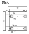
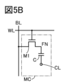
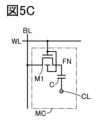
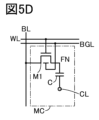
- 5A to 5F are diagrams illustrating configuration examples of a memory circuit.
- FIG. 6 is a flowchart illustrating an example of the operation of the semiconductor device.
- 7A and 7B are flowcharts illustrating an example of the operation of the semiconductor device.
- 8A and 8B are flowcharts illustrating an example of the operation of the semiconductor device.
- FIG. 9 is a diagram illustrating a configuration example of a semiconductor device.
- FIG. 9 is a diagram illustrating a configuration example of a semiconductor device.
- FIG. 10 is a diagram illustrating a configuration example of a semiconductor device.
- FIG. 11 is a diagram illustrating a configuration example of a semiconductor device.
- 12A to 12C are diagrams illustrating a configuration example of a semiconductor device.
- FIG. 13 is a diagram illustrating an example of the configuration of the storage unit.
- FIG. 14A is a diagram illustrating a configuration example of a storage layer.
- FIG. 14B is a diagram illustrating an equivalent circuit of the storage layer.
- FIG. 15 is a diagram illustrating an example of the configuration of the storage unit.
- FIG. 16A is a diagram illustrating a configuration example of a storage layer.
- FIG. 16B is a diagram illustrating an equivalent circuit of the storage layer.
- 17A and 17B are diagrams illustrating a configuration example of a semiconductor device.
- 18A to 18F are diagrams illustrating configuration examples of electronic equipment.
- a semiconductor device is a device that utilizes semiconductor characteristics, and refers to, for example, a circuit including a semiconductor element (for example, a transistor, a diode, a photodiode, etc.), or a device having the same circuit. It also refers to any device that can function by utilizing the characteristics of semiconductors. For example, an integrated circuit, a chip including an integrated circuit, or an electronic component containing a chip in a package is an example of a semiconductor device.
- a semiconductor element for example, a transistor, a diode, a photodiode, etc.
- a display device for example, a display device, a light emitting device, an imaging device, an arithmetic device, a control device, a storage device, a signal processing device, an electronic computer, or an electronic device is itself a semiconductor device and includes a semiconductor device. There may be cases where
- X and Y when it is stated that X and Y are connected, it means that X and Y are electrically connected, and when X and Y are functionally connected.
- the case where X and Y are directly connected and the case where X and Y are directly connected are disclosed in this specification and the like. Therefore, the present invention is not limited to predetermined connection relationships, for example, the connection relationships shown in the diagrams or text, and connection relationships other than those shown in the diagrams or text are also disclosed in the diagrams or text. It is assumed that X and Y are each objects (eg, a device, an element, a circuit, a wiring, an electrode, a terminal, a conductive film, a layer, etc.).
- X and Y are electrically connected means that when there is an object that has some kind of electrical effect between X and Y, it is possible to send and receive electrical signals between X and Y. means.
- An example of a case where X and Y are electrically connected is an element that enables electrical connection between X and Y (for example, a switch, a transistor, a capacitive element, an inductor, a resistive element, a diode, a display device, light emitting device, or load) can be connected between X and Y.
- An example of a case where X and Y are functionally connected is a circuit (for example, a logic circuit (for example, an inverter, a NAND circuit, or a NOR circuit) that enables a functional connection between X and Y).
- a circuit for example, a logic circuit (for example, an inverter, a NAND circuit, or a NOR circuit) that enables a functional connection between X and Y).
- signal conversion circuit for example, digital-to-analog conversion circuit, analog-to-digital conversion circuit, or gamma correction circuit
- potential level conversion circuit for example, power supply circuit (for example, boost circuit, step-down circuit, etc.), or signal potential level voltage sources, current sources, switching circuits, amplifier circuits (e.g.
- circuits that can increase signal amplitude or current amount, operational amplifiers, differential amplifier circuits, source follower circuits, buffer circuits, etc.), signal One or more generation circuits, storage circuits, control circuits, etc.
- X and Y can be connected between X and Y.
- X and Y can be connected between X and Y.
- X and Y are electrically connected, it means that or when X and Y are connected directly (i.e., when X and Y are connected without another element or circuit between them). (if applicable).
- X, Y, the source of the transistor in this specification, etc., may be referred to as one of the first terminal and the second terminal
- the drain in this specification, etc., the first terminal and the other of the second terminal
- X, Y, the source of the transistor in this specification, etc., may be referred to as one of the first terminal and the second terminal
- the drain in this specification, etc., the first terminal and the other of the second terminal
- X is electrically connected to Y via the source and drain of the transistor, and X, the source of the transistor, the drain of the transistor, and Y are provided in this connection order.” I can do it.
- X and Y are each objects (for example, a device, an element, a circuit, a wiring, an electrode, a terminal, a conductive film, a layer, etc.).
- the term “resistance element” can be, for example, a circuit element or wiring having a resistance value higher than 0 ⁇ . Therefore, in this specification and the like, a “resistance element” includes, for example, a wiring having a resistance value, a transistor through which a current flows between a source and a drain, a diode, a coil, and the like. Therefore, the term “resistance element” can be translated into terms such as “resistance”, “load”, or “region having a resistance value”, for example. Conversely, the terms “resistance,””load,” or “region having a resistance value” can be translated into terms such as “resistance element,” for example.
- the resistance value can be, for example, preferably 1 m ⁇ or more and 10 ⁇ or less, more preferably 5 m ⁇ or more and 5 ⁇ or less, and still more preferably 10 m ⁇ or more and 1 ⁇ or less. Further, for example, the resistance may be greater than or equal to 1 ⁇ and less than or equal to 1 ⁇ 10 9 ⁇ .
- the resistance value of the resistance element may be determined depending on the length of the wiring.
- the resistance element may use a conductor having a different resistivity from that of the conductor used as the wiring.
- the resistance value of the resistance element may be determined by doping the semiconductor with an impurity.
- a “capacitive element” refers to, for example, a circuit element having a capacitance value higher than 0F, a wiring region having a capacitance value higher than 0F, a parasitic capacitance, or It can be the gate capacitance of a transistor, etc. Therefore, in this specification and the like, a “capacitive element” is not limited to a circuit element that includes a pair of electrodes and a dielectric material included between the electrodes. The term “capacitive element” includes, for example, parasitic capacitance that occurs between wirings, or gate capacitance that occurs between one of the source or drain of a transistor and the gate.
- capacitor element terms such as “capacitive element,” “parasitic capacitance,” or “gate capacitance” can be replaced with terms such as “capacitance.”
- the term “capacitance” can be translated into terms such as “capacitive element,” “parasitic capacitance,” or “gate capacitance,” for example.
- the term “a pair of electrodes” in “capacitance” can be translated into, for example, a “pair of conductors,” a “pair of conductive regions,” or a “pair of regions.”
- the value of the capacitance can be, for example, 0.05 fF or more and 10 pF or less. Further, for example, it may be set to 1 pF or more and 10 ⁇ F or less.
- a transistor has a gate (also referred to as a gate terminal, gate region, or gate electrode), a source (also referred to as a source terminal, source region, or source electrode), and a drain (drain terminal, drain region, or It has three terminals called drain electrodes. Further, the transistor includes a region where a channel is formed between the drain and the source (also referred to as a channel formation region). A transistor allows current to flow between a source and a drain through a channel formation region. Note that the channel forming region is a region through which current mainly flows.
- the gate is a control terminal that controls the amount of current flowing in the channel formation region between the source and the drain.
- the two terminals that function as sources or drains are input/output terminals of the transistor.
- one of the two input/output terminals becomes a source and the other becomes a drain depending on the conductivity type of the transistor (n-channel type or p-channel type) and the level of potential applied to the three terminals of the transistor.
- the function as a source and the function as a drain may be interchanged. Therefore, in this specification and the like, the terms “source” and “drain” can be used interchangeably.
- the connection relationship of a transistor when describing the connection relationship of a transistor, "one of the source or the drain” (or the first electrode or the first terminal), or “the other of the source or the drain” (or the second electrode, or second terminal).
- the transistor may have a back gate in addition to the three terminals described above.
- one of the gate or back gate of the transistor is sometimes referred to as a first gate
- the other of the gate or back gate of the transistor is sometimes referred to as a second gate.
- the terms "gate” and “backgate” may be interchangeable.
- each gate is sometimes referred to as a first gate, a second gate, a third gate, or the like in this specification and the like.
- a transistor with a multi-gate structure having two or more gate electrodes can be used as a transistor.
- a transistor with a multi-gate structure channel formation regions are connected in series, so that a transistor with a multi-gate structure has a structure in which a plurality of transistors are connected in series. Therefore, a transistor with a multi-gate structure can reduce off-state current and improve the breakdown voltage (improve reliability) of the transistor.
- a transistor with a multi-gate structure operates in the saturation region, even if the voltage between the drain and source changes, the current between the drain and source does not change much, and the slope is flat. ⁇ Current characteristics can be obtained.
- Transistors with voltage-current characteristics with flat slopes can create ideal current source circuits or active loads with extremely high resistance values.
- a transistor having voltage/current characteristics with a flat slope can realize, for example, a differential circuit or a current mirror circuit with good characteristics.
- the circuit element may include a plurality of circuit elements.
- the resistor includes two or more resistors electrically connected in series.
- the capacitor includes a case where two or more capacitors are electrically connected in parallel.
- the transistor has two or more transistors electrically connected in series, and the gates of each transistor are electrically connected to each other.
- the switch has two or more transistors, and two or more transistors are connected electrically in series or in parallel.
- the gates of the respective transistors are electrically connected to each other.
- a “node” may be, for example, a “terminal,” “wiring,” “electrode,” “conductive layer,” “conductor,” or “conductor,” depending on the circuit configuration or device structure. It is possible to paraphrase it as “impurity region”. Furthermore, for example, “terminal” or “wiring” can be translated into “node”.
- Voltage refers to a potential difference from a reference potential.
- the reference potential is a ground potential (earth potential)
- “voltage” can be translated into “potential”. Note that the ground potential does not necessarily mean 0V.
- potential is relative. That is, as the reference potential changes, for example, the potential applied to the wiring, the potential applied to the circuit, or the potential output from the circuit also changes.
- high level potential also referred to as “high level potential”, “H potential”, or “H”
- low level potential low level potential
- L level potential
- current refers to a charge movement phenomenon (electrical conduction).
- electrical conduction electrical conduction
- the statement that "electrical conduction of a positively charged body is occurring” can be translated into “electrical conduction of a negatively charged body is occurring in the opposite direction.” Therefore, in this specification and the like, “current” refers to a charge movement phenomenon (electrical conduction) accompanying the movement of carriers, unless otherwise specified.
- the carrier here include electrons, holes, anions, cations, and complex ions. Note that carriers differ depending on the system in which current flows (eg, semiconductor, metal, electrolyte, vacuum, etc.).
- the "direction of current" in, for example, wiring is the direction in which positive carriers move, and is expressed in terms of the amount of positive current.
- the direction in which negative carriers move is opposite to the direction of current, and is expressed by a negative amount of current. Therefore, in this specification, etc., when there is no mention of the positive or negative current (or the direction of the current), for example, a statement such as “current flows from element A to element B” is replaced with “current flows from element B to element A.” It can be paraphrased as "flowing”. Furthermore, for example, a statement such as "current is input to element A” can be paraphrased to "current is output from element A”.
- ordinal numbers such as “first,” “second,” or “third” are added to avoid confusion of constituent elements. Therefore, the number of components is not limited. Further, the order of the constituent elements is not limited. For example, a component referred to as “first” in one embodiment of this specification etc. may be referred to as “second” in other embodiments or claims, etc. It is possible that Further, for example, a component referred to as “first” in one of the embodiments of this specification etc. may be omitted in other embodiments or claims.
- words indicating arrangement such as “above,” “below,” “above,” or “below” refer to the positional relationship between components. It is sometimes used for convenience to explain things. Further, the positional relationship between the constituent elements changes as appropriate depending on the direction in which each constituent element is depicted. Therefore, the words and phrases indicating the arrangement described in this specification and the like are not limited thereto, and can be appropriately rephrased depending on the situation. For example, the expression “insulator located on the upper surface of the conductor” can be translated into “insulator located on the lower surface of the conductor” by rotating the orientation of the drawing by 180 degrees. Additionally, the expression “insulator located on the top surface of the conductor” can be translated into “insulator located on the left (or right) surface of the conductor” by rotating the orientation of the drawing 90 degrees. can.
- electrode B on insulating layer A does not necessarily mean that electrode B is formed on insulating layer A in direct contact with it, but that other components are provided between insulating layer A and electrode B. Do not exclude what is included.
- words such as “row” or “column” may be used to describe components arranged in a matrix and their positional relationships. Further, the positional relationship between the constituent elements changes as appropriate depending on the direction in which each constituent element is depicted. Therefore, the terms such as “row” and “column” described in this specification and the like are not limited thereto, and can be appropriately rephrased depending on the situation. For example, the expression “row direction” can be translated into “column direction” by rotating the orientation of the drawing by 90 degrees.
- electrode B overlapping insulating layer A is not limited to the state in which electrode B is formed on insulating layer A.
- electrode B overlapping insulating layer A refers to, for example, a state in which electrode B is formed under insulating layer A, or a state in which electrode B is formed on the right (or left) side of insulating layer A. , etc. are not excluded.
- the term “adjacent” or “nearby” does not limit that components are in direct contact with each other.
- the expression “electrode B adjacent to insulating layer A” does not require that insulating layer A and electrode B be in direct contact with each other, and that other components may be present between insulating layer A and electrode B. Do not exclude what is included.
- words such as “film” and “layer” may be interchangeable depending on the situation.
- the term “conductive layer” may be changed to the term “conductive film.”
- the term “insulating film” may be changed to the term “insulating layer.”
- words such as “film” or “layer” may not be used and can be replaced with other words depending on the situation.
- the term “conductive layer” or “conductive film” may be changed to the term “conductor.” Further, the term “conductor” may be changed to the term “conductive layer” or “conductive film.” For example, the term “insulating layer” or “insulating film” may be changed to the term “insulator.” Further, the term “insulator” may be changed to the term “insulating layer” or “insulating film.”
- Electrode may be used as part of a “wiring” and vice versa.
- the term “electrode” or “wiring” includes, for example, a case where a plurality of “electrodes” or “wirings” are formed integrally.
- a “terminal” may be used as part of a “wiring” or “electrode,” and vice versa.
- the term “terminal” includes, for example, cases where a plurality of "electrodes", “wirings”, or “terminals” are formed integrally.
- an “electrode” can be part of a “wiring” or a “terminal.” Further, for example, a “terminal” can be a part of a “wiring” or an “electrode.” Furthermore, for example, terms such as “electrode,” “wiring,” or “terminal” may be replaced with terms such as "region.”
- terms such as “wiring,” “signal line,” or “power line” may be interchangeable depending on the situation.
- the term “wiring” may be changed to the term “signal line.”
- the term “wiring” may be changed to a term such as "power line”.
- the reverse is also true; for example, terms such as “signal line” or “power line” may be changed to the term “wiring”.
- a term such as “power line” may be changed to a term such as "signal line”.
- the reverse is also true; for example, a term such as “signal line” may be changed to a term such as "power line”.
- the term “potential” applied to the wiring may be changed to a term such as "signal”, for example.
- the reverse is also true; for example, a term such as “signal” may be changed to the term “potential”.
- a “switch” includes a plurality of terminals and has a function of switching (selecting) conduction or non-conduction between the terminals. For example, when a switch has two terminals and is electrically conductive between the two terminals, the switch is said to be “in a conducting state” or “in an on state.” Furthermore, when there is no conduction between both terminals, the switch is said to be “in a non-conducting state” or "in an off state.” Note that switching the switch to one of a conductive state and a non-conductive state, or maintaining one of a conductive state and a non-conductive state, is sometimes referred to as "controlling a conductive state.”
- a switch is a device that has the function of controlling whether or not current flows.
- a switch refers to a device that has the function of selecting and switching a path through which current flows.
- an electrical switch or a mechanical switch can be used as the switch.
- the switch is not limited to a specific type as long as it can control the current.
- switches that are normally in a non-conducting state, but become conductive by controlling the conductive state, and such switches are sometimes referred to as "A contacts.”
- switches are sometimes referred to as "B contacts.”
- Examples of electrical switches include transistors (e.g., bipolar transistors, MOS transistors, etc.), diodes (e.g., PN diode, PIN diode, Schottky diode, MIM (Metal Insulator Metal) diode, MIS (Metal Insulator Semiconductor)). diode , diode-connected transistors, etc.), or logic circuits that combine these. Note that when a transistor is operated as a simple switch, the polarity (conductivity type) of the transistor is not particularly limited.
- Examples of mechanical switches include switches using MEMS (micro electro mechanical systems) technology.
- the switch includes a mechanically movable electrode, and movement of the electrode selects a conducting state or a non-conducting state.
- the "conducting state" or “on state” of the transistor means, for example, a state in which the source electrode and drain electrode of the transistor can be considered to be electrically short-circuited, or a state in which the source electrode and drain electrode are considered to be electrically short-circuited.
- a “non-conducting state”, “blocking state”, or “off state” of a transistor refers to a state in which the source electrode and drain electrode of the transistor can be considered to be electrically disconnected.
- the voltage between the gate and source is lower than the threshold voltage, or in a p-channel transistor, the voltage between the gate and source is higher than the threshold voltage.
- the state, etc. may be referred to as a “non-conducting state", “blocking state”, or “off state”.
- the "off-state current" of a transistor refers to the current flowing between the source and drain (also referred to as drain current) when the transistor is in the off-state.
- drain current also referred to as drain current
- a drain current and a current flowing between a gate and a source or drain also referred to as gate leakage current
- leakage current when a transistor is in an off state
- the "channel length" of a transistor refers to, for example, the source in the region where the semiconductor (or the part of the semiconductor through which current flows when the transistor is on) and the gate overlap in a top view of the transistor. and the drain, or the distance between the source and drain in a region where a channel is formed.
- the "channel width" of a transistor refers to, for example, the area where the semiconductor (or the part of the semiconductor through which current flows when the transistor is on) and the gate overlap in a top view of the transistor. or the length of the portion where the source and drain face each other in a region where a channel is formed.
- parallel refers to a state in which two straight lines are arranged at an angle of -10° or more and 10° or less. Therefore, the case where the angle is greater than or equal to -5° and less than or equal to 5° is also included.
- substantially parallel or “substantially parallel” refers to a state in which two straight lines are arranged at an angle of -30° or more and 30° or less.
- perpendicular refers to a state in which two straight lines are arranged at an angle of 80° or more and 100° or less. Therefore, the case where the angle is 85° or more and 95° or less is also included.
- substantially perpendicular or “substantially perpendicular” refers to a state in which two straight lines are arranged at an angle of 60° or more and 120° or less.
- the heights match or approximately match means that the heights from the reference plane (for example, a flat surface such as the substrate surface) are the same in cross-sectional view.
- the surface of a single layer or multiple layers may be exposed by performing planarization treatment.
- the surfaces to be flattened have the same height from the reference surface.
- the heights of the plurality of layers on the surface to be processed may not be strictly equal depending on the processing apparatus, processing method, or material of the surface to be processed during the planarization process.
- the heights match or approximately match For example, if there are two layers with different heights (here, the first layer and the second layer) with respect to the reference plane, the height of the top surface of the first layer and the height of the second layer A case where the difference between the top surface height and the top surface height is 20 nm or less is also referred to as “the heights match or approximately match”.
- the ends match or roughly match means that at least a part of the outlines of the stacked layers overlap when viewed from above.
- the upper layer and the lower layer may be processed using the same mask pattern or partially the same mask pattern.
- the contours do not overlap, and the contour of the upper layer may be located inside the contour of the lower layer, or the contour of the upper layer may be located outside the contour of the lower layer. In this specification and the like, this case is also referred to as "the ends match or roughly match.”
- a semiconductor impurity refers to, for example, a substance other than the main component constituting a semiconductor layer.
- an element having a concentration of less than 0.1 atomic % is an impurity.
- examples of impurities that change the properties of the semiconductor include Group 1 elements, Group 2 elements, Group 13 elements, Group 14 elements, Group 15 elements, or oxides.
- transition metals other than the main components of semiconductors In particular, for example, hydrogen (also present in water), lithium, sodium, silicon, boron, phosphorus, carbon or nitrogen. Oxygen vacancies (also referred to as V O ) may be formed in the oxide semiconductor due to, for example, mixing of impurities.
- metal oxide refers to a metal oxide in a broad sense.
- Metal oxides are classified into, for example, oxide insulators, oxide conductors (including transparent oxide conductors), oxide semiconductors (also referred to as oxide semiconductors or simply OS), and the like.
- oxide semiconductors also referred to as oxide semiconductors or simply OS
- the metal oxide is sometimes called an oxide semiconductor.
- the metal oxide is a metal oxide semiconductor (metal oxide semiconductor). semiconductor).
- OS transistor can be translated as a transistor including a metal oxide or an oxide semiconductor.
- metal oxides containing nitrogen may also be collectively referred to as metal oxides. Further, a metal oxide containing nitrogen may be called a metal oxynitride.
- each embodiment can be appropriately combined with the structure shown in other embodiments to form one embodiment of the present invention. Further, when a plurality of configuration examples are shown in one embodiment, these configuration examples can be combined as appropriate.
- drawings and the like related to this specification may include variations in signals, voltages, or currents due to noise, or variations in signals, voltages, or currents due to timing shifts.
- layers or resist masks may be unintentionally reduced due to processing such as etching during the actual manufacturing process, but this is reflected in the drawings for ease of understanding. There are things I don't do.
- each block shown in the block diagram is not limited to the constituent elements described in this specification, etc., and can be rephrased as appropriate depending on the situation.
- arrows indicating the X direction, Y direction, and Z direction may be attached.
- the "X direction” refers to the direction along the X axis, and the forward direction and reverse direction may not be distinguished unless explicitly stated.
- the X direction, the Y direction, and the Z direction are directions that intersect with each other. More specifically, the X direction, the Y direction, and the Z direction are directions that are orthogonal to each other.
- one of the X direction, the Y direction, or the Z direction may be referred to as a "first direction” or a “first direction.” Further, the other direction may be referred to as a “second direction” or “second direction”. Further, the remaining one may be referred to as a "third direction” or "third direction.”
- the code when the same code is used for multiple elements, especially when it is necessary to distinguish them, the code may be, for example, "A”, “b”, “_1", “[n]", Alternatively, an identification code such as "[m, n]” may be added to the description.
- FIGS. 1 to 5 A configuration example of a semiconductor device according to one embodiment of the present invention will be described with reference to FIGS. 1 to 5. Further, an example of the operation of a semiconductor device according to one embodiment of the present invention will be described with reference to FIGS. 6 to 8.
- the semiconductor device according to one embodiment of the present invention may be suitably used as a part of a central processing unit (CPU), for example.
- CPU central processing unit
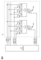
- FIG. 1 is a block diagram illustrating a configuration example of a semiconductor device 100 according to one embodiment of the present invention.
- the semiconductor device 100 includes a cache section 113, a cache controller 114, a core 115, a thermal detector 116, and a bus 117. , a memory controller 121, a power controller 122, and a clock controller 123.
- the cache unit 113 includes a first cache 111 (Cache1) and a second cache 112 (Cache2).
- the semiconductor device 100 can include one or more cores 115.
- the semiconductor device 100 shown in FIG. 1 includes four cores 115.
- a temperature sensor 131 (Sensor) and a memory 141 (Memory) are arranged around the semiconductor device 100. Note that one or both of the temperature sensor 131 and the memory 141 may be placed inside the semiconductor device 100.
- the core 115 has a function of performing program processing.
- the core 115 also has a function of sending a read request to the cache control unit 114 in order to obtain data for program processing.
- the read request includes the address of memory 141. Note that when the semiconductor device 100 is used as part of a CPU, the core 115 can have a function as an arithmetic device (also referred to as a processor core).
- the memory 141 has a function of storing data for performing program processing. Note that when the semiconductor device 100 is used as part of a CPU, the memory 141 can have a function as a main storage device (also referred to as main memory). As the memory 141, for example, DRAM (Dynamic Random Access Memory) can be used.
- DRAM Dynamic Random Access Memory
- the memory control unit 121 has a function of controlling data reading or writing to the memory 141 based on a request from the cache control unit 114.
- the cache unit 113 has a function of storing, in the first cache 111 or the second cache 112, data for performing program processing and an address of the memory 141 where the data is stored. Note that when the semiconductor device 100 is used as part of a CPU, the cache unit 113 can have a function as a buffer storage device (also referred to as a cache memory). Therefore, the cache unit 113 is preferably placed near the core 115 in order to exchange data with the core 115 at high speed.
- the cache unit 113 can have a function as a L-level cache.
- the cache unit 113 may function as an L-1 cache
- the memory 141 may function as an L-level cache.
- the cache control unit 114 Upon receiving a read request from the core 115, the cache control unit 114 reads the data from the cache unit 113 and sends it to the core 115 if data corresponding to the address included in the request exists in the cache unit 113. It has a function to output. Alternatively, by receiving a read request from the core 115, if the data corresponding to the address included in the request does not exist in the cache unit 113, the cache control unit 114 transfers the data to the memory via the memory control unit 121. 141 , output to the core 115 , and store in the cache unit 113 .
- the cache control unit 114 also has a function of sending an interrupt request to the core 115 in order to stop or restart program processing.
- the first cache 111 and the second cache 112 are each composed of transistors having different temperature characteristics.
- the first cache 111 for example, an SRAM (Static Random Access Memory) configured with a Si transistor (a transistor whose channel formation region contains silicon) can be used.
- an OS memory including an OS transistor a transistor containing an oxide semiconductor in a channel formation region
- OS memory is a memory that can store stored data for a long period of time by using OS transistors with extremely low off-state current.
- Si transistors operate faster than OS transistors. Furthermore, by electrically connecting the gate of an n-channel type Si transistor and the gate of a p-channel type Si transistor, a Si transistor can be used to create a CMOS circuit (for example, a complementary operating circuit, a CMOS logic gate, or CMOS logic circuit, etc.). A circuit configured with Si transistors can increase operating speed and reduce power consumption in a steady state. Therefore, in addition to the first cache 111, Si transistors are preferably used in, for example, the cache control section 114, the core 115, the heat detection section 116, the memory control section 121, the power supply control section 122, and the clock control section 123. .
- the OS transistor Since the band gap of the oxide semiconductor in which the channel is formed is 2 eV or more, the OS transistor has a characteristic that off-state current (current flowing between the source and drain when the transistor is off) is extremely low.
- the off-state current value of the OS transistor per 1 ⁇ m channel width at room temperature is 1aA (1 ⁇ 10 ⁇ 18 A) or less, 1zA (1 ⁇ 10 ⁇ 21 A) or less, or 1yA (1 ⁇ 10 ⁇ 24 A) or less It can be done.
- the off-state current value per 1 ⁇ m of channel width at room temperature is 1 fA (1 ⁇ 10 ⁇ 15 A) or more and 1 pA (1 ⁇ 10 ⁇ 12 A) or less. Therefore, it can be said that the off-state current of an OS transistor is about 10 orders of magnitude lower than that of a Si transistor.
- the off-state current of the OS transistor hardly increases even in a high temperature environment. Specifically, the off-state current hardly increases even under an environmental temperature of room temperature or higher and 200° C. or lower. Furthermore, the on-state current of the OS transistor does not easily decrease even in a high-temperature environment.
- the on-state current of a Si transistor decreases in a high-temperature environment. That is, an OS transistor has a higher on-state current than a Si transistor in a high-temperature environment. Furthermore, the OS transistor can perform a good switching operation even under an environmental temperature of 125° C. or higher and 150° C. or lower because it has a large ratio of on-current to off-current. Therefore, a semiconductor device including an OS transistor operates stably even in a high-temperature environment and has high reliability.
- the first cache 111 made of Si transistors operates faster than the second cache 112 made of OS transistors at a lower temperature.
- the first cache 111 may operate slower than the second cache 112 because its operating speed decreases as the temperature rises.
- first cache 111 and the second cache 112 are preferably placed near the core 115 in order to exchange data with the core 115 at high speed. Therefore, the first cache 111 and the second cache 112 are easily affected by the heat generated by the core 115.
- the cache control unit 114 may control the cache unit 113 to use the faster operating one of the first cache 111 and the second cache 112, depending on the temperature.
- the cache control unit 114 has a function of controlling the first cache 111 and the second cache 112 to be switched and used depending on the temperature around or inside the core 115. Thereby, the operating speed of the semiconductor device 100 can be improved. Further, a decrease in operating speed due to a rise in temperature of the semiconductor device 100 can be suppressed.
- the semiconductor layer of the OS transistor contains at least one of indium and zinc.
- the semiconductor layer of the OS transistor is made of, for example, indium, M (M is gallium, aluminum, yttrium, tin, silicon, boron, copper, vanadium, beryllium, titanium, iron, nickel, germanium, zirconium, molybdenum, lanthanum). , cerium, neodymium, hafnium, tantalum, tungsten, magnesium, and cobalt) and zinc.
- M is preferably one or more selected from gallium, aluminum, yttrium, and tin.
- an oxide containing indium (In), gallium (Ga), and zinc (Zn) also referred to as "IGZO”
- an oxide containing indium (In), aluminum (Al), and zinc (Zn) also referred to as "IAZO”
- an oxide containing indium (In), aluminum (Al), gallium (Ga), and zinc (Zn) also referred to as "IAGZO”
- IAGZO oxide containing indium (In), aluminum (Al), gallium (Ga), and zinc (Zn)
- the atomic ratio of In in the In-M-Zn oxide is preferably equal to or higher than the atomic ratio of M.
- the atomic ratio of In in the In-M-Zn oxide may be smaller than the atomic ratio of M.
- the nearby composition includes a range of plus or minus 30% of the desired atomic ratio.
- the heat detection unit 116 has a function of measuring temperature using the temperature sensor 131.
- the heat detection unit 116 also has a function of sending information indicating whether the measured temperature is equal to or higher than a predetermined temperature threshold to the cache control unit 114 via the bus 117.
- the heat detection unit 116 may include an analog-to-digital converter (ADC). Since the heat detection unit 116 includes an ADC, a temperature sensor that outputs an analog signal can be used as the temperature sensor 131.
- ADC analog-to-digital converter
- the temperature sensor 131 has a function of outputting a signal corresponding to temperature to the heat detection section 116. Temperature sensor 131 is provided around core 115 and outputs a signal corresponding to the temperature around core 115 to heat detection section 116 . Alternatively, the temperature sensor 131 may be provided inside the core 115 to output a signal corresponding to the temperature inside the core 115 to the heat detection section 116. As the temperature sensor 131, for example, a resistance temperature detector (eg, platinum, nickel, or copper), a thermistor, a thermocouple, or an IC temperature sensor may be used. Alternatively, as the temperature sensor 131, for example, a configuration using a semiconductor temperature sensor (for example, a silicon diode temperature sensor, etc.) or a configuration using a bandgap circuit may be used.
- a resistance temperature detector eg, platinum, nickel, or copper
- a thermistor e.g., a thermistor, a thermocouple, or an IC temperature sensor
- the cache control unit 114 has a function of receiving information as to whether the measured temperature is equal to or higher than a predetermined temperature threshold, and controlling the cache unit 113 according to the information. In other words, the cache control unit 114 uses the second cache 112 when the temperature of the core 115 is equal to or higher than the predetermined temperature threshold, and the cache control unit 114 uses the second cache 112 when the temperature of the core 115 is less than the predetermined temperature threshold. In this case, it is sufficient to have a function to control the use of the first cache 111.
- the semiconductor device 100 includes a plurality of cores 115 as shown in FIG.
- the average value, median value, or maximum value of each of the measured temperatures may be taken as the temperature around or inside the core 115.
- the heat detection unit 116 measures the temperature using the temperature sensor 131 provided around or inside one core 115 selected from the plurality of cores 115, and transfers the measured temperature to the core 115.
- the temperature may be around or inside 115.
- the heat detection unit 116 measures the temperature using a temperature sensor 131 provided around or inside the first cache 111 and around or inside the second cache 112, or both. Good too.
- the bus 117 functions as a transmission path for exchanging information such as data, requests, commands, or signals between the components included in the semiconductor device 100.
- the power supply control unit 122 has a function of controlling the supply of power (for example, potential VSS, potential VDD, etc.) to each component included in the semiconductor device 100.
- the potential VSS may be, for example, a ground potential.
- the potential VDD is a potential higher than the potential VSS, and may be set to a potential such that, for example, the potential difference between the potential VDD and the potential VSS is equal to or higher than the threshold voltage of the transistor.
- the power control unit 122 can stop the power supply to the first cache 111 by receiving a command to stop the power supply to the first cache 111. Further, the power control unit 122 can stop the power supply to the second cache 112, for example, by receiving a command to stop the power supply to the second cache 112.
- the clock control unit 123 has a function of controlling the supply of clock signals (for example, signal CLK, etc.) to each component included in the semiconductor device 100. For example, the clock control unit 123 can stop the supply of the clock signal to the first cache 111 by receiving a command to stop the supply of the clock signal to the first cache 111. Further, for example, the clock control unit 123 can stop the supply of the clock signal to the second cache 112 by receiving a command to stop the supply of the clock signal to the second cache 112.
- clock signals for example, signal CLK, etc.
- FIG. 2 is a circuit diagram illustrating a detailed configuration example around the cache unit 113 of the semiconductor device 100 shown in FIG.
- the cache unit 113 includes, in addition to the first cache 111 and the second cache 112 described above, a switch SW11, a switch SW12, a switch SW13, a switch SW14, and a switch SW15. , a switch SW16, a switch SW17, and a switch SW18.
- the cache control unit 114 exchanges the signal ADDR, the signal DATA, the signal HIT, the signal MEM1_EN, the signal MEM1_PW, the signal MEM2_EN, and the signal MEM2_PW with the cache unit 113 (first cache 111 or second cache 112). I can do it.
- Signal ADDR is a signal indicating the address of memory 141.
- the signal DATA is data for performing program processing in the core 115.
- Signal HIT is a signal indicating whether data corresponding to the address of signal ADDR exists in first cache 111 or second cache 112.
- FIG. 2 shows a configuration in which the cache unit 113 includes one switch SW13 and one switch SW17 to simplify the explanation, it may include a plurality of switches according to the number of bits of the signal ADDR.
- the switch SW13 and the plurality of switches SW17 may be provided.
- the cache unit 113 may include a plurality of switches SW12 and a plurality of switches SW16 according to the number of bits of the signal DATA. All you have to do is prepare.
- the cache control unit 114 Upon receiving a read request from the core 115, the cache control unit 114 first sends a signal ADDR to the first cache 111 or the second cache 112. When the first cache 111 or the second cache 112 receives the signal ADDR from the cache control unit 114, it determines whether data corresponding to the address of the memory 141 indicated by the signal ADDR is stored. If the data is stored, a signal DATA representing the data and a signal HIT indicating that the data exists (also referred to as a cache hit) are output to the cache control unit 114. If the data is not stored, a signal HIT indicating that the data does not exist (also referred to as a cache miss) is output to the cache control unit 114.
- Each of the switches SW11 to SW13 has a function of being turned on or off depending on the signal MEM1_EN.
- the switch SW14 has a function of being turned on or off depending on the signal MEM1_PW.
- Each of the switches SW15 to SW17 has a function of being turned on or off depending on the signal MEM2_EN.
- the switch SW18 has a function of being turned on or off depending on the signal MEM2_PW.
- the switch SW14 When the switch SW14 is turned on, the potential VSS is supplied to the first cache 111.
- the switch SW11 is in the on state, so that the signal HIT can be exchanged between the cache control unit 114 and the first cache 111.
- the signal DATA can be exchanged between the cache control unit 114 and the first cache 111.
- the signal ADDR can be exchanged between the cache control unit 114 and the first cache 111.
- the signal ADDR, the signal DATA, and the signal HIT can be exchanged between the cache control unit 114 and the first cache 111.
- a state is referred to as the first cache 111 being in a valid state.
- the signal ADDR, the signal DATA, and the signal HIT are not exchanged between the cache control unit 114 and the first cache 111.
- such a state is referred to as an invalid state of the first cache 111.
- the switch SW18 When the switch SW18 is turned on, the potential VSS is supplied to the second cache 112.
- the switch SW15 When the switch SW18 is in the on state, the switch SW15 is in the on state, so that the signal HIT can be exchanged between the cache control unit 114 and the second cache 112. Further, by turning on the switch SW16, the signal DATA can be exchanged between the cache control unit 114 and the second cache 112. Further, by turning on the switch SW17, the signal ADDR can be exchanged between the cache control unit 114 and the second cache 112.
- the signal ADDR, the signal DATA, and the signal HIT can be exchanged between the cache control unit 114 and the second cache 112.
- a state in which the second cache 112 is enabled.
- the signal ADDR, the signal DATA, and the signal HIT are not exchanged between the cache control unit 114 and the second cache 112.
- such a state is referred to as an invalid state of the second cache 112.
- the cache control unit 114 controls the cache unit 113 using the signals MEM1_EN, MEM1_PW, MEM2_EN, and MEM2_PW so that one of the first cache 111 and the second cache 112 becomes a valid state and the other becomes an invalid state. can be controlled.
- a case where the first cache 111 is in a valid state and the second cache 112 is in an invalid state is referred to as a first cache mode.
- a case where the second cache 112 is in a valid state and the first cache 111 is in an invalid state is referred to as a second cache mode.
- the cache control unit 114 receives information from the heat detection unit 116 as to whether the temperature around or inside the core 115 is equal to or higher than a predetermined temperature threshold, and depending on the information, It has a function of controlling the cache unit 113 so that it operates in the first cache mode or the second cache mode.
- FIG. 3 shows the transistor M11, the transistor M12, the transistor M13, the transistor M14, the transistor M15, the transistor M16, This is a configuration in which transistors M17 and M18 are each replaced.
- FIG. 3 shows a configuration in which the cache unit 113 includes one transistor M13 and one transistor M17 to simplify the explanation, it may include a plurality of transistors according to the number of bits of the signal ADDR.
- the transistor M13 and the plurality of transistors M17 may be provided.
- the configuration in which the cache unit 113 includes one transistor M12 and one transistor M16 is illustrated, the number of transistors M12 and M16 may vary depending on the number of bits of the signal DATA. All you have to do is prepare.
- An OS transistor can be used for each of the transistors M11 to M18.
- the transistors M11 to M18 have a large ratio of on-current to off-current and can perform good switching operations even in a high-temperature environment.
- the on-state current of the transistors M11 to M13 in the on-state is large, and the off-state current of the transistor M18 in the off-state is small.
- the on-state currents of the transistors M15 to M17 that are on-state are large, and the off-state current of transistor M14 that is off-state is small. Therefore, the operating speed of the semiconductor device 100 can be improved. Further, the power consumption of the semiconductor device 100 can be reduced. Further, a decrease in operating speed due to a rise in temperature of the semiconductor device 100 can be suppressed.
- FIG. 4 is a block diagram illustrating a configuration example of a storage device 300 that can be suitably used for the second cache 112 according to one aspect of the present invention.
- the memory device 300 includes a memory cell section 21 and a drive circuit section 22.
- the memory cell section 21 includes a plurality of memory cell arrays 90 arranged in a stacked manner.
- the memory cell array 90 includes a plurality of memory cells MC arranged in a matrix. A configuration example of memory cell MC will be described later.
- the drive circuit section 22 includes a PSW 62 (power switch), a PSW 63, and a peripheral circuit 71.
- Peripheral circuit 71 includes peripheral circuit 81, control circuit 72, and voltage generation circuit 73.
- each circuit, each signal, and each voltage can be removed or discarded as necessary. Also, other circuits or other signals may be added.
- Signal BW, signal CE, signal GW, signal CLK, signal WAKE, signal ADDR, signal WDA, signal PON1, and signal PON2 are each input signals from the outside.
- Signal HIT and signal RDA are output signals to the outside.
- Signal CLK is a clock signal. Further, the signal BW, the signal CE, and the signal GW are control signals. Signal CE is a chip enable signal. Signal GW is a global write enable signal. Signal BW is a byte write enable signal. Signal ADDR is an address signal. The signal HIT is a signal indicating whether data corresponding to the address signal exists in the memory cell section 21. Signal WDA is write data. Signal RDA is read data. Signal PON1 and signal PON2 are power gating control signals. Note that the signal PON1 and the signal PON2 may be generated by the control circuit 72.
- the control circuit 72 is a logic circuit that has a function of controlling the overall operation of the storage device 300. For example, the control circuit 72 outputs a signal HIT indicating whether data corresponding to the address signal exists in the memory cell section 21. For example, the control circuit 72 performs a logical operation on the signal CE, the signal GW, and the signal BW to determine the operation mode of the storage device 300 (e.g., write operation or read operation (e.g., read mode 1 or read mode 2)). Determine. Alternatively, the control circuit 72 generates a control signal for the peripheral circuit 81 so that this operation mode is executed.
- the operation mode of the storage device 300 e.g., write operation or read operation (e.g., read mode 1 or read mode 2).
- the control circuit 72 generates a control signal for the peripheral circuit 81 so that this operation mode is executed.
- the voltage generation circuit 73 has a function of generating a negative voltage.
- Signal WAKE has a function of controlling input of signal CLK to voltage generation circuit 73. For example, when the signal WAKE is given an H level signal, the voltage generation circuit 73 receives the signal CLK and generates a negative voltage.
- the peripheral circuit 81 is a circuit for writing or reading data to or from the memory cell MC.
- Peripheral circuit 81 includes drive circuit 51 including row decoder 82 , column decoder 84 , row driver 83 , column driver 85 , input circuit 87 , output circuit 88 , and sense amplifier 55 .
- Row decoder 82 and column decoder 84 have the function of decoding signal ADDR.
- Row decoder 82 is a circuit for specifying a row to be accessed.
- Column decoder 84 is a circuit for specifying a column to be accessed.
- Row driver 83 has a function of selecting a word line designated by row decoder 82.
- Column driver 85 has a function of selecting a bit line designated by column decoder 84.
- the drive circuit 51 has a function of writing data into the memory cell MC selected by the word line selected by the row driver 83 and the bit line selected by the column driver 85, and writes data using the sense amplifier 55, for example. It has a function to read out data, a function to hold read data, etc.
- Input circuit 87 has a function of holding signal WDA.
- the data held by the input circuit 87 is output to the column driver 85.
- the output data of the input circuit 87 is the data (data Din) to be written into the memory cell MC.
- the data (data Dout) read from the memory cell MC by the column driver 85 is output to the output circuit 88.
- the output circuit 88 has a function of holding data Dout. Further, the output circuit 88 has a function of outputting the data Dout to the outside of the storage device 300. Data output from output circuit 88 is signal RDA.
- the PSW 62 has a function of controlling the supply of the potential VDD to the peripheral circuit 71.
- the PSW 63 has a function of controlling the supply of the potential VHM to the row driver 83.
- the potential on the high power supply side of the storage device 300 is the potential VDD
- the potential on the low power supply side is the potential VSS.
- the potential VHM is a potential used to bring the word line to an H level (a potential that turns on a transistor electrically connected to the word line), and is higher than the potential VDD.
- PSW62 is controlled to be on or off by signal PON1.
- PSW63 is controlled to be on or off by signal PON2.
- the number of power domains to which the potential VDD is supplied in the peripheral circuit 71 is one, but the number may be plural. In this case, the drive circuit section 22 may provide a power switch for each power domain.
- FIG. 5A is a block diagram illustrating a configuration example of a memory circuit that can be suitably used in the memory device 300 according to one embodiment of the present invention.
- FIG. 5A shows a memory cell array 90, a word line drive circuit 91, and a bit line drive circuit 92.
- the memory cell array 90 has memory cells MC arranged in a matrix of m rows and n columns (m and n are positive integers).
- Memory cell MC is electrically connected to word line WL_1 to word line WL_m and bit line BL_1 to bit line BL_n.
- the memory cell MC includes, for example, a source line for flowing current, a wiring for applying a potential to the back gate of a transistor, or a wiring for setting one electrode of a capacitor to a fixed potential. It may be electrically connected to a capacitor line, etc.
- the word line drive circuit 91 is a circuit that outputs a signal for selecting memory cells MC in each row.
- the word line drive circuit 91 corresponds to, for example, the row decoder 82 and the row driver 83 included in the drive circuit section 22 of the storage device 300 described above.
- the word lines WL_1 to WL_m may be separate word lines for writing and reading. Note that in the description to be described later, one word line selected from the word lines WL_1 to WL_m may be referred to as a word line WL.
- the bit line drive circuit 92 is a circuit for writing data into or reading data from the memory cells MC in each column.
- the bit line drive circuit 92 corresponds to, for example, the drive circuit 51 including the column decoder 84, column driver 85, and sense amplifier 55 included in the drive circuit section 22 of the storage device 300 described above.
- the bit lines BL_1 to BL_n may be separate bit lines for writing and reading.
- one bit line selected from bit lines BL_1 to bit lines BL_n may be referred to as bit line BL.
- 5B to 5F are diagrams illustrating examples of circuit configurations that can be taken by the memory cell MC shown in FIG. 5A.
- Memory cell MC shown in FIG. 5B has a transistor M1 and a capacitor C.
- One of the source and drain of the transistor M1 is electrically connected to one electrode of the capacitor C.
- the other of the source and drain of transistor M1 is electrically connected to bit line BL.
- the gate of transistor M1 is electrically connected to word line WL.
- the other electrode of the capacitor C is electrically connected to the capacitor line CL.
- Transistor M1 is an OS transistor. OS transistors have a characteristic of extremely low off-state current. Therefore, by making the transistor M1 non-conductive, charge corresponding to data can be held in the charge holding node FN. Therefore, the refresh rate of data corresponding to the charge held in the charge holding node FN can be reduced.
- the memory cell MC shown in FIG. 5C is a modification of the memory cell MC shown in FIG. 5B.
- the difference from the transistor M1 in FIG. 5B is that the transistor M1 has a back gate, and by electrically connecting the back gate and the gate, the potential of the word line WL is applied from both sides. With such a configuration, it is possible to increase the amount of current flowing between the source and the drain when the transistor M1 is turned on.
- the memory cell MC shown in FIG. 5D is a modification of the memory cell MC shown in FIG. 5B.
- the difference from the transistor M1 in FIG. 5B is that the transistor M1 has a back gate, and by electrically connecting the back gate and the back gate line BGL, a potential different from that of the gate is applied to the back gate. It is in.
- the threshold voltage of the transistor M1 can be controlled. Thereby, the amount of current flowing between the source and drain of transistor M1 can be changed.
- Memory cell MC shown in FIG. 5E includes a transistor M1, a transistor M2, and a capacitor C.
- One of the source and drain of the transistor M1 is electrically connected to the gate of the transistor M2 and one electrode of the capacitor C.
- the other of the source and drain of the transistor M1 is electrically connected to the write bit line WBL.
- the gate of transistor M1 is electrically connected to write word line WWL.
- the other electrode of the capacitor C is electrically connected to the read word line RWL.
- One of the source and drain of the transistor M2 is electrically connected to the read bit line RBL.
- the other of the source and drain of transistor M2 is electrically connected to source line SL.
- the transistor M2 is illustrated as an n-channel transistor, it may be a p-channel transistor.
- Transistor M2 is an OS transistor. Note that the transistor M2 may be a Si transistor. Note that the transistor M1 can also have the same configuration as the transistor M1 shown in FIG. 5C or FIG. 5D described above.
- the memory cell MC shown in FIG. 5F has a transistor M1, a transistor M2, a transistor M3, and a capacitor C.
- One of the source and drain of the transistor M1 is electrically connected to the gate of the transistor M2 and one electrode of the capacitor C.
- the other of the source and drain of the transistor M1 is electrically connected to the write bit line WBL.
- the gate of transistor M1 is electrically connected to write word line WWL.
- the other electrode of the capacitor C is electrically connected to the capacitor line CL.
- One of the source and drain of transistor M2 is electrically connected to one of the source and drain of transistor M3.
- the other of the source and drain of transistor M2 is electrically connected to source line SL.
- the gate of transistor M3 is electrically connected to read word line RWL.
- the other of the source and drain of the transistor M3 is electrically connected to the read bit line RBL.
- the transistor M3 is illustrated as an n-channel transistor, it may be a p-channel transistor. By making the transistor M1 non-conductive, charge corresponding to data can be held in the charge holding node FN.
- Each of transistor M2 and transistor M3 is an OS transistor. Note that at least one of the transistor M2 and the transistor M3 may be a Si transistor. Note that the transistor M1 can also have the same configuration as the transistor M1 shown in FIG. 5C or FIG. 5D described above.
- DOSRAM Dynamic Oxide Semiconductor RAM (Random Access Memory).
- SRAM Static RAM
- the memory cell configurations shown in FIGS. 5B to 5D are effective in suppressing an increase in circuit area.
- NOSRAM registered trademark
- NOSRAM is an abbreviation for Nonvolatile Oxide Semiconductor RAM.
- NOSRAM may be used as a non-volatile memory. For example, NOSRAM can continue to store data even in a power gating state by turning off the write OS transistor.
- circuit configurations shown in FIGS. 5B to 5F are merely examples, and any configuration can be used as long as one embodiment of the present invention can be realized.
- the semiconductor device 100 operates in a normal state or in an overheated state.
- the normal state is a state in which the temperature T around or inside the core 115 is less than a predetermined temperature threshold Tth (temperature T is less than the temperature threshold Tth).
- the overheating state is a state in which the temperature T around or inside the core 115 is equal to or higher than a predetermined temperature threshold Tth (temperature T is equal to or higher than the temperature threshold Tth).
- temperature threshold Tth may be set to, for example, a temperature of 60° C. or more and 100° C. or less, more preferably a temperature of 60° C. or more and 80° C. or less.
- a time of 0.1 seconds or more and 10 seconds or less preferably a time of 0.1 seconds or more and 1 second or less may be set.
- the semiconductor device 100 uses the first cache 111 to perform program processing in the core 115. That is, in the normal state, the cache unit 113 operates in the first cache mode (the first cache 111 is in the valid state and the second cache 112 is in the invalid state). Furthermore, when the semiconductor device 100 is in an overheated state, the second cache 112 is used to perform program processing in the core 115. That is, in the case of an overheating state, the cache unit 113 operates in the second cache mode (the second cache 112 is in the valid state and the first cache 111 is in the invalid state). Note that the semiconductor device 100 performs a process of switching the operation of the cache unit 113 from the first cache mode to the second cache mode when transitioning from the normal state to the overheating state. Furthermore, when the semiconductor device 100 transitions from the overheating state to the normal state, the semiconductor device 100 performs a process of switching the operation of the cache unit 113 from the second cache mode to the first cache mode.
- FIG. 7A, and FIG. 7B are flowcharts illustrating an example of the operation of the semiconductor device 100.
- the flowchart shown in FIG. 6 shows the normal state (first cache mode), transition from the normal state to the overheating state (switching from the first cache mode to the second cache mode), the overheating state (second cache mode), and 3 is an example of the operation of the semiconductor device 100 in each of the transitions from the overheating state to the normal state (switching from the second cache mode to the first cache mode).
- the flowchart shown in FIG. 7A is an example of the process of switching from the first cache mode to the second cache mode (Process A).
- the flowchart shown in FIG. 7B is an example of the process of switching from the second cache mode to the first cache mode (Process B).
- step S01 While the program processing is being executed (step S01), the operations described below are performed. Assume that program processing is executed in at least one core 115 included in the semiconductor device 100 in a normal state. First, the heat detection unit 116 measures the temperature T around or inside the core 115 using the temperature sensor 131 (step S02). The heat detection unit 116 then sends information as to whether the temperature T is equal to or higher than a predetermined temperature threshold Tth (temperature T is equal to or higher than the temperature threshold Tth) to the cache control unit 114 via the bus 117. send.
- a predetermined temperature threshold Tth temperature T is equal to or higher than the temperature threshold Tth
- the cache control unit 114 receives information as to whether the temperature T is equal to or higher than the temperature threshold Tth from the heat detection unit 116, and receives information as to whether the temperature T is equal to or higher than the temperature threshold Tth, and receives information as to whether the temperature T is equal to or higher than the temperature threshold Tth. It is determined whether a certain state continues for a certain period of time (step S03). If it is in the normal state (not in the overheated state), the cache control unit 114 determines whether the second cache 112 is in the valid state (step S08). Since the normal state is the first cache mode (the second cache 112 is not in the valid state), the process returns to step S01.
- the semiconductor device 100 repeats step S01, step S02, step S03, and step S08 in order while the program processing is executed in the normal state.
- the first cache mode is in effect (the first cache 111 is in the valid state), so the first cache mode is switched to the second cache mode (steps S05 to S07). ). After switching from the first cache mode to the second cache mode, the process returns to step S01.
- the cache control unit 114 sends an interrupt request to the core 115, and upon receiving the request, the core 115 stops the program processing being executed (step S05).
- the cache control unit 114 performs process A (process of switching from the first cache mode to the second cache mode) (step S06).
- the cache control unit 114 may perform control to communicate with the second cache 112 when receiving a read request from the core 115.
- the cache control unit 114 sends an interrupt request to the core 115, and upon receiving the request, the core 115 restarts the stopped program processing (step S07).
- Process A in step S06 will be explained (see FIG. 7A).
- the cache control unit 114 disables the first cache 111 and disables the second cache 112 (step S21).
- the cache control unit 114 sends a signal MEM1_EN that turns switches SW11 to SW13 off, a signal MEM2_EN that turns switches SW15 to SW17 on, and a signal MEM2_EN that turns switch SW18 on. It is sufficient to output a signal MEM2_PW that becomes . Further, for example, in FIG. 3, the cache control unit 114 may output the signal MEM1_EN at the L level, the signal MEM2_EN at the H level, and the signal MEM2_PW at the H level.
- the L level is a potential at which the transistors M11 to M13 are turned off (for example, the potential VSS or a potential lower than the potential VSS).
- the H level is a potential at which the transistors M15 to M18 are turned on (for example, the potential VDD or a potential higher than the potential VDD).
- the cache control unit 114 when the cache control unit 114 receives a read request from the core 115, it exchanges the signal ADDR, the signal DATA, and the signal HIT with the second cache 112.
- the first cache 111 is no longer involved in the exchange of the signal ADDR, the signal DATA, and the signal HIT. In other words, the first cache 111 is no longer used for executing program processing. Therefore, for example, the cache control unit 114 may stop supplying power to the first cache 111. By stopping the supply of power to the first cache 111, the power consumption of the semiconductor device 100 can be reduced.
- the cache control unit 114 may output a signal MEM1_PW that turns off the switch SW14. Further, for example, in FIG. 3, the cache control unit 114 may output the signal MEM1_PW at the L level.
- the L level is a potential at which the transistor M14 is turned off (for example, the potential VSS or a potential lower than the potential VSS).
- the cache control unit 114 sends a command to the power supply control unit 122 to stop the power supply to the first cache 111, and , the power supply control unit 122 may stop supplying power to the first cache 111 by receiving the command.
- the cache control unit 114 may stop supplying the clock signal to the first cache 111. By stopping the supply of the clock signal to the first cache 111, it is possible to reduce the power consumption of the semiconductor device 100.
- the cache control unit 114 sends a command to the clock control unit 123 to stop the supply of the clock signal to the first cache 111, and
- the control unit 123 may stop supplying the clock signal to the first cache 111 by receiving the instruction.
- step S03 After transitioning to the overheating state and switching to the second cache mode, while the overheating state continues, it is determined in step S03 that the overheating state is present. Then, in step S04, it is determined that the second cache mode is in effect (the first cache 111 is not in the valid state).
- the semiconductor device 100 repeats step S01, step S02, step S03, and step S04 in order while the program processing is executed in the overheated state.
- the second cache mode is in effect (the second cache 112 is in the valid state), so the second cache mode is switched to the first cache mode (steps S09 to S11). ). After switching from the second cache mode to the first cache mode, the process returns to step S01.
- the cache control unit 114 sends an interrupt request to the core 115, and upon receiving the request, the core 115 stops the program processing being executed (step S09).
- the cache control unit 114 performs process B (process of switching from the second cache mode to the first cache mode) (step S10).
- the cache control unit 114 may perform control to communicate with the first cache 111 when receiving a read request from the core 115.
- the cache control unit 114 sends an interrupt request to the core 115, and upon receiving the request, the core 115 restarts the stopped program processing (step S11).
- Process B in step S10 will be explained (see FIG. 7B).
- the cache control unit 114 disables the second cache 112 and disables the first cache 111 (step S31).
- the cache control unit 114 sends a signal MEM1_EN that turns the switches SW11 to SW13 on, a signal MEM1_PW that turns the switch SW14 on, and a signal MEM1_PW that turns the switches SW15 to SW17 off. It is sufficient to output the signal MEM2_EN. Further, for example, in FIG. 3, the cache control unit 114 may output the signal MEM1_EN at the H level, the signal MEM1_PW at the H level, and the signal MEM2_EN at the L level.
- the H level is a potential at which the transistors M11 to M14 are turned on (for example, the potential VDD or a potential higher than the potential VDD).
- the L level is a potential at which the transistors M15 to M17 are turned on (for example, the potential VSS or a potential lower than the potential VSS).
- the cache control unit 114 when the cache control unit 114 receives a read request from the core 115, it exchanges the signal ADDR, the signal DATA, and the signal HIT with the first cache 111.
- the second cache 112 is no longer involved in the exchange of the signal ADDR, the signal DATA, and the signal HIT. In other words, the second cache 112 is no longer used for executing program processing. Therefore, for example, the cache control unit 114 may stop supplying power to the second cache 112. By stopping the supply of power to the second cache 112, the power consumption of the semiconductor device 100 can be reduced.
- the cache control unit 114 may output a signal MEM2_PW that turns off the switch SW18. Further, for example, in FIG. 3, the cache control unit 114 may output the signal MEM2_PW at the L level.
- the L level is a potential at which the transistor M18 is turned off (for example, the potential VSS or a potential lower than the potential VSS).
- the cache control unit 114 sends a command to the power supply control unit 122 to stop the power supply to the second cache 112, and , the power control unit 122 may stop supplying power to the second cache 112 by receiving the command.
- the cache control unit 114 may stop supplying the clock signal to the second cache 112. By stopping the supply of the clock signal to the second cache 112, it is possible to reduce the power consumption of the semiconductor device 100.
- the cache control unit 114 sends a command to the clock control unit 123 to stop the supply of the clock signal to the second cache 112, and
- the control unit 123 may stop supplying the clock signal to the second cache 112 by receiving the command.
- FIG. 6 is a flowchart illustrating another example of process A.
- processing B processing for switching from the second cache mode to the first cache mode
- FIG. 8B is a flowchart illustrating another example of process B.
- FIGS. 8A and 8B which will be described later, the description of parts similar to those of FIGS. 7A and 7B may be omitted because the above description can be referred to as appropriate.
- step S41 the second cache 112 is enabled (step S41).
- the information stored in the first cache 111 for example, data, addresses, attribute information, etc.
- step S42 the information stored in the first cache 111
- step S43 the first cache 111 is made invalid (step S43).
- step S41 for example, in FIG. 2, the cache control unit 114 outputs a signal MEM2_EN that turns on the switches SW15 to SW17 and a signal MEM2_PW that turns on the switch SW18. good. This allows the cache control unit 114 to exchange the signal ADDR, the signal DATA, and the signal HIT with the second cache.
- step S42 for example, the cache control unit 114 sends information (for example, data, address, attribute information, etc.) stored in the first cache 111 via the signal ADDR, the signal DATA, and the signal HIT. It is only necessary to perform control such that the information is read from the first cache 111 and the read information is written to the second cache 112.
- information for example, data, address, attribute information, etc.
- step S43 for example in FIG. 2, the cache control unit 114 may output a signal MEM1_EN that turns off the switches SW11 to SW13.
- the first cache 111 is no longer involved in the exchange of the signal ADDR, the signal DATA, and the signal HIT.
- the cache control unit 114 may output a signal EM1_PW that turns the switch SW14 off. Thereby, by stopping the supply of power to the first cache 111, it is possible to reduce the power consumption of the semiconductor device 100.
- the information for example, data, addresses, attribute information, etc.
- the information for example, data, addresses, attribute information, etc.
- the cache control unit 114 receives a read request from the core 115 after restarting program processing, it can communicate with the second cache 112 without reading the data from the memory 141. Therefore, the operating speed of the semiconductor device 100 can be improved.
- step S51 the first cache 111 is enabled (step S51).
- step S52 the information stored in the second cache 112 (for example, data, addresses, attribute information, etc.) is copied to the first cache 111 (step S52).
- step S53 the second cache 112 is made invalid (step S53).
- step S51 for example, in FIG. 2, the cache control unit 114 outputs a signal MEM1_EN that turns on the switches SW11 to SW13 and a signal MEM1_PW that turns on the switch SW14. good. This allows the cache control unit 114 to exchange the signal ADDR, the signal DATA, and the signal HIT with the first cache.
- step S52 for example, the cache control unit 114 sends information (for example, data, address, attribute information, etc.) stored in the second cache 112 via the signal ADDR, the signal DATA, and the signal HIT.
- the read information may be read from the second cache 112 and the read information may be written to the first cache 111.
- step S53 for example in FIG. 2, the cache control unit 114 may output a signal MEM2_EN that turns off the switches SW15 to SW17.
- the second cache 112 is no longer involved in the exchange of the signal ADDR, the signal DATA, and the signal HIT.
- the cache control unit 114 may output a signal EM2_PW that turns the switch SW18 off. Thereby, by stopping the supply of power to the second cache 112, it is possible to reduce the power consumption of the semiconductor device 100.
- the information (for example, data, addresses, attribute information, etc.) stored in the second cache 112 at the time when the program processing is stopped in step S09 is stored in step S10. is copied to the first cache 111. That is, when the program processing is restarted in step S11, the data for performing the program processing in the core 115 is stored in the first cache 111. Therefore, when the cache control unit 114 receives a read request from the core 115 after restarting program processing, it can communicate with the first cache 111 without reading the data from the memory 141. Therefore, the operating speed of the semiconductor device 100 can be improved.
- the semiconductor device according to one embodiment of the present invention is not limited to the description of the semiconductor device 100 described above. At least a part of the configuration examples, operation examples, and drawings corresponding to them illustrated in this embodiment mode may be used in combination with other configuration examples, operation examples, other drawings, and other examples described in this specification etc. It can be combined with the embodiments as appropriate.
- FIG. 9 is a schematic diagram illustrating a mounting example of a semiconductor device 170 according to one embodiment of the present invention.
- the semiconductor device 170 includes a substrate 171.
- the substrate 171 is, for example, a substrate containing silicon.
- a substrate containing a compound semiconductor such as silicon carbide or gallium nitride may be used.
- the Z direction is defined in order to make the explanation of the positional relationship of each element constituting the semiconductor device 170 easier to understand.
- the Z direction is perpendicular or approximately perpendicular to the surface of the substrate 171.
- approximately perpendicular refers to a state in which the angle between two target elements is greater than or equal to 85 degrees and less than or equal to 95 degrees.
- the Z direction may be referred to as the vertical direction for ease of understanding.
- a core region 185 and a memory region 181[0] are formed on one side of the substrate 171.
- the core region 185 and the memory region 181[0] are regions in which a Si transistor (a transistor whose channel formation region contains silicon) or a circuit including a Si transistor is provided.
- One or more memory layers are formed vertically stacked above the core region 185.
- Each of the memory layers 182[1] to 182[p] is a layer in which an OS transistor (a transistor containing an oxide semiconductor in a channel formation region) or a circuit including an OS transistor is provided.
- Vias 172 are formed between the substrate 171 and each of the memory layers 182[1] to 182[p].
- the substrate 171 and each of the memory layers 182[1] to 182[p] are electrically connected to each other via the vias 172 formed between them. That is, the circuits provided on one side of the substrate 171 and the circuits provided in each of the memory layers 182[1] to 182[p] are connected via the vias 172 formed between them. , are electrically connected to each other. For example, via a via 172 formed between the substrate 171 and the memory layer 182[1], a circuit provided on one side of the substrate 171 and a circuit provided on the memory layer 182[1] can be connected to each other. are electrically connected to each other.
- circuit provided in the memory layer 182[1] and the circuit provided in the memory layer 182[2] are connected via the via 172 formed between the memory layer 182[1] and the memory layer 182[2]. and the circuits are electrically connected to each other.
- the substrate 171 and the memory layers 182[1] to 182[p] are manufactured monolithically.
- die 180[1] to die 180[q] are arranged in a stacked manner in the vertical direction above the memory area 181[0].
- Each of die 180[1] to die 180[q] is, for example, a silicon die.
- a die refers to a chip piece obtained by forming a circuit pattern on, for example, a disk-shaped substrate (also referred to as a wafer) and cutting it into dice in the semiconductor chip manufacturing process.
- semiconductor materials that can be used for the die include silicon (Si), silicon carbide (SiC), and gallium nitride (GaN).
- Si silicon
- SiC silicon carbide
- GaN gallium nitride
- a die obtained from a silicon substrate also referred to as a silicon wafer
- a silicon die obtained from a silicon substrate is sometimes referred to as a silicon die.
- Memory regions 181[1] to 181[q] are formed in one-to-one correspondence on one side of each of die 180[1] to die 180[q].
- Each of the memory areas 181[1] to 181[q] is an area where a Si transistor or a circuit including a Si transistor is provided.
- An electrode 173 is formed on the substrate 171 and one surface of each of the die 180[1] to the die 180[q] (that is, on each of the memory regions 181[0] to 181[q]). Ru.
- An electrode 174 is formed on the other side of each of die 180[1] to die 180[q].
- a plug 175 that electrically connects electrode 173 and electrode 174 is formed to penetrate the die.
- the plug 175 is, for example, a through silicon via (TSV).
- the substrate 171 and the die 180[1] to the die 180[q] each have an electrode 173 formed on one side of each of the substrate 171 and the die 180[1] to the die 180[q-1].
- the electrode 174 formed on the other surface side of each of the dies 180[1] to 180[q] are joined, thereby being electrically connected to each other. That is, the circuits provided in each of the memory areas 181[0] to 181[q] are formed on one side of each of the substrate 171 and the die 180[1] to die 180[q-1].
- the electrode 173 and the electrode 174 formed on the other side of each of the dies 180[1] to 180[q] are joined, and thereby electrically connected to each other.
- the electrode 173 formed on one surface of the substrate 171 and the electrode 174 formed on the other surface of the die 180[1] The circuit provided in the memory area 181[1] is electrically connected to each other. Furthermore, the electrode 173 formed on one side of the die 180[1] and the electrode 174 formed on the other side of the die 180[2] are bonded to each other, so that the memory area 181[1] ] and the circuit provided in memory area 181[2] are electrically connected to each other.
- the same conductive material for each of the electrodes 173 and 174 for example, a metal film containing an element selected from aluminum, chromium, copper, tantalum, tin, zinc, gold, silver, platinum, titanium, molybdenum, and tungsten, or the above-mentioned
- a metal nitride film for example, a titanium nitride film, a molybdenum nitride film, a tungsten nitride film, etc.
- copper it is preferable to use copper as the conductive material for the electrodes 173 and 174.
- a Cu-Cu direct bonding technique (a technique for achieving electrical continuity by connecting copper (Cu) electrodes).
- a microbump bonding technique may be applied in which microbumps are formed on the electrodes 173 and the electrodes 174 for bonding.
- the electrode 173 may not be formed in the die 180[q].
- the memory areas 181[1] to 181[q] are formed in one-to-one correspondence on the other side of each of the die 180[1] to the die 180[q]. It's okay. In this case, for example, the electrode 173 and the plug 175 may not be formed in the die 180[q].
- the substrate 171 and the dies 180[1] to 180[q] are arranged so that one surface side and the other surface side face each other. Not exclusively.
- at least one of the dies 180[1] to 180[q] may be arranged such that one side or the other side faces each other.
- the electrodes 173 or the electrodes 174 are joined together to be electrically connected to each other.
- the electrode 174 and the plug 175 may not be formed in the die 180[q].
- the semiconductor device 170 described in this embodiment is a mounting example of the semiconductor device 100 described in the above-described first embodiment. Therefore, in the semiconductor device 170, for example, a part of the first cache 111 (for example, a memory cell section) included in the semiconductor device 100 is located in the memory areas 181[0] to 181[q], and the semiconductor device 100 A part of the second cache 112 (for example, a memory cell section) is provided in the memory layer 182[1] to the memory layer 182[p], and a core 115 included in the semiconductor device 100 is provided in the core region 185. It can be assumed that the configuration is as follows. Note that other components included in the semiconductor device 100 (for example, the cache control unit 114 and the heat detection unit 116) may be provided on the substrate 171, for example.
- the semiconductor device 170 has, for example, a structure in which the second cache 112 is stacked vertically on the core 115 provided on the substrate 171. Thereby, the second cache 112 can, for example, increase the storage density and shorten the signal delay time. Further, the semiconductor device 170 has, for example, a configuration in which the first cache 111 is provided on the dies 180[1] to dies 180[q] arranged in a vertically stacked manner on the substrate 171. Thereby, the first cache 111 can, for example, increase the storage density and shorten the signal delay time. With these features, for example, the operating speed of the semiconductor device 170 can be improved and the semiconductor device 170 can be made smaller.
- FIG. 10 is a schematic diagram illustrating another example of mounting the semiconductor device 170.
- memory layers 182[1] to 182[p] are stacked vertically above a core region 185 formed on a substrate 171.
- dies 180[1] to 180[q] are stacked vertically on the memory layer 182[p] to form memory regions 181[1] to 181[q], respectively. Placed.
- an electrode 173 formed on the memory layer 182[p] and an electrode 174 formed on the other side of the die 180[1] are bonded. By doing so, they are electrically connected to each other. That is, the circuit provided in the memory layer 182[p] and the circuit provided in the memory region 181[1] are connected to the electrode 173 formed in the memory layer 182[p] and the other side of the die 180[1]. By joining the electrodes 174 formed on the surface side, they are electrically connected to each other.
- the second cache 112 is stacked vertically above the core 115 provided on the substrate 171, and the second cache 112 is stacked vertically above the second cache 112.
- the first cache 111 is stacked on top of the first cache 111.
- the first cache 111 can, for example, increase the storage density and shorten the signal delay time.
- the memory layers 182[1] to 182[p] in which the second cache 112 is provided can have a function of reducing the effect of heat generated in the core 115 on the first cache 111.
- the semiconductor device according to one embodiment of the present invention is not limited to the above semiconductor device. At least a part of the configuration examples, operation examples, and drawings corresponding to them illustrated in this embodiment mode may be used in combination with other configuration examples, operation examples, other drawings, and other examples described in this specification etc. It can be combined with the embodiments as appropriate.
- FIG. 11 shows a part of the cross-sectional structure of the semiconductor device.
- the semiconductor device shown in FIG. 11 includes a transistor 550, a transistor 500, and a capacitor 600.
- 12A is a cross-sectional view of the transistor 500 in the channel length direction
- FIG. 12B is a cross-sectional view of the transistor 500 in the channel width direction
- FIG. 12C is a cross-sectional view of the transistor 550 in the channel width direction.
- the transistor 500 corresponds to the OS transistor described in the above embodiment mode
- the transistor 550 corresponds to a Si transistor.
- transistor 500 is provided above transistor 550, and capacitor 600 is provided above transistor 550 and transistor 500.
- the transistor 550 is provided over the substrate 311 and includes a conductor 316, an insulator 315, a semiconductor region 313 made of a part of the substrate 311, a low resistance region 314a functioning as a source region or a drain region, and a low resistance region 314b. .
- the transistor 550 As shown in FIG. 12C, in the transistor 550, the upper surface of the semiconductor region 313 and the side surfaces in the channel width direction are covered with a conductor 316 with an insulator 315 interposed therebetween. In this way, by making the transistor 550 a Fin type transistor, the effective channel width increases, so that the on-characteristics of the transistor 550 can be improved. Further, since the contribution of the electric field of the gate electrode can be increased, the off-state characteristics of the transistor 550 can be improved.
- the transistor 550 may be either a p-channel type or an n-channel type.
- the transistor 550 includes, for example, a region of the semiconductor region 313 where a channel is formed, a region near the region, a low resistance region 314a that becomes one of the source region or the drain region, and a low resistance region that becomes the other of the source region or the drain region. 314b, etc., preferably contain a semiconductor such as a silicon-based semiconductor, and preferably contain single crystal silicon.
- the transistor 550 may be formed of a material including, for example, Ge (germanium), SiGe (silicon germanium), GaAs (gallium arsenide), or GaAlAs (gallium aluminum arsenide).
- the transistor 550 may be formed using silicon in which the effective mass is controlled by applying stress to the crystal lattice and changing the lattice spacing.
- the transistor 550 may be, for example, a HEMT (High Electron Mobility Transistor) using GaAs, GaAlAs, or the like.
- the low resistance region 314a and the low resistance region 314b are made of, for example, an element imparting n-type conductivity such as arsenic or phosphorus, or a p-type conductivity such as boron. Contains elements that impart sex.
- the conductor 316 that functions as a gate electrode is made of a semiconductor material such as silicon containing an element that imparts n-type conductivity such as arsenic or phosphorus, or an element that imparts p-type conductivity such as boron. can be used.
- conductive materials such as, for example, metal materials, alloy materials, or metal oxide materials can be used.
- the threshold voltage of the transistor can be adjusted by selecting the material of the conductor. Specifically, it is preferable to use a material such as titanium nitride or tantalum nitride for the conductor. Furthermore, in order to achieve both electrical conductivity and embeddability, it is preferable to use a metal material such as tungsten or aluminum as a laminated layer for the conductor, and it is particularly preferable to use tungsten in terms of heat resistance.
- the transistor 550 may be formed using, for example, an SOI (Silicon on Insulator) substrate.
- SOI Silicon on Insulator
- SOI substrates are formed by implanting oxygen ions into a mirror-polished wafer and then heating it at a high temperature to form an oxide layer at a certain depth from the surface and eliminate defects that occur in the surface layer.
- a SIMOX (Separation by Implanted Oxygen) substrate may also be used.
- an SOI substrate formed using a smart cut method in which a semiconductor substrate is cleaved using the growth of microvoids formed by hydrogen ion implantation through heat treatment, or an ELTRAN method (registered trademark: Epitaxial Layer Transfer), etc. may also be used.
- a transistor formed using a single crystal substrate includes a single crystal semiconductor in a channel formation region.
- An insulator 320, an insulator 322, an insulator 324, and an insulator 326 are sequentially stacked and provided to cover the transistor 550.
- the insulator 320, the insulator 322, the insulator 324, and the insulator 326 for example, silicon oxide, silicon oxynitride, silicon nitride oxide, silicon nitride, aluminum oxide, aluminum oxynitride, aluminum nitride oxide, or aluminum nitride is used. Just use it.
- silicon oxynitride refers to a material whose composition contains more oxygen than nitrogen
- silicon nitride oxide refers to a material whose composition contains more nitrogen than oxygen.
- aluminum oxynitride refers to a material whose composition contains more oxygen than nitrogen
- aluminum nitride oxide refers to a material whose composition contains more nitrogen than oxygen.
- the insulator 322 may have a function as a flattening film that flattens a step caused by, for example, the transistor 550 provided below.
- the upper surface of the insulator 322 may be planarized by a planarization process using a chemical mechanical polishing (CMP) method or the like in order to improve flatness.
- CMP chemical mechanical polishing
- the insulator 324 it is preferable to use a film having barrier properties that prevents hydrogen, impurities, or the like from diffusing from the substrate 311 or the transistor 550 into a region where the transistor 500 is provided.
- the film having barrier properties against hydrogen for example, silicon nitride formed by a CVD method can be used.
- silicon nitride formed by a CVD method when hydrogen diffuses into a semiconductor element including an oxide semiconductor such as the transistor 500, the characteristics of the semiconductor element may deteriorate. Therefore, a film that suppresses hydrogen diffusion is preferably used between the transistor 500 and the transistor 550.
- the membrane that suppresses hydrogen diffusion is a membrane that releases a small amount of hydrogen.
- the amount of hydrogen desorbed can be analyzed using, for example, temperature programmed desorption gas analysis (TDS).
- TDS temperature programmed desorption gas analysis
- the amount of hydrogen desorbed from the insulator 324 is determined by the amount converted into hydrogen atoms per area of the insulator 324 when the surface temperature of the film is in the range of 50°C to 500°C.
- the amount may be 1 ⁇ 10 16 atoms/cm 2 or less, preferably 5 ⁇ 10 15 atoms/cm 2 or less.
- the insulator 326 preferably has a lower dielectric constant than the insulator 324.
- the dielectric constant of the insulator 326 is preferably less than 4, more preferably less than 3.
- the dielectric constant of the insulator 326 is preferably 0.7 times or less, more preferably 0.6 times or less, the dielectric constant of the insulator 324.
- the insulator 320 for example, a conductor 328, a conductor 330, and the like, which are connected to the capacitor 600 or the transistor 500, are embedded.
- the conductor 328 and the conductor 330 have a function as a plug or wiring.
- a conductor having a function as a plug or a wiring a plurality of structures may be collectively given the same reference numeral.
- the wiring and the plug electrically connected to the wiring may be integrated. That is, a part of the conductor may function as a wiring, and a part of the conductor may function as a plug.
- each plug or wiring may be a single layer or a conductive material such as a metal material, an alloy material, a metal nitride material, or a metal oxide material. It can be used in a stacked manner.
- a conductive material such as a metal material, an alloy material, a metal nitride material, or a metal oxide material. It can be used in a stacked manner.
- the material of the plug or wiring it is preferable to use a high melting point material such as tungsten or molybdenum, which has both heat resistance and conductivity.
- the material of the plug or wiring is preferably a low resistance conductive material such as aluminum or copper. By using a low-resistance conductive material for the plug or the wiring, wiring resistance can be lowered.
- a wiring layer may be provided over the insulator 326 and the conductor 330.
- an insulator 350, an insulator 352, and an insulator 354 are stacked in this order.
- a conductor 356 is formed on the insulator 350, the insulator 352, and the insulator 354.
- the conductor 356 functions as a plug or wiring connected to the transistor 550. Note that the conductor 356 can be provided using the same material as the conductor 328 and the conductor 330.
- the conductor 356 preferably includes a conductor having barrier properties against hydrogen.
- a conductor having hydrogen barrier properties is formed in the opening of the insulator 350 having hydrogen barrier properties.
- the conductor having barrier properties against hydrogen for example, tantalum nitride or the like may be used. Further, it is preferable to laminate tantalum nitride and tungsten, which has high conductivity. By using the conductor 356 as a stack of tantalum nitride and tungsten, the conductor 356 can suppress diffusion of hydrogen from the transistor 550 while maintaining conductivity as a wiring. In this case, it is preferable that the tantalum nitride layer of the conductor 356 having barrier properties against hydrogen be in contact with the insulator 350 having barrier properties against hydrogen.
- a wiring layer may be provided over the insulator 354 and the conductor 356.
- an insulator 360, an insulator 362, and an insulator 364 are stacked in this order.
- a conductor 366 is formed on the insulator 360, the insulator 362, and the insulator 364.
- the conductor 366 functions as a plug or wiring. Note that the conductor 366 can be provided using the same material as the conductor 328 and the conductor 330.
- the conductor 366 preferably includes a conductor having barrier properties against hydrogen.
- a conductor having hydrogen barrier properties is formed in the opening of the insulator 360 having hydrogen barrier properties.
- a wiring layer may be provided over the insulator 364 and the conductor 366.
- an insulator 370, an insulator 372, and an insulator 374 are stacked in this order.
- a conductor 376 is formed on the insulator 370, the insulator 372, and the insulator 374.
- the conductor 376 functions as a plug or wiring. Note that the conductor 376 can be provided using the same material as the conductor 328 and the conductor 330.
- the conductor 376 preferably includes a conductor having barrier properties against hydrogen.
- a conductor having hydrogen barrier properties is formed in the opening of the insulator 370 having hydrogen barrier properties.
- a wiring layer may be provided over the insulator 374 and the conductor 376.
- an insulator 380, an insulator 382, and an insulator 384 are stacked in this order.
- a conductor 386 is formed on the insulator 380, the insulator 382, and the insulator 384.
- the conductor 386 functions as a plug or wiring. Note that the conductor 386 can be provided using the same material as the conductor 328 and the conductor 330.
- the conductor 386 preferably includes a conductor having barrier properties against hydrogen.
- a conductor having hydrogen barrier properties is formed in the opening of the insulator 380 having hydrogen barrier properties.
- the semiconductor device is not limited to this.
- the number of wiring layers similar to the wiring layer containing the conductor 356 may be three or less, or the number of wiring layers similar to the wiring layer containing the conductor 356 may be five or more.
- An insulator 510, an insulator 512, an insulator 514, and an insulator 516 are sequentially stacked on the insulator 384. It is preferable that any one of the insulator 510, the insulator 512, the insulator 514, and the insulator 516 use a substance that has barrier properties against oxygen, hydrogen, and the like.
- a film having barrier properties that prevents hydrogen or impurities from diffusing from the substrate 311 or the region where the transistor 550 is provided to the region where the transistor 500 is provided can be used.
- the same material as the insulator 324 can be used for the insulator 510 and the insulator 514.
- the film having barrier properties against hydrogen for example, silicon nitride formed by a CVD method can be used.
- silicon nitride formed by a CVD method when hydrogen diffuses into a semiconductor element including an oxide semiconductor such as the transistor 500, the characteristics of the semiconductor element may deteriorate. Therefore, a film that suppresses hydrogen diffusion is preferably used between the transistor 500 and the transistor 550.
- the membrane that suppresses hydrogen diffusion is a membrane that releases a small amount of hydrogen.
- a metal oxide such as aluminum oxide, hafnium oxide, or tantalum oxide is preferably used for the insulator 510 and the insulator 514.
- aluminum oxide has a high blocking effect of preventing the membrane from permeating both oxygen and impurities such as hydrogen or moisture that cause variations in the electrical characteristics of the transistor. Therefore, aluminum oxide can prevent impurities such as hydrogen or moisture from entering the transistor 500 during and after the transistor manufacturing process. Further, aluminum oxide can suppress release of oxygen from an oxide that forms the transistor 500. Therefore, aluminum oxide is suitable for use as a protective film for the transistor 500.
- the same material as the insulator 320 can be used for the insulator 512 and the insulator 516. Furthermore, by using materials with relatively low dielectric constants as these insulators, parasitic capacitance occurring between wirings can be reduced.
- a silicon oxide film, a silicon oxynitride film, or the like can be used as the insulator 512 and the insulator 516.
- a conductor 518, a conductor (for example, conductor 503) forming the transistor 500, and the like are embedded in the insulator 510, the insulator 512, the insulator 514, and the insulator 516.
- the conductor 518 has a function as a plug or a wiring that is connected to the capacitor 600 or the transistor 550.
- the conductor 518 can be provided using the same material as the conductor 328 and the conductor 330.
- the conductor 518 in a region in contact with the insulator 510 and the insulator 514 is preferably a conductor having barrier properties against oxygen, hydrogen, and water.
- the transistor 550 and the transistor 500 can be separated by a layer having barrier properties against oxygen, hydrogen, and water, and diffusion of hydrogen from the transistor 550 to the transistor 500 can be suppressed.
- a transistor 500 is provided above the insulator 516.
- the transistor 500 includes a conductor 503 embedded in an insulator 514 and an insulator 516, and an insulator 520 disposed over the insulator 516 and the conductor 503. , an insulator 522 disposed on the insulator 520, an insulator 524 disposed on the insulator 522, an oxide 530a disposed on the insulator 524, and an oxide 530a disposed on the oxide 530a.
- the insulator 580 has an overlapping opening formed therein, an insulator 545 placed on the bottom and side surfaces of the opening, and a conductor 560 placed on the surface where the insulator 545 is formed.
- an insulator 544 is preferably disposed between the oxide 530a, the oxide 530b, the conductor 542a, the conductor 542b, and the insulator 580.
- the conductor 560 includes a conductor 560a provided inside the insulator 545, and a conductor 560b provided so as to be embedded inside the conductor 560a. It is preferable to have.
- an insulator 574 is preferably disposed over the insulator 580, the conductor 560, and the insulator 545.
- oxide 530a and the oxide 530b are sometimes collectively referred to as the oxide 530.
- the transistor 500 has a structure in which two layers, the oxide 530a and the oxide 530b, are stacked in the region where the channel is formed and in the vicinity thereof, one embodiment of the present invention is not limited to this. do not have.
- a single layer of the oxide 530b or a stacked structure of three or more layers may be provided in a region where a channel is formed and in the vicinity thereof.
- the conductor 560 is illustrated as having a two-layer stacked structure; however, one embodiment of the present invention is not limited to this.
- the conductor 560 may have a single layer structure or a laminated structure of three or more layers.
- the transistor 500 shown in FIGS. 11 and 12A is an example, and the structure is not limited to this, and an appropriate transistor may be used depending on the circuit structure, driving method, etc., for example.
- the conductor 560 functions as a gate electrode of the transistor, and the conductor 542a and the conductor 542b function as a source electrode or a drain electrode, respectively.
- the conductor 560 is formed so as to be embedded in the opening of the insulator 580 and in the region sandwiched between the conductor 542a and the conductor 542b.
- the arrangement of conductor 560, conductor 542a, and conductor 542b is selected in a self-aligned manner with respect to the opening in insulator 580. That is, in the transistor 500, the gate electrode can be disposed between the source electrode and the drain electrode in a self-aligned manner. Therefore, the conductor 560 can be formed without providing a margin for alignment. Therefore, the area occupied by the transistor 500 can be reduced. Thereby, miniaturization and high integration of semiconductor devices can be achieved.
- the conductor 560 is formed in a self-aligned manner in the region between the conductor 542a and the conductor 542b, the conductor 560 does not have a region overlapping with the conductor 542a or the conductor 542b. Thereby, the parasitic capacitance formed between the conductor 560 and the conductors 542a and 542b can be reduced. Therefore, the switching speed of the transistor 500 can be improved and the transistor 500 can have high frequency characteristics.
- the conductor 560 may function as a first gate (also referred to as a top gate) electrode.
- the conductor 503 may function as a second gate (also referred to as a bottom gate) electrode.
- the threshold voltage of the transistor 500 can be controlled by changing the potential applied to the conductor 503 independently of the potential applied to the conductor 560.
- the threshold voltage of the transistor 500 can be increased and the off-state current can be reduced. Therefore, when a negative potential is applied to the conductor 503, the drain current when the potential applied to the conductor 560 is 0 V can be made smaller than when no negative potential is applied.
- the conductor 503 is arranged to overlap the oxide 530 and the conductor 560. As a result, when a potential is applied to the conductor 560 and the conductor 503, the electric field generated from the conductor 560 and the electric field generated from the conductor 503 are connected to cover the channel formation region formed in the oxide 530. Can be done.
- a structure of a transistor in which a channel formation region is electrically surrounded by an electric field of a first gate electrode is referred to as a surrounded channel (S-channel) structure.
- the S-channel structure disclosed in this specification and the like has a structure different from the Fin type structure and the planar type structure.
- the S-channel structure disclosed in this specification and the like can also be regarded as a type of Fin type structure.
- a Fin type structure refers to a structure in which a gate electrode is arranged so as to surround at least two or more surfaces (specifically, two, three, or four sides) of a channel.
- the channel formation region can be electrically surrounded.
- the S-channel structure is a structure that electrically surrounds the channel formation region, it is substantially equivalent to a GAA (Gate All Around) structure or an LGAA (Lateral Gate All Around) structure. You can say that.
- a channel formation region formed at or near the interface between the oxide 530 and the gate insulator can be made to cover the entire bulk of the oxide 530. Can be done. Therefore, it is possible to improve the current density flowing through the transistor, so that it is possible to improve the on-state current of the transistor or improve the field effect mobility of the transistor.
- the conductor 503 has the same configuration as the conductor 518, and a conductor 503a is formed in contact with the inner wall of the opening of the insulator 514 and the insulator 516, and a conductor 503b is formed further inside.
- the transistor 500 has a structure in which the conductor 503a and the conductor 503b are stacked, one embodiment of the present invention is not limited to this.
- the conductor 503 may be provided as a single layer or a laminated structure of three or more layers.
- a conductive material for the conductor 503a which has a function of suppressing the diffusion of impurities such as hydrogen atoms, hydrogen molecules, water molecules, or copper atoms (the impurities are difficult to pass through).
- impurities such as hydrogen atoms, hydrogen molecules, water molecules, or copper atoms
- the conductor 503a it is preferable to use a conductive material that has a function of suppressing the diffusion of oxygen (for example, at least one of oxygen atoms and oxygen molecules) (the oxygen is difficult to permeate).
- the function of suppressing the diffusion of impurities or oxygen refers to the function of suppressing the diffusion of any one or all of the impurities or the oxygen.
- the conductor 503a has a function of suppressing oxygen diffusion, it is possible to suppress the conductivity from decreasing due to oxidation of the conductor 503b.
- the conductor 503 also serves as a wiring
- the conductor 503 is illustrated as a stack of the conductor 503a and the conductor 503b in this embodiment, the conductor 503 may have a single-layer structure.
- the insulator 520, the insulator 522, and the insulator 524 function as a second gate insulating film.
- the insulator 524 in contact with the oxide 530 it is preferable to use an insulator containing more oxygen than the oxygen that satisfies the stoichiometric composition.
- the oxygen is easily released from the film by heating.
- oxygen released by heating may be referred to as "excess oxygen.” That is, it is preferable that a region containing excess oxygen (also referred to as an “excess oxygen region”) is formed in the insulator 524.
- V OH defects
- electrons which are carriers
- a portion of hydrogen may combine with oxygen that is bonded to a metal atom to generate electrons, which are carriers. Therefore, a transistor using an oxide semiconductor containing a large amount of hydrogen tends to have normally-on characteristics. Further, since hydrogen in an oxide semiconductor is easily moved by stress such as heat or an electric field, if the oxide semiconductor contains a large amount of hydrogen, the reliability of the transistor may deteriorate. In one aspect of the invention, it is preferred to reduce the V OH in oxide 530 as much as possible to make it highly pure or substantially pure.
- impurities such as moisture or hydrogen in the oxide semiconductor are removed (also referred to as “dehydration” or “dehydrogenation treatment”). ) and supplying oxygen to the oxide semiconductor to compensate for oxygen vacancies (also referred to as “oxygenation treatment”) are important.
- oxygenation treatment also referred to as “oxygenation treatment”.
- an oxide material from which some oxygen is released by heating is one in which the amount of desorbed oxygen calculated as oxygen atoms obtained by TDS (Thermal Desorption Spectroscopy) analysis is 1.0 ⁇ 10 18 atoms/cm 3 or more, preferably 1.0 ⁇ 10 18 atoms/cm 3 or more.
- the oxide film is 0x10 19 atoms/cm 3 or more, more preferably 2.0x10 19 atoms/cm 3 or more, or 3.0x10 20 atoms/cm 3 or more.
- the surface temperature of the film during the above TDS analysis is preferably in the range of 100°C or more and 700°C or less, or 100°C or more and 400°C or less.
- the insulator having the excess oxygen region and the oxide 530 may be brought into contact with each other and subjected to one or more of heat treatment, microwave treatment, and RF treatment. By performing this treatment, water or hydrogen in the oxide 530 can be removed.
- a reaction occurs in which VoH bonds are broken, resulting in dehydrogenation.
- a reaction of "V O H ⁇ Vo+H" occurs, allowing dehydrogenation.
- a part of the hydrogen generated at this time may be removed from the oxide 530 or the insulator near the oxide 530 as H 2 O combined with oxygen. Further, some of the hydrogen may be gettered to one or both of the conductor 542a and the conductor 542b.
- the microwave processing it is preferable to use, for example, an apparatus having a power source that generates high-density plasma or an apparatus having a power source that applies RF to the substrate side.
- an apparatus having a power source that generates high-density plasma or an apparatus having a power source that applies RF to the substrate side.
- a gas containing oxygen and using high-density plasma high-density oxygen radicals can be generated, and by applying RF to the substrate side, the oxygen radicals generated by the high-density plasma can be generated.
- the microwave treatment may be performed at a pressure of 133 Pa or higher, preferably 200 Pa or higher, and more preferably 400 Pa or higher.
- the gases introduced into the apparatus for performing microwave processing for example, oxygen and argon are used, and the oxygen flow rate ratio (O 2 /(O 2 +Ar)) is 50% or less, preferably 10% or more. It is best to do this at 30% or less.
- heat treatment is preferably performed with the surface of the oxide 530 exposed.
- the heat treatment may be performed, for example, at a temperature of 100°C or higher and 450°C or lower, more preferably 350°C or higher and 400°C or lower.
- the heat treatment is performed in an atmosphere of nitrogen gas or inert gas, or an atmosphere containing 10 ppm or more, 1% or more, or 10% or more of oxidizing gas.
- the heat treatment is preferably performed in an oxygen atmosphere. Thereby, oxygen can be supplied to the oxide 530, and oxygen vacancies (V O ) can be reduced. Further, the heat treatment may be performed under reduced pressure.
- the heat treatment may be performed in an atmosphere containing 10 ppm or more, 1% or more, or 10% or more of oxidizing gas in order to compensate for the desorbed oxygen after heat treatment in a nitrogen gas or inert gas atmosphere. good.
- heat treatment may be performed continuously in an atmosphere of nitrogen gas or inert gas.
- the oxygen vacancies in the oxide 530 can be repaired by the supplied oxygen, or in other words, the reaction "Vo+O ⁇ null" can be promoted. Furthermore, the hydrogen remaining in the oxide 530 reacts with the supplied oxygen, so that the hydrogen can be removed as H 2 O (dehydrated). This can suppress hydrogen remaining in the oxide 530 from recombining with oxygen vacancies and forming V OH .
- the insulator 522 has a function of suppressing the diffusion of oxygen (for example, at least one of oxygen atoms and oxygen molecules) (the oxygen is difficult to permeate). It is preferable.
- the insulator 522 has a function of suppressing the diffusion of, for example, oxygen or impurities, the oxygen included in the oxide 530 does not diffuse toward the insulator 520, which is preferable. Further, the conductor 503 can be prevented from reacting with oxygen included in the insulator 524, the oxide 530, or the like, for example.
- the insulator 522 it is preferable to use an insulator made of a high dielectric constant (high-k) material (a material with a high relative dielectric constant).
- the insulator 522 is made of, for example, aluminum oxide, hafnium oxide, an oxide containing aluminum and hafnium (hafnium aluminate), tantalum oxide, zirconium oxide, lead zirconate titanate (PZT), strontium titanate (SrTiO 3 ), or It is preferable to use an insulator containing (Ba,Sr)TiO 3 (BST) or the like in a single layer or in a stacked layer.
- BST insulator containing
- an insulating material containing an oxide of one or both of aluminum and hafnium which is an insulating material that has the function of suppressing the diffusion of impurities and oxygen (the above-mentioned oxygen is difficult to permeate).
- the insulator containing an oxide of one or both of aluminum and hafnium it is preferable to use, for example, aluminum oxide, hafnium oxide, or an oxide containing aluminum and hafnium (hafnium aluminate).
- the insulator 522 may be formed by releasing oxygen from the oxide 530 or mixing impurities such as hydrogen into the oxide 530 from the peripheral area of the transistor 500. It functions as a layer that suppresses
- aluminum oxide, bismuth oxide, germanium oxide, niobium oxide, silicon oxide, titanium oxide, tungsten oxide, yttrium oxide, or zirconium oxide may be added to these insulators.
- these insulators may be nitrided. Silicon oxide, silicon oxynitride, or silicon nitride may be stacked on the above insulator.
- the insulator 520 is thermally stable.
- silicon oxide and silicon oxynitride are suitable because they are thermally stable.
- the insulator 520 having a stacked layer structure that is thermally stable and has a high dielectric constant can be obtained.
- an insulator 520, an insulator 522, and an insulator 524 are illustrated as the second gate insulating film having a three-layer stacked structure;
- the insulating film may have a single layer, two layers, or a stacked structure of four or more layers.
- the second gate insulating film is not limited to a laminated structure made of the same material, but may have a laminated structure made of different materials.
- a metal oxide that functions as an oxide semiconductor is used for the oxide 530 including the channel formation region.
- the oxide 530 for example, indium, M (M is gallium, aluminum, yttrium, tin, silicon, boron, copper, vanadium, beryllium, titanium, iron, nickel, germanium, zirconium, molybdenum, lanthanum, cerium, neodymium) , hafnium, tantalum, tungsten, magnesium, and cobalt) and zinc.
- a metal oxide that functions as an oxide semiconductor may be formed by a sputtering method or by an atomic layer deposition (ALD) method. Note that a metal oxide that functions as an oxide semiconductor will be described in detail in other embodiments.
- the oxide 530 it is preferable to use a metal oxide that functions as a channel formation region with a band gap of 2 eV or more, preferably 2.5 eV or more. In this way, by using a metal oxide with a large band gap for the oxide 530, the off-state current of the transistor 500 can be reduced.
- the oxide 530 has the oxide 530a below the oxide 530b, diffusion of impurities from a component formed below the oxide 530a to the oxide 530b can be suppressed.
- the oxide 530 preferably has a structure of a plurality of oxide layers in which the atomic ratio of each metal atom is different.
- the atomic ratio of the element M among the constituent elements is larger than the atomic ratio of the element M among the constituent elements in the metal oxide used for the oxide 530b. It is preferable.
- the atomic ratio of the element M to In is preferably larger than the atomic ratio of the element M to In in the metal oxide used for the oxide 530b.
- the atomic ratio of In to the element M is preferably larger than the atomic ratio of In to the element M in the metal oxide used for the oxide 530a.
- the energy at the bottom of the conduction band of the oxide 530a is preferably higher than the energy at the bottom of the conduction band of the oxide 530b.
- the electron affinity of the oxide 530a is preferably smaller than the electron affinity of the oxide 530b.
- the energy level at the lower end of the conduction band changes gently.
- the energy level at the lower end of the conduction band at the junction between the oxide 530a and the oxide 530b changes continuously or there is a continuous junction.
- the oxide 530a and the oxide 530b have a common element other than oxygen (as a main component), a mixed layer with a low defect level density can be formed.
- the oxide 530b is an In-Ga-Zn oxide, In-Ga-Zn oxide, Ga-Zn oxide, gallium oxide, or the like may be used as the oxide 530a.
- the main path of carriers is through the oxide 530b.
- the oxide 530a the above structure, the density of defect levels at the interface between the oxide 530a and the oxide 530b can be reduced. Therefore, the influence of interface scattering on carrier conduction is reduced, and the transistor 500 can obtain a high on-current.
- Examples of the conductor 542a and the conductor 542b include aluminum, chromium, copper, silver, gold, platinum, tantalum, nickel, titanium, molybdenum, tungsten, hafnium, vanadium, niobium, manganese, magnesium, zirconium, beryllium, and indium. It is preferable to use a metal element selected from , ruthenium, iridium, strontium, or lanthanum, an alloy containing the above-mentioned metal elements, or an alloy that is a combination of the above-mentioned metal elements.
- the material is preferable because it is a conductive material that is difficult to oxidize or a material that maintains conductivity even after absorbing oxygen. Furthermore, a metal nitride film such as tantalum nitride is preferable because it has barrier properties against hydrogen or oxygen.
- the conductor 542a and the conductor 542b are shown as having a single-layer structure, but they may have a laminated structure of two or more layers.
- a tantalum nitride film and a tungsten film may be stacked as the conductor 542a and the conductor 542b.
- a titanium film and an aluminum film may be stacked as the conductor 542a and the conductor 542b.
- the conductor 542a and the conductor 542b for example, a two-layer structure in which an aluminum film is laminated on a tungsten film, a two-layer structure in which a copper film is laminated on a copper-magnesium-aluminum alloy film, a copper film on a titanium film, etc.
- a two-layer structure in which films are stacked, or a two-layer structure in which a copper film is stacked on a tungsten film may be used.
- the conductor 542a and the conductor 542b for example, a three-layer structure in which an aluminum film or a copper film is laminated on a titanium film or a titanium nitride film, and a titanium film or a titanium nitride film is further formed thereon.
- a three-layer structure may be used in which an aluminum film or a copper film is laminated on a molybdenum film or a molybdenum nitride film, and a molybdenum film or a molybdenum nitride film is further formed thereon.
- a transparent conductive material containing indium oxide, tin oxide, or zinc oxide may be used as the conductor 542a and the conductor 542b.
- a region 543a and a region 543b may be formed as low resistance regions at and near the interface of the oxide 530 with the conductor 542a (conductor 542b).
- the region 543a functions as either a source region or a drain region
- the region 543b functions as the other source region or drain region.
- a channel formation region is formed in a region sandwiched between region 543a and region 543b.
- the oxygen concentration in the region 543a (region 543b) may be reduced.
- a metal compound layer containing a metal included in the conductor 542a (conductor 542b) and a component of the oxide 530 may be formed in the region 543a (region 543b). In such a case, the carrier concentration of the region 543a (region 543b) increases, and the region 543a (region 543b) becomes a low resistance region.
- the insulator 544 is provided to cover the conductor 542a and the conductor 542b, and suppresses oxidation of the conductor 542a and the conductor 542b. At this time, the insulator 544 may be provided to cover the side surface of the oxide 530 and be in contact with the insulator 524.
- the insulator 544 is, for example, a metal oxide containing one or more selected from hafnium, aluminum, gallium, yttrium, zirconium, tungsten, titanium, tantalum, nickel, germanium, neodymium, lanthanum, or magnesium. objects can be used. Furthermore, as the insulator 544, silicon nitride oxide, silicon nitride, or the like can be used, for example.
- the insulator 544 is an insulator containing an oxide of one or both of aluminum and hafnium, such as aluminum oxide, hafnium oxide, or an oxide containing aluminum and hafnium (hafnium aluminate). It is preferable to use In particular, hafnium aluminate has higher heat resistance than hafnium oxide film. Therefore, it is preferable because it is difficult to crystallize during heat treatment in a later step. Note that when the conductor 542a and the conductor 542b are made of an oxidation-resistant material or a material whose conductivity does not significantly decrease even if it absorbs oxygen, the insulator 544 is not an essential component. The insulator 544 may be designed as appropriate depending on the desired transistor characteristics.
- impurities such as water or hydrogen contained in the insulator 580 can be suppressed from diffusing into the oxide 530b. Further, oxidation of the conductor 542a and the conductor 542b due to excess oxygen in the insulator 580 can be suppressed.
- the insulator 545 functions as a first gate insulating film. Like the insulator 524 described above, the insulator 545 is preferably formed using an insulator that contains excess oxygen and releases oxygen when heated.
- silicon oxide with excess oxygen silicon oxynitride, silicon nitride oxide, silicon nitride, silicon oxide with fluorine added, silicon oxide with carbon added, silicon oxide with carbon and nitrogen added, or silicon oxide with vacancies. It is possible to use silicon oxide having the following properties. In particular, silicon oxide or silicon oxynitride is preferable because it is stable against heat.
- the insulator 545 By providing an insulator containing excess oxygen as the insulator 545, oxygen can be effectively supplied from the insulator 545 to the channel formation region of the oxide 530b. Further, similarly to the insulator 524, it is preferable that the concentration of impurities such as water or hydrogen in the insulator 545 is reduced.
- the thickness of the insulator 545 is preferably 1 nm or more and 20 nm or less.
- a metal oxide may be provided between the insulator 545 and the conductor 560.
- the metal oxide preferably suppresses oxygen diffusion from the insulator 545 to the conductor 560.
- the diffusion of excess oxygen from the insulator 545 to the conductor 560 is suppressed.
- a decrease in the amount of excess oxygen supplied to the oxide 530 can be suppressed.
- oxidation of the conductor 560 due to excess oxygen can be suppressed.
- a material that can be used for the insulator 544 may be used.
- the insulator 545 may have a laminated structure similarly to the second gate insulating film. As transistors become smaller and more highly integrated, problems such as leakage current may occur due to thinning of gate insulating films. Therefore, by making the insulator 545 that functions as a gate insulating film have a laminated structure of a high-k material and a thermally stable material, the physical thickness of the insulator 545 can be maintained and The gate potential during operation of the transistor 500 can be reduced. Further, the insulator 545 can have a laminated structure that is thermally stable and has a high dielectric constant.
- the conductor 560 functioning as the first gate electrode is shown as having a two-layer structure (conductor 560a and conductor 560b) in FIGS. 12A and 12B, it may have a single-layer structure or a laminated structure of three or more layers. It may be.
- the conductor 560a suppresses the diffusion of impurities such as, for example, hydrogen atoms, hydrogen molecules, water molecules, nitrogen atoms, nitrogen molecules, nitrogen oxide molecules (such as N 2 O, NO, or NO 2 ), or copper atoms. It is preferable to use a conductive material that has the function of Alternatively, it is preferable to use a conductive material that has a function of suppressing the diffusion of oxygen (for example, at least one of oxygen atoms and oxygen molecules). Since the conductor 560a has a function of suppressing the diffusion of oxygen, it is possible to prevent the conductor 560b from being oxidized by the oxygen contained in the insulator 545 and thereby reducing its conductivity.
- impurities such as, for example, hydrogen atoms, hydrogen molecules, water molecules, nitrogen atoms, nitrogen molecules, nitrogen oxide molecules (such as N 2 O, NO, or NO 2 ), or copper atoms. It is preferable to use a conductive material that has the function of Alternatively, it is preferable to use
- the conductive material having the function of suppressing oxygen diffusion it is preferable to use, for example, tantalum, tantalum nitride, ruthenium, ruthenium oxide, or the like.
- an oxide semiconductor that can be used as the oxide 530 can be used as the conductor 560a. In that case, by forming the conductor 560b by a sputtering method, the electrical resistance value of the conductor 560a can be lowered and the conductor 560a can be made into a conductor. This can be called an OC (Oxide Conductor) electrode.
- the conductor 560b is preferably made of a conductive material containing tungsten, copper, or aluminum as a main component. Further, since the conductor 560b also functions as a wiring, it is preferable to use a conductor with high conductivity. For example, a conductive material containing tungsten, copper, or aluminum as a main component can be used. Further, the conductor 560b may have a laminated structure. The conductor 560b may have a laminated structure of, for example, titanium or titanium nitride and the above conductive material.
- the insulator 580 is provided on the conductor 542a and the conductor 542b via the insulator 544.
- insulator 580 has regions of excess oxygen.
- the insulator 580 include silicon oxide, silicon oxynitride, silicon nitride oxide, silicon nitride, silicon oxide added with fluorine, silicon oxide added with carbon, silicon oxide added with carbon and nitrogen, and silicon oxide with holes. , or resin.
- silicon oxide or silicon oxynitride is preferable because it is thermally stable.
- silicon oxide or silicon oxide with vacancies is preferable because an excess oxygen region can be easily formed in a later step.
- insulator 580 has regions of excess oxygen.
- oxygen in the insulator 580 can be efficiently supplied to the oxide 530.
- concentration of impurities such as water or hydrogen in the insulator 580 is reduced.
- the opening in the insulator 580 is formed to overlap a region between the conductor 542a and the conductor 542b.
- the conductor 560 is formed so as to be embedded in the opening of the insulator 580 and the region sandwiched between the conductor 542a and the conductor 542b.
- the conductor 560 In miniaturizing semiconductor devices, it is required to shorten the gate length, but it is necessary to prevent the conductivity of the conductor 560 from decreasing. For this reason, when the thickness of the conductor 560 is increased, the conductor 560 can have a shape with a high aspect ratio.
- a conductor 560 is provided so as to be embedded in an opening of an insulator 580. Therefore, even if the conductor 560 has a high aspect ratio shape, the conductor 560 can be formed without collapsing during the process.
- the insulator 574 is preferably provided in contact with the top surface of the insulator 580, the top surface of the conductor 560, and the top surface of the insulator 545.
- an excess oxygen region can be provided in the insulator 545 and the insulator 580. Thereby, oxygen can be supplied into the oxide 530 from the excess oxygen region.
- a metal oxide containing one or more selected from hafnium, aluminum, gallium, yttrium, zirconium, tungsten, titanium, tantalum, nickel, germanium, or magnesium may be used. I can do it.
- aluminum oxide has high barrier properties and can suppress the diffusion of hydrogen and nitrogen even if it is a thin film of 0.5 nm or more and 3.0 nm or less. Therefore, aluminum oxide formed by sputtering can function as an oxygen supply source and also as a barrier film for impurities such as hydrogen.
- the insulator 581 functioning as an interlayer film over the insulator 574.
- the insulator 581 preferably has a reduced concentration of impurities such as water or hydrogen in the film.
- a conductor 540a and a conductor 540b are arranged in openings formed in the insulator 581, the insulator 574, the insulator 580, and the insulator 544.
- the conductor 540a and the conductor 540b are provided facing each other with the conductor 560 interposed therebetween.
- the conductor 540a and the conductor 540b have the same configuration as a conductor 546 and a conductor 548, which will be described later.
- An insulator 582 is provided on the insulator 581.
- the insulator 582 it is preferable to use a substance that has barrier properties against oxygen, hydrogen, and the like, for example. Therefore, the same material as the insulator 514 can be used for the insulator 582.
- a metal oxide such as aluminum oxide, hafnium oxide, or tantalum oxide for the insulator 582.
- aluminum oxide has a high blocking effect of preventing the membrane from permeating both oxygen and impurities such as hydrogen or moisture that cause variations in the electrical characteristics of the transistor. Therefore, aluminum oxide can prevent impurities such as hydrogen or moisture from entering the transistor 500 during and after the transistor manufacturing process. Further, release of oxygen from the oxide forming the transistor 500 can be suppressed. Therefore, it is suitable for use as a protective film for the transistor 500.
- an insulator 586 is provided on the insulator 582.
- the same material as the insulator 320 can be used for the insulator 586.
- the insulator 586 for example, a silicon oxide film, a silicon oxynitride film, or the like can be used.
- the insulator 520, the insulator 522, the insulator 524, the insulator 544, the insulator 580, the insulator 574, the insulator 581, the insulator 582, and the insulator 586 include, for example, a conductor 546 and a conductor. 548 etc. are embedded.
- the conductor 546 and the conductor 548 function as a plug or wiring connected to the capacitor 600, the transistor 500, or the transistor 550.
- the conductor 546 and the conductor 548 can be provided using the same material as the conductor 328 and the conductor 330.
- an opening may be formed to surround the transistor 500, and an insulator having high barrier properties against hydrogen or water may be formed to cover the opening.
- the plurality of transistors 500 may be wrapped together with an insulator having high barrier properties against hydrogen or water.
- an opening to surround the transistor 500 for example, an opening reaching the insulator 522 or 514 is formed, and the above-mentioned insulator with high barrier properties is formed in contact with the insulator 522 or 514. If formed, it can also serve as part of the manufacturing process of the transistor 500, which is preferable.
- the insulator with high barrier properties against hydrogen or water for example, a material similar to the insulator 522 or the insulator 514 may be used.
- Capacitor 600 includes a conductor 610, a conductor 620, and an insulator 630.
- a conductor 612 may be provided over the conductor 546 and the conductor 548.
- the conductor 612 functions as a plug or wiring connected to the transistor 500.
- the conductor 610 functions as an electrode of the capacitor 600. Note that the conductor 612 and the conductor 610 can be formed at the same time.
- the conductor 612 and the conductor 610 are, for example, a metal film containing an element selected from molybdenum, titanium, tantalum, tungsten, aluminum, copper, chromium, neodymium, and scandium, or a metal film containing the above-mentioned elements as a component.
- a metal nitride film (tantalum nitride film, titanium nitride film, molybdenum nitride film, or tungsten nitride film), etc. can be used.
- the conductor 612 and the conductor 610 may include, for example, indium tin oxide, indium oxide containing tungsten oxide, indium zinc oxide containing tungsten oxide, indium oxide containing titanium oxide, indium containing titanium oxide, etc. Conductive materials such as tin oxide, indium zinc oxide, or indium tin oxide doped with silicon oxide can also be applied.
- the conductor 612 and the conductor 610 have a single-layer structure in this embodiment, the structure is not limited to this, and the conductor 612 and the conductor 610 may have a laminated structure of two or more layers.
- a conductor having barrier properties and a conductor having high adhesion to the conductor having high conductivity may be formed between a conductor having barrier properties and a conductor having high conductivity. good.
- a conductor 620 is provided so as to overlap the conductor 610 with an insulator 630 in between.
- the conductor 620 can be made of, for example, a conductive material such as a metal material, an alloy material, or a metal oxide material.
- a conductive material such as a metal material, an alloy material, or a metal oxide material.
- a low-resistance metal material such as copper or aluminum may be used.
- An insulator 640 is provided on the conductor 620 and the insulator 630.
- Insulator 640 can be provided using the same material as insulator 320. Further, the insulator 640 may function as a flattening film that covers the uneven shape underneath.
- a semiconductor device using a transistor including an oxide semiconductor can be miniaturized or highly integrated.
- substrates that can be used in the semiconductor device of one embodiment of the present invention include, for example, glass substrates, quartz substrates, sapphire substrates, ceramic substrates, metal substrates (for example, stainless steel substrates, and substrates having stainless steel foil). , a tungsten substrate, or a substrate with tungsten foil), a semiconductor substrate (such as a single crystal semiconductor substrate, a polycrystalline semiconductor substrate, or a compound semiconductor substrate), or an SOI (Silicon on Insulator) substrate, etc. Can be used. Further, as the substrate, a plastic substrate having heat resistance that can withstand the processing temperature of this embodiment may be used. Examples of the glass substrate include barium borosilicate glass, aluminosilicate glass, aluminoborosilicate glass, and soda lime glass. Besides, for example, crystallized glass can be used as the glass substrate.
- a flexible substrate for example, a flexible substrate, a bonded film, paper containing a fibrous material, or a base film
- a flexible substrate for example, polyethylene terephthalate (PET), polyethylene naphthalate (PEN), polyether sulfone (PES), or polytetrafluoroethylene (PTFE)
- PET polyethylene terephthalate
- PEN polyethylene naphthalate
- PES polyether sulfone
- PTFE polytetrafluoroethylene
- plastics that can be used.
- polyamide, polyimide, aramid resin, epoxy resin, inorganic vapor-deposited film, or paper may be used.
- transistors using, for example, semiconductor substrates, single crystal substrates, or SOI substrates
- transistors with small variations in characteristics, size, or shape, high current capacity, and small size can be manufactured.
- the power consumption of the circuit can be reduced or the circuit can be highly integrated.
- a flexible substrate may be used as the substrate, and one or more of, for example, a transistor, a resistor, and a capacitor may be formed directly on the flexible substrate.
- a release layer may be provided between the substrate and one or more of, for example, transistors, resistors, and capacitors.
- the peeling layer can be used to separate a semiconductor device from a substrate after partially or completely completing a semiconductor device thereon, and to transfer the semiconductor device to another substrate.
- one or more of a transistor, a resistor, a capacitor, etc. can be transferred to a substrate with poor heat resistance or a flexible substrate.
- the above-mentioned peeling layer has, for example, a structure in which an inorganic film of a tungsten film and a silicon oxide film is laminated, a structure in which an organic resin film such as polyimide is formed on a substrate, a silicon film containing hydrogen, etc. can be used.
- a semiconductor device may be formed on one substrate and then transferred to another substrate.
- substrates on which semiconductor devices are transferred include, for example, paper substrates, cellophane substrates, aramid film substrates, polyimide film substrates, stone substrates, wood substrates, cloth substrates (e.g. , natural fibers (silk, cotton, or linen), synthetic fibers (nylon, polyurethane, or polyester), or recycled fibers (acetate, cupro, rayon, or recycled polyester), leather substrates, or rubber substrates. and so on.
- the transistor 550 illustrated in FIG. 11 is an example, and the structure is not limited to this, and an appropriate transistor may be used depending on, for example, the circuit structure or the driving method.
- the semiconductor device is a unipolar circuit consisting only of OS transistors (for example, a circuit consisting only of n-channel transistors or a circuit consisting only of p-channel transistors)
- the structure of the transistor 550 may be the same as that of the transistor 500.
- the structure, structure, method, etc. shown in this embodiment can be used in appropriate combination with the structure, structure, method, etc. shown in other embodiments.
- FIG. 13 shows an example of a cross-sectional configuration using a DOSRAM circuit configuration.
- FIG. 13 illustrates a case where memory layers 700[1] to 700[4] are stacked on the drive circuit layer 701.
- FIG. 13 illustrates a transistor 550 included in the driver circuit layer 701.
- the transistor 550 described in the above embodiment can be applied. Therefore, the above description of the transistor 550 can be referred to as appropriate.
- transistor 550 illustrated in FIG. 13 is an example, and the structure thereof is not limited, and an appropriate transistor may be used depending on the circuit configuration or driving method.
- the k-th storage layer 700 may be referred to as a storage layer 700[k]
- the k+1-th storage layer 700 may be referred to as a storage layer 700[k+1].
- k is an integer of 1 or more.
- a plurality of wiring layers can be provided depending on the design. Further, in this specification and the like, the wiring and the plug electrically connected to the wiring may be integrated. That is, a part of the conductor may function as a wiring, and a part of the conductor may function as a plug.
- an insulator 320, an insulator 322, an insulator 324, and an insulator 326 are sequentially stacked and provided as interlayer films over the transistor 550.
- a conductor 328 or the like is embedded in the insulator 320 and the insulator 322, for example.
- a conductor 330 or the like is embedded in the insulator 324 and the insulator 326, for example. Note that the conductor 328 and the conductor 330 function as a contact plug or a wiring.
- the insulator that functions as an interlayer film may function as a flattening film that covers the uneven shape below it.
- the upper surface of the insulator 320 may be planarized by a planarization process using a chemical mechanical polishing (CMP) method or the like in order to improve flatness.
- CMP chemical mechanical polishing
- a wiring layer may be provided over the insulator 326 and the conductor 330.
- an insulator 350, an insulator 357, an insulator 352, and an insulator 354 are stacked in this order on an insulator 326 and a conductor 330.
- a conductor 356 is formed on the insulator 350, the insulator 357, and the insulator 352. The conductor 356 functions as a contact plug or wiring.
- An insulator 514 included in the memory layer 700[1] is provided on the insulator 354. Furthermore, a conductor 358 is embedded in the insulator 514 and the insulator 354. The conductor 358 functions as a contact plug or wiring. For example, the bit line BL and the transistor 550 are electrically connected via a conductor 358, a conductor 356, a conductor 330, and the like.
- FIG. 14A shows an example of the cross-sectional structure of the memory layer 700[k]. Further, FIG. 14B shows an equivalent circuit diagram of FIG. 14A. FIG. 14A shows an example in which two memory cells MC are electrically connected to one bit line BL.
- Memory cell MC shown in FIGS. 13, 14A, and 14B includes a transistor M1 and a capacitor C.
- the transistor 500 described in the above embodiment can be used as the transistor M1. Therefore, the description of the transistor 500 described above can be referred to as appropriate.
- the transistor M1 differs from the transistor 500 in that the conductor 542a and the conductor 542b extend beyond the ends of the metal oxide 531 (oxide 531a and oxide 531b).
- the memory cell MC shown in FIGS. 13, 14A, and 14B corresponds to, for example, the memory cell MC shown in FIG. 5D of the above embodiment. Therefore, the explanation of FIG. 5D mentioned above can be referred to as appropriate.
- the memory cell MC shown in FIGS. 13 and 14A includes a conductor 156 that functions as one terminal of the capacitor C, an insulator 153 that functions as a dielectric, and a conductor 160 (conductor 160 that functions as the other terminal of the capacitor C). body 160a and conductor 160b).
- the conductor 156 is electrically connected to a portion of the conductor 542b. Further, the conductor 160 is electrically connected to a wiring PL (not shown in FIG. 14A).
- one of the source and drain of the transistor M1 is electrically connected to a part of the conductor 542b.
- the other of the source and drain of transistor M1 is electrically connected to a portion of conductor 542a.
- the gate of transistor M1 is electrically connected to word line WL.
- a portion of the conductor 542a is electrically connected to the bit line BL.
- Capacitor C is formed in an opening provided by removing a portion of insulator 574, insulator 580, and insulator 554. Since the conductor 156, the insulator 580, and the insulator 554 are formed along the side surfaces of the opening, they are preferably formed using, for example, an ALD method or a CVD method.
- a conductor that can be used for the conductor 505 or the conductor 560 may be used.
- titanium nitride formed using an ALD method may be used as the conductor 156.
- titanium nitride formed using an ALD method may be used as the conductor 160a, and tungsten formed using a CVD method may be used as the conductor 160b. Note that if the adhesion of tungsten to the insulator 153 is sufficiently high, a single layer film of tungsten formed using a CVD method may be used as the conductor 160.
- an insulator made of a high dielectric constant (high-k) material (a material with a high relative dielectric constant).
- high-k high dielectric constant
- an oxide, oxynitride, nitride oxide, or nitride containing one or more metal elements selected from aluminum, hafnium, zirconium, gallium, etc. can be used as an insulator of a high dielectric constant material.
- the above oxide, oxynitride, nitride oxide, or nitride may contain silicon.
- insulating layers made of the above materials can be stacked and used.
- insulators of high dielectric constant materials for example, aluminum oxide, hafnium oxide, zirconium oxide, oxides containing aluminum and hafnium, oxynitrides containing aluminum and hafnium, oxides containing silicon and hafnium, silicon and hafnium
- An oxynitride containing silicon and zirconium, an oxynitride containing silicon and zirconium, an oxide containing hafnium and zirconium, an oxynitride containing hafnium and zirconium, or the like can be used.
- the insulator 153 can be made thick enough to suppress leakage current, and the capacitance C can be sufficiently secured.
- the insulator 153 it is preferable to use a laminated insulating layer made of the above-mentioned materials, and it is preferable to use a laminated structure of a high dielectric constant material and a material having a higher dielectric strength than the high dielectric constant material.
- an insulating film in which zirconium oxide, aluminum oxide, and zirconium oxide are laminated in this order can be used.
- an insulating film in which zirconium oxide, aluminum oxide, zirconium oxide, and aluminum oxide are stacked in this order can be used.
- an insulating film in which hafnium zirconium oxide, aluminum oxide, hafnium zirconium oxide, and aluminum oxide are stacked in this order can be used.
- the insulator 153 by stacking and using an insulator having a relatively high dielectric strength, such as aluminum oxide, the dielectric strength is improved and electrostatic breakdown of the capacitor C can be suppressed.
- FIG. 15 shows an example of a cross-sectional configuration when the circuit configuration of a NOSRAM memory cell is used. Note that FIG. 15 is also a modification of FIG. 13. Further, FIG. 16A shows an example of the cross-sectional structure of the memory layer 700[k]. Further, FIG. 16B shows an equivalent circuit diagram of FIG. 16A.
- the memory cell MC shown in FIGS. 15, 16A, and 16B corresponds to, for example, the memory cell MC shown in FIG. 5F of the above embodiment. Therefore, the description of FIG. 5F mentioned above can be referred to as appropriate.
- the memory cell MC shown in FIGS. 15 and 16A includes a transistor M1, a transistor M2, and a transistor M3 on an insulator 514. Further, a conductor 215 is provided so as to be embedded in an insulator 516 on the insulator 514 . The conductor 215 and the conductor 505 can be formed simultaneously using the same material and the same process.
- the transistor M2 and the transistor M3 shown in FIGS. 15 and 16A share one island-shaped metal oxide 531.
- a part of one island-shaped metal oxide 531 functions as a channel formation region of transistor M2, and another part functions as a channel formation region of transistor M3.
- the source of the transistor M2 and the drain of the transistor M3, or the drain of the transistor M2 and the source of the transistor M3 are shared. Therefore, the area occupied by the transistors is smaller than when the transistors M2 and M3 are provided independently.
- an insulator 287 is provided on an insulator 581, and a conductor 161 is embedded in the insulator 287. Furthermore, the insulator 514 of the memory layer 700[k+1] is provided on the insulator 287 and the conductor 161.
- the other of the source and drain of the transistor M1 is electrically connected to the bit line WBL.
- the gate of transistor M1 is electrically connected to word line WWL.
- One of the source and the drain of the transistor M2 is electrically connected to one of the source and the drain of the transistor M3 by sharing the metal oxide 531.
- the other of the source and drain of transistor M2 is electrically connected to source line SL (not shown in FIG. 16A).
- the other of the source and drain of transistor M3 is electrically connected to bit line RBL.
- the gate of transistor M3 is electrically connected to word line RWL.
- FIG. 17A shows a perspective view showing a cross-sectional structure of a package using a lead frame type interposer.
- a chip 751 corresponding to a semiconductor device according to one embodiment of the present invention is connected to a terminal 752 on an interposer 750 by a wire bonding method.
- the terminal 752 is arranged on the surface of the interposer 750 on which the chip 751 is mounted.
- the chip 751 may be sealed with a molding resin 753, but in this case, the chip 751 is sealed with a portion of each terminal 752 exposed.
- FIG. 17B shows the configuration of an electronic device module in which a package is mounted on a circuit board.
- a package 802 and a battery 804 are mounted on a printed wiring board 801. Further, a printed wiring board 801 is mounted on a panel 800 provided with a display element using an FPC 803.
- the structure shown in this embodiment can be used in combination with the structure shown in other embodiments, etc., as appropriate.
- a semiconductor device is a display device, a personal computer, an image reproducing device including a recording medium (typically, a recording medium such as a DVD (Digital Versatile Disc), etc.), and the semiconductor device reproduces the recording medium and displays the image. It can be used for devices with a display that can be used.
- Other electronic devices that can use the semiconductor device according to one embodiment of the present invention include, for example, mobile phones, game machines including portable ones, personal digital assistants, electronic book terminals, cameras (for example, video cameras, or digital still cameras, etc.), goggle-type displays (head-mounted displays), navigation systems, sound reproduction devices (e.g. car audio or digital audio players, etc.), copying machines, facsimile machines, printers, multifunction printers, automated teller machines ( Examples include ATMs) and vending machines. Specific examples of these electronic devices are shown in FIGS. 18A to 18F.
- FIG. 18A shows a portable game machine, which includes, for example, a housing 5001, a housing 5002, a display portion 5003, a display portion 5004, a microphone 5005, a speaker 5006, an operation key 5007, a stylus 5008, and the like.
- a semiconductor device according to one embodiment of the present invention can be used in various integrated circuits included in portable game machines. Note that although the portable game machine shown in FIG. 18A has two display sections 5003 and 5004, the number of display sections that the portable game machine has is not limited to this.
- FIG. 18B shows a portable information terminal, which includes, for example, a first housing 5601, a second housing 5602, a first display portion 5603, a second display portion 5604, a connection portion 5605, an operation key 5606, and the like.
- the first display section 5603 is provided in the first casing 5601
- the second display section 5604 is provided in the second casing 5602.
- the first housing 5601 and the second housing 5602 are connected by a connecting part 5605, and the angle between the first housing 5601 and the second housing 5602 can be changed by the connecting part 5605. be.
- the image on the first display section 5603 may be switched according to the angle between the first casing 5601 and the second casing 5602 at the connection section 5605.
- a semiconductor device can be used for various integrated circuits included in mobile information terminals.
- at least one of the first display section 5603 and the second display section 5604 may be a display device that has an additional function as a position input device.
- the function as a position input device can be added by providing a touch panel to the display device.
- the function as a position input device can be added by providing a photoelectric conversion element, also called a photosensor, in the pixel portion of the display device.
- FIG. 18C shows a notebook personal computer, which includes, for example, a housing 5401, a display portion 5402, a keyboard 5403, a pointing device 5404, and the like.
- a semiconductor device according to one embodiment of the present invention can be used in various integrated circuits included in notebook personal computers.
- FIG. 18D shows an electric refrigerator-freezer, which includes, for example, a housing 5301, a refrigerator door 5302, a freezer door 5303, and the like.
- a semiconductor device according to one embodiment of the present invention can be used in various integrated circuits included in electric refrigerator-freezers.
- FIG. 18E shows a video camera, which includes, for example, a first housing 5801, a second housing 5802, a display portion 5803, an operation key 5804, a lens 5805, a connecting portion 5806, and the like.
- the operation key 5804 and lens 5805 are provided in the first casing 5801
- the display portion 5803 is provided in the second casing 5802.
- a semiconductor device according to one embodiment of the present invention can be used for various integrated circuits included in video cameras.
- the first housing 5801 and the second housing 5802 are connected by a connecting part 5806, and the angle between the first housing 5801 and the second housing 5802 can be changed by the connecting part 5806. be.
- the image on the display section 5803 may be switched according to the angle between the first casing 5801 and the second casing 5802 at the connection section 5806.
- FIG. 18F shows a car, which includes, for example, a car body 5101, wheels 5102, a dashboard 5103, lights 5104, and the like.
- a semiconductor device according to one embodiment of the present invention can be used in various integrated circuits included in automobiles.
- the structure, structure, method, etc. shown in this embodiment can be used in appropriate combination with the structure, structure, method, etc. shown in other embodiments.
Landscapes
- Engineering & Computer Science (AREA)
- Theoretical Computer Science (AREA)
- Physics & Mathematics (AREA)
- General Engineering & Computer Science (AREA)
- General Physics & Mathematics (AREA)
- Thin Film Transistor (AREA)
Abstract
新規な半導体装置を提供する。第1キャッシュと、第2キャッシュと、キャッシュ制御部と、コアと、を備え、キャッシュ制御部は、コアの周辺または内部の温度が予め定められた温度しきい値以上である場合、第2キャッシュに、プログラム処理を行うためのデータが格納されるように制御し、コアの周辺または内部の温度が予め定められた温度しきい値未満である場合、第1キャッシュに、プログラム処理を行うためのデータが格納されるように制御する機能を有する。
Description
本発明の一態様は、半導体装置に関する。
なお、本発明の一態様は、上記の技術分野に限定されない。本明細書等で開示する発明の一態様の技術分野は、物、方法、駆動方法、または、製造方法に関するものである。または、本発明の一態様は、プロセス、マシン、マニュファクチャ、または、組成物(コンポジション・オブ・マター)に関するものである。より具体的には、本明細書等で開示する本発明の一態様の技術分野としては、半導体装置、表示装置、発光装置、蓄電装置、光学装置、撮像装置、照明装置、演算装置、制御装置、記憶装置、入力装置、出力装置、入出力装置、信号処理装置、電子計算機、電子機器、それらの駆動方法、または、それらの製造方法、を一例として挙げることができる。
近年、半導体装置の開発が進められ、例えば、LSI、CPU(Central Processing Unit)、およびメモリなどが主に半導体装置に用いられている。CPUは、半導体ウエハを加工し、チップ化された半導体集積回路を有し、接続端子である電極が形成された半導体素子の集合体である。例えば、LSI、CPU、メモリなどの半導体回路(ICチップ)は、回路基板(例えばプリント配線基板)に実装され、様々な電子機器の部品の一つとして用いられる。
また、絶縁表面を有する基板上に形成された半導体薄膜を用いてトランジスタを構成する技術が注目されている。当該トランジスタは集積回路(IC)、画像表示装置(単に表示装置とも表記する)のような電子デバイスに広く応用されている。トランジスタに適用可能な半導体薄膜としてシリコン系半導体材料が広く知られているが、その他の材料として酸化物半導体が注目されている。
また、酸化物半導体を用いたトランジスタは、非導通状態において極めてリーク電流が小さいことが知られている。例えば、特許文献1には、酸化物半導体を用いたトランジスタのリーク電流が小さいという特性を応用した低消費電力のCPU等が開示されている。また、例えば、特許文献2には、酸化物半導体を用いたトランジスタのリーク電流が小さいという特性を応用して、長期にわたり記憶内容を保持することができる記憶装置等が、開示されている。
また、近年では電子機器の小型化、軽量化に伴い、集積回路のさらなる高密度化への要求が高まっている。また、集積回路を含む半導体装置の生産性の向上が求められている。例えば、特許文献3および非特許文献1では、酸化物半導体膜を用いる第1のトランジスタと、酸化物半導体膜を用いる第2のトランジスタとを積層させることで、メモリセルを複数重畳して設けることにより、集積回路の高密度化を図る技術が開示されている。
M.Oota et.al,"3D−Stacked CAAC−In−Ga−Zn Oxide FETs with Gate Length of 72nm",IEDM Tech.Dig.,2019,pp.50−53
CPUは、一般的に、プログラム処理を行うコアと、プログラム処理を行うためのデータが格納されるキャッシュメモリと、を備える。キャッシュメモリは、動作速度の観点から、一般的に、Siトランジスタ(チャネル形成領域にシリコンを含むトランジスタ)によって形成されたSRAM(Static Random Access Memory)が用いられる。また、キャッシュメモリは、コアとのデータのやり取りを高速に行うために、コアの近くに配置されることが好ましい。そのため、キャッシュメモリは、コアの発熱による影響を受けやすい。例えば、キャッシュメモリに用いられるSRAMは、コアの発熱の影響を受けることで、動作速度が低下してしまう。
本発明の一態様は、動作速度を向上させた半導体装置を提供することを課題の一つとする。または、温度上昇に伴う動作速度の低下を抑制した半導体装置を提供することを課題の一つとする。または、消費電力を低減させた半導体装置を提供することを課題の一つとする。または、小型化された半導体装置を提供することを課題の一つとする。または、高集積化された半導体装置を提供することを課題の一つとする。または、新規な半導体装置を提供することを課題の一つとする。
なお、上記列挙した課題は、他の課題の存在を妨げるものではない。なお、本発明の一態様は、上記列挙した課題の全てを解決する必要はないものとする。なお、上記列挙した課題以外の他の課題は、本明細書、図面、または特許請求の範囲等の記載から、自ずと明らかとなるものであり、本明細書、図面、または特許請求の範囲等の記載から、上記列挙した課題以外の他の課題を抽出することが可能である。
(1)
本発明の一態様は、第1キャッシュと、第2キャッシュと、キャッシュ制御部と、コアと、を備え、コアは、プログラム処理を行う機能を有し、キャッシュ制御部は、コアの周辺または内部の温度が予め定められた温度しきい値以上である場合、第2キャッシュに、プログラム処理を行うためのデータが格納されるように制御する機能を有し、キャッシュ制御部は、コアの周辺または内部の温度が予め定められた温度しきい値未満である場合、第1キャッシュに、プログラム処理を行うためのデータが格納されるように制御する機能を有する、半導体装置である。
本発明の一態様は、第1キャッシュと、第2キャッシュと、キャッシュ制御部と、コアと、を備え、コアは、プログラム処理を行う機能を有し、キャッシュ制御部は、コアの周辺または内部の温度が予め定められた温度しきい値以上である場合、第2キャッシュに、プログラム処理を行うためのデータが格納されるように制御する機能を有し、キャッシュ制御部は、コアの周辺または内部の温度が予め定められた温度しきい値未満である場合、第1キャッシュに、プログラム処理を行うためのデータが格納されるように制御する機能を有する、半導体装置である。
(2)
また、上記(1)において、第1キャッシュは、Siトランジスタを含み、第2キャッシュは、OSトランジスタを含んでもよい。
また、上記(1)において、第1キャッシュは、Siトランジスタを含み、第2キャッシュは、OSトランジスタを含んでもよい。
(3)
また、上記(2)において、基板と、基板の上の層と、基板の上のダイと、を備え、コアは、基板に設けられ、第1キャッシュの一部は、層に設けられ、第2キャッシュの一部は、ダイに設けられ、層は、基板と層との間に形成されたビアを介して、基板と電気的に接続され、ダイは、基板に形成された第1電極とダイに形成された第2電極とが接合されることで、基板と電気的に接続される、半導体装置であってもよい。
また、上記(2)において、基板と、基板の上の層と、基板の上のダイと、を備え、コアは、基板に設けられ、第1キャッシュの一部は、層に設けられ、第2キャッシュの一部は、ダイに設けられ、層は、基板と層との間に形成されたビアを介して、基板と電気的に接続され、ダイは、基板に形成された第1電極とダイに形成された第2電極とが接合されることで、基板と電気的に接続される、半導体装置であってもよい。
(4)
また、上記(2)において、基板と、基板の上の層と、層の上のダイと、を備え、コアは、基板に設けられ、第1キャッシュの一部は、層に設けられ、第2キャッシュの一部は、ダイに設けられ、層は、基板と層との間に形成されたビアを介して、基板と電気的に接続され、ダイは、層に形成された第1電極とダイに形成された第2電極とが接合されることで、層と電気的に接続される、半導体装置であってもよい。
また、上記(2)において、基板と、基板の上の層と、層の上のダイと、を備え、コアは、基板に設けられ、第1キャッシュの一部は、層に設けられ、第2キャッシュの一部は、ダイに設けられ、層は、基板と層との間に形成されたビアを介して、基板と電気的に接続され、ダイは、層に形成された第1電極とダイに形成された第2電極とが接合されることで、層と電気的に接続される、半導体装置であってもよい。
本発明の一態様は、動作速度を向上させた半導体装置を提供することができる。または、温度上昇に伴う動作速度の低下を抑制した半導体装置を提供することができる。または、消費電力を低減させた半導体装置を提供することができる。または、小型化された半導体装置を提供することができる。または、高集積化された半導体装置を提供することができる。または、新規な半導体装置を提供することができる。
なお、上記列挙した効果は、他の効果の存在を妨げるものではない。なお、本発明の一態様は、上記列挙した効果の全てを有する必要はない。なお、上記列挙した効果以外の他の効果は、本明細書、図面、または特許請求の範囲等の記載から、自ずと明らかとなるものであり、本明細書、図面、または特許請求の範囲等の記載から、上記列挙した効果以外の他の効果を抽出することが可能である。
図1は、半導体装置の構成例を説明する図である。
図2は、半導体装置の構成例を説明する図である。
図3は、半導体装置の構成例を説明する図である。
図4は、記憶装置の構成例を説明する図である。
図5A乃至図5Fは、記憶回路の構成例を説明する図である。
図6は、半導体装置の動作例を説明するフローチャートである。
図7A及び図7Bは、半導体装置の動作例を説明するフローチャートである。
図8A及び図8Bは、半導体装置の動作例を説明するフローチャートである。
図9は、半導体装置の構成例を説明する図である。
図10は、半導体装置の構成例を説明する図である。
図11は、半導体装置の構成例を説明する図である。
図12A乃至図12Cは、半導体装置の構成例を説明する図である。
図13は、記憶部の構成例を説明する図である。
図14Aは、記憶層の構成例を説明する図である。図14Bは、記憶層の等価回路を説明する図である。
図15は、記憶部の構成例を説明する図である。
図16Aは、記憶層の構成例を説明する図である。図16Bは、記憶層の等価回路を説明する図である。
図17A及び図17Bは、半導体装置の構成例を説明する図である。
図18A乃至図18Fは、電子機器の構成例を説明する図である。
本明細書等において、半導体装置とは、半導体特性を利用した装置であり、例えば、半導体素子(例えば、トランジスタ、ダイオード、またはフォトダイオードなど)を含む回路、または同回路を有する装置などをいう。また、半導体特性を利用することで機能しうる装置全般をいう。例えば、集積回路、集積回路を備えたチップ、またはパッケージにチップを収納した電子部品は、半導体装置の一例である。また、例えば、表示装置、発光装置、撮像装置、演算装置、制御装置、記憶装置、信号処理装置、電子計算機、または電子機器などは、それ自体が半導体装置であり、かつ、半導体装置を有している場合がある。
また、本明細書等において、XとYとが接続されている、と記載されている場合は、XとYとが電気的に接続されている場合と、XとYとが機能的に接続されている場合と、XとYとが直接接続されている場合とが、本明細書等に開示されているものとする。したがって、所定の接続関係、例えば、図または文章に示された接続関係、に限定されず、図または文章に示された接続関係以外のものも、図または文章に開示されているものとする。XおよびYは、それぞれ、対象物(例えば、装置、素子、回路、配線、電極、端子、導電膜、または層など)であるとする。
XとYとが電気的に接続されているとは、XとYとの間で、何らかの電気的作用を有する対象物が存在するとき、XとYとの電気信号の授受を可能とするものをいう。XとYとが電気的に接続されている場合の一例としては、XとYとの電気的な接続を可能とする素子(例えば、スイッチ、トランジスタ、容量素子、インダクタ、抵抗素子、ダイオード、表示デバイス、発光デバイス、または負荷など)が、XとYとの間に1個以上接続されることが可能である。
XとYとが機能的に接続されている場合の一例としては、XとYとの機能的な接続を可能とする回路(例えば、論理回路(例えば、インバータ、NAND回路、またはNOR回路など)、信号変換回路(例えば、デジタルアナログ変換回路、アナログデジタル変換回路、またはガンマ補正回路など)、電位レベル変換回路(例えば、電源回路(例えば、昇圧回路、または降圧回路など)、または信号の電位レベルを変えるレベルシフタ回路など)、電圧源、電流源、切り替え回路、増幅回路(例えば、信号振幅もしくは電流量などを大きく出来る回路、オペアンプ、差動増幅回路、ソースフォロワ回路、またはバッファ回路など)、信号生成回路、記憶回路、または制御回路など)が、XとYとの間に1個以上接続されることが可能である。なお、一例として、XとYとの間に別の回路を挟んでいても、Xから出力された信号がYへ伝達される場合は、XとYとは機能的に接続されているものとする。
なお、XとYとが電気的に接続されている、と明示的に記載する場合は、XとYとが電気的に接続されている場合(つまり、XとYとの間に別の素子または別の回路を挟んで接続されている場合)と、XとYとが直接接続されている場合(つまり、XとYとの間に別の素子または別の回路を挟まずに接続されている場合)とを含むものとする。
また、例えば、「XとYとトランジスタのソース(本明細書等では、第1の端子および第2の端子の一方と呼称する場合がある)とドレイン(本明細書等では、第1の端子および第2の端子の他方と呼称する場合がある)とは、互いに電気的に接続されており、X、トランジスタのソース、トランジスタのドレイン、Yの順序で電気的に接続されている。」と表現することができる。または、「トランジスタのソースはXと電気的に接続され、トランジスタのドレインはYと電気的に接続され、X、トランジスタのソース、トランジスタのドレイン、Yは、この順序で電気的に接続されている」と表現することができる。または、「Xは、トランジスタのソースとドレインとを介して、Yと電気的に接続され、X、トランジスタのソース、トランジスタのドレイン、Yは、この接続順序で設けられている」と表現することができる。これらの例と同様な表現方法を用いて、回路構成における接続の順序について規定することにより、トランジスタのソースと、ドレインとを、区別して、技術的範囲を決定することができる。なお、これらの表現方法は、一例であり、これらの表現方法に限定されない。ここで、XおよびYは、それぞれ、対象物(例えば、装置、素子、回路、配線、電極、端子、導電膜、または層など)であるとする。
なお、回路図上は独立している構成要素同士が電気的に接続しているように図示されている場合であっても、1つの構成要素が、複数の構成要素の機能を併せ持っている場合もある。例えば、配線の一部が電極としても機能する場合、一の導電膜が、配線および電極の、両方の構成要素の機能を併せ持っている。したがって、本明細書等における電気的に接続とは、このような、一の導電膜が、複数の構成要素の機能を併せ持っている場合も、その範疇に含める。
また、本明細書等において、「抵抗素子」とは、例えば、0Ωよりも高い抵抗値を有する回路素子、または配線などを用いることができる。そのため、本明細書等において、「抵抗素子」は、例えば、抵抗値を有する配線、ソース−ドレイン間に電流が流れるトランジスタ、ダイオード、またはコイルなどを含むものとする。そのため、「抵抗素子」という用語は、例えば、「抵抗」、「負荷」、または「抵抗値を有する領域」などの用語に言い換えることができるものとする。逆に、「抵抗」、「負荷」、または「抵抗値を有する領域」という用語は、例えば、「抵抗素子」などの用語に言い換えることができるものとする。抵抗値としては、例えば、好ましくは1mΩ以上10Ω以下、より好ましくは5mΩ以上5Ω以下、さらに好ましくは10mΩ以上1Ω以下とすることができる。また、例えば、1Ω以上1×10⁹Ω以下としてもよい。
また、配線を抵抗素子として用いる場合、当該抵抗素子は、当該配線の長さによって抵抗値を決める場合がある。または、抵抗素子は、配線として用いる導電体とは異なる抵抗率を有する導電体を用いる場合がある。または、半導体を抵抗素子として用いる場合、当該抵抗素子は、当該半導体に不純物をドーピングすることで抵抗値を決める場合がある。
また、本明細書等において、「容量素子」とは、例えば、0Fよりも高い静電容量の値を有する回路素子、0Fよりも高い静電容量の値を有する配線の領域、寄生容量、またはトランジスタのゲート容量などとすることができる。そのため、本明細書等において、「容量素子」は、一対の電極と、当該電極の間に含まれている誘電体と、を含む回路素子だけに限らない。「容量素子」は、例えば、配線と配線との間に生じる寄生容量、または、トランジスタのソースまたはドレインの一方とゲートとの間に生じるゲート容量、などを含むものとする。また、例えば、「容量素子」、「寄生容量」、または「ゲート容量」などという用語は、「容量」などの用語に言い換えることができるものとする。逆に、「容量」という用語は、例えば、「容量素子」、「寄生容量」、または「ゲート容量」などの用語に言い換えることができるものとする。また、「容量」の「一対の電極」という用語は、例えば、「一対の導電体」、「一対の導電領域」、または「一対の領域」などに言い換えることができる。なお、静電容量の値としては、例えば、0.05fF以上10pF以下とすることができる。また、例えば、1pF以上10μF以下としてもよい。
また、本明細書等において、トランジスタは、ゲート(ゲート端子、ゲート領域、またはゲート電極ともいう)、ソース(ソース端子、ソース領域、またはソース電極ともいう)、およびドレイン(ドレイン端子、ドレイン領域、またはドレイン電極ともいう)と呼ばれる3つの端子を有する。また、トランジスタは、ドレインとソースとの間にチャネルが形成される領域(チャネル形成領域ともいう)を有する。トランジスタは、チャネル形成領域を介して、ソースとドレインとの間に電流を流すことができるものである。なお、チャネル形成領域は、電流が主として流れる領域である。ゲートは、ソースとドレインとの間の、チャネル形成領域に流れる電流量を制御する制御端子である。ソースまたはドレインとして機能する2つの端子は、トランジスタの入出力端子である。
なお、2つの入出力端子は、トランジスタの導電型(nチャネル型またはpチャネル型)およびトランジスタの3つの端子に与えられる電位の高低によって、一方がソースとなり他方がドレインとなる。また、例えば、回路動作において電流の方向が変化する場合などにおいて、ソースとしての機能とドレインとしての機能とが入れ替わることがある。このため、本明細書等においては、「ソース」と「ドレイン」の用語は、言い換えることができるものとする。また、本明細書等では、トランジスタの接続関係を説明する際、「ソースまたはドレインの一方」(または第1電極、または第1端子)、または「ソースまたはドレインの他方」(または第2電極、または第2端子)という表記を用いる。
なお、トランジスタは、構造によって、上述した3つの端子に加えて、バックゲートを有する場合がある。この場合、本明細書等において、トランジスタのゲートまたはバックゲートの一方を第1ゲートと呼称し、トランジスタのゲートまたはバックゲートの他方を第2ゲートと呼称することがある。さらに、同じトランジスタにおいて、「ゲート」と「バックゲート」の用語は互いに入れ換えることができる場合がある。また、トランジスタが、3以上のゲートを有する場合、本明細書等においては、それぞれのゲートを、例えば、第1ゲート、第2ゲート、または第3ゲートなどと呼称することがある。
なお、本明細書等において、トランジスタは、ゲート電極が2個以上のマルチゲート構造のトランジスタを用いることができる。マルチゲート構造のトランジスタは、チャネル形成領域が直列に接続されるため、複数のトランジスタが直列に接続された構造となる。よって、マルチゲート構造のトランジスタは、オフ電流の低減、およびトランジスタの耐圧向上(信頼性の向上)を図ることができる。また、マルチゲート構造のトランジスタは、飽和領域で動作する時に、ドレインとソースとの間の電圧が変化しても、ドレインとソースとの間の電流があまり変化せず、傾きがフラットである電圧・電流特性を得ることができる。傾きがフラットである電圧・電流特性を持つトランジスタは、理想的な電流源回路、または非常に高い抵抗値をもつ能動負荷を実現することができる。その結果、傾きがフラットである電圧・電流特性を持つトランジスタは、例えば、特性のよい差動回路、またはカレントミラー回路などを実現することができる。
また、本明細書等において、回路図上で、単一の回路素子が図示されている場合、当該回路素子は、複数の回路素子を有する場合がある。例えば、回路図上に1個の抵抗が記載されている場合、当該抵抗は、2個以上の抵抗が直列に電気的に接続されている場合を含むものとする。また、例えば、回路図上に1個の容量が記載されている場合、当該容量は、2個以上の容量が並列に電気的に接続されている場合を含むものとする。また、例えば、回路図上に1個のトランジスタが記載されている場合、当該トランジスタは、2個以上のトランジスタが直列に電気的に接続され、かつそれぞれのトランジスタのゲート同士が電気的に接続されている場合を含むものとする。また、同様に、例えば、回路図上に1個のスイッチが記載されている場合、当該スイッチは、2個以上のトランジスタを有し、かつ、2個以上のトランジスタが直列または並列に電気的に接続され、かつ、それぞれのトランジスタのゲート同士が電気的に接続されている場合を含むものとする。
また、本明細書等において、「ノード」は、例えば、回路構成、またはデバイス構造などに応じて、「端子」、「配線」、「電極」、「導電層」、「導電体」、または「不純物領域」などと言い換えることが可能である。また、例えば、「端子」、または「配線」などは、「ノード」と言い換えることが可能である。
また、本明細書等において、「電圧」と「電位」は、適宜言い換えることができる。「電圧」は、基準となる電位からの電位差のことである。例えば、基準となる電位をグラウンド電位(接地電位)とすると、「電圧」は、「電位」に言い換えることができる。なお、グラウンド電位は、必ずしも0Vを意味するとは限らない。また、電位は、相対的なものである。すなわち、基準となる電位が変わることによって、例えば、配線に与えられる電位、回路などに印加される電位、または、回路などから出力される電位、なども変化する。
また、本明細書等において、「高レベル電位(「ハイレベル電位」、「H電位」、または「H」ともいう)」または「低レベル電位(「ローレベル電位」、「L電位」、または「L」ともいう)」という用語は、特定の電位を意味するものではない。例えば、2本の配線において、両方とも「高レベル電位を供給する配線として機能する」と記載されていた場合、両方の配線が与えるそれぞれの高レベル電位は、互いに等しくなくてもよい。また、同様に、2本の配線において、両方とも「低レベル電位を供給する配線として機能する」と記載されていた場合、両方の配線が与えるそれぞれの低レベル電位は、互いに等しくなくてもよい。
また、本明細書等において、「電流」とは、電荷の移動現象(電気伝導)のことである。例えば、「正の荷電体の電気伝導が起きている」という記載は、「その逆向きに負の荷電体の電気伝導が起きている」と換言することができる。そのため、本明細書等において、「電流」とは、特に断らない限り、キャリアの移動に伴う電荷の移動現象(電気伝導)をいうものとする。ここでいうキャリアとは、例えば、電子、正孔、アニオン、カチオン、または錯イオンなどが挙げられる。なお、キャリアは、電流の流れる系(例えば、半導体、金属、電解液、または真空中など)によって異なる。また、例えば配線などにおける「電流の向き」は、正のキャリアが移動する方向とし、正の電流量で記載する。換言すると、負のキャリアが移動する方向は、電流の向きと逆の方向となり、負の電流量で表現される。そのため、本明細書等において、電流の正負(または電流の向き)について断りがない場合、例えば、「素子Aから素子Bに電流が流れる」などの記載は、「素子Bから素子Aに電流が流れる」などに言い換えることができるものとする。また、例えば、「素子Aに電流が入力される」などの記載は、「素子Aから電流が出力される」などに言い換えることができるものとする。
また、本明細書等において、「第1」、「第2」、または「第3」という序数詞は、構成要素の混同を避けるために付したものである。したがって、構成要素の数を限定するものではない。また、構成要素の順序を限定するものではない。例えば、本明細書等の実施の形態の一において「第1」に言及された構成要素が、他の実施の形態あるいは特許請求の範囲等において、「第2」に言及された構成要素とされることもありうる。また、例えば、本明細書等の実施の形態の一において「第1」に言及された構成要素が、他の実施の形態あるいは特許請求の範囲等において、省略されることもありうる。
また、本明細書等において、例えば、「上に」、「下に」、「上方に」、または「下方に」などの配置を示す語句は、構成要素同士の位置関係を、図面を参照して説明するために、便宜上用いている場合がある。また、構成要素同士の位置関係は、各構成要素を描写する方向に応じて適宜変化するものである。したがって、本明細書等で説明した配置を示す語句は、それに限定されず、状況に応じて適切に言い換えることができる。例えば、「導電体の上面に位置する絶縁体」の表現は、示している図面の向きを180度回転することによって、「導電体の下面に位置する絶縁体」と言い換えることができる。また、「導電体の上面に位置する絶縁体」の表現は、示している図面の向きを90度回転することによって、「導電体の左面(もしくは右面)に位置する絶縁体」と言い換えることができる。
また、「上」または「下」の用語は、構成要素の位置関係が直上または直下で、かつ、直接接していることを限定するものではない。例えば、「絶縁層A上の電極B」の表現は、絶縁層Aの上に電極Bが直接接して形成されている必要はなく、絶縁層Aと電極Bとの間に他の構成要素を含むものを除外しない。
また、本明細書等において、マトリクス状に配置された構成要素、およびその位置関係を説明するために、例えば、「行」または「列」などの語句を使用する場合がある。また、構成要素同士の位置関係は、各構成要素を描写する方向に応じて適宜変化するものである。したがって、本明細書等で説明した、例えば、「行」または「列」などの語句は、それに限定されず、状況に応じて適切に言い換えることができる。例えば、「行方向」という表現は、示している図面の向きを90度回転することによって、「列方向」と言い換えることができる。
また、本明細書等において、例えば、「重なる」などの用語は、構成要素の積層順などの状態を限定するものではない。例えば、「絶縁層Aに重なる電極B」の表現は、絶縁層Aの上に電極Bが形成されている状態に限らない。「絶縁層Aに重なる電極B」の表現は、例えば、絶縁層Aの下に電極Bが形成されている状態、または、絶縁層Aの右側(もしくは左側)に電極Bが形成されている状態、などを除外しない。
また、本明細書等において、「隣接」または「近接」の用語は、構成要素が直接接していることを限定するものではない。例えば、「絶縁層Aに隣接する電極B」の表現は、絶縁層Aと電極Bとが直接接して形成されている必要はなく、絶縁層Aと電極Bとの間に他の構成要素を含むものを除外しない。
また、本明細書等において、例えば、「膜」または「層」などの語句は、状況に応じて、互いに入れ換えることが可能な場合がある。例えば、「導電層」という用語は、「導電膜」という用語に変更することが可能な場合がある。例えば、「絶縁膜」という用語は、「絶縁層」という用語に変更することが可能な場合がある。また、例えば、「膜」または「層」などの語句は、それらの語句を使わずに、状況に応じて、別の用語に入れ換えることが可能な場合がある。例えば、「導電層」または「導電膜」という用語は、「導電体」という用語に変更することが可能な場合がある。また、「導電体」という用語は、「導電層」または「導電膜」という用語に変更することが可能な場合がある。例えば、「絶縁層」または「絶縁膜」という用語は、「絶縁体」という用語に変更することが可能な場合がある。また、「絶縁体」という用語は、「絶縁層」または「絶縁膜」という用語に変更することが可能な場合がある。
また、本明細書等において、例えば、「電極」、「配線」、または「端子」などの用語は、これらの構成要素を機能的に限定するものではない。例えば、「電極」は、「配線」の一部として用いられることがあり、その逆もまた同様である。さらに、「電極」または「配線」の用語は、例えば、複数の「電極」または「配線」が一体となって形成されている場合なども含む。また、例えば、「端子」は、「配線」または「電極」の一部として用いられることがあり、その逆もまた同様である。さらに、「端子」の用語は、例えば、複数の「電極」、「配線」、または「端子」などが一体となって形成されている場合なども含む。そのため、例えば、「電極」は、「配線」または「端子」の一部とすることができる。また、例えば、「端子」は、「配線」または「電極」の一部とすることができる。また、例えば、「電極」、「配線」、または「端子」などの用語は、「領域」などの用語に置き換える場合がある。
また、本明細書等において、例えば、「配線」、「信号線」、または「電源線」などの用語は、状況に応じて、互いに入れ換えることが可能な場合がある。例えば、「配線」という用語は、「信号線」という用語に変更することが可能な場合がある。また、例えば、「配線」という用語は、「電源線」などの用語に変更することが可能な場合がある。また、その逆も同様で、例えば、「信号線」または「電源線」などの用語は、「配線」という用語に変更することが可能な場合がある。また、例えば、「電源線」などの用語は、「信号線」などの用語に変更することが可能な場合がある。また、その逆も同様で、例えば、「信号線」などの用語は、「電源線」などの用語に変更することが可能な場合がある。また、配線に印加されている「電位」という用語は、状況に応じて、例えば、「信号」などという用語に変更することが可能な場合がある。また、その逆も同様で、例えば、「信号」などの用語は、「電位」という用語に変更することが可能な場合がある。
また、本明細書等において、「スイッチ」とは、複数の端子を備え、かつ、当該端子間の導通または非導通を切り換える(選択する)機能を備える。例えば、スイッチが2つの端子を備え、かつ、両端子間が導通している場合、当該スイッチは、「導通状態である」または「オン状態である」という。また、両端子間が非導通である場合、当該スイッチは、「非導通状態である」または「オフ状態である」という。なお、当該スイッチは、導通状態もしくは非導通状態の一方の状態に切り換えること、または、導通状態もしくは非導通状態の一方の状態を維持することを、「導通状態を制御する」という場合がある。
つまり、スイッチとは、電流を流すか流さないかを制御する機能を備えるものをいう。または、スイッチとは、電流を流す経路を選択して切り換える機能を備えるものをいう。スイッチとして、例えば、電気的なスイッチまたは機械的なスイッチなどを用いることができる。つまり、スイッチは、電流を制御できるものであればよく、特定のものに限定されない。
なお、スイッチの種類として、通常は非導通状態で、導通状態を制御することで導通状態となるスイッチがあり、このようなスイッチは、「A接点」という場合がある。また、スイッチの種類として、通常は導通状態で、導通状態を制御することで非導通状態となるスイッチがあり、このようなスイッチは、「B接点」という場合がある。
電気的なスイッチとして、例えば、トランジスタ(例えば、バイポーラトランジスタ、またはMOSトランジスタなど)、ダイオード(例えば、PNダイオード、PINダイオード、ショットキーダイオード、MIM(Metal Insulator Metal)ダイオード、MIS(Metal Insulator Semiconductor)ダイオード、またはダイオード接続のトランジスタなど)、またはこれらを組み合わせた論理回路などがある。なお、トランジスタを単なるスイッチとして動作させる場合、トランジスタの極性(導電型)は、特に限定されない。
機械的なスイッチとして、例えば、MEMS(マイクロ・エレクトロ・メカニカル・システムズ)技術を用いたスイッチがある。そのスイッチは、機械的に動かすことが可能な電極を備え、かつ、その電極が動くことによって、導通状態または非導通状態を選択する。
なお、スイッチとしてトランジスタを用いる場合、トランジスタの「導通状態」または「オン状態」とは、例えば、トランジスタのソース電極とドレイン電極が電気的に短絡されているとみなせる状態、または、ソース電極とドレイン電極との間に電流を流すことができる状態、などをいう。例えば、nチャネル型トランジスタにおいて、ゲートとソースとの間の電圧がしきい値電圧よりも高い状態、または、pチャネル型トランジスタにおいて、ゲートとソースとの間の電圧がしきい値電圧よりも低い状態、などを、「導通状態」または「オン状態」という場合がある。また、トランジスタの「非導通状態」、「遮断状態」、または「オフ状態」とは、トランジスタのソース電極とドレイン電極が電気的に遮断されているとみなせる状態をいう。例えば、nチャネル型トランジスタにおいて、ゲートとソースとの間の電圧がしきい値電圧よりも低い状態、または、pチャネル型トランジスタにおいて、ゲートとソースとの間の電圧がしきい値電圧よりも高い状態、などを、「非導通状態」、「遮断状態」、または「オフ状態」という場合がある。
本明細書等において、トランジスタの「オフ電流」とは、特に断りがない場合、トランジスタがオフ状態にあるときの、ソースとドレインの間に流れる電流(ドレイン電流ともいう)をいう。なお、本明細書等において、トランジスタがオフ状態にあるときの、ドレイン電流、および、ゲートとソースまたはドレインの間に流れる電流(ゲートリーク電流ともいう)を、リーク電流という場合がある。
本明細書等において、トランジスタの「チャネル長」とは、例えば、トランジスタの上面図において、半導体(またはトランジスタがオン状態のときに半導体の中で電流の流れる部分)とゲートとが重なる領域におけるソースとドレインとの間の距離、または、チャネルが形成される領域におけるソースとドレインとの間の距離、をいう。
また、本明細書等において、トランジスタの「チャネル幅」とは、例えば、トランジスタの上面図において、半導体(またはトランジスタがオン状態のときに半導体の中で電流の流れる部分)とゲートとが重なる領域におけるソースとドレインとが向かい合っている部分の長さ、または、チャネルが形成される領域におけるソースとドレインとが向かい合っている部分の長さ、をいう。
本明細書等において、例えば、「基板」、「ウエハ」、または「ダイ」などの用語は、これらの構成要素を機能的に限定するものではない。例えば、「基板」、「ウエハ」、または「ダイ」などの用語は、状況に応じて、互いに入れ換えることが可能な場合がある。
本明細書等において、「平行」とは、2つの直線が−10°以上10°以下の角度で配置されている状態をいう。したがって、−5°以上5°以下の場合も含まれる。また、「略平行」または「概略平行」とは、2つの直線が−30°以上30°以下の角度で配置されている状態をいう。また、「垂直」とは、2つの直線が80°以上100°以下の角度で配置されている状態をいう。したがって、85°以上95°以下の場合も含まれる。また、「略垂直」または「概略垂直」とは、2つの直線が60°以上120°以下の角度で配置されている状態をいう。
なお、本明細書等において、「高さが一致または概略一致」とは、断面視において、基準となる面(例えば、基板表面などの平坦な面)からの高さが等しいことをいう。例えば、半導体装置の製造プロセスにおいて、平坦化処理を行うことで、単層または複数の層の表面が露出する場合がある。この場合、平坦化処理の被処理面は、基準となる面からの高さが等しくなる。ただし、当該被処理面は、平坦化処理の際の、処理装置、処理方法、または被処理面の材料によって、複数の層の高さが厳密には等しくならない場合がある。本明細書等において、この場合も、「高さが一致または概略一致」という。例えば、基準面に対して、高さが異なる2つの層(ここでは第1の層と、第2の層とする)を有する場合、第1の層の上面の高さと、第2の層の上面の高さと、の差が、20nm以下である場合も、「高さが一致または概略一致」という。
なお、本明細書等において、「端部が一致または概略一致」とは、上面視において、積層した層と層との間で少なくとも輪郭の一部が重なることをいう。例えば、半導体装置の製造プロセスにおいて、上層と下層とが、同一のマスクパターン、または一部が同一のマスクパターンにより加工された場合を含む。ただし、厳密には輪郭が重ならず、上層の輪郭が下層の輪郭より内側に位置すること、または、上層の輪郭が下層の輪郭より外側に位置することもある。本明細書等において、この場合も、「端部が一致または概略一致」という。
なお、本明細書等において、例えば、計数値および計量値に関して、または、計数値もしくは計量値に換算可能な、物、方法、および事象などに関して、「同一」、「同じ」、「等しい」、または「均一」(これらの同意語を含む)などと言う場合、これらは、明示されている場合を除き、プラスマイナス20%の誤差を含むものとする。
本明細書等において、半導体の不純物とは、例えば、半導体層を構成する主成分以外をいう。例えば、濃度が0.1原子%未満の元素は、不純物である。半導体は、不純物が含まれることにより、例えば、半導体の欠陥準位密度が高くなること、キャリア移動度が低下すること、または、結晶性が低下すること、などが起こる場合がある。半導体が酸化物半導体である場合、当該半導体の特性を変化させる不純物としては、例えば、第1族元素、第2族元素、第13族元素、第14族元素、第15族元素、または酸化物半導体の主成分以外の遷移金属などがある。特に、例えば、水素(水にも含まれる)、リチウム、ナトリウム、シリコン、ホウ素、リン、炭素、または窒素などがある。酸化物半導体は、例えば、不純物の混入によって、当該酸化物半導体に酸素欠損(VO:oxygen vacancyともいう)が形成される場合がある。
本明細書等において、金属酸化物(metal oxide)とは、広い意味での金属の酸化物である。金属酸化物は、例えば、酸化物絶縁体、酸化物導電体(透明酸化物導電体を含む)、または酸化物半導体(Oxide Semiconductorまたは単にOSともいう)などに分類される。例えば、トランジスタの半導体層に金属酸化物を用いた場合、当該金属酸化物は、酸化物半導体と呼称する場合がある。つまり、増幅作用、整流作用、およびスイッチング作用の少なくとも1つを有するトランジスタのチャネル形成領域を構成し得るものとして、金属酸化物を用いた場合、当該金属酸化物は、金属酸化物半導体(metal oxide semiconductor)と呼称することができる。また、「OSトランジスタ」の記載は、金属酸化物または酸化物半導体を有するトランジスタと換言することができる。
また、本明細書等において、窒素を有する金属酸化物も、金属酸化物(metal oxide)と総称する場合がある。また、窒素を有する金属酸化物は、金属酸窒化物(metal oxynitride)と呼称してもよい。
また、本明細書等において、各実施の形態に示す構成は、他の実施の形態に示す構成と適宜組み合わせて、本発明の一態様とすることができる。また、1つの実施の形態の中に、複数の構成例が示される場合、それらの構成例は、適宜組み合わせることが可能である。
本明細書に記載の実施の形態について、図面を参照しながら説明する。ただし、実施の形態は多くの異なる態様で実施することが可能である。よって、その趣旨および範囲から逸脱することなくその形態および詳細を様々に変更し得ることは、当業者であれば容易に理解される。したがって、本発明は、実施の形態の記載内容に限定して解釈されるものではない。なお、実施の形態を説明する図面は、発明の構成において、同一部分または同様な機能を有する部分に、同一の符号を異なる図面間で共通して用いることで、その繰り返しの説明を省略する場合がある。また、図面は、同様の機能を指す場合、ハッチングパターンを同じくし、特に符号を付さない場合がある。また、図面は、理解しやすくするため、例えば、斜視図または上面図(「平面図」ともいう)などにおいて、一部の構成要素の記載を省略している場合がある。また、図面は、一部の隠れ線の記載を省略する場合がある。また、図面は、例えば、ハッチングパターンなどの表記を省略する場合がある。
また、本明細書に係る図面等において、大きさ、層の厚さ、または領域は、明瞭化のために誇張されている場合がある。よって、図面は、例えば、その大きさまたは縦横比などに必ずしも限定されない。なお、図面は、理想的な例を模式的に示したものであり、例えば、図面に示す形状または値などに限定されない。
例えば、本明細書に係る図面等は、ノイズによる信号、電圧、もしくは電流のばらつき、または、タイミングのずれによる信号、電圧、もしくは電流のばらつき、などを含むことが可能である。
例えば、本明細書に係る図面等は、実際の製造工程において、エッチングなどの処理により、層またはレジストマスクなどが意図せずに目減りすることがあるが、理解を容易とするため、図に反映しないことがある。
また、本明細書に係る図面等において、ブロック図を示す際に、本発明の構成要素を機能毎に分類し、互いに独立したブロックとして示す場合がある。しかしながら、例えば、実際の回路等をブロック図で示す際に、構成要素を機能毎に切り分けることが難しく、一つの回路に複数の機能が関わる場合、または、複数の回路にわたって一つの機能が関わる場合、があり得る。そのため、ブロック図に示す各ブロックは、本明細書等で説明した構成要素に限定されず、状況に応じて適切に言い換えることができる。
また、本明細書に係る図面等において、X方向、Y方向、およびZ方向を示す矢印を付す場合がある。本明細書等において、「X方向」は、X軸に沿う方向であり、明示する場合を除き順方向と逆方向を区別しない場合がある。「Y方向」および「Z方向」についても、同様である。また、X方向、Y方向、およびZ方向は、それぞれが互いに交差する方向である。より具体的には、X方向、Y方向、およびZ方向は、それぞれが互いに直交する方向である。本明細書等では、X方向、Y方向、またはZ方向の1つを「第1方向」または「第1の方向」と呼ぶ場合がある。また、他の1つを「第2方向」または「第2の方向」と呼ぶ場合がある。また、残りの1つを「第3方向」または「第3の方向」と呼ぶ場合がある。
本明細書等において、複数の要素に同じ符号を用いる場合、特に、それらを区別する必要があるときには、符号に、例えば、“A”、“b”、“_1”、“[n]”、または“[m,n]”などの識別用の符号を付記して記載する場合がある。
(実施の形態1)
本発明の一態様に係る半導体装置の構成例について、図1乃至図5を参照しながら説明する。また、本発明の一態様に係る半導体装置の動作例について、図6乃至図8を参照しながら説明する。
本発明の一態様に係る半導体装置の構成例について、図1乃至図5を参照しながら説明する。また、本発明の一態様に係る半導体装置の動作例について、図6乃至図8を参照しながら説明する。
なお、本発明の一態様に係る半導体装置は、例えば、中央演算処理装置(CPU:Central Processing Unit)の一部に、好適に用いられてもよい。
<構成例>
図1は、本発明の一態様に係る半導体装置100の構成例を説明するブロック図である。図1に示すように、半導体装置100は、キャッシュ部113と、キャッシュ制御部114(Cache Controller)と、コア115(Core)と、熱検出部116(Thermal Detector)と、バス117(Bus)と、メモリ制御部121(Memory Controller)と、電源制御部122(Power Controller)と、クロック制御部123(Clock Controller)と、を備える。キャッシュ部113は、第1キャッシュ111(Cache1)と、第2キャッシュ112(Cache2)と、を備える。
図1は、本発明の一態様に係る半導体装置100の構成例を説明するブロック図である。図1に示すように、半導体装置100は、キャッシュ部113と、キャッシュ制御部114(Cache Controller)と、コア115(Core)と、熱検出部116(Thermal Detector)と、バス117(Bus)と、メモリ制御部121(Memory Controller)と、電源制御部122(Power Controller)と、クロック制御部123(Clock Controller)と、を備える。キャッシュ部113は、第1キャッシュ111(Cache1)と、第2キャッシュ112(Cache2)と、を備える。
なお、半導体装置100は、一または複数のコア115を備えることができる。一例として、図1に示す半導体装置100は、4個のコア115を備える。
また、図1に示すように、半導体装置100の周辺に、温度センサ131(Sensor)と、メモリ141(Memory)と、が配置されている。なお、温度センサ131およびメモリ141の、一方または双方は、半導体装置100の内部に配置されていてもよい。
コア115は、プログラム処理を行う機能を有する。また、コア115は、プログラム処理を行うためのデータを取得するために、キャッシュ制御部114へ読み取り要求を送る機能を有する。読み取り要求には、メモリ141のアドレスが含まれる。なお、半導体装置100をCPUの一部に用いる場合、コア115は、演算装置(プロセッサコアともいう)としての機能を有することができる。
メモリ141は、プログラム処理を行うためのデータを記憶する機能を有する。なお、半導体装置100をCPUの一部に用いる場合、メモリ141は、主記憶装置(メインメモリともいう)としての機能を有することができる。メモリ141として、例えば、DRAM(Dynamic Random Access Memory)を用いることができる。
メモリ制御部121は、キャッシュ制御部114からの要求に基づいて、メモリ141に対する、データの読み出しまたは書き込みを制御する機能を有する。
キャッシュ部113は、第1キャッシュ111または第2キャッシュ112に、プログラム処理を行うためのデータ、および、当該データが記憶されているメモリ141のアドレス、を格納する機能を有する。なお、半導体装置100をCPUの一部に用いる場合、キャッシュ部113は、緩衝記憶装置(キャッシュメモリともいう)としての機能を有することができる。そのため、キャッシュ部113は、コア115とのデータのやり取りを高速に行うために、コア115の近くに配置されることが好ましい。
なお、半導体装置100を、1次キャッシュ乃至L次キャッシュ(Lは2以上の整数)を備えるCPUに用いる場合、例えば、キャッシュ部113は、L次キャッシュとしての機能を有することができる。または、例えば、キャッシュ部113は、L−1次キャッシュとしての機能を有し、メモリ141は、L次キャッシュとしての機能を有する、としてもよい。
キャッシュ制御部114は、コア115から読み取り要求を受け取ることで、当該要求に含まれるアドレスに対応するデータがキャッシュ部113に存在する場合、当該データを、キャッシュ部113から読み出し、かつ、コア115へ出力する機能を有する。または、キャッシュ制御部114は、コア115から読み取り要求を受け取ることで、当該要求に含まれるアドレスに対応するデータがキャッシュ部113に存在しない場合、当該データを、メモリ制御部121を介して、メモリ141から読み出し、かつ、コア115へ出力し、かつ、キャッシュ部113に格納する機能を有する。
また、キャッシュ制御部114は、プログラム処理を停止または再開させるために、コア115へ割り込み要求を送る機能を有する。
第1キャッシュ111および第2キャッシュ112は、それぞれ、温度特性が異なるトランジスタで構成される。第1キャッシュ111として、例えば、Siトランジスタ(チャネル形成領域にシリコンを含むトランジスタ)で構成されたSRAM(Static Random Access Memory)を用いることができる。第2キャッシュ112として、例えば、OSトランジスタ(チャネル形成領域に酸化物半導体を含むトランジスタ)で構成される、OSメモリを用いることができる。OSメモリは、オフ電流が極めて低いOSトランジスタを用いることで、格納したデータを長期間記憶することができるメモリである。
Siトランジスタは、OSトランジスタよりも動作速度が速い。また、Siトランジスタは、nチャネル型のSiトランジスタのゲートとpチャネル型のSiトランジスタのゲートとを電気的に接続することで、CMOS回路(例えば、相補的に動作する回路、CMOS論理ゲート、またはCMOS論理回路など)を構成することができる。Siトランジスタで構成された回路は、動作速度を速くすることができ、かつ、定常状態における消費電力を低減することができる。そのため、Siトランジスタは、上記第1キャッシュ111に加え、例えば、キャッシュ制御部114、コア115、熱検出部116、メモリ制御部121、電源制御部122、およびクロック制御部123などに用いられると好ましい。
OSトランジスタは、チャネルが形成される酸化物半導体のバンドギャップが2eV以上であるため、オフ電流(トランジスタがオフ状態であるときにソースとドレインの間に流れる電流)が極めて低いという特性を有する。室温下における、チャネル幅1μmあたりのOSトランジスタのオフ電流値は、1aA(1×10⁻¹⁸A)以下、1zA(1×10⁻²¹A)以下、または1yA(1×10⁻²⁴A)以下とすることができる。なお、Siトランジスタの場合、室温下における、チャネル幅1μmあたりのオフ電流値は、1fA(1×10⁻¹⁵A)以上かつ1pA(1×10⁻¹²A)以下である。したがって、OSトランジスタのオフ電流は、Siトランジスタのオフ電流よりも10桁程度低いともいえる。
また、OSトランジスタは、高温環境下でもオフ電流がほとんど増加しない。具体的には、室温以上200℃以下の環境温度下でもオフ電流がほとんど増加しない。また、OSトランジスタは、高温環境下でもオン電流が低下しにくい。一方で、Siトランジスタは、高温環境下においてオン電流が低下する。すなわち、OSトランジスタは、高温環境下において、Siトランジスタよりも、オン電流が高くなる。また、OSトランジスタは、125℃以上かつ150℃以下といった環境温度下においても、オン電流とオフ電流の比が大きいため、良好なスイッチング動作を行うことができる。よって、OSトランジスタを含む半導体装置は、高温環境下においても動作が安定し、高い信頼性が得られる。
よって、Siトランジスタで構成された第1キャッシュ111は、OSトランジスタで構成された第2キャッシュ112よりも、温度が低い状態では動作が速い。一方で、第1キャッシュ111は、温度上昇に伴って動作速度が低下することで、第2キャッシュ112よりも、動作が遅くなる場合がある。
また、第1キャッシュ111および第2キャッシュ112は、コア115とのデータのやり取りを高速に行うために、コア115の近くに配置されることが好ましい。そのため、第1キャッシュ111および第2キャッシュ112は、コア115の発熱による影響を受けやすい。
すなわち、プログラム処理を行う際に、コア115で発生した熱が第1キャッシュ111および第2キャッシュ112に伝わることで温度が上昇するため、第1キャッシュ111は、第2キャッシュ112よりも、動作が遅くなる場合がある。よって、キャッシュ制御部114は、温度に応じて、第1キャッシュ111または第2キャッシュ112の、動作が速い方を使用するように、キャッシュ部113を制御すればよい。
キャッシュ制御部114は、コア115の周辺または内部の温度に応じて、第1キャッシュ111と第2キャッシュ112とを切り替えて使用するように制御する機能を有する。これによって、半導体装置100の動作速度の向上を図ることができる。また、半導体装置100の温度上昇に伴う動作速度の低下を抑制することができる。
OSトランジスタの半導体層は、インジウムおよび亜鉛の少なくとも一を含むと好ましい。また、OSトランジスタの半導体層は、例えば、インジウムと、M(Mは、ガリウム、アルミニウム、イットリウム、スズ、シリコン、ホウ素、銅、バナジウム、ベリリウム、チタン、鉄、ニッケル、ゲルマニウム、ジルコニウム、モリブデン、ランタン、セリウム、ネオジム、ハフニウム、タンタル、タングステン、マグネシウム、およびコバルト、から選ばれた一種または複数種)と、亜鉛と、を有することが好ましい。特に、Mは、ガリウム、アルミニウム、イットリウム、およびスズ、から選ばれた一種または複数種であることが好ましい。
特に、半導体層としては、インジウム(In)、ガリウム(Ga)、および亜鉛(Zn)を含む酸化物(「IGZO」とも記す)を用いることが好ましい。または、半導体層としては、インジウム(In)、アルミニウム(Al)、および亜鉛(Zn)を含む酸化物(「IAZO」とも記す)を用いてもよい。または、半導体層としては、インジウム(In)、アルミニウム(Al)、ガリウム(Ga)、および亜鉛(Zn)を含む酸化物(「IAGZO」とも記す)を用いてもよい。
半導体層がIn−M−Zn酸化物の場合、当該In−M−Zn酸化物におけるInの原子数比は、Mの原子数比以上であることが好ましい。このようなIn−M−Zn酸化物の金属元素の原子数比としては、例えば、In:M:Zn=1:1:1またはその近傍の組成、In:M:Zn=1:1:1.2またはその近傍の組成、In:M:Zn=2:1:3またはその近傍の組成、In:M:Zn=3:1:2またはその近傍の組成、In:M:Zn=4:2:3またはその近傍の組成、In:M:Zn=4:2:4.1またはその近傍の組成、In:M:Zn=5:1:3またはその近傍の組成、In:M:Zn=5:1:6またはその近傍の組成、In:M:Zn=5:1:7またはその近傍の組成、In:M:Zn=5:1:8またはその近傍の組成、In:M:Zn=6:1:6またはその近傍の組成、または、In:M:Zn=5:2:5またはその近傍の組成、などが挙げられる。また、当該In−M−Zn酸化物におけるInの原子数比は、Mの原子数比より小さくてもよい場合がある。このようなIn−M−Zn酸化物の金属元素の原子数比としては、例えば、In:M:Zn=1:3:2またはその近傍の組成、または、In:M:Zn=1:3:4またはその近傍の組成、などが挙げられる。なお、近傍の組成とは、所望の原子数比の、プラスマイナス30%の範囲を含む。
熱検出部116は、温度センサ131を用いて、温度を計測する機能を有する。また、熱検出部116は、計測した温度が予め定められた温度しきい値以上であるかどうかの情報を、バス117を介してキャッシュ制御部114へ送る機能を有する。
なお、熱検出部116は、アナログ−デジタル変換器(ADC:Analog−to−Digital Converter)を備えるとよい。熱検出部116がADCを備えることで、温度センサ131として、アナログ信号を出力する温度センサを用いることができる。
温度センサ131は、温度に対応する信号を熱検出部116へ出力する機能を有する。温度センサ131は、コア115の周辺に設けられることで、コア115の周辺の温度に対応する信号を熱検出部116へ出力する。または、温度センサ131は、コア115の内部に設けられることで、コア115の内部の温度に対応する信号を熱検出部116へ出力してもよい。温度センサ131として、例えば、測温抵抗体(例えば、白金、ニッケル、または銅など)、サーミスタ、熱電対、またはIC温度センサなどを用いればよい。または、温度センサ131として、例えば、半導体温度センサ(例えば、シリコンダイオード温度センサなど)を用いた構成、またはバンドギャップ回路を用いた構成などを用いてもよい。
キャッシュ制御部114は、計測した温度が予め定められた温度しきい値以上であるかどうかの情報を受け取り、かつ、当該情報に応じて、キャッシュ部113を制御する機能を有する。つまり、キャッシュ制御部114は、コア115の温度が予め定められた温度しきい値以上である場合、第2キャッシュ112を使用し、かつ、コア115の温度が予め定められた温度しきい値未満である場合、第1キャッシュ111を使用するように制御する機能を有すればよい。
なお、図1に示すように、半導体装置100が複数のコア115を備える場合、例えば、熱検出部116は、複数のコア115の、それぞれの周辺または内部に設けられた温度センサ131を用いて、それぞれの温度を計測し、かつ、計測したそれぞれの温度の平均値、中央値、または最大値を、コア115の周辺または内部の温度とすればよい。または、例えば、熱検出部116は、複数のコア115から選ばれた一のコア115の周辺または内部に設けられた温度センサ131を用いて、温度を計測し、かつ、計測した温度を、コア115の周辺または内部の温度としてもよい。
なお、例えば、熱検出部116は、第1キャッシュ111の周辺または内部、および、第2キャッシュ112の周辺または内部、の一方または双方に設けられた温度センサ131を用いて、温度を計測してもよい。
バス117は、半導体装置100が備える各構成要素間で、例えば、データ、要求、指令、または信号などの情報をやり取りする、伝送路としての機能を有する。
電源制御部122は、半導体装置100が備える各構成要素への電源(例えば、電位VSS、および電位VDDなど)の供給を制御する機能を有する。電位VSSは、例えば、接地電位とすればよい。電位VDDは、電位VSSよりも高い電位であり、例えば、電位VDDと電位VSSとの間の電位差が、トランジスタのしきい値電圧以上、となるような電位にすればよい。電源制御部122は、例えば、第1キャッシュ111への電源の供給を停止させる指令を受け取ることで、第1キャッシュ111への電源の供給を停止させることができる。また、電源制御部122は、例えば、第2キャッシュ112への電源の供給を停止させる指令を受け取ることで、第2キャッシュ112への電源の供給を停止させることができる。
クロック制御部123は、半導体装置100が備える各構成要素へのクロック信号(例えば、信号CLKなど)の供給を制御する機能を有する。例えば、クロック制御部123は、第1キャッシュ111へのクロック信号の供給を停止させる指令を受け取ることで、第1キャッシュ111へのクロック信号の供給を停止させることができる。また、例えば、クロック制御部123は、第2キャッシュ112へのクロック信号の供給を停止させる指令を受け取ることで、第2キャッシュ112へのクロック信号の供給を停止させることができる。
図2は、図1に示す半導体装置100について、キャッシュ部113周りの詳細な構成例を説明する回路図である。図2に示すように、キャッシュ部113は、前述した、第1キャッシュ111と、第2キャッシュ112と、に加えて、スイッチSW11と、スイッチSW12と、スイッチSW13と、スイッチSW14と、スイッチSW15と、スイッチSW16と、スイッチSW17と、スイッチSW18と、を備える。
キャッシュ制御部114は、キャッシュ部113(第1キャッシュ111または第2キャッシュ112)との間で、信号ADDR、信号DATA、信号HIT、信号MEM1_EN、信号MEM1_PW、信号MEM2_EN、および信号MEM2_PWをやり取りすることができる。
信号ADDRは、メモリ141のアドレスを示す信号である。信号DATAは、コア115でプログラム処理を行うためのデータである。信号HITは、信号ADDRのアドレスに対応するデータが、第1キャッシュ111または第2キャッシュ112に存在するかどうかを示す信号である。
なお、図2では、説明を簡単にするため、キャッシュ部113が、一つのスイッチSW13と、一つのスイッチSW17と、を備える構成を図示しているが、信号ADDRのビット数に合わせて、複数個のスイッチSW13と、複数個のスイッチSW17と、を備えればよい。また、キャッシュ部113が、一つのスイッチSW12と、一つのスイッチSW16と、を備える構成を図示しているが、信号DATAのビット数に合わせて、複数個のスイッチSW12と、複数個のスイッチSW16と、を備えればよい。
キャッシュ制御部114は、コア115から読み取り要求を受け取ると、まず、第1キャッシュ111または第2キャッシュ112へ信号ADDRを送る。第1キャッシュ111または第2キャッシュ112は、キャッシュ制御部114から信号ADDRを受け取ると、信号ADDRが示すメモリ141のアドレスに対応するデータが格納されているかどうか判定する。当該データが格納されている場合、当該データである信号DATA、および当該データが存在する(キャッシュヒットともいう)旨を示す信号HITを、キャッシュ制御部114へ出力する。当該データが格納されていない場合、当該データが存在しない(キャッシュミスともいう)旨を示す信号HITを、キャッシュ制御部114へ出力する。
スイッチSW11乃至スイッチSW13のそれぞれは、信号MEM1_ENに応じて、オン状態またはオフ状態となる機能を有する。スイッチSW14は、信号MEM1_PWに応じて、オン状態またはオフ状態となる機能を有する。スイッチSW15乃至スイッチSW17のそれぞれは、信号MEM2_ENに応じて、オン状態またはオフ状態となる機能を有する。スイッチSW18は、信号MEM2_PWに応じて、オン状態またはオフ状態となる機能を有する。
スイッチSW14がオン状態となることで、第1キャッシュ111に、電位VSSが供給される。スイッチSW14がオン状態である場合において、スイッチSW11がオン状態となることで、キャッシュ制御部114と第1キャッシュ111との間で、信号HITをやり取りすることができる。また、スイッチSW12がオン状態となることで、キャッシュ制御部114と第1キャッシュ111との間で、信号DATAをやり取りすることができる。また、スイッチSW13がオン状態となることで、キャッシュ制御部114と第1キャッシュ111との間で、信号ADDRをやり取りすることができる。
すなわち、スイッチSW11乃至スイッチSW14の全てがオン状態である場合、キャッシュ制御部114と第1キャッシュ111との間で、信号ADDR、信号DATA、および信号HITを、やり取りすることができるようになる。本実施の形態等では、このような状態を、第1キャッシュ111が有効状態である、という。また、スイッチSW11乃至スイッチSW14の少なくとも一がオフ状態である場合、キャッシュ制御部114と第1キャッシュ111との間で、信号ADDR、信号DATA、および信号HITを、やり取りしないようになる。本実施の形態等では、このような状態を、第1キャッシュ111が無効状態である、という。
スイッチSW18がオン状態となることで、第2キャッシュ112に、電位VSSが供給される。スイッチSW18がオン状態である場合において、スイッチSW15がオン状態となることで、キャッシュ制御部114と第2キャッシュ112との間で、信号HITをやり取りすることができる。また、スイッチSW16がオン状態となることで、キャッシュ制御部114と第2キャッシュ112との間で、信号DATAをやり取りすることができる。また、スイッチSW17がオン状態となることで、キャッシュ制御部114と第2キャッシュ112との間で、信号ADDRをやり取りすることができる。
すなわち、スイッチSW15乃至スイッチSW18の全てがオン状態である場合、キャッシュ制御部114と第2キャッシュ112との間で、信号ADDR、信号DATA、および信号HITを、やり取りすることができるようになる。本実施の形態等では、このような状態を、第2キャッシュ112が有効状態である、という。また、スイッチSW15乃至スイッチSW18の少なくとも一がオフ状態である場合、キャッシュ制御部114と第2キャッシュ112との間で、信号ADDR、信号DATA、および信号HITを、やり取りしないようになる。本実施の形態等では、このような状態を、第2キャッシュ112が無効状態である、という。
キャッシュ制御部114は、信号MEM1_EN、信号MEM1_PW、信号MEM2_EN、および信号MEM2_PWによって、第1キャッシュ111または第2キャッシュ112の一方が有効状態となり、かつ他方が無効状態となるように、キャッシュ部113を制御することができる。本実施の形態等では、第1キャッシュ111が有効状態であり、かつ第2キャッシュ112が無効状態である場合を、第1キャッシュモードという。また、第2キャッシュ112が有効状態であり、かつ第1キャッシュ111が無効状態である場合を、第2キャッシュモードという。
よって、キャッシュ制御部114は、コア115の周辺または内部の温度が予め定められた温度しきい値以上であるかどうかの情報を、熱検出部116から受け取り、かつ、当該情報に応じて、第1キャッシュモードまたは第2キャッシュモードで動作するように、キャッシュ部113を制御する機能を有する。
なお、スイッチSW11乃至スイッチSW18のそれぞれに、スイッチとして機能するトランジスタを用いることができる。図3は、スイッチSW11、スイッチSW12、スイッチSW13、スイッチSW14、スイッチSW15、スイッチSW16、スイッチSW17、およびスイッチSW18のそれぞれを、トランジスタM11、トランジスタM12、トランジスタM13、トランジスタM14、トランジスタM15、トランジスタM16、トランジスタM17、およびトランジスタM18のそれぞれに、置き換えた構成である。
なお、図3では、説明を簡単にするため、キャッシュ部113が、一つのトランジスタM13と、一つのトランジスタM17と、を備える構成を図示しているが、信号ADDRのビット数に合わせて、複数個のトランジスタM13と、複数個のトランジスタM17と、を備えればよい。また、キャッシュ部113が、一つのトランジスタM12と、一つのトランジスタM16と、を備える構成を図示しているが、信号DATAのビット数に合わせて、複数個のトランジスタM12と、複数個のトランジスタM16と、を備えればよい。
トランジスタM11乃至トランジスタM18のそれぞれに、OSトランジスタを用いることができる。トランジスタM11乃至トランジスタM18は、OSトランジスタを用いることで、高温環境下においても、オン電流とオフ電流の比が大きく、良好なスイッチング動作を行うことができる。例えば、第1キャッシュモードにおいて、高温環境下でも、オン状態であるトランジスタM11乃至トランジスタM13のオン電流は大きく、かつ、オフ状態であるトランジスタM18のオフ電流は小さい。また、例えば、第2キャッシュモードにおいて、高温環境下でも、オン状態であるトランジスタM15乃至トランジスタM17のオン電流は大きく、かつ、オフ状態であるトランジスタM14のオフ電流は小さい。よって、半導体装置100の動作速度の向上を図ることができる。また、半導体装置100の消費電力の低減を図ることができる。また、半導体装置100の温度上昇に伴う動作速度の低下を抑制することができる。
〔キャッシュの構成例〕
図4は、本発明の一態様に係る第2キャッシュ112に好適に用いることができる、記憶装置300の構成例を説明するブロック図である。
図4は、本発明の一態様に係る第2キャッシュ112に好適に用いることができる、記憶装置300の構成例を説明するブロック図である。
図4に示すように、記憶装置300は、メモリセル部21と、駆動回路部22と、を有する。
メモリセル部21は、積層して配置された複数のメモリセルアレイ90を備える。メモリセルアレイ90は、マトリクス状に配置された複数のメモリセルMCを備える。メモリセルMCの構成例についての説明は後述する。
駆動回路部22は、PSW62(パワースイッチ)、PSW63、および周辺回路71を有する。周辺回路71は、周辺回路81、コントロール回路72、および電圧生成回路73を有する。
記憶装置300において、各回路、各信号および各電圧は、必要に応じて、適宜取捨することができる。また、他の回路または他の信号を追加してもよい。信号BW、信号CE、信号GW、信号CLK、信号WAKE、信号ADDR、信号WDA、信号PON1、および信号PON2は、それぞれ、外部からの入力信号である。信号HIT、および信号RDAは、外部への出力信号である。
信号CLKはクロック信号である。また、信号BW、信号CE、および信号GWは制御信号である。信号CEは、チップイネーブル信号である。信号GWはグローバル書き込みイネーブル信号である。信号BWはバイト書き込みイネーブル信号である。信号ADDRはアドレス信号である。信号HITはアドレス信号に対応するデータがメモリセル部21に存在するかどうかを示す信号である。信号WDAは書き込みデータである。信号RDAは読み出しデータである。信号PON1および信号PON2は、パワーゲーティング制御用信号である。なお、信号PON1および信号PON2は、コントロール回路72で生成してもよい。
コントロール回路72は、記憶装置300の動作全般を制御する機能を有するロジック回路である。例えば、コントロール回路72は、アドレス信号に対応するデータがメモリセル部21に存在するかどうかを信号HITとして出力する。例えば、コントロール回路72は、信号CE、信号GW、および信号BWを論理演算して、記憶装置300の動作モード(例えば、書き込み動作、または、読み出し動作(例えば、読み出しモード1または読み出しモード2))を決定する。または、コントロール回路72は、この動作モードが実行されるように、周辺回路81の制御信号を生成する。
電圧生成回路73は、負電圧を生成する機能を有する。信号WAKEは、信号CLKの電圧生成回路73への入力を制御する機能を有する。例えば、電圧生成回路73は、信号WAKEにHレベルの信号が与えられると、信号CLKが電圧生成回路73へ入力され、負電圧を生成する。
周辺回路81は、メモリセルMCに対するデータの書き込みまたは読み出しをするための回路である。周辺回路81は、行デコーダ82、列デコーダ84、行ドライバ83、列ドライバ85、入力回路87、出力回路88、および、センスアンプ55を含む駆動回路51、を有する。
行デコーダ82および列デコーダ84は、信号ADDRをデコードする機能を有する。行デコーダ82は、アクセスする行を指定するための回路である。列デコーダ84は、アクセスする列を指定するための回路である。行ドライバ83は、行デコーダ82が指定するワード線を選択する機能を有する。列ドライバ85は、列デコーダ84が指定するビット線を選択する機能を有する。駆動回路51は、例えば、行ドライバ83が選択したワード線と、列ドライバ85が選択したビット線と、によって選択されるメモリセルMCに対して、データを書き込む機能、センスアンプ55を用いてデータを読み出す機能、または、読み出したデータを保持する機能、などを有する。
入力回路87は、信号WDAを保持する機能を有する。入力回路87が保持するデータは、列ドライバ85へ出力される。入力回路87の出力データが、メモリセルMCに書き込むデータ(データDin)である。列ドライバ85がメモリセルMCから読み出したデータ(データDout)は、出力回路88へ出力される。出力回路88は、データDoutを保持する機能を有する。また、出力回路88は、データDoutを記憶装置300の外部へ出力する機能を有する。出力回路88から出力されるデータが、信号RDAである。
PSW62は、周辺回路71への電位VDDの供給を制御する機能を有する。PSW63は、行ドライバ83への電位VHMの供給を制御する機能を有する。ここでは、記憶装置300の高電源側の電位が電位VDDであり、低電源側の電位が電位VSSである。また、電位VHMは、ワード線をHレベル(ワード線に電気的に接続されるトランジスタをオン状態にする電位)にするために用いられる電位であり、電位VDDよりも高い。PSW62は、信号PON1によって、オン状態またはオフ状態に制御される。PSW63は、信号PON2によって、オン状態またはオフ状態に制御される。図4では、周辺回路71において、電位VDDが供給される電源ドメインの数は、一としているが、複数にすることもできる。この場合、駆動回路部22は、各電源ドメインに対してパワースイッチを設ければよい。
〔メモリセルの構成例〕
図5Aは、本発明の一態様に係る記憶装置300に好適に用いることができる、記憶回路の構成例を説明するブロック図である。
図5Aは、本発明の一態様に係る記憶装置300に好適に用いることができる、記憶回路の構成例を説明するブロック図である。
図5Aに示すブロック図では、メモリセルアレイ90、ワード線駆動回路91、およびビット線駆動回路92を図示している。
メモリセルアレイ90は、m行n列(m、nは正の整数)のマトリクス状に設けられたメモリセルMCを有する。メモリセルMCは、ワード線WL_1乃至ワード線WL_m、およびビット線BL_1乃至ビット線BL_n、に電気的に接続される。メモリセルMCは、ビット線およびワード線の他、例えば、電流を流すためのソース線、トランジスタのバックゲートに電位を印加するための配線、または、容量の一方の電極を固定電位にするための容量線、などに電気的に接続されていてもよい。
ワード線駆動回路91は、各行におけるメモリセルMCを選択するための信号を出力する回路である。ワード線駆動回路91は、例えば、上述した記憶装置300の駆動回路部22が備える、行デコーダ82、および行ドライバ83などに対応する。ワード線WL_1乃至ワード線WL_mは、書き込み用と読み出し用とで、それぞれ別々のワード線があってもよい。なお、後述する説明において、ワード線WL_1乃至ワード線WL_mの中から選ばれた一のワード線を、ワード線WLと記載する場合がある。
ビット線駆動回路92は、各列におけるメモリセルMCへのデータの書き込み、またはメモリセルMCからのデータの読み出しを行うための回路である。ビット線駆動回路92は、例えば、上述した記憶装置300の駆動回路部22が備える、列デコーダ84、列ドライバ85、およびセンスアンプ55を含む駆動回路51などに対応する。ビット線BL_1乃至ビット線BL_nは、書き込み用と読み出し用とで、それぞれ別々のビット線があってもよい。なお、後述する説明において、ビット線BL_1乃至ビット線BL_nの中から選ばれた一のビット線を、ビット線BLと記載する場合がある。
図5B乃至図5Fは、図5Aに示すメモリセルMCが取り得る回路の構成例を説明する図である。
図5Bに示すメモリセルMCは、トランジスタM1、および容量Cを有する。トランジスタM1のソースまたはドレインの一方は、容量Cの一方の電極に電気的に接続される。トランジスタM1のソースまたはドレインの他方は、ビット線BLに電気的に接続される。トランジスタM1のゲートは、ワード線WLに電気的に接続される。容量Cの他方の電極は、容量線CLに電気的に接続される。トランジスタM1は、OSトランジスタである。OSトランジスタは、オフ電流が極めて低い特性を有する。そのため、トランジスタM1を非導通状態にすることで、電荷保持ノードFNに、データに応じた電荷を保持することができる。そのため、電荷保持ノードFNに保持された電荷に応じたデータの、リフレッシュレートを小さくすることができる。
図5Cに示すメモリセルMCは、図5Bに示すメモリセルMCの変形例である。図5BのトランジスタM1との違いは、トランジスタM1がバックゲートを有し、当該バックゲートとゲートとを電気的に接続することで、双方よりワード線WLの電位を印加する点にある。このような構成とすることで、トランジスタM1を導通状態とした際にソースとドレインとの間を流れる電流量を増加させることができる。
図5Dに示すメモリセルMCは、図5Bに示すメモリセルMCの変形例である。図5BのトランジスタM1との違いは、トランジスタM1がバックゲートを有し、当該バックゲートとバックゲート線BGLとを電気的に接続することで、当該バックゲートにゲートとは異なる電位を印加する点にある。このような構成とすることで、トランジスタM1のしきい値電圧を制御することができる。それによって、トランジスタM1のソースとドレインとの間を流れる電流量を変化させることができる。
図5Eに示すメモリセルMCは、トランジスタM1、トランジスタM2、および容量Cを有する。トランジスタM1のソースまたはドレインの一方は、トランジスタM2のゲート、および容量Cの一方の電極に電気的に接続される。トランジスタM1のソースまたはドレインの他方は、書き込み用のビット線WBLに電気的に接続される。トランジスタM1のゲートは、書き込み用のワード線WWLに電気的に接続される。容量Cの他方の電極は、読み出し用のワード線RWLに電気的に接続される。トランジスタM2のソースまたはドレインの一方は、読み出し用のビット線RBLに電気的に接続される。トランジスタM2のソースまたはドレインの他方は、ソース線SLに電気的に接続される。トランジスタM2は、nチャネル型のトランジスタを図示したが、pチャネル型トランジスタでもよい。トランジスタM1を非導通状態にすることで、電荷保持ノードFNにデータに応じた電荷を保持することができる。トランジスタM2は、OSトランジスタである。なお、トランジスタM2は、Siトランジスタであってもよい。なお、トランジスタM1は、上述した図5Cまたは図5Dに示すトランジスタM1と同様の構成とすることもできる。
図5Fに示すメモリセルMCは、トランジスタM1、トランジスタM2、トランジスタM3、および容量Cを有する。トランジスタM1のソースまたはドレインの一方は、トランジスタM2のゲート、および容量Cの一方の電極に電気的に接続される。トランジスタM1のソースまたはドレインの他方は、書き込み用のビット線WBLに電気的に接続される。トランジスタM1のゲートは、書き込み用のワード線WWLに電気的に接続される。容量Cの他方の電極は、容量線CLに電気的に接続される。トランジスタM2のソースまたはドレインの一方は、トランジスタM3のソースまたはドレインの一方に電気的に接続される。トランジスタM2のソースまたはドレインの他方は、ソース線SLに電気的に接続される。トランジスタM3のゲートは、読み出し用のワード線RWLに電気的に接続される。トランジスタM3のソースまたはドレインの他方は、読み出し用のビット線RBLに電気的に接続される。トランジスタM3は、nチャネル型のトランジスタを図示したが、pチャネル型トランジスタでもよい。トランジスタM1を非導通状態にすることで、電荷保持ノードFNにデータに応じた電荷を保持することができる。トランジスタM2およびトランジスタM3のそれぞれは、OSトランジスタである。なお、トランジスタM2およびトランジスタM3の少なくとも一は、Siトランジスタであってもよい。なお、トランジスタM1は、上述した図5Cまたは図5Dに示すトランジスタM1と同様の構成とすることもできる。
なお図5B乃至図5Dに示すようなメモリセルの構成は、DOSRAM(登録商標)と呼称される。DOSRAMとは、Dynamic Oxide Semiconductor RAM(Random Access Memory)の略称である。DOSRAMを用いた構成は、OSトランジスタのソースまたはドレインの一方と、容量の一方の電極と、を電気的に接続することで、OSトランジスタを非導通状態とした場合に、容量の一方の電極に蓄積された電荷を保持することができる。DOSRAMを用いた構成は、記憶するデータが増加する場合に特に有効である。例えば、DOSRAMは、記憶回路のメモリセルをSRAM(Static RAM)で構成する場合と比べて、回路面積の増加を抑制できる。特に図5B乃至図5Dに示すメモリセルの構成は、回路面積の増加の抑制に有効である。
また図5Eおよび図5Fに示すようなメモリセルの構成は、NOSRAM(登録商標)と呼称される。NOSRAMとは、Nonvolatile Oxide Semiconductor RAMの略称である。NOSRAMを用いた構成は、書き込み用のOSトランジスタのソースまたはドレインの一方と、読み出し用のトランジスタのゲートと、を電気的に接続することで、書き込み用のOSトランジスタを非導通状態とした場合に、読み出し用のトランジスタのゲートに蓄積された電荷を保持することができる。NOSRAMを用いた構成は、不揮発性メモリとして用いられてもよい。例えば、NOSRAMは、書き込み用のOSトランジスタを非導通状態とすることで、パワーゲーティング状態においてもデータを記憶し続けることができる。
なお、図5B乃至図5Fに示す回路構成はあくまで一例であり、本発明の一態様を実現可能であれば任意の構成とすることができる。
<動作例>
本発明の一態様に係る半導体装置100の動作例について説明する。半導体装置100は、通常状態または過熱状態で動作する。本実施の形態等において、通常状態は、コア115の周辺または内部の温度Tが予め定められた温度しきい値Tth未満(温度Tが温度しきい値Tth未満)である状態、であるとする。また、過熱状態は、コア115の周辺または内部の温度Tが予め定められた温度しきい値Tth以上(温度Tが温度しきい値Tth以上)である状態、であるとする。また、通常状態において、温度Tが温度しきい値Tth以上である状態が一定時間続くことで、過熱状態に遷移するとする。また、過熱状態において、温度Tが温度しきい値Tth未満である状態が一定時間続くことで、通常状態に遷移するとする。
本発明の一態様に係る半導体装置100の動作例について説明する。半導体装置100は、通常状態または過熱状態で動作する。本実施の形態等において、通常状態は、コア115の周辺または内部の温度Tが予め定められた温度しきい値Tth未満(温度Tが温度しきい値Tth未満)である状態、であるとする。また、過熱状態は、コア115の周辺または内部の温度Tが予め定められた温度しきい値Tth以上(温度Tが温度しきい値Tth以上)である状態、であるとする。また、通常状態において、温度Tが温度しきい値Tth以上である状態が一定時間続くことで、過熱状態に遷移するとする。また、過熱状態において、温度Tが温度しきい値Tth未満である状態が一定時間続くことで、通常状態に遷移するとする。
なお、上記の温度しきい値Tthとして、例えば、60℃以上100℃以下の温度、より好ましくは、60℃以上80℃以下の温度、を設定すればよい。
また、上記の一定時間として、好ましくは、0.1秒以上10秒以下の時間、より好ましくは、0.1秒以上1秒以下の時間、を設定すればよい。
半導体装置100は、通常状態の場合、第1キャッシュ111を使用して、コア115でプログラム処理を行う。すなわち、通常状態の場合、キャッシュ部113は、第1キャッシュモード(第1キャッシュ111が有効状態、かつ、第2キャッシュ112が無効状態)で動作する。また、半導体装置100は、過熱状態の場合、第2キャッシュ112を使用して、コア115でプログラム処理を行う。すなわち、過熱状態の場合、キャッシュ部113は、第2キャッシュモード(第2キャッシュ112が有効状態、かつ、第1キャッシュ111が無効状態)で動作する。なお、半導体装置100は、通常状態から過熱状態に遷移した際に、キャッシュ部113の動作を第1キャッシュモードから第2キャッシュモードに切り替える処理を行う。また、半導体装置100は、過熱状態から通常状態に遷移した際に、キャッシュ部113の動作を第2キャッシュモードから第1キャッシュモードに切り替える処理を行う。
図6、図7A、および図7Bは、半導体装置100の動作例を説明するフローチャートである。図6に示すフローチャートは、通常状態(第1キャッシュモード)、通常状態から過熱状態への遷移(第1キャッシュモードから第2キャッシュモードへの切り替え)、過熱状態(第2キャッシュモード)、および、過熱状態から通常状態への遷移(第2キャッシュモードから第1キャッシュモードへの切り替え)、のそれぞれにおける半導体装置100の動作例である。図7Aに示すフローチャートは、第1キャッシュモードから第2キャッシュモードに切り替える処理(処理A(Process A))の一例である。図7Bに示すフローチャートは、第2キャッシュモードから第1キャッシュモードに切り替える処理(処理B(Process B))の一例である。
〔通常状態(第1キャッシュモード)〕
プログラム処理が実行されている間(ステップS01)、以下に説明する動作が行われる。通常状態において、半導体装置100が備える少なくとも一のコア115で、プログラム処理が実行されているとする。まず、熱検出部116は、温度センサ131を用いて、コア115の周辺または内部の温度Tを計測する(ステップS02)。そして、熱検出部116は、温度Tが予め定められた温度しきい値Tth以上(温度Tが温度しきい値Tth以上)であるかどうかの情報を、バス117を介してキャッシュ制御部114へ送る。
プログラム処理が実行されている間(ステップS01)、以下に説明する動作が行われる。通常状態において、半導体装置100が備える少なくとも一のコア115で、プログラム処理が実行されているとする。まず、熱検出部116は、温度センサ131を用いて、コア115の周辺または内部の温度Tを計測する(ステップS02)。そして、熱検出部116は、温度Tが予め定められた温度しきい値Tth以上(温度Tが温度しきい値Tth以上)であるかどうかの情報を、バス117を介してキャッシュ制御部114へ送る。
次に、キャッシュ制御部114は、温度Tが温度しきい値Tth以上であるかどうかの情報を、熱検出部116から受け取り、過熱状態であるかどうか(温度Tが温度しきい値Tth以上である状態が一定時間続いているかどうか)判定する(ステップS03)。通常状態である(過熱状態でない)場合、キャッシュ制御部114は、第2キャッシュ112が有効状態であるかどうか判定する(ステップS08)。通常状態では、第1キャッシュモードである(第2キャッシュ112が有効状態でない)ため、ステップS01に戻る。
すなわち、半導体装置100は、通常状態でプログラム処理が実行されている間、ステップS01、ステップS02、ステップS03、およびステップS08、を順に繰り返して行う。
〔通常状態から過熱状態への遷移(第1キャッシュモードから第2キャッシュモードへの切り替え)〕
通常状態でプログラム処理の実行を続けていると、コア115の周辺または内部の温度Tが上昇し、予め定められた温度しきい値Tth以上(温度Tが温度しきい値Tth以上)になる場合がある。温度Tが温度しきい値Tth以上である状態が一定時間続いた場合、ステップS03で、過熱状態であると判定される。過熱状態である場合、キャッシュ制御部114は、第1キャッシュ111が有効状態であるかどうか判定する(ステップS04)。通常状態から過熱状態に遷移した直後では、第1キャッシュモードである(第1キャッシュ111が有効状態である)ため、第1キャッシュモードから第2キャッシュモードへの切り替えを行う(ステップS05乃至ステップS07)。そして、第1キャッシュモードから第2キャッシュモードへの切り替えを行った後、ステップS01に戻る。
通常状態でプログラム処理の実行を続けていると、コア115の周辺または内部の温度Tが上昇し、予め定められた温度しきい値Tth以上(温度Tが温度しきい値Tth以上)になる場合がある。温度Tが温度しきい値Tth以上である状態が一定時間続いた場合、ステップS03で、過熱状態であると判定される。過熱状態である場合、キャッシュ制御部114は、第1キャッシュ111が有効状態であるかどうか判定する(ステップS04)。通常状態から過熱状態に遷移した直後では、第1キャッシュモードである(第1キャッシュ111が有効状態である)ため、第1キャッシュモードから第2キャッシュモードへの切り替えを行う(ステップS05乃至ステップS07)。そして、第1キャッシュモードから第2キャッシュモードへの切り替えを行った後、ステップS01に戻る。
第1キャッシュモードから第2キャッシュモードへの切り替えについて説明する。まず、キャッシュ制御部114は、コア115へ割り込み要求を送り、かつ、当該要求を受け取ったコア115は、実行中のプログラム処理を停止させる(ステップS05)。次に、キャッシュ制御部114は、処理A(第1キャッシュモードから第2キャッシュモードに切り替える処理)を行う(ステップS06)。例えば、キャッシュ制御部114は、コア115から読み取り要求を受け取った際に、第2キャッシュ112とやり取りするように、制御すればよい。そして、キャッシュ制御部114は、コア115へ割り込み要求を送り、かつ、当該要求を受け取ったコア115は、停止中のプログラム処理を再開させる(ステップS07)。
ステップS06の処理Aについて説明する(図7Aを参照)。処理Aでは、キャッシュ制御部114は、第1キャッシュ111を無効状態にし、かつ、第2キャッシュ112を有効状態にする(ステップS21)。
具体的には、例えば、図2において、キャッシュ制御部114は、スイッチSW11乃至スイッチSW13がオフ状態となる信号MEM1_ENと、スイッチSW15乃至スイッチSW17がオン状態となる信号MEM2_ENと、スイッチSW18がオン状態となる信号MEM2_PWと、を出力すればよい。また、例えば、図3において、キャッシュ制御部114は、Lレベルである信号MEM1_ENと、Hレベルである信号MEM2_ENと、Hレベルである信号MEM2_PWと、を出力すればよい。ここで、Lレベルは、トランジスタM11乃至トランジスタM13がオフ状態となる電位(例えば、電位VSS、または電位VSSよりも低い電位)である。また、Hレベルは、トランジスタM15乃至トランジスタM18がオン状態となる電位(例えば、電位VDD、または電位VDDよりも高い電位)である。
これによって、キャッシュ制御部114は、コア115から読み取り要求を受け取った際に、信号ADDR、信号DATA、および信号HITを、第2キャッシュ112とやり取りするようになる。
また、第1キャッシュ111は、信号ADDR、信号DATA、および信号HITのやり取りに関与しなくなる。換言すると、第1キャッシュ111は、プログラム処理の実行に使用されなくなる。そのため、例えば、キャッシュ制御部114は、第1キャッシュ111への電源の供給を停止させてもよい。第1キャッシュ111への電源の供給を停止させることで、半導体装置100の消費電力の低減を図ることができる。
第1キャッシュ111への電源の供給を停止させる方法の一例として、図2において、キャッシュ制御部114は、スイッチSW14がオフ状態となる信号MEM1_PWを出力してもよい。また、例えば、図3において、キャッシュ制御部114は、Lレベルである信号MEM1_PWを出力してもよい。ここで、Lレベルは、トランジスタM14がオフ状態となる電位(例えば、電位VSS、または電位VSSよりも低い電位)である。
または、第1キャッシュ111への電源の供給を停止させる方法の別の例として、キャッシュ制御部114は、第1キャッシュ111への電源の供給を停止させる指令を、電源制御部122へ送り、かつ、電源制御部122は、当該指令を受け取ることで、第1キャッシュ111への電源の供給を停止させてもよい。
なお、例えば、キャッシュ制御部114は、第1キャッシュ111へのクロック信号の供給を停止させてもよい。第1キャッシュ111へのクロック信号の供給を停止させることで、半導体装置100の消費電力の低減を図ることができる。
第1キャッシュ111へのクロック信号の供給を停止させる方法の一例として、キャッシュ制御部114は、第1キャッシュ111へのクロック信号の供給を停止させる指令を、クロック制御部123へ送り、かつ、クロック制御部123は、当該指令を受け取ることで、第1キャッシュ111へのクロック信号の供給を停止させてもよい。
〔過熱状態(第2キャッシュモード)〕
過熱状態に遷移し、第2キャッシュモードへの切り替えを行った後では、過熱状態が続く間、ステップS03で、過熱状態であると判定される。そして、ステップS04で、第2キャッシュモードである(第1キャッシュ111が有効状態でない)と判定される。
過熱状態に遷移し、第2キャッシュモードへの切り替えを行った後では、過熱状態が続く間、ステップS03で、過熱状態であると判定される。そして、ステップS04で、第2キャッシュモードである(第1キャッシュ111が有効状態でない)と判定される。
すなわち、半導体装置100は、過熱状態でプログラム処理が実行されている間、ステップS01、ステップS02、ステップS03、およびステップS04、を順に繰り返して行う。
〔過熱状態から通常状態への遷移(第2キャッシュモードから第1キャッシュモードへの切り替え)〕
過熱状態でプログラム処理の実行を続けていると、コア115の周辺または内部の温度Tが下降し、予め定められた温度しきい値Tth未満(温度Tが温度しきい値Tth未満)になる場合がある。温度Tが温度しきい値Tth未満である状態が一定時間続いた場合、ステップS03で、通常状態である(過熱状態でない)と判定される。通常状態である場合、キャッシュ制御部114は、第2キャッシュ112が有効状態であるかどうか判定する(ステップS08)。過熱状態から通常状態に遷移した直後では、第2キャッシュモードである(第2キャッシュ112が有効状態である)ため、第2キャッシュモードから第1キャッシュモードへの切り替えを行う(ステップS09乃至ステップS11)。そして、第2キャッシュモードから第1キャッシュモードへの切り替えを行った後、ステップS01に戻る。
過熱状態でプログラム処理の実行を続けていると、コア115の周辺または内部の温度Tが下降し、予め定められた温度しきい値Tth未満(温度Tが温度しきい値Tth未満)になる場合がある。温度Tが温度しきい値Tth未満である状態が一定時間続いた場合、ステップS03で、通常状態である(過熱状態でない)と判定される。通常状態である場合、キャッシュ制御部114は、第2キャッシュ112が有効状態であるかどうか判定する(ステップS08)。過熱状態から通常状態に遷移した直後では、第2キャッシュモードである(第2キャッシュ112が有効状態である)ため、第2キャッシュモードから第1キャッシュモードへの切り替えを行う(ステップS09乃至ステップS11)。そして、第2キャッシュモードから第1キャッシュモードへの切り替えを行った後、ステップS01に戻る。
第2キャッシュモードから第1キャッシュモードへの切り替えについて説明する。まず、キャッシュ制御部114は、コア115へ割り込み要求を送り、かつ、当該要求を受け取ったコア115は、実行中のプログラム処理を停止させる(ステップS09)。次に、キャッシュ制御部114は、処理B(第2キャッシュモードから第1キャッシュモードに切り替える処理)を行う(ステップS10)。例えば、キャッシュ制御部114は、コア115から読み取り要求を受け取った際に、第1キャッシュ111とやり取りするように、制御すればよい。そして、キャッシュ制御部114は、コア115へ割り込み要求を送り、かつ、当該要求を受け取ったコア115は、停止中のプログラム処理を再開させる(ステップS11)。
ステップS10の処理Bについて説明する(図7Bを参照)。処理Bでは、キャッシュ制御部114は、第2キャッシュ112を無効状態にし、かつ、第1キャッシュ111を有効状態にする(ステップS31)。
具体的には、例えば、図2において、キャッシュ制御部114は、スイッチSW11乃至スイッチSW13がオン状態となる信号MEM1_ENと、スイッチSW14がオン状態となる信号MEM1_PWと、スイッチSW15乃至スイッチSW17がオフ状態となる信号MEM2_ENと、を出力すればよい。また、例えば、図3において、キャッシュ制御部114は、Hレベルである信号MEM1_ENと、Hレベルである信号MEM1_PWと、Lレベルである信号MEM2_ENと、を出力すればよい。ここで、Hレベルは、トランジスタM11乃至トランジスタM14がオン状態となる電位(例えば、電位VDD、または電位VDDよりも高い電位)である。また、Lレベルは、トランジスタM15乃至トランジスタM17がオン状態となる電位(例えば、電位VSS、または電位VSSよりも低い電位)である。
これによって、キャッシュ制御部114は、コア115から読み取り要求を受け取った際に、信号ADDR、信号DATA、および信号HITを、第1キャッシュ111とやり取りするようになる。
また、第2キャッシュ112は、信号ADDR、信号DATA、および信号HITのやり取りに関与しなくなる。換言すると、第2キャッシュ112は、プログラム処理の実行に使用されなくなる。そのため、例えば、キャッシュ制御部114は、第2キャッシュ112への電源の供給を停止させてもよい。第2キャッシュ112への電源の供給を停止させることで、半導体装置100の消費電力の低減を図ることができる。
第2キャッシュ112への電源の供給を停止させる方法の一例として、図2において、キャッシュ制御部114は、スイッチSW18がオフ状態となる信号MEM2_PWを出力してもよい。また、例えば、図3において、キャッシュ制御部114は、Lレベルである信号MEM2_PWを出力してもよい。ここで、Lレベルは、トランジスタM18がオフ状態となる電位(例えば、電位VSS、または電位VSSよりも低い電位)である。
または、第2キャッシュ112への電源の供給を停止させる方法の別の例として、キャッシュ制御部114は、第2キャッシュ112への電源の供給を停止させる指令を、電源制御部122へ送り、かつ、電源制御部122は、当該指令を受け取ることで、第2キャッシュ112への電源の供給を停止させてもよい。
なお、例えば、キャッシュ制御部114は、第2キャッシュ112へのクロック信号の供給を停止させてもよい。第2キャッシュ112へのクロック信号の供給を停止させることで、半導体装置100の消費電力の低減を図ることができる。
第2キャッシュ112へのクロック信号の供給を停止させる方法の一例として、キャッシュ制御部114は、第2キャッシュ112へのクロック信号の供給を停止させる指令を、クロック制御部123へ送り、かつ、クロック制御部123は、当該指令を受け取ることで、第2キャッシュ112へのクロック信号の供給を停止させてもよい。
このように、コア115の周辺または内部の温度に応じて、第1キャッシュ111と第2キャッシュ112とを切り替えて使用することで、半導体装置100の温度上昇に伴う動作速度の低下を抑制することができる。
<動作例2>
本発明の一態様に係る半導体装置100の動作は、上述した動作例に限らない。例えば、図6に示すフローチャートにおいて、処理A(第1キャッシュモードから第2キャッシュモードに切り替える処理)は、図7Aに示すフローチャートに限らない。図8Aは、処理Aの別の例を説明するフローチャートである。また、図6に示すフローチャートにおいて、処理B(第2キャッシュモードから第1キャッシュモードに切り替える処理)は、図7Bに示すフローチャートに限らない。図8Bは、処理Bの別の例を説明するフローチャートである。
本発明の一態様に係る半導体装置100の動作は、上述した動作例に限らない。例えば、図6に示すフローチャートにおいて、処理A(第1キャッシュモードから第2キャッシュモードに切り替える処理)は、図7Aに示すフローチャートに限らない。図8Aは、処理Aの別の例を説明するフローチャートである。また、図6に示すフローチャートにおいて、処理B(第2キャッシュモードから第1キャッシュモードに切り替える処理)は、図7Bに示すフローチャートに限らない。図8Bは、処理Bの別の例を説明するフローチャートである。
なお、後述する図8Aおよび図8Bの説明において、図7Aおよび図7Bと同様の箇所については、上述した説明を適宜参酌できるため、説明を省略する場合がある。
図8Aに示す処理Aでは、まず、第2キャッシュ112を有効状態にする(ステップS41)。次に、第1キャッシュ111に格納されている情報(例えば、データ、アドレス、および属性情報など)を第2キャッシュ112にコピーする(ステップS42)。そして、第1キャッシュ111を無効状態にする(ステップS43)。
具体的には、ステップS41では、例えば、図2において、キャッシュ制御部114は、スイッチSW15乃至スイッチSW17がオン状態となる信号MEM2_ENと、スイッチSW18がオン状態となる信号MEM2_PWと、を出力すればよい。これによって、キャッシュ制御部114は、信号ADDR、信号DATA、および信号HITを、第2キャッシュとやり取りすることができるようになる。
次に、ステップS42では、例えば、キャッシュ制御部114は、信号ADDR、信号DATA、および信号HITを介して、第1キャッシュ111に格納されている情報(例えば、データ、アドレス、および属性情報など)を第1キャッシュ111から読み出し、かつ、当該読み出した情報を第2キャッシュ112に書き込むように、制御すればよい。
そして、ステップS43では、例えば、図2において、キャッシュ制御部114は、スイッチSW11乃至スイッチSW13がオフ状態となる信号MEM1_ENを出力すればよい。これによって、第1キャッシュ111は、信号ADDR、信号DATA、および信号HITのやり取りに関与しなくなる。なお、キャッシュ制御部114は、スイッチSW14がオフ状態となる信号EM1_PWを出力してもよい。これによって、第1キャッシュ111への電源の供給を停止させることで、半導体装置100の消費電力の低減を図ることができる。
よって、図8Aに示す処理Aを採用した場合、ステップS05でプログラム処理を停止させた時点で第1キャッシュ111に格納されている情報(例えば、データ、アドレス、および属性情報など)が、ステップS06で第2キャッシュ112にコピーされる。つまり、ステップS07でプログラム処理を再開させた際、コア115でプログラム処理を行うためのデータが、第2キャッシュ112に格納されている状態になる。そのため、プログラム処理を再開させた後、キャッシュ制御部114がコア115から読み取り要求を受け取った際に、メモリ141から当該データの読み出しをすることなく、第2キャッシュ112とやり取りすることができる。よって、半導体装置100の動作速度の向上を図ることができる。
図8Bに示す処理Bでは、まず、第1キャッシュ111を有効状態にする(ステップS51)。次に、第2キャッシュ112に格納されている情報(例えば、データ、アドレス、および属性情報など)を第1キャッシュ111にコピーする(ステップS52)。そして、第2キャッシュ112を無効状態にする(ステップS53)。
具体的には、ステップS51では、例えば、図2において、キャッシュ制御部114は、スイッチSW11乃至スイッチSW13がオン状態となる信号MEM1_ENと、スイッチSW14がオン状態となる信号MEM1_PWと、を出力すればよい。これによって、キャッシュ制御部114は、信号ADDR、信号DATA、および信号HITを、第1キャッシュとやり取りすることができるようになる。
次に、ステップS52では、例えば、キャッシュ制御部114は、信号ADDR、信号DATA、および信号HITを介して、第2キャッシュ112に格納されている情報(例えば、データ、アドレス、および属性情報など)を第2キャッシュ112から読み出し、かつ、当該読み出した情報を第1キャッシュ111に書き込むように、制御すればよい。
そして、ステップS53では、例えば、図2において、キャッシュ制御部114は、スイッチSW15乃至スイッチSW17がオフ状態となる信号MEM2_ENを出力すればよい。これによって、第2キャッシュ112は、信号ADDR、信号DATA、および信号HITのやり取りに関与しなくなる。なお、キャッシュ制御部114は、スイッチSW18がオフ状態となる信号EM2_PWを出力してもよい。これによって、第2キャッシュ112への電源の供給を停止させることで、半導体装置100の消費電力の低減を図ることができる。
よって、図8Bに示す処理Bを採用した場合、ステップS09でプログラム処理を停止させた時点で第2キャッシュ112に格納されている情報(例えば、データ、アドレス、および属性情報など)が、ステップS10で第1キャッシュ111にコピーされる。つまり、ステップS11でプログラム処理を再開させた際、コア115でプログラム処理を行うためのデータが、第1キャッシュ111に格納されている状態になる。そのため、プログラム処理を再開させた後、キャッシュ制御部114がコア115から読み取り要求を受け取った際に、メモリ141から当該データの読み出しをすることなく、第1キャッシュ111とやり取りすることができる。よって、半導体装置100の動作速度の向上を図ることができる。
本発明の一態様に係る半導体装置は、上述した半導体装置100の説明に限定されない。本実施の形態で例示した構成例、動作例、およびそれらに対応する図面等は、少なくともその一部を、他の構成例、動作例、他の図面、および本明細書等に記載する他の実施の形態等と適宜組み合わせることができる。
(実施の形態2)
本実施の形態では、上述した半導体装置の実装例について説明する。
本実施の形態では、上述した半導体装置の実装例について説明する。
<実装例>
図9は、本発明の一態様に係る半導体装置170の実装例を説明する模式図である。図9に示すように、半導体装置170は、基板171を備える。基板171は、例えば、シリコンを含む基板などである。なお、基板171として、例えば、炭化ケイ素、または窒化ガリウムなどの化合物半導体を含む基板を用いてもよい。
図9は、本発明の一態様に係る半導体装置170の実装例を説明する模式図である。図9に示すように、半導体装置170は、基板171を備える。基板171は、例えば、シリコンを含む基板などである。なお、基板171として、例えば、炭化ケイ素、または窒化ガリウムなどの化合物半導体を含む基板を用いてもよい。
なお、図9に示す模式図では、半導体装置170を構成する各要素の位置関係の説明をわかりやすくするため、Z方向を規定している。図9において、Z方向は、基板171の面に対して垂直方向または概略垂直方向であるとする。本実施の形態等において、概略垂直とは、対象となる二つの要素のなす角度が、85度以上95度以下である状態をいう。本実施の形態等では、理解を容易にするため、Z方向を垂直方向と呼ぶ場合がある。
基板171の一方の面側に、コア領域185と、メモリ領域181[0]と、が形成される。コア領域185、およびメモリ領域181[0]は、Siトランジスタ(チャネル形成領域にシリコンを含むトランジスタ)、またはSiトランジスタを含む回路が設けられる領域である。
コア領域185の上の垂直方向に積層して、一または複数のメモリ層(メモリ層182[1]乃至メモリ層182[p](pは正の整数))が形成される。メモリ層182[1]乃至メモリ層182[p]のそれぞれは、OSトランジスタ(チャネル形成領域に酸化物半導体を含むトランジスタ)、またはOSトランジスタを含む回路が設けられる層である。
基板171、およびメモリ層182[1]乃至メモリ層182[p]のそれぞれの間に、ビア172が形成される。
基板171、およびメモリ層182[1]乃至メモリ層182[p]のそれぞれは、それぞれの間に形成されたビア172を介して、互いに電気的に接続される。すなわち、基板171の一方の面側に設けられた回路、およびメモリ層182[1]乃至メモリ層182[p]のそれぞれに設けられた回路は、それぞれの間に形成されたビア172を介して、互いに電気的に接続される。例えば、基板171とメモリ層182[1]との間に形成されたビア172を介して、基板171の一方の面側に設けられた回路と、メモリ層182[1]に設けられた回路とが、互いに電気的に接続される。また、メモリ層182[1]とメモリ層182[2]との間に形成されたビア172を介して、メモリ層182[1]に設けられた回路と、メモリ層182[2]に設けられた回路とが、互いに電気的に接続される。
つまり、基板171、およびメモリ層182[1]乃至メモリ層182[p]は、モノリシックで作製される。
メモリ領域181[0]の上の垂直方向に積層して、一または複数のダイ(ダイ180[1]乃至ダイ180[q](qは正の整数))が配置される。ダイ180[1]乃至ダイ180[q]のそれぞれは、例えば、シリコンダイなどである。
なお、本明細書等において、ダイとは、半導体チップの製造工程で、例えば円盤状の基板(ウエハともいう)などに回路パターンを形成し、さいの目状に切り分けて得られたチップ片を表す。なお、ダイに用いることのできる半導体材料として、例えば、シリコン(Si)、炭化ケイ素(SiC)、または窒化ガリウム(GaN)などが挙げられる。例えば、シリコン基板(シリコンウエハともいう)から得られたダイを、シリコンダイという場合がある。
ダイ180[1]乃至ダイ180[q]のそれぞれの一方の面側に、メモリ領域181[1]乃至メモリ領域181[q]のそれぞれが、一対一で対応するように形成される。メモリ領域181[1]乃至メモリ領域181[q]のそれぞれは、Siトランジスタ、またはSiトランジスタを含む回路が設けられる領域である。
基板171、およびダイ180[1]乃至ダイ180[q]のそれぞれの一方の面側(すなわち、メモリ領域181[0]乃至メモリ領域181[q]のそれぞれの上)に、電極173が形成される。ダイ180[1]乃至ダイ180[q]のそれぞれの他方の面側に、電極174が形成される。ダイ180[1]乃至ダイ180[q]のそれぞれのダイにおいて、電極173と電極174とを電気的に接続するプラグ175が、当該ダイを貫通して形成される。プラグ175は、例えば、シリコン貫通電極(TSV:Though Silicon Via)である。
基板171、およびダイ180[1]乃至ダイ180[q]のそれぞれは、基板171、およびダイ180[1]乃至ダイ180[q−1]のそれぞれの一方の面側に形成された電極173と、ダイ180[1]乃至ダイ180[q]のそれぞれの他方の面側に形成された電極174と、が接合されることで、互いに電気的に接続される。すなわち、メモリ領域181[0]乃至メモリ領域181[q]のそれぞれに設けられた回路は、基板171、およびダイ180[1]乃至ダイ180[q−1]のそれぞれの一方の面側に形成された電極173と、ダイ180[1]乃至ダイ180[q]のそれぞれの他方の面側に形成された電極174と、が接合されることで、互いに電気的に接続される。例えば、基板171の一方の面側に形成された電極173と、ダイ180[1]の他方の面側に形成された電極174と、が接合されることで、メモリ領域181[0]に設けられた回路と、メモリ領域181[1]に設けられた回路とが、互いに電気的に接続される。また、ダイ180[1]の一方の面側に形成された電極173と、ダイ180[2]の他方の面側に形成された電極174と、が接合されることで、メモリ領域181[1]に設けられた回路と、メモリ領域181[2]に設けられた回路とが、互いに電気的に接続される。
なお、電極173および電極174のそれぞれに、同じ導電性材料を用いることが好ましい。電極173および電極174の導電性材料として、例えば、アルミニウム、クロム、銅、タンタル、スズ、亜鉛、金、銀、白金、チタン、モリブデン、およびタングステンから選ばれた元素を含む金属膜、または、上記の元素を成分とする金属窒化物膜(例えば、窒化チタン膜、窒化モリブデン膜、または窒化タングステン膜など)、などを用いることができる。特に、電極173および電極174の導電性材料として、銅を用いることが好ましい。これによって、Cu−Cu直接接合技術(銅(Cu)の電極同士を接続することで電気的導通を図る技術)を適用することができる。なお、電極173および電極174の上にマイクロバンプを形成して接合する、マイクロバンプ接合技術を適用してもよい。
なお、例えば、ダイ180[q]において、電極173が形成されなくてもよい場合がある。
また、例えば、ダイ180[1]乃至ダイ180[q]のそれぞれの他方の面側に、メモリ領域181[1]乃至メモリ領域181[q]のそれぞれが、一対一で対応するように形成されてもよい。この場合、例えば、ダイ180[q]において、電極173およびプラグ175が形成されなくてもよい場合がある。
また、例えば、図9では、基板171、およびダイ180[1]乃至ダイ180[q]のそれぞれにおいて、一方の面側と他方の面側とが、互いに向き合うように配置されるが、これに限らない。例えば、ダイ180[1]乃至ダイ180[q]の少なくとも一において、一方の面側同士または他方の面側同士が、互いに向き合うように配置されてもよい。この場合、例えば、電極173同士または電極174同士が接合されることで、互いに電気的に接続される。また、例えば、ダイ180[q]において、電極174およびプラグ175が形成されなくてもよい場合がある。
なお、本実施の形態で説明した半導体装置170は、上述の実施の形態1で説明した半導体装置100の実装例である。よって、半導体装置170は、例えば、半導体装置100が備える第1キャッシュ111の一部(例えば、メモリセル部)がメモリ領域181[0]乃至メモリ領域181[q]に、かつ、半導体装置100が備える第2キャッシュ112の一部(例えば、メモリセル部)がメモリ層182[1]乃至メモリ層182[p]に、かつ、半導体装置100が備えるコア115がコア領域185に、それぞれ、設けられた構成であるとすることができる。なお、半導体装置100が備える他の構成要素(例えば、キャッシュ制御部114、および熱検出部116など)は、例えば、基板171に設けられるとよい。
つまり、半導体装置170は、例えば、基板171に設けられたコア115の上の垂直方向に積層して、第2キャッシュ112が設けられた構成である。これによって、第2キャッシュ112は、例えば、記憶密度を高くすることができ、かつ、信号の遅延時間を短くすることができる。また、半導体装置170は、例えば、基板171の上の垂直方向に積層して配置されたダイ180[1]乃至ダイ180[q]に、第1キャッシュ111が設けられた構成である。これによって、第1キャッシュ111は、例えば、記憶密度を高くすることができ、かつ、信号の遅延時間を短くすることができる。これらの特長によって、例えば、半導体装置170の動作速度の向上、および小型化を図ることができる。
<実装例2>
本発明の一態様に係る半導体装置170の実装は、上述した実装例に限らない。図10は、半導体装置170の別の実装例を説明する模式図である。
本発明の一態様に係る半導体装置170の実装は、上述した実装例に限らない。図10は、半導体装置170の別の実装例を説明する模式図である。
なお、後述する図10の説明において、図9と同様の箇所については、上述した説明を適宜参酌できるため、説明を省略する場合がある。
図10に示す半導体装置170では、基板171に形成されたコア領域185の上の垂直方向に積層して、メモリ層182[1]乃至メモリ層182[p]が形成される。かつ、メモリ層182[p]の上の垂直方向に積層して、メモリ領域181[1]乃至メモリ領域181[q]のそれぞれが形成された、ダイ180[1]乃至ダイ180[q]が配置される。
メモリ層182[p]、およびダイ180[1]は、メモリ層182[p]に形成された電極173と、ダイ180[1]の他方の面側に形成された電極174と、が接合されることで、互いに電気的に接続される。すなわち、メモリ層182[p]に設けられた回路、およびメモリ領域181[1]に設けられた回路は、メモリ層182[p]に形成された電極173と、ダイ180[1]の他方の面側に形成された電極174と、が接合されることで、互いに電気的に接続される。
つまり、図10に示す半導体装置170は、例えば、基板171に設けられたコア115の上の垂直方向に積層して、第2キャッシュ112が設けられ、かつ、第2キャッシュ112の上の垂直方向に積層して、第1キャッシュ111が設けられた構成である。これによって、第1キャッシュ111は、例えば、記憶密度を高くすることができ、かつ、信号の遅延時間を短くすることができる。これらの特長によって、例えば、半導体装置170の動作速度の向上、および小型化を図ることができる。
なお、第2キャッシュ112が設けられたメモリ層182[1]乃至メモリ層182[p]は、コア115で発生した熱が第1キャッシュ111に与える影響を低減する機能を有することができる。
なお、本発明の一態様に係る半導体装置は、上述した半導体装置に限定されない。本実施の形態で例示した構成例、動作例、およびそれらに対応する図面等は、少なくともその一部を、他の構成例、動作例、他の図面、および本明細書等に記載する他の実施の形態等と適宜組み合わせることができる。
(実施の形態3)
本実施の形態では、上記実施の形態で説明した半導体装置に適用可能なトランジスタの構成について説明する。一例として、異なる電気特性を有するトランジスタを積層して設ける構成について説明する。当該構成とすることで、半導体装置の設計自由度を高めることができる。また、異なる電気特性を有するトランジスタを積層して設けることで、半導体装置の集積度を高めることができる。
本実施の形態では、上記実施の形態で説明した半導体装置に適用可能なトランジスタの構成について説明する。一例として、異なる電気特性を有するトランジスタを積層して設ける構成について説明する。当該構成とすることで、半導体装置の設計自由度を高めることができる。また、異なる電気特性を有するトランジスタを積層して設けることで、半導体装置の集積度を高めることができる。
半導体装置の断面構造の一部を図11に示す。図11に示す半導体装置は、トランジスタ550と、トランジスタ500と、容量600と、を有している。図12Aはトランジスタ500のチャネル長方向の断面図であり、図12Bはトランジスタ500のチャネル幅方向の断面図であり、図12Cはトランジスタ550のチャネル幅方向の断面図である。例えば、トランジスタ500は上記実施の形態に示したOSトランジスタに相当し、トランジスタ550はSiトランジスタに相当する。
図11では、トランジスタ500はトランジスタ550の上方に設けられ、容量600はトランジスタ550、およびトランジスタ500の上方に設けられている。
トランジスタ550は、基板311上に設けられ、導電体316、絶縁体315、基板311の一部からなる半導体領域313、ソース領域またはドレイン領域として機能する低抵抗領域314a、および低抵抗領域314bを有する。
図12Cに示すように、トランジスタ550は、半導体領域313の上面およびチャネル幅方向の側面が絶縁体315を介して導電体316に覆われている。このように、トランジスタ550をFin型とすることにより、実効上のチャネル幅が増大することで、トランジスタ550のオン特性を向上させることができる。また、ゲート電極の電界の寄与を高くすることができるため、トランジスタ550のオフ特性を向上させることができる。
なお、トランジスタ550は、pチャネル型またはnチャネル型のいずれでもよい。
トランジスタ550は、例えば、半導体領域313のチャネルが形成される領域、その近傍の領域、ソース領域またはドレイン領域の一方となる低抵抗領域314a、および、ソース領域またはドレイン領域の他方となる低抵抗領域314b、などにおいて、シリコン系半導体などの半導体を含むことが好ましく、単結晶シリコンを含むことが好ましい。または、トランジスタ550は、例えば、Ge(ゲルマニウム)、SiGe(シリコンゲルマニウム)、GaAs(ガリウムヒ素)、またはGaAlAs(ガリウムアルミニウムヒ素)などを有する材料で形成してもよい。または、トランジスタ550は、結晶格子に応力を与え、格子間隔を変化させることで有効質量を制御したシリコンを用いた構成としてもよい。または、トランジスタ550は、例えば、GaAsおよびGaAlAsなどを用いたHEMT(High Electron Mobility Transistor)としてもよい。
低抵抗領域314aおよび低抵抗領域314bは、半導体領域313に適用される半導体材料に加え、例えば、ヒ素、もしくはリンなどのn型の導電性を付与する元素、または、ホウ素などのp型の導電性を付与する元素、を含む。
ゲート電極として機能する導電体316は、例えば、ヒ素、またはリンなどのn型の導電性を付与する元素、または、ホウ素などのp型の導電性を付与する元素、を含むシリコンなどの半導体材料を用いることができる。または、例えば、金属材料、合金材料、または金属酸化物材料などの導電性材料を用いることができる。
なお、導電体の材料によって仕事関数が決まるため、当該導電体の材料を選択することで、トランジスタのしきい値電圧を調整することができる。具体的には、導電体に、例えば、窒化チタン、または窒化タンタルなどの材料を用いることが好ましい。さらに導電性と埋め込み性を両立するために導電体に、例えば、タングステン、またはアルミニウムなどの金属材料を積層として用いることが好ましく、特にタングステンを用いることが耐熱性の点で好ましい。
トランジスタ550は、例えばSOI(Silicon on Insulator)基板などを用いて形成してもよい。
また、SOI基板としては、鏡面研磨ウエハに酸素イオンを注入した後、高温加熱することにより、表面から一定の深さに酸化層を形成させるとともに、表面層に生じた欠陥を消滅させて形成されたSIMOX(Separation by Implanted Oxygen)基板を用いてもよい。または、例えば、水素イオン注入により形成された微小ボイドの熱処理による成長を利用して半導体基板を劈開するスマートカット法、またはELTRAN法(登録商標:Epitaxial Layer Transfer)などを用いて形成されたSOI基板を用いてもよい。なお、単結晶基板を用いて形成されたトランジスタは、チャネル形成領域に単結晶半導体を有する。
トランジスタ550を覆って、絶縁体320、絶縁体322、絶縁体324、および絶縁体326が順に積層して設けられている。
絶縁体320、絶縁体322、絶縁体324、および絶縁体326として、例えば、酸化シリコン、酸化窒化シリコン、窒化酸化シリコン、窒化シリコン、酸化アルミニウム、酸化窒化アルミニウム、窒化酸化アルミニウム、または窒化アルミニウムなどを用いればよい。
なお、本明細書等において、酸化窒化シリコンとは、その組成として窒素よりも酸素の含有量が多い材料を指し、窒化酸化シリコンとは、その組成として、酸素よりも窒素の含有量が多い材料を指す。また、本明細書等において、酸化窒化アルミニウムとは、その組成として窒素よりも酸素の含有量が多い材料を指し、窒化酸化アルミニウムとは、その組成として、酸素よりも窒素の含有量が多い材料を指す。
絶縁体322は、その下方に設けられる例えばトランジスタ550などによって生じる段差を平坦化する平坦化膜としての機能を有していてもよい。例えば、絶縁体322の上面は、平坦性を高めるために、化学機械研磨(CMP:Chemical Mechanical Polishing)法などを用いた平坦化処理により平坦化されていてもよい。
また、絶縁体324には、例えば、基板311、またはトランジスタ550などから、トランジスタ500が設けられる領域に、水素または不純物などが拡散しないようなバリア性を有する膜を用いることが好ましい。
水素に対するバリア性を有する膜として、例えば、CVD法で形成した窒化シリコンを用いることができる。例えばトランジスタ500などの酸化物半導体を有する半導体素子に、水素が拡散することで、当該半導体素子の特性が低下する場合がある。したがって、トランジスタ500と、トランジスタ550との間に、水素の拡散を抑制する膜を用いることが好ましい。水素の拡散を抑制する膜とは、具体的には、水素の脱離量が少ない膜とする。
水素の脱離量は、例えば、昇温脱離ガス分析法(TDS)などを用いて分析することができる。例えば、絶縁体324の水素の脱離量は、TDS分析において、膜の表面温度が50℃から500℃の範囲において、水素原子に換算した脱離量が、絶縁体324の面積当たりに換算して、1×10¹⁶atoms/cm2以下、好ましくは5×1015atoms/cm2以下であればよい。
なお、絶縁体326は、絶縁体324よりも誘電率が低いことが好ましい。例えば、絶縁体326の比誘電率は4未満が好ましく、3未満がより好ましい。また例えば、絶縁体326の比誘電率は、絶縁体324の比誘電率の0.7倍以下が好ましく、0.6倍以下がより好ましい。誘電率が低い材料を層間膜とすることで、配線間に生じる寄生容量を低減することができる。
また、絶縁体320、絶縁体322、絶縁体324、および絶縁体326には、容量600、またはトランジスタ500と接続する、例えば、導電体328、および導電体330などが埋め込まれている。なお、導電体328、および導電体330は、プラグまたは配線としての機能を有する。また、プラグまたは配線としての機能を有する導電体は、複数の構成をまとめて同一の符号を付与する場合がある。また、本明細書等において、配線と、配線と電気的に接続するプラグと、が一体物であってもよい。すなわち、導電体の一部が配線として機能し、かつ、導電体の一部がプラグとして機能する場合もある。
各プラグまたは配線(例えば、導電体328、または導電体330など)の材料としては、例えば、金属材料、合金材料、金属窒化物材料、または金属酸化物材料などの導電性材料を、単層または積層して用いることができる。当該プラグまたは配線の材料としては、耐熱性と導電性を両立する、例えば、タングステン、またはモリブデンなどの高融点材料を用いることが好ましい。または、当該プラグまたは配線の材料としては、アルミニウム、または銅などの低抵抗導電性材料で形成することが好ましい。当該プラグまたは配線に低抵抗導電性材料を用いることで、配線抵抗を低くすることができる。
絶縁体326、および導電体330上に、配線層を設けてもよい。例えば、図11では、絶縁体350、絶縁体352、および絶縁体354が順に積層して設けられている。また、絶縁体350、絶縁体352、および絶縁体354には、導電体356が形成されている。導電体356は、トランジスタ550と接続するプラグまたは配線としての機能を有する。なお、導電体356は、導電体328、および導電体330と同様の材料を用いて設けることができる。
なお、例えば、絶縁体350は、絶縁体324と同様に、水素に対するバリア性を有する絶縁体を用いることが好ましい。また、導電体356は、水素に対するバリア性を有する導電体を含むことが好ましい。特に、水素に対するバリア性を有する絶縁体350が有する開口部に、水素に対するバリア性を有する導電体が形成される。当該構成により、トランジスタ550とトランジスタ500とは、バリア層により分離することができる。そのため、トランジスタ550からトランジスタ500への水素の拡散を抑制することができる。
なお、水素に対するバリア性を有する導電体としては、例えば、窒化タンタルなどを用いるとよい。また、窒化タンタルと、導電性が高いタングステンと、を積層するとよい。導電体356を、窒化タンタルとタングステンとの積層とすることで、導電体356は、配線としての導電性を保持したまま、トランジスタ550からの水素の拡散を抑制することができる。この場合、水素に対するバリア性を有する導電体356の窒化タンタル層が、水素に対するバリア性を有する絶縁体350と接する構成であることが好ましい。
絶縁体354、および導電体356上に、配線層を設けてもよい。例えば、図11では、絶縁体360、絶縁体362、および絶縁体364が順に積層して設けられている。また、絶縁体360、絶縁体362、および絶縁体364には、導電体366が形成されている。導電体366は、プラグまたは配線としての機能を有する。なお導電体366は、導電体328、および導電体330と同様の材料を用いて設けることができる。
なお、例えば、絶縁体360は、絶縁体324と同様に、水素に対するバリア性を有する絶縁体を用いることが好ましい。また、導電体366は、水素に対するバリア性を有する導電体を含むことが好ましい。特に、水素に対するバリア性を有する絶縁体360が有する開口部に、水素に対するバリア性を有する導電体が形成される。当該構成により、トランジスタ550とトランジスタ500とは、バリア層により分離することができる。そのため、トランジスタ550からトランジスタ500への水素の拡散を抑制することができる。
絶縁体364、および導電体366上に、配線層を設けてもよい。例えば、図11では、絶縁体370、絶縁体372、および絶縁体374が順に積層して設けられている。また、絶縁体370、絶縁体372、および絶縁体374には、導電体376が形成されている。導電体376は、プラグまたは配線としての機能を有する。なお導電体376は、導電体328、および導電体330と同様の材料を用いて設けることができる。
なお、例えば、絶縁体370は、絶縁体324と同様に、水素に対するバリア性を有する絶縁体を用いることが好ましい。また、導電体376は、水素に対するバリア性を有する導電体を含むことが好ましい。特に、水素に対するバリア性を有する絶縁体370が有する開口部に、水素に対するバリア性を有する導電体が形成される。当該構成により、トランジスタ550とトランジスタ500とは、バリア層により分離することができる。そのため、トランジスタ550からトランジスタ500への水素の拡散を抑制することができる。
絶縁体374、および導電体376上に、配線層を設けてもよい。例えば、図11では、絶縁体380、絶縁体382、および絶縁体384が順に積層して設けられている。また、絶縁体380、絶縁体382、および絶縁体384には、導電体386が形成されている。導電体386は、プラグまたは配線としての機能を有する。なお導電体386は、導電体328、および導電体330と同様の材料を用いて設けることができる。
なお、例えば、絶縁体380は、絶縁体324と同様に、水素に対するバリア性を有する絶縁体を用いることが好ましい。また、導電体386は、水素に対するバリア性を有する導電体を含むことが好ましい。特に、水素に対するバリア性を有する絶縁体380が有する開口部に、水素に対するバリア性を有する導電体が形成される。当該構成により、トランジスタ550とトランジスタ500とは、バリア層により分離することができる。そのため、トランジスタ550からトランジスタ500への水素の拡散を抑制することができる。
上記において、導電体356を含む配線層と同様の配線層を4層にする一例について、すなわち、導電体356を含む配線層、導電体366を含む配線層、導電体376を含む配線層、および導電体386を含む配線層、について説明したが、本実施の形態に係る半導体装置はこれに限られるものではない。導電体356を含む配線層と同様の配線層を3層以下にしてもよいし、導電体356を含む配線層と同様の配線層を5層以上にしてもよい。
絶縁体384上には絶縁体510、絶縁体512、絶縁体514、および絶縁体516が、順に積層して設けられている。絶縁体510、絶縁体512、絶縁体514、および絶縁体516のいずれかは、例えば酸素および水素などに対してバリア性のある物質を用いることが好ましい。
例えば、絶縁体510、および絶縁体514には、基板311、またはトランジスタ550を設ける領域などから、トランジスタ500を設ける領域に、水素または不純物などが拡散しないようなバリア性を有する膜を用いることが好ましい。したがって、絶縁体510、および絶縁体514には、絶縁体324と同様の材料を用いることができる。
水素に対するバリア性を有する膜として、例えば、CVD法で形成した窒化シリコンを用いることができる。例えばトランジスタ500などの酸化物半導体を有する半導体素子に、水素が拡散することで、当該半導体素子の特性が低下する場合がある。したがって、トランジスタ500と、トランジスタ550との間に、水素の拡散を抑制する膜を用いることが好ましい。水素の拡散を抑制する膜とは、具体的には、水素の脱離量が少ない膜とする。
また、水素に対するバリア性を有する膜として、例えば、絶縁体510、および絶縁体514には、酸化アルミニウム、酸化ハフニウム、または酸化タンタルなどの金属酸化物を用いることが好ましい。
特に、酸化アルミニウムは、酸素、および、トランジスタの電気特性の変動要因となる例えば水素または水分などの不純物、の両方に対して膜を透過させない遮断効果が高い。したがって、酸化アルミニウムは、トランジスタの作製工程中および作製後において、例えば水素または水分などの不純物のトランジスタ500への混入を防止することができる。また、酸化アルミニウムは、トランジスタ500を構成する酸化物からの酸素の放出を抑制することができる。そのため、酸化アルミニウムは、トランジスタ500に対する保護膜として用いることに適している。
また、例えば、絶縁体512、および絶縁体516には、絶縁体320と同様の材料を用いることができる。また、これらの絶縁体に、比較的誘電率が低い材料を適用することで、配線間に生じる寄生容量を低減することができる。例えば、絶縁体512、および絶縁体516として、酸化シリコン膜、または酸化窒化シリコン膜などを用いることができる。
絶縁体510、絶縁体512、絶縁体514、および絶縁体516には、例えば、導電体518、および、トランジスタ500を構成する導電体(例えば、導電体503)、などが埋め込まれている。なお、導電体518は、容量600、またはトランジスタ550と接続する、プラグまたは配線としての機能を有する。導電体518は、導電体328、および導電体330と同様の材料を用いて設けることができる。
特に、絶縁体510、および絶縁体514と接する領域の導電体518は、酸素、水素、および水に対するバリア性を有する導電体であることが好ましい。当該構成により、トランジスタ550とトランジスタ500とは、酸素、水素、および水に対するバリア性を有する層で、分離することができ、トランジスタ550からトランジスタ500への水素の拡散を抑制することができる。
絶縁体516の上方には、トランジスタ500が設けられている。
図12Aおよび図12Bに示すように、トランジスタ500は、絶縁体514および絶縁体516に埋め込まれるように配置された導電体503と、絶縁体516および導電体503の上に配置された絶縁体520と、絶縁体520の上に配置された絶縁体522と、絶縁体522の上に配置された絶縁体524と、絶縁体524の上に配置された酸化物530aと、酸化物530aの上に配置された酸化物530bと、酸化物530b上に互いに離れて配置された導電体542aおよび導電体542bと、導電体542aおよび導電体542b上に配置され、導電体542aと導電体542bの間に重畳して開口が形成された絶縁体580と、開口の底面および側面に配置された絶縁体545と、絶縁体545の形成面に配置された導電体560と、を有する。
また、図12Aおよび図12Bに示すように、酸化物530a、酸化物530b、導電体542a、および導電体542bと、絶縁体580と、の間に絶縁体544が配置されることが好ましい。また、図12Aおよび図12Bに示すように、導電体560は、絶縁体545の内側に設けられた導電体560aと、導電体560aの内側に埋め込まれるように設けられた導電体560bと、を有することが好ましい。また、図12Aおよび図12Bに示すように、絶縁体580、導電体560、および絶縁体545の上に絶縁体574が配置されることが好ましい。
なお、本明細書等において、酸化物530a、および酸化物530bをまとめて酸化物530という場合がある。
なお、トランジスタ500では、チャネルが形成される領域およびその近傍において、酸化物530a、および酸化物530bの2層を積層する構成について示しているが、本発明の一態様はこれに限られるものではない。例えば、チャネルが形成される領域およびその近傍において、酸化物530bの単層、または3層以上の積層構成を設ける構成にしてもよい。
また、トランジスタ500では、導電体560を2層の積層構成として示しているが、本発明の一態様はこれに限られるものではない。例えば、導電体560が、単層構成であってもよいし、3層以上の積層構成であってもよい。また、図11、および図12Aに示すトランジスタ500は一例であり、その構成に限定されず、例えば、回路構成、または駆動方法などに応じて適切なトランジスタを用いればよい。
ここで、導電体560は、トランジスタのゲート電極として機能し、導電体542aおよび導電体542bは、それぞれ、ソース電極またはドレイン電極として機能する。上記のように、導電体560は、絶縁体580の開口に、かつ、導電体542aと導電体542bとに挟まれた領域に、埋め込まれるように形成される。導電体560と、導電体542aおよび導電体542bと、の配置は、絶縁体580の開口に対して、自己整合的に選択される。つまり、トランジスタ500において、ゲート電極を、ソース電極とドレイン電極との間に、自己整合的に配置させることができる。よって、導電体560を、位置合わせのマージンを設けることなく形成することができる。そのため、トランジスタ500の占有面積の縮小を図ることができる。これにより、半導体装置の微細化および高集積化を図ることができる。
さらに、導電体560が、導電体542aと導電体542bとの間の領域に自己整合的に形成されるため、導電体560は、導電体542aまたは導電体542bと重畳する領域を有さない。これにより、導電体560と、導電体542aおよび導電体542bと、の間に形成される寄生容量を低減することができる。よって、トランジスタ500のスイッチング速度を向上させ、高い周波数特性を有せしめることができる。
ここで、導電体560は、第1のゲート(トップゲートともいう)電極として機能する場合がある。また、導電体503は、第2のゲート(ボトムゲートともいう)電極として機能する場合がある。その場合、トランジスタ500において、導電体503に印加する電位を、導電体560に印加する電位から独立して変化させることで、トランジスタ500のしきい値電圧を制御することができる。特に、導電体503に負の電位を印加することにより、トランジスタ500のしきい値電圧を大きくし、オフ電流を低減することが可能となる。したがって、導電体503に負の電位を印加したほうが、印加しない場合よりも、導電体560に印加する電位が0Vのときのドレイン電流を小さくすることができる。
導電体503は、酸化物530、および導電体560と、重なるように配置する。これにより、導電体560、および導電体503に電位を印加した場合、導電体560から生じる電界と、導電体503から生じる電界と、がつながり、酸化物530に形成されるチャネル形成領域を覆うことができる。
本明細書等において、第1のゲート電極の電界によって、チャネル形成領域を電気的に取り囲むトランジスタの構造を、surrounded channel(S−channel)構造とよぶ。また、本明細書等で開示するS−channel構造は、Fin型構造およびプレーナ型構造とは異なる構造を有する。一方で、本明細書等で開示するS−channel構造は、Fin型構造の一種として捉えることも可能である。なお、本明細書等において、Fin型構造とは、ゲート電極が少なくともチャネルの2面以上(具体的には、2面、3面、または4面など)を包むように配置される構造を示す。Fin型構造、およびS−channel構造を採用することで、短チャネル効果に対する耐性を高めたトランジスタとすることができる。別言すると、短チャネル効果が発生し難いトランジスタとすることができる。
トランジスタを、上記のS−channel構造とすることで、チャネル形成領域を電気的に取り囲むことができる。なお、S−channel構造は、チャネル形成領域を電気的に取り囲んでいる構造であるため、実質的にGAA(Gate All Around)構造、またはLGAA(Lateral Gate All Around)構造と、同等の構造であるともいえる。トランジスタをS−channel構造、GAA構造、またはLGAA構造とすることで、酸化物530とゲート絶縁体との、界面または界面近傍に形成されるチャネル形成領域を、酸化物530のバルク全体とすることができる。したがって、トランジスタに流れる電流密度を向上させることが可能となるため、トランジスタのオン電流の向上、または、トランジスタの電界効果移動度の向上、が実現できる。
また、導電体503は、導電体518と同様の構成であり、絶縁体514および絶縁体516の開口の内壁に接して導電体503aが形成され、さらに内側に導電体503bが形成されている。なお、トランジスタ500では、導電体503aおよび導電体503bを積層する構成について示しているが、本発明の一態様はこれに限られるものではない。例えば、導電体503は、単層、または3層以上の積層構成として設ける構成にしてもよい。
ここで、導電体503aは、例えば、水素原子、水素分子、水分子、または銅原子などの不純物の拡散を抑制する機能を有する(上記不純物が透過しにくい。)導電性材料を用いることが好ましい。または、導電体503aは、酸素(例えば、酸素原子、および酸素分子などの少なくとも一)の拡散を抑制する機能を有する(上記酸素が透過しにくい。)導電性材料を用いることが好ましい。なお、本明細書等において、不純物または酸素の拡散を抑制する機能とは、上記不純物または上記酸素の、いずれか一またはすべての拡散を抑制する機能とする。
例えば、導電体503aが酸素の拡散を抑制する機能を持つことにより、導電体503bが酸化して導電率が低下することを抑制することができる。
また、導電体503が配線の機能を兼ねる場合、導電体503bは、タングステン、銅、またはアルミニウムを主成分とする、導電性が高い導電性材料を用いることが好ましい。なお、本実施の形態では導電体503を、導電体503aと導電体503bとの積層で図示したが、導電体503は単層構成であってもよい。
絶縁体520、絶縁体522、および絶縁体524は、第2のゲート絶縁膜としての機能を有する。
ここで、酸化物530と接する絶縁体524は、化学量論的組成を満たす酸素よりも多くの酸素を含む絶縁体を用いることが好ましい。当該酸素は、加熱により膜中から放出されやすい。本明細書等では、加熱により放出される酸素を「過剰酸素」と呼ぶ場合がある。つまり、絶縁体524には、過剰酸素を含む領域(「過剰酸素領域」ともいう。)が形成されていることが好ましい。このような過剰酸素を含む絶縁体を酸化物530に接して設けることにより、酸化物530中の酸素欠損(VO:oxygen vacancyともいう)を低減し、トランジスタ500の信頼性を向上させることができる。なお、酸化物530中の酸素欠損に水素が入った場合、当該欠陥(以下、VOHと呼ぶ場合がある。)はドナーとして機能し、キャリアである電子が生成されることがある。また、水素の一部が金属原子と結合する酸素と結合して、キャリアである電子を生成する場合がある。従って、水素が多く含まれている酸化物半導体を用いたトランジスタは、ノーマリーオン特性となりやすい。また、酸化物半導体中の水素は、例えば、熱、または電界などのストレスによって動きやすいため、酸化物半導体に多くの水素が含まれると、トランジスタの信頼性が悪化する恐れもある。本発明の一態様においては、酸化物530中のVOHをできる限り低減し、高純度真性または実質的に高純度真性にすることが好ましい。このように、VOHが十分低減された酸化物半導体を得るには、酸化物半導体中の例えば水分または水素などの不純物を除去すること(「脱水」または「脱水素化処理」ともいう。)と、酸化物半導体に酸素を供給して酸素欠損を補償すること(「加酸素化処理」ともいう。)が重要である。例えばVOHなどの不純物が十分に低減された酸化物半導体をトランジスタのチャネル形成領域に用いることで、安定した電気特性を付与することができる。
過剰酸素領域を有する絶縁体として、具体的には、加熱により一部の酸素が脱離する酸化物材料を用いることが好ましい。加熱により酸素を脱離する酸化物とは、TDS(Thermal Desorption Spectroscopy)分析によって得られる酸素原子に換算した酸素の脱離量が、1.0×10¹⁸atoms/cm3以上、好ましくは1.0×1019atoms/cm3以上、さらに好ましくは2.0×1019atoms/cm3以上、または3.0×1020atoms/cm3以上である酸化物膜である。なお、上記TDS分析時における膜の表面温度としては100℃以上700℃以下、または100℃以上400℃以下の範囲が好ましい。
また、上記過剰酸素領域を有する絶縁体と、酸化物530と、を接して、加熱処理、マイクロ波処理、またはRF処理、のいずれか一または複数の処理を行っても良い。当該処理を行うことで、酸化物530中の水または水素を除去することができる。例えば、酸化物530において、VoHの結合が切断される反応が起きて、脱水素化することができる。別言すると、酸化物530において、「VOH→Vo+H」という反応が起きて、脱水素化することができる。このとき発生した水素の一部は、酸素と結合したH2Oとして、酸化物530、または酸化物530の近傍の絶縁体から除去される場合がある。また、水素の一部は、導電体542aおよび導電体542bの一方または双方にゲッタリングされる場合がある。
また、上記マイクロ波処理は、例えば、高密度プラズマを発生させる電源を有する装置、または、基板側にRFを印加する電源を有する装置、を用いると好適である。例えば、酸素を含むガスを用い、かつ高密度プラズマを用いることより、高密度の酸素ラジカルを生成することができ、基板側にRFを印加することで、高密度プラズマによって生成された酸素ラジカルを、効率よく酸化物530、または酸化物530の近傍の絶縁体中に導入することができる。また、上記マイクロ波処理は、圧力を133Pa以上、好ましくは200Pa以上、さらに好ましくは400Pa以上とすればよい。また、マイクロ波処理を行う装置内に導入するガスとしては、例えば、酸素と、アルゴンと、を用い、酸素流量比(O2/(O2+Ar))が50%以下、好ましくは10%以上30%以下で行うとよい。
また、トランジスタ500の作製工程中において、酸化物530の表面が露出した状態で、加熱処理を行うと好適である。当該加熱処理は、例えば、100℃以上450℃以下、より好ましくは350℃以上400℃以下で行えばよい。なお、加熱処理は、窒素ガスもしくは不活性ガスの雰囲気、または、酸化性ガスを10ppm以上、1%以上、もしくは10%以上含む雰囲気、で行う。例えば、加熱処理は、酸素雰囲気で行うことが好ましい。これにより、酸化物530に酸素を供給して、酸素欠損(VO)の低減を図ることができる。また、加熱処理は、減圧状態で行ってもよい。または、加熱処理は、窒素ガスもしくは不活性ガスの雰囲気で加熱処理した後に、脱離した酸素を補うために、酸化性ガスを10ppm以上、1%以上、または10%以上含む雰囲気で行ってもよい。または、酸化性ガスを10ppm以上、1%以上、または10%以上含む雰囲気で加熱処理した後に、連続して窒素ガスもしくは不活性ガスの雰囲気で加熱処理を行っても良い。
なお、酸化物530に加酸素化処理を行うことで、酸化物530中の酸素欠損を、供給された酸素により修復させる、別言すると「Vo+O→null」という反応を促進させることができる。さらに、酸化物530中に残存した水素と、供給された酸素と、が反応することで、当該水素をH2Oとして除去する(脱水化する)ことができる。これにより、酸化物530中に残存していた水素が酸素欠損に再結合してVOHが形成されるのを抑制することができる。
また、絶縁体524が、過剰酸素領域を有する場合、絶縁体522は、酸素(例えば、酸素原子、および酸素分子などの少なくとも一)の拡散を抑制する機能を有する(上記酸素が透過しにくい)ことが好ましい。
絶縁体522が、例えば酸素または不純物などの拡散を抑制する機能を有することで、酸化物530が有する酸素は、絶縁体520側へ拡散することがなく、好ましい。また、導電体503が、例えば、絶縁体524、または酸化物530などが有する酸素と反応することを抑制することができる。
絶縁体522には、高誘電率(high−k)材料(高い比誘電率の材料)の絶縁体を用いることが好ましい。絶縁体522は、例えば、酸化アルミニウム、酸化ハフニウム、アルミニウムおよびハフニウムを含む酸化物(ハフニウムアルミネート)、酸化タンタル、酸化ジルコニウム、チタン酸ジルコン酸鉛(PZT)、チタン酸ストロンチウム(SrTiO3)、または(Ba,Sr)TiO3(BST)などを含む絶縁体、を単層または積層で用いることが好ましい。トランジスタの微細化および高集積化が進むと、ゲート絶縁膜の薄膜化により、例えばリーク電流などの問題が生じる場合がある。ゲート絶縁膜として機能する絶縁体にhigh−k材料を用いることで、物理膜厚を保ちながら、トランジスタ動作時のゲート電位の低減が可能となる。
特に、例えば不純物および酸素などの拡散を抑制する機能を有する(上記酸素が透過しにくい)絶縁性材料である、アルミニウムまたはハフニウムの、一方または双方の酸化物を含む絶縁体を用いるとよい。アルミニウムまたはハフニウムの、一方または双方の酸化物を含む絶縁体として、例えば、酸化アルミニウム、酸化ハフニウム、または、アルミニウムおよびハフニウムを含む酸化物(ハフニウムアルミネート)、などを用いることが好ましい。このような材料を用いて絶縁体522を形成した場合、絶縁体522は、酸化物530からの酸素の放出、または、トランジスタ500の周辺部から酸化物530への例えば水素などの不純物の混入、を抑制する層として機能する。
または、これらの絶縁体に、例えば、酸化アルミニウム、酸化ビスマス、酸化ゲルマニウム、酸化ニオブ、酸化シリコン、酸化チタン、酸化タングステン、酸化イットリウム、または酸化ジルコニウムを添加してもよい。または、これらの絶縁体を窒化処理してもよい。上記の絶縁体に、酸化シリコン、酸化窒化シリコン、または窒化シリコンを積層して用いてもよい。
また、絶縁体520は、熱的に安定していることが好ましい。例えば、酸化シリコンおよび酸化窒化シリコンは、熱的に安定であるため、好適である。また、high−k材料の絶縁体を、酸化シリコン、または酸化窒化シリコンと組み合わせることで、熱的に安定かつ比誘電率の高い積層構成の絶縁体520を得ることができる。
なお、図12Aおよび図12Bのトランジスタ500では、3層の積層構成からなる第2のゲート絶縁膜として、絶縁体520、絶縁体522、および絶縁体524が図示されているが、第2のゲート絶縁膜は、単層、2層、または4層以上の積層構成を有していてもよい。その場合、第2のゲート絶縁膜は、同じ材料からなる積層構成に限定されず、異なる材料からなる積層構成でもよい。
トランジスタ500では、チャネル形成領域を含む酸化物530に、酸化物半導体として機能する金属酸化物が用いられる。酸化物530として、例えば、インジウムと、M(Mは、ガリウム、アルミニウム、イットリウム、スズ、シリコン、ホウ素、銅、バナジウム、ベリリウム、チタン、鉄、ニッケル、ゲルマニウム、ジルコニウム、モリブデン、ランタン、セリウム、ネオジム、ハフニウム、タンタル、タングステン、マグネシウム、およびコバルト、から選ばれた一種または複数種)と、亜鉛と、を有する金属酸化物を用いるとよい。
酸化物半導体として機能する金属酸化物の形成は、スパッタリング法で行なってもよいし、ALD(Atomic Layer Deposition)法で行なってもよい。なお、酸化物半導体として機能する金属酸化物については、他の実施の形態で詳細に説明する。
また、酸化物530において、チャネル形成領域として機能する金属酸化物は、バンドギャップが2eV以上、好ましくは2.5eV以上のものを用いることが好ましい。このように、酸化物530にバンドギャップの大きい金属酸化物を用いることで、トランジスタ500のオフ電流を低減することができる。
酸化物530は、酸化物530b下に酸化物530aを有することで、酸化物530aよりも下方に形成された構成物から、酸化物530bへの、不純物の拡散を抑制することができる。
なお、酸化物530は、各金属原子の原子数比が異なる複数の酸化物層の構成を有することが好ましい。具体的には、酸化物530aに用いる金属酸化物において、構成元素中の元素Mの原子数比が、酸化物530bに用いる金属酸化物における、構成元素中の元素Mの原子数比より、大きいことが好ましい。また、酸化物530aに用いる金属酸化物において、Inに対する元素Mの原子数比が、酸化物530bに用いる金属酸化物における、Inに対する元素Mの原子数比より大きいことが好ましい。また、酸化物530bに用いる金属酸化物において、元素Mに対するInの原子数比が、酸化物530aに用いる金属酸化物における、元素Mに対するInの原子数比より大きいことが好ましい。
また、酸化物530aの伝導帯下端のエネルギーが、酸化物530bの伝導帯下端のエネルギーより高くなることが好ましい。また、言い換えると、酸化物530aの電子親和力が、酸化物530bの電子親和力より小さいことが好ましい。
ここで、酸化物530aおよび酸化物530bの接合部において、伝導帯下端のエネルギー準位はなだらかに変化する。換言すると、酸化物530aおよび酸化物530bの接合部における伝導帯下端のエネルギー準位は、連続的に変化する、または、連続接合する、ともいうことができる。このようにするためには、酸化物530aと酸化物530bとの界面に形成される混合層の欠陥準位密度を低くするとよい。
具体的には、酸化物530aと酸化物530bが、酸素以外に共通の元素を有する(主成分とする)ことで、欠陥準位密度が低い混合層を形成することができる。例えば、酸化物530bがIn−Ga−Zn酸化物の場合、酸化物530aとして、In−Ga−Zn酸化物、Ga−Zn酸化物、または酸化ガリウムなどを用いるとよい。
このとき、キャリアの主たる経路は酸化物530bとなる。酸化物530aを上述の構成とすることで、酸化物530aと酸化物530bとの界面における欠陥準位密度を低くすることができる。そのため、界面散乱によるキャリア伝導への影響が小さくなり、トランジスタ500は高いオン電流を得られる。
酸化物530b上には、ソース電極またはドレイン電極として機能する、導電体542a、および導電体542bが設けられる。導電体542a、および導電体542bとしては、例えば、アルミニウム、クロム、銅、銀、金、白金、タンタル、ニッケル、チタン、モリブデン、タングステン、ハフニウム、バナジウム、ニオブ、マンガン、マグネシウム、ジルコニウム、ベリリウム、インジウム、ルテニウム、イリジウム、ストロンチウム、もしくはランタンから選ばれた金属元素、上述した金属元素を成分とする合金、または、上述した金属元素を組み合わせた合金、などを用いることが好ましい。例えば、窒化タンタル、窒化チタン、タングステン、チタンとアルミニウムとを含む窒化物、タンタルとアルミニウムとを含む窒化物、酸化ルテニウム、窒化ルテニウム、ストロンチウムとルテニウムとを含む酸化物、または、ランタンとニッケルとを含む酸化物、などを用いることが好ましい。また、窒化タンタル、窒化チタン、チタンとアルミニウムとを含む窒化物、タンタルとアルミニウムとを含む窒化物、酸化ルテニウム、窒化ルテニウム、ストロンチウムとルテニウムとを含む酸化物、または、ランタンとニッケルとを含む酸化物は、酸化しにくい導電性材料、または、酸素を吸収しても導電性を維持する材料、であるため、好ましい。更に、例えば、窒化タンタルなどの金属窒化物膜は、水素または酸素に対するバリア性があるため好ましい。
また、図12Aでは、導電体542a、および導電体542bを単層構成として示したが、2層以上の積層構成としてもよい。導電体542a、および導電体542bとして、例えば、窒化タンタル膜とタングステン膜とを積層するとよい。また、導電体542a、および導電体542bとして、例えば、チタン膜とアルミニウム膜とを積層してもよい。また、導電体542a、および導電体542bとして、例えば、タングステン膜上にアルミニウム膜を積層する二層構成、銅−マグネシウム−アルミニウム合金膜上に銅膜を積層する二層構成、チタン膜上に銅膜を積層する二層構成、または、タングステン膜上に銅膜を積層する二層構成、としてもよい。
また、導電体542a、および導電体542bとして、例えば、チタン膜または窒化チタン膜の上に重ねて、アルミニウム膜または銅膜を積層し、さらにその上にチタン膜または窒化チタン膜を形成する三層構成、または、モリブデン膜または窒化モリブデン膜の上に重ねて、アルミニウム膜または銅膜を積層し、さらにその上にモリブデン膜または窒化モリブデン膜を形成する三層構成、などとしてもよい。なお、導電体542a、および導電体542bとして、例えば、酸化インジウム、酸化錫、または酸化亜鉛を含む透明導電材料を用いてもよい。
また、図12Aに示すように、酸化物530の、導電体542a(導電体542b)との界面とその近傍には、低抵抗領域として、領域543a、および領域543bが形成される場合がある。このとき、領域543aはソース領域またはドレイン領域の一方として機能し、領域543bはソース領域またはドレイン領域の他方として機能する。また、領域543aと領域543bとに挟まれる領域にチャネル形成領域が形成される。
酸化物530と接するように上記導電体542a(導電体542b)を設けることで、領域543a(領域543b)の酸素濃度が低減する場合がある。また、領域543a(領域543b)に、導電体542a(導電体542b)に含まれる金属と、酸化物530の成分と、を含む金属化合物層が形成される場合がある。このような場合、領域543a(領域543b)のキャリア濃度が増加し、領域543a(領域543b)は、低抵抗領域となる。
絶縁体544は、導電体542a、および導電体542bを覆うように設けられ、導電体542a、および導電体542bの酸化を抑制する。このとき、絶縁体544は、酸化物530の側面を覆い、絶縁体524と接するように設けられてもよい。
絶縁体544として、例えば、ハフニウム、アルミニウム、ガリウム、イットリウム、ジルコニウム、タングステン、チタン、タンタル、ニッケル、ゲルマニウム、ネオジム、ランタン、またはマグネシウムなどから選ばれた、一種または二種以上が含まれた金属酸化物を用いることができる。また、絶縁体544として、例えば、窒化酸化シリコン、または窒化シリコンなども用いることができる。
特に、絶縁体544として、アルミニウムまたはハフニウムの、一方または双方の酸化物を含む絶縁体である、例えば、酸化アルミニウム、酸化ハフニウム、または、アルミニウムおよびハフニウムを含む酸化物(ハフニウムアルミネート)、などを用いることが好ましい。特に、ハフニウムアルミネートは、酸化ハフニウム膜よりも、耐熱性が高い。そのため、後の工程での熱処理において、結晶化しにくいため好ましい。なお、導電体542a、および導電体542bが、耐酸化性を有する材料、または、酸素を吸収しても著しく導電性が低下しない材料、である場合、絶縁体544は、必須の構成ではない。絶縁体544は、求めるトランジスタ特性により、適宜設計すればよい。
絶縁体544を有することで、絶縁体580に含まれる例えば水または水素などの不純物が、酸化物530bに拡散することを抑制することができる。また、絶縁体580が有する過剰酸素により、導電体542aおよび導電体542bが酸化するのを抑制することができる。
絶縁体545は、第1のゲート絶縁膜として機能する。絶縁体545は、上述した絶縁体524と同様に、過剰に酸素を含み、かつ加熱により酸素が放出される絶縁体を用いて形成することが好ましい。
具体的には、過剰酸素を有する酸化シリコン、酸化窒化シリコン、窒化酸化シリコン、窒化シリコン、フッ素を添加した酸化シリコン、炭素を添加した酸化シリコン、炭素および窒素を添加した酸化シリコン、または空孔を有する酸化シリコンを用いることができる。特に、酸化シリコン、または酸化窒化シリコンは熱に対し安定であるため好ましい。
過剰酸素を含む絶縁体を絶縁体545として設けることにより、絶縁体545から、酸化物530bのチャネル形成領域に効果的に酸素を供給することができる。また、絶縁体524と同様に、絶縁体545中の例えば水または水素などの不純物濃度が低減されていることが好ましい。絶縁体545の膜厚は、1nm以上20nm以下とするのが好ましい。
また、絶縁体545が有する過剰酸素を効率的に酸化物530へ供給するために、絶縁体545と導電体560との間に金属酸化物を設けてもよい。当該金属酸化物は、絶縁体545から導電体560への酸素拡散を抑制することが好ましい。絶縁体545と導電体560との間に、酸素の拡散を抑制する金属酸化物を設けることで、絶縁体545から導電体560への過剰酸素の拡散が抑制される。つまり、酸化物530へ供給する過剰酸素量の減少を抑制することができる。また、過剰酸素による導電体560の酸化を抑制することができる。当該金属酸化物としては、絶縁体544に用いることができる材料を用いればよい。
なお、絶縁体545は、第2のゲート絶縁膜と同様に、積層構成としてもよい。トランジスタの微細化および高集積化が進むと、ゲート絶縁膜の薄膜化により、例えばリーク電流などの問題が生じる場合がある。そのため、ゲート絶縁膜として機能する絶縁体545を、high−k材料と、熱的に安定している材料と、の積層構成とすることで、絶縁体545の物理膜厚を保ちながら、かつ、トランジスタ500の動作時のゲート電位の低減が可能となる。また、絶縁体545は、熱的に安定かつ比誘電率の高い積層構成とすることができる。
第1のゲート電極として機能する導電体560は、図12Aおよび図12Bでは2層構成(導電体560aおよび導電体560b)として示しているが、単層構成でもよいし、3層以上の積層構成であってもよい。
導電体560aは、例えば、水素原子、水素分子、水分子、窒素原子、窒素分子、酸化窒素分子(例えば、N2O、NO、またはNO2など)、または銅原子などの不純物の拡散を抑制する機能を有する導電性材料を用いることが好ましい。または、酸素(例えば、酸素原子、および酸素分子などの少なくとも一)の拡散を抑制する機能を有する導電性材料を用いることが好ましい。導電体560aが酸素の拡散を抑制する機能を持つことにより、絶縁体545に含まれる酸素により、導電体560bが酸化して導電率が低下することを抑制することができる。酸素の拡散を抑制する機能を有する導電性材料としては、例えば、タンタル、窒化タンタル、ルテニウム、または酸化ルテニウムなどを用いることが好ましい。また、導電体560aとして、酸化物530に適用できる酸化物半導体を用いることができる。その場合、導電体560bをスパッタリング法で成膜することで、導電体560aの電気抵抗値を低下させて、導電体にすることができる。これを、OC(Oxide Conductor)電極と呼ぶことができる。
また、導電体560bは、タングステン、銅、またはアルミニウムを主成分とする導電性材料を用いることが好ましい。また、導電体560bは、配線としても機能するため、導電性が高い導電体を用いることが好ましい。例えば、タングステン、銅、またはアルミニウムを主成分とする導電性材料を用いることができる。また、導電体560bは、積層構成としてもよい。導電体560bは、例えば、チタンまたは窒化チタンと、上記導電性材料と、の積層構成としてもよい。
絶縁体580は、絶縁体544を介して、導電体542a、および導電体542b上に設けられる。絶縁体580は、過剰酸素領域を有することが好ましい。絶縁体580として、例えば、酸化シリコン、酸化窒化シリコン、窒化酸化シリコン、窒化シリコン、フッ素を添加した酸化シリコン、炭素を添加した酸化シリコン、炭素および窒素を添加した酸化シリコン、空孔を有する酸化シリコン、または樹脂などを有することが好ましい。特に、酸化シリコン、または酸化窒化シリコンは、熱的に安定であるため好ましい。特に、酸化シリコン、または空孔を有する酸化シリコンは、後の工程で、容易に過剰酸素領域を形成することができるため好ましい。
絶縁体580は、過剰酸素領域を有することが好ましい。加熱により酸素が放出される絶縁体580を設けることで、絶縁体580中の酸素を、酸化物530へと効率良く供給することができる。なお、絶縁体580中の例えば水または水素などの不純物濃度が低減されていることが好ましい。
絶縁体580の開口は、導電体542aと導電体542bとの間の領域に重畳して形成される。これにより、導電体560は、絶縁体580の開口、および導電体542aと導電体542bとに挟まれた領域に、埋め込まれるように形成される。
半導体装置を微細化するに当たり、ゲート長を短くすることが求められるが、導電体560の導電性が下がらないようにする必要がある。そのために導電体560の膜厚を大きくすると、導電体560はアスペクト比が高い形状となりうる。本実施の形態では、導電体560を絶縁体580の開口に埋め込むように設ける。そのため、導電体560をアスペクト比の高い形状にしても、工程中に倒壊させることなく、導電体560を形成することができる。
絶縁体574は、絶縁体580の上面、導電体560の上面、および絶縁体545の上面に接して設けられることが好ましい。絶縁体574をスパッタリング法で成膜することで、絶縁体545、および絶縁体580に、過剰酸素領域を設けることができる。これにより、当該過剰酸素領域から、酸化物530中に酸素を供給することができる。
絶縁体574として、例えば、ハフニウム、アルミニウム、ガリウム、イットリウム、ジルコニウム、タングステン、チタン、タンタル、ニッケル、ゲルマニウム、またはマグネシウムなどから選ばれた、一種または二種以上が含まれた金属酸化物を用いることができる。
特に、酸化アルミニウムは、バリア性が高く、0.5nm以上3.0nm以下の薄膜であっても、水素および窒素の拡散を抑制することができる。したがって、スパッタリング法で成膜した酸化アルミニウムは、酸素供給源であるとともに、例えば水素などの不純物のバリア膜としての機能も有することができる。
また、絶縁体574の上に、層間膜として機能する絶縁体581を設けることが好ましい。絶縁体581は、例えば、絶縁体524などと同様に、膜中の水または水素などの不純物濃度が低減されていることが好ましい。
また、絶縁体581、絶縁体574、絶縁体580、および絶縁体544に形成された開口に、導電体540a、および導電体540bを配置する。導電体540aおよび導電体540bは、導電体560を挟んで対向して設けられる。導電体540aおよび導電体540bは、後述する導電体546、および導電体548と同様の構成である。
絶縁体581上には、絶縁体582が設けられている。絶縁体582は、例えば酸素および水素などに対してバリア性のある物質を用いることが好ましい。したがって、絶縁体582には、絶縁体514と同様の材料を用いることができる。絶縁体582には、例えば、酸化アルミニウム、酸化ハフニウム、または酸化タンタルなどの金属酸化物を用いることが好ましい。
特に、酸化アルミニウムは、酸素、および、トランジスタの電気特性の変動要因となる例えば水素または水分などの不純物、の両方に対して膜を透過させない遮断効果が高い。したがって、酸化アルミニウムは、トランジスタの作製工程中および作製後において、例えば水素または水分などの不純物のトランジスタ500への混入を防止することができる。また、トランジスタ500を構成する酸化物からの酸素の放出を抑制することができる。そのため、トランジスタ500に対する保護膜として用いることに適している。
また、絶縁体582上には、絶縁体586が設けられている。絶縁体586は、絶縁体320と同様の材料を用いることができる。また、これらの絶縁体に、比較的誘電率が低い材料を適用することで、配線間に生じる寄生容量を低減することができる。絶縁体586として、例えば、酸化シリコン膜、または酸化窒化シリコン膜などを用いることができる。
また、絶縁体520、絶縁体522、絶縁体524、絶縁体544、絶縁体580、絶縁体574、絶縁体581、絶縁体582、および絶縁体586には、例えば、導電体546、および導電体548などが埋め込まれている。
導電体546、および導電体548は、容量600、トランジスタ500、またはトランジスタ550と接続するプラグまたは配線としての機能を有する。導電体546、および導電体548は、導電体328、および導電体330と同様の材料を用いて設けることができる。
また、トランジスタ500の形成後、トランジスタ500を囲むように開口を形成し、当該開口を覆うように、水素または水に対するバリア性が高い絶縁体を形成してもよい。上述のバリア性の高い絶縁体でトランジスタ500を包み込むことで、外部から水分および水素が侵入するのを防止することができる。または、複数のトランジスタ500をまとめて、水素または水に対するバリア性が高い絶縁体で包み込んでもよい。なお、トランジスタ500を囲むように開口を形成する場合、例えば、絶縁体522または絶縁体514に達する開口を形成し、絶縁体522または絶縁体514に接するように上述のバリア性の高い絶縁体を形成すると、トランジスタ500の作製工程の一部を兼ねられるため、好適である。なお、水素または水に対するバリア性が高い絶縁体としては、例えば、絶縁体522または絶縁体514と同様の材料を用いればよい。
続いて、トランジスタ500の上方に、容量600が設けられている。容量600は、導電体610と、導電体620と、絶縁体630と、を有する。
また、導電体546、および導電体548上に、導電体612を設けてもよい。導電体612は、トランジスタ500と接続するプラグまたは配線としての機能を有する。導電体610は、容量600の電極としての機能を有する。なお、導電体612、および導電体610は、同時に形成することができる。
導電体612、および導電体610には、例えば、モリブデン、チタン、タンタル、タングステン、アルミニウム、銅、クロム、ネオジム、およびスカンジウムから選ばれた元素を含む金属膜、または、上述した元素を成分とする金属窒化物膜(窒化タンタル膜、窒化チタン膜、窒化モリブデン膜、または窒化タングステン膜)、などを用いることができる。または、導電体612、および導電体610には、例えば、インジウム錫酸化物、酸化タングステンを含むインジウム酸化物、酸化タングステンを含むインジウム亜鉛酸化物、酸化チタンを含むインジウム酸化物、酸化チタンを含むインジウム錫酸化物、インジウム亜鉛酸化物、または、酸化ケイ素を添加したインジウム錫酸化物、などの導電性材料を適用することもできる。
本実施の形態では、導電体612、および導電体610を単層構成で示したが、当該構成に限定されず、導電体612、および導電体610は、2層以上の積層構成でもよい。例えば、バリア性を有する導電体と導電性が高い導電体との間に、バリア性を有する導電体、および、導電性が高い導電体に対して密着性が高い導電体、を形成してもよい。
絶縁体630を介して、導電体610と重畳するように、導電体620を設ける。なお、導電体620は、例えば、金属材料、合金材料、または金属酸化物材料などの導電性材料を用いることができる。導電体620は、例えば、耐熱性と導電性を両立するタングステン、またはモリブデンなどの高融点材料を用いることが好ましく、特にタングステンを用いることが好ましい。また、導電体620は、例えば、他の導電体などの他の構成と同時に形成する場合は、低抵抗金属材料である、銅またはアルミニウムなどを用いればよい。
導電体620、および絶縁体630上には、絶縁体640が設けられている。絶縁体640は、絶縁体320と同様の材料を用いて設けることができる。また、絶縁体640は、その下方の凹凸形状を被覆する平坦化膜として機能してもよい。
本構成を用いることで、酸化物半導体を有するトランジスタを用いた半導体装置において、微細化または高集積化を図ることができる。
なお、本発明の一態様の半導体装置に用いることができる基板として、例えば、ガラス基板、石英基板、サファイア基板、セラミック基板、金属基板(例えば、ステンレス・スチル基板、ステンレス・スチル・ホイルを有する基板、タングステン基板、またはタングステン・ホイルを有する基板など)、半導体基板(例えば、単結晶半導体基板、多結晶半導体基板、または化合物半導体基板など)、または、SOI(SOI:Silicon on Insulator)基板、などを用いることができる。また、基板として、本実施の形態の処理温度に耐えうる耐熱性を有するプラスチック基板を用いてもよい。ガラス基板として、例えば、バリウムホウケイ酸ガラス、アルミノシリケートガラス、アルミノホウケイ酸ガラス、またはソーダライムガラスなどがある。他にも、ガラス基板として、例えば、結晶化ガラスなどを用いることができる。
また、基板として、例えば、可撓性基板、貼り合わせフィルム、繊維状の材料を含む紙、または基材フィルムなどを用いることができる。例えば、可撓性基板、貼り合わせフィルム、または基材フィルムなどとして、ポリエチレンテレフタレート(PET)、ポリエチレンナフタレート(PEN)、ポリエーテルサルフォン(PES)、またはポリテトラフルオロエチレン(PTFE)に代表されるプラスチックがある。または、例えば、アクリルなどの合成樹脂などがある。または、例えば、ポリプロピレン、ポリエステル、ポリフッ化ビニル、またはポリ塩化ビニルなどがある。または、例えば、ポリアミド、ポリイミド、アラミド樹脂、エポキシ樹脂、無機蒸着フィルム、または紙類などがある。特に、例えば、半導体基板、単結晶基板、またはSOI基板などを用いてトランジスタを製造することによって、特性、サイズ、または形状などのばらつきが少なく、かつ、電流能力が高く、かつ、サイズの小さいトランジスタを製造することができる。このようなトランジスタによって回路を構成すると、回路の低消費電力化、または、回路の高集積化、を図ることができる。
また、基板として、可撓性基板を用い、かつ、可撓性基板上に直接、例えば、トランジスタ、抵抗、および容量などの一以上を形成してもよい。または、基板と、例えば、トランジスタ、抵抗、および容量などの一以上と、の間に剥離層を設けてもよい。当該剥離層は、その上に半導体装置を一部または全部完成させた後、基板より分離し、かつ、他の基板に転載するために用いることができる。その際、例えば、トランジスタ、抵抗、および容量などの一以上は、耐熱性の劣る基板、または可撓性の基板などにも転載できる。なお、上述の剥離層には、例えば、タングステン膜と酸化シリコン膜との無機膜が積層された構成、基板上にポリイミドなどの有機樹脂膜が形成された構成、または、水素を含むシリコン膜、などを用いることができる。
つまり、ある基板上に半導体装置を形成し、その後、別の基板に半導体装置を転置してもよい。半導体装置が転置される基板としては、上述したトランジスタを形成することが可能な基板に加え、例えば、紙基板、セロファン基板、アラミドフィルム基板、ポリイミドフィルム基板、石材基板、木材基板、布基板(例えば、天然繊維(絹、綿、または麻)、合成繊維(ナイロン、ポリウレタン、またはポリエステル)、または、再生繊維(アセテート、キュプラ、レーヨン、または再生ポリエステル)、などを含む)、皮革基板、またはゴム基板などがある。これらの基板を用いることにより、可撓性を有する半導体装置の製造、または、壊れにくい半導体装置の製造、を図ることができる。また、半導体装置への耐熱性の付与を図ることができる。また、半導体装置の軽量化または薄型化を図ることができる。
可撓性を有する基板上に半導体装置を設けることで、重量の増加を抑え、かつ、破損しにくい半導体装置を提供することができる。
なお、図11に示すトランジスタ550は一例であり、その構成に限定されず、例えば、回路構成、または駆動方法などに応じて適切なトランジスタを用いればよい。例えば、半導体装置をOSトランジスタのみの単極性回路(例えば、nチャネル型のトランジスタのみで構成された回路、または、pチャネル型のトランジスタのみで構成された回路、を意味する。)とする場合、トランジスタ550の構成を、トランジスタ500と同様の構成にすればよい。
本実施の形態に示す構成、構造、または方法等は、他の実施の形態等に示す構成、構造、または方法等と適宜組み合わせて用いることができる。
(実施の形態4)
本実施の形態では、DOSRAMおよびNOSRAMといった、上記実施の形態で説明したOSトランジスタを有する記憶装置の断面構成例について説明する。
本実施の形態では、DOSRAMおよびNOSRAMといった、上記実施の形態で説明したOSトランジスタを有する記憶装置の断面構成例について説明する。
図13に、DOSRAMの回路構成を用いた場合の断面構成例を示す。図13では、駆動回路層701の上に、記憶層700[1]乃至記憶層700[4]が積層されている場合を例示している。
また、図13では、駆動回路層701が有するトランジスタ550を例示している。トランジスタ550は、上記実施の形態で説明したトランジスタ550を適用することができる。よって、上述したトランジスタ550の説明を適宜参酌できる。
なお、図13に示すトランジスタ550は一例であり、その構造に限定されず、回路構成または駆動方法に応じて適切なトランジスタを用いればよい。
駆動回路層701と記憶層700の間、または、k層目の記憶層700とk+1層目の記憶層700の間には、例えば、層間膜、配線、およびプラグなどが設けられた配線層が設けられていてもよい。なお、本実施の形態等では、k層目の記憶層700を記憶層700[k]と示し、k+1層目の記憶層700を記憶層700[k+1]と示す場合がある。ここで、kは1以上の整数である。
また、配線層は、設計に応じて複数層設けることができる。また、本明細書等において、配線と、配線と電気的に接続するプラグと、が一体物であってもよい。すなわち、導電体の一部が配線として機能し、かつ、導電体の一部がプラグとして機能する場合もある。
例えば、トランジスタ550上には、層間膜として、絶縁体320、絶縁体322、絶縁体324、および絶縁体326が、順に積層して設けられている。また、絶縁体320および絶縁体322には、例えば導電体328などが埋め込まれている。また、絶縁体324、および絶縁体326には、例えば導電体330などが埋め込まれている。なお、導電体328および導電体330は、コンタクトプラグまたは配線として機能する。
また、層間膜として機能する絶縁体は、その下方の凹凸形状を被覆する平坦化膜として機能してもよい。例えば、絶縁体320の上面は、平坦性を高めるために、化学機械研磨(CMP:Chemical Mechanical Polishing)法などを用いた平坦化処理により平坦化されていてもよい。
絶縁体326および導電体330上に、配線層を設けてもよい。例えば、図13において、絶縁体326および導電体330上に、絶縁体350、絶縁体357、絶縁体352、および絶縁体354が、順に積層して設けられている。絶縁体350、絶縁体357、および絶縁体352には、導電体356が形成されている。導電体356は、コンタクトプラグまたは配線として機能する。
絶縁体354の上には、記憶層700[1]が有する絶縁体514が設けられている。また、絶縁体514および絶縁体354には、導電体358が埋め込まれている。導電体358は、コンタクトプラグまたは配線として機能する。例えば、ビット線BLとトランジスタ550とは、導電体358、導電体356、および導電体330などを介して電気的に接続される。
図14Aに、記憶層700[k]の断面構造例を示す。また、図14Bに、図14Aの等価回路図を示す。図14Aでは、1つのビット線BLに2つのメモリセルMCが電気的に接続する例を示している。
図13、図14A、および図14Bに示すメモリセルMCは、トランジスタM1および容量Cを有する。トランジスタM1として、例えば、上記実施の形態に示したトランジスタ500を用いることができる。よって、上述したトランジスタ500の説明を適宜参酌できる。
なお、本実施の形態では、トランジスタM1としてトランジスタ500の変形例を示している。具体的には、トランジスタM1では、導電体542aおよび導電体542bが、金属酸化物531(酸化物531aおよび酸化物531b)の端部を越えて延在している点が、トランジスタ500と異なる。
また、図13、図14A、および図14Bに示すメモリセルMCは、例えば、上記実施の形態の図5Dに示したメモリセルMCに対応する。よって、上述した図5Dの説明を適宜参酌できる。
図13および図14Aに示すメモリセルMCは、容量Cの一方の端子として機能する導電体156と、誘電体として機能する絶縁体153と、容量Cの他方の端子として機能する導電体160(導電体160aおよび導電体160b)と、を有する。導電体156は、導電体542bの一部と電気的に接続される。また、導電体160は配線PL(図14Aに図示せず)と電気的に接続される。
また、トランジスタM1のソースまたはドレインの一方は、導電体542bの一部と電気的に接続される。トランジスタM1のソースまたはドレインの他方は、導電体542aの一部と電気的に接続される。トランジスタM1のゲートは、ワード線WLと電気的に接続される。導電体542aの一部は、ビット線BLと電気的に接続される。
容量Cは、絶縁体574、絶縁体580、および絶縁体554の一部を除去して設けられた開口部に形成されている。導電体156、絶縁体580、および絶縁体554は、該開口部の側面に沿って形成されるため、例えば、ALD法、またはCVD法などを用いて成膜することが好ましい。
また、導電体156および導電体160は、導電体505または導電体560に用いることができる導電体を用いればよい。例えば、導電体156として、ALD法を用いて形成した窒化チタンを用いればよい。また、導電体160aとして、ALD法を用いて形成した窒化チタンを用い、導電体160bとして、CVD法を用いて形成したタングステンを用いればよい。なお、絶縁体153に対するタングステンの密着性が十分高い場合は、導電体160として、CVD法を用いて形成したタングステンの単層膜を用いてもよい。
絶縁体153には、高誘電率(high−k)材料(高い比誘電率の材料)の絶縁体を用いることが好ましい。例えば、高誘電率材料の絶縁体として、アルミニウム、ハフニウム、ジルコニウム、およびガリウムなどから選ばれた金属元素を一種以上含む、酸化物、酸化窒化物、窒化酸化物、または窒化物、を用いることができる。また、上記の、酸化物、酸化窒化物、窒化酸化物、または窒化物に、シリコンを含有させてもよい。また、高誘電率材料の絶縁体として、上記の材料からなる絶縁層を積層して用いることもできる。
また、高誘電率材料の絶縁体として、例えば、酸化アルミニウム、酸化ハフニウム、酸化ジルコニウム、アルミニウムおよびハフニウムを有する酸化物、アルミニウムおよびハフニウムを有する酸化窒化物、シリコンおよびハフニウムを有する酸化物、シリコンおよびハフニウムを有する酸化窒化物、シリコンおよびジルコニウムを有する酸化物、シリコンおよびジルコニウムを有する酸化窒化物、ハフニウムおよびジルコニウムを有する酸化物、または、ハフニウムおよびジルコニウムを有する酸化窒化物、などを用いることができる。このような高誘電率材料を用いることで、リーク電流を抑制できる程度に絶縁体153を厚くし、かつ、容量Cの静電容量を十分確保することができる。
また、絶縁体153として、上記の材料からなる絶縁層を積層して用いることが好ましく、高誘電率材料と、当該高誘電率材料より絶縁耐力が大きい材料と、の積層構造を用いることが好ましい。絶縁体153として、例えば、酸化ジルコニウム、酸化アルミニウム、および酸化ジルコニウムが、この順番で積層された絶縁膜を用いることができる。また、例えば、酸化ジルコニウム、酸化アルミニウム、酸化ジルコニウム、および酸化アルミニウムが、この順番で積層された絶縁膜を用いることができる。また、例えば、ハフニウムジルコニウム酸化物、酸化アルミニウム、ハフニウムジルコニウム酸化物、および酸化アルミニウムが、この順番で積層された絶縁膜を用いることができる。絶縁体153として、酸化アルミニウムのような、比較的絶縁耐力が大きい絶縁体を積層して用いることで、絶縁耐力が向上し、容量Cの静電破壊を抑制することができる。
図15に、NOSRAMのメモリセルの回路構成を用いた場合の断面構成例を示す。なお、図15は、図13の変形例でもある。また、図16Aに、記憶層700[k]の断面構造例を示す。また、図16Bに、図16Aの等価回路図を示す。
なお、図15、図16A、および図16Bに示すメモリセルMCは、例えば、上記実施の形態の図5Fに示したメモリセルMCに対応する。よって、上述した図5Fの説明を適宜参酌できる。
図15および図16Aに示すメモリセルMCは、絶縁体514の上にトランジスタM1、トランジスタM2、およびトランジスタM3を有する。また、絶縁体514の上の絶縁体516に埋め込まれるように、導電体215が設けられている。導電体215は導電体505と同じ材料かつ同じ工程で同時に形成できる。
また、図15および図16Aに示すトランジスタM2およびトランジスタM3は、1つの島状の金属酸化物531を両者が共用している。言い換えると、1つの島状の金属酸化物531の一部がトランジスタM2のチャネル形成領域として機能し、他の一部がトランジスタM3のチャネル形成領域として機能する。また、トランジスタM2のソースとトランジスタM3のドレイン、もしくは、トランジスタM2のドレインとトランジスタM3のソースが共用される。よって、トランジスタM2とトランジスタM3をそれぞれ独立して設ける場合よりも、トランジスタの占有面積が少ない。
また、図15および図16Aに示すメモリセルMCは、絶縁体581の上に絶縁体287が設けられ、絶縁体287に導電体161が埋め込まれている。また、絶縁体287および導電体161の上に、記憶層700[k+1]の絶縁体514が設けられている。
記憶層700[k]の導電体161の一部と、記憶層700[k+1]の導電体215の一部とが、絶縁体514を介して重畳している領域が、容量Cとして機能する。すなわち、記憶層700[k]の導電体161が容量Cの一方の端子として機能し、記憶層700[k+1]の絶縁体514が容量Cの誘電体として機能し、記憶層700[k+1]の導電体215が容量Cの他方の端子として機能する。また、トランジスタM1のソースまたはドレインの一方は、コンタクトプラグを介して導電体161と電気的に接続され、トランジスタM2のゲートは、他のコンタクトプラグを介して導電体161と電気的に接続される。導電体161は、電荷保持ノードFNとして機能する。導電体215は、配線PLと電気的に接続される。
また、トランジスタM1のソースまたはドレインの他方は、ビット線WBLと電気的に接続される。トランジスタM1のゲートは、ワード線WWLと電気的に接続される。トランジスタM2のソースまたはドレインの一方は、金属酸化物531を共用することで、トランジスタM3のソースまたはドレインの一方と電気的に接続される。トランジスタM2のソースまたはドレインの他方は、ソース線SL(図16Aに図示せず)と電気的に接続される。トランジスタM3のソースまたはドレインの他方は、ビット線RBLと電気的に接続される。トランジスタM3のゲートは、ワード線RWLと電気的に接続される。
本実施の形態は、本明細書等に記載する他の実施の形態等と適宜組み合わせて実施することができる。
(実施の形態5)
本実施の形態では、本発明の一態様に係る半導体装置を有するチップの一例、および電子機器のモジュールの一例について説明する。
本実施の形態では、本発明の一態様に係る半導体装置を有するチップの一例、および電子機器のモジュールの一例について説明する。
図17Aに、リードフレーム型のインターポーザを用いたパッケージの断面構造を表す斜視図を示す。
図17Aに示すパッケージは、本発明の一態様にかかる半導体装置に相当するチップ751が、ワイヤボンディング法により、インターポーザ750上の端子752と接続されている。端子752は、インターポーザ750のチップ751がマウントされている面上に配置されている。そしてチップ751はモールド樹脂753によって封止されていても良いが、その際、各端子752の一部が露出した状態で封止されるようにする。
パッケージが回路基板に実装されている電子機器のモジュールの構成を、図17Bに示す。
図17Bに示すモジュールは、プリント配線基板801に、パッケージ802と、バッテリー804とが実装されている。また、表示素子が設けられたパネル800に、プリント配線基板801がFPC803によって実装されている。
以上、本実施の形態に示す構成等は、他の実施の形態等に示す構成等と適宜組み合わせて用いることができる。
(実施の形態6)
本発明の一態様に係る半導体装置は、表示機器、パーソナルコンピュータ、記録媒体を備えた画像再生装置(代表的には、例えばDVD(Digital Versatile Disc)などの記録媒体を再生し、その画像を表示しうるディスプレイを有する装置)に用いることができる。その他に、本発明の一態様に係る半導体装置を用いることができる電子装置として、例えば、携帯電話、携帯型を含むゲーム機、携帯情報端末、電子書籍端末、カメラ(例えば、ビデオカメラ、またはデジタルスチルカメラなど)、ゴーグル型ディスプレイ(ヘッドマウントディスプレイ)、ナビゲーションシステム、音響再生装置(例えば、カーオーディオ、またはデジタルオーディオプレイヤーなど)、複写機、ファクシミリ、プリンター、プリンター複合機、現金自動預け入れ払い機(ATM)、自動販売機などが挙げられる。これら電子装置の具体例を図18A乃至図18Fに示す。
本発明の一態様に係る半導体装置は、表示機器、パーソナルコンピュータ、記録媒体を備えた画像再生装置(代表的には、例えばDVD(Digital Versatile Disc)などの記録媒体を再生し、その画像を表示しうるディスプレイを有する装置)に用いることができる。その他に、本発明の一態様に係る半導体装置を用いることができる電子装置として、例えば、携帯電話、携帯型を含むゲーム機、携帯情報端末、電子書籍端末、カメラ(例えば、ビデオカメラ、またはデジタルスチルカメラなど)、ゴーグル型ディスプレイ(ヘッドマウントディスプレイ)、ナビゲーションシステム、音響再生装置(例えば、カーオーディオ、またはデジタルオーディオプレイヤーなど)、複写機、ファクシミリ、プリンター、プリンター複合機、現金自動預け入れ払い機(ATM)、自動販売機などが挙げられる。これら電子装置の具体例を図18A乃至図18Fに示す。
図18Aは、携帯型ゲーム機であり、例えば、筐体5001、筐体5002、表示部5003、表示部5004、マイクロホン5005、スピーカー5006、操作キー5007、およびスタイラス5008などを有する。本発明の一態様に係る半導体装置は、携帯型ゲーム機が有する各種集積回路に用いることができる。なお、図18Aに示した携帯型ゲーム機は、2つの表示部5003と表示部5004とを有しているが、携帯型ゲーム機が有する表示部の数は、これに限定されない。
図18Bは、携帯情報端末であり、例えば、第1筐体5601、第2筐体5602、第1表示部5603、第2表示部5604、接続部5605、および操作キー5606などを有する。第1表示部5603は、第1筐体5601に設けられており、第2表示部5604は、第2筐体5602に設けられている。そして、第1筐体5601と第2筐体5602とは、接続部5605により接続されており、第1筐体5601と第2筐体5602の間の角度は、接続部5605により変更が可能である。第1表示部5603における映像を、接続部5605における第1筐体5601と第2筐体5602との間の角度に従って、切り替える構成としても良い。本発明の一態様に係る半導体装置は、携帯情報端末が有する各種集積回路に用いることができる。また、第1表示部5603および第2表示部5604の少なくとも一方に、位置入力装置としての機能が付加された表示装置を用いるようにしても良い。なお、位置入力装置としての機能は、表示装置にタッチパネルを設けることで付加することができる。または、位置入力装置としての機能は、フォトセンサとも呼ばれる光電変換素子を表示装置の画素部に設けることでも、付加することができる。
図18Cは、ノート型パーソナルコンピュータであり、例えば、筐体5401、表示部5402、キーボード5403、およびポインティングデバイス5404などを有する。本発明の一態様に係る半導体装置は、ノート型パーソナルコンピュータが有する各種集積回路に用いることができる。
図18Dは、電気冷凍冷蔵庫であり、例えば、筐体5301、冷蔵室用扉5302、および冷凍室用扉5303などを有する。本発明の一態様に係る半導体装置は、電気冷凍冷蔵庫が有する各種集積回路に用いることができる。
図18Eは、ビデオカメラであり、例えば、第1筐体5801、第2筐体5802、表示部5803、操作キー5804、レンズ5805、および接続部5806などを有する。操作キー5804およびレンズ5805は、第1筐体5801に設けられており、表示部5803は、第2筐体5802に設けられている。本発明の一態様に係る半導体装置は、ビデオカメラが有する各種集積回路に用いることができる。そして、第1筐体5801と第2筐体5802とは、接続部5806により接続されており、第1筐体5801と第2筐体5802の間の角度は、接続部5806により変更が可能である。表示部5803における映像を、接続部5806における第1筐体5801と第2筐体5802との間の角度に従って切り替える構成としても良い。
図18Fは、自動車であり、例えば、車体5101、車輪5102、ダッシュボード5103、およびライト5104などを有する。本発明の一態様に係る半導体装置は、自動車が有する各種集積回路に用いることができる。
本実施の形態に示す構成、構造、または方法等は、他の実施の形態等に示す構成、構造、または方法等と適宜組み合わせて用いることができる。
100:半導体装置、111:第1キャッシュ、112:第2キャッシュ、113:キャッシュ部、114:キャッシュ制御部、115:コア、116:熱検出部、117:バス、121:メモリ制御部、122:電源制御部、123:クロック制御部、131:温度センサ、141:メモリ、SW11:スイッチ、SW12:スイッチ、SW13:スイッチ、SW14:スイッチ、SW15:スイッチ、SW16:スイッチ、SW17:スイッチ、SW18:スイッチ、ADDR:信号、DATA:信号、HIT:信号、MEM1_EN:信号、MEM2_EN:信号、MEM1_PW:信号、MEM2_PW:信号、VSS:電位、VDD:電位、M11:トランジスタ、M12:トランジスタ、M13:トランジスタ、M14:トランジスタ、M15:トランジスタ、M16:トランジスタ、M17:トランジスタ、M18:トランジスタ、300:記憶装置、21:メモリセル部、90:メモリセルアレイ、MC:メモリセル、22:駆動回路部、62:PSW、63:PSW、71:周辺回路、72:コントロール回路、73:電圧生成回路、81:周辺回路、82:行デコーダ、83:行ドライバ、84:列デコーダ、85:列ドライバ、87:入力回路、88:出力回路、51:駆動回路、55:センスアンプ、WDA:信号、RDA:信号、BW:信号、CE:信号、GW:信号、CLK:信号、WAKE:信号、PON1:信号、PON2:信号、Din:データ、Dout:データ、VHM:電位、91:ワード線駆動回路、92:ビット線駆動回路、M1:トランジスタ、M2:トランジスタ、M3:トランジスタ、C:容量、FN:電荷保持ノード、CL:容量線、WL:ワード線、WWL:ワード線、RWL:ワード線、BL:ビット線、WBL:ビット線、RBL:ビット線、BGL:バックゲート線、S01:ステップ、S02:ステップ、S03:ステップ、S04:ステップ、S05:ステップ、S06:ステップ、S07:ステップ、S08:ステップ、S09:ステップ、S10:ステップ、S11:ステップ、S21:ステップ、S31:ステップ、S41:ステップ、S42:ステップ、S43:ステップ、S51:ステップ、S52:ステップ、S53:ステップ、170:半導体装置、171:基板、180:ダイ、181:メモリ領域、182:メモリ層、185:コア領域、172:ビア、173:電極、174:電極、175:プラグ、311:基板、500:トランジスタ、550:トランジスタ、600:容量
Claims (4)
- 第1キャッシュと、第2キャッシュと、キャッシュ制御部と、コアと、を備え、
前記コアは、プログラム処理を行う機能を有し、
前記キャッシュ制御部は、前記コアの周辺または内部の温度が予め定められた温度しきい値以上である場合、前記第2キャッシュに、前記プログラム処理を行うためのデータが格納されるように制御する機能を有し、
前記キャッシュ制御部は、前記コアの周辺または内部の温度が予め定められた温度しきい値未満である場合、前記第1キャッシュに、前記プログラム処理を行うためのデータが格納されるように制御する機能を有する、
半導体装置。 - 請求項1において、
前記第1キャッシュは、Siトランジスタを含み、
前記第2キャッシュは、OSトランジスタを含む、
半導体装置。 - 請求項2において、
基板と、前記基板の上の層と、前記基板の上のダイと、を備え、
前記コアは、前記基板に設けられ、
前記第1キャッシュの一部は、前記層に設けられ、
前記第2キャッシュの一部は、前記ダイに設けられ、
前記層は、前記基板と前記層との間に形成されたビアを介して、前記基板と電気的に接続され、
前記ダイは、前記基板に形成された第1電極と前記ダイに形成された第2電極とが接合されることで、前記基板と電気的に接続される、
半導体装置。 - 請求項2において、
基板と、前記基板の上の層と、前記層の上のダイと、を備え、
前記コアは、前記基板に設けられ、
前記第1キャッシュの一部は、前記層に設けられ、
前記第2キャッシュの一部は、前記ダイに設けられ、
前記層は、前記基板と前記層との間に形成されたビアを介して、前記基板と電気的に接続され、
前記ダイは、前記層に形成された第1電極と前記ダイに形成された第2電極とが接合されることで、前記層と電気的に接続される、
半導体装置。
Applications Claiming Priority (2)
| Application Number | Priority Date | Filing Date | Title |
|---|---|---|---|
| JP2022-067525 | 2022-04-15 | ||
| JP2022067525 | 2022-04-15 |
Publications (1)
| Publication Number | Publication Date |
|---|---|
| WO2023199182A1 true WO2023199182A1 (ja) | 2023-10-19 |
Family
ID=88329214
Family Applications (1)
| Application Number | Title | Priority Date | Filing Date |
|---|---|---|---|
| PCT/IB2023/053511 WO2023199182A1 (ja) | 2022-04-15 | 2023-04-06 | 半導体装置 |
Country Status (1)
| Country | Link |
|---|---|
| WO (1) | WO2023199182A1 (ja) |
Citations (4)
| Publication number | Priority date | Publication date | Assignee | Title |
|---|---|---|---|---|
| JP2012185764A (ja) * | 2011-03-08 | 2012-09-27 | Nec Corp | メモリアクセス処理システム、制御方法、及びプログラム |
| WO2013080426A1 (ja) * | 2011-12-01 | 2013-06-06 | パナソニック株式会社 | 熱を考慮した構造を持つ集積回路装置、三次元集積回路、三次元プロセッサ装置、及びプロセススケジューラ |
| JP2013117965A (ja) * | 2011-12-05 | 2013-06-13 | Seagate Technology Llc | 温度に基づいた装置動作のための装置および方法 |
| US20180210836A1 (en) * | 2017-01-24 | 2018-07-26 | Microsoft Technology Licensing, Llc | Thermal and reliability based cache slice migration |
-
2023
- 2023-04-06 WO PCT/IB2023/053511 patent/WO2023199182A1/ja unknown
Patent Citations (4)
| Publication number | Priority date | Publication date | Assignee | Title |
|---|---|---|---|---|
| JP2012185764A (ja) * | 2011-03-08 | 2012-09-27 | Nec Corp | メモリアクセス処理システム、制御方法、及びプログラム |
| WO2013080426A1 (ja) * | 2011-12-01 | 2013-06-06 | パナソニック株式会社 | 熱を考慮した構造を持つ集積回路装置、三次元集積回路、三次元プロセッサ装置、及びプロセススケジューラ |
| JP2013117965A (ja) * | 2011-12-05 | 2013-06-13 | Seagate Technology Llc | 温度に基づいた装置動作のための装置および方法 |
| US20180210836A1 (en) * | 2017-01-24 | 2018-07-26 | Microsoft Technology Licensing, Llc | Thermal and reliability based cache slice migration |
Similar Documents
| Publication | Publication Date | Title |
|---|---|---|
| US11309431B2 (en) | Memory device, semiconductor device, and electronic device | |
| TWI573136B (zh) | 儲存裝置及信號處理電路 | |
| TWI570719B (zh) | 儲存裝置及信號處理電路 | |
| JP7439215B2 (ja) | 半導体装置 | |
| TWI627629B (zh) | 儲存裝置 | |
| WO2018203181A1 (ja) | 半導体装置 | |
| US9800247B2 (en) | Data processing device and driving method thereof | |
| US20220085020A1 (en) | Memory device | |
| TW201834244A (zh) | 半導體裝置以及半導體裝置的製造方法 | |
| US11742014B2 (en) | Semiconductor device | |
| JP7080231B2 (ja) | 半導体装置 | |
| WO2021069998A1 (ja) | 記憶装置 | |
| JP7480113B2 (ja) | 半導体装置および当該半導体装置を有する電気機器 | |
| WO2023199182A1 (ja) | 半導体装置 | |
| WO2024089570A1 (ja) | 半導体装置 | |
| WO2024079575A1 (ja) | 半導体装置 | |
| WO2024028680A1 (ja) | 半導体装置 | |
| WO2023242665A1 (ja) | 半導体装置 | |
| JP2020031503A (ja) | 半導体装置 | |
| WO2023223126A1 (ja) | 半導体装置 | |
| WO2023209491A1 (ja) | 半導体装置 | |
| WO2024052787A1 (ja) | 半導体装置 | |
| WO2024013604A1 (ja) | 半導体装置 | |
| WO2024074968A1 (ja) | 半導体装置、及び演算装置 | |
| JP2023152817A (ja) | 半導体装置 |
Legal Events
| Date | Code | Title | Description |
|---|---|---|---|
| 121 | Ep: the epo has been informed by wipo that ep was designated in this application |
Ref document number: 23787898 Country of ref document: EP Kind code of ref document: A1 |