WO2019009023A1 - 撮像装置 - Google Patents
撮像装置 Download PDFInfo
- Publication number
- WO2019009023A1 WO2019009023A1 PCT/JP2018/022308 JP2018022308W WO2019009023A1 WO 2019009023 A1 WO2019009023 A1 WO 2019009023A1 JP 2018022308 W JP2018022308 W JP 2018022308W WO 2019009023 A1 WO2019009023 A1 WO 2019009023A1
- Authority
- WO
- WIPO (PCT)
- Prior art keywords
- voltage
- transistor
- impurity region
- signal
- potential
- Prior art date
- Legal status (The legal status is an assumption and is not a legal conclusion. Google has not performed a legal analysis and makes no representation as to the accuracy of the status listed.)
- Ceased
Links
Images


Classifications
-
- H—ELECTRICITY
- H04—ELECTRIC COMMUNICATION TECHNIQUE
- H04N—PICTORIAL COMMUNICATION, e.g. TELEVISION
- H04N25/00—Circuitry of solid-state image sensors [SSIS]; Control thereof
- H04N25/50—Control of the SSIS exposure
- H04N25/57—Control of the dynamic range
- H04N25/59—Control of the dynamic range by controlling the amount of charge storable in the pixel, e.g. modification of the charge conversion ratio of the floating node capacitance
-
- H—ELECTRICITY
- H04—ELECTRIC COMMUNICATION TECHNIQUE
- H04N—PICTORIAL COMMUNICATION, e.g. TELEVISION
- H04N25/00—Circuitry of solid-state image sensors [SSIS]; Control thereof
- H04N25/60—Noise processing, e.g. detecting, correcting, reducing or removing noise
- H04N25/62—Detection or reduction of noise due to excess charges produced by the exposure, e.g. smear, blooming, ghost image, crosstalk or leakage between pixels
-
- H—ELECTRICITY
- H04—ELECTRIC COMMUNICATION TECHNIQUE
- H04N—PICTORIAL COMMUNICATION, e.g. TELEVISION
- H04N25/00—Circuitry of solid-state image sensors [SSIS]; Control thereof
- H04N25/60—Noise processing, e.g. detecting, correcting, reducing or removing noise
- H04N25/63—Noise processing, e.g. detecting, correcting, reducing or removing noise applied to dark current
-
- H—ELECTRICITY
- H04—ELECTRIC COMMUNICATION TECHNIQUE
- H04N—PICTORIAL COMMUNICATION, e.g. TELEVISION
- H04N25/00—Circuitry of solid-state image sensors [SSIS]; Control thereof
- H04N25/60—Noise processing, e.g. detecting, correcting, reducing or removing noise
- H04N25/65—Noise processing, e.g. detecting, correcting, reducing or removing noise applied to reset noise, e.g. KTC noise related to CMOS structures by techniques other than CDS
-
- H—ELECTRICITY
- H04—ELECTRIC COMMUNICATION TECHNIQUE
- H04N—PICTORIAL COMMUNICATION, e.g. TELEVISION
- H04N25/00—Circuitry of solid-state image sensors [SSIS]; Control thereof
- H04N25/60—Noise processing, e.g. detecting, correcting, reducing or removing noise
- H04N25/68—Noise processing, e.g. detecting, correcting, reducing or removing noise applied to defects
-
- H—ELECTRICITY
- H04—ELECTRIC COMMUNICATION TECHNIQUE
- H04N—PICTORIAL COMMUNICATION, e.g. TELEVISION
- H04N25/00—Circuitry of solid-state image sensors [SSIS]; Control thereof
- H04N25/70—SSIS architectures; Circuits associated therewith
-
- H—ELECTRICITY
- H04—ELECTRIC COMMUNICATION TECHNIQUE
- H04N—PICTORIAL COMMUNICATION, e.g. TELEVISION
- H04N25/00—Circuitry of solid-state image sensors [SSIS]; Control thereof
- H04N25/70—SSIS architectures; Circuits associated therewith
- H04N25/76—Addressed sensors, e.g. MOS or CMOS sensors
-
- H—ELECTRICITY
- H10—SEMICONDUCTOR DEVICES; ELECTRIC SOLID-STATE DEVICES NOT OTHERWISE PROVIDED FOR
- H10F—INORGANIC SEMICONDUCTOR DEVICES SENSITIVE TO INFRARED RADIATION, LIGHT, ELECTROMAGNETIC RADIATION OF SHORTER WAVELENGTH OR CORPUSCULAR RADIATION
- H10F39/00—Integrated devices, or assemblies of multiple devices, comprising at least one element covered by group H10F30/00, e.g. radiation detectors comprising photodiode arrays
- H10F39/10—Integrated devices
- H10F39/12—Image sensors
- H10F39/18—Complementary metal-oxide-semiconductor [CMOS] image sensors; Photodiode array image sensors
-
- H—ELECTRICITY
- H10—SEMICONDUCTOR DEVICES; ELECTRIC SOLID-STATE DEVICES NOT OTHERWISE PROVIDED FOR
- H10F—INORGANIC SEMICONDUCTOR DEVICES SENSITIVE TO INFRARED RADIATION, LIGHT, ELECTROMAGNETIC RADIATION OF SHORTER WAVELENGTH OR CORPUSCULAR RADIATION
- H10F39/00—Integrated devices, or assemblies of multiple devices, comprising at least one element covered by group H10F30/00, e.g. radiation detectors comprising photodiode arrays
- H10F39/10—Integrated devices
- H10F39/12—Image sensors
- H10F39/191—Photoconductor image sensors
-
- H—ELECTRICITY
- H10—SEMICONDUCTOR DEVICES; ELECTRIC SOLID-STATE DEVICES NOT OTHERWISE PROVIDED FOR
- H10F—INORGANIC SEMICONDUCTOR DEVICES SENSITIVE TO INFRARED RADIATION, LIGHT, ELECTROMAGNETIC RADIATION OF SHORTER WAVELENGTH OR CORPUSCULAR RADIATION
- H10F39/00—Integrated devices, or assemblies of multiple devices, comprising at least one element covered by group H10F30/00, e.g. radiation detectors comprising photodiode arrays
- H10F39/80—Constructional details of image sensors
- H10F39/803—Pixels having integrated switching, control, storage or amplification elements
- H10F39/8037—Pixels having integrated switching, control, storage or amplification elements the integrated elements comprising a transistor
-
- H—ELECTRICITY
- H10—SEMICONDUCTOR DEVICES; ELECTRIC SOLID-STATE DEVICES NOT OTHERWISE PROVIDED FOR
- H10F—INORGANIC SEMICONDUCTOR DEVICES SENSITIVE TO INFRARED RADIATION, LIGHT, ELECTROMAGNETIC RADIATION OF SHORTER WAVELENGTH OR CORPUSCULAR RADIATION
- H10F39/00—Integrated devices, or assemblies of multiple devices, comprising at least one element covered by group H10F30/00, e.g. radiation detectors comprising photodiode arrays
- H10F39/80—Constructional details of image sensors
- H10F39/809—Constructional details of image sensors of hybrid image sensors
-
- H—ELECTRICITY
- H10—SEMICONDUCTOR DEVICES; ELECTRIC SOLID-STATE DEVICES NOT OTHERWISE PROVIDED FOR
- H10F—INORGANIC SEMICONDUCTOR DEVICES SENSITIVE TO INFRARED RADIATION, LIGHT, ELECTROMAGNETIC RADIATION OF SHORTER WAVELENGTH OR CORPUSCULAR RADIATION
- H10F39/00—Integrated devices, or assemblies of multiple devices, comprising at least one element covered by group H10F30/00, e.g. radiation detectors comprising photodiode arrays
- H10F39/80—Constructional details of image sensors
- H10F39/811—Interconnections
Definitions
- the present disclosure relates to an imaging device.
- a charge coupled device (CCD) image sensor and a complementary metal oxide semiconductor (CMOS) image sensor are widely used in digital still cameras and digital cameras. As well known, these image sensors have photodiodes formed on a semiconductor substrate.
- CCD charge coupled device
- CMOS complementary metal oxide semiconductor
- a structure in which a photoelectric conversion portion having a photoelectric conversion layer is disposed above a semiconductor substrate has been proposed (for example, Patent Document 1).
- An imaging device having such a structure may be referred to as a stacked imaging device.
- a stacked imaging device is a node having an electrical connection with a photoelectric conversion unit, and has a floating node that temporarily accumulates one of positive and negative charges generated by photoelectric conversion as a signal charge.
- the floating node typically has a diffusion region formed on a semiconductor substrate supporting the photoelectric conversion unit, and a conductive structure electrically connecting the photoelectric conversion unit and the diffusion region to each other.
- the semiconductor substrate is provided with a CCD circuit or a CMOS circuit, and a signal corresponding to the amount of charge stored in the floating node is read out via the CCD circuit or the CMOS circuit.
- a leak current from an impurity region that accumulates charges generated by photoelectric conversion or to an impurity region may cause degradation in an image obtained. Therefore, it is useful to be able to reduce such leakage current.
- the leak current from the impurity region which accumulates the charge generated by photoelectric conversion or to the impurity region may be simply referred to as “dark current”.
- a semiconductor substrate having a first impurity region of n-type conductivity, a photoelectric conversion unit electrically connected to the first impurity region, and converting light into electric charge; a first terminal and a second terminal;
- the first terminal includes a capacitive element electrically connected to the first impurity region, and a voltage supply circuit electrically connected to the second terminal, wherein the voltage supply circuits are different from each other in the first A voltage and a second voltage are supplied to the second terminal, and the first impurity region stores positive charge among charges generated in the photoelectric conversion unit.
- the general or specific aspects may be realized in an element, a device, a module, a system or a method. Also, the comprehensive or specific aspects may be realized by any combination of elements, devices, apparatuses, modules, systems and methods.
- a dark current suppressed imaging device is provided.
- FIG. 1 is a diagram schematically illustrating an exemplary configuration of an imaging device according to a first embodiment of the present disclosure.
- FIG. 2 is a cross-sectional view schematically showing an exemplary device structure of the pixel 10.
- FIG. 3 is a view schematically showing a typical example of the circuit configuration of the pixel 10A shown in FIG.
- FIG. 4A is a timing chart for explaining an exemplary operation of the pixel 10A having the circuit configuration shown in FIG.
- FIG. 4B is a timing chart for explaining an exemplary operation when a p-type transistor is applied to the reset transistor 76 of the pixel 10A.
- FIG. 4C is a timing chart for explaining another example of the operation of the pixels 10A, 10Ap and 10Aq.
- FIG. 5 is a view schematically showing an example of another circuit configuration of the pixel 10.
- FIG. 6 is a view schematically showing an example of still another circuit configuration of the pixel 10.
- FIG. 7A is a view schematically showing an example of still another circuit configuration of the pixel 10.
- FIG. 7B is a view schematically showing an example of still another circuit configuration of the pixel 10.
- FIG. 8 is a timing chart for explaining an exemplary operation of the pixel 10Ar shown in FIG. 7A or the pixel 10As shown in FIG. 7B.
- FIG. 9A is a view schematically showing an example of still another circuit configuration of the pixel 10.
- FIG. 9B is a view schematically showing an example of still another circuit configuration of the pixel 10.
- FIG. 10 is a timing chart for explaining an exemplary operation of the pixel 10At shown in FIG. 9A or the pixel 10Au shown in FIG. 9B.
- FIG. 11A is a view schematically showing an example of still another circuit configuration of the pixel 10.
- FIG. 11B is a view schematically showing an example of still another circuit configuration of the pixel 10.
- FIG. 11C is a view schematically showing an example of still another circuit configuration of the pixel 10.
- FIG. 12 is a diagram schematically illustrating an example of a circuit configuration of the pixel 10B included in the imaging device according to the second embodiment of the present disclosure.
- FIG. 13 is a diagram showing a more specific example to which the circuit configuration shown in FIG. 12 is applied.
- FIG. 11A is a view schematically showing an example of still another circuit configuration of the pixel 10.
- FIG. 11B is a view schematically showing an example of still another circuit configuration of the pixel 10.
- FIG. 11C is a view schematically showing an example of still another circuit
- FIG. 14A is a timing chart for describing an exemplary operation of the pixel 10Bf having the circuit configuration shown in FIG.
- FIG. 14B is a timing chart for describing an exemplary operation when a p-type transistor is applied to the reset transistor 76 and the transistor 78 of the pixel 10Bf.
- FIG. 15 is a view showing a modified example of the imaging device according to the second embodiment of the present disclosure.
- FIG. 16 is a diagram showing another modified example of the imaging device according to the second embodiment of the present disclosure.
- FIG. 17A is a timing chart for illustrating an exemplary operation of the pixel 10Br having the circuit configuration shown in FIG. FIG.
- FIG. 17B is a timing chart for illustrating an exemplary operation when a p-type transistor is applied to the reset transistor 76 and the transistor 78 of the pixel 10Br and electrons are used as signal charges.
- FIG. 18 is a diagram showing still another modified example of the imaging device according to the second embodiment of the present disclosure.
- FIG. 19A is a diagram schematically illustrating an example of a circuit configuration of a pixel included in an imaging device according to a third embodiment of the present disclosure.
- FIG. 19B is a view schematically showing another example of the circuit configuration of the pixel included in the imaging device according to the third embodiment of the present disclosure.
- FIG. 20 is a timing chart for illustrating an exemplary operation of the pixel 10D having the circuit configuration shown in FIG. 19A.
- FIG. 21 is a diagram schematically illustrating an example of a circuit configuration of a pixel included in an imaging device according to a fourth embodiment of the present disclosure.
- FIG. 22A is a timing chart for describing an exemplary operation of the pixel 10C having the circuit configuration shown in FIG.
- FIG. 22B is a timing chart for illustrating an exemplary operation when a p-type transistor is applied to the reset transistor 76 of the pixel 10C and electrons are used as signal charges.
- FIG. 23 is a view showing a modified example of the imaging device according to the fourth embodiment of the present disclosure.
- FIG. 24 is a functional block diagram schematically illustrating an exemplary camera system according to a fifth embodiment of the present disclosure.
- This specification discloses an imaging device described in the following items.
- the imaging device according to claim 1, wherein the first impurity region stores positive charge among charges generated in the photoelectric conversion unit.
- the first transistor further includes a first transistor including the first impurity region as one of a source and a drain.
- the voltage supply circuit supplies the first voltage to the second terminal in a first period in which the first transistor is on, and in a second period after the first period and in which the first transistor is off.
- the first transistor further includes a first transistor including the first impurity region as one of a source and a drain.
- the voltage supply circuit supplies the first voltage to the second terminal during a first period in which the positive charge is accumulated in the first impurity region, and the first transistor is turned on after the first period.
- the semiconductor substrate has a second impurity region
- the first transistor includes the second impurity region as the other of a source and a drain,
- a semiconductor substrate having a first impurity region of p-type conductivity; A photoelectric conversion unit electrically connected to the first impurity region to convert light into charge; A capacitive element having a first terminal and a second terminal, wherein the first terminal is electrically connected to the first impurity region; A voltage supply circuit electrically connected to the second terminal; The voltage supply circuit supplies first and second voltages different from each other to the second terminal,
- the imaging device according to claim 1, wherein the first impurity region stores negative charge among charges generated in the photoelectric conversion unit.
- the first transistor further includes a first transistor including the first impurity region as one of a source and a drain.
- the voltage supply circuit supplies the first voltage to the second terminal in a first period in which the first transistor is on, and in a second period after the first period and in which the first transistor is off.
- the first transistor further includes a first transistor including the first impurity region as one of a source and a drain.
- the voltage supply circuit supplies the first voltage to the second terminal in a first period in which the negative charge is accumulated in the first impurity region, and the first transistor is turned on after the first period.
- the semiconductor substrate has a second impurity region
- the first transistor includes the second impurity region as the other of a source and a drain,
- the capacitive element and the first impurity region are at least a part of a charge storage node that stores charges of one polarity among charges generated in the photoelectric conversion unit,
- the imaging device according to any one of Items 1 to 10, wherein a capacitance value of the capacitive element is smaller than a capacitance value of a portion other than the capacitive element in the charge storage node.
- the photoelectric conversion unit is A first electrode, A second electrode facing the first electrode; A photoelectric conversion layer located between the first electrode and the second electrode; 12.
- the imaging device according to any one of items 1 to 11, wherein the first electrode is electrically connected to the first impurity region.
- a semiconductor substrate having a first impurity region and a second impurity region; A photoelectric conversion unit electrically connected to the first impurity region; A first transistor including a first impurity region as one of a source region and a drain region and including a second impurity region as the other of the source region and the drain region; And a voltage supply circuit electrically connected to the second impurity region, The voltage supply circuit applies a first voltage to the second impurity region in a first period in which the first transistor is on, and after the first period and in a second period in which the first transistor is off, An imaging device applying a different second voltage to the second impurity region.
- the configuration of the item 1 it is possible to prevent the occurrence of dark current due to forward bias applied to the pn junction between the first impurity region and the periphery thereof when the first transistor is turned off.
- a voltage with a smaller voltage difference can be applied as the first voltage and the second voltage.
- a voltage with a smaller voltage difference can be applied as the first voltage and the second voltage.
- the first transistor is n-type, The imaging device according to any one of Items 1 to 10, wherein the second voltage is higher than the first voltage.
- the potential of the first impurity region and / or the potential of the node between the first transistor and the second transistor can be avoided from being lower than the substrate potential of the semiconductor substrate.
- the first transistor is p-type, The imaging device according to any one of Items 1 to 10, wherein the second voltage is lower than the first voltage.
- the potential of the first impurity region and / or the potential of the node between the first transistor and the second transistor exceeds the substrate potential of the semiconductor substrate.
- the reset transistor is n-type, 14.
- the potential of the first impurity region and / or the potential of the node between the first transistor and the second transistor becomes lower than the substrate potential of the semiconductor substrate.
- the influence of dark current on a signal corresponding to the voltage level of the charge storage node after reset can be suppressed.
- the reset transistor is p-type, 14.
- the potential of the first impurity region and / or the potential of the node between the first transistor and the second transistor exceeds the substrate potential of the semiconductor substrate.
- the charge storage node includes an n-type first impurity region formed in the semiconductor substrate, 19.
- the charge storage node includes a p-type first impurity region formed in the semiconductor substrate, 19.
- the photoelectric converter is A first electrode supported on a semiconductor substrate; A second electrode, Further comprising a photoelectric conversion layer located between the first electrode and the second electrode; The imaging device according to any one of Items 1 to 17 or any one of Items 19 to 22, wherein the first electrode is electrically connected to the first impurity region.
- An imaging device comprising a plurality of pixels, wherein Each pixel of the plurality of pixels is A photoelectric conversion unit that generates charges by photoelectric conversion; A charge storage node for storing charge; A reset transistor electrically connected to the charge storage node and resetting the potential of the charge storage node to a reference potential; An amplification transistor electrically connected to the charge storage node and outputting a signal voltage according to the charge stored in the charge storage node; A capacitive element having one end electrically connected to the charge storage node and the other end connected to a voltage source; Equipped with A first voltage is applied to the other end of the capacitive element in the exposure period in which charge is stored in the charge storage node, and the other end of the capacitive element is different from the first voltage in the reset period in the non-exposure period other than the exposure period. 2 voltage is applied, An imaging device, wherein the reset period is a part of a non-exposure period, and a reset transistor resets the potential of the charge storage node to
- an imaging device capable of reducing leakage current is provided.
- the potential of the charge storage node is set to a low potential in the exposure period, and the potential of the charge storage node is high in the non-exposure period. By setting the potential, the dark current can be reduced without deteriorating the circuit characteristics.
- the voltage change of the control signal applied to the other end of the capacitive element can be applied to the FD node through the capacitive element.
- any control signal in the pixel can be used also as a control signal given to the capacitive element, so the number of control signal lines used can be reduced.
- a switch transistor electrically connected between one end of the capacitive element and the charge storage node, or between the voltage source and the other end, for switching connection / disconnection of the capacitive element and the charge storage node, item 26 27.
- the imaging device described in Item 29 it is possible to selectively use the FD potential control mode for controlling the potential of the charge storage node and the high gain mode for efficiently converting the signal charge.
- the charge is a hole, The imaging device according to any one of items 25 to 29, wherein the second voltage is higher than the first voltage.
- imaging device described in Item 30 it is possible to provide an imaging device that can reduce leakage current and that uses holes as signal charges.
- the charge is an electron, The imaging device according to any one of items 25 to 29, wherein the second voltage is lower than the first voltage.
- imaging device described in Item 32 it is possible to provide an imaging device that can reduce leakage current and that uses electrons as signal charges.
- the imaging device described in Item 35 it is possible to suppress the power supply noise of the control signal applied to the capacitive element from being mixed into the charge storage node.
- a high output can be obtained from the amplification transistor even for the potential of the charge storage node at a low level, so that the voltage range necessary for the operation of the current source of the source follower circuit can be secured. It becomes possible.
- the photoelectric converter is A first electrode, A second electrode facing the first electrode; A photoelectric conversion film located between the first electrode and the second electrode and generating charges by photoelectric conversion;
- the imaging device according to any one of Items 25 to 36, having:
- an imaging device including a photoelectric conversion unit having a photoelectric conversion film, which can reduce the leakage current.
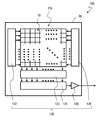
- FIG. 1 schematically shows an exemplary configuration of an imaging device according to a first embodiment of the present disclosure.
- An imaging device 100 illustrated in FIG. 1 includes a pixel array 110 including a plurality of pixels 10 and a peripheral circuit 120.
- the pixel array 110 includes a plurality of pixels 10 arranged, for example, in a matrix of m rows and n columns.
- m and n are natural numbers.
- the pixels 10 are two-dimensionally arranged on the semiconductor substrate 60, for example, to form an imaging region.
- the number and arrangement of the pixels 10 in the pixel array 110 are not limited to the illustrated example.
- the number of pixels 10 included in the imaging device 100 may be one.
- the imaging device 100 can be used as a line sensor.
- Each pixel 10 includes a photoelectric conversion unit that receives light and generates a charge.
- the photoelectric conversion portion of each pixel 10 has a structure including a buried photodiode formed on the semiconductor substrate 60 or a part of the photoelectric conversion layer disposed above the region corresponding to the imaging region in the semiconductor substrate 60. obtain.
- terms such as “upper” and “lower” are used only to designate the mutual arrangement between members, and are not intended to limit the posture when using the imaging device 100.
- the peripheral circuit 120 has a predetermined voltage applied to the vertical scanning circuit 122, the signal holding circuit 123, the horizontal scanning circuit 124, the output stage amplifier 126, and each pixel 10 in the pixel array 110. And a voltage supply circuit 128 for supplying the voltage.
- the peripheral circuit 120 is provided on the semiconductor substrate 60 on which the pixel array 110 described above is formed.
- the arrangement of peripheral circuit 120 is not limited to this example, and part or all of peripheral circuit 120 may be arranged on another substrate different from semiconductor substrate 60.
- the vertical scanning circuit 122 is also referred to as a row scanning circuit, and has, for example, a connection with an address signal line and a reset signal line provided corresponding to each row of the plurality of pixels 10.
- the vertical scanning circuit 122 can execute accumulation and readout of signal charges in the pixels 10 and reset of the accumulated signal charges on a row basis by supplying predetermined signals to the address signal line and the reset signal line. it can.
- the peripheral circuit 120 may have two or more vertical scanning circuits 122. In FIG. 1, in order to avoid complication of the drawing, illustration of various signal lines such as address signal lines and reset signal lines is omitted. Arrows in FIG. 1 schematically indicate the flow of signals supplied to various signal lines such as address signal lines and reset signal lines.
- the signal holding circuit 123 is connected to a vertical signal line (not shown) provided corresponding to each column of the plurality of pixels 10, and has a function of temporarily holding a signal output to the vertical signal line.
- the signal may be held in the form of analog values or in the form of digital values subjected to analog-to-digital conversion.
- the signal holding circuit 123 outputs, to the horizontal scanning circuit 124, the difference between the signal read from the pixel 10 after accumulation of the signal charge and the signal read from the pixel 10 after reset of the signal charge. .
- the operations between the signals may be performed in analog or digital form.
- the horizontal scanning circuit 124 also referred to as a column scanning circuit, typically includes an analog-to-digital converter circuit in part.
- the horizontal scanning circuit 124 has a function of reading out the difference signal obtained by the signal holding circuit 123 for each row of the plurality of pixels 10 to the output stage amplifier 126.
- the voltage supply circuit 128 is electrically connected to each pixel 10, and is configured to switch and supply two or more predetermined voltages to each pixel 10 when the imaging device 100 operates.
- the second voltage V B is a voltage different from the first voltage V A.
- the voltage supply circuit 128 may be configured to be capable of applying a predetermined voltage to each pixel 10 when the imaging device 100 operates, and is not limited to a specific power supply circuit.
- the voltage supply circuit 128 may be a circuit that generates a predetermined voltage, or may be a circuit that converts a voltage supplied from another power supply into a predetermined voltage.
- the voltage supply circuit 128 may be part of the vertical scanning circuit 122.
- the voltage applied from the voltage supply circuit 128 to each pixel 10 is not limited to two different voltages.
- the voltage supply circuit 128 may be configured to be able to switch between three or more different voltages and supply them to each pixel 10.
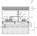
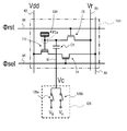
- FIG. 2 schematically illustrates a cross section of an exemplary device structure of the pixel 10.
- FIG. 2 schematically shows the shape, size and arrangement of each part in the pixel 10, and the shape, size and arrangement of each part shown in FIG. 2 do not necessarily reflect the shape, size and arrangement in a real device. The same applies to the other drawings of the present disclosure.
- the pixel 10A illustrated in FIG. 2 is an example of the above-described pixel 10.
- the pixel 10A roughly includes a part of the semiconductor substrate 60 and the photoelectric conversion unit 50A supported by the interlayer insulating layer 40 covering the semiconductor substrate 60.
- the photoelectric conversion unit 50 ⁇ / b> A includes the photoelectric conversion layer 54 located above the region corresponding to the imaging region in the semiconductor substrate 60. That is, a stacked imaging device is illustrated as the imaging device 100 here.
- the semiconductor substrate 60 includes a support substrate 60S and one or more semiconductor layers formed on the support substrate 60S.
- a p-type silicon substrate is illustrated as the support substrate 60S.
- Impurity regions 60 a to 60 e and an element isolation region 65 are provided in the semiconductor substrate 60.
- Each of impurity regions 60a to 60e is typically an n-type diffusion region.
- the photoelectric conversion unit 50A supported by the semiconductor substrate 60 includes the pixel electrode 52 on the interlayer insulating layer 40, the counter electrode 56 positioned farther from the semiconductor substrate 60 than the pixel electrode 52, and the pixel The photoelectric conversion layer 54 located between the electrode 52 and the counter electrode 56 is provided.
- the pixel electrode 52 is an electrode formed of metal such as aluminum or copper, metal nitride, or polysilicon to which conductivity is imparted by doping an impurity.
- the pixel electrode 52 is electrically separated from the pixel electrode 52 in another adjacent pixel 10A by being spatially separated.
- the counter electrode 56 is formed of a transparent conductive material such as ITO.
- transparent means transmitting at least a portion of light in the wavelength range to be detected, and it is not essential to transmit light over the entire wavelength range of visible light.
- the counter electrode 56 may be formed across the plurality of pixels 10A, while the pixel electrode 52 is separated between the pixel electrodes 52 in other adjacent pixels 10A.
- the counter electrode 56 is typically disposed above the semiconductor substrate 60 in the form of a single continuous electrode.
- the photoelectric conversion layer 54 is formed of an organic material or an inorganic material such as amorphous silicon.
- the photoelectric conversion layer 54 is formed, for example, by vacuum evaporation, and may have a thickness of about 500 nm.
- the photoelectric conversion layer 54 may have a layer composed of an organic material and a layer composed of an inorganic material.
- the photoelectric conversion layer 54 receives light incident through the counter electrode 56 and generates positive and negative charges by photoelectric conversion. Similar to the counter electrode 56, the photoelectric conversion layer 54 may also be disposed above the semiconductor substrate 60 in the form of a single continuous layer across the plurality of pixels 10A.
- a voltage line connected to a power supply (not shown) is connected to the counter electrode 56, and the counter electrode 56 has a predetermined bias voltage when the imaging device 100 operates. Receive the supply. By controlling the potential of the counter electrode 56 by application of a predetermined bias voltage, one of the positive and negative charges generated by photoelectric conversion can be collected by the pixel electrode 52 as a signal charge.
- the bias voltage applied to the counter electrode 56 may be supplied from the voltage supply circuit 128 described above.
- a bias voltage that is higher than the pixel electrode 52 may be applied to the counter electrode 56.
- positive charge Typical of positive charges as signal charges are holes. It is of course possible to use a negative charge, eg an electron, as the signal charge.
- a bias voltage that is lower than that of the pixel electrode 52 may be applied to the counter electrode 56.
- the pixel 10A includes the connection portion 42 disposed in the interlayer insulating layer 40. As schematically shown in FIG. 2, one end of the connection portion 42 is connected to the pixel electrode 52 of the photoelectric conversion unit 50.
- the connection unit 42 includes a plurality of wiring layers and a plurality of plugs, and electrically connects the photoelectric conversion unit 50A to a circuit formed on the semiconductor substrate 60.
- the plurality of wiring layers and the plurality of plugs are typically formed of a metal such as copper or tungsten or a metal compound such as metal nitride or metal oxide.
- the signal detection transistor 72, the address transistor 74, and the reset transistor 76 are formed on the semiconductor substrate 60.
- an n-channel field effect transistor represented by an n-channel MOS is exemplified as the signal detection transistor 72, the address transistor 74, and the reset transistor 76.
- a p-type transistor instead of the n-type transistor.
- an n-type silicon substrate may be used as the support substrate 60S, and the p-type is selected as the conductivity type of the impurity regions 60a to 60e.
- the reset transistor 76 includes the impurity region 60a formed in the semiconductor substrate 60 as one of the drain region and the source region, and includes the impurity region 60b as the other of the drain region and the source region.
- the connection portion 42 has a connection with the impurity region 60a, and therefore, the impurity region 60a is electrically connected to the pixel electrode 52 of the photoelectric conversion portion 50A through the connection portion 42. It is connected.
- a reset voltage line for supplying a reset voltage which is a reference voltage for reset is connected to the impurity region 60b.
- the reset transistor 76 is switched on and off to switch supply and cutoff of the reset voltage supplied from the reset voltage line to the impurity region 60a.
- which of the impurity region 60a and the impurity region 60b functions as the drain region of the reset transistor 76 is determined by the potential of the impurity region 60a and the impurity region 60b.
- the impurity region 60a and the impurity region 60b will be described as the drain region and the source region, respectively.
- the drain region and the source region may be interchanged.
- the imaging device 100 includes another transistor connected in series to the reset transistor 76, the same applies to the other transistors connected in series to the reset transistor 76.
- the signal detection transistor 72 includes a gate insulating layer 72g on the semiconductor substrate 60, a gate electrode 72e on the gate insulating layer 72g, an impurity region 60c as a drain region, and an impurity region 60d as a source region.
- a power supply line (not shown) is connected to the impurity region 60c, and a power supply voltage of, for example, 3.3 V is applied to the impurity region 60c from the power supply line when the imaging device 100 operates.
- connection portion 42 is also connected to the gate electrode 72 e of the signal detection transistor 72. That is, the gate electrode 72 e of the signal detection transistor 72 is electrically connected to the pixel electrode 52 of the photoelectric conversion unit 50 A through the connection unit 42.
- address transistor 74 includes an impurity region 60d as a drain region and an impurity region 60e as a source region.
- the address transistor 74 is electrically connected to the signal detection transistor 72 by sharing the impurity region 60 d with the signal detection transistor 72.
- a vertical signal line (not shown) is connected to impurity region 60e.
- the circuit in the pixel 10A is electrically separated from the circuit in the other adjacent pixel 10A by the element isolation region 65.
- the element isolation region 65 is also provided between the signal detection transistor 72 and the reset transistor 76.
- connection portion 42 has a connection with the pixel electrode 52.
- the impurity region 60 a and the gate electrode 72 e of the signal detection transistor 72 are electrically connected to the pixel electrode 52 through the connection portion 42.
- the pixel electrode 52, the connection portion 42, the impurity region 60a, and the gate electrode 72e function as a charge storage node that temporarily holds the signal charge collected by the pixel electrode 52.
- the pixel 10A further includes a control line 81 electrically connected to the connection portion 42.
- the control line 81 is a signal line connected to the voltage supply circuit 128 described above. That is, here, the impurity region 60a has an electrical connection with the voltage supply circuit 128 described above. As described later, a capacitive element or the like may be interposed between the impurity region 60 a and the voltage supply circuit 128.
- a voltage supply circuit 128 to the connecting portion 42 which constitutes a part of the charge storage nodes are electrically connected, switches the output of the voltage supply circuit 128 between the first voltage V A and the second voltage V B. This makes it possible, for example, to temporarily change the potential of the charge storage node after reset.
- the semiconductor substrate 60 has one or more semiconductor layers on the support substrate 60S.
- the semiconductor layer on the support substrate 60S includes a first p-type semiconductor layer 61p, an n-type semiconductor layer 61n, and a second p-type semiconductor layer 62p.
- the above-described impurity regions 60a to 60e and the element isolation region 65 are formed in the second p-type semiconductor layer 62p as ap well.
- the n-type semiconductor layer 61 n is located between the first p-type semiconductor layer 61 p and the second p-type semiconductor layer 62 p, and via an unshown well contact provided outside the imaging region when the imaging device 100 operates. The potential is controlled.
- the n-type semiconductor layer 61 n suppresses the inflow of minority carriers from the support substrate 60S or the peripheral circuit 120 to the charge storage node for storing signal charges.
- the semiconductor substrate 60 is a p-type provided between the second p-type semiconductor layer 62p and the support substrate 60S so as to penetrate the first p-type semiconductor layer 61p and the n-type semiconductor layer 61n. It has a region 63.
- the p-type region 63 has a relatively high impurity concentration, and electrically connects the second p-type semiconductor layer 62p and the support substrate 60S to each other.
- a substrate contact (not shown) is provided outside the imaging region, and the potential of the support substrate 60S and the second p-type semiconductor layer 62p is controlled via the substrate contact when the imaging device 100 operates. In other words, when the imaging device 100 operates, the substrate potential of the semiconductor substrate 60 is controlled via the substrate contact.
- the voltage supply circuit 128 described above may be configured to supply the substrate potential of the semiconductor substrate 60 via the substrate contact.
- an n-type transistor is applied as the signal detection transistor 72, the address transistor 74, and the reset transistor 76 as in the example described here, the substrate potential is typically ground.
- impurity region 60a constitutes a part of the charge storage node that temporarily stores the signal charge generated by photoelectric conversion unit 50A. This is because the junction capacitance formed by the pn junction between the impurity region 60a and the second p-type semiconductor layer 62p functions as a capacitance for accumulating at least a part of the signal charge.
- the pn junction between the impurity region 60a and the second p-type semiconductor layer 62p produces a depletion layer.
- lattice defects are present, and in particular, various lattice defects caused by impurities, dangling bonds, etc. exist on the surface of the semiconductor substrate 60. If a lattice defect exists in the depletion layer, for example, mixing of a charge different from the original signal charge into the impurity region 60a is likely to occur. In other words, lattice defects located in the depletion layer can cause dark current. Dark current results in a reduction in the signal-to-noise ratio and degrades the quality of the obtained image. If the depletion layer in the semiconductor substrate 60 can be reduced as much as possible to reduce lattice defects located in the depletion layer among lattice defects, it is useful because deterioration in image quality due to dark current is suppressed.
- the impurity region 60a in order to reduce the depletion layer formed by the pn junction between the impurity region 60a and the second p-type semiconductor layer 62p, the impurity region 60a after discharging the signal charge from the impurity region 60a. It is effective to make the potential of V close to the substrate potential as much as possible. That is, it is effective to make the potential of the impurity region 60a after reset as close as possible to the substrate potential. For example, when the signal charge is a hole and the substrate potential is ground, it is useful to apply a voltage as low as possible, which is close to 0 V, as the reset voltage.
- the potential of impurity region 60a is increased by electrical coupling through a circuit element such as a transistor connected to impurity region 60a. If it fluctuates, the potential of the impurity region 60a may fall below the substrate potential.
- a field effect transistor when a field effect transistor is connected to an n-type impurity region in a floating node that stores signal charge, the transistor is turned on and on due to the effect of electrical coupling via parasitic capacitance between the source and drain.
- the potential of the impurity region may decrease due to the switching off.
- forward bias is applied to the pn junction between the impurity region and the surrounding p well, and from the p-type silicon substrate as a support substrate Holes will flow into the impurity region. That is, there is a possibility that dark current occurs and the image quality of the obtained image is degraded.
- the present inventors have repeated studies in view of the above, for example, by varying the potential of the charge storage node after the reset by switching the first voltage V A and the second voltage V B, impurities accumulate signal charge region It has been found that it is possible to prevent the charge different from the original signal charge from being mixed in the impurity region with the switching on and off of the connected transistor.
- FIG. 3 schematically shows a typical example of the circuit configuration of the pixel 10A shown in FIG. Note that, in FIG. 2, illustration of voltage lines for supplying a predetermined bias voltage to the counter electrode 56 of the photoelectric conversion unit 50A is omitted in FIG. 2 in order to prevent the drawing from becoming excessively complicated. Likewise, in the following drawings, illustration of voltage lines for supplying a predetermined bias voltage to the counter electrode 56 is omitted.
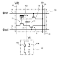
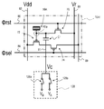
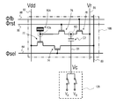
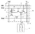
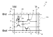
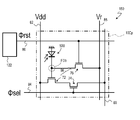
- the gate of the signal detection transistor 72 is connected to the photoelectric conversion unit 50A. It can be said that the node FDa between the photoelectric conversion unit 50A and the signal detection transistor 72 corresponds to a charge storage node. A voltage corresponding to the signal charge stored in the node FDa is applied to the gate of the signal detection transistor 72. As shown, the drain of the signal detection transistor 72 is connected to a power supply line 82 as a source follower power supply for supplying the power supply voltage Vdd, and the source of the signal detection transistor 72 is a vertical signal via the address transistor 74. Line 89 is connected. That is, the signal detection transistor 72 and the address transistor 74 form a source follower.
- An address signal line 84 connected to the vertical scanning circuit 122 is connected to the gate of the address transistor 74.
- the vertical scanning circuit 122 can read out the signal from the pixel 10 A to the vertical signal line 89 by controlling the address signal selsel applied to the address signal line 84.
- the reset transistor 76 is also connected to the node FDa.
- the side of the source and drain of the reset transistor 76 which is not connected to the node FDa is connected to the reset voltage line 85.
- a predetermined reset voltage Vr is applied to the reset voltage line 85.
- the reset signal line 86 connected to the vertical scanning circuit 122 is connected to the gate of the reset transistor 76. Under control of the reset signal ⁇ rst applied to the reset signal line 86, the vertical scanning circuit 122 can turn on the reset transistor 76 and apply the reset voltage Vr to the charge storage node. As described with reference to FIG.
- the reset transistor 76 includes the impurity region 60a forming a part of the charge storage node as a drain region or a source region. When the reset transistor 76 is turned on, the signal charge is discharged from the charge storage node, and the potential of the charge storage node is reset.
- the voltage supply circuit 128 is further electrically connected to the node FDa.
- the capacitive element C1 is interposed between the node FDa and the control line 81 connected to the voltage supply circuit 128.
- the node FDa is connected to one of the two terminals of the capacitive element C1. That is, in this example, one terminal of the capacitive element C1 is electrically connected to the impurity region 60a.
- the voltage supply circuit 128 is connected to the other of the two terminals of the capacitive element C1.
- the capacitive element C1 may have, for example, a metal-insulator-semiconductor (MIS) structure disposed in the interlayer insulating layer 40, or may be a depression-type MOS (DMOS) capacitor. Alternatively, it may be a MIM (metal-insulator-metal) structure. Adopting the MIM structure makes it easy to obtain a larger capacity value.
- MIS metal-insulator-semiconductor
- DMOS depression-type MOS
- MIM metal-insulator-metal
- voltage supply circuit 128 has switching elements 128a and 128b configured of field effect transistors or the like. That is, here, the voltage supply circuit 128, the switching by switching the switching elements 128a and 128b on and off, the voltage Vc applied to the control line 81 between the first voltage V A and the second voltage V B It is possible.
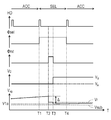
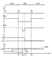
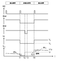
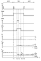
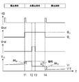
- FIG. 4A is a timing chart for explaining an exemplary operation of the pixel 10A having the circuit configuration shown in FIG.
- the top chart in FIG. 4A shows pulses of the horizontal synchronization signal HD.
- the period from the rise of a certain pulse to the rise of the next pulse corresponds to 1 H which is one horizontal scanning period.
- the reset of the pixels 10A belonging to one certain row among the plurality of pixels 10A included in the pixel array 110 and the readout of the signal from the pixels 10A are performed.
- the double arrow SEL in FIG. 4A indicates a selection period in which the address transistor 74 of the pixel of interest is turned on, and the arrow ACC indicates a non-selection period in which the address transistor 74 is turned off.
- the bottom chart in FIG. 4A shows temporal changes of the potential of the node FDa, ie, the potential V FD of the impurity region 60a, and the second chart from the bottom is applied from the voltage supply circuit 128 to the control line 81.
- the temporal change of voltage Vc is shown.
- the first voltage V A is applied to the control line 81.
- the address signal selsel After accumulation of signal charges by exposure, the address signal selsel is set to high level at time T1. By setting the address signal selsel to a high level, a first signal of a voltage level corresponding to the signal charge stored in the charge storage node is read out to the vertical signal line 89 through the signal detection transistor 72 and the address transistor 74. The read first signal is temporarily held by the signal holding circuit 123 shown in FIG.
- the reset signal rstrst is set to the high level, and the reset transistor 76 is turned on.
- the reset transistor 76 is turned on, the signal charge is discharged from the charge storage node, and the potential of the charge storage node is reset.
- the potential V FD of the impurity regions 60a by the reset voltage Vr is applied to the node FDa falls to Vr.
- a voltage higher than the substrate potential Vsub is used as the reset voltage Vr. Therefore, here, Vr> Vsub.
- the substrate potential Vsub is 0 V, a positive voltage near 0 V is used as the reset voltage Vr.
- the reset signal rstrst is set to low level, and the reset transistor 76 is turned off.
- the reset transistor 76 includes the impurity region 60 a as a drain region or a source region. Therefore, when the reset transistor 76 is turned off, the potential V FD of the impurity region 60a may be further lowered from Vr due to the electrical coupling caused by the parasitic capacitance of the reset transistor 76. As described above, at this time, if the potential V FD falls below the substrate potential Vsub, extra holes flow into the impurity region 60a.
- the potential V FD of the impurity region 60a immediately after the reset transistor 76 is off is V1a satisfying the relationship of Vr>V1a> Vsub.
- V1a may be about 0.2V. That is, the second voltage V B and appropriate selection, by switching between the output from the voltage supply circuit 128 of the first voltage V A and the second voltage V B, the potential V FD is the substrate potential Vsub of the impurity regions 60a It is prevented that it falls below.
- a potential difference of 0.2 V can be secured at the potential V FD of the impurity region 60 a with reference to the substrate potential. That is, the inflow of unnecessary holes to the impurity region 60a due to the potential V FD falling below the substrate potential Vsub is prevented. In other words, dark current is suppressed.
- V B the source of the reset transistor 76 - in consideration of the magnitude of the parasitic capacitance between the drain potential V FD when off the reset transistor 76 satisfies the relation of V1a> Vsub It is sufficient to select a voltage that will
- a second signal corresponding to the voltage level of the charge storage node after discharge of the signal charge is transmitted through the address transistor 74 during a period until time T4 when the next pulse of the horizontal synchronization signal HD And read out to the vertical signal line 89.
- the signal holding circuit 123 outputs the difference ⁇ between the first signal and the second signal to the horizontal scanning circuit 124 as a signal representing an image.
- the address transistor 74 is turned off, and accumulation of signal charge of the next frame is started.
- the voltage supply circuit 128 applies the first voltage V A to the impurity region 60 a during the first period from time T2 to T3 in which the reset transistor 76 is turned on. It followed, in the second period of time T3 ⁇ T4, and is configured to switch the voltage applied to the impurity regions 60a to a second voltage V B.
- the potential V FD of the impurity regions 60a with the off of the reset transistor 76 is possible to prevent that fall below the substrate potential Vsub. Therefore, it is possible to suppress the dark current generated by the flow of extra holes into impurity region 60a.
- capacitive element C1 since capacitive element C1 has an electrical connection with node FDa, at least one of the charge storage nodes for temporarily holding the signal charge, like impurity region 60a. Make up the department. In other words, the connection of capacitive element C1 to node FDa increases the capacitance value of the entire charge storage node. It is advantageous for the capacitance value of the capacitive element C1 to be as small as possible for the following two reasons.
- the first reason is that an increase in the capacitance value of the entire charge storage node results in a decrease in conversion gain. If the conversion gain is lowered, the influence of noise in the subsequent stage circuit becomes large, and there is a possibility that the SN ratio may be lowered. Therefore, from the viewpoint of avoiding the decrease in the SN ratio, it is useful that the capacitance value of the capacitive element C1 be as small as possible.
- the second reason is that if the capacitive element C1 has a relatively large capacitance value, the influence of noise mixing on the control line 81 via the capacitive element C1 to the node FDa may increase.
- Noise included in the voltage applied to control line 81 can be mixed in node FDa by electrical coupling via capacitive element C1.
- the configuration in which the voltage supplied to control line 81 is commonly applied to the charge storage nodes of the pixels belonging to the same row via the capacitive element C1 in other words, the first voltage V A
- the noise on the control line 81 may appear on the image as a horizontal line noise. It is useful to be able to suppress the horizontal noise because the horizontal noise tends to be easily recognized by the viewer of the image as compared to the random noise in units of pixels.
- capacitance value of capacitance element C1 is C 1 and the capacitance value of a portion other than capacitance element C1 of the charge storage nodes is C FD
- the magnitude of the voltage variation transmitted to node FDa is the voltage variation of control line 81 It is represented by the product of C 1 / (C 1 + C FD )). Therefore, in terms of horizontal noise suppression, capacitance value C 1 of the capacitor C1 is advantageously as small as possible.
- the capacitance value C 1 of the capacitor element C1, the capacitance value of the portions other than the capacitor element C1 of the charge storage node is beneficial to be smaller than C FD. It is made smaller than the capacitance value C FD portion other than the capacitive element C1 of the charge storage node capacitance value C 1 of the capacitor C1, the reduction in the SN ratio caused by connecting a capacitor C1 to the node FDa The degree may be smaller than the degree of reduction of the SN ratio when the F value is increased by one level.
- the capacitance value C 1 of the capacitor element C1 with the degree less than half of the capacitance value C FD, the degree of reduction of the SN ratio caused by connecting a capacitor C1 to node FDa, converted to F value
- the change can be limited to about (1/2) or less.
- the reset voltage Vr Since a larger positive voltage is used as the reset voltage Vr, the influence of the reduction in the potential V FD of the impurity region 60a due to the electrical coupling caused by the parasitic capacitance of the reset transistor 76 accompanying the turning off of the reset transistor 76 is small. It can be said. However, when using electrons as signal charges, it is necessary to use a higher voltage as the reset voltage Vr in order to improve the number of saturated electrons, and from the viewpoint of securing the number of saturated electrons sufficient for the required dynamic range, It is more advantageous to use holes as the charge.
- the conductivity type of each region in the semiconductor substrate 60 may be switched between n-type and p-type.
- the p-type transistor as the reset transistor 76 as described below, as the second voltage V B, using a voltage lower than the first voltage V A.
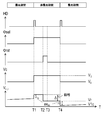
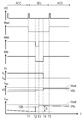
- FIG. 4B is a timing chart for explaining an exemplary operation when a p-type transistor is applied to the reset transistor 76 of the pixel 10A.
- a p-type transistor is applied to the reset transistor 76
- a higher voltage is used as a substrate potential Vsub than when an n-type transistor is applied to the reset transistor 76.
- Substrate potential Vsub may be, for example, about 3.3V.
- the effect of the change in the potential V FD of the impurity region 60a due to the electrical coupling caused by the parasitic capacitance of the reset transistor 76 is better when holes are used as signal charges. Is small. This is because of the same reason as in the case where an n-type transistor is applied to the reset transistor 76 and electrons are used as signal charges. However, in order to secure a sufficient number of saturated electrons, it is necessary to secure a sufficient potential difference between the substrate potential and the potential V FD of the impurity region 60a. On the other hand, if the signal charge is an electron, a voltage near 3.3 V which is the substrate potential may be used as the reset voltage Vr. When a p-type transistor is applied to the reset transistor 76, the signal charge is Using electrons is easier to secure a sufficient number of saturated electrons in the required dynamic range while avoiding circuit complexity.
- FIG. 4B shows an example of operation in the case where a p-type transistor is applied to the reset transistor 76 and electrons are used as signal charges.
- the reset transistor 76 is a p-type transistor and electrons are used as signal charges
- the signal detection transistor 72 and the address transistor 74 are also formed on the semiconductor substrate 60 as p-type transistors.
- the potential V FD of the impurity region 60a gradually decreases due to the accumulation of the signal charge due to the exposure.
- the address signal selsel is set to low level at time T1 to turn on the address transistor 74, and the first signal is read out to the vertical signal line 89.
- the reset signal rstrst is set to low level, and the reset transistor 76 is turned on.
- the potential V FD of the impurity region 60a rises to Vr.
- the reset voltage Vr at this time for example, a voltage of 2.8 V which is near the substrate potential Vsub and lower than the substrate potential Vsub is used.
- the reset signal rstrst is set to the high level, and the reset transistor 76 is turned off.
- the electrical coupling caused by the parasitic capacitance of the reset transistor 76 may further increase the potential V FD of the impurity region 60a from Vr.
- V FD exceeds the substrate potential Vsub
- a forward bias is applied to the pn junction between the impurity region 60a and the periphery thereof, and an n-type silicon substrate as a support substrate is redundantly connected to the impurity region 60a. Electrons flow in. In other words, dark current occurs.
- the time T3 only a reset signal ⁇ rst a high level, and switches the voltage Vc applied from the voltage supply circuit 128 to the control line 81 to lower than the first voltage V A second voltage V B .
- the potential of the node FDa between the photoelectric conversion unit 50A and the signal detection transistor 72 can be reduced via the capacitive element C1, As shown in FIG. 4B, the potential V FD of the impurity region 60a can be prevented from exceeding the substrate potential Vsub.
- the potential V FD of the impurity region 60a immediately after the reset transistor 76 is turned off is V1b which satisfies the relationship Vsub>V1b> Vr.
- V1b may be about 3.1V.
- the reset transistor 76 After the reset transistor 76 is turned off, the second signal corresponding to the voltage level of the charge storage node after discharging the signal charge is read out to the vertical signal line 89, and the absolute value of the difference ⁇ between the first signal and the second signal is obtained. Obtained as an image signal. After obtaining the second signal, the address transistor 74 is turned off, and accumulation of signal charge of the next frame is started.
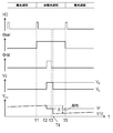
- control line 81 is connected between the exposure period for accumulating signal charges in the charge accumulation node and the period for resetting in a non-exposure period other than the exposure period of one frame period.
- the voltages supplied may be different from each other.
- FIG. 4C is a timing chart for explaining another example of the operation of the pixels 10A, 10Ap and 10Aq. Similar to the example shown in FIGS. 4A and 4B, in the operation example shown in FIG. 4C, the exposure period for accumulating the signal charge in the charge storage node and the non-exposure period other than the exposure period are alternately repeated.
- the non-exposure period includes, in part, a reset period for resetting the potential of the charge storage node to a predetermined potential.
- the pixel 10A shown in FIG. 3 is illustrated.
- the address signal selsel is made high.
- ⁇ V FD (V B ⁇ V A ) (C 1 / (C 1 + C FD )) (1)
- the potential of the node FDa at this time is read out to the vertical signal line 89 through the signal detection transistor 72 and the address transistor 74 as a first signal expressing a voltage level corresponding to the signal charge stored in the charge storage node.
- the reset signal rstrst is made high. Thereby, the signal charge is discharged from the charge storage node through the reset transistor 76, and the potential of the charge storage node is reset to the reset voltage Vr.
- the reset signal rstrst is set to low level, and the reset transistor 76 is turned off. From time T3 to time T4 at which the next pulse of horizontal synchronization signal HD rises, the second signal corresponding to the voltage level of the charge storage node after discharge of the signal charge is made vertical via address transistor 74. Read on line 89.
- the difference ⁇ between the first signal read from time T1 to time T2 and the second signal read from time T3 to time T4 represents an image. It becomes a true pixel signal.
- the voltage applied to the control line 81 is returned to the first voltage V A again.
- the potential of the node FDa drops from Vr to V1c due to capacitive coupling via the capacitive element C1.
- the fluctuation amount of the potential of the node FDa at this time (Vr ⁇ V1c) is equal to the above-described ⁇ V FD .
- the fluctuation amount ⁇ V FD is controlled by determining the first voltage V A and the second voltage V B based on the above equation (1). be able to.
- the desired ⁇ V FD can be achieved by the following procedure. First, at the time of product design, the capacitance ratio between the capacitive element C1 and a portion of the charge storage node other than the capacitive element C1 is determined from the total capacitance value of the target charge storage node. Then, the amplitude of the voltage applied to the control line 81 during actual operation, i.e., a specific voltage value of the first voltage V A and the second voltage V B is determined based on equation (1) above.
- either the first voltage VA or the second voltage VB is at ground (0 V). Since the ground side is generally low impedance, it is possible to suppress the mixing of power supply noise from the voltage supply circuit 128 connected to the control line 81 into the charge storage node. For example, when the second voltage V B is grounded, the first voltage V A is a negative level voltage.
- the voltage supply circuit 128, the control line 81, and supplies the first voltage V A to the exposure period for accumulating the signal charges impurity regions 60a to charge storage node includes in its part.
- a second voltage V B different from the first voltage V A is supplied.
- control may be employed to differ between at least the reset period and the other periods after the exposure period. According to such control, for example, the potential of the charge storage node can be temporarily reduced compared to the reset voltage Vr.
- the potential difference between the impurity region 60a and the second p-type semiconductor layer 62p located around it and grounded, for example, can be reduced.
- the depletion layer formed by the pn junction between the impurity region 60a and the second p-type semiconductor layer 62p is reduced, and the reduction of dark current is realized. That is, by setting the potential of the charge storage node to a low potential in the exposure period, an effect of dark current reduction can be expected.
- the potential of the charge storage node is raised by the potential difference amount between the second voltage V B and the first voltage V A. Therefore, by adjusting this potential difference, it is possible to set the source-drain voltage of the signal detection transistor 72 and the transistor of the subsequent stage circuit within the voltage range in which these transistors can operate. Therefore, the signal detection transistor 72 and the rear stage circuit can normally read out the pixel signal or the reference signal.
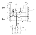
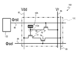
- FIG. 5 schematically shows an example of another circuit configuration of the pixel 10.
- the pixel 10Ap illustrated in FIG. 5 includes a photoelectric conversion unit 50B instead of the photoelectric conversion unit 50A.
- the photoelectric conversion unit 50B is, for example, a buried photodiode formed in the semiconductor substrate 60.
- the photoelectric conversion unit 50B is connected to the gate of the signal detection transistor 72.
- the node FDb between the photoelectric conversion unit 50B and the signal detection transistor 72 corresponds to a charge storage node.
- the pn junction in the embedded photodiode as the photoelectric conversion unit 50B, the impurity region 60a and the gate electrode 72e function as charge storage nodes for temporarily holding the charge generated by the photoelectric conversion unit 50B.
- Impurity region 60a may be part of a pn junction in the buried photodiode.
- the same operation as the operation described with reference to FIGS. 4A and 4B can be applied to the imaging device 100 having the pixel 10Ap.
- the reset signal ⁇ rst a low level
- to switch the voltage Vc applied to the control line 81 from the voltage supply circuit 128 from the first voltage V A higher than the first voltage V A second voltage V B the potential of the node FDb can be increased through the capacitive element C1.
- the second voltage V B the potential V FD of the impurity regions 60a is avoided that below the substrate potential Vsub, can suppress dark current.
- the reset transistor 76 or the like is a p-type transistor and electrons are stored as signal charges, which is more advantageous because a larger dynamic range can be obtained.
- FIG. 6 schematically shows an example of still another circuit configuration of the pixel 10.
- the pixel 10Aq illustrated in FIG. 6 further includes the transfer transistor 79 connected between the gate of the signal detection transistor 72 and the photoelectric conversion unit 50B.
- the transfer transistor 79 transfers the signal charge obtained by the photoelectric conversion unit 50B to a node FDc between the gate of the signal detection transistor 72 and the transfer transistor 79 at a predetermined timing.
- the transfer transistor 79 is, for example, an n-channel MOS.
- the transfer transistor 79 may share the impurity region 60 a with the reset transistor 76 as one of a source region and a drain region.
- the circuit configuration shown in FIG. 6 similar to the pixel 10Ap shown in FIG. 5, by switching the voltage Vc from the first voltage V A to the second voltage V B, the potential of a floating node node FDc, capacitance
- the potential V FD of the impurity region 60a can be avoided, for example, from rising below the substrate potential Vsub through the element C1.
- Switching of the voltage Vc from the first voltage V A to the second voltage V B is performed, for example, at the timing of turning off the reset transistor 76 after discharging the signal charge transferred to the node FDc by turning on the reset transistor 76. Be done.
- FIG. 7A and 7B schematically show an example of still another circuit configuration of the pixel 10.
- the pixel 10Ar shown in FIG. 7A has a signal detection transistor 72d of a depletion type instead of the signal detection transistor 72.
- a depletion type transistor as the signal detection transistor 72d, a high output can be obtained from the signal detection transistor 72d even when the potential of the node FDa is at a low level. Therefore, it becomes easier to secure the voltage range necessary for the operation of the current source configured of the load circuit and the like connected to the vertical signal line 89.
- the pixel 10As shown in FIG. 7B has a configuration in which the photoelectric conversion unit 50A of the pixel 10Ar shown in FIG. 7A is replaced with a photoelectric conversion unit 50B.
- the photoelectric conversion unit 50B is, for example, a buried photodiode formed in the semiconductor substrate 60. Even in the configuration using a photodiode, a depletion type transistor can be used as the signal detection transistor 72d.
- FIG. 8 is a timing chart for explaining an exemplary operation of the pixel 10Ar shown in FIG. 7A or the pixel 10As shown in FIG. 7B.
- the waveform of the voltage Vc in the non-exposure period is different from the waveform in the operation sequence illustrated in FIG. 4C.
- FIG. 8 wherein, in the non-exposure period, a short period of relatively high second voltage V B voltage Vc to be applied to the control line 81 from the voltage supply circuit 128.
- the voltage Vc is switched from the first voltage V A to the relatively high second voltage V B at the rise timing of the reset signal rstrst at time T 2, and the reset signal rstrst is low at time T 3 After being switched to the level, it is returned to the first voltage V A.
- the reset transistor 76 After the reset transistor 76 is turned off, the voltage Vc applied from the voltage supply circuit 128 to the control line 81 is switched to the first voltage VA , thereby contributing all changes in the voltage Vc to the change in the potential of the charge storage node. It becomes possible.
- the potential of the charge storage node drops from the reset voltage Vr by ⁇ V FD represented by the formula (1).
- the potential of the charge storage node can be lowered to a potential V1d lower than Vr.
- the true pixel signal representing the image of the subject is given by the difference between the first signal corresponding to the potential of the charge storage node at time T1 and the second signal corresponding to the potential of the charge storage node at time T4. .
- the first signal is read out to the vertical signal line 89 between time T1 and time T2, and the second signal is read out to the vertical signal line 89 between time T4 and time T5. That is, in this example, when the first voltage V A is applied to the control line 81, readout of the pixel signal and the reference signal is performed. Similarly, in this example, by using a voltage of 0V as the first voltage V A, it is possible to suppress the contamination of the noise nodes FDa or node FDb in voltage output from the voltage supply circuit 128.
- FIG. 9A and 9B schematically show an example of still another circuit configuration of the pixel 10.
- the pixel 10At shown in FIG. 9A is an example in which p-type transistors are applied as the signal detection transistor 72, the address transistor 74 and the reset transistor 76 in the circuit configuration shown in FIG.
- a pixel 10Au shown in FIG. 9B is an example in which p-type transistors are applied as the signal detection transistor 72, the address transistor 74 and the reset transistor 76 in the circuit configuration shown in FIG.
- electrons are typically used as signal charges.
- a p-type transistor is applied to the reset transistor 76, using electrons as the signal charge secures a sufficient number of saturated electrons in the required dynamic range while avoiding complication of the circuit. Cheap.
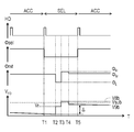
- FIG. 10 is a timing chart for explaining an exemplary operation of the pixel 10At shown in FIG. 9A or the pixel 10Au shown in FIG. 9B.
- the address signal ⁇ sel from the high level to the low level, switching the voltage Vc applied to the control line 81 to the relatively low from the first voltage V A second voltage V B .
- the address signal selsel is maintained at the low level in the non-exposure period.
- the potential of the charge storage node is obtained by capacitive coupling via the capacitive element C1. Decreases.
- the variation amount ⁇ V FD of the potential at this time is expressed by the above-mentioned equation (1) by the capacitance ratio between the capacitive element C1 and the portion of the charge storage node other than the capacitive element C1. From time T1 to time T2, a signal corresponding to the voltage V FD at this time is read out to the vertical signal line 89 as a first signal.
- the reset is performed by setting the reset signal rstrst to low level. That is, when the reset signal rstrst is set to low level, the reset transistor 76 is turned on, the signal charge stored in the node FDa or FDb is discharged through the reset transistor 76, and the potential of the charge storage node becomes the voltage Vr. It is reset.
- the reset signal rstrst is set to the high level to turn off the reset transistor 76.
- the second signal corresponding to the reset voltage Vr is read out to the vertical signal line 89 from time T3 to time T4.
- the difference between the first signal read from time T1 to time T2 and the second signal read from time T3 to time T4. are output as true pixel signals.
- the signal detection transistor 72, the address transistor 74, and the reset transistor 76 be p-type transistors.
- the reset transistor 76 is an n-channel MOS, for example, 0 V is used as the substrate potential Vsub.
- the reset transistor 76 is a p-channel MOS, and 0 V is adopted as the substrate potential Vsub.
- voltage V FD is lowered along with accumulation of electrons which are signal charges in the charge storage node, so that the voltage is applied to the pn junction between impurity region 60a and the periphery thereof. It is necessary to reset the potential of the charge storage node to a potential higher than the substrate potential Vsub prior to the accumulation of the signal charge in order to avoid the forward bias of the output voltage.
- the signal charge is an electron
- a voltage of 3.3 V can be used as the reset voltage Vr.
- the potential of the charge storage node drops from, for example, 3.3 V at the start of the exposure, and the potential difference between it and the substrate potential Vsub decreases. Therefore, the depletion layer width is reduced, and the effect of dark current reduction can be expected.
- the potential V FD of impurity region 60a is set to the substrate potential Vsub to prevent the applied voltage from becoming forward bias. It can not be raised more than that.
- the potential V FD of the impurity region 60a rises. Therefore, prior to the accumulation of the signal charge, the potential of the charge storage node is reset to a potential of, for example, 0 V lower than the substrate potential Vsub. In this case, the difference between the potential of the charge storage node at the start of exposure and the substrate potential Vsub is enlarged as compared with the case where an n-channel MOS is used as the reset transistor 76.
- 11A and 11B schematically show an example of still another circuit configuration of the pixel 10.
- the pixel 10Av shown in FIG. 11A further includes a transistor 71 connected between the capacitive element C and the control line 81.
- the difference between the pixel 10Av shown in FIG. 11A and the pixel 10Aw shown in FIG. 11B is that in the pixel 10Aw, the transistor 71 is connected between the node FDa and the capacitive element C1.
- the transistor 71 in the pixel 10Av illustrated in FIG. 11A has a function as a switching element that switches connection and disconnection between the capacitive element C1 and the voltage supply circuit 128.
- the transistor 71 in the pixel 10Aw illustrated in FIG. 11B has a function as a switching element that switches connection and disconnection between the node FDa and the capacitive element C1.
- the capacitance value of the entire charge storage node can be reduced.
- capacitive element C1 can be electrically disconnected from node FDa.
- capacitive element C1 is connected to node FDa or node FDb, and the voltage supplied to control line 81 is switched to control the potential of the charge storage node via capacitive element C1. It becomes possible. However, since the capacitance value of the entire charge storage node is increased as a result of connecting the capacitive element C1, the conversion gain at the time of converting the signal charge into a voltage may be reduced.
- a transistor 71 may be interposed between the capacitive element C1 and the voltage supply circuit 128, or between the node FDa or the node FDb and the capacitive element C1.
- the on / off switching of the transistor 71 can change the capacitance value of the entire charge storage node.
- the FD potential control mode in which the potential of the charge storage node is controlled via the capacitive element C1 by switching on and off of the transistor 71, and the high gain mode in which the signal charge is efficiently converted into a voltage signal. It becomes possible to use properly.
- the FD potential control mode is a mode in which the transistor 71 is turned on to electrically couple the voltage supply circuit 128 to the charge storage node via the capacitive element C1. In the high gain mode, the transistor 71 is turned off and the entire charge storage node is turned off. Is a mode in which the capacitance value of
- the mode switching may be automatically performed using an exposure time or an operating temperature as a criterion that has a large influence on dark current, or may be performed based on a user's instruction.
- the FD potential control mode may be selected for imaging under a long second exposure for over 1 second or a high temperature environment for over 80 degrees.
- the operation sequence in the FD potential control mode may be the same as the operation sequence described with reference to FIG. 4A, FIG. 4B, FIG. 4C, FIG. 8 or FIG.
- FIG. 11C schematically shows an example of still another circuit configuration of the pixel 10.
- the imaging device 100 includes a load transistor 73 connected to the vertical signal line 89.
- the load transistor 73 is, for example, an n-channel MOS, and functions as a current source 94.
- the imaging device 100 includes a feedback circuit 90x.
- the feedback circuit 90x includes an inverting amplifier 92 whose inverting input terminal is connected to the vertical signal line 89.
- the inverting amplifier 92 is provided for each column of the pixels 10Ax corresponding to the vertical signal line 89, and here, the reset voltage line 85 is connected to the output terminal thereof.
- the signal detection transistor 72, the address transistor 74, the inverting amplifier 92, and the reset transistor 76 form a feedback loop that negatively feeds back the electrical signal generated by the photoelectric conversion unit 50A.
- a voltage Vref of, for example, 1 V or near 1 V is supplied to the non-inverting input terminal of the inverting amplifier 92.
- the voltage Vref any voltage within the range of the power supply voltage Vdd and the ground can be used.
- the feedback loop is formed, the voltage of the vertical signal line 89 converges to the voltage Vref input to the non-inverting input terminal of the inverting amplifier 92.
- the potential of the node FDa can be reset to a potential at which the voltage of the vertical signal line 89 becomes Vref.
- the first signal and the second signal are read out to the vertical signal line 89 by the source follower formed by the signal detection transistor 72 and the current source 94.
- the potential of the node FDa at the time of signal reading is low, the voltage appearing on the vertical signal line 89 via the signal detection transistor 72 is also low, and the source-drain voltage necessary for operation in the saturation region can not be secured.
- the load transistor 73 may operate in the linear region. As a result, the source follower may not operate properly and the linearity of the signal may be degraded.
- the current value obtained by the current source 94 is set small, it is possible to operate the load transistor 73 in the saturation region, but in this case, a problem such as a reduction in the speed required for reading out a signal may occur. Further, the voltage drop of the vertical signal line 89 may cause the input signal to the inverting amplifier 92 to be out of the operating range, and the feedback circuit 90x may not operate properly. That is, there is a possibility that the potential of the node FDa can not be reset to such a potential that the voltage of the vertical signal line 89 becomes Vref.
- the operation sequence described with reference to FIG. 4C, FIG. 8 or FIG. 10 can be applied.
- the potential of the charge storage node in at least a part of the period of non-exposure period, through the capacitor C1 Temporarily raise or lower.
- the potential of the charge storage node is selectively raised in a non-exposure period other than the exposure period by switching the voltage applied from the voltage supply circuit 128 to the control line 81.
- the load transistor 73 By setting the potential of the charge storage node to a high potential selectively in the non-exposure period, the load transistor 73 is prevented from operating in the linear region, and the first signal and the second signal are normally output from the pixel. It is possible to read out. Since the signal read operation and the feedback operation are performed during the non-exposure period, there is no problem even if the potential of the charge storage node is low such that the load transistor 73 operates in the linear region during the exposure period. Absent. By setting the potential of the charge storage node to a low potential in the exposure period, it is possible to obtain an effect that the dark current can be suppressed without deteriorating the circuit characteristics.
- FIG. 12 schematically illustrates an example of the circuit configuration of the pixel 10B included in the imaging device according to the second embodiment of the present disclosure. Similar to the pixel 10A shown in FIG. 3, the pixel 10B shown in FIG. 12 is an example of the pixel 10 described above. The main difference between the pixel 10B shown in FIG. 12 and the pixel 10A described with reference to FIG. 3 is that the pixel 10B is not connected to the node FDa among the source and drain of the reset transistor 76. It is the point which further has the transistor 78 connected. Also, the voltage supply circuit 128 is electrically connected to a node RD between the reset transistor 76 and the transistor 78. In this example, voltage supply circuit 128 is electrically connected to impurity region 60 a via reset transistor 76.
- each pixel 10 of the imaging device 100 may have a circuit configuration further including a transistor 78 connected to the reset transistor 76.
- the transistor 78 is, for example, an n-channel MOS, and can include an impurity region 60 b as a source region or a drain region of the reset transistor 76 as a drain region or a source region.
- the reset voltage line 85 is connected to the side not connected to the reset transistor 76. For example, when the imaging device 100 operates, a predetermined reset is performed. A voltage Vr is applied to the transistor 78.
- the gate of the transistor 78 is connected to a signal line 88 for supplying the transistor 78 with a signal fb fb for controlling the on and off of the transistor 78.
- the signal line 88 has, for example, a connection with the vertical scanning circuit 122, and the vertical scanning circuit 122 can be configured to control the potential of the signal line 88.
- voltage supply circuit 128 is connected to a node RD between reset transistor 76 and transistor 78 via capacitive element C2. That is, in this example, the voltage supply circuit 128 is connected not to the impurity region 60a side of the reset transistor 76 but to the impurity region 60b side via the capacitive element C2.
- the capacitive element C2 connected between the control line 81 and the impurity region 60b can have the same configuration as the above-mentioned capacitive element C1.
- FIG. 13 shows a more specific example to which the circuit configuration shown in FIG. 12 is applied.
- the pixel 10 ⁇ / b> Bf illustrated in FIG. 13 is an example of the pixel 10 ⁇ / b> B illustrated in FIG. 12 and includes a feedback circuit 90.
- the feedback circuit 90 includes an inverting amplifier 92 whose inverting input terminal is connected to the vertical signal line 89, as in the example described with reference to FIG. 11C.
- the pixel 10 ⁇ / b> Bf includes a capacitive element C ⁇ b> 3 connected in parallel to the reset transistor 76.
- the feedback circuit 90 forms a feedback loop that negatively feeds back the electrical signal generated by the photoelectric conversion unit 50A.
- the feedback loop includes transistor 78 in part.
- thermal noise called kTC noise occurs when the transistor is turned on or off. After resetting the potential of the node FDa, simply turning off the reset transistor 76 causes kTC noise generated by turning off the reset transistor 76 to remain at the charge storage node before the signal charge is stored.
- the kTC noise generated with the turning off of the reset transistor can be reduced by using negative feedback as described in WO 2012/147302. The entire disclosure of WO 2012/147302 is incorporated herein by reference.
- this node RD is a floating node.
- the transistor 78 can include the impurity region 60b, for example, as a drain region. Therefore, when the transistor 78 is turned off, there is a possibility that the potential of the impurity region 60b may fall below the substrate potential due to electrical coupling caused by the parasitic capacitance of the transistor 78. When the potential of the impurity region 60b is lower than the substrate potential, the inflow of unnecessary holes from the p well causes an unintended fluctuation of the potential in the impurity region 60b, which may lower the SN ratio.
- the voltage supply circuit 128 is electrically connected to the impurity region 60 b. As described below, by switching the voltage Vc to be applied to the control line 81 from the voltage supply circuit 128 between the first voltage V A and the second voltage V B, the potential of the impurity region 60b is lower than the substrate potential Can be prevented.
- FIG. 14A is a timing chart for describing an exemplary operation of the pixel 10Bf having the circuit configuration shown in FIG.
- the second chart from the bottom in FIG. 14A shows temporal changes in the potential of the node RD, ie, the potential V RD of the impurity region 60b.
- Vc the potential of the node RD
- V A the potential of the impurity region 60b.
- the address signal selsel is set to the high level. At this time, the first signal of the voltage level corresponding to the signal charge stored in the charge storage node is read out.
- the reset signal rstrst and the signal fbfb are set to the high level. That is, the reset transistor 76 and the transistor 78 are turned on. The turning on of the reset transistor 76 and the transistor 78 forms a feedback loop. The formation of the feedback loop resets the potential of the node FDa.
- the potential of the node FDa is lowered to the voltage V2a such that the voltage of the vertical signal line 89 becomes Vref.
- a voltage that satisfies the relationship of V2a> Vsub is used as the voltage Vref applied to the non-inversion amplification terminal of the inversion amplifier 92.
- the potential V RD of the node RD with the ON of the reset transistor 76 and the transistor 78 is increased to V3.
- the voltage V3 satisfies the relationship of V3> Vsub.
- the reset signal rstrst is set to low level, and the reset transistor 76 is turned off.
- the potential V FD of the impurity region 60a is lowered from V2a to V4a as the reset transistor 76 is turned off.
- the potential V FD falls below the substrate potential Vsub, extra holes flow into the impurity region 60a.
- the relationship of V4a> Vsub is satisfied by properly selecting the voltage Vref. From the viewpoint of reducing the depletion layer as much as possible, it is useful that V4a be as close as possible to Vsub as long as the relationship of V4a> Vsub is satisfied.
- the capacitive element C3 is interposed between the node FDa and the node RD, and while the transistor 78 is not turned off, a feedback loop including the capacitive element C3 in its path is formed. Condition will continue. Therefore, the signal output from the transistor 78 is attenuated by the attenuation circuit formed by the capacitive element C3 and the parasitic capacitance of the node FDa itself.
- the signal fbfb is set to low level, and the transistor 78 is turned off.
- the time T4 just off the reset transistor 76, which switches the voltage Vc applied from the voltage supply circuit 128 to the control line 81 to a second voltage V B.
- the electrical coupling caused by the parasitic capacitance of the transistor 78 lowers the potential V RD of the impurity region 60b.
- the potential V RD decreases from V3 to V5a as the transistor 78 is turned off. At this time, if V5a ⁇ Vsub, extra holes causing noise will flow into the impurity region 60b.
- the voltage supply circuit 128 at the timing of switching off the transistor 78 from ON, than the first voltage V A voltage Vc from the first voltage V A and it is configured to switch to a higher second voltage V B.
- the voltage Vc from the first voltage V A to the second voltage V B it is possible to increase the potential V RD of the node RD via the capacitor C2, the potential V RD falls below the substrate potential It can prevent.
- the potential of the signal line 88 may be gradually lowered from the high level to the low level so as to cross the threshold voltage of the transistor 78.
- the resistance of the transistor 78 is gradually increased.
- the operating band of the transistor 78 narrows, and the frequency range of the signal to be fed back narrows.
- the transistor 78 When the voltage of the signal line 88 reaches a low level, the transistor 78 is turned off and the formation of the feedback loop is eliminated. At this time, if the operating band of the transistor 78 is a band sufficiently lower than the operating band of the signal detection transistor 72, the thermal noise generated in the transistor 78 is suppressed by 1 / (1 + AB) 1/2 by the feedback circuit 90. Be done.
- a in the equation is the gain of the feedback circuit 90
- B is the attenuation factor of the attenuation circuit formed by the capacitive element C3 and the parasitic capacitance of the node FDa.
- the transistor 78 is off means that when the transistor 78 is an n-type transistor, the voltage of the signal line 88 is set to a low level lower than the threshold voltage of the transistor 78.
- the transistor 78 is a p-type transistor, it indicates that the voltage of the signal line 88 is at a high level higher than the threshold voltage of the transistor 78.
- a second signal corresponding to the voltage level of the charge storage node is read out in a period until time T5 when the next pulse of the horizontal synchronization signal HD rises. Similar to the first example described with reference to FIGS. 4A and 4B, the difference ⁇ between the first signal and the second signal is output to the horizontal scanning circuit 124 as an image signal.
- the voltage supply circuit 128 applies the first voltage V A to the impurity region 60b during the first period in which the reset transistor 76 is on. Further, the voltage supply circuit 128, the reset transistor 76 is a transistor 78 even after having been turned off within a second time period which is switched off, and the second voltage V B is applied to the impurity regions 60b.
- the potential V2a of the impurity region 60a when the reset transistor 76 and the transistor 78 are turned on, and the potential V4a of the impurity region 60a when the transistor 78 is further turned off are the substrate potential Vsub. It is possible to make the potential as low as possible close to the substrate potential Vsub while suppressing that Further, with respect to impurity region 60b, the potential V3 when transistor 78 is turned on and the potential V5a when transistor 78 is turned off thereafter are suppressed to the substrate potential Vsub while being suppressed below the substrate potential Vsub. The potential can be as close as possible. Therefore, generation of dark current due to fluctuation of potential V RD due to electrical coupling via transistor 78 can be suppressed, and an image signal in which image quality deterioration due to dark current is suppressed can be obtained. .
- FIG. 14B is a timing chart for describing an exemplary operation when a p-type transistor is applied to the reset transistor 76 and the transistor 78 of the pixel 10Bf. Similar to the example described with reference to FIG. 4B, an example using electrons as signal charges will be described here. In this case, the signal detection transistor 72 and the address transistor 74 are also typically p-type transistors.
- the address signal selsel is set to low level, and the first signal is read out.
- the reset transistor 76 and the transistor 78 are turned on to form a feedback loop.
- the potential of the node FDa is reset to the voltage V2b such that the voltage of the vertical signal line 89 becomes Vref.
- a voltage that satisfies the relationship of V2b ⁇ Vsub is used as the voltage Vref.
- the potential V RD of the node RD rises to V 3 as the reset transistor 76 and the transistor 78 are turned on.
- the voltage V3 satisfies the relationship of V3 ⁇ Vsub.
- the reset transistor 76 is turned off.
- the potential V FD of the impurity region 60a is raised from V2b to V4b. Since the potential V FD is caused dark current when outweighs the substrate potential Vsub, so that the potential V FD does not exceed the substrate potential Vsub, proper selection of voltage Vref applied to the non-inverting amplifier terminal of the inverting amplifier 92 Do. From the viewpoint of reducing the depletion layer as much as possible, it is useful that V4b be as close as possible to Vsub as long as the relationship of V4b ⁇ Vsub is satisfied.
- the transistor 78 is turned off at time T4. At this time, the transistor 78 may be turned off by gradually raising the potential of the signal line 88 from low level to high level so as to cross the threshold voltage of the transistor 78.
- the electrical coupling due to the parasitic capacitance of the transistor 78 may increase the potential V RD of the impurity region 60b. In this example, the potential V RD rises from V3 to V5 b as the transistor 78 is turned off.
- a second signal corresponding to the voltage level of the charge storage node is read out in a period until time T5 when the next pulse of the horizontal synchronization signal HD rises.
- the difference ⁇ between the first signal and the second signal is output to the horizontal scanning circuit 124 as an image signal.
- FIG. 15 shows a modification of the imaging device according to the second embodiment of the present disclosure.
- the pixel 10Bp illustrated in FIG. 15 has a circuit configuration in which the photoelectric conversion unit 50A of the pixel 10B illustrated in FIG. 12 is replaced with a photoelectric conversion unit 50B.
- the operation of the imaging device 100 having the pixel 10Bp may be similar to, for example, the operation described with reference to FIG. 14A or 14B. That is, the first period the reset transistor 76 is on, the first voltage V A is applied to the impurity region 60b, the reset transistor 76 is a transistor 78 even after having been turned off is switched off 2 the period may apply operations such as applying a second voltage V B to the impurity regions 60b.
- the potential of the node RD is floating node, capacitance It can be raised, for example, via element C2. Therefore, the dark current can be suppressed by preventing the potential V RD of the impurity region 60b from being lower than the substrate potential Vsub due to the turning off of the transistor 78.
- a transfer transistor 79 may be further connected between the gate of the signal detection transistor 72 and the photoelectric conversion unit 50B.
- FIG. 16 shows another modified example of the imaging device according to the second embodiment of the present disclosure.
- the pixel 10Br illustrated in FIG. 16 is also an example of the above-described pixel 10.
- the main difference between the pixel 10Br shown in FIG. 16 and the pixel 10B described with reference to FIG. 12 is that in the pixel 10Br, the source of the transistor 78, not the node RD between the transistor 78 and the reset transistor 76.
- the voltage supply circuit 128 is electrically connected to the side of the drain and the drain not connected to the reset transistor 76. That is, in the example shown in FIG. 16, the control line 81 connected to the voltage supply circuit 128 is connected to the side of the source and the drain of the transistor 78 which is not connected to the reset transistor 76.
- FIG. 17A is a timing chart for illustrating an exemplary operation of the pixel 10Br having the circuit configuration shown in FIG. Compared to the operation example described with reference to FIG. 14A, the operation example shown in FIG. 17A, unlike the timing of switching the voltage applied to the control line 81 between the first voltage V A and the second voltage V B There is.
- the address signal selsel is set to high level, and a first signal at a voltage level corresponding to the signal charges accumulated in the charge accumulation node is read out.
- the reset signal rstrst and the signal fbfb are set to high level, and the reset transistor 76 and the transistor 78 are turned on.
- the voltage supply circuit 128 applies the first voltage V A to the control line 81 at time T2. Therefore, when the reset transistor 76 and the transistor 78 are turned on, the potential V FD of the impurity region 60 a and the potential V RD of the impurity region 60 b change to V A.
- substrate potential Vsub By applying a voltage higher than the voltage applied to the substrate contact to apply substrate potential Vsub as first voltage V A , potential V FD of impurity region 60 a and potential V RD of impurity region 60 b are substrates of semiconductor substrate 60. It is possible to avoid falling below the potential Vsub.
- the reset transistor 76 is turned off.
- the electric potential V FD of the impurity region 60a may drop from V A due to the electrical coupling caused by the parasitic capacitance of the reset transistor 76.
- the potential V FD of the impurity region 60a falls below the substrate potential Vsub due to the turning off of the reset transistor 76, extra holes flow into the impurity region 60a.
- the voltage supply circuit 128 are switched from the first voltage V A at the timing of the off the reset transistor 76 a voltage applied to the control line 81 to a second voltage V B.
- the transistor 78 is turned on, as shown in FIG. 17A, the potential V RD impurity region 60b is changed to V B.
- the field effect transistor has a parasitic capacitance between the source and drain, and functions as a capacitance in the off state. Therefore, by raising the voltage applied to control line 81 from first voltage V A to second voltage V B , potential V FD of impurity region 60 a can be raised via reset transistor 76 in the off state. It is. By appropriate selection of the specific value of the first voltage V A and the second voltage V B, can be reduced or offset the decreased amount of the potential V FD accompanying off the reset transistor 76, as a result, impurity regions 60a It can be avoided that the potential V FD falls below the substrate potential Vsub. In this example, the potential V FD of the impurity region 60a is changed to V6a satisfying the relationship of V6a> Vsub.
- the transistor 78 is turned off at time T4.
- the electrical coupling through the transistor 78 may lower the potential V RD of the impurity region 60 b due to the turning off of the transistor 78.
- the potential V RD of the impurity region 60 b is lowered from V B to V 7 a.
- the potential V RD of the impurity region 60 b immediately before the transistor 78 is turned off is V B. Since the transistor 78 in a state that is higher than the first voltage V A closer to the substrate potential Vsub second voltage V B is applied is turned off, the potential V RD may avoids falls below the substrate potential Vsub . As shown in FIG. 17A, the relationship of V7a> Vsub is established here.
- the second voltage V B may be used voltage as satisfied relationship V7a> Vsub. With lowest possible voltage as the second voltage V B as long as the relationship V7a> Vsub is satisfied, it is advantageous to a reduction in the depletion layer.
- the time T4 may be also be continuously applied to the second voltage V B to the control line 81 or later.
- the parasitic capacitance between the source and drain of reset transistor 76 is relatively small, so that even if the potential V RD of impurity region 60 b decreases from V B to V 7 a, it has almost no effect on the potential V FD of impurity region 60 a. It does not occur.
- a second signal corresponding to the voltage level of the charge storage node is read out in a period until time T5 when the next pulse of the horizontal synchronization signal HD rises.
- the difference ⁇ between the first signal and the second signal is output to the horizontal scanning circuit 124 as an image signal.
- the voltage supply circuit 128 applies the first voltage V A to the impurity region 60b during the first period in which the reset transistor 76 is on is described with reference to FIG. 14A.
- Such control can also prevent the potential V RD of the impurity region 60 b from falling below the substrate potential Vsub. Further, it is possible to suppress the generation of dark current due to the fluctuation of the potential V FD of the impurity region 60 a due to the electrical coupling through the reset transistor 76 in the off state.
- the transistor 78 is off after time T4 and the source-drain is non-conductive, but since the parasitic capacitance is provided between the source and drain, the transistor 78 functions as a capacitance. That is, the electrical coupling due to the parasitic capacitance of the transistor 78 can be used to control the potential V RD of the impurity region 60 b.
- the potential V.sub.RD is prevented from falling below the substrate potential V.sub.sub with the turning off of the transistor 78, thereby preventing extra holes from flowing into the impurity region 60b. obtain.
- the transistor 78 after being turned off can exhibit the same function as the capacitive element C2 shown in FIG.
- the capacitance value of the source-drain parasitic capacitance is generally relatively small. Therefore, as the circuit configuration illustrated in FIG. 12, a voltage supply circuit 128 through the capacitor C2 having a greater capacitance who connected to the node RD is, as the first voltage V A and the second voltage V B
- the potential V RD of the impurity region 60b can be changed more largely while applying a smaller voltage difference voltage.
- the circuit configuration shown in FIG. 12 can more effectively reduce the drop in potential V RD accompanying turning off of the transistor 78 than the circuit configuration shown in FIG. it is possible to use as the first voltage V a.
- FIG. 17B illustrates an exemplary operation when a p-type transistor is applied to the reset transistor 76, the transistor 78, the signal detection transistor 72, and the address transistor 74 of the pixel 10Br, and electrons are used as signal charges.
- the timing of switching the voltage applied to the control line 81 between the first voltage V A and the second voltage V B has been described with reference to FIG. 17A operation Common to the example.
- the second voltage V B using a voltage lower than the first voltage V A.
- the address transistor 74 is turned on, and a first signal of a voltage level corresponding to the signal charges accumulated in the charge accumulation node is read.
- the reset signal rstrst and the signal fbfb are set to low level, and the reset transistor 76 and the transistor 78 are turned on.
- voltage supply circuit 128 applies first voltage V A to control line 81 at time T 2, so potential V FD of impurity region 60 a and potential V RD of impurity region 60 b are set to V A. Change.
- the first voltage V A, the potential V FD and the potential V RD is so as not to exceed the substrate potential Vsub, using a voltage lower than the voltage giving the substrate potential Vsub.
- the reset transistor 76 is turned off.
- the electrical coupling caused by the parasitic capacitance of the reset transistor 76 may cause the potential V FD of the impurity region 60 a to rise from V A.
- V A the voltage applied to the control line 81 at the timing of the off reset transistor 76 is lower than the first voltage V A second voltage V B.
- Potential V RD of impurity region 60 b changes to V B.
- the potential V FD of the impurity region 60 a can be reduced via the reset transistor 76 in the off state.
- the transistor 78 as well as off the time T4, at the timing of the off-transistor 78, and returns the voltage applied to the control line 81 from the second voltage V B to the first voltage V A.
- electrical coupling via the transistor 78 can increase the potential V RD of the impurity region 60 b.
- the transistor 78 in a state that is lower than the first voltage V A closer to the substrate potential Vsub second voltage V B is applied to the control line 81 are turned off, the impurity regions immediately off of the transistor 78 Assuming that the potential V RD of 60b is V7b, the relationship of V7b ⁇ Vsub is established. That is avoided potential V RD will exceed the substrate potential Vsub.
- a second signal corresponding to the voltage level of the charge storage node is read out in a period until time T5 when the next pulse of the horizontal synchronization signal HD rises.
- the difference ⁇ between the first signal and the second signal is output to the horizontal scanning circuit 124 as an image signal.
- the potential V RD of the impurity region 60 b can be avoided from exceeding the substrate potential Vsub. Further, it is possible to suppress the generation of dark current due to the fluctuation of the potential V FD of the impurity region 60 a due to the electrical coupling through the reset transistor 76 in the off state.
- the reset transistor 76 When p-type transistors are applied to the reset transistor 76, the transistor 78, the signal detection transistor 72, and the address transistor 74 of the pixel 10Br shown in FIG. 16 and electrons are used as the signal charge, the description will be given with reference to FIG. The same control as in the example given can also be applied.
- FIG. 18 shows still another modified example of the imaging device according to the second embodiment of the present disclosure.
- the pixel 10Bq illustrated in FIG. 18 has a circuit configuration in which the photoelectric conversion unit 50A of the pixel 10Br illustrated in FIG. 16 is replaced with a photoelectric conversion unit 50B.
- the operation of the imaging device 100 having the pixel 10Bq may be similar to the operation described with reference to FIG. 17A or 17B. That is, of the period during which the transistor 78 is turned on, a period excluding the first period the reset transistor 76 is on, may the second voltage V B is applied to operation as applied to the impurity regions 60b. According to such control, for example, the potential V RD of the impurity region 60 b can be avoided from falling below the substrate potential Vsub.
- a transfer transistor 79 may be further connected between the gate of the signal detection transistor 72 and the photoelectric conversion unit 50B.
- Third Embodiment 19A and 19B schematically illustrate an example of a circuit configuration of a pixel included in an imaging device according to a third embodiment of the present disclosure.
- the imaging device 140 shown in FIG. 19A has a pixel 10D. Similar to the circuit configuration described with reference to FIG. 3, the pixel 10D has three transistors of the signal detection transistor 72, the address transistor 74, and the reset transistor 76 in the pixel 10D.
- the pixel 10Dp illustrated in FIG. 19B has a circuit configuration in which the photoelectric conversion unit 50A of the pixel 10D illustrated in FIG. 19A is replaced with a photoelectric conversion unit 50B.
- the main difference between the pixel 10D shown in FIG. 19A and the pixel 10A described with reference to FIG. 3 is that in the pixel 10D, the voltage supply circuit 128 is not connected to the node FDa, and the node FDa and the address The point is that the signal line 84 is electrically coupled via the capacitive element C1.
- the pixel 10D may have the same device structure as the device structure described with reference to FIG. 2 except that the control line 81 is not disposed in the interlayer insulating layer 40.
- the terminal of the capacitive element C1 not connected to the node FDb is connected to the address signal line 84 as in the pixel 10D shown in FIG. 19A.
- An address signal selsel is input to a terminal connected to the address signal line 84 among the terminals of the capacitive element C1. Therefore, these exemplary circuits have a configuration capable of controlling the potential of node FDa or node FDb by control of address signal selsel.
- the address signal line 84 is connected to one of the terminals of the capacitive element C1.
- the terminal on the side opposite to the side connected to the node FDa or the node FDb in the capacitive element C1 has a high level during the reset period, and the row is selected It is only necessary to input a control signal which is low level in a period other than the above.
- there may be a configuration in which the reset signal rstrst or another control signal is input to a terminal of the capacitive element C1 opposite to the side connected to the node FDa or the node FDb.
- FIG. 20 is a timing chart for illustrating an exemplary operation of the pixel 10D having the circuit configuration shown in FIG. 19A.
- the address signal ⁇ sel is, in FIG. 20 also serve voltage Vc shown in FIG. 4C
- Vc shown in FIG. 4C
- [Phi H is the high level It represents the signal ⁇ H
- ⁇ L represents the low level signal ⁇ L.
- the low level signal ⁇ L corresponds to the first voltage V A
- the high level signal ⁇ H corresponds to the second voltage V B.
- the node FDa is capacitively coupled to the address signal line 84 via the capacitive element C1. Therefore, the potential of the node FDa can be raised by setting the address signal selsel to high level at time T1.
- the variation amount ⁇ V FD of the potential at this time is expressed by the following equation (2).
- ⁇ V FD ( ⁇ H ⁇ L ) (C 1 / (C 1 + C FD )) (2)
- the second normal operation is normally performed within the voltage range operable in the circuit following the signal detection transistor 72. It is possible to carry out a readout of the signal.
- the capacitive element C1 is not limited to the element having the above-described MIS structure, MIM structure, or the like.
- the capacitive element C1 may be realized by a parasitic capacitance between wires.
- the capacitive element C1 may be realized by a parasitic capacitance between the gate of the signal detection transistor 72 and a wiring such as a signal line.
- FIG. 21 schematically illustrates an example of a circuit configuration of a pixel included in an imaging device according to a fourth embodiment of the present disclosure.
- the imaging device 150 shown in FIG. 21 has a pixel 10C. Similar to the circuit configuration described with reference to FIG. 3, the pixel 10C has three transistors of the signal detection transistor 72, the address transistor 74, and the reset transistor 76 in the pixel 10C.
- the three transistors of the signal detection transistor 72, the address transistor 74, and the reset transistor 76 constitute a detection circuit 95 that detects the signal charge stored in the node FDa electrically connected to the photoelectric conversion unit 50A.
- the voltage supply circuit 128 is not connected to the node FDa of the pixel 10C shown in FIG.
- the pixel 10C may have the same device structure as the device structure described with reference to FIG. 2 except that the control line 81 is not disposed in the interlayer insulating layer 40.
- FIG. 22A is a timing chart for describing an exemplary operation of the pixel 10C having the circuit configuration shown in FIG.
- the address transistor 74 is turned on at time T1 after signal charge storage by exposure, and the first signal at the voltage level corresponding to the signal charge stored in the charge storage node is read out. . Thereafter, similarly to the first example, at time T2, the reset signal ⁇ ⁇ rst is set to the high level, the reset transistor 76 is turned on, and the signal charge is discharged from the charge storage node through the reset transistor 76. At this time, the potential V FD of the impurity region 60a changes to Vr. Here, Vr> Vsub.
- the reset signal rstrst is set to low level, and the reset transistor 76 is turned off.
- the electrical coupling caused by the parasitic capacitance of the reset transistor 76 causes the potential V FD of the impurity region 60a to drop from Vr.
- Vr is a voltage close to the substrate potential Vsub, for example, the potential V FD after the reset transistor 76 is turned off may fall below the substrate potential Vsub.
- the potential V FD of the impurity region 60a is lowered from Vr to V8a where V8a ⁇ Vsub.
- the reset signal rstrst applied to the gate of the reset transistor 76 is lower than the high level signal H H and higher than the low level signal L L.
- the voltage level signal M M is switched.
- a voltage level that maintains the reset transistor 76 in the off state is used.
- the reset signal rstrst By raising the reset signal rstrst from the low level to the signal M M at an intermediate voltage level while maintaining the off state of the reset transistor 76, an electrical cup due to the parasitic capacitance between the gate and the drain of the reset transistor 76 utilizing a ring, it is possible to raise the potential V FD of the impurity regions 60a to a potential higher than the substrate potential Vsub.
- the potential V FD of the impurity region 60a is raised to V9a satisfying V9a> Vsub by raising the reset signal rstrst from the low level signal LL to an intermediate voltage level signal> M. .
- the reset signal rstrst is raised from the low level signal L L to an intermediate voltage level signal M M , after discharge of the signal charge, ie, until time T5 when the next pulse of the horizontal synchronization signal HD rises, ie, , And reads the second signal corresponding to the voltage level of the charge storage node after reset. That is, in this example, the reading of the second signal is performed in a state where the potential V FD of the impurity region 60a is higher than the substrate potential Vsub.
- the potential V FD of the impurity region 60 a may be temporarily lower than the substrate potential Vsub between the reading of the first signal and the reading of the second signal.
- an intermediate voltage applied to the reset signal line 86 so that the potential V FD exceeds the substrate potential Vsub. Determine the voltage level.
- the potential V FD of the impurity regions 60a is a short time only a period below the substrate potential Vsub, is higher than the potential V FD is the substrate potential Vsub of the impurity regions 60a after reset, the voltage level of the charge storage node after the reset The influence of dark current on the corresponding second signal can be suppressed.
- FIG. 22B is a timing chart for illustrating an exemplary operation when a p-type transistor is applied to the reset transistor 76 of the pixel 10C shown in FIG. 21 and electrons are used as signal charges.
- a p-type transistor is applied to the signal detection transistor 72, the address transistor 74, and the reset transistor 76 instead of the n-type transistor and electrons are used as signal charges, for example, the following operation can be applied.
- the address transistor 74 is turned on at time T1, and a first signal of a voltage level corresponding to the signal charges accumulated in the charge accumulation node is read out.
- the reset signal rstrst is set to low level to turn on the reset transistor 76, and the signal charge is discharged from the charge storage node.
- the potential V FD of the impurity region 60 a is Vr, and in this example, Vr ⁇ Vsub.
- the reset signal rstrst is set to a high level signal ⁇ H , and the reset transistor 76 is turned off.
- the potential V FD of the impurity region 60a is raised from Vr to V8b where V8b> Vsub.
- the reset signal ⁇ rst applied to the gate of the reset transistor 76 is switched to the signal [Phi M of intermediate voltage level between the signal of a low level [Phi L and a high-level signal [Phi H.
- the intermediate voltage level signal M M is higher than the low level signal L L and lower than the high level signal ⁇ H.
- an intermediate voltage level a voltage level which keeps the reset transistor 76 in the off state is used.
- the potential V FD of the impurity region 60 a is lower than the substrate potential Vsub at the time of reading of the second signal.
- the potential V FD of the impurity regions 60a is lower than the substrate potential Vsub, the potential V FD of the impurity regions 60a during the period from the reading of the first signal to the read of the second signal May temporarily exceed the substrate potential Vsub.
- the potential V FD of the impurity regions 60a is a short time only a period in excess of the substrate potential Vsub, is lower than the potential V FD is the substrate potential Vsub of the impurity regions 60a after reset, the voltage level of the charge storage node after the reset The influence of dark current on the corresponding second signal can be suppressed.
- the vertical scanning circuit 122 includes a first level signal for turning on the reset transistor 76, a second level signal for turning off the reset transistor 76, and an intermediate level signal for the reset transistor 76.
- the potential of the impurity region 60a is reset by sequentially applying to the gate.
- the voltage corresponding to the intermediate level signal M M is between the voltage corresponding to the first level signal and the voltage corresponding to the second level signal so that the reset transistor 76 can maintain the off state. It is a voltage.
- potential V FD of impurity region 60a is higher than substrate potential Vsub when intermediate level signal M M is applied to the gate of reset transistor 76, as described with reference to FIG. 22A.
- the influence of the dark current on the second signal corresponding to the voltage level of the charge storage node after reset can be suppressed to avoid the deterioration of the image quality.
- the potential V FD of the impurity region 60 a may be temporarily lower than the substrate potential Vsub when the signal of the second level is applied to the gate of the reset transistor 76.
- the fourth embodiment it is possible to prevent the deterioration of the image quality due to the dark current while avoiding the circuit becoming excessively complicated.
- the potential V FD of the impurity region 60a at the time of reading of the second signal corresponding to the voltage level of the charge storage node after reset can be set as low as possible, for example, close to the substrate potential Vsub, generation of dark current Can be effectively suppressed.
- FIG. 23 shows a modification of the imaging device according to the fourth embodiment of the present disclosure.
- the pixel 10Cp illustrated in FIG. 23 has a circuit configuration in which the photoelectric conversion unit 50A of the pixel 10C illustrated in FIG. 21 is replaced with a photoelectric conversion unit 50B.
- the operation of the imaging device 100 having the pixel 10Cp may be similar to the operation described with reference to FIGS. 22A and 22B.
- a transfer transistor 79 may be further connected between the gate of the signal detection transistor 72 and the photoelectric conversion unit 50B.
- the depletion layer formed can be reduced to reduce the number of lattice defects located in the depletion layer.
- peripheral circuit 120 including voltage supply circuit 128 or the like may be performed based on an instruction from a control circuit mounted on semiconductor substrate 60 or another substrate different from semiconductor substrate 60.
- Each circuit included in the imaging device may be realized by an integrated circuit such as an LSI, or some or all of them may be integrated in one chip as a single circuit.
- Each circuit included in the imaging device may be realized as an FPGA (field-programmable gate array) or may be a reconfigurable processor or the like.
- Each circuit included in the imaging apparatus may be realized as a circuit directed to a specific process, or may be realized by a combination of a general-purpose processing circuit and a program in which the process as described in the above embodiment is described. It may be realized.
- This program may be stored in a memory or the like formed on the semiconductor substrate 60 or another substrate.
- FIG. 24 schematically shows functional blocks of a camera system according to a fifth embodiment of the present disclosure.
- a camera system 200 illustrated in FIG. 24 includes an optical system 201, an imaging device 100, a signal processing circuit 203, a system controller 204, and a display device 205.
- Camera system 200 may be, for example, a smartphone, a digital camera, a video camera, and the like.
- the optical system 201 has, for example, a lens group including an optical zoom and a lens for autofocus and a stop.
- a lens group including an optical zoom and a lens for autofocus and a stop.
- any of the imaging devices described in the first to fourth embodiments can be applied.
- the signal processing circuit 203 is, for example, a DSP (Digital Signal Processor).
- the signal processing circuit 203 receives output data from the imaging device 100, and performs processing such as gamma correction, color interpolation processing, spatial interpolation processing, and auto white balance.
- the imaging device 100 and the signal processing circuit 203 may be realized as a single semiconductor device.
- the semiconductor device may be, for example, a so-called SoC (System on a Chip). According to such a configuration, the electronic device including the imaging device 100 as a part thereof can be further miniaturized.
- a system controller 204 controls the entire camera system 200.
- the system controller 204 is typically a semiconductor integrated circuit, and is, for example, a CPU (Central Processing Unit).
- the display device 205 is, for example, a liquid crystal display or an organic EL display.
- the display device 205 may include an input interface such as a touch panel.
- the user can execute selection and control of the processing content of the signal processing circuit 203 and setting of imaging conditions through the input interface using the touch pen.
- Each of the signal detection transistor 72, the address transistor 74, the reset transistor 76, the transistor 71, the transistor 78, the load transistor 73, and the transfer transistor 79 described above may be a p-channel MOS. As described above, when these transistors are p-channel MOSs, a voltage lower than the first voltage can be applied as the second voltage.
- the signal detection transistor 72, the address transistor 74, the reset transistor 76, the transistor 71, the transistor 78, the load transistor 73, and the transfer transistor 79 need not all be unified into either n channel MOS or p channel MOS. As these transistors, besides field effect transistors, bipolar transistors can also be used.
- an imaging device capable of imaging with high image quality by suppressing the influence of dark current.
- the imaging device of the present disclosure is useful for, for example, an image sensor, a digital camera, and the like.
- the imaging device of the present disclosure can be used as a camera for a mobile device, a medical camera, a camera for a robot, a security camera, a camera mounted on a vehicle, and the like.
Landscapes
- Engineering & Computer Science (AREA)
- Multimedia (AREA)
- Signal Processing (AREA)
- Solid State Image Pick-Up Elements (AREA)
- Transforming Light Signals Into Electric Signals (AREA)
Priority Applications (4)
| Application Number | Priority Date | Filing Date | Title |
|---|---|---|---|
| JP2018554794A JP6474014B1 (ja) | 2017-07-05 | 2018-06-12 | 撮像装置 |
| CN201880002381.3A CN109429559B (zh) | 2017-07-05 | 2018-06-12 | 摄像装置 |
| US16/377,855 US11233958B2 (en) | 2017-07-05 | 2019-04-08 | Imaging device |
| US17/551,720 US11678083B2 (en) | 2017-07-05 | 2021-12-15 | Imaging device |
Applications Claiming Priority (6)
| Application Number | Priority Date | Filing Date | Title |
|---|---|---|---|
| JP2017-131878 | 2017-07-05 | ||
| JP2017131878 | 2017-07-05 | ||
| JP2017-131879 | 2017-07-05 | ||
| JP2017131879 | 2017-07-05 | ||
| JP2018-104972 | 2018-05-31 | ||
| JP2018104972 | 2018-05-31 |
Related Child Applications (1)
| Application Number | Title | Priority Date | Filing Date |
|---|---|---|---|
| US16/377,855 Continuation US11233958B2 (en) | 2017-07-05 | 2019-04-08 | Imaging device |
Publications (1)
| Publication Number | Publication Date |
|---|---|
| WO2019009023A1 true WO2019009023A1 (ja) | 2019-01-10 |
Family
ID=64950868
Family Applications (1)
| Application Number | Title | Priority Date | Filing Date |
|---|---|---|---|
| PCT/JP2018/022308 Ceased WO2019009023A1 (ja) | 2017-07-05 | 2018-06-12 | 撮像装置 |
Country Status (4)
| Country | Link |
|---|---|
| US (2) | US11233958B2 (enExample) |
| JP (2) | JP6474014B1 (enExample) |
| CN (1) | CN109429559B (enExample) |
| WO (1) | WO2019009023A1 (enExample) |
Cited By (3)
| Publication number | Priority date | Publication date | Assignee | Title |
|---|---|---|---|---|
| CN111755467A (zh) * | 2019-03-29 | 2020-10-09 | 原相科技股份有限公司 | 影像传感器以及提高影像传感器信噪比的方法 |
| WO2021152943A1 (ja) * | 2020-01-30 | 2021-08-05 | パナソニックIpマネジメント株式会社 | 撮像装置 |
| US11451726B2 (en) | 2019-09-26 | 2022-09-20 | Panasonic Intellectual Property Management Co., Ltd. | Imaging device and drive method therefor |
Families Citing this family (5)
| Publication number | Priority date | Publication date | Assignee | Title |
|---|---|---|---|---|
| CN109429559B (zh) * | 2017-07-05 | 2022-06-03 | 松下知识产权经营株式会社 | 摄像装置 |
| WO2020026080A1 (ja) * | 2018-08-03 | 2020-02-06 | 株式会社半導体エネルギー研究所 | 撮像装置の動作方法 |
| US11025848B2 (en) * | 2018-08-31 | 2021-06-01 | Canon Kabushiki Kaisha | Photoelectric conversion device, imaging system, moving body, and stackable semiconductor device |
| KR20220031402A (ko) * | 2020-09-04 | 2022-03-11 | 삼성전자주식회사 | 전자 장치 |
| CN116711321A (zh) * | 2021-01-15 | 2023-09-05 | 松下知识产权经营株式会社 | 摄像装置及相机系统 |
Citations (4)
| Publication number | Priority date | Publication date | Assignee | Title |
|---|---|---|---|---|
| JP2008252695A (ja) * | 2007-03-30 | 2008-10-16 | National Univ Corp Shizuoka Univ | イメージセンサのための画素及びイメージセンサデバイス |
| JP2013175951A (ja) * | 2012-02-27 | 2013-09-05 | Honda Motor Co Ltd | 画素駆動装置及び画素駆動方法 |
| WO2014112279A1 (ja) * | 2013-01-16 | 2014-07-24 | ソニー株式会社 | 固体撮像素子および電子機器 |
| JP2016063216A (ja) * | 2014-09-12 | 2016-04-25 | パナソニックIpマネジメント株式会社 | 撮像装置 |
Family Cites Families (27)
| Publication number | Priority date | Publication date | Assignee | Title |
|---|---|---|---|---|
| US6512544B1 (en) * | 1998-06-17 | 2003-01-28 | Foveon, Inc. | Storage pixel sensor and array with compression |
| TW563088B (en) * | 2001-09-17 | 2003-11-21 | Semiconductor Energy Lab | Light emitting device, method of driving a light emitting device, and electronic equipment |
| JP3891126B2 (ja) * | 2003-02-21 | 2007-03-14 | セイコーエプソン株式会社 | 固体撮像装置 |
| CN1699936A (zh) * | 2004-05-21 | 2005-11-23 | 三洋电机株式会社 | 光量检测电路及使用光量检测电路的显示面板 |
| JP2006042121A (ja) | 2004-07-29 | 2006-02-09 | Sharp Corp | 増幅型固体撮像装置 |
| JP2009026892A (ja) | 2007-07-18 | 2009-02-05 | Nikon Corp | 固体撮像素子 |
| JP5251736B2 (ja) * | 2009-06-05 | 2013-07-31 | ソニー株式会社 | 固体撮像装置、固体撮像装置の駆動方法および電子機器 |
| JPWO2011058684A1 (ja) * | 2009-11-12 | 2013-03-28 | パナソニック株式会社 | 固体撮像装置 |
| JP6124217B2 (ja) | 2011-04-28 | 2017-05-10 | パナソニックIpマネジメント株式会社 | 固体撮像装置及びそれを用いたカメラシステム |
| JP6108884B2 (ja) * | 2013-03-08 | 2017-04-05 | キヤノン株式会社 | 光電変換装置及び撮像システム |
| JP2014175896A (ja) | 2013-03-11 | 2014-09-22 | Shimadzu Corp | 二次元画像検出器 |
| JP2015149672A (ja) * | 2014-02-07 | 2015-08-20 | キヤノン株式会社 | 光電変換装置及び光電変換システム |
| JP6395482B2 (ja) * | 2014-07-11 | 2018-09-26 | キヤノン株式会社 | 光電変換装置、および、撮像システム |
| JP2016021445A (ja) * | 2014-07-11 | 2016-02-04 | キヤノン株式会社 | 光電変換装置、および、撮像システム |
| JP6425448B2 (ja) * | 2014-07-31 | 2018-11-21 | キヤノン株式会社 | 光電変換装置、および、撮像システム |
| JP6682175B2 (ja) * | 2014-07-31 | 2020-04-15 | キヤノン株式会社 | 固体撮像素子および撮像システム |
| US9711558B2 (en) | 2014-09-12 | 2017-07-18 | Panasonic Intellectual Property Management Co., Ltd. | Imaging device with photoelectric converter |
| JP2016063142A (ja) * | 2014-09-19 | 2016-04-25 | 株式会社東芝 | 半導体装置 |
| CN105742303B (zh) | 2014-12-26 | 2020-08-25 | 松下知识产权经营株式会社 | 摄像装置 |
| JP6307771B2 (ja) | 2014-12-26 | 2018-04-11 | パナソニックIpマネジメント株式会社 | 撮像装置 |
| JP6587123B2 (ja) | 2015-06-08 | 2019-10-09 | パナソニックIpマネジメント株式会社 | 撮像装置 |
| JP6551882B2 (ja) | 2015-06-08 | 2019-07-31 | パナソニックIpマネジメント株式会社 | 撮像装置および信号処理回路 |
| JP2017098809A (ja) * | 2015-11-26 | 2017-06-01 | キヤノン株式会社 | 光電変換装置、および、撮像システム |
| JP6702711B2 (ja) * | 2015-12-17 | 2020-06-03 | キヤノン株式会社 | 光電変換装置、および、撮像システム |
| JP2017175345A (ja) | 2016-03-23 | 2017-09-28 | ソニー株式会社 | 固体撮像装置、固体撮像装置の駆動方法、及び、電子機器 |
| JP6784609B2 (ja) * | 2017-02-24 | 2020-11-11 | キヤノン株式会社 | 光電変換装置、撮像システム及び移動体 |
| CN109429559B (zh) * | 2017-07-05 | 2022-06-03 | 松下知识产权经营株式会社 | 摄像装置 |
-
2018
- 2018-06-12 CN CN201880002381.3A patent/CN109429559B/zh active Active
- 2018-06-12 WO PCT/JP2018/022308 patent/WO2019009023A1/ja not_active Ceased
- 2018-06-12 JP JP2018554794A patent/JP6474014B1/ja active Active
-
2019
- 2019-01-18 JP JP2019006947A patent/JP7162251B2/ja active Active
- 2019-04-08 US US16/377,855 patent/US11233958B2/en active Active
-
2021
- 2021-12-15 US US17/551,720 patent/US11678083B2/en active Active
Patent Citations (4)
| Publication number | Priority date | Publication date | Assignee | Title |
|---|---|---|---|---|
| JP2008252695A (ja) * | 2007-03-30 | 2008-10-16 | National Univ Corp Shizuoka Univ | イメージセンサのための画素及びイメージセンサデバイス |
| JP2013175951A (ja) * | 2012-02-27 | 2013-09-05 | Honda Motor Co Ltd | 画素駆動装置及び画素駆動方法 |
| WO2014112279A1 (ja) * | 2013-01-16 | 2014-07-24 | ソニー株式会社 | 固体撮像素子および電子機器 |
| JP2016063216A (ja) * | 2014-09-12 | 2016-04-25 | パナソニックIpマネジメント株式会社 | 撮像装置 |
Cited By (7)
| Publication number | Priority date | Publication date | Assignee | Title |
|---|---|---|---|---|
| CN111755467A (zh) * | 2019-03-29 | 2020-10-09 | 原相科技股份有限公司 | 影像传感器以及提高影像传感器信噪比的方法 |
| CN111755467B (zh) * | 2019-03-29 | 2024-03-15 | 原相科技股份有限公司 | 影像传感器以及提高影像传感器信噪比的方法 |
| US11451726B2 (en) | 2019-09-26 | 2022-09-20 | Panasonic Intellectual Property Management Co., Ltd. | Imaging device and drive method therefor |
| WO2021152943A1 (ja) * | 2020-01-30 | 2021-08-05 | パナソニックIpマネジメント株式会社 | 撮像装置 |
| JPWO2021152943A1 (enExample) * | 2020-01-30 | 2021-08-05 | ||
| JP7689307B2 (ja) | 2020-01-30 | 2025-06-06 | パナソニックIpマネジメント株式会社 | 撮像装置 |
| US12336316B2 (en) | 2020-01-30 | 2025-06-17 | Panasonic Intellectual Property Management Co., Ltd. | Imaging device |
Also Published As
| Publication number | Publication date |
|---|---|
| JP7162251B2 (ja) | 2022-10-28 |
| JP2019213188A (ja) | 2019-12-12 |
| CN109429559A (zh) | 2019-03-05 |
| US20220109800A1 (en) | 2022-04-07 |
| US11233958B2 (en) | 2022-01-25 |
| JP6474014B1 (ja) | 2019-02-27 |
| US11678083B2 (en) | 2023-06-13 |
| JPWO2019009023A1 (ja) | 2019-07-04 |
| US20190238767A1 (en) | 2019-08-01 |
| CN109429559B (zh) | 2022-06-03 |
Similar Documents
| Publication | Publication Date | Title |
|---|---|---|
| JP6474014B1 (ja) | 撮像装置 | |
| US11183524B2 (en) | Imaging device and camera system | |
| US12266666B2 (en) | Solid-state imaging device | |
| JP7460345B2 (ja) | 固体撮像装置、固体撮像装置の駆動方法、および電子機器 | |
| CN100591090C (zh) | 图像传感器中具有低噪声的像素电路 | |
| CN101909167B (zh) | 固体摄像器件、其驱动方法和包括该器件的电子系统 | |
| US9525835B2 (en) | Solid-state image pickup device and camera system | |
| CN107124565B (zh) | 摄像装置 | |
| JP6827238B2 (ja) | 撮像装置 | |
| CN102316279B (zh) | 固体摄像元件 | |
| JP7249552B2 (ja) | 撮像装置 | |
| WO2018086342A1 (zh) | 像素感应电路及其驱动方法、图像传感器、电子设备 | |
| JP2006314025A (ja) | 撮像装置と撮像装置用の電源供給方法 | |
| US20240259708A1 (en) | Imaging device | |
| WO2023166832A1 (ja) | 撮像装置 | |
| CN119071659A (zh) | 固体摄像装置、固体摄像装置的驱动方法以及电子设备 |
Legal Events
| Date | Code | Title | Description |
|---|---|---|---|
| ENP | Entry into the national phase |
Ref document number: 2018554794 Country of ref document: JP Kind code of ref document: A |
|
| 121 | Ep: the epo has been informed by wipo that ep was designated in this application |
Ref document number: 18827415 Country of ref document: EP Kind code of ref document: A1 |
|
| NENP | Non-entry into the national phase |
Ref country code: DE |
|
| 122 | Ep: pct application non-entry in european phase |
Ref document number: 18827415 Country of ref document: EP Kind code of ref document: A1 |