US11233958B2 - Imaging device - Google Patents
Imaging device Download PDFInfo
- Publication number
- US11233958B2 US11233958B2 US16/377,855 US201916377855A US11233958B2 US 11233958 B2 US11233958 B2 US 11233958B2 US 201916377855 A US201916377855 A US 201916377855A US 11233958 B2 US11233958 B2 US 11233958B2
- Authority
- US
- United States
- Prior art keywords
- voltage
- impurity region
- transistor
- potential
- signal
- Prior art date
- Legal status (The legal status is an assumption and is not a legal conclusion. Google has not performed a legal analysis and makes no representation as to the accuracy of the status listed.)
- Active, expires
Links
- 238000003384 imaging method Methods 0.000 title claims abstract description 151
- 239000012535 impurity Substances 0.000 claims abstract description 291
- 239000000758 substrate Substances 0.000 claims abstract description 184
- 239000003990 capacitor Substances 0.000 claims abstract description 128
- 239000004065 semiconductor Substances 0.000 claims abstract description 91
- 238000009825 accumulation Methods 0.000 claims description 126
- 238000006243 chemical reaction Methods 0.000 claims description 74
- 239000010410 layer Substances 0.000 description 59
- 238000001514 detection method Methods 0.000 description 56
- 230000007423 decrease Effects 0.000 description 43
- 230000008878 coupling Effects 0.000 description 32
- 238000010168 coupling process Methods 0.000 description 32
- 238000005859 coupling reaction Methods 0.000 description 32
- 230000003071 parasitic effect Effects 0.000 description 25
- 238000010586 diagram Methods 0.000 description 22
- 230000008859 change Effects 0.000 description 14
- 230000003247 decreasing effect Effects 0.000 description 14
- 238000012546 transfer Methods 0.000 description 14
- 238000000034 method Methods 0.000 description 12
- 230000000694 effects Effects 0.000 description 11
- 230000006870 function Effects 0.000 description 11
- 230000004048 modification Effects 0.000 description 11
- 238000012986 modification Methods 0.000 description 11
- 230000000630 rising effect Effects 0.000 description 10
- 230000002093 peripheral effect Effects 0.000 description 8
- XUIMIQQOPSSXEZ-UHFFFAOYSA-N Silicon Chemical compound [Si] XUIMIQQOPSSXEZ-UHFFFAOYSA-N 0.000 description 7
- 238000012545 processing Methods 0.000 description 7
- 229910052710 silicon Inorganic materials 0.000 description 7
- 239000010703 silicon Substances 0.000 description 7
- 230000008901 benefit Effects 0.000 description 6
- 230000007547 defect Effects 0.000 description 6
- 230000006866 deterioration Effects 0.000 description 6
- 239000011229 interlayer Substances 0.000 description 6
- 229910052751 metal Inorganic materials 0.000 description 5
- 239000002184 metal Substances 0.000 description 5
- 230000002542 deteriorative effect Effects 0.000 description 4
- 238000009792 diffusion process Methods 0.000 description 4
- 230000008569 process Effects 0.000 description 4
- 229920006395 saturated elastomer Polymers 0.000 description 4
- 230000002123 temporal effect Effects 0.000 description 4
- 230000003287 optical effect Effects 0.000 description 3
- RYGMFSIKBFXOCR-UHFFFAOYSA-N Copper Chemical compound [Cu] RYGMFSIKBFXOCR-UHFFFAOYSA-N 0.000 description 2
- 230000015572 biosynthetic process Effects 0.000 description 2
- 229910052802 copper Inorganic materials 0.000 description 2
- 239000010949 copper Substances 0.000 description 2
- 229910010272 inorganic material Inorganic materials 0.000 description 2
- 239000011147 inorganic material Substances 0.000 description 2
- 150000004767 nitrides Chemical class 0.000 description 2
- 239000011368 organic material Substances 0.000 description 2
- 230000009467 reduction Effects 0.000 description 2
- 229910052720 vanadium Inorganic materials 0.000 description 2
- 229910052782 aluminium Inorganic materials 0.000 description 1
- XAGFODPZIPBFFR-UHFFFAOYSA-N aluminium Chemical compound [Al] XAGFODPZIPBFFR-UHFFFAOYSA-N 0.000 description 1
- 229910021417 amorphous silicon Inorganic materials 0.000 description 1
- 230000002238 attenuated effect Effects 0.000 description 1
- 230000009286 beneficial effect Effects 0.000 description 1
- 239000000969 carrier Substances 0.000 description 1
- 230000000295 complement effect Effects 0.000 description 1
- 238000012937 correction Methods 0.000 description 1
- 230000005669 field effect Effects 0.000 description 1
- AMGQUBHHOARCQH-UHFFFAOYSA-N indium;oxotin Chemical compound [In].[Sn]=O AMGQUBHHOARCQH-UHFFFAOYSA-N 0.000 description 1
- 230000010354 integration Effects 0.000 description 1
- 239000004973 liquid crystal related substance Substances 0.000 description 1
- 239000000463 material Substances 0.000 description 1
- 239000011159 matrix material Substances 0.000 description 1
- 150000002736 metal compounds Chemical class 0.000 description 1
- 229910044991 metal oxide Inorganic materials 0.000 description 1
- 150000004706 metal oxides Chemical class 0.000 description 1
- 229910021420 polycrystalline silicon Inorganic materials 0.000 description 1
- 229920005591 polysilicon Polymers 0.000 description 1
- 230000001629 suppression Effects 0.000 description 1
- 239000012780 transparent material Substances 0.000 description 1
- WFKWXMTUELFFGS-UHFFFAOYSA-N tungsten Chemical compound [W] WFKWXMTUELFFGS-UHFFFAOYSA-N 0.000 description 1
- 229910052721 tungsten Inorganic materials 0.000 description 1
- 239000010937 tungsten Substances 0.000 description 1
- 238000001771 vacuum deposition Methods 0.000 description 1
Images


Classifications
-
- H—ELECTRICITY
- H04—ELECTRIC COMMUNICATION TECHNIQUE
- H04N—PICTORIAL COMMUNICATION, e.g. TELEVISION
- H04N25/00—Circuitry of solid-state image sensors [SSIS]; Control thereof
- H04N25/60—Noise processing, e.g. detecting, correcting, reducing or removing noise
- H04N25/63—Noise processing, e.g. detecting, correcting, reducing or removing noise applied to dark current
-
- H—ELECTRICITY
- H01—ELECTRIC ELEMENTS
- H01L—SEMICONDUCTOR DEVICES NOT COVERED BY CLASS H10
- H01L27/00—Devices consisting of a plurality of semiconductor or other solid-state components formed in or on a common substrate
- H01L27/14—Devices consisting of a plurality of semiconductor or other solid-state components formed in or on a common substrate including semiconductor components sensitive to infrared radiation, light, electromagnetic radiation of shorter wavelength or corpuscular radiation and specially adapted either for the conversion of the energy of such radiation into electrical energy or for the control of electrical energy by such radiation
- H01L27/144—Devices controlled by radiation
- H01L27/146—Imager structures
- H01L27/14601—Structural or functional details thereof
- H01L27/14636—Interconnect structures
-
- H04N5/361—
-
- H—ELECTRICITY
- H01—ELECTRIC ELEMENTS
- H01L—SEMICONDUCTOR DEVICES NOT COVERED BY CLASS H10
- H01L27/00—Devices consisting of a plurality of semiconductor or other solid-state components formed in or on a common substrate
- H01L27/14—Devices consisting of a plurality of semiconductor or other solid-state components formed in or on a common substrate including semiconductor components sensitive to infrared radiation, light, electromagnetic radiation of shorter wavelength or corpuscular radiation and specially adapted either for the conversion of the energy of such radiation into electrical energy or for the control of electrical energy by such radiation
- H01L27/144—Devices controlled by radiation
- H01L27/146—Imager structures
- H01L27/14601—Structural or functional details thereof
- H01L27/14609—Pixel-elements with integrated switching, control, storage or amplification elements
- H01L27/14612—Pixel-elements with integrated switching, control, storage or amplification elements involving a transistor
-
- H—ELECTRICITY
- H01—ELECTRIC ELEMENTS
- H01L—SEMICONDUCTOR DEVICES NOT COVERED BY CLASS H10
- H01L27/00—Devices consisting of a plurality of semiconductor or other solid-state components formed in or on a common substrate
- H01L27/14—Devices consisting of a plurality of semiconductor or other solid-state components formed in or on a common substrate including semiconductor components sensitive to infrared radiation, light, electromagnetic radiation of shorter wavelength or corpuscular radiation and specially adapted either for the conversion of the energy of such radiation into electrical energy or for the control of electrical energy by such radiation
- H01L27/144—Devices controlled by radiation
- H01L27/146—Imager structures
- H01L27/14601—Structural or functional details thereof
- H01L27/14634—Assemblies, i.e. Hybrid structures
-
- H—ELECTRICITY
- H01—ELECTRIC ELEMENTS
- H01L—SEMICONDUCTOR DEVICES NOT COVERED BY CLASS H10
- H01L27/00—Devices consisting of a plurality of semiconductor or other solid-state components formed in or on a common substrate
- H01L27/14—Devices consisting of a plurality of semiconductor or other solid-state components formed in or on a common substrate including semiconductor components sensitive to infrared radiation, light, electromagnetic radiation of shorter wavelength or corpuscular radiation and specially adapted either for the conversion of the energy of such radiation into electrical energy or for the control of electrical energy by such radiation
- H01L27/144—Devices controlled by radiation
- H01L27/146—Imager structures
- H01L27/14643—Photodiode arrays; MOS imagers
-
- H—ELECTRICITY
- H01—ELECTRIC ELEMENTS
- H01L—SEMICONDUCTOR DEVICES NOT COVERED BY CLASS H10
- H01L27/00—Devices consisting of a plurality of semiconductor or other solid-state components formed in or on a common substrate
- H01L27/14—Devices consisting of a plurality of semiconductor or other solid-state components formed in or on a common substrate including semiconductor components sensitive to infrared radiation, light, electromagnetic radiation of shorter wavelength or corpuscular radiation and specially adapted either for the conversion of the energy of such radiation into electrical energy or for the control of electrical energy by such radiation
- H01L27/144—Devices controlled by radiation
- H01L27/146—Imager structures
- H01L27/14665—Imagers using a photoconductor layer
-
- H—ELECTRICITY
- H04—ELECTRIC COMMUNICATION TECHNIQUE
- H04N—PICTORIAL COMMUNICATION, e.g. TELEVISION
- H04N25/00—Circuitry of solid-state image sensors [SSIS]; Control thereof
- H04N25/50—Control of the SSIS exposure
- H04N25/57—Control of the dynamic range
- H04N25/59—Control of the dynamic range by controlling the amount of charge storable in the pixel, e.g. modification of the charge conversion ratio of the floating node capacitance
-
- H—ELECTRICITY
- H04—ELECTRIC COMMUNICATION TECHNIQUE
- H04N—PICTORIAL COMMUNICATION, e.g. TELEVISION
- H04N25/00—Circuitry of solid-state image sensors [SSIS]; Control thereof
- H04N25/60—Noise processing, e.g. detecting, correcting, reducing or removing noise
- H04N25/62—Detection or reduction of noise due to excess charges produced by the exposure, e.g. smear, blooming, ghost image, crosstalk or leakage between pixels
-
- H—ELECTRICITY
- H04—ELECTRIC COMMUNICATION TECHNIQUE
- H04N—PICTORIAL COMMUNICATION, e.g. TELEVISION
- H04N25/00—Circuitry of solid-state image sensors [SSIS]; Control thereof
- H04N25/70—SSIS architectures; Circuits associated therewith
-
- H—ELECTRICITY
- H04—ELECTRIC COMMUNICATION TECHNIQUE
- H04N—PICTORIAL COMMUNICATION, e.g. TELEVISION
- H04N25/00—Circuitry of solid-state image sensors [SSIS]; Control thereof
- H04N25/70—SSIS architectures; Circuits associated therewith
- H04N25/76—Addressed sensors, e.g. MOS or CMOS sensors
-
- H04N5/3559—
-
- H04N5/359—
-
- H04N5/369—
-
- H04N5/374—
Definitions
- the present disclosure relates to an imaging device.
- Charge-coupled device (CCD) image sensors and complementary metal-oxide-semiconductor (CMOS) image sensors are widely used in digital still cameras, digital cameras, and the like.
- CMOS complementary metal-oxide-semiconductor
- an image sensor includes photodiodes formed on a semiconductor substrate.
- a structure has also been proposed in which a photoelectric conversion unit including a photoelectric conversion layer is provided above a semiconductor substrate (e.g., refer to International Publication No. 2012/147302).
- An imaging device having such a structure is called a “multilayer imaging device”.
- a multilayer imaging device includes a floating node that is electrically connected to a photoelectric conversion unit and that temporarily accumulates, as signal charges, positive or negative charges generated through photoelectric conversion.
- the floating node typically includes a diffusion region formed in a semiconductor substrate that supports the photoelectric conversion unit and a conductive member that electrically connects the photoelectric conversion unit and the diffusion region to each other.
- a CCD circuit or a CMOS circuit is provided on the semiconductor substrate, and a signal according to the charges accumulated in the floating node is read through the CCD circuit or the CMOS circuit.
- leak current In a field of imaging devices, it is desired to reduce noise. In an imaging device, a resultant image might deteriorate due to leak current from or to an impurity region that accumulates charges generated through photoelectric conversion. It is therefore advantageous to reduce leak current. In the following description, leak current from or to an impurity region that accumulates charges generated through photoelectric conversion will be simply referred to as “dark current”.
- One non-limiting and exemplary embodiment provides the following.
- the techniques disclosed here feature an imaging device including a semiconductor substrate that includes a first impurity region having n-type conductivity; a photoelectric converter that is electrically connected to the first impurity region and that converts light into charges; a capacitor that includes a first terminal and a second terminal, the first terminal being electrically connected to the first impurity region; and a voltage supply circuit electrically connected to the second terminal.
- the voltage supply circuit is configured to generate a first voltage and a second voltage different from the first voltage.
- the first impurity region accumulates positive charges generated by the photoelectric converter.
- an imaging device capable of suppressing dark current is provided.
- FIG. 1 is a diagram schematically illustrating an example of the configuration of an imaging device according to a first embodiment of the present disclosure
- FIG. 2 is a diagram schematically illustrating an example of a cross-section of the device structure of a pixel
- FIG. 3 is a diagram schematically illustrating a typical example of the circuit configuration of the pixel illustrated in FIG. 2 ;
- FIG. 4A is a timing chart illustrating an example of the operation of the pixel having the circuit configuration illustrated in FIG. 3 ;
- FIG. 4B is a timing chart illustrating an example of an operation at a time when a reset transistor of the pixel is a p-type transistor
- FIG. 4C is a timing chart illustrating another example of the operation of pixels
- FIG. 5 is a diagram schematically illustrating another example of the circuit configuration of the pixel
- FIG. 6 is a diagram schematically illustrating another example of the circuit configuration of the pixel
- FIG. 7A is a diagram schematically illustrating another example of the circuit configuration of the pixel.
- FIG. 7B is a diagram schematically illustrating another example of the circuit configuration of the pixel.
- FIG. 8 is a timing chart illustrating an example of the operation of the pixel illustrated in FIG. 7A or the pixel illustrated in FIG. 7B ;
- FIG. 9A is a diagram schematically illustrating another example of the circuit configuration of the pixel.
- FIG. 9B is a diagram schematically illustrating another example of the circuit configuration of the pixel.
- FIG. 10 is a timing chart illustrating an example of the operation of the pixel illustrated in FIG. 9A or the pixel illustrated in FIG. 9B ;
- FIG. 11A is a diagram schematically illustrating another example of the circuit configuration of the pixel.
- FIG. 11B is a diagram schematically illustrating another example of the circuit configuration of the pixel.
- FIG. 11C is a diagram schematically illustrating another example of the circuit configuration of the pixel.
- FIG. 12 is a diagram schematically illustrating an example of the circuit configuration of a pixel included in an imaging device according to a second embodiment of the present disclosure
- FIG. 13 is a diagram illustrating a more specific example in which the circuit configuration illustrated in FIG. 12 is applied;
- FIG. 14A is a timing chart illustrating an example of the operation of a pixel having the circuit configuration illustrated in FIG. 13 ;
- FIG. 14B is a timing chart illustrating an example of an operation at a time when a reset transistor and a transistor of the pixel are p-type transistors;
- FIG. 15 is a diagram illustrating an imaging device according to a modification of the second embodiment of the present disclosure.
- FIG. 16 is a diagram illustrating an imaging device according to another modification of the second embodiment of the present disclosure.
- FIG. 17A is a timing chart illustrating an example of the operation of the pixel having the circuit configuration illustrated in FIG. 16 ;
- FIG. 17B is a timing chart illustrating an example of an operation at a time when the reset transistor and the transistor of the pixel are p-type transistors and electrons are used as signal charges;
- FIG. 18 is a diagram illustrating an imaging device according to another modification of the second embodiment of the present disclosure.
- FIG. 19A is a diagram schematically illustrating an example of the circuit configuration of a pixel included in an imaging device according to a third embodiment of the present disclosure.
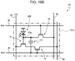
- FIG. 19B is a diagram schematically illustrating another example of the circuit configuration of the pixel included in the imaging device according to the third embodiment of the present disclosure.
- FIG. 20 is a timing chart illustrating an example of the operation of the pixel having the circuit configuration illustrated in FIG. 19A ;
- FIG. 21 is a diagram schematically illustrating an example of the circuit configuration of a pixel included in an imaging device according to a fourth embodiment of the present disclosure.
- FIG. 22A is a timing chart illustrating an example of the operation of the pixel having the circuit configuration illustrated in FIG. 21 ;
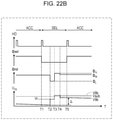
- FIG. 22B is a timing chart illustrating an example of an operation at a time when a reset transistor of the pixel illustrated in FIG. 21 is a p-type transistor and electrons are used as signal charges;
- FIG. 23 is a diagram illustrating an imaging device according to a modification of the fourth embodiment of the present disclosure.
- FIG. 24 is a functional block diagram schematically illustrating an example of a camera system according to a fifth embodiment of the present disclosure.
- An imaging device includes
- a semiconductor substrate that includes a first impurity region having n-type conductivity
- a photoelectric converter that is electrically connected to the first impurity region and that converts light into charges
- a capacitor that includes a first terminal and a second terminal, the first terminal being electrically connected to the first impurity region;
- the voltage supply circuit is configured to generate a first voltage and a second voltage different from the first voltage
- the first impurity region accumulates positive charges generated by the photoelectric converter.
- the imaging device according to Item 1 includes
- a first transistor including the first impurity region as a source or a drain, wherein
- the voltage supply circuit supplies the first voltage to the second terminal in a first period, and supplies the second voltage to the second terminal in a second period after the first period, the first transistor being in on-state in the first period, the first transistor being in off-state in the second period.
- the imaging device according to Item 1 includes
- a first transistor including the first impurity region as a source or a drain, wherein
- the voltage supply circuit supplies the first voltage to the second terminal in a first period, and supplies the second voltage to the second terminal in a second period after the first period, the positive charges being accumulated in the first impurity region in the first period, the first transistor being in on-state in the second period.
- the semiconductor substrate includes a second impurity region
- the first transistor includes the second impurity region as the other of the source and the drain, and
- the first terminal is connected to the second impurity region.
- the second voltage is greater than the first voltage
- An imaging device includes
- a semiconductor substrate that includes a first impurity region having p-type conductivity
- a photoelectric converter that is electrically connected to the first impurity region and that converts light into charges
- a capacitor that includes a first terminal and a second terminal, the first terminal being electrically connected to the first impurity region;
- the voltage supply circuit is configured to generate a first voltage and a second voltage different from the first voltage
- the first impurity region accumulates negative charges generated by the photoelectric converter.
- the imaging device according to Item 6 includes
- a first transistor including the first impurity region as a source or a drain, wherein
- the voltage supply circuit supplies the first voltage to the second terminal in a first period, and supplies the second voltage to the second terminal in a second period after the first period, the first transistor being in on-state in the first period, the first transistor being in off-state in the second period.
- the imaging device according to Item 6 includes
- a first transistor including the first impurity region as a source or a drain, wherein
- the voltage supply circuit supplies the first voltage to the second terminal in a first period, and supplies the second voltage to the second terminal in a second period after the first period, the negative charges being accumulated in the first impurity region in the first period, the first transistor being in on-state in the second period.
- the semiconductor substrate includes a second impurity region
- the first transistor includes the second impurity region as the other of the source and the drain, and
- the first terminal is connected to the second impurity region.
- the second voltage is less than the first voltage.
- the capacitor and the first impurity region are at least a part of a charge accumulation node that accumulates positive or negative charges generated by the photoelectric converter, and
- a capacitance of the capacitor is lower than a capacitance of a part of the charge accumulation node other than the capacitor.
- the photoelectric converter includes a first electrode, a second electrode facing the first electrode, and a photoelectric conversion layer located between the first electrode and the second electrode, and
- the first electrode is electrically connected to the first impurity region.
- the photoelectric converter is an embedded photodiode.
- An imaging device includes a semiconductor substrate including a first impurity region and a second impurity region, a photoelectric converter electrically connected to the first impurity region, a first transistor that includes the first impurity region as a source region or a drain region and the second impurity region as another of the source region and the drain region, and a voltage supply circuit electrically connected to the second impurity region.
- the voltage supply circuit applies a first voltage to the second impurity region in a first period, in which the first transistor is on, and a second voltage, which is different from the first voltage, to the second impurity region in a second period, which comes after the first period and in which the first transistor is off.
- the imaging device further includes a capacitor connected between the second impurity region and the voltage supply circuit.
- the imaging device further includes a second transistor whose source region or drain region is electrically connected to the second impurity region.
- the imaging device further includes a second transistor whose source region or drain region is electrically connected to the second impurity region.
- the voltage supply circuit is connected to another of the source region and the drain region of the second transistor.
- the second period is a period for which the second transistor remains on other than the first period.
- the second period starts when the second transistor is turned off.
- An imaging device includes a semiconductor substrate including a first impurity region, a photoelectric converter electrically connected to the first impurity region, a first transistor that includes the first impurity region as a source region or a drain region and that supplies or does not supply a reset voltage to the first impurity region, and a voltage supply circuit electrically connected to the first impurity region.
- the voltage supply circuit applies a first voltage to the first impurity region in a first period, in which the first transistor is on, and a second voltage, which is different from the first voltage, to the first impurity region in a second period, which comes after the first period and in which the first transistor is off.
- the imaging device further includes a capacitor connected between the first impurity region and the voltage supply circuit.
- the imaging device further includes a second transistor whose source region or drain region is electrically connected to another of the source region and the drain region of the first transistor.
- the voltage supply circuit is connected to the first impurity region through the first transistor.
- the imaging device further includes a feedback circuit that includes the second transistor and that negatively feeds back an electric signal generated by the photoelectric converter.
- kTC noise can be reduced through the negative feedback.
- the first transistor is of an n-type.
- the second voltage is higher than the first voltage.
- the potential of the first impurity region and/or the potential of a node between the first transistor and the second transistor can be kept from falling below a substrate potential of the semiconductor substrate.
- the first transistor is of a p-type.
- the second voltage is lower than the first voltage.
- the potential of the first impurity region and/or the potential of a node between the first transistor and the second transistor can be kept from exceeding a substrate potential of the semiconductor substrate.
- An imaging device includes a semiconductor substrate including a first impurity region, a photoelectric converter electrically connected to the first impurity region, a reset transistor that includes the first impurity region as a source region or a drain region and that supplies or does not supply a reset voltage to the first impurity region, and a driving circuit connected to a gate of the reset transistor.
- the driving circuit sequentially applies a first voltage for turning on the reset transistor, a second voltage for turning off the reset transistor, and a third voltage between the first voltage and the second voltage to the gate to reset a potential of the first impurity region.
- the reset transistor is of an n-type.
- the third voltage is lower than the first voltage but higher than the second voltage.
- the potential of the first impurity region and/or the potential of a node between the first transistor and the second transistor can be kept from falling below a substrate potential of the semiconductor substrate.
- a potential of the first impurity region becomes higher than a substrate potential of the semiconductor substrate when the driving circuit applies the third voltage to the gate.
- the reset transistor is of a p-type.
- the third voltage is higher than the first voltage but lower than the second voltage.
- the potential of the first impurity region and/or the potential of a node between the first transistor and the second transistor can be kept from exceeding a substrate potential of the semiconductor substrate.
- the potential of the first impurity region becomes lower than a substrate potential of the semiconductor substrate when the driving circuit applies the third voltage to the gate.
- a method for driving an imaging device including a photoelectric converter, a charge accumulation node electrically connected to the photoelectric converter, a detection circuit that detects signal charges accumulated in the charge accumulation node, and a reset transistor that discharges the signal charges includes resetting a potential of the charge accumulation node by sequentially applying a first voltage for turning on the reset transistor, a second voltage for turning off the reset transistor, and a third voltage between the first voltage and the second voltage to a gate of the reset transistor.
- the charge accumulation node includes an n-type first impurity region formed on a semiconductor substrate.
- the third voltage is lower than the first voltage but higher than the second voltage.
- the method according to Item 19 further includes applying, as the second voltage, a voltage with which a potential of the charge accumulation node becomes lower than a substrate potential of the semiconductor substrate.
- the charge accumulation node includes a p-type first impurity region formed on a semiconductor substrate.
- the third voltage is higher than the first voltage but lower than the second voltage.
- the method according to Item 21 further includes applying, as the second voltage, a voltage with which a potential of the charge accumulation node becomes higher than a substrate potential of the semiconductor substrate is applied.
- the photoelectric converter further includes a first electrode supported by the semiconductor substrate, a second electrode, and a photoelectric conversion layer located between the first electrode and the second electrode.
- the first electrode is electrically connected to the first impurity region.
- the photoelectric converter is an embedded photodiode.
- An imaging device includes a plurality of pixels.
- Each of the plurality of pixels includes a photoelectric converter that generates charges through photoelectric conversion, a charge accumulation node that accumulates the charges, a reset transistor that is electrically connected to the charge accumulation node and that resets a potential of the charge accumulation node to a reference potential, an amplifying transistor that is electrically connected to the charge accumulation node and that outputs a signal voltage corresponding to the charges accumulated in the charge accumulation node, and a capacitor including an end electrically connected to the charge accumulation node and another end connected to a voltage source. In an exposure period, in which the charges are accumulated in the charge accumulation node, a first voltage is applied to the other end of the capacitor.
- a second voltage which is different from the first voltage, is applied to the other end.
- the reset period is a part of the non-exposure period.
- the reset transistor resets the potential of the charge accumulation node to the reference potential.
- an imaging device capable of reducing leak current is provided.
- the second voltage is applied to the other end of the capacitor over the non-exposure period.
- the capacitor is electrically connected to a gate of the amplifying transistor.
- a change in the voltage of a control signal applied to the other end of the capacitor is given to a floating diffusion (FD) node through the capacitor.
- the imaging device further includes a selection transistor that is electrically connected to the amplifying transistor and that selectively outputs a signal voltage. A control signal of the selection transistor is transmitted to the other end of the capacitor.
- control signal in a pixel can also be used as a control signal transmitted to the capacitor, the number of control signal lines used can be reduced.
- the imaging device further includes a switch transistor that is electrically connected between the end of the capacitor and the charge accumulation node or between the voltage source and the other end and that connects the capacitor and the charge accumulation node to each other or disconnects the capacitor and the charge accumulation node from each other.
- an FD potential control mode in which the potential of the charge accumulation node is controlled, and a high gain mode, in which signal charges are efficiently converted, can be used.
- the charges are positive holes.
- the second voltage is higher than the first voltage.
- an imaging device that is capable of reducing leak current and that uses positive holes as signal charges can be provided.
- the reset transistor and the amplifying transistor are n-type transistors.
- the charges are electrons.
- the second voltage is lower than the first voltage.
- an imaging device that is capable of reducing leak current and that uses electrons as signal charges can be provided.
- the reset transistor and the amplifying transistor are p-type transistors.
- the first voltage is a ground voltage.
- power supply noise of the control signal applied to the capacitor can be kept from entering the charge accumulation node.
- the second voltage is a ground voltage.
- power supply noise of the control signal applied to the capacitor can be kept from entering the charge accumulation node.
- the amplifying transistor is a depletion transistor.
- the photoelectric converter includes a first electrode, a second electrode facing the first electrode, and a photoelectric conversion film that is located between the first electrode and the second electrode and that generates charges through photoelectric conversion.
- an imaging device that is capable of reducing leak current and that includes a photoelectric converter including a photoelectric conversion film is provided.
- FIG. 1 schematically illustrates an example of the configuration of an imaging device according to a first embodiment of the present disclosure.
- An imaging device 100 illustrated in FIG. 1 includes a pixel array 110 including a plurality of pixels 10 and a peripheral circuit 120 .
- the pixel array 110 includes the plurality of pixels 10 arranged in a matrix of m rows and n columns.
- m and n are natural numbers.
- the pixels 10 are arranged on a semiconductor substrate 60 in two dimensions, for example, and form an imaging area.
- the number and arrangement of the pixels 10 in the pixel array 110 are not limited to those illustrated in FIG. 1 .
- only one pixel 10 may be included in the imaging device 100 .
- the imaging device 100 may be used as a line sensor.
- Each pixel 10 includes a photoelectric conversion unit that receives light and generates charge.
- the photoelectric conversion unit of each pixel 10 may include an embedded photodiode formed in the semiconductor substrate 60 or a part of a photoelectric conversion layer provided above an area of the semiconductor substrate 60 corresponding to the imaging area. Terms “above”, “below”, and the like herein are used to specify relative positions of members and do not limit the orientation of the imaging device 100 during use.
- the peripheral circuit 120 includes a vertical scanning circuit 122 , a signal holding circuit 123 , a horizontal scanning circuit 124 , an output amplifier 126 , and a voltage supply circuit 128 that supplies a certain voltage to the pixels 10 in the pixel array 110 .
- the peripheral circuit 120 is provided on the semiconductor substrate 60 on which the pixel array 110 is formed.
- the arrangement of the peripheral circuit 120 is not limited to this example, and a part or the entirety of the peripheral circuit 120 may be provided on a substrate other than the semiconductor substrate 60 , instead.
- the vertical scanning circuit 122 is also called a “row scanning circuit” and connected to address signal lines and reset signal lines, for example, corresponding to rows of the pixels 10 .
- the vertical scanning circuit 122 supplies certain signals to the address signal lines and the reset signal lines to accumulate and read signal charges in and from the pixels 10 and reset accumulated signal charges in units of rows.
- the peripheral circuit 120 may include two or more vertical scanning circuits 122 .
- various signal lines such as the address signal lines and the reset signal lines are not illustrated for simplicity. Arrows illustrated in FIG. 1 schematically indicate flows of signals supplied to the various signal lines such as the address signal lines and the reset signal lines.
- the signal holding circuit 123 is connected to vertical signal lines, which are not illustrated, provided for columns of the pixels 10 and has a function of temporarily holding signals output to the vertical signal lines.
- the signals may be held as analog values or digital values, which are obtained by performing analog-to-digital conversion.
- the signal holding circuit 123 outputs, to the horizontal scanning circuit 124 , a difference between a signal read from a pixel 10 after signal charges are accumulated and a signal read from the pixel 10 after the signal charges are reset. Calculation between signals may be performed in an analog manner or a digital manner.
- the horizontal scanning circuit 124 is also called a “column scanning circuit” and typically includes an analog-to-digital conversion circuit.
- the horizontal scanning circuit 124 has a function of transferring, to the output amplifier 126 , differential signals obtained by the signal holding circuit 123 in units of rows of the pixels 10 .
- the voltage supply circuit 128 is electrically connected to the pixels 10 and supplies two or more certain voltages to the pixels 10 during operation of the imaging device 100 while switching between the two or more certain voltages.
- the voltage supply circuit 128 supplies a first voltage V A and a second voltage V B to the pixels 10 while switching between the first voltage V A and the second voltage V B .
- the second voltage V B is different from the first voltage V A .
- the voltage supply circuit 128 may be configured in any manner insofar as the voltage supply circuit 128 can supply the certain voltages to the pixels 10 , and is not limited to a power supply circuit of a certain type.
- the voltage supply circuit 128 may be a circuit that generates the certain voltages or a circuit that converts a voltage supplied from a power supply into the certain voltages.
- the voltage supply circuit 128 may be a part of the vertical scanning circuit 122 .
- the voltages applied from the voltage supply circuit 128 to the pixels 10 are not limited to two different voltages.
- the voltage supply circuit 128 may supply three or more different voltages to the pixels 10 , instead, while switching between the three or more different voltages.
- FIG. 2 schematically illustrates an example of a cross-section of the device structure of a pixel 10 .
- FIG. 2 only schematically illustrates shapes, dimensions, and arrangement of components of a pixel 10 .
- the shapes, the dimensions, and the arrangement of the components illustrated in FIG. 2 are not necessarily shapes, dimensions, and arrangement of components of an actual device. The same holds for the other drawings of the present disclosure.
- a pixel 10 A illustrated in FIG. 2 is an example of each of the above-described pixels 10 .
- the pixel 10 A includes a part of the semiconductor substrate 60 and a photoelectric conversion unit 50 A supported by an interlayer insulating layer 40 that covers the semiconductor substrate 60 .
- the photoelectric conversion unit 50 A includes a photoelectric conversion layer 54 located above an area of the semiconductor substrate 60 corresponding to the imaging area. That is, a multilayer imaging device will be described hereinafter as the imaging device 100 .
- the semiconductor substrate 60 includes a base substrate 60 S and one or more semiconductor layers formed on the base substrate 60 S.
- a p-type silicon substrate is used as an example of the base substrate 60 S.
- the semiconductor substrate 60 is provided with impurity regions 60 a to 60 e and device separating regions 65 .
- the impurity regions 60 a to 60 e are typically n-type diffusion regions.
- the photoelectric conversion unit 50 A supported by the semiconductor substrate 60 includes a pixel electrode 52 on the interlayer insulating layer 40 , an opposed electrode 56 located farther from the semiconductor substrate 60 than the pixel electrode 52 is, and the photoelectric conversion layer 54 located between the pixel electrode 52 and the opposite electrode 56 .
- the pixel electrode 52 is composed of a metal such as aluminum or copper, a metal nitride, a conductive polysilicon obtained through doping, or the like.
- the pixel electrode 52 is spatially separated from pixel electrodes 52 of adjacent pixels 10 A and consequently electrically separated from the pixel electrodes 52 of the adjacent pixels 10 A.
- the opposed electrode 56 is composed of a conductive transparent material such as indium tin oxide (ITO).
- a term “transparent” herein means that at least part of light in a wavelength band to be detected is passed through, and visible light need not be passed through over a wavelength band thereof.
- the pixel electrode 52 is separated from the pixel electrodes 52 of the adjacent pixels 10 A, the opposed electrode 56 is formed across a plurality of pixels 10 A.
- the opposed electrode 56 is typically disposed above the semiconductor substrate 60 as a single continuous electrode.
- the photoelectric conversion layer 54 is composed of an organic material or an inorganic material such as amorphous silicon.
- the photoelectric conversion layer 54 may be formed through vacuum deposition, for example, and have a thickness of about 500 nm.
- the photoelectric conversion layer 54 may include a layer formed of an organic material and a layer formed of an inorganic material.
- the photoelectric conversion layer 54 receives light incident through the opposed electrode 56 and generates positive and negative charges through photoelectric conversion. As with the opposed electrode 56 , the photoelectric conversion layer 54 may be disposed above the semiconductor substrate 60 across the plurality of pixels 10 A as a single continuous layer.
- a voltage line connected to a power supply which is not illustrated, is connected to the opposed electrode 56 , and the opposed electrode 56 receives a certain bias voltage during the operation of the imaging device 100 .
- the pixel electrode 52 can collect, as signal charges, either the positive charges or the negative charges generated through the photoelectric conversion.
- the bias voltage applied to the opposed electrode 56 may be supplied from the voltage supply circuit 128 , instead.
- a bias voltage whose potential is higher than that of the pixel electrode 52 may be applied to the opposed electrode 56 .
- positive charges will be used as signal charges unless otherwise noted.
- Positive charges as signal charges are typically positive holes.
- Negative charges as signal charges, such as electrons, may of course be used, instead.
- a bias voltage whose potential is lower than that of the pixel electrode 52 may be applied to the opposed electrode 56 .
- the pixel 10 A includes a connection unit 42 disposed in the interlayer insulating layer 40 . As schematically illustrated in FIG. 2 , an end of the connection unit 42 is connected to the pixel electrode 52 of the photoelectric conversion unit 50 A.
- the connection unit 42 includes a plurality of wiring layers and a plurality of plugs and electrically connects the photoelectric conversion unit 50 A to a circuit formed on the semiconductor substrate 60 .
- the plurality of wiring layers and the plurality of plugs are typically composed of a metal such as copper or tungsten or a metal compound such as a metal nitride or a metal oxide.
- a signal detection transistor 72 , an address transistor 74 , and a reset transistor 76 are formed on the semiconductor substrate 60 .
- N-channel field-effect transistors typified by n-channel metal-oxide-semiconductor (MOS) FETs will be used as the signal detection transistor 72 , the address transistor 74 , and the reset transistor 76 hereinafter unless otherwise noted.
- MOS metal-oxide-semiconductor
- p-type transistors may be used instead of n-type transistors.
- the base substrate 60 S may be an n-type silicon substrate, and p-type impurity regions 60 a to 60 e are used.
- the reset transistor 76 includes the impurity region 60 a formed in the semiconductor substrate 60 as either a drain region or a source region, for example, and the impurity region 60 b as the other of the drain region and the source region.
- the connection unit 42 is connected to the impurity region 60 a , that is, the impurity region 60 a is electrically connected to the pixel electrode 52 of the photoelectric conversion unit 50 A through the connection unit 42 .
- a reset voltage line for supplying a reset voltage which is a reference voltage for resetting, is connected to the impurity region 60 b .
- the reset transistor 76 switches between supplying and not supplying of the reset voltage supplied from the reset voltage line to the impurity region 60 a .
- the impurity region 60 a or the impurity region 60 b serves as the drain region of the reset transistor 76 is determined depending on the potential of the impurity regions 60 a and 60 b .
- the impurity regions 60 a and 60 b are the drain region and the source region, respectively, for convenience. Depending on a use condition of the imaging device 100 , however, the drain region and the source region might be switched.
- the imaging device 100 includes another transistor connected in series with the reset transistor 76 , the same holds for the other transistor.
- the signal detection transistor 72 includes a gate insulating layer 72 g on the semiconductor substrate 60 , a gate electrode 72 e on the gate insulating layer 72 g , the impurity region 60 c as a drain region 60 c , and the impurity region 60 d as a source region.
- a power supply line which is not illustrated, is connected to the impurity region 60 c , and a power supply voltage of 3.3 V, for example, is applied to the impurity region 60 c from the power supply line during the operation of the imaging device 100 .
- connection unit 42 is also connected to the gate electrode 72 e of the signal detection transistor 72 . That is, the gate electrode 72 e of the signal detection transistor 72 is electrically connected to the pixel electrode 52 of the photoelectric conversion unit 50 A through the connection unit 42 .
- the address transistor 74 includes the impurity region 60 d as a drain region and the impurity region 60 e as a source region.
- the address transistor 74 shares the impurity region 60 d with the signal detection transistor 72 and is electrically connected to the signal detection transistor 72 .
- a vertical signal line which is not illustrated, is connected to the impurity region 60 e .
- a circuit in the pixel 10 A is electrically separated by the device separating regions 65 from circuits in adjacent pixels 10 A.
- a device separating region 65 is also provided between the signal detection transistor 72 and the reset transistor 76 .
- connection unit 42 is connected to the pixel electrode 52 .
- the impurity region 60 a and the gate electrode 72 e of the signal detection transistor 72 are electrically connected to the pixel electrode 52 through the connection unit 42 .
- the pixel electrode 52 , the connection unit 42 , the impurity region 60 a , and the gate electrode 72 e function as a charge accumulation node that temporarily holds signal charges collected by the pixel electrode 52 .
- the pixel 10 A also includes a control line 81 electrically connected to the connection unit 42 .
- the control line 81 is a signal line connected to the voltage supply circuit 128 . That is, here, the impurity region 60 a is electrically connected to the voltage supply circuit 128 . As described later, a capacitor or the like may be provided between the impurity region 60 a and the voltage supply circuit 128 .
- the voltage supply circuit 128 is electrically connected to the connection unit 42 , which is a part of the charge accumulation node, and switches an output of the voltage supply circuit 128 between the first voltage V A and the second voltage V B . As a result, for example, the potential of the charge accumulation node after resetting can be temporarily changed.
- the semiconductor substrate 60 includes one or more semiconductor layers on the base substrate 60 S.
- the semiconductor layers on the base substrate 60 S include a first p-type semiconductor layer 61 p , an n-type semiconductor layer 61 n , and a second p-type semiconductor layer 62 p .
- the impurity regions 60 a to 60 e and the device separating regions 65 are formed in the second p-type semiconductor layer 62 p as a p-well.
- the n-type semiconductor layer 61 n is located between the first p-type semiconductor layer 61 p and the second p-type semiconductor layer 62 p , and the potential of the n-type semiconductor layer 61 n is controlled during the operation of the imaging device 100 through a well contact, which is not illustrated, provided outside the imaging area.
- the n-type semiconductor layer 61 n suppresses entry of a small number of carriers into the charge accumulation node that accumulates signal charges from the base substrate 60 S or the peripheral circuit 120 .
- the semiconductor substrate 60 includes a p-type region 63 that penetrates through the first p-type semiconductor layer 61 p and the n-type semiconductor layer 61 n from the second p-type semiconductor layer 62 p to the base substrate 60 S.
- the p-type region 63 has a relatively high impurity concentration and electrically connects the second p-type semiconductor layer 62 p and the base substrate 60 S to each other.
- a substrate contact, which is not illustrated, is provided outside the imaging area, and the potential of the base substrate 60 S and the second p-type semiconductor layer 62 p is controlled through the substrate contact during the operation of the imaging device 100 .
- the substrate potential of the semiconductor substrate 60 is controlled through the substrate contact during the operation of the imaging device 100 .
- the voltage supply circuit 128 may supply the substrate potential of the semiconductor substrate 60 through the substrate contact.
- the substrate potential is typically ground.
- the impurity region 60 a is a part of the charge accumulation node that temporarily accumulates signal charges generated by the photoelectric conversion unit 50 A. This is because a junction capacitor formed by a p-n junction between the impurity region 60 a and the second p-type semiconductor layer 62 p serves as a capacitor for accumulating at least part of signal charges.
- the p-n junction between the impurity region 60 a and the second p-type semiconductor layer 62 p causes a depletion layer.
- Various lattice defects are caused especially on a surface of the semiconductor substrate 60 due to impurities, dangling bonds, and the like.
- If there are lattice defects in the depletion layer for example, charges different from intended signal charges are likely to enter the impurity region 60 a .
- lattice defects in the depletion layer can cause dark current.
- the dark current decreases a signal-to-noise (S/N) ratio, thereby deteriorating the quality of a resultant image.
- S/N signal-to-noise
- the present inventors in order to reduce in size the depletion layer formed through the p-n junction between the impurity region 60 a and the second p-type semiconductor layer 62 p , it is effective to adjust the potential of the impurity region 60 a after signal charges are discharged from the impurity region 60 a as close to the substrate potential as possible. That is, it is effective to adjust the potential of the impurity region 60 a after resetting as close to the substrate potential as possible.
- signal charges are positive holes and the substrate potential is ground, for example, it is advantageous to use a low voltage close to 0 V as a reset voltage.
- the potential of an impurity region can decrease as the FET is turned on and off due to electrical coupling through parasitic capacitance between a source and a drain. If the potential of the impurity region falls below the substrate potential at this time, a forward bias is applied to a p-n junction between the impurity region and an adjacent p-well, and positive holes undesirably enter the impurity region from a p-type silicon substrate as a base substrate. That is, dark current might be generated, and the quality of a resultant image might deteriorate.
- the present inventors have found through examinations that entry of charges different from intended signal charges into an impurity region that accumulates the signal charges due to turning on and off of a transistor connected to the impurity region can be avoided, for example, by switching between the first voltage V A and the second voltage V B and changing the potential of the charge accumulation nodes after resetting.
- FIG. 3 schematically illustrates a typical example of the circuit configuration of the pixel 10 A illustrated in FIG. 2 .
- the voltage line that supplies the certain bias voltage to the opposed electrode 56 of the photoelectric conversion unit 50 A is not illustrated for simplicity. In other drawings, too, illustration of the voltage line that supplies the certain bias voltage to the opposed electrode 56 is omitted.
- a gate of the signal detection transistor 72 is connected to the photoelectric conversion unit 50 A.
- a node FDa between the photoelectric conversion unit 50 A and the signal detection transistor 72 corresponds to the charge accumulation node.
- a voltage corresponding to signal charges accumulated in the node FDa is applied to the gate of the signal detection transistor 72 .
- a power supply line 82 as a source follower power supply that supplies a power supply voltage Vdd is connected to a drain of the signal detection transistor 72
- a vertical signal line 89 is connected to a source of the signal detection transistor 72 through the address transistor 74 . That is, the signal detection transistor 72 and the address transistor 74 form a source follower.
- An address signal line 84 connected to the vertical scanning circuit 122 is connected to a gate of the address transistor 74 .
- the vertical scanning circuit 122 can transfer a signal from the pixel 10 A to the vertical signal line 89 by controlling an address signal ⁇ sel applied to the address signal line 84 .
- the node FDa will be focused upon.
- the reset transistor 76 is also connected to the node FDa.
- a source or a drain of the reset transistor 76 whichever is not connected to the node FDa, is connected to a reset voltage line 85 .
- a certain reset voltage Vr for example, is applied to the reset voltage line 85 .
- the reset signal line 86 connected to the vertical scanning circuit 122 is connected to a gate of the reset transistor 76 .
- the vertical scanning circuit 122 can apply the reset voltage Vr to the charge accumulation node by controlling a reset signal ⁇ rst applied to the reset signal line 86 and turning on the reset transistor 76 . As described with reference to FIG.
- the reset transistor 76 includes the impurity region 60 a , which is a part of the charge accumulation node, as a drain region or a source region. When the reset transistor 76 is turned on, signal charges are discharged from the charge accumulation node, and the potential of the charge accumulation node is reset.
- the voltage supply circuit 128 is also electrically connected to the node FDa.
- a capacitor C 1 is provided between the node FDa and the control line 81 connected to the voltage supply circuit 128 .
- the node FDa is connected to one of two ends of the capacitor C 1 . That is, in this example, the one end of the capacitor C 1 is electrically connected to the impurity region 60 a .
- the voltage supply circuit 128 is connected to another end of the capacitor C 1 .
- the capacitor C 1 may be a metal-insulator-semiconductor (MIS) capacitor provided in the interlayer insulating layer 40 or a depletion-mode MOS (DMOS) capacitor.
- the capacitor C 1 may be a metal-insulator-metal (MIM) capacitor. When a MIM capacitor is used, a higher capacitance can be obtained.
- MIS metal-insulator-semiconductor
- DMOS depletion-mode MOS
- MIM metal-insulator-metal
- the voltage supply circuit 128 includes switching devices 128 a and 128 b such as FETs. That is, here, the voltage supply circuit 128 switches a voltage Vc applied to the control line 81 between the first voltage V A and the second voltage V B by turning on and off the voltage supply circuits 128 a and 128 b.
- switching devices 128 a and 128 b such as FETs. That is, here, the voltage supply circuit 128 switches a voltage Vc applied to the control line 81 between the first voltage V A and the second voltage V B by turning on and off the voltage supply circuits 128 a and 128 b.
- FIG. 4A is a timing chart illustrating an example of the operation of the pixel 10 A having the circuit configuration illustrated in FIG. 3 .
- a top part of FIG. 4A indicates a pulse of a horizontal synchronizing signal HD.
- a period between a rising edge and a next rising edge corresponds to a period 1 H, which is one horizontal scanning period.
- pixels 10 A belonging to a certain row of the pixel array 110 are reset and signals are read from the pixels 10 A.
- a double-headed arrow SEL illustrated in FIG. 4A indicates a selection period for which the address transistor 74 of the pixel 10 A remains on, and arrows ACC indicate non-selection periods for which the address transistor 74 remains off.
- a bottom part of FIG. 4A indicates temporal changes in the potential of the node FDa, that is, potential V FD of the impurity region 60 a .
- a second lowest part of FIG. 4A indicates temporal changes in the voltage Vc applied to the control line 81 from the voltage supply circuit 128 .
- the first voltage V A is applied to the control line 81 at a time T 1 .
- the address signal ⁇ sel is turned high at the time T 1 .
- a first signal whose voltage level corresponds to the signal charges accumulated in the charge accumulation node is transferred to the vertical signal line 89 through the signal detection transistor 72 and the address transistor 74 .
- the first signal is then temporarily held by the signal holding circuit 123 illustrated in FIG. 1 .
- the reset signal ⁇ rst is turned high at a time T 2 to turn on the reset transistor 76 .
- the reset transistor 76 turns on, the signal charges are discharged from the charge accumulation node, and the potential of the charge accumulation node is reset.
- the reset voltage Vr is applied to the node FDa, and the potential V FD of the impurity region 60 a decreases to Vr.
- the reset voltage Vr is higher than a substrate potential Vsub, that is, Vr>Vsub.
- the reset voltage Vr is a positive voltage close to 0 V.
- the reset signal ⁇ rst is turned low at a time T 3 to turn off the reset transistor 76 .
- the reset transistor 76 includes the impurity region 60 a as the drain region or the source region.
- the potential V FD of the impurity region 60 a can further decrease from Vr due to electric coupling caused by parasitic capacitance of the reset transistor 76 .
- the potential V FD falls below the substrate potential Vsub at this time, positive holes undesirably enter the impurity region 60 a.
- the reset signal ⁇ rst is turned low but also the voltage Vc applied to the control line 81 from the voltage supply circuit 128 is switched to the second voltage V B .
- the second voltage V B is higher than the first voltage V A .
- the potential of the node FDa increases through the capacitor C 1 .
- the potential V FD of the impurity region 60 a immediately after the reset transistor 76 is turned off is V 1 a , which satisfies Vr>V 1 a >Vsub. If the reset voltage Vr is 0.5 V, for example, V 1 a can be about 0.2 V. That is, the potential V FD of the impurity region 60 a is kept from falling below the substrate potential Vsub by appropriately selecting the second voltage V B and switching the output of the voltage supply circuit 128 between the first voltage V A and the second voltage V B .
- a potential difference of 0.2 V is secured between the substrate potential Vsub and the potential V FD of the impurity region 60 a . That is, positive holes do not enter the impurity region 60 a since the potential V FD does not fall below the substrate potential Vsub. In other words, dark current is suppressed.
- a specific value of the second voltage V B may be selected in consideration of the parasitic capacitance between the source and the drain of the reset transistor 76 such that the potential V FD satisfies V 1 a >Vsub when the reset transistor 76 is off.
- a second signal corresponding to a voltage level of the charge accumulation node after the discharge of the signal charges is transferred to the vertical signal line 89 through the address transistor 74 .
- the signal holding circuit 123 outputs a difference ⁇ between the first and second signals to the horizontal scanning circuit 124 as a signal for representing an image.
- the address transistor 74 is turned off, and accumulation of signal charges for a next frame starts.
- the voltage supply circuit 128 applies the first voltage V A to the impurity region 60 a and, in a second period between the times T 3 and T 4 after the first period, switches the voltage applied to the impurity region 60 a to the second voltage V B .
- the voltage supply circuit 128 applies the first voltage V A to the impurity region 60 a and, in a second period between the times T 3 and T 4 after the first period, switches the voltage applied to the impurity region 60 a to the second voltage V B .
- the voltage Vc applied to the control line 81 is switched between the first voltage V A and the second voltage V B to change the potential of the node FDa through the capacitor C 1 .
- the potential of the charge accumulation node can be controlled without affecting signal charges accumulated in the charge accumulation node.
- the capacitor C 1 since the capacitor C 1 is electrically connected to the node FDa, the capacitor C 1 constitutes, as with the impurity region 60 a , at least a part of the charge accumulation node that temporarily holds signal charges. In other words, the connection of the capacitor C 1 to the node FDa increases the overall capacitance of the charge accumulation node.
- the capacitance of the capacitor C 1 is desirably as low as possible for the following two reasons.
- a first reason is that an increase in the overall capacitance of the charge accumulation node results in a decrease in conversion gain.
- the decrease in conversion gain in turn leads to a decrease in the S/N ratio because an effect of noise in subsequent circuits.
- it is beneficial that the capacitance of the capacitor C 1 is as low as possible.
- a second reason is that if the capacitor C 1 has a relatively high capacitance, noise in the control line 81 tends to affect the node FDa through the capacitor C 1 .
- Noise included in the voltage applied to the control line 81 can enter the node FDa due to electrical coupling through the capacitor C 1 .
- noise in the control line 81 can be observed as horizontal line noise on an image. Because horizontal line noise is more likely to be recognized by a viewer of an image than random noise at pixels, it is advantageous to suppress horizontal line noise.
- the magnitude of variation in voltage applied to the node FDa is represented by a product of variation in the voltage of the control line 81 and (C 1 /(C 1 +C FD )).
- the capacitance C 1 of the capacitor C 1 is desirably as low as possible.
- the capacitance C 1 of the capacitor C 1 is lower than the capacitance C FD of the part of the charge accumulation node other than the capacitor C 1 .
- the operation described with reference to FIG. 4A may be applied.
- the potential V FD of the impurity region 60 a decreases as signal charges are accumulated in the charge accumulation node, in contrast to when positive holes are used as signal charges.
- the reset voltage Vr may be, for example, a higher positive voltage, namely about 3.3 V, in order to secure a sufficient difference between the substrate potential and potential V FD of the impurity region 60 a.
- the reset voltage Vr is a higher positive voltage, an effect of a decrease in the potential V FD of the impurity region 60 a due to the electrical coupling caused by the parasitic capacitance of the reset transistor 76 when the reset transistor 76 is turned off is smaller.
- the reset voltage Vr needs to be higher to improve the number of saturated electrons. In order to secure the number of saturated electrons large enough to achieve a required dynamic range, therefore, it is advantageous to use positive holes as signal charges.
- the reset transistor 76 may be a p-type transistor, instead. In this case, conductivity types of the components of the semiconductor substrate 60 need to be switched between the n-type and the p-type. When the reset transistor 76 is a p-type transistor, however, the second voltage V B is set lower than the first voltage V A as described hereinafter.
- FIG. 4B is a timing chart illustrating an example of an operation at a time when the reset transistor 76 of the pixel 10 A is a p-type transistor.
- the substrate potential Vsub is higher than when the reset transistor 76 is an n-type transistor.
- the substrate potential Vsub may be, for example, about 3.3 V.
- the reset transistor 76 When the reset transistor 76 is a p-type transistor, an effect of a change in the potential V FD of the impurity region 60 a due to the electrical coupling caused by the parasitic capacitance of the reset transistor 76 is smaller if positive holes are used as signal charges. A reason of this phenomenon is the same as when the reset transistor 76 is an n-type transistor and electrons are used as signal charges. In order to secure a sufficient number of saturated electrons, however, a sufficient potential difference needs to be secured between the substrate potential Vsub and the potential V FD of the impurity region 60 a . When signal charges are electrons, on the other hand, the reset voltage Vr may be around 3.3 V, which is the substrate potential Vsub. When the reset transistor 76 is a p-type transistor, therefore, it becomes easier to secure a sufficient number of electrons for a required dynamic range while avoiding complication of circuits if electrons are used as signal charges.
- FIG. 4B illustrates an example of an operation at a time when the reset transistor 76 is a p-type transistor and electrons are used as signal charges.
- the signal detection transistor 72 and the address transistor 74 are also typically formed on the semiconductor substrate 60 as p-type transistors.
- the potential V FD of the impurity region 60 a gradually decreases in a period before the time T 1 due to accumulation of signal charges through exposure. After the signal charges are accumulated, the address signal ⁇ sel is turned low at the time T 1 to turn on the address transistor 74 and transfer a first signal to the vertical signal line 89 .
- the reset signal ⁇ rst is turned low at the time T 2 to turn on the reset transistor 76 .
- the potential V FD of the impurity region 60 a increases to Vr when the reset transistor 76 is turned on.
- the reset signal ⁇ rst is turned high at the time T 3 to turn off the reset transistor 76 .
- the potential V FD of the impurity region 60 a can further increase from Vr due to the electrical coupling caused by the parasitic capacitance of the reset transistor 76 . If the potential V FD exceeds the substrate potential Vsub at this time, a forward bias is applied to the p-n junction between the impurity region 60 a and an adjacent region, and electrons undesirably enter the impurity region 60 a from an n-type silicon substrate as a base substrate. In other words, dark current is caused.
- the potential V FD of the impurity region 60 a immediately after the reset transistor 76 is turned off is V 1 b , which satisfies Vsub>V 1 b >Vr.
- V 1 b may be about 3.1 V.
- a second signal corresponding to the voltage level of the charge accumulation node after signal charges are discharged is transferred to the vertical signal line 89 , and an absolute value of a difference ⁇ between the first and second signals is obtained as an image signal.
- the address transistor 74 is turned off, and accumulation of signal charges for a next frame starts.
- the operation of the imaging device 100 according to embodiments of the present disclosure is not limited to the example described with reference to FIGS. 4A and 4B .
- different voltages may be supplied to the control line 81 in each frame, for example, between an exposure period, in which signal charges are accumulated in the charge accumulation node, and a reset period included in a non-exposure period, which is a period other than the exposure period.
- FIG. 4C is a timing chart illustrating another example of the operation of pixels 10 A, 10 Ap, and 10 Aq.
- the exposure period for accumulating signal charges in the charge accumulation node and the non-exposure period alternate as in the example illustrated in FIGS. 4A and 4B .
- the non-exposure period includes the reset period, in which the potential of the charge accumulation node is reset to a certain value.
- the pixel 10 A illustrated in FIG. 3 is taken as an example.
- the address signal ⁇ sel is turned high at the time T 1 .
- the voltage applied to the control line 81 is switched from the first voltage V A to the higher second voltage V B .
- ⁇ V FD ( V B ⁇ V A )( C 1 /( C 1 +C FD )) (1)
- the potential of the node FDa at this time is transferred to the vertical signal line 89 through the signal detection transistor 72 and the address transistor 74 as a first signal indicating a voltage level according to signal charges accumulated in the charge accumulation node.
- the reset signal ⁇ rst is turned high. As a result, the signal charges are discharged from the charge accumulation node through the reset transistor 76 , and the potential of the charge accumulation node is reset to the reset voltage Vr.
- the reset signal ⁇ rst is turned low to turn off the reset transistor 76 .
- a second signal corresponding to the voltage level of the charge accumulation node after the signal charges are discharged is transferred to the vertical signal line 89 through the address transistor 74 between the time T 3 and the time T 4 , at which a next rising edge of the horizontal synchronizing signal HD appears.
- a difference ⁇ between the first signal read between the time T 1 and the time T 2 and the second signal read between the time T 3 and the time T 4 is a true pixel signal representing an image.
- the voltage applied to the control line 81 is reset to the first voltage V A .
- the potential of the node FDa decreases from Vr to V 1 c due to the capacitive coupling through the capacitor C 1 .
- a change (Vr ⁇ V 1 c ) in the potential of the node FDa is equal to the above-mentioned ⁇ V FD .
- the change ⁇ V FD can be controlled by determining the first voltage V A and the second voltage V B on the basis of expression (1).
- the desired change ⁇ V FD can be achieved using the following procedure. First, when a product is designed, a capacitance ratio of a capacitor C 1 of a target charge accumulation node to a part of the charge accumulation node other than the capacitor C 1 is determined from the overall capacitance of the charge accumulation node. The amplitude of the voltage applied to the control line 81 during actual operation, that is, specific values of the first voltage V A and the second voltage V B , is determined on the basis of expression (1).
- first voltage V A or the second voltage V B be ground (0 V), because ground generally has a low impedance and power supply noise from the voltage supply circuit 128 connected to the control line 81 can be kept from entering the charge accumulation node.
- the second voltage V B is ground, for example, the first voltage V A is a negative voltage.
- the voltage supply circuit 128 supplies the first voltage V A to the control line 81 in the exposure period, in which signal charges are accumulated in the charge accumulation node including the impurity region 60 a .
- the voltage supply circuit 128 supplies the second voltage V B , which is different from the first voltage V A .
- the second voltage V B is the voltage supplied to the control line 81 during the reset period, which is a period included in the non-exposure period in which the reset transistor 76 is turned on. Different voltages may thus be supplied to the control line 81 between at least a reset period after an exposure period and another period. In this case, for example, the potential of the charge accumulation node can be temporarily decreased from the reset voltage Vr.
- the potential of the charge accumulation node increases by a difference between the second voltage V B and the first voltage V A when a row is selected.
- source-drain voltages of the signal detection transistor 72 and transistors in subsequent circuits can be set within a voltage range within which these transistors are operable.
- the signal detection transistor 72 and the subsequent circuits can thus read a pixel signal or a reference signal normally.
- FIG. 5 schematically illustrates another example of the circuit configuration of the pixel 10 .
- a pixel 10 Ap illustrated in FIG. 5 includes a photoelectric conversion unit 50 B instead of the photoelectric conversion unit 50 A.
- the photoelectric conversion unit 50 B is, for example, an embedded photodiode formed in the semiconductor substrate 60 .
- the photoelectric conversion unit 50 B is connected to the gate of the signal detection transistor 72 in this example.
- a node FDb between the photoelectric conversion unit 50 B and the signal detection transistor 72 corresponds to a charge accumulation node.
- a p-n junction in the embedded photodiode, which is the photoelectric conversion unit 50 B, the impurity region 60 a , and the gate electrode 72 e function as a charge accumulation node that temporarily holds charges generated by the photoelectric conversion unit 50 B.
- the impurity region 60 a may be a part of the p-n junction in the embedded photodiode.
- the operation described with reference to FIGS. 4A and 4B may also be applied to the imaging device 100 including the pixel 10 Ap.
- the potential of the node FDb can be increased through the capacitor C 1 , for example, by switching the voltage Vc applied to the control line 81 from the voltage supply circuit 128 from the first voltage V A to the second voltage V B , which is higher than the first voltage V A , when the reset signal ⁇ rst is turned low.
- the second voltage V B By appropriately selecting the second voltage V B , the potential V FD of the impurity region 60 a is kept from falling below the substrate potential Vsub, and dark current is suppressed.
- a photoelectric conversion unit is an embedded photodiode, it is advantageous to use p-type transistors as the reset transistor 76 and the like and accumulate electrons as signal charges, because a wider dynamic range is achieved.
- FIG. 6 schematically illustrates another example of the circuit configuration of the pixel 10 .
- a pixel 10 Aq illustrated in FIG. 6 also includes a transfer transistor 79 connected between the gate of the signal detection transistor 72 and the photoelectric conversion unit 50 B.
- the transfer transistor 79 transfers signal charges obtained by the photoelectric conversion unit 50 B to a node FDc between the gate of the signal detection transistor 72 and the transfer transistor 79 at certain timings.
- the transfer transistor 79 is, for example, an n-channel MOS transistor.
- the transfer transistor 79 may share the impurity region 60 a with the reset transistor 76 as either a source region or a drain region.
- the potential of the node FDc which is a floating node, is increased through the capacitor C 1 by switching the voltage Vc from the first voltage V A to the second voltage V B , and the potential V FD of the impurity region 60 a is kept from falling below the substrate potential Vsub.
- the voltage Vc is switched from the first voltage V A to the second voltage V B , for example, when the reset transistor 76 is turned off after signal charges transferred to the node FDc are discharged by turning on the reset transistor 76 .
- FIGS. 7A and 7B schematically illustrate other examples of the circuit configuration of the pixel 10 .
- a pixel 10 Ar illustrated in FIG. 7A includes a depletion-mode signal detection transistor 72 instead of the signal detection transistor 72 .
- a depletion-mode transistor as the signal detection transistor 72 d , a high output is obtained from the signal detection transistor 72 d even if the potential of the node FDa is low.
- a voltage range necessary to operate a current source including a load circuit connected to the vertical signal line 89 therefore, can be secured more easily.
- the photoelectric conversion unit 50 A of the pixel 10 Ar illustrated in FIG. 7A is replaced by the photoelectric conversion unit 50 B.
- the photoelectric conversion unit 50 B is, for example, an embedded photodiode formed in the semiconductor substrate 60 . Even when a photodiode is used, too, the signal detection transistor 72 d may be a depletion-mode transistor.
- FIG. 8 is a timing chart illustrating an example of the operation of the pixel 10 Ar illustrated in FIG. 7A or the pixel 10 As illustrated in FIG. 7B .
- a waveform of the voltage Vc in the non-exposure period in this example is different from one in the operation sequence illustrated in FIG. 4C .
- a period for which the voltage Vc applied to the control line 81 from the voltage supply circuit 128 remains at the higher second voltage V B is shorter in the non-exposure period.
- the voltage Vc is switched from the first voltage V A to the higher second voltage V B at the time T 2 , at which a rising edge of the reset signal ⁇ rst appears, and reset to the first voltage V A after the reset signal ⁇ rst is turned low at the time T 3 .
- the potential of the charge accumulation node decreases from the reset voltage Vr by ⁇ V FD represented by expression (1) as a result of the switching of the voltage Vc at the time T 4 .
- the potential of the charge accumulation node decreases to V 1 d , which is lower than Vr.
- a true pixel signal representing an image of a subject is a difference between a first signal corresponding to the potential of the charge accumulation node at the time T 1 and a second signal corresponding to the potential of the charge accumulation node at the time T 4 .
- the first signal is transferred to the vertical signal line 89 between the time T 1 and the time T 2
- the second signal is transferred to the vertical signal line 89 between the time T 4 and a time T 5 . That is, in this example, a pixel signal and a reference signal are read while the first voltage V A is applied to the control line 81 . In this example, too, noise in a voltage output from the voltage supply circuit 128 is kept from entering the node FDa or FDb by setting the first voltage V A to 0 V.
- FIGS. 9A and 9B schematically illustrate other examples of the circuit configuration of the pixel 10 .
- the signal detection transistor 72 , the address transistor 74 , and the reset transistor 76 in the circuit configuration illustrated in FIG. 3 are replaced by p-type transistors.
- the signal detection transistor 72 , the address transistor 74 , and the reset transistor 76 in the circuit configuration illustrated in FIG. 5 are replaced by p-type transistors.
- electrons are typically used as signal charges.
- the reset transistor 76 is a p-type transistor, it is easier to secure a sufficient number of saturated electrons for a required dynamic range while avoiding complication of circuits if electrons are used as signal charges.
- FIG. 10 is a timing chart illustrating an example of the operation of the pixel 10 At illustrated in FIG. 9A or the pixel 10 Au illustrated in FIG. 9B .
- the address signal ⁇ sel is turned low at the time T 1 to switch the voltage Vc applied to the control line 81 from a first voltage V A to a lower second voltage V B .
- the address signal ⁇ sel By turning the address signal ⁇ sel low, the first signal is transferred from pixels in a selected row to the vertical signal line 89 through the signal detection transistor 72 and the address transistor 74 .
- the address signal ⁇ sel remains low in the non-exposure period.
- the potential of the charge accumulation node decreases due to capacitive coupling through the capacitor C 1 by switching the voltage Vc applied to the control line 81 from the first voltage V A to the second voltage V B .
- a change ⁇ V FD in the potential at this time is represented by the above-mentioned expression (1) on the basis of a capacitive ratio of the capacitor C 1 of the charge accumulation node to the part of the charge accumulation node other than the capacitor C 1 .
- a signal corresponding to the voltage V FD is transferred to the vertical signal line 89 as the first signal between the time T 1 and the time T 2 .
- the reset signal ⁇ rst is turned low at the time T 2 to perform resetting. That is, when the reset signal ⁇ rst turns low, the reset transistor 76 is turned on, signal charges accumulated in the node FDa or FDb are discharged through the reset transistor 76 , and the potential of the charge accumulation node is reset to the voltage Vr.
- the reset signal ⁇ rst is turned high at the time T 3 to turn off the reset transistor 76 .
- the second signal corresponding to the reset voltage Vr is transferred to the vertical signal line 89 between the time T 3 and the time T 4 .
- a difference between the first signal read between the time T 1 and the time T 2 and the second signal read between the time T 3 and the time T 4 is output as a true pixel signal.
- the voltage Vc applied to the control line 81 is reset to the first voltage V A from the second voltage V B .
- the potential of the charge accumulation node increases from Vr to V 1 e due to the capacitive coupling through the capacitor C 1 .
- at this time is equal to ⁇ V FD at a time when the voltage Vc applied to the control line 81 has been decreased from the first voltage V A to the second voltage V B .
- the substrate potential Vsub may be, for example, 0 V. It is assumed here that the reset transistor 76 is a p-channel MOS transistor and the substrate potential Vsub is 0 V.
- the voltage V FD decreases as electrons are accumulated in the charge accumulation node as signal charges.
- the potential of the charge accumulation node needs to be reset to a value higher than the substrate potential Vsub before signal charges are accumulated.
- the reset voltage Vr when signal charges are electrons, the reset voltage Vr may be, for example, 3.3 V.
- the potential of the charge accumulation node decreases from 3.3 V at a beginning of exposure, and a potential difference from the substrate potential Vsub decreases.
- a depletion layer therefore, is reduced in size, and dark current is suppressed.
- the substrate potential Vsub may be about 3.3 V. If the base substrate 60 S is an n-type silicon substrate and p-type impurity regions 60 a to 60 e are used, it is difficult to increase the potential V FD of the impurity region 60 a higher than the substrate potential Vsub in order not to make the applied voltage a forward bias. In addition, as positive holes are accumulated in the charge accumulation node, the potential V FD of the impurity region 60 a increases. The potential of the charge accumulation node, therefore, is reset to a value smaller than the substrate potential Vsub, namely 0 V, for example, before signal charges are accumulated. In this case, a difference between the potential of the charge accumulation node and the substrate potential Vsub at a beginning of exposure undesirably becomes larger than when the reset transistor 76 is an n-channel MOS transistor.
- FIGS. 11A and 11B schematically illustrate other examples of the circuit configuration of the pixel 10 .
- a pixel 10 Av illustrated in FIG. 11A also includes a transistor 71 connected between the capacitor C 1 and the control line 81 .
- a difference between the pixel 10 Av illustrated in FIG. 11A and a pixel 10 Aw illustrated in FIG. 11B is that, in the pixel 10 Aw, the transistor 71 is connected between the node FDa and the capacitor C 1 .
- the transistor 71 in the pixel 10 Av illustrated in FIG. 11A has a function as a switching device that connects the capacitor C 1 and the voltage supply circuit 128 to each other or disconnects the capacitor C 1 and the voltage supply circuit 128 from each other.
- the transistor 71 in the pixel 10 Aw illustrated in FIG. 11B has a function as a switching device that connects the node FDa and the capacitor C 1 to each other or disconnects the node FDa and the capacitor C 1 from each other.
- the potential of the charge accumulation node can be controlled through the capacitor C 1 by connecting the capacitor C 1 to the node FDa or FDb and switching the voltage supplied to the control line 81 . Because the overall capacitance of the charge accumulation node increases as a result of the connection of the capacitor C 1 , conversion gain when signal charges are converted into voltage can decrease.
- the transistor 71 may be provided between the capacitor C 1 and the voltage supply circuit 128 or between the node FDa or FDb and the capacitor C 1 .
- the overall capacitance of the charge accumulation node can be changed by turning on and off the transistor 71 .
- an FD potential control mode in which the potential of the charge accumulation node is controlled through the capacitor C 1
- a high gain mode in which signal charges are efficiently converted into voltage signals
- the voltage supply circuit 128 is electrically connected to the charge accumulation node through the capacitor C 1 by turning on the transistor 71 , and in the high gain mode, the overall capacitance of the charge accumulation node is decreased by turning off the transistor 71 .
- Mode switching may be automatically performed on the basis of an exposure period or an operation temperature with which an effect upon dark current becomes significant, or may be performed on the basis of an instruction from a user.
- the FD potential control mode may be selected, for example, for imaging with a long exposure period of longer than 1 second or a temperature of higher than 80° C.
- An operation sequence in the FD potential control mode may be the same as that described with reference to FIG. 4A, 4B, 4C, 8 , or 10 , and description thereof is omitted.
- FIG. 11C schematically illustrates another example of the circuit configuration of the pixel 10 .
- the imaging device 100 includes a load transistor 73 connected to the vertical signal line 89 .
- the load transistor 73 is an n-channel MOS transistor, for example, and functions as a current source 94 .
- the imaging device 100 includes a feedback circuit 90 x .
- the feedback circuit 90 x includes an inverting amplifier 92 whose inverting input terminal is connected to the vertical signal line 89 .
- the inverting amplifier 92 is provided for the vertical signal line 89 for each column of a pixel 10 Ax.
- the reset voltage line 85 is connected to an output terminal of the inverting amplifier 92 .
- the signal detection transistor 72 , the address transistor 74 , the inverting amplifier 92 , and the reset transistor 76 form a feedback loop that negatively feeds back electric signals generated by the photoelectric conversion unit 50 A.
- a voltage Vref of 1 V or about 1 V, for example, is supplied to a non-inverting input terminal of the inverting amplifier 92 .
- the voltage Vref may be any voltage within a range between a power supply voltage Vdd and ground.
- the feedback loop is formed, the voltage of the vertical signal line 89 becomes the voltage Vref input to the non-inverting input terminal of the inverting amplifier 92 .
- the potential of the node FDa can be reset such that the voltage of the vertical signal line 89 becomes the voltage Vref.
- First and second signals are transferred to the vertical signal line 89 by a source follower formed by the signal detection transistor 72 and the current source 94 . If the potential of the node FDa at the time of the transfer is low, a voltage generated in the vertical signal line 89 through the signal detection transistor 72 also becomes low. As a result, a source-drain voltage necessary for an operation in a saturation region might not be secured, and the load transistor 73 might operate in a linear region. Consequently, the source follower might not operate normally, and the linearity of signals might be affected.
- the load transistor 73 can operate in the saturation region if a current obtained by the current source 94 is set small, but in this case, reading speed of signals might decrease.
- the voltage of the vertical signal line 89 might decrease, and a signal input to the inverting amplifier 92 might fall out of an operation range, which prevents the feedback circuit 90 x from operating normally. That is, the potential of the node FDa might not be reset such that the voltage of the vertical signal line 89 becomes the voltage Vref.
- the operation sequence described with reference to FIG. 4C, 8 , or 10 may be applied to the imaging device 100 including the pixel 10 Ax. That is, the potential of the charge accumulation node is temporarily increased or decreased through the capacitor C 1 at least in a part of the non-exposure period by switching the voltage supplied to the control line 81 between the first voltage V A and the second voltage V B .
- the potential of the charge accumulation node is selectively increased in the non-exposure period by switching the voltage applied to the control line 81 from the voltage supply circuit 128 .
- the load transistor 73 By selectively setting the potential of the charge accumulation node high in the non-exposure period, the load transistor 73 does not operate in the linear region, and the first and second signals can be read from the pixels normally. Since the reading of signals and the feedback operation are performed in the non-exposure period, the potential of the charge accumulation node may be so low in the exposure period that the load transistor 73 operates in the linear region. By setting the potential of the charge accumulation node low in the exposure period, dark current can be suppressed without deteriorating circuit characteristics.
- FIG. 12 schematically illustrates an example of the circuit configuration of a pixel 10 B included in an imaging device according to a second embodiment of the present disclosure.
- the pixel 10 B illustrated in FIG. 12 is an example of the pixel 10 .
- a main difference between the pixel 10 B illustrated in FIG. 12 and the pixel 10 A illustrated in FIG. 3 is that the pixel 10 B further includes a transistor 78 connected to either the source or the drain of the reset transistor 76 , whichever is not connected to the node FDa.
- the voltage supply circuit 128 is electrically connected to a node RD provided between the reset transistor 76 and the transistor 78 .
- the voltage supply circuit 128 is electrically connected to the impurity region 60 a through the reset transistor 76 .
- each pixel 10 of the imaging device 100 may further include the transistor 78 connected to the reset transistor 76 .
- the transistor 78 is an n-channel MOS transistor, for example, and may include the impurity region 60 b , which is the source region or the drain region of the reset transistor 76 , as a drain region or a source region thereof.
- the reset voltage line 85 is connected to a source or a drain of the transistor 78 , whichever is not connected to the reset transistor 76 , and the certain reset voltage Vr is applied to the transistor 78 during the operation of the imaging device 100 .
- a signal line 88 that supplies a signal ⁇ fb for turning on and off the transistor 78 to the transistor 78 is connected to a gate of the transistor 78 .
- the signal line 88 is connected to the vertical scanning circuit 122 , for example, and the vertical scanning circuit 122 may be configured in such a way as to control the potential of the signal line 88 .
- the voltage supply circuit 128 is connected to the node RD between the reset transistor 76 and the transistor 78 through a capacitor C 2 . That is, in this example, the voltage supply circuit 128 is connected not to the impurity region 60 a of the reset transistor 76 but to the impurity region 60 b through the capacitor C 2 .
- the capacitor C 2 connected between the control line 81 and the impurity region 60 b may have the same configuration as the capacitor C 1 .
- the configuration of the capacitor C 2 need not necessarily be the same as that of the capacitor C 1 .
- FIG. 13 illustrates a more specific example in which the circuit configuration illustrated in FIG. 12 is applied.
- a pixel 10 Bf illustrated in FIG. 13 is an example of the pixel 10 B illustrated in FIG. 12 and includes a feedback circuit 90 .
- the feedback circuit 90 includes, as in the example described with reference to FIG. 11C , the inverting amplifier 92 whose inverting input terminal is connected to the vertical signal line 89 .
- the pixel 10 Bf includes a capacitor C 3 connected in parallel with the reset transistor 76 .
- the feedback circuit 90 forms a feedback loop that negatively feeds back electric signals generated by the photoelectric conversion unit 50 A.
- the feedback loop includes the transistor 78 .
- the node RD between the reset transistor 76 and the transistor 78 is a floating node.
- the transistor 78 may include the impurity region 60 b as a drain region. When the transistor 78 is turned off, therefore, the potential of the impurity region 60 b might fall below the substrate potential Vsub due to electrical coupling caused by parasitic capacitance of the transistor 78 . If the potential of the impurity region 60 b falls below the substrate potential Vsub, an unintended change might be caused in the potential of the impurity region 60 b due to entry of positive holes from a p-well, and the S/N ratio might decrease.
- the voltage supply circuit 128 is electrically connected to the impurity region 60 b .
- the potential of the impurity region 60 b can be kept from falling below the substrate potential Vsub by switching the voltage Vc applied to the control line 81 from the voltage supply circuit 128 between the first voltage V A and the second voltage V B .
- FIG. 14A is a timing chart illustrating an example of the operation of the pixel 10 Bf having the circuit configuration illustrated in FIG. 13 .
- a second lowest part of FIG. 14A indicates temporal changes in the potential of the node RD, that is, a potential V RD of the impurity region 60 b .
- the first voltage V A is applied to the control line 81 at the time T 1 as in the first example described with reference to FIGS. 4A and 4B .
- the address signal ⁇ sel is turned high at the time T 1 . At this time, a first signal whose voltage level corresponds to the signal charges accumulated in the charge accumulation node is read.
- the reset signal ⁇ rst and a signal ⁇ fb are turned high at the time T 2 . That is, the reset transistor 76 and the transistor 78 are turned on. As a result, a feedback loop is formed, and the potential of the node FDa is reset.
- the potential of the node FDa decreases to a voltage V 2 a with which the voltage of the vertical signal line 89 becomes Vref.
- the voltage Vref applied to the non-inverting input terminal of the inverting amplifier 92 satisfies V 2 a >Vsub.
- the potential V RD of the node RD increases to a voltage V 3 when the reset transistor 76 and the transistor 78 are turned on. As illustrated in FIG. 14A , the voltage V 3 satisfies V 3 >Vsub.
- the reset signal ⁇ rst is turned low at the time T 3 to turn off the reset transistor 76 .
- the potential V FD of the impurity region 60 a decreases from V 2 a to V 4 a due to the electrical coupling caused by the parasitic capacitance of the reset transistor 76 .
- the potential V FD can be kept from falling below the substrate potential Vsub by appropriately selecting the voltage Vref applied to the non-inverting input terminal of the inverting amplifier 92 .
- V 4 a >Vsub is satisfied by appropriately selecting the voltage Vref.
- the capacitor C 3 is provided between the node FDa and the node RD, and a feedback loop including the capacitor C 3 is formed while the transistor 78 is not off.
- a signal output from the transistor 78 therefore, is attenuated by an attenuation circuit formed by the capacitor C 3 and parasitic capacitance of the node FDa.
- the signal ⁇ fb is turned low to turn off the transistor 78 .
- the voltage Vc applied to the control line 81 from the voltage supply circuit 128 is switched to the second voltage V B .
- the potential V RD of the impurity region 60 b decreases due to the electrical coupling caused by the parasitic capacitance of the transistor 78 .
- the potential V RD is decreased from V 3 to V 5 a . If V 5 a ⁇ Vsub, positive holes, which cause noise, undesirably enter the impurity region 60 b.
- the voltage Vc is switched from the first voltage V A to the second voltage V B , which is higher than the first voltage V A , when the voltage supply circuit 128 turns on the transistor 78 .
- the potential V RD of the node RD increases through the capacitor C 2 and can be kept from falling below the substrate potential Vsub.
- the second voltage V B may be selected such that the potential V RD satisfies V 5 a >Vsub when the transistor 78 is off, in consideration of the parasitic capacitance between the source and the drain of the transistor 78 .
- the potential of the signal line 88 may be gradually decreased from high to low past a threshold voltage of the transistor 78 .
- the resistance of the transistor 78 gradually increases.
- an operation band of the transistor 78 becomes narrower, and a frequency band of a feedback signal also becomes narrower.
- the transistor 78 When the voltage of the signal line 88 has become low, the transistor 78 is turned off, and the feedback loop is canceled. If the operation band of the transistor 78 is sufficiently lower than an operation band of the signal detection transistor 72 , thermal noise generated by the transistor 78 is suppressed by the feedback circuit 90 to 1/(1+AB) 1/2 .
- A in the expression denotes the gain of the feedback circuit 90
- B denotes an attenuation ratio of the attenuation circuit formed by the capacitor C 3 and the parasitic capacitance of the node FDa.
- the transistor 78 is an n-type transistor and off herein, the voltage of the signal line 88 is lower than the threshold voltage of the transistor 78 .
- the transistor 78 is a p-type transistor and off herein, the voltage of the signal line 88 is higher than the threshold voltage of the transistor 78 .
- a second signal corresponding to the voltage level of the charge accumulation node is read before the time T 5 , at which a next rising edge of the horizontal synchronizing signal HD appears.
- a difference ⁇ between the first and second signals is output to the horizontal scanning circuit 124 as an image signal.
- the voltage supply circuit 128 applies the first voltage V A to the impurity region 60 b in a first period, in which the reset transistor 76 is on.
- the voltage supply circuit 128 applies the second voltage V B to the impurity region 60 b in a second period, which comes after the reset transistor 76 is turned off and in which the transistor 78 is turned off.
- the potential V 2 a of the impurity region 60 a when the reset transistor 76 and the transistor 78 are on and the potential V 4 a of the impurity region 60 a when the transistor 78 has been turned off become as low as possible and close to the substrate potential Vsub without falling below the substrate potential Vsub.
- the potential V 3 of the impurity region 60 b when the transistor 78 is on and the potential V 5 a of the impurity region 60 b when the transistor 78 has been turned off become as low as possible and close to the substrate potential Vsub without falling below the substrate potential Vsub. Dark current due to variation in the potential V RD caused by the electrical coupling through the transistor 78 , therefore, is suppressed, and an image signal can be obtained without deteriorating image quality.
- the reset transistor 76 and the transistor 78 may be p-type transistors, instead.
- FIG. 14B is a timing chart illustrating an example of an operation at a time when the reset transistor 76 and the transistor 78 of the pixel 10 Bf are p-type transistors. As in the example described with reference to FIG. 4B , an example in which electrons are used as signal charges will be described. In this case, the signal detection transistor 72 and the address transistor 74 , too, are typically p-type transistors.
- the address signal ⁇ sel is turned low at the time T 1 to read a first signal.
- the reset transistor 76 and the transistor 78 are turned on at the time T 2 to form a feedback loop.
- the potential of the node FDa is reset to a voltage V 2 b , with which the voltage of the vertical signal line 89 becomes Vref.
- the voltage Vref is a value with which V 2 B ⁇ Vsub is satisfied.
- the potential V RD of the node RD increase to V 3 when the reset transistor 76 and the transistor 78 are turned on.
- the voltage V 3 satisfies V 3 ⁇ Vsub.
- the reset transistor 76 is turned off at the time T 3 .
- the potential V FD of the impurity region 60 a increases from V 2 b to V 4 b when the reset transistor 76 is turned off.
- the voltage Vref applied to the non-inverting input terminal of the inverting amplifier 92 is appropriately selected so that the potential V FD does not exceed the substrate potential Vsub.
- V 4 b be as close to Vsub as possible insofar as V 4 b ⁇ Vsub is satisfied.
- the transistor 78 is turned off at the time T 4 .
- the transistor 78 may be turned off by gradually increasing the potential of the signal line 88 from low to high past the threshold voltage of the transistor 78 .
- the potential V RD of the impurity region 60 b can increase due to the electrical coupling caused by the parasitic capacitance of the transistor 78 .
- the potential V RD increases from V 3 to V 5 b when the transistor 78 is turned off.
- the potential V RD of the node RD can be decreased through the capacitor C 2 by turning off the transistor 78 and switching the voltage Vc applied to the control line 81 from the voltage supply circuit 128 to the second voltage V B , which is lower than the first voltage V A , and the potential V RD can be kept from exceeding the substrate potential Vsub.
- a second signal corresponding to the voltage level of the charge accumulation node is read before the time T 5 , at which a next rising edge of the horizontal synchronizing signal HD appears.
- a difference between the first and second signals is output to the horizontal scanning circuit 124 as an image signal.
- FIG. 15 illustrates an imaging device according to a modification of the second embodiment of the present disclosure.
- the photoelectric conversion unit 50 A of the pixel 10 B illustrated in FIG. 12 is replaced by the photoelectric conversion unit 50 B.
- the operation of the imaging device 100 including the pixel 10 Bp may be the same, for example, as that described with reference to FIG. 14A or 14B . That is, in the first period, in which the reset transistor 76 is on, the first voltage V A may be applied to the impurity region 60 b , and in the second period, which comes after the reset transistor 76 is turned off and in which the transistor 78 is off, the second voltage V B may be applied to the impurity region 60 b.
- the potential of the node RD which is a floating node, is increased, for example, through the capacitor C 2 by switching the voltage Vc from the first voltage V A to the second voltage V B .
- Dark current therefore, can be suppressed while keeping the potential V RD of the impurity region 60 b from falling below the substrate potential Vsub when the transistor 78 is turned off.
- the transfer transistor 79 may be connected between the gate of the signal detection transistor 72 and the photoelectric conversion unit 50 B.
- FIG. 16 illustrates an imaging device according to another modification of the second embodiment of the present disclosure.
- a pixel 10 Br illustrated in FIG. 16 is an example of the pixel 10 .
- a main difference between the pixel 10 Br illustrated in FIG. 16 and the pixel 10 B described with reference to FIG. 12 is that, in the pixel 10 Br, the voltage supply circuit 128 is electrically connected not to the node RD between the transistor 78 and the reset transistor 76 but to the source or the drain of the transistor 78 , whichever is not connected to the reset transistor 76 . That is, in the example illustrated in FIG. 16 , the control line 81 connected to the voltage supply circuit 128 is connected to the source or the drain of the transistor 78 , whichever is not connected to the reset transistor 76 .
- FIG. 17A is a timing chart illustrating an example of the operation of the pixel 10 Br having the circuit configuration illustrated in FIG. 16 .
- the operation illustrated in FIG. 17A is different from that described with reference to FIG. 14A in terms of the timing at which the voltage applied to the control line 81 is switched between the first voltage V A and the second voltage V B .
- the address signal ⁇ sel is turned high at the time T 1 , and a first signal whose voltage level corresponds to the signal charges accumulated in the charge accumulation node is read.
- the reset signal ⁇ rst and the signal ⁇ fb are turned high at the time T 2 to turn on the reset transistor 76 and the transistor 78 .
- the voltage supply circuit 128 applies the first voltage V A to the control line 81 at the time T 2 .
- the reset transistor 76 and the transistor 78 are turned on, the potential V FD of the impurity region 60 a and the potential V RD of the impurity region 60 b change to V A .
- the potential V FD of the impurity region 60 a and the potential V RD of the impurity region 60 b can be kept from falling below the substrate potential Vsub of the semiconductor substrate 60 .
- the reset transistor 76 is turned off at the time T 3 .
- the potential V FD of the impurity region 60 a can decrease from V A due to the electrical coupling caused by the parasitic capacitance of the reset transistor 76 . If the potential V FD of the impurity region 60 a falls below the substrate potential Vsub as a result of the turning off of the reset transistor 76 , positive holes undesirably enter the impurity region 60 a.
- the voltage supply circuit 128 switches the voltage applied to the control line 81 from the first voltage V A to the second voltage V B when the reset transistor 76 is turned off. At this time, the transistor 78 is on, and the potential V RD of the impurity region 60 b changes to V B as illustrated in FIG. 17A .
- an FET has a parasitic capacitance between a source and a drain and functions as a capacitor when off.
- the potential V FD of the impurity region 60 a therefore, can be increased through the reset transistor 76 that is off by increasing the voltage applied to the control line 81 from the first voltage V A to the second voltage V B .
- a decrease in the potential V FD caused when the reset transistor 76 is turned off can be reduced or eliminated, and the potential V FD of the impurity region 60 a can be kept from falling below the substrate potential Vsub.
- the potential V FD of the impurity region 60 a changes to V 6 a , which satisfies V 6 a >Vsub.
- the transistor 78 is turned off at the time T 4 .
- the voltage applied to the control line 81 is reset to the first voltage V A from the second voltage V B when the transistor 78 is turned off.
- the potential V RD of the impurity region 60 b can decrease due to the electrical coupling through the transistor 78 .
- the potential V RD of the impurity region 60 b decreases from V B to V 7 a.
- V RD of the impurity region 60 b immediately before the transistor 78 is turned off is V B . Since the transistor 78 is turned off with the second voltage V B , which is higher than the first voltage V A close to the substrate potential Vsub, applied, the potential V RD can be kept from falling below the substrate potential Vsub. As illustrated in FIG. 17A , V 7 a >Vsub is established.
- the second voltage V B may be selected such that V 7 a >Vsub is satisfied. It is advantageous in terms of reduction of the depletion layer in size that the second voltage V B is as low as possible insofar as V 7 a >Vsub is satisfied.
- the voltage applied to the control line 81 need not be switched when the transistor 78 is turned off, and the second voltage V B may continue to be applied to the control line 81 even after the time T 4 , instead.
- the parasitic capacitance between the source and the drain of the reset transistor 76 is relatively low, and the potential V FD of the impurity region 60 a is hardly affected even if the potential V RD of the impurity region 60 b decreases from V B to V 7 a.
- a second signal corresponding to the voltage level of the charge accumulation node is read before the time T 5 , at which a next rising edge of the horizontal synchronizing signal HD appears.
- a difference ⁇ between the first and second signals is output to the horizontal scanning circuit 124 as an image signal.
- the third example illustrated in FIG. 17A is the same as the example described with reference to FIG. 14A in that the first voltage V A is applied to the impurity region 60 b in the first period, in which the reset transistor 76 is on.
- the voltage supply circuit 128 applies the second voltage V B to the impurity region 60 b in a period for which the transistor 78 remains on other than the first period.
- the potential V RD of the impurity region 60 b can be kept from falling below the substrate potential Vsub.
- dark current due to variation in the potential V FD of the impurity region 60 a caused by the electrical coupling through the reset transistor 76 that is off can be suppressed.
- FIG. 14A is referred to again.
- the transistor 78 is turned off at the time T 4 .
- the potential V RD of the impurity region 60 b can decrease due to the electrical coupling through the transistor 78 as described above.
- the voltage applied to the control line 81 is switched to the second voltage V B when the transistor 78 is turned off, and a decrease in the potential due to the electrical coupling through the transistor 78 can be reduced.
- the transistor 78 is off after the time T 4 and functions as a capacitor since the transistor 78 has a parasitic capacitance between the source and the drain thereof although the source and the drain are not conductive. That is, the potential V RD of the impurity region 60 b can be controlled through the electrical coupling caused by the parasitic capacitance of the transistor 78 . By controlling the potential V RD through the transistor 78 , the potential V RD can be kept from falling below the substrate potential Vsub when the transistor 78 is turned off, and positive holes can be kept from entering the impurity region 60 b.
- the transistor 78 after being turned off can achieve the same function as the capacitor C 2 illustrated in FIG. 12 .
- the parasitic capacitance between the source and the drain is relatively low.
- the potential V RD of the impurity region 60 b can be varied more largely by connecting the voltage supply circuit 128 to the node RD through the capacitor C 2 having a higher capacitance even if a difference between the first voltage V A and the second voltage V B is smaller.
- a decrease in the potential V RD when the transistor 78 is turned off can be reduced more effectively with the circuit configuration illustrated in FIG. 12 than with the circuit configuration illustrated in FIG. 16 .
- the first voltage V A becomes closer to the substrate potential Vsub.
- FIG. 17B illustrates an example of an operation at a time when the reset transistor 76 , the transistor 78 , the signal detection transistor 72 , and the address transistor 74 of the pixel 10 Br are p-type transistors and electrons are used as signal charges.
- the timing at which the voltage applied to the control line 81 is switched between the first voltage V A and the second voltage V B is the same as in the operation described with reference to FIG. 17A .
- the second voltage V B is lower than the first voltage V A .
- the address transistor 74 is turned off at the time T 1 after signal charges are accumulated through exposure, and a first signal whose voltage level corresponds to the signal charges accumulated in the charge accumulation node is read.
- the reset signal ⁇ rst and the signal ⁇ fb are turned low at the time T 2 to turn on the reset transistor 76 and the transistor 78 .
- the voltage supply circuit 128 applies the first voltage V A to the control line 81 at the time T 2 , and the potential V FD of the impurity region 60 a and the potential V RD of the impurity region 60 b change to V A .
- the first voltage V A is lower than the voltage for achieving the substrate potential Vsub so that the potential V FD and the potential V RD do not exceed the substrate potential Vsub.
- the reset transistor 76 is turned off at the time T 3 .
- the potential V FD of the impurity region 60 a can increase from V A due to the electrical coupling caused by the parasitic capacitance of the reset transistor 76 .
- the potential V RD of the impurity region 60 b changes to V B by switching the voltage applied to the control line 81 from the first voltage V A to the second voltage V B , which is lower than the first voltage V A , when the reset transistor 76 is turned off.
- the potential V FD of the impurity region 60 a can be decreased through the reset transistor 76 that is off.
- the potential V FD of the impurity region 60 a can be kept from exceeding the substrate potential Vsub when the reset transistor 76 is turned off.
- the potential V FD of the impurity region 60 a changes to V 6 b that satisfies V 6 b ⁇ Vsub.
- the transistor 78 is turned off and the voltage applied to the control line 81 is reset to the first voltage V A from the second voltage V B at the time T 4 .
- the potential V RD of the impurity region 60 b can increase due to the electrical coupling through the transistor 78 .
- the transistor 78 is turned off with the second voltage V B , which is lower than the first voltage V A close to the substrate potential Vsub, applied to the control line 81 , and if the potential V RD of the impurity region 60 b immediately after the transistor 78 is turned off is denoted by V 7 b , V 7 b ⁇ Vsub is established. That is, the potential V RD is kept from exceeding the substrate potential Vsub.
- a second signal corresponding to the voltage level of the charge accumulation node is read before the time T 5 , at which a next rising edge of the horizontal synchronizing signal HD appears.
- a difference between the first and second signals is output to the horizontal scanning circuit 124 as an image signal.
- the potential V RD of the impurity region 60 b can be kept from exceeding the substrate potential Vsub.
- dark current due to variation in the potential V FD of the impurity region 60 a caused by the electrical coupling through the reset transistor 76 that is off can be suppressed.
- the reset transistor 76 , the transistor 78 , the signal detection transistor 72 , and the address transistor 74 of the pixel 10 Br are p-type transistors and electrons are used as signal charges, the control described with reference to FIG. 14B can be applied.
- FIG. 18 illustrates an imaging device according to another modification of the second embodiment of the present disclosure.
- the photoelectric conversion unit 50 A of the pixel 10 Br illustrated in FIG. 16 is replaced by the photoelectric conversion unit 50 B.
- the operation of the imaging device 100 including the pixel 10 Bq may be the same as that described with reference to FIG. 17A or 17B . That is, the second voltage V B may be applied to the impurity region 60 b in a period for which the transistor 78 remains on other than a first period, in which the reset transistor 76 is on. With this control, for example, the potential V RD of the impurity region 60 b can be kept from falling below the substrate potential Vsub.
- the transfer transistor 79 may be connected between the signal detection transistor 72 and the photoelectric conversion unit 50 B.
- FIGS. 19A and 19B schematically illustrate examples of the circuit configuration of a pixel included in an imaging device according to a third embodiment of the present disclosure.
- An imaging device 140 illustrated in FIG. 19A includes a pixel 10 D.
- the pixel 10 D includes the signal detection transistor 72 , the address transistor 74 , and the reset transistor 76 .
- the photoelectric conversion unit 50 A of the pixel 10 D illustrated in FIG. 19A is replaced by the photoelectric conversion unit 50 B.
- a main difference between the pixel 10 D illustrated in FIG. 19A and the pixel 10 A described with reference to FIG. 3 is that, in the pixel 10 D, the voltage supply circuit 128 is not connected to the node FDa and the node FDa and the address signal line 84 are electrically connected to each other through the capacitor C 1 .
- the pixel 10 D has the device structure described with reference to FIG. 2 except that the control line 81 is not provided in the interlayer insulating layer 40 .
- the pixel 10 Dp illustrated in FIG. 19B as in the pixel 10 D illustrated in FIG. 19A , a terminal of the capacitor C 1 that is not connected to the node FDb is connected to the address signal line 84 .
- the address signal ⁇ sel is input to the terminal of the capacitor C 1 connected to the address signal line 84 .
- the potential of the node FDa or FDb can be controlled by controlling the address signal ⁇ sel.
- the address signal line 84 need not necessarily be connected to a terminal of the capacitor C 1 .
- a control signal whose level is high during a reset period and low during a period in which a row is not selected may be input to a terminal of the capacitor C 1 that is not connected to the node FDa or FDb.
- the reset signal ⁇ rst or another control signal may be input to the terminal of the capacitor C 1 that is not connected to the node FDa or FDb.
- FIG. 20 is a timing chart illustrating an example of the operation of the pixel 10 D having the circuit configuration illustrated in FIG. 19A .
- the address signal ⁇ sel which also plays a role of the voltage Vc illustrated in FIG. 4C , switches between a high-level signal ⁇ H and a low-level signal ⁇ L .
- the low-level signal ⁇ L corresponds to the first voltage V A
- the high-level signal ⁇ H corresponds to the second voltage V B .
- the node FDa is capacitively coupled with the address signal line 84 through the capacitor C 1 .
- the potential of the node FDa therefore, can be increased by turning the address signal ⁇ sel high at the time T 1 .
- a change ⁇ V FD in the potential at this time is represented by expression (2).
- ⁇ V FD ( ⁇ H ⁇ L )( C 1 /( C 1 +C FD )) (2)
- the potential of the node FDa decreases by ⁇ V FD represented by expression (2).
- the potential of the charge accumulation node can thus be controlled using the ⁇ sel, and, as illustrated in FIG. 20 , for example, the potential of the node FDa when the address signal ⁇ sel has been reset to the low-level signal ⁇ L can be set to a potential V 1 f lower than the reset voltage Vr.
- the second signal can be normally read within a voltage range within which subsequent circuits of the signal detection transistor 72 are operable.
- the number of signal lines can be decreased since the potential of the charge accumulation node is controlled through the capacitive coupling using the address signal ⁇ sel.
- the pixel can be reduced in size.
- the capacitor C 1 is not limited to a MIS capacitor or a MIM capacitor.
- the capacitor C 1 may be achieved by a parasitic capacitance between wires, instead.
- the capacitor C 1 may be achieved by a parasitic capacitance between the gate of the signal detection transistor 72 and a signal line.
- FIG. 21 schematically illustrates an example of the circuit configuration of a pixel included in an imaging device according to a fourth embodiment of the present disclosure.
- An imaging device 150 illustrated in FIG. 21 includes a pixel 10 C.
- the pixel 10 C includes the signal detection transistor 72 , the address transistor 74 , and the reset transistor 76 .
- the signal detection transistor 72 , the address transistor 74 , and the reset transistor 76 include a detection circuit 95 that detects signal charges accumulated in the node FDa electrically connected to the photoelectric conversion unit 50 A.
- the voltage supply circuit 128 is not connected to the node FDa of the pixel 10 C illustrated in FIG. 21 .
- the pixel 10 C has the device structure described with reference to FIG. 2 except that the control line 81 is not provided in the interlayer insulating layer 40 .
- FIG. 22A is a timing chart illustrating an example of the operation of the pixel 10 C having the circuit configuration illustrated in FIG. 21 .
- This example is the same as the above-described typical example in that, after signal charges are accumulated through exposure, the address transistor 74 is turned on at the time T 1 to read a first signal whose voltage level corresponds to the signal charges accumulated in the charge accumulation node.
- the reset signal ⁇ rst is then turned high at the time T 2 as in the first example to turn on the reset transistor 76 and discharge the signal charges from the charge accumulation node through the reset transistor 76 .
- the potential V FD of the impurity region 60 a changes to Vr.
- the reset signal ⁇ rst is turned low at the time T 3 to turn off the reset transistor 76 .
- the potential V FD of the impurity region 60 a decreases from Vr due to the electrical coupling caused by the parasitic capacitance of the reset transistor 76 . If Vr is close to the substrate potential Vsub, for example, the potential V FD after the reset transistor 76 is turned off falls below the substrate potential Vsub. In this example, the potential V FD of the impurity region 60 a decreases from Vr to V 8 a , which is lower than Vsub, when the reset transistor 76 is turned off.
- the reset signal ⁇ rst applied to the gate of the reset transistor 76 is switched to an intermediate-level signal ⁇ M , whose voltage level is lower than that of the high-level signal ⁇ H but higher than that of the low-level signal ⁇ L .
- the intermediate-level signal ⁇ M has a voltage level with which the reset transistor 76 remains off.
- the potential V FD of the impurity region 60 a can be increased higher than the substrate potential Vsub using the electrical coupling caused by the parasitic capacitance between the gate and the drain of the reset transistor 76 .
- the potential V FD of the impurity region 60 a increases to V 9 a , which satisfies V 9 a >Vsub, by switching the reset signal ⁇ rst from the low-level signal ⁇ L to the intermediate-level signal ⁇ M .
- a second signal corresponding to the voltage level of the charge accumulation node after signal charges are discharged is read before the time T 5 , at which a next rising edge of the horizontal synchronizing signal HD appears. That is, in this example, the second signal is read with the potential V FD of the impurity region 60 a set higher than the substrate potential Vsub.
- the potential V FD of the impurity region 60 a may thus temporarily fall below the substrate potential Vsub between the reading of the first signal and the reading of the second signal.
- the voltage level of the intermediate-level signal ⁇ M applied to the reset signal line 86 is set such that the potential V FD exceeds the substrate potential Vsub when the reset signal ⁇ rst is switched from the low-level signal ⁇ L to the intermediate-level signal ⁇ M .
- FIG. 22B is a timing chart illustrating an example of an operation at a time when the reset transistor 76 of the pixel 10 C illustrated in FIG. 21 is a p-type transistor and electrons are used as signal charges.
- the signal detection transistor 72 , the address transistor 74 , and the reset transistor 76 are p-type transistors instead of n-type transistors and electrons are used as signal charges, for example, the following operation may be performed.
- the address transistor 74 is turned on at the time T 1 to read a first signal whose voltage level corresponds to the signal charges accumulated in the charge accumulation node.
- the reset signal ⁇ rst is turned low at the time T 2 to turn on the reset transistor 76 and discharge the signal charges from the charge accumulation node.
- the potential V FD of the impurity region 60 a is Vr, and Vr ⁇ Vsub in this example.
- the reset signal ⁇ rst is switched to the high-level signal ⁇ H at the time T 3 to turn off the reset transistor 76 .
- the potential V FD of the impurity region 60 a increases from Vr to V 8 b , which is higher than Vsub, when the reset transistor 76 is turned off.
- the reset signal ⁇ rst applied to the gate of the reset transistor 76 is then switched at the time T 4 to the intermediate-level signal ⁇ M , whose voltage level is between that of the low-level signal ⁇ L and that of the high-level signal ⁇ H .
- the voltage level of the intermediate-level signal ⁇ M is higher than that of the low-level signal ⁇ L but lower than that of the high-level signal ⁇ H .
- the intermediate-level signal ⁇ M has a voltage level with which the reset transistor 76 remains off.
- the potential V FD of the impurity region 60 a can be decreased lower than the substrate potential Vsub using the electrical coupling through the reset transistor 76 .
- the potential V FD of the impurity region 60 a decreases to V 9 b , which satisfies V 9 b ⁇ Vsub, by switching the reset signal ⁇ rst from the high-level signal ⁇ H to the intermediate-level signal ⁇ M .
- a second signal corresponding to the voltage level of the charge accumulation node after the signal charges are discharged is read before the time T 5 .
- the potential V FD of the impurity region 60 a is lower than the substrate potential Vsub when the second signal is read. If the potential V FD of the impurity region 60 a is lower than the substrate potential Vsub when the second signal is read, the potential V FD of the impurity region 60 a may temporarily exceed the substrate potential Vsub between the reading of the first signal and the reading of the second signal. If a period for which the potential V FD of the impurity region 60 a exceeds the substrate potential Vsub is extremely short and the potential V FD of the impurity region 60 a after the resetting is lower than the substrate potential Vsub, an effect of dark current upon the second signal corresponding to the voltage level of the charge accumulation node after the resetting can be suppressed.
- the vertical scanning circuit 122 resets the potential V FD of the impurity region 60 a by sequentially applying a first-level signal for turning on the reset transistor 76 , a second-level signal for turning off the reset transistor 76 , and an intermediate-level signal to the gate of the reset transistor 76 .
- the intermediate-level signal ⁇ M has a voltage level between a voltage level of the first-level signal and a voltage level of the second-level signal and with which the reset transistor 76 remains off.
- the potential V FD of the impurity region 60 a is higher than the substrate potential Vsub when the intermediate-level signal ⁇ M is applied to the gate of the reset transistor 76 , an effect of dark current upon the second signal corresponding to the voltage level of the charge accumulation node after the resetting can be suppressed, and deterioration of image quality can be avoided as described with reference to FIG. 22A .
- the potential V FD of the impurity region 60 a may temporarily fall below the substrate potential Vsub when the second-level signal is applied to the gate of the reset transistor 76 .
- the potential V FD of the impurity region 60 a when the second signal corresponding to the voltage level of the charge accumulation node after the resetting is read becomes close to the substrate potential Vsub and as low as possible, for example, and dark current can be effectively suppressed.
- FIG. 23 illustrates an imaging device according to a modification of the fourth embodiment of the present disclosure.
- the photoelectric conversion unit 50 A of the pixel 10 C illustrated in FIG. 21 is replaced by the photoelectric conversion unit 50 B.
- the operation of the imaging device 100 including the pixel 10 Cp may be the same as that described with reference to FIGS. 22A and 22B .
- the transfer transistor 79 may be connected between the signal detection transistor 72 and the photoelectric conversion unit 50 B.
- the potential of an impurity region included in a floating node can be controlled through a capacitor, and the number of lattice defects in a depletion layer formed between the impurity region and an adjacent region can be decreased by reducing the depletion layer in size.
- entry of noise due to a forward current generated in a p-n junction between the impurity region included in the floating node and the adjacent region can be suppressed.
- an imaging device in which a decrease in the S/N ratio due to dark current is suppressed is provided.
- Imaging devices are not limited to those described in the above examples, which may be modified in various ways.
- the operation of the peripheral circuit 120 including the voltage supply circuit 128 may be performed on the basis of an instruction from a control circuit provided on the semiconductor substrate 60 or another substrate.
- Each circuit included in an imaging device may be achieved by an integrated circuit such as a large-scale integration (LSI) circuit, or some or all of circuits included in an imaging device may be integrated on a chip as a single circuit.
- LSI large-scale integration
- Each circuit included in an imaging device may be achieved as a field-programmable gate array (FPGA), a reconfigurable processor, or the like.
- FPGA field-programmable gate array
- Each circuit included in an imaging device may be achieved as a circuit intended for a specific process or may be achieved by combining a general-purpose processing circuit and a program in which the process described in one of the above embodiments is described.
- the program may be stored in a memory provided on the semiconductor substrate 60 or another substrate.
- FIG. 24 schematically illustrates functional blocks of a camera system according to a fifth embodiment of the present disclosure.
- a camera system 200 illustrated in FIG. 24 includes an optical system 201 , the imaging device 100 , a signal processing circuit 203 , a system controller 204 , and a display apparatus 205 .
- the camera system 200 may be, for example, a smartphone, a digital camera, a video camera, or the like.
- the optical system 201 includes, for example, lenses such as an optical zoom lens and an autofocus lens and a diaphragm.
- the imaging device 100 may be one of the imaging devices 100 according to the first to fourth embodiments.
- the signal processing circuit 203 is, for example, a digital signal processor (DSP).
- DSP digital signal processor
- the signal processing circuit 203 receives output data from the imaging device 100 and performs processes such as gamma correction, color interpolation, space interpolation, and auto white balance.
- the imaging device 100 and the signal processing circuit 203 may be achieved as a single semiconductor apparatus.
- the semiconductor apparatus may be, for example, a so-called “system on a chip (SoC)”. With this configuration, an electronic device including the imaging device 100 can be reduced in size.
- SoC system on a chip
- the system controller 204 controls the entirety of the camera system 200 .
- the system controller 204 is typically a semiconductor integrated circuit, that is, for example, a central processing unit (CPU).
- the display apparatus 205 is, for example, a liquid crystal display or an organic electroluminescent (EL) display.
- the display apparatus 205 may include an input interface such as a touch panel.
- an input interface such as a touch panel.
- the signal detection transistor 72 , the address transistor 74 , the reset transistor 76 , the transistor 71 , the transistor 78 , the load transistor 73 , and the transfer transistor 79 may be p-channel MOS transistors, instead. As described above, when these transistors are p-channel MOS transistors, the second voltage may be lower than the first voltage.
- the signal detection transistor 72 , the address transistor 74 , the reset transistor 76 , the transistor 71 , the transistor 78 , the load transistor 73 , and the transfer transistor 79 need not be uniformly n-channel MOS transistors or p-channel MOS transistors. FETs or bipolar transistors may also be used.
- an imaging device capable of performing high-quality imaging is provided by suppressing an effect of dark current.
- the imaging device in the present disclosure is effective, for example, as an image sensor, a digital camera, or the like.
- the imaging device in the present disclosure may be used as a mobile device camera, a medical camera, a robot camera, a security camera, a camera mounted on a vehicle, or the like.
Abstract
Description
ΔV FD=(V B −V A)(C 1/(C 1 +C FD)) (1)
ΔV FD=(ΦH−ΦL)(C 1/(C 1 +C FD)) (2)
Claims (14)
Priority Applications (1)
| Application Number | Priority Date | Filing Date | Title |
|---|---|---|---|
| US17/551,720 US11678083B2 (en) | 2017-07-05 | 2021-12-15 | Imaging device |
Applications Claiming Priority (10)
| Application Number | Priority Date | Filing Date | Title |
|---|---|---|---|
| JP2017-131879 | 2017-07-05 | ||
| JP2017131879 | 2017-07-05 | ||
| JPJP2017-131879 | 2017-07-05 | ||
| JPJP2017-131878 | 2017-07-05 | ||
| JP2017-131878 | 2017-07-05 | ||
| JP2017131878 | 2017-07-05 | ||
| JP2018104972 | 2018-05-31 | ||
| JP2018--104972 | 2018-05-31 | ||
| JPJP2018-104972 | 2018-05-31 | ||
| PCT/JP2018/022308 WO2019009023A1 (en) | 2017-07-05 | 2018-06-12 | Imaging device |
Related Parent Applications (1)
| Application Number | Title | Priority Date | Filing Date |
|---|---|---|---|
| PCT/JP2018/022308 Continuation WO2019009023A1 (en) | 2017-07-05 | 2018-06-12 | Imaging device |
Related Child Applications (1)
| Application Number | Title | Priority Date | Filing Date |
|---|---|---|---|
| US17/551,720 Continuation US11678083B2 (en) | 2017-07-05 | 2021-12-15 | Imaging device |
Publications (2)
| Publication Number | Publication Date |
|---|---|
| US20190238767A1 US20190238767A1 (en) | 2019-08-01 |
| US11233958B2 true US11233958B2 (en) | 2022-01-25 |
Family
ID=64950868
Family Applications (2)
| Application Number | Title | Priority Date | Filing Date |
|---|---|---|---|
| US16/377,855 Active 2038-06-22 US11233958B2 (en) | 2017-07-05 | 2019-04-08 | Imaging device |
| US17/551,720 Active US11678083B2 (en) | 2017-07-05 | 2021-12-15 | Imaging device |
Family Applications After (1)
| Application Number | Title | Priority Date | Filing Date |
|---|---|---|---|
| US17/551,720 Active US11678083B2 (en) | 2017-07-05 | 2021-12-15 | Imaging device |
Country Status (4)
| Country | Link |
|---|---|
| US (2) | US11233958B2 (en) |
| JP (2) | JP6474014B1 (en) |
| CN (1) | CN109429559B (en) |
| WO (1) | WO2019009023A1 (en) |
Cited By (2)
| Publication number | Priority date | Publication date | Assignee | Title |
|---|---|---|---|---|
| US20210281777A1 (en) * | 2018-08-03 | 2021-09-09 | Semiconductor Energy Laboratory Co., Ltd. | Operation method of imaging device |
| US20220109800A1 (en) * | 2017-07-05 | 2022-04-07 | Panasonic Intellectual Property Management Co., Ltd. | Imaging device |
Families Citing this family (5)
| Publication number | Priority date | Publication date | Assignee | Title |
|---|---|---|---|---|
| US11025848B2 (en) * | 2018-08-31 | 2021-06-01 | Canon Kabushiki Kaisha | Photoelectric conversion device, imaging system, moving body, and stackable semiconductor device |
| US11050956B2 (en) * | 2019-03-29 | 2021-06-29 | Pixart Imaging Inc. | Image sensor and method for increasing signal-noise-ratio thereof |
| JP2021057885A (en) | 2019-09-26 | 2021-04-08 | パナソニックIpマネジメント株式会社 | Imaging apparatus and method of driving the same |
| JPWO2021152943A1 (en) * | 2020-01-30 | 2021-08-05 | ||
| KR20220031402A (en) * | 2020-09-04 | 2022-03-11 | 삼성전자주식회사 | Electronic device |
Citations (22)
| Publication number | Priority date | Publication date | Assignee | Title |
|---|---|---|---|---|
| US6512544B1 (en) * | 1998-06-17 | 2003-01-28 | Foveon, Inc. | Storage pixel sensor and array with compression |
| US20060023097A1 (en) | 2004-07-29 | 2006-02-02 | Sharp Kabushiki Kaisha | Amplification type solid-state image pickup device |
| JP2008252695A (en) | 2007-03-30 | 2008-10-16 | National Univ Corp Shizuoka Univ | Pixel for image sensor, and image sensor device |
| JP2009026892A (en) | 2007-07-18 | 2009-02-05 | Nikon Corp | Solid-state imaging element |
| US20120200752A1 (en) * | 2009-11-12 | 2012-08-09 | Panasonic Corporation | Solid-state image pickup device |
| WO2012147302A1 (en) | 2011-04-28 | 2012-11-01 | パナソニック株式会社 | Solid-state imaging device, and camera system using same |
| JP2013175951A (en) | 2012-02-27 | 2013-09-05 | Honda Motor Co Ltd | Pixel drive device and pixel drive method |
| WO2014112279A1 (en) | 2013-01-16 | 2014-07-24 | ソニー株式会社 | Solid-state imaging element and electronic device |
| JP2014175896A (en) | 2013-03-11 | 2014-09-22 | Shimadzu Corp | Two-dimensional image detector |
| US20160013328A1 (en) * | 2014-07-11 | 2016-01-14 | Canon Kabushiki Kaisha | Photoelectric conversion device and imaging system |
| US20160014364A1 (en) * | 2014-07-11 | 2016-01-14 | Canon Kabushiki Kaisha | Photoelectric conversion device and imaging system |
| US20160035920A1 (en) * | 2014-07-31 | 2016-02-04 | Canon Kabushiki Kaisha | Photoelectric conversion device and imaging system |
| US20160037117A1 (en) * | 2014-07-31 | 2016-02-04 | Canon Kabushiki Kaisha | Solid-state image pickup element and image pickup system |
| US20160079297A1 (en) | 2014-09-12 | 2016-03-17 | Panasonic Intellectual Property Management Co., Ltd. | Imaging device |
| JP2016063216A (en) | 2014-09-12 | 2016-04-25 | パナソニックIpマネジメント株式会社 | Imaging device |
| US20160190188A1 (en) | 2014-12-26 | 2016-06-30 | Panasonic Intellectual Property Management Co., Ltd. | Imaging device including unit pixel cell |
| US20160360132A1 (en) | 2015-06-08 | 2016-12-08 | Panasonic Intellectual Property Management Co., Ltd. | Imaging device including pixels |
| JP2017046333A (en) | 2014-12-26 | 2017-03-02 | パナソニックIpマネジメント株式会社 | Imaging apparatus |
| US20170154908A1 (en) * | 2015-11-26 | 2017-06-01 | Canon Kabushiki Kaisha | Photoelectric conversion device and imaging system |
| US20170180657A1 (en) * | 2015-12-17 | 2017-06-22 | Canon Kabushiki Kaisha | Photoelectric conversion device and imaging system |
| JP2017175345A (en) | 2016-03-23 | 2017-09-28 | ソニー株式会社 | Solid-state imaging device, method of driving the same, and electronic equipment |
| US20180249104A1 (en) * | 2017-02-24 | 2018-08-30 | Canon Kabushiki Kaisha | Photoelectric conversion device, imaging system, and mobile apparatus |
Family Cites Families (9)
| Publication number | Priority date | Publication date | Assignee | Title |
|---|---|---|---|---|
| TW563088B (en) * | 2001-09-17 | 2003-11-21 | Semiconductor Energy Lab | Light emitting device, method of driving a light emitting device, and electronic equipment |
| JP3891126B2 (en) * | 2003-02-21 | 2007-03-14 | セイコーエプソン株式会社 | Solid-state imaging device |
| CN1699936A (en) * | 2004-05-21 | 2005-11-23 | 三洋电机株式会社 | Light quantity detection circuit and display panel using the same |
| JP5251736B2 (en) * | 2009-06-05 | 2013-07-31 | ソニー株式会社 | Solid-state imaging device, driving method of solid-state imaging device, and electronic apparatus |
| JP6108884B2 (en) * | 2013-03-08 | 2017-04-05 | キヤノン株式会社 | Photoelectric conversion device and imaging system |
| JP2015149672A (en) * | 2014-02-07 | 2015-08-20 | キヤノン株式会社 | Photoelectric converter and photoelectric conversion system |
| JP2016063142A (en) * | 2014-09-19 | 2016-04-25 | 株式会社東芝 | Semiconductor device |
| JP6551882B2 (en) * | 2015-06-08 | 2019-07-31 | パナソニックIpマネジメント株式会社 | Imaging apparatus and signal processing circuit |
| WO2019009023A1 (en) * | 2017-07-05 | 2019-01-10 | パナソニックIpマネジメント株式会社 | Imaging device |
-
2018
- 2018-06-12 WO PCT/JP2018/022308 patent/WO2019009023A1/en active Application Filing
- 2018-06-12 CN CN201880002381.3A patent/CN109429559B/en active Active
- 2018-06-12 JP JP2018554794A patent/JP6474014B1/en active Active
-
2019
- 2019-01-18 JP JP2019006947A patent/JP7162251B2/en active Active
- 2019-04-08 US US16/377,855 patent/US11233958B2/en active Active
-
2021
- 2021-12-15 US US17/551,720 patent/US11678083B2/en active Active
Patent Citations (26)
| Publication number | Priority date | Publication date | Assignee | Title |
|---|---|---|---|---|
| US6512544B1 (en) * | 1998-06-17 | 2003-01-28 | Foveon, Inc. | Storage pixel sensor and array with compression |
| US20060023097A1 (en) | 2004-07-29 | 2006-02-02 | Sharp Kabushiki Kaisha | Amplification type solid-state image pickup device |
| JP2006042121A (en) | 2004-07-29 | 2006-02-09 | Sharp Corp | Amplification type solid-state imaging device |
| JP2008252695A (en) | 2007-03-30 | 2008-10-16 | National Univ Corp Shizuoka Univ | Pixel for image sensor, and image sensor device |
| JP2009026892A (en) | 2007-07-18 | 2009-02-05 | Nikon Corp | Solid-state imaging element |
| US20120200752A1 (en) * | 2009-11-12 | 2012-08-09 | Panasonic Corporation | Solid-state image pickup device |
| WO2012147302A1 (en) | 2011-04-28 | 2012-11-01 | パナソニック株式会社 | Solid-state imaging device, and camera system using same |
| US20140043510A1 (en) | 2011-04-28 | 2014-02-13 | Panasonic Corporation | Solid-state imaging device and camera system using solid-state imaging device |
| JP2013175951A (en) | 2012-02-27 | 2013-09-05 | Honda Motor Co Ltd | Pixel drive device and pixel drive method |
| WO2014112279A1 (en) | 2013-01-16 | 2014-07-24 | ソニー株式会社 | Solid-state imaging element and electronic device |
| US20150349008A1 (en) | 2013-01-16 | 2015-12-03 | Sony Corporation | Solid-state image pickup unit and electronic apparatus |
| JP2014175896A (en) | 2013-03-11 | 2014-09-22 | Shimadzu Corp | Two-dimensional image detector |
| US20160013328A1 (en) * | 2014-07-11 | 2016-01-14 | Canon Kabushiki Kaisha | Photoelectric conversion device and imaging system |
| US20160014364A1 (en) * | 2014-07-11 | 2016-01-14 | Canon Kabushiki Kaisha | Photoelectric conversion device and imaging system |
| US20160035920A1 (en) * | 2014-07-31 | 2016-02-04 | Canon Kabushiki Kaisha | Photoelectric conversion device and imaging system |
| US20160037117A1 (en) * | 2014-07-31 | 2016-02-04 | Canon Kabushiki Kaisha | Solid-state image pickup element and image pickup system |
| US20160079297A1 (en) | 2014-09-12 | 2016-03-17 | Panasonic Intellectual Property Management Co., Ltd. | Imaging device |
| JP2016063216A (en) | 2014-09-12 | 2016-04-25 | パナソニックIpマネジメント株式会社 | Imaging device |
| JP2017046333A (en) | 2014-12-26 | 2017-03-02 | パナソニックIpマネジメント株式会社 | Imaging apparatus |
| US20160190188A1 (en) | 2014-12-26 | 2016-06-30 | Panasonic Intellectual Property Management Co., Ltd. | Imaging device including unit pixel cell |
| US20160360132A1 (en) | 2015-06-08 | 2016-12-08 | Panasonic Intellectual Property Management Co., Ltd. | Imaging device including pixels |
| JP2017005404A (en) | 2015-06-08 | 2017-01-05 | パナソニックIpマネジメント株式会社 | Imaging device |
| US20170154908A1 (en) * | 2015-11-26 | 2017-06-01 | Canon Kabushiki Kaisha | Photoelectric conversion device and imaging system |
| US20170180657A1 (en) * | 2015-12-17 | 2017-06-22 | Canon Kabushiki Kaisha | Photoelectric conversion device and imaging system |
| JP2017175345A (en) | 2016-03-23 | 2017-09-28 | ソニー株式会社 | Solid-state imaging device, method of driving the same, and electronic equipment |
| US20180249104A1 (en) * | 2017-02-24 | 2018-08-30 | Canon Kabushiki Kaisha | Photoelectric conversion device, imaging system, and mobile apparatus |
Non-Patent Citations (1)
| Title |
|---|
| International Search Report of PCT application No. PCT/JP2018/022308 dated Sep. 4, 2018. |
Cited By (4)
| Publication number | Priority date | Publication date | Assignee | Title |
|---|---|---|---|---|
| US20220109800A1 (en) * | 2017-07-05 | 2022-04-07 | Panasonic Intellectual Property Management Co., Ltd. | Imaging device |
| US11678083B2 (en) * | 2017-07-05 | 2023-06-13 | Panasonic Intellectual Property Management Co., Ltd. | Imaging device |
| US20210281777A1 (en) * | 2018-08-03 | 2021-09-09 | Semiconductor Energy Laboratory Co., Ltd. | Operation method of imaging device |
| US11825220B2 (en) * | 2018-08-03 | 2023-11-21 | Semiconductor Energy Laboratory Co., Ltd. | Operation method of imaging device |
Also Published As
| Publication number | Publication date |
|---|---|
| CN109429559A (en) | 2019-03-05 |
| US11678083B2 (en) | 2023-06-13 |
| US20190238767A1 (en) | 2019-08-01 |
| JP2019213188A (en) | 2019-12-12 |
| JP6474014B1 (en) | 2019-02-27 |
| JP7162251B2 (en) | 2022-10-28 |
| WO2019009023A1 (en) | 2019-01-10 |
| US20220109800A1 (en) | 2022-04-07 |
| JPWO2019009023A1 (en) | 2019-07-04 |
| CN109429559B (en) | 2022-06-03 |
Similar Documents
| Publication | Publication Date | Title |
|---|---|---|
| US11678083B2 (en) | Imaging device | |
| US10681291B2 (en) | Imaging device including photoelectric converter | |
| US11482558B2 (en) | Imaging device including unit pixel cell | |
| US9992417B2 (en) | Solid-state imaging device, method for driving solid-state imaging device, and electronic apparatus | |
| US8816266B2 (en) | Solid-state imaging device, method for driving solid-state imaging device, and electronic apparatus | |
| US9894297B2 (en) | Imaging device | |
| US20200243587A1 (en) | Imaging device and camera system | |
| US11496702B2 (en) | Imaging device | |
| JP2018061271A (en) | Imaging apparatus | |
| JP7386442B2 (en) | Imaging device | |
| JP6587123B2 (en) | Imaging device | |
| WO2023166832A1 (en) | Imaging device | |
| US20220256106A1 (en) | Imaging device and control method | |
| US20230336886A1 (en) | Imaging device and camera system |
Legal Events
| Date | Code | Title | Description |
|---|---|---|---|
| FEPP | Fee payment procedure |
Free format text: ENTITY STATUS SET TO UNDISCOUNTED (ORIGINAL EVENT CODE: BIG.); ENTITY STATUS OF PATENT OWNER: LARGE ENTITY |
|
| AS | Assignment |
Owner name: PANASONIC INTELLECTUAL PROPERTY MANAGEMENT CO., LTD., JAPAN Free format text: ASSIGNMENT OF ASSIGNORS INTEREST;ASSIGNORS:SATOU, YOSHIAKI;YAMADA, SHOTA;MURAKAMI, MASASHI;AND OTHERS;REEL/FRAME:050646/0505 Effective date: 20190328 Owner name: PANASONIC INTELLECTUAL PROPERTY MANAGEMENT CO., LT Free format text: ASSIGNMENT OF ASSIGNORS INTEREST;ASSIGNORS:SATOU, YOSHIAKI;YAMADA, SHOTA;MURAKAMI, MASASHI;AND OTHERS;REEL/FRAME:050646/0505 Effective date: 20190328 |
|
| STPP | Information on status: patent application and granting procedure in general |
Free format text: NON FINAL ACTION MAILED |
|
| STPP | Information on status: patent application and granting procedure in general |
Free format text: RESPONSE TO NON-FINAL OFFICE ACTION ENTERED AND FORWARDED TO EXAMINER |
|
| STPP | Information on status: patent application and granting procedure in general |
Free format text: FINAL REJECTION MAILED |
|
| STPP | Information on status: patent application and granting procedure in general |
Free format text: RESPONSE AFTER FINAL ACTION FORWARDED TO EXAMINER |
|
| STPP | Information on status: patent application and granting procedure in general |
Free format text: ADVISORY ACTION MAILED |
|
| STPP | Information on status: patent application and granting procedure in general |
Free format text: NON FINAL ACTION MAILED |
|
| STPP | Information on status: patent application and granting procedure in general |
Free format text: RESPONSE TO NON-FINAL OFFICE ACTION ENTERED AND FORWARDED TO EXAMINER |
|
| STPP | Information on status: patent application and granting procedure in general |
Free format text: NOTICE OF ALLOWANCE MAILED -- APPLICATION RECEIVED IN OFFICE OF PUBLICATIONS |
|
| STPP | Information on status: patent application and granting procedure in general |
Free format text: PUBLICATIONS -- ISSUE FEE PAYMENT VERIFIED |
|
| STCF | Information on status: patent grant |
Free format text: PATENTED CASE |