WO2019009023A1 - Imaging device - Google Patents
Imaging device Download PDFInfo
- Publication number
- WO2019009023A1 WO2019009023A1 PCT/JP2018/022308 JP2018022308W WO2019009023A1 WO 2019009023 A1 WO2019009023 A1 WO 2019009023A1 JP 2018022308 W JP2018022308 W JP 2018022308W WO 2019009023 A1 WO2019009023 A1 WO 2019009023A1
- Authority
- WO
- WIPO (PCT)
- Prior art keywords
- voltage
- transistor
- impurity region
- signal
- potential
- Prior art date
Links
- 238000003384 imaging method Methods 0.000 title claims abstract description 169
- 239000012535 impurity Substances 0.000 claims abstract description 279
- 239000000758 substrate Substances 0.000 claims abstract description 183
- 238000006243 chemical reaction Methods 0.000 claims abstract description 99
- 239000004065 semiconductor Substances 0.000 claims abstract description 91
- 239000010410 layer Substances 0.000 description 61
- 238000001514 detection method Methods 0.000 description 59
- 230000008878 coupling Effects 0.000 description 31
- 238000010168 coupling process Methods 0.000 description 31
- 238000005859 coupling reaction Methods 0.000 description 31
- 230000003071 parasitic effect Effects 0.000 description 25
- 238000009825 accumulation Methods 0.000 description 19
- 239000003990 capacitor Substances 0.000 description 15
- 230000006870 function Effects 0.000 description 13
- 238000012546 transfer Methods 0.000 description 12
- 238000012545 processing Methods 0.000 description 11
- 230000009467 reduction Effects 0.000 description 11
- 230000003321 amplification Effects 0.000 description 9
- 230000008859 change Effects 0.000 description 9
- 230000007423 decrease Effects 0.000 description 9
- 238000000034 method Methods 0.000 description 9
- 238000003199 nucleic acid amplification method Methods 0.000 description 9
- 238000010586 diagram Methods 0.000 description 8
- 230000002093 peripheral effect Effects 0.000 description 8
- XUIMIQQOPSSXEZ-UHFFFAOYSA-N Silicon Chemical compound [Si] XUIMIQQOPSSXEZ-UHFFFAOYSA-N 0.000 description 7
- 230000007547 defect Effects 0.000 description 7
- 230000006866 deterioration Effects 0.000 description 7
- 229910052710 silicon Inorganic materials 0.000 description 7
- 239000010703 silicon Substances 0.000 description 7
- 230000000694 effects Effects 0.000 description 6
- 239000011229 interlayer Substances 0.000 description 6
- 230000004048 modification Effects 0.000 description 6
- 238000012986 modification Methods 0.000 description 6
- 230000005669 field effect Effects 0.000 description 5
- 229910052751 metal Inorganic materials 0.000 description 5
- 239000002184 metal Substances 0.000 description 5
- 229920006395 saturated elastomer Polymers 0.000 description 5
- 230000008901 benefit Effects 0.000 description 4
- 238000007599 discharging Methods 0.000 description 4
- 238000002955 isolation Methods 0.000 description 4
- 230000002123 temporal effect Effects 0.000 description 4
- 230000015572 biosynthetic process Effects 0.000 description 3
- 230000003247 decreasing effect Effects 0.000 description 3
- 238000009792 diffusion process Methods 0.000 description 3
- 230000003287 optical effect Effects 0.000 description 3
- RYGMFSIKBFXOCR-UHFFFAOYSA-N Copper Chemical compound [Cu] RYGMFSIKBFXOCR-UHFFFAOYSA-N 0.000 description 2
- 239000010949 copper Substances 0.000 description 2
- 229910052802 copper Inorganic materials 0.000 description 2
- 230000002542 deteriorative effect Effects 0.000 description 2
- 229910010272 inorganic material Inorganic materials 0.000 description 2
- 239000011147 inorganic material Substances 0.000 description 2
- 229910044991 metal oxide Inorganic materials 0.000 description 2
- 150000004706 metal oxides Chemical class 0.000 description 2
- 150000004767 nitrides Chemical class 0.000 description 2
- 239000011368 organic material Substances 0.000 description 2
- 230000008569 process Effects 0.000 description 2
- 230000001629 suppression Effects 0.000 description 2
- 102000003712 Complement factor B Human genes 0.000 description 1
- 108090000056 Complement factor B Proteins 0.000 description 1
- 229910052782 aluminium Inorganic materials 0.000 description 1
- XAGFODPZIPBFFR-UHFFFAOYSA-N aluminium Chemical compound [Al] XAGFODPZIPBFFR-UHFFFAOYSA-N 0.000 description 1
- 229910021417 amorphous silicon Inorganic materials 0.000 description 1
- 230000002238 attenuated effect Effects 0.000 description 1
- 230000009286 beneficial effect Effects 0.000 description 1
- 239000000969 carrier Substances 0.000 description 1
- 230000015556 catabolic process Effects 0.000 description 1
- 230000000295 complement effect Effects 0.000 description 1
- 239000004020 conductor Substances 0.000 description 1
- 238000011109 contamination Methods 0.000 description 1
- 238000012937 correction Methods 0.000 description 1
- 238000006731 degradation reaction Methods 0.000 description 1
- 238000013461 design Methods 0.000 description 1
- 239000004973 liquid crystal related substance Substances 0.000 description 1
- 239000000463 material Substances 0.000 description 1
- 239000011159 matrix material Substances 0.000 description 1
- 150000002736 metal compounds Chemical class 0.000 description 1
- 229910021420 polycrystalline silicon Inorganic materials 0.000 description 1
- 229920005591 polysilicon Polymers 0.000 description 1
- 230000000630 rising effect Effects 0.000 description 1
- WFKWXMTUELFFGS-UHFFFAOYSA-N tungsten Chemical compound [W] WFKWXMTUELFFGS-UHFFFAOYSA-N 0.000 description 1
- 229910052721 tungsten Inorganic materials 0.000 description 1
- 239000010937 tungsten Substances 0.000 description 1
- 238000007738 vacuum evaporation Methods 0.000 description 1
Images


Classifications
-
- H—ELECTRICITY
- H01—ELECTRIC ELEMENTS
- H01L—SEMICONDUCTOR DEVICES NOT COVERED BY CLASS H10
- H01L27/00—Devices consisting of a plurality of semiconductor or other solid-state components formed in or on a common substrate
- H01L27/14—Devices consisting of a plurality of semiconductor or other solid-state components formed in or on a common substrate including semiconductor components sensitive to infrared radiation, light, electromagnetic radiation of shorter wavelength or corpuscular radiation and specially adapted either for the conversion of the energy of such radiation into electrical energy or for the control of electrical energy by such radiation
- H01L27/144—Devices controlled by radiation
- H01L27/146—Imager structures
- H01L27/14601—Structural or functional details thereof
- H01L27/14636—Interconnect structures
-
- H—ELECTRICITY
- H04—ELECTRIC COMMUNICATION TECHNIQUE
- H04N—PICTORIAL COMMUNICATION, e.g. TELEVISION
- H04N25/00—Circuitry of solid-state image sensors [SSIS]; Control thereof
- H04N25/60—Noise processing, e.g. detecting, correcting, reducing or removing noise
- H04N25/63—Noise processing, e.g. detecting, correcting, reducing or removing noise applied to dark current
-
- H—ELECTRICITY
- H01—ELECTRIC ELEMENTS
- H01L—SEMICONDUCTOR DEVICES NOT COVERED BY CLASS H10
- H01L27/00—Devices consisting of a plurality of semiconductor or other solid-state components formed in or on a common substrate
- H01L27/14—Devices consisting of a plurality of semiconductor or other solid-state components formed in or on a common substrate including semiconductor components sensitive to infrared radiation, light, electromagnetic radiation of shorter wavelength or corpuscular radiation and specially adapted either for the conversion of the energy of such radiation into electrical energy or for the control of electrical energy by such radiation
- H01L27/144—Devices controlled by radiation
- H01L27/146—Imager structures
- H01L27/14601—Structural or functional details thereof
- H01L27/14609—Pixel-elements with integrated switching, control, storage or amplification elements
- H01L27/14612—Pixel-elements with integrated switching, control, storage or amplification elements involving a transistor
-
- H—ELECTRICITY
- H01—ELECTRIC ELEMENTS
- H01L—SEMICONDUCTOR DEVICES NOT COVERED BY CLASS H10
- H01L27/00—Devices consisting of a plurality of semiconductor or other solid-state components formed in or on a common substrate
- H01L27/14—Devices consisting of a plurality of semiconductor or other solid-state components formed in or on a common substrate including semiconductor components sensitive to infrared radiation, light, electromagnetic radiation of shorter wavelength or corpuscular radiation and specially adapted either for the conversion of the energy of such radiation into electrical energy or for the control of electrical energy by such radiation
- H01L27/144—Devices controlled by radiation
- H01L27/146—Imager structures
- H01L27/14601—Structural or functional details thereof
- H01L27/14634—Assemblies, i.e. Hybrid structures
-
- H—ELECTRICITY
- H01—ELECTRIC ELEMENTS
- H01L—SEMICONDUCTOR DEVICES NOT COVERED BY CLASS H10
- H01L27/00—Devices consisting of a plurality of semiconductor or other solid-state components formed in or on a common substrate
- H01L27/14—Devices consisting of a plurality of semiconductor or other solid-state components formed in or on a common substrate including semiconductor components sensitive to infrared radiation, light, electromagnetic radiation of shorter wavelength or corpuscular radiation and specially adapted either for the conversion of the energy of such radiation into electrical energy or for the control of electrical energy by such radiation
- H01L27/144—Devices controlled by radiation
- H01L27/146—Imager structures
- H01L27/14643—Photodiode arrays; MOS imagers
-
- H—ELECTRICITY
- H01—ELECTRIC ELEMENTS
- H01L—SEMICONDUCTOR DEVICES NOT COVERED BY CLASS H10
- H01L27/00—Devices consisting of a plurality of semiconductor or other solid-state components formed in or on a common substrate
- H01L27/14—Devices consisting of a plurality of semiconductor or other solid-state components formed in or on a common substrate including semiconductor components sensitive to infrared radiation, light, electromagnetic radiation of shorter wavelength or corpuscular radiation and specially adapted either for the conversion of the energy of such radiation into electrical energy or for the control of electrical energy by such radiation
- H01L27/144—Devices controlled by radiation
- H01L27/146—Imager structures
- H01L27/14665—Imagers using a photoconductor layer
-
- H—ELECTRICITY
- H04—ELECTRIC COMMUNICATION TECHNIQUE
- H04N—PICTORIAL COMMUNICATION, e.g. TELEVISION
- H04N25/00—Circuitry of solid-state image sensors [SSIS]; Control thereof
- H04N25/50—Control of the SSIS exposure
- H04N25/57—Control of the dynamic range
- H04N25/59—Control of the dynamic range by controlling the amount of charge storable in the pixel, e.g. modification of the charge conversion ratio of the floating node capacitance
-
- H—ELECTRICITY
- H04—ELECTRIC COMMUNICATION TECHNIQUE
- H04N—PICTORIAL COMMUNICATION, e.g. TELEVISION
- H04N25/00—Circuitry of solid-state image sensors [SSIS]; Control thereof
- H04N25/60—Noise processing, e.g. detecting, correcting, reducing or removing noise
- H04N25/62—Detection or reduction of noise due to excess charges produced by the exposure, e.g. smear, blooming, ghost image, crosstalk or leakage between pixels
-
- H—ELECTRICITY
- H04—ELECTRIC COMMUNICATION TECHNIQUE
- H04N—PICTORIAL COMMUNICATION, e.g. TELEVISION
- H04N25/00—Circuitry of solid-state image sensors [SSIS]; Control thereof
- H04N25/70—SSIS architectures; Circuits associated therewith
-
- H—ELECTRICITY
- H04—ELECTRIC COMMUNICATION TECHNIQUE
- H04N—PICTORIAL COMMUNICATION, e.g. TELEVISION
- H04N25/00—Circuitry of solid-state image sensors [SSIS]; Control thereof
- H04N25/70—SSIS architectures; Circuits associated therewith
- H04N25/76—Addressed sensors, e.g. MOS or CMOS sensors
Definitions
- the present disclosure relates to an imaging device.
- a charge coupled device (CCD) image sensor and a complementary metal oxide semiconductor (CMOS) image sensor are widely used in digital still cameras and digital cameras. As well known, these image sensors have photodiodes formed on a semiconductor substrate.
- CCD charge coupled device
- CMOS complementary metal oxide semiconductor
- a structure in which a photoelectric conversion portion having a photoelectric conversion layer is disposed above a semiconductor substrate has been proposed (for example, Patent Document 1).
- An imaging device having such a structure may be referred to as a stacked imaging device.
- a stacked imaging device is a node having an electrical connection with a photoelectric conversion unit, and has a floating node that temporarily accumulates one of positive and negative charges generated by photoelectric conversion as a signal charge.
- the floating node typically has a diffusion region formed on a semiconductor substrate supporting the photoelectric conversion unit, and a conductive structure electrically connecting the photoelectric conversion unit and the diffusion region to each other.
- the semiconductor substrate is provided with a CCD circuit or a CMOS circuit, and a signal corresponding to the amount of charge stored in the floating node is read out via the CCD circuit or the CMOS circuit.
- a leak current from an impurity region that accumulates charges generated by photoelectric conversion or to an impurity region may cause degradation in an image obtained. Therefore, it is useful to be able to reduce such leakage current.
- the leak current from the impurity region which accumulates the charge generated by photoelectric conversion or to the impurity region may be simply referred to as “dark current”.
- a semiconductor substrate having a first impurity region of n-type conductivity, a photoelectric conversion unit electrically connected to the first impurity region, and converting light into electric charge; a first terminal and a second terminal;
- the first terminal includes a capacitive element electrically connected to the first impurity region, and a voltage supply circuit electrically connected to the second terminal, wherein the voltage supply circuits are different from each other in the first A voltage and a second voltage are supplied to the second terminal, and the first impurity region stores positive charge among charges generated in the photoelectric conversion unit.
- the general or specific aspects may be realized in an element, a device, a module, a system or a method. Also, the comprehensive or specific aspects may be realized by any combination of elements, devices, apparatuses, modules, systems and methods.
- a dark current suppressed imaging device is provided.
- FIG. 1 is a diagram schematically illustrating an exemplary configuration of an imaging device according to a first embodiment of the present disclosure.
- FIG. 2 is a cross-sectional view schematically showing an exemplary device structure of the pixel 10.
- FIG. 3 is a view schematically showing a typical example of the circuit configuration of the pixel 10A shown in FIG.
- FIG. 4A is a timing chart for explaining an exemplary operation of the pixel 10A having the circuit configuration shown in FIG.
- FIG. 4B is a timing chart for explaining an exemplary operation when a p-type transistor is applied to the reset transistor 76 of the pixel 10A.
- FIG. 4C is a timing chart for explaining another example of the operation of the pixels 10A, 10Ap and 10Aq.
- FIG. 5 is a view schematically showing an example of another circuit configuration of the pixel 10.
- FIG. 6 is a view schematically showing an example of still another circuit configuration of the pixel 10.
- FIG. 7A is a view schematically showing an example of still another circuit configuration of the pixel 10.
- FIG. 7B is a view schematically showing an example of still another circuit configuration of the pixel 10.
- FIG. 8 is a timing chart for explaining an exemplary operation of the pixel 10Ar shown in FIG. 7A or the pixel 10As shown in FIG. 7B.
- FIG. 9A is a view schematically showing an example of still another circuit configuration of the pixel 10.
- FIG. 9B is a view schematically showing an example of still another circuit configuration of the pixel 10.
- FIG. 10 is a timing chart for explaining an exemplary operation of the pixel 10At shown in FIG. 9A or the pixel 10Au shown in FIG. 9B.
- FIG. 11A is a view schematically showing an example of still another circuit configuration of the pixel 10.
- FIG. 11B is a view schematically showing an example of still another circuit configuration of the pixel 10.
- FIG. 11C is a view schematically showing an example of still another circuit configuration of the pixel 10.
- FIG. 12 is a diagram schematically illustrating an example of a circuit configuration of the pixel 10B included in the imaging device according to the second embodiment of the present disclosure.
- FIG. 13 is a diagram showing a more specific example to which the circuit configuration shown in FIG. 12 is applied.
- FIG. 11A is a view schematically showing an example of still another circuit configuration of the pixel 10.
- FIG. 11B is a view schematically showing an example of still another circuit configuration of the pixel 10.
- FIG. 11C is a view schematically showing an example of still another circuit
- FIG. 14A is a timing chart for describing an exemplary operation of the pixel 10Bf having the circuit configuration shown in FIG.
- FIG. 14B is a timing chart for describing an exemplary operation when a p-type transistor is applied to the reset transistor 76 and the transistor 78 of the pixel 10Bf.
- FIG. 15 is a view showing a modified example of the imaging device according to the second embodiment of the present disclosure.
- FIG. 16 is a diagram showing another modified example of the imaging device according to the second embodiment of the present disclosure.
- FIG. 17A is a timing chart for illustrating an exemplary operation of the pixel 10Br having the circuit configuration shown in FIG. FIG.
- FIG. 17B is a timing chart for illustrating an exemplary operation when a p-type transistor is applied to the reset transistor 76 and the transistor 78 of the pixel 10Br and electrons are used as signal charges.
- FIG. 18 is a diagram showing still another modified example of the imaging device according to the second embodiment of the present disclosure.
- FIG. 19A is a diagram schematically illustrating an example of a circuit configuration of a pixel included in an imaging device according to a third embodiment of the present disclosure.
- FIG. 19B is a view schematically showing another example of the circuit configuration of the pixel included in the imaging device according to the third embodiment of the present disclosure.
- FIG. 20 is a timing chart for illustrating an exemplary operation of the pixel 10D having the circuit configuration shown in FIG. 19A.
- FIG. 21 is a diagram schematically illustrating an example of a circuit configuration of a pixel included in an imaging device according to a fourth embodiment of the present disclosure.
- FIG. 22A is a timing chart for describing an exemplary operation of the pixel 10C having the circuit configuration shown in FIG.
- FIG. 22B is a timing chart for illustrating an exemplary operation when a p-type transistor is applied to the reset transistor 76 of the pixel 10C and electrons are used as signal charges.
- FIG. 23 is a view showing a modified example of the imaging device according to the fourth embodiment of the present disclosure.
- FIG. 24 is a functional block diagram schematically illustrating an exemplary camera system according to a fifth embodiment of the present disclosure.
- This specification discloses an imaging device described in the following items.
- the imaging device according to claim 1, wherein the first impurity region stores positive charge among charges generated in the photoelectric conversion unit.
- the first transistor further includes a first transistor including the first impurity region as one of a source and a drain.
- the voltage supply circuit supplies the first voltage to the second terminal in a first period in which the first transistor is on, and in a second period after the first period and in which the first transistor is off.
- the first transistor further includes a first transistor including the first impurity region as one of a source and a drain.
- the voltage supply circuit supplies the first voltage to the second terminal during a first period in which the positive charge is accumulated in the first impurity region, and the first transistor is turned on after the first period.
- the semiconductor substrate has a second impurity region
- the first transistor includes the second impurity region as the other of a source and a drain,
- a semiconductor substrate having a first impurity region of p-type conductivity; A photoelectric conversion unit electrically connected to the first impurity region to convert light into charge; A capacitive element having a first terminal and a second terminal, wherein the first terminal is electrically connected to the first impurity region; A voltage supply circuit electrically connected to the second terminal; The voltage supply circuit supplies first and second voltages different from each other to the second terminal,
- the imaging device according to claim 1, wherein the first impurity region stores negative charge among charges generated in the photoelectric conversion unit.
- the first transistor further includes a first transistor including the first impurity region as one of a source and a drain.
- the voltage supply circuit supplies the first voltage to the second terminal in a first period in which the first transistor is on, and in a second period after the first period and in which the first transistor is off.
- the first transistor further includes a first transistor including the first impurity region as one of a source and a drain.
- the voltage supply circuit supplies the first voltage to the second terminal in a first period in which the negative charge is accumulated in the first impurity region, and the first transistor is turned on after the first period.
- the semiconductor substrate has a second impurity region
- the first transistor includes the second impurity region as the other of a source and a drain,
- the capacitive element and the first impurity region are at least a part of a charge storage node that stores charges of one polarity among charges generated in the photoelectric conversion unit,
- the imaging device according to any one of Items 1 to 10, wherein a capacitance value of the capacitive element is smaller than a capacitance value of a portion other than the capacitive element in the charge storage node.
- the photoelectric conversion unit is A first electrode, A second electrode facing the first electrode; A photoelectric conversion layer located between the first electrode and the second electrode; 12.
- the imaging device according to any one of items 1 to 11, wherein the first electrode is electrically connected to the first impurity region.
- a semiconductor substrate having a first impurity region and a second impurity region; A photoelectric conversion unit electrically connected to the first impurity region; A first transistor including a first impurity region as one of a source region and a drain region and including a second impurity region as the other of the source region and the drain region; And a voltage supply circuit electrically connected to the second impurity region, The voltage supply circuit applies a first voltage to the second impurity region in a first period in which the first transistor is on, and after the first period and in a second period in which the first transistor is off, An imaging device applying a different second voltage to the second impurity region.
- the configuration of the item 1 it is possible to prevent the occurrence of dark current due to forward bias applied to the pn junction between the first impurity region and the periphery thereof when the first transistor is turned off.
- a voltage with a smaller voltage difference can be applied as the first voltage and the second voltage.
- a voltage with a smaller voltage difference can be applied as the first voltage and the second voltage.
- the first transistor is n-type, The imaging device according to any one of Items 1 to 10, wherein the second voltage is higher than the first voltage.
- the potential of the first impurity region and / or the potential of the node between the first transistor and the second transistor can be avoided from being lower than the substrate potential of the semiconductor substrate.
- the first transistor is p-type, The imaging device according to any one of Items 1 to 10, wherein the second voltage is lower than the first voltage.
- the potential of the first impurity region and / or the potential of the node between the first transistor and the second transistor exceeds the substrate potential of the semiconductor substrate.
- the reset transistor is n-type, 14.
- the potential of the first impurity region and / or the potential of the node between the first transistor and the second transistor becomes lower than the substrate potential of the semiconductor substrate.
- the influence of dark current on a signal corresponding to the voltage level of the charge storage node after reset can be suppressed.
- the reset transistor is p-type, 14.
- the potential of the first impurity region and / or the potential of the node between the first transistor and the second transistor exceeds the substrate potential of the semiconductor substrate.
- the charge storage node includes an n-type first impurity region formed in the semiconductor substrate, 19.
- the charge storage node includes a p-type first impurity region formed in the semiconductor substrate, 19.
- the photoelectric converter is A first electrode supported on a semiconductor substrate; A second electrode, Further comprising a photoelectric conversion layer located between the first electrode and the second electrode; The imaging device according to any one of Items 1 to 17 or any one of Items 19 to 22, wherein the first electrode is electrically connected to the first impurity region.
- An imaging device comprising a plurality of pixels, wherein Each pixel of the plurality of pixels is A photoelectric conversion unit that generates charges by photoelectric conversion; A charge storage node for storing charge; A reset transistor electrically connected to the charge storage node and resetting the potential of the charge storage node to a reference potential; An amplification transistor electrically connected to the charge storage node and outputting a signal voltage according to the charge stored in the charge storage node; A capacitive element having one end electrically connected to the charge storage node and the other end connected to a voltage source; Equipped with A first voltage is applied to the other end of the capacitive element in the exposure period in which charge is stored in the charge storage node, and the other end of the capacitive element is different from the first voltage in the reset period in the non-exposure period other than the exposure period. 2 voltage is applied, An imaging device, wherein the reset period is a part of a non-exposure period, and a reset transistor resets the potential of the charge storage node to
- an imaging device capable of reducing leakage current is provided.
- the potential of the charge storage node is set to a low potential in the exposure period, and the potential of the charge storage node is high in the non-exposure period. By setting the potential, the dark current can be reduced without deteriorating the circuit characteristics.
- the voltage change of the control signal applied to the other end of the capacitive element can be applied to the FD node through the capacitive element.
- any control signal in the pixel can be used also as a control signal given to the capacitive element, so the number of control signal lines used can be reduced.
- a switch transistor electrically connected between one end of the capacitive element and the charge storage node, or between the voltage source and the other end, for switching connection / disconnection of the capacitive element and the charge storage node, item 26 27.
- the imaging device described in Item 29 it is possible to selectively use the FD potential control mode for controlling the potential of the charge storage node and the high gain mode for efficiently converting the signal charge.
- the charge is a hole, The imaging device according to any one of items 25 to 29, wherein the second voltage is higher than the first voltage.
- imaging device described in Item 30 it is possible to provide an imaging device that can reduce leakage current and that uses holes as signal charges.
- the charge is an electron, The imaging device according to any one of items 25 to 29, wherein the second voltage is lower than the first voltage.
- imaging device described in Item 32 it is possible to provide an imaging device that can reduce leakage current and that uses electrons as signal charges.
- the imaging device described in Item 35 it is possible to suppress the power supply noise of the control signal applied to the capacitive element from being mixed into the charge storage node.
- a high output can be obtained from the amplification transistor even for the potential of the charge storage node at a low level, so that the voltage range necessary for the operation of the current source of the source follower circuit can be secured. It becomes possible.
- the photoelectric converter is A first electrode, A second electrode facing the first electrode; A photoelectric conversion film located between the first electrode and the second electrode and generating charges by photoelectric conversion;
- the imaging device according to any one of Items 25 to 36, having:
- an imaging device including a photoelectric conversion unit having a photoelectric conversion film, which can reduce the leakage current.
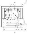
- FIG. 1 schematically shows an exemplary configuration of an imaging device according to a first embodiment of the present disclosure.
- An imaging device 100 illustrated in FIG. 1 includes a pixel array 110 including a plurality of pixels 10 and a peripheral circuit 120.
- the pixel array 110 includes a plurality of pixels 10 arranged, for example, in a matrix of m rows and n columns.
- m and n are natural numbers.
- the pixels 10 are two-dimensionally arranged on the semiconductor substrate 60, for example, to form an imaging region.
- the number and arrangement of the pixels 10 in the pixel array 110 are not limited to the illustrated example.
- the number of pixels 10 included in the imaging device 100 may be one.
- the imaging device 100 can be used as a line sensor.
- Each pixel 10 includes a photoelectric conversion unit that receives light and generates a charge.
- the photoelectric conversion portion of each pixel 10 has a structure including a buried photodiode formed on the semiconductor substrate 60 or a part of the photoelectric conversion layer disposed above the region corresponding to the imaging region in the semiconductor substrate 60. obtain.
- terms such as “upper” and “lower” are used only to designate the mutual arrangement between members, and are not intended to limit the posture when using the imaging device 100.
- the peripheral circuit 120 has a predetermined voltage applied to the vertical scanning circuit 122, the signal holding circuit 123, the horizontal scanning circuit 124, the output stage amplifier 126, and each pixel 10 in the pixel array 110. And a voltage supply circuit 128 for supplying the voltage.
- the peripheral circuit 120 is provided on the semiconductor substrate 60 on which the pixel array 110 described above is formed.
- the arrangement of peripheral circuit 120 is not limited to this example, and part or all of peripheral circuit 120 may be arranged on another substrate different from semiconductor substrate 60.
- the vertical scanning circuit 122 is also referred to as a row scanning circuit, and has, for example, a connection with an address signal line and a reset signal line provided corresponding to each row of the plurality of pixels 10.
- the vertical scanning circuit 122 can execute accumulation and readout of signal charges in the pixels 10 and reset of the accumulated signal charges on a row basis by supplying predetermined signals to the address signal line and the reset signal line. it can.
- the peripheral circuit 120 may have two or more vertical scanning circuits 122. In FIG. 1, in order to avoid complication of the drawing, illustration of various signal lines such as address signal lines and reset signal lines is omitted. Arrows in FIG. 1 schematically indicate the flow of signals supplied to various signal lines such as address signal lines and reset signal lines.
- the signal holding circuit 123 is connected to a vertical signal line (not shown) provided corresponding to each column of the plurality of pixels 10, and has a function of temporarily holding a signal output to the vertical signal line.
- the signal may be held in the form of analog values or in the form of digital values subjected to analog-to-digital conversion.
- the signal holding circuit 123 outputs, to the horizontal scanning circuit 124, the difference between the signal read from the pixel 10 after accumulation of the signal charge and the signal read from the pixel 10 after reset of the signal charge. .
- the operations between the signals may be performed in analog or digital form.
- the horizontal scanning circuit 124 also referred to as a column scanning circuit, typically includes an analog-to-digital converter circuit in part.
- the horizontal scanning circuit 124 has a function of reading out the difference signal obtained by the signal holding circuit 123 for each row of the plurality of pixels 10 to the output stage amplifier 126.
- the voltage supply circuit 128 is electrically connected to each pixel 10, and is configured to switch and supply two or more predetermined voltages to each pixel 10 when the imaging device 100 operates.
- the second voltage V B is a voltage different from the first voltage V A.
- the voltage supply circuit 128 may be configured to be capable of applying a predetermined voltage to each pixel 10 when the imaging device 100 operates, and is not limited to a specific power supply circuit.
- the voltage supply circuit 128 may be a circuit that generates a predetermined voltage, or may be a circuit that converts a voltage supplied from another power supply into a predetermined voltage.
- the voltage supply circuit 128 may be part of the vertical scanning circuit 122.
- the voltage applied from the voltage supply circuit 128 to each pixel 10 is not limited to two different voltages.
- the voltage supply circuit 128 may be configured to be able to switch between three or more different voltages and supply them to each pixel 10.
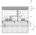
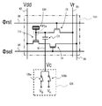
- FIG. 2 schematically illustrates a cross section of an exemplary device structure of the pixel 10.
- FIG. 2 schematically shows the shape, size and arrangement of each part in the pixel 10, and the shape, size and arrangement of each part shown in FIG. 2 do not necessarily reflect the shape, size and arrangement in a real device. The same applies to the other drawings of the present disclosure.
- the pixel 10A illustrated in FIG. 2 is an example of the above-described pixel 10.
- the pixel 10A roughly includes a part of the semiconductor substrate 60 and the photoelectric conversion unit 50A supported by the interlayer insulating layer 40 covering the semiconductor substrate 60.
- the photoelectric conversion unit 50 ⁇ / b> A includes the photoelectric conversion layer 54 located above the region corresponding to the imaging region in the semiconductor substrate 60. That is, a stacked imaging device is illustrated as the imaging device 100 here.
- the semiconductor substrate 60 includes a support substrate 60S and one or more semiconductor layers formed on the support substrate 60S.
- a p-type silicon substrate is illustrated as the support substrate 60S.
- Impurity regions 60 a to 60 e and an element isolation region 65 are provided in the semiconductor substrate 60.
- Each of impurity regions 60a to 60e is typically an n-type diffusion region.
- the photoelectric conversion unit 50A supported by the semiconductor substrate 60 includes the pixel electrode 52 on the interlayer insulating layer 40, the counter electrode 56 positioned farther from the semiconductor substrate 60 than the pixel electrode 52, and the pixel The photoelectric conversion layer 54 located between the electrode 52 and the counter electrode 56 is provided.
- the pixel electrode 52 is an electrode formed of metal such as aluminum or copper, metal nitride, or polysilicon to which conductivity is imparted by doping an impurity.
- the pixel electrode 52 is electrically separated from the pixel electrode 52 in another adjacent pixel 10A by being spatially separated.
- the counter electrode 56 is formed of a transparent conductive material such as ITO.
- transparent means transmitting at least a portion of light in the wavelength range to be detected, and it is not essential to transmit light over the entire wavelength range of visible light.
- the counter electrode 56 may be formed across the plurality of pixels 10A, while the pixel electrode 52 is separated between the pixel electrodes 52 in other adjacent pixels 10A.
- the counter electrode 56 is typically disposed above the semiconductor substrate 60 in the form of a single continuous electrode.
- the photoelectric conversion layer 54 is formed of an organic material or an inorganic material such as amorphous silicon.
- the photoelectric conversion layer 54 is formed, for example, by vacuum evaporation, and may have a thickness of about 500 nm.
- the photoelectric conversion layer 54 may have a layer composed of an organic material and a layer composed of an inorganic material.
- the photoelectric conversion layer 54 receives light incident through the counter electrode 56 and generates positive and negative charges by photoelectric conversion. Similar to the counter electrode 56, the photoelectric conversion layer 54 may also be disposed above the semiconductor substrate 60 in the form of a single continuous layer across the plurality of pixels 10A.
- a voltage line connected to a power supply (not shown) is connected to the counter electrode 56, and the counter electrode 56 has a predetermined bias voltage when the imaging device 100 operates. Receive the supply. By controlling the potential of the counter electrode 56 by application of a predetermined bias voltage, one of the positive and negative charges generated by photoelectric conversion can be collected by the pixel electrode 52 as a signal charge.
- the bias voltage applied to the counter electrode 56 may be supplied from the voltage supply circuit 128 described above.
- a bias voltage that is higher than the pixel electrode 52 may be applied to the counter electrode 56.
- positive charge Typical of positive charges as signal charges are holes. It is of course possible to use a negative charge, eg an electron, as the signal charge.
- a bias voltage that is lower than that of the pixel electrode 52 may be applied to the counter electrode 56.
- the pixel 10A includes the connection portion 42 disposed in the interlayer insulating layer 40. As schematically shown in FIG. 2, one end of the connection portion 42 is connected to the pixel electrode 52 of the photoelectric conversion unit 50.
- the connection unit 42 includes a plurality of wiring layers and a plurality of plugs, and electrically connects the photoelectric conversion unit 50A to a circuit formed on the semiconductor substrate 60.
- the plurality of wiring layers and the plurality of plugs are typically formed of a metal such as copper or tungsten or a metal compound such as metal nitride or metal oxide.
- the signal detection transistor 72, the address transistor 74, and the reset transistor 76 are formed on the semiconductor substrate 60.
- an n-channel field effect transistor represented by an n-channel MOS is exemplified as the signal detection transistor 72, the address transistor 74, and the reset transistor 76.
- a p-type transistor instead of the n-type transistor.
- an n-type silicon substrate may be used as the support substrate 60S, and the p-type is selected as the conductivity type of the impurity regions 60a to 60e.
- the reset transistor 76 includes the impurity region 60a formed in the semiconductor substrate 60 as one of the drain region and the source region, and includes the impurity region 60b as the other of the drain region and the source region.
- the connection portion 42 has a connection with the impurity region 60a, and therefore, the impurity region 60a is electrically connected to the pixel electrode 52 of the photoelectric conversion portion 50A through the connection portion 42. It is connected.
- a reset voltage line for supplying a reset voltage which is a reference voltage for reset is connected to the impurity region 60b.
- the reset transistor 76 is switched on and off to switch supply and cutoff of the reset voltage supplied from the reset voltage line to the impurity region 60a.
- which of the impurity region 60a and the impurity region 60b functions as the drain region of the reset transistor 76 is determined by the potential of the impurity region 60a and the impurity region 60b.
- the impurity region 60a and the impurity region 60b will be described as the drain region and the source region, respectively.
- the drain region and the source region may be interchanged.
- the imaging device 100 includes another transistor connected in series to the reset transistor 76, the same applies to the other transistors connected in series to the reset transistor 76.
- the signal detection transistor 72 includes a gate insulating layer 72g on the semiconductor substrate 60, a gate electrode 72e on the gate insulating layer 72g, an impurity region 60c as a drain region, and an impurity region 60d as a source region.
- a power supply line (not shown) is connected to the impurity region 60c, and a power supply voltage of, for example, 3.3 V is applied to the impurity region 60c from the power supply line when the imaging device 100 operates.
- connection portion 42 is also connected to the gate electrode 72 e of the signal detection transistor 72. That is, the gate electrode 72 e of the signal detection transistor 72 is electrically connected to the pixel electrode 52 of the photoelectric conversion unit 50 A through the connection unit 42.
- address transistor 74 includes an impurity region 60d as a drain region and an impurity region 60e as a source region.
- the address transistor 74 is electrically connected to the signal detection transistor 72 by sharing the impurity region 60 d with the signal detection transistor 72.
- a vertical signal line (not shown) is connected to impurity region 60e.
- the circuit in the pixel 10A is electrically separated from the circuit in the other adjacent pixel 10A by the element isolation region 65.
- the element isolation region 65 is also provided between the signal detection transistor 72 and the reset transistor 76.
- connection portion 42 has a connection with the pixel electrode 52.
- the impurity region 60 a and the gate electrode 72 e of the signal detection transistor 72 are electrically connected to the pixel electrode 52 through the connection portion 42.
- the pixel electrode 52, the connection portion 42, the impurity region 60a, and the gate electrode 72e function as a charge storage node that temporarily holds the signal charge collected by the pixel electrode 52.
- the pixel 10A further includes a control line 81 electrically connected to the connection portion 42.
- the control line 81 is a signal line connected to the voltage supply circuit 128 described above. That is, here, the impurity region 60a has an electrical connection with the voltage supply circuit 128 described above. As described later, a capacitive element or the like may be interposed between the impurity region 60 a and the voltage supply circuit 128.
- a voltage supply circuit 128 to the connecting portion 42 which constitutes a part of the charge storage nodes are electrically connected, switches the output of the voltage supply circuit 128 between the first voltage V A and the second voltage V B. This makes it possible, for example, to temporarily change the potential of the charge storage node after reset.
- the semiconductor substrate 60 has one or more semiconductor layers on the support substrate 60S.
- the semiconductor layer on the support substrate 60S includes a first p-type semiconductor layer 61p, an n-type semiconductor layer 61n, and a second p-type semiconductor layer 62p.
- the above-described impurity regions 60a to 60e and the element isolation region 65 are formed in the second p-type semiconductor layer 62p as ap well.
- the n-type semiconductor layer 61 n is located between the first p-type semiconductor layer 61 p and the second p-type semiconductor layer 62 p, and via an unshown well contact provided outside the imaging region when the imaging device 100 operates. The potential is controlled.
- the n-type semiconductor layer 61 n suppresses the inflow of minority carriers from the support substrate 60S or the peripheral circuit 120 to the charge storage node for storing signal charges.
- the semiconductor substrate 60 is a p-type provided between the second p-type semiconductor layer 62p and the support substrate 60S so as to penetrate the first p-type semiconductor layer 61p and the n-type semiconductor layer 61n. It has a region 63.
- the p-type region 63 has a relatively high impurity concentration, and electrically connects the second p-type semiconductor layer 62p and the support substrate 60S to each other.
- a substrate contact (not shown) is provided outside the imaging region, and the potential of the support substrate 60S and the second p-type semiconductor layer 62p is controlled via the substrate contact when the imaging device 100 operates. In other words, when the imaging device 100 operates, the substrate potential of the semiconductor substrate 60 is controlled via the substrate contact.
- the voltage supply circuit 128 described above may be configured to supply the substrate potential of the semiconductor substrate 60 via the substrate contact.
- an n-type transistor is applied as the signal detection transistor 72, the address transistor 74, and the reset transistor 76 as in the example described here, the substrate potential is typically ground.
- impurity region 60a constitutes a part of the charge storage node that temporarily stores the signal charge generated by photoelectric conversion unit 50A. This is because the junction capacitance formed by the pn junction between the impurity region 60a and the second p-type semiconductor layer 62p functions as a capacitance for accumulating at least a part of the signal charge.
- the pn junction between the impurity region 60a and the second p-type semiconductor layer 62p produces a depletion layer.
- lattice defects are present, and in particular, various lattice defects caused by impurities, dangling bonds, etc. exist on the surface of the semiconductor substrate 60. If a lattice defect exists in the depletion layer, for example, mixing of a charge different from the original signal charge into the impurity region 60a is likely to occur. In other words, lattice defects located in the depletion layer can cause dark current. Dark current results in a reduction in the signal-to-noise ratio and degrades the quality of the obtained image. If the depletion layer in the semiconductor substrate 60 can be reduced as much as possible to reduce lattice defects located in the depletion layer among lattice defects, it is useful because deterioration in image quality due to dark current is suppressed.
- the impurity region 60a in order to reduce the depletion layer formed by the pn junction between the impurity region 60a and the second p-type semiconductor layer 62p, the impurity region 60a after discharging the signal charge from the impurity region 60a. It is effective to make the potential of V close to the substrate potential as much as possible. That is, it is effective to make the potential of the impurity region 60a after reset as close as possible to the substrate potential. For example, when the signal charge is a hole and the substrate potential is ground, it is useful to apply a voltage as low as possible, which is close to 0 V, as the reset voltage.
- the potential of impurity region 60a is increased by electrical coupling through a circuit element such as a transistor connected to impurity region 60a. If it fluctuates, the potential of the impurity region 60a may fall below the substrate potential.
- a field effect transistor when a field effect transistor is connected to an n-type impurity region in a floating node that stores signal charge, the transistor is turned on and on due to the effect of electrical coupling via parasitic capacitance between the source and drain.
- the potential of the impurity region may decrease due to the switching off.
- forward bias is applied to the pn junction between the impurity region and the surrounding p well, and from the p-type silicon substrate as a support substrate Holes will flow into the impurity region. That is, there is a possibility that dark current occurs and the image quality of the obtained image is degraded.
- the present inventors have repeated studies in view of the above, for example, by varying the potential of the charge storage node after the reset by switching the first voltage V A and the second voltage V B, impurities accumulate signal charge region It has been found that it is possible to prevent the charge different from the original signal charge from being mixed in the impurity region with the switching on and off of the connected transistor.
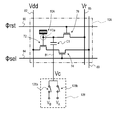
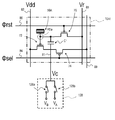
- FIG. 3 schematically shows a typical example of the circuit configuration of the pixel 10A shown in FIG. Note that, in FIG. 2, illustration of voltage lines for supplying a predetermined bias voltage to the counter electrode 56 of the photoelectric conversion unit 50A is omitted in FIG. 2 in order to prevent the drawing from becoming excessively complicated. Likewise, in the following drawings, illustration of voltage lines for supplying a predetermined bias voltage to the counter electrode 56 is omitted.
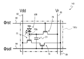
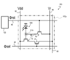
- the gate of the signal detection transistor 72 is connected to the photoelectric conversion unit 50A. It can be said that the node FDa between the photoelectric conversion unit 50A and the signal detection transistor 72 corresponds to a charge storage node. A voltage corresponding to the signal charge stored in the node FDa is applied to the gate of the signal detection transistor 72. As shown, the drain of the signal detection transistor 72 is connected to a power supply line 82 as a source follower power supply for supplying the power supply voltage Vdd, and the source of the signal detection transistor 72 is a vertical signal via the address transistor 74. Line 89 is connected. That is, the signal detection transistor 72 and the address transistor 74 form a source follower.
- An address signal line 84 connected to the vertical scanning circuit 122 is connected to the gate of the address transistor 74.
- the vertical scanning circuit 122 can read out the signal from the pixel 10 A to the vertical signal line 89 by controlling the address signal selsel applied to the address signal line 84.
- the reset transistor 76 is also connected to the node FDa.
- the side of the source and drain of the reset transistor 76 which is not connected to the node FDa is connected to the reset voltage line 85.
- a predetermined reset voltage Vr is applied to the reset voltage line 85.
- the reset signal line 86 connected to the vertical scanning circuit 122 is connected to the gate of the reset transistor 76. Under control of the reset signal ⁇ rst applied to the reset signal line 86, the vertical scanning circuit 122 can turn on the reset transistor 76 and apply the reset voltage Vr to the charge storage node. As described with reference to FIG.
- the reset transistor 76 includes the impurity region 60a forming a part of the charge storage node as a drain region or a source region. When the reset transistor 76 is turned on, the signal charge is discharged from the charge storage node, and the potential of the charge storage node is reset.
- the voltage supply circuit 128 is further electrically connected to the node FDa.
- the capacitive element C1 is interposed between the node FDa and the control line 81 connected to the voltage supply circuit 128.
- the node FDa is connected to one of the two terminals of the capacitive element C1. That is, in this example, one terminal of the capacitive element C1 is electrically connected to the impurity region 60a.
- the voltage supply circuit 128 is connected to the other of the two terminals of the capacitive element C1.
- the capacitive element C1 may have, for example, a metal-insulator-semiconductor (MIS) structure disposed in the interlayer insulating layer 40, or may be a depression-type MOS (DMOS) capacitor. Alternatively, it may be a MIM (metal-insulator-metal) structure. Adopting the MIM structure makes it easy to obtain a larger capacity value.
- MIS metal-insulator-semiconductor
- DMOS depression-type MOS
- MIM metal-insulator-metal
- voltage supply circuit 128 has switching elements 128a and 128b configured of field effect transistors or the like. That is, here, the voltage supply circuit 128, the switching by switching the switching elements 128a and 128b on and off, the voltage Vc applied to the control line 81 between the first voltage V A and the second voltage V B It is possible.
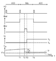
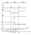
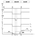
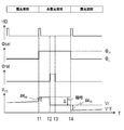
- FIG. 4A is a timing chart for explaining an exemplary operation of the pixel 10A having the circuit configuration shown in FIG.
- the top chart in FIG. 4A shows pulses of the horizontal synchronization signal HD.
- the period from the rise of a certain pulse to the rise of the next pulse corresponds to 1 H which is one horizontal scanning period.
- the reset of the pixels 10A belonging to one certain row among the plurality of pixels 10A included in the pixel array 110 and the readout of the signal from the pixels 10A are performed.
- the double arrow SEL in FIG. 4A indicates a selection period in which the address transistor 74 of the pixel of interest is turned on, and the arrow ACC indicates a non-selection period in which the address transistor 74 is turned off.
- the bottom chart in FIG. 4A shows temporal changes of the potential of the node FDa, ie, the potential V FD of the impurity region 60a, and the second chart from the bottom is applied from the voltage supply circuit 128 to the control line 81.
- the temporal change of voltage Vc is shown.
- the first voltage V A is applied to the control line 81.
- the address signal selsel After accumulation of signal charges by exposure, the address signal selsel is set to high level at time T1. By setting the address signal selsel to a high level, a first signal of a voltage level corresponding to the signal charge stored in the charge storage node is read out to the vertical signal line 89 through the signal detection transistor 72 and the address transistor 74. The read first signal is temporarily held by the signal holding circuit 123 shown in FIG.
- the reset signal rstrst is set to the high level, and the reset transistor 76 is turned on.
- the reset transistor 76 is turned on, the signal charge is discharged from the charge storage node, and the potential of the charge storage node is reset.
- the potential V FD of the impurity regions 60a by the reset voltage Vr is applied to the node FDa falls to Vr.
- a voltage higher than the substrate potential Vsub is used as the reset voltage Vr. Therefore, here, Vr> Vsub.
- the substrate potential Vsub is 0 V, a positive voltage near 0 V is used as the reset voltage Vr.
- the reset signal rstrst is set to low level, and the reset transistor 76 is turned off.
- the reset transistor 76 includes the impurity region 60 a as a drain region or a source region. Therefore, when the reset transistor 76 is turned off, the potential V FD of the impurity region 60a may be further lowered from Vr due to the electrical coupling caused by the parasitic capacitance of the reset transistor 76. As described above, at this time, if the potential V FD falls below the substrate potential Vsub, extra holes flow into the impurity region 60a.
- the potential V FD of the impurity region 60a immediately after the reset transistor 76 is off is V1a satisfying the relationship of Vr>V1a> Vsub.
- V1a may be about 0.2V. That is, the second voltage V B and appropriate selection, by switching between the output from the voltage supply circuit 128 of the first voltage V A and the second voltage V B, the potential V FD is the substrate potential Vsub of the impurity regions 60a It is prevented that it falls below.
- a potential difference of 0.2 V can be secured at the potential V FD of the impurity region 60 a with reference to the substrate potential. That is, the inflow of unnecessary holes to the impurity region 60a due to the potential V FD falling below the substrate potential Vsub is prevented. In other words, dark current is suppressed.
- V B the source of the reset transistor 76 - in consideration of the magnitude of the parasitic capacitance between the drain potential V FD when off the reset transistor 76 satisfies the relation of V1a> Vsub It is sufficient to select a voltage that will
- a second signal corresponding to the voltage level of the charge storage node after discharge of the signal charge is transmitted through the address transistor 74 during a period until time T4 when the next pulse of the horizontal synchronization signal HD And read out to the vertical signal line 89.
- the signal holding circuit 123 outputs the difference ⁇ between the first signal and the second signal to the horizontal scanning circuit 124 as a signal representing an image.
- the address transistor 74 is turned off, and accumulation of signal charge of the next frame is started.
- the voltage supply circuit 128 applies the first voltage V A to the impurity region 60 a during the first period from time T2 to T3 in which the reset transistor 76 is turned on. It followed, in the second period of time T3 ⁇ T4, and is configured to switch the voltage applied to the impurity regions 60a to a second voltage V B.
- the potential V FD of the impurity regions 60a with the off of the reset transistor 76 is possible to prevent that fall below the substrate potential Vsub. Therefore, it is possible to suppress the dark current generated by the flow of extra holes into impurity region 60a.
- capacitive element C1 since capacitive element C1 has an electrical connection with node FDa, at least one of the charge storage nodes for temporarily holding the signal charge, like impurity region 60a. Make up the department. In other words, the connection of capacitive element C1 to node FDa increases the capacitance value of the entire charge storage node. It is advantageous for the capacitance value of the capacitive element C1 to be as small as possible for the following two reasons.
- the first reason is that an increase in the capacitance value of the entire charge storage node results in a decrease in conversion gain. If the conversion gain is lowered, the influence of noise in the subsequent stage circuit becomes large, and there is a possibility that the SN ratio may be lowered. Therefore, from the viewpoint of avoiding the decrease in the SN ratio, it is useful that the capacitance value of the capacitive element C1 be as small as possible.
- the second reason is that if the capacitive element C1 has a relatively large capacitance value, the influence of noise mixing on the control line 81 via the capacitive element C1 to the node FDa may increase.
- Noise included in the voltage applied to control line 81 can be mixed in node FDa by electrical coupling via capacitive element C1.
- the configuration in which the voltage supplied to control line 81 is commonly applied to the charge storage nodes of the pixels belonging to the same row via the capacitive element C1 in other words, the first voltage V A
- the noise on the control line 81 may appear on the image as a horizontal line noise. It is useful to be able to suppress the horizontal noise because the horizontal noise tends to be easily recognized by the viewer of the image as compared to the random noise in units of pixels.
- capacitance value of capacitance element C1 is C 1 and the capacitance value of a portion other than capacitance element C1 of the charge storage nodes is C FD
- the magnitude of the voltage variation transmitted to node FDa is the voltage variation of control line 81 It is represented by the product of C 1 / (C 1 + C FD )). Therefore, in terms of horizontal noise suppression, capacitance value C 1 of the capacitor C1 is advantageously as small as possible.
- the capacitance value C 1 of the capacitor element C1, the capacitance value of the portions other than the capacitor element C1 of the charge storage node is beneficial to be smaller than C FD. It is made smaller than the capacitance value C FD portion other than the capacitive element C1 of the charge storage node capacitance value C 1 of the capacitor C1, the reduction in the SN ratio caused by connecting a capacitor C1 to the node FDa The degree may be smaller than the degree of reduction of the SN ratio when the F value is increased by one level.
- the capacitance value C 1 of the capacitor element C1 with the degree less than half of the capacitance value C FD, the degree of reduction of the SN ratio caused by connecting a capacitor C1 to node FDa, converted to F value
- the change can be limited to about (1/2) or less.
- the reset voltage Vr Since a larger positive voltage is used as the reset voltage Vr, the influence of the reduction in the potential V FD of the impurity region 60a due to the electrical coupling caused by the parasitic capacitance of the reset transistor 76 accompanying the turning off of the reset transistor 76 is small. It can be said. However, when using electrons as signal charges, it is necessary to use a higher voltage as the reset voltage Vr in order to improve the number of saturated electrons, and from the viewpoint of securing the number of saturated electrons sufficient for the required dynamic range, It is more advantageous to use holes as the charge.
- the conductivity type of each region in the semiconductor substrate 60 may be switched between n-type and p-type.
- the p-type transistor as the reset transistor 76 as described below, as the second voltage V B, using a voltage lower than the first voltage V A.
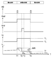
- FIG. 4B is a timing chart for explaining an exemplary operation when a p-type transistor is applied to the reset transistor 76 of the pixel 10A.
- a p-type transistor is applied to the reset transistor 76
- a higher voltage is used as a substrate potential Vsub than when an n-type transistor is applied to the reset transistor 76.
- Substrate potential Vsub may be, for example, about 3.3V.
- the effect of the change in the potential V FD of the impurity region 60a due to the electrical coupling caused by the parasitic capacitance of the reset transistor 76 is better when holes are used as signal charges. Is small. This is because of the same reason as in the case where an n-type transistor is applied to the reset transistor 76 and electrons are used as signal charges. However, in order to secure a sufficient number of saturated electrons, it is necessary to secure a sufficient potential difference between the substrate potential and the potential V FD of the impurity region 60a. On the other hand, if the signal charge is an electron, a voltage near 3.3 V which is the substrate potential may be used as the reset voltage Vr. When a p-type transistor is applied to the reset transistor 76, the signal charge is Using electrons is easier to secure a sufficient number of saturated electrons in the required dynamic range while avoiding circuit complexity.
- FIG. 4B shows an example of operation in the case where a p-type transistor is applied to the reset transistor 76 and electrons are used as signal charges.
- the reset transistor 76 is a p-type transistor and electrons are used as signal charges
- the signal detection transistor 72 and the address transistor 74 are also formed on the semiconductor substrate 60 as p-type transistors.
- the potential V FD of the impurity region 60a gradually decreases due to the accumulation of the signal charge due to the exposure.
- the address signal selsel is set to low level at time T1 to turn on the address transistor 74, and the first signal is read out to the vertical signal line 89.
- the reset signal rstrst is set to low level, and the reset transistor 76 is turned on.
- the potential V FD of the impurity region 60a rises to Vr.
- the reset voltage Vr at this time for example, a voltage of 2.8 V which is near the substrate potential Vsub and lower than the substrate potential Vsub is used.
- the reset signal rstrst is set to the high level, and the reset transistor 76 is turned off.
- the electrical coupling caused by the parasitic capacitance of the reset transistor 76 may further increase the potential V FD of the impurity region 60a from Vr.
- V FD exceeds the substrate potential Vsub
- a forward bias is applied to the pn junction between the impurity region 60a and the periphery thereof, and an n-type silicon substrate as a support substrate is redundantly connected to the impurity region 60a. Electrons flow in. In other words, dark current occurs.
- the time T3 only a reset signal ⁇ rst a high level, and switches the voltage Vc applied from the voltage supply circuit 128 to the control line 81 to lower than the first voltage V A second voltage V B .
- the potential of the node FDa between the photoelectric conversion unit 50A and the signal detection transistor 72 can be reduced via the capacitive element C1, As shown in FIG. 4B, the potential V FD of the impurity region 60a can be prevented from exceeding the substrate potential Vsub.
- the potential V FD of the impurity region 60a immediately after the reset transistor 76 is turned off is V1b which satisfies the relationship Vsub>V1b> Vr.
- V1b may be about 3.1V.
- the reset transistor 76 After the reset transistor 76 is turned off, the second signal corresponding to the voltage level of the charge storage node after discharging the signal charge is read out to the vertical signal line 89, and the absolute value of the difference ⁇ between the first signal and the second signal is obtained. Obtained as an image signal. After obtaining the second signal, the address transistor 74 is turned off, and accumulation of signal charge of the next frame is started.
- control line 81 is connected between the exposure period for accumulating signal charges in the charge accumulation node and the period for resetting in a non-exposure period other than the exposure period of one frame period.
- the voltages supplied may be different from each other.
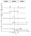
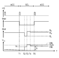
- FIG. 4C is a timing chart for explaining another example of the operation of the pixels 10A, 10Ap and 10Aq. Similar to the example shown in FIGS. 4A and 4B, in the operation example shown in FIG. 4C, the exposure period for accumulating the signal charge in the charge storage node and the non-exposure period other than the exposure period are alternately repeated.
- the non-exposure period includes, in part, a reset period for resetting the potential of the charge storage node to a predetermined potential.
- the pixel 10A shown in FIG. 3 is illustrated.
- the address signal selsel is made high.
- ⁇ V FD (V B ⁇ V A ) (C 1 / (C 1 + C FD )) (1)
- the potential of the node FDa at this time is read out to the vertical signal line 89 through the signal detection transistor 72 and the address transistor 74 as a first signal expressing a voltage level corresponding to the signal charge stored in the charge storage node.
- the reset signal rstrst is made high. Thereby, the signal charge is discharged from the charge storage node through the reset transistor 76, and the potential of the charge storage node is reset to the reset voltage Vr.
- the reset signal rstrst is set to low level, and the reset transistor 76 is turned off. From time T3 to time T4 at which the next pulse of horizontal synchronization signal HD rises, the second signal corresponding to the voltage level of the charge storage node after discharge of the signal charge is made vertical via address transistor 74. Read on line 89.
- the difference ⁇ between the first signal read from time T1 to time T2 and the second signal read from time T3 to time T4 represents an image. It becomes a true pixel signal.
- the voltage applied to the control line 81 is returned to the first voltage V A again.
- the potential of the node FDa drops from Vr to V1c due to capacitive coupling via the capacitive element C1.
- the fluctuation amount of the potential of the node FDa at this time (Vr ⁇ V1c) is equal to the above-described ⁇ V FD .
- the fluctuation amount ⁇ V FD is controlled by determining the first voltage V A and the second voltage V B based on the above equation (1). be able to.
- the desired ⁇ V FD can be achieved by the following procedure. First, at the time of product design, the capacitance ratio between the capacitive element C1 and a portion of the charge storage node other than the capacitive element C1 is determined from the total capacitance value of the target charge storage node. Then, the amplitude of the voltage applied to the control line 81 during actual operation, i.e., a specific voltage value of the first voltage V A and the second voltage V B is determined based on equation (1) above.
- either the first voltage VA or the second voltage VB is at ground (0 V). Since the ground side is generally low impedance, it is possible to suppress the mixing of power supply noise from the voltage supply circuit 128 connected to the control line 81 into the charge storage node. For example, when the second voltage V B is grounded, the first voltage V A is a negative level voltage.
- the voltage supply circuit 128, the control line 81, and supplies the first voltage V A to the exposure period for accumulating the signal charges impurity regions 60a to charge storage node includes in its part.
- a second voltage V B different from the first voltage V A is supplied.
- control may be employed to differ between at least the reset period and the other periods after the exposure period. According to such control, for example, the potential of the charge storage node can be temporarily reduced compared to the reset voltage Vr.
- the potential difference between the impurity region 60a and the second p-type semiconductor layer 62p located around it and grounded, for example, can be reduced.
- the depletion layer formed by the pn junction between the impurity region 60a and the second p-type semiconductor layer 62p is reduced, and the reduction of dark current is realized. That is, by setting the potential of the charge storage node to a low potential in the exposure period, an effect of dark current reduction can be expected.
- the potential of the charge storage node is raised by the potential difference amount between the second voltage V B and the first voltage V A. Therefore, by adjusting this potential difference, it is possible to set the source-drain voltage of the signal detection transistor 72 and the transistor of the subsequent stage circuit within the voltage range in which these transistors can operate. Therefore, the signal detection transistor 72 and the rear stage circuit can normally read out the pixel signal or the reference signal.
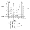
- FIG. 5 schematically shows an example of another circuit configuration of the pixel 10.
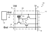
- the pixel 10Ap illustrated in FIG. 5 includes a photoelectric conversion unit 50B instead of the photoelectric conversion unit 50A.
- the photoelectric conversion unit 50B is, for example, a buried photodiode formed in the semiconductor substrate 60.
- the photoelectric conversion unit 50B is connected to the gate of the signal detection transistor 72.
- the node FDb between the photoelectric conversion unit 50B and the signal detection transistor 72 corresponds to a charge storage node.
- the pn junction in the embedded photodiode as the photoelectric conversion unit 50B, the impurity region 60a and the gate electrode 72e function as charge storage nodes for temporarily holding the charge generated by the photoelectric conversion unit 50B.
- Impurity region 60a may be part of a pn junction in the buried photodiode.
- the same operation as the operation described with reference to FIGS. 4A and 4B can be applied to the imaging device 100 having the pixel 10Ap.
- the reset signal ⁇ rst a low level
- to switch the voltage Vc applied to the control line 81 from the voltage supply circuit 128 from the first voltage V A higher than the first voltage V A second voltage V B the potential of the node FDb can be increased through the capacitive element C1.
- the second voltage V B the potential V FD of the impurity regions 60a is avoided that below the substrate potential Vsub, can suppress dark current.
- the reset transistor 76 or the like is a p-type transistor and electrons are stored as signal charges, which is more advantageous because a larger dynamic range can be obtained.
- FIG. 6 schematically shows an example of still another circuit configuration of the pixel 10.
- the pixel 10Aq illustrated in FIG. 6 further includes the transfer transistor 79 connected between the gate of the signal detection transistor 72 and the photoelectric conversion unit 50B.
- the transfer transistor 79 transfers the signal charge obtained by the photoelectric conversion unit 50B to a node FDc between the gate of the signal detection transistor 72 and the transfer transistor 79 at a predetermined timing.
- the transfer transistor 79 is, for example, an n-channel MOS.
- the transfer transistor 79 may share the impurity region 60 a with the reset transistor 76 as one of a source region and a drain region.
- the circuit configuration shown in FIG. 6 similar to the pixel 10Ap shown in FIG. 5, by switching the voltage Vc from the first voltage V A to the second voltage V B, the potential of a floating node node FDc, capacitance
- the potential V FD of the impurity region 60a can be avoided, for example, from rising below the substrate potential Vsub through the element C1.
- Switching of the voltage Vc from the first voltage V A to the second voltage V B is performed, for example, at the timing of turning off the reset transistor 76 after discharging the signal charge transferred to the node FDc by turning on the reset transistor 76. Be done.
- FIG. 7A and 7B schematically show an example of still another circuit configuration of the pixel 10.
- the pixel 10Ar shown in FIG. 7A has a signal detection transistor 72d of a depletion type instead of the signal detection transistor 72.
- a depletion type transistor as the signal detection transistor 72d, a high output can be obtained from the signal detection transistor 72d even when the potential of the node FDa is at a low level. Therefore, it becomes easier to secure the voltage range necessary for the operation of the current source configured of the load circuit and the like connected to the vertical signal line 89.
- the pixel 10As shown in FIG. 7B has a configuration in which the photoelectric conversion unit 50A of the pixel 10Ar shown in FIG. 7A is replaced with a photoelectric conversion unit 50B.
- the photoelectric conversion unit 50B is, for example, a buried photodiode formed in the semiconductor substrate 60. Even in the configuration using a photodiode, a depletion type transistor can be used as the signal detection transistor 72d.
- FIG. 8 is a timing chart for explaining an exemplary operation of the pixel 10Ar shown in FIG. 7A or the pixel 10As shown in FIG. 7B.
- the waveform of the voltage Vc in the non-exposure period is different from the waveform in the operation sequence illustrated in FIG. 4C.
- FIG. 8 wherein, in the non-exposure period, a short period of relatively high second voltage V B voltage Vc to be applied to the control line 81 from the voltage supply circuit 128.
- the voltage Vc is switched from the first voltage V A to the relatively high second voltage V B at the rise timing of the reset signal rstrst at time T 2, and the reset signal rstrst is low at time T 3 After being switched to the level, it is returned to the first voltage V A.
- the reset transistor 76 After the reset transistor 76 is turned off, the voltage Vc applied from the voltage supply circuit 128 to the control line 81 is switched to the first voltage VA , thereby contributing all changes in the voltage Vc to the change in the potential of the charge storage node. It becomes possible.
- the potential of the charge storage node drops from the reset voltage Vr by ⁇ V FD represented by the formula (1).
- the potential of the charge storage node can be lowered to a potential V1d lower than Vr.
- the true pixel signal representing the image of the subject is given by the difference between the first signal corresponding to the potential of the charge storage node at time T1 and the second signal corresponding to the potential of the charge storage node at time T4. .
- the first signal is read out to the vertical signal line 89 between time T1 and time T2, and the second signal is read out to the vertical signal line 89 between time T4 and time T5. That is, in this example, when the first voltage V A is applied to the control line 81, readout of the pixel signal and the reference signal is performed. Similarly, in this example, by using a voltage of 0V as the first voltage V A, it is possible to suppress the contamination of the noise nodes FDa or node FDb in voltage output from the voltage supply circuit 128.
- FIG. 9A and 9B schematically show an example of still another circuit configuration of the pixel 10.
- the pixel 10At shown in FIG. 9A is an example in which p-type transistors are applied as the signal detection transistor 72, the address transistor 74 and the reset transistor 76 in the circuit configuration shown in FIG.
- a pixel 10Au shown in FIG. 9B is an example in which p-type transistors are applied as the signal detection transistor 72, the address transistor 74 and the reset transistor 76 in the circuit configuration shown in FIG.
- electrons are typically used as signal charges.
- a p-type transistor is applied to the reset transistor 76, using electrons as the signal charge secures a sufficient number of saturated electrons in the required dynamic range while avoiding complication of the circuit. Cheap.
- FIG. 10 is a timing chart for explaining an exemplary operation of the pixel 10At shown in FIG. 9A or the pixel 10Au shown in FIG. 9B.
- the address signal ⁇ sel from the high level to the low level, switching the voltage Vc applied to the control line 81 to the relatively low from the first voltage V A second voltage V B .
- the address signal selsel is maintained at the low level in the non-exposure period.
- the potential of the charge storage node is obtained by capacitive coupling via the capacitive element C1. Decreases.
- the variation amount ⁇ V FD of the potential at this time is expressed by the above-mentioned equation (1) by the capacitance ratio between the capacitive element C1 and the portion of the charge storage node other than the capacitive element C1. From time T1 to time T2, a signal corresponding to the voltage V FD at this time is read out to the vertical signal line 89 as a first signal.
- the reset is performed by setting the reset signal rstrst to low level. That is, when the reset signal rstrst is set to low level, the reset transistor 76 is turned on, the signal charge stored in the node FDa or FDb is discharged through the reset transistor 76, and the potential of the charge storage node becomes the voltage Vr. It is reset.
- the reset signal rstrst is set to the high level to turn off the reset transistor 76.
- the second signal corresponding to the reset voltage Vr is read out to the vertical signal line 89 from time T3 to time T4.
- the difference between the first signal read from time T1 to time T2 and the second signal read from time T3 to time T4. are output as true pixel signals.
- the signal detection transistor 72, the address transistor 74, and the reset transistor 76 be p-type transistors.
- the reset transistor 76 is an n-channel MOS, for example, 0 V is used as the substrate potential Vsub.
- the reset transistor 76 is a p-channel MOS, and 0 V is adopted as the substrate potential Vsub.
- voltage V FD is lowered along with accumulation of electrons which are signal charges in the charge storage node, so that the voltage is applied to the pn junction between impurity region 60a and the periphery thereof. It is necessary to reset the potential of the charge storage node to a potential higher than the substrate potential Vsub prior to the accumulation of the signal charge in order to avoid the forward bias of the output voltage.
- the signal charge is an electron
- a voltage of 3.3 V can be used as the reset voltage Vr.
- the potential of the charge storage node drops from, for example, 3.3 V at the start of the exposure, and the potential difference between it and the substrate potential Vsub decreases. Therefore, the depletion layer width is reduced, and the effect of dark current reduction can be expected.
- the potential V FD of impurity region 60a is set to the substrate potential Vsub to prevent the applied voltage from becoming forward bias. It can not be raised more than that.
- the potential V FD of the impurity region 60a rises. Therefore, prior to the accumulation of the signal charge, the potential of the charge storage node is reset to a potential of, for example, 0 V lower than the substrate potential Vsub. In this case, the difference between the potential of the charge storage node at the start of exposure and the substrate potential Vsub is enlarged as compared with the case where an n-channel MOS is used as the reset transistor 76.
- 11A and 11B schematically show an example of still another circuit configuration of the pixel 10.
- the pixel 10Av shown in FIG. 11A further includes a transistor 71 connected between the capacitive element C and the control line 81.
- the difference between the pixel 10Av shown in FIG. 11A and the pixel 10Aw shown in FIG. 11B is that in the pixel 10Aw, the transistor 71 is connected between the node FDa and the capacitive element C1.
- the transistor 71 in the pixel 10Av illustrated in FIG. 11A has a function as a switching element that switches connection and disconnection between the capacitive element C1 and the voltage supply circuit 128.
- the transistor 71 in the pixel 10Aw illustrated in FIG. 11B has a function as a switching element that switches connection and disconnection between the node FDa and the capacitive element C1.
- the capacitance value of the entire charge storage node can be reduced.
- capacitive element C1 can be electrically disconnected from node FDa.
- capacitive element C1 is connected to node FDa or node FDb, and the voltage supplied to control line 81 is switched to control the potential of the charge storage node via capacitive element C1. It becomes possible. However, since the capacitance value of the entire charge storage node is increased as a result of connecting the capacitive element C1, the conversion gain at the time of converting the signal charge into a voltage may be reduced.
- a transistor 71 may be interposed between the capacitive element C1 and the voltage supply circuit 128, or between the node FDa or the node FDb and the capacitive element C1.
- the on / off switching of the transistor 71 can change the capacitance value of the entire charge storage node.
- the FD potential control mode in which the potential of the charge storage node is controlled via the capacitive element C1 by switching on and off of the transistor 71, and the high gain mode in which the signal charge is efficiently converted into a voltage signal. It becomes possible to use properly.
- the FD potential control mode is a mode in which the transistor 71 is turned on to electrically couple the voltage supply circuit 128 to the charge storage node via the capacitive element C1. In the high gain mode, the transistor 71 is turned off and the entire charge storage node is turned off. Is a mode in which the capacitance value of
- the mode switching may be automatically performed using an exposure time or an operating temperature as a criterion that has a large influence on dark current, or may be performed based on a user's instruction.
- the FD potential control mode may be selected for imaging under a long second exposure for over 1 second or a high temperature environment for over 80 degrees.
- the operation sequence in the FD potential control mode may be the same as the operation sequence described with reference to FIG. 4A, FIG. 4B, FIG. 4C, FIG. 8 or FIG.
- FIG. 11C schematically shows an example of still another circuit configuration of the pixel 10.
- the imaging device 100 includes a load transistor 73 connected to the vertical signal line 89.
- the load transistor 73 is, for example, an n-channel MOS, and functions as a current source 94.
- the imaging device 100 includes a feedback circuit 90x.
- the feedback circuit 90x includes an inverting amplifier 92 whose inverting input terminal is connected to the vertical signal line 89.
- the inverting amplifier 92 is provided for each column of the pixels 10Ax corresponding to the vertical signal line 89, and here, the reset voltage line 85 is connected to the output terminal thereof.
- the signal detection transistor 72, the address transistor 74, the inverting amplifier 92, and the reset transistor 76 form a feedback loop that negatively feeds back the electrical signal generated by the photoelectric conversion unit 50A.
- a voltage Vref of, for example, 1 V or near 1 V is supplied to the non-inverting input terminal of the inverting amplifier 92.
- the voltage Vref any voltage within the range of the power supply voltage Vdd and the ground can be used.
- the feedback loop is formed, the voltage of the vertical signal line 89 converges to the voltage Vref input to the non-inverting input terminal of the inverting amplifier 92.
- the potential of the node FDa can be reset to a potential at which the voltage of the vertical signal line 89 becomes Vref.
- the first signal and the second signal are read out to the vertical signal line 89 by the source follower formed by the signal detection transistor 72 and the current source 94.
- the potential of the node FDa at the time of signal reading is low, the voltage appearing on the vertical signal line 89 via the signal detection transistor 72 is also low, and the source-drain voltage necessary for operation in the saturation region can not be secured.
- the load transistor 73 may operate in the linear region. As a result, the source follower may not operate properly and the linearity of the signal may be degraded.
- the current value obtained by the current source 94 is set small, it is possible to operate the load transistor 73 in the saturation region, but in this case, a problem such as a reduction in the speed required for reading out a signal may occur. Further, the voltage drop of the vertical signal line 89 may cause the input signal to the inverting amplifier 92 to be out of the operating range, and the feedback circuit 90x may not operate properly. That is, there is a possibility that the potential of the node FDa can not be reset to such a potential that the voltage of the vertical signal line 89 becomes Vref.
- the operation sequence described with reference to FIG. 4C, FIG. 8 or FIG. 10 can be applied.
- the potential of the charge storage node in at least a part of the period of non-exposure period, through the capacitor C1 Temporarily raise or lower.
- the potential of the charge storage node is selectively raised in a non-exposure period other than the exposure period by switching the voltage applied from the voltage supply circuit 128 to the control line 81.
- the load transistor 73 By setting the potential of the charge storage node to a high potential selectively in the non-exposure period, the load transistor 73 is prevented from operating in the linear region, and the first signal and the second signal are normally output from the pixel. It is possible to read out. Since the signal read operation and the feedback operation are performed during the non-exposure period, there is no problem even if the potential of the charge storage node is low such that the load transistor 73 operates in the linear region during the exposure period. Absent. By setting the potential of the charge storage node to a low potential in the exposure period, it is possible to obtain an effect that the dark current can be suppressed without deteriorating the circuit characteristics.
- FIG. 12 schematically illustrates an example of the circuit configuration of the pixel 10B included in the imaging device according to the second embodiment of the present disclosure. Similar to the pixel 10A shown in FIG. 3, the pixel 10B shown in FIG. 12 is an example of the pixel 10 described above. The main difference between the pixel 10B shown in FIG. 12 and the pixel 10A described with reference to FIG. 3 is that the pixel 10B is not connected to the node FDa among the source and drain of the reset transistor 76. It is the point which further has the transistor 78 connected. Also, the voltage supply circuit 128 is electrically connected to a node RD between the reset transistor 76 and the transistor 78. In this example, voltage supply circuit 128 is electrically connected to impurity region 60 a via reset transistor 76.
- each pixel 10 of the imaging device 100 may have a circuit configuration further including a transistor 78 connected to the reset transistor 76.
- the transistor 78 is, for example, an n-channel MOS, and can include an impurity region 60 b as a source region or a drain region of the reset transistor 76 as a drain region or a source region.
- the reset voltage line 85 is connected to the side not connected to the reset transistor 76. For example, when the imaging device 100 operates, a predetermined reset is performed. A voltage Vr is applied to the transistor 78.
- the gate of the transistor 78 is connected to a signal line 88 for supplying the transistor 78 with a signal fb fb for controlling the on and off of the transistor 78.
- the signal line 88 has, for example, a connection with the vertical scanning circuit 122, and the vertical scanning circuit 122 can be configured to control the potential of the signal line 88.
- voltage supply circuit 128 is connected to a node RD between reset transistor 76 and transistor 78 via capacitive element C2. That is, in this example, the voltage supply circuit 128 is connected not to the impurity region 60a side of the reset transistor 76 but to the impurity region 60b side via the capacitive element C2.
- the capacitive element C2 connected between the control line 81 and the impurity region 60b can have the same configuration as the above-mentioned capacitive element C1.
- FIG. 13 shows a more specific example to which the circuit configuration shown in FIG. 12 is applied.
- the pixel 10 ⁇ / b> Bf illustrated in FIG. 13 is an example of the pixel 10 ⁇ / b> B illustrated in FIG. 12 and includes a feedback circuit 90.
- the feedback circuit 90 includes an inverting amplifier 92 whose inverting input terminal is connected to the vertical signal line 89, as in the example described with reference to FIG. 11C.
- the pixel 10 ⁇ / b> Bf includes a capacitive element C ⁇ b> 3 connected in parallel to the reset transistor 76.
- the feedback circuit 90 forms a feedback loop that negatively feeds back the electrical signal generated by the photoelectric conversion unit 50A.
- the feedback loop includes transistor 78 in part.
- thermal noise called kTC noise occurs when the transistor is turned on or off. After resetting the potential of the node FDa, simply turning off the reset transistor 76 causes kTC noise generated by turning off the reset transistor 76 to remain at the charge storage node before the signal charge is stored.
- the kTC noise generated with the turning off of the reset transistor can be reduced by using negative feedback as described in WO 2012/147302. The entire disclosure of WO 2012/147302 is incorporated herein by reference.
- this node RD is a floating node.
- the transistor 78 can include the impurity region 60b, for example, as a drain region. Therefore, when the transistor 78 is turned off, there is a possibility that the potential of the impurity region 60b may fall below the substrate potential due to electrical coupling caused by the parasitic capacitance of the transistor 78. When the potential of the impurity region 60b is lower than the substrate potential, the inflow of unnecessary holes from the p well causes an unintended fluctuation of the potential in the impurity region 60b, which may lower the SN ratio.
- the voltage supply circuit 128 is electrically connected to the impurity region 60 b. As described below, by switching the voltage Vc to be applied to the control line 81 from the voltage supply circuit 128 between the first voltage V A and the second voltage V B, the potential of the impurity region 60b is lower than the substrate potential Can be prevented.
- FIG. 14A is a timing chart for describing an exemplary operation of the pixel 10Bf having the circuit configuration shown in FIG.
- the second chart from the bottom in FIG. 14A shows temporal changes in the potential of the node RD, ie, the potential V RD of the impurity region 60b.
- Vc the potential of the node RD
- V A the potential of the impurity region 60b.
- the address signal selsel is set to the high level. At this time, the first signal of the voltage level corresponding to the signal charge stored in the charge storage node is read out.
- the reset signal rstrst and the signal fbfb are set to the high level. That is, the reset transistor 76 and the transistor 78 are turned on. The turning on of the reset transistor 76 and the transistor 78 forms a feedback loop. The formation of the feedback loop resets the potential of the node FDa.
- the potential of the node FDa is lowered to the voltage V2a such that the voltage of the vertical signal line 89 becomes Vref.
- a voltage that satisfies the relationship of V2a> Vsub is used as the voltage Vref applied to the non-inversion amplification terminal of the inversion amplifier 92.
- the potential V RD of the node RD with the ON of the reset transistor 76 and the transistor 78 is increased to V3.
- the voltage V3 satisfies the relationship of V3> Vsub.
- the reset signal rstrst is set to low level, and the reset transistor 76 is turned off.
- the potential V FD of the impurity region 60a is lowered from V2a to V4a as the reset transistor 76 is turned off.
- the potential V FD falls below the substrate potential Vsub, extra holes flow into the impurity region 60a.
- the relationship of V4a> Vsub is satisfied by properly selecting the voltage Vref. From the viewpoint of reducing the depletion layer as much as possible, it is useful that V4a be as close as possible to Vsub as long as the relationship of V4a> Vsub is satisfied.
- the capacitive element C3 is interposed between the node FDa and the node RD, and while the transistor 78 is not turned off, a feedback loop including the capacitive element C3 in its path is formed. Condition will continue. Therefore, the signal output from the transistor 78 is attenuated by the attenuation circuit formed by the capacitive element C3 and the parasitic capacitance of the node FDa itself.
- the signal fbfb is set to low level, and the transistor 78 is turned off.
- the time T4 just off the reset transistor 76, which switches the voltage Vc applied from the voltage supply circuit 128 to the control line 81 to a second voltage V B.
- the electrical coupling caused by the parasitic capacitance of the transistor 78 lowers the potential V RD of the impurity region 60b.
- the potential V RD decreases from V3 to V5a as the transistor 78 is turned off. At this time, if V5a ⁇ Vsub, extra holes causing noise will flow into the impurity region 60b.
- the voltage supply circuit 128 at the timing of switching off the transistor 78 from ON, than the first voltage V A voltage Vc from the first voltage V A and it is configured to switch to a higher second voltage V B.
- the voltage Vc from the first voltage V A to the second voltage V B it is possible to increase the potential V RD of the node RD via the capacitor C2, the potential V RD falls below the substrate potential It can prevent.
- the potential of the signal line 88 may be gradually lowered from the high level to the low level so as to cross the threshold voltage of the transistor 78.
- the resistance of the transistor 78 is gradually increased.
- the operating band of the transistor 78 narrows, and the frequency range of the signal to be fed back narrows.
- the transistor 78 When the voltage of the signal line 88 reaches a low level, the transistor 78 is turned off and the formation of the feedback loop is eliminated. At this time, if the operating band of the transistor 78 is a band sufficiently lower than the operating band of the signal detection transistor 72, the thermal noise generated in the transistor 78 is suppressed by 1 / (1 + AB) 1/2 by the feedback circuit 90. Be done.
- a in the equation is the gain of the feedback circuit 90
- B is the attenuation factor of the attenuation circuit formed by the capacitive element C3 and the parasitic capacitance of the node FDa.
- the transistor 78 is off means that when the transistor 78 is an n-type transistor, the voltage of the signal line 88 is set to a low level lower than the threshold voltage of the transistor 78.
- the transistor 78 is a p-type transistor, it indicates that the voltage of the signal line 88 is at a high level higher than the threshold voltage of the transistor 78.
- a second signal corresponding to the voltage level of the charge storage node is read out in a period until time T5 when the next pulse of the horizontal synchronization signal HD rises. Similar to the first example described with reference to FIGS. 4A and 4B, the difference ⁇ between the first signal and the second signal is output to the horizontal scanning circuit 124 as an image signal.
- the voltage supply circuit 128 applies the first voltage V A to the impurity region 60b during the first period in which the reset transistor 76 is on. Further, the voltage supply circuit 128, the reset transistor 76 is a transistor 78 even after having been turned off within a second time period which is switched off, and the second voltage V B is applied to the impurity regions 60b.
- the potential V2a of the impurity region 60a when the reset transistor 76 and the transistor 78 are turned on, and the potential V4a of the impurity region 60a when the transistor 78 is further turned off are the substrate potential Vsub. It is possible to make the potential as low as possible close to the substrate potential Vsub while suppressing that Further, with respect to impurity region 60b, the potential V3 when transistor 78 is turned on and the potential V5a when transistor 78 is turned off thereafter are suppressed to the substrate potential Vsub while being suppressed below the substrate potential Vsub. The potential can be as close as possible. Therefore, generation of dark current due to fluctuation of potential V RD due to electrical coupling via transistor 78 can be suppressed, and an image signal in which image quality deterioration due to dark current is suppressed can be obtained. .
- FIG. 14B is a timing chart for describing an exemplary operation when a p-type transistor is applied to the reset transistor 76 and the transistor 78 of the pixel 10Bf. Similar to the example described with reference to FIG. 4B, an example using electrons as signal charges will be described here. In this case, the signal detection transistor 72 and the address transistor 74 are also typically p-type transistors.
- the address signal selsel is set to low level, and the first signal is read out.
- the reset transistor 76 and the transistor 78 are turned on to form a feedback loop.
- the potential of the node FDa is reset to the voltage V2b such that the voltage of the vertical signal line 89 becomes Vref.
- a voltage that satisfies the relationship of V2b ⁇ Vsub is used as the voltage Vref.
- the potential V RD of the node RD rises to V 3 as the reset transistor 76 and the transistor 78 are turned on.
- the voltage V3 satisfies the relationship of V3 ⁇ Vsub.
- the reset transistor 76 is turned off.
- the potential V FD of the impurity region 60a is raised from V2b to V4b. Since the potential V FD is caused dark current when outweighs the substrate potential Vsub, so that the potential V FD does not exceed the substrate potential Vsub, proper selection of voltage Vref applied to the non-inverting amplifier terminal of the inverting amplifier 92 Do. From the viewpoint of reducing the depletion layer as much as possible, it is useful that V4b be as close as possible to Vsub as long as the relationship of V4b ⁇ Vsub is satisfied.
- the transistor 78 is turned off at time T4. At this time, the transistor 78 may be turned off by gradually raising the potential of the signal line 88 from low level to high level so as to cross the threshold voltage of the transistor 78.
- the electrical coupling due to the parasitic capacitance of the transistor 78 may increase the potential V RD of the impurity region 60b. In this example, the potential V RD rises from V3 to V5 b as the transistor 78 is turned off.
- a second signal corresponding to the voltage level of the charge storage node is read out in a period until time T5 when the next pulse of the horizontal synchronization signal HD rises.
- the difference ⁇ between the first signal and the second signal is output to the horizontal scanning circuit 124 as an image signal.
- FIG. 15 shows a modification of the imaging device according to the second embodiment of the present disclosure.
- the pixel 10Bp illustrated in FIG. 15 has a circuit configuration in which the photoelectric conversion unit 50A of the pixel 10B illustrated in FIG. 12 is replaced with a photoelectric conversion unit 50B.
- the operation of the imaging device 100 having the pixel 10Bp may be similar to, for example, the operation described with reference to FIG. 14A or 14B. That is, the first period the reset transistor 76 is on, the first voltage V A is applied to the impurity region 60b, the reset transistor 76 is a transistor 78 even after having been turned off is switched off 2 the period may apply operations such as applying a second voltage V B to the impurity regions 60b.
- the potential of the node RD is floating node, capacitance It can be raised, for example, via element C2. Therefore, the dark current can be suppressed by preventing the potential V RD of the impurity region 60b from being lower than the substrate potential Vsub due to the turning off of the transistor 78.
- a transfer transistor 79 may be further connected between the gate of the signal detection transistor 72 and the photoelectric conversion unit 50B.
- FIG. 16 shows another modified example of the imaging device according to the second embodiment of the present disclosure.
- the pixel 10Br illustrated in FIG. 16 is also an example of the above-described pixel 10.
- the main difference between the pixel 10Br shown in FIG. 16 and the pixel 10B described with reference to FIG. 12 is that in the pixel 10Br, the source of the transistor 78, not the node RD between the transistor 78 and the reset transistor 76.
- the voltage supply circuit 128 is electrically connected to the side of the drain and the drain not connected to the reset transistor 76. That is, in the example shown in FIG. 16, the control line 81 connected to the voltage supply circuit 128 is connected to the side of the source and the drain of the transistor 78 which is not connected to the reset transistor 76.
- FIG. 17A is a timing chart for illustrating an exemplary operation of the pixel 10Br having the circuit configuration shown in FIG. Compared to the operation example described with reference to FIG. 14A, the operation example shown in FIG. 17A, unlike the timing of switching the voltage applied to the control line 81 between the first voltage V A and the second voltage V B There is.
- the address signal selsel is set to high level, and a first signal at a voltage level corresponding to the signal charges accumulated in the charge accumulation node is read out.
- the reset signal rstrst and the signal fbfb are set to high level, and the reset transistor 76 and the transistor 78 are turned on.
- the voltage supply circuit 128 applies the first voltage V A to the control line 81 at time T2. Therefore, when the reset transistor 76 and the transistor 78 are turned on, the potential V FD of the impurity region 60 a and the potential V RD of the impurity region 60 b change to V A.
- substrate potential Vsub By applying a voltage higher than the voltage applied to the substrate contact to apply substrate potential Vsub as first voltage V A , potential V FD of impurity region 60 a and potential V RD of impurity region 60 b are substrates of semiconductor substrate 60. It is possible to avoid falling below the potential Vsub.
- the reset transistor 76 is turned off.
- the electric potential V FD of the impurity region 60a may drop from V A due to the electrical coupling caused by the parasitic capacitance of the reset transistor 76.
- the potential V FD of the impurity region 60a falls below the substrate potential Vsub due to the turning off of the reset transistor 76, extra holes flow into the impurity region 60a.
- the voltage supply circuit 128 are switched from the first voltage V A at the timing of the off the reset transistor 76 a voltage applied to the control line 81 to a second voltage V B.
- the transistor 78 is turned on, as shown in FIG. 17A, the potential V RD impurity region 60b is changed to V B.
- the field effect transistor has a parasitic capacitance between the source and drain, and functions as a capacitance in the off state. Therefore, by raising the voltage applied to control line 81 from first voltage V A to second voltage V B , potential V FD of impurity region 60 a can be raised via reset transistor 76 in the off state. It is. By appropriate selection of the specific value of the first voltage V A and the second voltage V B, can be reduced or offset the decreased amount of the potential V FD accompanying off the reset transistor 76, as a result, impurity regions 60a It can be avoided that the potential V FD falls below the substrate potential Vsub. In this example, the potential V FD of the impurity region 60a is changed to V6a satisfying the relationship of V6a> Vsub.
- the transistor 78 is turned off at time T4.
- the electrical coupling through the transistor 78 may lower the potential V RD of the impurity region 60 b due to the turning off of the transistor 78.
- the potential V RD of the impurity region 60 b is lowered from V B to V 7 a.
- the potential V RD of the impurity region 60 b immediately before the transistor 78 is turned off is V B. Since the transistor 78 in a state that is higher than the first voltage V A closer to the substrate potential Vsub second voltage V B is applied is turned off, the potential V RD may avoids falls below the substrate potential Vsub . As shown in FIG. 17A, the relationship of V7a> Vsub is established here.
- the second voltage V B may be used voltage as satisfied relationship V7a> Vsub. With lowest possible voltage as the second voltage V B as long as the relationship V7a> Vsub is satisfied, it is advantageous to a reduction in the depletion layer.
- the time T4 may be also be continuously applied to the second voltage V B to the control line 81 or later.
- the parasitic capacitance between the source and drain of reset transistor 76 is relatively small, so that even if the potential V RD of impurity region 60 b decreases from V B to V 7 a, it has almost no effect on the potential V FD of impurity region 60 a. It does not occur.
- a second signal corresponding to the voltage level of the charge storage node is read out in a period until time T5 when the next pulse of the horizontal synchronization signal HD rises.
- the difference ⁇ between the first signal and the second signal is output to the horizontal scanning circuit 124 as an image signal.
- the voltage supply circuit 128 applies the first voltage V A to the impurity region 60b during the first period in which the reset transistor 76 is on is described with reference to FIG. 14A.
- Such control can also prevent the potential V RD of the impurity region 60 b from falling below the substrate potential Vsub. Further, it is possible to suppress the generation of dark current due to the fluctuation of the potential V FD of the impurity region 60 a due to the electrical coupling through the reset transistor 76 in the off state.
- the transistor 78 is off after time T4 and the source-drain is non-conductive, but since the parasitic capacitance is provided between the source and drain, the transistor 78 functions as a capacitance. That is, the electrical coupling due to the parasitic capacitance of the transistor 78 can be used to control the potential V RD of the impurity region 60 b.
- the potential V.sub.RD is prevented from falling below the substrate potential V.sub.sub with the turning off of the transistor 78, thereby preventing extra holes from flowing into the impurity region 60b. obtain.
- the transistor 78 after being turned off can exhibit the same function as the capacitive element C2 shown in FIG.
- the capacitance value of the source-drain parasitic capacitance is generally relatively small. Therefore, as the circuit configuration illustrated in FIG. 12, a voltage supply circuit 128 through the capacitor C2 having a greater capacitance who connected to the node RD is, as the first voltage V A and the second voltage V B
- the potential V RD of the impurity region 60b can be changed more largely while applying a smaller voltage difference voltage.
- the circuit configuration shown in FIG. 12 can more effectively reduce the drop in potential V RD accompanying turning off of the transistor 78 than the circuit configuration shown in FIG. it is possible to use as the first voltage V a.
- FIG. 17B illustrates an exemplary operation when a p-type transistor is applied to the reset transistor 76, the transistor 78, the signal detection transistor 72, and the address transistor 74 of the pixel 10Br, and electrons are used as signal charges.
- the timing of switching the voltage applied to the control line 81 between the first voltage V A and the second voltage V B has been described with reference to FIG. 17A operation Common to the example.
- the second voltage V B using a voltage lower than the first voltage V A.
- the address transistor 74 is turned on, and a first signal of a voltage level corresponding to the signal charges accumulated in the charge accumulation node is read.
- the reset signal rstrst and the signal fbfb are set to low level, and the reset transistor 76 and the transistor 78 are turned on.
- voltage supply circuit 128 applies first voltage V A to control line 81 at time T 2, so potential V FD of impurity region 60 a and potential V RD of impurity region 60 b are set to V A. Change.
- the first voltage V A, the potential V FD and the potential V RD is so as not to exceed the substrate potential Vsub, using a voltage lower than the voltage giving the substrate potential Vsub.
- the reset transistor 76 is turned off.
- the electrical coupling caused by the parasitic capacitance of the reset transistor 76 may cause the potential V FD of the impurity region 60 a to rise from V A.
- V A the voltage applied to the control line 81 at the timing of the off reset transistor 76 is lower than the first voltage V A second voltage V B.
- Potential V RD of impurity region 60 b changes to V B.
- the potential V FD of the impurity region 60 a can be reduced via the reset transistor 76 in the off state.
- the transistor 78 as well as off the time T4, at the timing of the off-transistor 78, and returns the voltage applied to the control line 81 from the second voltage V B to the first voltage V A.
- electrical coupling via the transistor 78 can increase the potential V RD of the impurity region 60 b.
- the transistor 78 in a state that is lower than the first voltage V A closer to the substrate potential Vsub second voltage V B is applied to the control line 81 are turned off, the impurity regions immediately off of the transistor 78 Assuming that the potential V RD of 60b is V7b, the relationship of V7b ⁇ Vsub is established. That is avoided potential V RD will exceed the substrate potential Vsub.
- a second signal corresponding to the voltage level of the charge storage node is read out in a period until time T5 when the next pulse of the horizontal synchronization signal HD rises.
- the difference ⁇ between the first signal and the second signal is output to the horizontal scanning circuit 124 as an image signal.
- the potential V RD of the impurity region 60 b can be avoided from exceeding the substrate potential Vsub. Further, it is possible to suppress the generation of dark current due to the fluctuation of the potential V FD of the impurity region 60 a due to the electrical coupling through the reset transistor 76 in the off state.
- the reset transistor 76 When p-type transistors are applied to the reset transistor 76, the transistor 78, the signal detection transistor 72, and the address transistor 74 of the pixel 10Br shown in FIG. 16 and electrons are used as the signal charge, the description will be given with reference to FIG. The same control as in the example given can also be applied.
- FIG. 18 shows still another modified example of the imaging device according to the second embodiment of the present disclosure.
- the pixel 10Bq illustrated in FIG. 18 has a circuit configuration in which the photoelectric conversion unit 50A of the pixel 10Br illustrated in FIG. 16 is replaced with a photoelectric conversion unit 50B.
- the operation of the imaging device 100 having the pixel 10Bq may be similar to the operation described with reference to FIG. 17A or 17B. That is, of the period during which the transistor 78 is turned on, a period excluding the first period the reset transistor 76 is on, may the second voltage V B is applied to operation as applied to the impurity regions 60b. According to such control, for example, the potential V RD of the impurity region 60 b can be avoided from falling below the substrate potential Vsub.
- a transfer transistor 79 may be further connected between the gate of the signal detection transistor 72 and the photoelectric conversion unit 50B.
- Third Embodiment 19A and 19B schematically illustrate an example of a circuit configuration of a pixel included in an imaging device according to a third embodiment of the present disclosure.
- the imaging device 140 shown in FIG. 19A has a pixel 10D. Similar to the circuit configuration described with reference to FIG. 3, the pixel 10D has three transistors of the signal detection transistor 72, the address transistor 74, and the reset transistor 76 in the pixel 10D.
- the pixel 10Dp illustrated in FIG. 19B has a circuit configuration in which the photoelectric conversion unit 50A of the pixel 10D illustrated in FIG. 19A is replaced with a photoelectric conversion unit 50B.
- the main difference between the pixel 10D shown in FIG. 19A and the pixel 10A described with reference to FIG. 3 is that in the pixel 10D, the voltage supply circuit 128 is not connected to the node FDa, and the node FDa and the address The point is that the signal line 84 is electrically coupled via the capacitive element C1.
- the pixel 10D may have the same device structure as the device structure described with reference to FIG. 2 except that the control line 81 is not disposed in the interlayer insulating layer 40.
- the terminal of the capacitive element C1 not connected to the node FDb is connected to the address signal line 84 as in the pixel 10D shown in FIG. 19A.
- An address signal selsel is input to a terminal connected to the address signal line 84 among the terminals of the capacitive element C1. Therefore, these exemplary circuits have a configuration capable of controlling the potential of node FDa or node FDb by control of address signal selsel.
- the address signal line 84 is connected to one of the terminals of the capacitive element C1.
- the terminal on the side opposite to the side connected to the node FDa or the node FDb in the capacitive element C1 has a high level during the reset period, and the row is selected It is only necessary to input a control signal which is low level in a period other than the above.
- there may be a configuration in which the reset signal rstrst or another control signal is input to a terminal of the capacitive element C1 opposite to the side connected to the node FDa or the node FDb.
- FIG. 20 is a timing chart for illustrating an exemplary operation of the pixel 10D having the circuit configuration shown in FIG. 19A.
- the address signal ⁇ sel is, in FIG. 20 also serve voltage Vc shown in FIG. 4C
- Vc shown in FIG. 4C
- [Phi H is the high level It represents the signal ⁇ H
- ⁇ L represents the low level signal ⁇ L.
- the low level signal ⁇ L corresponds to the first voltage V A
- the high level signal ⁇ H corresponds to the second voltage V B.
- the node FDa is capacitively coupled to the address signal line 84 via the capacitive element C1. Therefore, the potential of the node FDa can be raised by setting the address signal selsel to high level at time T1.
- the variation amount ⁇ V FD of the potential at this time is expressed by the following equation (2).
- ⁇ V FD ( ⁇ H ⁇ L ) (C 1 / (C 1 + C FD )) (2)
- the second normal operation is normally performed within the voltage range operable in the circuit following the signal detection transistor 72. It is possible to carry out a readout of the signal.
- the capacitive element C1 is not limited to the element having the above-described MIS structure, MIM structure, or the like.
- the capacitive element C1 may be realized by a parasitic capacitance between wires.
- the capacitive element C1 may be realized by a parasitic capacitance between the gate of the signal detection transistor 72 and a wiring such as a signal line.
- FIG. 21 schematically illustrates an example of a circuit configuration of a pixel included in an imaging device according to a fourth embodiment of the present disclosure.
- the imaging device 150 shown in FIG. 21 has a pixel 10C. Similar to the circuit configuration described with reference to FIG. 3, the pixel 10C has three transistors of the signal detection transistor 72, the address transistor 74, and the reset transistor 76 in the pixel 10C.
- the three transistors of the signal detection transistor 72, the address transistor 74, and the reset transistor 76 constitute a detection circuit 95 that detects the signal charge stored in the node FDa electrically connected to the photoelectric conversion unit 50A.
- the voltage supply circuit 128 is not connected to the node FDa of the pixel 10C shown in FIG.
- the pixel 10C may have the same device structure as the device structure described with reference to FIG. 2 except that the control line 81 is not disposed in the interlayer insulating layer 40.
- FIG. 22A is a timing chart for describing an exemplary operation of the pixel 10C having the circuit configuration shown in FIG.
- the address transistor 74 is turned on at time T1 after signal charge storage by exposure, and the first signal at the voltage level corresponding to the signal charge stored in the charge storage node is read out. . Thereafter, similarly to the first example, at time T2, the reset signal ⁇ ⁇ rst is set to the high level, the reset transistor 76 is turned on, and the signal charge is discharged from the charge storage node through the reset transistor 76. At this time, the potential V FD of the impurity region 60a changes to Vr. Here, Vr> Vsub.
- the reset signal rstrst is set to low level, and the reset transistor 76 is turned off.
- the electrical coupling caused by the parasitic capacitance of the reset transistor 76 causes the potential V FD of the impurity region 60a to drop from Vr.
- Vr is a voltage close to the substrate potential Vsub, for example, the potential V FD after the reset transistor 76 is turned off may fall below the substrate potential Vsub.
- the potential V FD of the impurity region 60a is lowered from Vr to V8a where V8a ⁇ Vsub.
- the reset signal rstrst applied to the gate of the reset transistor 76 is lower than the high level signal H H and higher than the low level signal L L.
- the voltage level signal M M is switched.
- a voltage level that maintains the reset transistor 76 in the off state is used.
- the reset signal rstrst By raising the reset signal rstrst from the low level to the signal M M at an intermediate voltage level while maintaining the off state of the reset transistor 76, an electrical cup due to the parasitic capacitance between the gate and the drain of the reset transistor 76 utilizing a ring, it is possible to raise the potential V FD of the impurity regions 60a to a potential higher than the substrate potential Vsub.
- the potential V FD of the impurity region 60a is raised to V9a satisfying V9a> Vsub by raising the reset signal rstrst from the low level signal LL to an intermediate voltage level signal> M. .
- the reset signal rstrst is raised from the low level signal L L to an intermediate voltage level signal M M , after discharge of the signal charge, ie, until time T5 when the next pulse of the horizontal synchronization signal HD rises, ie, , And reads the second signal corresponding to the voltage level of the charge storage node after reset. That is, in this example, the reading of the second signal is performed in a state where the potential V FD of the impurity region 60a is higher than the substrate potential Vsub.
- the potential V FD of the impurity region 60 a may be temporarily lower than the substrate potential Vsub between the reading of the first signal and the reading of the second signal.
- an intermediate voltage applied to the reset signal line 86 so that the potential V FD exceeds the substrate potential Vsub. Determine the voltage level.
- the potential V FD of the impurity regions 60a is a short time only a period below the substrate potential Vsub, is higher than the potential V FD is the substrate potential Vsub of the impurity regions 60a after reset, the voltage level of the charge storage node after the reset The influence of dark current on the corresponding second signal can be suppressed.
- FIG. 22B is a timing chart for illustrating an exemplary operation when a p-type transistor is applied to the reset transistor 76 of the pixel 10C shown in FIG. 21 and electrons are used as signal charges.
- a p-type transistor is applied to the signal detection transistor 72, the address transistor 74, and the reset transistor 76 instead of the n-type transistor and electrons are used as signal charges, for example, the following operation can be applied.
- the address transistor 74 is turned on at time T1, and a first signal of a voltage level corresponding to the signal charges accumulated in the charge accumulation node is read out.
- the reset signal rstrst is set to low level to turn on the reset transistor 76, and the signal charge is discharged from the charge storage node.
- the potential V FD of the impurity region 60 a is Vr, and in this example, Vr ⁇ Vsub.
- the reset signal rstrst is set to a high level signal ⁇ H , and the reset transistor 76 is turned off.
- the potential V FD of the impurity region 60a is raised from Vr to V8b where V8b> Vsub.
- the reset signal ⁇ rst applied to the gate of the reset transistor 76 is switched to the signal [Phi M of intermediate voltage level between the signal of a low level [Phi L and a high-level signal [Phi H.
- the intermediate voltage level signal M M is higher than the low level signal L L and lower than the high level signal ⁇ H.
- an intermediate voltage level a voltage level which keeps the reset transistor 76 in the off state is used.
- the potential V FD of the impurity region 60 a is lower than the substrate potential Vsub at the time of reading of the second signal.
- the potential V FD of the impurity regions 60a is lower than the substrate potential Vsub, the potential V FD of the impurity regions 60a during the period from the reading of the first signal to the read of the second signal May temporarily exceed the substrate potential Vsub.
- the potential V FD of the impurity regions 60a is a short time only a period in excess of the substrate potential Vsub, is lower than the potential V FD is the substrate potential Vsub of the impurity regions 60a after reset, the voltage level of the charge storage node after the reset The influence of dark current on the corresponding second signal can be suppressed.
- the vertical scanning circuit 122 includes a first level signal for turning on the reset transistor 76, a second level signal for turning off the reset transistor 76, and an intermediate level signal for the reset transistor 76.
- the potential of the impurity region 60a is reset by sequentially applying to the gate.
- the voltage corresponding to the intermediate level signal M M is between the voltage corresponding to the first level signal and the voltage corresponding to the second level signal so that the reset transistor 76 can maintain the off state. It is a voltage.
- potential V FD of impurity region 60a is higher than substrate potential Vsub when intermediate level signal M M is applied to the gate of reset transistor 76, as described with reference to FIG. 22A.
- the influence of the dark current on the second signal corresponding to the voltage level of the charge storage node after reset can be suppressed to avoid the deterioration of the image quality.
- the potential V FD of the impurity region 60 a may be temporarily lower than the substrate potential Vsub when the signal of the second level is applied to the gate of the reset transistor 76.
- the fourth embodiment it is possible to prevent the deterioration of the image quality due to the dark current while avoiding the circuit becoming excessively complicated.
- the potential V FD of the impurity region 60a at the time of reading of the second signal corresponding to the voltage level of the charge storage node after reset can be set as low as possible, for example, close to the substrate potential Vsub, generation of dark current Can be effectively suppressed.
- FIG. 23 shows a modification of the imaging device according to the fourth embodiment of the present disclosure.
- the pixel 10Cp illustrated in FIG. 23 has a circuit configuration in which the photoelectric conversion unit 50A of the pixel 10C illustrated in FIG. 21 is replaced with a photoelectric conversion unit 50B.
- the operation of the imaging device 100 having the pixel 10Cp may be similar to the operation described with reference to FIGS. 22A and 22B.
- a transfer transistor 79 may be further connected between the gate of the signal detection transistor 72 and the photoelectric conversion unit 50B.
- the depletion layer formed can be reduced to reduce the number of lattice defects located in the depletion layer.
- peripheral circuit 120 including voltage supply circuit 128 or the like may be performed based on an instruction from a control circuit mounted on semiconductor substrate 60 or another substrate different from semiconductor substrate 60.
- Each circuit included in the imaging device may be realized by an integrated circuit such as an LSI, or some or all of them may be integrated in one chip as a single circuit.
- Each circuit included in the imaging device may be realized as an FPGA (field-programmable gate array) or may be a reconfigurable processor or the like.
- Each circuit included in the imaging apparatus may be realized as a circuit directed to a specific process, or may be realized by a combination of a general-purpose processing circuit and a program in which the process as described in the above embodiment is described. It may be realized.
- This program may be stored in a memory or the like formed on the semiconductor substrate 60 or another substrate.
- FIG. 24 schematically shows functional blocks of a camera system according to a fifth embodiment of the present disclosure.
- a camera system 200 illustrated in FIG. 24 includes an optical system 201, an imaging device 100, a signal processing circuit 203, a system controller 204, and a display device 205.
- Camera system 200 may be, for example, a smartphone, a digital camera, a video camera, and the like.
- the optical system 201 has, for example, a lens group including an optical zoom and a lens for autofocus and a stop.
- a lens group including an optical zoom and a lens for autofocus and a stop.
- any of the imaging devices described in the first to fourth embodiments can be applied.
- the signal processing circuit 203 is, for example, a DSP (Digital Signal Processor).
- the signal processing circuit 203 receives output data from the imaging device 100, and performs processing such as gamma correction, color interpolation processing, spatial interpolation processing, and auto white balance.
- the imaging device 100 and the signal processing circuit 203 may be realized as a single semiconductor device.
- the semiconductor device may be, for example, a so-called SoC (System on a Chip). According to such a configuration, the electronic device including the imaging device 100 as a part thereof can be further miniaturized.
- a system controller 204 controls the entire camera system 200.
- the system controller 204 is typically a semiconductor integrated circuit, and is, for example, a CPU (Central Processing Unit).
- the display device 205 is, for example, a liquid crystal display or an organic EL display.
- the display device 205 may include an input interface such as a touch panel.
- the user can execute selection and control of the processing content of the signal processing circuit 203 and setting of imaging conditions through the input interface using the touch pen.
- Each of the signal detection transistor 72, the address transistor 74, the reset transistor 76, the transistor 71, the transistor 78, the load transistor 73, and the transfer transistor 79 described above may be a p-channel MOS. As described above, when these transistors are p-channel MOSs, a voltage lower than the first voltage can be applied as the second voltage.
- the signal detection transistor 72, the address transistor 74, the reset transistor 76, the transistor 71, the transistor 78, the load transistor 73, and the transfer transistor 79 need not all be unified into either n channel MOS or p channel MOS. As these transistors, besides field effect transistors, bipolar transistors can also be used.
- an imaging device capable of imaging with high image quality by suppressing the influence of dark current.
- the imaging device of the present disclosure is useful for, for example, an image sensor, a digital camera, and the like.
- the imaging device of the present disclosure can be used as a camera for a mobile device, a medical camera, a camera for a robot, a security camera, a camera mounted on a vehicle, and the like.
Abstract
An imaging device which is provided with: a semiconductor substrate which comprises a first impurity region having an n-type conductivity; a photoelectric conversion unit which is electrically connected to the first impurity region and converts light into charges; a capacitive element which has a first terminal and a second terminal, with the first terminal being electrically connected to the first impurity region; and a voltage supply circuit which is electrically connected to the second terminal. The voltage supply circuit supplies a first voltage and a second voltage, which are different from each other, to the second terminal; and the first impurity region stores positive charges among the charges produced in the photoelectric conversion unit.
Description
本開示は、撮像装置に関する。
The present disclosure relates to an imaging device.
デジタルスチルカメラ、デジタルカメラなどにCCD(Charge Coupled Device)イメージセンサおよびCMOS(Complementary Metal Oxide Semiconductor)イメージセンサが広く用いられている。よく知られているように、これらのイメージセンサは、半導体基板に形成されたフォトダイオードを有する。
A charge coupled device (CCD) image sensor and a complementary metal oxide semiconductor (CMOS) image sensor are widely used in digital still cameras and digital cameras. As well known, these image sensors have photodiodes formed on a semiconductor substrate.
他方、光電変換層を有する光電変換部を半導体基板の上方に配置した構造が提案されている(例えば特許文献1)。このような構造を有する撮像装置は、積層型の撮像装置と呼ばれることがある。積層型の撮像装置は、光電変換部との電気的な接続を有するノードであって、光電変換によって生成された正および負の電荷の一方を信号電荷として一時的に蓄積する浮遊ノードを有する。この浮遊ノードは、典型的には、光電変換部を支持する半導体基板に形成された拡散領域と、光電変換部と拡散領域とを互いに電気的に接続する導電構造とを有する。半導体基板には、CCD回路またはCMOS回路が設けられ、浮遊ノードに蓄積された電荷量に応じた信号がCCD回路またはCMOS回路を介して読み出される。
On the other hand, a structure in which a photoelectric conversion portion having a photoelectric conversion layer is disposed above a semiconductor substrate has been proposed (for example, Patent Document 1). An imaging device having such a structure may be referred to as a stacked imaging device. A stacked imaging device is a node having an electrical connection with a photoelectric conversion unit, and has a floating node that temporarily accumulates one of positive and negative charges generated by photoelectric conversion as a signal charge. The floating node typically has a diffusion region formed on a semiconductor substrate supporting the photoelectric conversion unit, and a conductive structure electrically connecting the photoelectric conversion unit and the diffusion region to each other. The semiconductor substrate is provided with a CCD circuit or a CMOS circuit, and a signal corresponding to the amount of charge stored in the floating node is read out via the CCD circuit or the CMOS circuit.
撮像装置の分野では、ノイズ低減の要求がある。撮像装置では、光電変換によって発生した電荷を蓄積する不純物領域からの、または、不純物領域へのリーク電流により、得られる画像に劣化が生じることがある。したがって、このようなリーク電流を低減できると有益である。以下では、光電変換によって発生した電荷を蓄積する不純物領域からの、または、不純物領域へのリーク電流を単に「暗電流」と呼ぶことがある。
In the field of imaging devices, there is a need for noise reduction. In an imaging device, a leak current from an impurity region that accumulates charges generated by photoelectric conversion or to an impurity region may cause degradation in an image obtained. Therefore, it is useful to be able to reduce such leakage current. Hereinafter, the leak current from the impurity region which accumulates the charge generated by photoelectric conversion or to the impurity region may be simply referred to as “dark current”.
本開示の限定的ではないある例示的な実施形態によれば、以下が提供される。
According to one non-limiting exemplary embodiment of the present disclosure, the following is provided.
n型の導電型の第1不純物領域を有する半導体基板と、前記第1不純物領域に電気的に接続され、光を電荷に変換する光電変換部と、第1端子および第2端子を有し、前記第1端子が前記第1不純物領域に電気的に接続された容量素子と、前記第2端子に電気的に接続された電圧供給回路とを備え、前記電圧供給回路は、互いに異なる第1の電圧および第2の電圧を前記第2端子に供給し、前記第1不純物領域は、前記光電変換部で生じた電荷のうち正電荷を蓄積する、撮像装置。
a semiconductor substrate having a first impurity region of n-type conductivity, a photoelectric conversion unit electrically connected to the first impurity region, and converting light into electric charge; a first terminal and a second terminal; The first terminal includes a capacitive element electrically connected to the first impurity region, and a voltage supply circuit electrically connected to the second terminal, wherein the voltage supply circuits are different from each other in the first A voltage and a second voltage are supplied to the second terminal, and the first impurity region stores positive charge among charges generated in the photoelectric conversion unit.
包括的または具体的な態様は、素子、デバイス、モジュール、システムまたは方法で実現されてもよい。また、包括的または具体的な態様は、素子、デバイス、装置、モジュール、システムおよび方法の任意の組み合わせによって実現されてもよい。
The general or specific aspects may be realized in an element, a device, a module, a system or a method. Also, the comprehensive or specific aspects may be realized by any combination of elements, devices, apparatuses, modules, systems and methods.
開示された実施形態の追加的な効果および利点は、明細書および図面から明らかになる。効果および/または利点は、明細書および図面に開示の様々な実施形態または特徴によって個々に提供され、これらの1つ以上を得るために全てを必要とはしない。
Additional advantages and benefits of the disclosed embodiments will become apparent from the description and the drawings. The advantages and / or advantages may be individually provided by the various embodiments or features disclosed in the description and the drawings, and not all may be required to obtain one or more of these.
本開示の実施形態によれば、暗電流の抑制された撮像装置が提供される。
According to an embodiment of the present disclosure, a dark current suppressed imaging device is provided.
本明細書は、以下の項目に記載の撮像装置を開示している。
This specification discloses an imaging device described in the following items.
[項目1]
n型の導電型の第1不純物領域を有する半導体基板と、
前記第1不純物領域に電気的に接続され、光を電荷に変換する光電変換部と、
第1端子および第2端子を有し、前記第1端子が前記第1不純物領域に電気的に接続された容量素子と、
前記第2端子に電気的に接続された電圧供給回路と
を備え、
前記電圧供給回路は、互いに異なる第1の電圧および第2の電圧を前記第2端子に供給し、
前記第1不純物領域は、前記光電変換部で生じた電荷のうち正電荷を蓄積する、撮像装置。 [Item 1]
a semiconductor substrate having a first impurity region of n-type conductivity;
A photoelectric conversion unit electrically connected to the first impurity region to convert light into charge;
A capacitive element having a first terminal and a second terminal, wherein the first terminal is electrically connected to the first impurity region;
A voltage supply circuit electrically connected to the second terminal;
The voltage supply circuit supplies first and second voltages different from each other to the second terminal,
The imaging device according toclaim 1, wherein the first impurity region stores positive charge among charges generated in the photoelectric conversion unit.
n型の導電型の第1不純物領域を有する半導体基板と、
前記第1不純物領域に電気的に接続され、光を電荷に変換する光電変換部と、
第1端子および第2端子を有し、前記第1端子が前記第1不純物領域に電気的に接続された容量素子と、
前記第2端子に電気的に接続された電圧供給回路と
を備え、
前記電圧供給回路は、互いに異なる第1の電圧および第2の電圧を前記第2端子に供給し、
前記第1不純物領域は、前記光電変換部で生じた電荷のうち正電荷を蓄積する、撮像装置。 [Item 1]
a semiconductor substrate having a first impurity region of n-type conductivity;
A photoelectric conversion unit electrically connected to the first impurity region to convert light into charge;
A capacitive element having a first terminal and a second terminal, wherein the first terminal is electrically connected to the first impurity region;
A voltage supply circuit electrically connected to the second terminal;
The voltage supply circuit supplies first and second voltages different from each other to the second terminal,
The imaging device according to
[項目2]
前記第1不純物領域をソースおよびドレインの一方として含む第1トランジスタをさらに備え、
前記電圧供給回路は、前記第1トランジスタがオンである第1期間に前記第1電圧を前記第2端子に供給し、前記第1期間の後かつ前記第1トランジスタがオフである第2期間に前記第2電圧を前記第2端子に供給する、項目1に記載の撮像装置。 [Item 2]
The first transistor further includes a first transistor including the first impurity region as one of a source and a drain.
The voltage supply circuit supplies the first voltage to the second terminal in a first period in which the first transistor is on, and in a second period after the first period and in which the first transistor is off The imaging device according toitem 1, wherein the second voltage is supplied to the second terminal.
前記第1不純物領域をソースおよびドレインの一方として含む第1トランジスタをさらに備え、
前記電圧供給回路は、前記第1トランジスタがオンである第1期間に前記第1電圧を前記第2端子に供給し、前記第1期間の後かつ前記第1トランジスタがオフである第2期間に前記第2電圧を前記第2端子に供給する、項目1に記載の撮像装置。 [Item 2]
The first transistor further includes a first transistor including the first impurity region as one of a source and a drain.
The voltage supply circuit supplies the first voltage to the second terminal in a first period in which the first transistor is on, and in a second period after the first period and in which the first transistor is off The imaging device according to
[項目3]
前記第1不純物領域をソースおよびドレインの一方として含む第1トランジスタをさらに備え、
前記電圧供給回路は、前記正電荷を前記第1不純物領域に蓄積する第1期間に前記第1電圧を前記第2端子に供給し、前記第1期間の後かつ前記第1トランジスタがオンである第2期間に前記第2電圧を前記第2端子に供給する、項目1に記載の撮像装置。 [Item 3]
The first transistor further includes a first transistor including the first impurity region as one of a source and a drain.
The voltage supply circuit supplies the first voltage to the second terminal during a first period in which the positive charge is accumulated in the first impurity region, and the first transistor is turned on after the first period. The imaging device according toItem 1, wherein the second voltage is supplied to the second terminal in a second period.
前記第1不純物領域をソースおよびドレインの一方として含む第1トランジスタをさらに備え、
前記電圧供給回路は、前記正電荷を前記第1不純物領域に蓄積する第1期間に前記第1電圧を前記第2端子に供給し、前記第1期間の後かつ前記第1トランジスタがオンである第2期間に前記第2電圧を前記第2端子に供給する、項目1に記載の撮像装置。 [Item 3]
The first transistor further includes a first transistor including the first impurity region as one of a source and a drain.
The voltage supply circuit supplies the first voltage to the second terminal during a first period in which the positive charge is accumulated in the first impurity region, and the first transistor is turned on after the first period. The imaging device according to
[項目4]
前記半導体基板は、第2不純物領域を有し、
前記第1トランジスタは、前記第2不純物領域をソースおよびドレインの他方として含み、
前記第1端子は、前記第2不純物領域に接続されている、項目2または3に記載の撮像装置。 [Item 4]
The semiconductor substrate has a second impurity region,
The first transistor includes the second impurity region as the other of a source and a drain,
The imaging device according to Item 2 or 3, wherein the first terminal is connected to the second impurity region.
[項目5]
前記第2電圧は、前記第1電圧よりも高い、項目2から4のいずれか一項に記載の撮像装置。 [Item 5]
The imaging device according to any one of Items 2 to 4, wherein the second voltage is higher than the first voltage.
前記第2電圧は、前記第1電圧よりも高い、項目2から4のいずれか一項に記載の撮像装置。 [Item 5]
The imaging device according to any one of Items 2 to 4, wherein the second voltage is higher than the first voltage.
[項目6]
p型の導電型の第1不純物領域を有する半導体基板と、
前記第1不純物領域に電気的に接続され、光を電荷に変換する光電変換部と、
第1端子および第2端子を有し、前記第1端子が前記第1不純物領域に電気的に接続された容量素子と、
前記第2端子に電気的に接続された電圧供給回路と
を備え、
前記電圧供給回路は、互いに異なる第1の電圧および第2の電圧を前記第2端子に供給し、
前記第1不純物領域は、前記光電変換部で生じた電荷のうち負電荷を蓄積する、撮像装置。 [Item 6]
a semiconductor substrate having a first impurity region of p-type conductivity;
A photoelectric conversion unit electrically connected to the first impurity region to convert light into charge;
A capacitive element having a first terminal and a second terminal, wherein the first terminal is electrically connected to the first impurity region;
A voltage supply circuit electrically connected to the second terminal;
The voltage supply circuit supplies first and second voltages different from each other to the second terminal,
The imaging device according toclaim 1, wherein the first impurity region stores negative charge among charges generated in the photoelectric conversion unit.
p型の導電型の第1不純物領域を有する半導体基板と、
前記第1不純物領域に電気的に接続され、光を電荷に変換する光電変換部と、
第1端子および第2端子を有し、前記第1端子が前記第1不純物領域に電気的に接続された容量素子と、
前記第2端子に電気的に接続された電圧供給回路と
を備え、
前記電圧供給回路は、互いに異なる第1の電圧および第2の電圧を前記第2端子に供給し、
前記第1不純物領域は、前記光電変換部で生じた電荷のうち負電荷を蓄積する、撮像装置。 [Item 6]
a semiconductor substrate having a first impurity region of p-type conductivity;
A photoelectric conversion unit electrically connected to the first impurity region to convert light into charge;
A capacitive element having a first terminal and a second terminal, wherein the first terminal is electrically connected to the first impurity region;
A voltage supply circuit electrically connected to the second terminal;
The voltage supply circuit supplies first and second voltages different from each other to the second terminal,
The imaging device according to
[項目7]
前記第1不純物領域をソースおよびドレインの一方として含む第1トランジスタをさらに備え、
前記電圧供給回路は、前記第1トランジスタがオンである第1期間に前記第1電圧を前記第2端子に供給し、前記第1期間の後かつ前記第1トランジスタがオフである第2期間に前記第2電圧を前記第2端子に供給する、項目6に記載の撮像装置。 [Item 7]
The first transistor further includes a first transistor including the first impurity region as one of a source and a drain.
The voltage supply circuit supplies the first voltage to the second terminal in a first period in which the first transistor is on, and in a second period after the first period and in which the first transistor is off The imaging device according to Item 6, wherein the second voltage is supplied to the second terminal.
[項目8]
前記第1不純物領域をソースおよびドレインの一方として含む第1トランジスタをさらに備え、
前記電圧供給回路は、前記負電荷を前記第1不純物領域に蓄積する第1期間に前記第1電圧を前記第2端子に供給し、前記第1期間の後かつ前記第1トランジスタがオンである第2期間に前記第2電圧を前記第2端子に供給する、項目6に記載の撮像装置。 [Item 8]
The first transistor further includes a first transistor including the first impurity region as one of a source and a drain.
The voltage supply circuit supplies the first voltage to the second terminal in a first period in which the negative charge is accumulated in the first impurity region, and the first transistor is turned on after the first period. The imaging device according to Item 6, wherein the second voltage is supplied to the second terminal in a second period.
[項目9]
前記半導体基板は、第2不純物領域を有し、
前記第1トランジスタは、前記第2不純物領域をソースおよびドレインの他方として含み、
前記第1端子は、前記第2不純物領域に接続されている、項目7または8に記載の撮像装置。 [Item 9]
The semiconductor substrate has a second impurity region,
The first transistor includes the second impurity region as the other of a source and a drain,
The imaging device according toItem 7 or 8, wherein the first terminal is connected to the second impurity region.
前記半導体基板は、第2不純物領域を有し、
前記第1トランジスタは、前記第2不純物領域をソースおよびドレインの他方として含み、
前記第1端子は、前記第2不純物領域に接続されている、項目7または8に記載の撮像装置。 [Item 9]
The semiconductor substrate has a second impurity region,
The first transistor includes the second impurity region as the other of a source and a drain,
The imaging device according to
[項目10]
前記第2電圧は、前記第1電圧よりも低い、項目7から9のいずれか一項に記載の撮像装置。 [Item 10]
The imaging device according to any one ofitems 7 to 9, wherein the second voltage is lower than the first voltage.
前記第2電圧は、前記第1電圧よりも低い、項目7から9のいずれか一項に記載の撮像装置。 [Item 10]
The imaging device according to any one of
[項目11]
前記容量素子および前記第1不純物領域は、前記光電変換部で生じた電荷のうち一方の極性の電荷を蓄積する電荷蓄積ノードの少なくとも一部であり、
前記容量素子の容量値は、前記電荷蓄積ノードのうち前記容量素子以外の部分の容量値よりも小さい、項目1から10のいずれか一項に記載の撮像装置。 [Item 11]
The capacitive element and the first impurity region are at least a part of a charge storage node that stores charges of one polarity among charges generated in the photoelectric conversion unit,
The imaging device according to any one ofItems 1 to 10, wherein a capacitance value of the capacitive element is smaller than a capacitance value of a portion other than the capacitive element in the charge storage node.
前記容量素子および前記第1不純物領域は、前記光電変換部で生じた電荷のうち一方の極性の電荷を蓄積する電荷蓄積ノードの少なくとも一部であり、
前記容量素子の容量値は、前記電荷蓄積ノードのうち前記容量素子以外の部分の容量値よりも小さい、項目1から10のいずれか一項に記載の撮像装置。 [Item 11]
The capacitive element and the first impurity region are at least a part of a charge storage node that stores charges of one polarity among charges generated in the photoelectric conversion unit,
The imaging device according to any one of
[項目12]
前記光電変換部は、
第1電極と、
前記第1電極に対向する第2電極と、
前記第1電極および前記第2電極の間に位置する光電変換層と
を有し、
前記第1電極は、前記第1不純物領域に電気的に接続されている、項目1から11のいずれか一項に記載の撮像装置。 [Item 12]
The photoelectric conversion unit is
A first electrode,
A second electrode facing the first electrode;
A photoelectric conversion layer located between the first electrode and the second electrode;
12. The imaging device according to any one ofitems 1 to 11, wherein the first electrode is electrically connected to the first impurity region.
前記光電変換部は、
第1電極と、
前記第1電極に対向する第2電極と、
前記第1電極および前記第2電極の間に位置する光電変換層と
を有し、
前記第1電極は、前記第1不純物領域に電気的に接続されている、項目1から11のいずれか一項に記載の撮像装置。 [Item 12]
The photoelectric conversion unit is
A first electrode,
A second electrode facing the first electrode;
A photoelectric conversion layer located between the first electrode and the second electrode;
12. The imaging device according to any one of
[項目13]
前記光電変換部は、埋め込みフォトダイオードである、項目1から4および6から9のいずれか一項に記載の撮像装置。 [Item 13]
The imaging device according to any one ofItems 1 to 4 and 6 to 9, wherein the photoelectric conversion unit is an embedded photodiode.
前記光電変換部は、埋め込みフォトダイオードである、項目1から4および6から9のいずれか一項に記載の撮像装置。 [Item 13]
The imaging device according to any one of
また、本明細書は、以下の項目に記載の撮像装置を開示している。
Further, the present specification discloses an imaging device described in the following items.
[項目1]
第1不純物領域および第2不純物領域を有する半導体基板と、
第1不純物領域に電気的に接続された光電変換部と、
第1不純物領域をソース領域およびドレイン領域の一方として含み、第2不純物領域をソース領域およびドレイン領域の他方として含む第1トランジスタと、
第2不純物領域に電気的に接続された電圧供給回路と
を備え、
電圧供給回路は、第1トランジスタがオンである第1期間に第1電圧を第2不純物領域に印加し、第1期間の後かつ第1トランジスタがオフである第2期間に第1電圧とは異なる第2電圧を第2不純物領域に印加する、撮像装置。 [Item 1]
A semiconductor substrate having a first impurity region and a second impurity region;
A photoelectric conversion unit electrically connected to the first impurity region;
A first transistor including a first impurity region as one of a source region and a drain region and including a second impurity region as the other of the source region and the drain region;
And a voltage supply circuit electrically connected to the second impurity region,
The voltage supply circuit applies a first voltage to the second impurity region in a first period in which the first transistor is on, and after the first period and in a second period in which the first transistor is off, An imaging device applying a different second voltage to the second impurity region.
項目1の構成によれば、第1トランジスタのオフに伴って第1不純物領域とその周囲との間のpn接合に順方向バイアスがかかることによって暗電流が生じてしまうことを防止し得る。
According to the configuration of the item 1, it is possible to prevent the occurrence of dark current due to forward bias applied to the pn junction between the first impurity region and the periphery thereof when the first transistor is turned off.
[項目2]
第2不純物領域と電圧供給回路との間に接続された容量素子をさらに備える、項目1に記載の撮像装置。 [Item 2]
The imaging device according toItem 1, further comprising a capacitive element connected between the second impurity region and the voltage supply circuit.
第2不純物領域と電圧供給回路との間に接続された容量素子をさらに備える、項目1に記載の撮像装置。 [Item 2]
The imaging device according to
項目2の構成によれば、第1電圧および第2電圧として、より電圧差の小さな電圧を適用し得る。
According to the configuration of item 2, a voltage with a smaller voltage difference can be applied as the first voltage and the second voltage.
[項目3]
ソース領域およびドレイン領域の一方が第2不純物領域に電気的に接続された第2トランジスタをさらに備える、項目2に記載の撮像装置。 [Item 3]
The imaging device according to Item 2, further comprising a second transistor in which one of the source region and the drain region is electrically connected to the second impurity region.
ソース領域およびドレイン領域の一方が第2不純物領域に電気的に接続された第2トランジスタをさらに備える、項目2に記載の撮像装置。 [Item 3]
The imaging device according to Item 2, further comprising a second transistor in which one of the source region and the drain region is electrically connected to the second impurity region.
[項目4]
ソース領域およびドレイン領域の一方が第2不純物領域に電気的に接続された第2トランジスタをさらに備え、
電圧供給回路は、第2トランジスタのソース領域およびドレイン領域の他方に接続されている、項目1に記載の撮像装置。 [Item 4]
And a second transistor in which one of the source region and the drain region is electrically connected to the second impurity region,
The imaging device according toItem 1, wherein the voltage supply circuit is connected to the other of the source region and the drain region of the second transistor.
ソース領域およびドレイン領域の一方が第2不純物領域に電気的に接続された第2トランジスタをさらに備え、
電圧供給回路は、第2トランジスタのソース領域およびドレイン領域の他方に接続されている、項目1に記載の撮像装置。 [Item 4]
And a second transistor in which one of the source region and the drain region is electrically connected to the second impurity region,
The imaging device according to
項目4の構成によれば、第2トランジスタのオフに伴って第2不純物領域とその周囲との間のpn接合に順方向バイアスがかかることによって暗電流が生じてしまうことを防止し得る。
According to the configuration of item 4, it is possible to prevent the occurrence of dark current due to forward bias applied to the pn junction between the second impurity region and the periphery thereof when the second transistor is turned off.
[項目5]
第2期間は、第2トランジスタがオンである期間のうち、第1期間を除く期間である、項目3または4に記載の撮像装置。 [Item 5]
The imaging device according to Item 3 or 4, wherein the second period is a period excluding the first period among the periods in which the second transistor is on.
第2期間は、第2トランジスタがオンである期間のうち、第1期間を除く期間である、項目3または4に記載の撮像装置。 [Item 5]
The imaging device according to Item 3 or 4, wherein the second period is a period excluding the first period among the periods in which the second transistor is on.
項目5の構成によれば、第1トランジスタを介したカップリングによる、第1不純物領域の電位の変動に起因した暗電流の発生を抑制し得る。
According to the configuration of the item 5, it is possible to suppress the generation of dark current due to the fluctuation of the potential of the first impurity region due to the coupling via the first transistor.
[項目6]
第2期間は、第2トランジスタがオンからオフに切り替えられた時点から開始する、項目3または4に記載の撮像装置。 [Item 6]
The imaging device according to Item 3 or 4, wherein the second period starts from the time when the second transistor is switched from on to off.
第2期間は、第2トランジスタがオンからオフに切り替えられた時点から開始する、項目3または4に記載の撮像装置。 [Item 6]
The imaging device according to Item 3 or 4, wherein the second period starts from the time when the second transistor is switched from on to off.
項目6の構成によれば、第2トランジスタを介したカップリングによる、第2不純物領域の電位の変動に起因した暗電流の発生を抑制し得る。
According to the configuration of the item 6, generation of dark current due to fluctuation of the potential of the second impurity region due to coupling via the second transistor can be suppressed.
[項目7]
第1不純物領域を有する半導体基板と、
第1不純物領域に電気的に接続された光電変換部と、
第1不純物領域をソース領域およびドレイン領域の一方として含み、第1不純物領域へのリセット電圧の供給および遮断を切り替える第1トランジスタと、
第1不純物領域に電気的に接続された電圧供給回路と
を備え、
電圧供給回路は、第1トランジスタがオンである第1期間に第1電圧を第1不純物領域に印加し、第1期間に続く、第1トランジスタがオフとされた第2期間に第1電圧とは異なる第2電圧を第1不純物領域に印加する、撮像装置。 [Item 7]
A semiconductor substrate having a first impurity region,
A photoelectric conversion unit electrically connected to the first impurity region;
A first transistor that includes a first impurity region as one of a source region and a drain region and switches supply and shutoff of a reset voltage to the first impurity region;
A voltage supply circuit electrically connected to the first impurity region;
The voltage supply circuit applies a first voltage to the first impurity region in a first period in which the first transistor is on, and continues to the first voltage in a second period in which the first transistor is turned off. An imaging device for applying different second voltages to the first impurity region;
項目7の構成によれば、第1トランジスタのオフに伴って第1不純物領域とその周囲との間のpn接合に順方向バイアスがかかることによって暗電流が生じてしまうことを防止し得る。
According to the configuration of item 7, it is possible to prevent the occurrence of dark current due to forward bias applied to the pn junction between the first impurity region and the periphery thereof when the first transistor is turned off.
[項目8]
第1不純物領域と電圧供給回路との間に接続された容量素子をさらに備える、項目7に記載の撮像装置。 [Item 8]
The imaging device according toItem 7, further comprising a capacitive element connected between the first impurity region and the voltage supply circuit.
第1不純物領域と電圧供給回路との間に接続された容量素子をさらに備える、項目7に記載の撮像装置。 [Item 8]
The imaging device according to
項目8の構成によれば、第1電圧および第2電圧として、より電圧差の小さな電圧を適用し得る。
According to the configuration of item 8, a voltage with a smaller voltage difference can be applied as the first voltage and the second voltage.
[項目9]
ソース領域およびドレイン領域の一方が第1トランジスタのソース領域およびドレイン領域の他方に電気的に接続された第2トランジスタをさらに備え、
電圧供給回路は、第1トランジスタを介して第1不純物領域に接続されている、項目7または8に記載の撮像装置。 [Item 9]
And a second transistor in which one of the source region and the drain region is electrically connected to the other of the source region and the drain region of the first transistor,
9. The imaging device according toitem 7 or 8, wherein the voltage supply circuit is connected to the first impurity region via the first transistor.
ソース領域およびドレイン領域の一方が第1トランジスタのソース領域およびドレイン領域の他方に電気的に接続された第2トランジスタをさらに備え、
電圧供給回路は、第1トランジスタを介して第1不純物領域に接続されている、項目7または8に記載の撮像装置。 [Item 9]
And a second transistor in which one of the source region and the drain region is electrically connected to the other of the source region and the drain region of the first transistor,
9. The imaging device according to
[項目10]
第2トランジスタを含み、光電変換部で発生した電気信号を負帰還させるフィードバック回路をさらに備える、項目3、4、5、6または9に記載の撮像装置。 [Item 10]
10. The imaging device according to Item 3, 4, 5, 6 or 9, further comprising a feedback circuit that includes a second transistor and negatively feeds back an electrical signal generated by the photoelectric conversion unit.
項目10の構成によれば、負帰還を利用してkTCノイズを縮小することが可能である。
According to the configuration of item 10, it is possible to reduce kTC noise using negative feedback.
[項目11]
第1トランジスタは、n型であり、
第2電圧は、第1電圧よりも高い、項目1から10のいずれかに記載の撮像装置。 [Item 11]
The first transistor is n-type,
The imaging device according to any one ofItems 1 to 10, wherein the second voltage is higher than the first voltage.
第1トランジスタは、n型であり、
第2電圧は、第1電圧よりも高い、項目1から10のいずれかに記載の撮像装置。 [Item 11]
The first transistor is n-type,
The imaging device according to any one of
項目11の構成によれば、第1不純物領域の電位および/または第1トランジスタと第2トランジスタとの間のノードの電位が半導体基板の基板電位を下回ってしまうことを回避し得る。
According to the configuration of item 11, the potential of the first impurity region and / or the potential of the node between the first transistor and the second transistor can be avoided from being lower than the substrate potential of the semiconductor substrate.
[項目12]
第1トランジスタは、p型であり、
第2電圧は、第1電圧よりも低い、項目1から10のいずれかに記載の撮像装置。 [Item 12]
The first transistor is p-type,
The imaging device according to any one ofItems 1 to 10, wherein the second voltage is lower than the first voltage.
第1トランジスタは、p型であり、
第2電圧は、第1電圧よりも低い、項目1から10のいずれかに記載の撮像装置。 [Item 12]
The first transistor is p-type,
The imaging device according to any one of
項目12の構成によれば、第1不純物領域の電位および/または第1トランジスタと第2トランジスタとの間のノードの電位が半導体基板の基板電位を上回ってしまうことを回避し得る。
According to the configuration of item 12, it can be avoided that the potential of the first impurity region and / or the potential of the node between the first transistor and the second transistor exceeds the substrate potential of the semiconductor substrate.
[項目13]
第1不純物領域を有する半導体基板と、
第1不純物領域に電気的に接続された光電変換部と、
第1不純物領域をソース領域およびドレイン領域の一方として含み、第1不純物領域へのリセット電圧の供給および遮断を切り替えるリセットトランジスタと、
リセットトランジスタのゲートに接続された駆動回路と
を備え、
駆動回路は、リセットトランジスタがオンとなる第1電圧、リセットトランジスタがオフとなる第2電圧、および、第1電圧と第2電圧の間の第3電圧をゲートに順次に印加することにより、第1不純物領域の電位のリセットを実行する、撮像装置。 [Item 13]
A semiconductor substrate having a first impurity region,
A photoelectric conversion unit electrically connected to the first impurity region;
A reset transistor that includes a first impurity region as one of a source region and a drain region and switches supply and shutoff of a reset voltage to the first impurity region;
And a drive circuit connected to the gate of the reset transistor,
The drive circuit sequentially applies to the gate a first voltage at which the reset transistor is turned on, a second voltage at which the reset transistor is turned off, and a third voltage between the first voltage and the second voltage. 1) An imaging device that executes resetting of the potential of an impurity region.
項目13の構成によれば、回路が過度に複雑となることを避けながら、暗電流による画質の劣化を防止し得る。
According to the configuration of the item 13, it is possible to prevent the deterioration of the image quality due to the dark current while avoiding the circuit becoming excessively complicated.
[項目14]
リセットトランジスタは、n型であり、
第3電圧は、第1電圧よりも低く第2電圧よりも高い、項目13に記載の撮像装置。 [Item 14]
The reset transistor is n-type,
14. The imaging device according to item 13, wherein the third voltage is lower than the first voltage and higher than the second voltage.
リセットトランジスタは、n型であり、
第3電圧は、第1電圧よりも低く第2電圧よりも高い、項目13に記載の撮像装置。 [Item 14]
The reset transistor is n-type,
14. The imaging device according to item 13, wherein the third voltage is lower than the first voltage and higher than the second voltage.
項目14の構成によれば、第1不純物領域の電位および/または第1トランジスタと第2トランジスタとの間のノードの電位が半導体基板の基板電位を下回ってしまうことを回避し得る。
According to the configuration of the item 14, it can be avoided that the potential of the first impurity region and / or the potential of the node between the first transistor and the second transistor becomes lower than the substrate potential of the semiconductor substrate.
[項目15]
第3電圧は、駆動回路からゲートに第3電圧が印加されている状態において、第1不純物領域の電位が半導体基板の基板電位よりも高くなる電圧である、項目13または14に記載の撮像装置。 [Item 15]
The imaging device according to Item 13 or 14, wherein the third voltage is a voltage at which the potential of the first impurity region becomes higher than the substrate potential of the semiconductor substrate in a state where the third voltage is applied to the gate from the drive circuit. .
項目15の構成によれば、リセット後の電荷蓄積ノードの電圧レベルに対応する信号への暗電流の影響を抑制し得る。
According to the configuration of item 15, the influence of dark current on a signal corresponding to the voltage level of the charge storage node after reset can be suppressed.
[項目16]
リセットトランジスタは、p型であり、
第3電圧は、第1電圧よりも高く第2電圧よりも低い、項目13に記載の撮像装置。 [Item 16]
The reset transistor is p-type,
14. The imaging device according to item 13, wherein the third voltage is higher than the first voltage and lower than the second voltage.
リセットトランジスタは、p型であり、
第3電圧は、第1電圧よりも高く第2電圧よりも低い、項目13に記載の撮像装置。 [Item 16]
The reset transistor is p-type,
14. The imaging device according to item 13, wherein the third voltage is higher than the first voltage and lower than the second voltage.
項目16の構成によれば、第1不純物領域の電位および/または第1トランジスタと第2トランジスタとの間のノードの電位が半導体基板の基板電位を上回ってしまうことを回避し得る。
According to the configuration of the item 16, it is possible to avoid that the potential of the first impurity region and / or the potential of the node between the first transistor and the second transistor exceeds the substrate potential of the semiconductor substrate.
[項目17]
第3電圧は、駆動回路からゲートに第3電圧が印加されている状態において、第1不純物領域の電位が半導体基板の基板電位よりも低くなる電圧である、項目13または16に記載の撮像装置。 [Item 17]
The imaging device according to Item 13 or 16, wherein the third voltage is a voltage at which the potential of the first impurity region becomes lower than the substrate potential of the semiconductor substrate in a state where the third voltage is applied to the gate from the drive circuit. .
項目17の構成によれば、リセット後の電荷蓄積ノードの電圧レベルに対応する信号への暗電流の影響を抑制し得る。
According to the configuration of item 17, it is possible to suppress the influence of dark current on the signal corresponding to the voltage level of the charge storage node after reset.
[項目18]
光電変換部と、光電変換部に電気的に接続された電荷蓄積ノードと、電荷蓄積ノードに蓄積された信号電荷を検出する検出回路と、信号電荷を排出するリセットトランジスタとを備える撮像装置の駆動方法であって、
リセットトランジスタのゲートに、リセットトランジスタがオンとなる第1電圧、リセットトランジスタがオフとなる第2電圧、および、第1電圧と第2電圧の間の第3電圧を順次に印加することにより、電荷蓄積ノードの電位のリセットを実行する、撮像装置の駆動方法。 [Item 18]
Driving of an imaging device including a photoelectric conversion unit, a charge storage node electrically connected to the photoelectric conversion unit, a detection circuit detecting a signal charge stored in the charge storage node, and a reset transistor discharging the signal charge Method,
The charge is applied sequentially to the gate of the reset transistor by applying a first voltage at which the reset transistor is turned on, a second voltage at which the reset transistor is turned off, and a third voltage between the first voltage and the second voltage. A driving method of an imaging device, which performs reset of a potential of a storage node.
項目18の構成によれば、回路が過度に複雑となることを避けながら、暗電流による画質の劣化を防止し得る。
According to the configuration of the item 18, it is possible to prevent the deterioration of the image quality due to the dark current while avoiding the circuit becoming excessively complicated.
[項目19]
電荷蓄積ノードは、半導体基板に形成されたn型の第1不純物領域を含み、
第3電圧は、第1電圧よりも低く第2電圧よりも高い、項目18に記載の撮像装置。 [Item 19]
The charge storage node includes an n-type first impurity region formed in the semiconductor substrate,
19. The imaging device according to item 18, wherein the third voltage is lower than the first voltage and higher than the second voltage.
[項目20]
電荷蓄積ノードの電位が半導体基板の基板電位よりも低くなる電圧を第2電圧として印加する、項目19に記載の撮像装置の駆動方法。 [Item 20]
20. A method of driving an imaging device according to item 19, wherein a voltage at which the potential of the charge storage node becomes lower than the substrate potential of the semiconductor substrate is applied as a second voltage.
[項目21]
電荷蓄積ノードは、半導体基板に形成されたp型の第1不純物領域を含み、
第3電圧は、第1電圧よりも高く第2電圧よりも低い、項目18に記載の撮像装置。 [Item 21]
The charge storage node includes a p-type first impurity region formed in the semiconductor substrate,
19. The imaging device according to item 18, wherein the third voltage is higher than the first voltage and lower than the second voltage.
[項目22]
電荷蓄積ノードの電位が半導体基板の基板電位よりも高くなる電圧を第2電圧として印加する、項目21に記載の撮像装置の駆動方法。 [Item 22]
22. A driving method of an imaging device according to item 21, wherein a voltage at which the potential of the charge storage node becomes higher than the substrate potential of the semiconductor substrate is applied as a second voltage.
[項目23]
光電変換部は、
半導体基板に支持された第1電極と、
第2電極と、
第1電極および第2電極の間に位置する光電変換層と
をさらに含み、
第1電極は、第1不純物領域に電気的に接続されている、項目1から17のいずれか、または、項目19から22のいずれかに記載の撮像装置。 [Item 23]
The photoelectric converter is
A first electrode supported on a semiconductor substrate;
A second electrode,
Further comprising a photoelectric conversion layer located between the first electrode and the second electrode;
The imaging device according to any one ofItems 1 to 17 or any one of Items 19 to 22, wherein the first electrode is electrically connected to the first impurity region.
光電変換部は、
半導体基板に支持された第1電極と、
第2電極と、
第1電極および第2電極の間に位置する光電変換層と
をさらに含み、
第1電極は、第1不純物領域に電気的に接続されている、項目1から17のいずれか、または、項目19から22のいずれかに記載の撮像装置。 [Item 23]
The photoelectric converter is
A first electrode supported on a semiconductor substrate;
A second electrode,
Further comprising a photoelectric conversion layer located between the first electrode and the second electrode;
The imaging device according to any one of
[項目24]
光電変換部は、埋め込みフォトダイオードである、項目1から23のいずれかに記載の撮像装置。 [Item 24]
24. The imaging device according to any one ofitems 1 to 23, wherein the photoelectric conversion unit is a buried photodiode.
光電変換部は、埋め込みフォトダイオードである、項目1から23のいずれかに記載の撮像装置。 [Item 24]
24. The imaging device according to any one of
[項目25]
複数の画素を備える撮像装置であって、
複数の画素のそれぞれの画素は、
光電変換により電荷を生成する光電変換部と、
電荷を蓄積する電荷蓄積ノードと、
電荷蓄積ノードに電気的に接続され、電荷蓄積ノードの電位を基準電位にリセットするリセットトランジスタと、
電荷蓄積ノードに電気的に接続され、電荷蓄積ノードに蓄積された電荷に応じた信号電圧を出力する増幅トランジスタと、
一端が電荷蓄積ノードに電気的に接続され、他端が電圧源に接続される容量素子と、
を備え、
電荷を電荷蓄積ノードに蓄積する露光期間において、容量素子の他端には第1電圧が印加され、露光期間以外の非露光期間中のリセット期間において、他端には第1電圧とは異なる第2電圧が印加され、
リセット期間は、非露光期間の一部であり、リセットトランジスタが電荷蓄積ノードの電位を基準電位にリセットする期間である、撮像装置。 [Item 25]
An imaging device comprising a plurality of pixels, wherein
Each pixel of the plurality of pixels is
A photoelectric conversion unit that generates charges by photoelectric conversion;
A charge storage node for storing charge;
A reset transistor electrically connected to the charge storage node and resetting the potential of the charge storage node to a reference potential;
An amplification transistor electrically connected to the charge storage node and outputting a signal voltage according to the charge stored in the charge storage node;
A capacitive element having one end electrically connected to the charge storage node and the other end connected to a voltage source;
Equipped with
A first voltage is applied to the other end of the capacitive element in the exposure period in which charge is stored in the charge storage node, and the other end of the capacitive element is different from the first voltage in the reset period in the non-exposure period other than the exposure period. 2 voltage is applied,
An imaging device, wherein the reset period is a part of a non-exposure period, and a reset transistor resets the potential of the charge storage node to a reference potential.
項目25に記載の撮像装置によると、リーク電流を低減することが可能となる撮像装置が提供される。
According to the imaging device described in Item 25, an imaging device capable of reducing leakage current is provided.
[項目26]
非露光期間の全体において、容量素子の他端に第2電圧が印加される、項目25に記載の撮像装置。 [Item 26]
26. The imaging device according to Item 25, wherein a second voltage is applied to the other end of the capacitive element throughout the non-exposure period.
非露光期間の全体において、容量素子の他端に第2電圧が印加される、項目25に記載の撮像装置。 [Item 26]
26. The imaging device according to Item 25, wherein a second voltage is applied to the other end of the capacitive element throughout the non-exposure period.
項目26に記載の撮像装置によると、例えば信号電荷として正孔を用いる場合、露光期間では、電荷蓄積ノードの電位を低電位に設定し、かつ、非露光期間では、電荷蓄積ノードの電位を高電位に設定することにより、回路特性を劣化させることなく、暗電流を低減することができる。
According to the imaging device described in Item 26, for example, when holes are used as signal charges, the potential of the charge storage node is set to a low potential in the exposure period, and the potential of the charge storage node is high in the non-exposure period. By setting the potential, the dark current can be reduced without deteriorating the circuit characteristics.
[項目27]
容量素子は、増幅トランジスタのゲートに電気的に接続される、項目25または26に記載の撮像装置。 [Item 27]
27. The imaging device according to Item 25 or 26, wherein the capacitive element is electrically connected to the gate of the amplification transistor.
容量素子は、増幅トランジスタのゲートに電気的に接続される、項目25または26に記載の撮像装置。 [Item 27]
27. The imaging device according to Item 25 or 26, wherein the capacitive element is electrically connected to the gate of the amplification transistor.
項目27に記載の撮像装置によると、容量素子の他端に印加される制御信号の電圧変化を容量素子を介してFDノードに与えることができる。
According to the imaging device described in Item 27, the voltage change of the control signal applied to the other end of the capacitive element can be applied to the FD node through the capacitive element.
[項目28]
増幅トランジスタに電気的に接続され、信号電圧を選択的に出力する選択トランジスタをさらに備え、
選択トランジスタの制御信号が、容量素子の他端に接続される、項目26または27に記載の撮像装置。 [Item 28]
And a selection transistor electrically connected to the amplification transistor and selectively outputting the signal voltage,
The imaging device according to Item 26 or 27, wherein a control signal of the selection transistor is connected to the other end of the capacitive element.
項目28に記載の撮像装置によると、画素内の任意の制御信号を、容量素子に与える制御信号としても用いることができるので、使用する制御信号線の数を減らすことができる。
According to the imaging device described in Item 28, any control signal in the pixel can be used also as a control signal given to the capacitive element, so the number of control signal lines used can be reduced.
[項目29]
容量素子の一端と電荷蓄積ノードとの間、または、電圧源と他端との間に電気的に接続され、容量素子および電荷蓄積ノードの接続・非接続を切替えるスイッチトランジスタをさらに備える、項目26または27に記載の撮像装置。 [Item 29]
A switch transistor electrically connected between one end of the capacitive element and the charge storage node, or between the voltage source and the other end, for switching connection / disconnection of the capacitive element and the charge storage node, item 26 27. The imaging device according to 27.
項目29に記載の撮像装置によると、例えば、電荷蓄積ノードの電位を制御するFD電位制御モード、および、信号電荷を効率的に変換する高ゲインモードを使い分けることが可能となる。
According to the imaging device described in Item 29, for example, it is possible to selectively use the FD potential control mode for controlling the potential of the charge storage node and the high gain mode for efficiently converting the signal charge.
[項目30]
電荷は、正孔であり、
第2電圧は第1電圧よりも高い、項目25から29のいずれかに記載の撮像装置。 [Item 30]
The charge is a hole,
The imaging device according to any one of items 25 to 29, wherein the second voltage is higher than the first voltage.
電荷は、正孔であり、
第2電圧は第1電圧よりも高い、項目25から29のいずれかに記載の撮像装置。 [Item 30]
The charge is a hole,
The imaging device according to any one of items 25 to 29, wherein the second voltage is higher than the first voltage.
項目30に記載の撮像装置によると、リーク電流を低減することが可能な、信号電荷として正孔を用いる撮像装置を提供できる。
According to the imaging device described in Item 30, it is possible to provide an imaging device that can reduce leakage current and that uses holes as signal charges.
[項目31]
リセットトランジスタおよび増幅トランジスタはN型トランジスタである、項目30に記載の撮像装置。 [Item 31]
The imaging device according to Item 30, wherein the reset transistor and the amplification transistor are N-type transistors.
リセットトランジスタおよび増幅トランジスタはN型トランジスタである、項目30に記載の撮像装置。 [Item 31]
The imaging device according to Item 30, wherein the reset transistor and the amplification transistor are N-type transistors.
項目31に記載の撮像装置によると、信号電荷として正孔を用いる場合、リーク電流を適切に低減することが可能となる。
According to the imaging device described in Item 31, when holes are used as the signal charges, it is possible to appropriately reduce the leak current.
[項目32]
電荷は、電子であり、
第2電圧は第1電圧よりも低い、項目25から29のいずれかに記載の撮像装置。 [Item 32]
The charge is an electron,
The imaging device according to any one of items 25 to 29, wherein the second voltage is lower than the first voltage.
電荷は、電子であり、
第2電圧は第1電圧よりも低い、項目25から29のいずれかに記載の撮像装置。 [Item 32]
The charge is an electron,
The imaging device according to any one of items 25 to 29, wherein the second voltage is lower than the first voltage.
項目32に記載の撮像装置によると、リーク電流を低減することが可能な、信号電荷として電子を用いる撮像装置を提供できる。
According to the imaging device described in Item 32, it is possible to provide an imaging device that can reduce leakage current and that uses electrons as signal charges.
[項目33]
リセットトランジスタおよび増幅トランジスタはP型トランジスタである、項目32に記載の撮像装置。 [Item 33]
The imaging device according to Item 32, wherein the reset transistor and the amplification transistor are P-type transistors.
リセットトランジスタおよび増幅トランジスタはP型トランジスタである、項目32に記載の撮像装置。 [Item 33]
The imaging device according to Item 32, wherein the reset transistor and the amplification transistor are P-type transistors.
項目33に記載の撮像装置によると、信号電荷として電子を用いる場合、リーク電流を適切に低減することが可能となる。
According to the imaging device described in Item 33, when using electrons as the signal charge, it is possible to appropriately reduce the leak current.
[項目34]
第1電圧はグランド電圧である、項目30に記載の撮像装置。 [Item 34]
The imaging device according to Item 30, wherein the first voltage is a ground voltage.
第1電圧はグランド電圧である、項目30に記載の撮像装置。 [Item 34]
The imaging device according to Item 30, wherein the first voltage is a ground voltage.
項目34に記載の撮像装置によると、容量素子に印加される制御信号の電源ノイズが電荷蓄積ノードに混入することを抑制することが可能となる。
According to the imaging device described in Item 34, it is possible to suppress that the power supply noise of the control signal applied to the capacitive element is mixed in the charge storage node.
[項目35]
第2電圧はグランド電圧である、項目30に記載の撮像装置。 [Item 35]
The imaging device according to Item 30, wherein the second voltage is a ground voltage.
第2電圧はグランド電圧である、項目30に記載の撮像装置。 [Item 35]
The imaging device according to Item 30, wherein the second voltage is a ground voltage.
項目35に記載の撮像装置によると、容量素子に印加される制御信号の電源ノイズが電荷蓄積ノードに混入することを抑制することが可能となる。
According to the imaging device described in Item 35, it is possible to suppress the power supply noise of the control signal applied to the capacitive element from being mixed into the charge storage node.
[項目36]
増幅トランジスタは、デプレッション型のトランジスタである、項目25から35のいずれかに記載の撮像装置。 [Item 36]
36. The imaging device according to any one of items 25 to 35, wherein the amplification transistor is a depletion type transistor.
増幅トランジスタは、デプレッション型のトランジスタである、項目25から35のいずれかに記載の撮像装置。 [Item 36]
36. The imaging device according to any one of items 25 to 35, wherein the amplification transistor is a depletion type transistor.
項目36に記載の撮像装置によると、低レベルの電荷蓄積ノードの電位に対しても増幅トランジスタから高い出力が得られるため、ソースフォロア回路の電流源の動作に必要な電圧レンジを確保することが可能となる。
According to the imaging device described in Item 36, a high output can be obtained from the amplification transistor even for the potential of the charge storage node at a low level, so that the voltage range necessary for the operation of the current source of the source follower circuit can be secured. It becomes possible.
[項目37]
光電変換部は、
第1電極と、
第1電極に対向する第2電極と、
第1電極と第2電極との間に位置し、光電変換によって電荷を発生させる光電変換膜と、
を有する、項目25から36のいずれかに記載の撮像装置。 [Item 37]
The photoelectric converter is
A first electrode,
A second electrode facing the first electrode;
A photoelectric conversion film located between the first electrode and the second electrode and generating charges by photoelectric conversion;
The imaging device according to any one of Items 25 to 36, having:
項目37に記載の撮像装置によると、リーク電流を低減することが可能となる、光電変換膜を有する光電変換部を備える撮像装置が提供される。
According to the imaging device described in Item 37, there is provided an imaging device including a photoelectric conversion unit having a photoelectric conversion film, which can reduce the leakage current.
以下、図面を参照しながら、本開示の実施形態を詳細に説明する。なお、以下で説明する実施形態は、いずれも包括的または具体的な例を示す。以下の実施形態で示される数値、形状、材料、構成要素、構成要素の配置および接続形態、ステップ、ステップの順序などは、一例であり、本開示を限定する主旨ではない。本明細書において説明される種々の態様は、矛盾が生じない限り互いに組み合わせることが可能である。また、以下の実施形態における構成要素のうち、最上位概念を示す独立請求項に記載されていない構成要素については、任意の構成要素として説明される。以下の説明において、実質的に同じ機能を有する構成要素は共通の参照符号で示し、説明を省略することがある。
Hereinafter, embodiments of the present disclosure will be described in detail with reference to the drawings. The embodiments described below all show comprehensive or specific examples. Numerical values, shapes, materials, components, arrangement and connection of components, steps, order of steps, and the like shown in the following embodiments are merely examples, and are not intended to limit the present disclosure. The various aspects described herein can be combined with one another as long as no contradiction arises. Moreover, among the components in the following embodiments, components not described in the independent claim showing the highest level concept are described as optional components. In the following description, components having substantially the same function are denoted by the same reference numerals, and the description may be omitted.
(第1の実施形態)
図1は、本開示の第1の実施形態による撮像装置の例示的な構成を模式的に示す。図1に示す撮像装置100は、複数の画素10を含む画素アレイ110と、周辺回路120とを有する。 First Embodiment
FIG. 1 schematically shows an exemplary configuration of an imaging device according to a first embodiment of the present disclosure. Animaging device 100 illustrated in FIG. 1 includes a pixel array 110 including a plurality of pixels 10 and a peripheral circuit 120.
図1は、本開示の第1の実施形態による撮像装置の例示的な構成を模式的に示す。図1に示す撮像装置100は、複数の画素10を含む画素アレイ110と、周辺回路120とを有する。 First Embodiment
FIG. 1 schematically shows an exemplary configuration of an imaging device according to a first embodiment of the present disclosure. An
画素アレイ110は、例えばm行n列のマトリクス状に配置された複数の画素10を含む。ここで、m、nは、自然数である。画素10は、半導体基板60に例えば2次元に配列されることにより、撮像領域を形成する。画素アレイ110中の画素10の数および配置は、図示する例に限定されない。例えば、撮像装置100に含まれる画素10の数は、1つであってもよい。画素アレイ110中の画素10の配列が一次元である場合、撮像装置100をラインセンサとして利用することができる。
The pixel array 110 includes a plurality of pixels 10 arranged, for example, in a matrix of m rows and n columns. Here, m and n are natural numbers. The pixels 10 are two-dimensionally arranged on the semiconductor substrate 60, for example, to form an imaging region. The number and arrangement of the pixels 10 in the pixel array 110 are not limited to the illustrated example. For example, the number of pixels 10 included in the imaging device 100 may be one. When the array of the pixels 10 in the pixel array 110 is one-dimensional, the imaging device 100 can be used as a line sensor.
各画素10は、光の入射を受けて電荷を生成する光電変換部を含む。各画素10の光電変換部は、半導体基板60に形成された埋め込みフォトダイオード、または、半導体基板60のうち撮像領域に対応する領域の上方に配置された光電変換層の一部を含む構造であり得る。なお、本明細書において、「上方」、「下方」などの用語は、あくまでも部材間の相互の配置を指定するために用いており、撮像装置100の使用時における姿勢を限定する意図ではない。
Each pixel 10 includes a photoelectric conversion unit that receives light and generates a charge. The photoelectric conversion portion of each pixel 10 has a structure including a buried photodiode formed on the semiconductor substrate 60 or a part of the photoelectric conversion layer disposed above the region corresponding to the imaging region in the semiconductor substrate 60. obtain. In the present specification, terms such as “upper” and “lower” are used only to designate the mutual arrangement between members, and are not intended to limit the posture when using the imaging device 100.
図1に例示する構成において、周辺回路120は、垂直走査回路122と、信号保持回路123と、水平走査回路124と、出力段アンプ126と、画素アレイ110中の各画素10に所定の電圧を供給する電圧供給回路128とを含む。ここでは、周辺回路120は、上述の画素アレイ110が形成された半導体基板60上に設けられている。しかしながら、周辺回路120の配置はこの例に限定されず、周辺回路120の一部または全部が、半導体基板60とは異なる他の基板上に配置されてもかまわない。
In the configuration illustrated in FIG. 1, the peripheral circuit 120 has a predetermined voltage applied to the vertical scanning circuit 122, the signal holding circuit 123, the horizontal scanning circuit 124, the output stage amplifier 126, and each pixel 10 in the pixel array 110. And a voltage supply circuit 128 for supplying the voltage. Here, the peripheral circuit 120 is provided on the semiconductor substrate 60 on which the pixel array 110 described above is formed. However, the arrangement of peripheral circuit 120 is not limited to this example, and part or all of peripheral circuit 120 may be arranged on another substrate different from semiconductor substrate 60.
垂直走査回路122は、行走査回路とも呼ばれ、例えば、複数の画素10の各行に対応して設けられたアドレス信号線およびリセット信号線との接続を有する。垂直走査回路122は、アドレス信号線およびリセット信号線に所定の信号を供給することにより、画素10における信号電荷の蓄積および読み出し、ならびに、蓄積された信号電荷のリセットを行単位で実行することができる。周辺回路120は、2以上の垂直走査回路122を有していてもよい。なお、図1では、図面が複雑になることを避けるために、アドレス信号線、リセット信号線などの各種の信号線の図示は省略されている。図1中の矢印は、アドレス信号線、リセット信号線などの各種の信号線に供給される信号の流れを模式的に示している。
The vertical scanning circuit 122 is also referred to as a row scanning circuit, and has, for example, a connection with an address signal line and a reset signal line provided corresponding to each row of the plurality of pixels 10. The vertical scanning circuit 122 can execute accumulation and readout of signal charges in the pixels 10 and reset of the accumulated signal charges on a row basis by supplying predetermined signals to the address signal line and the reset signal line. it can. The peripheral circuit 120 may have two or more vertical scanning circuits 122. In FIG. 1, in order to avoid complication of the drawing, illustration of various signal lines such as address signal lines and reset signal lines is omitted. Arrows in FIG. 1 schematically indicate the flow of signals supplied to various signal lines such as address signal lines and reset signal lines.
信号保持回路123は、複数の画素10の各列に対応して設けられる不図示の垂直信号線に接続されており、垂直信号線に出力される信号を一時的に保持する機能を有する。信号は、アナログ値の形で保持されてもよいし、アナログ-デジタル変換の施されたデジタル値の形で保持されてもよい。信号保持回路123は、例えば、信号電荷の蓄積後に画素10から読み出された信号と、信号電荷のリセット後にその画素10から読み出された信号との間の差分を水平走査回路124に出力する。信号間の演算は、アナログ、デジタルのいずれの形で実行されてもよい。水平走査回路124は、列走査回路とも呼ばれ、典型的には、その一部にアナログ-デジタル変換回路を含む。水平走査回路124は、信号保持回路123によって複数の画素10の行単位で得られた、差分の信号を出力段アンプ126に読み出す機能を有する。
The signal holding circuit 123 is connected to a vertical signal line (not shown) provided corresponding to each column of the plurality of pixels 10, and has a function of temporarily holding a signal output to the vertical signal line. The signal may be held in the form of analog values or in the form of digital values subjected to analog-to-digital conversion. For example, the signal holding circuit 123 outputs, to the horizontal scanning circuit 124, the difference between the signal read from the pixel 10 after accumulation of the signal charge and the signal read from the pixel 10 after reset of the signal charge. . The operations between the signals may be performed in analog or digital form. The horizontal scanning circuit 124, also referred to as a column scanning circuit, typically includes an analog-to-digital converter circuit in part. The horizontal scanning circuit 124 has a function of reading out the difference signal obtained by the signal holding circuit 123 for each row of the plurality of pixels 10 to the output stage amplifier 126.
電圧供給回路128は、各画素10に電気的に接続されており、撮像装置100の動作時に各画素10に2以上の所定の電圧を切り替えて供給するように構成される。電圧供給回路128は、例えば、第1電圧VAおよび第2電圧VBを切り替えて各画素10に供給する。ここで、第2電圧VBは、第1電圧VAとは異なる電圧である。
The voltage supply circuit 128 is electrically connected to each pixel 10, and is configured to switch and supply two or more predetermined voltages to each pixel 10 when the imaging device 100 operates. Voltage supply circuit 128, for example, supplies by switching the first voltage V A and the second voltage V B to the pixels 10. Here, the second voltage V B is a voltage different from the first voltage V A.
電圧供給回路128は、撮像装置100の動作時に各画素10に所定の電圧を印加可能に構成されていればよく、特定の電源回路に限定されない。電圧供給回路128は、所定の電圧を生成する回路であってもよいし、他の電源から供給された電圧を所定の電圧に変換する回路であってもよい。電圧供給回路128は、垂直走査回路122の一部であってもよい。電圧供給回路128から各画素10に印加される電圧は、互いに異なる2つの電圧に限定されない。電圧供給回路128は、互いに異なる3つ以上の電圧を切り替えて各画素10に供給可能に構成されてもよい。
The voltage supply circuit 128 may be configured to be capable of applying a predetermined voltage to each pixel 10 when the imaging device 100 operates, and is not limited to a specific power supply circuit. The voltage supply circuit 128 may be a circuit that generates a predetermined voltage, or may be a circuit that converts a voltage supplied from another power supply into a predetermined voltage. The voltage supply circuit 128 may be part of the vertical scanning circuit 122. The voltage applied from the voltage supply circuit 128 to each pixel 10 is not limited to two different voltages. The voltage supply circuit 128 may be configured to be able to switch between three or more different voltages and supply them to each pixel 10.
(画素10のデバイス構造)
図2は、画素10の例示的なデバイス構造の断面を模式的に示す。図2は、画素10における各部の形状、寸法および配置をあくまで模式的に示し、図2中に示される各部の形状、寸法および配置は、必ずしも現実のデバイスにおける形状、寸法および配置を反映しない。本開示の他の図面についても同様である。 (Device structure of pixel 10)
FIG. 2 schematically illustrates a cross section of an exemplary device structure of thepixel 10. FIG. 2 schematically shows the shape, size and arrangement of each part in the pixel 10, and the shape, size and arrangement of each part shown in FIG. 2 do not necessarily reflect the shape, size and arrangement in a real device. The same applies to the other drawings of the present disclosure.
図2は、画素10の例示的なデバイス構造の断面を模式的に示す。図2は、画素10における各部の形状、寸法および配置をあくまで模式的に示し、図2中に示される各部の形状、寸法および配置は、必ずしも現実のデバイスにおける形状、寸法および配置を反映しない。本開示の他の図面についても同様である。 (Device structure of pixel 10)
FIG. 2 schematically illustrates a cross section of an exemplary device structure of the
図2に示す画素10Aは、上述の画素10の一例である。画素10Aは、概略的には、半導体基板60の一部と、半導体基板60を覆う層間絶縁層40に支持された光電変換部50Aとを含む。図2に示す例では、光電変換部50Aは、半導体基板60のうち撮像領域に対応する領域の上方に位置する光電変換層54を含んでいる。すなわち、ここでは、撮像装置100として積層型の撮像装置を例示する。
The pixel 10A illustrated in FIG. 2 is an example of the above-described pixel 10. The pixel 10A roughly includes a part of the semiconductor substrate 60 and the photoelectric conversion unit 50A supported by the interlayer insulating layer 40 covering the semiconductor substrate 60. In the example illustrated in FIG. 2, the photoelectric conversion unit 50 </ b> A includes the photoelectric conversion layer 54 located above the region corresponding to the imaging region in the semiconductor substrate 60. That is, a stacked imaging device is illustrated as the imaging device 100 here.
図2に模式的に示すように、半導体基板60は、支持基板60Sと、支持基板60S上に形成された1以上の半導体層とを含む。ここでは、支持基板60Sとして、p型シリコン基板を例示する。半導体基板60には、不純物領域60a~60eおよび素子分離領域65が設けられている。不純物領域60a~60eのそれぞれは、典型的には、n型の拡散領域である。
As schematically shown in FIG. 2, the semiconductor substrate 60 includes a support substrate 60S and one or more semiconductor layers formed on the support substrate 60S. Here, a p-type silicon substrate is illustrated as the support substrate 60S. Impurity regions 60 a to 60 e and an element isolation region 65 are provided in the semiconductor substrate 60. Each of impurity regions 60a to 60e is typically an n-type diffusion region.
図2に示すように、半導体基板60に支持された光電変換部50Aは、層間絶縁層40上の画素電極52と、画素電極52よりも半導体基板60から遠くに位置する対向電極56と、画素電極52および対向電極56の間に位置する光電変換層54とを有する。画素電極52は、アルミニウム、銅などの金属、金属窒化物、または、不純物がドープされることにより導電性が付与されたポリシリコンなどから形成される電極である。画素電極52は、空間的に分離されることにより、隣接する他の画素10A中の画素電極52から電気的に分離される。対向電極56は、ITOなどの透明な導電性材料から形成される。本明細書における「透明」は、検出しようとする波長範囲の光の少なくとも一部を透過することを意味し、可視光の波長範囲全体にわたって光を透過することは必須ではない。画素電極52が、隣接する他の画素10A中の画素電極52との間で分離されることに対し、対向電極56は、複数の画素10Aにわたって形成され得る。対向電極56は、典型的には、連続した単一の電極の形で半導体基板60の上方に配置される。
As shown in FIG. 2, the photoelectric conversion unit 50A supported by the semiconductor substrate 60 includes the pixel electrode 52 on the interlayer insulating layer 40, the counter electrode 56 positioned farther from the semiconductor substrate 60 than the pixel electrode 52, and the pixel The photoelectric conversion layer 54 located between the electrode 52 and the counter electrode 56 is provided. The pixel electrode 52 is an electrode formed of metal such as aluminum or copper, metal nitride, or polysilicon to which conductivity is imparted by doping an impurity. The pixel electrode 52 is electrically separated from the pixel electrode 52 in another adjacent pixel 10A by being spatially separated. The counter electrode 56 is formed of a transparent conductive material such as ITO. As used herein, "transparent" means transmitting at least a portion of light in the wavelength range to be detected, and it is not essential to transmit light over the entire wavelength range of visible light. The counter electrode 56 may be formed across the plurality of pixels 10A, while the pixel electrode 52 is separated between the pixel electrodes 52 in other adjacent pixels 10A. The counter electrode 56 is typically disposed above the semiconductor substrate 60 in the form of a single continuous electrode.
光電変換層54は、有機材料またはアモルファスシリコンなどの無機材料から形成される。光電変換層54は、例えば、真空蒸着によって形成され、500nm程度の厚さを有し得る。光電変換層54が、有機材料から構成される層と無機材料から構成される層とを有していてもよい。光電変換層54は、対向電極56を介して入射した光を受けて、光電変換により正および負の電荷を生成する。対向電極56と同様に、光電変換層54も、複数の画素10Aにわたって連続した単一の層の形で半導体基板60の上方に配置され得る。
The photoelectric conversion layer 54 is formed of an organic material or an inorganic material such as amorphous silicon. The photoelectric conversion layer 54 is formed, for example, by vacuum evaporation, and may have a thickness of about 500 nm. The photoelectric conversion layer 54 may have a layer composed of an organic material and a layer composed of an inorganic material. The photoelectric conversion layer 54 receives light incident through the counter electrode 56 and generates positive and negative charges by photoelectric conversion. Similar to the counter electrode 56, the photoelectric conversion layer 54 may also be disposed above the semiconductor substrate 60 in the form of a single continuous layer across the plurality of pixels 10A.
図2において図示が省略されているが、対向電極56には、不図示の電源に接続された電圧線が接続されており、対向電極56は、撮像装置100の動作時、所定のバイアス電圧の供給を受ける。所定のバイアス電圧の印加によって対向電極56の電位を制御することにより、光電変換によって生成された正および負の電荷のうちの一方を信号電荷として画素電極52によって収集することができる。
Although not shown in FIG. 2, a voltage line connected to a power supply (not shown) is connected to the counter electrode 56, and the counter electrode 56 has a predetermined bias voltage when the imaging device 100 operates. Receive the supply. By controlling the potential of the counter electrode 56 by application of a predetermined bias voltage, one of the positive and negative charges generated by photoelectric conversion can be collected by the pixel electrode 52 as a signal charge.
対向電極56に印加されるバイアス電圧は、上述の電圧供給回路128から供給されてもよい。信号電荷として正の電荷を利用する場合には、画素電極52よりも高電位となるようなバイアス電圧を対向電極56に印加すればよい。以下では、特に断りの無い限り、信号電荷として正の電荷を利用する例を説明する。信号電荷としての正の電荷の典型的は、正孔である。信号電荷として負の電荷、例えば電子を利用することももちろん可能である。信号電荷として負の電荷を利用する場合には、画素電極52よりも低電位となるようなバイアス電圧を対向電極56に印加すればよい。
The bias voltage applied to the counter electrode 56 may be supplied from the voltage supply circuit 128 described above. When a positive charge is used as the signal charge, a bias voltage that is higher than the pixel electrode 52 may be applied to the counter electrode 56. In the following, unless otherwise noted, an example of using positive charge as signal charge will be described. Typical of positive charges as signal charges are holes. It is of course possible to use a negative charge, eg an electron, as the signal charge. When a negative charge is used as the signal charge, a bias voltage that is lower than that of the pixel electrode 52 may be applied to the counter electrode 56.
画素10Aは、層間絶縁層40中に配置された接続部42を含む。図2に模式的に示すように、接続部42の一端は、光電変換部50の画素電極52に接続されている。接続部42は、複数の配線層および複数のプラグを含み、光電変換部50Aを、半導体基板60に形成された回路に電気的に接続する。複数の配線層および複数のプラグは、典型的には、銅もしくはタングステンなどの金属、または、金属窒化物もしくは金属酸化物などの金属化合物から形成される。この例では、半導体基板60に、信号検出トランジスタ72、アドレストランジスタ74およびリセットトランジスタ76が形成されている。
The pixel 10A includes the connection portion 42 disposed in the interlayer insulating layer 40. As schematically shown in FIG. 2, one end of the connection portion 42 is connected to the pixel electrode 52 of the photoelectric conversion unit 50. The connection unit 42 includes a plurality of wiring layers and a plurality of plugs, and electrically connects the photoelectric conversion unit 50A to a circuit formed on the semiconductor substrate 60. The plurality of wiring layers and the plurality of plugs are typically formed of a metal such as copper or tungsten or a metal compound such as metal nitride or metal oxide. In this example, the signal detection transistor 72, the address transistor 74, and the reset transistor 76 are formed on the semiconductor substrate 60.
以下、特に断りの無い限り、信号検出トランジスタ72、アドレストランジスタ74およびリセットトランジスタ76として、nチャンネルMOSに代表されるnチャンネルの電界効果トランジスタを例示する。後述するように、n型のトランジスタに代えてp型のトランジスタを適用することも可能である。この場合、支持基板60Sとしてn型シリコン基板を用いればよく、不純物領域60a~60eの導電型としてp型が選ばれる。
Hereinafter, unless otherwise specified, an n-channel field effect transistor represented by an n-channel MOS is exemplified as the signal detection transistor 72, the address transistor 74, and the reset transistor 76. As described later, it is also possible to apply a p-type transistor instead of the n-type transistor. In this case, an n-type silicon substrate may be used as the support substrate 60S, and the p-type is selected as the conductivity type of the impurity regions 60a to 60e.
リセットトランジスタ76は、例えば、半導体基板60に形成された不純物領域60aをドレイン領域およびソース領域の一方として含み、不純物領域60bをドレイン領域およびソース領域の他方として含む。図2に模式的に示すように、接続部42は、不純物領域60aとの接続を有し、したがって、不純物領域60aは、接続部42を介して光電変換部50Aの画素電極52に電気的に接続されている。
For example, the reset transistor 76 includes the impurity region 60a formed in the semiconductor substrate 60 as one of the drain region and the source region, and includes the impurity region 60b as the other of the drain region and the source region. As schematically shown in FIG. 2, the connection portion 42 has a connection with the impurity region 60a, and therefore, the impurity region 60a is electrically connected to the pixel electrode 52 of the photoelectric conversion portion 50A through the connection portion 42. It is connected.
図2においては図示が省略されているが、不純物領域60bには、リセットの基準電圧であるリセット電圧を供給するリセット電圧線が接続される。リセットトランジスタ76は、オンおよびオフが切り替えられることにより、リセット電圧線から供給されるリセット電圧の不純物領域60aへの供給および遮断を切り替える。なお、不純物領域60aおよび不純物領域60bのいずれがリセットトランジスタ76のドレイン領域として機能するかは、不純物領域60aおよび不純物領域60bの電位によって決まる。以下では、便宜上、不純物領域60aおよび不純物領域60bがそれぞれドレイン領域およびソース領域であるとして説明する。ただし、撮像装置100の使用状況によっては、ドレイン領域およびソース領域が入れ替わることもあり得る。撮像装置100が、リセットトランジスタ76に直列に接続される他のトランジスタを有する場合、リセットトランジスタ76に直列に接続される他のトランジスタについても同様である。
Although not shown in FIG. 2, a reset voltage line for supplying a reset voltage which is a reference voltage for reset is connected to the impurity region 60b. The reset transistor 76 is switched on and off to switch supply and cutoff of the reset voltage supplied from the reset voltage line to the impurity region 60a. Note that which of the impurity region 60a and the impurity region 60b functions as the drain region of the reset transistor 76 is determined by the potential of the impurity region 60a and the impurity region 60b. Hereinafter, for the sake of convenience, the impurity region 60a and the impurity region 60b will be described as the drain region and the source region, respectively. However, depending on the usage condition of the imaging device 100, the drain region and the source region may be interchanged. When the imaging device 100 includes another transistor connected in series to the reset transistor 76, the same applies to the other transistors connected in series to the reset transistor 76.
信号検出トランジスタ72は、半導体基板60上のゲート絶縁層72gと、ゲート絶縁層72g上のゲート電極72eと、ドレイン領域としての不純物領域60cと、ソース領域としての不純物領域60dとを含む。不純物領域60cには、不図示の電源線が接続されており、撮像装置100の動作時、不純物領域60cには、電源線から例えば3.3Vの電源電圧が印加される。
The signal detection transistor 72 includes a gate insulating layer 72g on the semiconductor substrate 60, a gate electrode 72e on the gate insulating layer 72g, an impurity region 60c as a drain region, and an impurity region 60d as a source region. A power supply line (not shown) is connected to the impurity region 60c, and a power supply voltage of, for example, 3.3 V is applied to the impurity region 60c from the power supply line when the imaging device 100 operates.
図2に示すように、接続部42は、信号検出トランジスタ72のゲート電極72eにも接続されている。つまり、信号検出トランジスタ72のゲート電極72eは、接続部42を介して光電変換部50Aの画素電極52に電気的に接続されている。
As shown in FIG. 2, the connection portion 42 is also connected to the gate electrode 72 e of the signal detection transistor 72. That is, the gate electrode 72 e of the signal detection transistor 72 is electrically connected to the pixel electrode 52 of the photoelectric conversion unit 50 A through the connection unit 42.
図2に例示する構成において、アドレストランジスタ74は、ドレイン領域としての不純物領域60dおよびソース領域としての不純物領域60eを含む。ここでは、アドレストランジスタ74は、信号検出トランジスタ72との間で不純物領域60dを共有することにより、信号検出トランジスタ72に電気的に接続されている。不純物領域60eには、不図示の垂直信号線が接続される。なお、画素10A中の回路は、素子分離領域65により、隣接する他の画素10A中の回路から電気的に分離される。図2に示すように、素子分離領域65は、信号検出トランジスタ72とリセットトランジスタ76との間にも設けられる。
In the configuration illustrated in FIG. 2, address transistor 74 includes an impurity region 60d as a drain region and an impurity region 60e as a source region. Here, the address transistor 74 is electrically connected to the signal detection transistor 72 by sharing the impurity region 60 d with the signal detection transistor 72. A vertical signal line (not shown) is connected to impurity region 60e. Note that the circuit in the pixel 10A is electrically separated from the circuit in the other adjacent pixel 10A by the element isolation region 65. As shown in FIG. 2, the element isolation region 65 is also provided between the signal detection transistor 72 and the reset transistor 76.
上述したように、接続部42は、画素電極52との接続を有する。また、不純物領域60a、および、信号検出トランジスタ72のゲート電極72eは、接続部42を介して画素電極52に電気的に接続されている。画素電極52、接続部42、不純物領域60aおよびゲート電極72eは、画素電極52によって収集された信号電荷を一時的に保持する電荷蓄積ノードとして機能する。
As described above, the connection portion 42 has a connection with the pixel electrode 52. The impurity region 60 a and the gate electrode 72 e of the signal detection transistor 72 are electrically connected to the pixel electrode 52 through the connection portion 42. The pixel electrode 52, the connection portion 42, the impurity region 60a, and the gate electrode 72e function as a charge storage node that temporarily holds the signal charge collected by the pixel electrode 52.
図2に例示する構成において、画素10Aは、接続部42に電気的に接続された制御線81をさらに有する。制御線81は、上述の電圧供給回路128に接続された信号線である。すなわち、ここでは、不純物領域60aは、上述の電圧供給回路128との間の電気的な接続を有する。なお、後述するように、不純物領域60aと電圧供給回路128との間には、容量素子などが介在し得る。電荷蓄積ノードの一部を構成する接続部42に電圧供給回路128を電気的に接続し、電圧供給回路128の出力を第1電圧VAおよび第2電圧VB間で切り替える。これによって、例えば、リセット後の電荷蓄積ノードの電位を一時的に変化させることが可能になる。
In the configuration illustrated in FIG. 2, the pixel 10A further includes a control line 81 electrically connected to the connection portion 42. The control line 81 is a signal line connected to the voltage supply circuit 128 described above. That is, here, the impurity region 60a has an electrical connection with the voltage supply circuit 128 described above. As described later, a capacitive element or the like may be interposed between the impurity region 60 a and the voltage supply circuit 128. A voltage supply circuit 128 to the connecting portion 42 which constitutes a part of the charge storage nodes are electrically connected, switches the output of the voltage supply circuit 128 between the first voltage V A and the second voltage V B. This makes it possible, for example, to temporarily change the potential of the charge storage node after reset.
ここで、半導体基板60の構成の詳細を説明する。上述したように、半導体基板60は、支持基板60S上に1以上の半導体層を有する。この例では、支持基板60S上の半導体層は、第1p型半導体層61p、n型半導体層61nおよび第2p型半導体層62pを含む。図2に模式的に示すように、上述の不純物領域60a~60eおよび素子分離領域65は、pウェルとしての第2p型半導体層62p中に形成されている。
Here, the details of the configuration of the semiconductor substrate 60 will be described. As described above, the semiconductor substrate 60 has one or more semiconductor layers on the support substrate 60S. In this example, the semiconductor layer on the support substrate 60S includes a first p-type semiconductor layer 61p, an n-type semiconductor layer 61n, and a second p-type semiconductor layer 62p. As schematically shown in FIG. 2, the above-described impurity regions 60a to 60e and the element isolation region 65 are formed in the second p-type semiconductor layer 62p as ap well.
n型半導体層61nは、第1p型半導体層61pと第2p型半導体層62pとの間に位置し、撮像装置100の動作時、撮像領域の外側に設けられた不図示のウェルコンタクトを介してその電位が制御される。n型半導体層61nは、信号電荷を蓄積する電荷蓄積ノードへの支持基板60Sまたは周辺回路120からの少数キャリアの流入を抑制する。
The n-type semiconductor layer 61 n is located between the first p-type semiconductor layer 61 p and the second p-type semiconductor layer 62 p, and via an unshown well contact provided outside the imaging region when the imaging device 100 operates. The potential is controlled. The n-type semiconductor layer 61 n suppresses the inflow of minority carriers from the support substrate 60S or the peripheral circuit 120 to the charge storage node for storing signal charges.
図2に例示する構成において、半導体基板60は、第1p型半導体層61pおよびn型半導体層61nを貫通するようにして第2p型半導体層62pと支持基板60Sとの間に設けられたp型領域63を有する。p型領域63は、比較的高い不純物濃度を有し、第2p型半導体層62pと支持基板60Sとを互いに電気的に接続する。撮像領域の外側には、不図示の基板コンタクトが設けられ、撮像装置100の動作時、基板コンタクトを介して、支持基板60Sおよび第2p型半導体層62pの電位が制御される。換言すれば、撮像装置100の動作時、半導体基板60の基板電位は、基板コンタクトを介して制御される。上述の電圧供給回路128が、基板コンタクトを介して半導体基板60の基板電位を供給するように構成されていてもよい。ここで説明する例のように、信号検出トランジスタ72、アドレストランジスタ74およびリセットトランジスタ76としてn型のトランジスタを適用する場合、基板電位は、典型的には、接地である。
In the configuration illustrated in FIG. 2, the semiconductor substrate 60 is a p-type provided between the second p-type semiconductor layer 62p and the support substrate 60S so as to penetrate the first p-type semiconductor layer 61p and the n-type semiconductor layer 61n. It has a region 63. The p-type region 63 has a relatively high impurity concentration, and electrically connects the second p-type semiconductor layer 62p and the support substrate 60S to each other. A substrate contact (not shown) is provided outside the imaging region, and the potential of the support substrate 60S and the second p-type semiconductor layer 62p is controlled via the substrate contact when the imaging device 100 operates. In other words, when the imaging device 100 operates, the substrate potential of the semiconductor substrate 60 is controlled via the substrate contact. The voltage supply circuit 128 described above may be configured to supply the substrate potential of the semiconductor substrate 60 via the substrate contact. When an n-type transistor is applied as the signal detection transistor 72, the address transistor 74, and the reset transistor 76 as in the example described here, the substrate potential is typically ground.
(暗電流の抑制)
上述したように、不純物領域60aは、光電変換部50Aによって生成された信号電荷を一時的に蓄積する電荷蓄積ノードの一部を構成する。これは、不純物領域60aと第2p型半導体層62pとの間のpn接合によって形成される接合容量が、信号電荷の少なくとも一部を蓄積する容量として機能するからである。 (Suppression of dark current)
As described above,impurity region 60a constitutes a part of the charge storage node that temporarily stores the signal charge generated by photoelectric conversion unit 50A. This is because the junction capacitance formed by the pn junction between the impurity region 60a and the second p-type semiconductor layer 62p functions as a capacitance for accumulating at least a part of the signal charge.
上述したように、不純物領域60aは、光電変換部50Aによって生成された信号電荷を一時的に蓄積する電荷蓄積ノードの一部を構成する。これは、不純物領域60aと第2p型半導体層62pとの間のpn接合によって形成される接合容量が、信号電荷の少なくとも一部を蓄積する容量として機能するからである。 (Suppression of dark current)
As described above,
ただし、不純物領域60aと第2p型半導体層62pとの間のpn接合は、空乏層を生じさせる。半導体基板60中には、格子欠陥が存在し、特に、半導体基板60の表面には、不純物、ダングリングボンドなどに起因する多様な格子欠陥が存在する。空乏層内に格子欠陥が存在すると、例えば、本来の信号電荷とは異なる電荷の不純物領域60aへの混入が生じやすくなる。換言すれば、空乏層内に位置する格子欠陥は、暗電流を生じさせる原因となり得る。暗電流は、SN比の低下をもたらし、得られる画像の画質を劣化させてしまう。半導体基板60中の空乏層をなるべく縮小して、格子欠陥のうち、空乏層内に位置する格子欠陥を低減できると、暗電流に起因する画質の劣化が抑制されるので有益である。
However, the pn junction between the impurity region 60a and the second p-type semiconductor layer 62p produces a depletion layer. In the semiconductor substrate 60, lattice defects are present, and in particular, various lattice defects caused by impurities, dangling bonds, etc. exist on the surface of the semiconductor substrate 60. If a lattice defect exists in the depletion layer, for example, mixing of a charge different from the original signal charge into the impurity region 60a is likely to occur. In other words, lattice defects located in the depletion layer can cause dark current. Dark current results in a reduction in the signal-to-noise ratio and degrades the quality of the obtained image. If the depletion layer in the semiconductor substrate 60 can be reduced as much as possible to reduce lattice defects located in the depletion layer among lattice defects, it is useful because deterioration in image quality due to dark current is suppressed.
本発明者らの検討によると、不純物領域60aと第2p型半導体層62pとの間のpn接合によって形成される空乏層の縮小には、不純物領域60aから信号電荷を排出した後の不純物領域60aの電位をなるべく基板電位に近づけることが有効である。すなわち、リセット後の不純物領域60aの電位をなるべく基板電位に近づけることが有効である。例えば信号電荷が正孔であり、かつ、基板電位が接地の場合、0Vに近い、なるべく低い電圧をリセット電圧として適用すると有益である。
According to the studies of the present inventors, in order to reduce the depletion layer formed by the pn junction between the impurity region 60a and the second p-type semiconductor layer 62p, the impurity region 60a after discharging the signal charge from the impurity region 60a. It is effective to make the potential of V close to the substrate potential as much as possible. That is, it is effective to make the potential of the impurity region 60a after reset as close as possible to the substrate potential. For example, when the signal charge is a hole and the substrate potential is ground, it is useful to apply a voltage as low as possible, which is close to 0 V, as the reset voltage.
ただし、リセット後の不純物領域60aの電位と基板電位との間の電位差が小さすぎると、不純物領域60aに接続されたトランジスタなどの回路要素を介した電気的なカップリングによって不純物領域60aの電位が変動した場合に、不純物領域60aの電位が基板電位を下回ってしまうおそれがある。
However, if the potential difference between the potential of impurity region 60a after reset and the substrate potential is too small, the potential of impurity region 60a is increased by electrical coupling through a circuit element such as a transistor connected to impurity region 60a. If it fluctuates, the potential of the impurity region 60a may fall below the substrate potential.
例えば、信号電荷を蓄積する浮遊ノード中のn型不純物領域に電界効果トランジスタが接続されていると、ソース-ドレイン間の寄生容量を介した電気的なカップリングの影響によって、そのトランジスタのオンおよびオフの切り替えに起因して不純物領域の電位が低下し得る。このとき、その不純物領域の電位が基板電位を下回ってしまうと、不純物領域とその周囲のpウェルとの間のpn接合に順方向バイアスがかかることになり、支持基板としてのp型シリコン基板から不純物領域に正孔が流入してしまう。すなわち、暗電流が生じ、得られる画像の画質が劣化するおそれがある。
For example, when a field effect transistor is connected to an n-type impurity region in a floating node that stores signal charge, the transistor is turned on and on due to the effect of electrical coupling via parasitic capacitance between the source and drain. The potential of the impurity region may decrease due to the switching off. At this time, if the potential of the impurity region falls below the substrate potential, forward bias is applied to the pn junction between the impurity region and the surrounding p well, and from the p-type silicon substrate as a support substrate Holes will flow into the impurity region. That is, there is a possibility that dark current occurs and the image quality of the obtained image is degraded.
本発明者らは、上記に鑑み検討を重ね、例えば、第1電圧VAおよび第2電圧VBの切り替えによってリセット後の電荷蓄積ノードの電位を変化させることにより、信号電荷を蓄積する不純物領域に接続されたトランジスタのオンおよびオフの切り替えに伴ってその不純物領域に本来の信号電荷とは異なる電荷が混入してしまうことを回避し得ることを見出した。
The present inventors have repeated studies in view of the above, for example, by varying the potential of the charge storage node after the reset by switching the first voltage V A and the second voltage V B, impurities accumulate signal charge region It has been found that it is possible to prevent the charge different from the original signal charge from being mixed in the impurity region with the switching on and off of the connected transistor.
図3は、図2に示す画素10Aの回路構成の典型例を模式的に示す。なお、図面が過度に複雑になることを避けるために、図2では、光電変換部50Aの対向電極56に所定のバイアス電圧を供給する電圧線の図示が省略されている。以降の図面についても同様に、対向電極56に所定のバイアス電圧を供給する電圧線の図示を省略する。
FIG. 3 schematically shows a typical example of the circuit configuration of the pixel 10A shown in FIG. Note that, in FIG. 2, illustration of voltage lines for supplying a predetermined bias voltage to the counter electrode 56 of the photoelectric conversion unit 50A is omitted in FIG. 2 in order to prevent the drawing from becoming excessively complicated. Likewise, in the following drawings, illustration of voltage lines for supplying a predetermined bias voltage to the counter electrode 56 is omitted.
図3に示すように、信号検出トランジスタ72のゲートは、光電変換部50Aに接続される。光電変換部50Aと信号検出トランジスタ72との間のノードFDaが電荷蓄積ノードに相当するといえる。信号検出トランジスタ72のゲートには、ノードFDaに蓄積された信号電荷に対応する電圧が印加される。図示するように、信号検出トランジスタ72のドレインには、電源電圧Vddを供給する、ソースフォロア電源としての電源線82が接続され、信号検出トランジスタ72のソースには、アドレストランジスタ74を介して垂直信号線89が接続される。すなわち、信号検出トランジスタ72およびアドレストランジスタ74は、ソースフォロアを形成する。アドレストランジスタ74のゲートには、垂直走査回路122に接続されたアドレス信号線84が接続されている。垂直走査回路122は、アドレス信号線84に印加するアドレス信号Φselの制御により、画素10Aからの信号を垂直信号線89に読み出すことができる。
As shown in FIG. 3, the gate of the signal detection transistor 72 is connected to the photoelectric conversion unit 50A. It can be said that the node FDa between the photoelectric conversion unit 50A and the signal detection transistor 72 corresponds to a charge storage node. A voltage corresponding to the signal charge stored in the node FDa is applied to the gate of the signal detection transistor 72. As shown, the drain of the signal detection transistor 72 is connected to a power supply line 82 as a source follower power supply for supplying the power supply voltage Vdd, and the source of the signal detection transistor 72 is a vertical signal via the address transistor 74. Line 89 is connected. That is, the signal detection transistor 72 and the address transistor 74 form a source follower. An address signal line 84 connected to the vertical scanning circuit 122 is connected to the gate of the address transistor 74. The vertical scanning circuit 122 can read out the signal from the pixel 10 A to the vertical signal line 89 by controlling the address signal selsel applied to the address signal line 84.
ノードFDaに注目する。ノードFDaには、リセットトランジスタ76も接続される。リセットトランジスタ76のソースおよびドレインのうちノードFDaに接続されていない側は、リセット電圧線85に接続されている。撮像装置100の動作時、リセット電圧線85には、例えば、所定のリセット電圧Vrが印加される。リセットトランジスタ76のゲートには、垂直走査回路122に接続されたリセット信号線86が接続されている。垂直走査回路122は、リセット信号線86に印加するリセット信号Φrstの制御により、リセットトランジスタ76をオンとして電荷蓄積ノードにリセット電圧Vrを印加することができる。図2を参照して説明したように、リセットトランジスタ76は、電荷蓄積ノードの一部を構成する不純物領域60aをドレイン領域またはソース領域として含む。リセットトランジスタ76のオンにより、電荷蓄積ノードから信号電荷が排出され、電荷蓄積ノードの電位がリセットされる。
Focus on the node FDa. The reset transistor 76 is also connected to the node FDa. The side of the source and drain of the reset transistor 76 which is not connected to the node FDa is connected to the reset voltage line 85. During operation of the imaging device 100, for example, a predetermined reset voltage Vr is applied to the reset voltage line 85. The reset signal line 86 connected to the vertical scanning circuit 122 is connected to the gate of the reset transistor 76. Under control of the reset signal Φrst applied to the reset signal line 86, the vertical scanning circuit 122 can turn on the reset transistor 76 and apply the reset voltage Vr to the charge storage node. As described with reference to FIG. 2, the reset transistor 76 includes the impurity region 60a forming a part of the charge storage node as a drain region or a source region. When the reset transistor 76 is turned on, the signal charge is discharged from the charge storage node, and the potential of the charge storage node is reset.
ここでは、ノードFDaに電圧供給回路128がさらに電気的に接続されている。この例では、ノードFDaと、電圧供給回路128に接続された制御線81との間に容量素子C1が介在している。換言すれば、容量素子C1が有する2つの端子のうちの一方には、ノードFDaが接続されている。すなわち、この例では、容量素子C1の一方の端子は、不純物領域60aに電気的に接続されている。容量素子C1の2つの端子のうちの他方には、電圧供給回路128が接続される。
Here, the voltage supply circuit 128 is further electrically connected to the node FDa. In this example, the capacitive element C1 is interposed between the node FDa and the control line 81 connected to the voltage supply circuit 128. In other words, the node FDa is connected to one of the two terminals of the capacitive element C1. That is, in this example, one terminal of the capacitive element C1 is electrically connected to the impurity region 60a. The voltage supply circuit 128 is connected to the other of the two terminals of the capacitive element C1.
容量素子C1の具体的な構成に特に限定はない。容量素子C1は、例えば、層間絶縁層40中に配置されたMIS(metal-insulator-semiconductor)構造であってもよいし、デプレッション型のMOS(DMOS)容量であってもよい。あるいは、MIM(metal-insulator-metal)構造であってもよい。MIM構造を採用すると、より大きな容量値を得やすい。
There are no particular limitations on the specific configuration of the capacitive element C1. The capacitive element C1 may have, for example, a metal-insulator-semiconductor (MIS) structure disposed in the interlayer insulating layer 40, or may be a depression-type MOS (DMOS) capacitor. Alternatively, it may be a MIM (metal-insulator-metal) structure. Adopting the MIM structure makes it easy to obtain a larger capacity value.
図3に例示する構成において、電圧供給回路128は、電界効果トランジスタなどから構成されるスイッチング素子128aおよび128bを有する。つまり、ここでは、電圧供給回路128は、スイッチング素子128aおよび128bのオンおよびオフを切り替えることにより、制御線81に印加される電圧Vcを第1電圧VAおよび第2電圧VBの間で切り替え可能である。
In the configuration illustrated in FIG. 3, voltage supply circuit 128 has switching elements 128a and 128b configured of field effect transistors or the like. That is, here, the voltage supply circuit 128, the switching by switching the switching elements 128a and 128b on and off, the voltage Vc applied to the control line 81 between the first voltage V A and the second voltage V B It is possible.
(撮像装置100の動作の第1の例)
次に、図4Aを参照して、撮像装置100の動作の一例を説明する。図4Aは、図3に示す回路構成を有する画素10Aの例示的な動作を説明するためのタイミングチャートである。図4A中、一番上のチャートは、水平同期信号HDのパルスを示す。あるパルスの立ち上がりから次のパルスの立ち上がりまでの期間が、1つの水平走査期間である1Hに対応する。この1H期間に、画素アレイ110に含まれる複数の画素10Aのうち、ある1つの行に属する画素10Aのリセットおよび画素10Aからの信号の読み出しが実行される。図4A中の両矢印SELは、注目した画素のアドレストランジスタ74がオンとされた選択期間を示し、矢印ACCは、アドレストランジスタ74がオフとされた非選択期間を示す。 (First Example of Operation of Imaging Device 100)
Next, an example of the operation of theimaging device 100 will be described with reference to FIG. 4A. FIG. 4A is a timing chart for explaining an exemplary operation of the pixel 10A having the circuit configuration shown in FIG. The top chart in FIG. 4A shows pulses of the horizontal synchronization signal HD. The period from the rise of a certain pulse to the rise of the next pulse corresponds to 1 H which is one horizontal scanning period. During the 1H period, the reset of the pixels 10A belonging to one certain row among the plurality of pixels 10A included in the pixel array 110 and the readout of the signal from the pixels 10A are performed. The double arrow SEL in FIG. 4A indicates a selection period in which the address transistor 74 of the pixel of interest is turned on, and the arrow ACC indicates a non-selection period in which the address transistor 74 is turned off.
次に、図4Aを参照して、撮像装置100の動作の一例を説明する。図4Aは、図3に示す回路構成を有する画素10Aの例示的な動作を説明するためのタイミングチャートである。図4A中、一番上のチャートは、水平同期信号HDのパルスを示す。あるパルスの立ち上がりから次のパルスの立ち上がりまでの期間が、1つの水平走査期間である1Hに対応する。この1H期間に、画素アレイ110に含まれる複数の画素10Aのうち、ある1つの行に属する画素10Aのリセットおよび画素10Aからの信号の読み出しが実行される。図4A中の両矢印SELは、注目した画素のアドレストランジスタ74がオンとされた選択期間を示し、矢印ACCは、アドレストランジスタ74がオフとされた非選択期間を示す。 (First Example of Operation of Imaging Device 100)
Next, an example of the operation of the
図4A中、一番下のチャートは、ノードFDaの電位すなわち不純物領域60aの電位VFDの時間的変化を示し、下から2番目のチャートは、電圧供給回路128から制御線81に印加される電圧Vcの時間的変化を示す。ここでは、時刻T1の時点において、制御線81には第1電圧VAが印加されている。
The bottom chart in FIG. 4A shows temporal changes of the potential of the node FDa, ie, the potential V FD of the impurity region 60a, and the second chart from the bottom is applied from the voltage supply circuit 128 to the control line 81. The temporal change of voltage Vc is shown. Here, at time T1, the first voltage V A is applied to the control line 81.
露光による信号電荷の蓄積後、時刻T1にアドレス信号Φselをハイレベルとする。アドレス信号Φselをハイレベルとすることにより、電荷蓄積ノードに蓄積された信号電荷に応じた電圧レベルの第1の信号が信号検出トランジスタ72およびアドレストランジスタ74を介して垂直信号線89に読み出される。読み出された第1の信号は、図1に示す信号保持回路123に一時的に保持される。
After accumulation of signal charges by exposure, the address signal selsel is set to high level at time T1. By setting the address signal selsel to a high level, a first signal of a voltage level corresponding to the signal charge stored in the charge storage node is read out to the vertical signal line 89 through the signal detection transistor 72 and the address transistor 74. The read first signal is temporarily held by the signal holding circuit 123 shown in FIG.
次に、時刻T2にリセット信号Φrstをハイレベルとし、リセットトランジスタ76をオンとする。リセットトランジスタ76のオンにより、電荷蓄積ノードから信号電荷が排出され、電荷蓄積ノードの電位がリセットされる。このとき、ノードFDaにリセット電圧Vrが印加されることによって不純物領域60aの電位VFDがVrに低下する。リセット電圧Vrとしては、基板電位Vsubよりも高い電圧を用いる。したがって、ここでは、Vr>Vsubである。基板電位Vsubが0Vである場合、リセット電圧Vrとして0V付近かつ正の電圧を用いる。
Next, at time T2, the reset signal rstrst is set to the high level, and the reset transistor 76 is turned on. When the reset transistor 76 is turned on, the signal charge is discharged from the charge storage node, and the potential of the charge storage node is reset. At this time, the potential V FD of the impurity regions 60a by the reset voltage Vr is applied to the node FDa falls to Vr. A voltage higher than the substrate potential Vsub is used as the reset voltage Vr. Therefore, here, Vr> Vsub. When the substrate potential Vsub is 0 V, a positive voltage near 0 V is used as the reset voltage Vr.
次に、時刻T3にリセット信号Φrstをローレベルとし、リセットトランジスタ76をオフとする。図2を参照して説明したように、リセットトランジスタ76は、不純物領域60aをドレイン領域またはソース領域として含む。そのため、リセットトランジスタ76をオフすると、リセットトランジスタ76が有する寄生容量に起因した電気的なカップリングにより、不純物領域60aの電位VFDがVrからさらに低下し得る。既に説明したように、このとき、電位VFDが基板電位Vsubを下回ってしまうと、不純物領域60aに余計な正孔が流入してしまう。
Next, at time T3, the reset signal rstrst is set to low level, and the reset transistor 76 is turned off. As described with reference to FIG. 2, the reset transistor 76 includes the impurity region 60 a as a drain region or a source region. Therefore, when the reset transistor 76 is turned off, the potential V FD of the impurity region 60a may be further lowered from Vr due to the electrical coupling caused by the parasitic capacitance of the reset transistor 76. As described above, at this time, if the potential V FD falls below the substrate potential Vsub, extra holes flow into the impurity region 60a.
ただし、ここでは、時刻T3にリセット信号Φrstをローレベルとするだけでなく、電圧供給回路128から制御線81に印加される電圧Vcを第2電圧VBに切り替えている。ここでは、第2電圧VBとして、第1電圧VAよりも高い電圧を用いる。
However, in this case, not a time T3 by the reset signal Φrst a low level, and switches the voltage Vc applied from the voltage supply circuit 128 to the control line 81 to a second voltage V B. Here, as the second voltage V B, using a voltage higher than the first voltage V A.
電圧Vcを第1電圧VAから第1電圧VAよりも高い第2電圧VBに切り替えることにより、容量素子C1を介してノードFDaの電位を上昇させることができる。この例では、リセットトランジスタ76のオフ直後の不純物領域60aの電位VFDは、Vr>V1a>Vsubの関係を満たすV1aとなっている。例えばリセット電圧Vrが0.5Vのとき、V1aは、0.2V程度であり得る。つまり、第2電圧VBを適切に選択し、電圧供給回路128からの出力を第1電圧VAおよび第2電圧VBの間で切り替えることにより、不純物領域60aの電位VFDが基板電位Vsubを下回ってしまうことが防止されている。この例では、基板電位を基準として不純物領域60aの電位VFDに、0.2Vの電位差を確保できている。つまり、電位VFDが基板電位Vsubを下回ることに起因する、余計な正孔の不純物領域60aへの流入が防止される。換言すれば、暗電流が抑制されている。第2電圧VBの具体的な値としては、リセットトランジスタ76のソース-ドレイン間の寄生容量の大きさなどを考慮して、リセットトランジスタ76のオフ時に電位VFDがV1a>Vsubの関係を満たすこととなるような電圧を選択すればよい。
By switching the voltage Vc from the first voltage V A higher than the first voltage V A second voltage V B, it can increase the potential of the node FDa through the capacitor C1. In this example, the potential V FD of the impurity region 60a immediately after the reset transistor 76 is off is V1a satisfying the relationship of Vr>V1a> Vsub. For example, when the reset voltage Vr is 0.5V, V1a may be about 0.2V. That is, the second voltage V B and appropriate selection, by switching between the output from the voltage supply circuit 128 of the first voltage V A and the second voltage V B, the potential V FD is the substrate potential Vsub of the impurity regions 60a It is prevented that it falls below. In this example, a potential difference of 0.2 V can be secured at the potential V FD of the impurity region 60 a with reference to the substrate potential. That is, the inflow of unnecessary holes to the impurity region 60a due to the potential V FD falling below the substrate potential Vsub is prevented. In other words, dark current is suppressed. A specific value of the second voltage V B, the source of the reset transistor 76 - in consideration of the magnitude of the parasitic capacitance between the drain potential V FD when off the reset transistor 76 satisfies the relation of V1a> Vsub It is sufficient to select a voltage that will
リセットトランジスタ76のオフ後、水平同期信号HDの次のパルスが立ち上がる時刻T4までの期間に、信号電荷の排出後の電荷蓄積ノードの電圧レベルに対応する第2の信号を、アドレストランジスタ74を介して垂直信号線89に読み出す。信号保持回路123は、第1の信号および第2の信号の差分Δを、画像を表現する信号として水平走査回路124に出力する。第2の信号の取得後、アドレストランジスタ74をオフとし、次のフレームの信号電荷の蓄積を開始する。
After the reset transistor 76 is turned off, a second signal corresponding to the voltage level of the charge storage node after discharge of the signal charge is transmitted through the address transistor 74 during a period until time T4 when the next pulse of the horizontal synchronization signal HD And read out to the vertical signal line 89. The signal holding circuit 123 outputs the difference Δ between the first signal and the second signal to the horizontal scanning circuit 124 as a signal representing an image. After obtaining the second signal, the address transistor 74 is turned off, and accumulation of signal charge of the next frame is started.
以上に説明した例では、電圧供給回路128が、リセットトランジスタ76がオンとされる、時刻T2~T3の第1の期間には第1電圧VAを不純物領域60aに印加し、第1の期間に続く、時刻T3~T4の第2の期間には、不純物領域60aに印加する電圧を第2電圧VBに切り替えるように構成されている。図4Aを参照しながら説明したように、電圧供給回路128から不純物領域60aに印加する電圧をリセットトランジスタ76のオフのタイミングで、第1電圧VAよりも高い第2電圧VBに切り替えることにより、リセットトランジスタ76のオフに伴って不純物領域60aの電位VFDが基板電位Vsubを下回ってしまうことを防止可能である。したがって、不純物領域60aに余計な正孔が流入することによって生じる暗電流を抑制できる。
In the example described above, the voltage supply circuit 128 applies the first voltage V A to the impurity region 60 a during the first period from time T2 to T3 in which the reset transistor 76 is turned on. It followed, in the second period of time T3 ~ T4, and is configured to switch the voltage applied to the impurity regions 60a to a second voltage V B. As described with reference to FIG. 4A, in the timing off of the reset transistor 76 a voltage applied to the impurity regions 60a from the voltage supply circuit 128, by switching to higher than the first voltage V A second voltage V B , the potential V FD of the impurity regions 60a with the off of the reset transistor 76 is possible to prevent that fall below the substrate potential Vsub. Therefore, it is possible to suppress the dark current generated by the flow of extra holes into impurity region 60a.
また、図3に示す例では、制御線81に印加される電圧Vcを第1電圧VAおよび第2電圧VBの間で切り替え、容量素子C1を介してノードFDaの電位を変化させている。このように、不純物領域60aと電圧供給回路128との間に容量素子C1を介在させることにより、電荷蓄積ノードに蓄積された信号電荷に影響を与えることなく、電荷蓄積ノードの電位を制御することが可能になる。
Further, in the example shown in FIG. 3, switch the voltage Vc applied to the control line 81 between the first voltage V A and the second voltage V B, and changing the potential of the node FDa through the capacitor C1 . Thus, by interposing the capacitive element C1 between the impurity region 60a and the voltage supply circuit 128, the potential of the charge storage node is controlled without affecting the signal charge stored in the charge storage node. Becomes possible.
ここで、図3を参照すればわかるように、容量素子C1は、ノードFDaとの電気的接続を有するため、不純物領域60aと同様に、信号電荷を一時的に保持する電荷蓄積ノードの少なくとも一部を構成する。換言すれば、ノードFDaへの容量素子C1の接続は、電荷蓄積ノード全体の容量値を増大させる。以下の2つの理由から、容量素子C1の容量値がなるべく小さくされることが有利である。
Here, as can be seen with reference to FIG. 3, since capacitive element C1 has an electrical connection with node FDa, at least one of the charge storage nodes for temporarily holding the signal charge, like impurity region 60a. Make up the department. In other words, the connection of capacitive element C1 to node FDa increases the capacitance value of the entire charge storage node. It is advantageous for the capacitance value of the capacitive element C1 to be as small as possible for the following two reasons.
第1の理由は、電荷蓄積ノード全体の容量値が増大すると、変換ゲインが低下する結果を招くからである。変換ゲインが低下すると、後段回路でのノイズの影響が大きくなり、SN比低下のおそれがある。したがって、SN比の低下を回避する観点からは、容量素子C1の容量値がなるべく小さくされることが有益である。
The first reason is that an increase in the capacitance value of the entire charge storage node results in a decrease in conversion gain. If the conversion gain is lowered, the influence of noise in the subsequent stage circuit becomes large, and there is a possibility that the SN ratio may be lowered. Therefore, from the viewpoint of avoiding the decrease in the SN ratio, it is useful that the capacitance value of the capacitive element C1 be as small as possible.
第2の理由は、容量素子C1が比較的に大きな容量値を有すると、ノードFDaへの容量素子C1を介した制御線81上のノイズの混入の影響が増大し得るからである。制御線81に印加される電圧に含まれるノイズは、容量素子C1を介した電気的なカップリングにより、ノードFDaに混入し得る。特に、同一の行に属する画素の電荷蓄積ノードに対して共通して、制御線81に供給された電圧が容量素子C1を介して印加されるような構成、換言すれば、第1電圧VAと第2電圧VBとの間の切り替えが行単位で実行されるような構成では、制御線81上のノイズが横線ノイズとして画像上に現れ得る。横線ノイズは、画素単位のランダムノイズと比較して画像の観察者に認識されやすい傾向があるため、横線ノイズを抑制できると有益である。
The second reason is that if the capacitive element C1 has a relatively large capacitance value, the influence of noise mixing on the control line 81 via the capacitive element C1 to the node FDa may increase. Noise included in the voltage applied to control line 81 can be mixed in node FDa by electrical coupling via capacitive element C1. In particular, the configuration in which the voltage supplied to control line 81 is commonly applied to the charge storage nodes of the pixels belonging to the same row via the capacitive element C1, in other words, the first voltage V A When the switching as performed row by row configuration between the second voltage V B, the noise on the control line 81 may appear on the image as a horizontal line noise. It is useful to be able to suppress the horizontal noise because the horizontal noise tends to be easily recognized by the viewer of the image as compared to the random noise in units of pixels.
容量素子C1の容量値をC1、電荷蓄積ノードのうち容量素子C1以外の部分の容量値をCFDとすると、ノードFDaに伝搬する電圧変動の大きさは、制御線81の電圧変動と(C1/(C1+CFD))との積で表される。したがって、横線ノイズ抑制の観点からも、容量素子C1の容量値C1はなるべく小さい方が有利である。
Assuming that the capacitance value of capacitance element C1 is C 1 and the capacitance value of a portion other than capacitance element C1 of the charge storage nodes is C FD , the magnitude of the voltage variation transmitted to node FDa is the voltage variation of control line 81 It is represented by the product of C 1 / (C 1 + C FD )). Therefore, in terms of horizontal noise suppression, capacitance value C 1 of the capacitor C1 is advantageously as small as possible.
また、容量素子C1の容量値C1は、電荷蓄積ノードのうち容量素子C1以外の部分の容量値をCFDよりも小さいと有益である。容量素子C1の容量値C1を電荷蓄積ノードのうち容量素子C1以外の部分の容量値CFDよりも小さくすることにより、ノードFDaに容量素子C1を接続したことに起因するSN比の低下の程度を、F値を一段大きな値にしたときのSN比の低下の程度よりも小さくし得る。例えば、容量素子C1の容量値C1を容量値CFDの1/2以下程度とすれば、ノードFDaに容量素子C1を接続したことに起因するSN比の低下の程度を、F値に換算して(1/2)段程度以下の変化に留め得る。
The capacitance value C 1 of the capacitor element C1, the capacitance value of the portions other than the capacitor element C1 of the charge storage node is beneficial to be smaller than C FD. It is made smaller than the capacitance value C FD portion other than the capacitive element C1 of the charge storage node capacitance value C 1 of the capacitor C1, the reduction in the SN ratio caused by connecting a capacitor C1 to the node FDa The degree may be smaller than the degree of reduction of the SN ratio when the F value is increased by one level. For example, if the capacitance value C 1 of the capacitor element C1 with the degree less than half of the capacitance value C FD, the degree of reduction of the SN ratio caused by connecting a capacitor C1 to node FDa, converted to F value The change can be limited to about (1/2) or less.
なお、正孔に代えて電子を信号電荷として用いる場合にも、図4Aを参照して説明した動作と同様の動作を適用し得る。ただし、信号電荷として正孔を用いる場合と比較して、信号電荷として電子を用いる場合、電荷蓄積ノードへの信号電荷量の蓄積に伴って不純物領域60aの電位VFDが低下する点が異なる。そのため、信号電荷として電子を用いる場合には、基板電位を基準として不純物領域60aの電位VFDとの間に十分な電位差を確保する観点から、リセット電圧Vrとしてより大きな正の電圧、例えば3.3V程度の電圧が用いられ得る。
In the case where electrons are used as signal charges instead of holes, the same operation as the operation described with reference to FIG. 4A can be applied. However, when electrons are used as the signal charge, the potential V FD of the impurity region 60a is lowered along with the accumulation of the signal charge amount at the charge storage node, as compared with the case where holes are used as the signal charge. Therefore, in the case of using electrons as the signal charge, from the viewpoint of securing a sufficient potential difference with the potential V FD of the impurity region 60a with reference to the substrate potential, a larger positive voltage, eg 3.V. A voltage of around 3 V can be used.
リセット電圧Vrとしてより大きな正の電圧を用いるので、リセットトランジスタ76のオフに伴う、リセットトランジスタ76が有する寄生容量に起因した電気的なカップリングによる不純物領域60aの電位VFDの低下の影響は小さいといえる。しかしながら、信号電荷として電子を用いる場合、飽和電子数を向上させるにはリセット電圧Vrとしてより高い電圧を用いる必要があり、要求されるダイナミックレンジに十分な飽和電子数の確保の観点からは、信号電荷として正孔を用いる方が有利である。
Since a larger positive voltage is used as the reset voltage Vr, the influence of the reduction in the potential V FD of the impurity region 60a due to the electrical coupling caused by the parasitic capacitance of the reset transistor 76 accompanying the turning off of the reset transistor 76 is small. It can be said. However, when using electrons as signal charges, it is necessary to use a higher voltage as the reset voltage Vr in order to improve the number of saturated electrons, and from the viewpoint of securing the number of saturated electrons sufficient for the required dynamic range, It is more advantageous to use holes as the charge.
リセットトランジスタ76としてp型のトランジスタを適用することも可能である。この場合、半導体基板60中の各領域の導電型をn型とp型との間で入れ替えればよい。ただし、リセットトランジスタ76としてp型のトランジスタを適用する場合には、以下に説明するように、第2電圧VBとして、第1電圧VAよりも低い電圧を用いる。
It is also possible to apply a p-type transistor as the reset transistor 76. In this case, the conductivity type of each region in the semiconductor substrate 60 may be switched between n-type and p-type. However, when applying the p-type transistor as the reset transistor 76, as described below, as the second voltage V B, using a voltage lower than the first voltage V A.
図4Bは、画素10Aのリセットトランジスタ76にp型のトランジスタを適用したときの例示的な動作を説明するためのタイミングチャートである。リセットトランジスタ76にp型のトランジスタを適用する場合には、基板電位Vsubとして、リセットトランジスタ76にn型のトランジスタを適用した場合よりも高い電圧が用いられる。基板電位Vsubは、例えば3.3V程度であり得る。
FIG. 4B is a timing chart for explaining an exemplary operation when a p-type transistor is applied to the reset transistor 76 of the pixel 10A. When a p-type transistor is applied to the reset transistor 76, a higher voltage is used as a substrate potential Vsub than when an n-type transistor is applied to the reset transistor 76. Substrate potential Vsub may be, for example, about 3.3V.
リセットトランジスタ76にp型のトランジスタを適用した場合、信号電荷として正孔を用いる方が、リセットトランジスタ76が有する寄生容量に起因した電気的なカップリングによる不純物領域60aの電位VFDの変化の影響は、小さい。これは、リセットトランジスタ76にn型のトランジスタを適用し、かつ、信号電荷として電子を用いた場合と同様の理由による。ただし、十分な飽和電子数を確保するには、基板電位を基準として不純物領域60aの電位VFDとの間に十分な電位差を確保する必要が生じる。これに対し、信号電荷が電子であれば、リセット電圧Vrとして、基板電位である3.3V付近の電圧を用いればよく、リセットトランジスタ76にp型のトランジスタを適用した場合には、信号電荷として電子を用いる方が、回路の複雑化を回避しながら、要求されるダイナミックレンジに十分な飽和電子数を確保しやすい。
When a p-type transistor is applied to the reset transistor 76, the effect of the change in the potential V FD of the impurity region 60a due to the electrical coupling caused by the parasitic capacitance of the reset transistor 76 is better when holes are used as signal charges. Is small. This is because of the same reason as in the case where an n-type transistor is applied to the reset transistor 76 and electrons are used as signal charges. However, in order to secure a sufficient number of saturated electrons, it is necessary to secure a sufficient potential difference between the substrate potential and the potential V FD of the impurity region 60a. On the other hand, if the signal charge is an electron, a voltage near 3.3 V which is the substrate potential may be used as the reset voltage Vr. When a p-type transistor is applied to the reset transistor 76, the signal charge is Using electrons is easier to secure a sufficient number of saturated electrons in the required dynamic range while avoiding circuit complexity.
したがって、ここでは、信号電荷として電子を用いる場合の動作の例を説明する。図4Bは、リセットトランジスタ76にp型のトランジスタを適用し、信号電荷として電子を用いる場合の動作の例を示している。リセットトランジスタ76がp型のトランジスタであり、信号電荷として電子を用いる場合、典型的には、信号検出トランジスタ72およびアドレストランジスタ74もp型のトランジスタとして半導体基板60に形成される。
Therefore, here, an example of operation in the case of using electrons as signal charges will be described. FIG. 4B shows an example of operation in the case where a p-type transistor is applied to the reset transistor 76 and electrons are used as signal charges. When the reset transistor 76 is a p-type transistor and electrons are used as signal charges, typically, the signal detection transistor 72 and the address transistor 74 are also formed on the semiconductor substrate 60 as p-type transistors.
図4Bに示す例では、時刻T1までの期間に注目すると、露光による信号電荷の蓄積により、不純物領域60aの電位VFDが徐々に低下している。信号電荷の蓄積後、時刻T1にアドレス信号Φselをローレベルとしてアドレストランジスタ74をオンとし、第1の信号を垂直信号線89に読み出す。
In the example shown in FIG. 4B, focusing on the period up to the time T1, the potential V FD of the impurity region 60a gradually decreases due to the accumulation of the signal charge due to the exposure. After the signal charge is stored, the address signal selsel is set to low level at time T1 to turn on the address transistor 74, and the first signal is read out to the vertical signal line 89.
次に、時刻T2にリセット信号Φrstをローレベルとし、リセットトランジスタ76をオンとする。図4Bに示すように、リセットトランジスタ76のオンにより、不純物領域60aの電位VFDは、Vrに上昇する。このときのリセット電圧Vrとしては、基板電位Vsub付近かつ基板電位Vsubよりも低い、例えば2.8Vの電圧が用いられる。
Next, at time T2, the reset signal rstrst is set to low level, and the reset transistor 76 is turned on. As shown in FIG. 4B, when the reset transistor 76 is turned on, the potential V FD of the impurity region 60a rises to Vr. As the reset voltage Vr at this time, for example, a voltage of 2.8 V which is near the substrate potential Vsub and lower than the substrate potential Vsub is used.
次に、時刻T3にリセット信号Φrstをハイレベルとし、リセットトランジスタ76をオフとする。リセットトランジスタ76をオフすると、リセットトランジスタ76が有する寄生容量に起因した電気的なカップリングにより、不純物領域60aの電位VFDがVrからさらに上昇し得る。このとき、電位VFDが基板電位Vsubを上回ってしまうと、不純物領域60aとその周囲との間のpn接合に順方向バイアスがかかり、支持基板としてのn型シリコン基板から不純物領域60aに余計な電子が流入してしまう。換言すれば、暗電流が生じてしまう。
Next, at time T3, the reset signal rstrst is set to the high level, and the reset transistor 76 is turned off. When the reset transistor 76 is turned off, the electrical coupling caused by the parasitic capacitance of the reset transistor 76 may further increase the potential V FD of the impurity region 60a from Vr. At this time, when the potential V FD exceeds the substrate potential Vsub, a forward bias is applied to the pn junction between the impurity region 60a and the periphery thereof, and an n-type silicon substrate as a support substrate is redundantly connected to the impurity region 60a. Electrons flow in. In other words, dark current occurs.
ここでは、時刻T3にリセット信号Φrstをハイレベルとするだけでなく、電圧供給回路128から制御線81に印加される電圧Vcを第1電圧VAよりも低い第2電圧VBに切り替えている。電圧Vcを第1電圧VAから第2電圧VBに切り替えることにより、容量素子C1を介して光電変換部50Aと信号検出トランジスタ72との間のノードFDaの電位を低下させることができ、図4Bに示すように、不純物領域60aの電位VFDが基板電位Vsubを上回ってしまうことを回避し得る。この例では、リセットトランジスタ76のオフ直後の不純物領域60aの電位VFDは、Vsub>V1b>Vrの関係を満たすV1bとなっている。V1bは、3.1V程度であり得る。
Here, not the time T3 only a reset signal Φrst a high level, and switches the voltage Vc applied from the voltage supply circuit 128 to the control line 81 to lower than the first voltage V A second voltage V B . By switching the voltage Vc from the first voltage V A to the second voltage V B , the potential of the node FDa between the photoelectric conversion unit 50A and the signal detection transistor 72 can be reduced via the capacitive element C1, As shown in FIG. 4B, the potential V FD of the impurity region 60a can be prevented from exceeding the substrate potential Vsub. In this example, the potential V FD of the impurity region 60a immediately after the reset transistor 76 is turned off is V1b which satisfies the relationship Vsub>V1b> Vr. V1b may be about 3.1V.
リセットトランジスタ76のオフ後、信号電荷の排出後の電荷蓄積ノードの電圧レベルに対応する第2の信号を垂直信号線89に読み出し、第1の信号および第2の信号の差分Δの絶対値を画像信号として得る。第2の信号の取得後、アドレストランジスタ74をオフとし、次のフレームの信号電荷の蓄積を開始する。
After the reset transistor 76 is turned off, the second signal corresponding to the voltage level of the charge storage node after discharging the signal charge is read out to the vertical signal line 89, and the absolute value of the difference Δ between the first signal and the second signal is obtained. Obtained as an image signal. After obtaining the second signal, the address transistor 74 is turned off, and accumulation of signal charge of the next frame is started.
(撮像装置100の動作の第2の例)
本開示の実施形態による撮像装置の動作の例は、図4Aおよび図4Bを参照して説明した例に限られない。例えば、以下に説明するように、信号電荷を電荷蓄積ノードに蓄積する露光期間と、1フレーム期間のうち露光期間以外の非露光期間中のリセットのための期間との間で、制御線81に供給する電圧を互いに異なる電圧としてもよい。 (Second Example of Operation of Imaging Device 100)
An example of the operation of an imaging device according to an embodiment of the present disclosure is not limited to the example described with reference to FIGS. 4A and 4B. For example, as described below, thecontrol line 81 is connected between the exposure period for accumulating signal charges in the charge accumulation node and the period for resetting in a non-exposure period other than the exposure period of one frame period. The voltages supplied may be different from each other.
本開示の実施形態による撮像装置の動作の例は、図4Aおよび図4Bを参照して説明した例に限られない。例えば、以下に説明するように、信号電荷を電荷蓄積ノードに蓄積する露光期間と、1フレーム期間のうち露光期間以外の非露光期間中のリセットのための期間との間で、制御線81に供給する電圧を互いに異なる電圧としてもよい。 (Second Example of Operation of Imaging Device 100)
An example of the operation of an imaging device according to an embodiment of the present disclosure is not limited to the example described with reference to FIGS. 4A and 4B. For example, as described below, the
図4Cは、画素10A、10Apおよび10Aqの動作の他の例を説明するためのタイミングチャートである。図4Aおよび図4Bに示す例と同様に、図4Cに示す動作例において、信号電荷を電荷蓄積ノードに蓄積するための露光期間および露光期間以外の非露光期間が交互に繰り返されている。非露光期間は、電荷蓄積ノードの電位を所定の電位にリセットするためのリセット期間をその一部に含む。
FIG. 4C is a timing chart for explaining another example of the operation of the pixels 10A, 10Ap and 10Aq. Similar to the example shown in FIGS. 4A and 4B, in the operation example shown in FIG. 4C, the exposure period for accumulating the signal charge in the charge storage node and the non-exposure period other than the exposure period are alternately repeated. The non-exposure period includes, in part, a reset period for resetting the potential of the charge storage node to a predetermined potential.
ここでは、図3に示す画素10Aを例示する。まず、時刻T1において、アドレス信号Φselをハイレベルにする。また、このとき、制御線81に印加する電圧を第1電圧VAから相対的に高い第2電圧VBに切り替える。
Here, the pixel 10A shown in FIG. 3 is illustrated. First, at time T1, the address signal selsel is made high. At this time, switch the voltage applied to the control line 81 to a relatively high from the first voltage V A second voltage V B.
制御線81に印加する電圧を第1電圧VAから第2電圧VBに切り替えることにより、容量素子C1を介した容量結合によってノードFDaの電位が一時的に上昇する。このとき、ノードFDaの電位の変動量ΔVFDは、下記の式(1)で表される。
By switching the voltage applied to the control line 81 to a second voltage V B from the first voltage V A, the potential of the node FDa by capacitive coupling through the capacitor C1 is temporarily increased. At this time, the variation amount ΔV FD of the potential of the node FDa is expressed by the following equation (1).
ΔVFD=(VB-VA)(C1/(C1+CFD)) (1)
このときのノードFDaの電位が、電荷蓄積ノードに蓄積された信号電荷に応じた電圧レベルを表現する第1の信号として信号検出トランジスタ72およびアドレストランジスタ74を介して垂直信号線89に読み出される。 ΔV FD = (V B −V A ) (C 1 / (C 1 + C FD )) (1)
The potential of the node FDa at this time is read out to thevertical signal line 89 through the signal detection transistor 72 and the address transistor 74 as a first signal expressing a voltage level corresponding to the signal charge stored in the charge storage node.
このときのノードFDaの電位が、電荷蓄積ノードに蓄積された信号電荷に応じた電圧レベルを表現する第1の信号として信号検出トランジスタ72およびアドレストランジスタ74を介して垂直信号線89に読み出される。 ΔV FD = (V B −V A ) (C 1 / (C 1 + C FD )) (1)
The potential of the node FDa at this time is read out to the
時刻T2において、リセット信号Φrstをハイレベルにする。これにより、リセットトランジスタ76を介して電荷蓄積ノードから信号電荷が排出され、電荷蓄積ノードの電位がリセット電圧Vrにリセットされる。
At time T2, the reset signal rstrst is made high. Thereby, the signal charge is discharged from the charge storage node through the reset transistor 76, and the potential of the charge storage node is reset to the reset voltage Vr.
時刻T3において、リセット信号Φrstをローレベルとし、リセットトランジスタ76をオフする。時刻T3から、水平同期信号HDの次のパルスが立ち上がる時刻T4までの間に、信号電荷の排出後の電荷蓄積ノードの電圧レベルに対応する第2の信号を、アドレストランジスタ74を介して垂直信号線89に読み出す。
At time T3, the reset signal rstrst is set to low level, and the reset transistor 76 is turned off. From time T3 to time T4 at which the next pulse of horizontal synchronization signal HD rises, the second signal corresponding to the voltage level of the charge storage node after discharge of the signal charge is made vertical via address transistor 74. Read on line 89.
この例では、時刻T1から時刻T2までの間に読み出された第1の信号と、時刻T3から時刻T4までの間に読み出された第2の信号との差分Δが、画像を表現する真の画素信号となる。
In this example, the difference Δ between the first signal read from time T1 to time T2 and the second signal read from time T3 to time T4 represents an image. It becomes a true pixel signal.
時刻T4において、制御線81に印加する電圧を再び第1電圧VAに戻す。容量素子C1を介した容量結合により、ノードFDaの電位は、VrからV1cに低下する。このときのノードFDaの電位の変動量である(Vr-V1c)は、上述したΔVFDに等しい。
At time T4, the voltage applied to the control line 81 is returned to the first voltage V A again. The potential of the node FDa drops from Vr to V1c due to capacitive coupling via the capacitive element C1. The fluctuation amount of the potential of the node FDa at this time (Vr−V1c) is equal to the above-described ΔV FD .
ここで、変動量ΔVFDは、容量値C1およびCFDが既知であれば、上述の式(1)に基づいて第1電圧VAおよび第2電圧VBを決定することにより、制御することができる。所望のΔVFDを以下の手順で実現することが可能である。まず、製品設計時において、ターゲットとする電荷蓄積ノードの全体の容量値から、容量素子C1と、電荷蓄積ノードのうち容量素子C1以外の部分との間の容量比を決定する。そして、実動作時に制御線81に印加する電圧の振幅、すなわち、第1電圧VAおよび第2電圧VBの具体的な電圧値を上述の式(1)に基づき決定する。
Here, if the capacitance values C 1 and C FD are known, the fluctuation amount ΔV FD is controlled by determining the first voltage V A and the second voltage V B based on the above equation (1). be able to. The desired ΔV FD can be achieved by the following procedure. First, at the time of product design, the capacitance ratio between the capacitive element C1 and a portion of the charge storage node other than the capacitive element C1 is determined from the total capacitance value of the target charge storage node. Then, the amplitude of the voltage applied to the control line 81 during actual operation, i.e., a specific voltage value of the first voltage V A and the second voltage V B is determined based on equation (1) above.
第1電圧VAおよび第2電圧VBのいずれかが接地(0V)であると有益である。接地側は一般に低インピーダンスであるので、制御線81に接続された電圧供給回路128からの電源ノイズの電荷蓄積ノードへの混入を抑制し得るからである。例えば第2電圧VBを接地とした場合、第1電圧VAは、負レベルの電圧となる。
Advantageously , either the first voltage VA or the second voltage VB is at ground (0 V). Since the ground side is generally low impedance, it is possible to suppress the mixing of power supply noise from the voltage supply circuit 128 connected to the control line 81 into the charge storage node. For example, when the second voltage V B is grounded, the first voltage V A is a negative level voltage.
この例では、電圧供給回路128は、制御線81に対して、不純物領域60aをその一部に含む電荷蓄積ノードに信号電荷を蓄積する露光期間に第1電圧VAを供給している。他方、行選択時には、第1電圧VAとは異なる第2電圧VBを供給している。ここでは、特に、非露光期間のうちリセットトランジスタ76がオンとされるリセット期間中に制御線81に供給される電圧は、第2電圧VBである。このように、露光期間後であって少なくともリセット期間と、その他の期間との間で異ならせるような制御も採用し得る。このような制御によれば、例えば、電荷蓄積ノードの電位をリセット電圧Vrと比較して一時的に低下させることができる。容量素子C1を介して電荷蓄積ノードの電位を低下させることにより、不純物領域60aと、その周囲に位置し、例えば接地とされる第2p型半導体層62pとの間の電位差を縮小できる。これにより、不純物領域60aと第2p型半導体層62pとの間のpn接合によって形成される空乏層が縮小され、暗電流の低減が実現される。すなわち、露光期間における電荷蓄積ノードの電位を低電位とすることにより、暗電流低減の効果が期待できる。
In this example, the voltage supply circuit 128, the control line 81, and supplies the first voltage V A to the exposure period for accumulating the signal charges impurity regions 60a to charge storage node includes in its part. On the other hand, at the time of row selection, a second voltage V B different from the first voltage V A is supplied. Here, in particular, the voltage supplied to the control line 81 during the reset period when the reset transistor 76 is turned on among the non-exposure period, the second voltage V B. In this manner, control may be employed to differ between at least the reset period and the other periods after the exposure period. According to such control, for example, the potential of the charge storage node can be temporarily reduced compared to the reset voltage Vr. By reducing the potential of the charge storage node via the capacitive element C1, the potential difference between the impurity region 60a and the second p-type semiconductor layer 62p located around it and grounded, for example, can be reduced. Thereby, the depletion layer formed by the pn junction between the impurity region 60a and the second p-type semiconductor layer 62p is reduced, and the reduction of dark current is realized. That is, by setting the potential of the charge storage node to a low potential in the exposure period, an effect of dark current reduction can be expected.
図4Cに例示する動作においては、行選択時、電荷蓄積ノードの電位は第2電圧VBと第1電圧VAとの電位差分だけ上昇する。そのため、この電位差を調整することにより、信号検出トランジスタ72および後段回路のトランジスタのソース-ドレイン電圧を、これらのトランジスタが動作可能な電圧範囲内に設定することができる。したがって、信号検出トランジスタ72および後段回路により、画素信号または基準信号の読み出しを正常に行うことが可能となる。
In the operation illustrated in FIG. 4C, when the row selection, the potential of the charge storage node is raised by the potential difference amount between the second voltage V B and the first voltage V A. Therefore, by adjusting this potential difference, it is possible to set the source-drain voltage of the signal detection transistor 72 and the transistor of the subsequent stage circuit within the voltage range in which these transistors can operate. Therefore, the signal detection transistor 72 and the rear stage circuit can normally read out the pixel signal or the reference signal.
(第1の実施形態の変形例)
本開示の撮像装置100は、積層型の撮像装置に限られない。図5は、画素10の他の回路構成の例を模式的に示す。図3を参照して説明した画素10Aと比較して、図5に示す画素10Apは、光電変換部50Aに代えて、光電変換部50Bを有する。光電変換部50Bは、例えば半導体基板60に形成された埋め込みフォトダイオードである。 (Modification of the first embodiment)
Theimaging device 100 of the present disclosure is not limited to a stacked imaging device. FIG. 5 schematically shows an example of another circuit configuration of the pixel 10. Compared to the pixel 10A described with reference to FIG. 3, the pixel 10Ap illustrated in FIG. 5 includes a photoelectric conversion unit 50B instead of the photoelectric conversion unit 50A. The photoelectric conversion unit 50B is, for example, a buried photodiode formed in the semiconductor substrate 60.
本開示の撮像装置100は、積層型の撮像装置に限られない。図5は、画素10の他の回路構成の例を模式的に示す。図3を参照して説明した画素10Aと比較して、図5に示す画素10Apは、光電変換部50Aに代えて、光電変換部50Bを有する。光電変換部50Bは、例えば半導体基板60に形成された埋め込みフォトダイオードである。 (Modification of the first embodiment)
The
図5に示すように、この例では、信号検出トランジスタ72のゲートに光電変換部50Bが接続される。図5に例示する構成では、光電変換部50Bと信号検出トランジスタ72との間のノードFDbが電荷蓄積ノードに相当するといえる。換言すれば、光電変換部50Bとしての埋め込みフォトダイオード中のpn接合、不純物領域60aおよびゲート電極72eなどが、光電変換部50Bによって生成された電荷を一時的に保持する電荷蓄積ノードとして機能する。不純物領域60aが、埋め込みフォトダイオード中のpn接合の一部であってもよい。
As shown in FIG. 5, in this example, the photoelectric conversion unit 50B is connected to the gate of the signal detection transistor 72. In the configuration illustrated in FIG. 5, it can be said that the node FDb between the photoelectric conversion unit 50B and the signal detection transistor 72 corresponds to a charge storage node. In other words, the pn junction in the embedded photodiode as the photoelectric conversion unit 50B, the impurity region 60a and the gate electrode 72e function as charge storage nodes for temporarily holding the charge generated by the photoelectric conversion unit 50B. Impurity region 60a may be part of a pn junction in the buried photodiode.
画素10Apを有する撮像装置100についても、図4Aおよび図4Bを参照して説明した動作と同様の動作を適用することが可能である。例えば、リセット信号Φrstをローレベルとするタイミングで、電圧供給回路128から制御線81に印加される電圧Vcを第1電圧VAから第1電圧VAよりも高い第2電圧VBに切り替えることにより、容量素子C1を介してノードFDbの電位を上昇させることができる。第2電圧VBを適切に選択することにより、不純物領域60aの電位VFDが基板電位Vsubを下回ることを回避して、暗電流を抑制し得る。なお、光電変換部として埋め込みフォトダイオードを適用する場合、リセットトランジスタ76などをp型のトランジスタとし、信号電荷として電子を蓄積する構成によれば、より大きなダイナミックレンジが得られるのでより有利である。
The same operation as the operation described with reference to FIGS. 4A and 4B can be applied to the imaging device 100 having the pixel 10Ap. For example, at the timing of the reset signal Φrst a low level, to switch the voltage Vc applied to the control line 81 from the voltage supply circuit 128 from the first voltage V A higher than the first voltage V A second voltage V B Thus, the potential of the node FDb can be increased through the capacitive element C1. By suitably selecting the second voltage V B, the potential V FD of the impurity regions 60a is avoided that below the substrate potential Vsub, can suppress dark current. When a buried photodiode is applied as the photoelectric conversion unit, the reset transistor 76 or the like is a p-type transistor and electrons are stored as signal charges, which is more advantageous because a larger dynamic range can be obtained.
図6は、画素10のさらに他の回路構成の例を模式的に示す。図5を参照して説明した画素10Apの回路構成と比較して、図6に示す画素10Aqは、信号検出トランジスタ72のゲートと光電変換部50Bとの間に接続された転送トランジスタ79をさらに有する。転送トランジスタ79は、光電変換部50Bによって得られた信号電荷を、信号検出トランジスタ72のゲートと転送トランジスタ79との間のノードFDcに所定のタイミングで転送する。転送トランジスタ79は、例えばnチャンネルMOSである。転送トランジスタ79は、不純物領域60aを、ソース領域およびドレイン領域の一方としてリセットトランジスタ76との間で共有していてもよい。
FIG. 6 schematically shows an example of still another circuit configuration of the pixel 10. Compared to the circuit configuration of the pixel 10Ap described with reference to FIG. 5, the pixel 10Aq illustrated in FIG. 6 further includes the transfer transistor 79 connected between the gate of the signal detection transistor 72 and the photoelectric conversion unit 50B. . The transfer transistor 79 transfers the signal charge obtained by the photoelectric conversion unit 50B to a node FDc between the gate of the signal detection transistor 72 and the transfer transistor 79 at a predetermined timing. The transfer transistor 79 is, for example, an n-channel MOS. The transfer transistor 79 may share the impurity region 60 a with the reset transistor 76 as one of a source region and a drain region.
図6に示す回路構成によれば、図5に示す画素10Apと同様に、電圧Vcを第1電圧VAから第2電圧VBに切り替えることにより、浮遊ノードであるノードFDcの電位を、容量素子C1を介して例えば上昇させ、不純物領域60aの電位VFDが基板電位Vsubを下回ることを回避し得る。電圧Vcを第1電圧VAから第2電圧VBへの切り替えは、例えば、ノードFDcに転送された信号電荷をリセットトランジスタ76のオンによって排出した後の、リセットトランジスタ76のオフのタイミングで実行される。
According to the circuit configuration shown in FIG. 6, similar to the pixel 10Ap shown in FIG. 5, by switching the voltage Vc from the first voltage V A to the second voltage V B, the potential of a floating node node FDc, capacitance The potential V FD of the impurity region 60a can be avoided, for example, from rising below the substrate potential Vsub through the element C1. Switching of the voltage Vc from the first voltage V A to the second voltage V B is performed, for example, at the timing of turning off the reset transistor 76 after discharging the signal charge transferred to the node FDc by turning on the reset transistor 76. Be done.
図7Aおよび図7Bは、画素10のさらに他の回路構成の例を模式的に示す。
7A and 7B schematically show an example of still another circuit configuration of the pixel 10.
図3を参照して説明した画素10Aと比較して、図7Aに示す画素10Arは、信号検出トランジスタ72に代えて、デプレッション型の信号検出トランジスタ72dを有する。信号検出トランジスタ72dとしてデプレッション型のトランジスタを用いることにより、ノードFDaの電位が低レベルにある場合であっても、信号検出トランジスタ72dから高い出力が得られる。そのため、垂直信号線89に接続された負荷回路などから構成される電流源の動作に必要な電圧レンジの確保がより容易になる。
Compared to the pixel 10A described with reference to FIG. 3, the pixel 10Ar shown in FIG. 7A has a signal detection transistor 72d of a depletion type instead of the signal detection transistor 72. By using a depletion type transistor as the signal detection transistor 72d, a high output can be obtained from the signal detection transistor 72d even when the potential of the node FDa is at a low level. Therefore, it becomes easier to secure the voltage range necessary for the operation of the current source configured of the load circuit and the like connected to the vertical signal line 89.
図7Bに示す画素10Asは、図7Aに示す画素10Arの光電変換部50Aを光電変換部50Bに置き換えた構成を有する。上述したように、光電変換部50Bは、例えば半導体基板60に形成された埋め込みフォトダイオードである。フォトダイオードを用いる構成においても、信号検出トランジスタ72dとしてデプレッション型のトランジスタを用いることができる。
The pixel 10As shown in FIG. 7B has a configuration in which the photoelectric conversion unit 50A of the pixel 10Ar shown in FIG. 7A is replaced with a photoelectric conversion unit 50B. As described above, the photoelectric conversion unit 50B is, for example, a buried photodiode formed in the semiconductor substrate 60. Even in the configuration using a photodiode, a depletion type transistor can be used as the signal detection transistor 72d.
図8は、図7Aに示す画素10Arまたは図7Bに示す画素10Asの例示的な動作を説明するためのタイミングチャートである。
FIG. 8 is a timing chart for explaining an exemplary operation of the pixel 10Ar shown in FIG. 7A or the pixel 10As shown in FIG. 7B.
図4Cを参照して説明した例と比較して、この例では、非露光期間における電圧Vcの波形が、図4Cに示す動作シーケンスにおける波形と異なる。図8に示すように、ここでは、非露光期間において、電圧供給回路128から制御線81に印加する電圧Vcを相対的に高い第2電圧VBとする期間が短い。図8に例示する動作において、電圧Vcは、時刻T2におけるリセット信号Φrstの立ち上がりのタイミングで第1電圧VAから相対的に高い第2電圧VBに切り替えられ、時刻T3においてリセット信号Φrstがローレベルに切り替えられた後に第1電圧VAに戻されている。リセットトランジスタ76をオフにした後に、電圧供給回路128から制御線81に印加する電圧Vcを第1電圧VAに切り替えることにより、電圧Vcの変化の全てを電荷蓄積ノードの電位の変動に寄与させることが可能となる。
Compared to the example described with reference to FIG. 4C, in this example, the waveform of the voltage Vc in the non-exposure period is different from the waveform in the operation sequence illustrated in FIG. 4C. As shown in FIG. 8, wherein, in the non-exposure period, a short period of relatively high second voltage V B voltage Vc to be applied to the control line 81 from the voltage supply circuit 128. In the operation illustrated in FIG. 8, the voltage Vc is switched from the first voltage V A to the relatively high second voltage V B at the rise timing of the reset signal rstrst at time T 2, and the reset signal rstrst is low at time T 3 After being switched to the level, it is returned to the first voltage V A. After the reset transistor 76 is turned off, the voltage Vc applied from the voltage supply circuit 128 to the control line 81 is switched to the first voltage VA , thereby contributing all changes in the voltage Vc to the change in the potential of the charge storage node. It becomes possible.
図8に示す例において、時刻T4における電圧Vcの切り替えにより、電荷蓄積ノードの電位は、リセット電圧Vrから式(1)で表されるΔVFDだけ低下する。その結果、電荷蓄積ノードの電位をVrよりも低い電位V1dに低下させることができる。被写体の像を表現する真の画素信号は、時刻T1における電荷蓄積ノードの電位に対応する第1の信号と、時刻T4における電荷蓄積ノードの電位に対応する第2の信号との差分で与えられる。
In the example shown in FIG. 8, by switching the voltage Vc at time T4, the potential of the charge storage node drops from the reset voltage Vr by ΔV FD represented by the formula (1). As a result, the potential of the charge storage node can be lowered to a potential V1d lower than Vr. The true pixel signal representing the image of the subject is given by the difference between the first signal corresponding to the potential of the charge storage node at time T1 and the second signal corresponding to the potential of the charge storage node at time T4. .
第1の信号は、時刻T1から時刻T2までの間に垂直信号線89に読み出され、第2の信号は、時刻T4から時刻T5までの間に垂直信号線89に読み出される。すなわち、この例では、第1電圧VAが制御線81に印加されているときに、画素信号および基準信号の読み出しを実行している。この例でも同様に、0Vの電圧を第1電圧VAとして用いることにより、電圧供給回路128から出力される電圧中のノイズのノードFDaまたはノードFDbへの混入を抑制することができる。
The first signal is read out to the vertical signal line 89 between time T1 and time T2, and the second signal is read out to the vertical signal line 89 between time T4 and time T5. That is, in this example, when the first voltage V A is applied to the control line 81, readout of the pixel signal and the reference signal is performed. Similarly, in this example, by using a voltage of 0V as the first voltage V A, it is possible to suppress the contamination of the noise nodes FDa or node FDb in voltage output from the voltage supply circuit 128.
図9Aおよび図9Bは、画素10のさらに他の回路構成の例を模式的に示す。図9Aに示す画素10Atは、図3に示す回路構成における信号検出トランジスタ72、アドレストランジスタ74およびリセットトランジスタ76としてp型のトランジスタを適用した例である。図9Bに示す画素10Auは、図5に示す回路構成における信号検出トランジスタ72、アドレストランジスタ74およびリセットトランジスタ76としてp型のトランジスタを適用した例である。
9A and 9B schematically show an example of still another circuit configuration of the pixel 10. The pixel 10At shown in FIG. 9A is an example in which p-type transistors are applied as the signal detection transistor 72, the address transistor 74 and the reset transistor 76 in the circuit configuration shown in FIG. A pixel 10Au shown in FIG. 9B is an example in which p-type transistors are applied as the signal detection transistor 72, the address transistor 74 and the reset transistor 76 in the circuit configuration shown in FIG.
図9Aおよび図9Bに例示する構成において、典型的には、信号電荷として電子が用いられる。上述したように、リセットトランジスタ76にp型のトランジスタを適用した場合、信号電荷として電子を用いる方が、回路の複雑化を回避しながら、要求されるダイナミックレンジに十分な飽和電子数を確保しやすい。
In the configuration illustrated in FIGS. 9A and 9B, electrons are typically used as signal charges. As described above, when a p-type transistor is applied to the reset transistor 76, using electrons as the signal charge secures a sufficient number of saturated electrons in the required dynamic range while avoiding complication of the circuit. Cheap.
図10は、図9Aに示す画素10Atまたは図9Bに示す画素10Auの例示的な動作を説明するためのタイミングチャートである。図10に示す例では、まず、時刻T1において、アドレス信号Φselをハイレベルからローレベルとし、制御線81に印加する電圧Vcを第1電圧VAから相対的に低い第2電圧VBに切り替える。アドレス信号Φselをローレベルにすることにより、選択された行の画素から、信号検出トランジスタ72およびアドレストランジスタ74を介して第1の信号が垂直信号線89に読み出される。ここでは、非露光期間においてアドレス信号Φselがローレベルに維持される。
FIG. 10 is a timing chart for explaining an exemplary operation of the pixel 10At shown in FIG. 9A or the pixel 10Au shown in FIG. 9B. In the example shown in FIG. 10, first, at time T1, the address signal Φsel from the high level to the low level, switching the voltage Vc applied to the control line 81 to the relatively low from the first voltage V A second voltage V B . By setting the address signal selsel to the low level, the first signal is read out to the vertical signal line 89 from the pixels of the selected row via the signal detection transistor 72 and the address transistor 74. Here, the address signal selsel is maintained at the low level in the non-exposure period.
電圧VFDのグラフからわかるように、制御線81に印加する電圧Vcを第1電圧VAから第2電圧VBに切り替えることにより、容量素子C1を介した容量結合によって、電荷蓄積ノードの電位が低下する。このときの電位の変動量ΔVFDは、容量素子C1と、電荷蓄積ノードのうち容量素子C1以外の部分との間の容量比により、上述の式(1)で表される。時刻T1から時刻T2までの間に、このときの電圧VFDに対応する信号が第1の信号として垂直信号線89に読み出される。
As can be seen from the graph of the voltage V FD , by switching the voltage V c applied to the control line 81 from the first voltage V A to the second voltage V B , the potential of the charge storage node is obtained by capacitive coupling via the capacitive element C1. Decreases. The variation amount ΔV FD of the potential at this time is expressed by the above-mentioned equation (1) by the capacitance ratio between the capacitive element C1 and the portion of the charge storage node other than the capacitive element C1. From time T1 to time T2, a signal corresponding to the voltage V FD at this time is read out to the vertical signal line 89 as a first signal.
この例では、時刻T2において、リセット信号Φrstをローレベルにすることにより、リセットが実行される。すなわち、リセット信号Φrstがローレベルとされることによりリセットトランジスタ76がオンとされ、ノードFDaまたはFDbに蓄積された信号電荷がリセットトランジスタ76を介して排出され、電荷蓄積ノードの電位が電圧Vrにリセットされる。
In this example, at time T2, the reset is performed by setting the reset signal rstrst to low level. That is, when the reset signal rstrst is set to low level, the reset transistor 76 is turned on, the signal charge stored in the node FDa or FDb is discharged through the reset transistor 76, and the potential of the charge storage node becomes the voltage Vr. It is reset.
次に、時刻T3において、リセット信号Φrstをハイレベルとしてリセットトランジスタ76をオフする。ここでは、時刻T3から時刻T4までの間に、リセット電圧Vrに対応する第2の信号を垂直信号線89に読み出す。図10中に模式的に示すように、時刻T1から時刻T2までの間に読み出された第1の信号と、時刻T3から時刻T4までの間に読み出された第2の信号との差分が、真の画素信号として出力される。
Next, at time T3, the reset signal rstrst is set to the high level to turn off the reset transistor 76. Here, the second signal corresponding to the reset voltage Vr is read out to the vertical signal line 89 from time T3 to time T4. As schematically shown in FIG. 10, the difference between the first signal read from time T1 to time T2 and the second signal read from time T3 to time T4. Are output as true pixel signals.
その後、時刻T4において、制御線81に印加する電圧Vcを第2電圧VBから第1電圧VAに戻す。これにより、容量素子C1を介した容量結合によって電荷蓄積ノードの電位がVrからV1eに上昇する。このときの変動量である|Vr-V1e|は、制御線81に印加する電圧Vcを第1電圧VAから第2電圧VBに低下させたときのΔVFDに等しい。
Then, at time T4, it returns the voltage Vc to be applied to the control line 81 from the second voltage V B to the first voltage V A. Thereby, the potential of the charge storage node rises from Vr to V1e by capacitive coupling via the capacitive element C1. The fluctuation amount | Vr−V1e | at this time is equal to ΔV FD when the voltage Vc applied to the control line 81 is reduced from the first voltage V A to the second voltage V B.
この例のように信号電荷として電子を用いる場合には、上述したように、支持基板60Sとしてn型シリコン基板を用い、不純物領域60a~60eの導電型をp型とすると有益である。すなわち、信号検出トランジスタ72、アドレストランジスタ74およびリセットトランジスタ76をp型のトランジスタとすることが望ましい。
In the case where electrons are used as signal charges as in this example, as described above, it is useful to use an n-type silicon substrate as the support substrate 60S and to set the conductivity type of the impurity regions 60a to 60e to p-type. That is, it is desirable that the signal detection transistor 72, the address transistor 74, and the reset transistor 76 be p-type transistors.
支持基板60Sとしてp型シリコン基板を用い、リセットトランジスタ76をnチャンネルMOSとした場合であれば、基板電位Vsubとしては例えば0Vが用いられる。ここで、リセットトランジスタ76をpチャンネルMOSとし、基板電位Vsubとして0Vを採用したとする。このとき、図10に模式的に示すように、信号電荷である電子の電荷蓄積ノードへの蓄積に伴い、電圧VFDが低下するので、不純物領域60aとその周囲との間のpn接合に印加される電圧が順バイアスとなることを避けるために、信号電荷の蓄積に先立ち、電荷蓄積ノードの電位を基板電位Vsubよりも高い電位にリセットする必要がある。
If a p-type silicon substrate is used as the support substrate 60S and the reset transistor 76 is an n-channel MOS, for example, 0 V is used as the substrate potential Vsub. Here, it is assumed that the reset transistor 76 is a p-channel MOS, and 0 V is adopted as the substrate potential Vsub. At this time, as schematically shown in FIG. 10, voltage V FD is lowered along with accumulation of electrons which are signal charges in the charge storage node, so that the voltage is applied to the pn junction between impurity region 60a and the periphery thereof. It is necessary to reset the potential of the charge storage node to a potential higher than the substrate potential Vsub prior to the accumulation of the signal charge in order to avoid the forward bias of the output voltage.
既に説明したように、信号電荷が電子である場合、リセット電圧Vrとしては、例えば3.3Vの電圧を用い得る。この場合、信号電荷の蓄積に伴い、電荷蓄積ノードの電位が露光開始時の例えば3.3Vから低下し、基板電位Vsubとの間の電位差が縮小する。したがって、空乏層幅が縮小され、暗電流低減の効果が期待できる。
As described above, when the signal charge is an electron, for example, a voltage of 3.3 V can be used as the reset voltage Vr. In this case, with the accumulation of the signal charge, the potential of the charge storage node drops from, for example, 3.3 V at the start of the exposure, and the potential difference between it and the substrate potential Vsub decreases. Therefore, the depletion layer width is reduced, and the effect of dark current reduction can be expected.
なお、暗電流低減の観点からは、信号電荷として正孔を用いる場合には、各トランジスタをnチャンネルMOSとする方が有利である。これは、以下の理由による。
From the viewpoint of reducing dark current, when holes are used as signal charges, it is more advantageous to use n-channel MOS transistors as transistors. This is due to the following reasons.
例えばリセットトランジスタ76にp型のトランジスタを適用した場合、基板電位Vsubとしては、例えば3.3V程度の電圧が用いられる。支持基板60Sとしてn型シリコン基板を用い、不純物領域60a~60eの導電型がp型である場合、印加電圧が順バイアスとなることを避けるために、不純物領域60aの電位VFDを基板電位Vsubよりも上昇させることはできない。また、電荷蓄積ノードに正孔が蓄積されるに伴って不純物領域60aの電位VFDが上昇する。したがって、信号電荷の蓄積に先立ち、電荷蓄積ノードの電位は、基板電位Vsubよりも低い例えば0Vの電位にリセットされる。この場合、露光開始時の電荷蓄積ノードの電位と基板電位Vsubとの間の差が、リセットトランジスタ76としてnチャンネルMOSを用いる場合と比較して拡大してしまうからである。
For example, when a p-type transistor is applied to the reset transistor 76, a voltage of, for example, about 3.3 V is used as the substrate potential Vsub. When an n-type silicon substrate is used as support substrate 60S and the conductivity type of impurity regions 60a to 60e is p-type, the potential V FD of impurity region 60a is set to the substrate potential Vsub to prevent the applied voltage from becoming forward bias. It can not be raised more than that. In addition, as holes are stored in the charge storage node, the potential V FD of the impurity region 60a rises. Therefore, prior to the accumulation of the signal charge, the potential of the charge storage node is reset to a potential of, for example, 0 V lower than the substrate potential Vsub. In this case, the difference between the potential of the charge storage node at the start of exposure and the substrate potential Vsub is enlarged as compared with the case where an n-channel MOS is used as the reset transistor 76.
図11Aおよび図11Bは、画素10のさらに他の回路構成の例を模式的に示す。
11A and 11B schematically show an example of still another circuit configuration of the pixel 10.
図3に示す画素10Aと比較して、図11Aに示す画素10Avは、容量素子Cと制御線81との間に接続されたトランジスタ71をさらに有する。図11Aに示す画素10Avと、図11Bに示す画素10Awとの間の相違点は、画素10Awでは、トランジスタ71がノードFDaと容量素子C1との間に接続されている点である。
Compared to the pixel 10A shown in FIG. 3, the pixel 10Av shown in FIG. 11A further includes a transistor 71 connected between the capacitive element C and the control line 81. The difference between the pixel 10Av shown in FIG. 11A and the pixel 10Aw shown in FIG. 11B is that in the pixel 10Aw, the transistor 71 is connected between the node FDa and the capacitive element C1.
図11Aに示す画素10Av中のトランジスタ71は、容量素子C1と電圧供給回路128との間の接続および遮断を切り替えるスイッチング素子としての機能を有する。図11Bに示す画素10Aw中のトランジスタ71は、ノードFDaと容量素子C1との間の接続および遮断を切り替えるスイッチング素子としての機能を有する。図11Aに例示する回路構成によれば、トランジスタ71のゲートに印加する制御信号Φsの電位の制御によってトランジスタ71をオフすることにより、電荷蓄積ノード全体の容量値を縮小することができる。図11Bに例示する回路構成によれば、ノードFDaから容量素子C1を電気的に切り離すことができる。
The transistor 71 in the pixel 10Av illustrated in FIG. 11A has a function as a switching element that switches connection and disconnection between the capacitive element C1 and the voltage supply circuit 128. The transistor 71 in the pixel 10Aw illustrated in FIG. 11B has a function as a switching element that switches connection and disconnection between the node FDa and the capacitive element C1. According to the circuit configuration illustrated in FIG. 11A, by turning off the transistor 71 by controlling the potential of the control signal ss applied to the gate of the transistor 71, the capacitance value of the entire charge storage node can be reduced. According to the circuit configuration illustrated in FIG. 11B, capacitive element C1 can be electrically disconnected from node FDa.
これまでの各例によって説明したように、ノードFDaまたはノードFDbに容量素子C1を接続し、制御線81に供給する電圧を切り替えることにより、容量素子C1を介して電荷蓄積ノードの電位を制御することが可能になる。ただし、容量素子C1を接続した結果、電荷蓄積ノード全体の容量値が増大するので、信号電荷を電圧に変換する際のコンバージョンゲインが低下し得る。
As described in each of the above examples, capacitive element C1 is connected to node FDa or node FDb, and the voltage supplied to control line 81 is switched to control the potential of the charge storage node via capacitive element C1. It becomes possible. However, since the capacitance value of the entire charge storage node is increased as a result of connecting the capacitive element C1, the conversion gain at the time of converting the signal charge into a voltage may be reduced.
図11Aおよび図11Bに例示するように、容量素子C1と電圧供給回路128との間、または、ノードFDaもしくはノードFDbと容量素子C1との間にトランジスタ71を介在させてもよい。これにより、トランジスタ71のオンおよびオフの切り替えによって、電荷蓄積ノード全体の容量値を変化させ得る。換言すれば、トランジスタ71のオンおよびオフの切り替えにより、容量素子C1を介して電荷蓄積ノードの電位を制御するFD電位制御モード、および、信号電荷を効率的に電圧信号に変換する高ゲインモードを使い分けることが可能となる。FD電位制御モードは、トランジスタ71をオンとして電圧供給回路128を、容量素子C1を介して電荷蓄積ノードに電気的に結合するモードであり、高ゲインモードは、トランジスタ71をオフとして電荷蓄積ノード全体の容量値を低下させたモードである。
As illustrated in FIGS. 11A and 11B, a transistor 71 may be interposed between the capacitive element C1 and the voltage supply circuit 128, or between the node FDa or the node FDb and the capacitive element C1. As a result, the on / off switching of the transistor 71 can change the capacitance value of the entire charge storage node. In other words, the FD potential control mode in which the potential of the charge storage node is controlled via the capacitive element C1 by switching on and off of the transistor 71, and the high gain mode in which the signal charge is efficiently converted into a voltage signal. It becomes possible to use properly. The FD potential control mode is a mode in which the transistor 71 is turned on to electrically couple the voltage supply circuit 128 to the charge storage node via the capacitive element C1. In the high gain mode, the transistor 71 is turned off and the entire charge storage node is turned off. Is a mode in which the capacitance value of
モードの切り替えは、暗電流への影響が大きくなるような露光時間または動作温度を判定基準として自動的に実行されてもよいし、ユーザの指示に基づいて実行されてもよい。例えば、1秒を超える長秒露光または80度を超える高温環境下での撮影にFD電位制御モードを選択し得る。FD電位制御モードにおける動作シーケンスは、図4A、図4B、図4C、図8または図10を参照して説明した動作シーケンスと同様であり得るので、動作に関する説明を省略する。
The mode switching may be automatically performed using an exposure time or an operating temperature as a criterion that has a large influence on dark current, or may be performed based on a user's instruction. For example, the FD potential control mode may be selected for imaging under a long second exposure for over 1 second or a high temperature environment for over 80 degrees. The operation sequence in the FD potential control mode may be the same as the operation sequence described with reference to FIG. 4A, FIG. 4B, FIG. 4C, FIG. 8 or FIG.
図11Cは、画素10のさらに他の回路構成の例を模式的に示す。図11Cに例示する構成において、撮像装置100は、垂直信号線89に接続された負荷トランジスタ73を有する。負荷トランジスタ73は、例えばnチャンネルMOSであり、電流源94として機能する。
FIG. 11C schematically shows an example of still another circuit configuration of the pixel 10. In the configuration illustrated in FIG. 11C, the imaging device 100 includes a load transistor 73 connected to the vertical signal line 89. The load transistor 73 is, for example, an n-channel MOS, and functions as a current source 94.
また、図11Cに示す例において、撮像装置100は、フィードバック回路90xを有する。フィードバック回路90xは、反転入力端子が垂直信号線89に接続された反転増幅器92を含む。反転増幅器92は、垂直信号線89に対応して画素10Axの列ごとに設けられ、ここでは、リセット電圧線85がその出力端子に接続されている。図示する例において、信号検出トランジスタ72、アドレストランジスタ74、反転増幅器92およびリセットトランジスタ76は、光電変換部50Aで発生した電気信号を負帰還させるフィードバックループを形成する。
Further, in the example illustrated in FIG. 11C, the imaging device 100 includes a feedback circuit 90x. The feedback circuit 90x includes an inverting amplifier 92 whose inverting input terminal is connected to the vertical signal line 89. The inverting amplifier 92 is provided for each column of the pixels 10Ax corresponding to the vertical signal line 89, and here, the reset voltage line 85 is connected to the output terminal thereof. In the illustrated example, the signal detection transistor 72, the address transistor 74, the inverting amplifier 92, and the reset transistor 76 form a feedback loop that negatively feeds back the electrical signal generated by the photoelectric conversion unit 50A.
撮像装置100の動作時、反転増幅器92の非反転入力端子には、例えば1Vまたは1V近傍の電圧Vrefが供給される。電圧Vrefとしては、電源電圧Vddおよび接地の範囲内の任意の大きさの電圧を用い得る。フィードバックループの形成時、垂直信号線89の電圧は、反転増幅器92の非反転入力端子に入力された電圧Vrefに収束する。換言すれば、フィードバックループの形成により、ノードFDaの電位を、垂直信号線89の電圧がVrefとなるような電位にリセットすることができる。
At the time of operation of the imaging device 100, a voltage Vref of, for example, 1 V or near 1 V is supplied to the non-inverting input terminal of the inverting amplifier 92. As the voltage Vref, any voltage within the range of the power supply voltage Vdd and the ground can be used. When the feedback loop is formed, the voltage of the vertical signal line 89 converges to the voltage Vref input to the non-inverting input terminal of the inverting amplifier 92. In other words, by forming the feedback loop, the potential of the node FDa can be reset to a potential at which the voltage of the vertical signal line 89 becomes Vref.
第1の信号および第2の信号は、信号検出トランジスタ72および電流源94によって形成されるソースフォロアによって垂直信号線89に読み出される。信号読み出し時におけるノードFDaの電位が低電位であると、信号検出トランジスタ72を介して垂直信号線89に現れる電圧も低くなり、飽和領域での動作に必要なソース-ドレイン電圧を確保できず、負荷トランジスタ73が線形領域で動作する可能性がある。その結果、ソースフォロアが正常に動作せず信号の線形性が低下するおそれがある。
The first signal and the second signal are read out to the vertical signal line 89 by the source follower formed by the signal detection transistor 72 and the current source 94. When the potential of the node FDa at the time of signal reading is low, the voltage appearing on the vertical signal line 89 via the signal detection transistor 72 is also low, and the source-drain voltage necessary for operation in the saturation region can not be secured. The load transistor 73 may operate in the linear region. As a result, the source follower may not operate properly and the linearity of the signal may be degraded.
電流源94によって得られる電流値を小さく設定すれば負荷トランジスタ73を飽和領域で動作させることが可能であるが、この場合、信号の読み出しに要する速度が低下するなどの課題が生じ得る。また、垂直信号線89の電圧低下により、反転増幅器92への入力信号が動作レンジから外れ、フィードバック回路90xが正常に動作しなくなるおそれがある。つまり、ノードFDaの電位を垂直信号線89の電圧がVrefとなるような電位にリセットできなくなる可能性がある。
If the current value obtained by the current source 94 is set small, it is possible to operate the load transistor 73 in the saturation region, but in this case, a problem such as a reduction in the speed required for reading out a signal may occur. Further, the voltage drop of the vertical signal line 89 may cause the input signal to the inverting amplifier 92 to be out of the operating range, and the feedback circuit 90x may not operate properly. That is, there is a possibility that the potential of the node FDa can not be reset to such a potential that the voltage of the vertical signal line 89 becomes Vref.
画素10Axを有する撮像装置には、例えば、図4C、図8または図10を参照して説明した動作シーケンスを適用し得る。すなわち、制御線81に供給する電圧を第1電圧VAおよび第2電圧VBの間で切り替えることにより、非露光期間の少なくとも一部の期間において電荷蓄積ノードの電位を、容量素子C1を介して一時的に上昇または低下させる。例えば信号電荷として正孔を用いる場合であれば、電圧供給回路128から制御線81に印加する電圧の切り替えにより、露光期間以外の非露光期間において電荷蓄積ノードの電位を選択的に上昇させる。
For the imaging device having the pixel 10Ax, for example, the operation sequence described with reference to FIG. 4C, FIG. 8 or FIG. 10 can be applied. In other words, by switching the voltage supplied to the control line 81 between the first voltage V A and the second voltage V B, the potential of the charge storage node in at least a part of the period of non-exposure period, through the capacitor C1 Temporarily raise or lower. For example, in the case of using holes as signal charges, the potential of the charge storage node is selectively raised in a non-exposure period other than the exposure period by switching the voltage applied from the voltage supply circuit 128 to the control line 81.
非露光期間において電荷蓄積ノードの電位を選択的に高電位に設定することにより、負荷トランジスタ73が線形領域で動作することを抑制して、第1の信号および第2の信号を画素から正常に読み出すことが可能である。なお、信号の読み出し動作およびフィードバック動作は、非露光期間に実行されるので、露光期間では、電荷蓄積ノードの電位が、負荷トランジスタ73が線形領域で動作するような低電位であっても問題はない。露光期間における電荷蓄積ノードの電位を低電位に設定することにより、回路特性を劣化させることなく、暗電流を抑制することができるという効果も得られる。
By setting the potential of the charge storage node to a high potential selectively in the non-exposure period, the load transistor 73 is prevented from operating in the linear region, and the first signal and the second signal are normally output from the pixel. It is possible to read out. Since the signal read operation and the feedback operation are performed during the non-exposure period, there is no problem even if the potential of the charge storage node is low such that the load transistor 73 operates in the linear region during the exposure period. Absent. By setting the potential of the charge storage node to a low potential in the exposure period, it is possible to obtain an effect that the dark current can be suppressed without deteriorating the circuit characteristics.
(第2の実施形態)
図12は、本開示の第2の実施形態による撮像装置が有する画素10Bの回路構成の一例を模式的に示す。図3に示す画素10Aと同様に、図12に示す画素10Bは、上述の画素10の一例である。図12に示す画素10Bと、図3を参照して説明した画素10Aとの間の主な相違点は、画素10Bが、リセットトランジスタ76のソースおよびドレインのうちノードFDaに接続されていない側に接続されたトランジスタ78をさらに有している点である。また、電圧供給回路128が、リセットトランジスタ76およびトランジスタ78の間のノードRDに電気的に接続されている点である。この例では、電圧供給回路128は、リセットトランジスタ76を介して不純物領域60aに電気的に接続される。 Second Embodiment
FIG. 12 schematically illustrates an example of the circuit configuration of thepixel 10B included in the imaging device according to the second embodiment of the present disclosure. Similar to the pixel 10A shown in FIG. 3, the pixel 10B shown in FIG. 12 is an example of the pixel 10 described above. The main difference between the pixel 10B shown in FIG. 12 and the pixel 10A described with reference to FIG. 3 is that the pixel 10B is not connected to the node FDa among the source and drain of the reset transistor 76. It is the point which further has the transistor 78 connected. Also, the voltage supply circuit 128 is electrically connected to a node RD between the reset transistor 76 and the transistor 78. In this example, voltage supply circuit 128 is electrically connected to impurity region 60 a via reset transistor 76.
図12は、本開示の第2の実施形態による撮像装置が有する画素10Bの回路構成の一例を模式的に示す。図3に示す画素10Aと同様に、図12に示す画素10Bは、上述の画素10の一例である。図12に示す画素10Bと、図3を参照して説明した画素10Aとの間の主な相違点は、画素10Bが、リセットトランジスタ76のソースおよびドレインのうちノードFDaに接続されていない側に接続されたトランジスタ78をさらに有している点である。また、電圧供給回路128が、リセットトランジスタ76およびトランジスタ78の間のノードRDに電気的に接続されている点である。この例では、電圧供給回路128は、リセットトランジスタ76を介して不純物領域60aに電気的に接続される。 Second Embodiment
FIG. 12 schematically illustrates an example of the circuit configuration of the
図12に例示されるように、撮像装置100の各画素10は、リセットトランジスタ76に接続されたトランジスタ78をさらに含む回路構成を有し得る。トランジスタ78は、例えばnチャンネルMOSであり、リセットトランジスタ76のソース領域またはドレイン領域としての不純物領域60bをドレイン領域またはソース領域として含み得る。図12に例示する構成において、トランジスタ78のソースおよびドレインのうち、リセットトランジスタ76に接続されていない側にはリセット電圧線85が接続されており、撮像装置100の動作時、例えば、所定のリセット電圧Vrがトランジスタ78に印加される。トランジスタ78のゲートには、トランジスタ78のオンおよびオフを制御するための信号Φfbをトランジスタ78に供給するための信号線88が接続されている。信号線88は、例えば垂直走査回路122との接続を有し、垂直走査回路122は、信号線88の電位を制御するように構成され得る。
As illustrated in FIG. 12, each pixel 10 of the imaging device 100 may have a circuit configuration further including a transistor 78 connected to the reset transistor 76. The transistor 78 is, for example, an n-channel MOS, and can include an impurity region 60 b as a source region or a drain region of the reset transistor 76 as a drain region or a source region. In the configuration illustrated in FIG. 12, among the source and drain of the transistor 78, the reset voltage line 85 is connected to the side not connected to the reset transistor 76. For example, when the imaging device 100 operates, a predetermined reset is performed. A voltage Vr is applied to the transistor 78. The gate of the transistor 78 is connected to a signal line 88 for supplying the transistor 78 with a signal fb fb for controlling the on and off of the transistor 78. The signal line 88 has, for example, a connection with the vertical scanning circuit 122, and the vertical scanning circuit 122 can be configured to control the potential of the signal line 88.
この例では、電圧供給回路128は、容量素子C2を介して、リセットトランジスタ76およびトランジスタ78の間のノードRDに接続されている。すなわち、この例では、電圧供給回路128は、リセットトランジスタ76の不純物領域60a側ではなく、不純物領域60b側に容量素子C2を介して接続されている。なお、制御線81と不純物領域60bとの間に接続された容量素子C2は、上述の容量素子C1と同様の構成を有し得る。もちろん、容量素子C2および上述の容量素子C1の構成が同一であることは、必須ではない。
In this example, voltage supply circuit 128 is connected to a node RD between reset transistor 76 and transistor 78 via capacitive element C2. That is, in this example, the voltage supply circuit 128 is connected not to the impurity region 60a side of the reset transistor 76 but to the impurity region 60b side via the capacitive element C2. The capacitive element C2 connected between the control line 81 and the impurity region 60b can have the same configuration as the above-mentioned capacitive element C1. Of course, it is not essential that the configurations of the capacitive element C2 and the above-mentioned capacitive element C1 are the same.
図13は、図12に示す回路構成が適用された、より具体的な例を示す。図13に示す画素10Bfは、図12に示す画素10Bの一例であり、フィードバック回路90を有する。図13に例示する構成において、フィードバック回路90は、図11Cを参照して説明した例と同様に、反転入力端子が垂直信号線89に接続された反転増幅器92を含む。
FIG. 13 shows a more specific example to which the circuit configuration shown in FIG. 12 is applied. The pixel 10 </ b> Bf illustrated in FIG. 13 is an example of the pixel 10 </ b> B illustrated in FIG. 12 and includes a feedback circuit 90. In the configuration illustrated in FIG. 13, the feedback circuit 90 includes an inverting amplifier 92 whose inverting input terminal is connected to the vertical signal line 89, as in the example described with reference to FIG. 11C.
図13に例示する構成において、画素10Bfは、リセットトランジスタ76に並列に接続された容量素子C3を有する。アドレストランジスタ74と、少なくともトランジスタ78とがオン状態のとき、フィードバック回路90は、光電変換部50Aで発生した電気信号を負帰還させるフィードバックループを形成する。このフィードバックループは、その一部にトランジスタ78を含む。
In the configuration illustrated in FIG. 13, the pixel 10 </ b> Bf includes a capacitive element C <b> 3 connected in parallel to the reset transistor 76. When the address transistor 74 and at least the transistor 78 are in the on state, the feedback circuit 90 forms a feedback loop that negatively feeds back the electrical signal generated by the photoelectric conversion unit 50A. The feedback loop includes transistor 78 in part.
よく知られているように、トランジスタのオンまたはオフに伴い、kTCノイズと呼ばれる熱ノイズが発生する。ノードFDaの電位のリセット後、リセットトランジスタ76を単純にオフとするだけでは、リセットトランジスタ76をオフとすることによって発生するkTCノイズが、信号電荷の蓄積前の電荷蓄積ノードに残留してしまう。しかしながら、リセットトランジスタのオフに伴って発生するkTCノイズは、国際公開第2012/147302号において説明されているように、負帰還を利用することによって低減可能である。参考のために、国際公開第2012/147302号の開示内容の全てを本明細書に援用する。
As well known, thermal noise called kTC noise occurs when the transistor is turned on or off. After resetting the potential of the node FDa, simply turning off the reset transistor 76 causes kTC noise generated by turning off the reset transistor 76 to remain at the charge storage node before the signal charge is stored. However, the kTC noise generated with the turning off of the reset transistor can be reduced by using negative feedback as described in WO 2012/147302. The entire disclosure of WO 2012/147302 is incorporated herein by reference.
図12および図13に示すような回路構成において、リセットトランジスタ76およびトランジスタ78の間のノードRDに注目すると、このノードRDは、浮遊ノードである。上述したように、トランジスタ78は、不純物領域60bを例えばドレイン領域として含み得る。そのため、トランジスタ78をオフすると、トランジスタ78が有する寄生容量に起因した電気的なカップリングによって不純物領域60bの電位が基板電位を下回ってしまうおそれがある。不純物領域60bの電位が基板電位を下回ると、pウェルからの余計な正孔の流入によって意図しない電位の変動が不純物領域60bに生じ、SN比が低下し得る。しかしながら、ここでは、不純物領域60bに電圧供給回路128が電気的に接続されている。以下に説明するように、電圧供給回路128から制御線81に印加する電圧Vcを第1電圧VAおよび第2電圧VBの間で切り替えることにより、不純物領域60bの電位が基板電位を下回ってしまうことを防止可能である。
In the circuit configurations as shown in FIGS. 12 and 13, focusing on the node RD between the reset transistor 76 and the transistor 78, this node RD is a floating node. As described above, the transistor 78 can include the impurity region 60b, for example, as a drain region. Therefore, when the transistor 78 is turned off, there is a possibility that the potential of the impurity region 60b may fall below the substrate potential due to electrical coupling caused by the parasitic capacitance of the transistor 78. When the potential of the impurity region 60b is lower than the substrate potential, the inflow of unnecessary holes from the p well causes an unintended fluctuation of the potential in the impurity region 60b, which may lower the SN ratio. However, here, the voltage supply circuit 128 is electrically connected to the impurity region 60 b. As described below, by switching the voltage Vc to be applied to the control line 81 from the voltage supply circuit 128 between the first voltage V A and the second voltage V B, the potential of the impurity region 60b is lower than the substrate potential Can be prevented.
図14Aは、図13に示す回路構成を有する画素10Bfの例示的な動作を説明するためのタイミングチャートである。図14A中、下から2番目のチャートは、ノードRDの電位すなわち不純物領域60bの電位VRDの時間的変化を示す。なお、電圧Vcの時間的変化を示すチャートからわかるように、ここでは、図4Aおよび図4Bを参照して説明した第1の例と同様に、時刻T1の時点において制御線81には第1電圧VAが印加されている。
FIG. 14A is a timing chart for describing an exemplary operation of the pixel 10Bf having the circuit configuration shown in FIG. The second chart from the bottom in FIG. 14A shows temporal changes in the potential of the node RD, ie, the potential V RD of the impurity region 60b. As can be seen from the chart showing temporal changes in voltage Vc, here, as in the first example described with reference to FIG. 4A and FIG. The voltage V A is applied.
露光による信号電荷の蓄積後、まず、時刻T1においてアドレス信号Φselをハイレベルとする。このとき、電荷蓄積ノードに蓄積された信号電荷に応じた電圧レベルの第1の信号を読み出す。
After accumulation of signal charges by exposure, first, at time T1, the address signal selsel is set to the high level. At this time, the first signal of the voltage level corresponding to the signal charge stored in the charge storage node is read out.
次に、時刻T2にリセット信号Φrstおよび信号Φfbをハイレベルとする。すなわち、リセットトランジスタ76およびトランジスタ78をオンとする。リセットトランジスタ76およびトランジスタ78のオンにより、フィードバックループが形成される。フィードバックループの形成により、ノードFDaの電位がリセットされる。ここでは、ノードFDaの電位が、垂直信号線89の電圧がVrefとなるような電圧V2aに低下する。このとき、反転増幅器92の非反転増幅端子に印加する電圧Vrefとして、V2a>Vsubの関係が満たされるような電圧を用いる。なお、図14Aに示す例では、リセットトランジスタ76およびトランジスタ78のオンに伴ってノードRDの電位VRDがV3に上昇している。図14Aに示すように、電圧V3は、V3>Vsubの関係を満たす。
Next, at time T2, the reset signal rstrst and the signal fbfb are set to the high level. That is, the reset transistor 76 and the transistor 78 are turned on. The turning on of the reset transistor 76 and the transistor 78 forms a feedback loop. The formation of the feedback loop resets the potential of the node FDa. Here, the potential of the node FDa is lowered to the voltage V2a such that the voltage of the vertical signal line 89 becomes Vref. At this time, a voltage that satisfies the relationship of V2a> Vsub is used as the voltage Vref applied to the non-inversion amplification terminal of the inversion amplifier 92. In the example shown in FIG. 14A, the potential V RD of the node RD with the ON of the reset transistor 76 and the transistor 78 is increased to V3. As shown in FIG. 14A, the voltage V3 satisfies the relationship of V3> Vsub.
次に、時刻T3にリセット信号Φrstをローレベルとし、リセットトランジスタ76をオフする。ここでは、リセットトランジスタ76が有する寄生容量に起因した電気的なカップリングにより、リセットトランジスタ76のオフに伴って不純物領域60aの電位VFDがV2aからV4aに低下している。上述したように、電位VFDが基板電位Vsubを下回ってしまうと、不純物領域60aに余計な正孔が流入してしまう。ただし、反転増幅器92の非反転増幅端子に印加する電圧Vrefを適切に選択することにより、電位VFDが基板電位Vsubを下回ることを防止し得る。この例では、電圧Vrefを適切に選択することによってV4a>Vsubの関係が満たされている。なお、空乏層をなるべく縮小する観点から、V4a>Vsubの関係が満たされる限りにおいてV4aがVsubになるべく近い電圧であると有益である。
Next, at time T3, the reset signal rstrst is set to low level, and the reset transistor 76 is turned off. Here, due to the electrical coupling caused by the parasitic capacitance of the reset transistor 76, the potential V FD of the impurity region 60a is lowered from V2a to V4a as the reset transistor 76 is turned off. As described above, when the potential V FD falls below the substrate potential Vsub, extra holes flow into the impurity region 60a. However, by appropriately selecting the voltage Vref applied to the non-inversion amplification terminal of the inverting amplifier 92, the potential V FD can be prevented from falling below the substrate potential Vsub. In this example, the relationship of V4a> Vsub is satisfied by properly selecting the voltage Vref. From the viewpoint of reducing the depletion layer as much as possible, it is useful that V4a be as close as possible to Vsub as long as the relationship of V4a> Vsub is satisfied.
上述したように、リセットトランジスタ76をオフとすることにより、kTCノイズが発生する。ただし、図13に例示する回路構成では、ノードFDaとノードRDとの間に容量素子C3が介在しており、トランジスタ78がオフでない間は、容量素子C3をその経路に含むフィードバックループが形成された状態が継続する。そのため、トランジスタ78が出力する信号は、容量素子C3とノードFDa自体が有する寄生容量とによって形成される減衰回路で減衰される。
As described above, turning off the reset transistor 76 generates kTC noise. However, in the circuit configuration illustrated in FIG. 13, the capacitive element C3 is interposed between the node FDa and the node RD, and while the transistor 78 is not turned off, a feedback loop including the capacitive element C3 in its path is formed. Condition will continue. Therefore, the signal output from the transistor 78 is attenuated by the attenuation circuit formed by the capacitive element C3 and the parasitic capacitance of the node FDa itself.
リセットトランジスタ76のオフ後、信号Φfbをローレベルとし、トランジスタ78をオフとする。ここでは、時刻T4にリセットトランジスタ76をオフとするだけでなく、電圧供給回路128から制御線81に印加される電圧Vcを第2電圧VBに切り替えている。
After the reset transistor 76 is turned off, the signal fbfb is set to low level, and the transistor 78 is turned off. Here, not the time T4 just off the reset transistor 76, which switches the voltage Vc applied from the voltage supply circuit 128 to the control line 81 to a second voltage V B.
図14Aに模式的に示すように、トランジスタ78をオフすると、トランジスタ78が有する寄生容量に起因した電気的なカップリングによって不純物領域60bの電位VRDが低下する。この例では、トランジスタ78のオフに伴って、電位VRDがV3からV5aに低下している。このとき、もし、V5a<Vsubであると、不純物領域60bに、ノイズの原因となる余計な正孔が流入してしまう。
As schematically shown in FIG. 14A, when the transistor 78 is turned off, the electrical coupling caused by the parasitic capacitance of the transistor 78 lowers the potential V RD of the impurity region 60b. In this example, the potential V RD decreases from V3 to V5a as the transistor 78 is turned off. At this time, if V5a <Vsub, extra holes causing noise will flow into the impurity region 60b.
図14A中の電圧Vcのチャートからわかるように、ここでは、電圧供給回路128が、トランジスタ78をオンからオフに切り替えたタイミングで、電圧Vcを第1電圧VAから第1電圧VAよりも高い第2電圧VBに切り替えるように構成されている。電圧Vcを第1電圧VAから第2電圧VBに切り替えることにより、容量素子C2を介してノードRDの電位VRDを上昇させることができ、電位VRDが基板電位を下回ってしまうことを防止し得る。第2電圧VBの具体的な値としては、トランジスタ78のソース-ドレイン間の寄生容量の大きさなどを考慮して、トランジスタ78のオフ時に電位VRDがV5a>Vsubの関係を満たすこととなるような電圧を選択すればよい。
As can be seen from the chart of voltage Vc in FIG. 14A, here, the voltage supply circuit 128 at the timing of switching off the transistor 78 from ON, than the first voltage V A voltage Vc from the first voltage V A and it is configured to switch to a higher second voltage V B. By switching the voltage Vc from the first voltage V A to the second voltage V B, it is possible to increase the potential V RD of the node RD via the capacitor C2, the potential V RD falls below the substrate potential It can prevent. A specific value of the second voltage V B, the source of the transistor 78 - in consideration of the magnitude of the parasitic capacitance between the drain, the potential V RD at the OFF time of the transistor 78 satisfy the relation of V5a> Vsub and It is sufficient to select such a voltage as
なお、トランジスタ78のオフにおいては、トランジスタ78の閾値電圧を跨ぐように、信号線88の電位をハイレベルからローレベルに向けて徐々に低下させてもよい。信号線88の電位をハイレベルからローレベルに向けて徐々に低下させると、トランジスタ78の抵抗が徐々に増加する。トランジスタ78の抵抗が増加すると、トランジスタ78の動作帯域が狭くなり、帰還する信号の周波数領域が狭くなる。
Note that when the transistor 78 is off, the potential of the signal line 88 may be gradually lowered from the high level to the low level so as to cross the threshold voltage of the transistor 78. As the potential of the signal line 88 is gradually lowered from high level to low level, the resistance of the transistor 78 is gradually increased. As the resistance of the transistor 78 increases, the operating band of the transistor 78 narrows, and the frequency range of the signal to be fed back narrows.
信号線88の電圧がローレベルに達すると、トランジスタ78がオフとなり、フィードバックループの形成が解消される。このとき、トランジスタ78の動作帯域が信号検出トランジスタ72の動作帯域よりも十分に低い帯域であると、トランジスタ78で発生する熱ノイズが、フィードバック回路90によって1/(1+AB)1/2倍に抑制される。ここで、式中のAは、フィードバック回路90の利得であり、Bは、容量素子C3とノードFDaの寄生容量とによって形成される減衰回路の減衰率である。減衰率Bは、容量素子C3およびノードFDaの寄生容量の容量値をそれぞれCcおよびCfとすれば、B=Cc/(Cc+Cf)と表される。したがって、容量素子C2の容量値と比較して容量素子C3の容量値Ccがなるべく小さい方が、熱ノイズの影響の低減に有利である。このように、トランジスタ78の動作帯域が信号検出トランジスタ72の動作帯域よりも低い状態でトランジスタ78をオフとすることにより、ノードFDaに残存するkTCノイズを低減することが可能である。なお、本明細書において「トランジスタ78がオフである」とは、トランジスタ78がn型のトランジスタであるとき、信号線88の電圧が、トランジスタ78の閾値電圧よりも低いローレベルとされていることを指し、トランジスタ78がp型のトランジスタであるとき、信号線88の電圧が、トランジスタ78の閾値電圧よりも高いハイレベルとされていることを指す。
When the voltage of the signal line 88 reaches a low level, the transistor 78 is turned off and the formation of the feedback loop is eliminated. At this time, if the operating band of the transistor 78 is a band sufficiently lower than the operating band of the signal detection transistor 72, the thermal noise generated in the transistor 78 is suppressed by 1 / (1 + AB) 1/2 by the feedback circuit 90. Be done. Here, A in the equation is the gain of the feedback circuit 90, and B is the attenuation factor of the attenuation circuit formed by the capacitive element C3 and the parasitic capacitance of the node FDa. The attenuation factor B is expressed as B = Cc / (Cc + Cf), where Cc and Cf denote capacitance values of parasitic capacitances of the capacitive element C3 and the node FDa, respectively. Therefore, it is advantageous to reduce the influence of the thermal noise if the capacitance value Cc of the capacitive element C3 is as small as possible as compared to the capacitance value of the capacitive element C2. As described above, by turning off the transistor 78 in a state where the operating band of the transistor 78 is lower than the operating band of the signal detection transistor 72, kTC noise remaining in the node FDa can be reduced. In the present specification, “the transistor 78 is off” means that when the transistor 78 is an n-type transistor, the voltage of the signal line 88 is set to a low level lower than the threshold voltage of the transistor 78. When the transistor 78 is a p-type transistor, it indicates that the voltage of the signal line 88 is at a high level higher than the threshold voltage of the transistor 78.
トランジスタ78のオフ後、水平同期信号HDの次のパルスが立ち上がる時刻T5までの期間に、電荷蓄積ノードの電圧レベルに対応する第2の信号を読み出す。図4Aおよび図4Bを参照して説明した第1の例と同様に、第1の信号および第2の信号の差分Δが、画像信号として水平走査回路124に出力される。
After the transistor 78 is turned off, a second signal corresponding to the voltage level of the charge storage node is read out in a period until time T5 when the next pulse of the horizontal synchronization signal HD rises. Similar to the first example described with reference to FIGS. 4A and 4B, the difference Δ between the first signal and the second signal is output to the horizontal scanning circuit 124 as an image signal.
以上に説明したように、この例では、電圧供給回路128は、リセットトランジスタ76がオンである第1の期間に、不純物領域60bに第1電圧VAを印加している。さらに、電圧供給回路128は、リセットトランジスタ76がオフとされた後であってトランジスタ78がオフに切り替えられた第2の期間に、第2電圧VBを不純物領域60bに印加している。
As described above, in this example, the voltage supply circuit 128 applies the first voltage V A to the impurity region 60b during the first period in which the reset transistor 76 is on. Further, the voltage supply circuit 128, the reset transistor 76 is a transistor 78 even after having been turned off within a second time period which is switched off, and the second voltage V B is applied to the impurity regions 60b.
第2の実施形態によれば、リセットトランジスタ76およびトランジスタ78をオンとしたときの不純物領域60aの電位V2aと、トランジスタ78をさらにオフとしたときの不純物領域60aの電位V4aとを、基板電位Vsubを下回ることを抑制しながら、基板電位Vsubに近いなるべく低い電位とすることが可能である。また、不純物領域60bに関しても、トランジスタ78をオンとしたときの電位V3と、その後にトランジスタ78をオフとしたときの電位V5aとを、基板電位Vsubを下回ることを抑制しながら、基板電位Vsubに近いなるべく低い電位とすることが可能である。したがって、トランジスタ78を介した、電気的なカップリングによる電位VRDの変動に起因する暗電流の発生を抑制して、暗電流に起因する画質の劣化が抑制された画像信号を得ることができる。
According to the second embodiment, the potential V2a of the impurity region 60a when the reset transistor 76 and the transistor 78 are turned on, and the potential V4a of the impurity region 60a when the transistor 78 is further turned off are the substrate potential Vsub. It is possible to make the potential as low as possible close to the substrate potential Vsub while suppressing that Further, with respect to impurity region 60b, the potential V3 when transistor 78 is turned on and the potential V5a when transistor 78 is turned off thereafter are suppressed to the substrate potential Vsub while being suppressed below the substrate potential Vsub. The potential can be as close as possible. Therefore, generation of dark current due to fluctuation of potential V RD due to electrical coupling via transistor 78 can be suppressed, and an image signal in which image quality deterioration due to dark current is suppressed can be obtained. .
リセットトランジスタ76およびトランジスタ78に、n型に代えてp型のトランジスタを適用することも可能である。図14Bは、画素10Bfのリセットトランジスタ76およびトランジスタ78にp型のトランジスタを適用したときの例示的な動作を説明するためのタイミングチャートである。図4Bを参照して説明した例と同様に、ここでは、信号電荷として電子を用いた例を説明する。この場合、信号検出トランジスタ72およびアドレストランジスタ74も典型的にはp型のトランジスタである。
It is also possible to apply a p-type transistor to the reset transistor 76 and the transistor 78 instead of the n-type. FIG. 14B is a timing chart for describing an exemplary operation when a p-type transistor is applied to the reset transistor 76 and the transistor 78 of the pixel 10Bf. Similar to the example described with reference to FIG. 4B, an example using electrons as signal charges will be described here. In this case, the signal detection transistor 72 and the address transistor 74 are also typically p-type transistors.
露光による信号電荷の蓄積後、まず、時刻T1においてアドレス信号Φselをローレベルとし、第1の信号を読み出す。次に、時刻T2にリセットトランジスタ76およびトランジスタ78をオンとし、フィードバックループを形成する。フィードバックループの形成により、ノードFDaの電位が、垂直信号線89の電圧がVrefとなるような電圧V2bにリセットされる。このとき、電圧Vrefとして、V2b<Vsubの関係が満たされるような電圧を用いる。また、この例では、リセットトランジスタ76およびトランジスタ78のオンに伴ってノードRDの電位VRDがV3に上昇している。電圧V3は、V3<Vsubの関係を満たす。
After accumulation of signal charges by exposure, first, at time T1, the address signal selsel is set to low level, and the first signal is read out. Next, at time T2, the reset transistor 76 and the transistor 78 are turned on to form a feedback loop. By the formation of the feedback loop, the potential of the node FDa is reset to the voltage V2b such that the voltage of the vertical signal line 89 becomes Vref. At this time, a voltage that satisfies the relationship of V2b <Vsub is used as the voltage Vref. Further, in this example, the potential V RD of the node RD rises to V 3 as the reset transistor 76 and the transistor 78 are turned on. The voltage V3 satisfies the relationship of V3 <Vsub.
次に、時刻T3にリセットトランジスタ76をオフする。ここでは、リセットトランジスタ76のオフに伴って不純物領域60aの電位VFDがV2bからV4bに上昇している。電位VFDが基板電位Vsubを上回ってしまうと暗電流が生じてしまうので、電位VFDが基板電位Vsubを超えないように、反転増幅器92の非反転増幅端子に印加する電圧Vrefを適切に選択する。空乏層をなるべく縮小する観点からは、V4b<Vsubの関係が満たされる限りにおいてV4bがVsubになるべく近い電圧であると有益である。
Next, at time T3, the reset transistor 76 is turned off. Here, as the reset transistor 76 is turned off, the potential V FD of the impurity region 60a is raised from V2b to V4b. Since the potential V FD is caused dark current when outweighs the substrate potential Vsub, so that the potential V FD does not exceed the substrate potential Vsub, proper selection of voltage Vref applied to the non-inverting amplifier terminal of the inverting amplifier 92 Do. From the viewpoint of reducing the depletion layer as much as possible, it is useful that V4b be as close as possible to Vsub as long as the relationship of V4b <Vsub is satisfied.
リセットトランジスタ76のオフ後、時刻T4に、トランジスタ78をオフとする。このとき、トランジスタ78の閾値電圧を跨ぐように信号線88の電位をローレベルからハイレベルに向けて徐々に上昇させることにより、トランジスタ78をオフとしてもよい。トランジスタ78をオフすると、トランジスタ78が有する寄生容量に起因した電気的なカップリングによって不純物領域60bの電位VRDが上昇し得る。この例では、トランジスタ78のオフに伴って、電位VRDがV3からV5bに上昇している。
After the reset transistor 76 is turned off, the transistor 78 is turned off at time T4. At this time, the transistor 78 may be turned off by gradually raising the potential of the signal line 88 from low level to high level so as to cross the threshold voltage of the transistor 78. When the transistor 78 is turned off, the electrical coupling due to the parasitic capacitance of the transistor 78 may increase the potential V RD of the impurity region 60b. In this example, the potential V RD rises from V3 to V5 b as the transistor 78 is turned off.
このとき、もし、V5b>Vsubであると、不純物領域60bに、ノイズの原因となる余計な電荷が混入してしまう。図14Bに示すように、トランジスタ78をオフとするだけでなく、電圧供給回路128から制御線81に印加される電圧Vcを、第1電圧VAよりも低い第2電圧VBに切り替えることにより、容量素子C2を介してノードRDの電位VRDを低下させることができ、電位VRDが基板電位を上回ってしまうことを防止し得る。
At this time, if V5b> Vsub, an extra charge causing noise will be mixed into the impurity region 60b. As shown in FIG. 14B, not only turns off the transistor 78, the voltage Vc applied from the voltage supply circuit 128 to the control line 81, by switching to lower than the first voltage V A second voltage V B , it is possible to lower the potential V RD of the node RD via the capacitor C2, the potential V RD may be prevented from being exceeded substrate potential.
トランジスタ78のオフ後、水平同期信号HDの次のパルスが立ち上がる時刻T5までの期間に、電荷蓄積ノードの電圧レベルに対応する第2の信号を読み出す。第1の信号および第2の信号の差分Δが、画像信号として水平走査回路124に出力される。
After the transistor 78 is turned off, a second signal corresponding to the voltage level of the charge storage node is read out in a period until time T5 when the next pulse of the horizontal synchronization signal HD rises. The difference Δ between the first signal and the second signal is output to the horizontal scanning circuit 124 as an image signal.
このように、トランジスタ78のオフのタイミングで電圧Vcを第1電圧VAから第1電圧VAよりも低い第2電圧VBに切り替えることにより、リセットトランジスタ76およびトランジスタ78にp型のトランジスタを適用した場合であっても、トランジスタ78を介した、電気的なカップリングによる電位VRDの変動に起因する暗電流の発生を抑制することが可能である。
Thus, by switching the voltage Vc from the first voltage V A to the second voltage V B lower than the first voltage V A at the timing when the transistor 78 is off, p-type transistors are used as the reset transistor 76 and the transistor 78. Even in the case of application, it is possible to suppress the generation of dark current due to the fluctuation of the potential V RD due to electrical coupling via the transistor 78.
(第2の実施形態の変形例)
図15は、本開示の第2の実施形態による撮像装置の変形例を示す。図15に示す画素10Bpは、図12に示す画素10Bの光電変換部50Aを光電変換部50Bに置き換えた回路構成を有する。 (Modification of the second embodiment)
FIG. 15 shows a modification of the imaging device according to the second embodiment of the present disclosure. The pixel 10Bp illustrated in FIG. 15 has a circuit configuration in which thephotoelectric conversion unit 50A of the pixel 10B illustrated in FIG. 12 is replaced with a photoelectric conversion unit 50B.
図15は、本開示の第2の実施形態による撮像装置の変形例を示す。図15に示す画素10Bpは、図12に示す画素10Bの光電変換部50Aを光電変換部50Bに置き換えた回路構成を有する。 (Modification of the second embodiment)
FIG. 15 shows a modification of the imaging device according to the second embodiment of the present disclosure. The pixel 10Bp illustrated in FIG. 15 has a circuit configuration in which the
画素10Bpを有する撮像装置100の動作は、例えば、図14Aまたは図14Bを参照して説明した動作と同様であり得る。すなわち、リセットトランジスタ76がオンである第1の期間に、不純物領域60bに第1電圧VAを印加し、リセットトランジスタ76がオフとされた後であってトランジスタ78がオフに切り替えられた第2の期間に、不純物領域60bに第2電圧VBを印加するような動作を適用し得る。
The operation of the imaging device 100 having the pixel 10Bp may be similar to, for example, the operation described with reference to FIG. 14A or 14B. That is, the first period the reset transistor 76 is on, the first voltage V A is applied to the impurity region 60b, the reset transistor 76 is a transistor 78 even after having been turned off is switched off 2 the period may apply operations such as applying a second voltage V B to the impurity regions 60b.
図15に示す回路構成によれば、図12に示す画素10Bと同様に、電圧Vcを第1電圧VAから第2電圧VBに切り替えることにより、浮遊ノードであるノードRDの電位を、容量素子C2を介して例えば上昇させることができる。したがって、トランジスタ78のオフに起因して不純物領域60bの電位VRDが基板電位Vsubを下回ってしまうことを回避して、暗電流を抑制し得る。なお、図6に示す画素10Aqと同様に、信号検出トランジスタ72のゲートと光電変換部50Bとの間に転送トランジスタ79がさらに接続されてもよい。
According to the circuit configuration shown in FIG. 15, similarly to the pixel 10B shown in FIG. 12, by switching the voltage Vc from the first voltage V A to the second voltage V B, the potential of the node RD is floating node, capacitance It can be raised, for example, via element C2. Therefore, the dark current can be suppressed by preventing the potential V RD of the impurity region 60b from being lower than the substrate potential Vsub due to the turning off of the transistor 78. As in the pixel 10Aq shown in FIG. 6, a transfer transistor 79 may be further connected between the gate of the signal detection transistor 72 and the photoelectric conversion unit 50B.
図16は、本開示の第2の実施形態による撮像装置の他の変形例を示す。図16に示す画素10Brも、上述の画素10の一例である。図16に示す画素10Brと、図12を参照して説明した画素10Bとの間の主な相違点は、画素10Brでは、トランジスタ78およびリセットトランジスタ76の間のノードRDではなく、トランジスタ78のソースおよびドレインのうちリセットトランジスタ76に接続されていない側に電圧供給回路128が電気的に接続されている点である。すなわち、図16に示す例では、電圧供給回路128に接続された制御線81が、トランジスタ78のソースおよびドレインのうちリセットトランジスタ76に接続されていない側に接続されている。
FIG. 16 shows another modified example of the imaging device according to the second embodiment of the present disclosure. The pixel 10Br illustrated in FIG. 16 is also an example of the above-described pixel 10. The main difference between the pixel 10Br shown in FIG. 16 and the pixel 10B described with reference to FIG. 12 is that in the pixel 10Br, the source of the transistor 78, not the node RD between the transistor 78 and the reset transistor 76. The voltage supply circuit 128 is electrically connected to the side of the drain and the drain not connected to the reset transistor 76. That is, in the example shown in FIG. 16, the control line 81 connected to the voltage supply circuit 128 is connected to the side of the source and the drain of the transistor 78 which is not connected to the reset transistor 76.
(撮像装置100の動作の第3の例)
図17Aは、図16に示す回路構成を有する画素10Brの例示的な動作を説明するためのタイミングチャートである。図14Aを参照して説明した動作例と比較して、図17Aに示す動作例は、制御線81に印加する電圧を第1電圧VAおよび第2電圧VBの間で切り替えるタイミングが異なっている。 (Third Example of Operation of Imaging Device 100)
FIG. 17A is a timing chart for illustrating an exemplary operation of the pixel 10Br having the circuit configuration shown in FIG. Compared to the operation example described with reference to FIG. 14A, the operation example shown in FIG. 17A, unlike the timing of switching the voltage applied to thecontrol line 81 between the first voltage V A and the second voltage V B There is.
図17Aは、図16に示す回路構成を有する画素10Brの例示的な動作を説明するためのタイミングチャートである。図14Aを参照して説明した動作例と比較して、図17Aに示す動作例は、制御線81に印加する電圧を第1電圧VAおよび第2電圧VBの間で切り替えるタイミングが異なっている。 (Third Example of Operation of Imaging Device 100)
FIG. 17A is a timing chart for illustrating an exemplary operation of the pixel 10Br having the circuit configuration shown in FIG. Compared to the operation example described with reference to FIG. 14A, the operation example shown in FIG. 17A, unlike the timing of switching the voltage applied to the
露光による信号電荷の蓄積後、まず、時刻T1においてアドレス信号Φselをハイレベルとし、電荷蓄積ノードに蓄積された信号電荷に応じた電圧レベルの第1の信号を読み出す。
After accumulation of signal charges by exposure, first, at time T1, the address signal selsel is set to high level, and a first signal at a voltage level corresponding to the signal charges accumulated in the charge accumulation node is read out.
次に、時刻T2にリセット信号Φrstおよび信号Φfbをハイレベルとし、リセットトランジスタ76およびトランジスタ78をオンとする。電圧Vcのチャートからわかるように、ここでは、電圧供給回路128は、時刻T2の時点で制御線81に第1電圧VAを印加している。したがって、リセットトランジスタ76およびトランジスタ78のオンにより、不純物領域60aの電位VFDおよび不純物領域60bの電位VRDは、VAに変化する。第1電圧VAとして、基板コンタクトに印加されて基板電位Vsubを与える電圧よりも大きな電圧を適用することにより、不純物領域60aの電位VFDおよび不純物領域60bの電位VRDが半導体基板60の基板電位Vsubを下回ってしまうことを回避できる。
Next, at time T2, the reset signal rstrst and the signal fbfb are set to high level, and the reset transistor 76 and the transistor 78 are turned on. As understood from the chart of the voltage Vc, the voltage supply circuit 128 applies the first voltage V A to the control line 81 at time T2. Therefore, when the reset transistor 76 and the transistor 78 are turned on, the potential V FD of the impurity region 60 a and the potential V RD of the impurity region 60 b change to V A. By applying a voltage higher than the voltage applied to the substrate contact to apply substrate potential Vsub as first voltage V A , potential V FD of impurity region 60 a and potential V RD of impurity region 60 b are substrates of semiconductor substrate 60. It is possible to avoid falling below the potential Vsub.
次に、時刻T3にリセットトランジスタ76をオフとする。リセットトランジスタ76をオフすると、リセットトランジスタ76が有する寄生容量に起因した電気的なカップリングにより、不純物領域60aの電位VFDがVAから低下し得る。このとき、リセットトランジスタ76のオフに起因して不純物領域60aの電位VFDが基板電位Vsubを下回ってしまうと、不純物領域60aに余計な正孔が流入してしまう。
Next, at time T3, the reset transistor 76 is turned off. When the reset transistor 76 is turned off, the electric potential V FD of the impurity region 60a may drop from V A due to the electrical coupling caused by the parasitic capacitance of the reset transistor 76. At this time, if the potential V FD of the impurity region 60a falls below the substrate potential Vsub due to the turning off of the reset transistor 76, extra holes flow into the impurity region 60a.
しかしながら、図17Aに示す例では、電圧供給回路128が、制御線81に印加する電圧をリセットトランジスタ76のオフのタイミングで第1電圧VAから第2電圧VBに切り替えている。このとき、トランジスタ78は、オン状態であり、図17Aに示すように、不純物領域60bの電位VRDは、VBに変化する。
However, in the example shown in FIG. 17A, the voltage supply circuit 128 are switched from the first voltage V A at the timing of the off the reset transistor 76 a voltage applied to the control line 81 to a second voltage V B. At this time, the transistor 78 is turned on, as shown in FIG. 17A, the potential V RD impurity region 60b is changed to V B.
上述したように、電界効果トランジスタは、ソース-ドレイン間に寄生容量を有し、オフとされた状態では容量として機能する。したがって、制御線81に印加する電圧を第1電圧VAから第2電圧VBに上昇させることにより、オフ状態のリセットトランジスタ76を介して、不純物領域60aの電位VFDを上昇させることが可能である。第1電圧VAおよび第2電圧VBの具体的な値を適切に選択することにより、リセットトランジスタ76のオフに伴う電位VFDの低下分を縮小または相殺でき、結果として、不純物領域60aの電位VFDが基板電位Vsubを下回ってしまうことを回避し得る。この例では、不純物領域60aの電位VFDが、V6a>Vsubの関係を満たすV6aに変化している。
As described above, the field effect transistor has a parasitic capacitance between the source and drain, and functions as a capacitance in the off state. Therefore, by raising the voltage applied to control line 81 from first voltage V A to second voltage V B , potential V FD of impurity region 60 a can be raised via reset transistor 76 in the off state. It is. By appropriate selection of the specific value of the first voltage V A and the second voltage V B, can be reduced or offset the decreased amount of the potential V FD accompanying off the reset transistor 76, as a result, impurity regions 60a It can be avoided that the potential V FD falls below the substrate potential Vsub. In this example, the potential V FD of the impurity region 60a is changed to V6a satisfying the relationship of V6a> Vsub.
次に、時刻T4にトランジスタ78をオフとする。この例では、トランジスタ78のオフのタイミングで、制御線81に印加する電圧を第2電圧VBから第1電圧VAに戻している。このとき、トランジスタ78を介した電気的なカップリングにより、トランジスタ78のオフに起因して不純物領域60bの電位VRDが低下し得る。この例では、不純物領域60bの電位VRDがVBからV7aに低下している。
Next, the transistor 78 is turned off at time T4. In this example, at the timing of the off-transistor 78, the voltage applied to the control line 81 from the second voltage V B to return to the first voltage V A. At this time, the electrical coupling through the transistor 78 may lower the potential V RD of the impurity region 60 b due to the turning off of the transistor 78. In this example, the potential V RD of the impurity region 60 b is lowered from V B to V 7 a.
ただし、ここでは、トランジスタ78のオフ直前の不純物領域60bの電位VRDがVBである。基板電位Vsubに近い第1電圧VAよりも高い第2電圧VBが印加された状態でトランジスタ78がオフとされているので、電位VRDが基板電位Vsubを下回ってしまうことを回避し得る。図17Aに示すように、ここでは、V7a>Vsubの関係が成立している。第2電圧VBとしては、V7a>Vsubの関係が満たされるような電圧を用いればよい。V7a>Vsubの関係が満たされる限りにおいてなるべく低い電圧を第2電圧VBとして用いると、空乏層の縮小に有利である。制御線81に印加する電圧をトランジスタ78のオフのタイミングで切り替えず、時刻T4以降も制御線81に第2電圧VBを印加し続けてもかまわない。なお、リセットトランジスタ76のソース-ドレイン間に寄生容量は、比較的小さく、そのため、不純物領域60bの電位VRDがVBからV7aに低下しても不純物領域60aの電位VFDにはほとんど影響が生じない。
However, here, the potential V RD of the impurity region 60 b immediately before the transistor 78 is turned off is V B. Since the transistor 78 in a state that is higher than the first voltage V A closer to the substrate potential Vsub second voltage V B is applied is turned off, the potential V RD may avoids falls below the substrate potential Vsub . As shown in FIG. 17A, the relationship of V7a> Vsub is established here. The second voltage V B, may be used voltage as satisfied relationship V7a> Vsub. With lowest possible voltage as the second voltage V B as long as the relationship V7a> Vsub is satisfied, it is advantageous to a reduction in the depletion layer. Without switching the voltage applied to the control line 81 at the timing of the off-transistor 78, the time T4 may be also be continuously applied to the second voltage V B to the control line 81 or later. The parasitic capacitance between the source and drain of reset transistor 76 is relatively small, so that even if the potential V RD of impurity region 60 b decreases from V B to V 7 a, it has almost no effect on the potential V FD of impurity region 60 a. It does not occur.
トランジスタ78のオフ後、水平同期信号HDの次のパルスが立ち上がる時刻T5までの期間に、電荷蓄積ノードの電圧レベルに対応する第2の信号を読み出す。第1の信号および第2の信号の差分Δが、画像信号として水平走査回路124に出力される。
After the transistor 78 is turned off, a second signal corresponding to the voltage level of the charge storage node is read out in a period until time T5 when the next pulse of the horizontal synchronization signal HD rises. The difference Δ between the first signal and the second signal is output to the horizontal scanning circuit 124 as an image signal.
図17Aに示す第3の例において、電圧供給回路128が、リセットトランジスタ76がオンである第1の期間に不純物領域60bに第1電圧VAを印加する点は、図14Aを参照して説明した例と共通である。ただし、この例では、電圧供給回路128は、トランジスタ78がオンとされた期間のうち、第1の期間を除く期間に、第2電圧VBを不純物領域60bに印加している。このような制御によっても、不純物領域60bの電位VRDが基板電位Vsubを下回ってしまうことを回避し得る。また、オフ状態のリセットトランジスタ76を介した電気的なカップリングによる、不純物領域60aの電位VFDの変動に起因した暗電流の発生を抑制することが可能である。
In the third example shown in FIG. 17A, the point that the voltage supply circuit 128 applies the first voltage V A to the impurity region 60b during the first period in which the reset transistor 76 is on is described with reference to FIG. 14A. Common to the example. However, in this example, the voltage supply circuit 128, among the period in which the transistor 78 is turned on, a period excluding the first period, and a second voltage V B is applied to the impurity regions 60b. Such control can also prevent the potential V RD of the impurity region 60 b from falling below the substrate potential Vsub. Further, it is possible to suppress the generation of dark current due to the fluctuation of the potential V FD of the impurity region 60 a due to the electrical coupling through the reset transistor 76 in the off state.
なお、図16に例示する回路構成に、図14Aを参照して説明した例と同様の制御を適用することも可能である。再び図14Aを参照する。図14Aに示す例では、時刻T4においてトランジスタ78がオフとされる。この点は、ここで説明した第3の例と共通である。トランジスタ78がオフとされると、上述したように、トランジスタ78を介した電気的なカップリングによって不純物領域60bの電位VRDが低下し得る。ただし、図14Aに示すように、制御線81に印加する電圧をトランジスタ78のオフのタイミングで第2電圧VBに切り替えることにより、トランジスタ78を介した電気的なカップリングに起因する電位の低下分を低減可能である。これは、時刻T4以降、トランジスタ78はオフ状態であり、ソース-ドレイン間が非導通状態となるものの、ソース-ドレイン間に寄生容量を有するので、トランジスタ78が容量として機能するからである。すなわち、トランジスタ78の寄生容量による電気的なカップリングを利用して、不純物領域60bの電位VRDを制御し得る。トランジスタ78を介した電位VRDの制御により、トランジスタ78のオフに伴って電位VRDが基板電位Vsubを下回ってしまうことを回避して、不純物領域60bへの余計な正孔の流入を防止し得る。
In addition, it is also possible to apply control similar to the example described with reference to FIG. 14A to the circuit configuration illustrated in FIG. Refer again to FIG. 14A. In the example shown in FIG. 14A, the transistor 78 is turned off at time T4. This point is common to the third example described here. When the transistor 78 is turned off, the electrical coupling via the transistor 78 may lower the potential V RD of the impurity region 60b, as described above. However, as shown in FIG. 14A, by switching the voltage applied to the control line 81 to a second voltage V B at the timing of the off-transistor 78, a decrease in potential due to the electrical coupling through the transistor 78 It is possible to reduce the minutes. This is because the transistor 78 is off after time T4 and the source-drain is non-conductive, but since the parasitic capacitance is provided between the source and drain, the transistor 78 functions as a capacitance. That is, the electrical coupling due to the parasitic capacitance of the transistor 78 can be used to control the potential V RD of the impurity region 60 b. By controlling the potential V.sub.RD via the transistor 78, the potential V.sub.RD is prevented from falling below the substrate potential V.sub.sub with the turning off of the transistor 78, thereby preventing extra holes from flowing into the impurity region 60b. obtain.
このように、オフ後のトランジスタ78は、図12に示す容量素子C2と同様の機能を発揮し得る。ただし、ソース-ドレイン間の寄生容量の容量値は一般に比較的小さい。そのため、図12に例示する回路構成のように、より大きな容量値を有する容量素子C2を介して電圧供給回路128をノードRDに接続した方が、第1電圧VAおよび第2電圧VBとしてより小さな電圧差の電圧を適用しながらも、不純物領域60bの電位VRDをより大きく変動させ得る。換言すれば、図16に示す回路構成よりも、図12に示す回路構成の方が、トランジスタ78のオフに伴う電位VRDの低下をより効果的に低減できるので、より基板電位Vsubに近い電圧を第1電圧VAとして用いることが可能になる。
Thus, the transistor 78 after being turned off can exhibit the same function as the capacitive element C2 shown in FIG. However, the capacitance value of the source-drain parasitic capacitance is generally relatively small. Therefore, as the circuit configuration illustrated in FIG. 12, a voltage supply circuit 128 through the capacitor C2 having a greater capacitance who connected to the node RD is, as the first voltage V A and the second voltage V B The potential V RD of the impurity region 60b can be changed more largely while applying a smaller voltage difference voltage. In other words, the circuit configuration shown in FIG. 12 can more effectively reduce the drop in potential V RD accompanying turning off of the transistor 78 than the circuit configuration shown in FIG. it is possible to use as the first voltage V a.
図17Bは、画素10Brのリセットトランジスタ76、トランジスタ78、信号検出トランジスタ72およびアドレストランジスタ74にp型のトランジスタを適用し、信号電荷として電子を用いたときの例示的な動作を示す。以下に説明するように、図17Bに示す動作例において、制御線81に印加する電圧を第1電圧VAおよび第2電圧VBの間で切り替えるタイミングは、図17Aを参照して説明した動作例と共通である。ただし、ここでは、第2電圧VBとして、第1電圧VAよりも低い電圧を用いる。
FIG. 17B illustrates an exemplary operation when a p-type transistor is applied to the reset transistor 76, the transistor 78, the signal detection transistor 72, and the address transistor 74 of the pixel 10Br, and electrons are used as signal charges. As described below, in the operation example shown in FIG. 17B, the timing of switching the voltage applied to the control line 81 between the first voltage V A and the second voltage V B has been described with reference to FIG. 17A operation Common to the example. However, here, as the second voltage V B, using a voltage lower than the first voltage V A.
図17Bに示す例では、露光による信号電荷の蓄積後、まず、時刻T1においてアドレストランジスタ74をオンとし、電荷蓄積ノードに蓄積された信号電荷に応じた電圧レベルの第1の信号を読み出す。次に、時刻T2にリセット信号Φrstおよび信号Φfbをローレベルとし、リセットトランジスタ76およびトランジスタ78をオンとする。ここでは、電圧供給回路128は、時刻T2の時点で制御線81に第1電圧VAを印加しているので、不純物領域60aの電位VFDおよび不純物領域60bの電位VRDは、VAに変化する。第1電圧VAとしては、電位VFDおよび電位VRDが基板電位Vsubを上回ってしまわないように、基板電位Vsubを与える電圧よりも低い電圧を用いる。
In the example shown in FIG. 17B, after accumulating signal charges by exposure, first, at time T1, the address transistor 74 is turned on, and a first signal of a voltage level corresponding to the signal charges accumulated in the charge accumulation node is read. Next, at time T2, the reset signal rstrst and the signal fbfb are set to low level, and the reset transistor 76 and the transistor 78 are turned on. Here, voltage supply circuit 128 applies first voltage V A to control line 81 at time T 2, so potential V FD of impurity region 60 a and potential V RD of impurity region 60 b are set to V A. Change. The first voltage V A, the potential V FD and the potential V RD is so as not to exceed the substrate potential Vsub, using a voltage lower than the voltage giving the substrate potential Vsub.
次に、時刻T3にリセットトランジスタ76をオフとする。リセットトランジスタ76をオフすると、リセットトランジスタ76が有する寄生容量に起因した電気的なカップリングにより、不純物領域60aの電位VFDがVAから上昇し得る。このとき、図17Bに示すように、制御線81に印加する電圧をリセットトランジスタ76のオフのタイミングで第1電圧VAから第1電圧VAよりも低い第2電圧VBに切り替えることにより、不純物領域60bの電位VRDがVBに変化する。また、制御線81に印加する電圧を第1電圧VAから第2電圧VBに切り替えることにより、オフ状態のリセットトランジスタ76を介して、不純物領域60aの電位VFDを低下させることができる。これにより、リセットトランジスタ76のオフに伴って不純物領域60aの電位VFDが基板電位Vsubを上回ってしまうことを回避し得る。この例では、不純物領域60aの電位VFDが、V6b<Vsubの関係を満たすV6bに変化している。
Next, at time T3, the reset transistor 76 is turned off. When the reset transistor 76 is turned off, the electrical coupling caused by the parasitic capacitance of the reset transistor 76 may cause the potential V FD of the impurity region 60 a to rise from V A. At this time, as shown in FIG. 17B, by switching from the first voltage V A and the voltage applied to the control line 81 at the timing of the off reset transistor 76 is lower than the first voltage V A second voltage V B, Potential V RD of impurity region 60 b changes to V B. Further, by switching the voltage applied to the control line 81 from the first voltage V A to the second voltage V B , the potential V FD of the impurity region 60 a can be reduced via the reset transistor 76 in the off state. This can prevent the potential V FD of the impurity region 60a from exceeding the substrate potential Vsub with the turning off of the reset transistor 76. In this example, the potential V FD of the impurity region 60a is changed to V6b which satisfies the relationship V6b <Vsub.
次に、時刻T4にトランジスタ78をオフとするとともに、トランジスタ78のオフのタイミングで、制御線81に印加する電圧を第2電圧VBから第1電圧VAに戻す。このとき、トランジスタ78を介した電気的なカップリングにより、不純物領域60bの電位VRDが上昇し得る。ただし、ここでは、基板電位Vsubに近い第1電圧VAよりも低い第2電圧VBが制御線81に印加された状態でトランジスタ78がオフとされており、トランジスタ78のオフ直後の不純物領域60bの電位VRDをV7bとすれば、V7b<Vsubの関係が成立している。すなわち、電位VRDが基板電位Vsubを上回ってしまうことが回避されている。
Then, the transistor 78 as well as off the time T4, at the timing of the off-transistor 78, and returns the voltage applied to the control line 81 from the second voltage V B to the first voltage V A. At this time, electrical coupling via the transistor 78 can increase the potential V RD of the impurity region 60 b. However, in this case, the transistor 78 in a state that is lower than the first voltage V A closer to the substrate potential Vsub second voltage V B is applied to the control line 81 are turned off, the impurity regions immediately off of the transistor 78 Assuming that the potential V RD of 60b is V7b, the relationship of V7b <Vsub is established. That is avoided potential V RD will exceed the substrate potential Vsub.
トランジスタ78のオフ後、水平同期信号HDの次のパルスが立ち上がる時刻T5までの期間に、電荷蓄積ノードの電圧レベルに対応する第2の信号を読み出す。第1の信号および第2の信号の差分Δが、画像信号として水平走査回路124に出力される。
After the transistor 78 is turned off, a second signal corresponding to the voltage level of the charge storage node is read out in a period until time T5 when the next pulse of the horizontal synchronization signal HD rises. The difference Δ between the first signal and the second signal is output to the horizontal scanning circuit 124 as an image signal.
このような制御によれば、不純物領域60bの電位VRDが基板電位Vsubを上回ってしまうことを回避し得る。また、オフ状態のリセットトランジスタ76を介した電気的なカップリングによる、不純物領域60aの電位VFDの変動に起因した暗電流の発生を抑制することが可能である。なお、図16に示す画素10Brのリセットトランジスタ76、トランジスタ78、信号検出トランジスタ72およびアドレストランジスタ74にp型のトランジスタを適用し、信号電荷として電子を用いる場合には、図14Bを参照して説明した例と同様の制御も適用し得る。
According to such control, the potential V RD of the impurity region 60 b can be avoided from exceeding the substrate potential Vsub. Further, it is possible to suppress the generation of dark current due to the fluctuation of the potential V FD of the impurity region 60 a due to the electrical coupling through the reset transistor 76 in the off state. When p-type transistors are applied to the reset transistor 76, the transistor 78, the signal detection transistor 72, and the address transistor 74 of the pixel 10Br shown in FIG. 16 and electrons are used as the signal charge, the description will be given with reference to FIG. The same control as in the example given can also be applied.
図18は、本開示の第2の実施形態による撮像装置のさらに他の変形例を示す。図18に示す画素10Bqは、図16に示す画素10Brの光電変換部50Aを光電変換部50Bに置き換えた回路構成を有する。画素10Bqを有する撮像装置100の動作は、図17Aまたは図17Bを参照して説明した動作と同様であり得る。すなわち、トランジスタ78がオンとされた期間のうち、リセットトランジスタ76がオンである第1の期間を除く期間に、第2電圧VBを不純物領域60bに印加するような動作を適用し得る。このような制御によれば、例えば、不純物領域60bの電位VRDが基板電位Vsubを下回ってしまうことを回避し得る。
FIG. 18 shows still another modified example of the imaging device according to the second embodiment of the present disclosure. The pixel 10Bq illustrated in FIG. 18 has a circuit configuration in which the photoelectric conversion unit 50A of the pixel 10Br illustrated in FIG. 16 is replaced with a photoelectric conversion unit 50B. The operation of the imaging device 100 having the pixel 10Bq may be similar to the operation described with reference to FIG. 17A or 17B. That is, of the period during which the transistor 78 is turned on, a period excluding the first period the reset transistor 76 is on, may the second voltage V B is applied to operation as applied to the impurity regions 60b. According to such control, for example, the potential V RD of the impurity region 60 b can be avoided from falling below the substrate potential Vsub.
なお、図18に例示する回路構成に、図14Aおよび図14Bを参照して説明した動作と同様の動作が適用されてもよい。図6に示す画素10Aqと同様に、信号検出トランジスタ72のゲートと光電変換部50Bとの間に転送トランジスタ79がさらに接続されてもよい。
An operation similar to the operation described with reference to FIGS. 14A and 14B may be applied to the circuit configuration illustrated in FIG. 18. Similarly to the pixel 10Aq illustrated in FIG. 6, a transfer transistor 79 may be further connected between the gate of the signal detection transistor 72 and the photoelectric conversion unit 50B.
(第3の実施形態)
図19Aおよび図19Bは、本開示の第3の実施形態による撮像装置が有する画素の回路構成の一例を模式的に示す。図19Aに示す撮像装置140は、画素10Dを有する。図3を参照して説明した回路構成と同様に、画素10Dは、信号検出トランジスタ72、アドレストランジスタ74およびリセットトランジスタ76の3つのトランジスタを画素10D内に有する。図19Bに示す画素10Dpは、図19Aに示す画素10Dの光電変換部50Aを光電変換部50Bに置き換えた回路構成を有する。 Third Embodiment
19A and 19B schematically illustrate an example of a circuit configuration of a pixel included in an imaging device according to a third embodiment of the present disclosure. Theimaging device 140 shown in FIG. 19A has a pixel 10D. Similar to the circuit configuration described with reference to FIG. 3, the pixel 10D has three transistors of the signal detection transistor 72, the address transistor 74, and the reset transistor 76 in the pixel 10D. The pixel 10Dp illustrated in FIG. 19B has a circuit configuration in which the photoelectric conversion unit 50A of the pixel 10D illustrated in FIG. 19A is replaced with a photoelectric conversion unit 50B.
図19Aおよび図19Bは、本開示の第3の実施形態による撮像装置が有する画素の回路構成の一例を模式的に示す。図19Aに示す撮像装置140は、画素10Dを有する。図3を参照して説明した回路構成と同様に、画素10Dは、信号検出トランジスタ72、アドレストランジスタ74およびリセットトランジスタ76の3つのトランジスタを画素10D内に有する。図19Bに示す画素10Dpは、図19Aに示す画素10Dの光電変換部50Aを光電変換部50Bに置き換えた回路構成を有する。 Third Embodiment
19A and 19B schematically illustrate an example of a circuit configuration of a pixel included in an imaging device according to a third embodiment of the present disclosure. The
図19Aに示す画素10Dと、図3を参照して説明した画素10Aとの間の主な相違点は、画素10Dでは、ノードFDaに電圧供給回路128は接続されておらず、ノードFDaとアドレス信号線84とが容量素子C1を介して電気的に結合されている点である。画素10Dは、層間絶縁層40内に制御線81が配置されないこと以外は、図2を参照して説明したデバイス構造と同様のデバイス構造を有し得る。図19Bに示す画素10Dpにおいても図19Aに示す画素10Dと同様に、容量素子C1の端子のうち、ノードFDbに接続されていない側の端子は、アドレス信号線84に接続されている。
The main difference between the pixel 10D shown in FIG. 19A and the pixel 10A described with reference to FIG. 3 is that in the pixel 10D, the voltage supply circuit 128 is not connected to the node FDa, and the node FDa and the address The point is that the signal line 84 is electrically coupled via the capacitive element C1. The pixel 10D may have the same device structure as the device structure described with reference to FIG. 2 except that the control line 81 is not disposed in the interlayer insulating layer 40. Also in the pixel 10Dp shown in FIG. 19B, the terminal of the capacitive element C1 not connected to the node FDb is connected to the address signal line 84 as in the pixel 10D shown in FIG. 19A.
容量素子C1の端子のうち、アドレス信号線84に接続された端子には、アドレス信号Φselが入力される。したがって、これらの例示的な回路は、アドレス信号Φselの制御により、ノードFDaまたはノードFDbの電位を制御することが可能な構成を有する。ただし、容量素子C1の端子の一方にアドレス信号線84が接続されることは必須ではない。例えば信号電荷として正孔を利用する場合であれば、容量素子C1のうち、ノードFDaまたはノードFDbに接続された側とは反対側の端子には、リセット期間にハイレベルであり、行選択時でない期間にローレベルであるような制御信号が入力されていればよい。例えば、容量素子C1のうち、ノードFDaまたはノードFDbに接続された側とは反対側の端子に、リセット信号Φrstまたは他の制御信号が入力されるような構成もあり得る。
An address signal selsel is input to a terminal connected to the address signal line 84 among the terminals of the capacitive element C1. Therefore, these exemplary circuits have a configuration capable of controlling the potential of node FDa or node FDb by control of address signal selsel. However, it is not essential that the address signal line 84 is connected to one of the terminals of the capacitive element C1. For example, in the case of using holes as signal charges, the terminal on the side opposite to the side connected to the node FDa or the node FDb in the capacitive element C1 has a high level during the reset period, and the row is selected It is only necessary to input a control signal which is low level in a period other than the above. For example, there may be a configuration in which the reset signal rstrst or another control signal is input to a terminal of the capacitive element C1 opposite to the side connected to the node FDa or the node FDb.
図20は、図19Aに示す回路構成を有する画素10Dの例示的な動作を説明するためのタイミングチャートである。図4Cを参照して説明した動作シーケンスと比較して、図20に例示する動作シーケンスでは、アドレス信号Φselが、図4Cに示す電圧Vcの役割も果たす図20中、ΦHは、ハイレベルの信号ΦHを表し、ΦLは、ローレベルの信号ΦLを表す。ここでは、ローレベルの信号ΦLが第1電圧VAに対応し、ハイレベルの信号ΦHが第2電圧VBに対応する。
FIG. 20 is a timing chart for illustrating an exemplary operation of the pixel 10D having the circuit configuration shown in FIG. 19A. Reference compared with the operation sequence described with FIG. 4C, in the operation sequence illustrated in FIG. 20, the address signal Φsel is, in FIG. 20 also serve voltage Vc shown in FIG. 4C, [Phi H is the high level It represents the signal 信号H and Φ L represents the low level signal Φ L. Here, the low level signal Φ L corresponds to the first voltage V A , and the high level signal Φ H corresponds to the second voltage V B.
画素10Dにおいて、ノードFDaは、容量素子C1を介してアドレス信号線84と容量結合している。そのため、時刻T1においてアドレス信号Φselをハイレベルにすることにより、ノードFDaの電位を上昇させることができる。このときの電位の変動量ΔVFDは、下記の式(2)で表される。
In the pixel 10D, the node FDa is capacitively coupled to the address signal line 84 via the capacitive element C1. Therefore, the potential of the node FDa can be raised by setting the address signal selsel to high level at time T1. The variation amount ΔV FD of the potential at this time is expressed by the following equation (2).
ΔVFD=(ΦH-ΦL)(C1/(C1+CFD)) (2)
時刻T4においてアドレス信号ΦselをローレベルのΦLにすることにより、ノードFDaの電位は、上記の式(2)で表されるΔVFDだけ低下する。このように、アドレス信号Φselを用いて電荷蓄積ノードの電位を制御することも可能であり、図20に示すように、例えば、アドレス信号ΦselをローレベルのΦLに戻したときのノードFDaの電位をリセット電圧Vrよりも低い電位V1fに設定することができる。なお、行選択時かつリセット実行後の不純物領域60aの電位VFDは、リセット電圧Vrに持ち上げられた状態であるので、信号検出トランジスタ72の後段回路において動作可能な電圧範囲で正常に第2の信号の読み出しを実行することが可能である。 ΔV FD = (Φ H −Φ L ) (C 1 / (C 1 + C FD )) (2)
By setting the address signal Φsel to a low level L L at time T4, the potential of the node FDa is lowered by ΔV FD represented by the above equation (2). Thus, it is also possible to control the potential of the charge storage node using the address signal .phi.SEL, as shown in FIG. 20, for example, node FDa when returning the address signal .phi.SEL to the low level [Phi L The potential can be set to a potential V1f lower than the reset voltage Vr. Since the potential V FD of theimpurity region 60a at the row selection and after the reset is performed is raised to the reset voltage Vr, the second normal operation is normally performed within the voltage range operable in the circuit following the signal detection transistor 72. It is possible to carry out a readout of the signal.
時刻T4においてアドレス信号ΦselをローレベルのΦLにすることにより、ノードFDaの電位は、上記の式(2)で表されるΔVFDだけ低下する。このように、アドレス信号Φselを用いて電荷蓄積ノードの電位を制御することも可能であり、図20に示すように、例えば、アドレス信号ΦselをローレベルのΦLに戻したときのノードFDaの電位をリセット電圧Vrよりも低い電位V1fに設定することができる。なお、行選択時かつリセット実行後の不純物領域60aの電位VFDは、リセット電圧Vrに持ち上げられた状態であるので、信号検出トランジスタ72の後段回路において動作可能な電圧範囲で正常に第2の信号の読み出しを実行することが可能である。 ΔV FD = (Φ H −Φ L ) (C 1 / (C 1 + C FD )) (2)
By setting the address signal Φsel to a low level L L at time T4, the potential of the node FDa is lowered by ΔV FD represented by the above equation (2). Thus, it is also possible to control the potential of the charge storage node using the address signal .phi.SEL, as shown in FIG. 20, for example, node FDa when returning the address signal .phi.SEL to the low level [Phi L The potential can be set to a potential V1f lower than the reset voltage Vr. Since the potential V FD of the
第3の実施形態によれば、例えばアドレス信号Φselを用いて容量結合を通して電荷蓄積ノードの電位が制御されるので、信号線の数を減らすことができる。これにより画素の小型化を図ることができる。なお、容量素子C1としては、上述のMIS構造、MIM構造などを有する素子に限定されない。例えば配線間の寄生容量などによって容量素子C1が実現されてもよい。例えば、信号検出トランジスタ72のゲートと信号線などの配線との間の寄生容量によって容量素子C1を実現してもよい。
According to the third embodiment, since the potential of the charge storage node is controlled through capacitive coupling using, for example, the address signal selsel, the number of signal lines can be reduced. Thus, the pixel can be miniaturized. The capacitive element C1 is not limited to the element having the above-described MIS structure, MIM structure, or the like. For example, the capacitive element C1 may be realized by a parasitic capacitance between wires. For example, the capacitive element C1 may be realized by a parasitic capacitance between the gate of the signal detection transistor 72 and a wiring such as a signal line.
(第4の実施形態)
図21は、本開示の第4の実施形態による撮像装置が有する画素の回路構成の一例を模式的に示す。図21に示す撮像装置150は、画素10Cを有する。図3を参照して説明した回路構成と同様に、画素10Cは、信号検出トランジスタ72、アドレストランジスタ74およびリセットトランジスタ76の3つのトランジスタを画素10C内に有する。これら信号検出トランジスタ72、アドレストランジスタ74およびリセットトランジスタ76の3つのトランジスタは、光電変換部50Aに電気的に接続されたノードFDaに蓄積される信号電荷を検出する検出回路95を構成する。ただし、図3に示す画素10Aと比較して、図21に示す画素10CのノードFDaには、電圧供給回路128は接続されていない。画素10Cは、層間絶縁層40内に制御線81が配置されないこと以外は、図2を参照して説明したデバイス構造と同様のデバイス構造を有し得る。 Fourth Embodiment
FIG. 21 schematically illustrates an example of a circuit configuration of a pixel included in an imaging device according to a fourth embodiment of the present disclosure. Theimaging device 150 shown in FIG. 21 has a pixel 10C. Similar to the circuit configuration described with reference to FIG. 3, the pixel 10C has three transistors of the signal detection transistor 72, the address transistor 74, and the reset transistor 76 in the pixel 10C. The three transistors of the signal detection transistor 72, the address transistor 74, and the reset transistor 76 constitute a detection circuit 95 that detects the signal charge stored in the node FDa electrically connected to the photoelectric conversion unit 50A. However, in comparison with the pixel 10A shown in FIG. 3, the voltage supply circuit 128 is not connected to the node FDa of the pixel 10C shown in FIG. The pixel 10C may have the same device structure as the device structure described with reference to FIG. 2 except that the control line 81 is not disposed in the interlayer insulating layer 40.
図21は、本開示の第4の実施形態による撮像装置が有する画素の回路構成の一例を模式的に示す。図21に示す撮像装置150は、画素10Cを有する。図3を参照して説明した回路構成と同様に、画素10Cは、信号検出トランジスタ72、アドレストランジスタ74およびリセットトランジスタ76の3つのトランジスタを画素10C内に有する。これら信号検出トランジスタ72、アドレストランジスタ74およびリセットトランジスタ76の3つのトランジスタは、光電変換部50Aに電気的に接続されたノードFDaに蓄積される信号電荷を検出する検出回路95を構成する。ただし、図3に示す画素10Aと比較して、図21に示す画素10CのノードFDaには、電圧供給回路128は接続されていない。画素10Cは、層間絶縁層40内に制御線81が配置されないこと以外は、図2を参照して説明したデバイス構造と同様のデバイス構造を有し得る。 Fourth Embodiment
FIG. 21 schematically illustrates an example of a circuit configuration of a pixel included in an imaging device according to a fourth embodiment of the present disclosure. The
(撮像装置150の動作の例)
図22Aは、図21に示す回路構成を有する画素10Cの例示的な動作を説明するためのタイミングチャートである。 (Example of Operation of Imaging Device 150)
FIG. 22A is a timing chart for describing an exemplary operation of thepixel 10C having the circuit configuration shown in FIG.
図22Aは、図21に示す回路構成を有する画素10Cの例示的な動作を説明するためのタイミングチャートである。 (Example of Operation of Imaging Device 150)
FIG. 22A is a timing chart for describing an exemplary operation of the
露光による信号電荷の蓄積後、時刻T1にアドレストランジスタ74をオンとし、電荷蓄積ノードに蓄積された信号電荷に応じた電圧レベルの第1の信号を読み出す点は、上述の典型例と同様である。その後、第1の例と同様に、時刻T2にリセット信号Φrstをハイレベルとし、リセットトランジスタ76をオンとして電荷蓄積ノードからリセットトランジスタ76を介して信号電荷を排出する。このとき、不純物領域60aの電位VFDは、Vrに変化する。なお、ここでは、Vr>Vsubである。
Similar to the above-described typical example, the address transistor 74 is turned on at time T1 after signal charge storage by exposure, and the first signal at the voltage level corresponding to the signal charge stored in the charge storage node is read out. . Thereafter, similarly to the first example, at time T2, the reset signal ハ イ rst is set to the high level, the reset transistor 76 is turned on, and the signal charge is discharged from the charge storage node through the reset transistor 76. At this time, the potential V FD of the impurity region 60a changes to Vr. Here, Vr> Vsub.
次に、時刻T3にリセット信号Φrstをローレベルとし、リセットトランジスタ76をオフとする。リセットトランジスタ76をオフすると、リセットトランジスタ76が有する寄生容量に起因した電気的なカップリングにより、不純物領域60aの電位VFDがVrから低下する。ここで、例えばVrが基板電位Vsubに近い電圧であると、リセットトランジスタ76のオフ後の電位VFDが基板電位Vsubを下回ることがある。この例では、リセットトランジスタ76のオフによって、不純物領域60aの電位VFDが、Vrから、V8a<VsubとなるV8aに低下している。
Next, at time T3, the reset signal rstrst is set to low level, and the reset transistor 76 is turned off. When the reset transistor 76 is turned off, the electrical coupling caused by the parasitic capacitance of the reset transistor 76 causes the potential V FD of the impurity region 60a to drop from Vr. Here, if Vr is a voltage close to the substrate potential Vsub, for example, the potential V FD after the reset transistor 76 is turned off may fall below the substrate potential Vsub. In this example, as the reset transistor 76 is turned off, the potential V FD of the impurity region 60a is lowered from Vr to V8a where V8a <Vsub.
しかしながら、図22Aに示す例では、時刻T4に、リセットトランジスタ76のゲートに印加されるリセット信号Φrstを、ハイレベルの信号ΦHよりも低くかつローレベルの信号ΦLよりも高い、中間的な電圧レベルの信号ΦMに切り替えている。ただし、中間的な電圧レベルとしては、リセットトランジスタ76がオフ状態を維持するような電圧レベルを用いる。
However, in the example shown in FIG. 22A, at time T4, the reset signal rstrst applied to the gate of the reset transistor 76 is lower than the high level signal H H and higher than the low level signal L L. The voltage level signal M M is switched. However, as an intermediate voltage level, a voltage level that maintains the reset transistor 76 in the off state is used.
リセットトランジスタ76のオフ状態を維持させたまま、リセット信号Φrstをローレベルから中間的な電圧レベルの信号ΦMに上昇させることにより、リセットトランジスタ76のゲート-ドレイン間の寄生容量による電気的なカップリングを利用して、不純物領域60aの電位VFDを基板電位Vsubよりも高い電位に引き上げることができる。この例では、リセット信号Φrstをローレベルの信号ΦLから中間的な電圧レベルの信号ΦMに上昇させることにより、不純物領域60aの電位VFDが、V9a>Vsubを満たすV9aに上昇している。
By raising the reset signal rstrst from the low level to the signal M M at an intermediate voltage level while maintaining the off state of the reset transistor 76, an electrical cup due to the parasitic capacitance between the gate and the drain of the reset transistor 76 utilizing a ring, it is possible to raise the potential V FD of the impurity regions 60a to a potential higher than the substrate potential Vsub. In this example, the potential V FD of the impurity region 60a is raised to V9a satisfying V9a> Vsub by raising the reset signal rstrst from the low level signal LL to an intermediate voltage level signal> M. .
リセット信号Φrstをローレベルの信号ΦLから中間的な電圧レベルの信号ΦMに上昇させた後、水平同期信号HDの次のパルスが立ち上がる時刻T5までの期間に、信号電荷の排出後、すなわち、リセット後の電荷蓄積ノードの電圧レベルに対応する第2の信号を読み出す。すなわち、この例では、不純物領域60aの電位VFDが基板電位Vsubよりも高くされた状態で第2の信号の読み出しが実行されている。
After the reset signal rstrst is raised from the low level signal L L to an intermediate voltage level signal M M , after discharge of the signal charge, ie, until time T5 when the next pulse of the horizontal synchronization signal HD rises, ie, , And reads the second signal corresponding to the voltage level of the charge storage node after reset. That is, in this example, the reading of the second signal is performed in a state where the potential V FD of the impurity region 60a is higher than the substrate potential Vsub.
このように、第1の信号の読み出しから第2の信号の読み出しまでの間において、不純物領域60aの電位VFDが基板電位Vsubを一時的に下回ってもかまわない。ただし、リセット信号Φrstをローレベルの信号ΦLから中間的な電圧レベルの信号ΦMに上昇させたときに電位VFDが基板電位Vsubを上回るように、リセット信号線86に印加する中間的な電圧レベルを決定する。不純物領域60aの電位VFDが基板電位Vsubを下回る期間がごく短時間であり、リセット後の不純物領域60aの電位VFDが基板電位Vsubよりも高ければ、リセット後の電荷蓄積ノードの電圧レベルに対応する第2の信号への暗電流の影響を抑制し得る。
As described above, the potential V FD of the impurity region 60 a may be temporarily lower than the substrate potential Vsub between the reading of the first signal and the reading of the second signal. However, when the reset signal rstrst is raised from the low level signal L L to an intermediate voltage level signal 中間M , an intermediate voltage applied to the reset signal line 86 so that the potential V FD exceeds the substrate potential Vsub. Determine the voltage level. The potential V FD of the impurity regions 60a is a short time only a period below the substrate potential Vsub, is higher than the potential V FD is the substrate potential Vsub of the impurity regions 60a after reset, the voltage level of the charge storage node after the reset The influence of dark current on the corresponding second signal can be suppressed.
図22Bは、図21に示す画素10Cのリセットトランジスタ76にp型のトランジスタを適用し、信号電荷として電子を用いたときの例示的な動作を説明するためのタイミングチャートである。n型トランジスタに代えて信号検出トランジスタ72、アドレストランジスタ74およびリセットトランジスタ76にp型のトランジスタを適用し、信号電荷として電子を用いる場合には、例えば以下の動作を適用し得る。
FIG. 22B is a timing chart for illustrating an exemplary operation when a p-type transistor is applied to the reset transistor 76 of the pixel 10C shown in FIG. 21 and electrons are used as signal charges. When a p-type transistor is applied to the signal detection transistor 72, the address transistor 74, and the reset transistor 76 instead of the n-type transistor and electrons are used as signal charges, for example, the following operation can be applied.
露光による信号電荷の蓄積後、まず、時刻T1にアドレストランジスタ74をオンとし、電荷蓄積ノードに蓄積された信号電荷に応じた電圧レベルの第1の信号を読み出す。次に、時刻T2にリセット信号Φrstをローレベルとしてリセットトランジスタ76をオンとし、電荷蓄積ノードから信号電荷を排出する。このとき、不純物領域60aの電位VFDは、Vrであり、この例では、Vr<Vsubである。
After accumulation of signal charges by exposure, first, the address transistor 74 is turned on at time T1, and a first signal of a voltage level corresponding to the signal charges accumulated in the charge accumulation node is read out. Next, at time T2, the reset signal rstrst is set to low level to turn on the reset transistor 76, and the signal charge is discharged from the charge storage node. At this time, the potential V FD of the impurity region 60 a is Vr, and in this example, Vr <Vsub.
次に、時刻T3にリセット信号Φrstをハイレベルの信号ΦHとし、リセットトランジスタ76をオフとする。この例では、リセットトランジスタ76のオフによって、不純物領域60aの電位VFDが、Vrから、V8b>VsubとなるV8bに上昇している。その後、時刻T4に、リセットトランジスタ76のゲートに印加されるリセット信号Φrstを、ローレベルの信号ΦLとハイレベルの信号ΦHとの間の中間的な電圧レベルの信号ΦMに切り替える。この例では、中間的な電圧レベルの信号ΦMは、ローレベルの信号ΦLよりも高く、ハイレベルの信号ΦHよりも低い。ここでも、中間的な電圧レベルとしては、リセットトランジスタ76がオフ状態を維持するような電圧レベルを用いる。
Next, at time T3, the reset signal rstrst is set to a high level signal Φ H , and the reset transistor 76 is turned off. In this example, as the reset transistor 76 is turned off, the potential V FD of the impurity region 60a is raised from Vr to V8b where V8b> Vsub. Thereafter, the time T4, the reset signal Φrst applied to the gate of the reset transistor 76 is switched to the signal [Phi M of intermediate voltage level between the signal of a low level [Phi L and a high-level signal [Phi H. In this example, the intermediate voltage level signal M M is higher than the low level signal L L and lower than the high level signal Φ H. Also here, as an intermediate voltage level, a voltage level which keeps the reset transistor 76 in the off state is used.
リセットトランジスタ76のオフ状態を維持させたまま、リセット信号Φrstをハイレベルから中間的な電圧レベルの信号ΦMに低下させることにより、リセットトランジスタ76を介した電気的なカップリングを利用して、不純物領域60aの電位VFDを基板電位Vsubよりも低い電位に引き下げることができる。この例では、リセット信号Φrstをハイレベルの信号ΦHから中間的な電圧レベルの信号ΦMに低下させることにより、不純物領域60aの電位VFDが、V9b<Vsubを満たすV9bに低下している。その後、時刻T5までの期間に、信号電荷の排出後の電荷蓄積ノードの電圧レベルに対応する第2の信号を読み出す。
By lowering the reset signal rstrst from the high level to the signal M M at an intermediate voltage level while maintaining the off state of the reset transistor 76, electrical coupling via the reset transistor 76 is utilized, Potential V FD of impurity region 60 a can be lowered to a potential lower than substrate potential Vsub. In this example, by decreasing the reset signal Φrst from the high level of the signal [Phi H to signal [Phi M of intermediate voltage level, the potential V FD of the impurity regions 60a has decreased to V9b satisfying V9b <Vsub . Thereafter, in the period until time T5, the second signal corresponding to the voltage level of the charge storage node after the discharge of the signal charge is read out.
この例では、第2の信号の読み出しの時点で、不純物領域60aの電位VFDは、基板電位Vsubよりも低くされている。第2の信号の読み出しの時点で、不純物領域60aの電位VFDが基板電位Vsubよりも低ければ、第1の信号の読み出しから第2の信号の読み出しまでの間において不純物領域60aの電位VFDが基板電位Vsubを一時的に上回ってもかまわない。不純物領域60aの電位VFDが基板電位Vsubを上回る期間がごく短時間であり、リセット後の不純物領域60aの電位VFDが基板電位Vsubよりも低ければ、リセット後の電荷蓄積ノードの電圧レベルに対応する第2の信号への暗電流の影響を抑制し得る。
In this example, the potential V FD of the impurity region 60 a is lower than the substrate potential Vsub at the time of reading of the second signal. At the time of reading of the second signal, if the potential V FD of the impurity regions 60a is lower than the substrate potential Vsub, the potential V FD of the impurity regions 60a during the period from the reading of the first signal to the read of the second signal May temporarily exceed the substrate potential Vsub. The potential V FD of the impurity regions 60a is a short time only a period in excess of the substrate potential Vsub, is lower than the potential V FD is the substrate potential Vsub of the impurity regions 60a after reset, the voltage level of the charge storage node after the reset The influence of dark current on the corresponding second signal can be suppressed.
第4の実施形態では、垂直走査回路122が、リセットトランジスタ76がオンとなる第1レベルの信号、リセットトランジスタ76がオフとなる第2レベルの信号、および、中間レベルの信号をリセットトランジスタ76のゲートに順次に印加することにより、不純物領域60aの電位のリセットを実行している。ここで、中間レベルの信号ΦMに対応する電圧は、第1レベルの信号に対応する電圧および第2レベルの信号に対応する電圧の間であってリセットトランジスタ76がオフ状態を維持できるような電圧である。図21に例示する回路構成において、リセットトランジスタ76のゲートへの中間レベルの信号ΦMの印加時に不純物領域60aの電位VFDが基板電位Vsubよりも高ければ、図22Aを参照して説明したように、リセット後の電荷蓄積ノードの電圧レベルに対応する第2の信号への暗電流の影響を抑制して、画質の劣化を回避し得る。このとき、リセットトランジスタ76のゲートへの第2レベルの信号の印加時に不純物領域60aの電位VFDが一時的に基板電位Vsubを下回ってもよい。
In the fourth embodiment, the vertical scanning circuit 122 includes a first level signal for turning on the reset transistor 76, a second level signal for turning off the reset transistor 76, and an intermediate level signal for the reset transistor 76. The potential of the impurity region 60a is reset by sequentially applying to the gate. Here, the voltage corresponding to the intermediate level signal M M is between the voltage corresponding to the first level signal and the voltage corresponding to the second level signal so that the reset transistor 76 can maintain the off state. It is a voltage. In the circuit configuration illustrated in FIG. 21, if potential V FD of impurity region 60a is higher than substrate potential Vsub when intermediate level signal M M is applied to the gate of reset transistor 76, as described with reference to FIG. 22A. In addition, the influence of the dark current on the second signal corresponding to the voltage level of the charge storage node after reset can be suppressed to avoid the deterioration of the image quality. At this time, the potential V FD of the impurity region 60 a may be temporarily lower than the substrate potential Vsub when the signal of the second level is applied to the gate of the reset transistor 76.
第4の実施形態によれば、回路が過度に複雑となることを避けながら、暗電流による画質の劣化を防止し得る。また、リセット後の電荷蓄積ノードの電圧レベルに対応する第2の信号の読み出し時の不純物領域60aの電位VFDを、例えば、基板電位Vsubに近い、なるべく低い電位とできるので、暗電流の発生を効果的に抑制することが可能である。
According to the fourth embodiment, it is possible to prevent the deterioration of the image quality due to the dark current while avoiding the circuit becoming excessively complicated. In addition, since the potential V FD of the impurity region 60a at the time of reading of the second signal corresponding to the voltage level of the charge storage node after reset can be set as low as possible, for example, close to the substrate potential Vsub, generation of dark current Can be effectively suppressed.
(第4の実施形態の変形例)
図23は、本開示の第4の実施形態による撮像装置の変形例を示す。図23に示す画素10Cpは、図21に示す画素10Cの光電変換部50Aを光電変換部50Bに置き換えた回路構成を有する。 (Modification of the fourth embodiment)
FIG. 23 shows a modification of the imaging device according to the fourth embodiment of the present disclosure. The pixel 10Cp illustrated in FIG. 23 has a circuit configuration in which thephotoelectric conversion unit 50A of the pixel 10C illustrated in FIG. 21 is replaced with a photoelectric conversion unit 50B.
図23は、本開示の第4の実施形態による撮像装置の変形例を示す。図23に示す画素10Cpは、図21に示す画素10Cの光電変換部50Aを光電変換部50Bに置き換えた回路構成を有する。 (Modification of the fourth embodiment)
FIG. 23 shows a modification of the imaging device according to the fourth embodiment of the present disclosure. The pixel 10Cp illustrated in FIG. 23 has a circuit configuration in which the
画素10Cpを有する撮像装置100の動作は、図22Aおよび図22Bを参照して説明した動作と同様であり得る。図23に示す回路構成によれば、図21に示す画素10Cと同様に、回路が過度に複雑となることを避けながら、暗電流による画質の劣化を防止し得る。図6に示す画素10Aqと同様に、信号検出トランジスタ72のゲートと光電変換部50Bとの間に転送トランジスタ79がさらに接続されてもよい。
The operation of the imaging device 100 having the pixel 10Cp may be similar to the operation described with reference to FIGS. 22A and 22B. According to the circuit configuration shown in FIG. 23, as with the pixel 10C shown in FIG. 21, it is possible to prevent the deterioration of the image quality due to the dark current while preventing the circuit from becoming excessively complicated. Similarly to the pixel 10Aq illustrated in FIG. 6, a transfer transistor 79 may be further connected between the gate of the signal detection transistor 72 and the photoelectric conversion unit 50B.
以上に説明したように、本開示の実施形態によれば、例えば、浮遊ノードに含まれる不純物領域の電位を、容量を介して制御することが可能であり、不純物領域とその周辺との間に形成される空乏層を縮小して空乏層内に位置する格子欠陥の数を低減できる。あるいは、浮遊ノードに含まれる不純物領域とその周辺との間のpn接合に順方向電流が発生することによるノイズの混入を抑制可能である。したがって、暗電流に起因するSN比の低下が抑制された撮像装置が提供される。
As described above, according to the embodiment of the present disclosure, for example, it is possible to control the potential of the impurity region included in the floating node via the capacitance, and between the impurity region and the periphery thereof The depletion layer formed can be reduced to reduce the number of lattice defects located in the depletion layer. Alternatively, it is possible to suppress noise mixing due to forward current generation in the pn junction between the impurity region included in the floating node and the periphery thereof. Therefore, the imaging device in which the fall of the SN ratio resulting from dark current is controlled is provided.
本開示の実施形態による撮像装置は、上述した例に限定されず、種々の改変が可能である。電圧供給回路128などを含む周辺回路120の動作は、半導体基板60、または、半導体基板60とは異なる他の基板に実装された制御回路からの指示に基づいて実行されてもよい。撮像装置に含まれる各回路は、LSIなどの集積回路によって実現されてもよいし、それらの一部または全部が、単一の回路として1つのチップに集積されていてもよい。撮像装置に含まれる各回路は、FPGA(field-programmable gate array)として実現されてもよいし、リコンフィギュラブル・プロセッサなどであってもよい。撮像装置に含まれる各回路は、特定の処理に向けられた回路として実現されてもよいし、汎用の処理回路と、上述の実施形態に例示したような処理が記述されたプログラムとの組み合わせによって実現されてもよい。このプログラムは、半導体基板60または他の基板に形成されたメモリなどに格納され得る。
The imaging device according to the embodiment of the present disclosure is not limited to the above-described example, and various modifications are possible. The operation of peripheral circuit 120 including voltage supply circuit 128 or the like may be performed based on an instruction from a control circuit mounted on semiconductor substrate 60 or another substrate different from semiconductor substrate 60. Each circuit included in the imaging device may be realized by an integrated circuit such as an LSI, or some or all of them may be integrated in one chip as a single circuit. Each circuit included in the imaging device may be realized as an FPGA (field-programmable gate array) or may be a reconfigurable processor or the like. Each circuit included in the imaging apparatus may be realized as a circuit directed to a specific process, or may be realized by a combination of a general-purpose processing circuit and a program in which the process as described in the above embodiment is described. It may be realized. This program may be stored in a memory or the like formed on the semiconductor substrate 60 or another substrate.
(第5の実施形態)
図24は、本開示の第5の実施形態によるカメラシステムの機能ブロックを模式的に示す。図24に示すカメラシステム200は、光学系201と、撮像装置100と、信号処理回路203と、システムコントローラ204と、表示装置205とを有する。カメラシステム200は、例えばスマートフォン、デジタルカメラおよびビデオカメラなどであり得る。 Fifth Embodiment
FIG. 24 schematically shows functional blocks of a camera system according to a fifth embodiment of the present disclosure. Acamera system 200 illustrated in FIG. 24 includes an optical system 201, an imaging device 100, a signal processing circuit 203, a system controller 204, and a display device 205. Camera system 200 may be, for example, a smartphone, a digital camera, a video camera, and the like.
図24は、本開示の第5の実施形態によるカメラシステムの機能ブロックを模式的に示す。図24に示すカメラシステム200は、光学系201と、撮像装置100と、信号処理回路203と、システムコントローラ204と、表示装置205とを有する。カメラシステム200は、例えばスマートフォン、デジタルカメラおよびビデオカメラなどであり得る。 Fifth Embodiment
FIG. 24 schematically shows functional blocks of a camera system according to a fifth embodiment of the present disclosure. A
光学系201は、例えば、光学ズームおよびオートフォーカス用のレンズを含むレンズ群および絞りを有する。撮像装置100としては、第1~第4の実施形態で説明した撮像装置のいずれも適用し得る。
The optical system 201 has, for example, a lens group including an optical zoom and a lens for autofocus and a stop. As the imaging device 100, any of the imaging devices described in the first to fourth embodiments can be applied.
信号処理回路203は、例えばDSP(Digital Signal Processor)である。信号処理回路203は、撮像装置100から出力データを受け取り、例えばガンマ補正、色補間処理、空間補間処理およびオートホワイトバランスなどの処理を行う。撮像装置100および信号処理回路203が、単一の半導体装置として実現されてもよい。半導体装置は、例えばいわゆるSoC(System on a Chip)であり得る。このような構成によれば、撮像装置100をその一部として含む電子機器をより小型化することができる。
The signal processing circuit 203 is, for example, a DSP (Digital Signal Processor). The signal processing circuit 203 receives output data from the imaging device 100, and performs processing such as gamma correction, color interpolation processing, spatial interpolation processing, and auto white balance. The imaging device 100 and the signal processing circuit 203 may be realized as a single semiconductor device. The semiconductor device may be, for example, a so-called SoC (System on a Chip). According to such a configuration, the electronic device including the imaging device 100 as a part thereof can be further miniaturized.
システムコントローラ204は、カメラシステム200の全体を制御する。システムコントローラ204は、典型的には半導体集積回路であり、例えばCPU(Central Processing Unit)である。
A system controller 204 controls the entire camera system 200. The system controller 204 is typically a semiconductor integrated circuit, and is, for example, a CPU (Central Processing Unit).
表示装置205は、例えば液晶ディスプレイまたは有機ELディスプレイである。表示装置205は、タッチパネルのような入力インタフェースを備えていてもよい。これにより、ユーザは、タッチペンを用いて、信号処理回路203の処理内容の選択および制御ならびに撮像条件の設定を、入力インタフェースを介して実行できる。
The display device 205 is, for example, a liquid crystal display or an organic EL display. The display device 205 may include an input interface such as a touch panel. Thus, the user can execute selection and control of the processing content of the signal processing circuit 203 and setting of imaging conditions through the input interface using the touch pen.
上述の信号検出トランジスタ72、アドレストランジスタ74、リセットトランジスタ76、トランジスタ71、トランジスタ78、負荷トランジスタ73および転送トランジスタ79の各々は、pチャンネルMOSであってもよい。上述したように、これらのトランジスタがpチャンネルMOSである場合には、第2電圧として、第1電圧よりも低い電圧を適用し得る。なお、信号検出トランジスタ72、アドレストランジスタ74、リセットトランジスタ76、トランジスタ71、トランジスタ78、負荷トランジスタ73および転送トランジスタ79の全てがnチャンネルMOSまたはpチャンネルMOSのいずれかに統一されている必要はない。これらのトランジスタとして、電界効果トランジスタのほか、バイポーラトランジスタも用い得る。
Each of the signal detection transistor 72, the address transistor 74, the reset transistor 76, the transistor 71, the transistor 78, the load transistor 73, and the transfer transistor 79 described above may be a p-channel MOS. As described above, when these transistors are p-channel MOSs, a voltage lower than the first voltage can be applied as the second voltage. The signal detection transistor 72, the address transistor 74, the reset transistor 76, the transistor 71, the transistor 78, the load transistor 73, and the transfer transistor 79 need not all be unified into either n channel MOS or p channel MOS. As these transistors, besides field effect transistors, bipolar transistors can also be used.
本開示の実施形態によれば、暗電流による影響を抑制して高画質で撮像が可能な撮像装置が提供される。本開示の撮像装置は、例えばイメージセンサ、デジタルカメラなどに有用である。本開示の撮像装置は、モバイル機器用カメラ、医療用カメラ、ロボット用カメラ、セキュリティカメラ、車両に搭載されて使用されるカメラなどに用いることができる。
According to an embodiment of the present disclosure, an imaging device capable of imaging with high image quality by suppressing the influence of dark current is provided. The imaging device of the present disclosure is useful for, for example, an image sensor, a digital camera, and the like. The imaging device of the present disclosure can be used as a camera for a mobile device, a medical camera, a camera for a robot, a security camera, a camera mounted on a vehicle, and the like.
10、10A~10C、10Ap~10Ax 画素
10Bf、10Br、10Bp、10Bq 画素
10C、10Cp、10D、10Dp 画素
42 接続部
50A、50B 光電変換部
52 画素電極
54 光電変換層
56 対向電極
60 半導体基板
60S 支持基板
60a~60e 不純物領域
61p 第1p型半導体層
62p 第2p型半導体層
71 トランジスタ
72、72d 信号検出トランジスタ
72e 信号検出トランジスタのゲート電極
73 負荷トランジスタ
74 アドレストランジスタ
76 リセットトランジスタ
78 トランジスタ
79 転送トランジスタ
81 制御線
84 アドレス信号線
86 リセット信号線
88 信号線
89 垂直信号線
90、90x フィードバック回路
94 電流源
95 検出回路
100、140、150 撮像装置
110 画素アレイ
120 周辺回路
122 垂直走査回路
128 電圧供給回路
200 カメラシステム
C1~C3 容量素子 10, 10A to 10C, 10Ap to 10Ax pixel 10Bf, 10Br, 10Bp,10Bq pixel 10C, 10Cp, 10D, 10Dp pixel 42 connection portion 50A, 50B photoelectric conversion unit 52 pixel electrode 54 photoelectric conversion layer 56 counter electrode 60 semiconductor substrate 60S supported Substrate 60a to 60e Impurity region 61p First p-type semiconductor layer 62p Second p-type semiconductor layer 71 Transistor 72, 72d Signal detection transistor 72e Gate electrode of signal detection transistor 73 Load transistor 74 Address transistor 76 Reset transistor 78 Transistor 79 Transfer transistor 81 Control line 84 address signal line 86 reset signal line 88 signal line 89 vertical signal line 90, 90x feedback circuit 94 current source 95 detection circuit 10 , 140, 150 imaging device 110 pixel array 120 around circuit 122 vertical scanning circuit 128 voltage supply circuit 200 camera system C1 ~ C3 capacitive element
10Bf、10Br、10Bp、10Bq 画素
10C、10Cp、10D、10Dp 画素
42 接続部
50A、50B 光電変換部
52 画素電極
54 光電変換層
56 対向電極
60 半導体基板
60S 支持基板
60a~60e 不純物領域
61p 第1p型半導体層
62p 第2p型半導体層
71 トランジスタ
72、72d 信号検出トランジスタ
72e 信号検出トランジスタのゲート電極
73 負荷トランジスタ
74 アドレストランジスタ
76 リセットトランジスタ
78 トランジスタ
79 転送トランジスタ
81 制御線
84 アドレス信号線
86 リセット信号線
88 信号線
89 垂直信号線
90、90x フィードバック回路
94 電流源
95 検出回路
100、140、150 撮像装置
110 画素アレイ
120 周辺回路
122 垂直走査回路
128 電圧供給回路
200 カメラシステム
C1~C3 容量素子 10, 10A to 10C, 10Ap to 10Ax pixel 10Bf, 10Br, 10Bp,
Claims (13)
- n型の導電型の第1不純物領域を有する半導体基板と、
前記第1不純物領域に電気的に接続され、光を電荷に変換する光電変換部と、
第1端子および第2端子を有し、前記第1端子が前記第1不純物領域に電気的に接続された容量素子と、
前記第2端子に電気的に接続された電圧供給回路と
を備え、
前記電圧供給回路は、互いに異なる第1の電圧および第2の電圧を前記第2端子に供給し、
前記第1不純物領域は、前記光電変換部で生じた電荷のうち正電荷を蓄積する、撮像装置。 a semiconductor substrate having a first impurity region of n-type conductivity;
A photoelectric conversion unit electrically connected to the first impurity region to convert light into charge;
A capacitive element having a first terminal and a second terminal, wherein the first terminal is electrically connected to the first impurity region;
A voltage supply circuit electrically connected to the second terminal;
The voltage supply circuit supplies first and second voltages different from each other to the second terminal,
The imaging device according to claim 1, wherein the first impurity region stores positive charge among charges generated in the photoelectric conversion unit. - 前記第1不純物領域をソースおよびドレインの一方として含む第1トランジスタをさらに備え、
前記電圧供給回路は、前記第1トランジスタがオンである第1期間に前記第1電圧を前記第2端子に供給し、前記第1期間の後かつ前記第1トランジスタがオフである第2期間に前記第2電圧を前記第2端子に供給する、請求項1に記載の撮像装置。 The first transistor further includes a first transistor including the first impurity region as one of a source and a drain.
The voltage supply circuit supplies the first voltage to the second terminal in a first period in which the first transistor is on, and in a second period after the first period and in which the first transistor is off The imaging device according to claim 1, wherein the second voltage is supplied to the second terminal. - 前記第1不純物領域をソースおよびドレインの一方として含む第1トランジスタをさらに備え、
前記電圧供給回路は、前記正電荷を前記第1不純物領域に蓄積する第1期間に前記第1電圧を前記第2端子に供給し、前記第1期間の後かつ前記第1トランジスタがオンである第2期間に前記第2電圧を前記第2端子に供給する、請求項1に記載の撮像装置。 The first transistor further includes a first transistor including the first impurity region as one of a source and a drain.
The voltage supply circuit supplies the first voltage to the second terminal during a first period in which the positive charge is accumulated in the first impurity region, and the first transistor is turned on after the first period. The imaging device according to claim 1, wherein the second voltage is supplied to the second terminal in a second period. - 前記半導体基板は、第2不純物領域を有し、
前記第1トランジスタは、前記第2不純物領域をソースおよびドレインの他方として含み、
前記第1端子は、前記第2不純物領域に接続されている、請求項2または3に記載の撮像装置。 The semiconductor substrate has a second impurity region,
The first transistor includes the second impurity region as the other of a source and a drain,
The imaging device according to claim 2, wherein the first terminal is connected to the second impurity region. - 前記第2電圧は、前記第1電圧よりも高い、請求項2から4のいずれか一項に記載の撮像装置。 The imaging device according to any one of claims 2 to 4, wherein the second voltage is higher than the first voltage.
- p型の導電型の第1不純物領域を有する半導体基板と、
前記第1不純物領域に電気的に接続され、光を電荷に変換する光電変換部と、
第1端子および第2端子を有し、前記第1端子が前記第1不純物領域に電気的に接続された容量素子と、
前記第2端子に電気的に接続された電圧供給回路と
を備え、
前記電圧供給回路は、互いに異なる第1の電圧および第2の電圧を前記第2端子に供給し、
前記第1不純物領域は、前記光電変換部で生じた電荷のうち負電荷を蓄積する、撮像装置。 a semiconductor substrate having a first impurity region of p-type conductivity;
A photoelectric conversion unit electrically connected to the first impurity region to convert light into charge;
A capacitive element having a first terminal and a second terminal, wherein the first terminal is electrically connected to the first impurity region;
A voltage supply circuit electrically connected to the second terminal;
The voltage supply circuit supplies first and second voltages different from each other to the second terminal,
The imaging device according to claim 1, wherein the first impurity region stores negative charge among charges generated in the photoelectric conversion unit. - 前記第1不純物領域をソースおよびドレインの一方として含む第1トランジスタをさらに備え、
前記電圧供給回路は、前記第1トランジスタがオンである第1期間に前記第1電圧を前記第2端子に供給し、前記第1期間の後かつ前記第1トランジスタがオフである第2期間に前記第2電圧を前記第2端子に供給する、請求項6に記載の撮像装置。 The first transistor further includes a first transistor including the first impurity region as one of a source and a drain.
The voltage supply circuit supplies the first voltage to the second terminal in a first period in which the first transistor is on, and in a second period after the first period and in which the first transistor is off The imaging device according to claim 6, wherein the second voltage is supplied to the second terminal. - 前記第1不純物領域をソースおよびドレインの一方として含む第1トランジスタをさらに備え、
前記電圧供給回路は、前記負電荷を前記第1不純物領域に蓄積する第1期間に前記第1電圧を前記第2端子に供給し、前記第1期間の後かつ前記第1トランジスタがオンである第2期間に前記第2電圧を前記第2端子に供給する、請求項6に記載の撮像装置。 The first transistor further includes a first transistor including the first impurity region as one of a source and a drain.
The voltage supply circuit supplies the first voltage to the second terminal in a first period in which the negative charge is accumulated in the first impurity region, and the first transistor is turned on after the first period. The imaging device according to claim 6, wherein the second voltage is supplied to the second terminal in a second period. - 前記半導体基板は、第2不純物領域を有し、
前記第1トランジスタは、前記第2不純物領域をソースおよびドレインの他方として含み、
前記第1端子は、前記第2不純物領域に接続されている、請求項7または8に記載の撮像装置。 The semiconductor substrate has a second impurity region,
The first transistor includes the second impurity region as the other of a source and a drain,
The imaging device according to claim 7, wherein the first terminal is connected to the second impurity region. - 前記第2電圧は、前記第1電圧よりも低い、請求項7から9のいずれか一項に記載の撮像装置。 The imaging device according to any one of claims 7 to 9, wherein the second voltage is lower than the first voltage.
- 前記容量素子および前記第1不純物領域は、前記光電変換部で生じた電荷のうち一方の極性の電荷を蓄積する電荷蓄積ノードの少なくとも一部であり、
前記容量素子の容量値は、前記電荷蓄積ノードのうち前記容量素子以外の部分の容量値よりも小さい、請求項1から10のいずれか一項に記載の撮像装置。 The capacitive element and the first impurity region are at least a part of a charge storage node that stores charges of one polarity among charges generated in the photoelectric conversion unit,
The imaging device according to any one of claims 1 to 10, wherein a capacitance value of the capacitive element is smaller than a capacitance value of a portion other than the capacitive element in the charge storage node. - 前記光電変換部は、
第1電極と、
前記第1電極に対向する第2電極と、
前記第1電極および前記第2電極の間に位置する光電変換層と
を有し、
前記第1電極は、前記第1不純物領域に電気的に接続されている、請求項1から11のいずれか一項に記載の撮像装置。 The photoelectric conversion unit is
A first electrode,
A second electrode facing the first electrode;
A photoelectric conversion layer located between the first electrode and the second electrode;
The imaging device according to any one of claims 1 to 11, wherein the first electrode is electrically connected to the first impurity region. - 前記光電変換部は、埋め込みフォトダイオードである、請求項1から4および6から9のいずれか一項に記載の撮像装置。 The imaging device according to any one of claims 1 to 4 and 6 to 9, wherein the photoelectric conversion unit is a buried photodiode.
Priority Applications (4)
| Application Number | Priority Date | Filing Date | Title |
|---|---|---|---|
| JP2018554794A JP6474014B1 (en) | 2017-07-05 | 2018-06-12 | Imaging device |
| CN201880002381.3A CN109429559B (en) | 2017-07-05 | 2018-06-12 | Image pickup apparatus |
| US16/377,855 US11233958B2 (en) | 2017-07-05 | 2019-04-08 | Imaging device |
| US17/551,720 US11678083B2 (en) | 2017-07-05 | 2021-12-15 | Imaging device |
Applications Claiming Priority (6)
| Application Number | Priority Date | Filing Date | Title |
|---|---|---|---|
| JP2017-131878 | 2017-07-05 | ||
| JP2017-131879 | 2017-07-05 | ||
| JP2017131879 | 2017-07-05 | ||
| JP2017131878 | 2017-07-05 | ||
| JP2018104972 | 2018-05-31 | ||
| JP2018-104972 | 2018-05-31 |
Related Child Applications (1)
| Application Number | Title | Priority Date | Filing Date |
|---|---|---|---|
| US16/377,855 Continuation US11233958B2 (en) | 2017-07-05 | 2019-04-08 | Imaging device |
Publications (1)
| Publication Number | Publication Date |
|---|---|
| WO2019009023A1 true WO2019009023A1 (en) | 2019-01-10 |
Family
ID=64950868
Family Applications (1)
| Application Number | Title | Priority Date | Filing Date |
|---|---|---|---|
| PCT/JP2018/022308 WO2019009023A1 (en) | 2017-07-05 | 2018-06-12 | Imaging device |
Country Status (4)
| Country | Link |
|---|---|
| US (2) | US11233958B2 (en) |
| JP (2) | JP6474014B1 (en) |
| CN (1) | CN109429559B (en) |
| WO (1) | WO2019009023A1 (en) |
Cited By (3)
| Publication number | Priority date | Publication date | Assignee | Title |
|---|---|---|---|---|
| CN111755467A (en) * | 2019-03-29 | 2020-10-09 | 原相科技股份有限公司 | Image sensor and method for improving signal-to-noise ratio of image sensor |
| WO2021152943A1 (en) * | 2020-01-30 | 2021-08-05 | パナソニックIpマネジメント株式会社 | Imaging device |
| US11451726B2 (en) | 2019-09-26 | 2022-09-20 | Panasonic Intellectual Property Management Co., Ltd. | Imaging device and drive method therefor |
Families Citing this family (4)
| Publication number | Priority date | Publication date | Assignee | Title |
|---|---|---|---|---|
| WO2019009023A1 (en) * | 2017-07-05 | 2019-01-10 | パナソニックIpマネジメント株式会社 | Imaging device |
| WO2020026080A1 (en) * | 2018-08-03 | 2020-02-06 | 株式会社半導体エネルギー研究所 | Operation method of image capturing device |
| US11025848B2 (en) * | 2018-08-31 | 2021-06-01 | Canon Kabushiki Kaisha | Photoelectric conversion device, imaging system, moving body, and stackable semiconductor device |
| KR20220031402A (en) * | 2020-09-04 | 2022-03-11 | 삼성전자주식회사 | Electronic device |
Citations (4)
| Publication number | Priority date | Publication date | Assignee | Title |
|---|---|---|---|---|
| JP2008252695A (en) * | 2007-03-30 | 2008-10-16 | National Univ Corp Shizuoka Univ | Pixel for image sensor, and image sensor device |
| JP2013175951A (en) * | 2012-02-27 | 2013-09-05 | Honda Motor Co Ltd | Pixel drive device and pixel drive method |
| WO2014112279A1 (en) * | 2013-01-16 | 2014-07-24 | ソニー株式会社 | Solid-state imaging element and electronic device |
| JP2016063216A (en) * | 2014-09-12 | 2016-04-25 | パナソニックIpマネジメント株式会社 | Imaging device |
Family Cites Families (27)
| Publication number | Priority date | Publication date | Assignee | Title |
|---|---|---|---|---|
| US6512544B1 (en) * | 1998-06-17 | 2003-01-28 | Foveon, Inc. | Storage pixel sensor and array with compression |
| TW563088B (en) * | 2001-09-17 | 2003-11-21 | Semiconductor Energy Lab | Light emitting device, method of driving a light emitting device, and electronic equipment |
| JP3891126B2 (en) * | 2003-02-21 | 2007-03-14 | セイコーエプソン株式会社 | Solid-state imaging device |
| CN1699936A (en) * | 2004-05-21 | 2005-11-23 | 三洋电机株式会社 | Light quantity detection circuit and display panel using the same |
| JP2006042121A (en) | 2004-07-29 | 2006-02-09 | Sharp Corp | Amplification type solid-state imaging device |
| JP2009026892A (en) | 2007-07-18 | 2009-02-05 | Nikon Corp | Solid-state imaging element |
| JP5251736B2 (en) * | 2009-06-05 | 2013-07-31 | ソニー株式会社 | Solid-state imaging device, driving method of solid-state imaging device, and electronic apparatus |
| JPWO2011058684A1 (en) * | 2009-11-12 | 2013-03-28 | パナソニック株式会社 | Solid-state imaging device |
| WO2012147302A1 (en) | 2011-04-28 | 2012-11-01 | パナソニック株式会社 | Solid-state imaging device, and camera system using same |
| JP6108884B2 (en) * | 2013-03-08 | 2017-04-05 | キヤノン株式会社 | Photoelectric conversion device and imaging system |
| JP2014175896A (en) | 2013-03-11 | 2014-09-22 | Shimadzu Corp | Two-dimensional image detector |
| JP2015149672A (en) * | 2014-02-07 | 2015-08-20 | キヤノン株式会社 | Photoelectric converter and photoelectric conversion system |
| JP2016021445A (en) * | 2014-07-11 | 2016-02-04 | キヤノン株式会社 | Photoelectric conversion device and imaging system |
| JP6395482B2 (en) * | 2014-07-11 | 2018-09-26 | キヤノン株式会社 | Photoelectric conversion device and imaging system |
| JP6425448B2 (en) * | 2014-07-31 | 2018-11-21 | キヤノン株式会社 | Photoelectric conversion device and imaging system |
| JP6682175B2 (en) * | 2014-07-31 | 2020-04-15 | キヤノン株式会社 | Solid-state imaging device and imaging system |
| US9711558B2 (en) | 2014-09-12 | 2017-07-18 | Panasonic Intellectual Property Management Co., Ltd. | Imaging device with photoelectric converter |
| JP2016063142A (en) * | 2014-09-19 | 2016-04-25 | 株式会社東芝 | Semiconductor device |
| CN105742303B (en) | 2014-12-26 | 2020-08-25 | 松下知识产权经营株式会社 | Image pickup apparatus |
| JP6307771B2 (en) | 2014-12-26 | 2018-04-11 | パナソニックIpマネジメント株式会社 | Imaging device |
| JP6551882B2 (en) | 2015-06-08 | 2019-07-31 | パナソニックIpマネジメント株式会社 | Imaging apparatus and signal processing circuit |
| JP6587123B2 (en) | 2015-06-08 | 2019-10-09 | パナソニックIpマネジメント株式会社 | Imaging device |
| JP2017098809A (en) * | 2015-11-26 | 2017-06-01 | キヤノン株式会社 | Photoelectric conversion device and imaging system |
| JP6702711B2 (en) * | 2015-12-17 | 2020-06-03 | キヤノン株式会社 | Photoelectric conversion device and imaging system |
| JP2017175345A (en) | 2016-03-23 | 2017-09-28 | ソニー株式会社 | Solid-state imaging device, method of driving the same, and electronic equipment |
| JP6784609B2 (en) * | 2017-02-24 | 2020-11-11 | キヤノン株式会社 | Photoelectric converter, imaging system and mobile |
| WO2019009023A1 (en) * | 2017-07-05 | 2019-01-10 | パナソニックIpマネジメント株式会社 | Imaging device |
-
2018
- 2018-06-12 WO PCT/JP2018/022308 patent/WO2019009023A1/en active Application Filing
- 2018-06-12 CN CN201880002381.3A patent/CN109429559B/en active Active
- 2018-06-12 JP JP2018554794A patent/JP6474014B1/en active Active
-
2019
- 2019-01-18 JP JP2019006947A patent/JP7162251B2/en active Active
- 2019-04-08 US US16/377,855 patent/US11233958B2/en active Active
-
2021
- 2021-12-15 US US17/551,720 patent/US11678083B2/en active Active
Patent Citations (4)
| Publication number | Priority date | Publication date | Assignee | Title |
|---|---|---|---|---|
| JP2008252695A (en) * | 2007-03-30 | 2008-10-16 | National Univ Corp Shizuoka Univ | Pixel for image sensor, and image sensor device |
| JP2013175951A (en) * | 2012-02-27 | 2013-09-05 | Honda Motor Co Ltd | Pixel drive device and pixel drive method |
| WO2014112279A1 (en) * | 2013-01-16 | 2014-07-24 | ソニー株式会社 | Solid-state imaging element and electronic device |
| JP2016063216A (en) * | 2014-09-12 | 2016-04-25 | パナソニックIpマネジメント株式会社 | Imaging device |
Cited By (4)
| Publication number | Priority date | Publication date | Assignee | Title |
|---|---|---|---|---|
| CN111755467A (en) * | 2019-03-29 | 2020-10-09 | 原相科技股份有限公司 | Image sensor and method for improving signal-to-noise ratio of image sensor |
| CN111755467B (en) * | 2019-03-29 | 2024-03-15 | 原相科技股份有限公司 | Image sensor and method for improving signal-to-noise ratio of image sensor |
| US11451726B2 (en) | 2019-09-26 | 2022-09-20 | Panasonic Intellectual Property Management Co., Ltd. | Imaging device and drive method therefor |
| WO2021152943A1 (en) * | 2020-01-30 | 2021-08-05 | パナソニックIpマネジメント株式会社 | Imaging device |
Also Published As
| Publication number | Publication date |
|---|---|
| CN109429559A (en) | 2019-03-05 |
| CN109429559B (en) | 2022-06-03 |
| US20220109800A1 (en) | 2022-04-07 |
| US11678083B2 (en) | 2023-06-13 |
| US20190238767A1 (en) | 2019-08-01 |
| JP6474014B1 (en) | 2019-02-27 |
| JP2019213188A (en) | 2019-12-12 |
| JP7162251B2 (en) | 2022-10-28 |
| JPWO2019009023A1 (en) | 2019-07-04 |
| US11233958B2 (en) | 2022-01-25 |
Similar Documents
| Publication | Publication Date | Title |
|---|---|---|
| JP6474014B1 (en) | Imaging device | |
| JP7460345B2 (en) | Solid-state imaging device, driving method for solid-state imaging device, and electronic device | |
| US9712765B2 (en) | Solid-state image pickup device and camera system | |
| US11605656B2 (en) | Solid-state imaging device | |
| US11183524B2 (en) | Imaging device and camera system | |
| US9479715B2 (en) | Solid-state imaging device, method of driving the same, and electronic system including the device | |
| US8934036B2 (en) | Solid state imaging device, driving method of the solid state imaging device and electronic equipment | |
| JP6827238B2 (en) | Imaging device | |
| JP2012015923A (en) | Solid-state image device | |
| JP2007027601A (en) | Imaging device | |
| WO2018086342A1 (en) | Pixel sensing circuit, driving method thereof, image sensor, and electronic device | |
| JP2006314025A (en) | Imaging apparatus and power supply method for the same | |
| WO2023166832A1 (en) | Imaging device | |
| JP7249552B2 (en) | Imaging device | |
| JP4618170B2 (en) | Solid-state imaging device | |
| US20120049041A1 (en) | Switched rail circuitry and modified cell structure and method of manufacture and use |
Legal Events
| Date | Code | Title | Description |
|---|---|---|---|
| ENP | Entry into the national phase |
Ref document number: 2018554794 Country of ref document: JP Kind code of ref document: A |
|
| 121 | Ep: the epo has been informed by wipo that ep was designated in this application |
Ref document number: 18827415 Country of ref document: EP Kind code of ref document: A1 |
|
| NENP | Non-entry into the national phase |
Ref country code: DE |
|
| 122 | Ep: pct application non-entry in european phase |
Ref document number: 18827415 Country of ref document: EP Kind code of ref document: A1 |