WO2021152943A1 - Imaging device - Google Patents
Imaging device Download PDFInfo
- Publication number
- WO2021152943A1 WO2021152943A1 PCT/JP2020/040481 JP2020040481W WO2021152943A1 WO 2021152943 A1 WO2021152943 A1 WO 2021152943A1 JP 2020040481 W JP2020040481 W JP 2020040481W WO 2021152943 A1 WO2021152943 A1 WO 2021152943A1
- Authority
- WO
- WIPO (PCT)
- Prior art keywords
- transistor
- peripheral
- region
- diffusion layer
- imaging device
- Prior art date
Links
- 238000003384 imaging method Methods 0.000 title claims abstract description 122
- 230000002093 peripheral effect Effects 0.000 claims abstract description 538
- 238000009792 diffusion process Methods 0.000 claims abstract description 446
- 239000012535 impurity Substances 0.000 claims abstract description 311
- 239000000758 substrate Substances 0.000 claims abstract description 261
- 239000004065 semiconductor Substances 0.000 claims abstract description 176
- 230000001629 suppression Effects 0.000 claims abstract description 21
- 230000001052 transient effect Effects 0.000 claims abstract description 15
- 229910052799 carbon Inorganic materials 0.000 claims description 145
- OKTJSMMVPCPJKN-UHFFFAOYSA-N Carbon Chemical compound [C] OKTJSMMVPCPJKN-UHFFFAOYSA-N 0.000 claims description 142
- IJGRMHOSHXDMSA-UHFFFAOYSA-N Atomic nitrogen Chemical compound N#N IJGRMHOSHXDMSA-UHFFFAOYSA-N 0.000 claims description 91
- 238000006243 chemical reaction Methods 0.000 claims description 72
- 238000003860 storage Methods 0.000 claims description 59
- 229910052757 nitrogen Inorganic materials 0.000 claims description 44
- 230000007547 defect Effects 0.000 claims description 39
- XKRFYHLGVUSROY-UHFFFAOYSA-N Argon Chemical compound [Ar] XKRFYHLGVUSROY-UHFFFAOYSA-N 0.000 claims description 38
- 229910052710 silicon Inorganic materials 0.000 claims description 35
- 239000010703 silicon Substances 0.000 claims description 35
- XUIMIQQOPSSXEZ-UHFFFAOYSA-N Silicon Chemical compound [Si] XUIMIQQOPSSXEZ-UHFFFAOYSA-N 0.000 claims description 34
- 229910052732 germanium Inorganic materials 0.000 claims description 32
- GNPVGFCGXDBREM-UHFFFAOYSA-N germanium atom Chemical compound [Ge] GNPVGFCGXDBREM-UHFFFAOYSA-N 0.000 claims description 31
- 229910052731 fluorine Inorganic materials 0.000 claims description 26
- 239000011737 fluorine Substances 0.000 claims description 26
- 238000009826 distribution Methods 0.000 claims description 20
- 229910052786 argon Inorganic materials 0.000 claims description 19
- 238000005204 segregation Methods 0.000 claims description 19
- 238000002955 isolation Methods 0.000 claims description 7
- PXGOKWXKJXAPGV-UHFFFAOYSA-N Fluorine Chemical compound FF PXGOKWXKJXAPGV-UHFFFAOYSA-N 0.000 claims 2
- 239000010410 layer Substances 0.000 description 624
- 230000003321 amplification Effects 0.000 description 95
- 238000003199 nucleic acid amplification method Methods 0.000 description 95
- 238000010438 heat treatment Methods 0.000 description 62
- 238000002347 injection Methods 0.000 description 38
- 239000007924 injection Substances 0.000 description 38
- 150000002500 ions Chemical class 0.000 description 34
- 238000002513 implantation Methods 0.000 description 28
- 230000000694 effects Effects 0.000 description 27
- 229910052751 metal Inorganic materials 0.000 description 25
- 239000002184 metal Substances 0.000 description 25
- YCKRFDGAMUMZLT-UHFFFAOYSA-N Fluorine atom Chemical compound [F] YCKRFDGAMUMZLT-UHFFFAOYSA-N 0.000 description 24
- 230000000903 blocking effect Effects 0.000 description 24
- 238000000926 separation method Methods 0.000 description 23
- VYPSYNLAJGMNEJ-UHFFFAOYSA-N Silicium dioxide Chemical compound O=[Si]=O VYPSYNLAJGMNEJ-UHFFFAOYSA-N 0.000 description 22
- 229910052796 boron Inorganic materials 0.000 description 22
- 125000006850 spacer group Chemical group 0.000 description 22
- 230000014509 gene expression Effects 0.000 description 20
- 238000005280 amorphization Methods 0.000 description 18
- 238000004519 manufacturing process Methods 0.000 description 18
- 238000000034 method Methods 0.000 description 18
- ZOXJGFHDIHLPTG-UHFFFAOYSA-N Boron Chemical compound [B] ZOXJGFHDIHLPTG-UHFFFAOYSA-N 0.000 description 17
- 108091006146 Channels Proteins 0.000 description 17
- 238000005468 ion implantation Methods 0.000 description 17
- 229910052698 phosphorus Inorganic materials 0.000 description 16
- 239000011574 phosphorus Substances 0.000 description 16
- OAICVXFJPJFONN-UHFFFAOYSA-N Phosphorus Chemical compound [P] OAICVXFJPJFONN-UHFFFAOYSA-N 0.000 description 15
- 230000004048 modification Effects 0.000 description 15
- 238000012986 modification Methods 0.000 description 15
- 229910052814 silicon oxide Inorganic materials 0.000 description 14
- -1 boron ion Chemical class 0.000 description 12
- 229910021420 polycrystalline silicon Inorganic materials 0.000 description 12
- 229920005591 polysilicon Polymers 0.000 description 12
- 230000000875 corresponding effect Effects 0.000 description 11
- 239000011229 interlayer Substances 0.000 description 11
- 229910052785 arsenic Inorganic materials 0.000 description 10
- 238000000137 annealing Methods 0.000 description 9
- RQNWIZPPADIBDY-UHFFFAOYSA-N arsenic atom Chemical compound [As] RQNWIZPPADIBDY-UHFFFAOYSA-N 0.000 description 9
- 239000013078 crystal Substances 0.000 description 9
- 230000006866 deterioration Effects 0.000 description 8
- 230000002401 inhibitory effect Effects 0.000 description 8
- 239000000463 material Substances 0.000 description 8
- 102000004129 N-Type Calcium Channels Human genes 0.000 description 7
- 108090000699 N-Type Calcium Channels Proteins 0.000 description 7
- 239000010949 copper Substances 0.000 description 7
- 229910052581 Si3N4 Inorganic materials 0.000 description 6
- 230000009471 action Effects 0.000 description 6
- 230000015572 biosynthetic process Effects 0.000 description 6
- 239000002019 doping agent Substances 0.000 description 6
- 230000005669 field effect Effects 0.000 description 6
- HQVNEWCFYHHQES-UHFFFAOYSA-N silicon nitride Chemical compound N12[Si]34N5[Si]62N3[Si]51N64 HQVNEWCFYHHQES-UHFFFAOYSA-N 0.000 description 6
- RYGMFSIKBFXOCR-UHFFFAOYSA-N Copper Chemical compound [Cu] RYGMFSIKBFXOCR-UHFFFAOYSA-N 0.000 description 5
- HAYXDMNJJFVXCI-UHFFFAOYSA-N arsenic(5+) Chemical compound [As+5] HAYXDMNJJFVXCI-UHFFFAOYSA-N 0.000 description 5
- 229910052802 copper Inorganic materials 0.000 description 5
- 230000002829 reductive effect Effects 0.000 description 5
- 235000012239 silicon dioxide Nutrition 0.000 description 5
- 239000000377 silicon dioxide Substances 0.000 description 5
- 229910052787 antimony Inorganic materials 0.000 description 4
- WATWJIUSRGPENY-UHFFFAOYSA-N antimony atom Chemical compound [Sb] WATWJIUSRGPENY-UHFFFAOYSA-N 0.000 description 4
- 238000010586 diagram Methods 0.000 description 4
- 229910052738 indium Inorganic materials 0.000 description 4
- APFVFJFRJDLVQX-UHFFFAOYSA-N indium atom Chemical compound [In] APFVFJFRJDLVQX-UHFFFAOYSA-N 0.000 description 4
- 238000005224 laser annealing Methods 0.000 description 4
- 230000008569 process Effects 0.000 description 4
- WFKWXMTUELFFGS-UHFFFAOYSA-N tungsten Chemical compound [W] WFKWXMTUELFFGS-UHFFFAOYSA-N 0.000 description 4
- 229910052721 tungsten Inorganic materials 0.000 description 4
- 239000010937 tungsten Substances 0.000 description 4
- 230000004913 activation Effects 0.000 description 3
- 238000009413 insulation Methods 0.000 description 3
- 229910052743 krypton Inorganic materials 0.000 description 3
- DNNSSWSSYDEUBZ-UHFFFAOYSA-N krypton atom Chemical compound [Kr] DNNSSWSSYDEUBZ-UHFFFAOYSA-N 0.000 description 3
- 229910044991 metal oxide Inorganic materials 0.000 description 3
- 150000004706 metal oxides Chemical class 0.000 description 3
- 229910052724 xenon Inorganic materials 0.000 description 3
- FHNFHKCVQCLJFQ-UHFFFAOYSA-N xenon atom Chemical compound [Xe] FHNFHKCVQCLJFQ-UHFFFAOYSA-N 0.000 description 3
- 238000009825 accumulation Methods 0.000 description 2
- 229910052782 aluminium Inorganic materials 0.000 description 2
- XAGFODPZIPBFFR-UHFFFAOYSA-N aluminium Chemical compound [Al] XAGFODPZIPBFFR-UHFFFAOYSA-N 0.000 description 2
- 230000008901 benefit Effects 0.000 description 2
- 229910052797 bismuth Inorganic materials 0.000 description 2
- JCXGWMGPZLAOME-UHFFFAOYSA-N bismuth atom Chemical compound [Bi] JCXGWMGPZLAOME-UHFFFAOYSA-N 0.000 description 2
- 239000000969 carrier Substances 0.000 description 2
- 150000001793 charged compounds Chemical class 0.000 description 2
- 238000005229 chemical vapour deposition Methods 0.000 description 2
- 230000007423 decrease Effects 0.000 description 2
- 238000005516 engineering process Methods 0.000 description 2
- 238000005530 etching Methods 0.000 description 2
- 238000005247 gettering Methods 0.000 description 2
- 238000005286 illumination Methods 0.000 description 2
- 229910010272 inorganic material Inorganic materials 0.000 description 2
- 239000011147 inorganic material Substances 0.000 description 2
- 239000012212 insulator Substances 0.000 description 2
- 239000000203 mixture Substances 0.000 description 2
- 150000004767 nitrides Chemical class 0.000 description 2
- 239000011368 organic material Substances 0.000 description 2
- 239000011148 porous material Substances 0.000 description 2
- 229910021332 silicide Inorganic materials 0.000 description 2
- FVBUAEGBCNSCDD-UHFFFAOYSA-N silicide(4-) Chemical compound [Si-4] FVBUAEGBCNSCDD-UHFFFAOYSA-N 0.000 description 2
- 239000007790 solid phase Substances 0.000 description 2
- KRHYYFGTRYWZRS-UHFFFAOYSA-M Fluoride anion Chemical compound [F-] KRHYYFGTRYWZRS-UHFFFAOYSA-M 0.000 description 1
- 229910004298 SiO 2 Inorganic materials 0.000 description 1
- 229910021417 amorphous silicon Inorganic materials 0.000 description 1
- 150000001721 carbon Chemical class 0.000 description 1
- 229910021386 carbon form Inorganic materials 0.000 description 1
- 230000015556 catabolic process Effects 0.000 description 1
- 230000008859 change Effects 0.000 description 1
- 230000005465 channeling Effects 0.000 description 1
- 230000000295 complement effect Effects 0.000 description 1
- 239000004020 conductor Substances 0.000 description 1
- 230000001276 controlling effect Effects 0.000 description 1
- 230000002596 correlated effect Effects 0.000 description 1
- 230000008878 coupling Effects 0.000 description 1
- 238000010168 coupling process Methods 0.000 description 1
- 238000005859 coupling reaction Methods 0.000 description 1
- 238000006731 degradation reaction Methods 0.000 description 1
- 239000003989 dielectric material Substances 0.000 description 1
- OKZIUSOJQLYFSE-UHFFFAOYSA-N difluoroboron Chemical compound F[B]F OKZIUSOJQLYFSE-UHFFFAOYSA-N 0.000 description 1
- 238000007599 discharging Methods 0.000 description 1
- 230000001747 exhibiting effect Effects 0.000 description 1
- 239000000945 filler Substances 0.000 description 1
- 229910052735 hafnium Inorganic materials 0.000 description 1
- VBJZVLUMGGDVMO-UHFFFAOYSA-N hafnium atom Chemical compound [Hf] VBJZVLUMGGDVMO-UHFFFAOYSA-N 0.000 description 1
- 229910000449 hafnium oxide Inorganic materials 0.000 description 1
- PDKGWPFVRLGFBG-UHFFFAOYSA-N hafnium(4+) oxygen(2-) silicon(4+) Chemical compound [O-2].[Hf+4].[Si+4].[O-2].[O-2].[O-2] PDKGWPFVRLGFBG-UHFFFAOYSA-N 0.000 description 1
- WIHZLLGSGQNAGK-UHFFFAOYSA-N hafnium(4+);oxygen(2-) Chemical compound [O-2].[O-2].[Hf+4] WIHZLLGSGQNAGK-UHFFFAOYSA-N 0.000 description 1
- 230000006872 improvement Effects 0.000 description 1
- 230000000670 limiting effect Effects 0.000 description 1
- 150000002736 metal compounds Chemical class 0.000 description 1
- 150000002739 metals Chemical class 0.000 description 1
- 150000002829 nitrogen Chemical class 0.000 description 1
- QJGQUHMNIGDVPM-UHFFFAOYSA-N nitrogen group Chemical group [N] QJGQUHMNIGDVPM-UHFFFAOYSA-N 0.000 description 1
- 230000036961 partial effect Effects 0.000 description 1
- 230000000630 rising effect Effects 0.000 description 1
- 238000005070 sampling Methods 0.000 description 1
- VSZWPYCFIRKVQL-UHFFFAOYSA-N selanylidenegallium;selenium Chemical compound [Se].[Se]=[Ga].[Se]=[Ga] VSZWPYCFIRKVQL-UHFFFAOYSA-N 0.000 description 1
- 230000035945 sensitivity Effects 0.000 description 1
- 238000004904 shortening Methods 0.000 description 1
- 239000005368 silicate glass Substances 0.000 description 1
- 239000002356 single layer Substances 0.000 description 1
- 238000000638 solvent extraction Methods 0.000 description 1
Images


Classifications
-
- H—ELECTRICITY
- H01—ELECTRIC ELEMENTS
- H01L—SEMICONDUCTOR DEVICES NOT COVERED BY CLASS H10
- H01L27/00—Devices consisting of a plurality of semiconductor or other solid-state components formed in or on a common substrate
- H01L27/14—Devices consisting of a plurality of semiconductor or other solid-state components formed in or on a common substrate including semiconductor components sensitive to infrared radiation, light, electromagnetic radiation of shorter wavelength or corpuscular radiation and specially adapted either for the conversion of the energy of such radiation into electrical energy or for the control of electrical energy by such radiation
- H01L27/144—Devices controlled by radiation
- H01L27/146—Imager structures
- H01L27/14601—Structural or functional details thereof
- H01L27/14609—Pixel-elements with integrated switching, control, storage or amplification elements
- H01L27/14612—Pixel-elements with integrated switching, control, storage or amplification elements involving a transistor
- H01L27/14614—Pixel-elements with integrated switching, control, storage or amplification elements involving a transistor having a special gate structure
-
- H—ELECTRICITY
- H01—ELECTRIC ELEMENTS
- H01L—SEMICONDUCTOR DEVICES NOT COVERED BY CLASS H10
- H01L21/00—Processes or apparatus adapted for the manufacture or treatment of semiconductor or solid state devices or of parts thereof
- H01L21/70—Manufacture or treatment of devices consisting of a plurality of solid state components formed in or on a common substrate or of parts thereof; Manufacture of integrated circuit devices or of parts thereof
- H01L21/77—Manufacture or treatment of devices consisting of a plurality of solid state components or integrated circuits formed in, or on, a common substrate
- H01L21/78—Manufacture or treatment of devices consisting of a plurality of solid state components or integrated circuits formed in, or on, a common substrate with subsequent division of the substrate into plural individual devices
- H01L21/82—Manufacture or treatment of devices consisting of a plurality of solid state components or integrated circuits formed in, or on, a common substrate with subsequent division of the substrate into plural individual devices to produce devices, e.g. integrated circuits, each consisting of a plurality of components
- H01L21/822—Manufacture or treatment of devices consisting of a plurality of solid state components or integrated circuits formed in, or on, a common substrate with subsequent division of the substrate into plural individual devices to produce devices, e.g. integrated circuits, each consisting of a plurality of components the substrate being a semiconductor, using silicon technology
- H01L21/8232—Field-effect technology
- H01L21/8234—MIS technology, i.e. integration processes of field effect transistors of the conductor-insulator-semiconductor type
- H01L21/8238—Complementary field-effect transistors, e.g. CMOS
-
- H—ELECTRICITY
- H01—ELECTRIC ELEMENTS
- H01L—SEMICONDUCTOR DEVICES NOT COVERED BY CLASS H10
- H01L27/00—Devices consisting of a plurality of semiconductor or other solid-state components formed in or on a common substrate
- H01L27/02—Devices consisting of a plurality of semiconductor or other solid-state components formed in or on a common substrate including semiconductor components specially adapted for rectifying, oscillating, amplifying or switching and having at least one potential-jump barrier or surface barrier; including integrated passive circuit elements with at least one potential-jump barrier or surface barrier
- H01L27/04—Devices consisting of a plurality of semiconductor or other solid-state components formed in or on a common substrate including semiconductor components specially adapted for rectifying, oscillating, amplifying or switching and having at least one potential-jump barrier or surface barrier; including integrated passive circuit elements with at least one potential-jump barrier or surface barrier the substrate being a semiconductor body
- H01L27/08—Devices consisting of a plurality of semiconductor or other solid-state components formed in or on a common substrate including semiconductor components specially adapted for rectifying, oscillating, amplifying or switching and having at least one potential-jump barrier or surface barrier; including integrated passive circuit elements with at least one potential-jump barrier or surface barrier the substrate being a semiconductor body including only semiconductor components of a single kind
- H01L27/085—Devices consisting of a plurality of semiconductor or other solid-state components formed in or on a common substrate including semiconductor components specially adapted for rectifying, oscillating, amplifying or switching and having at least one potential-jump barrier or surface barrier; including integrated passive circuit elements with at least one potential-jump barrier or surface barrier the substrate being a semiconductor body including only semiconductor components of a single kind including field-effect components only
- H01L27/088—Devices consisting of a plurality of semiconductor or other solid-state components formed in or on a common substrate including semiconductor components specially adapted for rectifying, oscillating, amplifying or switching and having at least one potential-jump barrier or surface barrier; including integrated passive circuit elements with at least one potential-jump barrier or surface barrier the substrate being a semiconductor body including only semiconductor components of a single kind including field-effect components only the components being field-effect transistors with insulated gate
- H01L27/092—Devices consisting of a plurality of semiconductor or other solid-state components formed in or on a common substrate including semiconductor components specially adapted for rectifying, oscillating, amplifying or switching and having at least one potential-jump barrier or surface barrier; including integrated passive circuit elements with at least one potential-jump barrier or surface barrier the substrate being a semiconductor body including only semiconductor components of a single kind including field-effect components only the components being field-effect transistors with insulated gate complementary MIS field-effect transistors
-
- H—ELECTRICITY
- H01—ELECTRIC ELEMENTS
- H01L—SEMICONDUCTOR DEVICES NOT COVERED BY CLASS H10
- H01L27/00—Devices consisting of a plurality of semiconductor or other solid-state components formed in or on a common substrate
- H01L27/14—Devices consisting of a plurality of semiconductor or other solid-state components formed in or on a common substrate including semiconductor components sensitive to infrared radiation, light, electromagnetic radiation of shorter wavelength or corpuscular radiation and specially adapted either for the conversion of the energy of such radiation into electrical energy or for the control of electrical energy by such radiation
- H01L27/144—Devices controlled by radiation
- H01L27/146—Imager structures
-
- H—ELECTRICITY
- H01—ELECTRIC ELEMENTS
- H01L—SEMICONDUCTOR DEVICES NOT COVERED BY CLASS H10
- H01L29/00—Semiconductor devices adapted for rectifying, amplifying, oscillating or switching, or capacitors or resistors with at least one potential-jump barrier or surface barrier, e.g. PN junction depletion layer or carrier concentration layer; Details of semiconductor bodies or of electrodes thereof ; Multistep manufacturing processes therefor
- H01L29/66—Types of semiconductor device ; Multistep manufacturing processes therefor
- H01L29/66007—Multistep manufacturing processes
- H01L29/66075—Multistep manufacturing processes of devices having semiconductor bodies comprising group 14 or group 13/15 materials
- H01L29/66227—Multistep manufacturing processes of devices having semiconductor bodies comprising group 14 or group 13/15 materials the devices being controllable only by the electric current supplied or the electric potential applied, to an electrode which does not carry the current to be rectified, amplified or switched, e.g. three-terminal devices
- H01L29/66409—Unipolar field-effect transistors
- H01L29/66477—Unipolar field-effect transistors with an insulated gate, i.e. MISFET
-
- H—ELECTRICITY
- H01—ELECTRIC ELEMENTS
- H01L—SEMICONDUCTOR DEVICES NOT COVERED BY CLASS H10
- H01L29/00—Semiconductor devices adapted for rectifying, amplifying, oscillating or switching, or capacitors or resistors with at least one potential-jump barrier or surface barrier, e.g. PN junction depletion layer or carrier concentration layer; Details of semiconductor bodies or of electrodes thereof ; Multistep manufacturing processes therefor
- H01L29/66—Types of semiconductor device ; Multistep manufacturing processes therefor
- H01L29/68—Types of semiconductor device ; Multistep manufacturing processes therefor controllable by only the electric current supplied, or only the electric potential applied, to an electrode which does not carry the current to be rectified, amplified or switched
- H01L29/76—Unipolar devices, e.g. field effect transistors
- H01L29/772—Field effect transistors
- H01L29/78—Field effect transistors with field effect produced by an insulated gate
-
- H—ELECTRICITY
- H04—ELECTRIC COMMUNICATION TECHNIQUE
- H04N—PICTORIAL COMMUNICATION, e.g. TELEVISION
- H04N25/00—Circuitry of solid-state image sensors [SSIS]; Control thereof
- H04N25/70—SSIS architectures; Circuits associated therewith
- H04N25/76—Addressed sensors, e.g. MOS or CMOS sensors
-
- H—ELECTRICITY
- H10—SEMICONDUCTOR DEVICES; ELECTRIC SOLID-STATE DEVICES NOT OTHERWISE PROVIDED FOR
- H10K—ORGANIC ELECTRIC SOLID-STATE DEVICES
- H10K39/00—Integrated devices, or assemblies of multiple devices, comprising at least one organic radiation-sensitive element covered by group H10K30/00
-
- H—ELECTRICITY
- H01—ELECTRIC ELEMENTS
- H01L—SEMICONDUCTOR DEVICES NOT COVERED BY CLASS H10
- H01L27/00—Devices consisting of a plurality of semiconductor or other solid-state components formed in or on a common substrate
- H01L27/14—Devices consisting of a plurality of semiconductor or other solid-state components formed in or on a common substrate including semiconductor components sensitive to infrared radiation, light, electromagnetic radiation of shorter wavelength or corpuscular radiation and specially adapted either for the conversion of the energy of such radiation into electrical energy or for the control of electrical energy by such radiation
- H01L27/144—Devices controlled by radiation
- H01L27/146—Imager structures
- H01L27/14601—Structural or functional details thereof
- H01L27/14634—Assemblies, i.e. Hybrid structures
Definitions
- This disclosure relates to an imaging device.
- Image sensors are used in digital cameras, etc.
- Examples of the image sensor include a CCD (Charge Coupled Device) image sensor and a CMOS (Complementary Metal Oxide Sensor) image sensor.
- CCD Charge Coupled Device
- CMOS Complementary Metal Oxide Sensor
- a photodiode is provided on the semiconductor substrate.
- a photoelectric conversion layer is provided above the semiconductor substrate.
- An image pickup device having such a structure is sometimes called a stacked image pickup device.
- signal charges are generated by photoelectric conversion.
- the generated charge is stored in the charge storage node.
- a signal corresponding to the amount of charge stored in the charge storage node is read out via a CCD circuit or a CMOS circuit formed on the semiconductor substrate.
- Patent Document 1 describes an imaging device.
- the image pickup apparatus of Patent Document 1 includes a pixel region and a peripheral region located outside the pixel region.
- Patent Document 1 does not study in detail how to improve the performance of the image pickup apparatus in consideration of the existence of transistors in the peripheral region.
- the image pickup apparatus includes a pixel region including a pixel transistor including a gate, a first peripheral region including at least one first peripheral transistor including a gate, and a first peripheral region located outside the pixel region.
- a semiconductor substrate including one substrate portion is provided.
- the gate length of the at least one first peripheral transistor is shorter than the gate length of the pixel transistor.
- the technique according to the present disclosure is suitable for improving the performance of the image pickup apparatus in consideration of the presence of the first peripheral transistor in the first peripheral region.
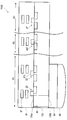
- FIG. 1 is a diagram schematically showing an exemplary configuration of an imaging device.
- FIG. 2 is a diagram schematically showing an exemplary circuit configuration of an imaging device.
- FIG. 3 is a schematic cross-sectional view showing a pixel region and a peripheral region, and a blocking region located between them.
- FIG. 4 is a schematic plan view showing another example of the shape of the blocking region.
- FIG. 5 is a cross-sectional view showing a transistor according to the first configuration example.
- FIG. 6 is a cross-sectional view showing a transistor according to a first modification of the first configuration example.
- FIG. 7 is a cross-sectional view showing a transistor according to a second modification of the first configuration example.
- FIG. 1 is a diagram schematically showing an exemplary configuration of an imaging device.
- FIG. 2 is a diagram schematically showing an exemplary circuit configuration of an imaging device.
- FIG. 3 is a schematic cross-sectional view showing a pixel region and a peripheral region, and a blocking region
- FIG. 8 is a diagram showing an impurity profile in the depth direction in the P-type source / drain diffusion layer according to the third modification of the first configuration example.
- FIG. 9 is a cross-sectional view showing a method for manufacturing a transistor according to the first configuration example.
- FIG. 10 is a cross-sectional view showing a method for manufacturing a transistor according to the first configuration example.
- FIG. 11 is a cross-sectional view showing a method for manufacturing a transistor according to the first configuration example.
- FIG. 12 is a graph showing an impurity profile in the depth direction in the extension forming region according to the first configuration example.
- FIG. 13 is a schematic plan view showing a transistor in the pixel region and a transistor in the peripheral region.
- FIG. 14 is a schematic plan view showing a transistor in the pixel region and a transistor in the peripheral region.
- FIG. 15 is a schematic cross-sectional view showing a transistor in the pixel region and a transistor in the peripheral region.
- FIG. 16 is a schematic plan view showing a transistor in the pixel region and a transistor in the peripheral region.
- FIG. 17 is a schematic plan view showing a transistor in the pixel region and a transistor in the peripheral region.
- FIG. 18 is a schematic plan view showing a transistor in the pixel region and a transistor in the peripheral region.
- FIG. 19 is a schematic plan view showing a transistor in the pixel region and a transistor in the peripheral region.
- FIG. 20 is a schematic cross-sectional view showing a transistor in the pixel region and a transistor in the peripheral region.
- FIG. 21 is a schematic plan view showing a transistor in the pixel region and a transistor in the peripheral region.
- FIG. 22 is a schematic plan view showing a transistor in the pixel region and a transistor in the peripheral region.
- FIG. 23 is a schematic cross-sectional view showing a transistor in the pixel region and a transistor in the peripheral region.
- FIG. 24 is a schematic cross-sectional view showing a transistor in the pixel region and a transistor in the peripheral region.
- FIG. 25 is a schematic view of a back-illuminated image pickup apparatus.
- FIG. 26 is a schematic view of a back-illuminated image pickup apparatus.
- FIG. 25 is a schematic view of a back-illuminated image pickup apparatus.
- FIG. 27 is a schematic view of a back-illuminated image pickup apparatus.
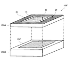
- FIG. 28 is a schematic view showing the shapes that the pixel region and the peripheral region of the image pickup apparatus can take.
- FIG. 29 is a schematic view showing the shapes that the pixel region and the peripheral region of the image pickup apparatus can take.
- FIG. 30 is a schematic view showing the shapes that the pixel region and the peripheral region of the image pickup apparatus can take.
- FIG. 31 is a schematic view showing the shapes that the pixel region and the peripheral region of the image pickup apparatus can take.
- FIG. 32 is a schematic view of a chip stack imaging device.
- the image pickup apparatus includes a pixel region including a pixel transistor including a gate, a first peripheral region including at least one first peripheral transistor including a gate, and a first peripheral region located outside the pixel region.
- a semiconductor substrate including a first substrate portion is provided.
- the gate length of the at least one first peripheral transistor is shorter than the gate length of the pixel transistor.
- the at least one first peripheral transistor is located in the first substrate portion, and the conductive type impurity and the specific type are specified. Includes a first specific layer containing seeds.
- the pixel transistor may be an amplification transistor.
- the technique according to the first aspect is suitable for improving the performance of the image pickup apparatus in consideration of the existence of the first peripheral transistor in the first peripheral region.
- the specific species may include at least one selected from the group consisting of carbon, nitrogen and fluorine.
- the specific species of the second aspect can suppress the transient accelerated diffusion of conductive impurities.
- the specific species may include at least one selected from the group consisting of germanium, silicon and argon.
- the specific species of the third aspect may include traces of pre-amorphization that can enhance the diffusion inhibitory effect of conductive impurities by impurities exemplified by carbon.
- the at least one first peripheral transistor includes a first gate insulating film.
- the pixel transistor may include a second gate insulating film.
- the first gate insulating film may be thinner than the second gate insulating film.
- the configuration of the fourth aspect is an example of the configuration of the imaging device.
- the imaging device is Pixel area including pixel transistor including gate and A first peripheral region including at least one first peripheral transistor including a gate and located outside the pixel region, and a first peripheral region.
- the semiconductor substrate including the first substrate portion and To be equipped.
- the at least one first peripheral transistor includes a first gate insulating film.
- the pixel transistor includes a second gate insulating film.
- the first gate insulating film is thinner than the second gate insulating film.
- the technique according to the fifth aspect is suitable for improving the performance of the image pickup apparatus in consideration of the presence of the first peripheral transistor in the first peripheral region.
- the specific species may include at least one selected from the group consisting of carbon, nitrogen and fluorine.
- the specific species of the sixth aspect can suppress the transient accelerated diffusion of conductive impurities.
- the imaging device in the seventh aspect of the present disclosure, for example, in the imaging device according to the fifth or sixth aspect, the imaging device according to the fifth or sixth aspect, the imaging device
- the specific species may include at least one selected from the group consisting of germanium, silicon and argon.
- the specific species of the seventh aspect may include traces of pre-amorphization that can enhance the diffusion inhibitory effect of conductive impurities by impurities exemplified by carbon.
- the at least one first peripheral transistor may include a first source, a first drain, and a first extension diffusion layer.
- the first extension diffusion layer may be adjacent to the first source or the first drain and shallower than the first source and the first drain.
- the first extension diffusion layer may include the first specific layer.
- the configuration of the eighth aspect is an example of the configuration of the imaging device.
- the at least one first peripheral transistor may include a first source, a first drain, and a first pocket diffusion layer adjacent to the first source or the first drain.
- the first pocket diffusion layer may include the first specific layer.
- the configuration of the ninth aspect is an example of the configuration of the imaging device.
- the at least one first peripheral transistor may include a first source and a first drain. At least one selected from the group consisting of the first source and the first drain may include the first specific layer.
- the configuration of the tenth aspect is an example of the configuration of the imaging device.
- the pixel region may include a charge storage region, which is an impurity region in which charges generated by photoelectric conversion are accumulated.
- the concentration of carbon in the first specific layer may be higher than the concentration of carbon in the charge storage region.
- the feature of the eleventh aspect is that a high-performance imaging device can have.
- the concentration of carbon in the first specific layer may be higher than the concentration of carbon under the gate of the pixel transistor.
- the feature of the twelfth aspect is that a high-performance imaging device can have.
- the semiconductor substrate may include a pixel substrate portion, and may include a pixel substrate portion.
- the pixel region may include a photoelectric conversion layer laminated on the pixel substrate portion.
- the configuration of the thirteenth aspect is an example of the configuration of the imaging device.
- the pixel region may include a photodiode.
- the configuration of the 14th aspect is an example of the configuration of the imaging device.
- the pixel transistor and at least one first peripheral transistor may be provided on a single semiconductor substrate.
- the configuration of the fifteenth aspect is an example of the configuration of the imaging device.
- the at least one first peripheral transistor may include an end-of-range (EOR) defect. At least a part of the first specific layer may be located above the EOR defect and may overlap with the EOR defect in a plan view.
- EOR end-of-range
- the EOR defect of the 16th aspect may be a trace of pre-amorphization that can enhance the diffusion suppressing effect of conductive impurities by impurities exemplified by carbon.
- the at least one first peripheral transistor may include a segregation portion in which a specific species is segregated in the depth direction of the first substrate portion. At least a part of the first specific layer may be located above the segregation portion and may overlap with the segregation portion in a plan view.
- the segregated portion of the 17th aspect may be a trace of pre-amorphization that can enhance the diffusion suppressing effect of conductive impurities by impurities exemplified by carbon.
- the pixel region may include a charge storage region, which is an impurity region in which charges generated by photoelectric conversion are accumulated.
- the segregated portion may be shallower than the charge storage region.
- the configuration of the 18th aspect is an example of the configuration of the imaging device.
- the at least one first peripheral transistor may include a plurality of first peripheral transistors.
- the plurality of first peripheral transistors may include a first-direction transistor and a second-direction transistor.
- the first-direction transistor may be located in the first direction from the pixel region.
- the second-direction transistor may be located in the second direction from the pixel region.
- the configuration of the 19th aspect is an example of the configuration of the imaging device.
- the at least one first peripheral transistor may include two first peripheral transistors.
- the first peripheral region may include a shallow trench isolation (STI) structure.
- STI shallow trench isolation
- the two first peripheral transistors may be separated from each other.
- the STI structure may have a trench.
- the distribution range of the specific species in at least one of the two first peripheral transistors may be shallower than the bottom of the trench.
- the configuration of the 20th aspect is an example of the configuration of the imaging device.
- the imaging device located between the pixel region and the first peripheral region in a plan view may be further provided.
- the second peripheral region may include a second peripheral transistor including a gate.
- the configuration of the 21st aspect is an example of the configuration of the imaging device.
- the at least one first peripheral transistor may include a first source, a first drain, and a first extension diffusion layer.
- the first extension diffusion layer may be adjacent to the first source or the first drain and shallower than the first source and the first drain.
- the second peripheral transistor may include a second source, a second drain, and a second extension diffusion layer.
- the second extension diffusion layer may be adjacent to the second source or the second drain and shallower than the second source and the second drain.
- the concentration of conductive impurities in the second extension diffusion layer may be lower than the concentration of conductive impurities in the first extension diffusion layer.
- the second extension diffusion layer may be deeper than the first extension diffusion layer.
- the configuration of the 22nd aspect is an example of the configuration of the second peripheral transistor.
- the gate length of the at least one first peripheral transistor may be shorter than the gate length of the second peripheral transistor.
- the configuration of the 23rd aspect is an example of the configuration of the imaging device.
- the gate length of the pixel transistor may be longer than the gate length of the second peripheral transistor.
- the configuration of the 24th aspect is an example of the configuration of the imaging device.
- the semiconductor substrate may include a second substrate portion, and may include a second substrate portion.
- the second peripheral transistor may include a second specific layer located in the second substrate portion and having conductive impurities. The concentration of the specific species in the first specific layer may be higher than the concentration of the specific species in the second specific layer.
- the configuration of the 25th aspect is an example of the configuration of the imaging device.
- the semiconductor substrate may include a second substrate portion, and may include a second substrate portion.
- the second peripheral transistor may include a second specific layer located in the second substrate portion and containing conductive impurities. The concentration of carbon in the second specific layer may be higher than the concentration of carbon under the gate of the pixel transistor.
- the configuration of the 26th aspect is an example of the configuration of the imaging device.
- the second peripheral transistor may include a second source, a second drain, and a second extension diffusion layer.
- the second extension diffusion layer may be adjacent to the second source or the second drain and shallower than the second source and the second drain.
- the second extension diffusion layer may include the second specific layer.
- the configuration of the 27th aspect is an example of the configuration of the imaging device.
- the second peripheral transistor may include a second source, a second drain, and a second pocket diffusion layer adjacent to the second source or the second drain.
- the second pocket diffusion layer may include the second specific layer.
- the configuration of the 28th aspect is an example of the configuration of the imaging device.
- the second peripheral transistor may include a second source and a second drain. At least one selected from the group consisting of the second source and the second drain may include the second specific layer.
- the configuration of the 29th aspect is an example of the configuration of the imaging device.
- the second peripheral transistor may include a second source, a second drain, and a second extension diffusion layer.
- the second extension diffusion layer may be adjacent to the second source or the second drain and shallower than the second source and the second drain.
- the second extension diffusion layer may contain nitrogen.
- the configuration of the thirtieth aspect is an example of the configuration of the second peripheral transistor.
- the second peripheral transistor may be an N-channel transistor.
- the reliability of the imaging device can be improved.
- the at least one first peripheral transistor may include a first gate insulating film.
- the second peripheral transistor may include a third gate insulating film.
- the first gate insulating film may be thinner than the third gate insulating film.
- the configuration of the 32nd aspect is an example of the configuration of the imaging device.
- the pixel transistor may include a second gate insulating film.
- the second peripheral transistor may include a third gate insulating film.
- the second gate insulating film may be thicker than the third gate insulating film.
- the configuration of the 33rd aspect is an example of the configuration of the imaging device.
- the at least one first peripheral transistor may be a load transistor.
- the pixel region may be connected to the load transistor via a vertical signal line.
- the configuration of the 34th aspect is an example of the configuration of the imaging device.
- the imaging device is A pixel area with pixel transistors and A first peripheral region having a first peripheral transistor and located outside the pixel region, With The gate length of the first peripheral transistor is shorter than the gate length of the pixel transistor.
- the pixel transistor is an amplification transistor and When at least one type of impurity, including at least one selected from the group consisting of carbon, nitrogen and fluorine, is defined as a specific species, The first peripheral transistor is located in the first substrate portion and has a first specific layer containing conductive impurities and the specific species.
- the imaging device is A pixel area with pixel transistors and A first peripheral region having a first peripheral transistor and located outside the pixel region, With The gate length of the first peripheral transistor is shorter than the gate length of the pixel transistor.
- the pixel transistor is an amplification transistor and When at least one impurity, including at least one selected from the group consisting of germanium, silicon and argon, is defined as a particular species.
- the first peripheral transistor is located in the first substrate portion and has a first specific layer containing conductive impurities and the specific species.
- the imaging device is A pixel area with pixel transistors and A first peripheral region having a first peripheral transistor and located outside the pixel region, With The gate insulating film of the first peripheral transistor is thinner than the gate insulating film of the pixel transistor.
- at least one type of impurity including at least one selected from the group consisting of carbon, nitrogen and fluorine, is defined as a specific species
- the first peripheral transistor is located in the first substrate portion and has a first specific layer containing conductive impurities and the specific species.
- the imaging device is A pixel area with pixel transistors and A first peripheral region having a first peripheral transistor and located outside the pixel region, With The gate insulating film of the first peripheral transistor is thinner than the gate insulating film of the pixel transistor.
- at least one impurity including at least one selected from the group consisting of germanium, silicon and argon, is defined as a particular species.
- the first peripheral transistor is located in the first substrate portion and has a first specific layer containing conductive impurities and the specific species.
- the imaging device is A pixel area with an amplification transistor and A first peripheral region having a first peripheral transistor and located outside the pixel region, With The gate length of the first peripheral transistor is shorter than the gate length of the amplification transistor.
- the first peripheral transistor has a first extension diffusion layer adjacent to its own first source or first drain, shallower than the first source and the first drain, and containing first impurities and carbon.
- the imaging device is A pixel area with an amplification transistor and A first peripheral region having a first peripheral transistor and located outside the pixel region, With The gate length of the first peripheral transistor is shorter than the gate length of the amplification transistor.
- the first peripheral transistor contains a first impurity and carbon in its first source or first drain.
- the first extension diffusion layer may contain at least one selected from the group consisting of nitrogen, fluorine, germanium, silicon and argon instead of or together with carbon.
- the first source or first drain may contain at least one selected from the group consisting of nitrogen, fluorine, germanium, silicon and argon in place of or with carbon.
- the first impurity is an impurity having a conductive type. The following description of conductive impurities may be applied to the first impurities.
- first impurity can be read as "conductive impurity”.
- carbon can be read as "at least one kind of impurity that contributes to the suppression of transient accelerated diffusion of the first impurity".
- the imaging device is A pixel area with pixel transistors and A first peripheral region having a first peripheral transistor and located outside the pixel region, With The gate length of the first peripheral transistor is shorter than the gate length of the pixel transistor.
- a High-k metal gate is configured in the first peripheral transistor.
- the imaging device is A pixel area with pixel transistors and A first peripheral region having a first peripheral transistor and located outside the pixel region, With The gate insulating film of the first peripheral transistor is thinner than the gate insulating film of the pixel transistor.
- a High-k metal gate is configured in the first peripheral transistor.
- the "plan view” means a view from a direction perpendicular to the semiconductor substrate, the first substrate portion, the second substrate portion, or the pixel substrate portion.
- the first substrate portion, the second substrate portion, and the pixel substrate portion will be described later.
- terms such as “upper”, “lower”, “upper surface”, and “lower surface” are used only to specify the mutual arrangement between the members, and limit the posture when the image pickup apparatus is used. It is not used with the intention of doing so.
- the extension diffusion layer is a concept including a so-called LDD (Lightly Doped Drain) diffusion layer.
- FIG. 1 schematically shows an exemplary configuration of an imaging device according to an embodiment of the present disclosure.
- the image pickup apparatus 100A shown in FIG. 1 has, for example, a plurality of pixels 110 arranged in a plurality of rows and columns.
- the pixels 110 are arranged in m rows and n columns to form a substantially rectangular pixel region R1.
- m and n independently represent integers of 1 or more.
- each of these pixels 110 has a photoelectric conversion structure supported by the semiconductor substrate 130 and a readout formed on the semiconductor substrate 130 and electrically connected to the photoelectric conversion structure.
- each of the plurality of pixels 110 is an impurity region provided on the semiconductor substrate 130, and is a charge accumulation that temporarily holds the signal charge generated by the photoelectric conversion structure. Includes an impurity region that functions as part of the region.
- a photodiode may be provided in the semiconductor substrate as a photoelectric conversion unit.
- the image pickup apparatus 100A further includes a peripheral circuit 120A that drives a plurality of pixels 110.
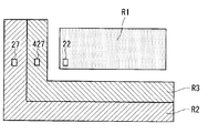
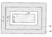
- the peripheral circuit 120A includes a vertical scanning circuit 122, a horizontal signal reading circuit 124, a voltage supply circuit 126, and a control circuit 128. In the embodiment of the present disclosure, a part or all of these circuits are formed on the semiconductor substrate 130 like the read-out circuit of each pixel. As schematically shown in FIG. 1, the peripheral circuit 120A is located in the first peripheral region R2 of the semiconductor substrate 130, which is located outside the pixel region R1 including the plurality of pixels 110.
- the image pickup apparatus 100A further has a blocking region 200A provided between the pixel region R1 and the first peripheral region R2.
- the blocking region 200A includes an impurity region 131 formed on the semiconductor substrate 130 and a plurality of contact plugs 211 provided on the impurity region 131.
- the impurity region 131 is typically a p-type diffusion region.
- the plurality of contact plugs 211 are electrically connected to the impurity region 131 of the semiconductor substrate 130 by being provided on the impurity region 131. As will be described later, the plurality of contact plugs 211 are configured to be able to supply a predetermined voltage to the impurity region 131 by connecting a power supply (not shown in FIG. 1). That is, during the operation of the image pickup apparatus 100A, the impurity region 131 is in a state where a predetermined voltage is applied via the contact plug 211.
- the cutoff region 200A has an element separation 220.
- the element separation 220 is a structure formed on the semiconductor substrate 130 by, for example, an STI (shallow trench isolation) process.
- the element separation 220 is formed between at least a plurality of pixels 110 of the semiconductor substrate 130 located at the outermost periphery of the pixel region R1 and a digital circuit such as a vertical scanning circuit 122 that operates based on a digital clock. Has a portion to be located.
- the element separation 220 is between the pixel 110 located on the outermost circumference of the pixel region R1 and the vertical scanning circuit 122, and between the pixel 110 located on the outermost circumference of the pixel region R1 and the horizontal signal reading circuit 124. Is located in.
- the element separation 220 may be provided on the semiconductor substrate 130 so as to surround the pixel region R1 in a top view.
- the device separation 220 corresponds to the shallow trench isolation structure in the present disclosure.
- a peripheral circuit including a circuit that operates based on a digital clock is formed on a semiconductor substrate provided with an impurity region that temporarily holds a signal charge obtained by photoelectric conversion
- the circuit that operates based on the digital clock is formed.
- the potential of the signal line that supplies the digital clock to the digital circuit represented by the CMOS logic circuit fluctuates depending on the digital clock. Fluctuations in the potential of the signal line due to the digital clock can fluctuate the substrate potential and, as a result, cause extra charge in the wells inside the semiconductor substrate. If extra charge due to fluctuations in the substrate potential flows into the impurity region in the pixel that holds the signal charge, the SN ratio decreases and the obtained image deteriorates.
- a blocking region 200A including an impurity region 131 configured to be connectable to a power source such as a ground by providing a plurality of contact plugs 211 includes a plurality of pixels 110. It is arranged between the pixel area R1 and the digital circuit.
- the potential of the impurity region 131 of the cutoff region 200A can be fixed by connecting a predetermined voltage source to the plurality of contact plugs 211.
- the potential of the impurity region 131 of the cutoff region 200A can be grounded via a plurality of contact plugs 211.
- the cutoff region 200A functions as a low impedance path for discharging the excess charge generated inside the semiconductor substrate 130. That is, it is possible to suppress the electrostatic coupling between the impurity region in the pixel that holds the signal charge and the peripheral circuit 120A, and advantageously suppress the dark current that uses the signal line that supplies the digital clock as a noise source. It is possible.
- the cutoff area 200A is not essential.
- the vertical scanning circuit 122 has connections with a plurality of address signal lines 34. These address signal lines 34 are provided corresponding to each line of the plurality of pixels 110. Each address signal line 34 is connected to one or more pixels belonging to the corresponding line.
- the vertical scanning circuit 122 controls the timing of reading the signal from the pixel 110 to the vertical signal line 35, which will be described later, by applying the line selection signal to the address signal line 34.
- the vertical scanning circuit 122 is also called a row scanning circuit.
- the signal line connected to the vertical scanning circuit 122 is not limited to the address signal line 34.
- a plurality of types of signal lines may be connected to the vertical scanning circuit 122 for each row of the plurality of pixels 110.
- the image pickup apparatus 100A also has a plurality of vertical signal lines 35.
- the vertical signal line 35 is provided for each row of the plurality of pixels 110.
- Each vertical signal line 35 is connected to one or more pixels belonging to the corresponding row.
- These vertical signal lines 35 are connected to the horizontal signal reading circuit 124.
- the horizontal signal reading circuit 124 sequentially outputs the signals read from the pixels 110 to an output line (not shown) in FIG.
- the horizontal signal reading circuit 124 is also called a column scanning circuit.
- the control circuit 128 controls the entire image pickup device 100A by receiving command data, a clock, or the like given from the outside of the image pickup device 100A, for example.
- the control circuit 128 typically has a timing generator and supplies drive signals to the vertical scanning circuit 122, the horizontal signal reading circuit 124, the voltage supply circuit 126 described later, and the like.
- the arrows extending from the control circuit 128 schematically represent the flow of the output signal from the control circuit 128.
- the control circuit 128 can be implemented, for example, by a microcontroller including one or more processors.
- the function of the control circuit 128 may be realized by a combination of a general-purpose processing circuit and software, or may be realized by hardware specialized for such processing.
- the peripheral circuit 120A includes a voltage supply circuit 126 electrically connected to each pixel 110 in the pixel region R1.
- the voltage supply circuit 126 supplies a predetermined voltage to the pixel 110 via the voltage line 38.
- the voltage supply circuit 126 is not limited to a specific power supply circuit, and may be a circuit that converts a voltage supplied from a power source such as a battery into a predetermined voltage, or may be a circuit that generates a predetermined voltage. good.
- the voltage supply circuit 126 may be a part of the vertical scanning circuit 122 described above. As schematically shown in FIG. 1, these circuits constituting the peripheral circuit 120A are arranged in the first peripheral region R2 outside the pixel region R1.
- the number and arrangement of the pixels 110 are not limited to the illustrated example.
- the number of pixels 110 included in the image pickup apparatus 100 may be one.
- the center of each pixel 110 is located on a grid point of a square lattice, but for example, a plurality of pixels so that the center of each pixel 110 is located on a grid point such as a triangular lattice or a hexagonal lattice.
- 110 may be arranged.
- the pixels 110 may be arranged one-dimensionally, and in this case, the image pickup apparatus 100A can be used as a line sensor.
- FIG. 2 schematically shows an exemplary circuit configuration of the image pickup apparatus 100A shown in FIG.
- four pixels 110 arranged in two rows and two columns are taken out and shown among the plurality of pixels 110 in order to avoid the drawing from becoming excessively complicated.
- Each of these pixels 110 includes a photoelectric conversion structure 10 supported by the semiconductor substrate 130 and a readout circuit 20 electrically connected to the photoelectric conversion structure 10.
- the photoelectric conversion structure 10 includes a photoelectric conversion layer arranged above the semiconductor substrate 130.
- the photoelectric conversion structure 10 of each pixel 110 has a connection with the voltage line 38 connected to the voltage supply circuit 126, so that a predetermined voltage can be applied via the voltage line 38 during the operation of the image pickup apparatus 100A.
- a predetermined voltage can be applied via the voltage line 38 during the operation of the image pickup apparatus 100A.
- a positive voltage of, for example, about 10 V can be applied to the voltage line 38 during the operation of the image pickup apparatus 100A. ..
- a case where holes are used as signal charges will be illustrated.
- the read circuit 20 includes an amplification transistor 22, an address transistor 24, and a reset transistor 26.
- the amplification transistor 22, the address transistor 24, and the reset transistor 26 are typically field effect transistors formed on the semiconductor substrate 130.
- an N-channel MOSFET Metal Oxide Semiconductor Field Effect Transistor
- the gate of the amplification transistor 22 is electrically connected to the photoelectric conversion structure 10.
- the charge storage node FD is a node that connects the gate of the amplification transistor 22 to the photoelectric conversion structure 10.
- the charge storage node FD has a function of temporarily holding the charge generated by the photoelectric conversion structure 10.
- the charge storage node FD includes an impurity region formed on the semiconductor substrate 130 as a part thereof. Reference numeral Z in FIG. 3 described later corresponds to an impurity region included in the charge storage node FD.
- the drain of the amplification transistor 22 of each pixel 110 is connected to the power supply wiring 32.
- the power supply wiring 32 supplies a power supply voltage VDD of, for example, about 3.3 V to the amplification transistor 22 during the operation of the image pickup apparatus 100A.
- the source of the amplification transistor 22 is connected to the vertical signal line 35 via the address transistor 24.
- the address signal line 34 is connected to the gate of the address transistor 24 connected between the amplification transistor 22 and the vertical signal line 35.
- the vertical scanning circuit 122 controls turning on and off of the address transistor 24 by applying a row selection signal to the address signal line 34. That is, the vertical scanning circuit 122 can read the output of the amplification transistor 22 of the selected pixel 110 to the corresponding vertical signal line 35 by controlling the row selection signal.
- the arrangement of the address transistor 24 is not limited to the example shown in FIG. 2, and may be between the drain of the amplification transistor 22 and the power supply wiring 32.
- a load circuit 45 and a column signal processing circuit 47 are connected to each of the vertical signal lines 35.
- the load circuit 45 forms a source follower circuit together with the amplification transistor 22.
- the column signal processing circuit 47 performs noise suppression signal processing represented by correlated double sampling, analog-to-digital conversion, and the like.
- the column signal processing circuit 47 is also called a row signal storage circuit.
- the horizontal signal reading circuit 124 sequentially reads signals from the plurality of column signal processing circuits 47 to the horizontal common signal line 49.
- the column signal processing circuit 47 may be part of the horizontal signal readout circuit 124.
- the load circuit 45 and the column signal processing circuit 47 may be a part of the peripheral circuit 120A described above.
- the read circuit 20 includes a reset transistor 26 in addition to the amplification transistor 22 and the address transistor 24.
- One of the drain and source of the reset transistor 26 is part of the charge storage node FD, and the other of the drain and source is connected to the reset voltage line 39.
- One of the drain and the source of the reset transistor 26 corresponds to the charge storage region Z in FIG. 3, and specifically corresponds to the impurity region 60n.
- the reset voltage line 39 can supply a predetermined reset voltage Vref to the reset transistor 26 of each pixel 110 during the operation of the image pickup apparatus 100A. ..
- the reset voltage supply circuit for example, a voltage of 0 V or a voltage near 0 V is selected. Similar to the voltage supply circuit 126 described above, the reset voltage supply circuit may be capable of applying a predetermined reset voltage Vref to the reset voltage line 39, and its specific configuration is not limited to a specific power supply circuit.
- the reset voltage supply circuit may be part of the vertical scanning circuit 122.
- the voltage supply circuit 126 and the reset voltage supply circuit may be independent and separate circuits, or may be arranged in the image pickup apparatus 100A in the form of a single voltage supply circuit.
- the reset voltage supply circuit may also be part of the peripheral circuit 120A described above.
- the reset signal line 36 is connected to the gate of the reset transistor 26. Similar to the address signal line 34, the reset signal line 36 is provided for each line of the plurality of pixels 110, and is connected to the vertical scanning circuit 122 here. As described above, the vertical scanning circuit 122 can select the pixel 110 to be read out of the signal line by line by applying the line selection signal to the address signal line 34. Similarly, the vertical scanning circuit 122 can turn on the reset transistor 26 in the selected row by applying a reset signal to the gate of the reset transistor 26 via the reset signal line 36. When the reset transistor 26 is turned on, the potential of the charge storage node FD is reset.
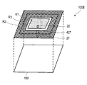
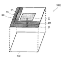
- FIG. 3 schematically shows a cross section including a pixel region R1 and a first peripheral region R2, and a blocking region 200A.
- the cross sections of two pixels located near the cutoff region 200A on behalf of the plurality of pixels 110 are shown.
- a photoelectric conversion layer 12 is provided in the pixel region R1.
- the photoelectric conversion layer 12 is supported by the semiconductor substrate 130.
- a translucent counter electrode 13 is arranged on the photoelectric conversion layer 12. As shown in FIG. 3, each of the photoelectric conversion layer 12 and the counter electrode 13 is typically provided continuously above the semiconductor substrate 130 over a plurality of pixels 110.
- the pixel 110 is a unit structure constituting the pixel region R1, and includes a photoelectric conversion structure 10 having a part of the photoelectric conversion layer 12, a part of the counter electrode 13, and the pixel electrode 11.
- the pixel electrode 11 of the photoelectric conversion structure 10 is located between the photoelectric conversion layer 12 and the semiconductor substrate 130, and is imparted with conductivity by being doped with a metal such as aluminum or copper, a metal nitride, or an impurity. It is formed from polysilicon or the like.
- the pixel electrode 11 of each pixel 110 is electrically separated from the pixel electrodes 11 of other adjacent pixels by being spatially separated for each pixel.
- the photoelectric conversion layer 12 of the photoelectric conversion structure 10 is formed of an organic material or an inorganic material such as amorphous silicon.
- the photoelectric conversion layer 12 receives the light incident through the counter electrode 13 and generates positive and negative charges by photoelectric conversion. That is, the photoelectric conversion structure 10 has a function of converting light into electric charges.
- the photoelectric conversion layer 12 may include a layer made of an organic material and a layer made of an inorganic material.
- the counter electrode 13 of the photoelectric conversion structure 10 is an electrode formed of a transparent conductive material such as ITO.
- the term "translucency" in the present specification means that the photoelectric conversion layer 12 transmits at least a part of light having a wavelength that can be absorbed, and transmits light over the entire wavelength range of visible light. Is not required.
- the counter electrode 13 has a connection with the voltage line 38 described above.
- the potential of the voltage line 38 is controlled to make the potential of the counter electrode 13 higher than the potential of the pixel electrode 11, for example, so that the positive and negative charges generated by the photoelectric conversion are positive.
- the electric charge can be selectively collected by the pixel electrode 11.
- Each of the plurality of pixels 110 further includes a part of the semiconductor substrate 130.
- the semiconductor substrate 130 has a plurality of impurity regions 60n as first impurity regions near the surface thereof.
- the impurity region 60n functions as one of the drain and the source of the reset transistor 26 included in the above-mentioned read circuit 20.
- the semiconductor substrate 130 also has an impurity region 61n, which is the other of the drain and source of the reset transistor 26.
- the impurity region 61n is connected to the reset voltage line 39 described above via a polysilicon plug or the like.
- the impurity region 60n and the impurity region 61n have an n-type conductive type. These plurality of impurity regions 60n and 61n are typically n-type diffusion regions.
- a plurality of readout circuits 20 are formed on the semiconductor substrate 130 corresponding to the plurality of pixels 110.
- the read-out circuit 20 of each pixel is electrically separated from the read-out circuit 20 of other pixels by the element separation 221 provided on the semiconductor substrate 130.
- an interlayer insulating layer 90 covering the semiconductor substrate 130 is located between the photoelectric conversion structure 10 and the semiconductor substrate 130.
- the interlayer insulating layer 90 generally includes a plurality of insulating layers and a plurality of layers of wiring.
- the plurality of wiring layers arranged in the interlayer insulation layer 90 include a wiring layer having an address signal line 34, a reset signal line 36, etc. as a part thereof, a vertical signal line 35, a power supply wiring 32, a reset voltage line 39, and the like. It may include a wiring layer or the like having a part thereof.
- the number of insulating layers and the number of wiring layers in the interlayer insulating layer 90 are not limited to this example, and can be set arbitrarily.
- a conductive structure 89 is provided that electrically connects the pixel electrodes 11 of the photoelectric conversion structure 10 to the readout circuit 20 formed on the semiconductor substrate 130.
- the conductive structure 89 includes wiring and vias arranged in the interlayer insulating layer 90. These wires and vias are typically formed from a metal such as copper or tungsten, or a metal compound such as a metal nitride or metal oxide.
- the conductive structure 89 also includes a contact plug cx connected to the above-mentioned impurity region 60n.
- the contact plug cx connected to the impurity region 60n is typically a polysilicon plug, and is doped with impurities such as phosphorus in order to increase conductivity.
- the conductive structure 89 also has an electrical connection with the gate electrode of the amplification transistor 22.
- a plug cy is connected to the contact plug cx. Examples of the metal that the plug cy can contain include tungsten, copper and the like.
- the semiconductor substrate 130 includes a support substrate 140 and one or more semiconductor layers formed on the support substrate 140.
- the semiconductor substrate 130 has an n-type impurity layer 62 provided on the support substrate 140.
- a p-type silicon substrate will be illustrated as the support substrate 140.
- the support substrate 140 may have a lower electrical resistivity than the impurity layer 62.
- the semiconductor substrate 130 may be an SOI (silicon-on-insulator) substrate, a substrate having a semiconductor layer on its surface due to epitaxial growth or the like, or the like.
- the semiconductor substrate 130 has an n-type semiconductor layer 62an on the support substrate 140 and a p-type semiconductor layer 63p on the n-type semiconductor layer 62an.
- the n-type semiconductor layer 62an located between the support substrate 140 and the p-type semiconductor layer 63p is a part of the above-mentioned impurity layer 62.
- the potential of the impurity layer 62 is controlled via well contacts (not shown in FIG. 3).
- an impurity layer 62 containing an n-type semiconductor layer 62an located in the pixel region R1 as a part thereof inside the semiconductor substrate 130 By providing an impurity layer 62 containing an n-type semiconductor layer 62an located in the pixel region R1 as a part thereof inside the semiconductor substrate 130, a small number from the support substrate 140 or peripheral circuits to the charge storage region for accumulating signal charges. The inflow of carriers can be suppressed.
- the semiconductor substrate 130 further has a p-type semiconductor layer 66p located on the p-type semiconductor layer 63p and a p-type impurity region 65p formed in the p-type semiconductor layer 66p.
- the above-mentioned impurity region 60n having a connection with the conductive structure 89 is provided in the p-type impurity region 65p.
- the junction capacitance formed by the pn junction between the impurity region 60n and the p-type impurity region 65p as the p-well functions as a capacitance for accumulating at least a part of the signal charge collected by the pixel electrode 11.
- the impurity region 60n constitutes a charge storage region that temporarily holds the signal charge.
- the impurity region 61n is provided in the p-type semiconductor layer 66p.
- the impurity concentration in the p-type impurity region 65p is lower than the impurity concentration in the p-type semiconductor layer 66p.
- the semiconductor substrate 130 has a plurality of p-type regions 64 provided in the semiconductor substrate 130 so as to penetrate the impurity layer 62.
- the p-type region 64 has a relatively high impurity concentration.
- the plurality of p-type regions 64 are located below the plurality of p-type regions 64a located in the pixel region R1 and the plurality of contact plugs 211 of the cutoff region 200A when viewed from the normal direction of the semiconductor substrate 130. Includes one or more p-type regions 64b located.
- the p-type region 64a is formed between the p-type semiconductor layer 63p and the support substrate 140 so as to penetrate the n-type semiconductor layer 62an, and has a function of electrically connecting the p-type semiconductor layer 63p and the support substrate 140.
- the p-type region 64b is electrically connected to the impurity region 131 by reaching the impurity region 131 of the blocking region 200A at one end thereof, and electrically connects the impurity region 131 and the support substrate 140.
- an electrical path from the impurity region 131 of the blocking region 200A to the p-type semiconductor layer 63p is formed in the semiconductor substrate 130 via the p-type region 64b, the support substrate 140, and the p-type region 64a.
- a plurality of contact plugs 211 are connected to the impurity region 131 of the cutoff region 200A, and these contact plugs 211 are configured to be connectable to a power source (not shown) such as ground.
- a power source not shown
- the potential of the impurity region 131 of the cutoff region 200A can be grounded via a plurality of contact plugs 211.
- a p-type semiconductor layer is utilized by utilizing an electrical path including an impurity region 131, a p-type region 64b, a support substrate 140, and a p-type region 64a.
- the potentials of the p-type impurity region 65p and the p-type semiconductor layer 66p can be controlled via 63p.
- an impurity region 131a having a relatively high impurity concentration is formed in a portion of the impurity region 131 located near the surface of the semiconductor substrate 130.
- the contact plug 211 is typically made of metal.
- the silicide layer 131s is formed between the plurality of contact plugs 211 and the impurity region 131.
- the contact resistance can be further reduced by providing the VDD layer 131s in the vicinity of the surface of the semiconductor substrate 130 in the impurity region 131a and connecting the plurality of contact plugs 211.
- the first peripheral region R2 includes, for example, a plurality of transistors 25 and a first peripheral transistor 27 that form a logic circuit such as a multiplexer.
- a logic circuit such as a multiplexer.
- an n-type semiconductor layer 62bn which is another part of the impurity layer 62, is formed on the support substrate 140, and n as a well on the n-type semiconductor layer 62bn.
- a type impurity region 81n and a p-type impurity region 82p are formed.
- the drain and source of the transistor 25 are located in the p-type impurity region 82p, and the drain and source of the first peripheral transistor 27 are located in the n-type impurity region 81n.
- the n-type semiconductor layer 62bn is separated from the n-type semiconductor layer 62an over the entire circumference of the pixel region R1 by interposing a part of the support substrate 140.
- a predetermined voltage is supplied to the n-type semiconductor layer 62bn by connecting a power source (not shown).
- the n-type impurity region 81n may be referred to as an N-type well.
- the depth of the n-type semiconductor layer 62an in the pixel region R1 and the depth of the n-type semiconductor layer 62bn in the first peripheral region R2 may be the same or different.
- the contact plug cp is connected to the drain, source, and gate electrodes of peripheral transistors such as transistors 25 and 27.
- the blocking region 200A further includes an n-type impurity region 83n located near the boundary with the first peripheral region R2.
- the n-type impurity region 83n is located on the n-type semiconductor layer 62bn of the impurity layer 62 and has an electrical connection with the n-type semiconductor layer 62bn.
- a plug may be provided in the n-type impurity region 83n.
- Each of the impurity layer and the impurity region located above the support substrate 140 is typically formed by ion implantation of impurities into the semiconductor layer obtained by epitaxial growth on the support substrate 140.
- the p-type region 64a located in the pixel region R1 of the p-type region 64 can be formed at a position that does not overlap with the element separation in the pixel in a plan view.
- a blocking region 200A is formed between the pixel region R1 and the first peripheral region R2.
- the blocking region 200A includes an element separation 220 located between the pixel region R1 and the first peripheral region R2, and an impurity region 131 in which a plurality of contact plugs 211 are arranged. Since the blocking region 200A includes at least the impurity region 131, the dopant in the impurity region 131 can be utilized to exert a so-called gettering effect. For example, it is known that when metal impurities are diffused in a region where pixels are arranged in a semiconductor substrate that supports a photoelectric conversion layer, the image quality is deteriorated. By making the dopant in the impurity region 131 function as a gettering center, it is possible to suppress the diffusion of metal impurities into the charge storage region and avoid deterioration of image quality due to the diffusion of metal impurities.
- Examples of p-type impurities or dopants for silicon substrates are boron, and examples of n-type dopants are phosphorus, arsenic, and antimony. Of these, the p-type dopant is known to be able to exert a gettering effect on most metals and is therefore suitable as a dopant in the impurity region 131. In a typical embodiment of the present disclosure, the p-type is selected as the conductive type of the impurity region 131 of the blocking region 200A.
- the blocking region 200A including the impurity region 131 doped with p-type impurities between the pixel region R1 and the first peripheral region R2 the diffusion of metal impurities into the pixel region R1 is effectively suppressed. Can be done. That is, it is possible to suppress the diffusion of metal impurities into the charge storage region of the pixel 110 and suppress the deterioration of image quality due to the diffusion of metal impurities.
- FIG. 4 shows another example of the shape of the blocking region.
- the imaging device 100B shown in FIG. 4 has a blocking region 200B that surrounds the pixel region R1 in a rectangular shape instead of the blocking region 200A.
- the impurity region 131 of the blocking region 200B surrounds the pixel region R1 in a circular shape without a break in a plan view.
- a plurality of contact plugs 211 are connected to the impurity region 131.
- the element separation 220 of the blocking region 200B also surrounds the pixel region R1 in a ring shape and seamlessly inside the impurity region 131. In such a configuration, it can be said that the element separation 220 defines the boundary between the pixel region R1 and the first peripheral region R2.
- the peripheral circuit 120B provided in the first peripheral region R2 includes a second vertical scanning circuit 129 and a second vertical scanning circuit 129 in addition to the vertical scanning circuit 122, the horizontal signal reading circuit 124, the voltage supply circuit 126, and the control circuit 128.
- the horizontal signal reading circuit 127 of 2 is included.
- the vertical scanning circuit 129 is arranged on the opposite side of the vertical scanning circuit 122 with the pixel region R1 in between. As shown in the figure, the vertical scanning circuit 129 is also connected to an address signal line 34 provided corresponding to each line of the plurality of pixels 110.
- the horizontal signal reading circuit 127 is arranged on the opposite side of the horizontal signal reading circuit 124 with the pixel region R1 in between, and vertical signal lines 35 provided corresponding to each row of the plurality of pixels 110 are connected. Will be done.
- the vertical scanning circuit 122 is responsible for the row selection operation of the left half pixel of the pixel area R1
- the vertical scanning circuit 129 is responsible for the row selection operation of the right half pixel of the pixel area R1.
- the horizontal signal reading circuit 124 is responsible for processing the signal read from the lower half pixel of the pixel area R1
- the horizontal signal reading circuit 127 is responsible for processing the signal read from the upper half pixel of the pixel area R1.
- the vertical scanning circuits 122, 129 and the horizontal signal reading circuits 124, 127 are arranged along the four rectangular sides of the pixel region R1.
- the vertical scanning circuit 122 and the set of pixels 110 between the vertical scanning circuit 129 and the set of pixels 110, between the horizontal signal readout circuit 124 and the set of pixels 110, and A cutoff region 200B is interposed between the horizontal signal readout circuit 127 and the set of pixels 110.
- a blocking region 200B By forming a blocking region 200B on the semiconductor substrate 130 in a shape that surrounds the pixel region R1 including an array of a plurality of pixels 110 in a plan view, between the charge storage region of the pixels and the circuit formed in the first peripheral region R2.
- the movement of electric charge in the above can be suppressed more effectively.
- the cutoff region cuts the pixel region R1 in a ring shape in a plan view. It is not essential in the embodiments of the present disclosure to surround without.
- the blocking region may include a plurality of portions arranged so as to include the element separation 220 and the impurity region 131, respectively, and surround the pixel region R1 as a whole. Even in such a configuration, the same effect as in the case where the blocking region is provided so as to surround the pixel region R1 in a circular shape without a break can be expected in a plan view. Further, the cutoff region 200B may not be provided.
- the first peripheral region R2 includes the first peripheral transistor 27.
- the first peripheral transistor 27 As described above, the first peripheral transistor 27 according to the embodiment will be described with reference to FIGS. 5 to 12.
- FIG. 5 shows the cross-sectional configuration of the first peripheral transistor 27 according to the first configuration example.
- the first peripheral transistor 27 is specifically a MIS type transistor, and more specifically a MOSFET.
- a gate insulating film 301 made of silicon oxide (SiO 2 ) is interposed on the main surface of the semiconductor substrate 130 made of P-type silicon (Si), and the gate insulating film 301 is made of polysilicon or a metal gate.
- the gate electrode 302 is formed.
- An impurity region 81n which is a deep N-type well, is formed.
- the support substrate 140, the n-type semiconductor layer 62bn, and the impurity region 81n which is the N-type well are laminated in this order.
- First pocket diffusion layers 307a and 307b are formed, respectively.
- Carbon (C) is contained in the first extension diffusion layers 306a and 306b, which are P-type extension high-concentration diffusion layers.
- the first extension diffusion layers 306a and 306b have a shallow impurity profile and maintain a steep and high activation concentration. As a result, an extension diffusion layer having a shallow bonding depth and low resistance is formed, and a fine device having a high driving force can be realized.
- heat treatment may be performed for the purpose of heating the pixel region R1.
- the first peripheral region R2 may also be heated.
- impurities are redistributed in the first peripheral transistor 27 of the first peripheral region R2. Can be suppressed and shallow junctions can be maintained.
- the first extension diffusion layers 306a and 306b contain carbon, the effect of suppressing the generation of residual defects in the first extension diffusion layers 306a and 306b can also be achieved.
- EOR (end of range) defects are exemplified as residual defects.
- the EOR defect is a defect layer formed in a region directly below the amorphous crystal (a / c) interface before heat treatment when the semiconductor substrate 130 made of silicon is heat-treated in an amorphous state.
- Source / drain diffusion layers 313a and 313b are formed.
- the P-type source / drain diffusion layers 313a and 313b contain carbon (C).
- one or both of the P-type source / drain diffusion layers 313a and 313b may not contain carbon (C).
- the “source / drain diffusion layer” refers to a diffusion layer that functions as a source or drain.
- Insulating offset spacers 309a and 309b are formed on both side surfaces of the gate electrode 302, and the offset spacers 309a and 309b contain carbon. Further, a first L-shaped cross section extending from the outer side surface of each of the offset spacers 309a and 309b to the upper portion of the inner end of the P-shaped source / drain diffusion layers 313a and 313b on the semiconductor substrate 130. The sidewalls 308Aa and 308Ab of the above are formed. Further, insulating second sidewalls 308Ba and 308Bb are formed on the outside of the first sidewalls 308Aa and 308Ab, respectively.
- arsenic ion was used as an impurity in the N-type channel diffusion layer 303, but instead, an ion of an element having a larger mass than the arsenic ion and showing N-type, or an arsenic ion. And an ion of an element having a larger mass than the arsenic ion and exhibiting an N-type may be used.
- the impurities that contribute to the suppression of TED are not limited to carbon.
- at least one selected from the group consisting of nitrogen, fluorine, germanium, silicon and argon may be used.
- Nitrogen, fluorine, germanium, silicon, argon and the like can also contribute to the suppression of TED.
- impurities such as nitrogen and fluorine also form excess point defects that cause TED and impurities-interstitial silicon or impurities-atomic pore complexes, clusters, etc., thereby forming excess point defects. Suppress.
- excess point defects are suppressed by forming a complex such as carbon-lattice silicon, nitrogen-lattice silicon, fluorine-lattice silicon, and fluorine-atomic pores.
- Germanium, silicon, argon and the like contribute to the suppression of TED through the pre-amorphization action.
- at least one selected from non-conductive elements from the group consisting of Group 14, Group 17 and Group 18 elements may be used as an impurity that contributes to the suppression of TED.
- the P-channel MIS type transistor is used as the transistor, but instead of this, an N-channel MIS type transistor may be used.
- examples of the N-type impurity ions constituting the extension diffusion layer include phosphorus (P) ion, arsenic (As) ion, antimony (Sb) ion and bismuth (Bi) ion.
- P phosphorus
- Au arsenic
- Sb antimony
- Bi bismuth
- a Group 5B element having a mass larger than that of arsenic ion can be used.
- a group III element having a larger mass than the boron ion such as boron (B) ion or indium (In) ion, or a group III element thereof is placed in the P-type pocket diffusion layer.
- Combinations can be used.
- the TED of the P-type pocket diffusion layer is suppressed by carbon, so that the variation in the threshold voltage due to the pocket profile can be suppressed.
- the N-type impurity ion constituting the extension diffusion layer one kind of the above-mentioned impurities may be used, or two or more kinds may be used in combination. The same applies to the elements used for the P-type pocket diffusion layer.
- FIG. 6 shows a cross-sectional configuration of a transistor according to a first modification of the first configuration example.
- the impurity profiles of the first extension diffusion layers 306a and 306b which are P-type extension high-concentration diffusion layers, are asymmetrical with respect to the gate electrode 302.
- the source region shallower and steeper than the drain region
- the carrier concentration gradient between the source region and the channel region becomes large, and the driving force in the MIS type transistor becomes large. improves.
- the extension profile of the drain region is deeper than that of the source region, the generation of hot carriers is suppressed as compared with the symmetrical, shallow and steep profile structure.
- the transistor having the configuration shown in FIG. 6 can be manufactured with reference to, for example, Patent Document 2.
- the first extension diffusion layer 306a is shallower than the first extension diffusion layer 306b.
- a configuration in which the first extension diffusion layer 306b is shallower than the first extension diffusion layer 306a may also be adopted.
- FIG. 7 shows a cross-sectional configuration of a transistor according to a second modification of the first configuration example.
- the transistor according to the second modification has a P-type extension high-concentration diffusion layer only on one side of the P-type source / drain diffusion layers 313a and 313b.
- the transistor according to the second modification has a first extension diffusion layer 306a, which is a P-type extension high-concentration diffusion layer adjacent to the P-type source / drain diffusion layer 313a, while P. It does not have a first extension diffusion layer adjacent to the mold source / drain diffusion layer 313b.
- a configuration having no first extension diffusion layer adjacent to the P-type source / drain diffusion layer 313a and having a first extension diffusion layer 306b adjacent to the P-type source / drain diffusion layer 313b can also be adopted.
- the transistor according to the second modification has an N-type pocket diffusion layer only on one side of the P-type source / drain diffusion layers 313a and 313b.
- the transistor according to the second modification has a first pocket diffusion layer 307a adjacent to the P-type source / drain diffusion layer 313a, while the first pocket diffusion layer 307a adjacent to the P-type source / drain diffusion layer 313b. It does not have a 1-pocket diffusion layer.
- a configuration having no first pocket diffusion layer adjacent to the P-type source / drain diffusion layer 313a and having a first pocket diffusion layer 307b adjacent to the P-type source / drain diffusion layer 313b can also be adopted.
- the P-type source / drain diffusion layers 313a and 313b contain fluorine (F) and carbon (C). Fluorine can result in partial amorphization of the semiconductor substrate 130. Fluorine can also suppress transient accelerated diffusion (TED) of impurities.
- FIG. 8 shows an example of the concentration distribution of impurities in the P-type source / drain diffusion layers 313a and 313b in the depth direction of the semiconductor substrate 130. The vertical axis is a logarithmic scale and indicates the concentrations of fluorine (F), carbon (C), boron (B) and germanium (Ge). The concentration distribution in FIG.
- the fluorine concentration distribution has segregation in the vicinity of the original a / c interface position.
- the diffusion of impurities is suppressed after the above annealing. Further, even if the first peripheral region R2 is heated during the heat treatment for the pixel region R1, the redistribution of impurities can be within a small range.
- the n-type semiconductor layer 62bn can be produced by a known method.
- N-type impurity ions such as phosphorus (P) ions are implanted in the channel formation region of the semiconductor substrate 130 made of P-type silicon, and the implantation energy is 260 keV and the implantation dose amount is 260 keV.
- the first ion implantation of 4 ⁇ 10 12 / cm 2 and the second ion implantation of injection energy of 540 keV and injection dose amount of 1 ⁇ 10 13 / cm 2 are performed to form an N-type well impurity implantation layer 304A. do.
- arsenic (As) ions are implanted into the semiconductor substrate 130 at an implantation energy of about 90 keV and an implantation dose of about 5 ⁇ 10 12 / cm 2 , and N-type well impurities are injected onto the N-type well impurity implantation layer 304A.
- the channel impurity implantation layer 303A is formed.
- a silicon oxide film may be deposited on the surface of the semiconductor substrate 130 before ion implantation.
- the order of formation of the N-type well impurity injection layer 304A and the N-type channel impurity injection layer 303A is not particularly limited.
- the temperature of the ion-implanted semiconductor substrate 130 is about 100 ° C./sec or more, for example, about 200 ° C./sec, and 850 ° C. to 1050 ° C.
- the temperature is raised to about 10 seconds, and the peak temperature is maintained for about 10 seconds at the maximum, or the first rapid heat treatment (RTA) that does not maintain the peak temperature is performed.
- RTA first rapid heat treatment
- an N-type channel diffusion layer 303 and an impurity region 81n which is an N-type well are formed on the upper part of the semiconductor substrate 130, respectively.
- the rapid heat treatment that does not maintain the peak temperature means a heat treatment in which the heat treatment temperature drops as soon as the heat treatment temperature reaches the peak temperature.
- the gate electrode 302 made of silicon is selectively formed.
- silicon oxide is used as the gate insulating film 301, but a high-k insulating film such as silicon oxide nitride (SiON), hafnium oxide (HfO x ), or hafnium oxide silicon (HfSiON) may be used. ..
- a metal gate, a laminated film of polysilicon and a metal gate polysilicon having a silicidized upper portion or polysilicon which is fully silicidized can be used.
- an insulating film made of silicon oxide having a film thickness of about 8 nm is deposited, and then by anisotropic etching, an offset spacer 309a having a finished thickness of about 4 nm is deposited.
- 309b are formed on both side surfaces of the gate electrode 302 and the gate insulating film 301.
- silicon oxide is used for the offset spacers 309a and 309b, but a high-k insulating film such as silicon nitride (SiN) or HfO 2 may be used.
- the implantation energy is 40 keV and the implantation dose amount is 2 ⁇ 10 13 / cm 2 into the semiconductor substrate 130 using the offset spacers 309a and 309b and the gate electrode 302 as masks.
- phosphorus (P) ions which are N-type impurities of a degree, are ion-implanted by angular implantation.
- an N-type impurity having an injection energy of 80 keV and an injection dose amount of about 1 ⁇ 10 13 / cm 2 , for example, arsenic (As) ion is ion-implanted by angular implantation to form an N-type pocket impurity implantation layer 307Aa. , 307Ab.
- the order of injection of P ions and As ions is not particularly limited.
- both P ions and As ions are injected into the N-type pocket impurity injection layers 307Aa and 307Ab.
- only one of P ion and As ion may be injected into the N-type pocket impurity injection layers 307Aa and 307Ab.
- the injection energy is 10 keV and the injection dose amount is about 5 ⁇ 10 14 / cm 2 in the semiconductor substrate 130 using the offset spacers 309a and 309b and the gate electrode 302 as masks.
- the amorphous layers 310a and 310b are selectively formed on the semiconductor substrate 130 by injecting the germanium (Ge) ions of the above.
- germanium is used for forming the amorphous layers 310a and 310b, silicon (Si), argon (Ar), krypton (Kr), xenon (Xe), carbon (C) and the like may be used.
- the offset spacers 309a and 309b and the gate electrode 302 are used as masks, and the implantation energy is 5 keV into the semiconductor substrate 130.
- Carbon (C) ions having an injection dose amount of about 1 ⁇ 10 15 / cm 2 are ion-implanted to form carbon implantation layers 311Aa and 311Ab.
- the carbon ion implantation may be performed, for example, if the implantation energy is in the range of 1 keV to 10 keV and the implantation dose amount is in the range of 1 ⁇ 10 14 / cm 2 to 3 ⁇ 10 15 / cm 2 .
- the semiconductor substrate 130 may be amorphized at the time of pocket injection by using ions having a relatively large mass number such as antimony (Sb) for N-type pocket impurity injection.
- Sb antimony
- the implantation energy is 0.5 keV and the implantation dose amount is 5 ⁇ 10 14 / cm on the semiconductor substrate 130 using the offset spacers 309a and 309b and the gate electrode 302 as masks.
- boron (B) ions which are about 2 P-type impurities, are ion-implanted to form the first P-type impurity implantation layers 306Aa and 306Ab on the carbon injection layers 311Aa and 311Ab.
- boron difluoride (BF 2 ), or cluster boron such as B 18 H x or B 10 H x , or indium (In) may be used.
- the concentration distribution (impurity profile) of each impurity (boron (B), carbon (C) and germanium (Ge)) in the depth direction of the semiconductor substrate 130 immediately after the injection of boron ions into the portion (a) of FIG. ) Is shown on a logarithmic scale.
- the depths of the amorphous layers 310a and 310b are about 30 nm under the germanium injection conditions according to the present production method example.
- the semiconductor substrate 130 is subjected to a second rapid heat treatment in which the substrate temperature is raised from 1200 ° C. to 1350 ° C. by laser annealing, for example, and the temperature is maintained for about 1 ms near the peak temperature.
- a second rapid heat treatment as shown in the part (d) of FIG. 10, boron ions are diffused in the lateral region of the gate electrode 302 in the semiconductor substrate 130, and the semiconductor substrate 130 has a relatively shallow joint surface.
- the first extension diffusion layers 306a and 306b and the first pocket diffusion layers 307a and 307b which are N-type pocket diffusion layers in which phosphorus ions and arsenic ions contained in the N-type pocket impurity injection layers 307Aa and 307Ab are diffused, are formed, respectively. Will be done.
- laser annealing is used for the second rapid heat treatment in milliseconds
- a so-called millisecond annealing (MSA) method such as flash lamp annealing may be used.
- MSA millisecond annealing
- the temperature of the semiconductor substrate 130 is raised to about 200 ° C./sec from 850 ° C. to 1050 ° C., and the peak temperature is maintained for about 10 seconds at the maximum.
- An annealing that does or does not maintain the peak temperature such as a cold spike-RTA, may be used.
- the concentration distribution in the vertical direction is shown on a logarithmic scale.
- the amorphous layers 310a and 310b formed at the time of germanium ion implantation have been restored to the crystal layer. Boron diffuses and has a peak at a position slightly deeper than immediately after ion implantation.
- Carbon has a first peak composed of carbon clusters near the concentration peak position at the time of ion implantation, and also has a second peak segregated near the original amorphous crystal (a / c) interface.
- Germanium has a concentration distribution that is almost the same as immediately after ion implantation.
- pre-amorphization a certain region of a semiconductor substrate is amorphized and impurities having polarity, that is, a conductive type, are injected into the region (for example, injection of B ions or the like). In this case, it is conceivable to perform amorphization and impurity injection in this order. Amorphization in this case can be referred to as pre-amorphization.
- pre-amorphization When the substrate is amorphized and then ion-implanted, channeling during ion implantation is suppressed, and a shallow implantation distribution can be formed. Specifically, an injection distribution with a small tail skirt can be formed.
- a first insulating film made of silicon oxide having a film thickness of about 10 nm covers the entire surface including the offset spacers 309a and 309b and the gate electrode 302 on the semiconductor substrate 130.
- a second insulating film made of silicon nitride having a film thickness of about 40 nm are sequentially deposited. Then, by performing anisotropic etching on the deposited first insulating film and the second insulating film, as shown in the portion (a) of FIG. 11, on the side surface of the gate electrode 302 on the gate length direction side.
- First sidewalls 308Aa and 308Ab are formed from the first insulating film, and second sidewalls 308Ba and 308Bb are formed from the second insulating film.
- the second sidewalls 308Ba and 308Bb may be silicon oxide instead of silicon nitride, and may be further formed by a laminated film composed of silicon oxide and silicon nitride.
- the gate electrode 302, the offset spacers 309a and 309b, the first sidewalls 308Aa and 308Ab and the second sidewalls 308Ba and 308Bb are used as masks on the semiconductor substrate 130.
- Boron ions which are P-type impurities having an injection energy of 3 keV and an injection dose of about 3 ⁇ 10 15 / cm 2 , are ion-implanted to form a second P-type impurity implantation layer 313Aa and 313Ab.
- the temperature of the semiconductor substrate 130 is raised from 1200 ° C. to 1350 ° C. by, for example, laser annealing, and the temperature is maintained for about 1 ms near the peak temperature. Perform the rapid heat treatment of 3.
- boron ions are diffused into the lateral regions of the first sidewalls 308Aa and 308Ab and the second sidewalls 308Ba and 308Bb in the semiconductor substrate 130, and the first extension diffusion layer 306a, A P-type source / drain diffusion layer 313a, 313b, which is a P-type high-concentration impurity diffusion layer connected to the 306b and has a joint surface deeper than the first extension diffusion layers 306a and 306b, is formed.
- MSA millisecond annealing
- the temperature is raised from about 200 ° C./sec to 250 ° C./sec and from 850 ° C. to 1050 ° C., and the peak temperature is maintained for about 10 seconds at the maximum.
- Annealing that does not maintain the peak temperature such as spike-RTA, may be used.
- the second rapid heat treatment shown in the part (d) of FIG. 10 may be omitted, and in that case, the third rapid heat treatment is also used.
- ion implantation for forming the extension diffusion layer is performed with lower energy than.
- the semiconductor substrate 130 was amorphized with germanium in the step shown in the portion (a) of FIG. 10, and then carbon was implanted as an impurity for preventing diffusion in the step shown in the portion (b) of FIG. Carbon has the effect of suppressing transient accelerated diffusion (TED) of impurity atoms.
- TED transient accelerated diffusion
- each shallow diffusion layer of a P-type field effect transistor (pFET: p-type field effect transistor) and an N-type field effect transistor (nFET: n-type field effect transistor) is used. It is effective for the formation of.
- the carbon plays a role of removing excess point defects in the semiconductor substrate 130 during the heat treatment.
- the excess point defects introduced by ion implantation are reduced, the TED of impurity atoms such as boron and phosphorus is suppressed, and the bonding depth of each diffusion layer can be kept shallow.
- the low resistance first extension diffusion layer 306a which has a shallow bond, suppresses the bond leak, and suppresses the increase in the resistance value due to the dose loss, by injecting carbon satisfying the above conditions, 306b can be reliably formed.
- a heat treatment for heating the pixel region R1 is performed, and the heat treatment may also heat the first peripheral region R2.
- a diffusion suppressing effect based on carbon injection and a related effect can be obtained.
- an interlayer film is deposited in both the pixel region R1 and the first peripheral region R2.
- the interlayer film is, for example, an NSG (No doped Silicate Glass) film.
- an opening is formed in the interlayer film.
- the impurity region and the like constituting the charge storage region Z may be injected in the pixel region R1.
- polysilicon is deposited so as to fill the above-mentioned opening, so that the opened plug portion is embedded.
- the polysilicon may be phosphorus-doped.
- a heat treatment is performed to heat the pixel region R1 including the plug portion.
- This heat treatment is, for example, a heat treatment at 850 ° C. for about 10 minutes.
- the first peripheral region R2 is also heated.
- the redistribution of impurities can be suppressed by the diffusion suppressing effect based on carbon injection, and shallow bonding can be maintained.
- the diffusion suppression effect based on carbon injection is effective. Further, as described above, even when an additional step of heat treatment for heating the pixel region R1 is performed, the diffusion suppressing effect based on carbon injection can be exhibited.
- first pocket diffusion layers 307a and 307b which are N-type pocket diffusion layers.
- P phosphorus
- the effect of preventing the diffusion of carbon ions becomes stronger than when arsenic (As) is used.
- the transistor and its manufacturing method according to the present disclosure can realize shallow junctions and low resistance of the extension diffusion layer due to miniaturization, and are useful for a MIS type transistor having a high driving force and a manufacturing method thereof.
- transistor in pixel area R1 and first peripheral area R2 Transistor in pixel area R1 and first peripheral area R2
- the transistors in the pixel region R1 and the first peripheral region R2 will be further described with reference to FIGS. 13 to 24. Note that in FIGS. 13 to 24, the cutoff regions 200A and 200B are not shown.
- one of the P-type source / drain diffusion layers 313a and 313b may be referred to as a source, and the other may be referred to as a drain.
- the P-type source / drain diffusion layer 313a which is the source of the first peripheral transistor 27, may be referred to as a first source.
- the P-type source / drain diffusion layer 313b, which is the drain of the first peripheral transistor 27, may be referred to as a first drain.
- the image pickup apparatus may include a second peripheral region R3 located between the pixel region R1 and the first peripheral region R2 in a plan view.
- One semiconductor substrate 130 may extend to both the pixel region R1 and the first peripheral region R2, the pixel region R1 is configured by using one semiconductor substrate, and the first peripheral region is used by another semiconductor substrate.
- R2 may be configured.
- One semiconductor substrate 130 may extend over the three regions of the pixel region R1, the first peripheral region R2, and the second peripheral region R3, and one semiconductor substrate is used to form the pixel region R1 and another.
- the first peripheral region R2 may be configured by using one semiconductor substrate, and the second peripheral region R3 may be configured by further using another semiconductor substrate.
- One semiconductor substrate 130 may extend across the pixel region R1 and the first peripheral region R2, and another semiconductor substrate may be used to form the second peripheral region R3.
- the pixel region R1 may be configured by using one semiconductor substrate, and one semiconductor substrate 130 may extend across the first peripheral region R2 and the second peripheral region R3. In this way, the imaging device may have at least one semiconductor substrate.
- the pixel substrate portion refers to a portion of at least one semiconductor substrate 130 that belongs to the pixel region R1.
- the first substrate portion refers to a portion of at least one semiconductor substrate 130 that belongs to the first peripheral region R2.
- the second substrate portion refers to a portion of at least one semiconductor substrate 130 that belongs to the second peripheral region R3.
- the pixel substrate portion can be specifically referred to as a pixel semiconductor substrate portion.
- the first substrate portion can be specifically referred to as a first semiconductor substrate portion.
- the second substrate portion may be specifically referred to as a second semiconductor substrate portion.
- the term "pixel transistor” will be explained.
- the pixel transistor is a transistor included in the pixel region R1.
- the amplification transistor 22, the address transistor 24, and the reset transistor 26 may correspond to pixel transistors.
- the amplification transistor 22 is illustrated as a pixel transistor. Further, a case where the pixel transistor is an amplification transistor 22 will be described below. However, as long as there is no contradiction, the amplification transistor 22 can be read as a pixel transistor, an address transistor 24, or a reset transistor 26 in the following description. Elements of transistors such as sources and drains and elements associated with transistors such as wiring can also be read as appropriate.
- FIG. 13 the amplification transistor 22 in the pixel region R1 and the first peripheral transistor 27 in the first peripheral region R2 when the configuration of FIG. 1 is adopted are schematically shown.
- FIG. 14 when the configuration of FIG. 4 is adopted, the amplification transistor 22 in the pixel region R1 and the first peripheral transistor 27 in the first peripheral region R2 are schematically shown.
- the first peripheral region R2 is located outside the pixel region R1. Specifically, in a plan view, the first peripheral region R2 is located outside the pixel region R1.
- the configuration that the amplification transistor 22 in the pixel region R1 and the first peripheral transistor 27 in the first peripheral region R2 can have is shown in FIG.
- the amplification transistor 22 is an N-channel MOSFET
- the first peripheral transistor 27 is a P-channel MOSFET.
- the conductive type of these transistors is not particularly limited. This point is the same for the transistors 427, 727, and 827 described later.
- the first peripheral transistor 27 is the same as that described with reference to FIG. However, in the example of FIG. 15, it is also possible to adopt another transistor instead of the first peripheral transistor 27. For example, it is also possible to adopt the transistor described with reference to FIG. 6, FIG. 7 or FIG.
- the contact plug cp is connected to the P-type source / drain diffusion layer 313a, which is the source of the first peripheral transistor 27.
- a contact plug cp is connected to the P-type source / drain diffusion layer 313b, which is the drain of the first peripheral transistor 27.
- a contact plug cp is connected to the gate electrode 302 of the first peripheral transistor 27.
- the contact plug cp is, for example, a metal plug.
- Examples of the metal that the contact plug cp can contain include tungsten, copper and the like.
- the amplification transistor 22 has a source 67a, a drain 67b, and a gate electrode 67c.
- the source 67a is an n-type impurity region.
- the drain 67ba is an n-type impurity region.
- the gate electrode 67c is made of, for example, a polysilicon material.
- a channel diffusion layer 68 is formed between the source 67a and the drain 67b.
- the channel diffusion layer 68 is an n-type impurity region.
- a gate insulating film 69 is formed between the gate electrode 67c and the pixel substrate portion.
- the gate insulating film 69 is an oxide film.
- the gate insulating film 69 contains silicon oxide in one example and silicon dioxide in one specific example.
- An offset spacer 70 is formed on the gate electrode 67c and the gate insulating film 69.
- the offset spacer 70 contains silicon oxide in one example and silicon dioxide in one specific example.
- a first sidewall 71a is formed on the offset spacer 70.
- the first sidewall 71a has an L-shaped cross section.
- a second sidewall 72a is formed on the outside of the first sidewall 71a.
- a first sidewall 71b is formed on the offset spacer 70.
- the first sidewall 71b has an L-shaped cross section.
- a second sidewall 72b is formed on the outside of the first sidewall 71b.
- the first sidewall 71a contains silicon oxide in one example and silicon dioxide in one specific example. This point is the same for the first sidewall 71b.
- the second sidewall 72a has a laminated structure including a plurality of insulating layers in one example, and includes a silicon dioxide layer and a silicon nitride layer in one specific example. This point is the same for the second sidewall 72b.
- a through hole is formed in the offset spacer 70 on the gate electrode 67c.
- the contact plug cx is connected to the gate electrode 67c through the through hole.
- the contact plug cx is connected to the drain 67b through the through hole.
- the contact plug cx is, for example, a polydilicon plug.
- the contact plug cx may be doped with impurities such as phosphorus in order to increase conductivity.
- a form in which the contact plug cx is connected to the source 67a can also be adopted. Specifically, a through hole is formed in the gate insulating film 69 and the offset spacer 70 on the source 67a, and the contact plug cx can be connected to the source 67a through the through hole.
- the contact plug cx connected to the gate electrode 67c is connected to the plug cy.
- the contact plug cx connected to the drain 67b is connected to the plug cy. If there is a contact plug cx connected to the source 67a, the contact plug cx may be connected to the plug cy.
- the plug cy is, for example, a metal plug.
- Examples of the metal that the plug cy can contain include tungsten, copper and the like.
- the imaging apparatus includes a pixel region R1 and a first peripheral region R2.
- the first peripheral region R2 is located outside the pixel region R1. Specifically, in a plan view, the first peripheral region R2 is located outside the pixel region R1. "Plane view” refers to a view from a direction perpendicular to the semiconductor substrate 130, the first substrate portion, the second substrate portion, or the pixel substrate portion.
- the pixel region R1 has an amplification transistor 22.
- the first peripheral region R2 has a first peripheral transistor 27.
- the first peripheral transistor 27 is a logic transistor.
- the first peripheral transistor 27 may be a planar type (planar type) transistor, or may be a three-dimensional structure transistor such as a FinFET (FinField-Effective Transistor).
- the amplification transistor 22 outputs a signal voltage corresponding to the signal charge obtained by photoelectric conversion.
- the photoelectric conversion is performed in the photoelectric conversion layer 12. Specifically, a path for guiding the signal charge from the photoelectric conversion layer 12 to the charge storage region Z and a path for guiding the signal charge from the charge storage region Z to the gate electrode 67c of the amplification transistor 22 are formed.
- the charge storage region Z corresponds to the impurity region 60n. As described above, the charge storage region Z is included in the charge storage node FD.
- reference numeral L 22 is the gate length of the amplification transistor 22.
- Reference numeral L 27 is the gate length of the first peripheral transistor 27. In the present embodiment, the gate length L 27 of the first peripheral transistor 27 is shorter than the gate length L 22 of the amplification transistor 22.
- the ratio L 27 / L 22 of the gate length L 27 of the first peripheral transistor 27 to the gate length L 22 of the amplification transistor 22 is, for example, 0.8 or less, and may be 0.34 or less. This ratio is, for example, 0.01 or more, and may be 0.05 or more.
- the gate length refers to the dimension of the gate electrode in the direction from the source to the drain or from the drain to the source.
- the gate width refers to the dimension of the gate electrode in the direction orthogonal to the direction of the gate length in a plan view.
- the direction orthogonal to the gate length direction in a plan view can also be referred to as a depth direction.
- the gate insulating film 301 of the first peripheral transistor 27 is thinner than the gate insulating film 69 of the amplification transistor 22.
- the ratio of the thickness T 301 of the gate insulating film 301 of the first peripheral transistor 27 to the thickness T 69 of the gate insulating film 69 of the amplification transistor 22 T 301 / T 69 is, for example, 0.7 or less, and 0.36 or less. It may be. This ratio is, for example, 0.1 or more, and may be 0.2 or more.
- the first peripheral transistor 27 has a first specific layer.
- the first specific layer is located in the first substrate portion.
- the first specific layer contains conductive impurities and specific species.
- Conductive type impurities are impurities having a conductive type. That is, the conductive type impurities are p-type or n-type impurities.
- the specific species is at least one type of impurity that contributes to the suppression of transient accelerated diffusion of conductive impurities.
- the particular species may comprise at least one selected from the group consisting of carbon, nitrogen and fluorine. Carbon, nitrogen and fluorine can suppress the transient accelerated diffusion of conductive impurities. That is, the specific species may contain at least one type of impurity that suppresses the transient accelerated diffusion of conductive impurities.
- the particular species may comprise at least one selected from the group consisting of germanium, silicon and argon. Germanium, silicon and argon can be traces of pre-amorphization that can enhance the diffusion inhibitory effect of conductive impurities by impurities exemplified by carbon.
- the specific species may contain at least one type of impurity, which is a trace of pre-amorphization that can enhance the diffusion inhibitory effect of the conductive impurities by the impurities exemplified by carbon.
- the particular species may also be referred to as a co-injection species.
- the first specific layer contains conductive impurities and specific species. Such a technique using the first specific layer is suitable for improving the performance of the image pickup apparatus in consideration of the existence of the first peripheral transistor 27 in the first peripheral region R2.
- the first peripheral transistor 27 has a P-type source / drain diffusion layer 313a which is a first source and a P-type source / drain diffusion layer 313b which is a first drain. At least one of the P-type source / drain diffusion layer 313a, which is the first source, and the P-type source / drain diffusion layer 313b, which is the first drain, includes the first specific layer.
- the first peripheral transistor 27 has a first extension diffusion layer EX1.
- the first extension diffusion layer EX1 is adjacent to the P-type source / drain diffusion layer 313a, which is the first source, or the P-type source / drain diffusion layer 313b, which is the first drain.
- the first extension diffusion layer EX1 is shallower than the P-type source / drain diffusion layer 313a, which is the first source, and the P-type source / drain diffusion layer 313b, which is the first drain.
- the first extension diffusion layer EX1 includes a first specific layer.
- the first extension diffusion layer EX1 is the first extension diffusion layer 306a or the first extension diffusion layer 306b.
- extension diffusion layer and source are adjacent specifically means that the extension diffusion layer and source are connected.
- similar expressions such as “extension diffusion layer and drain are adjacent”, “pocket diffusion layer and source are adjacent”, and “pocket diffusion layer and drain are adjacent”. Specifically, it means that those elements are connected.
- the first extension diffusion layer EX1 is shallower than the P-type source / drain diffusion layer 313a, which is the first source, and the P-type source / drain diffusion layer 313b, which is the first drain.” In terms of direction, the deepest part of the first extension diffusion layer EX1 is shallower than the deepest part of the first source P-type source / drain diffusion layer 313a and the first drain P-type source / drain diffusion layer 313b. Means that it is in. In this context, “shallow” can also be referred to as "shallow joint depth".
- the boundary between the extension diffusion layer, the source and the drain is a junction. The junction is the portion where the concentration of N-type impurities and the concentration of P-type impurities are equal.
- the first peripheral transistor 27 has a first extension diffusion layer 306a and a first extension diffusion layer 306b.
- the first extension diffusion layer 306a is adjacent to the P-type source / drain diffusion layer 313a, which is the first source.
- the first extension diffusion layer 306a is shallower than the P-type source / drain diffusion layer 313a, which is the first source, and the P-type source / drain diffusion layer 313b, which is the first drain.
- the first extension diffusion layer 306b is adjacent to the P-type source / drain diffusion layer 313b, which is the first drain.
- the first extension diffusion layer 306b is shallower than the P-type source / drain diffusion layer 313a, which is the first source, and the P-type source / drain diffusion layer 313b, which is the first drain.
- the first extension diffusion layer 306a and the first extension diffusion layer 306b include a first specific layer.
- the first peripheral transistor 27 has a first pocket diffusion layer P1.
- the first pocket diffusion layer P1 is adjacent to the P-type source / drain diffusion layer 313a, which is the first source, or the P-type source / drain diffusion layer 313b, which is the first drain.
- the first pocket diffusion layer P1 includes a first specific layer.
- the first pocket diffusion layer P1 is the first pocket diffusion layer 307a or the first pocket diffusion layer 307b.
- the first peripheral transistor 27 has a first pocket diffusion layer 307a and a first pocket diffusion layer 307b.
- the first pocket diffusion layer 307a is adjacent to the P-type source / drain diffusion layer 313a, which is the first source.
- the first pocket diffusion layer 307b is adjacent to the P-type source / drain diffusion layer 313b, which is the first drain.
- the first pocket diffusion layer 307a and the first pocket diffusion layer 307b include a first specific layer.
- the first specific layer may be included. Specifically, the P-type source / drain diffusion layer 313a which is the first source, the P-type source / drain diffusion layer 313b which is the first drain, the first extension diffusion layer 306a, the first extension diffusion layer 306b, and the first pocket. Only one selected from the diffusion layer 307a and the first pocket diffusion layer 307b may include the first specific layer.
- the first specific layer may be included.
- the P-type source / drain diffusion layer 313a which is the first source the P-type source / drain diffusion layer 313b which is the first drain, the first extension diffusion layer 306a, and the first extension diffusion layer.
- Two or more selected from 306b, the first pocket diffusion layer 307a and the first pocket diffusion layer 307b may include the first specific layer. When two or more selected from these include the first specific layer, the types of the specific species contained therein may be the same or different.
- the specific species of the P-type source / drain diffusion layer 313a which is the first source, may be carbon, and the specific species of the first extension diffusion layer EX1 may be nitrogen and fluorine.
- the conductive types of the conductive type impurities contained therein may be the same or different.
- one of the first source P-type source / drain diffusion layer 313a and the first pocket diffusion layer P1 contains boron and its conductive type is p-type, and the other contains phosphorus and its conductive type is n-type. May be good.
- the number of the first specific layers included in the image pickup apparatus may be one or a plurality.
- Heat treatment may be performed in the manufacturing process of the imaging device.
- the heat treatment can reduce defects in the pixel substrate portion in the pixel region R1. By reducing the defects, the dark current in the imaging device can be suppressed.
- the need to reduce defects is not necessarily high. Rather, in the first peripheral region R2, it may be necessary to suppress the deterioration of the performance of the first peripheral transistor 27 due to the diffusion of conductive impurities due to the heat treatment.
- the performance degradation is, for example, an undesired change in the threshold voltage of the first peripheral transistor 27.
- the first peripheral transistor 27 includes at least one of the first feature and the second feature.
- the first feature is that the gate length L 27 of the first peripheral transistor 27 is shorter than the gate length L 22 of the amplification transistor 22.
- the second feature is that the gate insulating film 301 of the first peripheral transistor 27 is thinner than the gate insulating film 69 of the amplification transistor 22.
- the first specific layer contains conductive impurities and specific species.
- the specific species can contribute to the suppression of diffusion of conductive impurities. This diffusion suppressing action can suppress the performance deterioration of the first peripheral transistor 27. Therefore, it is possible to suppress the above-mentioned demerit of performance deterioration of the first peripheral transistor 27 while enjoying the above-mentioned merit of suppressing dark current.
- the first specific example in which the first specific layer is included in the first extension diffusion layer EX1 and the gate length L 27 of the first peripheral transistor 27 is shorter than the gate length L 22 of the amplification transistor 22.
- Heat treatment may be performed in the manufacturing process of the image pickup apparatus. The heat treatment can reduce defects in the pixel substrate portion in the pixel region R1. By reducing the defects, the dark current in the imaging device can be suppressed.
- L 27 ⁇ L 22 the short-channel effect of the first peripheral transistor 27 is more likely to appear due to heating than the amplification transistor 22. The short-channel effect changes the threshold voltage of the transistor from a desired value, which can lead to a decrease in the performance of the transistor.
- the heat treatment may bring about the merit of suppressing the dark current in the pixel region R1 and the demerit of demonstrating the short channel effect in the first peripheral region R2.
- the threshold voltage refers to the gate-source voltage of the transistor when the drain current starts to flow in the transistor.
- the first extension diffusion layer EX1 contains conductive impurities and specific species.
- the specific species can contribute to the suppression of diffusion of conductive impurities.
- This diffusion suppressing action can suppress the short channel effect in the first peripheral transistor 27. Therefore, while enjoying the above-mentioned advantage of suppressing dark current, it is possible to suppress the above-mentioned disadvantage of short-channel effect.
- the short-channel effect of the first peripheral transistor 27 due to the heat treatment is suppressed by the diffusion suppressing action derived from the specific species of the first extension diffusion layer EX1.
- This means that the margin of the thermal budget of the heat treatment is widened as compared with the case where there is no diffusion suppressing action. Therefore, by increasing the heat treatment time, temperature, and the like, it is possible to suppress the dark current in the pixel region R1 without manifesting the short-channel effect in the first peripheral transistor 27.
- the first specific layer is contained in at least one of the P-type source / drain diffusion layer 313a which is the first source and the P-type source / drain diffusion layer 313b which is the first drain, and the gate of the first peripheral transistor 27.
- the length L 27 is considered a short second embodiment than the gate length L 22 of the amplification transistor 22.
- the dark current in the pixel region R1 is suppressed without manifesting the short channel effect in the first peripheral transistor 27. can.
- the first specific layer is included in the first pocket diffusion layer P1 and the gate length L 27 of the first peripheral transistor 27 is shorter than the gate length L 22 of the amplification transistor 22.
- the variation in the threshold voltage of the first peripheral transistor 27 can be suppressed by suppressing the diffusion of the conductive impurities in the first pocket diffusion layer P1. Therefore, according to the third specific example, as in the first specific example, by increasing the heat treatment time, temperature, and the like, the pixel region R1 does not manifest the variation in the threshold voltage of the first peripheral transistor 27. Dark current can be suppressed.
- the semiconductor substrate 130 may be a substrate in which a semiconductor layer is provided on the surface by epitaxial growth.
- a semiconductor layer is provided on the surface by epitaxial growth.
- the semiconductor layer derived from epitaxial growth it is easy to reduce the unintended carbon content. This can contribute to the suppression of dark current in the pixel region R1. Further, this makes it easy to make a difference between the pixel region R1 and the first peripheral region R2 regarding the concentration of a specific species such as carbon.
- the semiconductor substrate 130 may be a p-type silicon substrate. However, the semiconductor substrate 130 may be an n-type silicon substrate. The same applies to the pixel substrate portion, the first substrate portion, and the second substrate portion.
- the pixel region R1 has a pixel substrate portion and a photoelectric conversion layer 12.
- the photoelectric conversion layer 12 is laminated on the pixel substrate portion.
- the photoelectric conversion layer 12 is laminated on the pixel substrate portion.
- the amplification transistor 22 and the first peripheral transistor 27 are provided on a single semiconductor substrate 130.
- the first peripheral region R2 is likely to be heated by the heat treatment for heating the pixel region R1.
- An image pickup apparatus having such a configuration can easily enjoy the above-mentioned effect of suppressing dark current while suppressing performance deterioration of the first peripheral transistor 27.
- the first peripheral region R2 is heated at the same time during the heat treatment for heating the pixel region R1.
- the photoelectric conversion layer 12 may be a panchromatic film. Further, the photoelectric conversion layer 12 may be a film having no sensitivity to light in a part of the wavelength range, such as orthochromatic.
- Conductive impurities can be P-type impurities. Examples of P-type conductive impurities include boron and indium. also. Conductive impurities can be N-type impurities. Examples of N-type conductive impurities include phosphorus, arsenic, antimony, and bismuth.
- the first source, the first drain, and the first extension diffusion layer EX1 may have a first conductive type conductive impurity. The same applies to the first extension diffusion layer 306a and the first extension diffusion layer 306b.
- the first pocket diffusion layer P1 may have a second conductive type conductive impurity. The same applies to the first pocket diffusion layer 307a and the first pocket diffusion layer 307b.
- the first conductive type is n type or p type.
- the second conductive type is a conductive type opposite to the first conductive type.
- the second conductive type is a p-type or an n-type.
- the first peripheral transistor 27 is a logic transistor.
- the first peripheral transistor 27 can perform digital operation. In such a first peripheral transistor 27, speed may be prioritized.
- speed may be prioritized.
- the transistor is a fine transistor.
- the fact that the transistor is a fine transistor is also advantageous from the viewpoint of ensuring a high driving force of the transistor.
- the gate length L 27 of the first peripheral transistor 27 is shorter than the gate length L 22 of the amplification transistor 22.
- the gate insulating film 301 of the first peripheral transistor 27 is thinner than the gate insulating film 69 of the amplification transistor 22.
- the short gate length L 27 and the thin gate insulating film 301 may be advantageous from the viewpoint of operating the first peripheral transistor 27 at high speed and with a high driving force. This advantage due to the short gate length L 27 and the thin gate insulating film 301 can be exhibited, for example, when the first peripheral transistor 27 is a planar type (planar type) transistor. Further, the first peripheral transistor 27 of this specific example is located between, for example, the control unit and the pixel driver unit.
- the first specific layer contains germanium.
- germanium in the manufacturing process of the first peripheral transistor 27, germanium can preamorphize the inside of the first substrate portion. In the pre-amorphized region, the diffusion suppressing effect of conductive impurities by impurities exemplified by carbon tends to be enhanced. Germanium in this example can be a trace of pre-amorphization that can enhance the diffusion inhibitory effect of conductive impurities by impurities exemplified by carbon.
- the first specific layer may contain silicon, argon, krypton or xenon in place of germanium or in combination with germanium. More generally, the first specific layer may contain at least one element selected from the group consisting of germanium, silicon, argon, krypton and xenon. These elements can be traces of pre-amorphization that can enhance the diffusion inhibitory effect of conductive impurities by impurities exemplified by carbon.
- the first peripheral transistor 27 contains an end-of-range (EOR) defect. At least a part of the first specific layer is located above the EOR defect and overlaps with the EOR defect in a plan view.
- above the EOR defect means the surface side of the first substrate portion where the gate electrode 302 is provided, as viewed from the EOR defect.
- the amorphous crystal (a / c) interface before the heat treatment is performed when the heat treatment is performed in the state where the first substrate portion is amorphous, the amorphous crystal (a / c) interface before the heat treatment is performed.
- EOR defects can be formed in the area directly below.
- the EOR defect in this example can be a trace of pre-amorphization that can enhance the diffusion inhibitory effect of conductive impurities by impurities exemplified by carbon.
- the entire first specific layer may be located above the EOR defect and overlapping the EOR defect in a plan view.
- the first peripheral transistor 27 includes an segregated portion in which a specific species segregates with respect to the depth direction of the first substrate portion. At least a part of the first specific layer is located above the segregation portion and overlapping the segregation portion in a plan view. As described above, in the pre-amorphized region in the first substrate portion, the diffusion suppressing effect of the conductive impurities by the impurities exemplified by carbon tends to be enhanced. In the manufacturing process of the first peripheral transistor 27, when the heat treatment is performed in the state where the first substrate portion is amorphous, the segregation portion may be formed in the region immediately below the amorphous crystal (a / c) interface before the heat treatment. ..
- the segregated portion in this example may be a trace of pre-amorphization that can enhance the diffusion inhibitory effect of conductive impurities by impurities exemplified by carbon.
- the entire first specific layer may be located above the segregation portion and overlapping the segregation portion in a plan view.
- “segregation portion where a specific species is segregated” means that the specific species is unevenly distributed, and is intended to limit the formation process of the segregation portion. Not a thing.
- the segregation section will be described using a concentration profile, which is the relationship between the concentration of a specific species and the depth in the first substrate section.
- the concentration profile takes a minimum concentration at a first depth that substantially corresponds to the depth of the amorphous crystal (a / c) interface before heat treatment.
- the concentration reaches a maximum value at a second depth deeper than the first depth.
- the segregation portion refers to a portion of the first substrate portion that is deeper than the first depth and has a concentration of a specific species higher than the minimum value.
- the "original a / c interface" substantially corresponds to the first depth, and the upwardly convex portion just below the "original a / c interface” segregates. Corresponds to the department.
- the pixel region R1 includes the charge storage region Z.
- the charge generated by the photoelectric conversion is accumulated in the charge storage region Z.
- the charge storage region Z is an impurity region.
- the charge storage region Z corresponds to the impurity region 60n. Specifically, photoelectric conversion is performed in the photoelectric conversion structure 10, and the generated charge is sent to the charge storage region Z via the plug cy and the contact plug cx, and is stored in the charge storage region Z.
- the segregated portion is shallower than the charge storage region Z.
- the segregation portion is shallower than the charge storage region Z means that the deepest portion of the segregation portion is shallower than the deepest portion of the charge storage region Z with respect to the depth direction of the pixel substrate portion or the first substrate portion. It means that there is.
- the carbon concentration in the first specific layer is higher than the carbon concentration in the charge storage region Z.
- Carbon in the first specific layer can suppress the diffusion of conductive impurities.
- the presence of carbon in the charge storage region Z can cause dark current. Therefore, the feature that the carbon concentration in the first specific layer is higher than the carbon concentration in the charge storage region Z can be possessed by a high-performance image pickup apparatus.
- the concentration of carbon in the first specific layer is higher than the concentration of carbon in the charge storage region Z
- the concentration of carbon in the charge storage region Z may be zero or higher than zero. good.
- the boundary of the charge storage region Z is a junction.
- the junction is a portion where the concentration of N-type impurities and the concentration of P-type impurities are equal.
- the “carbon concentration” in the expression “the carbon concentration in the first specific layer is higher than the carbon concentration in the charge storage region Z" is the maximum value of the concentration.
- “carbon concentration” in this expression is the average concentration.
- the ratio C2 / C1 concentration C2 of carbon in the first specific layer to the concentration C1 of carbon in the charge accumulation region Z is, for example, 1 ⁇ 10 5 or more. This ratio is, for example, 1 ⁇ 10 11 or less.
- the concentration of conductive impurities in the first extension diffusion layer EX1 is, for example, 1 ⁇ 10 17 atoms / cm 3 or more.
- the carbon concentration in the first extension diffusion layer EX1 is, for example, 1 ⁇ 10 17 atoms / cm 3 or more.
- the concentration of conductive impurities in the first extension diffusion layer EX1 is, for example, 1 ⁇ 10 22 atoms / cm 3 or less.
- the carbon concentration in the first extension diffusion layer EX1 is, for example, 1 ⁇ 10 22 atoms / cm 3 or less.
- the concentration of carbon in the charge storage region Z is substantially zero.
- the fact that the carbon concentration in the charge storage region Z is substantially zero means that, for example, the carbon concentration in the charge storage region Z is less than 5 ⁇ 10 16 atoms / cm 3.
- the intentionally given carbon does not have to be present in the charge storage region Z.
- the carbon concentration in the charge storage region Z may be zero atoms / cm 3.
- the carbon concentration in the first specific layer is higher than the carbon concentration under the gate of the amplification transistor 22.
- This configuration is advantageous from the viewpoint of reducing dark current.
- “under the gate of the amplification transistor 22” refers to a portion of the surface of the pixel substrate portion existing on the gate 67c side that overlaps with the gate 67c of the amplification transistor 22 in a plan view.
- the concentration of carbon in the first specific layer is higher than the concentration of carbon under the gate of the amplification transistor 22”
- the concentration of carbon under the gate of the amplification transistor 22 may be zero, and may be less than zero. May be high.
- the “carbon concentration” in the expression “the carbon concentration in the first specific layer is higher than the carbon concentration under the gate of the amplification transistor 22" is the maximum value of the concentration.
- “carbon concentration” in this expression is the average concentration.
- the amplification transistor 22 does not have an extension diffusion layer.
- the material of the gate electrode 302 of the first peripheral transistor 27 for example, phosphorus-doped polysilicon can be used.
- phosphorus-doped polysilicon can be used as the material of the gate electrode 302 of the first peripheral transistor 27.
- a high-k metal gate is configured in the first peripheral transistor 27.
- a high-k metal gate can be configured by combining a gate electrode 302 made of metal and a gate insulating film 301 made of high-k material.
- High-k material refers to a material having a higher relative permittivity than silicon dioxide. Examples of high-k materials are hafnium (Hf), zirconium (Zr), aluminum (Al) and the like. The high-k material may also be referred to as a high dielectric material.
- the number of the first peripheral transistors 27 in the first peripheral region R1 may be one or a plurality.
- FIG. 16 when the configuration of FIG. 1 is adopted, the amplification transistor 22 in the pixel region R1 and the plurality of first peripheral transistors 27 in the first peripheral region R2 are schematically shown.
- FIG. 17 when the configuration of FIG. 4 is adopted, the amplification transistor 22 in the pixel region R1 and the plurality of first peripheral transistors 27 in the first peripheral region R2 are schematically shown.
- a plurality of first peripheral transistors 27 exist in the first peripheral region R2.
- the plurality of first peripheral transistors 27 include a first-direction transistor 27a and a second-direction transistor 27b.
- the first-direction transistor 27a is located in the first direction X1 from the pixel region R1 in a plan view.
- the second-direction transistor 27b is located in the second direction X2 from the pixel region R1 in a plan view.
- the first direction X1 and the second direction X2 are different directions from each other.
- the first direction X1 and the second direction X2 are directions orthogonal to each other.
- the image pickup apparatus may include a second peripheral region R3 located between the pixel region R1 and the first peripheral region R2 in a plan view.
- the second peripheral region R3 has a second peripheral transistor 427.
- the second peripheral transistor 427 is a logic transistor.
- the second peripheral transistor 427 may be a planar type (planar type) transistor, or may be a three-dimensional structure transistor such as a FinFET (FinField-Effective Transistor).
- the first peripheral region R2 is located outside the pixel region R1. Specifically, in a plan view, the first peripheral region R2 is located outside the pixel region R1.
- the first peripheral region R2 and the second peripheral region R3 are L-shaped.
- the first peripheral region R2 surrounds the second peripheral region R3, and the second peripheral region R3 surrounds the pixel region R1.
- the configuration that the second peripheral transistor 427 in the second peripheral region R3 can have is shown in FIG.
- the second peripheral transistor 427 is a P-channel MOSFET.
- the second peripheral transistor 427 in the second peripheral region R3 has similarities to the first peripheral transistor 27 in the first peripheral region R2.
- the second peripheral transistor 427 is a MIS transistor like the first peripheral transistor 27.
- the second peripheral transistor 427 includes a gate electrode 402, a second source 413a, a second drain 413b, second extension diffusion layers 406a and 406b, second pocket diffusion layers 407a and 407b, and channel diffusion. It includes a layer 403, a gate insulating film 401, offset spacers 409a and 409b, first sidewalls 408Aa and 408Ab, and second sidewalls 408Ba and 408Bb. Unless otherwise inconsistent, the description of the first peripheral transistor 27 can be incorporated into the description of the second peripheral transistor 427 for these components.
- the second peripheral transistor 427 has a second specific layer.
- the second specific layer is located in the second substrate portion.
- the second specific layer contains conductive impurities.
- composition of the conductive impurities in the second specific layer and the composition of the conductive impurities in the first specific layer may be the same or different.
- the second specific layer may contain a specific species.
- the specific species possessed by the second specific layer may be the same as or different from the specific species possessed by the first specific layer.
- the specific species of the first specific layer may be carbon
- the specific species of the second specific layer may be nitrogen and fluorine.
- the second peripheral transistor 427 has a second source 413a and a second drain 413b. At least one of the second source 413a and the second drain 413b includes a second specific layer.
- the second peripheral transistor 427 has a second extension diffusion layer EX2.
- the second extension diffusion layer EX2 is adjacent to the second source 413a or the second drain 413b.
- the second extension diffusion layer EX2 is shallower than the second source 413a and the second drain 413b.
- the second extension diffusion layer EX2 includes a second specific layer.
- the second extension diffusion layer EX2 is a second extension diffusion layer 406a or a second extension diffusion layer 406b.
- the second extension diffusion layer is shallower than the second source 413a and the second drain 413b
- the deepest part of the second extension diffusion layer is the second source 413a and the second source 413a with respect to the depth direction of the second substrate portion. It means that it is located shallower than the deepest part of the second drain 413b.
- shallow can also be referred to as “shallow joint depth”.
- the second peripheral transistor 427 has a second extension diffusion layer 406a and a second extension diffusion layer 406b.
- the second extension diffusion layer 406a is adjacent to the second source 413a.
- the second extension diffusion layer 406a is shallower than the second source 413a and the second drain 413b.
- the second extension diffusion layer 406b is adjacent to the second drain 413b.
- the second extension diffusion layer 406b is shallower than the second source 413a and the second drain 413b.
- the second extension diffusion layer 406a and the second extension diffusion layer 406b include a second specific layer.
- the second peripheral transistor 427 has a second pocket diffusion layer P2.
- the second pocket diffusion layer P2 is adjacent to the second source 413a or the second drain 413b.
- the second pocket diffusion layer P2 includes a second specific layer.
- the second pocket diffusion layer P2 is the second pocket diffusion layer 407a or the second pocket diffusion layer 407b.
- the second peripheral transistor 427 has a second pocket diffusion layer 407a and a second pocket diffusion layer 407b.
- the second pocket diffusion layer 407a is adjacent to the second source 413a.
- the second pocket diffusion layer 407b is adjacent to the second drain 413b.
- the second pocket diffusion layer 407a and the second pocket diffusion layer 407b include a second specific layer.
- Only one selected from the second source 413a, the second drain 413b, the second extension diffusion layer EX2, and the second pocket diffusion layer P2 may include the second specific layer. Specifically, only one selected from the second source 413a, the second drain 413b, the second extension diffusion layer 406a, the second extension diffusion layer 406b, the second pocket diffusion layer 407a and the second pocket diffusion layer 407b is selected. , The second specific layer may be included.
- Two or more selected from the second source 413a, the second drain 413b, the second extension diffusion layer EX2, and the second pocket diffusion layer P2 may include the second specific layer. Specifically, it is selected from the second source 413a, the second drain 413b, the second extension diffusion layer 406a, the second extension diffusion layer 406b, the second pocket diffusion layer 407a, and the second pocket diffusion layer 407b. Two or more of them may include the first specific layer. When two or more selected from these include the first specific layer, the types of the specific species contained therein may be the same or different.
- the specific species of the second source 413a may be carbon
- the specific species of the second extension diffusion layer EX2 may be nitrogen and fluorine.
- the conductive types of the conductive type impurities contained therein may be the same or different.
- one of the second source 413a and the second pocket diffusion layer P2 may contain boron and its conductive type may be p-type, and the other may contain phosphorus and its conductive type may be n-type.
- the number of the second specific layers included in the image pickup apparatus may be one or a plurality.
- the concentration of conductive impurities in the second extension diffusion layer EX2 is lower than the concentration of conductive impurities in the first extension diffusion layer EX1.
- the second extension diffusion layer EX2 is deeper than the first extension diffusion layer EX1.
- the first extension diffusion layer EX1 is the first extension diffusion layer 306a or the first extension diffusion layer 306b.
- the second extension diffusion layer EX2 is the second extension diffusion layer 406a or the second extension diffusion layer 406b.
- the second extension diffusion layer is deeper than the first extension diffusion layer
- the deepest part of the second extension diffusion layer is the first extension diffusion layer with respect to the depth direction of the pixel substrate portion or the second substrate portion. It means that it is deeper than the deepest part of.
- “deep” can also be referred to as “deep joint depth”.
- the concentration of conductive impurities in the expression “the concentration of conductive impurities in the second extension diffusion layer is lower than the concentration of conductive impurities in the first extension diffusion layer” is the maximum concentration. The value.
- the “concentration of conductive impurities” in this expression is the average concentration. In the above example, based on at least one of the first definition and the second definition, “the concentration of conductive impurities in the second extension diffusion layer is lower than the concentration of conductive impurities in the first extension diffusion layer". If it can be said, it is treated as "the concentration of conductive impurities in the second extension diffusion layer is lower than the concentration of conductive impurities in the first extension diffusion layer".
- the types of conductive impurities in the first extension diffusion layer and the types of conductive impurities in the second extension diffusion layer may be the same or different.
- the conductive impurity in the first extension diffusion layer may be boron
- the conductive impurity in the first extension diffusion layer may be indium.
- the second peripheral transistor 427 has a second extension diffusion layer 406a and a second extension diffusion layer 406b.
- the second extension diffusion layer 406a is adjacent to the second source 413a.
- the second extension diffusion layer 406a is shallower than the second source 413a and the second drain 413b.
- the second extension diffusion layer 406a has conductive impurities.
- the second extension diffusion layer 406b is adjacent to the second drain 413b.
- the second extension diffusion layer 406b is shallower than the second source 413a and the second drain 413b.
- the second extension diffusion layer 406b has conductive impurities.
- the concentration of conductive impurities in the second extension diffusion layer 406a is lower than the concentration of conductive impurities in the first extension diffusion layer 306a.
- the second extension diffusion layer 406a is deeper than the first extension diffusion layer 306a.
- the concentration of conductive impurities in the second extension diffusion layer 406b is lower than the concentration of conductive impurities in the first extension diffusion layer 306b.
- the second extension diffusion layer 406b is deeper than the first extension diffusion layer 306b.
- the gate length L 27 of the first peripheral transistor 27 is shorter than the gate length L 427 of the second peripheral transistor 427.
- the short gate length L 27 of the first peripheral transistor 27 is advantageous for miniaturization of the first peripheral transistor 27, and is advantageous from the viewpoint of operating the first peripheral transistor 27 at high speed.
- the second peripheral transistor 427 is included in the analog processing unit, and the first peripheral transistor 27 is included in the digital processing unit.
- the high-speed operation of the first peripheral transistor 27 having a short gate length L 27 is utilized in the digital processing unit. Digital processing can be realized. Since the first peripheral transistor 27 is finer, the speed of digital processing in the digital processing unit can be increased. On the other hand, since the gate length L 427 is relatively long, the variation in the threshold voltage of the second peripheral transistor 427 can be suppressed. Therefore, it is possible to improve the analog characteristics of the second peripheral transistor 427 in the analog processing unit.
- the ratio L 27 / L 427 of the gate length L 27 of the first peripheral transistor 27 to the gate length L 427 of the second peripheral transistor 427 is, for example, 0.8 or less, and may be 0.34 or less. This ratio is, for example, 0.01 or more, and may be 0.05 or more.
- the gate length L 22 of the amplification transistor 22 is longer than the gate length L 427 of the second peripheral transistor 427.
- the long gate length L 22 of the amplification transistor 22 may be advantageous for improving the characteristics of the amplification transistor 22.
- the amplification transistor 22 is included in the analog processing unit. In this specific example, the gate length L 22 is lengthened, the variation in the threshold voltage of the amplification transistor 22 is reduced, and the periglom coefficient can be easily improved. In the analog processing unit, analog processing that makes use of the good analog characteristics of the amplification transistor 22 based on this can be realized.
- the ratio L 427 / L 22 of the gate length L 427 of the second peripheral transistor 427 to the gate length L 22 of the amplification transistor 22 is, for example, 0.95 or less, and may be 0.9 or less. This ratio is, for example, 0.1 or more, and may be 0.36 or more.
- the gate insulating film 301 of the first peripheral transistor 27 is thinner than the gate insulating film 401 of the second peripheral transistor 427.
- the thin gate insulating film 301 of the first peripheral transistor 27 is advantageous for miniaturization of the first peripheral transistor 27, and is advantageous from the viewpoint of operating the first peripheral transistor 27 at high speed.
- the second peripheral transistor 427 is included in the analog processing unit, and the first peripheral transistor 27 is included in the digital processing unit.
- the digital processing unit can operate the first peripheral transistor 27 having a thin gate insulating film 301 at high speed. Digital processing that makes the most of this can be realized.
- the speed of digital processing in the digital processing unit can be increased.
- the gate insulating film 401 is relatively thick, the variation in the threshold voltage of the second peripheral transistor 427 can be suppressed. Therefore, it is possible to improve the analog characteristics of the second peripheral transistor 427 in the analog processing unit.
- the ratio T 301 / T 401 thickness T 301 of the gate insulating film 301 of the first peripheral transistor 27 to the thickness T 401 of the gate insulating film 401 of the second peripheral transistor 427 is, for example, 0.7 or less, 0. It may be 36 or less. This ratio is, for example, 0.1 or more, and may be 0.22 or more.
- the gate insulating film 69 of the amplification transistor 22 is thicker than the gate insulating film 401 of the second peripheral transistor 427.
- the thick gate insulating film 69 of the amplification transistor 22 may be advantageous for improving the characteristics of the amplification transistor 22.
- the amplification transistor 22 is included in the analog processing unit.
- the gate insulating film 69 is thickened, the variation in the threshold voltage of the amplification transistor 22 is reduced, and the periglom coefficient can be easily improved. In the analog processing unit, analog processing that makes use of the good analog characteristics of the amplification transistor 22 based on this can be realized.
- the ratio of the thickness T 401 of the gate insulating film 401 of the second peripheral transistor 427 to the thickness T 69 of the gate insulating film 69 of the amplification transistor 22 T 401 / T 69 is, for example, less than 1. This ratio is, for example, 0.68 or more.
- the second peripheral transistor 427 is a logic transistor.
- the second peripheral transistor 427 can perform analog operation while being incorporated in a pixel driver, a load cell, a column amplifier, a comparator, or the like.
- a wide dynamic range can be advantageous.
- the operating voltage of the transistor is high and the voltage range can be widened.
- the gate length L 427 of the second peripheral transistor 427 is longer than the gate length L 27 of the first peripheral transistor 27.
- the gate insulating film 401 of the second peripheral transistor 427 is thicker than the gate insulating film 301 of the first peripheral transistor 27.
- the long gate length L 427 and the thick gate insulating film 401 are advantageous from the viewpoint of increasing the operating voltage of the second peripheral transistor 427.
- the operating voltage is the drain voltage of a transistor when it is on.
- the pixel voltage is the voltage of the charge storage node in the pixel.
- the operating voltage of the second peripheral transistor 427 is higher than the operating voltage of the first peripheral transistor 27.
- the operating voltage of the second peripheral transistor 427 is, for example, 3.3V.
- the operating voltage of the first peripheral transistor 27 is, for example, 1.2V.
- the second peripheral transistor 427 has a longer gate length and a thicker gate insulating film than the first peripheral transistor 27, so that the variation in the threshold voltage is small. It is also an advantageous feature that the variation of the threshold voltage is small. Further, in this specific example, the threshold voltage of the second peripheral transistor 427 is higher than the threshold voltage of the first peripheral transistor 27.
- the threshold voltage of the second peripheral transistor 427 is, for example, about 0.5V.
- the threshold voltage of the first peripheral transistor 27 is, for example, about 0.3V.
- the concentration of the specific species in the first specific layer is higher than the concentration of the specific species in the second specific layer.
- the concentration of a specific species in the first specific layer is higher than the concentration of the specific species in the second specific layer
- the concentration of the specific species in the second specific layer may be zero or more than zero. It may be expensive.
- the concentration of a specific species in the expression is the maximum value of the concentration.
- the “concentration of a particular species” in this expression is the average concentration.
- the type of the specific species in the first specific layer and the type of the specific species in the second specific layer may be the same or different.
- the specific species in the first specific layer may be carbon
- the specific species in the second specific layer may be nitrogen and fluorine.
- the concentration of the specific species refers to the total concentration of those multiple types of impurities.
- the concentration of carbon in the first specific layer may be higher than the concentration of carbon in the second specific layer.
- the concentration of nitrogen in the first specific layer may be higher than the concentration of nitrogen in the second specific layer.
- the concentration of fluorine in the first specific layer may be higher than the concentration of fluorine in the second specific layer.
- the concentration of germanium in the first specific layer may be higher than the concentration of germanium in the second specific layer.
- the concentration of silicon in the first specific layer may be higher than the concentration of silicon in the second specific layer.
- the concentration of argon in the first specific layer may be higher than the concentration of argon in the second specific layer.
- the carbon concentration in the second specific layer is higher than the carbon concentration under the gate of the amplification transistor 22.
- under the gate of the amplification transistor 22 refers to a portion of the surface of the pixel substrate portion existing on the gate 67c side that overlaps with the gate 67c of the amplification transistor 22 in a plan view.
- the concentration of carbon in the second specific layer is higher than the concentration of carbon under the gate of the amplification transistor 22
- the concentration of carbon under the gate of the amplification transistor 22 may be zero, and may be less than zero. May be high.
- the “carbon concentration” in the expression “the carbon concentration in the second specific layer is higher than the carbon concentration under the gate of the amplification transistor 22" is the maximum value of the concentration.
- “carbon concentration” in this expression is the average concentration.
- the second extension diffusion layer EX2 contains nitrogen.
- the second extension diffusion layer 406a contains nitrogen.
- the second extension diffusion layer 406b contains nitrogen.
- the nitrogen in the second extension diffusion layer EX2 may be derived from the ion implantation of nitrogen (N) ions or may be derived from the implantation of the nitrogen molecule N 2.
- the nitrogen in the second extension diffusion layer 406a may be derived from the ion implantation of nitrogen (N) ions or may be derived from the implantation of the nitrogen molecule N 2.
- the nitrogen in the second extension diffusion layer 406b may be derived from the ion implantation of nitrogen (N) ions or may be derived from the implantation of the nitrogen molecule N 2. The point that the ions may be implanted is the same for the carbon in the first extension diffusion layer EX1 and the first extension diffusion layers 306a and 306b.
- the first peripheral region R2 has a first peripheral transistor 27 and a first peripheral transistor 727.
- An element separation 222 is arranged between the first peripheral transistor 27 and the first peripheral transistor 727.
- the second peripheral region R3 has a second peripheral transistor 427 and a second peripheral transistor 827.
- An element separation 222 is arranged between the second peripheral transistor 427 and the second peripheral transistor 827.
- the first peripheral transistor 27, the second peripheral transistor 427, and the amplification transistor 22 are described in a simplified manner, and the element separation 222 is not shown.
- the first peripheral transistor 727 has similarities to the first peripheral transistor 27.
- the first peripheral transistor 727 is a MIS transistor like the first peripheral transistor 27. Similar to the first peripheral transistor 27, the first peripheral transistor 727 includes a gate electrode 702, a source 713a, a drain 713b, extension diffusion layers 706a and 706b, pocket diffusion layers 707a and 707b, a channel diffusion layer 703, and a gate insulating film 701. Includes offset spacers 709a, 709b, first sidewalls 708Aa, 708Ab, and second sidewalls 708Ba, 708Bb.
- the first peripheral transistor 27 and the first peripheral transistor 727 are transistors having opposite polarities to each other.
- the first peripheral transistor 27 is a P-channel transistor, while the first peripheral transistor 727 is an N-channel transistor.
- the source P-type source / drain diffusion layer 313a is P-type, while the source 713a is N-type.
- the P-type source / drain diffusion layer 313b, which is a drain, is P-type, while the drain 713b is N-type.
- the first extension diffusion layer 306a is P-type, while the extension diffusion layer 706a is N-type.
- the first extension diffusion layer 306b is P-type, while the extension diffusion layer 706b is N-type.
- the first pocket diffusion layer 307a is N-type, while the pocket diffusion layer 707a is P-type.
- the first pocket diffusion layer 307b is N-type, while the pocket diffusion layer 707b is P-type.
- the channel diffusion layer 303 is N-type, while the channel diffusion layer 703 is P-type.
- the ordinal number "first” may be added to the components of the first peripheral transistor 727.
- the source 713a may be referred to as the first source.
- the drain 713b may be referred to as a first drain.
- the element separation 222 has an STI structure.
- the STI structure has a trench and a filling filled in the trench.
- the filler is, for example, an oxide.
- the depth of the trench is, for example, about 500 nm.
- the STI structure can be formed on the semiconductor substrate 130 by the STI process.
- the first peripheral region R2 has two first peripheral transistors 27 and 727 and an element separation 222 having an STI structure.
- the element separation 222 which has an STI structure, separates the two first peripheral transistors 27 and 727 into elements.
- the device separation 222 which has an STI structure, has a trench.
- the distribution range of the specific species in at least one of the first specific layers of the two first peripheral transistors 27 and 727 is a range shallower than the bottom of the trench.
- the “distribution range of a specific species” refers to a region in which the concentration of a specific species is 5 ⁇ 10 16 atoms / cm 3 or more. The same applies to the distribution range of carbon and the like.
- the “bottom of the trench” means the deepest part of the trench with respect to the depth direction of the first substrate portion.
- the concentration of the specific species refers to the total concentration of the plurality of types of impurities.
- the distribution range of carbon in at least one of the first specific layers of the two first peripheral transistors 27 and 727 may be shallower than the bottom of the trench.
- the distribution range of nitrogen in at least one of the first specific layers of the two first peripheral transistors 27 and 727 can be shallower than the bottom of the trench.
- the distribution range of fluorine in at least one of the first specific layers of the two first peripheral transistors 27 and 727 can be shallower than the bottom of the trench.
- the distribution range of germanium in at least one of the first specific layers of the two first peripheral transistors 27 and 727 can be shallower than the bottom of the trench.
- the distribution range of silicon in at least one of the first specific layers of the two first peripheral transistors 27 and 727 can be shallower than the bottom of the trench.
- the distribution range of argon in at least one of the first specific layers of the two first peripheral transistors 27 and 727 can be shallower than the bottom of the trench.
- the two first peripheral transistors 27 and 727 are transistors having opposite polarities.
- the element separation 222 which is an STI structure, is arranged between the two first peripheral transistors 27 and 727, more specifically, on a line segment connecting them.
- the specific species contributes to the suppression of impurity diffusion.
- the STI structure may project upward from a portion of the first substrate portion existing around itself.
- the element separation 222 may be an injection separation region.
- the second peripheral transistor 827 has similarities to the second peripheral transistor 427.
- the second peripheral transistor 827 is a MIS transistor like the second peripheral transistor 427. Similar to the second peripheral transistor 427, the second peripheral transistor 827 includes a gate electrode 802, a source 813a, a drain 813b, extension diffusion layers 806a and 806b, pocket diffusion layers 807a and 807b, a channel diffusion layer 803, and a gate insulating film 801. Includes offset spacers 809a, 809b, first sidewalls 808Aa, 808Ab, and second sidewalls 808Ba, 808Bb.
- the second peripheral transistor 427 and the second peripheral transistor 827 are transistors having opposite polarities to each other.
- the second peripheral transistor 427 is a P-channel transistor, while the second peripheral transistor 827 is an N-channel transistor.
- the second source 413a is P-type, while the source 813a is N-type.
- the second drain 413b is P-type, while the drain 813b is N-type.
- the second extension diffusion layer 406a is P-type, while the extension diffusion layer 806a is N-type.
- the second extension diffusion layer 406b is P-type, while the extension diffusion layer 806b is N-type.
- the second pocket diffusion layer 407a is N-type, while the pocket diffusion layer 807a is P-type.
- the second pocket diffusion layer 407b is N-type, while the pocket diffusion layer 807b is P-type.
- the channel diffusion layer 403 is N-type, while the channel diffusion layer 803 is P-type.
- the ordinal number "second" may be added to the components of the second peripheral transistor 427.
- the source 813a may be referred to as a second source.
- the drain 813b may be referred to as a second drain.
- the second peripheral area R3 is not essential.
- the second peripheral transistors 427 and 827 are not essential.
- at least one of the first peripheral transistors 27 and 727 may be used for analog processing.
- one first peripheral transistor is used for digital processing and another first peripheral transistor is used for analog processing.
- the description of the first peripheral transistor 27 and its elements can be used as a reference for the description of the first peripheral transistor 727 and its elements.
- the description of the second peripheral transistor 427 and its elements can be incorporated into the description of the second peripheral transistor 827 and its elements.
- the description regarding the relationship between the first peripheral transistor 27, the second peripheral transistor 427, and the amplification transistor 22 can be referred to the description regarding the relationship between the first peripheral transistor 727, the second peripheral transistor 827, and the amplification transistor 22.
- the gate length L 727 of the first peripheral transistor 727 may be shorter than the gate length L 22 of the amplification transistor 22.
- Gate length L 727 of the first peripheral transistor 727 may be shorter than the gate length L 827 of the second peripheral transistor 827.
- Gate length L 827 of the second peripheral transistor 827 may be shorter than the gate length L 22 of the amplification transistor 22.
- the extension diffusion layer 706a may be shallower than the source 713a and the drain 713b.
- the extension diffusion layer 706b may be shallower than the source 713a and the drain 713b.
- the extension diffusion layer 806a may be shallower than the source 813a and the drain 813b.
- the extension diffusion layer 806b may be shallower than the source 813a and the drain 813b.
- the extension diffusion layer 706a may contain conductive impurities and specific species.
- the extension diffusion layer 706b may contain conductive impurities and specific species.
- the extension diffusion layer 806a may contain nitrogen.
- the nitrogen in the extension diffusion layer 806a may be derived from the ion implantation of nitrogen (N) ions or may be derived from the implantation of the nitrogen molecule N 2.
- the extension diffusion layer 806b may contain nitrogen.
- the nitrogen in the extension diffusion layer 806b may be derived from the ion implantation of nitrogen (N) ions or may be derived from the implantation of the nitrogen molecule N 2.
- At least one of the extension diffusion layer 806a and the extension diffusion layer 806b of the second peripheral transistor 827 may contain nitrogen. This nitrogen affects not only the distribution of impurities in the second substrate portion but also the interfacial characteristics of the gate insulating film of the second peripheral transistor 827, which can improve the reliability of the image pickup apparatus.
- At least one of the above-mentioned nitrogen-containing extension diffusion layer 806a and extension diffusion layer 806b may be a so-called LDD diffusion layer.
- the extension diffusion layer 706a of the second peripheral transistor 727 which is a P-channel transistor, contains nitrogen. It may or may not contain nitrogen.
- the extension diffusion layer 706b of the second peripheral transistor 727, which is a P-channel transistor may or may not contain nitrogen.
- the amplification transistor 22, the second peripheral transistor 427, the second peripheral transistor 827, the first peripheral transistor 27, and the first peripheral transistor 727 are arranged in this order.
- FSI Front Side Illumination
- BSI backside illumination
- FIG. 25 is a schematic view of the back-illuminated image pickup apparatus 100C according to an example.
- the semiconductor substrate 130 has a front surface 130a and a back surface 130b.
- the back surface 130b is a surface on which light is incident.
- the surface 130a is a surface opposite to the side on which light is incident.
- the photoelectric conversion unit 10, the color filter 84, and the on-chip lens 85 are laminated in this order on the back surface 130b.
- the semiconductor substrate 130 and the photoelectric conversion unit 10 are joined by bonding the photoelectric conversion unit 10 to the polished back surface 130b.
- the color filter 84 and the on-chip lens 85 may be omitted.
- an interlayer insulating film for the purpose of flattening, protection, etc. may be provided between the photoelectric conversion unit 10 and the color filter 84 and at least one of the color filter 84 and the on-chip lens 85.
- the wiring portion 86 is laminated on the surface 130a.
- a plurality of wirings 87 are provided inside the insulator.
- the plurality of wires 87 are used to electrically connect the amplification transistor 22, the first peripheral transistor 27, and the second peripheral transistor 427 to the connection destination.
- the wiring 87 constitutes a part of an electric path 88 that electrically connects the pixel electrode 11 of the photoelectric conversion unit 10 and the gate electrode 67c of the amplification transistor 22.
- the electrical path 88 includes a through silicon via (Through-Silicon Via, TSV) provided on the semiconductor substrate 130.
- TSV Through-Silicon Via
- FIG. 25 the illustration of the through silicon via is omitted.
- the dotted line representing the electric path 88 is a schematic one, and is not drawn for the purpose of limiting the position of the electric path 88 or the like.
- a Cu—Cu connection may be adopted instead of the TSV connection.
- the transistor 22, the first peripheral transistor 27, and the second peripheral transistor 427 may have the features described with reference to FIGS. 1 to 24. The same applies to other elements such as the photoelectric conversion unit 10.
- the first peripheral transistor 27 and the second peripheral transistor 427 include a source, a drain, an extension diffusion layer, a pocket diffusion layer, and the like.
- the semiconductor substrate 130 includes a support substrate 140.
- FIG. 26 is a schematic view of the back-illuminated image pickup apparatus 100D according to another example.
- the image pickup device 100D shown in FIG. 26 includes the elements of the image pickup device 100C shown in FIG. 25.
- the image pickup apparatus 100D further includes a photodiode 80 and a transfer transistor 29.
- the photodiode 80 and the transfer transistor 29 are provided in the semiconductor substrate 130.
- the pixel region R1 has a photodiode 80 provided in the pixel substrate portion.
- the pixel substrate portion refers to a portion of at least one semiconductor substrate 130 located in the pixel region R1.
- the photodiode 80 corresponds to the photoelectric conversion unit as well as the photoelectric conversion unit 10.
- the photodiode 80 generates a signal charge by photoelectric conversion.
- the transfer transistor 29 transfers this signal charge to a charge storage region (not shown).
- the irradiation of light from the on-chip lens 85 and the color filter 84 side to the photodiode 80 is not hindered by the wiring 87 of the wiring portion 86. Therefore, efficient photoelectric conversion by the photodiode 80 is possible.
- FIG. 27 is a schematic view of the back-illuminated image pickup apparatus 100E according to another example.
- the image pickup device 100E shown in FIG. 27 includes a part of the elements of the image pickup device 100D shown in FIG. 26. However, the image pickup apparatus 100E shown in FIG. 27 does not have the photoelectric conversion unit 10.
- FIG. 28 to 31 are schematic views showing the shapes that the pixel region R1, the first peripheral region R2, and the second peripheral region R3 of the image pickup apparatus 100E shown in FIG. 27 can take.
- the second peripheral region R3 surrounds the pixel region R1.
- the first peripheral region R2 surrounds the second peripheral region R3.
- the second peripheral region R3 has a square shape outside the pixel region R1.
- the first peripheral region R2 has a square shape outside the second peripheral region R3.
- the second peripheral region R3 has a U shape outside the pixel region R1.
- the first peripheral region R2 has a U shape outside the second peripheral region R3.
- the second peripheral region R3 is L-shaped outside the pixel region R1.
- the first peripheral region R2 has an L shape outside the second peripheral region R3.
- the second peripheral region R3 extends straight outside the pixel region R1.
- the first peripheral region R2 extends straight outside the second peripheral region R3.
- the shapes of the pixel region R1, the first peripheral region R2, and the second peripheral region R3 shown in FIGS. 28 to 31 are also applicable to the imaging devices 100C and 100D shown in FIGS. 25 and 26. Further, these shapes can also be applied to the imaging devices 100A and 100B shown in FIGS. 1 to 24.
- an image pickup device using a single semiconductor substrate has been described as an example.
- the above description can also be applied to a so-called chip stack imaging device in which a plurality of semiconductor substrates are laminated on each other.
- the chip stack imaging device can also be referred to as a chip-stacked imaging device.
- FIG. 32 is a schematic view of the chip stack imaging device 100F according to an example.
- the first semiconductor substrate 130A and the second semiconductor substrate 130B are laminated on each other.
- the first semiconductor substrate 130A is provided with a pixel region R1 and a first peripheral region R2.
- a peripheral circuit 120C is provided on the second semiconductor substrate 130B.
- the peripheral circuit 120C may include a part or all of a circuit equivalent to the peripheral circuit 120A or the peripheral circuit 120B.
- TSV connection and Cu—Cu connection can be used for electrical connection between the element provided on the first semiconductor substrate 130A and the element provided on the second semiconductor substrate 130B. ..
- the pixel region R1 has an amplification transistor 22.
- the first peripheral region R2 has a first peripheral transistor 27.
- the first peripheral transistor 27 is a load transistor.
- the pixel region R1 is connected to the load transistor via the vertical signal line 35.
- the amplification transistor 22 is connected to the load transistor via the vertical signal line 35.
- the above load transistor functions as a constant current source.
- a constant current determined by the load transistor flows through the amplification transistor 22, the vertical signal line 35, and the load transistor in this order.
- the amplification transistor 22 and the load transistor form a source follower. Therefore, a voltage corresponding to the gate voltage of the amplification transistor 22, that is, the voltage in the charge storage region Z appears on the vertical signal line 35. This state continues as long as the address transistor 24 is on.
- the load transistor may be included in the load circuit 45 shown in FIG.
- the first peripheral transistor 27 may be included in at least one of the comparator and the driver.
- the first peripheral transistor 27 may or may not be included in the peripheral circuit 120C.
- the second peripheral region R3 may be provided outside the first peripheral region R2.
- the specific species of the first specific layer contributes to the diffusion suppression, the dark current in the pixel region R1 is suppressed while suppressing the performance deterioration of the first peripheral transistor 27 due to the heat treatment. Can be suppressed.
- the pixel region R1, the first peripheral region R2, and the second peripheral region R3 may have the characteristics described with reference to FIGS. 1 to 24.
- the pixel region R1 may include an address transistor 24, a reset transistor 26, and the like in addition to the amplification transistor 22.
- the first peripheral region R2 may include a first peripheral transistor 727 in addition to the first peripheral transistor 27.
- the second peripheral region R3 may include a second peripheral transistor 827 in addition to the second peripheral transistor 427.
- the pocket diffusion layer 707a and the pocket diffusion layer 707b of the first peripheral transistor 727 and the pocket diffusion layer 807a and the pocket diffusion layer 807b of the second peripheral transistor 827 can be omitted.
- the cutoff areas 200A and 200B can be omitted.
- a silicide layer may be formed on the drain, source, and gate electrodes of the first peripheral transistor 27.
- a specific species may be contained only in the pocket diffusion layer.
- a specific type of injection is performed only in the P-type pocket diffusion layer of the transistor.
- the concentration of the specific species injected into the P-type pocket diffusion layer may be lower than the concentration of the specific species injected into the extension diffusion layer when the first peripheral transistor shown in FIG. 5 is manufactured.
- the features relating to the second peripheral region R3 may be applied to the first peripheral region R2.
- the features of the second peripheral transistors 427 and 827 may be applied to the first peripheral transistors 27 and 727.
- the features relating to the first peripheral region R2 may be applied to the second peripheral region R3.
- the features of the first peripheral transistors 27 and 727 may be applied to the second peripheral transistors 427 and 827.
- the imaging device of the present disclosure is useful for, for example, an image sensor, a digital camera, or the like.
- the imaging device of the present disclosure can be used, for example, for a medical camera, a robot camera, a security camera, a camera mounted on a vehicle, and the like.
- Photoelectric conversion structure 11 P-type electrode 12 Photoelectric conversion layer 13 Opposite electrode 20 Read circuit 22 Amplification transistor 24 Address transistor 25, 27, 29, 427, 727, 827 Transistor 26 Reset transistor 32 Power supply wiring 34 Address signal line 35 Vertical signal line 36 Reset signal line 38 Voltage line 39 Reset voltage line 45 Load circuit 47
- Column signal processing circuit 49 Horizontal common signal line 60n, 61n, 131, 131a Impure region 62 Impure layer 62an, 62bn n-type semiconductor layer 63pp P-type semiconductor layer 64, 64a , 64b p-type region 65p, 82p p-type impurity region 66p p-type semiconductor layer 67a, 313a, 413a, 713a, 813a Source 67b, 313b, 413b, 713b, 813b Drain 67c, 302, 402 Gate electrodes 68, 303, 403 channels Diffusion Layers 69, 301, 401 Gate Insulation Films 70, 309a
Abstract
An imaging device according to one embodiment in the present disclosure comprises: a pixel region which includes a pixel transistor including a gate; a first peripheral region which includes at least one first peripheral transistor including a gate and is positioned to the outer side of the pixel region; and a semiconductor substrate which includes a first substrate section. The length of the gate of the at least one first peripheral transistor is shorter than the length of the gate of the pixel transistor. When at least one type of impurity contributing to the suppression of transient accelerated diffusion of conductive impurities is defined as a specific type, the at least one first peripheral transistor is positioned within the first substrate section and includes a first specific layer containing conductive impurities and the specific type.
Description
本開示は、撮像装置に関する。
This disclosure relates to an imaging device.
デジタルカメラ等に、イメージセンサが用いられている。イメージセンサとしては、CCD(Charge Coupled Device)イメージセンサ及びCMOS(Complementary Metal Oxide Semiconductor)イメージセンサ等が挙げられる。
Image sensors are used in digital cameras, etc. Examples of the image sensor include a CCD (Charge Coupled Device) image sensor and a CMOS (Complementary Metal Oxide Sensor) image sensor.
一例に係るイメージセンサでは、半導体基板にフォトダイオードが設けられている。
In the image sensor according to an example, a photodiode is provided on the semiconductor substrate.
別例に係るイメージセンサでは、半導体基板の上方に光電変換層が設けられている。このような構造を有する撮像装置は、積層型の撮像装置と呼ばれることがある。
In the image sensor according to another example, a photoelectric conversion layer is provided above the semiconductor substrate. An image pickup device having such a structure is sometimes called a stacked image pickup device.
一具体例に係る積層型の撮像装置では、光電変換によって、信号電荷が発生する。発生した電荷は、電荷蓄積ノードに蓄積される。電荷蓄積ノードに蓄積された電荷量に応じた信号が、半導体基板に形成されたCCD回路又はCMOS回路を介して読み出される。
In the stacked image pickup device according to a specific example, signal charges are generated by photoelectric conversion. The generated charge is stored in the charge storage node. A signal corresponding to the amount of charge stored in the charge storage node is read out via a CCD circuit or a CMOS circuit formed on the semiconductor substrate.
特許文献1では、撮像装置について記載されている。特許文献1の撮像装置は、画素領域と、画素領域の外側に位置する周辺領域と、を備えている。
Patent Document 1 describes an imaging device. The image pickup apparatus of Patent Document 1 includes a pixel region and a peripheral region located outside the pixel region.
特許文献1では、周辺領域におけるトランジスタの存在を考慮して撮像装置の性能を向上させることについて、詳細には検討されていない。
Patent Document 1 does not study in detail how to improve the performance of the image pickup apparatus in consideration of the existence of transistors in the peripheral region.
本開示の一態様に係る撮像装置は、ゲートを含む画素トランジスタを含む画素領域と、ゲートを含む少なくとも1つの第1周辺トランジスタを含み、前記画素領域の外側に位置する第1周辺領域と、第1基板部を含む半導体基板と、を備える。前記少なくとも1つの第1周辺トランジスタのゲート長は、前記画素トランジスタのゲート長よりも短い。導電型不純物の過渡増速拡散の抑制に寄与する少なくとも1種類の不純物を特定種と定義したとき、前記少なくとも1つの第1周辺トランジスタは、前記第1基板部内に位置し導電型不純物及び前記特定種を含有する第1特定層を含む。
The image pickup apparatus according to one aspect of the present disclosure includes a pixel region including a pixel transistor including a gate, a first peripheral region including at least one first peripheral transistor including a gate, and a first peripheral region located outside the pixel region. A semiconductor substrate including one substrate portion is provided. The gate length of the at least one first peripheral transistor is shorter than the gate length of the pixel transistor. When at least one type of impurity that contributes to the suppression of transient accelerated diffusion of conductive type impurities is defined as a specific type, the at least one first peripheral transistor is located in the first substrate portion, and the conductive type impurity and the specific type are specified. Includes a first specific layer containing seeds.
本開示に係る技術は、第1周辺領域における第1周辺トランジスタの存在を考慮して撮像装置の性能を向上させるのに適している。
The technique according to the present disclosure is suitable for improving the performance of the image pickup apparatus in consideration of the presence of the first peripheral transistor in the first peripheral region.
(本開示に係る一態様の概要)
本開示の第1態様に係る撮像装置は、ゲートを含む画素トランジスタを含む画素領域と、ゲートを含む少なくとも1つの第1周辺トランジスタを含み、前記画素領域の外側に位置する第1周辺領域と、第1基板部を含む半導体基板と、を備える。前記少なくとも1つの第1周辺トランジスタのゲート長は、前記画素トランジスタのゲート長よりも短い。導電型不純物の過渡増速拡散の抑制に寄与する少なくとも1種類の不純物を特定種と定義したとき、前記少なくとも1つの第1周辺トランジスタは、前記第1基板部内に位置し導電型不純物及び前記特定種を含有する第1特定層を含む。
本開示の第1態様に係る撮像装置において、前記画素トランジスタは、増幅トランジスタであってもよい。 (Summary of one aspect relating to this disclosure)
The image pickup apparatus according to the first aspect of the present disclosure includes a pixel region including a pixel transistor including a gate, a first peripheral region including at least one first peripheral transistor including a gate, and a first peripheral region located outside the pixel region. A semiconductor substrate including a first substrate portion is provided. The gate length of the at least one first peripheral transistor is shorter than the gate length of the pixel transistor. When at least one type of impurity that contributes to the suppression of transient accelerated diffusion of conductive type impurities is defined as a specific type, the at least one first peripheral transistor is located in the first substrate portion, and the conductive type impurity and the specific type are specified. Includes a first specific layer containing seeds.
In the image pickup apparatus according to the first aspect of the present disclosure, the pixel transistor may be an amplification transistor.
第1態様に係る技術は、第1周辺領域における第1周辺トランジスタの存在を考慮して撮像装置の性能を向上させるのに適している。
The technique according to the first aspect is suitable for improving the performance of the image pickup apparatus in consideration of the existence of the first peripheral transistor in the first peripheral region.
本開示の第2態様において、例えば、第1態様に係る撮像装置では、
前記特定種は、炭素、窒素及びフッ素からなる群より選択される少なくとも1つを含んでいてもよい。 In the second aspect of the present disclosure, for example, in the imaging device according to the first aspect,
The specific species may include at least one selected from the group consisting of carbon, nitrogen and fluorine.
前記特定種は、炭素、窒素及びフッ素からなる群より選択される少なくとも1つを含んでいてもよい。 In the second aspect of the present disclosure, for example, in the imaging device according to the first aspect,
The specific species may include at least one selected from the group consisting of carbon, nitrogen and fluorine.
第2態様の特定種は、導電型不純物の過渡増速拡散を抑制し得る。
The specific species of the second aspect can suppress the transient accelerated diffusion of conductive impurities.
本開示の第3態様において、例えば、第1態様又は第2態様に係る撮像装置では、
前記特定種は、ゲルマニウム、シリコン及びアルゴンからなる群より選択される少なくとも1つを含んでいてもよい。 In the third aspect of the present disclosure, for example, in the image pickup apparatus according to the first aspect or the second aspect,
The specific species may include at least one selected from the group consisting of germanium, silicon and argon.
第3態様の特定種は、炭素に例示される不純物による導電型不純物の拡散抑制作用を高め得るプリアモルファス化がなされた痕跡を含み得る。
The specific species of the third aspect may include traces of pre-amorphization that can enhance the diffusion inhibitory effect of conductive impurities by impurities exemplified by carbon.
本開示の第4態様において、例えば、第1から第3態様のいずれか1つに係る撮像装置では、
前記少なくとも1つの第1周辺トランジスタは第1ゲート絶縁膜を含み、
前記画素トランジスタは第2ゲート絶縁膜を含んでもよく、
前記第1ゲート絶縁膜は、前記第2ゲート絶縁膜よりも薄くてもよい。 In the fourth aspect of the present disclosure, for example, in the imaging device according to any one of the first to third aspects,
The at least one first peripheral transistor includes a first gate insulating film.
The pixel transistor may include a second gate insulating film.
The first gate insulating film may be thinner than the second gate insulating film.
第4態様の構成は、撮像装置の構成の例である。
The configuration of the fourth aspect is an example of the configuration of the imaging device.
本開示の第5態様に係る撮像装置は、
ゲートを含む画素トランジスタを含む画素領域と、
ゲートを含む少なくとも1つの第1周辺トランジスタを含み、前記画素領域の外側に位置する第1周辺領域と、
第1基板部を含む半導体基板と、
を備える。
前記少なくとも1つの第1周辺トランジスタは第1ゲート絶縁膜を含み、
前記画素トランジスタは第2ゲート絶縁膜を含み、
前記第1ゲート絶縁膜は、前記第2ゲート絶縁膜よりも薄く、
導電型不純物の過渡増速拡散の抑制に寄与する少なくとも1種類の不純物を特定種と定義したとき、
前記少なくとも1つの第1周辺トランジスタは、前記第1基板部内に位置し導電型不純物及び前記特定種を含有する第1特定層を含む。 The imaging device according to the fifth aspect of the present disclosure is
Pixel area including pixel transistor including gate and
A first peripheral region including at least one first peripheral transistor including a gate and located outside the pixel region, and a first peripheral region.
The semiconductor substrate including the first substrate portion and
To be equipped.
The at least one first peripheral transistor includes a first gate insulating film.
The pixel transistor includes a second gate insulating film.
The first gate insulating film is thinner than the second gate insulating film.
When at least one type of impurity that contributes to the suppression of transient accelerated diffusion of conductive impurities is defined as a specific type,
The at least one first peripheral transistor includes a first specific layer located in the first substrate portion and containing conductive impurities and the specific species.
第5態様に係る技術は、第1周辺領域における第1周辺トランジスタの存在を考慮して撮像装置の性能を向上させるのに適している。
The technique according to the fifth aspect is suitable for improving the performance of the image pickup apparatus in consideration of the presence of the first peripheral transistor in the first peripheral region.
本開示の第6態様において、例えば、第5態様に係る撮像装置では、
前記特定種は、炭素、窒素及びフッ素からなる群より選択される少なくとも1つを含んでいてもよい。 In the sixth aspect of the present disclosure, for example, in the imaging device according to the fifth aspect,
The specific species may include at least one selected from the group consisting of carbon, nitrogen and fluorine.
前記特定種は、炭素、窒素及びフッ素からなる群より選択される少なくとも1つを含んでいてもよい。 In the sixth aspect of the present disclosure, for example, in the imaging device according to the fifth aspect,
The specific species may include at least one selected from the group consisting of carbon, nitrogen and fluorine.
第6態様の特定種は、導電型不純物の過渡増速拡散を抑制し得る。
The specific species of the sixth aspect can suppress the transient accelerated diffusion of conductive impurities.
本開示の第7態様において、例えば、第5態様又は第6態様に係る撮像装置では、
前記特定種は、ゲルマニウム、シリコン及びアルゴンからなる群より選択される少なくとも1つを含んでいてもよい。 In the seventh aspect of the present disclosure, for example, in the imaging device according to the fifth or sixth aspect, the imaging device
The specific species may include at least one selected from the group consisting of germanium, silicon and argon.
第7態様の特定種は、炭素に例示される不純物による導電型不純物の拡散抑制作用を高め得るプリアモルファス化がなされた痕跡を含み得る。
The specific species of the seventh aspect may include traces of pre-amorphization that can enhance the diffusion inhibitory effect of conductive impurities by impurities exemplified by carbon.
本開示の第8態様において、例えば、第1から第7態様のいずれか1つに係る撮像装置では、
前記少なくとも1つの第1周辺トランジスタは、第1ソース、第1ドレイン、及び第1エクステンション拡散層を含んでもよく、
前記第1エクステンション拡散層は、前記第1ソース又は前記第1ドレインに隣接し、前記第1ソース及び前記第1ドレインよりも浅くてもよく、
前記第1エクステンション拡散層は、前記第1特定層を含んでいてもよい。 In the eighth aspect of the present disclosure, for example, in the imaging device according to any one of the first to seventh aspects,
The at least one first peripheral transistor may include a first source, a first drain, and a first extension diffusion layer.
The first extension diffusion layer may be adjacent to the first source or the first drain and shallower than the first source and the first drain.
The first extension diffusion layer may include the first specific layer.
第8態様の構成は、撮像装置の構成の例である。
The configuration of the eighth aspect is an example of the configuration of the imaging device.
本開示の第9態様において、例えば、第1から第8態様のいずれか1つに係る撮像装置では、
前記少なくとも1つの第1周辺トランジスタは、第1ソース、第1ドレイン、及び前記第1ソース又は前記第1ドレインに隣接する第1ポケット拡散層を含んでもよく、
前記第1ポケット拡散層は、前記第1特定層を含んでいてもよい。 In the ninth aspect of the present disclosure, for example, in the imaging device according to any one of the first to eighth aspects,
The at least one first peripheral transistor may include a first source, a first drain, and a first pocket diffusion layer adjacent to the first source or the first drain.
The first pocket diffusion layer may include the first specific layer.
第9態様の構成は、撮像装置の構成の例である。
The configuration of the ninth aspect is an example of the configuration of the imaging device.
本開示の第10態様において、例えば、第1から第9態様のいずれか1つに係る撮像装置では、
前記少なくとも1つの第1周辺トランジスタは、第1ソース及び第1ドレインを含んでもよく、
前記第1ソース及び前記第1ドレインからなる群から選択される少なくとも一方は、前記第1特定層を含んでいてもよい。 In the tenth aspect of the present disclosure, for example, in the image pickup apparatus according to any one of the first to ninth aspects,
The at least one first peripheral transistor may include a first source and a first drain.
At least one selected from the group consisting of the first source and the first drain may include the first specific layer.
第10態様の構成は、撮像装置の構成の例である。
The configuration of the tenth aspect is an example of the configuration of the imaging device.
本開示の第11態様において、例えば、第1から第10態様のいずれか1つに係る撮像装置では、
前記画素領域は、光電変換により生成された電荷が蓄積され、不純物領域である、電荷蓄積領域を含んでいてもよく、
前記第1特定層における炭素の濃度は、前記電荷蓄積領域における炭素の濃度よりも高くてもよい。 In the eleventh aspect of the present disclosure, for example, in the image pickup apparatus according to any one of the first to tenth aspects,
The pixel region may include a charge storage region, which is an impurity region in which charges generated by photoelectric conversion are accumulated.
The concentration of carbon in the first specific layer may be higher than the concentration of carbon in the charge storage region.
第11態様の特徴は、高性能の撮像装置が有し得るものである。
The feature of the eleventh aspect is that a high-performance imaging device can have.
本開示の第12態様において、例えば、第1から第11態様のいずれか1つに係る撮像装置では、
前記第1特定層における炭素の濃度は、前記画素トランジスタの前記ゲート下における炭素の濃度よりも高くてもよい。 In the twelfth aspect of the present disclosure, for example, in the imaging device according to any one of the first to eleventh aspects,
The concentration of carbon in the first specific layer may be higher than the concentration of carbon under the gate of the pixel transistor.
第12態様の特徴は、高性能の撮像装置が有し得るものである。
The feature of the twelfth aspect is that a high-performance imaging device can have.
本開示の第13態様において、例えば、第1から第12態様のいずれか1つに係る撮像装置では、
前記半導体基板は画素基板部を含んでもよく、
前記画素領域は、前記画素基板部上に積層された光電変換層を含んでいてもよい。 In the thirteenth aspect of the present disclosure, for example, in the image pickup apparatus according to any one of the first to twelfth aspects,
The semiconductor substrate may include a pixel substrate portion, and may include a pixel substrate portion.
The pixel region may include a photoelectric conversion layer laminated on the pixel substrate portion.
第13態様の構成は、撮像装置の構成の例である。
The configuration of the thirteenth aspect is an example of the configuration of the imaging device.
本開示の第14態様において、例えば、第1から第13態様のいずれか1つに係る撮像装置では、
前記画素領域は、フォトダイオードを含んでいてもよい。 In the fourteenth aspect of the present disclosure, for example, in the imaging device according to any one of the first to thirteenth aspects,
The pixel region may include a photodiode.
前記画素領域は、フォトダイオードを含んでいてもよい。 In the fourteenth aspect of the present disclosure, for example, in the imaging device according to any one of the first to thirteenth aspects,
The pixel region may include a photodiode.
第14態様の構成は、撮像装置の構成の例である。
The configuration of the 14th aspect is an example of the configuration of the imaging device.
本開示の第15態様において、例えば、第1から第14態様のいずれか1つに係る撮像装置では、
前記画素トランジスタ及び前記少なくとも1つの第1周辺トランジスタは、単一の半導体基板に設けられていてもよい。 In the fifteenth aspect of the present disclosure, for example, in the imaging device according to any one of the first to the fourteenth aspects,
The pixel transistor and at least one first peripheral transistor may be provided on a single semiconductor substrate.
第15態様の構成は、撮像装置の構成の例である。
The configuration of the fifteenth aspect is an example of the configuration of the imaging device.
本開示の第16態様において、例えば、第1から第15態様のいずれか1つに係る撮像装置では、
前記少なくとも1つの第1周辺トランジスタは、エンドオブレンジ(EOR)欠陥を含んでいてもよく、
前記第1特定層の少なくとも一部は、前記EOR欠陥の上方に位置し、かつ平面視で前記EOR欠陥と重複していてもよい。 In the 16th aspect of the present disclosure, for example, in the imaging device according to any one of the 1st to 15th aspects,
The at least one first peripheral transistor may include an end-of-range (EOR) defect.
At least a part of the first specific layer may be located above the EOR defect and may overlap with the EOR defect in a plan view.
第16態様のEOR欠陥は、炭素に例示される不純物による導電型不純物の拡散抑制作用を高め得るプリアモルファス化がなされた痕跡であり得る。
The EOR defect of the 16th aspect may be a trace of pre-amorphization that can enhance the diffusion suppressing effect of conductive impurities by impurities exemplified by carbon.
本開示の第17態様において、例えば、第1から第16態様のいずれか1つに係る撮像装置では、
前記少なくとも1つの第1周辺トランジスタは、前記第1基板部の深さ方向において特定種が偏析した偏析部を含んでいてもよく、
前記第1特定層の少なくとも一部は、前記偏析部の上方に位置し、かつ平面視で前記偏析部と重複していてもよい。 In the 17th aspect of the present disclosure, for example, in the imaging device according to any one of the 1st to 16th aspects,
The at least one first peripheral transistor may include a segregation portion in which a specific species is segregated in the depth direction of the first substrate portion.
At least a part of the first specific layer may be located above the segregation portion and may overlap with the segregation portion in a plan view.
第17態様の偏析部は、炭素に例示される不純物による導電型不純物の拡散抑制作用を高め得るプリアモルファス化がなされた痕跡であり得る。
The segregated portion of the 17th aspect may be a trace of pre-amorphization that can enhance the diffusion suppressing effect of conductive impurities by impurities exemplified by carbon.
本開示の第18態様において、例えば、第17態様に係る撮像装置では、
前記画素領域は、光電変換により生成された電荷が蓄積され、不純物領域である、電荷蓄積領域を含んでいてもよく、
前記偏析部は、前記電荷蓄積領域よりも浅くてもよい。 In the eighteenth aspect of the present disclosure, for example, in the imaging device according to the seventeenth aspect,
The pixel region may include a charge storage region, which is an impurity region in which charges generated by photoelectric conversion are accumulated.
The segregated portion may be shallower than the charge storage region.
第18態様の構成は、撮像装置の構成の例である。
The configuration of the 18th aspect is an example of the configuration of the imaging device.
本開示の第19態様において、例えば、第1から第18態様のいずれか1つに係る撮像装置では、
前記少なくとも1つの第1周辺トランジスタは、複数の第1周辺トランジスタを含んでいてもよく、
前記複数の第1周辺トランジスタは、第1方向トランジスタ及び第2方向トランジスタを含んでいてもよく、
平面視において、前記第1方向トランジスタは、前記画素領域から第1方向に位置していてもよく、
平面視において、前記第2方向トランジスタは、前記画素領域から第2方向に位置していてもよい。 In the 19th aspect of the present disclosure, for example, in the image pickup apparatus according to any one of the 1st to 18th aspects,
The at least one first peripheral transistor may include a plurality of first peripheral transistors.
The plurality of first peripheral transistors may include a first-direction transistor and a second-direction transistor.
In a plan view, the first-direction transistor may be located in the first direction from the pixel region.
In a plan view, the second-direction transistor may be located in the second direction from the pixel region.
第19態様の構成は、撮像装置の構成の例である。
The configuration of the 19th aspect is an example of the configuration of the imaging device.
本開示の第20態様において、例えば、第1から第19態様のいずれか1つに係る撮像装置では、
前記少なくとも1つの第1周辺トランジスタは、2つの第1周辺トランジスタを含んでいてもよく、
前記第1周辺領域は、シャロートレンチアイソレーション(STI)構造を含んでいてもよく、
前記STI構造は、前記2つの第1周辺トランジスタを素子分離していてもよく、
前記STI構造は、トレンチを有していてもよく、
前記2つの前記第1周辺トランジスタの少なくとも一方の前記第1特定層における前記特定種の分布範囲は、前記トレンチの底よりも浅い範囲であってもよい。 In the 20th aspect of the present disclosure, for example, in the imaging device according to any one of the 1st to 19th aspects,
The at least one first peripheral transistor may include two first peripheral transistors.
The first peripheral region may include a shallow trench isolation (STI) structure.
In the STI structure, the two first peripheral transistors may be separated from each other.
The STI structure may have a trench.
The distribution range of the specific species in at least one of the two first peripheral transistors may be shallower than the bottom of the trench.
第20態様の構成は、撮像装置の構成の例である。
The configuration of the 20th aspect is an example of the configuration of the imaging device.
本開示の第21態様において、例えば、第1から第20態様のいずれか1つに係る撮像装置は、
平面視において前記画素領域及び前記第1周辺領域の間に位置する第2周辺領域をさらに備えていてもよく、
前記第2周辺領域は、ゲートを含む第2周辺トランジスタを含んでいてもよい。 In the 21st aspect of the present disclosure, for example, the imaging device according to any one of the 1st to 20th aspects is
A second peripheral region located between the pixel region and the first peripheral region in a plan view may be further provided.
The second peripheral region may include a second peripheral transistor including a gate.
第21態様の構成は、撮像装置の構成の例である。
The configuration of the 21st aspect is an example of the configuration of the imaging device.
本開示の第22態様において、例えば、第21態様に係る撮像装置では、
前記少なくとも1つの第1周辺トランジスタは、第1ソース、第1ドレイン、及び第1エクステンション拡散層を含んでいてもよく、
前記第1エクステンション拡散層は、前記第1ソース又は前記第1ドレインに隣接し、前記第1ソース及び前記第1ドレインよりも浅くてもよく、
前記第2周辺トランジスタは、第2ソース、第2ドレイン、及び第2エクステンション拡散層を含んでいてもよく、
前記第2エクステンション拡散層は、前記第2ソース又は前記第2ドレインに隣接し、前記第2ソース及び前記第2ドレインよりも浅くてもよく、
前記第2エクステンション拡散層における導電型不純物の濃度は、前記第1エクステンション拡散層における導電型不純物の濃度よりも低くてもよく、
前記第2エクステンション拡散層は、前記第1エクステンション拡散層よりも深くてもよい。 In the 22nd aspect of the present disclosure, for example, in the imaging device according to the 21st aspect,
The at least one first peripheral transistor may include a first source, a first drain, and a first extension diffusion layer.
The first extension diffusion layer may be adjacent to the first source or the first drain and shallower than the first source and the first drain.
The second peripheral transistor may include a second source, a second drain, and a second extension diffusion layer.
The second extension diffusion layer may be adjacent to the second source or the second drain and shallower than the second source and the second drain.
The concentration of conductive impurities in the second extension diffusion layer may be lower than the concentration of conductive impurities in the first extension diffusion layer.
The second extension diffusion layer may be deeper than the first extension diffusion layer.
第22態様の構成は、第2周辺トランジスタの構成の例である。
The configuration of the 22nd aspect is an example of the configuration of the second peripheral transistor.
本開示の第23態様において、例えば、第21態様又は第22態様に係る撮像装置では、
前記少なくとも1つの第1周辺トランジスタのゲート長は、前記第2周辺トランジスタのゲート長よりも短くてもよい。 In the 23rd aspect of the present disclosure, for example, in the imaging device according to the 21st aspect or the 22nd aspect,
The gate length of the at least one first peripheral transistor may be shorter than the gate length of the second peripheral transistor.
第23態様の構成は、撮像装置の構成の例である。
The configuration of the 23rd aspect is an example of the configuration of the imaging device.
本開示の第24態様において、例えば、第21から第23態様のいずれか1つに係る撮像装置では、
前記画素トランジスタのゲート長は、前記第2周辺トランジスタのゲート長よりも長くてもよい。 In the 24th aspect of the present disclosure, for example, in the image pickup apparatus according to any one of the 21st to 23rd aspects,
The gate length of the pixel transistor may be longer than the gate length of the second peripheral transistor.
前記画素トランジスタのゲート長は、前記第2周辺トランジスタのゲート長よりも長くてもよい。 In the 24th aspect of the present disclosure, for example, in the image pickup apparatus according to any one of the 21st to 23rd aspects,
The gate length of the pixel transistor may be longer than the gate length of the second peripheral transistor.
第24態様の構成は、撮像装置の構成の例である。
The configuration of the 24th aspect is an example of the configuration of the imaging device.
本開示の第25態様において、例えば、第21から第24態様のいずれか1つに係る撮像装置では、
前記半導体基板は第2基板部を含んでいてもよく、
前記第2周辺トランジスタは、前記第2基板部内に位置し導電型不純物を有する第2特定層を含んでいてもよく、
前記第1特定層における前記特定種の濃度は、前記第2特定層における前記特定種の濃度よりも高くてもよい。 In the 25th aspect of the present disclosure, for example, in the imaging device according to any one of the 21st to 24th aspects,
The semiconductor substrate may include a second substrate portion, and may include a second substrate portion.
The second peripheral transistor may include a second specific layer located in the second substrate portion and having conductive impurities.
The concentration of the specific species in the first specific layer may be higher than the concentration of the specific species in the second specific layer.
第25態様の構成は、撮像装置の構成の例である。
The configuration of the 25th aspect is an example of the configuration of the imaging device.
本開示の第26態様において、例えば、第21から第25態様のいずれか1つに係る撮像装置では、
前記半導体基板は第2基板部を含んでいてもよく、
前記第2周辺トランジスタは、前記第2基板部内に位置し導電型不純物を含有する第2特定層を含んでいてもよく、
前記第2特定層における炭素の濃度は、前記画素トランジスタの前記ゲート下における炭素の濃度よりも高くてもよい。 In the 26th aspect of the present disclosure, for example, in the imaging device according to any one of the 21st to 25th aspects,
The semiconductor substrate may include a second substrate portion, and may include a second substrate portion.
The second peripheral transistor may include a second specific layer located in the second substrate portion and containing conductive impurities.
The concentration of carbon in the second specific layer may be higher than the concentration of carbon under the gate of the pixel transistor.
第26態様の構成は、撮像装置の構成の例である。
The configuration of the 26th aspect is an example of the configuration of the imaging device.
本開示の第27態様において、例えば、第25態様又は第26態様に係る撮像装置では、
前記第2周辺トランジスタは、第2ソース、第2ドレイン、及び第2エクステンション拡散層を含んでいてもよく、
前記第2エクステンション拡散層は、前記第2ソース又は前記第2ドレインに隣接し、前記第2ソース及び前記第2ドレインよりも浅くてもよく、
前記第2エクステンション拡散層は、前記第2特定層を含んでいてもよい。 In the 27th aspect of the present disclosure, for example, in the imaging device according to the 25th aspect or the 26th aspect,
The second peripheral transistor may include a second source, a second drain, and a second extension diffusion layer.
The second extension diffusion layer may be adjacent to the second source or the second drain and shallower than the second source and the second drain.
The second extension diffusion layer may include the second specific layer.
第27態様の構成は、撮像装置の構成の例である。
The configuration of the 27th aspect is an example of the configuration of the imaging device.
本開示の第28態様において、例えば、第25から第27態様のいずれか1つに係る撮像装置では、
前記第2周辺トランジスタは、第2ソース、第2ドレイン、及び前記第2ソース又は前記第2ドレインに隣接する第2ポケット拡散層を含んでいてもよく、
前記第2ポケット拡散層は、前記第2特定層を含んでいてもよい。 In the 28th aspect of the present disclosure, for example, in the imaging device according to any one of the 25th to 27th aspects,
The second peripheral transistor may include a second source, a second drain, and a second pocket diffusion layer adjacent to the second source or the second drain.
The second pocket diffusion layer may include the second specific layer.
第28態様の構成は、撮像装置の構成の例である。
The configuration of the 28th aspect is an example of the configuration of the imaging device.
本開示の第29態様において、例えば、第25から第28態様のいずれか1つに係る撮像装置では、
前記第2周辺トランジスタは、第2ソース及び第2ドレインを含んでいてもよく、
前記第2ソース及び前記第2ドレインからなる群から選択される少なくとも一方は、前記第2特定層を含んでいてもよい。 In the 29th aspect of the present disclosure, for example, in the imaging device according to any one of the 25th to 28th aspects,
The second peripheral transistor may include a second source and a second drain.
At least one selected from the group consisting of the second source and the second drain may include the second specific layer.
第29態様の構成は、撮像装置の構成の例である。
The configuration of the 29th aspect is an example of the configuration of the imaging device.
本開示の第30態様において、例えば、第21から第29態様のいずれか1つに係る撮像装置では、
前記第2周辺トランジスタは、第2ソース、第2ドレイン、及び第2エクステンション拡散層を含んでいてもよく、
前記第2エクステンション拡散層は、前記第2ソース又は前記第2ドレインに隣接し、前記第2ソース及び前記第2ドレインよりも浅くてもよく、
前記第2エクステンション拡散層は、窒素を含んでいてもよい。 In the thirtieth aspect of the present disclosure, for example, in the image pickup apparatus according to any one of the 21st to 29th aspects,
The second peripheral transistor may include a second source, a second drain, and a second extension diffusion layer.
The second extension diffusion layer may be adjacent to the second source or the second drain and shallower than the second source and the second drain.
The second extension diffusion layer may contain nitrogen.
第30態様の構成は、第2周辺トランジスタの構成の例である。
The configuration of the thirtieth aspect is an example of the configuration of the second peripheral transistor.
本開示の第31態様において、例えば、第30態様に係る撮像装置では、
前記第2周辺トランジスタは、Nチャネルトランジスタであってもよい。 In the 31st aspect of the present disclosure, for example, in the imaging device according to the 30th aspect,
The second peripheral transistor may be an N-channel transistor.
前記第2周辺トランジスタは、Nチャネルトランジスタであってもよい。 In the 31st aspect of the present disclosure, for example, in the imaging device according to the 30th aspect,
The second peripheral transistor may be an N-channel transistor.
第31態様によれば、撮像装置の信頼性が向上され得る。
According to the 31st aspect, the reliability of the imaging device can be improved.
本開示の第32態様において、例えば、第21から第31態様のいずれか1つに係る撮像装置では、
前記少なくとも1つの第1周辺トランジスタは第1ゲート絶縁膜を含んでいてもよく、
前記第2周辺トランジスタは第3ゲート絶縁膜を含んでいてもよく、
前記第1ゲート絶縁膜は、前記第3ゲート絶縁膜よりも薄くてもよい。 In the 32nd aspect of the present disclosure, for example, in the imaging device according to any one of the 21st to 31st aspects,
The at least one first peripheral transistor may include a first gate insulating film.
The second peripheral transistor may include a third gate insulating film.
The first gate insulating film may be thinner than the third gate insulating film.
第32態様の構成は、撮像装置の構成の例である。
The configuration of the 32nd aspect is an example of the configuration of the imaging device.
本開示の第33態様において、例えば、第21から第32態様のいずれか1つに係る撮像装置では、
前記画素トランジスタは第2ゲート絶縁膜を含んでいてもよく、
前記第2周辺トランジスタは第3ゲート絶縁膜を含んでいてもよく、
前記第2ゲート絶縁膜は、前記第3ゲート絶縁膜よりも厚くてもよい。 In the 33rd aspect of the present disclosure, for example, in the imaging device according to any one of the 21st to 32nd aspects,
The pixel transistor may include a second gate insulating film.
The second peripheral transistor may include a third gate insulating film.
The second gate insulating film may be thicker than the third gate insulating film.
第33態様の構成は、撮像装置の構成の例である。
The configuration of the 33rd aspect is an example of the configuration of the imaging device.
本開示の第34態様において、例えば、第1から第33態様のいずれか1つに係る撮像装置では、
前記少なくとも1つの第1周辺トランジスタは、ロードトランジスタであってもよく、
前記画素領域は、垂直信号線を介して前記ロードトランジスタに接続されていてもよい。 In the 34th aspect of the present disclosure, for example, in the imaging device according to any one of the 1st to 33rd aspects,
The at least one first peripheral transistor may be a load transistor.
The pixel region may be connected to the load transistor via a vertical signal line.
第34態様の構成は、撮像装置の構成の例である。
The configuration of the 34th aspect is an example of the configuration of the imaging device.
本開示の第35態様に係る撮像装置は、
画素トランジスタを有する画素領域と、
第1周辺トランジスタを有し、前記画素領域の外側に位置する第1周辺領域と、
を備え、
前記第1周辺トランジスタのゲート長は、前記画素トランジスタのゲート長よりも短く、
前記画素トランジスタは、増幅トランジスタであり、
炭素、窒素及びフッ素からなる群より選択される少なくとも1つを含む少なくとも1種類の不純物を特定種と定義したとき、
前記第1周辺トランジスタは、第1基板部内に位置し導電型不純物及び前記特定種を含む第1特定層を有する。 The imaging device according to the 35th aspect of the present disclosure is
A pixel area with pixel transistors and
A first peripheral region having a first peripheral transistor and located outside the pixel region,
With
The gate length of the first peripheral transistor is shorter than the gate length of the pixel transistor.
The pixel transistor is an amplification transistor and
When at least one type of impurity, including at least one selected from the group consisting of carbon, nitrogen and fluorine, is defined as a specific species,
The first peripheral transistor is located in the first substrate portion and has a first specific layer containing conductive impurities and the specific species.
本開示の第36態様に係る撮像装置は、
画素トランジスタを有する画素領域と、
第1周辺トランジスタを有し、前記画素領域の外側に位置する第1周辺領域と、
を備え、
前記第1周辺トランジスタのゲート長は、前記画素トランジスタのゲート長よりも短く、
前記画素トランジスタは、増幅トランジスタであり、
ゲルマニウム、シリコン及びアルゴンからなる群より選択される少なくとも1つを含む少なくとも1種類の不純物を特定種と定義したとき、
前記第1周辺トランジスタは、第1基板部内に位置し導電型不純物及び前記特定種を含む第1特定層を有する。 The imaging device according to the 36th aspect of the present disclosure is
A pixel area with pixel transistors and
A first peripheral region having a first peripheral transistor and located outside the pixel region,
With
The gate length of the first peripheral transistor is shorter than the gate length of the pixel transistor.
The pixel transistor is an amplification transistor and
When at least one impurity, including at least one selected from the group consisting of germanium, silicon and argon, is defined as a particular species.
The first peripheral transistor is located in the first substrate portion and has a first specific layer containing conductive impurities and the specific species.
本開示の第37態様に係る撮像装置は、
画素トランジスタを有する画素領域と、
第1周辺トランジスタを有し、前記画素領域の外側に位置する第1周辺領域と、
を備え、
前記第1周辺トランジスタのゲート絶縁膜は、前記画素トランジスタのゲート絶縁膜よりも薄く、
炭素、窒素及びフッ素からなる群より選択される少なくとも1つを含む少なくとも1種類の不純物を特定種と定義したとき、
前記第1周辺トランジスタは、第1基板部内に位置し導電型不純物及び前記特定種を含む第1特定層を有する。 The imaging device according to the 37th aspect of the present disclosure is
A pixel area with pixel transistors and
A first peripheral region having a first peripheral transistor and located outside the pixel region,
With
The gate insulating film of the first peripheral transistor is thinner than the gate insulating film of the pixel transistor.
When at least one type of impurity, including at least one selected from the group consisting of carbon, nitrogen and fluorine, is defined as a specific species,
The first peripheral transistor is located in the first substrate portion and has a first specific layer containing conductive impurities and the specific species.
本開示の第38態様に係る撮像装置は、
画素トランジスタを有する画素領域と、
第1周辺トランジスタを有し、前記画素領域の外側に位置する第1周辺領域と、
を備え、
前記第1周辺トランジスタのゲート絶縁膜は、前記画素トランジスタのゲート絶縁膜よりも薄く、
ゲルマニウム、シリコン及びアルゴンからなる群より選択される少なくとも1つを含む少なくとも1種類の不純物を特定種と定義したとき、
前記第1周辺トランジスタは、第1基板部内に位置し導電型不純物及び前記特定種を含む第1特定層を有する。 The imaging device according to the 38th aspect of the present disclosure is
A pixel area with pixel transistors and
A first peripheral region having a first peripheral transistor and located outside the pixel region,
With
The gate insulating film of the first peripheral transistor is thinner than the gate insulating film of the pixel transistor.
When at least one impurity, including at least one selected from the group consisting of germanium, silicon and argon, is defined as a particular species.
The first peripheral transistor is located in the first substrate portion and has a first specific layer containing conductive impurities and the specific species.
本開示の第39態様に係る撮像装置は、
増幅トランジスタを有する画素領域と、
第1周辺トランジスタを有し、前記画素領域の外側に位置する第1周辺領域と、
を備え、
前記第1周辺トランジスタのゲート長は、前記増幅トランジスタのゲート長よりも短く、
前記第1周辺トランジスタは、自身の第1ソース又は第1ドレインに隣接し、前記第1ソース及び前記第1ドレインよりも浅く、第1不純物と炭素とを含む第1エクステンション拡散層を有する。 The imaging device according to the 39th aspect of the present disclosure is
A pixel area with an amplification transistor and
A first peripheral region having a first peripheral transistor and located outside the pixel region,
With
The gate length of the first peripheral transistor is shorter than the gate length of the amplification transistor.
The first peripheral transistor has a first extension diffusion layer adjacent to its own first source or first drain, shallower than the first source and the first drain, and containing first impurities and carbon.
本開示の第40態様に係る撮像装置は、
増幅トランジスタを有する画素領域と、
第1周辺トランジスタを有し、前記画素領域の外側に位置する第1周辺領域と、
を備え、
前記第1周辺トランジスタのゲート長は、前記増幅トランジスタのゲート長よりも短く、
前記第1周辺トランジスタは、自身の第1ソース又は第1ドレインに第1不純物と炭素とを含む。 The imaging device according to the 40th aspect of the present disclosure is
A pixel area with an amplification transistor and
A first peripheral region having a first peripheral transistor and located outside the pixel region,
With
The gate length of the first peripheral transistor is shorter than the gate length of the amplification transistor.
The first peripheral transistor contains a first impurity and carbon in its first source or first drain.
第39態様において、第1エクステンション拡散層は、炭素に代えて、又は炭素とともに、窒素、フッ素、ゲルマニウム、シリコン及びアルゴンからなる群より選択される少なくとも1つを含んでいてもよい。第40態様において、第1ソース又は第1ドレインは、炭素に代えて、又は炭素とともに、窒素、フッ素、ゲルマニウム、シリコン及びアルゴンからなる群より選択される少なくとも1つを含んでいてもよい。第39態様及び第40態様において、第1不純物は、導電型を有する不純物である。第1不純物には、後述の導電型不純物に関する説明が適用され得る。第39態様及び第40態様において、「第1不純物」を「導電型不純物」に読み替え可能である。第39態様及び第40態様において、「炭素」を、「第1不純物の過渡増速拡散の抑制に寄与する少なくとも1種類の不純物」に読み替え可能である。
In the 39th aspect, the first extension diffusion layer may contain at least one selected from the group consisting of nitrogen, fluorine, germanium, silicon and argon instead of or together with carbon. In the 40th aspect, the first source or first drain may contain at least one selected from the group consisting of nitrogen, fluorine, germanium, silicon and argon in place of or with carbon. In the 39th and 40th aspects, the first impurity is an impurity having a conductive type. The following description of conductive impurities may be applied to the first impurities. In the 39th and 40th aspects, "first impurity" can be read as "conductive impurity". In the 39th and 40th aspects, "carbon" can be read as "at least one kind of impurity that contributes to the suppression of transient accelerated diffusion of the first impurity".
本開示の第41態様に係る撮像装置は、
画素トランジスタを有する画素領域と、
第1周辺トランジスタを有し、前記画素領域の外側に位置する第1周辺領域と、
を備え、
前記第1周辺トランジスタのゲート長は、前記画素トランジスタのゲート長よりも短く、
前記第1周辺トランジスタにおいて、High-kメタルゲートが構成されている。 The imaging device according to the 41st aspect of the present disclosure is
A pixel area with pixel transistors and
A first peripheral region having a first peripheral transistor and located outside the pixel region,
With
The gate length of the first peripheral transistor is shorter than the gate length of the pixel transistor.
A High-k metal gate is configured in the first peripheral transistor.
本開示の第42態様に係る撮像装置は、
画素トランジスタを有する画素領域と、
第1周辺トランジスタを有し、前記画素領域の外側に位置する第1周辺領域と、
を備え、
前記第1周辺トランジスタのゲート絶縁膜は、前記画素トランジスタのゲート絶縁膜よりも薄く、
前記第1周辺トランジスタにおいて、High-kメタルゲートが構成されている。 The imaging device according to the 42nd aspect of the present disclosure is
A pixel area with pixel transistors and
A first peripheral region having a first peripheral transistor and located outside the pixel region,
With
The gate insulating film of the first peripheral transistor is thinner than the gate insulating film of the pixel transistor.
A High-k metal gate is configured in the first peripheral transistor.
矛盾のない限り、第1態様から第42態様の技術を適宜組み合わせることが可能である。
As long as there is no contradiction, it is possible to appropriately combine the techniques of the first aspect to the 42nd aspect.
以下、図面を参照しながら、本開示の実施形態を詳細に説明する。なお、以下で説明する実施形態は、いずれも包括的又は具体的な例を示す。以下の実施形態で示される数値、形状、材料、構成要素、構成要素の配置及び接続形態、ステップ、ステップの順序等は、一例であり、本開示を限定する主旨ではない。本明細書において説明される種々の態様は、矛盾が生じない限り互いに組み合わせることが可能である。また、以下の実施形態における構成要素のうち、最上位概念を示す独立請求項に記載されていない構成要素については、任意の構成要素として説明される。
Hereinafter, embodiments of the present disclosure will be described in detail with reference to the drawings. In addition, all the embodiments described below show comprehensive or specific examples. Numerical values, shapes, materials, components, arrangement and connection forms of components, steps, step order, etc. shown in the following embodiments are examples, and are not intended to limit the present disclosure. The various aspects described herein can be combined with each other as long as there is no conflict. Further, among the components in the following embodiments, the components not described in the independent claims indicating the highest level concept are described as arbitrary components.
以下の説明において、実質的に同じ機能を有する構成要素については共通の参照符号で示し、説明を省略することがある。また、図面が過度に複雑になることを避けるために、一部の要素の図示を省略することがある。撮像装置の各種の要素に関し、図面に表れた寸法及び外観等は、実際の撮像装置における寸法及び外観と異なり得る。すなわち、添付の各図は、あくまでも本開示の理解のための模式図であり、実際の撮像装置に対する縮尺等が必ずしも厳密に反映されたものではない。
In the following description, components having substantially the same function are indicated by a common reference code, and the description may be omitted. In addition, some elements may be omitted in order to avoid overly complicated drawings. With respect to various elements of the image pickup apparatus, the dimensions and appearance shown in the drawings may differ from the dimensions and appearance of the actual image pickup apparatus. That is, each of the attached figures is merely a schematic diagram for understanding the present disclosure, and does not necessarily strictly reflect the scale or the like with respect to the actual imaging device.
本明細書において、「平面視」とは、半導体基板、第1基板部、第2基板部又は画素基板部に垂直な方向から見たときのことを言う。第1基板部、第2基板部及び画素基板部については後述する。本明細書において、「上方」、「下方」、「上面」及び「下面」等の用語は、あくまでも部材間の相互の配置を指定するために用いており、撮像装置の使用時における姿勢を限定する意図で用いられているのではない。
In the present specification, the "plan view" means a view from a direction perpendicular to the semiconductor substrate, the first substrate portion, the second substrate portion, or the pixel substrate portion. The first substrate portion, the second substrate portion, and the pixel substrate portion will be described later. In the present specification, terms such as "upper", "lower", "upper surface", and "lower surface" are used only to specify the mutual arrangement between the members, and limit the posture when the image pickup apparatus is used. It is not used with the intention of doing so.
本明細書では、エクステンション拡散層は、いわゆるLDD(Lightly Doped Drain)拡散層を含む概念であるものとする。
In the present specification, the extension diffusion layer is a concept including a so-called LDD (Lightly Doped Drain) diffusion layer.
(撮像装置の実施形態)
図1は、本開示のある実施形態による撮像装置の例示的な構成を模式的に示す。図1に示す撮像装置100Aは、例えば複数の行及び列に配列された複数の画素110を有する。図1に例示する構成において、画素110は、m行n列に配列され、概ね矩形状の画素領域R1を形成している。ここで、m、nは、独立して1以上の整数を表す。 (Embodiment of Imaging Device)
FIG. 1 schematically shows an exemplary configuration of an imaging device according to an embodiment of the present disclosure. Theimage pickup apparatus 100A shown in FIG. 1 has, for example, a plurality of pixels 110 arranged in a plurality of rows and columns. In the configuration illustrated in FIG. 1, the pixels 110 are arranged in m rows and n columns to form a substantially rectangular pixel region R1. Here, m and n independently represent integers of 1 or more.
図1は、本開示のある実施形態による撮像装置の例示的な構成を模式的に示す。図1に示す撮像装置100Aは、例えば複数の行及び列に配列された複数の画素110を有する。図1に例示する構成において、画素110は、m行n列に配列され、概ね矩形状の画素領域R1を形成している。ここで、m、nは、独立して1以上の整数を表す。 (Embodiment of Imaging Device)
FIG. 1 schematically shows an exemplary configuration of an imaging device according to an embodiment of the present disclosure. The
後述するように、本開示の実施形態では、これらの画素110のそれぞれは、半導体基板130に支持された光電変換構造と、半導体基板130に形成され、光電変換構造に電気的に接続された読出し回路とを有する。すなわち、以下では、いわゆる「積層型」と呼ばれる撮像装置を例にとって本開示の実施形態を説明する。後に図面を参照して詳しく説明するように、複数の画素110のそれぞれは、半導体基板130に設けられた不純物領域であって、光電変換構造によって生成された信号電荷を一時的に保持する電荷蓄積領域の一部として機能する不純物領域を含む。ただし、上記のような光電変換構造を設ける代わりに、フォトダイオードを光電変換部として半導体基板内に設けてもよい。
As will be described later, in the embodiments of the present disclosure, each of these pixels 110 has a photoelectric conversion structure supported by the semiconductor substrate 130 and a readout formed on the semiconductor substrate 130 and electrically connected to the photoelectric conversion structure. Has a circuit. That is, in the following, the embodiments of the present disclosure will be described by taking a so-called "stacked type" imaging device as an example. As will be described in detail later with reference to the drawings, each of the plurality of pixels 110 is an impurity region provided on the semiconductor substrate 130, and is a charge accumulation that temporarily holds the signal charge generated by the photoelectric conversion structure. Includes an impurity region that functions as part of the region. However, instead of providing the photoelectric conversion structure as described above, a photodiode may be provided in the semiconductor substrate as a photoelectric conversion unit.
撮像装置100Aは、さらに、複数の画素110を駆動する周辺回路120Aを有する。図1に示す例において、周辺回路120Aは、垂直走査回路122と、水平信号読出し回路124と、電圧供給回路126と、制御回路128とを含む。本開示の実施形態では、これらの回路の一部又は全部が、各画素の読出し回路と同様に半導体基板130に形成される。図1に模式的に示すように、周辺回路120Aは、半導体基板130のうち、複数の画素110を含む画素領域R1の外側に位置する第1周辺領域R2に位置する。
The image pickup apparatus 100A further includes a peripheral circuit 120A that drives a plurality of pixels 110. In the example shown in FIG. 1, the peripheral circuit 120A includes a vertical scanning circuit 122, a horizontal signal reading circuit 124, a voltage supply circuit 126, and a control circuit 128. In the embodiment of the present disclosure, a part or all of these circuits are formed on the semiconductor substrate 130 like the read-out circuit of each pixel. As schematically shown in FIG. 1, the peripheral circuit 120A is located in the first peripheral region R2 of the semiconductor substrate 130, which is located outside the pixel region R1 including the plurality of pixels 110.
撮像装置100Aは、さらに、画素領域R1と第1周辺領域R2との間に設けられた遮断領域200Aを有する。図1に模式的に示すように、遮断領域200Aは、半導体基板130に形成された不純物領域131と、不純物領域131上に設けられた複数のコンタクトプラグ211とを含む。不純物領域131は、典型的には、p型の拡散領域である。
The image pickup apparatus 100A further has a blocking region 200A provided between the pixel region R1 and the first peripheral region R2. As schematically shown in FIG. 1, the blocking region 200A includes an impurity region 131 formed on the semiconductor substrate 130 and a plurality of contact plugs 211 provided on the impurity region 131. The impurity region 131 is typically a p-type diffusion region.
複数のコンタクトプラグ211は、不純物領域131上に設けられることにより、半導体基板130の不純物領域131に電気的に接続されている。後述するように、複数のコンタクトプラグ211は、図1において不図示の電源が接続されることにより、不純物領域131に所定の電圧を供給可能に構成されている。すなわち、撮像装置100Aの動作時、不純物領域131は、コンタクトプラグ211を介して所定の電圧が印加された状態にある。
The plurality of contact plugs 211 are electrically connected to the impurity region 131 of the semiconductor substrate 130 by being provided on the impurity region 131. As will be described later, the plurality of contact plugs 211 are configured to be able to supply a predetermined voltage to the impurity region 131 by connecting a power supply (not shown in FIG. 1). That is, during the operation of the image pickup apparatus 100A, the impurity region 131 is in a state where a predetermined voltage is applied via the contact plug 211.
また、遮断領域200Aは、素子分離220を有する。素子分離220は、例えばSTI(shallow trench isolation)プロセスによって半導体基板130に形成された構造である。素子分離220は、半導体基板130のうち、少なくとも、複数の画素110のうち画素領域R1の最外周に位置する画素と、デジタルクロックに基づいて動作する垂直走査回路122等のデジタル回路との間に位置する部分を有する。ここでは、素子分離220は、画素領域R1の最外周に位置する画素110と垂直走査回路122との間、及び、画素領域R1の最外周に位置する画素110と水平信号読出し回路124との間に位置している。後述するように、素子分離220は、上面視において画素領域R1を取り囲むように半導体基板130に設けられ得る。素子分離220は、本開示におけるシャロートレンチアイソレーション構造に相当する。
Further, the cutoff region 200A has an element separation 220. The element separation 220 is a structure formed on the semiconductor substrate 130 by, for example, an STI (shallow trench isolation) process. The element separation 220 is formed between at least a plurality of pixels 110 of the semiconductor substrate 130 located at the outermost periphery of the pixel region R1 and a digital circuit such as a vertical scanning circuit 122 that operates based on a digital clock. Has a portion to be located. Here, the element separation 220 is between the pixel 110 located on the outermost circumference of the pixel region R1 and the vertical scanning circuit 122, and between the pixel 110 located on the outermost circumference of the pixel region R1 and the horizontal signal reading circuit 124. Is located in. As will be described later, the element separation 220 may be provided on the semiconductor substrate 130 so as to surround the pixel region R1 in a top view. The device separation 220 corresponds to the shallow trench isolation structure in the present disclosure.
デジタルクロックに基づいて動作する回路を含む周辺回路を、光電変換により得られる信号電荷を一時的に保持する不純物領域の設けられた半導体基板に形成した構成では、デジタルクロックに基づいて動作する回路は、入力のパルスの立ち上がり及び立ち下がりごとにノイズを発生させるノイズ源となり得る。より具体的には、CMOSロジック回路に代表されるデジタル回路にデジタルクロックを供給する信号線の電位は、デジタルクロックによって変動する。デジタルクロックに起因する信号線の電位の変動は、基板電位を変動させ、その結果、半導体基板の内部のウェルに余計な電荷を生じさせる要因となり得る。信号電荷を保持する画素中の不純物領域に、基板電位の変動に起因する余計な電荷が流入すると、SN比が低下し、得られる画像に劣化が生じてしまう。
In a configuration in which a peripheral circuit including a circuit that operates based on a digital clock is formed on a semiconductor substrate provided with an impurity region that temporarily holds a signal charge obtained by photoelectric conversion, the circuit that operates based on the digital clock is formed. , Can be a noise source that generates noise at each rising and falling edge of the input pulse. More specifically, the potential of the signal line that supplies the digital clock to the digital circuit represented by the CMOS logic circuit fluctuates depending on the digital clock. Fluctuations in the potential of the signal line due to the digital clock can fluctuate the substrate potential and, as a result, cause extra charge in the wells inside the semiconductor substrate. If extra charge due to fluctuations in the substrate potential flows into the impurity region in the pixel that holds the signal charge, the SN ratio decreases and the obtained image deteriorates.
これに対し、図1に示す撮像装置100Aでは、複数のコンタクトプラグ211が設けられることによりグラウンド等の電源に接続可能に構成された不純物領域131を含む遮断領域200Aを、複数の画素110を含む画素領域R1とデジタル回路との間に配置している。撮像装置100Aの動作時、遮断領域200Aの不純物領域131の電位は、複数のコンタクトプラグ211に所定の電圧源を接続することにより固定可能である。例えば複数のコンタクトプラグ211を介して遮断領域200Aの不純物領域131の電位を接地とすることが可能である。このとき、遮断領域200Aは、半導体基板130の内部に生じた余分な電荷を排出する低インピーダンスの経路として機能する。すなわち、信号電荷を保持する画素中の不純物領域と、周辺回路120Aとの間の静電的なカップリングを抑制でき、デジタルクロックを供給する信号線をノイズ源とする暗電流を有利に抑制することが可能である。ただし、遮断領域200Aは必須ではない。
On the other hand, in the image pickup apparatus 100A shown in FIG. 1, a blocking region 200A including an impurity region 131 configured to be connectable to a power source such as a ground by providing a plurality of contact plugs 211 includes a plurality of pixels 110. It is arranged between the pixel area R1 and the digital circuit. During the operation of the image pickup apparatus 100A, the potential of the impurity region 131 of the cutoff region 200A can be fixed by connecting a predetermined voltage source to the plurality of contact plugs 211. For example, the potential of the impurity region 131 of the cutoff region 200A can be grounded via a plurality of contact plugs 211. At this time, the cutoff region 200A functions as a low impedance path for discharging the excess charge generated inside the semiconductor substrate 130. That is, it is possible to suppress the electrostatic coupling between the impurity region in the pixel that holds the signal charge and the peripheral circuit 120A, and advantageously suppress the dark current that uses the signal line that supplies the digital clock as a noise source. It is possible. However, the cutoff area 200A is not essential.
ここで、周辺回路120Aを構成する各回路の詳細を説明する。垂直走査回路122は、複数のアドレス信号線34との接続を有する。これらアドレス信号線34は、複数の画素110の各行に対応して設けられている。各アドレス信号線34は、対応する行に属する1以上の画素に接続されている。垂直走査回路122は、アドレス信号線34への行選択信号の印加により、画素110からの、後述する垂直信号線35への信号の読出しのタイミングを制御する。垂直走査回路122は、行走査回路とも呼ばれる。なお、垂直走査回路122に接続される信号線は、アドレス信号線34に限定されない。垂直走査回路122には、複数の画素110の行ごとに複数の種類の信号線が接続され得る。
Here, the details of each circuit constituting the peripheral circuit 120A will be described. The vertical scanning circuit 122 has connections with a plurality of address signal lines 34. These address signal lines 34 are provided corresponding to each line of the plurality of pixels 110. Each address signal line 34 is connected to one or more pixels belonging to the corresponding line. The vertical scanning circuit 122 controls the timing of reading the signal from the pixel 110 to the vertical signal line 35, which will be described later, by applying the line selection signal to the address signal line 34. The vertical scanning circuit 122 is also called a row scanning circuit. The signal line connected to the vertical scanning circuit 122 is not limited to the address signal line 34. A plurality of types of signal lines may be connected to the vertical scanning circuit 122 for each row of the plurality of pixels 110.
図1に模式的に示すように、撮像装置100Aは、複数の垂直信号線35も有する。垂直信号線35は、複数の画素110の列ごとに設けられる。各垂直信号線35は、対応する列に属する1以上の画素に接続されている。これらの垂直信号線35は、水平信号読出し回路124に接続されている。水平信号読出し回路124は、画素110から読み出された信号を図1において不図示の出力線に順次に出力する。水平信号読出し回路124は、列走査回路とも呼ばれる。
As schematically shown in FIG. 1, the image pickup apparatus 100A also has a plurality of vertical signal lines 35. The vertical signal line 35 is provided for each row of the plurality of pixels 110. Each vertical signal line 35 is connected to one or more pixels belonging to the corresponding row. These vertical signal lines 35 are connected to the horizontal signal reading circuit 124. The horizontal signal reading circuit 124 sequentially outputs the signals read from the pixels 110 to an output line (not shown) in FIG. The horizontal signal reading circuit 124 is also called a column scanning circuit.
制御回路128は、撮像装置100Aの例えば外部から与えられる指令データ、クロック等を受け取って撮像装置100A全体を制御する。制御回路128は、典型的には、タイミングジェネレータを有し、垂直走査回路122、水平信号読出し回路124及び後述の電圧供給回路126等に駆動信号を供給する。図1中、制御回路128から延びる矢印は、制御回路128からの出力信号の流れを模式的に表現している。制御回路128は、例えば1以上のプロセッサを含むマイクロコントローラによって実現され得る。制御回路128の機能は、汎用の処理回路とソフトウェアとの組み合わせによって実現されてもよいし、このような処理に特化したハードウェアによって実現されてもよい。
The control circuit 128 controls the entire image pickup device 100A by receiving command data, a clock, or the like given from the outside of the image pickup device 100A, for example. The control circuit 128 typically has a timing generator and supplies drive signals to the vertical scanning circuit 122, the horizontal signal reading circuit 124, the voltage supply circuit 126 described later, and the like. In FIG. 1, the arrows extending from the control circuit 128 schematically represent the flow of the output signal from the control circuit 128. The control circuit 128 can be implemented, for example, by a microcontroller including one or more processors. The function of the control circuit 128 may be realized by a combination of a general-purpose processing circuit and software, or may be realized by hardware specialized for such processing.
本開示の実施形態において、周辺回路120Aは、画素領域R1中の各画素110に電気的に接続された電圧供給回路126を含む。電圧供給回路126は、電圧線38を介して画素110に所定の電圧を供給する。電圧供給回路126は、特定の電源回路に限定されず、バッテリー等の電源から供給された電圧を所定の電圧に変換する回路であってもよいし、所定の電圧を生成する回路であってもよい。電圧供給回路126は、上述の垂直走査回路122の一部であってもよい。図1において模式的に示すように、周辺回路120Aを構成するこれらの回路は、画素領域R1の外側の第1周辺領域R2に配置される。
In the embodiments of the present disclosure, the peripheral circuit 120A includes a voltage supply circuit 126 electrically connected to each pixel 110 in the pixel region R1. The voltage supply circuit 126 supplies a predetermined voltage to the pixel 110 via the voltage line 38. The voltage supply circuit 126 is not limited to a specific power supply circuit, and may be a circuit that converts a voltage supplied from a power source such as a battery into a predetermined voltage, or may be a circuit that generates a predetermined voltage. good. The voltage supply circuit 126 may be a part of the vertical scanning circuit 122 described above. As schematically shown in FIG. 1, these circuits constituting the peripheral circuit 120A are arranged in the first peripheral region R2 outside the pixel region R1.
なお、画素110の数及び配置は、図示する例に限定されない。例えば、撮像装置100に含まれる画素110の数は、1つであってもよい。この例では、各画素110の中心が正方格子の格子点上に位置しているが、例えば、各画素110の中心が、三角格子、六角格子等の格子点上に位置するように複数の画素110を配置してもよい。例えば画素110を1次元に配列してもよく、この場合、撮像装置100Aをラインセンサとして利用し得る。
The number and arrangement of the pixels 110 are not limited to the illustrated example. For example, the number of pixels 110 included in the image pickup apparatus 100 may be one. In this example, the center of each pixel 110 is located on a grid point of a square lattice, but for example, a plurality of pixels so that the center of each pixel 110 is located on a grid point such as a triangular lattice or a hexagonal lattice. 110 may be arranged. For example, the pixels 110 may be arranged one-dimensionally, and in this case, the image pickup apparatus 100A can be used as a line sensor.
図2は、図1に示す撮像装置100Aの例示的な回路構成を模式的に示す。図2では、図面が過度に複雑となることを避けるために、複数の画素110のうち、2行2列に配列された4つの画素110を取り出して示している。これら画素110の各々は、半導体基板130に支持された光電変換構造10と、光電変換構造10に電気的に接続された読出し回路20とを含む。後に図面を参照して詳しく説明するように、光電変換構造10は、半導体基板130の上方に配置された光電変換層を含む。
FIG. 2 schematically shows an exemplary circuit configuration of the image pickup apparatus 100A shown in FIG. In FIG. 2, four pixels 110 arranged in two rows and two columns are taken out and shown among the plurality of pixels 110 in order to avoid the drawing from becoming excessively complicated. Each of these pixels 110 includes a photoelectric conversion structure 10 supported by the semiconductor substrate 130 and a readout circuit 20 electrically connected to the photoelectric conversion structure 10. As will be described in detail later with reference to the drawings, the photoelectric conversion structure 10 includes a photoelectric conversion layer arranged above the semiconductor substrate 130.
各画素110の光電変換構造10は、電圧供給回路126に接続された電圧線38との接続を有することにより、撮像装置100Aの動作時に電圧線38を介して所定の電圧を印加可能に構成されている。例えば、光電変換によって生成された正及び負の電荷のうち、正の電荷を信号電荷として利用する場合であれば、撮像装置100Aの動作時に電圧線38に例えば10V程度の正電圧が印加され得る。以下では、信号電荷として正孔を利用する場合を例示する。
The photoelectric conversion structure 10 of each pixel 110 has a connection with the voltage line 38 connected to the voltage supply circuit 126, so that a predetermined voltage can be applied via the voltage line 38 during the operation of the image pickup apparatus 100A. ing. For example, when the positive charge is used as the signal charge among the positive and negative charges generated by the photoelectric conversion, a positive voltage of, for example, about 10 V can be applied to the voltage line 38 during the operation of the image pickup apparatus 100A. .. In the following, a case where holes are used as signal charges will be illustrated.
図2に例示する構成において、読出し回路20は、増幅トランジスタ22、アドレストランジスタ24及びリセットトランジスタ26を含む。増幅トランジスタ22、アドレストランジスタ24及びリセットトランジスタ26は、典型的には、半導体基板130に形成された電界効果トランジスタである。以下では、特に断りの無い限り、トランジスタとしてNチャンネルMOSFET(Metal Oxide Semiconductor Field Effect Transistor)を用いた例を説明する。
In the configuration illustrated in FIG. 2, the read circuit 20 includes an amplification transistor 22, an address transistor 24, and a reset transistor 26. The amplification transistor 22, the address transistor 24, and the reset transistor 26 are typically field effect transistors formed on the semiconductor substrate 130. Hereinafter, unless otherwise specified, an example in which an N-channel MOSFET (Metal Oxide Semiconductor Field Effect Transistor) is used as a transistor will be described.
図2において模式的に示すように、増幅トランジスタ22のゲートは、光電変換構造10に電気的に接続されている。動作時に、電圧線38を介して電圧供給回路126から各画素110の光電変換構造10に所定の電圧を印加することにより、信号電荷として例えば正孔を電荷蓄積ノードFDに蓄積することができる。ここで、電荷蓄積ノードFDは、増幅トランジスタ22のゲートを光電変換構造10に接続するノードである。電荷蓄積ノードFDは、光電変換構造10によって生成された電荷を一時的に保持する機能を有する。電荷蓄積ノードFDは、半導体基板130に形成された不純物領域をその一部に含む。後述の図3の符号Zは、電荷蓄積ノードFDに含まれる不純物領域に該当する。
As schematically shown in FIG. 2, the gate of the amplification transistor 22 is electrically connected to the photoelectric conversion structure 10. By applying a predetermined voltage from the voltage supply circuit 126 to the photoelectric conversion structure 10 of each pixel 110 via the voltage line 38 during operation, for example, holes can be stored in the charge storage node FD as signal charges. Here, the charge storage node FD is a node that connects the gate of the amplification transistor 22 to the photoelectric conversion structure 10. The charge storage node FD has a function of temporarily holding the charge generated by the photoelectric conversion structure 10. The charge storage node FD includes an impurity region formed on the semiconductor substrate 130 as a part thereof. Reference numeral Z in FIG. 3 described later corresponds to an impurity region included in the charge storage node FD.
図2に示すように、各画素110の増幅トランジスタ22のドレインは、電源配線32に接続される。電源配線32は、撮像装置100Aの動作時に増幅トランジスタ22に例えば3.3V程度の電源電圧VDDを供給する。他方、増幅トランジスタ22のソースは、アドレストランジスタ24を介して垂直信号線35に接続される。増幅トランジスタ22は、ドレインに電源電圧VDDの供給を受けることにより、電荷蓄積ノードFDに蓄積された信号電荷の量に応じた信号電圧を出力する。
As shown in FIG. 2, the drain of the amplification transistor 22 of each pixel 110 is connected to the power supply wiring 32. The power supply wiring 32 supplies a power supply voltage VDD of, for example, about 3.3 V to the amplification transistor 22 during the operation of the image pickup apparatus 100A. On the other hand, the source of the amplification transistor 22 is connected to the vertical signal line 35 via the address transistor 24. By receiving the power supply voltage VDD from the drain, the amplification transistor 22 outputs a signal voltage corresponding to the amount of signal charge stored in the charge storage node FD.
増幅トランジスタ22と垂直信号線35との間に接続されたアドレストランジスタ24のゲートには、アドレス信号線34が接続される。垂直走査回路122は、アドレス信号線34への行選択信号の印加により、アドレストランジスタ24のオン及びオフを制御する。すなわち、垂直走査回路122は、行選択信号の制御により、選択した画素110の増幅トランジスタ22の出力を、対応する垂直信号線35に読み出すことができる。なお、アドレストランジスタ24の配置は、図2に示す例に限定されず、増幅トランジスタ22のドレインと電源配線32との間であってもよい。
The address signal line 34 is connected to the gate of the address transistor 24 connected between the amplification transistor 22 and the vertical signal line 35. The vertical scanning circuit 122 controls turning on and off of the address transistor 24 by applying a row selection signal to the address signal line 34. That is, the vertical scanning circuit 122 can read the output of the amplification transistor 22 of the selected pixel 110 to the corresponding vertical signal line 35 by controlling the row selection signal. The arrangement of the address transistor 24 is not limited to the example shown in FIG. 2, and may be between the drain of the amplification transistor 22 and the power supply wiring 32.
垂直信号線35の各々には、負荷回路45及びカラム信号処理回路47が接続される。負荷回路45は、増幅トランジスタ22とともにソースフォロア回路を形成する。カラム信号処理回路47は、相関二重サンプリングに代表される雑音抑圧信号処理及びアナログーデジタル変換等を行う。カラム信号処理回路47は、行信号蓄積回路とも呼ばれる。水平信号読出し回路124は、複数のカラム信号処理回路47から水平共通信号線49に信号を順次読み出す。カラム信号処理回路47は、水平信号読出し回路124の一部であり得る。負荷回路45及びカラム信号処理回路47は、上述の周辺回路120Aの一部であり得る。
A load circuit 45 and a column signal processing circuit 47 are connected to each of the vertical signal lines 35. The load circuit 45 forms a source follower circuit together with the amplification transistor 22. The column signal processing circuit 47 performs noise suppression signal processing represented by correlated double sampling, analog-to-digital conversion, and the like. The column signal processing circuit 47 is also called a row signal storage circuit. The horizontal signal reading circuit 124 sequentially reads signals from the plurality of column signal processing circuits 47 to the horizontal common signal line 49. The column signal processing circuit 47 may be part of the horizontal signal readout circuit 124. The load circuit 45 and the column signal processing circuit 47 may be a part of the peripheral circuit 120A described above.
この例では、読出し回路20は、増幅トランジスタ22及びアドレストランジスタ24に加えてリセットトランジスタ26を含んでいる。リセットトランジスタ26のドレイン及びソースの一方は、電荷蓄積ノードFDの一部であり、ドレイン及びソースの他方は、リセット電圧線39に接続される。リセットトランジスタ26のドレイン及びソースの上記一方は、図3の電荷蓄積領域Zに対応し、具体的には不純物領域60nに対応する。リセット電圧線39は、図2において不図示のリセット電圧供給回路との接続を有することにより、撮像装置100Aの動作時に各画素110のリセットトランジスタ26に所定のリセット電圧Vrefを供給可能とされている。リセット電圧Vrefとしては、例えば0V又は0V付近の電圧が選ばれる。上述の電圧供給回路126と同様に、リセット電圧供給回路は、所定のリセット電圧Vrefをリセット電圧線39に印加可能であればよく、その具体的な構成は、特定の電源回路に限定されない。リセット電圧供給回路は、垂直走査回路122の一部であってもよい。電圧供給回路126及びリセット電圧供給回路は、独立した別個の回路であってもよいし、単一の電圧供給回路の形で撮像装置100Aに配置されてもよい。リセット電圧供給回路も、上述の周辺回路120Aの一部であり得る。
In this example, the read circuit 20 includes a reset transistor 26 in addition to the amplification transistor 22 and the address transistor 24. One of the drain and source of the reset transistor 26 is part of the charge storage node FD, and the other of the drain and source is connected to the reset voltage line 39. One of the drain and the source of the reset transistor 26 corresponds to the charge storage region Z in FIG. 3, and specifically corresponds to the impurity region 60n. By having a connection with a reset voltage supply circuit (not shown) in FIG. 2, the reset voltage line 39 can supply a predetermined reset voltage Vref to the reset transistor 26 of each pixel 110 during the operation of the image pickup apparatus 100A. .. As the reset voltage Vref, for example, a voltage of 0 V or a voltage near 0 V is selected. Similar to the voltage supply circuit 126 described above, the reset voltage supply circuit may be capable of applying a predetermined reset voltage Vref to the reset voltage line 39, and its specific configuration is not limited to a specific power supply circuit. The reset voltage supply circuit may be part of the vertical scanning circuit 122. The voltage supply circuit 126 and the reset voltage supply circuit may be independent and separate circuits, or may be arranged in the image pickup apparatus 100A in the form of a single voltage supply circuit. The reset voltage supply circuit may also be part of the peripheral circuit 120A described above.
リセットトランジスタ26のゲートには、リセット信号線36が接続される。リセット信号線36は、アドレス信号線34と同様に複数の画素110の行ごとに設けられ、ここでは、垂直走査回路122に接続されている。上述したように、垂直走査回路122は、アドレス信号線34に行選択信号を印加することによって、信号の読出しの対象となる画素110を行単位で選択することができる。同様に、垂直走査回路122は、リセット信号線36を介してリセットトランジスタ26のゲートにリセット信号を印加することにより、選択された行のリセットトランジスタ26をオンとすることができる。リセットトランジスタ26がオンとされることにより、電荷蓄積ノードFDの電位がリセットされる。
The reset signal line 36 is connected to the gate of the reset transistor 26. Similar to the address signal line 34, the reset signal line 36 is provided for each line of the plurality of pixels 110, and is connected to the vertical scanning circuit 122 here. As described above, the vertical scanning circuit 122 can select the pixel 110 to be read out of the signal line by line by applying the line selection signal to the address signal line 34. Similarly, the vertical scanning circuit 122 can turn on the reset transistor 26 in the selected row by applying a reset signal to the gate of the reset transistor 26 via the reset signal line 36. When the reset transistor 26 is turned on, the potential of the charge storage node FD is reset.
(画素及び遮断領域)
図3は、画素領域R1及び第1周辺領域R2と、遮断領域200Aとを含む断面を模式的に示す。ここでは、複数の画素110を代表して遮断領域200Aの近くに位置する2つの画素の断面が示されている。 (Pixel and cutoff area)
FIG. 3 schematically shows a cross section including a pixel region R1 and a first peripheral region R2, and a blockingregion 200A. Here, the cross sections of two pixels located near the cutoff region 200A on behalf of the plurality of pixels 110 are shown.
図3は、画素領域R1及び第1周辺領域R2と、遮断領域200Aとを含む断面を模式的に示す。ここでは、複数の画素110を代表して遮断領域200Aの近くに位置する2つの画素の断面が示されている。 (Pixel and cutoff area)
FIG. 3 schematically shows a cross section including a pixel region R1 and a first peripheral region R2, and a blocking
まず、画素領域R1に注目する。画素領域R1には、光電変換層12が設けられる。光電変換層12は、半導体基板130によって支持される。光電変換層12上には、透光性の対向電極13が配置される。図3に示すように、光電変換層12及び対向電極13のそれぞれは、典型的には、複数の画素110にわたって半導体基板130の上方に連続して設けられる。
First, pay attention to the pixel area R1. A photoelectric conversion layer 12 is provided in the pixel region R1. The photoelectric conversion layer 12 is supported by the semiconductor substrate 130. A translucent counter electrode 13 is arranged on the photoelectric conversion layer 12. As shown in FIG. 3, each of the photoelectric conversion layer 12 and the counter electrode 13 is typically provided continuously above the semiconductor substrate 130 over a plurality of pixels 110.
画素110は、画素領域R1を構成する単位構造であり、光電変換層12の一部及び対向電極13の一部と、画素電極11とを有する光電変換構造10を含む。光電変換構造10の画素電極11は、光電変換層12と半導体基板130との間に位置し、アルミニウム、銅等の金属、金属窒化物、又は、不純物がドープされることにより導電性が付与されたポリシリコン等から形成される。図3に模式的に示すように、各画素110の画素電極11は、画素ごとに空間的に分離されることにより、隣接する他の画素の画素電極11から電気的に分離されている。
The pixel 110 is a unit structure constituting the pixel region R1, and includes a photoelectric conversion structure 10 having a part of the photoelectric conversion layer 12, a part of the counter electrode 13, and the pixel electrode 11. The pixel electrode 11 of the photoelectric conversion structure 10 is located between the photoelectric conversion layer 12 and the semiconductor substrate 130, and is imparted with conductivity by being doped with a metal such as aluminum or copper, a metal nitride, or an impurity. It is formed from polysilicon or the like. As schematically shown in FIG. 3, the pixel electrode 11 of each pixel 110 is electrically separated from the pixel electrodes 11 of other adjacent pixels by being spatially separated for each pixel.
光電変換構造10の光電変換層12は、有機材料、又は、アモルファスシリコン等の無機材料から形成される。光電変換層12は、対向電極13を介して入射した光を受けて、光電変換により正及び負の電荷を生成する。すなわち、光電変換構造10は、光を電荷に変換する機能を有する。光電変換層12は、有機材料から構成される層と無機材料から構成される層とを含んでいてもよい。
The photoelectric conversion layer 12 of the photoelectric conversion structure 10 is formed of an organic material or an inorganic material such as amorphous silicon. The photoelectric conversion layer 12 receives the light incident through the counter electrode 13 and generates positive and negative charges by photoelectric conversion. That is, the photoelectric conversion structure 10 has a function of converting light into electric charges. The photoelectric conversion layer 12 may include a layer made of an organic material and a layer made of an inorganic material.
光電変換構造10の対向電極13は、ITO等の透明導電性材料から形成される電極である。なお、本明細書における「透光性」の用語は、光電変換層12が吸収可能な波長の光の少なくとも一部を透過することを意味し、可視光の波長範囲全体にわたって光を透過することは必須ではない。図3において図示が省略されているが、対向電極13は、上述の電圧線38との接続を有する。撮像装置100Aの動作時、電圧線38の電位を制御して対向電極13の電位を画素電極11の電位よりも例えば高くすることにより、光電変換で生成された正及び負の電荷のうち正の電荷を画素電極11によって選択的に収集することができる。複数の画素110にわたって連続した単一の層の形で対向電極13を形成することにより、電圧線38を介して複数の画素110の対向電極13に一括して所定の電位を印加することが可能である。
The counter electrode 13 of the photoelectric conversion structure 10 is an electrode formed of a transparent conductive material such as ITO. The term "translucency" in the present specification means that the photoelectric conversion layer 12 transmits at least a part of light having a wavelength that can be absorbed, and transmits light over the entire wavelength range of visible light. Is not required. Although not shown in FIG. 3, the counter electrode 13 has a connection with the voltage line 38 described above. During the operation of the image pickup apparatus 100A, the potential of the voltage line 38 is controlled to make the potential of the counter electrode 13 higher than the potential of the pixel electrode 11, for example, so that the positive and negative charges generated by the photoelectric conversion are positive. The electric charge can be selectively collected by the pixel electrode 11. By forming the counter electrode 13 in the form of a single layer continuous over the plurality of pixels 110, it is possible to collectively apply a predetermined potential to the counter electrodes 13 of the plurality of pixels 110 via the voltage line 38. Is.
複数の画素110のそれぞれは、さらに、半導体基板130の一部を含む。図3に模式的に示すように、半導体基板130は、その表面近くに、第1不純物領域としての複数の不純物領域60nを有する。不純物領域60nは、上述の読出し回路20に含まれるリセットトランジスタ26のドレイン及びソースの一方として機能する。また、半導体基板130は、リセットトランジスタ26のドレイン及びソースの他方である不純物領域61nも有している。図3に模式的に示すように、不純物領域61nは、ポリシリコンプラグ等を介して、上述のリセット電圧線39に接続される。ここでは、不純物領域60n及び不純物領域61nは、n型の導電型を有する。これら複数の不純物領域60n、61nは、典型的には、n型の拡散領域である。
Each of the plurality of pixels 110 further includes a part of the semiconductor substrate 130. As schematically shown in FIG. 3, the semiconductor substrate 130 has a plurality of impurity regions 60n as first impurity regions near the surface thereof. The impurity region 60n functions as one of the drain and the source of the reset transistor 26 included in the above-mentioned read circuit 20. The semiconductor substrate 130 also has an impurity region 61n, which is the other of the drain and source of the reset transistor 26. As schematically shown in FIG. 3, the impurity region 61n is connected to the reset voltage line 39 described above via a polysilicon plug or the like. Here, the impurity region 60n and the impurity region 61n have an n-type conductive type. These plurality of impurity regions 60n and 61n are typically n-type diffusion regions.
このことから理解されるように、半導体基板130には、複数の画素110に対応して複数の読出し回路20が形成される。各画素の読出し回路20は、半導体基板130に設けられた素子分離221によって他の画素の読出し回路20から電気的に分離される。
As can be understood from this, a plurality of readout circuits 20 are formed on the semiconductor substrate 130 corresponding to the plurality of pixels 110. The read-out circuit 20 of each pixel is electrically separated from the read-out circuit 20 of other pixels by the element separation 221 provided on the semiconductor substrate 130.
図3に示すように、光電変換構造10と半導体基板130との間には、半導体基板130を覆う層間絶縁層90が位置する。層間絶縁層90は、一般に、複数層の絶縁層と、複数層の配線とを含む。層間絶縁層90中に配置された複数層の配線層は、アドレス信号線34及びリセット信号線36等をその一部に有する配線層、垂直信号線35、電源配線32及びリセット電圧線39等をその一部に有する配線層等を含み得る。層間絶縁層90中の絶縁層の数及び配線層の数は、この例に限定されず、任意に設定可能である。
As shown in FIG. 3, an interlayer insulating layer 90 covering the semiconductor substrate 130 is located between the photoelectric conversion structure 10 and the semiconductor substrate 130. The interlayer insulating layer 90 generally includes a plurality of insulating layers and a plurality of layers of wiring. The plurality of wiring layers arranged in the interlayer insulation layer 90 include a wiring layer having an address signal line 34, a reset signal line 36, etc. as a part thereof, a vertical signal line 35, a power supply wiring 32, a reset voltage line 39, and the like. It may include a wiring layer or the like having a part thereof. The number of insulating layers and the number of wiring layers in the interlayer insulating layer 90 are not limited to this example, and can be set arbitrarily.
層間絶縁層90の内部には、半導体基板130に形成された読出し回路20に光電変換構造10の画素電極11を電気的に接続する導電構造89が設けられる。図3に模式的に示すように、導電構造89は、層間絶縁層90中に配置された配線及びビアを含む。これらの配線及びビアは、典型的には、銅もしくはタングステン等の金属、又は、金属窒化物もしくは金属酸化物等の金属化合物から形成される。導電構造89は、上述の不純物領域60nに接続されたコンタクトプラグcxも含む。不純物領域60nに接続されたコンタクトプラグcxは、典型的には、ポリシリコンプラグであり、導電性を高めるためにリン等の不純物がドープされている。なお、図3では図示が省略されているが、導電構造89は、増幅トランジスタ22のゲート電極との間にも電気的接続を有する。コンタクトプラグcxには、プラグcyが接続されている。プラグcyが含み得る金属として、タングステン、銅等が例示される。
Inside the interlayer insulating layer 90, a conductive structure 89 is provided that electrically connects the pixel electrodes 11 of the photoelectric conversion structure 10 to the readout circuit 20 formed on the semiconductor substrate 130. As schematically shown in FIG. 3, the conductive structure 89 includes wiring and vias arranged in the interlayer insulating layer 90. These wires and vias are typically formed from a metal such as copper or tungsten, or a metal compound such as a metal nitride or metal oxide. The conductive structure 89 also includes a contact plug cx connected to the above-mentioned impurity region 60n. The contact plug cx connected to the impurity region 60n is typically a polysilicon plug, and is doped with impurities such as phosphorus in order to increase conductivity. Although not shown in FIG. 3, the conductive structure 89 also has an electrical connection with the gate electrode of the amplification transistor 22. A plug cy is connected to the contact plug cx. Examples of the metal that the plug cy can contain include tungsten, copper and the like.
半導体基板130に注目する。半導体基板130は、支持基板140と、支持基板140上に形成された1以上の半導体層とを含む。図3に示す例では、半導体基板130は、支持基板140上に設けられたn型の不純物層62を有する。以下では、支持基板140として、p型シリコン基板を例示する。支持基板140は、不純物層62と比較して低い電気抵抗率を有し得る。なお、半導体基板130は、SOI(silicon-on-insulator)基板、又は、エピタキシャル成長等により表面に半導体層が設けられた基板等であってもよい。
Pay attention to the semiconductor substrate 130. The semiconductor substrate 130 includes a support substrate 140 and one or more semiconductor layers formed on the support substrate 140. In the example shown in FIG. 3, the semiconductor substrate 130 has an n-type impurity layer 62 provided on the support substrate 140. In the following, a p-type silicon substrate will be illustrated as the support substrate 140. The support substrate 140 may have a lower electrical resistivity than the impurity layer 62. The semiconductor substrate 130 may be an SOI (silicon-on-insulator) substrate, a substrate having a semiconductor layer on its surface due to epitaxial growth or the like, or the like.
図3に例示する構成においてまず画素領域R1に注目する。半導体基板130は、支持基板140上のn型半導体層62anと、n型半導体層62an上のp型半導体層63pとを有する。支持基板140とp型半導体層63pとの間に位置するn型半導体層62anは、上述の不純物層62の一部である。撮像装置100Aの動作時、不純物層62の電位は、図3において不図示のウェルコンタクトを介して制御される。画素領域R1に位置するn型半導体層62anをその一部に含む不純物層62を半導体基板130の内部に設けることにより、信号電荷を蓄積する電荷蓄積領域への支持基板140又は周辺回路からの少数キャリアの流入を抑制できる。
First, pay attention to the pixel region R1 in the configuration illustrated in FIG. The semiconductor substrate 130 has an n-type semiconductor layer 62an on the support substrate 140 and a p-type semiconductor layer 63p on the n-type semiconductor layer 62an. The n-type semiconductor layer 62an located between the support substrate 140 and the p-type semiconductor layer 63p is a part of the above-mentioned impurity layer 62. During operation of the image pickup apparatus 100A, the potential of the impurity layer 62 is controlled via well contacts (not shown in FIG. 3). By providing an impurity layer 62 containing an n-type semiconductor layer 62an located in the pixel region R1 as a part thereof inside the semiconductor substrate 130, a small number from the support substrate 140 or peripheral circuits to the charge storage region for accumulating signal charges. The inflow of carriers can be suppressed.
図3に例示する構成において、半導体基板130は、p型半導体層63p上に位置するp型半導体層66pと、p型半導体層66p中に形成されたp型不純物領域65pとをさらに有している。この例では、導電構造89との接続を有する上述の不純物領域60nは、p型不純物領域65p中に設けられている。不純物領域60nと、pウェルとしてのp型不純物領域65pとの間のpn接合によって形成される接合容量は、画素電極11によって収集される信号電荷の少なくとも一部を蓄積する容量として機能する。すなわち、不純物領域60nは、信号電荷を一時的に保持する電荷蓄積領域を構成する。他方、不純物領域61nは、p型半導体層66p中に設けられている。ここでは、p型不純物領域65pにおける不純物濃度は、p型半導体層66pにおける不純物濃度よりも低い。
In the configuration illustrated in FIG. 3, the semiconductor substrate 130 further has a p-type semiconductor layer 66p located on the p-type semiconductor layer 63p and a p-type impurity region 65p formed in the p-type semiconductor layer 66p. There is. In this example, the above-mentioned impurity region 60n having a connection with the conductive structure 89 is provided in the p-type impurity region 65p. The junction capacitance formed by the pn junction between the impurity region 60n and the p-type impurity region 65p as the p-well functions as a capacitance for accumulating at least a part of the signal charge collected by the pixel electrode 11. That is, the impurity region 60n constitutes a charge storage region that temporarily holds the signal charge. On the other hand, the impurity region 61n is provided in the p-type semiconductor layer 66p. Here, the impurity concentration in the p-type impurity region 65p is lower than the impurity concentration in the p-type semiconductor layer 66p.
また、半導体基板130は、不純物層62を貫通するようにして半導体基板130中に設けられた複数のp型領域64を有する。p型領域64は、比較的に高い不純物濃度を有する。半導体基板130の内部にp型領域64を設けることにより、不純物層62を介して隔てられた導電型の共通する2つの領域を電気的に接続することが可能になる。
Further, the semiconductor substrate 130 has a plurality of p-type regions 64 provided in the semiconductor substrate 130 so as to penetrate the impurity layer 62. The p-type region 64 has a relatively high impurity concentration. By providing the p-type region 64 inside the semiconductor substrate 130, it becomes possible to electrically connect two common regions of the conductive type separated by an impurity layer 62.
ここでは、複数のp型領域64は、半導体基板130の法線方向から見たときに画素領域R1中に位置する複数のp型領域64aと、遮断領域200Aの複数のコンタクトプラグ211の下方に位置する1以上のp型領域64bとを含む。p型領域64aは、n型半導体層62anを貫通するようにしてp型半導体層63pと支持基板140との間に形成され、p型半導体層63pと支持基板140とを電気的に接続する機能を有する。他方、p型領域64bは、その一端が遮断領域200Aの不純物領域131に達することにより不純物領域131に電気的に接続され、不純物領域131と支持基板140とを電気的に接続している。
Here, the plurality of p-type regions 64 are located below the plurality of p-type regions 64a located in the pixel region R1 and the plurality of contact plugs 211 of the cutoff region 200A when viewed from the normal direction of the semiconductor substrate 130. Includes one or more p-type regions 64b located. The p-type region 64a is formed between the p-type semiconductor layer 63p and the support substrate 140 so as to penetrate the n-type semiconductor layer 62an, and has a function of electrically connecting the p-type semiconductor layer 63p and the support substrate 140. Has. On the other hand, the p-type region 64b is electrically connected to the impurity region 131 by reaching the impurity region 131 of the blocking region 200A at one end thereof, and electrically connects the impurity region 131 and the support substrate 140.
したがって、ここでは、p型領域64b、支持基板140及びp型領域64aを介して遮断領域200Aの不純物領域131からp型半導体層63pに至る電気的な経路が半導体基板130中に形成される。上述したように、遮断領域200Aの不純物領域131には複数のコンタクトプラグ211が接続されており、これらコンタクトプラグ211は、グラウンド等の不図示の電源に接続可能に構成されている。例えば複数のコンタクトプラグ211を介して遮断領域200Aの不純物領域131の電位を接地とすることが可能である。遮断領域200Aの複数のコンタクトプラグ211に適当な電源を接続することにより、不純物領域131、p型領域64b、支持基板140及びp型領域64aを含む電気的経路を利用して、p型半導体層63pを介してp型不純物領域65p及びp型半導体層66pの電位を制御することができる。
Therefore, here, an electrical path from the impurity region 131 of the blocking region 200A to the p-type semiconductor layer 63p is formed in the semiconductor substrate 130 via the p-type region 64b, the support substrate 140, and the p-type region 64a. As described above, a plurality of contact plugs 211 are connected to the impurity region 131 of the cutoff region 200A, and these contact plugs 211 are configured to be connectable to a power source (not shown) such as ground. For example, the potential of the impurity region 131 of the cutoff region 200A can be grounded via a plurality of contact plugs 211. By connecting an appropriate power source to a plurality of contact plugs 211 of the cutoff region 200A, a p-type semiconductor layer is utilized by utilizing an electrical path including an impurity region 131, a p-type region 64b, a support substrate 140, and a p-type region 64a. The potentials of the p-type impurity region 65p and the p-type semiconductor layer 66p can be controlled via 63p.
なお、図3に示す例では、不純物領域131のうち半導体基板130の表面付近に位置する部分に、相対的に不純物濃度が高くされた不純物領域131aが形成されている。コンタクトプラグ211は、典型的には、金属から形成される。不純物領域131のうち不純物濃度が相対的に高い不純物領域131aを設け、不純物領域131aに複数のコンタクトプラグ211を接続することにより、複数のコンタクトプラグ211と不純物領域131との間のコンタクト抵抗低減の効果が得られる。
In the example shown in FIG. 3, an impurity region 131a having a relatively high impurity concentration is formed in a portion of the impurity region 131 located near the surface of the semiconductor substrate 130. The contact plug 211 is typically made of metal. By providing an impurity region 131a having a relatively high impurity concentration among the impurity regions 131 and connecting a plurality of contact plugs 211 to the impurity region 131a, the contact resistance between the plurality of contact plugs 211 and the impurity region 131 can be reduced. The effect is obtained.
さらに、この例では、複数のコンタクトプラグ211と不純物領域131との間にシリサイド層131sを形成している。不純物領域131aのうち半導体基板130の表面近傍にシリサイド層131sを設けて複数のコンタクトプラグ211を接続することにより、コンタクト抵抗をより低減することができる。
Further, in this example, the silicide layer 131s is formed between the plurality of contact plugs 211 and the impurity region 131. The contact resistance can be further reduced by providing the VDD layer 131s in the vicinity of the surface of the semiconductor substrate 130 in the impurity region 131a and connecting the plurality of contact plugs 211.
次に、半導体基板130の第1周辺領域R2に注目する。上述したように、第1周辺領域R2には、複数の画素110を駆動するための回路及び複数の画素110から読み出された信号を処理するための回路が形成されている。第1周辺領域R2は、例えば、マルチプレクサ等のロジック回路を構成する複数のトランジスタ25及び第1周辺トランジスタ27を含む。図3に模式的に示すように、ここでは、不純物層62の他の一部であるn型半導体層62bnが支持基板140上に形成されており、n型半導体層62bn上にウェルとしてのn型不純物領域81nとp型不純物領域82pとが形成されている。トランジスタ25のドレイン及びソースは、p型不純物領域82p中に位置し、第1周辺トランジスタ27のドレイン及びソースは、n型不純物領域81n中に位置する。なお、n型半導体層62bnは、支持基板140の一部が介在することにより、画素領域R1の全周にわたってn型半導体層62anからは分離されている。n型半導体層62bnには、不図示の電源が接続されることにより所定の電圧が供給される。以下では、n型不純物領域81nを、N型ウェルと称することがある。
Next, pay attention to the first peripheral region R2 of the semiconductor substrate 130. As described above, in the first peripheral region R2, a circuit for driving the plurality of pixels 110 and a circuit for processing the signal read from the plurality of pixels 110 are formed. The first peripheral region R2 includes, for example, a plurality of transistors 25 and a first peripheral transistor 27 that form a logic circuit such as a multiplexer. As schematically shown in FIG. 3, here, an n-type semiconductor layer 62bn, which is another part of the impurity layer 62, is formed on the support substrate 140, and n as a well on the n-type semiconductor layer 62bn. A type impurity region 81n and a p-type impurity region 82p are formed. The drain and source of the transistor 25 are located in the p-type impurity region 82p, and the drain and source of the first peripheral transistor 27 are located in the n-type impurity region 81n. The n-type semiconductor layer 62bn is separated from the n-type semiconductor layer 62an over the entire circumference of the pixel region R1 by interposing a part of the support substrate 140. A predetermined voltage is supplied to the n-type semiconductor layer 62bn by connecting a power source (not shown). Hereinafter, the n-type impurity region 81n may be referred to as an N-type well.
画素領域R1のn型半導体層62anの深さと、第1周辺領域R2のn型半導体層62bnの深さは、同じであってもよく、異なっていてもよい。
The depth of the n-type semiconductor layer 62an in the pixel region R1 and the depth of the n-type semiconductor layer 62bn in the first peripheral region R2 may be the same or different.
図3に例示する構成では、トランジスタ25及び27等の周辺トランジスタのドレイン、ソース及びゲート電極に、コンタクトプラグcpが接続されている。
In the configuration illustrated in FIG. 3, the contact plug cp is connected to the drain, source, and gate electrodes of peripheral transistors such as transistors 25 and 27.
図3に示す例では、遮断領域200Aは、第1周辺領域R2との境界付近に位置するn型不純物領域83nをさらに含む。n型不純物領域83nは、不純物層62のうちn型半導体層62bn上に位置し、n型半導体層62bnとの間に電気的接続を有する。n型不純物領域83nにプラグが設けられてもよい。n型不純物領域83nに接続されたプラグに適当な電源を接続することにより、n型不純物領域83n及びn型半導体層62bnの電位を制御することが可能になる。
In the example shown in FIG. 3, the blocking region 200A further includes an n-type impurity region 83n located near the boundary with the first peripheral region R2. The n-type impurity region 83n is located on the n-type semiconductor layer 62bn of the impurity layer 62 and has an electrical connection with the n-type semiconductor layer 62bn. A plug may be provided in the n-type impurity region 83n. By connecting an appropriate power supply to the plug connected to the n-type impurity region 83n, it becomes possible to control the potentials of the n-type impurity region 83n and the n-type semiconductor layer 62bn.
支持基板140の上方に位置する不純物層及び不純物領域のそれぞれは、典型的には、支持基板140上にエピタキシャル成長で得た半導体層への不純物のイオン注入によって形成される。なお、p型領域64のうち画素領域R1に位置するp型領域64aは、平面視において画素中の素子分離に重ならない位置に形成され得る。
Each of the impurity layer and the impurity region located above the support substrate 140 is typically formed by ion implantation of impurities into the semiconductor layer obtained by epitaxial growth on the support substrate 140. The p-type region 64a located in the pixel region R1 of the p-type region 64 can be formed at a position that does not overlap with the element separation in the pixel in a plan view.
本実施形態において、画素領域R1と第1周辺領域R2との間には、遮断領域200Aが形成されている。上述したように、遮断領域200Aは、画素領域R1と第1周辺領域R2との間に位置する素子分離220と、複数のコンタクトプラグ211が配置された不純物領域131とを含んでいる。遮断領域200Aが少なくとも不純物領域131を含むことにより、不純物領域131中のドーパントを利用して、いわゆるゲッタリング効果を発揮させ得る。例えば、光電変換層を支持する半導体基板のうち画素の配置された領域に金属不純物が拡散すると、画質の低下が生じることが知られている。不純物領域131中のドーパントをゲッタリングセンターとして機能させることにより、電荷蓄積領域への金属不純物の拡散を抑制して、金属不純物の拡散に起因する画質の低下を回避し得る。
In the present embodiment, a blocking region 200A is formed between the pixel region R1 and the first peripheral region R2. As described above, the blocking region 200A includes an element separation 220 located between the pixel region R1 and the first peripheral region R2, and an impurity region 131 in which a plurality of contact plugs 211 are arranged. Since the blocking region 200A includes at least the impurity region 131, the dopant in the impurity region 131 can be utilized to exert a so-called gettering effect. For example, it is known that when metal impurities are diffused in a region where pixels are arranged in a semiconductor substrate that supports a photoelectric conversion layer, the image quality is deteriorated. By making the dopant in the impurity region 131 function as a gettering center, it is possible to suppress the diffusion of metal impurities into the charge storage region and avoid deterioration of image quality due to the diffusion of metal impurities.
シリコン基板に対するp型の不純物すなわちドーパントの例は、ホウ素であり、n型のドーパントの例は、リン、ヒ素、アンチモンである。これらのうち、p型ドーパントは、殆どの金属に対してゲッタリング効果を発揮し得ることが知られており、したがって不純物領域131のドーパントとして適している。本開示の典型的な実施形態では、遮断領域200Aの不純物領域131の導電型としてp型が選ばれる。例えばp型の不純物がドープされた不純物領域131を含む遮断領域200Aを画素領域R1と第1周辺領域R2との間に配置することにより、画素領域R1への金属不純物の拡散を効果的に抑制し得る。すなわち、画素110の電荷蓄積領域への金属不純物の拡散を抑制して、金属不純物の拡散に起因する画質の劣化を抑制することができる。
Examples of p-type impurities or dopants for silicon substrates are boron, and examples of n-type dopants are phosphorus, arsenic, and antimony. Of these, the p-type dopant is known to be able to exert a gettering effect on most metals and is therefore suitable as a dopant in the impurity region 131. In a typical embodiment of the present disclosure, the p-type is selected as the conductive type of the impurity region 131 of the blocking region 200A. For example, by arranging the blocking region 200A including the impurity region 131 doped with p-type impurities between the pixel region R1 and the first peripheral region R2, the diffusion of metal impurities into the pixel region R1 is effectively suppressed. Can be done. That is, it is possible to suppress the diffusion of metal impurities into the charge storage region of the pixel 110 and suppress the deterioration of image quality due to the diffusion of metal impurities.
図4は、遮断領域の形状の他の例を示す。図1に示す撮像装置100Aと比較して、図4に示す撮像装置100Bは、遮断領域200Aに代えて、矩形状に画素領域R1を取り囲む遮断領域200Bを有する。上述の遮断領域200Aと比較して、遮断領域200Bの不純物領域131は、平面視において画素領域R1を環状に切れ目なく取り囲んでいる。図4に模式的に示すように、この例においてもやはり不純物領域131に複数のコンタクトプラグ211が接続される。なお、この例では、遮断領域200Bの素子分離220も不純物領域131の内側において画素領域R1を環状に切れ目なく取り囲んでいる。このような構成においては、素子分離220により、画素領域R1と、第1周辺領域R2との境界が画定されるといってよい。
FIG. 4 shows another example of the shape of the blocking region. Compared with the imaging device 100A shown in FIG. 1, the imaging device 100B shown in FIG. 4 has a blocking region 200B that surrounds the pixel region R1 in a rectangular shape instead of the blocking region 200A. Compared with the above-mentioned blocking region 200A, the impurity region 131 of the blocking region 200B surrounds the pixel region R1 in a circular shape without a break in a plan view. As schematically shown in FIG. 4, in this example as well, a plurality of contact plugs 211 are connected to the impurity region 131. In this example, the element separation 220 of the blocking region 200B also surrounds the pixel region R1 in a ring shape and seamlessly inside the impurity region 131. In such a configuration, it can be said that the element separation 220 defines the boundary between the pixel region R1 and the first peripheral region R2.
ここでは、第1周辺領域R2に設けられた周辺回路120Bは、垂直走査回路122、水平信号読出し回路124、電圧供給回路126及び制御回路128に加えて、第2の垂直走査回路129と、第2の水平信号読出し回路127とを含んでいる。垂直走査回路129は、画素領域R1を間に挟んで垂直走査回路122と反対側に配置されている。図示するように、垂直走査回路129にも、複数の画素110の各行に対応して設けられたアドレス信号線34が接続されている。同様に、水平信号読出し回路127は、画素領域R1を間に挟んで水平信号読出し回路124と反対側に配置され、複数の画素110の各列に対応して設けられた垂直信号線35が接続される。
Here, the peripheral circuit 120B provided in the first peripheral region R2 includes a second vertical scanning circuit 129 and a second vertical scanning circuit 129 in addition to the vertical scanning circuit 122, the horizontal signal reading circuit 124, the voltage supply circuit 126, and the control circuit 128. The horizontal signal reading circuit 127 of 2 is included. The vertical scanning circuit 129 is arranged on the opposite side of the vertical scanning circuit 122 with the pixel region R1 in between. As shown in the figure, the vertical scanning circuit 129 is also connected to an address signal line 34 provided corresponding to each line of the plurality of pixels 110. Similarly, the horizontal signal reading circuit 127 is arranged on the opposite side of the horizontal signal reading circuit 124 with the pixel region R1 in between, and vertical signal lines 35 provided corresponding to each row of the plurality of pixels 110 are connected. Will be done.
例えば、垂直走査回路122は、画素領域R1の左半分の画素の行選択動作を担い、垂直走査回路129は、画素領域R1の右半分の画素の行選択動作を担う。また、水平信号読出し回路124は、画素領域R1の下半分の画素から読み出された信号の処理を担い、水平信号読出し回路127は、画素領域R1の上半分の画素から読み出された信号の処理を担う。このように、画素領域R1を区画して複数の垂直走査回路及び水平信号読出し回路によって信号の読出しを実行することにより、フレームレートの短縮等の動作の高速化を図ることができる。
For example, the vertical scanning circuit 122 is responsible for the row selection operation of the left half pixel of the pixel area R1, and the vertical scanning circuit 129 is responsible for the row selection operation of the right half pixel of the pixel area R1. Further, the horizontal signal reading circuit 124 is responsible for processing the signal read from the lower half pixel of the pixel area R1, and the horizontal signal reading circuit 127 is responsible for processing the signal read from the upper half pixel of the pixel area R1. Responsible for processing. In this way, by partitioning the pixel region R1 and executing signal reading by a plurality of vertical scanning circuits and horizontal signal reading circuits, it is possible to speed up operations such as shortening the frame rate.
図4に例示する構成において、垂直走査回路122、129、及び、水平信号読出し回路124、127は、画素領域R1の矩形状の四辺に沿って配置されている。換言すれば、この例では、垂直走査回路122と画素110の集合との間、垂直走査回路129と画素110の集合との間、水平信号読出し回路124と画素110の集合との間、及び、水平信号読出し回路127と画素110の集合との間のいずれにも遮断領域200Bが介在している。
In the configuration illustrated in FIG. 4, the vertical scanning circuits 122, 129 and the horizontal signal reading circuits 124, 127 are arranged along the four rectangular sides of the pixel region R1. In other words, in this example, between the vertical scanning circuit 122 and the set of pixels 110, between the vertical scanning circuit 129 and the set of pixels 110, between the horizontal signal readout circuit 124 and the set of pixels 110, and A cutoff region 200B is interposed between the horizontal signal readout circuit 127 and the set of pixels 110.
複数の画素110のアレイを含む画素領域R1を平面視において取り囲む形状で遮断領域200Bを半導体基板130に形成することにより、画素の電荷蓄積領域と第1周辺領域R2に形成された回路との間における電荷の移動をより効果的に抑制し得る。なお、図4に示す例のように、周辺回路を構成する回路群が例えば矩形状の画素領域R1を取り囲むように配置されている場合において、遮断領域が平面視において画素領域R1を環状に切れ目なく取り囲むことは、本開示の実施形態において必須ではない。例えば、遮断領域が、それぞれが素子分離220及び不純物領域131を含み、全体として画素領域R1を取り囲むように配置された複数の部分を含んでいてもよい。このような構成においても、平面視において画素領域R1を環状に切れ目なく取り囲むように遮断領域を設けた場合と同様の効果を期待できる。また、遮断領域200Bがなくてもよい。
By forming a blocking region 200B on the semiconductor substrate 130 in a shape that surrounds the pixel region R1 including an array of a plurality of pixels 110 in a plan view, between the charge storage region of the pixels and the circuit formed in the first peripheral region R2. The movement of electric charge in the above can be suppressed more effectively. As in the example shown in FIG. 4, when the circuit group constituting the peripheral circuit is arranged so as to surround, for example, the rectangular pixel region R1, the cutoff region cuts the pixel region R1 in a ring shape in a plan view. It is not essential in the embodiments of the present disclosure to surround without. For example, the blocking region may include a plurality of portions arranged so as to include the element separation 220 and the impurity region 131, respectively, and surround the pixel region R1 as a whole. Even in such a configuration, the same effect as in the case where the blocking region is provided so as to surround the pixel region R1 in a circular shape without a break can be expected in a plan view. Further, the cutoff region 200B may not be provided.
(第1周辺領域R2のトランジスタ)
上記のように、第1周辺領域R2は、第1周辺トランジスタ27を含む。以下、実施形態に係る第1周辺トランジスタ27の構成例について、図5から図12を参照しつつ、説明する。 (Transistor in the first peripheral region R2)
As described above, the first peripheral region R2 includes the firstperipheral transistor 27. Hereinafter, a configuration example of the first peripheral transistor 27 according to the embodiment will be described with reference to FIGS. 5 to 12.
上記のように、第1周辺領域R2は、第1周辺トランジスタ27を含む。以下、実施形態に係る第1周辺トランジスタ27の構成例について、図5から図12を参照しつつ、説明する。 (Transistor in the first peripheral region R2)
As described above, the first peripheral region R2 includes the first
図5は第1の構成例に係る第1周辺トランジスタ27の断面構成を示している。この第1周辺トランジスタ27は、具体的には、MIS型トランジスタであり、より具体的にはMOSFETである。
FIG. 5 shows the cross-sectional configuration of the first peripheral transistor 27 according to the first configuration example. The first peripheral transistor 27 is specifically a MIS type transistor, and more specifically a MOSFET.
図5に示すように、例えば、P型シリコン(Si)からなる半導体基板130の主面上には、酸化シリコン(SiO2)からなるゲート絶縁膜301を介在させ、且つポリシリコン又はメタルゲートからなるゲート電極302が形成されている。半導体基板130の上部には、例えばヒ素(As)が拡散されたN型チャネル拡散層303と、例えばヒ素(As)及びリン(P)が拡散され、N型チャネル拡散層303よりも接合深さが深いN型ウェルである不純物領域81nとが形成されている。半導体基板130では、支持基板140、n型半導体層62bn及びN型ウェルである不純物領域81nが、この順に積層されている。
As shown in FIG. 5, for example, a gate insulating film 301 made of silicon oxide (SiO 2 ) is interposed on the main surface of the semiconductor substrate 130 made of P-type silicon (Si), and the gate insulating film 301 is made of polysilicon or a metal gate. The gate electrode 302 is formed. On the upper part of the semiconductor substrate 130, for example, an N-type channel diffusion layer 303 in which arsenic (As) is diffused and, for example, arsenic (As) and phosphorus (P) are diffused, and the bonding depth is higher than that of the N-type channel diffusion layer 303. An impurity region 81n, which is a deep N-type well, is formed. In the semiconductor substrate 130, the support substrate 140, the n-type semiconductor layer 62bn, and the impurity region 81n which is the N-type well are laminated in this order.
N型チャネル拡散層303におけるゲート長方向の領域、すなわちソース及びドレインが形成される領域に、P型不純物である例えばボロン(B)が拡散してなり、比較的に浅い接合を有するP型エクステンション高濃度拡散層である第1エクステンション拡散層306a、306bと、該第1エクステンション拡散層306a、306bの下側に、N型不純物である例えばヒ素(As)が拡散されてなるN型ポケット拡散層である第1ポケット拡散層307a、307bとがそれぞれ形成されている。
A P-type extension having a relatively shallow junction in which a P-type impurity such as boron (B) is diffused in a region in the gate length direction of the N-type channel diffusion layer 303, that is, a region where a source and a drain are formed. An N-type pocket diffusion layer in which N-type impurities such as arsenic (As) are diffused under the first extension diffusion layers 306a and 306b, which are high-concentration diffusion layers, and the first extension diffusion layers 306a and 306b. First pocket diffusion layers 307a and 307b are formed, respectively.
P型エクステンション高濃度拡散層である第1エクステンション拡散層306a、306bには、炭素(C)が含まれている。
Carbon (C) is contained in the first extension diffusion layers 306a and 306b, which are P-type extension high-concentration diffusion layers.
本構成例においては、炭素を用いてボロンの拡散を抑制しており、このため、第1エクステンション拡散層306a、306bは、不純物プロファイルが浅く急峻で且つ高い活性化濃度を保っている。これにより、接合深さが浅く低抵抗なエクステンション拡散層が形成され、高駆動力を有する微細デバイスを実現できる。
In this configuration example, carbon is used to suppress the diffusion of boron. Therefore, the first extension diffusion layers 306a and 306b have a shallow impurity profile and maintain a steep and high activation concentration. As a result, an extension diffusion layer having a shallow bonding depth and low resistance is formed, and a fine device having a high driving force can be realized.
ところで、撮像装置の製造過程においては、画素領域R1を加熱する目的で、加熱処理が行われることがある。この加熱処理により、第1周辺領域R2も加熱されることがある。しかし、炭素に由来する上記の拡散抑制作用によれば、このような加熱処理により第1周辺領域R2が加熱された場合においても、第1周辺領域R2の第1周辺トランジスタ27において不純物の再分布が抑制され、浅い接合が維持され得る。
By the way, in the manufacturing process of the image pickup apparatus, heat treatment may be performed for the purpose of heating the pixel region R1. By this heat treatment, the first peripheral region R2 may also be heated. However, according to the above diffusion suppressing action derived from carbon, even when the first peripheral region R2 is heated by such a heat treatment, impurities are redistributed in the first peripheral transistor 27 of the first peripheral region R2. Can be suppressed and shallow junctions can be maintained.
また、第1エクステンション拡散層306a、306bが炭素を含有することにより、第1エクステンション拡散層306a、306bにおける残留欠陥の発生が抑制されるという効果も奏され得る。残留欠陥として、EOR(end of range)欠陥が例示される。ここで、EOR欠陥とは、シリコンからなる半導体基板130がアモルファス化した状態で熱処理が施された場合に、熱処理前のアモルファス・クリスタル(a/c)界面直下の領域に形成される欠陥層のことをいう。
Further, since the first extension diffusion layers 306a and 306b contain carbon, the effect of suppressing the generation of residual defects in the first extension diffusion layers 306a and 306b can also be achieved. EOR (end of range) defects are exemplified as residual defects. Here, the EOR defect is a defect layer formed in a region directly below the amorphous crystal (a / c) interface before heat treatment when the semiconductor substrate 130 made of silicon is heat-treated in an amorphous state. Say that.
また、ボロンによる過渡増速拡散(Transient enhanced diffusion:以下、TEDと略称する。)を抑制するために、炭素注入を行なっている。炭素は、TEDを起こす過剰点欠陥と炭素-格子間シリコンの複合体、クラスタ等を形成し、これにより過剰点欠陥を抑制する。また、過剰点欠陥は成長して転位ループ等の2次欠陥を生成し得ることを考慮すると、炭素は結晶欠陥を抑制するとも言える。このように、半導体基板130のエクステンション形成領域に、2次欠陥等の残留欠陥層の生成が抑制された結晶層を用いていることにより、残留欠陥層に起因する接合リークの発生をも抑制することができる。
In addition, carbon injection is performed in order to suppress transient enhanced diffusion (hereinafter abbreviated as TED) due to boron. Carbon forms a complex, cluster, etc. of carbon-lattice silicon with the excess point defect that causes TED, thereby suppressing the excess point defect. Further, considering that the excess point defect can grow and generate a secondary defect such as a dislocation loop, it can be said that carbon suppresses the crystal defect. As described above, by using the crystal layer in which the formation of the residual defect layer such as the secondary defect is suppressed in the extension forming region of the semiconductor substrate 130, the generation of the bonding leak due to the residual defect layer is also suppressed. be able to.
また、半導体基板130における第1エクステンション拡散層306a、306bの外側の領域には、第1エクステンション拡散層306a、306bと接続され、接合深さが第1エクステンション拡散層306a、306bよりも深いP型ソース・ドレイン拡散層313a、313bが形成されている。本構成例では、P型ソース・ドレイン拡散層313a、313bには、炭素(C)が含まれている。ただし、P型ソース・ドレイン拡散層313a、313bの一方又は両方が、炭素(C)を含んでいなくてもよい。なお、「ソース・ドレイン拡散層」は、ソースまたはドレインとして機能する拡散層を指す。
Further, the region outside the first extension diffusion layers 306a and 306b in the semiconductor substrate 130 is connected to the first extension diffusion layers 306a and 306b, and the bonding depth is deeper than that of the first extension diffusion layers 306a and 306b. Source / drain diffusion layers 313a and 313b are formed. In this configuration example, the P-type source / drain diffusion layers 313a and 313b contain carbon (C). However, one or both of the P-type source / drain diffusion layers 313a and 313b may not contain carbon (C). The “source / drain diffusion layer” refers to a diffusion layer that functions as a source or drain.
ゲート電極302の両側面上には、絶縁性のオフセットスペーサ309a、309bが形成され、該オフセットスペーサ309a、309bには炭素が含まれている。さらに、各オフセットスペーサ309a、309bの外側の側面上から半導体基板130上であってP型ソース・ドレイン拡散層313a、313bの内側の端部の上側部分にまで延びる、断面L字状の第1のサイドウォール308Aa、308Abが形成されている。また、第1のサイドウォール308Aa、308Abの外側には、絶縁性の第2のサイドウォール308Ba、308Bbがそれぞれ形成されている。
Insulating offset spacers 309a and 309b are formed on both side surfaces of the gate electrode 302, and the offset spacers 309a and 309b contain carbon. Further, a first L-shaped cross section extending from the outer side surface of each of the offset spacers 309a and 309b to the upper portion of the inner end of the P-shaped source / drain diffusion layers 313a and 313b on the semiconductor substrate 130. The sidewalls 308Aa and 308Ab of the above are formed. Further, insulating second sidewalls 308Ba and 308Bb are formed on the outside of the first sidewalls 308Aa and 308Ab, respectively.
なお、第1の構成例においては、N型チャネル拡散層303の不純物にヒ素イオンを用いたが、これに代えて、ヒ素イオンよりも質量が大きく且つN型を示す元素のイオン、又はヒ素イオンと該ヒ素イオンよりも質量が大きく且つN型を示す元素のイオンとの双方を用いてもよい。
In the first configuration example, arsenic ion was used as an impurity in the N-type channel diffusion layer 303, but instead, an ion of an element having a larger mass than the arsenic ion and showing N-type, or an arsenic ion. And an ion of an element having a larger mass than the arsenic ion and exhibiting an N-type may be used.
また、TEDの抑制に寄与する不純物は、炭素に限定されない。炭素に代えて、又は炭素とともに、窒素、フッ素、ゲルマニウム、シリコン及びアルゴンからなる群より選択される少なくとも1つを用いてもよい。窒素、フッ素、ゲルマニウム、シリコン、アルゴン等も、TEDの抑制に寄与し得る。具体的には、炭素と同様、窒素、フッ素等の不純物も、TEDを起こす過剰点欠陥と不純物-格子間シリコンまたは不純物-原子空孔の複合体、クラスタ等を形成し、これにより過剰点欠陥を抑制する。具体的には、炭素-格子間シリコン、窒素-格子間シリコン、フッ素-格子間シリコン、フッ素-原子空孔等の複合体の形成により過剰点欠陥を抑制する。ゲルマニウム、シリコン、アルゴン等は、プリアモルファス化作用を通じ、TEDの抑制に寄与する。他にも、14族、17族及び18族の元素からなる群のうち、導電性を持たない元素から選択される少なくとも1つをTEDの抑制に寄与する不純物として用いてもよい。
Also, the impurities that contribute to the suppression of TED are not limited to carbon. Instead of or in combination with carbon, at least one selected from the group consisting of nitrogen, fluorine, germanium, silicon and argon may be used. Nitrogen, fluorine, germanium, silicon, argon and the like can also contribute to the suppression of TED. Specifically, like carbon, impurities such as nitrogen and fluorine also form excess point defects that cause TED and impurities-interstitial silicon or impurities-atomic pore complexes, clusters, etc., thereby forming excess point defects. Suppress. Specifically, excess point defects are suppressed by forming a complex such as carbon-lattice silicon, nitrogen-lattice silicon, fluorine-lattice silicon, and fluorine-atomic pores. Germanium, silicon, argon and the like contribute to the suppression of TED through the pre-amorphization action. In addition, at least one selected from non-conductive elements from the group consisting of Group 14, Group 17 and Group 18 elements may be used as an impurity that contributes to the suppression of TED.
また、第1の構成例においては、トランジスタとしてPチャネルMIS型トランジスタとしたが、これに代えて、NチャネルMIS型トランジスタであってもよい。NチャネルMIS型トランジスタの場合には、エクステンション拡散層を構成するN型の不純物イオンとして、例えば、リン(P)イオン、ヒ素(As)イオン、アンチモン(Sb)イオン又はビスマス(Bi)イオン等のようにヒ素イオンよりも質量が大きい5B族元素を用いることができる。また、NチャネルMIS型トランジスタの場合には、P型ポケット拡散層に、例えば、ボロン(B)イオン又はインジウム(In)イオン等のように、ボロンイオンよりも質量が大きいIII族元素、又はその組み合わせを用いることができる。これにより、P型ポケット拡散層のTEDが炭素により抑制されるため、ポケットプロファイルに起因した閾値電圧のばらつきを抑制することができる。エクステンション拡散層を構成するN型の不純物イオンとして、上記の不純物の1種を用いてもよく、2種以上を組み合わせて用いてもよい。P型ポケット拡散層に用いる要素についても同様である。
Further, in the first configuration example, the P-channel MIS type transistor is used as the transistor, but instead of this, an N-channel MIS type transistor may be used. In the case of an N-channel MIS type transistor, examples of the N-type impurity ions constituting the extension diffusion layer include phosphorus (P) ion, arsenic (As) ion, antimony (Sb) ion and bismuth (Bi) ion. As described above, a Group 5B element having a mass larger than that of arsenic ion can be used. Further, in the case of an N-channel MIS type transistor, a group III element having a larger mass than the boron ion, such as boron (B) ion or indium (In) ion, or a group III element thereof is placed in the P-type pocket diffusion layer. Combinations can be used. As a result, the TED of the P-type pocket diffusion layer is suppressed by carbon, so that the variation in the threshold voltage due to the pocket profile can be suppressed. As the N-type impurity ion constituting the extension diffusion layer, one kind of the above-mentioned impurities may be used, or two or more kinds may be used in combination. The same applies to the elements used for the P-type pocket diffusion layer.
(第1の構成例の第1の変形例)
図6に第1の構成例の第1の変形例に係るトランジスタの断面構成を示す。図6に示すように、第1の変形例に係るトランジスタでは、P型エクステンション高濃度拡散層である第1エクステンション拡散層306a、306bの不純物プロファイルは、ゲート電極302に対し左右非対称である。図6に示すように、ドレイン領域と比べてソース領域を浅く且つ急峻なエクステンションプロファイルとすることにより、ソース領域とチャネル領域との間のキャリア濃度勾配が大きくなって、MIS型トランジスタにおける駆動力が向上する。また、ドレイン領域のエクステンションプロファイルはソース領域と比べて深くなるため、左右対称で浅く且つ急峻なプロファイル構造と比べてホットキャリアの発生が抑制される。なお、図6の構成を有するトランジスタは、例えば、特許文献2を参考に作製され得る。 (First modification of the first configuration example)
FIG. 6 shows a cross-sectional configuration of a transistor according to a first modification of the first configuration example. As shown in FIG. 6, in the transistor according to the first modification, the impurity profiles of the first extension diffusion layers 306a and 306b, which are P-type extension high-concentration diffusion layers, are asymmetrical with respect to the gate electrode 302. As shown in FIG. 6, by making the source region shallower and steeper than the drain region, the carrier concentration gradient between the source region and the channel region becomes large, and the driving force in the MIS type transistor becomes large. improves. Further, since the extension profile of the drain region is deeper than that of the source region, the generation of hot carriers is suppressed as compared with the symmetrical, shallow and steep profile structure. The transistor having the configuration shown in FIG. 6 can be manufactured with reference to, for example, Patent Document 2.
図6に第1の構成例の第1の変形例に係るトランジスタの断面構成を示す。図6に示すように、第1の変形例に係るトランジスタでは、P型エクステンション高濃度拡散層である第1エクステンション拡散層306a、306bの不純物プロファイルは、ゲート電極302に対し左右非対称である。図6に示すように、ドレイン領域と比べてソース領域を浅く且つ急峻なエクステンションプロファイルとすることにより、ソース領域とチャネル領域との間のキャリア濃度勾配が大きくなって、MIS型トランジスタにおける駆動力が向上する。また、ドレイン領域のエクステンションプロファイルはソース領域と比べて深くなるため、左右対称で浅く且つ急峻なプロファイル構造と比べてホットキャリアの発生が抑制される。なお、図6の構成を有するトランジスタは、例えば、特許文献2を参考に作製され得る。 (First modification of the first configuration example)
FIG. 6 shows a cross-sectional configuration of a transistor according to a first modification of the first configuration example. As shown in FIG. 6, in the transistor according to the first modification, the impurity profiles of the first
図6に示す例では、第1エクステンション拡散層306aは、第1エクステンション拡散層306bよりも浅い。ただし、第1エクステンション拡散層306bが第1エクステンション拡散層306aよりも浅い構成も採用され得る。
In the example shown in FIG. 6, the first extension diffusion layer 306a is shallower than the first extension diffusion layer 306b. However, a configuration in which the first extension diffusion layer 306b is shallower than the first extension diffusion layer 306a may also be adopted.
(第1の構成例の第2の変形例)
図7に第1の構成例の第2の変形例に係るトランジスタの断面構成を示す。図7に示すように、第2の変形例に係るトランジスタは、P型ソース・ドレイン拡散層313a、313bの一方側のみに、P型エクステンション高濃度拡散層を有する。 (Second modification of the first configuration example)
FIG. 7 shows a cross-sectional configuration of a transistor according to a second modification of the first configuration example. As shown in FIG. 7, the transistor according to the second modification has a P-type extension high-concentration diffusion layer only on one side of the P-type source / drain diffusion layers 313a and 313b.
図7に第1の構成例の第2の変形例に係るトランジスタの断面構成を示す。図7に示すように、第2の変形例に係るトランジスタは、P型ソース・ドレイン拡散層313a、313bの一方側のみに、P型エクステンション高濃度拡散層を有する。 (Second modification of the first configuration example)
FIG. 7 shows a cross-sectional configuration of a transistor according to a second modification of the first configuration example. As shown in FIG. 7, the transistor according to the second modification has a P-type extension high-concentration diffusion layer only on one side of the P-type source /
図7に示す例では、第2の変形例に係るトランジスタは、P型ソース・ドレイン拡散層313aに隣接するP型エクステンション高濃度拡散層である第1エクステンション拡散層306aを有し、一方、P型ソース・ドレイン拡散層313bに隣接する第1エクステンション拡散層を有さない。ただし、P型ソース・ドレイン拡散層313aに隣接する第1エクステンション拡散層を有さず、一方、P型ソース・ドレイン拡散層313bに隣接する第1エクステンション拡散層306bを有する構成も採用され得る。
In the example shown in FIG. 7, the transistor according to the second modification has a first extension diffusion layer 306a, which is a P-type extension high-concentration diffusion layer adjacent to the P-type source / drain diffusion layer 313a, while P. It does not have a first extension diffusion layer adjacent to the mold source / drain diffusion layer 313b. However, a configuration having no first extension diffusion layer adjacent to the P-type source / drain diffusion layer 313a and having a first extension diffusion layer 306b adjacent to the P-type source / drain diffusion layer 313b can also be adopted.
また、図7に示すように、第2の変形例に係るトランジスタは、P型ソース・ドレイン拡散層313a、313bの一方側のみに、N型ポケット拡散層を有する。具体的には、第2の変形例に係るトランジスタは、P型ソース・ドレイン拡散層313aに隣接する第1ポケット拡散層307aを有し、一方、P型ソース・ドレイン拡散層313bに隣接する第1ポケット拡散層を有さない。ただし、P型ソース・ドレイン拡散層313aに隣接する第1ポケット拡散層を有さず、一方、P型ソース・ドレイン拡散層313bに隣接する第1ポケット拡散層307bを有する構成も採用され得る。
Further, as shown in FIG. 7, the transistor according to the second modification has an N-type pocket diffusion layer only on one side of the P-type source / drain diffusion layers 313a and 313b. Specifically, the transistor according to the second modification has a first pocket diffusion layer 307a adjacent to the P-type source / drain diffusion layer 313a, while the first pocket diffusion layer 307a adjacent to the P-type source / drain diffusion layer 313b. It does not have a 1-pocket diffusion layer. However, a configuration having no first pocket diffusion layer adjacent to the P-type source / drain diffusion layer 313a and having a first pocket diffusion layer 307b adjacent to the P-type source / drain diffusion layer 313b can also be adopted.
(第1の構成例の第3の変形例)
第1の構成例の第3の変形例では、P型ソース・ドレイン拡散層313a、313bは、フッ素(F)及び炭素(C)を含んでいる。フッ素は、半導体基板130の部分的なアモルファス化をもたらし得る。また、フッ素は、不純物の過渡増速拡散(TED)を抑制し得る。図8に、P型ソース・ドレイン拡散層313a、313bにおける不純物の、半導体基板130の深さ方向の濃度分布の例を示す。縦軸は、対数目盛で、フッ素(F)、炭素(C)、ボロン(B)及びゲルマニウム(Ge)の濃度を示す。図8の濃度分布は、フッ素がアモルファス化及び不純物の拡散抑制のために注入されアニール時に拡散した場合に関するものである。図8の例では、フッ素の濃度分布は、元のa/c界面位置の近傍に偏析を有する。 (Third modification of the first configuration example)
In the third modification of the first configuration example, the P-type source / drain diffusion layers 313a and 313b contain fluorine (F) and carbon (C). Fluorine can result in partial amorphization of the semiconductor substrate 130. Fluorine can also suppress transient accelerated diffusion (TED) of impurities. FIG. 8 shows an example of the concentration distribution of impurities in the P-type source / drain diffusion layers 313a and 313b in the depth direction of the semiconductor substrate 130. The vertical axis is a logarithmic scale and indicates the concentrations of fluorine (F), carbon (C), boron (B) and germanium (Ge). The concentration distribution in FIG. 8 relates to a case where fluorine is injected for amorphization and diffusion suppression of impurities and diffused at the time of annealing. In the example of FIG. 8, the fluorine concentration distribution has segregation in the vicinity of the original a / c interface position.
第1の構成例の第3の変形例では、P型ソース・ドレイン拡散層313a、313bは、フッ素(F)及び炭素(C)を含んでいる。フッ素は、半導体基板130の部分的なアモルファス化をもたらし得る。また、フッ素は、不純物の過渡増速拡散(TED)を抑制し得る。図8に、P型ソース・ドレイン拡散層313a、313bにおける不純物の、半導体基板130の深さ方向の濃度分布の例を示す。縦軸は、対数目盛で、フッ素(F)、炭素(C)、ボロン(B)及びゲルマニウム(Ge)の濃度を示す。図8の濃度分布は、フッ素がアモルファス化及び不純物の拡散抑制のために注入されアニール時に拡散した場合に関するものである。図8の例では、フッ素の濃度分布は、元のa/c界面位置の近傍に偏析を有する。 (Third modification of the first configuration example)
In the third modification of the first configuration example, the P-type source /
第3の変形例によれば、上記のアニール後において、不純物の拡散が抑制される。また、画素領域R1用の熱処理の際に第1周辺領域R2が加熱されても、不純物の再分布が小さい範囲に収まり得る。
According to the third modification, the diffusion of impurities is suppressed after the above annealing. Further, even if the first peripheral region R2 is heated during the heat treatment for the pixel region R1, the redistribution of impurities can be within a small range.
以下、図5に示すトランジスタの製造方法について図面を参照しながら説明する。なお、以下では、n型半導体層62bnの作製方法の説明は割愛する。n型半導体層62bnの作製は、公知の方法により行うことができる。
Hereinafter, the method for manufacturing the transistor shown in FIG. 5 will be described with reference to the drawings. In the following, the description of the method for producing the n-type semiconductor layer 62bn will be omitted. The n-type semiconductor layer 62bn can be produced by a known method.
図9の部分(a)から(e)、図10の部分(a)から(d)及び図11の部分(a)から(c)は、第1の構成例に係るMIS型トランジスタの製造方法の工程順の断面構成を示している。
9 (a) to (e), 10 (a) to (d), and 11 (a) to 11 (c) are methods for manufacturing a MIS type transistor according to the first configuration example. The cross-sectional structure of the process order is shown.
まず、図9の部分(a)に示すように、P型シリコンからなる半導体基板130のチャネル形成領域にN型の不純物イオン、例えばリン(P)イオンを、注入エネルギーが260keV及び注入ドーズ量が4×10¹²/cm2の1回目のイオン注入と、注入エネルギーが540keV及び注入ドーズ量が1×1013/cm2の2回目のイオン注入を行って、N型ウェル不純物注入層304Aを形成する。その後、半導体基板130に、ヒ素(As)イオンを注入エネルギーが約90keV、注入ドーズ量が5×1012/cm2程度でイオン注入を行って、N型ウェル不純物注入層304Aの上部にN型チャネル不純物注入層303Aを形成する。このとき、イオン注入を行う前に、半導体基板130の表面にシリコン酸化膜を堆積してもよい。なお、N型ウェル不純物注入層304AとN型チャネル不純物注入層303Aとの形成順序は特に問われない。
First, as shown in part (a) of FIG. 9, N-type impurity ions such as phosphorus (P) ions are implanted in the channel formation region of the semiconductor substrate 130 made of P-type silicon, and the implantation energy is 260 keV and the implantation dose amount is 260 keV. The first ion implantation of 4 × 10 12 / cm 2 and the second ion implantation of injection energy of 540 keV and injection dose amount of 1 × 10 13 / cm 2 are performed to form an N-type well impurity implantation layer 304A. do. After that, arsenic (As) ions are implanted into the semiconductor substrate 130 at an implantation energy of about 90 keV and an implantation dose of about 5 × 10 12 / cm 2 , and N-type well impurities are injected onto the N-type well impurity implantation layer 304A. The channel impurity implantation layer 303A is formed. At this time, a silicon oxide film may be deposited on the surface of the semiconductor substrate 130 before ion implantation. The order of formation of the N-type well impurity injection layer 304A and the N-type channel impurity injection layer 303A is not particularly limited.
次に、図9の部分(b)に示すように、イオン注入された半導体基板130に対して、約100℃/sec以上、例えば約200℃/secの昇温レートで且つ850℃から1050℃程度にまで昇温し、ピーク温度を最大で10秒間程度保持するか又はピーク温度を保持しない第1の急速熱処理(RTA)を行う。この第1の急速熱処理により、半導体基板130の上部に、N型チャネル拡散層303及びN型ウェルである不純物領域81nをそれぞれ形成する。なお、ピーク温度を保持しない急速熱処理とは、熱処理温度がピーク温度に達すると同時に降温する熱処理をいう。
Next, as shown in the part (b) of FIG. 9, the temperature of the ion-implanted semiconductor substrate 130 is about 100 ° C./sec or more, for example, about 200 ° C./sec, and 850 ° C. to 1050 ° C. The temperature is raised to about 10 seconds, and the peak temperature is maintained for about 10 seconds at the maximum, or the first rapid heat treatment (RTA) that does not maintain the peak temperature is performed. By this first rapid heat treatment, an N-type channel diffusion layer 303 and an impurity region 81n which is an N-type well are formed on the upper part of the semiconductor substrate 130, respectively. The rapid heat treatment that does not maintain the peak temperature means a heat treatment in which the heat treatment temperature drops as soon as the heat treatment temperature reaches the peak temperature.
次に、図9の部分(c)に示すように、半導体基板130の上に、膜厚が1.5nm程度の酸化シリコンからなるゲート絶縁膜301と、その上に膜厚が100nm程度のポリシリコンからなるゲート電極302とを選択的に形成する。ここで、ゲート絶縁膜301には、酸化シリコンを用いたが、酸化窒化シリコン(SiON)、酸化ハフニウム(HfOx)、酸化窒化ハフニウムシリコン(HfSiON)等のhigh-k絶縁膜を用いてもよい。また、ゲート電極302には、ポリシリコンに代えて、メタルゲート、ポリシリコンとメタルゲートとの積層膜、又は上部がシリサイド化されたポリシリコン若しくはフルシリサイド化されたポリシリコンを用いることができる。
Next, as shown in the portion (c) of FIG. 9, a gate insulating film 301 made of silicon oxide having a film thickness of about 1.5 nm and a poly having a film thickness of about 100 nm on the semiconductor substrate 130. The gate electrode 302 made of silicon is selectively formed. Here, silicon oxide is used as the gate insulating film 301, but a high-k insulating film such as silicon oxide nitride (SiON), hafnium oxide (HfO x ), or hafnium oxide silicon (HfSiON) may be used. .. Further, as the gate electrode 302, instead of polysilicon, a metal gate, a laminated film of polysilicon and a metal gate, polysilicon having a silicidized upper portion or polysilicon which is fully silicidized can be used.
次に、図9の部分(d)に示すように、膜厚が8nm程度の酸化シリコンからなる絶縁膜を堆積し、その後、異方性エッチングにより、仕上がりの厚さが4nm程度のオフセットスペーサ309a、309bをゲート電極302及びゲート絶縁膜301の両側面上に形成する。ここで、オフセットスペーサ309a、309bには酸化シリコンを用いたが、窒化シリコン(SiN)又はHfO2等のhigh-k絶縁膜を用いてもよい。
Next, as shown in the portion (d) of FIG. 9, an insulating film made of silicon oxide having a film thickness of about 8 nm is deposited, and then by anisotropic etching, an offset spacer 309a having a finished thickness of about 4 nm is deposited. , 309b are formed on both side surfaces of the gate electrode 302 and the gate insulating film 301. Here, silicon oxide is used for the offset spacers 309a and 309b, but a high-k insulating film such as silicon nitride (SiN) or HfO 2 may be used.
次に、図9の部分(e)に示すように、オフセットスペーサ309a、309b及びゲート電極302をマスクとして、半導体基板130に、注入エネルギーが40keVで、注入ドーズ量が2×10¹³/cm2程度のN型の不純物である、例えばリン(P)イオンを角度注入によりイオン注入する。続いて、注入エネルギーが80keVで、注入ドーズ量が1×1013/cm2程度のN型の不純物である、例えばヒ素(As)イオンを角度注入でイオン注入してN型ポケット不純物注入層307Aa、307Abを形成する。ここで、PイオンとAsイオンとの注入の順序は特に問われない。
Next, as shown in the portion (e) of FIG. 9, the implantation energy is 40 keV and the implantation dose amount is 2 × 10 13 / cm 2 into the semiconductor substrate 130 using the offset spacers 309a and 309b and the gate electrode 302 as masks. For example, phosphorus (P) ions, which are N-type impurities of a degree, are ion-implanted by angular implantation. Subsequently, an N-type impurity having an injection energy of 80 keV and an injection dose amount of about 1 × 10 13 / cm 2 , for example, arsenic (As) ion is ion-implanted by angular implantation to form an N-type pocket impurity implantation layer 307Aa. , 307Ab. Here, the order of injection of P ions and As ions is not particularly limited.
この例では、N型ポケット不純物注入層307Aa、307Abに、Pイオン及びAsイオンの両方が注入される。ただし、N型ポケット不純物注入層307Aa、307Abに、Pイオン及びAsイオンの一方のみが注入されてもよい。
In this example, both P ions and As ions are injected into the N-type pocket impurity injection layers 307Aa and 307Ab. However, only one of P ion and As ion may be injected into the N-type pocket impurity injection layers 307Aa and 307Ab.
次に、図10の部分(a)に示すように、オフセットスペーサ309a、309b及びゲート電極302をマスクとして、半導体基板130に注入エネルギーが10keVで、注入ドーズ量が5×10¹⁴/cm2程度のゲルマニウム(Ge)イオンを注入することにより、半導体基板130にアモルファス層310a、310bを選択的に形成する。ここで、アモルファス層310a、310bの形成にはゲルマニウムを用いたが、シリコン(Si)、アルゴン(Ar)、クリプトン(Kr)、キセノン(Xe)又は炭素(C)等を用いてもよい。
Next, as shown in the portion (a) of FIG. 10, the injection energy is 10 keV and the injection dose amount is about 5 × 10 14 / cm 2 in the semiconductor substrate 130 using the offset spacers 309a and 309b and the gate electrode 302 as masks. The amorphous layers 310a and 310b are selectively formed on the semiconductor substrate 130 by injecting the germanium (Ge) ions of the above. Here, although germanium is used for forming the amorphous layers 310a and 310b, silicon (Si), argon (Ar), krypton (Kr), xenon (Xe), carbon (C) and the like may be used.
次に、図10の部分(b)に示すように、アモルファス層310a、310bが形成された状態で、オフセットスペーサ309a、309b及びゲート電極302をマスクとして、半導体基板130に、注入エネルギーが5keVで、注入ドーズ量が1×10¹⁵/cm2程度の炭素(C)イオンをイオン注入して、炭素注入層311Aa、311Abを形成する。なお、炭素イオンのイオン注入は、例えば注入エネルギーが1keVから10keV、注入ドーズ量が1×1014/cm2から3×1015/cm2の範囲であればよい。このとき、炭素イオンに代えて炭素を含む分子、例えばC5H5、C7H7等の分子イオンを用いてもよい。また、拡散防止用の不純物イオンである炭素イオンに代えて、窒素イオン、フッ素イオン等を用いてもよい。また、アモルファス層310a、310bの形成にゲルマニウムに代えて炭素又は炭素を含む分子イオンを用いる場合には、アモルファス層310a、310bの形成工程と炭素注入層311Aa、311Abの形成工程とを同時に行うことも可能である。また、N型ポケット不純物注入にアンチモン(Sb)等の比較的に質量数が大きいイオンを用いて、ポケット注入時に半導体基板130をアモルファス化してもよい。
Next, as shown in the portion (b) of FIG. 10, with the amorphous layers 310a and 310b formed, the offset spacers 309a and 309b and the gate electrode 302 are used as masks, and the implantation energy is 5 keV into the semiconductor substrate 130. , Carbon (C) ions having an injection dose amount of about 1 × 10 15 / cm 2 are ion-implanted to form carbon implantation layers 311Aa and 311Ab. The carbon ion implantation may be performed, for example, if the implantation energy is in the range of 1 keV to 10 keV and the implantation dose amount is in the range of 1 × 10 14 / cm 2 to 3 × 10 15 / cm 2 . At this time, instead of carbon ions, molecules containing carbon, for example, molecular ions such as C 5 H 5 and C 7 H 7 may be used. Further, instead of carbon ion which is an impurity ion for preventing diffusion, nitrogen ion, fluorine ion or the like may be used. When carbon or a molecular ion containing carbon is used instead of germanium for forming the amorphous layers 310a and 310b, the steps of forming the amorphous layers 310a and 310b and the steps of forming the carbon injection layers 311Aa and 311Ab are performed at the same time. Is also possible. Further, the semiconductor substrate 130 may be amorphized at the time of pocket injection by using ions having a relatively large mass number such as antimony (Sb) for N-type pocket impurity injection.
次に、図10の部分(c)に示すように、オフセットスペーサ309a、309b及びゲート電極302をマスクとして半導体基板130に、注入エネルギーが0.5keVで、注入ドーズ量が5×10¹⁴/cm2程度のP型の不純物である、例えばボロン(B)イオンをイオン注入して、炭素注入層311Aa、311Abの上部に第1のP型不純物注入層306Aa、306Abを形成する。なお、ボロンに代えて、二フッ化ボロン(BF2)、若しくは例えばB18Hx又はB10Hx等のクラスタボロン、又はインジウム(In)を用いてもよい。
Next, as shown in the portion (c) of FIG. 10, the implantation energy is 0.5 keV and the implantation dose amount is 5 × 10 14 / cm on the semiconductor substrate 130 using the offset spacers 309a and 309b and the gate electrode 302 as masks. For example, boron (B) ions, which are about 2 P-type impurities, are ion-implanted to form the first P-type impurity implantation layers 306Aa and 306Ab on the carbon injection layers 311Aa and 311Ab. Instead of boron, boron difluoride (BF 2 ), or cluster boron such as B 18 H x or B 10 H x , or indium (In) may be used.
ここで、図12の部分(a)にボロンイオンの注入直後における各不純物(ボロン(B)、炭素(C)及びゲルマニウム(Ge))の、半導体基板130の深さ方向の濃度分布(不純物プロファイル)を対数目盛で示す。図12の部分(a)に示すように、本製造方法例に係るゲルマニウムの注入条件では、アモルファス層310a、310bの深さは約30nmとなる。
Here, the concentration distribution (impurity profile) of each impurity (boron (B), carbon (C) and germanium (Ge)) in the depth direction of the semiconductor substrate 130 immediately after the injection of boron ions into the portion (a) of FIG. ) Is shown on a logarithmic scale. As shown in the portion (a) of FIG. 12, the depths of the amorphous layers 310a and 310b are about 30 nm under the germanium injection conditions according to the present production method example.
次に、半導体基板130に対して、例えばレーザアニールにより基板温度を1200℃から1350℃にまで昇温し、ピーク温度付近で1ms程度保持する第2の急速熱処理を行う。この第2の急速熱処理により、図10の部分(d)に示すように、半導体基板130におけるゲート電極302の側方の領域に、ボロンイオンが拡散してなり、比較的に浅い接合面を持つ第1エクステンション拡散層306a、306bと、N型ポケット不純物注入層307Aa、307Abに含まれるリンイオン及びヒ素イオンが拡散してなるN型ポケット拡散層である第1ポケット拡散層307a、307bとがそれぞれ形成される。ここで、ミリ秒単位の第2の急速熱処理にはレーザアニールを用いたが、フラッシュランプアニール等のいわゆるミリセカンドアニール(MSA)法を用いてもよい。さらには、第2の急速熱処理には、半導体基板130に対して、約200℃/secの昇温レートで且つ850℃から1050℃程度にまで昇温し、ピーク温度を最大で10秒間程度保持するか又はピーク温度を保持しないアニール、例えば低温化したspike-RTAを用いてもよい。
Next, the semiconductor substrate 130 is subjected to a second rapid heat treatment in which the substrate temperature is raised from 1200 ° C. to 1350 ° C. by laser annealing, for example, and the temperature is maintained for about 1 ms near the peak temperature. By this second rapid heat treatment, as shown in the part (d) of FIG. 10, boron ions are diffused in the lateral region of the gate electrode 302 in the semiconductor substrate 130, and the semiconductor substrate 130 has a relatively shallow joint surface. The first extension diffusion layers 306a and 306b and the first pocket diffusion layers 307a and 307b, which are N-type pocket diffusion layers in which phosphorus ions and arsenic ions contained in the N-type pocket impurity injection layers 307Aa and 307Ab are diffused, are formed, respectively. Will be done. Here, although laser annealing is used for the second rapid heat treatment in milliseconds, a so-called millisecond annealing (MSA) method such as flash lamp annealing may be used. Further, in the second rapid heat treatment, the temperature of the semiconductor substrate 130 is raised to about 200 ° C./sec from 850 ° C. to 1050 ° C., and the peak temperature is maintained for about 10 seconds at the maximum. An annealing that does or does not maintain the peak temperature, such as a cold spike-RTA, may be used.
図12の部分(b)に第2の急速熱処理により形成されたP型エクステンション高濃度拡散層である第1エクステンション拡散層306a、306bにおける不純物(B、C、Ge)の、半導体基板130の深さ方向の濃度分布を対数目盛で示す。第2の急速熱処理を行った後には、ゲルマニウムのイオン注入時に形成されたアモルファス層310a、310bは結晶層に回復している。ボロンは拡散してイオン注入直後よりも少し深い位置にピークを持つ。炭素は、イオン注入時の濃度ピーク位置付近に炭素クラスタからなる第1のピークを有し、元のアモルファス・クリスタル(a/c)界面付近にも偏析した第2のピークを有する。ゲルマニウムはイオン注入直後とほぼ変わらない濃度分布を有している。
The depth of the semiconductor substrate 130 of impurities (B, C, Ge) in the first extension diffusion layers 306a and 306b, which are P-type extension high-concentration diffusion layers formed in the portion (b) of FIG. 12 by the second rapid heat treatment. The concentration distribution in the vertical direction is shown on a logarithmic scale. After the second rapid heat treatment, the amorphous layers 310a and 310b formed at the time of germanium ion implantation have been restored to the crystal layer. Boron diffuses and has a peak at a position slightly deeper than immediately after ion implantation. Carbon has a first peak composed of carbon clusters near the concentration peak position at the time of ion implantation, and also has a second peak segregated near the original amorphous crystal (a / c) interface. Germanium has a concentration distribution that is almost the same as immediately after ion implantation.
ここで、「プリアモルファス化」という概念について説明する。半導体基板におけるある領域のアモルファス化と、その領域への極性すなわち導電型を有する不純物の注入(例えば、Bイオン等の注入)と、を行うとする。この場合、アモルファス化及び不純物注入をこの順で行うことが考えられる。この場合のアモルファス化は、プリアモルファス化と称され得る。基板をアモルファス化してからイオン注入すると、イオン注入時のチャネリングが抑制され、浅い注入分布が形成され得る。具体的には、いわゆるテールのすそ引きが小さい注入分布が形成され得る。そして、後にアニールを行うことにより、アモルファス層が結晶層に回復する固相再成長(Solid Phase Epitaxial regrowth)が起こり、不純物の高い活性化率と、浅い接合深さと、がもたらされる。本製造方法例では、第1エクステンション拡散層306a、306bを形成するためのBイオン注入前のプリアモルファス化がなされていると言える。
Here, the concept of "pre-amorphization" will be explained. It is assumed that a certain region of a semiconductor substrate is amorphized and impurities having polarity, that is, a conductive type, are injected into the region (for example, injection of B ions or the like). In this case, it is conceivable to perform amorphization and impurity injection in this order. Amorphization in this case can be referred to as pre-amorphization. When the substrate is amorphized and then ion-implanted, channeling during ion implantation is suppressed, and a shallow implantation distribution can be formed. Specifically, an injection distribution with a small tail skirt can be formed. Then, by performing annealing later, solid-phase regrowth (Solid Phase Epitaxial refine) in which the amorphous layer is restored to the crystal layer occurs, resulting in a high activation rate of impurities and a shallow bonding depth. In this production method example, it can be said that pre-amorphization before implantation of B ions for forming the first extension diffusion layers 306a and 306b is performed.
次に、例えば化学的気相堆積(CVD)法により、半導体基板130上に、オフセットスペーサ309a、309b及びゲート電極302を含む全面にわたって、膜厚が約10nmの酸化シリコンからなる第1の絶縁膜と、膜厚が約40nmの窒化シリコンからなる第2の絶縁膜とを順次堆積する。その後、堆積した第1の絶縁膜及び第2の絶縁膜に対して異方性エッチングを行うことにより、図11の部分(a)に示すように、ゲート電極302におけるゲート長方向側の側面上に、第1の絶縁膜から第1のサイドウォール308Aa、308Abを形成し、第2の絶縁膜から第2のサイドウォール308Ba、308Bbを形成する。ここで、第2のサイドウォール308Ba、308Bbは、窒化シリコンに代えて酸化シリコンでもよく、さらには、酸化シリコンと窒化シリコンとからなる積層膜により形成してもよい。
Next, for example, by a chemical vapor deposition (CVD) method, a first insulating film made of silicon oxide having a film thickness of about 10 nm covers the entire surface including the offset spacers 309a and 309b and the gate electrode 302 on the semiconductor substrate 130. And a second insulating film made of silicon nitride having a film thickness of about 40 nm are sequentially deposited. Then, by performing anisotropic etching on the deposited first insulating film and the second insulating film, as shown in the portion (a) of FIG. 11, on the side surface of the gate electrode 302 on the gate length direction side. First sidewalls 308Aa and 308Ab are formed from the first insulating film, and second sidewalls 308Ba and 308Bb are formed from the second insulating film. Here, the second sidewalls 308Ba and 308Bb may be silicon oxide instead of silicon nitride, and may be further formed by a laminated film composed of silicon oxide and silicon nitride.
次に、図11の部分(b)に示すように、ゲート電極302、オフセットスペーサ309a、309b、第1のサイドウォール308Aa、308Ab及び第2のサイドウォール308Ba、308Bbをマスクとして半導体基板130に、注入エネルギーが3keVで、注入ドーズ量が3×10¹⁵/cm2程度のP型の不純物であるボロンイオンをイオン注入して、第2のP型不純物注入層313Aa、313Abを形成する。
Next, as shown in the portion (b) of FIG. 11, the gate electrode 302, the offset spacers 309a and 309b, the first sidewalls 308Aa and 308Ab and the second sidewalls 308Ba and 308Bb are used as masks on the semiconductor substrate 130. Boron ions, which are P-type impurities having an injection energy of 3 keV and an injection dose of about 3 × 10 15 / cm 2 , are ion-implanted to form a second P-type impurity implantation layer 313Aa and 313Ab.
次に、図11の部分(c)に示すように、半導体基板130に対して、例えばレーザアニールにより、基板温度を1200℃から1350℃にまで昇温し、ピーク温度付近で1ms程度保持する第3の急速熱処理を行う。この第3の急速熱処理により、半導体基板130における第1のサイドウォール308Aa、308Ab、第2のサイドウォール308Ba、308Bbの側方の領域にボロンイオンが拡散してなり、第1エクステンション拡散層306a、306bと接続され、且つ該第1エクステンション拡散層306a、306bよりも深い接合面を持つP型高濃度不純物拡散層であるP型ソース・ドレイン拡散層313a、313bを形成する。ここで、ミリ秒単位の急速熱処理にはレーザアニールを用いたが、フラッシュランプアニール等のいわゆるミリセカンドアニール(MSA)法を用いてもよい。また、第3の急速熱処理には、約200℃/secから250℃/secの昇温レートで且つ850℃から1050℃程度にまで昇温し、ピーク温度を最大で10秒間程度保持するか又はピーク温度を保持しないアニール、例えばspike-RTAを用いてもよい。
Next, as shown in the portion (c) of FIG. 11, the temperature of the semiconductor substrate 130 is raised from 1200 ° C. to 1350 ° C. by, for example, laser annealing, and the temperature is maintained for about 1 ms near the peak temperature. Perform the rapid heat treatment of 3. By this third rapid heat treatment, boron ions are diffused into the lateral regions of the first sidewalls 308Aa and 308Ab and the second sidewalls 308Ba and 308Bb in the semiconductor substrate 130, and the first extension diffusion layer 306a, A P-type source / drain diffusion layer 313a, 313b, which is a P-type high-concentration impurity diffusion layer connected to the 306b and has a joint surface deeper than the first extension diffusion layers 306a and 306b, is formed. Here, although laser annealing is used for rapid heat treatment in milliseconds, a so-called millisecond annealing (MSA) method such as flash lamp annealing may be used. Further, in the third rapid heat treatment, the temperature is raised from about 200 ° C./sec to 250 ° C./sec and from 850 ° C. to 1050 ° C., and the peak temperature is maintained for about 10 seconds at the maximum. Annealing that does not maintain the peak temperature, such as spike-RTA, may be used.
なお、図10の部分(d)に示す第2の急速熱処理は省略してもよく、その場合には第3の急速熱処理で兼用する。
The second rapid heat treatment shown in the part (d) of FIG. 10 may be omitted, and in that case, the third rapid heat treatment is also used.
このように、本製造方法によると、図10の部分(c)に示す第1のP型不純物注入層306Aa、306Abの形成工程において、エクステンション拡散層形成用のイオン注入を低エネルギーで行うよりも前に、図10の部分(a)に示す工程において半導体基板130をゲルマニウムによりアモルファス化し、その後図10の部分(b)に示す工程において拡散防止用の不純物として炭素を注入している。炭素は不純物原子の過渡増速拡散(TED)を抑制する効果がある。炭素はボロン及びリンの拡散を大きく抑制するため、P型電界効果トランジスタ(pFET:p-type field effect transistor)及びN型電界効果トランジスタ(nFET:n-type field effect transistor)のそれぞれの浅い拡散層の形成に有効である。
As described above, according to the present manufacturing method, in the step of forming the first P-type impurity implantation layers 306Aa and 306Ab shown in the part (c) of FIG. 10, ion implantation for forming the extension diffusion layer is performed with lower energy than. Previously, the semiconductor substrate 130 was amorphized with germanium in the step shown in the portion (a) of FIG. 10, and then carbon was implanted as an impurity for preventing diffusion in the step shown in the portion (b) of FIG. Carbon has the effect of suppressing transient accelerated diffusion (TED) of impurity atoms. Since carbon greatly suppresses the diffusion of boron and phosphorus, each shallow diffusion layer of a P-type field effect transistor (pFET: p-type field effect transistor) and an N-type field effect transistor (nFET: n-type field effect transistor) is used. It is effective for the formation of.
第1エクステンション拡散層306a、306bの形成領域に炭素を共注入(co-implant)するため、炭素が熱処理時に半導体基板130中の過剰点欠陥を除去する役割を果たす。これにより、イオン注入により導入された過剰点欠陥が減少し、ボロン及びリン等の不純物原子のTEDが抑制されて、各拡散層の接合深さを浅く保つことができる。
Since carbon is co-implanted into the formation regions of the first extension diffusion layers 306a and 306b, the carbon plays a role of removing excess point defects in the semiconductor substrate 130 during the heat treatment. As a result, the excess point defects introduced by ion implantation are reduced, the TED of impurity atoms such as boron and phosphorus is suppressed, and the bonding depth of each diffusion layer can be kept shallow.
以上のことから、上記の条件を満たす炭素の注入により、浅い接合を有し且つ接合リークを抑制し、またドーズロスに起因する抵抗値の増大が抑制された低抵抗な第1エクステンション拡散層306a、306bを確実に形成することができる。
From the above, the low resistance first extension diffusion layer 306a, which has a shallow bond, suppresses the bond leak, and suppresses the increase in the resistance value due to the dose loss, by injecting carbon satisfying the above conditions, 306b can be reliably formed.
上記のとおり、画素領域R1を加熱するための加熱処理が行われ、その加熱処理により、第1周辺領域R2も加熱される場合がある。しかし、そのような加熱処理が行われる場合であっても、炭素の注入に基づく拡散抑制効果及び関連する効果が得られる。
As described above, a heat treatment for heating the pixel region R1 is performed, and the heat treatment may also heat the first peripheral region R2. However, even when such a heat treatment is performed, a diffusion suppressing effect based on carbon injection and a related effect can be obtained.
一具体例では、図11の部分(c)の活性化熱処理の後に、画素領域R1及び第1周辺領域R2の両方において、層間膜が堆積される。層間膜は、例えば、NSG(No doped Silicate Glass)膜である。次に、画素領域R1において、層間膜に開口を形成する。開口形成後に、画素領域R1において、電荷蓄積領域Zを構成する不純物領域等の注入を行ってもよい。次に、画素領域R1において、上記の開口を充填するようにポリシリコンを堆積させることにより、開口したプラグ部の埋込を行う。ポリシリコンは、リンドープされたものであってもよい。次に、プラグ部を含んだ画素領域R1を加熱する加熱処理を行う。この加熱処理は、例えば、850℃で10分程度の加熱処理である。この加熱処理により、第1周辺領域R2も加熱される。しかし、第1周辺領域R2では、炭素注入に基づく拡散抑制効果により、不純物の再分布が抑制され、浅い接合が維持され得る。
In one specific example, after the activation heat treatment of the portion (c) of FIG. 11, an interlayer film is deposited in both the pixel region R1 and the first peripheral region R2. The interlayer film is, for example, an NSG (No doped Silicate Glass) film. Next, in the pixel region R1, an opening is formed in the interlayer film. After the opening is formed, the impurity region and the like constituting the charge storage region Z may be injected in the pixel region R1. Next, in the pixel region R1, polysilicon is deposited so as to fill the above-mentioned opening, so that the opened plug portion is embedded. The polysilicon may be phosphorus-doped. Next, a heat treatment is performed to heat the pixel region R1 including the plug portion. This heat treatment is, for example, a heat treatment at 850 ° C. for about 10 minutes. By this heat treatment, the first peripheral region R2 is also heated. However, in the first peripheral region R2, the redistribution of impurities can be suppressed by the diffusion suppressing effect based on carbon injection, and shallow bonding can be maintained.
第1周辺領域R2の第1周辺トランジスタ27の製造時にのみ着目しても、炭素注入に基づく拡散抑制効果は有効である。さらに、上記のとおり、画素領域R1を加熱するための加熱処理という追加の工程が行われる場合においても、炭素注入に基づく拡散抑制効果は発揮され得る。
Even if attention is paid only at the time of manufacturing the first peripheral transistor 27 in the first peripheral region R2, the diffusion suppression effect based on carbon injection is effective. Further, as described above, even when an additional step of heat treatment for heating the pixel region R1 is performed, the diffusion suppressing effect based on carbon injection can be exhibited.
なお、N型ポケット拡散層である第1ポケット拡散層307a、307bにはリン(P)のみを用いてもよい。リンを用いると、ヒ素(As)を用いる場合よりも炭素イオンの拡散防止効果がより強くなる。
Note that only phosphorus (P) may be used for the first pocket diffusion layers 307a and 307b, which are N-type pocket diffusion layers. When phosphorus is used, the effect of preventing the diffusion of carbon ions becomes stronger than when arsenic (As) is used.
本開示に係るトランジスタ及びその製造方法は、微細化に伴うエクステンション拡散層の浅接合化と低抵抗化とを実現でき、高駆動力を有するMIS型のトランジスタ及びその製造方法等に有用である。
The transistor and its manufacturing method according to the present disclosure can realize shallow junctions and low resistance of the extension diffusion layer due to miniaturization, and are useful for a MIS type transistor having a high driving force and a manufacturing method thereof.
(画素領域R1及び第1周辺領域R2のトランジスタ)
以下、図13から図24を参照しつつ、画素領域R1及び第1周辺領域R2のトランジスタについて、さらに説明を行う。なお、図13から図24では、遮断領域200A、200Bの図示は省略している。 (Transistor in pixel area R1 and first peripheral area R2)
Hereinafter, the transistors in the pixel region R1 and the first peripheral region R2 will be further described with reference to FIGS. 13 to 24. Note that in FIGS. 13 to 24, the cutoff regions 200A and 200B are not shown.
以下、図13から図24を参照しつつ、画素領域R1及び第1周辺領域R2のトランジスタについて、さらに説明を行う。なお、図13から図24では、遮断領域200A、200Bの図示は省略している。 (Transistor in pixel area R1 and first peripheral area R2)
Hereinafter, the transistors in the pixel region R1 and the first peripheral region R2 will be further described with reference to FIGS. 13 to 24. Note that in FIGS. 13 to 24, the
以下では、先に用いた用語を別の用語に言い換えることがある。例えば、P型ソース・ドレイン拡散層313a、313bの一方をソースと称し、他方をドレインと称することがある。
In the following, the term used earlier may be paraphrased into another term. For example, one of the P-type source / drain diffusion layers 313a and 313b may be referred to as a source, and the other may be referred to as a drain.
以下では、第1周辺トランジスタ27のソースであるP型ソース・ドレイン拡散層313aを、第1ソースと称することがある。第1周辺トランジスタ27のドレインであるP型ソース・ドレイン拡散層313bを、第1ドレインと称することがある。
Hereinafter, the P-type source / drain diffusion layer 313a, which is the source of the first peripheral transistor 27, may be referred to as a first source. The P-type source / drain diffusion layer 313b, which is the drain of the first peripheral transistor 27, may be referred to as a first drain.
図18及び図19に示すように、撮像装置は、平面視において画素領域R1及び第1周辺領域R2の間に位置する第2周辺領域R3を備えていてもよい。
As shown in FIGS. 18 and 19, the image pickup apparatus may include a second peripheral region R3 located between the pixel region R1 and the first peripheral region R2 in a plan view.
1つの半導体基板130が画素領域R1、第1周辺領域R2の両方に拡がっていてもよく、1つの半導体基板を用いて画素領域R1が構成され別の1つの半導体基板を用いて第1周辺領域R2が構成されていてもよい。1つの半導体基板130が画素領域R1、第1周辺領域R2及び第2周辺領域R3の3つの領域を跨って拡がっていてもよく、1つの半導体基板を用いて画素領域R1が構成され、別の1つの半導体基板を用いて第1周辺領域R2が構成され、さらに別の1つの半導体基板を用いて第2周辺領域R3が構成されていてもよい。1つの半導体基板130が画素領域R1及び第1周辺領域R2を跨って拡がり、別の1つの半導体基板を用いて第2周辺領域R3が構成されていてもよい。また、1つの半導体基板を用いて画素領域R1が構成され、1つの半導体基板130が第1周辺領域R2及び第2周辺領域R3を跨って拡がっていてもよい。このように、撮像装置は、少なくとも1つの半導体基板を有し得る。
One semiconductor substrate 130 may extend to both the pixel region R1 and the first peripheral region R2, the pixel region R1 is configured by using one semiconductor substrate, and the first peripheral region is used by another semiconductor substrate. R2 may be configured. One semiconductor substrate 130 may extend over the three regions of the pixel region R1, the first peripheral region R2, and the second peripheral region R3, and one semiconductor substrate is used to form the pixel region R1 and another. The first peripheral region R2 may be configured by using one semiconductor substrate, and the second peripheral region R3 may be configured by further using another semiconductor substrate. One semiconductor substrate 130 may extend across the pixel region R1 and the first peripheral region R2, and another semiconductor substrate may be used to form the second peripheral region R3. Further, the pixel region R1 may be configured by using one semiconductor substrate, and one semiconductor substrate 130 may extend across the first peripheral region R2 and the second peripheral region R3. In this way, the imaging device may have at least one semiconductor substrate.
以下では、画素基板部、第1基板部及び第2基板部という用語を用いることがある。画素基板部は、少なくとも1つの半導体基板130のうち、画素領域R1に属する部分を指す。第1基板部は、少なくとも1つの半導体基板130のうち、第1周辺領域R2に属する部分を指す。第2基板部は、少なくとも1つの半導体基板130のうち、第2周辺領域R3に属する部分を指す。
In the following, the terms pixel substrate portion, first substrate portion, and second substrate portion may be used. The pixel substrate portion refers to a portion of at least one semiconductor substrate 130 that belongs to the pixel region R1. The first substrate portion refers to a portion of at least one semiconductor substrate 130 that belongs to the first peripheral region R2. The second substrate portion refers to a portion of at least one semiconductor substrate 130 that belongs to the second peripheral region R3.
画素基板部は、具体的には画素半導体基板部と称され得る。第1基板部は、具体的には第1半導体基板部と称され得る。第2基板部は、具体的には第2半導体基板部と称され得る。
The pixel substrate portion can be specifically referred to as a pixel semiconductor substrate portion. The first substrate portion can be specifically referred to as a first semiconductor substrate portion. The second substrate portion may be specifically referred to as a second semiconductor substrate portion.
「画素トランジスタ」という用語について説明する。画素トランジスタは、画素領域R1が有するトランジスタである。例えば、増幅トランジスタ22、アドレストランジスタ24及びリセットトランジスタ26は、画素トランジスタに該当し得る。図13から図32では、画素トランジスタとして増幅トランジスタ22を例示している。また、以下では、画素トランジスタが増幅トランジスタ22である場合について説明する。ただし、矛盾のない限り、以下の説明において、増幅トランジスタ22を、画素トランジスタ、アドレストランジスタ24又はリセットトランジスタ26に読み替えることができる。ソース及びドレイン等のトランジスタが有する要素及び配線等のトランジスタに関連付けられた要素についても、適宜の読み替えがなされ得る。
The term "pixel transistor" will be explained. The pixel transistor is a transistor included in the pixel region R1. For example, the amplification transistor 22, the address transistor 24, and the reset transistor 26 may correspond to pixel transistors. In FIGS. 13 to 32, the amplification transistor 22 is illustrated as a pixel transistor. Further, a case where the pixel transistor is an amplification transistor 22 will be described below. However, as long as there is no contradiction, the amplification transistor 22 can be read as a pixel transistor, an address transistor 24, or a reset transistor 26 in the following description. Elements of transistors such as sources and drains and elements associated with transistors such as wiring can also be read as appropriate.
図13では、図1の構成が採用される場合における、画素領域R1における増幅トランジスタ22と、第1周辺領域R2における第1周辺トランジスタ27とが、模式的に示されている。図14では、図4の構成が採用される場合における、画素領域R1における増幅トランジスタ22と、第1周辺領域R2における第1周辺トランジスタ27とが、模式的に示されている。
In FIG. 13, the amplification transistor 22 in the pixel region R1 and the first peripheral transistor 27 in the first peripheral region R2 when the configuration of FIG. 1 is adopted are schematically shown. In FIG. 14, when the configuration of FIG. 4 is adopted, the amplification transistor 22 in the pixel region R1 and the first peripheral transistor 27 in the first peripheral region R2 are schematically shown.
図13及び図14の例において、第1周辺領域R2は、画素領域R1の外側に位置する。具体的には、平面視において、第1周辺領域R2は、画素領域R1の外側に位置する。
In the examples of FIGS. 13 and 14, the first peripheral region R2 is located outside the pixel region R1. Specifically, in a plan view, the first peripheral region R2 is located outside the pixel region R1.
図13及び図14の例において、画素領域R1における増幅トランジスタ22及び第1周辺領域R2における第1周辺トランジスタ27が有し得る構成を、図15に示す。図15の例では、増幅トランジスタ22はNチャンネルMOSFETであり、第1周辺トランジスタ27はPチャンネルMOSFETである。ただし、上述のとおり、これらのトランジスタの導電型は特に限定されない。この点は、後述のトランジスタ427、727、827についても同様である。
In the examples of FIGS. 13 and 14, the configuration that the amplification transistor 22 in the pixel region R1 and the first peripheral transistor 27 in the first peripheral region R2 can have is shown in FIG. In the example of FIG. 15, the amplification transistor 22 is an N-channel MOSFET, and the first peripheral transistor 27 is a P-channel MOSFET. However, as described above, the conductive type of these transistors is not particularly limited. This point is the same for the transistors 427, 727, and 827 described later.
図15の例において、第1周辺トランジスタ27は、図5を参照して説明したものと同様である。ただし、図15の例において、第1周辺トランジスタ27に代えて、他のトランジスタを採用することも可能である。例えば、図6、図7又は図8を参照して説明したトランジスタを採用することも可能である。
In the example of FIG. 15, the first peripheral transistor 27 is the same as that described with reference to FIG. However, in the example of FIG. 15, it is also possible to adopt another transistor instead of the first peripheral transistor 27. For example, it is also possible to adopt the transistor described with reference to FIG. 6, FIG. 7 or FIG.
図15の例では、第1周辺トランジスタ27のソースであるP型ソース・ドレイン拡散層313aに、コンタクトプラグcpが接続されている。第1周辺トランジスタ27のドレインであるP型ソース・ドレイン拡散層313bに、コンタクトプラグcpが接続されている。第1周辺トランジスタ27のゲート電極302に、コンタクトプラグcpが接続されている。
In the example of FIG. 15, the contact plug cp is connected to the P-type source / drain diffusion layer 313a, which is the source of the first peripheral transistor 27. A contact plug cp is connected to the P-type source / drain diffusion layer 313b, which is the drain of the first peripheral transistor 27. A contact plug cp is connected to the gate electrode 302 of the first peripheral transistor 27.
コンタクトプラグcpは、一例では金属プラグである。コンタクトプラグcpが含み得る金属として、タングステン、銅等が例示される。
The contact plug cp is, for example, a metal plug. Examples of the metal that the contact plug cp can contain include tungsten, copper and the like.
図15の例において、増幅トランジスタ22は、ソース67aと、ドレイン67bと、ゲート電極67cと、を有する。ソース67aは、n型の不純物領域である。ドレイン67baは、n型の不純物領域である。ゲート電極67cは、例えばポリシリコン材料でできている。
In the example of FIG. 15, the amplification transistor 22 has a source 67a, a drain 67b, and a gate electrode 67c. The source 67a is an n-type impurity region. The drain 67ba is an n-type impurity region. The gate electrode 67c is made of, for example, a polysilicon material.
ソース67aとドレイン67bとの間には、チャネル拡散層68が形成されている。チャネル拡散層68は、n型の不純物領域である。
A channel diffusion layer 68 is formed between the source 67a and the drain 67b. The channel diffusion layer 68 is an n-type impurity region.
ゲート電極67cと画素基板部の間には、ゲート絶縁膜69が形成されている。具体的には、ゲート絶縁膜69は、酸化膜である。ゲート絶縁膜69は、一例では酸化シリコンを含み、一具体例では二酸化シリコンを含む。
A gate insulating film 69 is formed between the gate electrode 67c and the pixel substrate portion. Specifically, the gate insulating film 69 is an oxide film. The gate insulating film 69 contains silicon oxide in one example and silicon dioxide in one specific example.
ゲート電極67c及びゲート絶縁膜69上には、オフセットスペーサ70が形成されている。オフセットスペーサ70は、一例では酸化シリコンを含み、一具体例では二酸化シリコンを含む。
An offset spacer 70 is formed on the gate electrode 67c and the gate insulating film 69. The offset spacer 70 contains silicon oxide in one example and silicon dioxide in one specific example.
ソース67a側において、オフセットスペーサ70上に、第1のサイドウォール71aが形成されている。図15の例では、第1のサイドウォール71aは、断面L字状である。第1のサイドウォール71aの外側には、第2のサイドウォール72aが形成されている。
On the source 67a side, a first sidewall 71a is formed on the offset spacer 70. In the example of FIG. 15, the first sidewall 71a has an L-shaped cross section. A second sidewall 72a is formed on the outside of the first sidewall 71a.
ドレイン67b側において、オフセットスペーサ70上に、第1のサイドウォール71bが形成されている。図15の例では、第1のサイドウォール71bは、断面L字状である。第1のサイドウォール71bの外側には、第2のサイドウォール72bが形成されている。
On the drain 67b side, a first sidewall 71b is formed on the offset spacer 70. In the example of FIG. 15, the first sidewall 71b has an L-shaped cross section. A second sidewall 72b is formed on the outside of the first sidewall 71b.
第1のサイドウォール71aは、一例では酸化シリコンを含み、一具体例では二酸化シリコンを含む。この点は、第1のサイドウォール71bについても同様である。第2のサイドウォール72aは、一例では複数の絶縁層を含む積層構造を有しており、一具体例では二酸化シリコン層とシリコン窒化層とを含んでいる。この点は、第2のサイドウォール72bについても同様である。
The first sidewall 71a contains silicon oxide in one example and silicon dioxide in one specific example. This point is the same for the first sidewall 71b. The second sidewall 72a has a laminated structure including a plurality of insulating layers in one example, and includes a silicon dioxide layer and a silicon nitride layer in one specific example. This point is the same for the second sidewall 72b.
ゲート電極67c上において、オフセットスペーサ70には貫通孔が形成されている。その貫通孔を介して、コンタクトプラグcxがゲート電極67cに接続されている。ドレイン67b上において、ゲート絶縁膜69及びオフセットスペーサ70には貫通孔が形成されている。その貫通孔を介して、コンタクトプラグcxがドレイン67bに接続されている。
A through hole is formed in the offset spacer 70 on the gate electrode 67c. The contact plug cx is connected to the gate electrode 67c through the through hole. On the drain 67b, a through hole is formed in the gate insulating film 69 and the offset spacer 70. The contact plug cx is connected to the drain 67b through the through hole.
コンタクトプラグcxは、例えば、ポリジリコンプラグである。コンタクトプラグcxは、導電性を高めるためにリン等の不純物がドープされていてもよい。
The contact plug cx is, for example, a polydilicon plug. The contact plug cx may be doped with impurities such as phosphorus in order to increase conductivity.
なお、コンタクトプラグcxがソース67aに接続される形態も採用され得る。具体的には、ソース67a上において、ゲート絶縁膜69及びオフセットスペーサ70に貫通孔を形成し、その貫通孔を介してコンタクトプラグcxがソース67aに接続され得る。
A form in which the contact plug cx is connected to the source 67a can also be adopted. Specifically, a through hole is formed in the gate insulating film 69 and the offset spacer 70 on the source 67a, and the contact plug cx can be connected to the source 67a through the through hole.
ゲート電極67cに接続されたコンタクトプラグcxは、プラグcyに接続されている。ドレイン67bに接続されたコンタクトプラグcxは、プラグcyに接続されている。ソース67aに接続されたコンタクトプラグcxが存在する場合、そのコンタクトプラグcxをプラグcyに接続してもよい。
The contact plug cx connected to the gate electrode 67c is connected to the plug cy. The contact plug cx connected to the drain 67b is connected to the plug cy. If there is a contact plug cx connected to the source 67a, the contact plug cx may be connected to the plug cy.
プラグcyは、一例では金属プラグである。プラグcyが含み得る金属として、タングステン、銅等が例示される。
The plug cy is, for example, a metal plug. Examples of the metal that the plug cy can contain include tungsten, copper and the like.
図1から図15を参照した説明から理解されるように、本実施の形態に係る撮像装置は、画素領域R1と、第1周辺領域R2と、を備える。第1周辺領域R2は、画素領域R1の外側に位置する。具体的には、平面視において、第1周辺領域R2は、画素領域R1の外側に位置する。「平面視」とは、半導体基板130、第1基板部、第2基板部又は画素基板部に垂直な方向から見たときのことを言う。画素領域R1は、増幅トランジスタ22を有する。第1周辺領域R2は、第1周辺トランジスタ27を有する。一例では、第1周辺トランジスタ27は、ロジックトランジスタである。第1周辺トランジスタ27は、平面型(プレーナー型)のトランジスタであってもよく、FinFET(Fin Field-Effect Transistor)等の3次元構造トランジスタであってもよい。
As can be understood from the description with reference to FIGS. 1 to 15, the imaging apparatus according to the present embodiment includes a pixel region R1 and a first peripheral region R2. The first peripheral region R2 is located outside the pixel region R1. Specifically, in a plan view, the first peripheral region R2 is located outside the pixel region R1. "Plane view" refers to a view from a direction perpendicular to the semiconductor substrate 130, the first substrate portion, the second substrate portion, or the pixel substrate portion. The pixel region R1 has an amplification transistor 22. The first peripheral region R2 has a first peripheral transistor 27. In one example, the first peripheral transistor 27 is a logic transistor. The first peripheral transistor 27 may be a planar type (planar type) transistor, or may be a three-dimensional structure transistor such as a FinFET (FinField-Effective Transistor).
本実施の形態では、増幅トランジスタ22は、光電変換により得られた信号電荷に応じた信号電圧を出力する。光電変換は、光電変換層12において行われる。具体的には、光電変換層12から電荷蓄積領域Zに信号電荷を導く経路と、電荷蓄積領域Zから増幅トランジスタ22のゲート電極67cに信号電荷を導く経路と、が形成されている。図3の例では、電荷蓄積領域Zは、不純物領域60nに対応する。上述のとおり、電荷蓄積領域Zは、電荷蓄積ノードFDに含まれる。
In the present embodiment, the amplification transistor 22 outputs a signal voltage corresponding to the signal charge obtained by photoelectric conversion. The photoelectric conversion is performed in the photoelectric conversion layer 12. Specifically, a path for guiding the signal charge from the photoelectric conversion layer 12 to the charge storage region Z and a path for guiding the signal charge from the charge storage region Z to the gate electrode 67c of the amplification transistor 22 are formed. In the example of FIG. 3, the charge storage region Z corresponds to the impurity region 60n. As described above, the charge storage region Z is included in the charge storage node FD.
図15において、符号L22は、増幅トランジスタ22のゲート長である。符号L27は、第1周辺トランジスタ27のゲート長である。本実施の形態では、第1周辺トランジスタ27のゲート長L27は、増幅トランジスタ22のゲート長L22よりも短い。
In FIG. 15, reference numeral L 22 is the gate length of the amplification transistor 22. Reference numeral L 27 is the gate length of the first peripheral transistor 27. In the present embodiment, the gate length L 27 of the first peripheral transistor 27 is shorter than the gate length L 22 of the amplification transistor 22.
増幅トランジスタ22のゲート長L22に対する第1周辺トランジスタ27のゲート長L27の比率L27/L22は、例えば0.8以下であり、0.34以下であってもよい。この比率は、例えば0.01以上であり、0.05以上であってもよい。
The ratio L 27 / L 22 of the gate length L 27 of the first peripheral transistor 27 to the gate length L 22 of the amplification transistor 22 is, for example, 0.8 or less, and may be 0.34 or less. This ratio is, for example, 0.01 or more, and may be 0.05 or more.
ここで、ゲート長は、ソースからドレインあるいはドレインからソースに向かう方向における、ゲート電極の寸法を指す。ゲート幅は、平面視においてゲート長の方向に直交する方向におけるゲート電極の寸法を指す。平面視においてゲート長の方向に直交する方向は、奥行方向とも称され得る。
Here, the gate length refers to the dimension of the gate electrode in the direction from the source to the drain or from the drain to the source. The gate width refers to the dimension of the gate electrode in the direction orthogonal to the direction of the gate length in a plan view. The direction orthogonal to the gate length direction in a plan view can also be referred to as a depth direction.
本実施の形態では、第1周辺トランジスタ27のゲート絶縁膜301は、増幅トランジスタ22のゲート絶縁膜69よりも薄い。
In the present embodiment, the gate insulating film 301 of the first peripheral transistor 27 is thinner than the gate insulating film 69 of the amplification transistor 22.
増幅トランジスタ22のゲート絶縁膜69の厚さT69に対する第1周辺トランジスタ27のゲート絶縁膜301の厚さT301の比率T301/T69は、例えば0.7以下であり、0.36以下であってもよい。この比率は、例えば0.1以上であり、0.2以上であってもよい。
The ratio of the thickness T 301 of the gate insulating film 301 of the first peripheral transistor 27 to the thickness T 69 of the gate insulating film 69 of the amplification transistor 22 T 301 / T 69 is, for example, 0.7 or less, and 0.36 or less. It may be. This ratio is, for example, 0.1 or more, and may be 0.2 or more.
一例では、第1周辺トランジスタ27は、第1特定層を有する。第1特定層は、第1基板部内に位置する。第1特定層は、導電型不純物及び特定種を含む。
In one example, the first peripheral transistor 27 has a first specific layer. The first specific layer is located in the first substrate portion. The first specific layer contains conductive impurities and specific species.
導電型不純物は、導電型を有する不純物である。すなわち、導電型不純物は、p型又はn型の不純物である。
Conductive type impurities are impurities having a conductive type. That is, the conductive type impurities are p-type or n-type impurities.
本実施形態では、特定種は、導電型不純物の過渡増速拡散の抑制に寄与する少なくとも1種類の不純物である。特定種は、炭素、窒素及びフッ素からなる群より選択される少なくとも1つを含み得る。炭素、窒素及びフッ素は、導電型不純物の過渡増速拡散を抑制し得る。つまり、特定種は、導電型不純物の過渡増速拡散を抑制する少なくとも1種類の不純物を含み得る。また、特定種は、ゲルマニウム、シリコン及びアルゴンからなる群より選択される少なくとも1つを含み得る。ゲルマニウム、シリコン及びアルゴンは、炭素に例示される不純物による導電型不純物の拡散抑制作用を高め得るプリアモルファス化がなされた痕跡であり得る。つまり、特定種は、炭素に例示される不純物による導電型不純物の拡散抑制作用を高め得るプリアモルファス化がなされた痕跡である少なくとも1種類の不純物を含み得る。上述の例では、特定種は、共注入種とも称され得る。
In this embodiment, the specific species is at least one type of impurity that contributes to the suppression of transient accelerated diffusion of conductive impurities. The particular species may comprise at least one selected from the group consisting of carbon, nitrogen and fluorine. Carbon, nitrogen and fluorine can suppress the transient accelerated diffusion of conductive impurities. That is, the specific species may contain at least one type of impurity that suppresses the transient accelerated diffusion of conductive impurities. Also, the particular species may comprise at least one selected from the group consisting of germanium, silicon and argon. Germanium, silicon and argon can be traces of pre-amorphization that can enhance the diffusion inhibitory effect of conductive impurities by impurities exemplified by carbon. That is, the specific species may contain at least one type of impurity, which is a trace of pre-amorphization that can enhance the diffusion inhibitory effect of the conductive impurities by the impurities exemplified by carbon. In the above example, the particular species may also be referred to as a co-injection species.
上記のように、第1特定層は、導電型不純物及び特定種を含む。このような第1特定層を用いる技術は、第1周辺領域R2における第1周辺トランジスタ27の存在を考慮して撮像装置の性能を向上させるのに適している。
As described above, the first specific layer contains conductive impurities and specific species. Such a technique using the first specific layer is suitable for improving the performance of the image pickup apparatus in consideration of the existence of the first peripheral transistor 27 in the first peripheral region R2.
一例では、第1周辺トランジスタ27は、第1ソースであるP型ソース・ドレイン拡散層313a及び第1ドレインであるP型ソース・ドレイン拡散層313bを有する。第1ソースであるP型ソース・ドレイン拡散層313a及び第1ドレインであるP型ソース・ドレイン拡散層313bの少なくとも一方は、第1特定層を含む。
In one example, the first peripheral transistor 27 has a P-type source / drain diffusion layer 313a which is a first source and a P-type source / drain diffusion layer 313b which is a first drain. At least one of the P-type source / drain diffusion layer 313a, which is the first source, and the P-type source / drain diffusion layer 313b, which is the first drain, includes the first specific layer.
一例では、第1周辺トランジスタ27は、第1エクステンション拡散層EX1を有する。第1エクステンション拡散層EX1は、第1ソースであるP型ソース・ドレイン拡散層313a又は第1ドレインであるP型ソース・ドレイン拡散層313bに隣接している。第1エクステンション拡散層EX1は、第1ソースであるP型ソース・ドレイン拡散層313a及び第1ドレインであるP型ソース・ドレイン拡散層313bよりも浅い。第1エクステンション拡散層EX1は、第1特定層を含む。第1エクステンション拡散層EX1は、第1エクステンション拡散層306a又は第1エクステンション拡散層306bである。
In one example, the first peripheral transistor 27 has a first extension diffusion layer EX1. The first extension diffusion layer EX1 is adjacent to the P-type source / drain diffusion layer 313a, which is the first source, or the P-type source / drain diffusion layer 313b, which is the first drain. The first extension diffusion layer EX1 is shallower than the P-type source / drain diffusion layer 313a, which is the first source, and the P-type source / drain diffusion layer 313b, which is the first drain. The first extension diffusion layer EX1 includes a first specific layer. The first extension diffusion layer EX1 is the first extension diffusion layer 306a or the first extension diffusion layer 306b.
「エクステンション拡散層とソースが隣接している」という表現は、具体的には、エクステンション拡散層とソースとが接続されていることを意味する。「エクステンション拡散層とドレインが隣接している」、「ポケット拡散層とソースが隣接している」、「ポケット拡散層とドレインが隣接している」等の類似の表現についても、同様であり、具体的にはそれらの要素が接続されていることを意味する。
The expression "extension diffusion layer and source are adjacent" specifically means that the extension diffusion layer and source are connected. The same applies to similar expressions such as "extension diffusion layer and drain are adjacent", "pocket diffusion layer and source are adjacent", and "pocket diffusion layer and drain are adjacent". Specifically, it means that those elements are connected.
「第1エクステンション拡散層EX1は、第1ソースであるP型ソース・ドレイン拡散層313a及び第1ドレインであるP型ソース・ドレイン拡散層313bよりも浅い」とは、第1基板部の深さ方向に関し、第1エクステンション拡散層EX1の最も深い部分が、第1ソースであるP型ソース・ドレイン拡散層313a及び第1ドレインであるP型ソース・ドレイン拡散層313bの最も深い部分よりも浅い位置にあることを意味する。この文脈において、「浅い」を「接合深さが浅い」と称することもできる。エクステンション拡散層、ソース及びドレインの境界は、ジャンクションである。ジャンクションは、N型の不純物の濃度とP型の不純物の濃度が等しい部分である。
"The first extension diffusion layer EX1 is shallower than the P-type source / drain diffusion layer 313a, which is the first source, and the P-type source / drain diffusion layer 313b, which is the first drain." In terms of direction, the deepest part of the first extension diffusion layer EX1 is shallower than the deepest part of the first source P-type source / drain diffusion layer 313a and the first drain P-type source / drain diffusion layer 313b. Means that it is in. In this context, "shallow" can also be referred to as "shallow joint depth". The boundary between the extension diffusion layer, the source and the drain is a junction. The junction is the portion where the concentration of N-type impurities and the concentration of P-type impurities are equal.
図示の例では、第1周辺トランジスタ27は、第1エクステンション拡散層306a及び第1エクステンション拡散層306bを有する。第1エクステンション拡散層306aは、第1ソースであるP型ソース・ドレイン拡散層313aに隣接している。第1エクステンション拡散層306aは、第1ソースであるP型ソース・ドレイン拡散層313a及び第1ドレインであるP型ソース・ドレイン拡散層313bよりも浅い。第1エクステンション拡散層306bは、第1ドレインであるP型ソース・ドレイン拡散層313bに隣接している。第1エクステンション拡散層306bは、第1ソースであるP型ソース・ドレイン拡散層313a及び第1ドレインであるP型ソース・ドレイン拡散層313bよりも浅い。第1エクステンション拡散層306a及び第1エクステンション拡散層306bは、第1特定層を含む。
In the illustrated example, the first peripheral transistor 27 has a first extension diffusion layer 306a and a first extension diffusion layer 306b. The first extension diffusion layer 306a is adjacent to the P-type source / drain diffusion layer 313a, which is the first source. The first extension diffusion layer 306a is shallower than the P-type source / drain diffusion layer 313a, which is the first source, and the P-type source / drain diffusion layer 313b, which is the first drain. The first extension diffusion layer 306b is adjacent to the P-type source / drain diffusion layer 313b, which is the first drain. The first extension diffusion layer 306b is shallower than the P-type source / drain diffusion layer 313a, which is the first source, and the P-type source / drain diffusion layer 313b, which is the first drain. The first extension diffusion layer 306a and the first extension diffusion layer 306b include a first specific layer.
一例では、第1周辺トランジスタ27は、第1ポケット拡散層P1を有する。第1ポケット拡散層P1は、第1ソースであるP型ソース・ドレイン拡散層313a又は第1ドレインであるP型ソース・ドレイン拡散層313bに隣接している。第1ポケット拡散層P1は、第1特定層を含む。第1ポケット拡散層P1は、第1ポケット拡散層307a又は第1ポケット拡散層307bである。
In one example, the first peripheral transistor 27 has a first pocket diffusion layer P1. The first pocket diffusion layer P1 is adjacent to the P-type source / drain diffusion layer 313a, which is the first source, or the P-type source / drain diffusion layer 313b, which is the first drain. The first pocket diffusion layer P1 includes a first specific layer. The first pocket diffusion layer P1 is the first pocket diffusion layer 307a or the first pocket diffusion layer 307b.
図示の例では、第1周辺トランジスタ27は、第1ポケット拡散層307a及び第1ポケット拡散層307bを有する。第1ポケット拡散層307aは、第1ソースであるP型ソース・ドレイン拡散層313aに隣接している。第1ポケット拡散層307bは、第1ドレインであるP型ソース・ドレイン拡散層313bに隣接している。第1ポケット拡散層307a及び第1ポケット拡散層307bは、第1特定層を含んでいる。
In the illustrated example, the first peripheral transistor 27 has a first pocket diffusion layer 307a and a first pocket diffusion layer 307b. The first pocket diffusion layer 307a is adjacent to the P-type source / drain diffusion layer 313a, which is the first source. The first pocket diffusion layer 307b is adjacent to the P-type source / drain diffusion layer 313b, which is the first drain. The first pocket diffusion layer 307a and the first pocket diffusion layer 307b include a first specific layer.
第1ソースであるP型ソース・ドレイン拡散層313a、第1ドレインであるP型ソース・ドレイン拡散層313b、第1エクステンション拡散層EX1及び第1ポケット拡散層P1から選択される1つのみが、第1特定層を含んでいてもよい。具体的には、第1ソースであるP型ソース・ドレイン拡散層313a、第1ドレインであるP型ソース・ドレイン拡散層313b、第1エクステンション拡散層306a、第1エクステンション拡散層306b、第1ポケット拡散層307a及び第1ポケット拡散層307bから選択される1つのみが、第1特定層を含んでいてもよい。
Only one selected from the first source P-type source / drain diffusion layer 313a, the first drain P-type source / drain diffusion layer 313b, the first extension diffusion layer EX1 and the first pocket diffusion layer P1 The first specific layer may be included. Specifically, the P-type source / drain diffusion layer 313a which is the first source, the P-type source / drain diffusion layer 313b which is the first drain, the first extension diffusion layer 306a, the first extension diffusion layer 306b, and the first pocket. Only one selected from the diffusion layer 307a and the first pocket diffusion layer 307b may include the first specific layer.
第1ソースであるP型ソース・ドレイン拡散層313a、第1ドレインであるP型ソース・ドレイン拡散層313b、第1エクステンション拡散層EX1及び第1ポケット拡散層P1から選択される2つ以上が、第1特定層を含んでいてもよい。具体的には、具体的には、第1ソースであるP型ソース・ドレイン拡散層313a、第1ドレインであるP型ソース・ドレイン拡散層313b、第1エクステンション拡散層306a、第1エクステンション拡散層306b、第1ポケット拡散層307a及び第1ポケット拡散層307bから選択される2つ以上が、第1特定層を含んでいてもよい。これらから選択される2つ以上が第1特定層を含む場合、これらが含む特定種の種類は、同じであってもよく、異なっていてもよい。例えば、第1ソースであるP型ソース・ドレイン拡散層313aの特定種が炭素であり、第1エクステンション拡散層EX1の特定種が窒素及びフッ素であってもよい。また、この場合、これらが含む導電型不純物の導電型は、同じであってもよく、異なっていてもよい。例えば、第1ソースであるP型ソース・ドレイン拡散層313a及び第1ポケット拡散層P1の一方がボロン含みその導電型がp型であり、他方がリンを含みその導電型がn型であってもよい。
Two or more selected from the first source P-type source / drain diffusion layer 313a, the first drain P-type source / drain diffusion layer 313b, the first extension diffusion layer EX1 and the first pocket diffusion layer P1 The first specific layer may be included. Specifically, the P-type source / drain diffusion layer 313a which is the first source, the P-type source / drain diffusion layer 313b which is the first drain, the first extension diffusion layer 306a, and the first extension diffusion layer. Two or more selected from 306b, the first pocket diffusion layer 307a and the first pocket diffusion layer 307b may include the first specific layer. When two or more selected from these include the first specific layer, the types of the specific species contained therein may be the same or different. For example, the specific species of the P-type source / drain diffusion layer 313a, which is the first source, may be carbon, and the specific species of the first extension diffusion layer EX1 may be nitrogen and fluorine. Further, in this case, the conductive types of the conductive type impurities contained therein may be the same or different. For example, one of the first source P-type source / drain diffusion layer 313a and the first pocket diffusion layer P1 contains boron and its conductive type is p-type, and the other contains phosphorus and its conductive type is n-type. May be good.
以上の説明から理解されるように、撮像装置が有する第1特定層の数は、1つであってもよく、複数であってもよい。
As understood from the above description, the number of the first specific layers included in the image pickup apparatus may be one or a plurality.
以下、第1特定層を用いる技術が上記のような性能向上に寄与し得る状況の一例を説明する。
Hereinafter, an example of a situation in which the technology using the first specific layer can contribute to the performance improvement as described above will be described.
撮像装置の製造過程において、加熱処理を行うことがある。加熱処理は、画素領域R1においては、画素基板部における欠陥を低減させ得る。欠陥を低減させることにより、撮像装置における暗電流が抑制され得る。一方、第1周辺領域R2においては、欠陥を低減させる必要性は必ずしも高くない。むしろ、第1周辺領域R2では、加熱処理に伴う導電型不純物の拡散に起因する、第1周辺トランジスタ27の性能劣化を抑制するべき場合がある。性能劣化は、例えば、第1周辺トランジスタ27の閾値電圧の望まれない変化である。
Heat treatment may be performed in the manufacturing process of the imaging device. The heat treatment can reduce defects in the pixel substrate portion in the pixel region R1. By reducing the defects, the dark current in the imaging device can be suppressed. On the other hand, in the first peripheral region R2, the need to reduce defects is not necessarily high. Rather, in the first peripheral region R2, it may be necessary to suppress the deterioration of the performance of the first peripheral transistor 27 due to the diffusion of conductive impurities due to the heat treatment. The performance degradation is, for example, an undesired change in the threshold voltage of the first peripheral transistor 27.
特に、本実施の形態では、第1周辺トランジスタ27は、第1の特徴及び第2の特徴の少なくとも一方を含む。第1の特徴は、第1周辺トランジスタ27のゲート長L27は増幅トランジスタ22のゲート長L22よりも短いという特徴である。第2の特徴は、第1周辺トランジスタ27のゲート絶縁膜301は、増幅トランジスタ22のゲート絶縁膜69よりも薄いという特徴である。第1周辺トランジスタ27が第1の特徴及び第2の特徴の少なくとも一方を含むというような微細構造を有する場合、第1周辺トランジスタ27の性能は、追加熱処理による導電型不純物の拡散再分布による影響を受け易い。
In particular, in the present embodiment, the first peripheral transistor 27 includes at least one of the first feature and the second feature. The first feature is that the gate length L 27 of the first peripheral transistor 27 is shorter than the gate length L 22 of the amplification transistor 22. The second feature is that the gate insulating film 301 of the first peripheral transistor 27 is thinner than the gate insulating film 69 of the amplification transistor 22. When the first peripheral transistor 27 has a fine structure such that it contains at least one of the first feature and the second feature, the performance of the first peripheral transistor 27 is affected by the diffusion redistribution of conductive impurities by the additional heat treatment. Easy to receive.
この点、上述のように、本実施の形態の一例では、第1特定層は、導電型不純物及び特定種を含む。特定種は、導電型不純物の拡散抑制に寄与し得る。この拡散抑制作用は、第1周辺トランジスタ27の性能劣化を抑制し得る。このため、暗電流抑制という上記のメリットを享受しつつ、第1周辺トランジスタ27の性能劣化という上記のデメリットを抑えることが可能になる。
In this regard, as described above, in the example of the present embodiment, the first specific layer contains conductive impurities and specific species. The specific species can contribute to the suppression of diffusion of conductive impurities. This diffusion suppressing action can suppress the performance deterioration of the first peripheral transistor 27. Therefore, it is possible to suppress the above-mentioned demerit of performance deterioration of the first peripheral transistor 27 while enjoying the above-mentioned merit of suppressing dark current.
具体的に、第1特定層が第1エクステンション拡散層EX1に含まれており、かつ、第1周辺トランジスタ27のゲート長L27が増幅トランジスタ22のゲート長L22よりも短い第1具体例について考える。撮像装置の製造過程において、加熱処理を行うことがある。加熱処理は、画素領域R1においては、画素基板部における欠陥を低減させ得る。欠陥を低減させることにより、撮像装置における暗電流が抑制され得る。一方、L27<L22の場合は、第1周辺トランジスタ27では、増幅トランジスタ22に比べ、加熱により短チャネル効果が現れ易い。短チャネル効果は、トランジスタの閾値電圧を所望の値から変化させ、トランジスタの性能低下を招き得る。このように、加熱処理は、画素領域R1においては暗電流を抑制するというメリットをもたらし、一方で、第1周辺領域R2においては短チャネル効果を顕在化させるというデメリットをもたらし得る。ここで、閾値電圧は、トランジスタにドレイン電流が流れ始めるときのトランジスタのゲート・ソース間電圧を指す。
Specifically, the first specific example in which the first specific layer is included in the first extension diffusion layer EX1 and the gate length L 27 of the first peripheral transistor 27 is shorter than the gate length L 22 of the amplification transistor 22. think. Heat treatment may be performed in the manufacturing process of the image pickup apparatus. The heat treatment can reduce defects in the pixel substrate portion in the pixel region R1. By reducing the defects, the dark current in the imaging device can be suppressed. On the other hand, when L 27 <L 22 , the short-channel effect of the first peripheral transistor 27 is more likely to appear due to heating than the amplification transistor 22. The short-channel effect changes the threshold voltage of the transistor from a desired value, which can lead to a decrease in the performance of the transistor. As described above, the heat treatment may bring about the merit of suppressing the dark current in the pixel region R1 and the demerit of demonstrating the short channel effect in the first peripheral region R2. Here, the threshold voltage refers to the gate-source voltage of the transistor when the drain current starts to flow in the transistor.
この点、第1具体例では、第1エクステンション拡散層EX1は、導電型不純物及び特定種を含む。特定種は、導電型不純物の拡散抑制に寄与し得る。この拡散抑制作用は、第1周辺トランジスタ27における短チャネル効果を抑制し得る。このため、暗電流抑制という上記のメリットを享受しつつ、短チャネル効果という上記のデメリットを抑えることが可能になる。
In this regard, in the first specific example, the first extension diffusion layer EX1 contains conductive impurities and specific species. The specific species can contribute to the suppression of diffusion of conductive impurities. This diffusion suppressing action can suppress the short channel effect in the first peripheral transistor 27. Therefore, while enjoying the above-mentioned advantage of suppressing dark current, it is possible to suppress the above-mentioned disadvantage of short-channel effect.
上記のように、第1具体例では、第1エクステンション拡散層EX1の特定種に由来する拡散抑制作用により、熱処理に起因する第1周辺トランジスタ27の短チャネル効果が抑制される。このことは、拡散抑制作用がない場合に比べ、熱処理のサーマルバジェットのマージンが広がることを意味する。そのため、熱処理の時間、温度等を大きくすることによって、第1周辺トランジスタ27における短チャネル効果を顕在化させることなく画素領域R1における暗電流を抑制できる。
As described above, in the first specific example, the short-channel effect of the first peripheral transistor 27 due to the heat treatment is suppressed by the diffusion suppressing action derived from the specific species of the first extension diffusion layer EX1. This means that the margin of the thermal budget of the heat treatment is widened as compared with the case where there is no diffusion suppressing action. Therefore, by increasing the heat treatment time, temperature, and the like, it is possible to suppress the dark current in the pixel region R1 without manifesting the short-channel effect in the first peripheral transistor 27.
第1特定層が第1ソースであるP型ソース・ドレイン拡散層313a及び第1ドレインであるP型ソース・ドレイン拡散層313bの少なくとも一方に含まれており、かつ、第1周辺トランジスタ27のゲート長L27が増幅トランジスタ22のゲート長L22よりも短い第2具体例について考える。第2具体例においても、第1具体例と同様に、熱処理の時間及び温度等を大きくすることによって、第1周辺トランジスタ27における短チャネル効果を顕在化させることなく画素領域R1における暗電流を抑制できる。
The first specific layer is contained in at least one of the P-type source / drain diffusion layer 313a which is the first source and the P-type source / drain diffusion layer 313b which is the first drain, and the gate of the first peripheral transistor 27. the length L 27 is considered a short second embodiment than the gate length L 22 of the amplification transistor 22. In the second specific example as well, as in the first specific example, by increasing the heat treatment time, temperature, etc., the dark current in the pixel region R1 is suppressed without manifesting the short channel effect in the first peripheral transistor 27. can.
第1特定層が第1ポケット拡散層P1に含まれており、かつ、第1周辺トランジスタ27のゲート長L27が増幅トランジスタ22のゲート長L22よりも短い第3具体例について考える。第3具体例においては、第1ポケット拡散層P1の導電型不純物の拡散抑制により、第1周辺トランジスタ27の閾値電圧のばらつきが抑制され得る。このため、第3具体例によれば、第1具体例と同様に、熱処理の時間及び温度等を大きくすることによって、第1周辺トランジスタ27の閾値電圧のばらつきを顕在化させることなく画素領域R1における暗電流を抑制できる。
Consider a third specific example in which the first specific layer is included in the first pocket diffusion layer P1 and the gate length L 27 of the first peripheral transistor 27 is shorter than the gate length L 22 of the amplification transistor 22. In the third specific example, the variation in the threshold voltage of the first peripheral transistor 27 can be suppressed by suppressing the diffusion of the conductive impurities in the first pocket diffusion layer P1. Therefore, according to the third specific example, as in the first specific example, by increasing the heat treatment time, temperature, and the like, the pixel region R1 does not manifest the variation in the threshold voltage of the first peripheral transistor 27. Dark current can be suppressed.
上述のように、半導体基板130は、エピタキシャル成長により表面に半導体層が設けられた基板であってもよい。画素基板部、第1基板部及び第2基板部についても同様である。エピタキシャル成長由来の半導体層では、意図しない炭素の含有を低減し易い。このことは、画素領域R1における暗電流の抑制に貢献し得る。また、このことは、炭素等の特定種の濃度に関する、画素領域R1と第1周辺領域R2との差をつけ易くする。
As described above, the semiconductor substrate 130 may be a substrate in which a semiconductor layer is provided on the surface by epitaxial growth. The same applies to the pixel substrate portion, the first substrate portion, and the second substrate portion. In the semiconductor layer derived from epitaxial growth, it is easy to reduce the unintended carbon content. This can contribute to the suppression of dark current in the pixel region R1. Further, this makes it easy to make a difference between the pixel region R1 and the first peripheral region R2 regarding the concentration of a specific species such as carbon.
上述のように、半導体基板130は、p型シリコン基板であってもよい。ただし、半導体基板130は、n型シリコン基板であってもよい。画素基板部、第1基板部及び第2基板部についても同様である。
As described above, the semiconductor substrate 130 may be a p-type silicon substrate. However, the semiconductor substrate 130 may be an n-type silicon substrate. The same applies to the pixel substrate portion, the first substrate portion, and the second substrate portion.
一例では、画素領域R1は、画素基板部と、光電変換層12と、を有する。光電変換層12は、画素基板部上に積層されている。典型例では、このような構成を有する画素領域R1を作製する場合、上記のような熱処理を実施する。このため、この構成を有する画素領域R1を備えた撮像装置では、第1周辺トランジスタ27の性能劣化を抑制しつつ暗電流を抑制するという上記の効果を享受し得る。なお、「光電変換層12は、画素基板部上に積層されている」とは、光電変換層12と画素基板部の間に絶縁層等の要素が介在されている形態を包含する概念である。光電変換層12は、画素基板部によって支持されているとも言える。
In one example, the pixel region R1 has a pixel substrate portion and a photoelectric conversion layer 12. The photoelectric conversion layer 12 is laminated on the pixel substrate portion. In a typical example, when the pixel region R1 having such a configuration is produced, the heat treatment as described above is performed. Therefore, the image pickup apparatus provided with the pixel region R1 having this configuration can enjoy the above-mentioned effect of suppressing the dark current while suppressing the performance deterioration of the first peripheral transistor 27. The phrase "the photoelectric conversion layer 12 is laminated on the pixel substrate portion" is a concept including a form in which an element such as an insulating layer is interposed between the photoelectric conversion layer 12 and the pixel substrate portion. .. It can be said that the photoelectric conversion layer 12 is supported by the pixel substrate portion.
一例では、増幅トランジスタ22及び第1周辺トランジスタ27は、単一の半導体基板130に設けられている。このような構成を有する撮像装置では、画素領域R1を加熱するための加熱処理により、第1周辺領域R2が加熱され易い。このような構成を有する撮像装置では、第1周辺トランジスタ27の性能劣化を抑制しつつ暗電流を抑制するという上記の効果を享受し易い。典型的には、このような構成を有する撮像装置では、画素領域R1を加熱するための加熱処理の際に、第1周辺領域R2は同時に加熱される。
In one example, the amplification transistor 22 and the first peripheral transistor 27 are provided on a single semiconductor substrate 130. In the image pickup apparatus having such a configuration, the first peripheral region R2 is likely to be heated by the heat treatment for heating the pixel region R1. An image pickup apparatus having such a configuration can easily enjoy the above-mentioned effect of suppressing dark current while suppressing performance deterioration of the first peripheral transistor 27. Typically, in an image pickup apparatus having such a configuration, the first peripheral region R2 is heated at the same time during the heat treatment for heating the pixel region R1.
光電変換層12は、パンクロマチック膜であってもよい。また、光電変換層12は、オルソクロマティックのような、一部の波長範囲の光に対して感度を持たない膜であってもよい。
The photoelectric conversion layer 12 may be a panchromatic film. Further, the photoelectric conversion layer 12 may be a film having no sensitivity to light in a part of the wavelength range, such as orthochromatic.
導電型不純物は、P型不純物であり得る。P型である導電型不純物として、ボロン、インジウム等が例示される。また。導電型不純物は、N型不純物であり得る。N型である導電型不純物として、リン、ヒ素、アンチモン、ビスマス等が例示される。
Conductive impurities can be P-type impurities. Examples of P-type conductive impurities include boron and indium. also. Conductive impurities can be N-type impurities. Examples of N-type conductive impurities include phosphorus, arsenic, antimony, and bismuth.
第1ソース、第1ドレイン及び第1エクステンション拡散層EX1は、第1導電型の導電型不純物を有し得る。第1エクステンション拡散層306a及び第1エクステンション拡散層306bについても同様である。これに対し、第1ポケット拡散層P1は、第2導電型の導電型不純物を有し得る。第1ポケット拡散層307a及び第1ポケット拡散層307bについても同様である。第1導電型は、n型又はp型である。また、第2導電型は、第1導電型とは反対の導電型である。第2導電型は、p型又はn型である。
The first source, the first drain, and the first extension diffusion layer EX1 may have a first conductive type conductive impurity. The same applies to the first extension diffusion layer 306a and the first extension diffusion layer 306b. On the other hand, the first pocket diffusion layer P1 may have a second conductive type conductive impurity. The same applies to the first pocket diffusion layer 307a and the first pocket diffusion layer 307b. The first conductive type is n type or p type. The second conductive type is a conductive type opposite to the first conductive type. The second conductive type is a p-type or an n-type.
一具体例では、第1周辺トランジスタ27は、ロジックトランジスタである。第1周辺トランジスタ27は、デジタル動作を行うことができる。このような第1周辺トランジスタ27では、速度が優先されることがある。トランジスタに高速動作を行わせるには、トランジスタが微細トランジスタであることが有利である。また、トランジスタが微細トランジスタであることは、トランジスタの高駆動力を確保する観点からも有利である。この点、この具体例では、第1周辺トランジスタ27のゲート長L27は、増幅トランジスタ22のゲート長L22よりも短い。また、第1周辺トランジスタ27のゲート絶縁膜301は、増幅トランジスタ22のゲート絶縁膜69よりも薄い。ゲート長L27が短くゲート絶縁膜301が薄いことは、第1周辺トランジスタ27を高速かつ高駆動力で動作させる観点から有利であり得る。ゲート長L27が短くゲート絶縁膜301が薄いことによるこの優位性は、例えば、第1周辺トランジスタ27が平面型(プレーナー型)のトランジスタである場合に発揮され得る。また、この具体例の第1周辺トランジスタ27は、例えば、制御部と画素ドライバ部の間に位置している。
In one specific example, the first peripheral transistor 27 is a logic transistor. The first peripheral transistor 27 can perform digital operation. In such a first peripheral transistor 27, speed may be prioritized. In order for the transistor to operate at high speed, it is advantageous that the transistor is a fine transistor. Further, the fact that the transistor is a fine transistor is also advantageous from the viewpoint of ensuring a high driving force of the transistor. In this respect, in this specific example, the gate length L 27 of the first peripheral transistor 27 is shorter than the gate length L 22 of the amplification transistor 22. Further, the gate insulating film 301 of the first peripheral transistor 27 is thinner than the gate insulating film 69 of the amplification transistor 22. The short gate length L 27 and the thin gate insulating film 301 may be advantageous from the viewpoint of operating the first peripheral transistor 27 at high speed and with a high driving force. This advantage due to the short gate length L 27 and the thin gate insulating film 301 can be exhibited, for example, when the first peripheral transistor 27 is a planar type (planar type) transistor. Further, the first peripheral transistor 27 of this specific example is located between, for example, the control unit and the pixel driver unit.
一例では、第1特定層は、ゲルマニウムを含む。上述の説明から理解されるように、第1周辺トランジスタ27の製造過程において、ゲルマニウムは、第1基板部内をプリアモルファス化し得る。プリアモルファス化された領域では、炭素に例示される不純物による導電型不純物の拡散抑制作用が高まり易い。この例におけるゲルマニウムは、炭素に例示される不純物による導電型不純物の拡散抑制作用を高め得るプリアモルファス化がなされた痕跡であり得る。
In one example, the first specific layer contains germanium. As can be understood from the above description, in the manufacturing process of the first peripheral transistor 27, germanium can preamorphize the inside of the first substrate portion. In the pre-amorphized region, the diffusion suppressing effect of conductive impurities by impurities exemplified by carbon tends to be enhanced. Germanium in this example can be a trace of pre-amorphization that can enhance the diffusion inhibitory effect of conductive impurities by impurities exemplified by carbon.
第1特定層は、ゲルマニウムに代えて、あるいはゲルマニウムとともに、シリコン、アルゴン、クリプトン又はキセノンを含んでいてもよい。より一般的には、第1特定層は、ゲルマニウム、シリコン、アルゴン、クリプトン及びキセノンからなる群より選択される少なくとも1つの要素を含んでいてもよい。これらの要素は、炭素に例示される不純物による導電型不純物の拡散抑制作用を高め得るプリアモルファス化がなされた痕跡であり得る。
The first specific layer may contain silicon, argon, krypton or xenon in place of germanium or in combination with germanium. More generally, the first specific layer may contain at least one element selected from the group consisting of germanium, silicon, argon, krypton and xenon. These elements can be traces of pre-amorphization that can enhance the diffusion inhibitory effect of conductive impurities by impurities exemplified by carbon.
一例では、第1周辺トランジスタ27は、エンドオブレンジ(EOR)欠陥を含む。第1特定層の少なくとも一部は、EOR欠陥の上方かつ平面視でEOR欠陥と重複する位置にある。この文脈において、EOR欠陥の上方とは、EOR欠陥から見て、第1基板部におけるゲート電極302が設けられた表面側を意味する。上記のように、第1基板部内のプリアモルファス化された領域では、炭素に例示される不純物による導電型不純物の拡散抑制作用が高まり易い。上述の説明から理解されるように、第1周辺トランジスタ27の製造過程において、第1基板部がアモルファス化した状態で熱処理が施された場合に、熱処理前のアモルファス・クリスタル(a/c)界面直下の領域にEOR欠陥が形成され得る。この例におけるEOR欠陥は、炭素に例示される不純物による導電型不純物の拡散抑制作用を高め得るプリアモルファス化がなされた痕跡であり得る。第1特定層の全体が、EOR欠陥の上方かつ平面視でEOR欠陥と重複する位置にあってもよい。
In one example, the first peripheral transistor 27 contains an end-of-range (EOR) defect. At least a part of the first specific layer is located above the EOR defect and overlaps with the EOR defect in a plan view. In this context, above the EOR defect means the surface side of the first substrate portion where the gate electrode 302 is provided, as viewed from the EOR defect. As described above, in the pre-amorphized region in the first substrate portion, the diffusion suppressing effect of the conductive impurities by the impurities exemplified by carbon tends to be enhanced. As can be understood from the above description, in the manufacturing process of the first peripheral transistor 27, when the heat treatment is performed in the state where the first substrate portion is amorphous, the amorphous crystal (a / c) interface before the heat treatment is performed. EOR defects can be formed in the area directly below. The EOR defect in this example can be a trace of pre-amorphization that can enhance the diffusion inhibitory effect of conductive impurities by impurities exemplified by carbon. The entire first specific layer may be located above the EOR defect and overlapping the EOR defect in a plan view.
一例では、第1周辺トランジスタ27は、第1基板部の深さ方向に関して特定種が偏析した偏析部を含む。第1特定層の少なくとも一部は、偏析部の上方かつ平面視で偏析部と重複する位置にある。上記のように、第1基板部内のプリアモルファス化された領域では、炭素に例示される不純物による導電型不純物の拡散抑制作用が高まり易い。第1周辺トランジスタ27の製造過程において、第1基板部がアモルファス化した状態で熱処理が施された場合に、熱処理前のアモルファス・クリスタル(a/c)界面直下の領域に偏析部が形成され得る。この例における偏析部は、炭素に例示される不純物による導電型不純物の拡散抑制作用を高め得るプリアモルファス化がなされた痕跡であり得る。第1特定層の全体が、偏析部の上方かつ平面視で偏析部と重複する位置にあってもよい。なお、「特定種が偏析した偏析部」という表現において、「偏析」は、特定種が不均一に偏在していることを意味するのであって、偏析部の形成過程を限定することを意図したものでない。
In one example, the first peripheral transistor 27 includes an segregated portion in which a specific species segregates with respect to the depth direction of the first substrate portion. At least a part of the first specific layer is located above the segregation portion and overlapping the segregation portion in a plan view. As described above, in the pre-amorphized region in the first substrate portion, the diffusion suppressing effect of the conductive impurities by the impurities exemplified by carbon tends to be enhanced. In the manufacturing process of the first peripheral transistor 27, when the heat treatment is performed in the state where the first substrate portion is amorphous, the segregation portion may be formed in the region immediately below the amorphous crystal (a / c) interface before the heat treatment. .. The segregated portion in this example may be a trace of pre-amorphization that can enhance the diffusion inhibitory effect of conductive impurities by impurities exemplified by carbon. The entire first specific layer may be located above the segregation portion and overlapping the segregation portion in a plan view. In addition, in the expression "segregation portion where a specific species is segregated", "segregation" means that the specific species is unevenly distributed, and is intended to limit the formation process of the segregation portion. Not a thing.
偏析部について、第1基板部における深さに対する特定種の濃度の関係である濃度プロファイルを用いて説明する。偏析部が存在する場合、上記濃度プロファイルでは、熱処理前のアモルファス・クリスタル(a/c)界面の深さに実質的に対応する第1深さにおいて、濃度が極小値をとる。上記濃度プロファイルでは、第1深さよりも深い第2深さにおいて、濃度が極大値をとる。偏析部は、第1基板部における、第1深さよりも深くかつ特定種の濃度が上記極小値よりも高い部分を指す。図12の部分(b)の炭素のプロファイルでは、「元のa/c界面」が第1深さに実質的に対応し、「元のa/c界面」直下における上に凸の部分が偏析部に対応する。
The segregation section will be described using a concentration profile, which is the relationship between the concentration of a specific species and the depth in the first substrate section. In the presence of segregated portions, the concentration profile takes a minimum concentration at a first depth that substantially corresponds to the depth of the amorphous crystal (a / c) interface before heat treatment. In the above concentration profile, the concentration reaches a maximum value at a second depth deeper than the first depth. The segregation portion refers to a portion of the first substrate portion that is deeper than the first depth and has a concentration of a specific species higher than the minimum value. In the carbon profile of part (b) of FIG. 12, the "original a / c interface" substantially corresponds to the first depth, and the upwardly convex portion just below the "original a / c interface" segregates. Corresponds to the department.
本実施の形態では、画素領域R1は、電荷蓄積領域Zを含む。電荷蓄積領域Zには、光電変換により生成された電荷が蓄積される。電荷蓄積領域Zは、不純物領域である。図3の例では、電荷蓄積領域Zは、不純物領域60nに対応する。具体的には、光電変換構造10において光電変換がなされ、生成された電荷がプラグcy及びコンタクトプラグcxを介して電荷蓄積領域Zへと送られ、電荷蓄積領域Zにおいて蓄積される。
In the present embodiment, the pixel region R1 includes the charge storage region Z. The charge generated by the photoelectric conversion is accumulated in the charge storage region Z. The charge storage region Z is an impurity region. In the example of FIG. 3, the charge storage region Z corresponds to the impurity region 60n. Specifically, photoelectric conversion is performed in the photoelectric conversion structure 10, and the generated charge is sent to the charge storage region Z via the plug cy and the contact plug cx, and is stored in the charge storage region Z.
一例では、偏析部は、電荷蓄積領域Zよりも浅い。「偏析部は、電荷蓄積領域Zよりも浅い」は、画素基板部又は第1基板部の深さ方向に関し、偏析部の最も深い部分が、電荷蓄積領域Zの最も深い部分よりも浅い位置にあることを意味する。
In one example, the segregated portion is shallower than the charge storage region Z. "The segregation portion is shallower than the charge storage region Z" means that the deepest portion of the segregation portion is shallower than the deepest portion of the charge storage region Z with respect to the depth direction of the pixel substrate portion or the first substrate portion. It means that there is.
一例では、第1特定層における炭素の濃度は、電荷蓄積領域Zにおける炭素の濃度よりも高い。第1特定層における炭素は、導電型不純物の拡散を抑制し得る。一方、電荷蓄積領域Zにおける炭素の存在は、暗電流の原因となり得る。よって、第1特定層における炭素の濃度が電荷蓄積領域Zにおける炭素の濃度よりも高いという特徴は、高性能の撮像装置が有し得るものである。「第1特定層における炭素の濃度は、電荷蓄積領域Zにおける炭素の濃度よりも高い」という表現において、電荷蓄積領域Zにおける炭素の濃度は、ゼロであってもよく、ゼロよりも高くてもよい。
In one example, the carbon concentration in the first specific layer is higher than the carbon concentration in the charge storage region Z. Carbon in the first specific layer can suppress the diffusion of conductive impurities. On the other hand, the presence of carbon in the charge storage region Z can cause dark current. Therefore, the feature that the carbon concentration in the first specific layer is higher than the carbon concentration in the charge storage region Z can be possessed by a high-performance image pickup apparatus. In the expression "the concentration of carbon in the first specific layer is higher than the concentration of carbon in the charge storage region Z", the concentration of carbon in the charge storage region Z may be zero or higher than zero. good.
ここで、電荷蓄積領域Zの境界は、ジャンクションである。上述の通り、ジャンクションは、N型の不純物の濃度とP型の不純物の濃度が等しい部分である。
Here, the boundary of the charge storage region Z is a junction. As described above, the junction is a portion where the concentration of N-type impurities and the concentration of P-type impurities are equal.
第1の定義では、「第1特定層における炭素の濃度は、電荷蓄積領域Zにおける炭素の濃度よりも高い」という表現における「炭素の濃度」は、濃度の最大値である。第2の定義では、この表現における「炭素の濃度」は、平均濃度である。上記の例では、第1の定義及び第2の定義の少なくとも一方に基づいて「第1特定層における炭素の濃度は、電荷蓄積領域Zにおける炭素の濃度よりも高い」と言える場合、「第1特定層における炭素の濃度は、電荷蓄積領域Zにおける炭素の濃度よりも高い」と扱うこととする。
In the first definition, the "carbon concentration" in the expression "the carbon concentration in the first specific layer is higher than the carbon concentration in the charge storage region Z" is the maximum value of the concentration. In the second definition, "carbon concentration" in this expression is the average concentration. In the above example, when it can be said that "the concentration of carbon in the first specific layer is higher than the concentration of carbon in the charge storage region Z" based on at least one of the first definition and the second definition, "the first The concentration of carbon in the specific layer is higher than the concentration of carbon in the charge storage region Z. "
特定種が炭素である場合を考える。電荷蓄積領域Zにおける炭素の濃度C1に対する第1特定層における炭素の濃度C2の比率C2/C1は、例えば、1×105以上である。この比率は、例えば、1×1011以下である。
Consider the case where a specific species is carbon. The ratio C2 / C1 concentration C2 of carbon in the first specific layer to the concentration C1 of carbon in the charge accumulation region Z is, for example, 1 × 10 5 or more. This ratio is, for example, 1 × 10 11 or less.
特定種が炭素であり、かつ、第1特定層が第1エクステンション拡散層EX1に含まれている場合について考える。第1エクステンション拡散層EX1における導電型不純物の濃度は、例えば、1×10¹⁷atoms/cm3以上である。第1エクステンション拡散層EX1における炭素の濃度は、例えば1×1017atoms/cm3以上である。第1エクステンション拡散層EX1における導電型不純物の濃度は、例えば、1×1022atoms/cm3以下である。第1エクステンション拡散層EX1における炭素の濃度は、例えば1×1022atoms/cm3以下である。これらの説明は、第1エクステンション拡散層306a及び306bの両方に適用され得る。
Consider the case where the specific species is carbon and the first specific layer is contained in the first extension diffusion layer EX1. The concentration of conductive impurities in the first extension diffusion layer EX1 is, for example, 1 × 10 17 atoms / cm 3 or more. The carbon concentration in the first extension diffusion layer EX1 is, for example, 1 × 10 17 atoms / cm 3 or more. The concentration of conductive impurities in the first extension diffusion layer EX1 is, for example, 1 × 10 22 atoms / cm 3 or less. The carbon concentration in the first extension diffusion layer EX1 is, for example, 1 × 10 22 atoms / cm 3 or less. These explanations can be applied to both the first extension diffusion layers 306a and 306b.
一例では、電荷蓄積領域Zにおける炭素の濃度は、実質的にゼロである。ここで、電荷蓄積領域Zにおける炭素の濃度が実質的にゼロであるとは、例えば、電荷蓄積領域Zにおける炭素の濃度が5×10¹⁶atoms/cm3未満であることを言う。電荷蓄積領域Zには、意図して与えられた炭素が存在しなくてもよい。電荷蓄積領域Zにおける炭素の濃度はゼロatoms/cm3であってもよい。
In one example, the concentration of carbon in the charge storage region Z is substantially zero. Here, the fact that the carbon concentration in the charge storage region Z is substantially zero means that, for example, the carbon concentration in the charge storage region Z is less than 5 × 10 16 atoms / cm 3. The intentionally given carbon does not have to be present in the charge storage region Z. The carbon concentration in the charge storage region Z may be zero atoms / cm 3.
一例では、第1特定層における炭素の濃度は、増幅トランジスタ22のゲート下における炭素の濃度よりも高い。この構成は、暗電流を低減する観点から有利である。ここで、「増幅トランジスタ22のゲート下」は、ゲート67c側に存する画素基板部の表面のうち平面視で増幅トランジスタ22のゲート67cと重複する部分を指す。「第1特定層における炭素の濃度は、増幅トランジスタ22のゲート下における炭素の濃度よりも高い」という表現において、増幅トランジスタ22のゲート下における炭素の濃度は、ゼロであってもよく、ゼロよりも高くてもよい。
In one example, the carbon concentration in the first specific layer is higher than the carbon concentration under the gate of the amplification transistor 22. This configuration is advantageous from the viewpoint of reducing dark current. Here, "under the gate of the amplification transistor 22" refers to a portion of the surface of the pixel substrate portion existing on the gate 67c side that overlaps with the gate 67c of the amplification transistor 22 in a plan view. In the expression "the concentration of carbon in the first specific layer is higher than the concentration of carbon under the gate of the amplification transistor 22", the concentration of carbon under the gate of the amplification transistor 22 may be zero, and may be less than zero. May be high.
第1の定義では、「第1特定層における炭素の濃度は、増幅トランジスタ22のゲート下における炭素の濃度よりも高い」という表現における「炭素の濃度」は、濃度の最大値である。第2の定義では、この表現における「炭素の濃度」は、平均濃度である。上記の例では、第1の定義及び第2の定義の少なくとも一方に基づいて「第1特定層における炭素の濃度は、増幅トランジスタ22のゲート下における炭素の濃度よりも高い」と言える場合、「第1特定層における炭素の濃度は、増幅トランジスタ22のゲート下における炭素の濃度よりも高い」と扱うこととする。
In the first definition, the "carbon concentration" in the expression "the carbon concentration in the first specific layer is higher than the carbon concentration under the gate of the amplification transistor 22" is the maximum value of the concentration. In the second definition, "carbon concentration" in this expression is the average concentration. In the above example, when it can be said that "the concentration of carbon in the first specific layer is higher than the concentration of carbon under the gate of the amplification transistor 22" based on at least one of the first definition and the second definition, " The concentration of carbon in the first specific layer is higher than the concentration of carbon under the gate of the amplification transistor 22. "
一例では、増幅トランジスタ22は、エクステンション拡散層を有さない。
In one example, the amplification transistor 22 does not have an extension diffusion layer.
ところで、第1周辺トランジスタ27のゲート電極302の材料として、例えば、リンがドープされたポリシリコンを用いることも可能である。ただし、その場合、画素領域R1を加熱するための加熱処理により第1周辺領域R2も加熱されたときに、リンが第1基板部に染み出すことがある。この点、一例に係る撮像装置では、第1周辺トランジスタ27において、High-kメタルゲートが構成されている。このようにすれば、ゲート電極302から第1基板部への不純物の染み出しを抑制あるいは回避できる。このことは、第1周辺トランジスタ27における短チャネル効果の抑制に貢献し得る。具体的には、金属でできたゲート電極302と、high-k材料でできたゲート絶縁膜301と、の組み合わせにより、High-kメタルゲートを構成できる。high-k材料は、二酸化ケイ素と比べて高い比誘電率を有する材料を指す。high-k材料の例は、ハフニウム(Hf)、ジルコニウム(Zr)、アルミニウム(Al)等である。high-k材料は、高誘電体材料とも称され得る。
By the way, as the material of the gate electrode 302 of the first peripheral transistor 27, for example, phosphorus-doped polysilicon can be used. However, in that case, when the first peripheral region R2 is also heated by the heat treatment for heating the pixel region R1, phosphorus may seep into the first substrate portion. In this regard, in the image pickup apparatus according to an example, a high-k metal gate is configured in the first peripheral transistor 27. By doing so, it is possible to suppress or avoid the exudation of impurities from the gate electrode 302 to the first substrate portion. This can contribute to the suppression of the short channel effect in the first peripheral transistor 27. Specifically, a high-k metal gate can be configured by combining a gate electrode 302 made of metal and a gate insulating film 301 made of high-k material. High-k material refers to a material having a higher relative permittivity than silicon dioxide. Examples of high-k materials are hafnium (Hf), zirconium (Zr), aluminum (Al) and the like. The high-k material may also be referred to as a high dielectric material.
第1周辺領域R1における第1周辺トランジスタ27の数は、1つであってもよく、複数であってもよい。
The number of the first peripheral transistors 27 in the first peripheral region R1 may be one or a plurality.
図16では、図1の構成が採用される場合における、画素領域R1における増幅トランジスタ22と、第1周辺領域R2における複数の第1周辺トランジスタ27とが、模式的に示されている。図17では、図4の構成が採用される場合における、画素領域R1における増幅トランジスタ22と、第1周辺領域R2における複数の第1周辺トランジスタ27とが、模式的に示されている。
In FIG. 16, when the configuration of FIG. 1 is adopted, the amplification transistor 22 in the pixel region R1 and the plurality of first peripheral transistors 27 in the first peripheral region R2 are schematically shown. In FIG. 17, when the configuration of FIG. 4 is adopted, the amplification transistor 22 in the pixel region R1 and the plurality of first peripheral transistors 27 in the first peripheral region R2 are schematically shown.
図16及び図17の例では、第1周辺領域R2において、第1周辺トランジスタ27は、複数存在する。複数の第1周辺トランジスタ27は、第1方向トランジスタ27aと、第2方向トランジスタ27bと、を含む。第1方向トランジスタ27aは、平面視において、画素領域R1から第1方向X1に位置する。第2方向トランジスタ27bは、平面視において、画素領域R1から第2方向X2に位置する。なお、「第1周辺トランジスタ27は、複数存在する」という表現は、それらのトランジスタが完全同一であることを必須とすることを意図したものではない。後述の「2つの第1周辺トランジスタ」についても同様である。
In the examples of FIGS. 16 and 17, a plurality of first peripheral transistors 27 exist in the first peripheral region R2. The plurality of first peripheral transistors 27 include a first-direction transistor 27a and a second-direction transistor 27b. The first-direction transistor 27a is located in the first direction X1 from the pixel region R1 in a plan view. The second-direction transistor 27b is located in the second direction X2 from the pixel region R1 in a plan view. The expression "there are a plurality of first peripheral transistors 27" is not intended to require that the transistors are completely the same. The same applies to the "two first peripheral transistors" described later.
なお、第1方向X1及び第2方向X2は、互いに異なる方向である。図16及び図17の例では、第1方向X1及び第2方向X2は、互いに直交する方向である。
The first direction X1 and the second direction X2 are different directions from each other. In the examples of FIGS. 16 and 17, the first direction X1 and the second direction X2 are directions orthogonal to each other.
図18及び図19に示すように、撮像装置は、平面視において画素領域R1及び第1周辺領域R2の間に位置する第2周辺領域R3を備えていてもよい。図18及び図19の例では、第2周辺領域R3は、第2周辺トランジスタ427を有している。一例では、第2周辺トランジスタ427は、ロジックトランジスタである。第2周辺トランジスタ427は、平面型(プレーナー型)のトランジスタであってもよく、FinFET(Fin Field-Effect Transistor)等の3次元構造トランジスタであってもよい。
As shown in FIGS. 18 and 19, the image pickup apparatus may include a second peripheral region R3 located between the pixel region R1 and the first peripheral region R2 in a plan view. In the examples of FIGS. 18 and 19, the second peripheral region R3 has a second peripheral transistor 427. In one example, the second peripheral transistor 427 is a logic transistor. The second peripheral transistor 427 may be a planar type (planar type) transistor, or may be a three-dimensional structure transistor such as a FinFET (FinField-Effective Transistor).
図18及び図19の例において、第1周辺領域R2は、画素領域R1の外側に位置する。具体的には、平面視において、第1周辺領域R2は、画素領域R1の外側に位置する。
In the examples of FIGS. 18 and 19, the first peripheral region R2 is located outside the pixel region R1. Specifically, in a plan view, the first peripheral region R2 is located outside the pixel region R1.
図18の例では、平面視において、第1周辺領域R2及び第2周辺領域R3は、L字状である。図19の例では、平面視において、第1周辺領域R2は第2周辺領域R3を取り囲み、第2周辺領域R3は画素領域R1を取り囲んでいる。
In the example of FIG. 18, in a plan view, the first peripheral region R2 and the second peripheral region R3 are L-shaped. In the example of FIG. 19, in a plan view, the first peripheral region R2 surrounds the second peripheral region R3, and the second peripheral region R3 surrounds the pixel region R1.
図18及び図19の例において、第2周辺領域R3における第2周辺トランジスタ427が有し得る構成を、図20に示す。図20の例では、第2周辺トランジスタ427はPチャンネルMOSFETである。
In the examples of FIGS. 18 and 19, the configuration that the second peripheral transistor 427 in the second peripheral region R3 can have is shown in FIG. In the example of FIG. 20, the second peripheral transistor 427 is a P-channel MOSFET.
図20の例において、第2周辺領域R3の第2周辺トランジスタ427には、第1周辺領域R2の第1周辺トランジスタ27との類似点がある。具体的には、第2周辺トランジスタ427は、第1周辺トランジスタ27と同様、MISトランジスタである。第2周辺トランジスタ427は、第1周辺トランジスタ27と同様に、ゲート電極402、第2ソース413a、第2ドレイン413b、第2エクステンション拡散層406a、406b、第2ポケット拡散層407a、407b、チャネル拡散層403、ゲート絶縁膜401、オフセットスペーサ409a、409b、第1のサイドウォール408Aa、408Ab、第2のサイドウォール408Ba、408Bbを含む。特に矛盾がない限り、これらの構成要素については、第1周辺トランジスタ27に関する説明を、第2周辺トランジスタ427に関する説明に援用できる。
In the example of FIG. 20, the second peripheral transistor 427 in the second peripheral region R3 has similarities to the first peripheral transistor 27 in the first peripheral region R2. Specifically, the second peripheral transistor 427 is a MIS transistor like the first peripheral transistor 27. Similar to the first peripheral transistor 27, the second peripheral transistor 427 includes a gate electrode 402, a second source 413a, a second drain 413b, second extension diffusion layers 406a and 406b, second pocket diffusion layers 407a and 407b, and channel diffusion. It includes a layer 403, a gate insulating film 401, offset spacers 409a and 409b, first sidewalls 408Aa and 408Ab, and second sidewalls 408Ba and 408Bb. Unless otherwise inconsistent, the description of the first peripheral transistor 27 can be incorporated into the description of the second peripheral transistor 427 for these components.
一例では、第2周辺トランジスタ427は、第2特定層を有する。第2特定層は、第2基板部内に位置する。第2特定層は、導電型不純物を含む。
In one example, the second peripheral transistor 427 has a second specific layer. The second specific layer is located in the second substrate portion. The second specific layer contains conductive impurities.
第2特定層の導電型不純物の組成と第1特定層の導電型不純物の組成とは、同一であってもよく、異なっていてもよい。
The composition of the conductive impurities in the second specific layer and the composition of the conductive impurities in the first specific layer may be the same or different.
第2特定層は、特定種を含んでいてもよい。第2特定層が有する特定種は、第1特定層が有する特定種と同じであってもよく、異なっていてもよい。例えば、第1特定層の特定種が炭素であり、第2特定層の特定種が窒素及びフッ素であってもよい。
The second specific layer may contain a specific species. The specific species possessed by the second specific layer may be the same as or different from the specific species possessed by the first specific layer. For example, the specific species of the first specific layer may be carbon, and the specific species of the second specific layer may be nitrogen and fluorine.
一例では、第2周辺トランジスタ427は、第2ソース413a及び第2ドレイン413bを有する。第2ソース413a及び第2ドレイン413bの少なくとも一方は、第2特定層を含む。
In one example, the second peripheral transistor 427 has a second source 413a and a second drain 413b. At least one of the second source 413a and the second drain 413b includes a second specific layer.
一例では、第2周辺トランジスタ427は、第2エクステンション拡散層EX2を有する。第2エクステンション拡散層EX2は、第2ソース413a又は第2ドレイン413bに隣接している。第2エクステンション拡散層EX2は、第2ソース413a及び第2ドレイン413bよりも浅い。第2エクステンション拡散層EX2は、第2特定層を含む。第2エクステンション拡散層EX2は、第2エクステンション拡散層406a又は第2エクステンション拡散層406bである。
In one example, the second peripheral transistor 427 has a second extension diffusion layer EX2. The second extension diffusion layer EX2 is adjacent to the second source 413a or the second drain 413b. The second extension diffusion layer EX2 is shallower than the second source 413a and the second drain 413b. The second extension diffusion layer EX2 includes a second specific layer. The second extension diffusion layer EX2 is a second extension diffusion layer 406a or a second extension diffusion layer 406b.
「第2エクステンション拡散層は、第2ソース413a及び第2ドレイン413bよりも浅い」とは、第2基板部の深さ方向に関し、第2エクステンション拡散層の最も深い部分が、第2ソース413a及び第2ドレイン413bの最も深い部分よりも浅い位置にあることを意味する。この文脈において、「浅い」を「接合深さが浅い」と称することもできる。
"The second extension diffusion layer is shallower than the second source 413a and the second drain 413b" means that the deepest part of the second extension diffusion layer is the second source 413a and the second source 413a with respect to the depth direction of the second substrate portion. It means that it is located shallower than the deepest part of the second drain 413b. In this context, "shallow" can also be referred to as "shallow joint depth".
図示の例では、第2周辺トランジスタ427は、第2エクステンション拡散層406a及び第2エクステンション拡散層406bを有する。第2エクステンション拡散層406aは、第2ソース413aに隣接している。第2エクステンション拡散層406aは、第2ソース413a及び第2ドレイン413bよりも浅い。第2エクステンション拡散層406bは、第2ドレイン413bに隣接している。第2エクステンション拡散層406bは、第2ソース413a及び第2ドレイン413bよりも浅い。第2エクステンション拡散層406a及び第2エクステンション拡散層406bは、第2特定層を含む。
In the illustrated example, the second peripheral transistor 427 has a second extension diffusion layer 406a and a second extension diffusion layer 406b. The second extension diffusion layer 406a is adjacent to the second source 413a. The second extension diffusion layer 406a is shallower than the second source 413a and the second drain 413b. The second extension diffusion layer 406b is adjacent to the second drain 413b. The second extension diffusion layer 406b is shallower than the second source 413a and the second drain 413b. The second extension diffusion layer 406a and the second extension diffusion layer 406b include a second specific layer.
一例では、第2周辺トランジスタ427は、第2ポケット拡散層P2を有する。第2ポケット拡散層P2は、第2ソース413a又は第2ドレイン413bに隣接している。第2ポケット拡散層P2は、第2特定層を含む。第2ポケット拡散層P2は、第2ポケット拡散層407a又は第2ポケット拡散層407bである。
In one example, the second peripheral transistor 427 has a second pocket diffusion layer P2. The second pocket diffusion layer P2 is adjacent to the second source 413a or the second drain 413b. The second pocket diffusion layer P2 includes a second specific layer. The second pocket diffusion layer P2 is the second pocket diffusion layer 407a or the second pocket diffusion layer 407b.
図示の例では、第2周辺トランジスタ427は、第2ポケット拡散層407a及び第2ポケット拡散層407bを有する。第2ポケット拡散層407aは、第2ソース413aに隣接している。第2ポケット拡散層407bは、第2ドレイン413bに隣接している。第2ポケット拡散層407a及び第2ポケット拡散層407bは、第2特定層を含んでいる。
In the illustrated example, the second peripheral transistor 427 has a second pocket diffusion layer 407a and a second pocket diffusion layer 407b. The second pocket diffusion layer 407a is adjacent to the second source 413a. The second pocket diffusion layer 407b is adjacent to the second drain 413b. The second pocket diffusion layer 407a and the second pocket diffusion layer 407b include a second specific layer.
第2ソース413a、第2ドレイン413b、第2エクステンション拡散層EX2及び第2ポケット拡散層P2から選択される1つのみが、第2特定層を含んでいてもよい。具体的には、第2ソース413a、第2ドレイン413b、第2エクステンション拡散層406a、第2エクステンション拡散層406b、第2ポケット拡散層407a及び第2ポケット拡散層407bから選択される1つのみが、第2特定層を含んでいてもよい。
Only one selected from the second source 413a, the second drain 413b, the second extension diffusion layer EX2, and the second pocket diffusion layer P2 may include the second specific layer. Specifically, only one selected from the second source 413a, the second drain 413b, the second extension diffusion layer 406a, the second extension diffusion layer 406b, the second pocket diffusion layer 407a and the second pocket diffusion layer 407b is selected. , The second specific layer may be included.
第2ソース413a、第2ドレイン413b、第2エクステンション拡散層EX2及び第2ポケット拡散層P2から選択される2つ以上が、第2特定層を含んでいてもよい。具体的には、具体的には、第2ソース413a、第2ドレイン413b、第2エクステンション拡散層406a、第2エクステンション拡散層406b、第2ポケット拡散層407a及び第2ポケット拡散層407bから選択される2つ以上が、第1特定層を含んでいてもよい。これらから選択される2つ以上が第1特定層を含む場合、これらが含む特定種の種類は、同じであってもよく、異なっていてもよい。例えば、第2ソース413aの特定種が炭素であり、第2エクステンション拡散層EX2の特定種が窒素及びフッ素であってもよい。また、この場合、これらが含む導電型不純物の導電型は、同じであってもよく、異なっていてもよい。例えば、第2ソース413a及び第2ポケット拡散層P2の一方がボロン含みその導電型がp型であり、他方がリンを含みその導電型がn型であってもよい。
Two or more selected from the second source 413a, the second drain 413b, the second extension diffusion layer EX2, and the second pocket diffusion layer P2 may include the second specific layer. Specifically, it is selected from the second source 413a, the second drain 413b, the second extension diffusion layer 406a, the second extension diffusion layer 406b, the second pocket diffusion layer 407a, and the second pocket diffusion layer 407b. Two or more of them may include the first specific layer. When two or more selected from these include the first specific layer, the types of the specific species contained therein may be the same or different. For example, the specific species of the second source 413a may be carbon, and the specific species of the second extension diffusion layer EX2 may be nitrogen and fluorine. Further, in this case, the conductive types of the conductive type impurities contained therein may be the same or different. For example, one of the second source 413a and the second pocket diffusion layer P2 may contain boron and its conductive type may be p-type, and the other may contain phosphorus and its conductive type may be n-type.
以上の説明から理解されるように、撮像装置が有する第2特定層の数は、1つであってもよく、複数であってもよい。
As understood from the above description, the number of the second specific layers included in the image pickup apparatus may be one or a plurality.
一例では、第2エクステンション拡散層EX2における導電型不純物の濃度は、第1エクステンション拡散層EX1における導電型不純物の濃度よりも低い。第2エクステンション拡散層EX2は、第1エクステンション拡散層EX1よりも深い。上述の通り、第1エクステンション拡散層EX1は、第1エクステンション拡散層306a又は第1エクステンション拡散層306bである。また、第2エクステンション拡散層EX2は、第2エクステンション拡散層406a又は第2エクステンション拡散層406bである。
In one example, the concentration of conductive impurities in the second extension diffusion layer EX2 is lower than the concentration of conductive impurities in the first extension diffusion layer EX1. The second extension diffusion layer EX2 is deeper than the first extension diffusion layer EX1. As described above, the first extension diffusion layer EX1 is the first extension diffusion layer 306a or the first extension diffusion layer 306b. The second extension diffusion layer EX2 is the second extension diffusion layer 406a or the second extension diffusion layer 406b.
「第2エクステンション拡散層は、第1エクステンション拡散層よりも深い」とは、画素基板部又は第2基板部の深さ方向に関し、第2エクステンション拡散層の最も深い部分が、第1エクステンション拡散層の最も深い部分よりも深い位置にあることを意味する。この文脈において、「深い」を「接合深さが深い」と称することもできる。
"The second extension diffusion layer is deeper than the first extension diffusion layer" means that the deepest part of the second extension diffusion layer is the first extension diffusion layer with respect to the depth direction of the pixel substrate portion or the second substrate portion. It means that it is deeper than the deepest part of. In this context, "deep" can also be referred to as "deep joint depth".
第1の定義では、「第2エクステンション拡散層における導電型不純物の濃度は、第1エクステンション拡散層における導電型不純物の濃度よりも低い」という表現における「導電型不純物の濃度」は、濃度の最大値である。第2の定義では、この表現における「導電型不純物の濃度」は、平均濃度である。上記の例では、第1の定義及び第2の定義の少なくとも一方に基づいて「第2エクステンション拡散層における導電型不純物の濃度は、第1エクステンション拡散層における導電型不純物の濃度よりも低い」と言える場合、「第2エクステンション拡散層における導電型不純物の濃度は、第1エクステンション拡散層における導電型不純物の濃度よりも低い」と扱うこととする。また、この表現において、第1エクステンション拡散層における導電型不純物の種類と第2エクステンション拡散層における導電型不純物の種類とは、同じであってもよく異なっていてもよい。例えば、第1エクステンション拡散層における導電型不純物がボロンであり、第1エクステンション拡散層における導電型不純物がインジウムであってもよい。
In the first definition, the "concentration of conductive impurities" in the expression "the concentration of conductive impurities in the second extension diffusion layer is lower than the concentration of conductive impurities in the first extension diffusion layer" is the maximum concentration. The value. In the second definition, the "concentration of conductive impurities" in this expression is the average concentration. In the above example, based on at least one of the first definition and the second definition, "the concentration of conductive impurities in the second extension diffusion layer is lower than the concentration of conductive impurities in the first extension diffusion layer". If it can be said, it is treated as "the concentration of conductive impurities in the second extension diffusion layer is lower than the concentration of conductive impurities in the first extension diffusion layer". Further, in this expression, the types of conductive impurities in the first extension diffusion layer and the types of conductive impurities in the second extension diffusion layer may be the same or different. For example, the conductive impurity in the first extension diffusion layer may be boron, and the conductive impurity in the first extension diffusion layer may be indium.
図示の例では、第2周辺トランジスタ427は、第2エクステンション拡散層406a及び第2エクステンション拡散層406bを有する。第2エクステンション拡散層406aは、第2ソース413aに隣接している。第2エクステンション拡散層406aは、第2ソース413a及び第2ドレイン413bよりも浅い。第2エクステンション拡散層406aは、導電型不純物を有する。第2エクステンション拡散層406bは、第2ドレイン413bに隣接している。第2エクステンション拡散層406bは、第2ソース413a及び第2ドレイン413bよりも浅い。第2エクステンション拡散層406bは、導電型不純物を有する。第2エクステンション拡散層406aにおける導電型不純物の濃度は、第1エクステンション拡散層306aにおける導電型不純物の濃度よりも低い。第2エクステンション拡散層406aは、第1エクステンション拡散層306aよりも深い。第2エクステンション拡散層406bにおける導電型不純物の濃度は、第1エクステンション拡散層306bにおける導電型不純物の濃度よりも低い。第2エクステンション拡散層406bは、第1エクステンション拡散層306bよりも深い。
In the illustrated example, the second peripheral transistor 427 has a second extension diffusion layer 406a and a second extension diffusion layer 406b. The second extension diffusion layer 406a is adjacent to the second source 413a. The second extension diffusion layer 406a is shallower than the second source 413a and the second drain 413b. The second extension diffusion layer 406a has conductive impurities. The second extension diffusion layer 406b is adjacent to the second drain 413b. The second extension diffusion layer 406b is shallower than the second source 413a and the second drain 413b. The second extension diffusion layer 406b has conductive impurities. The concentration of conductive impurities in the second extension diffusion layer 406a is lower than the concentration of conductive impurities in the first extension diffusion layer 306a. The second extension diffusion layer 406a is deeper than the first extension diffusion layer 306a. The concentration of conductive impurities in the second extension diffusion layer 406b is lower than the concentration of conductive impurities in the first extension diffusion layer 306b. The second extension diffusion layer 406b is deeper than the first extension diffusion layer 306b.
一例では、第1周辺トランジスタ27のゲート長L27は、第2周辺トランジスタ427のゲート長L427よりも短い。第1周辺トランジスタ27のゲート長L27が短いことは、第1周辺トランジスタ27の微細化に有利であり、第1周辺トランジスタ27を高速動作させる観点から有利である。一具体例では、第2周辺トランジスタ427がアナログ処理部に含まれており、第1周辺トランジスタ27がデジタル処理部に含まれている。この具体例においては、第1周辺トランジスタ27と第2周辺トランジスタ427とで異なるゲート長を採用することにより、デジタル処理部において、ゲート長L27が短い第1周辺トランジスタ27の高速動作を活かしたデジタル処理が実現され得る。第1周辺トランジスタ27がより微細であることにより、デジタル処理部におけるデジタル処理の高速化が可能となる。一方で、ゲート長L427が相対的に長いことにより、第2周辺トランジスタ427のしきい値電圧のばらつきが抑制され得る。このため、アナログ処理部における第2周辺トランジスタ427のアナログ特性改善を併せて実現できる。
In one example, the gate length L 27 of the first peripheral transistor 27 is shorter than the gate length L 427 of the second peripheral transistor 427. The short gate length L 27 of the first peripheral transistor 27 is advantageous for miniaturization of the first peripheral transistor 27, and is advantageous from the viewpoint of operating the first peripheral transistor 27 at high speed. In one specific example, the second peripheral transistor 427 is included in the analog processing unit, and the first peripheral transistor 27 is included in the digital processing unit. In this specific example, by adopting different gate lengths for the first peripheral transistor 27 and the second peripheral transistor 427, the high-speed operation of the first peripheral transistor 27 having a short gate length L 27 is utilized in the digital processing unit. Digital processing can be realized. Since the first peripheral transistor 27 is finer, the speed of digital processing in the digital processing unit can be increased. On the other hand, since the gate length L 427 is relatively long, the variation in the threshold voltage of the second peripheral transistor 427 can be suppressed. Therefore, it is possible to improve the analog characteristics of the second peripheral transistor 427 in the analog processing unit.
第2周辺トランジスタ427のゲート長L427に対する第1周辺トランジスタ27のゲート長L27の比率L27/L427は、例えば0.8以下であり、0.34以下であってもよい。この比率は、例えば0.01以上であり、0.05以上であってもよい。
The ratio L 27 / L 427 of the gate length L 27 of the first peripheral transistor 27 to the gate length L 427 of the second peripheral transistor 427 is, for example, 0.8 or less, and may be 0.34 or less. This ratio is, for example, 0.01 or more, and may be 0.05 or more.
一例では、増幅トランジスタ22のゲート長L22は、第2周辺トランジスタ427のゲート長L427よりも長い。増幅トランジスタ22のゲート長L22が長いことは、増幅トランジスタ22の特性向上に有利であり得る。一具体例では、増幅トランジスタ22は、アナログ処理部に含まれている。この具体例においては、ゲート長L22を長くし、増幅トランジスタ22の閾値電圧のばらつきを小さくし、ペリグロム係数を改善し易い。アナログ処理部においては、これに基づく増幅トランジスタ22の良好なアナログ特性を活かしたアナログ処理が実現され得る。
In one example, the gate length L 22 of the amplification transistor 22 is longer than the gate length L 427 of the second peripheral transistor 427. The long gate length L 22 of the amplification transistor 22 may be advantageous for improving the characteristics of the amplification transistor 22. In one specific example, the amplification transistor 22 is included in the analog processing unit. In this specific example, the gate length L 22 is lengthened, the variation in the threshold voltage of the amplification transistor 22 is reduced, and the periglom coefficient can be easily improved. In the analog processing unit, analog processing that makes use of the good analog characteristics of the amplification transistor 22 based on this can be realized.
増幅トランジスタ22のゲート長L22に対する第2周辺トランジスタ427のゲート長L427の比率L427/L22は、例えば0.95以下であり、0.9以下であってもよい。この比率は、例えば0.1以上であり、0.36以上であってもよい。
The ratio L 427 / L 22 of the gate length L 427 of the second peripheral transistor 427 to the gate length L 22 of the amplification transistor 22 is, for example, 0.95 or less, and may be 0.9 or less. This ratio is, for example, 0.1 or more, and may be 0.36 or more.
一例では、第1周辺トランジスタ27のゲート絶縁膜301は、第2周辺トランジスタ427のゲート絶縁膜401よりも薄い。第1周辺トランジスタ27のゲート絶縁膜301が薄いことは、第1周辺トランジスタ27の微細化に有利であり、第1周辺トランジスタ27を高速動作させる観点から有利である。一具体例では、第2周辺トランジスタ427がアナログ処理部に含まれており、第1周辺トランジスタ27がデジタル処理部に含まれている。この具体例においては、第1周辺トランジスタ27と第2周辺トランジスタ427とで異なるゲート絶縁膜厚さを採用することにより、デジタル処理部において、ゲート絶縁膜301が薄い第1周辺トランジスタ27の高速動作を活かしたデジタル処理が実現され得る。第1周辺トランジスタ27がより微細であることにより、デジタル処理部におけるデジタル処理の高速化が可能となる。一方で、ゲート絶縁膜401が相対的に厚いことにより、第2周辺トランジスタ427のしきい値電圧のばらつきが抑制され得る。このため、アナログ処理部における第2周辺トランジスタ427のアナログ特性改善を併せて実現できる。
In one example, the gate insulating film 301 of the first peripheral transistor 27 is thinner than the gate insulating film 401 of the second peripheral transistor 427. The thin gate insulating film 301 of the first peripheral transistor 27 is advantageous for miniaturization of the first peripheral transistor 27, and is advantageous from the viewpoint of operating the first peripheral transistor 27 at high speed. In one specific example, the second peripheral transistor 427 is included in the analog processing unit, and the first peripheral transistor 27 is included in the digital processing unit. In this specific example, by adopting different gate insulating film thicknesses for the first peripheral transistor 27 and the second peripheral transistor 427, the digital processing unit can operate the first peripheral transistor 27 having a thin gate insulating film 301 at high speed. Digital processing that makes the most of this can be realized. Since the first peripheral transistor 27 is finer, the speed of digital processing in the digital processing unit can be increased. On the other hand, since the gate insulating film 401 is relatively thick, the variation in the threshold voltage of the second peripheral transistor 427 can be suppressed. Therefore, it is possible to improve the analog characteristics of the second peripheral transistor 427 in the analog processing unit.
第2周辺トランジスタ427のゲート絶縁膜401の厚さT401に対する第1周辺トランジスタ27のゲート絶縁膜301の厚さT301の比率T301/T401は、例えば0.7以下であり、0.36以下であってもよい。この比率は、例えば0.1以上であり、0.22以上であってもよい。
The ratio T 301 / T 401 thickness T 301 of the gate insulating film 301 of the first peripheral transistor 27 to the thickness T 401 of the gate insulating film 401 of the second peripheral transistor 427 is, for example, 0.7 or less, 0. It may be 36 or less. This ratio is, for example, 0.1 or more, and may be 0.22 or more.
一例では、増幅トランジスタ22のゲート絶縁膜69は、第2周辺トランジスタ427のゲート絶縁膜401よりも厚い。増幅トランジスタ22のゲート絶縁膜69が厚いことは、増幅トランジスタ22の特性向上に有利であり得る。一具体例では、増幅トランジスタ22は、アナログ処理部に含まれている。この具体例においては、ゲート絶縁膜69を厚くし、増幅トランジスタ22の閾値電圧のばらつきを小さくし、ペリグロム係数を改善し易い。アナログ処理部においては、これに基づく増幅トランジスタ22の良好なアナログ特性を活かしたアナログ処理が実現され得る。
In one example, the gate insulating film 69 of the amplification transistor 22 is thicker than the gate insulating film 401 of the second peripheral transistor 427. The thick gate insulating film 69 of the amplification transistor 22 may be advantageous for improving the characteristics of the amplification transistor 22. In one specific example, the amplification transistor 22 is included in the analog processing unit. In this specific example, the gate insulating film 69 is thickened, the variation in the threshold voltage of the amplification transistor 22 is reduced, and the periglom coefficient can be easily improved. In the analog processing unit, analog processing that makes use of the good analog characteristics of the amplification transistor 22 based on this can be realized.
増幅トランジスタ22のゲート絶縁膜69の厚さT69に対する第2周辺トランジスタ427のゲート絶縁膜401の厚さT401の比率T401/T69は、例えば、1未満である。この比率は、例えば、0.68以上である。
The ratio of the thickness T 401 of the gate insulating film 401 of the second peripheral transistor 427 to the thickness T 69 of the gate insulating film 69 of the amplification transistor 22 T 401 / T 69 is, for example, less than 1. This ratio is, for example, 0.68 or more.
一具体例では、第2周辺トランジスタ427は、ロジックトランジスタである。第2周辺トランジスタ427は、画素ドライバ、ロードセル、カラムアンプ、コンパレータ等に組み込まれた状態で、アナログ動作を行うことができる。アナログ動作においては、ダイナミックレンジが広いことが有利であり得る。広いダイナミックレンジを確保するには、トランジスタの動作電圧が高く、電圧レンジを広くとれることが有利である。例えば、画素電圧が3Vから3.5V程度の場合、動作電圧が3.3Vであることが有利であり得る。この点、この具体例では、第2周辺トランジスタ427のゲート長L427は、第1周辺トランジスタ27のゲート長L27よりも長い。第2周辺トランジスタ427のゲート絶縁膜401は、第1周辺トランジスタ27のゲート絶縁膜301よりも厚い。ゲート長L427が長くゲート絶縁膜401が厚いことは、第2周辺トランジスタ427の動作電圧を高くする観点から有利である。なお、上記の文脈において、動作電圧は、トランジスタがオンであるときのそのトランジスタのドレイン電圧である。画素電圧は、画素における電荷蓄積ノードの電圧である。
In one specific example, the second peripheral transistor 427 is a logic transistor. The second peripheral transistor 427 can perform analog operation while being incorporated in a pixel driver, a load cell, a column amplifier, a comparator, or the like. In analog operation, a wide dynamic range can be advantageous. In order to secure a wide dynamic range, it is advantageous that the operating voltage of the transistor is high and the voltage range can be widened. For example, when the pixel voltage is about 3V to 3.5V, it may be advantageous that the operating voltage is 3.3V. In this respect, in this specific example, the gate length L 427 of the second peripheral transistor 427 is longer than the gate length L 27 of the first peripheral transistor 27. The gate insulating film 401 of the second peripheral transistor 427 is thicker than the gate insulating film 301 of the first peripheral transistor 27. The long gate length L 427 and the thick gate insulating film 401 are advantageous from the viewpoint of increasing the operating voltage of the second peripheral transistor 427. In the above context, the operating voltage is the drain voltage of a transistor when it is on. The pixel voltage is the voltage of the charge storage node in the pixel.
この具体例では、第2周辺トランジスタ427の動作電圧は、第1周辺トランジスタ27の動作電圧よりも高い。第2周辺トランジスタ427の動作電圧は、例えば、3.3Vである。第1周辺トランジスタ27の動作電圧は、例えば、1.2Vである。
In this specific example, the operating voltage of the second peripheral transistor 427 is higher than the operating voltage of the first peripheral transistor 27. The operating voltage of the second peripheral transistor 427 is, for example, 3.3V. The operating voltage of the first peripheral transistor 27 is, for example, 1.2V.
この具体例では、第2周辺トランジスタ427では、第1周辺トランジスタ27に比べ、ゲート長が長くゲート絶縁膜が厚いため、閾値電圧のばらつきが小さい。閾値電圧のばらつきが小さいことも、有利な特徴である。また、この具体例では、第2周辺トランジスタ427の閾値電圧は、第1周辺トランジスタ27の閾値電圧よりも高い。第2周辺トランジスタ427の閾値電圧は、例えば、0.5V程度である。第1周辺トランジスタ27の閾値電圧は、例えば、0.3V程度である。
In this specific example, the second peripheral transistor 427 has a longer gate length and a thicker gate insulating film than the first peripheral transistor 27, so that the variation in the threshold voltage is small. It is also an advantageous feature that the variation of the threshold voltage is small. Further, in this specific example, the threshold voltage of the second peripheral transistor 427 is higher than the threshold voltage of the first peripheral transistor 27. The threshold voltage of the second peripheral transistor 427 is, for example, about 0.5V. The threshold voltage of the first peripheral transistor 27 is, for example, about 0.3V.
一例では、第1特定層における特定種の濃度は、第2特定層における特定種の濃度よりも高い。「第1特定層における特定種の濃度は、第2特定層における特定種の濃度よりも高い」という表現において、第2特定層における特定種の濃度は、ゼロであってもよく、ゼロよりも高くてもよい。
In one example, the concentration of the specific species in the first specific layer is higher than the concentration of the specific species in the second specific layer. In the expression "the concentration of a specific species in the first specific layer is higher than the concentration of the specific species in the second specific layer", the concentration of the specific species in the second specific layer may be zero or more than zero. It may be expensive.
第1の定義では、「第1特定層における特定種の濃度は、第2特定層における特定種の濃度よりも高い」という表現における「特定種の濃度」は、濃度の最大値である。第2の定義では、この表現における「特定種の濃度」は、平均濃度である。上記の例では、第1の定義及び第2の定義の少なくとも一方に基づいて「第1特定層における特定種の濃度は、第2特定層における特定種の濃度よりも高い」と言える場合、「第1特定層における特定種の濃度は、第2特定層における特定種の濃度よりも高い」と扱うこととする。また、この表現において、第1特定層における特定種の種類と第2特定層における特定種の種類とは、同じであってもよく異なっていてもよい。例えば、第1特定層における特定種が炭素であり、第2特定層における特定種が窒素及びフッ素であってもよい。
In the first definition, the "concentration of a specific species" in the expression "the concentration of a specific species in the first specific layer is higher than the concentration of the specific species in the second specific layer" is the maximum value of the concentration. In the second definition, the "concentration of a particular species" in this expression is the average concentration. In the above example, when it can be said that "the concentration of a specific species in the first specific layer is higher than the concentration of the specific species in the second specific layer" based on at least one of the first definition and the second definition, " The concentration of the specific species in the first specific layer is higher than the concentration of the specific species in the second specific layer. " Further, in this expression, the type of the specific species in the first specific layer and the type of the specific species in the second specific layer may be the same or different. For example, the specific species in the first specific layer may be carbon, and the specific species in the second specific layer may be nitrogen and fluorine.
特定種が複数種類の不純物により構成されている場合、特定種の濃度は、それら複数種類の不純物の合計濃度を指す。
When a specific species is composed of multiple types of impurities, the concentration of the specific species refers to the total concentration of those multiple types of impurities.
第1特定層における炭素の濃度は、第2特定層における炭素の濃度よりも高くてもよい。第1特定層における窒素の濃度は、第2特定層における窒素の濃度よりも高くてもよい。第1特定層におけるフッ素の濃度は、第2特定層におけるフッ素の濃度よりも高くてもよい。第1特定層におけるゲルマニウムの濃度は、第2特定層におけるゲルマニウムの濃度よりも高くてもよい。第1特定層におけるシリコンの濃度は、第2特定層におけるシリコンの濃度よりも高くてもよい。第1特定層におけるアルゴンの濃度は、第2特定層におけるアルゴンの濃度よりも高くてもよい。
The concentration of carbon in the first specific layer may be higher than the concentration of carbon in the second specific layer. The concentration of nitrogen in the first specific layer may be higher than the concentration of nitrogen in the second specific layer. The concentration of fluorine in the first specific layer may be higher than the concentration of fluorine in the second specific layer. The concentration of germanium in the first specific layer may be higher than the concentration of germanium in the second specific layer. The concentration of silicon in the first specific layer may be higher than the concentration of silicon in the second specific layer. The concentration of argon in the first specific layer may be higher than the concentration of argon in the second specific layer.
一例では、第2特定層における炭素の濃度は、増幅トランジスタ22のゲート下における炭素の濃度よりも高い。上述のとおり、「増幅トランジスタ22のゲート下」は、ゲート67c側に存する画素基板部の表面のうち平面視で増幅トランジスタ22のゲート67cと重複する部分を指す。「第2特定層における炭素の濃度は、増幅トランジスタ22のゲート下における炭素の濃度よりも高い」という表現において、増幅トランジスタ22のゲート下における炭素の濃度は、ゼロであってもよく、ゼロよりも高くてもよい。
In one example, the carbon concentration in the second specific layer is higher than the carbon concentration under the gate of the amplification transistor 22. As described above, "under the gate of the amplification transistor 22" refers to a portion of the surface of the pixel substrate portion existing on the gate 67c side that overlaps with the gate 67c of the amplification transistor 22 in a plan view. In the expression "the concentration of carbon in the second specific layer is higher than the concentration of carbon under the gate of the amplification transistor 22", the concentration of carbon under the gate of the amplification transistor 22 may be zero, and may be less than zero. May be high.
第1の定義では、「第2特定層における炭素の濃度は、増幅トランジスタ22のゲート下における炭素の濃度よりも高い」という表現における「炭素の濃度」は、濃度の最大値である。第2の定義では、この表現における「炭素の濃度」は、平均濃度である。上記の例では、第1の定義及び第2の定義の少なくとも一方に基づいて「第2特定層における炭素の濃度は、増幅トランジスタ22のゲート下における炭素の濃度よりも高い」と言える場合、「第2特定層における炭素の濃度は、増幅トランジスタ22のゲート下における炭素の濃度よりも高い」と扱うこととする。
In the first definition, the "carbon concentration" in the expression "the carbon concentration in the second specific layer is higher than the carbon concentration under the gate of the amplification transistor 22" is the maximum value of the concentration. In the second definition, "carbon concentration" in this expression is the average concentration. In the above example, when it can be said that "the concentration of carbon in the second specific layer is higher than the concentration of carbon under the gate of the amplification transistor 22" based on at least one of the first definition and the second definition, " The concentration of carbon in the second specific layer is higher than the concentration of carbon under the gate of the amplification transistor 22. "
一例では、第2エクステンション拡散層EX2は、窒素を含む。
In one example, the second extension diffusion layer EX2 contains nitrogen.
図示の例では、第2エクステンション拡散層406aは、窒素を含む。第2エクステンション拡散層406bは、窒素を含む。
In the illustrated example, the second extension diffusion layer 406a contains nitrogen. The second extension diffusion layer 406b contains nitrogen.
第2エクステンション拡散層EX2の窒素は、窒素(N)イオンのイオン注入に由来するものであってもよく、窒素分子N2の注入に由来するものであってもよい。図示の例では、第2エクステンション拡散層406aの窒素は、窒素(N)イオンのイオン注入に由来するものであってもよく、窒素分子N2の注入に由来するものであってもよい。第2エクステンション拡散層406bの窒素は、窒素(N)イオンのイオン注入に由来するものであってもよく、窒素分子N2の注入に由来するものであってもよい。なお、イオン注入されたものであってもよい点は、第1エクステンション拡散層EX1、第1エクステンション拡散層306a及び306bにおける炭素についても同様である。
The nitrogen in the second extension diffusion layer EX2 may be derived from the ion implantation of nitrogen (N) ions or may be derived from the implantation of the nitrogen molecule N 2. In the illustrated example, the nitrogen in the second extension diffusion layer 406a may be derived from the ion implantation of nitrogen (N) ions or may be derived from the implantation of the nitrogen molecule N 2. The nitrogen in the second extension diffusion layer 406b may be derived from the ion implantation of nitrogen (N) ions or may be derived from the implantation of the nitrogen molecule N 2. The point that the ions may be implanted is the same for the carbon in the first extension diffusion layer EX1 and the first extension diffusion layers 306a and 306b.
当然ながら、図18から図20に図示したトランジスタ以外のトランジスタが設けられていてもよい。図21から図24に示す例では、第1周辺領域R2は、第1周辺トランジスタ27及び第1周辺トランジスタ727を有している。第1周辺トランジスタ27と第1周辺トランジスタ727との間には、素子分離222が配置されている。第2周辺領域R3は、第2周辺トランジスタ427及び第2周辺トランジスタ827を有している。第2周辺トランジスタ427と第2周辺トランジスタ827との間には、素子分離222が配置されている。なお、図24では、第1周辺トランジスタ27、第2周辺トランジスタ427及び増幅トランジスタ22を簡略化して記載し、素子分離222の図示を省略している。
Of course, a transistor other than the transistor shown in FIGS. 18 to 20 may be provided. In the example shown in FIGS. 21 to 24, the first peripheral region R2 has a first peripheral transistor 27 and a first peripheral transistor 727. An element separation 222 is arranged between the first peripheral transistor 27 and the first peripheral transistor 727. The second peripheral region R3 has a second peripheral transistor 427 and a second peripheral transistor 827. An element separation 222 is arranged between the second peripheral transistor 427 and the second peripheral transistor 827. In FIG. 24, the first peripheral transistor 27, the second peripheral transistor 427, and the amplification transistor 22 are described in a simplified manner, and the element separation 222 is not shown.
図21から図24の例において、第1周辺トランジスタ727には、第1周辺トランジスタ27との類似点がある。具体的には、第1周辺トランジスタ727は、第1周辺トランジスタ27と同様、MISトランジスタである。第1周辺トランジスタ727は、第1周辺トランジスタ27と同様に、ゲート電極702、ソース713a、ドレイン713b、エクステンション拡散層706a、706b、ポケット拡散層707a、707b、チャネル拡散層703、ゲート絶縁膜701、オフセットスペーサ709a、709b、第1のサイドウォール708Aa、708Ab、第2のサイドウォール708Ba、708Bbを含む。
In the examples of FIGS. 21 to 24, the first peripheral transistor 727 has similarities to the first peripheral transistor 27. Specifically, the first peripheral transistor 727 is a MIS transistor like the first peripheral transistor 27. Similar to the first peripheral transistor 27, the first peripheral transistor 727 includes a gate electrode 702, a source 713a, a drain 713b, extension diffusion layers 706a and 706b, pocket diffusion layers 707a and 707b, a channel diffusion layer 703, and a gate insulating film 701. Includes offset spacers 709a, 709b, first sidewalls 708Aa, 708Ab, and second sidewalls 708Ba, 708Bb.
ただし、第1周辺トランジスタ27及び第1周辺トランジスタ727は、互いに極性が反対であるトランジスタである。具体的には、第1周辺トランジスタ27はPチャネルトランジスタであり、一方、第1周辺トランジスタ727はNチャネルトランジスタである。ソースであるP型ソース・ドレイン拡散層313aはP型であり、一方、ソース713aはN型である。ドレインであるP型ソース・ドレイン拡散層313bはP型であり、一方、ドレイン713bはN型である。第1エクステンション拡散層306aはP型であり、一方、エクステンション拡散層706aはN型である。第1エクステンション拡散層306bはP型であり、一方、エクステンション拡散層706bはN型である。第1ポケット拡散層307aはN型であり、一方、ポケット拡散層707aはP型である。第1ポケット拡散層307bはN型であり、一方、ポケット拡散層707bはP型である。チャネル拡散層303はN型であり、一方、チャネル拡散層703はP型である。
However, the first peripheral transistor 27 and the first peripheral transistor 727 are transistors having opposite polarities to each other. Specifically, the first peripheral transistor 27 is a P-channel transistor, while the first peripheral transistor 727 is an N-channel transistor. The source P-type source / drain diffusion layer 313a is P-type, while the source 713a is N-type. The P-type source / drain diffusion layer 313b, which is a drain, is P-type, while the drain 713b is N-type. The first extension diffusion layer 306a is P-type, while the extension diffusion layer 706a is N-type. The first extension diffusion layer 306b is P-type, while the extension diffusion layer 706b is N-type. The first pocket diffusion layer 307a is N-type, while the pocket diffusion layer 707a is P-type. The first pocket diffusion layer 307b is N-type, while the pocket diffusion layer 707b is P-type. The channel diffusion layer 303 is N-type, while the channel diffusion layer 703 is P-type.
以下では、第1周辺トランジスタ727の構成要素に「第1」という序数詞を付してもよい。例えば、ソース713aを第1ソースと称してもよい。また、ドレイン713bを第1ドレインと称してもよい。
In the following, the ordinal number "first" may be added to the components of the first peripheral transistor 727. For example, the source 713a may be referred to as the first source. Further, the drain 713b may be referred to as a first drain.
図示の例では、素子分離222は、STI構造である。STI構造は、トレンチ(溝)と、トレンチに充填された充填物を有する。充填物は、例えば、酸化物である。トレンチの深さは、例えば、500nm程度である。STI構造は、STIプロセスによって半導体基板130に形成され得る。
In the illustrated example, the element separation 222 has an STI structure. The STI structure has a trench and a filling filled in the trench. The filler is, for example, an oxide. The depth of the trench is, for example, about 500 nm. The STI structure can be formed on the semiconductor substrate 130 by the STI process.
図示の例では、第1周辺領域R2は、2つの第1周辺トランジスタ27及び727と、STI構造である素子分離222と、を有する。STI構造である素子分離222は、2つの第1周辺トランジスタ27及び727を素子分離している。STI構造である素子分離222は、トレンチを有する。2つの第1周辺トランジスタ27及び727の少なくとも一方の第1特定層における特定種の分布範囲は、トレンチの底よりも浅い範囲である。なお、この文脈において、「特定種の分布範囲」は、特定種の濃度が5×10¹⁶atoms/cm3以上である領域を指す。炭素等の分布範囲についても同様である。「トレンチの底」は、第1基板部の深さ方向に関する、トレンチの最も深い部分を意味する。上述のとおり、特定種が複数種類の不純物により構成されている場合、特定種の濃度は、それら複数種類の不純物の合計濃度を指す。
In the illustrated example, the first peripheral region R2 has two first peripheral transistors 27 and 727 and an element separation 222 having an STI structure. The element separation 222, which has an STI structure, separates the two first peripheral transistors 27 and 727 into elements. The device separation 222, which has an STI structure, has a trench. The distribution range of the specific species in at least one of the first specific layers of the two first peripheral transistors 27 and 727 is a range shallower than the bottom of the trench. In this context, the “distribution range of a specific species” refers to a region in which the concentration of a specific species is 5 × 10 16 atoms / cm 3 or more. The same applies to the distribution range of carbon and the like. The "bottom of the trench" means the deepest part of the trench with respect to the depth direction of the first substrate portion. As described above, when a specific species is composed of a plurality of types of impurities, the concentration of the specific species refers to the total concentration of the plurality of types of impurities.
2つの第1周辺トランジスタ27及び727の少なくとも一方の第1特定層における炭素の分布範囲は、トレンチの底よりも浅い範囲でありうる。2つの第1周辺トランジスタ27及び727の少なくとも一方の第1特定層における窒素の分布範囲は、トレンチの底よりも浅い範囲でありうる。2つの第1周辺トランジスタ27及び727の少なくとも一方の第1特定層におけるフッ素の分布範囲は、トレンチの底よりも浅い範囲でありうる。2つの第1周辺トランジスタ27及び727の少なくとも一方の第1特定層におけるゲルマニウムの分布範囲は、トレンチの底よりも浅い範囲でありうる。2つの第1周辺トランジスタ27及び727の少なくとも一方の第1特定層におけるシリコンの分布範囲は、トレンチの底よりも浅い範囲でありうる。2つの第1周辺トランジスタ27及び727の少なくとも一方の第1特定層におけるアルゴンの分布範囲は、トレンチの底よりも浅い範囲でありうる。
The distribution range of carbon in at least one of the first specific layers of the two first peripheral transistors 27 and 727 may be shallower than the bottom of the trench. The distribution range of nitrogen in at least one of the first specific layers of the two first peripheral transistors 27 and 727 can be shallower than the bottom of the trench. The distribution range of fluorine in at least one of the first specific layers of the two first peripheral transistors 27 and 727 can be shallower than the bottom of the trench. The distribution range of germanium in at least one of the first specific layers of the two first peripheral transistors 27 and 727 can be shallower than the bottom of the trench. The distribution range of silicon in at least one of the first specific layers of the two first peripheral transistors 27 and 727 can be shallower than the bottom of the trench. The distribution range of argon in at least one of the first specific layers of the two first peripheral transistors 27 and 727 can be shallower than the bottom of the trench.
具体的には、2つの第1周辺トランジスタ27及び727は、互いに極性が反対であるトランジスタである。平面視において、STI構造である素子分離222は、2つの第1周辺トランジスタ27及び727の間、より具体的にはこれらの結ぶ線分上、に配置されている。上記特定種は、不純物拡散抑制に寄与する。図23に例示しているように、STI構造は、自身の周囲に存する第1基板部の部分から上方に突出していてもよい。
Specifically, the two first peripheral transistors 27 and 727 are transistors having opposite polarities. In a plan view, the element separation 222, which is an STI structure, is arranged between the two first peripheral transistors 27 and 727, more specifically, on a line segment connecting them. The specific species contributes to the suppression of impurity diffusion. As illustrated in FIG. 23, the STI structure may project upward from a portion of the first substrate portion existing around itself.
なお、素子分離222は、注入分離領域であってもよい。
Note that the element separation 222 may be an injection separation region.
図21から図24の例において、第2周辺トランジスタ827には、第2周辺トランジスタ427との類似点がある。具体的には、第2周辺トランジスタ827は、第2周辺トランジスタ427と同様、MISトランジスタである。第2周辺トランジスタ827は、第2周辺トランジスタ427と同様に、ゲート電極802、ソース813a、ドレイン813b、エクステンション拡散層806a、806b、ポケット拡散層807a、807b、チャネル拡散層803、ゲート絶縁膜801、オフセットスペーサ809a、809b、第1のサイドウォール808Aa、808Ab、第2のサイドウォール808Ba、808Bbを含む。
In the examples of FIGS. 21 to 24, the second peripheral transistor 827 has similarities to the second peripheral transistor 427. Specifically, the second peripheral transistor 827 is a MIS transistor like the second peripheral transistor 427. Similar to the second peripheral transistor 427, the second peripheral transistor 827 includes a gate electrode 802, a source 813a, a drain 813b, extension diffusion layers 806a and 806b, pocket diffusion layers 807a and 807b, a channel diffusion layer 803, and a gate insulating film 801. Includes offset spacers 809a, 809b, first sidewalls 808Aa, 808Ab, and second sidewalls 808Ba, 808Bb.
ただし、第2周辺トランジスタ427及び第2周辺トランジスタ827は、互いに極性が反対であるトランジスタである。具体的には、第2周辺トランジスタ427はPチャネルトランジスタであり、一方、第2周辺トランジスタ827はNチャネルトランジスタである。第2ソース413aはP型であり、一方、ソース813aはN型である。第2ドレイン413bはP型であり、一方、ドレイン813bはN型である。第2エクステンション拡散層406aはP型であり、一方、エクステンション拡散層806aはN型である。第2エクステンション拡散層406bはP型であり、一方、エクステンション拡散層806bはN型である。第2ポケット拡散層407aはN型であり、一方、ポケット拡散層807aはP型である。第2ポケット拡散層407bはN型であり、一方、ポケット拡散層807bはP型である。チャネル拡散層403はN型であり、一方、チャネル拡散層803はP型である。
However, the second peripheral transistor 427 and the second peripheral transistor 827 are transistors having opposite polarities to each other. Specifically, the second peripheral transistor 427 is a P-channel transistor, while the second peripheral transistor 827 is an N-channel transistor. The second source 413a is P-type, while the source 813a is N-type. The second drain 413b is P-type, while the drain 813b is N-type. The second extension diffusion layer 406a is P-type, while the extension diffusion layer 806a is N-type. The second extension diffusion layer 406b is P-type, while the extension diffusion layer 806b is N-type. The second pocket diffusion layer 407a is N-type, while the pocket diffusion layer 807a is P-type. The second pocket diffusion layer 407b is N-type, while the pocket diffusion layer 807b is P-type. The channel diffusion layer 403 is N-type, while the channel diffusion layer 803 is P-type.
第2周辺トランジスタ427の構成要素に「第2」という序数詞を付してもよい。例えば、ソース813aを第2ソースと称してもよい。また、ドレイン813bを第2ドレインと称してもよい。
The ordinal number "second" may be added to the components of the second peripheral transistor 427. For example, the source 813a may be referred to as a second source. Further, the drain 813b may be referred to as a second drain.
念のため断っておくが、第2周辺領域R3は必須ではない。当然ながら、第2周辺トランジスタ427及び827は必須ではない。また、第1周辺領域R2において、第1周辺トランジスタ27及び727の少なくとも一方をアナログ処理に用いてもよい。一具体例では、第1周辺領域R2において、ある第1周辺トランジスタがデジタル処理に用いられ、別の第1周辺トランジスタがアナログ処理に用いられる。
As a precaution, the second peripheral area R3 is not essential. Of course, the second peripheral transistors 427 and 827 are not essential. Further, in the first peripheral region R2, at least one of the first peripheral transistors 27 and 727 may be used for analog processing. In one specific example, in the first peripheral region R2, one first peripheral transistor is used for digital processing and another first peripheral transistor is used for analog processing.
特に矛盾がない限り、第1周辺トランジスタ27及びその要素に関する説明を、第1周辺トランジスタ727及びその要素に関する説明に援用できる。特に矛盾がない限り、第2周辺トランジスタ427及びその要素に関する説明を、第2周辺トランジスタ827及びその要素に関する説明に援用できる。特に矛盾がない限り、第1周辺トランジスタ27、第2周辺トランジスタ427及び増幅トランジスタ22の関係に関する説明を、第1周辺トランジスタ727、第2周辺トランジスタ827及び増幅トランジスタ22の関係に関する説明に援用できる。
Unless there is a particular contradiction, the description of the first peripheral transistor 27 and its elements can be used as a reference for the description of the first peripheral transistor 727 and its elements. Unless otherwise inconsistent, the description of the second peripheral transistor 427 and its elements can be incorporated into the description of the second peripheral transistor 827 and its elements. Unless there is a particular contradiction, the description regarding the relationship between the first peripheral transistor 27, the second peripheral transistor 427, and the amplification transistor 22 can be referred to the description regarding the relationship between the first peripheral transistor 727, the second peripheral transistor 827, and the amplification transistor 22.
例えば、第1周辺トランジスタ727のゲート長L727は、増幅トランジスタ22のゲート長L22よりも短くてもよい。第1周辺トランジスタ727のゲート長L727は、第2周辺トランジスタ827のゲート長L827よりも短くてもよい。第2周辺トランジスタ827のゲート長L827は、増幅トランジスタ22のゲート長L22よりも短くてもよい。エクステンション拡散層706aは、ソース713a及びドレイン713bよりも浅くてもよい。エクステンション拡散層706bは、ソース713a及びドレイン713bよりも浅くてもよい。エクステンション拡散層806aは、ソース813a及びドレイン813bよりも浅くてもよい。エクステンション拡散層806bは、ソース813a及びドレイン813bよりも浅くてもよい。エクステンション拡散層706aは、導電型不純物と特定種とを含んでいてもよい。エクステンション拡散層706bは、導電型不純物と特定種とを含んでいてもよい。エクステンション拡散層806aは、窒素を含んでいてもよい。エクステンション拡散層806aの窒素は、窒素(N)イオンのイオン注入に由来するものであってもよく、窒素分子N2の注入に由来するものであってもよい。エクステンション拡散層806bは、窒素を含んでいてもよい。エクステンション拡散層806bの窒素は、窒素(N)イオンのイオン注入に由来するものであってもよく、窒素分子N2の注入に由来するものであってもよい。
For example, the gate length L 727 of the first peripheral transistor 727 may be shorter than the gate length L 22 of the amplification transistor 22. Gate length L 727 of the first peripheral transistor 727 may be shorter than the gate length L 827 of the second peripheral transistor 827. Gate length L 827 of the second peripheral transistor 827 may be shorter than the gate length L 22 of the amplification transistor 22. The extension diffusion layer 706a may be shallower than the source 713a and the drain 713b. The extension diffusion layer 706b may be shallower than the source 713a and the drain 713b. The extension diffusion layer 806a may be shallower than the source 813a and the drain 813b. The extension diffusion layer 806b may be shallower than the source 813a and the drain 813b. The extension diffusion layer 706a may contain conductive impurities and specific species. The extension diffusion layer 706b may contain conductive impurities and specific species. The extension diffusion layer 806a may contain nitrogen. The nitrogen in the extension diffusion layer 806a may be derived from the ion implantation of nitrogen (N) ions or may be derived from the implantation of the nitrogen molecule N 2. The extension diffusion layer 806b may contain nitrogen. The nitrogen in the extension diffusion layer 806b may be derived from the ion implantation of nitrogen (N) ions or may be derived from the implantation of the nitrogen molecule N 2.
上記の説明から理解されるように、撮像装置では、Nチャネルトランジスタである第2周辺トランジスタ827のエクステンション拡散層806a及びエクステンション拡散層806bの少なくとも一方が、窒素を含み得る。この窒素は、第2基板部中の不純物分布だけでなく、第2周辺トランジスタ827のゲート絶縁膜の界面特性にも影響し、これにより撮像装置の信頼性が向上され得る。上記の窒素を含むエクステンション拡散層806a及びエクステンション拡散層806bの少なくとも一方は、いわゆるLDD拡散層であってもよい。
As understood from the above description, in the imaging apparatus, at least one of the extension diffusion layer 806a and the extension diffusion layer 806b of the second peripheral transistor 827, which is an N-channel transistor, may contain nitrogen. This nitrogen affects not only the distribution of impurities in the second substrate portion but also the interfacial characteristics of the gate insulating film of the second peripheral transistor 827, which can improve the reliability of the image pickup apparatus. At least one of the above-mentioned nitrogen-containing extension diffusion layer 806a and extension diffusion layer 806b may be a so-called LDD diffusion layer.
Nチャネルトランジスタである第2周辺トランジスタ827のエクステンション拡散層806a及びエクステンション拡散層806bの少なくとも一方が窒素を含んでいる例において、Pチャネルトランジスタである第2周辺トランジスタ727のエクステンション拡散層706aは、窒素を含んでいてもよく、窒素を含んでいなくてもよい。この例において、Pチャネルトランジスタである第2周辺トランジスタ727のエクステンション拡散層706bは、窒素を含んでいてもよく、窒素を含んでいなくてもよい。
In an example in which at least one of the extension diffusion layer 806a and the extension diffusion layer 806b of the second peripheral transistor 827, which is an N-channel transistor, contains nitrogen, the extension diffusion layer 706a of the second peripheral transistor 727, which is a P-channel transistor, contains nitrogen. It may or may not contain nitrogen. In this example, the extension diffusion layer 706b of the second peripheral transistor 727, which is a P-channel transistor, may or may not contain nitrogen.
平面視において、増幅トランジスタ22、第2周辺トランジスタ427、第2周辺トランジスタ827、第1周辺トランジスタ27及び第1周辺トランジスタ727は、この順に並んでいる。
In a plan view, the amplification transistor 22, the second peripheral transistor 427, the second peripheral transistor 827, the first peripheral transistor 27, and the first peripheral transistor 727 are arranged in this order.
特に矛盾がない限り、図21から図24を参照して説明した事項は、図13から図17の例にも適用できる。
Unless there is a particular contradiction, the matters described with reference to FIGS. 21 to 24 can also be applied to the examples of FIGS. 13 to 17.
上述の説明では、表面照射(Front Side Illumination:FSI)型の撮像装置を例に挙げて説明した。ただし、上述の説明は、裏面照射(Back side Illumination:BSI)型の撮像装置にも適用可能である。
In the above description, a surface irradiation (Front Side Illumination: FSI) type imaging device has been described as an example. However, the above description can also be applied to a backside illumination (BSI) type imaging device.
図25は、一例に係る裏面照射型の撮像装置100Cの模式図である。
FIG. 25 is a schematic view of the back-illuminated image pickup apparatus 100C according to an example.
図25に示す撮像装置100Cでは、半導体基板130は、表面130a及び裏面130bを有する。裏面130bは、光が入射される側の面である。表面130aは、光が入射される側とは反対側の面である。
In the image pickup apparatus 100C shown in FIG. 25, the semiconductor substrate 130 has a front surface 130a and a back surface 130b. The back surface 130b is a surface on which light is incident. The surface 130a is a surface opposite to the side on which light is incident.
裏面130b上に、光電変換部10、カラーフィルタ84及びオンチップレンズ85がこの順に積層されている。典型例では、研磨された裏面130bに光電変換部10が張り合わされることにより、半導体基板130と光電変換部10とが接合されている。カラーフィルタ84及びオンチップレンズ85は省略され得る。また、光電変換部10とカラーフィルタ84との間及びカラーフィルタ84とオンチップレンズ85との間の少なくとも一方に、平坦化、保護等を目的とした層間絶縁膜を設けてもよい。
The photoelectric conversion unit 10, the color filter 84, and the on-chip lens 85 are laminated in this order on the back surface 130b. In a typical example, the semiconductor substrate 130 and the photoelectric conversion unit 10 are joined by bonding the photoelectric conversion unit 10 to the polished back surface 130b. The color filter 84 and the on-chip lens 85 may be omitted. Further, an interlayer insulating film for the purpose of flattening, protection, etc. may be provided between the photoelectric conversion unit 10 and the color filter 84 and at least one of the color filter 84 and the on-chip lens 85.
表面130a上に、配線部86が積層されている。配線部86では、複数の配線87が、絶縁体の内部に設けられている。複数の配線87は、増幅トランジスタ22、第1周辺トランジスタ27及び第2周辺トランジスタ427を接続先に電気的に接続するのに用いられている。例えば、配線87は、光電変換部10の画素電極11と増幅トランジスタ22のゲート電極67cとを電気的に接続する電気経路88の一部を構成する。具体的には、この例では、電気経路88は、半導体基板130に設けられたシリコン貫通電極(Through-Silicon Via、TSV)を含む。図25では、シリコン貫通電極の図示は省略されている。図25において、電気経路88を表わす点線は、模式的なものであり、電気経路88の位置等を限定する趣旨で描かれたものではない。なお、TSV接続に代えて、Cu-Cu接続を採用してもよい。
The wiring portion 86 is laminated on the surface 130a. In the wiring unit 86, a plurality of wirings 87 are provided inside the insulator. The plurality of wires 87 are used to electrically connect the amplification transistor 22, the first peripheral transistor 27, and the second peripheral transistor 427 to the connection destination. For example, the wiring 87 constitutes a part of an electric path 88 that electrically connects the pixel electrode 11 of the photoelectric conversion unit 10 and the gate electrode 67c of the amplification transistor 22. Specifically, in this example, the electrical path 88 includes a through silicon via (Through-Silicon Via, TSV) provided on the semiconductor substrate 130. In FIG. 25, the illustration of the through silicon via is omitted. In FIG. 25, the dotted line representing the electric path 88 is a schematic one, and is not drawn for the purpose of limiting the position of the electric path 88 or the like. A Cu—Cu connection may be adopted instead of the TSV connection.
図25では詳細な図示は行っていないが、トランジスタ22、第1周辺トランジスタ27及び第2周辺トランジスタ427には、図1から図24を用いて説明した特徴を有し得る。光電変換部10等の他の要素についても同様である。具体的には、この例では、第1周辺トランジスタ27及び第2周辺トランジスタ427は、ソース、ドレイン、エクステンション拡散層、ポケット拡散層等を含んでいる。半導体基板130は、支持基板140を含んでいる。
Although not shown in detail in FIG. 25, the transistor 22, the first peripheral transistor 27, and the second peripheral transistor 427 may have the features described with reference to FIGS. 1 to 24. The same applies to other elements such as the photoelectric conversion unit 10. Specifically, in this example, the first peripheral transistor 27 and the second peripheral transistor 427 include a source, a drain, an extension diffusion layer, a pocket diffusion layer, and the like. The semiconductor substrate 130 includes a support substrate 140.
図26は、別の例に係る裏面照射型の撮像装置100Dの模式図である。
FIG. 26 is a schematic view of the back-illuminated image pickup apparatus 100D according to another example.
図26に示す撮像装置100Dは、図25に示す撮像装置100Cの要素を含む。撮像装置100Dは、さらに、フォトダイオード80及び転送トランジスタ29を含む。フォトダイオード80及び転送トランジスタ29は、半導体基板130内に設けられている。具体的には、画素領域R1は、画素基板部内に設けられたフォトダイオード80を有する。上述のとおり、画素基板部は、少なくとも1つの半導体基板130のうち、画素領域R1に位置する部分を指す。
The image pickup device 100D shown in FIG. 26 includes the elements of the image pickup device 100C shown in FIG. 25. The image pickup apparatus 100D further includes a photodiode 80 and a transfer transistor 29. The photodiode 80 and the transfer transistor 29 are provided in the semiconductor substrate 130. Specifically, the pixel region R1 has a photodiode 80 provided in the pixel substrate portion. As described above, the pixel substrate portion refers to a portion of at least one semiconductor substrate 130 located in the pixel region R1.
フォトダイオード80は、光電変換部10と同様、光電変換部に該当する。フォトダイオード80は、光電変換により信号電荷を生成する。転送トランジスタ29は、この信号電荷を図示しない電荷蓄積領域に転送する。
The photodiode 80 corresponds to the photoelectric conversion unit as well as the photoelectric conversion unit 10. The photodiode 80 generates a signal charge by photoelectric conversion. The transfer transistor 29 transfers this signal charge to a charge storage region (not shown).
図26に示す裏面照射型の構成によれば、オンチップレンズ85及びカラーフィルタ84側からフォトダイオード80への光の照射が配線部86の配線87により妨げられることがない。このため、フォトダイオード80による効率的な光電変換が可能である。
According to the back-illuminated configuration shown in FIG. 26, the irradiation of light from the on-chip lens 85 and the color filter 84 side to the photodiode 80 is not hindered by the wiring 87 of the wiring portion 86. Therefore, efficient photoelectric conversion by the photodiode 80 is possible.
図27は、別の例に係る裏面照射型の撮像装置100Eの模式図である。
FIG. 27 is a schematic view of the back-illuminated image pickup apparatus 100E according to another example.
図27に示す撮像装置100Eは、図26に示す撮像装置100Dの要素の一部を含む。ただし、図27に示す撮像装置100Eは、光電変換部10を有さない。
The image pickup device 100E shown in FIG. 27 includes a part of the elements of the image pickup device 100D shown in FIG. 26. However, the image pickup apparatus 100E shown in FIG. 27 does not have the photoelectric conversion unit 10.
図28から図31は、図27に示す撮像装置100Eの画素領域R1、第1周辺領域R2及び第2周辺領域R3がとりうる形状を示す模式図である。
28 to 31 are schematic views showing the shapes that the pixel region R1, the first peripheral region R2, and the second peripheral region R3 of the image pickup apparatus 100E shown in FIG. 27 can take.
図28の例では、平面視において、第2周辺領域R3は、画素領域R1を取り囲んでいる。平面視において、第1周辺領域R2は、第2周辺領域R3を取り囲んでいる。具体的には、図28の例では、平面視において、第2周辺領域R3は、画素領域R1の外側で、ロの字を呈している。平面視において、第1周辺領域R2は、第2周辺領域R3の外側で、ロの字を呈している。
In the example of FIG. 28, in a plan view, the second peripheral region R3 surrounds the pixel region R1. In a plan view, the first peripheral region R2 surrounds the second peripheral region R3. Specifically, in the example of FIG. 28, in a plan view, the second peripheral region R3 has a square shape outside the pixel region R1. In a plan view, the first peripheral region R2 has a square shape outside the second peripheral region R3.
図29の例では、平面視において、第2周辺領域R3は、画素領域R1の外側で、コの字を呈している。平面視において、第1周辺領域R2は、第2周辺領域R3の外側で、コの字を呈している。
In the example of FIG. 29, in a plan view, the second peripheral region R3 has a U shape outside the pixel region R1. In a plan view, the first peripheral region R2 has a U shape outside the second peripheral region R3.
図30の例では、平面視において、第2周辺領域R3は、画素領域R1の外側で、L字を呈している。平面視において、第1周辺領域R2は、第2周辺領域R3の外側で、L字を呈している。
In the example of FIG. 30, in a plan view, the second peripheral region R3 is L-shaped outside the pixel region R1. In a plan view, the first peripheral region R2 has an L shape outside the second peripheral region R3.
図31の例では、平面視において、第2周辺領域R3は、画素領域R1の外側で、真っ直ぐに延びている。平面視において、第1周辺領域R2は、第2周辺領域R3の外側で、真っ直ぐに延びている。
In the example of FIG. 31, in a plan view, the second peripheral region R3 extends straight outside the pixel region R1. In a plan view, the first peripheral region R2 extends straight outside the second peripheral region R3.
図28から図31に示す画素領域R1、第1周辺領域R2及び第2周辺領域R3の形状は、図25及び図26に示す撮像装置100C及び100Dにも適用可能である。また、これらの形状は、図1から図24に示す撮像装置100A及び100Bにも適用可能である。
The shapes of the pixel region R1, the first peripheral region R2, and the second peripheral region R3 shown in FIGS. 28 to 31 are also applicable to the imaging devices 100C and 100D shown in FIGS. 25 and 26. Further, these shapes can also be applied to the imaging devices 100A and 100B shown in FIGS. 1 to 24.
上述の説明では、単一の半導体基板を用いた撮像装置を例に挙げて説明した。ただし、上述の説明は、複数の半導体基板が互いに積層された、いわゆるチップスタックの撮像装置にも適用可能である。チップスタックの撮像装置は、チップ積層型の撮像装置とも称され得る。
In the above description, an image pickup device using a single semiconductor substrate has been described as an example. However, the above description can also be applied to a so-called chip stack imaging device in which a plurality of semiconductor substrates are laminated on each other. The chip stack imaging device can also be referred to as a chip-stacked imaging device.
図32は、一例に係るチップスタックの撮像装置100Fの模式図である。
FIG. 32 is a schematic view of the chip stack imaging device 100F according to an example.
図32に示す撮像装置100Fでは、第1半導体基板130Aと第2半導体基板130Bとが互いに積層されている。第1半導体基板130Aには、画素領域R1及び第1周辺領域R2が設けられている。第2半導体基板130Bには、周辺回路120Cが設けられている。周辺回路120Cは、周辺回路120A又は周辺回路120Bと等価な回路の一部又は全部を含み得る。
In the image pickup apparatus 100F shown in FIG. 32, the first semiconductor substrate 130A and the second semiconductor substrate 130B are laminated on each other. The first semiconductor substrate 130A is provided with a pixel region R1 and a first peripheral region R2. A peripheral circuit 120C is provided on the second semiconductor substrate 130B. The peripheral circuit 120C may include a part or all of a circuit equivalent to the peripheral circuit 120A or the peripheral circuit 120B.
図示は省略するが、第1半導体基板130Aに設けられた素子と第2半導体基板130Bに設けられた素子との電気的な接続には、TSV接続及びCu-Cu接続の少なくとも一方が利用され得る。
Although not shown, at least one of TSV connection and Cu—Cu connection can be used for electrical connection between the element provided on the first semiconductor substrate 130A and the element provided on the second semiconductor substrate 130B. ..
画素領域R1は、増幅トランジスタ22を有する。第1周辺領域R2は、第1周辺トランジスタ27を有する。
The pixel region R1 has an amplification transistor 22. The first peripheral region R2 has a first peripheral transistor 27.
一例では、撮像装置100Fにおいて、第1周辺トランジスタ27は、ロードトランジスタである。画素領域R1は、垂直信号線35を介してロードトランジスタに接続されている。具体的には、増幅トランジスタ22は、垂直信号線35を介してロードトランジスタに接続されている。
In one example, in the image pickup apparatus 100F, the first peripheral transistor 27 is a load transistor. The pixel region R1 is connected to the load transistor via the vertical signal line 35. Specifically, the amplification transistor 22 is connected to the load transistor via the vertical signal line 35.
一具体例では、上記のロードトランジスタは、定電流源として機能する。ロードトランジスタによって決められる定電流が、増幅トランジスタ22、垂直信号線35及びロードトランジスタをこの順に流れる。増幅トランジスタ22とロードトランジスタはソースフォロアを組む。このため、増幅トランジスタ22のゲート電圧すなわち電荷蓄積領域Zの電圧に対応した電圧が、垂直信号線35に現れる。この状態は、アドレストランジスタ24がオンしている間、継続する。ロードトランジスタは、図2に示す負荷回路45に含まれ得る。
In one specific example, the above load transistor functions as a constant current source. A constant current determined by the load transistor flows through the amplification transistor 22, the vertical signal line 35, and the load transistor in this order. The amplification transistor 22 and the load transistor form a source follower. Therefore, a voltage corresponding to the gate voltage of the amplification transistor 22, that is, the voltage in the charge storage region Z appears on the vertical signal line 35. This state continues as long as the address transistor 24 is on. The load transistor may be included in the load circuit 45 shown in FIG.
撮像装置100Fにおいて、第1周辺トランジスタ27は、コンパレータ及びドライバの少なくとも一方に含まれていてもよい。
In the image pickup apparatus 100F, the first peripheral transistor 27 may be included in at least one of the comparator and the driver.
図32の例において、第1周辺トランジスタ27は、周辺回路120Cに含まれていても含まれていなくてもよい。図32の例において、第1周辺領域R2の外側に、第2周辺領域R3が設けられていてもよい。
In the example of FIG. 32, the first peripheral transistor 27 may or may not be included in the peripheral circuit 120C. In the example of FIG. 32, the second peripheral region R3 may be provided outside the first peripheral region R2.
図25から図32の例においても、第1特定層の特定種が拡散抑制に寄与することにより、熱処理に起因する第1周辺トランジスタ27の性能劣化を抑制しつつ、画素領域R1における暗電流を抑制し得る。
Also in the examples of FIGS. 25 to 32, since the specific species of the first specific layer contributes to the diffusion suppression, the dark current in the pixel region R1 is suppressed while suppressing the performance deterioration of the first peripheral transistor 27 due to the heat treatment. Can be suppressed.
図25から図32の例において、画素領域R1、第1周辺領域R2及び第2周辺領域R3は、図1から図24を用いて説明した特徴を有し得る。例えば、画素領域R1は、増幅トランジスタ22の他に、アドレストランジスタ24及びリセットトランジスタ26等を含み得る。第1周辺領域R2は、第1周辺トランジスタ27の他に、第1周辺トランジスタ727を含み得る。第2周辺領域R3は、第2周辺トランジスタ427の他に、第2周辺トランジスタ827を含み得る。
In the example of FIGS. 25 to 32, the pixel region R1, the first peripheral region R2, and the second peripheral region R3 may have the characteristics described with reference to FIGS. 1 to 24. For example, the pixel region R1 may include an address transistor 24, a reset transistor 26, and the like in addition to the amplification transistor 22. The first peripheral region R2 may include a first peripheral transistor 727 in addition to the first peripheral transistor 27. The second peripheral region R3 may include a second peripheral transistor 827 in addition to the second peripheral transistor 427.
本開示に係る技術に関し、種々の変更を適用可能である。例えば、第1周辺トランジスタ727のポケット拡散層707a及びポケット拡散層707b並びに第2周辺トランジスタ827のポケット拡散層807a及びポケット拡散層807bは省略可能である。また、遮断領域200A,200Bは、省略可能である。また、第1周辺トランジスタ27のドレイン、ソース及びゲート電極上に、シリサイド層が形成されていてもよい。
Various changes can be applied to the technology related to this disclosure. For example, the pocket diffusion layer 707a and the pocket diffusion layer 707b of the first peripheral transistor 727 and the pocket diffusion layer 807a and the pocket diffusion layer 807b of the second peripheral transistor 827 can be omitted. Further, the cutoff areas 200A and 200B can be omitted. Further, a silicide layer may be formed on the drain, source, and gate electrodes of the first peripheral transistor 27.
第1周辺トランジスタにおいて、特定種が、ポケット拡散層のみに含まれていてもよい。そのような第1周辺トランジスタとしてNチャネルMIS型トランジスタを作製する場合、例えば、該トランジスタのP型ポケット拡散層のみに特定種の注入がなされる。その場合、P型ポケット拡散層に注入される特定種の濃度は、図5の第1周辺トランジスタを作製する場合においてエクステンション拡散層に注入される特定種の濃度よりも薄くてもよい。
In the first peripheral transistor, a specific species may be contained only in the pocket diffusion layer. When an N-channel MIS type transistor is manufactured as such a first peripheral transistor, for example, a specific type of injection is performed only in the P-type pocket diffusion layer of the transistor. In that case, the concentration of the specific species injected into the P-type pocket diffusion layer may be lower than the concentration of the specific species injected into the extension diffusion layer when the first peripheral transistor shown in FIG. 5 is manufactured.
第2周辺領域R3に関する特徴を、第1周辺領域R2に適用してもよい。例えば、第2周辺トランジスタ427及び827の特徴を、第1周辺トランジスタ27及び727に適用してもよい。
The features relating to the second peripheral region R3 may be applied to the first peripheral region R2. For example, the features of the second peripheral transistors 427 and 827 may be applied to the first peripheral transistors 27 and 727.
第1周辺領域R2に関する特徴を、第2周辺領域R3に適用してもよい。例えば、第1周辺トランジスタ27及び727の特徴を、第2周辺トランジスタ427及び827に適用してもよい。
The features relating to the first peripheral region R2 may be applied to the second peripheral region R3. For example, the features of the first peripheral transistors 27 and 727 may be applied to the second peripheral transistors 427 and 827.
本開示の撮像装置は、例えばイメージセンサ、デジタルカメラ等に有用である。本開示の撮像装置は、例えば、医療用カメラ、ロボット用カメラ、セキュリティカメラ、車両に搭載されて使用されるカメラ等に用いることができる。
The imaging device of the present disclosure is useful for, for example, an image sensor, a digital camera, or the like. The imaging device of the present disclosure can be used, for example, for a medical camera, a robot camera, a security camera, a camera mounted on a vehicle, and the like.
10 光電変換構造
11 画素電極
12 光電変換層
13 対向電極
20 読出し回路
22 増幅トランジスタ
24 アドレストランジスタ
25、27、29、427、727、827 トランジスタ
26 リセットトランジスタ
32 電源配線
34 アドレス信号線
35 垂直信号線
36 リセット信号線
38 電圧線
39 リセット電圧線
45 負荷回路
47 カラム信号処理回路
49 水平共通信号線
60n、61n、131、131a 不純物領域
62 不純物層
62an、62bn n型半導体層
63p p型半導体層
64、64a、64b p型領域
65p、82p p型不純物領域
66p p型半導体層
67a、313a、413a、713a、813a ソース
67b、313b、413b、713b、813b ドレイン
67c、302、402 ゲート電極
68、303、403 チャネル拡散層
69、301、401 ゲート絶縁膜
70、309a、309b、409a、409b、709a、709b、809a、809b オフセットスペーサ
71a、71b、308Aa、308Ab、408Aa、408Ab、708Aa、708Ab、808Aa、808Ab 第1のサイドウォール
72a、72b、308Ba、308Bb、408Ba、408Bb、708Ba、708Bb、808Ba、808Bb 第2のサイドウォール
80 フォトダイオード
81n、83n n型不純物領域
84 カラーフィルタ
85 オンチップレンズ
86 配線部
87 配線
88 電気経路
89 導電構造
90 層間絶縁層
100A、100B、100C、100D、100E、100F 撮像装置
110 画素
120A、120B、120C 周辺回路
122、129 垂直走査回路
124、127 水平信号読出し回路
126 電圧供給回路
128 制御回路
130、130A、130B 半導体基板
130a 表面
130b 裏面
131s シリサイド層
140 支持基板
200A、200B 遮断領域
211、cp、cx コンタクトプラグ
cy プラグ
220、221、222 素子分離
303A N型チャネル不純物注入層
304A N型ウェル不純物注入層
306a、306b、406a、406b、706a、706b、806a、806b P型エクステンション高濃度拡散層
306Aa、306Ab 第1のP型不純物注入層
307a、307b、407a、407b、707a、707b、807a、807b N型ポケット拡散層
307Aa、307Ab N型ポケット不純物注入層
310a、310b アモルファス層
311Aa、311Ab 炭素注入層
313Aa、313Ab 第2のP型不純物注入層
FD 電荷蓄積ノード
R1 画素領域
R2、R3 周辺領域
X1、X2 方向
Z 電荷蓄積領域 10 Photoelectric conversion structure 11 P-type electrode 12 Photoelectric conversion layer 13 Opposite electrode 20 Read circuit 22 Amplification transistor 24 Address transistor 25, 27, 29, 427, 727, 827 Transistor 26 Reset transistor 32 Power supply wiring 34 Address signal line 35 Vertical signal line 36 Reset signal line 38 Voltage line 39 Reset voltage line 45 Load circuit 47 Column signal processing circuit 49 Horizontal common signal line 60n, 61n, 131, 131a Impure region 62 Impure layer 62an, 62bn n-type semiconductor layer 63pp P-type semiconductor layer 64, 64a , 64b p-type region 65p, 82p p-type impurity region 66p p-type semiconductor layer 67a, 313a, 413a, 713a, 813a Source 67b, 313b, 413b, 713b, 813b Drain 67c, 302, 402 Gate electrodes 68, 303, 403 channels Diffusion Layers 69, 301, 401 Gate Insulation Films 70, 309a, 309b, 409a, 409b, 709a, 709b, 809a, 809b Offset Spacers 71a, 71b, 308Aa, 308Ab, 408Aa, 408Ab, 708Aa, 708Ab, 808Aa, 808Ab First Sidewalls 72a, 72b, 308Ba, 308Bb, 408Ba, 408Bb, 708Ba, 708Bb, 808Ba, 808Bb Second sidewall 80 photodiode 81n, 83n n-type impurity region 84 color filter 85 on-chip lens 86 wiring part 87 wiring 88 Electric path 89 Conductive structure 90 Interlayer insulation layer 100A, 100B, 100C, 100D, 100E, 100F Image pickup device 110 pixels 120A, 120B, 120C Peripheral circuit 122, 129 Vertical scanning circuit 124, 127 Horizontal signal readout circuit 126 Voltage supply circuit 128 Control Circuits 130, 130A, 130B Semiconductor substrate 130a Front surface 130b Back surface 131s VDD layer 140 Support substrate 200A, 200B Blocking region 211, cp, cx Contact plug cy plug 220, 222, 222 Element separation 303A N-type channel impurity injection layer 304A N-type well Impurement injection layers 306a, 306b, 406a, 406b, 706a, 706b, 806a, 806b P-type extension high-concentration diffusion layers 306Aa, 306Ab First P-type impurity injection layers 307a, 307b, 407a, 407b, 707a, 707b, 807a, 807b N-type pocket diffusion layer 307Aa, 307Ab N-type pocket impurity injection layer 310a, 310b Amorphous layer 311Aa, 311Ab Carbon injection layer 313Aa, 313Ab Second P-type impurity injection layer FD Charge storage node R1 Pixel region R2, R3 peripheral region X1, X2 direction Z charge storage region
Claims (34)
- ゲートを含む画素トランジスタを含む画素領域と、
ゲートを含む少なくとも1つの第1周辺トランジスタを含み、前記画素領域の外側に位置する第1周辺領域と、
第1基板部を含む半導体基板と、
を備え、
前記少なくとも1つの第1周辺トランジスタのゲート長は、前記画素トランジスタのゲート長よりも短く、
導電型不純物の過渡増速拡散の抑制に寄与する少なくとも1種類の不純物を特定種と定義したとき、
前記少なくとも1つの第1周辺トランジスタは、前記第1基板部内に位置し導電型不純物及び前記特定種を含有する第1特定層を含む、
撮像装置。 Pixel area including pixel transistor including gate and
A first peripheral region including at least one first peripheral transistor including a gate and located outside the pixel region, and a first peripheral region.
The semiconductor substrate including the first substrate portion and
With
The gate length of the at least one first peripheral transistor is shorter than the gate length of the pixel transistor.
When at least one type of impurity that contributes to the suppression of transient accelerated diffusion of conductive impurities is defined as a specific type,
The at least one first peripheral transistor includes a first specific layer located in the first substrate portion and containing conductive impurities and the specific species.
Imaging device. - 前記特定種は、炭素、窒素及びフッ素からなる群より選択される少なくとも1つを含む、
請求項1に記載の撮像装置。 The specific species comprises at least one selected from the group consisting of carbon, nitrogen and fluorine.
The imaging device according to claim 1. - 前記特定種は、ゲルマニウム、シリコン及びアルゴンからなる群より選択される少なくとも1つを含む、
請求項1又は2に記載の撮像装置。 The particular species comprises at least one selected from the group consisting of germanium, silicon and argon.
The imaging device according to claim 1 or 2. - 前記少なくとも1つの第1周辺トランジスタは第1ゲート絶縁膜を含み、
前記画素トランジスタは第2ゲート絶縁膜を含み、
前記第1ゲート絶縁膜は、前記第2ゲート絶縁膜よりも薄い、
請求項1から3のいずれか一項に記載の撮像装置。 The at least one first peripheral transistor includes a first gate insulating film.
The pixel transistor includes a second gate insulating film.
The first gate insulating film is thinner than the second gate insulating film.
The imaging device according to any one of claims 1 to 3. - ゲートを含む画素トランジスタを含む画素領域と、
ゲートを含む少なくとも1つの第1周辺トランジスタを含み、前記画素領域の外側に位置する第1周辺領域と、
第1基板部を含む半導体基板と、
を備え、
前記少なくとも1つの第1周辺トランジスタは第1ゲート絶縁膜を含み、
前記画素トランジスタは第2ゲート絶縁膜を含み、
前記第1ゲート絶縁膜は、前記第2ゲート絶縁膜よりも薄く、
導電型不純物の過渡増速拡散の抑制に寄与する少なくとも1種類の不純物を特定種と定義したとき、
前記少なくとも1つの第1周辺トランジスタは、前記第1基板部内に位置し導電型不純物及び前記特定種を含有する第1特定層を含む、
撮像装置。 Pixel area including pixel transistor including gate and
A first peripheral region including at least one first peripheral transistor including a gate and located outside the pixel region, and a first peripheral region.
The semiconductor substrate including the first substrate portion and
With
The at least one first peripheral transistor includes a first gate insulating film.
The pixel transistor includes a second gate insulating film.
The first gate insulating film is thinner than the second gate insulating film.
When at least one type of impurity that contributes to the suppression of transient accelerated diffusion of conductive impurities is defined as a specific type,
The at least one first peripheral transistor includes a first specific layer located in the first substrate portion and containing conductive impurities and the specific species.
Imaging device. - 前記特定種は、炭素、窒素及びフッ素からなる群より選択される少なくとも1つを含む、
請求項5に記載の撮像装置。 The specific species comprises at least one selected from the group consisting of carbon, nitrogen and fluorine.
The imaging device according to claim 5. - 前記特定種は、ゲルマニウム、シリコン及びアルゴンからなる群より選択される少なくとも1つを含む、
請求項5又は6に記載の撮像装置。 The particular species comprises at least one selected from the group consisting of germanium, silicon and argon.
The imaging device according to claim 5 or 6. - 前記少なくとも1つの第1周辺トランジスタは、第1ソース、第1ドレイン、及び第1エクステンション拡散層を含み、
前記第1エクステンション拡散層は、前記第1ソース又は前記第1ドレインに隣接し、前記第1ソース及び前記第1ドレインよりも浅く、
前記第1エクステンション拡散層は、前記第1特定層を含む、
請求項1から7のいずれか一項に記載の撮像装置。 The at least one first peripheral transistor includes a first source, a first drain, and a first extension diffusion layer.
The first extension diffusion layer is adjacent to the first source or the first drain and is shallower than the first source and the first drain.
The first extension diffusion layer includes the first specific layer.
The imaging device according to any one of claims 1 to 7. - 前記少なくとも1つの第1周辺トランジスタは、第1ソース、第1ドレイン、及び前記第1ソース又は前記第1ドレインに隣接する第1ポケット拡散層を含み、
前記第1ポケット拡散層は、前記第1特定層を含む、
請求項1から7のいずれか一項に記載の撮像装置。 The at least one first peripheral transistor includes a first source, a first drain, and a first pocket diffusion layer adjacent to the first source or the first drain.
The first pocket diffusion layer includes the first specific layer.
The imaging device according to any one of claims 1 to 7. - 前記少なくとも1つの第1周辺トランジスタは、第1ソース及び第1ドレインを含み、
前記第1ソース及び前記第1ドレインからなる群から選択される少なくとも一方は、前記第1特定層を含む、
請求項1から7のいずれか一項に記載の撮像装置。 The at least one first peripheral transistor includes a first source and a first drain.
At least one selected from the group consisting of the first source and the first drain comprises the first specific layer.
The imaging device according to any one of claims 1 to 7. - 前記画素領域は、光電変換により生成された電荷が蓄積され、不純物領域である、電荷蓄積領域を含み、
前記第1特定層における炭素の濃度は、前記電荷蓄積領域における炭素の濃度よりも高い、
請求項1から10のいずれか一項に記載の撮像装置。 The pixel region includes a charge storage region in which charges generated by photoelectric conversion are accumulated and is an impurity region.
The concentration of carbon in the first specific layer is higher than the concentration of carbon in the charge storage region.
The imaging device according to any one of claims 1 to 10. - 前記第1特定層における炭素の濃度は、前記画素トランジスタの前記ゲート下における炭素の濃度よりも高い、
請求項1から11のいずれか一項に記載の撮像装置。 The concentration of carbon in the first specific layer is higher than the concentration of carbon under the gate of the pixel transistor.
The imaging device according to any one of claims 1 to 11. - 前記半導体基板は画素基板部を含み、
前記画素領域は、前記画素基板部上に積層された光電変換層を含む、
請求項1から12のいずれか一項に記載の撮像装置。 The semiconductor substrate includes a pixel substrate portion and includes a pixel substrate portion.
The pixel region includes a photoelectric conversion layer laminated on the pixel substrate portion.
The imaging device according to any one of claims 1 to 12. - 前記画素領域は、フォトダイオードを含む、
請求項1から13のいずれか一項に記載の撮像装置。 The pixel region includes a photodiode.
The imaging device according to any one of claims 1 to 13. - 前記画素トランジスタ及び前記少なくとも1つの第1周辺トランジスタは、前記半導体基板に設けられている、
請求項1から14のいずれか一項に記載の撮像装置。 The pixel transistor and at least one first peripheral transistor are provided on the semiconductor substrate.
The imaging device according to any one of claims 1 to 14. - 前記少なくとも1つの第1周辺トランジスタは、エンドオブレンジ欠陥を含み、
前記第1特定層の少なくとも一部は、前記エンドオブレンジ欠陥の上方に位置し、かつ平面視で前記エンドオブレンジ欠陥と重複する、
請求項1から15のいずれか一項に記載の撮像装置。 The at least one first peripheral transistor contains an end-of-range defect.
At least a part of the first specific layer is located above the end-of-range defect and overlaps the end-of-range defect in a plan view.
The imaging device according to any one of claims 1 to 15. - 前記少なくとも1つの第1周辺トランジスタは、前記第1基板部の深さ方向において前記特定種が偏析した偏析部を含み、
前記第1特定層の少なくとも一部は、前記偏析部の上方に位置し、かつ平面視で前記偏析部と重複する、
請求項1から16のいずれか一項に記載の撮像装置。 The at least one first peripheral transistor includes an segregation portion in which the specific species is segregated in the depth direction of the first substrate portion.
At least a part of the first specific layer is located above the segregation portion and overlaps with the segregation portion in a plan view.
The imaging device according to any one of claims 1 to 16. - 前記画素領域は、光電変換により生成された電荷が蓄積され、不純物領域である、電荷蓄積領域を含み、
前記偏析部は、前記電荷蓄積領域よりも浅い、
請求項17に記載の撮像装置。 The pixel region includes a charge storage region in which charges generated by photoelectric conversion are accumulated and is an impurity region.
The segregated portion is shallower than the charge storage region.
The imaging device according to claim 17. - 前記少なくとも1つの第1周辺トランジスタは、複数の第1周辺トランジスタを含み、
前記複数の第1周辺トランジスタは、第1方向トランジスタ及び第2方向トランジスタを含み、
平面視において、前記第1方向トランジスタは、前記画素領域から第1方向に位置し、
平面視において、前記第2方向トランジスタは、前記画素領域から第2方向に位置する、
請求項1から18のいずれか一項に記載の撮像装置。 The at least one first peripheral transistor includes a plurality of first peripheral transistors.
The plurality of first peripheral transistors include a first-direction transistor and a second-direction transistor.
In a plan view, the first-direction transistor is located in the first direction from the pixel region.
In a plan view, the second-direction transistor is located in the second direction from the pixel region.
The imaging device according to any one of claims 1 to 18. - 前記少なくとも1つの第1周辺トランジスタは、2つの第1周辺トランジスタを含み、
前記第1周辺領域は、シャロートレンチアイソレーション構造を含み、
前記シャロートレンチアイソレーション構造は、前記2つの第1周辺トランジスタを素子分離し、
前記シャロートレンチアイソレーション構造は、トレンチを有し、
前記2つの第1周辺トランジスタの少なくとも一方の前記第1特定層における前記特定種の分布範囲は、前記トレンチの底よりも浅い範囲である、
請求項1から18のいずれか一項に記載の撮像装置。 The at least one first peripheral transistor includes two first peripheral transistors.
The first peripheral region includes a shallow trench isolation structure and includes a shallow trench isolation structure.
The shallow trench isolation structure separates the two first peripheral transistors into elements.
The shallow trench isolation structure has a trench and has a trench.
The distribution range of the specific species in the first specific layer of at least one of the two first peripheral transistors is a range shallower than the bottom of the trench.
The imaging device according to any one of claims 1 to 18. - 平面視において前記画素領域及び前記第1周辺領域の間に位置する第2周辺領域をさらに備え、
前記第2周辺領域は、ゲートを含む第2周辺トランジスタを含む、
請求項1から20のいずれか一項に記載の撮像装置。 Further, a second peripheral region located between the pixel region and the first peripheral region in a plan view is provided.
The second peripheral region includes a second peripheral transistor including a gate.
The imaging device according to any one of claims 1 to 20. - 前記少なくとも1つの第1周辺トランジスタは、第1ソース、第1ドレイン、及び第1エクステンション拡散層を含み、
前記第1エクステンション拡散層は、前記第1ソース又は前記第1ドレインに隣接し、前記第1ソース及び前記第1ドレインよりも浅く、
前記第2周辺トランジスタは、第2ソース、第2ドレイン、及び第2エクステンション拡散層を含み、
前記第2エクステンション拡散層は、前記第2ソース又は前記第2ドレインに隣接し、前記第2ソース及び前記第2ドレインよりも浅く、
前記第2エクステンション拡散層における導電型不純物の濃度は、前記第1エクステンション拡散層における導電型不純物の濃度よりも低く、
前記第2エクステンション拡散層は、前記第1エクステンション拡散層よりも深い、
請求項21に記載の撮像装置。 The at least one first peripheral transistor includes a first source, a first drain, and a first extension diffusion layer.
The first extension diffusion layer is adjacent to the first source or the first drain and is shallower than the first source and the first drain.
The second peripheral transistor includes a second source, a second drain, and a second extension diffusion layer.
The second extension diffusion layer is adjacent to the second source or the second drain and is shallower than the second source and the second drain.
The concentration of conductive impurities in the second extension diffusion layer is lower than the concentration of conductive impurities in the first extension diffusion layer.
The second extension diffusion layer is deeper than the first extension diffusion layer.
The imaging device according to claim 21. - 前記少なくとも1つの第1周辺トランジスタのゲート長は、前記第2周辺トランジスタのゲート長よりも短い、
請求項21又は22に記載の撮像装置。 The gate length of the at least one first peripheral transistor is shorter than the gate length of the second peripheral transistor.
The imaging device according to claim 21 or 22. - 前記画素トランジスタのゲート長は、前記第2周辺トランジスタのゲート長よりも長い、
請求項21から23のいずれか一項に記載の撮像装置。 The gate length of the pixel transistor is longer than the gate length of the second peripheral transistor.
The imaging device according to any one of claims 21 to 23. - 前記半導体基板は第2基板部を含み、
前記第2周辺トランジスタは、前記第2基板部内に位置し導電型不純物を含有する第2特定層を含み、
前記第1特定層における前記特定種の濃度は、前記第2特定層における前記特定種の濃度よりも高い、
請求項21から24のいずれか一項に記載の撮像装置。 The semiconductor substrate includes a second substrate portion and includes a second substrate portion.
The second peripheral transistor includes a second specific layer located in the second substrate portion and containing conductive impurities.
The concentration of the specific species in the first specific layer is higher than the concentration of the specific species in the second specific layer.
The imaging device according to any one of claims 21 to 24. - 前記半導体基板は第2基板部を含み、
前記第2周辺トランジスタは、前記第2基板部内に位置し導電型不純物を含有する第2特定層を含み、
前記第2特定層における炭素の濃度は、前記画素トランジスタの前記ゲート下における炭素の濃度よりも高い、
請求項21から24のいずれか一項に記載の撮像装置。 The semiconductor substrate includes a second substrate portion and includes a second substrate portion.
The second peripheral transistor includes a second specific layer located in the second substrate portion and containing conductive impurities.
The concentration of carbon in the second specific layer is higher than the concentration of carbon under the gate of the pixel transistor.
The imaging device according to any one of claims 21 to 24. - 前記第2周辺トランジスタは、第2ソース、第2ドレイン、及び第2エクステンション拡散層を含み、
前記第2エクステンション拡散層は、前記第2ソース又は前記第2ドレインに隣接し、前記第2ソース及び前記第2ドレインよりも浅く、
前記第2エクステンション拡散層は、前記第2特定層を含む、
請求項25又は26に記載の撮像装置。 The second peripheral transistor includes a second source, a second drain, and a second extension diffusion layer.
The second extension diffusion layer is adjacent to the second source or the second drain and is shallower than the second source and the second drain.
The second extension diffusion layer includes the second specific layer.
The imaging device according to claim 25 or 26. - 前記第2周辺トランジスタは、第2ソース、第2ドレイン、及び前記第2ソース又は前記第2ドレインに隣接する第2ポケット拡散層を含み、
前記第2ポケット拡散層は、前記第2特定層を含む、
請求項25又は26に記載の撮像装置。 The second peripheral transistor includes a second source, a second drain, and a second pocket diffusion layer adjacent to the second source or the second drain.
The second pocket diffusion layer includes the second specific layer.
The imaging device according to claim 25 or 26. - 前記第2周辺トランジスタは、第2ソース及び第2ドレインを含み、
前記第2ソース及び前記第2ドレインからなる群から選択される少なくとも一方は、前記第2特定層を含む、
請求項25又は26に記載の撮像装置。 The second peripheral transistor includes a second source and a second drain.
At least one selected from the group consisting of the second source and the second drain comprises the second specific layer.
The imaging device according to claim 25 or 26. - 前記第2周辺トランジスタは、第2ソース、第2ドレイン、及び第2エクステンション拡散層を含み、
前記第2エクステンション拡散層は、前記第2ソース又は前記第2ドレインに隣接し、前記第2ソース及び前記第2ドレインよりも浅く、
前記第2エクステンション拡散層は、窒素を含む、
請求項21から26のいずれか一項に記載の撮像装置。 The second peripheral transistor includes a second source, a second drain, and a second extension diffusion layer.
The second extension diffusion layer is adjacent to the second source or the second drain and is shallower than the second source and the second drain.
The second extension diffusion layer contains nitrogen.
The imaging device according to any one of claims 21 to 26. - 前記第2周辺トランジスタは、Nチャネルトランジスタである、
請求項30に記載の撮像装置。 The second peripheral transistor is an N-channel transistor.
The imaging device according to claim 30. - 前記少なくとも1つの第1周辺トランジスタは第1ゲート絶縁膜を含み、
前記第2周辺トランジスタは第3ゲート絶縁膜を含み、
前記第1ゲート絶縁膜は、前記第3ゲート絶縁膜よりも薄い、
請求項21から31のいずれか一項に記載の撮像装置。 The at least one first peripheral transistor includes a first gate insulating film.
The second peripheral transistor includes a third gate insulating film, and the second peripheral transistor includes a third gate insulating film.
The first gate insulating film is thinner than the third gate insulating film.
The imaging device according to any one of claims 21 to 31. - 前記画素トランジスタは第2ゲート絶縁膜を含み、
前記第2周辺トランジスタは第3ゲート絶縁膜を含み、
前記第2ゲート絶縁膜は、前記第3ゲート絶縁膜よりも厚い、
請求項21から32のいずれか一項に記載の撮像装置。 The pixel transistor includes a second gate insulating film.
The second peripheral transistor includes a third gate insulating film, and the second peripheral transistor includes a third gate insulating film.
The second gate insulating film is thicker than the third gate insulating film.
The imaging device according to any one of claims 21 to 32. - 前記少なくとも1つの第1周辺トランジスタは、ロードトランジスタであり、
前記画素領域は、垂直信号線を介して前記ロードトランジスタに接続されている、
請求項1から33のいずれか一項に記載の撮像装置。 The at least one first peripheral transistor is a load transistor, and the first peripheral transistor is a load transistor.
The pixel region is connected to the load transistor via a vertical signal line.
The imaging device according to any one of claims 1 to 33.
Priority Applications (2)
| Application Number | Priority Date | Filing Date | Title |
|---|---|---|---|
| JP2021574466A JPWO2021152943A1 (en) | 2020-01-30 | 2020-10-28 | |
| US17/811,319 US20220344394A1 (en) | 2020-01-30 | 2022-07-08 | Imaging device |
Applications Claiming Priority (4)
| Application Number | Priority Date | Filing Date | Title |
|---|---|---|---|
| JP2020-013415 | 2020-01-30 | ||
| JP2020013415 | 2020-01-30 | ||
| JP2020-160031 | 2020-09-24 | ||
| JP2020160031 | 2020-09-24 |
Related Child Applications (1)
| Application Number | Title | Priority Date | Filing Date |
|---|---|---|---|
| US17/811,319 Continuation US20220344394A1 (en) | 2020-01-30 | 2022-07-08 | Imaging device |
Publications (1)
| Publication Number | Publication Date |
|---|---|
| WO2021152943A1 true WO2021152943A1 (en) | 2021-08-05 |
Family
ID=77078153
Family Applications (1)
| Application Number | Title | Priority Date | Filing Date |
|---|---|---|---|
| PCT/JP2020/040481 WO2021152943A1 (en) | 2020-01-30 | 2020-10-28 | Imaging device |
Country Status (4)
| Country | Link |
|---|---|
| US (1) | US20220344394A1 (en) |
| JP (1) | JPWO2021152943A1 (en) |
| TW (1) | TW202143460A (en) |
| WO (1) | WO2021152943A1 (en) |
Cited By (1)
| Publication number | Priority date | Publication date | Assignee | Title |
|---|---|---|---|---|
| WO2023135953A1 (en) * | 2022-01-11 | 2023-07-20 | パナソニックIpマネジメント株式会社 | Imaging device |
Citations (13)
| Publication number | Priority date | Publication date | Assignee | Title |
|---|---|---|---|---|
| WO2004068588A1 (en) * | 2003-01-31 | 2004-08-12 | Fujitsu Limited | Semiconductor device and method for fabricating the same |
| JP2006121025A (en) * | 2004-09-27 | 2006-05-11 | Matsushita Electric Ind Co Ltd | Semiconductor device and method for manufacturing the same |
| JP2007123844A (en) * | 2005-09-28 | 2007-05-17 | Fujitsu Ltd | Manufacturing method for semiconductor device |
| JP2009272423A (en) * | 2008-05-07 | 2009-11-19 | Panasonic Corp | Semiconductor device and method of manufacturing same |
| JP2010056515A (en) * | 2008-08-01 | 2010-03-11 | Sony Corp | Solid-state imaging device, method for manufacturing the same, and imaging apparatus |
| JP2010192794A (en) * | 2009-02-20 | 2010-09-02 | Sony Corp | Solid-state imaging device and manufacturing method thereof, and imaging apparatus |
| JP2010205951A (en) * | 2009-03-04 | 2010-09-16 | Sony Corp | Solid-state imaging device and method of manufacturing the same, and imaging device |
| JP2012238760A (en) * | 2011-05-12 | 2012-12-06 | Tohoku Univ | Semiconductor device and method of manufacturing the same |
| JP2013020998A (en) * | 2011-07-07 | 2013-01-31 | Renesas Electronics Corp | Semiconductor device and manufacturing method of the same |
| JP2013149741A (en) * | 2012-01-18 | 2013-08-01 | Canon Inc | Photoelectric conversion device, imaging system, and method for manufacturing photoelectric conversion device |
| WO2014002390A1 (en) * | 2012-06-28 | 2014-01-03 | パナソニック株式会社 | Solid-state image pickup apparatus and method for manufacturing same |
| JP2016001709A (en) * | 2014-06-12 | 2016-01-07 | キヤノン株式会社 | Solid state image pickup device manufacturing method |
| WO2019009023A1 (en) * | 2017-07-05 | 2019-01-10 | パナソニックIpマネジメント株式会社 | Imaging device |
-
2020
- 2020-10-28 WO PCT/JP2020/040481 patent/WO2021152943A1/en active Application Filing
- 2020-10-28 JP JP2021574466A patent/JPWO2021152943A1/ja active Pending
- 2020-10-29 TW TW109137712A patent/TW202143460A/en unknown
-
2022
- 2022-07-08 US US17/811,319 patent/US20220344394A1/en active Pending
Patent Citations (13)
| Publication number | Priority date | Publication date | Assignee | Title |
|---|---|---|---|---|
| WO2004068588A1 (en) * | 2003-01-31 | 2004-08-12 | Fujitsu Limited | Semiconductor device and method for fabricating the same |
| JP2006121025A (en) * | 2004-09-27 | 2006-05-11 | Matsushita Electric Ind Co Ltd | Semiconductor device and method for manufacturing the same |
| JP2007123844A (en) * | 2005-09-28 | 2007-05-17 | Fujitsu Ltd | Manufacturing method for semiconductor device |
| JP2009272423A (en) * | 2008-05-07 | 2009-11-19 | Panasonic Corp | Semiconductor device and method of manufacturing same |
| JP2010056515A (en) * | 2008-08-01 | 2010-03-11 | Sony Corp | Solid-state imaging device, method for manufacturing the same, and imaging apparatus |
| JP2010192794A (en) * | 2009-02-20 | 2010-09-02 | Sony Corp | Solid-state imaging device and manufacturing method thereof, and imaging apparatus |
| JP2010205951A (en) * | 2009-03-04 | 2010-09-16 | Sony Corp | Solid-state imaging device and method of manufacturing the same, and imaging device |
| JP2012238760A (en) * | 2011-05-12 | 2012-12-06 | Tohoku Univ | Semiconductor device and method of manufacturing the same |
| JP2013020998A (en) * | 2011-07-07 | 2013-01-31 | Renesas Electronics Corp | Semiconductor device and manufacturing method of the same |
| JP2013149741A (en) * | 2012-01-18 | 2013-08-01 | Canon Inc | Photoelectric conversion device, imaging system, and method for manufacturing photoelectric conversion device |
| WO2014002390A1 (en) * | 2012-06-28 | 2014-01-03 | パナソニック株式会社 | Solid-state image pickup apparatus and method for manufacturing same |
| JP2016001709A (en) * | 2014-06-12 | 2016-01-07 | キヤノン株式会社 | Solid state image pickup device manufacturing method |
| WO2019009023A1 (en) * | 2017-07-05 | 2019-01-10 | パナソニックIpマネジメント株式会社 | Imaging device |
Cited By (1)
| Publication number | Priority date | Publication date | Assignee | Title |
|---|---|---|---|---|
| WO2023135953A1 (en) * | 2022-01-11 | 2023-07-20 | パナソニックIpマネジメント株式会社 | Imaging device |
Also Published As
| Publication number | Publication date |
|---|---|
| TW202143460A (en) | 2021-11-16 |
| US20220344394A1 (en) | 2022-10-27 |
| JPWO2021152943A1 (en) | 2021-08-05 |
Similar Documents
| Publication | Publication Date | Title |
|---|---|---|
| US11355533B2 (en) | Solid-state imaging device, method of manufacturing the same, and imaging apparatus | |
| CN101640210B (en) | Solid-state imaging device, method for manufacturing solid-state imaging device, and imaging apparatus | |
| US7524695B2 (en) | Image sensor and pixel having an optimized floating diffusion | |
| US8354699B2 (en) | Method and apparatus providing CMOS imager device pixel with transistor having lower threshold voltage than other imager device transistors | |
| US8431880B2 (en) | Solid-state imaging device, method of producing the same, and imaging device | |
| TWI239643B (en) | Tailoring gate work-function in image sensors | |
| CN101908542B (en) | Semiconductor device and a method of manufacturing the same, and solid-state image pickup element | |
| KR20080084849A (en) | Method and apparatus for providing an integrated circuit having p and n doped gates | |
| CN103456752A (en) | Cmos image sensor and method for forming the same | |
| CN205752180U (en) | transistor and imaging system for integrated circuit | |
| WO2021152943A1 (en) | Imaging device | |
| US20070004076A1 (en) | CMOS image sensor including two types of device isolation regions and method of fabricating the same | |
| KR20130135032A (en) | Self-aligned implantation process for forming junction isolation regions | |
| WO2022215442A1 (en) | Imaging device and method for manufacturing same | |
| WO2023276744A1 (en) | Imaging device and method for manufacturing same | |
| US20210273123A1 (en) | Full well capacity for image sensor | |
| US20130234214A1 (en) | Solid-state imaging device and method of manufacturing the same | |
| WO2023135953A1 (en) | Imaging device | |
| WO2022176491A1 (en) | Imaging device | |
| TWI581409B (en) | Solid-state imaging device, method of producing the same, and imaging device | |
| KR20120138532A (en) | Cmos image sensor and method for fabricating the same |
Legal Events
| Date | Code | Title | Description |
|---|---|---|---|
| 121 | Ep: the epo has been informed by wipo that ep was designated in this application |
Ref document number: 20917246 Country of ref document: EP Kind code of ref document: A1 |
|
| ENP | Entry into the national phase |
Ref document number: 2021574466 Country of ref document: JP Kind code of ref document: A |
|
| NENP | Non-entry into the national phase |
Ref country code: DE |
|
| 122 | Ep: pct application non-entry in european phase |
Ref document number: 20917246 Country of ref document: EP Kind code of ref document: A1 |