WO2018155346A1 - 駆動回路、マトリックス基板および表示装置 - Google Patents
駆動回路、マトリックス基板および表示装置 Download PDFInfo
- Publication number
- WO2018155346A1 WO2018155346A1 PCT/JP2018/005566 JP2018005566W WO2018155346A1 WO 2018155346 A1 WO2018155346 A1 WO 2018155346A1 JP 2018005566 W JP2018005566 W JP 2018005566W WO 2018155346 A1 WO2018155346 A1 WO 2018155346A1
- Authority
- WO
- WIPO (PCT)
- Prior art keywords
- wiring
- type
- conductive layer
- redundant
- branch
- Prior art date
Links
- 239000000758 substrate Substances 0.000 title claims description 100
- 239000011159 matrix material Substances 0.000 title claims description 50
- 230000002093 peripheral effect Effects 0.000 claims description 19
- 239000000382 optic material Substances 0.000 claims 1
- 238000007789 sealing Methods 0.000 claims 1
- 238000004519 manufacturing process Methods 0.000 abstract description 18
- 239000010410 layer Substances 0.000 description 201
- 239000004065 semiconductor Substances 0.000 description 76
- 239000010408 film Substances 0.000 description 56
- 239000003990 capacitor Substances 0.000 description 25
- 239000011229 interlayer Substances 0.000 description 22
- 229910007541 Zn O Inorganic materials 0.000 description 18
- 238000005520 cutting process Methods 0.000 description 13
- 239000004973 liquid crystal related substance Substances 0.000 description 13
- 239000000463 material Substances 0.000 description 13
- 239000003566 sealing material Substances 0.000 description 12
- 238000000034 method Methods 0.000 description 11
- 230000007547 defect Effects 0.000 description 9
- 239000011701 zinc Substances 0.000 description 9
- 239000011810 insulating material Substances 0.000 description 8
- 239000004020 conductor Substances 0.000 description 6
- 239000010949 copper Substances 0.000 description 6
- 239000010936 titanium Substances 0.000 description 6
- 230000002950 deficient Effects 0.000 description 5
- 238000005516 engineering process Methods 0.000 description 5
- 229910052738 indium Inorganic materials 0.000 description 5
- 239000000155 melt Substances 0.000 description 5
- 238000000206 photolithography Methods 0.000 description 5
- 239000011651 chromium Substances 0.000 description 4
- 238000010586 diagram Methods 0.000 description 4
- 229910052733 gallium Inorganic materials 0.000 description 4
- 239000010931 gold Substances 0.000 description 4
- 239000011347 resin Substances 0.000 description 4
- 229920005989 resin Polymers 0.000 description 4
- 239000010409 thin film Substances 0.000 description 4
- 229910052725 zinc Inorganic materials 0.000 description 4
- RYGMFSIKBFXOCR-UHFFFAOYSA-N Copper Chemical compound [Cu] RYGMFSIKBFXOCR-UHFFFAOYSA-N 0.000 description 3
- RTAQQCXQSZGOHL-UHFFFAOYSA-N Titanium Chemical compound [Ti] RTAQQCXQSZGOHL-UHFFFAOYSA-N 0.000 description 3
- XLOMVQKBTHCTTD-UHFFFAOYSA-N Zinc monoxide Chemical compound [Zn]=O XLOMVQKBTHCTTD-UHFFFAOYSA-N 0.000 description 3
- 239000000956 alloy Substances 0.000 description 3
- 229910045601 alloy Inorganic materials 0.000 description 3
- 229910052782 aluminium Inorganic materials 0.000 description 3
- XAGFODPZIPBFFR-UHFFFAOYSA-N aluminium Chemical compound [Al] XAGFODPZIPBFFR-UHFFFAOYSA-N 0.000 description 3
- 230000009286 beneficial effect Effects 0.000 description 3
- 229910052802 copper Inorganic materials 0.000 description 3
- 230000000694 effects Effects 0.000 description 3
- APFVFJFRJDLVQX-UHFFFAOYSA-N indium atom Chemical compound [In] APFVFJFRJDLVQX-UHFFFAOYSA-N 0.000 description 3
- 239000007769 metal material Substances 0.000 description 3
- 230000002250 progressing effect Effects 0.000 description 3
- 230000009467 reduction Effects 0.000 description 3
- 125000006850 spacer group Chemical group 0.000 description 3
- 229910052719 titanium Inorganic materials 0.000 description 3
- VYZAMTAEIAYCRO-UHFFFAOYSA-N Chromium Chemical compound [Cr] VYZAMTAEIAYCRO-UHFFFAOYSA-N 0.000 description 2
- GYHNNYVSQQEPJS-UHFFFAOYSA-N Gallium Chemical compound [Ga] GYHNNYVSQQEPJS-UHFFFAOYSA-N 0.000 description 2
- ZOKXTWBITQBERF-UHFFFAOYSA-N Molybdenum Chemical compound [Mo] ZOKXTWBITQBERF-UHFFFAOYSA-N 0.000 description 2
- 229910052581 Si3N4 Inorganic materials 0.000 description 2
- VYPSYNLAJGMNEJ-UHFFFAOYSA-N Silicium dioxide Chemical compound O=[Si]=O VYPSYNLAJGMNEJ-UHFFFAOYSA-N 0.000 description 2
- HCHKCACWOHOZIP-UHFFFAOYSA-N Zinc Chemical compound [Zn] HCHKCACWOHOZIP-UHFFFAOYSA-N 0.000 description 2
- 229910021417 amorphous silicon Inorganic materials 0.000 description 2
- 230000005540 biological transmission Effects 0.000 description 2
- CXKCTMHTOKXKQT-UHFFFAOYSA-N cadmium oxide Inorganic materials [Cd]=O CXKCTMHTOKXKQT-UHFFFAOYSA-N 0.000 description 2
- CFEAAQFZALKQPA-UHFFFAOYSA-N cadmium(2+);oxygen(2-) Chemical compound [O-2].[Cd+2] CFEAAQFZALKQPA-UHFFFAOYSA-N 0.000 description 2
- 229910052804 chromium Inorganic materials 0.000 description 2
- 239000013078 crystal Substances 0.000 description 2
- 238000007667 floating Methods 0.000 description 2
- PCHJSUWPFVWCPO-UHFFFAOYSA-N gold Chemical compound [Au] PCHJSUWPFVWCPO-UHFFFAOYSA-N 0.000 description 2
- 229910052737 gold Inorganic materials 0.000 description 2
- 229910052750 molybdenum Inorganic materials 0.000 description 2
- 239000011733 molybdenum Substances 0.000 description 2
- 239000002245 particle Substances 0.000 description 2
- 238000000059 patterning Methods 0.000 description 2
- -1 polyethylene terephthalate Polymers 0.000 description 2
- 230000008569 process Effects 0.000 description 2
- 239000000047 product Substances 0.000 description 2
- 230000008439 repair process Effects 0.000 description 2
- HQVNEWCFYHHQES-UHFFFAOYSA-N silicon nitride Chemical compound N12[Si]34N5[Si]62N3[Si]51N64 HQVNEWCFYHHQES-UHFFFAOYSA-N 0.000 description 2
- WFKWXMTUELFFGS-UHFFFAOYSA-N tungsten Chemical compound [W] WFKWXMTUELFFGS-UHFFFAOYSA-N 0.000 description 2
- 229910052721 tungsten Inorganic materials 0.000 description 2
- 239000010937 tungsten Substances 0.000 description 2
- 239000011787 zinc oxide Substances 0.000 description 2
- 239000004642 Polyimide Substances 0.000 description 1
- 229910004298 SiO 2 Inorganic materials 0.000 description 1
- 229910020923 Sn-O Inorganic materials 0.000 description 1
- 229910006404 SnO 2 Inorganic materials 0.000 description 1
- ATJFFYVFTNAWJD-UHFFFAOYSA-N Tin Chemical compound [Sn] ATJFFYVFTNAWJD-UHFFFAOYSA-N 0.000 description 1
- 229910003077 Ti−O Inorganic materials 0.000 description 1
- 239000000470 constituent Substances 0.000 description 1
- 230000003111 delayed effect Effects 0.000 description 1
- 239000011521 glass Substances 0.000 description 1
- 230000001678 irradiating effect Effects 0.000 description 1
- 230000007774 longterm Effects 0.000 description 1
- 230000007257 malfunction Effects 0.000 description 1
- 238000002844 melting Methods 0.000 description 1
- 230000008018 melting Effects 0.000 description 1
- 229910052751 metal Inorganic materials 0.000 description 1
- 239000002184 metal Substances 0.000 description 1
- 229910044991 metal oxide Inorganic materials 0.000 description 1
- 150000004706 metal oxides Chemical class 0.000 description 1
- 239000000203 mixture Substances 0.000 description 1
- 230000004048 modification Effects 0.000 description 1
- 238000012986 modification Methods 0.000 description 1
- 230000003287 optical effect Effects 0.000 description 1
- 239000012466 permeate Substances 0.000 description 1
- 239000004033 plastic Substances 0.000 description 1
- 229920003023 plastic Polymers 0.000 description 1
- 229920000139 polyethylene terephthalate Polymers 0.000 description 1
- 239000005020 polyethylene terephthalate Substances 0.000 description 1
- 229920001721 polyimide Polymers 0.000 description 1
- 235000012239 silicon dioxide Nutrition 0.000 description 1
- 239000000377 silicon dioxide Substances 0.000 description 1
Images


Classifications
-
- G—PHYSICS
- G02—OPTICS
- G02F—OPTICAL DEVICES OR ARRANGEMENTS FOR THE CONTROL OF LIGHT BY MODIFICATION OF THE OPTICAL PROPERTIES OF THE MEDIA OF THE ELEMENTS INVOLVED THEREIN; NON-LINEAR OPTICS; FREQUENCY-CHANGING OF LIGHT; OPTICAL LOGIC ELEMENTS; OPTICAL ANALOGUE/DIGITAL CONVERTERS
- G02F1/00—Devices or arrangements for the control of the intensity, colour, phase, polarisation or direction of light arriving from an independent light source, e.g. switching, gating or modulating; Non-linear optics
- G02F1/01—Devices or arrangements for the control of the intensity, colour, phase, polarisation or direction of light arriving from an independent light source, e.g. switching, gating or modulating; Non-linear optics for the control of the intensity, phase, polarisation or colour
- G02F1/13—Devices or arrangements for the control of the intensity, colour, phase, polarisation or direction of light arriving from an independent light source, e.g. switching, gating or modulating; Non-linear optics for the control of the intensity, phase, polarisation or colour based on liquid crystals, e.g. single liquid crystal display cells
- G02F1/133—Constructional arrangements; Operation of liquid crystal cells; Circuit arrangements
- G02F1/1333—Constructional arrangements; Manufacturing methods
- G02F1/1345—Conductors connecting electrodes to cell terminals
- G02F1/13454—Drivers integrated on the active matrix substrate
-
- G—PHYSICS
- G09—EDUCATION; CRYPTOGRAPHY; DISPLAY; ADVERTISING; SEALS
- G09G—ARRANGEMENTS OR CIRCUITS FOR CONTROL OF INDICATING DEVICES USING STATIC MEANS TO PRESENT VARIABLE INFORMATION
- G09G3/00—Control arrangements or circuits, of interest only in connection with visual indicators other than cathode-ray tubes
- G09G3/20—Control arrangements or circuits, of interest only in connection with visual indicators other than cathode-ray tubes for presentation of an assembly of a number of characters, e.g. a page, by composing the assembly by combination of individual elements arranged in a matrix no fixed position being assigned to or needed to be assigned to the individual characters or partial characters
-
- G—PHYSICS
- G02—OPTICS
- G02F—OPTICAL DEVICES OR ARRANGEMENTS FOR THE CONTROL OF LIGHT BY MODIFICATION OF THE OPTICAL PROPERTIES OF THE MEDIA OF THE ELEMENTS INVOLVED THEREIN; NON-LINEAR OPTICS; FREQUENCY-CHANGING OF LIGHT; OPTICAL LOGIC ELEMENTS; OPTICAL ANALOGUE/DIGITAL CONVERTERS
- G02F1/00—Devices or arrangements for the control of the intensity, colour, phase, polarisation or direction of light arriving from an independent light source, e.g. switching, gating or modulating; Non-linear optics
- G02F1/01—Devices or arrangements for the control of the intensity, colour, phase, polarisation or direction of light arriving from an independent light source, e.g. switching, gating or modulating; Non-linear optics for the control of the intensity, phase, polarisation or colour
- G02F1/13—Devices or arrangements for the control of the intensity, colour, phase, polarisation or direction of light arriving from an independent light source, e.g. switching, gating or modulating; Non-linear optics for the control of the intensity, phase, polarisation or colour based on liquid crystals, e.g. single liquid crystal display cells
- G02F1/133—Constructional arrangements; Operation of liquid crystal cells; Circuit arrangements
- G02F1/1333—Constructional arrangements; Manufacturing methods
- G02F1/1339—Gaskets; Spacers; Sealing of cells
-
- G—PHYSICS
- G02—OPTICS
- G02F—OPTICAL DEVICES OR ARRANGEMENTS FOR THE CONTROL OF LIGHT BY MODIFICATION OF THE OPTICAL PROPERTIES OF THE MEDIA OF THE ELEMENTS INVOLVED THEREIN; NON-LINEAR OPTICS; FREQUENCY-CHANGING OF LIGHT; OPTICAL LOGIC ELEMENTS; OPTICAL ANALOGUE/DIGITAL CONVERTERS
- G02F1/00—Devices or arrangements for the control of the intensity, colour, phase, polarisation or direction of light arriving from an independent light source, e.g. switching, gating or modulating; Non-linear optics
- G02F1/01—Devices or arrangements for the control of the intensity, colour, phase, polarisation or direction of light arriving from an independent light source, e.g. switching, gating or modulating; Non-linear optics for the control of the intensity, phase, polarisation or colour
- G02F1/13—Devices or arrangements for the control of the intensity, colour, phase, polarisation or direction of light arriving from an independent light source, e.g. switching, gating or modulating; Non-linear optics for the control of the intensity, phase, polarisation or colour based on liquid crystals, e.g. single liquid crystal display cells
- G02F1/133—Constructional arrangements; Operation of liquid crystal cells; Circuit arrangements
- G02F1/136—Liquid crystal cells structurally associated with a semi-conducting layer or substrate, e.g. cells forming part of an integrated circuit
- G02F1/1362—Active matrix addressed cells
- G02F1/136286—Wiring, e.g. gate line, drain line
-
- G—PHYSICS
- G02—OPTICS
- G02F—OPTICAL DEVICES OR ARRANGEMENTS FOR THE CONTROL OF LIGHT BY MODIFICATION OF THE OPTICAL PROPERTIES OF THE MEDIA OF THE ELEMENTS INVOLVED THEREIN; NON-LINEAR OPTICS; FREQUENCY-CHANGING OF LIGHT; OPTICAL LOGIC ELEMENTS; OPTICAL ANALOGUE/DIGITAL CONVERTERS
- G02F1/00—Devices or arrangements for the control of the intensity, colour, phase, polarisation or direction of light arriving from an independent light source, e.g. switching, gating or modulating; Non-linear optics
- G02F1/01—Devices or arrangements for the control of the intensity, colour, phase, polarisation or direction of light arriving from an independent light source, e.g. switching, gating or modulating; Non-linear optics for the control of the intensity, phase, polarisation or colour
- G02F1/13—Devices or arrangements for the control of the intensity, colour, phase, polarisation or direction of light arriving from an independent light source, e.g. switching, gating or modulating; Non-linear optics for the control of the intensity, phase, polarisation or colour based on liquid crystals, e.g. single liquid crystal display cells
- G02F1/133—Constructional arrangements; Operation of liquid crystal cells; Circuit arrangements
- G02F1/136—Liquid crystal cells structurally associated with a semi-conducting layer or substrate, e.g. cells forming part of an integrated circuit
- G02F1/1362—Active matrix addressed cells
- G02F1/1368—Active matrix addressed cells in which the switching element is a three-electrode device
-
- G—PHYSICS
- G09—EDUCATION; CRYPTOGRAPHY; DISPLAY; ADVERTISING; SEALS
- G09F—DISPLAYING; ADVERTISING; SIGNS; LABELS OR NAME-PLATES; SEALS
- G09F9/00—Indicating arrangements for variable information in which the information is built-up on a support by selection or combination of individual elements
- G09F9/30—Indicating arrangements for variable information in which the information is built-up on a support by selection or combination of individual elements in which the desired character or characters are formed by combining individual elements
-
- G—PHYSICS
- G09—EDUCATION; CRYPTOGRAPHY; DISPLAY; ADVERTISING; SEALS
- G09G—ARRANGEMENTS OR CIRCUITS FOR CONTROL OF INDICATING DEVICES USING STATIC MEANS TO PRESENT VARIABLE INFORMATION
- G09G3/00—Control arrangements or circuits, of interest only in connection with visual indicators other than cathode-ray tubes
- G09G3/20—Control arrangements or circuits, of interest only in connection with visual indicators other than cathode-ray tubes for presentation of an assembly of a number of characters, e.g. a page, by composing the assembly by combination of individual elements arranged in a matrix no fixed position being assigned to or needed to be assigned to the individual characters or partial characters
- G09G3/22—Control arrangements or circuits, of interest only in connection with visual indicators other than cathode-ray tubes for presentation of an assembly of a number of characters, e.g. a page, by composing the assembly by combination of individual elements arranged in a matrix no fixed position being assigned to or needed to be assigned to the individual characters or partial characters using controlled light sources
- G09G3/30—Control arrangements or circuits, of interest only in connection with visual indicators other than cathode-ray tubes for presentation of an assembly of a number of characters, e.g. a page, by composing the assembly by combination of individual elements arranged in a matrix no fixed position being assigned to or needed to be assigned to the individual characters or partial characters using controlled light sources using electroluminescent panels
- G09G3/32—Control arrangements or circuits, of interest only in connection with visual indicators other than cathode-ray tubes for presentation of an assembly of a number of characters, e.g. a page, by composing the assembly by combination of individual elements arranged in a matrix no fixed position being assigned to or needed to be assigned to the individual characters or partial characters using controlled light sources using electroluminescent panels semiconductive, e.g. using light-emitting diodes [LED]
- G09G3/3208—Control arrangements or circuits, of interest only in connection with visual indicators other than cathode-ray tubes for presentation of an assembly of a number of characters, e.g. a page, by composing the assembly by combination of individual elements arranged in a matrix no fixed position being assigned to or needed to be assigned to the individual characters or partial characters using controlled light sources using electroluminescent panels semiconductive, e.g. using light-emitting diodes [LED] organic, e.g. using organic light-emitting diodes [OLED]
- G09G3/3266—Details of drivers for scan electrodes
-
- G—PHYSICS
- G09—EDUCATION; CRYPTOGRAPHY; DISPLAY; ADVERTISING; SEALS
- G09G—ARRANGEMENTS OR CIRCUITS FOR CONTROL OF INDICATING DEVICES USING STATIC MEANS TO PRESENT VARIABLE INFORMATION
- G09G3/00—Control arrangements or circuits, of interest only in connection with visual indicators other than cathode-ray tubes
- G09G3/20—Control arrangements or circuits, of interest only in connection with visual indicators other than cathode-ray tubes for presentation of an assembly of a number of characters, e.g. a page, by composing the assembly by combination of individual elements arranged in a matrix no fixed position being assigned to or needed to be assigned to the individual characters or partial characters
- G09G3/34—Control arrangements or circuits, of interest only in connection with visual indicators other than cathode-ray tubes for presentation of an assembly of a number of characters, e.g. a page, by composing the assembly by combination of individual elements arranged in a matrix no fixed position being assigned to or needed to be assigned to the individual characters or partial characters by control of light from an independent source
- G09G3/36—Control arrangements or circuits, of interest only in connection with visual indicators other than cathode-ray tubes for presentation of an assembly of a number of characters, e.g. a page, by composing the assembly by combination of individual elements arranged in a matrix no fixed position being assigned to or needed to be assigned to the individual characters or partial characters by control of light from an independent source using liquid crystals
- G09G3/3611—Control of matrices with row and column drivers
- G09G3/3648—Control of matrices with row and column drivers using an active matrix
-
- G—PHYSICS
- G09—EDUCATION; CRYPTOGRAPHY; DISPLAY; ADVERTISING; SEALS
- G09G—ARRANGEMENTS OR CIRCUITS FOR CONTROL OF INDICATING DEVICES USING STATIC MEANS TO PRESENT VARIABLE INFORMATION
- G09G3/00—Control arrangements or circuits, of interest only in connection with visual indicators other than cathode-ray tubes
- G09G3/20—Control arrangements or circuits, of interest only in connection with visual indicators other than cathode-ray tubes for presentation of an assembly of a number of characters, e.g. a page, by composing the assembly by combination of individual elements arranged in a matrix no fixed position being assigned to or needed to be assigned to the individual characters or partial characters
- G09G3/34—Control arrangements or circuits, of interest only in connection with visual indicators other than cathode-ray tubes for presentation of an assembly of a number of characters, e.g. a page, by composing the assembly by combination of individual elements arranged in a matrix no fixed position being assigned to or needed to be assigned to the individual characters or partial characters by control of light from an independent source
- G09G3/36—Control arrangements or circuits, of interest only in connection with visual indicators other than cathode-ray tubes for presentation of an assembly of a number of characters, e.g. a page, by composing the assembly by combination of individual elements arranged in a matrix no fixed position being assigned to or needed to be assigned to the individual characters or partial characters by control of light from an independent source using liquid crystals
- G09G3/3611—Control of matrices with row and column drivers
- G09G3/3674—Details of drivers for scan electrodes
- G09G3/3677—Details of drivers for scan electrodes suitable for active matrices only
-
- H—ELECTRICITY
- H01—ELECTRIC ELEMENTS
- H01L—SEMICONDUCTOR DEVICES NOT COVERED BY CLASS H10
- H01L27/00—Devices consisting of a plurality of semiconductor or other solid-state components formed in or on a common substrate
- H01L27/02—Devices consisting of a plurality of semiconductor or other solid-state components formed in or on a common substrate including semiconductor components specially adapted for rectifying, oscillating, amplifying or switching and having potential barriers; including integrated passive circuit elements having potential barriers
- H01L27/12—Devices consisting of a plurality of semiconductor or other solid-state components formed in or on a common substrate including semiconductor components specially adapted for rectifying, oscillating, amplifying or switching and having potential barriers; including integrated passive circuit elements having potential barriers the substrate being other than a semiconductor body, e.g. an insulating body
- H01L27/1214—Devices consisting of a plurality of semiconductor or other solid-state components formed in or on a common substrate including semiconductor components specially adapted for rectifying, oscillating, amplifying or switching and having potential barriers; including integrated passive circuit elements having potential barriers the substrate being other than a semiconductor body, e.g. an insulating body comprising a plurality of TFTs formed on a non-semiconducting substrate, e.g. driving circuits for AMLCDs
- H01L27/124—Devices consisting of a plurality of semiconductor or other solid-state components formed in or on a common substrate including semiconductor components specially adapted for rectifying, oscillating, amplifying or switching and having potential barriers; including integrated passive circuit elements having potential barriers the substrate being other than a semiconductor body, e.g. an insulating body comprising a plurality of TFTs formed on a non-semiconducting substrate, e.g. driving circuits for AMLCDs with a particular composition, shape or layout of the wiring layers specially adapted to the circuit arrangement, e.g. scanning lines in LCD pixel circuits
-
- H—ELECTRICITY
- H03—ELECTRONIC CIRCUITRY
- H03K—PULSE TECHNIQUE
- H03K17/00—Electronic switching or gating, i.e. not by contact-making and –breaking
- H03K17/06—Modifications for ensuring a fully conducting state
-
- H—ELECTRICITY
- H03—ELECTRONIC CIRCUITRY
- H03K—PULSE TECHNIQUE
- H03K17/00—Electronic switching or gating, i.e. not by contact-making and –breaking
- H03K17/51—Electronic switching or gating, i.e. not by contact-making and –breaking characterised by the components used
- H03K17/56—Electronic switching or gating, i.e. not by contact-making and –breaking characterised by the components used by the use, as active elements, of semiconductor devices
- H03K17/687—Electronic switching or gating, i.e. not by contact-making and –breaking characterised by the components used by the use, as active elements, of semiconductor devices the devices being field-effect transistors
-
- G—PHYSICS
- G02—OPTICS
- G02F—OPTICAL DEVICES OR ARRANGEMENTS FOR THE CONTROL OF LIGHT BY MODIFICATION OF THE OPTICAL PROPERTIES OF THE MEDIA OF THE ELEMENTS INVOLVED THEREIN; NON-LINEAR OPTICS; FREQUENCY-CHANGING OF LIGHT; OPTICAL LOGIC ELEMENTS; OPTICAL ANALOGUE/DIGITAL CONVERTERS
- G02F1/00—Devices or arrangements for the control of the intensity, colour, phase, polarisation or direction of light arriving from an independent light source, e.g. switching, gating or modulating; Non-linear optics
- G02F1/01—Devices or arrangements for the control of the intensity, colour, phase, polarisation or direction of light arriving from an independent light source, e.g. switching, gating or modulating; Non-linear optics for the control of the intensity, phase, polarisation or colour
- G02F1/13—Devices or arrangements for the control of the intensity, colour, phase, polarisation or direction of light arriving from an independent light source, e.g. switching, gating or modulating; Non-linear optics for the control of the intensity, phase, polarisation or colour based on liquid crystals, e.g. single liquid crystal display cells
- G02F1/133—Constructional arrangements; Operation of liquid crystal cells; Circuit arrangements
- G02F1/1333—Constructional arrangements; Manufacturing methods
- G02F1/1345—Conductors connecting electrodes to cell terminals
- G02F1/13452—Conductors connecting driver circuitry and terminals of panels
-
- G—PHYSICS
- G09—EDUCATION; CRYPTOGRAPHY; DISPLAY; ADVERTISING; SEALS
- G09G—ARRANGEMENTS OR CIRCUITS FOR CONTROL OF INDICATING DEVICES USING STATIC MEANS TO PRESENT VARIABLE INFORMATION
- G09G2300/00—Aspects of the constitution of display devices
- G09G2300/04—Structural and physical details of display devices
- G09G2300/0404—Matrix technologies
- G09G2300/0408—Integration of the drivers onto the display substrate
-
- G—PHYSICS
- G09—EDUCATION; CRYPTOGRAPHY; DISPLAY; ADVERTISING; SEALS
- G09G—ARRANGEMENTS OR CIRCUITS FOR CONTROL OF INDICATING DEVICES USING STATIC MEANS TO PRESENT VARIABLE INFORMATION
- G09G2300/00—Aspects of the constitution of display devices
- G09G2300/04—Structural and physical details of display devices
- G09G2300/0421—Structural details of the set of electrodes
- G09G2300/0426—Layout of electrodes and connections
-
- G—PHYSICS
- G09—EDUCATION; CRYPTOGRAPHY; DISPLAY; ADVERTISING; SEALS
- G09G—ARRANGEMENTS OR CIRCUITS FOR CONTROL OF INDICATING DEVICES USING STATIC MEANS TO PRESENT VARIABLE INFORMATION
- G09G2300/00—Aspects of the constitution of display devices
- G09G2300/08—Active matrix structure, i.e. with use of active elements, inclusive of non-linear two terminal elements, in the pixels together with light emitting or modulating elements
-
- G—PHYSICS
- G09—EDUCATION; CRYPTOGRAPHY; DISPLAY; ADVERTISING; SEALS
- G09G—ARRANGEMENTS OR CIRCUITS FOR CONTROL OF INDICATING DEVICES USING STATIC MEANS TO PRESENT VARIABLE INFORMATION
- G09G2310/00—Command of the display device
- G09G2310/02—Addressing, scanning or driving the display screen or processing steps related thereto
- G09G2310/0264—Details of driving circuits
- G09G2310/0267—Details of drivers for scan electrodes, other than drivers for liquid crystal, plasma or OLED displays
-
- G—PHYSICS
- G09—EDUCATION; CRYPTOGRAPHY; DISPLAY; ADVERTISING; SEALS
- G09G—ARRANGEMENTS OR CIRCUITS FOR CONTROL OF INDICATING DEVICES USING STATIC MEANS TO PRESENT VARIABLE INFORMATION
- G09G2310/00—Command of the display device
- G09G2310/08—Details of timing specific for flat panels, other than clock recovery
Definitions
- the present invention relates to a drive circuit, and more particularly to a matrix substrate in which the drive circuit is monolithically formed and a display device using the matrix substrate.
- Patent Documents 1 to 3 include (i) a display region in which a pixel transistor is disposed, and (ii) a peripheral region in which a scanning line driving circuit and a source driving circuit for driving the pixel transistor are disposed. , A display device using an active matrix substrate is disclosed.
- Patent Document 1 discloses a branch wiring that connects a transistor included in a unit circuit and a trunk wiring bypasses a transistor that is not connected. A configuration that is not necessary.
- Patent Document 2 discloses a configuration in which three wirings of a unit circuit can overlap each other in the same region.
- Patent Document 3 discloses a configuration for preventing stress concentration on the lead-out wiring in order to prevent breakage of the lead-out wiring.
- the above-described scanning line driving circuit has a problem that the manufacturing yield of the scanning line driving circuit is low. This is because as the vertical width of the unit circuit becomes narrower, the branch wiring included in the unit circuit becomes thinner, and the branch wiring becomes easier to break.
- the present invention has been made in view of the above problems, and an object thereof is to realize a drive circuit having a high manufacturing yield.
- a driving circuit includes a plurality of unit circuits for driving a plurality of output lines and a first conductive layer for connecting the unit circuits. And at least one of the unit circuits includes a plurality of circuit elements and circuit elements included in the unit circuit. (I) another unit circuit included in the unit circuit. A second type wiring formed from a second conductive layer for connecting to any one of the circuit element of (ii) the first type wiring and (iii) the trunk wiring for supplying input; A third type wiring formed from a third conductive layer at least partially corresponding to at least one of the two type wirings, wherein the at least one of the second type wirings includes a plurality of first type connections. And the third type wiring is connected to each first type connection of the corresponding second type wiring. A structure comprising a plurality of second type connecting portion connectable to the parts.
- the second type wiring having the corresponding third type wiring includes a plurality of first type connection portions, and the third type wiring is A plurality of second type connection portions connectable to each first type connection portion of the corresponding second type wiring are provided.
- the second type wiring and the third type wiring corresponding to each other can be connected by connecting the first connection part and the second connection part.
- the first type connection portion can be connected by the third type wiring in addition to the second type wiring. In other words, the wiring can be doubled.
- the drive circuit has redundancy against the disconnection of the second type wiring, so that it is possible to reduce the defect of the drive circuit due to the disconnection of the second type wiring. For this reason, the manufacturing yield of the drive circuit can be improved.
- FIG. 2 is a signal diagram showing a schematic configuration of signal potentials supplied by a low potential trunk line and a clock trunk line shown in FIG. 1.
- FIG. 2 is a circuit diagram illustrating a schematic circuit configuration of a unit circuit illustrated in FIG. 1.
- FIG. 2 is a plan view showing a schematic circuit arrangement of the scanning line driving circuit shown in FIG. 1.
- FIG. 5 is a plan view showing a schematic circuit arrangement of the unit circuit shown in FIG. 4. It is AA arrow sectional drawing of FIG.
- FIG. 5 is a plan view showing a schematic pattern of a gate layer of the scanning line driving circuit shown in FIG. 4.
- FIG. 5 is a plan view showing a schematic pattern of a semiconductor layer of the scanning line driving circuit shown in FIG. 4.
- FIG. 5 is a plan view showing a schematic pattern of a source layer of the scanning line driving circuit shown in FIG. 4.
- FIG. 5 is a plan view showing a schematic pattern of contact holes of the scanning line driving circuit shown in FIG. 4.
- FIG. 5 is a plan view showing a schematic pattern of a redundant wiring layer of the scanning line driving circuit shown in FIG. 4. It is BB arrow sectional drawing of FIG.
- FIG. 16 It is CC sectional view taken on the line of FIG. It is a top view which shows schematic circuit arrangement
- Embodiment 1 Hereinafter, Embodiment 1 of the present invention will be described in detail.
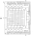
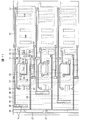
- FIG. 1 is a plan view showing a schematic configuration of a matrix substrate 20 including a scanning line driving circuit 47 according to Embodiment 1 of the present invention.
- the matrix substrate 20 includes an insulating substrate 21, and the insulating substrate 21 has a display region 30 and a peripheral region 40 other than the display region 30 on its upper surface.
- a plurality of scanning lines 31 (output lines) and a plurality of data lines 32 are arranged in a grid pattern.
- other structures such as a pixel transistor and a pixel electrode are also provided in the display region 30.
- a scanning line driving circuit 47 (driving circuit) composed of a plurality of unit circuits 50 for driving each scanning line 31, a data line driving circuit 48 for driving each data line 32, and A terminal portion 49 for connecting the matrix substrate 20 to the outside, wiring extending from the terminal portion 49 toward the scanning line driving circuit 47, wiring extending from the terminal portion 49 toward the data line driving circuit 48, Is arranged.
- the data line 32 extends in the vertical direction in FIG. 1 and is connected to the data line driving circuit 48 on the lower side.
- the display area 30 may be divided into upper and lower parts, and the data line driving circuit 48 may be arranged above and below the display area 30.
- the scanning lines 31 extend in the left-right direction in FIG. 1 and are alternately connected to the scanning line driving circuits 47 on both the left and right sides.
- the scanning lines 31 may be connected to the scanning line driving circuits 47 on both the left and right sides.
- the scanning line driving circuit 47 may be arranged only on the left and right sides.
- the scanning line driving circuit 47 according to the first embodiment is two shift registers combined so that the periods are shifted. Therefore, the matrix substrate 20 according to the first embodiment includes four shift registers, and the scanning lines 31 connected to the shift registers are sequentially driven.
- the total number of scanning lines 31 is N (N: natural number).
- the unit circuit 50 that drives the n-th (n: natural number less than or equal to N) scanning line 31 is an n-th unit circuit 50. Further, the potential output from the n-th unit circuit 50 to the n-th scanning line 31 is Out (n).
- the wiring extending from the terminal portion 49 toward the scanning line driving circuit 47 includes a low potential trunk wiring 34 (stem wiring) for supplying a low potential Vss, a first clock trunk wiring 35 for supplying a first clock signal CK1, A second clock trunk line 36 for supplying a second clock signal CK2, a third clock trunk line 37 for supplying a third clock signal CK3, a fourth clock trunk line 38 for supplying a fourth clock signal CK4, and initialization; An initialization wiring 68 (first type wiring) for supplying a signal Reset and a start trunk wiring (not shown) for supplying a start signal are included.
- first clock trunk line 35, the second clock trunk line 36, the third clock trunk line 37, and the fourth clock trunk line 38 are collectively referred to as “clock trunk lines 35 to 38”.
- the first clock signal CK1, the second clock signal CK2, the third clock signal CK3, and the fourth clock signal CK4 are collectively referred to as “clock signals CK1 to CK4”.
- the initialization wiring 68 shown in FIG. 1 passes through the inside of the scanning line driving circuit 47 and is not called a trunk wiring.
- FIG. 2 is a signal diagram showing a schematic configuration of signal potentials supplied by the low potential trunk line 34 and the clock trunk lines 35 to 38 shown in FIG.
- the low potential Vss is a signal potential indicating “0” and is a substantially constant potential.
- the clock signals CK1 to CK4 have the same length in one cycle, and are inverted to a signal potential Vss indicating “0” and a signal potential Vdd indicating “1” every half cycle. If the length of one cycle of the clock signals CK1 to CK4 is 8H, the length of H is several ⁇ sec (for example, 8 ⁇ sec).
- the second clock signal CK2 is a signal that is a half cycle earlier than the first clock signal CK1.
- the third clock signal CK3 is a signal that is a quarter cycle earlier than the first clock signal CK1.
- the fourth clock signal CK4 is a signal that is a half cycle earlier than the third clock signal CK3 (that is, the first clock signal is delayed by a quarter cycle).
- the initialization signal Reset is a signal potential Vdd indicating “1” when the scanning line driving circuit 47 is initialized, and a signal potential indicating “0” in other cases.
- FIG. 3 shows the following two conditions: (i) n is greater than 4 and less than N-3, and (ii) the remainder obtained by dividing n by 8 is 1 or 2.
- FIG. 2 is a circuit diagram showing a schematic circuit configuration of an n-th unit circuit 50 shown in FIG.
- (Ii) is a condition for specifying the clock signals CK1 to CK4 input to the unit circuit 50.
- this chapter describes the n-th unit circuit 50 that satisfies the above two conditions.
- the n-th stage unit circuit 50 that does not satisfy the above two conditions has the same configuration as that of the unit circuit 50 shown in FIG.
- the n-th unit circuit 50 includes a first transistor Tr1 (circuit element), a second transistor Tr2, a third transistor Tr3, a fourth transistor Tr4, a fifth transistor Tr5, A sixth transistor Tr6 and a bootstrap capacitor Cap are provided.
- the first transistor Tr1, the second transistor Tr2, the third transistor Tr3, the fourth transistor Tr4, the fifth transistor Tr5, and the sixth transistor Tr6 are collectively referred to as “transistors Tr1 to Tr6”.
- the transistors Tr1 to Tr6 are (i) energized between the source and drain while the gate potential is equal to or higher than the potential Vdd indicating “1”, and (ii) while the gate potential is the potential Vss indicating “0”.
- the source-drain state is de-energized.
- the transistors Tr1 to Tr6 are bottom gate type and channel etch type thin film transistors (thin film transistors, TFTs) formed on the insulating substrate 21, but are not limited thereto.
- the transistors Tr1 to Tr6 may be other types of thin film transistors such as a top gate type or an etch stop type.
- the scanning line driving circuit 47 may be disposed on a semiconductor substrate, and the transistors Tr1 to Tr6 may be other types of transistors such as metal oxide semiconductor (MOS) transistors. Good.
- the bootstrap capacitor Cap may be any capacitor.
- the output Out (n + 4) of the subsequent unit circuit 50 is input to the gate electrode of the first transistor Tr1.
- the low potential Vss is supplied to the source electrode of the first transistor Tr1, the source electrode of the third transistor Tr3, the source electrode of the fourth transistor Tr4, and the source electrode of the fifth transistor Tr5.
- the drain electrode of the first transistor Tr1, the drain electrode of the second transistor Tr2, the drain electrode of the fifth transistor Tr5, one electrode of the bootstrap capacitor Cap, and the gate electrode of the sixth transistor Tr6 are connected to each other.
- the potential of the gate electrode of the sixth transistor Tr6 is assumed to be nodeA (n).
- the output Out (n-4) of the unit circuit 50 in the previous stage is input to the gate electrode and the source electrode of the second transistor Tr2.
- the second clock signal CK2 is input to the gate electrode of the third transistor Tr3.
- the drain electrode of the third transistor Tr3, the drain electrode of the fourth transistor Tr4, the other electrode of the bootstrap capacitor Cap, the drain electrode of the sixth transistor Tr6, and the scanning line 31 are connected to each other.
- the potentials of these electrodes are output as Out (n) to the scanning line 31 and the unit circuits 50 in the subsequent stage and the previous stage.
- the first clock signal CK1 is input to the source electrode of the sixth transistor Tr6.
- the scanning line 31 becomes the signal potential Vdd via the sixth transistor Tr6.
- the first clock signal CK1 is inverted from “0” to “1” and the scanning line 31 is charged to the signal potential Vdd, the gate electrode of the sixth transistor Tr6 and the one electrode of the bootstrap capacitor The potential is pushed up.
- nodeA (n) becomes a signal potential indicating “1 + ⁇ ” higher than the signal potential Vdd ( ⁇ > 0).
- ⁇ corresponds to the total capacity of the capacity between the electrodes of the bootstrap capacity Cap and the capacity between the gate electrode and the train electrode of the sixth transistor Tr6.
- the sixth transistor Tr6 is an output transistor of the unit circuit 50 because it outputs the drain potential to the scanning line 31. For this reason, the sixth transistor Tr6 has a small channel resistance when the source-drain is energized so that it can sufficiently charge the scanning line 31, and can flow when the energized state. It is preferable that the source-drain current is large. Therefore, the sixth transistor Tr6 preferably has a wide channel width and a short channel length. Therefore, the area occupied by the sixth transistor Tr6 on the insulating substrate 21 in plan view is likely to be larger than the other transistors Tr1 to Tr5.
- the bootstrap capacitor Cap holds the gate-drain potential difference of the sixth transistor Tr6 and pushes nodeA (n) to a higher potential so that Out (n) reaches the potential Vdd during its output period. Therefore, it is preferable that the capacity is sufficiently large. For this reason, the bootstrap capacitor Cap also tends to occupy an area on the insulating substrate 21 in plan view, compared with the transistors Tr1 to Tr5 other than the sixth transistor Tr6.
- the output Out (n) of the n-th unit circuit 50 is as shown in Table 1.
- the sequential driving of the scanning lines 31 starts from the start stage and ends at the end stage.
- the initialization signal Reset 0, but immediately after finishing at the end stage or before starting from the start stage again.
- the unit circuit 50 shown in FIG. 3 is an exemplification, and does not limit the scope of the present invention.
- the unit circuit 50 may be a flip-flop circuit having another circuit configuration or a circuit other than the flip-flop circuit.
- the scanning line driving circuit 47 may include a plurality of types of unit circuits 50 having different circuit configurations.
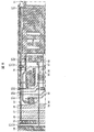
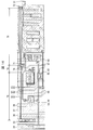
- FIG. 4 is a plan view showing a schematic circuit arrangement of the scanning line driving circuit 47 shown in FIG.
- the scanning line driving circuit 47 further includes a first relay wiring 66 (first type wiring) that connects the unit circuits 50, a second relay wiring 67, an initialization wiring 68, including.
- the initialization wiring 68 passes through the inside of the scanning line driving circuit 47 and is connected to the plurality of unit circuits 50.
- the initialization wiring 68 is a wiring that supplies the initialization signal Reset to the scanning line driving circuit 47 and also a wiring that connects the unit circuits 50.
- the first relay wiring 66 outputs the output Out (n) of the nth unit circuit 50, the gate electrode of the first transistor of the (n-4) th unit circuit 50, and the (n + 4) th unit circuit.
- This is a relay wiring for supplying to the gate electrode of 50 second transistors. Therefore, the first relay wiring 66 for supplying the output Out (n) has the (n ⁇ 4) th stage, the (n ⁇ 2) th stage, the nth stage, the (n + 2) th stage, and the (n + 4) th stage.
- the five unit circuits 50 are extended.
- the first relay wiring 66 for supplying the output Out (n) includes (i) the unit circuit 50 between the (n ⁇ 4) th stage and the nth stage, and (ii) the nth stage and (n + 4). ) The unit circuit 50 is connected to the stage.
- the second relay wiring 67 is (ii) a branch wiring that supplies any one of the clock signals CK1 to CK4 to the source electrode of the sixth transistor Tr6 of the unit circuit 50 in the n-th stage.
- the relay wiring extends toward the gate electrode of the third transistor Tr3 of the unit circuit 50 in the stage.
- the second relay wiring 67 is a relay wiring that supplies any one of the clock signals CK1 to CK4. Therefore, the second relay wiring 67 for supplying any one of the clock signals CK1 to CK4 from the n-th unit circuit 50 has the (n-4) th, (n-2) th, and nth stages. It extends over three unit circuits 50.
- the second relay wiring 67 for supplying any one of the clock signals CK1 to CK4 from the branch wiring of the n-th unit circuit 50 is connected between the (n-4) -th and n-th unit circuits 50. Connected.
- the initialization wiring 68 supplies the initialization signal Reset directly to the gate electrodes of the fourth transistor Tr4 and the fifth transistor Tr5 of each unit circuit 50. For this reason, the initialization wiring 68 is extended to all the unit circuits 50 in the odd-numbered stages and to all the unit circuits 50 in the even-numbered stages.
- the initialization wiring 68 is connected to (i) the unit circuit 50 between the (n ⁇ 2) th stage and the nth stage, and (ii) the unit circuit 50 between the nth stage and the (n + 2) th stage. Are connected.
- the first relay wiring 66, the second relay wiring 67, and the initialization wiring 68 are wirings extending substantially in parallel with the data lines 32, and are formed from the gate layer 22 (see FIG. 7) as will be described later. Wiring.
- FIG. 5 is a plan view showing a schematic circuit arrangement of the unit circuit 50 shown in FIG. FIG. 5 is similar to FIG. 3, in which (i) n is greater than 4 and less than N-3, and (ii) a condition in which the remainder of dividing n by 1 is 1 or 2. And n satisfying the two conditions.
- this chapter describes the n-th unit circuit 50 that satisfies the above two conditions.
- the n-th stage unit circuit 50 that does not satisfy the above two conditions is connected to the trunk wiring connected to the clock trunk wiring 35 to 38 and / or the first relay wiring 66 and / or the second relay wiring according to n.
- the connection destination of 67 is different, the rest is the same as the circuit arrangement of the unit circuit 50 shown in FIG.
- the n-th unit circuit 50 further includes a first branch wiring 61 (second type wiring), a second branch wiring 62, a third branch wiring 63, and a fourth branch wiring 64.
- the first branch wiring 61, the second branch wiring 62, the third branch wiring 63, the fourth branch wiring 64, and the fifth branch wiring 65 are collectively referred to as “branch wirings 61 to 65”.
- the first redundant wiring 51, the second redundant wiring 52, the third redundant wiring 53, the fourth redundant wiring 54, and the fifth redundant wiring 55 are collectively referred to as “redundant wirings 51 to 55”.
- the branch wirings 61 to 65 are wirings formed from the source layer 25 (see FIG. 9), as will be described later.
- the redundant wirings 51 to 55 are wirings formed from the redundant wiring layer 27 (see FIG. 11).
- the first redundant wiring 51 includes a switching unit 71 for connecting the first branch wiring 61 to the first clock trunk wiring 35 at the left end of FIG.
- the first redundant wiring 51 includes a switching unit 71 for connecting the first branch wiring 61 to the second relay wiring 67 at the center.
- the first redundant wiring 51 includes a connection portion 57 (second type connection portion) that can be connected to the first branch wiring 61 at the right end of FIG.
- the switching unit 71 included in the first redundant wiring 51 at the left end and the center in FIG. 5 is also the connection unit 57 that can be connected to the first branch wiring 61.
- the first branch wiring 61 is a branch wiring that connects the source electrode of the sixth transistor Tr6 to the first clock trunk wiring 35.
- the first branch wiring 61 is a branch wiring that supplies the first clock signal CK1.
- the first branch wiring 61 can be connected to the first redundant wiring 51 at the left end of FIG. 5, and (ii) the first clock trunk via the switching section 71 of the first redundant wiring 51.
- a connecting portion 72 (first type connecting portion and third type connecting portion) that can be connected to the wiring 35 is provided.
- the first branch wiring 61 can be connected to (i) the first redundant wiring 51 in the center, and (ii) can be connected to the second relay wiring 67 via the switching section 71 of the first redundant wiring 51.
- a connecting portion 72 is provided.
- the first branch wiring 61 includes a connection portion 72 that can be connected to the connection portion 57 of the first redundant wiring 51 at the right end of FIG.
- the first branch wiring 61 is formed integrally with the source electrode of the sixth transistor Tr6.
- the second redundant wiring 52 includes a connecting portion 57 that can be connected to the second branch wiring 62 at the left end in FIG.
- the second redundant wiring 52 includes a connection portion 57 that can be connected to the second branch wiring 62 at an end near the drain electrode of the second transistor Tr2.
- the second redundant wiring 52 is connected to a switching section 71 for connecting the second branch wiring 62 to one end of the bootstrap capacitor Cap integral with the gate electrode of the sixth transistor Tr6 at the right end of FIG. Is provided.
- the switching unit 71 included in the second redundant wiring 52 at the right end in FIG. 5 is also the connection unit 57 that can be connected to the second branch wiring 62.
- the second branch wiring 62 connects one electrode of the bootstrap capacitor Cap integrated with the gate electrode of the sixth transistor Tr6 to the drain electrodes of the first transistor Tr1, the second transistor Tr2, and the fifth transistor Tr5. It is.
- the second branch wiring 62 includes a connecting portion 72 that can be connected to the second redundant wiring 52 at the left end of FIG.
- the second branch wiring 62 includes a connection portion 72 that can be connected to the second redundant wiring 52 at the end near the drain electrode of the second transistor Tr2.
- the second branch wiring 62 can be connected to the bent portion on the right side of FIG. 5 (i) can be connected to the second redundant wiring 52, and (ii) the bootstrap capacitance Cap via the switching portion 71 of the second redundant wiring 52.
- the connection part 72 which can be connected to one electrode of this is provided.
- the second branch wiring 62 is formed integrally with the drain electrodes of the first transistor Tr1, the second transistor Tr2, and the fifth transistor Tr5.
- the third redundant wiring 53 includes a connecting portion 57 that can be connected to the third branch wiring 63 at the upper left end of FIG.
- the third redundant wiring 53 includes a switching section 71 for connecting the third branch wiring 63 to the gate electrode of the second transistor Tr2 at the lower right end of FIG.
- the switching unit 71 provided in the third redundant wiring 53 at the lower right end in FIG. 5 is also the connection unit 57 that can be connected to the third branch wiring 63.
- the third branch wiring 63 couples the two divided source electrodes of the second transistor Tr2 and connects the source electrode of the second transistor Tr2 to the gate electrode of the second transistor Tr2.
- the third branch wiring 63 includes (i) a connection portion 72 that can be connected to the third redundant wiring 53 at the bent portion on the upper left side in FIG.
- the third branch wiring 63 can be connected to the (i) third redundant wiring 53 at the lower right end of FIG. 5, and (ii) the second branch wiring 63 is connected to the second redundant wiring 53 via the switching section 71.
- a connection portion 72 that can be connected to the gate electrode of the transistor Tr2 is provided.
- the third branch wiring 63 is formed integrally with the source electrode of the second transistor Tr2.
- the third branch wiring 63 is formed integrally with the two source electrodes of the second transistor Tr2.
- the fourth redundant wiring 54 includes a switching section 71 for connecting the fourth branch wiring 64 to the low potential trunk wiring 34 at the left end in FIG.
- the fourth redundant wiring 54 includes a connection portion 57 that can be connected to the fourth branch wiring 64 at the center and the right end of FIG.
- the switching unit 71 included in the fourth redundant wiring 54 at the left end in FIG. 5 is also the connection unit 57 that can be connected to the fourth branch wiring 64.
- the fourth branch wiring 64 is a branch wiring that connects the low potential trunk wiring 34 to the source electrodes of the first transistor Tr1, the third transistor Tr3, the fourth transistor Tr4, and the fifth transistor Tr5.
- the fourth branch wiring 64 is a branch wiring that supplies the low potential Vss.
- the fourth branch wiring 64 can be connected to (i) the fourth redundant wiring 54 at the left end in FIG. 5, and (ii) the low potential trunk wiring through the switching section 71 of the fourth redundant wiring 54. 34 is provided.
- the fourth branch wiring 64 includes a connection portion 72 that can be connected to the fourth redundant wiring 54 at a branch portion that branches toward the source electrode of the first transistor Tr1.
- the fourth branch wiring 64 includes a connection portion 72 that can be connected to the fourth redundant wiring 54 in the vicinity of the source electrode of the fourth transistor Tr4.
- the fourth branch wiring 64 is formed integrally with the source electrodes of the first transistor Tr1, the third transistor Tr3, the fourth transistor Tr4, and the fifth transistor Tr5.
- the fifth redundant wiring 55 includes a switching section 71 for connecting the fifth branch wiring 65 to the first relay wiring 66 at the left end in FIG.
- the fifth redundant wiring includes a connection portion 57 that can be connected to the fifth branch wiring 65 at the right end of FIG.
- the switching unit 71 included in the fifth redundant wiring 55 at the right end in FIG. 5 is also the connection unit 57 that can be connected to the fifth branch wiring 65.
- the fifth branch wiring 65 includes the first relay wiring 66, the drain electrode of the third transistor Tr3, the drain electrode of the fourth transistor Tr4, and the other electrode of the bootstrap capacitor Cap integrated with the drain electrode of the sixth transistor Tr6. Is a branch wiring connecting the two.
- the fifth branch wiring 65 is a branch wiring that supplies the output Out (n) of the n-th unit circuit 50.
- the fifth branch wiring 65 can be connected to (i) the fifth redundant wiring 55 at the left end in FIG. 5, and (ii) the first relay wiring via the switching section 71 of the fifth redundant wiring 55.
- 66 is provided with a connecting portion 72 that can be connected to 66.
- the fifth branch wiring 65 includes (i) a connection portion 72 that can be connected to the fifth redundant wiring 55 at the right end of FIG.
- the fifth branch wiring 65 is formed integrally with the drain electrode of the third transistor Tr3, the drain electrode of the fourth transistor Tr4, and the other electrode of the bootstrap capacitor Cap.
- connection switching unit 71 replaces the branch wirings 61 to 65 formed from the source layer 25 (see FIG. 9) with the wirings formed from the gate layer 22 (see FIG. 7) (low-potential trunk wiring 34, clock trunk wiring 35 to 38, the first relay wiring 66, the second relay wiring 67) or an electrode (the gate electrode of the second transistor Tr2, the one electrode of the bootstrap capacitor Cap integral with the gate electrode of the sixth transistor Tr6).
- Distance wiring In the first embodiment, the reconnection unit 71 is provided integrally with the redundant wirings 51 to 55.
- the connection changing unit 71 is not limited to this, and is provided separately from the redundant wirings 51 to 55 as in the second embodiment described later. May be.
- the redundant wirings 51 to 55 entirely overlap with the corresponding branch wirings 61 to 65 except for the switching unit 71, the present invention is not limited to this.
- the redundant wirings 51 to 55 may not overlap with the corresponding branch wirings 61 to 65 or may partially overlap. In the overlapping section, the redundant wirings 51 to 55 are preferably thinner than the corresponding branch wirings 61 to 65.
- the first relay wiring 66 and the second relay wiring 67 intersect with the branch wirings 61 to 65 at the intersection 74, but do not intersect with the transistors Tr1 to Tr5 and the bootstrap capacitor Cap.
- the branch wirings 61 to 65 each include a plurality of connection portions 72.
- Each of the redundant wirings 51 to 55 includes a plurality of connection parts 57 (including connection parts 57 integrated with the switching part 71) that can be connected to the connection parts 72 of the corresponding branch wirings 61 to 65.
- the branch wirings 61 to 65 and the redundant wirings 51 to 55 corresponding to each other are connected by the connection between the connection part 72 and the connection part 57.
- the connection lines 72 connected between the branch lines 61 to 65 are also connected to the corresponding redundant lines 51 to 55. Therefore, the branch wirings 61 to 65 are doubled by the redundant wirings 51 to 55.
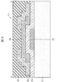
- FIG. 6 is a cross-sectional view taken along the line AA of FIG. 5 and is a cross-sectional view showing a schematic stacked structure of the first transistor Tr1. Although not described, the transistors Tr2 to Tr6 other than the first transistor Tr1 have the same stacked structure.
- the first transistor Tr1 according to the first embodiment is a bottom gate type and channel etch type TFT.
- the first transistor is formed on the insulating substrate 21, and includes a gate electrode (G) formed from the gate layer 22 (first conductive layer), the gate insulating film 23, and the semiconductor layer 24.
- G gate electrode
- S source electrode
- D drain electrode
- the insulating substrate 21 is a substrate that supports the scanning line driving circuit 47.
- the insulating substrate 21 may be formed of any material as long as it has insulating properties.
- a plastic substrate made of a glass substrate, polyethylene terephthalate, polyimide, or the like may be used.
- the gate layer 22 is a conductive layer formed on the insulating substrate 21.
- the gate layer 22 is made of, for example, a metal material such as titanium (Ti), copper (Cu), chromium (Cr), aluminum (Al), gold (Au), molybdenum (Mo), tungsten (W), or an alloy thereof. Can be formed.
- the gate insulating film 23 is an insulating film formed so as to cover the surfaces of the insulating substrate 21 and the gate layer 22.
- the gate insulating film 23 may be formed of an organic insulating material such as polyparavinylphenol (PVP) or an inorganic insulating material such as silicon dioxide (SiO 2 ) and silicon nitride (SiN x ). It may be.
- the semiconductor layer 24 is formed on the gate insulating film 23 and is a semiconductor layer for conducting the source electrode (S) and the drain electrode (D).
- the semiconductor layer 24 may be made of an oxide semiconductor, for example.
- the oxide semiconductor constituting the semiconductor layer 24 may be an amorphous oxide semiconductor or a crystalline oxide semiconductor having a crystalline portion.
- the crystalline oxide semiconductor include a polycrystalline oxide semiconductor, a microcrystalline oxide semiconductor, and a crystalline oxide semiconductor in which the c-axis is oriented substantially perpendicular to the layer surface.
- the semiconductor layer 24 made of an oxide semiconductor may have a stacked structure of two or more layers.
- the semiconductor layer 24 may include an amorphous oxide semiconductor layer and a crystalline oxide semiconductor layer.
- the semiconductor layer 24 may include a plurality of crystalline oxide semiconductor layers having different crystal structures.
- the semiconductor layer 24 may include a plurality of amorphous oxide semiconductor layers.
- the energy gap of the oxide semiconductor included in the upper layer is larger than the energy gap of the oxide semiconductor included in the lower layer. Is also preferably large. However, when the difference in energy gap between these layers is relatively small, the energy gap of the lower oxide semiconductor may be larger than the energy gap of the upper oxide semiconductor.
- the semiconductor layer 24 may contain at least one metal element of In, Ga, and Zn, for example.
- the semiconductor layer 24 includes, for example, an In—Ga—Zn—O-based semiconductor (eg, indium gallium zinc oxide).
- Such an oxide semiconductor layer can be formed of an oxide semiconductor layer containing an In—Ga—Zn—O-based semiconductor.
- the In—Ga—Zn—O-based semiconductor may be amorphous or crystalline.
- a crystalline In—Ga—Zn—O-based semiconductor in which the c-axis is oriented substantially perpendicular to the layer surface is preferable.
- a thin film transistor having an In—Ga—Zn—O-based semiconductor layer has high mobility (more than 20 times that of an a-Si TFT) and low leakage current (less than 1/100 of that of an a-Si TFT).
- the transistors Tr1 to Tr6 included in the scanning line driving circuit 47 and the pixel transistors disposed in the display region 30 are preferably used.
- the semiconductor layer 24 may include another oxide semiconductor instead of the In—Ga—Zn—O-based semiconductor.
- an In—Sn—Zn—O-based semiconductor eg, In 2 O 3 —SnO 2 —ZnO; InSnZnO
- the In—Sn—Zn—O-based semiconductor is a ternary oxide of In (indium), Sn (tin), and Zn (zinc).
- the oxide semiconductor layer includes an In—Al—Zn—O based semiconductor, an In—Al—Sn—Zn—O based semiconductor, a Zn—O based semiconductor, an In—Zn—O based semiconductor, and a Zn—Ti—O based semiconductor.
- Cd—Ge—O based semiconductor Cd—Pb—O based semiconductor, CdO (cadmium oxide), Mg—Zn—O based semiconductor, In—Ga—Sn—O based semiconductor, In—Ga—O based semiconductor, A Zr—In—Zn—O based semiconductor, an Hf—In—Zn—O based semiconductor, or the like may be included.
- the source layer 25 is made of, for example, a metal material such as titanium (Ti), copper (Cu), chromium (Cr), gold (Au), aluminum (Al), molybdenum (Mo), tungsten (W), or an alloy thereof. Can be formed.
- a metal material such as titanium (Ti), copper (Cu), chromium (Cr), gold (Au), aluminum (Al), molybdenum (Mo), tungsten (W), or an alloy thereof. Can be formed.
- the first interlayer insulating film 26 fills a space between the source electrode (S) and the drain electrode (G) formed from the source layer 25 so as to be separated from each other on the gate insulating film 23 and the semiconductor layer 24. To do.
- the first interlayer insulating film 26 is provided on the top surfaces of the gate insulating film 23, the semiconductor layer 24, and the source layer 25.
- the material of the first interlayer insulating film 26 may be the same insulating material as that of the gate insulating film 23, or may be an insulating material different from that of the gate insulating film 23.
- the layers (gate layer 22, gate insulating film 23, semiconductor layer 24, source layer 25, first interlayer insulating film 26) constituting the transistors Tr1 to Tr6 included in the scanning line driving circuit 47 are disposed in the display region 30.
- a layer constituting a pixel transistor is preferable.
- scanning line drive circuit manufacturing process A schematic process for manufacturing the scanning line driving circuit 47 shown in FIG. 4 will be described below with reference to FIGS. Although not described, the scanning line driving circuit 47, the data line driving circuit 48, and the configuration of the pixel transistors and pixel electrodes in the display region 30 are also formed on the insulating substrate 21.
- FIG. 7 is a plan view showing a schematic pattern of the gate layer 22 of the scanning line driving circuit 47 shown in FIG.
- FIG. 8 is a plan view showing a schematic pattern of the semiconductor layer 24 of the scanning line driving circuit 47 shown in FIG.
- FIG. 9 is a plan view showing a schematic pattern of the source layer 25 of the scanning line driving circuit 47 shown in FIG.
- FIG. 10 is a plan view showing a schematic pattern of the contact hole 29 of the scanning line driving circuit 47 shown in FIG.
- FIG. 11 is a plan view showing a schematic pattern of the redundant wiring layer 27 of the scanning line driving circuit 47 shown in FIG.
- a conductive material is deposited on the entire surface of the insulating substrate 21 to form the gate layer 22.
- the gate layer 22 is etched using a photolithography technique or the like so that the gate layer 22 remains in the pattern as shown in FIG. Accordingly, as shown in FIG. 7, the low potential trunk line 34, the clock trunk lines 35 to 38, the gate electrodes of the transistors Tr1 to Tr6, one electrode of the bootstrap capacitor Cap, the first relay line 66, the second relay line 67, And the initialization wiring 68 is formed.
- the gate insulating film 23 is deposited on the entire surface of the insulating substrate 21 from above the gate layer 22.
- the gate insulating film 23 is an insulating film for forming gate insulating films of the transistors Tr1 to Tr6 included in the scanning line driving circuit 47.
- the gate insulating film 23 is also preferably an insulating film for forming a gate insulating film of a pixel transistor disposed in the display region 30.
- a semiconductor material is deposited on the entire surface of the insulating substrate 21 from above the gate insulating film 23 to form the semiconductor layer 24.
- the semiconductor layer 24 is etched using a photolithography technique or the like so that the semiconductor layer 24 remains in the pattern as shown in FIG. As a result, as shown in FIG. 8, the semiconductor layer 24 serving as the channels of the transistors Tr1 to Tr6 is formed.
- a conductive material is deposited on the entire surface of the insulating substrate 21 from above the semiconductor layer 24 to form the source layer 25.
- the source layer 25 is etched using a photolithography technique or the like so that the source layer 25 remains in the pattern as shown in FIG.
- source and drain electrodes of the transistors Tr1 to Tr6, branch wirings 61 to 65, one electrode of the bootstrap capacitor Cap, and the scanning line 31 are formed.
- the scanning line 31 is formed in the gate layer 22.
- the scanning line 31 formed integrally with one electrode of the bootstrap capacitor Cap is formed by the source layer 25, but is connected to the gate layer 22 outside the display region 30 (inside the peripheral region 40). Yes.
- connection part 72 of the fourth branch wiring 64 to be connected to the low-potential trunk line 34 overlaps the low-potential trunk line 34 so as to overlap the low-potential trunk line 34.
- an insulating material is deposited on the entire surface of the insulating substrate 21 from above the source layer 25 to form a first interlayer insulating film 26.
- contact holes 29 are formed as shown in FIG. 10 by using a photolithography technique or the like.
- the first interlayer insulating film 26 is etched to expose the source layer 25 from the contact hole 29.
- the first interlayer insulating film 26 and the gate insulating film 23 are etched to expose the gate layer 22 from the contact hole 29.
- a conductive material is deposited on the entire surface of the insulating substrate 21 from above the first interlayer insulating film 26 to form a redundant wiring layer 27 (third conductive layer).
- the redundant wiring layer 27 is etched using a photolithography technique or the like so that the redundant wiring layer 27 remains in the pattern as shown in FIG. Thereby, the redundant wirings 51 to 55 are formed, and the conductive material for forming the redundant wiring layer 27 is embedded in the contact hole 29. Therefore, the redundant wiring layer 27 is connected to the gate layer 22 through the contact hole 29 where the gate layer 22 is exposed. Further, the redundant wiring layer 27 is connected to the source layer 25 through the contact hole 29 where the source layer 25 is exposed.
- the redundant wiring layer 27 for example, a metal material such as copper (Cu), titanium (Ti), aluminum (Al), or an alloy thereof can be used.
- the redundant wiring layer 27 is a common electrode for forming an auxiliary capacitance in a TN (twisted nematic) method or a VA (vertical aligned) method, or a common electrode in an FFS (fringe field switching) method. It may be a wiring for reducing resistance or a conductive layer for a channel light shielding film of a TFT. It is preferable that the redundant wiring layer 27 is such an existing conductive layer because the number of wiring layers is not increased.
- the switching unit 71 of the fourth redundant wiring 54 for connecting the fourth branch wiring 64 to the low potential trunk wiring 34 is a unit of different stages so as to overlap the low potential trunk wiring 34. It is preferable that the connection switching unit 71 of the circuit 50 is continuously arranged. Since the switching unit 71 arranged in this manner functions like another low potential trunk line 34, the wiring resistance of the low potential trunk line 34 is reduced.
- a photocurable resin is often used.
- the scanning line driving circuit 47 can be provided with a translucent portion that can transmit light that cures the photocurable resin. Is preferred.
- the three slits of the one electrode formed from the gate layer 22 of the bootstrap capacitor Cap shown in FIG. 6 are translucent portions that can transmit light for curing the photocurable resin.
- the redundant wirings 51 to 55 in the overlapping section are narrower than the corresponding branch wirings 61 to 65.
- the seal 11 on the scanning line driving circuit 47 (see FIG. 13) Is more preferable because it is easy to form. Since the redundant wirings 51 to 55 on the opposite side of the insulating substrate 21 are thin, the sealing material can be hardened more easily. Similarly, the three slits of the other electrode formed from the source layer 25 of the bootstrap capacitor Cap are also larger than the slits of the one electrode so that the sealing material can be hardened more easily.
- the second interlayer insulating film 28 is deposited on the entire surface of the insulating substrate 21 from above the source layer 25 to form the second interlayer insulating film 28.
- the material of the second interlayer insulating film 28 may be the same insulating material as the first interlayer insulating film 26, or may be an insulating material different from that of the first interlayer insulating film 26.
- the second interlayer insulating film 28 may be silicon nitride (SiN x ) having a thickness of 0.2 mm to 0.8 mm.
- FIG. 12 is a cross-sectional view taken along the line BB in FIG. 5 and is a cross-sectional view showing a schematic configuration of the intersecting portion 74 and the switching portion 71.
- the second relay wiring 67 connecting the unit circuits at the (n ⁇ 2) th stage and the (n + 2) th stage intersects the first branch wiring 61.
- 12 includes a first branch wiring 61, a second relay wiring 67 that connects the unit circuits of the (n ⁇ 4) th stage and the nth stage, and a first redundancy wiring.
- the wiring 51 is connected.
- the second relay wiring 67 formed from the gate layer 22 is first redundant formed from the first branch wiring 61 formed from the source layer 25 and the redundant wiring layer 27. Crosses the wiring 51.
- the second relay wiring 67 is not sandwiched between the first branch wiring 61 and the first redundant wiring 51.
- the wiring capacity between the second relay wiring 67 and the first branch wiring 61 and the first redundant wiring 51 is smaller than the sandwiched configuration.
- any of the clock signals CK1 to CK4 transmitted by the first branch wiring 61 and any of the clock signals CK1 to CK4 transmitted by the first redundant wiring 51 are the same. For this reason, the wiring capacity between the first branch wiring 61 and the first redundant wiring 51 is not a problem.
- stacking the gate layer 22, the source layer 25, and the redundant wiring layer 27 in this order on the insulating substrate 21 means that the first relay wiring 66 and the second relay wiring at the intersection 74.
- This is preferable because the wiring capacity of 67 is reduced.
- Reduction of the wiring capacity is preferable because signal dullness in the intersecting first relay wiring 66, second relay wiring 67, and initialization wiring 68 is reduced.
- the reduction of the wiring capacitance is preferable because signal blunting in the intersecting first branch wiring 61, second branch wiring 62, fourth branch wiring 64, and fifth branch wiring 65 is also reduced.
- the connecting portion 71 that connects the first branch wiring 61 to the second relay wiring 67 is formed integrally with the first redundant wiring 51.
- the connection switching unit 71 is also the connection unit 57 of the first redundant wiring 51.
- the first redundant wiring 51 is connected to the first branch wiring 61 and the second relay wiring 67 through the contact hole 29. Therefore, both the connecting portion 71 and the connecting portion 57 of the first redundant wiring 51 need to be sufficiently larger than the contact hole 29.
- the configuration in which the switching portion 71 is integrated with the first redundant wiring 51 is more than the configuration in which the first redundant wiring 51 includes the connection portion 57 separately from the switching portion 71. It is easy to reduce the area occupied by.
- the uppermost layer of the laminated structure laminated on the insulating substrate 21 is the second interlayer insulating film 28.
- the uppermost layer is an insulating film because the seal 11 (see FIG. 13) can be easily formed on the scanning line driving circuit 47.
- the conductive layer is easily broken by the spacer included in the sealing material.
- a TN (twisted nematic) type or VA (vertical aligned) type liquid crystal display device when a spacer mixed with conductive particles is used for conduction with a counter electrode provided on the counter substrate. Short circuit due to conductive particles is likely to occur.
- the uppermost layer is an insulating film, the conductive layer is not easily broken or short-circuited.
- the uppermost layer of the laminated structure laminated on the insulating substrate 21 in the peripheral region 40 is an insulating film.
- the seal 11 is not formed in the display region 30, the uppermost layer of the display region 30 may be a transparent conductive layer or the like that forms a pixel electrode.
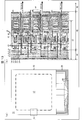
- FIG. 13 is a plan view showing a schematic configuration of a liquid crystal display panel 100 (display device) using the matrix substrate 20 shown in FIG.
- FIG. 13A is a perspective plan view of the liquid crystal display panel 100.
- FIG. 13B is an enlarged view of the matrix substrate 20 in a portion of a box C in FIG.
- the liquid crystal display panel 100 includes a matrix substrate 20, a counter substrate 10 facing the matrix substrate, and a liquid crystal 12 (electrical) sealed between the counter substrate 10 and the matrix substrate 20.
- a liquid crystal 12 electrical
- Optical material and a seal 11 for enclosing the liquid crystal 12.
- the seal 11 is formed in the seal region 41 included in the peripheral region 40 so that the terminal portion 49 of the matrix substrate 20 can be connected to the outside along the outer periphery of the counter substrate 10.
- a sealing material for forming the seal 11 a photocurable resin is usually used.
- the matrix substrate 20 is provided with a light-transmitting portion that can transmit light for curing the seal material.
- a spacer for maintaining a distance between the counter substrate 10 and the matrix substrate 20 is usually mixed in the sealing material.
- the seal region 41 includes (i) a main wiring region 44 in which the low potential main wiring 34 and clock main wirings 35 to 38 are disposed, and (ii) a scanning line driving circuit. It overlaps with the drive circuit area 45 in which 47 is disposed.
- a configuration of overlapping is preferable because the area of the peripheral region 40 can be reduced compared to a configuration in which the seal region 41 does not overlap with the main wiring region 44 and the drive circuit region 45.
- the ratio of the seal region 41 overlapping the drive circuit region 45 is high.
- the sixth transistor Tr6 has a large area and it is difficult to provide an opening serving as a transmission part.
- the sixth transistor Tr6 is provided on the side close to the display region 30 so that the seal region 41 does not overlap the sixth transistor Tr6.
- the first branch wiring 61 that connects the source electrode of the sixth transistor Tr6 to any one of the clock trunk wirings 35 to 38 is the longest of the branch wirings 61 to 65, and is most easily disconnected.
- the scanning line driving circuit 47 becomes defective when the branch wirings 61 to 65 are disconnected. For this reason, the defect rate of the scanning line driving circuit 47 is high, and it is difficult to improve the manufacturing yield of the matrix substrate 20.
- the branch wirings 61 to 65 are substantially doubled by the corresponding redundant wirings 51 to 55.
- the scanning line driving circuit 47 becomes defective. For this reason, since the probability that both of them are disconnected is lower than the probability that only one of them is disconnected, the defect rate of the scanning line driving circuit 47 can be reduced, and the manufacturing yield of the matrix substrate 20 can be improved.
- the branch wirings 61 to 65 can be doubled using the corresponding redundant wirings 51 to 55. Therefore, for example, even if the second branch wiring 62 is disconnected, the drain electrodes of the first transistor Tr1, the second transistor Tr2, and the fifth transistor Tr5 are connected to one electrode of the bootstrap capacitor Cap and the second redundant wiring 52. Connected by. In this way, each unit circuit 50 is provided with redundancy against disconnection of the branch wirings 61 to 65 due to the double wiring, so that defects of the unit circuit 50 due to disconnection of the branch wirings 61 to 65 can be reduced. Thereby, the manufacturing yield of the scanning line driving circuit 47 and the matrix substrate 20 can be improved.
- all of the branch wirings 61 to 65 can be double-tracked, but only a part of the branch wirings 61 to 65 may be double-tracked. In this case, it is preferable that at least the first branch wiring 61 can be doubled. Because the sixth transistor Tr6, which is an output transistor, is normally disposed on the display area side of the drive circuit area 45, the first branch wiring 61 is the longest of the branch wirings 61 to 65, and the most It is because it is easy to disconnect.
- Example 2 The configuration according to the first embodiment of the present invention can be applied to a high-definition medium-sized display device and is beneficial.
- the configuration according to Embodiment 1 of the present invention is applied to an active matrix substrate for a 4.4 type FHD (full high vision display) with a pixel pitch of 17 ⁇ m ⁇ 51 ⁇ m.
- the interval between the data lines 32 is 17 ⁇ m
- the interval between the scanning lines 31 is 51 ⁇ m
- the number of scanning lines 31 was 1920.
- the scanning line driving circuit 47 is provided with a surplus space where the unit circuit 50 is not provided for each unit circuit 50 of 20 to 30 stages, and a bypass wiring for a common electrode is provided in the surplus space. .
- the branch wirings 61 to 65 included in the unit circuit 50 are formed with a width of 4 ⁇ m, and the redundant wirings 51 to 55 are formed. A width of 3 ⁇ m was formed.
- the scanning line drive circuit 47 is overlapped with the seal region 41 except for the sixth transistor Tr6 so that the scan line drive circuit 47 overlaps the seal region 41.
- the seal 11 was formed so as to completely overlap.
- the matrix substrate 20 according to the second embodiment is partially different from the matrix substrate 20 according to the first embodiment in the circuit arrangement of the unit circuits 50 as shown in FIG. It is the same configuration.
- the circuit configuration of the unit circuit 50 according to the second embodiment is the same as that of the unit circuit 50 according to the first embodiment shown in FIG.
- FIG. 14 is a plan view showing a schematic circuit arrangement of the unit circuit 50 according to the second embodiment.
- the switching unit 71 in the unit circuit 50 according to the second embodiment is separated from the redundant wirings 51a, 51b, 52 to 55.
- the first redundant wiring 51 in the first embodiment is divided into a first left redundant wiring 51a on the left side of FIG. 14 and a first right redundant wiring 51b on the right side of FIG.
- the branch lines 61 to 65 include a connection part 72 for connecting to the switching part 71 and a connection part 72 for connecting to the redundant lines 51a, 51b, 52 to 55.
- Each of the redundant wirings 51a, 51b, 52 to 55 includes a plurality of connection portions 57 that can be connected to the connection portions 72 of the corresponding branch wirings 61 to 65.
- the redundant wirings 51a, 51b, 52 to 55 are not connected to the corresponding branch wirings 61 to 65 in advance. Therefore, in the state shown in FIG. 14, the branch lines 61 to 65 can be doubled by the redundant lines 51a, 51b, and 52 to 55, but are not yet doubled. In other words, in the state shown in FIG. 14, the redundant wirings 51a, 51b, 52 to 55 are floating wirings.
- the second relay wiring 67 that connects between the (n ⁇ 2) -th stage and the (n + 2) -th unit circuit 50 is the (i) first left redundant wiring 51a in the n-th unit circuit 50. 14 and (ii) the first branch wiring 61 is connected to the second relay wiring 67 that connects the unit circuit 50 between the (n-4) -th stage and the n-th stage. It passes between the part 71.
- FIG. 15 is a cross-sectional view taken along the line CC of FIG. 14, and is a cross-sectional view showing a schematic configuration of the intersection part 74 and the connection part 71.
- the first left redundant wiring 51 a is separated from the switching unit 71. Further, the connection part 72 of the first branch wiring 61 is not connected to the connection part 57 of the first left redundant wiring 51a.
- connection portions 57 of the redundant wirings 51a, 51b, 52 to 55 are arranged so as to overlap with the corresponding connection portions 72 of the corresponding branch wirings 61 to 65. For this reason, the connection part 57 and the connection part 72 corresponding to each other can be melt-connected. Therefore, for example, when any of the branch wirings 61 to 65 is disconnected, the branch wirings 61 to 65 and the corresponding redundant wiring are connected by melt-connecting the plurality of corresponding connection portions 57 and the connection portions 72. 51a, 51b, 52 to 55 can be connected, and a defective product can be relieved.
- the source layer 25, the first interlayer insulating film 26, and the redundant wiring layer 27 are selectively irradiated by selectively irradiating the selected connection portion 57 and the connection portion 72 with a laser beam. Melt. By melting, a hole is opened in the first interlayer insulating film 26 and the source layer 25 and the redundant wiring layer 27 are joined.
- the laser beam may be irradiated from the upper surface side of the insulating substrate 21 or from the lower surface side.
- the counter substrate 10 is often provided with a light shielding film, when the melt connection is performed after the counter substrate 10 is bonded to the matrix substrate 20 by the seal 11, the laser beam is prevented from being cut off. Is preferably irradiated from the lower surface side of the insulating substrate 21.
- connection part 57 and the connection part 72 corresponding to each other may be connected before or after the counter substrate 10 is bonded to the matrix substrate 20 by the seal 11.
- the number of insulating films between the redundant wiring layer 27 and the source layer 25 is preferably small so that the melt connection is easy, and the second interlayer is interposed between the redundant wiring layer 27 and the source layer 25. More preferably, only the insulating film 28 is sandwiched.
- connection part 72 for connecting to the redundant wirings 51a, 51b, 52 to 55 of the branch wirings 61 to 65 is (i) the branch wirings 61 to 65 so that the irradiated laser light is not blocked by the gate layer 22. Is different from the intersection 74 where the first relay wiring 66 or the second relay wiring 67 or the initialization wiring 68 intersect, and (ii) the position where the branch wirings 61 to 65 overlap the gate electrodes of the transistors Tr1 to Tr6. Preferably there is.
- the connecting portion 71 provided in the center of the first redundant wiring 51 is close to the second redundant wiring 52, so that it is easily short-circuited.
- the switching unit 71 provided at the left end of the fifth redundant wiring 55 of the n-th unit circuit 50 is close to the first redundant wiring 51 of the adjacent (n + 2) -stage unit circuit 50, so that a short circuit occurs. It's easy to do.
- the redundant wirings 51 to 55 are connected to the corresponding branch wirings 61 to 65, and the switching unit 71 is included in the redundant wirings 51 to 55.
- the switching portion 71 provided in the center of the first redundant wiring 51 is short-circuited with the second redundant wiring 52
- the first branch wiring is short-circuited with the second branch wiring.
- the switching section 71 provided at the left end of the fifth redundant wiring 55 of the n-th unit circuit 50 is short-circuited with the first redundant wiring 51 of the adjacent (n + 2) -stage unit circuit 50
- the n-th stage The fifth branch wiring 65 of the unit circuit 50 is short-circuited with the first branch wiring 61 of the (n + 2) stage unit circuit 50.
- the redundant wirings 51a, 51b, and 52 to 55 are arranged separately from the switching unit 71 and are floating. Wiring. For this reason, even if the switching unit 71 is short-circuited with another redundant wiring (not corresponding to the branch wirings 61 to 65 to which the switching unit 71 is connected), as long as the short-circuited redundant wiring is not connected to the branch wiring. The wiring is not short-circuited. Therefore, it is possible to reduce defects in the unit circuit 50 due to a short circuit between the redundant wirings 51 to 55 and the switching unit 71.
- the unit circuit 50 has redundancy against the disconnection of the branch wirings 61 to 65. . Furthermore, according to the structure which concerns on Embodiment 2, the redundancy with respect to the short circuit of the switching part 71 and another redundant wiring is also provided. Thereby, the manufacturing yield of the scanning line driving circuit 47 and the matrix substrate 20 can be further improved.
- the configuration according to the first embodiment and the configuration according to the second embodiment may be combined.
- both the manufacturing efficiency of the scanning line driving circuit 47 (the manufacturing yield at a stage not involving the work related to the melt connection) and the final manufacturing yield after the defective connection is relieved by performing the melt connection. Can be improved. It is preferable to determine how to combine them in consideration of the arrangement of the switching unit 71 and the redundant wirings 51 to 55.
- the matrix substrate 20 according to the third embodiment is partially different from the matrix substrate 20 according to the first embodiment in the circuit arrangement of the unit circuits 50 as shown in FIG. It is the same configuration.
- the circuit configuration of the unit circuit 50 according to the third embodiment is the same as that of the unit circuit 50 according to the first embodiment shown in FIG.
- FIG. 16 is a plan view showing a schematic circuit arrangement of the unit circuit 50 according to the third embodiment.
- the first redundant wiring 51 in the n-th unit circuit 50 according to the third embodiment is different from the first branch wiring 61 in the n-th unit circuit 50 in the (n ⁇ 2) th stage.
- the crossing portion 74 that crosses the second relay wiring 67 that connects the unit circuit 50 to the (n + 2) stage is bypassed.
- the first redundant wiring 51 Due to this detour, the first redundant wiring 51 according to the third embodiment has an overlapping section 75 that overlaps the corresponding first branch wiring 61 and a detour section 76 that bypasses the intersection 74.
- the first redundant wiring 51 has only one bypass section 76, but the present invention is not limited to this.
- the other redundant wirings 52 to 55 may also have a bypass section 76, and the redundant wirings 51 to 55 may have two or more bypass sections 76.
- FIG. 17 is an enlarged view of the vicinity of the bypass section 76 shown in FIG. 16 (a) before cutting and (b) after cutting.
- the branch lines 61 to 65 intersect the first relay line 66, the second relay line 67, or the initialization line 68. For this reason, at the intersection 74, the branch wirings 61 to 65 may be short-circuited with the first relay wiring 66, the second relay wiring 67, or the initialization wiring 68. When a short circuit occurs, the short circuit between the branch wirings 61 to 65 and the first relay wiring 66 or the second relay wiring 67 or the initialization wiring 68 is eliminated by separating the shorted intersection 74 from the branch wirings 61 to 65. Can do.
- the first redundant wiring 51 does not overlap the first branch wiring 61 in the bypass section 76.
- FIG. 17B only the first branch wiring 61 can be cut and the first branch wiring 61 can be separated from the intersection 74 by laser irradiation or the like.
- the first branch wiring 61 and the second relay wiring 67 are short-circuited by separating the first branch wiring 61 from the intersection 74. Can be resolved. Since the cut first branch wiring 61 is doubled in advance by the first redundant wiring 51, the clock signal is transmitted to (i) the source electrode of the sixth transistor Tr6 and (ii) the second relay wiring 67. Can still be supplied. For this reason, it is possible to reduce defects in the unit circuit 50 due to a short circuit of the branch wirings 61 to 65 at the intersection.
- the length of the cutting section 77 indicates the patterning accuracy of the wirings (branch wirings 61 to 65, redundant wirings 51 to 55, the first relay wiring 66, the second relay wiring 67, and the initialization wiring 68) (shown in FIGS. 7 to 11). Line width and positional deviation of the pattern), alignment accuracy of the irradiation position of laser irradiation for cutting, workability of the cutting operation, scattering of the conductive material in and near the cutting portion 78, and the cutting portion 78 It is preferable to secure the length in consideration of the length and the like.
- the length of the cutting section 77 is 5 ⁇ m or more.
- the branch wirings 61 to 65 are double-wired, so that the unit circuit 50 has redundancy against disconnection of the branch wirings 61 to 65. . Furthermore, according to the configuration of the third embodiment, it is possible to eliminate the short circuit of the branch wirings 61 to 65 at the intersection 74. Thereby, the manufacturing yield of the scanning line driving circuit 47 and the matrix substrate 20 can be further improved.
- the configurations according to the first to third embodiments may be combined. By combining them as appropriate, the manufacturing efficiency of the scanning line driving circuit 47 (manufacturing yield at a stage not involving work related to melt connection or disconnection) and final manufacture after repairing defective products by performing melt connection or disconnection Both yield and yield can be improved.
- the combination of the wiring capacity, the probability that the redundant wirings are short-circuited, and the translucent light that can transmit light for curing the sealing material It is preferable to make a determination in consideration of securing the part.
- the driving circuit connects a plurality of unit circuits (50) for driving a plurality of output lines (scanning lines 31) and the unit circuits. And a first type wiring (first relay wiring 66, second relay wiring 67, initialization wiring 68) formed from a first conductive layer (gate layer 22) for at least one of the unit circuits.
- first relay wiring 66, second relay wiring 67, initialization wiring 68 formed from a first conductive layer (gate layer 22) for at least one of the unit circuits.
- One is a plurality of circuit elements (transistors Tr1 to Tr6, a bootstrap capacitor Cap) and a circuit element included in the unit circuit; (ii) another circuit element included in the unit circuit; and (ii) the first circuit element.
- a second type wiring (branch wirings 61 to 65) formed from the second conductive layer (source layer 25) for connection to either the seed wiring or the trunk wiring for supplying (iii) input; At least one of the second type wirings is at least A third type wiring (redundant wiring 51 to 55, first left redundant wiring 51a, first right redundant wiring 51b) formed from a third conductive layer (redundant wiring layer 27) partially corresponding to
- the at least one of the second type wirings includes a plurality of first type connection parts (branch wiring connection parts 72), and the third type wirings correspond to the first type connection parts of the corresponding second type wirings.
- a plurality of second-type connection portions (redundant wiring connection portions 57) that can be connected to each other.
- the second type wiring having the corresponding third type wiring includes the plurality of first type connection portions, and the third type wiring is the corresponding second type wiring.
- a plurality of second type connection parts connectable to each first type connection part are provided.
- the second type wiring and the third type wiring corresponding to each other can be connected by connecting the first connection part and the second connection part.
- the first type connection portion can be connected by the third type wiring in addition to the second type wiring.
- the wiring can be doubled.
- at least one unit circuit has redundancy against disconnection of the second type wiring, so that the drive circuit has redundancy against disconnection of the second type wiring.
- the probability that both wires are disconnected is smaller than the probability that one wire is disconnected. Therefore, the probability of disconnection of all the wirings connecting between the first-type connection portions can be reduced by double wiring. As a result, defects in the drive circuit due to disconnection can be reduced, so that the manufacturing yield of the drive circuit can be improved.
- the first type connection part and the second type connection part are (i) so that the third type wiring is connected only between the first type connection parts where the second type wiring connecting between them is disconnected. Or (ii) may be connected regardless of the disconnection of the second type wiring.
- the combined wiring resistance between the first type connection parts connected by both the second type wiring and the third type wiring is the same as that of the first type connection part connected only by the second type wiring. It is smaller than the wiring resistance between. For this reason, the first type connection portion and the second type connection portion corresponding to each other are connected so that the third type wiring is connected also between the first type connection portions where the second type wiring connecting between them is not disconnected. By connecting, wiring resistance can be reduced.
- At least one of the unit circuits (50) includes the circuit elements (transistors Tr1 to Tr6, bootstrap).
- the capacitor Cap) includes an output transistor (sixth transistor Tr6) for driving the corresponding output line (scanning line 31), and the output transistor corresponds to one of the source electrode and the drain electrode (drain electrode).
- the main wiring is connected to the output line, and the other of the source electrode and the drain electrode (source electrode) is a second type wiring (first branch wiring 61) having a corresponding third type wiring (first redundant wiring 51).
- the configuration may be such that it is connected to any one of the clock trunk wires 35 to 38.
- At least the second type wiring that connects the output transistor to the main wiring can be double-tracked.
- the channel resistance when the source-drain is energized is small.
- the smaller the channel resistance the larger the current flowing between the source and drain, and the smaller the voltage drop at the source and drain.
- the smaller the channel resistance of the output transistor the stronger the drive circuit is against the output resistance, and the dullness of the output signal can be reduced.
- the output transistor when the drive circuit drives the scanning line of the matrix substrate as the output line, the output transistor preferably has a small channel resistance so that the ability to charge the scanning line is sufficiently high.
- the output transistor tends to be larger than circuit elements other than the output transistor.
- the output transistor conventionally has a large area and does not overlap or contact the wiring in a plan view.
- a photocurable material is often used as a sealing material for forming a seal for enclosing an electro-optical material such as liquid crystal. For this reason, in the area
- the output transistor is disposed on the display region side, and (ii) the main wiring is disposed on the opposite side of the display region.
- the circuit elements included in the unit circuit other than the output transistor have been laid out so that the circuit elements are arranged between the output transistor and the main line.
- the second type wiring for connecting the output transistor to the main wiring is the longest among the second type wirings. For this reason, the second type wiring for connecting the output transistor to the main wiring has the highest probability of disconnection and the wiring resistance is likely to be the highest. For these reasons, it is extremely beneficial that the second type wiring for connecting the output transistor to the main wiring can be doubled.
- the other of the source electrode and the drain electrode of the output transistor receives a clock signal.
- the main wiring any of clock main wirings 35 to 38 for supplying to the driving circuit may be connected.
- the drive circuit (scanning line drive circuit 47) is the first conductive layer (gate layer 22) and the second conductive layer (source) in any one of the aspects 1 to 3.
- the layer 25) and the third conductive layer (redundant wiring layer 27) may be different conductive layers.
- the first type wiring, the second type wiring, and the third type wiring are viewed in plan view. Can be superimposed on each other. Therefore, the second type wiring may be arranged so that the second type wiring intersects with the first type wiring. Further, the third type wiring may be arranged so that the third type wiring intersects with the first type wiring. Further, the third type wiring may be arranged so that the third type wiring extends along the second type wiring on the second type wiring.
- the driving circuit (scanning line driving circuit 47) according to Aspect 5 of the present invention is the same as that in Aspect 4 described above, between the second conductive layer (source layer 25) and the third conductive layer (redundant wiring layer 27). May be configured such that only the insulating film (first interlayer insulating film 26) is sandwiched.
- the thickness of the insulating film between the second conductive layer and the third conductive layer is preferably thin.
- the second type wiring is the circuit element (transistors Tr1 to Tr6, boot) in the above aspect 4 or 5.
- Strap capacitor Cap formed from the first conductive layer, the first type wiring (first relay wiring 66, second relay wiring 67, initialization wiring 68), and the first conductive layer.
- a third type connection portion (branch wire connection portion 72) for connection to any one of the main wires (low potential main wire 34, clock main wires 35 to 38); It is good also as a structure containing at least 1st type connection part (connection part 72 of branch wiring).
- the third type connection portion for connecting the second type wiring to the circuit element, the first type wiring or the trunk wiring includes at least one of the first type connection portions. For this reason, the number of connection parts (the first type connection part and the third type connection part) provided in the second type wiring can be reduced.
- connection part for connecting wirings formed from different conductive layers is larger than the part that is not a connection part.
- an insulating film is formed on the conductive layer
- a through hole is formed in the insulating film
- another conductive layer is formed on the insulating film, and a conductive material is formed in the through hole. Connect the wiring by filling in.
- the connecting portion needs to be sufficiently larger than the opening of the through hole.
- reducing the number of connection portions provided in the second type wiring is beneficial for reducing the area for arranging the second type wiring, and reducing the area for the layout of the drive circuit. Useful for area.
- the unit circuit (50) is a connection formed from the third conductive layer (redundant wiring layer 27).
- the second type wiring (branch wirings 61 to 65) further includes an electrode (of the bootstrap capacitor Cap) formed from the first conductive layer of the circuit element through the switching part.
- Clock trunk wires 35 to 38 Clock trunk wires 35 to 38
- a third type connection portion (branch wire connection portion 72) for connection to any one of the clock trunk wires 35 to 38)
- the switching portion includes the third type wires (redundant wires 51a, 51b, 52-55) It may be configured to have been.
- the drive circuit (scanning line drive circuit 47) according to Aspect 8 of the present invention is any one of Aspects 4 to 7 described above, and includes at least the third type wiring (redundant wirings 51a, 51b, 52 to 55).
- One may have a configuration having an overlapping section (overlapping section 75) overlapping with the corresponding second type wiring (branch wirings 61 to 55) in plan view.
- At least one of the third type wirings has an overlapping section that overlaps with the corresponding second type wiring.
- GMD gate driver monolithic
- a seal material is cured in a peripheral region of the matrix substrate to form a seal that encloses an electro-optical material such as liquid crystal between the matrix substrate and the counter substrate.
- a scanning line driving circuit is also used in the peripheral region of the matrix substrate. Therefore, in order to reduce the area of the peripheral region, a part or all of the drive circuit region forming the scanning line drive circuit overlaps with the seal region forming the seal. For this reason, it is preferable that the scanning line driving circuit has a configuration in which it is easy to ensure a light-transmitting portion through which light that cures the sealing material is transmitted so that a photo-curable sealing material can be used.
- At least one of the third type wirings has an overlapping section that overlaps with the corresponding second type wiring. For this reason, it is easy to ensure a translucent part. Therefore, it is possible to realize a drive circuit suitable for a matrix substrate that employs GMD technology.
- the drive circuit (scanning line drive circuit 47) according to aspect 9 of the present invention is the above-described aspect 8, wherein the first conductive layer (gate layer 22), the second conductive layer (source layer 25), and the first The three conductive layers (redundant wiring layer 27) may be stacked on the insulating substrate (21) in this order.
- the driving circuit (scanning line driving circuit 47) according to the tenth aspect of the present invention is the third type wiring (redundant wirings 51 to 55, first left redundant wiring 51a, first right redundant wiring 51b) according to the ninth aspect. May be narrower than the width of the corresponding second type wiring (branch wirings 61 to 65) in the overlapping section (75).
- the scanning line driving circuit has a configuration that facilitates securing a light-transmitting portion through which light that cures the sealing material passes. Therefore, it is possible to realize a drive circuit suitable for a matrix substrate that employs GMD technology.
- the drive circuit (scanning line drive circuit 47) is the third type wiring (redundant wirings 51 to 55, first left redundant wiring 51a, At least one of the first right redundant wirings 51b) corresponds to the corresponding second type wiring (branch wirings 61 to 65) and the first type wiring (first relay wiring 66, second relay wiring 67, initial state) in plan view. It is good also as a structure which has the detour section (76) which detours the cross
- At least one of the third type wirings has a detour section that bypasses the intersection where the second type wiring and the first type wiring intersect. For this reason, when the second type wiring and the first type wiring are short-circuited at the detoured intersection, the repair is easy. For example, (i) the second-type wiring is cut on both sides of the short-circuited intersection, and (ii) the first-type connection between the second-type wirings that are connected by the cutting is disconnected. The first type connection portion and the second type connection portion are connected so that the third type wiring is connected. In order to facilitate cutting for repair, it is preferable that wiring and circuit elements are not provided on the second type wiring on both sides (for example, within 5 ⁇ m) of the detoured intersection.
- the circuit element includes: (i) the first conductive layer (gate layer 22). It may be configured to include a transistor (Tr1 to Tr6) having a formed gate electrode and (ii) a source electrode and a drain electrode formed from the second conductive layer (source layer 25).
- the first-type wiring is connected to one unit circuit and the other one. It may be configured to include a first relay wiring (66) for supplying the output of the unit circuit.
- the unit circuit can be supplied with the output of another unit circuit.
- a flip-flop circuit can be used as a unit circuit, so that the driver circuit can function as a shift register.
- the first type wiring is connected to one unit circuit and another one of the above-described ones. It may be configured to include the second relay wiring (67) for supplying the input of the unit circuit.
- the relay wiring can be branched from the branch wiring connecting the circuit element to the trunk wiring, or the relay wiring can be branched from the electrode of the circuit element connected to the trunk wiring.
- the first type wiring is an initialization signal for initializing the unit circuit. It is good also as a structure containing the initialization wiring (68) for supplying (Reset).
- the matrix substrate (20) according to the sixteenth aspect of the present invention includes a display area (30) in which the output lines are arranged as scanning lines (31), and a drive circuit according to any one of the first to fifteenth aspects (A configuration including an insulating substrate (21) having a scanning line driving circuit 47) and a peripheral region (40) in which the main wiring (low potential main wiring 34, clock main wiring 35 to 38) is disposed. is there.
- the matrix substrate (20) includes a display area (30) provided with a plurality of scanning lines (31), and (i) a plurality of unit circuits (50) for driving each scanning line. And first type wiring (first relay wiring 66, second relay wiring 67, initialization wiring 68) formed from the first conductive layer (gate layer 22) for connecting the unit circuits.
- a driving circuit (scanning line driving circuit 47), and (ii) a main wiring (low potential main wiring 34, clock main wiring 35 to 38) for supplying inputs (Vss, CK1 to CK4) to the driving circuit;
- at least one of the unit circuits includes a plurality of circuit elements (transistors Tr1 to Tr6, a bootstrap capacitor Cap), and a peripheral region (40) in which Circuits included in the unit circuit
- Seed wiring (redundant wirings 51 to 55, first left redundant wiring 51a, first right redundant wiring 51b), and at least one of the second type wirings includes a plurality of first type connection portions (branch wirings).
- the third-type wiring includes a plurality of second-type connection portions (redundant wiring connection portions 57) that can be connected to the respective first-type connection portions of the corresponding second-type wiring.
- the peripheral region (40) forms a seal (11) for enclosing the electro-optical material (liquid crystal 12).
- the first conductive layer (gate layer 22), the second conductive layer (source layer 25), and the stacked layer are formed on the insulating substrate (21) in the seal region.
- the uppermost layer of the stack including the third conductive layer (redundant wiring layer 27) may be an insulating film (second interlayer insulating film 28).
- the display device (liquid crystal display panel 100) according to the nineteenth aspect of the present invention includes the matrix substrate according to any one of the sixteenth to eighteenth aspects described above.
Landscapes
- Physics & Mathematics (AREA)
- Engineering & Computer Science (AREA)
- General Physics & Mathematics (AREA)
- Nonlinear Science (AREA)
- Chemical & Material Sciences (AREA)
- Crystallography & Structural Chemistry (AREA)
- Theoretical Computer Science (AREA)
- Computer Hardware Design (AREA)
- Mathematical Physics (AREA)
- Optics & Photonics (AREA)
- Microelectronics & Electronic Packaging (AREA)
- Power Engineering (AREA)
- Condensed Matter Physics & Semiconductors (AREA)
- Liquid Crystal (AREA)
- Devices For Indicating Variable Information By Combining Individual Elements (AREA)
Priority Applications (2)
| Application Number | Priority Date | Filing Date | Title |
|---|---|---|---|
| CN201880009671.0A CN110268460B (zh) | 2017-02-23 | 2018-02-16 | 驱动电路、矩阵基板以及显示装置 |
| US16/481,493 US10866471B2 (en) | 2017-02-23 | 2018-02-16 | Drive circuit, matrix substrate, and display device |
Applications Claiming Priority (2)
| Application Number | Priority Date | Filing Date | Title |
|---|---|---|---|
| JP2017032661 | 2017-02-23 | ||
| JP2017-032661 | 2017-02-23 |
Publications (1)
| Publication Number | Publication Date |
|---|---|
| WO2018155346A1 true WO2018155346A1 (ja) | 2018-08-30 |
Family
ID=63253638
Family Applications (1)
| Application Number | Title | Priority Date | Filing Date |
|---|---|---|---|
| PCT/JP2018/005566 WO2018155346A1 (ja) | 2017-02-23 | 2018-02-16 | 駆動回路、マトリックス基板および表示装置 |
Country Status (3)
| Country | Link |
|---|---|
| US (1) | US10866471B2 (zh) |
| CN (1) | CN110268460B (zh) |
| WO (1) | WO2018155346A1 (zh) |
Cited By (2)
| Publication number | Priority date | Publication date | Assignee | Title |
|---|---|---|---|---|
| JP2020098267A (ja) * | 2018-12-18 | 2020-06-25 | 株式会社ジャパンディスプレイ | 表示装置 |
| EP3828763A1 (fr) * | 2019-11-29 | 2021-06-02 | Idemia Identity & Security France | Capteur d'empreinte à détection d'impédance |
Families Citing this family (5)
| Publication number | Priority date | Publication date | Assignee | Title |
|---|---|---|---|---|
| CN110322845B (zh) * | 2018-03-29 | 2021-08-20 | 瀚宇彩晶股份有限公司 | 栅极驱动电路和显示面板 |
| JP6705469B2 (ja) * | 2018-05-23 | 2020-06-03 | セイコーエプソン株式会社 | 電気光学装置、電子機器 |
| CN210403730U (zh) * | 2019-10-22 | 2020-04-24 | 北京京东方技术开发有限公司 | 显示面板及阵列基板 |
| CN113785350B (zh) * | 2020-04-10 | 2023-06-16 | 京东方科技集团股份有限公司 | 显示基板及其制作方法、显示装置 |
| CN114077105A (zh) * | 2020-08-12 | 2022-02-22 | 深超光电(深圳)有限公司 | 液晶显示面板的制备方法 |
Citations (9)
| Publication number | Priority date | Publication date | Assignee | Title |
|---|---|---|---|---|
| JPH1039333A (ja) * | 1996-07-19 | 1998-02-13 | Sharp Corp | アクティブマトリクス型表示装置およびその欠陥修正方法 |
| JP2000047602A (ja) * | 1998-07-28 | 2000-02-18 | Seiko Epson Corp | 電気光学装置及びそれを用いた投射型表示装置 |
| JP2000162634A (ja) * | 1998-01-30 | 2000-06-16 | Seiko Epson Corp | 電気光学装置及びその製造方法並びに電子機器 |
| US20020122149A1 (en) * | 2000-12-29 | 2002-09-05 | Choo Kyo Seop | Reflective or transflective liquid crystal display device and method for manufacturing the same |
| JP2005018031A (ja) * | 2003-06-02 | 2005-01-20 | Seiko Epson Corp | 電気光学装置及びこれを備えた電子機器 |
| JP2009134233A (ja) * | 2007-11-01 | 2009-06-18 | Sony Corp | アクティブマトリックス型表示装置 |
| JP2010134078A (ja) * | 2008-12-03 | 2010-06-17 | Seiko Epson Corp | 電気光学装置及び電子機器 |
| JP2011033846A (ja) * | 2009-08-01 | 2011-02-17 | Videocon Global Ltd | 液晶表示装置及びその製造方法 |
| JP2014021472A (ja) * | 2012-07-24 | 2014-02-03 | Mitsubishi Electric Corp | 表示パネルおよび表示装置 |
Family Cites Families (30)
| Publication number | Priority date | Publication date | Assignee | Title |
|---|---|---|---|---|
| US6697037B1 (en) * | 1996-04-29 | 2004-02-24 | International Business Machines Corporation | TFT LCD active data line repair |
| TW556013B (en) * | 1998-01-30 | 2003-10-01 | Seiko Epson Corp | Electro-optical apparatus, method of producing the same and electronic apparatus |
| JP4206518B2 (ja) | 1998-08-03 | 2009-01-14 | セイコーエプソン株式会社 | 電気光学装置及びその製造方法並びに電子機器 |
| GB9825314D0 (en) * | 1998-11-20 | 1999-01-13 | Koninkl Philips Electronics Nv | Active matrix liquid crystal display devices |
| JP3458382B2 (ja) * | 1998-11-26 | 2003-10-20 | セイコーエプソン株式会社 | 電気光学装置及びその製造方法並びに電子機器 |
| JP3689003B2 (ja) * | 2000-03-30 | 2005-08-31 | シャープ株式会社 | アクティブマトリクス型液晶表示装置 |
| JP3669282B2 (ja) | 2000-05-19 | 2005-07-06 | セイコーエプソン株式会社 | 電気光学装置及び電子機器 |
| JP2002040486A (ja) | 2000-05-19 | 2002-02-06 | Seiko Epson Corp | 電気光学装置、その製造方法および電子機器 |
| SG111923A1 (en) * | 2000-12-21 | 2005-06-29 | Semiconductor Energy Lab | Light emitting device and method of manufacturing the same |
| US6903377B2 (en) * | 2001-11-09 | 2005-06-07 | Semiconductor Energy Laboratory Co., Ltd. | Light emitting apparatus and method for manufacturing the same |
| CN100428319C (zh) * | 2002-04-08 | 2008-10-22 | 三星电子株式会社 | 驱动电路及液晶显示器 |
| KR100887996B1 (ko) * | 2002-12-24 | 2009-03-09 | 엘지디스플레이 주식회사 | 구동회로 일체형 액정표시장치의 박막 트랜지스터 및 그제조방법 |
| US8847861B2 (en) * | 2005-05-20 | 2014-09-30 | Semiconductor Energy Laboratory Co., Ltd. | Active matrix display device, method for driving the same, and electronic device |
| US9153341B2 (en) * | 2005-10-18 | 2015-10-06 | Semiconductor Energy Laboratory Co., Ltd. | Shift register, semiconductor device, display device, and electronic device |
| JP2007328255A (ja) * | 2006-06-09 | 2007-12-20 | Futaba Corp | アクティブマトリクス型表示素子 |
| WO2008010334A1 (fr) * | 2006-07-19 | 2008-01-24 | Sharp Kabushiki Kaisha | substrat matriciel actif, panneau à cristaux liquides, affichage, récepteur de télévision |
| JP4932415B2 (ja) * | 2006-09-29 | 2012-05-16 | 株式会社半導体エネルギー研究所 | 半導体装置 |
| JP4277894B2 (ja) * | 2006-11-06 | 2009-06-10 | エプソンイメージングデバイス株式会社 | 電気光学装置、駆動回路および電子機器 |
| US9666719B2 (en) * | 2008-07-31 | 2017-05-30 | Semiconductor Energy Laboratory Co., Ltd. | Semiconductor device and manufacturing method thereof |
| TWI525603B (zh) * | 2009-01-16 | 2016-03-11 | 半導體能源研究所股份有限公司 | 液晶顯示裝置及其電子裝置 |
| CN102308253B (zh) * | 2009-02-16 | 2014-12-17 | 夏普株式会社 | Tft阵列基板和液晶显示面板 |
| US8450144B2 (en) * | 2009-03-26 | 2013-05-28 | Semiconductor Energy Laboratory Co., Ltd. | Semiconductor device and method for manufacturing the same |
| US8686422B2 (en) * | 2009-07-16 | 2014-04-01 | Sharp Kabushiki Kaisha | Active matrix substrate and active matrix display device |
| EP2477172A4 (en) * | 2009-09-11 | 2016-03-23 | Sharp Kk | ACTIVE MATRIX SUBSTRATE AND ACTIVE MATRIX DISPLAY DEVICE |
| WO2011036911A1 (ja) * | 2009-09-25 | 2011-03-31 | シャープ株式会社 | 液晶表示装置 |
| CN102640042B (zh) * | 2009-12-04 | 2015-08-05 | 夏普株式会社 | 液晶显示装置 |
| US9244317B2 (en) * | 2010-04-22 | 2016-01-26 | Sharp Kabushiki Kaisha | Active matrix substrate and display device |
| US9076756B2 (en) * | 2010-09-02 | 2015-07-07 | Sharp Kabushiki Kaisha | Semiconductor device, semiconductor device unit, active matrix substrate, liquid crystal panel, and liquid crystal display |
| JP5913945B2 (ja) * | 2011-12-07 | 2016-05-11 | 株式会社ジャパンディスプレイ | 表示装置 |
| EP2840566B1 (en) * | 2012-04-20 | 2017-06-14 | Sharp Kabushiki Kaisha | Display device |
-
2018
- 2018-02-16 US US16/481,493 patent/US10866471B2/en active Active
- 2018-02-16 WO PCT/JP2018/005566 patent/WO2018155346A1/ja active Application Filing
- 2018-02-16 CN CN201880009671.0A patent/CN110268460B/zh active Active
Patent Citations (9)
| Publication number | Priority date | Publication date | Assignee | Title |
|---|---|---|---|---|
| JPH1039333A (ja) * | 1996-07-19 | 1998-02-13 | Sharp Corp | アクティブマトリクス型表示装置およびその欠陥修正方法 |
| JP2000162634A (ja) * | 1998-01-30 | 2000-06-16 | Seiko Epson Corp | 電気光学装置及びその製造方法並びに電子機器 |
| JP2000047602A (ja) * | 1998-07-28 | 2000-02-18 | Seiko Epson Corp | 電気光学装置及びそれを用いた投射型表示装置 |
| US20020122149A1 (en) * | 2000-12-29 | 2002-09-05 | Choo Kyo Seop | Reflective or transflective liquid crystal display device and method for manufacturing the same |
| JP2005018031A (ja) * | 2003-06-02 | 2005-01-20 | Seiko Epson Corp | 電気光学装置及びこれを備えた電子機器 |
| JP2009134233A (ja) * | 2007-11-01 | 2009-06-18 | Sony Corp | アクティブマトリックス型表示装置 |
| JP2010134078A (ja) * | 2008-12-03 | 2010-06-17 | Seiko Epson Corp | 電気光学装置及び電子機器 |
| JP2011033846A (ja) * | 2009-08-01 | 2011-02-17 | Videocon Global Ltd | 液晶表示装置及びその製造方法 |
| JP2014021472A (ja) * | 2012-07-24 | 2014-02-03 | Mitsubishi Electric Corp | 表示パネルおよび表示装置 |
Cited By (6)
| Publication number | Priority date | Publication date | Assignee | Title |
|---|---|---|---|---|
| JP2020098267A (ja) * | 2018-12-18 | 2020-06-25 | 株式会社ジャパンディスプレイ | 表示装置 |
| JP7159031B2 (ja) | 2018-12-18 | 2022-10-24 | 株式会社ジャパンディスプレイ | 表示装置 |
| EP3828763A1 (fr) * | 2019-11-29 | 2021-06-02 | Idemia Identity & Security France | Capteur d'empreinte à détection d'impédance |
| FR3103934A1 (fr) * | 2019-11-29 | 2021-06-04 | Idemia Identity & Security France | Capteur d’empreinte à détection d’impédance |
| US11328536B2 (en) | 2019-11-29 | 2022-05-10 | Idemia Identity & Security France | Fingerprint sensor with impedance detection |
| TWI764396B (zh) * | 2019-11-29 | 2022-05-11 | 法商艾迪米亞身份安全法國公司 | 具阻抗偵測的指紋感測器 |
Also Published As
| Publication number | Publication date |
|---|---|
| US20190391436A1 (en) | 2019-12-26 |
| CN110268460A (zh) | 2019-09-20 |
| US10866471B2 (en) | 2020-12-15 |
| CN110268460B (zh) | 2021-08-10 |
Similar Documents
| Publication | Publication Date | Title |
|---|---|---|
| WO2018155346A1 (ja) | 駆動回路、マトリックス基板および表示装置 | |
| WO2018155347A1 (ja) | 駆動回路、マトリックス基板および表示装置 | |
| US7286202B2 (en) | Image display and manufacturing method thereof having particular internal wiring structure | |
| US8462308B2 (en) | Array substrate having connection wirings | |
| KR101276483B1 (ko) | 회로 기판 및 표시 장치 | |
| KR102022698B1 (ko) | 표시 패널 | |
| WO2009150862A1 (ja) | Tft、シフトレジスタ、走査信号線駆動回路、および表示装置、ならびにtftの成形方法 | |
| JP5971679B2 (ja) | 液晶表示装置 | |
| WO2009104302A1 (ja) | Tft、シフトレジスタ、走査信号線駆動回路、スイッチ回路、および、表示装置 | |
| JP6227016B2 (ja) | アクティブマトリクス基板 | |
| KR102046848B1 (ko) | 액정표시장치 | |
| JP5236812B2 (ja) | アクティブマトリクス基板およびアクティブマトリクス型表示装置 | |
| CN108897177B (zh) | 拼接墙液晶面板单元及拼接墙液晶面板 | |
| JP2019184938A (ja) | アクティブマトリクス基板、表示装置およびアクティブマトリクス基板の欠陥修正方法 | |
| KR101696393B1 (ko) | 표시 패널 | |
| JPH021821A (ja) | アクティブマトリクス表示装置 | |
| WO2014174902A1 (ja) | 半導体装置および半導体装置の製造方法 | |
| KR102647372B1 (ko) | 표시 장치 및 그 제조 방법 | |
| EP3460846B1 (en) | Thin film transistor array substrate and display device using same | |
| TW200422748A (en) | Manufacturing method of optoelectronic substrate, manufacturing method of optoelectronic apparatus, and the optoelectronic apparatus | |
| JPH0258030A (ja) | 液晶表示装置 | |
| JPH01134345A (ja) | アクティブマトリクス基板 | |
| JP2005019627A (ja) | 液晶表示装置 | |
| KR101267532B1 (ko) | 스토리지 온 커먼 방식의 액정표시장치 및 그 제조방법 | |
| JPS63276031A (ja) | 液晶表示装置 |
Legal Events
| Date | Code | Title | Description |
|---|---|---|---|
| 121 | Ep: the epo has been informed by wipo that ep was designated in this application |
Ref document number: 18756903 Country of ref document: EP Kind code of ref document: A1 |
|
| NENP | Non-entry into the national phase |
Ref country code: DE |
|
| 122 | Ep: pct application non-entry in european phase |
Ref document number: 18756903 Country of ref document: EP Kind code of ref document: A1 |
|
| NENP | Non-entry into the national phase |
Ref country code: JP |