JP2014021472A - 表示パネルおよび表示装置 - Google Patents
表示パネルおよび表示装置 Download PDFInfo
- Publication number
- JP2014021472A JP2014021472A JP2012163408A JP2012163408A JP2014021472A JP 2014021472 A JP2014021472 A JP 2014021472A JP 2012163408 A JP2012163408 A JP 2012163408A JP 2012163408 A JP2012163408 A JP 2012163408A JP 2014021472 A JP2014021472 A JP 2014021472A
- Authority
- JP
- Japan
- Prior art keywords
- substrate
- wiring
- redundant pattern
- display panel
- circuit component
- Prior art date
- Legal status (The legal status is an assumption and is not a legal conclusion. Google has not performed a legal analysis and makes no representation as to the accuracy of the status listed.)
- Pending
Links
Images


Classifications
-
- H—ELECTRICITY
- H05—ELECTRIC TECHNIQUES NOT OTHERWISE PROVIDED FOR
- H05K—PRINTED CIRCUITS; CASINGS OR CONSTRUCTIONAL DETAILS OF ELECTRIC APPARATUS; MANUFACTURE OF ASSEMBLAGES OF ELECTRICAL COMPONENTS
- H05K7/00—Constructional details common to different types of electric apparatus
- H05K7/02—Arrangements of circuit components or wiring on supporting structure
-
- G—PHYSICS
- G02—OPTICS
- G02F—OPTICAL DEVICES OR ARRANGEMENTS FOR THE CONTROL OF LIGHT BY MODIFICATION OF THE OPTICAL PROPERTIES OF THE MEDIA OF THE ELEMENTS INVOLVED THEREIN; NON-LINEAR OPTICS; FREQUENCY-CHANGING OF LIGHT; OPTICAL LOGIC ELEMENTS; OPTICAL ANALOGUE/DIGITAL CONVERTERS
- G02F1/00—Devices or arrangements for the control of the intensity, colour, phase, polarisation or direction of light arriving from an independent light source, e.g. switching, gating or modulating; Non-linear optics
- G02F1/01—Devices or arrangements for the control of the intensity, colour, phase, polarisation or direction of light arriving from an independent light source, e.g. switching, gating or modulating; Non-linear optics for the control of the intensity, phase, polarisation or colour
- G02F1/13—Devices or arrangements for the control of the intensity, colour, phase, polarisation or direction of light arriving from an independent light source, e.g. switching, gating or modulating; Non-linear optics for the control of the intensity, phase, polarisation or colour based on liquid crystals, e.g. single liquid crystal display cells
- G02F1/133—Constructional arrangements; Operation of liquid crystal cells; Circuit arrangements
- G02F1/1333—Constructional arrangements; Manufacturing methods
- G02F1/1345—Conductors connecting electrodes to cell terminals
-
- G—PHYSICS
- G09—EDUCATION; CRYPTOGRAPHY; DISPLAY; ADVERTISING; SEALS
- G09G—ARRANGEMENTS OR CIRCUITS FOR CONTROL OF INDICATING DEVICES USING STATIC MEANS TO PRESENT VARIABLE INFORMATION
- G09G2300/00—Aspects of the constitution of display devices
- G09G2300/04—Structural and physical details of display devices
- G09G2300/0421—Structural details of the set of electrodes
- G09G2300/0426—Layout of electrodes and connections
-
- G—PHYSICS
- G09—EDUCATION; CRYPTOGRAPHY; DISPLAY; ADVERTISING; SEALS
- G09G—ARRANGEMENTS OR CIRCUITS FOR CONTROL OF INDICATING DEVICES USING STATIC MEANS TO PRESENT VARIABLE INFORMATION
- G09G2330/00—Aspects of power supply; Aspects of display protection and defect management
- G09G2330/08—Fault-tolerant or redundant circuits, or circuits in which repair of defects is prepared
-
- G—PHYSICS
- G09—EDUCATION; CRYPTOGRAPHY; DISPLAY; ADVERTISING; SEALS
- G09G—ARRANGEMENTS OR CIRCUITS FOR CONTROL OF INDICATING DEVICES USING STATIC MEANS TO PRESENT VARIABLE INFORMATION
- G09G3/00—Control arrangements or circuits, of interest only in connection with visual indicators other than cathode-ray tubes
- G09G3/20—Control arrangements or circuits, of interest only in connection with visual indicators other than cathode-ray tubes for presentation of an assembly of a number of characters, e.g. a page, by composing the assembly by combination of individual elements arranged in a matrix no fixed position being assigned to or needed to be assigned to the individual characters or partial characters
- G09G3/34—Control arrangements or circuits, of interest only in connection with visual indicators other than cathode-ray tubes for presentation of an assembly of a number of characters, e.g. a page, by composing the assembly by combination of individual elements arranged in a matrix no fixed position being assigned to or needed to be assigned to the individual characters or partial characters by control of light from an independent source
- G09G3/36—Control arrangements or circuits, of interest only in connection with visual indicators other than cathode-ray tubes for presentation of an assembly of a number of characters, e.g. a page, by composing the assembly by combination of individual elements arranged in a matrix no fixed position being assigned to or needed to be assigned to the individual characters or partial characters by control of light from an independent source using liquid crystals
- G09G3/3611—Control of matrices with row and column drivers
- G09G3/3648—Control of matrices with row and column drivers using an active matrix
Abstract
【解決手段】回路部品実装領域R20を有する基板10は、ソース配線41と、冗長パターン61とを含む。基板20は、基板10と対向して配置される基板20nの一部が、回路部品実装領域R20を露出させるための切断ラインL1に沿って切断されることにより形成されたものである。ソース配線41は、表示領域R10内から回路部品実装領域R20まで延在する。冗長パターン61は、ソース配線41の近傍であって、かつ、切断ラインL1に対応する位置に形成される。
【選択図】図4
Description
図1は、本発明の実施の形態1に係る表示装置1000の構成を示す平面図である。表示装置1000は、一例として、液晶表示装置である。なお、表示装置1000は、液晶表示装置に限定されず、対向して配置される2枚の基板を用いた構成を有する他の方式の表示装置であってもよい。
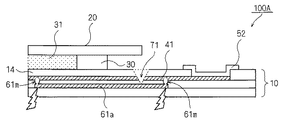
図11は、本発明の実施の形態2に係る表示パネル100Aの一部を示す平面図である。図11は、図3と同様に、表示パネル100Aの一部を拡大した図である。図12は、図11のY5−Y6線に沿った表示パネル100Aの断面図である。なお、本実施の形態に係る表示装置は、表示パネル100Aを含む。
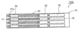
図14は、本発明の実施の形態3に係る表示パネル100Bの一部を示す平面図である。図14は、図3と同様に、表示パネル100Bの一部を拡大した図である。図15は、図14のY7−Y8線に沿った表示パネル100Bの断面図である。なお、本実施の形態に係る表示装置は、表示パネル100Bを含む。
図16は、本発明の実施の形態4に係る表示パネル100Cの一部を示す平面図である。図16は、図3と同様に、表示パネル100Cの一部を拡大した図である。なお、図16では、図の簡略化のため、一部の構成要素(例えば、シール材30)を示していない。
Claims (9)
- 映像を表示するための表示領域と、該表示領域の周辺に形成され、回路部品を実装するための回路部品実装領域とを有する第1基板と、
前記第1基板と対向して配置される第2基板と、を備え、
前記第2基板は、前記第1基板と対向して配置される基板の一部が、前記回路部品実装領域を露出させるための切断ラインに沿って切断されることにより形成されたものであり、
前記第1基板は、
前記表示領域内から前記回路部品実装領域まで延在する第1配線と、
前記第1配線の近傍であって、かつ、前記切断ラインに対応する位置に形成される冗長パターンと、を含む
表示パネル。 - 前記冗長パターンは、前記第1基板の主面に沿った方向において前記第1配線の一部と重なる位置であって、かつ、前記第1基板の厚み方向において前記第1配線と異なる位置に形成される
請求項1に記載の表示パネル。 - 前記表示パネルは、さらに、
前記第1基板と前記第2基板とを接続するシール材を備え、
前記切断ラインは、前記シール材の位置の外側に配置され、
前記冗長パターンは、前記シール材の位置を跨いで延在する
請求項1または2に記載の表示パネル。 - 前記冗長パターンは、該冗長パターンの近傍の前記第1配線に断線箇所が存在する場合、前記断線箇所を挟む前記第1配線の2箇所を電気的に接続するために用いられる
請求項1〜3のいずれか1項に記載の表示パネル。 - 前記冗長パターンは、導体で構成され、
前記冗長パターンおよび前記第1配線の各々は、所定方向に延在し、かつ、互いに近接して設けられ、
前記冗長パターンは、前記断線箇所を挟む前記第1配線の2箇所にそれぞれ近接する、前記冗長パターンの2箇所をレーザー光で照射されることにより、前記第1配線の2箇所を電気的に接続する
請求項4に記載の表示パネル。 - 前記冗長パターンは、コンタクトホールを介して、前記第1配線と電気的に接続されている
請求項1〜3のいずれか1項に記載の表示パネル。 - 前記冗長パターンは、前記第1配線とは異なる第2配線である
請求項1に記載の表示パネル。 - 前記第2配線は、前記第1基板の厚み方向において前記第1配線と略同位置に形成され、
前記第2配線は、前記切断ラインの位置を跨ぐ前記第1配線の2箇所と電気的に接続されている
請求項7に記載の表示パネル。 - 請求項1〜8のいずれか1項に記載の表示パネルを含む表示装置。
Priority Applications (2)
| Application Number | Priority Date | Filing Date | Title |
|---|---|---|---|
| JP2012163408A JP2014021472A (ja) | 2012-07-24 | 2012-07-24 | 表示パネルおよび表示装置 |
| US13/935,869 US20140029228A1 (en) | 2012-07-24 | 2013-07-05 | Display panel and display device |
Applications Claiming Priority (1)
| Application Number | Priority Date | Filing Date | Title |
|---|---|---|---|
| JP2012163408A JP2014021472A (ja) | 2012-07-24 | 2012-07-24 | 表示パネルおよび表示装置 |
Publications (2)
| Publication Number | Publication Date |
|---|---|
| JP2014021472A true JP2014021472A (ja) | 2014-02-03 |
| JP2014021472A5 JP2014021472A5 (ja) | 2015-08-20 |
Family
ID=49994709
Family Applications (1)
| Application Number | Title | Priority Date | Filing Date |
|---|---|---|---|
| JP2012163408A Pending JP2014021472A (ja) | 2012-07-24 | 2012-07-24 | 表示パネルおよび表示装置 |
Country Status (2)
| Country | Link |
|---|---|
| US (1) | US20140029228A1 (ja) |
| JP (1) | JP2014021472A (ja) |
Cited By (4)
| Publication number | Priority date | Publication date | Assignee | Title |
|---|---|---|---|---|
| JP2016206342A (ja) * | 2015-04-20 | 2016-12-08 | 株式会社ジャパンディスプレイ | 表示装置 |
| JP2016212367A (ja) * | 2015-05-05 | 2016-12-15 | 群創光電股▲ふん▼有限公司Innolux Corporation | 表示パネル |
| WO2018155346A1 (ja) * | 2017-02-23 | 2018-08-30 | シャープ株式会社 | 駆動回路、マトリックス基板および表示装置 |
| WO2023100365A1 (ja) * | 2021-12-03 | 2023-06-08 | シャープディスプレイテクノロジー株式会社 | 表示装置 |
Families Citing this family (3)
| Publication number | Priority date | Publication date | Assignee | Title |
|---|---|---|---|---|
| JP6168927B2 (ja) * | 2013-09-05 | 2017-07-26 | 株式会社ジャパンディスプレイ | 表示装置 |
| JP2016120579A (ja) * | 2014-12-25 | 2016-07-07 | オークマ株式会社 | 切削液タンク |
| KR20210144973A (ko) * | 2020-05-21 | 2021-12-01 | 삼성디스플레이 주식회사 | 표시 장치 |
Citations (6)
| Publication number | Priority date | Publication date | Assignee | Title |
|---|---|---|---|---|
| JPH0682815A (ja) * | 1992-08-28 | 1994-03-25 | Sharp Corp | アクティブマトリクス型液晶表示装置 |
| JPH11163479A (ja) * | 1997-09-19 | 1999-06-18 | Toshiba Corp | 配線基板、表示装置のアレイ基板、アレイ基板を備えた液晶表示装置、並びに配線基板およびアレイ基板の製造方法 |
| JP2002258315A (ja) * | 2001-03-01 | 2002-09-11 | Display Technologies Inc | アレイ基板、及びこれを用いる液晶表示装置 |
| JP2003222904A (ja) * | 2002-01-30 | 2003-08-08 | Matsushita Electric Ind Co Ltd | 液晶表示パネル |
| JP2009300634A (ja) * | 2008-06-12 | 2009-12-24 | Epson Imaging Devices Corp | 液晶表示パネル |
| WO2010092725A1 (ja) * | 2009-02-10 | 2010-08-19 | シャープ株式会社 | 接続端子及び該接続端子を備えた表示装置 |
Family Cites Families (5)
| Publication number | Priority date | Publication date | Assignee | Title |
|---|---|---|---|---|
| US20020008799A1 (en) * | 2000-07-10 | 2002-01-24 | Hitachi, Ltd. | Liquid crystal display unit |
| TW472165B (en) * | 1997-09-19 | 2002-01-11 | Toshiba Corp | Array substrate for display device, liquid crystal display device having array substrate and the manufacturing method of array substrate |
| TW556013B (en) * | 1998-01-30 | 2003-10-01 | Seiko Epson Corp | Electro-optical apparatus, method of producing the same and electronic apparatus |
| JP2003222905A (ja) * | 2002-01-30 | 2003-08-08 | Matsushita Electric Ind Co Ltd | 液晶表示装置の製造方法とその修復方法 |
| CN101299124B (zh) * | 2008-06-25 | 2010-06-02 | 昆山龙腾光电有限公司 | 液晶显示装置的阵列基板 |
-
2012
- 2012-07-24 JP JP2012163408A patent/JP2014021472A/ja active Pending
-
2013
- 2013-07-05 US US13/935,869 patent/US20140029228A1/en not_active Abandoned
Patent Citations (6)
| Publication number | Priority date | Publication date | Assignee | Title |
|---|---|---|---|---|
| JPH0682815A (ja) * | 1992-08-28 | 1994-03-25 | Sharp Corp | アクティブマトリクス型液晶表示装置 |
| JPH11163479A (ja) * | 1997-09-19 | 1999-06-18 | Toshiba Corp | 配線基板、表示装置のアレイ基板、アレイ基板を備えた液晶表示装置、並びに配線基板およびアレイ基板の製造方法 |
| JP2002258315A (ja) * | 2001-03-01 | 2002-09-11 | Display Technologies Inc | アレイ基板、及びこれを用いる液晶表示装置 |
| JP2003222904A (ja) * | 2002-01-30 | 2003-08-08 | Matsushita Electric Ind Co Ltd | 液晶表示パネル |
| JP2009300634A (ja) * | 2008-06-12 | 2009-12-24 | Epson Imaging Devices Corp | 液晶表示パネル |
| WO2010092725A1 (ja) * | 2009-02-10 | 2010-08-19 | シャープ株式会社 | 接続端子及び該接続端子を備えた表示装置 |
Cited By (6)
| Publication number | Priority date | Publication date | Assignee | Title |
|---|---|---|---|---|
| JP2016206342A (ja) * | 2015-04-20 | 2016-12-08 | 株式会社ジャパンディスプレイ | 表示装置 |
| JP2016212367A (ja) * | 2015-05-05 | 2016-12-15 | 群創光電股▲ふん▼有限公司Innolux Corporation | 表示パネル |
| US9881969B2 (en) | 2015-05-05 | 2018-01-30 | Innolux Corporation | Display panel |
| US10074691B2 (en) | 2015-05-05 | 2018-09-11 | Innolux Corporation | Display panel |
| WO2018155346A1 (ja) * | 2017-02-23 | 2018-08-30 | シャープ株式会社 | 駆動回路、マトリックス基板および表示装置 |
| WO2023100365A1 (ja) * | 2021-12-03 | 2023-06-08 | シャープディスプレイテクノロジー株式会社 | 表示装置 |
Also Published As
| Publication number | Publication date |
|---|---|
| US20140029228A1 (en) | 2014-01-30 |
Similar Documents
| Publication | Publication Date | Title |
|---|---|---|
| JP2014021472A (ja) | 表示パネルおよび表示装置 | |
| KR101307260B1 (ko) | 라인 온 글라스형 액정표시장치 및 그 제조방법 | |
| US10459265B2 (en) | Display device | |
| US20090167976A1 (en) | Array Substrate of Liquid Crystal Display, Method of Repairing Same, and Liquid Crystal Display | |
| KR20090126052A (ko) | 박막 트랜지스터 기판 및 이를 표함하는 표시 장치 | |
| TWI639878B (zh) | 電子機器及其製造方法 | |
| KR101542205B1 (ko) | 박막 트랜지스터 기판 | |
| JP6980549B2 (ja) | 表示装置 | |
| WO2020119548A1 (zh) | 显示面板的修复方法和显示面板 | |
| WO2011092997A1 (ja) | 表示装置の欠陥修正方法、表示装置およびその製造方法 | |
| KR100695719B1 (ko) | 액정표시장치 | |
| JP2009244598A (ja) | 母基板の分断方法および液晶表示装置の製造方法並びに液晶表示装置 | |
| US6977708B2 (en) | Substrate for liquid crystal display having multiple terminals connected to semiconductor chip, and liquid crystal display having the same | |
| JP6518332B2 (ja) | アレイ基板とその断線補修方法 | |
| JP2016090855A (ja) | 表示装置およびその製造方法 | |
| JP6168777B2 (ja) | 表示パネル及び表示装置ならびに当該表示パネルの製造方法 | |
| KR20070017625A (ko) | 액정 표시 장치와 이의 제조방법 | |
| JP6473692B2 (ja) | 表示パネル | |
| US9268186B2 (en) | Array substrate, display panel and display device | |
| US8164733B2 (en) | Liquid crystal display panel | |
| JP2010271413A (ja) | 基板、表示パネル、表示パネルの修正方法 | |
| KR20150048364A (ko) | 구동 집적회로 패드부 및 이를 포함하는 평판 표시 패널 | |
| JP2021026166A (ja) | 電子素子と液晶表示装置 | |
| JP2001242488A (ja) | 液晶表示装置及びその製造方法 | |
| KR101298341B1 (ko) | 액정표시장치의 어레이 기판 및 그 제조 방법, 그리고액정표시장치의 배선 검사 방법 |
Legal Events
| Date | Code | Title | Description |
|---|---|---|---|
| A521 | Request for written amendment filed |
Free format text: JAPANESE INTERMEDIATE CODE: A523 Effective date: 20150703 |
|
| A621 | Written request for application examination |
Free format text: JAPANESE INTERMEDIATE CODE: A621 Effective date: 20150703 |
|
| A977 | Report on retrieval |
Free format text: JAPANESE INTERMEDIATE CODE: A971007 Effective date: 20160414 |
|
| A131 | Notification of reasons for refusal |
Free format text: JAPANESE INTERMEDIATE CODE: A131 Effective date: 20160419 |
|
| A02 | Decision of refusal |
Free format text: JAPANESE INTERMEDIATE CODE: A02 Effective date: 20161025 |