JP2014021472A - Display panel and display device - Google Patents
Display panel and display device Download PDFInfo
- Publication number
- JP2014021472A JP2014021472A JP2012163408A JP2012163408A JP2014021472A JP 2014021472 A JP2014021472 A JP 2014021472A JP 2012163408 A JP2012163408 A JP 2012163408A JP 2012163408 A JP2012163408 A JP 2012163408A JP 2014021472 A JP2014021472 A JP 2014021472A
- Authority
- JP
- Japan
- Prior art keywords
- substrate
- wiring
- redundant pattern
- display panel
- circuit component
- Prior art date
- Legal status (The legal status is an assumption and is not a legal conclusion. Google has not performed a legal analysis and makes no representation as to the accuracy of the status listed.)
- Pending
Links
Images


Classifications
-
- H—ELECTRICITY
- H05—ELECTRIC TECHNIQUES NOT OTHERWISE PROVIDED FOR
- H05K—PRINTED CIRCUITS; CASINGS OR CONSTRUCTIONAL DETAILS OF ELECTRIC APPARATUS; MANUFACTURE OF ASSEMBLAGES OF ELECTRICAL COMPONENTS
- H05K7/00—Constructional details common to different types of electric apparatus
- H05K7/02—Arrangements of circuit components or wiring on supporting structure
-
- G—PHYSICS
- G02—OPTICS
- G02F—OPTICAL DEVICES OR ARRANGEMENTS FOR THE CONTROL OF LIGHT BY MODIFICATION OF THE OPTICAL PROPERTIES OF THE MEDIA OF THE ELEMENTS INVOLVED THEREIN; NON-LINEAR OPTICS; FREQUENCY-CHANGING OF LIGHT; OPTICAL LOGIC ELEMENTS; OPTICAL ANALOGUE/DIGITAL CONVERTERS
- G02F1/00—Devices or arrangements for the control of the intensity, colour, phase, polarisation or direction of light arriving from an independent light source, e.g. switching, gating or modulating; Non-linear optics
- G02F1/01—Devices or arrangements for the control of the intensity, colour, phase, polarisation or direction of light arriving from an independent light source, e.g. switching, gating or modulating; Non-linear optics for the control of the intensity, phase, polarisation or colour
- G02F1/13—Devices or arrangements for the control of the intensity, colour, phase, polarisation or direction of light arriving from an independent light source, e.g. switching, gating or modulating; Non-linear optics for the control of the intensity, phase, polarisation or colour based on liquid crystals, e.g. single liquid crystal display cells
- G02F1/133—Constructional arrangements; Operation of liquid crystal cells; Circuit arrangements
- G02F1/1333—Constructional arrangements; Manufacturing methods
- G02F1/1345—Conductors connecting electrodes to cell terminals
-
- G—PHYSICS
- G09—EDUCATION; CRYPTOGRAPHY; DISPLAY; ADVERTISING; SEALS
- G09G—ARRANGEMENTS OR CIRCUITS FOR CONTROL OF INDICATING DEVICES USING STATIC MEANS TO PRESENT VARIABLE INFORMATION
- G09G2300/00—Aspects of the constitution of display devices
- G09G2300/04—Structural and physical details of display devices
- G09G2300/0421—Structural details of the set of electrodes
- G09G2300/0426—Layout of electrodes and connections
-
- G—PHYSICS
- G09—EDUCATION; CRYPTOGRAPHY; DISPLAY; ADVERTISING; SEALS
- G09G—ARRANGEMENTS OR CIRCUITS FOR CONTROL OF INDICATING DEVICES USING STATIC MEANS TO PRESENT VARIABLE INFORMATION
- G09G2330/00—Aspects of power supply; Aspects of display protection and defect management
- G09G2330/08—Fault-tolerant or redundant circuits, or circuits in which repair of defects is prepared
-
- G—PHYSICS
- G09—EDUCATION; CRYPTOGRAPHY; DISPLAY; ADVERTISING; SEALS
- G09G—ARRANGEMENTS OR CIRCUITS FOR CONTROL OF INDICATING DEVICES USING STATIC MEANS TO PRESENT VARIABLE INFORMATION
- G09G3/00—Control arrangements or circuits, of interest only in connection with visual indicators other than cathode-ray tubes
- G09G3/20—Control arrangements or circuits, of interest only in connection with visual indicators other than cathode-ray tubes for presentation of an assembly of a number of characters, e.g. a page, by composing the assembly by combination of individual elements arranged in a matrix no fixed position being assigned to or needed to be assigned to the individual characters or partial characters
- G09G3/34—Control arrangements or circuits, of interest only in connection with visual indicators other than cathode-ray tubes for presentation of an assembly of a number of characters, e.g. a page, by composing the assembly by combination of individual elements arranged in a matrix no fixed position being assigned to or needed to be assigned to the individual characters or partial characters by control of light from an independent source
- G09G3/36—Control arrangements or circuits, of interest only in connection with visual indicators other than cathode-ray tubes for presentation of an assembly of a number of characters, e.g. a page, by composing the assembly by combination of individual elements arranged in a matrix no fixed position being assigned to or needed to be assigned to the individual characters or partial characters by control of light from an independent source using liquid crystals
- G09G3/3611—Control of matrices with row and column drivers
- G09G3/3648—Control of matrices with row and column drivers using an active matrix
Abstract
Description
本発明は、断線等の不具合に対処可能な表示パネルおよび表示装置に関する。 The present invention relates to a display panel and a display device that can cope with problems such as disconnection.
あらゆる分野において表示装置は流布している。表示装置は、液晶を利用した液晶表示装置が主流となっている。液晶表示装置は、TFT(Thin Film Transistor)アレイ基板と、TFTアレイ基板と対向して配置される対向基板と、液晶層とを備える。 Display devices are widely used in all fields. As the display device, a liquid crystal display device using a liquid crystal has become the mainstream. The liquid crystal display device includes a TFT (Thin Film Transistor) array substrate, a counter substrate disposed to face the TFT array substrate, and a liquid crystal layer.
TFTアレイ基板は、映像を表示するための表示領域と、当該表示領域の周辺に形成される回路部品実装領域とを有する。表示領域では、複数の縦配線および横配線が交差する。表示領域内の複数の配線には、表示領域の周辺領域の配線から、信号が伝達される。回路部品実装領域には、信号を出力するIC(Integrated Circuit)およびその他の回路部品等が実装される。液晶層は、TFTアレイ基板と対向基板との間に設けられる。 The TFT array substrate has a display area for displaying an image and a circuit component mounting area formed around the display area. In the display area, a plurality of vertical wirings and horizontal wirings intersect. Signals are transmitted to the plurality of wirings in the display area from the wiring in the peripheral area of the display area. In the circuit component mounting area, an IC (Integrated Circuit) that outputs a signal and other circuit components are mounted. The liquid crystal layer is provided between the TFT array substrate and the counter substrate.
液晶表示装置の回路部品実装領域は、対向基板とTFTアレイ基板を重ね合せた後、TFT基板の回路部品実装領域に対向している対向基板の一部を切断して除去することにより露出される。 The circuit component mounting area of the liquid crystal display device is exposed by superposing the counter substrate and the TFT array substrate and then cutting and removing a part of the counter substrate facing the circuit component mounting area of the TFT substrate. .
回路部品実装領域を露出させた後、表示領域の各配線、素子に信号を出力するドライバーIC、ドライバーICを駆動させるための電源、信号を入力する回路基板と接続するFPC等が、回路部品実装領域に実装される。 After the circuit component mounting area is exposed, each wiring in the display area, a driver IC that outputs a signal to the element, a power source for driving the driver IC, an FPC that is connected to a circuit board that inputs the signal, etc. Implemented in the area.
対向基板の一部の除去(対向基板の切断)は、例えば、対向基板の上部にダイヤモンドカッター等により浅い深さの切断ライン(スクライブライン)を付け、当該切断ライン付近に荷重をかけることにより行われる。 Removal of a part of the counter substrate (cutting of the counter substrate) is performed, for example, by attaching a cutting line (scribe line) with a shallow depth to the top of the counter substrate with a diamond cutter or the like and applying a load near the cutting line. Is called.
上記のような切断方法によれば、対向基板の切断工程時に切り粉が発生し、当該切り粉がTFTアレイ基板の表面に付着する。これにより、TFTアレイ基板の保護膜(絶縁膜)にキズが付く場合がある。また、切断工程で発生した、対向基板の端材が、TFTアレイ基板に接触することにより、TFTアレイ基板にキズが付く場合がある。この場合、切り粉が堆積したTFTアレイ基板に過度な荷重が加わった場合、TFTアレイ基板の膜の剥離、断線等の線欠陥等の不良を発生させる可能性がある。 According to the cutting method as described above, chips are generated during the cutting process of the counter substrate, and the chips adhere to the surface of the TFT array substrate. As a result, the protective film (insulating film) of the TFT array substrate may be damaged. In addition, the end material of the counter substrate generated in the cutting process may come into contact with the TFT array substrate, so that the TFT array substrate may be damaged. In this case, when an excessive load is applied to the TFT array substrate on which the chips are deposited, there is a possibility that defects such as line defects such as film peeling and disconnection of the TFT array substrate may occur.
製造工程内で明らかに生じた断線等の線欠陥については、製造工程内での検査での脱落(選別)により排除される。そのため、当該線欠陥は、製品の歩留低下の要因の一つとなっていた。また、断線まで至らないキズがある製品においては、製造工程途中の検査の当該製品のすり抜け(見落とし)により、市場での使用において線欠陥を発生させる可能性もあった。 Line defects such as disconnection that clearly occur in the manufacturing process are eliminated by dropout (selection) in the inspection in the manufacturing process. For this reason, the line defect has been one of the causes of product yield reduction. Further, in the case of a product having a scratch that does not lead to disconnection, there is a possibility that a line defect is generated in use in the market due to passing through (oversight) of the product in the inspection during the manufacturing process.
先行文献1には、表示領域内の配線の断線を修復するための技術(以下、従来技術Aという)が開示されている。従来技術Aでは、ソース配線(ライン)とゲート配線とがクロス(重畳)する箇所以外において、ソース配線とゲート配線との間に導電性ラインを設けた冗長構造を有する。また、従来技術Aでは、断線部分が確認された場合、レーザー光にて、断線部分を有する配線と導電性ラインとを接続することにより、断線部分を修復する。
具体的には、従来技術Aでは、表示領域内において、ゲート配線と、当該ゲート配線の上方に形成されたソース配線との間に、導電性ラインを挟む構成を有する。導電性ラインは、ソース配線およびゲート配線の各々に対し平行に設けられる。また、従来技術Aでは、ソース配線とゲート配線とが重畳するクロス部では、ソース配線に平行な導電性ラインは形成されていない。ソース配線もしくはゲート配線に断線が発生した場合、断線箇所の両端部付近にレーザー光を照射する。これにより、断線部分を有する配線と、当該配線と絶縁膜を介した導電性ラインとを接続することにより、断線部分を修復する。なお、この従来技術Aでは、表示領域内の全ての配線に冗長性を持たせる。 Specifically, the related art A has a configuration in which a conductive line is sandwiched between a gate line and a source line formed above the gate line in the display region. The conductive line is provided in parallel to each of the source wiring and the gate wiring. In the related art A, the conductive line parallel to the source wiring is not formed in the cross portion where the source wiring and the gate wiring overlap. When a disconnection occurs in the source wiring or the gate wiring, laser light is irradiated near both ends of the disconnection part. Thereby, the disconnected portion is repaired by connecting the wiring having the disconnected portion and the conductive line through the wiring and the insulating film. In this prior art A, all the wirings in the display area are made redundant.
しかしながら、従来技術Aの構成では、冗長配線である導電性ラインと、ソース配線またはゲート配線との間に寄生キャパシタンス(容量)が生じる。これにより、従来技術Aの構成を、電気的に駆動させる上で高負荷状態となり、信号の歪み、遅延を誘発させ、製品の性能が低下する原因となる。 However, in the configuration of the conventional technique A, a parasitic capacitance (capacitance) is generated between the conductive line which is a redundant wiring and the source wiring or the gate wiring. As a result, the configuration of the prior art A is in a high load state when electrically driven, which induces signal distortion and delay, causing the product performance to deteriorate.
また画素設計での平面レイアウトでは冗長配線のための場所(空間)が必要となるため、画素の開口部が狭くなり、冗長配線がない場合と同じ表示輝度を得るためにバックライト輝度を上げる等の対策が必要となる。そのため、従来技術Aでは、消費電力の増加等、製品として市場での競争力を低下させる要因を発生させていた。 In addition, since the plane layout in the pixel design requires a place (space) for redundant wiring, the opening of the pixel is narrowed, and the backlight luminance is increased in order to obtain the same display luminance as when there is no redundant wiring. Measures are required. For this reason, in the conventional technique A, factors such as an increase in power consumption, which reduce competitiveness in the market as a product, are generated.
従来技術Aでは、このような要因を潜在的に有しながら、断線等の線欠陥(不具合)は、表示領域内よりも、表示領域外の配線領域(特に、回路部品実装領域)を露出させる際に発生することが多い。すなわち、回路部品実装領域を有する基板における断線は、当該回路部品実装領域を露出させる際に発生する可能性が高い。したがって、回路部品実装領域の近傍において、当該回路部品実装領域を有する基板に形成される配線の断線等の不具合が発生する可能性が高い。 In the prior art A, while having such a factor potentially, a line defect (defect) such as disconnection exposes a wiring region (particularly, a circuit component mounting region) outside the display region rather than within the display region. Often occurs. That is, the disconnection in the substrate having the circuit component mounting area is likely to occur when the circuit component mounting area is exposed. Therefore, in the vicinity of the circuit component mounting region, there is a high possibility that problems such as disconnection of wiring formed on the substrate having the circuit component mounting region will occur.
なお、従来技術Aでは、対向して配置される2枚の基板を用いた構成における回路部品実装領域の近傍に生じる断線等の不具合を修復するための構成については明記されていない。そのため、従来技術Aでは、回路部品実装領域の近傍に生じる断線等の不具合の影響を回避することができないという問題がある。 In the prior art A, a configuration for repairing a defect such as a disconnection that occurs in the vicinity of a circuit component mounting area in a configuration using two substrates arranged opposite to each other is not specified. For this reason, the conventional technique A has a problem that it is not possible to avoid the influence of defects such as disconnection occurring in the vicinity of the circuit component mounting area.
本発明は、このような問題を解決するためになされたものであり、回路部品実装領域の近傍に生じる不具合の影響を回避することが可能な表示パネル等を提供することを目的とする。 The present invention has been made to solve such a problem, and an object of the present invention is to provide a display panel or the like that can avoid the influence of a defect occurring in the vicinity of a circuit component mounting region.
上記目的を達成するために、本発明の一態様に係る表示パネルは、映像を表示するための表示領域と、該表示領域の周辺に形成され、回路部品を実装するための回路部品実装領域とを有する第1基板と、前記第1基板と対向して配置される第2基板と、を備え、前記第2基板は、前記第1基板と対向して配置される基板の一部が、前記回路部品実装領域を露出させるための切断ラインに沿って切断されることにより形成されたものであり、前記第1基板は、前記表示領域内から前記回路部品実装領域まで延在する第1配線と、前記第1配線の近傍であって、かつ、前記切断ラインに対応する位置に形成される冗長パターンとを含む。 In order to achieve the above object, a display panel according to an aspect of the present invention includes a display area for displaying an image, a circuit component mounting area for mounting a circuit component, which is formed around the display area. A first substrate having a second substrate disposed opposite to the first substrate, wherein the second substrate includes a portion of the substrate disposed opposite to the first substrate, The first substrate is formed by cutting along a cutting line for exposing the circuit component mounting region, and the first substrate includes first wiring extending from the display region to the circuit component mounting region. And a redundant pattern formed in the vicinity of the first wiring and at a position corresponding to the cutting line.
本発明によれば、回路部品実装領域を有する第1基板は、第1配線と、冗長パターンとを含む。第2基板は、前記第1基板と対向して配置される基板の一部が、前記回路部品実装領域を露出させるための切断ラインに沿って切断されることにより形成されたものである。前記第1配線は、前記表示領域内から前記回路部品実装領域まで延在する。前記冗長パターンは、前記第1配線の近傍であって、かつ、前記切断ラインに対応する位置に形成される。 According to the present invention, the first substrate having the circuit component mounting area includes the first wiring and the redundant pattern. The second substrate is formed by cutting a part of the substrate disposed facing the first substrate along a cutting line for exposing the circuit component mounting region. The first wiring extends from the display area to the circuit component mounting area. The redundant pattern is formed in the vicinity of the first wiring and at a position corresponding to the cutting line.
これにより、回路部品実装領域の近傍において生じる可能性が高い、回路部品実装領域を有する第1基板に含まれる第1配線の断線等の不具合の影響を回避することができる。すなわち、回路部品実装領域の近傍に生じる不具合の影響を回避することができる。 Thereby, it is possible to avoid the influence of problems such as disconnection of the first wiring included in the first substrate having the circuit component mounting area, which is highly likely to occur in the vicinity of the circuit component mounting area. That is, it is possible to avoid the influence of a defect that occurs in the vicinity of the circuit component mounting area.
以下、図面を参照しつつ、本発明の実施の形態について説明する。以下の説明では、同一の構成要素には同一の符号を付してある。それらの名称および機能も同じである。したがって、適宜、重複する説明は省略する場合がある。 Hereinafter, embodiments of the present invention will be described with reference to the drawings. In the following description, the same components are denoted by the same reference numerals. Their names and functions are also the same. Therefore, the overlapping description may be omitted as appropriate.
なお、実施の形態において例示される各構成要素の寸法、材質、形状、それらの相対配置などは、本発明が適用される装置の構成や各種条件により適宜変更されるものであり、本発明はそれらの例示に限定されるものではない。また、各図における各構成要素の寸法は、実際の寸法と異なる場合がある。 It should be noted that the dimensions, materials, shapes, relative arrangements, and the like of the constituent elements exemplified in the embodiments are appropriately changed depending on the configuration of the apparatus to which the present invention is applied and various conditions. It is not limited to those examples. Moreover, the dimension of each component in each figure may differ from an actual dimension.
<実施の形態1>
図1は、本発明の実施の形態1に係る表示装置1000の構成を示す平面図である。表示装置1000は、一例として、液晶表示装置である。なお、表示装置1000は、液晶表示装置に限定されず、対向して配置される2枚の基板を用いた構成を有する他の方式の表示装置であってもよい。
<
FIG. 1 is a plan view showing a configuration of a
図1において、X,Y,Z方向の各々は、互いに直交する。以下の図に示されるX,Y,Z方向の各々も、互いに直交する。以下においては、X方向と、当該X方向の反対の方向(−X方向)とを含む方向をX軸方向ともいう。また、以下においては、Y方向と、当該Y方向の反対の方向(−Y方向)とを含む方向をY軸方向ともいう。また、以下においては、Z方向と、当該Z方向の反対の方向(−Z方向)とを含む方向をZ軸方向ともいう。 In FIG. 1, the X, Y, and Z directions are orthogonal to each other. The X, Y, and Z directions shown in the following figures are also orthogonal to each other. Hereinafter, a direction including the X direction and the direction opposite to the X direction (−X direction) is also referred to as an X-axis direction. In the following, the direction including the Y direction and the direction opposite to the Y direction (−Y direction) is also referred to as a Y-axis direction. In the following, a direction including the Z direction and a direction opposite to the Z direction (−Z direction) is also referred to as a Z-axis direction.
表示装置1000は、表示パネル100を含む。表示パネル100は、一例として、液晶表示パネルである。なお、表示パネル100は、液晶表示パネルに限定されず、対向して配置される2枚の基板を用いた構成を有する他の方式の表示パネルであってもよい。なお、表示装置1000は、表示パネル100を制御するための、図示しない回路等も含む。
The
表示パネル100は、基板10,20を備える。なお、基板10,20の詳細は後述する。なお、図1では、構造を分かりやすくするために、基板20を透過させて示している。また、表示パネル100は、表示領域R10と、回路部品実装領域R20とを有する。表示領域R10は、映像(画像)を表示するための領域である。表示領域R10は、行列上に配列された、図示しない複数の画素部(画素)から構成される。
The
回路部品実装領域R20は、回路部品を実装するための領域である。図1に示すように、回路部品実装領域R20は、基板10のうち基板20が存在しない領域である。図1では、一例として、回路部品実装領域R20の形状は、L字状である。回路部品実装領域R20は、表示領域R10の周辺領域に含まれる。すなわち、回路部品実装領域R20は、表示領域R10の周辺に形成される。
The circuit component mounting region R20 is a region for mounting circuit components. As shown in FIG. 1, the circuit component mounting region R <b> 20 is a region of the
表示パネル100は、さらに、複数のソース配線41と、複数のゲート配線42と、FPC(Flexible Printed Circuits)40a,40bとを備える。
The
複数のソース配線41は、表示領域R10において、垂直方向(Y軸方向)に延在する。各ソース配線41は、データ信号を、対応する画素部に伝達する。
The plurality of
複数のゲート配線42は、表示領域R10において、水平方向(X軸方向)に延在する。各ゲート配線42は、データを蓄える画素部(画素)を選択するために利用される。各ゲート配線42は、表示領域R10内から回路部品実装領域R20まで延在する。
The plurality of
なお、図1では、図を簡略化するために、複数のゲート配線42の一部と、複数のソース配線41の一部とが、回路部品実装領域R20まで延在していないように示される。実際には、表示パネル100に含まれる複数のゲート配線42およびソース配線41は、回路部品実装領域R20まで延在する。
In FIG. 1, in order to simplify the drawing, a part of the plurality of
回路部品実装領域R20には、コンタクト領域が形成される。コンタクト領域には、FPC40a,40bが接続される。 A contact region is formed in the circuit component mounting region R20. FPCs 40a and 40b are connected to the contact area.
FPC40a,40bの各々には、ドライバーICが実装される。また、FPC40a,40bの各々には、後述の透明電極52が形成される。
A driver IC is mounted on each of the
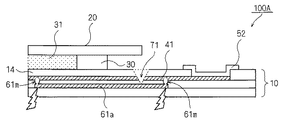
図2は、本発明の実施の形態1に係る表示パネル100の断面図である。具体的には、図2は、図1のY1−Y2線に沿った表示パネル100の断面図である。
FIG. 2 is a cross-sectional view of
図1および図2を参照して、表示パネル100は、さらに、液晶層31と、シール材30とを備える。
Referring to FIGS. 1 and 2,
基板10は、アレイ状に形成された複数のTFTを有するTFTアレイ基板である。基板10は、表示領域R10と、回路部品実装領域R20とを有する。また、基板10は、表示領域R10内から回路部品実装領域R20内まで延在するソース配線41を含む。すなわち、ソース配線41は、表示領域R10内から回路部品実装領域R20まで延在する。
The
基板20は、基板10と対向して配置される対向基板(カラーフィルター基板)である。
The
基板10と基板20とは、表示領域R10の最外周のブラックマトリクス領域(BM領域)下で、シール材30により接続されている。すなわち、シール材30は、基板10と基板20とを接続する。シール材30は、Y軸方向において、表示領域R10と回路部品実装領域R20との間に形成される。当該Y軸方向は、基板10の主面に沿った方向である。基板10の主面とは、基板20と対向する、基板10の面である。
The
図3は、本発明の実施の形態1に係る表示パネル100の一部を示す平面図である。具体的には、図3は、図1のY1−Y2線の近傍の拡大図である。図4は、図3のY3−Y4線に沿った表示パネル100の断面図である。
FIG. 3 is a plan view showing a part of the
図3および図4を参照して、基板10は、ガラス基板11と、層間絶縁膜12と、パッシベーション膜14と、前述のソース配線41と、前述のゲート配線42と、後述の冗長パターン61とを含む。
3 and 4,
ガラス基板11上には、ゲート配線42(ゲート配線膜)が積層される。また、ガラス基板11上には、ゲート配線42および後述の冗長パターン61を覆うように層間絶縁膜12が積層される。層間絶縁膜12は、例えば、シリコン窒化膜である。
A gate wiring 42 (gate wiring film) is stacked on the
層間絶縁膜12上において、スイッチング素子であるTFTを形成するためのアモルファスシリコン膜(図示せず)をパターニング後、ソース配線41(ソース配線膜)が形成される。
A source wiring 41 (source wiring film) is formed on the
後述の冗長パターン61およびソース配線41の各々は、所定方向(Y軸方向)に延在する。また、冗長パターン61およびソース配線41の各々は、互いに近接して設けられる。ソース配線41上には、パッシベーション膜14および透明電極52が形成される。
Each of a later-described
対向基板としての基板20は、詳細は後述するが、図示しないブラックマトリクス層、色材層および透明電極等を含む。
The
基板10の表面および、当該基板10の表面に対向する、基板20の表面には、図示しない配向膜が塗布される。液晶層31は、基板10と基板20との間に設けられる。具体的には、液晶層31は、基板10、基板20およびシール材30で構成される空間に設けられる。なお、図4では、液晶層31の存在を分かりやすくするために、液晶層31の厚みを誇張して示してしる。実際には、液晶層31の厚みは、基板10,20等の厚みよりも、大幅に薄い。そのため、基板10は、基板20の近傍に設けられる。
An alignment film (not shown) is applied to the surface of the
次に、TFTアレイ基板である基板10の製造工程について、図5および図6を用いて説明する。図5は、基板10全体を示す平面図である。図5において、基板10は、前述したように、表示領域R10と、回路部品実装領域R20とを有する。図6は、基板10の製造工程を示す断面図である。表示領域R10の周辺には、回路部品実装領域R20を含む周辺領域が設けられる。
Next, a manufacturing process of the
まず、ゲート配線形成工程において、図6(a)に示すように、ガラス基板11上にゲート配線42を形成するために、スパッタ装置によりガラス基板11上に金属膜が成膜される。その後、写真製版装置により、レジスト塗布、パターン露光、現像が行われ、当該金属膜をエッチングにより加工することにより、表示領域R10に、ゲート配線42が形成される。
First, in the gate wiring formation step, as shown in FIG. 6A, in order to form the
このゲート配線形成工程において、ガラス基板11のうち、基板20の後述の切断ラインL1と対向する位置に、冗長パターン61が形成される。冗長パターン61は、ソース配線41が延在する方向(Y軸方向)に沿って延在する。冗長パターン61は、導体(例えば、金属)で構成される。
In this gate wiring formation step, a
その後、図6(b)に示すように、CVD装置にて、層間絶縁膜12(シリコン窒化膜)が形成される。次に、図6(c)に示すように、アモルファスシリコン層が成膜される。当該アモルファスシリコン層は、表示領域内の画素内のTFTを形成するための層である。そして、写真製版(レジスト塗布、パターン露光、現像、レジスト除去)、エッチングにより、アモルファスシリコン膜13が形成される。
Thereafter, as shown in FIG. 6B, an interlayer insulating film 12 (silicon nitride film) is formed by a CVD apparatus. Next, as shown in FIG. 6C, an amorphous silicon layer is formed. The amorphous silicon layer is a layer for forming a TFT in a pixel in the display area. Then, the
次に、図6(d)に示すように、ソース配線41を形成するために、スパッタ装置により金属膜が成膜される。その後、写真製版(レジスト塗布、パターン露光、現像、レジスト除去)、エッチングが行われることにより、ソース配線41(ソース配線膜)が形成される。これにより、基板20の切断ラインL1に対向する(相当する)箇所にて、前述のゲート配線形成工程で形成した冗長パターン61とソース配線41とが層間絶縁膜12の一部を挟んだ構造となる。
Next, as shown in FIG. 6D, in order to form the
図6(e)に示すように、さらに、CVD装置により、保護膜(絶縁膜)としてのパッシベーション膜14が成膜される。パッシベーション膜14は、例えば、シリコン窒化膜である。そして、写真製版(レジスト塗布、パターン露光、現像、レジスト除去)により、ゲート配線金属膜上、ソース配線41上にコンタクトホールが形成される。
As shown in FIG. 6E, a
最後に、図6(f)に示すように、スパッタ装置により、透明電極膜が成膜され、表示領域の画素内の透明電極、回路部品実装領域R20のコンタクトホールに、透明電極52が形成される。以上により、図2および図6(f)に示すように、前述の冗長パターン61を含む基板10が形成される。
Finally, as shown in FIG. 6 (f), a transparent electrode film is formed by a sputtering apparatus, and a
その後、基板10と対向するように、図7の基板20n(対向基板)が設けられる。すなわち、基板20n(対向基板)は、基板10(TFTアレイ基板)と重ね合うように設けられる。ここで、基板20nは、回路部品実装領域R20を露出させるための当該基板20nの一部(領域R21)が切断される前の基板である。基板20nは、基板10と同じサイズである。基板20nは、基板10の回路部品実装領域R20と対向する領域R21を有する。領域R21の部分は、基板20nの不要な部分である。基板20nの領域R21は、ガラスを含む材料で構成される。
Thereafter, the
次に、図8を用いて、回路部品実装領域R20を露出させるまでの工程について説明する。図8は、回路部品実装領域R20を露出させるまでの工程を説明するための図である。 Next, a process until the circuit component mounting region R20 is exposed will be described with reference to FIG. FIG. 8 is a diagram for explaining a process until the circuit component mounting region R20 is exposed.
図8(a)に示すように、基板20n(対向基板)は、ガラス基板21、ブラックマトリクス領域22、色材層23および透明電極24から構成される。
As shown in FIG. 8A, the
ブラックマトリクス領域22は、表示領域R10の周辺に設けられる。すなわち、ブラックマトリクス領域22は、表示領域R10外に設けられる。
The
基板10の表面および、当該基板10の表面に対向する、基板20nの表面には、図示しない配向膜が塗布される。当該配向膜は、表示領域R10内の液晶層31の液晶の配向を定めるための膜である。配向膜が塗布された基板10および基板20nの表面は、ラビング布にて処理される。なお、図8(a)では、配向膜塗布、ラビングは図示していない。
An alignment film (not shown) is applied to the surface of the
次に、基板20nのブラックマトリクス領域22にシール材30が塗布される。シール材30が塗布された基板20nが、基板10(TFTアレイ基板)と重ね合うように配置される。これにより、図8(a)の構成となる。
Next, the sealing
次に、切断工程が行われる。切断工程では、図8(b)に示すように、基板10の回路部品実装領域R20を露出させるために、基板20nの一部に、鉛直方向に沿った切断ラインL1を形成する。切断ラインL1は、図7の領域R21の部分を切断するためのラインである。すなわち、切断ラインL1は、回路部品実装領域R20を露出させるためのラインである。つまり、切断ラインL1のY軸方向の位置は、回路部品実装領域R20の一方の端の位置である。前述したように、Y軸方向は、基板10の主面に沿った方向である。
Next, a cutting process is performed. In the cutting step, as shown in FIG. 8B, in order to expose the circuit component mounting region R20 of the
そのため、切断ラインL1は、基板20n(基板10)の主面に沿った方向(Y軸方向)において回路部品実装領域R20の端部近傍に配置される。すなわち、切断ラインL1は、基板20n(基板10)の主面に沿った方向(Y軸方向)においてシール材30の位置の外側に配置される。切断ラインL1は、ダイヤモンドカッター、ホイール装置等により形成される。
Therefore, the cutting line L1 is disposed in the vicinity of the end of the circuit component mounting region R20 in the direction (Y-axis direction) along the main surface of the
切断ラインL1を形成した後、図8(c)に示すように、切断ラインL1を加圧することにより、領域R21の部分(基板20nの不要な部分)が切断される。以下においては、領域R21の部分を、端材21nとも表記する。なお、基板20nのうち、領域R21の部分(端材21n)が切断されることにより、前述の基板20が形成される。すなわち、基板20は、基板10と対向して配置される基板20nの一部(端材21n)が、切断ラインL1に沿って切断されることにより形成されたものである。したがって、切断ラインL1は、Y軸方向において、基板20の端面の位置に相当する。
After forming the cutting line L1, as shown in FIG. 8C, the cutting line L1 is pressurized to cut the region R21 (unnecessary portion of the
以上により、図8(c)、図3および図4に示すように、基板10のうち、基板20nの切断ラインL1と対向する位置に、冗長パターン61が形成される。具体的には、冗長パターン61は、基板10の主面に沿った方向においてソース配線41の一部と重なる位置であって、かつ、基板10の厚み方向においてソース配線41と異なる位置に形成される。すなわち、冗長パターン61は、ソース配線41の近傍であって、かつ、切断ラインL1に対応(対向)する位置に形成される。
As described above, as shown in FIGS. 8C, 3 and 4, the
なお、図4および図8(c)に示すように、冗長パターン61は、当該冗長パターン61のY軸方向の中心部の位置が、切断ラインL1と対向する位置になるように設けられる。当該Y軸方向は、基板10の主面に沿った方向である。
As shown in FIGS. 4 and 8C, the
なお、冗長パターン61は、当該冗長パターン61のY軸方向の中心部の位置が、切断ラインL1と対向する位置の近傍の位置になるように、設けられてもよい。
Note that the
この後、基板10、基板20およびシール材30により形成される空間に、液晶が注入されることにより、液晶層31が形成される。これにより、表示パネル100が作製される。
Thereafter, a
なお、図8(d)に示すように、端材21nが切断される際に、端材21nが基板10に接触する場合がある。この場合、切断工程で発生した切り粉が堆積している基板10の表面部(パッシベーション膜14)および当該パッシベーション膜14の下のソース配線41に対し、キズ71がつき、ソース配線41が断線する場合がある。すなわち、回路部品実装領域R20および回路部品実装領域R20の近傍は、断線等の不具合が発生する可能性が高い。
As shown in FIG. 8D, the
そこで、作製された表示パネル100は、回路部品実装領域R20に回路部品が実装される前に、表示検査が行われる。この表示検査では、ソース配線41等の配線の断線等の不具合を見つけるための検査が実施される。
Therefore, display inspection of the manufactured
本実施の形態では、検査により、断線した配線、または、断線の発生の可能性のある配線等が検出された場合、リペア処理が行われる。 In the present embodiment, the repair process is performed when a disconnected wiring or a wiring that may cause a disconnection is detected by the inspection.
次に、本実施の形態において、断線等の不具合が検出された場合に行われるリペア処理について説明する。 Next, a repair process performed when a defect such as a disconnection is detected in the present embodiment will be described.
ここで、図9に示すように、前述の切断工程において、ソース配線41を断線するキズ71が生じたとする。この場合、リペア処理では、レーザーリペア装置等が、基板10の裏面から、キズ71(断線箇所)を挟むソース配線41の2箇所にそれぞれ近接する、冗長パターン61の2箇所をレーザー光で照射する。これにより、冗長パターン61の一部が融解し、融解部61mが生じる。融解部61mにより、キズ71を挟むソース配線41の2箇所が、冗長パターン61を介して、電気的に接続される。すなわち、冗長パターン61は、断線箇所(キズ71)を挟むソース配線41の2箇所にそれぞれ近接する、冗長パターン61の2箇所をレーザー光で照射されることにより、当該ソース配線41の2箇所を電気的に接続する。つまり、冗長パターン61は、断線箇所接続用パターンである。
Here, as shown in FIG. 9, it is assumed that a
以上により、冗長パターン61は、当該冗長パターン61の近傍のソース配線41に断線箇所(キズ71)が存在する場合、断線箇所(キズ71)を挟むソース配線41の2箇所を電気的に接続するために用いられる。すなわち、冗長パターン61は、ソース配線41の断線等の不具合の影響を回避するためのパターンである。
As described above, the
これにより、ソース配線41を断線するキズ71が発生した箇所を回避して、ソース配線41の断線が修復される。そのため、製造歩留の低下を抑制することが可能となる。
Thereby, the location where the
以上説明したように、本実施の形態によれば、回路部品実装領域R20を有する基板10は、ソース配線41と、冗長パターン61とを含む。基板20は、基板10と対向して配置される基板20nの一部が、回路部品実装領域R20を露出させるための切断ラインL1に沿って切断されることにより形成されたものである。ソース配線41は、表示領域R10内から回路部品実装領域R20まで延在する。冗長パターン61は、ソース配線41の近傍であって、かつ、基板10において、切断ラインL1に対応(対向)する位置に形成される。
As described above, according to the present embodiment, the
これにより、回路部品実装領域R20の近傍において生じる可能性が高い、基板10に含まれる配線(例えば、ソース配線41)の断線等の不具合の影響を回避することができる。すなわち、回路部品実装領域R20の近傍に生じる不具合の影響を回避することができる。
Thereby, it is possible to avoid the influence of problems such as disconnection of wiring (for example, source wiring 41) included in the
また、言い換えれば、本実施の形態の構成によれば、基板10の回路部品実装領域R20を露出させるための切断ラインL1と対向する基板10に、冗長パターン61を設ける。冗長パターン61は、ソース配線41の近傍であって、かつ、切断ラインL1に対向(対応)する位置に形成される。また、冗長パターン61は、当該ソース配線41と、冗長パターン61との間に層間絶縁膜12を挟むように設けられる。
In other words, according to the configuration of the present embodiment, the
この構成により、対向基板(基板20n)の切断工程において、切断された端材等によりソース配線41を断線するキズが発生した場合であっても、レーザーリペア等により、当該キズが発生した箇所を有するソース配線41の断線を修復することができる。これにより、表示パネルの特性の劣化、表示パネルの設計自由度を低減させることなく、断線等による製造歩留の低下を抑制することが可能となる。したがって、本実施の形態によれば、信頼性の高い表示パネルおよび当該表示パネルを含む表示装置を提供することができる。
With this configuration, in the cutting process of the counter substrate (
また、上記説明では、冗長パターン61は、ソース配線41に対する断線等の不具合の影響を回避するために形成されていた。すなわち、冗長パターン61は、ソース配線41に対応づけて形成されていたがこれに限定されない。冗長パターン61は、ゲート配線42に対応づけて形成するようにしてもよい。
In the above description, the
具体的には、冗長パターン61は、ソース配線41が延在する方向(Y軸方向)に沿って延在するとしたがこれに限定されない。冗長パターン61は、ゲート配線42が延在する方向(X軸方向)に沿って延在するように設けてもよい。この場合、冗長パターン61は、図3において、ソース配線41およびゲート配線42を、それぞれ、ゲート配線42およびソース配線41に置き換えた構成に設けられる。この構成の場合においても、上記と同様な効果を得ることができる。すなわち、ゲート配線42に、当該ゲート配線42を断線するキズが発生した場合であっても、図9で説明したリペア処理と同様な処理により、ゲート配線42の断線を修復することができる。
Specifically, although the
なお、冗長パターン61の表面に識別マークを明記してもよい。図10は、識別マークを明記した冗長パターン61を示す図である。図10(a)は、図3を簡略化して示した図である。図10(b)は、冗長パターン61の表面に識別マーク62を明記した状態を示す図である。識別マーク62は、例えば、配線アドレスである。
An identification mark may be specified on the surface of the
このように、冗長パターン61の表面に識別マークを明記することにより、配線の断線時における配線の修復とともに、識別マークを配線アドレスとして利用することも可能である。
Thus, by specifying the identification mark on the surface of the
<実施の形態2>
図11は、本発明の実施の形態2に係る表示パネル100Aの一部を示す平面図である。図11は、図3と同様に、表示パネル100Aの一部を拡大した図である。図12は、図11のY5−Y6線に沿った表示パネル100Aの断面図である。なお、本実施の形態に係る表示装置は、表示パネル100Aを含む。
<Embodiment 2>
FIG. 11 is a plan view showing part of the
図11および図12を参照して、表示パネル100Aは、実施の形態1に係る表示パネル100と比較して、冗長パターン61の代わりに冗長パターン61aを含む点が異なる。表示パネル100Aのそれ以外の構成は、表示パネル100と同様なので詳細な説明は繰り返さない。
Referring to FIGS. 11 and 12,
冗長パターン61aは、図4の冗長パターン61と比較して、長さが異なる。冗長パターン61aのそれ以外の構成は、冗長パターン61と同様なので詳細な説明は繰り返さない。
The
冗長パターン61aは、冗長パターン61と同様に、前述のゲート配線形成工程において形成される。冗長パターン61aおよびソース配線41の各々は、所定方向(Y軸方向)に延在する。また、冗長パターン61およびソース配線41の各々は、互いに近接して設けられる。
The
さらに、冗長パターン61aは、シール材30の位置を跨いで延在する。すなわち、冗長パターン61aは、回路部品実装領域R20内から表示領域R10内まで延在する。つまり、冗長パターン61aの一方の端部が、表示パネル100Aにおいて、シール材30の位置より、内側に配置される。したがって、冗長パターン61aに対するレーザー光によるダメージが大気中に曝され、腐食等の不具合が発生する可能性を低減させることができる。
Further, the
なお、図13に示すように、表示パネル100Aの製造途中の前述の切断工程において、ソース配線41を断線するキズ71が生じたとする。この場合、実施の形態1と同様に、リペア処理が行われる。すなわち、レーザーリペア装置等が、キズ71(断線箇所)を挟むソース配線41の2箇所にそれぞれ近接する、冗長パターン61aの2箇所をレーザー光で照射する。これにより、冗長パターン61aの一部が融解し、融解部61mが生じる。融解部61mにより、キズ71を挟むソース配線41の2箇所が、冗長パターン61aを介して、電気的に接続される。すなわち、冗長パターン61aは、断線箇所(キズ71)を挟むソース配線41の2箇所にそれぞれ近接する、冗長パターン61aの2箇所をレーザー光で照射されることにより、当該ソース配線41の2箇所を電気的に接続する。
As shown in FIG. 13, it is assumed that a
以上により、冗長パターン61aは、当該冗長パターン61aの近傍のソース配線41に断線箇所(キズ71)が存在する場合、断線箇所(キズ71)を挟むソース配線41の2箇所を電気的に接続するために用いられる。すなわち、冗長パターン61aは、ソース配線41の断線等の不具合の影響を回避するためのパターンである。すなわち、冗長パターン61aは、ソース配線41の断線等の不具合の影響を回避するためのパターンである。
As described above, the
これにより、ソース配線41を断線するキズ71が発生した箇所を回避して、ソース配線41の断線が修復される。そのため、製造歩留の低下を抑制することが可能となる。
Thereby, the location where the
なお、実施の形態1の表示パネル100では、狭領域に、レーザー光による接続箇所を2箇所設ける必要がある。そのため、レーザー光による接続のための、ある程度の大きさの領域が必要になる。
Note that in the
一方、本実施の形態では、図13に示すように、冗長パターン61aにおいてレーザー光が照射される2箇所は十分に離れている。そのため、レーザー光による接続のための領域を大きくする必要がない。そのため、表示パネル100のサイズの拡大を抑制することが可能となる。
On the other hand, in the present embodiment, as shown in FIG. 13, the two places where the laser beam is irradiated in the
なお、本実施の形態の表示パネル100Aにおいても、実施の形態1と同様、冗長パターン61aは、ソース配線41の代わりにゲート配線42に対応づけて形成されてもよい。すなわち、冗長パターン61aは、ゲート配線42の不具合の影響を回避するために、ゲート配線42が延在する方向(X軸方向)に沿って延在するように設けてもよい。
In the
<実施の形態3>
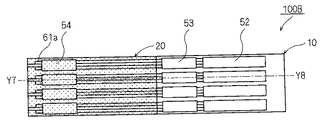
図14は、本発明の実施の形態3に係る表示パネル100Bの一部を示す平面図である。図14は、図3と同様に、表示パネル100Bの一部を拡大した図である。図15は、図14のY7−Y8線に沿った表示パネル100Bの断面図である。なお、本実施の形態に係る表示装置は、表示パネル100Bを含む。
<Embodiment 3>
FIG. 14 is a plan view showing part of the
図14および図15を参照して、表示パネル100Bは、図12の表示パネル100Aと比較して、さらに、導電膜53,54を含む点が異なる。表示パネル100Bのそれ以外の構成は、表示パネル100Aと同様なので詳細な説明は繰り返さない。
14 and 15,
表示パネル100Bの基板10には、コンタクトホールh1,h2が形成される。コンタクトホールh1,h2は、図6(f)の状態の基板10のパッシベーション膜14および層間絶縁膜12に形成される。冗長パターン61aは、コンタクトホールh1,h2を介して、ソース配線41と電気的に接続されている。なお、導電膜53,54は、コンタクトホールh1,h2の形成後に、形成される。
Contact holes h1 and h2 are formed in the
以下具体的に説明する。コンタクトホールh1には導電膜53が形成される。導電膜53は、冗長パターン61aの一方の端部とソース配線41とを電気的に接続する。コンタクトホールh2には導電膜54が形成される。導電膜54は、冗長パターン61aの他方の端部とソース配線41とを電気的に接続する。すなわち、冗長パターン61aと、ソース配線41とは、電気的に並列接続されている。
This will be specifically described below. A
上記構成により、例えば、前述の切断工程において、ソース配線41のうち、切断ラインL1と対向する部分に、キズが生じたとする。この場合においても、キズを挟むソース配線41の2箇所が、導電膜53,54および冗長パターン61aにより、電気的に接続された状態が維持される。そのため、ソース配線41の断線を防止することができる。すなわち、本実施の形態における冗長パターン61aは、ソース配線41の断線等の不具合の影響を回避するためのパターンである。
With the above configuration, for example, it is assumed that a scratch is generated in a portion of the
また、上記構成により、製造工程内での検査を不要にすることができる。また、市場で製品(表示パネル100Bを含む表示装置)が使用されても、断線の後れ発生を防止することができる。
Moreover, the said structure can make the test | inspection in a manufacturing process unnecessary. Even if a product (a display device including the
また、上記構成によれば、実施の形体1,2のように、冗長パターン61を利用したレーザー光を用いたリペア処理を行う必要がない。そのため、レーザー光照射による照射部分のダメージの影響、レーザー光の接続による2箇所の金属のコンタクト特性の不安定性要因を排除することができる。その結果、本実施の形態によれば、実施の形態1,2よりも、さらに高い信頼性のある表示パネルおよび当該表示パネルを含む表示装置を得ることが可能となる。
Moreover, according to the said structure, it is not necessary to perform the repair process using the laser beam using the
なお、本実施の形態の表示パネル100Bにおいても、実施の形態1と同様、冗長パターン61aは、ソース配線41の代わりにゲート配線42に対応づけて形成されてもよい。すなわち、冗長パターン61aは、ゲート配線42の不具合の影響を回避するために、ゲート配線42が延在する方向(X軸方向)に沿って延在するように設けてもよい。この場合、導電膜53,54は、冗長パターン61aの一方の端部および他方の端部を、ゲート配線42と電気的に接続するように設けられる。
In the
<実施の形態4>
図16は、本発明の実施の形態4に係る表示パネル100Cの一部を示す平面図である。図16は、図3と同様に、表示パネル100Cの一部を拡大した図である。なお、図16では、図の簡略化のため、一部の構成要素(例えば、シール材30)を示していない。
<Embodiment 4>
FIG. 16 is a plan view showing a part of the
図17は、図16のY9−Y10線に沿った表示パネル100Cの断面図である。なお、本実施の形態に係る表示装置は、表示パネル100Cを含む。
FIG. 17 is a cross-sectional view of the
図16および図17を参照して、表示パネル100Cは、図12の表示パネル100Aと比較して、冗長パターン61aの代わりに冗長パターン41aを含む点が異なる。
Referring to FIGS. 16 and 17,
冗長パターン41aは、第1配線としてのソース配線41とは異なる接続配線(第2配線)である。冗長パターン41aは、基板10の厚み方向(Z軸方向)においてソース配線41と略同位置に形成される。冗長パターン41aは、ソース配線41における基板10の主面方向に沿って設けられる。すなわち、図16において、基板10のうち、切断ラインL1を挟む箇所の近傍には、冗長パターンを含む複数の配線が平面的に配置される。
The
また、冗長パターン41aは、切断ラインL1の位置を跨ぐソース配線41の2箇所と電気的に接続されている。具体的には、冗長パターン41aは、ソース配線41のうち切断ラインL1に対向する(対応する)部分(部分41x)を挟むソース配線41の2箇所と電気的に接続されている。すなわち、冗長パターン41aは、ソース配線41と電気的に並列接続される。
Further, the
これにより、冗長パターン41aは、ソース配線41のバイパスパターンとして機能する。すなわち、本実施の形態では、ソース配線41の一部にバイパスパターン(冗長パターン41a)を形成する。以上により、表示パネル100Cは、同一の配線層において複数の配線が並列接続された冗長構成を有する。
As a result, the
以上の構成により、本実施の形態では、例えば、前述の切断工程において、ソース配線41の部分41x近傍にキズが発生したとしても、レーザー光によりリペア処理を行う必要がない。また、本実施の形態の構成では、実施の形態3のように、コンタクトホールを形成して、ソース配線41と冗長パターンとを接続する必要がない。したがって、本実施の構成によれば、実施の形態3よりも、特性が安定し、高い信頼性のある表示パネルおよび当該表示パネルを含む表示装置を得ることが可能となる。
With the above configuration, in the present embodiment, for example, even if a flaw occurs in the vicinity of the
なお、上記において、配線(ソース配線41)の一部にバイパスパターン(冗長パターン41a)を形成する構成としたが、この構成に限定されない。例えば、冗長パターン41aの一方の端部は、ソース配線41と接続しない構成としてもよい。この構成において、断線等の不具合が発生した場合、前述のリペア処理と同様に、冗長パターン41aの一方の端部にレーザー光を照射し、冗長パターン41aの一方の端部とソース配線41とを接続する。これより、実施の形態1と同様な効果を得ることができる。
In the above description, the bypass pattern (
なお、本実施の形態の表示パネル100Cにおいても、実施の形態1と同様、冗長パターン41aは、ソース配線41の代わりにゲート配線42に対応づけて形成されてもよい。すなわち、冗長パターン41aは、ゲート配線42の不具合の影響を回避するために、ゲート配線42に対応づけて形成してもよい。具体的には、冗長パターン41aの一方の端部および他方の端部は、ゲート配線42と電気的に接続する構成としてもよい。
In the
なお、本発明は、その発明の範囲内において、各実施の形態を自由に組み合わせたり、各実施の形態を適宜、変形、省略することが可能である。 It should be noted that the present invention can be freely combined with each other within the scope of the invention, and each embodiment can be appropriately modified or omitted.
本発明は、回路部品実装領域の近傍に生じる不具合の影響を回避することが可能な表示パネルとして、利用することができる。 The present invention can be used as a display panel capable of avoiding the influence of defects occurring in the vicinity of a circuit component mounting area.
10,20,20n 基板、41 ソース配線、41a,61,61a 冗長パターン、42 ゲート配線、53,54 導電膜、100,100A,100B,100C 表示パネル、1000 表示装置。 10, 20, 20n substrate, 41 source wiring, 41a, 61, 61a redundant pattern, 42 gate wiring, 53, 54 conductive film, 100, 100A, 100B, 100C display panel, 1000 display device.
Claims (9)
前記第1基板と対向して配置される第2基板と、を備え、
前記第2基板は、前記第1基板と対向して配置される基板の一部が、前記回路部品実装領域を露出させるための切断ラインに沿って切断されることにより形成されたものであり、
前記第1基板は、
前記表示領域内から前記回路部品実装領域まで延在する第1配線と、
前記第1配線の近傍であって、かつ、前記切断ラインに対応する位置に形成される冗長パターンと、を含む
表示パネル。 A first substrate having a display area for displaying an image, and a circuit component mounting area formed around the display area for mounting a circuit component;
A second substrate disposed opposite to the first substrate,
The second substrate is formed by cutting a part of a substrate disposed to face the first substrate along a cutting line for exposing the circuit component mounting region,
The first substrate is
First wiring extending from the display area to the circuit component mounting area;
A redundant pattern formed in the vicinity of the first wiring and at a position corresponding to the cutting line.
請求項1に記載の表示パネル。 The redundant pattern is formed at a position overlapping with a part of the first wiring in a direction along the main surface of the first substrate and at a position different from the first wiring in the thickness direction of the first substrate. The display panel according to claim 1.
前記第1基板と前記第2基板とを接続するシール材を備え、
前記切断ラインは、前記シール材の位置の外側に配置され、
前記冗長パターンは、前記シール材の位置を跨いで延在する
請求項1または2に記載の表示パネル。 The display panel further includes:
A sealing material for connecting the first substrate and the second substrate;
The cutting line is arranged outside the position of the sealing material,
The display panel according to claim 1, wherein the redundant pattern extends across a position of the sealing material.
請求項1〜3のいずれか1項に記載の表示パネル。 The redundant pattern is used to electrically connect two portions of the first wiring sandwiching the disconnection portion when the disconnection portion exists in the first wiring in the vicinity of the redundant pattern. The display panel according to any one of the above.
前記冗長パターンおよび前記第1配線の各々は、所定方向に延在し、かつ、互いに近接して設けられ、
前記冗長パターンは、前記断線箇所を挟む前記第1配線の2箇所にそれぞれ近接する、前記冗長パターンの2箇所をレーザー光で照射されることにより、前記第1配線の2箇所を電気的に接続する
請求項4に記載の表示パネル。 The redundant pattern is composed of a conductor,
Each of the redundant pattern and the first wiring extends in a predetermined direction and is provided close to each other,
The redundant pattern is electrically connected to two locations of the first wiring by irradiating two locations of the redundant pattern with laser light, which are adjacent to the two locations of the first wiring sandwiching the disconnection location, respectively. The display panel according to claim 4.
請求項1〜3のいずれか1項に記載の表示パネル。 The display panel according to claim 1, wherein the redundant pattern is electrically connected to the first wiring through a contact hole.
請求項1に記載の表示パネル。 The display panel according to claim 1, wherein the redundant pattern is a second wiring different from the first wiring.
前記第2配線は、前記切断ラインの位置を跨ぐ前記第1配線の2箇所と電気的に接続されている
請求項7に記載の表示パネル。 The second wiring is formed at substantially the same position as the first wiring in the thickness direction of the first substrate,
The display panel according to claim 7, wherein the second wiring is electrically connected to two portions of the first wiring that straddle the position of the cutting line.
Priority Applications (2)
| Application Number | Priority Date | Filing Date | Title |
|---|---|---|---|
| JP2012163408A JP2014021472A (en) | 2012-07-24 | 2012-07-24 | Display panel and display device |
| US13/935,869 US20140029228A1 (en) | 2012-07-24 | 2013-07-05 | Display panel and display device |
Applications Claiming Priority (1)
| Application Number | Priority Date | Filing Date | Title |
|---|---|---|---|
| JP2012163408A JP2014021472A (en) | 2012-07-24 | 2012-07-24 | Display panel and display device |
Publications (2)
| Publication Number | Publication Date |
|---|---|
| JP2014021472A true JP2014021472A (en) | 2014-02-03 |
| JP2014021472A5 JP2014021472A5 (en) | 2015-08-20 |
Family
ID=49994709
Family Applications (1)
| Application Number | Title | Priority Date | Filing Date |
|---|---|---|---|
| JP2012163408A Pending JP2014021472A (en) | 2012-07-24 | 2012-07-24 | Display panel and display device |
Country Status (2)
| Country | Link |
|---|---|
| US (1) | US20140029228A1 (en) |
| JP (1) | JP2014021472A (en) |
Cited By (4)
| Publication number | Priority date | Publication date | Assignee | Title |
|---|---|---|---|---|
| JP2016206342A (en) * | 2015-04-20 | 2016-12-08 | 株式会社ジャパンディスプレイ | Display device |
| JP2016212367A (en) * | 2015-05-05 | 2016-12-15 | 群創光電股▲ふん▼有限公司Innolux Corporation | Display panel |
| WO2018155346A1 (en) * | 2017-02-23 | 2018-08-30 | シャープ株式会社 | Drive circuit, matrix substrate, and display device |
| WO2023100365A1 (en) * | 2021-12-03 | 2023-06-08 | シャープディスプレイテクノロジー株式会社 | Display device |
Families Citing this family (3)
| Publication number | Priority date | Publication date | Assignee | Title |
|---|---|---|---|---|
| JP6168927B2 (en) * | 2013-09-05 | 2017-07-26 | 株式会社ジャパンディスプレイ | Display device |
| JP2016120579A (en) * | 2014-12-25 | 2016-07-07 | オークマ株式会社 | Cutting liquid tank |
| KR20210144973A (en) * | 2020-05-21 | 2021-12-01 | 삼성디스플레이 주식회사 | Display device |
Citations (6)
| Publication number | Priority date | Publication date | Assignee | Title |
|---|---|---|---|---|
| JPH0682815A (en) * | 1992-08-28 | 1994-03-25 | Sharp Corp | Active matrix type liquid crystal display device |
| JPH11163479A (en) * | 1997-09-19 | 1999-06-18 | Toshiba Corp | Wiring substrate, array substrate for display device, liquid crystal display device having array substrate, and method for manufacturing the wiring substrate and the array substrate |
| JP2002258315A (en) * | 2001-03-01 | 2002-09-11 | Display Technologies Inc | Array substrate and liquid crystal display device using the same |
| JP2003222904A (en) * | 2002-01-30 | 2003-08-08 | Matsushita Electric Ind Co Ltd | Liquid crystal display panel |
| JP2009300634A (en) * | 2008-06-12 | 2009-12-24 | Epson Imaging Devices Corp | Liquid crystal display panel |
| WO2010092725A1 (en) * | 2009-02-10 | 2010-08-19 | シャープ株式会社 | Connection terminal and display device with the connection terminal |
Family Cites Families (5)
| Publication number | Priority date | Publication date | Assignee | Title |
|---|---|---|---|---|
| US20020008799A1 (en) * | 2000-07-10 | 2002-01-24 | Hitachi, Ltd. | Liquid crystal display unit |
| TW472165B (en) * | 1997-09-19 | 2002-01-11 | Toshiba Corp | Array substrate for display device, liquid crystal display device having array substrate and the manufacturing method of array substrate |
| TW556013B (en) * | 1998-01-30 | 2003-10-01 | Seiko Epson Corp | Electro-optical apparatus, method of producing the same and electronic apparatus |
| JP2003222905A (en) * | 2002-01-30 | 2003-08-08 | Matsushita Electric Ind Co Ltd | Method for manufacturing liquid crystal display device and repairing method therefor |
| CN101299124B (en) * | 2008-06-25 | 2010-06-02 | 昆山龙腾光电有限公司 | Array substrates of LCD devices |
-
2012
- 2012-07-24 JP JP2012163408A patent/JP2014021472A/en active Pending
-
2013
- 2013-07-05 US US13/935,869 patent/US20140029228A1/en not_active Abandoned
Patent Citations (6)
| Publication number | Priority date | Publication date | Assignee | Title |
|---|---|---|---|---|
| JPH0682815A (en) * | 1992-08-28 | 1994-03-25 | Sharp Corp | Active matrix type liquid crystal display device |
| JPH11163479A (en) * | 1997-09-19 | 1999-06-18 | Toshiba Corp | Wiring substrate, array substrate for display device, liquid crystal display device having array substrate, and method for manufacturing the wiring substrate and the array substrate |
| JP2002258315A (en) * | 2001-03-01 | 2002-09-11 | Display Technologies Inc | Array substrate and liquid crystal display device using the same |
| JP2003222904A (en) * | 2002-01-30 | 2003-08-08 | Matsushita Electric Ind Co Ltd | Liquid crystal display panel |
| JP2009300634A (en) * | 2008-06-12 | 2009-12-24 | Epson Imaging Devices Corp | Liquid crystal display panel |
| WO2010092725A1 (en) * | 2009-02-10 | 2010-08-19 | シャープ株式会社 | Connection terminal and display device with the connection terminal |
Cited By (6)
| Publication number | Priority date | Publication date | Assignee | Title |
|---|---|---|---|---|
| JP2016206342A (en) * | 2015-04-20 | 2016-12-08 | 株式会社ジャパンディスプレイ | Display device |
| JP2016212367A (en) * | 2015-05-05 | 2016-12-15 | 群創光電股▲ふん▼有限公司Innolux Corporation | Display panel |
| US9881969B2 (en) | 2015-05-05 | 2018-01-30 | Innolux Corporation | Display panel |
| US10074691B2 (en) | 2015-05-05 | 2018-09-11 | Innolux Corporation | Display panel |
| WO2018155346A1 (en) * | 2017-02-23 | 2018-08-30 | シャープ株式会社 | Drive circuit, matrix substrate, and display device |
| WO2023100365A1 (en) * | 2021-12-03 | 2023-06-08 | シャープディスプレイテクノロジー株式会社 | Display device |
Also Published As
| Publication number | Publication date |
|---|---|
| US20140029228A1 (en) | 2014-01-30 |
Similar Documents
| Publication | Publication Date | Title |
|---|---|---|
| JP2014021472A (en) | Display panel and display device | |
| KR101307260B1 (en) | Line on glass type liquid crystal display device and method of fabricating the same | |
| US10459265B2 (en) | Display device | |
| US20090167976A1 (en) | Array Substrate of Liquid Crystal Display, Method of Repairing Same, and Liquid Crystal Display | |
| KR20090126052A (en) | Thin film transistor substrate and display device having the same | |
| EP2878996B1 (en) | Display device and manufacturing and testing methods thereof | |
| TWI639878B (en) | Electronic machine and manufacturing method thereof | |
| KR101542205B1 (en) | thin film transistor substrate | |
| JP6980549B2 (en) | Display device | |
| WO2020119548A1 (en) | Repair method for display panel, and display panel | |
| WO2011092997A1 (en) | Method for repairing defect of display device, display device, and method for manufacturing display device | |
| KR100695719B1 (en) | Liquid crystal display device | |
| JP2009244598A (en) | Method of dividing base substrate, method of manufacturing liquid crystal display device, and liquid crystal display device | |
| US6977708B2 (en) | Substrate for liquid crystal display having multiple terminals connected to semiconductor chip, and liquid crystal display having the same | |
| JP6518332B2 (en) | Array substrate and repair method thereof | |
| JP2016090855A (en) | Display device and manufacturing method of the same | |
| JP6168777B2 (en) | Display panel, display device, and method of manufacturing the display panel | |
| KR20070017625A (en) | Liquid crystal display and manufacturing method of the same | |
| JP6473692B2 (en) | Display panel | |
| US9268186B2 (en) | Array substrate, display panel and display device | |
| US8164733B2 (en) | Liquid crystal display panel | |
| JP2010271413A (en) | Substrate, display panel, and method for correcting the display panel | |
| KR20150048364A (en) | Driving integrated circuit pad unit and flat display panel having the same | |
| JP2021026166A (en) | Electronic element and liquid crystal display device | |
| JP2001242488A (en) | Liquid crystal display device and its manufacturing method |
Legal Events
| Date | Code | Title | Description |
|---|---|---|---|
| A521 | Request for written amendment filed |
Free format text: JAPANESE INTERMEDIATE CODE: A523 Effective date: 20150703 |
|
| A621 | Written request for application examination |
Free format text: JAPANESE INTERMEDIATE CODE: A621 Effective date: 20150703 |
|
| A977 | Report on retrieval |
Free format text: JAPANESE INTERMEDIATE CODE: A971007 Effective date: 20160414 |
|
| A131 | Notification of reasons for refusal |
Free format text: JAPANESE INTERMEDIATE CODE: A131 Effective date: 20160419 |
|
| A02 | Decision of refusal |
Free format text: JAPANESE INTERMEDIATE CODE: A02 Effective date: 20161025 |