WO2018092440A1 - ウェーハのエッジ研磨装置及び方法 - Google Patents
ウェーハのエッジ研磨装置及び方法 Download PDFInfo
- Publication number
- WO2018092440A1 WO2018092440A1 PCT/JP2017/035873 JP2017035873W WO2018092440A1 WO 2018092440 A1 WO2018092440 A1 WO 2018092440A1 JP 2017035873 W JP2017035873 W JP 2017035873W WO 2018092440 A1 WO2018092440 A1 WO 2018092440A1
- Authority
- WO
- WIPO (PCT)
- Prior art keywords
- wafer
- cleaning
- chuck table
- edge polishing
- polishing
- Prior art date
- Legal status (The legal status is an assumption and is not a legal conclusion. Google has not performed a legal analysis and makes no representation as to the accuracy of the status listed.)
- Ceased
Links
Images




Classifications
-
- B—PERFORMING OPERATIONS; TRANSPORTING
- B24—GRINDING; POLISHING
- B24B—MACHINES, DEVICES, OR PROCESSES FOR GRINDING OR POLISHING; DRESSING OR CONDITIONING OF ABRADING SURFACES; FEEDING OF GRINDING, POLISHING, OR LAPPING AGENTS
- B24B37/00—Lapping machines or devices; Accessories
- B24B37/27—Work carriers
-
- B—PERFORMING OPERATIONS; TRANSPORTING
- B24—GRINDING; POLISHING
- B24B—MACHINES, DEVICES, OR PROCESSES FOR GRINDING OR POLISHING; DRESSING OR CONDITIONING OF ABRADING SURFACES; FEEDING OF GRINDING, POLISHING, OR LAPPING AGENTS
- B24B55/00—Safety devices for grinding or polishing machines; Accessories fitted to grinding or polishing machines for keeping tools or parts of the machine in good working condition
- B24B55/06—Dust extraction equipment on grinding or polishing machines
-
- B—PERFORMING OPERATIONS; TRANSPORTING
- B24—GRINDING; POLISHING
- B24B—MACHINES, DEVICES, OR PROCESSES FOR GRINDING OR POLISHING; DRESSING OR CONDITIONING OF ABRADING SURFACES; FEEDING OF GRINDING, POLISHING, OR LAPPING AGENTS
- B24B9/00—Machines or devices designed for grinding edges or bevels on work or for removing burrs; Accessories therefor
-
- B—PERFORMING OPERATIONS; TRANSPORTING
- B24—GRINDING; POLISHING
- B24B—MACHINES, DEVICES, OR PROCESSES FOR GRINDING OR POLISHING; DRESSING OR CONDITIONING OF ABRADING SURFACES; FEEDING OF GRINDING, POLISHING, OR LAPPING AGENTS
- B24B9/00—Machines or devices designed for grinding edges or bevels on work or for removing burrs; Accessories therefor
- B24B9/02—Machines or devices designed for grinding edges or bevels on work or for removing burrs; Accessories therefor characterised by a special design with respect to properties of materials specific to articles to be ground
- B24B9/06—Machines or devices designed for grinding edges or bevels on work or for removing burrs; Accessories therefor characterised by a special design with respect to properties of materials specific to articles to be ground of non-metallic inorganic material, e.g. stone, ceramics, porcelain
- B24B9/065—Machines or devices designed for grinding edges or bevels on work or for removing burrs; Accessories therefor characterised by a special design with respect to properties of materials specific to articles to be ground of non-metallic inorganic material, e.g. stone, ceramics, porcelain of thin, brittle parts, e.g. semiconductors, wafers
-
- H—ELECTRICITY
- H10—SEMICONDUCTOR DEVICES; ELECTRIC SOLID-STATE DEVICES NOT OTHERWISE PROVIDED FOR
- H10P—GENERIC PROCESSES OR APPARATUS FOR THE MANUFACTURE OR TREATMENT OF DEVICES COVERED BY CLASS H10
- H10P52/00—Grinding, lapping or polishing of wafers, substrates or parts of devices
-
- H—ELECTRICITY
- H10—SEMICONDUCTOR DEVICES; ELECTRIC SOLID-STATE DEVICES NOT OTHERWISE PROVIDED FOR
- H10P—GENERIC PROCESSES OR APPARATUS FOR THE MANUFACTURE OR TREATMENT OF DEVICES COVERED BY CLASS H10
- H10P72/00—Handling or holding of wafers, substrates or devices during manufacture or treatment thereof
- H10P72/04—Apparatus for manufacture or treatment
- H10P72/0402—Apparatus for fluid treatment
- H10P72/0406—Apparatus for fluid treatment for cleaning followed by drying, rinsing, stripping, blasting or the like
-
- H—ELECTRICITY
- H10—SEMICONDUCTOR DEVICES; ELECTRIC SOLID-STATE DEVICES NOT OTHERWISE PROVIDED FOR
- H10P—GENERIC PROCESSES OR APPARATUS FOR THE MANUFACTURE OR TREATMENT OF DEVICES COVERED BY CLASS H10
- H10P72/00—Handling or holding of wafers, substrates or devices during manufacture or treatment thereof
- H10P72/04—Apparatus for manufacture or treatment
- H10P72/0402—Apparatus for fluid treatment
- H10P72/0406—Apparatus for fluid treatment for cleaning followed by drying, rinsing, stripping, blasting or the like
- H10P72/0411—Apparatus for fluid treatment for cleaning followed by drying, rinsing, stripping, blasting or the like for wet cleaning or washing
- H10P72/0412—Apparatus for fluid treatment for cleaning followed by drying, rinsing, stripping, blasting or the like for wet cleaning or washing using mainly scrubbing means, e.g. brushes
-
- H—ELECTRICITY
- H10—SEMICONDUCTOR DEVICES; ELECTRIC SOLID-STATE DEVICES NOT OTHERWISE PROVIDED FOR
- H10P—GENERIC PROCESSES OR APPARATUS FOR THE MANUFACTURE OR TREATMENT OF DEVICES COVERED BY CLASS H10
- H10P72/00—Handling or holding of wafers, substrates or devices during manufacture or treatment thereof
- H10P72/04—Apparatus for manufacture or treatment
- H10P72/0402—Apparatus for fluid treatment
- H10P72/0406—Apparatus for fluid treatment for cleaning followed by drying, rinsing, stripping, blasting or the like
- H10P72/0411—Apparatus for fluid treatment for cleaning followed by drying, rinsing, stripping, blasting or the like for wet cleaning or washing
- H10P72/0414—Apparatus for fluid treatment for cleaning followed by drying, rinsing, stripping, blasting or the like for wet cleaning or washing using mainly spraying means, e.g. nozzles
-
- H—ELECTRICITY
- H10—SEMICONDUCTOR DEVICES; ELECTRIC SOLID-STATE DEVICES NOT OTHERWISE PROVIDED FOR
- H10P—GENERIC PROCESSES OR APPARATUS FOR THE MANUFACTURE OR TREATMENT OF DEVICES COVERED BY CLASS H10
- H10P72/00—Handling or holding of wafers, substrates or devices during manufacture or treatment thereof
- H10P72/04—Apparatus for manufacture or treatment
- H10P72/0451—Apparatus for manufacturing or treating in a plurality of work-stations
- H10P72/0468—Apparatus for manufacturing or treating in a plurality of work-stations comprising a chamber adapted to a particular process
- H10P72/0472—Apparatus for manufacturing or treating in a plurality of work-stations comprising a chamber adapted to a particular process comprising at least one polishing chamber
-
- H—ELECTRICITY
- H10—SEMICONDUCTOR DEVICES; ELECTRIC SOLID-STATE DEVICES NOT OTHERWISE PROVIDED FOR
- H10P—GENERIC PROCESSES OR APPARATUS FOR THE MANUFACTURE OR TREATMENT OF DEVICES COVERED BY CLASS H10
- H10P72/00—Handling or holding of wafers, substrates or devices during manufacture or treatment thereof
- H10P72/70—Handling or holding of wafers, substrates or devices during manufacture or treatment thereof for supporting or gripping
- H10P72/78—Handling or holding of wafers, substrates or devices during manufacture or treatment thereof for supporting or gripping using vacuum or suction, e.g. Bernoulli chucks
Definitions
- the present invention relates to a wafer edge polishing apparatus and method, and more particularly, to a chuck table cleaning mechanism for sucking and holding the back surface of a wafer during polishing.
- Silicon wafers are widely used as substrate materials for semiconductor devices.
- a silicon wafer is manufactured by sequentially performing peripheral grinding, slicing, lapping, etching, double-side polishing, single-side polishing, cleaning, and the like on a silicon single crystal ingot.
- edge polishing is becoming mainstream after performing double-side polishing of a wafer so that not only the front and back surfaces of the wafer but also the edges have no flaws.
- Patent Document 1 describes a polishing apparatus for a work outer peripheral portion capable of simultaneously polishing the end surface and the outer peripheral surface of both front and back surfaces.
- the chuck surface is cleaned by spraying a cleaning liquid such as pure water at a high pressure from the nozzle toward the chuck surface (suction support surface) of the carrier plate of the semiconductor wafer processing machine.
- a cleaning liquid such as pure water
- An adsorption support surface cleaning device is described.
- the suction support surface faces downward, and the foreign matter knocked out by the high-pressure cleaning liquid falls together with the cleaning liquid, so that the foreign matter adhering to the suction support surface is removed without rubbing with a brush.
- Patent Literature 2 it is possible to eliminate the shortage of cleaning power of the prior art in which brush cleaning is performed while applying low-pressure water to the chuck surface, and it is impossible to remove foreign matters finer than the brush hair. And the problem that the foreign matter simply moves on the chuck surface and is not removed.
- Patent Document 3 describes a wafer chamfering apparatus provided with a table cleaning unit for cleaning the upper surface of a chuck table.
- the table cleaning unit is composed of cleaning liquid nozzles, air nozzles and cleaning brushes arranged in a straight line, and the table cleaning unit reciprocates along the upper surface of the chuck table while the cleaning liquid is jetted from the cleaning nozzles. Since the cleaning brush slides on the upper surface of the chuck table, the upper surface of the chuck table can be rinsed and brush cleaned.
- Patent Document 3 is for rinsing and brush cleaning the upper surface of the chuck table.
- the cleaning liquid nozzle and the cleaning brush are arranged in a straight line, and the cleaning brush is arranged in a direction perpendicular to the arrangement direction. Since the brush cleaning is performed by reciprocating, there is a problem that the effect of removing the slurry residue accumulated on the outer peripheral portion of the circular chuck table is small.
- an object of the present invention is to provide a wafer edge polishing apparatus and method using a cleaning mechanism that has a high cleaning effect on slurry residues adhering to the chuck table.
- a wafer edge polishing apparatus includes a chuck table for sucking and holding a wafer, a rotation driving mechanism for rotating the chuck table, and a wafer rotating while being sucked and held by the chuck table.
- An edge polishing unit that polishes the edge of the wafer while supplying slurry to the substrate, and a cleaning unit that removes slurry residues on the chuck table.
- the cleaning unit surrounds the high-pressure jet nozzle and the periphery of the high-pressure jet nozzle. It includes a cleaning head having a brush provided so as to surround it, and the chuck table is brush-cleaned simultaneously with high-pressure cleaning using the cleaning head.
- the present invention high pressure water is jetted and the slurry residue on the chuck table is struck out and swept out with a brush to remove the slurry residue, so that the removal rate of the slurry residue can be increased. Further, since the slurry residue is removed while confined in the room of the brush surrounding the high pressure water, the chuck table can be efficiently cleaned while preventing the high pressure water from scattering. Therefore, it is possible to prevent the back surface of the wafer from being damaged during edge polishing of the wafer.
- the cleaning unit further includes a cleaning head moving mechanism that reciprocates the cleaning head in a radial direction of the chuck table.
- a cleaning head moving mechanism that reciprocates the cleaning head in a radial direction of the chuck table.
- the chuck table is provided in a processing chamber, and the cleaning head moving mechanism retracts the cleaning head to the outside of the processing chamber in an edge polishing process, and the cleaning head is moved in the processing chamber in a cleaning process. It is preferable to enter.
- the wafer carry-in port for feeding the wafer onto the chuck table in the processing chamber also serves as an entrance of the cleaning head into the processing chamber. Accordingly, a chuck table cleaning mechanism can be realized with a simple configuration.
- the wafer to be polished by the edge polishing unit has been subjected to polishing on both sides by a double-side polishing step.
- edge polishing after double-side polishing of the wafer there is no step of polishing the back surface of the wafer after edge polishing, so it is necessary to prevent the occurrence of scratch defects on the back surface of the wafer.
- the incidence of scratch defects on the back surface of the wafer can be reduced, the production yield of the final wafer product having no scratch defects on the back surface can be increased.
- the chuck table preferably vacuum-sucks the wafer.
- the problem of slurry residue on the chuck table is large, and thus the effect of the present invention is also remarkable.
- the wafer edge polishing method includes an edge polishing step of polishing the edge of the wafer while supplying the slurry to the rotating wafer while being sucked and held by the chuck table, and removing the slurry residue on the chuck table.
- Cleaning step, and in the cleaning step, the chuck table is brush cleaned simultaneously with the high pressure cleaning using a cleaning head provided with a brush so as to surround the periphery of the high pressure jet nozzle.
- the present invention high pressure water is jetted and the slurry residue on the chuck table is struck out and swept out with a brush to remove the slurry residue, so that the removal rate of the slurry residue can be increased. Further, since the slurry residue is removed while confined in the room of the brush surrounding the high pressure water, the chuck table can be efficiently cleaned while preventing the high pressure water from scattering. Therefore, it is possible to prevent the back surface of the wafer from being damaged during edge polishing of the wafer.
- the cleaning head is preferably reciprocated in the radial direction of the chuck table.
- the cleaning effect of the slurry residue on the chuck table can be enhanced by reciprocating the cleaning head.
- the chuck table is provided in a processing chamber, and the cleaning head is retracted to the outside of the processing chamber in the edge polishing step, and enters the processing chamber in the cleaning step.
- the wafer carry-in port for feeding the wafer onto the chuck table in the processing chamber also serves as an entrance of the cleaning head into the processing chamber. Accordingly, a chuck table cleaning mechanism can be realized with a simple configuration.
- the wafer is vacuum-sucked by the chuck table.
- the problem of the slurry residue on the chuck table is large, so the effect of the present invention is also remarkable.
- the edge polishing step is preferably performed after a double-side polishing step for polishing both front and back surfaces of the wafer, and the edge polishing step is performed before a single-side polishing step for mirror-finishing only the surface of the wafer. More preferably it is performed.
- edge polishing after double-side polishing of the wafer there is no step of polishing the back surface of the wafer after edge polishing, so it is necessary to prevent the occurrence of scratch defects on the back surface of the wafer.
- the production yield of the final wafer product having no scratch defects on the back surface can be increased.
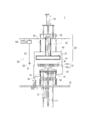
- FIG. 1 is a schematic cross-sectional view showing the configuration and standby state of a wafer edge polishing apparatus according to an embodiment of the present invention.
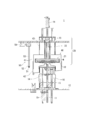
- FIG. 2 is a schematic cross-sectional view showing the configuration of the wafer edge polishing apparatus and the cleaning state of the chuck table according to the embodiment of the present invention.
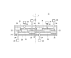
- FIG. 3 is a schematic cross-sectional view showing the configuration and edge polishing state of the wafer edge polishing apparatus according to the embodiment of the present invention.
- FIG. 4 is a side view schematically showing an example of the configuration of the rotary head 21 of the edge polishing unit 20.
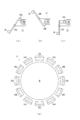
- FIG. 5 is a diagram schematically showing an example of the configuration of the edge polishing head 35, in which (a) to (c) are side sectional views and (d) is a plan view.
- FIG. 6 is a plan view for explaining the operation of the cleaning arm 51 set in the processing chamber 40.
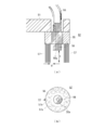
- 7A and 7B are diagrams showing the structure of the cleaning head 52, where FIG. 7A is a side sectional view and FIG. 7B is a plan view.
- FIG. 8 is a schematic diagram illustrating a mechanism for depositing slurry residue on the chuck table in the edge polishing process.
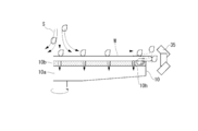
- FIG. 9 is a schematic diagram illustrating a method for cleaning slurry residue by the cleaning unit 50.
- FIG. 10 is a graph showing changes in the number of scratch defects on the back surface of the wafer as the number of processed wafers (pad life) increases.
- FIG. 1 to 3 are schematic cross-sectional views showing a configuration of a wafer edge polishing apparatus according to an embodiment of the present invention.
- FIG. 1 is a standby state in which the chuck table is in a lowered position
- FIG. FIG. 3 shows the cleaning state
- FIG. 3 shows the edge polishing state.
- the edge polishing apparatus 1 cleans the chuck table 10 that chucks and holds the back surface of the wafer, the edge polishing unit 20 disposed above the chuck table 10, and the chuck table 10. And a cleaning unit 50.
- the chuck table 10 and the edge polishing unit 20 are provided in the processing chamber 40 surrounded by the upper side cover 41 and the lower side cover 42, but the cleaning unit 50 is provided outside the processing chamber 40.
- the wafer W to be processed is, for example, a silicon wafer, and a silicon single crystal ingot manufactured by the CZ method is subjected to peripheral grinding, slicing, lapping, etching, and double-side polishing.
- the double-side polishing process is performed in a state where the wafer is accommodated in the carrier. Therefore, during the double-side polishing, the end surface of the wafer collides with the inner peripheral surface of the carrier loading hole through the slurry, and the end surface of the wafer after double-side polishing is performed.
- the surface is rougher than the front and back surfaces and has many scratch defects.
- the chuck table 10 is formed by adhering a chuck pad 10b to the upper surface of a resin-made chuck table body 10a, and the upper surface of the chuck pad 10b constitutes an adsorption support surface of the wafer W.
- the chuck pad 10b is made of a material that does not damage the wafer W, such as nonwoven fabric, foamed resin, or suede.
- a large number of air holes are formed on the upper surface of the chuck table 10, and the air holes are connected to a vacuum path for guiding negative pressure air.
- the wafer W placed on the upper surface of the chuck table 10 is vacuum-sucked and held by negative pressure air supplied to the vent hole.
- the chuck table 10 is fixed to the upper end portion of the rotary shaft 11, and the rotary shaft 11 is rotatably supported by a pedestal 13 provided on the support base 12 via a bearing 14, and below the support base 12. It is connected to a motor 15 provided. Thereby, the chuck table 10 is rotationally driven by the motor 15 together with the rotary shaft 11.
- the rotation shaft 11 and the motor 15 constitute a rotation drive mechanism that rotates the chuck table 10.
- a motor 16 for driving the chuck table 10 up and down is provided in the base 13, and the chuck table 10 is driven up and down together with the rotary shaft 11 and the base 13.
- the chuck table 10 in FIGS. 1 and 2 is in the lowered position (retreat position), and the chuck table 10 in FIG. 3 is in the raised position.
- the upper side cover 41 constituting the processing chamber 40 is connected to the cylinder 44 via the lifting arm 43, and the processing chamber 40 is opened when the cylinder 44 lifts the upper side cover 41.
- the wafer W to be processed is fed into the processing chamber 40 from a wafer carry-in port 46 formed between the lower side cover 42 by lifting the upper side cover 41 as shown in FIG. Placed on top.
- the cleaning unit 50 includes a cleaning arm 51, a cleaning head 52 provided at the distal end of the cleaning arm 51, a rotating shaft 53 connected to the base end of the cleaning arm 51, and a motor 54 that rotationally drives the rotating shaft 53.
- the cleaning arm 51 is configured to be movable back and forth in the processing chamber 40.
- the cleaning arm 51 of the cleaning unit 50 is configured to enter the processing chamber 40 from the wafer carry-in port 46. During the edge polishing process of the wafer W, the cleaning arm 51 is retracted to the outside of the processing chamber 40. However, during the cleaning process of the chuck table 10, the cleaning arm 51 enters the processing chamber 40 and performs a cleaning operation. As described above, the motor 54 and the rotary shaft 53 not only reciprocate the cleaning head 52 in the radial direction of the chuck table 10, but also retract the cleaning head 52 to the outside of the processing chamber 40 in the edge polishing process.
- the cleaning head moving mechanism for allowing the cleaning head to enter the processing chamber 40 is configured so that the cleaning arm 51 can enter the processing chamber 40 using the existing doorway provided in the processing chamber 40. .
- the edge polishing unit 20 includes a rotary head 21, a hollow shaft 22 that rotatably supports the rotary head 21, and a motor 23 that rotationally drives the hollow shaft 22.
- a supply pipe for supplying slurry is incorporated inside the hollow shaft 22, and the slurry is supplied to the center of the surface of the wafer W. Further, the slurry used for the polishing process is discharged and recovered from a slurry discharge port 45 provided at the lower end of the inclined bottom surface of the processing chamber 40.
- FIG. 4 is a side view schematically showing an example of the configuration of the rotary head 21 of the edge polishing unit 20.
- the rotary head 21 includes an upper ring 31, a ring-shaped lower ring 32 provided below and in parallel to the upper ring 31, and a plurality of connecting rods 33 that connect the upper ring 31 and the lower ring 32.
- a polishing space 21S is formed between the upper ring 31 and the lower ring 32, and the wafer W is processed in the polishing space 21S.
- the opening diameter of the lower ring 32 is larger than the diameter (for example, 450 mm) of the wafer W to be processed, and the wafer W on the chuck table 10 is polished through the opening of the lower ring 32 by raising the chuck table 10. It is possible to enter the space 21S.
- the rotary head 21 is provided with a plurality of edge polishing heads 35.
- Each of the plurality of edge polishing heads 35 is attached to the upper ring 31 or the lower ring 32 via the edge polishing arm 34, and the edge polishing arm 34 is configured to be rotatable around the upper ring 31 or the lower ring 32. It has become.
- the edge polishing head 35 is provided at the distal end portion of the edge polishing head 35 facing the polishing space 21 ⁇ / b> S, and a weight portion 36 is provided at the base end portion of the edge polishing arm 34.
- FIG. 5 is a diagram schematically showing an example of the configuration of the edge polishing head 35, in which (a) to (c) are side sectional views and (d) is a plan view.
- FIGS. 5A to 5C there are three types of edge polishing heads 35, and as shown in FIG. 5A, an upper polishing head 35A for polishing the upper surface of the wafer W, and FIG. As shown in FIG. 5B, the lower polishing head 35B polishes the lower side of the end face of the wafer W, and the central polishing head 35C polishes the center of the end face of the wafer W as shown in FIG. 5C.
- the upper polishing arm 34A that supports the upper polishing head 35A is preferably pivotally supported by the lower ring 32
- the lower polishing arm 34B that supports the lower polishing head 35B is pivotally supported by the upper ring 31. It is preferable.
- the central polishing arm 34 ⁇ / b> C that supports the central polishing head 35 ⁇ / b> C may be supported by the lower ring 32 or may be supported by the upper ring 31.
- the upper polishing head 35A, the lower polishing head 35B, and the central polishing head 35C are arranged at equal intervals along the outer periphery of the wafer W as shown in FIG. It can be polished well.
- the edge polishing arm 34 is rotated by the centrifugal force F applied to the weight portion 36 and the lever principle using the upper ring 31 or the lower ring 32 as a fulcrum, and the edge polishing head 35 is moved to the wafer W. Press against the end face of. Since the edge polishing head 35 rotates around the wafer W while pressing the edge of the wafer W, the edge of the wafer W is polished with an appropriate pressure.
- the edge-polished wafer W becomes a final wafer product through a single-side polishing process or a cleaning process in which only the surface is mirror-finished.
- the wafer manufacturing method according to the present embodiment performs edge polishing after double-side polishing, and there is no step of polishing the back surface of the wafer after edge polishing.
- the edge polishing apparatus 1 periodically performs a cleaning step after the edge polishing step. Since the slurry residue on the chuck table 10 is removed, the probability of scratching the back surface of the wafer in the edge polishing process can be greatly reduced. Therefore, it is possible to provide a wafer with improved defect quality at the edge as well as the front and back surfaces.
- FIG. 6 is a plan view for explaining the operation of the cleaning arm 51 set in the processing chamber 40.
- a cleaning head 52 having a brush is provided at a distal end portion 51 a of the cleaning arm 51, and a base end portion 51 b of the cleaning arm 51 is pivotally supported by a rotating shaft 53.
- the cleaning arm 51 swings within a range of a predetermined angle ⁇ around the base end portion 51 b, and the cleaning head 52 moves between the central portion and the outer peripheral portion of the chuck table 10.
- the upper surface of the chuck table 10 provided with the air holes 10h is cleaned by reciprocating in parallel with the upper surface of the chuck 10.
- FIG. 7A and 7B are diagrams showing the structure of the cleaning head 52, where FIG. 7A is a side sectional view and FIG. 7B is a plan view.
- the cleaning head 52 includes a resin-made annular base 55 attached to the cleaning arm 51, a high-pressure jet nozzle 56 for injecting a cleaning liquid such as pure water, and a high-pressure. And a brush 57 provided in an annular shape so as to surround the jet nozzle 56.
- the high-pressure jet nozzle 56 is fitted in the hollow portion of the base 55, and the brush 57 is implanted on the bottom surface of the base 55.
- the brush 57 is formed by arranging a bristle bundle 57a, which is an aggregate of a plurality of filaments (for example, 50), around the high-pressure jet nozzle 56, and is provided in an annular shape so as to surround the high-pressure jet nozzle 56. Yes.
- the space width d between the outer diameter of the high-pressure jet nozzle 56 and the brush 57 is preferably 10 mm or more and 20 mm or less. This is because when the space width d is smaller than 10 mm, the space enclosed by the brush 57 is too narrow and it becomes difficult to confine the slurry residue. When the space width d is larger than 20 mm, the high-pressure water is used. This is because the effect of sweeping away the slurry residue floating by the brush 57 becomes weak.
- the high pressure jet nozzle 56 is connected to the tank via a pipe 58 and a pump, and the cleaning liquid in the tank is supplied to the high pressure jet nozzle 56.
- the diameter of the opening 56a of the high-pressure jet nozzle 56 is preferably 0.5 mm or more and 2.5 mm or less, and the high-pressure jet pressure is preferably about 10 MPa.
- the height h from the tip of the high-pressure jet nozzle 56 to the tip of the brush 57 is preferably 15 mm or more and 25 mm or less. This is because if the height h is lower than 15 mm, the space of the room surrounded by the brush 57 is too narrow and it becomes difficult to confine the slurry residue, and if the height h is higher than 25 mm, it is lifted by high pressure water. This is because the effect of sweeping off the slurry residue with the brush 57 is weakened.
- FIG. 8 is a schematic diagram for explaining a mechanism for depositing slurry residue on the chuck table in the edge polishing process.
- the slurry S containing abrasive grains when supplied to the center of the surface of the wafer W in the edge polishing process, the slurry S flows in the outer peripheral direction by the centrifugal force caused by the rotation of the wafer W and is edge polished.
- the edge polishing head 35 supplied to the head 35 and traveling along the outer periphery of the wafer W polishes the edge of the wafer W together with the slurry S.
- a part of the slurry S goes from the front surface side to the back surface side of the wafer W and adheres to the outer peripheral surface of the chuck pad of the chuck table 10.
- the back surface of the wafer W is in close contact with the chuck table 10, but when the wafer W rotates at high speed, a gap is generated between the wafer W and the chuck table 10 because the end portion (outer peripheral portion) vibrates in the vertical direction. Therefore, it is considered that the slurry residue adheres to the end portion of the chuck table 10. Therefore, in this embodiment, the residue of the slurry S is removed by cleaning the upper surface of the chuck table 10 using the cleaning head 52.
- FIG. 9 is a schematic diagram for explaining a method for cleaning slurry residue by the cleaning unit 50.
- the brush of the cleaning head 52 is pressed against the outer periphery of the chuck table 10, and the cleaning head 52 reciprocates in parallel with the upper surface of the chuck table 10.
- the slurry residue adhering to the upper surface of the chuck table 10 is removed. Since high-pressure water is jetted from the high-pressure jet nozzle 56 during the cleaning process, the slurry residue on the chuck table can be knocked out, and the slurry residue floated with the high-pressure water can be swept out with a brush and removed. In particular, since the slurry residue is removed while confined in the room of the brush surrounding the high pressure water, the chuck table 10 is efficiently cleaned while preventing the high pressure water from being scattered.
- the cleaning head 52 includes the high-pressure jet nozzle 56 and the annular brush 57 provided around the high-pressure jet nozzle 56, and the chuck table 10 is subjected to high-pressure cleaning. Simultaneously with the brush cleaning, the slurry residue can be surely removed. Therefore, a wafer with a very small number of scratch defects on the back surface can be manufactured.
- the cleaning process of the chuck table is performed, and the edge polishing process of the evaluation wafer is continuously performed for 5 sheets.
- the cleaning step and the edge polishing step of the five evaluation wafers were alternately repeated five times to obtain 25 example samples of the evaluation wafer.
- the cleaning conditions of the chuck table are as follows: wafer rotation speed: 200 rpm, wafer rotation direction: counterclockwise, cleaning head swing frequency: 37 times, cleaning arm swing start angle: 50 °, cleaning arm swing return angle: 90 ° C.
- the cleaning arm swing speed was 10 ° / sec
- the high-pressure jet pressure was 10 MPa
- the chuck cleaning position was 21 mm
- the cleaning time was 5 min.
- a suede type having a thickness of 0.5 to 0.8 mm and a compression rate of 2 to 10% was used.
- the edge polishing process is continuously performed under the same conditions as in the embodiment except that the chuck table cleaning process is not performed after five edge polishing processes of the evaluation wafer are performed continuously.
- a comparative sample of the wafer was obtained. That is, in the manufacture of the comparative sample, after performing the edge polishing process of 300 wafers, the chuck table cleaning process was performed only once, and thereafter the chuck table was not cleaned at all.
- the back surfaces of the example sample and the comparative example sample of the evaluation wafer were respectively measured with a particle counter, and the number of scratch defects having a size of 200 nm or more was obtained.
- FIG. 10 is a graph showing changes in the number of scratch defects on the back surface of the wafer as the number of processed wafers (pad life) increases.
- the number of scratches and defects increased gradually as the number of wafers processed increased.
- the number of wafers exceeds the certain number of 300 and the 25th wafer, the number reaches about 500.
- the number of scratch defects was always less than 50 regardless of the increase in the number of processed wafers.
Landscapes
- Engineering & Computer Science (AREA)
- Mechanical Engineering (AREA)
- Chemical & Material Sciences (AREA)
- Ceramic Engineering (AREA)
- Inorganic Chemistry (AREA)
- Mechanical Treatment Of Semiconductor (AREA)
- Grinding-Machine Dressing And Accessory Apparatuses (AREA)
- Grinding And Polishing Of Tertiary Curved Surfaces And Surfaces With Complex Shapes (AREA)
Abstract
【課題】チャックテーブル上に付着するスラリー残渣の洗浄効果が高い洗浄機構を備えたエッジ研磨装置を提供する。 【解決手段】エッジ研磨装置1は、ウェーハWを吸着保持するチャックテーブル10と、チャックテーブル10を回転させる回転駆動機構と、チャックテーブル10によって吸着保持された状態で回転するウェーハWにスラリーを供給しながらウェーハのエッジを研磨するエッジ研磨ユニット20と、チャックテーブル10上のスラリー残渣を除去する洗浄ユニット50とを備える。洗浄ユニット50は、高圧ジェットノズル及び当該高圧ジェットノズルの周囲を取り囲むブラシを備えた洗浄ヘッド52を含み、洗浄ヘッド52を用いてチャックテーブル10を高圧洗浄と同時にブラシ洗浄する。
Description
本発明は、ウェーハのエッジ研磨装置及び方法に関し、特に、研磨加工時にウェーハの裏面を吸着保持するチャックテーブルの洗浄機構に関する。
半導体デバイスの基板材料としてシリコンウェーハが広く用いられている。シリコンウェーハは、シリコン単結晶インゴットに外周研削、スライス、ラッピング、エッチング、両面研磨、片面研磨、洗浄等の工程を順次行うことにより製造される。特に最近は、ウェーハの表裏両面のみならずエッジにも傷欠陥がない状態にするため、ウェーハの両面研磨を行った後にエッジ研磨を行うことが主流になりつつある。特許文献1には、表裏両面側の端面と外周面とを同時に研磨加工することが可能なワーク外周部の研磨装置が記載されている。
ウェーハのエッジ研磨工程では、ウェーハを吸着保持するチャックテーブル上に付着するスラリー残渣が問題となる。チャックテーブル上に残存する砥粒はウェーハの裏面を傷つける原因となり、チャックテーブル上に砥粒が残存している状態でウェーハの裏面をチャッキングすると当該裏面に傷欠陥が発生するからである。上記のように両面研磨を行った後にエッジ研磨を行う場合、エッジ研磨工程後にはウェーハの表面のみを研磨する片面研磨工程があるだけでウェーハの裏面の品質を改善する機会が存在しないため、エッジ研磨工程で発生するウェーハの裏面の傷欠陥は特に問題となる。
上記問題を解決するためには、チャックテーブル上に付着するスラリー残渣を除去することが望ましい。チャックテーブルの洗浄方法に関し、例えば特許文献2には、半導体ウェーハ加工機のキャリアプレートのチャック面(吸着支持面)に向けてノズルから純水等の洗浄液を高圧で噴射することによってチャック面を洗浄する吸着支持面の洗浄装置が記載されている。この洗浄装置において吸着支持面は下向きであり、高圧の洗浄液によって叩き出された異物は洗浄液と共に落下するので、吸着支持面に付着する異物はブラシで擦ることなく除去される。特許文献2に記載の洗浄装置によれば、チャック面に低圧水をかけながらブラシ洗浄する従来技術の洗浄力不足を解消することができ、ブラシの毛よりも細かな異物を除去することができないという問題や、異物が単にチャック面の上を移動するだけで除去されないという問題を解決することができる。
また特許文献3には、チャックテーブルの上面を洗浄するテーブル洗浄ユニットを備えたウェーハ面取り装置が記載されている。テーブル洗浄ユニットは、一直線上に配列された洗浄液ノズル、エアノズル及び洗浄ブラシから構成されており、洗浄ノズルから洗浄液が噴射された状態でテーブル洗浄ユニットがチャックテーブルの上面に沿って往復移動することにより、洗浄ブラシがチャックテーブルの上面を摺動するので、チャックテーブルの上面をリンス洗浄及びブラシ洗浄することができる。
しかしながら、吸着支持面に高圧の洗浄液を噴射して洗浄する特許文献2に記載の洗浄方法は、吸着支持面が下向きの場合には有効であるが、吸着支持面が上向きの場合にはスラリー残渣の位置が多少移動する程度に留まり、スラリー残渣を十分に除去することができないという問題がある。また特許文献3に記載の洗浄方法は、チャックテーブルの上面をリンス洗浄及びブラシ洗浄するものであるが、洗浄液ノズル及び洗浄ブラシが一直線上に配列され、それらの配列方向と直交する方向に洗浄ブラシを往復移動させることでブラシ洗浄を行うものであるため、円形のチャックテーブルの外周部に堆積しているスラリー残渣を除去する効果が小さいという問題がある。
したがって、本発明の目的は、チャックテーブル上に付着するスラリー残渣の洗浄効果が高い洗浄機構を用いたウェーハのエッジ研磨装置及び方法を提供することにある。
上記課題を解決するため、本発明によるウェーハのエッジ研磨装置は、ウェーハを吸着保持するチャックテーブルと、前記チャックテーブルを回転させる回転駆動機構と、前記チャックテーブルによって吸着保持された状態で回転するウェーハにスラリーを供給しながら前記ウェーハのエッジを研磨するエッジ研磨ユニットと、前記チャックテーブル上のスラリー残渣を除去する洗浄ユニットとを備え、前記洗浄ユニットは、高圧ジェットノズル及び当該高圧ジェットノズルの周囲を取り囲むように設けられたブラシを備えた洗浄ヘッドを含み、前記洗浄ヘッドを用いて前記チャックテーブルを高圧洗浄と同時にブラシ洗浄することを特徴とする。
本発明によれば、高圧水を噴射してチャックテーブル上のスラリー残渣を叩き出しながらブラシで掃き出してスラリー残渣を払い除くことができ、スラリー残渣の除去率を高めることができる。また高圧水を囲むブラシの部屋に閉じ込めながらスラリー残渣を払い除くので、高圧水の飛散を防止しながらチャックテーブルを効率良く洗浄することができる。したがって、ウェーハのエッジ研磨加工時にウェーハの裏面が傷つくことを防止することができる。
本発明において、前記洗浄ユニットは、前記洗浄ヘッドを前記チャックテーブルの径方向に往復移動させる洗浄ヘッド移動機構をさらに含むことが好ましい。このように、洗浄ヘッドを往復移動させることにより、チャックテーブル上のスラリー残渣の洗浄効果を高めることができる。
本発明において、前記チャックテーブルは加工室内に設けられており、前記洗浄ヘッド移動機構は、エッジ研磨工程において前記洗浄ヘッドを前記加工室の外側に退避させ、洗浄工程において前記洗浄ヘッドを前記加工室内に進入させることが好ましい。この場合において、前記ウェーハを前記加工室内の前記チャックテーブル上に送り込むウェーハ搬入口は、前記洗浄ヘッドの前記加工室内への進入口を兼ねていることが好ましい。これによれば、簡単な構成によりチャックテーブルの洗浄機構を実現することができる。
本発明において、前記エッジ研磨ユニットによって研磨されるウェーハは、両面研磨工程によって表裏両面の研磨が施されたものであることが好ましい。ウェーハを両面研磨した後にエッジ研磨する場合、エッジ研磨後にウェーハの裏面を研磨する工程がないため、ウェーハの裏面の傷欠陥の発生を防止する必要があるが、本発明によれば、エッジ研磨工程でウェーハの裏面の傷欠陥の発生率を低減できるので、裏面に傷欠陥がない最終ウェーハ製品の製造歩留まりを高めることができる。
本発明において、前記チャックテーブルは前記ウェーハを真空吸着することが好ましい。このような構成のエッジ研磨装置では、チャックテーブル上のスラリー残渣の問題が大きいことから、本発明の効果も顕著である。
また本発明によるウェーハのエッジ研磨方法は、チャックテーブルによって吸着保持された状態で回転するウェーハにスラリーを供給しながら前記ウェーハのエッジを研磨するエッジ研磨工程と、前記チャックテーブル上のスラリー残渣を除去する洗浄工程とを備え、前記洗浄工程では、高圧ジェットノズルの周囲を取り囲むようにブラシが設けられた洗浄ヘッドを用いて前記チャックテーブルを高圧洗浄と同時にブラシ洗浄することを特徴とする。
本発明によれば、高圧水を噴射してチャックテーブル上のスラリー残渣を叩き出しながらブラシで掃き出してスラリー残渣を払い除くことができ、スラリー残渣の除去率を高めることができる。また高圧水を囲むブラシの部屋に閉じ込めながらスラリー残渣を払い除くので、高圧水の飛散を防止しながらチャックテーブルを効率良く洗浄することができる。したがって、ウェーハのエッジ研磨加工時にウェーハの裏面が傷つくことを防止することができる。
前記洗浄工程では、前記洗浄ヘッドを前記チャックテーブルの径方向に往復移動させることが好ましい。このように、洗浄ヘッドを往復移動させることにより、チャックテーブル上のスラリー残渣の洗浄効果を高めることができる。
本発明において、前記チャックテーブルは加工室内に設けられており、前記洗浄ヘッドは、前記エッジ研磨工程において加工室の外側に退避しており、前記洗浄工程において前記加工室内に進入していることが好ましい。この場合において、前記ウェーハを前記加工室内の前記チャックテーブル上に送り込むウェーハ搬入口は、前記洗浄ヘッドの前記加工室内への進入口を兼ねていることが好ましい。これによれば、簡単な構成によりチャックテーブルの洗浄機構を実現することができる。
本発明において、前記エッジ研磨工程は、前記チャックテーブルによって前記ウェーハを真空吸着することが好ましい。このようなエッジ研磨方法では、チャックテーブル上のスラリー残渣の問題が大きいことから、本発明の効果も顕著である。
本発明において、前記エッジ研磨工程は、前記ウェーハの表裏両面を研磨する両面研磨工程の後に行なわれることが好ましく、前記エッジ研磨工程は、前記ウェーハの表面のみを鏡面加工する片面研磨工程の前に行われることがさらに好ましい。ウェーハを両面研磨した後にエッジ研磨する場合、エッジ研磨後にウェーハの裏面を研磨する工程がないため、ウェーハの裏面の傷欠陥の発生を防止する必要があるが、本発明によれば、エッジ研磨工程でウェーハの裏面の傷欠陥の発生率を低減できるので、裏面に傷欠陥がない最終ウェーハ製品の製造歩留まりを高めることができる。
本発明によれば、チャックテーブル上に残留するスラリー残渣の洗浄効果が高められた洗浄機構を用いたウェーハのエッジ研磨装置及び方法を提供することができる。
以下、添付図面を参照しながら、本発明の好ましい実施の形態について詳細に説明する。
図1~図3は、本発明の実施の形態によるウェーハのエッジ研磨装置の構成を示す略断面図であって、特に図1はチャックテーブルが降下位置にある待機状態、図2はチャックテーブルの洗浄状態、図3はエッジ研磨状態をそれぞれ示している。
図1~図3に示すように、このエッジ研磨装置1は、ウェーハの裏面を吸着保持するチャックテーブル10と、チャックテーブル10の上方に配置されたエッジ研磨ユニット20と、チャックテーブル10を洗浄する洗浄ユニット50とを備えている。チャックテーブル10及びエッジ研磨ユニット20は上側サイドカバー41及び下側サイドカバー42に囲まれた加工室40内に設けられているが、洗浄ユニット50は加工室40の外側に設けられている。
加工対象となるウェーハWは、例えばシリコンウェーハであって、CZ法により製造されたシリコン単結晶インゴットに外周研削、スライス、ラッピング、エッチング及び両面研磨が施されたものである。通常、両面研磨工程はウェーハをキャリアに収容した状態で行われるので、両面研磨中にウェーハの端面がスラリーを介してキャリアのウェーハ装填孔の内周面に衝突し、両面研磨後のウェーハの端面は表裏面に比べて粗く、多くの傷欠陥が存在している。しかし、両面研磨工程の後にエッジ研磨工程を行った場合には、両面研磨工程で生じたウェーハの端面の傷欠陥を十分に除去することができ、最終ウェーハ製品において表裏両面のみならず端面の品質も高めることができる。
チャックテーブル10は、樹脂製のチャックテーブル本体10aの上面にチャックパッド10bが貼り付けられてなるものであり、チャックパッド10bの上面がウェーハWの吸着支持面を構成している。チャックパッド10bは不織布、発泡樹脂、スウェードなどのウェーハWを傷つけない素材からなる。またチャックテーブル10の上面には多数の通気孔が形成されており、通気孔は負圧空気を案内する真空路に接続されている。チャックテーブル10の上面に載置されたウェーハWは通気孔に供給される負圧空気によって真空吸着されて保持される。
チャックテーブル10は回転シャフト11の上端部に固定されており、回転シャフト11は支持台12上に設けられた台座13に軸受け14を介して回転自在に支持されており、支持台12の下方に設けられたモータ15に連結されている。これにより、チャックテーブル10は回転シャフト11と共にモータ15によって回転駆動される。このように、回転シャフト11及びモータ15は、チャックテーブル10を回転させる回転駆動機構を構成している。
また台座13内にはチャックテーブル10を昇降駆動するためのモータ16が設けられており、チャックテーブル10は回転シャフト11及び台座13と共に昇降駆動される。図1及び図2のチャックテーブル10は降下位置(待避位置)にあり、また図3のチャックテーブル10は上昇位置にある。
加工室40を構成する上側サイドカバー41は、昇降アーム43を介してシリンダー44に接続されており、シリンダー44が上側サイドカバー41を持ち上げることで加工室40が開放される。加工対象となるウェーハWは、図2に示すように上側サイドカバー41を持ち上げることによって下側サイドカバー42との間に形成されるウェーハ搬入口46から加工室40内に送り込まれ、チャックテーブル10上に載置される。
洗浄ユニット50は、洗浄アーム51と、洗浄アーム51の先端部に設けられた洗浄ヘッド52と、洗浄アーム51の基端部に接続された回転シャフト53と、回転シャフト53を回転駆動するモータ54とを備えており、洗浄アーム51は加工室40内に進退自在な構成を有している。
本実施形態において洗浄ユニット50の洗浄アーム51は、ウェーハ搬入口46から加工室40内に進入するように構成されている。ウェーハWのエッジ研磨工程中は洗浄アーム51が加工室40の外側に退避しているが、チャックテーブル10の洗浄工程中は洗浄アーム51が加工室40内に進入して洗浄動作を行う。このように、モータ54及び回転シャフト53は、洗浄ヘッド52をチャックテーブル10の径方向に往復移動させるだけでなく、エッジ研磨工程において洗浄ヘッド52を加工室40の外側に退避させ、また洗浄工程において洗浄ヘッドを加工室40内に進入させる洗浄ヘッド移動機構を構成しており、加工室40に設けられている既存の出入口を利用して洗浄アーム51を加工室40内に進入させることができる。
エッジ研磨ユニット20は、回転ヘッド21と、回転ヘッド21を回転自在に支持する中空シャフト22と、中空シャフト22を回転駆動するモータ23とを備えている。中空シャフト22の内部にはスラリーを供給する供給管が組み込まれており、ウェーハWの表面の中心部にスラリーが供給されるようになっている。さらに研磨加工に使用されたスラリーは、加工室40の傾斜した底面の下端に設けられたスラリー排出口45から排出されて回収される。
図4は、エッジ研磨ユニット20の回転ヘッド21の構成の一例を概略的に示す側面図である。
回転ヘッド21は、上側リング31と、上側リング31の下方においてこれと平行に設けられたリング状の下側リング32と、上側リング31と下側リング32とを連結する複数本の連結ロッド33とで構成されており、上側リング31と下側リング32との間には研磨スペース21Sが形成されており、ウェーハWは研磨スペース21S内で加工される。下側リング32の開口径は加工対象となるウェーハWの直径(例えば450mm)よりも大きく、チャックテーブル10を上昇させることでチャックテーブル10上のウェーハWは下側リング32の開口を通って研磨スペース21S内に進入することができる。
回転ヘッド21には複数のエッジ研磨ヘッド35が設けられている。複数のエッジ研磨ヘッド35の各々はエッジ研磨アーム34を介して上側リング31又は下側リング32に取り付けられており、エッジ研磨アーム34は上側リング31又は下側リング32を中心に回転自在な構成となっている。エッジ研磨ヘッド35は、研磨スペース21S側を向いているエッジ研磨ヘッド35の先端部に設けられており、エッジ研磨アーム34の基端部には重り部36が設けられている。
図5は、エッジ研磨ヘッド35の構成の一例を概略的に示す図であって、(a)~(c)は側面断面図、(d)は平面図である。
図5(a)~(c)に示すように、エッジ研磨ヘッド35には3種類あって、図5(a)に示すようにウェーハWの端面の上方を研磨する上側研磨ヘッド35Aと、図5(b)に示すようにウェーハWの端面の下方を研磨する下側研磨ヘッド35Bと、図5(c)に示すようにウェーハWの端面の中央を研磨する中央研磨ヘッド35Cとで構成される。この場合、上側研磨ヘッド35Aを支持する上側研磨アーム34Aは下側リング32に軸支されることが好ましく、下側研磨ヘッド35Bを支持する下側研磨アーム34Bは上側リング31に軸支されることが好ましい。中央研磨ヘッド35Cを支持する中央研磨アーム34Cは下側リング32に軸支されてもよく、上側リング31に軸支されてもよい。これらの上側研磨ヘッド35A、下側研磨ヘッド35B及び中央研磨ヘッド35Cが、図5(d)に示すようにウェーハWの外周に沿って等間隔に配置されることにより、ウェーハWのエッジをバランスよく研磨することができる。
回転ヘッド21を回転させると、重り部36に加わる遠心力Fと上側リング31又は下側リング32を支点とするテコの原理により、エッジ研磨アーム34は回動してエッジ研磨ヘッド35をウェーハWの端面に押し付ける。エッジ研磨ヘッド35はウェーハWのエッジを押圧しながらウェーハWの周りを回転するので、ウェーハWのエッジが適切な圧力で研磨される。
こうしてエッジ研磨されたウェーハWは、その表面のみを鏡面加工する片面研磨工程や洗浄工程などを経て最終ウェーハ製品となる。本実施形態によるウェーハの製造方法は、両面研磨後にエッジ研磨を行うものであり、エッジ研磨後にウェーハの裏面を研磨する工程は存在しないが、エッジ研磨装置1はエッジ研磨工程後に洗浄工程を定期的に実施し、チャックテーブル10上のスラリー残渣を除去することから、エッジ研磨工程でウェーハの裏面に傷が付く確率を大幅に低減することができる。したがって、表裏面のみならずエッジの欠陥品質も改善されたウェーハを提供することができる。
図6は、加工室40内にセットされた洗浄アーム51の動作を説明するための平面図である。
図6に示すように、洗浄アーム51の先端部51aにはブラシを有する洗浄ヘッド52が設けられており、洗浄アーム51の基端部51bは回転シャフト53に軸支されている。そして回転シャフト53が回転することで洗浄アーム51が基端部51bを中心に所定の角度θの範囲内でスイングし、洗浄ヘッド52がチャックテーブル10の中心部と外周部との間をチャックテーブル10の上面と平行に往復移動して、通気孔10hが設けられたチャックテーブル10の上面を洗浄する。
図7は、洗浄ヘッド52の構造を示す図であって、(a)は側面断面図、(b)は平面図である。
図7(a)及び(b)に示すように、洗浄ヘッド52は、洗浄アーム51に取り付けられた樹脂製の環状のベース55と、純水等の洗浄液を噴射する高圧ジェットノズル56と、高圧ジェットノズル56を取り囲むように環状に設けられたブラシ57とを備えている。高圧ジェットノズル56はベース55の中空部に嵌め込まれており、ブラシ57はベース55の底面に植設されている。
ブラシ57は、複数本のフィラメント(例えば50本)の集合体であるブリスル束57aを高圧ジェットノズル56の周囲に配置してなるものであり、高圧ジェットノズル56を取り囲むように環状に設けられている。高圧ジェットノズル56の外径とブラシ57との間のスペース幅dは10mm以上20mm以下であることが好ましい。スペース幅dが10mmよりも狭い場合にはブラシ57によって囲まれた部屋のスペースが狭すぎてスラリー残渣を閉じ込めることが難しくなるからであり、またスペース幅dが20mmよりも広い場合には高圧水によって浮き上がったスラリー残渣をブラシ57で掃き出す効果が弱くなるからである。
高圧ジェットノズル56は配管58及びポンプを介してタンクに接続されており、タンク内の洗浄液が高圧ジェットノズル56に供給される。高圧ジェットノズル56の開口56aの直径は0.5mm以上2.5mm以下であることが好ましく、高圧ジェット圧力は10MPa前後であることが好ましい。また、高圧ジェットノズル56の先端からブラシ57の先端までの高さhは15mm以上25mm以下であることが好ましい。高さhが15mmよりも低いとブラシ57によって囲まれた部屋のスペースが狭すぎてスラリー残渣を閉じ込めることが難しくなるからであり、また高さhが25mmよりも高い場合には高圧水によって浮き上がったスラリー残渣をブラシ57で掃き出す効果が弱くなるからである。
図8は、エッジ研磨工程においてチャックテーブル上にスラリー残渣が堆積するメカニズムを説明する模式図である。
図8に示すように、エッジ研磨工程においてウェーハWの表面の中心部に砥粒を含むスラリーSが供給されると、このスラリーSはウェーハWの回転による遠心力によって外周方向に流れてエッジ研磨ヘッド35に供給され、ウェーハWの外周に沿って走行するエッジ研磨ヘッド35がこのスラリーSと共にウェーハWのエッジを研磨する。このとき、スラリーSの一部がウェーハWの表面側から裏面側に回り込んでチャックテーブル10のチャックパットの外周部の表面に付着する。ウェーハWの裏面はチャックテーブル10に密着しているが、ウェーハWが高速回転するとその端部(外周部)が上下方向に振動することによりウェーハWとチャックテーブル10との間に隙間が発生するため、チャックテーブル10の端部にスラリー残渣が付着するものと考えられる。そこで本実施形態では、洗浄ヘッド52を用いてチャックテーブル10の上面を洗浄することにより、スラリーSの残渣を除去する。
図9は、洗浄ユニット50によるスラリー残渣の洗浄方法を説明する模式図である。
図9に示すように、チャックテーブル10の洗浄工程では、洗浄ヘッド52のブラシがチャックテーブル10の外周部に押し当てられ、洗浄ヘッド52がチャックテーブル10の上面と平行に往復移動することにより、チャックテーブル10の上面に付着するスラリー残渣を払い除かれる。洗浄工程中は高圧ジェットノズル56から高圧水を噴射しているので、チャックテーブル上のスラリー残渣を叩き出すことができ、高圧水で浮かせたスラリー残渣をブラシで掃き出して除去することができる。特に、高圧水を囲むブラシの部屋に閉じ込めながらスラリー残渣が払い除かれるので、高圧水の飛散を防止しながらチャックテーブル10が効率良く洗浄される。
以上説明したように、本実施形態によるウェーハのエッジ研磨装置1は、洗浄ヘッド52が高圧ジェットノズル56とその周囲に設けられた環状のブラシ57との組み合わせで構成され、チャックテーブル10を高圧洗浄と同時にブラシ洗浄するので、スラリー残渣を確実に除去することができる。したがって、裏面の傷欠陥の個数が非常に少ないウェーハを製造することができる。
以上、本発明の好ましい実施形態について説明したが、本発明は、上記の実施形態に限定されることなく、本発明の主旨を逸脱しない範囲で種々の変更が可能であり、それらも本発明の範囲内に包含されるものであることはいうまでもない。
チャックテーブルの洗浄工程の有無がエッジ研磨後のウェーハの裏面の品質に与える影響について評価した。加工対象となるウェーハは、CZ法により製造されたシリコン単結晶インゴットに対して外周研削、スライス、ラッピング、エッチング、両面研磨を順に施した450mmシリコンウェーハを用いた。
評価試験では、図1に示したエッジ研磨装置を用いて予め300枚のウェーハのエッジ研磨工程を行った後、チャックテーブルの洗浄工程を行い、さらに評価用ウェーハのエッジ研磨工程を5枚連続して実施し、このような洗浄工程と5枚の評価用ウェーハのエッジ研磨工程とを交互に5回ずつ繰り返して、25枚の評価用ウェーハの実施例サンプルを得た。
チャックテーブルの洗浄条件は、ウェーハ回転数:200rpm、ウェーハ回転方向:反時計回り、洗浄ヘッドのスイング回数:37回、洗浄アームのスイング開始角度:50°、洗浄アームのスイング折り返し角度:90℃、洗浄アームのスイング速度:10°/sec、高圧ジェット圧力:10MPa、チャック洗浄位置:21mm、洗浄時間:5minとした。またチャックテーブルの吸着支持面を構成するチャックパッドとしては、厚さが0.5~0.8mm、圧縮率が2~10%のスウェードタイプを用いた。
一方、評価用ウェーハのエッジ研磨工程を5枚連続して実施した後にチャックテーブルの洗浄工程を行わない点以外は実施例と同一条件下でエッジ研磨工程を連続して行い、25枚の評価用ウェーハの比較例サンプルを得た。すなわち、比較例サンプルの製造では、300枚のウェーハのエッジ研磨工程を行った後、チャックテーブルの洗浄工程を1回だけ行い、その後はチャックテーブルの洗浄を一切行わなかった。
その後、評価用ウェーハの実施例サンプル及び比較例サンプルの裏面をパーティクルカウンターでそれぞれ測定して、サイズが200nm以上の傷欠陥の個数を求めた。
図10は、ウェーハの加工枚数(パッドライフ)の増加に伴うウェーハの裏面の傷欠陥の個数の変化を示すグラフである。
図10に示すように、チャックテーブルの洗浄工程を行わなかった比較例では、ウェーハの加工枚数の増加と共に傷欠陥の個数が徐々に増加し、15枚目のウェーハときには傷欠陥の個数が閾値である300個を超え、さらに25枚目のウェーハのときには約500個に達した。一方、チャックテーブルの洗浄工程を行った実施例では、ウェーハの加工枚数の増加によらず、傷欠陥の個数は常に50個未満となった。このように、チャックテーブルの洗浄工程を定期的に実施することによってエッジ研磨後のウェーハの裏面の傷欠陥の個数を低減できることが確認された。
1 エッジ研磨装置
10 チャックテーブル
10a チャックテーブル本体
10b チャックパッド
10h 通気孔
11 回転シャフト
12 支持台
13 台座
15 モータ(チャックテーブル回転)
16 モータ(チャックテーブル昇降用)
20 エッジ研磨ユニット
21 回転ヘッド
21S 研磨スペース
22 中空シャフト
23 モータ(回転ヘッド回転用)
31 上側リング
32 下側リング
33 連結ロッド
34 エッジ研磨アーム
34A 上側研磨アーム
34B 下側研磨アーム
34C 中央研磨アーム
35 エッジ研磨ヘッド
35A 上側研磨ヘッド
35B 下側研磨ヘッド
35C 中央研磨ヘッド
36 重り部
40 加工室
41 上側サイドカバー
42 下側サイドカバー
43 昇降アーム
44 シリンダー
45 スラリー排出口
46 ウェーハ搬入口
50 洗浄ユニット
51 洗浄アーム
51a 洗浄アームの先端部
51b 洗浄アームの基端部
52 洗浄ヘッド
53 回転シャフト
54 モータ
55 ベース
56 高圧ジェットノズル
56a 高圧ジェットノズルの開口
57 ブラシ(環状ブラシ)
57a ブリスル束
58 配管
S スラリー
W ウェーハ
10 チャックテーブル
10a チャックテーブル本体
10b チャックパッド
10h 通気孔
11 回転シャフト
12 支持台
13 台座
15 モータ(チャックテーブル回転)
16 モータ(チャックテーブル昇降用)
20 エッジ研磨ユニット
21 回転ヘッド
21S 研磨スペース
22 中空シャフト
23 モータ(回転ヘッド回転用)
31 上側リング
32 下側リング
33 連結ロッド
34 エッジ研磨アーム
34A 上側研磨アーム
34B 下側研磨アーム
34C 中央研磨アーム
35 エッジ研磨ヘッド
35A 上側研磨ヘッド
35B 下側研磨ヘッド
35C 中央研磨ヘッド
36 重り部
40 加工室
41 上側サイドカバー
42 下側サイドカバー
43 昇降アーム
44 シリンダー
45 スラリー排出口
46 ウェーハ搬入口
50 洗浄ユニット
51 洗浄アーム
51a 洗浄アームの先端部
51b 洗浄アームの基端部
52 洗浄ヘッド
53 回転シャフト
54 モータ
55 ベース
56 高圧ジェットノズル
56a 高圧ジェットノズルの開口
57 ブラシ(環状ブラシ)
57a ブリスル束
58 配管
S スラリー
W ウェーハ
Claims (11)
- ウェーハを吸着保持するチャックテーブルと、
前記チャックテーブルを回転させる回転駆動機構と、
前記チャックテーブルによって吸着保持された状態で回転するウェーハにスラリーを供給しながら前記ウェーハのエッジを研磨するエッジ研磨ユニットと、
前記チャックテーブル上のスラリー残渣を除去する洗浄ユニットとを備え、
前記洗浄ユニットは、高圧ジェットノズル及び当該高圧ジェットノズルの周囲を取り囲むように設けられたブラシを備えた洗浄ヘッドを含み、前記洗浄ヘッドを用いて前記チャックテーブルを高圧洗浄と同時にブラシ洗浄することを特徴とするウェーハのエッジ研磨装置。 - 前記洗浄ユニットは、前記洗浄ヘッドを前記チャックテーブルの径方向に往復移動させる洗浄ヘッド移動機構をさらに含む、請求項1に記載のウェーハのエッジ研磨装置。
- 前記チャックテーブルは加工室内に設けられており、
前記洗浄ヘッド移動機構は、エッジ研磨工程において前記洗浄ヘッドを前記加工室の外側に退避させ、洗浄工程において前記洗浄ヘッドを前記加工室内に進入させる、請求項2に記載のウェーハのエッジ研磨装置。 - 前記エッジ研磨ユニットによって研磨されるウェーハは、両面研磨工程によって表裏両面の研磨が施されたものである、請求項1乃至3のいずれか一項に記載のウェーハのエッジ研磨装置。
- 前記チャックテーブルは前記ウェーハを真空吸着する、請求項1乃至4のいずれか一項に記載のウェーハのエッジ研磨装置。
- チャックテーブルによって吸着保持された状態で回転するウェーハにスラリーを供給しながら前記ウェーハのエッジを研磨するエッジ研磨工程と、
前記チャックテーブル上のスラリー残渣を除去する洗浄工程とを備え、
前記洗浄工程では、高圧ジェットノズルの周囲を取り囲むようにブラシが設けられた洗浄ヘッドを用いて前記チャックテーブルを高圧洗浄と同時にブラシ洗浄することを特徴とするウェーハのエッジ研磨方法。 - 前記洗浄工程では、前記洗浄ヘッドを前記チャックテーブルの径方向に往復移動させる、請求項6に記載のウェーハのエッジ研磨方法。
- 前記チャックテーブルは加工室内に設けられており、
前記洗浄ヘッドは、前記エッジ研磨工程において加工室の外側に退避しており、前記洗浄工程において前記加工室内に進入している、請求項6又は7に記載のウェーハのエッジ研磨方法。 - 前記エッジ研磨工程は、前記ウェーハの表裏両面を研磨する両面研磨工程の後に行なわれる、請求項6乃至8のいずれか一項に記載のウェーハのエッジ研磨方法。
- 前記エッジ研磨工程は、前記チャックテーブルによって前記ウェーハを真空吸着する、請求項6乃至9のいずれか一項に記載のウェーハのエッジ研磨方法。
- 前記エッジ研磨工程は、前記ウェーハの表面のみを鏡面加工する片面研磨工程の前に行われる、請求項6乃至10のいずれか一項に記載のウェーハのエッジ研磨方法。
Priority Applications (4)
| Application Number | Priority Date | Filing Date | Title |
|---|---|---|---|
| CN201780069895.6A CN109937117B (zh) | 2016-11-15 | 2017-10-02 | 晶片的边缘抛光装置及方法 |
| US16/349,430 US11559869B2 (en) | 2016-11-15 | 2017-10-02 | Wafer edge polishing apparatus and method |
| DE112017005747.7T DE112017005747B4 (de) | 2016-11-15 | 2017-10-02 | Waferkantenpoliervorrichtung und -verfahren |
| KR1020197011933A KR102182910B1 (ko) | 2016-11-15 | 2017-10-02 | 웨이퍼의 엣지 연마 장치 및 방법 |
Applications Claiming Priority (2)
| Application Number | Priority Date | Filing Date | Title |
|---|---|---|---|
| JP2016-222064 | 2016-11-15 | ||
| JP2016222064A JP6304349B1 (ja) | 2016-11-15 | 2016-11-15 | ウェーハのエッジ研磨装置及び方法 |
Publications (1)
| Publication Number | Publication Date |
|---|---|
| WO2018092440A1 true WO2018092440A1 (ja) | 2018-05-24 |
Family
ID=61828575
Family Applications (1)
| Application Number | Title | Priority Date | Filing Date |
|---|---|---|---|
| PCT/JP2017/035873 Ceased WO2018092440A1 (ja) | 2016-11-15 | 2017-10-02 | ウェーハのエッジ研磨装置及び方法 |
Country Status (7)
| Country | Link |
|---|---|
| US (1) | US11559869B2 (ja) |
| JP (1) | JP6304349B1 (ja) |
| KR (1) | KR102182910B1 (ja) |
| CN (1) | CN109937117B (ja) |
| DE (1) | DE112017005747B4 (ja) |
| TW (1) | TWI680834B (ja) |
| WO (1) | WO2018092440A1 (ja) |
Cited By (1)
| Publication number | Priority date | Publication date | Assignee | Title |
|---|---|---|---|---|
| CN114833117A (zh) * | 2022-04-25 | 2022-08-02 | 嘉兴立鸿科技有限公司 | 一种晶圆片清洗机 |
Families Citing this family (24)
| Publication number | Priority date | Publication date | Assignee | Title |
|---|---|---|---|---|
| JP2020116692A (ja) * | 2019-01-24 | 2020-08-06 | 東京エレクトロン株式会社 | 加工装置及び加工方法 |
| TWI837277B (zh) * | 2019-01-24 | 2024-04-01 | 日商東京威力科創股份有限公司 | 加工裝置及加工方法 |
| CN111755319A (zh) * | 2019-03-29 | 2020-10-09 | 中芯集成电路(宁波)有限公司 | 晶圆清洗方法及光刻胶图案化方法 |
| CN111744836B (zh) * | 2019-03-29 | 2022-09-16 | 中芯集成电路(宁波)有限公司 | 晶圆清洗装置及控制系统 |
| JP7347986B2 (ja) * | 2019-08-06 | 2023-09-20 | 株式会社ディスコ | エッジトリミング装置 |
| CN114286736B (zh) * | 2019-08-27 | 2024-08-06 | 应用材料公司 | 化学机械抛光校正工具 |
| JP7218731B2 (ja) * | 2020-01-09 | 2023-02-07 | 信越半導体株式会社 | ラッピング装置の洗浄装置 |
| JP7403634B2 (ja) * | 2020-03-24 | 2023-12-22 | 東京エレクトロン株式会社 | 除去加工装置 |
| CN111834259A (zh) * | 2020-07-17 | 2020-10-27 | 中国科学院微电子研究所 | 一种清洗组件 |
| CN111681978B (zh) * | 2020-08-12 | 2020-12-01 | 山东元旭光电股份有限公司 | 一种晶圆清洗装置 |
| CN112497046A (zh) * | 2020-11-26 | 2021-03-16 | 上海新昇半导体科技有限公司 | 晶圆边缘抛光设备及方法 |
| CN112372474B (zh) * | 2020-12-01 | 2021-12-31 | 宁波运生工贸有限公司 | 一种机械精工用打磨装置 |
| JP7650590B2 (ja) * | 2021-03-29 | 2025-03-25 | 株式会社ディスコ | 研磨装置 |
| US20230024009A1 (en) * | 2021-07-20 | 2023-01-26 | Applied Materials, Inc. | Face-up wafer edge polishing apparatus |
| CN113877677B (zh) * | 2021-08-19 | 2022-11-18 | 广东嘉俊陶瓷有限公司 | 一种陶瓷加工生产用研磨装置 |
| CN114274041B (zh) * | 2021-12-24 | 2023-03-14 | 西安奕斯伟材料科技有限公司 | 双面研磨装置和双面研磨方法 |
| US12090600B2 (en) | 2022-06-06 | 2024-09-17 | Applied Materials, Inc. | Face-up wafer electrochemical planarization apparatus |
| US12519020B2 (en) * | 2022-06-17 | 2026-01-06 | Taiwan Semiconductor Manufacturing Company, Ltd. | Semiconductor processing tool and methods of operation |
| CN115741291B (zh) * | 2022-12-07 | 2025-09-16 | 华海清科股份有限公司 | 一种晶圆边缘处理装置 |
| CN115890478B (zh) * | 2022-12-29 | 2024-11-22 | 西安奕斯伟材料科技股份有限公司 | 抛光头和抛光设备 |
| CN116766029A (zh) * | 2023-08-02 | 2023-09-19 | 苏州博宏源机械制造有限公司 | 一种晶圆夹持式边缘抛光装置及其工艺 |
| WO2025032574A1 (en) * | 2023-08-05 | 2025-02-13 | Core Flow Ltd. | Configurable chuck apparatus for chemical mechanical planarization and cooperating ring |
| CN117226612B (zh) * | 2023-11-01 | 2025-11-04 | 山东浪潮华光光电子股份有限公司 | 一种改善研磨后晶片衬底碎屑粘附的方法 |
| US20260021551A1 (en) * | 2024-07-19 | 2026-01-22 | Applied Materials, Inc. | Chemical mechanical polishing using flexure mounted pad |
Citations (6)
| Publication number | Priority date | Publication date | Assignee | Title |
|---|---|---|---|---|
| JPH11104947A (ja) * | 1997-10-03 | 1999-04-20 | Toshiro Doi | 研磨パッドのドレッシング装置 |
| JP2000138191A (ja) * | 1998-10-29 | 2000-05-16 | Tokyo Seimitsu Co Ltd | ウェーハ面取り装置 |
| US6295683B1 (en) * | 1999-12-09 | 2001-10-02 | United Microelectronics Corp. | Equipment for brushing the underside of a semiconductor wafer |
| JP2004079842A (ja) * | 2002-08-20 | 2004-03-11 | Dainippon Screen Mfg Co Ltd | 基板処理装置および基板処理方法 |
| JP2013258227A (ja) * | 2012-06-12 | 2013-12-26 | Sumco Techxiv株式会社 | 半導体ウェーハの製造方法 |
| CN204658194U (zh) * | 2015-03-26 | 2015-09-23 | 武汉新芯集成电路制造有限公司 | 一种清洗装置 |
Family Cites Families (18)
| Publication number | Priority date | Publication date | Assignee | Title |
|---|---|---|---|---|
| JPS62128125A (ja) * | 1985-11-29 | 1987-06-10 | Canon Inc | ウエハ洗浄装置 |
| JPH01171762A (ja) * | 1987-12-28 | 1989-07-06 | Shibayama Kikai Kk | 半導体のウエハ研削盤の吸着チャック洗浄装置 |
| JPH05121385A (ja) * | 1991-10-28 | 1993-05-18 | Sharp Corp | 洗浄装置 |
| JPH06275582A (ja) * | 1993-03-18 | 1994-09-30 | Sumitomo Electric Ind Ltd | ウエハ加工装置 |
| JPH0786218A (ja) * | 1993-09-17 | 1995-03-31 | Dainippon Screen Mfg Co Ltd | 基板洗浄装置 |
| JPH10166268A (ja) * | 1996-12-10 | 1998-06-23 | Miyazaki Oki Electric Co Ltd | バックグラインダーチャックテーブルの洗浄装置 |
| JPH10256199A (ja) | 1997-03-07 | 1998-09-25 | Asahi Sanac Kk | 吸着支持面の洗浄装置 |
| JPH10294261A (ja) * | 1997-04-18 | 1998-11-04 | Sony Corp | レジスト塗布装置 |
| JP2000237700A (ja) * | 1999-02-23 | 2000-09-05 | Dainippon Screen Mfg Co Ltd | 基板洗浄装置 |
| JP2006237055A (ja) * | 2005-02-22 | 2006-09-07 | Shin Etsu Handotai Co Ltd | 半導体ウェーハの製造方法および半導体ウェーハの鏡面面取り方法 |
| JP5033066B2 (ja) | 2008-06-13 | 2012-09-26 | 株式会社Bbs金明 | ワーク外周部の研磨装置および研磨方法 |
| JP5600867B2 (ja) * | 2008-06-16 | 2014-10-08 | 株式会社Sumco | 半導体ウェーハの製造方法 |
| JP5009253B2 (ja) * | 2008-08-07 | 2012-08-22 | 東京エレクトロン株式会社 | 基板洗浄装置 |
| CN101656195A (zh) * | 2008-08-22 | 2010-02-24 | 北京有色金属研究总院 | 大直径硅片的制造方法 |
| JP2010228058A (ja) * | 2009-03-27 | 2010-10-14 | Fujikoshi Mach Corp | 研磨布の洗浄装置および洗浄方法 |
| JP6244962B2 (ja) | 2014-02-17 | 2017-12-13 | 株式会社Sumco | 半導体ウェーハの製造方法 |
| SG10201906815XA (en) | 2014-08-26 | 2019-08-27 | Ebara Corp | Substrate processing apparatus |
| JP6380333B2 (ja) | 2015-10-30 | 2018-08-29 | 株式会社Sumco | ウェーハ研磨装置およびこれに用いる研磨ヘッド |
-
2016
- 2016-11-15 JP JP2016222064A patent/JP6304349B1/ja active Active
-
2017
- 2017-10-02 CN CN201780069895.6A patent/CN109937117B/zh active Active
- 2017-10-02 DE DE112017005747.7T patent/DE112017005747B4/de active Active
- 2017-10-02 WO PCT/JP2017/035873 patent/WO2018092440A1/ja not_active Ceased
- 2017-10-02 KR KR1020197011933A patent/KR102182910B1/ko active Active
- 2017-10-02 US US16/349,430 patent/US11559869B2/en active Active
- 2017-10-06 TW TW106134511A patent/TWI680834B/zh active
Patent Citations (6)
| Publication number | Priority date | Publication date | Assignee | Title |
|---|---|---|---|---|
| JPH11104947A (ja) * | 1997-10-03 | 1999-04-20 | Toshiro Doi | 研磨パッドのドレッシング装置 |
| JP2000138191A (ja) * | 1998-10-29 | 2000-05-16 | Tokyo Seimitsu Co Ltd | ウェーハ面取り装置 |
| US6295683B1 (en) * | 1999-12-09 | 2001-10-02 | United Microelectronics Corp. | Equipment for brushing the underside of a semiconductor wafer |
| JP2004079842A (ja) * | 2002-08-20 | 2004-03-11 | Dainippon Screen Mfg Co Ltd | 基板処理装置および基板処理方法 |
| JP2013258227A (ja) * | 2012-06-12 | 2013-12-26 | Sumco Techxiv株式会社 | 半導体ウェーハの製造方法 |
| CN204658194U (zh) * | 2015-03-26 | 2015-09-23 | 武汉新芯集成电路制造有限公司 | 一种清洗装置 |
Cited By (1)
| Publication number | Priority date | Publication date | Assignee | Title |
|---|---|---|---|---|
| CN114833117A (zh) * | 2022-04-25 | 2022-08-02 | 嘉兴立鸿科技有限公司 | 一种晶圆片清洗机 |
Also Published As
| Publication number | Publication date |
|---|---|
| CN109937117A (zh) | 2019-06-25 |
| KR102182910B1 (ko) | 2020-11-25 |
| KR20190052138A (ko) | 2019-05-15 |
| DE112017005747T5 (de) | 2019-08-14 |
| CN109937117B (zh) | 2021-06-22 |
| JP6304349B1 (ja) | 2018-04-04 |
| TW201829129A (zh) | 2018-08-16 |
| JP2018079523A (ja) | 2018-05-24 |
| DE112017005747B4 (de) | 2024-09-26 |
| TWI680834B (zh) | 2020-01-01 |
| US11559869B2 (en) | 2023-01-24 |
| US20190299354A1 (en) | 2019-10-03 |
Similar Documents
| Publication | Publication Date | Title |
|---|---|---|
| JP6304349B1 (ja) | ウェーハのエッジ研磨装置及び方法 | |
| TWI703644B (zh) | 研磨基板表面的裝置及方法 | |
| JP5788484B2 (ja) | 裏面が研削された基板を研磨する方法および装置 | |
| TW201330148A (zh) | 基板洗淨方法及基板洗淨裝置 | |
| JP4790322B2 (ja) | 加工装置および加工方法 | |
| KR100897226B1 (ko) | 화학기계 연마장치의 내부 세척식 연마헤드 | |
| JP2010023119A (ja) | 半導体基板の平坦化装置および平坦化方法 | |
| JP2014216456A (ja) | 基板洗浄装置 | |
| TW202207299A (zh) | 修整裝置和研磨裝置 | |
| TW201922413A (zh) | 基板處理裝置及基板處理方法 | |
| CN101060938A (zh) | 玻璃基板清洗装置及玻璃基板清洗方法 | |
| CN215588812U (zh) | 基板处理装置和研磨头 | |
| CN114649245B (zh) | 一种用于承载和清洁硅片的装置 | |
| JP2020184581A (ja) | 基板処理装置および基板処理方法 | |
| JP2007005661A (ja) | ベベル研磨方法及びベベル研磨装置 | |
| KR20080109181A (ko) | 반도체 제조설비의 웨이퍼 표면 세정장치 | |
| JP2006120757A (ja) | ワークチャック洗浄ブラシ、ワークチャックの洗浄方法及びワークチャックの洗浄装置 | |
| JP2006066447A (ja) | ワークチャックの洗浄装置、ワークチャックの洗浄方法、及びワークチャックの洗浄装置を備えた研磨装置 | |
| CN115464469A (zh) | 一种碳化硅晶圆研磨抛光工艺 | |
| JP4963411B2 (ja) | 半導体装置または半導体ウェハの製造方法 | |
| CN220902970U (zh) | 晶片研磨装置 | |
| JP2019129268A (ja) | 2流体式非接触パッド | |
| JP4909575B2 (ja) | 洗浄方法,洗浄装置 | |
| JP2006269582A (ja) | ワークチャックの洗浄装置、研磨装置、ワークチャックの洗浄方法及びウェーハの製造方法 | |
| JPH11347938A (ja) | 研磨生成物の排出機構及び研磨装置 |
Legal Events
| Date | Code | Title | Description |
|---|---|---|---|
| 121 | Ep: the epo has been informed by wipo that ep was designated in this application |
Ref document number: 17871064 Country of ref document: EP Kind code of ref document: A1 |
|
| ENP | Entry into the national phase |
Ref document number: 20197011933 Country of ref document: KR Kind code of ref document: A |
|
| 122 | Ep: pct application non-entry in european phase |
Ref document number: 17871064 Country of ref document: EP Kind code of ref document: A1 |