WO2017149604A1 - 半導体装置の製造方法、基板処理装置、および記録媒体 - Google Patents
半導体装置の製造方法、基板処理装置、および記録媒体 Download PDFInfo
- Publication number
- WO2017149604A1 WO2017149604A1 PCT/JP2016/056067 JP2016056067W WO2017149604A1 WO 2017149604 A1 WO2017149604 A1 WO 2017149604A1 JP 2016056067 W JP2016056067 W JP 2016056067W WO 2017149604 A1 WO2017149604 A1 WO 2017149604A1
- Authority
- WO
- WIPO (PCT)
- Prior art keywords
- film
- group
- gas
- substrate
- chemical bond
- Prior art date
- Legal status (The legal status is an assumption and is not a legal conclusion. Google has not performed a legal analysis and makes no representation as to the accuracy of the status listed.)
- Ceased
Links
Images




Classifications
-
- H—ELECTRICITY
- H10—SEMICONDUCTOR DEVICES; ELECTRIC SOLID-STATE DEVICES NOT OTHERWISE PROVIDED FOR
- H10P—GENERIC PROCESSES OR APPARATUS FOR THE MANUFACTURE OR TREATMENT OF DEVICES COVERED BY CLASS H10
- H10P14/00—Formation of materials, e.g. in the shape of layers or pillars
- H10P14/20—Formation of materials, e.g. in the shape of layers or pillars of semiconductor materials
- H10P14/34—Deposited materials, e.g. layers
- H10P14/3402—Deposited materials, e.g. layers characterised by the chemical composition
- H10P14/3404—Deposited materials, e.g. layers characterised by the chemical composition being Group IVA materials
- H10P14/3411—Silicon, silicon germanium or germanium
-
- C—CHEMISTRY; METALLURGY
- C23—COATING METALLIC MATERIAL; COATING MATERIAL WITH METALLIC MATERIAL; CHEMICAL SURFACE TREATMENT; DIFFUSION TREATMENT OF METALLIC MATERIAL; COATING BY VACUUM EVAPORATION, BY SPUTTERING, BY ION IMPLANTATION OR BY CHEMICAL VAPOUR DEPOSITION, IN GENERAL; INHIBITING CORROSION OF METALLIC MATERIAL OR INCRUSTATION IN GENERAL
- C23C—COATING METALLIC MATERIAL; COATING MATERIAL WITH METALLIC MATERIAL; SURFACE TREATMENT OF METALLIC MATERIAL BY DIFFUSION INTO THE SURFACE, BY CHEMICAL CONVERSION OR SUBSTITUTION; COATING BY VACUUM EVAPORATION, BY SPUTTERING, BY ION IMPLANTATION OR BY CHEMICAL VAPOUR DEPOSITION, IN GENERAL
- C23C16/00—Chemical coating by decomposition of gaseous compounds, without leaving reaction products of surface material in the coating, i.e. chemical vapour deposition [CVD] processes
- C23C16/22—Chemical coating by decomposition of gaseous compounds, without leaving reaction products of surface material in the coating, i.e. chemical vapour deposition [CVD] processes characterised by the deposition of inorganic material, other than metallic material
- C23C16/30—Deposition of compounds, mixtures or solid solutions, e.g. borides, carbides, nitrides
-
- C—CHEMISTRY; METALLURGY
- C23—COATING METALLIC MATERIAL; COATING MATERIAL WITH METALLIC MATERIAL; CHEMICAL SURFACE TREATMENT; DIFFUSION TREATMENT OF METALLIC MATERIAL; COATING BY VACUUM EVAPORATION, BY SPUTTERING, BY ION IMPLANTATION OR BY CHEMICAL VAPOUR DEPOSITION, IN GENERAL; INHIBITING CORROSION OF METALLIC MATERIAL OR INCRUSTATION IN GENERAL
- C23C—COATING METALLIC MATERIAL; COATING MATERIAL WITH METALLIC MATERIAL; SURFACE TREATMENT OF METALLIC MATERIAL BY DIFFUSION INTO THE SURFACE, BY CHEMICAL CONVERSION OR SUBSTITUTION; COATING BY VACUUM EVAPORATION, BY SPUTTERING, BY ION IMPLANTATION OR BY CHEMICAL VAPOUR DEPOSITION, IN GENERAL
- C23C16/00—Chemical coating by decomposition of gaseous compounds, without leaving reaction products of surface material in the coating, i.e. chemical vapour deposition [CVD] processes
- C23C16/22—Chemical coating by decomposition of gaseous compounds, without leaving reaction products of surface material in the coating, i.e. chemical vapour deposition [CVD] processes characterised by the deposition of inorganic material, other than metallic material
- C23C16/30—Deposition of compounds, mixtures or solid solutions, e.g. borides, carbides, nitrides
- C23C16/32—Carbides
- C23C16/325—Silicon carbide
-
- C—CHEMISTRY; METALLURGY
- C23—COATING METALLIC MATERIAL; COATING MATERIAL WITH METALLIC MATERIAL; CHEMICAL SURFACE TREATMENT; DIFFUSION TREATMENT OF METALLIC MATERIAL; COATING BY VACUUM EVAPORATION, BY SPUTTERING, BY ION IMPLANTATION OR BY CHEMICAL VAPOUR DEPOSITION, IN GENERAL; INHIBITING CORROSION OF METALLIC MATERIAL OR INCRUSTATION IN GENERAL
- C23C—COATING METALLIC MATERIAL; COATING MATERIAL WITH METALLIC MATERIAL; SURFACE TREATMENT OF METALLIC MATERIAL BY DIFFUSION INTO THE SURFACE, BY CHEMICAL CONVERSION OR SUBSTITUTION; COATING BY VACUUM EVAPORATION, BY SPUTTERING, BY ION IMPLANTATION OR BY CHEMICAL VAPOUR DEPOSITION, IN GENERAL
- C23C16/00—Chemical coating by decomposition of gaseous compounds, without leaving reaction products of surface material in the coating, i.e. chemical vapour deposition [CVD] processes
- C23C16/22—Chemical coating by decomposition of gaseous compounds, without leaving reaction products of surface material in the coating, i.e. chemical vapour deposition [CVD] processes characterised by the deposition of inorganic material, other than metallic material
- C23C16/30—Deposition of compounds, mixtures or solid solutions, e.g. borides, carbides, nitrides
- C23C16/36—Carbonitrides
-
- C—CHEMISTRY; METALLURGY
- C23—COATING METALLIC MATERIAL; COATING MATERIAL WITH METALLIC MATERIAL; CHEMICAL SURFACE TREATMENT; DIFFUSION TREATMENT OF METALLIC MATERIAL; COATING BY VACUUM EVAPORATION, BY SPUTTERING, BY ION IMPLANTATION OR BY CHEMICAL VAPOUR DEPOSITION, IN GENERAL; INHIBITING CORROSION OF METALLIC MATERIAL OR INCRUSTATION IN GENERAL
- C23C—COATING METALLIC MATERIAL; COATING MATERIAL WITH METALLIC MATERIAL; SURFACE TREATMENT OF METALLIC MATERIAL BY DIFFUSION INTO THE SURFACE, BY CHEMICAL CONVERSION OR SUBSTITUTION; COATING BY VACUUM EVAPORATION, BY SPUTTERING, BY ION IMPLANTATION OR BY CHEMICAL VAPOUR DEPOSITION, IN GENERAL
- C23C16/00—Chemical coating by decomposition of gaseous compounds, without leaving reaction products of surface material in the coating, i.e. chemical vapour deposition [CVD] processes
- C23C16/44—Chemical coating by decomposition of gaseous compounds, without leaving reaction products of surface material in the coating, i.e. chemical vapour deposition [CVD] processes characterised by the method of coating
- C23C16/455—Chemical coating by decomposition of gaseous compounds, without leaving reaction products of surface material in the coating, i.e. chemical vapour deposition [CVD] processes characterised by the method of coating characterised by the method used for introducing gases into reaction chamber or for modifying gas flows in reaction chamber
-
- C—CHEMISTRY; METALLURGY
- C23—COATING METALLIC MATERIAL; COATING MATERIAL WITH METALLIC MATERIAL; CHEMICAL SURFACE TREATMENT; DIFFUSION TREATMENT OF METALLIC MATERIAL; COATING BY VACUUM EVAPORATION, BY SPUTTERING, BY ION IMPLANTATION OR BY CHEMICAL VAPOUR DEPOSITION, IN GENERAL; INHIBITING CORROSION OF METALLIC MATERIAL OR INCRUSTATION IN GENERAL
- C23C—COATING METALLIC MATERIAL; COATING MATERIAL WITH METALLIC MATERIAL; SURFACE TREATMENT OF METALLIC MATERIAL BY DIFFUSION INTO THE SURFACE, BY CHEMICAL CONVERSION OR SUBSTITUTION; COATING BY VACUUM EVAPORATION, BY SPUTTERING, BY ION IMPLANTATION OR BY CHEMICAL VAPOUR DEPOSITION, IN GENERAL
- C23C16/00—Chemical coating by decomposition of gaseous compounds, without leaving reaction products of surface material in the coating, i.e. chemical vapour deposition [CVD] processes
- C23C16/44—Chemical coating by decomposition of gaseous compounds, without leaving reaction products of surface material in the coating, i.e. chemical vapour deposition [CVD] processes characterised by the method of coating
- C23C16/455—Chemical coating by decomposition of gaseous compounds, without leaving reaction products of surface material in the coating, i.e. chemical vapour deposition [CVD] processes characterised by the method of coating characterised by the method used for introducing gases into reaction chamber or for modifying gas flows in reaction chamber
- C23C16/45523—Pulsed gas flow or change of composition over time
-
- C—CHEMISTRY; METALLURGY
- C23—COATING METALLIC MATERIAL; COATING MATERIAL WITH METALLIC MATERIAL; CHEMICAL SURFACE TREATMENT; DIFFUSION TREATMENT OF METALLIC MATERIAL; COATING BY VACUUM EVAPORATION, BY SPUTTERING, BY ION IMPLANTATION OR BY CHEMICAL VAPOUR DEPOSITION, IN GENERAL; INHIBITING CORROSION OF METALLIC MATERIAL OR INCRUSTATION IN GENERAL
- C23C—COATING METALLIC MATERIAL; COATING MATERIAL WITH METALLIC MATERIAL; SURFACE TREATMENT OF METALLIC MATERIAL BY DIFFUSION INTO THE SURFACE, BY CHEMICAL CONVERSION OR SUBSTITUTION; COATING BY VACUUM EVAPORATION, BY SPUTTERING, BY ION IMPLANTATION OR BY CHEMICAL VAPOUR DEPOSITION, IN GENERAL
- C23C16/00—Chemical coating by decomposition of gaseous compounds, without leaving reaction products of surface material in the coating, i.e. chemical vapour deposition [CVD] processes
- C23C16/44—Chemical coating by decomposition of gaseous compounds, without leaving reaction products of surface material in the coating, i.e. chemical vapour deposition [CVD] processes characterised by the method of coating
- C23C16/455—Chemical coating by decomposition of gaseous compounds, without leaving reaction products of surface material in the coating, i.e. chemical vapour deposition [CVD] processes characterised by the method of coating characterised by the method used for introducing gases into reaction chamber or for modifying gas flows in reaction chamber
- C23C16/45563—Gas nozzles
- C23C16/45565—Shower nozzles
-
- C—CHEMISTRY; METALLURGY
- C23—COATING METALLIC MATERIAL; COATING MATERIAL WITH METALLIC MATERIAL; CHEMICAL SURFACE TREATMENT; DIFFUSION TREATMENT OF METALLIC MATERIAL; COATING BY VACUUM EVAPORATION, BY SPUTTERING, BY ION IMPLANTATION OR BY CHEMICAL VAPOUR DEPOSITION, IN GENERAL; INHIBITING CORROSION OF METALLIC MATERIAL OR INCRUSTATION IN GENERAL
- C23C—COATING METALLIC MATERIAL; COATING MATERIAL WITH METALLIC MATERIAL; SURFACE TREATMENT OF METALLIC MATERIAL BY DIFFUSION INTO THE SURFACE, BY CHEMICAL CONVERSION OR SUBSTITUTION; COATING BY VACUUM EVAPORATION, BY SPUTTERING, BY ION IMPLANTATION OR BY CHEMICAL VAPOUR DEPOSITION, IN GENERAL
- C23C16/00—Chemical coating by decomposition of gaseous compounds, without leaving reaction products of surface material in the coating, i.e. chemical vapour deposition [CVD] processes
- C23C16/44—Chemical coating by decomposition of gaseous compounds, without leaving reaction products of surface material in the coating, i.e. chemical vapour deposition [CVD] processes characterised by the method of coating
- C23C16/455—Chemical coating by decomposition of gaseous compounds, without leaving reaction products of surface material in the coating, i.e. chemical vapour deposition [CVD] processes characterised by the method of coating characterised by the method used for introducing gases into reaction chamber or for modifying gas flows in reaction chamber
- C23C16/45563—Gas nozzles
- C23C16/45578—Elongated nozzles, tubes with holes
-
- C—CHEMISTRY; METALLURGY
- C23—COATING METALLIC MATERIAL; COATING MATERIAL WITH METALLIC MATERIAL; CHEMICAL SURFACE TREATMENT; DIFFUSION TREATMENT OF METALLIC MATERIAL; COATING BY VACUUM EVAPORATION, BY SPUTTERING, BY ION IMPLANTATION OR BY CHEMICAL VAPOUR DEPOSITION, IN GENERAL; INHIBITING CORROSION OF METALLIC MATERIAL OR INCRUSTATION IN GENERAL
- C23C—COATING METALLIC MATERIAL; COATING MATERIAL WITH METALLIC MATERIAL; SURFACE TREATMENT OF METALLIC MATERIAL BY DIFFUSION INTO THE SURFACE, BY CHEMICAL CONVERSION OR SUBSTITUTION; COATING BY VACUUM EVAPORATION, BY SPUTTERING, BY ION IMPLANTATION OR BY CHEMICAL VAPOUR DEPOSITION, IN GENERAL
- C23C16/00—Chemical coating by decomposition of gaseous compounds, without leaving reaction products of surface material in the coating, i.e. chemical vapour deposition [CVD] processes
- C23C16/44—Chemical coating by decomposition of gaseous compounds, without leaving reaction products of surface material in the coating, i.e. chemical vapour deposition [CVD] processes characterised by the method of coating
- C23C16/458—Chemical coating by decomposition of gaseous compounds, without leaving reaction products of surface material in the coating, i.e. chemical vapour deposition [CVD] processes characterised by the method of coating characterised by the method used for supporting substrates in the reaction chamber
- C23C16/4582—Rigid and flat substrates, e.g. plates or discs
- C23C16/4583—Rigid and flat substrates, e.g. plates or discs the substrate being supported substantially horizontally
- C23C16/4584—Rigid and flat substrates, e.g. plates or discs the substrate being supported substantially horizontally the substrate being rotated
-
- C—CHEMISTRY; METALLURGY
- C23—COATING METALLIC MATERIAL; COATING MATERIAL WITH METALLIC MATERIAL; CHEMICAL SURFACE TREATMENT; DIFFUSION TREATMENT OF METALLIC MATERIAL; COATING BY VACUUM EVAPORATION, BY SPUTTERING, BY ION IMPLANTATION OR BY CHEMICAL VAPOUR DEPOSITION, IN GENERAL; INHIBITING CORROSION OF METALLIC MATERIAL OR INCRUSTATION IN GENERAL
- C23C—COATING METALLIC MATERIAL; COATING MATERIAL WITH METALLIC MATERIAL; SURFACE TREATMENT OF METALLIC MATERIAL BY DIFFUSION INTO THE SURFACE, BY CHEMICAL CONVERSION OR SUBSTITUTION; COATING BY VACUUM EVAPORATION, BY SPUTTERING, BY ION IMPLANTATION OR BY CHEMICAL VAPOUR DEPOSITION, IN GENERAL
- C23C16/00—Chemical coating by decomposition of gaseous compounds, without leaving reaction products of surface material in the coating, i.e. chemical vapour deposition [CVD] processes
- C23C16/44—Chemical coating by decomposition of gaseous compounds, without leaving reaction products of surface material in the coating, i.e. chemical vapour deposition [CVD] processes characterised by the method of coating
- C23C16/52—Controlling or regulating the coating process
-
- H—ELECTRICITY
- H10—SEMICONDUCTOR DEVICES; ELECTRIC SOLID-STATE DEVICES NOT OTHERWISE PROVIDED FOR
- H10P—GENERIC PROCESSES OR APPARATUS FOR THE MANUFACTURE OR TREATMENT OF DEVICES COVERED BY CLASS H10
- H10P14/00—Formation of materials, e.g. in the shape of layers or pillars
- H10P14/20—Formation of materials, e.g. in the shape of layers or pillars of semiconductor materials
- H10P14/24—Formation of materials, e.g. in the shape of layers or pillars of semiconductor materials using chemical vapour deposition [CVD]
-
- H—ELECTRICITY
- H10—SEMICONDUCTOR DEVICES; ELECTRIC SOLID-STATE DEVICES NOT OTHERWISE PROVIDED FOR
- H10P—GENERIC PROCESSES OR APPARATUS FOR THE MANUFACTURE OR TREATMENT OF DEVICES COVERED BY CLASS H10
- H10P14/00—Formation of materials, e.g. in the shape of layers or pillars
- H10P14/20—Formation of materials, e.g. in the shape of layers or pillars of semiconductor materials
- H10P14/34—Deposited materials, e.g. layers
- H10P14/3438—Doping during depositing
- H10P14/3441—Conductivity type
-
- H—ELECTRICITY
- H10—SEMICONDUCTOR DEVICES; ELECTRIC SOLID-STATE DEVICES NOT OTHERWISE PROVIDED FOR
- H10P—GENERIC PROCESSES OR APPARATUS FOR THE MANUFACTURE OR TREATMENT OF DEVICES COVERED BY CLASS H10
- H10P14/00—Formation of materials, e.g. in the shape of layers or pillars
- H10P14/60—Formation of materials, e.g. in the shape of layers or pillars of insulating materials
-
- H—ELECTRICITY
- H10—SEMICONDUCTOR DEVICES; ELECTRIC SOLID-STATE DEVICES NOT OTHERWISE PROVIDED FOR
- H10P—GENERIC PROCESSES OR APPARATUS FOR THE MANUFACTURE OR TREATMENT OF DEVICES COVERED BY CLASS H10
- H10P14/00—Formation of materials, e.g. in the shape of layers or pillars
- H10P14/60—Formation of materials, e.g. in the shape of layers or pillars of insulating materials
- H10P14/63—Formation of materials, e.g. in the shape of layers or pillars of insulating materials characterised by the formation processes
- H10P14/6326—Deposition processes
- H10P14/6328—Deposition from the gas or vapour phase
- H10P14/6334—Deposition from the gas or vapour phase using decomposition or reaction of gaseous or vapour phase compounds, i.e. chemical vapour deposition
- H10P14/6338—Deposition from the gas or vapour phase using decomposition or reaction of gaseous or vapour phase compounds, i.e. chemical vapour deposition the reactions being activated by other means than plasma or thermal, e.g. photo-CVD
-
- H—ELECTRICITY
- H10—SEMICONDUCTOR DEVICES; ELECTRIC SOLID-STATE DEVICES NOT OTHERWISE PROVIDED FOR
- H10P—GENERIC PROCESSES OR APPARATUS FOR THE MANUFACTURE OR TREATMENT OF DEVICES COVERED BY CLASS H10
- H10P14/00—Formation of materials, e.g. in the shape of layers or pillars
- H10P14/60—Formation of materials, e.g. in the shape of layers or pillars of insulating materials
- H10P14/65—Formation of materials, e.g. in the shape of layers or pillars of insulating materials characterised by treatments performed before or after the formation of the materials
- H10P14/6502—Formation of materials, e.g. in the shape of layers or pillars of insulating materials characterised by treatments performed before or after the formation of the materials of treatments performed before formation of the materials
- H10P14/6512—Formation of materials, e.g. in the shape of layers or pillars of insulating materials characterised by treatments performed before or after the formation of the materials of treatments performed before formation of the materials by exposure to a gas or vapour
-
- H—ELECTRICITY
- H10—SEMICONDUCTOR DEVICES; ELECTRIC SOLID-STATE DEVICES NOT OTHERWISE PROVIDED FOR
- H10P—GENERIC PROCESSES OR APPARATUS FOR THE MANUFACTURE OR TREATMENT OF DEVICES COVERED BY CLASS H10
- H10P14/00—Formation of materials, e.g. in the shape of layers or pillars
- H10P14/60—Formation of materials, e.g. in the shape of layers or pillars of insulating materials
- H10P14/66—Formation of materials, e.g. in the shape of layers or pillars of insulating materials characterised by the type of materials
- H10P14/668—Formation of materials, e.g. in the shape of layers or pillars of insulating materials characterised by the type of materials the materials being characterised by the deposition precursor materials
- H10P14/6681—Formation of materials, e.g. in the shape of layers or pillars of insulating materials characterised by the type of materials the materials being characterised by the deposition precursor materials the precursor containing a compound comprising Si
- H10P14/6682—Formation of materials, e.g. in the shape of layers or pillars of insulating materials characterised by the type of materials the materials being characterised by the deposition precursor materials the precursor containing a compound comprising Si the compound being a silane, e.g. disilane, methylsilane or chlorosilane
-
- H—ELECTRICITY
- H10—SEMICONDUCTOR DEVICES; ELECTRIC SOLID-STATE DEVICES NOT OTHERWISE PROVIDED FOR
- H10P—GENERIC PROCESSES OR APPARATUS FOR THE MANUFACTURE OR TREATMENT OF DEVICES COVERED BY CLASS H10
- H10P14/00—Formation of materials, e.g. in the shape of layers or pillars
- H10P14/60—Formation of materials, e.g. in the shape of layers or pillars of insulating materials
- H10P14/66—Formation of materials, e.g. in the shape of layers or pillars of insulating materials characterised by the type of materials
- H10P14/668—Formation of materials, e.g. in the shape of layers or pillars of insulating materials characterised by the type of materials the materials being characterised by the deposition precursor materials
- H10P14/6681—Formation of materials, e.g. in the shape of layers or pillars of insulating materials characterised by the type of materials the materials being characterised by the deposition precursor materials the precursor containing a compound comprising Si
- H10P14/6687—Formation of materials, e.g. in the shape of layers or pillars of insulating materials characterised by the type of materials the materials being characterised by the deposition precursor materials the precursor containing a compound comprising Si the compound comprising silicon and nitrogen
-
- H—ELECTRICITY
- H10—SEMICONDUCTOR DEVICES; ELECTRIC SOLID-STATE DEVICES NOT OTHERWISE PROVIDED FOR
- H10P—GENERIC PROCESSES OR APPARATUS FOR THE MANUFACTURE OR TREATMENT OF DEVICES COVERED BY CLASS H10
- H10P14/00—Formation of materials, e.g. in the shape of layers or pillars
- H10P14/60—Formation of materials, e.g. in the shape of layers or pillars of insulating materials
- H10P14/69—Inorganic materials
- H10P14/6903—Inorganic materials containing silicon
- H10P14/6905—Inorganic materials containing silicon being a silicon carbide or silicon carbonitride and not containing oxygen, e.g. SiC or SiC:H
-
- H—ELECTRICITY
- H10—SEMICONDUCTOR DEVICES; ELECTRIC SOLID-STATE DEVICES NOT OTHERWISE PROVIDED FOR
- H10P—GENERIC PROCESSES OR APPARATUS FOR THE MANUFACTURE OR TREATMENT OF DEVICES COVERED BY CLASS H10
- H10P72/00—Handling or holding of wafers, substrates or devices during manufacture or treatment thereof
- H10P72/04—Apparatus for manufacture or treatment
- H10P72/0402—Apparatus for fluid treatment
-
- H—ELECTRICITY
- H10—SEMICONDUCTOR DEVICES; ELECTRIC SOLID-STATE DEVICES NOT OTHERWISE PROVIDED FOR
- H10P—GENERIC PROCESSES OR APPARATUS FOR THE MANUFACTURE OR TREATMENT OF DEVICES COVERED BY CLASS H10
- H10P76/00—Manufacture or treatment of masks on semiconductor bodies, e.g. by lithography or photolithography
- H10P76/40—Manufacture or treatment of masks on semiconductor bodies, e.g. by lithography or photolithography of masks comprising inorganic materials
- H10P76/405—Manufacture or treatment of masks on semiconductor bodies, e.g. by lithography or photolithography of masks comprising inorganic materials characterised by their composition, e.g. multilayer masks
-
- H—ELECTRICITY
- H10—SEMICONDUCTOR DEVICES; ELECTRIC SOLID-STATE DEVICES NOT OTHERWISE PROVIDED FOR
- H10P—GENERIC PROCESSES OR APPARATUS FOR THE MANUFACTURE OR TREATMENT OF DEVICES COVERED BY CLASS H10
- H10P95/00—Generic processes or apparatus for manufacture or treatments not covered by the other groups of this subclass
- H10P95/90—Thermal treatments, e.g. annealing or sintering
-
- H—ELECTRICITY
- H10—SEMICONDUCTOR DEVICES; ELECTRIC SOLID-STATE DEVICES NOT OTHERWISE PROVIDED FOR
- H10P—GENERIC PROCESSES OR APPARATUS FOR THE MANUFACTURE OR TREATMENT OF DEVICES COVERED BY CLASS H10
- H10P14/00—Formation of materials, e.g. in the shape of layers or pillars
- H10P14/20—Formation of materials, e.g. in the shape of layers or pillars of semiconductor materials
- H10P14/34—Deposited materials, e.g. layers
- H10P14/3402—Deposited materials, e.g. layers characterised by the chemical composition
- H10P14/3404—Deposited materials, e.g. layers characterised by the chemical composition being Group IVA materials
- H10P14/3408—Silicon carbide
Definitions
- the present invention relates to a semiconductor device manufacturing method, a substrate processing apparatus, and a recording medium.
- a process of forming a film on a substrate may be performed.
- An object of the present invention is to provide a technique capable of improving the controllability of the composition ratio of a film formed on a substrate.
- the substrate includes a chemical bond between a predetermined element and nitrogen, or a chemical bond between the predetermined element and carbon, and a chemical bond between the predetermined element and hydrogen, and a chemical bond free of nitrogen and hydrogen.
- Supplying one raw material Supplying a pseudo catalyst containing a Group 13 element and not containing a chemical bond of nitrogen and hydrogen to the substrate; Having a process of forming a film on the substrate by performing at least a certain period of overlap,
- a technique is provided in which supply of a substance containing a chemical bond between nitrogen and hydrogen to the substrate is not performed.
- the controllability of the composition ratio of the film formed on the substrate can be improved.
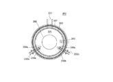
- FIG. 2 is a schematic configuration diagram of a part of a vertical processing furnace of a substrate processing apparatus suitably used in an embodiment of the present invention, and is a diagram showing a part of the processing furnace as a cross-sectional view taken along line AA of FIG.
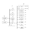
- the controller of the substrate processing apparatus used suitably by embodiment of this invention, and is a figure which shows the control system of a controller with a block diagram.
- (A) is a diagram showing a film forming sequence according to an embodiment of the present invention
- (b) to (d) are diagrams showing modifications of the film forming sequence according to an embodiment of the present invention.
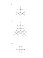
- (A) to (c) are diagrams showing chemical structural formulas of TSA, TEB, and DS, respectively. It is a figure which shows the evaluation result of a film-forming rate. It is a figure which shows the other evaluation result of a film-forming rate.
- (A) is a figure which shows the process conditions at the time of film-forming
- (b) is a figure which shows the composition of the formed film
- the processing furnace 202 has a heater 207 as a heating mechanism (temperature adjustment unit).
- the heater 207 has a cylindrical shape and is vertically installed by being supported by a holding plate.
- the heater 207 also functions as an activation mechanism (excitation unit) that activates (excites) gas with heat.
- a reaction tube 203 is disposed inside the heater 207 concentrically with the heater 207.
- the reaction tube 203 is made of a heat-resistant material such as quartz (SiO 2 ) or silicon carbide (SiC), and is formed in a cylindrical shape with the upper end closed and the lower end opened.
- a manifold (inlet flange) 209 is disposed below the reaction tube 203 concentrically with the reaction tube 203.
- the manifold 209 is made of a metal such as stainless steel (SUS), for example, and is formed in a cylindrical shape with an upper end and a lower end opened. The upper end portion of the manifold 209 is engaged with the lower end portion of the reaction tube 203 and is configured to support the reaction tube 203.
- An O-ring 220a as a seal member is provided between the manifold 209 and the reaction tube 203.
- the reaction tube 203 is installed vertically like the heater 207.
- the reaction vessel 203 and the manifold 209 mainly constitute a processing vessel (reaction vessel).
- a processing chamber 201 is formed in the cylindrical hollow portion of the processing container.
- the processing chamber 201 is configured to accommodate a plurality of wafers 200 as substrates.
- nozzles 249a and 249b are provided so as to penetrate the side wall of the manifold 209.
- Gas supply pipes 232a and 232b are connected to the nozzles 249a and 249b, respectively.
- a gas supply pipe 232c is connected to the gas supply pipe 232a.
- the gas supply pipes 232a to 232c are provided with mass flow controllers (MFC) 241a to 241c as flow rate controllers (flow rate control units) and valves 243a to 243c as opening / closing valves, respectively, in order from the upstream direction.
- MFC mass flow controllers
- Gas supply pipes 232d and 232e for supplying an inert gas are connected to the downstream sides of the valves 243a and 243b of the gas supply pipes 232a and 232b, respectively.
- the gas supply pipes 232d and 232e are respectively provided with MFCs 241d and 241e and valves 243d and 243e in this order from the upstream direction.
- Nozzles 249a and 249b are connected to the distal ends of the gas supply pipes 232a and 232b, respectively. As shown in FIG. 2, the nozzles 249 a and 249 b are arranged in an annular space in plan view between the inner wall of the reaction tube 203 and the wafer 200, along the upper portion from the lower portion of the inner wall of the reaction tube 203. Each is provided so as to rise upward in the stacking direction. That is, the nozzles 249a and 249b are respectively provided along the wafer arrangement area in the area horizontally surrounding the wafer arrangement area on the side of the wafer arrangement area where the wafers 200 are arranged. The nozzles 249a and 249b are respectively configured as L-shaped long nozzles.
- Gas supply holes 250a and 250b for supplying gas are provided on the side surfaces of the nozzles 249a and 249b, respectively.
- the gas supply holes 250 a and 250 b are opened so as to face the center of the reaction tube 203, and gas can be supplied toward the wafer 200.
- a plurality of gas supply holes 250a and 250b are provided from the lower part to the upper part of the reaction tube 203, each having the same opening area, and further provided at the same opening pitch.
- annular shape in a plan view defined by the inner wall of the side wall of the reaction tube 203 and the ends (peripheral portions) of the plurality of wafers 200 arranged in the reaction tube 203 is provided.
- Gas is conveyed through nozzles 249a and 249b arranged in a vertically long space, that is, in a cylindrical space.
- gas is first ejected into the reaction tube 203 from the gas supply holes 250a and 250b opened in the nozzles 249a and 249b, respectively, in the vicinity of the wafer 200.
- the main flow of gas in the reaction tube 203 is a direction parallel to the surface of the wafer 200, that is, a horizontal direction.
- the gas that flows on the surface of the wafer 200 flows toward the exhaust port, that is, the direction of the exhaust pipe 231 described later.
- the direction of the gas flow is appropriately specified depending on the position of the exhaust port, and is not limited to the vertical direction.
- a chemical bond between Si and hydrogen (H) (Si—H bond) is MFC 241a, valve 243a, It is supplied into the processing chamber 201 through the nozzle 249a.
- the first raw material for example, trisilylamine (N (SiH 3 ) 3 , abbreviation: TSA) gas can be used.
- TSA trisilylamine
- TSA is a substance containing Si—N bonds and Si—H bonds, and includes three Si—N bonds and nine Si—H bonds in one molecule. Is included. Note that three Sis are bonded to one N (central element) in TSA. TSA acts as an Si source and also as an N source in a film forming process to be described later.
- a pseudo catalyst containing boron (B) as a Group 13 (Group III) element and containing no N—H bond is supplied into the processing chamber 201 through the MFC 241b, the valve 243b, and the nozzle 249b. Is done.
- the term “catalyst” as used herein refers to a substance that does not change itself before and after a chemical reaction but changes the rate of the reaction.
- the pseudo catalyst in the reaction system of the present embodiment changes the reaction rate and the like as described later, but at least a part of itself changes before and after the chemical reaction. That is, the pseudo catalyst in the reaction system of the present embodiment acts as a catalyst, but is not strictly a “catalyst”.
- TEB triethylborane
- B (C 2 H 5 ) 3 abbreviation: TEB
- TEB triethylborane
- FIG. 5B TEB is a substance containing a BC bond, a CH bond, and a CC bond, and three BC bonds in one molecule, It contains 15 C—H bonds and 3 C—C bonds. Note that three Cs are bonded to one B (central element) in TEB. TEB not only acts as a catalyst but also acts as a B source and also as a C source in a film forming process described later.
- the second raw material having a molecular structure (chemical structure) different from that of the first raw material and containing an Si—H bond and not containing an NH bond is an MFC 241c, a valve 243c, a gas supply pipe 232a, a nozzle. It is supplied into the processing chamber 201 through 249a.
- the second raw material for example, disilane (Si 2 H 6 , abbreviation: DS) gas can be used.
- DS is a substance containing a Si—H bond and a Si—Si bond, and acts as a Si source in a film forming process described later.
- nitrogen (N 2 ) gas is used as an inert gas via the MFCs 241d and 241e, valves 243d and 243e, gas supply pipes 232a and 232b, and nozzles 249a and 249b, respectively. Supplied into 201.
- the first raw material supply system is mainly configured by the gas supply pipe 232a, the MFC 241a, and the valve 243a.
- a second raw material supply system is mainly configured by the gas supply pipe 232c, the MFC 241c, and the valve 243c.
- a pseudo catalyst supply system is mainly configured by the gas supply pipe 232b, the MFC 241b, and the valve 243b.
- an inert gas supply system is mainly configured by the gas supply pipes 232d and 232e, the MFCs 241d and 241e, and the valves 243d and 243e.
- any or all of the various supply systems described above may be configured as an integrated supply system 248 in which valves 243a to 243e, MFCs 241a to 241e, and the like are integrated.
- the integrated supply system 248 is connected to each of the gas supply pipes 232a to 232e, and supplies various gases into the gas supply pipes 232a to 232e, that is, opens and closes the valves 243a to 243e and MFCs 241a to 241e.
- the flow rate adjusting operation and the like are configured to be controlled by a controller 121 described later.
- the integrated supply system 248 is configured as an integrated or divided type integrated unit, and can be attached to and detached from the gas supply pipes 232a to 232e in units of integrated units, and maintenance and replacement of the supply system. , And the like can be added in units of integrated units.
- the reaction tube 203 is provided with an exhaust pipe 231 for exhausting the atmosphere in the processing chamber 201.
- the exhaust pipe 231 is connected to a pressure sensor 245 as a pressure detector (pressure detection unit) for detecting the pressure in the processing chamber 201 and an APC (Auto Pressure Controller) valve 244 as a pressure regulator (pressure adjustment unit).
- a vacuum pump 246 as a vacuum exhaust device is connected.
- the APC valve 244 can perform vacuum evacuation and vacuum evacuation stop in the processing chamber 201 by opening and closing the valve with the vacuum pump 246 activated, and further, with the vacuum pump 246 activated,
- the pressure in the processing chamber 201 can be adjusted by adjusting the valve opening based on the pressure information detected by the pressure sensor 245.
- An exhaust system is mainly configured by the exhaust pipe 231, the APC valve 244, and the pressure sensor 245.
- the vacuum pump 246 may be included in the exhaust system.
- a seal cap 219 is provided as a furnace opening lid capable of airtightly closing the lower end opening of the manifold 209.
- the seal cap 219 is made of a metal such as SUS and is formed in a disk shape.
- an O-ring 220b is provided as a seal member that comes into contact with the lower end of the manifold 209.
- a rotation mechanism 267 for rotating a boat 217 described later is installed below the seal cap 219.
- a rotation shaft 255 of the rotation mechanism 267 passes through the seal cap 219 and is connected to the boat 217.
- the rotation mechanism 267 is configured to rotate the wafer 200 by rotating the boat 217.
- the seal cap 219 is configured to be raised and lowered in the vertical direction by a boat elevator 115 as an elevating mechanism installed outside the reaction tube 203.
- the boat elevator 115 is configured so that the boat 217 can be carried in and out of the processing chamber 201 by moving the seal cap 219 up and down.
- the boat elevator 115 is configured as a transfer device (transfer mechanism) that transfers the boat 217, that is, the wafers 200 into and out of the processing chamber 201.
- a shutter 219s is provided below the manifold 209 as a furnace port lid that can airtightly close the lower end opening of the manifold 209 while the seal cap 219 is lowered by the boat elevator 115.
- the shutter 219s is made of a metal such as SUS and is formed in a disk shape. On the upper surface of the shutter 219s, an O-ring 220c as a seal member that comes into contact with the lower end of the manifold 209 is provided.
- the opening / closing operation (elevating operation, rotating operation, etc.) of the shutter 219s is controlled by the shutter opening / closing mechanism 115s.
- the boat 217 as a substrate support is configured to support a plurality of, for example, 25 to 200, wafers 200 in a multi-stage manner by aligning them vertically in a horizontal posture and with their centers aligned. It is configured to arrange at intervals.
- the boat 217 is made of a heat-resistant material such as quartz or SiC.
- heat insulating plates 218 made of a heat-resistant material such as quartz or SiC are supported in multiple stages. With this configuration, heat from the heater 207 is not easily transmitted to the seal cap 219 side.
- a temperature sensor 263 is installed as a temperature detector. By adjusting the power supply to the heater 207 based on the temperature information detected by the temperature sensor 263, the temperature in the processing chamber 201 becomes a desired temperature distribution.
- the temperature sensor 263 is configured in an L shape similarly to the nozzles 249a and 249b, and is provided along the inner wall of the reaction tube 203.
- the controller 121 which is a control unit (control means), is configured as a computer having a CPU (Central Processing Unit) 121a, a RAM (Random Access Memory) 121b, a storage device 121c, and an I / O port 121d.
- the RAM 121b, the storage device 121c, and the I / O port 121d are configured to exchange data with the CPU 121a via the internal bus 121e.
- An input / output device 122 configured as a touch panel or the like is connected to the controller 121.
- the storage device 121c includes a flash memory, a HDD (Hard Disk Drive), and the like.
- a control program that controls the operation of the substrate processing apparatus, a process recipe that describes a film forming process procedure and conditions that will be described later, and the like are stored in a readable manner.
- the process recipe is a combination of processes so that a predetermined result can be obtained by causing the controller 121 to execute each procedure in a film forming process to be described later, and functions as a program.
- process recipes, control programs, and the like are collectively referred to simply as programs.
- the process recipe is also simply called a recipe.
- the RAM 121b is configured as a memory area (work area) in which programs, data, and the like read by the CPU 121a are temporarily stored.
- the I / O port 121d includes the above-described MFCs 241a to 241e, valves 243a to 243e, pressure sensor 245, APC valve 244, vacuum pump 246, temperature sensor 263, heater 207, rotation mechanism 267, boat elevator 115, shutter opening / closing mechanism 115s, etc. It is connected to the.
- the CPU 121a is configured to read out and execute a control program from the storage device 121c and to read a recipe from the storage device 121c in response to an operation command input from the input / output device 122 or the like.
- the CPU 121a adjusts the flow rate of various gases by the MFCs 241a to 241e, the opening / closing operation of the valves 243a to 243e, the opening / closing operation of the APC valve 244 and the pressure adjustment by the APC valve 244 based on the pressure sensor 245 so as to follow the contents of the read recipe.
- the controller 121 installs the above-mentioned program stored in an external storage device 123 (for example, a magnetic disk such as a hard disk, an optical disk such as a CD or a DVD, a magneto-optical disk such as an MO, or a semiconductor memory such as a USB memory) 123 on a computer.
- an external storage device 123 for example, a magnetic disk such as a hard disk, an optical disk such as a CD or a DVD, a magneto-optical disk such as an MO, or a semiconductor memory such as a USB memory
- the storage device 121c and the external storage device 123 are configured as computer-readable recording media. Hereinafter, these are collectively referred to simply as a recording medium.
- recording medium When the term “recording medium” is used in this specification, it may include only the storage device 121c alone, may include only the external storage device 123 alone, or may include both of them.
- the program may be provided to the computer using communication means such as the Internet or a dedicated line
- the film forming sequence shown in FIG. Supplying a TSA gas as a first raw material to a wafer 200 as a substrate; Supplying TEB gas as a pseudo catalyst to the wafer 200; Film forming step of forming a silicon film (Si film) doped with B, C, and N as a film containing Si, B, C, and N on the wafer 200 by performing at least a certain period of overlap. Have In the film forming step, supply of a substance containing an N—H bond is not performed.
- Si film doped with B, C, and N is also referred to as a silicon borocarbonitride film (SiBCN film) or simply an Si film.
- SiBCN film silicon borocarbonitride film
- the film forming sequence shown in FIG. 4A may be indicated as follows, or may be indicated using the symbol [a]. The same notation is used in the following description of the modified examples.
- wafer when the term “wafer” is used, it means “wafer itself” or “a laminate (aggregate) of a wafer and a predetermined layer or film formed on the surface”. In other words, it may be called a wafer including a predetermined layer or film formed on the surface.
- wafer surface when the term “wafer surface” is used in this specification, it means “the surface of the wafer itself (exposed surface)” or “the surface of a predetermined layer or film formed on the wafer”. That is, it may mean “the outermost surface of the wafer as a laminated body”.
- the phrase “supplying a predetermined gas to the wafer” means “supplying a predetermined gas directly to the surface of the wafer itself” or “on the wafer. It may mean that a predetermined gas is supplied to the layer or film formed on the substrate, that is, the outermost surface of the wafer as a laminate. Further, in the present specification, the phrase “form a predetermined layer (or film) on the wafer” means “form a predetermined layer (or film) directly on the surface of the wafer itself”. In other cases, it may mean “to form a predetermined layer (or film) on a layer or film formed on the wafer, that is, on the outermost surface of the wafer as a laminate”.
- substrate is also synonymous with the term “wafer”.
- Vacuum exhaust (reduced pressure) is performed by the vacuum pump 246 so that the processing chamber 201, that is, the space where the wafer 200 exists, has a desired pressure (degree of vacuum).
- the pressure in the processing chamber 201 is measured by the pressure sensor 245, and the APC valve 244 is feedback-controlled based on the measured pressure information.
- the vacuum pump 246 maintains a state in which it is always operated until at least the processing on the wafer 200 is completed. Further, the wafer 200 in the processing chamber 201 is heated by the heater 207 so as to have a desired film formation temperature.
- the power supply to the heater 207 is feedback-controlled based on the temperature information detected by the temperature sensor 263 so that the inside of the processing chamber 201 has a desired temperature distribution. Heating of the processing chamber 201 by the heater 207 is continuously performed at least until the processing on the wafer 200 is completed. Further, the rotation of the boat 217 and the wafers 200 by the rotation mechanism 267 is started. The rotation of the boat 217 and the wafer 200 by the rotation mechanism 267 is continuously performed at least until the processing on the wafer 200 is completed.
- Deposition step In this step, TSA gas and TEB gas are simultaneously supplied to the wafer 200 in the processing chamber 201. That is, the TSA gas supply period and the TEB gas supply period overlap each other.
- valves 243a and 243b are opened, and TSA gas and TEB gas are allowed to flow into the gas supply pipes 232a and 232b, respectively.
- the flow rates of the TSA gas and the TEB gas are adjusted by the MFCs 241a and 241b, respectively, are supplied into the processing chamber 201 through the nozzles 249a and 249b, and are exhausted from the exhaust pipe 231.
- the TSA gas and the TEB gas are supplied to the wafer 200 together, that is, simultaneously.
- the valves 243d and 243e may be opened at the same time so that N 2 gas flows into the gas supply pipes 232d and 232e.
- the flow rate of the N 2 gas is adjusted by the MFCs 241 d and 241 e, supplied into the processing chamber 201 together with the TSA gas and the TEB gas, and exhausted from the exhaust pipe 231.
- the temperature of the wafer 200 (deposition temperature) is set to a predetermined temperature in the range of 150 to 400 ° C., preferably 250 to 350 ° C., for example.
- the pressure in the processing chamber 201 (film formation pressure) is set to a predetermined pressure within a range of 1 to 600 Pa, preferably 5 to 30 Pa, for example.
- the above temperature range is a temperature at which TSA does not thermally decompose (self-decompose) when at least TSA is present alone in processing chamber 201, and each of TSA and TEB is independent in processing chamber 201. When present, it contains a temperature (150-325 ° C.) at which no material will thermally decompose.
- the above-described temperature zone is also a temperature at which the DS does not thermally decompose when a DS used in a modification described later is present alone.
- the film formation temperature is less than 150 ° C. (or the film formation pressure is less than 1 Pa)
- the film formation reaction on the wafer 200 described later does not proceed easily, and a practical film formation speed cannot be obtained, resulting in a decrease in productivity.
- a poor quality film containing a large amount of dangling bonds may be formed on the wafer 200.
- the film forming temperature is set to 150 ° C. or higher (or the film forming pressure to 1 Pa or higher)
- the film forming reaction on the wafer 200 is advanced and a practical film forming speed can be obtained.
- dangling bonds contained in the film formed on the wafer 200 can be reduced, and the film quality of the film can be improved.
- the film forming reaction on the wafer 200 can be further promoted and the film forming speed can be further increased.
- dangling bonds contained in the film formed on the wafer 200 can be further reduced, and the film quality of this film can be further improved.
- TEB When the film formation temperature exceeds 400 ° C. (or the film formation pressure exceeds 600 Pa), TEB tends to be thermally decomposed, and it may be difficult to proceed with the film formation process utilizing the catalytic action of TEB.
- the film forming temperature By setting the film forming temperature to 400 ° C. or lower (or the film forming pressure to 600 Pa or lower), it is possible to suppress the thermal decomposition of TEB and to proceed with the film forming process using the catalytic action of TEB.
- the film forming temperature By setting the film forming temperature to 350 ° C. or lower (or the film forming pressure to 30 Pa or lower), the thermal decomposition of TEB can be more reliably suppressed, and the film forming process utilizing the catalytic action of TEB can be more reliably advanced. It becomes possible.
- the supply flow rate of the TSA gas is, for example, a predetermined flow rate in the range of 1 to 2000 sccm, preferably 50 to 200 sccm.
- the supply flow rate of the TEB gas is, for example, a predetermined flow rate in the range of 1 to 1000 sccm, preferably 25 to 100 sccm.
- the supply flow rate of N 2 gas is, for example, a predetermined flow rate in the range of 1 ⁇ 10000 sccm.
- the supply flow rates of these gases can be determined as appropriate according to the composition of the film to be formed on the wafer 200.
- the film formation reaction of the Si film on the wafer 200 proceeds at a practical film formation rate, for example, a rate of 5 min / min or more, preferably 10 ⁇ / min or more.
- TEB acts as a catalyst. That is, TEB is a chemical species having a low energy vacant orbit and acts as a Lewis acid, that is, an electron pair acceptor in the reaction system of the present embodiment.
- TSA acts as a Lewis base, that is, an electron pair donor in the reaction system of this embodiment.
- protons (H + ) are extracted from TSA, and the above-described film formation process proceeds.
- TEB mainly acts on Si—H bonds, not Si—N bonds, among the chemical bonds of TSA.
- the Si film formed in this embodiment can be used as a film for a sidewall spacer (SWS) by controlling the composition thereof, and also can be used as a silicon core in a double patterning (DP) process. That is, it can be used as a film for a hard mask (silicon hard mask).
- SWS sidewall spacer
- DP double patterning
- the Si film formed on the wafer 200 it is preferable to appropriately adjust the execution time of the film formation step so that the film thickness is, for example, 50 to 100 mm (5 to 10 nm). Further, when the Si film formed on the wafer 200 is used as a hard mask, it is preferable to appropriately adjust the execution time of the film forming step so that the film thickness is, for example, 200 to 300 mm (20 to 30 nm).
- a substance (silylamine) represented by the structural formula of N (SiX 3 ) 3 can be used as the first raw material.
- X refers to at least one functional group (substituent) selected from the group consisting of hydrogen, halogeno group, alkyl group, amino group, alkoxy group and hydroxy group.
- the halogeno group here is a halogen atom that functions as a monovalent functional group, such as a chloro group (—Cl), a fluoro group (—F), a bromo group (—Br), an iodo group (—I), etc. That is.
- the alkyl group here is a monovalent functional group represented by the structural formula of —C n H 2n + 1 , wherein one H is removed from a chain saturated hydrocarbon (alkane).
- alkyl group examples include a methyl group (—CH 3 ), an ethyl group (—C 2 H 5 ), a propyl group (—C 3 H 7 ), an isopropyl group (—CH (CH 3 ) CH 3 ), a butyl group (— C 4 H 9 ), an isobutyl group (—CH 2 CH (CH 3 ) 2 ) and the like.
- the amino group here is a monovalent functional group represented by the structural formula of —NR 1 R 2 (where R 1 and R 2 are alkyl groups, respectively), such as —NH 2 , —NHR, etc.
- the amino group containing the N—H bond is not meant.
- the alkoxy group here is a monovalent functional group represented by the structural formula of —OR, in which an alkyl group (R) is bonded to an oxygen atom (O).
- the hydroxy group is a monovalent functional group represented by the structural formula of —OH. Examples of silylamines having these functional groups include TSA, N (SiH 2 (NR 1 R 2 )) 3 , N (SiH (NR 1 R 2 ) 2 ) 3 , N (Si (NR 1 R 2). 3 ) 3 is mentioned.
- a substance represented by a composition formula of Si n C m H 2n + 2m + 2 (n and m are integers of 1 or more), that is, an organic silane having no unsaturated bond is used. You can also.
- organic silanes examples include monomethylsilane (SiCH 6 ), monoethylsilane (SiC 2 H 8 ), dimethylsilane (SiC 2 H 8 ), 1,2-disilapropane (Si 2 CH 8 ), 1,3- Disilapropane (Si 2 CH 8 ), trimethylsilane (SiC 3 H 10 ), monopropylsilane (SiC 3 H 10 ), 1,2-disilabutane (Si 2 C 2 H 10 ), 1,3-disilabutane (Si 2 C) 2 H 10 ), 1,4-disilabutane (Si 2 C 2 H 10 ), 2,3-disilabutane (Si 2 C 2 H 10 ), 2,4-disilapentane (Si 2 C 3 H 12 ), 1,3 , 5-trisilapentane (Si 3 C 2 H 12 ) or the like, that is, a silane containing an alkyl group
- An alkylene group is a divalent functional group represented by the structural formula of —C n H 2n + 2 —, in which two H atoms are removed from an alkane.
- Examples of the alkylene group include a methylene group (—CH 2 —), an ethylene group (—C 2 H 4 —), a propylene group (—C 3 H 6 —), a butylene group (—C 4 H 8 —), and the like. .
- a substance represented by a composition formula of Si n C m H 2n + 2m (n is an integer of 1 or more, m is an integer of 2 or more), that is, a vinyl group (—CH ⁇ CH 2 ),
- An organic silane containing an allyl group (—CH 2 CH ⁇ CH 2 ) and having an unsaturated bond, or an organic silane having a cyclic structure (cyclo structure) can also be used.
- organic silanes examples include vinyl silane (SiC 2 H 6 ), methyl vinyl silane (SiC 3 H 6 ), allyl silane (SiC 3 H 6 ), silacyclobutane (SiC 3 H 6 ), 1,3-disilacyclobutane (A substance such as Si 2 C 2 H 6 ) can be used. These substances are substances containing at least a Si—C bond and a Si—H bond, and some include a C—H bond and a C—C bond.
- a silylamine containing an alkyl group that is, a substance that not only acts as a Si source and N source but also acts as a C source, than using TSA as the first raw material, It becomes possible to control in a direction to increase the C concentration of the Si film formed on the wafer 200.
- Si formed on the wafer 200 can be formed more than when TSA is used as the first raw material. It becomes possible to increase the amount of Si—N bonds contained in the film and control the N concentration of the film to increase.
- TSA is used as the first raw material by using a silylamine containing an alkoxy group as the first raw material, that is, a substance that acts not only as a Si source and an N source but also as a C source and an O source.
- a silylamine containing an alkoxy group that is, a substance that acts not only as a Si source and an N source but also as a C source and an O source.
- the C concentration of the Si film formed on the wafer 200 can be controlled to be increased, and a small amount of O can be added to the film.
- a silylamine containing a hydroxy group as a first raw material, that is, a substance that not only acts as an Si source and an N source but also acts as an O source, the Si film formed on the wafer 200 is used. , O can be added in a small amount.
- organosilane containing Si—C bond and Si—H bond and not containing Si—N bond as the first raw material, that is, a substance that acts as an Si source but does not act as an N source
- a Si film doped with N-free B and C is also referred to as a silicon borocarbide film (SiBC film) or simply an Si film for convenience.
- the first raw material hydrogen, a halogeno group, an alkyl group, an Si—N bond or a Si—C bond, and a Si—H bond and hydrogen, a halogeno group, an alkyl group,
- a substance containing at least one selected from the group consisting of an alkylene group, an amino group, an alkoxy group, a hydroxy group, a vinyl group and an allyl group, and structural isomers and derivatives thereof can be suitably used.
- a substance (boron compound) represented by the structural formula of BX 3 can be suitably used.
- X is at least one functional group selected from the group consisting of hydrogen, halogeno group, alkyl group, amino group, alkoxy group and hydroxy group.
- boron compounds having these functional groups include TEB, borane (borohydride) such as diborane (B 2 H 6 ), trichloroborane (BCl 3 ), trifluoroborane (BF 3 ), Haloborane such as bromoborane (BBr 3 ), triiodoborane (BI 3 ), trimethylborane (B (CH 3 ) 3 ), triethylborane (B (C 2 H 5 ) 3 ), triisopropylborane (B (C 3 H 7 ) 3 , alkylborane such as tributylborane (B (C 4 H 9 ) 3 ), trisdimethylaminoborane (B [N (CH 3 ) 2 ] 3 ), trisdiethylaminoborane (B [N (C 2 H 5) 2] 3) , tris dipropylamino borane (B [N (C 3 H 7) 2] 3), tri
- a C-free boron hydride or haloborane that is, a substance that acts as a B source but does not act as a C source can be used to form C into the Si film formed on the wafer 200. Can be avoided. That is, it becomes possible to form a Si film doped with B and N not containing C on the wafer 200.
- the Si film doped with B and N is also referred to as a silicon boronitride film (SiBN film) or simply as a Si film for convenience.
- the pseudocatalyst is formed on wafer 200 as compared with the case of using TEB as a pseudocatalyst. It becomes possible to increase the C concentration of the Si film.
- the C concentration of the Si film formed on the wafer 200 is controlled to be lower than when TEB is used as the pseudo catalyst. It becomes possible.
- aminoborane that is, a substance that not only acts as a B source and a C source but also acts as an N source, is formed on the wafer 200 as compared with the case where TEB is used as a pseudo catalyst. It is possible to control the N concentration of the Si film to be increased.
- a pseudo catalyst aluminum containing an alkyl group represented by a structural formula such as Al (CH 3 ) 3 , Al (C 2 H 5 ) 3 , Al (C 3 H 7 ) 3 in addition to the above-described boron compound.
- a compound or an aluminum compound containing a halogeno group represented by a structural formula such as AlCl 3 can also be used. These substances are substances containing no NH bond containing aluminum (Al) as a Group 13 element.
- a film containing Si, Al, C, N that is, an Si film doped with Al, C, N (SiAlCN film) is formed on the wafer 200. can do.
- a film containing Si, Al, N that is, a Si film doped with Al, N (SiAlN film) is formed on the wafer 200. be able to.
- the pseudo catalyst is selected from the group consisting of hydrogen, a halogeno group, an alkyl group, an amino group, an alkoxy group, and a hydroxy group as long as a substance containing a Group 13 element and containing no NH bond is used. Substances containing at least one and structural isomers and derivatives thereof can be suitably used.
- the type of the pseudo catalyst By appropriately selecting the type of the pseudo catalyst, the composition and physical properties of the film formed on the wafer 200 can be controlled in a wide range and precisely.
- the inert gas for example, a rare gas such as Ar gas, He gas, Ne gas, or Xe gas can be used in addition to N 2 gas.
- a rare gas such as Ar gas, He gas, Ne gas, or Xe gas can be used in addition to N 2 gas.
- TEB can act as a catalyst by simultaneously supplying a TSA gas acting as a Lewis base and a TEB gas acting as a Lewis acid to the wafer 200.
- a TSA gas acting as a Lewis base and a TEB gas acting as a Lewis acid to the wafer 200.
- the film forming process on the wafer 200 can be allowed to proceed at a practical rate under the low-temperature conditions described above.
- By performing the film forming process under a low temperature condition it is possible to reduce the thermal damage that the wafer 200 receives and to control the thermal history well.
- N By using a substance containing Si—N bonds such as TSA but not containing N—H bonds as the first raw material, N can be added to the film formed on the wafer 200 by adding N— It is possible to carry out in the form of Si—N bonds instead of H bonds.
- the film forming step since the supply of the substance containing NH bonds such as NH 3 gas to the wafer 200 is not performed, the addition of NH bonds to the film formed on the wafer 200 is not performed. It is also possible to suppress more reliably.
- the film formed on the wafer 200 can be a film having high oxidation resistance (ashing resistance).
- N incorporated into the film in the Si—N bond state acts as a protective (guard) element that suppresses oxidation of the film, whereas NH
- a film formed according to the present embodiment is a film formed using NH 3 gas as an N source (containing many NH bonds). It has been confirmed that the film exhibits high ashing resistance even if the N concentration of the film is approximately the same as that of a film containing almost no Si—N bond.
- the amount of N added to the Si film can be further increased by using a substance having a higher N content (number of N atoms contained in one molecule) than TSA as the first raw material.
- N / SiBCN ratio the ratio of the amount of N to the amount of Si, B, C, N contained in the Si film formed on the wafer 200.
- the extinction coefficient is a coefficient indicating the degree to which the light intensity is attenuated by absorption by the Si film when the light travels through the substance (Si film). The attenuation increases as this value increases. Means to grow.
- the Si film has a low extinction coefficient in order to confirm the alignment mark and the like.
- the supply flow rate of TSA gas is increased, the partial pressure or concentration of TSA gas in the processing chamber 201 is increased, or a substance having a higher Si content than TSA is used as the first raw material.
- the ratio of the amount of Si to the amount of Si, B, C, and N contained in the Si film Si / SiBCN ratio
- the Si content ratio can be increased.
- the ashing resistance of the Si film can be increased, and the resistance of the Si film to hydrogen fluoride (HF) or the like, that is, the etching resistance can be increased.
- this film can be used as a sacrificial film suitable for use as a hard mask.
- the Si / SiBCN ratio of the Si film formed on the wafer 200 is set to, for example, the first raw material supply flow rate (the first raw material supply flow rate to the pseudo catalyst). And the type of the first raw material can be controlled appropriately. In the film forming sequence shown in FIG. 4A, it is difficult to change the Si / SiBCN ratio described above even if the film forming temperature or film forming pressure is changed.
- (E) B or C can be added to the Si film formed on the wafer 200 by using a substance containing B and C such as TEB as a pseudo catalyst.
- the TEB gas supply flow rate is increased, the TEB gas partial pressure or concentration in the processing chamber 201 is increased, or a substance having a higher C content than TEB is used as a pseudo catalyst.
- a substance having a higher C content than TEB is used as a pseudo catalyst.
- B or C added to the Si film By increasing the amount of B and C added to the Si film and increasing the ratio of B and C to the amount of Si, B, C and N contained in the Si film (B, C / SiBCN ratio) Etching resistance can be improved and the extinction coefficient can be reduced.
- this film can be used as a low-k film suitable for SWS applications, for example.
- the B, C / SiBCN ratio of the Si film formed on the wafer 200 is set to, for example, the supply flow rate of the pseudo catalyst (supply of the pseudo catalyst to the first raw material). It is possible to control by appropriately selecting the ratio of the flow rate) and the type of the pseudo catalyst. In the film forming sequence shown in FIG. 4A, it is difficult to change the B, C / SiBCN ratio described above even if the film forming temperature or film forming pressure is changed.
- the film forming step further includes a step of supplying a DS gas, a step of supplying a TSA gas, and a TEB gas.
- a step of overlapping with at least a certain period of time may be included.
- the supply flow rate and supply time of the DS gas can be set similarly to the supply flow rate and supply time of the TSA gas. Note that the film formation sequence shown in FIG. 4D and the symbol [d] shows a case where TSA gas, DS gas, and TEB gas are supplied simultaneously and continuously during the execution period of the film formation step.
- the N / SiBCN ratio and the B, C / SiBCN ratio can be extended over a wider range than the film forming sequence shown in FIG. It can be freely controlled.
- the N / SiBCN ratio in the Si film formed on the wafer 200 can be controlled to increase. It becomes. Further, by reducing the above TSA / DS, it is possible to control the N / SiBCN ratio in the Si film formed on the wafer 200 in a decreasing direction.
- the B, C / SiBCN ratio in the Si film formed on the wafer 200 is controlled to increase. It becomes possible. Further, by reducing the above-described TEB / DS, it is possible to control in a direction to decrease the B, C / SiBCN ratio in the Si film formed on the wafer 200.
- a hydrogenation represented by a substance such as SiH 4 , Si 3 H 8 , Si 4 H 10 , that is, a general formula Si n H 2n + 2 (n is an integer of 1 or 2 or more) Silicon can be used.
- silicon hydride higher than DS it is possible to increase the Si content ratio (Si / SiBCN ratio) in the Si film formed on the wafer 200. Since the catalytic action by TEB can be obtained as long as it has a Si—H bond, a silane (halosilane) containing a halogeno group represented by a chemical formula such as SiH 3 Cl or SiH 2 Cl 2 is used as the second raw material. You can also.
- An aminosilane containing an —H bond and an Si—N bond and not containing an NH bond can also be used.
- Step 1 for supplying the TSA gas to the wafer 200 and Step 2 for supplying the TEB gas to the wafer 200 are alternately performed a predetermined number of times. It may be performed (n times).
- the residual gas removal step for removing the residual gas and the like from the processing chamber 201 is not performed.
- the TSA gas and the TEB gas are mixed in the processing chamber 201, and the film forming process using the catalytic action of TEB can be advanced.
- the step coverage and film thickness controllability of the Si film formed on the wafer 200 can be improved as compared with the case where the TSA gas and the TEB gas are supplied simultaneously.
- the supply flow rate of TSA gas or TEB gas into the processing chamber 201 should be higher than the exhaust flow rate of TSA gas or TEB gas from the processing chamber 201. preferable. Further, when maintaining the state in which the gas is sealed in the processing chamber 201 for a predetermined time, after supplying a predetermined amount of gas into the processing chamber 201 in a state where the exhaust system is substantially blocked, By stopping the gas supply and maintaining the state for a predetermined time, the amount of gas used can be reduced and the gas cost can be reduced.
- Recipes used for substrate processing are individually determined according to the processing details (film type, composition ratio, film quality, film thickness, processing procedures, processing conditions, etc.) And stored in the storage device 121c via the telecommunication line or the external storage device 123. And when starting a board
- the above-described recipe is not limited to a case of newly creating, but may be prepared by changing an existing recipe that has already been installed in the substrate processing apparatus, for example.
- the changed recipe may be installed in the substrate processing apparatus via an electric communication line or a recording medium on which the recipe is recorded.
- an existing recipe that has already been installed in the substrate processing apparatus may be directly changed by operating the input / output device 122 provided in the existing substrate processing apparatus.
- a film is formed using a batch-type substrate processing apparatus that processes a plurality of substrates at one time.
- the present invention is not limited to the above-described embodiment, and can be suitably applied to a case where a film is formed using, for example, a single-wafer type substrate processing apparatus that processes one or several substrates at a time.
- a film is formed using a substrate processing apparatus having a hot wall type processing furnace.
- the present invention is not limited to the above-described embodiment, and can be suitably applied to a case where a film is formed using a substrate processing apparatus having a cold wall type processing furnace.
- the processing furnace 302 includes a processing container 303 that forms the processing chamber 301, a shower head 303s as a gas supply unit that supplies gas into the processing chamber 301 in a shower shape, and one or several wafers 200 in a horizontal posture.
- a support base 317 for supporting, a rotating shaft 355 for supporting the support base 317 from below, and a heater 307 provided on the support base 317 are provided.
- Gas supply ports 332a and 332b are connected to the inlet (gas inlet) of the shower head 303s.
- the gas supply port 332a is connected to a supply system similar to the first and second raw material supply systems of the above-described embodiment.
- a supply system similar to the pseudo catalyst supply system of the above-described embodiment is connected to the gas supply port 332b.
- a gas dispersion plate that supplies gas into the processing chamber 301 in a shower shape is provided at the outlet (gas outlet) of the shower head 303s.
- the shower head 303 s is provided at a position facing (facing) the surface of the wafer 200 carried into the processing chamber 301.
- the processing vessel 303 is provided with an exhaust port 331 for exhausting the inside of the processing chamber 301.
- An exhaust system similar to the exhaust system of the above-described embodiment is connected to the exhaust port 331.
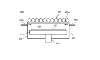
- the present invention can also be suitably applied to the case where a film is formed using a substrate processing apparatus including the processing furnace 402 shown in FIG.
- the processing furnace 402 includes a processing container 403 that forms a processing chamber 401, a support base 417 that supports one or several wafers 200 in a horizontal position, a rotating shaft 455 that supports the support base 417 from below, and a processing container.
- a lamp heater 407 that irradiates light toward the wafer 200 in the 403 and a quartz window 403w that transmits light from the lamp heater 407 are provided.
- Gas supply ports 432 a and 432 b are connected to the processing container 403.
- the gas supply port 432a is connected to a supply system similar to the first and second raw material supply systems in the above-described embodiment.
- a supply system similar to the pseudo catalyst supply system of the above-described embodiment is connected to the gas supply port 432b.
- the gas supply ports 432a and 432b are respectively provided on the side of the end portion of the wafer 200 loaded into the processing chamber 401, that is, at a position not facing the surface of the wafer 200 loaded into the processing chamber 401.
- the processing container 403 is provided with an exhaust port 431 for exhausting the inside of the processing chamber 401.
- An exhaust system similar to the exhaust system of the above-described embodiment is connected to the exhaust port 431.
- the film forming process can be performed with the same processing procedure and processing conditions as in the above-described embodiment and modification, and the same effect as in the above-described embodiment and modification can be obtained. It is done.
- the present invention is not limited to such an embodiment. That is, the present invention can be suitably applied to the case where a film containing a metal element such as germanium (Ge) or B as a main element in addition to Si is formed on the substrate.
- the present invention also provides titanium (Ti), zirconium (Zr), hafnium (Hf), niobium (Nb), tantalum (Ta), molybdenum (Mo), tungsten (W), yttrium (Y), La (lanthanum).
- the present invention can also be suitably applied to the case where a film containing a metal element such as strontium (Sr) or aluminum (Al) as a main element is formed on a substrate.
- processing procedure and processing conditions at this time can be the same as the processing procedure and processing conditions of the above-described embodiment, for example.
- Example 1 Film formation evaluations A1 to A3 were performed using the substrate processing apparatus in the above-described embodiment.
- the film formation process according to the film formation sequence shown in FIG. 4A was performed under conditions of film formation temperatures of 300 ° C., 325 ° C., and 350 ° C., respectively.
- film formation evaluation A2 film formation processing by a film formation sequence for supplying TEB gas alone to the wafer was performed under conditions of film formation temperatures of 325 ° C., 350 ° C., 375 ° C., and 400 ° C., respectively.
- film formation processing by a film formation sequence for supplying the TSA gas alone to the wafer was performed under conditions of film formation temperatures of 500 ° C. and 525 ° C., respectively.
- the other processing conditions are those within the condition range described in the above embodiment, and are common to the film formation evaluations A1 to A3.
- FIG. 6 is a diagram showing the evaluation results of the film formation rate.
- the horizontal axis indicates the film formation temperature
- the vertical axis indicates the film formation rate ( ⁇ / min).
- ⁇ , ⁇ , and ⁇ indicate film formation evaluations A1 to A3, respectively.
- the film formation evaluation A1 it is difficult to obtain a practical film formation rate when the film formation temperature is 300 ° C., but it is practically achieved by setting the film formation temperature to 325 ° C. or higher. It can be seen that the film rate is obtained.
- a practical film formation rate is difficult to obtain when the film formation temperature is 350 ° C.
- the film formation process can be performed at a practical film formation rate in a low temperature region where the film formation process cannot proceed. It is also possible to proceed with the film treatment. This is presumably because the amount of energy (activation energy) required for activating TSA is reduced by supplying TEB gas together with TSA gas, and TSA is easily activated.
- the pressure in the processing chamber (partial pressure of the TSA gas and TEB gas in the processing chamber) is appropriately adjusted to further increase the temperature to 300 ° C. or less. It has been confirmed that the film formation process can proceed at a practical film formation rate even in a low temperature region, for example, at a temperature of 250 ° C. or lower.
- Film formation evaluations B1 to B3 were performed using the substrate processing apparatus in the above-described embodiment.
- the film formation process according to the film formation sequence shown in FIG. 4A was performed under the conditions of a film formation temperature of 350 ° C. and a total partial pressure of 3 Pa of TSA gas and TEB gas in the processing chamber.
- the same film formation process as the film formation evaluation B1 was performed under conditions of a film formation temperature of 325 ° C. and total partial pressures of 3 Pa, 9 Pa, and 30 Pa of TSA gas and TEB gas in the processing chamber.
- the same film formation process as the film formation evaluation B1 was performed under conditions of a film formation temperature of 300 ° C. and total partial pressures of 3 Pa, 9 Pa, and 30 Pa of TSA gas and TEB gas in the processing chamber.
- the other processing conditions are those within the condition range described in the above embodiment, and are common to the film formation evaluations B1 to B3.
- FIG. 7 is a diagram showing the evaluation results of the film formation rate.
- the horizontal axis in FIG. 7 represents the total partial pressure (Pa) of the TSA gas and TEB gas, and the vertical axis represents the film formation rate ( ⁇ / min).
- ⁇ , ⁇ , and ⁇ indicate film formation evaluations B1 to B3, respectively. According to FIG. 7, it can be seen that the film formation rate increases as the film formation temperature is increased and the total partial pressure of the TSA gas and the TEB gas is increased. Further, in the film formation evaluation B1, it can be seen that a practical film formation rate can be obtained even when the total partial pressure of the TSA gas and the TEB gas is 3 Pa.
- the film formation evaluation B2 it is difficult to obtain a practical film formation rate when the total partial pressure of the TSA gas and the TEB gas is 3 Pa, but the total partial pressure of the TSA gas and the TEB gas is increased to 9 Pa. It can be seen that a practical film formation rate can be obtained. Further, in the film formation evaluation B3, when the total partial pressure of the TSA gas and the TEB gas is 9 Pa or less, a practical film formation rate is difficult to obtain, but the total partial pressure of the TSA gas and the TEB gas is increased to 30 Pa. It can be seen that a practical film forming rate can be obtained.
- a temperature of 350 ° C. or lower for example, a temperature of 325 ° C. or 300 ° C.
- the film formation process can proceed at a practical film formation rate.
- the inventors have adjusted the total partial pressure of the TSA gas and the TEB gas in the processing chamber appropriately, so that the practical growth can be achieved even in a further low temperature region of 300 ° C. or lower, for example, 250 ° C. or lower. It has been confirmed that the film forming process can proceed at the film rate.
- Film formation evaluations C1 to C8 were performed using the substrate processing apparatus in the above-described embodiment.
- the film formation process according to the film formation sequence shown in FIG. 4A is performed.
- the film formation process according to the film formation sequence shown in FIG. was performed by a film forming sequence in which TSA gas, TEB gas, and NH 3 gas were simultaneously supplied to the wafer.
- the film formation temperature (° C.), film formation pressure (Pa), TSA gas, DS gas, TEB gas, and NH 3 gas supply flow rates (sccm) in the film formation evaluations C1 to C8 are shown in FIG.
- the condition was within the condition range.
- the other processing conditions are those within the condition range described in the above embodiment, and are common to the film formation evaluations C1 to C8.
- the composition of each of the films formed in the film formation evaluations C1 to C8 (hereinafter referred to as films C1 to C8, respectively) was measured by XPS (X-ray photoelectron spectroscopy).
- XPS X-ray photoelectron spectroscopy
- FIG. 8B shows that the compositions of the films C1 to C3 are almost the same. That is, when the supply flow rates of the TSA gas and the TEB gas are set to the same level, the film composition hardly changes even when the processing conditions such as the film forming temperature and the film forming pressure are changed.
- the Si concentration of the film C4 is higher than the Si concentrations of the films C1 to C3. That is, it can be seen that by increasing the ratio of the TSA gas supply flow rate to the TEB gas supply flow rate, the Si concentration of the film formed on the wafer can be controlled to increase.
- the composition of the film is mainly determined by the supply flow rates of the TSA gas and the TEB gas, not the film formation temperature and the film formation pressure.
- the Si concentration of the films C5 to C7 is higher than the Si concentration of the films C1 to C4. From this, by using both TSA gas and DS gas as raw materials, that is, when TSA gas and TEB gas are supplied simultaneously, DS gas is further added to these gases, so that on the wafer. It can be seen that the film can be controlled to increase the Si concentration of the film formed. It can also be seen that the Si concentrations of the films C6 and C7 are higher than the Si concentration of the film C5. Therefore, when TSA gas and DS gas are used as raw materials, the DS gas supply flow rate is increased, that is, when TSA gas and TEB gas are supplied simultaneously, DS gas is further added to these gases. It can be seen that by increasing the supply flow rate, the Si concentration of the film formed on the wafer can be controlled to increase.
- the films C1 to C8 are all N-free Si films, such as Si films formed by performing a film forming sequence for simultaneously supplying BCl 3 and SiH 4 to the wafer. It has been confirmed that the film has a low extinction coefficient.
- the TSA gas and TEB gas supply flow rate is adjusted appropriately, DS gas is added to these gases, and the DS gas supply flow rate is adjusted appropriately, so that it is formed on the wafer.
- the Si film can be enriched with Si, the B concentration and C concentration of the film can be appropriately reduced, and the N concentration of the film can be appropriately increased. Further, since the composition of the Si film is not easily affected by the film formation temperature and the film formation pressure as described above, it is possible to set these conditions over a wide range (freely). It becomes easy to improve thickness uniformity between wafers and wafer in-plane uniformity.
- Controller control unit 200 wafer (substrate) 201 Processing chamber 202 Processing furnace 203 Reaction tube 207 Heater 231 Exhaust tubes 232a to 232e Gas supply tubes
Landscapes
- Chemical & Material Sciences (AREA)
- Chemical Kinetics & Catalysis (AREA)
- Engineering & Computer Science (AREA)
- Mechanical Engineering (AREA)
- General Chemical & Material Sciences (AREA)
- Materials Engineering (AREA)
- Metallurgy (AREA)
- Organic Chemistry (AREA)
- Inorganic Chemistry (AREA)
- Chemical Vapour Deposition (AREA)
- Formation Of Insulating Films (AREA)
- Physics & Mathematics (AREA)
- Plasma & Fusion (AREA)
Abstract
Description
基板に対して、所定元素と窒素との化学結合または前記所定元素と炭素との化学結合と、前記所定元素と水素との化学結合と、を含み、窒素と水素との化学結合非含有の第1原料を供給する工程と、
前記基板に対して、第13族元素を含み窒素と水素との化学結合非含有の擬似触媒を供給する工程と、
を少なくとも一定期間オーバーラップさせて行うことで、前記基板上に膜を形成する工程を有し、
前記膜を形成する工程では、窒素と水素との化学結合を含む物質の前記基板に対する供給を不実施とする技術が提供される。
以下、本発明の一実施形態について図1~図3を参照しながら説明する。
図1に示すように、処理炉202は加熱機構(温度調整部)としてのヒータ207を有する。ヒータ207は円筒形状であり、保持板に支持されることにより垂直に据え付けられている。ヒータ207は、ガスを熱で活性化(励起)させる活性化機構(励起部)としても機能する。
上述の基板処理装置を用い、半導体装置の製造工程の一工程として、基板上に膜を形成するシーケンス例について、図4(a)を用いて説明する。以下の説明において、基板処理装置を構成する各部の動作はコントローラ121により制御される。
基板としてのウエハ200に対して第1原料としてのTSAガスを供給するステップと、
ウエハ200に対して擬似触媒としてのTEBガスを供給するステップと、
を少なくとも一定期間オーバーラップさせて行うことで、ウエハ200上に、Si,B,C,Nを含む膜として、B,C,Nがドープされたシリコン膜(Si膜)を形成する成膜ステップを有し、
成膜ステップでは、N-H結合を含む物質の供給を不実施とする。
複数枚のウエハ200がボート217に装填(ウエハチャージ)されると、シャッタ開閉機構115sによりシャッタ219sが移動させられて、マニホールド209の下端開口が開放される(シャッタオープン)。その後、図1に示すように、複数枚のウエハ200を支持したボート217は、ボートエレベータ115によって持ち上げられて処理室201内へ搬入(ボートロード)される。この状態で、シールキャップ219は、Oリング220bを介してマニホールド209の下端をシールした状態となる。
処理室201内、すなわち、ウエハ200が存在する空間が所望の圧力(真空度)となるように、真空ポンプ246によって真空排気(減圧排気)される。この際、処理室201内の圧力は圧力センサ245で測定され、この測定された圧力情報に基づきAPCバルブ244がフィードバック制御される。真空ポンプ246は、少なくともウエハ200に対する処理が終了するまでの間は常時作動させた状態を維持する。また、処理室201内のウエハ200が所望の成膜温度となるようにヒータ207によって加熱される。この際、処理室201内が所望の温度分布となるように、温度センサ263が検出した温度情報に基づきヒータ207への通電具合がフィードバック制御される。ヒータ207による処理室201内の加熱は、少なくともウエハ200に対する処理が終了するまでの間は継続して行われる。また、回転機構267によるボート217およびウエハ200の回転を開始する。回転機構267によるボート217およびウエハ200の回転は、少なくともウエハ200に対する処理が終了するまでの間は継続して行われる。
このステップでは、処理室201内のウエハ200に対し、TSAガスとTEBガスとを同時に供給する。すなわち、TSAガスの供給期間とTEBガスの供給期間とをオーバーラップさせる。
成膜ステップが終了し、ウエハ200上に所望組成の膜が形成されたら、バルブ243a,243bを閉じ、処理室201内へのTSAガス、TEBガスの供給をそれぞれ停止する。また、ガス供給管232d,232eのそれぞれからN2ガスを処理室201内へ供給し、排気管231から排気する。N2ガスはパージガスとして作用する。これにより、処理室201内がパージされ、処理室201内に残留するガスや反応副生成物が処理室201内から除去される(アフターパージ)。その後、処理室201内の雰囲気が不活性ガスに置換され(不活性ガス置換)、処理室201内の圧力が常圧に復帰される(大気圧復帰)。
その後、ボートエレベータ115によりシールキャップ219が下降され、マニホールド209の下端が開口されるとともに、処理済のウエハ200が、ボート217に支持された状態でマニホールド209の下端から反応管203の外部に搬出(ボートアンロード)される。ボートアンロードの後は、シャッタ219sが移動させられ、マニホールド209の下端開口がOリング220cを介してシャッタ219sによりシールされる(シャッタクローズ)。処理済のウエハ200は、反応管203の外部に搬出された後、ボート217より取り出されることとなる(ウエハディスチャージ)。
本実施形態によれば、以下に示す1つ又は複数の効果が得られる。
本実施形態における成膜ステップは、以下に示す変形例のように変更することができる。
図4(b)や、以下に記号[b]を用いて示す成膜シーケンスのように、成膜ステップでは、TEBガスの供給期間中に、TSAガスの供給を間欠的に所定回数(n回)行うようにしてもよい。
図4(c)や、以下に記号[c]を用いて示す成膜シーケンスのように、成膜ステップでは、TSAガスの供給期間中に、TEBガスの供給を間欠的に所定回数(n回)行うようにしてもよい。
図4(d)や、以下に記号[d]を用いて示す成膜シーケンスのように、成膜ステップは、さらに、DSガスを供給するステップを、TSAガスを供給するステップおよびTEBガスを供給するステップと少なくとも一定期間オーバーラップさせて行うステップを含んでいてもよい。DSガスの供給流量や供給時間は、TSAガスの供給流量や供給時間と同様に設定することができる。なお、図4(d)や記号[d]に示す成膜シーケンスは、成膜ステップの実施期間中、TSAガス、DSガス、TEBガスを同時かつ連続的に供給する場合を示している。
以下に記号[e]を用いて示す成膜シーケンスのように、ウエハ200に対してTSAガスを供給するステップ1と、ウエハ200に対してTEBガスを供給するステップ2と、を交互に所定回数(n回)行うようにしてもよい。この場合、ステップ1,2のそれぞれにおいて、処理室201内から残留ガス等を除去する残留ガス除去ステップを不実施とする。これにより、処理室201内でTSAガスとTEBガスとを混合させ、TEBの触媒作用を利用した成膜処理を進行させることが可能となる。本変形例によれば、ウエハ200上に形成するSi膜の段差被覆性、膜厚制御性等を、TSAガスとTEBガスとを同時に供給する場合に比べ、それぞれ向上させることが可能となる。
記号[a]~[e]に示す成膜シーケンスは、以下のように、間に処理室201内のパージを挟んで、もしくは、間に処理室201内のパージを挟むことなく、繰り返したり、組み合わせたりすることが可能である。なお、複数の成膜シーケンスを組み合わせる場合は、その実施順序を入れ替えるなど任意に変更することも可能である。また、以下に示す他に、3種以上の成膜シーケンスを任意に組み合わせて用いることも可能である。
[b]×n ⇒ Si
[c]×n ⇒ Si
[d]×n ⇒ Si
[e]×n ⇒ Si
([a]→[c])×n ⇒ Si
([a]→[d])×n ⇒ Si
([a]→[e])×n ⇒ Si
([b]→[c])×n ⇒ Si
([b]→[d])×n ⇒ Si
([b]→[e])×n ⇒ Si
([c]→[d])×n ⇒ Si
([c]→[e])×n ⇒ Si
([d]→[e])×n ⇒ Si
記号[a]~[e]に示す成膜シーケンスでは、処理室201内にTSAガスやTEBガス等を供給する際、APCバルブ244の開度をごく小さく設定するか、全閉(フルクローズ)とし、排気系を実質的に閉塞することにより、これらのガスを処理室201内に実質的に封じ込めた状態を所定時間維持するようにしてもよい。これにより、TEBによる触媒作用を発揮させるのに必要な反応時間を充分に確保し、上述の成膜処理を確実に進行させることが可能となる。なお、APCバルブ244の開度をごく小さく設定する場合、処理室201内へのTSAガスやTEBガスの供給流量が処理室201からのTSAガスやTEBガスの排気流量を上回るようにするのが好ましい。また、処理室201内へガスを封じ込めた状態を所定時間維持する際、排気系を実質的に閉塞した状態で、処理室201内へ所定量のガスを供給した後、処理室201内へのガス供給を停止し、その状態を所定時間維持するようにすることで、ガスの使用量を削減し、ガスコストを低減させることが可能となる。
以上、本発明の実施形態を具体的に説明した。但し、本発明は上述の実施形態に限定されるものではなく、その要旨を逸脱しない範囲で種々変更可能である。
上述の実施形態における基板処理装置を用い、成膜評価A1~A3をそれぞれ実施した。成膜評価A1では、図4(a)に示す成膜シーケンスによる成膜処理を、成膜温度300℃、325℃、350℃の各条件下でそれぞれ実施した。成膜評価A2では、ウエハに対してTEBガスを単体で供給する成膜シーケンスによる成膜処理を、成膜温度325℃、350℃、375℃、400℃の各条件下でそれぞれ実施した。成膜評価A3では、ウエハに対してTSAガスを単体で供給する成膜シーケンスによる成膜処理を、成膜温度500℃、525℃の各条件下でそれぞれ実施した。他の処理条件は、上述の実施形態に記載の条件範囲内の条件であって、成膜評価A1~A3で共通の条件とした。
上述の実施形態における基板処理装置を用い、成膜評価B1~B3をそれぞれ実施した。成膜評価B1では、図4(a)に示す成膜シーケンスによる成膜処理を、成膜温度350℃、処理室内におけるTSAガスとTEBガスの合計分圧3Paの条件下で実施した。成膜評価B2では、成膜評価B1と同様の成膜処理を、成膜温度325℃、処理室内におけるTSAガスとTEBガスの合計分圧3Pa、9Pa、30Paの各条件下でそれぞれ実施した。成膜評価B3では、成膜評価B1と同様の成膜処理を、成膜温度300℃、処理室内におけるTSAガスとTEBガスの合計分圧3Pa、9Pa、30Paの各条件下でそれぞれ実施した。他の処理条件は、上述の実施形態に記載の条件範囲内の条件であって、成膜評価B1~B3で共通の条件とした。
上述の実施形態における基板処理装置を用い、成膜評価C1~C8をそれぞれ実施した。成膜評価C1~C4では図4(a)に示す成膜シーケンスによる成膜処理を、成膜評価C5~C7では図4(d)に示す成膜シーケンスによる成膜処理を、成膜評価C8ではウエハに対してTSAガス、TEBガス、NH3ガスを同時に供給する成膜シーケンスによる成膜処理をそれぞれ実施した。成膜評価C1~C8における成膜温度(℃)、成膜圧力(Pa)、TSAガス、DSガス、TEBガス、NH3ガスの各供給流量(sccm)は、図8(a)に示す処理条件範囲内の条件とした。他の処理条件は、上述の実施形態に記載の条件範囲内の条件であって、成膜評価C1~C8で共通の条件とした。
200 ウエハ(基板)
201 処理室
202 処理炉
203 反応管
207 ヒータ
231 排気管
232a~232e ガス供給管
Claims (14)
- 基板に対して、所定元素と窒素との化学結合または前記所定元素と炭素との化学結合と、前記所定元素と水素との化学結合と、を含み、窒素と水素との化学結合非含有の第1原料を供給する工程と、
前記基板に対して、第13族元素を含み窒素と水素との化学結合非含有の擬似触媒を供給する工程と、
を少なくとも一定期間オーバーラップさせて行うことで、前記基板上に膜を形成する工程を有し、
前記膜を形成する工程では、窒素と水素との化学結合を含む物質の前記基板に対する供給を不実施とする半導体装置の製造方法。 - 前記膜を形成する工程は、前記擬似触媒が前記第1原料に含まれる水素を引き抜く条件下で行われる請求項1に記載の半導体装置の製造方法。
- 前記擬似触媒は、前記膜を形成する工程における反応系において、ルイス酸として作用する物質を含む請求項1に記載の半導体装置の製造方法。
- 前記擬似触媒は、水素、ハロゲノ基、アルキル基、アミノ基、アルコキシ基およびヒドロキシ基からなる群より選択される少なくとも1つを含む請求項1に記載の半導体装置の製造方法。
- 前記擬似触媒は第13族元素としてボロンまたはアルミニウムを含む請求項1に記載の半導体装置の製造方法。
- 前記第1原料は、前記膜を形成する工程における反応系において、ルイス塩基として作用する物質を含む請求項1に記載の半導体装置の製造方法。
- 前記第1原料は、水素、ハロゲノ基、アルキル基、アルキレン基、アミノ基、アルコキシ基およびヒドロキシ基からなる群より選択される少なくとも1つを含み、
前記擬似触媒は、水素、ハロゲノ基、アルキル基、アミノ基、アルコキシ基およびヒドロキシ基からなる群より選択される少なくとも1つを含む請求項1に記載の半導体装置の製造方法。 - 前記膜を形成する工程では、前記基板の温度を150℃以上400℃以下とする請求項1に記載の半導体装置の製造方法。
- 前記膜を形成する工程では、前記基板が存在する空間の圧力を1Pa以上600Pa以下とする請求項8に記載の半導体装置の製造方法。
- 前記膜を形成する工程は、さらに、前記第1原料とは分子構造が異なり、前記所定元素と水素との化学結合を含み窒素と水素との化学結合非含有の第2原料を供給する工程を、前記第1原料を供給する工程および前記擬似触媒を供給する工程と少なくとも一定期間オーバーラップさせて行う工程を含む請求項1に記載の半導体装置の製造方法。
- 前記第2原料は一般式SinH2n+2(nは1または2以上の整数)で表される物質である請求項10に記載の半導体装置の製造方法。
- 前記所定元素は半金属元素または金属元素を含む請求項1に記載の半導体装置の製造方法。
- 基板を収容する処理室と、
前記処理室内の基板に対して、所定元素と窒素との化学結合または前記所定元素と炭素との化学結合と、前記所定元素と水素との化学結合と、を含み、窒素と水素との化学結合非含有の第1原料を供給する第1原料供給系と、
前記処理室内の基板に対して、第13族元素を含み窒素と水素との化学結合非含有の擬似触媒を供給する擬似触媒供給系と、
前記処理室内において、基板に対して前記第1原料を供給する処理と、前記基板に対して前記擬似触媒を供給する処理と、を少なくとも一定期間オーバーラップさせて行うことで、前記基板上に膜を形成する処理を行わせ、前記膜を形成する処理では、窒素と水素との化学結合を含む物質の前記基板に対する供給を不実施とするように、前記第1原料供給系および前記擬似触媒供給系を制御するよう構成される制御部と、
を有する基板処理装置。 - 基板に対して、所定元素と窒素との化学結合または前記所定元素と炭素との化学結合と、前記所定元素と水素との化学結合と、を含み、窒素と水素との化学結合非含有の第1原料を供給する手順と、
前記基板に対して、第13族元素を含み窒素と水素との化学結合非含有の擬似触媒を供給する手順と、
を少なくとも一定期間オーバーラップさせて行うことで、前記基板上に膜を形成する手順をコンピュータによって基板処理装置に実行させ、
前記膜を形成する手順では、窒素と水素との化学結合を含む物質の前記基板に対する供給を不実施とするプログラムを記録したコンピュータ読み取り可能な記録媒体。
Priority Applications (5)
| Application Number | Priority Date | Filing Date | Title |
|---|---|---|---|
| CN201680079075.0A CN108475624B (zh) | 2016-02-29 | 2016-02-29 | 半导体器件的制造方法、衬底处理装置以及记录介质 |
| KR1020187024299A KR102130459B1 (ko) | 2016-02-29 | 2016-02-29 | 반도체 장치의 제조 방법, 기판 처리 장치 및 프로그램 |
| PCT/JP2016/056067 WO2017149604A1 (ja) | 2016-02-29 | 2016-02-29 | 半導体装置の製造方法、基板処理装置、および記録媒体 |
| JP2018502871A JP6473269B2 (ja) | 2016-02-29 | 2016-02-29 | 半導体装置の製造方法、基板処理装置、およびプログラム |
| US16/115,179 US12217959B2 (en) | 2016-02-29 | 2018-08-28 | Method of manufacturing semiconductor device, substrate processing apparatus, and recording medium |
Applications Claiming Priority (1)
| Application Number | Priority Date | Filing Date | Title |
|---|---|---|---|
| PCT/JP2016/056067 WO2017149604A1 (ja) | 2016-02-29 | 2016-02-29 | 半導体装置の製造方法、基板処理装置、および記録媒体 |
Related Child Applications (1)
| Application Number | Title | Priority Date | Filing Date |
|---|---|---|---|
| US16/115,179 Continuation US12217959B2 (en) | 2016-02-29 | 2018-08-28 | Method of manufacturing semiconductor device, substrate processing apparatus, and recording medium |
Publications (1)
| Publication Number | Publication Date |
|---|---|
| WO2017149604A1 true WO2017149604A1 (ja) | 2017-09-08 |
Family
ID=59742573
Family Applications (1)
| Application Number | Title | Priority Date | Filing Date |
|---|---|---|---|
| PCT/JP2016/056067 Ceased WO2017149604A1 (ja) | 2016-02-29 | 2016-02-29 | 半導体装置の製造方法、基板処理装置、および記録媒体 |
Country Status (5)
| Country | Link |
|---|---|
| US (1) | US12217959B2 (ja) |
| JP (1) | JP6473269B2 (ja) |
| KR (1) | KR102130459B1 (ja) |
| CN (1) | CN108475624B (ja) |
| WO (1) | WO2017149604A1 (ja) |
Cited By (7)
| Publication number | Priority date | Publication date | Assignee | Title |
|---|---|---|---|---|
| CN109950130A (zh) * | 2017-12-20 | 2019-06-28 | 株式会社国际电气 | 半导体器件的制造方法、衬底处理装置、及记录介质 |
| US10410856B2 (en) | 2013-10-16 | 2019-09-10 | Asm Ip Holding B.V. | Deposition of boron and carbon containing materials |
| JP2020088361A (ja) * | 2018-11-30 | 2020-06-04 | 株式会社Kokusai Electric | 半導体装置の製造方法、基板処理装置、およびプログラム |
| US10818489B2 (en) | 2013-12-11 | 2020-10-27 | Asm Ip Holding B.V. | Atomic layer deposition of silicon carbon nitride based material |
| JP2021015991A (ja) * | 2017-12-20 | 2021-02-12 | 株式会社Kokusai Electric | 半導体装置の製造方法、基板処理装置、およびプログラム |
| US11056353B2 (en) | 2017-06-01 | 2021-07-06 | Asm Ip Holding B.V. | Method and structure for wet etch utilizing etch protection layer comprising boron and carbon |
| JP2024516142A (ja) * | 2021-04-20 | 2024-04-12 | アプライド マテリアルズ インコーポレイテッド | 炭素含有材料の触媒熱堆積 |
Families Citing this family (3)
| Publication number | Priority date | Publication date | Assignee | Title |
|---|---|---|---|---|
| JP7321730B2 (ja) * | 2019-03-14 | 2023-08-07 | キオクシア株式会社 | 半導体装置の製造方法 |
| KR102788749B1 (ko) * | 2019-07-16 | 2025-03-31 | 가부시키가이샤 코쿠사이 엘렉트릭 | 반도체 장치의 제조 방법, 기판 처리 방법, 기판 처리 장치 및 프로그램 |
| JP7436438B2 (ja) * | 2021-09-29 | 2024-02-21 | 株式会社Kokusai Electric | 半導体装置の製造方法、基板処理方法、基板処理装置、およびプログラム |
Citations (7)
| Publication number | Priority date | Publication date | Assignee | Title |
|---|---|---|---|---|
| JP2006270016A (ja) * | 2004-07-28 | 2006-10-05 | Tokyo Electron Ltd | 成膜方法、成膜装置及び記憶媒体 |
| JP2006287194A (ja) * | 2005-03-09 | 2006-10-19 | Tokyo Electron Ltd | 成膜方法、成膜装置及び記憶媒体 |
| JP2008060455A (ja) * | 2006-09-01 | 2008-03-13 | Tokyo Electron Ltd | 成膜方法、成膜装置及び記憶媒体 |
| JP2014093331A (ja) * | 2012-10-31 | 2014-05-19 | Tokyo Electron Ltd | 重合膜の成膜方法、成膜装置の環境維持方法、成膜装置、並びに電子製品の製造方法 |
| JP2015525773A (ja) * | 2012-07-20 | 2015-09-07 | レール・リキード−ソシエテ・アノニム・プール・レテュード・エ・レクスプロワタシオン・デ・プロセデ・ジョルジュ・クロード | Ald/cvdシリコン含有膜用のオルガノシラン前駆体 |
| JP2015185614A (ja) * | 2014-03-20 | 2015-10-22 | 株式会社日立国際電気 | 基板処理方法、基板処理装置およびプログラム |
| JP2015183260A (ja) * | 2014-03-25 | 2015-10-22 | 株式会社日立国際電気 | クリーニング方法、基板処理装置およびプログラム |
Family Cites Families (40)
| Publication number | Priority date | Publication date | Assignee | Title |
|---|---|---|---|---|
| US6372558B1 (en) | 1998-08-18 | 2002-04-16 | Sony Corporation | Electrooptic device, driving substrate for electrooptic device, and method of manufacturing the device and substrate |
| US6426265B1 (en) | 2001-01-30 | 2002-07-30 | International Business Machines Corporation | Incorporation of carbon in silicon/silicon germanium epitaxial layer to enhance yield for Si-Ge bipolar technology |
| JP4965247B2 (ja) * | 2003-04-23 | 2012-07-04 | アイクストロン・インコーポレーテッド | 促進されたaldプロセス |
| JP4403824B2 (ja) | 2003-05-26 | 2010-01-27 | 東京エレクトロン株式会社 | シリコン窒化膜の成膜方法 |
| JP4396547B2 (ja) | 2004-06-28 | 2010-01-13 | 東京エレクトロン株式会社 | 成膜方法、成膜装置及び記憶媒体 |
| US7749879B2 (en) | 2006-08-03 | 2010-07-06 | Micron Technology, Inc. | ALD of silicon films on germanium |
| JP4935684B2 (ja) | 2008-01-12 | 2012-05-23 | 東京エレクトロン株式会社 | 成膜方法及び成膜装置 |
| JP2010141223A (ja) | 2008-12-15 | 2010-06-24 | Hitachi Kokusai Electric Inc | 半導体装置の製造方法及び基板処理装置 |
| JP5275093B2 (ja) | 2009-03-13 | 2013-08-28 | 東京エレクトロン株式会社 | 基板処理方法 |
| JP5656010B2 (ja) * | 2009-12-04 | 2015-01-21 | ノベラス・システムズ・インコーポレーテッドNovellus Systems Incorporated | ハードマスク膜を形成する方法およびハードマスク膜を成膜する装置 |
| US8247332B2 (en) | 2009-12-04 | 2012-08-21 | Novellus Systems, Inc. | Hardmask materials |
| JP4967066B2 (ja) | 2010-04-27 | 2012-07-04 | 東京エレクトロン株式会社 | アモルファスシリコン膜の成膜方法および成膜装置 |
| JP5337269B2 (ja) | 2010-04-27 | 2013-11-06 | 東京エレクトロン株式会社 | アモルファスシリコン膜の成膜方法および成膜装置 |
| JP5696530B2 (ja) | 2010-05-01 | 2015-04-08 | 東京エレクトロン株式会社 | 薄膜の形成方法及び成膜装置 |
| JP2012142482A (ja) | 2011-01-05 | 2012-07-26 | Hitachi Kokusai Electric Inc | 基板処理装置 |
| JP2012186275A (ja) | 2011-03-04 | 2012-09-27 | Hitachi Kokusai Electric Inc | 基板処理装置及び半導体装置の製造方法 |
| JP5699980B2 (ja) | 2011-06-16 | 2015-04-15 | 東京エレクトロン株式会社 | 成膜方法及び成膜装置 |
| JP5959307B2 (ja) | 2011-06-22 | 2016-08-02 | 株式会社日立国際電気 | 半導体装置の製造方法、基板処理方法、基板処理装置およびプログラム |
| JP6043546B2 (ja) | 2011-10-21 | 2016-12-14 | 株式会社日立国際電気 | 半導体装置の製造方法、基板処理方法、基板処理装置およびプログラム |
| JP5793398B2 (ja) | 2011-10-28 | 2015-10-14 | 東京エレクトロン株式会社 | シード層の形成方法及びシリコン含有薄膜の成膜方法 |
| TWI541377B (zh) | 2011-11-04 | 2016-07-11 | Asm國際股份有限公司 | 形成摻雜二氧化矽薄膜的方法 |
| JP6039996B2 (ja) | 2011-12-09 | 2016-12-07 | 株式会社日立国際電気 | 半導体装置の製造方法、基板処理方法、基板処理装置およびプログラム |
| JP5951443B2 (ja) | 2011-12-09 | 2016-07-13 | 株式会社日立国際電気 | 半導体装置の製造方法、基板処理方法、基板処理装置およびプログラム |
| JP5869923B2 (ja) | 2012-03-09 | 2016-02-24 | 株式会社日立国際電気 | 半導体装置の製造方法、基板処理方法、基板処理装置およびプログラム |
| JP2013191770A (ja) | 2012-03-14 | 2013-09-26 | Tokyo Electron Ltd | 成膜装置の安定化方法及び成膜装置 |
| JP6047039B2 (ja) | 2012-04-20 | 2016-12-21 | 株式会社日立国際電気 | 半導体装置の製造方法、基板処理方法、基板処理装置およびプログラム |
| JP6125279B2 (ja) * | 2013-03-05 | 2017-05-10 | 株式会社日立国際電気 | 半導体装置の製造方法、基板処理装置およびプログラム |
| WO2015045099A1 (ja) * | 2013-09-27 | 2015-04-02 | 株式会社日立国際電気 | 半導体装置の製造方法、基板処理装置および記録媒体 |
| JP5852151B2 (ja) | 2014-02-12 | 2016-02-03 | 株式会社日立国際電気 | 半導体装置の製造方法、基板処理装置、プログラム及び記録媒体 |
| JP5886366B2 (ja) | 2014-06-04 | 2016-03-16 | 株式会社日立国際電気 | 半導体装置の製造方法、基板処理装置、プログラムおよび記録媒体 |
| JP6629312B2 (ja) * | 2014-07-03 | 2020-01-15 | アプライド マテリアルズ インコーポレイテッドApplied Materials,Incorporated | 選択的堆積のための方法及び装置 |
| JP6347544B2 (ja) | 2014-07-09 | 2018-06-27 | 株式会社日立国際電気 | 半導体装置の製造方法、基板処理装置およびプログラム |
| WO2016094711A2 (en) * | 2014-12-13 | 2016-06-16 | L'air Liquide, Societe Anonyme Pour L'etude Et L'exploitation Des Procedes Georges Claude | Organosilane precursors for ald/cvd silicon-containing film applications and methods of using the same |
| CN107889510A (zh) * | 2015-06-16 | 2018-04-06 | 弗萨姆材料美国有限责任公司 | 卤硅烷化合物和组合物以及用于使用其沉积含硅膜的方法 |
| JP6523080B2 (ja) | 2015-07-10 | 2019-05-29 | 株式会社Kokusai Electric | 半導体装置の製造方法、基板処理装置およびプログラム |
| JP6523091B2 (ja) | 2015-07-24 | 2019-05-29 | 株式会社Kokusai Electric | 半導体装置の製造方法、基板処理装置およびプログラム |
| JP6055879B1 (ja) | 2015-08-05 | 2016-12-27 | 株式会社日立国際電気 | 半導体装置の製造方法、基板処理装置およびプログラム |
| US10258976B2 (en) * | 2015-12-15 | 2019-04-16 | UNIVERSITé LAVAL | Precatalysts and process for the metal-free functionalization of SP2 carbons using the same |
| JP6594804B2 (ja) | 2016-03-11 | 2019-10-23 | 株式会社Kokusai Electric | 半導体装置の製造方法、基板処理装置およびプログラム |
| US20160314962A1 (en) | 2016-06-30 | 2016-10-27 | American Air Liquide, Inc. | Cyclic organoaminosilane precursors for forming silicon-containing films and methods of using the same |
-
2016
- 2016-02-29 CN CN201680079075.0A patent/CN108475624B/zh active Active
- 2016-02-29 JP JP2018502871A patent/JP6473269B2/ja active Active
- 2016-02-29 KR KR1020187024299A patent/KR102130459B1/ko active Active
- 2016-02-29 WO PCT/JP2016/056067 patent/WO2017149604A1/ja not_active Ceased
-
2018
- 2018-08-28 US US16/115,179 patent/US12217959B2/en active Active
Patent Citations (7)
| Publication number | Priority date | Publication date | Assignee | Title |
|---|---|---|---|---|
| JP2006270016A (ja) * | 2004-07-28 | 2006-10-05 | Tokyo Electron Ltd | 成膜方法、成膜装置及び記憶媒体 |
| JP2006287194A (ja) * | 2005-03-09 | 2006-10-19 | Tokyo Electron Ltd | 成膜方法、成膜装置及び記憶媒体 |
| JP2008060455A (ja) * | 2006-09-01 | 2008-03-13 | Tokyo Electron Ltd | 成膜方法、成膜装置及び記憶媒体 |
| JP2015525773A (ja) * | 2012-07-20 | 2015-09-07 | レール・リキード−ソシエテ・アノニム・プール・レテュード・エ・レクスプロワタシオン・デ・プロセデ・ジョルジュ・クロード | Ald/cvdシリコン含有膜用のオルガノシラン前駆体 |
| JP2014093331A (ja) * | 2012-10-31 | 2014-05-19 | Tokyo Electron Ltd | 重合膜の成膜方法、成膜装置の環境維持方法、成膜装置、並びに電子製品の製造方法 |
| JP2015185614A (ja) * | 2014-03-20 | 2015-10-22 | 株式会社日立国際電気 | 基板処理方法、基板処理装置およびプログラム |
| JP2015183260A (ja) * | 2014-03-25 | 2015-10-22 | 株式会社日立国際電気 | クリーニング方法、基板処理装置およびプログラム |
Cited By (18)
| Publication number | Priority date | Publication date | Assignee | Title |
|---|---|---|---|---|
| US10790137B2 (en) | 2013-10-16 | 2020-09-29 | Asm Ip Holding B.V. | Deposition of boron and carbon containing materials |
| US10410856B2 (en) | 2013-10-16 | 2019-09-10 | Asm Ip Holding B.V. | Deposition of boron and carbon containing materials |
| US10818489B2 (en) | 2013-12-11 | 2020-10-27 | Asm Ip Holding B.V. | Atomic layer deposition of silicon carbon nitride based material |
| US11056353B2 (en) | 2017-06-01 | 2021-07-06 | Asm Ip Holding B.V. | Method and structure for wet etch utilizing etch protection layer comprising boron and carbon |
| KR102419555B1 (ko) * | 2017-12-20 | 2022-07-12 | 가부시키가이샤 코쿠사이 엘렉트릭 | 반도체 장치의 제조 방법, 기판 처리 방법, 기판 처리 장치 및 프로그램 |
| TWI742327B (zh) * | 2017-12-20 | 2021-10-11 | 日商國際電氣股份有限公司 | 半導體裝置之製造方法、基板處理方法、基板處理裝置及程式 |
| JP2019110263A (ja) * | 2017-12-20 | 2019-07-04 | 株式会社Kokusai Electric | 半導体装置の製造方法、基板処理装置、およびプログラム |
| JP2021015991A (ja) * | 2017-12-20 | 2021-02-12 | 株式会社Kokusai Electric | 半導体装置の製造方法、基板処理装置、およびプログラム |
| KR20190074980A (ko) * | 2017-12-20 | 2019-06-28 | 가부시키가이샤 코쿠사이 엘렉트릭 | 반도체 장치의 제조 방법, 기판 처리 장치 및 프로그램 |
| KR102301992B1 (ko) * | 2017-12-20 | 2021-09-14 | 가부시키가이샤 코쿠사이 엘렉트릭 | 반도체 장치의 제조 방법, 기판 처리 방법, 기판 처리 장치 및 프로그램 |
| KR20210116381A (ko) * | 2017-12-20 | 2021-09-27 | 가부시키가이샤 코쿠사이 엘렉트릭 | 반도체 장치의 제조 방법, 기판 처리 방법, 기판 처리 장치 및 프로그램 |
| US12281386B2 (en) | 2017-12-20 | 2025-04-22 | Kokusai Electric Corporation | Method of processing substrate for forming film containing silicon by supplying precursor containing Si—C bonds |
| CN109950130A (zh) * | 2017-12-20 | 2019-06-28 | 株式会社国际电气 | 半导体器件的制造方法、衬底处理装置、及记录介质 |
| TWI784698B (zh) * | 2017-12-20 | 2022-11-21 | 日商國際電氣股份有限公司 | 半導體裝置之製造方法、基板處理方法、基板處理裝置及程式 |
| CN109950130B (zh) * | 2017-12-20 | 2023-08-25 | 株式会社国际电气 | 半导体器件的制造方法、衬底处理装置、及记录介质 |
| US11746416B2 (en) | 2017-12-20 | 2023-09-05 | Kokusai Electric Corporation | Method of processing substrate and manufacturing semiconductor device by forming film containing silicon |
| JP2020088361A (ja) * | 2018-11-30 | 2020-06-04 | 株式会社Kokusai Electric | 半導体装置の製造方法、基板処理装置、およびプログラム |
| JP2024516142A (ja) * | 2021-04-20 | 2024-04-12 | アプライド マテリアルズ インコーポレイテッド | 炭素含有材料の触媒熱堆積 |
Also Published As
| Publication number | Publication date |
|---|---|
| KR102130459B1 (ko) | 2020-07-07 |
| CN108475624A (zh) | 2018-08-31 |
| KR20180104709A (ko) | 2018-09-21 |
| JPWO2017149604A1 (ja) | 2018-10-18 |
| US12217959B2 (en) | 2025-02-04 |
| CN108475624B (zh) | 2023-10-20 |
| JP6473269B2 (ja) | 2019-02-20 |
| US20180363138A1 (en) | 2018-12-20 |
Similar Documents
| Publication | Publication Date | Title |
|---|---|---|
| JP6473269B2 (ja) | 半導体装置の製造方法、基板処理装置、およびプログラム | |
| JP5883049B2 (ja) | 半導体装置の製造方法、基板処理装置、プログラムおよび記録媒体 | |
| US20210305043A1 (en) | Method of manufacturing semiconductor device, substrate processing apparatus, and recording medium | |
| JP7431343B2 (ja) | 基板処理方法、半導体装置の製造方法、基板処理装置、およびプログラム | |
| JP6523091B2 (ja) | 半導体装置の製造方法、基板処理装置およびプログラム | |
| JP5855691B2 (ja) | 半導体装置の製造方法、基板処理装置、プログラム及び記録媒体 | |
| KR20210084302A (ko) | 반도체 장치의 제조 방법, 기판 처리 장치, 및 프로그램 | |
| JP2016018907A (ja) | 半導体装置の製造方法、基板処理装置およびプログラム | |
| TWI847623B (zh) | 基板處理方法、半導體裝置之製造方法、基板處理裝置及其程式 | |
| US20250270694A1 (en) | Processing apparatus, processing method, method of manufacturing semiconductor device, and recording medium | |
| US20240030026A1 (en) | Processing method, method of manufacturing semiconductor device, processing apparatus, and recording medium | |
| US12581878B2 (en) | Method of processing substrate, method of manufacturing semiconductor device, substrate processing apparatus, and recording medium | |
| JP7640620B2 (ja) | 処理方法、半導体装置の製造方法、処理装置、およびプログラム | |
| WO2015045099A1 (ja) | 半導体装置の製造方法、基板処理装置および記録媒体 | |
| JP6470060B2 (ja) | 半導体装置の製造方法、基板処理装置およびプログラム | |
| TW202249098A (zh) | 基板處理方法、半導體裝置之製造方法、基板處理裝置及程式 | |
| WO2020188801A1 (ja) | 半導体装置の製造方法、基板処理装置、およびプログラム | |
| JP6224258B2 (ja) | 半導体装置の製造方法、基板処理装置およびプログラム | |
| CN115868007B (en) | Substrate processing method, semiconductor device manufacturing method, substrate processing apparatus, and recording medium | |
| US20260028711A1 (en) | Method of processing substrate, method of manufacturing semiconductor device, recording medium, and substrate processing apparatus | |
| CN121815977A (zh) | 衬底处理方法、半导体器件的制造方法、程序制品及衬底处理装置 |
Legal Events
| Date | Code | Title | Description |
|---|---|---|---|
| ENP | Entry into the national phase |
Ref document number: 2018502871 Country of ref document: JP Kind code of ref document: A |
|
| WWE | Wipo information: entry into national phase |
Ref document number: 201680079075.0 Country of ref document: CN |
|
| ENP | Entry into the national phase |
Ref document number: 20187024299 Country of ref document: KR Kind code of ref document: A |
|
| WWE | Wipo information: entry into national phase |
Ref document number: 1020187024299 Country of ref document: KR |
|
| NENP | Non-entry into the national phase |
Ref country code: DE |
|
| 121 | Ep: the epo has been informed by wipo that ep was designated in this application |
Ref document number: 16892449 Country of ref document: EP Kind code of ref document: A1 |
|
| 122 | Ep: pct application non-entry in european phase |
Ref document number: 16892449 Country of ref document: EP Kind code of ref document: A1 |