WO2017130421A1 - 半導体モジュール - Google Patents
半導体モジュール Download PDFInfo
- Publication number
- WO2017130421A1 WO2017130421A1 PCT/JP2016/052843 JP2016052843W WO2017130421A1 WO 2017130421 A1 WO2017130421 A1 WO 2017130421A1 JP 2016052843 W JP2016052843 W JP 2016052843W WO 2017130421 A1 WO2017130421 A1 WO 2017130421A1
- Authority
- WO
- WIPO (PCT)
- Prior art keywords
- semiconductor module
- conductor layer
- substrate
- electrode
- semiconductor
- Prior art date
Links
Images


Classifications
-
- H—ELECTRICITY
- H01—ELECTRIC ELEMENTS
- H01L—SEMICONDUCTOR DEVICES NOT COVERED BY CLASS H10
- H01L23/00—Details of semiconductor or other solid state devices
- H01L23/02—Containers; Seals
- H01L23/04—Containers; Seals characterised by the shape of the container or parts, e.g. caps, walls
- H01L23/053—Containers; Seals characterised by the shape of the container or parts, e.g. caps, walls the container being a hollow construction and having an insulating or insulated base as a mounting for the semiconductor body
-
- H—ELECTRICITY
- H01—ELECTRIC ELEMENTS
- H01L—SEMICONDUCTOR DEVICES NOT COVERED BY CLASS H10
- H01L23/00—Details of semiconductor or other solid state devices
- H01L23/16—Fillings or auxiliary members in containers or encapsulations, e.g. centering rings
- H01L23/18—Fillings characterised by the material, its physical or chemical properties, or its arrangement within the complete device
- H01L23/24—Fillings characterised by the material, its physical or chemical properties, or its arrangement within the complete device solid or gel at the normal operating temperature of the device
-
- H—ELECTRICITY
- H01—ELECTRIC ELEMENTS
- H01L—SEMICONDUCTOR DEVICES NOT COVERED BY CLASS H10
- H01L23/00—Details of semiconductor or other solid state devices
- H01L23/28—Encapsulations, e.g. encapsulating layers, coatings, e.g. for protection
- H01L23/29—Encapsulations, e.g. encapsulating layers, coatings, e.g. for protection characterised by the material, e.g. carbon
-
- H—ELECTRICITY
- H01—ELECTRIC ELEMENTS
- H01L—SEMICONDUCTOR DEVICES NOT COVERED BY CLASS H10
- H01L23/00—Details of semiconductor or other solid state devices
- H01L23/28—Encapsulations, e.g. encapsulating layers, coatings, e.g. for protection
- H01L23/31—Encapsulations, e.g. encapsulating layers, coatings, e.g. for protection characterised by the arrangement or shape
- H01L23/3107—Encapsulations, e.g. encapsulating layers, coatings, e.g. for protection characterised by the arrangement or shape the device being completely enclosed
- H01L23/3121—Encapsulations, e.g. encapsulating layers, coatings, e.g. for protection characterised by the arrangement or shape the device being completely enclosed a substrate forming part of the encapsulation
-
- H—ELECTRICITY
- H01—ELECTRIC ELEMENTS
- H01L—SEMICONDUCTOR DEVICES NOT COVERED BY CLASS H10
- H01L23/00—Details of semiconductor or other solid state devices
- H01L23/28—Encapsulations, e.g. encapsulating layers, coatings, e.g. for protection
- H01L23/31—Encapsulations, e.g. encapsulating layers, coatings, e.g. for protection characterised by the arrangement or shape
- H01L23/3107—Encapsulations, e.g. encapsulating layers, coatings, e.g. for protection characterised by the arrangement or shape the device being completely enclosed
- H01L23/3135—Double encapsulation or coating and encapsulation
-
- H—ELECTRICITY
- H01—ELECTRIC ELEMENTS
- H01L—SEMICONDUCTOR DEVICES NOT COVERED BY CLASS H10
- H01L23/00—Details of semiconductor or other solid state devices
- H01L23/34—Arrangements for cooling, heating, ventilating or temperature compensation ; Temperature sensing arrangements
- H01L23/36—Selection of materials, or shaping, to facilitate cooling or heating, e.g. heatsinks
- H01L23/373—Cooling facilitated by selection of materials for the device or materials for thermal expansion adaptation, e.g. carbon
- H01L23/3735—Laminates or multilayers, e.g. direct bond copper ceramic substrates
-
- H—ELECTRICITY
- H01—ELECTRIC ELEMENTS
- H01L—SEMICONDUCTOR DEVICES NOT COVERED BY CLASS H10
- H01L23/00—Details of semiconductor or other solid state devices
- H01L23/34—Arrangements for cooling, heating, ventilating or temperature compensation ; Temperature sensing arrangements
- H01L23/42—Fillings or auxiliary members in containers or encapsulations selected or arranged to facilitate heating or cooling
- H01L23/433—Auxiliary members in containers characterised by their shape, e.g. pistons
- H01L23/4334—Auxiliary members in encapsulations
-
- H—ELECTRICITY
- H01—ELECTRIC ELEMENTS
- H01L—SEMICONDUCTOR DEVICES NOT COVERED BY CLASS H10
- H01L23/00—Details of semiconductor or other solid state devices
- H01L23/48—Arrangements for conducting electric current to or from the solid state body in operation, e.g. leads, terminal arrangements ; Selection of materials therefor
- H01L23/482—Arrangements for conducting electric current to or from the solid state body in operation, e.g. leads, terminal arrangements ; Selection of materials therefor consisting of lead-in layers inseparably applied to the semiconductor body
- H01L23/4822—Beam leads
-
- H—ELECTRICITY
- H01—ELECTRIC ELEMENTS
- H01L—SEMICONDUCTOR DEVICES NOT COVERED BY CLASS H10
- H01L23/00—Details of semiconductor or other solid state devices
- H01L23/48—Arrangements for conducting electric current to or from the solid state body in operation, e.g. leads, terminal arrangements ; Selection of materials therefor
- H01L23/488—Arrangements for conducting electric current to or from the solid state body in operation, e.g. leads, terminal arrangements ; Selection of materials therefor consisting of soldered or bonded constructions
- H01L23/498—Leads, i.e. metallisations or lead-frames on insulating substrates, e.g. chip carriers
- H01L23/49833—Leads, i.e. metallisations or lead-frames on insulating substrates, e.g. chip carriers the chip support structure consisting of a plurality of insulating substrates
-
- H—ELECTRICITY
- H01—ELECTRIC ELEMENTS
- H01L—SEMICONDUCTOR DEVICES NOT COVERED BY CLASS H10
- H01L23/00—Details of semiconductor or other solid state devices
- H01L23/552—Protection against radiation, e.g. light or electromagnetic waves
-
- H—ELECTRICITY
- H01—ELECTRIC ELEMENTS
- H01L—SEMICONDUCTOR DEVICES NOT COVERED BY CLASS H10
- H01L23/00—Details of semiconductor or other solid state devices
- H01L23/58—Structural electrical arrangements for semiconductor devices not otherwise provided for, e.g. in combination with batteries
- H01L23/60—Protection against electrostatic charges or discharges, e.g. Faraday shields
-
- H—ELECTRICITY
- H01—ELECTRIC ELEMENTS
- H01L—SEMICONDUCTOR DEVICES NOT COVERED BY CLASS H10
- H01L24/00—Arrangements for connecting or disconnecting semiconductor or solid-state bodies; Methods or apparatus related thereto
- H01L24/01—Means for bonding being attached to, or being formed on, the surface to be connected, e.g. chip-to-package, die-attach, "first-level" interconnects; Manufacturing methods related thereto
- H01L24/10—Bump connectors ; Manufacturing methods related thereto
- H01L24/15—Structure, shape, material or disposition of the bump connectors after the connecting process
- H01L24/16—Structure, shape, material or disposition of the bump connectors after the connecting process of an individual bump connector
-
- H—ELECTRICITY
- H01—ELECTRIC ELEMENTS
- H01L—SEMICONDUCTOR DEVICES NOT COVERED BY CLASS H10
- H01L24/00—Arrangements for connecting or disconnecting semiconductor or solid-state bodies; Methods or apparatus related thereto
- H01L24/73—Means for bonding being of different types provided for in two or more of groups H01L24/10, H01L24/18, H01L24/26, H01L24/34, H01L24/42, H01L24/50, H01L24/63, H01L24/71
-
- H—ELECTRICITY
- H01—ELECTRIC ELEMENTS
- H01L—SEMICONDUCTOR DEVICES NOT COVERED BY CLASS H10
- H01L25/00—Assemblies consisting of a plurality of individual semiconductor or other solid state devices ; Multistep manufacturing processes thereof
- H01L25/03—Assemblies consisting of a plurality of individual semiconductor or other solid state devices ; Multistep manufacturing processes thereof all the devices being of a type provided for in the same subgroup of groups H01L27/00 - H01L33/00, or in a single subclass of H10K, H10N, e.g. assemblies of rectifier diodes
- H01L25/04—Assemblies consisting of a plurality of individual semiconductor or other solid state devices ; Multistep manufacturing processes thereof all the devices being of a type provided for in the same subgroup of groups H01L27/00 - H01L33/00, or in a single subclass of H10K, H10N, e.g. assemblies of rectifier diodes the devices not having separate containers
- H01L25/065—Assemblies consisting of a plurality of individual semiconductor or other solid state devices ; Multistep manufacturing processes thereof all the devices being of a type provided for in the same subgroup of groups H01L27/00 - H01L33/00, or in a single subclass of H10K, H10N, e.g. assemblies of rectifier diodes the devices not having separate containers the devices being of a type provided for in group H01L27/00
- H01L25/0657—Stacked arrangements of devices
-
- H—ELECTRICITY
- H01—ELECTRIC ELEMENTS
- H01L—SEMICONDUCTOR DEVICES NOT COVERED BY CLASS H10
- H01L25/00—Assemblies consisting of a plurality of individual semiconductor or other solid state devices ; Multistep manufacturing processes thereof
- H01L25/16—Assemblies consisting of a plurality of individual semiconductor or other solid state devices ; Multistep manufacturing processes thereof the devices being of types provided for in two or more different main groups of groups H01L27/00 - H01L33/00, or in a single subclass of H10K, H10N, e.g. forming hybrid circuits
- H01L25/162—Assemblies consisting of a plurality of individual semiconductor or other solid state devices ; Multistep manufacturing processes thereof the devices being of types provided for in two or more different main groups of groups H01L27/00 - H01L33/00, or in a single subclass of H10K, H10N, e.g. forming hybrid circuits the devices being mounted on two or more different substrates
-
- H—ELECTRICITY
- H01—ELECTRIC ELEMENTS
- H01L—SEMICONDUCTOR DEVICES NOT COVERED BY CLASS H10
- H01L25/00—Assemblies consisting of a plurality of individual semiconductor or other solid state devices ; Multistep manufacturing processes thereof
- H01L25/18—Assemblies consisting of a plurality of individual semiconductor or other solid state devices ; Multistep manufacturing processes thereof the devices being of types provided for in two or more different subgroups of the same main group of groups H01L27/00 - H01L33/00, or in a single subclass of H10K, H10N
-
- H—ELECTRICITY
- H01—ELECTRIC ELEMENTS
- H01L—SEMICONDUCTOR DEVICES NOT COVERED BY CLASS H10
- H01L2224/00—Indexing scheme for arrangements for connecting or disconnecting semiconductor or solid-state bodies and methods related thereto as covered by H01L24/00
- H01L2224/01—Means for bonding being attached to, or being formed on, the surface to be connected, e.g. chip-to-package, die-attach, "first-level" interconnects; Manufacturing methods related thereto
- H01L2224/02—Bonding areas; Manufacturing methods related thereto
- H01L2224/04—Structure, shape, material or disposition of the bonding areas prior to the connecting process
- H01L2224/05—Structure, shape, material or disposition of the bonding areas prior to the connecting process of an individual bonding area
- H01L2224/0554—External layer
- H01L2224/0555—Shape
- H01L2224/05552—Shape in top view
- H01L2224/05553—Shape in top view being rectangular
-
- H—ELECTRICITY
- H01—ELECTRIC ELEMENTS
- H01L—SEMICONDUCTOR DEVICES NOT COVERED BY CLASS H10
- H01L2224/00—Indexing scheme for arrangements for connecting or disconnecting semiconductor or solid-state bodies and methods related thereto as covered by H01L24/00
- H01L2224/01—Means for bonding being attached to, or being formed on, the surface to be connected, e.g. chip-to-package, die-attach, "first-level" interconnects; Manufacturing methods related thereto
- H01L2224/02—Bonding areas; Manufacturing methods related thereto
- H01L2224/04—Structure, shape, material or disposition of the bonding areas prior to the connecting process
- H01L2224/06—Structure, shape, material or disposition of the bonding areas prior to the connecting process of a plurality of bonding areas
- H01L2224/0601—Structure
- H01L2224/0603—Bonding areas having different sizes, e.g. different heights or widths
-
- H—ELECTRICITY
- H01—ELECTRIC ELEMENTS
- H01L—SEMICONDUCTOR DEVICES NOT COVERED BY CLASS H10
- H01L2224/00—Indexing scheme for arrangements for connecting or disconnecting semiconductor or solid-state bodies and methods related thereto as covered by H01L24/00
- H01L2224/01—Means for bonding being attached to, or being formed on, the surface to be connected, e.g. chip-to-package, die-attach, "first-level" interconnects; Manufacturing methods related thereto
- H01L2224/02—Bonding areas; Manufacturing methods related thereto
- H01L2224/04—Structure, shape, material or disposition of the bonding areas prior to the connecting process
- H01L2224/06—Structure, shape, material or disposition of the bonding areas prior to the connecting process of a plurality of bonding areas
- H01L2224/061—Disposition
- H01L2224/0618—Disposition being disposed on at least two different sides of the body, e.g. dual array
- H01L2224/06181—On opposite sides of the body
-
- H—ELECTRICITY
- H01—ELECTRIC ELEMENTS
- H01L—SEMICONDUCTOR DEVICES NOT COVERED BY CLASS H10
- H01L2224/00—Indexing scheme for arrangements for connecting or disconnecting semiconductor or solid-state bodies and methods related thereto as covered by H01L24/00
- H01L2224/01—Means for bonding being attached to, or being formed on, the surface to be connected, e.g. chip-to-package, die-attach, "first-level" interconnects; Manufacturing methods related thereto
- H01L2224/10—Bump connectors; Manufacturing methods related thereto
- H01L2224/12—Structure, shape, material or disposition of the bump connectors prior to the connecting process
- H01L2224/13—Structure, shape, material or disposition of the bump connectors prior to the connecting process of an individual bump connector
- H01L2224/13001—Core members of the bump connector
- H01L2224/13099—Material
- H01L2224/131—Material with a principal constituent of the material being a metal or a metalloid, e.g. boron [B], silicon [Si], germanium [Ge], arsenic [As], antimony [Sb], tellurium [Te] and polonium [Po], and alloys thereof
- H01L2224/13117—Material with a principal constituent of the material being a metal or a metalloid, e.g. boron [B], silicon [Si], germanium [Ge], arsenic [As], antimony [Sb], tellurium [Te] and polonium [Po], and alloys thereof the principal constituent melting at a temperature of greater than or equal to 400°C and less than 950°C
- H01L2224/13124—Aluminium [Al] as principal constituent
-
- H—ELECTRICITY
- H01—ELECTRIC ELEMENTS
- H01L—SEMICONDUCTOR DEVICES NOT COVERED BY CLASS H10
- H01L2224/00—Indexing scheme for arrangements for connecting or disconnecting semiconductor or solid-state bodies and methods related thereto as covered by H01L24/00
- H01L2224/01—Means for bonding being attached to, or being formed on, the surface to be connected, e.g. chip-to-package, die-attach, "first-level" interconnects; Manufacturing methods related thereto
- H01L2224/10—Bump connectors; Manufacturing methods related thereto
- H01L2224/15—Structure, shape, material or disposition of the bump connectors after the connecting process
- H01L2224/16—Structure, shape, material or disposition of the bump connectors after the connecting process of an individual bump connector
- H01L2224/161—Disposition
- H01L2224/16135—Disposition the bump connector connecting between different semiconductor or solid-state bodies, i.e. chip-to-chip
- H01L2224/16145—Disposition the bump connector connecting between different semiconductor or solid-state bodies, i.e. chip-to-chip the bodies being stacked
-
- H—ELECTRICITY
- H01—ELECTRIC ELEMENTS
- H01L—SEMICONDUCTOR DEVICES NOT COVERED BY CLASS H10
- H01L2224/00—Indexing scheme for arrangements for connecting or disconnecting semiconductor or solid-state bodies and methods related thereto as covered by H01L24/00
- H01L2224/01—Means for bonding being attached to, or being formed on, the surface to be connected, e.g. chip-to-package, die-attach, "first-level" interconnects; Manufacturing methods related thereto
- H01L2224/10—Bump connectors; Manufacturing methods related thereto
- H01L2224/15—Structure, shape, material or disposition of the bump connectors after the connecting process
- H01L2224/16—Structure, shape, material or disposition of the bump connectors after the connecting process of an individual bump connector
- H01L2224/161—Disposition
- H01L2224/16151—Disposition the bump connector connecting between a semiconductor or solid-state body and an item not being a semiconductor or solid-state body, e.g. chip-to-substrate, chip-to-passive
- H01L2224/16221—Disposition the bump connector connecting between a semiconductor or solid-state body and an item not being a semiconductor or solid-state body, e.g. chip-to-substrate, chip-to-passive the body and the item being stacked
- H01L2224/16225—Disposition the bump connector connecting between a semiconductor or solid-state body and an item not being a semiconductor or solid-state body, e.g. chip-to-substrate, chip-to-passive the body and the item being stacked the item being non-metallic, e.g. insulating substrate with or without metallisation
- H01L2224/1624—Disposition the bump connector connecting between a semiconductor or solid-state body and an item not being a semiconductor or solid-state body, e.g. chip-to-substrate, chip-to-passive the body and the item being stacked the item being non-metallic, e.g. insulating substrate with or without metallisation the bump connector connecting between the body and an opposite side of the item with respect to the body
-
- H—ELECTRICITY
- H01—ELECTRIC ELEMENTS
- H01L—SEMICONDUCTOR DEVICES NOT COVERED BY CLASS H10
- H01L2224/00—Indexing scheme for arrangements for connecting or disconnecting semiconductor or solid-state bodies and methods related thereto as covered by H01L24/00
- H01L2224/01—Means for bonding being attached to, or being formed on, the surface to be connected, e.g. chip-to-package, die-attach, "first-level" interconnects; Manufacturing methods related thereto
- H01L2224/26—Layer connectors, e.g. plate connectors, solder or adhesive layers; Manufacturing methods related thereto
- H01L2224/2612—Auxiliary members for layer connectors, e.g. spacers
-
- H—ELECTRICITY
- H01—ELECTRIC ELEMENTS
- H01L—SEMICONDUCTOR DEVICES NOT COVERED BY CLASS H10
- H01L2224/00—Indexing scheme for arrangements for connecting or disconnecting semiconductor or solid-state bodies and methods related thereto as covered by H01L24/00
- H01L2224/01—Means for bonding being attached to, or being formed on, the surface to be connected, e.g. chip-to-package, die-attach, "first-level" interconnects; Manufacturing methods related thereto
- H01L2224/26—Layer connectors, e.g. plate connectors, solder or adhesive layers; Manufacturing methods related thereto
- H01L2224/28—Structure, shape, material or disposition of the layer connectors prior to the connecting process
- H01L2224/29—Structure, shape, material or disposition of the layer connectors prior to the connecting process of an individual layer connector
- H01L2224/29001—Core members of the layer connector
- H01L2224/29099—Material
- H01L2224/291—Material with a principal constituent of the material being a metal or a metalloid, e.g. boron [B], silicon [Si], germanium [Ge], arsenic [As], antimony [Sb], tellurium [Te] and polonium [Po], and alloys thereof
-
- H—ELECTRICITY
- H01—ELECTRIC ELEMENTS
- H01L—SEMICONDUCTOR DEVICES NOT COVERED BY CLASS H10
- H01L2224/00—Indexing scheme for arrangements for connecting or disconnecting semiconductor or solid-state bodies and methods related thereto as covered by H01L24/00
- H01L2224/01—Means for bonding being attached to, or being formed on, the surface to be connected, e.g. chip-to-package, die-attach, "first-level" interconnects; Manufacturing methods related thereto
- H01L2224/26—Layer connectors, e.g. plate connectors, solder or adhesive layers; Manufacturing methods related thereto
- H01L2224/31—Structure, shape, material or disposition of the layer connectors after the connecting process
- H01L2224/32—Structure, shape, material or disposition of the layer connectors after the connecting process of an individual layer connector
- H01L2224/321—Disposition
- H01L2224/32135—Disposition the layer connector connecting between different semiconductor or solid-state bodies, i.e. chip-to-chip
- H01L2224/32145—Disposition the layer connector connecting between different semiconductor or solid-state bodies, i.e. chip-to-chip the bodies being stacked
-
- H—ELECTRICITY
- H01—ELECTRIC ELEMENTS
- H01L—SEMICONDUCTOR DEVICES NOT COVERED BY CLASS H10
- H01L2224/00—Indexing scheme for arrangements for connecting or disconnecting semiconductor or solid-state bodies and methods related thereto as covered by H01L24/00
- H01L2224/01—Means for bonding being attached to, or being formed on, the surface to be connected, e.g. chip-to-package, die-attach, "first-level" interconnects; Manufacturing methods related thereto
- H01L2224/26—Layer connectors, e.g. plate connectors, solder or adhesive layers; Manufacturing methods related thereto
- H01L2224/31—Structure, shape, material or disposition of the layer connectors after the connecting process
- H01L2224/32—Structure, shape, material or disposition of the layer connectors after the connecting process of an individual layer connector
- H01L2224/321—Disposition
- H01L2224/32151—Disposition the layer connector connecting between a semiconductor or solid-state body and an item not being a semiconductor or solid-state body, e.g. chip-to-substrate, chip-to-passive
- H01L2224/32221—Disposition the layer connector connecting between a semiconductor or solid-state body and an item not being a semiconductor or solid-state body, e.g. chip-to-substrate, chip-to-passive the body and the item being stacked
- H01L2224/32225—Disposition the layer connector connecting between a semiconductor or solid-state body and an item not being a semiconductor or solid-state body, e.g. chip-to-substrate, chip-to-passive the body and the item being stacked the item being non-metallic, e.g. insulating substrate with or without metallisation
- H01L2224/32227—Disposition the layer connector connecting between a semiconductor or solid-state body and an item not being a semiconductor or solid-state body, e.g. chip-to-substrate, chip-to-passive the body and the item being stacked the item being non-metallic, e.g. insulating substrate with or without metallisation the layer connector connecting to a bond pad of the item
-
- H—ELECTRICITY
- H01—ELECTRIC ELEMENTS
- H01L—SEMICONDUCTOR DEVICES NOT COVERED BY CLASS H10
- H01L2224/00—Indexing scheme for arrangements for connecting or disconnecting semiconductor or solid-state bodies and methods related thereto as covered by H01L24/00
- H01L2224/01—Means for bonding being attached to, or being formed on, the surface to be connected, e.g. chip-to-package, die-attach, "first-level" interconnects; Manufacturing methods related thereto
- H01L2224/26—Layer connectors, e.g. plate connectors, solder or adhesive layers; Manufacturing methods related thereto
- H01L2224/31—Structure, shape, material or disposition of the layer connectors after the connecting process
- H01L2224/32—Structure, shape, material or disposition of the layer connectors after the connecting process of an individual layer connector
- H01L2224/321—Disposition
- H01L2224/32151—Disposition the layer connector connecting between a semiconductor or solid-state body and an item not being a semiconductor or solid-state body, e.g. chip-to-substrate, chip-to-passive
- H01L2224/32221—Disposition the layer connector connecting between a semiconductor or solid-state body and an item not being a semiconductor or solid-state body, e.g. chip-to-substrate, chip-to-passive the body and the item being stacked
- H01L2224/32225—Disposition the layer connector connecting between a semiconductor or solid-state body and an item not being a semiconductor or solid-state body, e.g. chip-to-substrate, chip-to-passive the body and the item being stacked the item being non-metallic, e.g. insulating substrate with or without metallisation
- H01L2224/32238—Disposition the layer connector connecting between a semiconductor or solid-state body and an item not being a semiconductor or solid-state body, e.g. chip-to-substrate, chip-to-passive the body and the item being stacked the item being non-metallic, e.g. insulating substrate with or without metallisation the layer connector connecting to a bonding area protruding from the surface of the item
-
- H—ELECTRICITY
- H01—ELECTRIC ELEMENTS
- H01L—SEMICONDUCTOR DEVICES NOT COVERED BY CLASS H10
- H01L2224/00—Indexing scheme for arrangements for connecting or disconnecting semiconductor or solid-state bodies and methods related thereto as covered by H01L24/00
- H01L2224/01—Means for bonding being attached to, or being formed on, the surface to be connected, e.g. chip-to-package, die-attach, "first-level" interconnects; Manufacturing methods related thereto
- H01L2224/26—Layer connectors, e.g. plate connectors, solder or adhesive layers; Manufacturing methods related thereto
- H01L2224/31—Structure, shape, material or disposition of the layer connectors after the connecting process
- H01L2224/32—Structure, shape, material or disposition of the layer connectors after the connecting process of an individual layer connector
- H01L2224/321—Disposition
- H01L2224/32151—Disposition the layer connector connecting between a semiconductor or solid-state body and an item not being a semiconductor or solid-state body, e.g. chip-to-substrate, chip-to-passive
- H01L2224/32221—Disposition the layer connector connecting between a semiconductor or solid-state body and an item not being a semiconductor or solid-state body, e.g. chip-to-substrate, chip-to-passive the body and the item being stacked
- H01L2224/32245—Disposition the layer connector connecting between a semiconductor or solid-state body and an item not being a semiconductor or solid-state body, e.g. chip-to-substrate, chip-to-passive the body and the item being stacked the item being metallic
-
- H—ELECTRICITY
- H01—ELECTRIC ELEMENTS
- H01L—SEMICONDUCTOR DEVICES NOT COVERED BY CLASS H10
- H01L2224/00—Indexing scheme for arrangements for connecting or disconnecting semiconductor or solid-state bodies and methods related thereto as covered by H01L24/00
- H01L2224/01—Means for bonding being attached to, or being formed on, the surface to be connected, e.g. chip-to-package, die-attach, "first-level" interconnects; Manufacturing methods related thereto
- H01L2224/26—Layer connectors, e.g. plate connectors, solder or adhesive layers; Manufacturing methods related thereto
- H01L2224/31—Structure, shape, material or disposition of the layer connectors after the connecting process
- H01L2224/33—Structure, shape, material or disposition of the layer connectors after the connecting process of a plurality of layer connectors
- H01L2224/331—Disposition
- H01L2224/3318—Disposition being disposed on at least two different sides of the body, e.g. dual array
- H01L2224/33181—On opposite sides of the body
-
- H—ELECTRICITY
- H01—ELECTRIC ELEMENTS
- H01L—SEMICONDUCTOR DEVICES NOT COVERED BY CLASS H10
- H01L2224/00—Indexing scheme for arrangements for connecting or disconnecting semiconductor or solid-state bodies and methods related thereto as covered by H01L24/00
- H01L2224/01—Means for bonding being attached to, or being formed on, the surface to be connected, e.g. chip-to-package, die-attach, "first-level" interconnects; Manufacturing methods related thereto
- H01L2224/34—Strap connectors, e.g. copper straps for grounding power devices; Manufacturing methods related thereto
- H01L2224/39—Structure, shape, material or disposition of the strap connectors after the connecting process
- H01L2224/40—Structure, shape, material or disposition of the strap connectors after the connecting process of an individual strap connector
- H01L2224/401—Disposition
- H01L2224/40151—Connecting between a semiconductor or solid-state body and an item not being a semiconductor or solid-state body, e.g. chip-to-substrate, chip-to-passive
- H01L2224/40221—Connecting between a semiconductor or solid-state body and an item not being a semiconductor or solid-state body, e.g. chip-to-substrate, chip-to-passive the body and the item being stacked
- H01L2224/40225—Connecting between a semiconductor or solid-state body and an item not being a semiconductor or solid-state body, e.g. chip-to-substrate, chip-to-passive the body and the item being stacked the item being non-metallic, e.g. insulating substrate with or without metallisation
- H01L2224/40227—Connecting the strap to a bond pad of the item
-
- H—ELECTRICITY
- H01—ELECTRIC ELEMENTS
- H01L—SEMICONDUCTOR DEVICES NOT COVERED BY CLASS H10
- H01L2224/00—Indexing scheme for arrangements for connecting or disconnecting semiconductor or solid-state bodies and methods related thereto as covered by H01L24/00
- H01L2224/01—Means for bonding being attached to, or being formed on, the surface to be connected, e.g. chip-to-package, die-attach, "first-level" interconnects; Manufacturing methods related thereto
- H01L2224/34—Strap connectors, e.g. copper straps for grounding power devices; Manufacturing methods related thereto
- H01L2224/39—Structure, shape, material or disposition of the strap connectors after the connecting process
- H01L2224/40—Structure, shape, material or disposition of the strap connectors after the connecting process of an individual strap connector
- H01L2224/404—Connecting portions
- H01L2224/40475—Connecting portions connected to auxiliary connecting means on the bonding areas
- H01L2224/40499—Material of the auxiliary connecting means
-
- H—ELECTRICITY
- H01—ELECTRIC ELEMENTS
- H01L—SEMICONDUCTOR DEVICES NOT COVERED BY CLASS H10
- H01L2224/00—Indexing scheme for arrangements for connecting or disconnecting semiconductor or solid-state bodies and methods related thereto as covered by H01L24/00
- H01L2224/01—Means for bonding being attached to, or being formed on, the surface to be connected, e.g. chip-to-package, die-attach, "first-level" interconnects; Manufacturing methods related thereto
- H01L2224/42—Wire connectors; Manufacturing methods related thereto
- H01L2224/47—Structure, shape, material or disposition of the wire connectors after the connecting process
- H01L2224/48—Structure, shape, material or disposition of the wire connectors after the connecting process of an individual wire connector
- H01L2224/4805—Shape
- H01L2224/4809—Loop shape
- H01L2224/48091—Arched
-
- H—ELECTRICITY
- H01—ELECTRIC ELEMENTS
- H01L—SEMICONDUCTOR DEVICES NOT COVERED BY CLASS H10
- H01L2224/00—Indexing scheme for arrangements for connecting or disconnecting semiconductor or solid-state bodies and methods related thereto as covered by H01L24/00
- H01L2224/01—Means for bonding being attached to, or being formed on, the surface to be connected, e.g. chip-to-package, die-attach, "first-level" interconnects; Manufacturing methods related thereto
- H01L2224/42—Wire connectors; Manufacturing methods related thereto
- H01L2224/47—Structure, shape, material or disposition of the wire connectors after the connecting process
- H01L2224/48—Structure, shape, material or disposition of the wire connectors after the connecting process of an individual wire connector
- H01L2224/481—Disposition
- H01L2224/48135—Connecting between different semiconductor or solid-state bodies, i.e. chip-to-chip
- H01L2224/48137—Connecting between different semiconductor or solid-state bodies, i.e. chip-to-chip the bodies being arranged next to each other, e.g. on a common substrate
-
- H—ELECTRICITY
- H01—ELECTRIC ELEMENTS
- H01L—SEMICONDUCTOR DEVICES NOT COVERED BY CLASS H10
- H01L2224/00—Indexing scheme for arrangements for connecting or disconnecting semiconductor or solid-state bodies and methods related thereto as covered by H01L24/00
- H01L2224/73—Means for bonding being of different types provided for in two or more of groups H01L2224/10, H01L2224/18, H01L2224/26, H01L2224/34, H01L2224/42, H01L2224/50, H01L2224/63, H01L2224/71
- H01L2224/732—Location after the connecting process
- H01L2224/73201—Location after the connecting process on the same surface
- H01L2224/73203—Bump and layer connectors
-
- H—ELECTRICITY
- H01—ELECTRIC ELEMENTS
- H01L—SEMICONDUCTOR DEVICES NOT COVERED BY CLASS H10
- H01L2224/00—Indexing scheme for arrangements for connecting or disconnecting semiconductor or solid-state bodies and methods related thereto as covered by H01L24/00
- H01L2224/73—Means for bonding being of different types provided for in two or more of groups H01L2224/10, H01L2224/18, H01L2224/26, H01L2224/34, H01L2224/42, H01L2224/50, H01L2224/63, H01L2224/71
- H01L2224/732—Location after the connecting process
- H01L2224/73201—Location after the connecting process on the same surface
- H01L2224/73215—Layer and wire connectors
-
- H—ELECTRICITY
- H01—ELECTRIC ELEMENTS
- H01L—SEMICONDUCTOR DEVICES NOT COVERED BY CLASS H10
- H01L2224/00—Indexing scheme for arrangements for connecting or disconnecting semiconductor or solid-state bodies and methods related thereto as covered by H01L24/00
- H01L2224/73—Means for bonding being of different types provided for in two or more of groups H01L2224/10, H01L2224/18, H01L2224/26, H01L2224/34, H01L2224/42, H01L2224/50, H01L2224/63, H01L2224/71
- H01L2224/732—Location after the connecting process
- H01L2224/73201—Location after the connecting process on the same surface
- H01L2224/73221—Strap and wire connectors
-
- H—ELECTRICITY
- H01—ELECTRIC ELEMENTS
- H01L—SEMICONDUCTOR DEVICES NOT COVERED BY CLASS H10
- H01L2224/00—Indexing scheme for arrangements for connecting or disconnecting semiconductor or solid-state bodies and methods related thereto as covered by H01L24/00
- H01L2224/73—Means for bonding being of different types provided for in two or more of groups H01L2224/10, H01L2224/18, H01L2224/26, H01L2224/34, H01L2224/42, H01L2224/50, H01L2224/63, H01L2224/71
- H01L2224/732—Location after the connecting process
- H01L2224/73251—Location after the connecting process on different surfaces
- H01L2224/73253—Bump and layer connectors
-
- H—ELECTRICITY
- H01—ELECTRIC ELEMENTS
- H01L—SEMICONDUCTOR DEVICES NOT COVERED BY CLASS H10
- H01L2224/00—Indexing scheme for arrangements for connecting or disconnecting semiconductor or solid-state bodies and methods related thereto as covered by H01L24/00
- H01L2224/73—Means for bonding being of different types provided for in two or more of groups H01L2224/10, H01L2224/18, H01L2224/26, H01L2224/34, H01L2224/42, H01L2224/50, H01L2224/63, H01L2224/71
- H01L2224/732—Location after the connecting process
- H01L2224/73251—Location after the connecting process on different surfaces
- H01L2224/73255—Bump and strap connectors
-
- H—ELECTRICITY
- H01—ELECTRIC ELEMENTS
- H01L—SEMICONDUCTOR DEVICES NOT COVERED BY CLASS H10
- H01L2224/00—Indexing scheme for arrangements for connecting or disconnecting semiconductor or solid-state bodies and methods related thereto as covered by H01L24/00
- H01L2224/73—Means for bonding being of different types provided for in two or more of groups H01L2224/10, H01L2224/18, H01L2224/26, H01L2224/34, H01L2224/42, H01L2224/50, H01L2224/63, H01L2224/71
- H01L2224/732—Location after the connecting process
- H01L2224/73251—Location after the connecting process on different surfaces
- H01L2224/73263—Layer and strap connectors
-
- H—ELECTRICITY
- H01—ELECTRIC ELEMENTS
- H01L—SEMICONDUCTOR DEVICES NOT COVERED BY CLASS H10
- H01L2224/00—Indexing scheme for arrangements for connecting or disconnecting semiconductor or solid-state bodies and methods related thereto as covered by H01L24/00
- H01L2224/73—Means for bonding being of different types provided for in two or more of groups H01L2224/10, H01L2224/18, H01L2224/26, H01L2224/34, H01L2224/42, H01L2224/50, H01L2224/63, H01L2224/71
- H01L2224/732—Location after the connecting process
- H01L2224/73251—Location after the connecting process on different surfaces
- H01L2224/73265—Layer and wire connectors
-
- H—ELECTRICITY
- H01—ELECTRIC ELEMENTS
- H01L—SEMICONDUCTOR DEVICES NOT COVERED BY CLASS H10
- H01L2225/00—Details relating to assemblies covered by the group H01L25/00 but not provided for in its subgroups
- H01L2225/03—All the devices being of a type provided for in the same subgroup of groups H01L27/00 - H01L33/648 and H10K99/00
- H01L2225/04—All the devices being of a type provided for in the same subgroup of groups H01L27/00 - H01L33/648 and H10K99/00 the devices not having separate containers
- H01L2225/065—All the devices being of a type provided for in the same subgroup of groups H01L27/00 - H01L33/648 and H10K99/00 the devices not having separate containers the devices being of a type provided for in group H01L27/00
- H01L2225/06503—Stacked arrangements of devices
- H01L2225/06555—Geometry of the stack, e.g. form of the devices, geometry to facilitate stacking
-
- H—ELECTRICITY
- H01—ELECTRIC ELEMENTS
- H01L—SEMICONDUCTOR DEVICES NOT COVERED BY CLASS H10
- H01L2225/00—Details relating to assemblies covered by the group H01L25/00 but not provided for in its subgroups
- H01L2225/03—All the devices being of a type provided for in the same subgroup of groups H01L27/00 - H01L33/648 and H10K99/00
- H01L2225/04—All the devices being of a type provided for in the same subgroup of groups H01L27/00 - H01L33/648 and H10K99/00 the devices not having separate containers
- H01L2225/065—All the devices being of a type provided for in the same subgroup of groups H01L27/00 - H01L33/648 and H10K99/00 the devices not having separate containers the devices being of a type provided for in group H01L27/00
- H01L2225/06503—Stacked arrangements of devices
- H01L2225/06579—TAB carriers; beam leads
-
- H—ELECTRICITY
- H01—ELECTRIC ELEMENTS
- H01L—SEMICONDUCTOR DEVICES NOT COVERED BY CLASS H10
- H01L2225/00—Details relating to assemblies covered by the group H01L25/00 but not provided for in its subgroups
- H01L2225/03—All the devices being of a type provided for in the same subgroup of groups H01L27/00 - H01L33/648 and H10K99/00
- H01L2225/04—All the devices being of a type provided for in the same subgroup of groups H01L27/00 - H01L33/648 and H10K99/00 the devices not having separate containers
- H01L2225/065—All the devices being of a type provided for in the same subgroup of groups H01L27/00 - H01L33/648 and H10K99/00 the devices not having separate containers the devices being of a type provided for in group H01L27/00
- H01L2225/06503—Stacked arrangements of devices
- H01L2225/06582—Housing for the assembly, e.g. chip scale package [CSP]
-
- H—ELECTRICITY
- H01—ELECTRIC ELEMENTS
- H01L—SEMICONDUCTOR DEVICES NOT COVERED BY CLASS H10
- H01L2225/00—Details relating to assemblies covered by the group H01L25/00 but not provided for in its subgroups
- H01L2225/03—All the devices being of a type provided for in the same subgroup of groups H01L27/00 - H01L33/648 and H10K99/00
- H01L2225/04—All the devices being of a type provided for in the same subgroup of groups H01L27/00 - H01L33/648 and H10K99/00 the devices not having separate containers
- H01L2225/065—All the devices being of a type provided for in the same subgroup of groups H01L27/00 - H01L33/648 and H10K99/00 the devices not having separate containers the devices being of a type provided for in group H01L27/00
- H01L2225/06503—Stacked arrangements of devices
- H01L2225/06589—Thermal management, e.g. cooling
-
- H—ELECTRICITY
- H01—ELECTRIC ELEMENTS
- H01L—SEMICONDUCTOR DEVICES NOT COVERED BY CLASS H10
- H01L23/00—Details of semiconductor or other solid state devices
- H01L23/48—Arrangements for conducting electric current to or from the solid state body in operation, e.g. leads, terminal arrangements ; Selection of materials therefor
- H01L23/488—Arrangements for conducting electric current to or from the solid state body in operation, e.g. leads, terminal arrangements ; Selection of materials therefor consisting of soldered or bonded constructions
- H01L23/498—Leads, i.e. metallisations or lead-frames on insulating substrates, e.g. chip carriers
- H01L23/49811—Additional leads joined to the metallisation on the insulating substrate, e.g. pins, bumps, wires, flat leads
-
- H—ELECTRICITY
- H01—ELECTRIC ELEMENTS
- H01L—SEMICONDUCTOR DEVICES NOT COVERED BY CLASS H10
- H01L24/00—Arrangements for connecting or disconnecting semiconductor or solid-state bodies; Methods or apparatus related thereto
- H01L24/01—Means for bonding being attached to, or being formed on, the surface to be connected, e.g. chip-to-package, die-attach, "first-level" interconnects; Manufacturing methods related thereto
- H01L24/02—Bonding areas ; Manufacturing methods related thereto
- H01L24/04—Structure, shape, material or disposition of the bonding areas prior to the connecting process
- H01L24/05—Structure, shape, material or disposition of the bonding areas prior to the connecting process of an individual bonding area
-
- H—ELECTRICITY
- H01—ELECTRIC ELEMENTS
- H01L—SEMICONDUCTOR DEVICES NOT COVERED BY CLASS H10
- H01L24/00—Arrangements for connecting or disconnecting semiconductor or solid-state bodies; Methods or apparatus related thereto
- H01L24/01—Means for bonding being attached to, or being formed on, the surface to be connected, e.g. chip-to-package, die-attach, "first-level" interconnects; Manufacturing methods related thereto
- H01L24/10—Bump connectors ; Manufacturing methods related thereto
- H01L24/12—Structure, shape, material or disposition of the bump connectors prior to the connecting process
- H01L24/13—Structure, shape, material or disposition of the bump connectors prior to the connecting process of an individual bump connector
-
- H—ELECTRICITY
- H01—ELECTRIC ELEMENTS
- H01L—SEMICONDUCTOR DEVICES NOT COVERED BY CLASS H10
- H01L24/00—Arrangements for connecting or disconnecting semiconductor or solid-state bodies; Methods or apparatus related thereto
- H01L24/01—Means for bonding being attached to, or being formed on, the surface to be connected, e.g. chip-to-package, die-attach, "first-level" interconnects; Manufacturing methods related thereto
- H01L24/26—Layer connectors, e.g. plate connectors, solder or adhesive layers; Manufacturing methods related thereto
- H01L24/28—Structure, shape, material or disposition of the layer connectors prior to the connecting process
- H01L24/29—Structure, shape, material or disposition of the layer connectors prior to the connecting process of an individual layer connector
-
- H—ELECTRICITY
- H01—ELECTRIC ELEMENTS
- H01L—SEMICONDUCTOR DEVICES NOT COVERED BY CLASS H10
- H01L24/00—Arrangements for connecting or disconnecting semiconductor or solid-state bodies; Methods or apparatus related thereto
- H01L24/01—Means for bonding being attached to, or being formed on, the surface to be connected, e.g. chip-to-package, die-attach, "first-level" interconnects; Manufacturing methods related thereto
- H01L24/26—Layer connectors, e.g. plate connectors, solder or adhesive layers; Manufacturing methods related thereto
- H01L24/31—Structure, shape, material or disposition of the layer connectors after the connecting process
- H01L24/32—Structure, shape, material or disposition of the layer connectors after the connecting process of an individual layer connector
-
- H—ELECTRICITY
- H01—ELECTRIC ELEMENTS
- H01L—SEMICONDUCTOR DEVICES NOT COVERED BY CLASS H10
- H01L24/00—Arrangements for connecting or disconnecting semiconductor or solid-state bodies; Methods or apparatus related thereto
- H01L24/01—Means for bonding being attached to, or being formed on, the surface to be connected, e.g. chip-to-package, die-attach, "first-level" interconnects; Manufacturing methods related thereto
- H01L24/26—Layer connectors, e.g. plate connectors, solder or adhesive layers; Manufacturing methods related thereto
- H01L24/31—Structure, shape, material or disposition of the layer connectors after the connecting process
- H01L24/33—Structure, shape, material or disposition of the layer connectors after the connecting process of a plurality of layer connectors
-
- H—ELECTRICITY
- H01—ELECTRIC ELEMENTS
- H01L—SEMICONDUCTOR DEVICES NOT COVERED BY CLASS H10
- H01L24/00—Arrangements for connecting or disconnecting semiconductor or solid-state bodies; Methods or apparatus related thereto
- H01L24/01—Means for bonding being attached to, or being formed on, the surface to be connected, e.g. chip-to-package, die-attach, "first-level" interconnects; Manufacturing methods related thereto
- H01L24/34—Strap connectors, e.g. copper straps for grounding power devices; Manufacturing methods related thereto
- H01L24/39—Structure, shape, material or disposition of the strap connectors after the connecting process
- H01L24/40—Structure, shape, material or disposition of the strap connectors after the connecting process of an individual strap connector
-
- H—ELECTRICITY
- H01—ELECTRIC ELEMENTS
- H01L—SEMICONDUCTOR DEVICES NOT COVERED BY CLASS H10
- H01L25/00—Assemblies consisting of a plurality of individual semiconductor or other solid state devices ; Multistep manufacturing processes thereof
- H01L25/03—Assemblies consisting of a plurality of individual semiconductor or other solid state devices ; Multistep manufacturing processes thereof all the devices being of a type provided for in the same subgroup of groups H01L27/00 - H01L33/00, or in a single subclass of H10K, H10N, e.g. assemblies of rectifier diodes
- H01L25/04—Assemblies consisting of a plurality of individual semiconductor or other solid state devices ; Multistep manufacturing processes thereof all the devices being of a type provided for in the same subgroup of groups H01L27/00 - H01L33/00, or in a single subclass of H10K, H10N, e.g. assemblies of rectifier diodes the devices not having separate containers
- H01L25/07—Assemblies consisting of a plurality of individual semiconductor or other solid state devices ; Multistep manufacturing processes thereof all the devices being of a type provided for in the same subgroup of groups H01L27/00 - H01L33/00, or in a single subclass of H10K, H10N, e.g. assemblies of rectifier diodes the devices not having separate containers the devices being of a type provided for in group H01L29/00
- H01L25/074—Stacked arrangements of non-apertured devices
-
- H—ELECTRICITY
- H01—ELECTRIC ELEMENTS
- H01L—SEMICONDUCTOR DEVICES NOT COVERED BY CLASS H10
- H01L2924/00—Indexing scheme for arrangements or methods for connecting or disconnecting semiconductor or solid-state bodies as covered by H01L24/00
- H01L2924/0001—Technical content checked by a classifier
- H01L2924/00014—Technical content checked by a classifier the subject-matter covered by the group, the symbol of which is combined with the symbol of this group, being disclosed without further technical details
-
- H—ELECTRICITY
- H01—ELECTRIC ELEMENTS
- H01L—SEMICONDUCTOR DEVICES NOT COVERED BY CLASS H10
- H01L2924/00—Indexing scheme for arrangements or methods for connecting or disconnecting semiconductor or solid-state bodies as covered by H01L24/00
- H01L2924/10—Details of semiconductor or other solid state devices to be connected
- H01L2924/11—Device type
- H01L2924/13—Discrete devices, e.g. 3 terminal devices
- H01L2924/1304—Transistor
- H01L2924/1305—Bipolar Junction Transistor [BJT]
- H01L2924/13055—Insulated gate bipolar transistor [IGBT]
-
- H—ELECTRICITY
- H01—ELECTRIC ELEMENTS
- H01L—SEMICONDUCTOR DEVICES NOT COVERED BY CLASS H10
- H01L2924/00—Indexing scheme for arrangements or methods for connecting or disconnecting semiconductor or solid-state bodies as covered by H01L24/00
- H01L2924/15—Details of package parts other than the semiconductor or other solid state devices to be connected
- H01L2924/151—Die mounting substrate
- H01L2924/1515—Shape
- H01L2924/15151—Shape the die mounting substrate comprising an aperture, e.g. for underfilling, outgassing, window type wire connections
-
- H—ELECTRICITY
- H01—ELECTRIC ELEMENTS
- H01L—SEMICONDUCTOR DEVICES NOT COVERED BY CLASS H10
- H01L2924/00—Indexing scheme for arrangements or methods for connecting or disconnecting semiconductor or solid-state bodies as covered by H01L24/00
- H01L2924/15—Details of package parts other than the semiconductor or other solid state devices to be connected
- H01L2924/181—Encapsulation
- H01L2924/1811—Structure
-
- H—ELECTRICITY
- H01—ELECTRIC ELEMENTS
- H01L—SEMICONDUCTOR DEVICES NOT COVERED BY CLASS H10
- H01L2924/00—Indexing scheme for arrangements or methods for connecting or disconnecting semiconductor or solid-state bodies as covered by H01L24/00
- H01L2924/15—Details of package parts other than the semiconductor or other solid state devices to be connected
- H01L2924/181—Encapsulation
- H01L2924/1815—Shape
-
- H—ELECTRICITY
- H01—ELECTRIC ELEMENTS
- H01L—SEMICONDUCTOR DEVICES NOT COVERED BY CLASS H10
- H01L2924/00—Indexing scheme for arrangements or methods for connecting or disconnecting semiconductor or solid-state bodies as covered by H01L24/00
- H01L2924/15—Details of package parts other than the semiconductor or other solid state devices to be connected
- H01L2924/181—Encapsulation
- H01L2924/182—Disposition
-
- H—ELECTRICITY
- H01—ELECTRIC ELEMENTS
- H01L—SEMICONDUCTOR DEVICES NOT COVERED BY CLASS H10
- H01L2924/00—Indexing scheme for arrangements or methods for connecting or disconnecting semiconductor or solid-state bodies as covered by H01L24/00
- H01L2924/19—Details of hybrid assemblies other than the semiconductor or other solid state devices to be connected
- H01L2924/191—Disposition
- H01L2924/19101—Disposition of discrete passive components
- H01L2924/19107—Disposition of discrete passive components off-chip wires
Definitions
- the present invention relates to a semiconductor module.
- Patent Document 1 a semiconductor module including a substrate and a semiconductor element is known (see, for example, Patent Document 1).
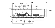
- the conventional semiconductor module 8 includes an insulating substrate 811, a conductor layer 812 provided on one surface of the insulating substrate 811, and other conductors provided at positions separated from the conductor layer 812.
- a substrate 810 having conductor layers 813 and 814, a first electrode 821 on one surface (the lower surface in FIG. 9), and two second electrodes 822 and 823 on the other surface (the upper surface in FIG. 9).
- one second electrode 822 is electrically connected to the terminal 874 through the wire 870 and another conductor layer 813, and the other second electrode 823. Is electrically connected to a terminal 876 through a wire 872.
- the conventional semiconductor module 8 includes the resin portion 860 formed by arranging the resin in the bowl-shaped space formed by the substrate 810 and the wall portion 816, the semiconductor module 8 has a shock resistance.
- the inventors of the present invention have conceived a semiconductor module capable of easily forming a structure for resin sealing, and have already filed an application as PCT / JP2015 / 051655 (hereinafter referred to as a prior application). .
- the semiconductor module 9 includes a first substrate 910 having a first conductive layer 912 provided on at least one surface of the first insulating substrate 911 and the first insulating substrate 911.
- a device portion (semiconductor element) 920 having a first electrode 921 on one side and a second electrode 922 on the other side, the first electrode 921 being joined to the first conductor layer 912;
- a second insulating layer 932 provided on at least one surface of the second insulating substrate 931 and the second insulating substrate 931, and the second conductive layer 932 is joined to the second electrode 922, and a planar surface
- the surrounding wall 934 is formed at a position surrounding the bonding portion 933 with the upper end surface protruding from the bonding surface between the bonding portion 933 and the second electrode 922, and the first wall via the surrounding wall portion 934 is provided.
- the substrate 910 It includes a second substrate 930, is defined by the surrounding wall portion 934, and a
- the device portion 920 is disposed so that the entire device portion 920 is located inside the region defined by the surrounding wall portion 934 in plan view.
- the second conductor layer 932 is positioned so as to surround the bonding portion 933 in plan view, and the upper end surface is above the bonding surface between the bonding portion 933 and the second electrode 922. Since it has the surrounding wall part 934 formed in the protruding state, there is no need to separately prepare a member for forming a structure for resin sealing (for example, the wall part 816 in the conventional semiconductor module 8), A structure for resin sealing can be easily formed.
- the semiconductor module 9 according to the prior application is a semiconductor module having higher heat dissipation than before.
- the present invention has been made to solve the above-described problems, and provides a semiconductor module that satisfies the demand for downsizing of a product even when a control IC for controlling a power device unit is provided. With the goal.
- a semiconductor module of the present invention has a first substrate having a first insulating substrate and a first conductor layer provided on one surface of the first insulating substrate, and a first electrode on one surface. And a power device portion having a second electrode and a gate electrode on the other surface, wherein the first electrode is electrically connected to the first conductor layer, a second insulating substrate, and the second insulation A second conductor layer provided on one side of the conductive substrate and a third conductor layer provided on the other side of the second insulating substrate, wherein the second insulating substrate is positioned at the gate electrode. And the second conductor layer is joined to the second electrode and the upper end surface is located at a position surrounding the joined portion in plan view.
- a surrounding wall formed in a state of projecting from the joint surface with the joint, and through the surrounding wall A second substrate in contact with the first substrate, and an inner side made of a resin that is defined by the surrounding wall portion and disposed in a space sandwiched between the first insulating substrate and the second insulating substrate
- the gate electrode is electrically connected to a control signal output terminal of the control IC through the connection member.
- the surrounding wall portion formed at a position surrounding the joint portion is only when the surrounding wall portion is formed at a position surrounding the joint portion over the entire circumference in a plan view.
- the case where the surrounding wall portion is formed only in a predetermined portion of the position surrounding the joint portion is included.
- the surrounding wall portion is formed at a position surrounding the joint portion over the entire circumference in plan view.
- the surrounding wall portion is formed only in a predetermined portion of the position surrounding the joint portion in plan view.
- the surrounding wall portion is formed in a state of being continuous with the joint portion, and the first substrate is the first conductor layer on one surface of the first insulating substrate.
- the surrounding wall portion is formed in a state of being continuous with the joint portion” means not only when the surrounding wall portion is adjacent to the joint portion, but also between the surrounding wall portion and the joint portion. This includes the case where another member is sandwiched between them.
- a groove for engaging with the surrounding wall is formed in the fourth conductor layer.
- the surrounding wall portion is formed in a state of being separated from the joint portion.
- the first substrate is joined to the surrounding wall portion at a position spaced apart from the first conductor layer on one surface of the first insulating substrate. It is preferable that a groove for engaging with the surrounding wall is formed in the fourth conductor layer.
- the power device unit includes one semiconductor element, and the one semiconductor element has a first electrode on one surface and a second electrode on the other surface. It is preferable to have a gate electrode.
- the power device unit has a structure in which a plurality of semiconductor elements are stacked, and at least one of the plurality of semiconductor elements has a first electrode on one surface. And having the second electrode and the gate electrode on the other surface.
- each gate electrode can be electrically connected to a connection member.
- the power device section has a structure in which a plurality of semiconductor elements are stacked, and the first substrate is provided at a position separated from the first conductor layer.
- the semiconductor module further includes a fifth conductor layer, one end of which is sandwiched between two semiconductor elements of the plurality of semiconductor elements, and the other end is the fifth conductor layer. It is preferable to further include a second connection member that is electrically connected to the first connection member.
- the power device section has a structure in which a plurality of semiconductor elements are stacked, and at least two of the plurality of semiconductor elements are arranged on one side.
- One electrode, and a second electrode and a gate electrode on the other surface, and each of the at least two semiconductor elements has an entire semiconductor element inside a region defined by the surrounding wall portion in plan view. It is preferable to be laminated so as to be positioned.
- the power device section has a structure in which a plurality of semiconductor elements are stacked, and at least two of the plurality of semiconductor elements are arranged on one side.
- the joint portion and the surrounding wall portion are formed from one copper layer.
- the semiconductor module of the present invention since the first substrate, the power device unit, the second substrate, and the control IC are stacked in this order, even when the control IC for controlling the power device unit is provided, 1 It is not necessary to secure a region for installing the control IC on one side of the insulating substrate, and the occupied area is made narrower than when the control IC is installed side by side with the power device unit on the one side of the first insulating substrate. be able to. As a result, the semiconductor module of the present invention is a semiconductor module that satisfies the demand for product miniaturization.
- the second insulating substrate has a hole provided at a position corresponding to the position of the gate electrode, and the connection member is disposed inside the hole of the second insulating substrate.
- the gate electrode is electrically connected to the control signal output terminal of the control IC through the connecting member, the first control electrode is disposed on the third conductor layer. 2
- the power device unit can be controlled by the control IC without being obstructed by the insulating substrate.
- the connecting member is disposed inside the hole of the second insulating substrate, and the gate electrode is electrically connected to the control signal output terminal of the control IC via the connecting member. Therefore, the length of the wiring (the length of the connecting member) between the gate electrode of the power device portion and the control signal output terminal of the control IC can be short, and it is difficult to be affected by external noise.
- the second conductor layer has the surrounding wall portion formed at a position surrounding the joint portion in a plan view, so that heat is generated when an excessive load is applied to the power device portion. Even if the inner resin portion ignites, the surrounding wall portion can serve as a fire barrier to prevent the surrounding fire from spreading.
- the second conductor layer has the surrounding wall portion formed at a position surrounding the joint portion in plan view, so that the power device portion is shielded from the outside by the surrounding wall portion. Therefore, it is possible to prevent the power device unit from oscillating or malfunctioning due to noise from the outside of the power device unit.
- the semiconductor module of the present invention is a semiconductor module with less defects due to oscillation or malfunction.
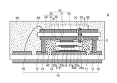
- FIG. 1 is a diagram illustrating a semiconductor module 1 according to a first embodiment.
- 1A is a cross-sectional view of the semiconductor module 1
- FIG. 1B is a plan cross-sectional view taken along line AA of FIG. 1A.
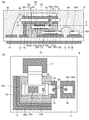
- FIG. 3 is a view for explaining a second substrate 30.
- 2A is a plan view of the second substrate 30, and
- FIG. 2B is a cross-sectional view taken along the line BB of FIG. 2A.
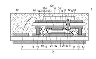
- FIG. 6 is a diagram illustrating a semiconductor module 2 according to a second embodiment.
- 3A is a cross-sectional view of the semiconductor module 2
- FIG. 3B is a CC cross-sectional view of FIG. 3A.
- FIG. 6 is a cross-sectional view showing a semiconductor module 3 according to a third embodiment.
- FIG. 6 is a cross-sectional view showing a semiconductor module 4 according to a fourth embodiment.
- 5A is a cross-sectional view of the semiconductor module 4, and
- FIG. 5B is a DD cross-sectional view of FIG. 5A.
- FIG. 6 is a diagram illustrating a semiconductor module 5 according to a fifth embodiment.
- 6A is a cross-sectional view of the semiconductor module 5, and
- FIG. 6B is a EE plan cross-sectional view of FIG. 6A.
- FIG. 9 is a cross-sectional view showing a semiconductor module 6 according to a sixth embodiment.
- FIG. 7A is a cross-sectional view of the semiconductor module 6, and
- FIG. 7B is a FF plane cross-sectional view of FIG. 7A.
- FIG. 10 is a cross-sectional view showing a semiconductor module 7 according to a seventh embodiment. It is sectional drawing which shows the conventional semiconductor module 8.
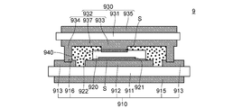
- Reference numeral 815 denotes a heat dissipating conductor layer of the substrate 810. It is sectional drawing which shows the semiconductor module 9 which concerns on a prior application.
- Reference numeral 913 indicates a third conductor layer
- reference numeral 915 indicates a heat dissipation conductor layer of the first substrate 910
- reference numeral 916 indicates a groove
- reference numeral 935 indicates a heat dissipation conductor layer of the second substrate 930.
- Reference numeral 937 indicates a flat portion
- reference numeral S indicates solder.
- the semiconductor module 1 according to Embodiment 1 includes a first substrate 10, a power device unit, a second substrate 30, an inner resin unit 40, A control IC 50, an outer resin portion 60, and a connector (connection member) 70 are provided, and the first substrate 10, the power device portion, the second substrate 30, and the control IC 50 are stacked in this order.
- the first substrate 10 includes a first insulating substrate 11, a first conductor layer 12 provided on one surface of the first insulating substrate 11, and a surrounding wall described later at a position separated from the first conductor layer 12.
- a fourth conductor layer 13 bonded to the portion 34, a conductor layer 14 for external connection provided at a position separated from the first conductor layer 12 and the fourth conductor layer 13, and a first insulating substrate 11 is a mounting board having a heat-dissipating conductor layer 15 provided on the other surface of 11.
- the first insulating substrate 11 is made of ceramics (for example, alumina), the first conductor layer 12, the fourth conductor layer 13, the external connection conductor layer 14, and the heat dissipation conductor layer. 15 is made of metal (for example, copper).
- the first substrate 10 is a DCB substrate (Direct Copper Bonding substrate) in which the first insulating substrate 11 and each conductor layer are bonded by eutectic bonding. By setting it as such a structure, it becomes a semiconductor module which has high heat dissipation.
- the fourth conductor layer 13 is formed with a groove 16 for engaging with a surrounding wall 34 described later.
- the groove portion 16 is formed by etching the fourth conductor layer.
- the external connection conductor layer 14 is not partially covered by the outer resin portion 60 or is connected to an external connection terminal (not shown), whereby an external circuit (not shown). ).
- the external connection conductor layer 14 is electrically connected to an input terminal (or control signal output terminal) of the control IC 50 via a third conductor layer 35 and a wire 80 described later.
- the power device section is composed of one semiconductor element 20, has a first electrode 21 on one side (lower side in FIG. 1), and a second electrode 22 and a gate electrode 23 on the other side (upper side in FIG. 1).
- the power device portion is arranged so that the entire semiconductor element 20 is located inside a region defined by the surrounding wall portion 34 in plan view.
- the semiconductor element 20 is a three-terminal semiconductor element (for example, IGBT).
- the gate electrode 23 is electrically connected to the control signal output terminal 52 of the control IC 50 through the connector 70.
- the first electrode 21 is electrically connected to the first conductor layer 12 and the second electrode 22 is bonded to a bonding portion 33 of the second substrate 30 to be described later via a bonding material S (for example, solder). It is connected to the.
- a bonding material S for example, solder
- the second substrate 30 includes a second insulating substrate 31, a second conductor layer 32 provided on one surface of the second insulating substrate 31, and the second insulating substrate 31. It has the 3rd conductor layer 35 provided in the other side.
- the second insulating substrate 31 is made of ceramics (for example, alumina), and the second conductor layer 32 and the third conductor layer 35 are made of metal (for example, copper).
- the second substrate 30 is a DCB substrate in which the second insulating substrate 31 and each conductor layer are bonded by eutectic bonding.
- the second insulating substrate 31 (and the second conductor layer 32 and the third conductor layer 35) has a hole 36 provided at a position corresponding to the position of the gate electrode 23.
- the second conductor layer 32 has a joint portion 33 joined to the second electrode 22, and an upper end surface at a position surrounding the joint portion 33 in a plan view and the second electrode 22 and the joint portion 33.
- the surrounding wall part 34 and the flat part 37 which were formed in the state which protruded rather than the joint surface with are included.
- the second substrate 30 is in contact with the first substrate 10 through the surrounding wall portion 34.
- the joint portion 33 and the surrounding wall portion 34 are formed by etching one copper layer. By setting it as such a structure, the junction part 33 and the surrounding wall part 34 can be formed accurately.
- the surrounding wall portion 34 is formed at a position surrounding the joint portion 33 over the entire circumference in plan view (see FIG. 1B). That is, the shape of the surrounding wall portion 34 is a “B” shape in plan view.
- the surrounding wall portion 34 is formed in a state of being continuous with the joint portion 33 through the flat portion 37 of the second conductor layer 32.
- the surrounding wall portion 34 is engaged with the groove portion 16 of the fourth conductor layer 13 of the first substrate 10 and is bonded via a bonding material (for example, solder).
- a bonding material for example, solder
- the length from the boundary surface between the second insulating substrate 31 and the second conductor layer 32 to the upper end surface of the surrounding wall portion 34 is, for example, in the range of 0.2 to 1.0 mm.
- the thickness of the joint portion 33 is, for example, in the range of 0.15 to 0.5 mm.
- the inner resin portion 40 is made of resin disposed in “a space defined by the surrounding wall portion 34 and sandwiched between the first insulating substrate 11 and the second insulating substrate 31”.
- An appropriate resin for example, epoxy resin
- the control IC 50 controls driving of the power device unit by controlling on / off of the gate electrode 23 of the power device unit.
- the control IC 50 is disposed on the third conductor layer 35.
- the control IC 50 has a predetermined control signal output terminal 52, and the control signal output terminal 52 and the gate electrode 23 are electrically connected via a connector 70 described later.
- the outer resin portion 60 is made of a resin disposed on one surface side of the first substrate 10 so as to cover at least the second substrate 30 and the control IC 50.
- the resin constituting the outer resin part 60 the same resin as that of the inner resin part 40 is used, but a different resin can also be used.
- the connector (connecting member) 70 is disposed inside the hole 36 of the second insulating substrate 31.
- the connector 70 has an elongated columnar shape, one end is electrically connected to the gate electrode 23 of the power device unit, and the other end is electrically connected to the control signal output terminal 52 of the control IC 50. Yes.
- the connector 70 is formed by punching / bending a metal plate. An appropriate material (for example, aluminum) can be used as the material of the metal plate.
- the semiconductor module 1 according to Embodiment 1 is a semiconductor module that satisfies the demand for product miniaturization.
- the second insulating substrate 31 has the hole 36 provided at a position corresponding to the position of the gate electrode 23, and the hole 36 of the second insulating substrate 31. Is connected to the control signal output terminal 52 of the control IC 50 via the connector 70, so that the control IC 50 is connected to the third conductor layer 35. Even in the case of being disposed above, the power device unit can be controlled by the control IC 50 without being obstructed by the second insulating substrate 31.
- the connector 70 is disposed inside the hole 36 of the second insulating substrate 31, and the gate electrode 23 is connected to the control signal of the control IC 50 via the connector 70. Since it is electrically connected to the output terminal 52, the length of the wiring (the length of the connector 70) between the gate electrode 23 of the power device section and the control signal output terminal 52 of the control IC 50 can be shortened. Less susceptible to external noise.
- the second conductor layer 32 has the surrounding wall portion 34 formed at a position surrounding the joint portion 33 in a plan view, so that an excessive load is applied to the power device portion. Even when the inner resin portion 40 is ignited by the heat generated when the fire is applied, it is possible to prevent the surrounding fire from spreading by the surrounding wall portion 34 serving as a fire barrier.
- the second conductor layer 32 has the surrounding wall portion 34 formed at a position surrounding the joint portion 33 in a plan view, so that the power device portion is surrounded by the outside. It can be shielded by the wall 34 and can prevent the power device unit from oscillating or malfunctioning due to noise from the outside of the power device unit. As a result, the semiconductor module 1 according to the first embodiment The semiconductor module is less likely to malfunction due to malfunction.
- the surrounding wall portion 34 is formed at a position that surrounds the joint portion 33 over the entire circumference in plan view, and therefore when an excessive load is applied to the power device portion. Even when the inner resin portion 40 is ignited by the heat generation, the surrounding wall portion 34 completely surrounds the inner resin portion 40, so that it is possible to reliably prevent the surrounding fire from spreading. Further, since the power device portion can be completely shielded from the outside by the surrounding wall portion 34, it is possible to reliably prevent the power device portion from oscillating or malfunctioning due to noise from the outside of the power device portion.
- the surrounding wall portion 34 is formed in a state of being continuous with the joint portion 33, and the first substrate 10 is connected to the first conductor layer 12 on one surface of the second insulating substrate 31.
- the fourth conductor layer 13 is further joined to the surrounding wall portion 34 at a spaced position, and the fourth conductor layer 13 is electrically connected to the second electrode 22 via the surrounding wall portion 34 and the joining portion 33. It is connected.
- the second electrode 22 of the power device portion can be electrically connected to the outside through the joint portion 33, the surrounding wall portion 34, and the fourth conductor layer 13.
- junction part 33, the surrounding wall part 34, and the 4th conductor layer 13 have a cross-sectional area larger than a wire and resistance is low, it is hard to produce a malfunction when a big electric current is sent through a semiconductor module, and much higher reliability. It becomes a semiconductor module having properties.
- the semiconductor module 1 since it has the above-described configuration, heat generated in the power device portion is radiated to the outside via the joint portion 33, the surrounding wall portion 34, and the fourth conductor layer 13. Thus, a semiconductor module having even higher heat dissipation can be obtained.
- the surrounding wall portion 34 of the second substrate 30 can be easily positioned by fitting into the groove portion 16 of the fourth conductor layer 13.
- the power device unit includes the single semiconductor element 20, and the semiconductor element 20 has the first electrode 21 on one side and the second side on the other side. Since it has the electrode 22 and the gate electrode 23, it becomes a semiconductor module with a simple wiring design.
- the joint portion 33 and the surrounding wall portion 34 are formed from one copper layer, a joint material (for example, solder) is used in the manufacturing process of the semiconductor module. Even when it is put in a high-temperature furnace to melt it, the length of the surrounding wall 34 hardly changes. Accordingly, since the load of the second substrate 30 is distributed to the surrounding wall portion 34, the load of the second substrate 30 does not concentrate on the power device portion. As a result, the power device part is less likely to be broken in the manufacturing process of the semiconductor module, so that not only the semiconductor module with a high yield is obtained, but also when it is put in a high temperature furnace to melt the bonding material (for example, solder). The thickness of the bonding material can be prevented from changing, and a highly reliable semiconductor module can be obtained.
- a joint material for example, solder
- the joint portion 33 and the surrounding wall portion 34 are formed from one copper layer, the surrounding wall portion 34 is not inclined, In the manufacturing process of the semiconductor module, the second substrate 30 can be accurately positioned without the second substrate 30 rotating in the ⁇ direction in plan view.
- the semiconductor module 2 according to the second embodiment basically has the same configuration as the semiconductor module 1 according to the first embodiment, but the configuration of the surrounding wall portion is different from that of the semiconductor module 1 according to the first embodiment. That is, in the semiconductor module 2 according to the second embodiment, as shown in FIG. 3, the surrounding wall portion 34 is a predetermined portion of the position surrounding the joint portion 33 in plan view (over the 3/4 circumference of the joint portion 33). It is formed only at the surrounding position (see FIG. 3B). That is, the shape of the surrounding wall portion 34 is a “U” shape in plan view.
- the semiconductor module 2 according to the second embodiment is different from the semiconductor module 1 according to the first embodiment in the configuration of the surrounding wall portion, but as in the case of the semiconductor module 1 according to the first embodiment, Since the first substrate 10, the power device unit (semiconductor element 20), the second substrate 30a, and the control IC 50 are stacked in this order, the first insulating property is provided even when the control IC 50 that controls the power device unit is provided. It is not necessary to secure a region for installing the control IC 50 on one side of the substrate 11, and the occupation area is made narrower than when the control IC 50 is installed side by side with the power device unit on the one side of the first insulating substrate 11. Can do. As a result, the semiconductor module 2 according to the second embodiment is a semiconductor module that satisfies the demand for product miniaturization.
- the surrounding wall portion 34a is formed only in a predetermined portion of the position surrounding the joint portion 33 in plan view, and thus forms the inner resin portion 40.
- a space sandwiched between the first insulating substrate 11 and the second insulating substrate 31 at a position where the surrounding wall portion 34 is not formed in a position surrounding the joint portion 33 in plan view Resin can be injected.
- the semiconductor module 2 according to the second embodiment has the same configuration as the semiconductor module 1 according to the first embodiment except for the configuration of the surrounding wall portion, the effects of the semiconductor module 1 according to the first embodiment can be obtained. Of which, it has a corresponding effect.
- the semiconductor module 3 according to the third embodiment basically has the same configuration as the semiconductor module 1 according to the first embodiment, but the configuration of the power device unit is different from that of the semiconductor module 1 according to the first embodiment. That is, in the semiconductor module 3 according to the third embodiment, the power device unit has a structure in which two semiconductor elements 20a and 20b are stacked as shown in FIG.
- the power device unit has a structure in which a three-terminal semiconductor element 20a is stacked on a two-terminal semiconductor element 20b.
- the three-terminal semiconductor element 20a has a first electrode 21a formed on one side (lower side) electrically connected to a second electrode 22b of the semiconductor element 20b, and is formed on the other side (upper side).
- the second electrode 22a is electrically connected to the three-terminal joint 33a
- the gate electrode 23a is electrically connected to the control signal output terminal 52 of the control IC 50 via the connector 70.
- the first electrode 21b formed on one side (lower side) is electrically connected to the first conductor layer 12, and the second electrode formed on the other side (upper side).
- the electrode 22b is electrically connected to the first electrode 21a of the three-terminal semiconductor element 20a.
- the configuration of the power device unit is different from that of the semiconductor module 1 according to the first embodiment. Since the first substrate 10, the power device unit (semiconductor elements 20a, 20b), the second substrate 30, and the control IC 50 are stacked in this order, even if the control IC 50 for controlling the power device unit is provided, the first There is no need to secure a region for installing the control IC 50 on one side of the insulating substrate 11, and the occupied area is smaller than when the control IC 50 is installed side by side with the power device unit on the one side of the first insulating substrate 11. can do. As a result, the semiconductor module 3 according to the third embodiment is a semiconductor module that satisfies the demand for product miniaturization.
- the power device unit has a structure in which the two semiconductor elements 20a and 20b are stacked, so that the two semiconductor elements 20a and 20b are connected to the first insulating substrate 11. Occupied area can be made narrower than when arranged side by side on one side. As a result, the semiconductor module satisfies a high level of demand for product miniaturization.
- the semiconductor module 3 according to the third embodiment has the same configuration as that of the semiconductor module 1 according to the first embodiment except for the configuration of the power device unit, the effects of the semiconductor module 1 according to the first embodiment can be obtained. Of which, it has a corresponding effect.
- the semiconductor module 4 according to the fourth embodiment basically has the same configuration as the semiconductor module 3 according to the third embodiment, but is different from the case of the semiconductor module 3 according to the third embodiment in that it includes a second connection member. Different. That is, in the semiconductor module 4 according to the fourth embodiment, as shown in FIG. 5, one end is sandwiched between two semiconductor elements 20a and 20b, and the other end is a fifth conductor layer 17 described later. And a second connection member 82 that is electrically connected to the first connection member 82.
- the second connecting member 82 is formed by punching / bending a metal plate (for example, an aluminum plate).
- One end of the second connection member 82 is slightly larger than the two semiconductor elements 20a and 20b in plan view, and the upper side (second substrate side) of the one end is joined to the first electrode 21a of the semiconductor element 20a. Bonded via a material (solder), the lower side (first substrate side) of one end is bonded to the second electrode 22b of the semiconductor element 20b via a bonding material (solder).
- the first substrate 10 further includes a fifth conductor layer 17 provided at a position separated from both the first conductor layer 12 and the external connection conductor layer 14.
- the fifth conductor layer 17 is not partially covered by the outer resin portion 60 or connected to an external connection terminal (not shown), thereby causing an external circuit (not shown). Connected with.
- the surrounding wall portion 34b is formed only in a predetermined portion (a position surrounding the 3 ⁇ 4 circumference of the joint portion 33) in a position surrounding the joint portion 33b in a plan view (see FIG. 5B). That is, the shape of the surrounding wall portion 34b is a “U” shape in plan view.
- the second connecting member 82 is “a space sandwiched between the first insulating substrate 11 and the second insulating substrate 31 b at a position where the surrounding wall portion 34 b is not formed in a position surrounding the joint portion 33 b in a plan view. To pass through.
- the semiconductor module 4 according to the fourth embodiment is different from the semiconductor module 3 according to the third embodiment in that the second connection member is provided, but similarly to the semiconductor module 3 according to the third embodiment. Since the first substrate 10, the power device unit (semiconductor elements 20a and 20b), the second substrate 30b, and the control IC 50 are stacked in this order, the control IC 50 that controls the power device unit is provided. There is no need to secure a region for installing the control IC 50 on one side of the first insulating substrate 11, and the occupied area is larger than when the control IC 50 is installed side by side with the power device unit on one side of the first insulating substrate 11. Can be narrowed. As a result, the semiconductor module 4 according to the fourth embodiment is a semiconductor module that satisfies the demand for product miniaturization.
- the semiconductor module 4 according to the fourth embodiment, one end is sandwiched between the two semiconductor elements 20a and 20b, and the other end is electrically connected to the fifth conductor layer 17. Since the second connecting member 82 is provided, the semiconductor module has a higher degree of design freedom.
- the semiconductor module 4 according to the fourth embodiment has the same configuration as that of the semiconductor module 3 according to the third embodiment except that the semiconductor module 4 according to the fourth embodiment includes the second connection member. It has a corresponding effect among the effects.
- the semiconductor module 5 according to the fifth embodiment basically has the same configuration as the semiconductor module 3 according to the third embodiment, but the configuration of the power device unit is different from that of the semiconductor module 3 according to the third embodiment. That is, in the semiconductor module 5 according to the fifth embodiment, the two semiconductor elements 20a and 20c (the semiconductor element on the second substrate side is 20a and the semiconductor element on the first substrate side is 20c) are all shown in FIG. As shown, the first electrodes 21a and 21c are provided on one side, and the second electrodes 22a and 22c and the two gate electrodes 23a and 23c are provided on the other side.
- the two semiconductor elements 20a and 20c are both laminated so that the entire semiconductor element is located inside the region defined by the surrounding wall portion 34 in plan view.
- the second insulating substrate 31 has holes corresponding to the gate electrodes 23a and 23c of the two semiconductor elements 20a and 20c, and the connectors 70a and 70c are arranged inside the holes.
- the configuration of the power device unit is different from that in the semiconductor module 3 according to the third embodiment. Since the first substrate 10, the power device unit (semiconductor elements 20a and 20c), the second substrate 30, and the control IC 50 are stacked in this order, even if the control IC 50 for controlling the power device unit is provided, the first There is no need to secure a region for installing the control IC 50 on one side of the insulating substrate 11, and the occupied area is smaller than when the control IC 50 is installed side by side with the power device unit on the one side of the first insulating substrate 11. can do. As a result, the semiconductor module 5 according to the fifth embodiment is a semiconductor module that satisfies the demand for product miniaturization.
- the two semiconductor elements 20a and 20c are stacked such that the entire semiconductor element is positioned inside the region defined by the surrounding wall portion 34 in plan view. Therefore, the two semiconductor elements 20a and 20c can be completely shielded from the outside by the surrounding wall portion 34, and as a result, the two semiconductor elements 20a and 20c may oscillate or malfunction due to external noise. It can be surely prevented.
- the semiconductor module 5 according to the fifth embodiment has the same configuration as that of the semiconductor module 3 according to the third embodiment except for the configuration of the power device unit, the effects of the semiconductor module 3 according to the third embodiment can be obtained. Of which, it has a corresponding effect.
- the semiconductor module 6 according to the sixth embodiment basically has the same configuration as the semiconductor module 5 according to the fifth embodiment, but the configuration of the power device unit is different from that of the semiconductor module 5 according to the fifth embodiment. That is, in the semiconductor module 6 according to the sixth embodiment, one of the two semiconductor elements (the lower semiconductor element 20c) is a region defined by the surrounding wall 34c in plan view, as shown in FIG. The gate electrode 23c of the semiconductor element 20c is stacked on the outside of the semiconductor element 20c.
- the semiconductor module 6 according to Embodiment 6 has a second connection in which one end is sandwiched between the two semiconductor elements 20 a and 20 c and the other end is electrically connected to the fifth conductor layer 17.
- a member 82 is further provided.
- One end of the second connection member 82 is slightly larger than the semiconductor elements 20a and 20c in a plan view, and the upper side (second substrate side) of the one end is the first electrode 21a of the semiconductor element 20a and a bonding material ( The first electrode 22c is bonded to the second electrode 22c of the semiconductor element 20c via a bonding material (solder).
- the surrounding wall portion 34c is formed only at a predetermined position (a position surrounding the joint portion 33 over a half circumference in the plan view) among positions surrounding the joint portion 33c in the plan view (see FIG. 7B). That is, the shape of the surrounding wall portion 34c is an “L” shape in plan view.
- the gate electrode 23c of the (lower) semiconductor element 20c is electrically connected via a wire 80 to a control signal output terminal 52b of a control IC 50b provided at a position separated from the surrounding wall 34c.
- the gate electrode 23c In a predetermined direction perpendicular to the outer edge of the surrounding wall portion 34c, the gate electrode 23c is separated from the outer edge of the region defined by the surrounding wall portion 34c in plan view by a factor of three times the width of the gate electrode 23c in the predetermined direction. It is preferable. By adopting such a configuration, the linear distance between the wire 80 connecting the gate electrode 23c and the control signal output terminal 52c of the control IC 50b and the surrounding wall portion 34c becomes long, and short-circuiting is difficult.
- the configuration of the power device unit is different from that in the semiconductor module 5 according to the fifth embodiment, but as in the case of the semiconductor module 5 according to the fifth embodiment, Since the one substrate 10, the power device unit (semiconductor elements 20a and 20c), the second substrate 30c, and the control IC 50a are stacked in this order, the first IC 10a is provided even if the control IC 50a for controlling the power device unit is provided. It is not necessary to secure a region for installing the control IC 50a on one side of the insulating substrate 11, and the occupied area is narrower than when the control IC 50a is installed side by side with the power device unit on the one side of the first insulating substrate 11. can do. As a result, the semiconductor module 6 according to the sixth embodiment is a semiconductor module that satisfies the demand for product miniaturization.
- the semiconductor module 6 according to the sixth embodiment since the gate electrode 23c of the semiconductor element 20c is positioned outside the region defined by the surrounding wall portion 34c in plan view, the power device portion Even when the second substrate 30c is provided in the uppermost part, the gate electrode 23c of the power device unit and the control signal output terminal 52b of the control IC 50b can be connected by the wire 80 having a small diameter.
- the semiconductor module 6 according to the sixth embodiment is a semiconductor module capable of controlling the power device unit (the semiconductor element 20b below the power device unit) with the control IC 50b.
- the semiconductor module 6 according to the sixth embodiment has the same configuration as that of the semiconductor module 5 according to the fifth embodiment except for the configuration of the power device unit, the effect of the semiconductor module 5 according to the fifth embodiment is obtained. Of which, it has a corresponding effect.
- the semiconductor module 7 according to the seventh embodiment basically has the same configuration as that of the semiconductor module 1 according to the first embodiment, but the configuration of the surrounding wall portion is different from that of the semiconductor module 1 according to the first embodiment. That is, in the semiconductor module 7 according to the seventh embodiment, the surrounding wall portion 34d is formed in a state of being separated from the joint portion 33d as shown in FIG.
- the first substrate 10 further includes a fourth conductor layer 13 joined to the surrounding wall portion 34d at a position separated from the first conductor layer 12 on one surface of the first insulating substrate 11, and the fourth conductor
- the layer 13 is formed with a groove portion 16 for engaging with the surrounding wall portion 34d.
- the semiconductor module 7 according to the seventh embodiment is different from the semiconductor module 1 according to the first embodiment in the configuration of the surrounding wall portion, but as in the case of the semiconductor module 1 according to the first embodiment, Since the first substrate 10, the power device unit (semiconductor element 20), the second substrate 30d, and the control IC 50 are stacked in this order, the first insulating property is provided even when the control IC 50 that controls the power device unit is provided. It is not necessary to secure a region for installing the control IC 50 on one side of the substrate 11, and the occupation area is made narrower than when the control IC 50 is installed side by side with the power device unit on the one side of the first insulating substrate 11. Can do. As a result, the semiconductor module 7 according to the seventh embodiment is a semiconductor module that satisfies the demand for product miniaturization.
- the surrounding wall portion 34d is formed in a state of being separated from the joint portion 33d, and therefore, with other conductor layers and semiconductor elements via the surrounding wall portion 34d. It is possible to prevent a short circuit and a semiconductor module that is difficult to be destroyed.
- the semiconductor module 7 according to the seventh embodiment has the same configuration as that of the semiconductor module 1 according to the first embodiment except for the configuration of the surrounding wall portion, the effects of the semiconductor module 1 according to the first embodiment can be obtained. Of which, it has a corresponding effect.
- the power device section has a structure in which two semiconductor elements are stacked, but the present invention is not limited to this.
- the power device unit may have a structure in which three or more semiconductor elements are stacked.
- the two semiconductor elements are stacked while being shifted by 90 °, but the present invention is not limited to this. Two semiconductor elements may be stacked in a state shifted by an angle other than 90 °.
- the first substrate is a DCB substrate, but the present invention is not limited to this.
- the first substrate may be a general printed board or an aluminum board.
- the second substrate is a DCB substrate, but the present invention is not limited to this.
- the second substrate may be a general printed board or an aluminum board.
- the heat dissipating conductor layer is provided on the other surface side of the first substrate, but the present invention is not limited to this.
- the heat dissipating conductor layer may not be provided.
- the joint portion and the surrounding wall portion are formed by etching one conductor layer, but the present invention is not limited to this.
- the joint portion and the surrounding wall portion may be separately formed and then joined to the second insulating substrate 31 to form the joint portion and the surrounding wall portion.
- the groove portion for engaging with the surrounding wall portion is formed in the fourth conductor layer, but the present invention is not limited to this.
- the groove portion may not be formed in the fourth conductor layer.
- gate electrode 30, 30a, 30b, 30c, 30d ... second substrate , 31 ... second insulating substrate, 32, 32a, 32b, 32c, 32d ... second conductor layer, 33, 33a, 33b, 33c, 33d ... junction, 34, 34a, 34b, 34c, 34d ... surrounding wall Part, 35 ... third conductor layer, 36 ... hole, 37 ... flat part, 4 ... inner resin part, 50, 50a, 50b ... control IC, 52, 52a, 52b ... control signal output terminal, 60 ... outer resin part, 70 ... connector (for gate electrode connection), 80 ... wire, 82 ... first 2 connecting members, S ... bonding material
Priority Applications (5)
| Application Number | Priority Date | Filing Date | Title |
|---|---|---|---|
| US15/740,924 US10461042B2 (en) | 2016-01-31 | 2016-01-31 | Semiconductor module |
| PCT/JP2016/052843 WO2017130421A1 (ja) | 2016-01-31 | 2016-01-31 | 半導体モジュール |
| JP2016560940A JP6254299B2 (ja) | 2016-01-31 | 2016-01-31 | 半導体モジュール |
| EP16888007.8A EP3410477A4 (de) | 2016-01-31 | 2016-01-31 | Halbleitermodul |
| CN201680078362.XA CN108475672B (zh) | 2016-01-31 | 2016-01-31 | 半导体模块 |
Applications Claiming Priority (1)
| Application Number | Priority Date | Filing Date | Title |
|---|---|---|---|
| PCT/JP2016/052843 WO2017130421A1 (ja) | 2016-01-31 | 2016-01-31 | 半導体モジュール |
Publications (1)
| Publication Number | Publication Date |
|---|---|
| WO2017130421A1 true WO2017130421A1 (ja) | 2017-08-03 |
Family
ID=59397786
Family Applications (1)
| Application Number | Title | Priority Date | Filing Date |
|---|---|---|---|
| PCT/JP2016/052843 WO2017130421A1 (ja) | 2016-01-31 | 2016-01-31 | 半導体モジュール |
Country Status (5)
| Country | Link |
|---|---|
| US (1) | US10461042B2 (de) |
| EP (1) | EP3410477A4 (de) |
| JP (1) | JP6254299B2 (de) |
| CN (1) | CN108475672B (de) |
| WO (1) | WO2017130421A1 (de) |
Cited By (3)
| Publication number | Priority date | Publication date | Assignee | Title |
|---|---|---|---|---|
| WO2020110170A1 (ja) * | 2018-11-26 | 2020-06-04 | 三菱電機株式会社 | 半導体パッケージ、その製造方法、及び、半導体装置 |
| CN112425056A (zh) * | 2018-06-08 | 2021-02-26 | 法雷奥电机设备公司 | 电气电路、开关臂和电压转换器 |
| JP2022027946A (ja) * | 2018-11-26 | 2022-02-14 | 三菱電機株式会社 | 半導体パッケージ、及び、半導体装置 |
Families Citing this family (6)
| Publication number | Priority date | Publication date | Assignee | Title |
|---|---|---|---|---|
| US10622340B2 (en) * | 2016-11-21 | 2020-04-14 | Samsung Electronics Co., Ltd. | Semiconductor package |
| JP6999462B2 (ja) * | 2018-03-26 | 2022-01-18 | 日立Astemo株式会社 | パワー半導体装置 |
| KR102448248B1 (ko) * | 2018-05-24 | 2022-09-27 | 삼성전자주식회사 | Pop형 반도체 패키지 및 그 제조 방법 |
| JP7279324B2 (ja) * | 2018-09-14 | 2023-05-23 | 富士電機株式会社 | 半導体モジュール |
| CN110729255A (zh) * | 2019-08-08 | 2020-01-24 | 厦门云天半导体科技有限公司 | 一种键合墙体扇出器件的三维封装结构和方法 |
| DE102021214625A1 (de) | 2021-12-17 | 2023-06-22 | Robert Bosch Gesellschaft mit beschränkter Haftung | Leistungsmodul |
Citations (6)
| Publication number | Priority date | Publication date | Assignee | Title |
|---|---|---|---|---|
| JPH1012812A (ja) * | 1996-06-20 | 1998-01-16 | Toshiba Corp | 電力用半導体装置 |
| JPH1197616A (ja) * | 1997-09-25 | 1999-04-09 | Hitachi Ltd | マルチチップモジュールおよびその製造方法 |
| JP2008103552A (ja) * | 2006-10-19 | 2008-05-01 | Mitsubishi Materials Corp | パワーモジュールの積層構造体 |
| US20100001291A1 (en) * | 2008-07-07 | 2010-01-07 | Infineon Technologies Ag | Electronic device and manufacturing thereof |
| JP2013016684A (ja) * | 2011-07-05 | 2013-01-24 | Mitsubishi Electric Corp | 半導体装置および半導体装置の製造方法 |
| JP2015156466A (ja) * | 2014-01-17 | 2015-08-27 | ローム株式会社 | パワーモジュールおよびその製造方法 |
Family Cites Families (23)
| Publication number | Priority date | Publication date | Assignee | Title |
|---|---|---|---|---|
| US6081028A (en) * | 1994-03-29 | 2000-06-27 | Sun Microsystems, Inc. | Thermal management enhancements for cavity packages |
| CN1420538A (zh) * | 1996-07-12 | 2003-05-28 | 富士通株式会社 | 半导体装置的制造方法和半导体装置及其装配方法 |
| JP3879150B2 (ja) | 1996-08-12 | 2007-02-07 | 株式会社デンソー | 半導体装置 |
| DE69838849T2 (de) * | 1997-08-19 | 2008-12-11 | Hitachi, Ltd. | Mehrchip-Modulstruktur und deren Herstellung |
| JP2001127246A (ja) * | 1999-10-29 | 2001-05-11 | Fujitsu Ltd | 半導体装置 |
| JP4119146B2 (ja) * | 2002-03-29 | 2008-07-16 | 富士通株式会社 | 電子部品パッケージ |
| JP4635564B2 (ja) | 2004-11-04 | 2011-02-23 | 富士電機システムズ株式会社 | 半導体装置 |
| JP4551321B2 (ja) * | 2005-07-21 | 2010-09-29 | 新光電気工業株式会社 | 電子部品実装構造及びその製造方法 |
| KR101037229B1 (ko) * | 2006-04-27 | 2011-05-25 | 스미토모 베이클리트 컴퍼니 리미티드 | 반도체 장치 및 반도체 장치의 제조 방법 |
| JP2011151103A (ja) | 2010-01-20 | 2011-08-04 | Fujikura Ltd | 電子部品相互の接続構造及び接続方法 |
| JP2013069942A (ja) | 2011-09-24 | 2013-04-18 | Denso Corp | 半導体装置及びその製造方法 |
| CN103594386A (zh) * | 2012-08-17 | 2014-02-19 | 宏启胜精密电子(秦皇岛)有限公司 | 层叠封装结构及其制作方法 |
| JP6076653B2 (ja) * | 2012-08-29 | 2017-02-08 | 新光電気工業株式会社 | 電子部品内蔵基板及び電子部品内蔵基板の製造方法 |
| JP2014175485A (ja) * | 2013-03-08 | 2014-09-22 | Ibiden Co Ltd | 配線板及びその製造方法 |
| WO2014184846A1 (ja) * | 2013-05-13 | 2014-11-20 | 新電元工業株式会社 | 電子モジュールおよびその製造方法 |
| TWI656633B (zh) * | 2014-02-28 | 2019-04-11 | 日商半導體能源研究所股份有限公司 | 顯示裝置的製造方法及電子裝置的製造方法 |
| JP6093093B2 (ja) | 2015-01-22 | 2017-03-08 | 新電元工業株式会社 | 半導体モジュール |
| US9892993B2 (en) * | 2015-04-28 | 2018-02-13 | Shindengen Electric Manufacturing Co., Ltd. | Semiconductor module having stacked insulated substrate structures |
| JP6086989B1 (ja) * | 2015-04-28 | 2017-03-01 | 新電元工業株式会社 | 半導体モジュール |
| JP6761276B2 (ja) * | 2015-05-28 | 2020-09-23 | 株式会社半導体エネルギー研究所 | 表示装置の作製方法、および電子機器の作製方法 |
| US10181457B2 (en) * | 2015-10-26 | 2019-01-15 | Invensas Corporation | Microelectronic package for wafer-level chip scale packaging with fan-out |
| US9984992B2 (en) * | 2015-12-30 | 2018-05-29 | Invensas Corporation | Embedded wire bond wires for vertical integration with separate surface mount and wire bond mounting surfaces |
| WO2017130420A1 (ja) * | 2016-01-31 | 2017-08-03 | 新電元工業株式会社 | 半導体モジュール |
-
2016
- 2016-01-31 EP EP16888007.8A patent/EP3410477A4/de active Pending
- 2016-01-31 JP JP2016560940A patent/JP6254299B2/ja active Active
- 2016-01-31 US US15/740,924 patent/US10461042B2/en active Active
- 2016-01-31 WO PCT/JP2016/052843 patent/WO2017130421A1/ja active Application Filing
- 2016-01-31 CN CN201680078362.XA patent/CN108475672B/zh active Active
Patent Citations (6)
| Publication number | Priority date | Publication date | Assignee | Title |
|---|---|---|---|---|
| JPH1012812A (ja) * | 1996-06-20 | 1998-01-16 | Toshiba Corp | 電力用半導体装置 |
| JPH1197616A (ja) * | 1997-09-25 | 1999-04-09 | Hitachi Ltd | マルチチップモジュールおよびその製造方法 |
| JP2008103552A (ja) * | 2006-10-19 | 2008-05-01 | Mitsubishi Materials Corp | パワーモジュールの積層構造体 |
| US20100001291A1 (en) * | 2008-07-07 | 2010-01-07 | Infineon Technologies Ag | Electronic device and manufacturing thereof |
| JP2013016684A (ja) * | 2011-07-05 | 2013-01-24 | Mitsubishi Electric Corp | 半導体装置および半導体装置の製造方法 |
| JP2015156466A (ja) * | 2014-01-17 | 2015-08-27 | ローム株式会社 | パワーモジュールおよびその製造方法 |
Non-Patent Citations (1)
| Title |
|---|
| See also references of EP3410477A4 * |
Cited By (7)
| Publication number | Priority date | Publication date | Assignee | Title |
|---|---|---|---|---|
| CN112425056A (zh) * | 2018-06-08 | 2021-02-26 | 法雷奥电机设备公司 | 电气电路、开关臂和电压转换器 |
| JP2021526004A (ja) * | 2018-06-08 | 2021-09-27 | ヴァレオ エキプマン エレクトリク モトゥール | 電気回路、スイッチングアーム、および電圧変換器 |
| WO2020110170A1 (ja) * | 2018-11-26 | 2020-06-04 | 三菱電機株式会社 | 半導体パッケージ、その製造方法、及び、半導体装置 |
| JPWO2020110170A1 (ja) * | 2018-11-26 | 2021-05-13 | 三菱電機株式会社 | 半導体パッケージ、その製造方法、及び、半導体装置 |
| JP6997340B2 (ja) | 2018-11-26 | 2022-01-17 | 三菱電機株式会社 | 半導体パッケージ、その製造方法、及び、半導体装置 |
| JP2022027946A (ja) * | 2018-11-26 | 2022-02-14 | 三菱電機株式会社 | 半導体パッケージ、及び、半導体装置 |
| JP7254156B2 (ja) | 2018-11-26 | 2023-04-07 | 三菱電機株式会社 | 半導体パッケージ、及び、半導体装置 |
Also Published As
| Publication number | Publication date |
|---|---|
| US10461042B2 (en) | 2019-10-29 |
| JP6254299B2 (ja) | 2017-12-27 |
| JPWO2017130421A1 (ja) | 2018-02-01 |
| EP3410477A1 (de) | 2018-12-05 |
| EP3410477A4 (de) | 2019-09-11 |
| CN108475672A (zh) | 2018-08-31 |
| US20180226356A1 (en) | 2018-08-09 |
| CN108475672B (zh) | 2021-04-27 |
Similar Documents
| Publication | Publication Date | Title |
|---|---|---|
| JP6254299B2 (ja) | 半導体モジュール | |
| JP6254300B2 (ja) | 半導体モジュール | |
| JP5537736B2 (ja) | 半導体素子収納用パッケージ、これを備えた半導体装置および電子装置 | |
| CN107534023B (zh) | 半导体元件封装件、半导体装置以及安装构造体 | |
| WO2013175714A1 (ja) | 半導体装置及びその製造方法 | |
| WO2018101382A1 (ja) | 高周波モジュール | |
| CN103872036A (zh) | 半导体模块及其制造方法 | |
| WO2015129731A1 (ja) | 電子部品収納用パッケージおよび電子装置 | |
| WO2018151176A1 (ja) | 熱電素子内蔵パッケージ | |
| JP6226068B2 (ja) | 半導体装置 | |
| JP5285224B2 (ja) | 回路装置 | |
| JPWO2020017582A1 (ja) | モジュール | |
| JP6790902B2 (ja) | 電子装置 | |
| JP6711098B2 (ja) | 半導体装置の放熱構造 | |
| JP6093093B2 (ja) | 半導体モジュール | |
| US10251256B2 (en) | Heat dissipating structure | |
| JP2017034224A (ja) | 電子モジュール | |
| WO2020090411A1 (ja) | 半導体装置 | |
| JP6959785B2 (ja) | 回路基板、電子部品および電子モジュール | |
| WO2011108051A1 (ja) | 半導体装置 | |
| JP7025845B2 (ja) | 配線基板、電子装置および電子モジュール | |
| JP2005317594A (ja) | 配線基板 | |
| WO2017110540A1 (ja) | 回路構成体 | |
| KR102248521B1 (ko) | 전력 모듈 및 그 제조 방법 | |
| JP2017005129A (ja) | 半導体装置 |
Legal Events
| Date | Code | Title | Description |
|---|---|---|---|
| ENP | Entry into the national phase |
Ref document number: 2016560940 Country of ref document: JP Kind code of ref document: A |
|
| 121 | Ep: the epo has been informed by wipo that ep was designated in this application |
Ref document number: 16888007 Country of ref document: EP Kind code of ref document: A1 |
|
| WWE | Wipo information: entry into national phase |
Ref document number: 15740924 Country of ref document: US |
|
| NENP | Non-entry into the national phase |
Ref country code: DE |