WO2017057556A1 - 光透過性導電フィルム、及び、アニール処理された光透過性導電フィルムの製造方法 - Google Patents
光透過性導電フィルム、及び、アニール処理された光透過性導電フィルムの製造方法 Download PDFInfo
- Publication number
- WO2017057556A1 WO2017057556A1 PCT/JP2016/078794 JP2016078794W WO2017057556A1 WO 2017057556 A1 WO2017057556 A1 WO 2017057556A1 JP 2016078794 W JP2016078794 W JP 2016078794W WO 2017057556 A1 WO2017057556 A1 WO 2017057556A1
- Authority
- WO
- WIPO (PCT)
- Prior art keywords
- conductive layer
- light
- conductive film
- layer
- film
- Prior art date
- Legal status (The legal status is an assumption and is not a legal conclusion. Google has not performed a legal analysis and makes no representation as to the accuracy of the status listed.)
- Ceased
Links
Images


Classifications
-
- H—ELECTRICITY
- H01—ELECTRIC ELEMENTS
- H01B—CABLES; CONDUCTORS; INSULATORS; SELECTION OF MATERIALS FOR THEIR CONDUCTIVE, INSULATING OR DIELECTRIC PROPERTIES
- H01B5/00—Non-insulated conductors or conductive bodies characterised by their form
- H01B5/14—Non-insulated conductors or conductive bodies characterised by their form comprising conductive layers or films on insulating-supports
-
- B—PERFORMING OPERATIONS; TRANSPORTING
- B32—LAYERED PRODUCTS
- B32B—LAYERED PRODUCTS, i.e. PRODUCTS BUILT-UP OF STRATA OF FLAT OR NON-FLAT, e.g. CELLULAR OR HONEYCOMB, FORM
- B32B9/00—Layered products comprising a layer of a particular substance not covered by groups B32B11/00 - B32B29/00
-
- C—CHEMISTRY; METALLURGY
- C23—COATING METALLIC MATERIAL; COATING MATERIAL WITH METALLIC MATERIAL; CHEMICAL SURFACE TREATMENT; DIFFUSION TREATMENT OF METALLIC MATERIAL; COATING BY VACUUM EVAPORATION, BY SPUTTERING, BY ION IMPLANTATION OR BY CHEMICAL VAPOUR DEPOSITION, IN GENERAL; INHIBITING CORROSION OF METALLIC MATERIAL OR INCRUSTATION IN GENERAL
- C23C—COATING METALLIC MATERIAL; COATING MATERIAL WITH METALLIC MATERIAL; SURFACE TREATMENT OF METALLIC MATERIAL BY DIFFUSION INTO THE SURFACE, BY CHEMICAL CONVERSION OR SUBSTITUTION; COATING BY VACUUM EVAPORATION, BY SPUTTERING, BY ION IMPLANTATION OR BY CHEMICAL VAPOUR DEPOSITION, IN GENERAL
- C23C14/00—Coating by vacuum evaporation, by sputtering or by ion implantation of the coating forming material
- C23C14/06—Coating by vacuum evaporation, by sputtering or by ion implantation of the coating forming material characterised by the coating material
- C23C14/08—Oxides
-
- C—CHEMISTRY; METALLURGY
- C23—COATING METALLIC MATERIAL; COATING MATERIAL WITH METALLIC MATERIAL; CHEMICAL SURFACE TREATMENT; DIFFUSION TREATMENT OF METALLIC MATERIAL; COATING BY VACUUM EVAPORATION, BY SPUTTERING, BY ION IMPLANTATION OR BY CHEMICAL VAPOUR DEPOSITION, IN GENERAL; INHIBITING CORROSION OF METALLIC MATERIAL OR INCRUSTATION IN GENERAL
- C23C—COATING METALLIC MATERIAL; COATING MATERIAL WITH METALLIC MATERIAL; SURFACE TREATMENT OF METALLIC MATERIAL BY DIFFUSION INTO THE SURFACE, BY CHEMICAL CONVERSION OR SUBSTITUTION; COATING BY VACUUM EVAPORATION, BY SPUTTERING, BY ION IMPLANTATION OR BY CHEMICAL VAPOUR DEPOSITION, IN GENERAL
- C23C14/00—Coating by vacuum evaporation, by sputtering or by ion implantation of the coating forming material
- C23C14/22—Coating by vacuum evaporation, by sputtering or by ion implantation of the coating forming material characterised by the process of coating
- C23C14/34—Sputtering
-
- H—ELECTRICITY
- H01—ELECTRIC ELEMENTS
- H01B—CABLES; CONDUCTORS; INSULATORS; SELECTION OF MATERIALS FOR THEIR CONDUCTIVE, INSULATING OR DIELECTRIC PROPERTIES
- H01B13/00—Apparatus or processes specially adapted for manufacturing conductors or cables
-
- C—CHEMISTRY; METALLURGY
- C23—COATING METALLIC MATERIAL; COATING MATERIAL WITH METALLIC MATERIAL; CHEMICAL SURFACE TREATMENT; DIFFUSION TREATMENT OF METALLIC MATERIAL; COATING BY VACUUM EVAPORATION, BY SPUTTERING, BY ION IMPLANTATION OR BY CHEMICAL VAPOUR DEPOSITION, IN GENERAL; INHIBITING CORROSION OF METALLIC MATERIAL OR INCRUSTATION IN GENERAL
- C23C—COATING METALLIC MATERIAL; COATING MATERIAL WITH METALLIC MATERIAL; SURFACE TREATMENT OF METALLIC MATERIAL BY DIFFUSION INTO THE SURFACE, BY CHEMICAL CONVERSION OR SUBSTITUTION; COATING BY VACUUM EVAPORATION, BY SPUTTERING, BY ION IMPLANTATION OR BY CHEMICAL VAPOUR DEPOSITION, IN GENERAL
- C23C14/00—Coating by vacuum evaporation, by sputtering or by ion implantation of the coating forming material
- C23C14/22—Coating by vacuum evaporation, by sputtering or by ion implantation of the coating forming material characterised by the process of coating
- C23C14/34—Sputtering
- C23C14/35—Sputtering by application of a magnetic field, e.g. magnetron sputtering
Definitions
- the present invention relates to a light-transmitting conductive film having light transmittance and conductivity.
- the present invention also relates to a method for producing an annealed light transmissive conductive film comprising a step of annealing the light transmissive conductive film.
- touch panel type liquid crystal display devices have been widely used in electronic devices such as smartphones, mobile phones, notebook computers, tablet PCs, copiers, and car navigation systems.
- a liquid crystal display device a light transmissive conductive film in which a transparent conductive layer is laminated on a substrate is used.
- the transparent conductive thin film is formed of an indium / tin composite oxide.
- the transparent conductive layer is usually used with an increased crystallinity by annealing the entire light-transmitting conductive film. Conventionally, since it is necessary to perform this annealing process for a long time, there is a problem that the production efficiency of the transparent conductive film is deteriorated and the cost of the transparent conductive film is increased.
- the resistance value is unlikely to be sufficiently low.
- An object of the present invention is to provide a light-transmitting conductive film capable of reducing the resistance value even when annealing is performed in a short time. Moreover, this invention is providing the manufacturing method of the light-transmitting conductive film annealed using the said light-transmitting conductive film.
- the total content of In atoms and Sn atoms in the conductive layer is 100% by weight
- the content of Sn atoms is 7% by weight or more
- the carrier density of the conductive layer is 4 ⁇ .
- a light-transmitting conductive film which is 10 20 / cm 3 or more and 6 ⁇ 10 20 / cm 3 or less
- the hole mobility of the conductive layer is 20 cm 2 / V ⁇ s or more and 28 cm 2 / V ⁇ s or less.
- the carrier density of the said conductive layer after heating for 10 minutes at 150 degreeC is 7.0 * 10 ⁇ 20 > / cm ⁇ 3 > or more, 2.0 * 10 ⁇ 21 > /. cm 3 or less
- the hole mobility of the conductive layer after heating 10 minutes at 0.99 ° C. is 20cm 2 / V ⁇ s or more, or less 30cm 2 / V ⁇ s.
- the thickness of the conductive layer is 16 nm or more and 19.9 nm or less.
- a method for producing an annealed light transmissive conductive film comprising the step of annealing the light transmissive conductive film described above.
- the light-transmitting conductive film according to the present invention includes a light-transmitting and conductive layer and a base material disposed on one surface side of the conductive layer, and the conductive layer is made of indium tin. It is an amorphous layer of an oxide, and the content of Sn atoms is 7% by weight or more in the total content of In atoms and Sn atoms in the conductive layer of 100% by weight. Since 4 ⁇ 10 20 / cm 3 or more and 6 ⁇ 10 20 / cm 3 or less and the hole mobility of the conductive layer is 20 cm 2 / V ⁇ s or more and 28 cm 2 / V ⁇ s or less, annealing treatment is performed. Even if it is performed in a short time, the resistance value can be lowered.
- FIG. 1 is a cross-sectional view showing a light-transmitting conductive film according to the first embodiment of the present invention.
- FIG. 2 is a sectional view showing a light transmissive conductive film according to the second embodiment of the present invention.
- FIG. 3 is a cross-sectional view showing a light transmissive conductive film obtained by annealing the light transmissive conductive film according to the first embodiment of the present invention.
- the light transmissive conductive film according to the present invention includes a conductive layer and a base material.
- the conductive layer has light transmittance and conductivity.
- the base material is disposed on one surface side of the conductive layer.
- the conductive layer is an amorphous layer of indium tin oxide.
- the content of Sn atoms is 7% by weight or more in the total content of 100% by weight of In atoms and Sn atoms in the conductive layer.
- the carrier density of the conductive layer is 4 ⁇ 10 20 / cm 3 or more and 6 ⁇ 10 20 / cm 3 or less.
- the hole mobility of the conductive layer is 20 cm 2 / V ⁇ s or more and 28 cm 2 / V ⁇ s or less.
- the resistance value can be lowered even if the annealing process is performed in a short time.
- the inventors of the present invention have studied to provide the light-transmitting conductive film itself before the annealing treatment with a property that makes it possible to reduce the resistance value of the light-transmitting conductive film after the annealing treatment.
- the conductive layer satisfies the above configuration in the light-transmitting conductive film before annealing, the resistance value is lowered even if annealing is performed in a short time. I found that I can do it.
- the light-transmitting conductive film before the annealing process is obtained.
- the inventors have found that the conductive layer only needs to satisfy the above-described configuration.
- the light-transmitting conductive film according to the present invention can be used for obtaining a light-transmitting conductive film that has been annealed for a long time and has been annealed for a long time. If the annealing process is performed for a long time, the resistance value can be further reduced.
- the carrier density of the conductive layer before the annealing treatment is preferably 4.5 ⁇ 10 20 / cm 3 or more, preferably 5.5 ⁇ 10 20 / cm 3 or less. .
- the hole mobility of the conductive layer before the annealing treatment is preferably 22 cm 2 / V ⁇ s or more, and preferably 26 cm 2 / V ⁇ s or less.
- the substrate preferably includes a substrate film, preferably includes a hard coat layer, and preferably includes an undercoat layer.
- the light-transmitting conductive film according to the present invention includes a protective film, the conductive layer is disposed on the first surface of the base material, and the second opposite to the first surface of the base material. It is preferable that the said protective film is arrange
- the resistance value of the annealed light-transmitting conductive film can be lowered. Therefore, when the annealed light-transmitting conductive film is used for a liquid crystal display device , Can improve the display quality. Therefore, the light-transmitting conductive film subjected to the annealing treatment can be suitably used for a liquid crystal display device, and can be suitably used for a touch panel.
- the carrier density of the conductive layer after annealing is preferably 7.0 ⁇ 10 20 / cm 3 or more, preferably 2.0 ⁇ 10 21 / cm 3 or less.
- the hole mobility of the conductive layer after annealing is preferably 20 cm 2 / V ⁇ s or more, preferably 30 cm 2 / V ⁇ s. It is as follows.
- FIG. 1 is a cross-sectional view showing a light-transmitting conductive film according to the first embodiment of the present invention.
- the light transmissive conductive film 1 shown in FIG. 1 is a light transmissive conductive film before annealing.
- the light transmissive conductive film 1 includes a substrate 2, a conductive layer 3, and a protective film 4.
- the substrate 2 has a first surface 2a and a second surface 2b.
- the first surface 2a and the second surface 2b are opposed to each other.
- a conductive layer 3 is laminated on the first surface 2 a of the substrate 2.
- the first surface 2a is a surface on the side where the conductive layer 3 is laminated.
- the substrate 2 is a member disposed between the conductive layer 3 and the protective film 4 and is a support member for the conductive layer 3.
- the conductive layer 3 is an amorphous layer of indium tin oxide, and the content of Sn atoms is 7% in the total content of 100% by weight of In atoms and Sn atoms in the conductive layer 3.
- the carrier density of the conductive layer 3 is 4 ⁇ 10 20 / cm 3 or more and 6 ⁇ 10 20 / cm 3 or less, and the hole mobility of the conductive layer 3 is 20 cm 2 / V ⁇ s or more and 28 cm. 2 / V ⁇ s or less.
- the conductive layer may be provided partially or may be a patterned conductive layer.
- the protective film 4 is laminated on the second surface 2b of the substrate 2.
- the second surface 2b is a surface on the side where the protective film 4 is laminated.
- the base material 2 has a base film 11, first and second hard coat layers 12 and 13, and an undercoat layer 14.
- the base film 11 is made of a material having high light transmittance.
- a second hard coat layer 13 and an undercoat layer 14 are laminated in this order.
- the undercoat layer 14 is in contact with the conductive layer 3.
- a first hard coat layer 12 is laminated on the surface of the base film 11 on the protective film 4 side.
- the first hard coat layer 12 is in contact with the protective film 4.
- the conductive layer 3 is made of a material having high light transmittance and high conductivity.
- the protective film may be laminated on the second surface of the base material by an adhesive layer. It is preferable that the 2nd surface of a base material is in contact with the said adhesive layer of a protective film.
- FIG. 2 is a cross-sectional view showing a light-transmitting conductive film according to the second embodiment of the present invention.
- the light transmissive conductive film 1A shown in FIG. 2 is a light transmissive conductive film before annealing.
- the first hard coat layer 12 is not provided.
- the light transmissive conductive film 1A has a base 2A in which an undercoat layer 14, a second hard coat layer 13, and a base film 11 are laminated in this order.
- the protective film 4 is laminated directly on the surface of the base film 11 opposite to the conductive layer 3.
- the first hard coat layer may not be provided like the light transmissive conductive film 1A.
- a protective film may be directly laminated on the surface of the base film. Further, at least one of the second hard coat layer and the undercoat layer may not be provided.
- the undercoat layer and the conductive layer may be laminated in this order, or the conductive layer may be laminated directly on the base film.
- the undercoat layer may be a single layer or a multilayer.
- the light transmissive conductive film 1 can be produced, for example, by the following method.
- 1st hard coat layer 12 is formed on one surface of substrate film 11. Specifically, when an ultraviolet curable resin is used as the resin, a photocurable monomer and a photoinitiator are stirred in a diluent to prepare a coating solution. The obtained coating liquid is applied onto the base film 11 and the resin is cured by irradiating with ultraviolet rays to form the first hard coat layer 12.
- the protective film 4 is formed on the first hard coat layer 12.
- a protective film provided with a pressure-sensitive adhesive layer on a base sheet is used as the protective film 4
- the adhesive surface is bonded to the surface of the first hard coat layer 12, and the first hard coat layer 12 is then bonded.
- the protective film 4 can be formed.
- a second hard coat layer 13 is formed on the surface of the base film 11 opposite to the first hard coat layer 12.
- a photocurable monomer and a photoinitiator are stirred in a diluent to prepare a coating solution.
- the obtained coating liquid is applied on the surface of the base film 11 opposite to the first hard coat layer 12 side, and the resin is cured by irradiating ultraviolet rays to form the second hard coat layer 13. .
- the undercoat layer 14 is formed on the second hard coat layer 13. Specifically, when SiO 2 is used, the undercoat layer 14 can be formed on the second hard coat layer 13 by vapor deposition or sputtering.
- the first and second hard coat layers 12 and 13 and the undercoat layer 14 are formed on the base film 11.
- the first and second hard coat layers 12 and 13 and the undercoat layer 14 may not be provided.
- the surface of the base film 11 on the conductive layer 3 side is the first surface 2 a of the base material 2
- the surface of the base film 11 on the protective film 4 side is the second surface of the base material 2. It is the surface 2b.
- the light transmissive conductive film 1 can be produced by forming the conductive layer 3 on the undercoat layer 14.
- the method for forming the conductive layer is not particularly limited. For example, a method of etching a metal film formed by vapor deposition or sputtering, various printing methods such as screen printing or inkjet printing, and a known patterning method such as a photolithography method using a resist can be used.
- the formed conductive layer can be used with its crystallinity enhanced by an annealing treatment to be described later.
- the light-transmitting conductive film 1 is suitably used for obtaining a light-transmitting conductive film 1X that has been annealed as shown in FIG. 3 by annealing.
- a step of annealing the light-transmitting conductive film 1 can be performed.
- the conductive layer 3 before the annealing treatment is not in a pattern shape, a resist layer is partially formed on the surface of the conductive layer 3 opposite to the base film 11 side, and etching treatment is performed.
- the conductive layer 3X can be formed. After the etching process, washing with water is performed.
- the annealed light-transmitting conductive film 1X has a patterned conductive layer 3X.
- the patterned conductive layer 3 ⁇ / b> X is partially stacked on the first surface 2 a of the substrate 2.
- the light-transmitting conductive film 1X that has been subjected to the annealing treatment has a portion where the patterned conductive layer 3X is present and a portion where the patterned conductive layer 3X is not present on the first surface 2a of the substrate 2.
- the temperature of the annealing treatment is preferably 120 ° C. or higher, more preferably 140 ° C. or higher, preferably 170 ° C. or lower, more preferably 160 ° C. or lower.
- the treatment time for the annealing treatment is preferably 5 minutes or more, more preferably 10 minutes or more, preferably 60 minutes or less, more preferably 30 minutes or less.
- the resistance value can be lowered even if annealing is performed in a short time.
- the annealed light-transmitting conductive film 1X may be used with the protective film 4 laminated, or may be used after the protective film 4 is peeled off.
- the total thickness of the substrate is preferably 23 ⁇ m or more, more preferably 50 ⁇ m or more, preferably 300 ⁇ m or less, more preferably 200 ⁇ m or less.
- the base film preferably has high light transmittance.
- the material of the base film is not particularly limited.
- examples include phthalate, triacetylcellulose, and cellulose nanofiber.
- the material for the base film may be used alone or in combination.
- the thickness of the base film is preferably 5 ⁇ m or more, more preferably 20 ⁇ m or more, preferably 190 ⁇ m or less, more preferably 125 ⁇ m or less.
- the pattern of the conductive layer can be made even less visible.
- the average transmittance in the visible light region with a wavelength of 380 to 780 nm is preferably 85% or more, more preferably 90% or more.
- the base film may contain various stabilizers, ultraviolet absorbers, plasticizers, lubricants, or colorants.
- First and second hard coat layers are preferably composed of a binder resin.
- the binder resin is preferably a cured resin.
- the curable resin a thermosetting resin, an active energy ray curable resin, or the like can be used. From the viewpoint of improving productivity and economy, the curable resin is preferably an ultraviolet curable resin.
- Examples of the photocurable monomer for forming the ultraviolet curable resin include 1,6-hexanediol diacrylate, 1,4-butanediol diacrylate, ethylene glycol diacrylate, diethylene glycol diacrylate, and tetraethylene glycol diacrylate.
- triacrylate compounds such as trimethylolpropane triacrylate, trimethylolpropane trimethacrylate, pentaerythritol monohydroxytriacrylate and trimethylolpropane triethoxytriacrylate; such as pentaerythritol tetraacrylate and di-trimethylolpropane tetraacrylate Tetraacrylate compounds
- pentaacrylate compounds such as dipentaerythritol (monohydroxy) pentaacrylate.
- a polyfunctional acrylate compound having five or more functional groups may be used as the ultraviolet curable resin.
- the said polyfunctional acrylate compound may be used independently and may use multiple together. Moreover, you may add a photoinitiator, a photosensitizer, a leveling agent, a diluent, etc. to the said polyfunctional acrylate compound.
- the first hard coat layer may be composed of a resin portion and a filler.
- the pattern of the conductive layer can be made even less visible.
- the first hard coat layer does not contain a filler and is constituted only by the resin portion from the viewpoint of making it difficult to produce the yuzu skin.
- the average particle diameter of a filler is smaller than the thickness of a 1st hard-coat layer, and the filler does not protrude in the surface of a 1st hard-coat layer.
- the filler is not particularly limited.
- metal oxide such as silica, iron oxide, aluminum oxide, zinc oxide, titanium oxide, silicon dioxide, antimony oxide, zirconium oxide, tin oxide, cerium oxide, and indium-tin oxide.
- Product particles resin particles such as silicone, (meth) acryl, styrene, melamine, and the like. More specifically, resin particles such as crosslinked poly (meth) methyl acrylate can be used.
- the said filler may be used independently and may use multiple together.
- each of the first and second hard coat layers may contain various stabilizers, ultraviolet absorbers, plasticizers, lubricants or colorants.
- the undercoat layer is, for example, a refractive index adjustment layer.
- the undercoat layer By providing the undercoat layer, the difference in refractive index between the conductive layer and the second hard coat layer or substrate film can be reduced, so that the light transmissive conductive film can be made more transparent. Can be increased.
- the material constituting the undercoat layer is not particularly limited as long as it has a refractive index adjustment function, inorganic materials such as SiO 2 , MgF 2 , Al 2 O 3 , acrylic resin, urethane resin, melamine resin, alkyd resin, and the like Organic materials such as siloxane polymers can be mentioned.
- the undercoat layer can be formed by a vacuum deposition method, a sputtering method, an ion plating method, or a coating method.
- the conductive layer is made of a light-transmitting conductive material. Indium tin oxide (ITO) is used as the conductive material.
- the conductive layer is an amorphous layer.
- the conductive layer before annealing is formed so that the carrier density and the hole mobility satisfy the above ranges.
- the carrier density and the hole mobility can be adjusted by the type of introduced gas at the time of forming the conductive layer, the partial pressure thereof, and the input power amount of the cathode.
- a desired partial pressure is obtained by combining a rare gas such as Ar, Ne, or He and a gas such as O 2 , H 2 O, or H 2 as the process gas.
- the carrier density and the hole mobility are adjusted by mixing and using.
- the thickness of the conductive layer is preferably 12 nm or more, more preferably 16 nm or more, still more preferably 17 nm or more, preferably 50 nm or less, more preferably 30 nm or less, and even more preferably 19.9 nm or less.
- the thickness of the conductive layer is not less than the above lower limit, the resistance value of the light-transmitting conductive film can be effectively reduced, and the conductivity can be further increased.
- the thickness of the conductive layer is less than or equal to the above upper limit, the pattern of the conductive layer can be made less visible and the light transmissive conductive film can be made even thinner.
- the average transmittance in the visible light region is preferably 85% or more, more preferably 90% or more.
- the conductive layer contains In atoms and Sn atoms.
- the Sn atom content is 7% by weight or more in the total content of 100% by weight of In atoms and Sn atoms in the conductive layer. When the Sn atom content is less than 7% by weight, the carrier density does not increase and the resistance value deteriorates.
- the content of Sn atoms may be 30% by weight or less, may be 20% by weight or less, and may be 10% by weight or less. It may be.
- the protective film is comprised by the base material sheet and the adhesive layer.
- the base sheet preferably has high light transmittance.
- the material of the base sheet is not particularly limited, but for example, polyolefin, polyethersulfone, polysulfone, polycarbonate, cycloolefin polymer, polyarylate, polyamide, polymethyl methacrylate, polyethylene terephthalate, polybutylene terephthalate, polyethylene naphthalate , Triacetyl cellulose, and cellulose nanofibers.
- the pressure-sensitive adhesive layer can be composed of a (meth) acrylic pressure-sensitive adhesive, a rubber-based pressure-sensitive adhesive, a urethane-based adhesive, or an epoxy-based adhesive. From the viewpoint of suppressing an increase in adhesive force due to heat treatment, the adhesive layer is preferably composed of a (meth) acrylic adhesive.
- the above (meth) acrylic pressure-sensitive adhesive is a pressure-sensitive adhesive obtained by adding a crosslinking agent, a tackifying resin, various stabilizers and the like to a (meth) acrylic polymer as necessary.
- the (meth) acrylic polymer is not particularly limited, but (meth) acrylic copolymer obtained by copolymerizing a mixed monomer containing a (meth) acrylic acid ester monomer and another copolymerizable monomer. A polymer is preferred.
- the (meth) acrylic acid ester monomer is not particularly limited, and is obtained by an esterification reaction between a primary or secondary alkyl alcohol having 1 to 12 carbon atoms in the alkyl group and (meth) acrylic acid (
- a (meth) acrylic acid ester monomer is preferred, and specific examples include ethyl (meth) acrylate, butyl (meth) acrylate, and 2-ethylhexyl (meth) acrylate.
- the said (meth) acrylic acid ester monomer may be used independently and may use multiple together.
- Examples of the other copolymerizable polymerizable monomer include hydroxyalkyl (meth) acrylates such as 2-hydroxyethyl (meth) acrylate, hydroxypropyl (meth) acrylate, and hydroxybutyl (meth) acrylate; Isobornyl (meth) acrylate, hydroxyalkyl (meth) acrylate, glycerin dimethacrylate, glycidyl (meth) acrylate, 2-methacryloyloxyethyl isocyanate, (meth) acrylic acid, itaconic acid, maleic anhydride, crotonic acid, malein Examples thereof include functional monomers such as acid and fumaric acid.
- the other copolymerizable polymerizable monomers may be used alone or in combination.
- the crosslinking agent is not particularly limited, and for example, an isocyanate crosslinking agent, an epoxy crosslinking agent, a melamine crosslinking agent, a peroxide crosslinking agent, a urea crosslinking agent, a metal alkoxide crosslinking agent, a metal chelate crosslinking agent.
- the above crosslinking agents may be used alone or in combination.
- the tackifying resin is not particularly limited, and examples thereof include petroleum resins such as aliphatic copolymers, aromatic copolymers, aliphatic / aromatic copolymers, and alicyclic copolymers.
- petroleum resins such as aliphatic copolymers, aromatic copolymers, aliphatic / aromatic copolymers, and alicyclic copolymers.
- the tackifying resin may be a hydrogenated resin.
- the tackifying resins may be used alone or in combination.
- the thickness of the protective film is preferably 25 ⁇ m or more, more preferably 50 ⁇ m or more, preferably 300 ⁇ m or less, more preferably 200 ⁇ m or less.
- the thickness of the protective film is not less than the above lower limit and not more than the above upper limit, the pattern of the conductive layer can be made even less visible.
- Example 1 Production of light-transmitting conductive film Content of tin atoms in a total of 100% by weight of indium atoms and tin atoms on a PET film (thickness: 125 ⁇ m) as a base film using a DC magnetron sputtering apparatus A conductive layer (indium tin oxide layer) having a thickness of 17.00 nm was formed so that the light-transmitting conductive film was obtained.
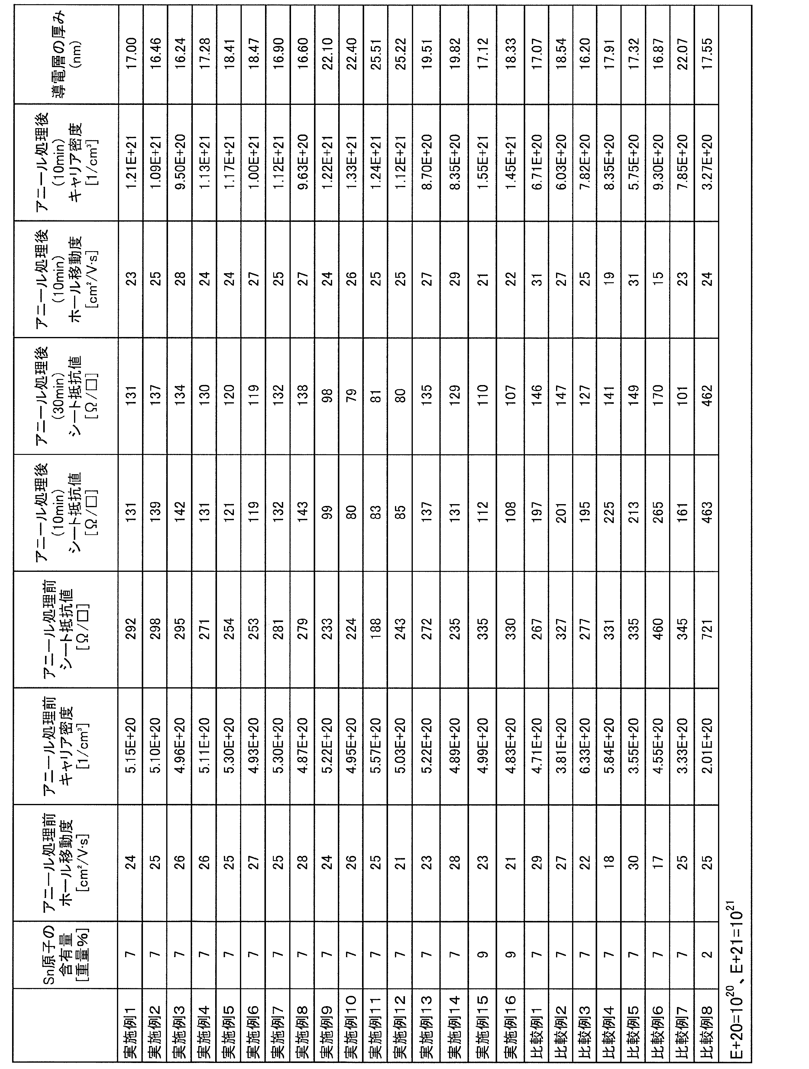
- Examples 2 to 8 and Comparative Examples 1 to 4 A light transmissive conductive film and an annealed light transmissive conductive film in the same manner as in Example 1 except that the hole mobility, carrier density and thickness of the conductive layer were set as shown in Table 1 below. Got. The hole mobility and carrier density of the conductive layer were adjusted by changing the type of gas introduced during the formation of the conductive layer and the amount of partial pressure thereof.
- Example 9 to 16 and Comparative Examples 5 to 8 In the same manner as in Example 1 except that the Sn atom content in the conductive layer, the hole mobility, the carrier density and the thickness of the conductive layer were set as shown in Table 1 below, An annealed light-transmitting conductive film was obtained.
- the hole mobility and carrier density of the conductive layer were adjusted by changing the types of gases introduced during the formation of the conductive layer, their partial pressure amount, and the input power amount of the cathode.
- the thickness of the conductive layer in the light-transmitting conductive film before the annealing treatment is measured using a fluorescent X-ray analyzer ZSX Primus III + (manufactured by Rigaku Corporation). It was determined by measuring the amount of In per area.
- the carrier density of the conductive layer in the light transmissive conductive film before and after the annealing treatment is It measured using the Hall effect measuring apparatus (made by Seinan Kogyo Co., Ltd.).
- the measurement method is the van der pauw method (DC measurement).
Landscapes
- Chemical & Material Sciences (AREA)
- Engineering & Computer Science (AREA)
- Chemical Kinetics & Catalysis (AREA)
- Materials Engineering (AREA)
- Mechanical Engineering (AREA)
- Metallurgy (AREA)
- Organic Chemistry (AREA)
- Manufacturing & Machinery (AREA)
- Laminated Bodies (AREA)
- Non-Insulated Conductors (AREA)
- Physical Vapour Deposition (AREA)
- Manufacturing Of Electric Cables (AREA)
Abstract
アニール処理を短時間で行ったとしても、抵抗値を低くすることができる光透過性導電フィルムを提供する。 本発明に係る光透過性導電フィルムは、光透過性及び導電性を有する導電層と、前記導電層の一方の表面側に配置されている基材とを備え、前記導電層は、インジウム・スズ酸化物の非晶質層であり、前記導電層におけるIn原子とSn原子との合計の含有量100重量%中、Sn原子の含有量が7重量%以上であり、前記導電層のキャリア密度が4×10²⁰/cm3以上、6×1020/cm3以下であり、前記導電層のホール移動度が20cm2/V・s以上、28cm2/V・s以下である。
Description
本発明は、光透過性及び導電性を有する光透過性導電フィルムに関する。また、本発明は、上記光透過性導電フィルムをアニール処理する工程を備えるアニール処理された光透過性導電フィルムの製造方法に関する。
近年、スマートフォン、携帯電話、ノートパソコン、タブレットPC、複写機又はカーナビゲーションなどの電子機器において、タッチパネル式の液晶表示装置が、広く用いられている。このような液晶表示装置では、基材上に透明導電層が積層された光透過性導電フィルムが用いられている。
下記の特許文献1には、透明なフィルム基材と、透明なSiOx(x=1.0~2.0)薄膜と、透明な導電性薄膜とがこの順で積層されている透明導電フィルムが開示されている。上記透明な導電性薄膜は、インジウム・スズ複合酸化物により形成されている。
上記透明導電層は、通常、光透過性導電フィルム全体をアニール処理することにより、結晶性を高めて用いられる。従来、このアニール処理を長時間行う必要があるため、透明導電フィルムの製造効率が悪くなり、透明導電フィルムのコストが高くなるという問題がある。
一方で、アニール処理の時間を短くすると、抵抗値が十分に低くなりにくい。
本発明の目的は、アニール処理を短時間で行ったとしても、抵抗値を低くすることができる光透過性導電フィルムを提供することである。また、本発明は、上記光透過性導電フィルムを用いるアニール処理された光透過性導電フィルムの製造方法を提供することである。
本発明の広い局面によれば、光透過性及び導電性を有する導電層と、前記導電層の一方の表面側に配置されている基材とを備え、前記導電層は、インジウム・スズ酸化物の非晶質層であり、前記導電層におけるIn原子とSn原子との合計の含有量100重量%中、Sn原子の含有量が7重量%以上であり、前記導電層のキャリア密度が4×10²⁰/cm3以上、6×1020/cm3以下であり、前記導電層のホール移動度が20cm2/V・s以上、28cm2/V・s以下である、光透過性導電フィルムが提供される。
本発明に係る光透過性導電フィルムのある特定の局面では、150℃で10分加熱した後の前記導電層のキャリア密度が7.0×10²⁰/cm3以上、2.0×1021/cm3以下であり、150℃で10分加熱した後の前記導電層のホール移動度が20cm2/V・s以上、30cm2/V・s以下である。
本発明に係る光透過性導電フィルムのある特定の局面では、前記導電層の厚みが16nm以上、19.9nm以下である。
本発明の広い局面によれば、上述した光透過性導電フィルムをアニール処理する工程を備える、アニール処理された光透過性導電フィルムの製造方法が提供される。
本発明に係る光透過性導電フィルムは、光透過性及び導電性を有する導電層と、上記導電層の一方の表面側に配置されている基材とを備え、上記導電層は、インジウム・スズ酸化物の非晶質層であり、上記導電層におけるIn原子とSn原子との合計の含有量100重量%中、Sn原子の含有量が7重量%以上であり、上記導電層のキャリア密度が4×10²⁰/cm3以上、6×1020/cm3以下であり、上記導電層のホール移動度が20cm2/V・s以上、28cm2/V・s以下であるので、アニール処理を短時間で行ったとしても、抵抗値を低くすることができる。
以下、本発明の詳細を説明する。
本発明に係る光透過性導電フィルムは、導電層と、基材とを備える。上記導電層は、光透過性及び導電性を有する。上記基材は、上記導電層の一方の表面側に配置されている。
本発明に係る光透過性導電フィルムでは、上記導電層は、インジウム・スズ酸化物の非晶質層である。本発明に係る光透過性導電フィルムでは、上記導電層におけるIn原子とSn原子との合計の含有量100重量%中、Sn原子の含有量が7重量%以上である。本発明に係る光透過性導電フィルムでは、上記導電層のキャリア密度が4×10²⁰/cm3以上、6×1020/cm3以下である。本発明に係る光透過性導電フィルムでは、上記導電層のホール移動度が20cm2/V・s以上、28cm2/V・s以下である。
本発明では、上記の構成が備えられているので、アニール処理を短時間で行ったとしても、抵抗値を低くすることができる。本発明者らは、アニール処理前の光透過性導電フィルム自体において、アニール処理後の光透過性導電フィルムの抵抗値を低くすることを可能にする性質を備えさせる検討を行った。本発明者らの検討の結果、アニール処理前の光透過性導電フィルムにおいて、上記導電層が上記の構成を満足していれば、アニール処理を短時間で行ったとしても、抵抗値を低くすることができることを見出した。また、本発明者らの検討の結果、アニール処理を短時間で行ったとしても、抵抗値が低いアニール処理された光透過性導電フィルムを得るためには、アニール処理前の光透過性導電フィルムにおいて、上記導電層が上記の構成を満足していればよいことを見出した。なお、本発明に係る光透過性導電フィルムは、アニール処理を長時間行い、長時間アニール処理された光透過性導電フィルムを得るためにも用いることができる。アニール処理を長時間行えば、抵抗値をより一層低くすることができる。
抵抗値をより一層低くする観点からは、アニール処理前の上記導電層のキャリア密度は、好ましくは4.5×10²⁰/cm3以上、好ましくは5.5×1020/cm3以下である。
抵抗値をより一層低くする観点からは、アニール処理前の上記導電層のホール移動度は、好ましくは22cm2/V・s以上、好ましくは26cm2/V・s以下である。
上記基材は、基材フィルムを含むことが好ましく、ハードコート層を含むことが好ましく、アンダーコート層を含むことが好ましい。本発明に係る光透過性導電フィルムは、保護フィルムを備え、上記基材の第1の表面上に上記導電層が配置されており、上記基材の上記第1の表面とは反対の第2の表面上に、上記保護フィルムが配置されていることが好ましい。
また、本発明に係る光透過性導電フィルムでは、アニール処理された光透過性導電フィルムの抵抗値を低くすることができるため、アニール処理された光透過性導電フィルムを液晶表示装置に用いた場合、表示品質を高めることができる。よって、アニール処理された光透過性導電フィルムは、液晶表示装置に好適に用いることができ、タッチパネルにより好適に用いることができる。
安定的に低い抵抗値を達成する観点からは、アニール処理(150℃で30分加熱)後の導電層のキャリア密度は好ましくは7.0×10²⁰/cm3以上、好ましくは2.0×1021/cm3以下である。安定的に低い抵抗値を達成する観点からは、アニール処理(150℃で30分加熱)後の導電層のホール移動度は好ましくは20cm2/V・s以上、好ましくは30cm2/V・s以下である。
以下、図面を参照しつつ、本発明の具体的な実施形態を説明する。
図1は、本発明の第1の実施形態に係る光透過性導電フィルムを示す断面図である。
図1に示す光透過性導電フィルム1は、アニール処理前の光透過性導電フィルムである。光透過性導電フィルム1は、基材2、導電層3及び保護フィルム4を備える。
基材2は、第1の表面2a及び第2の表面2bを有する。第1の表面2aと、第2の表面2bとは、互いに対向している。基材2の第1の表面2a上に、導電層3が積層されている。第1の表面2aは、導電層3が積層される側の表面である。基材2は、導電層3と保護フィルム4との間に配置される部材であり、導電層3の支持部材である。本実施形態では、導電層3は、インジウム・スズ酸化物の非晶質層であり、導電層3におけるIn原子とSn原子との合計の含有量100重量%中、Sn原子の含有量が7重量%以上であり、導電層3のキャリア密度は4×10²⁰/cm3以上、6×1020/cm3以下であり、導電層3のホール移動度は20cm2/V・s以上、28cm2/V・s以下である。
アニール処理前の光透過性導電フィルムにおいて、導電層は、部分的に設けられていてもよく、パターン状の導電層であってもよい。
基材2の第2の表面2b上に、保護フィルム4が積層されている。第2の表面2bは、保護フィルム4が積層される側の表面である。保護フィルム4を設けることで、基材2の第2の表面2bを保護することができる。
基材2は、基材フィルム11、第1及び第2のハードコート層12,13及びアンダーコート層14を有する。基材フィルム11は、光透過性の高い材料により構成されている。基材フィルム11の導電層3側の表面上には、第2のハードコート層13及びアンダーコート層14がこの順に積層されている。アンダーコート層14は、導電層3に接している。
基材フィルム11の保護フィルム4側の表面上には、第1のハードコート層12が積層されている。第1のハードコート層12は、保護フィルム4に接している。
導電層3は、光透過性が高く、かつ導電性の高い材料により構成されている。
保護フィルムは、粘着剤層により、基材の第2の表面に積層されてもよい。基材の第2の表面は、保護フィルムの上記粘着剤層と接していることが好ましい。
図2は、本発明の第2の実施形態に係る光透過性導電フィルムを示す断面図である。
図2に示す光透過性導電フィルム1Aは、アニール処理前の光透過性導電フィルムである。光透過性導電フィルム1Aでは、第1のハードコート層12が設けられていない。光透過性導電フィルム1Aは、アンダーコート層14と、第2のハードコート層13と、基材フィルム11とがこの順で積層された基材2Aを有する。光透過性導電フィルム1Aでは、基材フィルム11の導電層3とは反対側の表面上に直接、保護フィルム4が積層されている。
本発明に係る光透過性導電フィルムでは、光透過性導電フィルム1Aのように、第1のハードコート層が設けられていなくてもよい。基材フィルムの表面上に、保護フィルムが直接積層されていてもよい。また、第2のハードコート層及びアンダーコート層のうち少なくとも一方が設けられていなくてもよい。基材フィルムの導電層側の表面上には、アンダーコート層及び導電層がこの順に積層されていてもよく、基材フィルムに導電層が直接積層されていてもよい。アンダーコート層は、単層であってもよく、多層であってもよい。
次に、図1に示す光透過性導電フィルム1の製造方法、及び、図3に示すアニール処理された光透過性導電フィルム1Xの製造方法を説明する。
光透過性導電フィルム1は、例えば、以下の方法により作製することができる。
基材フィルム11の一方の表面上に、第1のハードコート層12を形成する。具体的には、樹脂に紫外線硬化樹脂を用いる場合は、光硬化性モノマー及び光開始剤を希釈剤中で撹拌して塗工液を作製する。得られた塗工液を基材フィルム11上に塗布し、紫外線を照射して樹脂を硬化させて、第1のハードコート層12を形成する。
続いて、第1のハードコート層12上に保護フィルム4を形成する。保護フィルム4として、基材シート上に粘着剤層が設けられた保護フィルムを用いる場合は、粘着面を第1のハードコート層12の表面に貼り合わせて、第1のハードコート層12上に保護フィルム4を形成することができる。
次に、基材フィルム11の第1のハードコート層12とは反対側の表面上に、第2のハードコート層13を形成する。具体的には、樹脂に紫外線硬化樹脂を用いる場合は、光硬化性モノマー及び光開始剤を、希釈剤中で撹拌して塗工液を作製する。得られた塗工液を基材フィルム11の第1のハードコート層12側とは反対側の表面上に塗布し、紫外線を照射して樹脂を硬化させ第2のハードコート層13を形成する。
次に、第2のハードコート層13上にアンダーコート層14を形成する。具体的に、SiO2を用いる場合は、蒸着又はスパッタリングにより第2のハードコート層13上にアンダーコート層14を形成することができる。
上記のようにして、基材フィルム11上に、第1及び第2のハードコート層12,13及びアンダーコート層14を形成する。なお、本発明において、第1及び第2のハードコート層12,13及びアンダーコート層14は設けなくてもよい。この場合には、基材フィルム11の導電層3側の表面が、基材2の第1の表面2aであり、基材フィルム11の保護フィルム4側の表面が、基材2の第2の表面2bである。
次に、アンダーコート層14上に、導電層3を形成することにより、光透過性導電フィルム1を作製することができる。
導電層の形成方法としては、特に限定されない。例えば、蒸着又はスパッタリングにより形成した金属膜をエッチングする方法や、スクリーン印刷又はインクジェット印刷などの各種印刷方法、並びにレジストを用いたフォトリソグラフィー法等の公知のパターニング方法等を用いることができる。形成した導電層は、後述するアニール処理により結晶性を高めて用いることができる。
光透過性導電フィルム1は、アニール処理によって、図3に示すアニール処理された光透過性導電フィルム1Xを得るために好適に用いられる。アニール処理された光透過性導電フィルム1Xを得るために、光透過性導電フィルム1をアニール処理する工程を行うことができる。アニール処理前の導電層3がパターン状ではない場合に、導電層3の基材フィルム11側とは反対側の表面上に、レジスト層を部分的に形成して、エッチング処理することで、パターン状の導電層3Xを形成することができる。エッチング処理後には、水洗が行われる。
アニール処理された光透過性導電フィルム1Xは、パターン状の導電層3Xを有する。パターン状の導電層3Xは、基材2の第1の表面2a上に部分的に積層されている。アニール処理された光透過性導電フィルム1Xは、基材2の第1の表面2a上において、パターン状の導電層3Xがある部分と、パターン状の導電層3Xがない部分とを有する。
アニール処理の温度は、好ましくは120℃以上、より好ましくは140℃以上、好ましくは170℃以下、より好ましくは160℃以下である。
上記アニール処理の処理時間は、好ましくは5分以上、より好ましくは10分以上、好ましくは60分以下、より好ましくは30分以下である。本発明では、アニール処理を短時間で行っても、抵抗値を低くすることができる。
アニール処理された光透過性導電フィルム1Xは、保護フィルム4を積層したまま使用してもよいし、保護フィルム4を剥がして使用してもよい。
以下、光透過性導電フィルムを構成する各層の詳細を説明する。
(基材)
基材の全体の厚みは、好ましくは23μm以上、より好ましくは50μm以上、好ましくは300μm以下、より好ましくは200μm以下である。
基材の全体の厚みは、好ましくは23μm以上、より好ましくは50μm以上、好ましくは300μm以下、より好ましくは200μm以下である。
基材フィルム;
基材フィルムは、高い光透過性を有することが好ましい。従って、基材フィルムの材料としては、特に限定されないが、例えば、ポリオレフィン、ポリエーテルサルフォン、ポリスルホン、ポリカーボネート、シクロオレフィンポリマー、ポリアリレート、ポリアミド、ポリメチルメタクリレート、ポリエチレンテレフタレート、ポリブチレンテレフタレート、ポリエチレンナフタレート、トリアセチルセルロース、及びセルロースナノファイバー等が挙げられる。上記基材フィルムの材料は、単独で用いてもよく、複数を併用してもよい。
基材フィルムは、高い光透過性を有することが好ましい。従って、基材フィルムの材料としては、特に限定されないが、例えば、ポリオレフィン、ポリエーテルサルフォン、ポリスルホン、ポリカーボネート、シクロオレフィンポリマー、ポリアリレート、ポリアミド、ポリメチルメタクリレート、ポリエチレンテレフタレート、ポリブチレンテレフタレート、ポリエチレンナフタレート、トリアセチルセルロース、及びセルロースナノファイバー等が挙げられる。上記基材フィルムの材料は、単独で用いてもよく、複数を併用してもよい。
基材フィルムの厚みは、好ましくは5μm以上、より好ましくは20μm以上、好ましくは190μm以下、より好ましくは125μm以下である。基材フィルムの厚みが、上記下限以上及び上記上限以下である場合、導電層のパターンを、より一層視認され難くすることができる。
また、基材フィルムの光透過率に関しては、波長380~780nmの可視光領域における平均透過率が好ましくは85%以上、より好ましくは90%以上である。
また、基材フィルムは、各種安定剤、紫外線吸収剤、可塑剤、滑剤又は着色剤を含んでいてもよい。
第1及び第2のハードコート層;
第1及び第2のハードコート層はそれぞれ、バインダー樹脂により構成されていることが好ましい。上記バインダー樹脂は、硬化樹脂であることが好ましい。上記硬化樹脂としては、熱硬化樹脂や、活性エネルギー線硬化樹脂などを用いることができる。生産性及び経済性を良好にする観点から、上記硬化樹脂は、紫外線硬化樹脂であることが好ましい。
第1及び第2のハードコート層はそれぞれ、バインダー樹脂により構成されていることが好ましい。上記バインダー樹脂は、硬化樹脂であることが好ましい。上記硬化樹脂としては、熱硬化樹脂や、活性エネルギー線硬化樹脂などを用いることができる。生産性及び経済性を良好にする観点から、上記硬化樹脂は、紫外線硬化樹脂であることが好ましい。
上記紫外線硬化樹脂を形成するための光硬化性モノマーとしては、例えば、1,6-ヘキサンジオールジアクリレート、1,4-ブタンジオールジアクリレート、エチレングリコールジアクリレート、ジエチレングリコールジアクリレート、テトラエチレングリコールジアクリレート、トリプロピレングリコールジアクリレート、ネオペンチルグリコールジアクリレート、1,4-ブタンジオールジメタクリレート、ポリ(ブタンジオール)ジアクリレート、テトラエチレングリコールジメタクリレート、1,3-ブチレングリコールジアクリレート、トリエチレングリコールジアクリレート、トリイソプロピレングリコールジアクリレート、ポリエチレングリコールジアクリレート及びビスフェノールAジメタクリレートのようなジアクリレート化合物;トリメチロールプロパントリアクリレート、トリメチロールプロパントリメタクリレート、ペンタエリトリトールモノヒドロキシトリアクリレート及びトリメチロールプロパントリエトキシトリアクリレートのようなトリアクリレート化合物;ペンタエリトリトールテトラアクリレート及びジ-トリメチロールプロパンテトラアクリレートのようなテトラアクリレート化合物;並びにジペンタエリトリトール(モノヒドロキシ)ペンタアクリレートのようなペンタアクリレート化合物等が挙げられる。上記紫外線硬化樹脂としては、5官能以上の多官能アクリレート化合物も用いてもよい。上記多官能アクリレート化合物は、単独で用いてもよく、複数を併用してもよい。また、上記多官能アクリレート化合物に、光開始剤、光増感剤、レベリング剤、希釈剤などを添加してもよい。
また、第1のハードコート層は、樹脂部及びフィラーにより構成されていてもよい。第1のハードコート層がフィラーを含む場合、導電層のパターンをより一層視認され難くすることができる。なお、第1のハードコート層がフィラーを含む場合、ゆず肌が生じることがあり、光透過性導電フィルムを液晶表示装置に用いると表示光が見えにくくなることがある。従って、ゆず肌を生じ難くする観点からは、第1のハードコート層が、フィラーを含まず、樹脂部のみによって構成されていることが望ましい。あるいは、フィラーの平均粒子径が、第1のハードコート層の厚みより小さく、フィラーが、第1のハードコート層の表面において突出していないことが好ましい。
上記フィラーとしては、特に限定されないが、例えば、シリカ、酸化鉄、酸化アルミニウム、酸化亜鉛、酸化チタン、二酸化ケイ素、酸化アンチモン、酸化ジルコニウム、酸化錫、酸化セリウム、インジウム-錫酸化物などの金属酸化物粒子;シリコーン、(メタ)アクリル、スチレン、メラミンなどの樹脂粒子等が挙げられる。より具体的には、架橋ポリ(メタ)アクリル酸メチルなどの樹脂粒子を用いることができる。上記フィラーは、単独で用いてもよく、複数を併用してもよい。
また、第1及び第2のハードコート層はそれぞれ、各種安定剤、紫外線吸収剤、可塑剤、滑剤又は着色剤を含んでいてもよい。
アンダーコート層;
アンダーコート層は、例えば、屈折率調整層である。アンダーコート層を設けることで、導電層と、第2のハードコート層又は基材フィルムとの間の屈折率の差を小さくすることができるので、光透過性導電フィルムの光透過性をより一層高めることができる。
アンダーコート層は、例えば、屈折率調整層である。アンダーコート層を設けることで、導電層と、第2のハードコート層又は基材フィルムとの間の屈折率の差を小さくすることができるので、光透過性導電フィルムの光透過性をより一層高めることができる。
アンダーコート層を構成する材料としては、屈折率調整機能を有する限り特に限定されず、SiO2、MgF2、Al2O3などの無機材料や、アクリル樹脂、ウレタン樹脂、メラミン樹脂、アルキド樹脂及びシロキサンポリマーなどの有機材料が挙げられる。
アンダーコート層は、真空蒸着法、スパッタリング法、イオンプレーティング法又は塗工法により形成することができる。
(導電層)
導電層は、光透過性を有する導電性材料により形成されている。上記導電性材料として、インジウム・スズ酸化物(ITO)が用いられている。上記導電層は、非晶質層である。
導電層は、光透過性を有する導電性材料により形成されている。上記導電性材料として、インジウム・スズ酸化物(ITO)が用いられている。上記導電層は、非晶質層である。
本発明では、アニール処理前の上記導電層は、上記キャリア密度及び上記ホール移動度が上記の範囲を満足するように形成される。上記キャリア密度及び上記ホール移動度は、導電層の形成時の導入ガスの種類、それらの分圧及びカソードの投入電力量により調整することができる。一例として、導電層をマグネトロンスパッタ装置によって形成する場合、そのプロセスガスとしてAr、Ne、Heなどの希ガスや、O2、H2O、H2などのガスを組み合わせ、所望の分圧になるよう混合し、使用することで、上記キャリア密度及び上記ホール移動度を調整する。
導電層の厚みは、好ましくは12nm以上、より好ましくは16nm以上、更に好ましくは17nm以上、好ましくは50nm以下、より好ましくは30nm以下、更に好ましくは19.9nm以下である。
導電層の厚みが上記下限以上である場合、光透過性導電フィルムの抵抗値を効果的に低くすることができ、導電性をより一層高めることができる。導電層の厚みが上記上限以下である場合、導電層のパターンをより一層視認され難くすることができ、光透過性導電フィルムをより一層薄くすることができる。
また、導電層の光透過率に関しては、可視光領域における平均透過率が好ましくは85%以上、より好ましくは90%以上である。
導電層は、In原子及びSn原子を含む。導電層におけるIn原子とSn原子との合計の含有量100重量%中、Sn原子の含有量が7重量%以上である。上記Sn原子の含有量が7重量%未満であると、キャリア密度が大きくならず、抵抗値が悪化する。導電層におけるIn原子とSn原子との合計の含有量100重量%中、Sn原子の含有量は、30重量%以下であってもよく、20重量%以下であってもよく、10重量%以下であってもよい。
(保護フィルム)
保護フィルムは、基材シート及び粘着剤層により構成されていることが好ましい。
保護フィルムは、基材シート及び粘着剤層により構成されていることが好ましい。
上記基材シートは、高い光透過性を有することが好ましい。上記基材シートの材料としては、特に限定されないが、例えば、ポリオレフィン、ポリエーテルサルフォン、ポリスルホン、ポリカーボネート、シクロオレフィンポリマー、ポリアリレート、ポリアミド、ポリメチルメタクリレート、ポリエチレンテレフタレート、ポリブチレンテレフタレート、ポリエチレンナフタレート、トリアセチルセルロース、及びセルロースナノファイバー等が挙げられる。
上記粘着剤層は、(メタ)アクリル系粘着剤、ゴム系粘着剤、ウレタン系接着剤又はエポキシ系接着剤により構成することができる。熱処理による粘着力の上昇を抑制する観点から、上記粘着剤層は、(メタ)アクリル系粘着剤により構成されていることが好ましい。
上記(メタ)アクリル系粘着剤は、(メタ)アクリル重合体に、必要に応じて架橋剤、粘着付与樹脂及び各種安定剤などを添加した粘着剤である。
上記(メタ)アクリル重合体は、特に限定されないが、(メタ)アクリル酸エステルモノマーと、他の共重合可能な重合性モノマーとを含む混合モノマーを共重合して得られた(メタ)アクリル共重合体であることが好ましい。
上記(メタ)アクリル酸エステルモノマーとしては、特に限定されないが、アルキル基の炭素数が1~12の1級又は2級のアルキルアルコールと、(メタ)アクリル酸とのエステル化反応により得られる(メタ)アクリル酸エステルモノマーが好ましく、具体的には、(メタ)アクリル酸エチル、(メタ)アクリル酸ブチル、(メタ)アクリル酸-2-エチルヘキシルなどが挙げられる。上記(メタ)アクリル酸エステルモノマーは、単独で用いてもよく、複数を併用してもよい。
上記他の共重合可能な重合性モノマーとしては、例えば、(メタ)アクリル酸2-ヒドロキシエチル、(メタ)アクリル酸ヒドロキシプロピル、(メタ)アクリル酸ヒドロキシブチル等の(メタ)アクリル酸ヒドロキシアルキル;(メタ)アクリル酸イソボルニル、(メタ)アクリル酸ヒドロキシアルキル、グリセリンジメタクリレート、(メタ)アクリル酸グリシジル、2-メタクリロイルオキシエチルイソシアネート、(メタ)アクリル酸、イタコン酸、無水マレイン酸、クロトン酸、マレイン酸及びフマル酸等の官能性モノマーが挙げられる。上記他の共重合可能な重合性モノマーは、単独で用いてもよく、複数を併用してもよい。
上記架橋剤としては、特に限定されず、例えば、イソシアネート系架橋剤、エポキシ系架橋剤、メラミン系架橋剤、過酸化物系架橋剤、尿素系架橋剤、金属アルコキシド系架橋剤、金属キレート系架橋剤、金属塩系架橋剤、カルボジイミド系架橋剤、オキサゾリン系架橋剤、アジリジン系架橋剤、アミン系架橋剤、多官能アクリレート化合物などが挙げられる。上記架橋剤は、単独で用いてもよく、複数を併用してもよい。
上記粘着付与樹脂としては、特に限定されないが、例えば、脂肪族系共重合体、芳香族系共重合体、脂肪族・芳香族系共重合体及び脂環式系共重合体等の石油系樹脂;クマロン-インデン系樹脂;テルペン系樹脂;テルペンフェノール系樹脂;重合ロジン等のロジン系樹脂;フェノール系樹脂;キシレン系樹脂等が挙げられる。上記粘着付与樹脂は、水素添加された樹脂であってもよい。上記粘着付与樹脂は、単独で用いてもよく、複数を併用してもよい。
保護フィルムの厚みは、好ましくは25μm以上、より好ましくは50μm以上、好ましくは300μm以下、より好ましくは200μm以下である。保護フィルムの厚みが、上記下限以上及び上記上限以下である場合、導電層のパターンを、より一層視認され難くすることができる。
以下、本発明について、具体的な実施例に基づき、更に詳しく説明する。なお、本発明は以下の実施例に限定されない。
(実施例1)
(1)光透過性導電フィルムの作製
基材フィルムであるPETフィルム(厚み125μm)上に、DCマグネトロンスパッタ装置を用いて、インジウム原子とスズ原子との合計100重量%中にスズ原子の含有量が7重量%となるように、厚さ17.00nmの導電層(インジウム・スズ酸化物層)を形成して、光透過性導電フィルムを得た。
(1)光透過性導電フィルムの作製
基材フィルムであるPETフィルム(厚み125μm)上に、DCマグネトロンスパッタ装置を用いて、インジウム原子とスズ原子との合計100重量%中にスズ原子の含有量が7重量%となるように、厚さ17.00nmの導電層(インジウム・スズ酸化物層)を形成して、光透過性導電フィルムを得た。
(2)アニール処理された光透過性導電フィルムの作製
PETフィルム上に形成された導電層を、IRアニール機(富士科学器械社製)を用いて、炉内温度150℃に設定し、10分間、又は30分間アニール処理した。
PETフィルム上に形成された導電層を、IRアニール機(富士科学器械社製)を用いて、炉内温度150℃に設定し、10分間、又は30分間アニール処理した。
(実施例2~8及び比較例1~4)
導電層のホール移動度、キャリア密度及び厚みを下記の表1に示すように設定したこと以外は実施例1と同様にして、光透過性導電フィルム、及び、アニール処理された光透過性導電フィルムを得た。導電層のホール移動度及びキャリア密度は、導電層の形成時の導入ガスの種類、及び、それらの分圧量を変更することで調整した。
導電層のホール移動度、キャリア密度及び厚みを下記の表1に示すように設定したこと以外は実施例1と同様にして、光透過性導電フィルム、及び、アニール処理された光透過性導電フィルムを得た。導電層のホール移動度及びキャリア密度は、導電層の形成時の導入ガスの種類、及び、それらの分圧量を変更することで調整した。
(実施例9~16及び比較例5~8)
導電層におけるSn原子の含有量、導電層のホール移動度、キャリア密度及び厚みを下記の表1に示すように設定したこと以外は実施例1と同様にして、光透過性導電フィルム、及び、アニール処理された光透過性導電フィルムを得た。導電層のホール移動度及びキャリア密度は、導電層の形成時の導入ガスの種類、それらの分圧量及びカソードの投入電力量を変更することで調整した。
導電層におけるSn原子の含有量、導電層のホール移動度、キャリア密度及び厚みを下記の表1に示すように設定したこと以外は実施例1と同様にして、光透過性導電フィルム、及び、アニール処理された光透過性導電フィルムを得た。導電層のホール移動度及びキャリア密度は、導電層の形成時の導入ガスの種類、それらの分圧量及びカソードの投入電力量を変更することで調整した。
(評価)
(1)アニール処理前の光透過性導電フィルムにおける導電層の厚み
アニール処理前の光透過性導電フィルムにおける導電層の厚みを、蛍光X線分析装置 ZSX PrimusIII+(リガク社製)を用いて、単位面積当たりのIn量を測定することにより求めた。
(1)アニール処理前の光透過性導電フィルムにおける導電層の厚み
アニール処理前の光透過性導電フィルムにおける導電層の厚みを、蛍光X線分析装置 ZSX PrimusIII+(リガク社製)を用いて、単位面積当たりのIn量を測定することにより求めた。
(2)アニール処理前及びアニール処理後の光透過性導電フィルムにおける導電層のキャリア密度
アニール処理前、及びアニール処理後(10分後)の光透過性導電フィルムにおいて、導電層のキャリア密度を、ホール効果測定装置(誠南工業社製)を用いて測定した。測定方法はvan der pauw法(DC測定)である。
アニール処理前、及びアニール処理後(10分後)の光透過性導電フィルムにおいて、導電層のキャリア密度を、ホール効果測定装置(誠南工業社製)を用いて測定した。測定方法はvan der pauw法(DC測定)である。
(3)アニール処理前及びアニール処理後の光透過性導電フィルムにおける導電層のホール移動度
アニール処理前、及びアニール処理後(10分後)の光透過性導電フィルムにおいて、導電層のホール移動度を、ホール効果測定装置(誠南工業社製)を用いて測定した。
アニール処理前、及びアニール処理後(10分後)の光透過性導電フィルムにおいて、導電層のホール移動度を、ホール効果測定装置(誠南工業社製)を用いて測定した。
(4)アニール処理前の光透過性導電フィルム、及びアニール処理後の光透過性導電フィルムにおける抵抗値
アニール処理前の光透過性導電フィルム、及びアニール処理後(10分後又は30分後)の光透過性導電フィルムにおいて、導電層の抵抗値を、Loresta-AX MCP-T370(三菱アナリテック社製)を用いて、4端子法にて、測定した。
アニール処理前の光透過性導電フィルム、及びアニール処理後(10分後又は30分後)の光透過性導電フィルムにおいて、導電層の抵抗値を、Loresta-AX MCP-T370(三菱アナリテック社製)を用いて、4端子法にて、測定した。
1,1A…光透過性導電フィルム
1X…アニール処理された光透過性導電フィルム
2,2A…基材
2a…第1の表面
2b…第2の表面
3…導電層
3X…パターン状の導電層
4…保護フィルム
11…基材フィルム
12…第1のハードコート層
13…第2のハードコート層
14…アンダーコート層
1X…アニール処理された光透過性導電フィルム
2,2A…基材
2a…第1の表面
2b…第2の表面
3…導電層
3X…パターン状の導電層
4…保護フィルム
11…基材フィルム
12…第1のハードコート層
13…第2のハードコート層
14…アンダーコート層
Claims (4)
- 光透過性及び導電性を有する導電層と、
前記導電層の一方の表面側に配置されている基材とを備え、
前記導電層は、インジウム・スズ酸化物の非晶質層であり、
前記導電層におけるIn原子とSn原子との合計の含有量100重量%中、Sn原子の含有量が7重量%以上であり、
前記導電層のキャリア密度が4×10²⁰/cm3以上、6×1020/cm3以下であり、
前記導電層のホール移動度が20cm2/V・s以上、28cm2/V・s以下である、光透過性導電フィルム。 - 150℃で10分加熱した後の前記導電層のキャリア密度が7.0×10²⁰/cm3以上、2.0×1021/cm3以下であり、
150℃で10分加熱した後の前記導電層のホール移動度が20cm2/V・s以上、30cm2/V・s以下である、請求項1に記載の光透過性導電フィルム。 - 前記導電層の厚みが16nm以上、19.9nm以下である、請求項1又は2に記載の光透過性導電フィルム。
- 請求項1~3のいずれか1項に記載の光透過性導電フィルムをアニール処理する工程を備える、アニール処理された光透過性導電フィルムの製造方法。
Priority Applications (2)
| Application Number | Priority Date | Filing Date | Title |
|---|---|---|---|
| JP2016567867A JP6159490B1 (ja) | 2015-09-30 | 2016-09-29 | 光透過性導電フィルム、及び、アニール処理された光透過性導電フィルムの製造方法 |
| CN201680027950.0A CN107533883B (zh) | 2015-09-30 | 2016-09-29 | 透光性导电膜、及经退火处理的透光性导电膜的制造方法 |
Applications Claiming Priority (2)
| Application Number | Priority Date | Filing Date | Title |
|---|---|---|---|
| JP2015195414 | 2015-09-30 | ||
| JP2015-195414 | 2015-09-30 |
Publications (1)
| Publication Number | Publication Date |
|---|---|
| WO2017057556A1 true WO2017057556A1 (ja) | 2017-04-06 |
Family
ID=58423928
Family Applications (1)
| Application Number | Title | Priority Date | Filing Date |
|---|---|---|---|
| PCT/JP2016/078794 Ceased WO2017057556A1 (ja) | 2015-09-30 | 2016-09-29 | 光透過性導電フィルム、及び、アニール処理された光透過性導電フィルムの製造方法 |
Country Status (3)
| Country | Link |
|---|---|
| JP (2) | JP6159490B1 (ja) |
| CN (1) | CN107533883B (ja) |
| WO (1) | WO2017057556A1 (ja) |
Cited By (10)
| Publication number | Priority date | Publication date | Assignee | Title |
|---|---|---|---|---|
| JP2017092033A (ja) * | 2015-11-09 | 2017-05-25 | 日東電工株式会社 | 光透過性導電フィルムおよび調光フィルム |
| WO2018207622A1 (ja) * | 2017-05-09 | 2018-11-15 | 日東電工株式会社 | 光透過性導電層付きフィルム、調光フィルムおよび調光装置 |
| JP2019029335A (ja) * | 2017-05-09 | 2019-02-21 | 日東電工株式会社 | 光透過性導電層付きフィルム、調光フィルムおよび調光装置 |
| WO2020095814A1 (ja) * | 2018-11-07 | 2020-05-14 | 日東電工株式会社 | タッチパネル用光透過性導電層付きフィルム、光透過性導電層付き偏光フィルムおよびタッチパネル表示装置 |
| WO2020122150A1 (ja) * | 2018-12-12 | 2020-06-18 | 日東電工株式会社 | 電波吸収体用インピーダンス整合膜、電波吸収体用インピーダンス整合膜付フィルム、電波吸収体、及び電波吸収体用積層体 |
| KR20200094648A (ko) * | 2019-01-30 | 2020-08-07 | 닛토덴코 가부시키가이샤 | 투명 도전성 필름 |
| JP2020123476A (ja) * | 2019-01-30 | 2020-08-13 | 日東電工株式会社 | 透明導電性フィルム |
| JP2020136148A (ja) * | 2019-02-22 | 2020-08-31 | 日東電工株式会社 | 光透過性導電フィルム |
| JP2020136147A (ja) * | 2019-02-22 | 2020-08-31 | 日東電工株式会社 | 光透過性導電フィルム |
| WO2023042844A1 (ja) * | 2021-09-17 | 2023-03-23 | 日東電工株式会社 | 透明導電性フィルム |
Families Citing this family (1)
| Publication number | Priority date | Publication date | Assignee | Title |
|---|---|---|---|---|
| WO2021187582A1 (ja) * | 2020-03-19 | 2021-09-23 | 日東電工株式会社 | 透明導電層および透明導電性フィルム |
Citations (10)
| Publication number | Priority date | Publication date | Assignee | Title |
|---|---|---|---|---|
| JPH09286070A (ja) * | 1995-12-20 | 1997-11-04 | Mitsui Toatsu Chem Inc | 透明導電性積層体及びそれを用いたエレクトロルミネッセンス発光素子 |
| JP2004207221A (ja) * | 2002-10-04 | 2004-07-22 | Sumitomo Metal Mining Co Ltd | 酸化物透明電極膜とその製造方法、透明導電性基材、太陽電池および光検出素子 |
| JP2004247060A (ja) * | 2003-02-10 | 2004-09-02 | Sumitomo Metal Mining Co Ltd | 透明導電性酸化物複合体とこれを用いた太陽電池および表示装置 |
| WO2011043235A1 (ja) * | 2009-10-06 | 2011-04-14 | Jx日鉱日石金属株式会社 | 酸化インジウム焼結体、酸化インジウム透明導電膜及び該透明導電膜の製造方法 |
| JP2013152827A (ja) * | 2012-01-24 | 2013-08-08 | Kaneka Corp | 透明電極付き基板およびその製造方法 |
| JP2013229283A (ja) * | 2007-05-23 | 2013-11-07 | National Institute Of Advanced Industrial & Technology | 酸化物透明導電膜、およびそれを用いた光電変換素子、光検出素子 |
| WO2013172055A1 (ja) * | 2012-05-17 | 2013-11-21 | 株式会社カネカ | 透明電極付き基板およびその製造方法、ならびにタッチパネル |
| WO2014034575A1 (ja) * | 2012-08-31 | 2014-03-06 | 株式会社カネカ | 透明電極付き基板の製造方法、および透明電極付き基板 |
| JP2014148734A (ja) * | 2013-02-04 | 2014-08-21 | Kaneka Corp | 透明電極付き基板の製造方法及び透明電極付き基板 |
| WO2014157312A1 (ja) * | 2013-03-29 | 2014-10-02 | 株式会社カネカ | 透明導電積層フィルムおよびその製造方法 |
Family Cites Families (5)
| Publication number | Priority date | Publication date | Assignee | Title |
|---|---|---|---|---|
| JP3749531B2 (ja) * | 2003-08-29 | 2006-03-01 | 日東電工株式会社 | 透明導電積層体の製造方法 |
| US20110094577A1 (en) * | 2009-10-28 | 2011-04-28 | Dilip Kumar Chatterjee | Conductive metal oxide films and photovoltaic devices |
| JP5543907B2 (ja) * | 2010-12-24 | 2014-07-09 | 日東電工株式会社 | 透明導電性フィルムおよびその製造方法 |
| JP5881501B2 (ja) * | 2012-03-29 | 2016-03-09 | 株式会社Neomaxマテリアル | 発光素子用基板および発光モジュール |
| KR20140041873A (ko) * | 2012-06-07 | 2014-04-04 | 닛토덴코 가부시키가이샤 | 투명 도전성 필름 |
-
2016
- 2016-09-29 WO PCT/JP2016/078794 patent/WO2017057556A1/ja not_active Ceased
- 2016-09-29 JP JP2016567867A patent/JP6159490B1/ja active Active
- 2016-09-29 CN CN201680027950.0A patent/CN107533883B/zh not_active Expired - Fee Related
-
2017
- 2017-05-25 JP JP2017103226A patent/JP2017160545A/ja active Pending
Patent Citations (10)
| Publication number | Priority date | Publication date | Assignee | Title |
|---|---|---|---|---|
| JPH09286070A (ja) * | 1995-12-20 | 1997-11-04 | Mitsui Toatsu Chem Inc | 透明導電性積層体及びそれを用いたエレクトロルミネッセンス発光素子 |
| JP2004207221A (ja) * | 2002-10-04 | 2004-07-22 | Sumitomo Metal Mining Co Ltd | 酸化物透明電極膜とその製造方法、透明導電性基材、太陽電池および光検出素子 |
| JP2004247060A (ja) * | 2003-02-10 | 2004-09-02 | Sumitomo Metal Mining Co Ltd | 透明導電性酸化物複合体とこれを用いた太陽電池および表示装置 |
| JP2013229283A (ja) * | 2007-05-23 | 2013-11-07 | National Institute Of Advanced Industrial & Technology | 酸化物透明導電膜、およびそれを用いた光電変換素子、光検出素子 |
| WO2011043235A1 (ja) * | 2009-10-06 | 2011-04-14 | Jx日鉱日石金属株式会社 | 酸化インジウム焼結体、酸化インジウム透明導電膜及び該透明導電膜の製造方法 |
| JP2013152827A (ja) * | 2012-01-24 | 2013-08-08 | Kaneka Corp | 透明電極付き基板およびその製造方法 |
| WO2013172055A1 (ja) * | 2012-05-17 | 2013-11-21 | 株式会社カネカ | 透明電極付き基板およびその製造方法、ならびにタッチパネル |
| WO2014034575A1 (ja) * | 2012-08-31 | 2014-03-06 | 株式会社カネカ | 透明電極付き基板の製造方法、および透明電極付き基板 |
| JP2014148734A (ja) * | 2013-02-04 | 2014-08-21 | Kaneka Corp | 透明電極付き基板の製造方法及び透明電極付き基板 |
| WO2014157312A1 (ja) * | 2013-03-29 | 2014-10-02 | 株式会社カネカ | 透明導電積層フィルムおよびその製造方法 |
Cited By (33)
| Publication number | Priority date | Publication date | Assignee | Title |
|---|---|---|---|---|
| US20190122784A1 (en) * | 2015-11-09 | 2019-04-25 | Nitto Denko Corporation | Light transmitting conductive film and light control film |
| JP2017092033A (ja) * | 2015-11-09 | 2017-05-25 | 日東電工株式会社 | 光透過性導電フィルムおよび調光フィルム |
| US10720264B2 (en) | 2015-11-09 | 2020-07-21 | Nitto Denko Corporation | Light transmitting conductive film and light control film |
| JP2019025915A (ja) * | 2015-11-09 | 2019-02-21 | 日東電工株式会社 | 調光フィルム |
| JP2018081928A (ja) * | 2015-11-09 | 2018-05-24 | 日東電工株式会社 | 光透過性導電フィルムおよび調光フィルム |
| JP2019033088A (ja) * | 2015-11-09 | 2019-02-28 | 日東電工株式会社 | 光透過性導電フィルム |
| KR102518569B1 (ko) | 2017-05-09 | 2023-04-05 | 닛토덴코 가부시키가이샤 | 광 투과성 도전층 형성 필름, 조광 필름 및 조광 장치 |
| CN110637343A (zh) * | 2017-05-09 | 2019-12-31 | 日东电工株式会社 | 带透光性导电层的薄膜、调光薄膜和调光装置 |
| JP2019029335A (ja) * | 2017-05-09 | 2019-02-21 | 日東電工株式会社 | 光透過性導電層付きフィルム、調光フィルムおよび調光装置 |
| KR20200003806A (ko) * | 2017-05-09 | 2020-01-10 | 닛토덴코 가부시키가이샤 | 광 투과성 도전층 형성 필름, 조광 필름 및 조광 장치 |
| JP7039506B2 (ja) | 2017-05-09 | 2022-03-22 | 日東電工株式会社 | 光透過性導電層付きフィルム |
| CN110637343B (zh) * | 2017-05-09 | 2021-04-27 | 日东电工株式会社 | 带透光性导电层的薄膜、调光薄膜和调光装置 |
| JP2019123243A (ja) * | 2017-05-09 | 2019-07-25 | 日東電工株式会社 | 光透過性導電層付きフィルム |
| WO2018207622A1 (ja) * | 2017-05-09 | 2018-11-15 | 日東電工株式会社 | 光透過性導電層付きフィルム、調光フィルムおよび調光装置 |
| WO2020095814A1 (ja) * | 2018-11-07 | 2020-05-14 | 日東電工株式会社 | タッチパネル用光透過性導電層付きフィルム、光透過性導電層付き偏光フィルムおよびタッチパネル表示装置 |
| JP7469043B2 (ja) | 2018-11-07 | 2024-04-16 | 日東電工株式会社 | タッチパネル用光透過性導電層付きフィルム、光透過性導電層付き偏光フィルムおよびタッチパネル表示装置 |
| JPWO2020095814A1 (ja) * | 2018-11-07 | 2021-09-24 | 日東電工株式会社 | タッチパネル用光透過性導電層付きフィルム、光透過性導電層付き偏光フィルムおよびタッチパネル表示装置 |
| US11991871B2 (en) | 2018-12-12 | 2024-05-21 | Nitto Denko Corporation | Impedance matching film for radio wave absorber, impedance matching film-attached film for radio wave absorber, radio wave absorber, and laminate for radio wave absorber |
| JP7626526B2 (ja) | 2018-12-12 | 2025-02-07 | 日東電工株式会社 | 電波吸収体用インピーダンス整合膜、電波吸収体用インピーダンス整合膜付フィルム、電波吸収体、及び電波吸収体用積層体 |
| JP2020096185A (ja) * | 2018-12-12 | 2020-06-18 | 日東電工株式会社 | 電波吸収体用インピーダンス整合膜、電波吸収体用インピーダンス整合膜付フィルム、電波吸収体、及び電波吸収体用積層体 |
| WO2020122150A1 (ja) * | 2018-12-12 | 2020-06-18 | 日東電工株式会社 | 電波吸収体用インピーダンス整合膜、電波吸収体用インピーダンス整合膜付フィルム、電波吸収体、及び電波吸収体用積層体 |
| EP3895888A4 (en) * | 2018-12-12 | 2022-10-05 | Nitto Denko Corporation | IMPEDANCE MATCHING FILM FOR RADIO WAVE ABSORBER, FILM WITH IMPEDANCE MATCHING FILM FOR RADIO WAVE ABSORBER, RADIO WAVE ABSORBER, AND LAMINATE FOR RADIO WAVE ABSORBER |
| JP2020123476A (ja) * | 2019-01-30 | 2020-08-13 | 日東電工株式会社 | 透明導電性フィルム |
| JP7198097B2 (ja) | 2019-01-30 | 2022-12-28 | 日東電工株式会社 | 透明導電性フィルム |
| JP7198096B2 (ja) | 2019-01-30 | 2022-12-28 | 日東電工株式会社 | 透明導電性フィルム |
| JP2020123475A (ja) * | 2019-01-30 | 2020-08-13 | 日東電工株式会社 | 透明導電性フィルム |
| KR102742370B1 (ko) * | 2019-01-30 | 2024-12-12 | 닛토덴코 가부시키가이샤 | 투명 도전성 필름 |
| KR20200094648A (ko) * | 2019-01-30 | 2020-08-07 | 닛토덴코 가부시키가이샤 | 투명 도전성 필름 |
| JP2020136147A (ja) * | 2019-02-22 | 2020-08-31 | 日東電工株式会社 | 光透過性導電フィルム |
| JP7378937B2 (ja) | 2019-02-22 | 2023-11-14 | 日東電工株式会社 | 光透過性導電フィルム |
| JP2020136148A (ja) * | 2019-02-22 | 2020-08-31 | 日東電工株式会社 | 光透過性導電フィルム |
| KR102950976B1 (ko) | 2019-02-22 | 2026-04-09 | 닛토덴코 가부시키가이샤 | 광 투과성 도전 필름 |
| WO2023042844A1 (ja) * | 2021-09-17 | 2023-03-23 | 日東電工株式会社 | 透明導電性フィルム |
Also Published As
| Publication number | Publication date |
|---|---|
| JP2017160545A (ja) | 2017-09-14 |
| CN107533883A (zh) | 2018-01-02 |
| CN107533883B (zh) | 2021-09-28 |
| JPWO2017057556A1 (ja) | 2017-10-05 |
| JP6159490B1 (ja) | 2017-07-05 |
Similar Documents
| Publication | Publication Date | Title |
|---|---|---|
| JP6159490B1 (ja) | 光透過性導電フィルム、及び、アニール処理された光透過性導電フィルムの製造方法 | |
| US10353520B2 (en) | Display device with capacitive touch panel, capacitive touch panel | |
| JP2015212923A (ja) | アンチニュートンリング積層体およびそのアンチニュートンリング積層体を用いた静電容量式タッチパネル | |
| JP2017121696A (ja) | 光透過性導電フィルム積層体の製造方法 | |
| JP6560622B2 (ja) | 光透過性導電フィルム積層体 | |
| CN109791816B (zh) | 调光膜用透明导电膜与调光膜 | |
| JP6669468B2 (ja) | 光透過性導電フィルム、及び、アニール処理された光透過性導電フィルムの製造方法 | |
| JP7074510B2 (ja) | 調光フィルム用透明導電フィルム及び調光フィルム | |
| JP6166828B1 (ja) | 光透過性導電フィルム及びパターン状の導電層を有する光透過性導電フィルムの製造方法 | |
| JP6269304B2 (ja) | 貼りつき防止機能を有した全光線透過率向上フィルム。 | |
| JP7107775B2 (ja) | 調光フィルム用透明導電フィルム、及び、調光フィルム | |
| JPWO2016051247A1 (ja) | アンチニュートンリング積層体およびそのアンチニュートンリング積層体を用いた静電容量式タッチパネル | |
| JP2018164985A (ja) | 保護フィルム付き光透過性導電フィルム | |
| JP6849490B2 (ja) | 光透過性導電フィルム及び光透過性導電フィルムの製造方法 | |
| JP6745177B2 (ja) | 光透過性導電フィルム | |
| JP2017174807A (ja) | 光透過性導電フィルム及び光透過性導電フィルムの製造方法 | |
| JP6718344B2 (ja) | 光透過性導電フィルム及び光透過性導電フィルムの製造方法 | |
| JP6696866B2 (ja) | 光透過性導電フィルムの製造方法及び光透過性導電フィルム製造用積層体 | |
| JP2022008590A (ja) | 光透過性導電フィルム、及び、アニール処理された光透過性導電フィルムの製造方法 | |
| JP6718343B2 (ja) | 光透過性導電フィルム及び光透過性導電フィルムの製造方法 | |
| JPWO2018186412A1 (ja) | 光透過性導電フィルムの可視化の分析方法、及び光透過性導電フィルム | |
| JP2017209901A (ja) | 光透過性導電フィルム | |
| JP2017181622A (ja) | 光透過性導電フィルム | |
| JP2020123475A (ja) | 透明導電性フィルム |
Legal Events
| Date | Code | Title | Description |
|---|---|---|---|
| ENP | Entry into the national phase |
Ref document number: 2016567867 Country of ref document: JP Kind code of ref document: A |
|
| 121 | Ep: the epo has been informed by wipo that ep was designated in this application |
Ref document number: 16851727 Country of ref document: EP Kind code of ref document: A1 |
|
| NENP | Non-entry into the national phase |
Ref country code: DE |
|
| 122 | Ep: pct application non-entry in european phase |
Ref document number: 16851727 Country of ref document: EP Kind code of ref document: A1 |