WO2017057415A1 - パターン描画装置およびパターン描画方法 - Google Patents
パターン描画装置およびパターン描画方法 Download PDFInfo
- Publication number
- WO2017057415A1 WO2017057415A1 PCT/JP2016/078541 JP2016078541W WO2017057415A1 WO 2017057415 A1 WO2017057415 A1 WO 2017057415A1 JP 2016078541 W JP2016078541 W JP 2016078541W WO 2017057415 A1 WO2017057415 A1 WO 2017057415A1
- Authority
- WO
- WIPO (PCT)
- Prior art keywords
- scanning
- substrate
- light source
- unit
- pattern
- Prior art date
- Legal status (The legal status is an assumption and is not a legal conclusion. Google has not performed a legal analysis and makes no representation as to the accuracy of the status listed.)
- Ceased
Links
Images


Classifications
-
- G—PHYSICS
- G03—PHOTOGRAPHY; CINEMATOGRAPHY; ANALOGOUS TECHNIQUES USING WAVES OTHER THAN OPTICAL WAVES; ELECTROGRAPHY; HOLOGRAPHY
- G03F—PHOTOMECHANICAL PRODUCTION OF TEXTURED OR PATTERNED SURFACES, e.g. FOR PRINTING, FOR PROCESSING OF SEMICONDUCTOR DEVICES; MATERIALS THEREFOR; ORIGINALS THEREFOR; APPARATUS SPECIALLY ADAPTED THEREFOR
- G03F7/00—Photomechanical, e.g. photolithographic, production of textured or patterned surfaces, e.g. printing surfaces; Materials therefor, e.g. comprising photoresists; Apparatus specially adapted therefor
- G03F7/70—Microphotolithographic exposure; Apparatus therefor
- G03F7/70216—Mask projection systems
- G03F7/70283—Mask effects on the imaging process
- G03F7/70291—Addressable masks, e.g. spatial light modulators [SLMs], digital micro-mirror devices [DMDs] or liquid crystal display [LCD] patterning devices
-
- G—PHYSICS
- G02—OPTICS
- G02B—OPTICAL ELEMENTS, SYSTEMS OR APPARATUS
- G02B26/00—Optical devices or arrangements for the control of light using movable or deformable optical elements
- G02B26/08—Optical devices or arrangements for the control of light using movable or deformable optical elements for controlling the direction of light
- G02B26/10—Scanning systems
- G02B26/12—Scanning systems using multifaceted mirrors
- G02B26/124—Details of the optical system between the light source and the polygonal mirror
-
- G—PHYSICS
- G02—OPTICS
- G02B—OPTICAL ELEMENTS, SYSTEMS OR APPARATUS
- G02B26/00—Optical devices or arrangements for the control of light using movable or deformable optical elements
- G02B26/08—Optical devices or arrangements for the control of light using movable or deformable optical elements for controlling the direction of light
- G02B26/10—Scanning systems
- G02B26/12—Scanning systems using multifaceted mirrors
- G02B26/125—Details of the optical system between the polygonal mirror and the image plane
-
- G—PHYSICS
- G02—OPTICS
- G02F—OPTICAL DEVICES OR ARRANGEMENTS FOR THE CONTROL OF LIGHT BY MODIFICATION OF THE OPTICAL PROPERTIES OF THE MEDIA OF THE ELEMENTS INVOLVED THEREIN; NON-LINEAR OPTICS; FREQUENCY-CHANGING OF LIGHT; OPTICAL LOGIC ELEMENTS; OPTICAL ANALOGUE/DIGITAL CONVERTERS
- G02F1/00—Devices or arrangements for the control of the intensity, colour, phase, polarisation or direction of light arriving from an independent light source, e.g. switching, gating or modulating; Non-linear optics
- G02F1/29—Devices or arrangements for the control of the intensity, colour, phase, polarisation or direction of light arriving from an independent light source, e.g. switching, gating or modulating; Non-linear optics for the control of the position or the direction of light beams, i.e. deflection
- G02F1/33—Acousto-optical deflection devices
-
- G—PHYSICS
- G03—PHOTOGRAPHY; CINEMATOGRAPHY; ANALOGOUS TECHNIQUES USING WAVES OTHER THAN OPTICAL WAVES; ELECTROGRAPHY; HOLOGRAPHY
- G03F—PHOTOMECHANICAL PRODUCTION OF TEXTURED OR PATTERNED SURFACES, e.g. FOR PRINTING, FOR PROCESSING OF SEMICONDUCTOR DEVICES; MATERIALS THEREFOR; ORIGINALS THEREFOR; APPARATUS SPECIALLY ADAPTED THEREFOR
- G03F7/00—Photomechanical, e.g. photolithographic, production of textured or patterned surfaces, e.g. printing surfaces; Materials therefor, e.g. comprising photoresists; Apparatus specially adapted therefor
- G03F7/20—Exposure; Apparatus therefor
- G03F7/2051—Exposure without an original mask, e.g. using a programmed deflection of a point source, by scanning, by drawing with a light beam, using an addressed light or corpuscular source
- G03F7/2057—Exposure without an original mask, e.g. using a programmed deflection of a point source, by scanning, by drawing with a light beam, using an addressed light or corpuscular source using an addressed light valve, e.g. a liquid crystal device
-
- G—PHYSICS
- G03—PHOTOGRAPHY; CINEMATOGRAPHY; ANALOGOUS TECHNIQUES USING WAVES OTHER THAN OPTICAL WAVES; ELECTROGRAPHY; HOLOGRAPHY
- G03F—PHOTOMECHANICAL PRODUCTION OF TEXTURED OR PATTERNED SURFACES, e.g. FOR PRINTING, FOR PROCESSING OF SEMICONDUCTOR DEVICES; MATERIALS THEREFOR; ORIGINALS THEREFOR; APPARATUS SPECIALLY ADAPTED THEREFOR
- G03F7/00—Photomechanical, e.g. photolithographic, production of textured or patterned surfaces, e.g. printing surfaces; Materials therefor, e.g. comprising photoresists; Apparatus specially adapted therefor
- G03F7/20—Exposure; Apparatus therefor
- G03F7/24—Curved surfaces
-
- G—PHYSICS
- G03—PHOTOGRAPHY; CINEMATOGRAPHY; ANALOGOUS TECHNIQUES USING WAVES OTHER THAN OPTICAL WAVES; ELECTROGRAPHY; HOLOGRAPHY
- G03F—PHOTOMECHANICAL PRODUCTION OF TEXTURED OR PATTERNED SURFACES, e.g. FOR PRINTING, FOR PROCESSING OF SEMICONDUCTOR DEVICES; MATERIALS THEREFOR; ORIGINALS THEREFOR; APPARATUS SPECIALLY ADAPTED THEREFOR
- G03F7/00—Photomechanical, e.g. photolithographic, production of textured or patterned surfaces, e.g. printing surfaces; Materials therefor, e.g. comprising photoresists; Apparatus specially adapted therefor
- G03F7/70—Microphotolithographic exposure; Apparatus therefor
- G03F7/70216—Mask projection systems
- G03F7/70358—Scanning exposure, i.e. relative movement of patterned beam and workpiece during imaging
Definitions
- the present invention relates to a pattern drawing apparatus and a pattern drawing method for drawing a pattern by scanning spot light irradiated on an irradiated object.
- a beam from a laser diode (LD) is repeatedly deflected by a polygon mirror, and the deflected beam is an f ⁇ lens.
- LD laser diode
- An electrophotographic image forming apparatus that scans on a photoconductor via a photoconductor is known.
- the temperature change in the writing unit including the laser diode (LD), the rotating polygon mirror, the f ⁇ lens, and the like is changed according to the change in the drive current of the laser diode (LD). Predict from.
- a write-use that becomes a reference when controlling the lighting of the laser diode (LD) in response to an image signal.
- the frequency of the clock signal is changed.
- the pattern of the image to be drawn is a pattern for an electronic device, even if the magnification error is corrected only by changing the frequency of the clock signal as disclosed in Japanese Patent Application Laid-Open No. 2009-220489, high accuracy is achieved. Cannot handle magnification correction finely.
- the first aspect of the present invention forms a pattern on the substrate by projecting the beam onto the substrate and scanning in the main scanning direction while modulating the intensity of the beam from the light source according to the pattern information.
- a pattern writing apparatus comprising: a plurality of scanning units including a deflecting member that deflects the beam from the light source for scanning the beam in the main scanning direction; In order to supply the beam from the light source in a time-sharing manner to each of the plurality of scanning units, the beam from the light source is set in a deflected state or a non-deflected state.
- An electro-optic deflecting device capable of adjusting the deflection angle of the beam in order to switch and shift the scanning locus of the beam in the sub-scanning direction intersecting the main scanning direction; Equipped with a.
- the second aspect of the present invention forms a pattern on the substrate by projecting the beam onto the substrate and scanning in the main scanning direction while modulating the intensity of the beam from the light source according to the pattern information.
- each of a plurality of scanning units arranged so that scanning trajectories of the beam projected on the substrate are shifted from each other uses the deflecting member to scan the beam from the light source in the main scanning.
- the drawing beam modulated according to the pattern information is projected onto the substrate and scanned in the main scanning direction, and the substrate and the drawing beam intersect with the main scanning direction.
- a pattern drawing apparatus for forming a pattern on the substrate by relatively moving in a direction, wherein a plurality of scanning units including a scanning member that scans the drawing beam are shifted from each other so that scanning trajectories by the drawing beam are shifted from each other.
- a scanning device arranged; a beam switching device including a plurality of first electro-optic members for selectively supplying a beam from a light source device for generating the drawing beam to each of the plurality of scanning units; and the main scanning.
- the scanning beam of the drawing beam scanned in the direction is displaced in the sub-scanning direction so that the light source device from the light source device that enters each of the plurality of scanning units.
- the chromatography beam and a beam deflection device comprising a second electro-optical element that deflects in the direction corresponding to the sub-scanning direction.
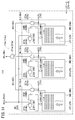
- FIG. 1 It is a figure which shows schematic structure of the device manufacturing system containing the exposure apparatus which performs the exposure process to the board
- FIG. 7 generate
- FIG. 7 shows the structure of the signal generation part shown in FIG. 7 which has the function to expand / contract a correction pixel.
- FIG. 9 shows the truth value table of the preset value which the preset part shown in FIG. 9 outputs.
- FIG. 3 is a block diagram showing an electrical configuration of the exposure apparatus shown in FIG. 2.
- FIG. 13 is a time chart showing an origin signal output from the origin sensor of FIG. 5 provided in each scanning unit and an incident permission signal generated by the selection element drive control unit shown in FIG. 12 according to the origin signal. It is a figure which shows the structure of the drawing data output part shown in FIG.
- FIG. 15 is a time chart showing a pixel permission pulse generated by the drawing permission signal generated by the drawing permission signal generating unit shown in FIG. 14 and a pixel shift pulse output from the transmission timing switching unit of FIG. 9 during a period when the drawing permission signal is high. It is a figure which shows the relationship between the position of the drawing line expanded / contracted within the range of the maximum scanning length, and delay time. It is a figure which shows the structure of the light source device in the modification of 1st Embodiment.
- FIG. 18 is a diagram illustrating a configuration of a clock signal generation unit illustrated in FIG. 17.
- FIG. 19 is a timing chart for explaining the operation of the clock signal generation unit of FIG. 18.
- FIG. It is a figure which shows the structure of the signal generation part provided in the inside of the light source device in 2nd Embodiment.
- 21A is a diagram showing a first example of the configuration of the delay circuit shown in FIG. 20, and
- FIG. 21B is a diagram showing a second example of the configuration of the delay circuit shown in FIG.
- It is a time chart which shows the signal output from each part of the signal generation part shown in FIG.
- FIG. 23A is a diagram for describing a pattern drawn when local magnification correction is not performed, and FIG.
- FIG. 23B is a drawing when local magnification correction (reduction) is performed according to the time chart shown in FIG. It is a figure explaining the pattern to be performed.
- FIG. 11 is an explanatory diagram of Modification 1 of each of the above-described embodiments, and drawing optics instead of the electro-optic element that modulates the intensity of the spot light according to the pattern data described in each of the above-described embodiments (including the modification) It is a figure which shows the example of arrangement
- FIG. 6 It is a figure showing a part of schematic structure of the drawing apparatus of the tandem system in the modification of 3rd Embodiment. It is a figure which shows the structure of the beam switching member provided corresponding to one scanning unit in the beam switching part by 4th Embodiment. It is a figure which shows the structure which replaced the optical element for selection and the unit side incident mirror which comprise the beam switching part shown in FIG. 6 or FIG. 24 with the structure of FIG. It is a figure which shows an example of a structure of the beam shifter part shown in FIG. FIG.
- FIG. 37A is a diagram showing an example of a beam deflecting member using an electro-optic element in which electrodes are formed on opposite parallel side surfaces of a transparent crystal medium formed in a prism shape (triangle) with a predetermined thickness.
- FIG. 37B is a diagram showing an example of a beam deflection member using an electro-optic element made of a KTN (KTa 1-x Nb x O 3 ) crystal.
- a pattern drawing apparatus and a pattern drawing method according to an aspect of the present invention will be described in detail below with reference to the accompanying drawings by listing preferred embodiments.
- the aspect of this invention is not limited to these embodiment, What added the various change or improvement is included. That is, the constituent elements described below include those that can be easily assumed by those skilled in the art and substantially the same elements, and the constituent elements described below can be appropriately combined. In addition, various omissions, substitutions, or changes of the components can be made without departing from the scope of the present invention.
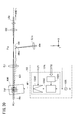
- FIG. 1 is a diagram showing a schematic configuration of a device manufacturing system 10 including an exposure apparatus EX that performs an exposure process on a substrate (irradiated body) P according to the first embodiment.
- EX an exposure apparatus
- FIG. 1 an XYZ orthogonal coordinate system in which the gravity direction is the Z direction is set, and the X direction, the Y direction, and the Z direction will be described according to the arrows shown in the drawing.
- the device manufacturing system 10 is a system (substrate processing apparatus) that manufactures an electronic device by performing predetermined processing (exposure processing or the like) on the substrate P.
- a manufacturing line for manufacturing a flexible display as an electronic device for example, a film-like touch panel, a film-like color filter for a liquid crystal display panel, a flexible wiring, or a flexible sensor is constructed. It is a manufacturing system. The following description is based on the assumption that a flexible display is used as the electronic device. Examples of the flexible display include an organic EL display and a liquid crystal display.
- the device manufacturing system 10 sends out the substrate P from a supply roll FR1 obtained by winding a flexible sheet-like substrate (sheet substrate) P in a roll shape, and continuously performs various processes on the delivered substrate P. After that, the substrate P after various treatments is wound up by the recovery roll FR2, and has a so-called roll-to-roll (Roll To Roll) structure.
- the substrate P has a belt-like shape in which the moving direction (transport direction) of the substrate P is the longitudinal direction (long) and the width direction is the short direction (short).
- the film-like substrate P includes at least a processing apparatus (first processing apparatus) PR1, a processing apparatus (second processing apparatus) PR2, an exposure apparatus (third processing apparatus) EX, An example of winding up to the collection roll FR2 through the processing device (fourth processing device) PR3 and the processing device (fifth processing device) PR4 is shown.
- the X direction is a direction (conveying direction) in which the substrate P is directed from the supply roll FR1 to the collection roll FR2 in the horizontal plane.
- the Y direction is a direction orthogonal to the X direction in the horizontal plane, and is the width direction (short direction) of the substrate P.
- the Z direction is a direction (upward direction) orthogonal to the X direction and the Y direction, and is parallel to the direction in which gravity acts.
- a resin film or a foil (foil) made of a metal or alloy such as stainless steel is used.
- the material of the resin film include polyethylene resin, polypropylene resin, polyester resin, ethylene vinyl copolymer resin, polyvinyl chloride resin, cellulose resin, polyamide resin, polyimide resin, polycarbonate resin, polystyrene resin, and vinyl acetate resin. Among them, one containing at least one or more may be used. Further, the thickness and rigidity (Young's modulus) of the substrate P may be in a range that does not cause folds or irreversible wrinkles due to buckling in the substrate P when passing through the conveyance path of the device manufacturing system 10. .
- a film such as PET (polyethylene terephthalate) or PEN (polyethylene naphthalate) having a thickness of about 25 ⁇ m to 200 ⁇ m is typical of a suitable sheet substrate.
- the substrate P may receive heat in each process performed by the processing apparatus PR1, the processing apparatus PR2, the exposure apparatus EX, the processing apparatus PR3, and the processing apparatus PR4, the substrate P is made of a material whose thermal expansion coefficient is not remarkably large. It is preferable to select the substrate P.
- the thermal expansion coefficient can be suppressed by mixing an inorganic filler with a resin film.
- the inorganic filler may be, for example, titanium oxide, zinc oxide, alumina, or silicon oxide.
- the substrate P may be a single layer of ultrathin glass having a thickness of about 100 ⁇ m manufactured by a float process or the like, or a laminate in which the above resin film, foil, or the like is bonded to the ultrathin glass. It may be.
- the flexibility of the substrate P means the property that the substrate P can be bent without being sheared or broken even when a force of its own weight is applied to the substrate P. .
- flexibility includes a property of bending by a force of about its own weight.
- the degree of flexibility varies depending on the material, size and thickness of the substrate P, the layer structure formed on the substrate P, the environment such as temperature or humidity, and the like. In any case, when the substrate P is correctly wound around the conveyance direction changing members such as various conveyance rollers and rotating drums provided in the conveyance path in the device manufacturing system 10 according to the first embodiment, If the substrate P can be smoothly transported without being bent and creased or damaged (breaking or cracking), it can be said to be a flexible range.
- the processing apparatus PR1 applies the coating process to the substrate P while transporting the substrate P transported from the supply roll FR1 toward the processing apparatus PR2 in a transport direction (+ X direction) along the longitudinal direction at a predetermined speed. It is the coating device which performs.
- the processing apparatus PR1 selectively or uniformly applies the photosensitive functional liquid to the surface of the substrate P.
- the substrate P having the photosensitive functional liquid applied on the surface thereof is conveyed toward the processing apparatus PR2.
- the processing apparatus PR2 is a drying apparatus that performs a drying process on the substrate P while transporting the substrate P transported from the processing apparatus PR1 toward the exposure apparatus EX in the transport direction (+ X direction) at a predetermined speed. .
- the processing apparatus PR2 removes the solvent or water contained in the photosensitive functional liquid with a blower, an infrared light source, a ceramic heater, or the like that blows drying air (hot air) such as hot air or dry air onto the surface of the substrate P, and performs photosensitivity. Dry sexual function liquid.
- a film to be a photosensitive functional layer photosensitive layer
- the photosensitive functional layer may be formed on the surface of the substrate P by attaching a dry film to the surface of the substrate P.
- a pasting apparatus for sticking the dry film to the substrate P may be provided instead of the processing apparatus PR1 and the processing apparatus PR2.
- a typical one of the photosensitive functional liquid (layer) is a photoresist (liquid or dry film).
- a photoresist liquid or dry film
- the lyophilic property of the part that has been irradiated with ultraviolet rays There is a photosensitive silane coupling agent (SAM) that is modified, or a photosensitive reducing agent in which a plating reducing group is exposed in a portion irradiated with ultraviolet rays.
- SAM photosensitive silane coupling agent
- the pattern portion exposed to ultraviolet rays on the substrate P is modified from lyophobic to lyophilic.
- conductive ink ink containing conductive nanoparticles such as silver or copper
- a liquid containing a semiconductor material on the lyophilic portion, a thin film transistor (TFT) or the like
- a pattern layer to be an electrode, a semiconductor, insulation, or a wiring for connection can be formed.
- a photosensitive reducing agent is used as the photosensitive functional liquid (layer)
- the plating reducing group is exposed to the pattern portion exposed to ultraviolet rays on the substrate P. Therefore, after exposure, the substrate P is immediately immersed in a plating solution containing palladium ions or the like for a certain period of time, so that a pattern layer of palladium is formed (deposited).
- Such a plating process is an additive process, but may be based on an etching process as a subtractive process.
- the substrate P sent to the exposure apparatus EX is made of PET or PEN as a base material, and a metal thin film such as aluminum (Al) or copper (Cu) is deposited on the entire surface or selectively, and further, It may be a laminate of a photoresist layer thereon.
- a photosensitive reducing agent is used as the photosensitive functional liquid (layer).
- the exposure apparatus EX is a processing apparatus that performs exposure processing on the substrate P while transporting the substrate P transported from the processing apparatus PR2 toward the processing apparatus PR3 in the transport direction (+ X direction) at a predetermined speed.
- the exposure apparatus EX uses a light corresponding to a pattern for an electronic device (for example, a pattern of an electrode or wiring of a TFT constituting the electronic device) on the surface of the substrate P (the surface of the photosensitive functional layer, that is, the photosensitive surface). Irradiate the pattern. Thereby, a latent image (modified portion) corresponding to the pattern is formed on the photosensitive functional layer.
- the exposure apparatus EX is a direct drawing type exposure apparatus that does not use a mask, that is, a so-called raster scan type exposure apparatus (pattern drawing apparatus).
- the exposure apparatus EX transmits the spot light SP of the pulsed beam LB (pulse beam) for exposure to the substrate P while conveying the substrate P in the + X direction (sub-scanning direction).
- the intensity of the spot light SP is modulated at high speed according to the pattern data (drawing data, pattern information) while one-dimensionally scanning (main scanning) in the predetermined scanning direction (Y direction) on the irradiated surface (photosensitive surface). (ON / OFF).
- a light pattern corresponding to a predetermined pattern such as an electronic device, a circuit, or a wiring is drawn and exposed on the irradiated surface of the substrate P. That is, the spot light SP is relatively two-dimensionally scanned on the irradiated surface of the substrate P by the sub-scanning of the substrate P and the main scanning of the spot light SP, and a predetermined pattern is drawn and exposed on the substrate P. . Further, since the substrate P is transported along the transport direction (+ X direction), the exposure region W where the pattern is exposed by the exposure apparatus EX is spaced at a predetermined interval along the longitudinal direction of the substrate P. A plurality are provided (see FIG. 4).
- the exposure area W is also a device formation area. Since the electronic device is configured by superimposing a plurality of pattern layers (layers on which patterns are formed), a pattern corresponding to each layer may be exposed by the exposure apparatus EX.
- the processing apparatus PR3 is a wet processing apparatus that performs wet processing on the substrate P while transporting the substrate P transported from the exposure apparatus EX toward the processing apparatus PR4 in the transport direction (+ X direction) at a predetermined speed. is there.
- the processing apparatus PR3 performs a plating process which is a kind of wet process on the substrate P. That is, the substrate P is immersed in a plating solution stored in the processing tank for a predetermined time. As a result, a pattern layer corresponding to the latent image is deposited (formed) on the surface of the photosensitive functional layer.
- a predetermined material for example, palladium
- a predetermined material for example, palladium
- a coating process or a plating process of a liquid which is a kind of wet process is performed by the processing apparatus PR3.
- a pattern layer corresponding to the latent image is formed on the surface of the photosensitive functional layer. That is, a predetermined material (for example, conductive ink or palladium) is selectively formed on the substrate P according to the difference between the irradiated portion of the spot light SP of the photosensitive functional layer of the substrate P and the irradiated portion, This is the pattern layer.
- photosensitive functional layer when a photoresist is employed as the photosensitive functional layer, development processing which is a kind of wet processing is performed by the processing apparatus PR3. In this case, a pattern corresponding to the latent image is formed on the photosensitive functional layer (photoresist) by this development processing.
- the processing apparatus PR4 performs cleaning / drying processing on the substrate P while transporting the substrate P transported from the processing apparatus PR3 toward the recovery roll FR2 in the transport direction (+ X direction) at a predetermined speed. It is a drying device.
- the processing apparatus PR4 cleans the substrate P that has been subjected to the wet processing with pure water, and then dries until the moisture content of the substrate P is equal to or lower than a predetermined value at a glass transition temperature or lower.
- the processing apparatus PR4 may be an annealing / drying apparatus that performs an annealing process and a drying process on the substrate P.
- the substrate P is irradiated with, for example, high-intensity pulsed light from a strobe lamp in order to strengthen the electrical coupling between the nanoparticles contained in the applied conductive ink.
- a processing apparatus (wet processing apparatus) PR5 that performs an etching process between the processing apparatus PR4 and the recovery roll FR2, and a substrate P that has been subjected to the etching process.
- a processing apparatus (cleaning / drying apparatus) PR6 for performing the cleaning / drying process may be provided.
- a photoresist is adopted as the photosensitive functional layer
- a pattern layer is formed on the substrate P by performing an etching process. That is, a predetermined material (for example, aluminum (Al) or copper (Cu)) is selectively formed on the substrate P according to the difference between the irradiated portion of the spot light SP of the photosensitive functional layer of the substrate P and the irradiated portion. This is a pattern layer.
- the processing apparatuses PR5 and PR6 have a function of transporting the substrate P sent in the transport direction (+ X direction) at a predetermined speed toward the collection roll FR2.
- the function of the plurality of processing apparatuses PR1 to PR4 (including processing apparatuses PR5 and PR6 as necessary) to transfer the substrate P in the + X direction is configured as a substrate transfer apparatus.
- One pattern layer is formed on the substrate P through at least each process of the device manufacturing system 10.
- each process of the device manufacturing system 10 as illustrated in FIG. 1 is performed at least twice in order to generate the electronic device. Have to go through. Therefore, a pattern layer can be laminated
- the processed substrate P is in a state in which a plurality of electronic devices are connected along the longitudinal direction of the substrate P with a predetermined interval. That is, the substrate P is a multi-sided substrate.
- the collection roll FR2 that collects the substrate P formed in a state where the electronic devices are connected may be mounted on a dicing apparatus (not shown).
- the dicing apparatus to which the recovery roll FR2 is attached divides (dices) the processed substrate P into electronic devices (exposure regions W that are device formation regions) to form electronic devices that are a plurality of single wafers.
- the dimension in the width direction (short direction) is about 10 cm to 2 m
- the dimension in the length direction (long direction) is 10 m or more.
- substrate P is not limited to an above-described dimension.
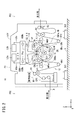
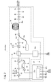
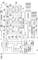
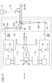
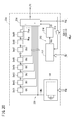
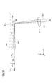
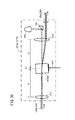
- FIG. 2 is a block diagram showing the configuration of the exposure apparatus EX.
- the exposure apparatus EX is stored in the temperature control chamber ECV.
- This temperature control chamber ECV keeps the inside at a predetermined temperature and a predetermined humidity, thereby suppressing a change in shape due to the temperature of the substrate P transported inside, and occurring along with the hygroscopicity and transport of the substrate P.
- the humidity is set in consideration of static charge.
- the temperature control chamber ECV is arranged on the installation surface E of the manufacturing factory via passive or active vibration isolation units SU1, SU2.
- the anti-vibration units SU1 and SU2 reduce vibration from the installation surface E.
- the installation surface E may be the floor surface of the factory itself, or may be a surface on an installation base (pedestal) that is exclusively installed on the floor surface in order to obtain a horizontal surface.
- the control device (control unit) 16 controls each part of the exposure apparatus EX.
- the control device 16 includes a computer and a recording medium on which the program is recorded, and functions as the control device 16 of the first embodiment when the computer executes the program.
- the substrate transport mechanism 12 constitutes a part of the substrate transport apparatus of the device manufacturing system 10, and after the substrate P transported from the processing apparatus PR2 is transported at a predetermined speed in the exposure apparatus EX, the processing is performed. It sends out to the apparatus PR3 at a predetermined speed.
- the substrate transport mechanism 12 defines a transport path for the substrate P transported in the exposure apparatus EX.
- the substrate transport mechanism 12 includes an edge position controller EPC, a driving roller R1, a tension adjusting roller RT1, a rotating drum (cylindrical drum) DR, a tension adjusting roller RT2, in order from the upstream side ( ⁇ X direction side) in the transport direction of the substrate P.
- a driving roller R2 and a driving roller R3 are provided.
- the edge position controller EPC adjusts the position in the width direction (the Y direction and the short direction of the substrate P) of the substrate P transported from the processing apparatus PR2.
- the edge position controller EPC has a position at the end (edge) in the width direction of the substrate P that is transported in a state of a predetermined tension, which is about ⁇ 10 ⁇ m to several tens ⁇ m with respect to the target position.
- the position of the substrate P in the width direction is adjusted by moving the substrate P in the width direction so that it falls within this range (allowable range).
- the edge position controller EPC includes a roller on which the substrate P is stretched in a state where a predetermined tension is applied, and an edge sensor (end detection unit) (not shown) that detects the position of the end portion (edge) in the width direction of the substrate P. And have.
- the edge position controller EPC adjusts the position of the substrate P in the width direction by moving the roller of the edge position controller EPC in the Y direction based on the detection signal detected by the edge sensor.
- the driving roller (nip roller) R1 rotates while holding both front and back surfaces of the substrate P conveyed from the edge position controller EPC, and conveys the substrate P toward the rotating drum DR.
- the edge position controller EPC appropriately adjusts the position in the width direction of the substrate P so that the longitudinal direction of the substrate P wound around the rotating drum DR is always orthogonal to the central axis AXo of the rotating drum DR.
- the parallelism between the rotation axis of the roller and the Y axis of the edge position controller EPC may be appropriately adjusted so as to correct the tilt error in the traveling direction of the substrate P.
- the rotary drum DR has a central axis AXo extending in the Y direction and extending in a direction intersecting with the direction in which gravity works, and a cylindrical outer peripheral surface having a constant radius from the central axis AXo.
- the rotating drum DR rotates around the central axis AXo while supporting (holding) a part of the substrate P by bending the outer surface (circumferential surface) into a cylindrical surface in the longitudinal direction. Transport P in the + X direction.
- the rotating drum DR supports an area (portion) on the substrate P onto which the beam LB (spot light SP) from the exposure head 14 is projected on its outer peripheral surface.
- the rotating drum DR supports (holds and holds) the substrate P from the surface (back surface) opposite to the surface on which the electronic device is formed (surface on which the photosensitive surface is formed).
- shafts Sft supported by annular bearings are provided so that the rotating drum DR rotates around the central axis AXo.
- the shaft Sft rotates at a constant rotational speed around the central axis AXo by receiving a rotational torque from a rotational drive source (not shown) (for example, a motor or a speed reduction mechanism) controlled by the control device 16.
- a rotational drive source not shown
- a plane including the central axis AXo and parallel to the YZ plane is referred to as a central plane Poc.
- the driving rollers (nip rollers) R2 and R3 are arranged at a predetermined interval along the transport direction (+ X direction) of the substrate P, and give a predetermined slack (play) to the substrate P after exposure.
- the drive rollers R2 and R3 rotate while holding both front and back surfaces of the substrate P, and transport the substrate P toward the processing apparatus PR3.
- the tension adjusting rollers RT1 and RT2 are urged in the ⁇ Z direction, and apply a predetermined tension in the longitudinal direction to the substrate P that is wound around and supported by the rotary drum DR. As a result, the longitudinal tension applied to the substrate P applied to the rotating drum DR is stabilized within a predetermined range.
- the control device 16 rotates the driving rollers R1 to R3 by controlling a rotation driving source (not shown) (for example, a motor, a speed reducer, etc.).
- a rotation driving source for example, a motor, a speed reducer, etc.
- the rotation axes of the drive rollers R1 to R3 and the rotation axes of the tension adjustment rollers RT1 and RT2 are parallel to the center axis AXo of the rotation drum DR.
- the light source device LS (LSa, LSb) generates and emits a pulsed beam (pulse beam, pulsed light, laser) LB.
- the beam LB is ultraviolet light having a peak wavelength in a wavelength band of 370 nm or less, and the light emission frequency (oscillation frequency, predetermined frequency) of the beam LB is Fa.
- the beam LB emitted from the light source device LS (LSa, LSb) is incident on the exposure head 14 via the beam switching unit BDU.
- the light source device LS (LSa, LSb) emits and emits the beam LB at the emission frequency Fa according to the control of the control device 16.
- the configuration of the light source device LS (LSa, LSb) will be described later in detail.
- a semiconductor laser element that generates pulsed light in the infrared wavelength region, a fiber amplifier, an amplified red light, and the like. Consists of a wavelength conversion element (harmonic generation element) that converts pulsed light in the outer wavelength range to pulsed light in the ultraviolet wavelength range, with an oscillation frequency Fa of several hundred MHz, and an emission time of one pulsed light of about picoseconds It is assumed that a fiber amplifier laser light source (harmonic laser light source) capable of obtaining high-intensity ultraviolet pulsed light is used.
- the beam LB from the light source device LSa may be represented by LBa and the beam LB from the light source device LSb may be represented by LBb.
- the beam switching unit BDU switches the scanning unit Un on which the beams LBa and LBb are incident so that the beam LBn is incident on the scanning unit Un that scans the spot light SP. That is, the beam switching unit BDU causes the beam LBa from the light source device LSa to enter one of the scanning units U1 to U3 that scans the spot light SP. Similarly, the beam switching unit BDU causes the beam LBb from the light source device LSb to enter one scanning unit Un that scans the spot light SP among the scanning units U4 to U6.
- the beam switching unit BDU will be described in detail later.
- the scanning unit Un that scans the spot light SP is switched in the order of U1 ⁇ U2 ⁇ U3, and for the scanning units U4 to U6, the scanning that scans the spot light SP. Assume that the unit Un is switched in the order of U4 ⁇ U5 ⁇ U6.
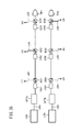
- the exposure head 14 is a so-called multi-beam type exposure head in which a plurality of scanning units Un (U1 to U6) having the same configuration are arranged.
- the exposure head 14 draws a pattern on a part of the substrate P supported by the outer peripheral surface (circumferential surface) of the rotary drum DR by a plurality of scanning units Un (U1 to U6). Since the exposure head 14 repeatedly performs pattern exposure for an electronic device on the substrate P, an exposure region (electronic device formation region) W where the pattern is exposed is a predetermined interval along the longitudinal direction of the substrate P.
- a plurality are provided (see FIG. 4).
- the plurality of scanning units Un (U1 to U6) are arranged in a predetermined arrangement relationship.
- the plurality of scanning units Un are arranged in a staggered arrangement in two rows in the transport direction of the substrate P with the center plane Poc interposed therebetween.
- the odd-numbered scanning units U1, U3, U5 are arranged in a line on the upstream side ( ⁇ X direction side) in the transport direction of the substrate P with respect to the center plane Poc and at a predetermined interval along the Y direction.
- the even-numbered scanning units U2, U4, U6 are arranged in a line at a predetermined interval along the Y direction on the downstream side (+ X direction side) in the transport direction of the substrate P with respect to the center plane Poc.
- the odd-numbered scanning units U1, U3, and U5 and the even-numbered scanning units U2, U4, and U6 are provided symmetrically with respect to the center plane Poc.
- Each scanning unit Un projects the beam LB from the light source device LS (LSa, LSb) so as to converge on the spot light SP on the irradiated surface of the substrate P.
- One-dimensional scanning is performed by the rotating polygon mirror PM (see FIG. 5).
- the spot light SP is one-dimensionally scanned on the irradiated surface of the substrate P by the polygon mirror (deflecting member) PM of each of the scanning units Un (U1 to U6).
- the configuration of the scanning unit Un will be described in detail later.
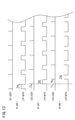
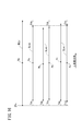
- the scanning unit U1 scans the spot light SP along the drawing line SL1, and similarly, the scanning units U2 to U6 scan the spot light SP along the drawing lines SL2 to SL6.
- the drawing lines SLn (SL1 to SL6) of the plurality of scanning units Un (U1 to U6) are not separated from each other in the Y direction (the width direction of the substrate P, the main scanning direction), as shown in FIGS. , Are set to be spliced.
- the beam LB from the light source device LS (LSa, LSb) that enters the scanning unit Un via the beam switching unit BDU may be represented as LBn.
- the beam LBn incident on the scanning unit U1 may be represented by LB1, and similarly, the beam LBn incident on the scanning units U2 to U6 may be represented by LB2 to LB6.
- the drawing lines SLn (SL1 to SL6) indicate the scanning trajectory of the spot light SP of the beam LBn (LB1 to LB6) scanned by the scanning unit Un (U1 to U6).
- the beam LBn incident on the scanning unit Un may be a linearly polarized beam (P-polarized light or S-polarized light) polarized in a predetermined direction, and is a P-polarized beam in the first embodiment.
- each of the scanning units Un (U1 to U6) shares the scanning area so that the plurality of scanning units Un (U1 to U6) cover all of the exposure area W in the width direction. ing. Accordingly, each scanning unit Un (U1 to U6) can draw a pattern for each of a plurality of regions (drawing ranges) divided in the width direction of the substrate P.
- the width in the Y direction that can be drawn is increased to about 120 to 360 mm.
- the length of each drawing line SLn (SL1 to SL6) (length of the drawing range) is the same. That is, the scanning distance of the spot light SP of the beam LBn scanned along each of the drawing lines SL1 to SL6 is basically the same. Note that it is possible to increase the width of the exposure region W by increasing the length of the drawing line SLn itself or increasing the number of scanning units Un arranged in the Y direction.
- the actual drawing lines SLn are set slightly shorter than the maximum length (maximum scanning length) that the spot light SP can actually scan on the irradiated surface.
- the scanning length of the drawing line SLn on which pattern drawing is possible is 30 mm when the drawing magnification in the main scanning direction (Y direction) is an initial value (no magnification correction)
- the maximum scanning on the irradiated surface of the spot light SP The length is set to about 31 mm with a margin of about 0.5 mm on each of the drawing start point (scanning start point) side and the drawing end point (scanning end point) side of the drawing line SLn.
- the maximum scanning length of the spot light SP is not limited to 31 mm, and is mainly determined by the aperture of the f ⁇ lens FT (see FIG. 5) provided after the polygon mirror (rotating polygon mirror) PM in the scanning unit Un.
- the plurality of drawing lines SLn are arranged in a staggered arrangement in two rows in the circumferential direction of the rotary drum DR with the center surface Poc interposed therebetween.
- the odd-numbered drawing lines SL1, SL3, and SL5 are positioned on the irradiated surface of the substrate P on the upstream side ( ⁇ X direction side) in the transport direction of the substrate P with respect to the center plane Poc.
- the even-numbered drawing lines SL2, SL4, and SL6 are positioned on the irradiated surface of the substrate P on the downstream side (+ X direction side) in the transport direction of the substrate P with respect to the center plane Poc.
- the drawing lines SL1 to SL6 are substantially parallel to the width direction of the substrate P, that is, the central axis AXo of the rotary drum DR.
- the drawing lines SL1, SL3, and SL5 are arranged in a line on a straight line at a predetermined interval along the width direction (main scanning direction) of the substrate P.
- the drawing lines SL2, SL4, and SL6 are arranged in a line on the straight line at a predetermined interval along the width direction (main scanning direction) of the substrate P.
- the drawing line SL2 is arranged between the drawing line SL1 and the drawing line SL3 in the width direction of the substrate P.
- the drawing line SL3 is arranged between the drawing line SL2 and the drawing line SL4 in the width direction of the substrate P.
- the drawing line SL4 is arranged between the drawing line SL3 and the drawing line SL5 with respect to the width direction of the substrate P, and the drawing line SL5 is arranged between the drawing line SL4 and the drawing line SL6 with respect to the width direction of the substrate P.
- the plurality of drawing lines SLn (SL1 to SL6) are arranged so as to be shifted from each other in the Y direction (main scanning direction).
- the main scanning direction of the spot light SP of the beams LB1, LB3, LB5 scanned along each of the odd-numbered drawing lines SL1, SL3, SL5 is a one-dimensional direction and is the same direction.
- the main scanning direction of the spot light SP of the beams LB2, LB4, and LB6 scanned along the even-numbered drawing lines SL2, SL4, and SL6 is a one-dimensional direction and is the same direction.
- the main scanning direction of the spot light SP may be opposite to each other.
- the main scanning direction of the spot light SP of the beams LB1, LB3, LB5 scanned along the drawing lines SL1, SL3, SL5 is the -Y direction.
- the main scanning direction of the spot light SP of the beams LB2, LB4, and LB6 scanned along the drawing lines SL2, SL4, and SL6 is the + Y direction.
- the end of the drawing lines SL3 and SL5 on the drawing end point side and the end of the drawing lines SL2 and SL4 on the drawing end point side are adjacent or partially overlap in the Y direction.
- each drawing line SLn so that the ends of the drawing lines SLn adjacent in the Y direction partially overlap, for example, the drawing start point or the drawing end with respect to the length of each drawing line SLn It is preferable to overlap within a range of several percent or less in the Y direction including points.
- joining the drawing lines SLn in the Y direction means that the ends of the drawing lines SLn are adjacent to each other or partially overlap in the Y direction.
- the width (dimension in the X direction) of the drawing line SLn in the sub-scanning direction is a thickness corresponding to the size (diameter) ⁇ of the spot light SP.
- the width of the drawing line SLn is also 3 ⁇ m.
- the spot light SP may be projected along the drawing line SLn so as to overlap by a predetermined length (for example, 7/8 of the size ⁇ of the spot light SP).
- drawing lines SLn for example, the drawing line SL1 and the drawing line SL2 adjacent in the Y direction are connected to each other, they are overlapped by a predetermined length (for example, 7/8 of the size ⁇ of the spot light SP). It is good.
- the spot light SP projected onto the drawing line SLn during main scanning Is discrete according to the oscillation frequency Fa (for example, 400 MHz) of the beam LB (LBa, LBb). Therefore, it is necessary to overlap the spot light SP projected by one pulse light of the beam LB and the spot light SP projected by the next one pulse light in the main scanning direction.
- the amount of overlap is set by the size ⁇ of the spot light SP, the scanning speed (main scanning speed) Vs of the spot light SP, and the oscillation frequency Fa of the beam LB.
- the effective size ⁇ of the spot light SP is determined by 1 / e 2 (or 1/2) of the peak intensity of the spot light SP when the intensity distribution of the spot light SP is approximated by a Gaussian distribution.
- the scanning speed Vs and the oscillation frequency Fa of the spot light SP are set so that the spot light SP overlaps the effective size (dimension) ⁇ by about ⁇ ⁇ 7/8. Is done. Accordingly, the projection interval of the spot light SP along the main scanning direction is ⁇ / 8. Therefore, also in the sub-scanning direction (direction orthogonal to the drawing line SLn), the substrate P is effective for the spot light SP between one scanning of the spot light SP along the drawing line SLn and the next scanning.
- the exposure amount to the photosensitive functional layer on the substrate P can be set by adjusting the peak value of the beam LB (pulse light). However, the exposure amount can be increased in a situation where the intensity of the beam LB cannot be increased.
- the spot light SP is caused to fall by the decrease in the scanning speed Vs of the spot light SP in the main scanning direction, the increase in the oscillation frequency Fa of the beam LB, or the decrease in the transport speed Vt of the substrate P in the sub scanning direction.
- the overlap amount in the main scanning direction or the sub-scanning direction may be increased.
- the scanning speed Vs of the spot light SP in the main scanning direction increases in proportion to the rotational speed (rotational speed Vp) of the polygon mirror PM.
- Each scanning unit Un (U1 to U6) irradiates each beam LBn toward the substrate P so that each beam LBn travels toward the central axis AXo of the rotating drum DR at least in the XZ plane.
- the optical path (beam central axis) of the beam LBn traveling from each scanning unit Un (U1 to U6) toward the substrate P becomes parallel to the normal line of the irradiated surface of the substrate P in the XZ plane.
- each scanning unit Un (U1 to U6) is configured such that the beam LBn irradiated to the drawing line SLn (SL1 to SL6) is perpendicular to the irradiated surface of the substrate P in a plane parallel to the YZ plane.
- the beam LBn is irradiated toward the substrate P. That is, the beam LBn (LB1 to LB6) projected onto the substrate P is scanned in a telecentric state with respect to the main scanning direction of the spot light SP on the irradiated surface.
- a line perpendicular to the irradiated surface of the substrate P also called an optical axis
- SLn SL1 to SL6
- Un U1 to U6
- Each irradiation center axis Len (Le1 to Le6) is a line connecting the drawing lines SL1 to SL6 and the center axis AXo on the XZ plane.
- the irradiation center axes Le1, Le3, Le5 of the odd-numbered scanning units U1, U3, U5 are in the same direction in the XZ plane, and the irradiation center axes Le2 of the even-numbered scanning units U2, U4, U6. , Le4 and Le6 are in the same direction in the XZ plane.
- irradiation center axes Le1, Le3, Le5 and the irradiation center axes Le2, Le4, Le6 are set such that the angle is ⁇ ⁇ 1 with respect to the center plane Poc in the XZ plane (see FIG. 2).
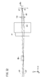
- a plurality of alignment microscopes AM1m (AM11 to AM14) and AM2m (AM21 to AM24) shown in FIG. 2 are for detecting a plurality of alignment marks MKm (MK1 to MK4) formed on the substrate P shown in FIG. And a plurality (four in the first embodiment) are provided along the Y direction.
- the plurality of alignment marks MKm (MK1 to MK4) are reference marks for relatively aligning (aligning) the predetermined pattern drawn in the exposure area W on the irradiated surface of the substrate P with the substrate P. It is.
- a plurality of alignment microscopes AM1m (AM11 to AM14) and AM2m (AM21 to AM24) are arranged on the substrate P supported by the outer peripheral surface (circumferential surface) of the rotating drum DR, and a plurality of alignment marks MKm (MK1 to MK4). Is detected.
- the plurality of alignment microscopes AM1m (AM11 to AM14) are more than the irradiated area (area surrounded by the drawing lines SL1 to SL6) on the substrate P by the spot light SP of the beam LBn (LB1 to LB6) from the exposure head 14. It is provided on the upstream side ( ⁇ X direction side) in the transport direction of the substrate P.
- the plurality of alignment microscopes AM2m are irradiated from an irradiation area (area surrounded by the drawing lines SL1 to SL6) on the substrate P by the spot light SP of the beam LBn (LB1 to LB6) from the exposure head 14. Is also provided on the downstream side (+ X direction side) in the transport direction of the substrate P.
- the alignment microscopes AM1m (AM11 to AM14) and AM2m (AM21 to AM24) are a local region (observation region) Vw1m (Vw11) including a light source that projects illumination light for alignment onto the substrate P and an alignment mark MKm on the surface of the substrate P.
- Vw1m Vw11
- Vw2m Vw21 to Vw24
- an observation optical system including an objective lens
- the transport speed Vt of the substrate P is increased.
- an image pickup device such as a CCD or a CMOS for picking up an image with a corresponding high-speed shutter.
- Imaging signals (image data) captured by each of the plurality of alignment microscopes AM1m (AM11 to AM14) and AM2m (AM21 to AM24) are sent to the control device 16.
- the mark position detection unit 106 (see FIG. 12) of the control device 16 performs image analysis of the plurality of image signals that have been sent, so that the position of the alignment mark MKm (MK1 to MK4) on the substrate P (mark position). Information).
- the illumination light for alignment is light in a wavelength region that has little sensitivity to the photosensitive functional layer on the substrate P, for example, light having a wavelength of about 500 to 800 nm.
- a plurality of alignment marks MK1 to MK4 are provided around each exposure area W.
- a plurality of alignment marks MK1 and MK4 are formed on both sides of the exposure region W in the width direction of the substrate P at a constant interval Dh along the longitudinal direction of the substrate P.
- the alignment mark MK1 is formed on the ⁇ Y direction side in the width direction of the substrate P
- the alignment mark MK4 is formed on the + Y direction side in the width direction of the substrate P.
- Such alignment marks MK1 and MK4 are located at the same position in the longitudinal direction (X direction) of the substrate P when the substrate P is not deformed due to a large tension or a thermal process. Be placed.
- the alignment marks MK2 and MK3 are between the alignment mark MK1 and the alignment mark MK4, and extend in the width direction (short direction) of the substrate P in the margin part between the + X direction side and the ⁇ X direction side of the exposure region W. Is formed.
- the alignment marks MK2 and MK3 are formed between the exposure area W and the exposure area W.
- the alignment mark MK2 is formed on the ⁇ Y direction side in the width direction of the substrate P
- the alignment mark MK3 is formed on the + Y direction side of the substrate P.
- the Y-direction interval between the alignment mark MK1 and the margin alignment mark MK2 arranged at the ⁇ Y direction end of the substrate P, the Y-direction interval between the margin alignment mark MK2 and the alignment mark MK3, and The interval in the Y direction between the alignment mark MK4 arranged at the end on the + Y direction side of the substrate P and the alignment mark MK3 in the blank portion is set to the same distance.
- These alignment marks MKm (MK1 to MK4) may be formed together when forming the first pattern layer. For example, when the pattern of the first layer is exposed, the alignment mark pattern may be exposed around the exposure area W where the pattern is exposed.
- the alignment mark MKm may be formed in the exposure area W. For example, it may be formed in the exposure area W along the outline of the exposure area W. Further, a pattern portion at a specific position or a specific shape portion in the pattern of the electronic device formed in the exposure region W may be used as the alignment mark MKm.
- Alignment microscopes AM11 and AM21 are arranged so as to image alignment marks MK1 existing in observation regions (detection regions) Vw11 and Vw21 by the objective lens, as shown in FIG.
- the alignment microscopes AM12 to AM14 and AM22 to AM24 are arranged so as to image the alignment marks MK2 to MK4 existing in the observation areas Vw12 to Vw14 and Vw22 to Vw24 by the objective lens.
- the plurality of alignment microscopes AM11 to AM14 and AM21 to AM24 correspond to the positions of the plurality of alignment marks MK1 to MK4, and the substrates P in the order of AM11 to AM14 and AM21 to AM24 from the ⁇ Y direction side of the substrate P. It is provided along the width direction.
- the observation region Vw2m (Vw21 to Vw24) of the alignment microscope AM2m (AM21 to AM24) is not shown.
- the distance between the exposure position (drawing lines SL1 to SL6) and the observation region Vw1m (Vw11 to Vw14) in the X direction is shorter than the length of the exposure region W in the X direction. It is provided to become.
- the distance between the exposure position (drawing lines SL1 to SL6) and the observation region Vw2m (Vw21 to Vw24) with respect to the X direction is longer than the length of the exposure region W in the X direction. Is also provided to be shorter.
- the number of alignment microscopes AM1m and AM2m provided in the Y direction can be changed according to the number of alignment marks MKm formed in the width direction of the substrate P. Further, the sizes of the observation regions Vw1m (Vw11 to Vw14) and Vw2m (Vw21 to Vw24) on the irradiated surface of the substrate P are set according to the size of the alignment marks MK1 to MK4 and the alignment accuracy (position measurement accuracy). However, it is about 100 to 500 ⁇ m square.
- scale portions SDa and SDb having scales formed in an annular shape over the entire circumferential direction of the outer peripheral surface of the rotary drum DR are provided at both ends of the rotary drum DR.
- the scale portions SDa and SDb are diffraction gratings in which concave or convex lattice lines are engraved at a constant pitch (for example, 20 ⁇ m) in the circumferential direction of the outer peripheral surface of the rotary drum DR, and are configured as incremental scales.
- the scale portions SDa and SDb rotate integrally with the rotary drum DR around the central axis AXo.
- Encoders ENja and ENjb optically detect the rotational angle position of the rotary drum DR.
- Four encoders ENja (EN1a, EN2a, EN3a, EN4a) are provided so as to face the scale part SDa provided at the end of the rotary drum DR on the ⁇ Y direction side.
- four encoders ENjb (EN1b, EN2b, EN3b, EN4b) are provided so as to face the scale part SDb provided at the end on the + Y direction side of the rotary drum DR.
- the encoders EN1a and EN1b are provided on the upstream side ( ⁇ X direction side) in the transport direction of the substrate P with respect to the center plane Poc, and are disposed on the installation direction line Lx1 (see FIGS. 2 and 3).
- the installation azimuth line Lx1 is a line connecting the projection positions (reading positions) of the measurement light beams on the scale portions SDa and SDb of the encoders EN1a and EN1b and the central axis AXo on the XZ plane.
- the installation orientation line Lx1 is a line connecting the observation region Vw1m (Vw11 to Vw14) of each alignment microscope AM1m (AM11 to AM14) and the central axis AXo on the XZ plane. That is, a plurality of alignment microscopes AM1m (AM11 to AM14) are also arranged on the installation direction line Lx1.
- the encoders EN2a and EN2b are provided on the upstream side ( ⁇ X direction side) in the transport direction of the substrate P with respect to the center plane Poc, and further downstream in the transport direction of the substrate P (+ X direction) from the encoders EN1a and EN1b. Side).
- the encoders EN2a and EN2b are disposed on the installation direction line Lx2 (see FIGS. 2 and 3).
- the installation azimuth line Lx2 is a line connecting the projection positions (reading positions) of the measurement light beams on the scale portions SDa and SDb of the encoders EN2a and EN2b and the central axis AXo on the XZ plane.
- the installation azimuth line Lx2 overlaps with the irradiation center axes Le1, Le3, Le5 at the same angular position in the XZ plane.
- the encoders EN3a and EN3b are provided on the downstream side (+ X direction side) in the transport direction of the substrate P with respect to the center plane Poc, and are disposed on the installation direction line Lx3 (see FIGS. 2 and 3).
- the installation azimuth line Lx3 is a line connecting the projection positions (reading positions) of the measurement light beams on the scale portions SDa and SDb of the encoders EN3a and EN3b and the central axis AXo on the XZ plane.
- This installation orientation line Lx3 overlaps with the irradiation center axes Le2, Le4, and Le6 at the same angular position in the XZ plane. Therefore, the installation azimuth line Lx2 and the installation azimuth line Lx3 are set so that the angle is ⁇ ⁇ 1 with respect to the center plane Poc in the XZ plane (see FIG. 2).
- Encoders EN4a and EN4b are provided on the downstream side (+ X direction side) in the transport direction of the substrate P from the encoders EN3a and EN3b, and are arranged on the installation direction line Lx4 (see FIG. 2).
- the installation azimuth line Lx4 is a line connecting the projection positions (reading positions) of the measurement light beams on the scale portions SDa and SDb of the encoders EN4a and EN4b and the central axis AXo on the XZ plane.
- the installation orientation line Lx4 is a line connecting the observation region Vw2m (Vw21 to Vw24) of each alignment microscope AM2m (AM21 to AM24) and the central axis AXo on the XZ plane.
- a plurality of alignment microscopes AM2m are also arranged on the installation direction line Lx4.
- the installation azimuth line Lx1 and the installation azimuth line Lx4 are set such that the angle is ⁇ ⁇ 2 with respect to the center plane Poc in the XZ plane (see FIG. 2).
- Each encoder ENja (EN1a to EN4a), ENjb (EN1b to EN4b) projects a measurement light beam toward the scale portions SDa and SDb, and detects the reflected light beam (diffracted light) to detect a pulse signal. Is output to the control device 16.
- the rotational position detector 108 (see FIG. 12) of the control device 16 counts the detection signal (pulse signal), thereby measuring the rotational angular position and angular change of the rotary drum DR with submicron resolution. From the change in the angle of the rotating drum DR, the transport speed Vt of the substrate P can also be measured.
- the rotational position detector 108 individually counts detection signals from the encoders ENja (EN1a to EN4a) and ENjb (EN1b to EN4b).
- the rotational position detection unit 108 includes a plurality of counter circuits CNja (CN1a to CN4a) and CNjb (CN1b to CN4b).
- the counter circuit CN1a counts the detection signal from the encoder EN1a
- the counter circuit CN1b counts the detection signal from the encoder EN1b.
- the counter circuits CN2a to CN4a and CN2b to CN4b count detection signals from the encoders EN2a to EN4a and EN2b to EN4b.
- Each of the counter circuits CNja (CN1a to CN4a) and CNjb (CN1b to CN4b) has encoders ENja (EN1a to EN4a) and ENjb (EN1b to EN4b) formed in a part of the circumferential direction of the scale portions SDa and SDb.
- the count values corresponding to the encoders ENja and ENjb that have detected the origin mark ZZ are reset to zero.
- One of the count values of the counter circuits CN1a and CN1b or the average value thereof is used as the rotation angle position of the rotary drum DR on the installation direction line Lx1, and either one of the count values of the counter circuits CN2a and CN2b or the average The value is used as the rotation angle position of the rotary drum DR on the installation direction line Lx2.
- one or the average value of the count values of the counter circuits CN3a and CN3b is used as the rotation angle position of the rotary drum DR on the installation direction line Lx3, and either one of the count values of the counter circuits CN4a and CN4b or The average value is used as the rotation angle position of the rotary drum DR on the installation direction line Lx4.
- the count values of the counter circuits CN1a and CN1b are the same except when the rotary drum DR rotates eccentrically with respect to the central axis AXo due to a manufacturing error of the rotary drum DR.
- the count values of the counter circuits CN2a and CN2b are the same, and the count values of the counter circuits CN3a and CN3b and the count values of the counter circuits CN4a and CN4b are also the same.
- alignment microscope AM1m (AM11 to AM14) and encoders EN1a and EN1b are arranged on installation orientation line Lx1
- alignment microscope AM2m (AM21 to AM24) and encoders EN4a and EN4b are installation orientation lines Lx4. Is placed on top. Therefore, the position detection of the alignment mark MKm (MK1 to MK4) by the image analysis of the mark position detection unit 106 of the plurality of imaging signals picked up by the plurality of alignment microscopes AM1m (AM11 to AM14) and the moment when the alignment microscope AM1m picks up the image.
- the position of the substrate P on the installation orientation line Lx1 can be measured with high accuracy based on the information on the rotational angle position of the rotary drum DR (the count value based on the encoders EN1a and EN1b).
- the position detection of the alignment mark MKm MK1 to MK4 by the image analysis of the mark position detection unit 106 of the plurality of imaging signals captured by the plurality of alignment microscopes AM2m (AM21 to AM24), and the moment when the alignment microscope AM2m images
- the position of the substrate P on the installation orientation line Lx4 can be measured with high accuracy based on the information on the rotational angle position of the rotary drum DR (the count value based on the encoders EN4a and EN4b).
- the count values of the detection signals from the encoders EN1a and EN1b, the count values of the detection signals from the encoders EN2a and EN2b, the count values of the detection signals from the encoders EN3a and EN3b, and the detection signals from the encoders EN4a and EN4b The count value is reset to zero at the moment when each encoder ENja, ENjb detects the origin mark ZZ. Therefore, when the position on the installation orientation line Lx1 of the substrate P wound around the rotary drum DR when the count value based on the encoders EN1a and EN1b is the first value (for example, 100) is the first position.
- the count value based on the encoders EN2a, EN2b is the first value (for example, , 100).
- the count value of the detection signal based on the encoders EN3a, EN3b is the first. (For example, 100).
- the count value of the detection signal based on the encoders EN4a and EN4b becomes the first value (for example, 100).
- the substrate P is wound inside the scale portions SDa and SDb at both ends of the rotary drum DR.
- the radius from the central axis AXo of the outer peripheral surface of the scale portions SDa and SDb is set smaller than the radius from the central axis AXo of the outer peripheral surface of the rotary drum DR.
- the outer peripheral surfaces of the scale portions SDa and SDb may be set so as to be flush with the outer peripheral surface of the substrate P wound around the rotary drum DR.
- the radius (distance) from the central axis AXo of the outer peripheral surfaces of the scale portions SDa and SDb and the radius (distance) from the central axis AXo of the outer peripheral surface (irradiated surface) of the substrate P wound around the rotary drum DR May be set to be the same.
- each of the encoders ENja (EN1a to EN4a) and ENjb (EN1b to EN4b) can detect the scale portions SDa and SDb at the same radial position as the irradiated surface of the substrate P wound around the rotary drum DR. . Therefore, the Abbe error caused by the difference between the measurement positions by the encoders ENja and ENjb and the processing positions (drawing lines SL1 to SL6) in the radial direction of the rotary drum DR can be reduced.
- the radius of the outer peripheral surface of the scale portions SDa and SDb and the outer peripheral surface of the substrate P wound around the rotary drum DR are different. It is difficult to always make the radius the same. Therefore, in the case of the scale portions SDa and SDb shown in FIG. 3, the radius of the outer peripheral surface (scale surface) is set to coincide with the radius of the outer peripheral surface of the rotary drum DR. Furthermore, the scale portions SDa and SDb can be formed of individual disks, and the disks (scale disks) can be coaxially attached to the shaft Sft of the rotary drum DR. Even in this case, it is preferable to align the radius of the outer peripheral surface (scale surface) of the scale disk and the radius of the outer peripheral surface of the rotary drum DR so that the Abbe error falls within the allowable value.
- the start position of the drawing exposure of the exposure region W in the longitudinal direction (X direction) of the substrate P is determined by the control device 16 based on any one of these or the average value. Since the length of the exposure area W in the X direction is known in advance, the control device 16 determines the drawing exposure start position every time a predetermined number of alignment marks MKm (MK1 to MK4) are detected.
- the drawing exposure start position of the exposure region W in the longitudinal direction of the substrate P is located on the drawing lines SL1, SL3, SL5. Accordingly, the scanning units U1, U3, and U5 can start scanning the spot light SP based on the count values of the encoders EN2a and EN2b.
- the drawing exposure start position of the exposure region W in the longitudinal direction of the substrate P is positioned on the drawing lines SL2, SL4, and SL6. To do. Therefore, the scanning units U2, U4, and U6 can start scanning the spot light SP based on the count values of the encoders EN3a and EN3b.
- the tension adjusting rollers RT1 and RT2 apply a predetermined tension to the substrate P in the longitudinal direction, so that the substrate P is conveyed along with the rotation of the rotating drum DR while being in close contact with the rotating drum DR. .
- the rotational speed Vp of the rotating drum DR is high, or the tension applied to the substrate P by the tension adjusting rollers RT1 and RT2 is too low or too high, the substrate P slips with respect to the rotating drum DR. May occur.
- the encoders EN1a and EN1b at the moment when the alignment microscope AM1m images the alignment mark MKmA (a specific alignment mark MKm) based on the count value based on the encoders EN4a and 4b.
- the count value is the same as the count value based on (for example, 150)
- this alignment mark MKmA is detected by the alignment microscope AM2m.
- the count value based on the encoders EN4a and EN4b is a count value based on the encoders EN1a and EN1b at the moment when the alignment mark AMKm images the alignment mark MKmA (for example, , 150), the alignment mark MKmA is not detected by the alignment microscope AM2m.
- the count value based on the encoders EN4a and EN4b exceeds 150, for example, the alignment mark MKmA is detected by the alignment microscope AM2m.
- the slip amount of the substrate P can be measured by additionally installing the alignment microscope AM2m and the encoders EN4a and EN4b.
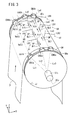
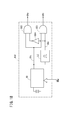
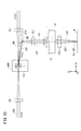
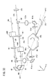
- each scanning unit Un (U1 to U6) has the same configuration, only the scanning unit U1 will be described, and the description of the other scanning units Un will be omitted.
- the direction parallel to the irradiation center axis Len (Le1) is the Zt direction
- the substrate P is on the plane orthogonal to the Zt direction
- the substrate P passes from the processing apparatus PR2 through the exposure apparatus EX to the processing apparatus PR3.
- the direction going to the Xt direction is defined as the Yt direction
- the direction perpendicular to the Xt direction on the plane orthogonal to the Zt direction is defined as the Yt direction.
- the three-dimensional coordinates of Xt, Yt, and Zt in FIG. 5 are the same as the three-dimensional coordinates of X, Y, and Z in FIG. 2, and the Z-axis direction is parallel to the irradiation center axis Len (Le1).
- the three-dimensional coordinates rotated as described above.
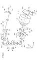
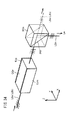
- a reflection mirror M10 As shown in FIG. 5, in the scanning unit U1, along the traveling direction of the beam LB1 from the incident position of the beam LB1 to the irradiated surface (substrate P), a reflection mirror M10, a beam expander BE, a reflection mirror M11, Polarization beam splitter BS1, reflection mirror M12, shift optical member (parallel plate) SR, deflection adjustment optical member (prism) DP, field aperture FA, reflection mirror M13, ⁇ / 4 wavelength plate QW, cylindrical lens CYA, reflection mirror M14, A polygon mirror PM, an f ⁇ lens FT, a reflection mirror M15, and a cylindrical lens CYb are provided.
- an origin sensor (origin detector) OP1 that detects the timing at which the scanning unit U1 can start drawing, and reflected light from the irradiated surface (substrate P) are detected via the polarization beam splitter BS1.
- An optical lens system G10 and a photodetector DT are provided.
- the beam LB1 incident on the scanning unit U1 travels in the ⁇ Zt direction and enters the reflection mirror M10 inclined by 45 ° with respect to the XtYt plane.
- the axis of the beam LB1 incident on the scanning unit U1 is incident on the reflection mirror M10 so as to be coaxial with the irradiation center axis Le1.
- the reflection mirror M10 functions as an incident optical member that causes the beam LB1 to enter the scanning unit U1, and the incident beam LB1 is moved from the reflection mirror M10 to the ⁇ Xt direction along the optical axis AXa set parallel to the Xt axis. Reflected in the -Xt direction toward the distant reflecting mirror M11.
- the optical axis AXa is orthogonal to the irradiation center axis Le1 in a plane parallel to the XtZt plane.
- the beam LB1 reflected by the reflection mirror M10 passes through the beam expander BE arranged along the optical axis AXa and enters the reflection mirror M11.
- the beam expander BE expands the diameter of the transmitted beam LB1.
- the beam expander BE includes a condensing lens Be1 and a collimator lens Be2 that collimates the beam LB1 diverged after being converged by the condensing lens Be1.
- the reflection mirror M11 is disposed with an inclination of 45 ° with respect to the YtZt plane, and reflects the incident beam LB1 (optical axis AXa) toward the polarization beam splitter BS1 in the ⁇ Yt direction.
- the polarization separation surface of the polarization beam splitter BS1 disposed away from the reflection mirror M11 in the ⁇ Yt direction is disposed with an inclination of 45 ° with respect to the YtZt plane, reflects the P-polarized beam, and is orthogonal to the P-polarized light. It transmits a linearly polarized (S-polarized) beam polarized in the direction. Since the beam LB1 incident on the scanning unit U1 is a P-polarized beam, the polarization beam splitter BS1 reflects the beam LB1 from the reflection mirror M11 in the -Xt direction and guides it to the reflection mirror M12 side.
- the reflection mirror M12 is disposed with an inclination of 45 ° with respect to the XtYt plane, and reflects the incident beam LB1 in the ⁇ Zt direction toward the reflection mirror M13 that is separated from the reflection mirror M12 in the ⁇ Zt direction.
- the beam LB1 reflected by the reflection mirror M12 passes through the shift optical member SR, the deflection adjustment optical member DP, and the field aperture (field stop) FA along the optical axis AXc parallel to the Zt axis, and reaches the reflection mirror M13. Incident.
- the shift optical member SR two-dimensionally adjusts the center position in the cross section of the beam LB1 in a plane (XtYt plane) orthogonal to the traveling direction (optical axis AXc) of the beam LB1.
- the shift optical member SR is composed of two quartz parallel plates Sr1 and Sr2 arranged along the optical axis AXc.
- the parallel plate Sr1 can be tilted about the Xt axis, and the parallel plate Sr2 is Yt axis. Can be tilted around.
- the parallel plates Sr1 and Sr2 are inclined about the Xt axis and the Yt axis, respectively, so that the position of the center of the beam LB1 is shifted two-dimensionally by a minute amount on the XtYt plane orthogonal to the traveling direction of the beam LB1.
- the parallel plates Sr1 and Sr2 are driven by an actuator (drive unit) (not shown) under the control of the control device 16.
- the deflection adjusting optical member DP finely adjusts the inclination of the beam LB1 reflected by the reflecting mirror M12 and passing through the shift optical member SR with respect to the optical axis AXc.
- the deflection adjusting optical member DP is composed of two wedge-shaped prisms Dp1 and Dp2 arranged along the optical axis AXc, and each of the prisms Dp1 and Dp2 is provided so as to be able to rotate 360 ° about the optical axis AXc. It has been.
- the axis of the beam LB1 reaching the reflecting mirror M13 and the optical axis AXc are made parallel, or the axis of the beam LB1 reaching the irradiated surface of the substrate P and irradiation Parallelism with the central axis Le1 is performed.
- the beam LB1 after the deflection adjustment by the two prisms Dp1 and Dp2 may be laterally shifted in a plane parallel to the cross section of the beam LB1, and the lateral shift is caused by the previous shift optical member SR. Can be returned to.
- the prisms Dp1 and Dp2 are driven by an actuator (drive unit) (not shown) under the control of the control device 16.
- the beam LB1 that has passed through the shift optical member SR and the deflection adjustment optical member DP passes through the circular aperture of the field aperture FA and reaches the reflection mirror M13.
- the circular aperture of the field aperture FA is a stop that cuts the skirt portion of the intensity distribution in the cross section of the beam LB1 expanded by the beam expander BE. If the circular aperture of the field aperture FA is a variable iris diaphragm whose diameter can be adjusted, the intensity (luminance) of the spot light SP can be adjusted.
- the reflection mirror M13 is disposed with an inclination of 45 ° with respect to the XtYt plane, and reflects the incident beam LB1 toward the reflection mirror M14 in the + Xt direction.
- the beam LB1 reflected by the reflection mirror M13 enters the reflection mirror M14 via the ⁇ / 4 wavelength plate QW and the cylindrical lens CYa.
- the reflection mirror M14 reflects the incident beam LB1 toward the polygon mirror (rotating polygonal mirror, scanning deflection member) PM.
- the polygon mirror PM reflects the incident beam LB1 toward the + Xt direction toward the f ⁇ lens FT having the optical axis AXf parallel to the Xt axis.
- the polygon mirror PM deflects (reflects) the incident beam LB1 one-dimensionally in a plane parallel to the XtYt plane in order to scan the spot light SP of the beam LB1 on the irradiated surface of the substrate P.
- the polygon mirror PM has a rotation axis AXp extending in the Zt-axis direction and a plurality of reflection surfaces RP formed around the rotation axis AXp (in this embodiment, the number Np of reflection surfaces RP is eight). ).
- the reflection direction of the beam LB1 is deflected by the single reflection surface RP, and the spot light SP of the beam LB1 irradiated on the irradiated surface of the substrate P is changed in the main scanning direction (width direction of the substrate P, Yt direction). Can be scanned along.
- the spot light SP of the beam LB1 can be scanned along the main scanning direction by one reflecting surface RP.
- the number of drawing lines SL1 in which the spot light SP is scanned on the irradiated surface of the substrate P by one rotation of the polygon mirror PM is eight, which is the same as the number of the reflecting surfaces RP.
- the polygon mirror PM is rotated at a constant speed by a rotation drive source (for example, a motor, a speed reduction mechanism, etc.) RM under the control of the control device 16.
- the effective length (for example, 30 mm) of the drawing line SL1 is shorter than the maximum scanning length (for example, 31 mm) that allows the spot light SP to be scanned by the polygon mirror PM.
- the center point of the drawing line SL1 (the point through which the irradiation center axis Le1 passes) is set at the center of the maximum scanning length.
- the cylindrical lens CYa converges the incident beam LB1 on the reflection surface RP of the polygon mirror PM in the non-scanning direction (Zt direction) orthogonal to the main scanning direction (rotation direction) of the polygon mirror PM. That is, the cylindrical lens CYa converges the beam LB1 in a slit shape (ellipse shape) extending in a direction parallel to the XtYt plane on the reflection surface RP.
- a slit shape ellipse shape
- the influence can be suppressed.
- it is possible to prevent the irradiation position of the beam LB1 (drawing line SL1) irradiated on the irradiated surface of the substrate P from shifting in the Xt direction due to a slight tilt error for each reflecting surface RP of the polygon mirror PM. it can.
- the f ⁇ lens (scanning lens system) FT having the optical axis AXf extending in the Xt axis direction projects the beam LB1 reflected by the polygon mirror PM onto the reflection mirror M15 so as to be parallel to the optical axis AXf on the XtYt plane.
- This is a telecentric scan lens.
- the incident angle ⁇ of the beam LB1 to the f ⁇ lens FT changes according to the rotation angle ( ⁇ / 2) of the polygon mirror PM.
- the f ⁇ lens FT projects the beam LB1 to the image height position on the irradiated surface of the substrate P in proportion to the incident angle ⁇ through the reflection mirror M15 and the cylindrical lens CYb.
- the reflection mirror M15 reflects the beam LB1 from the f ⁇ lens FT in the ⁇ Zt direction toward the substrate P through the cylindrical lens CYb.
- the beam LB1 projected onto the substrate P is a minute spot light having a diameter of about several ⁇ m (for example, 3 ⁇ m) on the irradiated surface of the substrate P. Converged to SP. Further, the spot light SP projected on the irradiated surface of the substrate P is one-dimensionally scanned by the polygon mirror PM along the drawing line SL1 extending in the Yt direction.
- the optical axis AXf of the f ⁇ lens FT and the irradiation center axis Le1 are on the same plane, and the plane is parallel to the XtZt plane. Therefore, the beam LB1 traveling on the optical axis AXf is reflected in the ⁇ Zt direction by the reflection mirror M15, and is projected on the substrate P coaxially with the irradiation center axis Le1.
- at least the f ⁇ lens FT functions as a projection optical system that projects the beam LB1 deflected by the polygon mirror PM onto the irradiated surface of the substrate P.
- At least the reflecting members (reflecting mirrors M11 to M15) and the polarizing beam splitter BS1 function as an optical path deflecting member that bends the optical path of the beam LB1 from the reflecting mirror M10 to the substrate P.
- the incident axis of the beam LB1 incident on the reflecting mirror M10 and the irradiation center axis Le1 can be made substantially coaxial.
- the beam LB1 passing through the scanning unit U1 passes through a substantially U-shaped or U-shaped optical path, and then travels in the ⁇ Zt direction and is projected onto the substrate P.
- the spot light SP of the beam LBn (LB1 to LB6) is one-dimensionally aligned in the main scanning direction (Y direction) by each scanning unit Un (U1 to U6).
- the spot light SP can be relatively two-dimensionally scanned on the irradiated surface of the substrate P.
- the effective length of the drawing lines SLn (SL1 to SL6) is 30 mm
- the spot light SP is irradiated onto the irradiated surface of the substrate P along the drawing lines SLn (SL1 to SL6) while being overlapped by ⁇ m
- the feed speed (conveyance speed) Vt of the substrate P in the sub-scanning direction is 0.6048 mm / sec and the scanning of the spot light SP is performed at intervals of 0.375 ⁇ m also in the sub-scanning direction, the drawing line SLn.
- the maximum incident angle (corresponding to the maximum scanning length of the spot light SP) at which the beam LB1 reflected by one reflecting surface RP of the polygon mirror PM effectively enters the f ⁇ lens FT is the focal length and the maximum scanning length of the f ⁇ lens FT. It will be roughly decided by. As an example, in the case of a polygon mirror PM having eight reflecting surfaces RP, the ratio (scanning efficiency) of the rotation angle ⁇ that contributes to actual scanning out of the rotation angles 45 ° for one reflecting surface RP is expressed as ⁇ / 45 °. Is done.
- the rotation angle ⁇ that contributes to actual scanning is 15 degrees
- the origin sensor OP1 shown in FIG. 5 generates an origin signal SZ1 when the rotational position of the reflection surface RP of the polygon mirror PM reaches a predetermined position where the scanning of the spot light SP by the reflection surface RP can be started.
- the origin sensor OP1 generates the origin signal SZ1 when the angle of the reflection surface RP from which the spot light SP is scanned becomes a predetermined angular position. Since the polygon mirror PM has eight reflecting surfaces RP, the origin sensor OP1 outputs the origin signal SZ1 eight times during the period in which the polygon mirror PM rotates once.
- the origin signal SZ1 generated by the origin sensor OP1 is sent to the control device 16.
- the origin signal SZ1 is information indicating the drawing start timing (scanning start timing) of the spot light SP by the scanning unit U1.
- the origin sensor OP1 includes a beam transmission system opa for emitting a laser beam Bga in a wavelength region that is non-photosensitive to the photosensitive functional layer of the substrate P to the reflecting surface RP, and a laser beam Bga reflected by the reflecting surface RP. And a beam receiving system opb that receives the reflected beam Bgb and generates an origin signal SZ1.
- the beam transmission system opa includes a light source that emits a laser beam Bga and an optical member (such as a reflection mirror or a lens) that projects the laser beam Bga emitted from the light source onto the reflection surface RP.
- the beam receiving system opb includes a light receiving unit including a photoelectric conversion element that receives the received reflected beam Bgb and converts it into an electrical signal, and an optical member that guides the reflected beam Bgb reflected by the reflecting surface RP to the light receiving unit. (Reflection mirror, lens, etc.).
- the beam transmission system opa and the beam reception system opb emit the beam transmission system opa when the rotation position of the polygon mirror PM comes to a predetermined position immediately before the scanning of the spot light SP by the reflection surface RP is started.
- the reflected beam Bgb of the laser beam Bga is provided at a position where the beam receiving system opb can receive it.
- the origin sensors OPn provided in the scanning units U2 to U6 are represented by OP2 to OP6, and the origin signals SZn generated by the origin sensors OP2 to OP6 are represented by SZ2 to SZ6.
- the control device 16 Based on the origin signal SZn (SZ1 to SZ6), the control device 16 manages which scanning unit Un will perform scanning of the spot light SP from now on. Further, the delay time Tdn from when the origin signals SZ2 to SZ6 are generated until the scanning of the spot light SP along the drawing lines SL2 to SL6 by the scanning units U2 to U6 may be represented by Td2 to Td6.
- the photodetector DT shown in FIG. 5 has a photoelectric conversion element that photoelectrically converts incident light.
- a predetermined reference pattern is formed on the surface of the rotary drum DR.
- the portion on the rotating drum DR on which the reference pattern is formed is made of a material having a low reflectance (10 to 50%) with respect to the wavelength region of the beam LB1, and on the rotating drum DR on which the reference pattern is not formed.
- the other part is made of a material having a reflectance of 10% or less or a material that absorbs light.
- the reflected light is a cylindrical lens CYb, a reflection mirror M15, an f ⁇ lens FT, a polygon mirror PM, a reflection mirror M14, a cylindrical lens CYa, a ⁇ / 4 wavelength plate QW, a reflection mirror M13, a field aperture FA, a deflection adjusting optical member DP,
- the light passes through the shift optical member SR and the reflection mirror M12 and enters the polarization beam splitter BS1.
- a ⁇ / 4 wavelength plate QW is provided between the polarizing beam splitter BS1 and the substrate P, specifically, between the reflection mirror M13 and the cylindrical lens CYa.
- the beam LB1 irradiated to the substrate P is converted from the P-polarized light to the circularly-polarized beam LB1 by the ⁇ / 4 wavelength plate QW, and the reflected light incident on the polarizing beam splitter BS1 from the substrate P is converted to the ⁇ /
- the circularly polarized light is converted to S polarized light by the four-wavelength plate QW. Accordingly, the reflected light from the substrate P passes through the polarization beam splitter BS1 and enters the photodetector DT via the optical lens system G10.
- the rotating drum DR is rotated and the scanning unit U1 scans the spot light SP.
- the spot light SP is irradiated two-dimensionally. Therefore, the image of the reference pattern formed on the rotary drum DR can be acquired by the photodetector DT.
- the change in the intensity of the photoelectric signal output from the photodetector DT is changed in response to a clock signal LTC (made by the light source device LS) for pulse emission of the beam LB1 (spot light SP). By sampling, it is acquired as one-dimensional image data in the Yt direction. Further, in response to the measurement values of the encoders EN2a and EN2b that measure the rotational angle position of the rotary drum DR on the drawing line SL1, every certain distance in the sub-scanning direction (for example, 1/8 of the size ⁇ of the spot light SP). The two-dimensional image information on the surface of the rotating drum DR is obtained by arranging the one-dimensional image data in the Yt direction in the Xt direction.
- the control device 16 measures the inclination of the drawing line SL1 of the scanning unit U1 based on the acquired two-dimensional image information of the reference pattern of the rotating drum DR.
- the inclination of the drawing line SL1 may be a relative inclination between the scanning units Un (U1 to U6), or may be an inclination (absolute inclination) with respect to the central axis AXo of the rotating drum DR. . It goes without saying that the inclinations of the respective drawing lines SL2 to SL6 can be measured in the same manner.
- the plurality of scanning units Un are configured so that each of the plurality of scanning units Un (U1 to U6) can rotate (rotate) about the irradiation center axis Len (Le1 to Le6). It is held by a body frame (not shown).
- each drawing line SLn (SL1 to SL6) also has an irradiation center axis Len on the irradiated surface of the substrate P. It rotates around (Le1 to Le6). Accordingly, each drawing line SLn (SL1 to SL6) is inclined with respect to the Y direction.
- each scanning unit Un (U1 to U6) rotates around the irradiation center axis Len (Le1 to Le6), the beam LBn (LB1 to LB6) passing through each scanning unit Un (U1 to U6). And the relative positional relationship between the scanning units Un (U1 to U6) and the optical members in each scanning unit Un (U1 to U6) remain unchanged. Accordingly, each scanning unit Un (U1 to U6) can scan the spot light SP along the drawing line SLn (SL1 to SL6) rotated on the irradiated surface of the substrate P.
- the rotation of each scanning unit Un (U1 to U6) about the irradiation center axis Len (Le1 to Le6) is performed by an actuator (not shown) under the control of the control device 16.
- the control device 16 rotates the scanning unit Un (U1 to U6) around the irradiation center axis Len (Le1 to Le6) in accordance with the measured inclination of each drawing line SLn, so that a plurality of drawing lines SLn are obtained.
- the parallel state of (SL1 to SL6) can be maintained. If the substrate P or the exposure region W is distorted (deformed) based on the position of the alignment mark MKm detected using the alignment microscopes AM1m and AM2m, the pattern to be drawn must be distorted accordingly. There is sex.
- each drawing line SLn is slightly inclined with respect to the Y direction according to the distortion (deformation) of the substrate P and the exposure region W.
- the pattern drawn along each drawing line SLn is controlled to expand or contract in accordance with a specified magnification (for example, ppm order), or Each drawing line SLn can be individually controlled to be slightly shifted in the sub-scanning direction (Xt direction in FIG. 5).
- the predetermined allowable range is that the drawing start point (or drawing end point) of the actual drawing line SLn when the scanning unit Un is rotated by the angle ⁇ sm, the irradiation center axis Len, and the rotation center axis are completely set.
- the difference amount from the drawing start point (or drawing end point) of the designed drawing line SLn is the main scanning direction of the spot light SP. Is set to be within a predetermined distance (for example, the size ⁇ of the spot light SP). Even if the optical axis of the beam LBn actually incident on the scanning unit Un does not completely coincide with the rotation center axis of the scanning unit Un, it is sufficient if it is coaxial within the predetermined allowable range.
- FIG. 6 is a configuration diagram of the beam switching unit BDU.
- the beam switching unit BDU includes a plurality of selection optical elements AOMn (AOM1 to AOM6), a plurality of condenser lenses CD1 to CD6, a plurality of reflection mirrors M1 to M14, a plurality of unit side incidence mirrors IM1 to IM6, It has a plurality of collimator lenses CL1 to CL6 and absorbers TR1 and TR2.
- the selection optical elements AOMn are transmissive to the beam LB (LBa, LBb) and are acousto-optic modulators (AOMs) driven by ultrasonic signals. is there.
- These optical members (selection optical elements AOM1 to AOM6, condensing lenses CD1 to CD6, reflection mirrors M1 to M14, unit side incidence mirrors IM1 to IM6, collimator lenses CL1 to CL6, and absorbers TR1 and TR2) Is supported by a plate-like support member IUB.
- the support member IUB supports these optical members from above (the + Z direction side) above the plurality of scanning units Un (U1 to U6) (+ Z direction side). Therefore, the support member IUB also has a function of insulating between the selection optical element AOMn (AOM1 to AOM6) serving as a heat source and the plurality of scanning units Un (U1 to U6).
- the beam LBa from the light source device LSa is guided by the reflecting mirrors M1 to M6 so that its optical path is bent into a spiral shape and guided to the absorber TR1.
- the light path LBb from the light source device LSb is also bent into a spiral shape by the reflection mirrors M7 to M14 and guided to the absorber TR2.
- the beam LBa (parallel light beam) from the light source device LSa travels in the + Y direction parallel to the Y axis, and enters the reflection mirror M1 through the condenser lens CD1.
- the beam LBa reflected in the ⁇ X direction by the reflecting mirror M1 passes straight through the first selection optical element AOM1 disposed at the focal position (beam waist position) of the condenser lens CD1, and is parallel again by the collimator lens CL1. It is made a luminous flux and reaches the reflection mirror M2.
- the beam LBa reflected in the + Y direction by the reflection mirror M2 is reflected in the + X direction by the reflection mirror M3 after passing through the condenser lens CD2.
- the beam LBa reflected in the + X direction by the reflection mirror M3 passes straight through the second selection optical element AOM2 arranged at the focal position (beam waist position) of the condenser lens CD2, and is parallel again by the collimator lens CL2. It is made a luminous flux and reaches the reflection mirror M4.
- the beam LBa reflected in the + Y direction by the reflection mirror M4 passes through the condenser lens CD3 and then is reflected in the ⁇ X direction by the reflection mirror M5.
- the beam LBa reflected in the ⁇ X direction by the reflecting mirror M5 passes straight through the third selection optical element AOM3 disposed at the focal position (beam waist position) of the condenser lens CD3, and is again reflected by the collimator lens CL3.
- the light beam is converted into a parallel light beam and reaches the reflection mirror M6.
- the beam LBa reflected in the + Y direction by the reflection mirror M6 enters the absorber TR1.
- the absorber TR1 is an optical trap that absorbs the beam LBa in order to suppress leakage of the beam LBa to the outside.
- a beam LBb (parallel light beam) from the light source device LSb travels in the + Y direction parallel to the Y axis and enters the reflection mirror M13, and the beam LBb reflected in the + X direction by the reflection mirror M13 is reflected in the + Y direction by the reflection mirror M14. Is done.
- the beam LBb reflected in the + Y direction by the reflection mirror M14 is reflected in the + X direction by the reflection mirror M7 after passing through the condenser lens CD4.
- the beam LBb reflected in the + X direction by the reflection mirror M7 is transmitted straight through the fourth selection optical element AOM4 disposed at the focal position (beam waist position) of the condenser lens CD4, and is again parallel by the collimator lens CL4. It is made a luminous flux and reaches the reflection mirror M8.
- the beam LBb reflected in the + Y direction by the reflection mirror M8 passes through the condenser lens CD5 and then is reflected in the ⁇ X direction by the reflection mirror M9.
- the beam LBb reflected in the ⁇ X direction by the reflecting mirror M9 is transmitted straight through the fifth selection optical element AOM5 disposed at the focal position (beam waist position) of the condenser lens CD5, and again by the collimator lens CL5. It is made a parallel light beam and reaches the reflection mirror M10.
- the beam LBb reflected in the + Y direction by the reflection mirror M10 passes through the condenser lens CD6 and then is reflected in the + X direction by the reflection mirror M11.
- the beam LBb reflected in the + X direction by the reflection mirror M11 passes straight through the sixth selection optical element AOM6 disposed at the focal position (beam waist position) of the condensing lens CD6, and is parallel again by the collimator lens CL6.
- the absorber TR2 is an optical trap that absorbs the beam LBb in order to suppress leakage of the beam LBb to the outside.
- the optical elements for selection AOM1 to AOM3 are arranged in series along the traveling direction of the beam LBa so as to sequentially transmit the beam LBa from the light source device LSa.
- the selection optical elements AOM1 to AOM3 are arranged so that the beam waist of the beam LBa is formed inside the selection optical elements AOM1 to AOM3 by the condensing lenses CD1 to CD3 and the collimator lenses CL1 to CL3.
- the diameter of the beam LBa incident on the selection optical elements (acousto-optic modulation elements) AOM1 to AOM3 is reduced to increase the diffraction efficiency and improve the responsiveness.
- the selection optical elements AOM4 to AOM6 are arranged in series along the traveling direction of the beam LBb so as to sequentially transmit the beam LBb from the light source device LSb.
- the selection optical elements AOM4 to AOM6 are arranged so that the beam waist of the beam LBb is formed inside the selection optical elements AOM4 to AOM6 by the condensing lenses CD4 to CD6 and the collimator lenses CL4 to CL6.
- the diameter of the beam LBb incident on the selection optical elements (acousto-optic modulation elements) AOM4 to AOM6 is reduced to increase the diffraction efficiency and improve the response.
- Each of the selection optical elements AOMn (AOM1 to AOM6), when an ultrasonic signal (high frequency signal) is applied, the incident beam (0th order light) LB (LBa, LBb) is converted into a diffraction angle corresponding to the high frequency.
- the first-order diffracted light diffracted in (2) is generated as an exit beam (beam LBn).
- the beams LBn emitted as first-order diffracted light from each of the plurality of selection optical elements AOMn (AOM1 to AOM6) are referred to as beams LB1 to LB6, and each of the selection optical elements AOMn (AOM1 to AOM6).
- the generation efficiency of the first-order diffracted light is about 80% of the zero-order light, so that the beams LBn (LB1 to LB1) deflected by the respective selection optical elements AOMn (AOM1 to AOM6) LB6) is lower than the intensity of the original beam LB (LBa, LBb).
- any one of the optical elements for selection AOMn (AOM1 to AOM6) is in the ON state, about 20% of 0th-order light traveling straight without being diffracted remains, which is finally absorbed by the absorbers TR1 and TR2. Is done.
- each of the plurality of optical elements for selection AOMn applies a beam LBn (LB1 to LB6), which is a deflected first-order diffracted light, to an incident beam LB (LBa, LBb).
- LBn LB1 to LB6
- Beams LBn (LB1 to LB6) deflected and emitted from each of the selection optical elements AOMn (AOM1 to AOM6) are provided at positions separated from each of the selection optical elements AOMn (AOM1 to AOM6) by a predetermined distance.
- the light is projected onto the unit side incident mirrors IM1 to IM6, and is reflected so as to be coaxial with the irradiation center axes Le1 to Le6 in the ⁇ Z direction.
- the beams LB1 to LB6 reflected by the unit side incident mirrors IM1 to IM6 (hereinafter also simply referred to as mirrors IM1 to IM6) pass through each of the openings TH1 to TH6 formed in the support member IUB, and the irradiation center axis Le1. Are incident on each of the scanning units Un (U1 to U6) along the lines Le6.
- the optical element for selection AOMn is a diffraction grating that causes a periodic coarse / fine change in refractive index in a predetermined direction in the transmission member by ultrasonic waves
- the incident beam LB (LBa, LBb) is linearly polarized light (P-polarized light).
- the polarization direction and the periodic direction of the diffraction grating are set so that the generation efficiency (diffraction efficiency) of the first-order diffracted light is the highest. As shown in FIG.
- the polarization direction of the beam LB from the light source device LS (LSa, LSb) is set (adjusted) so as to match with the ⁇ Z direction.
- the same optical elements AOMn (AOM1 to AOM6) for selection, configurations, functions, operations, and the like may be used.
- the plurality of optical elements for selection AOMn (AOM1 to AOM6) generate diffracted light by diffracting the incident beam LB (LBa, LBb) in accordance with on / off of a drive signal (high frequency signal) from the control device 16. Turn on / off. For example, when the driving optical signal (high frequency signal) from the control device 16 is not applied and the selection optical element AOM1 is in an off state, the selection optical element AOM1 transmits the incident beam LBa from the light source device LSa without diffracting it.
- the beam LBa that has passed through the selection optical element AOM1 passes through the collimator lens CL1 and enters the reflection mirror M2.
- the selection optical element AOM1 diffracts the incident beam LBa and directs it to the mirror IM1 when the drive signal (high frequency signal) from the control device 16 is applied and turned on. That is, the selection optical element AOM1 is switched by this drive signal.
- the mirror IM1 selects the beam LB1, which is the first-order diffracted light diffracted by the selection optical element AOM1, and reflects it to the scanning unit U1 side.
- the beam LB1 reflected by the selection mirror IM1 enters the scanning unit U1 along the irradiation center axis Le1 through the opening TH1 of the support member IUB. Therefore, the mirror IM1 reflects the incident beam LB1 so that the optical axis of the reflected beam LB1 is coaxial with the irradiation center axis Le1.
- the selection optical element AOM1 When the selection optical element AOM1 is in the ON state, the 0th-order light (intensity of about 20% of the incident beam) of the beam LB that passes straight through the selection optical element AOM1 is the collimator lenses CL1 to CL3 thereafter.
- the light passes through the condenser lenses CD2 to CD3, the reflection mirrors M2 to M6, and the selection optical elements AOM2 to AOM3, and reaches the absorber TR1.
- the selection optical elements AOM2 and AOM3 do not diffract the incident beam LBa (0th-order light) when the drive signal (high frequency signal) from the control device 16 is not applied and is turned off.
- the light passes through the lenses CL2 and CL3 (the reflection mirrors M4 and M6).
- the selection optical elements AOM2 and AOM3 are directed to the mirrors IM2 and IM3 by directing the beams LB2 and LB3, which are the first-order diffracted light of the incident beam LBa, when the drive signal from the control device 16 is applied and turned on. Dodge.
- the mirrors IM2 and IM3 reflect the beams LB2 and LB3 diffracted by the selection optical elements AOM2 and AOM3 toward the scanning units U2 and U3.
- the beams LB2 and LB3 reflected by the mirrors IM2 and IM3 enter the scanning units U2 and U3 through the openings TH2 and TH3 of the support member IUB and coaxial with the irradiation center axes Le2 and Le3.
- control device 16 turns on / off (high / low) the drive signals (high-frequency signals) to be applied to the selection optical elements AOM1 to AOM3, whereby the selection optical elements AOM1 to AOM3. Either one is switched and the beam LBa goes to the subsequent selection optical element AOM2, AOM3 or absorber TR1, or one of the deflected beams LB1 to LB3 goes to the corresponding scanning unit U1 to U3 Switch.
- the selection optical element AOM4 when the selection optical element AOM4 is in an OFF state without being applied with a drive signal (high frequency signal) from the control device 16, the beam LBb from the incident light source device LSb is not diffracted and the collimator lens CL4 side. The light passes through the reflection mirror M8.
- the selection optical element AOM4 directs the beam LB4, which is the first-order diffracted light of the incident beam LBb, to the mirror IM4 when the drive signal from the control device 16 is applied and turned on.
- the mirror IM4 reflects the beam LB4 diffracted by the selection optical element AOM4 toward the scanning unit U4.
- the beam LB4 reflected by the mirror IM4 is coaxial with the irradiation center axis Le4 and enters the scanning unit U4 through the opening TH4 of the support member IUB.
- the selection optical elements AOM5 and AOM6 when they are in an OFF state without being applied with a drive signal (high frequency signal) from the control device 16, they do not diffract the incident beam LBb and are on the collimator lens CL5 and CL6 side. The light passes through the reflection mirrors M10 and M12.
- the selection optical elements AOM5 and AOM6 direct the beams LB5 and LB6, which are the first-order diffracted light of the incident beam LBb, to the mirrors IM5 and IM6 when the drive signal from the control device 16 is applied and turned on. .
- the mirrors IM5 and IM6 reflect the beams LB5 and LB6 diffracted by the selection optical elements AOM5 and AOM6 toward the scanning units U5 and U6.
- the beams LB5 and LB6 reflected by the mirrors IM5 and IM6 are coaxial with the irradiation center axes Le5 and Le6 and enter the scanning units U5 and U6 through the openings TH5 and TH6 of the support member IUB.
- control device 16 turns on / off (high / low) the drive signals (high-frequency signals) to be applied to the selection optical elements AOM4 to AOM6, whereby the selection optical elements AOM4 to AOM6. Either one of them is switched so that the beam LBb goes to the subsequent selection optical element AOM5, AOM6 or absorber TR2, or one of the deflected beams LB4 to LB6 goes to the corresponding scanning unit U4 to U6 Switch.
- the beam switching unit BDU includes the plurality of selection optical elements AOMn (AOM1 to AOM3) arranged in series along the traveling direction of the beam LBa from the light source device LSa, so that the optical path of the beam LBa Can be switched to select one scanning unit Un (U1 to U3) on which the beam LBn (LB1 to LB3) is incident. Accordingly, the beams LBn (LB1 to LB3), which are the first-order diffracted lights of the beam LBa from the light source device LSa, can be sequentially incident on each of the three scanning units Un (U1 to U3).
- the control device 16 when it is desired to make the beam LB1 incident on the scanning unit U1, the control device 16 turns on only the selection optical element AOM1 among the plurality of selection optical elements AOM1 to AOM3, and applies the beam LB3 to the scanning unit U3. If it is desired to make the light incident, only the selection optical element AOM3 needs to be turned on.
- the beam switching unit BDU includes a plurality of optical elements for selection AOMn (AOM4 to AOM6) arranged in series along the traveling direction of the beam LBb from the light source device LSb, thereby switching the optical path of the beam LBb.
- AOM4 to AOM6 a plurality of optical elements for selection AOMn (AOM4 to AOM6) arranged in series along the traveling direction of the beam LBb from the light source device LSb, thereby switching the optical path of the beam LBb.
- the control device 16 turns on only the selection optical element AOM4 among the plurality of selection optical elements AOM4 to AOM6, and applies the beam LB6 to the scanning unit U6. If it is desired to make the light incident, only the selection optical element AOM6 needs to be turned on.
- the plurality of selection optical elements AOMn are provided corresponding to the plurality of scanning units Un (U1 to U6), and switch whether or not the beam LBn is incident on the corresponding scanning unit Un. .
- the selection optical elements AOM1 to AOM3 are referred to as first optical element modules
- the selection optical elements AOM4 to AOM6 are referred to as second optical element modules.
- the scanning units U1 to U3 corresponding to the selection optical elements AOM1 to AOM3 of the first optical element module are referred to as a first scanning module and correspond to the selection optical elements AOM4 to AOM6 of the second optical element module.
- the scanning units U4 to U6 are referred to as a second scanning module. Therefore, the scanning of the spot light SP is performed in parallel by any one scanning unit Un of the first scanning module and any one scanning unit Un of the second scanning module.
- the scanning efficiency is 1 /. Therefore, for example, while one scanning unit Un rotates by an angle corresponding to one reflecting surface RP (45 degrees), the angle at which the spot light SP can be scanned is 15 degrees, and the other angle range (30 degrees) ), The spot light SP cannot be scanned, and the beam LBn incident on the polygon mirror PM during that time is wasted.
- the rotation angle of the polygon mirror PM of one certain scanning unit Un is an angle that does not contribute to the actual scanning
- the beam LBn is incident on the other scanning unit Un, so that the other scanning unit
- the spot light SP is scanned by the Un polygon mirror PM. Since the scanning efficiency of the polygon mirror PM is 1/3, the beam LBn is distributed to the other two scanning units Un between one scanning unit Un scanning the spot light SP and the next scanning. Thus, the spot light SP can be scanned. Therefore, in the first embodiment, the plurality of scanning units Un (U1 to U6) are divided into two groups (scanning modules), and the three scanning units U1 to U3 are used as the first scanning module. Units U4 to U6 were used as the second scanning module.
- the beam LBn (LB1 to LB3) is sequentially applied to any one of the three scanning units U1 to U3. It can be made incident. Therefore, each of the scanning units U1 to U3 can sequentially scan the spot light SP without wasting the beam LBa from the light source device LSa.
- the beam LBn (LB4 to LB6) is incident on any one of the three scanning units U4 to U6 in order while the polygon mirror PM of the scanning unit U4 rotates 45 degrees (one reflection surface RP). be able to.
- the scanning units U4 to U6 can sequentially scan the spot light SP without wasting the beam LBb from the light source device LSb. It should be noted that the polygon mirror PM is rotated exactly by an angle (45 degrees) corresponding to one reflecting surface RP after each scanning unit Un starts scanning the spot light SP and before starting the next scanning. become.
- each of the three scanning units Un (U1 to U3, U4 to U6) of each scanning module scans the spot light SP in a predetermined order.
- the control device 16 switches on the three selection optical elements AOMn (AOM1 to AOM3, AOM4 to AOM6) of each optical element module in a predetermined order, and the beams LBn (LB1 to LB3, LB4 to LB6) are incident.
- the scanning units Un (U1 to U3, U4 to U6) to be switched are sequentially switched.
- the control device 16 Switches on the three optical elements AOMn (AOM1 to AOM3, AOM4 to AOM6) of each optical element module in the order of AOM1 ⁇ AOM2 ⁇ AOM3, AOM4 ⁇ AOM5 ⁇ AOM6, and the beam LBn is incident
- the scanning units Un to be switched are switched in the order of U1 ⁇ U2 ⁇ U3 and U4 ⁇ U5 ⁇ U6.
- each polygon mirror PM of the three scanning units Un (U1 to U3, U4 to U6) of each scanning module needs to satisfy the following conditions and rotate.
- the condition is that the polygon mirrors PM of the three scanning units Un (U1 to U3, U4 to U6) of each scanning module are synchronously controlled so as to have the same rotational speed Vp. It is necessary to perform synchronous control so that the rotation angle position (angular position of each reflecting surface RP) has a predetermined phase relationship.
- the rotation with the same rotation speed Vp of the polygon mirror PM of the three scanning units Un of each scanning module is called synchronous rotation.
- Each selection optical element AOMn (AOM1 to AOM6) of the beam switching unit BDU is turned on only during one scanning period of the spot light SP by each polygon mirror PM of the scanning unit Un (U1 to U6). It only has to be.
- the time Tpx corresponding to the rotation angle of one reflection surface RP of the polygon mirror PM 60. / (Np ⁇ Vp) [seconds].
- the time Tpx is about 0.62 milliseconds.
- FIG. 7 is a diagram showing a configuration of a light source device (pulse light source device, pulse laser device) LSa (LSb).
- a light source device LSa (LSb) as a fiber laser device includes a pulsed light generation unit 20 and a control circuit 22.
- the pulse light generator 20 includes DFB semiconductor laser elements 30 and 32, a polarization beam splitter 34, an electro-optic element (intensity modulation section) 36 as a drawing optical modulator, a drive circuit 36a for the electro-optic element 36, and a polarization beam splitter.
- the control circuit 22 has a signal generator 22a that generates a clock signal LTC and a pixel shift pulse BSC.
- a signal generator 22a that generates a clock signal LTC and a pixel shift pulse BSC.
- BSC may be represented by BSCa
- the pixel shift pulse BSC from the light source device LSb may be represented by BSCb.
- the DFB semiconductor laser element (first solid-state laser element) 30 generates sharp (sharp) or sharp pulsed seed light (pulse beam, beam) S1 at an oscillation frequency Fa (for example, 400 MHz) which is a predetermined frequency.
- the DFB semiconductor laser element (second solid-state laser element) 32 generates a pulsed seed light (pulse beam, beam) S2 that is slow (time broad) at an oscillation frequency Fa (for example, 400 MHz) that is a predetermined frequency. appear.
- the seed light S1 generated by the DFB semiconductor laser element 30 and the seed light S2 generated by the DFB semiconductor laser element 32 are synchronized in emission timing.
- the seed lights S1 and S2 both have substantially the same energy per pulse, but have different polarization states, and the peak intensity of the seed light S1 is stronger.
- the seed light S1 and the seed light S2 are linearly polarized light, and their polarization directions are orthogonal to each other.
- the polarization state of the seed light S1 generated by the DFB semiconductor laser element 30 will be described as S-polarized light
- the polarization state of the seed light S2 generated by the DFB semiconductor laser element 32 will be described as P-polarized light.
- the seed lights S1 and S2 are light in the infrared wavelength region.
- the control circuit 22 controls the DFB semiconductor laser elements 30 and 32 so that the seed lights S1 and S2 emit light in response to the clock pulse of the clock signal LTC sent from the signal generator 22a.
- the DFB semiconductor laser elements 30 and 32 emit seed light S1 and S2 at a predetermined frequency (oscillation frequency) Fa in response to each clock pulse (oscillation frequency Fa) of the clock signal LTC.
- the control circuit 22 is controlled by the control device 16.
- the seed lights S 1 and S 2 generated by the DFB semiconductor laser elements 30 and 32 are guided to the polarization beam splitter 34.
- the clock signal LTC serving as the reference clock signal is a counter unit CONn (CON1 to CON6) for designating the row direction address in the memory circuit of the bit map-like pattern data (FIG. 14). And a base of the pixel shift pulse BSC (BSCa, BSCb) supplied to each of them.
- the signal generator 22a includes the overall magnification correction information TMg for correcting the overall magnification of the drawing line SLn on the irradiated surface of the substrate P and the local magnification correction information for performing the local magnification correction of the drawing line SLn.
- CMgn (CMg1 to CMg6) is input from the control device 16.
- the expansion / contraction of the drawing line SLn (fine adjustment of the scanning length) can be performed within the range of the maximum scanning length (for example, 31 mm) of the drawing line SLn.
- the overall magnification correction in the first embodiment is simply described. Along the main scanning direction, the number of spot lights included in one pixel (1 bit) on the drawing data is kept constant. By uniformly finely adjusting the projection interval (that is, the oscillation frequency of the spot light) of the projected spot light SP, the magnification in the scanning direction of the entire drawing line SLn is uniformly corrected.
- the local magnification correction in the first embodiment is simply described.
- One pixel (1 bit) located at each of a plurality of discrete correction points set on one drawing line is targeted.
- the pixel at each correction point drawn on the substrate Is slightly expanded or contracted in the main scanning direction.
- the polarization beam splitter 34 transmits S-polarized light and reflects P-polarized light, and includes seed light S1 generated by the DFB semiconductor laser element 30 and seed light S2 generated by the DFB semiconductor laser element 32. Is guided to the electro-optic element 36. Specifically, the polarization beam splitter 34 transmits the S-polarized seed light S1 generated by the DFB semiconductor laser element 30 to guide the seed light S1 to the electro-optical element 36. The polarization beam splitter 34 reflects the P-polarized seed light S2 generated by the DFB semiconductor laser element 32 to guide the seed light S2 to the electro-optic element 36.
- the DFB semiconductor laser elements 30 and 32 and the polarization beam splitter 34 constitute a pulse light source unit 35 that generates seed lights S1 and S2.
- the electro-optic element (intensity modulation section) 36 is transmissive to the seed lights S1 and S2, and for example, an electro-optic modulator (EOM: Electro-Optic Modulator) is used.
- EOM Electro-Optic Modulator
- the electro-optical element 36 switches the polarization states of the seed lights S1 and S2 by the drive circuit 36a.
- the drawing bit string data SBa is generated based on pattern data (bit pattern) corresponding to the pattern to be exposed by each of the scanning units U1 to U3, and the drawing bit string data SBb is each of the scanning units U4 to U6. Are generated based on pattern data (bit pattern) corresponding to the pattern to be exposed.
- the drawing bit string data SBa is input to the drive circuit 36a of the light source device LSa
- the drawing bit string data SBb is input to the drive circuit 36a of the light source device LSb.
- the seed light S1 and S2 from each of the DFB semiconductor laser element 30 and the DFB semiconductor laser element 32 has a long wavelength range of 800 nm or more, and therefore, the electro-optic element 36 having a polarization state switching response of about GHz is used. Can do.
- the pattern data (drawing data) is provided for each scanning unit Un, and a pattern drawn by each scanning unit Un is divided by pixels having a dimension Pxy set according to the size ⁇ of the spot light SP, and a plurality of pixels Are represented by logical information (pixel data) corresponding to the pattern. That is, this pattern data is two-dimensional so that the direction along the main scanning direction (Y direction) of the spot light SP is the row direction and the direction along the sub-transport direction (X direction) of the substrate P is the column direction.
- This is bitmap data composed of logical information of a plurality of pixels decomposed into two. The logical information of this pixel is 1-bit data of “0” or “1”.
- the logical information of “0” means that the intensity of the spot light SP irradiated on the substrate P is set to a low level (non-drawing), and the logical information of “1” is the spot light SP irradiated on the substrate P. This means that the intensity is set to a high level (drawing).
- the pixel dimension Pxy in the main scanning direction (Y direction) is Py, and the sub-scanning direction (X direction) dimension is Px.
- the logical information of the pixels for one column of the pattern data corresponds to one drawing line SLn (SL1 to SL6). Therefore, the number of pixels for one column is determined in accordance with the pixel size Pxy on the irradiated surface of the substrate P and the length of the drawing line SLn.
- the size Pxy of one pixel is set to be equal to or larger than the size ⁇ of the spot light SP. For example, when the effective size ⁇ of the spot light SP is 3 ⁇ m, the size Pxy of one pixel is It is set to about 3 ⁇ m square or more.
- the intensity of the spot light SP projected onto the substrate P along one drawing line SLn (SL1 to SL6) is modulated according to the logical information of the pixels for one column.
- serial data DLn This logical information of the pixels for one column is called serial data DLn. That is, the pattern data is bitmap data in which serial data DLn are arranged in the column direction.
- the serial data DLn of the pattern data of the scanning unit U1 is represented by DL1
- the serial data DLn of the pattern data of the scanning units U2 to U6 is represented by DL2 to DL6.
- the serial data DL1 to DL3 (DL4 to DL6) of the pattern data of the units U1 to U3 (U4 to U6) are also output to the drive circuit 36a of the light source device LSa (LSb) in a predetermined order.
- Serial data DL1 to DL3 sequentially output to the drive circuit 36a of the light source device LSa are referred to as drawing bit string data SBa
- serial data DL4 to DL6 sequentially output to the drive circuit 36a of the light source device LSb are referred to as drawing bit string data SBb.
- serial data DL1 for one column is the drive circuit 36a of the light source device LSa.
- the serial data DL1 to DL3 corresponding to one column constituting the drawing bit string data SBa is converted to DL1 ⁇ the serial data DL2 corresponding to one column is output to the drive circuit 36a of the light source device LSa.
- the signals are output to the drive circuit 36a of the light source device LSa in the order of DL2 ⁇ DL3.
- serial data DL1 to DL3 of the next column is output to the drive circuit 36a of the light source device LSa as the drawing bit string data SBa in the order of DL1 ⁇ DL2 ⁇ DL3.
- serial data DL4 for one column is the drive circuit of the light source device LSb.
- the serial data DL4 to DL6 corresponding to one column constituting the drawing bit string data SBb is converted to DL4. Output in the order of DL5 ⁇ DL6 to the drive circuit 36a of the light source device LSb.
- serial data DL4 to DL6 of the next column is output to the drive circuit 36a of the light source device LSb as the drawing bit string data SBb in the order of DL4 ⁇ DL5 ⁇ DL6.
- a specific configuration for outputting the drawing bit string data SBa (SBb) to the drive circuit 36a of the light source device LSa (LSb) will be described in detail later.
- the electro-optic element 36 When the logical information for one pixel of the drawing bit string data SBa (SBb) input to the drive circuit 36a is in the low (“0”) state, the electro-optic element 36 remains as it is without changing the polarization state of the seed light S1 and S2. Guide to the polarization beam splitter 38.
- the electro-optic element 36 when the logical information for one pixel of the drawing bit string data SBa (SBb) input to the drive circuit 36a is in a high (“1”) state, the electro-optic element 36 is in the polarization state of the incident seed lights S1 and S2. Is changed, that is, the polarization direction is changed by 90 degrees and guided to the polarization beam splitter 38.
- the drive circuit 36a drives the electro-optic element 36 based on the drawing bit string data SBa (SBb), so that the logic information of the pixel of the drawing bit string data SBa (SBb) is high (“ 1 "), S-polarized seed light S1 is converted into P-polarized seed light S1, and P-polarized seed light S2 is converted into S-polarized seed light S2.
- the polarization beam splitter 38 transmits P-polarized light and guides it to the combiner 44 through the lens element GL, and reflects S-polarized light to the absorber 40.
- the light (seed light) that passes through the polarization beam splitter 38 is represented by a beam Lse.
- the oscillation frequency of this pulsed beam Lse is Fa.
- the excitation light source 42 generates excitation light, and the generated excitation light is guided to the combiner 44 through the optical fiber 42a.
- the combiner 44 combines the beam Lse emitted from the polarization beam splitter 38 and the excitation light and outputs the combined light to the fiber optical amplifier 46.
- the fiber optical amplifier 46 is doped with a laser medium that is pumped by pumping light.
- the laser medium is pumped by the pumping light, so that the beam Lse as the seed light is amplified.
- the laser medium doped in the fiber optical amplifier 46 rare earth elements such as erbium (Er), ytterbium (Yb), thulium (Tm) are used.
- the amplified beam Lse is emitted from the exit end 46 a of the fiber optical amplifier 46 with a predetermined divergence angle, converged or collimated by the lens element GL, and enters the wavelength conversion optical element 48.
- the wavelength conversion optical element (first wavelength conversion optical element) 48 is configured to convert the incident beam Lse (wavelength ⁇ ) into the second half of the wavelength ⁇ by the second harmonic generation (SHG). Convert to harmonics.
- a PPLN (Periodically Poled LiNbO 3 ) crystal which is a quasi phase matching (QPM) crystal is preferably used as the wavelength conversion optical element 48. It is also possible to use a PPLT (Periodically Poled LiTaO 3 ) crystal or the like.
- the wavelength conversion optical element (second wavelength conversion optical element) 50 includes the second harmonic (wavelength ⁇ / 2) converted by the wavelength conversion optical element 48 and the seed light remaining without being converted by the wavelength conversion optical element 48.
- a sum frequency with (wavelength ⁇ ) (Sum Frequency Generation: SFG)
- SFG Standard Frequency Generation
- a third harmonic whose wavelength is 1/3 of ⁇ is generated.
- the third harmonic becomes ultraviolet light (beam LB) having a peak wavelength in a wavelength band of 370 mm or less (for example, 355 nm).
- the electro-optical element (intensity modulation unit) 36 is incident.
- the seed lights S1 and S2 are guided to the polarization beam splitter 38 as they are without changing the polarization state. Therefore, the beam Lse that passes through the polarization beam splitter 38 becomes the seed light S2. Therefore, the P-polarized LBa (LBb) finally output from the light source device LSa (LSb) has the same oscillation profile (time characteristic) as the seed light S2 from the DFB semiconductor laser element 32.
- the beam LBa (LBb) has a low pulse peak intensity and has a broad and dull characteristic. Since the fiber optical amplifier 46 has low amplification efficiency with respect to the seed light S2 having such a low peak intensity, the beam LBa (LBb) emitted from the light source device LSa (LSb) is not amplified to the energy required for exposure. Become. Therefore, from the viewpoint of exposure, the light source device LSa (LSb) substantially has the same result as not emitting the beam LBa (LBb). That is, the intensity of the spot light SP applied to the substrate P is at a low level.
- the ultraviolet light beam LBa (LBb) derived from the seed light S2 is continuously irradiated even if it has a slight intensity. Therefore, when the drawing lines SL1 to SL6 remain in the same position on the substrate P for a long time (for example, when the substrate P is stopped due to a trouble in the transport system), the light source device LSa (LSb) A movable shutter may be provided on the exit window (not shown) of the beam LBa (LBb) to close the exit window.
- the electro-optic element (intensity modulation unit) 36 is The incident seed lights S1 and S2 are changed in polarization state and guided to the polarization beam splitter 38. Therefore, the beam Lse that passes through the polarization beam splitter 38 becomes the seed light S1. Therefore, the beam LBa (LBb) emitted from the light source device LSa (LSb) is generated from the seed light S1 from the DFB semiconductor laser element 30.
- the seed light S1 from the DFB semiconductor laser element 30 Since the seed light S1 from the DFB semiconductor laser element 30 has a strong peak intensity, it is efficiently amplified by the fiber optical amplifier 46, and the P-polarized beam LBa (LBb) output from the light source device LSa (LSb) It has the energy necessary for exposure. That is, the intensity of the spot light SP applied to the substrate P is at a high level.
- the electro-optic element 36 serving as the drawing light modulator is provided in the light source device LSa (LSb), by controlling one electro-optic element (intensity modulation section) 36, the scanning module 3
- the intensity of the spot light SP scanned by the two scanning units U1 to U3 (U4 to U6) can be modulated according to the pattern to be drawn. Therefore, the beam LBa (LBb) emitted from the light source device LSa (LSb) is a drawing beam whose intensity is modulated.
- the seed light S2 is emitted from the light source devices LSa and LSb even during a period in which the drawing bit string data SBa (DL1 to DL3) and SBb (DL4 to DL6) are not applied to the drive circuit 36a.
- the beams LBa and LBb derived from the above are emitted. Therefore, even if the effective scanning length (for example, 30 mm) of the drawing line SLn is set within the range of the maximum scanning length (for example, 31 mm) capable of scanning with the spot light SP, actually, the spot light SP The light SP is scanned along the main scanning direction over the entire range of the maximum scanning length.
- the drawing line SLn in the first embodiment refers to a scanning line that is scanned with the intensity of the spot light SP modulated by each serial data DL1 to DL6, that is, a drawing line. . Accordingly, the scanning period of the spot light SP along the drawing line SLn is substantially the same as the period during which the logical information of each pixel of the serial data DLn is output.
- the DFB semiconductor laser element 32 and the polarization beam splitter 34 are omitted, and only the seed light S1 from the DFB semiconductor laser element 30 is converted into pattern data (drawing bit string data SBa, SBb, or serial data). It is also conceivable to guide the fiber optical amplifier 46 in a burst wave shape by switching the polarization state of the electro-optic element 36 based on DLn). However, when this configuration is adopted, the periodicity of incidence of the seed light S1 on the fiber optical amplifier 46 is greatly disturbed according to the pattern to be drawn.
- the seed light S1 from the DFB semiconductor laser element 30 does not enter the fiber optical amplifier 46 and then the seed light S1 enters the fiber optical amplifier 46, the seed light S1 immediately after the incident is more than normal.
- the seed light S2 broad pulse light with low peak intensity
- the seed light S2 is used in a period in which the seed light S1 is not incident on the fiber optical amplifier 46.
- the DFB semiconductor laser elements 30 and 32 may be driven based on pattern data (drawing bit string data SBa, SBb or serial data DLn).
- the DFB semiconductor laser elements 30 and 32 function as a drawing light modulator (intensity modulation unit). That is, the control circuit 22 controls the DFB semiconductor laser elements 30 and 32 based on the drawing bit string data SBa (DL1 to DL3) and SBb (DL4 to DL6), and oscillates in a pulse shape at a predetermined frequency Fa.
- Lights S1 and S2 are generated selectively (alternatively).
- the polarization beam splitters 34 and 38, the electro-optic element 36, and the absorber 40 are not necessary, and one of the seed lights S1 and S2 selectively pulse-oscillated from any one of the DFB semiconductor laser elements 30 and 32. Is directly incident on the combiner 44.
- the control circuit 22 prevents the seed light S1 from the DFB semiconductor laser element 30 and the seed light S2 from the DFB semiconductor laser element 32 from entering the fiber optical amplifier 46 at the same time. 32 drive is controlled. That is, when the substrate P is irradiated with the spot light SP of each beam LBn, the DFB semiconductor laser device 30 is controlled so that only the seed light S1 enters the fiber optical amplifier 46.
- the DFB semiconductor laser device 32 When the substrate P is not irradiated with the spot light SP of each beam LBn (the intensity of the spot light SP is extremely low), the DFB semiconductor laser device 32 is set so that only the seed light S2 enters the fiber optical amplifier 46. Control. Thus, whether or not the substrate P is irradiated with the beam LBn is determined based on the logical information (high / low) of the pixel. In this case, the polarization states of the seed lights S1 and S2 may be P-polarized light.
- the beam LBa (LBb) is emitted so as to be projected.
- the beam LBa (LBb) emitted from the light source device LSa (LSb) is generated in response to the clock pulse of the clock signal LTC generated by the signal generator 22a.
- the relative scanning speed of the spot light SP with respect to the substrate P in the main scanning direction is set to Vs.
- N ⁇ m (m is an integer of 1 or more having a relationship of m ⁇ N) corresponds to the pixels (hereinafter, correction pixels).
- N ⁇ m clock pulses LTC are output to the correction pixel
- one piece of logical information of the pixel of the drawing bit string data SBa (SBb) to be output to the drive circuit 36a is provided in the row direction. shift. For example, when N is 8 and m is 1, 7 or 9 spot lights SP are projected to the correction pixel.
- the correction pixel expands and contracts in the main scanning direction, and as a result, each of the drawing lines SL1 to SL3 (SL4 to SL6) expands and contracts as a whole.
- Eight spot lights SP are projected to non-correction pixels other than the correction pixels.
- the correction pixel designation and the expansion / contraction rate (magnification) of the correction pixel in the main scanning direction include correction position information Nv for designating the correction pixel and magnification information SCA indicating the expansion / contraction rate (magnification) of the correction pixel in the main scanning direction. It is determined based on the included local magnification correction information (correction information) CMgn.
- the magnification information SCA is information indicating a value of “ ⁇ m”.
- the local magnification correction information CMgn (CMg1 to CMg6) is provided for each scanning unit Un (U1 to U6).
- N is 8 and “m” is 1
- the local magnification correction is performed, 7 or 9 (N ⁇ m) spot lights SP are irradiated to the correction pixel. Since the number of pixels per drawing line SLn remains 10,000, the number of spot lights SP irradiated on one drawing line SLn is larger or smaller than 80000. For example, in the case of expansion, nine spot lights SP are projected onto the correction pixels.
- the spot light SP irradiated on one drawing line SLn The number is 80040. In the case of reduction, since seven spot lights SP are projected to the correction pixels, if there are 40 correction pixels per drawing line SLn, the spot light SP irradiated on one drawing line SLn The number is 79960.
- FIG. 9 is a diagram illustrating a configuration of the signal generation unit 22a having a function of expanding and contracting the correction pixels of the light source device LSa (LSb).
- the signal generation unit 22 a includes a clock generation unit (oscillator) 60, a correction pixel designation unit 62, and a transmission timing switching unit 64.
- the clock generation unit 60, the correction pixel designation unit 62, the transmission timing switching unit 64, and the like can be collectively configured by FPGA (Field (Programmable Gate Array).
- the clock generator 60 oscillates a clock signal (reference clock signal) LTC having an oscillation frequency Fa according to the overall magnification correction information TMg.
- the clock generator 60 when the overall magnification correction information TMg is 0, the clock generator 60 generates (generates) a clock pulse (clock signal LTC) at an oscillation frequency Fa of 400 MHz. Therefore, in this case, the light source device LS (LSa, LSb) emits a pulsed beam LB (LBa, LBb) at 400 MHz.
- the rotational speed Vp of the polygon mirror PM is such that 80000 spot lights SP are irradiated at intervals of 0.375 ⁇ m along the main scanning direction.
- the scanning length of the drawing line SLn is 30 mm.
- the oscillation frequency Fa becomes higher than 400 MHz by the overall magnification correction information TMg
- the projection interval in the main scanning direction of the spot light SP on the irradiated surface of the substrate P becomes shorter, and as a result, the drawing line SLn becomes shorter than 30 mm.
- the oscillation frequency Fa becomes lower than 400 MHz by the overall magnification correction information TMg
- the projection interval in the scanning direction of the spot light SP on the irradiated surface of the substrate P becomes longer, and as a result, the drawing line SLn becomes longer than 30 mm. .
- the overall magnification of the drawing line SLn can be adjusted by the overall magnification correction information TMg.
- the clock signal LTC generated by the clock generation unit 60 is sent to the control circuit 22 and is also sent to the correction pixel designation unit 62 and the transmission timing switching unit 64.
- the correction pixel designating unit 62 designates at least one pixel arranged at a specific position as a correction pixel among a plurality of pixels arranged along each drawing line SLn (SL1 to SL6).
- the correction pixel specifying unit 62 specifies a correction pixel based on correction position information (setting value) Nv that is a part of local magnification correction information (correction information) CMgn (CMg1 to CMg6).
- the correction position information Nv of the local magnification correction information (correction information) CMgn is on the drawing line SLn according to the drawing magnification of the pattern drawn along the drawing line SLn (or the magnification of the drawing line SLn in the main scanning direction).
- the correction pixel specifying unit 62 can specify a plurality of pixels arranged at discrete positions at equal intervals on the drawing line SLn (SL1 to SL6) as correction pixels.
- the correction pixel designation unit 62 designates correction pixels. It can be said that non-corrected pixels are also designated.
- the transmission timing switching unit (transmission timing control unit) 64 includes the correction pixel specified by the correction pixel specifying unit 62 based on the correction position information Nv of the local magnification correction information CMgn (CMg1 to CMg6), and the local magnification correction information CMgn (CMg1). Based on the magnification information SCA of ( ⁇ CMg6), the transmission timing of the logical information of each pixel of the serial data DLn (DL1 to DL6) is controlled (switched).
- the correction pixel expands and contracts based on the magnification information SCA of the local magnification correction information CMgn (CMg1 to CMg6).
- the transmission timing of the logical information of the pixels of the serial data DLn transmitted (supplied) to the drive circuit 36a is switched.
- the transmission timing switching unit 64 is configured to generate clock pulses (spots) of the clock signal LTC at the timing when the spot light SP scans pixels (normal pixels, non-correction pixels) that are not correction pixels on the drawing line SLn (SL1 to SL6).
- N of the light SP) corresponds to one pixel, and at the timing when the spot light SP scans the correction pixels on the drawing line SLn (SL1 to SL6), N ⁇ m of the clock pulse (spot light SP) of the clock signal LTC
- the transmission timing of the logical information of each pixel of the serial data DLn (DL1 to DL6) transmitted to the drive circuit 36a is switched so that each corresponds to one pixel.
- the transmission timing switching unit 64 drives the logical information of the next pixel when N clock pulses of the clock signal LTC are generated.
- the logic information of the next pixel is obtained.
- the transmission timing of the logical information of each pixel of the serial data DLn (DL1 to DL6) sent to the drive circuit 36a is switched (controlled) so as to be outputted to 36a.
- the value of “ ⁇ m” is determined based on the magnification information SCA that is a part of the local magnification correction information CMgn (CMg1 to CMg6).
- the correction pixel designating unit 62 uses the correction position information Nv of the local magnification correction information CMgn corresponding to the scanning unit Un to which the beam LBn is incident by the beam switching unit BDU, on the drawing line SLn of the scanning unit Un to which the beam LBn is incident. A plurality of correction pixels to be arranged in is designated.
- the transmission timing switching unit 64 includes correction pixels on the drawing line SLn of the scanning unit Un on which the beam LBn specified by the correction pixel specifying unit 62 is incident and local magnification correction information CMgn corresponding to the scanning unit Un on which the beam LBn is incident. Based on the magnification information SCA, the transmission timing of the logical information of each pixel of the serial data DLn corresponding to the scanning unit Un on which the beam LBn is incident is switched.
- the first optical element modules (AOM1 to AOM3) of the beam switching unit BDU cause the beams LBa (LB1 to LB3) from the light source device LSa to pass through any of the first scanning modules (U1 to U3). Or one scanning unit Un. Therefore, the correction pixel designating unit 62 of the signal generation unit 22a of the light source device LSa includes the correction position information Nv of the local magnification correction information CMgn corresponding to one scanning unit Un incident with the beam LBn among the scanning units U1 to U3. Based on this, a correction pixel is designated.
- the transmission timing switching unit 64 of the signal generation unit 22a of the light source device LSa includes the magnification information SCA of the local magnification correction information CMgn of one scanning unit Un to which the beam LBn is incident among the scanning units U1 to U3, and the correction pixel. Based on the correction pixel designated by the designation unit 62, the transmission timing of the logical information for each pixel of the serial data DLn corresponding to one scanning unit Un on which the beam LBn is incident is switched.
- the correction pixel specifying unit 62 of the light source device LSa is on the drawing line SL2 based on the correction position information Nv of the local magnification correction information CMg2 corresponding to the scanning unit U2.
- a plurality of pixels arranged at discrete positions at equal intervals are designated as correction pixels.
- the transmission timing switching unit 64 of the signal generation unit 22a of the light source device LSa scans based on the correction pixels on the drawing line SL2 specified by the correction pixel specification unit 62 and the magnification information SCA of the local magnification correction information CMg2.
- the transmission timing of the logical information of each pixel of the serial data DL2 corresponding to the unit U2 is switched.
- the beams LBb (LB4 to LB6) from the light source device LSb are converted into the second scanning modules (U4 to U6) by the second optical element modules (AOM4 to AOM6) of the beam switching unit BDU.
- the correction pixel designating unit 62 of the signal generation unit 22a of the light source device LSb uses the correction position information Nv of the local magnification correction information CMgn corresponding to one scanning unit Un incident with the beam LBn among the scanning units U4 to U6. Based on this, a correction pixel is designated.
- the transmission timing switching unit 64 of the signal generation unit 22a of the light source device LSb includes the magnification information SCA of the local magnification correction information CMgn of one scanning unit Un to which the beam LBn is incident among the scanning units U4 to U6, and the correction pixel. Based on the correction pixel designated by the designation unit 62, the transmission timing of the logical information for each pixel of the serial data DLn corresponding to one scanning unit Un on which the beam LBn is incident is switched.
- the correction pixel specifying unit 62 of the light source device LSb is on the drawing line SL6 based on the correction position information Nv of the local magnification correction information CMg6 corresponding to the scanning unit U6.
- a plurality of pixels arranged at discrete positions at equal intervals are designated as correction pixels.
- the transmission timing switching unit 64 of the light source device LSb corresponds to the scanning unit U6 based on the correction pixel on the drawing line SL6 specified by the correction pixel specifying unit 62 and the magnification information SCA of the local magnification correction information CMg6.
- the transmission timing of logic information of each pixel of the serial data DL6 is switched.
- the correction pixel specifying unit 62 includes a first frequency division counter circuit 70 and delay elements 72 and 74.
- the first frequency division counter circuit 70 is a subtraction counter and receives a clock pulse (reference clock pulse) of the clock signal LTC.
- the first frequency division counter circuit 70 decrements the count value C1 every time the count value C1 is preset to the correction position information (set value) Nv and the clock pulse of the clock signal LTC is input.
- the first frequency division counter circuit 70 outputs a one-pulse coincidence signal Ida when the count value C1 becomes zero.
- the first frequency division counter circuit 70 outputs the coincidence signal Ida when the clock pulse of the clock signal LTC is counted by the correction position information Nv.
- This coincidence signal Ida means that the next one pixel is a correction pixel, and the first frequency division counter circuit 70 designates the correction pixel by outputting the coincidence signal Ida.
- the coincidence signal Ida is output, the spot light SP of the beam LBn emitted according to the next generated clock pulse is projected onto the correction pixel.
- the coincidence signal Ida output from the first frequency division counter circuit 70 is input to the first frequency division counter circuit 70 via the delay element 72.
- the coincidence signal Ida is input, the first frequency dividing counter circuit 70 is in a presettable state.
- the first frequency dividing counter circuit 70 calculates the count value C1 as the correction position information (set value). ) Preset to Nv. Thereby, a plurality of correction pixels can be designated at equal intervals along the drawing line SLn. A specific value of the correction position information Nv will be exemplified later.
- the coincidence signal Ida is output to the transmission timing switching unit 64 as a one-pulse setting signal Spp through the delay element 74.
- the delay elements 72 and 74 delay the input coincidence signal Ida for a predetermined time and output it.
- the delay time (fixed time) of the delay elements 72 and 74 is shorter than the reference period Ta of the clock signal LTC.
- the transmission timing switching unit 64 includes a preset unit 76, a second frequency division counter circuit 78, and delay elements 80 and 82.
- the preset unit 76 divides the clock pulse (spot light SP) of the clock signal LTC generated continuously for each pixel, so that the number of clock pulses (spot light SP) of the clock signal LTC is the next pixel.
- a preset value indicating whether it corresponds is output.
- the preset unit 76 receives magnification information SCA (consisting of expansion / contraction information POL and expansion / contraction rate information REC), which is a part of the local magnification correction information CMgn.
- the expansion / contraction information POL is information indicating whether the correction pixel is expanded or contracted
- the expansion / contraction rate information REC is information indicating how much the correction pixel is expanded or contracted with respect to the normal pixel.
- the correction pixels correspond to N ⁇ m spot lights SP (clock pulses of the clock signal LTC)
- the magnification information SCA is information indicating “ ⁇ m”.
- the polarity “ ⁇ ” of “ ⁇ m” corresponds to the expansion / contraction information (polarity information) POL
- “m” corresponds to the expansion / contraction rate information REC.
- the one-pulse setting signal Spp (logical value is “1”)
- the signal Spp is input, a preset value of 7 ⁇ 1 is output to the second frequency division counter circuit 78.
- the preset unit 76 when the expansion / contraction information POL is “+” (expansion), the preset unit 76 outputs a preset value of “8”, and when the expansion / contraction information POL is “ ⁇ ” (reduction), the preset unit 76 The preset value of “6” is output. Therefore, a truth table of preset values output by the preset unit 76 in the first embodiment is shown as in FIG.
- the preset unit 76 is in the period when the one-pulse setting signal Spp is not input (that is, the period during which the logical value of the setting signal Spp is “0”). Regardless of POL, the preset value “7” is output to the second frequency division counter circuit 78. Further, when a one-pulse setting signal Spp (logical value is “1”) is input, the preset unit 76 divides the preset value (“6” or “8”) according to the expansion / contraction information POL by the second frequency division. The data is output to the counter circuit 78.
- the preset unit 76 When the expansion / contraction information POL is “1” (expansion), the preset unit 76 outputs a preset value of “8” to the second frequency division counter circuit 78, and when the expansion / contraction information POL is “0” (reduction). Outputs the preset value “6” to the second frequency division counter circuit 78.
- the second frequency division counter circuit 78 is a subtraction counter and receives a clock pulse of the clock signal LTC.
- the second frequency division counter circuit 78 presets the count value C2 to the preset value output from the preset unit 76, and decrements the count value C2 every time a clock pulse of the clock signal LTC is input.
- the second frequency division counter circuit 78 outputs a one-pulse coincidence signal Idb when the count value C2 becomes zero. That is, the second frequency division counter circuit 78 outputs the coincidence signal Idb when the clock pulse of the clock signal LTC is counted by the preset value.
- the coincidence signal Idb is information indicating a division of one pixel, and is output as a pixel shift pulse BSC (BSCa, BSCb) via the delay element 82.
- this pixel shift pulse BSC (BSCa, BSCb) is generated, the logical information of the pixel of the serial data DLn output to the drive circuit 36a is shifted by one in the row direction. That is, when the pixel shift pulse BSC (BSCa, BSCb) is generated, the logical information of the next pixel in the row direction is input to the drive circuit 36a.
- the logical information of the pixels of the serial data DL1 to DL3 input to the drive circuit 36a of the light source device LSa is shifted by one in the row direction.
- the pixel shift pulse BSCb is generated, the light source The logical information of the pixels of the serial data DL4 to DL6 input to the drive circuit 36a of the device LSb is shifted by one in the row direction.
- the coincidence signal Idb output from the second frequency division counter circuit 78 is input to the second frequency division counter circuit 78 via the delay element 80.
- the coincidence signal Idb is input, the second frequency division counter circuit 78 is in a presettable state.
- the count value C2 is output from the preset unit 76. Preset to the preset value.
- the transmission timing of the logical information of each pixel of the serial data DLn can be switched so that the logical information of the next pixel is output.
- the delay elements 80 and 82 output the input coincidence signal Idb after being delayed for a predetermined time, and the delay time (predetermined time) is shorter than the reference period Ta of the clock signal LTC.
- the delay time predetermined time
- the count value C2 of the second frequency division counter circuit 78 is simultaneously inputted from the preset unit 76 at the same time as the next clock pulse is inputted. It can be preset to the output preset value.
- the pixel shift pulse BSC (BSCa, BSCb) is output from the signal generator 22a before the next clock pulse is output. Can do.
- the one-pulse setting signal Spp is not generated.
- the second frequency division counter circuit 78 presets the preset value “7” output from the preset unit 76. Therefore, every time eight clock pulses of the clock signal LTC are output, the pixel shift pulse BSC (BSCa, BSCb) is output from the signal generation unit 22a, and the logic of the pixel of the serial data DLn input to the drive circuit 36a. Information is shifted by one in the row direction. Therefore, at the timing when the spot light SP scanned in the main scanning direction passes through a pixel (normal pixel) that is not a correction target, eight spot lights SP are projected to one pixel.
- the coincidence signal Ida from the first frequency division counter circuit 70 is output.
- a setting signal Spp of one pulse corresponding to is input to the preset unit 76. Therefore, the count value C2 of the second frequency division counter circuit 78 corresponds to the expansion / contraction information POL output from the preset unit 76 every time the number of clock pulses of the clock signal LTC corresponding to the number of correction position information Nv is output. It is preset to a preset value (“6” or “8”).
- the expansion / contraction information POL is “0”
- the count value C2 of the second frequency division counter circuit 78 is preset to the preset value “6”, and thus seven clock pulses of the clock signal LTC are output.
- the pixel shift pulse BSC (BSCa, BSCb) is output from the signal generator 22a.
- the count value C2 of the second frequency division counter circuit 78 is preset to a preset value of “8”, so that nine clock pulses of the clock signal LTC are output.
- the pixel shift pulse BSC (BSCa, BSCb) is output from the signal generator 22a.
- the pixel shift pulse BSC (BSCa, BSCb)
- the logical information of the pixel of the serial data DLn input to the drive circuit 36a is shifted by one in the row direction. Therefore, at the timing when the spot light SP scanned in the main scanning direction passes through the correction pixel, seven or nine spot lights SP are projected to one pixel. As a result, it is possible to expand and contract the correction pixels arranged on the drawing line SLn discretely at equal intervals (Nv intervals of clock pulses of the clock signal LTC).
- the correction pixels are arranged at intervals of 250 pixels. In this case, there are 9960 pixels (normal pixels) other than the correction target.
- the number of spot lights SP (clock pulses of the clock signal LTC) of the correction pixels is seven (when the expansion / contraction information POL is “0”)
- the number of spot lights SP (clock pulses of the clock signal LTC) of the correction pixels is nine (when the expansion / contraction information POL is “1”)
- the clock pulse of the clock signal LTC is generated at a predetermined frequency (oscillation frequency) Fa regardless of whether or not the local magnification correction is performed, the projection interval of the spot light SP along the drawing line SLn.
- the size ⁇ of the spot light SP is 3 ⁇ m, and the spot light SP is projected while being overlapped by 7/8 along the main scanning direction. That is, the projection interval of the spot light SP is 0.375 ⁇ m, which is 1/8 of the size ⁇ of the spot light SP, and the expansion / contraction amount per pixel in the correction pixel is also ⁇ 0.375 ⁇ m.
- the correction position information (setting value) Nv of the local magnification correction information CMgn (CMg1 to CMg6) can be arbitrarily changed, and is appropriately set according to the magnification of the drawing line SLn.
- the correction position information Nv may be set so that one correction pixel is positioned on the drawing line SLn.
- the drawing line SL can be expanded and contracted also by the overall magnification correction information TMg, the local magnification correction can perform finer magnification correction finer.
- the scanning length of the drawing line SLn is expanded or contracted by 15 ⁇ m (ratio 500 ppm) based on the overall magnification correction information TMg.
- the oscillation frequency Fa must be increased or decreased by about 0.2 MHz (ratio 500 ppm), and adjustment thereof is difficult. Even if it can be adjusted, it switches to the adjusted oscillation frequency Fa with a certain delay (time constant), so that a desired magnification cannot be obtained during that time.
- the drawing magnification correction ratio is set to 500 ppm or less, for example, about several ppm to several tens of ppm
- the discrete correction pixels are more effective than the overall magnification correction method that changes the oscillation frequency Fa of the light source device LSa (LSb).
- the local magnification correction method that increases or decreases the number of spot lights in the light source can easily perform correction with high resolution.
- both the overall magnification correction method and the local magnification correction method are used in combination, there is an advantage that high-resolution correction can be performed while corresponding to a large drawing magnification correction ratio.
- m is set to 1 by the expansion / contraction rate information REC, m may be an integer of 1 or more having a relationship of m ⁇ N.
- the value of the correction position information Nv is constant in one drawing line SLn, the correction position information Nv may be changed in one drawing line SLn. Even in this case, a plurality of correction pixels are designated at discrete positions on the drawing line SLn, but the interval between the correction pixels is not changed by changing the correction position information Nv. It can be made uniform.
- the position of the correction pixel may be varied without changing the number of correction pixels on the drawing line SLn for each scanning of the beam along the drawing line SLn or for each rotation of the polygon mirror PM. .
- the clock pulse of the clock signal LTC generated by the clock generation unit 60 is supplied to the first frequency division counter circuit 70 of the correction pixel designation unit 62 and the second frequency division counter of the transmission timing switching unit 64 via the gate circuit GTa. It is input to the circuit 78.
- the gate circuit GTa is a gate that opens during a period in which a drawing permission signal SQn described later is high (logical value is 1). That is, the first frequency division counter circuit 70 and the second frequency division counter circuit 78 count the clock pulses of the clock signal LTC only while the drawing permission signal SQn is high.
- the drawing permission signal SQn (SQ1 to SQ6) is a signal indicating whether or not drawing by scanning of the spot light SP of the corresponding scanning unit Un (U1 to U6) is permitted, and drawing is permitted only during the high period. Is done. That is, while the drawing permission signal SQn (SQ1 to SQ6) is high, the spot light SP of the corresponding scanning unit Un (U1 to U6) is scanned along the drawing line SLn (SL1 to SL6) and serial. The intensity is modulated based on the data DLn (DL1 to DL6).
- three drawing permission signals SQ1 to SQ3 corresponding to the scanning units U1 to U3 are applied to the gate circuit GTa of the light source device LSa.
- the gate circuit GTa of the light source device LSa outputs a clock pulse of the clock signal LTC input during a period when any of the drawing permission signals SQ1 to SQ3 is high (H).
- three drawing permission signals SQ4 to SQ6 corresponding to the scanning units U4 to U6 are applied to the gate circuit GTa of the light source device LSb.
- the gate circuit GTa of the light source device LSb outputs a clock pulse of the clock signal LTC that is input while any of the drawing permission signals SQ4 to SQ6 is high (H).
- the drawing line SLn means a range in which the intensity is modulated by the serial data DLn within the range of the maximum scanning length in which the spot light SP is scanned along the main scanning direction.
- the first frequency division counter circuit 70 accurately designates the correction pixel located on the drawing line SLn by counting the clock pulse of the clock signal LTC only during the period when the drawing permission signal SQn is high.
- the second frequency division counter circuit 78 can accurately delimit pixels located on the drawing line SL.
- FIG. 11 shows each clock pulse of the clock signal LTC, the count value C2 of the second frequency division counter circuit 78, the output timing of the pixel shift pulse BSC (BSCa, BSCb), and the pixel of the serial data DLn input to the drive circuit 36a. It is a time chart which shows the switching timing of this logic information.
- the size ⁇ of the spot light SP of the beam LB generated in response to the clock pulse of the clock signal LTC is displayed very small relative to the pixel size Pxy.
- the second frequency division counter circuit 78 decrements the count value C2 every time the clock pulse of the clock signal LTC is input, and when the count value C2 becomes 0, the coincidence signal Idb (not shown).
- a pixel shift pulse BSC (BSCa, BSCb) is output in accordance with the coincidence signal Idb.
- the pixel shift pulse BSC (BSCa, BSCb) is output from the clock pulse when the count value C2 becomes 0 until the next clock pulse is input.
- the logical information of the pixel of the serial data DLn input to the drive circuit 36a is shifted by one in the row direction. That is, when the pixel shift pulse BSC (BSCa, BSCb) is output, the logical information of the pixel in the next row is output to the drive circuit 36a.
- FIG. 11 shows an example in which the logical information of the pixel is switched in the order of “0” ⁇ “1” ⁇ “1” ⁇ “0” in accordance with the output of the pixel shift pulse BSC (BSCa, BSCb). .
- the first frequency division counter circuit 70 decrements the count value C1 every time a clock pulse of the clock signal LTC is input, and outputs a coincidence signal Ida when the count value C1 becomes zero.
- a setting signal Spp (value is “1”) is generated and input to the preset unit 76.
- the first frequency division counter circuit 70 presets the count value C1 in the correction position information Nv when a new clock pulse of the clock signal LTC is input.
- the second frequency division counter circuit 78 presets the count value C2 to the preset value output from the preset unit 76 simultaneously with the input of the clock pulse of the next clock signal LTC.
- the setting signal Spp value is “1”
- the preset unit 76 outputs a preset value of “7”. For this reason, during the period in which one pulse of the setting signal Spp is not generated (the period in which the logical value of the setting signal Spp is “0”), the pixel shift from the signal generator 22a is performed every time eight clock pulses of the clock signal LTC are generated. Pulse BSC (BSCa, BSCb) is output. Therefore, in a period in which one pulse of the setting signal Spp is not generated, eight spot lights SP are projected along the main scanning direction with respect to one pixel (normal pixel).
- the setting signal Spp value “1”
- the preset value from the preset unit 76 is set. Is a value (“6” or “8”) corresponding to the expansion / contraction information POL. Therefore, when one pulse of the setting signal Spp (logical value “1”) is generated, the pixel shift pulse BSC (BSCa, BSCb) is generated from the signal generator 22a after the generation of seven or nine clock pulses of the clock signal LTC. Is output. Therefore, when one pulse of the setting signal Spp is generated, seven or nine spot lights SP are projected along one main scanning direction with respect to one pixel (correction pixel).
- the preset value is set to “6”. Therefore, when seven clock pulses are generated, the pixel shift pulse BSC (BSCa, BSCb) is output. Thereafter, until the count value C1 of the first frequency division counter circuit 70 becomes 0 again, the logic value of the setting signal Spp remains “0”, and therefore the count value C2 of the second frequency division counter circuit 78 The preset value is returned to “7”.
- correction pixel designation unit 62 and the transmission timing switching unit 64 are provided inside the signal generation unit 22a
- the correction pixel designation unit 62 and the transmission timing switching unit 64 are provided inside the control circuit 22 and are connected to the signal generation unit 22a.
- the correction pixel specifying unit 62 and the transmission timing switching unit 64 may be provided outside the control circuit 22.
- the correction pixel specifying unit 62 and the transmission timing switching unit 64 may be provided inside a beam control device 104 (to be described later) (for example, inside the drawing data output unit 114).
- FIG. 12 is a block diagram showing an electrical configuration of the exposure apparatus EX.
- the control device 16 of the exposure apparatus EX includes a polygon drive control unit 100, a selection element drive control unit 102, a beam control device 104, a mark position detection unit 106, and a rotation position detection unit 108.
- the origin signals SZn (SZ1 to SZ6) output from the origin sensors OPn (OP1 to OP6) of the respective scanning units Un (U1 to U6) are input to the polygon drive control unit 100 and the selection element drive control unit 102.
- SZn SZ1 to SZ6 output from the origin sensors OPn (OP1 to OP6) of the respective scanning units Un (U1 to U6)
- the beam LBa (LBb) from the light source device LSa (LSb) is diffracted by the selection optical element AOM2 (AOM5), and the beam LB2 (LB5) which is the first-order diffracted light is scanned unit U2.
- a state of being incident on (U5) is shown.
- the polygon drive control unit 100 drives and controls the rotation of the polygon mirror PM of each scanning unit Un (U1 to U6).
- the polygon drive control unit 100 has a rotation drive source (motor, speed reducer, etc.) RM that drives the polygon mirror PM of each scanning unit Un (U1 to U6), and controls the rotation of the motor to control the polygon. Drive and control the rotation of the mirror PM.
- the polygon driving control unit 100 scans the three scanning modules of each scanning module so that the rotational angle positions of the polygon mirror PM of the three scanning units Un (U1 to U3, U4 to U6) of each scanning module have a predetermined phase relationship. Each polygon mirror PM of the unit Un (U1 to U3, U4 to U6) is rotated synchronously.
- the polygon drive control unit 100 has the same rotational speed (number of rotations) Vp of the polygon mirror PM of the three scanning units Un (U1 to U3, U4 to U6) of each scanning module, and a constant angle.
- the rotation of the polygon mirror PM of the plurality of scanning units Un (U1 to U6) is controlled so that the phase of the rotation angle position is shifted by minutes.
- the rotation speeds Vp of the polygon mirrors PM of the scanning units Un (U1 to U6) are all the same.
- the rotation angle ⁇ of the polygon mirror PM that contributes to actual scanning is set to 15 degrees, so that the scanning efficiency of the octagonal polygon mirror PM having eight reflecting surfaces RP is 1 / 3.
- the scanning of the spot light SP by the three scanning units Un is performed in the order of U1 ⁇ U2 ⁇ U3. Therefore, in this order, each polygon of each of the scanning units U1 to U3 is rotated so that the polygon mirror PM of each of the three scanning units U1 to U3 rotates at a constant speed with the phase of the rotational angle position shifted by 15 degrees.
- the mirror PM is synchronously controlled by the polygon drive control unit 100.
- each polygon mirror of each of the scanning units U4 to U6 is rotated at a constant speed with the rotation angle position of each polygon mirror PM of each of the three scanning units U4 to U6 being shifted by 15 degrees. PM is synchronously controlled by the polygon drive control unit 100.
- the polygon drive control unit 100 uses the scanning unit U2 of the scanning unit U2 with reference to the origin signal SZ1 from the origin sensor OP1 of the scanning unit U1.
- the rotational phase of the polygon mirror PM of the scanning unit U2 is controlled so that the origin signal SZ2 from the origin sensor OP2 is delayed by the time Ts.
- the polygon drive control unit 100 rotates the rotation phase of the polygon mirror PM of the scanning unit U3 so that the origin signal SZ3 from the origin sensor OP3 of the scanning unit U3 is delayed by 2 ⁇ time Ts with reference to the origin signal SZ1. To control.
- the polygon drive control unit 100 uses the origin signal SZ5 from the origin sensor OP4 of the scanning unit U5 as a reference for the origin signal SZ4 from the origin sensor OP4 of the scanning unit U4.
- the rotational phase of the polygon mirror PM of the scanning unit U5 is controlled so as to be delayed by Ts.
- the polygon drive control unit 100 uses the origin signal SZ4 as a reference so that the origin signal SZ6 from the origin sensor OP6 of the scan unit U6 is generated with a delay of 2 ⁇ time Ts, and the rotation phase of the polygon mirror PM of the scan unit U6. To control.
- the phase of the rotational angle position of each polygon mirror PM of each of the scanning units U4 to U6 is shifted by 15 degrees in the order of U4, U5, and U6. Therefore, the three scanning units Un (U4 to U6) of the second scanning module can scan the spot light SP in the order of U4 ⁇ U5 ⁇ U6.
- the selection element drive control unit (beam switching drive control unit) 102 controls the selection optical elements AOMn (AOM1 to AOM3, AOM4 to AOM6) of each optical element module of the beam switching unit BDU, and controls one of the scanning modules. From the start of scanning of the spot light SP by the scanning unit Un until the start of the next scanning, the beam LB (LBa, LBb) from the light source device LS (LSa, LSb) is converted into three scanning units of each scanning module. Allocate to Un (U1 to U3, U4 to U6) in order.
- the selection element drive control unit 102 when the origin signal SZn (SZ1 to SZ6) is generated, the selection element drive control unit 102 generates the origin signal SZn (SZ1 to SZ6) for a certain time (on time Ton) after the origin signal SZn is generated.
- Drive signals (high frequency signals) HFn (HF1 to HF6) are applied to the optical elements for selection AOMn (AOM1 to AOM6) corresponding to the scanning units Un (U1 to U6) that generate the above.
- the optical element AOMn for selection to which the drive signal (high frequency signal) HFn is applied is turned on for the on time Ton, and the beam LBn can be incident on the corresponding scanning unit Un.
- the on-time Ton is a time equal to or shorter than the time Ts.
- the origin signals SZ1 to SZ3 generated by the three scanning units U1 to U3 of the first scanning module are generated in the order of SZ1 ⁇ SZ2 ⁇ SZ3 at time Ts intervals. Therefore, drive signals (high-frequency signals) HF1 to HF3 are applied to the selection optical elements AOM1 to AOM3 of the first optical element module in the order of AOM1 ⁇ AOM2 ⁇ AOM3 at time Ts intervals for the on time Ton.
- the first optical element module (AOM1 to AOM3) transmits one scanning unit Un incident with the beam LBn (LB1 to LB3) from the light source device LSa in the order of U1 ⁇ U2 ⁇ U3 at time Ts intervals. Can be switched.
- the scanning unit Un that scans the spot light SP is switched in the order of U1 ⁇ U2 ⁇ U3 at time Ts intervals.
- the beam LBn (LB1 to LB3) from the light source device LSa is scanned three times. The light can be incident on any one of the units Un (U1 to U3) in order.
- the origin signals SZ4 to SZ6 generated by the three scanning units U4 to U6 of the second scanning module are generated in the order of SZ4 ⁇ SZ5 ⁇ SZ6 at time Ts intervals. Therefore, drive signals (high frequency signals) HF4 to HF6 are applied to the selection optical elements AOM4 to AOM6 of the second optical element module in the order of AOM4 ⁇ AOM5 ⁇ AOM6 at time Ts intervals for the on time Ton. . Therefore, the second optical element module (AOM4 to AOM6) transmits one scanning unit Un on which the beam LBn (LB4 to LB6) from the light source device LSb is incident in the order of U4 ⁇ U5 ⁇ U6 at time Ts intervals. Can be switched.
- the scanning unit Un that scans the spot light SP is switched in the order of U4 ⁇ U5 ⁇ U6 at time Ts intervals.
- the beam LBn (LB4 to LB6) from the light source device LSb is scanned three times. The light can be incident on any one of the units Un (U4 to U6) in order.
- the selection element drive control unit 102 will be described in more detail.
- the origin signal SZn SZ1 to SZ6
- the selection element drive control unit 102 When the origin signal SZn (SZ1 to SZ6) is generated, the selection element drive control unit 102 generates the origin signal SZn (SZ1 to SZ6) as shown in FIG. After that, a plurality of incident permission signals LPn (LP1 to LP6) that become H (high) for a certain time (on time Ton) are generated.
- the plurality of incident permission signals LPn LP1 to LP6) are signals that permit the corresponding selection optical elements AOMn (AOM1 to AOM6) to be turned on.
- the incident permission signals LPn are signals that permit the incidence of the beam LBn (LB1 to LB6) to the corresponding scanning units Un (U1 to U6).
- the selection element drive control unit 102 applies the drive signal (high frequency) to the corresponding selection optical element AOMn (AOM1 to AOM6) only during the ON time Ton when the incident permission signal LPn (LP1 to LP6) is H (high).
- Signal) HFn HF1 to HF6 is applied to turn on the corresponding selection optical element AOMn (the state in which the first-order diffracted light is generated).
- the selection element drive control unit 102 applies the drive signals HF1 to HF3 to the corresponding selection optical elements AOM1 to AOM3 for a certain time Ton when the incidence permission signals LP1 to LP3 are H (high). Thereby, the beams LB1 to LB3 from the light source device LSa enter the corresponding scanning units U1 to U3.
- the selection element drive control unit 102 supplies drive signals (high frequency signals) HF4 to HF6 to the corresponding selection optical elements AOM4 to AOM6 for a certain time Ton when the incidence permission signals LP4 to LP6 are H (high). Apply. Thereby, the beams LB4 to LB6 from the light source device LSb enter the corresponding scanning units U4 to U6.
- the incident permission signals LP1 to LP3 corresponding to the three selection optical elements AOM1 to AOM3 of the first optical element module have rise timings of LP1 ⁇ LP2 ⁇ LP3, which become H (high).
- the ON times Ton that are shifted by time Ts in this order and become H (high) do not overlap each other. Therefore, the scanning unit Un on which the beams LBn (LB1 to LB3) are incident is switched in the order of U1 ⁇ U2 ⁇ U3 at time Ts intervals.
- the incident permission signals LP4 to LP6 corresponding to the three selection optical elements AOM4 to AOM6 of the second optical element module have a rising timing that becomes H (high) in the order of LP4 ⁇ LP5 ⁇ LP6.
- the ON times Ton that are shifted by Ts and become H (high) do not overlap each other. Accordingly, the scanning unit Un on which the beam LBn (LB4 to LB6) is incident is switched in the order of U4 ⁇ U5 ⁇ U6 at time Ts intervals.
- the selection element drive control unit 102 outputs the generated plurality of incident permission signals LPn (LP1 to LP6) to the beam control device 104.
- the beam control device (beam control unit) 104 controls the emission frequency Fa of the beam LB (LBa, LBb, LBn), the magnification of the drawing line SLn on which the spot light SP of the beam LB is drawn, and the intensity modulation of the beam LB. To do.
- the beam control apparatus 104 includes an overall magnification setting unit 110, a local magnification setting unit 112, a drawing data output unit 114, and an exposure control unit 116.
- the overall magnification setting unit (overall magnification correction information storage unit) 110 stores the overall magnification correction information TMg sent from the exposure control unit 116 and controls the overall magnification correction information TMg of the light source device LS (LSa, LSb).
- the signal is output to the signal generator 22a of the circuit 22.
- the clock generator 60 of the signal generator 22a generates a clock signal LTC having an oscillation frequency Fa according to the overall magnification correction information TMg.
- the local magnification setting unit (local magnification correction information storage unit, correction information storage unit) 112 stores the local magnification correction information (correction information) CMgn sent from the exposure control unit 116 and also uses the local magnification correction information CMgn as a light source. It outputs to the signal generation part 22a of the control circuit 22 of apparatus LS (LSa, LSb). Based on the local magnification correction information CMgn, the position of the correction pixel on the drawing line SLn is designated (specified), and the magnification is determined.
- the signal generator 22a of the control circuit 22 outputs a pixel shift pulse BSC (BSCa, BSCb) according to the correction pixel determined based on the local magnification correction information CMg and the magnification.
- the local magnification setting unit 112 stores the local magnification correction information CMgn (CMg1 to CMg6) for each scanning unit Un (U1 to U6) sent from the exposure control unit 116. Then, the local magnification setting unit 112 outputs the local magnification correction information CMgn corresponding to the scanning unit Un that scans the spot light SP to the signal generation unit 22a of the light source device LS (LSa, LSb).
- the local magnification setting unit 112 uses the local magnification correction information CMgn corresponding to the scanning unit Un that has generated the origin signal SZn (SZ1 to SZ6) as the light source device LSa serving as a generation source of the beam LBn incident on the scanning unit Un. (LSa, LSb) is output to the signal generator 22a.
- the scanning unit Un that has generated the origin signal SZn (that is, the scanning unit Un that will perform the scanning of the spot light SP from now on) is one of the scanning units U1 to U3, the local magnification setting unit 112
- the local magnification correction information CMgn corresponding to the scanning unit Un that has generated SZn is output to the signal generator 22a of the light source device LSa.
- the scanning unit Un that has generated the origin signal SZn is one of the scanning units U4 to U6, the local magnification setting unit 112 performs local magnification correction information corresponding to the scanning unit Un that has generated the origin signal SZn.
- CMgn is output to the signal generator 22a of the light source device LSb.
- the pixel shift pulse BSC (BSCa, BSCb) corresponding to the scanning unit Un (U1 to U3, U4 to U6) that scans the spot light SP is transmitted to the light source device LS (LSa, LSb). Output from the transmission timing switching unit 64. Thereby, the scanning length can be individually adjusted for each drawing line SLn.
- the drawing data output unit 114 corresponds to the scanning unit Un that has generated the origin signal SZn (the scanning unit Un that will perform the scanning of the spot light SP) among the three scanning units Un (U1 to U3) of the first scanning module.
- the serial data DLn for one column is output as drawing bit string data SBa to the drive circuit 36a of the light source device LSa.
- the drawing data output unit 114 is a scanning unit Un that has generated the origin signal SZn (the scanning unit Un that will scan the spot light SP from now on) among the three scanning units Un (U4 to U6) of the second scanning module.
- the serial data DLn (DL4 to DL6) for one column corresponding to is output to the drive circuit 36a of the light source device LSb as the drawing bit string data SBb.
- the drawing data output unit 114 is DL1 ⁇ DL2 ⁇ DL3.
- Serial data DL1 to DL3 repeated in order are output as drawing bit string data SBa.
- the drawing data output unit 114 is DL4 ⁇ DL5 ⁇ DL6.
- Serial data DL4 to DL6 repeated in order are output as drawing bit string data SBb.
- the drawing data output unit 114 includes a first data output unit 114a that outputs the drawing bit string data SBa, and a second data output unit 114b that outputs the drawing bit string data SBb.
- the first data output unit 114a includes three generation circuits GE1, GE2, and GE3 corresponding to each of the scanning units U1 to U3 (selection optical elements AOM1 to AOM3), and a three-input OR gate unit GT1m.
- the generation circuit GE1 includes a memory unit BM1, a counter unit CON1, AND gates GT1a and GT1b with inputs, and a drawing permission signal generation unit OSM1.
- the generation circuit GE2 includes a memory unit BM2, a counter unit CON2, a 2-input AND gate unit GT2a and GT2b, and a drawing permission signal generation unit OSM2.
- the generation circuit GE3 includes a memory unit BM3, a counter unit CON3, two-input AND gate units GT3a and GT3b, and a drawing permission signal generation unit OSM3.
- the second data output unit 114b includes three generation circuits GE4, GE5, and GE6 corresponding to each of the scanning units U1 to U3 (selection optical elements AOM1 to AOM3), and a three-input OR gate unit GT2m.
- the generation circuit GE4 includes a memory unit BM4, a counter unit CON4, two-input AND gate units GT4a and GT4b, and a drawing permission signal generation unit OSM4.
- the generation circuit GE5 includes a memory unit BM5, a counter unit CON5, two-input AND gate units GT5a and GT5b, and a drawing permission signal generation unit OSM5.
- the generation circuit GE6 includes a memory unit BM6, a counter unit CON6, two-input AND gate units GT6a and GT6b, and a drawing permission signal generation unit OSM6.
- Each drawing permission signal generation unit OSMn (OSM1 to OSM6) is configured by a one-shot multivibrator or the like. Each drawing permission signal generation unit OSMn (OSM1 to OSM6) generates a drawing permission signal SQn (SQ1 to SQ6) for adjusting the drawing start timing of the spot light SP by the corresponding scanning unit Un (U1 to U6). Each drawing permission signal generation unit OSMn (OSM1 to OSM6) is supplied with the incident permission signal LPn (LP1 to LP6) of the corresponding scanning unit Un (U1 to U6), and this input permission signal LPn (LP1 to LPM). Based on LP6), a drawing permission signal SQn (SQ1 to SQ6) is generated.
- the drawing permission signal generation unit OSM1 receives the incidence permission signal LP1, and the drawing permission signal generation unit OSM1 generates the drawing permission signal SQ1 based on the input permission signal LP1.
- the entrance permission signals LP2 to LP6 are input to the drawing permission signal generation units OSM2 to OSM6, and the drawing permission signal generation units OSM2 to OSM6 receive the drawing permission signal SQ2 based on the input permission signals LP2 to LP6.
- the drawing permission signal SQn SQ1 to SQ6
- the serial data DLn (DL1 to DL6) of the corresponding scanning unit Un U1 to U6) is output to the drive circuit 36a.
- FIG. 15 is a time chart showing a drawing permission signal SQn generated by the drawing permission signal generation unit OSMn and a pixel shift pulse BSC output during a period when the drawing permission signal SQn is high (logical value is 1).
- the origin signal SZn SZ1 to SZ6
- the incident permission signal LPn LP1 to LP6 which becomes high (H) for a certain time (on time Ton) after the origin signal SZn (SZ1 to SZ6) is generated.
- the on-time Ton is equal to or shorter than the time Ts that is the maximum scanning time of the spot light SP of the scanning unit Un.
- the drawing permission signal generation unit OSMn (OSM1 to OSM6) has a delay time Tdn after the incidence permission signal LPn (LP1 to LP6) becomes high “1”, that is, after the origin signal SZn (SZ1 to SZ6) is generated.
- a drawing permission signal SQn (SQ1 to SQ6) that rises after (Td1 to Td6) has elapsed and falls at the same time or before the incidence permission signal LPn (LP1 to LP6) becomes low “0” is generated.
- the drawing permission signal generation unit OSM3 rises after the delay time Td3 has elapsed since the incidence permission signal LP3 becomes high, and falls simultaneously with or before the incidence permission signal LP3 becomes low. SQ3 is generated.
- the drawing permission signals SQ1 to SQ3 become high (H) in the order of SQ1 ⁇ SQ2 ⁇ SQ3, and the time for high (H) does not overlap each other.
- the drawing permission signals SQ4 to SQ6 become high (H) in the order of SQ4.fwdarw.SQ5.fwdarw.SQ6, and the times when they become high (H) do not overlap each other.
- the drawing permission signal SQn (SQ1 to SQ6) is actually high (H)
- the drawing of the spot light SP is permitted on the irradiated surface of the substrate P.
- the position of the drawing line SLn on the substrate P can be shifted along the main scanning direction (Y direction) by changing the delay time Tdn. That is, by shortening the delay time Td, the position of the drawing line SLn in the main scanning direction is shifted to the drawing start position side (the side opposite to the main scanning direction), and by increasing the delay time Td, the drawing line The position of SLn in the main scanning direction is shifted to the drawing end position side (main scanning direction side).
- the delay time Tdn is set such that the center point of the drawing line SLn is at the center (middle point) of the maximum scanning length (for example, 31 mm).
- the delay time Tdn may be determined based on the overall magnification correction information TMg and the local magnification correction information CMgn.
- the drawing lines SLn (SL1 to SL6) can be individually shifted along the main scanning direction by the delay time Tdn (Td1 to Td6).
- the exposure control unit 116 generates delay information indicating the delay time Tdn (Td1 to Td6) based on the overall magnification correction information TMg and the local magnification correction information CMgn, and the generated delay information is used as the drawing permission signal generation unit OSMn (OSM1 to OSM1). To OSM6).
- the drawing permission signal generation unit OSMn (OSM1 to OSM6) determines the delay time Tdn (Td1 to Td6) of the drawing permission signal SQn (SQ1 to SQ6) to be generated based on the input delay information.
- FIG. 16 is a diagram showing the relationship between the position of the drawing line SLn stretched within the range of the maximum scanning length and the delay time Td.
- a symbol MSLn indicates a drawing line SLn having a maximum scanning length.
- the symbol SLna indicates an initial drawing line SLn that is not expanded or contracted, and the delay time Tdn in this case is represented by Tda. That is, the delay time Tda is set as an initial value so that the center point pa of the drawing line SLna is at the midpoint pm of the maximum scanning length.
- Symbol SLnb indicates the drawing line SLn when the initial value drawing line SLna is reduced by the overall magnification correction or the local magnification correction.
- the symbol SLnc indicates the initial value drawing line SLna by the overall magnification correction or the local magnification correction. The drawing line SLn when expanded by magnification correction is shown.
- the drawing start timing is the same as that of the drawing line SLna. Therefore, the drawing start point of the drawing line SLnb does not shift along the main scanning direction with respect to the drawing start point of the drawing line SLna. However, in this case, since the drawing line SLnb is reduced with respect to the drawing line SLna, the drawing end point of the drawing line SLnb is shifted from the drawing end point of the drawing line SLna toward the drawing start point.
- the delay time Tdb may be determined based on the reduction rate of the drawing line SLnb so that the center point pb of the drawing line SLnb matches the midpoint pm of the drawing line MSLn. In this case, the delay time Tdb is longer than the delay time Tda, and the drawing start point of the drawing line SLnb is shifted to the drawing end point side (main scanning direction side) from the drawing start point of the drawing line SLna.
- the drawing start timing is the same as that of the drawing line SLna. Therefore, the drawing start point of the drawing line SLnc does not shift along the main scanning direction with respect to the drawing start point of the drawing line SLna. However, in this case, since the drawing line SLnb is extended with respect to the drawing line SLna, the drawing end point of the drawing line SLnc is closer to the drawing end point (main scanning direction side) than the drawing end point of the drawing line SLna. It will shift to.
- the delay time Tdc may be determined based on the expansion rate of the drawing line SLnc so that the center point pc of the drawing line SLnc matches the midpoint pm of the drawing line MSLn.
- the delay time Tdc is shorter than the delay time Tda, and the drawing start point of the drawing line SLnc is shifted from the drawing start point of the drawing line SLna to the drawing start point side (opposite to the main scanning direction). It becomes.
- the drawing permission signals SQn (SQ1 to SQ6) generated by the respective drawing permission signal generation units OSMn (OSM1 to OSM6) are input to one input terminal of the AND gate unit GTnb (GT1b to GT6b).
- a pixel shift pulse BSC (BSCa, BSCb) is input to the other input terminal of the AND gate part GTnb (GT1b to GT6b).
- the pixel shift pulse BSCa from the signal generation unit 22a of the light source device LSa is simultaneously input to the AND gate units GT1b to GT3b, and the pixel shift pulse from the signal generation unit 22a of the light source device LSb is input to the AND gate units GT4b to GT6b.
- BSCb is input simultaneously.
- the AND gate part GTnb (GT1b to GT6b) is inputted only when the drawing permission signal SQn (SQ1 to SQ6) input from the drawing permission signal generation part OSMn (OSM1 to OSM6) is high.
- the pixel shift pulse BSC (BSCa, BSCb) is output. It should be noted that the pixel shift pulse BSCa (BSCb) is generated by the gate circuit GTa of FIG. 9 while the drawing permission signals SQ1 to SQ3 (SQ4 to SQ6) are high.
- the three AND gate portions GT1b to GT3b include serial data of the scanning unit Un corresponding to the drawing permission signal SQn which is high among the three drawing permission signals SQ1 to SQ3 (SQ4 to SQ6).
- a pixel shift pulse BSCa (BSCb) for shifting DLn pixels is input. More specifically, during the period when the drawing permission signal SQ1 is high, the pixel shift pulse BSCa for shifting the pixel of the serial data DL1 of the scanning unit U1 corresponding to the drawing permission signal SQ1 is input to the three AND gate portions GT1b to GT3b.
- the pixel shift pulse BSCa for shifting the pixels of the serial data DL2 and DL3 of the scanning units U2 and U3 corresponding to the drawing permission signals SQ2 and SQ3 has three AND gate portions. It is input to GT1b to GT3b.
- the pixel shift pulse BSCb for shifting the pixels of the serial data DL4 to DL6 of the scanning units U4 to U6 corresponding to the drawing permission signals SQ4 to SQ6 is three ANDs. The signals are input to the gate parts GT4b to GT6b.
- Each memory unit (drawing data storage unit) BMn (BM1 to BM6) is a memory for storing pattern data (bitmap) corresponding to a pattern to be drawn and exposed by the corresponding scanning unit Un (U1 to U6).
- the counter unit CONn (CON1 to CON6) outputs the logical information of each pixel of the serial data DLn (DL1 to DL6) from the pattern data stored in the memory unit BMn (BM1 to BM6) one pixel at a time in the row direction. This is a counter for outputting in synchronization with the shift pulse BSC (BSCa, BSCb).
- the drawing permission signal SQn (SQ1 to SQ6) is high (H)
- the logical information of each pixel of the serial data DLn (DL1 to DL6) of the corresponding scanning unit Un (U1 to U6) is Each pixel is output in synchronization with the pixel shift pulse BSC (BSCa, BSCb) in the row direction.
- the drawing permission signal SQ1 (SQ2, SQ3) is high (H)
- the logical information of the serial data DL1 (DL2, DL3) is output in synchronization with the pixel shift pulse BSCa pixel by pixel.
- the logic information of the serial data DL4 (DL5, DL6) is output pixel by pixel in synchronization with the pixel shift pulse BSCb.
- the serial data DLn (DL1 to DL6) of the pattern data stored in the memory unit BMn (BM1 to BM6) is shifted in the column direction by an address counter (not shown) or the like. That is, the columns read by the address counter (not shown) are shifted as the first column, the second column, the third column, and so on.
- the incident permission signal LP2 corresponding to the scanning unit U2 that performs the next scanning becomes high (H). Is performed at the timing when the origin signal SZ2 is generated.
- the incident permission signal LP3 corresponding to the scanning unit U3 that performs the next scanning becomes high (H).
- the serial data DL3 of the pattern data stored in the memory unit BM3 is shifted when the incident permission signal LP1 corresponding to the scanning unit U1 that performs the next scanning is high (H) after the serial data DL3 is output. Is performed at the timing when the origin signal SZ1 is generated. It is assumed that the three scanning units U1 to U3 of the first scanning module scan the spot light SP in the order of U1 ⁇ U2 ⁇ U3.
- the shift of the serial data DL4 to DL6 of the pattern data stored in the memory units BM4 to BM6 is performed after the output of the serial data DL4 to DL6, and then the scanning units U5, U6, U4 that perform scanning next. Is performed at the timing when the entrance permission signals LP5, LP6, LP4 corresponding to (H) become high (the timing at which the origin signals SZ5, SZ6, SZ4 are generated). It is assumed that the three scanning units U4 to U6 of the second scanning module scan the spot light SP in the order of U4 ⁇ U5 ⁇ U6.
- Serial data DLn (DL1 to DL6) output from the memory unit BMn (BM1 to BM6) is input to one input terminal of the AND gate unit GTna (GT1a to GT6a).
- the incident permission signal LPn (LP1 to LP6) is input to the other input terminal of the AND gate part GTna (GT1a to GT6a). Therefore, the AND gate part GTna (GT1a to GT6a) outputs the serial data DLn (DL1 to DL6) while the incident permission signal LPn (LP1 to LP6) is high (H) (during time Ton).
- the serial data DLn of the scanning unit Un that scans the spot light SP is output.
- serial data DLn (DL1 to DL3) is output in the order of DL1 ⁇ DL2 ⁇ DL3 from the generation circuits GE1 to GE3 of the first data output unit 114a and is input to the 3-input OR gate part GT1m.
- serial data DLn (DL4 to DL6) is output in the order of DL4 ⁇ DL5 ⁇ DL6 from the generation circuits GE4 to GE6 of the second data output unit 114b, and is input to the three-input OR gate part GT2m.
- the OR gate part GT1m outputs serial data DLn (DL1 ⁇ DL2 ⁇ DL3) repeatedly input in the order of DL1 ⁇ DL2 ⁇ DL3 as drawing bit string data SBa to the drive circuit 36a of the light source device LSa.
- the three scanning units U1 to U3 of the first scanning module can scan the spot light SP in the order of U1 ⁇ U2 ⁇ U3, and simultaneously draw and expose a pattern according to the pattern data. it can.
- the OR gate part GT2m outputs the serial data DLn repeatedly input in the order of DL4 ⁇ DL5 ⁇ DL6 as the drawing bit string data SBb to the drive circuit 36a of the light source device LSb.
- the three scanning units U4 to U6 of the second scanning module can scan the spot light SP in the order of U4 ⁇ U5 ⁇ U6 and simultaneously draw and expose a pattern according to the pattern data. it can.
- pattern data is prepared for each scanning unit Un (U1 to U6), and pattern data for three scanning units Un (U1 to U3, U4 to U6) is provided for each scanning module.
- the serial data DL1 to DL3 and DL4 to DL6 are output in accordance with the order of the scanning units Un that scan the spot light SP (U1 ⁇ U2 ⁇ U3, U4 ⁇ U5 ⁇ U6).
- each serial data DLn pattern data of the pattern data of the three scanning units Un (U1 to U3, U4 to U6) is provided for each scanning module.
- One pattern data combining DL1 to DL3, DL4 to DL6) may be prepared.
- serial data DLn (DL1 to DL3, DL4 to DL6) of each column of pattern data of three scanning units Un (U1 to U3, U4 to U6).
- One pattern data arranged according to the order of the units Un may be constructed.
- serial data DLn of one pattern data constructed for each scanning module may be output in order from the first column according to the drawing permission signal SQn (SQ1 to SQ3, SQ4 to SQ6).
- the exposure control unit 116 shown in FIG. 12 controls the overall magnification setting unit 110, the local magnification setting unit 112, and the drawing data output unit 114.
- the exposure control unit 116 includes positional information of the alignment marks MKm (MK1 to MK4) on the installation orientation lines Lx1 and Lx4 detected by the mark position detection unit 106, and installation orientation lines Lx1 to Lx4 detected by the rotational position detection unit 108.
- the rotation angle position information (count values based on the counter circuits CN1a to CN4a, CN1b to CN4b) of the upper rotary drum DR is input.
- the exposure control unit 116 detects the position information of the alignment mark MKm (MK1 to MK4) on the installation azimuth line Lx1 and the rotation angle position of the rotary drum DR (count values of the counter circuits CN1a and CN1b) on the installation azimuth line Lx1. Based on this, the drawing exposure start position of the exposure region W in the sub-scanning direction (X direction) of the substrate P is detected (determined).
- the exposure control unit 116 detects the rotation angle position of the rotary drum DR on the installation azimuth line Lx1 when the drawing exposure start position is detected, and the rotation angle position on the installation azimuth line Lx2 (in the counter circuits CN2a and CN2b). Based on the count value), it is determined whether or not the drawing exposure start position of the substrate P has been transported to the drawing lines SL1, SL3, and SL5 on the installation orientation line Lx2.
- the exposure control unit 116 determines that the drawing exposure start position has been conveyed to the drawing lines SL1, SL3, and SL5, the exposure control unit 116 controls the local magnification setting unit 112, the drawing data output unit 114, and the like to scan units U1, U3, U5 starts drawing by scanning the spot light SP.
- the exposure control unit 116 performs local magnification correction information CMg1 corresponding to the scanning units U1 and U3 that scan the spot light SP to the local magnification setting unit 112 at the timing when the scanning units U1 and U3 perform drawing exposure.
- CMg3 is output to the signal generator 22a of the light source device LSa.
- the signal generation unit 22a of the light source device LSa converts the pixel shift pulse BSCa for shifting the pixels of the serial data DL1 and DL3 of the scanning units U1 and U3 that scan the spot light SP into the local magnification correction information CMg1 and CMg3. In response.
- the drawing data output unit 114 shifts the logical information of each pixel of the serial data DL1 and DL3 corresponding to the scanning units U1 and U3 that scan the spot light SP pixel by pixel.
- the exposure control unit 116 causes the local magnification setting unit 112 to output local magnification correction information CMg5 corresponding to the scanning unit U5 to the signal generation unit 22a of the light source device LSb at the timing when the scanning unit U5 performs drawing exposure. .
- the signal generator 22a of the light source device LSb generates a pixel shift pulse BSCb for shifting the pixel of the serial data DL5 corresponding to the scanning unit U5 that scans the spot light SP according to the local magnification correction information CMg5. .
- the drawing data output unit 114 shifts the logical information of each pixel of the serial data DL5 of the scanning unit U5 that scans the spot light SP one pixel at a time.
- the exposure control unit 116 detects the rotation angle position of the rotary drum DR on the installation direction line Lx1 when the drawing exposure start position is detected, and the rotation angle position on the installation direction line Lx3 (of the counter circuits CN3a and CN3b). On the basis of the count value), it is determined whether or not the drawing exposure start position of the substrate P has been transported to the drawing lines SL2, SL4, SL6 on the installation orientation line Lx3.
- the exposure control unit 116 determines that the drawing exposure start position has been conveyed onto the drawing lines SL2, SL4, and SL6, the exposure control unit 116 controls the local magnification setting unit 112 and the drawing data output unit 114, and further scan units U2 and U4. , U6 starts scanning the spot light SP.
- the exposure control unit 116 supplies the local magnification correction information CMg2 corresponding to the scanning unit U2 that scans the spot light SP to the local magnification setting unit 112 at the timing when the scanning unit U2 performs drawing exposure.
- the signal generator 22a outputs the signal.
- the signal generation unit 22a of the light source device LSa generates a pixel shift pulse BSCa that shifts the pixels of the serial data DL2 of the scanning unit U2 that scans the spot light SP according to the local magnification correction information CMg2.
- the drawing data output unit 114 shifts the logical information of each pixel of the serial data DL2 of the scanning unit U2 that scans the spot light SP one pixel at a time.
- the exposure control unit 116 sends the local magnification correction information CMg4 and CMg6 corresponding to the scanning units U4 and U6 to the local magnification setting unit 112 at the timing when the scanning units U4 and U6 perform drawing exposure.
- the output is made to the generator 22a.
- the signal generator 22a of the light source device LSb converts the pixel shift pulse BSCb for shifting the pixels of the serial data DL4 and DL6 of the scanning units U4 and U6 that scan the spot light SP into the local magnification correction information CMg4 and CMg6.
- the drawing data output unit 114 shifts the logical information of each pixel of the serial data DL4 and DL6 of the scanning units U4 and U6 that scan the spot light SP one pixel at a time.
- an incident permission signal LPn (LP1 to LP6) as shown in FIG. 13 is generated, and from the start of drawing exposure on the drawing lines SL1, SL3, SL5 to immediately before the start of drawing exposure on the drawing lines SL2, SL4, SL6.
- the AND gate portions GT2a, GT4a, and GT6a in FIG. 14 are opened, and serial data DL2, DL4, and DL6 are output. Therefore, before the drawing exposure start position of the exposure area W reaches the drawing lines SL2, SL4, SL6, a pattern is drawn by scanning the spot light SP by the scanning units U2, U4, U6.
- the exposure permission signal LPn (LP1 to LP6) is sent to the AND gate part GTna (GT1a to GT6a) and the drawing permission signal generation part OSMn (OSM1 to OSM6) under the control of the exposure controller 116. It is preferable to provide a selection gate circuit for selecting whether or not to be prohibited for each of the generation circuits GEn (GE1 to GE6). Thus, only when the selection gate circuit of each of the generation circuits GEn (GE1 to GE6) is open, the incident permission signal is supplied to the AND gate part GTna (GT1a to GT6a) and the drawing permission signal generation part OSMn (OSM1 to OSM6). LPn (LP1 to LP6) is input.
- the exposure control unit 116 prohibits the output of the serial data DL2, DL4, and DL6 by closing the selection gate circuits of the generation circuits GE2, GE4, and GE6 and opening the selection gate circuits of the generation circuits GE1, GE3, and GE5. be able to.
- the drawing permission signals SQ2, SQ4, and SQ6 are not generated by closing the selection gate circuits of the generation circuits GE2, GE4, and GE6. Therefore, while the selection gate circuits of the generation circuits GE2, GE4, and GE6 are closed, the pixel shift pulse BSC (BSCa, BSCb) that shifts the pixels of the serial data DL2, DL4, DL6 by the gate circuit GTa (see FIG. 9). ) Is also prohibited.
- the exposure control unit 116 When the selection gate circuit is not provided in each of the generation circuits GEn (GE1 to GE6), the exposure control unit 116 outputs serial data among the drawing bit string data SBa and SBb output to the drive circuit 36a of the light source devices LSa and LSb.
- the drawing exposure by the scanning units U2, U4, and U6 can be substantially canceled.
- the columns of serial data DL2, DL4, DL6 output from the memory units BM2, BM4, BM6 are not shifted and remain in the first column.
- the drawing exposure end position in the exposure area W first reaches the drawing lines SL1, SL3, and SL5, and then reaches the drawing lines SL2, SL4, and SL6 after a certain period of time. Therefore, after the drawing exposure end position reaches the drawing lines SL1, SL3, and SL5, the pattern drawing exposure is performed only by the scanning units U2, U4, and U6 until reaching the drawing lines SL2, SL4, and SL6. Become. Accordingly, the exposure control unit 116 closes the selection gate circuits of the generation circuits GE1, GE3, and GE5 and opens the selection gate circuits of the generation circuits GE2, GE4, and GE6, thereby prohibiting the output of the serial data DL1, DL3, and DL5. be able to.
- pixel shift pulses BSC BSCa, BSCb
- the exposure control unit 116 outputs serial data among the drawing bit string data SBa and SBb output to the drive circuit 36a of the light source devices LSa and LSb.
- the exposure control unit 116 detects the position information of the alignment marks MKm (MK1 to MK4) on the installation orientation lines Lx1 and Lx4 detected by the mark position detection unit 106, and the installation orientation line Lx1 detected by the rotational position detection unit 108. Based on the rotation angle position information of the rotary drum DR on Lx4, distortion (deformation) of the substrate P or the exposure region W is sequentially calculated. For example, when the substrate P is deformed by receiving a large tension in the longitudinal direction or undergoing a thermal process, the shape of the exposure region W is also distorted (deformed), and the alignment mark MKm (MK1 to MK4) The arrangement is not a rectangular shape as shown in FIG. 4 but is distorted (deformed).
- the exposure control unit 116 performs the entire process based on the calculated distortion of the substrate P or the exposure region W. At least one of magnification correction information TMg and local magnification correction information CMgn is generated. Then, at least one of the generated overall magnification correction information TMg and local magnification correction information CMgn is output to the overall magnification setting unit 110 or the local magnification setting unit 112. Thereby, the precision of overlay exposure can be improved. Further, the exposure control unit 116 may generate corrected tilt angle information for each drawing line SLn according to the distortion of the substrate P or the exposure region W.
- the above-described actuator rotates each scanning unit Un (U1 to U6) about the irradiation center axis Len (Le1 to Le6).
- the exposure controller 116 scans the spot light SP by each scanning unit Un (U1 to U6), or scans the spot light SP a predetermined number of times, or the substrate P or the exposure area W.
- at least one of the overall magnification correction information TMg and the local magnification correction information CMgn and the corrected inclination angle information may be generated again.
- the exposure apparatus EX of the first embodiment uses the spot light SP of the beam LB (Lse, LBa, LBb, LBn) generated by the seed lights S1, S2 from the pulse light source unit 35 as a pattern.
- the pattern is drawn on the substrate P by relatively scanning the spot light SP along the drawing line SLn on the substrate P while modulating the intensity accordingly.
- the exposure apparatus EX includes at least a memory unit BMn, a clock generation unit 60, a light source control unit, a correction pixel designation unit 62, and a transmission timing switching unit 64.
- the memory unit BMn stores pattern data drawn by scanning the spot light SP of the scanning unit Un.
- the clock generator 60 has a reference period Ta determined by Pxy / (N ⁇ Vs), and generates a clock signal LTC having N clock pulses per pixel size Pxy during scanning of the spot light SP.
- the light source control unit includes at least a control circuit 22, an electro-optic element 36, a drive circuit 36 a, and a drawing data output unit 114.
- the light source control unit controls the pulse light source unit 35 so as to generate the beam LB in response to the clock pulse of the clock signal LTC, and the pixels of the serial data DLn constituting the pattern data sequentially transmitted from the memory unit BMn
- the intensity of the beam LB is modulated based on each logical information.
- the correction pixel designating unit 62 designates at least one pixel arranged at a specific position as a correction pixel among the plurality of pixels arranged on the drawing line SLn.
- the transmission timing switching unit 64 corresponds to one clock pulse corresponding to one pixel, and the spot light SP is corrected on the drawing line SLn.
- the transmission timing of the logic information of the pixel from the memory unit BMn is switched so that N ⁇ m clock pulses correspond to one pixel. Therefore, the magnification of the drawing line SLn (pattern to be drawn) can be finely corrected, and precise overlay exposure on the micron order can be performed.
- the exposure apparatus EX includes a polygon mirror PM that deflects the beam LB in one dimension, and an optical lens member that collects the beam LB deflected by the polygon mirror PM as a spot light SP on the substrate P (at least f ⁇ ).
- a plurality of scanning units Un having a lens FT and a cylindrical lens CYb).
- the exposure apparatus EX draws a pattern on the substrate P by the spot light SP projected from each of the plurality of scanning units Un. Thereby, the width of the exposure region W can be easily increased.
- the exposure apparatus EX includes a polygon drive control unit 100 that synchronously rotates each polygon mirror PM so that the rotation angle positions of the polygon mirror PM of each of the plurality of scanning units Un have a predetermined phase relationship, and a light source device LSa ( Or a beam switching unit BDU that switches the beam from LSb) to sequentially guide the beam from one of the plurality of scanning units Un according to the rotational angle position of the polygon mirror PM.
- LSa Or a beam switching unit BDU that switches the beam from LSb
- each of the plurality of scanning units Un can sequentially scan the spot light SP after one scanning unit Un starts scanning the spot light SP until the next scanning is started. .
- the beam LB can be used effectively.
- the exposure apparatus EX stores local magnification correction information (correction information) CMgn for specifying a correction pixel to be corrected among a plurality of pixels located on the drawing line SLn for each of the plurality of scanning units Un.
- a magnification setting unit (correction information storage unit) 112 is provided.
- the correction pixel designating unit 62 is a correction pixel located on the drawing line SLn of the scanning unit Un guided by the beam LB based on the local magnification correction information CMgn corresponding to the scanning unit Un guided by the beam switching unit BDU. Is specified. Thereby, the magnification of the drawing line SLn (pattern to be drawn) can be finely corrected for each drawing line SLn (scanning unit Un). Therefore, the overlay accuracy of pattern exposure is improved.
- the local magnification correction information CMgn includes correction position information Nv for designating a correction pixel at each of a plurality of discrete positions on the drawing line SLn according to the drawing magnification of the pattern drawn along the drawing line SLn. .
- the correction pixel specifying unit 62 specifies a plurality of correction pixels discretely positioned on the drawing line SLn based on the correction position information Nv.
- the sending timing switching unit 64 is a logic information memory unit BMn so that clock pulses of N ⁇ m clock signals LTC correspond to the correction pixels in each of the plurality of correction pixels located on the drawing line SLn. The transmission timing from is switched. Accordingly, the drawing line SLn (pattern to be drawn) can be corrected (expanded / contracted) without unevenness.
- the local magnification correction information CMgn includes the magnification information SCA for setting the above-described “ ⁇ m” value in accordance with the drawing magnification of the pattern drawn along the drawing line SLn.
- the drawing line SLn pattern to be drawn
- the drawing magnification can be expanded and contracted according to the drawing magnification.
- the beam switching unit BDU is arranged in series along the traveling direction of the beam LB from the light source device LSa (or LSb), and switches the optical path of the beam LB to select one scanning unit Un on which the beam LB enters. It has the optical element AOMn for selection. Therefore, the beam LB from the light source device LSa (or LSb) can be efficiently concentrated on one scanning unit Un to be subjected to drawing exposure, and a high exposure amount can be obtained. For example, a drawing sound in which one beam LB from the light source device LSa (or LSb) is amplitude-divided into three using a plurality of beam splitters, and each of the divided three beams LB is modulated by serial data DLn.
- the beam intensity attenuation in the acousto-optic modulation element for drawing is 20%, and the beam intensity in each scanning unit Un When the attenuation is 30%, the intensity of the spot light SP in one scanning unit Un is about 18.67% when the intensity of the original beam LB is 100%.
- the beam LB from the light source device LSa (or LSb) is deflected by three selection optical elements AOMn (AOM1 to AOM3, AOM4 to AOM6), and three scanning units Un.
- the plurality of optical elements AOMn for selection are provided corresponding to the plurality of scanning units Un, and switch whether to make the beam LB incident on the corresponding scanning units Un. Therefore, one scanning unit Un to which the beam LBn should be incident can be easily selected from the plurality of scanning units Un.
- the six selection optical elements AOMn (AOM1 to AOM1 ⁇ The AOM 6) was divided into two optical element modules (two sets), and the six scanning units Un (U1 to U6) were divided into two scanning modules (two sets) correspondingly.
- the Q selection optical elements AOMn are divided into Q / H optical element modules (Q / H).
- Q scanning units Un may be divided into Q / H scanning modules.
- the number of optical elements AOMn for selection included in each of the Q / H optical element modules (Q / H sets) is equal, and the Q / H scanning modules (Q / H sets)
- the number of scanning units Un included in each is preferably equal.
- Q / H is preferably a positive number. That is, Q is preferably a multiple of H.
- the six selection optical elements AOMn are equal to three optical element modules (three sets).
- the six scanning units Un may be equally divided into three scanning modules (three sets).
- the polygon mirror PM has an octagonal shape (eight reflecting surfaces RP). However, it may be a hexagonal or heptagonal shape or more than a hexagonal shape. It may be. This also changes the scanning efficiency of the polygon mirror PM. In general, when conditions other than the number of reflection surfaces Np of the polygon mirror PM having a polygonal shape (for example, conditions such as the aperture and focal length of the f ⁇ lens FT) are the same, the larger the number of reflection surfaces Np, The scanning efficiency of the polygon mirror PM on one reflecting surface RP increases, and the scanning efficiency of the polygon mirror PM decreases as the number of reflecting surfaces decreases.
- the outer shape of the polygon mirror PM becomes closer to a circle, so that windage loss during rotation is reduced and the polygon mirror PM can be rotated at a higher speed.
- an 8-sided polygon mirror PM when used with a scanning efficiency of less than 1/3, it can be changed to a 24-sided (8-sided / 3) polygon mirror PM.
- the polygon mirrors on each of the 24 surfaces of the three scanning units Un in order to distribute the beam LBa (LBb) from one light source device LSa (LSb) to each of the three scanning units Un in a time division manner, the polygon mirrors on each of the 24 surfaces of the three scanning units Un.
- the PMs may be controlled to be synchronously rotated so as to have the same angular phase (the origin signal is generated at the same timing) and to be drawn once every two reflecting surfaces of the polygon mirror PM.
- the pixel dimension Px and the dimension Py are the same length (for example, 3 ⁇ m), but the dimension Px and the dimension Py may be different.
- the clock generator 60 has a reference period Ta determined by Py / (N ⁇ Vs), and generates a clock signal LTC having N clock pulses per pixel size Py during scanning of the spot light SP. do it.
- the first embodiment may be modified as follows.
- Spot lights SP (clock pulse of clock signal LTC) correspond to each other.
- the size Pxy of one pixel is 3 ⁇ m, which is the same as the size ⁇ of the spot light SP, and the oscillation frequency Fa of the clock signal LTC is 400 MHz, the projection interval of the spot light SP scanned along the main scanning direction is 0.375 ⁇ m. Therefore, the correction pixel has a size expanded and contracted by 0.375 ⁇ m with respect to a normal pixel having a dimension Pxy of 3 ⁇ m in the main scanning direction.
- the value of “ ⁇ m” determined by the magnification information SCA is “ ⁇ 2”
- the size Pxy of one pixel is 3 ⁇ m, which is the same as the size ⁇ of the spot light SP, and the oscillation frequency Fa of the clock signal LTC is 800 MHz, which is twice 400 MHz, 16 spots for a normal pixel.
- the optical SP (clock pulse of the clock signal LTC) corresponds. Therefore, if the value of “ ⁇ m” determined by the magnification information SCA is kept “ ⁇ 1”, 16 ⁇ 1 spot lights SP (clock pulse of the clock signal LTC) correspond to the correction pixel. In this case, the projection interval of the spot light SP scanned in the main scanning direction is 0.1875 (3 ⁇ 1/16) ⁇ m.
- the correction pixel expands and contracts by 0.375 ⁇ m with respect to the normal pixel of the dimension Pxy of 3 ⁇ m, and the ratio is 12 .5%. Therefore, finer magnification correction can be performed by increasing the oscillation frequency Fa of the clock signal LTC.
- the pulsed seed lights S1 and S2 are generated at the oscillation frequency Fa (for example, 800 MHz) increased by the DFB semiconductor laser elements 30 and 32 of the pulsed light generation unit 20. It may not occur. Further, when the DFB semiconductor laser elements 30 and 32 that can respond at the increased oscillation frequency Fa are used, there is a problem that the cost is increased. Therefore, in this modification, the frequency of the spot light SP is set to 800 MHz by synthesizing the beam LB generated at the oscillation frequency Fb of 400 MHz.
- the frequency of the spot light SP (oscillation frequency Fa) is set to 800 MHz, and the spot light SP is irradiated 160000 times in one scan, so the time required for one scan of the spot light SP along the drawing line SLn.
- FIG. 17 is a diagram showing a configuration of the light source device LSa (LSb) in the present modification.
- the light source device LSa (LSb) includes a clock signal generation unit 150, two control circuits 152a and 152b, two pulsed light generation units 20 (hereinafter, 20a and 20b), an OR gate unit (clock generation unit) GX1, and a synthesis unit.
- An optical member 154 is provided.
- the clock signal generation unit 150 has (Pxy ⁇ M) / () where Vs is the scanning speed of the spot light SP, N is an integer of 2 or more, and M is the number of pulse light generation units 20 (pulse light source units 35).
- a plurality of (M) clock signals (first clock signals) CK having a reference period Tb determined by (N ⁇ Vs) and having a phase for each correction time of 1 / M of the reference period Tb are generated.
- This M is an integer greater than or equal to 2 and smaller than N.
- the number N of clock pulses (spot light SP) per pixel is 16
- M is 2
- Pxy is 3 ⁇ m
- Vs is 150 m / sec.
- the frequency Fb (1 / Tc) is 400 MHz.
- the clock signal generator 150 since the clock signal generator 150 generates a plurality (M) of clock signals to which the phase is given every 1 / M correction time of the reference period Tb, the phase is changed every 1/2 correction time of the reference period Tb.
- Two given clock signals CK are generated. These two clock signals CK are represented by CKa and CKb. That is, the clock signal generation unit 150 of the present modification generates 400 MHz clock signals CKa and CKb whose phases are shifted from each other by a half cycle.
- the clock signal CKa generated (generated) by the clock signal generation unit 150 is output to the control circuit 152a and the OR gate unit GX1, and the clock signal CKb is output to the control circuit 152b and the OR gate unit GX1.
- FIG. 18 is a diagram illustrating a configuration of the clock signal generation unit 150.
- the clock signal generation unit 150 includes a clock generation unit 60, a one-shot pulse generator LC, 2-input AND gate units GX2, GX3, and a NOT gate unit GX4.
- the clock generation unit 60 generates the clock signal CKs having an oscillation frequency (light emission frequency) Fc of 800 MHz when the overall magnification correction information TMg is 0 and the overall magnification correction information TMg is 0. .
- the clock signal CKs generated by the clock generator 60 is input to one input terminal of the AND gates GX1 and GX2 and the one-shot pulse generator LC.
- the one-shot pulse generator LC normally outputs a signal SDo having a logical value “0”, but when a clock pulse of the clock signal CKs is generated, a signal having a logical value “1” for a certain time Tdp from the falling edge of the clock pulse. Output SDo. That is, the one-shot pulse generator LC inverts the logic value for a certain time Tdp in accordance with the falling edge of the clock pulse of the clock signal CKs.
- the time Tdp is set to have a relationship of Tc ⁇ Tdp ⁇ 2 ⁇ Tc, and is preferably set to Tdp ⁇ 1.5 ⁇ Tc.
- This signal SDo is input to the other input terminal of the AND gate portion GX3.
- the signal SDo is input to the other input terminal of the AND gate portion GX2 via the NOT gate portion GX4. That is, a signal obtained by inverting the signal SDo is input to the AND gate unit GX2.
- the AND gate unit GX2 outputs the clock signal CKa based on the input clock signal CKs and a signal obtained by inverting the value of the signal SDo.
- the AND gate unit GX3 outputs the clock signal CKb based on the input clock signal CKs and the signal SDo. Therefore, the AND gate unit GX2 outputs the clock pulse of the input clock signal CKs only when the logical value of the signal SDo is “0”, and the AND gate unit GX3 outputs the logical value of the signal SDo of “1”. Only when the clock pulse of the input clock signal CKs is output.
- FIG. 19 is a timing chart for explaining the operation of the clock signal generator 150 of FIG.
- a clock pulse of the clock signal CKs (this clock pulse is referred to as the first clock pulse) is generated in a state where the logical value of the signal SDo is “0” (low)
- an output signal (clock signal CKb) of the AND gate unit GX3 is generated.
- the one-shot pulse generator LC changes the logical value of the signal SDo to “1” for a certain time Tdp from the falling edge of the clock pulse. To. Since the clock pulse of the clock signal CKs is generated at a cycle Tc shorter than the time Tdp, the logical value of the signal SDo remains “1” at the timing when the next (second) clock pulse is generated. Therefore, the AND gate unit GX3 outputs the input second clock pulse, and the AND gate unit GX2 does not output the second clock pulse.
- the AND gate unit GX3 does not output the input third clock pulse, and the AND gate unit GX2 outputs the input third clock pulse.
- the AND gate unit GX2 generates a clock signal CKa in which every other clock pulse of the clock signal CKs having the oscillation frequency Fc of 800 MHz is thinned, and the AND gate unit GX3 generates the clock signal CKa.
- the clock signal CKb is generated by thinning out every other clock pulse of the clock signal CKs whose oscillation frequency Fc is 800 MHz so that the phase is shifted by a half cycle. That is, the clock signal generation unit 150 divides the clock signal CKs having the oscillation frequency Fc of 800 MHz by half and generates two clock signals CKa and CKb whose phases are shifted from each other by a half cycle. Therefore, the oscillation frequency (light emission frequency) Fb of the clock signals CKa and CKb is 400 MHz.
- the control circuit 152a emits the seed light S1 and S2 in response to each clock pulse of the clock signal CKa so that the pulse light source unit 35 (specifically, the DFB semiconductor laser elements 30 and 32) of the pulsed light generation unit 20a. ) To control. As a result, the frequency of the beam LBa1 (LBb1) emitted from the pulsed light generator 20a is 400 MHz.
- the control circuit 152b emits the seed light S1 and S2 in response to each clock pulse of the clock signal CKb, so that the pulse light source unit 35 (specifically, the DFB semiconductor laser elements 30, 32) of the pulsed light generation unit 20b. ) To control. As a result, the frequency of the beam LBa2 (LBb2) emitted from the pulsed light generation unit 20b is 400 MHz, and the phase of the emission timing is shifted by a half cycle with respect to the beam LBa1 (LBb1).
- the seed lights S1 and S2 emitted by the DFB semiconductor laser elements 30 and 32 of the pulse light generators 20a and 20b are linearly polarized light whose polarization directions are orthogonal to each other, and pulse light.
- the DFB semiconductor laser elements 30 and the DFB semiconductor laser elements 32 of the generators 20a and 20b are also linearly polarized light whose polarization directions are orthogonal to each other.
- the beam LBa1 (LBb1) emitted from the pulsed light generation unit 20a and the beam LBa2 (LBb2) emitted from the pulsed light generation unit 20b become linearly polarized light orthogonal to each other.
- the polarization states of the seed light S1 emitted from the DFB semiconductor laser element 30 of the pulsed light generation unit 20a and the seed light S2 emitted from the DFB semiconductor laser element 32 of the pulsed light generation unit 20b are both S-polarized.
- the polarization state of the seed light S2 emitted from the DFB semiconductor laser element 32 of the pulsed light generation unit 20a and the seed light S1 emitted from the DFB semiconductor laser element 30 of the pulsed light generation unit 20b are both P-polarized.
- the beam LBa1 (LBb1) emitted from the pulsed light generation unit 20a becomes P-polarized light
- the beam LBa2 (LBb2) emitted from the pulsed light generation unit 20b becomes S-polarized light.
- the polarization beam splitter 34 of the pulsed light generation unit 20a transmits S-polarized light and reflects P-polarized light
- the polarization beam splitter 34 of the pulsed light generation unit 20b transmits P-polarized light. It is assumed that S-polarized light is reflected.
- the polarization beam splitter 38 of the pulsed light generation unit 20a transmits P-polarized light and reflects S-polarized light
- the polarization beam splitter 38 of the pulsed light generation unit 20b transmits S-polarized light. It is assumed that P-polarized light is reflected.
- the clock signal generation unit 150 may include a clock generation unit 60 and a variable delay circuit (not shown).
- the clock signal CKs is delayed.
- the clock signal generation unit 150 outputs the clock signal CKs generated by the clock generation unit 60 as the clock signal CKa to the control circuit 152a and the OR gate unit GX1, and the clock delayed by the variable delay circuit by 1 ⁇ 2 period Tc.
- the signal CKs is output as a clock signal CKb to the control circuit 152b and the OR gate unit GX1.
- the clock signal LTC is input to the correction pixel designating unit 62 and the transmission timing switching unit 64 having the same configuration as shown in FIG. 9 via the gate circuit GTa.
- a correction pixel is designated based on the 800 MHz clock signal LTC, and the transmission timing of the logical information of each pixel of the drawing bit string data SBa (SBb) or the serial data DL1 to DL3 (DL4 to DL6), that is, The timing of shifting the pixel of the logical information to be output, that is, the output timing of the pixel shift pulse SBCa (SBCb) is determined.
- the correction pixel designation unit 62 and the transmission timing switching unit 64 may be provided inside the light source device LSa (LSb) or may be provided outside the light source device LSa (LSb).
- the logical information of each pixel of the drawing bit string data SBa (SBb) or serial data DL1 to DL3 (DL4 to DL6) sequentially output in accordance with the pixel shift pulse BSCa (BSCb) output from the transmission timing switching unit 64 is obtained.
- the intensity of the beams LBa1 (LBb1) and LBa2 (LBb2) emitted from the pulsed light generators 20a and 20b is based on the drawing bit string data SBa (SBb) or the serial data DL1 to DL3 (DL4 to DL6). Modulated.
- the combining optical member 154 includes a polarization beam splitter PBS that combines the P-polarized beam LBa1 (LBb1) emitted from the pulsed light generation unit 20a and the S-polarized beam LBa2 (LBb2) emitted from the pulsed light generation unit 20b.
- a polarization beam splitter PBS that combines the P-polarized beam LBa1 (LBb1) emitted from the pulsed light generation unit 20a and the S-polarized beam LBa2 (LBb2) emitted from the pulsed light generation unit 20b.
- the polarization beam splitter PBS Since the polarization beam splitter PBS has characteristics of transmitting P-polarized light and reflecting S-polarized light, it transmits the beam LBa1 (LBb1) and reflects the beam LBa2 (LBb2). At this time, the polarization separation plane of the polarization beam splitter PBS is inclined 45 degrees with respect to a plane orthogonal to the optical axis of the beam LBa1 (LBb1) incident on the polarization beam splitter PBS, and the beam LBa2 incident on the polarization beam splitter PBS. It is arranged so as to be inclined by 45 degrees with respect to a plane orthogonal to the optical axis of (LBb2).
- the beam LBa1 (LBb1) transmitted through the polarization beam splitter PBS and the beam LBa2 (LBb2) reflected by the polarization beam splitter are coaxial, so that the beam LBa1 (LBb1) and the beam LBa2 (LBb2) are combined.
- the beam LBa (LBb) emitted from the light source device LSa (LSb) includes the P-polarized beam LB1a (LB1b) and the S-polarized beam LB2a (LB2b).
- the optical lens system G10, the photodetector DT, and the ⁇ / 4 wavelength plate QW in the unit Un may be omitted.
- the inclination of the drawing line SLn cannot be detected.
- the deflection states of the beams LB1a (LB1b) and LB2a (LB2b) are made the same (for example, linear P deflection or circular polarization) by a polarizing plate or the like.
- the combining optical member 154 may combine the two beams LB1a (LB1b) and the beam LB2a (LB2b) so as to be coaxial with each other.
- the light source device LSa (LSb) emits the beams LBa1 (LBb1) and LBa2 (LBb2) emitted at 400 MHz by the two pulsed light generators 20 (20a, 20b).
- the intensity modulation is performed, and the intensity-modulated beams LBa1 (LBb1) and LBa2 (LBb2) are combined and emitted as a beam LBa (LBb). Therefore, compared to the first embodiment, the drawing line SLn (drawing) The pattern) can be finely corrected.
- the magnifying lenses G20a and G20b for enlarging the diameters of the beams LBa1 (LBb1) and LBa2 (LBb2) and the expanded beams LBa1 (LBb1) and LBa2 (LBb2) are converted into parallel light.
- Collimator lenses CL20a and CL20b may be provided.
- Reference numeral 160 denotes a light guide member including a reflecting mirror and the like for guiding the combined beam LBa (LBb) to the beam profiler 162.
- the light guide member 160 condenses (converges) the beam LBa (LBb) so that the beam LBa (LBb) becomes spot light on the measurement surface of the beam profiler 162.
- the beam profiler 162 measures the two-dimensional light intensity distribution of the spot light of the focused beam LBa (LBb) with high accuracy. Thereby, the coaxiality of the beam LBa1 (LBb1) and the beam LBa2 (LBb2) of the combined beam LBa (LBb) can be accurately measured.
- the light guide member 160 is configured to be retractable from the optical axis position (optical path) of the beam LBa (LBb) by moving the reflecting mirror or the like.
- 16 spot lights SP correspond to one pixel.
- eight spot lights SP correspond to one pixel.
- Clock pulse may correspond.
- the projection interval of the spot light SP is 0.1875 ⁇ m
- X8 ⁇ m the size ⁇ of the spot light SP is also set to be equal to or smaller than the dimension Pxy, that is, 1.5 ⁇ m or less.
- the same effect as in the present modification can be obtained, and the size of the pixel can be reduced, so that the resolution and resolution of the pattern can be remarkably fined, resulting in higher definition.
- Various patterns can be drawn and exposed.
- the pixel dimension Px and the dimension Py are the same length (for example, 3 ⁇ m), but the lengths of the dimension Px and the dimension Py may be different.
- the clock signal generation unit 150 has a reference period Tb determined by (Py ⁇ M) / (N ⁇ Vs), and a plurality (M) of phases each having a correction time of 1 / M of the reference period Tb.
- the clock signal (first clock signal) CK may be generated.
- the projection interval of the spot light SP in the main scanning direction is made constant, and the spot light SP (clock pulse of the clock signal LTC) per pixel of the correction pixel is locally provided.
- the scanning length of the drawing line SLn was expanded / contracted by changing the number of.
- the number of spot lights SP (clock pulse of the clock signal LTC) per pixel is all the same, and the projection interval of the spot light SP in the main scanning direction is locally set. By changing, the scanning length of the drawing line SLn is expanded or contracted.
- the effective length of the drawing lines SLn (SL1 to SL6) is 30 mm
- the size ⁇ of the spot light SP is 3 ⁇ m
- the feed speed (conveyance speed) Vt of the substrate P in the sub-scanning direction is 2.419 mm / sec and the spot light SP is also scanned in the sub-scanning direction at intervals of 1.5 ⁇ m, the drawing line SLn.
- the size Pxy of one pixel is 3 ⁇ m, which is the same as the effective size ⁇ of the spot light SP, and two spot lights SP (clock pulse of the clock signal LTC) for one pixel. Is supported.
- FIG. 20 is a diagram illustrating a configuration of a signal generation unit 22a provided in the light source device LSa (LSb) according to the second embodiment.
- symbol is attached
- the signal generator 22a is provided inside the control circuit 22 as in the first embodiment, but may be provided outside the control circuit 22. Further, the signal generator 22a may be provided outside the light source device LSa (LSb).
- the local magnification setting unit 112 stores local magnification correction information CMgn ′ (CMg1 ′ to CMg6 ′) for each scanning unit Un (U1 to U6). As in the first embodiment, the local magnification setting unit 112 generates local magnification correction information CMgn ′ corresponding to the scanning unit Un that performs scanning with the spot light SP, as a signal generation unit of the light source device LS (LSa, LSb). To 22a.
- the local magnification correction information CMgn ′ is information for performing local magnification correction.
- the signal generation unit 22 a includes a clock signal generation unit 200, a correction point designation unit 202, and a clock switching unit 204.
- the clock signal generation unit 200, the correction point designating unit 202, the clock switching unit 204, and the like can be configured collectively by an FPGA (Field Programmable Gate Array).
- ⁇ is an effective size of the spot light SP
- Vs is a relative speed of the spot light SP with respect to the substrate P in the main scanning direction.
- the spot light SP irradiated along the main scanning direction is discretely irradiated onto the irradiated surface of the substrate P with a predetermined interval. Will be.
- the spot lights SP are irradiated onto the irradiated surface of the substrate P so as to overlap each other in the main scanning direction.
- the clock signal generation unit 200 includes a clock generation unit (oscillator) 60 and a plurality (N ⁇ 1) of delay circuits De (De01 to De49).
- the clock signal (output signal) CK 0 from the clock generation unit 60 is input to the first delay circuit De01 of the plurality of delay circuits De (De01 to De49) connected in series and the clock switching unit 204.
- a signal (output signal) CK 1 is output.
- the second stage of the delay circuit De02 a clock signal from the preceding delay circuit De01 (output signal) CK 1 and the same reference period Te (10 nsec), and, 0 the clock signal CK 1.
- a clock signal (output signal) CK 2 having a delay of 2 nsec is output.
- the delay circuits De03 to De49 in the third and subsequent stages have the same reference cycle Te (10 nsec) as the clock signals (output signals) CK 2 to CK 48 from the preceding delay circuits De02 to De48, and the clock signal Clock signals (output signals) CK 3 to CK 49 having a delay of 0.2 nsec with respect to CK 2 to CK 48 are output.
- the clock signal CK 0 to CK 49 are signals having a phase difference of 0.2 nsec
- the clock signal CK 0 has the same reference period Te (10 nsec) as the clock signal CK 49 and A clock signal having a further delay of 0.2 nsec with respect to the signal CK 49 and a signal shifted by exactly one cycle. Therefore, the clock signal CK 0 can be regarded as a clock signal delayed by 0.2 nsec substantially with respect to each clock pulse of the clock signal CK 49 .
- the clock signals CK 1 to CK 49 from the delay circuits De01 to De49 are input to the second to 50th input terminals of the clock switching unit 204.
- each delay circuit De (De01 to De49), for example, a gate circuit (logic circuit) as shown in FIG. 21A or FIG. 21B is used.
- FIG. 21A an input signal (clock signal CK p ) is input to one input terminal In1, and a high (logical value is 1) signal is applied to the other input terminal In2. .
- the AND gate circuit GT10 outputs an output signal (clock signal CK p + 1 ) having a delay of 0.2 nsec with respect to the input signal (clock signal CK p ).
- an input signal (clock signal CK p ) is input to one input terminal In1, and a low (logical value is 0) signal is applied to the other input terminal In2. Is done.
- each delay circuit De may obtain a desired delay time by a gate circuit (logic circuit) formed by a plurality of transistors, or one or two transistors are connected. It may be simple.
- the control circuit 22 controls the DFB semiconductor laser elements 30 and 32 so that the seed lights S1 and S2 emit light in response to each clock pulse of the clock signal LTC output from the clock switching unit 204. Therefore, the oscillation frequency Fa of the pulsed beam LBa (LBb) emitted from the light source device LSa (LSb) is 100 MHz in principle.
- the clock switching unit 204 is a clock resulting from the generation of the clock signal CK p output as the clock signal LTC, that is, the beam LBa (LBb) at the timing when the spot light SP passes through the specific correction point CPP located on the scanning line.
- the signal CK p is switched to another clock signal CK p having a different phase difference.
- the clock switching unit 204 sets the clock signal CK p to be selected as the clock signal LTC at the timing when the spot light SP passes through the correction point CPP to 0.2 nsec with respect to the clock signal CK p currently selected as the clock signal LTC. Is switched to a clock signal CK p ⁇ 1 having a phase difference of only.
- CMgn ′ (CMg1′ ⁇ It is determined in accordance with 1-bit expansion / contraction information (polarity information) POL 'which is a part of CMg6').
- the clock switching unit 204 If distortion information POL' is high "1" (stretching), the clock switching unit 204, the clock signal CK p of 0.2nsec only the phase is delayed with respect to clock signal CK p being output as the current clock signal LTC +1 is selected and output as the clock signal LTC.
- the clock switching unit 204 when the expansion / contraction information POL ′ is low “0” (reduction), the clock switching unit 204 is a clock signal whose phase is advanced by 0.2 nsec with respect to the clock signal CK p currently output as the clock signal LTC. CK p-1 is selected and output as the clock signal LTC.
- the clock switching unit 204 outputs the clock signal CK as the clock signal LTC.
- switch the p clock signal CK 12 when distortion information POL' is low (L), switches the clock signal CK p to be output as a clock signal LTC in the clock signal CK 10.
- the same expansion / contraction information POL ′ is input during one scanning period of the spot light SP.
- the clock switching unit 204 uses the expansion / contraction information POL ′ of the local magnification correction information CMgn ′ corresponding to the scanning unit Un to which the beam LBn is incident by the beam switching unit BDU, and uses the phase of the clock signal CK p output as the clock signal LTC. The direction in which the phase shifts (whether the phase advances or is delayed) is determined.
- the beam LBa (LB1 to LB3) from the light source device LSa is guided to any one of the scanning units U1 to U3.
- the clock switching unit 204 of the signal generation unit 22a of the light source device LSa includes the expansion / contraction information POL ′ of the local magnification correction information CMgn ′ corresponding to one scanning unit Un incident to the beam LBn among the scanning units U1 to U3. Based on this, the direction in which the phase of the clock signal CK p output as the clock signal LTC is shifted is determined. For example, when the beam LB2 is incident on the scanning unit U2, the clock switching unit 204 of the light source device LSa outputs the clock signal LTC based on the expansion / contraction information POL ′ of the local magnification correction information CMg2 ′ corresponding to the scanning unit U2. The direction in which the phase of the clock signal CK p to be shifted is shifted is determined.
- the beam LBb (LB4 to LB6) from the light source device LSb is guided to any one of the scanning units U4 to U6.
- the clock switching unit 204 of the signal generation unit 22a of the light source device LSb uses the expansion / contraction information POL ′ of the local magnification correction information CMgn ′ corresponding to one scanning unit Un incident to the beam LBn among the scanning units U4 to U6. Based on this, the direction in which the phase of the clock signal CK p output as the clock signal LTC is shifted is determined.
- the clock switching unit 204 of the light source device LSb outputs the clock signal LTC based on the expansion / contraction information POL ′ of the local magnification correction information CMg6 ′ corresponding to the scanning unit U6.
- the direction in which the phase of the clock signal CK p to be shifted is shifted is determined.
- the correction point designating unit 202 designates a specific point on each drawing line SLn (SL1 to SL6) as the correction point CPP.
- the correction point designating unit 202 performs correction based on correction position information (set value) Nv ′ for designating a correction point CPP which is a part of local magnification correction information (correction information) CMgn ′ (CMg1 ′ to CMg6 ′). Specify the point CPP.
- the correction position information Nv ′ of the local magnification correction information CMgn ′ is equal to the drawing line SLn according to the drawing magnification of the pattern drawn along the drawing line SLn (or the magnification of the drawing line SLn in the main scanning direction).
- the correction point designating unit 202 can designate positions that are discretely arranged at equal intervals on the drawing line SLn (SL1 to SL6) as the correction point CPP.
- This correction point CPP is set between the projection positions of the two adjacent spot lights SP projected along the drawing line SLn (the center position of the spot light SP).
- the correction point designating unit 202 designates the correction point CPP using the correction position information Nv ′ of the local magnification correction information CMgn ′ corresponding to the scanning unit Un on which the beam LBn is incident by the beam switching unit BDU. Since the beam LBa (LB1 to LB3) from the light source device LSa is guided to any one of the scanning units U1 to U3, the correction point designating unit 202 of the signal generation unit 22a of the light source device LSa includes the scanning units U1 to U3. Among them, the correction point CPP is designated based on the correction position information Nv ′ of the local magnification correction information CMgn ′ corresponding to one scanning unit Un on which the beam LBn is incident.
- the correction point designating unit 202 of the light source device LSa uses the drawing line SLn2 based on the correction position information Nv ′ of the local magnification correction information CMg2 ′ corresponding to the scanning unit U2.
- a plurality of positions that are discretely arranged on the top at equal intervals are designated as correction points CPP.
- the correction point specifying unit 202 of the signal generating unit 22a of the light source device LSb is connected to the scanning units U4 to U4.
- the correction point CPP is designated based on the correction position information Nv ′ of the local magnification correction information CMgn ′ corresponding to one scanning unit Un on which the beam LBn is incident.
- the correction point designating unit 202 of the light source device LSb performs the drawing line SLn6 based on the correction position information Nv ′ of the local magnification correction information CMg6 ′ corresponding to the scanning unit U6.
- a plurality of positions discretely arranged on the top at equal intervals are designated as correction points CPP.
- the correction point specifying unit 202 includes a frequency division counter circuit 212 and a shift pulse output unit 214.
- the frequency division counter circuit 212 is a subtraction counter, and receives a clock pulse (reference clock pulse) of the clock signal LTC output from the clock switching unit 204.
- the clock pulse of the clock signal LTC output from the clock switching unit 204 is input to the frequency division counter circuit 212 via the gate circuit GTa.
- the gate circuit GTa is a gate that opens during a period when the drawing permission signal SQn described in the first embodiment is high (H). That is, the frequency division counter circuit 212 counts the clock pulse of the clock signal LTC only during the period when the drawing permission signal SQn is high.
- Three drawing permission signals SQ1 to SQ3 corresponding to the scanning units U1 to U3 are applied to the gate circuit GTa of the signal generator 22a of the light source device LSa. Therefore, the gate circuit GTa of the light source device LSa outputs the clock pulse of the clock signal LTC input during the period when one of the drawing permission signals SQ1 to SQ3 is high (H) to the frequency division counter circuit 212.
- three drawing permission signals SQ4 to SQ6 corresponding to the scanning units U4 to U6 are applied to the gate circuit GTa of the signal generator 22a of the light source device LSb. Therefore, the gate circuit GTa of the light source device LSb outputs the clock pulse of the clock signal LTC input during the period when any of the drawing permission signals SQ4 to SQ6 is high (H) to the frequency division counter circuit 212.
- the frequency division counter circuit 212 decrements the count value C3 every time the count value C3 is preset to the correction position information (set value) Nv ′ and the clock pulse of the clock signal LTC is input.
- the frequency division counter circuit 212 outputs a one-pulse coincidence signal Idc to the shift pulse output unit 214 when the count value C3 becomes zero. That is, the frequency division counter circuit 212 outputs the coincidence signal Idc when the clock pulse of the clock signal LTC is counted by the correction position information Nv ′.
- the coincidence signal Idc is information indicating that the correction point CPP exists before the next clock pulse is generated.
- the frequency division counter circuit 212 presets the count value C3 in the corrected position information Nv ′. Thereby, a plurality of correction points CPP can be designated at equal intervals along the drawing line SLn.
- the specific value of the correction position information Nv ′ will be exemplified later.
- the shift pulse output unit 214 outputs the shift pulse CS to the clock switching unit 204 when the coincidence signal Idc is input.
- the clock switching unit 204 switches the clock signal CK p to be output as a clock signal LTC.
- the shift pulse CS is information indicating the correction point CPP, and is generated after the count value C3 of the frequency division counter circuit 212 becomes 0 and before the next clock pulse is input. Therefore, the position on the substrate P of the spot light SP of the beam LBa (LBb) generated in response to the clock pulse in which the count value C3 of the frequency division counter circuit 212 is zero, and the beam LBa generated in response to the next clock pulse.
- the correction point CPP exists between the position (LBb) of the spot light SP on the substrate P.
- correction points CPP are arranged at intervals of 500 optical SPs (clock pulses of the clock signal LTC). Therefore, the corrected position information Nv ′ is 500.
- FIG. 22 is a time chart showing signals output from each part of the signal generator 22a shown in FIG. All of the 50 clock signals CK 0 to CK 49 generated by the clock signal generation unit 200 have the same period Te as the clock signal CK 0 output by the clock generation unit 60, but their phases are delayed by 0.2 nsec. It has become a thing. Therefore, for example, the clock signal CK 3 has a phase delayed by 0.6 nsec with respect to the clock signal CK 0 , and the clock signal CK 49 has a phase delayed by 9.8 nsec with respect to the clock signal CK 0 . ing.
- the frequency division counter circuit 212 When the frequency division counter circuit 212 counts the clock pulse of the clock signal LTC output from the clock switching unit 204 by the correction position information (set value) Nv ′, it outputs a coincidence signal Idc (not shown).
- the shift pulse output unit 214 outputs the shift pulse CS.
- the shift pulse output unit 214 normally outputs a high (logical value of 1) signal, but when the coincidence signal Idc is output, the shift pulse output unit 214 falls to low (logical value of 0), and the reference of the clock signal CKp.
- a shift pulse CS that rises to high (logic value is 1) is output.
- the shift pulse CS rises before the next clock pulse is input after the frequency division counter circuit 212 counts the clock pulse of the clock signal LTC by the correction position information (set value) Nv ′.
- a clock signal CK p to be output as a clock signal LTC the clock signal CK p to shift pulse CS is not output until immediately before the occurrence, distortion information POL' To a clock signal CK p ⁇ 1 whose phase is shifted by 0.2 nsec.
- the clock signal CK p output as the clock signal LTC immediately before the generation of the shift pulse CS is CK 0 and the expansion / contraction information POL ′ is “0” (reduction)
- the rising edge of the shift pulse CS In response to this, the clock signal CK 49 is switched.
- the clock switching unit 204 has a phase of 0 each time the spot light SP passes through the correction point CPP (that is, every time the shift pulse CS is generated). to proceed by .2nsec switching the clock signal CK p to be output as a clock signal LTC. Therefore, the clock signal CK p output (selected) as the clock signal LTC is switched in the order of CK 0 ⁇ CK 49 ⁇ CK 48 ⁇ CK 47 ⁇ .
- the clock switching unit 204 has a phase of 0. as delayed by 2nsec switching the clock signal CK p to be output (selected) as the clock signal LTC. Therefore, the clock signal CK p output (selected) as the clock signal LTC is switched in the order of CK 0 ⁇ CK 1 ⁇ CK 2 ⁇ CK 3 ⁇ .
- the spot light SP having an effective size ⁇ of 3 ⁇ m is projected along the main scanning direction so as to overlap each other by 1.5 ⁇ m, the period of the clock signal LTC at the correction point CPP is corrected.
- FIG. 23A is a diagram for explaining a pattern PP drawn when local magnification correction is not performed
- FIG. 23B is a diagram when local magnification correction (reduction) is performed according to the time chart shown in FIG. It is a figure explaining pattern PP to be drawn.
- the spot light SP having a high intensity is represented by a solid line
- the spot light SP having a low intensity or zero is represented by a broken line.
- a pattern PP is drawn by the spot light SP generated in response to each clock pulse of the clock signal LTC.
- the clock signal LTC and pattern PP of FIG. 23A (when local magnification correction is not performed) are represented by LTC1 and PP1
- the clock signal LTC and the pattern PP when the magnification correction is performed are represented by LTC2 and PP2.
- the dimension Pxy of each pixel to be drawn has a constant length in the main scanning direction.
- the length of the pixel in the sub-scanning direction (X direction) is represented by Px
- the length of the main scanning direction (Y direction) is represented by Py.
- the exposure apparatus EX of the second embodiment uses the spot light SP of the beam LB (Lse, LBa, LBb, LBn) generated according to the seed light S1, S2 from the pulse light source unit 35.
- the pattern is drawn on the substrate P by relatively scanning the spot light SP along the drawing line SLn on the substrate P while modulating the intensity according to the pattern data.
- the exposure apparatus EX includes at least a clock signal generation unit 200, a control circuit (light source control unit) 22, and a clock switching unit 204.
- the clock signal generator 200 has a reference period Te (for example, 10 nsec) shorter than the period determined by ⁇ / Vs, and a correction time (for example, 0.2 nsec) that is 1 / N of the reference period Te.
- Control circuit (light source control unit) 22 a pulse light source unit 35 so that the beam LB is generated in response to each clock pulse of one of the clock signal CK p among the plurality of clock signals CK p (clock signal LTC) To control.
- the clock switching unit 204 is output as the clock signal CK p resulting from the generation of the beam LB, that is, the clock signal LTC at the timing when the spot light SP passes through the specific correction point CPP designated on the drawing line SLn.
- the clock signal CK p switch to other different clock signal CK p phase difference. Therefore, the magnification of the drawing line SLn (pattern to be drawn) can be finely corrected, and precise overlay exposure on the micron order can be performed.
- the exposure apparatus EX stores local magnification correction information (correction information) CMgn ′ for designating the correction point CPP on the drawing line SLn for each of the plurality of scanning units Un. Is provided.
- Clock switching unit 204 beam switch the clock signal CK p Based on the switching unit BDU local magnification correction information CMgn' corresponding to the scanning unit Un the beam LB is guided by. Thereby, the magnification of the drawing line SLn (pattern to be drawn) can be finely corrected for each drawing line SLn (scanning unit Un). Therefore, the overlay accuracy of pattern exposure is improved.
- the local magnification correction information CMgn ′ is correction position information for designating a correction point CPP at each of a plurality of discrete positions on the drawing line SLn according to the drawing magnification of the pattern drawn along the drawing line SLn.
- Nv ′ is included.
- the local magnification correction information CMgn ′ is based on the drawing magnification of the pattern drawn along the drawing line SLn, and the clock signal CK p to be switched is phase-shifted with respect to the clock signal CK p currently input to the control circuit 22.
- the drawing line SLn pattern to be drawn
- POL ′ expansion / contraction information
- the clock signal CK p ⁇ q having a phase difference of .2 nsec may be switched.
- q is an integer of 1 or more having a relationship of q ⁇ N. Therefore, for example, when q is 2 and the clock signal CK p output as the currently output clock signal LTC is the clock signal CK 11 , the expansion / contraction information POL ′ is “1”.
- the clock switching unit 204 switches to the clock signal CK 13 whose phase is delayed by 0.4 nsec with respect to the clock signal CK 11 .
- the expansion / contraction information POL ′ is “1”
- the clock switching unit 204 switches to the clock signal CK 9 whose phase is advanced by 0.4 nsec with respect to the clock signal CK 11 .
- Information indicating the value of “q” is input from the local magnification setting unit 112 (see FIG. 12) to the clock switching unit 204 as expansion / contraction rate information REC ′.
- the expansion / contraction rate information REC ′ is included in a part of the local magnification correction information CMgn ′.
- the same expansion / contraction rate information REC ′ is input during one scanning period of the spot light SP.
- the correction position information (setting value) Nv ′ of the local magnification correction information CMgn ′ can be arbitrarily changed and is appropriately set according to the magnification of the drawing line SLn.
- the correction position information Nv ′ may be set so that there is one correction point CPP located on the drawing line SLn.
- the correction position information Nv ′ may be changed in one drawing line SLn.
- the plurality of correction points CPP are designated at discrete positions on the drawing line SLn, but the interval between the correction points CPP is changed by changing the correction position information Nv.
- correction pixel (correction point CPP) is not changed without changing the number of correction pixels on the drawing line SLn for each scanning of the beam LBn (spot light SP) along the drawing line SLn or for each rotation of the polygon mirror PM. ) May be made different.
- an electro-optic element (intensity modulation section) 36 serving as a drawing light modulator provided in the pulsed light generation section 20 of the light source devices LSa and LSb is provided.
- the drawing bit string data SBa (serial data DL1 to DL3) and SBb (serial data DL4 to DL6) are used for switching.
- the drawing optical element AOM is used instead of the electro-optic element 36 as the drawing optical modulator.
- the drawing optical element AOM is an acousto-optic modulator (AOM).
- the beam LBa from the light source device LSa first enters between the selection optical element AOM1 and the light source device LSa.
- a drawing optical element (intensity modulation unit) AOMa is disposed.
- a drawing optical element (intensity) is placed between the optical element for selection AOM4 and the light source apparatus LSb that the beam LBb from the light source device LSb first enters.
- a modulation unit) AOMb is arranged.
- the drawing optical element AOMa is switched according to the drawing bit string data SBa (serial data DL1 to DL3) output from the first data output unit 114a of the drawing data output unit 114 shown in FIG.
- AOMb is switched by the drawing bit string data SBb (serial data DL4 to DL6) output from the second data output unit 114b.
- the drawing optical element AOMa (AOMb) transmits the incident beam LBa (LBb) to the absorber (not shown), and the logical information of the pixel is “1”.
- the generated first-order diffracted light is guided to the selection optical element AOM1 (AOM4). Therefore, when the logical information of the pixel is “0”, the spot light SP is not projected onto the irradiated surface of the substrate P, so the intensity of the spot light SP is low (zero), and the logical information of the pixel is “ In the case of “1”, the intensity of the spot light SP is at a high level. Thereby, the intensity of the spot light SP scanned by the scanning units U1 to U3 (U4 to U6) can be modulated according to the serial data DL1 to DL3 (DL4 to DL6). Even in this case, the same effects as those of the above-described embodiments and the like can be obtained.
- a drawing optical element (intensity modulation unit) AOMcn (AOMc1 to AOMc6) may be provided for each scanning unit Un (U1 to U6).
- the drawing optical element AOMcn may be provided in front of the reflection mirror M14 (see FIG. 5) of each scanning unit Un.
- the drawing optical elements AOMcn (AOMc1 to AOMc6) of the scanning units Un (U1 to U6) are switched according to the serial data DLn (DL1 to DL6).
- the drawing optical element AOMc1 provided in the scanning unit U1 is switched according to the serial data DL1.
- drawing optical elements AOMc2 to AOMc6 provided in the scanning units U2 to U6 are switched according to the serial data DL2 to DL6. Further, the drawing optical element AOMcn of each scanning unit Un guides the incident beam LBn to an absorber (not shown) when the pixel logical information is “0”, and enters when the pixel logical information is “1”. First order diffracted light is generated by diffracting the beam LBn. The generated first-order diffracted light (beam LBn) is guided to the reflection mirror M14 and projected onto the substrate as spot light SP.
- the DFB semiconductor laser element 32 since it is not necessary to modulate the intensity of the beam LB in the light source device LSa (LSb), the DFB semiconductor laser element 32, the polarization beam splitters 34 and 38, the electro-optic element 36, and the absorber 40 are used. Is no longer necessary. Therefore, the seed light S 1 emitted from the DFB semiconductor laser element 30 is directly guided to the combiner 44.
- Each of the beams LB from the light source device LS is divided into three or six using a plurality of beam splitters, and each of the divided three or six beams LB is divided into three or six. You may make it inject into the scanning unit Un. In this case, the intensity of each divided beam LB incident on the scanning unit Un is modulated using the serial data DLn.
- a plurality of sheets P are formed on the surface of the substrate P curved in a cylindrical surface in a state where the sheet-like substrate P is in close contact with the outer peripheral surface of the rotary drum DR.
- a pattern is drawn along the drawing line SLn by each of the scanning units Un.
- a configuration may be adopted in which exposure processing is performed while feeding the substrate P in the longitudinal direction while supporting the substrate P in a planar shape.
- the irradiation center axes Le2, Le4, Le6 of the even-numbered scanning units U2, U4, U6 are parallel to the Z axis when viewed in a plane parallel to the XZ plane, and at a constant interval in the X direction.
- a plurality of scanning units U1 to U6 may be arranged so as to be positioned at.
- each scanning unit Un has a reflection surface of the polygon mirror PM as shown in FIG.
- a first cylindrical lens (toric lens) CYa that converges the beam LBn that travels in a one-dimensional direction (Zt direction in FIG. 5) and a beam LBn that is reflected by one reflecting surface of the polygon mirror PM and passes through the f ⁇ lens FT.
- the rear focal point of the first cylindrical lens CYa is set to be the position of the reflection surface of the polygon mirror PM when viewed in a plane orthogonal to the generatrix of the first cylindrical lens CYa. Furthermore, when viewed in a plane orthogonal to the generatrix of the second cylindrical lens CYb, the synthesis system of the f ⁇ lens FT and the second cylindrical lens CYb is such that the reflective surface of the polygon mirror PM and the irradiated surface of the substrate P are It is set to have an optically conjugate relationship (imaging relationship).
- the reflective surface of the polygon mirror PM is set within a predetermined tolerance range at or near the front focal point of the f ⁇ lens FT, and the substrate P is positioned at the rear focal point of the second cylindrical lens CYb.
- the surface to be irradiated is set so as to be positioned within a predetermined depth of focus range (Depth of Focus).
- the optical elements for selection AOMn (AOM1 to AOM6), the optical elements for drawing AOMa, AOMb, or the scanning units Un provided in the beam switching unit BDU of FIG. 6 or FIG.
- a direction (X) in which the drawing optical element AOMcn (AOMc1 to AOMc6) provided diffracts the incident beam (0th order light) as a drawing beam (first order diffracted light) intersects the drawing line SLn on the substrate P (X Direction or Xt direction) is set optically conjugate with each of the irradiated surface of the substrate P and the reflecting surface of the polygon mirror PM.
- the deflection direction of the drawing beam (first-order diffracted light) by these optical elements AOM corresponds to the direction in which the optical power is optically orthogonal (or intersecting) with the direction of the generatrix of the cylindrical lens CYb (or CYa).
- This type of optical element AOM (acousto-optic modulation element) has a problem that the deflection angle (diffraction angle) varies depending on the temperature of an optical member that generates a diffraction grating inside by ultrasonic vibration.
- the deflection direction of the drawing beam (first-order diffracted light) by the optical element AOM is set to match the direction in which the refractive power of the second cylindrical lens CYb (or the first cylindrical lens CYa) is exhibited.
- FIG. 25 shows the arrangement of the condenser lens (condenser lens) CD1, the selection optical element AOM1, the collimator lens CL1, and the unit side incident mirror IM1 in the beam switching unit BDU shown in FIG. 6 or FIG. It is the figure which abbreviate
- the beam LBa incident on the condenser lens CD1 is, for example, a parallel light beam having a circular cross section with a diameter of several millimeters, and is converged by the condenser lens CD1 so as to have a beam waist (minimum diameter) at the position of the rear focal point.
- the deflection position PDF of the selection optical element AOM1 is set at the beam waist position.
- the selection optical element AOM1 is in the on state (the incidence permission signal LP1 is in the H state)
- the beam first-order diffracted light
- LB1 is generated.
- the selection optical element AOM1 is in the off state (incident permission signal LP1 is in the L state)
- the beam LBa is not diffracted at the deflection position PDF, so that the beam LBa becomes a divergent light beam as it is from the deflection position PDF. Head toward lens CL1.
- the beam LBa that has passed through the collimator lens CL1 becomes a parallel beam again, and the condenser lens CD2 in the next stage, It goes to the optical element for selection AOM2.
- the beam LB1 deflected (diffracted) by the selection optical element AOM1 is reflected by the unit-side incident mirror IM1 and travels toward the scanning unit U1.
- a collimator lens CL1 ′ similar to the collimator lens CL1 is provided after the mirror IM1, and a beam LB1 traveling as a divergent light beam from the selection optical element AOM1 is transmitted.
- the beam LB1 that has passed through the collimator lens CL1 ′ is incident on the scanning unit U1 in FIG.
- the drawing line SL1 extends linearly in the Yt direction, and the spot light SP is scanned in the Yt direction.
- the direction in which the second cylindrical lens CYb exhibits refractive power is the Xt direction.
- the beam LB1 emitted from the collimator lens CL1 ′ is translated (drifted) in the lateral direction. ) Beam LB1 ′.
- the drifted beam LB1 ′ exits from the f ⁇ lens FT, it drifts and exits in the Xt direction from the original exit position.
- the beam LB1 ′ is collected as the spot light SP by the refractive power of the second cylindrical lens CYb. The position in the Xt direction where light shines hardly changes from the position before drift.
- the deflection position PDF of the selection optical element AOM1 and the irradiated surface of the substrate P are set in an optically conjugate relationship, and the bus line of the second cylindrical lens CYb (or the first cylindrical lens CYa).
- the deflection position PDF of the selection optical element AOM1 and the reflection surface of the polygon mirror PM are set in an optically conjugate relationship within a plane orthogonal to the plane (that is, a plane parallel to the XtZt plane in FIG. 25).
- the deflection angle ⁇ df depends on the temperature change of the selection optical element AOM1. Even if the fluctuation occurs, the fluctuation of the position of the drawing line SL1 (spot light SP) due to the fluctuation is suppressed to a negligible level.
- the relationship as described above is the same as the selection optical elements AOM2 to AOM6 and the drawing optical elements AOMa and AOMb for the other scanning units U2 to U6, or the drawing optical elements AOMcn (AOMc1 to AOMc1 to AOMc1 to AOMc1 to AOMc1). The same is set in AOMc6).
- the light source device LS (LSa, LSb) is a pulse laser light source, a clock corresponding to one correction pixel designated on the drawing line SLn.
- the readout of drawing data (bit string) is controlled so that the number of pulses of the signal LTC (the number of pulses of the spot light SP) is different from the number of pulses of the clock signal LTC corresponding to other non-correction pixels.
- the beam LB from the light source device LS (LSa, LSb) was pulsed.
- the light source device LS (LSa, LSb) is provided in each of the plurality of scanning units Un as a semiconductor laser light source capable of continuous light emission or a semiconductor light source such as a light emitting diode (LED), and a beam from the semiconductor light source
- the light emission time of the semiconductor light source may be controlled to be slightly different between the correction pixel and another pixel (non-correction pixel).
- the semiconductor light source may be continuously lit only during a period when the drawing bit string data SBa (SBb) shown in FIG.
- the semiconductor light source may be pulsed in response to a clock pulse obtained by a logical product (AND) of the clock signal LTC and the drawing bit string data SBa (SBb) as shown in FIG.
- FIG. 26 shows a planar arrangement of the galvanometer mirror GM and the f ⁇ lens FT of the scanning unit Ua1 of the fifth modification.
- the optical axis AXf of the f ⁇ lens FT is arranged parallel to the X axis of the orthogonal coordinate system XYZ, and the rotation (vibration) central axis Cg of the galvano mirror GM is arranged parallel to the Z axis.
- the reflection plane of the galvanometer mirror GM is parallel to the Z axis and is set to have an angle of 45 degrees in the XY plane with respect to the optical axis AXf of the f ⁇ lens FT at the neutral position of the vibration around the rotation center axis Cg.
- the beam LB1 from the light source device LS that has entered the reflection surface of the galvanometer mirror GM through the beam transmission system (a parallel light beam whose intensity is modulated according to the drawing data has a circular cross section) is reflected by the reflection surface in the + X direction. Is done.
- the beam LB1 reflected by the galvanometer mirror GM is incident on the f ⁇ lens FT within the range of a predetermined deflection angle ⁇ g, and is condensed as the spot light SP on the drawing line SL1 on the substrate P.
- the scanning speed of the spot light SP in the main scanning direction is not constant, and a slight speed difference may occur between the central portion and the peripheral portion of the drawing line SL1. .
- Such speed unevenness of the spot light SP appears as a partial drawing magnification error of the drawing pattern along the main scanning direction, particularly as a magnification error in the central portion and the peripheral portion of the drawing line SLn. According to the first embodiment or the second embodiment, it is possible to easily correct such a partial magnification error.
- FIG. 27 shows an example in which the angle of the reflecting surface that reflects the beam LB1 from the light source device LS is changed and the beam LB1 is deflected and scanned in the main scanning direction as in the polygon mirror PM and the galvanometer mirror GM.
- FIG. 6 is a perspective view of a scanning unit UR1 that scans the spot light SP of the beam LB1 in an arc shape on the irradiated body (substrate P) by a mechanical rotation mechanism.
- the substrate P is arranged in parallel with the XY plane of the orthogonal coordinate system XYZ, and moves at a predetermined speed in the X direction for sub-scanning.
- the scanning unit UR1 is parallel to the mirrors MR1 and XY which fold the beam LB1 (parallel light beam having a circular cross section) incident along the optical axis AXu of the beam transmission system set parallel to the Z axis at 90 degrees.
- a condensing lens G30 having an optical axis AXv and coaxially incident on the beam LB1 reflected by the mirror MR1 along the optical axis AXv, and an optical axis AXv parallel to the XY plane as an optical axis AXw parallel to the Z axis
- a mirror MR2 that bends in a straight line.
- the condensing lens G30 condenses the incident beam LB1 as spot light SP 'on the surface (irradiated surface) of the substrate P.
- the housing of the scanning unit UR1 holds the mirrors MR1 and MR2 and the condenser lens G30 as a unit, and has a single optical axis AXu parallel to the Z axis as a central axis as indicated by an arrow AR in a plane parallel to the XY plane. It rotates at a high speed in the direction at a predetermined speed.
- the spot light SP ′ is length Lam from the rotation center point CR by the rotation of the scanning unit UR1. Is scanned along a circle with a radius of. In the configuration of the scanning unit UR1, the spot light SP 'can be projected onto the irradiated surface over 360 degrees on a circle having a radius Lam.
- the spot light SP ′ whose intensity is modulated according to the drawing data is received only when the scanning unit UR1 is in a certain angular range ⁇ u.
- a pattern is drawn along the arcuate drawing line SL1 ′ corresponding to the angle range ⁇ u.
- the intensity modulation control (timing) of the spot light SP ′ according to the drawing data is performed in two-dimensional pixels of the drawing data.
- the arc-shaped drawing line SL1 ′ is superimposed on the map, and the pixel bit corresponding to the scanning position of the spot light SP ′ (the rotation angle position of the scanning unit UR1) is in the drawing state (“1”) or the non-drawing state.
- the intensity of the spot light SP ′ (beam LB1) may be modulated according to whether it is (“0”).
- the casing of the scanning unit UR1 is shown as a prismatic shape extending in the radial direction from the optical axis AXu (rotation center point CR).
- the mirror MR1 and MR2 have a disk shape with a thickness in the Z direction for holding the condenser lens G30.
- the beam LBa (LBb) from the light source device LSa (LSb) is provided by a large number of relay systems including a condenser lens CD and a collimator lens (collimator lens) LC.
- a plurality of beam waists (light condensing points) are formed in the beam waist, and optical elements for selection (acousto-optic modulation elements) AOM1 to AOM6 are arranged at the respective positions of the beam waists.
- the beam waist position of the beam LBa (LBb) is finally set to be optically conjugate with the surface of the substrate P (the spot lights SP of the beams LB1 to LB6), the optical element for selection (acoustics) Even if an error occurs in the deflection angle due to changes in the characteristics of the optical modulation elements AOM1 to AOM6, the spot light SP on the substrate P is suppressed from drifting in the sub-scanning direction (Xt direction). Therefore, when finely adjusting the drawing line SLn by the spot light SP in the sub-scanning direction (Xt direction) within a range of about a pixel size (several ⁇ m) for each scanning unit Un, the scanning unit Un shown in FIG.
- the inner parallel plate Sr2 may be tilted. Furthermore, in order to automate the inclination of the parallel plate Sr2, a mechanism such as a small piezo motor or an inclination amount monitoring system may be provided.
- the third embodiment from the light source device LS (LSa, LSb) as shown in FIG. 7 provided in the exposure apparatus (drawing apparatus) EX according to each of the previous embodiments and modifications to each scanning unit Un.
- the optical configuration and arrangement of the beam transmission system (beam switching unit BDU) are slightly changed, and the selection optical elements (acousto-optic modulation elements) AOM1 to AOM6 are subdivided with the beam switching function and the position of the spot light SP.
- a shift function for fine adjustment in the scanning direction is also provided.
- the configuration of the third embodiment will be described below with reference to FIGS.
- FIG. 28 is a diagram showing in detail the configuration of the wavelength converter in the pulsed light generator 20 of the light source device LSa (LSb) shown in FIG. 7, and FIG. 29 is the first selection from the light source device LSa (LSb).
- FIG. 30 shows the optical path of the beam LBa (LBb is omitted) to the optical element AOM1, and FIG. 30 shows the optical path from the selection optical element AOM1 to the selection optical element AOM2 in the next stage and the configuration of the driver circuit for the selection optical element AOM1.
- FIG. 31 is a diagram for explaining the state of beam selection and beam shift in the selection mirror (branch reflection mirror) IM1 after the selection optical element AOM1
- FIG. 32 is a diagram from the polygon mirror PM to the substrate P. It is a figure explaining behavior of a beam.
- the amplified seed light Lse is emitted from the emission end 46a of the fiber optical amplifier 46 in the light source device LSa with a small divergence angle (NA: numerical aperture).
- the lens element GL (GLa) condenses the seed light Lse so as to be a beam waist in the first wavelength conversion element 48. Accordingly, the first-order harmonic beam wavelength-converted by the first wavelength conversion element 48 is incident on the lens element GL (GLb) with a divergence.
- the lens element GLb condenses the first-order harmonic beam so that it becomes a beam waist in the second wavelength conversion element 50.
- the secondary harmonic beam wavelength-converted by the second wavelength conversion element 50 is incident on the lens element GL (GLc) with a divergence.
- the lens element GLc is arranged so that the secondary harmonic beam is turned into a thin beam LBa (LBb) that is substantially parallel and exits from the exit window 20H of the light source device LSa.
- the diameter of the beam LBa emitted from the emission window 20H is several mm or less, and preferably about 1 mm.
- each of the wavelength conversion elements 48 and 50 is set so as to be optically conjugate with the emission end 46a (light emission point) of the fiber optical amplifier 46 by the lens elements GLa and GLb.
- the traveling direction of the generated harmonic beam is slightly inclined due to the change in the crystal characteristics of the wavelength conversion elements 48 and 50, the drift in the angular direction (azimuth) of the beam LBa emitted from the emission window 20H is suppressed. It is done.
- the lens element GLc and the exit window 20H are shown apart from each other, but the lens element GLc itself may be arranged at the position of the exit window 20H.
- the beam LBa emitted from the exit window 20H travels along the optical axis AXj of the expander system formed by the two condenser lenses CD0 and CD1, and the beam diameter is reduced to about 1 ⁇ 2. It is converted into a parallel light beam and enters the first stage selection optical element AOM1.
- the beam LBa from the exit window 20H becomes a beam waist at a condensing position Pep between the condensing lens CD0 and the condensing lens CD1.
- the condenser lens CD1 is provided as the condenser lens CD1 in FIG. 6 (or FIG. 24).
- the deflection position PDF (diffraction point) of the beam in the selection optical element AOM1 is set so as to be optically conjugate with the exit window 20H by the expander system using the condenser lenses CD0 and CD1. Further, the condensing position Pep is set so as to be optically conjugate with each of the emission end 46a and the wavelength conversion elements 48 and 50 of the fiber optical amplifier 46 in FIG.
- the deflection direction of the beam of the optical element AOM1 for selection that is, the diffraction direction of the beam LB1 emitted as the first-order diffracted light of the incident beam LBa at the time of switching is Z direction (the spot light SP on the substrate P is set in the sub scanning direction (Direction to shift).
- the beam LBa passing through the selection optical element AOM1 is, for example, a parallel light beam having a beam diameter of about 0.5 mm, and the beam LB1 emitted as the first-order diffracted light is also a parallel light beam having a beam diameter of about 0.5 mm. become. That is, in each of the above-described embodiments (including modifications), the beam LBa (LBb) is converged so as to be a beam waist in the selection optical element AOM1, but in the third embodiment, for selection
- the beam LBa (LBb) passing through the optical element AOM1 is a parallel light beam having a minute diameter.
- the beam LBa transmitted through the selection optical element AOM1 and the beam LB1 deflected as the first-order diffracted light at the time of switching are collimator lenses CL1 (FIG. 6 or FIG. 6) arranged coaxially with the optical axis AXj. 24 corresponding to the lens CL1 in FIG.
- the deflection position PDF of the selection optical element AOM1 is set to the position of the front focal point of the collimator lens CL1. Therefore, the beams LBa and LB1 are converged so as to be beam waists on the rear focal plane Pip of the collimator lens (condensing lens) CL1.
- the beam LBa traveling along the optical axis AXj of the collimator lens CL1 is incident on the condensing lens (condenser lens) CD2 shown in FIG. It becomes a parallel light beam of about 5 mm and enters the second-stage selection optical element AOM2.
- the polarization position PDF of the second-stage selection optical element AOM2 is arranged in a conjugate relationship with the polarization position PDF of the selection optical element AOM1 by a relay system including the collimator lens CL1 and the condenser lens CD2.
- the selection mirror IM1 shown in FIG. 6 or FIG. 24 is arranged in the vicinity of the surface Pip between the collimator lens CL1 and the condenser lens CD2.
- the beams LBa and LB1 become the thinnest beam waist and are separated in the Z direction, so that the arrangement of the reflection surface IM1a of the mirror IM1 is facilitated.
- the deflection position PDF and the surface Pip of the optical element for selection AOM1 have a relationship between the pupil position and the image plane by the collimator lens CL1, and the central axis (mainly) of the beam LB1 from the collimator lens CL1 toward the reflection surface IM1a of the mirror IM1.
- the beam LB1 reflected by the reflecting surface IM1a of the mirror IM1 is converted into a parallel light beam by a collimator lens CL1a equivalent to the condensing lens CD2, and goes to the mirror M10 of the scanning unit U1 shown in FIG.
- the surface Pip has an optically conjugate relationship with the condensing position Pep by the collimator lens CL1 and the condensing lens CD1 in FIG. Therefore, the plane Pip is in a conjugate relationship with each of the emission end 46a of the fiber optical amplifier 46 and the wavelength conversion elements 48 and 50 of FIG.
- the surface Pip is formed by the relay lens system including the lens elements GLa, GLb, GLc, the condensing lenses CD0, CD1, and the collimator lens CL1, and the emission end 46a of the fiber optical amplifier 46 and the wavelength conversion elements 48, 50.
- the relay lens system including the lens elements GLa, GLb, GLc, the condensing lenses CD0, CD1, and the collimator lens CL1, and the emission end 46a of the fiber optical amplifier 46 and the wavelength conversion elements 48, 50.
- the optical axis AXm of the collimator lens CL1a is set coaxially with the irradiation center line Le1 in FIG. 5, and when the deflection angle of the beam LB1 by the selection optical element AOM1 at the time of switching is a specified angle (reference setting angle), The beam LB1 is incident on the collimator lens CL1a so that the center line (principal ray) is coaxial with the optical axis AXm. Further, as shown in FIG. 30, the reflection surface IM1a of the mirror IM1 reflects only the beam LB1 so as not to block the optical path of the beam LBa, and the beam LB1 reaching the reflection surface IM1a is slightly shifted in the Z direction.
- the size is set so as to reliably reflect the beam LB1.
- the reflection surface IM1a of the selection mirror IM1 is arranged at the position of the surface Pip, spot light condensed by the beam LB1 is created on the reflection surface IM1a, so that the reflection surface IM1a is slightly shifted from the position of the surface Pip. It is preferable to displace the mirror IM1 in the X direction.
- a reflective film dielectric multilayer film having high ultraviolet resistance is formed on the reflective surface IM1a.
- a drive circuit 102A for providing both the beam switching function and the shift function to the selection optical element AOM1 is provided in the selection element drive control unit 102 shown in FIG. It is done.
- the drive circuit 102A receives the correction signal FSS for changing the frequency of the drive signal HF1 to be applied to the selection optical element AOM1 from the reference frequency, and generates a correction high-frequency signal corresponding to the frequency to be corrected with respect to the reference frequency.
- a mixing circuit 102A2 that synthesizes a high-frequency signal having a stable frequency generated by the local oscillation circuit 102A1 and the reference oscillator 102S and a corrected high-frequency signal from the local oscillation circuit 102A1 so that the frequency is added or subtracted, and a mixing circuit 102A2.
- the amplifier circuit 102A3 is configured to convert the frequency-combined high-frequency signal into a drive signal HF1 amplified to an amplitude suitable for driving the ultrasonic transducer of the optical element for selection AOM1.
- the amplifier circuit 102A3 has a switching function for switching the high-frequency drive signal HF1 between a high level and a low level (or amplitude zero) in response to the incident permission signal LP1 generated by the selection element drive control unit 102 in FIG. Yes. Therefore, while the drive signal HF1 is at a high level amplitude (while the signal LP1 is at H level), the selection optical element AOM1 deflects the beam LBa to generate the beam LB1.
- the optical system of the mirror IM1 and the collimator lens CL1a and the drive circuit 102A as shown in FIG. 30 are similarly provided for each of the other selection optical elements AOM2 to AOM6.
- the local oscillation circuit 102A1 and the mixing circuit 102A2 function as a frequency modulation circuit that changes the frequency of the drive signal HF1 according to the value of the correction signal FSS.
- the frequency of the drive signal HF1 output from the amplifier circuit 102A3 is the specified angle (reference set angle) of the deflection angle of the beam LB1 by the selection optical element AOM1. ) Is set to a specified frequency.
- the correction signal FSS represents the correction amount + ⁇ Fs
- the frequency of the drive signal HF1 is corrected so that the deflection angle of the beam LB1 by the selection optical element AOM1 is increased by ⁇ with respect to the specified angle.
- the frequency of the drive signal HF1 is corrected so that the deflection angle of the beam LB1 by the selection optical element AOM1 is decreased by ⁇ with respect to the specified angle.
- the deflection angle of the beam LB1 changes by ⁇ ⁇ with respect to the specified angle, the position of the beam LB1 incident on the reflection surface IM1a of the mirror IM1 is slightly shifted in the Z direction, and the beam LB1 (parallel light beam) emitted from the collimator lens CL1a Is slightly inclined with respect to the optical axis AXm. This will be further described with reference to FIG.
- FIG. 31 is an optical path diagram exaggeratingly showing the shift of the beam LB1 deflected by the selection optical element AOM1.
- the center axis of the beam LB1 is coaxial with the optical axis AXm of the collimator lens CL1a.
- the central axis of the beam LB1 emitted from the collimator lens CL1 is separated by ⁇ SF0 in the ⁇ Z direction from the central axis (optical axis AXj) of the original beam LBa.
- the central axis AXm ′ of the beam LB1 ′ directed toward the mirror IM1 moves from the specified position (a position coaxial with the optical axis AXm) by ⁇ SF1 ⁇ SF0, only in the ⁇ Z direction. Shift horizontally (translate).
- the beam LB1 (LB1') is condensed on the surface Pip 'so as to be a beam waist.
- the center axis AXm ′ of the beam LB1 ′ directed from the surface Pip ′ toward the collimator lens CL1a is parallel to the optical axis AXm, and the surface Pip ′ is set at the position of the front focal point of the collimator lens CL1a, thereby exiting from the collimator lens CL1a.
- the beam LB1 ′ is converted into a parallel light beam slightly tilted in the XZ plane with respect to the optical axis AXm.
- the lens system in the scanning unit U1 (lenses Be1, Be2 and cylindrical in FIG. 5) is such that the plane Pip ′ is finally conjugate with the surface of the substrate P (spot light SP).
- Lenses CYa, CYb, and f ⁇ lens TF) are arranged.
- FIG. 32 is a diagram of the optical path from one reflecting surface RP (RPa) of the polygon mirror PM in the scanning unit U1 to the substrate P developed from the Yt direction.
- the beam LB1 deflected at a specified angle by the selection optical element AOM1 is incident on the reflection surface RPa of the polygon mirror PM and reflected in a plane parallel to the XtYt plane.
- the beam LB1 incident on the reflecting surface RPa is converged in the Zt direction on the reflecting surface RPa by the first cylindrical lens CYa shown in FIG. 5 in the XtZt plane.
- the beam LB1 reflected by the reflecting surface RPa is deflected at a high speed in accordance with the rotational speed of the polygon mirror PM within a plane parallel to the XtYt plane including the optical axis AXf of the f ⁇ lens FT, and the f ⁇ lens FT and the second cylindrical beam. It is condensed as spot light SP on the substrate P via the lens CYb.
- the spot light SP is one-dimensionally scanned in the direction perpendicular to the paper surface in FIG.
- the beam LB1 ′ laterally shifted by ⁇ SF1 ⁇ SF0 with respect to the beam LB1 on the surface Pip ′ is slightly in the Zt direction with respect to the irradiation position of the beam LB on the reflection surface RPa of the polygon mirror PM. Incident at a position shifted to.
- the optical path of the beam LB1 ′ reflected by the reflecting surface RPa is slightly shifted from the optical path of the beam LB1 in the XtZt plane, passes through the f ⁇ lens FT and the second cylindrical lens CYb, and passes through the substrate P.
- the light is condensed as spot light SP ′.
- the reflection surface RPa of the polygon mirror PM is optically disposed on the pupil plane of the f ⁇ lens FT.
- the reflection surface RPa is reflected in the XtZt plane of FIG.
- the RPa and the surface of the substrate P are in a conjugate relationship. Therefore, when the beam LB1 irradiated on the reflection surface RPa of the polygon mirror PM is slightly shifted in the Zt direction as the beam LB1 ′, the spot light SP on the substrate P is changed in the sub-scanning direction as the spot light SP ′. Is shifted by ⁇ SFp.
- the spot light SP can be shifted by ⁇ ⁇ SFp in the sub-scanning direction by changing the frequency of the drive signal HF1 of the selection optical element AOM1 by ⁇ ⁇ Fs from the specified frequency.
- ) is the maximum range of the deflection angle of the selection optical element AOM1 itself, the size of the reflection surface IM1a of the mirror IM1, and the optical system (relay system) up to the polygon mirror PM in the scanning unit U1.
- the magnification Although it is limited by the magnification, the Zt-direction width of the reflection surface of the polygon mirror PM, the magnification from the polygon mirror PM to the substrate P (the magnification of the f ⁇ lens FT), etc., the effective size of the spot light SP on the substrate P ( (Diameter) or a range of pixel dimensions (Pxy) defined on the drawing data.
- the effective size of the spot light SP on the substrate P (Diameter) or a range of pixel dimensions (Pxy) defined on the drawing data.
- a shift amount larger than that may be set.
- the selection optical element AOM1 and the scanning unit U1 have been described, but the same applies to the other selection optical elements AOM2 to AOM6 and the scanning units U2 to U6.
- the selection optical element AOMn (AOM1 to AOM6) has the beam switching function in response to the incident permission signal LPn (LP1 to LP6) and the spot in response to the correction signal FSS. Since it can also be used for the shift function of the light SP, the configuration of the beam transmission system (beam switching unit BDU) for supplying the beam to each scanning unit Un (U1 to U6) is simplified. Furthermore, compared to the case where acousto-optic modulators (AOM and AOD) for beam selection and spot light SP shift are separately provided for each scanning unit Un, the heat source can be reduced and the temperature of the exposure apparatus EX can be stabilized. Can increase the sex.
- the drive circuit (102A) for driving the acousto-optic modulator is a large heat source, but is disposed near the acousto-optic modulator because the drive signal HF1 has a high frequency of 50 MHz or higher. Even if a mechanism for cooling the drive circuit (102A) is provided, if the number is large, the temperature in the apparatus tends to rise in a short time, and the drawing accuracy decreases due to fluctuations due to temperature changes of the optical system (lens and mirror). there's a possibility that. For this reason, it is desirable that the number of drive circuits and acousto-optic modulation elements as heat sources be small.
- each of the selection optical elements AOMn (AOM1 to AOM6) changes the deflection angle of the beam LBn deflected as the first-order diffracted light of the incident beam LBa (LBb) due to the influence of the temperature change
- the third embodiment by providing a feedback control system that adjusts the value of the correction signal FSS given to the drive circuit 102A of FIG. 30 according to a temperature change, fluctuations in the deflection angle can be easily offset.
- the beam shift function by the selection optical element AOMn makes fine adjustment of the position of the drawing line SLn by the spot light SPn of the beam LBn from each of the plurality of scanning units Un at high speed in the sub-scanning direction. it can.
- the selection optical element AOM1 shown in FIG. 30 is controlled so that the correction amount by the correction signal FSS is changed every time the incident permission signal LP1 becomes H level, each reflection surface of the polygon mirror PM, that is, the spot light.
- the drawing line SL1 can be shifted in the sub-scanning direction within a range of about the pixel size (or spot light size).
- each of the adjacent scanning units Un is slightly rotated around the irradiation center axis Le1 to Le6 to adjust the inclination of each drawing line SLn
- the previous first embodiment or second embodiment is adjusted.
- the end of each drawing line SLn at the time of pattern drawing can be changed.
- the accuracy can be increased.
- the overlay accuracy can be increased.
- the surface of the substrate P position where the beam LBn is condensed as the spot light SP
- the surface Pip ′ in FIG. 31 are set in a conjugate relationship with each other, and the surface Pip ′.
- (Pip) is set in a conjugate relationship with each of the wavelength conversion elements 48 and 50 in the light source device LSa (LSb) and the emission end 46a of the fiber optical amplifier 46. Therefore, with one of the reflecting surfaces of the polygon mirror PM stationary in a certain direction, the beam LBn is projected as a spot light SP on one point on the surface of the substrate P through the f ⁇ lens FT and the cylindrical lens CYb.
- the spot light SP on the substrate P is stationary without being affected by the drift.
- the scanning start position of the spot light SP in the main scanning direction or the drawing start position in response to the origin signal SD is stable without drifting in the main scanning direction. Therefore, pattern drawing can be performed with long-term stable accuracy.
- the third embodiment can be modified as follows.
- the drawing lines SLn (SL1 to SL6) by each of the plurality of scanning units Un (U1 to U6) so as to cover the width in the Y direction of the pattern drawing region (exposure region W).
- the drawing lines SLn (SL1 to SL6) by each of the plurality of scanning units Un (U1 to U6) so as to cover the width in the Y direction of the pattern drawing region (exposure region W).
- the drawing lines SLn (SL1 to SL6) by each of the plurality of scanning units Un (U1 to U6) so as to cover the width in the Y direction of the pattern drawing region (exposure region W).
- U1 to U6 the pattern drawing region
- the selection optical element AOMn can be used for both the switching function and the spot light SP (drawing line SLn) shift function, as in the third embodiment.
- beams LB1 and LB2 that are intensity-modulated according to the drawing pattern (drawing pattern) are projected onto two different reflecting surfaces RPa and RPb of one polygon mirror PM, and reflected by the reflecting surface PRa.
- the beam LB1 is incident on a first f ⁇ lens FT (hereinafter referred to as FT1) having an optical axis AXf1 parallel to the X axis, and the beam LB2 reflected by the reflecting surface PRb has an optical axis AXf2 parallel to the X axis.
- FT1 first f ⁇ lens FT
- first f ⁇ lens FT1 and the second f ⁇ lens FT2 are not shown in FIG. 33, they are arranged like the f ⁇ lens FT shown in FIG. 5 and each of the first and second f ⁇ lenses FT1. , FT2, a mirror M15 and a second cylindrical lens CYb are similarly provided. In order to simplify the description, illustration of some components may be omitted and description thereof may be omitted.
- the beam LBa from the light source device LSa shown in FIG. 7 is converted into a parallel light beam having a beam diameter of about 0.5 mm through the optical system shown in FIGS. Acousto-optic modulation element) enters AOM1.
- the beam LB1 deflected as the first-order diffracted light by the selection optical element AOM1 switched to the deflected state becomes a beam waist in the vicinity of the mirror IM1 by the collimator lens (condensing lens) CL1 as described in FIG. Focused.
- the beam LB1 reflected in the ⁇ Z direction by the mirror IM1 is converted into a parallel light beam again by the collimator lens CL1a arranged as shown in FIG. (Hereinafter referred to as CYa1).
- the beam LB1 converged only in the Z direction by the first cylindrical lens CYa1 is applied to the first reflecting surface RPa of the polygon mirror PM rotating around the rotation center AXp parallel to the Z axis.
- the reflecting surface RPa is set so as to be positioned on the pupil plane of a first f ⁇ lens (scanning lens) FT1 (not shown) having the optical axis AXf1, and the beam LB1 is telecentric on the surface of the substrate P (irradiated body).
- One-dimensional scanning is performed while maintaining the state.
- the beam LBa incident on the selection optical element AOM1 travels straight along the optical axis (AXj) of the collimator lens (condensing lens) CL1, After converging as a beam waist in the space above the mirror for selection IM1, it is reflected by the mirror M2 as a divergent light beam.
- the beam LBa reflected by the mirror M2 is converted again into a parallel light beam by the condenser lens CD2, reflected by the mirror M3, and incident on the second-stage selection optical element AOM2.
- the mirrors M2 and M3 and the condensing lens CD2 are the same as those shown in FIG. 6 or FIG. 24, and the deflection positions pdf of the selecting optical element AOM1 and the selecting optical element AOM2
- the conjugate relationship is set by a relay system including the lens CL1 and the condenser lens CD2.
- the beam LB2 deflected as the first-order diffracted light by the selection optical element AOM2 switched to the deflected state is condensed as a beam waist near the mirror IM2 by the collimator lens (condensing lens) CL2.
- the beam LB2 reflected in the ⁇ Z direction by the mirror IM2 is converted into a parallel light beam again by the collimator lens CL2a arranged as shown in FIG. 31, and is reflected by the mirror M13 (hereinafter referred to as M13b) and is reflected by the first cylindrical lens CYa. (Hereinafter referred to as CYa2).
- the beam LB2 converged only in the Z direction by the first cylindrical lens CYa2 is applied to the second reflecting surface RPb of the polygon mirror PM.
- the reflecting surface RPb is set so as to be positioned on the pupil plane of a second f ⁇ lens (scanning lens) FT2 (not shown) having the optical axis AXf2, and the beam LB2 is telecentric on the surface of the substrate P (irradiated body).
- One-dimensional scanning is performed while maintaining the state.
- the beam LBa transmitted through the selection optical element AOM2 is converted again into a parallel light beam by the condenser lens CD3, and the second-stage selection optical element AOM2 To the third-stage selection optical element AOM3 arranged in a conjugate relationship.
- the first f ⁇ lens FT1, the subsequent mirror M15 (hereinafter referred to as M15a), and the second cylindrical lens CYb (hereinafter referred to as CYb1) constitute the first scanning optical system, and the second f ⁇ lens.
- the second scanning optical system includes FT2, the subsequent mirror M15 (hereinafter referred to as M15b), and the second cylindrical lens CYb (hereinafter referred to as CYb2).
- the scanning trajectory (drawing line SL1) by the spot light of the beam LB1 from the first scanning optical system and the scanning trajectory (drawing line SL2) by the spot light of the beam LB2 from the second scanning optical system are shown in FIG. 33 are shifted in the X direction (sub-scanning direction).
- a pattern drawn by the drawing line SL1 by the first scanning optical system and a pattern drawn by the drawing line SL2 by the second scanning optical system are transferred to the substrate P.
- exposure is performed by overlapping (double exposure), or each of the two exposure areas W separated in the transport direction (long direction) of the substrate P is exposed. It becomes possible.
- the conveyance direction of the drawing lines SL1 and SL2 ( The distance in the sub-scanning direction) can be finely adjusted, and the overlay accuracy during double exposure can be increased. Further, if the beam scanning apparatus having the configuration as shown in FIG. 33 is applied to a multi-color (RGB, CMY) laser beam printer or the like, it is possible to suppress the color shift of the printed image.
- a multi-color (RGB, CMY) laser beam printer or the like it is possible to suppress the color shift of the printed image.
- the beam LBa from the light source device LSa is passed in series through two (plural) selection optical elements (acousto-optic modulation elements) AOM1 and AOM2, and any one selection optical element AOMn is passed through.
- the switching timing of each of the selection optical elements AOM1 and AOM2 to the polarization state / non-deflection state can be freely set. For example, when a pattern is drawn on the substrate P only by the drawing line SL1 (first scanning optical system), the incident permission signal LP1 (FIGS. 12 and 30) is activated (the origin signal as shown in FIG. 13). In response to SZ1, a state in which the H level is repeatedly generated) is set, and the incident permission signal LP2 may be limited to maintain the L level.
- the beam LBa (LBb) from the light source device LSa (LSb) is selectively supplied to one of the scanning units Un (U1 to U6).
- the selection optical element AOMn (AOM1 to AOM6) for this purpose was used as an acousto-optic modulation element. That is, the first-order diffracted light deflected and output with respect to the incident beam by a predetermined diffraction angle is supplied to the scanning unit Un as the drawing beam LBn, but the selection optical elements AOMn (AOM1 to AOM6) An electro-optic deflecting member that does not use the diffraction phenomenon may be used.
- FIG. 34 shows a configuration of a beam switching member provided corresponding to one scanning unit Un in the beam switching unit BDU according to the fourth embodiment.
- the light source device LSa (LSb) is used.
- FIG. 25 shows the electro-optic element OSn that receives the beam LBa (LBb) and the polarization beam splitter BSn that transmits or reflects the beam according to the polarization characteristics of the beam that has passed through the electro-optic element OSn. It is provided in place of the combination system of the selection optical element AOM1 and the unit side incidence mirror IM1, or the combination system of the selection optical element AOM1, the collimator lens CL1, and the unit side incidence mirror IM1 shown in FIG.
- the traveling direction of the beam LBa (LBb) emitted as a parallel light beam from the light source device LSa (LSb) is set parallel to the X axis
- the beam LBa (LBb) incident on the electro-optical element OSn is generated.
- a voltage of several Kv is applied between the electrodes EJp and EJm formed on the surface facing the Y direction of the electro-optic element OSn
- the beam transmitted through the electro-optic element OSn is incident.
- the light is rotated by 90 degrees from the current polarization state, becomes linearly polarized light polarized in the Z direction, and enters the polarization beam splitter BSn.
- the beam transmitted through the electro-optical element OSn becomes linearly polarized light that is polarized in the Y direction while maintaining the polarization state at the time of incidence. Therefore, when the voltage between the electrodes EJp and EJm is in an off state, the beam from the electro-optic element OSn is 45 in the polarization splitting plane psp (XY plane and YZ plane) of the cubic polarization beam splitter BSn. It passes through the tilted surface as it is.
- the electro-optical element OSn includes a crystalline medium or an amorphous medium that exhibits a Pockels effect in which the refractive index changes with the first power of the applied electric field strength, or a Kerr effect in which the refractive index changes with the square of the applied electric field strength. Is done.
- the electro-optic element OSn may be a crystal medium that exhibits a Faraday effect in which the refractive index changes with a magnetic field instead of an electric field.
- FIG. 35 shows a modification in which the optical elements for selection AOM1 to AOM6 and the unit side incident mirrors IM1 to IM6 constituting the beam switching unit BDU shown in FIG. 6 (or FIG. 24) are replaced with the structure of FIG. .
- the linearly polarized beam LBa emitted from the light source device LSa as a parallel light beam (with a beam diameter of 1 mm or less) uses an acoustooptic modulator or an acoustooptic deflector (AOD) as shown in FIGS.
- AOD acoustooptic deflector
- the polarizing beam splitter BS1 After passing through the beam shifter part SFTa in the order of the electro-optical element OS1, the polarizing beam splitter BS1, the electro-optical element OS2, the polarizing beam splitter BS2, the electro-optical element OS3, and the polarizing beam splitter BS3, the light enters the absorber TR1.
- the polarization beam splitter BS1 When an electric field is applied to the electro-optic element OS1, the polarization beam splitter BS1 reflects the beam LBa toward the scanning unit U1 as a drawing beam LB1.
- the polarization beam splitter BS2 reflects the beam LBa as a drawing beam LB2 toward the scanning unit U2, and the polarization beam splitter BS3 reflects to the electro-optic element OS3.
- the beam LBa is reflected as a drawing beam LB3 toward the scanning unit U3.
- an electric field is applied only to the electro-optical element OS2 of the electro-optical elements OS1 to OS3, and the beam LBa emitted from the beam shifter part SFTa is incident only on the scanning unit U2 as a beam LB2.
- a linearly polarized beam LBb emitted from the light source device LSb as a parallel light beam passes through the beam shifter SFTb using an acousto-optic deflection element (AOD), the electro-optic element OS4, After passing through the polarizing beam splitter BS4, the electro-optical element OS5, the polarizing beam splitter BS5, the electro-optical element OS6, and the polarizing beam splitter BS6 in this order, the light enters the absorber TR2.
- AOD acousto-optic deflection element
- the polarizing beam splitter BS4 When an electric field is applied to the electro-optical element OS4, the polarizing beam splitter BS4 reflects the beam LBb as a drawing beam LB4 toward the scanning unit U4, and the polarizing beam splitter BS5 applies an electric field to the electro-optical element OS5. Then, the beam LBb is reflected toward the scanning unit U5 as a drawing beam LB5, and the polarization beam splitter BS6 scans the beam LBb as the drawing beam LB6 when an electric field is applied to the electro-optic element OS6. Reflected toward unit U6. In FIG. 35, the electric field is applied only to the electro-optical element OS6 among the electro-optical elements OS4 to OS6, and the beam LBb emitted from the beam shifter unit SFTb is incident only on the scanning unit U6 as the beam LB6.
- the beam shifter parts SFTa and SFTb are configured as shown in FIG. 36 using acousto-optic deflection elements AODs as an example.
- the acousto-optic deflection elements AODs are driven by a drive signal HFn from a drive circuit similar to the drive circuit 102A shown in FIG.
- the parallel beam LBa (LBb) from the light source device LSa (LSb) is incident on the lens CG1 having the focal length f1 coaxially with the optical axis, and is condensed so as to be a beam waist on the surface pu.
- the deflection point of the acousto-optic deflection element AODs is arranged at the position of the surface pu.
- the beam LBa (LBb) that has become a beam waist on the surface pu is not diffracted but is incident on the lens CG2 at the focal length f2 from the surface pu and becomes a parallel light beam by the mirror OM. It is reflected and enters the absorber TR3.
- the driving signal HFn is applied to the acousto-optic deflecting element AODs, the acousto-optic deflecting element AODs generates the first-order diffracted light of the beam LBa (LBb) deflected at a diffraction angle corresponding to the frequency of the driving signal HFn.
- the first-order diffracted light is referred to herein as a deflected beam LBa (LBb). Since the deflection point of the acoustooptic deflection element AODs is disposed on the surface pu which is the position of the focal length f2 of the lens CG2, the deflected beam LBa (LBb) emitted from the lens CG2 is parallel to the optical axis of the lens CG2. Is incident on the electro-optical element OS1 or OS4 of FIG.
- the beam LBa (LBb) emitted from the lens CG2 is positioned in a direction perpendicular to the optical axis in a state parallel to the optical axis of the lens CG2. shift.
- the position shift direction of the beam LBa (LBb) corresponds to the Z direction on the incident end face of the electro-optical element OSn (OS1 or OS4) shown in FIG. 34, and the shift amount corresponds to the change amount of the frequency of the drive signal HFn. To do.
- the beam shifter unit SFTa is provided in common for the three scanning units U1, U2, and U3, and the beam shifter unit SFTb is provided in common for the three scanning units U4, U5, and U6. ing. Therefore, the frequency of the drive signal HFn applied to the acousto-optic deflection elements AODs is the timing at which any one of the electro-optic elements OS1 to OS3 or any one of the electro-optic elements OS4 to OS6 in FIG.
- the beam LBa (LBb) passing through the electro-optical elements OS1 to OS3 (OS4 to OS6) is shifted parallel to the Z direction in FIG. 34, and is reflected by the polarization beam splitters BS1 to BS3 (BS4 to BS6).
- LBn (LB1 to Lb6) is shifted in parallel in the X direction in FIG.
- the spot light SP is shifted by ⁇ SFp in the sub-scanning direction.
- the beam LBa (LBb) is configured to converge on the beam waist at the deflection point of the acousto-optic deflection element AODs.
- a thin parallel light beam may be used, and the beam LBn distributed to each of the scanning units U1 to U6 in the state shown in FIG. 31 may be slightly shifted.
- the beam LBa (LBb) from the light source device LSa (LSb) is selectively distributed (switched) to any one of the three scanning units U1 to U3 (U4 to U6).
- the beam shifter portion SFTa by the acoustooptic deflection elements AODs having a deflection action is used to shift the spot light SP in the sub-scanning direction.
- SFTb is provided on the upstream side of the electro-optical elements OS1 to OS3 (OS4 to OS6) on the optical path.
- the high-speed shift operation of the spot light SP in each of the three scanning units U1 to U3 (U4 to U6) in the sub-scanning direction is performed by the beam shifter section SFTa (SFTb) by one acousto-optic deflection element AODs. ),
- SFTa beam shifter section
- AODs acousto-optic deflection element
- FIG. 37 shows an example of a beam deflecting member that is provided in place of the optical elements AOM1 to AOM6, AOMa, AOMb, and the acoustooptic deflecting elements AODs used in the above-described embodiments and modifications, and that does not depend on the diffraction action.
- FIG. 37A shows an electro-optical element ODn in which electrodes EJp and EJm are formed on opposing parallel side surfaces (upper and lower surfaces in FIG. 37A) of a transparent crystal medium formed in a prism shape (triangle) with a predetermined thickness. .
- the crystal medium has a chemical composition of KDP (KH 2 PO 4 ), ADP (NH 4 H 2 PO 4 ), KD * P (KD 2 PO 4 ), KDA (KH 2 AsO 4 ), BaTiO 3 , SrTiO 3 , It is a material represented by LiNbO 3 , LiTaO 3 or the like.
- the beam LBa (LBb) incident from one inclined surface of the electro-optic element ODn is deflected according to the difference between the initial refractive index of the crystal medium and the refractive index of air when the electric field between the electrodes EJp and EJm is zero. And ejected from the other slope.
- the refractive index of the crystal medium changes from the initial value, so that the incident beam LBa (LBb) is different from the initial angle from the other slope.
- the beam LBn is emitted. Even using such an electro-optical element ODn, the beam LBa (LBb) from the light source device LSa (LSb) can be switched and supplied to each of the scanning units U1 to U6 in a time-sharing manner.
- the deflection angle of the emitted beam LBn can be slightly changed at high speed by changing the electric field intensity applied to the electro-optical element ODn
- the spot light SP on the substrate P is sub-directed to the electro-optical element ODn together with the switching function.
- a function of shifting a slight amount in the scanning direction may be provided.
- electro-optic elements ODn may be used instead of acousto-optic deflection elements AODs of a single beam shifter portion SFTa (SFTb) as shown in FIG.
- FIG. 37B uses, for example, an electro-optic element KDn made of KTN (KTa 1-x Nb x O 3 ) crystal as disclosed in Japanese Patent Application Laid-Open No. 2014-081575 and International Publication No. WO2005 / 124398.
- deviation member is shown.
- the electro-optic element KDn is composed of a crystal medium formed in a long prismatic shape along the traveling direction of the beam LBa (LBb), and electrodes EJp and EJm arranged to face each other with the crystal medium interposed therebetween.
- the electro-optical element KDn is housed in a case having a temperature control function so as to be maintained at a constant temperature (for example, 40 degrees).
- a constant temperature for example, 40 degrees.
- the beam LBa (LBb) incident from one end face of the prismatic KTN crystal medium travels straight in the KTN crystal medium and is emitted from the other end face.
- the beam LBa (LBb) passing through the KTN crystal medium is deflected in the direction of the electric field and emitted from the other end face as a beam LBn.
- the KTN crystal medium is also a material whose refractive index changes depending on the strength of the electric field, but a large refractive index change can be obtained with an electric field strength (several hundreds V) that is one digit lower than the various crystal media mentioned above. . Therefore, when the voltage applied between the electrodes EJp and EJm is changed, the deflection angle of the beam LBn emitted from the electro-optical element KDn with respect to the original beam LBa (LBb) is relatively large (for example, 0 to 5 degrees). And can be adjusted at high speed.
- the beam LBa (LBb) from the light source device LSa (LSb) can be switched and supplied to each of the scanning units U1 to U6 in a time division manner.
- the deflection angle of the emitted beam LBn can be changed at high speed by changing the electric field strength applied to the electro-optical element KDn
- the spot light SP on the substrate P is applied to the electro-optical element KDn along with the switching function. You may also have the function to shift to.
- an electro-optic element KDn may be used instead of the acousto-optic deflection elements AODs of the single beam shifter portion SFTa (SFTb) as shown in FIG.
Landscapes
- Physics & Mathematics (AREA)
- General Physics & Mathematics (AREA)
- Optics & Photonics (AREA)
- Nonlinear Science (AREA)
- Exposure And Positioning Against Photoresist Photosensitive Materials (AREA)
- Optical Modulation, Optical Deflection, Nonlinear Optics, Optical Demodulation, Optical Logic Elements (AREA)
- Mechanical Optical Scanning Systems (AREA)
Priority Applications (6)
| Application Number | Priority Date | Filing Date | Title |
|---|---|---|---|
| CN201680056753.1A CN108139690A (zh) | 2015-09-28 | 2016-09-27 | 图案描绘装置及图案描绘方法 |
| HK18108158.1A HK1248829A1 (zh) | 2015-09-28 | 2016-09-27 | 图案描绘装置及图案描绘方法 |
| KR1020187008676A KR102789884B1 (ko) | 2015-09-28 | 2016-09-27 | 패턴 묘화 장치 및 패턴 묘화 방법 |
| KR1020257010194A KR20250051128A (ko) | 2015-09-28 | 2016-09-27 | 패턴 묘화 장치 및 패턴 묘화 방법 |
| CN201910086630.8A CN110082905B (zh) | 2015-09-28 | 2016-09-27 | 图案描绘装置及基板处理装置 |
| CN202311024301.3A CN116974156A (zh) | 2015-09-28 | 2016-09-27 | 图案描绘装置 |
Applications Claiming Priority (2)
| Application Number | Priority Date | Filing Date | Title |
|---|---|---|---|
| JP2015189496A JP6651768B2 (ja) | 2015-09-28 | 2015-09-28 | パターン描画装置 |
| JP2015-189496 | 2015-09-28 |
Publications (1)
| Publication Number | Publication Date |
|---|---|
| WO2017057415A1 true WO2017057415A1 (ja) | 2017-04-06 |
Family
ID=58423880
Family Applications (1)
| Application Number | Title | Priority Date | Filing Date |
|---|---|---|---|
| PCT/JP2016/078541 Ceased WO2017057415A1 (ja) | 2015-09-28 | 2016-09-27 | パターン描画装置およびパターン描画方法 |
Country Status (6)
| Country | Link |
|---|---|
| JP (1) | JP6651768B2 (enExample) |
| KR (2) | KR102789884B1 (enExample) |
| CN (5) | CN116974156A (enExample) |
| HK (2) | HK1248829A1 (enExample) |
| TW (2) | TWI762965B (enExample) |
| WO (1) | WO2017057415A1 (enExample) |
Cited By (3)
| Publication number | Priority date | Publication date | Assignee | Title |
|---|---|---|---|---|
| CN111512233A (zh) * | 2017-09-08 | 2020-08-07 | 株式会社尼康 | 图案描绘装置 |
| WO2022092320A1 (ja) * | 2020-11-02 | 2022-05-05 | 株式会社ニコン | パターン露光装置 |
| US11409199B2 (en) | 2017-10-25 | 2022-08-09 | Nikon Corporation | Pattern drawing device |
Families Citing this family (8)
| Publication number | Priority date | Publication date | Assignee | Title |
|---|---|---|---|---|
| JP6901261B2 (ja) * | 2016-12-27 | 2021-07-14 | 株式会社ディスコ | レーザー装置 |
| JP6891083B2 (ja) | 2017-09-25 | 2021-06-18 | 株式会社Screenホールディングス | 基材処理装置および検出方法 |
| JP7070581B2 (ja) * | 2017-09-26 | 2022-05-18 | 株式会社ニコン | パターン描画装置 |
| TWI667530B (zh) * | 2017-09-28 | 2019-08-01 | 日商紐富來科技股份有限公司 | Inspection method and inspection device |
| JP6583451B2 (ja) * | 2018-03-01 | 2019-10-02 | 株式会社ニコン | パターン描画装置 |
| JP7239388B2 (ja) * | 2019-05-09 | 2023-03-14 | 株式会社アドテックエンジニアリング | 直描式露光装置 |
| JP7744276B2 (ja) * | 2022-03-24 | 2025-09-25 | 株式会社Screenホールディングス | 光源装置 |
| FR3150917A1 (fr) * | 2023-07-06 | 2025-01-10 | Commissariat à l'Energie Atomique et aux Energies Alternatives | Système laser adapté à distribuer un faisceau laser impulsionnel de puissance suivant plusieurs directions successives |
Citations (7)
| Publication number | Priority date | Publication date | Assignee | Title |
|---|---|---|---|---|
| JPH01237513A (ja) * | 1987-05-13 | 1989-09-22 | Dainippon Screen Mfg Co Ltd | 光ビーム偏向走査装置 |
| JPH10142538A (ja) * | 1996-11-12 | 1998-05-29 | Asahi Optical Co Ltd | マルチヘッド走査光学系を持つレーザ描画装置 |
| JP2000263271A (ja) * | 1999-01-14 | 2000-09-26 | Hitachi Via Mechanics Ltd | レーザ加工方法およびレーザ加工機 |
| JP2003048093A (ja) * | 2001-08-03 | 2003-02-18 | Matsushita Electric Ind Co Ltd | レーザ加工装置およびその加工方法 |
| JP2003053576A (ja) * | 2001-08-16 | 2003-02-26 | Sumitomo Heavy Ind Ltd | レーザ加工方法及び装置 |
| JP2015145990A (ja) * | 2014-02-04 | 2015-08-13 | 株式会社ニコン | 露光装置 |
| JP2015210437A (ja) * | 2014-04-28 | 2015-11-24 | 株式会社ニコン | パターン描画装置 |
Family Cites Families (32)
| Publication number | Priority date | Publication date | Assignee | Title |
|---|---|---|---|---|
| JP2711197B2 (ja) * | 1992-01-21 | 1998-02-10 | 大日本スクリーン製造株式会社 | 光ビーム走査方法 |
| JP3474302B2 (ja) * | 1995-03-20 | 2003-12-08 | 富士写真フイルム株式会社 | 光ビーム偏向走査装置 |
| CN100350329C (zh) * | 1998-06-23 | 2007-11-21 | 株式会社理光 | 光束特性评价装置 |
| SE516347C2 (sv) * | 1999-11-17 | 2001-12-17 | Micronic Laser Systems Ab | Laserskanningssystem och metod för mikrolitografisk skrivning |
| JP3975478B2 (ja) * | 2001-07-17 | 2007-09-12 | セイコーエプソン株式会社 | パターン描画装置 |
| JP2003039730A (ja) * | 2001-08-01 | 2003-02-13 | Noritsu Koki Co Ltd | 焼付装置およびこれを備えた画像出力装置ならびに焼付方法 |
| JP4593884B2 (ja) * | 2002-05-10 | 2010-12-08 | キヤノン株式会社 | レーザ走査制御装置 |
| JP2004223934A (ja) * | 2003-01-24 | 2004-08-12 | Canon Inc | 画像形成装置 |
| JP3876237B2 (ja) * | 2003-07-17 | 2007-01-31 | 住友重機械工業株式会社 | レーザ加工装置 |
| JP4699699B2 (ja) * | 2004-01-15 | 2011-06-15 | 株式会社東芝 | ビーム光走査装置及び画像形成装置 |
| JP2006053438A (ja) * | 2004-08-13 | 2006-02-23 | Fuji Photo Film Co Ltd | 走査露光装置 |
| CN101203808A (zh) * | 2005-04-15 | 2008-06-18 | 麦克罗尼克激光系统公司 | 图像增强技术 |
| JP4425206B2 (ja) * | 2005-11-07 | 2010-03-03 | シャープ株式会社 | 光走査装置及びこれを用いた画像形成装置 |
| JP2007269001A (ja) * | 2006-03-10 | 2007-10-18 | Ricoh Co Ltd | 光走査装置、光走査方法、画像形成装置、カラー画像形成装置、プログラム、記録媒体 |
| JP4952182B2 (ja) * | 2006-03-20 | 2012-06-13 | 株式会社ニコン | 走査型露光装置、マイクロデバイスの製造方法、走査露光方法、及びマスク |
| JP4994827B2 (ja) | 2006-12-25 | 2012-08-08 | オリンパス株式会社 | レーザ走査型顕微鏡 |
| DE102007011425A1 (de) * | 2007-03-08 | 2008-09-11 | Fraunhofer-Gesellschaft zur Förderung der angewandten Forschung e.V. | Projektionsvorrichtung zum scannenden Projizieren |
| JP4946593B2 (ja) * | 2007-04-20 | 2012-06-06 | パナソニック株式会社 | プラズマディスプレイ装置およびプラズマディスプレイパネルの駆動方法 |
| JP4934498B2 (ja) * | 2007-05-17 | 2012-05-16 | キヤノン株式会社 | 走査式光学装置、画像形成装置及びジッター補正方法 |
| JP2008309820A (ja) * | 2007-06-12 | 2008-12-25 | Dainippon Screen Mfg Co Ltd | 描画システム、描画装置、および描画方法 |
| JP2009020489A (ja) * | 2007-06-14 | 2009-01-29 | Kyocera Mita Corp | 現像装置及びそれを備えた画像形成装置 |
| JP4473297B2 (ja) * | 2007-09-20 | 2010-06-02 | 日立ビアメカニクス株式会社 | レーザ直描装置 |
| JP2009146515A (ja) * | 2007-12-14 | 2009-07-02 | Sony Corp | 記憶媒体製造方法、情報記憶原盤製造装置 |
| JP5391579B2 (ja) * | 2008-05-15 | 2014-01-15 | 船井電機株式会社 | 振動素子 |
| JP5428666B2 (ja) * | 2008-09-17 | 2014-02-26 | 株式会社リコー | 画像形成装置および画像形成方法 |
| CN101364053B (zh) * | 2008-09-19 | 2010-09-29 | 清溢精密光电(深圳)有限公司 | 一种光刻机曝光系统及其控制方法 |
| JP5724173B2 (ja) * | 2009-11-16 | 2015-05-27 | オムロン株式会社 | レーザ加工装置およびレーザ加工方法 |
| JP5193326B2 (ja) * | 2011-02-25 | 2013-05-08 | 三星ダイヤモンド工業株式会社 | 基板加工装置および基板加工方法 |
| CN103777476B (zh) * | 2012-10-19 | 2016-01-27 | 上海微电子装备有限公司 | 一种离轴对准系统及对准方法 |
| JP6281193B2 (ja) * | 2013-05-30 | 2018-02-21 | ソニー株式会社 | レーザー走査型顕微鏡システム |
| JP6311720B2 (ja) * | 2013-10-25 | 2018-04-18 | 株式会社ニコン | レーザ装置、該レーザ装置を備えた露光装置及び検査装置 |
| CN109212748B (zh) * | 2014-04-28 | 2021-05-18 | 株式会社尼康 | 光束扫描装置及光束扫描方法 |
-
2015
- 2015-09-28 JP JP2015189496A patent/JP6651768B2/ja active Active
-
2016
- 2016-09-27 WO PCT/JP2016/078541 patent/WO2017057415A1/ja not_active Ceased
- 2016-09-27 KR KR1020187008676A patent/KR102789884B1/ko active Active
- 2016-09-27 CN CN202311024301.3A patent/CN116974156A/zh active Pending
- 2016-09-27 KR KR1020257010194A patent/KR20250051128A/ko active Pending
- 2016-09-27 CN CN201811044160.0A patent/CN108931899B/zh active Active
- 2016-09-27 CN CN201910086058.5A patent/CN109991733B/zh active Active
- 2016-09-27 CN CN201910086630.8A patent/CN110082905B/zh active Active
- 2016-09-27 HK HK18108158.1A patent/HK1248829A1/zh unknown
- 2016-09-27 CN CN201680056753.1A patent/CN108139690A/zh active Pending
- 2016-09-29 TW TW109122577A patent/TWI762965B/zh active
- 2016-09-29 TW TW105131295A patent/TWI701525B/zh active
-
2018
- 2018-06-25 HK HK18116235.1A patent/HK1257067A1/zh unknown
Patent Citations (7)
| Publication number | Priority date | Publication date | Assignee | Title |
|---|---|---|---|---|
| JPH01237513A (ja) * | 1987-05-13 | 1989-09-22 | Dainippon Screen Mfg Co Ltd | 光ビーム偏向走査装置 |
| JPH10142538A (ja) * | 1996-11-12 | 1998-05-29 | Asahi Optical Co Ltd | マルチヘッド走査光学系を持つレーザ描画装置 |
| JP2000263271A (ja) * | 1999-01-14 | 2000-09-26 | Hitachi Via Mechanics Ltd | レーザ加工方法およびレーザ加工機 |
| JP2003048093A (ja) * | 2001-08-03 | 2003-02-18 | Matsushita Electric Ind Co Ltd | レーザ加工装置およびその加工方法 |
| JP2003053576A (ja) * | 2001-08-16 | 2003-02-26 | Sumitomo Heavy Ind Ltd | レーザ加工方法及び装置 |
| JP2015145990A (ja) * | 2014-02-04 | 2015-08-13 | 株式会社ニコン | 露光装置 |
| JP2015210437A (ja) * | 2014-04-28 | 2015-11-24 | 株式会社ニコン | パターン描画装置 |
Cited By (6)
| Publication number | Priority date | Publication date | Assignee | Title |
|---|---|---|---|---|
| CN111512233A (zh) * | 2017-09-08 | 2020-08-07 | 株式会社尼康 | 图案描绘装置 |
| US11409199B2 (en) | 2017-10-25 | 2022-08-09 | Nikon Corporation | Pattern drawing device |
| WO2022092320A1 (ja) * | 2020-11-02 | 2022-05-05 | 株式会社ニコン | パターン露光装置 |
| JPWO2022092320A1 (enExample) * | 2020-11-02 | 2022-05-05 | ||
| JP2024113029A (ja) * | 2020-11-02 | 2024-08-21 | 株式会社ニコン | パターン露光装置 |
| JP7559829B2 (ja) | 2020-11-02 | 2024-10-02 | 株式会社ニコン | パターン露光装置 |
Also Published As
| Publication number | Publication date |
|---|---|
| CN110082905A (zh) | 2019-08-02 |
| CN108931899A (zh) | 2018-12-04 |
| CN108139690A (zh) | 2018-06-08 |
| KR20250051128A (ko) | 2025-04-16 |
| TW201727393A (zh) | 2017-08-01 |
| TWI762965B (zh) | 2022-05-01 |
| CN116974156A (zh) | 2023-10-31 |
| TW202038024A (zh) | 2020-10-16 |
| CN109991733B (zh) | 2021-07-30 |
| HK1257067A1 (zh) | 2019-10-11 |
| JP2017067823A (ja) | 2017-04-06 |
| CN108931899B (zh) | 2021-08-06 |
| CN110082905B (zh) | 2022-06-03 |
| TWI701525B (zh) | 2020-08-11 |
| KR102789884B1 (ko) | 2025-04-01 |
| CN109991733A (zh) | 2019-07-09 |
| HK1248829A1 (zh) | 2018-10-19 |
| JP6651768B2 (ja) | 2020-02-19 |
| KR20180058728A (ko) | 2018-06-01 |
Similar Documents
| Publication | Publication Date | Title |
|---|---|---|
| KR102789884B1 (ko) | 패턴 묘화 장치 및 패턴 묘화 방법 | |
| JP6919660B2 (ja) | パターン描画装置、およびパターン描画方法 | |
| JP6583451B2 (ja) | パターン描画装置 | |
| JP6870755B2 (ja) | パターン描画方法 | |
| JP6582782B2 (ja) | パターン描画装置 | |
| JP6520590B2 (ja) | パターン描画装置およびパターン描画方法 | |
| JP6835163B2 (ja) | パターン露光装置 | |
| JP6504293B2 (ja) | パターン描画装置 | |
| JP6569281B2 (ja) | ビーム走査装置およびビーム走査方法 | |
| JP2019200433A (ja) | パターン描画方法 | |
| HK40003476A (en) | Pattern rendering device and substrate treatment device | |
| HK40004637A (en) | Pattern drawing device and substrate treatment device, as well as pattern drawing method and method for manufacturing elements | |
| JP2017058494A (ja) | パターン描画装置、パターン描画方法、基板処理装置、および、デバイス製造方法 | |
| HK40001179A (en) | Pattern drawing device and pattern drawing method | |
| HK1262718A1 (en) | Pattern drawing device |
Legal Events
| Date | Code | Title | Description |
|---|---|---|---|
| 121 | Ep: the epo has been informed by wipo that ep was designated in this application |
Ref document number: 16851586 Country of ref document: EP Kind code of ref document: A1 |
|
| ENP | Entry into the national phase |
Ref document number: 20187008676 Country of ref document: KR Kind code of ref document: A |
|
| NENP | Non-entry into the national phase |
Ref country code: DE |
|
| 122 | Ep: pct application non-entry in european phase |
Ref document number: 16851586 Country of ref document: EP Kind code of ref document: A1 |
|
| WWP | Wipo information: published in national office |
Ref document number: 1020257010194 Country of ref document: KR |