WO2017057415A1 - パターン描画装置およびパターン描画方法 - Google Patents
パターン描画装置およびパターン描画方法 Download PDFInfo
- Publication number
- WO2017057415A1 WO2017057415A1 PCT/JP2016/078541 JP2016078541W WO2017057415A1 WO 2017057415 A1 WO2017057415 A1 WO 2017057415A1 JP 2016078541 W JP2016078541 W JP 2016078541W WO 2017057415 A1 WO2017057415 A1 WO 2017057415A1
- Authority
- WO
- WIPO (PCT)
- Prior art keywords
- scanning
- substrate
- light source
- unit
- pattern
- Prior art date
Links
- 238000000034 method Methods 0.000 title claims description 31
- 238000009877 rendering Methods 0.000 title abstract description 4
- 239000000758 substrate Substances 0.000 claims abstract description 360
- 230000003287 optical effect Effects 0.000 claims description 409
- 230000010287 polarization Effects 0.000 claims description 83
- 238000006243 chemical reaction Methods 0.000 claims description 27
- 230000008859 change Effects 0.000 claims description 23
- 230000005684 electric field Effects 0.000 claims description 22
- 239000013078 crystal Substances 0.000 claims description 21
- 210000001747 pupil Anatomy 0.000 claims description 5
- 230000003247 decreasing effect Effects 0.000 claims description 4
- 238000012937 correction Methods 0.000 description 400
- 239000005022 packaging material Substances 0.000 description 125
- 230000007274 generation of a signal involved in cell-cell signaling Effects 0.000 description 71
- 238000012545 processing Methods 0.000 description 63
- 230000004048 modification Effects 0.000 description 59
- 238000012986 modification Methods 0.000 description 59
- 239000004065 semiconductor Substances 0.000 description 55
- 230000010355 oscillation Effects 0.000 description 54
- 230000005540 biological transmission Effects 0.000 description 50
- 238000009434 installation Methods 0.000 description 46
- 230000008602 contraction Effects 0.000 description 45
- 230000004044 response Effects 0.000 description 33
- 238000010586 diagram Methods 0.000 description 27
- 239000000835 fiber Substances 0.000 description 27
- 210000001624 hip Anatomy 0.000 description 27
- 238000001514 detection method Methods 0.000 description 26
- 230000006870 function Effects 0.000 description 26
- 239000010410 layer Substances 0.000 description 23
- 239000006096 absorbing agent Substances 0.000 description 21
- 230000002093 peripheral effect Effects 0.000 description 21
- 230000008569 process Effects 0.000 description 21
- 239000002346 layers by function Substances 0.000 description 18
- 230000003111 delayed effect Effects 0.000 description 16
- 238000004519 manufacturing process Methods 0.000 description 16
- 230000002829 reductive effect Effects 0.000 description 16
- 239000000463 material Substances 0.000 description 15
- 101100423825 Arabidopsis thaliana SYP61 gene Proteins 0.000 description 14
- 101150096276 HOG1 gene Proteins 0.000 description 14
- 102100039929 Intraflagellar transport protein 172 homolog Human genes 0.000 description 14
- 101150078678 osm-1 gene Proteins 0.000 description 14
- 239000007788 liquid Substances 0.000 description 12
- 239000010408 film Substances 0.000 description 11
- 230000009467 reduction Effects 0.000 description 11
- 238000001035 drying Methods 0.000 description 9
- 238000005259 measurement Methods 0.000 description 9
- 229920005989 resin Polymers 0.000 description 8
- 239000011347 resin Substances 0.000 description 8
- 239000004743 Polypropylene Substances 0.000 description 7
- KDLHZDBZIXYQEI-UHFFFAOYSA-N palladium Substances [Pd] KDLHZDBZIXYQEI-UHFFFAOYSA-N 0.000 description 7
- 238000007747 plating Methods 0.000 description 7
- 238000011144 upstream manufacturing Methods 0.000 description 7
- 230000007423 decrease Effects 0.000 description 6
- 230000007246 mechanism Effects 0.000 description 6
- 229920002120 photoresistant polymer Polymers 0.000 description 6
- 238000011084 recovery Methods 0.000 description 6
- 101150064776 Msln gene Proteins 0.000 description 5
- 230000015572 biosynthetic process Effects 0.000 description 5
- 239000003638 chemical reducing agent Substances 0.000 description 5
- 239000010949 copper Substances 0.000 description 5
- 230000005284 excitation Effects 0.000 description 5
- 230000004907 flux Effects 0.000 description 5
- 239000006087 Silane Coupling Agent Substances 0.000 description 4
- 238000009826 distribution Methods 0.000 description 4
- 230000000694 effects Effects 0.000 description 4
- 238000005530 etching Methods 0.000 description 4
- 238000003384 imaging method Methods 0.000 description 4
- 238000002156 mixing Methods 0.000 description 4
- 229910052763 palladium Inorganic materials 0.000 description 4
- -1 polypropylene Polymers 0.000 description 4
- 238000003860 storage Methods 0.000 description 4
- 230000007723 transport mechanism Effects 0.000 description 4
- RYGMFSIKBFXOCR-UHFFFAOYSA-N Copper Chemical compound [Cu] RYGMFSIKBFXOCR-UHFFFAOYSA-N 0.000 description 3
- 101100168115 Neurospora crassa (strain ATCC 24698 / 74-OR23-1A / CBS 708.71 / DSM 1257 / FGSC 987) con-6 gene Proteins 0.000 description 3
- 101100113449 Saccharomyces cerevisiae (strain ATCC 204508 / S288c) ARO7 gene Proteins 0.000 description 3
- 230000009471 action Effects 0.000 description 3
- 238000000137 annealing Methods 0.000 description 3
- 238000004140 cleaning Methods 0.000 description 3
- 238000000576 coating method Methods 0.000 description 3
- 229910052802 copper Inorganic materials 0.000 description 3
- 238000011161 development Methods 0.000 description 3
- 239000011888 foil Substances 0.000 description 3
- 230000005484 gravity Effects 0.000 description 3
- 238000010191 image analysis Methods 0.000 description 3
- 230000000737 periodic effect Effects 0.000 description 3
- 229920003207 poly(ethylene-2,6-naphthalate) Polymers 0.000 description 3
- 239000011112 polyethylene naphthalate Substances 0.000 description 3
- 229920000139 polyethylene terephthalate Polymers 0.000 description 3
- 239000005020 polyethylene terephthalate Substances 0.000 description 3
- 238000005086 pumping Methods 0.000 description 3
- 230000000630 rising effect Effects 0.000 description 3
- 230000001360 synchronised effect Effects 0.000 description 3
- 238000011282 treatment Methods 0.000 description 3
- 101100273638 Caenorhabditis elegans cya-1 gene Proteins 0.000 description 2
- 101100028213 Caenorhabditis elegans osm-3 gene Proteins 0.000 description 2
- 229910013641 LiNbO 3 Inorganic materials 0.000 description 2
- VYPSYNLAJGMNEJ-UHFFFAOYSA-N Silicium dioxide Chemical compound O=[Si]=O VYPSYNLAJGMNEJ-UHFFFAOYSA-N 0.000 description 2
- XLOMVQKBTHCTTD-UHFFFAOYSA-N Zinc monoxide Chemical compound [Zn]=O XLOMVQKBTHCTTD-UHFFFAOYSA-N 0.000 description 2
- 229910052782 aluminium Inorganic materials 0.000 description 2
- XAGFODPZIPBFFR-UHFFFAOYSA-N aluminium Chemical compound [Al] XAGFODPZIPBFFR-UHFFFAOYSA-N 0.000 description 2
- 230000003321 amplification Effects 0.000 description 2
- 230000006399 behavior Effects 0.000 description 2
- 238000005452 bending Methods 0.000 description 2
- 239000000470 constituent Substances 0.000 description 2
- 239000011521 glass Substances 0.000 description 2
- 210000003128 head Anatomy 0.000 description 2
- 238000005286 illumination Methods 0.000 description 2
- 239000011256 inorganic filler Substances 0.000 description 2
- 229910003475 inorganic filler Inorganic materials 0.000 description 2
- 239000004973 liquid crystal related substance Substances 0.000 description 2
- 229910052751 metal Inorganic materials 0.000 description 2
- 239000002184 metal Substances 0.000 description 2
- 238000003199 nucleic acid amplification method Methods 0.000 description 2
- 230000036961 partial effect Effects 0.000 description 2
- 230000004043 responsiveness Effects 0.000 description 2
- 238000000926 separation method Methods 0.000 description 2
- 238000003786 synthesis reaction Methods 0.000 description 2
- 230000002194 synthesizing effect Effects 0.000 description 2
- 239000010409 thin film Substances 0.000 description 2
- 238000012546 transfer Methods 0.000 description 2
- XLYOFNOQVPJJNP-UHFFFAOYSA-N water Substances O XLYOFNOQVPJJNP-UHFFFAOYSA-N 0.000 description 2
- 238000004804 winding Methods 0.000 description 2
- 101100393868 Arabidopsis thaliana GT11 gene Proteins 0.000 description 1
- 101100059439 Caenorhabditis elegans cyb-1 gene Proteins 0.000 description 1
- 101100005620 Caenorhabditis elegans cyb-3 gene Proteins 0.000 description 1
- 229910052691 Erbium Inorganic materials 0.000 description 1
- VGGSQFUCUMXWEO-UHFFFAOYSA-N Ethene Chemical compound C=C VGGSQFUCUMXWEO-UHFFFAOYSA-N 0.000 description 1
- 239000005977 Ethylene Substances 0.000 description 1
- 230000005374 Kerr effect Effects 0.000 description 1
- 101000605019 Lachesana tarabaevi M-zodatoxin-Lt1a Proteins 0.000 description 1
- 206010034972 Photosensitivity reaction Diseases 0.000 description 1
- 238000006124 Pilkington process Methods 0.000 description 1
- 230000005697 Pockels effect Effects 0.000 description 1
- 101100127659 Saccharomyces cerevisiae (strain ATCC 204508 / S288c) LAM5 gene Proteins 0.000 description 1
- 229910002367 SrTiO Inorganic materials 0.000 description 1
- 229910052775 Thulium Inorganic materials 0.000 description 1
- GWEVSGVZZGPLCZ-UHFFFAOYSA-N Titan oxide Chemical compound O=[Ti]=O GWEVSGVZZGPLCZ-UHFFFAOYSA-N 0.000 description 1
- 230000006750 UV protection Effects 0.000 description 1
- XTXRWKRVRITETP-UHFFFAOYSA-N Vinyl acetate Chemical compound CC(=O)OC=C XTXRWKRVRITETP-UHFFFAOYSA-N 0.000 description 1
- 229910052769 Ytterbium Inorganic materials 0.000 description 1
- 239000000654 additive Substances 0.000 description 1
- 230000000996 additive effect Effects 0.000 description 1
- 239000000956 alloy Substances 0.000 description 1
- 229910045601 alloy Inorganic materials 0.000 description 1
- 230000004075 alteration Effects 0.000 description 1
- PNEYBMLMFCGWSK-UHFFFAOYSA-N aluminium oxide Inorganic materials [O-2].[O-2].[O-2].[Al+3].[Al+3] PNEYBMLMFCGWSK-UHFFFAOYSA-N 0.000 description 1
- 230000008901 benefit Effects 0.000 description 1
- 239000012461 cellulose resin Substances 0.000 description 1
- 239000000919 ceramic Substances 0.000 description 1
- 238000004587 chromatography analysis Methods 0.000 description 1
- 239000011248 coating agent Substances 0.000 description 1
- 239000011370 conductive nanoparticle Substances 0.000 description 1
- 238000001816 cooling Methods 0.000 description 1
- 230000008878 coupling Effects 0.000 description 1
- 238000010168 coupling process Methods 0.000 description 1
- 238000005859 coupling reaction Methods 0.000 description 1
- 238000005336 cracking Methods 0.000 description 1
- 238000013500 data storage Methods 0.000 description 1
- 230000001934 delay Effects 0.000 description 1
- 238000013461 design Methods 0.000 description 1
- UYAHIZSMUZPPFV-UHFFFAOYSA-N erbium Chemical compound [Er] UYAHIZSMUZPPFV-UHFFFAOYSA-N 0.000 description 1
- 230000009477 glass transition Effects 0.000 description 1
- 230000003760 hair shine Effects 0.000 description 1
- 230000006872 improvement Effects 0.000 description 1
- 238000009413 insulation Methods 0.000 description 1
- 230000002427 irreversible effect Effects 0.000 description 1
- 238000002955 isolation Methods 0.000 description 1
- 238000005304 joining Methods 0.000 description 1
- 230000007774 longterm Effects 0.000 description 1
- 239000000203 mixture Substances 0.000 description 1
- 238000012544 monitoring process Methods 0.000 description 1
- 239000002105 nanoparticle Substances 0.000 description 1
- 230000007935 neutral effect Effects 0.000 description 1
- NJPPVKZQTLUDBO-UHFFFAOYSA-N novaluron Chemical compound C1=C(Cl)C(OC(F)(F)C(OC(F)(F)F)F)=CC=C1NC(=O)NC(=O)C1=C(F)C=CC=C1F NJPPVKZQTLUDBO-UHFFFAOYSA-N 0.000 description 1
- 239000013307 optical fiber Substances 0.000 description 1
- 230000010363 phase shift Effects 0.000 description 1
- 230000036211 photosensitivity Effects 0.000 description 1
- 229920006122 polyamide resin Polymers 0.000 description 1
- 229920005668 polycarbonate resin Polymers 0.000 description 1
- 239000004431 polycarbonate resin Substances 0.000 description 1
- 229920001225 polyester resin Polymers 0.000 description 1
- 239000004645 polyester resin Substances 0.000 description 1
- 229920013716 polyethylene resin Polymers 0.000 description 1
- 229920001721 polyimide Polymers 0.000 description 1
- 239000009719 polyimide resin Substances 0.000 description 1
- 229920001155 polypropylene Polymers 0.000 description 1
- 229920005990 polystyrene resin Polymers 0.000 description 1
- 239000004800 polyvinyl chloride Substances 0.000 description 1
- 229920000915 polyvinyl chloride Polymers 0.000 description 1
- 239000010453 quartz Substances 0.000 description 1
- 229910052761 rare earth metal Inorganic materials 0.000 description 1
- 238000005070 sampling Methods 0.000 description 1
- 230000035945 sensitivity Effects 0.000 description 1
- 230000036299 sexual function Effects 0.000 description 1
- 238000004904 shortening Methods 0.000 description 1
- 229910052814 silicon oxide Inorganic materials 0.000 description 1
- 229910052709 silver Inorganic materials 0.000 description 1
- 239000004332 silver Substances 0.000 description 1
- 239000002356 single layer Substances 0.000 description 1
- 239000002904 solvent Substances 0.000 description 1
- 239000010935 stainless steel Substances 0.000 description 1
- 229910001220 stainless steel Inorganic materials 0.000 description 1
- 230000003068 static effect Effects 0.000 description 1
- 239000000126 substance Substances 0.000 description 1
- 238000006467 substitution reaction Methods 0.000 description 1
- FRNOGLGSGLTDKL-UHFFFAOYSA-N thulium atom Chemical compound [Tm] FRNOGLGSGLTDKL-UHFFFAOYSA-N 0.000 description 1
- OGIDPMRJRNCKJF-UHFFFAOYSA-N titanium oxide Inorganic materials [Ti]=O OGIDPMRJRNCKJF-UHFFFAOYSA-N 0.000 description 1
- 229920006163 vinyl copolymer Polymers 0.000 description 1
- 235000012431 wafers Nutrition 0.000 description 1
- 230000037303 wrinkles Effects 0.000 description 1
- NAWDYIZEMPQZHO-UHFFFAOYSA-N ytterbium Chemical compound [Yb] NAWDYIZEMPQZHO-UHFFFAOYSA-N 0.000 description 1
- 239000011787 zinc oxide Substances 0.000 description 1
Images


Classifications
-
- G—PHYSICS
- G03—PHOTOGRAPHY; CINEMATOGRAPHY; ANALOGOUS TECHNIQUES USING WAVES OTHER THAN OPTICAL WAVES; ELECTROGRAPHY; HOLOGRAPHY
- G03F—PHOTOMECHANICAL PRODUCTION OF TEXTURED OR PATTERNED SURFACES, e.g. FOR PRINTING, FOR PROCESSING OF SEMICONDUCTOR DEVICES; MATERIALS THEREFOR; ORIGINALS THEREFOR; APPARATUS SPECIALLY ADAPTED THEREFOR
- G03F7/00—Photomechanical, e.g. photolithographic, production of textured or patterned surfaces, e.g. printing surfaces; Materials therefor, e.g. comprising photoresists; Apparatus specially adapted therefor
- G03F7/20—Exposure; Apparatus therefor
- G03F7/2051—Exposure without an original mask, e.g. using a programmed deflection of a point source, by scanning, by drawing with a light beam, using an addressed light or corpuscular source
- G03F7/2057—Exposure without an original mask, e.g. using a programmed deflection of a point source, by scanning, by drawing with a light beam, using an addressed light or corpuscular source using an addressed light valve, e.g. a liquid crystal device
-
- G—PHYSICS
- G03—PHOTOGRAPHY; CINEMATOGRAPHY; ANALOGOUS TECHNIQUES USING WAVES OTHER THAN OPTICAL WAVES; ELECTROGRAPHY; HOLOGRAPHY
- G03F—PHOTOMECHANICAL PRODUCTION OF TEXTURED OR PATTERNED SURFACES, e.g. FOR PRINTING, FOR PROCESSING OF SEMICONDUCTOR DEVICES; MATERIALS THEREFOR; ORIGINALS THEREFOR; APPARATUS SPECIALLY ADAPTED THEREFOR
- G03F7/00—Photomechanical, e.g. photolithographic, production of textured or patterned surfaces, e.g. printing surfaces; Materials therefor, e.g. comprising photoresists; Apparatus specially adapted therefor
- G03F7/20—Exposure; Apparatus therefor
- G03F7/2002—Exposure; Apparatus therefor with visible light or UV light, through an original having an opaque pattern on a transparent support, e.g. film printing, projection printing; by reflection of visible or UV light from an original such as a printed image
- G03F7/2004—Exposure; Apparatus therefor with visible light or UV light, through an original having an opaque pattern on a transparent support, e.g. film printing, projection printing; by reflection of visible or UV light from an original such as a printed image characterised by the use of a particular light source, e.g. fluorescent lamps or deep UV light
- G03F7/2006—Exposure; Apparatus therefor with visible light or UV light, through an original having an opaque pattern on a transparent support, e.g. film printing, projection printing; by reflection of visible or UV light from an original such as a printed image characterised by the use of a particular light source, e.g. fluorescent lamps or deep UV light using coherent light; using polarised light
-
- G—PHYSICS
- G02—OPTICS
- G02B—OPTICAL ELEMENTS, SYSTEMS OR APPARATUS
- G02B26/00—Optical devices or arrangements for the control of light using movable or deformable optical elements
- G02B26/08—Optical devices or arrangements for the control of light using movable or deformable optical elements for controlling the direction of light
- G02B26/10—Scanning systems
- G02B26/12—Scanning systems using multifaceted mirrors
-
- G—PHYSICS
- G02—OPTICS
- G02F—OPTICAL DEVICES OR ARRANGEMENTS FOR THE CONTROL OF LIGHT BY MODIFICATION OF THE OPTICAL PROPERTIES OF THE MEDIA OF THE ELEMENTS INVOLVED THEREIN; NON-LINEAR OPTICS; FREQUENCY-CHANGING OF LIGHT; OPTICAL LOGIC ELEMENTS; OPTICAL ANALOGUE/DIGITAL CONVERTERS
- G02F1/00—Devices or arrangements for the control of the intensity, colour, phase, polarisation or direction of light arriving from an independent light source, e.g. switching, gating or modulating; Non-linear optics
- G02F1/29—Devices or arrangements for the control of the intensity, colour, phase, polarisation or direction of light arriving from an independent light source, e.g. switching, gating or modulating; Non-linear optics for the control of the position or the direction of light beams, i.e. deflection
- G02F1/33—Acousto-optical deflection devices
-
- G—PHYSICS
- G03—PHOTOGRAPHY; CINEMATOGRAPHY; ANALOGOUS TECHNIQUES USING WAVES OTHER THAN OPTICAL WAVES; ELECTROGRAPHY; HOLOGRAPHY
- G03F—PHOTOMECHANICAL PRODUCTION OF TEXTURED OR PATTERNED SURFACES, e.g. FOR PRINTING, FOR PROCESSING OF SEMICONDUCTOR DEVICES; MATERIALS THEREFOR; ORIGINALS THEREFOR; APPARATUS SPECIALLY ADAPTED THEREFOR
- G03F7/00—Photomechanical, e.g. photolithographic, production of textured or patterned surfaces, e.g. printing surfaces; Materials therefor, e.g. comprising photoresists; Apparatus specially adapted therefor
- G03F7/20—Exposure; Apparatus therefor
- G03F7/24—Curved surfaces
-
- G—PHYSICS
- G03—PHOTOGRAPHY; CINEMATOGRAPHY; ANALOGOUS TECHNIQUES USING WAVES OTHER THAN OPTICAL WAVES; ELECTROGRAPHY; HOLOGRAPHY
- G03F—PHOTOMECHANICAL PRODUCTION OF TEXTURED OR PATTERNED SURFACES, e.g. FOR PRINTING, FOR PROCESSING OF SEMICONDUCTOR DEVICES; MATERIALS THEREFOR; ORIGINALS THEREFOR; APPARATUS SPECIALLY ADAPTED THEREFOR
- G03F7/00—Photomechanical, e.g. photolithographic, production of textured or patterned surfaces, e.g. printing surfaces; Materials therefor, e.g. comprising photoresists; Apparatus specially adapted therefor
- G03F7/70—Microphotolithographic exposure; Apparatus therefor
- G03F7/70216—Mask projection systems
- G03F7/70283—Mask effects on the imaging process
- G03F7/70291—Addressable masks, e.g. spatial light modulators [SLMs], digital micro-mirror devices [DMDs] or liquid crystal display [LCD] patterning devices
-
- G—PHYSICS
- G03—PHOTOGRAPHY; CINEMATOGRAPHY; ANALOGOUS TECHNIQUES USING WAVES OTHER THAN OPTICAL WAVES; ELECTROGRAPHY; HOLOGRAPHY
- G03F—PHOTOMECHANICAL PRODUCTION OF TEXTURED OR PATTERNED SURFACES, e.g. FOR PRINTING, FOR PROCESSING OF SEMICONDUCTOR DEVICES; MATERIALS THEREFOR; ORIGINALS THEREFOR; APPARATUS SPECIALLY ADAPTED THEREFOR
- G03F7/00—Photomechanical, e.g. photolithographic, production of textured or patterned surfaces, e.g. printing surfaces; Materials therefor, e.g. comprising photoresists; Apparatus specially adapted therefor
- G03F7/70—Microphotolithographic exposure; Apparatus therefor
- G03F7/70216—Mask projection systems
- G03F7/70358—Scanning exposure, i.e. relative movement of patterned beam and workpiece during imaging
-
- G—PHYSICS
- G03—PHOTOGRAPHY; CINEMATOGRAPHY; ANALOGOUS TECHNIQUES USING WAVES OTHER THAN OPTICAL WAVES; ELECTROGRAPHY; HOLOGRAPHY
- G03F—PHOTOMECHANICAL PRODUCTION OF TEXTURED OR PATTERNED SURFACES, e.g. FOR PRINTING, FOR PROCESSING OF SEMICONDUCTOR DEVICES; MATERIALS THEREFOR; ORIGINALS THEREFOR; APPARATUS SPECIALLY ADAPTED THEREFOR
- G03F7/00—Photomechanical, e.g. photolithographic, production of textured or patterned surfaces, e.g. printing surfaces; Materials therefor, e.g. comprising photoresists; Apparatus specially adapted therefor
- G03F7/70—Microphotolithographic exposure; Apparatus therefor
- G03F7/70483—Information management; Active and passive control; Testing; Wafer monitoring, e.g. pattern monitoring
- G03F7/7055—Exposure light control in all parts of the microlithographic apparatus, e.g. pulse length control or light interruption
- G03F7/70566—Polarisation control
Definitions
- the present invention relates to a pattern drawing apparatus and a pattern drawing method for drawing a pattern by scanning spot light irradiated on an irradiated object.
- a beam from a laser diode (LD) is repeatedly deflected by a polygon mirror, and the deflected beam is an f ⁇ lens.
- LD laser diode
- An electrophotographic image forming apparatus that scans on a photoconductor via a photoconductor is known.
- the temperature change in the writing unit including the laser diode (LD), the rotating polygon mirror, the f ⁇ lens, and the like is changed according to the change in the drive current of the laser diode (LD). Predict from.
- a write-use that becomes a reference when controlling the lighting of the laser diode (LD) in response to an image signal.
- the frequency of the clock signal is changed.
- the pattern of the image to be drawn is a pattern for an electronic device, even if the magnification error is corrected only by changing the frequency of the clock signal as disclosed in Japanese Patent Application Laid-Open No. 2009-220489, high accuracy is achieved. Cannot handle magnification correction finely.
- the first aspect of the present invention forms a pattern on the substrate by projecting the beam onto the substrate and scanning in the main scanning direction while modulating the intensity of the beam from the light source according to the pattern information.
- a pattern writing apparatus comprising: a plurality of scanning units including a deflecting member that deflects the beam from the light source for scanning the beam in the main scanning direction; In order to supply the beam from the light source in a time-sharing manner to each of the plurality of scanning units, the beam from the light source is set in a deflected state or a non-deflected state.
- An electro-optic deflecting device capable of adjusting the deflection angle of the beam in order to switch and shift the scanning locus of the beam in the sub-scanning direction intersecting the main scanning direction; Equipped with a.
- the second aspect of the present invention forms a pattern on the substrate by projecting the beam onto the substrate and scanning in the main scanning direction while modulating the intensity of the beam from the light source according to the pattern information.
- each of a plurality of scanning units arranged so that scanning trajectories of the beam projected on the substrate are shifted from each other uses the deflecting member to scan the beam from the light source in the main scanning.
- the drawing beam modulated according to the pattern information is projected onto the substrate and scanned in the main scanning direction, and the substrate and the drawing beam intersect with the main scanning direction.
- a pattern drawing apparatus for forming a pattern on the substrate by relatively moving in a direction, wherein a plurality of scanning units including a scanning member that scans the drawing beam are shifted from each other so that scanning trajectories by the drawing beam are shifted from each other.
- a scanning device arranged; a beam switching device including a plurality of first electro-optic members for selectively supplying a beam from a light source device for generating the drawing beam to each of the plurality of scanning units; and the main scanning.
- the scanning beam of the drawing beam scanned in the direction is displaced in the sub-scanning direction so that the light source device from the light source device that enters each of the plurality of scanning units.
- the chromatography beam and a beam deflection device comprising a second electro-optical element that deflects in the direction corresponding to the sub-scanning direction.
- FIG. 1 It is a figure which shows schematic structure of the device manufacturing system containing the exposure apparatus which performs the exposure process to the board
- FIG. 7 generate
- FIG. 7 shows the structure of the signal generation part shown in FIG. 7 which has the function to expand / contract a correction pixel.
- FIG. 9 shows the truth value table of the preset value which the preset part shown in FIG. 9 outputs.
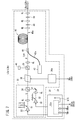
- FIG. 3 is a block diagram showing an electrical configuration of the exposure apparatus shown in FIG. 2.
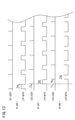
- FIG. 13 is a time chart showing an origin signal output from the origin sensor of FIG. 5 provided in each scanning unit and an incident permission signal generated by the selection element drive control unit shown in FIG. 12 according to the origin signal. It is a figure which shows the structure of the drawing data output part shown in FIG.
- FIG. 15 is a time chart showing a pixel permission pulse generated by the drawing permission signal generated by the drawing permission signal generating unit shown in FIG. 14 and a pixel shift pulse output from the transmission timing switching unit of FIG. 9 during a period when the drawing permission signal is high. It is a figure which shows the relationship between the position of the drawing line expanded / contracted within the range of the maximum scanning length, and delay time. It is a figure which shows the structure of the light source device in the modification of 1st Embodiment.
- FIG. 18 is a diagram illustrating a configuration of a clock signal generation unit illustrated in FIG. 17.
- FIG. 19 is a timing chart for explaining the operation of the clock signal generation unit of FIG. 18.
- FIG. It is a figure which shows the structure of the signal generation part provided in the inside of the light source device in 2nd Embodiment.
- 21A is a diagram showing a first example of the configuration of the delay circuit shown in FIG. 20, and
- FIG. 21B is a diagram showing a second example of the configuration of the delay circuit shown in FIG.
- It is a time chart which shows the signal output from each part of the signal generation part shown in FIG.
- FIG. 23A is a diagram for describing a pattern drawn when local magnification correction is not performed, and FIG.
- FIG. 23B is a drawing when local magnification correction (reduction) is performed according to the time chart shown in FIG. It is a figure explaining the pattern to be performed.
- FIG. 11 is an explanatory diagram of Modification 1 of each of the above-described embodiments, and drawing optics instead of the electro-optic element that modulates the intensity of the spot light according to the pattern data described in each of the above-described embodiments (including the modification) It is a figure which shows the example of arrangement
- FIG. 6 It is a figure showing a part of schematic structure of the drawing apparatus of the tandem system in the modification of 3rd Embodiment. It is a figure which shows the structure of the beam switching member provided corresponding to one scanning unit in the beam switching part by 4th Embodiment. It is a figure which shows the structure which replaced the optical element for selection and the unit side incident mirror which comprise the beam switching part shown in FIG. 6 or FIG. 24 with the structure of FIG. It is a figure which shows an example of a structure of the beam shifter part shown in FIG. FIG.
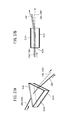
- FIG. 37A is a diagram showing an example of a beam deflecting member using an electro-optic element in which electrodes are formed on opposite parallel side surfaces of a transparent crystal medium formed in a prism shape (triangle) with a predetermined thickness.
- FIG. 37B is a diagram showing an example of a beam deflection member using an electro-optic element made of a KTN (KTa 1-x Nb x O 3 ) crystal.
- a pattern drawing apparatus and a pattern drawing method according to an aspect of the present invention will be described in detail below with reference to the accompanying drawings by listing preferred embodiments.
- the aspect of this invention is not limited to these embodiment, What added the various change or improvement is included. That is, the constituent elements described below include those that can be easily assumed by those skilled in the art and substantially the same elements, and the constituent elements described below can be appropriately combined. In addition, various omissions, substitutions, or changes of the components can be made without departing from the scope of the present invention.
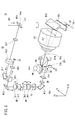
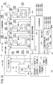
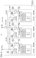
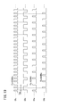
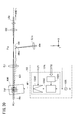
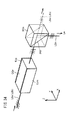
- FIG. 1 is a diagram showing a schematic configuration of a device manufacturing system 10 including an exposure apparatus EX that performs an exposure process on a substrate (irradiated body) P according to the first embodiment.
- EX an exposure apparatus
- FIG. 1 an XYZ orthogonal coordinate system in which the gravity direction is the Z direction is set, and the X direction, the Y direction, and the Z direction will be described according to the arrows shown in the drawing.
- the device manufacturing system 10 is a system (substrate processing apparatus) that manufactures an electronic device by performing predetermined processing (exposure processing or the like) on the substrate P.
- a manufacturing line for manufacturing a flexible display as an electronic device for example, a film-like touch panel, a film-like color filter for a liquid crystal display panel, a flexible wiring, or a flexible sensor is constructed. It is a manufacturing system. The following description is based on the assumption that a flexible display is used as the electronic device. Examples of the flexible display include an organic EL display and a liquid crystal display.
- the device manufacturing system 10 sends out the substrate P from a supply roll FR1 obtained by winding a flexible sheet-like substrate (sheet substrate) P in a roll shape, and continuously performs various processes on the delivered substrate P. After that, the substrate P after various treatments is wound up by the recovery roll FR2, and has a so-called roll-to-roll (Roll To Roll) structure.
- the substrate P has a belt-like shape in which the moving direction (transport direction) of the substrate P is the longitudinal direction (long) and the width direction is the short direction (short).
- the film-like substrate P includes at least a processing apparatus (first processing apparatus) PR1, a processing apparatus (second processing apparatus) PR2, an exposure apparatus (third processing apparatus) EX, An example of winding up to the collection roll FR2 through the processing device (fourth processing device) PR3 and the processing device (fifth processing device) PR4 is shown.
- the X direction is a direction (conveying direction) in which the substrate P is directed from the supply roll FR1 to the collection roll FR2 in the horizontal plane.
- the Y direction is a direction orthogonal to the X direction in the horizontal plane, and is the width direction (short direction) of the substrate P.
- the Z direction is a direction (upward direction) orthogonal to the X direction and the Y direction, and is parallel to the direction in which gravity acts.
- a resin film or a foil (foil) made of a metal or alloy such as stainless steel is used.
- the material of the resin film include polyethylene resin, polypropylene resin, polyester resin, ethylene vinyl copolymer resin, polyvinyl chloride resin, cellulose resin, polyamide resin, polyimide resin, polycarbonate resin, polystyrene resin, and vinyl acetate resin. Among them, one containing at least one or more may be used. Further, the thickness and rigidity (Young's modulus) of the substrate P may be in a range that does not cause folds or irreversible wrinkles due to buckling in the substrate P when passing through the conveyance path of the device manufacturing system 10. .
- a film such as PET (polyethylene terephthalate) or PEN (polyethylene naphthalate) having a thickness of about 25 ⁇ m to 200 ⁇ m is typical of a suitable sheet substrate.
- the substrate P may receive heat in each process performed by the processing apparatus PR1, the processing apparatus PR2, the exposure apparatus EX, the processing apparatus PR3, and the processing apparatus PR4, the substrate P is made of a material whose thermal expansion coefficient is not remarkably large. It is preferable to select the substrate P.
- the thermal expansion coefficient can be suppressed by mixing an inorganic filler with a resin film.
- the inorganic filler may be, for example, titanium oxide, zinc oxide, alumina, or silicon oxide.
- the substrate P may be a single layer of ultrathin glass having a thickness of about 100 ⁇ m manufactured by a float process or the like, or a laminate in which the above resin film, foil, or the like is bonded to the ultrathin glass. It may be.
- the flexibility of the substrate P means the property that the substrate P can be bent without being sheared or broken even when a force of its own weight is applied to the substrate P. .
- flexibility includes a property of bending by a force of about its own weight.
- the degree of flexibility varies depending on the material, size and thickness of the substrate P, the layer structure formed on the substrate P, the environment such as temperature or humidity, and the like. In any case, when the substrate P is correctly wound around the conveyance direction changing members such as various conveyance rollers and rotating drums provided in the conveyance path in the device manufacturing system 10 according to the first embodiment, If the substrate P can be smoothly transported without being bent and creased or damaged (breaking or cracking), it can be said to be a flexible range.
- the processing apparatus PR1 applies the coating process to the substrate P while transporting the substrate P transported from the supply roll FR1 toward the processing apparatus PR2 in a transport direction (+ X direction) along the longitudinal direction at a predetermined speed. It is the coating device which performs.
- the processing apparatus PR1 selectively or uniformly applies the photosensitive functional liquid to the surface of the substrate P.
- the substrate P having the photosensitive functional liquid applied on the surface thereof is conveyed toward the processing apparatus PR2.
- the processing apparatus PR2 is a drying apparatus that performs a drying process on the substrate P while transporting the substrate P transported from the processing apparatus PR1 toward the exposure apparatus EX in the transport direction (+ X direction) at a predetermined speed. .
- the processing apparatus PR2 removes the solvent or water contained in the photosensitive functional liquid with a blower, an infrared light source, a ceramic heater, or the like that blows drying air (hot air) such as hot air or dry air onto the surface of the substrate P, and performs photosensitivity. Dry sexual function liquid.
- a film to be a photosensitive functional layer photosensitive layer
- the photosensitive functional layer may be formed on the surface of the substrate P by attaching a dry film to the surface of the substrate P.
- a pasting apparatus for sticking the dry film to the substrate P may be provided instead of the processing apparatus PR1 and the processing apparatus PR2.
- a typical one of the photosensitive functional liquid (layer) is a photoresist (liquid or dry film).
- a photoresist liquid or dry film
- the lyophilic property of the part that has been irradiated with ultraviolet rays There is a photosensitive silane coupling agent (SAM) that is modified, or a photosensitive reducing agent in which a plating reducing group is exposed in a portion irradiated with ultraviolet rays.
- SAM photosensitive silane coupling agent
- the pattern portion exposed to ultraviolet rays on the substrate P is modified from lyophobic to lyophilic.
- conductive ink ink containing conductive nanoparticles such as silver or copper
- a liquid containing a semiconductor material on the lyophilic portion, a thin film transistor (TFT) or the like
- a pattern layer to be an electrode, a semiconductor, insulation, or a wiring for connection can be formed.
- a photosensitive reducing agent is used as the photosensitive functional liquid (layer)
- the plating reducing group is exposed to the pattern portion exposed to ultraviolet rays on the substrate P. Therefore, after exposure, the substrate P is immediately immersed in a plating solution containing palladium ions or the like for a certain period of time, so that a pattern layer of palladium is formed (deposited).
- Such a plating process is an additive process, but may be based on an etching process as a subtractive process.
- the substrate P sent to the exposure apparatus EX is made of PET or PEN as a base material, and a metal thin film such as aluminum (Al) or copper (Cu) is deposited on the entire surface or selectively, and further, It may be a laminate of a photoresist layer thereon.
- a photosensitive reducing agent is used as the photosensitive functional liquid (layer).
- the exposure apparatus EX is a processing apparatus that performs exposure processing on the substrate P while transporting the substrate P transported from the processing apparatus PR2 toward the processing apparatus PR3 in the transport direction (+ X direction) at a predetermined speed.
- the exposure apparatus EX uses a light corresponding to a pattern for an electronic device (for example, a pattern of an electrode or wiring of a TFT constituting the electronic device) on the surface of the substrate P (the surface of the photosensitive functional layer, that is, the photosensitive surface). Irradiate the pattern. Thereby, a latent image (modified portion) corresponding to the pattern is formed on the photosensitive functional layer.
- the exposure apparatus EX is a direct drawing type exposure apparatus that does not use a mask, that is, a so-called raster scan type exposure apparatus (pattern drawing apparatus).
- the exposure apparatus EX transmits the spot light SP of the pulsed beam LB (pulse beam) for exposure to the substrate P while conveying the substrate P in the + X direction (sub-scanning direction).
- the intensity of the spot light SP is modulated at high speed according to the pattern data (drawing data, pattern information) while one-dimensionally scanning (main scanning) in the predetermined scanning direction (Y direction) on the irradiated surface (photosensitive surface). (ON / OFF).
- a light pattern corresponding to a predetermined pattern such as an electronic device, a circuit, or a wiring is drawn and exposed on the irradiated surface of the substrate P. That is, the spot light SP is relatively two-dimensionally scanned on the irradiated surface of the substrate P by the sub-scanning of the substrate P and the main scanning of the spot light SP, and a predetermined pattern is drawn and exposed on the substrate P. . Further, since the substrate P is transported along the transport direction (+ X direction), the exposure region W where the pattern is exposed by the exposure apparatus EX is spaced at a predetermined interval along the longitudinal direction of the substrate P. A plurality are provided (see FIG. 4).
- the exposure area W is also a device formation area. Since the electronic device is configured by superimposing a plurality of pattern layers (layers on which patterns are formed), a pattern corresponding to each layer may be exposed by the exposure apparatus EX.
- the processing apparatus PR3 is a wet processing apparatus that performs wet processing on the substrate P while transporting the substrate P transported from the exposure apparatus EX toward the processing apparatus PR4 in the transport direction (+ X direction) at a predetermined speed. is there.
- the processing apparatus PR3 performs a plating process which is a kind of wet process on the substrate P. That is, the substrate P is immersed in a plating solution stored in the processing tank for a predetermined time. As a result, a pattern layer corresponding to the latent image is deposited (formed) on the surface of the photosensitive functional layer.
- a predetermined material for example, palladium
- a predetermined material for example, palladium
- a coating process or a plating process of a liquid which is a kind of wet process is performed by the processing apparatus PR3.
- a pattern layer corresponding to the latent image is formed on the surface of the photosensitive functional layer. That is, a predetermined material (for example, conductive ink or palladium) is selectively formed on the substrate P according to the difference between the irradiated portion of the spot light SP of the photosensitive functional layer of the substrate P and the irradiated portion, This is the pattern layer.
- photosensitive functional layer when a photoresist is employed as the photosensitive functional layer, development processing which is a kind of wet processing is performed by the processing apparatus PR3. In this case, a pattern corresponding to the latent image is formed on the photosensitive functional layer (photoresist) by this development processing.
- the processing apparatus PR4 performs cleaning / drying processing on the substrate P while transporting the substrate P transported from the processing apparatus PR3 toward the recovery roll FR2 in the transport direction (+ X direction) at a predetermined speed. It is a drying device.
- the processing apparatus PR4 cleans the substrate P that has been subjected to the wet processing with pure water, and then dries until the moisture content of the substrate P is equal to or lower than a predetermined value at a glass transition temperature or lower.
- the processing apparatus PR4 may be an annealing / drying apparatus that performs an annealing process and a drying process on the substrate P.
- the substrate P is irradiated with, for example, high-intensity pulsed light from a strobe lamp in order to strengthen the electrical coupling between the nanoparticles contained in the applied conductive ink.
- a processing apparatus (wet processing apparatus) PR5 that performs an etching process between the processing apparatus PR4 and the recovery roll FR2, and a substrate P that has been subjected to the etching process.
- a processing apparatus (cleaning / drying apparatus) PR6 for performing the cleaning / drying process may be provided.
- a photoresist is adopted as the photosensitive functional layer
- a pattern layer is formed on the substrate P by performing an etching process. That is, a predetermined material (for example, aluminum (Al) or copper (Cu)) is selectively formed on the substrate P according to the difference between the irradiated portion of the spot light SP of the photosensitive functional layer of the substrate P and the irradiated portion. This is a pattern layer.
- the processing apparatuses PR5 and PR6 have a function of transporting the substrate P sent in the transport direction (+ X direction) at a predetermined speed toward the collection roll FR2.
- the function of the plurality of processing apparatuses PR1 to PR4 (including processing apparatuses PR5 and PR6 as necessary) to transfer the substrate P in the + X direction is configured as a substrate transfer apparatus.
- One pattern layer is formed on the substrate P through at least each process of the device manufacturing system 10.
- each process of the device manufacturing system 10 as illustrated in FIG. 1 is performed at least twice in order to generate the electronic device. Have to go through. Therefore, a pattern layer can be laminated
- the processed substrate P is in a state in which a plurality of electronic devices are connected along the longitudinal direction of the substrate P with a predetermined interval. That is, the substrate P is a multi-sided substrate.
- the collection roll FR2 that collects the substrate P formed in a state where the electronic devices are connected may be mounted on a dicing apparatus (not shown).
- the dicing apparatus to which the recovery roll FR2 is attached divides (dices) the processed substrate P into electronic devices (exposure regions W that are device formation regions) to form electronic devices that are a plurality of single wafers.
- the dimension in the width direction (short direction) is about 10 cm to 2 m
- the dimension in the length direction (long direction) is 10 m or more.
- substrate P is not limited to an above-described dimension.
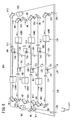
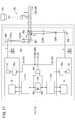
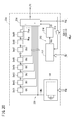
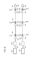
- FIG. 2 is a block diagram showing the configuration of the exposure apparatus EX.
- the exposure apparatus EX is stored in the temperature control chamber ECV.
- This temperature control chamber ECV keeps the inside at a predetermined temperature and a predetermined humidity, thereby suppressing a change in shape due to the temperature of the substrate P transported inside, and occurring along with the hygroscopicity and transport of the substrate P.
- the humidity is set in consideration of static charge.
- the temperature control chamber ECV is arranged on the installation surface E of the manufacturing factory via passive or active vibration isolation units SU1, SU2.
- the anti-vibration units SU1 and SU2 reduce vibration from the installation surface E.
- the installation surface E may be the floor surface of the factory itself, or may be a surface on an installation base (pedestal) that is exclusively installed on the floor surface in order to obtain a horizontal surface.
- the control device (control unit) 16 controls each part of the exposure apparatus EX.
- the control device 16 includes a computer and a recording medium on which the program is recorded, and functions as the control device 16 of the first embodiment when the computer executes the program.
- the substrate transport mechanism 12 constitutes a part of the substrate transport apparatus of the device manufacturing system 10, and after the substrate P transported from the processing apparatus PR2 is transported at a predetermined speed in the exposure apparatus EX, the processing is performed. It sends out to the apparatus PR3 at a predetermined speed.
- the substrate transport mechanism 12 defines a transport path for the substrate P transported in the exposure apparatus EX.
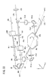
- the substrate transport mechanism 12 includes an edge position controller EPC, a driving roller R1, a tension adjusting roller RT1, a rotating drum (cylindrical drum) DR, a tension adjusting roller RT2, in order from the upstream side ( ⁇ X direction side) in the transport direction of the substrate P.
- a driving roller R2 and a driving roller R3 are provided.
- the edge position controller EPC adjusts the position in the width direction (the Y direction and the short direction of the substrate P) of the substrate P transported from the processing apparatus PR2.
- the edge position controller EPC has a position at the end (edge) in the width direction of the substrate P that is transported in a state of a predetermined tension, which is about ⁇ 10 ⁇ m to several tens ⁇ m with respect to the target position.
- the position of the substrate P in the width direction is adjusted by moving the substrate P in the width direction so that it falls within this range (allowable range).
- the edge position controller EPC includes a roller on which the substrate P is stretched in a state where a predetermined tension is applied, and an edge sensor (end detection unit) (not shown) that detects the position of the end portion (edge) in the width direction of the substrate P. And have.
- the edge position controller EPC adjusts the position of the substrate P in the width direction by moving the roller of the edge position controller EPC in the Y direction based on the detection signal detected by the edge sensor.
- the driving roller (nip roller) R1 rotates while holding both front and back surfaces of the substrate P conveyed from the edge position controller EPC, and conveys the substrate P toward the rotating drum DR.
- the edge position controller EPC appropriately adjusts the position in the width direction of the substrate P so that the longitudinal direction of the substrate P wound around the rotating drum DR is always orthogonal to the central axis AXo of the rotating drum DR.
- the parallelism between the rotation axis of the roller and the Y axis of the edge position controller EPC may be appropriately adjusted so as to correct the tilt error in the traveling direction of the substrate P.
- the rotary drum DR has a central axis AXo extending in the Y direction and extending in a direction intersecting with the direction in which gravity works, and a cylindrical outer peripheral surface having a constant radius from the central axis AXo.
- the rotating drum DR rotates around the central axis AXo while supporting (holding) a part of the substrate P by bending the outer surface (circumferential surface) into a cylindrical surface in the longitudinal direction. Transport P in the + X direction.
- the rotating drum DR supports an area (portion) on the substrate P onto which the beam LB (spot light SP) from the exposure head 14 is projected on its outer peripheral surface.
- the rotating drum DR supports (holds and holds) the substrate P from the surface (back surface) opposite to the surface on which the electronic device is formed (surface on which the photosensitive surface is formed).
- shafts Sft supported by annular bearings are provided so that the rotating drum DR rotates around the central axis AXo.
- the shaft Sft rotates at a constant rotational speed around the central axis AXo by receiving a rotational torque from a rotational drive source (not shown) (for example, a motor or a speed reduction mechanism) controlled by the control device 16.
- a rotational drive source not shown
- a plane including the central axis AXo and parallel to the YZ plane is referred to as a central plane Poc.
- the driving rollers (nip rollers) R2 and R3 are arranged at a predetermined interval along the transport direction (+ X direction) of the substrate P, and give a predetermined slack (play) to the substrate P after exposure.
- the drive rollers R2 and R3 rotate while holding both front and back surfaces of the substrate P, and transport the substrate P toward the processing apparatus PR3.
- the tension adjusting rollers RT1 and RT2 are urged in the ⁇ Z direction, and apply a predetermined tension in the longitudinal direction to the substrate P that is wound around and supported by the rotary drum DR. As a result, the longitudinal tension applied to the substrate P applied to the rotating drum DR is stabilized within a predetermined range.
- the control device 16 rotates the driving rollers R1 to R3 by controlling a rotation driving source (not shown) (for example, a motor, a speed reducer, etc.).
- a rotation driving source for example, a motor, a speed reducer, etc.
- the rotation axes of the drive rollers R1 to R3 and the rotation axes of the tension adjustment rollers RT1 and RT2 are parallel to the center axis AXo of the rotation drum DR.
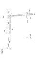
- the light source device LS (LSa, LSb) generates and emits a pulsed beam (pulse beam, pulsed light, laser) LB.
- the beam LB is ultraviolet light having a peak wavelength in a wavelength band of 370 nm or less, and the light emission frequency (oscillation frequency, predetermined frequency) of the beam LB is Fa.
- the beam LB emitted from the light source device LS (LSa, LSb) is incident on the exposure head 14 via the beam switching unit BDU.
- the light source device LS (LSa, LSb) emits and emits the beam LB at the emission frequency Fa according to the control of the control device 16.
- the configuration of the light source device LS (LSa, LSb) will be described later in detail.
- a semiconductor laser element that generates pulsed light in the infrared wavelength region, a fiber amplifier, an amplified red light, and the like. Consists of a wavelength conversion element (harmonic generation element) that converts pulsed light in the outer wavelength range to pulsed light in the ultraviolet wavelength range, with an oscillation frequency Fa of several hundred MHz, and an emission time of one pulsed light of about picoseconds It is assumed that a fiber amplifier laser light source (harmonic laser light source) capable of obtaining high-intensity ultraviolet pulsed light is used.
- the beam LB from the light source device LSa may be represented by LBa and the beam LB from the light source device LSb may be represented by LBb.
- the beam switching unit BDU switches the scanning unit Un on which the beams LBa and LBb are incident so that the beam LBn is incident on the scanning unit Un that scans the spot light SP. That is, the beam switching unit BDU causes the beam LBa from the light source device LSa to enter one of the scanning units U1 to U3 that scans the spot light SP. Similarly, the beam switching unit BDU causes the beam LBb from the light source device LSb to enter one scanning unit Un that scans the spot light SP among the scanning units U4 to U6.
- the beam switching unit BDU will be described in detail later.
- the scanning unit Un that scans the spot light SP is switched in the order of U1 ⁇ U2 ⁇ U3, and for the scanning units U4 to U6, the scanning that scans the spot light SP. Assume that the unit Un is switched in the order of U4 ⁇ U5 ⁇ U6.
- the exposure head 14 is a so-called multi-beam type exposure head in which a plurality of scanning units Un (U1 to U6) having the same configuration are arranged.
- the exposure head 14 draws a pattern on a part of the substrate P supported by the outer peripheral surface (circumferential surface) of the rotary drum DR by a plurality of scanning units Un (U1 to U6). Since the exposure head 14 repeatedly performs pattern exposure for an electronic device on the substrate P, an exposure region (electronic device formation region) W where the pattern is exposed is a predetermined interval along the longitudinal direction of the substrate P.
- a plurality are provided (see FIG. 4).
- the plurality of scanning units Un (U1 to U6) are arranged in a predetermined arrangement relationship.
- the plurality of scanning units Un are arranged in a staggered arrangement in two rows in the transport direction of the substrate P with the center plane Poc interposed therebetween.
- the odd-numbered scanning units U1, U3, U5 are arranged in a line on the upstream side ( ⁇ X direction side) in the transport direction of the substrate P with respect to the center plane Poc and at a predetermined interval along the Y direction.
- the even-numbered scanning units U2, U4, U6 are arranged in a line at a predetermined interval along the Y direction on the downstream side (+ X direction side) in the transport direction of the substrate P with respect to the center plane Poc.
- the odd-numbered scanning units U1, U3, and U5 and the even-numbered scanning units U2, U4, and U6 are provided symmetrically with respect to the center plane Poc.
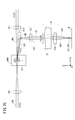
- Each scanning unit Un projects the beam LB from the light source device LS (LSa, LSb) so as to converge on the spot light SP on the irradiated surface of the substrate P.
- One-dimensional scanning is performed by the rotating polygon mirror PM (see FIG. 5).
- the spot light SP is one-dimensionally scanned on the irradiated surface of the substrate P by the polygon mirror (deflecting member) PM of each of the scanning units Un (U1 to U6).
- the configuration of the scanning unit Un will be described in detail later.
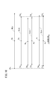
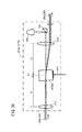
- the scanning unit U1 scans the spot light SP along the drawing line SL1, and similarly, the scanning units U2 to U6 scan the spot light SP along the drawing lines SL2 to SL6.
- the drawing lines SLn (SL1 to SL6) of the plurality of scanning units Un (U1 to U6) are not separated from each other in the Y direction (the width direction of the substrate P, the main scanning direction), as shown in FIGS. , Are set to be spliced.
- the beam LB from the light source device LS (LSa, LSb) that enters the scanning unit Un via the beam switching unit BDU may be represented as LBn.
- the beam LBn incident on the scanning unit U1 may be represented by LB1, and similarly, the beam LBn incident on the scanning units U2 to U6 may be represented by LB2 to LB6.
- the drawing lines SLn (SL1 to SL6) indicate the scanning trajectory of the spot light SP of the beam LBn (LB1 to LB6) scanned by the scanning unit Un (U1 to U6).
- the beam LBn incident on the scanning unit Un may be a linearly polarized beam (P-polarized light or S-polarized light) polarized in a predetermined direction, and is a P-polarized beam in the first embodiment.
- each of the scanning units Un (U1 to U6) shares the scanning area so that the plurality of scanning units Un (U1 to U6) cover all of the exposure area W in the width direction. ing. Accordingly, each scanning unit Un (U1 to U6) can draw a pattern for each of a plurality of regions (drawing ranges) divided in the width direction of the substrate P.
- the width in the Y direction that can be drawn is increased to about 120 to 360 mm.
- the length of each drawing line SLn (SL1 to SL6) (length of the drawing range) is the same. That is, the scanning distance of the spot light SP of the beam LBn scanned along each of the drawing lines SL1 to SL6 is basically the same. Note that it is possible to increase the width of the exposure region W by increasing the length of the drawing line SLn itself or increasing the number of scanning units Un arranged in the Y direction.
- the actual drawing lines SLn are set slightly shorter than the maximum length (maximum scanning length) that the spot light SP can actually scan on the irradiated surface.
- the scanning length of the drawing line SLn on which pattern drawing is possible is 30 mm when the drawing magnification in the main scanning direction (Y direction) is an initial value (no magnification correction)
- the maximum scanning on the irradiated surface of the spot light SP The length is set to about 31 mm with a margin of about 0.5 mm on each of the drawing start point (scanning start point) side and the drawing end point (scanning end point) side of the drawing line SLn.
- the maximum scanning length of the spot light SP is not limited to 31 mm, and is mainly determined by the aperture of the f ⁇ lens FT (see FIG. 5) provided after the polygon mirror (rotating polygon mirror) PM in the scanning unit Un.
- the plurality of drawing lines SLn are arranged in a staggered arrangement in two rows in the circumferential direction of the rotary drum DR with the center surface Poc interposed therebetween.
- the odd-numbered drawing lines SL1, SL3, and SL5 are positioned on the irradiated surface of the substrate P on the upstream side ( ⁇ X direction side) in the transport direction of the substrate P with respect to the center plane Poc.
- the even-numbered drawing lines SL2, SL4, and SL6 are positioned on the irradiated surface of the substrate P on the downstream side (+ X direction side) in the transport direction of the substrate P with respect to the center plane Poc.
- the drawing lines SL1 to SL6 are substantially parallel to the width direction of the substrate P, that is, the central axis AXo of the rotary drum DR.
- the drawing lines SL1, SL3, and SL5 are arranged in a line on a straight line at a predetermined interval along the width direction (main scanning direction) of the substrate P.
- the drawing lines SL2, SL4, and SL6 are arranged in a line on the straight line at a predetermined interval along the width direction (main scanning direction) of the substrate P.
- the drawing line SL2 is arranged between the drawing line SL1 and the drawing line SL3 in the width direction of the substrate P.
- the drawing line SL3 is arranged between the drawing line SL2 and the drawing line SL4 in the width direction of the substrate P.
- the drawing line SL4 is arranged between the drawing line SL3 and the drawing line SL5 with respect to the width direction of the substrate P, and the drawing line SL5 is arranged between the drawing line SL4 and the drawing line SL6 with respect to the width direction of the substrate P.
- the plurality of drawing lines SLn (SL1 to SL6) are arranged so as to be shifted from each other in the Y direction (main scanning direction).
- the main scanning direction of the spot light SP of the beams LB1, LB3, LB5 scanned along each of the odd-numbered drawing lines SL1, SL3, SL5 is a one-dimensional direction and is the same direction.
- the main scanning direction of the spot light SP of the beams LB2, LB4, and LB6 scanned along the even-numbered drawing lines SL2, SL4, and SL6 is a one-dimensional direction and is the same direction.
- the main scanning direction of the spot light SP may be opposite to each other.
- the main scanning direction of the spot light SP of the beams LB1, LB3, LB5 scanned along the drawing lines SL1, SL3, SL5 is the -Y direction.
- the main scanning direction of the spot light SP of the beams LB2, LB4, and LB6 scanned along the drawing lines SL2, SL4, and SL6 is the + Y direction.
- the end of the drawing lines SL3 and SL5 on the drawing end point side and the end of the drawing lines SL2 and SL4 on the drawing end point side are adjacent or partially overlap in the Y direction.
- each drawing line SLn so that the ends of the drawing lines SLn adjacent in the Y direction partially overlap, for example, the drawing start point or the drawing end with respect to the length of each drawing line SLn It is preferable to overlap within a range of several percent or less in the Y direction including points.
- joining the drawing lines SLn in the Y direction means that the ends of the drawing lines SLn are adjacent to each other or partially overlap in the Y direction.
- the width (dimension in the X direction) of the drawing line SLn in the sub-scanning direction is a thickness corresponding to the size (diameter) ⁇ of the spot light SP.
- the width of the drawing line SLn is also 3 ⁇ m.
- the spot light SP may be projected along the drawing line SLn so as to overlap by a predetermined length (for example, 7/8 of the size ⁇ of the spot light SP).
- drawing lines SLn for example, the drawing line SL1 and the drawing line SL2 adjacent in the Y direction are connected to each other, they are overlapped by a predetermined length (for example, 7/8 of the size ⁇ of the spot light SP). It is good.
- the spot light SP projected onto the drawing line SLn during main scanning Is discrete according to the oscillation frequency Fa (for example, 400 MHz) of the beam LB (LBa, LBb). Therefore, it is necessary to overlap the spot light SP projected by one pulse light of the beam LB and the spot light SP projected by the next one pulse light in the main scanning direction.
- the amount of overlap is set by the size ⁇ of the spot light SP, the scanning speed (main scanning speed) Vs of the spot light SP, and the oscillation frequency Fa of the beam LB.
- the effective size ⁇ of the spot light SP is determined by 1 / e 2 (or 1/2) of the peak intensity of the spot light SP when the intensity distribution of the spot light SP is approximated by a Gaussian distribution.
- the scanning speed Vs and the oscillation frequency Fa of the spot light SP are set so that the spot light SP overlaps the effective size (dimension) ⁇ by about ⁇ ⁇ 7/8. Is done. Accordingly, the projection interval of the spot light SP along the main scanning direction is ⁇ / 8. Therefore, also in the sub-scanning direction (direction orthogonal to the drawing line SLn), the substrate P is effective for the spot light SP between one scanning of the spot light SP along the drawing line SLn and the next scanning.
- the exposure amount to the photosensitive functional layer on the substrate P can be set by adjusting the peak value of the beam LB (pulse light). However, the exposure amount can be increased in a situation where the intensity of the beam LB cannot be increased.
- the spot light SP is caused to fall by the decrease in the scanning speed Vs of the spot light SP in the main scanning direction, the increase in the oscillation frequency Fa of the beam LB, or the decrease in the transport speed Vt of the substrate P in the sub scanning direction.
- the overlap amount in the main scanning direction or the sub-scanning direction may be increased.
- the scanning speed Vs of the spot light SP in the main scanning direction increases in proportion to the rotational speed (rotational speed Vp) of the polygon mirror PM.
- Each scanning unit Un (U1 to U6) irradiates each beam LBn toward the substrate P so that each beam LBn travels toward the central axis AXo of the rotating drum DR at least in the XZ plane.
- the optical path (beam central axis) of the beam LBn traveling from each scanning unit Un (U1 to U6) toward the substrate P becomes parallel to the normal line of the irradiated surface of the substrate P in the XZ plane.
- each scanning unit Un (U1 to U6) is configured such that the beam LBn irradiated to the drawing line SLn (SL1 to SL6) is perpendicular to the irradiated surface of the substrate P in a plane parallel to the YZ plane.
- the beam LBn is irradiated toward the substrate P. That is, the beam LBn (LB1 to LB6) projected onto the substrate P is scanned in a telecentric state with respect to the main scanning direction of the spot light SP on the irradiated surface.
- a line perpendicular to the irradiated surface of the substrate P also called an optical axis
- SLn SL1 to SL6
- Un U1 to U6
- Each irradiation center axis Len (Le1 to Le6) is a line connecting the drawing lines SL1 to SL6 and the center axis AXo on the XZ plane.
- the irradiation center axes Le1, Le3, Le5 of the odd-numbered scanning units U1, U3, U5 are in the same direction in the XZ plane, and the irradiation center axes Le2 of the even-numbered scanning units U2, U4, U6. , Le4 and Le6 are in the same direction in the XZ plane.
- irradiation center axes Le1, Le3, Le5 and the irradiation center axes Le2, Le4, Le6 are set such that the angle is ⁇ ⁇ 1 with respect to the center plane Poc in the XZ plane (see FIG. 2).
- a plurality of alignment microscopes AM1m (AM11 to AM14) and AM2m (AM21 to AM24) shown in FIG. 2 are for detecting a plurality of alignment marks MKm (MK1 to MK4) formed on the substrate P shown in FIG. And a plurality (four in the first embodiment) are provided along the Y direction.
- the plurality of alignment marks MKm (MK1 to MK4) are reference marks for relatively aligning (aligning) the predetermined pattern drawn in the exposure area W on the irradiated surface of the substrate P with the substrate P. It is.
- a plurality of alignment microscopes AM1m (AM11 to AM14) and AM2m (AM21 to AM24) are arranged on the substrate P supported by the outer peripheral surface (circumferential surface) of the rotating drum DR, and a plurality of alignment marks MKm (MK1 to MK4). Is detected.
- the plurality of alignment microscopes AM1m (AM11 to AM14) are more than the irradiated area (area surrounded by the drawing lines SL1 to SL6) on the substrate P by the spot light SP of the beam LBn (LB1 to LB6) from the exposure head 14. It is provided on the upstream side ( ⁇ X direction side) in the transport direction of the substrate P.
- the plurality of alignment microscopes AM2m are irradiated from an irradiation area (area surrounded by the drawing lines SL1 to SL6) on the substrate P by the spot light SP of the beam LBn (LB1 to LB6) from the exposure head 14. Is also provided on the downstream side (+ X direction side) in the transport direction of the substrate P.
- the alignment microscopes AM1m (AM11 to AM14) and AM2m (AM21 to AM24) are a local region (observation region) Vw1m (Vw11) including a light source that projects illumination light for alignment onto the substrate P and an alignment mark MKm on the surface of the substrate P.
- Vw1m Vw11
- Vw2m Vw21 to Vw24
- an observation optical system including an objective lens
- the transport speed Vt of the substrate P is increased.
- an image pickup device such as a CCD or a CMOS for picking up an image with a corresponding high-speed shutter.
- Imaging signals (image data) captured by each of the plurality of alignment microscopes AM1m (AM11 to AM14) and AM2m (AM21 to AM24) are sent to the control device 16.
- the mark position detection unit 106 (see FIG. 12) of the control device 16 performs image analysis of the plurality of image signals that have been sent, so that the position of the alignment mark MKm (MK1 to MK4) on the substrate P (mark position). Information).
- the illumination light for alignment is light in a wavelength region that has little sensitivity to the photosensitive functional layer on the substrate P, for example, light having a wavelength of about 500 to 800 nm.
- a plurality of alignment marks MK1 to MK4 are provided around each exposure area W.
- a plurality of alignment marks MK1 and MK4 are formed on both sides of the exposure region W in the width direction of the substrate P at a constant interval Dh along the longitudinal direction of the substrate P.
- the alignment mark MK1 is formed on the ⁇ Y direction side in the width direction of the substrate P
- the alignment mark MK4 is formed on the + Y direction side in the width direction of the substrate P.
- Such alignment marks MK1 and MK4 are located at the same position in the longitudinal direction (X direction) of the substrate P when the substrate P is not deformed due to a large tension or a thermal process. Be placed.
- the alignment marks MK2 and MK3 are between the alignment mark MK1 and the alignment mark MK4, and extend in the width direction (short direction) of the substrate P in the margin part between the + X direction side and the ⁇ X direction side of the exposure region W. Is formed.
- the alignment marks MK2 and MK3 are formed between the exposure area W and the exposure area W.
- the alignment mark MK2 is formed on the ⁇ Y direction side in the width direction of the substrate P
- the alignment mark MK3 is formed on the + Y direction side of the substrate P.
- the Y-direction interval between the alignment mark MK1 and the margin alignment mark MK2 arranged at the ⁇ Y direction end of the substrate P, the Y-direction interval between the margin alignment mark MK2 and the alignment mark MK3, and The interval in the Y direction between the alignment mark MK4 arranged at the end on the + Y direction side of the substrate P and the alignment mark MK3 in the blank portion is set to the same distance.
- These alignment marks MKm (MK1 to MK4) may be formed together when forming the first pattern layer. For example, when the pattern of the first layer is exposed, the alignment mark pattern may be exposed around the exposure area W where the pattern is exposed.
- the alignment mark MKm may be formed in the exposure area W. For example, it may be formed in the exposure area W along the outline of the exposure area W. Further, a pattern portion at a specific position or a specific shape portion in the pattern of the electronic device formed in the exposure region W may be used as the alignment mark MKm.
- Alignment microscopes AM11 and AM21 are arranged so as to image alignment marks MK1 existing in observation regions (detection regions) Vw11 and Vw21 by the objective lens, as shown in FIG.
- the alignment microscopes AM12 to AM14 and AM22 to AM24 are arranged so as to image the alignment marks MK2 to MK4 existing in the observation areas Vw12 to Vw14 and Vw22 to Vw24 by the objective lens.
- the plurality of alignment microscopes AM11 to AM14 and AM21 to AM24 correspond to the positions of the plurality of alignment marks MK1 to MK4, and the substrates P in the order of AM11 to AM14 and AM21 to AM24 from the ⁇ Y direction side of the substrate P. It is provided along the width direction.
- the observation region Vw2m (Vw21 to Vw24) of the alignment microscope AM2m (AM21 to AM24) is not shown.
- the distance between the exposure position (drawing lines SL1 to SL6) and the observation region Vw1m (Vw11 to Vw14) in the X direction is shorter than the length of the exposure region W in the X direction. It is provided to become.
- the distance between the exposure position (drawing lines SL1 to SL6) and the observation region Vw2m (Vw21 to Vw24) with respect to the X direction is longer than the length of the exposure region W in the X direction. Is also provided to be shorter.
- the number of alignment microscopes AM1m and AM2m provided in the Y direction can be changed according to the number of alignment marks MKm formed in the width direction of the substrate P. Further, the sizes of the observation regions Vw1m (Vw11 to Vw14) and Vw2m (Vw21 to Vw24) on the irradiated surface of the substrate P are set according to the size of the alignment marks MK1 to MK4 and the alignment accuracy (position measurement accuracy). However, it is about 100 to 500 ⁇ m square.
- scale portions SDa and SDb having scales formed in an annular shape over the entire circumferential direction of the outer peripheral surface of the rotary drum DR are provided at both ends of the rotary drum DR.
- the scale portions SDa and SDb are diffraction gratings in which concave or convex lattice lines are engraved at a constant pitch (for example, 20 ⁇ m) in the circumferential direction of the outer peripheral surface of the rotary drum DR, and are configured as incremental scales.
- the scale portions SDa and SDb rotate integrally with the rotary drum DR around the central axis AXo.
- Encoders ENja and ENjb optically detect the rotational angle position of the rotary drum DR.
- Four encoders ENja (EN1a, EN2a, EN3a, EN4a) are provided so as to face the scale part SDa provided at the end of the rotary drum DR on the ⁇ Y direction side.
- four encoders ENjb (EN1b, EN2b, EN3b, EN4b) are provided so as to face the scale part SDb provided at the end on the + Y direction side of the rotary drum DR.
- the encoders EN1a and EN1b are provided on the upstream side ( ⁇ X direction side) in the transport direction of the substrate P with respect to the center plane Poc, and are disposed on the installation direction line Lx1 (see FIGS. 2 and 3).
- the installation azimuth line Lx1 is a line connecting the projection positions (reading positions) of the measurement light beams on the scale portions SDa and SDb of the encoders EN1a and EN1b and the central axis AXo on the XZ plane.
- the installation orientation line Lx1 is a line connecting the observation region Vw1m (Vw11 to Vw14) of each alignment microscope AM1m (AM11 to AM14) and the central axis AXo on the XZ plane. That is, a plurality of alignment microscopes AM1m (AM11 to AM14) are also arranged on the installation direction line Lx1.
- the encoders EN2a and EN2b are provided on the upstream side ( ⁇ X direction side) in the transport direction of the substrate P with respect to the center plane Poc, and further downstream in the transport direction of the substrate P (+ X direction) from the encoders EN1a and EN1b. Side).
- the encoders EN2a and EN2b are disposed on the installation direction line Lx2 (see FIGS. 2 and 3).
- the installation azimuth line Lx2 is a line connecting the projection positions (reading positions) of the measurement light beams on the scale portions SDa and SDb of the encoders EN2a and EN2b and the central axis AXo on the XZ plane.
- the installation azimuth line Lx2 overlaps with the irradiation center axes Le1, Le3, Le5 at the same angular position in the XZ plane.
- the encoders EN3a and EN3b are provided on the downstream side (+ X direction side) in the transport direction of the substrate P with respect to the center plane Poc, and are disposed on the installation direction line Lx3 (see FIGS. 2 and 3).
- the installation azimuth line Lx3 is a line connecting the projection positions (reading positions) of the measurement light beams on the scale portions SDa and SDb of the encoders EN3a and EN3b and the central axis AXo on the XZ plane.
- This installation orientation line Lx3 overlaps with the irradiation center axes Le2, Le4, and Le6 at the same angular position in the XZ plane. Therefore, the installation azimuth line Lx2 and the installation azimuth line Lx3 are set so that the angle is ⁇ ⁇ 1 with respect to the center plane Poc in the XZ plane (see FIG. 2).
- Encoders EN4a and EN4b are provided on the downstream side (+ X direction side) in the transport direction of the substrate P from the encoders EN3a and EN3b, and are arranged on the installation direction line Lx4 (see FIG. 2).
- the installation azimuth line Lx4 is a line connecting the projection positions (reading positions) of the measurement light beams on the scale portions SDa and SDb of the encoders EN4a and EN4b and the central axis AXo on the XZ plane.
- the installation orientation line Lx4 is a line connecting the observation region Vw2m (Vw21 to Vw24) of each alignment microscope AM2m (AM21 to AM24) and the central axis AXo on the XZ plane.
- a plurality of alignment microscopes AM2m are also arranged on the installation direction line Lx4.
- the installation azimuth line Lx1 and the installation azimuth line Lx4 are set such that the angle is ⁇ ⁇ 2 with respect to the center plane Poc in the XZ plane (see FIG. 2).
- Each encoder ENja (EN1a to EN4a), ENjb (EN1b to EN4b) projects a measurement light beam toward the scale portions SDa and SDb, and detects the reflected light beam (diffracted light) to detect a pulse signal. Is output to the control device 16.
- the rotational position detector 108 (see FIG. 12) of the control device 16 counts the detection signal (pulse signal), thereby measuring the rotational angular position and angular change of the rotary drum DR with submicron resolution. From the change in the angle of the rotating drum DR, the transport speed Vt of the substrate P can also be measured.
- the rotational position detector 108 individually counts detection signals from the encoders ENja (EN1a to EN4a) and ENjb (EN1b to EN4b).
- the rotational position detection unit 108 includes a plurality of counter circuits CNja (CN1a to CN4a) and CNjb (CN1b to CN4b).
- the counter circuit CN1a counts the detection signal from the encoder EN1a
- the counter circuit CN1b counts the detection signal from the encoder EN1b.
- the counter circuits CN2a to CN4a and CN2b to CN4b count detection signals from the encoders EN2a to EN4a and EN2b to EN4b.
- Each of the counter circuits CNja (CN1a to CN4a) and CNjb (CN1b to CN4b) has encoders ENja (EN1a to EN4a) and ENjb (EN1b to EN4b) formed in a part of the circumferential direction of the scale portions SDa and SDb.
- the count values corresponding to the encoders ENja and ENjb that have detected the origin mark ZZ are reset to zero.
- One of the count values of the counter circuits CN1a and CN1b or the average value thereof is used as the rotation angle position of the rotary drum DR on the installation direction line Lx1, and either one of the count values of the counter circuits CN2a and CN2b or the average The value is used as the rotation angle position of the rotary drum DR on the installation direction line Lx2.
- one or the average value of the count values of the counter circuits CN3a and CN3b is used as the rotation angle position of the rotary drum DR on the installation direction line Lx3, and either one of the count values of the counter circuits CN4a and CN4b or The average value is used as the rotation angle position of the rotary drum DR on the installation direction line Lx4.
- the count values of the counter circuits CN1a and CN1b are the same except when the rotary drum DR rotates eccentrically with respect to the central axis AXo due to a manufacturing error of the rotary drum DR.
- the count values of the counter circuits CN2a and CN2b are the same, and the count values of the counter circuits CN3a and CN3b and the count values of the counter circuits CN4a and CN4b are also the same.
- alignment microscope AM1m (AM11 to AM14) and encoders EN1a and EN1b are arranged on installation orientation line Lx1
- alignment microscope AM2m (AM21 to AM24) and encoders EN4a and EN4b are installation orientation lines Lx4. Is placed on top. Therefore, the position detection of the alignment mark MKm (MK1 to MK4) by the image analysis of the mark position detection unit 106 of the plurality of imaging signals picked up by the plurality of alignment microscopes AM1m (AM11 to AM14) and the moment when the alignment microscope AM1m picks up the image.
- the position of the substrate P on the installation orientation line Lx1 can be measured with high accuracy based on the information on the rotational angle position of the rotary drum DR (the count value based on the encoders EN1a and EN1b).
- the position detection of the alignment mark MKm MK1 to MK4 by the image analysis of the mark position detection unit 106 of the plurality of imaging signals captured by the plurality of alignment microscopes AM2m (AM21 to AM24), and the moment when the alignment microscope AM2m images
- the position of the substrate P on the installation orientation line Lx4 can be measured with high accuracy based on the information on the rotational angle position of the rotary drum DR (the count value based on the encoders EN4a and EN4b).
- the count values of the detection signals from the encoders EN1a and EN1b, the count values of the detection signals from the encoders EN2a and EN2b, the count values of the detection signals from the encoders EN3a and EN3b, and the detection signals from the encoders EN4a and EN4b The count value is reset to zero at the moment when each encoder ENja, ENjb detects the origin mark ZZ. Therefore, when the position on the installation orientation line Lx1 of the substrate P wound around the rotary drum DR when the count value based on the encoders EN1a and EN1b is the first value (for example, 100) is the first position.
- the count value based on the encoders EN2a, EN2b is the first value (for example, , 100).
- the count value of the detection signal based on the encoders EN3a, EN3b is the first. (For example, 100).
- the count value of the detection signal based on the encoders EN4a and EN4b becomes the first value (for example, 100).
- the substrate P is wound inside the scale portions SDa and SDb at both ends of the rotary drum DR.
- the radius from the central axis AXo of the outer peripheral surface of the scale portions SDa and SDb is set smaller than the radius from the central axis AXo of the outer peripheral surface of the rotary drum DR.
- the outer peripheral surfaces of the scale portions SDa and SDb may be set so as to be flush with the outer peripheral surface of the substrate P wound around the rotary drum DR.
- the radius (distance) from the central axis AXo of the outer peripheral surfaces of the scale portions SDa and SDb and the radius (distance) from the central axis AXo of the outer peripheral surface (irradiated surface) of the substrate P wound around the rotary drum DR May be set to be the same.
- each of the encoders ENja (EN1a to EN4a) and ENjb (EN1b to EN4b) can detect the scale portions SDa and SDb at the same radial position as the irradiated surface of the substrate P wound around the rotary drum DR. . Therefore, the Abbe error caused by the difference between the measurement positions by the encoders ENja and ENjb and the processing positions (drawing lines SL1 to SL6) in the radial direction of the rotary drum DR can be reduced.
- the radius of the outer peripheral surface of the scale portions SDa and SDb and the outer peripheral surface of the substrate P wound around the rotary drum DR are different. It is difficult to always make the radius the same. Therefore, in the case of the scale portions SDa and SDb shown in FIG. 3, the radius of the outer peripheral surface (scale surface) is set to coincide with the radius of the outer peripheral surface of the rotary drum DR. Furthermore, the scale portions SDa and SDb can be formed of individual disks, and the disks (scale disks) can be coaxially attached to the shaft Sft of the rotary drum DR. Even in this case, it is preferable to align the radius of the outer peripheral surface (scale surface) of the scale disk and the radius of the outer peripheral surface of the rotary drum DR so that the Abbe error falls within the allowable value.
- the start position of the drawing exposure of the exposure region W in the longitudinal direction (X direction) of the substrate P is determined by the control device 16 based on any one of these or the average value. Since the length of the exposure area W in the X direction is known in advance, the control device 16 determines the drawing exposure start position every time a predetermined number of alignment marks MKm (MK1 to MK4) are detected.
- the drawing exposure start position of the exposure region W in the longitudinal direction of the substrate P is located on the drawing lines SL1, SL3, SL5. Accordingly, the scanning units U1, U3, and U5 can start scanning the spot light SP based on the count values of the encoders EN2a and EN2b.
- the drawing exposure start position of the exposure region W in the longitudinal direction of the substrate P is positioned on the drawing lines SL2, SL4, and SL6. To do. Therefore, the scanning units U2, U4, and U6 can start scanning the spot light SP based on the count values of the encoders EN3a and EN3b.
- the tension adjusting rollers RT1 and RT2 apply a predetermined tension to the substrate P in the longitudinal direction, so that the substrate P is conveyed along with the rotation of the rotating drum DR while being in close contact with the rotating drum DR. .
- the rotational speed Vp of the rotating drum DR is high, or the tension applied to the substrate P by the tension adjusting rollers RT1 and RT2 is too low or too high, the substrate P slips with respect to the rotating drum DR. May occur.
- the encoders EN1a and EN1b at the moment when the alignment microscope AM1m images the alignment mark MKmA (a specific alignment mark MKm) based on the count value based on the encoders EN4a and 4b.
- the count value is the same as the count value based on (for example, 150)
- this alignment mark MKmA is detected by the alignment microscope AM2m.
- the count value based on the encoders EN4a and EN4b is a count value based on the encoders EN1a and EN1b at the moment when the alignment mark AMKm images the alignment mark MKmA (for example, , 150), the alignment mark MKmA is not detected by the alignment microscope AM2m.
- the count value based on the encoders EN4a and EN4b exceeds 150, for example, the alignment mark MKmA is detected by the alignment microscope AM2m.
- the slip amount of the substrate P can be measured by additionally installing the alignment microscope AM2m and the encoders EN4a and EN4b.
- each scanning unit Un (U1 to U6) has the same configuration, only the scanning unit U1 will be described, and the description of the other scanning units Un will be omitted.
- the direction parallel to the irradiation center axis Len (Le1) is the Zt direction
- the substrate P is on the plane orthogonal to the Zt direction
- the substrate P passes from the processing apparatus PR2 through the exposure apparatus EX to the processing apparatus PR3.
- the direction going to the Xt direction is defined as the Yt direction
- the direction perpendicular to the Xt direction on the plane orthogonal to the Zt direction is defined as the Yt direction.
- the three-dimensional coordinates of Xt, Yt, and Zt in FIG. 5 are the same as the three-dimensional coordinates of X, Y, and Z in FIG. 2, and the Z-axis direction is parallel to the irradiation center axis Len (Le1).
- the three-dimensional coordinates rotated as described above.
- a reflection mirror M10 As shown in FIG. 5, in the scanning unit U1, along the traveling direction of the beam LB1 from the incident position of the beam LB1 to the irradiated surface (substrate P), a reflection mirror M10, a beam expander BE, a reflection mirror M11, Polarization beam splitter BS1, reflection mirror M12, shift optical member (parallel plate) SR, deflection adjustment optical member (prism) DP, field aperture FA, reflection mirror M13, ⁇ / 4 wavelength plate QW, cylindrical lens CYA, reflection mirror M14, A polygon mirror PM, an f ⁇ lens FT, a reflection mirror M15, and a cylindrical lens CYb are provided.
- an origin sensor (origin detector) OP1 that detects the timing at which the scanning unit U1 can start drawing, and reflected light from the irradiated surface (substrate P) are detected via the polarization beam splitter BS1.
- An optical lens system G10 and a photodetector DT are provided.
- the beam LB1 incident on the scanning unit U1 travels in the ⁇ Zt direction and enters the reflection mirror M10 inclined by 45 ° with respect to the XtYt plane.
- the axis of the beam LB1 incident on the scanning unit U1 is incident on the reflection mirror M10 so as to be coaxial with the irradiation center axis Le1.
- the reflection mirror M10 functions as an incident optical member that causes the beam LB1 to enter the scanning unit U1, and the incident beam LB1 is moved from the reflection mirror M10 to the ⁇ Xt direction along the optical axis AXa set parallel to the Xt axis. Reflected in the -Xt direction toward the distant reflecting mirror M11.
- the optical axis AXa is orthogonal to the irradiation center axis Le1 in a plane parallel to the XtZt plane.
- the beam LB1 reflected by the reflection mirror M10 passes through the beam expander BE arranged along the optical axis AXa and enters the reflection mirror M11.
- the beam expander BE expands the diameter of the transmitted beam LB1.
- the beam expander BE includes a condensing lens Be1 and a collimator lens Be2 that collimates the beam LB1 diverged after being converged by the condensing lens Be1.
- the reflection mirror M11 is disposed with an inclination of 45 ° with respect to the YtZt plane, and reflects the incident beam LB1 (optical axis AXa) toward the polarization beam splitter BS1 in the ⁇ Yt direction.
- the polarization separation surface of the polarization beam splitter BS1 disposed away from the reflection mirror M11 in the ⁇ Yt direction is disposed with an inclination of 45 ° with respect to the YtZt plane, reflects the P-polarized beam, and is orthogonal to the P-polarized light. It transmits a linearly polarized (S-polarized) beam polarized in the direction. Since the beam LB1 incident on the scanning unit U1 is a P-polarized beam, the polarization beam splitter BS1 reflects the beam LB1 from the reflection mirror M11 in the -Xt direction and guides it to the reflection mirror M12 side.
- the reflection mirror M12 is disposed with an inclination of 45 ° with respect to the XtYt plane, and reflects the incident beam LB1 in the ⁇ Zt direction toward the reflection mirror M13 that is separated from the reflection mirror M12 in the ⁇ Zt direction.
- the beam LB1 reflected by the reflection mirror M12 passes through the shift optical member SR, the deflection adjustment optical member DP, and the field aperture (field stop) FA along the optical axis AXc parallel to the Zt axis, and reaches the reflection mirror M13. Incident.
- the shift optical member SR two-dimensionally adjusts the center position in the cross section of the beam LB1 in a plane (XtYt plane) orthogonal to the traveling direction (optical axis AXc) of the beam LB1.
- the shift optical member SR is composed of two quartz parallel plates Sr1 and Sr2 arranged along the optical axis AXc.
- the parallel plate Sr1 can be tilted about the Xt axis, and the parallel plate Sr2 is Yt axis. Can be tilted around.
- the parallel plates Sr1 and Sr2 are inclined about the Xt axis and the Yt axis, respectively, so that the position of the center of the beam LB1 is shifted two-dimensionally by a minute amount on the XtYt plane orthogonal to the traveling direction of the beam LB1.
- the parallel plates Sr1 and Sr2 are driven by an actuator (drive unit) (not shown) under the control of the control device 16.
- the deflection adjusting optical member DP finely adjusts the inclination of the beam LB1 reflected by the reflecting mirror M12 and passing through the shift optical member SR with respect to the optical axis AXc.
- the deflection adjusting optical member DP is composed of two wedge-shaped prisms Dp1 and Dp2 arranged along the optical axis AXc, and each of the prisms Dp1 and Dp2 is provided so as to be able to rotate 360 ° about the optical axis AXc. It has been.
- the axis of the beam LB1 reaching the reflecting mirror M13 and the optical axis AXc are made parallel, or the axis of the beam LB1 reaching the irradiated surface of the substrate P and irradiation Parallelism with the central axis Le1 is performed.
- the beam LB1 after the deflection adjustment by the two prisms Dp1 and Dp2 may be laterally shifted in a plane parallel to the cross section of the beam LB1, and the lateral shift is caused by the previous shift optical member SR. Can be returned to.
- the prisms Dp1 and Dp2 are driven by an actuator (drive unit) (not shown) under the control of the control device 16.
- the beam LB1 that has passed through the shift optical member SR and the deflection adjustment optical member DP passes through the circular aperture of the field aperture FA and reaches the reflection mirror M13.
- the circular aperture of the field aperture FA is a stop that cuts the skirt portion of the intensity distribution in the cross section of the beam LB1 expanded by the beam expander BE. If the circular aperture of the field aperture FA is a variable iris diaphragm whose diameter can be adjusted, the intensity (luminance) of the spot light SP can be adjusted.
- the reflection mirror M13 is disposed with an inclination of 45 ° with respect to the XtYt plane, and reflects the incident beam LB1 toward the reflection mirror M14 in the + Xt direction.
- the beam LB1 reflected by the reflection mirror M13 enters the reflection mirror M14 via the ⁇ / 4 wavelength plate QW and the cylindrical lens CYa.
- the reflection mirror M14 reflects the incident beam LB1 toward the polygon mirror (rotating polygonal mirror, scanning deflection member) PM.
- the polygon mirror PM reflects the incident beam LB1 toward the + Xt direction toward the f ⁇ lens FT having the optical axis AXf parallel to the Xt axis.
- the polygon mirror PM deflects (reflects) the incident beam LB1 one-dimensionally in a plane parallel to the XtYt plane in order to scan the spot light SP of the beam LB1 on the irradiated surface of the substrate P.
- the polygon mirror PM has a rotation axis AXp extending in the Zt-axis direction and a plurality of reflection surfaces RP formed around the rotation axis AXp (in this embodiment, the number Np of reflection surfaces RP is eight). ).
- the reflection direction of the beam LB1 is deflected by the single reflection surface RP, and the spot light SP of the beam LB1 irradiated on the irradiated surface of the substrate P is changed in the main scanning direction (width direction of the substrate P, Yt direction). Can be scanned along.
- the spot light SP of the beam LB1 can be scanned along the main scanning direction by one reflecting surface RP.
- the number of drawing lines SL1 in which the spot light SP is scanned on the irradiated surface of the substrate P by one rotation of the polygon mirror PM is eight, which is the same as the number of the reflecting surfaces RP.
- the polygon mirror PM is rotated at a constant speed by a rotation drive source (for example, a motor, a speed reduction mechanism, etc.) RM under the control of the control device 16.
- the effective length (for example, 30 mm) of the drawing line SL1 is shorter than the maximum scanning length (for example, 31 mm) that allows the spot light SP to be scanned by the polygon mirror PM.
- the center point of the drawing line SL1 (the point through which the irradiation center axis Le1 passes) is set at the center of the maximum scanning length.
- the cylindrical lens CYa converges the incident beam LB1 on the reflection surface RP of the polygon mirror PM in the non-scanning direction (Zt direction) orthogonal to the main scanning direction (rotation direction) of the polygon mirror PM. That is, the cylindrical lens CYa converges the beam LB1 in a slit shape (ellipse shape) extending in a direction parallel to the XtYt plane on the reflection surface RP.
- a slit shape ellipse shape
- the influence can be suppressed.
- it is possible to prevent the irradiation position of the beam LB1 (drawing line SL1) irradiated on the irradiated surface of the substrate P from shifting in the Xt direction due to a slight tilt error for each reflecting surface RP of the polygon mirror PM. it can.
- the f ⁇ lens (scanning lens system) FT having the optical axis AXf extending in the Xt axis direction projects the beam LB1 reflected by the polygon mirror PM onto the reflection mirror M15 so as to be parallel to the optical axis AXf on the XtYt plane.
- This is a telecentric scan lens.
- the incident angle ⁇ of the beam LB1 to the f ⁇ lens FT changes according to the rotation angle ( ⁇ / 2) of the polygon mirror PM.
- the f ⁇ lens FT projects the beam LB1 to the image height position on the irradiated surface of the substrate P in proportion to the incident angle ⁇ through the reflection mirror M15 and the cylindrical lens CYb.
- the reflection mirror M15 reflects the beam LB1 from the f ⁇ lens FT in the ⁇ Zt direction toward the substrate P through the cylindrical lens CYb.
- the beam LB1 projected onto the substrate P is a minute spot light having a diameter of about several ⁇ m (for example, 3 ⁇ m) on the irradiated surface of the substrate P. Converged to SP. Further, the spot light SP projected on the irradiated surface of the substrate P is one-dimensionally scanned by the polygon mirror PM along the drawing line SL1 extending in the Yt direction.
- the optical axis AXf of the f ⁇ lens FT and the irradiation center axis Le1 are on the same plane, and the plane is parallel to the XtZt plane. Therefore, the beam LB1 traveling on the optical axis AXf is reflected in the ⁇ Zt direction by the reflection mirror M15, and is projected on the substrate P coaxially with the irradiation center axis Le1.
- at least the f ⁇ lens FT functions as a projection optical system that projects the beam LB1 deflected by the polygon mirror PM onto the irradiated surface of the substrate P.
- At least the reflecting members (reflecting mirrors M11 to M15) and the polarizing beam splitter BS1 function as an optical path deflecting member that bends the optical path of the beam LB1 from the reflecting mirror M10 to the substrate P.
- the incident axis of the beam LB1 incident on the reflecting mirror M10 and the irradiation center axis Le1 can be made substantially coaxial.
- the beam LB1 passing through the scanning unit U1 passes through a substantially U-shaped or U-shaped optical path, and then travels in the ⁇ Zt direction and is projected onto the substrate P.
- the spot light SP of the beam LBn (LB1 to LB6) is one-dimensionally aligned in the main scanning direction (Y direction) by each scanning unit Un (U1 to U6).
- the spot light SP can be relatively two-dimensionally scanned on the irradiated surface of the substrate P.
- the effective length of the drawing lines SLn (SL1 to SL6) is 30 mm
- the spot light SP is irradiated onto the irradiated surface of the substrate P along the drawing lines SLn (SL1 to SL6) while being overlapped by ⁇ m
- the feed speed (conveyance speed) Vt of the substrate P in the sub-scanning direction is 0.6048 mm / sec and the scanning of the spot light SP is performed at intervals of 0.375 ⁇ m also in the sub-scanning direction, the drawing line SLn.
- the maximum incident angle (corresponding to the maximum scanning length of the spot light SP) at which the beam LB1 reflected by one reflecting surface RP of the polygon mirror PM effectively enters the f ⁇ lens FT is the focal length and the maximum scanning length of the f ⁇ lens FT. It will be roughly decided by. As an example, in the case of a polygon mirror PM having eight reflecting surfaces RP, the ratio (scanning efficiency) of the rotation angle ⁇ that contributes to actual scanning out of the rotation angles 45 ° for one reflecting surface RP is expressed as ⁇ / 45 °. Is done.
- the rotation angle ⁇ that contributes to actual scanning is 15 degrees
- the origin sensor OP1 shown in FIG. 5 generates an origin signal SZ1 when the rotational position of the reflection surface RP of the polygon mirror PM reaches a predetermined position where the scanning of the spot light SP by the reflection surface RP can be started.
- the origin sensor OP1 generates the origin signal SZ1 when the angle of the reflection surface RP from which the spot light SP is scanned becomes a predetermined angular position. Since the polygon mirror PM has eight reflecting surfaces RP, the origin sensor OP1 outputs the origin signal SZ1 eight times during the period in which the polygon mirror PM rotates once.
- the origin signal SZ1 generated by the origin sensor OP1 is sent to the control device 16.
- the origin signal SZ1 is information indicating the drawing start timing (scanning start timing) of the spot light SP by the scanning unit U1.
- the origin sensor OP1 includes a beam transmission system opa for emitting a laser beam Bga in a wavelength region that is non-photosensitive to the photosensitive functional layer of the substrate P to the reflecting surface RP, and a laser beam Bga reflected by the reflecting surface RP. And a beam receiving system opb that receives the reflected beam Bgb and generates an origin signal SZ1.
- the beam transmission system opa includes a light source that emits a laser beam Bga and an optical member (such as a reflection mirror or a lens) that projects the laser beam Bga emitted from the light source onto the reflection surface RP.
- the beam receiving system opb includes a light receiving unit including a photoelectric conversion element that receives the received reflected beam Bgb and converts it into an electrical signal, and an optical member that guides the reflected beam Bgb reflected by the reflecting surface RP to the light receiving unit. (Reflection mirror, lens, etc.).
- the beam transmission system opa and the beam reception system opb emit the beam transmission system opa when the rotation position of the polygon mirror PM comes to a predetermined position immediately before the scanning of the spot light SP by the reflection surface RP is started.
- the reflected beam Bgb of the laser beam Bga is provided at a position where the beam receiving system opb can receive it.
- the origin sensors OPn provided in the scanning units U2 to U6 are represented by OP2 to OP6, and the origin signals SZn generated by the origin sensors OP2 to OP6 are represented by SZ2 to SZ6.
- the control device 16 Based on the origin signal SZn (SZ1 to SZ6), the control device 16 manages which scanning unit Un will perform scanning of the spot light SP from now on. Further, the delay time Tdn from when the origin signals SZ2 to SZ6 are generated until the scanning of the spot light SP along the drawing lines SL2 to SL6 by the scanning units U2 to U6 may be represented by Td2 to Td6.
- the photodetector DT shown in FIG. 5 has a photoelectric conversion element that photoelectrically converts incident light.
- a predetermined reference pattern is formed on the surface of the rotary drum DR.
- the portion on the rotating drum DR on which the reference pattern is formed is made of a material having a low reflectance (10 to 50%) with respect to the wavelength region of the beam LB1, and on the rotating drum DR on which the reference pattern is not formed.
- the other part is made of a material having a reflectance of 10% or less or a material that absorbs light.
- the reflected light is a cylindrical lens CYb, a reflection mirror M15, an f ⁇ lens FT, a polygon mirror PM, a reflection mirror M14, a cylindrical lens CYa, a ⁇ / 4 wavelength plate QW, a reflection mirror M13, a field aperture FA, a deflection adjusting optical member DP,
- the light passes through the shift optical member SR and the reflection mirror M12 and enters the polarization beam splitter BS1.
- a ⁇ / 4 wavelength plate QW is provided between the polarizing beam splitter BS1 and the substrate P, specifically, between the reflection mirror M13 and the cylindrical lens CYa.
- the beam LB1 irradiated to the substrate P is converted from the P-polarized light to the circularly-polarized beam LB1 by the ⁇ / 4 wavelength plate QW, and the reflected light incident on the polarizing beam splitter BS1 from the substrate P is converted to the ⁇ /
- the circularly polarized light is converted to S polarized light by the four-wavelength plate QW. Accordingly, the reflected light from the substrate P passes through the polarization beam splitter BS1 and enters the photodetector DT via the optical lens system G10.
- the rotating drum DR is rotated and the scanning unit U1 scans the spot light SP.
- the spot light SP is irradiated two-dimensionally. Therefore, the image of the reference pattern formed on the rotary drum DR can be acquired by the photodetector DT.
- the change in the intensity of the photoelectric signal output from the photodetector DT is changed in response to a clock signal LTC (made by the light source device LS) for pulse emission of the beam LB1 (spot light SP). By sampling, it is acquired as one-dimensional image data in the Yt direction. Further, in response to the measurement values of the encoders EN2a and EN2b that measure the rotational angle position of the rotary drum DR on the drawing line SL1, every certain distance in the sub-scanning direction (for example, 1/8 of the size ⁇ of the spot light SP). The two-dimensional image information on the surface of the rotating drum DR is obtained by arranging the one-dimensional image data in the Yt direction in the Xt direction.
- the control device 16 measures the inclination of the drawing line SL1 of the scanning unit U1 based on the acquired two-dimensional image information of the reference pattern of the rotating drum DR.
- the inclination of the drawing line SL1 may be a relative inclination between the scanning units Un (U1 to U6), or may be an inclination (absolute inclination) with respect to the central axis AXo of the rotating drum DR. . It goes without saying that the inclinations of the respective drawing lines SL2 to SL6 can be measured in the same manner.
- the plurality of scanning units Un are configured so that each of the plurality of scanning units Un (U1 to U6) can rotate (rotate) about the irradiation center axis Len (Le1 to Le6). It is held by a body frame (not shown).
- each drawing line SLn (SL1 to SL6) also has an irradiation center axis Len on the irradiated surface of the substrate P. It rotates around (Le1 to Le6). Accordingly, each drawing line SLn (SL1 to SL6) is inclined with respect to the Y direction.
- each scanning unit Un (U1 to U6) rotates around the irradiation center axis Len (Le1 to Le6), the beam LBn (LB1 to LB6) passing through each scanning unit Un (U1 to U6). And the relative positional relationship between the scanning units Un (U1 to U6) and the optical members in each scanning unit Un (U1 to U6) remain unchanged. Accordingly, each scanning unit Un (U1 to U6) can scan the spot light SP along the drawing line SLn (SL1 to SL6) rotated on the irradiated surface of the substrate P.
- the rotation of each scanning unit Un (U1 to U6) about the irradiation center axis Len (Le1 to Le6) is performed by an actuator (not shown) under the control of the control device 16.
- the control device 16 rotates the scanning unit Un (U1 to U6) around the irradiation center axis Len (Le1 to Le6) in accordance with the measured inclination of each drawing line SLn, so that a plurality of drawing lines SLn are obtained.
- the parallel state of (SL1 to SL6) can be maintained. If the substrate P or the exposure region W is distorted (deformed) based on the position of the alignment mark MKm detected using the alignment microscopes AM1m and AM2m, the pattern to be drawn must be distorted accordingly. There is sex.
- each drawing line SLn is slightly inclined with respect to the Y direction according to the distortion (deformation) of the substrate P and the exposure region W.
- the pattern drawn along each drawing line SLn is controlled to expand or contract in accordance with a specified magnification (for example, ppm order), or Each drawing line SLn can be individually controlled to be slightly shifted in the sub-scanning direction (Xt direction in FIG. 5).
- the predetermined allowable range is that the drawing start point (or drawing end point) of the actual drawing line SLn when the scanning unit Un is rotated by the angle ⁇ sm, the irradiation center axis Len, and the rotation center axis are completely set.
- the difference amount from the drawing start point (or drawing end point) of the designed drawing line SLn is the main scanning direction of the spot light SP. Is set to be within a predetermined distance (for example, the size ⁇ of the spot light SP). Even if the optical axis of the beam LBn actually incident on the scanning unit Un does not completely coincide with the rotation center axis of the scanning unit Un, it is sufficient if it is coaxial within the predetermined allowable range.
- FIG. 6 is a configuration diagram of the beam switching unit BDU.
- the beam switching unit BDU includes a plurality of selection optical elements AOMn (AOM1 to AOM6), a plurality of condenser lenses CD1 to CD6, a plurality of reflection mirrors M1 to M14, a plurality of unit side incidence mirrors IM1 to IM6, It has a plurality of collimator lenses CL1 to CL6 and absorbers TR1 and TR2.
- the selection optical elements AOMn are transmissive to the beam LB (LBa, LBb) and are acousto-optic modulators (AOMs) driven by ultrasonic signals. is there.
- These optical members (selection optical elements AOM1 to AOM6, condensing lenses CD1 to CD6, reflection mirrors M1 to M14, unit side incidence mirrors IM1 to IM6, collimator lenses CL1 to CL6, and absorbers TR1 and TR2) Is supported by a plate-like support member IUB.
- the support member IUB supports these optical members from above (the + Z direction side) above the plurality of scanning units Un (U1 to U6) (+ Z direction side). Therefore, the support member IUB also has a function of insulating between the selection optical element AOMn (AOM1 to AOM6) serving as a heat source and the plurality of scanning units Un (U1 to U6).
- the beam LBa from the light source device LSa is guided by the reflecting mirrors M1 to M6 so that its optical path is bent into a spiral shape and guided to the absorber TR1.
- the light path LBb from the light source device LSb is also bent into a spiral shape by the reflection mirrors M7 to M14 and guided to the absorber TR2.
- the beam LBa (parallel light beam) from the light source device LSa travels in the + Y direction parallel to the Y axis, and enters the reflection mirror M1 through the condenser lens CD1.
- the beam LBa reflected in the ⁇ X direction by the reflecting mirror M1 passes straight through the first selection optical element AOM1 disposed at the focal position (beam waist position) of the condenser lens CD1, and is parallel again by the collimator lens CL1. It is made a luminous flux and reaches the reflection mirror M2.
- the beam LBa reflected in the + Y direction by the reflection mirror M2 is reflected in the + X direction by the reflection mirror M3 after passing through the condenser lens CD2.
- the beam LBa reflected in the + X direction by the reflection mirror M3 passes straight through the second selection optical element AOM2 arranged at the focal position (beam waist position) of the condenser lens CD2, and is parallel again by the collimator lens CL2. It is made a luminous flux and reaches the reflection mirror M4.
- the beam LBa reflected in the + Y direction by the reflection mirror M4 passes through the condenser lens CD3 and then is reflected in the ⁇ X direction by the reflection mirror M5.
- the beam LBa reflected in the ⁇ X direction by the reflecting mirror M5 passes straight through the third selection optical element AOM3 disposed at the focal position (beam waist position) of the condenser lens CD3, and is again reflected by the collimator lens CL3.
- the light beam is converted into a parallel light beam and reaches the reflection mirror M6.
- the beam LBa reflected in the + Y direction by the reflection mirror M6 enters the absorber TR1.
- the absorber TR1 is an optical trap that absorbs the beam LBa in order to suppress leakage of the beam LBa to the outside.
- a beam LBb (parallel light beam) from the light source device LSb travels in the + Y direction parallel to the Y axis and enters the reflection mirror M13, and the beam LBb reflected in the + X direction by the reflection mirror M13 is reflected in the + Y direction by the reflection mirror M14. Is done.
- the beam LBb reflected in the + Y direction by the reflection mirror M14 is reflected in the + X direction by the reflection mirror M7 after passing through the condenser lens CD4.
- the beam LBb reflected in the + X direction by the reflection mirror M7 is transmitted straight through the fourth selection optical element AOM4 disposed at the focal position (beam waist position) of the condenser lens CD4, and is again parallel by the collimator lens CL4. It is made a luminous flux and reaches the reflection mirror M8.
- the beam LBb reflected in the + Y direction by the reflection mirror M8 passes through the condenser lens CD5 and then is reflected in the ⁇ X direction by the reflection mirror M9.
- the beam LBb reflected in the ⁇ X direction by the reflecting mirror M9 is transmitted straight through the fifth selection optical element AOM5 disposed at the focal position (beam waist position) of the condenser lens CD5, and again by the collimator lens CL5. It is made a parallel light beam and reaches the reflection mirror M10.
- the beam LBb reflected in the + Y direction by the reflection mirror M10 passes through the condenser lens CD6 and then is reflected in the + X direction by the reflection mirror M11.
- the beam LBb reflected in the + X direction by the reflection mirror M11 passes straight through the sixth selection optical element AOM6 disposed at the focal position (beam waist position) of the condensing lens CD6, and is parallel again by the collimator lens CL6.
- the absorber TR2 is an optical trap that absorbs the beam LBb in order to suppress leakage of the beam LBb to the outside.
- the optical elements for selection AOM1 to AOM3 are arranged in series along the traveling direction of the beam LBa so as to sequentially transmit the beam LBa from the light source device LSa.
- the selection optical elements AOM1 to AOM3 are arranged so that the beam waist of the beam LBa is formed inside the selection optical elements AOM1 to AOM3 by the condensing lenses CD1 to CD3 and the collimator lenses CL1 to CL3.
- the diameter of the beam LBa incident on the selection optical elements (acousto-optic modulation elements) AOM1 to AOM3 is reduced to increase the diffraction efficiency and improve the responsiveness.
- the selection optical elements AOM4 to AOM6 are arranged in series along the traveling direction of the beam LBb so as to sequentially transmit the beam LBb from the light source device LSb.
- the selection optical elements AOM4 to AOM6 are arranged so that the beam waist of the beam LBb is formed inside the selection optical elements AOM4 to AOM6 by the condensing lenses CD4 to CD6 and the collimator lenses CL4 to CL6.
- the diameter of the beam LBb incident on the selection optical elements (acousto-optic modulation elements) AOM4 to AOM6 is reduced to increase the diffraction efficiency and improve the response.
- Each of the selection optical elements AOMn (AOM1 to AOM6), when an ultrasonic signal (high frequency signal) is applied, the incident beam (0th order light) LB (LBa, LBb) is converted into a diffraction angle corresponding to the high frequency.
- the first-order diffracted light diffracted in (2) is generated as an exit beam (beam LBn).
- the beams LBn emitted as first-order diffracted light from each of the plurality of selection optical elements AOMn (AOM1 to AOM6) are referred to as beams LB1 to LB6, and each of the selection optical elements AOMn (AOM1 to AOM6).
- the generation efficiency of the first-order diffracted light is about 80% of the zero-order light, so that the beams LBn (LB1 to LB1) deflected by the respective selection optical elements AOMn (AOM1 to AOM6) LB6) is lower than the intensity of the original beam LB (LBa, LBb).
- any one of the optical elements for selection AOMn (AOM1 to AOM6) is in the ON state, about 20% of 0th-order light traveling straight without being diffracted remains, which is finally absorbed by the absorbers TR1 and TR2. Is done.
- each of the plurality of optical elements for selection AOMn applies a beam LBn (LB1 to LB6), which is a deflected first-order diffracted light, to an incident beam LB (LBa, LBb).
- LBn LB1 to LB6
- Beams LBn (LB1 to LB6) deflected and emitted from each of the selection optical elements AOMn (AOM1 to AOM6) are provided at positions separated from each of the selection optical elements AOMn (AOM1 to AOM6) by a predetermined distance.
- the light is projected onto the unit side incident mirrors IM1 to IM6, and is reflected so as to be coaxial with the irradiation center axes Le1 to Le6 in the ⁇ Z direction.
- the beams LB1 to LB6 reflected by the unit side incident mirrors IM1 to IM6 (hereinafter also simply referred to as mirrors IM1 to IM6) pass through each of the openings TH1 to TH6 formed in the support member IUB, and the irradiation center axis Le1. Are incident on each of the scanning units Un (U1 to U6) along the lines Le6.
- the optical element for selection AOMn is a diffraction grating that causes a periodic coarse / fine change in refractive index in a predetermined direction in the transmission member by ultrasonic waves
- the incident beam LB (LBa, LBb) is linearly polarized light (P-polarized light).
- the polarization direction and the periodic direction of the diffraction grating are set so that the generation efficiency (diffraction efficiency) of the first-order diffracted light is the highest. As shown in FIG.
- the polarization direction of the beam LB from the light source device LS (LSa, LSb) is set (adjusted) so as to match with the ⁇ Z direction.
- the same optical elements AOMn (AOM1 to AOM6) for selection, configurations, functions, operations, and the like may be used.
- the plurality of optical elements for selection AOMn (AOM1 to AOM6) generate diffracted light by diffracting the incident beam LB (LBa, LBb) in accordance with on / off of a drive signal (high frequency signal) from the control device 16. Turn on / off. For example, when the driving optical signal (high frequency signal) from the control device 16 is not applied and the selection optical element AOM1 is in an off state, the selection optical element AOM1 transmits the incident beam LBa from the light source device LSa without diffracting it.
- the beam LBa that has passed through the selection optical element AOM1 passes through the collimator lens CL1 and enters the reflection mirror M2.
- the selection optical element AOM1 diffracts the incident beam LBa and directs it to the mirror IM1 when the drive signal (high frequency signal) from the control device 16 is applied and turned on. That is, the selection optical element AOM1 is switched by this drive signal.
- the mirror IM1 selects the beam LB1, which is the first-order diffracted light diffracted by the selection optical element AOM1, and reflects it to the scanning unit U1 side.
- the beam LB1 reflected by the selection mirror IM1 enters the scanning unit U1 along the irradiation center axis Le1 through the opening TH1 of the support member IUB. Therefore, the mirror IM1 reflects the incident beam LB1 so that the optical axis of the reflected beam LB1 is coaxial with the irradiation center axis Le1.
- the selection optical element AOM1 When the selection optical element AOM1 is in the ON state, the 0th-order light (intensity of about 20% of the incident beam) of the beam LB that passes straight through the selection optical element AOM1 is the collimator lenses CL1 to CL3 thereafter.
- the light passes through the condenser lenses CD2 to CD3, the reflection mirrors M2 to M6, and the selection optical elements AOM2 to AOM3, and reaches the absorber TR1.
- the selection optical elements AOM2 and AOM3 do not diffract the incident beam LBa (0th-order light) when the drive signal (high frequency signal) from the control device 16 is not applied and is turned off.
- the light passes through the lenses CL2 and CL3 (the reflection mirrors M4 and M6).
- the selection optical elements AOM2 and AOM3 are directed to the mirrors IM2 and IM3 by directing the beams LB2 and LB3, which are the first-order diffracted light of the incident beam LBa, when the drive signal from the control device 16 is applied and turned on. Dodge.
- the mirrors IM2 and IM3 reflect the beams LB2 and LB3 diffracted by the selection optical elements AOM2 and AOM3 toward the scanning units U2 and U3.
- the beams LB2 and LB3 reflected by the mirrors IM2 and IM3 enter the scanning units U2 and U3 through the openings TH2 and TH3 of the support member IUB and coaxial with the irradiation center axes Le2 and Le3.
- control device 16 turns on / off (high / low) the drive signals (high-frequency signals) to be applied to the selection optical elements AOM1 to AOM3, whereby the selection optical elements AOM1 to AOM3. Either one is switched and the beam LBa goes to the subsequent selection optical element AOM2, AOM3 or absorber TR1, or one of the deflected beams LB1 to LB3 goes to the corresponding scanning unit U1 to U3 Switch.
- the selection optical element AOM4 when the selection optical element AOM4 is in an OFF state without being applied with a drive signal (high frequency signal) from the control device 16, the beam LBb from the incident light source device LSb is not diffracted and the collimator lens CL4 side. The light passes through the reflection mirror M8.
- the selection optical element AOM4 directs the beam LB4, which is the first-order diffracted light of the incident beam LBb, to the mirror IM4 when the drive signal from the control device 16 is applied and turned on.
- the mirror IM4 reflects the beam LB4 diffracted by the selection optical element AOM4 toward the scanning unit U4.
- the beam LB4 reflected by the mirror IM4 is coaxial with the irradiation center axis Le4 and enters the scanning unit U4 through the opening TH4 of the support member IUB.
- the selection optical elements AOM5 and AOM6 when they are in an OFF state without being applied with a drive signal (high frequency signal) from the control device 16, they do not diffract the incident beam LBb and are on the collimator lens CL5 and CL6 side. The light passes through the reflection mirrors M10 and M12.
- the selection optical elements AOM5 and AOM6 direct the beams LB5 and LB6, which are the first-order diffracted light of the incident beam LBb, to the mirrors IM5 and IM6 when the drive signal from the control device 16 is applied and turned on. .
- the mirrors IM5 and IM6 reflect the beams LB5 and LB6 diffracted by the selection optical elements AOM5 and AOM6 toward the scanning units U5 and U6.
- the beams LB5 and LB6 reflected by the mirrors IM5 and IM6 are coaxial with the irradiation center axes Le5 and Le6 and enter the scanning units U5 and U6 through the openings TH5 and TH6 of the support member IUB.
- control device 16 turns on / off (high / low) the drive signals (high-frequency signals) to be applied to the selection optical elements AOM4 to AOM6, whereby the selection optical elements AOM4 to AOM6. Either one of them is switched so that the beam LBb goes to the subsequent selection optical element AOM5, AOM6 or absorber TR2, or one of the deflected beams LB4 to LB6 goes to the corresponding scanning unit U4 to U6 Switch.
- the beam switching unit BDU includes the plurality of selection optical elements AOMn (AOM1 to AOM3) arranged in series along the traveling direction of the beam LBa from the light source device LSa, so that the optical path of the beam LBa Can be switched to select one scanning unit Un (U1 to U3) on which the beam LBn (LB1 to LB3) is incident. Accordingly, the beams LBn (LB1 to LB3), which are the first-order diffracted lights of the beam LBa from the light source device LSa, can be sequentially incident on each of the three scanning units Un (U1 to U3).
- the control device 16 when it is desired to make the beam LB1 incident on the scanning unit U1, the control device 16 turns on only the selection optical element AOM1 among the plurality of selection optical elements AOM1 to AOM3, and applies the beam LB3 to the scanning unit U3. If it is desired to make the light incident, only the selection optical element AOM3 needs to be turned on.
- the beam switching unit BDU includes a plurality of optical elements for selection AOMn (AOM4 to AOM6) arranged in series along the traveling direction of the beam LBb from the light source device LSb, thereby switching the optical path of the beam LBb.
- AOM4 to AOM6 a plurality of optical elements for selection AOMn (AOM4 to AOM6) arranged in series along the traveling direction of the beam LBb from the light source device LSb, thereby switching the optical path of the beam LBb.
- the control device 16 turns on only the selection optical element AOM4 among the plurality of selection optical elements AOM4 to AOM6, and applies the beam LB6 to the scanning unit U6. If it is desired to make the light incident, only the selection optical element AOM6 needs to be turned on.
- the plurality of selection optical elements AOMn are provided corresponding to the plurality of scanning units Un (U1 to U6), and switch whether or not the beam LBn is incident on the corresponding scanning unit Un. .
- the selection optical elements AOM1 to AOM3 are referred to as first optical element modules
- the selection optical elements AOM4 to AOM6 are referred to as second optical element modules.
- the scanning units U1 to U3 corresponding to the selection optical elements AOM1 to AOM3 of the first optical element module are referred to as a first scanning module and correspond to the selection optical elements AOM4 to AOM6 of the second optical element module.
- the scanning units U4 to U6 are referred to as a second scanning module. Therefore, the scanning of the spot light SP is performed in parallel by any one scanning unit Un of the first scanning module and any one scanning unit Un of the second scanning module.
- the scanning efficiency is 1 /. Therefore, for example, while one scanning unit Un rotates by an angle corresponding to one reflecting surface RP (45 degrees), the angle at which the spot light SP can be scanned is 15 degrees, and the other angle range (30 degrees) ), The spot light SP cannot be scanned, and the beam LBn incident on the polygon mirror PM during that time is wasted.
- the rotation angle of the polygon mirror PM of one certain scanning unit Un is an angle that does not contribute to the actual scanning
- the beam LBn is incident on the other scanning unit Un, so that the other scanning unit
- the spot light SP is scanned by the Un polygon mirror PM. Since the scanning efficiency of the polygon mirror PM is 1/3, the beam LBn is distributed to the other two scanning units Un between one scanning unit Un scanning the spot light SP and the next scanning. Thus, the spot light SP can be scanned. Therefore, in the first embodiment, the plurality of scanning units Un (U1 to U6) are divided into two groups (scanning modules), and the three scanning units U1 to U3 are used as the first scanning module. Units U4 to U6 were used as the second scanning module.
- the beam LBn (LB1 to LB3) is sequentially applied to any one of the three scanning units U1 to U3. It can be made incident. Therefore, each of the scanning units U1 to U3 can sequentially scan the spot light SP without wasting the beam LBa from the light source device LSa.
- the beam LBn (LB4 to LB6) is incident on any one of the three scanning units U4 to U6 in order while the polygon mirror PM of the scanning unit U4 rotates 45 degrees (one reflection surface RP). be able to.
- the scanning units U4 to U6 can sequentially scan the spot light SP without wasting the beam LBb from the light source device LSb. It should be noted that the polygon mirror PM is rotated exactly by an angle (45 degrees) corresponding to one reflecting surface RP after each scanning unit Un starts scanning the spot light SP and before starting the next scanning. become.
- each of the three scanning units Un (U1 to U3, U4 to U6) of each scanning module scans the spot light SP in a predetermined order.
- the control device 16 switches on the three selection optical elements AOMn (AOM1 to AOM3, AOM4 to AOM6) of each optical element module in a predetermined order, and the beams LBn (LB1 to LB3, LB4 to LB6) are incident.
- the scanning units Un (U1 to U3, U4 to U6) to be switched are sequentially switched.
- the control device 16 Switches on the three optical elements AOMn (AOM1 to AOM3, AOM4 to AOM6) of each optical element module in the order of AOM1 ⁇ AOM2 ⁇ AOM3, AOM4 ⁇ AOM5 ⁇ AOM6, and the beam LBn is incident
- the scanning units Un to be switched are switched in the order of U1 ⁇ U2 ⁇ U3 and U4 ⁇ U5 ⁇ U6.
- each polygon mirror PM of the three scanning units Un (U1 to U3, U4 to U6) of each scanning module needs to satisfy the following conditions and rotate.
- the condition is that the polygon mirrors PM of the three scanning units Un (U1 to U3, U4 to U6) of each scanning module are synchronously controlled so as to have the same rotational speed Vp. It is necessary to perform synchronous control so that the rotation angle position (angular position of each reflecting surface RP) has a predetermined phase relationship.
- the rotation with the same rotation speed Vp of the polygon mirror PM of the three scanning units Un of each scanning module is called synchronous rotation.
- Each selection optical element AOMn (AOM1 to AOM6) of the beam switching unit BDU is turned on only during one scanning period of the spot light SP by each polygon mirror PM of the scanning unit Un (U1 to U6). It only has to be.
- the time Tpx corresponding to the rotation angle of one reflection surface RP of the polygon mirror PM 60. / (Np ⁇ Vp) [seconds].
- the time Tpx is about 0.62 milliseconds.
- FIG. 7 is a diagram showing a configuration of a light source device (pulse light source device, pulse laser device) LSa (LSb).
- a light source device LSa (LSb) as a fiber laser device includes a pulsed light generation unit 20 and a control circuit 22.
- the pulse light generator 20 includes DFB semiconductor laser elements 30 and 32, a polarization beam splitter 34, an electro-optic element (intensity modulation section) 36 as a drawing optical modulator, a drive circuit 36a for the electro-optic element 36, and a polarization beam splitter.
- the control circuit 22 has a signal generator 22a that generates a clock signal LTC and a pixel shift pulse BSC.
- a signal generator 22a that generates a clock signal LTC and a pixel shift pulse BSC.
- BSC may be represented by BSCa
- the pixel shift pulse BSC from the light source device LSb may be represented by BSCb.
- the DFB semiconductor laser element (first solid-state laser element) 30 generates sharp (sharp) or sharp pulsed seed light (pulse beam, beam) S1 at an oscillation frequency Fa (for example, 400 MHz) which is a predetermined frequency.
- the DFB semiconductor laser element (second solid-state laser element) 32 generates a pulsed seed light (pulse beam, beam) S2 that is slow (time broad) at an oscillation frequency Fa (for example, 400 MHz) that is a predetermined frequency. appear.
- the seed light S1 generated by the DFB semiconductor laser element 30 and the seed light S2 generated by the DFB semiconductor laser element 32 are synchronized in emission timing.
- the seed lights S1 and S2 both have substantially the same energy per pulse, but have different polarization states, and the peak intensity of the seed light S1 is stronger.
- the seed light S1 and the seed light S2 are linearly polarized light, and their polarization directions are orthogonal to each other.
- the polarization state of the seed light S1 generated by the DFB semiconductor laser element 30 will be described as S-polarized light
- the polarization state of the seed light S2 generated by the DFB semiconductor laser element 32 will be described as P-polarized light.
- the seed lights S1 and S2 are light in the infrared wavelength region.
- the control circuit 22 controls the DFB semiconductor laser elements 30 and 32 so that the seed lights S1 and S2 emit light in response to the clock pulse of the clock signal LTC sent from the signal generator 22a.
- the DFB semiconductor laser elements 30 and 32 emit seed light S1 and S2 at a predetermined frequency (oscillation frequency) Fa in response to each clock pulse (oscillation frequency Fa) of the clock signal LTC.
- the control circuit 22 is controlled by the control device 16.
- the seed lights S 1 and S 2 generated by the DFB semiconductor laser elements 30 and 32 are guided to the polarization beam splitter 34.
- the clock signal LTC serving as the reference clock signal is a counter unit CONn (CON1 to CON6) for designating the row direction address in the memory circuit of the bit map-like pattern data (FIG. 14). And a base of the pixel shift pulse BSC (BSCa, BSCb) supplied to each of them.
- the signal generator 22a includes the overall magnification correction information TMg for correcting the overall magnification of the drawing line SLn on the irradiated surface of the substrate P and the local magnification correction information for performing the local magnification correction of the drawing line SLn.
- CMgn (CMg1 to CMg6) is input from the control device 16.
- the expansion / contraction of the drawing line SLn (fine adjustment of the scanning length) can be performed within the range of the maximum scanning length (for example, 31 mm) of the drawing line SLn.
- the overall magnification correction in the first embodiment is simply described. Along the main scanning direction, the number of spot lights included in one pixel (1 bit) on the drawing data is kept constant. By uniformly finely adjusting the projection interval (that is, the oscillation frequency of the spot light) of the projected spot light SP, the magnification in the scanning direction of the entire drawing line SLn is uniformly corrected.
- the local magnification correction in the first embodiment is simply described.
- One pixel (1 bit) located at each of a plurality of discrete correction points set on one drawing line is targeted.
- the pixel at each correction point drawn on the substrate Is slightly expanded or contracted in the main scanning direction.
- the polarization beam splitter 34 transmits S-polarized light and reflects P-polarized light, and includes seed light S1 generated by the DFB semiconductor laser element 30 and seed light S2 generated by the DFB semiconductor laser element 32. Is guided to the electro-optic element 36. Specifically, the polarization beam splitter 34 transmits the S-polarized seed light S1 generated by the DFB semiconductor laser element 30 to guide the seed light S1 to the electro-optical element 36. The polarization beam splitter 34 reflects the P-polarized seed light S2 generated by the DFB semiconductor laser element 32 to guide the seed light S2 to the electro-optic element 36.
- the DFB semiconductor laser elements 30 and 32 and the polarization beam splitter 34 constitute a pulse light source unit 35 that generates seed lights S1 and S2.
- the electro-optic element (intensity modulation section) 36 is transmissive to the seed lights S1 and S2, and for example, an electro-optic modulator (EOM: Electro-Optic Modulator) is used.
- EOM Electro-Optic Modulator
- the electro-optical element 36 switches the polarization states of the seed lights S1 and S2 by the drive circuit 36a.
- the drawing bit string data SBa is generated based on pattern data (bit pattern) corresponding to the pattern to be exposed by each of the scanning units U1 to U3, and the drawing bit string data SBb is each of the scanning units U4 to U6. Are generated based on pattern data (bit pattern) corresponding to the pattern to be exposed.
- the drawing bit string data SBa is input to the drive circuit 36a of the light source device LSa
- the drawing bit string data SBb is input to the drive circuit 36a of the light source device LSb.
- the seed light S1 and S2 from each of the DFB semiconductor laser element 30 and the DFB semiconductor laser element 32 has a long wavelength range of 800 nm or more, and therefore, the electro-optic element 36 having a polarization state switching response of about GHz is used. Can do.
- the pattern data (drawing data) is provided for each scanning unit Un, and a pattern drawn by each scanning unit Un is divided by pixels having a dimension Pxy set according to the size ⁇ of the spot light SP, and a plurality of pixels Are represented by logical information (pixel data) corresponding to the pattern. That is, this pattern data is two-dimensional so that the direction along the main scanning direction (Y direction) of the spot light SP is the row direction and the direction along the sub-transport direction (X direction) of the substrate P is the column direction.
- This is bitmap data composed of logical information of a plurality of pixels decomposed into two. The logical information of this pixel is 1-bit data of “0” or “1”.
- the logical information of “0” means that the intensity of the spot light SP irradiated on the substrate P is set to a low level (non-drawing), and the logical information of “1” is the spot light SP irradiated on the substrate P. This means that the intensity is set to a high level (drawing).
- the pixel dimension Pxy in the main scanning direction (Y direction) is Py, and the sub-scanning direction (X direction) dimension is Px.
- the logical information of the pixels for one column of the pattern data corresponds to one drawing line SLn (SL1 to SL6). Therefore, the number of pixels for one column is determined in accordance with the pixel size Pxy on the irradiated surface of the substrate P and the length of the drawing line SLn.
- the size Pxy of one pixel is set to be equal to or larger than the size ⁇ of the spot light SP. For example, when the effective size ⁇ of the spot light SP is 3 ⁇ m, the size Pxy of one pixel is It is set to about 3 ⁇ m square or more.
- the intensity of the spot light SP projected onto the substrate P along one drawing line SLn (SL1 to SL6) is modulated according to the logical information of the pixels for one column.
- serial data DLn This logical information of the pixels for one column is called serial data DLn. That is, the pattern data is bitmap data in which serial data DLn are arranged in the column direction.
- the serial data DLn of the pattern data of the scanning unit U1 is represented by DL1
- the serial data DLn of the pattern data of the scanning units U2 to U6 is represented by DL2 to DL6.
- the serial data DL1 to DL3 (DL4 to DL6) of the pattern data of the units U1 to U3 (U4 to U6) are also output to the drive circuit 36a of the light source device LSa (LSb) in a predetermined order.
- Serial data DL1 to DL3 sequentially output to the drive circuit 36a of the light source device LSa are referred to as drawing bit string data SBa
- serial data DL4 to DL6 sequentially output to the drive circuit 36a of the light source device LSb are referred to as drawing bit string data SBb.
- serial data DL1 for one column is the drive circuit 36a of the light source device LSa.
- the serial data DL1 to DL3 corresponding to one column constituting the drawing bit string data SBa is converted to DL1 ⁇ the serial data DL2 corresponding to one column is output to the drive circuit 36a of the light source device LSa.
- the signals are output to the drive circuit 36a of the light source device LSa in the order of DL2 ⁇ DL3.
- serial data DL1 to DL3 of the next column is output to the drive circuit 36a of the light source device LSa as the drawing bit string data SBa in the order of DL1 ⁇ DL2 ⁇ DL3.
- serial data DL4 for one column is the drive circuit of the light source device LSb.
- the serial data DL4 to DL6 corresponding to one column constituting the drawing bit string data SBb is converted to DL4. Output in the order of DL5 ⁇ DL6 to the drive circuit 36a of the light source device LSb.
- serial data DL4 to DL6 of the next column is output to the drive circuit 36a of the light source device LSb as the drawing bit string data SBb in the order of DL4 ⁇ DL5 ⁇ DL6.
- a specific configuration for outputting the drawing bit string data SBa (SBb) to the drive circuit 36a of the light source device LSa (LSb) will be described in detail later.
- the electro-optic element 36 When the logical information for one pixel of the drawing bit string data SBa (SBb) input to the drive circuit 36a is in the low (“0”) state, the electro-optic element 36 remains as it is without changing the polarization state of the seed light S1 and S2. Guide to the polarization beam splitter 38.
- the electro-optic element 36 when the logical information for one pixel of the drawing bit string data SBa (SBb) input to the drive circuit 36a is in a high (“1”) state, the electro-optic element 36 is in the polarization state of the incident seed lights S1 and S2. Is changed, that is, the polarization direction is changed by 90 degrees and guided to the polarization beam splitter 38.
- the drive circuit 36a drives the electro-optic element 36 based on the drawing bit string data SBa (SBb), so that the logic information of the pixel of the drawing bit string data SBa (SBb) is high (“ 1 "), S-polarized seed light S1 is converted into P-polarized seed light S1, and P-polarized seed light S2 is converted into S-polarized seed light S2.
- the polarization beam splitter 38 transmits P-polarized light and guides it to the combiner 44 through the lens element GL, and reflects S-polarized light to the absorber 40.
- the light (seed light) that passes through the polarization beam splitter 38 is represented by a beam Lse.
- the oscillation frequency of this pulsed beam Lse is Fa.
- the excitation light source 42 generates excitation light, and the generated excitation light is guided to the combiner 44 through the optical fiber 42a.
- the combiner 44 combines the beam Lse emitted from the polarization beam splitter 38 and the excitation light and outputs the combined light to the fiber optical amplifier 46.
- the fiber optical amplifier 46 is doped with a laser medium that is pumped by pumping light.
- the laser medium is pumped by the pumping light, so that the beam Lse as the seed light is amplified.
- the laser medium doped in the fiber optical amplifier 46 rare earth elements such as erbium (Er), ytterbium (Yb), thulium (Tm) are used.
- the amplified beam Lse is emitted from the exit end 46 a of the fiber optical amplifier 46 with a predetermined divergence angle, converged or collimated by the lens element GL, and enters the wavelength conversion optical element 48.
- the wavelength conversion optical element (first wavelength conversion optical element) 48 is configured to convert the incident beam Lse (wavelength ⁇ ) into the second half of the wavelength ⁇ by the second harmonic generation (SHG). Convert to harmonics.
- a PPLN (Periodically Poled LiNbO 3 ) crystal which is a quasi phase matching (QPM) crystal is preferably used as the wavelength conversion optical element 48. It is also possible to use a PPLT (Periodically Poled LiTaO 3 ) crystal or the like.
- the wavelength conversion optical element (second wavelength conversion optical element) 50 includes the second harmonic (wavelength ⁇ / 2) converted by the wavelength conversion optical element 48 and the seed light remaining without being converted by the wavelength conversion optical element 48.
- a sum frequency with (wavelength ⁇ ) (Sum Frequency Generation: SFG)
- SFG Standard Frequency Generation
- a third harmonic whose wavelength is 1/3 of ⁇ is generated.
- the third harmonic becomes ultraviolet light (beam LB) having a peak wavelength in a wavelength band of 370 mm or less (for example, 355 nm).
- the electro-optical element (intensity modulation unit) 36 is incident.
- the seed lights S1 and S2 are guided to the polarization beam splitter 38 as they are without changing the polarization state. Therefore, the beam Lse that passes through the polarization beam splitter 38 becomes the seed light S2. Therefore, the P-polarized LBa (LBb) finally output from the light source device LSa (LSb) has the same oscillation profile (time characteristic) as the seed light S2 from the DFB semiconductor laser element 32.
- the beam LBa (LBb) has a low pulse peak intensity and has a broad and dull characteristic. Since the fiber optical amplifier 46 has low amplification efficiency with respect to the seed light S2 having such a low peak intensity, the beam LBa (LBb) emitted from the light source device LSa (LSb) is not amplified to the energy required for exposure. Become. Therefore, from the viewpoint of exposure, the light source device LSa (LSb) substantially has the same result as not emitting the beam LBa (LBb). That is, the intensity of the spot light SP applied to the substrate P is at a low level.
- the ultraviolet light beam LBa (LBb) derived from the seed light S2 is continuously irradiated even if it has a slight intensity. Therefore, when the drawing lines SL1 to SL6 remain in the same position on the substrate P for a long time (for example, when the substrate P is stopped due to a trouble in the transport system), the light source device LSa (LSb) A movable shutter may be provided on the exit window (not shown) of the beam LBa (LBb) to close the exit window.
- the electro-optic element (intensity modulation unit) 36 is The incident seed lights S1 and S2 are changed in polarization state and guided to the polarization beam splitter 38. Therefore, the beam Lse that passes through the polarization beam splitter 38 becomes the seed light S1. Therefore, the beam LBa (LBb) emitted from the light source device LSa (LSb) is generated from the seed light S1 from the DFB semiconductor laser element 30.
- the seed light S1 from the DFB semiconductor laser element 30 Since the seed light S1 from the DFB semiconductor laser element 30 has a strong peak intensity, it is efficiently amplified by the fiber optical amplifier 46, and the P-polarized beam LBa (LBb) output from the light source device LSa (LSb) It has the energy necessary for exposure. That is, the intensity of the spot light SP applied to the substrate P is at a high level.
- the electro-optic element 36 serving as the drawing light modulator is provided in the light source device LSa (LSb), by controlling one electro-optic element (intensity modulation section) 36, the scanning module 3
- the intensity of the spot light SP scanned by the two scanning units U1 to U3 (U4 to U6) can be modulated according to the pattern to be drawn. Therefore, the beam LBa (LBb) emitted from the light source device LSa (LSb) is a drawing beam whose intensity is modulated.
- the seed light S2 is emitted from the light source devices LSa and LSb even during a period in which the drawing bit string data SBa (DL1 to DL3) and SBb (DL4 to DL6) are not applied to the drive circuit 36a.
- the beams LBa and LBb derived from the above are emitted. Therefore, even if the effective scanning length (for example, 30 mm) of the drawing line SLn is set within the range of the maximum scanning length (for example, 31 mm) capable of scanning with the spot light SP, actually, the spot light SP The light SP is scanned along the main scanning direction over the entire range of the maximum scanning length.
- the drawing line SLn in the first embodiment refers to a scanning line that is scanned with the intensity of the spot light SP modulated by each serial data DL1 to DL6, that is, a drawing line. . Accordingly, the scanning period of the spot light SP along the drawing line SLn is substantially the same as the period during which the logical information of each pixel of the serial data DLn is output.
- the DFB semiconductor laser element 32 and the polarization beam splitter 34 are omitted, and only the seed light S1 from the DFB semiconductor laser element 30 is converted into pattern data (drawing bit string data SBa, SBb, or serial data). It is also conceivable to guide the fiber optical amplifier 46 in a burst wave shape by switching the polarization state of the electro-optic element 36 based on DLn). However, when this configuration is adopted, the periodicity of incidence of the seed light S1 on the fiber optical amplifier 46 is greatly disturbed according to the pattern to be drawn.
- the seed light S1 from the DFB semiconductor laser element 30 does not enter the fiber optical amplifier 46 and then the seed light S1 enters the fiber optical amplifier 46, the seed light S1 immediately after the incident is more than normal.
- the seed light S2 broad pulse light with low peak intensity
- the seed light S2 is used in a period in which the seed light S1 is not incident on the fiber optical amplifier 46.
- the DFB semiconductor laser elements 30 and 32 may be driven based on pattern data (drawing bit string data SBa, SBb or serial data DLn).
- the DFB semiconductor laser elements 30 and 32 function as a drawing light modulator (intensity modulation unit). That is, the control circuit 22 controls the DFB semiconductor laser elements 30 and 32 based on the drawing bit string data SBa (DL1 to DL3) and SBb (DL4 to DL6), and oscillates in a pulse shape at a predetermined frequency Fa.
- Lights S1 and S2 are generated selectively (alternatively).
- the polarization beam splitters 34 and 38, the electro-optic element 36, and the absorber 40 are not necessary, and one of the seed lights S1 and S2 selectively pulse-oscillated from any one of the DFB semiconductor laser elements 30 and 32. Is directly incident on the combiner 44.
- the control circuit 22 prevents the seed light S1 from the DFB semiconductor laser element 30 and the seed light S2 from the DFB semiconductor laser element 32 from entering the fiber optical amplifier 46 at the same time. 32 drive is controlled. That is, when the substrate P is irradiated with the spot light SP of each beam LBn, the DFB semiconductor laser device 30 is controlled so that only the seed light S1 enters the fiber optical amplifier 46.
- the DFB semiconductor laser device 32 When the substrate P is not irradiated with the spot light SP of each beam LBn (the intensity of the spot light SP is extremely low), the DFB semiconductor laser device 32 is set so that only the seed light S2 enters the fiber optical amplifier 46. Control. Thus, whether or not the substrate P is irradiated with the beam LBn is determined based on the logical information (high / low) of the pixel. In this case, the polarization states of the seed lights S1 and S2 may be P-polarized light.
- the beam LBa (LBb) is emitted so as to be projected.
- the beam LBa (LBb) emitted from the light source device LSa (LSb) is generated in response to the clock pulse of the clock signal LTC generated by the signal generator 22a.
- the relative scanning speed of the spot light SP with respect to the substrate P in the main scanning direction is set to Vs.
- N ⁇ m (m is an integer of 1 or more having a relationship of m ⁇ N) corresponds to the pixels (hereinafter, correction pixels).
- N ⁇ m clock pulses LTC are output to the correction pixel
- one piece of logical information of the pixel of the drawing bit string data SBa (SBb) to be output to the drive circuit 36a is provided in the row direction. shift. For example, when N is 8 and m is 1, 7 or 9 spot lights SP are projected to the correction pixel.
- the correction pixel expands and contracts in the main scanning direction, and as a result, each of the drawing lines SL1 to SL3 (SL4 to SL6) expands and contracts as a whole.
- Eight spot lights SP are projected to non-correction pixels other than the correction pixels.
- the correction pixel designation and the expansion / contraction rate (magnification) of the correction pixel in the main scanning direction include correction position information Nv for designating the correction pixel and magnification information SCA indicating the expansion / contraction rate (magnification) of the correction pixel in the main scanning direction. It is determined based on the included local magnification correction information (correction information) CMgn.
- the magnification information SCA is information indicating a value of “ ⁇ m”.
- the local magnification correction information CMgn (CMg1 to CMg6) is provided for each scanning unit Un (U1 to U6).
- N is 8 and “m” is 1
- the local magnification correction is performed, 7 or 9 (N ⁇ m) spot lights SP are irradiated to the correction pixel. Since the number of pixels per drawing line SLn remains 10,000, the number of spot lights SP irradiated on one drawing line SLn is larger or smaller than 80000. For example, in the case of expansion, nine spot lights SP are projected onto the correction pixels.
- the spot light SP irradiated on one drawing line SLn The number is 80040. In the case of reduction, since seven spot lights SP are projected to the correction pixels, if there are 40 correction pixels per drawing line SLn, the spot light SP irradiated on one drawing line SLn The number is 79960.
- FIG. 9 is a diagram illustrating a configuration of the signal generation unit 22a having a function of expanding and contracting the correction pixels of the light source device LSa (LSb).
- the signal generation unit 22 a includes a clock generation unit (oscillator) 60, a correction pixel designation unit 62, and a transmission timing switching unit 64.
- the clock generation unit 60, the correction pixel designation unit 62, the transmission timing switching unit 64, and the like can be collectively configured by FPGA (Field (Programmable Gate Array).
- the clock generator 60 oscillates a clock signal (reference clock signal) LTC having an oscillation frequency Fa according to the overall magnification correction information TMg.
- the clock generator 60 when the overall magnification correction information TMg is 0, the clock generator 60 generates (generates) a clock pulse (clock signal LTC) at an oscillation frequency Fa of 400 MHz. Therefore, in this case, the light source device LS (LSa, LSb) emits a pulsed beam LB (LBa, LBb) at 400 MHz.
- the rotational speed Vp of the polygon mirror PM is such that 80000 spot lights SP are irradiated at intervals of 0.375 ⁇ m along the main scanning direction.
- the scanning length of the drawing line SLn is 30 mm.
- the oscillation frequency Fa becomes higher than 400 MHz by the overall magnification correction information TMg
- the projection interval in the main scanning direction of the spot light SP on the irradiated surface of the substrate P becomes shorter, and as a result, the drawing line SLn becomes shorter than 30 mm.
- the oscillation frequency Fa becomes lower than 400 MHz by the overall magnification correction information TMg
- the projection interval in the scanning direction of the spot light SP on the irradiated surface of the substrate P becomes longer, and as a result, the drawing line SLn becomes longer than 30 mm. .
- the overall magnification of the drawing line SLn can be adjusted by the overall magnification correction information TMg.
- the clock signal LTC generated by the clock generation unit 60 is sent to the control circuit 22 and is also sent to the correction pixel designation unit 62 and the transmission timing switching unit 64.
- the correction pixel designating unit 62 designates at least one pixel arranged at a specific position as a correction pixel among a plurality of pixels arranged along each drawing line SLn (SL1 to SL6).
- the correction pixel specifying unit 62 specifies a correction pixel based on correction position information (setting value) Nv that is a part of local magnification correction information (correction information) CMgn (CMg1 to CMg6).
- the correction position information Nv of the local magnification correction information (correction information) CMgn is on the drawing line SLn according to the drawing magnification of the pattern drawn along the drawing line SLn (or the magnification of the drawing line SLn in the main scanning direction).
- the correction pixel specifying unit 62 can specify a plurality of pixels arranged at discrete positions at equal intervals on the drawing line SLn (SL1 to SL6) as correction pixels.
- the correction pixel designation unit 62 designates correction pixels. It can be said that non-corrected pixels are also designated.
- the transmission timing switching unit (transmission timing control unit) 64 includes the correction pixel specified by the correction pixel specifying unit 62 based on the correction position information Nv of the local magnification correction information CMgn (CMg1 to CMg6), and the local magnification correction information CMgn (CMg1). Based on the magnification information SCA of ( ⁇ CMg6), the transmission timing of the logical information of each pixel of the serial data DLn (DL1 to DL6) is controlled (switched).
- the correction pixel expands and contracts based on the magnification information SCA of the local magnification correction information CMgn (CMg1 to CMg6).
- the transmission timing of the logical information of the pixels of the serial data DLn transmitted (supplied) to the drive circuit 36a is switched.
- the transmission timing switching unit 64 is configured to generate clock pulses (spots) of the clock signal LTC at the timing when the spot light SP scans pixels (normal pixels, non-correction pixels) that are not correction pixels on the drawing line SLn (SL1 to SL6).
- N of the light SP) corresponds to one pixel, and at the timing when the spot light SP scans the correction pixels on the drawing line SLn (SL1 to SL6), N ⁇ m of the clock pulse (spot light SP) of the clock signal LTC
- the transmission timing of the logical information of each pixel of the serial data DLn (DL1 to DL6) transmitted to the drive circuit 36a is switched so that each corresponds to one pixel.
- the transmission timing switching unit 64 drives the logical information of the next pixel when N clock pulses of the clock signal LTC are generated.
- the logic information of the next pixel is obtained.
- the transmission timing of the logical information of each pixel of the serial data DLn (DL1 to DL6) sent to the drive circuit 36a is switched (controlled) so as to be outputted to 36a.
- the value of “ ⁇ m” is determined based on the magnification information SCA that is a part of the local magnification correction information CMgn (CMg1 to CMg6).
- the correction pixel designating unit 62 uses the correction position information Nv of the local magnification correction information CMgn corresponding to the scanning unit Un to which the beam LBn is incident by the beam switching unit BDU, on the drawing line SLn of the scanning unit Un to which the beam LBn is incident. A plurality of correction pixels to be arranged in is designated.
- the transmission timing switching unit 64 includes correction pixels on the drawing line SLn of the scanning unit Un on which the beam LBn specified by the correction pixel specifying unit 62 is incident and local magnification correction information CMgn corresponding to the scanning unit Un on which the beam LBn is incident. Based on the magnification information SCA, the transmission timing of the logical information of each pixel of the serial data DLn corresponding to the scanning unit Un on which the beam LBn is incident is switched.
- the first optical element modules (AOM1 to AOM3) of the beam switching unit BDU cause the beams LBa (LB1 to LB3) from the light source device LSa to pass through any of the first scanning modules (U1 to U3). Or one scanning unit Un. Therefore, the correction pixel designating unit 62 of the signal generation unit 22a of the light source device LSa includes the correction position information Nv of the local magnification correction information CMgn corresponding to one scanning unit Un incident with the beam LBn among the scanning units U1 to U3. Based on this, a correction pixel is designated.
- the transmission timing switching unit 64 of the signal generation unit 22a of the light source device LSa includes the magnification information SCA of the local magnification correction information CMgn of one scanning unit Un to which the beam LBn is incident among the scanning units U1 to U3, and the correction pixel. Based on the correction pixel designated by the designation unit 62, the transmission timing of the logical information for each pixel of the serial data DLn corresponding to one scanning unit Un on which the beam LBn is incident is switched.
- the correction pixel specifying unit 62 of the light source device LSa is on the drawing line SL2 based on the correction position information Nv of the local magnification correction information CMg2 corresponding to the scanning unit U2.
- a plurality of pixels arranged at discrete positions at equal intervals are designated as correction pixels.
- the transmission timing switching unit 64 of the signal generation unit 22a of the light source device LSa scans based on the correction pixels on the drawing line SL2 specified by the correction pixel specification unit 62 and the magnification information SCA of the local magnification correction information CMg2.
- the transmission timing of the logical information of each pixel of the serial data DL2 corresponding to the unit U2 is switched.
- the beams LBb (LB4 to LB6) from the light source device LSb are converted into the second scanning modules (U4 to U6) by the second optical element modules (AOM4 to AOM6) of the beam switching unit BDU.
- the correction pixel designating unit 62 of the signal generation unit 22a of the light source device LSb uses the correction position information Nv of the local magnification correction information CMgn corresponding to one scanning unit Un incident with the beam LBn among the scanning units U4 to U6. Based on this, a correction pixel is designated.
- the transmission timing switching unit 64 of the signal generation unit 22a of the light source device LSb includes the magnification information SCA of the local magnification correction information CMgn of one scanning unit Un to which the beam LBn is incident among the scanning units U4 to U6, and the correction pixel. Based on the correction pixel designated by the designation unit 62, the transmission timing of the logical information for each pixel of the serial data DLn corresponding to one scanning unit Un on which the beam LBn is incident is switched.
- the correction pixel specifying unit 62 of the light source device LSb is on the drawing line SL6 based on the correction position information Nv of the local magnification correction information CMg6 corresponding to the scanning unit U6.
- a plurality of pixels arranged at discrete positions at equal intervals are designated as correction pixels.
- the transmission timing switching unit 64 of the light source device LSb corresponds to the scanning unit U6 based on the correction pixel on the drawing line SL6 specified by the correction pixel specifying unit 62 and the magnification information SCA of the local magnification correction information CMg6.
- the transmission timing of logic information of each pixel of the serial data DL6 is switched.
- the correction pixel specifying unit 62 includes a first frequency division counter circuit 70 and delay elements 72 and 74.
- the first frequency division counter circuit 70 is a subtraction counter and receives a clock pulse (reference clock pulse) of the clock signal LTC.
- the first frequency division counter circuit 70 decrements the count value C1 every time the count value C1 is preset to the correction position information (set value) Nv and the clock pulse of the clock signal LTC is input.
- the first frequency division counter circuit 70 outputs a one-pulse coincidence signal Ida when the count value C1 becomes zero.
- the first frequency division counter circuit 70 outputs the coincidence signal Ida when the clock pulse of the clock signal LTC is counted by the correction position information Nv.
- This coincidence signal Ida means that the next one pixel is a correction pixel, and the first frequency division counter circuit 70 designates the correction pixel by outputting the coincidence signal Ida.
- the coincidence signal Ida is output, the spot light SP of the beam LBn emitted according to the next generated clock pulse is projected onto the correction pixel.
- the coincidence signal Ida output from the first frequency division counter circuit 70 is input to the first frequency division counter circuit 70 via the delay element 72.
- the coincidence signal Ida is input, the first frequency dividing counter circuit 70 is in a presettable state.
- the first frequency dividing counter circuit 70 calculates the count value C1 as the correction position information (set value). ) Preset to Nv. Thereby, a plurality of correction pixels can be designated at equal intervals along the drawing line SLn. A specific value of the correction position information Nv will be exemplified later.
- the coincidence signal Ida is output to the transmission timing switching unit 64 as a one-pulse setting signal Spp through the delay element 74.
- the delay elements 72 and 74 delay the input coincidence signal Ida for a predetermined time and output it.
- the delay time (fixed time) of the delay elements 72 and 74 is shorter than the reference period Ta of the clock signal LTC.
- the transmission timing switching unit 64 includes a preset unit 76, a second frequency division counter circuit 78, and delay elements 80 and 82.
- the preset unit 76 divides the clock pulse (spot light SP) of the clock signal LTC generated continuously for each pixel, so that the number of clock pulses (spot light SP) of the clock signal LTC is the next pixel.
- a preset value indicating whether it corresponds is output.
- the preset unit 76 receives magnification information SCA (consisting of expansion / contraction information POL and expansion / contraction rate information REC), which is a part of the local magnification correction information CMgn.
- the expansion / contraction information POL is information indicating whether the correction pixel is expanded or contracted
- the expansion / contraction rate information REC is information indicating how much the correction pixel is expanded or contracted with respect to the normal pixel.
- the correction pixels correspond to N ⁇ m spot lights SP (clock pulses of the clock signal LTC)
- the magnification information SCA is information indicating “ ⁇ m”.
- the polarity “ ⁇ ” of “ ⁇ m” corresponds to the expansion / contraction information (polarity information) POL
- “m” corresponds to the expansion / contraction rate information REC.
- the one-pulse setting signal Spp (logical value is “1”)
- the signal Spp is input, a preset value of 7 ⁇ 1 is output to the second frequency division counter circuit 78.
- the preset unit 76 when the expansion / contraction information POL is “+” (expansion), the preset unit 76 outputs a preset value of “8”, and when the expansion / contraction information POL is “ ⁇ ” (reduction), the preset unit 76 The preset value of “6” is output. Therefore, a truth table of preset values output by the preset unit 76 in the first embodiment is shown as in FIG.
- the preset unit 76 is in the period when the one-pulse setting signal Spp is not input (that is, the period during which the logical value of the setting signal Spp is “0”). Regardless of POL, the preset value “7” is output to the second frequency division counter circuit 78. Further, when a one-pulse setting signal Spp (logical value is “1”) is input, the preset unit 76 divides the preset value (“6” or “8”) according to the expansion / contraction information POL by the second frequency division. The data is output to the counter circuit 78.
- the preset unit 76 When the expansion / contraction information POL is “1” (expansion), the preset unit 76 outputs a preset value of “8” to the second frequency division counter circuit 78, and when the expansion / contraction information POL is “0” (reduction). Outputs the preset value “6” to the second frequency division counter circuit 78.
- the second frequency division counter circuit 78 is a subtraction counter and receives a clock pulse of the clock signal LTC.
- the second frequency division counter circuit 78 presets the count value C2 to the preset value output from the preset unit 76, and decrements the count value C2 every time a clock pulse of the clock signal LTC is input.
- the second frequency division counter circuit 78 outputs a one-pulse coincidence signal Idb when the count value C2 becomes zero. That is, the second frequency division counter circuit 78 outputs the coincidence signal Idb when the clock pulse of the clock signal LTC is counted by the preset value.
- the coincidence signal Idb is information indicating a division of one pixel, and is output as a pixel shift pulse BSC (BSCa, BSCb) via the delay element 82.
- this pixel shift pulse BSC (BSCa, BSCb) is generated, the logical information of the pixel of the serial data DLn output to the drive circuit 36a is shifted by one in the row direction. That is, when the pixel shift pulse BSC (BSCa, BSCb) is generated, the logical information of the next pixel in the row direction is input to the drive circuit 36a.
- the logical information of the pixels of the serial data DL1 to DL3 input to the drive circuit 36a of the light source device LSa is shifted by one in the row direction.
- the pixel shift pulse BSCb is generated, the light source The logical information of the pixels of the serial data DL4 to DL6 input to the drive circuit 36a of the device LSb is shifted by one in the row direction.
- the coincidence signal Idb output from the second frequency division counter circuit 78 is input to the second frequency division counter circuit 78 via the delay element 80.
- the coincidence signal Idb is input, the second frequency division counter circuit 78 is in a presettable state.
- the count value C2 is output from the preset unit 76. Preset to the preset value.
- the transmission timing of the logical information of each pixel of the serial data DLn can be switched so that the logical information of the next pixel is output.
- the delay elements 80 and 82 output the input coincidence signal Idb after being delayed for a predetermined time, and the delay time (predetermined time) is shorter than the reference period Ta of the clock signal LTC.
- the delay time predetermined time
- the count value C2 of the second frequency division counter circuit 78 is simultaneously inputted from the preset unit 76 at the same time as the next clock pulse is inputted. It can be preset to the output preset value.
- the pixel shift pulse BSC (BSCa, BSCb) is output from the signal generator 22a before the next clock pulse is output. Can do.
- the one-pulse setting signal Spp is not generated.
- the second frequency division counter circuit 78 presets the preset value “7” output from the preset unit 76. Therefore, every time eight clock pulses of the clock signal LTC are output, the pixel shift pulse BSC (BSCa, BSCb) is output from the signal generation unit 22a, and the logic of the pixel of the serial data DLn input to the drive circuit 36a. Information is shifted by one in the row direction. Therefore, at the timing when the spot light SP scanned in the main scanning direction passes through a pixel (normal pixel) that is not a correction target, eight spot lights SP are projected to one pixel.
- the coincidence signal Ida from the first frequency division counter circuit 70 is output.
- a setting signal Spp of one pulse corresponding to is input to the preset unit 76. Therefore, the count value C2 of the second frequency division counter circuit 78 corresponds to the expansion / contraction information POL output from the preset unit 76 every time the number of clock pulses of the clock signal LTC corresponding to the number of correction position information Nv is output. It is preset to a preset value (“6” or “8”).
- the expansion / contraction information POL is “0”
- the count value C2 of the second frequency division counter circuit 78 is preset to the preset value “6”, and thus seven clock pulses of the clock signal LTC are output.
- the pixel shift pulse BSC (BSCa, BSCb) is output from the signal generator 22a.
- the count value C2 of the second frequency division counter circuit 78 is preset to a preset value of “8”, so that nine clock pulses of the clock signal LTC are output.
- the pixel shift pulse BSC (BSCa, BSCb) is output from the signal generator 22a.
- the pixel shift pulse BSC (BSCa, BSCb)
- the logical information of the pixel of the serial data DLn input to the drive circuit 36a is shifted by one in the row direction. Therefore, at the timing when the spot light SP scanned in the main scanning direction passes through the correction pixel, seven or nine spot lights SP are projected to one pixel. As a result, it is possible to expand and contract the correction pixels arranged on the drawing line SLn discretely at equal intervals (Nv intervals of clock pulses of the clock signal LTC).
- the correction pixels are arranged at intervals of 250 pixels. In this case, there are 9960 pixels (normal pixels) other than the correction target.
- the number of spot lights SP (clock pulses of the clock signal LTC) of the correction pixels is seven (when the expansion / contraction information POL is “0”)
- the number of spot lights SP (clock pulses of the clock signal LTC) of the correction pixels is nine (when the expansion / contraction information POL is “1”)
- the clock pulse of the clock signal LTC is generated at a predetermined frequency (oscillation frequency) Fa regardless of whether or not the local magnification correction is performed, the projection interval of the spot light SP along the drawing line SLn.
- the size ⁇ of the spot light SP is 3 ⁇ m, and the spot light SP is projected while being overlapped by 7/8 along the main scanning direction. That is, the projection interval of the spot light SP is 0.375 ⁇ m, which is 1/8 of the size ⁇ of the spot light SP, and the expansion / contraction amount per pixel in the correction pixel is also ⁇ 0.375 ⁇ m.
- the correction position information (setting value) Nv of the local magnification correction information CMgn (CMg1 to CMg6) can be arbitrarily changed, and is appropriately set according to the magnification of the drawing line SLn.
- the correction position information Nv may be set so that one correction pixel is positioned on the drawing line SLn.
- the drawing line SL can be expanded and contracted also by the overall magnification correction information TMg, the local magnification correction can perform finer magnification correction finer.
- the scanning length of the drawing line SLn is expanded or contracted by 15 ⁇ m (ratio 500 ppm) based on the overall magnification correction information TMg.
- the oscillation frequency Fa must be increased or decreased by about 0.2 MHz (ratio 500 ppm), and adjustment thereof is difficult. Even if it can be adjusted, it switches to the adjusted oscillation frequency Fa with a certain delay (time constant), so that a desired magnification cannot be obtained during that time.
- the drawing magnification correction ratio is set to 500 ppm or less, for example, about several ppm to several tens of ppm
- the discrete correction pixels are more effective than the overall magnification correction method that changes the oscillation frequency Fa of the light source device LSa (LSb).
- the local magnification correction method that increases or decreases the number of spot lights in the light source can easily perform correction with high resolution.
- both the overall magnification correction method and the local magnification correction method are used in combination, there is an advantage that high-resolution correction can be performed while corresponding to a large drawing magnification correction ratio.
- m is set to 1 by the expansion / contraction rate information REC, m may be an integer of 1 or more having a relationship of m ⁇ N.
- the value of the correction position information Nv is constant in one drawing line SLn, the correction position information Nv may be changed in one drawing line SLn. Even in this case, a plurality of correction pixels are designated at discrete positions on the drawing line SLn, but the interval between the correction pixels is not changed by changing the correction position information Nv. It can be made uniform.
- the position of the correction pixel may be varied without changing the number of correction pixels on the drawing line SLn for each scanning of the beam along the drawing line SLn or for each rotation of the polygon mirror PM. .
- the clock pulse of the clock signal LTC generated by the clock generation unit 60 is supplied to the first frequency division counter circuit 70 of the correction pixel designation unit 62 and the second frequency division counter of the transmission timing switching unit 64 via the gate circuit GTa. It is input to the circuit 78.
- the gate circuit GTa is a gate that opens during a period in which a drawing permission signal SQn described later is high (logical value is 1). That is, the first frequency division counter circuit 70 and the second frequency division counter circuit 78 count the clock pulses of the clock signal LTC only while the drawing permission signal SQn is high.
- the drawing permission signal SQn (SQ1 to SQ6) is a signal indicating whether or not drawing by scanning of the spot light SP of the corresponding scanning unit Un (U1 to U6) is permitted, and drawing is permitted only during the high period. Is done. That is, while the drawing permission signal SQn (SQ1 to SQ6) is high, the spot light SP of the corresponding scanning unit Un (U1 to U6) is scanned along the drawing line SLn (SL1 to SL6) and serial. The intensity is modulated based on the data DLn (DL1 to DL6).
- three drawing permission signals SQ1 to SQ3 corresponding to the scanning units U1 to U3 are applied to the gate circuit GTa of the light source device LSa.
- the gate circuit GTa of the light source device LSa outputs a clock pulse of the clock signal LTC input during a period when any of the drawing permission signals SQ1 to SQ3 is high (H).
- three drawing permission signals SQ4 to SQ6 corresponding to the scanning units U4 to U6 are applied to the gate circuit GTa of the light source device LSb.
- the gate circuit GTa of the light source device LSb outputs a clock pulse of the clock signal LTC that is input while any of the drawing permission signals SQ4 to SQ6 is high (H).
- the drawing line SLn means a range in which the intensity is modulated by the serial data DLn within the range of the maximum scanning length in which the spot light SP is scanned along the main scanning direction.
- the first frequency division counter circuit 70 accurately designates the correction pixel located on the drawing line SLn by counting the clock pulse of the clock signal LTC only during the period when the drawing permission signal SQn is high.
- the second frequency division counter circuit 78 can accurately delimit pixels located on the drawing line SL.
- FIG. 11 shows each clock pulse of the clock signal LTC, the count value C2 of the second frequency division counter circuit 78, the output timing of the pixel shift pulse BSC (BSCa, BSCb), and the pixel of the serial data DLn input to the drive circuit 36a. It is a time chart which shows the switching timing of this logic information.
- the size ⁇ of the spot light SP of the beam LB generated in response to the clock pulse of the clock signal LTC is displayed very small relative to the pixel size Pxy.
- the second frequency division counter circuit 78 decrements the count value C2 every time the clock pulse of the clock signal LTC is input, and when the count value C2 becomes 0, the coincidence signal Idb (not shown).
- a pixel shift pulse BSC (BSCa, BSCb) is output in accordance with the coincidence signal Idb.
- the pixel shift pulse BSC (BSCa, BSCb) is output from the clock pulse when the count value C2 becomes 0 until the next clock pulse is input.
- the logical information of the pixel of the serial data DLn input to the drive circuit 36a is shifted by one in the row direction. That is, when the pixel shift pulse BSC (BSCa, BSCb) is output, the logical information of the pixel in the next row is output to the drive circuit 36a.
- FIG. 11 shows an example in which the logical information of the pixel is switched in the order of “0” ⁇ “1” ⁇ “1” ⁇ “0” in accordance with the output of the pixel shift pulse BSC (BSCa, BSCb). .
- the first frequency division counter circuit 70 decrements the count value C1 every time a clock pulse of the clock signal LTC is input, and outputs a coincidence signal Ida when the count value C1 becomes zero.
- a setting signal Spp (value is “1”) is generated and input to the preset unit 76.
- the first frequency division counter circuit 70 presets the count value C1 in the correction position information Nv when a new clock pulse of the clock signal LTC is input.
- the second frequency division counter circuit 78 presets the count value C2 to the preset value output from the preset unit 76 simultaneously with the input of the clock pulse of the next clock signal LTC.
- the setting signal Spp value is “1”
- the preset unit 76 outputs a preset value of “7”. For this reason, during the period in which one pulse of the setting signal Spp is not generated (the period in which the logical value of the setting signal Spp is “0”), the pixel shift from the signal generator 22a is performed every time eight clock pulses of the clock signal LTC are generated. Pulse BSC (BSCa, BSCb) is output. Therefore, in a period in which one pulse of the setting signal Spp is not generated, eight spot lights SP are projected along the main scanning direction with respect to one pixel (normal pixel).
- the setting signal Spp value “1”
- the preset value from the preset unit 76 is set. Is a value (“6” or “8”) corresponding to the expansion / contraction information POL. Therefore, when one pulse of the setting signal Spp (logical value “1”) is generated, the pixel shift pulse BSC (BSCa, BSCb) is generated from the signal generator 22a after the generation of seven or nine clock pulses of the clock signal LTC. Is output. Therefore, when one pulse of the setting signal Spp is generated, seven or nine spot lights SP are projected along one main scanning direction with respect to one pixel (correction pixel).
- the preset value is set to “6”. Therefore, when seven clock pulses are generated, the pixel shift pulse BSC (BSCa, BSCb) is output. Thereafter, until the count value C1 of the first frequency division counter circuit 70 becomes 0 again, the logic value of the setting signal Spp remains “0”, and therefore the count value C2 of the second frequency division counter circuit 78 The preset value is returned to “7”.
- correction pixel designation unit 62 and the transmission timing switching unit 64 are provided inside the signal generation unit 22a
- the correction pixel designation unit 62 and the transmission timing switching unit 64 are provided inside the control circuit 22 and are connected to the signal generation unit 22a.
- the correction pixel specifying unit 62 and the transmission timing switching unit 64 may be provided outside the control circuit 22.
- the correction pixel specifying unit 62 and the transmission timing switching unit 64 may be provided inside a beam control device 104 (to be described later) (for example, inside the drawing data output unit 114).
- FIG. 12 is a block diagram showing an electrical configuration of the exposure apparatus EX.
- the control device 16 of the exposure apparatus EX includes a polygon drive control unit 100, a selection element drive control unit 102, a beam control device 104, a mark position detection unit 106, and a rotation position detection unit 108.
- the origin signals SZn (SZ1 to SZ6) output from the origin sensors OPn (OP1 to OP6) of the respective scanning units Un (U1 to U6) are input to the polygon drive control unit 100 and the selection element drive control unit 102.
- SZn SZ1 to SZ6 output from the origin sensors OPn (OP1 to OP6) of the respective scanning units Un (U1 to U6)
- the beam LBa (LBb) from the light source device LSa (LSb) is diffracted by the selection optical element AOM2 (AOM5), and the beam LB2 (LB5) which is the first-order diffracted light is scanned unit U2.
- a state of being incident on (U5) is shown.
- the polygon drive control unit 100 drives and controls the rotation of the polygon mirror PM of each scanning unit Un (U1 to U6).
- the polygon drive control unit 100 has a rotation drive source (motor, speed reducer, etc.) RM that drives the polygon mirror PM of each scanning unit Un (U1 to U6), and controls the rotation of the motor to control the polygon. Drive and control the rotation of the mirror PM.
- the polygon driving control unit 100 scans the three scanning modules of each scanning module so that the rotational angle positions of the polygon mirror PM of the three scanning units Un (U1 to U3, U4 to U6) of each scanning module have a predetermined phase relationship. Each polygon mirror PM of the unit Un (U1 to U3, U4 to U6) is rotated synchronously.
- the polygon drive control unit 100 has the same rotational speed (number of rotations) Vp of the polygon mirror PM of the three scanning units Un (U1 to U3, U4 to U6) of each scanning module, and a constant angle.
- the rotation of the polygon mirror PM of the plurality of scanning units Un (U1 to U6) is controlled so that the phase of the rotation angle position is shifted by minutes.
- the rotation speeds Vp of the polygon mirrors PM of the scanning units Un (U1 to U6) are all the same.
- the rotation angle ⁇ of the polygon mirror PM that contributes to actual scanning is set to 15 degrees, so that the scanning efficiency of the octagonal polygon mirror PM having eight reflecting surfaces RP is 1 / 3.
- the scanning of the spot light SP by the three scanning units Un is performed in the order of U1 ⁇ U2 ⁇ U3. Therefore, in this order, each polygon of each of the scanning units U1 to U3 is rotated so that the polygon mirror PM of each of the three scanning units U1 to U3 rotates at a constant speed with the phase of the rotational angle position shifted by 15 degrees.
- the mirror PM is synchronously controlled by the polygon drive control unit 100.
- each polygon mirror of each of the scanning units U4 to U6 is rotated at a constant speed with the rotation angle position of each polygon mirror PM of each of the three scanning units U4 to U6 being shifted by 15 degrees. PM is synchronously controlled by the polygon drive control unit 100.
- the polygon drive control unit 100 uses the scanning unit U2 of the scanning unit U2 with reference to the origin signal SZ1 from the origin sensor OP1 of the scanning unit U1.
- the rotational phase of the polygon mirror PM of the scanning unit U2 is controlled so that the origin signal SZ2 from the origin sensor OP2 is delayed by the time Ts.
- the polygon drive control unit 100 rotates the rotation phase of the polygon mirror PM of the scanning unit U3 so that the origin signal SZ3 from the origin sensor OP3 of the scanning unit U3 is delayed by 2 ⁇ time Ts with reference to the origin signal SZ1. To control.
- the polygon drive control unit 100 uses the origin signal SZ5 from the origin sensor OP4 of the scanning unit U5 as a reference for the origin signal SZ4 from the origin sensor OP4 of the scanning unit U4.
- the rotational phase of the polygon mirror PM of the scanning unit U5 is controlled so as to be delayed by Ts.
- the polygon drive control unit 100 uses the origin signal SZ4 as a reference so that the origin signal SZ6 from the origin sensor OP6 of the scan unit U6 is generated with a delay of 2 ⁇ time Ts, and the rotation phase of the polygon mirror PM of the scan unit U6. To control.
- the phase of the rotational angle position of each polygon mirror PM of each of the scanning units U4 to U6 is shifted by 15 degrees in the order of U4, U5, and U6. Therefore, the three scanning units Un (U4 to U6) of the second scanning module can scan the spot light SP in the order of U4 ⁇ U5 ⁇ U6.
- the selection element drive control unit (beam switching drive control unit) 102 controls the selection optical elements AOMn (AOM1 to AOM3, AOM4 to AOM6) of each optical element module of the beam switching unit BDU, and controls one of the scanning modules. From the start of scanning of the spot light SP by the scanning unit Un until the start of the next scanning, the beam LB (LBa, LBb) from the light source device LS (LSa, LSb) is converted into three scanning units of each scanning module. Allocate to Un (U1 to U3, U4 to U6) in order.
- the selection element drive control unit 102 when the origin signal SZn (SZ1 to SZ6) is generated, the selection element drive control unit 102 generates the origin signal SZn (SZ1 to SZ6) for a certain time (on time Ton) after the origin signal SZn is generated.
- Drive signals (high frequency signals) HFn (HF1 to HF6) are applied to the optical elements for selection AOMn (AOM1 to AOM6) corresponding to the scanning units Un (U1 to U6) that generate the above.
- the optical element AOMn for selection to which the drive signal (high frequency signal) HFn is applied is turned on for the on time Ton, and the beam LBn can be incident on the corresponding scanning unit Un.
- the on-time Ton is a time equal to or shorter than the time Ts.
- the origin signals SZ1 to SZ3 generated by the three scanning units U1 to U3 of the first scanning module are generated in the order of SZ1 ⁇ SZ2 ⁇ SZ3 at time Ts intervals. Therefore, drive signals (high-frequency signals) HF1 to HF3 are applied to the selection optical elements AOM1 to AOM3 of the first optical element module in the order of AOM1 ⁇ AOM2 ⁇ AOM3 at time Ts intervals for the on time Ton.
- the first optical element module (AOM1 to AOM3) transmits one scanning unit Un incident with the beam LBn (LB1 to LB3) from the light source device LSa in the order of U1 ⁇ U2 ⁇ U3 at time Ts intervals. Can be switched.
- the scanning unit Un that scans the spot light SP is switched in the order of U1 ⁇ U2 ⁇ U3 at time Ts intervals.
- the beam LBn (LB1 to LB3) from the light source device LSa is scanned three times. The light can be incident on any one of the units Un (U1 to U3) in order.
- the origin signals SZ4 to SZ6 generated by the three scanning units U4 to U6 of the second scanning module are generated in the order of SZ4 ⁇ SZ5 ⁇ SZ6 at time Ts intervals. Therefore, drive signals (high frequency signals) HF4 to HF6 are applied to the selection optical elements AOM4 to AOM6 of the second optical element module in the order of AOM4 ⁇ AOM5 ⁇ AOM6 at time Ts intervals for the on time Ton. . Therefore, the second optical element module (AOM4 to AOM6) transmits one scanning unit Un on which the beam LBn (LB4 to LB6) from the light source device LSb is incident in the order of U4 ⁇ U5 ⁇ U6 at time Ts intervals. Can be switched.
- the scanning unit Un that scans the spot light SP is switched in the order of U4 ⁇ U5 ⁇ U6 at time Ts intervals.
- the beam LBn (LB4 to LB6) from the light source device LSb is scanned three times. The light can be incident on any one of the units Un (U4 to U6) in order.
- the selection element drive control unit 102 will be described in more detail.
- the origin signal SZn SZ1 to SZ6
- the selection element drive control unit 102 When the origin signal SZn (SZ1 to SZ6) is generated, the selection element drive control unit 102 generates the origin signal SZn (SZ1 to SZ6) as shown in FIG. After that, a plurality of incident permission signals LPn (LP1 to LP6) that become H (high) for a certain time (on time Ton) are generated.
- the plurality of incident permission signals LPn LP1 to LP6) are signals that permit the corresponding selection optical elements AOMn (AOM1 to AOM6) to be turned on.
- the incident permission signals LPn are signals that permit the incidence of the beam LBn (LB1 to LB6) to the corresponding scanning units Un (U1 to U6).
- the selection element drive control unit 102 applies the drive signal (high frequency) to the corresponding selection optical element AOMn (AOM1 to AOM6) only during the ON time Ton when the incident permission signal LPn (LP1 to LP6) is H (high).
- Signal) HFn HF1 to HF6 is applied to turn on the corresponding selection optical element AOMn (the state in which the first-order diffracted light is generated).
- the selection element drive control unit 102 applies the drive signals HF1 to HF3 to the corresponding selection optical elements AOM1 to AOM3 for a certain time Ton when the incidence permission signals LP1 to LP3 are H (high). Thereby, the beams LB1 to LB3 from the light source device LSa enter the corresponding scanning units U1 to U3.
- the selection element drive control unit 102 supplies drive signals (high frequency signals) HF4 to HF6 to the corresponding selection optical elements AOM4 to AOM6 for a certain time Ton when the incidence permission signals LP4 to LP6 are H (high). Apply. Thereby, the beams LB4 to LB6 from the light source device LSb enter the corresponding scanning units U4 to U6.
- the incident permission signals LP1 to LP3 corresponding to the three selection optical elements AOM1 to AOM3 of the first optical element module have rise timings of LP1 ⁇ LP2 ⁇ LP3, which become H (high).
- the ON times Ton that are shifted by time Ts in this order and become H (high) do not overlap each other. Therefore, the scanning unit Un on which the beams LBn (LB1 to LB3) are incident is switched in the order of U1 ⁇ U2 ⁇ U3 at time Ts intervals.
- the incident permission signals LP4 to LP6 corresponding to the three selection optical elements AOM4 to AOM6 of the second optical element module have a rising timing that becomes H (high) in the order of LP4 ⁇ LP5 ⁇ LP6.
- the ON times Ton that are shifted by Ts and become H (high) do not overlap each other. Accordingly, the scanning unit Un on which the beam LBn (LB4 to LB6) is incident is switched in the order of U4 ⁇ U5 ⁇ U6 at time Ts intervals.
- the selection element drive control unit 102 outputs the generated plurality of incident permission signals LPn (LP1 to LP6) to the beam control device 104.
- the beam control device (beam control unit) 104 controls the emission frequency Fa of the beam LB (LBa, LBb, LBn), the magnification of the drawing line SLn on which the spot light SP of the beam LB is drawn, and the intensity modulation of the beam LB. To do.
- the beam control apparatus 104 includes an overall magnification setting unit 110, a local magnification setting unit 112, a drawing data output unit 114, and an exposure control unit 116.
- the overall magnification setting unit (overall magnification correction information storage unit) 110 stores the overall magnification correction information TMg sent from the exposure control unit 116 and controls the overall magnification correction information TMg of the light source device LS (LSa, LSb).
- the signal is output to the signal generator 22a of the circuit 22.
- the clock generator 60 of the signal generator 22a generates a clock signal LTC having an oscillation frequency Fa according to the overall magnification correction information TMg.
- the local magnification setting unit (local magnification correction information storage unit, correction information storage unit) 112 stores the local magnification correction information (correction information) CMgn sent from the exposure control unit 116 and also uses the local magnification correction information CMgn as a light source. It outputs to the signal generation part 22a of the control circuit 22 of apparatus LS (LSa, LSb). Based on the local magnification correction information CMgn, the position of the correction pixel on the drawing line SLn is designated (specified), and the magnification is determined.
- the signal generator 22a of the control circuit 22 outputs a pixel shift pulse BSC (BSCa, BSCb) according to the correction pixel determined based on the local magnification correction information CMg and the magnification.
- the local magnification setting unit 112 stores the local magnification correction information CMgn (CMg1 to CMg6) for each scanning unit Un (U1 to U6) sent from the exposure control unit 116. Then, the local magnification setting unit 112 outputs the local magnification correction information CMgn corresponding to the scanning unit Un that scans the spot light SP to the signal generation unit 22a of the light source device LS (LSa, LSb).
- the local magnification setting unit 112 uses the local magnification correction information CMgn corresponding to the scanning unit Un that has generated the origin signal SZn (SZ1 to SZ6) as the light source device LSa serving as a generation source of the beam LBn incident on the scanning unit Un. (LSa, LSb) is output to the signal generator 22a.
- the scanning unit Un that has generated the origin signal SZn (that is, the scanning unit Un that will perform the scanning of the spot light SP from now on) is one of the scanning units U1 to U3, the local magnification setting unit 112
- the local magnification correction information CMgn corresponding to the scanning unit Un that has generated SZn is output to the signal generator 22a of the light source device LSa.
- the scanning unit Un that has generated the origin signal SZn is one of the scanning units U4 to U6, the local magnification setting unit 112 performs local magnification correction information corresponding to the scanning unit Un that has generated the origin signal SZn.
- CMgn is output to the signal generator 22a of the light source device LSb.
- the pixel shift pulse BSC (BSCa, BSCb) corresponding to the scanning unit Un (U1 to U3, U4 to U6) that scans the spot light SP is transmitted to the light source device LS (LSa, LSb). Output from the transmission timing switching unit 64. Thereby, the scanning length can be individually adjusted for each drawing line SLn.
- the drawing data output unit 114 corresponds to the scanning unit Un that has generated the origin signal SZn (the scanning unit Un that will perform the scanning of the spot light SP) among the three scanning units Un (U1 to U3) of the first scanning module.
- the serial data DLn for one column is output as drawing bit string data SBa to the drive circuit 36a of the light source device LSa.
- the drawing data output unit 114 is a scanning unit Un that has generated the origin signal SZn (the scanning unit Un that will scan the spot light SP from now on) among the three scanning units Un (U4 to U6) of the second scanning module.
- the serial data DLn (DL4 to DL6) for one column corresponding to is output to the drive circuit 36a of the light source device LSb as the drawing bit string data SBb.
- the drawing data output unit 114 is DL1 ⁇ DL2 ⁇ DL3.
- Serial data DL1 to DL3 repeated in order are output as drawing bit string data SBa.
- the drawing data output unit 114 is DL4 ⁇ DL5 ⁇ DL6.
- Serial data DL4 to DL6 repeated in order are output as drawing bit string data SBb.
- the drawing data output unit 114 includes a first data output unit 114a that outputs the drawing bit string data SBa, and a second data output unit 114b that outputs the drawing bit string data SBb.
- the first data output unit 114a includes three generation circuits GE1, GE2, and GE3 corresponding to each of the scanning units U1 to U3 (selection optical elements AOM1 to AOM3), and a three-input OR gate unit GT1m.
- the generation circuit GE1 includes a memory unit BM1, a counter unit CON1, AND gates GT1a and GT1b with inputs, and a drawing permission signal generation unit OSM1.
- the generation circuit GE2 includes a memory unit BM2, a counter unit CON2, a 2-input AND gate unit GT2a and GT2b, and a drawing permission signal generation unit OSM2.
- the generation circuit GE3 includes a memory unit BM3, a counter unit CON3, two-input AND gate units GT3a and GT3b, and a drawing permission signal generation unit OSM3.
- the second data output unit 114b includes three generation circuits GE4, GE5, and GE6 corresponding to each of the scanning units U1 to U3 (selection optical elements AOM1 to AOM3), and a three-input OR gate unit GT2m.
- the generation circuit GE4 includes a memory unit BM4, a counter unit CON4, two-input AND gate units GT4a and GT4b, and a drawing permission signal generation unit OSM4.
- the generation circuit GE5 includes a memory unit BM5, a counter unit CON5, two-input AND gate units GT5a and GT5b, and a drawing permission signal generation unit OSM5.
- the generation circuit GE6 includes a memory unit BM6, a counter unit CON6, two-input AND gate units GT6a and GT6b, and a drawing permission signal generation unit OSM6.
- Each drawing permission signal generation unit OSMn (OSM1 to OSM6) is configured by a one-shot multivibrator or the like. Each drawing permission signal generation unit OSMn (OSM1 to OSM6) generates a drawing permission signal SQn (SQ1 to SQ6) for adjusting the drawing start timing of the spot light SP by the corresponding scanning unit Un (U1 to U6). Each drawing permission signal generation unit OSMn (OSM1 to OSM6) is supplied with the incident permission signal LPn (LP1 to LP6) of the corresponding scanning unit Un (U1 to U6), and this input permission signal LPn (LP1 to LPM). Based on LP6), a drawing permission signal SQn (SQ1 to SQ6) is generated.
- the drawing permission signal generation unit OSM1 receives the incidence permission signal LP1, and the drawing permission signal generation unit OSM1 generates the drawing permission signal SQ1 based on the input permission signal LP1.
- the entrance permission signals LP2 to LP6 are input to the drawing permission signal generation units OSM2 to OSM6, and the drawing permission signal generation units OSM2 to OSM6 receive the drawing permission signal SQ2 based on the input permission signals LP2 to LP6.
- the drawing permission signal SQn SQ1 to SQ6
- the serial data DLn (DL1 to DL6) of the corresponding scanning unit Un U1 to U6) is output to the drive circuit 36a.
- FIG. 15 is a time chart showing a drawing permission signal SQn generated by the drawing permission signal generation unit OSMn and a pixel shift pulse BSC output during a period when the drawing permission signal SQn is high (logical value is 1).
- the origin signal SZn SZ1 to SZ6
- the incident permission signal LPn LP1 to LP6 which becomes high (H) for a certain time (on time Ton) after the origin signal SZn (SZ1 to SZ6) is generated.
- the on-time Ton is equal to or shorter than the time Ts that is the maximum scanning time of the spot light SP of the scanning unit Un.
- the drawing permission signal generation unit OSMn (OSM1 to OSM6) has a delay time Tdn after the incidence permission signal LPn (LP1 to LP6) becomes high “1”, that is, after the origin signal SZn (SZ1 to SZ6) is generated.
- a drawing permission signal SQn (SQ1 to SQ6) that rises after (Td1 to Td6) has elapsed and falls at the same time or before the incidence permission signal LPn (LP1 to LP6) becomes low “0” is generated.
- the drawing permission signal generation unit OSM3 rises after the delay time Td3 has elapsed since the incidence permission signal LP3 becomes high, and falls simultaneously with or before the incidence permission signal LP3 becomes low. SQ3 is generated.
- the drawing permission signals SQ1 to SQ3 become high (H) in the order of SQ1 ⁇ SQ2 ⁇ SQ3, and the time for high (H) does not overlap each other.
- the drawing permission signals SQ4 to SQ6 become high (H) in the order of SQ4.fwdarw.SQ5.fwdarw.SQ6, and the times when they become high (H) do not overlap each other.
- the drawing permission signal SQn (SQ1 to SQ6) is actually high (H)
- the drawing of the spot light SP is permitted on the irradiated surface of the substrate P.
- the position of the drawing line SLn on the substrate P can be shifted along the main scanning direction (Y direction) by changing the delay time Tdn. That is, by shortening the delay time Td, the position of the drawing line SLn in the main scanning direction is shifted to the drawing start position side (the side opposite to the main scanning direction), and by increasing the delay time Td, the drawing line The position of SLn in the main scanning direction is shifted to the drawing end position side (main scanning direction side).
- the delay time Tdn is set such that the center point of the drawing line SLn is at the center (middle point) of the maximum scanning length (for example, 31 mm).
- the delay time Tdn may be determined based on the overall magnification correction information TMg and the local magnification correction information CMgn.
- the drawing lines SLn (SL1 to SL6) can be individually shifted along the main scanning direction by the delay time Tdn (Td1 to Td6).
- the exposure control unit 116 generates delay information indicating the delay time Tdn (Td1 to Td6) based on the overall magnification correction information TMg and the local magnification correction information CMgn, and the generated delay information is used as the drawing permission signal generation unit OSMn (OSM1 to OSM1). To OSM6).
- the drawing permission signal generation unit OSMn (OSM1 to OSM6) determines the delay time Tdn (Td1 to Td6) of the drawing permission signal SQn (SQ1 to SQ6) to be generated based on the input delay information.
- FIG. 16 is a diagram showing the relationship between the position of the drawing line SLn stretched within the range of the maximum scanning length and the delay time Td.
- a symbol MSLn indicates a drawing line SLn having a maximum scanning length.
- the symbol SLna indicates an initial drawing line SLn that is not expanded or contracted, and the delay time Tdn in this case is represented by Tda. That is, the delay time Tda is set as an initial value so that the center point pa of the drawing line SLna is at the midpoint pm of the maximum scanning length.
- Symbol SLnb indicates the drawing line SLn when the initial value drawing line SLna is reduced by the overall magnification correction or the local magnification correction.
- the symbol SLnc indicates the initial value drawing line SLna by the overall magnification correction or the local magnification correction. The drawing line SLn when expanded by magnification correction is shown.
- the drawing start timing is the same as that of the drawing line SLna. Therefore, the drawing start point of the drawing line SLnb does not shift along the main scanning direction with respect to the drawing start point of the drawing line SLna. However, in this case, since the drawing line SLnb is reduced with respect to the drawing line SLna, the drawing end point of the drawing line SLnb is shifted from the drawing end point of the drawing line SLna toward the drawing start point.
- the delay time Tdb may be determined based on the reduction rate of the drawing line SLnb so that the center point pb of the drawing line SLnb matches the midpoint pm of the drawing line MSLn. In this case, the delay time Tdb is longer than the delay time Tda, and the drawing start point of the drawing line SLnb is shifted to the drawing end point side (main scanning direction side) from the drawing start point of the drawing line SLna.
- the drawing start timing is the same as that of the drawing line SLna. Therefore, the drawing start point of the drawing line SLnc does not shift along the main scanning direction with respect to the drawing start point of the drawing line SLna. However, in this case, since the drawing line SLnb is extended with respect to the drawing line SLna, the drawing end point of the drawing line SLnc is closer to the drawing end point (main scanning direction side) than the drawing end point of the drawing line SLna. It will shift to.
- the delay time Tdc may be determined based on the expansion rate of the drawing line SLnc so that the center point pc of the drawing line SLnc matches the midpoint pm of the drawing line MSLn.
- the delay time Tdc is shorter than the delay time Tda, and the drawing start point of the drawing line SLnc is shifted from the drawing start point of the drawing line SLna to the drawing start point side (opposite to the main scanning direction). It becomes.
- the drawing permission signals SQn (SQ1 to SQ6) generated by the respective drawing permission signal generation units OSMn (OSM1 to OSM6) are input to one input terminal of the AND gate unit GTnb (GT1b to GT6b).
- a pixel shift pulse BSC (BSCa, BSCb) is input to the other input terminal of the AND gate part GTnb (GT1b to GT6b).
- the pixel shift pulse BSCa from the signal generation unit 22a of the light source device LSa is simultaneously input to the AND gate units GT1b to GT3b, and the pixel shift pulse from the signal generation unit 22a of the light source device LSb is input to the AND gate units GT4b to GT6b.
- BSCb is input simultaneously.
- the AND gate part GTnb (GT1b to GT6b) is inputted only when the drawing permission signal SQn (SQ1 to SQ6) input from the drawing permission signal generation part OSMn (OSM1 to OSM6) is high.
- the pixel shift pulse BSC (BSCa, BSCb) is output. It should be noted that the pixel shift pulse BSCa (BSCb) is generated by the gate circuit GTa of FIG. 9 while the drawing permission signals SQ1 to SQ3 (SQ4 to SQ6) are high.
- the three AND gate portions GT1b to GT3b include serial data of the scanning unit Un corresponding to the drawing permission signal SQn which is high among the three drawing permission signals SQ1 to SQ3 (SQ4 to SQ6).
- a pixel shift pulse BSCa (BSCb) for shifting DLn pixels is input. More specifically, during the period when the drawing permission signal SQ1 is high, the pixel shift pulse BSCa for shifting the pixel of the serial data DL1 of the scanning unit U1 corresponding to the drawing permission signal SQ1 is input to the three AND gate portions GT1b to GT3b.
- the pixel shift pulse BSCa for shifting the pixels of the serial data DL2 and DL3 of the scanning units U2 and U3 corresponding to the drawing permission signals SQ2 and SQ3 has three AND gate portions. It is input to GT1b to GT3b.
- the pixel shift pulse BSCb for shifting the pixels of the serial data DL4 to DL6 of the scanning units U4 to U6 corresponding to the drawing permission signals SQ4 to SQ6 is three ANDs. The signals are input to the gate parts GT4b to GT6b.
- Each memory unit (drawing data storage unit) BMn (BM1 to BM6) is a memory for storing pattern data (bitmap) corresponding to a pattern to be drawn and exposed by the corresponding scanning unit Un (U1 to U6).
- the counter unit CONn (CON1 to CON6) outputs the logical information of each pixel of the serial data DLn (DL1 to DL6) from the pattern data stored in the memory unit BMn (BM1 to BM6) one pixel at a time in the row direction. This is a counter for outputting in synchronization with the shift pulse BSC (BSCa, BSCb).
- the drawing permission signal SQn (SQ1 to SQ6) is high (H)
- the logical information of each pixel of the serial data DLn (DL1 to DL6) of the corresponding scanning unit Un (U1 to U6) is Each pixel is output in synchronization with the pixel shift pulse BSC (BSCa, BSCb) in the row direction.
- the drawing permission signal SQ1 (SQ2, SQ3) is high (H)
- the logical information of the serial data DL1 (DL2, DL3) is output in synchronization with the pixel shift pulse BSCa pixel by pixel.
- the logic information of the serial data DL4 (DL5, DL6) is output pixel by pixel in synchronization with the pixel shift pulse BSCb.
- the serial data DLn (DL1 to DL6) of the pattern data stored in the memory unit BMn (BM1 to BM6) is shifted in the column direction by an address counter (not shown) or the like. That is, the columns read by the address counter (not shown) are shifted as the first column, the second column, the third column, and so on.
- the incident permission signal LP2 corresponding to the scanning unit U2 that performs the next scanning becomes high (H). Is performed at the timing when the origin signal SZ2 is generated.
- the incident permission signal LP3 corresponding to the scanning unit U3 that performs the next scanning becomes high (H).
- the serial data DL3 of the pattern data stored in the memory unit BM3 is shifted when the incident permission signal LP1 corresponding to the scanning unit U1 that performs the next scanning is high (H) after the serial data DL3 is output. Is performed at the timing when the origin signal SZ1 is generated. It is assumed that the three scanning units U1 to U3 of the first scanning module scan the spot light SP in the order of U1 ⁇ U2 ⁇ U3.
- the shift of the serial data DL4 to DL6 of the pattern data stored in the memory units BM4 to BM6 is performed after the output of the serial data DL4 to DL6, and then the scanning units U5, U6, U4 that perform scanning next. Is performed at the timing when the entrance permission signals LP5, LP6, LP4 corresponding to (H) become high (the timing at which the origin signals SZ5, SZ6, SZ4 are generated). It is assumed that the three scanning units U4 to U6 of the second scanning module scan the spot light SP in the order of U4 ⁇ U5 ⁇ U6.
- Serial data DLn (DL1 to DL6) output from the memory unit BMn (BM1 to BM6) is input to one input terminal of the AND gate unit GTna (GT1a to GT6a).
- the incident permission signal LPn (LP1 to LP6) is input to the other input terminal of the AND gate part GTna (GT1a to GT6a). Therefore, the AND gate part GTna (GT1a to GT6a) outputs the serial data DLn (DL1 to DL6) while the incident permission signal LPn (LP1 to LP6) is high (H) (during time Ton).
- the serial data DLn of the scanning unit Un that scans the spot light SP is output.
- serial data DLn (DL1 to DL3) is output in the order of DL1 ⁇ DL2 ⁇ DL3 from the generation circuits GE1 to GE3 of the first data output unit 114a and is input to the 3-input OR gate part GT1m.
- serial data DLn (DL4 to DL6) is output in the order of DL4 ⁇ DL5 ⁇ DL6 from the generation circuits GE4 to GE6 of the second data output unit 114b, and is input to the three-input OR gate part GT2m.
- the OR gate part GT1m outputs serial data DLn (DL1 ⁇ DL2 ⁇ DL3) repeatedly input in the order of DL1 ⁇ DL2 ⁇ DL3 as drawing bit string data SBa to the drive circuit 36a of the light source device LSa.
- the three scanning units U1 to U3 of the first scanning module can scan the spot light SP in the order of U1 ⁇ U2 ⁇ U3, and simultaneously draw and expose a pattern according to the pattern data. it can.
- the OR gate part GT2m outputs the serial data DLn repeatedly input in the order of DL4 ⁇ DL5 ⁇ DL6 as the drawing bit string data SBb to the drive circuit 36a of the light source device LSb.
- the three scanning units U4 to U6 of the second scanning module can scan the spot light SP in the order of U4 ⁇ U5 ⁇ U6 and simultaneously draw and expose a pattern according to the pattern data. it can.
- pattern data is prepared for each scanning unit Un (U1 to U6), and pattern data for three scanning units Un (U1 to U3, U4 to U6) is provided for each scanning module.
- the serial data DL1 to DL3 and DL4 to DL6 are output in accordance with the order of the scanning units Un that scan the spot light SP (U1 ⁇ U2 ⁇ U3, U4 ⁇ U5 ⁇ U6).
- each serial data DLn pattern data of the pattern data of the three scanning units Un (U1 to U3, U4 to U6) is provided for each scanning module.
- One pattern data combining DL1 to DL3, DL4 to DL6) may be prepared.
- serial data DLn (DL1 to DL3, DL4 to DL6) of each column of pattern data of three scanning units Un (U1 to U3, U4 to U6).
- One pattern data arranged according to the order of the units Un may be constructed.
- serial data DLn of one pattern data constructed for each scanning module may be output in order from the first column according to the drawing permission signal SQn (SQ1 to SQ3, SQ4 to SQ6).
- the exposure control unit 116 shown in FIG. 12 controls the overall magnification setting unit 110, the local magnification setting unit 112, and the drawing data output unit 114.
- the exposure control unit 116 includes positional information of the alignment marks MKm (MK1 to MK4) on the installation orientation lines Lx1 and Lx4 detected by the mark position detection unit 106, and installation orientation lines Lx1 to Lx4 detected by the rotational position detection unit 108.
- the rotation angle position information (count values based on the counter circuits CN1a to CN4a, CN1b to CN4b) of the upper rotary drum DR is input.
- the exposure control unit 116 detects the position information of the alignment mark MKm (MK1 to MK4) on the installation azimuth line Lx1 and the rotation angle position of the rotary drum DR (count values of the counter circuits CN1a and CN1b) on the installation azimuth line Lx1. Based on this, the drawing exposure start position of the exposure region W in the sub-scanning direction (X direction) of the substrate P is detected (determined).
- the exposure control unit 116 detects the rotation angle position of the rotary drum DR on the installation azimuth line Lx1 when the drawing exposure start position is detected, and the rotation angle position on the installation azimuth line Lx2 (in the counter circuits CN2a and CN2b). Based on the count value), it is determined whether or not the drawing exposure start position of the substrate P has been transported to the drawing lines SL1, SL3, and SL5 on the installation orientation line Lx2.
- the exposure control unit 116 determines that the drawing exposure start position has been conveyed to the drawing lines SL1, SL3, and SL5, the exposure control unit 116 controls the local magnification setting unit 112, the drawing data output unit 114, and the like to scan units U1, U3, U5 starts drawing by scanning the spot light SP.
- the exposure control unit 116 performs local magnification correction information CMg1 corresponding to the scanning units U1 and U3 that scan the spot light SP to the local magnification setting unit 112 at the timing when the scanning units U1 and U3 perform drawing exposure.
- CMg3 is output to the signal generator 22a of the light source device LSa.
- the signal generation unit 22a of the light source device LSa converts the pixel shift pulse BSCa for shifting the pixels of the serial data DL1 and DL3 of the scanning units U1 and U3 that scan the spot light SP into the local magnification correction information CMg1 and CMg3. In response.
- the drawing data output unit 114 shifts the logical information of each pixel of the serial data DL1 and DL3 corresponding to the scanning units U1 and U3 that scan the spot light SP pixel by pixel.
- the exposure control unit 116 causes the local magnification setting unit 112 to output local magnification correction information CMg5 corresponding to the scanning unit U5 to the signal generation unit 22a of the light source device LSb at the timing when the scanning unit U5 performs drawing exposure. .
- the signal generator 22a of the light source device LSb generates a pixel shift pulse BSCb for shifting the pixel of the serial data DL5 corresponding to the scanning unit U5 that scans the spot light SP according to the local magnification correction information CMg5. .
- the drawing data output unit 114 shifts the logical information of each pixel of the serial data DL5 of the scanning unit U5 that scans the spot light SP one pixel at a time.
- the exposure control unit 116 detects the rotation angle position of the rotary drum DR on the installation direction line Lx1 when the drawing exposure start position is detected, and the rotation angle position on the installation direction line Lx3 (of the counter circuits CN3a and CN3b). On the basis of the count value), it is determined whether or not the drawing exposure start position of the substrate P has been transported to the drawing lines SL2, SL4, SL6 on the installation orientation line Lx3.
- the exposure control unit 116 determines that the drawing exposure start position has been conveyed onto the drawing lines SL2, SL4, and SL6, the exposure control unit 116 controls the local magnification setting unit 112 and the drawing data output unit 114, and further scan units U2 and U4. , U6 starts scanning the spot light SP.
- the exposure control unit 116 supplies the local magnification correction information CMg2 corresponding to the scanning unit U2 that scans the spot light SP to the local magnification setting unit 112 at the timing when the scanning unit U2 performs drawing exposure.
- the signal generator 22a outputs the signal.
- the signal generation unit 22a of the light source device LSa generates a pixel shift pulse BSCa that shifts the pixels of the serial data DL2 of the scanning unit U2 that scans the spot light SP according to the local magnification correction information CMg2.
- the drawing data output unit 114 shifts the logical information of each pixel of the serial data DL2 of the scanning unit U2 that scans the spot light SP one pixel at a time.
- the exposure control unit 116 sends the local magnification correction information CMg4 and CMg6 corresponding to the scanning units U4 and U6 to the local magnification setting unit 112 at the timing when the scanning units U4 and U6 perform drawing exposure.
- the output is made to the generator 22a.
- the signal generator 22a of the light source device LSb converts the pixel shift pulse BSCb for shifting the pixels of the serial data DL4 and DL6 of the scanning units U4 and U6 that scan the spot light SP into the local magnification correction information CMg4 and CMg6.
- the drawing data output unit 114 shifts the logical information of each pixel of the serial data DL4 and DL6 of the scanning units U4 and U6 that scan the spot light SP one pixel at a time.
- an incident permission signal LPn (LP1 to LP6) as shown in FIG. 13 is generated, and from the start of drawing exposure on the drawing lines SL1, SL3, SL5 to immediately before the start of drawing exposure on the drawing lines SL2, SL4, SL6.
- the AND gate portions GT2a, GT4a, and GT6a in FIG. 14 are opened, and serial data DL2, DL4, and DL6 are output. Therefore, before the drawing exposure start position of the exposure area W reaches the drawing lines SL2, SL4, SL6, a pattern is drawn by scanning the spot light SP by the scanning units U2, U4, U6.
- the exposure permission signal LPn (LP1 to LP6) is sent to the AND gate part GTna (GT1a to GT6a) and the drawing permission signal generation part OSMn (OSM1 to OSM6) under the control of the exposure controller 116. It is preferable to provide a selection gate circuit for selecting whether or not to be prohibited for each of the generation circuits GEn (GE1 to GE6). Thus, only when the selection gate circuit of each of the generation circuits GEn (GE1 to GE6) is open, the incident permission signal is supplied to the AND gate part GTna (GT1a to GT6a) and the drawing permission signal generation part OSMn (OSM1 to OSM6). LPn (LP1 to LP6) is input.
- the exposure control unit 116 prohibits the output of the serial data DL2, DL4, and DL6 by closing the selection gate circuits of the generation circuits GE2, GE4, and GE6 and opening the selection gate circuits of the generation circuits GE1, GE3, and GE5. be able to.
- the drawing permission signals SQ2, SQ4, and SQ6 are not generated by closing the selection gate circuits of the generation circuits GE2, GE4, and GE6. Therefore, while the selection gate circuits of the generation circuits GE2, GE4, and GE6 are closed, the pixel shift pulse BSC (BSCa, BSCb) that shifts the pixels of the serial data DL2, DL4, DL6 by the gate circuit GTa (see FIG. 9). ) Is also prohibited.
- the exposure control unit 116 When the selection gate circuit is not provided in each of the generation circuits GEn (GE1 to GE6), the exposure control unit 116 outputs serial data among the drawing bit string data SBa and SBb output to the drive circuit 36a of the light source devices LSa and LSb.
- the drawing exposure by the scanning units U2, U4, and U6 can be substantially canceled.
- the columns of serial data DL2, DL4, DL6 output from the memory units BM2, BM4, BM6 are not shifted and remain in the first column.
- the drawing exposure end position in the exposure area W first reaches the drawing lines SL1, SL3, and SL5, and then reaches the drawing lines SL2, SL4, and SL6 after a certain period of time. Therefore, after the drawing exposure end position reaches the drawing lines SL1, SL3, and SL5, the pattern drawing exposure is performed only by the scanning units U2, U4, and U6 until reaching the drawing lines SL2, SL4, and SL6. Become. Accordingly, the exposure control unit 116 closes the selection gate circuits of the generation circuits GE1, GE3, and GE5 and opens the selection gate circuits of the generation circuits GE2, GE4, and GE6, thereby prohibiting the output of the serial data DL1, DL3, and DL5. be able to.
- pixel shift pulses BSC BSCa, BSCb
- the exposure control unit 116 outputs serial data among the drawing bit string data SBa and SBb output to the drive circuit 36a of the light source devices LSa and LSb.
- the exposure control unit 116 detects the position information of the alignment marks MKm (MK1 to MK4) on the installation orientation lines Lx1 and Lx4 detected by the mark position detection unit 106, and the installation orientation line Lx1 detected by the rotational position detection unit 108. Based on the rotation angle position information of the rotary drum DR on Lx4, distortion (deformation) of the substrate P or the exposure region W is sequentially calculated. For example, when the substrate P is deformed by receiving a large tension in the longitudinal direction or undergoing a thermal process, the shape of the exposure region W is also distorted (deformed), and the alignment mark MKm (MK1 to MK4) The arrangement is not a rectangular shape as shown in FIG. 4 but is distorted (deformed).
- the exposure control unit 116 performs the entire process based on the calculated distortion of the substrate P or the exposure region W. At least one of magnification correction information TMg and local magnification correction information CMgn is generated. Then, at least one of the generated overall magnification correction information TMg and local magnification correction information CMgn is output to the overall magnification setting unit 110 or the local magnification setting unit 112. Thereby, the precision of overlay exposure can be improved. Further, the exposure control unit 116 may generate corrected tilt angle information for each drawing line SLn according to the distortion of the substrate P or the exposure region W.
- the above-described actuator rotates each scanning unit Un (U1 to U6) about the irradiation center axis Len (Le1 to Le6).
- the exposure controller 116 scans the spot light SP by each scanning unit Un (U1 to U6), or scans the spot light SP a predetermined number of times, or the substrate P or the exposure area W.
- at least one of the overall magnification correction information TMg and the local magnification correction information CMgn and the corrected inclination angle information may be generated again.
- the exposure apparatus EX of the first embodiment uses the spot light SP of the beam LB (Lse, LBa, LBb, LBn) generated by the seed lights S1, S2 from the pulse light source unit 35 as a pattern.
- the pattern is drawn on the substrate P by relatively scanning the spot light SP along the drawing line SLn on the substrate P while modulating the intensity accordingly.
- the exposure apparatus EX includes at least a memory unit BMn, a clock generation unit 60, a light source control unit, a correction pixel designation unit 62, and a transmission timing switching unit 64.
- the memory unit BMn stores pattern data drawn by scanning the spot light SP of the scanning unit Un.
- the clock generator 60 has a reference period Ta determined by Pxy / (N ⁇ Vs), and generates a clock signal LTC having N clock pulses per pixel size Pxy during scanning of the spot light SP.
- the light source control unit includes at least a control circuit 22, an electro-optic element 36, a drive circuit 36 a, and a drawing data output unit 114.
- the light source control unit controls the pulse light source unit 35 so as to generate the beam LB in response to the clock pulse of the clock signal LTC, and the pixels of the serial data DLn constituting the pattern data sequentially transmitted from the memory unit BMn
- the intensity of the beam LB is modulated based on each logical information.
- the correction pixel designating unit 62 designates at least one pixel arranged at a specific position as a correction pixel among the plurality of pixels arranged on the drawing line SLn.
- the transmission timing switching unit 64 corresponds to one clock pulse corresponding to one pixel, and the spot light SP is corrected on the drawing line SLn.
- the transmission timing of the logic information of the pixel from the memory unit BMn is switched so that N ⁇ m clock pulses correspond to one pixel. Therefore, the magnification of the drawing line SLn (pattern to be drawn) can be finely corrected, and precise overlay exposure on the micron order can be performed.
- the exposure apparatus EX includes a polygon mirror PM that deflects the beam LB in one dimension, and an optical lens member that collects the beam LB deflected by the polygon mirror PM as a spot light SP on the substrate P (at least f ⁇ ).
- a plurality of scanning units Un having a lens FT and a cylindrical lens CYb).
- the exposure apparatus EX draws a pattern on the substrate P by the spot light SP projected from each of the plurality of scanning units Un. Thereby, the width of the exposure region W can be easily increased.
- the exposure apparatus EX includes a polygon drive control unit 100 that synchronously rotates each polygon mirror PM so that the rotation angle positions of the polygon mirror PM of each of the plurality of scanning units Un have a predetermined phase relationship, and a light source device LSa ( Or a beam switching unit BDU that switches the beam from LSb) to sequentially guide the beam from one of the plurality of scanning units Un according to the rotational angle position of the polygon mirror PM.
- LSa Or a beam switching unit BDU that switches the beam from LSb
- each of the plurality of scanning units Un can sequentially scan the spot light SP after one scanning unit Un starts scanning the spot light SP until the next scanning is started. .
- the beam LB can be used effectively.
- the exposure apparatus EX stores local magnification correction information (correction information) CMgn for specifying a correction pixel to be corrected among a plurality of pixels located on the drawing line SLn for each of the plurality of scanning units Un.
- a magnification setting unit (correction information storage unit) 112 is provided.
- the correction pixel designating unit 62 is a correction pixel located on the drawing line SLn of the scanning unit Un guided by the beam LB based on the local magnification correction information CMgn corresponding to the scanning unit Un guided by the beam switching unit BDU. Is specified. Thereby, the magnification of the drawing line SLn (pattern to be drawn) can be finely corrected for each drawing line SLn (scanning unit Un). Therefore, the overlay accuracy of pattern exposure is improved.
- the local magnification correction information CMgn includes correction position information Nv for designating a correction pixel at each of a plurality of discrete positions on the drawing line SLn according to the drawing magnification of the pattern drawn along the drawing line SLn. .
- the correction pixel specifying unit 62 specifies a plurality of correction pixels discretely positioned on the drawing line SLn based on the correction position information Nv.
- the sending timing switching unit 64 is a logic information memory unit BMn so that clock pulses of N ⁇ m clock signals LTC correspond to the correction pixels in each of the plurality of correction pixels located on the drawing line SLn. The transmission timing from is switched. Accordingly, the drawing line SLn (pattern to be drawn) can be corrected (expanded / contracted) without unevenness.
- the local magnification correction information CMgn includes the magnification information SCA for setting the above-described “ ⁇ m” value in accordance with the drawing magnification of the pattern drawn along the drawing line SLn.
- the drawing line SLn pattern to be drawn
- the drawing magnification can be expanded and contracted according to the drawing magnification.
- the beam switching unit BDU is arranged in series along the traveling direction of the beam LB from the light source device LSa (or LSb), and switches the optical path of the beam LB to select one scanning unit Un on which the beam LB enters. It has the optical element AOMn for selection. Therefore, the beam LB from the light source device LSa (or LSb) can be efficiently concentrated on one scanning unit Un to be subjected to drawing exposure, and a high exposure amount can be obtained. For example, a drawing sound in which one beam LB from the light source device LSa (or LSb) is amplitude-divided into three using a plurality of beam splitters, and each of the divided three beams LB is modulated by serial data DLn.
- the beam intensity attenuation in the acousto-optic modulation element for drawing is 20%, and the beam intensity in each scanning unit Un When the attenuation is 30%, the intensity of the spot light SP in one scanning unit Un is about 18.67% when the intensity of the original beam LB is 100%.
- the beam LB from the light source device LSa (or LSb) is deflected by three selection optical elements AOMn (AOM1 to AOM3, AOM4 to AOM6), and three scanning units Un.
- the plurality of optical elements AOMn for selection are provided corresponding to the plurality of scanning units Un, and switch whether to make the beam LB incident on the corresponding scanning units Un. Therefore, one scanning unit Un to which the beam LBn should be incident can be easily selected from the plurality of scanning units Un.
- the six selection optical elements AOMn (AOM1 to AOM1 ⁇ The AOM 6) was divided into two optical element modules (two sets), and the six scanning units Un (U1 to U6) were divided into two scanning modules (two sets) correspondingly.
- the Q selection optical elements AOMn are divided into Q / H optical element modules (Q / H).
- Q scanning units Un may be divided into Q / H scanning modules.
- the number of optical elements AOMn for selection included in each of the Q / H optical element modules (Q / H sets) is equal, and the Q / H scanning modules (Q / H sets)
- the number of scanning units Un included in each is preferably equal.
- Q / H is preferably a positive number. That is, Q is preferably a multiple of H.
- the six selection optical elements AOMn are equal to three optical element modules (three sets).
- the six scanning units Un may be equally divided into three scanning modules (three sets).
- the polygon mirror PM has an octagonal shape (eight reflecting surfaces RP). However, it may be a hexagonal or heptagonal shape or more than a hexagonal shape. It may be. This also changes the scanning efficiency of the polygon mirror PM. In general, when conditions other than the number of reflection surfaces Np of the polygon mirror PM having a polygonal shape (for example, conditions such as the aperture and focal length of the f ⁇ lens FT) are the same, the larger the number of reflection surfaces Np, The scanning efficiency of the polygon mirror PM on one reflecting surface RP increases, and the scanning efficiency of the polygon mirror PM decreases as the number of reflecting surfaces decreases.
- the outer shape of the polygon mirror PM becomes closer to a circle, so that windage loss during rotation is reduced and the polygon mirror PM can be rotated at a higher speed.
- an 8-sided polygon mirror PM when used with a scanning efficiency of less than 1/3, it can be changed to a 24-sided (8-sided / 3) polygon mirror PM.
- the polygon mirrors on each of the 24 surfaces of the three scanning units Un in order to distribute the beam LBa (LBb) from one light source device LSa (LSb) to each of the three scanning units Un in a time division manner, the polygon mirrors on each of the 24 surfaces of the three scanning units Un.
- the PMs may be controlled to be synchronously rotated so as to have the same angular phase (the origin signal is generated at the same timing) and to be drawn once every two reflecting surfaces of the polygon mirror PM.
- the pixel dimension Px and the dimension Py are the same length (for example, 3 ⁇ m), but the dimension Px and the dimension Py may be different.
- the clock generator 60 has a reference period Ta determined by Py / (N ⁇ Vs), and generates a clock signal LTC having N clock pulses per pixel size Py during scanning of the spot light SP. do it.
- the first embodiment may be modified as follows.
- Spot lights SP (clock pulse of clock signal LTC) correspond to each other.
- the size Pxy of one pixel is 3 ⁇ m, which is the same as the size ⁇ of the spot light SP, and the oscillation frequency Fa of the clock signal LTC is 400 MHz, the projection interval of the spot light SP scanned along the main scanning direction is 0.375 ⁇ m. Therefore, the correction pixel has a size expanded and contracted by 0.375 ⁇ m with respect to a normal pixel having a dimension Pxy of 3 ⁇ m in the main scanning direction.
- the value of “ ⁇ m” determined by the magnification information SCA is “ ⁇ 2”
- the size Pxy of one pixel is 3 ⁇ m, which is the same as the size ⁇ of the spot light SP, and the oscillation frequency Fa of the clock signal LTC is 800 MHz, which is twice 400 MHz, 16 spots for a normal pixel.
- the optical SP (clock pulse of the clock signal LTC) corresponds. Therefore, if the value of “ ⁇ m” determined by the magnification information SCA is kept “ ⁇ 1”, 16 ⁇ 1 spot lights SP (clock pulse of the clock signal LTC) correspond to the correction pixel. In this case, the projection interval of the spot light SP scanned in the main scanning direction is 0.1875 (3 ⁇ 1/16) ⁇ m.
- the correction pixel expands and contracts by 0.375 ⁇ m with respect to the normal pixel of the dimension Pxy of 3 ⁇ m, and the ratio is 12 .5%. Therefore, finer magnification correction can be performed by increasing the oscillation frequency Fa of the clock signal LTC.
- the pulsed seed lights S1 and S2 are generated at the oscillation frequency Fa (for example, 800 MHz) increased by the DFB semiconductor laser elements 30 and 32 of the pulsed light generation unit 20. It may not occur. Further, when the DFB semiconductor laser elements 30 and 32 that can respond at the increased oscillation frequency Fa are used, there is a problem that the cost is increased. Therefore, in this modification, the frequency of the spot light SP is set to 800 MHz by synthesizing the beam LB generated at the oscillation frequency Fb of 400 MHz.
- the frequency of the spot light SP (oscillation frequency Fa) is set to 800 MHz, and the spot light SP is irradiated 160000 times in one scan, so the time required for one scan of the spot light SP along the drawing line SLn.
- FIG. 17 is a diagram showing a configuration of the light source device LSa (LSb) in the present modification.
- the light source device LSa (LSb) includes a clock signal generation unit 150, two control circuits 152a and 152b, two pulsed light generation units 20 (hereinafter, 20a and 20b), an OR gate unit (clock generation unit) GX1, and a synthesis unit.
- An optical member 154 is provided.
- the clock signal generation unit 150 has (Pxy ⁇ M) / () where Vs is the scanning speed of the spot light SP, N is an integer of 2 or more, and M is the number of pulse light generation units 20 (pulse light source units 35).
- a plurality of (M) clock signals (first clock signals) CK having a reference period Tb determined by (N ⁇ Vs) and having a phase for each correction time of 1 / M of the reference period Tb are generated.
- This M is an integer greater than or equal to 2 and smaller than N.
- the number N of clock pulses (spot light SP) per pixel is 16
- M is 2
- Pxy is 3 ⁇ m
- Vs is 150 m / sec.
- the frequency Fb (1 / Tc) is 400 MHz.
- the clock signal generator 150 since the clock signal generator 150 generates a plurality (M) of clock signals to which the phase is given every 1 / M correction time of the reference period Tb, the phase is changed every 1/2 correction time of the reference period Tb.
- Two given clock signals CK are generated. These two clock signals CK are represented by CKa and CKb. That is, the clock signal generation unit 150 of the present modification generates 400 MHz clock signals CKa and CKb whose phases are shifted from each other by a half cycle.
- the clock signal CKa generated (generated) by the clock signal generation unit 150 is output to the control circuit 152a and the OR gate unit GX1, and the clock signal CKb is output to the control circuit 152b and the OR gate unit GX1.
- FIG. 18 is a diagram illustrating a configuration of the clock signal generation unit 150.
- the clock signal generation unit 150 includes a clock generation unit 60, a one-shot pulse generator LC, 2-input AND gate units GX2, GX3, and a NOT gate unit GX4.
- the clock generation unit 60 generates the clock signal CKs having an oscillation frequency (light emission frequency) Fc of 800 MHz when the overall magnification correction information TMg is 0 and the overall magnification correction information TMg is 0. .
- the clock signal CKs generated by the clock generator 60 is input to one input terminal of the AND gates GX1 and GX2 and the one-shot pulse generator LC.
- the one-shot pulse generator LC normally outputs a signal SDo having a logical value “0”, but when a clock pulse of the clock signal CKs is generated, a signal having a logical value “1” for a certain time Tdp from the falling edge of the clock pulse. Output SDo. That is, the one-shot pulse generator LC inverts the logic value for a certain time Tdp in accordance with the falling edge of the clock pulse of the clock signal CKs.
- the time Tdp is set to have a relationship of Tc ⁇ Tdp ⁇ 2 ⁇ Tc, and is preferably set to Tdp ⁇ 1.5 ⁇ Tc.
- This signal SDo is input to the other input terminal of the AND gate portion GX3.
- the signal SDo is input to the other input terminal of the AND gate portion GX2 via the NOT gate portion GX4. That is, a signal obtained by inverting the signal SDo is input to the AND gate unit GX2.
- the AND gate unit GX2 outputs the clock signal CKa based on the input clock signal CKs and a signal obtained by inverting the value of the signal SDo.
- the AND gate unit GX3 outputs the clock signal CKb based on the input clock signal CKs and the signal SDo. Therefore, the AND gate unit GX2 outputs the clock pulse of the input clock signal CKs only when the logical value of the signal SDo is “0”, and the AND gate unit GX3 outputs the logical value of the signal SDo of “1”. Only when the clock pulse of the input clock signal CKs is output.
- FIG. 19 is a timing chart for explaining the operation of the clock signal generator 150 of FIG.
- a clock pulse of the clock signal CKs (this clock pulse is referred to as the first clock pulse) is generated in a state where the logical value of the signal SDo is “0” (low)
- an output signal (clock signal CKb) of the AND gate unit GX3 is generated.
- the one-shot pulse generator LC changes the logical value of the signal SDo to “1” for a certain time Tdp from the falling edge of the clock pulse. To. Since the clock pulse of the clock signal CKs is generated at a cycle Tc shorter than the time Tdp, the logical value of the signal SDo remains “1” at the timing when the next (second) clock pulse is generated. Therefore, the AND gate unit GX3 outputs the input second clock pulse, and the AND gate unit GX2 does not output the second clock pulse.
- the AND gate unit GX3 does not output the input third clock pulse, and the AND gate unit GX2 outputs the input third clock pulse.
- the AND gate unit GX2 generates a clock signal CKa in which every other clock pulse of the clock signal CKs having the oscillation frequency Fc of 800 MHz is thinned, and the AND gate unit GX3 generates the clock signal CKa.
- the clock signal CKb is generated by thinning out every other clock pulse of the clock signal CKs whose oscillation frequency Fc is 800 MHz so that the phase is shifted by a half cycle. That is, the clock signal generation unit 150 divides the clock signal CKs having the oscillation frequency Fc of 800 MHz by half and generates two clock signals CKa and CKb whose phases are shifted from each other by a half cycle. Therefore, the oscillation frequency (light emission frequency) Fb of the clock signals CKa and CKb is 400 MHz.
- the control circuit 152a emits the seed light S1 and S2 in response to each clock pulse of the clock signal CKa so that the pulse light source unit 35 (specifically, the DFB semiconductor laser elements 30 and 32) of the pulsed light generation unit 20a. ) To control. As a result, the frequency of the beam LBa1 (LBb1) emitted from the pulsed light generator 20a is 400 MHz.
- the control circuit 152b emits the seed light S1 and S2 in response to each clock pulse of the clock signal CKb, so that the pulse light source unit 35 (specifically, the DFB semiconductor laser elements 30, 32) of the pulsed light generation unit 20b. ) To control. As a result, the frequency of the beam LBa2 (LBb2) emitted from the pulsed light generation unit 20b is 400 MHz, and the phase of the emission timing is shifted by a half cycle with respect to the beam LBa1 (LBb1).
- the seed lights S1 and S2 emitted by the DFB semiconductor laser elements 30 and 32 of the pulse light generators 20a and 20b are linearly polarized light whose polarization directions are orthogonal to each other, and pulse light.
- the DFB semiconductor laser elements 30 and the DFB semiconductor laser elements 32 of the generators 20a and 20b are also linearly polarized light whose polarization directions are orthogonal to each other.
- the beam LBa1 (LBb1) emitted from the pulsed light generation unit 20a and the beam LBa2 (LBb2) emitted from the pulsed light generation unit 20b become linearly polarized light orthogonal to each other.
- the polarization states of the seed light S1 emitted from the DFB semiconductor laser element 30 of the pulsed light generation unit 20a and the seed light S2 emitted from the DFB semiconductor laser element 32 of the pulsed light generation unit 20b are both S-polarized.
- the polarization state of the seed light S2 emitted from the DFB semiconductor laser element 32 of the pulsed light generation unit 20a and the seed light S1 emitted from the DFB semiconductor laser element 30 of the pulsed light generation unit 20b are both P-polarized.
- the beam LBa1 (LBb1) emitted from the pulsed light generation unit 20a becomes P-polarized light
- the beam LBa2 (LBb2) emitted from the pulsed light generation unit 20b becomes S-polarized light.
- the polarization beam splitter 34 of the pulsed light generation unit 20a transmits S-polarized light and reflects P-polarized light
- the polarization beam splitter 34 of the pulsed light generation unit 20b transmits P-polarized light. It is assumed that S-polarized light is reflected.
- the polarization beam splitter 38 of the pulsed light generation unit 20a transmits P-polarized light and reflects S-polarized light
- the polarization beam splitter 38 of the pulsed light generation unit 20b transmits S-polarized light. It is assumed that P-polarized light is reflected.
- the clock signal generation unit 150 may include a clock generation unit 60 and a variable delay circuit (not shown).
- the clock signal CKs is delayed.
- the clock signal generation unit 150 outputs the clock signal CKs generated by the clock generation unit 60 as the clock signal CKa to the control circuit 152a and the OR gate unit GX1, and the clock delayed by the variable delay circuit by 1 ⁇ 2 period Tc.
- the signal CKs is output as a clock signal CKb to the control circuit 152b and the OR gate unit GX1.
- the clock signal LTC is input to the correction pixel designating unit 62 and the transmission timing switching unit 64 having the same configuration as shown in FIG. 9 via the gate circuit GTa.
- a correction pixel is designated based on the 800 MHz clock signal LTC, and the transmission timing of the logical information of each pixel of the drawing bit string data SBa (SBb) or the serial data DL1 to DL3 (DL4 to DL6), that is, The timing of shifting the pixel of the logical information to be output, that is, the output timing of the pixel shift pulse SBCa (SBCb) is determined.
- the correction pixel designation unit 62 and the transmission timing switching unit 64 may be provided inside the light source device LSa (LSb) or may be provided outside the light source device LSa (LSb).
- the logical information of each pixel of the drawing bit string data SBa (SBb) or serial data DL1 to DL3 (DL4 to DL6) sequentially output in accordance with the pixel shift pulse BSCa (BSCb) output from the transmission timing switching unit 64 is obtained.
- the intensity of the beams LBa1 (LBb1) and LBa2 (LBb2) emitted from the pulsed light generators 20a and 20b is based on the drawing bit string data SBa (SBb) or the serial data DL1 to DL3 (DL4 to DL6). Modulated.
- the combining optical member 154 includes a polarization beam splitter PBS that combines the P-polarized beam LBa1 (LBb1) emitted from the pulsed light generation unit 20a and the S-polarized beam LBa2 (LBb2) emitted from the pulsed light generation unit 20b.
- a polarization beam splitter PBS that combines the P-polarized beam LBa1 (LBb1) emitted from the pulsed light generation unit 20a and the S-polarized beam LBa2 (LBb2) emitted from the pulsed light generation unit 20b.
- the polarization beam splitter PBS Since the polarization beam splitter PBS has characteristics of transmitting P-polarized light and reflecting S-polarized light, it transmits the beam LBa1 (LBb1) and reflects the beam LBa2 (LBb2). At this time, the polarization separation plane of the polarization beam splitter PBS is inclined 45 degrees with respect to a plane orthogonal to the optical axis of the beam LBa1 (LBb1) incident on the polarization beam splitter PBS, and the beam LBa2 incident on the polarization beam splitter PBS. It is arranged so as to be inclined by 45 degrees with respect to a plane orthogonal to the optical axis of (LBb2).
- the beam LBa1 (LBb1) transmitted through the polarization beam splitter PBS and the beam LBa2 (LBb2) reflected by the polarization beam splitter are coaxial, so that the beam LBa1 (LBb1) and the beam LBa2 (LBb2) are combined.
- the beam LBa (LBb) emitted from the light source device LSa (LSb) includes the P-polarized beam LB1a (LB1b) and the S-polarized beam LB2a (LB2b).
- the optical lens system G10, the photodetector DT, and the ⁇ / 4 wavelength plate QW in the unit Un may be omitted.
- the inclination of the drawing line SLn cannot be detected.
- the deflection states of the beams LB1a (LB1b) and LB2a (LB2b) are made the same (for example, linear P deflection or circular polarization) by a polarizing plate or the like.
- the combining optical member 154 may combine the two beams LB1a (LB1b) and the beam LB2a (LB2b) so as to be coaxial with each other.
- the light source device LSa (LSb) emits the beams LBa1 (LBb1) and LBa2 (LBb2) emitted at 400 MHz by the two pulsed light generators 20 (20a, 20b).
- the intensity modulation is performed, and the intensity-modulated beams LBa1 (LBb1) and LBa2 (LBb2) are combined and emitted as a beam LBa (LBb). Therefore, compared to the first embodiment, the drawing line SLn (drawing) The pattern) can be finely corrected.
- the magnifying lenses G20a and G20b for enlarging the diameters of the beams LBa1 (LBb1) and LBa2 (LBb2) and the expanded beams LBa1 (LBb1) and LBa2 (LBb2) are converted into parallel light.
- Collimator lenses CL20a and CL20b may be provided.
- Reference numeral 160 denotes a light guide member including a reflecting mirror and the like for guiding the combined beam LBa (LBb) to the beam profiler 162.
- the light guide member 160 condenses (converges) the beam LBa (LBb) so that the beam LBa (LBb) becomes spot light on the measurement surface of the beam profiler 162.
- the beam profiler 162 measures the two-dimensional light intensity distribution of the spot light of the focused beam LBa (LBb) with high accuracy. Thereby, the coaxiality of the beam LBa1 (LBb1) and the beam LBa2 (LBb2) of the combined beam LBa (LBb) can be accurately measured.
- the light guide member 160 is configured to be retractable from the optical axis position (optical path) of the beam LBa (LBb) by moving the reflecting mirror or the like.
- 16 spot lights SP correspond to one pixel.
- eight spot lights SP correspond to one pixel.
- Clock pulse may correspond.
- the projection interval of the spot light SP is 0.1875 ⁇ m
- X8 ⁇ m the size ⁇ of the spot light SP is also set to be equal to or smaller than the dimension Pxy, that is, 1.5 ⁇ m or less.
- the same effect as in the present modification can be obtained, and the size of the pixel can be reduced, so that the resolution and resolution of the pattern can be remarkably fined, resulting in higher definition.
- Various patterns can be drawn and exposed.
- the pixel dimension Px and the dimension Py are the same length (for example, 3 ⁇ m), but the lengths of the dimension Px and the dimension Py may be different.
- the clock signal generation unit 150 has a reference period Tb determined by (Py ⁇ M) / (N ⁇ Vs), and a plurality (M) of phases each having a correction time of 1 / M of the reference period Tb.
- the clock signal (first clock signal) CK may be generated.
- the projection interval of the spot light SP in the main scanning direction is made constant, and the spot light SP (clock pulse of the clock signal LTC) per pixel of the correction pixel is locally provided.
- the scanning length of the drawing line SLn was expanded / contracted by changing the number of.
- the number of spot lights SP (clock pulse of the clock signal LTC) per pixel is all the same, and the projection interval of the spot light SP in the main scanning direction is locally set. By changing, the scanning length of the drawing line SLn is expanded or contracted.
- the effective length of the drawing lines SLn (SL1 to SL6) is 30 mm
- the size ⁇ of the spot light SP is 3 ⁇ m
- the feed speed (conveyance speed) Vt of the substrate P in the sub-scanning direction is 2.419 mm / sec and the spot light SP is also scanned in the sub-scanning direction at intervals of 1.5 ⁇ m, the drawing line SLn.
- the size Pxy of one pixel is 3 ⁇ m, which is the same as the effective size ⁇ of the spot light SP, and two spot lights SP (clock pulse of the clock signal LTC) for one pixel. Is supported.
- FIG. 20 is a diagram illustrating a configuration of a signal generation unit 22a provided in the light source device LSa (LSb) according to the second embodiment.
- symbol is attached
- the signal generator 22a is provided inside the control circuit 22 as in the first embodiment, but may be provided outside the control circuit 22. Further, the signal generator 22a may be provided outside the light source device LSa (LSb).
- the local magnification setting unit 112 stores local magnification correction information CMgn ′ (CMg1 ′ to CMg6 ′) for each scanning unit Un (U1 to U6). As in the first embodiment, the local magnification setting unit 112 generates local magnification correction information CMgn ′ corresponding to the scanning unit Un that performs scanning with the spot light SP, as a signal generation unit of the light source device LS (LSa, LSb). To 22a.
- the local magnification correction information CMgn ′ is information for performing local magnification correction.
- the signal generation unit 22 a includes a clock signal generation unit 200, a correction point designation unit 202, and a clock switching unit 204.
- the clock signal generation unit 200, the correction point designating unit 202, the clock switching unit 204, and the like can be configured collectively by an FPGA (Field Programmable Gate Array).
- ⁇ is an effective size of the spot light SP
- Vs is a relative speed of the spot light SP with respect to the substrate P in the main scanning direction.
- the spot light SP irradiated along the main scanning direction is discretely irradiated onto the irradiated surface of the substrate P with a predetermined interval. Will be.
- the spot lights SP are irradiated onto the irradiated surface of the substrate P so as to overlap each other in the main scanning direction.
- the clock signal generation unit 200 includes a clock generation unit (oscillator) 60 and a plurality (N ⁇ 1) of delay circuits De (De01 to De49).
- the clock signal (output signal) CK 0 from the clock generation unit 60 is input to the first delay circuit De01 of the plurality of delay circuits De (De01 to De49) connected in series and the clock switching unit 204.
- a signal (output signal) CK 1 is output.
- the second stage of the delay circuit De02 a clock signal from the preceding delay circuit De01 (output signal) CK 1 and the same reference period Te (10 nsec), and, 0 the clock signal CK 1.
- a clock signal (output signal) CK 2 having a delay of 2 nsec is output.
- the delay circuits De03 to De49 in the third and subsequent stages have the same reference cycle Te (10 nsec) as the clock signals (output signals) CK 2 to CK 48 from the preceding delay circuits De02 to De48, and the clock signal Clock signals (output signals) CK 3 to CK 49 having a delay of 0.2 nsec with respect to CK 2 to CK 48 are output.
- the clock signal CK 0 to CK 49 are signals having a phase difference of 0.2 nsec
- the clock signal CK 0 has the same reference period Te (10 nsec) as the clock signal CK 49 and A clock signal having a further delay of 0.2 nsec with respect to the signal CK 49 and a signal shifted by exactly one cycle. Therefore, the clock signal CK 0 can be regarded as a clock signal delayed by 0.2 nsec substantially with respect to each clock pulse of the clock signal CK 49 .
- the clock signals CK 1 to CK 49 from the delay circuits De01 to De49 are input to the second to 50th input terminals of the clock switching unit 204.
- each delay circuit De (De01 to De49), for example, a gate circuit (logic circuit) as shown in FIG. 21A or FIG. 21B is used.
- FIG. 21A an input signal (clock signal CK p ) is input to one input terminal In1, and a high (logical value is 1) signal is applied to the other input terminal In2. .
- the AND gate circuit GT10 outputs an output signal (clock signal CK p + 1 ) having a delay of 0.2 nsec with respect to the input signal (clock signal CK p ).
- an input signal (clock signal CK p ) is input to one input terminal In1, and a low (logical value is 0) signal is applied to the other input terminal In2. Is done.
- each delay circuit De may obtain a desired delay time by a gate circuit (logic circuit) formed by a plurality of transistors, or one or two transistors are connected. It may be simple.
- the control circuit 22 controls the DFB semiconductor laser elements 30 and 32 so that the seed lights S1 and S2 emit light in response to each clock pulse of the clock signal LTC output from the clock switching unit 204. Therefore, the oscillation frequency Fa of the pulsed beam LBa (LBb) emitted from the light source device LSa (LSb) is 100 MHz in principle.
- the clock switching unit 204 is a clock resulting from the generation of the clock signal CK p output as the clock signal LTC, that is, the beam LBa (LBb) at the timing when the spot light SP passes through the specific correction point CPP located on the scanning line.
- the signal CK p is switched to another clock signal CK p having a different phase difference.
- the clock switching unit 204 sets the clock signal CK p to be selected as the clock signal LTC at the timing when the spot light SP passes through the correction point CPP to 0.2 nsec with respect to the clock signal CK p currently selected as the clock signal LTC. Is switched to a clock signal CK p ⁇ 1 having a phase difference of only.
- CMgn ′ (CMg1′ ⁇ It is determined in accordance with 1-bit expansion / contraction information (polarity information) POL 'which is a part of CMg6').
- the clock switching unit 204 If distortion information POL' is high "1" (stretching), the clock switching unit 204, the clock signal CK p of 0.2nsec only the phase is delayed with respect to clock signal CK p being output as the current clock signal LTC +1 is selected and output as the clock signal LTC.
- the clock switching unit 204 when the expansion / contraction information POL ′ is low “0” (reduction), the clock switching unit 204 is a clock signal whose phase is advanced by 0.2 nsec with respect to the clock signal CK p currently output as the clock signal LTC. CK p-1 is selected and output as the clock signal LTC.
- the clock switching unit 204 outputs the clock signal CK as the clock signal LTC.
- switch the p clock signal CK 12 when distortion information POL' is low (L), switches the clock signal CK p to be output as a clock signal LTC in the clock signal CK 10.
- the same expansion / contraction information POL ′ is input during one scanning period of the spot light SP.
- the clock switching unit 204 uses the expansion / contraction information POL ′ of the local magnification correction information CMgn ′ corresponding to the scanning unit Un to which the beam LBn is incident by the beam switching unit BDU, and uses the phase of the clock signal CK p output as the clock signal LTC. The direction in which the phase shifts (whether the phase advances or is delayed) is determined.
- the beam LBa (LB1 to LB3) from the light source device LSa is guided to any one of the scanning units U1 to U3.
- the clock switching unit 204 of the signal generation unit 22a of the light source device LSa includes the expansion / contraction information POL ′ of the local magnification correction information CMgn ′ corresponding to one scanning unit Un incident to the beam LBn among the scanning units U1 to U3. Based on this, the direction in which the phase of the clock signal CK p output as the clock signal LTC is shifted is determined. For example, when the beam LB2 is incident on the scanning unit U2, the clock switching unit 204 of the light source device LSa outputs the clock signal LTC based on the expansion / contraction information POL ′ of the local magnification correction information CMg2 ′ corresponding to the scanning unit U2. The direction in which the phase of the clock signal CK p to be shifted is shifted is determined.
- the beam LBb (LB4 to LB6) from the light source device LSb is guided to any one of the scanning units U4 to U6.
- the clock switching unit 204 of the signal generation unit 22a of the light source device LSb uses the expansion / contraction information POL ′ of the local magnification correction information CMgn ′ corresponding to one scanning unit Un incident to the beam LBn among the scanning units U4 to U6. Based on this, the direction in which the phase of the clock signal CK p output as the clock signal LTC is shifted is determined.
- the clock switching unit 204 of the light source device LSb outputs the clock signal LTC based on the expansion / contraction information POL ′ of the local magnification correction information CMg6 ′ corresponding to the scanning unit U6.
- the direction in which the phase of the clock signal CK p to be shifted is shifted is determined.
- the correction point designating unit 202 designates a specific point on each drawing line SLn (SL1 to SL6) as the correction point CPP.
- the correction point designating unit 202 performs correction based on correction position information (set value) Nv ′ for designating a correction point CPP which is a part of local magnification correction information (correction information) CMgn ′ (CMg1 ′ to CMg6 ′). Specify the point CPP.
- the correction position information Nv ′ of the local magnification correction information CMgn ′ is equal to the drawing line SLn according to the drawing magnification of the pattern drawn along the drawing line SLn (or the magnification of the drawing line SLn in the main scanning direction).
- the correction point designating unit 202 can designate positions that are discretely arranged at equal intervals on the drawing line SLn (SL1 to SL6) as the correction point CPP.
- This correction point CPP is set between the projection positions of the two adjacent spot lights SP projected along the drawing line SLn (the center position of the spot light SP).
- the correction point designating unit 202 designates the correction point CPP using the correction position information Nv ′ of the local magnification correction information CMgn ′ corresponding to the scanning unit Un on which the beam LBn is incident by the beam switching unit BDU. Since the beam LBa (LB1 to LB3) from the light source device LSa is guided to any one of the scanning units U1 to U3, the correction point designating unit 202 of the signal generation unit 22a of the light source device LSa includes the scanning units U1 to U3. Among them, the correction point CPP is designated based on the correction position information Nv ′ of the local magnification correction information CMgn ′ corresponding to one scanning unit Un on which the beam LBn is incident.
- the correction point designating unit 202 of the light source device LSa uses the drawing line SLn2 based on the correction position information Nv ′ of the local magnification correction information CMg2 ′ corresponding to the scanning unit U2.
- a plurality of positions that are discretely arranged on the top at equal intervals are designated as correction points CPP.
- the correction point specifying unit 202 of the signal generating unit 22a of the light source device LSb is connected to the scanning units U4 to U4.
- the correction point CPP is designated based on the correction position information Nv ′ of the local magnification correction information CMgn ′ corresponding to one scanning unit Un on which the beam LBn is incident.
- the correction point designating unit 202 of the light source device LSb performs the drawing line SLn6 based on the correction position information Nv ′ of the local magnification correction information CMg6 ′ corresponding to the scanning unit U6.
- a plurality of positions discretely arranged on the top at equal intervals are designated as correction points CPP.
- the correction point specifying unit 202 includes a frequency division counter circuit 212 and a shift pulse output unit 214.
- the frequency division counter circuit 212 is a subtraction counter, and receives a clock pulse (reference clock pulse) of the clock signal LTC output from the clock switching unit 204.
- the clock pulse of the clock signal LTC output from the clock switching unit 204 is input to the frequency division counter circuit 212 via the gate circuit GTa.
- the gate circuit GTa is a gate that opens during a period when the drawing permission signal SQn described in the first embodiment is high (H). That is, the frequency division counter circuit 212 counts the clock pulse of the clock signal LTC only during the period when the drawing permission signal SQn is high.
- Three drawing permission signals SQ1 to SQ3 corresponding to the scanning units U1 to U3 are applied to the gate circuit GTa of the signal generator 22a of the light source device LSa. Therefore, the gate circuit GTa of the light source device LSa outputs the clock pulse of the clock signal LTC input during the period when one of the drawing permission signals SQ1 to SQ3 is high (H) to the frequency division counter circuit 212.
- three drawing permission signals SQ4 to SQ6 corresponding to the scanning units U4 to U6 are applied to the gate circuit GTa of the signal generator 22a of the light source device LSb. Therefore, the gate circuit GTa of the light source device LSb outputs the clock pulse of the clock signal LTC input during the period when any of the drawing permission signals SQ4 to SQ6 is high (H) to the frequency division counter circuit 212.
- the frequency division counter circuit 212 decrements the count value C3 every time the count value C3 is preset to the correction position information (set value) Nv ′ and the clock pulse of the clock signal LTC is input.
- the frequency division counter circuit 212 outputs a one-pulse coincidence signal Idc to the shift pulse output unit 214 when the count value C3 becomes zero. That is, the frequency division counter circuit 212 outputs the coincidence signal Idc when the clock pulse of the clock signal LTC is counted by the correction position information Nv ′.
- the coincidence signal Idc is information indicating that the correction point CPP exists before the next clock pulse is generated.
- the frequency division counter circuit 212 presets the count value C3 in the corrected position information Nv ′. Thereby, a plurality of correction points CPP can be designated at equal intervals along the drawing line SLn.
- the specific value of the correction position information Nv ′ will be exemplified later.
- the shift pulse output unit 214 outputs the shift pulse CS to the clock switching unit 204 when the coincidence signal Idc is input.
- the clock switching unit 204 switches the clock signal CK p to be output as a clock signal LTC.
- the shift pulse CS is information indicating the correction point CPP, and is generated after the count value C3 of the frequency division counter circuit 212 becomes 0 and before the next clock pulse is input. Therefore, the position on the substrate P of the spot light SP of the beam LBa (LBb) generated in response to the clock pulse in which the count value C3 of the frequency division counter circuit 212 is zero, and the beam LBa generated in response to the next clock pulse.
- the correction point CPP exists between the position (LBb) of the spot light SP on the substrate P.
- correction points CPP are arranged at intervals of 500 optical SPs (clock pulses of the clock signal LTC). Therefore, the corrected position information Nv ′ is 500.
- FIG. 22 is a time chart showing signals output from each part of the signal generator 22a shown in FIG. All of the 50 clock signals CK 0 to CK 49 generated by the clock signal generation unit 200 have the same period Te as the clock signal CK 0 output by the clock generation unit 60, but their phases are delayed by 0.2 nsec. It has become a thing. Therefore, for example, the clock signal CK 3 has a phase delayed by 0.6 nsec with respect to the clock signal CK 0 , and the clock signal CK 49 has a phase delayed by 9.8 nsec with respect to the clock signal CK 0 . ing.
- the frequency division counter circuit 212 When the frequency division counter circuit 212 counts the clock pulse of the clock signal LTC output from the clock switching unit 204 by the correction position information (set value) Nv ′, it outputs a coincidence signal Idc (not shown).
- the shift pulse output unit 214 outputs the shift pulse CS.
- the shift pulse output unit 214 normally outputs a high (logical value of 1) signal, but when the coincidence signal Idc is output, the shift pulse output unit 214 falls to low (logical value of 0), and the reference of the clock signal CKp.
- a shift pulse CS that rises to high (logic value is 1) is output.
- the shift pulse CS rises before the next clock pulse is input after the frequency division counter circuit 212 counts the clock pulse of the clock signal LTC by the correction position information (set value) Nv ′.
- a clock signal CK p to be output as a clock signal LTC the clock signal CK p to shift pulse CS is not output until immediately before the occurrence, distortion information POL' To a clock signal CK p ⁇ 1 whose phase is shifted by 0.2 nsec.
- the clock signal CK p output as the clock signal LTC immediately before the generation of the shift pulse CS is CK 0 and the expansion / contraction information POL ′ is “0” (reduction)
- the rising edge of the shift pulse CS In response to this, the clock signal CK 49 is switched.
- the clock switching unit 204 has a phase of 0 each time the spot light SP passes through the correction point CPP (that is, every time the shift pulse CS is generated). to proceed by .2nsec switching the clock signal CK p to be output as a clock signal LTC. Therefore, the clock signal CK p output (selected) as the clock signal LTC is switched in the order of CK 0 ⁇ CK 49 ⁇ CK 48 ⁇ CK 47 ⁇ .
- the clock switching unit 204 has a phase of 0. as delayed by 2nsec switching the clock signal CK p to be output (selected) as the clock signal LTC. Therefore, the clock signal CK p output (selected) as the clock signal LTC is switched in the order of CK 0 ⁇ CK 1 ⁇ CK 2 ⁇ CK 3 ⁇ .
- the spot light SP having an effective size ⁇ of 3 ⁇ m is projected along the main scanning direction so as to overlap each other by 1.5 ⁇ m, the period of the clock signal LTC at the correction point CPP is corrected.
- FIG. 23A is a diagram for explaining a pattern PP drawn when local magnification correction is not performed
- FIG. 23B is a diagram when local magnification correction (reduction) is performed according to the time chart shown in FIG. It is a figure explaining pattern PP to be drawn.
- the spot light SP having a high intensity is represented by a solid line
- the spot light SP having a low intensity or zero is represented by a broken line.
- a pattern PP is drawn by the spot light SP generated in response to each clock pulse of the clock signal LTC.
- the clock signal LTC and pattern PP of FIG. 23A (when local magnification correction is not performed) are represented by LTC1 and PP1
- the clock signal LTC and the pattern PP when the magnification correction is performed are represented by LTC2 and PP2.
- the dimension Pxy of each pixel to be drawn has a constant length in the main scanning direction.
- the length of the pixel in the sub-scanning direction (X direction) is represented by Px
- the length of the main scanning direction (Y direction) is represented by Py.
- the exposure apparatus EX of the second embodiment uses the spot light SP of the beam LB (Lse, LBa, LBb, LBn) generated according to the seed light S1, S2 from the pulse light source unit 35.
- the pattern is drawn on the substrate P by relatively scanning the spot light SP along the drawing line SLn on the substrate P while modulating the intensity according to the pattern data.
- the exposure apparatus EX includes at least a clock signal generation unit 200, a control circuit (light source control unit) 22, and a clock switching unit 204.
- the clock signal generator 200 has a reference period Te (for example, 10 nsec) shorter than the period determined by ⁇ / Vs, and a correction time (for example, 0.2 nsec) that is 1 / N of the reference period Te.
- Control circuit (light source control unit) 22 a pulse light source unit 35 so that the beam LB is generated in response to each clock pulse of one of the clock signal CK p among the plurality of clock signals CK p (clock signal LTC) To control.
- the clock switching unit 204 is output as the clock signal CK p resulting from the generation of the beam LB, that is, the clock signal LTC at the timing when the spot light SP passes through the specific correction point CPP designated on the drawing line SLn.
- the clock signal CK p switch to other different clock signal CK p phase difference. Therefore, the magnification of the drawing line SLn (pattern to be drawn) can be finely corrected, and precise overlay exposure on the micron order can be performed.
- the exposure apparatus EX stores local magnification correction information (correction information) CMgn ′ for designating the correction point CPP on the drawing line SLn for each of the plurality of scanning units Un. Is provided.
- Clock switching unit 204 beam switch the clock signal CK p Based on the switching unit BDU local magnification correction information CMgn' corresponding to the scanning unit Un the beam LB is guided by. Thereby, the magnification of the drawing line SLn (pattern to be drawn) can be finely corrected for each drawing line SLn (scanning unit Un). Therefore, the overlay accuracy of pattern exposure is improved.
- the local magnification correction information CMgn ′ is correction position information for designating a correction point CPP at each of a plurality of discrete positions on the drawing line SLn according to the drawing magnification of the pattern drawn along the drawing line SLn.
- Nv ′ is included.
- the local magnification correction information CMgn ′ is based on the drawing magnification of the pattern drawn along the drawing line SLn, and the clock signal CK p to be switched is phase-shifted with respect to the clock signal CK p currently input to the control circuit 22.
- the drawing line SLn pattern to be drawn
- POL ′ expansion / contraction information
- the clock signal CK p ⁇ q having a phase difference of .2 nsec may be switched.
- q is an integer of 1 or more having a relationship of q ⁇ N. Therefore, for example, when q is 2 and the clock signal CK p output as the currently output clock signal LTC is the clock signal CK 11 , the expansion / contraction information POL ′ is “1”.
- the clock switching unit 204 switches to the clock signal CK 13 whose phase is delayed by 0.4 nsec with respect to the clock signal CK 11 .
- the expansion / contraction information POL ′ is “1”
- the clock switching unit 204 switches to the clock signal CK 9 whose phase is advanced by 0.4 nsec with respect to the clock signal CK 11 .
- Information indicating the value of “q” is input from the local magnification setting unit 112 (see FIG. 12) to the clock switching unit 204 as expansion / contraction rate information REC ′.
- the expansion / contraction rate information REC ′ is included in a part of the local magnification correction information CMgn ′.
- the same expansion / contraction rate information REC ′ is input during one scanning period of the spot light SP.
- the correction position information (setting value) Nv ′ of the local magnification correction information CMgn ′ can be arbitrarily changed and is appropriately set according to the magnification of the drawing line SLn.
- the correction position information Nv ′ may be set so that there is one correction point CPP located on the drawing line SLn.
- the correction position information Nv ′ may be changed in one drawing line SLn.
- the plurality of correction points CPP are designated at discrete positions on the drawing line SLn, but the interval between the correction points CPP is changed by changing the correction position information Nv.
- correction pixel (correction point CPP) is not changed without changing the number of correction pixels on the drawing line SLn for each scanning of the beam LBn (spot light SP) along the drawing line SLn or for each rotation of the polygon mirror PM. ) May be made different.
- an electro-optic element (intensity modulation section) 36 serving as a drawing light modulator provided in the pulsed light generation section 20 of the light source devices LSa and LSb is provided.
- the drawing bit string data SBa (serial data DL1 to DL3) and SBb (serial data DL4 to DL6) are used for switching.
- the drawing optical element AOM is used instead of the electro-optic element 36 as the drawing optical modulator.
- the drawing optical element AOM is an acousto-optic modulator (AOM).
- the beam LBa from the light source device LSa first enters between the selection optical element AOM1 and the light source device LSa.
- a drawing optical element (intensity modulation unit) AOMa is disposed.
- a drawing optical element (intensity) is placed between the optical element for selection AOM4 and the light source apparatus LSb that the beam LBb from the light source device LSb first enters.
- a modulation unit) AOMb is arranged.
- the drawing optical element AOMa is switched according to the drawing bit string data SBa (serial data DL1 to DL3) output from the first data output unit 114a of the drawing data output unit 114 shown in FIG.
- AOMb is switched by the drawing bit string data SBb (serial data DL4 to DL6) output from the second data output unit 114b.
- the drawing optical element AOMa (AOMb) transmits the incident beam LBa (LBb) to the absorber (not shown), and the logical information of the pixel is “1”.
- the generated first-order diffracted light is guided to the selection optical element AOM1 (AOM4). Therefore, when the logical information of the pixel is “0”, the spot light SP is not projected onto the irradiated surface of the substrate P, so the intensity of the spot light SP is low (zero), and the logical information of the pixel is “ In the case of “1”, the intensity of the spot light SP is at a high level. Thereby, the intensity of the spot light SP scanned by the scanning units U1 to U3 (U4 to U6) can be modulated according to the serial data DL1 to DL3 (DL4 to DL6). Even in this case, the same effects as those of the above-described embodiments and the like can be obtained.
- a drawing optical element (intensity modulation unit) AOMcn (AOMc1 to AOMc6) may be provided for each scanning unit Un (U1 to U6).
- the drawing optical element AOMcn may be provided in front of the reflection mirror M14 (see FIG. 5) of each scanning unit Un.
- the drawing optical elements AOMcn (AOMc1 to AOMc6) of the scanning units Un (U1 to U6) are switched according to the serial data DLn (DL1 to DL6).
- the drawing optical element AOMc1 provided in the scanning unit U1 is switched according to the serial data DL1.
- drawing optical elements AOMc2 to AOMc6 provided in the scanning units U2 to U6 are switched according to the serial data DL2 to DL6. Further, the drawing optical element AOMcn of each scanning unit Un guides the incident beam LBn to an absorber (not shown) when the pixel logical information is “0”, and enters when the pixel logical information is “1”. First order diffracted light is generated by diffracting the beam LBn. The generated first-order diffracted light (beam LBn) is guided to the reflection mirror M14 and projected onto the substrate as spot light SP.
- the DFB semiconductor laser element 32 since it is not necessary to modulate the intensity of the beam LB in the light source device LSa (LSb), the DFB semiconductor laser element 32, the polarization beam splitters 34 and 38, the electro-optic element 36, and the absorber 40 are used. Is no longer necessary. Therefore, the seed light S 1 emitted from the DFB semiconductor laser element 30 is directly guided to the combiner 44.
- Each of the beams LB from the light source device LS is divided into three or six using a plurality of beam splitters, and each of the divided three or six beams LB is divided into three or six. You may make it inject into the scanning unit Un. In this case, the intensity of each divided beam LB incident on the scanning unit Un is modulated using the serial data DLn.
- a plurality of sheets P are formed on the surface of the substrate P curved in a cylindrical surface in a state where the sheet-like substrate P is in close contact with the outer peripheral surface of the rotary drum DR.
- a pattern is drawn along the drawing line SLn by each of the scanning units Un.
- a configuration may be adopted in which exposure processing is performed while feeding the substrate P in the longitudinal direction while supporting the substrate P in a planar shape.
- the irradiation center axes Le2, Le4, Le6 of the even-numbered scanning units U2, U4, U6 are parallel to the Z axis when viewed in a plane parallel to the XZ plane, and at a constant interval in the X direction.
- a plurality of scanning units U1 to U6 may be arranged so as to be positioned at.
- each scanning unit Un has a reflection surface of the polygon mirror PM as shown in FIG.
- a first cylindrical lens (toric lens) CYa that converges the beam LBn that travels in a one-dimensional direction (Zt direction in FIG. 5) and a beam LBn that is reflected by one reflecting surface of the polygon mirror PM and passes through the f ⁇ lens FT.
- the rear focal point of the first cylindrical lens CYa is set to be the position of the reflection surface of the polygon mirror PM when viewed in a plane orthogonal to the generatrix of the first cylindrical lens CYa. Furthermore, when viewed in a plane orthogonal to the generatrix of the second cylindrical lens CYb, the synthesis system of the f ⁇ lens FT and the second cylindrical lens CYb is such that the reflective surface of the polygon mirror PM and the irradiated surface of the substrate P are It is set to have an optically conjugate relationship (imaging relationship).
- the reflective surface of the polygon mirror PM is set within a predetermined tolerance range at or near the front focal point of the f ⁇ lens FT, and the substrate P is positioned at the rear focal point of the second cylindrical lens CYb.
- the surface to be irradiated is set so as to be positioned within a predetermined depth of focus range (Depth of Focus).
- the optical elements for selection AOMn (AOM1 to AOM6), the optical elements for drawing AOMa, AOMb, or the scanning units Un provided in the beam switching unit BDU of FIG. 6 or FIG.
- a direction (X) in which the drawing optical element AOMcn (AOMc1 to AOMc6) provided diffracts the incident beam (0th order light) as a drawing beam (first order diffracted light) intersects the drawing line SLn on the substrate P (X Direction or Xt direction) is set optically conjugate with each of the irradiated surface of the substrate P and the reflecting surface of the polygon mirror PM.
- the deflection direction of the drawing beam (first-order diffracted light) by these optical elements AOM corresponds to the direction in which the optical power is optically orthogonal (or intersecting) with the direction of the generatrix of the cylindrical lens CYb (or CYa).
- This type of optical element AOM (acousto-optic modulation element) has a problem that the deflection angle (diffraction angle) varies depending on the temperature of an optical member that generates a diffraction grating inside by ultrasonic vibration.
- the deflection direction of the drawing beam (first-order diffracted light) by the optical element AOM is set to match the direction in which the refractive power of the second cylindrical lens CYb (or the first cylindrical lens CYa) is exhibited.
- FIG. 25 shows the arrangement of the condenser lens (condenser lens) CD1, the selection optical element AOM1, the collimator lens CL1, and the unit side incident mirror IM1 in the beam switching unit BDU shown in FIG. 6 or FIG. It is the figure which abbreviate
- the beam LBa incident on the condenser lens CD1 is, for example, a parallel light beam having a circular cross section with a diameter of several millimeters, and is converged by the condenser lens CD1 so as to have a beam waist (minimum diameter) at the position of the rear focal point.
- the deflection position PDF of the selection optical element AOM1 is set at the beam waist position.
- the selection optical element AOM1 is in the on state (the incidence permission signal LP1 is in the H state)
- the beam first-order diffracted light
- LB1 is generated.
- the selection optical element AOM1 is in the off state (incident permission signal LP1 is in the L state)
- the beam LBa is not diffracted at the deflection position PDF, so that the beam LBa becomes a divergent light beam as it is from the deflection position PDF. Head toward lens CL1.
- the beam LBa that has passed through the collimator lens CL1 becomes a parallel beam again, and the condenser lens CD2 in the next stage, It goes to the optical element for selection AOM2.
- the beam LB1 deflected (diffracted) by the selection optical element AOM1 is reflected by the unit-side incident mirror IM1 and travels toward the scanning unit U1.
- a collimator lens CL1 ′ similar to the collimator lens CL1 is provided after the mirror IM1, and a beam LB1 traveling as a divergent light beam from the selection optical element AOM1 is transmitted.
- the beam LB1 that has passed through the collimator lens CL1 ′ is incident on the scanning unit U1 in FIG.
- the drawing line SL1 extends linearly in the Yt direction, and the spot light SP is scanned in the Yt direction.
- the direction in which the second cylindrical lens CYb exhibits refractive power is the Xt direction.
- the beam LB1 emitted from the collimator lens CL1 ′ is translated (drifted) in the lateral direction. ) Beam LB1 ′.
- the drifted beam LB1 ′ exits from the f ⁇ lens FT, it drifts and exits in the Xt direction from the original exit position.
- the beam LB1 ′ is collected as the spot light SP by the refractive power of the second cylindrical lens CYb. The position in the Xt direction where light shines hardly changes from the position before drift.
- the deflection position PDF of the selection optical element AOM1 and the irradiated surface of the substrate P are set in an optically conjugate relationship, and the bus line of the second cylindrical lens CYb (or the first cylindrical lens CYa).
- the deflection position PDF of the selection optical element AOM1 and the reflection surface of the polygon mirror PM are set in an optically conjugate relationship within a plane orthogonal to the plane (that is, a plane parallel to the XtZt plane in FIG. 25).
- the deflection angle ⁇ df depends on the temperature change of the selection optical element AOM1. Even if the fluctuation occurs, the fluctuation of the position of the drawing line SL1 (spot light SP) due to the fluctuation is suppressed to a negligible level.
- the relationship as described above is the same as the selection optical elements AOM2 to AOM6 and the drawing optical elements AOMa and AOMb for the other scanning units U2 to U6, or the drawing optical elements AOMcn (AOMc1 to AOMc1 to AOMc1 to AOMc1 to AOMc1). The same is set in AOMc6).
- the light source device LS (LSa, LSb) is a pulse laser light source, a clock corresponding to one correction pixel designated on the drawing line SLn.
- the readout of drawing data (bit string) is controlled so that the number of pulses of the signal LTC (the number of pulses of the spot light SP) is different from the number of pulses of the clock signal LTC corresponding to other non-correction pixels.
- the beam LB from the light source device LS (LSa, LSb) was pulsed.
- the light source device LS (LSa, LSb) is provided in each of the plurality of scanning units Un as a semiconductor laser light source capable of continuous light emission or a semiconductor light source such as a light emitting diode (LED), and a beam from the semiconductor light source
- the light emission time of the semiconductor light source may be controlled to be slightly different between the correction pixel and another pixel (non-correction pixel).
- the semiconductor light source may be continuously lit only during a period when the drawing bit string data SBa (SBb) shown in FIG.
- the semiconductor light source may be pulsed in response to a clock pulse obtained by a logical product (AND) of the clock signal LTC and the drawing bit string data SBa (SBb) as shown in FIG.
- FIG. 26 shows a planar arrangement of the galvanometer mirror GM and the f ⁇ lens FT of the scanning unit Ua1 of the fifth modification.
- the optical axis AXf of the f ⁇ lens FT is arranged parallel to the X axis of the orthogonal coordinate system XYZ, and the rotation (vibration) central axis Cg of the galvano mirror GM is arranged parallel to the Z axis.
- the reflection plane of the galvanometer mirror GM is parallel to the Z axis and is set to have an angle of 45 degrees in the XY plane with respect to the optical axis AXf of the f ⁇ lens FT at the neutral position of the vibration around the rotation center axis Cg.
- the beam LB1 from the light source device LS that has entered the reflection surface of the galvanometer mirror GM through the beam transmission system (a parallel light beam whose intensity is modulated according to the drawing data has a circular cross section) is reflected by the reflection surface in the + X direction. Is done.
- the beam LB1 reflected by the galvanometer mirror GM is incident on the f ⁇ lens FT within the range of a predetermined deflection angle ⁇ g, and is condensed as the spot light SP on the drawing line SL1 on the substrate P.
- the scanning speed of the spot light SP in the main scanning direction is not constant, and a slight speed difference may occur between the central portion and the peripheral portion of the drawing line SL1. .
- Such speed unevenness of the spot light SP appears as a partial drawing magnification error of the drawing pattern along the main scanning direction, particularly as a magnification error in the central portion and the peripheral portion of the drawing line SLn. According to the first embodiment or the second embodiment, it is possible to easily correct such a partial magnification error.
- FIG. 27 shows an example in which the angle of the reflecting surface that reflects the beam LB1 from the light source device LS is changed and the beam LB1 is deflected and scanned in the main scanning direction as in the polygon mirror PM and the galvanometer mirror GM.
- FIG. 6 is a perspective view of a scanning unit UR1 that scans the spot light SP of the beam LB1 in an arc shape on the irradiated body (substrate P) by a mechanical rotation mechanism.
- the substrate P is arranged in parallel with the XY plane of the orthogonal coordinate system XYZ, and moves at a predetermined speed in the X direction for sub-scanning.
- the scanning unit UR1 is parallel to the mirrors MR1 and XY which fold the beam LB1 (parallel light beam having a circular cross section) incident along the optical axis AXu of the beam transmission system set parallel to the Z axis at 90 degrees.
- a condensing lens G30 having an optical axis AXv and coaxially incident on the beam LB1 reflected by the mirror MR1 along the optical axis AXv, and an optical axis AXv parallel to the XY plane as an optical axis AXw parallel to the Z axis
- a mirror MR2 that bends in a straight line.
- the condensing lens G30 condenses the incident beam LB1 as spot light SP 'on the surface (irradiated surface) of the substrate P.
- the housing of the scanning unit UR1 holds the mirrors MR1 and MR2 and the condenser lens G30 as a unit, and has a single optical axis AXu parallel to the Z axis as a central axis as indicated by an arrow AR in a plane parallel to the XY plane. It rotates at a high speed in the direction at a predetermined speed.
- the spot light SP ′ is length Lam from the rotation center point CR by the rotation of the scanning unit UR1. Is scanned along a circle with a radius of. In the configuration of the scanning unit UR1, the spot light SP 'can be projected onto the irradiated surface over 360 degrees on a circle having a radius Lam.
- the spot light SP ′ whose intensity is modulated according to the drawing data is received only when the scanning unit UR1 is in a certain angular range ⁇ u.
- a pattern is drawn along the arcuate drawing line SL1 ′ corresponding to the angle range ⁇ u.
- the intensity modulation control (timing) of the spot light SP ′ according to the drawing data is performed in two-dimensional pixels of the drawing data.
- the arc-shaped drawing line SL1 ′ is superimposed on the map, and the pixel bit corresponding to the scanning position of the spot light SP ′ (the rotation angle position of the scanning unit UR1) is in the drawing state (“1”) or the non-drawing state.
- the intensity of the spot light SP ′ (beam LB1) may be modulated according to whether it is (“0”).
- the casing of the scanning unit UR1 is shown as a prismatic shape extending in the radial direction from the optical axis AXu (rotation center point CR).
- the mirror MR1 and MR2 have a disk shape with a thickness in the Z direction for holding the condenser lens G30.
- the beam LBa (LBb) from the light source device LSa (LSb) is provided by a large number of relay systems including a condenser lens CD and a collimator lens (collimator lens) LC.
- a plurality of beam waists (light condensing points) are formed in the beam waist, and optical elements for selection (acousto-optic modulation elements) AOM1 to AOM6 are arranged at the respective positions of the beam waists.
- the beam waist position of the beam LBa (LBb) is finally set to be optically conjugate with the surface of the substrate P (the spot lights SP of the beams LB1 to LB6), the optical element for selection (acoustics) Even if an error occurs in the deflection angle due to changes in the characteristics of the optical modulation elements AOM1 to AOM6, the spot light SP on the substrate P is suppressed from drifting in the sub-scanning direction (Xt direction). Therefore, when finely adjusting the drawing line SLn by the spot light SP in the sub-scanning direction (Xt direction) within a range of about a pixel size (several ⁇ m) for each scanning unit Un, the scanning unit Un shown in FIG.
- the inner parallel plate Sr2 may be tilted. Furthermore, in order to automate the inclination of the parallel plate Sr2, a mechanism such as a small piezo motor or an inclination amount monitoring system may be provided.
- the third embodiment from the light source device LS (LSa, LSb) as shown in FIG. 7 provided in the exposure apparatus (drawing apparatus) EX according to each of the previous embodiments and modifications to each scanning unit Un.
- the optical configuration and arrangement of the beam transmission system (beam switching unit BDU) are slightly changed, and the selection optical elements (acousto-optic modulation elements) AOM1 to AOM6 are subdivided with the beam switching function and the position of the spot light SP.
- a shift function for fine adjustment in the scanning direction is also provided.
- the configuration of the third embodiment will be described below with reference to FIGS.
- FIG. 28 is a diagram showing in detail the configuration of the wavelength converter in the pulsed light generator 20 of the light source device LSa (LSb) shown in FIG. 7, and FIG. 29 is the first selection from the light source device LSa (LSb).
- FIG. 30 shows the optical path of the beam LBa (LBb is omitted) to the optical element AOM1, and FIG. 30 shows the optical path from the selection optical element AOM1 to the selection optical element AOM2 in the next stage and the configuration of the driver circuit for the selection optical element AOM1.
- FIG. 31 is a diagram for explaining the state of beam selection and beam shift in the selection mirror (branch reflection mirror) IM1 after the selection optical element AOM1
- FIG. 32 is a diagram from the polygon mirror PM to the substrate P. It is a figure explaining behavior of a beam.
- the amplified seed light Lse is emitted from the emission end 46a of the fiber optical amplifier 46 in the light source device LSa with a small divergence angle (NA: numerical aperture).
- the lens element GL (GLa) condenses the seed light Lse so as to be a beam waist in the first wavelength conversion element 48. Accordingly, the first-order harmonic beam wavelength-converted by the first wavelength conversion element 48 is incident on the lens element GL (GLb) with a divergence.
- the lens element GLb condenses the first-order harmonic beam so that it becomes a beam waist in the second wavelength conversion element 50.
- the secondary harmonic beam wavelength-converted by the second wavelength conversion element 50 is incident on the lens element GL (GLc) with a divergence.
- the lens element GLc is arranged so that the secondary harmonic beam is turned into a thin beam LBa (LBb) that is substantially parallel and exits from the exit window 20H of the light source device LSa.
- the diameter of the beam LBa emitted from the emission window 20H is several mm or less, and preferably about 1 mm.
- each of the wavelength conversion elements 48 and 50 is set so as to be optically conjugate with the emission end 46a (light emission point) of the fiber optical amplifier 46 by the lens elements GLa and GLb.
- the traveling direction of the generated harmonic beam is slightly inclined due to the change in the crystal characteristics of the wavelength conversion elements 48 and 50, the drift in the angular direction (azimuth) of the beam LBa emitted from the emission window 20H is suppressed. It is done.
- the lens element GLc and the exit window 20H are shown apart from each other, but the lens element GLc itself may be arranged at the position of the exit window 20H.
- the beam LBa emitted from the exit window 20H travels along the optical axis AXj of the expander system formed by the two condenser lenses CD0 and CD1, and the beam diameter is reduced to about 1 ⁇ 2. It is converted into a parallel light beam and enters the first stage selection optical element AOM1.
- the beam LBa from the exit window 20H becomes a beam waist at a condensing position Pep between the condensing lens CD0 and the condensing lens CD1.
- the condenser lens CD1 is provided as the condenser lens CD1 in FIG. 6 (or FIG. 24).
- the deflection position PDF (diffraction point) of the beam in the selection optical element AOM1 is set so as to be optically conjugate with the exit window 20H by the expander system using the condenser lenses CD0 and CD1. Further, the condensing position Pep is set so as to be optically conjugate with each of the emission end 46a and the wavelength conversion elements 48 and 50 of the fiber optical amplifier 46 in FIG.
- the deflection direction of the beam of the optical element AOM1 for selection that is, the diffraction direction of the beam LB1 emitted as the first-order diffracted light of the incident beam LBa at the time of switching is Z direction (the spot light SP on the substrate P is set in the sub scanning direction (Direction to shift).
- the beam LBa passing through the selection optical element AOM1 is, for example, a parallel light beam having a beam diameter of about 0.5 mm, and the beam LB1 emitted as the first-order diffracted light is also a parallel light beam having a beam diameter of about 0.5 mm. become. That is, in each of the above-described embodiments (including modifications), the beam LBa (LBb) is converged so as to be a beam waist in the selection optical element AOM1, but in the third embodiment, for selection
- the beam LBa (LBb) passing through the optical element AOM1 is a parallel light beam having a minute diameter.
- the beam LBa transmitted through the selection optical element AOM1 and the beam LB1 deflected as the first-order diffracted light at the time of switching are collimator lenses CL1 (FIG. 6 or FIG. 6) arranged coaxially with the optical axis AXj. 24 corresponding to the lens CL1 in FIG.
- the deflection position PDF of the selection optical element AOM1 is set to the position of the front focal point of the collimator lens CL1. Therefore, the beams LBa and LB1 are converged so as to be beam waists on the rear focal plane Pip of the collimator lens (condensing lens) CL1.
- the beam LBa traveling along the optical axis AXj of the collimator lens CL1 is incident on the condensing lens (condenser lens) CD2 shown in FIG. It becomes a parallel light beam of about 5 mm and enters the second-stage selection optical element AOM2.
- the polarization position PDF of the second-stage selection optical element AOM2 is arranged in a conjugate relationship with the polarization position PDF of the selection optical element AOM1 by a relay system including the collimator lens CL1 and the condenser lens CD2.
- the selection mirror IM1 shown in FIG. 6 or FIG. 24 is arranged in the vicinity of the surface Pip between the collimator lens CL1 and the condenser lens CD2.
- the beams LBa and LB1 become the thinnest beam waist and are separated in the Z direction, so that the arrangement of the reflection surface IM1a of the mirror IM1 is facilitated.
- the deflection position PDF and the surface Pip of the optical element for selection AOM1 have a relationship between the pupil position and the image plane by the collimator lens CL1, and the central axis (mainly) of the beam LB1 from the collimator lens CL1 toward the reflection surface IM1a of the mirror IM1.
- the beam LB1 reflected by the reflecting surface IM1a of the mirror IM1 is converted into a parallel light beam by a collimator lens CL1a equivalent to the condensing lens CD2, and goes to the mirror M10 of the scanning unit U1 shown in FIG.
- the surface Pip has an optically conjugate relationship with the condensing position Pep by the collimator lens CL1 and the condensing lens CD1 in FIG. Therefore, the plane Pip is in a conjugate relationship with each of the emission end 46a of the fiber optical amplifier 46 and the wavelength conversion elements 48 and 50 of FIG.
- the surface Pip is formed by the relay lens system including the lens elements GLa, GLb, GLc, the condensing lenses CD0, CD1, and the collimator lens CL1, and the emission end 46a of the fiber optical amplifier 46 and the wavelength conversion elements 48, 50.
- the relay lens system including the lens elements GLa, GLb, GLc, the condensing lenses CD0, CD1, and the collimator lens CL1, and the emission end 46a of the fiber optical amplifier 46 and the wavelength conversion elements 48, 50.
- the optical axis AXm of the collimator lens CL1a is set coaxially with the irradiation center line Le1 in FIG. 5, and when the deflection angle of the beam LB1 by the selection optical element AOM1 at the time of switching is a specified angle (reference setting angle), The beam LB1 is incident on the collimator lens CL1a so that the center line (principal ray) is coaxial with the optical axis AXm. Further, as shown in FIG. 30, the reflection surface IM1a of the mirror IM1 reflects only the beam LB1 so as not to block the optical path of the beam LBa, and the beam LB1 reaching the reflection surface IM1a is slightly shifted in the Z direction.
- the size is set so as to reliably reflect the beam LB1.
- the reflection surface IM1a of the selection mirror IM1 is arranged at the position of the surface Pip, spot light condensed by the beam LB1 is created on the reflection surface IM1a, so that the reflection surface IM1a is slightly shifted from the position of the surface Pip. It is preferable to displace the mirror IM1 in the X direction.
- a reflective film dielectric multilayer film having high ultraviolet resistance is formed on the reflective surface IM1a.
- a drive circuit 102A for providing both the beam switching function and the shift function to the selection optical element AOM1 is provided in the selection element drive control unit 102 shown in FIG. It is done.
- the drive circuit 102A receives the correction signal FSS for changing the frequency of the drive signal HF1 to be applied to the selection optical element AOM1 from the reference frequency, and generates a correction high-frequency signal corresponding to the frequency to be corrected with respect to the reference frequency.
- a mixing circuit 102A2 that synthesizes a high-frequency signal having a stable frequency generated by the local oscillation circuit 102A1 and the reference oscillator 102S and a corrected high-frequency signal from the local oscillation circuit 102A1 so that the frequency is added or subtracted, and a mixing circuit 102A2.
- the amplifier circuit 102A3 is configured to convert the frequency-combined high-frequency signal into a drive signal HF1 amplified to an amplitude suitable for driving the ultrasonic transducer of the optical element for selection AOM1.
- the amplifier circuit 102A3 has a switching function for switching the high-frequency drive signal HF1 between a high level and a low level (or amplitude zero) in response to the incident permission signal LP1 generated by the selection element drive control unit 102 in FIG. Yes. Therefore, while the drive signal HF1 is at a high level amplitude (while the signal LP1 is at H level), the selection optical element AOM1 deflects the beam LBa to generate the beam LB1.
- the optical system of the mirror IM1 and the collimator lens CL1a and the drive circuit 102A as shown in FIG. 30 are similarly provided for each of the other selection optical elements AOM2 to AOM6.
- the local oscillation circuit 102A1 and the mixing circuit 102A2 function as a frequency modulation circuit that changes the frequency of the drive signal HF1 according to the value of the correction signal FSS.
- the frequency of the drive signal HF1 output from the amplifier circuit 102A3 is the specified angle (reference set angle) of the deflection angle of the beam LB1 by the selection optical element AOM1. ) Is set to a specified frequency.
- the correction signal FSS represents the correction amount + ⁇ Fs
- the frequency of the drive signal HF1 is corrected so that the deflection angle of the beam LB1 by the selection optical element AOM1 is increased by ⁇ with respect to the specified angle.
- the frequency of the drive signal HF1 is corrected so that the deflection angle of the beam LB1 by the selection optical element AOM1 is decreased by ⁇ with respect to the specified angle.
- the deflection angle of the beam LB1 changes by ⁇ ⁇ with respect to the specified angle, the position of the beam LB1 incident on the reflection surface IM1a of the mirror IM1 is slightly shifted in the Z direction, and the beam LB1 (parallel light beam) emitted from the collimator lens CL1a Is slightly inclined with respect to the optical axis AXm. This will be further described with reference to FIG.
- FIG. 31 is an optical path diagram exaggeratingly showing the shift of the beam LB1 deflected by the selection optical element AOM1.
- the center axis of the beam LB1 is coaxial with the optical axis AXm of the collimator lens CL1a.
- the central axis of the beam LB1 emitted from the collimator lens CL1 is separated by ⁇ SF0 in the ⁇ Z direction from the central axis (optical axis AXj) of the original beam LBa.
- the central axis AXm ′ of the beam LB1 ′ directed toward the mirror IM1 moves from the specified position (a position coaxial with the optical axis AXm) by ⁇ SF1 ⁇ SF0, only in the ⁇ Z direction. Shift horizontally (translate).
- the beam LB1 (LB1') is condensed on the surface Pip 'so as to be a beam waist.
- the center axis AXm ′ of the beam LB1 ′ directed from the surface Pip ′ toward the collimator lens CL1a is parallel to the optical axis AXm, and the surface Pip ′ is set at the position of the front focal point of the collimator lens CL1a, thereby exiting from the collimator lens CL1a.
- the beam LB1 ′ is converted into a parallel light beam slightly tilted in the XZ plane with respect to the optical axis AXm.
- the lens system in the scanning unit U1 (lenses Be1, Be2 and cylindrical in FIG. 5) is such that the plane Pip ′ is finally conjugate with the surface of the substrate P (spot light SP).
- Lenses CYa, CYb, and f ⁇ lens TF) are arranged.
- FIG. 32 is a diagram of the optical path from one reflecting surface RP (RPa) of the polygon mirror PM in the scanning unit U1 to the substrate P developed from the Yt direction.
- the beam LB1 deflected at a specified angle by the selection optical element AOM1 is incident on the reflection surface RPa of the polygon mirror PM and reflected in a plane parallel to the XtYt plane.
- the beam LB1 incident on the reflecting surface RPa is converged in the Zt direction on the reflecting surface RPa by the first cylindrical lens CYa shown in FIG. 5 in the XtZt plane.
- the beam LB1 reflected by the reflecting surface RPa is deflected at a high speed in accordance with the rotational speed of the polygon mirror PM within a plane parallel to the XtYt plane including the optical axis AXf of the f ⁇ lens FT, and the f ⁇ lens FT and the second cylindrical beam. It is condensed as spot light SP on the substrate P via the lens CYb.
- the spot light SP is one-dimensionally scanned in the direction perpendicular to the paper surface in FIG.
- the beam LB1 ′ laterally shifted by ⁇ SF1 ⁇ SF0 with respect to the beam LB1 on the surface Pip ′ is slightly in the Zt direction with respect to the irradiation position of the beam LB on the reflection surface RPa of the polygon mirror PM. Incident at a position shifted to.
- the optical path of the beam LB1 ′ reflected by the reflecting surface RPa is slightly shifted from the optical path of the beam LB1 in the XtZt plane, passes through the f ⁇ lens FT and the second cylindrical lens CYb, and passes through the substrate P.
- the light is condensed as spot light SP ′.
- the reflection surface RPa of the polygon mirror PM is optically disposed on the pupil plane of the f ⁇ lens FT.
- the reflection surface RPa is reflected in the XtZt plane of FIG.
- the RPa and the surface of the substrate P are in a conjugate relationship. Therefore, when the beam LB1 irradiated on the reflection surface RPa of the polygon mirror PM is slightly shifted in the Zt direction as the beam LB1 ′, the spot light SP on the substrate P is changed in the sub-scanning direction as the spot light SP ′. Is shifted by ⁇ SFp.
- the spot light SP can be shifted by ⁇ ⁇ SFp in the sub-scanning direction by changing the frequency of the drive signal HF1 of the selection optical element AOM1 by ⁇ ⁇ Fs from the specified frequency.
- ) is the maximum range of the deflection angle of the selection optical element AOM1 itself, the size of the reflection surface IM1a of the mirror IM1, and the optical system (relay system) up to the polygon mirror PM in the scanning unit U1.
- the magnification Although it is limited by the magnification, the Zt-direction width of the reflection surface of the polygon mirror PM, the magnification from the polygon mirror PM to the substrate P (the magnification of the f ⁇ lens FT), etc., the effective size of the spot light SP on the substrate P ( (Diameter) or a range of pixel dimensions (Pxy) defined on the drawing data.
- the effective size of the spot light SP on the substrate P (Diameter) or a range of pixel dimensions (Pxy) defined on the drawing data.
- a shift amount larger than that may be set.
- the selection optical element AOM1 and the scanning unit U1 have been described, but the same applies to the other selection optical elements AOM2 to AOM6 and the scanning units U2 to U6.
- the selection optical element AOMn (AOM1 to AOM6) has the beam switching function in response to the incident permission signal LPn (LP1 to LP6) and the spot in response to the correction signal FSS. Since it can also be used for the shift function of the light SP, the configuration of the beam transmission system (beam switching unit BDU) for supplying the beam to each scanning unit Un (U1 to U6) is simplified. Furthermore, compared to the case where acousto-optic modulators (AOM and AOD) for beam selection and spot light SP shift are separately provided for each scanning unit Un, the heat source can be reduced and the temperature of the exposure apparatus EX can be stabilized. Can increase the sex.
- the drive circuit (102A) for driving the acousto-optic modulator is a large heat source, but is disposed near the acousto-optic modulator because the drive signal HF1 has a high frequency of 50 MHz or higher. Even if a mechanism for cooling the drive circuit (102A) is provided, if the number is large, the temperature in the apparatus tends to rise in a short time, and the drawing accuracy decreases due to fluctuations due to temperature changes of the optical system (lens and mirror). there's a possibility that. For this reason, it is desirable that the number of drive circuits and acousto-optic modulation elements as heat sources be small.
- each of the selection optical elements AOMn (AOM1 to AOM6) changes the deflection angle of the beam LBn deflected as the first-order diffracted light of the incident beam LBa (LBb) due to the influence of the temperature change
- the third embodiment by providing a feedback control system that adjusts the value of the correction signal FSS given to the drive circuit 102A of FIG. 30 according to a temperature change, fluctuations in the deflection angle can be easily offset.
- the beam shift function by the selection optical element AOMn makes fine adjustment of the position of the drawing line SLn by the spot light SPn of the beam LBn from each of the plurality of scanning units Un at high speed in the sub-scanning direction. it can.
- the selection optical element AOM1 shown in FIG. 30 is controlled so that the correction amount by the correction signal FSS is changed every time the incident permission signal LP1 becomes H level, each reflection surface of the polygon mirror PM, that is, the spot light.
- the drawing line SL1 can be shifted in the sub-scanning direction within a range of about the pixel size (or spot light size).
- each of the adjacent scanning units Un is slightly rotated around the irradiation center axis Le1 to Le6 to adjust the inclination of each drawing line SLn
- the previous first embodiment or second embodiment is adjusted.
- the end of each drawing line SLn at the time of pattern drawing can be changed.
- the accuracy can be increased.
- the overlay accuracy can be increased.
- the surface of the substrate P position where the beam LBn is condensed as the spot light SP
- the surface Pip ′ in FIG. 31 are set in a conjugate relationship with each other, and the surface Pip ′.
- (Pip) is set in a conjugate relationship with each of the wavelength conversion elements 48 and 50 in the light source device LSa (LSb) and the emission end 46a of the fiber optical amplifier 46. Therefore, with one of the reflecting surfaces of the polygon mirror PM stationary in a certain direction, the beam LBn is projected as a spot light SP on one point on the surface of the substrate P through the f ⁇ lens FT and the cylindrical lens CYb.
- the spot light SP on the substrate P is stationary without being affected by the drift.
- the scanning start position of the spot light SP in the main scanning direction or the drawing start position in response to the origin signal SD is stable without drifting in the main scanning direction. Therefore, pattern drawing can be performed with long-term stable accuracy.
- the third embodiment can be modified as follows.
- the drawing lines SLn (SL1 to SL6) by each of the plurality of scanning units Un (U1 to U6) so as to cover the width in the Y direction of the pattern drawing region (exposure region W).
- the drawing lines SLn (SL1 to SL6) by each of the plurality of scanning units Un (U1 to U6) so as to cover the width in the Y direction of the pattern drawing region (exposure region W).
- the drawing lines SLn (SL1 to SL6) by each of the plurality of scanning units Un (U1 to U6) so as to cover the width in the Y direction of the pattern drawing region (exposure region W).
- U1 to U6 the pattern drawing region
- the selection optical element AOMn can be used for both the switching function and the spot light SP (drawing line SLn) shift function, as in the third embodiment.
- beams LB1 and LB2 that are intensity-modulated according to the drawing pattern (drawing pattern) are projected onto two different reflecting surfaces RPa and RPb of one polygon mirror PM, and reflected by the reflecting surface PRa.
- the beam LB1 is incident on a first f ⁇ lens FT (hereinafter referred to as FT1) having an optical axis AXf1 parallel to the X axis, and the beam LB2 reflected by the reflecting surface PRb has an optical axis AXf2 parallel to the X axis.
- FT1 first f ⁇ lens FT
- first f ⁇ lens FT1 and the second f ⁇ lens FT2 are not shown in FIG. 33, they are arranged like the f ⁇ lens FT shown in FIG. 5 and each of the first and second f ⁇ lenses FT1. , FT2, a mirror M15 and a second cylindrical lens CYb are similarly provided. In order to simplify the description, illustration of some components may be omitted and description thereof may be omitted.
- the beam LBa from the light source device LSa shown in FIG. 7 is converted into a parallel light beam having a beam diameter of about 0.5 mm through the optical system shown in FIGS. Acousto-optic modulation element) enters AOM1.
- the beam LB1 deflected as the first-order diffracted light by the selection optical element AOM1 switched to the deflected state becomes a beam waist in the vicinity of the mirror IM1 by the collimator lens (condensing lens) CL1 as described in FIG. Focused.
- the beam LB1 reflected in the ⁇ Z direction by the mirror IM1 is converted into a parallel light beam again by the collimator lens CL1a arranged as shown in FIG. (Hereinafter referred to as CYa1).
- the beam LB1 converged only in the Z direction by the first cylindrical lens CYa1 is applied to the first reflecting surface RPa of the polygon mirror PM rotating around the rotation center AXp parallel to the Z axis.
- the reflecting surface RPa is set so as to be positioned on the pupil plane of a first f ⁇ lens (scanning lens) FT1 (not shown) having the optical axis AXf1, and the beam LB1 is telecentric on the surface of the substrate P (irradiated body).
- One-dimensional scanning is performed while maintaining the state.
- the beam LBa incident on the selection optical element AOM1 travels straight along the optical axis (AXj) of the collimator lens (condensing lens) CL1, After converging as a beam waist in the space above the mirror for selection IM1, it is reflected by the mirror M2 as a divergent light beam.
- the beam LBa reflected by the mirror M2 is converted again into a parallel light beam by the condenser lens CD2, reflected by the mirror M3, and incident on the second-stage selection optical element AOM2.
- the mirrors M2 and M3 and the condensing lens CD2 are the same as those shown in FIG. 6 or FIG. 24, and the deflection positions pdf of the selecting optical element AOM1 and the selecting optical element AOM2
- the conjugate relationship is set by a relay system including the lens CL1 and the condenser lens CD2.
- the beam LB2 deflected as the first-order diffracted light by the selection optical element AOM2 switched to the deflected state is condensed as a beam waist near the mirror IM2 by the collimator lens (condensing lens) CL2.
- the beam LB2 reflected in the ⁇ Z direction by the mirror IM2 is converted into a parallel light beam again by the collimator lens CL2a arranged as shown in FIG. 31, and is reflected by the mirror M13 (hereinafter referred to as M13b) and is reflected by the first cylindrical lens CYa. (Hereinafter referred to as CYa2).
- the beam LB2 converged only in the Z direction by the first cylindrical lens CYa2 is applied to the second reflecting surface RPb of the polygon mirror PM.
- the reflecting surface RPb is set so as to be positioned on the pupil plane of a second f ⁇ lens (scanning lens) FT2 (not shown) having the optical axis AXf2, and the beam LB2 is telecentric on the surface of the substrate P (irradiated body).
- One-dimensional scanning is performed while maintaining the state.
- the beam LBa transmitted through the selection optical element AOM2 is converted again into a parallel light beam by the condenser lens CD3, and the second-stage selection optical element AOM2 To the third-stage selection optical element AOM3 arranged in a conjugate relationship.
- the first f ⁇ lens FT1, the subsequent mirror M15 (hereinafter referred to as M15a), and the second cylindrical lens CYb (hereinafter referred to as CYb1) constitute the first scanning optical system, and the second f ⁇ lens.
- the second scanning optical system includes FT2, the subsequent mirror M15 (hereinafter referred to as M15b), and the second cylindrical lens CYb (hereinafter referred to as CYb2).
- the scanning trajectory (drawing line SL1) by the spot light of the beam LB1 from the first scanning optical system and the scanning trajectory (drawing line SL2) by the spot light of the beam LB2 from the second scanning optical system are shown in FIG. 33 are shifted in the X direction (sub-scanning direction).
- a pattern drawn by the drawing line SL1 by the first scanning optical system and a pattern drawn by the drawing line SL2 by the second scanning optical system are transferred to the substrate P.
- exposure is performed by overlapping (double exposure), or each of the two exposure areas W separated in the transport direction (long direction) of the substrate P is exposed. It becomes possible.
- the conveyance direction of the drawing lines SL1 and SL2 ( The distance in the sub-scanning direction) can be finely adjusted, and the overlay accuracy during double exposure can be increased. Further, if the beam scanning apparatus having the configuration as shown in FIG. 33 is applied to a multi-color (RGB, CMY) laser beam printer or the like, it is possible to suppress the color shift of the printed image.
- a multi-color (RGB, CMY) laser beam printer or the like it is possible to suppress the color shift of the printed image.
- the beam LBa from the light source device LSa is passed in series through two (plural) selection optical elements (acousto-optic modulation elements) AOM1 and AOM2, and any one selection optical element AOMn is passed through.
- the switching timing of each of the selection optical elements AOM1 and AOM2 to the polarization state / non-deflection state can be freely set. For example, when a pattern is drawn on the substrate P only by the drawing line SL1 (first scanning optical system), the incident permission signal LP1 (FIGS. 12 and 30) is activated (the origin signal as shown in FIG. 13). In response to SZ1, a state in which the H level is repeatedly generated) is set, and the incident permission signal LP2 may be limited to maintain the L level.
- the beam LBa (LBb) from the light source device LSa (LSb) is selectively supplied to one of the scanning units Un (U1 to U6).
- the selection optical element AOMn (AOM1 to AOM6) for this purpose was used as an acousto-optic modulation element. That is, the first-order diffracted light deflected and output with respect to the incident beam by a predetermined diffraction angle is supplied to the scanning unit Un as the drawing beam LBn, but the selection optical elements AOMn (AOM1 to AOM6) An electro-optic deflecting member that does not use the diffraction phenomenon may be used.
- FIG. 34 shows a configuration of a beam switching member provided corresponding to one scanning unit Un in the beam switching unit BDU according to the fourth embodiment.
- the light source device LSa (LSb) is used.
- FIG. 25 shows the electro-optic element OSn that receives the beam LBa (LBb) and the polarization beam splitter BSn that transmits or reflects the beam according to the polarization characteristics of the beam that has passed through the electro-optic element OSn. It is provided in place of the combination system of the selection optical element AOM1 and the unit side incidence mirror IM1, or the combination system of the selection optical element AOM1, the collimator lens CL1, and the unit side incidence mirror IM1 shown in FIG.
- the traveling direction of the beam LBa (LBb) emitted as a parallel light beam from the light source device LSa (LSb) is set parallel to the X axis
- the beam LBa (LBb) incident on the electro-optical element OSn is generated.
- a voltage of several Kv is applied between the electrodes EJp and EJm formed on the surface facing the Y direction of the electro-optic element OSn
- the beam transmitted through the electro-optic element OSn is incident.
- the light is rotated by 90 degrees from the current polarization state, becomes linearly polarized light polarized in the Z direction, and enters the polarization beam splitter BSn.
- the beam transmitted through the electro-optical element OSn becomes linearly polarized light that is polarized in the Y direction while maintaining the polarization state at the time of incidence. Therefore, when the voltage between the electrodes EJp and EJm is in an off state, the beam from the electro-optic element OSn is 45 in the polarization splitting plane psp (XY plane and YZ plane) of the cubic polarization beam splitter BSn. It passes through the tilted surface as it is.
- the electro-optical element OSn includes a crystalline medium or an amorphous medium that exhibits a Pockels effect in which the refractive index changes with the first power of the applied electric field strength, or a Kerr effect in which the refractive index changes with the square of the applied electric field strength. Is done.
- the electro-optic element OSn may be a crystal medium that exhibits a Faraday effect in which the refractive index changes with a magnetic field instead of an electric field.
- FIG. 35 shows a modification in which the optical elements for selection AOM1 to AOM6 and the unit side incident mirrors IM1 to IM6 constituting the beam switching unit BDU shown in FIG. 6 (or FIG. 24) are replaced with the structure of FIG. .
- the linearly polarized beam LBa emitted from the light source device LSa as a parallel light beam (with a beam diameter of 1 mm or less) uses an acoustooptic modulator or an acoustooptic deflector (AOD) as shown in FIGS.
- AOD acoustooptic deflector
- the polarizing beam splitter BS1 After passing through the beam shifter part SFTa in the order of the electro-optical element OS1, the polarizing beam splitter BS1, the electro-optical element OS2, the polarizing beam splitter BS2, the electro-optical element OS3, and the polarizing beam splitter BS3, the light enters the absorber TR1.
- the polarization beam splitter BS1 When an electric field is applied to the electro-optic element OS1, the polarization beam splitter BS1 reflects the beam LBa toward the scanning unit U1 as a drawing beam LB1.
- the polarization beam splitter BS2 reflects the beam LBa as a drawing beam LB2 toward the scanning unit U2, and the polarization beam splitter BS3 reflects to the electro-optic element OS3.
- the beam LBa is reflected as a drawing beam LB3 toward the scanning unit U3.
- an electric field is applied only to the electro-optical element OS2 of the electro-optical elements OS1 to OS3, and the beam LBa emitted from the beam shifter part SFTa is incident only on the scanning unit U2 as a beam LB2.
- a linearly polarized beam LBb emitted from the light source device LSb as a parallel light beam passes through the beam shifter SFTb using an acousto-optic deflection element (AOD), the electro-optic element OS4, After passing through the polarizing beam splitter BS4, the electro-optical element OS5, the polarizing beam splitter BS5, the electro-optical element OS6, and the polarizing beam splitter BS6 in this order, the light enters the absorber TR2.
- AOD acousto-optic deflection element
- the polarizing beam splitter BS4 When an electric field is applied to the electro-optical element OS4, the polarizing beam splitter BS4 reflects the beam LBb as a drawing beam LB4 toward the scanning unit U4, and the polarizing beam splitter BS5 applies an electric field to the electro-optical element OS5. Then, the beam LBb is reflected toward the scanning unit U5 as a drawing beam LB5, and the polarization beam splitter BS6 scans the beam LBb as the drawing beam LB6 when an electric field is applied to the electro-optic element OS6. Reflected toward unit U6. In FIG. 35, the electric field is applied only to the electro-optical element OS6 among the electro-optical elements OS4 to OS6, and the beam LBb emitted from the beam shifter unit SFTb is incident only on the scanning unit U6 as the beam LB6.
- the beam shifter parts SFTa and SFTb are configured as shown in FIG. 36 using acousto-optic deflection elements AODs as an example.
- the acousto-optic deflection elements AODs are driven by a drive signal HFn from a drive circuit similar to the drive circuit 102A shown in FIG.
- the parallel beam LBa (LBb) from the light source device LSa (LSb) is incident on the lens CG1 having the focal length f1 coaxially with the optical axis, and is condensed so as to be a beam waist on the surface pu.
- the deflection point of the acousto-optic deflection element AODs is arranged at the position of the surface pu.
- the beam LBa (LBb) that has become a beam waist on the surface pu is not diffracted but is incident on the lens CG2 at the focal length f2 from the surface pu and becomes a parallel light beam by the mirror OM. It is reflected and enters the absorber TR3.
- the driving signal HFn is applied to the acousto-optic deflecting element AODs, the acousto-optic deflecting element AODs generates the first-order diffracted light of the beam LBa (LBb) deflected at a diffraction angle corresponding to the frequency of the driving signal HFn.
- the first-order diffracted light is referred to herein as a deflected beam LBa (LBb). Since the deflection point of the acoustooptic deflection element AODs is disposed on the surface pu which is the position of the focal length f2 of the lens CG2, the deflected beam LBa (LBb) emitted from the lens CG2 is parallel to the optical axis of the lens CG2. Is incident on the electro-optical element OS1 or OS4 of FIG.
- the beam LBa (LBb) emitted from the lens CG2 is positioned in a direction perpendicular to the optical axis in a state parallel to the optical axis of the lens CG2. shift.
- the position shift direction of the beam LBa (LBb) corresponds to the Z direction on the incident end face of the electro-optical element OSn (OS1 or OS4) shown in FIG. 34, and the shift amount corresponds to the change amount of the frequency of the drive signal HFn. To do.
- the beam shifter unit SFTa is provided in common for the three scanning units U1, U2, and U3, and the beam shifter unit SFTb is provided in common for the three scanning units U4, U5, and U6. ing. Therefore, the frequency of the drive signal HFn applied to the acousto-optic deflection elements AODs is the timing at which any one of the electro-optic elements OS1 to OS3 or any one of the electro-optic elements OS4 to OS6 in FIG.
- the beam LBa (LBb) passing through the electro-optical elements OS1 to OS3 (OS4 to OS6) is shifted parallel to the Z direction in FIG. 34, and is reflected by the polarization beam splitters BS1 to BS3 (BS4 to BS6).
- LBn (LB1 to Lb6) is shifted in parallel in the X direction in FIG.
- the spot light SP is shifted by ⁇ SFp in the sub-scanning direction.
- the beam LBa (LBb) is configured to converge on the beam waist at the deflection point of the acousto-optic deflection element AODs.
- a thin parallel light beam may be used, and the beam LBn distributed to each of the scanning units U1 to U6 in the state shown in FIG. 31 may be slightly shifted.
- the beam LBa (LBb) from the light source device LSa (LSb) is selectively distributed (switched) to any one of the three scanning units U1 to U3 (U4 to U6).
- the beam shifter portion SFTa by the acoustooptic deflection elements AODs having a deflection action is used to shift the spot light SP in the sub-scanning direction.
- SFTb is provided on the upstream side of the electro-optical elements OS1 to OS3 (OS4 to OS6) on the optical path.
- the high-speed shift operation of the spot light SP in each of the three scanning units U1 to U3 (U4 to U6) in the sub-scanning direction is performed by the beam shifter section SFTa (SFTb) by one acousto-optic deflection element AODs. ),
- SFTa beam shifter section
- AODs acousto-optic deflection element
- FIG. 37 shows an example of a beam deflecting member that is provided in place of the optical elements AOM1 to AOM6, AOMa, AOMb, and the acoustooptic deflecting elements AODs used in the above-described embodiments and modifications, and that does not depend on the diffraction action.
- FIG. 37A shows an electro-optical element ODn in which electrodes EJp and EJm are formed on opposing parallel side surfaces (upper and lower surfaces in FIG. 37A) of a transparent crystal medium formed in a prism shape (triangle) with a predetermined thickness. .
- the crystal medium has a chemical composition of KDP (KH 2 PO 4 ), ADP (NH 4 H 2 PO 4 ), KD * P (KD 2 PO 4 ), KDA (KH 2 AsO 4 ), BaTiO 3 , SrTiO 3 , It is a material represented by LiNbO 3 , LiTaO 3 or the like.
- the beam LBa (LBb) incident from one inclined surface of the electro-optic element ODn is deflected according to the difference between the initial refractive index of the crystal medium and the refractive index of air when the electric field between the electrodes EJp and EJm is zero. And ejected from the other slope.
- the refractive index of the crystal medium changes from the initial value, so that the incident beam LBa (LBb) is different from the initial angle from the other slope.
- the beam LBn is emitted. Even using such an electro-optical element ODn, the beam LBa (LBb) from the light source device LSa (LSb) can be switched and supplied to each of the scanning units U1 to U6 in a time-sharing manner.
- the deflection angle of the emitted beam LBn can be slightly changed at high speed by changing the electric field intensity applied to the electro-optical element ODn
- the spot light SP on the substrate P is sub-directed to the electro-optical element ODn together with the switching function.
- a function of shifting a slight amount in the scanning direction may be provided.
- electro-optic elements ODn may be used instead of acousto-optic deflection elements AODs of a single beam shifter portion SFTa (SFTb) as shown in FIG.
- FIG. 37B uses, for example, an electro-optic element KDn made of KTN (KTa 1-x Nb x O 3 ) crystal as disclosed in Japanese Patent Application Laid-Open No. 2014-081575 and International Publication No. WO2005 / 124398.
- deviation member is shown.
- the electro-optic element KDn is composed of a crystal medium formed in a long prismatic shape along the traveling direction of the beam LBa (LBb), and electrodes EJp and EJm arranged to face each other with the crystal medium interposed therebetween.
- the electro-optical element KDn is housed in a case having a temperature control function so as to be maintained at a constant temperature (for example, 40 degrees).
- a constant temperature for example, 40 degrees.
- the beam LBa (LBb) incident from one end face of the prismatic KTN crystal medium travels straight in the KTN crystal medium and is emitted from the other end face.
- the beam LBa (LBb) passing through the KTN crystal medium is deflected in the direction of the electric field and emitted from the other end face as a beam LBn.
- the KTN crystal medium is also a material whose refractive index changes depending on the strength of the electric field, but a large refractive index change can be obtained with an electric field strength (several hundreds V) that is one digit lower than the various crystal media mentioned above. . Therefore, when the voltage applied between the electrodes EJp and EJm is changed, the deflection angle of the beam LBn emitted from the electro-optical element KDn with respect to the original beam LBa (LBb) is relatively large (for example, 0 to 5 degrees). And can be adjusted at high speed.
- the beam LBa (LBb) from the light source device LSa (LSb) can be switched and supplied to each of the scanning units U1 to U6 in a time division manner.
- the deflection angle of the emitted beam LBn can be changed at high speed by changing the electric field strength applied to the electro-optical element KDn
- the spot light SP on the substrate P is applied to the electro-optical element KDn along with the switching function. You may also have the function to shift to.
- an electro-optic element KDn may be used instead of the acousto-optic deflection elements AODs of the single beam shifter portion SFTa (SFTb) as shown in FIG.
Landscapes
- Physics & Mathematics (AREA)
- General Physics & Mathematics (AREA)
- Optics & Photonics (AREA)
- Nonlinear Science (AREA)
- Exposure And Positioning Against Photoresist Photosensitive Materials (AREA)
- Optical Modulation, Optical Deflection, Nonlinear Optics, Optical Demodulation, Optical Logic Elements (AREA)
- Mechanical Optical Scanning Systems (AREA)
Abstract
光源(LS)からのビーム(LB)をパターン情報に応じて強度変調しつつ、ビーム(LB)を基板(P)上に投射して主走査方向に走査することで、基板(P)上にパターンを形成するパターン描画装置(EX)であって、ビーム(LB)の主走査方向への走査のために、光源(LS)からのビーム(LB)を偏向する偏向部材(PM)を含む複数の走査ユニット(Un)を、基板(P)上に投射されるビーム(LB)の走査軌跡が互いにずれるように配置した走査装置(14)と、光源(LS)からのビーム(LB)を複数の走査ユニット(Un)の各々に時分割で供給するために、光源(LS)からのビーム(LB)を偏向状態または非偏向状態に切り換えるとともに、ビーム(LB)の走査軌跡を主走査方向と交差した副走査方向にシフトさせるために、ビーム(LB)の偏向角の調整が可能な電気光学偏向装置(BDU)とを備える。
Description
本発明は、被照射体上に照射されるスポット光を走査してパターンを描画するパターン描画装置およびパターン描画方法に関する。
回転ポリゴンミラーを用いた描画装置として、例えば、特開2009-220489号公報に開示されているように、レーザダイオード(LD)からのビームをポリゴンミラーで繰り返し偏向し、偏向されたビームをfθレンズを介して感光体上で走査する電子写真方式の画像形成装置が知られている。特開2009-220489号公報に開示された画像形成装置では、レーザダイオード(LD)、回転ポリゴンミラー、および、fθレンズ等を含む書き込みユニット内の温度変化をレーザダイオード(LD)の駆動電流の変化から予測する。そして、温度変化によって生じるfθレンズの倍率誤差(ビームの主走査方向の倍率誤差)を補正するために、画像信号に応答してレーザダイオード(LD)を点灯制御する際の基準となる書き込み用のクロック信号の周波数を変更している。しかしながら、描画すべき画像のパターンが、電子デバイスのためのパターンである場合は、特開2009-220489号公報のように、クロック信号の周波数変更だけで倍率誤差を補正しても、高精度な倍率補正にきめ細かく対応できない。
本発明の第1の態様は、光源からのビームをパターン情報に応じて強度変調しつつ、前記ビームを基板上に投射して主走査方向に走査することで、前記基板上にパターンを形成するパターン描画装置であって、前記ビームの前記主走査方向への走査のために、前記光源からの前記ビームを偏向する偏向部材を含む複数の走査ユニットを、前記基板上に投射される前記ビームの走査軌跡が互いにずれるように配置した走査装置と、前記光源からの前記ビームを前記複数の走査ユニットの各々に時分割で供給するために、前記光源からの前記ビームを偏向状態または非偏向状態に切り換えるとともに、前記ビームの走査軌跡を前記主走査方向と交差した副走査方向にシフトさせるために、前記ビームの偏向角の調整が可能な電気光学偏向装置と、を備える。
本発明の第2の態様は、光源からのビームをパターン情報に応じて強度変調しつつ、前記ビームを基板上に投射して主走査方向に走査することで、前記基板上にパターンを形成するパターン描画方法であって、前記基板上に投射される前記ビームの走査軌跡が互いにずれるように配置された複数の走査ユニットの各々が、偏向部材を用いて前記光源からの前記ビームを前記主走査方向に走査することと、前記光源からの前記ビームを前記複数の走査ユニットの各々に時分割で供給するために、前記光源からの前記ビームを偏向状態または非偏向状態に切り換えるとともに、前記複数の走査ユニットの各々によって走査される前記ビームの走査軌跡を前記主走査方向と交差した副走査方向にシフトさせるここと、を含む。
本発明の第3の態様は、パターン情報に応じて変調された描画ビームを基板に投射して主走査方向に走査すると共に、前記基板と前記描画ビームとを前記主走査方向と交差した副走査方向に相対移動させることで、前記基板上にパターンを形成するパターン描画装置であって、前記描画ビームを走査する走査部材を含む複数の走査ユニットを、前記描画ビームによる走査軌跡が互いにずれるように配置した走査装置と、前記描画ビームを生成する光源装置からのビームを前記複数の走査ユニットの各々に選択的に供給するための複数の第1電子光学部材を含むビーム切換装置と、前記主走査方向に走査される前記描画ビームの走査位置が前記副走査方向に変位するように、前記複数の走査ユニットの各々に入射する前記光源装置からの前記ビームを前記副走査方向に対応した向きに偏向させる第2電子光学部材を含むビーム偏向装置と、を備える。
本発明の態様に係るパターン描画装置およびパターン描画方法について、好適な実施の形態を掲げ、添付の図面を参照しながら以下、詳細に説明する。なお、本発明の態様は、これらの実施の形態に限定されるものではなく、多様な変更または改良を加えたものも含まれる。つまり、以下に記載した構成要素には、当業者が容易に想定できるもの、実質的に同一のものが含まれ、以下に記載した構成要素は適宜組み合わせることが可能である。また、本発明の要旨を逸脱しない範囲で構成要素の種々の省略、置換または変更を行うことができる。
[第1の実施の形態]
図1は、第1の実施の形態の基板(被照射体)Pに露光処理を施す露光装置EXを含むデバイス製造システム10の概略構成を示す図である。なお、以下の説明においては、特に断わりのない限り、重力方向をZ方向とするXYZ直交座標系を設定し、図に示す矢印にしたがって、X方向、Y方向、およびZ方向を説明する。
図1は、第1の実施の形態の基板(被照射体)Pに露光処理を施す露光装置EXを含むデバイス製造システム10の概略構成を示す図である。なお、以下の説明においては、特に断わりのない限り、重力方向をZ方向とするXYZ直交座標系を設定し、図に示す矢印にしたがって、X方向、Y方向、およびZ方向を説明する。
デバイス製造システム10は、基板Pに所定の処理(露光処理等)を施して、電子デバイスを製造するシステム(基板処理装置)である。デバイス製造システム10は、例えば、電子デバイスとしてのフレキシブル・ディスプレイ、フィルム状のタッチパネル、液晶表示パネル用のフィルム状のカラーフィルター、フレキシブル配線、または、フレキシブル・センサ等を製造する製造ラインが構築された製造システムである。以下、電子デバイスとしてフレキシブル・ディスプレイを前提として説明する。フレキシブル・ディスプレイとしては、例えば、有機ELディスプレイ、液晶ディスプレイ等がある。デバイス製造システム10は、可撓性のシート状の基板(シート基板)Pをロール状に巻いた供給ロールFR1から基板Pが送出され、送出された基板Pに対して各種処理を連続的に施した後、各種処理後の基板Pを回収ロールFR2で巻き取る、いわゆる、ロール・ツー・ロール(Roll To Roll)方式の構造を有する。基板Pは、基板Pの移動方向(搬送方向)が長手方向(長尺)となり、幅方向が短手方向(短尺)となる帯状の形状を有する。第1の実施の形態においては、フィルム状の基板Pが、少なくとも処理装置(第1の処理装置)PR1、処理装置(第2の処理装置)PR2、露光装置(第3の処理装置)EX、処理装置(第4の処理装置)PR3、および、処理装置(第5の処理装置)PR4を経て、回収ロールFR2に巻き取られるまでの例を示している。
なお、本第1の実施の形態では、X方向は、水平面内において、基板Pが供給ロールFR1から回収ロールFR2に向かう方向(搬送方向)である。Y方向は、水平面内においてX方向に直交する方向であり、基板Pの幅方向(短尺方向)である。Z方向は、X方向とY方向とに直交する方向(上方向)であり、重力が働く方向と平行である。
基板Pは、例えば、樹脂フィルム、若しくは、ステンレス鋼等の金属または合金からなる箔(フォイル)等が用いられる。樹脂フィルムの材質としては、例えば、ポリエチレン樹脂、ポリプロピレン樹脂、ポリエステル樹脂、エチレンビニル共重合体樹脂、ポリ塩化ビニル樹脂、セルロース樹脂、ポリアミド樹脂、ポリイミド樹脂、ポリカーボネート樹脂、ポリスチレン樹脂、および酢酸ビニル樹脂のうち、少なくとも1つ以上を含んだものを用いてもよい。また、基板Pの厚みや剛性(ヤング率)は、デバイス製造システム10の搬送路を通る際に、基板Pに座屈による折れ目や非可逆的なシワが生じないような範囲であればよい。基板Pの母材として、厚みが25μm~200μm程度のPET(ポリエチレンテレフタレート)やPEN(ポリエチレンナフタレート)等のフィルムは、好適なシート基板の典型である。
基板Pは、処理装置PR1、処理装置PR2、露光装置EX、処理装置PR3、および、処理装置PR4で施される各処理において熱を受ける場合があるため、熱膨張係数が顕著に大きくない材質の基板Pを選定することが好ましい。例えば、無機フィラーを樹脂フィルムに混合することによって熱膨張係数を抑えることができる。無機フィラーは、例えば、酸化チタン、酸化亜鉛、アルミナ、または酸化ケイ素等でもよい。また、基板Pは、フロート法等で製造された厚さ100μm程度の極薄ガラスの単層体であってもよいし、この極薄ガラスに上記の樹脂フィルム、箔等を貼り合わせた積層体であってもよい。
ところで、基板Pの可撓性(flexibility)とは、基板Pに自重程度の力を加えてもせん断したり破断したりすることはなく、その基板Pを撓めることが可能な性質をいう。また、自重程度の力によって屈曲する性質も可撓性に含まれる。また、基板Pの材質、大きさ、厚さ、基板P上に成膜される層構造、温度、または、湿度等の環境等に応じて、可撓性の程度は変わる。いずれにしろ、本第1の実施の形態によるデバイス製造システム10内の搬送路に設けられる各種の搬送用ローラ、回転ドラム等の搬送方向転換用の部材に基板Pを正しく巻き付けた場合に、座屈して折り目がついたり、破損(破れや割れが発生)したりせずに、基板Pを滑らかに搬送できれば、可撓性の範囲といえる。
処理装置PR1は、供給ロールFR1から搬送されてきた基板Pを処理装置PR2に向けて所定の速度で長尺方向に沿った搬送方向(+X方向)に搬送しつつ、基板Pに対して塗布処理を行う塗布装置である。処理装置PR1は、基板Pの表面に感光性機能液を選択的または一様に塗布する。この感光性機能液が表面に塗布された基板Pは処理装置PR2に向けて搬送される。
処理装置PR2は、処理装置PR1から搬送されてきた基板Pを露光装置EXに向けて所定の速度で搬送方向(+X方向)に搬送しつつ、基板Pに対して乾燥処理を行う乾燥装置である。処理装置PR2は、熱風またはドライエアー等の乾燥用エアー(温風)を基板Pの表面に吹き付けるブロワー、赤外線光源、セラミックヒーター等によって感光性機能液に含まれる溶剤または水を除去して、感光性機能液を乾燥させる。これにより、基板Pの表面に感光性機能層(光感応層)となる膜が選択的または一様に形成される。なお、ドライフィルムを基板Pの表面に貼り付けることで、基板Pの表面に感光性機能層を形成してもよい。この場合は、処理装置PR1および処理装置PR2に代えて、ドライフィルムを基板Pに貼り付ける貼付装置(処理装置)を設ければよい。
ここで、この感光性機能液(層)の典型的なものはフォトレジスト(液状またはドライフィルム状)であるが、現像処理が不要な材料として、紫外線の照射を受けた部分の親撥液性が改質される感光性シランカップリング剤(SAM)、或いは紫外線の照射を受けた部分にメッキ還元基が露呈する感光性還元剤等がある。感光性機能液(層)として感光性シランカップリング剤を用いる場合は、基板P上の紫外線で露光されたパターン部分が撥液性から親液性に改質される。そのため、親液性となった部分の上に導電性インク(銀や銅等の導電性ナノ粒子を含有するインク)または半導体材料を含有した液体等を選択塗布することで、薄膜トランジスタ(TFT)等を構成する電極、半導体、絶縁、或いは接続用の配線となるパターン層を形成することができる。感光性機能液(層)として、感光性還元剤を用いる場合は、基板P上の紫外線で露光されたパターン部分にメッキ還元基が露呈する。そのため、露光後、基板Pを直ちにパラジウムイオン等を含むメッキ液中に一定時間浸漬することで、パラジウムによるパターン層が形成(析出)される。このようなメッキ処理はアディティブ(additive)なプロセスであるが、その他、サブトラクティブ(subtractive)なプロセスとしてのエッチング処理を前提にしてもよい。その場合は、露光装置EXへ送られる基板Pは、母材をPETやPENとし、その表面にアルミニウム(Al)や銅(Cu)等の金属性薄膜を全面または選択的に蒸着し、さらにその上にフォトレジスト層を積層したものであってもよい。本第1の実施の形態では、感光性機能液(層)として感光性還元剤が用いられる。
露光装置EXは、処理装置PR2から搬送されてきた基板Pを処理装置PR3に向けて所定の速度で搬送方向(+X方向)に搬送しつつ、基板Pに対して露光処理を行う処理装置である。露光装置EXは、基板Pの表面(感光性機能層の表面、すなわち、感光面)に、電子デバイス用のパターン(例えば、電子デバイスを構成するTFTの電極や配線等のパターン)に応じた光パターンを照射する。これにより、感光性機能層に前記パターンに対応した潜像(改質部)が形成される。
本第1の実施の形態においては、露光装置EXは、マスクを用いない直描方式の露光装置、いわゆるラスタースキャン方式の露光装置(パターン描画装置)である。後で詳細に説明するが、露光装置EXは、基板Pを+X方向(副走査の方向)に搬送しながら、露光用のパルス状のビームLB(パルスビーム)のスポット光SPを、基板Pの被照射面(感光面)上で所定の走査方向(Y方向)に1次元に走査(主走査)しつつ、スポット光SPの強度をパターンデータ(描画データ、パターン情報)に応じて高速に変調(オン/オフ)する。これにより、基板Pの被照射面に電子デバイス、回路または配線等の所定のパターンに応じた光パターンが描画露光される。つまり、基板Pの副走査と、スポット光SPの主走査とで、スポット光SPが基板Pの被照射面上で相対的に2次元走査されて、基板Pに所定のパターンが描画露光される。また、基板Pは、搬送方向(+X方向)に沿って搬送されているので、露光装置EXによってパターンが露光される露光領域Wは、基板Pの長尺方向に沿って所定の間隔をあけて複数設けられることになる(図4参照)。この露光領域Wに電子デバイスが形成されるので、露光領域Wは、デバイス形成領域でもある。なお、電子デバイスは、複数のパターン層(パターンが形成された層)が重ね合わされることで構成されるので、露光装置EXによって各層に対応したパターンが露光されるようにしてもよい。
処理装置PR3は、露光装置EXから搬送されてきた基板Pを処理装置PR4に向けて所定の速度で搬送方向(+X方向)に搬送しつつ、基板Pに対して湿式処理を行う湿式処理装置である。本第1の実施の形態では、処理装置PR3は、基板Pに対して湿式処理の一種であるメッキ処理を行う。つまり、基板Pを処理槽に貯蔵されたメッキ液に所定時間浸漬する。これにより、感光性機能層の表面に潜像に応じたパターン層が析出(形成)される。つまり、基板Pの感光性機能層上のスポット光SPの照射部分と非照射部分の違いに応じて、基板P上に所定の材料(例えば、パラジウム)が選択的に形成され、これがパターン層となる。
なお、感光性機能層として感光性シランカップリング剤を用いる場合は、湿式処理の一種である液体(例えば、導電性インク等を含有した液体)の塗布処理またはメッキ処理が処理装置PR3によって行われる。この場合であっても、感光性機能層の表面に潜像に応じたパターン層が形成される。つまり、基板Pの感光性機能層のスポット光SPの照射部分と被照射部分の違いに応じて、基板P上に所定の材料(例えば、導電性インクまたはパラジウム等)が選択的に形成され、これがパターン層となる。また、感光性機能層としてフォトレジストを採用する場合は、処理装置PR3によって、湿式処理の一種である現像処理が行われる。この場合は、この現像処理によって、潜像に応じたパターンが感光性機能層(フォトレジスト)に形成される。
処理装置PR4は、処理装置PR3から搬送されてきた基板Pを回収ロールFR2に向けて所定の速度で搬送方向(+X方向)に搬送しつつ、基板Pに対して洗浄・乾燥処理を行う洗浄・乾燥装置である。処理装置PR4は、湿式処理が施された基板Pに対して純水による洗浄を行い、その後ガラス転移温度以下で、基板Pの水分含有率が所定値以下になるまで乾燥させる。
なお、感光性機能層として感光性シランカップリング剤を用いた場合は、処理装置PR4は、基板Pに対してアニール処理と乾燥処理を行うアニール・乾燥装置であってもよい。アニール処理は、塗布された導電性インクに含有されるナノ粒子同士の電気的な結合を強固にするために、例えば、ストロボランプからの高輝度のパルス光を基板Pに照射する。感光性機能層としてフォトレジストを採用した場合は、処理装置PR4と回収ロールFR2との間に、エッチング処理を行う処理装置(湿式処理装置)PR5と、エッチング処理が施された基板Pに対して洗浄・乾燥処理を行う処理装置(洗浄・乾燥装置)PR6とを設けてもよい。これにより、感光性機能層としてフォトレジストを採用した場合は、エッチング処理が施されることで、基板Pにパターン層が形成される。つまり、基板Pの感光性機能層のスポット光SPの照射部分と被照射部分の違いに応じて、基板P上に所定の材料(例えば、アルミニウム(Al)または銅(Cu)等)が選択的に形成され、これがパターン層となる。処理装置PR5、PR6は、送られてきた基板Pを回収ロールFR2に向けて所定の速度で基板Pを搬送方向(+X方向)に搬送する機能を有する。複数の処理装置PR1~PR4(必要に応じて処理装置PR5、PR6も含む)が、基板Pを+X方向に搬送する機能は基板搬送装置として構成される。
このようにして、各処理が施された基板Pは回収ロールFR2によって回収される。デバイス製造システム10の少なくとも各処理を経て、1つのパターン層が基板P上に形成される。上述したように、電子デバイスは、複数のパターン層が重ね合わされることで構成されるので、電子デバイスを生成するために、図1に示すようなデバイス製造システム10の各処理を少なくとも2回は経なければならない。そのため、基板Pが巻き取られた回収ロールFR2を供給ロールFR1として別のデバイス製造システム10に装着することで、パターン層を積層することができる。そのような動作を繰り返して、電子デバイスが形成される。処理後の基板Pは、複数の電子デバイスが所定の間隔をあけて基板Pの長尺方向に沿って連なった状態となる。つまり、基板Pは、多面取り用の基板となっている。
電子デバイスが連なった状態で形成された基板Pを回収した回収ロールFR2は、図示しないダイシング装置に装着されてもよい。回収ロールFR2が装着されたダイシング装置は、処理後の基板Pを電子デバイス(デバイス形成領域である露光領域W)毎に分割(ダイシング)することで、複数の枚葉となった電子デバイスにする。基板Pの寸法は、例えば、幅方向(短尺となる方向)の寸法が10cm~2m程度であり、長さ方向(長尺となる方向)の寸法が10m以上である。なお、基板Pの寸法は、上記した寸法に限定されない。
図2は、露光装置EXの構成を示す構成図である。露光装置EXは、温調チャンバーECV内に格納されている。この温調チャンバーECVは、内部を所定の温度、所定の湿度に保つことで、内部において搬送される基板Pの温度による形状変化を抑制するとともに、基板Pの吸湿性や搬送に伴って発生する静電気の帯電等を考慮した湿度に設定される。温調チャンバーECVは、パッシブまたはアクティブな防振ユニットSU1、SU2を介して製造工場の設置面Eに配置される。防振ユニットSU1、SU2は、設置面Eからの振動を低減する。この設置面Eは、工場の床面自体であってもよいし、水平面を出すために床面上に専用に設置される設置土台(ペデスタル)上の面であってもよい。露光装置EXは、基板搬送機構12と、同一構成の2つの光源装置(光源)LS(LSa、LSb)と、ビーム切換部(電気光学偏向装置を含む)BDUと、露光ヘッド(走査装置)14と、制御装置16と、複数のアライメント顕微鏡AM1m、AM2m(なお、m=1、2、3、4)と、複数のエンコーダENja、ENjb(なお、j=1、2、3、4)とを少なくとも備えている。制御装置(制御部)16は、露光装置EXの各部を制御するものである。この制御装置16は、コンピュータとプログラムが記録された記録媒体等とを含み、該コンピュータがプログラムを実行することで、本第1の実施の形態の制御装置16として機能する。
基板搬送機構12は、デバイス製造システム10の前記基板搬送装置の一部を構成するものであり、処理装置PR2から搬送される基板Pを、露光装置EX内で所定の速度で搬送した後、処理装置PR3に所定の速度で送り出す。この基板搬送機構12によって、露光装置EX内で搬送される基板Pの搬送路が規定される。基板搬送機構12は、基板Pの搬送方向の上流側(-X方向側)から順に、エッジポジションコントローラEPC、駆動ローラR1、テンション調整ローラRT1、回転ドラム(円筒ドラム)DR、テンション調整ローラRT2、駆動ローラR2、および、駆動ローラR3を有している。
エッジポジションコントローラEPCは、処理装置PR2から搬送される基板Pの幅方向(Y方向であって基板Pの短尺方向)における位置を調整する。つまり、エッジポジションコントローラEPCは、所定のテンションがかけられた状態で搬送されている基板Pの幅方向の端部(エッジ)における位置が、目標位置に対して±十数μm~数十μm程度の範囲(許容範囲)に収まるように、基板Pを幅方向に移動させて、基板Pの幅方向における位置を調整する。エッジポジションコントローラEPCは、所定のテンションがかけられた状態で基板Pが掛け渡されるローラと、基板Pの幅方向の端部(エッジ)の位置を検出する図示しないエッジセンサ(端部検出部)とを有する。エッジポジションコントローラEPCは、前記エッジセンサが検出した検出信号に基づいて、エッジポジションコントローラEPCの前記ローラをY方向に移動させて、基板Pの幅方向における位置を調整する。駆動ローラ(ニップローラ)R1は、エッジポジションコントローラEPCから搬送される基板Pの表裏両面を保持しながら回転し、基板Pを回転ドラムDRへ向けて搬送する。なお、エッジポジションコントローラEPCは、回転ドラムDRに巻き付く基板Pの長尺方向が、回転ドラムDRの中心軸AXoに対して常に直交するように、基板Pの幅方向における位置と適宜調整するとともに、基板Pの進行方向における傾き誤差を補正するように、エッジポジションコントローラEPCの前記ローラの回転軸とY軸との平行度を適宜調整してもよい。
回転ドラムDRは、Y方向に延びるとともに重力が働く方向と交差した方向に延びた中心軸AXoと、中心軸AXoから一定半径の円筒状の外周面とを有する。回転ドラムDRは、この外周面(円周面)に倣って基板Pの一部を長尺方向に円筒面状に湾曲させて支持(保持)しつつ、中心軸AXoを中心に回転して基板Pを+X方向に搬送する。回転ドラムDRは、露光ヘッド14からのビームLB(スポット光SP)が投射される基板P上の領域(部分)をその外周面で支持する。回転ドラムDRは、電子デバイスが形成される面(感光面が形成された側の面)とは反対側の面(裏面)側から基板Pを支持(密着保持)する。回転ドラムDRのY方向の両側には、回転ドラムDRが中心軸AXoの周りを回転するように環状のベアリングで支持されたシャフトSftが設けられている。このシャフトSftは、制御装置16によって制御される図示しない回転駆動源(例えば、モータや減速機構等)からの回転トルクが与えられることで中心軸AXo回りに一定の回転速度で回転する。なお、便宜的に、中心軸AXoを含み、YZ平面と平行な平面を中心面Pocと呼ぶ。
駆動ローラ(ニップローラ)R2、R3は、基板Pの搬送方向(+X方向)に沿って所定の間隔を空けて配置されており、露光後の基板Pに所定の弛み(あそび)を与えている。駆動ローラR2、R3は、駆動ローラR1と同様に、基板Pの表裏両面を保持しながら回転し、基板Pを処理装置PR3へ向けて搬送する。テンション調整ローラRT1、RT2は、-Z方向に付勢されており、回転ドラムDRに巻き付けられて支持されている基板Pに長尺方向に所定のテンションを与えている。これにより、回転ドラムDRにかかる基板Pに付与される長尺方向のテンションを所定の範囲内に安定化させている。制御装置16は、図示しない回転駆動源(例えば、モータや減速機等)を制御することで、駆動ローラR1~R3を回転させる。なお、駆動ローラR1~R3の回転軸、および、テンション調整ローラRT1、RT2の回転軸は、回転ドラムDRの中心軸AXoと平行している。
光源装置LS(LSa、LSb)は、パルス状のビーム(パルスビーム、パルス光、レーザ)LBを発生して射出する。このビームLBは、370nm以下の波長帯域にピーク波長を有する紫外線光であり、ビームLBの発光周波数(発振周波数、所定周波数)をFaとする。光源装置LS(LSa、LSb)が射出したビームLBは、ビーム切換部BDUを介して露光ヘッド14に入射する。光源装置LS(LSa、LSb)は、制御装置16の制御にしたがって、発光周波数FaでビームLBを発光して射出する。この光源装置LS(LSa、LSb)の構成は、後で詳細に説明するが、第1の実施の形態では、赤外波長域のパルス光を発生する半導体レーザ素子、ファイバー増幅器、増幅された赤外波長域のパルス光を紫外波長域のパルス光に変換する波長変換素子(高調波発生素子)等で構成され、発振周波数Faが数百MHzで、1パルス光の発光時間がピコ秒程度の高輝度な紫外線のパルス光が得られるファイバーアンプレーザ光源(高調波レーザ光源)を用いるものとする。なお、光源装置LSaからのビームLBと、光源装置LSbからのビームLBとを区別するために、光源装置LSaからのビームLBをLBa、光源装置LSbからのビームLBをLBbで表す場合がある。
ビーム切換部BDUは、露光ヘッド14を構成する複数の走査ユニットUn(なお、n=1、2、・・・、6)のうち2つの走査ユニットUnに、2つの光源装置LS(LSa、LSb)からのビームLB(LBa、LBb)を入射させるとともに、ビームLB(LBa、LBb)が入射する走査ユニットUnを切り換える。詳しくは、ビーム切換部BDUは、3つの走査ユニットU1~U3のうち1つの走査ユニットUnに光源装置LSaからのビームLBaを入射させ、3つの走査ユニットU4~U6のうち1つの走査ユニットUnに、光源装置LSbからのビームLBbを入射させる。また、ビーム切換部BDUは、ビームLBaが入射する走査ユニットUnを走査ユニットU1~U3の中で切り換え、走査ビームLBbが入射する走査ユニットUnを走査ユニットU4~U6の中で切り換える。
ビーム切換部BDUは、スポット光SPの走査を行う走査ユニットUnにビームLBnが入射するように、ビームLBa、LBbが入射する走査ユニットUnを切り換える。つまり、ビーム切換部BDUは、走査ユニットU1~U3のうち、スポット光SPの走査を行う1つの走査ユニットUnに、光源装置LSaからのビームLBaを入射させる。同様に、ビーム切換部BDUは、走査ユニットU4~U6のうち、スポット光SPの走査を行う1つの走査ユニットUnに、光源装置LSbからのビームLBbを入射させる。このビーム切換部BDUについては後で詳細に説明する。なお、走査ユニットU1~U3に関しては、スポット光SPの走査を行う走査ユニットUnが、U1→U2→U3、の順番で切り換わり、走査ユニットU4~U6に関しては、スポット光SPの走査を行う走査ユニットUnが、U4→U5→U6、の順番で切り換わるものとする。
露光ヘッド14は、同一構成の複数の走査ユニットUn(U1~U6)を配列した、いわゆるマルチビーム型の露光ヘッドとなっている。露光ヘッド14は、回転ドラムDRの外周面(円周面)で支持されている基板Pの一部分に、複数の走査ユニットUn(U1~U6)によってパターンを描画する。露光ヘッド14は、基板Pに対して電子デバイス用のパターン露光を繰り返し行うことから、パターンが露光される露光領域(電子デバイス形成領域)Wは、基板Pの長尺方向に沿って所定の間隔をあけて複数設けられている(図4参照)。複数の走査ユニットUn(U1~U6)は、所定の配置関係で配置されている。複数の走査ユニットUn(U1~U6)は、中心面Pocを挟んで基板Pの搬送方向に2列に千鳥配列で配置される。奇数番の走査ユニットU1、U3、U5は、中心面Pocに対して基板Pの搬送方向の上流側(-X方向側)で、且つ、Y方向に沿って所定の間隔だけ離して1列に配置されている。偶数番の走査ユニットU2、U4、U6は、中心面Pocに対して基板Pの搬送方向の下流側(+X方向側)で、Y方向に沿って所定の間隔だけ離して1列に配置されている。奇数番の走査ユニットU1、U3、U5と、偶数番の走査ユニットU2、U4、U6とは、中心面Pocに対して対称に設けられている。
各走査ユニットUn(U1~U6)は、光源装置LS(LSa、LSb)からのビームLBを基板Pの被照射面上でスポット光SPに収斂するように投射しつつ、そのスポット光SPを、回転するポリゴンミラーPM(図5参照)によって1次元に走査する。この各走査ユニットUn(U1~U6)のポリゴンミラー(偏向部材)PMによって、基板Pの被照射面上でスポット光SPが1次元に走査される。このスポット光SPの走査によって、基板P上(基板Pの被照射面上)に、1ライン分のパターンが描画される直線的な描画ライン(走査線)SLn(なお、n=1、2、・・・、6)が規定される。この走査ユニットUnの構成については、後で詳しく説明する。
走査ユニットU1は、スポット光SPを描画ラインSL1に沿って走査し、同様に、走査ユニットU2~U6は、スポット光SPを描画ラインSL2~SL6に沿って走査する。複数の走査ユニットUn(U1~U6)の描画ラインSLn(SL1~SL6)は、図3、図4に示すように、Y方向(基板Pの幅方向、主走査方向)に関して互いに分離することなく、継ぎ合わされるように設定されている。なお、ビーム切換部BDUを介して走査ユニットUnに入射する光源装置LS(LSa、LSb)からのビームLBを、LBnと表す場合がある。そして、走査ユニットU1に入射するビームLBnをLB1で表し、同様に、走査ユニットU2~U6に入射するビームLBnをLB2~LB6で表す場合がある。この描画ラインSLn(SL1~SL6)は、走査ユニットUn(U1~U6)によって走査されるビームLBn(LB1~LB6)のスポット光SPの走査軌跡を示すものである。走査ユニットUnに入射するビームLBnは、所定の方向に偏光した直線偏光(P偏光またはS偏光)のビームであってもよく、本第1の実施の形態では、P偏光のビームとする。
図4に示すように、複数の走査ユニットUn(U1~U6)は全部で露光領域Wの幅方向の全てをカバーするように、各走査ユニットUn(U1~U6)は、走査領域を分担している。これにより、各走査ユニットUn(U1~U6)は、基板Pの幅方向に分割された複数の領域(描画範囲)毎にパターンを描画することができる。例えば、1つの走査ユニットUnによるY方向の走査長(描画ラインSLnの長さ)を20~60mm程度とすると、奇数番の走査ユニットU1、U3、U5の3個と、偶数番の走査ユニットU2、U4、U6の3個との計6個の走査ユニットUnをY方向に配置することによって、描画可能なY方向の幅を120~360mm程度まで広げている。各描画ラインSLn(SL1~SL6)の長さ(描画範囲の長さ)は、原則として同一とする。つまり、描画ラインSL1~SL6の各々に沿って走査されるビームLBnのスポット光SPの走査距離は、原則として同一とする。なお、露光領域Wの幅を広くしたい場合は、描画ラインSLn自体の長さを長くするか、Y方向に配置する走査ユニットUnの数を増やすことで対応することができる。
なお、実際の各描画ラインSLn(SL1~SL6)は、スポット光SPが被照射面上を実際に走査可能な最大の長さ(最大走査長)よりも僅かに短く設定される。例えば、主走査方向(Y方向)の描画倍率が初期値(倍率補正無し)の場合にパターン描画可能な描画ラインSLnの走査長を30mmとすると、スポット光SPの被照射面上での最大走査長は、描画ラインSLnの描画開始点(走査開始点)側と描画終了点(走査終了点)側の各々に0.5mm程度の余裕を持たせて、31mm程度に設定されている。このように設定することによって、スポット光SPの最大走査長31mmの範囲内で、30mmの描画ラインSLnの位置を主走査方向に微調整したり、描画倍率を微調整したりすることが可能となる。スポット光SPの最大走査長は31mmに限定されるものではなく、主に走査ユニットUn内のポリゴンミラー(回転ポリゴンミラー)PMの後に設けられるfθレンズFT(図5参照)の口径によって決まる。
複数の描画ラインSLn(SL1~SL6)は、中心面Pocを挟んで、回転ドラムDRの周方向に2列に千鳥配列で配置される。奇数番の描画ラインSL1、SL3、SL5は、中心面Pocに対して基板Pの搬送方向の上流側(-X方向側)の基板Pの被照射面上に位置する。偶数番の描画ラインSL2、SL4、SL6は、中心面Pocに対して基板Pの搬送方向の下流側(+X方向側)の基板Pの被照射面上に位置する。描画ラインSL1~SL6は、基板Pの幅方向、つまり、回転ドラムDRの中心軸AXoと略並行となっている。
描画ラインSL1、SL3、SL5は、基板Pの幅方向(主走査方向)に沿って所定の間隔をあけて直線上に1列に配置されている。描画ラインSL2、SL4、SL6も同様に、基板Pの幅方向(主走査方向)に沿って所定の間隔をあけて直線上に1列に配置されている。このとき、描画ラインSL2は、基板Pの幅方向に関して、描画ラインSL1と描画ラインSL3との間に配置される。同様に、描画ラインSL3は、基板Pの幅方向に関して、描画ラインSL2と描画ラインSL4との間に配置されている。描画ラインSL4は、基板Pの幅方向に関して、描画ラインSL3と描画ラインSL5との間に配置され、描画ラインSL5は、基板Pの幅方向に関して、描画ラインSL4と描画ラインSL6との間に配置されている。このように、複数の描画ラインSLn(SL1~SL6)は、Y方向(主走査方向)に関して、互いにずれるように配置されている。
奇数番の描画ラインSL1、SL3、SL5の各々に沿って走査されるビームLB1、LB3、LB5のスポット光SPの主走査方向は、1次元の方向となっており、同じ方向となっている。偶数番の描画ラインSL2、SL4、SL6の各々に沿って走査されるビームLB2、LB4、LB6のスポット光SPの主走査方向は、1次元の方向となっており、同じ方向となっている。この描画ラインSL1、SL3、SL5に沿って走査されるビームLB1、LB3、LB5のスポット光SPの主走査方向と、描画ラインSL2、SL4、SL6に沿って走査されるビームLB2、LB4、LB6のスポット光SPの主走査方向とは互いに逆方向であってもよい。本第1の実施の形態では、描画ラインSL1、SL3、SL5に沿って走査されるビームLB1、LB3、LB5のスポット光SPの主走査方向は-Y方向である。また、描画ラインSL2、SL4、SL6に沿って走査されるビームLB2、LB4、LB6のスポット光SPの主走査方向は+Y方向である。これにより、描画ラインSL1、SL3、SL5の描画開始点側の端部と、描画ラインSL2、SL4、SL6の描画開始点側の端部とはY方向に関して隣接または一部重複する。また、描画ラインSL3、SL5の描画終了点側の端部と、描画ラインSL2、SL4の描画終了点側の端部とはY方向に関して隣接または一部重複する。Y方向に隣り合う描画ラインSLnの端部同士を一部重複させるように、各描画ラインSLnを配置する場合は、例えば、各描画ラインSLnの長さに対して、描画開始点、または描画終了点を含んでY方向に数%以下の範囲で重複させるとよい。なお、描画ラインSLnをY方向に継ぎ合わせるとは、描画ラインSLnの端部同士をY方向に関して隣接または一部重複させることを意味する。
なお、描画ラインSLnの副走査方向の幅(X方向の寸法)は、スポット光SPのサイズ(直径)φに応じた太さである。例えば、スポット光SPのサイズ(寸法)φが3μmの場合は、描画ラインSLnの幅も3μmとなる。スポット光SPは、所定の長さ(例えば、スポット光SPのサイズφの7/8とする)だけオーバーラップするように、描画ラインSLnに沿って投射されてもよい。また、Y方向に隣り合う描画ラインSLn(例えば、描画ラインSL1と描画ラインSL2)同士を互いに継ぐ場合も、所定の長さ(例えば、スポット光SPのサイズφの7/8)だけオーバーラップさせるのがよい。
本第1の実施の形態の場合、光源装置LS(LSa、LSb)からのビームLB(LBa、LBb)がパルス光であるため、主走査の間に描画ラインSLn上に投射されるスポット光SPは、ビームLB(LBa、LBb)の発振周波数Fa(例えば、400MHz)に応じて離散的になる。そのため、ビームLBの1パルス光によって投射されるスポット光SPと次の1パルス光によって投射されるスポット光SPとを、主走査方向にオーバーラップさせる必要がある。そのオーバーラップの量は、スポット光SPのサイズφ、スポット光SPの走査速度(主走査の速度)Vs、および、ビームLBの発振周波数Faによって設定される。スポット光SPの実効的なサイズφは、スポット光SPの強度分布がガウス分布で近似される場合、スポット光SPのピーク強度の1/e2(または1/2)で決まる。本第1の実施の形態では、実効的なサイズ(寸法)φに対して、φ×7/8程度スポット光SPがオーバーラップするように、スポット光SPの走査速度Vsおよび発振周波数Faが設定される。したがって、スポット光SPの主走査方向に沿った投射間隔は、φ/8となる。そのため、副走査方向(描画ラインSLnと直交した方向)に関しても、描画ラインSLnに沿ったスポット光SPの1回の走査と、次の走査との間で、基板Pがスポット光SPの実効的なサイズφの略1/8の距離だけ移動するように設定することが望ましい。また、基板P上の感光性機能層への露光量の設定は、ビームLB(パルス光)のピーク値の調整で可能であるが、ビームLBの強度を上げられない状況で露光量を増大させたい場合は、スポット光SPの主走査方向の走査速度Vsの低下、ビームLBの発振周波数Faの増大、或いは基板Pの副走査方向の搬送速度Vtの低下等のいずれかによって、スポット光SPの主走査方向または副走査方向に関するオーバーラップ量を増加させればよい。スポット光SPの主走査方向の走査速度Vsは、ポリゴンミラーPMの回転数(回転速度Vp)に比例して速くなる。
各走査ユニットUn(U1~U6)は、少なくともXZ平面において、各ビームLBnが回転ドラムDRの中心軸AXoに向かって進むように、各ビームLBnを基板Pに向けて照射する。これにより、各走査ユニットUn(U1~U6)から基板Pに向かって進むビームLBnの光路(ビーム中心軸)は、XZ平面において、基板Pの被照射面の法線と平行となる。また、各走査ユニットUn(U1~U6)は、描画ラインSLn(SL1~SL6)に照射するビームLBnが、YZ平面と平行な面内では基板Pの被照射面に対して垂直となるように、ビームLBnを基板Pに向けて照射する。すなわち、被照射面でのスポット光SPの主走査方向に関して、基板Pに投射されるビームLBn(LB1~LB6)はテレセントリックな状態で走査される。ここで、各走査ユニットUn(U1~U6)によって規定される所定の描画ラインSLn(SL1~SL6)の各中点を通って基板Pの被照射面と垂直な線(または光軸とも呼ぶ)を、照射中心軸Len(Le1~Le6)と呼ぶ。
この各照射中心軸Len(Le1~Le6)は、XZ平面において、描画ラインSL1~SL6と中心軸AXoとを結ぶ線となっている。奇数番の走査ユニットU1、U3、U5の各々の照射中心軸Le1、Le3、Le5は、XZ平面において同じ方向となっており、偶数番の走査ユニットU2、U4、U6の各々の照射中心軸Le2、Le4、Le6は、XZ平面において同じ方向となっている。また、照射中心軸Le1、Le3、Le5と照射中心軸Le2、Le4、Le6とは、XZ平面において、中心面Pocに対して角度が±θ1となるように設定されている(図2参照)。
図2に示した複数のアライメント顕微鏡AM1m(AM11~AM14)、AM2m(AM21~AM24)は、図4に示す基板Pに形成された複数のアライメントマークMKm(MK1~MK4)を検出するためのものであり、Y方向に沿って複数(本第1の実施の形態では、4つ)設けられている。複数のアライメントマークMKm(MK1~MK4)は、基板Pの被照射面上の露光領域Wに描画される所定のパターンと、基板Pとを相対的に位置合わせする(アライメントする)ための基準マークである。複数のアライメント顕微鏡AM1m(AM11~AM14)、AM2m(AM21~AM24)は、回転ドラムDRの外周面(円周面)で支持されている基板P上で、複数のアライメントマークMKm(MK1~MK4)を検出する。複数のアライメント顕微鏡AM1m(AM11~AM14)は、露光ヘッド14からのビームLBn(LB1~LB6)のスポット光SPによる基板P上の被照射領域(描画ラインSL1~SL6で囲まれた領域)よりも基板Pの搬送方向の上流側(-X方向側)に設けられている。また、複数のアライメント顕微鏡AM2m(AM21~AM24)は、露光ヘッド14からビームLBn(LB1~LB6)のスポット光SPによる基板P上の被照射領域(描画ラインSL1~SL6で囲まれた領域)よりも基板Pの搬送方向の下流側(+X方向側)に設けられている。
アライメント顕微鏡AM1m(AM11~AM14)、AM2m(AM21~AM24)は、アライメント用の照明光を基板Pに投射する光源と、基板Pの表面のアライメントマークMKmを含む局所領域(観察領域)Vw1m(Vw11~Vw14)、Vw2m(Vw21~Vw24)の拡大像を得る観察光学系(対物レンズを含む)と、その拡大像を基板Pが搬送方向に移動している間に、基板Pの搬送速度Vtに応じた高速シャッタで撮像するCCD、CMOS等の撮像素子とを有する。複数のアライメント顕微鏡AM1m(AM11~AM14)、AM2m(AM21~AM24)の各々が撮像した撮像信号(画像データ)は制御装置16に送られる。制御装置16のマーク位置検出部106(図12参照)は、この送られてきた複数の撮像信号の画像解析を行うことで、基板P上のアライメントマークMKm(MK1~MK4)の位置(マーク位置情報)を検出する。なお、アライメント用の照明光は、基板P上の感光性機能層に対してほとんど感度を持たない波長域の光、例えば、波長500~800nm程度の光である。
複数のアライメントマークMK1~MK4は、各露光領域Wの周りに設けられている。アライメントマークMK1、MK4は、露光領域Wの基板Pの幅方向の両側に、基板Pの長尺方向に沿って一定の間隔Dhで複数形成されている。アライメントマークMK1は、基板Pの幅方向の-Y方向側に、アライメントマークMK4は、基板Pの幅方向の+Y方向側にそれぞれ形成されている。このようなアライメントマークMK1、MK4は、基板Pが大きなテンションを受けたり、熱プロセスを受けたりして変形していない状態では、基板Pの長尺方向(X方向)に関して同一位置になるように配置される。さらに、アライメントマークMK2、MK3は、アライメントマークMK1とアライメントマークMK4の間であって、露光領域Wの+X方向側と-X方向側との余白部に基板Pの幅方向(短尺方向)に沿って形成されている。アライメントマークMK2、MK3は、露光領域Wと露光領域Wとの間に形成されている。アライメントマークMK2は、基板Pの幅方向の-Y方向側に、アライメントマークMK3は、基板Pの+Y方向側に形成されている。
さらに、基板Pの-Y方向側の端部に配列されるアライメントマークMK1と余白部のアライメントマークMK2とのY方向の間隔、余白部のアライメントマークMK2とアライメントマークMK3のY方向の間隔、および基板Pの+Y方向側の端部に配列されるアライメントマークMK4と余白部のアライメントマークMK3とのY方向の間隔は、いずれも同じ距離に設定されている。これらのアライメントマークMKm(MK1~MK4)は、第1層のパターン層の形成の際に一緒に形成されてもよい。例えば、第1層のパターンを露光する際に、パターンが露光される露光領域Wの周りにアライメントマーク用のパターンも一緒に露光してもよい。なお、アライメントマークMKmは、露光領域W内に形成されてもよい。例えば、露光領域W内であって、露光領域Wの輪郭に沿って形成されてもよい。また、露光領域W内に形成される電子デバイスのパターン中の特定位置のパターン部分、或いは特定形状の部分をアライメントマークMKmとして利用してもよい。
アライメント顕微鏡AM11、AM21は、図4に示すように、対物レンズによる観察領域(検出領域)Vw11、Vw21内に存在するアライメントマークMK1を撮像するように配置される。同様に、アライメント顕微鏡AM12~AM14、AM22~AM24は、対物レンズによる観察領域Vw12~Vw14、Vw22~Vw24内に存在するアライメントマークMK2~MK4を撮像するように配置される。したがって、複数のアライメント顕微鏡AM11~AM14、AM21~AM24は、複数のアライメントマークMK1~MK4の位置に対応して、基板Pの-Y方向側からAM11~AM14、AM21~AM24、の順で基板Pの幅方向に沿って設けられている。なお、図3においては、アライメント顕微鏡AM2m(AM21~AM24)の観察領域Vw2m(Vw21~Vw24)の図示を省略している。
複数のアライメント顕微鏡AM1m(AM11~AM14)は、X方向に関して、露光位置(描画ラインSL1~SL6)と観察領域Vw1m(Vw11~Vw14)との距離が、露光領域WのX方向の長さよりも短くなるように設けられている。複数のアライメント顕微鏡AM2m(AM21~AM24)も同様に、X方向に関して、露光位置(描画ラインSL1~SL6)と観察領域Vw2m(Vw21~Vw24)との距離が、露光領域WのX方向の長さよりも短くなるように設けられている。なお、Y方向に設けられるアライメント顕微鏡AM1m、AM2mの数は、基板Pの幅方向に形成されるアライメントマークMKmの数に応じて変更可能である。また、各観察領域Vw1m(Vw11~Vw14)、Vw2m(Vw21~Vw24)の基板Pの被照射面上の大きさは、アライメントマークMK1~MK4の大きさやアライメント精度(位置計測精度)に応じて設定されるが、100~500μm角程度の大きさである。
図3に示すように、回転ドラムDRの両端部には、回転ドラムDRの外周面の周方向の全体に亘って環状に形成された目盛を有するスケール部SDa、SDbが設けられている。このスケール部SDa、SDbは、回転ドラムDRの外周面の周方向に一定のピッチ(例えば、20μm)で凹状または凸状の格子線を刻設した回折格子であり、インクリメンタル型のスケールとして構成される。このスケール部SDa、SDbは、中心軸AXo回りに回転ドラムDRと一体に回転する。スケール部SDa、SDbを読み取るスケール読取ヘッドとしての複数のエンコーダENja、ENjb(なお、j=1、2、3、4)は、このスケール部SDa、SDbと対向するように設けられている(図2、図3参照)。なお、図3においては、エンコーダEN4a、EN4bの図示を省略している。
エンコーダENja、ENjbは、回転ドラムDRの回転角度位置を光学的に検出するものである。回転ドラムDRの-Y方向側の端部に設けられたスケール部SDaに対向して、4つのエンコーダENja(EN1a、EN2a、EN3a、EN4a)が設けられている。同様に、回転ドラムDRの+Y方向側の端部に設けられたスケール部SDbに対向して、4つのエンコーダENjb(EN1b、EN2b、EN3b、EN4b)が設けられている。
エンコーダEN1a、EN1bは、中心面Pocに対して基板Pの搬送方向の上流側(-X方向側)に設けられており、設置方位線Lx1上に配置されている(図2、図3参照)。設置方位線Lx1は、XZ平面において、エンコーダEN1a、EN1bの計測用の光ビームのスケール部SDa、SDb上への投射位置(読取位置)と、中心軸AXoとを結ぶ線となっている。また、設置方位線Lx1は、XZ平面において、各アライメント顕微鏡AM1m(AM11~AM14)の観察領域Vw1m(Vw11~Vw14)と中心軸AXoとを結ぶ線となっている。つまり、複数のアライメント顕微鏡AM1m(AM11~AM14)も設置方位線Lx1上に配置されている。
エンコーダEN2a、EN2bは、中心面Pocに対して基板Pの搬送方向の上流側(-X方向側)に設けられており、且つ、エンコーダEN1a、EN1bより基板Pの搬送方向の下流側(+X方向側)に設けられている。エンコーダEN2a、EN2bは、設置方位線Lx2上に配置されている(図2、図3参照)。設置方位線Lx2は、XZ平面において、エンコーダEN2a、EN2bの計測用の光ビームのスケール部SDa、SDb上への投射位置(読取位置)と、中心軸AXoとを結ぶ線となっている。この設置方位線Lx2は、XZ平面において、照射中心軸Le1、Le3、Le5と同角度位置となって重なっている。
エンコーダEN3a、EN3bは、中心面Pocに対して基板Pの搬送方向の下流側(+X方向側)に設けられており、設置方位線Lx3上に配置されている(図2、図3参照)。設置方位線Lx3は、XZ平面において、エンコーダEN3a、EN3bの計測用の光ビームのスケール部SDa、SDb上への投射位置(読取位置)と、中心軸AXoとを結ぶ線となっている。この設置方位線Lx3は、XZ平面において、照射中心軸Le2、Le4、Le6と同角度位置となって重なっている。したがって、設置方位線Lx2と設置方位線Lx3とは、XZ平面において、中心面Pocに対して角度が±θ1となるように設定されている(図2参照)。
エンコーダEN4a、EN4bは、エンコーダEN3a、EN3bより基板Pの搬送方向の下流側(+X方向側)に設けられており、設置方位線Lx4上に配置されている(図2参照)。設置方位線Lx4は、XZ平面において、エンコーダEN4a、EN4bの計測用の光ビームのスケール部SDa、SDb上への投射位置(読取位置)と、中心軸AXoとを結ぶ線となっている。また、設置方位線Lx4は、XZ平面において、各アライメント顕微鏡AM2m(AM21~AM24)の観察領域Vw2m(Vw21~Vw24)と中心軸AXoとを結ぶ線となっている。つまり、複数のアライメント顕微鏡AM2m(AM21~AM24)も設置方位線Lx4上に配置されている。この設置方位線Lx1と設置方位線Lx4とは、XZ平面において、中心面Pocに対して角度が±θ2となるように設定されている(図2参照)。
各エンコーダENja(EN1a~EN4a)、ENjb(EN1b~EN4b)は、スケール部SDa、SDbに向けて計測用の光ビームを投射し、その反射光束(回折光)を光電検出することにより、パルス信号である検出信号を制御装置16に出力する。制御装置16の回転位置検出部108(図12参照)は、その検出信号(パルス信号)をカウントすることで、回転ドラムDRの回転角度位置および角度変化をサブミクロンの分解能で計測する。この回転ドラムDRの角度変化から、基板Pの搬送速度Vtも計測することができる。回転位置検出部108は、各エンコーダENja(EN1a~EN4a)、ENjb(EN1b~EN4b)からの検出信号をそれぞれ個別にカウントする。
具体的には、回転位置検出部108は、複数のカウンタ回路CNja(CN1a~CN4a)、CNjb(CN1b~CN4b)を有する。カウンタ回路CN1aは、エンコーダEN1aからの検出信号をカウントし、カウンタ回路CN1bは、エンコーダEN1bからの検出信号をカウントする。同様にして、カウンタ回路CN2a~CN4a、CN2b~CN4bは、エンコーダEN2a~EN4a、EN2b~EN4bからの検出信号をカウントする。この各カウンタ回路CNja(CN1a~CN4a)、CNjb(CN1b~CN4b)は、各エンコーダENja(EN1a~EN4a)、ENjb(EN1b~EN4b)がスケール部SDa、SDbの周方向の一部に形成された図3に示す原点マーク(原点パターン)ZZを検出すると、原点マークZZを検出したエンコーダENja、ENjbに対応するカウント値を0にリセットする。
このカウンタ回路CN1a、CN1bのカウント値のいずれか一方若しくはその平均値は、設置方位線Lx1上における回転ドラムDRの回転角度位置として用いられ、カウンタ回路CN2a、CN2bのカウント値のいずれか一方若しくは平均値は、設置方位線Lx2上における回転ドラムDRの回転角度位置として用いられる。同様に、カウンタ回路CN3a、CN3bのカウント値のいずれか一方若しくは平均値は、設置方位線Lx3上における回転ドラムDRの回転角度位置として用いられ、カウンタ回路CN4a、CN4bのカウント値のいずれか一方若しくはその平均値は、設置方位線Lx4上における回転ドラムDRの回転角度位置として用いられる。なお、回転ドラムDRの製造誤差等によって回転ドラムDRが中心軸AXoに対して偏心して回転している場合を除き、原則として、カウンタ回路CN1a、CN1bのカウント値は同一となる。同様にして、カウンタ回路CN2a、CN2bのカウント値も同一となり、カウンタ回路CN3a、CN3bのカウント値、カウンタ回路CN4a、CN4bのカウント値もそれぞれ同一となる。
上述したように、アライメント顕微鏡AM1m(AM11~AM14)とエンコーダEN1a、EN1bとは、設置方位線Lx1上に配置され、アライメント顕微鏡AM2m(AM21~AM24)とエンコーダEN4a、EN4bとは、設置方位線Lx4上に配置されている。したがって、複数のアライメント顕微鏡AM1m(AM11~AM14)が撮像した複数の撮像信号のマーク位置検出部106の画像解析によるアライメントマークMKm(MK1~MK4)の位置検出と、アライメント顕微鏡AM1mが撮像した瞬間の回転ドラムDRの回転角度位置の情報(エンコーダEN1a、EN1bに基づくカウント値)とに基づいて、設置方位線Lx1上における基板Pの位置を高精度に計測することができる。同様に、複数のアライメント顕微鏡AM2m(AM21~AM24)が撮像した複数の撮像信号のマーク位置検出部106の画像解析によるアライメントマークMKm(MK1~MK4)の位置検出と、アライメント顕微鏡AM2mが撮像した瞬間の回転ドラムDRの回転角度位置の情報(エンコーダEN4a、EN4bに基づくカウント値)とに基づいて、設置方位線Lx4上における基板Pの位置を高精度に計測することができる。
また、エンコーダEN1a、EN1bからの検出信号のカウント値と、エンコーダEN2a、EN2bからの検出信号のカウント値と、エンコーダEN3a、EN3bからの検出信号のカウント値と、エンコーダEN4a、EN4bからの検出信号のカウント値は、各エンコーダENja、ENjbが原点マークZZを検出した瞬間にゼロにリセットされる。そのため、エンコーダEN1a、EN1bに基づくカウント値が第1の値(例えば、100)のときの、回転ドラムDRに巻き付けられている基板Pの設置方位線Lx1上における位置を第1の位置とした場合に、基板P上の第1の位置が設置方位線Lx2上の位置(描画ラインSL1、SL3、SL5の位置)まで搬送されると、エンコーダEN2a、EN2bに基づくカウント値は第1の値(例えば、100)となる。同様に、基板P上の第1の位置が設置方位線Lx3上の位置(描画ラインSL2、SL4、SL6の位置)まで搬送されると、エンコーダEN3a、EN3bに基づく検出信号のカウント値は第1の値(例えば、100)となる。同様に、基板P上の第1の位置が設置方位線Lx4上の位置まで搬送されると、エンコーダEN4a、EN4bに基づく検出信号のカウント値は第1の値(例えば、100)となる。
ところで、基板Pは、回転ドラムDRの両端のスケール部SDa、SDbより内側に巻き付けられている。図2では、スケール部SDa、SDbの外周面の中心軸AXoからの半径を、回転ドラムDRの外周面の中心軸AXoからの半径より小さく設定した。しかしながら、図3に示すように、スケール部SDa、SDbの外周面を、回転ドラムDRに巻き付けられた基板Pの外周面と同一面となるように設定してもよい。つまり、スケール部SDa、SDbの外周面の中心軸AXoからの半径(距離)と、回転ドラムDRに巻き付けられた基板Pの外周面(被照射面)の中心軸AXoからの半径(距離)とが同一となるように設定してもよい。これにより、各エンコーダENja(EN1a~EN4a)、ENjb(EN1b~EN4b)は、回転ドラムDRに巻き付いた基板Pの被照射面と同じ径方向の位置でスケール部SDa、SDbを検出することができる。したがって、エンコーダENja、ENjbによる計測位置と処理位置(描画ラインSL1~SL6)とが回転ドラムDRの径方向で異なることで生じるアッベ誤差を小さくすることができる。
ただし、被照射体としての基板Pの厚さは十数μm~数百μmと大きく異なるため、スケール部SDa、SDbの外周面の半径と、回転ドラムDRに巻き付けられた基板Pの外周面の半径とを常に同一にすることは難しい。そのため、図3に示したスケール部SDa、SDbの場合、その外周面(スケール面)の半径は、回転ドラムDRの外周面の半径と一致するように設定される。さらに、スケール部SDa、SDbを個別の円盤で構成し、その円盤(スケール円盤)を回転ドラムDRのシャフトSftに同軸に取り付けることも可能である。その場合も、アッベ誤差が許容値内に収まる程度に、スケール円盤の外周面(スケール面)の半径と回転ドラムDRの外周面の半径とを揃えておくのがよい。
以上のことから、アライメント顕微鏡AM1m(AM11~AM14)によって検出されたアライメントマークMKm(MK1~MK4)の基板P上の位置と、エンコーダEN1a、EN1bに基づくカウント値(カウンタ回路CN1a、CN1bのカウント値のいずれか一方若しくは平均値)に基づいて、制御装置16によって基板Pの長尺方向(X方向)における露光領域Wの描画露光の開始位置が決定される。なお、露光領域WのX方向の長さは予め既知なので、制御装置16は、アライメントマークMKm(MK1~MK4)を所定個数検出する度に、描画露光の開始位置として決定する。そして、露光開始位置が決定された際のエンコーダEN1a、EN1bに基づくカウント値を第1の値(例えば、100)とした場合は、エンコーダEN2a、EN2bに基づくカウント値が第1の値(例えば、100)となると、基板Pの長尺方向における露光領域Wの描画露光の開始位置が描画ラインSL1、SL3、SL5上に位置する。したがって、走査ユニットU1、U3、U5は、エンコーダEN2a、EN2bのカウント値に基づいて、スポット光SPの走査を開始することができる。また、エンコーダEN3a、EN3bに基づくカウント値が第1の値(例えば、100)となると、基板Pの長尺方向における露光領域Wの描画露光の開始位置が描画ラインSL2、SL4、SL6上に位置する。したがって、走査ユニットU2、U4、U6は、エンコーダEN3a、EN3bのカウント値に基づいて、スポット光SPの走査を開始することができる。
通常は、テンション調整ローラRT1、RT2が基板Pに長尺方向に所定のテンションを与えることで、基板Pは、回転ドラムDRに密着しながら、回転ドラムDRの回転と一緒になって搬送される。しかし、回転ドラムDRの回転速度Vpが速かったり、テンション調整ローラRT1、RT2が基板Pに与えるテンションが低くなり過ぎたり、高くなり過ぎたりする等の理由により、基板Pの回転ドラムDRに対する滑りが発生する可能性がある。基板Pの回転ドラムDRに対する滑りが発生しない状態時においては、エンコーダEN4a、4bに基づくカウント値が、アライメントマークMKmA(ある特定のアライメントマークMKm)をアライメント顕微鏡AM1mが撮像した瞬間のエンコーダEN1a、EN1bに基づくカウント値(例えば、150)と同じ値になった場合は、アライメント顕微鏡AM2mによって、このアライメントマークMKmAが検出される。
しかしながら、基板Pの回転ドラムDRに対する滑りが発生している場合は、エンコーダEN4a、EN4bに基づくカウント値が、アライメントマークMKmAをアライメント顕微鏡AM1mが撮像した瞬間のエンコーダEN1a、EN1bに基づくカウント値(例えば、150)と同じ値となっても、アライメント顕微鏡AM2mによって、このアライメントマークMKmAが検出されない。この場合は、エンコーダEN4a、EN4bに基づくカウント値が、例えば、150を過ぎてから、アライメント顕微鏡AM2mによって、アライメントマークMKmAが検出されることになる。したがって、アライメントマークMKmAをアライメント顕微鏡AM1mが撮像した瞬間のエンコーダEN1a、EN1bに基づくカウント値と、アライメントマークMKmAをアライメント顕微鏡AM2mが撮像した瞬間のエンコーダEN4a、EN4bのカウント値とに基づいて、基板Pに対する滑り量を求めることができる。このように、このアライメント顕微鏡AM2mおよびエンコーダEN4a、EN4bを追加設置することで、基板Pの滑り量を測定することができる。
次に、図5を参照して走査ユニットUn(U1~U6)の光学的な構成について説明する。なお、各走査ユニットUn(U1~U6)は、同一の構成を有することから、走査ユニットU1についてのみ説明し、他の走査ユニットUnについてはその説明を省略する。また、図5においては、照射中心軸Len(Le1)と平行する方向をZt方向とし、Zt方向と直交する平面上にあって、基板Pが処理装置PR2から露光装置EXを経て処理装置PR3に向かう方向をXt方向とし、Zt方向と直交する平面上であって、Xt方向と直交する方向をYt方向とする。つまり、図5のXt、Yt、Ztの3次元座標は、図2のX、Y、Zの3次元座標を、Y軸を中心にZ軸方向が照射中心軸Len(Le1)と平行となるように回転させた3次元座標である。
図5に示すように、走査ユニットU1内には、ビームLB1の入射位置から被照射面(基板P)までのビームLB1の進行方向に沿って、反射ミラーM10、ビームエキスパンダーBE、反射ミラーM11、偏光ビームスプリッタBS1、反射ミラーM12、シフト光学部材(平行平板)SR、偏向調整光学部材(プリズム)DP、フィールドアパーチャFA、反射ミラーM13、λ/4波長板QW、シリンドリカルレンズCYa、反射ミラーM14、ポリゴンミラーPM、fθレンズFT、反射ミラーM15、シリンドリカルレンズCYbが設けられる。さらに、走査ユニットU1内には、走査ユニットU1の描画開始可能タイミングを検出する原点センサ(原点検出器)OP1と、被照射面(基板P)からの反射光を偏光ビームスプリッタBS1を介して検出するための光学レンズ系G10および光検出器DTとが設けられる。
走査ユニットU1に入射するビームLB1は、-Zt方向に向けて進み、XtYt平面に対して45°傾いた反射ミラーM10に入射する。この走査ユニットU1に入射するビームLB1の軸線は、照射中心軸Le1と同軸になるように反射ミラーM10に入射する。反射ミラーM10は、ビームLB1を走査ユニットU1に入射させる入射光学部材として機能し、入射したビームLB1を、Xt軸と平行に設定される光軸AXaに沿って、反射ミラーM10から-Xt方向に離れた反射ミラーM11に向けて-Xt方向に反射する。したがって、光軸AXaはXtZt平面と平行な面内で照射中心軸Le1と直交する。反射ミラーM10で反射したビームLB1は、光軸AXaに沿って配置されるビームエキスパンダーBEを透過して反射ミラーM11に入射する。ビームエキスパンダーBEは、透過するビームLB1の径を拡大させる。ビームエキスパンダーBEは、集光レンズBe1と、集光レンズBe1によって収斂された後に発散するビームLB1を平行光にするコリメータレンズBe2とを有する。
反射ミラーM11は、YtZt平面に対して45°傾いて配置され、入射したビームLB1(光軸AXa)を偏光ビームスプリッタBS1に向けて-Yt方向に反射する。反射ミラーM11に対して-Yt方向に離れて設置されている偏光ビームスプリッタBS1の偏光分離面は、YtZt平面に対して45°傾いて配置され、P偏光のビームを反射し、P偏光と直交する方向に偏光した直線偏光(S偏光)のビームを透過するものである。走査ユニットU1に入射するビームLB1は、P偏光のビームなので、偏光ビームスプリッタBS1は、反射ミラーM11からのビームLB1を-Xt方向に反射して反射ミラーM12側に導く。
反射ミラーM12は、XtYt平面に対して45°傾いて配置され、入射したビームLB1を、反射ミラーM12から-Zt方向に離れた反射ミラーM13に向けて-Zt方向に反射する。反射ミラーM12で反射されたビームLB1は、Zt軸と平行な光軸AXcに沿ってシフト光学部材SR、偏向調整光学部材DP、およびフィールドアパーチャ(視野絞り)FAを通過して、反射ミラーM13に入射する。シフト光学部材SRは、ビームLB1の進行方向(光軸AXc)と直交する平面(XtYt平面)内において、ビームLB1の断面内の中心位置を2次元的に調整する。シフト光学部材SRは、光軸AXcに沿って配置される2枚の石英の平行平板Sr1、Sr2で構成され、平行平板Sr1は、Xt軸回りに傾斜可能であり、平行平板Sr2は、Yt軸回りに傾斜可能である。この平行平板Sr1、Sr2がそれぞれ、Xt軸、Yt軸回りに傾斜することで、ビームLB1の進行方向と直交するXtYt平面において、ビームLB1の中心の位置を2次元に微小量シフトする。この平行平板Sr1、Sr2は、制御装置16の制御の下、図示しないアクチュエータ(駆動部)によって駆動する。
偏向調整光学部材DPは、反射ミラーM12で反射されてシフト光学部材SRを通ってきたビームLB1の光軸AXcに対する傾きを微調整するものである。偏向調整光学部材DPは、光軸AXcに沿って配置される2つの楔状のプリズムDp1、Dp2で構成され、プリズムDp1、Dp2の各々は独立して光軸AXcを中心に360°回転可能に設けられている。2つのプリズムDp1、Dp2の回転角度位置を調整することによって、反射ミラーM13に達するビームLB1の軸線と光軸AXcとの平行出し、または、基板Pの被照射面に達するビームLB1の軸線と照射中心軸Le1との平行出しが行われる。なお、2つのプリズムDp1、Dp2によって偏向調整された後のビームLB1は、ビームLB1の断面と平行な面内で横シフトしている場合があり、その横シフトは先のシフト光学部材SRによって元に戻すことができる。このプリズムDp1、Dp2は、制御装置16の制御の下、図示しないアクチュエータ(駆動部)によって駆動する。
このように、シフト光学部材SRと偏向調整光学部材DPとを通ったビームLB1は、フィールドアパーチャFAの円形開口を透過して反射ミラーM13に達する。フィールドアパーチャFAの円形開口は、ビームエキスパンダーBEで拡大されたビームLB1の断面内の強度分布の裾野部分をカットする絞りである。フィールドアパーチャFAの円形開口を口径が調整可能な可変虹彩絞りにすると、スポット光SPの強度(輝度)を調整することができる。
反射ミラーM13は、XtYt平面に対して45°傾いて配置され、入射したビームLB1を反射ミラーM14に向けて+Xt方向に反射する。反射ミラーM13で反射したビームLB1は、λ/4波長板QWおよびシリンドリカルレンズCYaを介して反射ミラーM14に入射する。反射ミラーM14は、入射したビームLB1をポリゴンミラー(回転多面鏡、走査用偏向部材)PMに向けて反射する。ポリゴンミラーPMは、入射したビームLB1を、Xt軸と平行な光軸AXfを有するfθレンズFTに向けて+Xt方向側に反射する。ポリゴンミラーPMは、ビームLB1のスポット光SPを基板Pの被照射面上で走査するために、入射したビームLB1をXtYt平面と平行な面内で1次元に偏向(反射)する。具体的には、ポリゴンミラーPMは、Zt軸方向に延びる回転軸AXpと、回転軸AXpの周りに形成された複数の反射面RP(本実施の形態では反射面RPの数Npを8とする)とを有する。回転軸AXpを中心にこのポリゴンミラーPMを所定の回転方向に回転させることで反射面RPに照射されるパルス状のビームLB1の反射角を連続的に変化させることができる。これにより、1つの反射面RPによってビームLB1の反射方向が偏向され、基板Pの被照射面上に照射されるビームLB1のスポット光SPを主走査方向(基板Pの幅方向、Yt方向)に沿って走査することができる。
つまり、1つの反射面RPによって、ビームLB1のスポット光SPを主走査方向に沿って走査することができる。このため、ポリゴンミラーPMの1回転で、基板Pの被照射面上にスポット光SPが走査される描画ラインSL1の数は、最大で反射面RPの数と同じ8本となる。ポリゴンミラーPMは、制御装置16の制御の下、回転駆動源(例えば、モータや減速機構等)RMによって一定の速度で回転する。先に説明したように、描画ラインSL1の実効的な長さ(例えば、30mm)は、このポリゴンミラーPMによってスポット光SPを走査することができる最大走査長(例えば、31mm)以下の長さに設定されており、初期設定(設計上)では、最大走査長の中央に描画ラインSL1の中心点(照射中心軸Le1が通る点)が設定されている。
シリンドリカルレンズCYaは、ポリゴンミラーPMによる主走査方向(回転方向)と直交する非走査方向(Zt方向)に関して、入射したビームLB1をポリゴンミラーPMの反射面RP上に収斂する。つまり、シリンドリカルレンズCYaは、ビームLB1を反射面RP上でXtYt平面と平行な方向に延びたスリット状(長楕円状)に収斂する。母線がYt方向と平行となっているシリンドリカルレンズCYaと、後述のシリンドリカルレンズCYbとによって、反射面RPがZt方向に対して傾いている場合(XtYt平面の法線に対する反射面RPの傾き)があっても、その影響を抑制することができる。例えば、基板Pの被照射面上に照射されるビームLB1(描画ラインSL1)の照射位置が、ポリゴンミラーPMの各反射面RP毎の僅かな傾き誤差によってXt方向にずれることを抑制することができる。
Xt軸方向に延びる光軸AXfを有するfθレンズ(走査用レンズ系)FTは、ポリゴンミラーPMによって反射されたビームLB1を、XtYt平面において、光軸AXfと平行となるように反射ミラーM15に投射するテレセントリック系のスキャンレンズである。ビームLB1のfθレンズFTへの入射角θは、ポリゴンミラーPMの回転角(θ/2)に応じて変わる。fθレンズFTは、反射ミラーM15およびシリンドリカルレンズCYbを介して、その入射角θに比例した基板Pの被照射面上の像高位置にビームLB1を投射する。焦点距離をfoとし、像高位置をyとすると、fθレンズFTは、y=fo×θ、の関係(歪曲収差)を満たすように設計されている。したがって、このfθレンズFTによって、ビームLB1をYt方向(Y方向)に正確に等速で走査することが可能になる。fθレンズFTへの入射角θが0度のときに、fθレンズFTに入射したビームLB1は、光軸AXf上に沿って進む。
反射ミラーM15は、fθレンズFTからのビームLB1を、シリンドリカルレンズCYbを介して基板Pに向けて-Zt方向に反射する。fθレンズFTおよび母線がYt方向と平行となっているシリンドリカルレンズCYbによって、基板Pに投射されるビームLB1が基板Pの被照射面上で直径数μm程度(例えば、3μm)の微小なスポット光SPに収斂される。また、基板Pの被照射面上に投射されるスポット光SPは、ポリゴンミラーPMによって、Yt方向に延びる描画ラインSL1によって1次元走査される。なお、fθレンズFTの光軸AXfと照射中心軸Le1とは、同一の平面上にあり、その平面はXtZt平面と平行である。したがって、光軸AXf上に進んだビームLB1は、反射ミラーM15によって-Zt方向に反射し、照射中心軸Le1と同軸になって基板Pに投射される。本第1の実施の形態において、少なくともfθレンズFTは、ポリゴンミラーPMによって偏向されたビームLB1を基板Pの被照射面に投射する投射光学系として機能する。また、少なくとも反射部材(反射ミラーM11~M15)および偏光ビームスプリッタBS1は、反射ミラーM10から基板PまでのビームLB1の光路を折り曲げる光路偏向部材として機能する。この光路偏向部材によって、反射ミラーM10に入射するビームLB1の入射軸と照射中心軸Le1とを略同軸にすることができる。XtZt平面に関して、走査ユニットU1内を通るビームLB1は、略U字状またはコ字状の光路を通った後、-Zt方向に進んで基板Pに投射される。
このように、基板PがX方向に搬送されている状態で、各走査ユニットUn(U1~U6)によって、ビームLBn(LB1~LB6)のスポット光SPを主走査方向(Y方向)に一次元に走査することで、スポット光SPを基板Pの被照射面に相対的に2次元走査することができる。
なお、一例として、描画ラインSLn(SL1~SL6)の実効的な長さを30mmとし、実効的なサイズφが3μmのスポット光SPの7/8ずつ、つまり、2.625(=3×7/8)μmずつ、オーバーラップさせながらスポット光SPを描画ラインSLn(SL1~SL6)に沿って基板Pの被照射面上に照射する場合は、スポット光SPは、0.375μmの間隔で照射される。したがって、1回の走査で照射されるスポット光SPの数は、80000(=30〔mm〕/0.375〔μm〕)となる。また、基板Pの副走査方向の送り速度(搬送速度)Vtを0.6048mm/secとし、副走査方向についてもスポット光SPの走査が0.375μmの間隔で行われるものとすると、描画ラインSLnに沿った1回の走査開始(描画開始)時点と次の走査開始時点との時間差Tpxは、約620μsec(=0.375〔μm〕/0.6048〔mm/sec〕)となる。この時間差Tpxは、8反射面RPのポリゴンミラーPMが1面分(45度=360度/8)だけ回転する時間である。この場合、ポリゴンミラーPMの1回転の時間が、約4.96msec(=8×620〔μsec〕)となるように設定される必要があるので、ポリゴンミラーPMの回転速度Vpは、毎秒約201.613回転(=1/4.96〔msec〕)、すなわち、約12096.8rpmに設定される。
一方、ポリゴンミラーPMの1反射面RPで反射したビームLB1が有効にfθレンズFTに入射する最大入射角度(スポット光SPの最大走査長に対応)は、fθレンズFTの焦点距離と最大走査長によっておおよそ決まってしまう。一例として、8反射面RPのポリゴンミラーPMの場合は、1反射面RP分の回転角度45度のうちで実走査に寄与する回転角度αの比率(走査効率)は、α/45度で表される。本第1の実施の形態では、実走査に寄与する回転角度αを15度とするので、走査効率は1/3(=15度/45度)となり、fθレンズFTの最大入射角は30度(光軸AXfを中心として±15度)となる。そのため、描画ラインSLnの最大走査長(例えば、31mm)分だけスポット光SPを走査するのに必要な時間Tsは、Ts=Tpx×走査効率、となり、先の数値例の場合は、時間Ts、約206.666・・・μsec(=620〔μsec〕/3)、となる。本第1の実施の形態における描画ラインSLn(SL1~SL6)の実効的な走査長を30mmとするので、この描画ラインSLnに沿ったスポット光SPの1走査の走査時間Tspは、約200μsec(=206.666・・・〔μsec〕×30〔mm〕/31〔mm〕)、となる。したがって、この時間Tspの間に、80000のスポット光SP(パルス光)を照射する必要があるので、光源装置LS(LSa、LSb)からのビームLBの発光周波数(発振周波数)Faは、Fa≒80000回/200μsec=400MHzとなる。
図5に示す原点センサOP1は、ポリゴンミラーPMの反射面RPの回転位置が、反射面RPによるスポット光SPの走査が開始可能な所定位置にくると原点信号SZ1を発生する。言い換えるならば、原点センサOP1は、これからスポット光SPの走査を行う反射面RPの角度が所定の角度位置になったときに原点信号SZ1を発生する。ポリゴンミラーPMは、8つの反射面RPを有するので、原点センサOP1は、ポリゴンミラーPMが1回転する期間で、8回原点信号SZ1を出力することになる。この原点センサOP1が発生した原点信号SZ1は、制御装置16に送られる。原点センサOP1が原点信号SZ1を発生してから、遅延時間Td1経過後にスポット光SPの描画ラインSL1に沿った走査が開始される。つまり、この原点信号SZ1は、走査ユニットU1によるスポット光SPの描画開始タイミング(走査開始タイミング)を示す情報となっている。
原点センサOP1は、基板Pの感光性機能層に対して非感光性の波長域のレーザビームBgaを反射面RPに対して射出するビーム送光系opaと、反射面RPで反射したレーザビームBgaの反射ビームBgbを受光して原点信号SZ1を発生するビーム受光系opbとを有する。ビーム送光系opaは、図示しないが、レーザビームBgaを射出する光源と、光源が発光したレーザビームBgaを反射面RPに投射する光学部材(反射ミラーやレンズ等)とを有する。ビーム受光系opbは、図示しないが、受光した反射ビームBgbを受光して電気信号に変換する光電変換素子を含む受光部と、反射面RPで反射した反射ビームBgbを前記受光部に導く光学部材(反射ミラーやレンズ等)を有する。ビーム送光系opaとビーム受光系opbとは、ポリゴンミラーPMの回転位置が、反射面RPによるスポット光SPの走査が開始される直前の所定位置にきたときに、ビーム送光系opaが射出したレーザビームBgaの反射ビームBgbをビーム受光系opbが受光することができる位置に設けられている。なお、走査ユニットU2~U6に設けられている原点センサOPnをOP2~OP6で表し、原点センサOP2~OP6で発生する原点信号SZnをSZ2~SZ6で表す。制御装置16は、この原点信号SZn(SZ1~SZ6)に基づいて、どの走査ユニットUnがこれからスポット光SPの走査を行うかを管理している。また、原点信号SZ2~SZ6が発生してから、走査ユニットU2~U6による描画ラインSL2~SL6に沿ったスポット光SPの走査を開始するまでの遅延時間TdnをTd2~Td6で表す場合がある。
図5に示す光検出器DTは、入射した光を光電変換する光電変換素子を有する。回転ドラムDRの表面には、予め決められた基準パターンが形成されている。この基準パターンが形成された回転ドラムDR上の部分は、ビームLB1の波長域に対して低めの反射率(10~50%)の素材で構成され、基準パターンが形成されていない回転ドラムDR上の他の部分は、反射率が10%以下の材料または光を吸収する材料で構成される。そのため、基板Pが巻き付けられていない状態(または基板Pの透明部を通した状態)で、回転ドラムDRの基準パターンが形成された領域に走査ユニットU1からビームLB1のスポット光SPを照射すると、その反射光が、シリンドリカルレンズCYb、反射ミラーM15、fθレンズFT、ポリゴンミラーPM、反射ミラーM14、シリンドリカルレンズCYa、λ/4波長板QW、反射ミラーM13、フィールドアパーチャFA、偏向調整光学部材DP、シフト光学部材SR、および、反射ミラーM12を通過して偏光ビームスプリッタBS1に入射する。ここで、偏光ビームスプリッタBS1と基板Pとの間、具体的には、反射ミラーM13とシリンドリカルレンズCYaとの間には、λ/4波長板QWが設けられている。これにより、基板Pに照射されるビームLB1は、このλ/4波長板QWによってP偏光から円偏光のビームLB1に変換され、基板Pから偏光ビームスプリッタBS1に入射する反射光は、このλ/4波長板QWによって、円偏光からS偏光に変換される。したがって、基板Pからの反射光は偏光ビームスプリッタBS1を透過し、光学レンズ系G10を介して光検出器DTに入射する。
このとき、パルス状のビームLB1が連続して走査ユニットU1に入射される状態で、回転ドラムDRを回転して走査ユニットU1がスポット光SPを走査することで、回転ドラムDRの外周面には、スポット光SPが2次元的に照射される。したがって、回転ドラムDRに形成された基準パターンの画像を光検出器DTによって取得することができる。
具体的には、光検出器DTから出力される光電信号の強度変化を、ビームLB1(スポット光SP)のパルス発光のためのクロック信号LTC(光源装置LSで作られる)に応答して、デジタルサンプリングすることでYt方向の1次元の画像データとして取得する。さらに、描画ラインSL1上における回転ドラムDRの回転角度位置を計測するエンコーダEN2a、EN2bの計測値に応答して、副走査方向の一定距離(例えば、スポット光SPのサイズφの1/8)ごとにYt方向の1次元の画像データをXt方向に並べることにより、回転ドラムDRの表面の2次元の画像情報を所得する。制御装置16は、この取得した回転ドラムDRの基準パターンの2次元の画像情報に基づいて、走査ユニットU1の描画ラインSL1の傾きを計測する。この描画ラインSL1の傾きとは、各走査ユニットUn(U1~U6)間における相対的な傾きであってもよく、回転ドラムDRの中心軸AXoに対する傾き(絶対的な傾き)であってもよい。なお、同様にして、各描画ラインSL2~SL6の傾きも計測することができることはいうまでもない。
なお、複数の走査ユニットUn(U1~U6)は、複数の走査ユニットUn(U1~U6)の各々が照射中心軸Len(Le1~Le6)回りに回動(回転)することができるように、図示しない本体フレームに保持されている。この各走査ユニットUn(U1~U6)が、照射中心軸Len(Le1~Le6)回りに回動すると、各描画ラインSLn(SL1~SL6)も、基板Pの被照射面上で照射中心軸Len(Le1~Le6)回りに回動する。したがって、各描画ラインSLn(SL1~SL6)は、Y方向に対して傾くことになる。各走査ユニットUn(U1~U6)が照射中心軸Len(Le1~Le6)回りに回動した場合であっても、各走査ユニットUn(U1~U6)内を通過するビームLBn(LB1~LB6)と各走査ユニットUn(U1~U6)内の光学的な部材との相対的な位置関係は変わらない。したがって、各走査ユニットUn(U1~U6)は、基板Pの被照射面上で回動した描画ラインSLn(SL1~SL6)に沿ってスポット光SPを走査することができる。この各走査ユニットUn(U1~U6)の照射中心軸Len(Le1~Le6)回りの回動は、制御装置16の制御の下、図示しないアクチュエータによって行われる。
そのため、制御装置16は、計測した各描画ラインSLnの傾きに応じて、走査ユニットUn(U1~U6)を照射中心軸Len(Le1~Le6)回りに回動させることで、複数の描画ラインSLn(SL1~SL6)の平行状態を保つことができる。また、アライメント顕微鏡AM1m、AM2mを用いて検出したアライメントマークMKmの位置に基づいて、基板Pや露光領域Wが歪んでいる(変形している)場合は、それに応じて描画するパターンも歪ませる必要性がある。そのため、制御装置16は、基板Pや露光領域Wが歪んでいる(変形している)と判断した場合は、走査ユニットUn(U1~U6)を照射中心軸Len(Le1~Le6)回りに回動させることで、基板Pや露光領域Wの歪み(変形)に応じて各描画ラインSLnをY方向に対して微少に傾斜させる。その際、本実施の形態においては、後で説明するように、各描画ラインSLnに沿って描画されるパターンを、指定された倍率(例えば、ppmオーダー)に応じて伸縮させるような制御、或いは、各描画ラインSLnを個別に副走査方向(図5中のXt方向)に微少にシフトさせる制御が可能となっている。
なお、走査ユニットUnの照射中心軸Lenと、走査ユニットUnが実際に回動する軸(回動中心軸)とが完全に一致していなくても、所定の許容範囲内で両者が同軸であればよい。この所定の許容範囲は、走査ユニットUnを角度θsmだけ回動させたときの実際の描画ラインSLnの描画開始点(または描画終了点)と、照射中心軸Lenと回動中心軸とが完全に一致すると仮定したときに走査ユニットUnを所定の角度θsmだけ回動させたときの設計上の描画ラインSLnの描画開始点(または描画終了点)との差分量が、スポット光SPの主走査方向に関して、所定の距離(例えば、スポット光SPのサイズφ)以内となるように設定されている。また、走査ユニットUnに実際に入射するビームLBnの光軸が、走査ユニットUnの回動中心軸と完全に一致してなくても、前記した所定の許容範囲内で同軸であればよい。
図6は、ビーム切換部BDUの構成図である。ビーム切換部BDUは、複数の選択用光学素子AOMn(AOM1~AOM6)と、複数の集光レンズCD1~CD6と、複数の反射ミラーM1~M14と、複数のユニット側入射ミラーIM1~IM6と、複数のコリメータレンズCL1~CL6と、吸収体TR1、TR2とを有する。選択用光学素子AOMn(AOM1~AOM6)は、ビームLB(LBa、LBb)に対して透過性を有するものであり、超音波信号で駆動される音響光学変調素子(AOM:Acousto-Optic Modulator)である。これらの光学的な部材(選択用光学素子AOM1~AOM6、集光レンズCD1~CD6、反射ミラーM1~M14、ユニット側入射ミラーIM1~IM6、コリメータレンズCL1~CL6、および、吸収体TR1、TR2)は、板状の支持部材IUBによって支持されている。この支持部材IUBは、複数の走査ユニットUn(U1~U6)の上方(+Z方向側)で、これらの光学的な部材を下方(-Z方向側)から支持する。したがって、支持部材IUBは、発熱源となる選択用光学素子AOMn(AOM1~AOM6)と複数の走査ユニットUn(U1~U6)との間を断熱する機能も備えている。
光源装置LSaからビームLBaは、反射ミラーM1~M6によってその光路がつづらおり状に曲げられて、吸収体TR1まで導かれる。また、光源装置LSbからのビームLBbも同様に、反射ミラーM7~M14によってその光路がつづらおり状に曲げられて、吸収体TR2まで導かれる。以下、選択用光学素子AOMn(AOM1~AOM6)がいずれもオフ状態(超音波信号が印加されていない状態)の場合で、詳述する。
光源装置LSaからのビームLBa(平行光束)は、Y軸と平行に+Y方向に進んで集光レンズCD1を通って反射ミラーM1に入射する。反射ミラーM1で-X方向に反射したビームLBaは、集光レンズCD1の焦点位置(ビームウェスト位置)に配置された第1の選択用光学素子AOM1をストレートに透過し、コリメータレンズCL1によって再び平行光束にされて、反射ミラーM2に至る。反射ミラーM2で+Y方向に反射したビームLBaは、集光レンズCD2を通った後に反射ミラーM3で+X方向に反射される。
反射ミラーM3で+X方向に反射されたビームLBaは、集光レンズCD2の焦点位置(ビームウェスト位置)に配置された第2の選択用光学素子AOM2をストレートに透過し、コリメータレンズCL2によって再び平行光束にされて、反射ミラーM4に至る。反射ミラーM4で+Y方向に反射されたビームLBaは、集光レンズCD3を通った後に反射ミラーM5で-X方向に反射される。反射ミラーM5で-X方向に反射されたビームLBaは、集光レンズCD3の焦点位置(ビームウェスト位置)に配置された第3の選択用光学素子AOM3をストレートに透過し、コリメータレンズCL3によって再び平行光束にされて、反射ミラーM6に至る。反射ミラーM6で+Y方向に反射したビームLBaは、吸収体TR1に入射する。この吸収体TR1は、ビームLBaの外部への漏れを抑制するためにビームLBaを吸収する光トラップである。
光源装置LSbからのビームLBb(平行光束)は、Y軸と平行に+Y方向に進んで反射ミラーM13に入射し、反射ミラーM13で+X方向に反射したビームLBbは反射ミラーM14で+Y方向に反射される。反射ミラーM14で+Y方向に反射したビームLBbは、集光レンズCD4を通った後に反射ミラーM7で+X方向に反射される。反射ミラーM7で+X方向に反射されたビームLBbは、集光レンズCD4の焦点位置(ビームウェスト位置)に配置された第4の選択用光学素子AOM4をストレートに透過し、コリメータレンズCL4によって再び平行光束にされて、反射ミラーM8に至る。反射ミラーM8で+Y方向に反射されたビームLBbは、集光レンズCD5を通った後に反射ミラーM9で-X方向に反射される。
反射ミラーM9で-X方向に反射されたビームLBbは、集光レンズCD5の焦点位置(ビームウェスト位置)に配置された第5の選択用光学素子AOM5をストレートに透過し、コリメータレンズCL5によって再び平行光束にされて、反射ミラーM10に至る。反射ミラーM10で+Y方向に反射されたビームLBbは、集光レンズCD6を通った後に反射ミラーM11で+X方向に反射される。反射ミラーM11で+X方向に反射されたビームLBbは、集光レンズCD6の焦点位置(ビームウェスト位置)に配置された第6の選択用光学素子AOM6をストレートに透過し、コリメータレンズCL6によって再び平行光束にされて、反射ミラーM12に至る。反射ミラーM12で-Y方向に反射したビームLBbは、吸収体TR2に入射する。この吸収体TR2は、ビームLBbの外部への漏れを抑制するためにビームLBbを吸収する光トラップである。
以上のように、選択用光学素子AOM1~AOM3は、光源装置LSaからのビームLBaを順次透過するようにビームLBaの進行方向に沿って直列に配置される。また、選択用光学素子AOM1~AOM3は、集光レンズCD1~CD3とコリメータレンズCL1~CL3とによって、各選択用光学素子AOM1~AOM3の内部にビームLBaのビームウェストが形成されるように配置される。これにより、選択用光学素子(音響光学変調素子)AOM1~AOM3に入射するビームLBaの径を小さくして、回折効率を高くするとともに応答性を高めている。同様に、選択用光学素子AOM4~AOM6は、光源装置LSbからのビームLBbを順次透過するようにビームLBbの進行方向に沿って直列に配置される。また、選択用光学素子AOM4~AOM6は、集光レンズCD4~CD6とコリメータレンズCL4~CL6とによって、各選択用光学素子AOM4~AOM6の内部にビームLBbのビームウェストが形成されるように配置される。これにより、選択用光学素子(音響光学変調素子)AOM4~AOM6に入射するビームLBbの径を小さくして、回折効率を高くするとともに応答性を高めている。
各選択用光学素子AOMn(AOM1~AOM6)は、超音波信号(高周波信号)が印加されると、入射したビーム(0次光)LB(LBa、LBb)を、高周波の周波数に応じた回折角で回折させた1次回折光を射出ビーム(ビームLBn)として発生させるものである。本第1の実施の形態では、複数の選択用光学素子AOMn(AOM1~AOM6)の各々から1次回折光として射出されるビームLBnをビームLB1~LB6とし、各選択用光学素子AOMn(AOM1~AOM6)は、光源装置LSa、LSbからのビームLB(LBa、LBb)の光路を偏向する機能を奏するものとして扱う。ただし、実際の音響光学変調素子は、1次回折光の発生効率が0次光の80%程度であるため、各選択用光学素子AOMn(AOM1~AOM6)の各々で偏向されたビームLBn(LB1~LB6)は、元のビームLB(LBa、LBb)の強度よりは低下している。また、選択用光学素子AOMn(AOM1~AOM6)のいずれか1つがオン状態のとき、回折されずに直進する0次光が20%程度残存するが、それは最終的に吸収体TR1、TR2によって吸収される。
図6に示すように、複数の選択用光学素子AOMn(AOM1~AOM6)の各々は、偏向された1次回折光であるビームLBn(LB1~LB6)を、入射するビームLB(LBa、LBb)に対して-Z方向に偏向するように設置される。選択用光学素子AOMn(AOM1~AOM6)の各々から偏向して射出するビームLBn(LB1~LB6)は、選択用光学素子AOMn(AOM1~AOM6)の各々から所定距離だけ離れた位置に設けられたユニット側入射ミラーIM1~IM6に投射され、そこで-Z方向に照射中心軸Le1~Le6と同軸になるように反射される。ユニット側入射ミラーIM1~IM6(以下、単にミラーIM1~IM6とも呼ぶ)で反射されたビームLB1~LB6は、支持部材IUBに形成された開口部TH1~TH6の各々を通って、照射中心軸Le1~Le6に沿うように走査ユニットUn(U1~U6)の各々に入射する。
なお、選択用光学素子AOMnは、超音波によって透過部材中の所定方向に屈折率の周期的な粗密変化を生じさせる回折格子であるため、入射ビームLB(LBa、LBb)が直線偏光(P偏光かS偏光)である場合、その偏光方向と回折格子の周期方向とは、1次回折光の発生効率(回折効率)が最も高くなるように設定される。図6のように、各選択用光学素子AOMnが入射したビームLB(LBa、LBs)を-Z方向に回折偏向するように設置される場合、選択用光学素子AOMn内に生成される回折格子の周期方向も-Z方向であるので、それと整合するように光源装置LS(LSa、LSb)からのビームLBの偏光方向が設定(調整)される。
各選択用光学素子AOMn(AOM1~AOM6)の構成、機能、作用等は互いに同一のものを用いてもよい。複数の選択用光学素子AOMn(AOM1~AOM6)は、制御装置16からの駆動信号(高周波信号)のオン/オフにしたがって、入射したビームLB(LBa、LBb)を回折させた回折光の発生をオン/オフする。例えば、選択用光学素子AOM1は、制御装置16からの駆動信号(高周波信号)が印加されずにオフの状態のときは、入射した光源装置LSaからのビームLBaを回折させずに透過する。したがって、選択用光学素子AOM1を透過したビームLBaは、コリメータレンズCL1を透過して反射ミラーM2に入射する。一方、選択用光学素子AOM1は、制御装置16からの駆動信号(高周波信号)が印加されてオンの状態のときは、入射したビームLBaを回折させてミラーIM1に向かわせる。つまり、この駆動信号によって選択用光学素子AOM1がスイッチングする。ミラーIM1は、選択用光学素子AOM1によって回折された1次回折光であるビームLB1を選択して走査ユニットU1側に反射する。選択用のミラーIM1で反射したビームLB1は、支持部材IUBの開口部TH1を通って照射中心軸Le1に沿って走査ユニットU1に入射する。したがって、ミラーIM1は、反射したビームLB1の光軸が照射中心軸Le1と同軸となるように、入射したビームLB1を反射する。また、選択用光学素子AOM1がオンの状態のとき、選択用光学素子AOM1をストレートに透過するビームLBの0次光(入射ビームの20%程度の強度)は、その後のコリメータレンズCL1~CL3、集光レンズCD2~CD3、反射ミラーM2~M6、および、選択用光学素子AOM2~AOM3を透過して吸収体TR1に達する。
同様に、選択用光学素子AOM2、AOM3は、制御装置16からの駆動信号(高周波信号)が印加されずにオフの状態のときは、入射したビームLBa(0次光)を回折させずにコリメータレンズCL2、CL3側(反射ミラーM4、M6側)に透過する。一方、選択用光学素子AOM2、AOM3は、制御装置16からの駆動信号が印加されてオンの状態のときは、入射したビームLBaの1次回折光であるビームLB2、LB3をミラーIM2、IM3に向かわせる。このミラーIM2、IM3は、選択用光学素子AOM2、AOM3によって回折されたビームLB2、LB3を走査ユニットU2、U3側に反射する。ミラーIM2、IM3で反射したビームLB2、LB3は、支持部材IUBの開口部TH2、TH3を通って照射中心軸Le2、Le3と同軸となって走査ユニットU2、U3に入射する。
このように、制御装置16は、選択用光学素子AOM1~AOM3の各々に印加すべき駆動信号(高周波信号)をオン/オフ(ハイ/ロー)にすることによって、選択用光学素子AOM1~AOM3のいずれか1つをスイッチングして、ビームLBaが後続の選択用光学素子AOM2、AOM3または吸収体TR1に向かうか、偏向されたビームLB1~LB3の1つが、対応する走査ユニットU1~U3に向かうかを切り換える。
また、選択用光学素子AOM4は、制御装置16からの駆動信号(高周波信号)が印加されずにオフの状態のときは、入射した光源装置LSbからのビームLBbを回折させずにコリメータレンズCL4側(反射ミラーM8側)に透過する。一方、選択用光学素子AOM4は、制御装置16からの駆動信号が印加されてオンの状態ときは、入射したビームLBbの1次回折光であるビームLB4をミラーIM4に向かわせる。このミラーIM4は、選択用光学素子AOM4によって回折されたビームLB4を走査ユニットU4側に反射する。ミラーIM4で反射したビームLB4は、照射中心軸Le4と同軸となって、支持部材IUBの開口部TH4を通って走査ユニットU4に入射する。
同様に、選択用光学素子AOM5、AOM6は、制御装置16からの駆動信号(高周波信号)が印加されずにオフの状態のときは、入射したビームLBbを回折させずにコリメータレンズCL5、CL6側(反射ミラーM10、M12側)に透過する。一方、選択用光学素子AOM5、AOM6は、制御装置16からの駆動信号が印加されてオンの状態ときは、入射したビームLBbの1次回折光であるビームLB5、LB6をミラーIM5、IM6に向かわせる。このミラーIM5、IM6は、選択用光学素子AOM5、AOM6によって回折されたビームLB5、LB6を走査ユニットU5、U6側に反射する。ミラーIM5、IM6で反射したビームLB5、LB6は、照射中心軸Le5、Le6と同軸となって、支持部材IUBの開口部TH5、TH6の各々を通って走査ユニットU5、U6に入射する。
このように、制御装置16は、選択用光学素子AOM4~AOM6の各々に印加すべき駆動信号(高周波信号)をオン/オフ(ハイ/ロー)にすることによって、選択用光学素子AOM4~AOM6のいずれか1つをスイッチングして、ビームLBbが後続の選択用光学素子AOM5、AOM6または吸収体TR2に向かうか、偏向されたビームLB4~LB6の1つが、対応する走査ユニットU4~U6に向かうかを切り換える。
以上のように、ビーム切換部BDUは、光源装置LSaからのビームLBaの進行方向に沿って直列に配置された複数の選択用光学素子AOMn(AOM1~AOM3)を備えることで、ビームLBaの光路を切り換えてビームLBn(LB1~LB3)が入射する走査ユニットUn(U1~U3)を1つ選択することができる。したがって、光源装置LSaからのビームLBaの1次回折光であるビームLBn(LB1~LB3)を、3つの走査ユニットUn(U1~U3)の各々に順番に入射させることができる。例えば、走査ユニットU1にビームLB1を入射させたい場合は、制御装置16が、複数の選択用光学素子AOM1~AOM3のうち、選択用光学素子AOM1のみをオン状態にし、走査ユニットU3にビームLB3を入射させたい場合は、選択用光学素子AOM3のみをオン状態にすればよい。
同様に、ビーム切換部BDUは、光源装置LSbからのビームLBbの進行方向に沿って直列に配置された複数の選択用光学素子AOMn(AOM4~AOM6)を備えることで、ビームLBbの光路を切り換えてビームLBn(LB4~LB6)が入射する走査ユニットUn(U4~U6)を1つ選択することができる。したがって、光源装置LSbからのビームLBbの1次回折光であるビームLBn(LB4~LB6)を、3つの走査ユニットUn(U4~U6)の各々に順番に入射させることができる。例えば、走査ユニットU4にビームLB4を入射させたい場合は、制御装置16が、複数の選択用光学素子AOM4~AOM6のうち、選択用光学素子AOM4のみをオン状態にし、走査ユニットU6にビームLB6を入射させたい場合は、選択用光学素子AOM6のみをオン状態にすればよい。
この複数の選択用光学素子AOMn(AOM1~AOM6)は、複数の走査ユニットUn(U1~U6)に対応して設けられ、対応する走査ユニットUnにビームLBnを入射させるか否かを切り換えている。なお、本第1の実施の形態では、選択用光学素子AOM1~AOM3を、第1の光学素子モジュールと呼び、選択用光学素子AOM4~AOM6を、第2の光学素子モジュールと呼ぶ。また、第1の光学素子モジュールの選択用光学素子AOM1~AOM3に対応する走査ユニットU1~U3を第1の走査モジュールと呼び、第2の光学素子モジュールの選択用光学素子AOM4~AOM6に対応する走査ユニットU4~U6を第2の走査モジュールと呼ぶ。したがって、第1の走査モジュールのいずれか1つの走査ユニットUnと、第2の走査モジュールのいずれか1つの走査ユニットUnとで、スポット光SPの走査が並行して行われることになる。
上述したように、本第1の実施の形態では、走査ユニットUnのポリゴンミラーPMの実走査に寄与する回転角度αを15度とするので、走査効率は1/3となる。したがって、例えば、1つの走査ユニットUnが1反射面RP分の角度(45度)回転する間に、スポット光SPの走査を行うことができる角度は15度となり、それ以外の角度範囲(30度)では、スポット光SPの走査を行うことはできず、その間にポリゴンミラーPMに入射するビームLBnは無駄となる。したがって、ある1つの走査ユニットUnのポリゴンミラーPMの回転角度が実走査に寄与しない角度となっている間に、それ以外の他の走査ユニットUnにビームLBnを入射させることで、他の走査ユニットUnのポリゴンミラーPMによってスポット光SPの走査を行わせる。ポリゴンミラーPMの走査効率は1/3なので、ある1つの走査ユニットUnがスポット光SPを走査してから次の走査を行うまでの間に、それ以外の2つの走査ユニットUnにビームLBnを振り分けて、スポット光SPの走査を行うことが可能である。そのため、本第1の実施の形態は、複数の走査ユニットUn(U1~U6)を2つのグループ(走査モジュール)に分け、3つの走査ユニットU1~U3を第1の走査モジュールとし、3つの走査ユニットU4~U6を第2の走査モジュールとした。
これにより、例えば、走査ユニットU1のポリゴンミラーPMが45度(1反射面RP分)回転する間に、ビームLBn(LB1~LB3)を3つの走査ユニットU1~U3のいずれか1つに順番に入射させることができる。したがって、走査ユニットU1~U3の各々は、光源装置LSaからのビームLBaを無駄にすることなく、順番にスポット光SPの走査を行うことができる。同様に、走査ユニットU4のポリゴンミラーPMが45度(1反射面RP分)回転する間に、ビームLBn(LB4~LB6)を3つの走査ユニットU4~U6のいずれか1つに順番に入射させることができる。したがって、走査ユニットU4~U6は、光源装置LSbからのビームLBbを無駄にすることなく、順番にスポット光SPの走査を行うことができる。なお、各走査ユニットUnがスポット光SPの走査を開始してから次の走査を開始するまでの間に、ポリゴンミラーPMは、丁度1反射面RP分の角度(45度)回転していることになる。
本第1の実施の形態では、各走査モジュールの3つの走査ユニットUn(U1~U3、U4~U6)の各々は、所定の順番でスポット光SPの走査を行うので、これに対応して、制御装置16は、各光学素子モジュールの3つの選択用光学素子AOMn(AOM1~AOM3、AOM4~AOM6)を所定の順番でオンにスイッチングして、ビームLBn(LB1~LB3、LB4~LB6)が入射する走査ユニットUn(U1~U3、U4~U6)を順番に切り換える。例えば、各走査モジュールの3つの走査ユニットU1~U3、U4~U6のスポット光SPの走査を行う順番が、U1→U2→U3、U4→U5→U6、となっている場合は、制御装置16は、各光学素子モジュールの3つの選択用光学素子AOMn(AOM1~AOM3、AOM4~AOM6)を、AOM1→AOM2→AOM3、AOM4→AOM5→AOM6、の順番でオンにスイッチングして、ビームLBnが入射する走査ユニットUnを、U1→U2→U3、U4→U5→U6、の順番で切り換える。
なお、ポリゴンミラーPMが1反射面RP分の角度(45度)回転する間に、各走査モジュールの3つの走査ユニットUn(U1~U3、U4~U6)が順番にスポット光SPの走査を行うためには、各走査モジュールの3つの走査ユニットUn(U1~U3、U4~U6)の各ポリゴンミラーPMが、次のような条件を満たして回転する必要がある。その条件とは、各走査モジュールの3つの走査ユニットUn(U1~U3、U4~U6)の各ポリゴンミラーPMが、同一の回転速度Vpとなるように同期制御されるとともに、各ポリゴンミラーPMの回転角度位置(各反射面RPの角度位置)が所定の位相関係となるように同期制御される必要がある。各走査モジュールの3つの走査ユニットUnのポリゴンミラーPMの回転速度Vpが同一で回転することを同期回転と呼ぶ。
ビーム切換部BDUの各選択用光学素子AOMn(AOM1~AOM6)は、走査ユニットUn(U1~U6)の各々のポリゴンミラーPMによるスポット光SPの1回の走査期間の間だけ、オン状態となっていればよい。また、ポリゴンミラーPMの反射面数をNp、ポリゴンミラーPMの回転速度をVp(rpm)とすると、ポリゴンミラーPMの反射面RPの1面分の回転角度に対応した時間Tpxは、Tpx=60/(Np×Vp)〔秒〕となる。例えば、反射面数Npが8、回転速度Vp〔rpm〕が1.20968万の場合、時間Tpxは、約0.62ミリ秒となる。これは周波数に換算すると約1.6129kHz程度であり、紫外域の波長のビームLBをパターンデータ(描画データ)に応答して数十MHz程度で高速に変調するための音響光学変調素子に比べると、相当に低い応答周波数の音響光学変調素子でよいことを意味する。そのため、入射するビームLB(0次光)に対して偏向されるビームLB1~LB6(1次回折光)の回折角が大きいものを使うことができ、選択用光学素子AOM1~AOM6をストレートに通過するビームLBの進路に対して、偏向されたビームLB1~LB6を分離するミラーIM1~IM6の配置が容易になる。
図7は、光源装置(パルス光源装置、パルスレーザ装置)LSa(LSb)の構成を示す図である。ファイバーレーザ装置としての光源装置LSa(LSb)は、パルス光発生部20と、制御回路22とを備える。パルス光発生部20は、DFB半導体レーザ素子30、32、偏光ビームスプリッタ34、描画用光変調器としての電気光学素子(強度変調部)36、この電気光学素子36の駆動回路36a、偏光ビームスプリッタ38、吸収体40、励起光源42、コンバイナ44、ファイバー光増幅器46、波長変換光学素子(波長変換素子という場合もある)48、50、および、複数のレンズ素子GLを有する。制御回路22は、クロック信号LTCおよび画素シフトパルスBSCを発生する信号発生部22aを有する。なお、光源装置LSaの信号発生部22aから出力される画素シフトパルスBSCと、光源装置LSbの信号発生部22aから出力される画素シフトパルスBSCとを区別するため、光源装置LSaからの画素シフトパルスBSCをBSCaで表し、光源装置LSbからの画素シフトパルスBSCをBSCbで表す場合がある。
DFB半導体レーザ素子(第1固体レーザ素子)30は、所定周波数である発振周波数Fa(例えば、400MHz)で俊鋭(峻鋭)若しくは尖鋭のパルス状の種光(パルスビーム、ビーム)S1を発生し、DFB半導体レーザ素子(第2固体レーザ素子)32は、所定周波数である発振周波数Fa(例えば、400MHz)で緩慢(時間的にブロード)なパルス状の種光(パルスビーム、ビーム)S2を発生する。DFB半導体レーザ素子30が発生する種光S1と、DFB半導体レーザ素子32が発生する種光S2とは、発光タイミングが同期している。種光S1、S2は、ともに1パルス当たりのエネルギーは略同一であるが、偏光状態が互いに異なり、ピーク強度は種光S1の方が強い。この種光S1と種光S2とは、直線偏光の光であり、その偏光方向は互いに直交している。本第1の実施の形態では、DFB半導体レーザ素子30が発生する種光S1の偏光状態をS偏光とし、DFB半導体レーザ素子32が発生する種光S2の偏光状態をP偏光として説明する。この種光S1、S2は、赤外波長域の光である。
制御回路22は、信号発生部22aから送られてきたクロック信号LTCのクロックパルスに応答して種光S1、S2が発光するようにDFB半導体レーザ素子30、32を制御する。これにより、このDFB半導体レーザ素子30、32は、クロック信号LTCの各クロックパルス(発振周波数Fa)に応答して、所定周波数(発振周波数)Faで種光S1、S2を発光する。この制御回路22は、制御装置16によって制御される。このクロック信号LTCのクロックパルスの周期(=1/Fa)を、基準周期Taと呼ぶ。DFB半導体レーザ素子30、32で発生した種光S1、S2は、偏光ビームスプリッタ34に導かれる。
なお、この基準クロック信号となるクロック信号LTCは、詳しくは後述するが、ビットマップ状のパターンデータのメモリ回路中の行方向のアドレスを指定するためのカウンタ部CONn(CON1~CON6)(図14参照)の各々に供給される画素シフトパルスBSC(BSCa、BSCb)のベースとなるものである。また、信号発生部22aには、基板Pの被照射面上における描画ラインSLnの全体倍率補正を行うための全体倍率補正情報TMgと、描画ラインSLnの局所倍率補正を行うための局所倍率補正情報CMgn(CMg1~CMg6)とが制御装置16から入力される。後で詳しく説明するが、これにより、基板Pの被照射面上における描画ラインSLnの長さ(走査長)を微調整することができる。この描画ラインSLnの伸縮(走査長の微調整)は、描画ラインSLnの最大走査長(例えば、31mm)の範囲内で行うことができる。なお、本第1の実施の形態での全体倍率補正とは、簡単に説明すると、描画データ上の1画素(1ビット)に含まれるスポット光の数は一定にしたまま、主走査方向に沿って投射されるスポット光SPの投射間隔(つまり、スポット光の発振周波数)を一律に微調整することで、描画ラインSLn全体の走査方向の倍率を一様に補正するものである。また、本第1の実施の形態での局所倍率補正とは、簡単に説明すると、1描画ライン上に設定される離散的な複数の補正点の各々に位置する1画素(1ビット)を対象に、その補正点の画素に含まれるべきスポット光の数を、隣接する他の画素に含まれるべきスポット光の数に対して増減させることで、基板上に描画される各補正点での画素のサイズを主走査方向に僅かに伸縮させるものである。
偏光ビームスプリッタ34は、S偏光の光を透過し、P偏光の光を反射するものであり、DFB半導体レーザ素子30が発生した種光S1と、DFB半導体レーザ素子32が発生した種光S2とを、電気光学素子36に導く。詳しくは、偏光ビームスプリッタ34は、DFB半導体レーザ素子30が発生したS偏光の種光S1を透過することで種光S1を電気光学素子36に導く。また、偏光ビームスプリッタ34は、DFB半導体レーザ素子32が発生したP偏光の種光S2を反射することで種光S2を電気光学素子36に導く。DFB半導体レーザ素子30、32、および、偏光ビームスプリッタ34は、種光S1、S2を生成するパルス光源部35を構成する。
電気光学素子(強度変調部)36は、種光S1、S2に対して透過性を有するものであり、例えば、電気光学変調器(EOM:Electro-Optic Modulator)が用いられる。電気光学素子36は、描画ビット列データSBa(SBb)のハイ/ロー状態に応答して、種光S1、S2の偏光状態を駆動回路36aによって切り換えるものである。描画ビット列データSBaは、走査ユニットU1~U3の各々が露光すべきパターンに応じたパターンデータ(ビットパターン)に基づいて生成されるものであり、描画ビット列データSBbは、走査ユニットU4~U6の各々が露光すべきパターンに応じたパターンデータ(ビットパターン)に基づいて生成されるものである。したがって、描画ビット列データSBaは、光源装置LSaの駆動回路36aに入力され、描画ビット列データSBbは、光源装置LSbの駆動回路36aに入力される。DFB半導体レーザ素子30、DFB半導体レーザ素子32の各々からの種光S1、S2は波長域が800nm以上と長いため、電気光学素子36として、偏光状態の切り換え応答性がGHz程度のものを使うことができる。
パターンデータ(描画データ)は、走査ユニットUn毎に設けられ、各走査ユニットUnによって描画されるパターンを、スポット光SPのサイズφに応じて設定される寸法Pxyの画素によって分割し、複数の画素の各々を前記パターンに応じた論理情報(画素データ)で表したものである。つまり、このパターンデータは、スポット光SPの主走査方向(Y方向)に沿った方向を行方向とし、基板Pの副搬送方向(X方向)に沿った方向を列方向とするように2次元に分解された複数の画素の論理情報で構成されているビットマップデータである。この画素の論理情報は、「0」または「1」の1ビットのデータである。「0」の論理情報は、基板Pに照射するスポット光SPの強度を低レベル(非描画)にすることを意味し、「1」の論理情報は、基板P上に照射するスポット光SPの強度を高レベル(描画)にすることを意味する。なお、画素の寸法Pxyの主走査方向(Y方向)の寸法をPyとし、副走査方向(X方向)の寸法をPxとする。
パターンデータの1列分の画素の論理情報は、1本分の描画ラインSLn(SL1~SL6)に対応するものである。したがって、1列分の画素の数は、基板Pの被照射面上での画素の寸法Pxyと描画ラインSLnの長さとに応じて決まる。この1画素の寸法Pxyは、スポット光SPのサイズφと同程度、或いは、それ以上に設定され、例えば、スポット光SPの実効的なサイズφが3μmの場合は、1画素の寸法Pxyは、3μm角程度以上に設定される。1列分の画素の論理情報に応じて、1本の描画ラインSLn(SL1~SL6)に沿って基板Pに投射されるスポット光SPの強度が変調される。この1列分の画素の論理情報をシリアルデータDLnと呼ぶ。つまり、パターンデータは、シリアルデータDLnが列方向に並んだビットマップデータである。走査ユニットU1のパターンデータのシリアルデータDLnをDL1で表し、同様に、走査ユニットU2~U6のパターンデータのシリアルデータDLnをDL2~DL6で表す。
また、走査モジュールの3つの走査ユニットU1~U3(U4~U6)は、所定の順番でスポット光SPの走査を1回ずつ行う動作を繰り返すことから、それに対応して、走査モジュールの3つの走査ユニットU1~U3(U4~U6)のパターンデータのシリアルデータDL1~DL3(DL4~DL6)も、所定の順番で、光源装置LSa(LSb)の駆動回路36aに出力される。この光源装置LSaの駆動回路36aに順次出力されるシリアルデータDL1~DL3を描画ビット列データSBaと呼び、この光源装置LSbの駆動回路36aに順次出力されるシリアルデータDL4~DL6を描画ビット列データSBbと呼ぶ。
例えば、第1の走査モジュールにおいて、スポット光SPの走査を行う走査ユニットUnの順番が、U1→U2→U3、の場合は、まず、1列分のシリアルデータDL1が光源装置LSaの駆動回路36aに出力され、続いて、1列分のシリアルデータDL2が光源装置LSaの駆動回路36aに出力されるといった具合に、描画ビット列データSBaを構成する1列分のシリアルデータDL1~DL3が、DL1→DL2→DL3、の順番で光源装置LSaの駆動回路36aに出力される。その後、次の列のシリアルデータDL1~DL3が、DL1→DL2→DL3、の順番で描画ビット列データSBaとして光源装置LSaの駆動回路36aに出力される。同様に、第2の走査モジュールにおいて、スポット光SPの走査を行う走査ユニットUnの順番が、U4→U5→U6、の場合は、まず、1列分のシリアルデータDL4が光源装置LSbの駆動回路36aに出力され、続いて、1列分のシリアルデータDL5が光源装置LSbの駆動回路36aに出力されるといった具合に、描画ビット列データSBbを構成する1列分のシリアルデータDL4~DL6が、DL4→DL5→DL6、の順番で光源装置LSbの駆動回路36aに出力される。その後、次の列のシリアルデータDL4~DL6が、DL4→DL5→DL6、の順番で描画ビット列データSBbとして光源装置LSbの駆動回路36aに出力される。この光源装置LSa(LSb)の駆動回路36aに描画ビット列データSBa(SBb)を出力する具体的な構成については後で詳細に説明する。
駆動回路36aに入力される描画ビット列データSBa(SBb)の1画素分の論理情報がロー(「0」)状態のとき、電気光学素子36は種光S1、S2の偏光状態を変えずにそのまま偏光ビームスプリッタ38に導く。一方で、駆動回路36aに入力される描画ビット列データSBa(SBb)の1画素分の論理情報がハイ(「1」)状態のとき、電気光学素子36は入射した種光S1、S2の偏光状態を変えて、つまり、偏光方向を90度変えて偏光ビームスプリッタ38に導く。このように駆動回路36aが描画ビット列データSBa(SBb)に基づいて電気光学素子36を駆動することによって、電気光学素子36は、描画ビット列データSBa(SBb)の画素の論理情報がハイ状態(「1」)のときは、S偏光の種光S1をP偏光の種光S1に変換し、P偏光の種光S2をS偏光の種光S2に変換する。
偏光ビームスプリッタ38は、P偏光の光を透過してレンズ素子GLを介してコンバイナ44に導き、S偏光の光を反射させて吸収体40に導くものである。この偏光ビームスプリッタ38を透過する光(種光)をビームLseで表す。このパルス状のビームLseの発振周波数はFaとなる。励起光源42は励起光を発生し、該発生した励起光は、光ファイバー42aを通ってコンバイナ44に導かれる。コンバイナ44は、偏光ビームスプリッタ38から照射されたビームLseと励起光とを合成して、ファイバー光増幅器46に出力する。ファイバー光増幅器46は、励起光によって励起されるレーザ媒質がドープされている。したがって、合成されたビームLseおよび励起光が伝送するファイバー光増幅器46内では、励起光によってレーザ媒質が励起されることにより、種光としてのビームLseが増幅される。ファイバー光増幅器46内にドープされるレーザ媒質としては、エルビウム(Er)、イッテルビウム(Yb)、ツリウム(Tm)等の希土類元素が用いられる。この増幅されたビームLseは、ファイバー光増幅器46の射出端46aから所定の発散角を伴って放射され、レンズ素子GLによって収斂またはコリメートされて波長変換光学素子48に入射する。
波長変換光学素子(第1の波長変換光学素子)48は、第2高調波発生(Second Harmonic Generation:SHG)によって、入射したビームLse(波長λ)を、波長がλの1/2の第2高調波に変換する。波長変換光学素子48として、疑似位相整合(Quasi Phase Matching:QPM)結晶であるPPLN(Periodically Poled LiNbO3)結晶が好適に用いられる。なお、PPLT(Periodically Poled LiTaO3)結晶等を用いることも可能である。
波長変換光学素子(第2の波長変換光学素子)50は、波長変換光学素子48が変換した第2高調波(波長λ/2)と、波長変換光学素子48によって変換されずに残留した種光(波長λ)との和周波発生(Sum Frequency Generation:SFG)により、波長がλの1/3の第3高調波を発生する。この第3高調波が、370mm以下の波長帯域(例えば、355nm)にピーク波長を有する紫外線光(ビームLB)となる。
図8に示すように、駆動回路36aに印加する描画ビット列データSBa(SBb)の1画素分の論理情報がロー(「0」)の場合は、電気光学素子(強度変調部)36は、入射した種光S1、S2の偏光状態を変えずにそのまま偏光ビームスプリッタ38に導く。そのため、偏光ビームスプリッタ38を透過するビームLseは種光S2となる。したがって、光源装置LSa(LSb)から最終的に出力されるP偏光のLBa(LBb)は、DFB半導体レーザ素子32からの種光S2と同じ発振プロファイル(時間特性)を有する。すなわち、この場合は、ビームLBa(LBb)は、パルスのピーク強度が低く、時間的にブロードな鈍った特性となる。ファイバー光増幅器46は、そのようなピーク強度が低い種光S2に対する増幅効率が低いため、光源装置LSa(LSb)から射出されるビームLBa(LBb)は、露光に必要なエネルギーまで増幅されない光となる。したがって、露光という観点からみれば、実質的に光源装置LSa(LSb)はビームLBa(LBb)を射出していないのと同じ結果となる。つまり、基板Pに照射されるスポット光SPの強度は低レベルとなる。ただし、パターンの露光が行われない期間(非露光期間)では、種光S2由来の紫外域のビームLBa(LBb)が僅かな強度であっても照射され続ける。そのため、描画ラインSL1~SL6が、長時間、基板P上の同じ位置にある状態が続く場合(例えば、搬送系のトラブルによって基板Pが停止している場合等)は、光源装置LSa(LSb)のビームLBa(LBb)の射出窓(図示略)に可動シャッタを設けて、射出窓を閉じるようにするとよい。
一方、図8に示すように、駆動回路36aに印加する描画ビット列データSBa(SBb)の1画素分の論理情報がハイ(「1」)の場合は、電気光学素子(強度変調部)36は、入射した種光S1、S2の偏光状態を変えて偏光ビームスプリッタ38に導く。そのため、偏光ビームスプリッタ38を透過するビームLseは種光S1となる。したがって、光源装置LSa(LSb)から射出されるビームLBa(LBb)は、DFB半導体レーザ素子30からの種光S1に由来して生成されたものとなる。DFB半導体レーザ素子30からの種光S1はピーク強度が強いため、ファイバー光増幅器46によって効率的に増幅され、光源装置LSa(LSb)から出力されるP偏光のビームLBa(LBb)は、基板Pの露光に必要なエネルギーを持つ。つまり、基板Pに照射されるスポット光SPの強度は高レベルとなる。
このように、光源装置LSa(LSb)内に、描画用光変調器としての電気光学素子36を設けたので、1つの電気光学素子(強度変調部)36を制御することで、走査モジュールの3つの走査ユニットU1~U3(U4~U6)によって走査されるスポット光SPの強度を、描画すべきパターンに応じて変調させることができる。したがって、光源装置LSa(LSb)から射出されるビームLBa(LBb)は、強度変調された描画ビームとなる。
ここで、本第1の実施の形態では、駆動回路36aに描画ビット列データSBa(DL1~DL3)、SBb(DL4~DL6)が印加されていない期間においても、光源装置LSa、LSbから種光S2に由来するビームLBa、LBbが射出されることになる。そのため、スポット光SPの走査が可能な最大走査長(例えば、31mm)以下の範囲内で描画ラインSLnの実効的な走査長(例えば、30mm)が設定されていたとしても、実際には、スポット光SPは、最大走査長の全範囲に亘って主走査方向に沿って走査される。ただし、描画ラインSLn以外の位置に投射されるスポット光SPの強度は低レベルである。したがって、本第1の実施の形態でいうところの描画ラインSLnとは、各シリアルデータDL1~DL6によってスポット光SPの強度が変調されて走査される、つまり、描画される走査線のことをいう。したがって、描画ラインSLnに沿ったスポット光SPの走査期間と、シリアルデータDLnの各画素の論理情報が出力される期間とは略同一である。
なお、図7の構成において、DFB半導体レーザ素子32および偏光ビームスプリッタ34を省略して、DFB半導体レーザ素子30からの種光S1のみを、パターンデータ(描画ビット列データSBa、SBb、または、シリアルデータDLn)に基づく電気光学素子36の偏光状態の切り換えで、ファイバー光増幅器46にバースト波状に導光することも考えられる。しかしながら、この構成を採用すると、種光S1のファイバー光増幅器46への入射周期性が描画すべきパターンに応じて大きく乱される。すなわち、ファイバー光増幅器46にDFB半導体レーザ素子30からの種光S1が入射しない状態が続いた後に、ファイバー光増幅器46に種光S1が入射すると、入射直後の種光S1は通常のときよりも大きな増幅率で増幅され、ファイバー光増幅器46からは、規定以上の大きな強度を持つビームが発生するという問題がある。そこで、本第1の実施の形態では、好ましい態様として、ファイバー光増幅器46に種光S1が入射しない期間に、DFB半導体レーザ素子32からの種光S2(ピーク強度が低いブロードなパルス光)をファイバー光増幅器46に入射することで、このような問題を解決している。
また、電気光学素子36をスイッチングするようにしたが、パターンデータ(描画ビット列データSBa、SBb、または、シリアルデータDLn)に基づいて、DFB半導体レーザ素子30、32を駆動するようにしてもよい。この場合は、このDFB半導体レーザ素子30、32が、描画用光変調器(強度変調部)として機能する。つまり、制御回路22は、描画ビット列データSBa(DL1~DL3)、SBb(DL4~DL6)、に基づいて、DFB半導体レーザ素子30、32を制御して、所定周波数Faでパルス状に発振する種光S1、S2を選択的(択一的)に発生させる。この場合は、偏光ビームスプリッタ34、38、電気光学素子36、および吸収体40は不要となり、DFB半導体レーザ素子30、32のいずれか一方から選択的にパルス発振される種光S1、S2の一方が、直接コンバイナ44に入射する。このとき、制御回路22は、DFB半導体レーザ素子30からの種光S1と、DFB半導体レーザ素子32からの種光S2とが同時にファイバー光増幅器46に入射しないように、各DFB半導体レーザ素子30、32の駆動を制御する。すなわち、基板Pに各ビームLBnのスポット光SPを照射する場合は、種光S1のみがファイバー光増幅器46に入射するようにDFB半導体レーザ素子30を制御する。また、基板Pに各ビームLBnのスポット光SPを照射しない(スポット光SPの強度を極めて低くする)場合には、種光S2のみがファイバー光増幅器46に入射するようにDFB半導体レーザ素子32を制御する。このように、基板PにビームLBnを照射するか否かは、画素の論理情報(ハイ/ロー)に基づいて決定される。また、この場合の種光S1、S2の偏光状態はともにP偏光でよい。
ここで、光源装置LSa(LSb)は、スポット光SPの走査中に、基板Pの被照射面上の寸法Pxyの1画素に対して、スポット光SPが主走査方向に沿ってN個(本第1の実施の形態では、N=8とする)投射されるように、ビームLBa(LBb)を射出する。この光源装置LSa(LSb)から射出されるビームLBa(LBb)は、信号発生部22aが発生するクロック信号LTCのクロックパルスに応答して発生する。したがって、寸法Pxyの1画素に対してスポット光SPをN個(Nは2以上の整数)投射するためには、主走査方向におけるスポット光SPの基板Pに対する相対的な走査速度をVsとしたとき、信号発生部22aは、Pxy/(N×Vs)またはPy/(N×Vs)で決まる基準周期Ta(=1/Fa)でクロック信号LTCのクロックパルスを発生する必要がある。例えば、実効的な描画ラインSLnの長さを30mmとし、1回の走査時間Tspを200μsecとすると、スポット光SPの走査速度Vsは、150m/secとなる。そして、画素の寸法Pxy(PxおよびPy)がスポット光SPの実効的なサイズと同じ3μmであって、Nが8個の場合は、基準周期Ta=3μm/(8×150m/sec)=0.0025μsecとなり、その周波数Fa(=1/Ta)は、400MHzとなる。
原則として、1画素に対してN(=8)個のスポット光SPが対応するので、クロック信号LTCのクロックパルスがN個(8個)出力される度に、駆動回路36aに出力するシリアルデータDL1~DL3(DL4~DL6)で構成される描画ビット列データSBa(SBb)の画素の論理情報が行方向に1つシフトすることになる。図8に示すように、ある画素の画素データとして論理情報(「1」)が出力され始めてから8個のクロックパルスが出力されると、次の画素の論理情報である「0」が出力される。そして、各描画ラインSL1~SL3(SL4~SL6)の長さを局所的に倍率補正するために、各描画ラインSL1~SL3(SL4~SL6)上に離散的に等間隔に配置された補正対象となる画素(以下、補正画素)に対しては、N±m個(mは、m<Nの関係を有する1以上の整数)のスポット光SPが対応する。そのため、補正画素に対しては、N±m個のクロック信号LTCのクロックパルスが出力されると、駆動回路36aに出力する描画ビット列データSBa(SBb)の画素の論理情報が行方向に1つシフトする。例えば、Nが8、mが1の場合は、補正画素に対しては7個または9個のスポット光SPが投射される。したがって、補正画素が主走査方向に伸縮することになり、結果として描画ラインSL1~SL3(SL4~SL6)の各々が全体的に伸縮することになる。補正画素以外の非補正画素に対しては8個のスポット光SPが投射される。この補正画素の指定および補正画素の主走査方向における伸縮率(倍率)は、補正画素を指定するための補正位置情報Nvおよび補正画素の主走査方向における伸縮率(倍率)を示す倍率情報SCAを含む局所倍率補正情報(補正情報)CMgnに基づいて決定される。なお、倍率情報SCAは、「±m」の値を示す情報である。この局所倍率補正情報CMgn(CMg1~CMg6)は、走査ユニットUn(U1~U6)毎に設けられている。
本第1の実施の形態では、局所倍率補正を行わない場合は、1描画ラインSLn当り80000のスポット光SPが主走査方向に沿って走査され、1画素当りのスポット光SPは8個なので、1描画ラインSLn当りの画素の数(シリアルデータDLnの論理情報の数)は、10000(=80000/8)、となる。また、「N」を8、「m」を1とするので、局所倍率補正を行う場合は、補正画素に7個または9個(N±m個)のスポット光SPを照射することになるが、1描画ラインSLn当りの画素の数は10000のままなので、1描画ラインSLnで照射されるスポット光SPの数が80000より多くまたは少なくなる。例えば、伸長の場合は、補正画素に対して9つのスポット光SPを投射するので、1描画ラインSLn当り40個の補正画素が存在する場合は、1描画ラインSLnで照射されるスポット光SPの数は80040となる。また、縮小の場合は、補正画素に対して7つのスポット光SPを投射するので、1描画ラインSLn当り40個の補正画素が存在する場合は、1描画ラインSLnで照射されるスポット光SPの数は79960となる。
図9は、光源装置LSa(LSb)の補正画素を伸縮させる機能を有する信号発生部22aの構成を示す図である。信号発生部22aは、クロック発生部(発振器)60と、補正画素指定部62と、送出タイミング切換部64とを有する。このクロック発生部60、補正画素指定部62、および、送出タイミング切換部64等は、FPGA(Field Programmable Gate Array)により集約して構成することができる。
クロック発生部60は、全体倍率補正情報TMgに応じた発振周波数Faのクロック信号(基準クロック信号)LTCを発振する。本第1の実施の形態では、全体倍率補正情報TMgが0の場合に、クロック発生部60が400MHzの発振周波数Faでクロックパルス(クロック信号LTC)を発生(生成)する。したがって、この場合は、光源装置LS(LSa、LSb)は、パルス状のビームLB(LBa、LBb)を400MHzで射出する。また、本第1の実施の形態では、発振周波数Faが400MHzのときに、80000個のスポット光SPが主走査方向に沿って0.375μm間隔で照射されるようにポリゴンミラーPMの回転速度Vpが設定されているので、描画ラインSLnの走査長は30mmとなる。全体倍率補正情報TMgによって発振周波数Faが400MHzより高くなると、基板Pの被照射面上でのスポット光SPの主走査方向の投射間隔は短くなり、その結果描画ラインSLnが30mmより短くなる。逆に、全体倍率補正情報TMgによって発振周波数Faが400MHzより低くなると、基板Pの被照射面上でのスポット光SPの走査方向の投射間隔は長くなり、その結果描画ラインSLnが30mmより長くなる。このように、全体倍率補正情報TMgによって、描画ラインSLnの全体倍率を調整することができる。この全体倍率補正情報TMgに応じて基板Pの被照射面上における画素の主走査方向における寸法Pxyの長さは伸縮されるが、本第1の実施の形態では、全体倍率補正情報TMgは0(発振周波数Fa=400MHz)とするので、画素の寸法Pxyは、スポット光SPのサイズφと同程度となる。クロック発生部60が発生したクロック信号LTCは、制御回路22に送られるとともに、補正画素指定部62および送出タイミング切換部64にも送られる。
補正画素指定部62は、各描画ラインSLn(SL1~SL6)に沿って並ぶ複数の画素のうちで、特定の位置に配置される少なくとも1つの画素を補正画素として指定するものである。補正画素指定部62は、局所倍率補正情報(補正情報)CMgn(CMg1~CMg6)の一部である補正位置情報(設定値)Nvに基づいて補正画素を指定する。局所倍率補正情報(補正情報)CMgnの補正位置情報Nvは、描画ラインSLnに沿って描画されるパターンの描画倍率(または描画ラインSLnの主走査方向における倍率)に応じて、描画ラインSLn上の等間隔に離散的な複数の位置の各々に補正画素を指定するための情報であり、補正画素と補正画素との距離間隔(等間隔)を示す情報である。これにより、補正画素指定部62は、描画ラインSLn(SL1~SL6)上の等間隔に離散的な位置に配置される複数の画素を補正画素として指定することができる。各描画ラインSLn(SL1~SL6)に沿って並ぶ複数の画素のうち、補正画素として指定されなかった画素は、非補正画素となるので、補正画素指定部62は、補正画素を指定することで、非補正画素も指定しているといえる。なお、「N±m」の「m」の値が一定の場合は、補正すべき描画ラインSLn(SL1~SL6)の伸縮率が大きくなる程、指定される補正画素の数は多くなる。
送出タイミング切換部(送出タイミング制御部)64は、局所倍率補正情報CMgn(CMg1~CMg6)の補正位置情報Nvに基づいて補正画素指定部62が指定した補正画素と、局所倍率補正情報CMgn(CMg1~CMg6)の倍率情報SCAとに基づいて、シリアルデータDLn(DL1~DL6)の各画素の論理情報の送出タイミングを制御する(切り換える)。つまり、描画ラインSLn(SL1~SL6)に沿ってスポット光SPが走査される画素が補正画素の場合は、局所倍率補正情報CMgn(CMg1~CMg6)の倍率情報SCAに基づいて補正画素が伸縮するように、駆動回路36aに送出(供給)されるシリアルデータDLnの画素の論理情報(つまり、パターンデータの行方向の画素毎の論理情報)の送出タイミングを切り換える。
詳しくは、送出タイミング切換部64は、描画ラインSLn(SL1~SL6)上の補正画素でない画素(通常画素、非補正画素)をスポット光SPが走査するタイミングでは、クロック信号LTCのクロックパルス(スポット光SP)のN個が1画素に対応し、描画ラインSLn(SL1~SL6)上の補正画素をスポット光SPが走査するタイミングでは、クロック信号LTCのクロックパルス(スポット光SP)のN±m個が1画素に対応するように、駆動回路36aに送出されるシリアルデータDLn(DL1~DL6)の各画素の論理情報の送出タイミングを切り換える。つまり、送出タイミング切換部64は、描画ラインSLn(SL1~SL6)上の通常画素をスポット光SPが走査するタイミングでは、クロック信号LTCのクロックパルスがN個発生すると次の画素の論理情報が駆動回路36aに出力され、描画ラインSLn(SL1~SL6)上の補正画素をスポット光SPが走査するタイミングでは、クロック信号LTCのクロックパルスがN±m個発生すると次の画素の論理情報が駆動回路36aに出力されるように、駆動回路36aに送出されるシリアルデータDLn(DL1~DL6)の各画素の論理情報の送出タイミングを切り換える(制御する)。この「±m」の値は、局所倍率補正情報CMgn(CMg1~CMg6)の一部である倍率情報SCAに基づいて決定される。
補正画素指定部62は、ビーム切換部BDUによってビームLBnが入射する走査ユニットUnに対応した局所倍率補正情報CMgnの補正位置情報Nvを用いて、ビームLBnが入射する走査ユニットUnの描画ラインSLn上に配置される複数の補正画素を指定する。送出タイミング切換部64は、補正画素指定部62が指定したビームLBnが入射する走査ユニットUnの描画ラインSLn上の補正画素と、ビームLBnが入射する走査ユニットUnに対応する局所倍率補正情報CMgnの倍率情報SCAとに基づいて、ビームLBnが入射する走査ユニットUnに対応するシリアルデータDLnの各画素の論理情報の送出タイミングを切り換える。
光源装置LSaの場合は、ビーム切換部BDUの第1の光学素子モジュール(AOM1~AOM3)によって光源装置LSaからのビームLBa(LB1~LB3)が、第1の走査モジュール(U1~U3)のいずれか1つの走査ユニットUnに導かれる。したがって、光源装置LSaの信号発生部22aの補正画素指定部62は、走査ユニットU1~U3のうち、ビームLBnが入射する1つの走査ユニットUnに対応する局所倍率補正情報CMgnの補正位置情報Nvに基づいて補正画素を指定する。また、光源装置LSaの信号発生部22aの送出タイミング切換部64は、走査ユニットU1~U3のうち、ビームLBnが入射する1つの走査ユニットUnの局所倍率補正情報CMgnの倍率情報SCAと、補正画素指定部62が指定した補正画素とに基づいて、ビームLBnが入射する1つの走査ユニットUnに対応するシリアルデータDLnの画素毎の論理情報の送出タイミングを切り換える。例えば、走査ユニットU2にビームLB2が入射する場合は、光源装置LSaの補正画素指定部62は、走査ユニットU2に対応した局所倍率補正情報CMg2の補正位置情報Nvに基づいて、描画ラインSL2上の等間隔に離散的な位置に配置される複数の画素を補正画素として指定する。そして、光源装置LSaの信号発生部22aの送出タイミング切換部64は、補正画素指定部62が指定した描画ラインSL2上の補正画素と、局所倍率補正情報CMg2の倍率情報SCAとに基づいて、走査ユニットU2に対応したシリアルデータDL2の各画素の論理情報の送出タイミングを切り換える。
また、光源装置LSbの場合は、ビーム切換部BDUの第2の光学素子モジュール(AOM4~AOM6)によって光源装置LSbからのビームLBb(LB4~LB6)が、第2の走査モジュール(U4~U6)のいずれか1つの走査ユニットUnに導かれる。したがって、光源装置LSbの信号発生部22aの補正画素指定部62は、走査ユニットU4~U6のうち、ビームLBnが入射する1つの走査ユニットUnに対応する局所倍率補正情報CMgnの補正位置情報Nvに基づいて補正画素を指定する。また、光源装置LSbの信号発生部22aの送出タイミング切換部64は、走査ユニットU4~U6のうち、ビームLBnが入射する1つの走査ユニットUnの局所倍率補正情報CMgnの倍率情報SCAと、補正画素指定部62が指定した補正画素とに基づいて、ビームLBnが入射する1つの走査ユニットUnに対応するシリアルデータDLnの画素毎の論理情報の送出タイミングを切り換える。例えば、走査ユニットU6にビームLB6が入射する場合は、光源装置LSbの補正画素指定部62は、走査ユニットU6に対応した局所倍率補正情報CMg6の補正位置情報Nvに基づいて、描画ラインSL6上の等間隔に離散的な位置に配置される複数の画素を補正画素として指定する。そして、光源装置LSbの送出タイミング切換部64は、補正画素指定部62が指定した描画ラインSL6上の補正画素と、局所倍率補正情報CMg6の倍率情報SCAとに基づいて、走査ユニットU6に対応したシリアルデータDL6の各画素の論理情報の送出タイミングを切り換える。
補正画素指定部62について具体的に説明すると、補正画素指定部62は、第1の分周カウンタ回路70と遅延素子72、74とを有する。第1の分周カウンタ回路70は、減算カウンタであり、クロック信号LTCのクロックパルス(基準クロックパルス)が入力される。第1の分周カウンタ回路70は、カウント値C1が補正位置情報(設定値)Nvにプリセットされ、クロック信号LTCのクロックパルスが入力される度にカウント値C1をデクリメントする。第1の分周カウンタ回路70は、カウント値C1が0になると1パルスの一致信号Idaを出力する。つまり、第1の分周カウンタ回路70は、クロック信号LTCのクロックパルスを補正位置情報Nv分だけカウントすると一致信号Idaを出力する。この一致信号Idaは、次の1画素が補正画素であることを意味しており、第1の分周カウンタ回路70は、一致信号Idaを出力することで補正画素を指定している。一致信号Idaが出力されると、次に発生するクロックパルスに応じて発光したビームLBnのスポット光SPは、補正画素に投射される。第1の分周カウンタ回路70が出力した一致信号Idaは、遅延素子72を介して第1の分周カウンタ回路70に入力される。第1の分周カウンタ回路70は、一致信号Idaが入力されると、プリセット可能な状態になり、新たにクロック信号LTCのクロックパルスが入力されると、カウント値C1を補正位置情報(設定値)Nvにプリセットする。これにより、描画ラインSLnに沿って等間隔に補正画素を複数指定することができる。なお、補正位置情報Nvの具体的な値は、後で例示する。
この一致信号Idaは、遅延素子74を介して1パルスの設定信号Sppとして、送出タイミング切換部64に出力される。遅延素子72、74は、入力された一致信号Idaを一定時間遅延させて出力するものである。遅延素子72、74の遅延時間(一定時間)は、クロック信号LTCの基準周期Taよりも短い時間である。そうすることで、クロック信号LTCのクロックパルスが入力されてカウント値C1が0になった後、次のクロックパルスの入力と同時に第1の分周カウンタ回路70のカウント値C1を補正位置情報Nvにプリセットすることができる。また、クロック信号LTCのクロックパルスが入力されてカウント値C1が0になった後、次のクロックパルスが入力される前に設定信号Sppを送出タイミング切換部64に出力することができる。
送出タイミング切換部64について具体的に説明すると、送出タイミング切換部64は、プリセット部76、第2の分周カウンタ回路78、および、遅延素子80、82を有する。プリセット部76には、連続して発生するクロック信号LTCのクロックパルス(スポット光SP)を画素毎に区切るために、次の画素がクロック信号LTCのクロックパルス(スポット光SP)の何個分に相当するのかを示すプリセット値を出力する。このプリセット部76には、局所倍率補正情報CMgnの一部である倍率情報SCA(伸縮情報POLと伸縮率情報RECとからなる)が入力される。この伸縮情報POLは、補正画素を伸長させるか縮小させるかを示す情報であり、伸縮率情報RECは、補正画素を通常画素に対してどのくらいの割合で伸長または伸縮させるかを示す情報である。補正画素に対してはN±m個のスポット光SP(クロック信号LTCのクロックパルス)が対応することはすでに述べた通りであり、倍率情報SCAは、この「±m」を示す情報である。そして、「±m」の極性「±」が伸縮情報(極性情報)POLに対応し、「m」が伸縮率情報RECに対応する。1ビットの伸縮情報POLの値がハイ(論理理が「1」)の場合は、極性「+」(補正画素を伸長すること)を意味し、ロー(論理値が「0」)の場合は、極性「-」(補正画素を縮小すること)を意味している。スポット光SPの1回の走査期間中は、同一の倍率情報SCAが入力される。したがって、1描画ラインSLn上の指定された補正画素は全て同一の倍率で伸長または縮小される。なお、本第1の実施の形態では、伸縮率情報RECによってm=1に設定されるものとする。
1パルスの設定信号Sppが発生していない期間(つまり、設定信号Sppの論理値が「0」の期間)は、主走査方向に走査されているスポット光SPが通過(走査)する画素は、補正画素以外の通常の画素(通常画素)となる。したがって、通常画素に対しては、1画素に対してN(=8)個のスポット光SP(クロック信号LTCのクロックパルス)が対応するため、プリセット部76は、1パルスの設定信号Sppが入力されていない期間は、「7」のプリセット値を第2の分周カウンタ回路78に出力する。一方、1パルスの設定信号Spp(論理値が「1」)が発生すると、スポット光SPがこれから通過(走査)する画素は補正画素ということになる。したがって、補正画素に対しては、1画素に対してN±m(=8±1)個のスポット光SP(クロック信号LTCのクロックパルス)が対応するため、プリセット部76は、1パルスの設定信号Sppが入力されると、7±1のプリセット値を第2の分周カウンタ回路78に出力する。例えば、伸縮情報POLが「+」(伸長)の場合は、プリセット部76は、「8」のプリセット値を出力し、伸縮情報POLが「-」(縮小)の場合は、プリセット部76は、「6」のプリセット値を出力する。したがって、本第1の実施の形態におけるプリセット部76が出力するプリセット値の真理値表は、図10のように示される。
つまり、図10の真理値表に示すように、プリセット部76は、1パルスの設定信号Sppが入力されていない期間(つまり、設定信号Sppの論理値が「0」の期間)は、伸縮情報POLにかかわらず「7」のプリセット値を第2の分周カウンタ回路78に出力する。また、プリセット部76は、1パルスの設定信号Spp(論理値は「1」)が入力されると、伸縮情報POLに応じたプリセット値(「6」または「8」)を第2の分周カウンタ回路78に出力する。プリセット部76は、伸縮情報POLが「1」(伸長)の場合は、「8」のプリセット値を第2の分周カウンタ回路78に出力し、伸縮情報POLが「0」(縮小)の場合は、「6」のプリセット値を第2の分周カウンタ回路78に出力する。
第2の分周カウンタ回路78は、減算カウンタであり、クロック信号LTCのクロックパルスが入力される。第2の分周カウンタ回路78は、カウント値C2がプリセット部76から出力されたプリセット値にプリセットされ、クロック信号LTCのクロックパルスが入力される度にカウント値C2をデクリメントする。第2の分周カウンタ回路78は、カウント値C2が0になると1パルスの一致信号Idbを出力する。つまり、第2の分周カウンタ回路78は、クロック信号LTCのクロックパルスをプリセット値分だけカウントすると一致信号Idbを出力する。この一致信号Idbは、1画素の区切を示す情報であり、遅延素子82を介して画素シフトパルスBSC(BSCa、BSCb)として出力される。この画素シフトパルスBSC(BSCa、BSCb)が発生すると、駆動回路36aに出力されるシリアルデータDLnの画素の論理情報が行方向に1つシフトされる。つまり、画素シフトパルスBSC(BSCa、BSCb)が発生すると、行方向の次の画素の論理情報が駆動回路36aに入力される。画素シフトパルスBSCaが発生すると、光源装置LSaの駆動回路36aに入力されるシリアルデータDL1~DL3の画素の論理情報が行方向に1つシフトされ、同様に、画素シフトパルスBSCbが発生すると、光源装置LSbの駆動回路36aに入力されるシリアルデータDL4~DL6の画素の論理情報が行方向に1つシフトされる。
第2の分周カウンタ回路78が出力した一致信号Idbは、遅延素子80を介して第2の分周カウンタ回路78に入力される。第2の分周カウンタ回路78は、一致信号Idbが入力されると、プリセット可能な状態になり、新たにクロック信号LTCのクロックパルスが入力されると、カウント値C2をプリセット部76から出力されたプリセット値にプリセットする。これにより、スポット光SPが通常画素を走査するタイミングでは、クロック信号LTCのクロックパルスが8個発生すると、次の画素の論理情報が出力され、スポット光SPが補正画素を走査するタイミングでは、クロック信号LTCのクロックパルスが7個または9個発生すると、次の画素の論理情報が出力されるように、シリアルデータDLnの各画素の論理情報の送出タイミングを切り換えることができる。
なお、遅延素子80、82は、入力された一致信号Idbを一定時間遅延させて出力するものであり、その遅延時間(一定時間)は、クロック信号LTCの基準周期Taよりも短い時間である。そうすることで、クロック信号LTCのクロックパルスが入力されてカウント値C2が0になった後、次のクロックパルスの入力と同時に第2の分周カウンタ回路78のカウント値C2をプリセット部76から出力されたプリセット値にプリセットすることができる。また、クロック信号LTCのクロックパルスが入力されてカウント値C2が0になった後、次のクロックパルスが出力される前に画素シフトパルスBSC(BSCa、BSCb)を信号発生部22aから出力することができる。
このように、クロック信号LTCのクロックパルスが補正位置情報Nv分の数だけ出力されるまでは、つまり、スポット光SPが補正画素を通過するまでは、1パルスの設定信号Sppが発生しないので、第2の分周カウンタ回路78は、カウント値C2が0になると、プリセット部76から出力されたプリセット値「7」にプリセットする。したがって、クロック信号LTCのクロックパルスが8個出力される度に、信号発生部22aから画素シフトパルスBSC(BSCa、BSCb)が出力されて、駆動回路36aに入力されるシリアルデータDLnの画素の論理情報が行方向に1つシフトされる。したがって、主走査方向に走査されているスポット光SPが補正対象でない画素(通常画素)を通過するタイミングでは、1画素に対して8つスポット光SPが投射されることになる。
そして、クロック信号LTCのクロックパルスが補正位置情報Nv分の数だけ出力される度に、つまり、スポット光SPが補正画素を通過する度に、第1の分周カウンタ回路70からの一致信号Idaに応じた1パルスの設定信号Sppがプリセット部76に入力される。そのため、第2の分周カウンタ回路78のカウント値C2は、クロック信号LTCのクロックパルスが補正位置情報Nv分の数だけ出力される度に、プリセット部76から出力される伸縮情報POLに応じたプリセット値(「6」または「8」)にプリセットされる。したがって、伸縮情報POLが「0」の場合には、第2の分周カウンタ回路78のカウント値C2は「6」のプリセット値にプリセットされるので、クロック信号LTCのクロックパルスが7個出力されると、信号発生部22aから画素シフトパルスBSC(BSCa、BSCb)が出力される。また、伸縮情報POLが「1」の場合は、第2の分周カウンタ回路78のカウント値C2は「8」のプリセット値にプリセットされるので、クロック信号LTCのクロックパルスが9個出力されると、信号発生部22aから画素シフトパルスBSC(BSCa、BSCb)が出力される。この画素シフトパルスBSC(BSCa、BSCb)が出力されると、駆動回路36aに入力されるシリアルデータDLnの画素の論理情報が行方向に1つシフトされる。したがって、主走査方向に走査されているスポット光SPが補正画素を通過するタイミングでは、1画素に対して7つまたは9つのスポット光SPが投射されることになる。その結果、描画ラインSLn上に離散的に等間隔(クロック信号LTCのクロックパルスのNv間隔)に配置された補正画素を伸縮することができる。
1描画ラインSLnの画素の数を10000とし、描画ラインSLn上に補正画素の数を等間隔に40個配置すると、250画素間隔で補正画素が配置されることになる。この場合は、補正対象以外の画素(通常画素)は、9960個となる。補正画素のスポット光SP(クロック信号LTCのクロックパルス)の数が7個の場合(伸縮情報POLが「0」の場合)、1描画ラインSLnで投射されるスポット光SPの数は、79960(=80000-40、若しくは、=9960×8+40×7)となり、補正位置情報Nvは、1999(=79960/40)、となる。したがって、1描画ラインSLnで見ると、局所倍率補正がない場合の走査長(描画ラインSLnの長さ)の初期値を30mmとすると、局所倍率補正によって縮小された走査長は、40個分だけスポット光SPが照射されていないので、15μm(=3μm×1/8×40)だけ縮小されており、その倍率は、0.9995(=29.985/30)、すなわち-500ppmとなる。また、補正画素のスポット光SP(クロック信号LTCのクロックパルス)の数が9個の場合(伸縮情報POLが「1」の場合)、1描画ラインSLnで投射されるスポット光SPの数は、80040(=80000+40、若しくは、=9960×8+40×9)となり、補正位置情報Nvは、2001(=80040/40)、となる。したがって、1描画ラインSLnで見ると、局所倍率補正がない場合の走査長(描画ラインSLnの長さ)の初期値を30mmとすると、局所倍率補正によって伸長された走査長は、40個分だけ余分にスポット光SPが照射されているので、15μm(=3μm×1/8×40)だけ伸長されており、その倍率は、1.0005(=30.015/30)、すなわち+500ppmとなる。なお、上述したように、クロック信号LTCのクロックパルスは、局所倍率補正の有無にかかわらず、所定周波数(発振周波数)Faで発生しているので、描画ラインSLnに沿ったスポット光SPの投射間隔は一定であり、本第1の実施の形態では、スポット光SPのサイズφを3μmとし、スポット光SPは主走査方向に沿って7/8ずつオーバーラップしながら投射されているものとする。つまり、スポット光SPの投射間隔は、スポット光SPのサイズφの1/8である、0.375μm、となり、補正画素での1画素当りの伸縮量も、±0.375μmとなる。
この局所倍率補正情報CMgn(CMg1~CMg6)の補正位置情報(設定値)Nvは、任意に変更することができ、描画ラインSLnの倍率に応じて適宜設定される。例えば、描画ラインSLn上に位置する補正画素が1つとなるように、補正位置情報Nvを設定してもよい。全体倍率補正情報TMgによっても、描画ラインSLを伸縮させることはできるが、局所倍率補正の方がきめ細やかな微小な倍率補正を行うことができる。例えば、発振周波数Faが400MHzで描画ラインSLnの走査長(描画範囲)の初期値を30mmとした場合に、全体倍率補正情報TMgによって描画ラインSLnの走査長を15μm(比率500ppm)だけ伸縮または伸長させる場合には、発振周波数Faを、約0.2MHz(比率500ppm)だけ大きくまたは小さくしなければならず、その調整が難しい。また、調整することができたとしても、一定の遅れ(時定数)を持って調整後の発振周波数Faに切り換わるため、その間は、所望する倍率を得ることができない。さらに、描画倍率の補正比が500ppm以下、例えば数ppm~数十ppm程度に設定される場合は、光源装置LSa(LSb)の発振周波数Faを変える全体倍率補正方式よりも、離散的な補正画素でのスポット光の数を増減する局所倍率補正方式の方が、分解能が高い補正を簡単に行える。もちろん、全体倍率補正方式と局所倍率補正方式の両方を併用すれば、大きな描画倍率の補正比に対応しつつ高分解能な補正ができるといった利点が得られる。
また、伸縮率情報RECによってmを1に設定したが、mは、m<Nの関係を有する1以上の整数であればよい。さらに、1描画ラインSLnでは補正位置情報Nvの値を一定としたが、1描画ラインSLnで、補正位置情報Nvを変更させてもよい。この場合であっても、描画ラインSLn上の離散的な位置に複数の補正画素が指定されることには変わりはないが、補正位置情報Nvを変更することで、補正画素間の間隔を不均一にすることができる。さらに、描画ラインSLnに沿ったビームの1走査毎、或いはポリゴンミラーPMの1回転毎に、描画ラインSLn上の補正画素の数は変えずに、補正画素の位置を異ならせるようにしてもよい。
なお、クロック発生部60が発生したクロック信号LTCのクロックパルスは、ゲート回路GTaを介して補正画素指定部62の第1の分周カウンタ回路70および送出タイミング切換部64の第2の分周カウンタ回路78に入力される。このゲート回路GTaは、後述する描画許可信号SQnがハイ(論理値は1)の期間に開くゲートである。つまり、第1の分周カウンタ回路70および第2の分周カウンタ回路78は、描画許可信号SQnがハイの期間中だけ、クロック信号LTCのクロックパルスをカウントすることになる。この描画許可信号SQn(SQ1~SQ6)は、対応する走査ユニットUn(U1~U6)のスポット光SPの走査による描画を許可するか否かを示す信号であり、ハイの期間中だけ描画が許可される。つまり、この描画許可信号SQn(SQ1~SQ6)がハイの期間中だけ、対応する走査ユニットUn(U1~U6)のスポット光SPが描画ラインSLn(SL1~SL6)に沿って走査されつつ、シリアルデータDLn(DL1~DL6)に基づいてその強度が変調される。
そのため、光源装置LSaのゲート回路GTaには、走査ユニットU1~U3に対応する3つの描画許可信号SQ1~SQ3が印加される。光源装置LSaのゲート回路GTaは、描画許可信号SQ1~SQ3のいずれかがハイ(H)の期間に入力されたクロック信号LTCのクロックパルスを出力する。同様に、光源装置LSbのゲート回路GTaには、走査ユニットU4~U6に対応する3つの描画許可信号SQ4~SQ6が印加される。光源装置LSbのゲート回路GTaは、描画許可信号SQ4~SQ6のいずれかがハイ(H)の期間に入力されたクロック信号LTCのクロックパルスを出力する。上述したように、描画ラインSLnとは、スポット光SPが主走査方向に沿って走査される最大走査長の範囲内で、シリアルデータDLnによって強度変調される範囲のことを意味している。このように、描画許可信号SQnがハイの期間中だけ、クロック信号LTCのクロックパルスをカウントすることで、第1の分周カウンタ回路70は、描画ラインSLn上に位置する補正画素を正確に指定することができ、第2の分周カウンタ回路78は、描画ラインSL上に位置する画素を正確に区切ることができる。
図11は、クロック信号LTCの各クロックパルス、第2の分周カウンタ回路78のカウント値C2、画素シフトパルスBSC(BSCa、BSCb)の出力タイミング、駆動回路36aに入力されるシリアルデータDLnの画素の論理情報の切換タイミングを示すタイムチャートである。なお、図11では、便宜上、クロック信号LTCのクロックパルスに応答して発生するビームLBのスポット光SPのサイズφを、画素の寸法Pxyに対して極めて小さく表示している。図11に示すように、第2の分周カウンタ回路78は、クロック信号LTCのクロックパルスが入力される度にカウント値C2をデクリメントし、そのカウント値C2が0になると一致信号Idb(図示略)を出力する。この一致信号Idbに応じて画素シフトパルスBSC(BSCa、BSCb)が出力される。この画素シフトパルスBSC(BSCa、BSCb)は、カウント値C2が0になったクロックパルスから次のクロックパルスが入力されるまでの間に出力される。この画素シフトパルスBSC(BSCa、BSCb)に応じて、駆動回路36aに入力されるシリアルデータDLnの画素の論理情報が行方向に1つシフトされる。つまり、画素シフトパルスBSC(BSCa、BSCb)が出力されると、次の行の画素の論理情報が駆動回路36aに出力されることになる。図11では、画素シフトパルスBSC(BSCa、BSCb)の出力に応じて、「0」→「1」→「1」→「0」の順で画素の論理情報が切り換えられた例を示している。
図示しないが、第1の分周カウンタ回路70は、クロック信号LTCのクロックパルスが入力される度にカウント値C1をデクリメントし、そのカウント値C1が0になると一致信号Idaを出力する。この一致信号Idaに応じて設定信号Spp(値は「1」)が発生し、プリセット部76に入力される。第1の分周カウンタ回路70は、一致信号Idaを出力した後、新たにクロック信号LTCのクロックパルスが入力されると、カウント値C1を補正位置情報Nvにプリセットする。
第2の分周カウンタ回路78は、カウント値C2が0になると、次のクロック信号LTCのクロックパルスの入力と同時に、カウント値C2をプリセット部76から出力されたプリセット値にプリセットする。このプリセット部76は、設定信号Spp(値が「1」)が発生してない場合は、「7」のプリセット値を出力する。そのため、1パルスの設定信号Sppが発生していない期間(設定信号Sppの論理値が「0」の期間)では、クロック信号LTCのクロックパルスが8個発生する度に信号発生部22aから画素シフトパルスBSC(BSCa、BSCb)が出力される。したがって、1パルスの設定信号Sppが発生されていない期間では、1画素(通常画素)に対して8つのスポット光SPが主走査方向に沿って投射されることになる。
一方で、設定信号Spp(値が「1」)がプリセット部76に入力されると(第1の分周カウンタ回路70のカウント値C1が「0」になると)、プリセット部76からのプリセット値は、伸縮情報POLに応じた値(「6」または「8」)となる。そのため、1パルスの設定信号Spp(論理値が「1」)が発生すると、クロック信号LTCのクロックパルスが7個または9個発生したあと信号発生部22aから画素シフトパルスBSC(BSCa、BSCb)が出力される。したがって、1パルスの設定信号Sppが発生すると、1画素(補正画素)に対して7つまたは9つのスポット光SPが主走査方向に沿って投射されることになる。図11に示す例では、設定信号Sppが発生すると、プリセット値は「6」に設定されているので、クロックパルスが7個発生すると、画素シフトパルスBSC(BSCa、BSCb)が出力されている。その後は、第1の分周カウンタ回路70のカウント値C1が再び0になるまでは、設定信号Sppの論理値は「0」のままなので、第2の分周カウンタ回路78のカウント値C2のプリセット値は「7」に戻される。
なお、補正画素指定部62および送出タイミング切換部64を信号発生部22aの内部に設けるようにしたが、補正画素指定部62および送出タイミング切換部64を、制御回路22の内部であって、信号発生部22aの外に設けるようにしてもよいし、補正画素指定部62および送出タイミング切換部64を制御回路22の外に設けるようにしてもよい。この場合は、補正画素指定部62および送出タイミング切換部64を、後述するビーム制御装置104の内部(例えば、描画データ出力部114の内部)に設けるようにしてもよい。
図12は、露光装置EXの電気的な構成を示すブロック図である。露光装置EXの制御装置16は、ポリゴン駆動制御部100、選択素子駆動制御部102、ビーム制御装置104、マーク位置検出部106、および、回転位置検出部108を有する。なお、各走査ユニットUn(U1~U6)の原点センサOPn(OP1~OP6)が出力した原点信号SZn(SZ1~SZ6)は、ポリゴン駆動制御部100および選択素子駆動制御部102に入力される。なお、図12に示す例では、光源装置LSa(LSb)からのビームLBa(LBb)が選択用光学素子AOM2(AOM5)によって回折され、その1次回折光であるビームLB2(LB5)が走査ユニットU2(U5)に入射している状態を示している。
ポリゴン駆動制御部100は、各走査ユニットUn(U1~U6)のポリゴンミラーPMの回転を駆動制御する。ポリゴン駆動制御部100は、各走査ユニットUn(U1~U6)のポリゴンミラーPMを駆動させる回転駆動源(モータや減速機等)RMを有し、このモータの回転を駆動制御することで、ポリゴンミラーPMの回転を駆動制御する。ポリゴン駆動制御部100は、各走査モジュールの3つの走査ユニットUn(U1~U3、U4~U6)のポリゴンミラーPMの回転角度位置が所定の位相関係となるように、各走査モジュールの3つの走査ユニットUn(U1~U3、U4~U6)のポリゴンミラーPMの各々を同期回転させる。詳しくは、ポリゴン駆動制御部100は、各走査モジュールの3つの走査ユニットUn(U1~U3、U4~U6)のポリゴンミラーPMの回転速度(回転数)Vpが互いに同一で、且つ、一定の角度分ずつ回転角度位置の位相がずれるように、複数の走査ユニットUn(U1~U6)のポリゴンミラーPMの回転を制御する。なお、各走査ユニットUn(U1~U6)のポリゴンミラーPMの回転速度Vpは、全て同一とする。
本第1の実施の形態では、上述したように、実走査に寄与するポリゴンミラーPMの回転角度αを15度とするので、反射面RPが8つの八角形のポリゴンミラーPMの走査効率は1/3となる。第1の走査モジュールでは、3つの走査ユニットUnによるスポット光SPの走査が、U1→U2→U3、の順番で行われる。したがって、この順番で、この3つの走査ユニットU1~U3の各々のポリゴンミラーPMの回転角度位置の位相が15度ずつずれた状態で等速回転するように、走査ユニットU1~U3の各々のポリゴンミラーPMがポリゴン駆動制御部100によって同期制御される。また、第2の走査モジュールでは、3つの走査ユニットUnによるスポット光SPの走査が、U4→U5→U6、の順番で行われる。したがって、この順番で、3つの走査ユニットU4~U6の各々のポリゴンミラーPMの回転角度位置の位相が15度ずつずれた状態で等速回転するように、走査ユニットU4~U6の各々のポリゴンミラーPMがポリゴン駆動制御部100によって同期制御される。
具体的には、図13に示すように、ポリゴン駆動制御部100は、例えば、第1の走査モジュールに関しては、走査ユニットU1の原点センサOP1からの原点信号SZ1を基準にして、走査ユニットU2の原点センサOP2からの原点信号SZ2が時間Tsだけ遅れて発生するように、走査ユニットU2のポリゴンミラーPMの回転位相を制御する。ポリゴン駆動制御部100は、原点信号SZ1を基準にして、走査ユニットU3の原点センサOP3からの原点信号SZ3が2×時間Tsだけ遅れて発生するように、走査ユニットU3のポリゴンミラーPMの回転位相を制御する。この時間Tsは、ポリゴンミラーPMが15度回転する時間(スポット光SPの最大走査時間)であり、本第1の実施の形態では、約206.666・・・μsec(=Tpx×1/3=620〔μsec〕/3)である。これにより、各走査ユニットU1~U3の各々のポリゴンミラーPMの回転角度位置の位相差が、U1、U2、U3の順番で15度ずつずれた状態となる。したがって、第1の走査モジュールの3つの走査ユニットU1~U3は、U1→U2→U3の順番で、スポット光SPの走査を行うことができる。
第2の走査モジュールに関しても同様に、ポリゴン駆動制御部100は、例えば、走査ユニットU4の原点センサOP4からの原点信号SZ4を基準にして、走査ユニットU5の原点センサOP5からの原点信号SZ5が時間Tsだけ遅れて発生するように、走査ユニットU5のポリゴンミラーPMの回転位相を制御する。ポリゴン駆動制御部100は、原点信号SZ4を基準にして、走査ユニットU6の原点センサOP6からの原点信号SZ6が2×時間Tsだけ遅れて発生するように、走査ユニットU6のポリゴンミラーPMの回転位相を制御する。これにより、各走査ユニットU4~U6の各々のポリゴンミラーPMの回転角度位置の位相が、U4、U5、U6の順番で15度ずつずれた状態となる。したがって、第2の走査モジュールの3つの走査ユニットUn(U4~U6)は、U4→U5→U6の順番で、スポット光SPの走査を行うことができる。
選択素子駆動制御部(ビーム切換駆動制御部)102は、ビーム切換部BDUの各光学素子モジュールの選択用光学素子AOMn(AOM1~AOM3、AOM4~AOM6)を制御して、各走査モジュールの1つの走査ユニットUnがスポット光SPの走査を開始してから次の走査を開始するまでに、光源装置LS(LSa、LSb)からのビームLB(LBa、LBb)を、各走査モジュールの3つの走査ユニットUn(U1~U3、U4~U6)に順番に振り分ける。なお、1つの走査ユニットUnがスポット光SPの走査を開始してから次の走査を開始するまでに、ポリゴンミラーPMは45度回転しており、その時間間隔は、時間Tpx(=3×Ts)となる。
具体的には、選択素子駆動制御部102は、原点信号SZn(SZ1~SZ6)が発生すると、原点信号SZnが発生してから一定時間(オン時間Ton)だけ、原点信号SZn(SZ1~SZ6)を発生した走査ユニットUn(U1~U6)に対応する選択用光学素子AOMn(AOM1~AOM6)に駆動信号(高周波信号)HFn(HF1~HF6)を印加する。これにより、駆動信号(高周波信号)HFnが印加された選択用光学素子AOMnは、オン時間Tonだけオン状態となり、対応する走査ユニットUnにビームLBnを入射させることができる。また、原点信号SZnを発生した走査ユニットUnにビームLBnを入射させるので、スポット光SPの走査を行うことができる走査ユニットUnにビームLBnを入射させることができる。なお、このオン時間Tonは、時間Ts以下の時間である。
第1の走査モジュールの3つの走査ユニットU1~U3で発生する原点信号SZ1~SZ3は、時間Ts間隔で、SZ1→SZ2→SZ3、の順で発生する。そのため、第1の光学素子モジュールの各選択用光学素子AOM1~AOM3には、時間Ts間隔で、AOM1→AOM2→AOM3、の順番で駆動信号(高周波信号)HF1~HF3がオン時間Tonだけ印加される。したがって、第1の光学素子モジュール(AOM1~AOM3)は、光源装置LSaからのビームLBn(LB1~LB3)が入射する1つの走査ユニットUnを時間Ts間隔で、U1→U2→U3、の順番で切り換えることができる。これにより、スポット光SPの走査を行う走査ユニットUnが時間Ts間隔で、U1→U2→U3、の順番で切り換わることになる。また、走査ユニットU1がスポット光SPの走査を開始してから次の走査を開始するまでの時間(Tpx=3×Ts)に、光源装置LSaからのビームLBn(LB1~LB3)を3つの走査ユニットUn(U1~U3)のいずれか1つに順番に入射させることができる。
同様に、第2の走査モジュールの3つの走査ユニットU4~U6で発生する原点信号SZ4~SZ6は、時間Ts間隔で、SZ4→SZ5→SZ6、の順で発生する。そのため第2の光学素子モジュールの各選択用光学素子AOM4~AOM6には、時間Ts間隔で、AOM4→AOM5→AOM6、の順番で駆動信号(高周波信号)HF4~HF6がオン時間Tonだけ印加される。したがって、第2の光学素子モジュール(AOM4~AOM6)は、光源装置LSbからのビームLBn(LB4~LB6)が入射する1つの走査ユニットUnを時間Ts間隔で、U4→U5→U6、の順番で切り換えることができる。これにより、スポット光SPの走査を行う走査ユニットUnが時間Ts間隔で、U4→U5→U6、の順番で切り換わることになる。また、走査ユニットU4がスポット光SPの走査を開始してから次の走査を開始するまでの時間(Tpx=3×Ts)に、光源装置LSbからのビームLBn(LB4~LB6)を3つの走査ユニットUn(U4~U6)のいずれか1つに順番に入射させることができる。
選択素子駆動制御部102についてさらに詳しく説明すると、選択素子駆動制御部102は、原点信号SZn(SZ1~SZ6)が発生すると、図13に示すように、原点信号SZn(SZ1~SZ6)が発生してから一定時間(オン時間Ton)だけH(ハイ)になる複数の入射許可信号LPn(LP1~LP6)を生成する。この複数の入射許可信号LPn(LP1~LP6)は、対応する選択用光学素子AOMn(AOM1~AOM6)をオン状態にすることを許可する信号である。つまり、入射許可信号LPn(LP1~LP6)は、対応する走査ユニットUn(U1~U6)へのビームLBn(LB1~LB6)の入射を許可する信号である。そして、選択素子駆動制御部102は、入射許可信号LPn(LP1~LP6)がH(ハイ)になっているオン時間Tonだけ、対応する選択用光学素子AOMn(AOM1~AOM6)に駆動信号(高周波信号)HFn(HF1~HF6)を印加して、対応する選択用光学素子AOMnをオン状態(1次回折光を発生する状態)にする。例えば、選択素子駆動制御部102は、入射許可信号LP1~LP3がH(ハイ)になっている一定時間Tonだけ、対応する選択用光学素子AOM1~AOM3に駆動信号HF1~HF3を印加する。これにより、光源装置LSaからのビームLB1~LB3が、対応する走査ユニットU1~U3に入射する。また、選択素子駆動制御部102は、入射許可信号LP4~LP6がH(ハイ)になっている一定時間Tonだけ、対応する選択用光学素子AOM4~AOM6に駆動信号(高周波信号)HF4~HF6を印加する。これにより、光源装置LSbからのビームLB4~LB6が、対応する走査ユニットU4~U6に入射する。
図13に示すように、第1の光学素子モジュールの3つの選択用光学素子AOM1~AOM3に対応する入射許可信号LP1~LP3は、H(ハイ)になる立ち上がりタイミングが、LP1→LP2→LP3、の順で時間Tsずつずれており、且つ、H(ハイ)になるオン時間Tonが互いに重複することはない。したがって、ビームLBn(LB1~LB3)が入射する走査ユニットUnは、時間Ts間隔で、U1→U2→U3、の順で切り換わる。同様に、第2の光学素子モジュールの3つの選択用光学素子AOM4~AOM6に対応する入射許可信号LP4~LP6は、H(ハイ)になる立ち上がりタイミングが、LP4→LP5→LP6、の順で時間Tsずつずれており、且つ、H(ハイ)になるオン時間Tonが互いに重複することはない。したがって、ビームLBn(LB4~LB6)が入射する走査ユニットUnは、時間Ts間隔で、U4→U5→U6、の順で切り換わる。選択素子駆動制御部102は、生成した複数の入射許可信号LPn(LP1~LP6)を、ビーム制御装置104に出力する。
ビーム制御装置(ビーム制御部)104は、ビームLB(LBa、LBb、LBn)の発光周波数Fa、ビームLBのスポット光SPが描画される描画ラインSLnの倍率、および、ビームLBの強度変調を制御するものである。ビーム制御装置104は、全体倍率設定部110、局所倍率設定部112、描画データ出力部114、および、露光制御部116を備える。全体倍率設定部(全体倍率補正情報記憶部)110は、露光制御部116から送られてきた全体倍率補正情報TMgを記憶するとともに、全体倍率補正情報TMgを光源装置LS(LSa、LSb)の制御回路22の信号発生部22aに出力する。信号発生部22aのクロック発生部60は、この全体倍率補正情報TMgに応じた発振周波数Faのクロック信号LTCを生成する。
局所倍率設定部(局所倍率補正情報記憶部、補正情報記憶部)112は、露光制御部116から送られてきた局所倍率補正情報(補正情報)CMgnを記憶するとともに、局所倍率補正情報CMgnを光源装置LS(LSa、LSb)の制御回路22の信号発生部22aに出力する。この局所倍率補正情報CMgnに基づいて、描画ラインSLn上の補正画素の位置が指定(特定)され、その倍率が決定される。制御回路22の信号発生部22aは、この局所倍率補正情報CMgに基づいて決定した補正画素、および、その倍率に応じて、画素シフトパルスBSC(BSCa、BSCb)を出力する。なお、局所倍率設定部112は、露光制御部116から送られてきた走査ユニットUn(U1~U6)毎の局所倍率補正情報CMgn(CMg1~CMg6)を記憶する。そして、局所倍率設定部112は、スポット光SPの走査を行う走査ユニットUnに対応する局所倍率補正情報CMgnを光源装置LS(LSa、LSb)の信号発生部22aに出力する。つまり、局所倍率設定部112は、原点信号SZn(SZ1~SZ6)を発生した走査ユニットUnに対応する局所倍率補正情報CMgnを、該走査ユニットUnに入射するビームLBnの発生源となる光源装置LSa(LSa、LSb)の信号発生部22aに出力する。
例えば、原点信号SZnを発生した走査ユニットUn(つまり、これからスポット光SPの走査を行う走査ユニットUn)が、走査ユニットU1~U3のいずれかである場合は、局所倍率設定部112は、原点信号SZnを発生した走査ユニットUnに対応する局所倍率補正情報CMgnを、光源装置LSaの信号発生部22aに出力する。同様に、原点信号SZnを発生した走査ユニットUnが、走査ユニットU4~U6のいずれかである場合は、局所倍率設定部112は、原点信号SZnを発生した走査ユニットUnに対応する局所倍率補正情報CMgnを、光源装置LSbの信号発生部22aに出力する。これにより、走査モジュール毎に、スポット光SPの走査を行う走査ユニットUn(U1~U3、U4~U6)に対応する画素シフトパルスBSC(BSCa、BSCb)が、光源装置LS(LSa、LSb)の送出タイミング切換部64から出力される。これにより、描画ラインSLn毎に個別に走査長を調整することができる。
描画データ出力部114は、第1の走査モジュールの3つの走査ユニットUn(U1~U3)のうち、原点信号SZnを発生した走査ユニットUn(これからスポット光SPの走査を行う走査ユニットUn)に対応する1列分のシリアルデータDLnを描画ビット列データSBaとして光源装置LSaの駆動回路36aに出力する。また、描画データ出力部114は、第2の走査モジュールの3つの走査ユニットUn(U4~U6)のうち、原点信号SZnを発生した走査ユニットUn(これからスポット光SPの走査を行う走査ユニットUn)に対応する1列分のシリアルデータDLn(DL4~DL6)を描画ビット列データSBbとして光源装置LSbの駆動回路36aに出力する。第1の走査モジュールに関しては、スポット光SPの走査を行う走査ユニットU1~U3の順番は、U1→U2→U3、となっているので、描画データ出力部114は、DL1→DL2→DL3、の順番で繰り返されるシリアルデータDL1~DL3を描画ビット列データSBaとして出力する。第2の走査モジュールに関しては、スポット光SPの走査を行う走査ユニットU4~U6の順番は、U4→U5→U6、となっているので、描画データ出力部114は、DL4→DL5→DL6、の順番で繰り返されるシリアルデータDL4~DL6を描画ビット列データSBbとして出力する。
図14を用いて、描画データ出力部114の構成について詳しく説明する。描画データ出力部114は、描画ビット列データSBaを出力する第1データ出力部114aと、描画ビット列データSBbを出力する第2データ出力部114bとを有する。第1データ出力部114aは、走査ユニットU1~U3(選択用光学素子AOM1~AOM3)の各々に対応した3つの生成回路GE1、GE2、GE3と、3入力のORゲート部GT1mとを有する。生成回路GE1は、メモリ部BM1、カウンタ部CON1、2入力のANDゲート部GT1a、GT1b、および、描画許可信号生成部OSM1を有する。生成回路GE2は、メモリ部BM2、カウンタ部CON2、2入力のANDゲート部GT2a、GT2b、および、描画許可信号生成部OSM2を有する。生成回路GE3は、メモリ部BM3、カウンタ部CON3、2入力のANDゲート部GT3a、GT3b、および、描画許可信号生成部OSM3を有する。第2データ出力部114bは、走査ユニットU1~U3(選択用光学素子AOM1~AOM3)の各々に対応した3つの生成回路GE4、GE5、GE6と、3入力のORゲート部GT2mとを有する。生成回路GE4は、メモリ部BM4、カウンタ部CON4、2入力のANDゲート部GT4a、GT4b、および、描画許可信号生成部OSM4を有する。生成回路GE5は、メモリ部BM5、カウンタ部CON5、2入力のANDゲート部GT5a、GT5b、および、描画許可信号生成部OSM5を有する。生成回路GE6は、メモリ部BM6、カウンタ部CON6、2入力のANDゲート部GT6a、GT6b、および、描画許可信号生成部OSM6を有する。
各描画許可信号生成部OSMn(OSM1~OSM6)は、ワンショットマルチバイブレータ等によって構成されている。各描画許可信号生成部OSMn(OSM1~OSM6)は、対応する走査ユニットUn(U1~U6)によるスポット光SPの描画開始タイミングを調整する描画許可信号SQn(SQ1~SQ6)を生成する。各描画許可信号生成部OSMn(OSM1~OSM6)には、対応する走査ユニットUn(U1~U6)の入射許可信号LPn(LP1~LP6)が入力され、この入力された入射許可信号LPn(LP1~LP6)に基づいて、描画許可信号SQn(SQ1~SQ6)を生成する。例えば、描画許可信号生成部OSM1には入射許可信号LP1が入力され、描画許可信号生成部OSM1は、この入力された入射許可信号LP1に基づいて描画許可信号SQ1を生成する。同様に、描画許可信号生成部OSM2~OSM6には入射許可信号LP2~LP6が入力され、描画許可信号生成部OSM2~OSM6は、この入力された入射許可信号LP2~LP6に基づいて描画許可信号SQ2~SQ6を生成する。この描画許可信号SQn(SQ1~SQ6)がハイ(H)になっている期間中に、対応する走査ユニットUn(U1~U6)のシリアルデータDLn(DL1~DL6)が、駆動回路36aに出力される。
図15は、描画許可信号生成部OSMnによって生成される描画許可信号SQnおよび描画許可信号SQnがハイ(論理値は1)の期間中に出力される画素シフトパルスBSCを示すタイムチャートである。上述したように原点信号SZn(SZ1~SZ6)が発生すると、原点信号SZn(SZ1~SZ6)が発生してから一定時間(オン時間Ton)ハイ(H)になる入射許可信号LPn(LP1~LP6)が生成される。なお、このオン時間Tonは、走査ユニットUnのスポット光SPの最大走査時間である時間Ts以下の時間であることはいうまでもない。描画許可信号生成部OSMn(OSM1~OSM6)は、入射許可信号LPn(LP1~LP6)がハイ「1」になってから、つまり、原点信号SZn(SZ1~SZ6)が発生してから遅延時間Tdn(Td1~Td6)経過した後に立ち上がり、且つ、入射許可信号LPn(LP1~LP6)がロー「0」になるのと同時またはその前に、立ち下がる描画許可信号SQn(SQ1~SQ6)を生成する。例えば、描画許可信号生成部OSM3は、入射許可信号LP3がハイになってから遅延時間Td3経過した後に立ち上がり、且つ、入射許可信号LP3がローになるのと同時またはその前に立ち下がる描画許可信号SQ3を生成する。この描画許可信号SQ1~SQ3は、SQ1→SQ2→SQ3、の順でハイ(H)になり、ハイ(H)になる時間が互いに重複することはない。同様に、描画許可信号SQ4~SQ6が、SQ4→SQ5→SQ6、の順でハイ(H)になり、ハイ(H)になる時間が互いに重複することはない。この描画許可信号SQn(SQ1~SQ6)が実際にハイ(H)になっている期間で、基板Pの被照射面上にスポット光SPの描画が許可される。
この遅延時間Tdnを変動させることで、基板P上における描画ラインSLnの位置を主走査方向(Y方向)に沿ってシフトさせることができる。つまり、遅延時間Tdを短くすることによって、描画ラインSLnの主走査方向における位置が、描画開始位置側(主走査方向とは反対側)にシフトされ、遅延時間Tdを長くすることによって、描画ラインSLnの主走査方向における位置が、描画終了位置側(主走査方向側)にシフトされる。この遅延時間Tdnは、原則として、描画ラインSLnの中心点が最大走査長(例えば、31mm)の中央(中点)にくるように設定される。したがって、遅延時間Tdnが一定のままで、描画ラインSLnの走査長が全体倍率補正情報TMgおよび局所倍率補正情報CMgnの少なくとも一方によって伸縮されると、描画ラインSLnの中心点が最大走査長の中央に位置しなくなる。したがって、全体倍率補正情報TMgおよび局所倍率補正情報CMgnによってこの遅延時間Tdnを決定してもよい。この遅延時間Tdn(Td1~Td6)によって、各描画ラインSLn(SL1~SL6)を主走査方向に沿って個別にシフトさせることができる。露光制御部116は、全体倍率補正情報TMgおよび局所倍率補正情報CMgnに基づいて遅延時間Tdn(Td1~Td6)を示す遅延情報を生成し、生成した遅延情報を描画許可信号生成部OSMn(OSM1~OSM6)に出力する。描画許可信号生成部OSMn(OSM1~OSM6)は、入力された遅延情報に基づいて、生成する描画許可信号SQn(SQ1~SQ6)の遅延時間Tdn(Td1~Td6)を決定する。
図16は、最大走査長の範囲内で伸縮された描画ラインSLnの位置と遅延時間Tdとの関係を示す図である。符号MSLnは、最大走査長の描画ラインSLnを示している。また、符号SLnaは、伸縮されていない初期値の描画ラインSLnを示し、この場合の遅延時間TdnをTdaで表している。つまり、描画ラインSLnaの中心点paが最大走査長の中点pmにくるように、この遅延時間Tdaが初期値として設定されている。また、符号SLnbは、初期値の描画ラインSLnaを全体倍率補正または局所倍率補正によって縮小したときの描画ラインSLnを示すものであり、符号SLncは、初期値の描画ラインSLnaを全体倍率補正または局所倍率補正によって伸長したときの描画ラインSLnを示すものである。
描画ラインSLnbの遅延時間を描画ラインSLnaのときと同じ遅延時間Tdaとした場合は、描画開始タイミングは、描画ラインSLnaのときと同一となる。したがって、描画ラインSLnbの描画開始点が、描画ラインSLnaの描画開始点に対して主走査方向に沿ってシフトすることはない。しかしながら、この場合だと、描画ラインSLnbは描画ラインSLnaに対して縮小されているため、描画ラインSLnbの描画終了点は、描画ラインSLnaの描画終了点より描画開始点側にずれてしまう。そのため、描画ラインSLnbの中心点pbの位置は、最大走査長の描画ラインMSLnの中点pmの位置より描画開始点側にずれてしまう。したがって、描画ラインSLnbの場合は、描画ラインSLnbの縮小率に基づいて、描画ラインSLnbの中心点pbが描画ラインMSLnの中点pmと一致するように遅延時間Tdbを決定してもよい。この場合の遅延時間Tdbは、遅延時間Tdaより長くなり、描画ラインSLnbの描画開始点は、描画ラインSLnaの描画開始点より描画終了点側(主走査方向側)にシフトされた状態となる。
また、描画ラインSLncの遅延時間を描画ラインSLnaのときと同じ遅延時間Tdaとした場合は、描画開始タイミングは、描画ラインSLnaのときと同一となる。したがって、描画ラインSLncの描画開始点が、描画ラインSLnaの描画開始点に対して主走査方向に沿ってシフトすることはない。しかしながら、この場合だと、描画ラインSLnbは描画ラインSLnaに対して伸長されているため、描画ラインSLncの描画終了点は、描画ラインSLnaの描画終了点より描画終了点側(主走査方向側)にずれてしまう。そのため、描画ラインSLncの中心点pcの位置は、最大走査長の描画ラインMSLnの中点pmの位置より描画終了点側にずれてしまう。したがって、描画ラインSLncの場合は、描画ラインSLncの伸長率に基づいて、描画ラインSLncの中心点pcが描画ラインMSLnの中点pmと一致するように遅延時間Tdcを決定してもよい。この場合の遅延時間Tdcは、遅延時間Tdaより短くなり、描画ラインSLncの描画開始点は、描画ラインSLnaの描画開始点より描画開始点側(主走査方向とは反対側)にシフトされた状態となる。
図14の説明に戻り、各描画許可信号生成部OSMn(OSM1~OSM6)が生成した描画許可信号SQn(SQ1~SQ6)は、ANDゲート部GTnb(GT1b~GT6b)の一方の入力端子に入力される。詳しくは、ANDゲート部GT1bの一方の入力端子には、描画許可信号SQ1が入力され、同様に、ANDゲート部GT2b~GT6bの一方の入力端子には描画許可信号SQ2~SQ6が入力される。ANDゲート部GTnb(GT1b~GT6b)の他方の入力端子には、画素シフトパルスBSC(BSCa、BSCb)が入力される。ANDゲート部GT1b~GT3bには、光源装置LSaの信号発生部22aからの画素シフトパルスBSCaが同時に入力され、ANDゲート部GT4b~GT6bには、光源装置LSbの信号発生部22aからの画素シフトパルスBSCbが同時に入力される。ANDゲート部GTnb(GT1b~GT6b)は、図15に示すように、描画許可信号生成部OSMn(OSM1~OSM6)から入力される描画許可信号SQn(SQ1~SQ6)がハイの時間だけ、入力された画素シフトパルスBSC(BSCa、BSCb)を出力する。なお、図9のゲート回路GTaによって、画素シフトパルスBSCa(BSCb)は、描画許可信号SQ1~SQ3(SQ4~SQ6)がハイの期間中に生成される。
3つのANDゲート部GT1b~GT3b(GT4b~GT6b)には、3つの描画許可信号SQ1~SQ3(SQ4~SQ6)のうち、ハイになっている描画許可信号SQnに対応する走査ユニットUnのシリアルデータDLnの画素をシフトさせる画素シフトパルスBSCa(BSCb)が入力される。詳しく説明すると、描画許可信号SQ1がハイの期間中に、描画許可信号SQ1に対応する走査ユニットU1のシリアルデータDL1の画素をシフトさせる画素シフトパルスBSCaが3つのANDゲート部GT1b~GT3bに入力される。また、描画許可信号SQ2、SQ3がハイの期間中に、描画許可信号SQ2、SQ3に対応する走査ユニットU2、U3のシリアルデータDL2、DL3の画素をシフトさせる画素シフトパルスBSCaが3つのANDゲート部GT1b~GT3bに入力される。同様にして、描画許可信号SQ4~SQ6がハイの期間中に、描画許可信号SQ4~SQ6に対応する走査ユニットU4~U6のシリアルデータDL4~DL6の画素をシフトさせる画素シフトパルスBSCbが3つのANDゲート部GT4b~GT6bに入力される。
各メモリ部(描画データ記憶部)BMn(BM1~BM6)は、対応する走査ユニットUn(U1~U6)が描画露光すべきパターンに応じたパターンデータ(ビットマップ)を記憶するメモリである。カウンタ部CONn(CON1~CON6)は、メモリ部BMn(BM1~BM6)に記憶されたパターンデータのうち、シリアルデータDLn(DL1~DL6)の各画素の論理情報を、行方向に1画素ずつ画素シフトパルスBSC(BSCa、BSCb)に同期して出力するためのカウンタである。これにより、描画許可信号SQn(SQ1~SQ6)がハイ(H)の時間中に、それに対応する走査ユニットUn(U1~U6)のシリアルデータDLn(DL1~DL6)の各画素の論理情報が、行方向に1画素ずつ画素シフトパルスBSC(BSCa、BSCb)に同期して出力されることになる。例えば、描画許可信号SQ1(SQ2、SQ3)がハイ(H)の期間中には、シリアルデータDL1(DL2、DL3)の論理情報が、1画素ずつ画素シフトパルスBSCaに同期して出力される。また、描画許可信号SQ4(SQ5、SQ6)がハイ(H)の期間中には、シリアルデータDL4(DL5、DL6)の論理情報が、1画素ずつ画素シフトパルスBSCbに同期して出力される。
また、メモリ部BMn(BM1~BM6)に記憶されたパターンデータのシリアルデータDLn(DL1~DL6)は、不図示のアドレスカウンタ等によって列方向にシフトされる。つまり、不図示のアドレスカウンタによって読み出す列が、1列目、2列目、3列目、・・・、というようにシフトされる。そのシフトは、例えば、走査ユニットU1に対応するメモリ部BM1であればシリアルデータDL1を出力し終わった後で、次に走査を行う走査ユニットU2に対応した入射許可信号LP2がハイ(H)になったタイミング(原点信号SZ2が発生したタイミング)で行われる。メモリ部BM2に記憶されたパターンデータのシリアルデータDL2のシフトは、シリアルデータDL2を出力し終わった後で、次に走査を行う走査ユニットU3に対応した入射許可信号LP3がハイ(H)になったタイミング(原点信号SZ3が発生したタイミング)で行われる。また、メモリ部BM3に記憶されたパターンデータのシリアルデータDL3のシフトは、シリアルデータDL3を出力し終わった後で、次に走査を行う走査ユニットU1に対応した入射許可信号LP1がハイ(H)になったタイミング(原点信号SZ1が発生したタイミング)で行われる。なお、第1の走査モジュールの3つの走査ユニットU1~U3は、U1→U2→U3、の順でスポット光SPの走査を行うものとする。
同様にして、メモリ部BM4~BM6に記憶されたパターンデータのシリアルデータDL4~DL6のシフトは、シリアルデータDL4~DL6を出力し終わった後で、次に走査を行う走査ユニットU5、U6、U4に対応した入射許可信号LP5、LP6、LP4がハイ(H)になったタイミング(原点信号SZ5、SZ6、SZ4が発生したタイミング)で行われる。なお、第2の走査モジュールの3つの走査ユニットU4~U6は、U4→U5→U6、の順でスポット光SPの走査を行うものとする。
メモリ部BMn(BM1~BM6)から出力されるシリアルデータDLn(DL1~DL6)は、ANDゲート部GTna(GT1a~GT6a)の一方の入力端子に入力される。ANDゲート部GTna(GT1a~GT6a)の他方の入力端子には、入射許可信号LPn(LP1~LP6)が入力される。したがって、ANDゲート部GTna(GT1a~GT6a)は、入射許可信号LPn(LP1~LP6)がハイ(H)の期間中(時間Ton中)、シリアルデータDLn(DL1~DL6)を出力する。これにより、スポット光SPの走査を行う走査ユニットUnのシリアルデータDLnが出力されることになる。これにより、第1データ出力部114aの生成回路GE1~GE3から、シリアルデータDLn(DL1~DL3)が、DL1→DL2→DL3、の順で出力され、3入力のORゲート部GT1mに入力される。同様にして、第2データ出力部114bの生成回路GE4~GE6から、シリアルデータDLn(DL4~DL6)が、DL4→DL5→DL6、の順で出力され、3入力のORゲート部GT2mに入力される。
ORゲート部GT1mは、DL1→DL2→DL3、の順に繰り返し入力されたシリアルデータDLn(DL1→DL2→DL3)を描画ビット列データSBaとして光源装置LSaの駆動回路36aに出力する。これにより、第1の走査モジュールの3つの走査ユニットU1~U3は、U1→U2→U3、の順番で、スポット光SPの走査を行うと同時に、パターンデータに応じたパターンを描画露光することができる。同様にして、ORゲート部GT2mは、DL4→DL5→DL6、の順に繰り返し入力されたシリアルデータDLnを描画ビット列データSBbとして光源装置LSbの駆動回路36aに出力する。これにより、第2の走査モジュールの3つの走査ユニットU4~U6は、U4→U5→U6、の順番で、スポット光SPの走査を行うと同時に、パターンデータに応じたパターンを描画露光することができる。
なお、本第1の実施の形態では、走査ユニットUn(U1~U6)毎に、パターンデータを用意し、走査モジュール毎に、3つの走査ユニットUn(U1~U3、U4~U6)のパターンデータの中から、スポット光SPの走査を行う走査ユニットUnの順番(U1→U2→U3、U4→U5→U6)にしたがって、シリアルデータDL1~DL3、DL4~DL6を出力するようにした。しかしながら、スポット光SPの走査を行う走査ユニットUnの順番は予め決められているので、走査モジュール毎に、3つの走査ユニットUn(U1~U3、U4~U6)のパターンデータの各シリアルデータDLn(DL1~DL3、DL4~DL6)を組み合わせた1つのパターンデータを用意してもよい。つまり、走査モジュール毎に、3つの走査ユニットUn(U1~U3、U4~U6)のパターンデータの各列のシリアルデータDLn(DL1~DL3、DL4~DL6)を、スポット光SPの走査を行う走査ユニットUnの順番に応じて配列させた1つのパターンデータを構築するようにしてもよい。この場合は、走査モジュール毎に構築された1つのパターンデータのシリアルデータDLnを描画許可信号SQn(SQ1~SQ3、SQ4~SQ6)に応じて、1列目から順番に出力すればよい。
さて、図12に示した露光制御部116は、全体倍率設定部110、局所倍率設定部112、および、描画データ出力部114を制御するものである。露光制御部116には、マーク位置検出部106が検出した設置方位線Lx1、Lx4上におけるアライメントマークMKm(MK1~MK4)の位置情報と、回転位置検出部108が検出した設置方位線Lx1~Lx4上における回転ドラムDRの回転角度位置情報(カウンタ回路CN1a~CN4a、CN1b~CN4bに基づくカウント値)とが入力される。露光制御部116は、設置方位線Lx1上におけるアライメントマークMKm(MK1~MK4)の位置情報と、設置方位線Lx1上における回転ドラムDRの回転角度位置(カウンタ回路CN1a、CN1bのカウント値)とに基づいて、基板Pの副走査方向(X方向)における露光領域Wの描画露光の開始位置を検出(決定)する。
そして、露光制御部116は、描画露光の開始位置が検出されたときの設置方位線Lx1上における回転ドラムDRの回転角度位置と、設置方位線Lx2上における回転角度位置(カウンタ回路CN2a、CN2bに基づくカウント値)とに基づいて、基板Pの描画露光の開始位置が設置方位線Lx2上にある描画ラインSL1、SL3、SL5上まで搬送されたか否かを判断する。露光制御部116は、描画露光の開始位置が描画ラインSL1、SL3、SL5上まで搬送されたと判断すると、局所倍率設定部112および描画データ出力部114等を制御して、走査ユニットU1、U3、U5にスポット光SPの走査による描画を開始させる。
この場合は、露光制御部116は、走査ユニットU1、U3が描画露光を行うタイミングで、局所倍率設定部112にスポット光SPの走査を行う走査ユニットU1、U3に対応する局所倍率補正情報CMg1、CMg3を光源装置LSaの信号発生部22aに出力させる。これにより、光源装置LSaの信号発生部22aは、スポット光SPの走査を行う走査ユニットU1、U3のシリアルデータDL1、DL3の画素をシフトさせる画素シフトパルスBSCaを、局所倍率補正情報CMg1、CMg3に応じて発生する。この画素シフトパルスBSCaに応じて、描画データ出力部114は、スポット光SPの走査を行う走査ユニットU1、U3に対応するシリアルデータDL1、DL3の各画素の論理情報を1画素ずつシフトさせていく。同様に、露光制御部116は、走査ユニットU5が描画露光を行うタイミングで、局所倍率設定部112に、走査ユニットU5に対応する局所倍率補正情報CMg5を光源装置LSbの信号発生部22aに出力させる。これにより、光源装置LSbの信号発生部22aは、スポット光SPの走査を行う走査ユニットU5に対応するシリアルデータDL5の画素をシフトさせる画素シフトパルスBSCbを、局所倍率補正情報CMg5に応じて発生する。この画素シフトパルスBSCbに応じて、描画データ出力部114は、スポット光SPの走査を行う走査ユニットU5のシリアルデータDL5の各画素の論理情報を1画素ずつシフトさせていく。
その後、露光制御部116は、描画露光の開始位置が検出されたときの設置方位線Lx1上における回転ドラムDRの回転角度位置と、設置方位線Lx3上における回転角度位置(カウンタ回路CN3a、CN3bのカウント値)とに基づいて、基板Pの描画露光の開始位置が設置方位線Lx3上にある描画ラインSL2、SL4、SL6上まで搬送されたか否かを判断する。露光制御部116は、描画露光の開始位置が描画ラインSL2、SL4、SL6上まで搬送されたと判断すると、局所倍率設定部112および描画データ出力部114を制御して、さらに、走査ユニットU2、U4、U6にスポット光SPの走査を開始させる。
この場合は、露光制御部116は、走査ユニットU2が描画露光を行うタイミングで、局所倍率設定部112に、スポット光SPの走査を行う走査ユニットU2に対応する局所倍率補正情報CMg2を光源装置LSaの信号発生部22aに出力させる。これにより、光源装置LSaの信号発生部22aは、スポット光SPの走査を行う走査ユニットU2のシリアルデータDL2の画素をシフトさせる画素シフトパルスBSCaを、局所倍率補正情報CMg2に応じて発生する。この画素シフトパルスBSCaに応じて、描画データ出力部114は、スポット光SPの走査を行う走査ユニットU2のシリアルデータDL2の各画素の論理情報を1画素ずつシフトさせていく。同様に、露光制御部116は、走査ユニットU4、U6が描画露光を行うタイミングで、局所倍率設定部112に、走査ユニットU4、U6に対応する局所倍率補正情報CMg4、CMg6を光源装置LSbの信号発生部22aに出力させる。これにより、光源装置LSbの信号発生部22aは、スポット光SPの走査を行う走査ユニットU4、U6のシリアルデータDL4、DL6の画素をシフトさせる画素シフトパルスBSCbを、局所倍率補正情報CMg4、CMg6に応じて発生する。この画素シフトパルスBSCbに応じて、描画データ出力部114は、スポット光SPの走査を行う走査ユニットU4、U6のシリアルデータDL4、DL6の各画素の論理情報を1画素ずつシフトさせていく。
先の図4から分かるように、基板Pは+X方向に搬送されるので、描画ラインSL1、SL3、SL5の各々における描画露光が先行し、基板Pが所定距離だけさらに搬送されてから、描画ラインSL2、SL4、SL6の各々における描画露光が行われる。一方で、第1の走査モジュールの3つの走査ユニットU1~U3の各ポリゴンミラーPM、第2の走査モジュールの3つの走査ユニットU4~U6の各ポリゴンミラーPMは、所定の位相差を持って回転制御されているため、原点信号SZ1~SZ3、SZ4~SZ6は、図13に示すように、時間Tsだけ位相差を持って発生し続ける。そのため、図13に示すような入射許可信号LPn(LP1~LP6)が発生し、描画ラインSL1、SL3、SL5における描画露光の開始時点から描画ラインSL2、SL4、SL6における描画露光の開始直前までの間も、図14中のANDゲート部GT2a、GT4a、GT6aが開かれ、シリアルデータDL2、DL4、DL6が出力される。したがって、露光領域Wの描画露光の開始位置が描画ラインSL2、SL4、SL6上に達する前に、走査ユニットU2、U4、U6によるスポット光SPの走査によってパターンが描画されてしまう。
そこで、図14の構成において、露光制御部116の制御によって、入射許可信号LPn(LP1~LP6)を、ANDゲート部GTna(GT1a~GT6a)および描画許可信号生成部OSMn(OSM1~OSM6)に送るか禁止するかを選択する選択ゲート回路を、生成回路GEn(GE1~GE6)毎に設けるのがよい。これにより、各生成回路GEn(GE1~GE6)の選択ゲート回路が開かれている期間中だけ、ANDゲート部GTna(GT1a~GT6a)および描画許可信号生成部OSMn(OSM1~OSM6)に入射許可信号LPn(LP1~LP6)が入力される。したがって、露光制御部116は、生成回路GE2、GE4、GE6の選択ゲート回路を閉じ、生成回路GE1、GE3、GE5の選択ゲート回路を開くことで、シリアルデータDL2、DL4、DL6の出力を禁止することができる。また、この生成回路GE2、GE4、GE6の選択ゲート回路を閉じることで、描画許可信号SQ2、SQ4、SQ6が生成されることもない。したがって、生成回路GE2、GE4、GE6の選択ゲート回路を閉じている間は、ゲート回路GTa(図9参照)によって、シリアルデータDL2、DL4、DL6の画素をシフトする画素シフトパルスBSC(BSCa、BSCb)の生成も禁止される。
なお、各生成回路GEn(GE1~GE6)に選択ゲート回路を設けない場合は、露光制御部116は、光源装置LSa、LSbの駆動回路36aに出力する描画ビット列データSBa、SBbのうち、シリアルデータDL2、DL4、DL6に対応する部分の画素の論理情報を全て「0」にキャンセルすることで、実質的に走査ユニットU2、U4、U6による描画露光をキャンセルすることができる。キャンセル期間中は、メモリ部BM2、BM4、BM6から出力されるシリアルデータDL2、DL4、DL6の列は、シフトされず1列目のままである。そして、露光領域Wの描画露光の開始位置が描画ラインSL2、SL4、SL6上に到達してから、シリアルデータDL2、DL4、DL6の出力を開始し、シリアルデータDL2、DL4、DL6の列方向へのシフトが行われる。
同様に、露光領域Wの描画露光の終了位置は、先に描画ラインSL1、SL3、SL5上に到達し、その後一定の時間をおいて、描画ラインSL2、SL4、SL6上に達する。そのため、描画露光の終了位置が描画ラインSL1、SL3、SL5に到達した後、描画ラインSL2、SL4、SL6に到達するまでは、走査ユニットU2、U4、U6のみでパターンの描画露光を行うことになる。したがって、露光制御部116は、生成回路GE1、GE3、GE5の選択ゲート回路を閉じ、生成回路GE2、GE4、GE6の選択ゲート回路を開くことで、シリアルデータDL1、DL3、DL5の出力を禁止することができる。また、この生成回路GE1、GE3、GE5の選択ゲート回路を閉じることで、図9に示すゲート回路GTaによって、シリアルデータDL1、DL3、DL5の画素をシフトする画素シフトパルスBSC(BSCa、BSCb)の生成も禁止される。なお、各生成回路GEn(GE1~GE6)に選択ゲート回路を設けない場合は、露光制御部116は、光源装置LSa、LSbの駆動回路36aに出力する描画ビット列データSBa、SBbのうち、シリアルデータDL1、DL3、DL5に対応する部分の画素の論理情報を全て「0」にキャンセルすることで、実質的に走査ユニットU1、U3、U5による描画露光をキャンセルすることができる。
また、露光制御部116は、マーク位置検出部106が検出した設置方位線Lx1、Lx4上におけるアライメントマークMKm(MK1~MK4)の位置情報と、回転位置検出部108が検出した設置方位線Lx1、Lx4上における回転ドラムDRの回転角度位置情報とに基づいて、基板Pまたは露光領域Wの歪み(変形)を逐次演算する。例えば、基板Pが長尺方向に大きなテンションを受けたり、熱プロセスを受けたりして変形している場合は、露光領域Wの形状も歪み(変形し)、アライメントマークMKm(MK1~MK4)の配列も、図4に示すような矩形状にならず、歪んだ(変形した)状態になる。基板Pまたは露光領域Wが歪んだ場合は、それに応じて各描画ラインSLnの倍率を変更する必要があるので、露光制御部116は、演算した基板Pまたは露光領域Wの歪みに基づいて、全体倍率補正情報TMgおよび局所倍率補正情報CMgnの少なくとも一方を生成する。そして、この生成された全体倍率補正情報TMgおよび局所倍率補正情報CMgnの少なくとも一方は、全体倍率設定部110または局所倍率設定部112に出力される。これにより、重ね合わせ露光の精度を向上させることができる。また、露光制御部116は、基板Pまたは露光領域Wの歪みに応じて、各描画ラインSLn毎に補正傾き角情報を生成してもよい。この生成された補正傾き角情報に基づいて、上述した前記アクチュエータが、各走査ユニットUn(U1~U6)を照射中心軸Len(Le1~Le6)回りに回動させる。これにより、重ね合わせ露光の精度がより向上する。露光制御部116は、各走査ユニットUn(U1~U6)によってスポット光SPの走査が行われる度、若しくは、スポット光SPの走査が所定回数行われる度に、若しくは、基板Pまたは露光領域Wの歪みの傾向が許容範囲を超えて変わったときに、全体倍率補正情報TMgおよび局所倍率補正情報CMgnの少なくとも一方と、補正傾き角情報とを再び生成してもよい。
以上のように、第1の実施の形態の露光装置EXは、パルス光源部35からの種光S1、S2によって生成されるビームLB(Lse、LBa、LBb、LBn)のスポット光SPをパターンに応じて強度変調しつつ、基板P上の描画ラインSLnに沿ってスポット光SPを相対的に走査することにより、基板P上にパターンを描画する。そして、露光装置EXは、メモリ部BMn、クロック発生部60、光源制御部、補正画素指定部62、および、送出タイミング切換部64を少なくとも備える。上述したように、メモリ部BMnは、走査ユニットUnのスポット光SPの走査によって描画されるパターンデータを記憶したものである。クロック発生部60は、Pxy/(N×Vs)で決まる基準周期Taを有し、スポット光SPの走査中に1画素の寸法Pxy当りN個のクロックパルスを有するクロック信号LTCを生成する。光源制御部は、少なくとも、制御回路22と、電気光学素子36、駆動回路36a、および、描画データ出力部114から構成される。この光源制御部は、クロック信号LTCのクロックパルスに応答してビームLBを発生するようにパルス光源部35を制御するとともに、メモリ部BMnから順次送出されるパターンデータを構成するシリアルデータDLnの画素毎の論理情報に基づいてビームLBの強度を変調する。補正画素指定部62は、描画ラインSLn上に並ぶ複数の画素のうちで、特定の位置に配置される少なくとも1つの画素を補正画素として指定する。送出タイミング切換部64は、スポット光SPが描画ラインSLn上の補正画素以外の通常画素を走査するタイミングでは、クロックパルスのN個が1画素に対応し、スポット光SPが描画ラインSLn上の補正画素を走査するタイミングでは、クロックパルスのN±m個が1画素に対応するように、画素の論理情報のメモリ部BMnからの送出タイミングを切り換える。したがって、描画ラインSLn(描画するパターン)の倍率をきめ細やかに補正することができ、ミクロンオーダーでの精密な重ね合わせ露光を行うことができる。
露光装置EXは、ビームLBを1次元に偏向するポリゴンミラーPMと、ポリゴンミラーPMで偏向されたビームLBを入射して、基板P上にスポット光SPとして集光する光学レンズ部材(少なくとも、fθレンズFTおよびシリンドリカルレンズCYbを含む)とを有する走査ユニットUnを複数備える。露光装置EXは、複数の走査ユニットUnの各々から投射されるスポット光SPによって、基板P上にパターンを描画する。これにより、露光領域Wの幅を簡単に広げることができる。
露光装置EXは、複数の走査ユニットUnの各々のポリゴンミラーPMの回転角度位置が所定の位相関係となるように、ポリゴンミラーPMの各々を同期回転させるポリゴン駆動制御部100と、光源装置LSa(またはLSb)からのビームを、ポリゴンミラーPMの回転角度位置に応じて、複数の走査ユニットUnのいずれか1つに順番に導くように切り換えるビーム切換部BDUと、を備える。これにより、1つの走査ユニットUnがスポット光SPの走査を開始してから次の走査を開始するまでの間に、複数の走査ユニットUnの各々が順番にスポット光SPの走査を行うことができる。その結果、ビームLBを有効に活用することができる。
露光装置EXは、描画ラインSLn上に位置する複数の画素のうち、補正対象となる補正画素を指定するための局所倍率補正情報(補正情報)CMgnを、複数の走査ユニットUn毎に記憶する局所倍率設定部(補正情報記憶部)112を備える。補正画素指定部62は、ビーム切換部BDUによってビームLBが導かれる走査ユニットUnに対応した局所倍率補正情報CMgnに基づいて、ビームLBが導かれる走査ユニットUnの描画ラインSLn上に位置する補正画素を指定する。これにより、描画ラインSLn(走査ユニットUn)毎に、描画ラインSLn(描画するパターン)の倍率をきめ細やかに補正することができる。したがって、パターン露光の重ね合わせ精度が向上する。
局所倍率補正情報CMgnは、描画ラインSLnに沿って描画されるパターンの描画倍率に応じて描画ラインSLn上の離散的な複数の位置の各々に補正画素を指定するための補正位置情報Nvを含む。補正画素指定部62は、補正位置情報Nvに基づいて、描画ラインSLn上に離散的に位置する複数の補正画素を指定する。送出タイミング切換部64は、描画ラインSLn上に位置する複数の補正画素の各々で、補正画素に対してN±m個のクロック信号LTCのクロックパルスが対応するように、論理情報のメモリ部BMnからの送出タイミングを切り換える。これにより、ムラなく描画ラインSLn(描画するパターン)を倍率補正(伸縮)させることができる。
局所倍率補正情報CMgnは、描画ラインSLnに沿って描画されるパターンの描画倍率に応じて、前記した「±m」の値を設定するための倍率情報SCAを含む。これにより、描画倍率に応じて、描画ラインSLn(描画するパターン)を伸縮させることができる。
ビーム切換部BDUは、光源装置LSa(またはLSb)からのビームLBの進行方向に沿って直列に配置され、ビームLBの光路を切り換えてビームLBが入射する走査ユニットUnを1つ選択する複数の選択用光学素子AOMnを有する。したがって、描画露光すべき1つの走査ユニットUnに対して光源装置LSa(またはLSb)からのビームLBを効率的に集中させることができ、高い露光量が得られる。例えば、光源装置LSa(またはLSb)からの1つのビームLBを複数のビームスプリッタを使って3つに振幅分割し、分割した3つのビームLBの各々を、シリアルデータDLnによって変調させる描画用の音響光学変調素子(強度変調部)AOMを介して、3つの走査ユニットUnに導いた場合、描画用の音響光学変調素子でのビーム強度の減衰を20%、各走査ユニットUn内でのビーム強度の減衰を30%とすると、1つの走査ユニットUnにおけるスポット光SPの強度は、元のビームLBの強度を100%としたとき、約18.67%となる。一方、第1の実施の形態のように、光源装置LSa(またはLSb)からのビームLBを3つの選択用光学素子AOMn(AOM1~AOM3、AOM4~AOM6)によって偏向させて、3つの走査ユニットUn(U1~U3、U4~U6)のいずれか1つに入射するようにした場合、選択用光学素子AOMnでのビーム強度の減衰を20%としたとき、1つの走査ユニットUnにおけるスポット光SPの強度は、元のビームLBの強度の約56%になる。
複数の選択用光学素子AOMnは、複数の走査ユニットUnに対応して設けられ、対応する走査ユニットUnにビームLBを入射させるか否かを切り換える。したがって、複数の走査ユニットUnのうち、ビームLBnが入射すべき1つの走査ユニットUnを簡単に選択できる。
なお、本第1の実施の形態では、ポリゴンミラーPMの走査効率が1/3、ビームLBa、LBbが振り分けられる走査ユニットUnの数を3つとしたので、6つの選択用光学素子AOMn(AOM1~AOM6)を2つの光学素子モジュール(2つの組)に分け、それに対応して6つの走査ユニットUn(U1~U6)を2つの走査モジュール(2つの組)に分けた。しかしながら、ポリゴンミラーPMの走査効率が1/H、走査ユニットUnおよび選択用光学素子AOMnの数がQの場合は、Q個の選択用光学素子AOMnをQ/H個の光学素子モジュール(Q/Hの組)に分ける。そして、Q個の走査ユニットUnをQ/Hの走査モジュールに分ければよい。この場合、Q/H個の光学素子モジュール(Q/Hの組)の各々に含まれる選択用光学素子AOMnの数は等しく、また、Q/H個の走査モジュール(Q/Hの組)の各々に含まれる走査ユニットUnの数も等しくするのが好ましい。なお、このQ/Hは、正数であることが好ましい。つまり、Qは、Hの倍数であることが好ましい。例えば、ポリゴンミラーPMの走査効率が1/2、走査ユニットUnおよび選択用光学素子AOMnの数が6つの場合は、6つの選択用光学素子AOMnを3つの光学素子モジュール(3つの組)に等しく分け、6つの走査ユニットUnを3つの走査モジュール(3つの組)に等しく分ければよい。
また、上記第1の実施の形態では、ポリゴンミラーPMの形状を、8角形としたが(反射面RPが8つ)としたが、6角形、7角形であってもよいし、9角形以上であってもよい。これにより、ポリゴンミラーPMの走査効率も変わる。一般的に、多角形の形状のポリゴンミラーPMの反射面数Np以外の条件(例えば、fθレンズFTの口径や焦点距離等の条件)が同一の場合は、反射面数Npが多くなる程、ポリゴンミラーPMの1反射面RPにおける走査効率は大きくなり、反射面数が少なくなる程、ポリゴンミラーPMの走査効率は小さくなる。また、反射面数Npが多くなる程、ポリゴンミラーPMの外形が円形に近づくので、回転中の風損が減り、ポリゴンミラーPMをより高速に回転させることができる。例えば、先の例のように、8面のポリゴンミラーPMを走査効率1/3未満で使う場合、24面(8面÷1/3)のポリゴンミラーPMに変えることもできる。ただし、その場合は、1つの光源装置LSa(LSb)からのビームLBa(LBb)を3つの走査ユニットUnの各々に時分割で振り分けるために、3つの走査ユニットUnの各々の24面のポリゴンミラーPMは、同じ角度位相となる(原点信号が同一タイミングで発生する)ように同期回転させ、ポリゴンミラーPMの2つの反射面置きに1回の描画が行われるように制御すればよい。
また、上記第1の実施の形態では、画素の寸法Pxと寸法Pyとは同じ長さ(例えば、3μm)としたが、寸法Pxと寸法Pyとの長さを異ならせてもよい。要は、クロック発生部60は、Py/(N×Vs)で決まる基準周期Taを有し、スポット光SPの走査中に1画素の寸法Py当りN個のクロックパルスを有するクロック信号LTCを生成すればよい。
[第1の実施の形態の変形例]
上記第1の実施の形態は、以下のように変形してもよい。
上記第1の実施の形態は、以下のように変形してもよい。
上記第1の実施の形態においては、通常画素に対してN(=8)個のスポット光SP(クロック信号LTCのクロックパルス)が対応し、補正画素に対してN±m(=8±1)個のスポット光SP(クロック信号LTCのクロックパルス)が対応するようにした。また、1画素の寸法Pxyを、スポット光SPのサイズφと同じ3μmとし、クロック信号LTCの発振周波数Faを400MHzとしているので、主走査方向に沿って走査されるスポット光SPの投射間隔は、0.375μmとなる。したがって、補正画素は、主走査方向に関して、寸法Pxyが3μmの通常画素に対して、0.375μmだけ伸縮した大きさとなる。つまり、補正画素が伸縮する割合は、12.5(=0.375/3)%となる。また、倍率情報SCAによって定められる「±m」の値が、「±2」の場合は、寸法Pxyが3μmの通常画素に対して、補正画素は、0.75μmだけ伸縮し、その割合は、25(=0.75/3)%となる。
これに対して、1画素の寸法Pxyを、スポット光SPのサイズφと同じ3μmとし、クロック信号LTCの発振周波数Faを400MHzの2倍である800MHzにすると、通常画素に対して16個のスポット光SP(クロック信号LTCのクロックパルス)が対応することになる。したがって、倍率情報SCAによって定められる「±m」の値を「±1」のままにすると、補正画素に対して16±1個のスポット光SP(クロック信号LTCのクロックパルス)が対応する。この場合は、主走査方向に走査されるスポット光SPの投射間隔は、0.1875(3×1/16)μmとなる。したがって、補正画素は、主走査方向に関して、寸法Pxyが3μmの通常画素に対して、0.1875μmだけ伸縮し、その割合は、6.25(=0.1875/3)%となる。また、倍率情報SCAによって定められる「±m」の値が、「±2」の場合は、寸法Pxyが3μm通常画素に対して、補正画素は、0.375μmだけ伸縮し、その割合は、12.5%となる。したがって、クロック信号LTCの発振周波数Faを高くした方が、きめ細やかな倍率補正を行うことができる。
しかしながら、発振周波数Faを400MHzから高くした場合であっても、パルス光発生部20のDFB半導体レーザ素子30、32が高くした発振周波数Fa(例えば、800MHz)でパルス状の種光S1、S2を発生することができない場合がある。また、高くした発振周波数Faで応答することができるDFB半導体レーザ素子30、32を用いた場合は、コストが高くなるという問題がある。したがって、本変形例では、400MHzの発振周波数Fbで発生したビームLBを合成することで、スポット光SPの周波数を800MHzにするというものである。
なお、本変形例では、描画ラインSLn(SL1~SL6)の実効的な長さを30mmとし、実効的なサイズφが3μmのスポット光SPを、15/16ずつ、つまり、2.8125(=3×15/16)μmずつ、オーバーラップさせながらスポット光SPを描画ラインSLn(SL1~SL6)に沿って基板P上(基板Pの被照射面上)に照射するものとする。したがって、スポット光SPの投射間隔は、0.1875μmとなり、1回の走査で照射されるスポット光SPの数は、160000(=30〔mm〕/0.1875〔μm〕)となる。また、スポット光SPの周波数(発振周波数Fa)を800MHzとし、1回の走査で、スポット光SPを160000回照射するので、描画ラインSLnに沿ったスポット光SPの1回の走査に必要な時間Tspは、200μsec(=160000〔回〕/800〔MHz〕)となり、その走査速度Vsは、150m/sec(=30〔mm〕/200〔μsec〕)となる。また、副走査方向についても、スポット光SPの走査が、0.1875μmの間隔で行われるものとすると、時間Tpx(=620μsec)当り0.1875μmだけ基板Pが進む必要があることから、搬送速度(送り速度)Vtは、約0.3024mm/sec(=0.1875〔μm〕/620〔μsec〕)となる。なお、本変形例のポリゴンミラーPMの回転速度Vpは、上記第1の実施の形態と同じ、約12096.8rpmとする。
図17は、本変形例における光源装置LSa(LSb)の構成を示す図である。なお、上記第1の実施の形態と同一の構成については同様の符号を付し、異なる箇所のみを説明する。光源装置LSa(LSb)は、クロック信号発生部150、2つの制御回路152a、152b、2つのパルス光発生部20(以下、20a、20b)、ORゲート部(クロック発生部)GX1、および、合成光学部材154を有する。
クロック信号発生部150は、スポット光SPの走査速度をVs、Nを2以上の整数とし、パルス光発生部20(パルス光源部35)の数をMとしたとき、(Pxy×M)/(N×Vs)で決まる基準周期Tbを有するとともに、基準周期Tbの1/Mの補正時間ずつ位相を与えた複数(M個)のクロック信号(第1クロック信号)CKを発生する。このMは、2以上の整数であってNより小さい整数である。本変形例では、1画素当りのクロックパルス(スポット光SP)の数Nは16、Mは2、Pxyは3μm、Vsは150m/secとなるので、基準周期Tb=(3μm×2)/(16×150m/sec)=0.0025μsecとなり、その周波数Fb(1/Tc)は、400MHzとなる。また、クロック信号発生部150は、基準周期Tbの1/Mの補正時間ずつ位相を与えた複数(M個)のクロック信号を発生することから、基準周期Tbの1/2補正時間ずつ位相を与えた2つのクロック信号CKを発生する。この2つのクロック信号CKをCKa、CKbで表す。つまり、本変形例のクロック信号発生部150は、互いに位相が半周期ずれた400MHzのクロック信号CKa、CKbを生成することになる。クロック信号発生部150が発生(生成)したクロック信号CKaは、制御回路152aおよびORゲート部GX1に出力され、クロック信号CKbは、制御回路152bおよびORゲート部GX1に出力される。
図18は、クロック信号発生部150の構成を示す図である。クロック信号発生部150は、クロック発生部60、ワンショットパルス発生器LC、2入力のANDゲート部GX2、GX3、および、NOTゲート部GX4を有する。上記第1の実施の形態でも説明したように、クロック発生部60は、全体倍率補正情報TMgに応じた発振周波数Fc(周期Tc=1/Fc)のクロック信号CKsを発生(生成)する。本変形例では、クロック発生部60は、全体倍率補正情報TMgを0とし、全体倍率補正情報TMgが0の場合に、発振周波数(発光周波数)Fcが800MHzのクロック信号CKsを生成するものとする。クロック発生部60が発生したクロック信号CKsは、ANDゲート部GX1、GX2の一方の入力端子およびワンショットパルス発生器LCにそれぞれ入力される。
ワンショットパルス発生器LCは、通常は論理値「0」の信号SDoを出力するが、クロック信号CKsのクロックパルスが発生すると、クロックパルスの立ち下がりから一定時間Tdpだけ論理値「1」の信号SDoを出力する。つまり、ワンショットパルス発生器LCは、クロック信号CKsのクロックパルスの立ち下がりに応じて一定時間Tdpだけ論理値を反転させる。時間Tdpは、Tc<Tdp<2×Tc、の関係に設定され、好ましくは、Tdp≒1.5×Tc、に設定される。ANDゲート部GX3の他方の入力端子には、この信号SDoが入力される。ANDゲート部GX2の他方の入力端子には、NOTゲート部GX4を介して信号SDoが入力される。つまり、ANDゲート部GX2には、信号SDoを反転させた信号が入力される。ANDゲート部GX2は、入力されたクロック信号CKsと信号SDoの値を反転した信号とに基づいて、クロック信号CKaを出力する。ANDゲート部GX3は、入力されたクロック信号CKsと信号SDoとに基づいて、クロック信号CKbを出力する。したがって、ANDゲート部GX2は、信号SDoの論理値が「0」のときだけ、入力されたクロック信号CKsのクロックパルスを出力し、ANDゲート部GX3は、信号SDoの論理値が「1」のときだけ、入力されたクロック信号CKsのクロックパルスを出力する。
図19は、図18のクロック信号発生部150の動作を説明するタイミングチャートである。信号SDoの論理値が「0」(ロー)の状態で、クロック信号CKsのクロックパルス(このクロックパルスを1番目のクロックパルスと呼ぶ)が発生すると、ANDゲート部GX3の出力信号(クロック信号CKb)の値は「0」(ロー)となる。つまり、ANDゲート部GX3は、入力された1番目のクロックパルスを出力しない。一方で、信号SDoの論理値が「0」の場合は、NOTゲート部GX4によって信号SDoの値を反転させた値「1」がANDゲート部GX2に入力されるので、ANDゲート部GX2の出力信号(クロック信号CKa)の値は「1」となる。つまり、ANDゲート部GX2は、入力された1番目のクロックパルスを出力する。
信号SDoの論理値「0」の状態で、クロック信号CKsのクロックパルスが発生すると、ワンショットパルス発生器LCは、そのクロックパルスの立ち下がりから一定時間Tdpだけ信号SDoの論理値を「1」にする。クロック信号CKsのクロックパルスは、時間Tdpより短い周期Tcで発生しているので、次の(2番目の)クロックパルスが発生するタイミングでは、信号SDoの論理値は「1」のままとなる。したがって、ANDゲート部GX3は、入力された2番目のクロックパルスを出力し、ANDゲート部GX2は、2番目のクロックパルスを出力しない。3番目のクロックパルスは、1番目のクロックパルスの立ち下がりから一定時間Tdpが経過した後に発生するので、3番目のクロックパルスが発生するタイミングでは、信号SDoの論理は「0」となっている。したがって、ANDゲート部GX3は、入力された3番目のクロックパルスを出力せず、ANDゲート部GX2は、入力された3番目のクロックパルスを出力する。このような動作の繰り返しにより、ANDゲート部GX2は、発振周波数Fcが800MHzのクロック信号CKsのクロックパルスを1つ置きに間引いたクロック信号CKaを生成し、ANDゲート部GX3は、クロック信号CKaに対して位相が半周期ずれるように、発振周波数Fcが800MHzのクロック信号CKsのクロックパルスを1つ置きに間引いたクロック信号CKbを生成する。つまり、クロック信号発生部150は、発振周波数Fcが800MHzのクロック信号CKsを1/2に分周し、且つ、互いに位相が半周期ずれた2つのクロック信号CKa、CKbを生成している。したがって、このクロック信号CKa、CKbの発振周波数(発光周波数)Fbは400MHzとなる。
制御回路152aは、クロック信号CKaの各クロックパルスに応答して種光S1、S2を発光するように、パルス光発生部20aのパルス光源部35(具体的には、DFB半導体レーザ素子30、32)を制御する。これにより、パルス光発生部20aが射出するビームLBa1(LBb1)の周波数は400MHzとなる。制御回路152bは、クロック信号CKbの各クロックパルスに応答して種光S1、S2を発光するように、パルス光発生部20bのパルス光源部35(具体的には、DFB半導体レーザ素子30、32)を制御する。これにより、パルス光発生部20bが射出するビームLBa2(LBb2)の周波数は400MHzとなり、且つ、ビームLBa1(LBb1)に対して射出タイミングの位相が半周期ずれている。
なお、本変形例では、各パルス光発生部20a、20bのDFB半導体レーザ素子30、32が発光する種光S1、S2は、互いに偏光方向が直行した直線偏光の光であり、且つ、パルス光発生部20a、20bのDFB半導体レーザ素子30同士、および、DFB半導体レーザ素子32同士も、互いに偏光方向が直交した直線偏光の光である。これにより、パルス光発生部20aから射出されるビームLBa1(LBb1)と、パルス光発生部20bから射出されるビームLBa2(LBb2)とは、互いに直行する直線偏光の光となる。本変形例では、パルス光発生部20aのDFB半導体レーザ素子30が発光する種光S1、および、パルス光発生部20bのDFB半導体レーザ素子32が発光する種光S2の偏光状態はともにS偏光となる。また、パルス光発生部20aのDFB半導体レーザ素子32が発光する種光S2、および、パルス光発生部20bのDFB半導体レーザ素子30が発光する種光S1の偏光状態はともにP偏光となる。したがって、本変形例では、パルス光発生部20aが射出するビームLBa1(LBb1)はP偏光の光となり、パルス光発生部20bが射出するビームLBa2(LBb2)はS偏光の光となる。なお、パルス光発生部20aの偏光ビームスプリッタ34は、S偏光の光を透過してP偏光の光を反射し、パルス光発生部20bの偏光ビームスプリッタ34は、P偏光の光を透過してS偏光の光を反射することを前提とする。また、パルス光発生部20aの偏光ビームスプリッタ38は、P偏光の光を透過してS偏光の光を反射し、パルス光発生部20bの偏光ビームスプリッタ38は、S偏光の光を透過してP偏光の光を反射することを前提とする。
ORゲート部GX1は、入力された位相が互いに半周期ずれている2つのクロック信号CKa、CKbを合成して1つのクロック信号(基準クロック信号)LTCを生成(発生)する。これにより、クロック信号LTCの各クロックパルス(基準クロックパルス)は、800MHzの発振周波数Fa(周期Ta=1/Fa)で発生する。なお、クロック信号LTCは、クロック信号発生部150のクロック発生部60が発生したクロック信号CKsの周波数および位相と同一なので、ORゲート部GX1を設けなくてもよい。この場合は、クロック発生部60が発生したクロック信号CKsをクロック信号LTCとして用いればよい。
また、クロック信号発生部150は、クロック発生部60と可変遅延回路(図示略)とを有する構成であってもよい。この場合は、クロック発生部60は、400MHzの発振周波数Fcでクロック信号CKsを生成(発生)するとともに、前記可変遅延回路は、クロック信号CKsの周期Tc(=1/Fc)の1/2だけクロック信号CKsを遅延させる。クロック信号発生部150は、クロック発生部60が発生したクロック信号CKsをクロック信号CKaとして制御回路152aおよびORゲート部GX1に出力するとともに、前記可変遅延回路が1/2周期Tcだけ遅延させたクロック信号CKsをクロック信号CKbとして制御回路152bおよびORゲート部GX1に出力する。
このクロック信号LTCは、図示しないが、図9で示したのと同一構成の補正画素指定部62および送出タイミング切換部64にゲート回路GTaを介して入力される。本変形例では、この800MHzのクロック信号LTCに基づいて、補正画素が指定され、描画ビット列データSBa(SBb)若しくはシリアルデータDL1~DL3(DL4~DL6)の各画素の論理情報の送出タイミング、つまり、出力する論理情報の画素をシフトするタイミング、つまり、画素シフトパルスSBCa(SBCb)の出力タイミングが決定される。この補正画素指定部62および送出タイミング切換部64は、光源装置LSa(LSb)の内部に設けられていてもよいし、光源装置LSa(LSb)の外部に設けられていてもよい。
そして、この送出タイミング切換部64から出力される画素シフトパルスBSCa(BSCb)にしたがって順次出力される描画ビット列データSBa(SBb)若しくはシリアルデータDL1~DL3(DL4~DL6)の各画素の論理情報が、光源装置LSa(LSb)のパルス光発生部20a、20bの駆動回路36aに出力される。したがって、パルス光発生部20a、20bから射出されるビームLBa1(LBb1)、LBa2(LBb2)は、この描画ビット列データSBa(SBb)若しくはシリアルデータDL1~DL3(DL4~DL6)に基づいてその強度が変調される。また、射出されたビームLBa1(LBb1)、LBa2(LBb2)は、合成光学部材154によって1つのビームLBa(LBb)に合成される。このビームLBa1(LBb1)とビームLBa2(LB2b)とは、発振周波数Fbが400MHzで同一であり、位相が半周期ずれていることから、合成光学部材154によって800MHzのビームLBa(LBb)が生成されることになる。したがって、この生成された発振周波数Fa(=800MHz)のビームLBa(LBb)が光源装置LSa(LSb)から射出される。
合成光学部材154は、パルス光発生部20aが射出したP偏光のビームLBa1(LBb1)と、パルス光発生部20bが射出したS偏光のビームLBa2(LBb2)とを合成する偏光ビームスプリッタPBSと、パルス光発生部20aが射出したビームLBa1(LBb1)を偏光ビームスプリッタPBSに導くミラーM20、M21と、パルス光発生部20bが射出したビームLBa2(LBb2)を偏光ビームスプリッタPBSに導くミラーM22とを少なくとも有する。偏光ビームスプリッタPBSは、P偏光の光を透過し、S偏光の光を反射する特性を有するので、ビームLBa1(LBb1)を透過し、ビームLBa2(LBb2)を反射する。このとき、偏光ビームスプリッタPBSの偏向分離面は、偏光ビームスプリッタPBSに入射するビームLBa1(LBb1)の光軸と直交する平面に対して45度傾き、且つ、偏光ビームスプリッタPBSに入射するビームLBa2(LBb2)の光軸と直交する平面に対して45度傾くように配置されている。これにより、偏光ビームスプリッタPBSを透過したビームLBa1(LBb1)と、偏光ビームスプリッタで反射したビームLBa2(LBb2)とが同軸となるので、ビームLBa1(LBb1)とビームLBa2(LBb2)とが合成される。
なお、光源装置LSa(LSb)から射出されるビームLBa(LBb)は、P偏向のビームLB1a(LB1b)とS偏光のビームLB2a(LB2b)を含むものとなっているので、図5に示す走査ユニットUn内の光学レンズ系G10、光検出器DT、および、λ/4波長板QWを省略してもよい。この場合は、描画ラインSLnの傾きを検出することができなくなる。また、描画ラインSLnの傾きを検出したい場合は、ビームLB1a(LB1b)と、ビームLB2a(LB2b)の偏向状態を、偏光板等によってともに同一(例えば、直線P偏向または円偏光)にする。そして、合成光学部材154は、互いに同軸となるようにこの2つのビームLB1a(LB1b)、ビームLB2a(LB2b)を合成すればよい。
このように、本変形例の露光装置EXでは、光源装置LSa(LSb)は、2つのパルス光発生部20(20a、20b)で、400MHzで発光したビームLBa1(LBb1)、LBa2(LBb2)を強度変調し、その強度変調されたビームLBa1(LBb1)、LBa2(LBb2)を合成してビームLBa(LBb)として射出するので、上記第1の実施の形態に比べ、さらに、描画ラインSLn(描画するパターン)の倍率をきめ細やかに補正することができる。
なお、ビームLBa1(LBb1)、LBa2(LBb2)の単位面積当たりの強度が強いと、それに応じて偏光ビームスプリッタPBS等に焼けが生じてしまう。そのため、単位面積当たりの強度を下げるために、ビームLBa1(LBb1)、LBa2(LBb2)の径を拡大させる拡大レンズG20a、G20bと、拡大されたビームLBa1(LBb1)、LBa2(LBb2)を平行光にするコリメータレンズCL20a、CL20bとを設けてもよい。また、参照符号160は、合成されたビームLBa(LBb)をビームプロファイラー162に導くための反射鏡等を含む光導光部材である。この光導光部材160は、ビームプロファイラー162の計測面上でビームLBa(LBb)がスポット光となるようにビームLBa(LBb)を集光(収斂)する。ビームプロファイラー162は、集光したビームLBa(LBb)のスポット光の2次元的な光強度分布を高精度に計測する。これにより、合成されたビームLBa(LBb)のビームLBa1(LBb1)とビームLBa2(LBb2)との同軸性を精密に計測することができる。この光導光部材160は、反射鏡の移動等によってビームLBa(LBb)の光軸位置(光路)から退避可能に構成される。
また、本変形例では、1画素に対して16個のスポット光SP(クロック信号LTCのクロックパルス)が対応するようにしたが、1画素に対して8個のスポット光SP(クロック信号LTCのクロックパルス)が対応するようにしてもよい。スポット光SPの投射間隔は、本変形例と同様に、0.1875μmとすると、8個のスポット光SPが1画素に対応するため、1画素の寸法Pxyは、1.5(=0.1875×8)μmとなる。したがって、この場合は、スポット光SPのサイズφも寸法Pxyと同程度以下の大きさ、つまり、1.5μm以下とする。この場合であっても、本変形例と同様の効果を得ることができるとともに、画素の寸法を小さくすることができるので、パターンの解像度、分解能を飛躍的に細かくすることができ、より高精細なパターンを描画露光することができる。
画素の寸法Pxと寸法Pyとは同じ長さ(例えば、3μm)としたが、寸法Pxと寸法Pyとの長さを異ならせてもよい。要は、クロック信号発生部150は、(Py×M)/(N×Vs)で決まる基準周期Tbを有するとともに、基準周期Tbの1/Mの補正時間ずつ位相を与えた複数(M個)のクロック信号(第1クロック信号)CKを発生すればよい。
[第2の実施の形態]
次に、第2の実施の形態について説明する。上記第1の実施の形態(変形例も含む)では、主走査方向におけるスポット光SPの投射間隔を一定にし、局所的に補正画素の1画素当りのスポット光SP(クロック信号LTCのクロックパルス)の数を変更することで、描画ラインSLnの走査長を伸縮させた。これに対して、本第2の実施の形態では、1画素当りのスポット光SP(クロック信号LTCのクロックパルス)の数は全て同じにし、局所的に主走査方向におけるスポット光SPの投射間隔を変更させることで、描画ラインSLnの走査長を伸縮させる。
次に、第2の実施の形態について説明する。上記第1の実施の形態(変形例も含む)では、主走査方向におけるスポット光SPの投射間隔を一定にし、局所的に補正画素の1画素当りのスポット光SP(クロック信号LTCのクロックパルス)の数を変更することで、描画ラインSLnの走査長を伸縮させた。これに対して、本第2の実施の形態では、1画素当りのスポット光SP(クロック信号LTCのクロックパルス)の数は全て同じにし、局所的に主走査方向におけるスポット光SPの投射間隔を変更させることで、描画ラインSLnの走査長を伸縮させる。
なお、本第2の実施の形態においては、描画ラインSLn(SL1~SL6)の実効的な長さを30mm、スポット光SPのサイズφを3μmとし、原則として主走査方向におけるスポット光SPの投射間隔をスポット光SPのサイズφの1/2、つまり、1.5μmとする。したがって、1回の走査で照射されるスポット光SPの数は、20000(=30〔mm〕/1.5〔μm〕)となる。また、基板Pの副走査方向の送り速度(搬送速度)Vtを2.419mm/secとし、副走査方向についてもスポット光SPの走査が1.5μmの間隔で行われるものとすると、描画ラインSLnに沿った1回の走査開始(描画開始)時点と次の走査開始時点との時間差Tpxは、約620μsec(=1.5〔μm〕/2.419〔mm/sec〕)となる。この時間差Tpxは、8反射面RPのポリゴンミラーPMが1面分(45度=360度/8)だけ回転する時間である。この場合、ポリゴンミラーPMの1回転の時間が、約4.96msec(=8×620〔μsec〕)となるように設定される必要があるので、ポリゴンミラーPMの回転速度Vpは、毎秒約201.613回転(=1/4.96〔msec〕)、すなわち、約12096.8rpmに設定される。
また、ポリゴンミラーPMの反射面の数Npを8とし、その走査効率を1/3とする。そのため、描画ラインSLnの最大走査長(例えば、31mm)分だけスポット光SPを走査するのに必要な時間Tsは、Ts=Tpx×走査効率、となり、先の数値例の場合は、時間Tsは、約206.666・・・μsec(620〔μsec〕/3)、となる。描画ラインSLn(SL1~SL6)が伸縮されない場合(倍率が1倍の場合)の実効的な走査長を30mmとするので、この描画ラインSLnに沿ったスポット光SPの1走査の走査時間Tspは、約200μsec(=206.666・・・〔μsec〕×30〔mm〕/31〔mm〕)、となる。したがって、描画ラインSLnが伸縮されない場合は、この時間Tspの間に、20000のスポット光SP(パルス光)を照射する必要があるので、光源装置LSからのビームLBの発光周波数(発振周波数)Feは、Fe≒20000〔回〕/200〔μsec〕=100MHzとなる。また、スポット光SPの走査速度Vsは、30〔mm〕/200〔μsec〕=150m/secとなる。なお、本第2の実施の形態では、1画素の寸法Pxyをスポット光SPの実効的なサイズφと同じ3μmとし、1画素に対して2個のスポット光SP(クロック信号LTCのクロックパルス)が対応しているものとする。
図20は、第2の実施の形態における光源装置LSa(LSb)の内部に設けられる信号発生部22aの構成を示す図である。なお、上記第1の実施の形態(変形例も含む)と同様の構成については同様の符号を付し、異なる部分だけを説明する。この信号発生部22aは、上記第1の実施の形態と同様に、制御回路22の内部に設けられているが、制御回路22の外部に設けられていてもよい。また、光源装置LSa(LSb)の外部にこの信号発生部22aを設けてもよい。また、本第2の実施の形態では、図12に示す局所倍率設定部112から補正位置情報Nv´と伸縮情報(極性情報)POL´とを有する局所倍率補正情報CMgn´が信号発生部22aに送られるものとする。この局所倍率設定部112は、走査ユニットUn(U1~U6)毎に、局所倍率補正情報CMgn´(CMg1´~CMg6´)を記憶する。局所倍率設定部112は、上記第1の実施の形態と同様に、スポット光SPの走査を行う走査ユニットUnに対応する局所倍率補正情報CMgn´を光源装置LS(LSa、LSb)の信号発生部22aに出力する。なお、局所倍率補正情報CMgn´は、局所倍率補正を行うための情報である。
信号発生部22aは、クロック信号発生部200、補正点指定部202、および、クロック切換部204を有する。このクロック信号発生部200、補正点指定部202、および、クロック切換部204等は、FPGA(Field Programmable Gate Array)により集約して構成することができる。クロック信号発生部200は、φ/Vs、で定まる周期よりも短い基準周期Teを有するとともに、基準周期Teの1/Nの補正時間ずつ位相差を与えた複数(N個)のクロック信号CKp(p=0、1、2、・・・、N-1)を生成する。φは、スポット光SPの実効的なサイズであり、Vsは、基板Pに対するスポット光SPの主走査方向の相対的な速度である。なお、基準周期Teが、φ/Vsで定まる周期よりも長い場合は、主走査方向に沿って照射されるスポット光SPが所定の間隔をあけて離散的に基板Pの被照射面上に照射されてしまう。逆に、基準周期Teが、φ/Vsで定まる周期よりも短い場合は、スポット光SPが主走査方向に関して互いに重なり合うように基板Pの被照射面上に照射される。本第2の実施の形態では、原則として、スポット光SPがサイズφの1/2ずつオーバーラップするように発振周波数Feが100MHzのパルス状のスポット光SPを照射するので、基準周期Teは、1/Fe=1/100〔MHz〕=10〔nsec〕となり、φ/Vs=3〔μm〕/150〔mm/sec〕=20nsecより小さい値となる。また、N=50とするので、クロック信号発生部200は、0.2nsec(=10〔nsec〕/50)の位相差が与えられた50個のクロック信号CK0~CK49を生成する。
具体的には、クロック信号発生部200は、クロック発生部(発振器)60と、複数(N-1個)の遅延回路De(De01~De49)とを有する。クロック発生部60は、全体倍率補正情報TMgに応じた発振周波数Fe(=1/Te)で発振するクロックパルスからなるクロック信号CK0を発生する。本第2の実施の形態では、全体倍率補正情報TMgを0とし、クロック発生部60は、100MHzの発振周波数Fe(基準周期Te=10nsec)でクロック信号CK0を発生する。
クロック発生部60からのクロック信号(出力信号)CK0は、直列に接続された複数の遅延回路De(De01~De49)の初段(先頭)の遅延回路De01に入力されるとともに、クロック切換部204の1番目の入力端子に入力される。この遅延回路De(De01~De049)は、入力信号であるクロック信号CKpを一定時間(Te/N=0.2nsec)だけ遅延させて出力する。したがって、初段の遅延回路De01は、クロック発生部60が発生したクロック信号CK0と同一の基準周期Te(10nsec)であり、且つ、クロック信号CK0に対して0.2nsecの遅れを持ったクロック信号(出力信号)CK1を出力する。同様に、2段目の遅延回路De02は、前段の遅延回路De01からのクロック信号(出力信号)CK1と同一の基準周期Te(10nsec)であり、且つ、クロック信号CK1に対して0.2nsecの遅れを持ったクロック信号(出力信号)CK2を出力する。3段目以降の遅延回路De03~De49も同様に、前段の遅延回路De02~De48からのクロック信号(出力信号)CK2~CK48と同一の基準周期Te(10nsec)であり、且つ、クロック信号CK2~CK48に対して0.2nsecの遅れを持ったクロック信号(出力信号)CK3~CK49を出力する。
クロック信号CK0~CK49は、0.2nsecずつ位相差が与えられた信号であることから、クロック信号CK0は、クロック信号CK49と同一の基準周期Te(10nsec)であり、且つ、クロック信号CK49に対してさらに0.2nsecの遅れを持ったクロック信号と、丁度1周期だけずれた信号となる。したがって、クロック信号CK0は、実質的にクロック信号CK49の各クロックパルスに対して0.2nsecの遅れたクロック信号と見做すことができる。遅延回路De01~De49からのクロック信号CK1~CK49は、クロック切換部204の2番目~50番目の入力端子に入力される。
各遅延回路De(De01~De49)は、例えば、図21Aまたは図21Bに示すようなゲート回路(論理回路)が使われる。図21Aでは、一方の入力端子In1に入力信号(クロック信号CKp)が入力され、他方の入力端子In2に、ハイ(論理値は1)の信号が印加されるANDゲート回路GT10によって構成される。このANDゲート回路GT10によって、入力信号(クロック信号CKp)に対して0.2nsecだけ遅れを持った出力信号(クロック信号CKp+1)が出力される。また、図21Bでは、一方の入力端子In1に入力信号(クロック信号CKp)が入力され、他方の入力端子In2に、ロー(論理値は0)の信号が印加されるORゲート回路GT11によって構成される。このORゲート回路GT11によって、入力信号(クロック信号CKp)に対して0.2nsecだけ遅れを持った出力信号(クロック信号CKp+1)が出力される。このように、各遅延回路De(De01~De49)は、複数のトランジスタで組まれるゲート回路(論理回路)によって所望の遅延時間を得るようにしてもよいし、1~2個のトランジスタを接続した簡単なものであってもよい。
クロック切換部204は、入力された50個のクロック信号CKp(CK0~CK49)のうち、いずれか1つのクロック信号CKpを選択し、選択したクロック信号CKpをクロック信号(基準クロック信号)LTCとして出力するマルチプレクサ(選択回路)である。したがって、クロック信号LTCの発振周波数Fa(=1/Ta)は、原則としてクロック信号CK0~CK49の発振周波数Fe(=1/Ta)、つまり、100MHzと同じになる。制御回路22は、クロック切換部204から出力されるクロック信号LTCの各クロックパルスに応答して種光S1、S2が発光するように、DFB半導体レーザ素子30、32を制御する。したがって、光源装置LSa(LSb)から射出されるパルス状のビームLBa(LBb)の発振周波数Faは、原則として100MHzとなる。
クロック切換部204は、スポット光SPが走査線上に位置する特定の補正点CPPを通過するタイミングで、クロック信号LTCとして出力するクロック信号CKp、つまり、ビームLBa(LBb)の発生に起因するクロック信号CKpを、位相差の異なる他のクロック信号CKpに切り換える。クロック切換部204は、スポット光SPが補正点CPPを通過するタイミングで、クロック信号LTCとして選択するクロック信号CKpを、クロック信号LTCとして現在選択しているクロック信号CKpに対して0.2nsecだけ位相差を有するクロック信号CKp±1に切り換える。この切り換えるクロック信号CKp±1の位相差の方向、つまり、位相が0.2nsecだけ遅れる方向か位相が0.2nsecだけ進む方向かは、局所倍率補正情報(補正情報)CMgn´(CMg1´~CMg6´)の一部である1ビットの伸縮情報(極性情報)POL´に応じて決定される。
伸縮情報POL´がハイ「1」(伸長)の場合は、クロック切換部204は、現在クロック信号LTCとして出力しているクロック信号CKpに対して0.2nsecだけ位相が遅れたクロック信号CKp+1をクロック信号LTCとして選択して出力する。また、伸縮情報POL´がロー「0」(縮小)の場合は、クロック切換部204は、現在クロック信号LTCとして出力しているクロック信号CKpに対して0.2nsecだけ位相が進んだクロック信号CKp-1をクロック信号LTCとして選択して出力する。例えば、クロック切換部204は、現在クロック信号LTCとして出力しているクロック信号CKpがCK11の場合において、伸縮情報POL´がハイ(H)の場合は、クロック信号LTCとして出力するクロック信号CKpをクロック信号CK12に切り換え、伸縮情報POL´がロー(L)の場合は、クロック信号LTCとして出力するクロック信号CKpをクロック信号CK10に切り換える。スポット光SPの1回の走査期間中は、同一の伸縮情報POL´が入力される。
クロック切換部204は、ビーム切換部BDUによってビームLBnが入射する走査ユニットUnに対応した局所倍率補正情報CMgn´の伸縮情報POL´を用いて、クロック信号LTCとして出力されるクロック信号CKpの位相がずれる方向(位相が進む方向か遅れる方向か)を決定する。光源装置LSaからのビームLBa(LB1~LB3)は走査ユニットU1~U3のいずれか1つに導かれる。したがって、光源装置LSaの信号発生部22aのクロック切換部204は、走査ユニットU1~U3のうち、ビームLBnが入射する1つの走査ユニットUnに対応する局所倍率補正情報CMgn´の伸縮情報POL´に基づいて、クロック信号LTCとして出力されるクロック信号CKpの位相がずれる方向を決定する。例えば、走査ユニットU2にビームLB2が入射する場合は、光源装置LSaのクロック切換部204は、走査ユニットU2に対応した局所倍率補正情報CMg2´の伸縮情報POL´に基づいて、クロック信号LTCとして出力されるクロック信号CKpの位相がずれる方向を決定する。
また、光源装置LSbからのビームLBb(LB4~LB6)は走査ユニットU4~U6のいずれか1つに導かれる。したがって、光源装置LSbの信号発生部22aのクロック切換部204は、走査ユニットU4~U6のうち、ビームLBnが入射する1つの走査ユニットUnに対応する局所倍率補正情報CMgn´の伸縮情報POL´に基づいて、クロック信号LTCとして出力されるクロック信号CKpの位相がずれる方向を決定する。例えば、走査ユニットU6にビームLB6が入射する場合は、光源装置LSbのクロック切換部204は、走査ユニットU6に対応した局所倍率補正情報CMg6´の伸縮情報POL´に基づいて、クロック信号LTCとして出力されるクロック信号CKpの位相がずれる方向を決定する。
補正点指定部202は、各描画ラインSLn(SL1~SL6)上の特定の点を補正点CPPとして指定する。補正点指定部202は、局所倍率補正情報(補正情報)CMgn´(CMg1´~CMg6´)の一部である補正点CPPを指定するための補正位置情報(設定値)Nv´に基づいて補正点CPPを指定する。この局所倍率補正情報CMgn´の補正位置情報Nv´は、描画ラインSLnに沿って描画されるパターンの描画倍率(または描画ラインSLnの主走査方向における倍率)に応じて、描画ラインSLn上の等間隔に離散的な複数の位置の各々に補正点CPPを指定するための情報であり、補正点CPPと補正点CPPとの距離間隔(等間隔)を示す情報である。これにより、補正点指定部202は、描画ラインSLn(SL1~SL6)上に等間隔に離散的に配置される位置を補正点CPPとして指定することができる。この補正点CPPは、描画ラインSLnに沿って投射される隣り合う2つのスポット光SPの投射位置(スポット光SPの中心位置)の間に設定される。
補正点指定部202は、ビーム切換部BDUによってビームLBnが入射する走査ユニットUnに対応した局所倍率補正情報CMgn´の補正位置情報Nv´を用いて補正点CPPを指定する。光源装置LSaからのビームLBa(LB1~LB3)が走査ユニットU1~U3のいずれか1つに導かれるので、光源装置LSaの信号発生部22aの補正点指定部202は、走査ユニットU1~U3のうち、ビームLBnが入射する1つの走査ユニットUnに対応する局所倍率補正情報CMgn´の補正位置情報Nv´に基づいて補正点CPPを指定する。例えば、走査ユニットU2にビームLB2が入射する場合は、光源装置LSaの補正点指定部202は、走査ユニットU2に対応した局所倍率補正情報CMg2´の補正位置情報Nv´に基づいて、描画ラインSLn2上に等間隔に離散的に配置される複数の位置を補正点CPPとして指定する。
また、光源装置LSbからのビームLBb(LB4~LB6)が走査ユニットU4~U6のいずれか1つに導かれるので、光源装置LSbの信号発生部22aの補正点指定部202は、走査ユニットU4~U6のうち、ビームLBnが入射する1つの走査ユニットUnに対応する局所倍率補正情報CMgn´の補正位置情報Nv´に基づいて補正点CPPを指定する。例えば、走査ユニットU6にビームLB6が入射する場合は、光源装置LSbの補正点指定部202は、走査ユニットU6に対応した局所倍率補正情報CMg6´の補正位置情報Nv´に基づいて、描画ラインSLn6上に等間隔に離散的に配置される複数の位置を補正点CPPとして指定する。
この補正点指定部202について具体的に説明すると、補正点指定部202は、分周カウンタ回路212とシフトパルス出力部214とを有する。分周カウンタ回路212は、減算カウンタであり、クロック切換部204から出力されるクロック信号LTCのクロックパルス(基準クロックパルス)が入力される。クロック切換部204から出力されたクロック信号LTCのクロックパルスは、ゲート回路GTaを介して分周カウンタ回路212に入力される。ゲート回路GTaは、上記第1の実施の形態で説明した描画許可信号SQnがハイ(H)の期間に開くゲートである。つまり、分周カウンタ回路212は、描画許可信号SQnがハイの期間中だけ、クロック信号LTCのクロックパルスをカウントすることになる。光源装置LSaの信号発生部22aのゲート回路GTaには、走査ユニットU1~U3に対応する3つの描画許可信号SQ1~SQ3が印加される。したがって、光源装置LSaのゲート回路GTaは、描画許可信号SQ1~SQ3のいずれかがハイ(H)の期間に入力されたクロック信号LTCのクロックパルスを分周カウンタ回路212に出力する。同様に、光源装置LSbの信号発生部22aのゲート回路GTaには、走査ユニットU4~U6に対応する3つの描画許可信号SQ4~SQ6が印加される。したがって、光源装置LSbのゲート回路GTaは、描画許可信号SQ4~SQ6のいずれかがハイ(H)の期間に入力されたクロック信号LTCのクロックパルスを分周カウンタ回路212に出力する。
分周カウンタ回路212は、カウント値C3が補正位置情報(設定値)Nv´にプリセットされ、クロック信号LTCのクロックパルスが入力される度にカウント値C3をデクリメントする。分周カウンタ回路212は、カウント値C3が0になると1パルスの一致信号Idcをシフトパルス出力部214に出力する。つまり、分周カウンタ回路212は、クロック信号LTCのクロックパルスを補正位置情報Nv´分だけカウントすると一致信号Idcを出力する。この一致信号Idcは、次のクロックパルスが発生する前に補正点CPPが存在することを示す情報である。また、分周カウンタ回路212は、カウント値C3が0になった後、次のクロックパルスが入力されると、カウント値C3を補正位置情報Nv´にプリセットする。これにより、描画ラインSLnに沿って等間隔に補正点CPPを複数指定することができる。なお、補正位置情報Nv´の具体的な値は、後で例示する。
シフトパルス出力部214は、一致信号Idcが入力されるとシフトパルスCSをクロック切換部204に出力する。このシフトパルスCSが発生すると、クロック切換部204は、クロック信号LTCとして出力するクロック信号CKpを切り換える。このシフトパルスCSは、補正点CPPを示す情報であり、分周カウンタ回路212のカウント値C3が0になった後、次のクロックパルスが入力される前に発生する。したがって、分周カウンタ回路212のカウント値C3を0にしたクロックパルスに応じて発生したビームLBa(LBb)のスポット光SPの基板P上における位置と、次のクロックパルスに応じて発生したビームLBa(LBb)のスポット光SPの基板P上における位置との間に補正点CPPは存在することになる。
上述したように、本第2の実施の形態では、1描画ラインSLn当り20000個のスポット光SPを投射し、描画ラインSLn上に補正点CPPを等間隔に離散的に40個配置すると、スポット光SP(クロック信号LTCのクロックパルス)の500個間隔で補正点CPPが配置されることになる。したがって、補正位置情報Nv´は、500となる。
図22は、図20に示す信号発生部22aの各部から出力される信号を示すタイムチャートである。クロック信号発生部200が発生する50個のクロック信号CK0~CK49は、いずれもクロック発生部60が出力するクロック信号CK0と同じ周期Teではあるが、その位相が0.2nsecずつ遅れたものとなっている。したがって、例えば、クロック信号CK3は、クロック信号CK0に対して0.6nsec位相が遅れたものとなり、クロック信号CK49は、クロック信号CK0に対して9.8nsec位相が遅れたものとなっている。
分周カウンタ回路212が、クロック切換部204から出力されるクロック信号LTCのクロックパルスを補正位置情報(設定値)Nv´分だけカウントすると一致信号Idc(図示略)を出力し、これに応じて、シフトパルス出力部214がシフトパルスCSを出力する。シフトパルス出力部214は、通常は、ハイ(論理値が1)の信号を出力しているが、一致信号Idcが出力されるとロー(論理値は0)に立ち下がり、クロック信号CKpの基準周期Teの半分(半周期)の時間が経過するとハイ(論理値は1)に立ち上がるシフトパルスCSを出力する。これにより、このシフトパルスCSは、分周カウンタ回路212がクロック信号LTCのクロックパルスを補正位置情報(設定値)Nv´分だけカウントしてから、次のクロックパルスが入力される前に立ち上がる。
クロック切換部204は、シフトパルスCSの立ち上がりに応答して、クロック信号LTCとして出力するクロック信号CKpを、シフトパルスCSが発生する直前まで出力していたクロック信号CKpから、伸縮情報POL´に応じた方向に0.2nsec位相がずれたクロック信号CKp±1に切り換える。図22の例では、シフトパルスCSが発生する直前までクロック信号LTCとして出力していたクロック信号CKpをCK0、伸縮情報POL´を「0」(縮小)としているので、シフトパルスCSの立ち上がりに応答して、クロック信号CK49に切り換わっている。このように、伸縮情報POL´が「0」の場合は、スポット光SPが補正点CPPを通過する度に(つまり、シフトパルスCSが発生する度に)、クロック切換部204は、位相が0.2nsecずつ進むようにクロック信号LTCとして出力するクロック信号CKpを切り換える。したがって、クロック信号LTCとして出力(選択)されるクロック信号CKpは、CK0→CK49→CK48→CK47→・・・・、の順番で切り換わる。このシフトパルスCSが発生する補正点CPPの位置では、クロック信号LTCの周期が基準周期Te(=10nsec)に対して、0.2nsec短い時間(9.8nsec)となり、それ以降は、スポット光SPが次の補正点CPPを通過するまで(次のシフトパルスCSが発生するまで)、クロック信号LTCの周期は基準周期Te(=10nsec)となる。
逆に、伸縮情報POL´が「1」の場合は、スポット光SPが補正点CPPを通過する度に(つまり、シフトパルスCSが発生する度に)、クロック切換部204は、位相が0.2nsecずつ遅れるようにクロック信号LTCとして出力(選択)するクロック信号CKpを切り換える。したがって、クロック信号LTCとして出力(選択)されるクロック信号CKpは、CK0→CK1→CK2→CK3→・・・・、の順番で切り換わる。このシフトパルスCSが発生する補正点CPPの位置では、クロック信号LTCの周期が基準周期Te(=10nsec)に対して、0.2nsec長い時間(10.2nsec)となり、それ以降は、スポット光SPが次の補正点CPPを通過するまで(次のシフトパルスCSが発生するまで)、クロック信号LTCの周期は基準周期Te(=10nsec)となる。
本第2の実施の形態では、実効的なサイズφが3μmのスポット光SPが1.5μmずつ重なるように主走査方向に沿って投射されるので、補正点CPPにおけるクロック信号LTCの周期の補正時間(±0.2nsec)は、0.03μm(=1.5〔μm〕×(±0.2〔nsec〕/10〔nsec〕))に相当し、1画素当り±0.03μm伸縮することになる。したがって、上記第1の実施の形態(変形例も含む)に比べ、よりきめ細やかな倍率補正が可能となる。
図23Aは、局所倍率補正が行われていない場合に描画されるパターンPPを説明する図であり、図23Bは、図22に示すタイムチャートにしたがって局所倍率補正(縮小)が行われた場合に描画されるパターンPPを説明する図である。なお、強度が高レベルのスポット光SPを実線で表し、強度が低レベルまたはゼロのスポット光SPを破線で表している。
図23A、図23Bに示すように、クロック信号LTCの各クロックパルスに応答して発生したスポット光SPによってパターンPPが描画される。図23Aと図23Bのクロック信号LTCとパターンPPとを区別するため、図23A(局所倍率補正が行われていない場合)のクロック信号LTC、パターンPPを、LTC1、PP1で表し、図23B(局所倍率補正が行われた場合)のクロック信号LTC、パターンPPを、LTC2、PP2で表している。
局所倍率補正が行われていない場合は、図23Aに示すように、描画される各画素の寸法Pxyは、主走査方向において一定の長さとなる。なお、画素の副走査方向(X方向)の長さをPxで表し、主走査方向(Y方向)の長さをPyで表している。図22に示すようなタイムチャートにしたがって局所倍率補正(縮小)が行われると、補正点CPPを含む画素の寸法Pxyは、画素の長さPyがΔPy(=0.03μm)だけ縮んだ状態となる。逆に、伸長の局所倍率補正が行われると、補正点CPPを含む画素の寸法Pxyは、画素の長さPyがΔPy(=0.03μm)だけ伸びた状態となる。
なお、シリアルデータDLnの画素シフトについては特に触れなかったが、クロック切換部204からクロック信号LTCのクロックパルスが2個出力される度に、図12に示す描画データ出力部114は、光源装置LSa(LSb)の駆動回路36aに出力するシリアルデータDLnの画素の論理情報を行方向に1つシフトする。これにより、スポット光SP(クロック信号LTCのクロックパルス)の2個が1画素に対応することになる。
以上のように、第2の実施の形態の露光装置EXは、パルス光源部35からの種光S1、S2に応じて生成されるビームLB(Lse、LBa、LBb、LBn)のスポット光SPをパターンデータに応じて強度変調しつつ、基板P上の描画ラインSLnに沿ってスポット光SPを相対的に走査することにより、基板P上にパターンを描画する。露光装置EXは、クロック信号発生部200、制御回路(光源制御部)22、および、クロック切換部204を少なくとも備える。上述したように、クロック信号発生部200は、φ/Vsで決まる周期よりも短い基準周期Te(例えば、10nsec)を有するとともに、基準周期Teの1/Nの補正時間(例えば、0.2nsec)ずつ位相差を与えた複数(N=50個)のクロック信号CKp(CK0~CK49)を生成する。制御回路(光源制御部)22は、複数のクロック信号CKpのうちいずれか1つのクロック信号CKp(クロック信号LTC)の各クロックパルスに応答してビームLBが発生するようにパルス光源部35を制御する。クロック切換部204は、スポット光SPが描画ラインSLn上に指定される特定の補正点CPPを通過するタイミングで、ビームLBの発生に起因するクロック信号CKp、つまり、クロック信号LTCとして出力されるクロック信号CKpを、位相差の異なる他のクロック信号CKpに切り換える。したがって、描画ラインSLn(描画するパターン)の倍率をきめ細やかに補正することができ、ミクロンオーダーでの精密な重ね合わせ露光を行うことができる。
クロック切換部204は、スポット光SPが描画ラインSLn上の補正点CPPを通過する際に、制御回路22に現在入力しているクロック信号CKpに対して、補正時間(±Te/N=0.2nsec)の位相差を有するクロック信号CKpに切り換える。これにより、描画ラインSLn(描画するパターン)の倍率をよりきめ細やかに補正することができる。
露光装置EXは、描画ラインSLn上の補正点CPPを指定するための局所倍率補正情報(補正情報)CMgn´を、複数の走査ユニットUn毎に記憶する局所倍率設定部(補正情報記憶部)112を備える。クロック切換部204は、ビーム切換部BDUによってビームLBが導かれる走査ユニットUnに対応した局所倍率補正情報CMgn´に基づいてクロック信号CKpを切り換える。これにより、描画ラインSLn(走査ユニットUn)毎に、描画ラインSLn(描画するパターン)の倍率をきめ細やかに補正することができる。したがって、パターン露光の重ね合わせ精度が向上する。
局所倍率補正情報CMgn´は、描画ラインSLnに沿って描画されるパターンの描画倍率に応じて、描画ラインSLn上の離散的な複数の位置の各々に補正点CPPを指定するための補正位置情報Nv´を含む。クロック切換部204は、補正位置情報Nv´に基づいて描画ラインSLn上の複数の補正点CPPの各々でクロック信号CKpを切り換える。これにより、ムラなく描画ラインSLn(描画するパターン)を倍率補正(伸縮)させることができる。
局所倍率補正情報CMgn´は、描画ラインSLnに沿って描画されるパターンの描画倍率に応じて、切り換えるクロック信号CKpが、制御回路22に現在入力しているクロック信号CKpに対して、位相が遅れる方向か進む方向かであるかの伸縮情報(極性情報)POL´を含む。これにより、伸縮情報POL´に応じて、描画ラインSLn(描画するパターン)を伸長または縮小させることができる。
なお、クロック切換部204は、クロック信号LTCとして出力するクロック信号CKpを、現在出力しているクロック信号LTCとして出力しているクロック信号CKpに対して、q×Te/N=q×0.2nsec、だけ位相差を有するクロック信号CKp±qに切り換えてもよい。ただし、qは、q<Nの関係を有する1以上の整数であるとする。したがって、例えば、qが2の場合であって、現在出力しているクロック信号LTCとして出力しているクロック信号CKpがクロック信号CK11の場合であって、伸縮情報POL´が「1」のときは、クロック切換部204は、クロック信号CK11に対して位相が0.4nsecだけ遅れたクロック信号CK13に切り換える。また、伸縮情報POL´が「1」の場合は、クロック切換部204は、クロック信号CK11に対して位相が0.4nsecだけ進んだクロック信号CK9に切り換える。この「q」の値を示す情報は、伸縮率情報REC´として、局所倍率設定部112(図12参照)からクロック切換部204に入力される。この伸縮率情報REC´は、局所倍率補正情報CMgn´の一部に含まれる。スポット光SPの1回の走査期間中は、同一の伸縮率情報REC´が入力される。
この局所倍率補正情報CMgn´(CMg1´~CMg6´)の補正位置情報(設定値)Nv´は、任意に変更することができ、描画ラインSLnの倍率に応じて適宜設定される。例えば、描画ラインSLn上に位置する補正点CPPが1つとなるように、補正位置情報Nv´を設定してもよい。また、1描画ラインSLnでは補正位置情報Nv´の値を一定としたが、1描画ラインSLnで、補正位置情報Nv´を変更させてもよい。この場合であっても、描画ラインSLn上の離散的な位置に複数の補正点CPPが指定されることには変わりはないが、補正位置情報Nvを変更することで、補正点CPPの間隔を不均一にすることができる。さらに、描画ラインSLnに沿ったビームLBn(スポット光SP)の1走査毎、或いはポリゴンミラーPMの1回転毎に、描画ラインSLn上の補正画素の数は変えずに、補正画素(補正点CPP)の位置を異ならせるようにしてもよい。
[第1および第2の実施の形態の変形例]
上記各実施の形態(変形例も含む)は、以下のような変形も可能である。なお、上記各実施の形態(変形例も含む)と同一の構成については同様の符号を付し、異なる箇所のみを説明する。
上記各実施の形態(変形例も含む)は、以下のような変形も可能である。なお、上記各実施の形態(変形例も含む)と同一の構成については同様の符号を付し、異なる箇所のみを説明する。
(変形例1)上記各実施の形態(変形例も含む)では、光源装置LSa、LSbのパルス光発生部20に設けられた描画用光変調器としての電気光学素子(強度変調部)36を、描画ビット列データSBa(シリアルデータDL1~DL3)、SBb(シリアルデータDL4~DL6)を用いてスイッチングするようにした。しかしながら、変形例1では、描画用光変調器として、電気光学素子36に代えて描画用光学素子AOMを用いる。この描画用光学素子AOMは、音響光学変調素子(AOM:Acousto-Optic Modulator)である。
例えば、図24に示すように、ビーム切換部BDUの選択用光学素子AOM1~AOM3のうち、光源装置LSaからのビームLBaが最初に入射する選択用光学素子AOM1と光源装置LSaとの間に、描画用光学素子(強度変調部)AOMaを配置する。同様に、ビーム切換部BDUの選択用光学素子AOM4~AOM6のうち、光源装置LSbからのビームLBbが最初に入射する選択用光学素子AOM4と光源装置LSbとの間に、描画用光学素子(強度変調部)AOMbを配置する。この描画用光学素子AOMaは、図14に示した描画データ出力部114の第1データ出力部114aから出力される描画ビット列データSBa(シリアルデータDL1~DL3)に応じてスイッチングされ、描画用光学素子AOMbは、第2データ出力部114bから出力される描画ビット列データSBb(シリアルデータDL4~DL6)によってスイッチングされる。この描画用光学素子AOMa(AOMb)は、画素の論理情報が「0」の場合は入射したビームLBa(LBb)を透過して図示しない吸収体に導き、画素の論理情報が「1」の場合は入射したビームLBa(LBb)を回折させた1次回折光を発生する。この発生した1次回折光が選択用光学素子AOM1(AOM4)に導かれる。したがって、画素の論理情報が「0」の場合は、基板Pの被照射面上にスポット光SPが投射されないので、スポット光SPの強度は低レベル(ゼロ)になり、画素の論理情報が「1」の場合は、スポット光SPの強度は高レベルになる。これにより、走査ユニットU1~U3(U4~U6)によって走査されるスポット光SPの強度をシリアルデータDL1~DL3(DL4~DL6)に応じて変調させることができる。この場合であっても、上記各実施の形態等と同様の効果を得ることができる。
また、描画用光学素子(強度変調部)AOMcn(AOMc1~AOMc6)を走査ユニットUn(U1~U6)毎に設けてもよい。この場合は、描画用光学素子AOMcnは、各走査ユニットUnの反射ミラーM14(図5参照)の手前に設けてもよい。この各走査ユニットUn(U1~U6)の描画用光学素子AOMcn(AOMc1~AOMc6)は、各シリアルデータDLn(DL1~DL6)に応じてスイッチングされる。走査ユニットU1内に設けられた描画用光学素子AOMc1は、シリアルデータDL1に応じてスイッチングされる。同様に、走査ユニットU2~U6内に設けられた描画用光学素子AOMc2~AOMc6は、シリアルデータDL2~DL6に応じてスイッチングされる。また、各走査ユニットUnの描画用光学素子AOMcnは、画素の論理情報が「0」の場合は、入射したビームLBnを図示しない吸収体に導き、画素の論理情報が「1」の場合は入射したビームLBnを回折させた1次回折光を発生する。この発生した1次回折光(ビームLBn)は、反射ミラーM14に導かれてスポット光SPとして基板上に投射される。
本変形例1では、光源装置LSa(LSb)内で、ビームLBの強度変調を行う必要がないので、DFB半導体レーザ素子32、偏光ビームスプリッタ34、38、電気光学素子36、および、吸収体40は不要となる。したがって、DFB半導体レーザ素子30が発光した種光S1は、直接コンバイナ44に導かれる。
(変形例2)光源装置LSからのビームLBの各々を、複数のビームスプリッタを使って3つまたは6つに分割し、分割した3つまたは6のビームLBの各々を、3つのまたは6つの走査ユニットUnに入射させるようにしてもよい。この場合は、走査ユニットUnに入射する分割後のそれぞれのビームLBをシリアルデータDLnを用いて強度変調させる。
(変形例3)上記各実施の形態(変形例も含む)では、シート状の基板Pを回転ドラムDRの外周面に密接させた状態で、円筒面状に湾曲した基板Pの表面に、複数の走査ユニットUnの各々による描画ラインSLnに沿ったパターン描画を行うようにした。しかしながら、例えば、国際公開第WO2013/150677号パンフレットに開示されているように、基板Pを平面状に支持しつつ長尺方向に送りながら露光処理するような構成であってもよい。この場合、基板Pの表面がXY平面と平行に設定されるものとすると、例えば、図2、図3に示した奇数番の走査ユニットU1、U3、U5の各照射中心軸Le1、Le3、Le5と、偶数番の走査ユニットU2、U4、U6の各照射中心軸Le2、Le4、Le6とが、XZ平面と平行な面内でみると互いにZ軸と平行で、且つ、X方向に一定の間隔で位置するように、複数の走査ユニットU1~U6を配置すればよい。
(変形例4)以上の第1の実施の形態、第2の実施の形態、或いはそれらの各変形例において、各走査ユニットUnは、図5に示したように、ポリゴンミラーPMの反射面に向かうビームLBnを1次元方向(図5ではZt方向)に収斂する第1のシリンドリカルレンズ(トーリックレンズ)CYaと、ポリゴンミラーPMの1つの反射面で反射して、fθレンズFTを通ったビームLBnを1次元方向(図5ではXt方向)に収斂する第2のシリンドリカルレンズ(トーリックレンズ)CYbとを設けることにより、ポリゴンミラーPMの各反射面の僅かな倒れによる描画ラインSLn(スポット光SP)の副走査方向(Xt方向)へのブレを抑制している。この場合、第1のシリンドリカルレンズCYaの母線と直交する面内でみたとき、第1のシリンドリカルレンズCYaの後側焦点が、ポリゴンミラーPMの反射面の位置となるように設定される。さらに、第2のシリンドリカルレンズCYbの母線と直交した面内でみたとき、fθレンズFTと第2のシリンドリカルレンズCYbとの合成系は、ポリゴンミラーPMの反射面と基板Pの被照射面とが光学的に共役な関係(結像関係)となるように設定されている。すなわち、fθレンズFTの前側焦点の位置またはその近傍にポリゴンミラーPMの反射面が所定の公差範囲内で位置するように設定され、第2のシリンドリカルレンズCYbの後側焦点の位置に基板Pの被照射面が所定の焦点深度範囲(Depth of Focus)内で位置するように設定される。
さらに、このような関係の下で、図6または図24のビーム切換部BDU中に設けられる選択用光学素子AOMn(AOM1~AOM6)や描画用光学素子AOMa、AOMb、或いは各走査ユニットUn内に設けられる描画用光学素子AOMcn(AOMc1~AOMc6)が、入射ビーム(0次光)を描画用ビーム(1次回折光)として回折する偏向位置を、基板P上の描画ラインSLnと交差する方向(X方向またはXt方向)に関して、基板Pの被照射面、および、ポリゴンミラーPMの反射面の各々と光学的に共役に設定する。すなわち、それらの光学素子AOMによる描画用ビーム(1次回折光)の偏向方向が、光学的に、シリンドリカルレンズCYb(或いはCYa)の母線の方向と直交(または交差)した屈折力を呈する方向に対応するように設定される。
この種の光学素子AOM(音響光学変調素子)は、超音波振動により内部に回折格子を生成する光学部材の温度によって、偏向角(回折角)が変動するといった問題がある。しかしながら、上記のように、光学素子AOMによる描画用ビーム(1次回折光)の偏向方向を、第2のシリンドリカルレンズCYb(または第1のシリンドリカルレンズCYa)の屈折力を呈する方向に合せるように設定することにより、光学素子AOMの温度変化で生じる偏向角(回折角)の変動に起因した描画ラインSLn(スポット光SP)の副走査方向(Xt方向)への変動を抑制することができる。
そのことを、図25を参照して説明する。図25は、図6または図24に示したビーム切換部BDU中の集光レンズ(コンデンサーレンズ)CD1、選択用光学素子AOM1、コリメータレンズCL1、および、ユニット側入射ミラーIM1の配置と、走査ユニットU1内の第2のシリンドリカルレンズCYbの配置との関係を、途中の光路を省略して模式的に示した図である。集光レンズCD1に入射するビームLBaは、例えば数mm径の円形断面を有する平行光束であり、集光レンズCD1によって後側焦点の位置でビームウェスト(最小径)となるように収斂される。そのビームウェストの位置に、選択用光学素子AOM1の偏向位置Pdfがくるように設定される。選択用光学素子AOM1がオン状態(入射許可信号LP1がH状態)のとき、偏向位置Pdfにおいて、入射するビームLBaに対して偏向角(回折角)θdfだけ向きを変えたビーム(1次回折光)LB1が生成される。選択用光学素子AOM1がオフ状態(入射許可信号LP1がL状態)のとき、偏向位置PdfでのビームLBaの回折が行われないため、ビームLBaは、偏向位置Pdfからそのまま発散光束となってコリメータレンズCL1に向かう。コリメータレンズCL1の前側焦点の位置も、選択用光学素子AOM1の偏向位置Pdfに合されているため、コリメータレンズCL1を透過したビームLBaは、再び平行光束となって次段の集光レンズCD2、選択用光学素子AOM2に向かう。
選択用光学素子AOM1で偏向(回折)されたビームLB1は、ユニット側入射ミラーIM1で反射されて、走査ユニットU1に向かう。先の図6、図24では図示を省略したが、ミラーIM1の後には、コリメータレンズCL1と同じようなコリメータレンズCL1’が設けられ、選択用光学素子AOM1から発散光束となって進むビームLB1を平行光束にする。そのため、コリメータレンズCL1’の前側焦点の位置は選択用光学素子AOM1の偏向位置Pdfに設定される。コリメータレンズCL1’を通ったビームLB1は、図5の走査ユニットU1に入射し、第1のシリンドリカルレンズCYa、ポリゴンミラーPM、fθレンズFT、および、反射ミラーM15等を経て、母線がYt方向に延びる第2のシリンドリカルレンズCYbに入射した後、基板P上の描画ラインSL1上にスポット光SPとして集光される。図25において、描画ラインSL1はYt方向に直線的に延びており、スポット光SPはYt方向に走査される。ここで、第2のシリンドリカルレンズCYbが屈折力を呈する方向はXt方向である。
選択用光学素子AOM1で偏向されるビームLB1の偏向角θdfが、選択用光学素子AOM1の温度変化により、Δθdfだけ変動すると、コリメータレンズCL1’から射出するビームLB1は、横方向に平行移動(ドリフト)したビームLB1’となる。ドリフトしたビームLB1’は、fθレンズFTから射出する際、本来の射出位置からXt方向にドリフトして射出するが、第2のシリンドリカルレンズCYbの屈折力により、ビームLB1’がスポット光SPとして集光するXt方向の位置は、ドリフト前の位置とほとんど変化しない。このように、選択用光学素子AOM1の偏向位置Pdfと基板Pの被照射面とを光学的に共役な関係に設定すること、第2のシリンドリカルレンズCYb(または第1のシリンドリカルレンズCYa)の母線と直交する面(すなわち、図25中のXtZt面と平行な面)内において、選択用光学素子AOM1の偏向位置PdfとポリゴンミラーPMの反射面とを光学的に共役な関係に設定すること、そして、選択用光学素子AOM1によるビームLB1の偏向方向(回折方向)がXtZt面と平行な面内にあるように設定することにより、選択用光学素子AOM1の温度変化に依存して偏向角θdfに変動が生じても、それに起因した描画ラインSL1(スポット光SP)の位置変動は無視できる程度に抑制される。以上のような関係は、他の走査ユニットU2~U6のための選択用光学素子AOM2~AOM6や描画用光学素子AOMa、AOMb、或いは各走査ユニットUn内に設けられる描画用光学素子AOMcn(AOMc1~AOMc6)においても、同様に設定される。
ところで、先の第1の実施の形態(変形例も含む)では、光源装置LS(LSa、LSb)がパルスレーザ光源であったため、描画ラインSLn上に指定される1つの補正画素に対応するクロック信号LTCのパルス数(スポット光SPのパルス数)と、他の非補正画素に対応するクロック信号LTCのパルス数とが異なるように描画データ(ビット列)の読み出しを制御し、そのクロック信号LTCのパルスに応答して、光源装置LS(LSa、LSb)からのビームLBをパルス発光させた。しかしながら、光源装置LS(LSa、LSb)を、連続発光も可能な半導体レーザ光源、または、発光ダイオード(LED)等の半導体光源として、複数の走査ユニットUnの各々に設け、その半導体光源からのビームで直接スポット光SPを生成する場合は、補正画素と他の画素(非補正画素)とで半導体光源の発光時間を僅かに異ならせるように制御してもよい。そのような制御の際は、先の図8で示した描画ビット列データSBa(SBb)がHレベルの期間だけ半導体光源を連続点灯させるようにすればよい。もちろん、図8中のようなクロック信号LTCと描画ビット列データSBa(SBb)との論理積(AND)で得られるクロックパルスに応答して、半導体光源をパルス点灯させるようにしてもよい。
(変形例5)以上の各実施の形態や変形例では、スポット光SPの主走査方向の走査をポリゴンミラーPMで行ったが、ポリゴンミラーPMの代わりに、図26に示すようなガルバノミラー(振動ミラー)GMを使うこともできる。図26は、本変形例5の走査ユニットUa1のガルバノミラーGMとfθレンズFTとの平面配置を示す。fθレンズFTの光軸AXfは直交座標系XYZのX軸と平行に配置され、ガルバノミラーGMの回転(振動)中心軸Cgは、Z軸と平行に配置される。ガルバノミラーGMの反射平面は、Z軸と平行であるとともに、回転中心軸Cg回りの振動の中立位置ではfθレンズFTの光軸AXfに対してXY面内で45度の角度となるように設定されている。ビーム送光系を通ってガルバノミラーGMの反射面に入射した光源装置LSからのビームLB1(描画データに応じて強度変調された断面が円形の平行光束)は、その反射面で+X方向に反射される。ガルバノミラーGMで反射されたビームLB1は、所定の振れ角度θgの範囲でfθレンズFTに入射し、基板P上の描画ラインSL1にスポット光SPとして集光される。
ガルバノミラーGMを主走査用の偏向部材とする場合、スポット光SPの主走査方向の走査速度が一定とならず、描画ラインSL1の中央部と周辺部とで僅かに速度差が生じることがある。これは、ガルバノミラーGMの往復振動によるビームLB1の振れ角度の変化が時間軸に対して線形にならない部分が生じるからである。そのようなスポット光SPの速度ムラは、主走査方向に沿った描画パターンの部分的な描画倍率誤差、特に描画ラインSLnの中央部と周辺部での倍率誤差として現われる。先の第1の実施の形態、または第2の実施の形態によれば、そのような部分的な倍率誤差に対しても容易に補正することが可能である。
(変形例6)図27は、ポリゴンミラーPMやガルバノミラーGMのように、光源装置LSからのビームLB1を反射する反射面の角度を変えて、ビームLB1を主走査方向に偏向走査する代わりに、機械的な回転機構によって、ビームLB1のスポット光SPを被照射体(基板P)上で円弧状に走査する方式の走査ユニットUR1の斜視図である。図27において、基板Pは直交座標系XYZのXY面と平行に配置され、副走査のためにX方向に所定速度で移動する。走査ユニットUR1には、Z軸と平行に設定されるビーム送光系の光軸AXuに沿って入射するビームLB1(断面が円形の平行光束)を90度に折り曲げるミラーMR1、XY面と平行な光軸AXvを有し、ミラーMR1で反射されたビームLB1を光軸AXvに沿って同軸に入射する集光レンズG30、および、XY面と平行な光軸AXvをZ軸と平行な光軸AXwに折り曲げるミラーMR2とが設けられる。集光レンズG30は、入射したビームLB1を基板Pの表面(被照射面)にスポット光SP’として集光する。走査ユニットUR1の筐体は、ミラーMR1、MR2、集光レンズG30を一体に保持して、Z軸と平行な光軸AXuを中心軸としてXY面と平行な面内で矢印ARのように一方向に所定速度で高速回転する。
被照射面上で、回転中心軸となる光軸AXuの延長線と交差する点を回転中心点CRとすると、走査ユニットUR1の回転によって、スポット光SP’は、回転中心点CRから長さLamを半径とする円に沿って走査される。この走査ユニットUR1の構成では、スポット光SP’は、半径Lamの円上の360度に渡って被照射面に投射可能である。しかしながら、実際には、副走査方向や半径Lamの円の曲率を考慮して、走査ユニットUR1が一定の角度範囲θuにあるときだけ、描画データに応じて強度変調されたスポット光SP’を被照射面に投射し、角度範囲θuに対応した円弧状の描画ラインSL1’に沿ってパターンを描画する。本変形例の場合、スポット光SP’による円弧状の描画ラインSL1’の走査開始点Jsと走査終了点Jeとの副走査方向(X方向)の各位置は、揃っているのが好ましい。
また、本変形例の場合、描画ラインSL1’がY軸と平行な直線ではないため、描画データに応じたスポット光SP’の強度変調の制御(タイミング)は、描画データの2次元的な画素マップ上に、円弧状の描画ラインSL1’を重ね合せて、スポット光SP’の走査位置(走査ユニットUR1の回転角度位置)に応じた画素ビットが、描画状態(「1」)か非描画状態(「0」)かに応じて、スポット光SP’(ビームLB1)の強度を変調させればよい。スポット光SP’の走査位置をリアルタイムに精密に計測するために、走査ユニットUR1の筐体には、半径Lam程度のロータリーエンコーダ用のスケール円盤を光軸AXuと同軸に設けるのが好ましい。図27では、走査ユニットUR1の筐体を、光軸AXu(回転中心点CR)から径方向に延びる角柱状で示したが、回転時の軸ブレ等を低減し安定した回転特性を得るために、ミラーMR1、MR2、集光レンズG30を保持するZ方向の厚みを持った円盤状とするのが望ましい。
[第3の実施の形態]
次に、第3の実施の形態について説明する。なお、上記各実施の形態(変形例も含む)と同様の構成については同一の符号を付し、異なる箇所のみを説明する。上記各実施の形態の変形例4として説明した図25の構成では、集光レンズCDとコリメータレンズ(コリメータレンズ)LCによる多数のリレー系によって、光源装置LSa(LSb)からのビームLBa(LBb)に複数のビームウェスト(集光点)を作り、そのビームウェストの位置の各々に選択用光学素子(音響光学変調素子)AOM1~AOM6を配置した。ビームLBa(LBb)のビームウェスト位置は、最終的に基板Pの表面(ビームLB1~LB6の各スポット光SP)と光学的に共役になるように設定されているため、選択用光学素子(音響光学変調素子)AOM1~AOM6の特性変化等によって偏向角に誤差が生じても、基板P上のスポット光SPが副走査方向(Xt方向)にドリフトすることが抑制される。そのため、走査ユニットUn毎に、スポット光SPによる描画ラインSLnを副走査方向(Xt方向)に画素寸法(数μm)程度の範囲で微調整する場合は、先の図5に示した走査ユニットUn内の平行平板Sr2を傾ければよい。さらに平行平板Sr2の傾斜を自動化するには、小型のピエゾモータや傾斜量のモニター系といった機構を設ければよい。
次に、第3の実施の形態について説明する。なお、上記各実施の形態(変形例も含む)と同様の構成については同一の符号を付し、異なる箇所のみを説明する。上記各実施の形態の変形例4として説明した図25の構成では、集光レンズCDとコリメータレンズ(コリメータレンズ)LCによる多数のリレー系によって、光源装置LSa(LSb)からのビームLBa(LBb)に複数のビームウェスト(集光点)を作り、そのビームウェストの位置の各々に選択用光学素子(音響光学変調素子)AOM1~AOM6を配置した。ビームLBa(LBb)のビームウェスト位置は、最終的に基板Pの表面(ビームLB1~LB6の各スポット光SP)と光学的に共役になるように設定されているため、選択用光学素子(音響光学変調素子)AOM1~AOM6の特性変化等によって偏向角に誤差が生じても、基板P上のスポット光SPが副走査方向(Xt方向)にドリフトすることが抑制される。そのため、走査ユニットUn毎に、スポット光SPによる描画ラインSLnを副走査方向(Xt方向)に画素寸法(数μm)程度の範囲で微調整する場合は、先の図5に示した走査ユニットUn内の平行平板Sr2を傾ければよい。さらに平行平板Sr2の傾斜を自動化するには、小型のピエゾモータや傾斜量のモニター系といった機構を設ければよい。
しかしながら、平行平板Sr2の傾斜を自動化しても、機械的な駆動であるために、例えばポリゴンミラーPMの1回転分の時間に対応した高い応答性を持った制御は難しい。そこで、第3の実施の形態では、先の各実施の形態や変形例による露光装置(描画装置)EXに設けられる図7のような光源装置LS(LSa、LSb)から各走査ユニットUnまでのビーム送光系(ビーム切換部BDU)の光学的な構成や配置を少し変更し、選択用光学素子(音響光学変調素子)AOM1~AOM6に、ビームのスイッチング機能とともに、スポット光SPの位置を副走査方向に微調整するシフト機能を兼用して持たせるようにする。以下、本第3の実施の形態の構成を図28~図32により説明する。
図28は、先の図7に示した光源装置LSa(LSb)のパルス光発生部20内の波長変換部の構成を詳細に示す図、図29は光源装置LSa(LSb)から最初の選択用光学素子AOM1までのビームLBa(LBbは省略)の光路を示す図、図30は、選択用光学素子AOM1から次段の選択用光学素子AOM2までの光路と選択用光学素子AOM1のドライバ回路の構成を示す図、図31は選択用光学素子AOM1の後の選択用のミラー(分岐反射鏡)IM1でのビーム選択とビームシフトの様子を説明する図、図32はポリゴンミラーPMから基板Pまでのビームの振る舞いを説明する図である。
図28に示すように、光源装置LSa内のファイバー光増幅器46の射出端46aからは、増幅された種光Lseが小さな発散角(NA:開口数)で射出する。レンズ素子GL(GLa)は種光Lseが第1の波長変換素子48中でビームウェストとなるように集光する。したがって、第1の波長変換素子48で波長変換された1次の高調波ビームは発散性を持ってレンズ素子GL(GLb)に入射する。レンズ素子GLbは1次の高調波ビームが第2の波長変換素子50中でビームウェストとなるように集光する。第2の波長変換素子50で波長変換された2次の高調波ビームは発散性を持ってレンズ素子GL(GLc)に入射する。レンズ素子GLcは、2次の高調波ビームをほぼ平行な細いビームLBa(LBb)にして、光源装置LSaの射出窓20Hから射出するように配置される。射出窓20Hから射出するビームLBaの直径は数mm以下であり、好ましくは1mm程度である。このように、波長変換素子48、50の各々は、レンズ素子GLa、GLbによってファイバー光増幅器46の射出端46a(発光点)と光学的に共役になるように設定される。したがって、波長変換素子48、50の結晶特性の変動によって、生成される高調波ビームの進行方向がわずかに傾いた場合でも、射出窓20Hから射出するビームLBaの角度方向(方位)に関するドリフトが抑えられる。なお、図28では、レンズ素子GLcと射出窓20Hとを離して示してあるが、レンズ素子GLc自体を射出窓20Hの位置に配置してもよい。
射出窓20Hから射出したビームLBaは、図29に示すように、2つの集光レンズCD0、CD1よるエクスパンダー系の光軸AXjに沿って進み、ビーム径が1/2程度に縮小されたほぼ平行光束に変換されて1段目の選択用光学素子AOM1に入射する。射出窓20HからのビームLBaは集光レンズCD0と集光レンズCD1の間の集光位置Pepでビームウェストとなる。集光レンズCD1は、先の図6(または図24)中の集光レンズCD1として設けられる。さらに、選択用光学素子AOM1内のビームの偏向位置Pdf(回折点)は、集光レンズCD0、CD1よるエクスパンダー系によって、射出窓20Hと光学的に共役になるように設定される。さらに、集光位置Pepは、図28中のファイバー光増幅器46の射出端46a、波長変換素子48、50の各々と光学的に共役になるように設定される。また、選択用光学素子AOM1のビームの偏向方向、すなわちスイッチング時に、入射したビームLBaの1次回折光として射出するビームLB1の回折方向は、Z方向(基板P上のスポット光SPを副走査方向にシフトさせる方向)に設定される。選択用光学素子AOM1を通るビームLBaは、例えば、ビーム径が約0.5mm程度の平行光束となっており、1次回折光として射出するビームLB1も、ビーム径が約0.5mm程度の平行光束になる。つまり、上記各実施の形態(変形例も含む)においては、選択用光学素子AOM1内でビームウェストとなるようにビームLBa(LBb)を収斂したが、本第3の実施の形態では、選択用光学素子AOM1を通るビームLBa(LBb)を、微小の径を有する平行光束とする。
図30に示すように、選択用光学素子AOM1を透過したビームLBaと、スイッチング時に1次回折光として偏向されるビームLB1は、光軸AXjと同軸に配置されたコリメータレンズCL1(図6、または図24中のレンズCL1に相当)に共に入射する。選択用光学素子AOM1の偏向位置Pdfは、コリメータレンズCL1の前側焦点の位置に設定される。したがって、ビームLBaとビームLB1は、コリメータレンズ(集光レンズ)CL1の後側焦点の面Pipでそれぞれビームウェストとなるように収斂される。コリメータレンズCL1の光軸AXjに沿って進むビームLBaは、面Pipから発散した状態で図6(または図24)に示した集光レンズ(コンデンサーレンズ)CD2に入射し、再びビーム径が0.5mm程度の平行光束となって、2段目の選択用光学素子AOM2に入射する。2段目の選択用光学素子AOM2の偏光位置Pdfは、コリメータレンズCL1と集光レンズCD2とによるリレー系によって、選択用光学素子AOM1の偏光位置Pdfと共役関係に配置される。
図6や図24に示した選択用のミラーIM1は、本第3の実施の形態では、コリメータレンズCL1と集光レンズCD2の間の面Pipの近傍に配置される。面Pipでは、ビームLBa、LB1が最も細いビームウェストとなってZ方向に分離するので、ミラーIM1の反射面IM1aの配置が容易になる。選択用光学素子AOM1の偏向位置Pdfと面Pipとは、コリメータレンズCL1によって瞳位置と像面の関係になっており、コリメータレンズCL1からミラーIM1の反射面IM1aに向かうビームLB1の中心軸(主光線)は、ビームLBaの主光線(光軸AXj)と平行になる。ミラーIM1の反射面IM1aで反射したビームLB1は、集光レンズCD2と同等のコリメータレンズCL1aによって平行光束に変換されて、図5に示した走査ユニットU1のミラーM10に向かう。なお、面Pipは、コリメータレンズCL1と図29中の集光レンズCD1とによって集光位置Pepと光学的に共役な関係になっている。したがって、面Pipは、図28のファイバー光増幅器46の射出端46a、波長変換素子48、50の各々とも共役な関係になっている。つまり、面Pipは、レンズ素子GLa、GLb、GLc、集光レンズCD0、CD1、および、コリメータレンズCL1から構成されるリレーレンズ系によって、ファイバー光増幅器46の射出端46a、波長変換素子48、50の各々と共役に設定されている。
コリメータレンズCL1aの光軸AXmは、図5中の照射中心線Le1と同軸に設定され、スイッチング時の選択用光学素子AOM1によるビームLB1の偏向角が規定角度(基準の設定角)のときに、ビームLB1の中心線(主光線)が光軸AXmと同軸になるようにコリメータレンズCL1aに入射する。また、ミラーIM1の反射面IM1aは、図30のように、ビームLBaの光路を遮らないようにビームLB1のみを反射するとともに、反射面IM1aに達するビームLB1がZ方向に僅かにシフトとした場合でもビームLB1を確実に反射するような大きさに設定される。ただし、選択ミラーIM1の反射面IM1aを面Pipの位置に配置した場合、反射面IM1a上にビームLB1が集光したスポット光が作られるため、反射面IM1aが面Pipの位置から少しずれるようにミラーIM1をX方向にずらして配置するのがよい。また、反射面IM1aには紫外線耐性の高い反射膜(誘電体多層膜)が形成されている。
本第3の実施の形態では、先の図12に示した選択素子駆動制御部102内に、選択用光学素子AOM1にビームのスイッチング機能とシフト機能の両方を持たせるためのドライブ回路102Aが設けられる。ドライブ回路102Aは、選択用光学素子AOM1に印加すべき駆動信号HF1の周波数を基準周波数から変えるための補正信号FSSを受けて、基準周波数に対して補正すべき周波数に応じた補正高周波信号を生成する局部発振回路102A1と、基準発振器102Sで作られる安定な周波数の高周波信号と、局部発振回路102A1からの補正高周波信号とを周波数が加減算されるように合成する混合回路102A2と、混合回路102A2で周波数合成された高周波信号を、選択用光学素子AOM1の超音波振動子の駆動に適した振幅まで増幅した駆動信号HF1に変換する増幅回路102A3とで構成される。増幅回路102A3は、図12の選択素子駆動制御部102で生成される入射許可信号LP1に応答して、高周波の駆動信号HF1を高レベルと低レベル(または振幅ゼロ)に切り替えるスイッチング機能を備えている。したがって、駆動信号HF1が高レベルの振幅の間(信号LP1がHレベルの間)、選択用光学素子AOM1はビームLBaを偏向してビームLB1を生成する。以上の図30のようなミラーIM1とコリメータレンズCL1aの光学系とドライブ回路102Aは、他の選択用光学素子AOM2~AOM6の各々に対しても同様に設けられる。以上の構成において、局部発振回路102A1と混合回路102A2とは、補正信号FSSの値に応じて駆動信号HF1の周波数を変化させる周波数変調回路として機能する。
このドライブ回路102Aにおいて、補正信号FSSが補正量ゼロを表す場合、増幅回路102A3から出力される駆動信号HF1の周波数は、選択用光学素子AOM1によるビームLB1の偏向角が規定角度(基準の設定角)になるような規定周波数に設定される。補正信号FSSが補正量+ΔFsを表す場合は、選択用光学素子AOM1によるビームLB1の偏向角が規定角度に対してΔθγだけ増加するように駆動信号HF1の周波数が補正される。補正信号FSSが補正量-ΔFsを表す場合は、選択用光学素子AOM1によるビームLB1の偏向角が規定角度に対してΔθγだけ減少するように駆動信号HF1の周波数が補正される。ビームLB1の偏向角が規定角度に対して±Δθγ変化すると、ミラーIM1の反射面IM1aに入射するビームLB1の位置が僅かにZ方向にシフトし、コリメータレンズCL1aから射出するビームLB1(平行光束)が光軸AXmに対して僅かに傾いたものとなる。その様子を図31によりさらに説明する。
図31は、選択用光学素子AOM1で偏向されるビームLB1のシフトの様子を誇張して示した光路図である。ビームLB1が選択用光学素子AOM1によって規定角度で偏向されている場合、ビームLB1の中心軸はコリメータレンズCL1aの光軸AXmと同軸になっている。このとき、コリメータレンズCL1から射出したビームLB1の中心軸は、元のビームLBaの中心軸(光軸AXj)から-Z方向にΔSF0だけ離れている。その状態から、選択用光学素子AOM1を駆動する駆動信号HF1の周波数を、例えばΔFsだけ高くしたとすると、選択用光学素子AOM1でのビームLB1の偏向角が規定角度に対してΔθγだけ増加し、ミラーIM1に達するビームLB1’の中心軸AXm’は、光軸AXjから-Z方向にΔSF1だけ離れて位置する。このように、駆動信号HF1の周波数のΔFsの変化によって、ミラーIM1に向かうビームLB1’の中心軸AXm’は、規定位置(光軸AXmと同軸の位置)から、ΔSF1-ΔSF0、だけ-Z方向に横シフト(平行移動)する。
光軸AXm上には、面Pipに相当する面Pip’が存在し、その面Pip’でビームLB1(LB1’)はビームウェストとなるように集光される。面Pip’からコリメータレンズCL1aに向かうビームLB1’の中心軸AXm’は光軸AXmと平行であり、面Pip’をコリメータレンズCL1aの前側焦点の位置に設定することで、コリメータレンズCL1aから射出するビームLB1’は、光軸AXmに対してXZ面内で僅かに傾いた平行光束に変換される。本第3の実施の形態では、面Pip’が最終的に基板Pの表面(スポット光SP)と共役になるように、走査ユニットU1内のレンズ系(図5中のレンズBe1、Be2、シリンドリカルレンズCYa、CYb、fθレンズTF)が配置される。
図32は、走査ユニットU1内のポリゴンミラーPMの1つの反射面RP(RPa)から基板Pまでの光路を展開してYt方向から見た図である。選択用光学素子AOM1によって規定角度で偏向されたビームLB1は、XtYt面と平行な面内でポリゴンミラーPMの反射面RPaに入射して反射される。反射面RPaに入射するビームLB1は、XtZt面内では、図5に示した第1のシリンドリカルレンズCYaにより反射面RPa上でZt方向に収斂される。反射面RPaで反射したビームLB1は、fθレンズFTの光軸AXfを含むXtYt面と平行な面内で、ポリゴンミラーPMの回転速度に応じて高速に偏向され、fθレンズFTと第2のシリンドリカルレンズCYbとを介して、基板P上にスポット光SPとして集光される。スポット光SPは図31では紙面と垂直な方向に1次元走査される。
一方、図31のように、面Pip’でビームLB1に対してΔSF1-ΔSF0だけ横シフトしたビームLB1’は、ポリゴンミラーPMの反射面RPa上のビームLBの照射位置に対して僅かにZt方向にずれた位置に入射する。それによって、反射面RPaで反射したビームLB1’の光路は、XtZt面内では、ビームLB1の光路と僅かにずれた状態で、fθレンズFTと第2のシリンドリカルレンズCYbとを通って、基板P上にスポット光SP’として集光される。ポリゴンミラーPMの反射面RPaは、光学的にはfθレンズFTの瞳面に配置されるが、2つのシリンドリカルレンズCYa、CYbによる面倒れ補正の作用によって、図32のXtZt面内では、反射面RPaと基板Pの表面とは共役関係になっている。したがって、ポリゴンミラーPMの反射面RPa上に照射されるビームLB1がビームLB1’のようにZt方向に僅かにシフトすると、基板P上のスポット光SPはスポット光SP’のように、副走査方向にΔSFpだけシフトする。
以上の構成のように、選択用光学素子AOM1の駆動信号HF1の周波数を規定周波数から±ΔFsだけ変化させることにより、スポット光SPを副走査方向に±ΔSFpだけシフトさせることができる。そのシフト量(|ΔSFp|)は、選択用光学素子AOM1自体の偏向角の最大範囲、ミラーIM1の反射面IM1aの大きさ、走査ユニットU1内のポリゴンミラーPMまでの光学系(リレー系)の倍率、ポリゴンミラーPMの反射面のZt方向の幅、ポリゴンミラーPMから基板Pまでの倍率(fθレンズFTの倍率)等による制限を受けるが、スポット光SPの基板P上の実効的なサイズ(径)程度、或いは描画データ上で定義される画素寸法(Pxy)程度の範囲に設定される。もちろん、それ以上のシフト量に設定してもよい。なお、選択用光学素子AOM1および走査ユニットU1に関して説明したが、他の選択用光学素子AOM2~AOM6および走査ユニットU2~U6に関しても同様である。
このように、本第3の実施の形態では、選択用光学素子AOMn(AOM1~AOM6)を、入射許可信号LPn(LP1~LP6)に応答したビームのスイッチング機能と、補正信号FSSに応答したスポット光SPのシフト機能とのために兼用できるので、各走査ユニットUn(U1~U6)にビームを供給するビーム送光系(ビーム切換部BDU)の構成が簡単になる。さらに、走査ユニットUn毎にビーム選択用とスポット光SPのシフト用の音響光学変調素子(AOMやAOD)を別々に設ける場合に比べて、発熱源を減らすことができ、露光装置EXの温度安定性を高めることができる。特に、音響光学変調素子を駆動するドライブ回路(102A)は大きな発熱源になるが、駆動信号HF1が50MHz以上の高周波であるため、音響光学変調素子の近くに配置される。ドライブ回路(102A)を冷却する機構を設けても、その数が多いと装置内の温度が短時間で上昇し易くなり、光学系(レンズやミラー)の温度変化による変動で、描画精度が低下する可能性がある。そのため、熱源となるドライブ回路、および音響光学変調素子は少ない方が望ましい。また、選択用光学素子AOMn(AOM1~AOM6)の各々が、温度変化の影響を受けて、入射ビームLBa(LBb)の1次回折光として偏向されるビームLBnの偏向角を変動させる場合、本第3の実施の形態では、図30のドライブ回路102Aに与える補正信号FSSの値を、温度変化に応じて調整するフィードバック制御系を設けることにより、偏向角の変動を容易に相殺することができる。
本第3の実施の形態の選択用光学素子AOMnによるビームシフト機能は、複数の走査ユニットUnの各々からのビームLBnのスポット光SPnによる描画ラインSLnの位置を、高速に副走査方向に微調整できる。例えば、図30に示した選択用光学素子AOM1を入射許可信号LP1がHレベルになる度に、補正信号FSSによる補正量を変えるように制御すると、ポリゴンミラーPMの反射面毎、すなわち、スポット光SPの走査毎に、描画ラインSL1を副走査方向に画素サイズ(またはスポット光のサイズ)程度の範囲でシフトできる。そのため、隣接する走査ユニットUnの各々を、照射中心軸Le1~Le6の周りに微少回転させて各描画ラインSLnの傾きを調整した後、先の第1の実施の形態や第2の実施の形態のようにして描画倍率を補正することに加えて、第3の実施の形態のように描画ラインSLnを副走査方向にシフトさせることによって、各描画ラインSLnの端部におけるパターン描画時の継ぎの精度を高めることが可能となる。また、基板Pにすでに形成された下地パターンに対して、新たなパターンを重ね合わせて描画する際も、その重ね合わせの精度を高めることができる。
以上の第3の実施の形態では、基板Pの表面(ビームLBnがスポット光SPとして集光する位置)と、図31中の面Pip’とは互いに共役な関係に設定され、さらに面Pip’(Pip)は、光源装置LSa(LSb)中の波長変換素子48、50、ファイバー光増幅器46の射出端46aの各々とも互いに共役な関係に設定されている。そのため、ポリゴンミラーPMの反射面の1つを一定の向きに静止させた状態にして、ビームLBnをfθレンズFTとシリンドリカルレンズCYbを介して基板Pの表面の1点にスポット光SPとして投射した場合、波長変換素子48、50の結晶特性の変化によって高調波ビームの進行方向が角度的にドリフトしても、その影響を受けることなく基板P上のスポット光SPは静止している。このことは、スポット光SPの主走査方向の走査開始位置、或いは原点信号SDに応答した描画開始位置が、主走査方向にドリフトすることなく安定していることを意味する。したがって、長期的に安定した精度でパターン描画ができる。
[第3の実施の形態の変形例]
上記第3の実施の形態は、以下のような変形も可能である。上記各実施の形態やその変形例では、パターン描画領域(露光領域W)のY方向の幅をカバーするように、複数の走査ユニットUn(U1~U6)の各々による描画ラインSLn(SL1~SL6)が、主走査方向(Y方向)にずれて端部で継がれるように走査ユニットUnを配置した。しかしながら、例えば、特開2014-160130号公報に開示されているように、複数の描画ラインSLn(複数の走査ビーム)が副走査方向にずれて配置するようなタンデム方式の描画装置であっても、光学系の配置を変更することで、第3の実施形態と同様に、選択用光学素子AOMnをスイッチング機能とスポット光SP(描画ラインSLn)のシフト機能とに兼用させることができる。
上記第3の実施の形態は、以下のような変形も可能である。上記各実施の形態やその変形例では、パターン描画領域(露光領域W)のY方向の幅をカバーするように、複数の走査ユニットUn(U1~U6)の各々による描画ラインSLn(SL1~SL6)が、主走査方向(Y方向)にずれて端部で継がれるように走査ユニットUnを配置した。しかしながら、例えば、特開2014-160130号公報に開示されているように、複数の描画ラインSLn(複数の走査ビーム)が副走査方向にずれて配置するようなタンデム方式の描画装置であっても、光学系の配置を変更することで、第3の実施形態と同様に、選択用光学素子AOMnをスイッチング機能とスポット光SP(描画ラインSLn)のシフト機能とに兼用させることができる。
図33は、1つのポリゴンミラーPMの異なる2つの反射面RPa、RPbの各々に、描画パターン(描画するパターン)に応じて強度変調されたビームLB1、LB2を投射し、反射面PRaで反射されたビームLB1は、X軸と平行な光軸AXf1を有する第1のfθレンズFT(以下、FT1)に入射させ、反射面PRbで反射されたビームLB2は、X軸と平行な光軸AXf2を有する第2のfθレンズFT(以下、FT2)に入射させるタンデム方式の描画装置の概略構成の一部を表す図である。第1のfθレンズFT1と第2のfθレンズFT2は、図33では図示を省略したが、先の図5に示したfθレンズFTのように配置され、第1、第2の各fθレンズFT1、FT2の後には、ミラーM15、第2のシリンドリカルレンズCYbが同様に設けられる。なお、説明を簡単にするため一部の構成の図示を省略し、その説明を省くこともある。
先の図7に示した光源装置LSaからのビームLBaは、図28、図29に示した光学系を介して、ビーム径が0.5mm程度の平行光束となって最初の選択用光学素子(音響光学変調素子)AOM1に入射する。偏向状態にスイッチされた選択用光学素子AOM1によって1次回折光として偏向されたビームLB1は、図30で説明したようにコリメータレンズ(集光レンズ)CL1によって、ミラーIM1の付近にビームウェストとなって集光される。ミラーIM1で-Z方向に反射されたビームLB1は、図31のように配置されるコリメータレンズCL1aによって再び平行光束に変化され、ミラーM13(以下、M13a)で反射されて第1のシリンドリカルレンズCYa(以下、CYa1)に入射する。第1のシリンドリカルレンズCYa1でZ方向のみに収斂されるビームLB1は、Z軸と平行な回転中心AXpの回りに回転するポリゴンミラーPMの第1の反射面RPaに照射される。反射面RPaは、光軸AXf1を有する不図示の第1のfθレンズ(走査用レンズ)FT1の瞳面に位置するように設定され、ビームLB1は基板P(被照射体)の表面にテレセントリックな状態を保って1次元走査される。
また、選択用光学素子AOM1が非偏向状態にスイッチされている場合、選択用光学素子AOM1に入射するビームLBaは、コリメータレンズ(集光レンズ)CL1の光軸(AXj)に沿って直進し、選択用のミラーIM1の上方空間でビームウェストとなって収斂した後、発散光束となってミラーM2で反射される。ミラーM2で反射されたビームLBaは、集光レンズCD2によって再び平行光束に変換され、ミラーM3で反射されて、2段目の選択用光学素子AOM2に入射する。ミラーM2、M3と集光レンズCD2は、先の図6または図24に示したものと同じであり、選択用光学素子AOM1と選択用光学素子AOM2の各偏向位置Pdfは、コリメータレンズ(集光レンズ)CL1と集光レンズCD2によるリレー系によって、共役関係に設定されている。
偏向状態にスイッチされた選択用光学素子AOM2によって1次回折光として偏向されたビームLB2は、コリメータレンズ(集光レンズ)CL2によって、ミラーIM2の付近にビームウェストとなって集光される。ミラーIM2で-Z方向に反射されたビームLB2は、図31のように配置されるコリメータレンズCL2aによって再び平行光束に変化され、ミラーM13(以下、M13b)で反射されて第1のシリンドリカルレンズCYa(以下、CYa2)に入射する。第1のシリンドリカルレンズCYa2でZ方向のみに収斂されるビームLB2は、ポリゴンミラーPMの第2の反射面RPbに照射される。反射面RPbは、光軸AXf2を有する不図示の第2のfθレンズ(走査用レンズ)FT2の瞳面に位置するように設定され、ビームLB2は基板P(被照射体)の表面にテレセントリックな状態を保って1次元走査される。選択用光学素子AOM1、AOM2の両方が非偏向状態の場合、選択用光学素子AOM2を透過したビームLBaは、集光レンズCD3によって再び平行光束に変換されて、2段目の選択用光学素子AOM2と共役関係に配置された3段目の選択用光学素子AOM3に向かう。
ここで、第1のfθレンズFT1と、その後のミラーM15(以下、M15a)と第2のシリンドリカルレンズCYb(以下、CYb1)とを含めて第1の走査用光学系とし、第2のfθレンズFT2と、その後のミラーM15(以下、M15b)と第2のシリンドリカルレンズCYb(以下、CYb2)とを含めて第2の走査用光学系とする。第1の走査用光学系からのビームLB1のスポット光による走査軌跡(描画ラインSL1)と、第2の走査用光学系からのビームLB2のスポット光による走査軌跡(描画ラインSL2)とは、図33中でX方向(副走査方向)にずらして配置される。
このような、タンデム型の描画装置では、第1の走査用光学系による描画ラインSL1によって描画されるパターンと、第2の走査用光学系による描画ラインSL2によって描画されるパターンとを、基板P(被照射体)上の同じ露光領域W内で重ね合せて露光すること(2重露光)、或いは、基板Pの搬送方向(長尺方向)に離れた2つの露光領域Wの各々に露光することが可能となる。その場合、選択用光学素子AOM1に印加する駆動信号HF1、選択用光学素子AOM2に印加する駆動信号HF2のいずれか一方、または双方に周波数変調を与えることで、描画ラインSL1とSL2の搬送方向(副走査方向)の間隔距離を微調整でき、2重露光の際の重ね合せ精度を高めることができる。また、図33のような構成のビーム走査装置を、多色(RGB、CMY)のレーザビームプリンタ等に適用すれば、印刷された画像の色ずれを小さく抑えることも可能である。
以上、本変形例では、光源装置LSaからのビームLBaを、2つ(複数)の選択用光学素子(音響光学変調素子)AOM1、AOM2に直列に通し、いずれか1つの選択用光学素子AOMnを偏向状態にスイッチングすることで、異なる角度方向からポリゴンミラーPMの反射面に向かう描画用のビーム(LBn)を選択的に切換えることができる。選択用光学素子AOM1、AOM2の各々の偏光状態/非偏向状態へのスイッチングのタイミングは自由に設定可能である。例えば、描画ラインSL1(第1の走査用光学系)のみによって基板P上にパターンを描画する場合は、入射許可信号LP1(図12、図30)をアクティブな状態(図13のように原点信号SZ1に応答して、繰り返しHレベルを生成する状態)にし、入射許可信号LP2はLレベルを保つように制限すればよい。
[第4の実施の形態]
上記の第1~第3の実施の形態、およびそれらの各変形例では、光源装置LSa(LSb)からのビームLBa(LBb)を走査ユニットUn(U1~U6)のいずれかに選択的に供給するための選択用光学素子AOMn(AOM1~AOM6)を音響光学変調素子とした。すなわち、入射ビームに対して所定の回折角で偏向されて出力される1次回折光を描画用のビームLBnとして走査ユニットUnに供給しているが、選択用光学素子AOMn(AOM1~AOM6)は、回折現象を使わない電気光学偏向部材であってもよい。
上記の第1~第3の実施の形態、およびそれらの各変形例では、光源装置LSa(LSb)からのビームLBa(LBb)を走査ユニットUn(U1~U6)のいずれかに選択的に供給するための選択用光学素子AOMn(AOM1~AOM6)を音響光学変調素子とした。すなわち、入射ビームに対して所定の回折角で偏向されて出力される1次回折光を描画用のビームLBnとして走査ユニットUnに供給しているが、選択用光学素子AOMn(AOM1~AOM6)は、回折現象を使わない電気光学偏向部材であってもよい。
図34は、第4の実施の形態によるビーム切換部BDU内の1つの走査ユニットUnに対応して設けられたビーム切換部材の構成を示し、本実施の形態では、光源装置LSa(LSb)からのビームLBa(LBb)を入射する電気光学素子OSnと、電気光学素子OSnを透過したビームの偏光特性に応じて、ビームを透過または反射する偏光ビームスプリッタBSnとが、先の図25に示した選択用光学素子AOM1とユニット側入射ミラーIM1との組み合せ系、或いは、図30に示した選択用光学素子AOM1、コリメータレンズCL1、ユニット側入射ミラーIM1の組み合せ系の代わりに設けられる。
図34において、光源装置LSa(LSb)から平行光束となって射出されるビームLBa(LBb)の進行方向をX軸と平行に設定したとき、電気光学素子OSnに入射するビームLBa(LBb)をY方向に偏光した直線偏光とし、電気光学素子OSnのY方向に対向した面に形成された電極EJp、EJmの間に数Kvの電圧を印加すると、電気光学素子OSnを透過したビームは、入射時の偏光状態から90度回転してZ方向に偏光した直線偏光となって、偏光ビームスプリッタBSnに入射する。電極EJp、EJm間に電圧を印加しない場合、電気光学素子OSnを透過したビームは、入射時の偏光状態のままY方向に偏光した直線偏光となる。したがって、電極EJp、EJm間の電圧が零のオフ状態のとき、電気光学素子OSnからのビームは、立方体状の偏光ビームスプリッタBSnの偏光分割面psp(XY面とYZ面の各々に対して45度傾いた面)をそのまま透過する。電極EJp、EJm間に電圧が印加されるオン状態のとき、電気光学素子OSnからのビームは偏光ビームスプリッタBSnの偏光分割面pspで反射されて、描画データ(例えば図14中の描画ビット列データSBa、SBb)に応じて強度変調された描画用のビームLBnとなって走査ユニットUnに向かう。電気光学素子OSnは、印加される電界強度の1乗で屈折率が変化するポッケルス効果、または印加される電界強度の2乗で屈折率が変化するカー効果を呈する結晶媒体または非結晶媒体で構成される。また電気光学素子OSnは、電界の代わりに磁界によって屈折率が変化するファラデー効果を呈する結晶媒体であってもよい。
図35は、図6(または図24)に示したビーム切換部BDUを構成する選択用光学素子AOM1~AOM6とユニット側入射ミラーIM1~IM6とを、図34の構成に置き換えた変形例を示す。光源装置LSaから平行光束(ビーム径は1mm以下)として射出される直線偏光のビームLBaは、図25、図30に示したような音響光学変調素子、または音響光学偏向素子(AOD)を用いたビームシフター部SFTaを介して、電気光学素子OS1、偏光ビームスプリッタBS1、電気光学素子OS2、偏光ビームスプリッタBS2、電気光学素子OS3、偏光ビームスプリッタBS3の順に通った後、吸収体TR1に入射する。偏光ビームスプリッタBS1は、電気光学素子OS1に電界が印加されたとき、ビームLBaを描画用のビームLB1として走査ユニットU1に向けて反射する。同様に、偏光ビームスプリッタBS2は、電気光学素子OS2に電界が印加されたとき、ビームLBaを描画用のビームLB2として走査ユニットU2に向けて反射し、偏光ビームスプリッタBS3は、電気光学素子OS3に電界が印加されたとき、ビームLBaを描画用のビームLB3として走査ユニットU3に向けて反射する。図35では、電気光学素子OS1~OS3のうちの電気光学素子OS2のみに電界が印加され、ビームシフター部SFTaから射出されるビームLBaがビームLB2として走査ユニットU2のみに入射している。
同様に、光源装置LSbから平行光束(ビーム径は1mm以下)として射出される直線偏光のビームLBbは、音響光学偏向素子(AOD)を用いたビームシフター部SFTbを介して、電気光学素子OS4、偏光ビームスプリッタBS4、電気光学素子OS5、偏光ビームスプリッタBS5、電気光学素子OS6、偏光ビームスプリッタBS6の順に通った後、吸収体TR2に入射する。偏光ビームスプリッタBS4は、電気光学素子OS4に電界が印加されたとき、ビームLBbを描画用のビームLB4として走査ユニットU4に向けて反射し、偏光ビームスプリッタBS5は、電気光学素子OS5に電界が印加されたとき、ビームLBbを描画用のビームLB5として走査ユニットU5に向けて反射し、偏光ビームスプリッタBS6は、電気光学素子OS6に電界が印加されたとき、ビームLBbを描画用のビームLB6として走査ユニットU6に向けて反射する。図35では、電気光学素子OS4~OS6のうちの電気光学素子OS6のみに電界が印加され、ビームシフター部SFTbから射出されるビームLBbがビームLB6として走査ユニットU6のみに入射している。
ビームシフター部SFTa、SFTbは、一例として、音響光学偏向素子AODsを用いて図36のように構成される。音響光学偏向素子AODsは、図30に示されているドライブ回路102Aと同様のドライブ回路からの駆動信号HFnによって駆動される。光源装置LSa(LSb)からの平行なビームLBa(LBb)は、焦点距離f1のレンズCG1に光軸と同軸となって入射し、面puでビームウェストとなるように集光する。音響光学偏向素子AODsの偏向点は、面puの位置に配置される。駆動信号HFnがオフの状態では、面puでビームウェストとなったビームLBa(LBb)は回折されることなく、面puから焦点距離f2のレンズCG2に入射し、平行光束になってミラーOMで反射されて吸収体TR3に入射する。駆動信号HFnが音響光学偏向素子AODsに印加されたオン状態のとき、音響光学偏向素子AODsは駆動信号HFnの周波数に応じた回折角で偏向されたビームLBa(LBb)の1次回折光が生成される。その1次回折光は、ここでは偏向されたビームLBa(LBb)と呼ぶ。音響光学偏向素子AODsの偏向点は、レンズCG2の焦点距離f2の位置である面puに配置されるので、レンズCG2から射出する偏向されたビームLBa(LBb)は、レンズCG2の光軸と平行な平行光束となって、図35の電気光学素子OS1、またはOS4に入射する。
音響光学偏向素子AODsに印加される駆動信号HFnの周波数を変えることにより、レンズCG2から射出するビームLBa(LBb)は、レンズCG2の光軸と平行な状態で、光軸と垂直な方向に位置シフトする。ビームLBa(LBb)の位置シフトの方向は、図34に示した電気光学素子OSn(OS1またはOS4)の入射端面上でZ方向に対応し、シフト量は駆動信号HFnの周波数の変化量に対応する。本実施の形態の場合、ビームシフター部SFTaは3つの走査ユニットU1、U2、U3に対して共通に設けられ、ビームシフター部SFTbは3つの走査ユニットU4、U5、U6に対して共通に設けられている。そのため、音響光学偏向素子AODsに印加される駆動信号HFnの周波数は、図35の電気光学素子OS1~OS3のいずれか1つ、または電気光学素子OS4~OS6のいずれか1つがオン状態になるタイミングに同期して、オン状態となる電気光学素子OSnに対応した走査ユニットUnから射出されるビームLBnに対して設定されるスポット光SPの副走査方向(X方向)へのシフト量ΔSFp(図32参照)に対応するように変調(FM変調)される。これにより、電気光学素子OS1~OS3(OS4~OS6)を通るビームLBa(LBb)が図34中でZ方向に平行にシフトし、偏光ビームスプリッタBS1~BS3(BS4~BS6)で反射されたビームLBn(LB1~Lb6)は、図34中でX方向に平行シフトする。これにより、図32で説明したように、スポット光SPが副走査方向にΔSFpだけシフトされる。なお、図36では、ビームLBa(LBb)が音響光学偏向素子AODsの偏向点でビームウェストに収斂するように構成したが、音響光学偏向素子AODsに通すビームLBa(LBb)を図30のように細い平行光束とし、図31のような状態で各走査ユニットU1~U6に振り分けられるビームLBnを微少シフトさせる構成としてもよい。
以上、本実施の形態では、光源装置LSa(LSb)からのビームLBa(LBb)を、3つの走査ユニットU1~U3(U4~U6)のいずれか1つに選択的に振り分ける(スイッチングする)ために、偏向作用を持たない電気光学素子OS1~OS3(OS4~OS6)を用いたので、スポット光SPを副走査方向にシフトさせるために、偏向作用を持つ音響光学偏向素子AODsによるビームシフター部SFTa(SFTb)が、光路上の電気光学素子OS1~OS3(OS4~OS6)の上流側に設けられる。このように構成すると、3つの走査ユニットU1~U3(U4~U6)の各々におけるスポット光SPの副走査方向への高速なシフト動作を、1つの音響光学偏向素子AODsによるビームシフター部SFTa(SFTb)で行うため、音響光学偏向素子やその駆動回路の数が低減でき、熱源を少なくすることができる。
〔変形例〕
図37は、上記の各実施形態や変形例で使われた選択用光学素子AOM1~AOM6、AOMa、AOMbや音響光学偏向素子AODsの代わりに設けられ、回折作用によらないビーム偏向部材の一例を示す。図37Aは、所定の厚みでプリズム状(三角形)に形成された透過性の結晶媒体の対向する平行な側面(図37Aでは上下面)に電極EJp、EJmが形成された電気光学素子ODnを示す。結晶媒体は、化学組成として、KDP(KH2PO4)、ADP(NH4H2PO4)、KD*P(KD2PO4)、KDA(KH2AsO4)、BaTiO3、SrTiO3、LiNbO3、LiTaO3等で表される材料である。電気光学素子ODnの一方の斜面から入射したビームLBa(LBb)は、電極EJp、EJm間の電界が零のときは、結晶媒体の初期の屈折率と空気の屈折率との差に応じて偏向されて、他方の斜面から射出する。電極EJp、EJm間に一定値以上の電界が印加されると、結晶媒体の屈折率が初期値から変化するため、入射したビームLBa(LBb)は、他方の斜面から初期の角度と異なる角度で射出するビームLBnとなる。このような電気光学素子ODnを用いても、光源装置LSa(LSb)からのビームLBa(LBb)を、走査ユニットU1~U6の各々に時分割でスイッチングして供給することができる。また、電気光学素子ODnに印加する電界強度を変えることで、射出するビームLBnの偏向角を微少に高速に変えられるので、電気光学素子ODnにスイッチング機能と共に、基板P上のスポット光SPを副走査方向に微少量シフトさせる機能を併せ持たせてもよい。さらに、図36のような単独のビームシフター部SFTa(SFTb)の音響光学偏向素子AODsの代わりに電気光学素子ODnを用いてもよい。
図37は、上記の各実施形態や変形例で使われた選択用光学素子AOM1~AOM6、AOMa、AOMbや音響光学偏向素子AODsの代わりに設けられ、回折作用によらないビーム偏向部材の一例を示す。図37Aは、所定の厚みでプリズム状(三角形)に形成された透過性の結晶媒体の対向する平行な側面(図37Aでは上下面)に電極EJp、EJmが形成された電気光学素子ODnを示す。結晶媒体は、化学組成として、KDP(KH2PO4)、ADP(NH4H2PO4)、KD*P(KD2PO4)、KDA(KH2AsO4)、BaTiO3、SrTiO3、LiNbO3、LiTaO3等で表される材料である。電気光学素子ODnの一方の斜面から入射したビームLBa(LBb)は、電極EJp、EJm間の電界が零のときは、結晶媒体の初期の屈折率と空気の屈折率との差に応じて偏向されて、他方の斜面から射出する。電極EJp、EJm間に一定値以上の電界が印加されると、結晶媒体の屈折率が初期値から変化するため、入射したビームLBa(LBb)は、他方の斜面から初期の角度と異なる角度で射出するビームLBnとなる。このような電気光学素子ODnを用いても、光源装置LSa(LSb)からのビームLBa(LBb)を、走査ユニットU1~U6の各々に時分割でスイッチングして供給することができる。また、電気光学素子ODnに印加する電界強度を変えることで、射出するビームLBnの偏向角を微少に高速に変えられるので、電気光学素子ODnにスイッチング機能と共に、基板P上のスポット光SPを副走査方向に微少量シフトさせる機能を併せ持たせてもよい。さらに、図36のような単独のビームシフター部SFTa(SFTb)の音響光学偏向素子AODsの代わりに電気光学素子ODnを用いてもよい。
図37Bは、例えば、特開2014-081575号公報、国際公開第公報WO2005/124398号パンフレットに開示されているようなKTN(KTa1-xNbxO3)結晶による電気光学素子KDnを用いたビーム偏向部材の例を示す。図37Bにおいて、電気光学素子KDnは、ビームLBa(LBb)の進行方向に沿って長い角柱状に形成された結晶媒体と、その結晶媒体を挟んで対向配置される電極EJp、EJmとで構成される。電気光学素子KDnは、一定の温度(例えば40度台)に保たれるように、温調機能を有するケース内に収納される。電極EJp、EJm間の電界強度が零のとき、角柱状のKTN結晶媒体の一方の端面から入射したビームLBa(LBb)は、KTN結晶媒体内を直進して、他方の端面から射出する。電極EJp、EJm間に電界強度を印加すると、KTN結晶媒体内を通るビームLBa(LBb)が、電界の方向に偏向されて、他方の端面からビームLBnとして射出する。KTN結晶媒体も、電界の強度によって屈折率が変化する材料ではあるが、先に挙げた各種の結晶媒体と比べて、一桁ほど低い電界強度(数百V)で大きな屈折率変化が得られる。そのため、電極EJp、EJm間に印加する電圧を変えると、電気光学素子KDnから射出するビームLBnの元のビームLBa(LBb)に対する偏向角を比較的に大きな範囲(例えば、0度~5度)で、高速に調整できる。
このような電気光学素子KDnを用いても、光源装置LSa(LSb)からのビームLBa(LBb)を、走査ユニットU1~U6の各々に時分割でスイッチングして供給することができる。また、電気光学素子KDnに印加する電界強度を変えることで、射出するビームLBnの偏向角を高速に変えられるので、電気光学素子KDnにスイッチング機能と共に、基板P上のスポット光SPを副走査方向にシフトさせる機能を併せ持たせてもよい。さらに、図36のような単独のビームシフター部SFTa(SFTb)の音響光学偏向素子AODsの代わりに電気光学素子KDnを用いてもよい。
Claims (15)
- 光源からのビームをパターン情報に応じて強度変調しつつ、前記ビームを基板上に投射して主走査方向に走査することで、前記基板上にパターンを形成するパターン描画装置であって、
前記ビームの前記主走査方向への走査のために、前記光源からの前記ビームを偏向する偏向部材を含む複数の走査ユニットを、前記基板上に投射される前記ビームの走査軌跡が互いにずれるように配置した走査装置と、
前記光源からの前記ビームを前記複数の走査ユニットの各々に時分割で供給するために、前記光源からの前記ビームを偏向状態または非偏向状態に切り換えるとともに、前記ビームの走査軌跡を前記主走査方向と交差した副走査方向にシフトさせるために、前記ビームの偏向角の調整が可能な電気光学偏向装置と、
を備える、パターン描画装置。 - 請求項1に記載のパターン描画装置であって、
前記電気光学偏向装置は、前記複数の走査ユニットの各々に対応して設けられた音響光学変調素子を含む、パターン描画装置。 - 請求項2に記載のパターン描画装置であって、
前記音響光学変調素子が、前記ビームを偏向状態または非偏向状態に切り換えるように、高周波の駆動信号を前記音響光学変調素子に供給するとともに、前記偏向角を変えるために、前記駆動信号の周波数を可変にするドライブ回路を備える、パターン描画装置。 - 請求項3に記載のパターン描画装置であって、
前記ドライブ回路は、前記偏向角を補正しない状態時においては、前記偏向角が規定角度となる規定周波数を前記音響光学変調素子に供給し、前記偏向角の補正時においては、前記偏向角の補正に応じて前記規定周波数から増減した周波数を前記音響光学変調素子に供給する、パターン描画装置。 - 請求項2~4のいずれか1項に記載のパターン描画装置であって、
前記偏向部材は、前記音響光学変調素子で偏向された前記ビームを反射する複数の反射面を有する回転多面鏡であり、
前記走査ユニットは、前記回転多面鏡で反射された前記ビームを入射し、前記ビームを集光したスポット光を前記基板上に投射する走査用レンズ系を含み、
前記回転多面鏡の前記反射面は、前記走査用レンズ系の瞳位置に設定されている、パターン描画装置。 - 請求項2~5のいずれか1項に記載のパターン描画装置であって、
前記音響光学変調素子で偏向された前記ビームを1次回折ビーム、前記音響光学変調素子で偏向されずに進む前記ビームを0次ビームとしたとき、前記1次回折ビームと前記0次ビームをともに入射するとともに、前記音響光学変調素子内に焦点位置が設定されている集光レンズと、
前記集光レンズで集光される前記1次回折ビームの集光位置の近傍に配置され、前記1次回折ビームだけを前記走査ユニットに向けて反射する分岐反射鏡と、
を備える、パターン描画装置。 - 請求項6に記載のパターン描画装置であって、
前記走査ユニット内の前記1次回折ビームの光路中に配置される前記走査用レンズ系を含む複数のレンズによって、前記分岐反射鏡の近傍に設定される前記1次回折ビームの集光位置が、前記走査用レンズ系を介して前記基板と光学的に略共役となるように設定されている、パターン描画装置。 - 請求項6または7に記載のパターン描画装置であって、
前記光源は、種光の波長を変換して前記ビームとして射出する波長変換素子を備えた高調波レーザ光源であり、
前記分岐反射鏡の近傍に設定される前記1次回折ビームの集光位置と前記波長変換素子とを光学的に略共役に設定するリレーレンズ系を備える、パターン描画装置。 - 光源からのビームをパターン情報に応じて強度変調しつつ、前記ビームを基板上に投射して主走査方向に走査することで、前記基板上にパターンを形成するパターン描画方法であって、
前記基板上に投射される前記ビームの走査軌跡が互いにずれるように配置された複数の走査ユニットの各々が、偏向部材を用いて前記光源からの前記ビームを前記主走査方向に走査することと、
前記光源からの前記ビームを前記複数の走査ユニットの各々に時分割で供給するために、前記光源からの前記ビームを偏向状態または非偏向状態に切り換えるとともに、前記複数の走査ユニットの各々によって走査される前記ビームの走査軌跡を前記主走査方向と交差した副走査方向にシフトさせるここと、
を含む、パターン描画方法。 - パターン情報に応じて変調された描画ビームを基板に投射して主走査方向に走査すると共に、前記基板と前記描画ビームとを前記主走査方向と交差した副走査方向に相対移動させることで、前記基板上にパターンを形成するパターン描画装置であって、
前記描画ビームを走査する走査部材を含む複数の走査ユニットを、前記描画ビームによる走査軌跡が互いにずれるように配置した走査装置と、
前記描画ビームを生成する光源装置からのビームを前記複数の走査ユニットの各々に選択的に供給するための複数の第1電子光学部材を含むビーム切換装置と、
前記主走査方向に走査される前記描画ビームの走査位置が前記副走査方向に変位するように、前記複数の走査ユニットの各々に入射する前記光源装置からの前記ビームを前記副走査方向に対応した向きに偏向させる第2電子光学部材を含むビーム偏向装置と、
を備える、パターン描画装置。 - 請求項10に記載のパターン描画装置であって、
前記複数の第1電子光学部材の各々は、前記光源装置からの前記ビームに対して透過性を有し、電界または磁界によって偏光状態を切り換える結晶媒体で構成されると共に、前記光源装置からの前記ビームを順番に通すように配置される、パターン描画装置。 - 請求項11に記載のパターン描画装置であって、
前記ビーム切換装置は、前記第1電子光学部材を通った前記ビームを偏光状態に応じて透過または反射させる偏光ビームスプリッタを、前記複数の第1電子光学部材の各々に対応して備える、パターン描画装置。
- 請求項12に記載のパターン描画装置であって、
前記第2電子光学部材は、駆動信号の周波数に応じて回折角を変えて前記光源装置からの前記ビームの偏向角を変える音響光学変調素子、または印加する電界強度に応じて屈折率を変えて前記光源装置からの前記ビームの偏向角を変える電気光学素子で構成される、パターン描画装置。 - 請求項10に記載のパターン描画装置であって、
前記第1電子光学部材と前記第2電子光学部材の各々を、駆動信号の周波数に応じて回折角を変えて前記光源装置からの前記ビームの偏向角を変える音響光学変調素子とする、パターン描画装置。 - 請求項14に記載のパターン描画装置であって、
前記第1電子光学部材としての前記音響光学変調素子を、前記第2電子光学部材として兼用する、パターン描画装置。
Priority Applications (5)
| Application Number | Priority Date | Filing Date | Title |
|---|---|---|---|
| KR1020187008676A KR20180058728A (ko) | 2015-09-28 | 2016-09-27 | 패턴 묘화 장치 및 패턴 묘화 방법 |
| CN201680056753.1A CN108139690A (zh) | 2015-09-28 | 2016-09-27 | 图案描绘装置及图案描绘方法 |
| CN202311024301.3A CN116974156A (zh) | 2015-09-28 | 2016-09-27 | 图案描绘装置 |
| CN201910086630.8A CN110082905B (zh) | 2015-09-28 | 2016-09-27 | 图案描绘装置及基板处理装置 |
| HK18108158.1A HK1248829A1 (zh) | 2015-09-28 | 2018-06-25 | 圖案描繪裝置及圖案描繪方法 |
Applications Claiming Priority (2)
| Application Number | Priority Date | Filing Date | Title |
|---|---|---|---|
| JP2015-189496 | 2015-09-28 | ||
| JP2015189496A JP6651768B2 (ja) | 2015-09-28 | 2015-09-28 | パターン描画装置 |
Publications (1)
| Publication Number | Publication Date |
|---|---|
| WO2017057415A1 true WO2017057415A1 (ja) | 2017-04-06 |
Family
ID=58423880
Family Applications (1)
| Application Number | Title | Priority Date | Filing Date |
|---|---|---|---|
| PCT/JP2016/078541 WO2017057415A1 (ja) | 2015-09-28 | 2016-09-27 | パターン描画装置およびパターン描画方法 |
Country Status (6)
| Country | Link |
|---|---|
| JP (1) | JP6651768B2 (ja) |
| KR (1) | KR20180058728A (ja) |
| CN (5) | CN116974156A (ja) |
| HK (2) | HK1248829A1 (ja) |
| TW (2) | TWI701525B (ja) |
| WO (1) | WO2017057415A1 (ja) |
Cited By (3)
| Publication number | Priority date | Publication date | Assignee | Title |
|---|---|---|---|---|
| CN111512233A (zh) * | 2017-09-08 | 2020-08-07 | 株式会社尼康 | 图案描绘装置 |
| WO2022092320A1 (ja) * | 2020-11-02 | 2022-05-05 | 株式会社ニコン | パターン露光装置 |
| US11409199B2 (en) | 2017-10-25 | 2022-08-09 | Nikon Corporation | Pattern drawing device |
Families Citing this family (6)
| Publication number | Priority date | Publication date | Assignee | Title |
|---|---|---|---|---|
| JP6901261B2 (ja) * | 2016-12-27 | 2021-07-14 | 株式会社ディスコ | レーザー装置 |
| JP6891083B2 (ja) | 2017-09-25 | 2021-06-18 | 株式会社Screenホールディングス | 基材処理装置および検出方法 |
| JP7070581B2 (ja) * | 2017-09-26 | 2022-05-18 | 株式会社ニコン | パターン描画装置 |
| TWI667530B (zh) * | 2017-09-28 | 2019-08-01 | 日商紐富來科技股份有限公司 | Inspection method and inspection device |
| JP6583451B2 (ja) * | 2018-03-01 | 2019-10-02 | 株式会社ニコン | パターン描画装置 |
| JP7239388B2 (ja) * | 2019-05-09 | 2023-03-14 | 株式会社アドテックエンジニアリング | 直描式露光装置 |
Citations (7)
| Publication number | Priority date | Publication date | Assignee | Title |
|---|---|---|---|---|
| JPH01237513A (ja) * | 1987-05-13 | 1989-09-22 | Dainippon Screen Mfg Co Ltd | 光ビーム偏向走査装置 |
| JPH10142538A (ja) * | 1996-11-12 | 1998-05-29 | Asahi Optical Co Ltd | マルチヘッド走査光学系を持つレーザ描画装置 |
| JP2000263271A (ja) * | 1999-01-14 | 2000-09-26 | Hitachi Via Mechanics Ltd | レーザ加工方法およびレーザ加工機 |
| JP2003048093A (ja) * | 2001-08-03 | 2003-02-18 | Matsushita Electric Ind Co Ltd | レーザ加工装置およびその加工方法 |
| JP2003053576A (ja) * | 2001-08-16 | 2003-02-26 | Sumitomo Heavy Ind Ltd | レーザ加工方法及び装置 |
| JP2015145990A (ja) * | 2014-02-04 | 2015-08-13 | 株式会社ニコン | 露光装置 |
| JP2015210437A (ja) * | 2014-04-28 | 2015-11-24 | 株式会社ニコン | パターン描画装置 |
Family Cites Families (30)
| Publication number | Priority date | Publication date | Assignee | Title |
|---|---|---|---|---|
| JP2711197B2 (ja) * | 1992-01-21 | 1998-02-10 | 大日本スクリーン製造株式会社 | 光ビーム走査方法 |
| JP3474302B2 (ja) * | 1995-03-20 | 2003-12-08 | 富士写真フイルム株式会社 | 光ビーム偏向走査装置 |
| CN100350329C (zh) * | 1998-06-23 | 2007-11-21 | 株式会社理光 | 光束特性评价装置 |
| SE516347C2 (sv) * | 1999-11-17 | 2001-12-17 | Micronic Laser Systems Ab | Laserskanningssystem och metod för mikrolitografisk skrivning |
| JP3975478B2 (ja) * | 2001-07-17 | 2007-09-12 | セイコーエプソン株式会社 | パターン描画装置 |
| JP2003039730A (ja) * | 2001-08-01 | 2003-02-13 | Noritsu Koki Co Ltd | 焼付装置およびこれを備えた画像出力装置ならびに焼付方法 |
| JP4593884B2 (ja) * | 2002-05-10 | 2010-12-08 | キヤノン株式会社 | レーザ走査制御装置 |
| JP2004223934A (ja) * | 2003-01-24 | 2004-08-12 | Canon Inc | 画像形成装置 |
| JP4699699B2 (ja) * | 2004-01-15 | 2011-06-15 | 株式会社東芝 | ビーム光走査装置及び画像形成装置 |
| JP2006053438A (ja) * | 2004-08-13 | 2006-02-23 | Fuji Photo Film Co Ltd | 走査露光装置 |
| CN101203808A (zh) * | 2005-04-15 | 2008-06-18 | 麦克罗尼克激光系统公司 | 图像增强技术 |
| JP4425206B2 (ja) * | 2005-11-07 | 2010-03-03 | シャープ株式会社 | 光走査装置及びこれを用いた画像形成装置 |
| JP2007269001A (ja) * | 2006-03-10 | 2007-10-18 | Ricoh Co Ltd | 光走査装置、光走査方法、画像形成装置、カラー画像形成装置、プログラム、記録媒体 |
| JP4952182B2 (ja) * | 2006-03-20 | 2012-06-13 | 株式会社ニコン | 走査型露光装置、マイクロデバイスの製造方法、走査露光方法、及びマスク |
| DE102007011425A1 (de) * | 2007-03-08 | 2008-09-11 | Fraunhofer-Gesellschaft zur Förderung der angewandten Forschung e.V. | Projektionsvorrichtung zum scannenden Projizieren |
| JP4946593B2 (ja) * | 2007-04-20 | 2012-06-06 | パナソニック株式会社 | プラズマディスプレイ装置およびプラズマディスプレイパネルの駆動方法 |
| JP4934498B2 (ja) * | 2007-05-17 | 2012-05-16 | キヤノン株式会社 | 走査式光学装置、画像形成装置及びジッター補正方法 |
| JP2008309820A (ja) * | 2007-06-12 | 2008-12-25 | Dainippon Screen Mfg Co Ltd | 描画システム、描画装置、および描画方法 |
| JP2009020489A (ja) * | 2007-06-14 | 2009-01-29 | Kyocera Mita Corp | 現像装置及びそれを備えた画像形成装置 |
| JP4473297B2 (ja) * | 2007-09-20 | 2010-06-02 | 日立ビアメカニクス株式会社 | レーザ直描装置 |
| JP2009146515A (ja) * | 2007-12-14 | 2009-07-02 | Sony Corp | 記憶媒体製造方法、情報記憶原盤製造装置 |
| JP5391579B2 (ja) * | 2008-05-15 | 2014-01-15 | 船井電機株式会社 | 振動素子 |
| JP5428666B2 (ja) * | 2008-09-17 | 2014-02-26 | 株式会社リコー | 画像形成装置および画像形成方法 |
| CN101364053B (zh) * | 2008-09-19 | 2010-09-29 | 清溢精密光电(深圳)有限公司 | 一种光刻机曝光系统及其控制方法 |
| JP5724173B2 (ja) * | 2009-11-16 | 2015-05-27 | オムロン株式会社 | レーザ加工装置およびレーザ加工方法 |
| JP5193326B2 (ja) * | 2011-02-25 | 2013-05-08 | 三星ダイヤモンド工業株式会社 | 基板加工装置および基板加工方法 |
| CN103777476B (zh) * | 2012-10-19 | 2016-01-27 | 上海微电子装备有限公司 | 一种离轴对准系统及对准方法 |
| JP6281193B2 (ja) * | 2013-05-30 | 2018-02-21 | ソニー株式会社 | レーザー走査型顕微鏡システム |
| WO2015060385A1 (ja) * | 2013-10-25 | 2015-04-30 | 株式会社ニコン | レーザ装置、該レーザ装置を備えた露光装置及び検査装置 |
| CN109212748B (zh) * | 2014-04-28 | 2021-05-18 | 株式会社尼康 | 光束扫描装置及光束扫描方法 |
-
2015
- 2015-09-28 JP JP2015189496A patent/JP6651768B2/ja active Active
-
2016
- 2016-09-27 CN CN202311024301.3A patent/CN116974156A/zh active Pending
- 2016-09-27 KR KR1020187008676A patent/KR20180058728A/ko not_active Application Discontinuation
- 2016-09-27 WO PCT/JP2016/078541 patent/WO2017057415A1/ja active Application Filing
- 2016-09-27 CN CN201910086058.5A patent/CN109991733B/zh active Active
- 2016-09-27 CN CN201680056753.1A patent/CN108139690A/zh active Pending
- 2016-09-27 CN CN201811044160.0A patent/CN108931899B/zh active Active
- 2016-09-27 CN CN201910086630.8A patent/CN110082905B/zh active Active
- 2016-09-29 TW TW105131295A patent/TWI701525B/zh active
- 2016-09-29 TW TW109122577A patent/TWI762965B/zh active
-
2018
- 2018-06-25 HK HK18108158.1A patent/HK1248829A1/zh unknown
- 2018-06-25 HK HK18116235.1A patent/HK1257067A1/zh unknown
Patent Citations (7)
| Publication number | Priority date | Publication date | Assignee | Title |
|---|---|---|---|---|
| JPH01237513A (ja) * | 1987-05-13 | 1989-09-22 | Dainippon Screen Mfg Co Ltd | 光ビーム偏向走査装置 |
| JPH10142538A (ja) * | 1996-11-12 | 1998-05-29 | Asahi Optical Co Ltd | マルチヘッド走査光学系を持つレーザ描画装置 |
| JP2000263271A (ja) * | 1999-01-14 | 2000-09-26 | Hitachi Via Mechanics Ltd | レーザ加工方法およびレーザ加工機 |
| JP2003048093A (ja) * | 2001-08-03 | 2003-02-18 | Matsushita Electric Ind Co Ltd | レーザ加工装置およびその加工方法 |
| JP2003053576A (ja) * | 2001-08-16 | 2003-02-26 | Sumitomo Heavy Ind Ltd | レーザ加工方法及び装置 |
| JP2015145990A (ja) * | 2014-02-04 | 2015-08-13 | 株式会社ニコン | 露光装置 |
| JP2015210437A (ja) * | 2014-04-28 | 2015-11-24 | 株式会社ニコン | パターン描画装置 |
Cited By (3)
| Publication number | Priority date | Publication date | Assignee | Title |
|---|---|---|---|---|
| CN111512233A (zh) * | 2017-09-08 | 2020-08-07 | 株式会社尼康 | 图案描绘装置 |
| US11409199B2 (en) | 2017-10-25 | 2022-08-09 | Nikon Corporation | Pattern drawing device |
| WO2022092320A1 (ja) * | 2020-11-02 | 2022-05-05 | 株式会社ニコン | パターン露光装置 |
Also Published As
| Publication number | Publication date |
|---|---|
| CN110082905B (zh) | 2022-06-03 |
| CN108931899A (zh) | 2018-12-04 |
| CN109991733A (zh) | 2019-07-09 |
| CN110082905A (zh) | 2019-08-02 |
| JP2017067823A (ja) | 2017-04-06 |
| HK1248829A1 (zh) | 2018-10-19 |
| CN108139690A (zh) | 2018-06-08 |
| CN116974156A (zh) | 2023-10-31 |
| CN108931899B (zh) | 2021-08-06 |
| KR20180058728A (ko) | 2018-06-01 |
| CN109991733B (zh) | 2021-07-30 |
| TWI701525B (zh) | 2020-08-11 |
| HK1257067A1 (zh) | 2019-10-11 |
| TWI762965B (zh) | 2022-05-01 |
| TW202038024A (zh) | 2020-10-16 |
| JP6651768B2 (ja) | 2020-02-19 |
| TW201727393A (zh) | 2017-08-01 |
Similar Documents
| Publication | Publication Date | Title |
|---|---|---|
| WO2017057415A1 (ja) | パターン描画装置およびパターン描画方法 | |
| CN109343214B (zh) | 图案描绘装置 | |
| KR102380603B1 (ko) | 패턴 묘화 장치, 패턴 묘화 방법, 및 디바이스 제조 방법 | |
| JP6870755B2 (ja) | パターン描画方法 | |
| JP6583451B2 (ja) | パターン描画装置 | |
| JP6919660B2 (ja) | パターン描画装置、およびパターン描画方法 | |
| JP6520590B2 (ja) | パターン描画装置およびパターン描画方法 | |
| JP6582782B2 (ja) | パターン描画装置 | |
| JP6835163B2 (ja) | パターン露光装置 | |
| JP6504293B2 (ja) | パターン描画装置 | |
| JP6569281B2 (ja) | ビーム走査装置およびビーム走査方法 | |
| JP6690214B2 (ja) | パターン描画装置 | |
| JP2017058494A (ja) | パターン描画装置、パターン描画方法、基板処理装置、および、デバイス製造方法 | |
| JP2019200433A (ja) | パターン描画方法 | |
| JP2017107069A (ja) | 基板処理装置およびテスト用シート基板 |
Legal Events
| Date | Code | Title | Description |
|---|---|---|---|
| 121 | Ep: the epo has been informed by wipo that ep was designated in this application |
Ref document number: 16851586 Country of ref document: EP Kind code of ref document: A1 |
|
| ENP | Entry into the national phase |
Ref document number: 20187008676 Country of ref document: KR Kind code of ref document: A |
|
| NENP | Non-entry into the national phase |
Ref country code: DE |
|
| 122 | Ep: pct application non-entry in european phase |
Ref document number: 16851586 Country of ref document: EP Kind code of ref document: A1 |