WO2016208677A1 - 弾性波フィルタ、マルチプレクサ、デュプレクサ、高周波フロントエンド回路、および通信装置 - Google Patents
弾性波フィルタ、マルチプレクサ、デュプレクサ、高周波フロントエンド回路、および通信装置 Download PDFInfo
- Publication number
- WO2016208677A1 WO2016208677A1 PCT/JP2016/068688 JP2016068688W WO2016208677A1 WO 2016208677 A1 WO2016208677 A1 WO 2016208677A1 JP 2016068688 W JP2016068688 W JP 2016068688W WO 2016208677 A1 WO2016208677 A1 WO 2016208677A1
- Authority
- WO
- WIPO (PCT)
- Prior art keywords
- series
- frequency
- transmission
- resonators
- resonator
- Prior art date
- Legal status (The legal status is an assumption and is not a legal conclusion. Google has not performed a legal analysis and makes no representation as to the accuracy of the status listed.)
- Ceased
Links
Images









Classifications
-
- H—ELECTRICITY
- H03—ELECTRONIC CIRCUITRY
- H03H—IMPEDANCE NETWORKS, e.g. RESONANT CIRCUITS; RESONATORS
- H03H9/00—Networks comprising electromechanical or electro-acoustic elements; Electromechanical resonators
- H03H9/70—Multiple-port networks for connecting several sources or loads, working on different frequencies or frequency bands, to a common load or source
- H03H9/72—Networks using surface acoustic waves
-
- H—ELECTRICITY
- H03—ELECTRONIC CIRCUITRY
- H03H—IMPEDANCE NETWORKS, e.g. RESONANT CIRCUITS; RESONATORS
- H03H9/00—Networks comprising electromechanical or electro-acoustic elements; Electromechanical resonators
- H03H9/70—Multiple-port networks for connecting several sources or loads, working on different frequencies or frequency bands, to a common load or source
- H03H9/72—Networks using surface acoustic waves
- H03H9/725—Duplexers
-
- H—ELECTRICITY
- H03—ELECTRONIC CIRCUITRY
- H03H—IMPEDANCE NETWORKS, e.g. RESONANT CIRCUITS; RESONATORS
- H03H9/00—Networks comprising electromechanical or electro-acoustic elements; Electromechanical resonators
- H03H9/02—Details
- H03H9/02535—Details of surface acoustic wave devices
- H03H9/02543—Characteristics of substrate, e.g. cutting angles
- H03H9/02574—Characteristics of substrate, e.g. cutting angles of combined substrates, multilayered substrates, piezoelectrical layers on not-piezoelectrical substrate
-
- H—ELECTRICITY
- H03—ELECTRONIC CIRCUITRY
- H03H—IMPEDANCE NETWORKS, e.g. RESONANT CIRCUITS; RESONATORS
- H03H9/00—Networks comprising electromechanical or electro-acoustic elements; Electromechanical resonators
- H03H9/02—Details
- H03H9/125—Driving means, e.g. electrodes, coils
- H03H9/145—Driving means, e.g. electrodes, coils for networks using surface acoustic waves
-
- H—ELECTRICITY
- H03—ELECTRONIC CIRCUITRY
- H03H—IMPEDANCE NETWORKS, e.g. RESONANT CIRCUITS; RESONATORS
- H03H9/00—Networks comprising electromechanical or electro-acoustic elements; Electromechanical resonators
- H03H9/25—Constructional features of resonators using surface acoustic waves
-
- H—ELECTRICITY
- H03—ELECTRONIC CIRCUITRY
- H03H—IMPEDANCE NETWORKS, e.g. RESONANT CIRCUITS; RESONATORS
- H03H9/00—Networks comprising electromechanical or electro-acoustic elements; Electromechanical resonators
- H03H9/46—Filters
- H03H9/64—Filters using surface acoustic waves
-
- H—ELECTRICITY
- H03—ELECTRONIC CIRCUITRY
- H03H—IMPEDANCE NETWORKS, e.g. RESONANT CIRCUITS; RESONATORS
- H03H9/00—Networks comprising electromechanical or electro-acoustic elements; Electromechanical resonators
- H03H9/46—Filters
- H03H9/64—Filters using surface acoustic waves
- H03H9/6423—Means for obtaining a particular transfer characteristic
- H03H9/6433—Coupled resonator filters
- H03H9/6483—Ladder SAW filters
Definitions
- the present invention relates to an elastic wave filter, a multiplexer, a duplexer, a high-frequency front-end circuit, and a communication device.
- Patent Document 1 discloses a ladder-type surface acoustic wave element applicable to a high frequency band and a wide bandwidth. Specifically, the surface acoustic wave element is connected in series to a parallel resonator having a predetermined resonance frequency, a series resonator having a resonance frequency substantially matching the anti-resonance frequency of the parallel resonator, and the parallel resonator. A band-pass filter. The parallel resonator and the series resonator are configured by an IDT (Interdigital Transducer) electrode formed on a piezoelectric substrate.
- IDT Interdigital Transducer
- the present invention has been made to solve the above-described problem, and an acoustic wave filter, a multiplexer, and a duplexer having a high steepness in a pass characteristic outside the pass band while maintaining a desired impedance in the pass band. And a high-frequency front-end circuit and a communication device.
- an acoustic wave filter includes four or more series resonators connected in series between an input terminal and an output terminal, the input terminal, and the output terminal. And a parallel resonator connected between any one of the connection nodes of the four or more series resonators and a reference terminal, and among the four or more series resonators, the first connected closest to the input terminal.
- the frequency difference which is the difference between the anti-resonance frequency and the resonance frequency of all series resonators other than the first series resonator and the second series resonator connected closest to the output terminal, is the first series resonator and the The anti-resonance frequency of all the series resonators other than the frequency difference between the anti-resonance frequency and the resonance frequency of the second series resonator is smaller than the first series resonator and the second series resonator. 1 series resonator and Lower than the anti-resonance frequency of the serial second series resonator.
- the anti-resonance frequencies of all the series resonators other than the first series resonator and the second series resonator that are closest to the input terminal and the output terminal are set to the first series resonator and the second series resonance.
- the frequency difference of all series resonators other than the first series resonator and the second series resonator is shifted between the first series resonator and the second series resonator while shifting to a lower frequency side than the antiresonance frequency of the child. It is smaller than the frequency difference.
- the impedance characteristic in the pass band can maintain a good characteristic.
- the anti-resonance frequency of all series resonators other than the first series resonator and the second series resonator close to the high band end of the pass band, the insertion loss in the high band region of the pass band is reduced. Steepness and isolation are improved. Therefore, it is possible to realize a steepness with high insertion loss in a high interband region of the passband while maintaining a desired impedance in the passband.
- the four or more series resonators and the parallel resonators each have an IDT electrode formed on a substrate including a piezoelectric layer, and other than the first series resonator and the second series resonator.
- the repetition pitch of the plurality of electrode fingers constituting the IDT electrodes of all series resonators is larger than the repetition pitch of the plurality of electrode fingers constituting the IDT electrodes of the first series resonator and the second series resonator. It can be large.
- the wavelengths of all series resonators other than the first series resonator and the second series resonator can be increased, and the antiresonance frequency of the series resonator can be relatively lowered.
- the substrate including the piezoelectric layer has a higher bulk wave sound velocity than the piezoelectric layer on which the IDT electrode is formed and the elastic wave sound velocity propagating through the piezoelectric layer.
- the four or more series resonators are five series resonators, and of the five series resonators, three series resonators other than the first series resonator and the second series resonator are opposite to each other.
- a frequency difference that is a difference between a resonance frequency and a resonance frequency is smaller than a frequency difference between an anti-resonance frequency and a resonance frequency of the first series resonator and the second series resonator, and the first series resonator and
- the anti-resonance frequencies of the three series resonators other than the second series resonator may be lower than the anti-resonance frequencies of the first series resonator and the second series resonator.
- the multiplexer is a multiplexer that demultiplexes an input signal by including a plurality of bandpass filters that selectively pass a predetermined frequency band, and the plurality of bandpass filters pass through the multiplexer.
- Each of the frequency bands is different, and one end of each of the plurality of bandpass filters is connected to a common terminal, and the bandpass other than the bandpass filter having the highest frequency band among the plurality of bandpass filters.
- At least one of the filters is any one of the elastic wave filters described above.
- the duplexer includes a transmission filter and a reception filter, and one end of the transmission filter and one end of the reception filter are connected in common to the antenna terminal.
- the filter having the lower frequency band to pass among the transmission side filter and the reception side filter is any one of the elastic wave filters described above.
- a high-frequency front-end circuit includes an acoustic wave filter described above, a multiplexer described above, or a duplexer described above, and an amplifier circuit connected to the acoustic wave filter, the multiplexer, or the duplexer. And comprising.
- a high-frequency front provided with an elastic wave filter having a high steepness of a pass characteristic outside the pass band while maintaining a desired impedance in the pass band even for a frequency standard having a wide pass band and a narrow adjacent band interval.
- An end circuit can be provided.
- a communication device includes an RF signal processing circuit that processes a high-frequency signal transmitted and received by an antenna element, and the high-frequency signal that is transmitted between the antenna element and the RF signal processing circuit.
- a high-frequency front-end circuit as described.
- a communication apparatus including an elastic wave filter having high steepness in a pass characteristic outside a pass band while maintaining a desired impedance in the pass band even for a frequency standard having a wide pass band and a narrow adjacent band interval.
- the elastic wave filter of the present invention even for a frequency standard having a wide pass band and a narrow adjacent band interval, the steepness of the pass characteristic outside the pass band is maintained while maintaining a desired impedance in the pass band. It is possible to provide an elastic wave filter, a multiplexer, and a duplexer having the same.
- FIG. 1 is a circuit configuration diagram of a duplexer according to an embodiment.
- FIG. 2 is a plan view and a cross-sectional view schematically illustrating a resonator of the surface acoustic wave filter according to the embodiment.
- FIG. 3 is a schematic plan view illustrating an electrode configuration of the longitudinally coupled surface acoustic wave filter according to the embodiment.
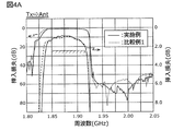
- FIG. 4A is a graph comparing the pass characteristics of the transmission-side filters according to Example and Comparative Example 1.
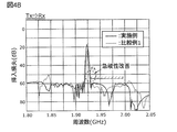
- FIG. 4B is a graph comparing the isolation characteristics between the transmission input terminal and the reception output terminal according to Example and Comparative Example 1.
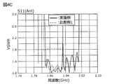
- FIG. 4C is a graph comparing the VSWRs on the antenna terminal side of the transmission-side filter according to Example and Comparative Example 1.
- FIG. 4D is a graph comparing VSWRs on the transmission input terminal side of the transmission-side filter according to the example and the comparative example 1.
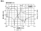
- FIG. FIG. 5A is a graph illustrating impedance characteristics of the first series resonator of the transmission filter according to the example.
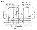
- FIG. 5B is a graph illustrating impedance characteristics of the second series resonator of the transmission filter according to the example.
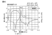
- FIG. 5C is a graph illustrating impedance characteristics of the third series resonator of the transmission filter according to the example.
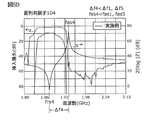
- FIG. 5D is a graph illustrating impedance characteristics of the fourth series resonator of the transmission filter according to the example.
- FIG. 5E is a graph illustrating impedance characteristics of the fifth series resonator of the transmission filter according to the example.
- FIG. 6A is a graph illustrating impedance characteristics of the first series resonator of the transmission filter according to Comparative Example 1.
- FIG. 6B is a graph illustrating impedance characteristics of the second series resonator of the transmission filter according to the first comparative example.
- 6C is a graph showing impedance characteristics of the third series resonator of the transmission filter according to Comparative Example 1.
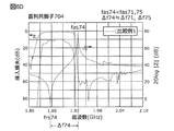
- FIG. 6D is a graph illustrating impedance characteristics of the fourth series resonator of the transmission filter according to the first comparative example.
- FIG. 6E is a graph illustrating impedance characteristics of the fifth series resonator of the transmission filter according to the first comparative example.
- FIG. 7A is a graph comparing the pass characteristics of the transmission-side filters according to the example and the comparative example 2.
- FIG. 7B is a graph comparing the isolation characteristics between the transmission input terminal and the reception output terminal according to Example and Comparative Example 2.
- FIG. 7C is a graph comparing VSWRs on the antenna terminal side of the transmission-side filter according to Example and Comparative Example 2.
- FIG. 7D is a graph comparing VSWRs on the transmission input terminal side of the transmission-side filter according to the example and the comparative example 2.
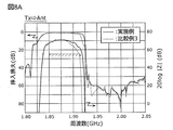
- FIG. 8A is a graph comparing the pass characteristics of the transmission-side filters according to Example and Comparative Example 3.
- FIG. 8B is a graph comparing the isolation characteristics between the transmission input terminal and the reception output terminal according to Example and Comparative Example 3.
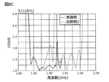
- FIG. 8C is a graph comparing the VSWRs on the antenna terminal side of the transmission-side filter according to Example and Comparative Example 3.
- FIG. 8D is a graph comparing the VSWRs on the transmission input terminal side of the transmission side filter according to the example and the comparative example 3.
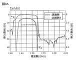
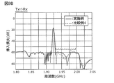
- FIG. 9A is a graph comparing the pass characteristics of the transmission-side filters according to Example and Comparative Example 4.
- FIG. 9B is a graph comparing the isolation characteristics between the transmission input terminal and the reception output terminal according to Example and Comparative Example 4.
- FIG. 10 is a circuit configuration diagram of a high-frequency front-end circuit and a communication device including the duplexer according to the embodiment.
- FIG. 1 is a circuit configuration diagram of a duplexer 1 according to an embodiment. As illustrated in FIG. 1, the duplexer 1 includes a transmission filter 10, a reception filter 20, an antenna terminal 31, and an inductance element 311.
- the transmission-side filter 10 receives a transmission wave generated by a transmission circuit (RFIC or the like) via a transmission input terminal 11, filters the transmission wave with a transmission pass band, and an antenna terminal that is a transmission-side output terminal This is a non-balanced input-unbalanced output type band-pass filter that outputs to 31.
- the transmission-side filter 10 is an essential part of the present invention, and is a ladder-type surface acoustic wave filter. The configuration of the transmission filter 10 will be described in detail in the configuration of the transmission filter described later.
- the reception-side filter 20 receives the reception wave input from the antenna terminal 31 that is also the reception-side input terminal, filters the reception wave in the reception passband, and outputs the filtered signal to the reception output terminal 21.
- the reception filter 20 includes, for example, a longitudinally coupled surface acoustic wave filter unit. More specifically, the reception-side filter 20 includes a longitudinally coupled filter unit 21A, series resonators 201 and 202, and parallel resonators 251 and 252.
- the inductance element 311 is an impedance matching element provided between the antenna terminal 31 and the connection point between the transmission side filter 10 and the reception side filter 20. Thereby, impedance matching between the antenna element and the transmission side filter 10 and the reception side filter 20 can be achieved.
- FIG. 2 is a plan view and a cross-sectional view schematically showing a resonator of the surface acoustic wave filter according to the embodiment.
- a schematic plan view and a schematic cross-sectional view showing the structure of the series resonator 101 among the plurality of resonators constituting the transmission filter 10 and the reception filter 20 are illustrated.
- the series resonator 101 shown in FIG. 2 is for explaining a typical structure of the plurality of resonators, and the number and length of electrode fingers constituting the electrode are the same. It is not limited.
- Each resonator of the transmitting filter 10 and the receiving filter 20 is composed of a substrate 50 having a piezoelectric layer 53 and IDT (InterDigital Transducer) electrodes 11a and 11b having a comb shape.
- IDT InterDigital Transducer
- the IDT electrode 11a includes a plurality of electrode fingers 110a that are parallel to each other and a bus bar electrode 111a that connects the plurality of electrode fingers 110a.
- the IDT electrode 11b includes a plurality of electrode fingers 110b that are parallel to each other and a bus bar electrode 111b that connects the plurality of electrode fingers 110b.
- the plurality of electrode fingers 110a and 110b are formed along a direction orthogonal to the X-axis direction.
- the IDT electrode 54 constituted by the plurality of electrode fingers 110a and 110b and the bus bar electrodes 111a and 111b has a laminated structure of the adhesion layer 541 and the main electrode layer 542 as shown in the sectional view of FIG. ing.
- the adhesion layer 541 is a layer for improving the adhesion between the substrate 50 and the main electrode layer 542, and, for example, Ti is used as a material.
- the film thickness of the adhesion layer 541 is, for example, 12 nm.
- the main electrode layer 542 is made of, for example, Al containing 1% Cu.
- the film thickness of the main electrode layer 542 is, for example, 162 nm.
- the protective layer 55 is formed so as to cover the IDT electrodes 11a and 11b.
- the protective layer 55 is a layer for the purpose of protecting the main electrode layer 542 from the external environment, adjusting frequency temperature characteristics, and improving moisture resistance, for example, a film mainly composed of silicon dioxide. .
- adherence layer 541, the main electrode layer 542, and the protective layer 55 is not limited to the material mentioned above.
- the IDT electrode 54 does not have to have the above laminated structure.
- the IDT electrode 54 may be made of, for example, a metal or alloy such as Ti, Al, Cu, Pt, Au, Ag, or Pd, or may be made of a plurality of laminates made of the above metal or alloy. May be. Further, the protective layer 55 may not be formed.
- the substrate 50 includes a high sonic support substrate 51, a low sonic film 52, and a piezoelectric layer 53.
- the high sonic support substrate 51, the low sonic film 52, and the piezoelectric layer 53 are provided. It has a laminated structure in this order.
- the piezoelectric layer 53 is made of a 50 ° Y-cut X-propagating LiTaO 3 piezoelectric single crystal or a piezoelectric ceramic (a lithium tantalate single crystal cut along a plane whose normal is an axis rotated about 50 ° from the Y axis with the X axis as the central axis, or Ceramic, which is a single crystal or ceramic in which surface acoustic waves propagate in the X-axis direction).
- the piezoelectric layer 53 has a thickness of 600 nm, for example.
- the high sound velocity support substrate 51 is a substrate that supports the low sound velocity film 52, the piezoelectric film body layer 53, and the IDT electrode 54.
- the high acoustic velocity support substrate 51 is a substrate in which the acoustic velocity of the bulk wave in the high acoustic velocity support substrate 51 is higher than that of the surface wave or boundary wave propagating in the piezoelectric layer 53, and the surface acoustic wave is
- the piezoelectric layer 53 and the low sound velocity film 52 are confined in a portion where they are laminated, and function so as not to leak downward from the high sound velocity support substrate 51.
- the high sound speed support substrate 51 is, for example, a silicon substrate, and has a thickness of, for example, 200 ⁇ m.
- the low acoustic velocity film 52 is a membrane in which the acoustic velocity of the bulk wave in the low acoustic velocity film 52 is lower than the acoustic velocity of the elastic wave propagating through the piezoelectric layer 53. Arranged between. Due to this structure and the property that energy is concentrated in a medium where acoustic waves are essentially low in sound velocity, leakage of surface acoustic wave energy to the outside of the IDT electrode is suppressed.
- the low acoustic velocity film 52 is, for example, a film mainly composed of silicon dioxide and has a thickness of, for example, 670 nm.
- the Q value at the resonance frequency and the anti-resonance frequency can be significantly increased as compared with the conventional structure in which the piezoelectric substrate is used as a single layer. That is, since a surface acoustic wave resonator having a high Q value can be configured, a filter with a small insertion loss can be configured using the surface acoustic wave resonator.
- the frequency difference ⁇ f between the resonance frequency and the antiresonance frequency of the series resonators 102 to 104 excluding the series resonators 101 and 105 connected to both terminals of the transmission side filter 10 described later is connected to both terminals.
- the Q values of the series resonators 102 to 104 are smaller than the Q values of the series resonators 101 and 105.
- the Q values of the series resonators 102 to 104 can be maintained at a high value. Therefore, it is possible to form a surface acoustic wave filter having low loss in the pass band and high steepness outside the pass band even for frequency standards having a wide pass band and a narrow adjacent band interval.
- the high sound velocity support substrate 51 has a structure in which a support substrate and a high sound velocity film in which the sound velocity of the propagating bulk wave is higher than the acoustic wave of the surface wave and boundary wave propagating through the piezoelectric layer 53 are laminated.
- the support substrate is a piezoelectric material such as sapphire, lithium tantalate, lithium niobate, crystal, alumina, magnesia, silicon nitride, aluminum nitride, silicon carbide, zirconia, cordierite, mullite, steatite, forsterite, etc.
- the high sound velocity film includes various materials such as aluminum nitride, aluminum oxide, silicon carbide, silicon nitride, silicon oxynitride, DLC film or diamond, a medium mainly composed of the above materials, and a medium mainly composed of a mixture of the above materials. High sound velocity material can be used.
- the wavelength of the surface acoustic wave resonator is defined by the repetition pitch ⁇ of the plurality of electrode fingers 110a and 110b constituting the IDT electrodes 11a and 11b shown in the middle of FIG.
- the crossing width L of the IDT electrode is an overlapping electrode finger length when viewed from the X-axis direction of the electrode finger 110a of the IDT electrode 11a and the electrode finger 110b of the IDT electrode 11b.
- the duty ratio is the line width occupation ratio of the plurality of electrode fingers 110a and 110b, and is the ratio of the line width to the sum of the line width and the space width of the plurality of electrode fingers 110a and 110b. More specifically, the duty ratio is when the line width of the electrode fingers 110a and 110b constituting the IDT electrodes 11a and 11b is W and the space width between the adjacent electrode fingers 110a and 110b is S. , W / (W + S).
- the transmission filter 10 includes series resonators 101 to 105, parallel resonators 151 to 154, matching inductance elements 141 and 161, and a transmission input terminal 11.
- the series resonators 101 to 105 are connected in series between the transmission input terminal 11 and the antenna terminal 31.
- the parallel resonators 151 to 154 are connected in parallel to each other between the connection points of the transmission input terminal 11, the antenna terminal 31, and the series resonators 101 to 105 and the reference terminal (ground). Due to the above-described connection configuration of the series resonators 101 to 105 and the parallel resonators 151 to 154, the transmission-side filter 10 constitutes a ladder-type bandpass filter.
- the inductance element 141 is connected between the transmission input terminal 11 and the series resonator 101, and the inductance element 161 is connected between the connection point of the parallel resonators 152, 153, and 154 and the reference terminal. .
- Table 1 shows details of design parameters (pitch ⁇ , cross width L, IDT logarithm N, duty ratio D) of the series resonators 101 to 105 and the parallel resonators 151 to 154 of the transmission filter 10 according to the present embodiment. .
- the pitch ⁇ of each resonator shown in Table 1 is defined as the wavelength of each resonator. Further, the capacitance of each resonator is determined by the design parameters shown in Table 1, the dielectric constant of the piezoelectric substrate 50, and the like.
- a T-type ladder filter is configured by nine resonators, but a ⁇ -type ladder filter may be configured. Further, the number of resonators is not limited to nine, and the number of series resonators may be four or more.
- the frequency difference (fas1-frs1) between the antiresonance frequency fas1 and the resonance frequency frs1 of the series resonator 101 (first resonator) connected closest to the transmission input terminal 11 is defined as ⁇ f1.
- the frequency difference (fas ⁇ frs5) between the antiresonance frequency fas5 and the resonance frequency frs5 of the series resonator 105 connected closest to the antenna terminal 31 is defined as ⁇ f5.
- the frequency differences ⁇ f2, ⁇ f3, and ⁇ f4, which are the differences, are smaller than the frequency differences ⁇ f1 and ⁇ f5 between the antiresonance frequencies of the series resonators 101 and 105 and the resonance frequency, and are the antiresonance frequencies of the series resonators 102, 103, and 104.
- fas2, fas3, and fas4 are lower than the antiresonance frequencies fas1 and fas5 of the series resonators 101 and 105.
- the wavelengths of the series resonators 102, 103, and 104 may be made larger than the wavelengths of the series resonators 101 and 105. That is, if the repetition pitches of the plurality of electrode fingers constituting the IDT electrodes of the series resonators 101 to 105 are ⁇ 1 to ⁇ 5, respectively, the relationship in Equation 1 may be realized by the following Equation 3. .
- the duplexer 1 including the filter 10 and the transmission-side filter 10.
- IDT electrode thinning-out processing is used as a design technique for reducing the frequency differences ⁇ f2, ⁇ f3, and ⁇ f4 of the series resonators 102 to 104 with respect to the series resonators 101 and 105.
- a method of reducing the frequency difference ⁇ f in addition to the IDT electrode thinning weighting process, a process of connecting a capacitor in parallel to the resonator, a process of changing the electrode film thickness and duty ratio of the resonator, and the like are used. .
- the ⁇ f adjusting means according to the present invention the above-described effects can be obtained by using any of the above-described processes.
- the transmission-side filter 10 and the duplexer 1 having the characteristics of Equations 1 to 3 have high steepness in the pass characteristics outside the passband while maintaining a desired impedance in the passband.
- the reception-side filter 20 includes a longitudinally coupled filter unit 21 ⁇ / b> A, a ladder type filter unit having series resonators 201 and 202 and a parallel resonator 251, and a trap unit having a parallel resonator 252. It is configured.
- FIG. 3 is a schematic plan view showing an electrode configuration of the vertically coupled filter portion 21A according to the embodiment.
- the longitudinally coupled filter unit 21A includes IDTs 211 to 219, reflectors 220 and 221, an input terminal 22 and an output terminal 23.
- the IDTs 211 to 219 are each composed of a pair of IDT electrodes facing each other.
- IDTs 214 and 216 are arranged to sandwich IDT 215 in the X-axis direction
- IDTs 213 and 217 are arranged to sandwich IDTs 214 to 216 in the X-axis direction.
- the IDTs 212 and 218 are arranged so as to sandwich the IDTs 213 to 217 in the X-axis direction
- the IDTs 211 and 219 are arranged so as to sandwich the IDTs 212 to 218 in the X-axis direction.
- Reflectors 220 and 221 are arranged so as to sandwich IDTs 211 to 219 in the X-axis direction.
- the IDTs 211, 213, 215, 217 and 219 are connected in parallel between the input terminal 22 and the reference terminal (ground), and the IDTs 212, 214, 216 and 218 are connected in parallel between the output terminal 23 and the reference terminal. It is connected.
- IDTs 211 to 219, series resonators 201 and 202, and parallel resonators 251 and 252 are the same as those shown in FIG.
- the parallel resonators 151 to 154 shown in FIG. 1 each have a resonance frequency frp and an anti-resonance frequency fap (> frp) in resonance characteristics.
- Each of the series resonators 101 to 105 has a resonance frequency frs and an anti-resonance frequency fas (> frs> frp) in resonance characteristics.
- the resonance frequencies frs of the series resonators 101 to 105 are designed to be substantially the same, the design parameters of the resonators are different as shown in Table 1, so they do not necessarily match.
- the antiresonance frequency fas of the series resonators 101 to 105 the resonance frequency frp of the parallel resonators 151 to 154, and the antiresonance frequency fap of the parallel resonators 151 to 154, which do not necessarily match.
- the anti-resonance frequency fap of the parallel resonators 151 to 154 and the resonance frequency frs of the series resonators 101 to 105 are brought close to each other.
- the vicinity of the resonance frequency frp in which the impedances of the parallel resonators 151 to 154 approach zero becomes a low-frequency side stop band.
- the impedance of the parallel resonators 151 to 154 increases near the antiresonance frequency fap, and the impedance of the series resonators 101 to 105 approaches 0 near the resonance frequency frs.
- the signal path from the transmission input terminal 11 to the antenna terminal 31 becomes a signal passband.
- the impedances of the series resonators 101 to 105 become higher and become a high-frequency side blocking region. That is, the steepness of the attenuation characteristic in the high-frequency-side blocking region is greatly affected by where the anti-resonance frequency fas of the series resonators 101 to 105 is set outside the signal passing region.
- the transmission-side filter 10 having the structure and the operation principle shown in FIGS. 1 and 2, when a high frequency signal is input from the transmission input terminal 11, a potential difference is generated between the transmission input terminal 11 and the reference terminal. As a result, a surface acoustic wave propagating in the X direction is generated when the piezoelectric substrate 50 is distorted.
- the pitch ⁇ of the IDT electrodes 11a and 11b substantially coincide with the wavelength of the pass band, only the high-frequency signal having the frequency component to be passed passes through the transmission-side filter 10.
- FIG. 4A is a graph illustrating pass characteristics of the transmission-side filter according to the example and the comparative example 1.
- FIG. 4B is a graph showing isolation characteristics between the transmission input terminal 11 and the reception output terminal 21 according to the example and the comparative example 1.
- FIG. 4C is a graph showing VSWR on the antenna terminal side of the transmission-side filter according to the example and the comparative example 1.
- FIG. 4D is a graph showing VSWR on the transmission terminal side of the transmission-side filter according to the example and the comparative example 1.
- the transmission-side filter according to Comparative Example 1 shown in FIGS. 4A to 4D has the ladder-type configuration shown in FIG. 1, that is, has five series resonators and four parallel resonators. Although it is the same as the transmission side filter 10 according to the embodiment, the design parameters of each resonator are different. Specifically, the design parameters of the resonator are set so that the transmission-side filter according to Comparative Example 1 satisfies the following relational expression.
- the series resonators 701, 702, 703, 704, and 705 are assumed to be close to the transmission input terminal.
- the resonance frequencies of the series resonators 701 to 705 are frs71 to frs75, respectively, and the antiresonance frequencies are fas71 to fas75, respectively.
- the frequency difference between the resonance frequency and the anti-resonance frequency of the series resonators 701 to 705 is set to ⁇ f71 to ⁇ f75, respectively.
- the antiresonance frequency fas74 of the series resonator 704 that is not closest to either the transmission input terminal or the antenna terminal is equal to the antiresonance frequency fas71 of the other four series resonators. Lower than fas72, fas73 and fas75.
- the antiresonance frequencies fas72 and fas73 of the series resonators 702 and 703 are the same as or higher than the antiresonance frequencies fas71 and fas75 of the series resonators 701 and 705. Further, the frequency differences ⁇ f71 to ⁇ f75 of the five series resonators are substantially equal.
- 5A to 5E are graphs showing impedance characteristics of the series resonators 101 to 105 of the transmission-side filter according to the embodiment, respectively.
- 6A to 6E are graphs showing impedance characteristics of the series resonators 701 to 705 of the transmission-side filter according to Comparative Example 1, respectively.
- the frequency characteristic graphs shown in FIGS. 5A to 5E and FIGS. 6A to 6E display the transmission characteristics of the transmission filter (left vertical axis: S21) and the impedance characteristics (right side of each series resonator). Vertical axis: 20log
- the transmission-side filter 10 compared with the antiresonance frequencies fas1 and fas5 of the series resonators 101 and 105 shown in FIGS. 5A and 5E, they are shown in FIGS. 5B to 5D.
- the antiresonance frequencies fas2 to fas4 of the series resonators 102 to 104 are close to the high band end of the transmission band.
- the frequency differences ⁇ f2 to ⁇ f4 of the series resonators 102 to 104 shown in FIGS. 5B to 5D are smaller than the frequency differences ⁇ f1 and ⁇ f5 of the series resonators 101 and 105 shown in FIGS. 5A and 5E. That is, in the transmission side filter according to the embodiment, the above formulas 1 and 2 are established.
- the steepness of the attenuation characteristic in the transmission / reception band area F A can be obtained. It has been improved. Specifically, the frequency interval from the high band of the transmission band (frequency at which the insertion loss is 2.5 dB or less) to the transmission / reception band area (frequency at which isolation is 55 dB) is higher than that of the first comparative example. Is about 1.6MHz narrower.
- the capacitances of the series resonator 101 connected to the transmission input terminal 11 and the series resonator 105 connected to the antenna terminal are determined.
- the resonance frequencies frs1 and frs5 of the series resonators 101 and 105 are set to be near the center frequency of the transmission band. If the anti-resonance frequencies fas2 to fas4 of the series resonators 102 to 104 are made closer to the high band end of the transmission band compared to fas1 and fas5, and ⁇ f2 to ⁇ f4 are maintained equal to ⁇ f1 and ⁇ f5, the resonance will occur.
- the frequencies frs2 to frs4 are shifted from the center frequency of the transmission band to the low frequency side.
- the impedance characteristic in the transmission band deteriorates due to the low frequency shift of the resonance frequency.
- ⁇ f2 to ⁇ f4 are reduced while the antiresonance frequencies fas2 to fas4 are shifted to the low frequency side.
- the resonance frequencies frs2 to frs4 are not shifted to the lower frequency range, so that the impedance characteristics within the transmission band can be maintained. That is, the transmission-side filter 10 according to the present embodiment can achieve a steepness with high insertion loss in the frequency domain between adjacent reception bands while maintaining a desired impedance in the transmission band.
- FIG. 7A is a graph illustrating pass characteristics of the transmission-side filter according to the example and the comparative example 2.
- FIG. 7B is a graph showing isolation characteristics between the transmission input terminal 11 and the reception output terminal 21 according to the example and the comparative example 2.
- FIG. 7C is a graph showing VSWR on the antenna terminal side of the transmission-side filter according to the example and the comparative example 2.
- FIG. 7D is a graph showing the VSWR on the transmission terminal side of the transmission side filter according to the example and the comparative example 2.
- the transmission-side filter according to the comparative example 2 shown in FIGS. 7A to 7D has the ladder-type configuration shown in FIG. 1, that is, has five series resonators and four parallel resonators. Although it is the same as the transmission side filter 10 according to the embodiment, the design parameters of each resonator are different. Specifically, the design parameters of the resonator are set so that the transmission side filter according to Comparative Example 2 satisfies the following relational expression.
- the series resonators 801, 802, 803, 804, and 805 are from those close to the transmission input terminal.
- the resonance frequencies of the series resonators 801 to 805 are frs81 to frs85, respectively, and the antiresonance frequencies are fas81 to fas85, respectively.
- the frequency difference between the resonance frequency and the antiresonance frequency of the series resonators 801 to 805 is set to ⁇ f81 to ⁇ f85, respectively.
- the antiresonance frequencies fas82 to fas84 of the series resonators 802 to 804 that are not closest to either the transmission input terminal or the antenna terminal are antiresonant with the series resonators 801 and 805. It is lower than the frequencies fas81 and fas85. Further, the frequency differences ⁇ f81 to ⁇ f85 of the five series resonators are substantially equal.
- the antiresonance frequencies fas82 to fas84 of the series resonators 802 to 804 are changed to the antiresonance frequencies fas81 of the series resonators 801 and 805. And closer to the high band end of the transmission band than fas85.
- the isolation near the lower end (1930 MHz) of the reception band is not improved.
- FIG. 8A is a graph illustrating pass characteristics of the transmission-side filter according to the example and the comparative example 3.
- FIG. 8B is a graph showing isolation characteristics between the transmission input terminal 11 and the reception output terminal 21 according to the example and the comparative example 3.
- FIG. 8C is a graph showing VSWR on the antenna terminal side of the transmission-side filter according to the example and the comparative example 3.
- FIG. 8D is a graph showing VSWR on the transmission terminal side of the transmission-side filter according to Example and Comparative Example 3.
- the transmission-side filter according to Comparative Example 3 shown in FIGS. 8A to 8D has the ladder-type configuration shown in FIG. 1, that is, has five series resonators and four parallel resonators. Although it is the same as the transmission side filter 10 according to the embodiment, the design parameters of each resonator are different. Specifically, in the transmission-side filter according to Comparative Example 3, the resonator design parameters are set so as to satisfy the following relational expression.
- the series resonators 901, 902, 903, 904, and 905 are from those close to the transmission input terminal.
- the resonance frequencies of the series resonators 901 to 905 are frs91 to frs95, respectively, and the antiresonance frequencies are fas91 to fas95, respectively.
- the frequency difference between the resonance frequency and the anti-resonance frequency of the series resonators 901 to 905 is assumed to be ⁇ f91 to ⁇ f95, respectively.
- the antiresonance frequencies fas91 to fas93 of the series resonators 901 to 903 including the series resonator 901 closest to the transmission input terminal are antiresonant with the series resonators 904 and 905. It is lower than the frequencies fas94 and fas95. Further, the frequency differences ⁇ f91 to ⁇ f93 of the series resonators 901 to 903 are smaller than the frequency differences ⁇ f94 and ⁇ f95 of the series resonators 904 and 905. That is, in the transmission-side filter according to Comparative Example 3, Expression 8 and Expression 9 are established.
- the antiresonance frequencies fas91 to fas93 of the series resonators 901 to 903 become the antiresonance frequencies fas94 of the series resonators 904 and 905. And closer to the high band end of the transmission band than fas95.
- FIG. 9A is a graph illustrating pass characteristics of the transmission-side filter according to the example and the comparative example 4.
- FIG. 9B is a graph showing isolation characteristics between the transmission input terminal 11 and the reception output terminal 21 according to the example and the comparative example 4.
- the transmission-side filter according to Comparative Example 4 shown in FIGS. 9A and 9B has the ladder-type configuration shown in FIG. 1, that is, has five series resonators and four parallel resonators. Although it is the same as the transmission side filter 10 according to the embodiment, the design parameters of each resonator are different. Specifically, in the transmission-side filter according to Comparative Example 4, the design parameters of the resonator are set so as to satisfy the following relational expression.
- symbol of the series resonator, antiresonance frequency, resonance frequency, and frequency difference of the transmission side filter which concerns on the comparative example 4 is the same as each code
- the transmission-side filter according to Comparative Example 4 is obtained by increasing the frequency of the series resonator 901 of Comparative Example 3 in order to improve the impedance at the transmission input terminal as compared with the transmission-side filter according to Comparative Example 3. That is, the antiresonance frequency fas91 of the series resonator 901 is set higher than that of the comparative example 3.
- each series resonator according to Comparative Example 4 can particularly improve the impedance at the transmission input terminal.
- the steepness of the insertion loss and the isolation in the region between the transmission and reception bands are deteriorated.
- the configuration of the transmission-side filter according to Comparative Example 4 cannot achieve both desired impedance in the transmission band and desired steepness in a region higher than the transmission band.
- Table 2 shows a summary of the relationship between the anti-resonance frequency and the frequency difference of the transmission-side filters according to the example and the comparative examples 1 to 4.
- the anti-resonance frequency fas set lower than the anti-resonance frequency fas of the reference series resonator closest to the transmission input terminal and the antenna terminal is marked with “>”. Further, “>” is attached to the frequency difference ⁇ f set smaller than the reference frequency difference ⁇ f of the reference series resonator closest to the transmission input terminal and the antenna terminal.
- Comparative Example 4 the frequency of the series resonator 901 is increased in order to improve the impedance at the transmission input terminal in Comparative Example 3. Thereby, although the impedance at the transmission input terminal can be improved, the steepness and isolation of the insertion loss in the region between the transmission and reception bands is deteriorated.
- the anti-resonance frequencies fas2 to fas4 of the series resonators 102 to 104 other than the series resonators 101 and 105 that are closest to the transmission input terminal 11 and the antenna terminal 31 are used. Is shifted to a lower frequency side than fas1 and fas5, and ⁇ f2 to ⁇ f4 are made smaller than ⁇ f1 and ⁇ f5. As a result, the resonance frequencies frs2 to frs4 do not shift to a low frequency range, so that the impedance characteristics within the transmission band can maintain desired characteristics.
- the transmission-side filter 10 can achieve a steepness with high insertion loss in the frequency domain between adjacent reception bands while maintaining a desired impedance in the transmission band.
- the transmission-side filter 10 has the IDT electrodes formed on the piezoelectric substrate 50, and is connected in series between the transmission input terminal 11 and the antenna terminal 31.
- Two series resonators 101 to 105 and parallel resonators 151 to 154 having IDT electrodes formed on the piezoelectric substrate 50 are provided.
- the frequency differences ⁇ f 2 to ⁇ f 4 of all the series resonators 102 to 104 other than the series resonator 101 connected closest to the transmission input terminal 11 and the series resonator 105 connected closest to the antenna terminal 31 are in series.
- the frequency differences ⁇ f1 and ⁇ f5 of the resonators 101 and 105 are smaller, and the antiresonance frequencies fas2 to fas4 of the series resonators 102 to 104 are lower than the antiresonance frequencies fas1 and fas5 of the series resonators 101 and 105.
- the repetition pitches ⁇ 2 to ⁇ 4 of the plurality of electrode fingers constituting the IDT electrodes of the series resonators 102 to 104 are larger than the repetition pitches ⁇ 1 and ⁇ 5 of the plurality of electrode fingers constituting the IDT electrodes of the series resonators 101 and 105. It can be large.
- the transmission-side filter (elastic wave filter) according to the present embodiment is not limited to the configuration including five series resonators, and may include four or more series resonators. ⁇ f of all series resonators other than the first series resonator connected closest to the input terminal and the second series resonator connected closest to the output terminal of the first and second series resonators
- the antiresonance frequency fas of all the series resonators other than the first series resonator and the second series resonator is smaller than ⁇ f of the series resonator, and the antiresonance frequencies of the first series resonator and the second series resonator are What is necessary is just to be lower than the frequency fas. With this configuration, the same effect as that of the transmission filter 10 according to the present embodiment is achieved.
- a multiplexer that demultiplexes an input signal by having a plurality of bandpass filters that selectively pass a predetermined frequency band, and each of the frequency bands that the plurality of bandpass filters pass is different.
- One end of each of the bandpass filters is connected to a common terminal, and at least one of the bandpass filters other than the bandpass filter having the highest frequency band among the plurality of bandpass filters is the transmission-side filter according to the embodiment.
- a band-pass filter having ten characteristics may be used.
- the duplexer that is the bandpass filter having the characteristics of the transmission-side filter 10 according to the embodiment may be used as the filter having the lower frequency band to pass among the transmission-side filter and the reception-side filter.
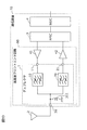
- FIG. 10 is a circuit configuration diagram of the high-frequency front-end circuit 60 and the communication device 70 including the duplexer 1 according to the embodiment.
- a high frequency front end circuit 60, an antenna element 2, an RF signal processing circuit (RFIC) 3, and a baseband signal processing circuit (BBIC) 4 are shown.
- the high-frequency front end circuit 60, the RF signal processing circuit 3, and the baseband signal processing circuit 4 constitute a communication device 70.
- the high frequency front end circuit 60 includes a duplexer 1, a power amplifier circuit 41, and a low noise amplifier circuit 42.
- the power amplifier circuit 41 is a transmission amplifier circuit that amplifies the high-frequency transmission signal output from the RF signal processing circuit 3 and outputs it to the antenna element 2 via the transmission input terminal 11, the transmission-side filter 10, and the antenna terminal 31. is there.
- the low noise amplifier circuit 42 is a reception amplification circuit that amplifies a high-frequency signal that has passed through the antenna element 2, the antenna terminal 31, and the transmission-side filter 20 and outputs the amplified signal to the RF signal processing circuit 3.
- the RF signal processing circuit 3 performs signal processing on the high-frequency reception signal input from the antenna element 2 via the reception signal path by down-conversion or the like, and the received signal generated by the signal processing is a baseband signal processing circuit 4. Output to. Further, the RF signal processing circuit 3 performs signal processing on the transmission signal input from the baseband signal processing circuit 4 by up-conversion or the like, and outputs the high-frequency transmission signal generated by the signal processing to the power amplifier circuit 31.
- the RF signal processing circuit 3 is, for example, an RFIC (Radio Frequency Integrated Circuit).
- the signal processed by the baseband signal processing circuit 4 is used, for example, for displaying an image as an image signal or for a call as an audio signal.
- the high-frequency front end circuit 60 may include other circuit elements between the duplexer 1, the power amplifier circuit 41, and the low noise amplifier circuit 42.
- an elastic wave filter having a high steepness of a pass characteristic outside the pass band while maintaining a desired impedance in the pass band even for a frequency standard having a wide pass band and a narrow adjacent band interval. It is possible to provide a high-frequency front-end circuit and a communication device that are provided.
- the duplexer has been described as an example. Can be applied. That is, the high-frequency front end circuit and the communication device only need to include two or more filters.
- the high-frequency front end circuit and the communication device are not limited to the configuration including both the transmission filter and the reception filter, and may be configured to include only the transmission filter or only the reception filter.
- the communication device 70 may not include the baseband signal processing circuit 4 in accordance with the high frequency signal processing method.
- the piezoelectric layer 53 of the substrate 50 uses a 50 ° Y-cut X-propagation LiTaO 3 single crystal, but the cut angle of the single crystal material is not limited to this. That is, the cut angle of the piezoelectric layer of the surface acoustic wave filter satisfying the above formulas 1 and 2 using LiTaO 3 single crystal as the piezoelectric layer is not limited to 50 ° Y. Even a surface acoustic wave filter using a LiTaO 3 piezoelectric layer having a cut angle other than the above can achieve the same effect.
- the piezoelectric layer may be made of another piezoelectric single crystal such as LiNbO 3 .
- a structure in which a piezoelectric layer is laminated on a supporting substrate may be used in addition to a piezoelectric layer as a whole.
- the acoustic wave filter which concerns on this invention is not limited to a surface acoustic wave filter, and is comprised with a series resonator and a parallel resonator.
- An elastic wave filter using a boundary acoustic wave or BAW (Bulk Acoustic Wave) may be used. Also by this, the same effect as the effect which the surface acoustic wave filter concerning the above-mentioned embodiment has is produced.
- the transmission filter 10 has been described as the main part of the present invention.
- the contents of the present invention may be used in the reception filter 20.
- the reception-side filter 20 includes four or more series resonators connected in series between the input terminal and the output terminal, and a connection node between the input terminal, the output terminal, and the four or more series resonators.
- a parallel resonator connected between any one of the first and second reference resonators, and among the four or more series resonators, the first series resonator connected closest to the input terminal and the output connected to the output terminal are connected closest to each other.
- the frequency difference that is the difference between the antiresonance frequency and the resonance frequency of all series resonators other than the second series resonator is the frequency between the antiresonance frequency and the resonance frequency of the first series resonator and the second series resonator. Less than the difference, and the anti-resonance frequencies of all series resonators other than the first series resonator and the second series resonator are lower than the anti-resonance frequencies of the first series resonator and the second series resonator, It has the characteristics.
- the present invention can be widely used in communication devices such as mobile phones as an elastic wave filter, multiplexer, and duplexer that can be applied to a frequency standard having a wide bandwidth and a narrow band interval.
- RFIC RF Signal Processing Circuit
- BBIC Baseband signal processing circuit
- SYMBOLS 10 Transmission side filter 11 Transmission input terminal 11a, 11b, 54 IDT electrode 20 Reception side filter 21 Reception output terminal 21A Vertical coupling type filter part 22 Input terminal 23 Output terminal 31 Antenna terminal 41 Power amplifier circuit 42 Low noise amplifier circuit 50 Substrate 51 High Sonic support substrate 52 Low sound velocity film 53 Piezoelectric layer 55 Protective layer 60 High frequency front end circuit 70 Communication device 101, 102, 103, 104, 105, 201, 202, 701, 702, 703, 704, 705, 801, 802, 803, 804, 805, 901, 902, 903, 904, 905 Series resonator 110a, 110b Electrode finger 111a, 111b Bus bar electrode 141, 161, 311 Inductance element 151, 152, 153, 154, 251 252 parallel resonators 211,212,213,214,215,216,217
Landscapes
- Physics & Mathematics (AREA)
- Acoustics & Sound (AREA)
- Surface Acoustic Wave Elements And Circuit Networks Thereof (AREA)
Abstract
Description
[1.デュプレクサの基本構成]
本実施例では、LTE(Time Division Long Term Evolution)規格のBand25(送信通過帯域:1850-1915MHz、受信通過帯域:1930-1995MHz)に適用されるアンテナデュプレクサについて例示する。
送信側フィルタ10および受信側フィルタ20の構成要素である共振子の構造について説明する。
図1に示すように、送信側フィルタ10は、直列共振子101~105と、並列共振子151~154と、整合用のインダクタンス素子141および161と、送信入力端子11とを備える。

Δf1、Δf5>Δf2、Δf3、Δf4 (式2)
図1に示すように、受信側フィルタ20は、縦結合型フィルタ部21Aと、直列共振子201および202ならびに並列共振子251を有するラダー型フィルタ部と、並列共振子252を有するトラップ部とで構成されている。
ここで、本実施の形態に係るラダー型の弾性表面波フィルタの動作原理について説明する。
図4Aは、実施例および比較例1に係る送信側フィルタの通過特性を示すグラフである。また、図4Bは、実施例および比較例1に係る送信入力端子11-受信出力端子21間のアイソレーション特性を示すグラフである。また、図4Cは、実施例および比較例1に係る送信側フィルタのアンテナ端子側のVSWRを示すグラフである。また、図4Dは実施例および比較例1に係る送信側フィルタの送信端子側のVSWRを示すグラフである。
Δf71≒Δf72≒Δf73≒Δf74≒Δf75 (式5)
図7Aは、実施例および比較例2に係る送信側フィルタの通過特性を示すグラフである。また、図7Bは、実施例および比較例2に係る送信入力端子11-受信出力端子21間のアイソレーション特性を示すグラフである。また、図7Cは、実施例および比較例2に係る送信側フィルタのアンテナ端子側のVSWRを示すグラフである。また、図7Dは実施例および比較例2に係る送信側フィルタの送信端子側のVSWRを示すグラフである。
Δf81≒Δf82≒Δf83≒Δf84≒Δf85 (式7)
図8Aは、実施例および比較例3に係る送信側フィルタの通過特性を示すグラフである。また、図8Bは、実施例および比較例3に係る送信入力端子11-受信出力端子21間のアイソレーション特性を示すグラフである。また、図8Cは、実施例および比較例3に係る送信側フィルタのアンテナ端子側のVSWRを示すグラフである。また、図8Dは実施例および比較例3に係る送信側フィルタの送信端子側のVSWRを示すグラフである。
Δf94、Δf95>Δf91、Δf92、Δf93 (式9)
図9Aは、実施例および比較例4に係る送信側フィルタの通過特性を示すグラフである。また、図9Bは、実施例および比較例4に係る送信入力端子11-受信出力端子21間のアイソレーション特性を示すグラフである。
Δf94、Δf95>Δf91、Δf92、Δf93 (式11)
表2に、実施例および比較例1~4に係る送信側フィルタの反共振周波数および周波数差の関係をまとめた結果を示す。

ここで、上記実施例に係るデュプレクサ1を備える高周波フロントエンド回路60および通信装置70について説明する。
以上、本発明の実施の形態に係る弾性表面波フィルタ、マルチプレクサおよびデュプレクサついて、実施例を挙げて説明したが、本発明は、上記実施例には限定されない。例えば、上記各実施例に次のような変形を施した態様も、本発明に含まれ得る。
2 アンテナ素子
3 RF信号処理回路(RFIC)
4 ベースバンド信号処理回路(BBIC)
10 送信側フィルタ
11 送信入力端子
11a、11b、54 IDT電極
20 受信側フィルタ
21 受信出力端子
21A 縦結合型フィルタ部
22 入力端子
23 出力端子
31 アンテナ端子
41 パワーアンプ回路
42 ローノイズアンプ回路
50 基板
51 高音速支持基板
52 低音速膜
53 圧電体層
55 保護層
60 高周波フロントエンド回路
70 通信装置
101、102、103、104、105、201、202、701、702、703、704、705、801、802、803、804、805、901、902、903、904、905 直列共振子
110a、110b 電極指
111a、111b バスバー電極
141、161、311 インダクタンス素子
151、152、153、154、251、252 並列共振子
211、212、213、214、215、216、217、218、219 IDT
220、221 反射器
541 密着層
542 主電極層
Claims (8)
- 入力端子と出力端子との間に互いに直列に接続された4以上の直列共振子と、
前記入力端子、前記出力端子および前記4以上の直列共振子の接続ノードのいずれかと基準端子との間に接続された並列共振子とを備え、
前記4以上の直列共振子のうち、前記入力端子に最も近く接続された第1直列共振子および前記出力端子に最も近く接続された第2直列共振子以外の全ての直列共振子の反共振周波数と共振周波数との差である周波数差は、前記第1直列共振子および前記第2直列共振子の反共振周波数と共振周波数との周波数差よりも小さく、かつ、前記第1直列共振子および前記第2直列共振子以外の全ての直列共振子の反共振周波数は、前記第1直列共振子および前記第2直列共振子の反共振周波数よりも低い
弾性波フィルタ。 - 前記4以上の直列共振子及び前記並列共振子は、圧電体層を備える基板上に形成されたIDT電極を有しており、
前記第1直列共振子および前記第2直列共振子以外の全ての直列共振子の前記IDT電極を構成する複数の電極指の繰り返しピッチは、前記第1直列共振子および前記第2直列共振子の前記IDT電極を構成する複数の電極指の繰り返しピッチよりも大きい
請求項1に記載の弾性波フィルタ。 - 前記圧電体層を備える基板は、
前記IDT電極が一方面上に形成された圧電体層と、
前記圧電体層を伝搬する弾性波音速よりも、伝搬するバルク波音速が高速である高音速支持基板と、
前記高音速支持基板と前記圧電体層との間に配置され、前記圧電体層を伝搬する弾性波音速よりも、伝搬するバルク波音速が低速である低音速膜とを備える
請求項2に記載の弾性波フィルタ。 - 前記4以上の直列共振子は、5つの直列共振子であり、
前記5つの直列共振子のうち、前記第1直列共振子および前記第2直列共振子以外の3つの直列共振子の反共振周波数と共振周波数の差である周波数差は、前記第1直列共振子および前記第2直列共振子の反共振周波数と共振周波数との周波数差よりも小さく、かつ、前記第1直列共振子および前記第2直列共振子以外の3つの直列共振子の反共振周波数は、前記第1直列共振子および前記第2直列共振子の反共振周波数よりも低い
請求項1~3のいずれか1項に記載の弾性波フィルタ。 - 所定の周波数帯域を選択的に通過させる帯域通過フィルタを複数有することにより、入力信号を分波するマルチプレクサであって、
前記複数の帯域通過フィルタが通過させる前記周波数帯域のそれぞれは異なり、前記複数の帯域通過フィルタのそれぞれの一端同士は共通端子に接続され、
前記複数の帯域通過フィルタのうち、最も高い前記周波数帯域を有する帯域通過フィルタ以外の帯域通過フィルタの少なくとも1つが、請求項1~4のいずれか1項に記載の弾性波フィルタである
マルチプレクサ。 - 送信側フィルタと、受信側フィルタとを有し、前記送信側フィルタの一端と、前記受信側フィルタとの一端とが共通接続されて、アンテナ端子に接続されたデュプレクサにおいて、
前記送信側フィルタおよび前記受信側フィルタのうち、通過させる周波数帯域が低いほうのフィルタが、請求項1~4のいずれか1項に記載の弾性波フィルタである
デュプレクサ。 - 請求項1~4のいずれか1項に記載の弾性波フィルタ、請求項5に記載のマルチプレクサ、または請求項6に記載のデュプレクサと、
前記弾性波フィルタ、前記マルチプレクサまたは前記デュプレクサに接続された増幅回路と、を備える
高周波フロントエンド回路。 - アンテナ素子で送受信される高周波信号を処理するRF信号処理回路と、
前記アンテナ素子と前記RF信号処理回路との間で前記高周波信号を伝達する請求項7に記載の高周波フロントエンド回路と、を備える
通信装置。
Priority Applications (5)
| Application Number | Priority Date | Filing Date | Title |
|---|---|---|---|
| DE112016002879.2T DE112016002879B4 (de) | 2015-06-24 | 2016-06-23 | Filter für elastische Wellen, Multiplexer, Duplexer, Hochfrequenz-Frontend-Schaltkreis, und Kommunikationsvorrichtung |
| KR1020177037034A KR102058177B1 (ko) | 2015-06-24 | 2016-06-23 | 탄성파 필터, 멀티플렉서, 듀플렉서, 고주파 프론트 엔드 회로, 및 통신장치 |
| JP2017524973A JP6481758B2 (ja) | 2015-06-24 | 2016-06-23 | 弾性波フィルタ、マルチプレクサ、デュプレクサ、高周波フロントエンド回路、および通信装置 |
| CN201680036231.5A CN107710614B (zh) | 2015-06-24 | 2016-06-23 | 弹性波滤波器、多工器、双工器、高频前端电路以及通信装置 |
| US15/846,256 US10530336B2 (en) | 2015-06-24 | 2017-12-19 | Elastic wave filter, multiplexer, duplexer, high-frequency front end circuit, and communication device |
Applications Claiming Priority (2)
| Application Number | Priority Date | Filing Date | Title |
|---|---|---|---|
| JP2015-127088 | 2015-06-24 | ||
| JP2015127088 | 2015-06-24 |
Related Child Applications (1)
| Application Number | Title | Priority Date | Filing Date |
|---|---|---|---|
| US15/846,256 Continuation US10530336B2 (en) | 2015-06-24 | 2017-12-19 | Elastic wave filter, multiplexer, duplexer, high-frequency front end circuit, and communication device |
Publications (1)
| Publication Number | Publication Date |
|---|---|
| WO2016208677A1 true WO2016208677A1 (ja) | 2016-12-29 |
Family
ID=57586218
Family Applications (1)
| Application Number | Title | Priority Date | Filing Date |
|---|---|---|---|
| PCT/JP2016/068688 Ceased WO2016208677A1 (ja) | 2015-06-24 | 2016-06-23 | 弾性波フィルタ、マルチプレクサ、デュプレクサ、高周波フロントエンド回路、および通信装置 |
Country Status (6)
| Country | Link |
|---|---|
| US (1) | US10530336B2 (ja) |
| JP (1) | JP6481758B2 (ja) |
| KR (1) | KR102058177B1 (ja) |
| CN (1) | CN107710614B (ja) |
| DE (1) | DE112016002879B4 (ja) |
| WO (1) | WO2016208677A1 (ja) |
Cited By (22)
| Publication number | Priority date | Publication date | Assignee | Title |
|---|---|---|---|---|
| WO2018135489A1 (ja) * | 2017-01-17 | 2018-07-26 | 株式会社村田製作所 | 弾性波装置、高周波フロントエンド回路及び通信装置 |
| WO2018163860A1 (ja) * | 2017-03-06 | 2018-09-13 | 株式会社村田製作所 | 弾性波装置、高周波フロントエンド回路、通信装置及び弾性波装置の製造方法 |
| WO2018168503A1 (ja) * | 2017-03-14 | 2018-09-20 | 株式会社村田製作所 | エクストラクタ |
| WO2018168439A1 (ja) * | 2017-03-13 | 2018-09-20 | 株式会社村田製作所 | ノッチフィルタ |
| WO2018198508A1 (ja) * | 2017-04-27 | 2018-11-01 | 株式会社村田製作所 | 弾性波装置、および、それを用いた高周波フロントエンド回路、通信装置 |
| WO2018212105A1 (ja) * | 2017-05-15 | 2018-11-22 | 株式会社村田製作所 | マルチプレクサ、送信装置および受信装置 |
| WO2019013015A1 (ja) * | 2017-07-10 | 2019-01-17 | 株式会社村田製作所 | 高周波フィルタ、マルチプレクサ、高周波フロントエンド回路および通信装置 |
| WO2019065670A1 (ja) * | 2017-09-29 | 2019-04-04 | 株式会社村田製作所 | マルチプレクサ、高周波フロントエンド回路及び通信装置 |
| WO2019065671A1 (ja) * | 2017-09-29 | 2019-04-04 | 株式会社村田製作所 | マルチプレクサ、高周波フロントエンド回路及び通信装置 |
| WO2019065861A1 (ja) * | 2017-09-29 | 2019-04-04 | 株式会社村田製作所 | マルチプレクサ、高周波フロントエンド回路及び通信装置 |
| WO2019065863A1 (ja) * | 2017-09-29 | 2019-04-04 | 株式会社村田製作所 | マルチプレクサ、高周波フロントエンド回路及び通信装置 |
| CN109600125A (zh) * | 2017-10-02 | 2019-04-09 | 株式会社村田制作所 | 滤波器 |
| WO2019124126A1 (ja) * | 2017-12-22 | 2019-06-27 | 株式会社村田製作所 | 弾性波装置、高周波フロントエンド回路及び通信装置並びに弾性波装置の製造方法 |
| KR20190108607A (ko) * | 2017-03-09 | 2019-09-24 | 가부시키가이샤 무라타 세이사쿠쇼 | 탄성파 장치, 멀티플렉서, 고주파 프론트 엔드 회로 및 통신 장치 |
| KR20190112121A (ko) * | 2017-03-09 | 2019-10-02 | 가부시키가이샤 무라타 세이사쿠쇼 | 멀티플렉서, 고주파 프론트 엔드 회로 및 통신 장치 |
| KR20190112106A (ko) * | 2017-04-05 | 2019-10-02 | 가부시키가이샤 무라타 세이사쿠쇼 | 멀티플렉서, 고주파 프론트 엔드 회로 및 통신 장치 |
| WO2019189634A1 (ja) * | 2018-03-29 | 2019-10-03 | 株式会社村田製作所 | 弾性波共振子及びマルチプレクサ |
| KR20190124786A (ko) * | 2017-04-17 | 2019-11-05 | 가부시키가이샤 무라타 세이사쿠쇼 | 탄성파 장치, 고주파 프론트 엔드 회로 및 통신 장치 |
| KR20200007963A (ko) * | 2017-06-23 | 2020-01-22 | 가부시키가이샤 무라타 세이사쿠쇼 | 탄성파 장치, 고주파 프론트엔드 회로 및 통신 장치 |
| CN111602337A (zh) * | 2018-01-12 | 2020-08-28 | 株式会社村田制作所 | 弹性波装置、多工器、高频前端电路及通信装置 |
| JP2021013074A (ja) * | 2019-07-04 | 2021-02-04 | 太陽誘電株式会社 | 弾性波デバイス、フィルタおよびマルチプレクサ |
| US20220255532A1 (en) * | 2021-02-05 | 2022-08-11 | Chengdu Pinnacle Microwave Co., Ltd. | Duplexer with high isolation and high steepness on low-frequency side of receiving band |
Families Citing this family (21)
| Publication number | Priority date | Publication date | Assignee | Title |
|---|---|---|---|---|
| JP6445152B2 (ja) * | 2016-01-29 | 2018-12-26 | 京セラ株式会社 | 弾性波共振子、弾性波フィルタ、分波器および通信装置 |
| US10615773B2 (en) * | 2017-09-11 | 2020-04-07 | Akoustis, Inc. | Wireless communication infrastructure system configured with a single crystal piezo resonator and filter structure |
| US20200220513A1 (en) * | 2016-03-11 | 2020-07-09 | Akoustis, Inc. | Wireless communication infrastructure system configured with a single crystal piezo resonator and filter structure using thin film transfer process |
| CN110710106B (zh) * | 2017-07-04 | 2023-10-31 | 京瓷株式会社 | 弹性波装置、分波器及通信装置 |
| JP2019145895A (ja) * | 2018-02-16 | 2019-08-29 | 株式会社村田製作所 | 弾性波装置、マルチプレクサ、高周波フロントエンド回路及び通信装置 |
| JP6939983B2 (ja) * | 2018-03-28 | 2021-09-22 | 株式会社村田製作所 | マルチプレクサ、高周波フロントエンド回路、通信装置、および弾性波フィルタ |
| JP6733853B2 (ja) * | 2018-05-14 | 2020-08-05 | 株式会社村田製作所 | マルチプレクサ、高周波フロントエンド回路および通信装置 |
| JP6922845B2 (ja) * | 2018-05-23 | 2021-08-18 | 株式会社村田製作所 | マルチプレクサおよび通信装置 |
| JP7047919B2 (ja) * | 2018-08-13 | 2022-04-05 | 株式会社村田製作所 | 弾性波フィルタ |
| CN109831176B (zh) * | 2018-12-05 | 2023-02-17 | 天津大学 | 一种压电声波滤波器及双工器 |
| DE102018132862A1 (de) * | 2018-12-19 | 2020-06-25 | RF360 Europe GmbH | Akustischer Oberflächenwellenresonator und Multiplexer, der diesen umfasst |
| JP6939763B2 (ja) * | 2018-12-25 | 2021-09-22 | 株式会社村田製作所 | マルチプレクサ、高周波フロントエンド回路、および通信装置 |
| JP6889413B2 (ja) * | 2018-12-25 | 2021-06-18 | 株式会社村田製作所 | マルチプレクサ、高周波フロントエンド回路、および通信装置 |
| US20220263491A1 (en) * | 2019-07-30 | 2022-08-18 | Kyocera Corporation | Acoustic wave device and communication apparatus |
| CN110661508B (zh) * | 2019-09-17 | 2025-03-14 | 天津大学 | 一种双工器、多工器、高频前端电路以及通信装置 |
| US20210126619A1 (en) | 2019-10-24 | 2021-04-29 | Skyworks Solutions, Inc. | Acoustic wave filter with different types of resonators |
| JP7215413B2 (ja) * | 2019-12-27 | 2023-01-31 | 株式会社村田製作所 | 弾性波フィルタ |
| WO2021246447A1 (ja) * | 2020-06-04 | 2021-12-09 | 株式会社村田製作所 | 弾性波装置 |
| WO2022019284A1 (ja) * | 2020-07-22 | 2022-01-27 | 株式会社村田製作所 | 弾性波フィルタ、高周波モジュールおよびマルチプレクサ |
| KR20220123934A (ko) * | 2021-03-02 | 2022-09-13 | 삼성전기주식회사 | 음향 공진기 필터 |
| JP7075150B1 (ja) * | 2021-08-16 | 2022-05-25 | 三安ジャパンテクノロジー株式会社 | デュプレクサ |
Citations (4)
| Publication number | Priority date | Publication date | Assignee | Title |
|---|---|---|---|---|
| JPH09167937A (ja) * | 1995-12-18 | 1997-06-24 | Oki Electric Ind Co Ltd | 弾性表面波フィルタ |
| JP2008160562A (ja) * | 2006-12-25 | 2008-07-10 | Kyocera Corp | 分波器および通信装置 |
| WO2010061477A1 (ja) * | 2008-11-28 | 2010-06-03 | 富士通株式会社 | フィルタ、デュプレクサおよび電子装置 |
| WO2014108254A1 (de) * | 2013-01-11 | 2014-07-17 | Epcos Ag | Breitbandiges filter in abzweigtechnik |
Family Cites Families (15)
| Publication number | Priority date | Publication date | Assignee | Title |
|---|---|---|---|---|
| JP2800905B2 (ja) | 1991-10-28 | 1998-09-21 | 富士通株式会社 | 弾性表面波フィルタ |
| JP3228223B2 (ja) * | 1998-05-26 | 2001-11-12 | 株式会社村田製作所 | 弾性表面波フィルタ |
| JP3896907B2 (ja) * | 2002-06-19 | 2007-03-22 | 株式会社村田製作所 | 弾性表面波フィルタ、分波器、通信機 |
| JP4144509B2 (ja) * | 2003-01-16 | 2008-09-03 | 株式会社村田製作所 | ラダー型フィルタ、分波器、通信装置 |
| US7760048B2 (en) | 2004-04-19 | 2010-07-20 | Murata Manufacturing Co., Ltd. | Elastic wave filter and communication device equipped with the elastic wave filter |
| US7586389B2 (en) * | 2006-06-19 | 2009-09-08 | Maxim Integrated Products, Inc. | Impedance transformation and filter using bulk acoustic wave technology |
| US7501912B2 (en) * | 2006-08-17 | 2009-03-10 | Avago Technologies Wireless Ip (Singapore) Pte. Ltd. | General matching network for acoustic wave filters and acoustic resonators |
| JP2010011300A (ja) * | 2008-06-30 | 2010-01-14 | Murata Mfg Co Ltd | 共振器、該共振器を用いるフィルタ及びデュプレクサ |
| JP4871966B2 (ja) * | 2009-01-30 | 2012-02-08 | 太陽誘電株式会社 | 高周波デバイス、フィルタ、デュープレクサ、通信モジュール、通信装置 |
| JP5263390B2 (ja) | 2009-04-23 | 2013-08-14 | パナソニック株式会社 | アンテナ共用器とこれを搭載した電子機器 |
| WO2011096245A1 (ja) * | 2010-02-04 | 2011-08-11 | 太陽誘電株式会社 | フィルタ、デュープレクサ、通信モジュール、通信装置 |
| CN106209007B (zh) | 2010-12-24 | 2019-07-05 | 株式会社村田制作所 | 弹性波装置 |
| WO2012114593A1 (ja) | 2011-02-24 | 2012-08-30 | 株式会社村田製作所 | 弾性波分波器 |
| BR112014003781A2 (pt) * | 2011-08-19 | 2017-03-21 | Sdcmaterials Inc | substratos revestidos para uso em catalisadores e conversores catalíticos e métodos para revestir substratos com composições de revestimento por imersão |
| US9419585B2 (en) * | 2013-08-22 | 2016-08-16 | Murata Manufacturing Co., Ltd. | Elastic wave filter device and duplexer |
-
2016
- 2016-06-23 CN CN201680036231.5A patent/CN107710614B/zh active Active
- 2016-06-23 JP JP2017524973A patent/JP6481758B2/ja active Active
- 2016-06-23 WO PCT/JP2016/068688 patent/WO2016208677A1/ja not_active Ceased
- 2016-06-23 KR KR1020177037034A patent/KR102058177B1/ko active Active
- 2016-06-23 DE DE112016002879.2T patent/DE112016002879B4/de active Active
-
2017
- 2017-12-19 US US15/846,256 patent/US10530336B2/en active Active
Patent Citations (4)
| Publication number | Priority date | Publication date | Assignee | Title |
|---|---|---|---|---|
| JPH09167937A (ja) * | 1995-12-18 | 1997-06-24 | Oki Electric Ind Co Ltd | 弾性表面波フィルタ |
| JP2008160562A (ja) * | 2006-12-25 | 2008-07-10 | Kyocera Corp | 分波器および通信装置 |
| WO2010061477A1 (ja) * | 2008-11-28 | 2010-06-03 | 富士通株式会社 | フィルタ、デュプレクサおよび電子装置 |
| WO2014108254A1 (de) * | 2013-01-11 | 2014-07-17 | Epcos Ag | Breitbandiges filter in abzweigtechnik |
Cited By (66)
| Publication number | Priority date | Publication date | Assignee | Title |
|---|---|---|---|---|
| CN110178307B (zh) * | 2017-01-17 | 2023-02-28 | 株式会社村田制作所 | 弹性波装置、高频前端电路以及通信装置 |
| WO2018135489A1 (ja) * | 2017-01-17 | 2018-07-26 | 株式会社村田製作所 | 弾性波装置、高周波フロントエンド回路及び通信装置 |
| CN110178307A (zh) * | 2017-01-17 | 2019-08-27 | 株式会社村田制作所 | 弹性波装置、高频前端电路以及通信装置 |
| US11025221B2 (en) | 2017-01-17 | 2021-06-01 | Murata Manufacturing Co., Ltd. | Acoustic wave device, high-frequency front end circuit, and communication device |
| CN110383682A (zh) * | 2017-03-06 | 2019-10-25 | 株式会社村田制作所 | 弹性波装置、高频前端电路、通信装置及弹性波装置的制造方法 |
| US10771039B2 (en) | 2017-03-06 | 2020-09-08 | Murata Manufacturing Co., Ltd. | Acoustic wave device, high frequency front end circuit, communication apparatus, and manufacturing method for acoustic wave device |
| WO2018163860A1 (ja) * | 2017-03-06 | 2018-09-13 | 株式会社村田製作所 | 弾性波装置、高周波フロントエンド回路、通信装置及び弾性波装置の製造方法 |
| KR102215432B1 (ko) | 2017-03-09 | 2021-02-16 | 가부시키가이샤 무라타 세이사쿠쇼 | 탄성파 장치, 멀티플렉서, 고주파 프론트 엔드 회로 및 통신 장치 |
| KR20190108607A (ko) * | 2017-03-09 | 2019-09-24 | 가부시키가이샤 무라타 세이사쿠쇼 | 탄성파 장치, 멀티플렉서, 고주파 프론트 엔드 회로 및 통신 장치 |
| KR102215435B1 (ko) | 2017-03-09 | 2021-02-16 | 가부시키가이샤 무라타 세이사쿠쇼 | 멀티플렉서, 고주파 프론트 엔드 회로 및 통신 장치 |
| CN110383683B (zh) * | 2017-03-09 | 2023-04-28 | 株式会社村田制作所 | 多工器、高频前端电路以及通信装置 |
| CN110383683A (zh) * | 2017-03-09 | 2019-10-25 | 株式会社村田制作所 | 多工器、高频前端电路以及通信装置 |
| KR20190112121A (ko) * | 2017-03-09 | 2019-10-02 | 가부시키가이샤 무라타 세이사쿠쇼 | 멀티플렉서, 고주파 프론트 엔드 회로 및 통신 장치 |
| CN110383688B (zh) * | 2017-03-13 | 2023-01-24 | 株式会社村田制作所 | 陷波滤波器 |
| CN110383688A (zh) * | 2017-03-13 | 2019-10-25 | 株式会社村田制作所 | 陷波滤波器 |
| US11043933B2 (en) | 2017-03-13 | 2021-06-22 | Murata Manufacturing Co., Ltd. | Notch filter |
| WO2018168439A1 (ja) * | 2017-03-13 | 2018-09-20 | 株式会社村田製作所 | ノッチフィルタ |
| JPWO2018168439A1 (ja) * | 2017-03-13 | 2019-07-25 | 株式会社村田製作所 | ノッチフィルタ |
| CN110419162A (zh) * | 2017-03-14 | 2019-11-05 | 株式会社村田制作所 | 提取器 |
| CN110419162B (zh) * | 2017-03-14 | 2023-01-24 | 株式会社村田制作所 | 提取器 |
| US10958241B2 (en) | 2017-03-14 | 2021-03-23 | Murata Manufacturing Co., Ltd. | Extractor |
| WO2018168503A1 (ja) * | 2017-03-14 | 2018-09-20 | 株式会社村田製作所 | エクストラクタ |
| JPWO2018168503A1 (ja) * | 2017-03-14 | 2019-11-07 | 株式会社村田製作所 | エクストラクタ |
| KR20190112106A (ko) * | 2017-04-05 | 2019-10-02 | 가부시키가이샤 무라타 세이사쿠쇼 | 멀티플렉서, 고주파 프론트 엔드 회로 및 통신 장치 |
| KR102186689B1 (ko) | 2017-04-05 | 2020-12-07 | 가부시키가이샤 무라타 세이사쿠쇼 | 멀티플렉서, 고주파 프론트 엔드 회로 및 통신 장치 |
| KR102306240B1 (ko) | 2017-04-17 | 2021-09-30 | 가부시키가이샤 무라타 세이사쿠쇼 | 탄성파 장치, 고주파 프론트 엔드 회로 및 통신 장치 |
| KR20190124786A (ko) * | 2017-04-17 | 2019-11-05 | 가부시키가이샤 무라타 세이사쿠쇼 | 탄성파 장치, 고주파 프론트 엔드 회로 및 통신 장치 |
| WO2018198508A1 (ja) * | 2017-04-27 | 2018-11-01 | 株式会社村田製作所 | 弾性波装置、および、それを用いた高周波フロントエンド回路、通信装置 |
| WO2018212105A1 (ja) * | 2017-05-15 | 2018-11-22 | 株式会社村田製作所 | マルチプレクサ、送信装置および受信装置 |
| KR102243352B1 (ko) | 2017-06-23 | 2021-04-21 | 가부시키가이샤 무라타 세이사쿠쇼 | 탄성파 장치, 고주파 프론트엔드 회로 및 통신 장치 |
| KR20200007963A (ko) * | 2017-06-23 | 2020-01-22 | 가부시키가이샤 무라타 세이사쿠쇼 | 탄성파 장치, 고주파 프론트엔드 회로 및 통신 장치 |
| US11489514B2 (en) | 2017-07-10 | 2022-11-01 | Murata Manufacturing Co., Ltd. | Radio-frequency filter, multiplexer, radio-frequency front-end circuit, and communication device |
| WO2019013015A1 (ja) * | 2017-07-10 | 2019-01-17 | 株式会社村田製作所 | 高周波フィルタ、マルチプレクサ、高周波フロントエンド回路および通信装置 |
| CN111183584A (zh) * | 2017-09-29 | 2020-05-19 | 株式会社村田制作所 | 多工器、高频前端电路以及通信装置 |
| US11271545B2 (en) | 2017-09-29 | 2022-03-08 | Murata Manufacturing Co., Ltd. | Multiplexer, radio-frequency front end circuit, and communication device |
| CN111108689B (zh) * | 2017-09-29 | 2023-09-26 | 株式会社村田制作所 | 多工器、高频前端电路以及通信装置 |
| CN111164888B (zh) * | 2017-09-29 | 2023-09-12 | 株式会社村田制作所 | 多工器、高频前端电路以及通信装置 |
| JPWO2019065861A1 (ja) * | 2017-09-29 | 2020-10-22 | 株式会社村田製作所 | マルチプレクサ、高周波フロントエンド回路及び通信装置 |
| CN111164888A (zh) * | 2017-09-29 | 2020-05-15 | 株式会社村田制作所 | 多工器、高频前端电路以及通信装置 |
| CN111183584B (zh) * | 2017-09-29 | 2023-08-18 | 株式会社村田制作所 | 多工器、高频前端电路以及通信装置 |
| WO2019065670A1 (ja) * | 2017-09-29 | 2019-04-04 | 株式会社村田製作所 | マルチプレクサ、高周波フロントエンド回路及び通信装置 |
| CN111164891A (zh) * | 2017-09-29 | 2020-05-15 | 株式会社村田制作所 | 多工器、高频前端电路以及通信装置 |
| CN111108689A (zh) * | 2017-09-29 | 2020-05-05 | 株式会社村田制作所 | 多工器、高频前端电路以及通信装置 |
| CN111164891B (zh) * | 2017-09-29 | 2023-04-04 | 株式会社村田制作所 | 多工器、高频前端电路以及通信装置 |
| WO2019065671A1 (ja) * | 2017-09-29 | 2019-04-04 | 株式会社村田製作所 | マルチプレクサ、高周波フロントエンド回路及び通信装置 |
| WO2019065861A1 (ja) * | 2017-09-29 | 2019-04-04 | 株式会社村田製作所 | マルチプレクサ、高周波フロントエンド回路及び通信装置 |
| WO2019065863A1 (ja) * | 2017-09-29 | 2019-04-04 | 株式会社村田製作所 | マルチプレクサ、高周波フロントエンド回路及び通信装置 |
| US11296676B2 (en) | 2017-09-29 | 2022-04-05 | Murata Manufacturing Co., Ltd. | Multiplexer, high-frequency front-end circuit, and communication device |
| US11146300B2 (en) | 2017-09-29 | 2021-10-12 | Murata Manufacturing Co., Ltd. | Multiplexer, high-frequency front-end circuit, and communication device |
| US11245384B2 (en) | 2017-09-29 | 2022-02-08 | Murata Manufacturing Co., Ltd. | Multiplexer, radio-frequency front end circuit, and communication device |
| KR102166218B1 (ko) * | 2017-10-02 | 2020-10-15 | 가부시키가이샤 무라타 세이사쿠쇼 | 필터 |
| US10742194B2 (en) | 2017-10-02 | 2020-08-11 | Murata Manufacturing Co., Ltd. | Filter |
| CN109600125A (zh) * | 2017-10-02 | 2019-04-09 | 株式会社村田制作所 | 滤波器 |
| JP2019068295A (ja) * | 2017-10-02 | 2019-04-25 | 株式会社村田製作所 | フィルタ |
| US20190140618A1 (en) * | 2017-10-02 | 2019-05-09 | Murata Manufacturing Co., Ltd. | Filter |
| KR20190039002A (ko) * | 2017-10-02 | 2019-04-10 | 가부시키가이샤 무라타 세이사쿠쇼 | 필터 |
| WO2019124126A1 (ja) * | 2017-12-22 | 2019-06-27 | 株式会社村田製作所 | 弾性波装置、高周波フロントエンド回路及び通信装置並びに弾性波装置の製造方法 |
| US11626851B2 (en) | 2017-12-22 | 2023-04-11 | Murata Manufacturing Co., Ltd. | Acoustic wave device, high-frequency front end circuit, communication device, and method for manufacturing acoustic wave device |
| CN111602337A (zh) * | 2018-01-12 | 2020-08-28 | 株式会社村田制作所 | 弹性波装置、多工器、高频前端电路及通信装置 |
| CN111602337B (zh) * | 2018-01-12 | 2023-09-12 | 株式会社村田制作所 | 弹性波装置、多工器、高频前端电路及通信装置 |
| US20200412327A1 (en) * | 2018-03-29 | 2020-12-31 | Murata Manufacturing Co., Ltd. | Acoustic wave resonator and multiplexer |
| WO2019189634A1 (ja) * | 2018-03-29 | 2019-10-03 | 株式会社村田製作所 | 弾性波共振子及びマルチプレクサ |
| US11863158B2 (en) | 2018-03-29 | 2024-01-02 | Murata Manufacturing Co., Ltd. | Acoustic wave resonator and multiplexer |
| JP2021013074A (ja) * | 2019-07-04 | 2021-02-04 | 太陽誘電株式会社 | 弾性波デバイス、フィルタおよびマルチプレクサ |
| JP7374629B2 (ja) | 2019-07-04 | 2023-11-07 | 太陽誘電株式会社 | 弾性波デバイス、フィルタおよびマルチプレクサ |
| US20220255532A1 (en) * | 2021-02-05 | 2022-08-11 | Chengdu Pinnacle Microwave Co., Ltd. | Duplexer with high isolation and high steepness on low-frequency side of receiving band |
Also Published As
| Publication number | Publication date |
|---|---|
| US20180123565A1 (en) | 2018-05-03 |
| JP6481758B2 (ja) | 2019-03-13 |
| JPWO2016208677A1 (ja) | 2018-02-15 |
| DE112016002879B4 (de) | 2024-08-22 |
| CN107710614A (zh) | 2018-02-16 |
| US10530336B2 (en) | 2020-01-07 |
| DE112016002879T5 (de) | 2018-03-08 |
| KR20180012787A (ko) | 2018-02-06 |
| CN107710614B (zh) | 2021-05-28 |
| KR102058177B1 (ko) | 2019-12-20 |
Similar Documents
| Publication | Publication Date | Title |
|---|---|---|
| JP6481758B2 (ja) | 弾性波フィルタ、マルチプレクサ、デュプレクサ、高周波フロントエンド回路、および通信装置 | |
| CN111448759B (zh) | 多工器、高频前端电路及通信装置 | |
| JP6222406B2 (ja) | マルチプレクサ、送信装置、受信装置、高周波フロントエンド回路、通信装置、およびマルチプレクサのインピーダンス整合方法 | |
| JP6690608B2 (ja) | マルチプレクサ、高周波フロントエンド回路および通信装置 | |
| JP6790907B2 (ja) | マルチプレクサ、送信装置および受信装置 | |
| US11699991B2 (en) | Multiplexer, high frequency front-end circuit, and communication apparatus | |
| JP6773238B2 (ja) | 弾性波フィルタ、マルチプレクサ、高周波フロントエンド回路および通信装置 | |
| JP2018137655A5 (ja) | ||
| JP2017152881A (ja) | マルチプレクサ、送信装置および受信装置 | |
| WO2017159834A1 (ja) | 高周波フィルタ素子、マルチプレクサ、送信装置および受信装置 | |
| JP2019036856A (ja) | マルチプレクサ | |
| CN110892640A (zh) | 多工器、高频前端电路以及通信装置 | |
| WO2018092511A1 (ja) | 弾性表面波フィルタおよびマルチプレクサ | |
| CN110582939B (zh) | 多工器、高频前端电路以及通信装置 | |
| WO2017115870A1 (ja) | 弾性波フィルタ装置およびデュプレクサ | |
| JP6885526B2 (ja) | フィルタ、マルチプレクサ、高周波フロントエンド回路及び通信装置 | |
| JP7103420B2 (ja) | フィルタ装置およびマルチプレクサ | |
| JP2019004364A (ja) | 弾性波フィルタ及びマルチプレクサ | |
| JP7231007B2 (ja) | フィルタ、マルチプレクサ、高周波フロントエンド回路及び通信装置 | |
| WO2018212105A1 (ja) | マルチプレクサ、送信装置および受信装置 |
Legal Events
| Date | Code | Title | Description |
|---|---|---|---|
| 121 | Ep: the epo has been informed by wipo that ep was designated in this application |
Ref document number: 16814446 Country of ref document: EP Kind code of ref document: A1 |
|
| ENP | Entry into the national phase |
Ref document number: 2017524973 Country of ref document: JP Kind code of ref document: A |
|
| ENP | Entry into the national phase |
Ref document number: 20177037034 Country of ref document: KR Kind code of ref document: A |
|
| WWE | Wipo information: entry into national phase |
Ref document number: 112016002879 Country of ref document: DE |
|
| 122 | Ep: pct application non-entry in european phase |
Ref document number: 16814446 Country of ref document: EP Kind code of ref document: A1 |