WO2016203677A1 - Soiウェーハの製造方法 - Google Patents
Soiウェーハの製造方法 Download PDFInfo
- Publication number
- WO2016203677A1 WO2016203677A1 PCT/JP2016/001235 JP2016001235W WO2016203677A1 WO 2016203677 A1 WO2016203677 A1 WO 2016203677A1 JP 2016001235 W JP2016001235 W JP 2016001235W WO 2016203677 A1 WO2016203677 A1 WO 2016203677A1
- Authority
- WO
- WIPO (PCT)
- Prior art keywords
- wafer
- heat treatment
- silicon
- oxide film
- soi
- Prior art date
Links
Images

Classifications
-
- H—ELECTRICITY
- H01—ELECTRIC ELEMENTS
- H01L—SEMICONDUCTOR DEVICES NOT COVERED BY CLASS H10
- H01L21/00—Processes or apparatus adapted for the manufacture or treatment of semiconductor or solid state devices or of parts thereof
- H01L21/70—Manufacture or treatment of devices consisting of a plurality of solid state components formed in or on a common substrate or of parts thereof; Manufacture of integrated circuit devices or of parts thereof
- H01L21/71—Manufacture of specific parts of devices defined in group H01L21/70
- H01L21/76—Making of isolation regions between components
- H01L21/762—Dielectric regions, e.g. EPIC dielectric isolation, LOCOS; Trench refilling techniques, SOI technology, use of channel stoppers
- H01L21/7624—Dielectric regions, e.g. EPIC dielectric isolation, LOCOS; Trench refilling techniques, SOI technology, use of channel stoppers using semiconductor on insulator [SOI] technology
- H01L21/76251—Dielectric regions, e.g. EPIC dielectric isolation, LOCOS; Trench refilling techniques, SOI technology, use of channel stoppers using semiconductor on insulator [SOI] technology using bonding techniques
- H01L21/76254—Dielectric regions, e.g. EPIC dielectric isolation, LOCOS; Trench refilling techniques, SOI technology, use of channel stoppers using semiconductor on insulator [SOI] technology using bonding techniques with separation/delamination along an ion implanted layer, e.g. Smart-cut, Unibond
-
- H—ELECTRICITY
- H01—ELECTRIC ELEMENTS
- H01L—SEMICONDUCTOR DEVICES NOT COVERED BY CLASS H10
- H01L21/00—Processes or apparatus adapted for the manufacture or treatment of semiconductor or solid state devices or of parts thereof
- H01L21/02—Manufacture or treatment of semiconductor devices or of parts thereof
- H01L21/04—Manufacture or treatment of semiconductor devices or of parts thereof the devices having potential barriers, e.g. a PN junction, depletion layer or carrier concentration layer
- H01L21/18—Manufacture or treatment of semiconductor devices or of parts thereof the devices having potential barriers, e.g. a PN junction, depletion layer or carrier concentration layer the devices having semiconductor bodies comprising elements of Group IV of the Periodic Table or AIIIBV compounds with or without impurities, e.g. doping materials
- H01L21/20—Deposition of semiconductor materials on a substrate, e.g. epitaxial growth solid phase epitaxy
- H01L21/2003—Deposition of semiconductor materials on a substrate, e.g. epitaxial growth solid phase epitaxy characterised by the substrate
- H01L21/2007—Bonding of semiconductor wafers to insulating substrates or to semiconducting substrates using an intermediate insulating layer
-
- H—ELECTRICITY
- H01—ELECTRIC ELEMENTS
- H01L—SEMICONDUCTOR DEVICES NOT COVERED BY CLASS H10
- H01L21/00—Processes or apparatus adapted for the manufacture or treatment of semiconductor or solid state devices or of parts thereof
- H01L21/02—Manufacture or treatment of semiconductor devices or of parts thereof
- H01L21/04—Manufacture or treatment of semiconductor devices or of parts thereof the devices having potential barriers, e.g. a PN junction, depletion layer or carrier concentration layer
- H01L21/18—Manufacture or treatment of semiconductor devices or of parts thereof the devices having potential barriers, e.g. a PN junction, depletion layer or carrier concentration layer the devices having semiconductor bodies comprising elements of Group IV of the Periodic Table or AIIIBV compounds with or without impurities, e.g. doping materials
- H01L21/30—Treatment of semiconductor bodies using processes or apparatus not provided for in groups H01L21/20 - H01L21/26
- H01L21/302—Treatment of semiconductor bodies using processes or apparatus not provided for in groups H01L21/20 - H01L21/26 to change their surface-physical characteristics or shape, e.g. etching, polishing, cutting
- H01L21/306—Chemical or electrical treatment, e.g. electrolytic etching
- H01L21/30604—Chemical etching
-
- H—ELECTRICITY
- H01—ELECTRIC ELEMENTS
- H01L—SEMICONDUCTOR DEVICES NOT COVERED BY CLASS H10
- H01L21/00—Processes or apparatus adapted for the manufacture or treatment of semiconductor or solid state devices or of parts thereof
- H01L21/02—Manufacture or treatment of semiconductor devices or of parts thereof
- H01L21/04—Manufacture or treatment of semiconductor devices or of parts thereof the devices having potential barriers, e.g. a PN junction, depletion layer or carrier concentration layer
- H01L21/18—Manufacture or treatment of semiconductor devices or of parts thereof the devices having potential barriers, e.g. a PN junction, depletion layer or carrier concentration layer the devices having semiconductor bodies comprising elements of Group IV of the Periodic Table or AIIIBV compounds with or without impurities, e.g. doping materials
- H01L21/30—Treatment of semiconductor bodies using processes or apparatus not provided for in groups H01L21/20 - H01L21/26
- H01L21/324—Thermal treatment for modifying the properties of semiconductor bodies, e.g. annealing, sintering
-
- H—ELECTRICITY
- H01—ELECTRIC ELEMENTS
- H01L—SEMICONDUCTOR DEVICES NOT COVERED BY CLASS H10
- H01L21/00—Processes or apparatus adapted for the manufacture or treatment of semiconductor or solid state devices or of parts thereof
- H01L21/70—Manufacture or treatment of devices consisting of a plurality of solid state components formed in or on a common substrate or of parts thereof; Manufacture of integrated circuit devices or of parts thereof
- H01L21/71—Manufacture of specific parts of devices defined in group H01L21/70
- H01L21/76—Making of isolation regions between components
- H01L21/762—Dielectric regions, e.g. EPIC dielectric isolation, LOCOS; Trench refilling techniques, SOI technology, use of channel stoppers
- H01L21/7624—Dielectric regions, e.g. EPIC dielectric isolation, LOCOS; Trench refilling techniques, SOI technology, use of channel stoppers using semiconductor on insulator [SOI] technology
- H01L21/76251—Dielectric regions, e.g. EPIC dielectric isolation, LOCOS; Trench refilling techniques, SOI technology, use of channel stoppers using semiconductor on insulator [SOI] technology using bonding techniques
- H01L21/76259—Dielectric regions, e.g. EPIC dielectric isolation, LOCOS; Trench refilling techniques, SOI technology, use of channel stoppers using semiconductor on insulator [SOI] technology using bonding techniques with separation/delamination along a porous layer
-
- H—ELECTRICITY
- H10—SEMICONDUCTOR DEVICES; ELECTRIC SOLID-STATE DEVICES NOT OTHERWISE PROVIDED FOR
- H10D—INORGANIC ELECTRIC SEMICONDUCTOR DEVICES
- H10D86/00—Integrated devices formed in or on insulating or conducting substrates, e.g. formed in silicon-on-insulator [SOI] substrates or on stainless steel or glass substrates
- H10D86/201—Integrated devices formed in or on insulating or conducting substrates, e.g. formed in silicon-on-insulator [SOI] substrates or on stainless steel or glass substrates the substrates comprising an insulating layer on a semiconductor body, e.g. SOI
Definitions
- the present invention relates to an SOI wafer manufacturing method, and more particularly to an SOI wafer manufacturing method using an ion implantation separation method.
- An SOI (Silicon on Insulator) wafer manufacturing method is a method of manufacturing an SOI wafer by peeling an ion-implanted wafer after bonding (ion)
- An injection peeling method a technique called a smart cut method (registered trademark)) has attracted attention.
- an oxide film is formed on at least one of two silicon wafers, and gas ions such as hydrogen ions or rare gas ions are implanted from the upper surface of one silicon wafer (bond wafer), An ion implantation layer (also referred to as a microbubble layer or an encapsulation layer) is formed inside the wafer. After that, the surface into which the ions are implanted is brought into close contact with the other silicon wafer (base wafer) through an oxide film, and then a heat treatment (peeling heat treatment) is applied, and one wafer (bond wafer) with a microbubble layer as a cleavage plane. ) In a thin film.
- polishing polish with very little polishing margin (removal: about 100 nm) has been performed.
- polishing including a machining element since the removal allowance for polishing is not uniform, the film thickness uniformity of the SOI layer achieved by implantation and peeling of hydrogen ions and the like deteriorates. Problem arises.
- a flattening process for improving the surface roughness by performing a high-temperature heat treatment instead of the touch polish has been performed.
- a heat treatment under a reducing atmosphere containing hydrogen rapid heating / rapid cooling heat treatment (RTA treatment)
- RTA treatment rapid cooling heat treatment
- Patent Document 3 when an SOI wafer having an oxide film on a terrace portion is manufactured by an ion implantation separation method, silicon flakes adhere to the oxide film on the terrace portion when the bond wafer is peeled off. Therefore, the subsequent epitaxial growth causes particle contamination and the like.
- SC1 cleaning cleaning with a mixed aqueous solution of NH 4 OH and H 2 O 2
- HF is used as a cleaning process for removing silicon flakes existing in the terrace portion before epitaxial growth. It describes that wet cleaning such as cleaning is performed.
- the back surface oxide film having the same thickness is used to suppress the warpage of the wafer. Is formed.
- Such an SOI wafer having a thick BOX layer has recently been used for Si photonics and RF devices (high frequency devices).
- Patent Document 3 it is known that particles such as silicon flakes adhere to the terrace portion of the bonded wafer immediately after peeling.
- the present invention has been made in view of the above problems, and the peeling surface of an SOI wafer having a silicon oxide film on a terrace portion, which is manufactured by performing a peeling heat treatment by an ion implantation peeling method, is an argon gas-containing atmosphere. It is an object of the present invention to provide a method for manufacturing an SOI wafer that makes it possible to flatten the peeled surface without forming unnecessary dents in the terrace portion when performing the flattening heat treatment.
- the present invention forms an ion-implanted layer by ion-implanting at least one gas ion of hydrogen ions and rare gas ions from the surface of a bond wafer made of a silicon single crystal.
- the ion-implanted surface of the wafer and the surface of the base wafer made of a silicon single crystal are bonded together via a silicon oxide film formed on the surface of the base wafer, and then a heat treatment for peeling is performed on the ion-implanted layer.
- the SOI wafer is subjected to planarization heat treatment in an atmosphere containing argon gas.
- the peeling heat treatment after performing the treatment for removing the silicon flakes on the oxide film (hereinafter also referred to as the terrace oxide film) of the terrace portion of the SOI wafer without interposing another heat treatment, the argon gas
- the peeling surface can be planarized without forming unnecessary dents in the terrace portion when performing the planarization heat treatment in the argon gas-containing atmosphere.
- the silicon flakes can be removed by performing etching to reduce the thickness of the silicon oxide film in the terrace portion using an aqueous solution containing HF.
- the silicon oxide film between the silicon flake and the terrace portion is removed, and the silicon flake is removed. It can be lifted off.
- HF hydrogen fluoride
- cleaning can be performed by a physical action.
- the silicon flakes can be effectively removed by performing cleaning by physical action (cleaning that rubs the wafer surface, etc.).
- a sacrificial oxidation process is performed on the SOI layer of the SOI wafer after performing the process of removing the silicon flakes and before performing the planarization heat treatment in the argon gas-containing atmosphere. It is preferable.
- the damage on the peeled surface can be sufficiently removed, so that an SOI layer having excellent crystallinity can be obtained.
- the silicon flakes on the terrace oxide film can be removed at a stage where the adhesion strength immediately after the peeling heat treatment is weak, it is possible to produce a bonded SOI wafer having no silicon flakes on the terrace oxide film. it can. While maintaining this state, planarization of the SOI layer surface by high-temperature annealing in an argon gas-containing atmosphere can suppress generation of bright spots (dents) in the terrace portion.
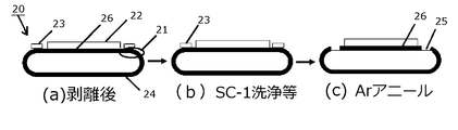
- a region called the terrace portion 21 where the SOI layer 22 is not transferred is formed in the peripheral portion of the wafer (FIG. 2A).
- the peripheral portion of the material wafer before being bonded has a sagging shape due to polishing or the like, and therefore, when the wafer is bonded, the peripheral portion of the wafer cannot be bonded completely, and this unbonded portion Si
- the SOI wafer 20 having a relatively thick SOI layer 22 when the SOI layer 22 at the time of peeling becomes thick (for example, 500 nm or more), the silicon flakes 23 peeled off at the time of peeling also become thick. Then, since the rigidity of the silicon thin piece itself is increased, the area of the silicon thin piece 23 to be peeled is relatively increased. Even if cleaning after peeling is performed in such a situation, since the surface area of the silicon flakes 23 is large, it becomes difficult for the cleaning liquid to enter between the silicon flakes 23 and the Si substrate. That is, the silicon flakes 23 are lifted off during cleaning and cannot be peeled off from the wafer, leaving the silicon flakes 23 in the subsequent process. That is, the thicker the silicon flakes 23 are (the deeper the ion implantation depth is to the bond wafer), the harder the silicon flakes 23 that are formed are removed.
- the acceleration power source of the ion implanter is used. Due to restrictions, there are cases where ions cannot be implanted into the Si layer via a thick oxide film formed on the bond wafer surface. In this case, the main oxide film 24 to be the BOX layer 26 is formed on the base wafer, and ion implantation is performed on the bare wafer (or a wafer with an oxide film on which a thin oxide film is formed), and the wafer is peeled off.
- the peeled silicon flakes are composed of an oxide film and a Si layer.
- the silicon flakes warp like bimetal due to the difference in thermal expansion coefficient between Si and the oxide film.
- the silicon flakes are not warped because they are composed only of Si.
- the silicon flakes are not warped, so that no gap is formed between the silicon flakes and the Si substrate, and the cleaning liquid cannot enter. That is, it becomes extremely difficult to lift off the silicon flakes during cleaning and peel them off from the wafer, leaving the silicon flakes in the subsequent process. That is, when the ion implantation is performed on the bond wafer without using the oxide film, the formed silicon flakes are more difficult to remove than when the ion implantation is performed through the oxide film.
- the inventors of the present invention have found that the silicon flakes 23 adhering to the silicon oxide film 24 of the terrace portion 21 become the recesses 25 of the terrace portion 21 when the flattening heat treatment is performed thereafter (see FIG. 2 (c)). That is, when the silicon thin piece 23 is placed on the silicon oxide film 24 of the terrace portion 21 during high-temperature annealing in an argon gas-containing atmosphere for flattening the peeling surface, the silicon thin piece 23 and the silicon oxide film 24 react with each other. However, the silicon oxide film 24 of the terrace portion 21 is largely etched around the silicon flakes 23 based on the reaction formula of Si + SiO 2 ⁇ 2SiO (gas).
- the dent 25 formed by this etching is detected as a bright spot in the sensitive inspection at the final inspection. If the device manufacturing process is performed in a state in which such a depression 25 is formed in the terrace portion 21, the photoresist tends to remain and becomes a source of contamination and particles.
- the inventors of the present invention have found that it is necessary to perform planarization heat treatment in an argon gas-containing atmosphere in a state where the silicon flakes 23 on the oxide film in the terrace portion are sufficiently removed.
- Patent Document 3 discloses the polysilicon growth of the terrace portion by epitaxial growth, but it is similar to the planarization heat treatment in an argon gas-containing atmosphere. In the heat treatment that does not involve film growth, the problem that dents are generated in the terrace portion has not been known so far, and is a phenomenon that the present inventors have found for the first time.
- An object of the present invention is to flatten the peeling surface without forming such a dent in the terrace portion.
- the present invention will be described in detail below.
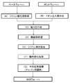
- FIG. 1 is a process flow diagram showing an example of a method for manufacturing an SOI wafer according to the present invention.
- a silicon oxide film is formed on the surface of a base wafer made of silicon single crystal by thermal oxidation or the like (FIG. 1A).
- the thickness of the silicon oxide film to be formed is not particularly limited, in the present invention, it can be set to 2 ⁇ m, for example.
- At least one kind of gas ions of hydrogen ions and rare gas ions is ion-implanted from the surface of the bond wafer made of silicon single crystal to form an ion-implanted layer at a predetermined depth of the bond wafer (FIG. 1B )).
- the depth of the ion implantation layer at this time is reflected in the thickness of the SOI layer formed after peeling. Therefore, the thickness of the SOI layer can be controlled by performing ion implantation while controlling the implantation energy and the like.
- ion implantation may be performed on a bond wafer made of a silicon single crystal having no oxide film on the surface, or a thin silicon oxide film is formed on the bond wafer and ion implantation is performed through the oxide film. Also good.
- the processing for the base wafer and the processing for the bond wafer can be performed independently, either of which may be performed first or in parallel.
- the ion-implanted surface of the bond wafer and the surface of the base wafer made of silicon single crystal are bonded together via a silicon oxide film formed on the surface of the base wafer (FIG. 1C).
- the bond wafer and the base wafer are brought into contact with each other in a clean atmosphere at room temperature, whereby the wafers are bonded to each other without using an adhesive or the like.
- an SOI wafer having a buried oxide film layer (BOX layer) and an SOI layer on the base wafer is manufactured by performing a peeling heat treatment to peel off the bond wafer with the ion implantation layer (FIG. 1D).
- the bond wafer can be exfoliated with an ion implantation layer by applying heat treatment in an inert gas atmosphere such as Ar, usually 400 ° C. or more and 700 ° C. or less for 30 minutes or more. Can be minutes.
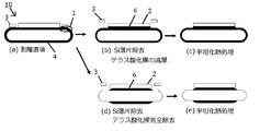
- the silicon flakes 3 existing on the silicon oxide film 4 of the terrace portion 1 of the SOI wafer 10 are removed without interposing another heat treatment (FIG. 1E).
- the removal of the silicon flakes 3 is not a problem as long as it can be removed by ordinary cleaning such as RCA cleaning. However, if a wafer having a large peel thickness or a bare wafer bond wafer is used, the silicon flakes can be removed only by RCA cleaning. 3 may not be removed.
- an aqueous solution containing HF hydrogen fluoride
- etching to reduce the oxide film thickness of the terrace portion 1 is performed, so that silicon oxidation between the silicon thin piece 3 and the terrace portion 1 is performed.
- the film 4 can be removed, the silicon flakes 3 can be lifted off, and the silicon flakes 3 on the terrace oxide film can be effectively removed (FIG. 3B).
- aqueous solution containing HF for example, a 15% HF aqueous solution can be used.
- the thickness to be reduced depends on the peeling temperature and the SOI layer thickness at the time of peeling, and is not particularly limited as long as the silicon flakes can be removed, but can be set to 1 to 100 nm, for example, and 5 nm or more. preferable.
- the silicon flakes 3 can be removed even if the silicon oxide film 4 in the terrace portion 1 is completely removed as shown in FIG. 3D.
- the peripheral portion of the SOI layer 2 is overexposed by overetching of the BOX layer 6.
- etching at the interface between the SOI layer 2 and the BOX layer 6 proceeds by high-temperature annealing (planarization heat treatment) in an argon gas-containing atmosphere, and a thin-film SOI layer is formed. It is desirable not to completely remove the terrace oxide film because it can be a new particle generation source.
- the silicon flakes 3 can be effectively removed even by performing cleaning (cleaning by physical action) that rubs the wafer surface using a sponge or the like, such as scrub cleaning. Can do.
- a sacrificial oxidation process (sacrificial oxidation +) is performed on the surface of the SOI layer after delamination in order to remove a damaged layer generated during ion implantation and delamination.
- Oxide film removal) oxygen precipitation inside the wafer may be controlled, or RTA (Rapid Thermal Anneal) may be performed for quality improvement such as surface roughness improvement.
- RTA Rapid Thermal Anneal
- these heat treatments have a higher heat treatment temperature than the peeling heat treatment, the adhesion strength between the silicon flakes and the terrace oxide film is increased, and even if HF cleaning is performed after these heat treatments, the silicon flakes are removed. It may become impossible to remove. Therefore, in the present invention, it is necessary to remove the silicon flakes on the oxide film in the terrace portion after the peeling heat treatment without interposing any other heat treatment (other than the peeling heat treatment).
- planarization heat treatment is performed in an argon gas-containing atmosphere, but before that, it is preferable to perform a sacrificial oxidation process on the SOI layer of the SOI wafer (FIG. 1F )).
- a sacrificial oxidation process on the SOI layer of the SOI wafer (FIG. 1F )).
- the bonding interface bond strength can be enhanced at the same time as the damage on the SOI layer surface is oxidized.
- 15% HF cleaning and, if necessary, RCA cleaning are performed.
- planarization heat treatment in an argon gas-containing atmosphere is performed on the SOI wafer 10 from which the silicon flakes 3 on the silicon oxide film 4 in the terrace portion 1 have been removed (FIGS. 1G and 3C).
- heat treatment can be performed at 1200 ° C. for 2 hours in a 100% Ar gas atmosphere.
- planarization heat treatment By the planarization heat treatment, the surface roughness due to peeling in the ion implantation layer is improved, and a wafer surface at a level that can be used as a device can be formed. Further, in the present invention, an SOI wafer having no silicon flakes is formed on the oxide film in the terrace portion, and a planarization heat treatment is performed in an argon gas-containing atmosphere. The generation of bright spots (that is, dents) due to the silicon flakes that have occurred in the terrace portion after the planarization heat treatment in step 1 can be suppressed, and the terrace portion can be kept clean. As a result, contamination and particle generation in the device manufacturing process can be avoided.
- sacrificial oxidation may be performed to further remove the remaining damage layer and adjust the SOI layer thickness.
- the hydrogen atmosphere RTA (H 2) is performed before the planarization heat treatment in the argon gas-containing atmosphere.
- RTA can also be performed.
- the process order in this case is as follows. Peeling heat treatment ⁇ Silicon flake removal ⁇ H 2 RTA ⁇ sacrificial oxidation treatment ⁇ Ar annealing As described above, by adding H 2 RTA (eg, 1150 ° C., 60 seconds), the temperature of Ar annealing can be lowered to less than 1200 ° C. it can.
- Examples 1 to 3 A silicon wafer with a diameter of 300 mm and a crystal orientation ⁇ 100> was used as a bond wafer and a base wafer, and a bonded SOI wafer was manufactured under the conditions shown in Table 1 (Examples 1 to 3). Microscopic observation was performed. In Examples 1 to 3, no bright spots (dents) were observed, and a beautiful terrace portion was formed. A micrograph of Example 2 is shown in FIG.
- Example 4 Except that the silicon flake removal process was scrub cleaning in which the wafer surface was rubbed with a sponge in pure water, Ar annealing was performed under the same conditions as in Example 3, followed by microscopic observation of the recess in the terrace portion. However, no dent was observed.
- Comparative Examples 1 to 3 A silicon single crystal wafer having a diameter of 300 mm and a crystal orientation ⁇ 100> was used as the bond wafer and the base wafer, and only the SC-1 cleaning was performed under the conditions shown in Table 2, that is, after the peeling heat treatment (silicon on the terrace portion of the SOI wafer). An SOI wafer was manufactured (without performing treatment for removing silicon flakes present on the oxide film) (Comparative Examples 1 to 3), and the presence or absence of a dent in the terrace was observed with a microscope. A micrograph of Comparative Example 2 is shown in FIG.
- Comparative Example 1 since the planarization heat treatment was performed without removing the silicon flakes on the terrace portion, a depression was generated in the terrace portion by Ar annealing.
- Comparative Examples 2 and 3 the oxide film at the terrace portion is reduced by removing the oxide film during the sacrificial oxidation process before the planarization heat treatment (Ar annealing), but the silicon flakes are strengthened by the oxidation heat treatment and H 2 RTA. Since it adhered, it was not removed and a dent was generated by Ar annealing.
- the present invention is not limited to the above embodiment.
- the above-described embodiment is an exemplification, and the present invention has substantially the same configuration as the technical idea described in the claims of the present invention, and any device that exhibits the same function and effect is the present invention. It is included in the technical scope of the invention.
Landscapes
- Engineering & Computer Science (AREA)
- Microelectronics & Electronic Packaging (AREA)
- Condensed Matter Physics & Semiconductors (AREA)
- General Physics & Mathematics (AREA)
- Manufacturing & Machinery (AREA)
- Computer Hardware Design (AREA)
- Physics & Mathematics (AREA)
- Power Engineering (AREA)
- Chemical & Material Sciences (AREA)
- Chemical Kinetics & Catalysis (AREA)
- General Chemical & Material Sciences (AREA)
- Element Separation (AREA)
- Cleaning Or Drying Semiconductors (AREA)
Priority Applications (5)
| Application Number | Priority Date | Filing Date | Title |
|---|---|---|---|
| SG11201709420PA SG11201709420PA (en) | 2015-06-15 | 2016-03-08 | Method for producing soi wafer |
| KR1020177035353A KR102327330B1 (ko) | 2015-06-15 | 2016-03-08 | Soi웨이퍼의 제조방법 |
| EP16811158.1A EP3309820B1 (en) | 2015-06-15 | 2016-03-08 | Method of manufacturing soi wafer |
| CN201680028359.7A CN107615445B (zh) | 2015-06-15 | 2016-03-08 | 绝缘体上硅晶圆的制造方法 |
| US15/574,326 US10204824B2 (en) | 2015-06-15 | 2016-03-08 | Method for producing SOI wafer |
Applications Claiming Priority (2)
| Application Number | Priority Date | Filing Date | Title |
|---|---|---|---|
| JP2015-120424 | 2015-06-15 | ||
| JP2015120424A JP6380245B2 (ja) | 2015-06-15 | 2015-06-15 | Soiウェーハの製造方法 |
Publications (1)
| Publication Number | Publication Date |
|---|---|
| WO2016203677A1 true WO2016203677A1 (ja) | 2016-12-22 |
Family
ID=57545735
Family Applications (1)
| Application Number | Title | Priority Date | Filing Date |
|---|---|---|---|
| PCT/JP2016/001235 WO2016203677A1 (ja) | 2015-06-15 | 2016-03-08 | Soiウェーハの製造方法 |
Country Status (8)
Families Citing this family (5)
| Publication number | Priority date | Publication date | Assignee | Title |
|---|---|---|---|---|
| JP6473970B2 (ja) * | 2015-10-28 | 2019-02-27 | 信越半導体株式会社 | 貼り合わせsoiウェーハの製造方法 |
| CN109037031B (zh) * | 2018-07-11 | 2021-11-19 | 华东师范大学 | 一种掺镍氧化铜薄膜晶体管及制备方法 |
| CN110739285A (zh) * | 2019-10-30 | 2020-01-31 | 北京工业大学 | 硅基金属中间层化合物半导体晶圆的结构及制备方法 |
| KR102456461B1 (ko) | 2020-11-26 | 2022-10-19 | 현대제철 주식회사 | 딥러닝을 이용한 철강 미세 조직 분석 방법 및 시스템 |
| CN112582332A (zh) * | 2020-12-08 | 2021-03-30 | 上海新昇半导体科技有限公司 | 一种绝缘体上硅结构及其方法 |
Citations (3)
| Publication number | Priority date | Publication date | Assignee | Title |
|---|---|---|---|---|
| JP2008028070A (ja) * | 2006-07-20 | 2008-02-07 | Sumco Corp | 貼り合わせウェーハの製造方法 |
| JP2009027124A (ja) * | 2007-06-21 | 2009-02-05 | Shin Etsu Handotai Co Ltd | Soiウェーハの製造方法 |
| JP2013084663A (ja) * | 2011-10-06 | 2013-05-09 | Shin Etsu Handotai Co Ltd | 貼り合わせsoiウェーハの製造方法 |
Family Cites Families (14)
| Publication number | Priority date | Publication date | Assignee | Title |
|---|---|---|---|---|
| FR2681472B1 (fr) | 1991-09-18 | 1993-10-29 | Commissariat Energie Atomique | Procede de fabrication de films minces de materiau semiconducteur. |
| JPH11307472A (ja) | 1998-04-23 | 1999-11-05 | Shin Etsu Handotai Co Ltd | 水素イオン剥離法によってsoiウエーハを製造する方法およびこの方法で製造されたsoiウエーハ |
| JP2000124092A (ja) * | 1998-10-16 | 2000-04-28 | Shin Etsu Handotai Co Ltd | 水素イオン注入剥離法によってsoiウエーハを製造する方法およびこの方法で製造されたsoiウエーハ |
| JP4304879B2 (ja) * | 2001-04-06 | 2009-07-29 | 信越半導体株式会社 | 水素イオンまたは希ガスイオンの注入量の決定方法 |
| JP4123861B2 (ja) * | 2002-08-06 | 2008-07-23 | 株式会社Sumco | 半導体基板の製造方法 |
| FR2860842B1 (fr) * | 2003-10-14 | 2007-11-02 | Tracit Technologies | Procede de preparation et d'assemblage de substrats |
| JP4603865B2 (ja) * | 2004-12-01 | 2010-12-22 | 信越化学工業株式会社 | 酸化膜付きシリコン基板の製造方法及び酸化膜付きシリコン基板 |
| FR2880184B1 (fr) * | 2004-12-28 | 2007-03-30 | Commissariat Energie Atomique | Procede de detourage d'une structure obtenue par assemblage de deux plaques |
| JP2007317988A (ja) * | 2006-05-29 | 2007-12-06 | Shin Etsu Handotai Co Ltd | 貼り合わせウエーハの製造方法 |
| JP5135935B2 (ja) * | 2007-07-27 | 2013-02-06 | 信越半導体株式会社 | 貼り合わせウエーハの製造方法 |
| JP5531642B2 (ja) * | 2010-01-22 | 2014-06-25 | 信越半導体株式会社 | 貼り合わせウェーハの製造方法 |
| JP5477277B2 (ja) * | 2010-12-20 | 2014-04-23 | 信越半導体株式会社 | Soiウェーハの製造方法 |
| JP2013143407A (ja) * | 2012-01-06 | 2013-07-22 | Shin Etsu Handotai Co Ltd | 貼り合わせsoiウェーハの製造方法 |
| JP5673572B2 (ja) * | 2012-01-24 | 2015-02-18 | 信越半導体株式会社 | 貼り合わせsoiウェーハの製造方法 |
-
2015
- 2015-06-15 JP JP2015120424A patent/JP6380245B2/ja active Active
-
2016
- 2016-03-08 US US15/574,326 patent/US10204824B2/en active Active
- 2016-03-08 CN CN201680028359.7A patent/CN107615445B/zh active Active
- 2016-03-08 WO PCT/JP2016/001235 patent/WO2016203677A1/ja active Application Filing
- 2016-03-08 EP EP16811158.1A patent/EP3309820B1/en active Active
- 2016-03-08 SG SG11201709420PA patent/SG11201709420PA/en unknown
- 2016-03-08 KR KR1020177035353A patent/KR102327330B1/ko active Active
- 2016-03-11 TW TW105107464A patent/TWI685019B/zh active
Patent Citations (3)
| Publication number | Priority date | Publication date | Assignee | Title |
|---|---|---|---|---|
| JP2008028070A (ja) * | 2006-07-20 | 2008-02-07 | Sumco Corp | 貼り合わせウェーハの製造方法 |
| JP2009027124A (ja) * | 2007-06-21 | 2009-02-05 | Shin Etsu Handotai Co Ltd | Soiウェーハの製造方法 |
| JP2013084663A (ja) * | 2011-10-06 | 2013-05-09 | Shin Etsu Handotai Co Ltd | 貼り合わせsoiウェーハの製造方法 |
Also Published As
| Publication number | Publication date |
|---|---|
| TW201643938A (zh) | 2016-12-16 |
| SG11201709420PA (en) | 2017-12-28 |
| EP3309820B1 (en) | 2020-01-29 |
| EP3309820A1 (en) | 2018-04-18 |
| CN107615445A (zh) | 2018-01-19 |
| KR20180016394A (ko) | 2018-02-14 |
| US20180144975A1 (en) | 2018-05-24 |
| CN107615445B (zh) | 2020-10-30 |
| TWI685019B (zh) | 2020-02-11 |
| JP2017005201A (ja) | 2017-01-05 |
| KR102327330B1 (ko) | 2021-11-17 |
| US10204824B2 (en) | 2019-02-12 |
| JP6380245B2 (ja) | 2018-08-29 |
| EP3309820A4 (en) | 2019-01-23 |
Similar Documents
| Publication | Publication Date | Title |
|---|---|---|
| JP4509488B2 (ja) | 貼り合わせ基板の製造方法 | |
| WO2013102968A1 (ja) | 貼り合わせsoiウェーハの製造方法 | |
| US20130089968A1 (en) | Method for finishing silicon on insulator substrates | |
| JP6380245B2 (ja) | Soiウェーハの製造方法 | |
| JP4421652B2 (ja) | Soiウェーハの製造方法 | |
| KR101901872B1 (ko) | Soi웨이퍼의 제조방법 | |
| JP5673572B2 (ja) | 貼り合わせsoiウェーハの製造方法 | |
| WO2015141121A1 (ja) | 貼り合わせウェーハの製造方法 | |
| TWI487014B (zh) | 自施體基板轉移一層至處理基板之方法 | |
| TW200822199A (en) | Method for producing bonded wafer | |
| WO2010098007A1 (ja) | Soiウェーハの製造方法 | |
| WO2015136834A1 (ja) | 貼り合わせsoiウェーハの製造方法 | |
| WO2016059748A1 (ja) | 貼り合わせウェーハの製造方法 | |
| WO2017217129A1 (ja) | 貼り合わせウェーハの製造方法 | |
| KR102317552B1 (ko) | 접합 soi 웨이퍼의 제조방법 | |
| JP7251419B2 (ja) | 貼り合わせsoiウェーハの製造方法 | |
| JP5119742B2 (ja) | 貼り合わせウエーハの製造方法 | |
| KR20160052551A (ko) | 접합 웨이퍼의 제조방법 | |
| JP2006013179A (ja) | Soiウェーハの製造方法 | |
| JP2014212172A (ja) | 貼り合わせウェーハの製造方法 |
Legal Events
| Date | Code | Title | Description |
|---|---|---|---|
| 121 | Ep: the epo has been informed by wipo that ep was designated in this application |
Ref document number: 16811158 Country of ref document: EP Kind code of ref document: A1 |
|
| WWE | Wipo information: entry into national phase |
Ref document number: 11201709420P Country of ref document: SG Ref document number: 15574326 Country of ref document: US |
|
| ENP | Entry into the national phase |
Ref document number: 20177035353 Country of ref document: KR Kind code of ref document: A |
|
| NENP | Non-entry into the national phase |
Ref country code: DE |
|
| WWE | Wipo information: entry into national phase |
Ref document number: 2016811158 Country of ref document: EP |