JP2013143407A - 貼り合わせsoiウェーハの製造方法 - Google Patents
貼り合わせsoiウェーハの製造方法 Download PDFInfo
- Publication number
- JP2013143407A JP2013143407A JP2012001611A JP2012001611A JP2013143407A JP 2013143407 A JP2013143407 A JP 2013143407A JP 2012001611 A JP2012001611 A JP 2012001611A JP 2012001611 A JP2012001611 A JP 2012001611A JP 2013143407 A JP2013143407 A JP 2013143407A
- Authority
- JP
- Japan
- Prior art keywords
- wafer
- rta
- temperature
- soi wafer
- ion
- Prior art date
- Legal status (The legal status is an assumption and is not a legal conclusion. Google has not performed a legal analysis and makes no representation as to the accuracy of the status listed.)
- Pending
Links
Images


Classifications
-
- H—ELECTRICITY
- H01—ELECTRIC ELEMENTS
- H01L—SEMICONDUCTOR DEVICES NOT COVERED BY CLASS H10
- H01L21/00—Processes or apparatus adapted for the manufacture or treatment of semiconductor or solid state devices or of parts thereof
- H01L21/70—Manufacture or treatment of devices consisting of a plurality of solid state components formed in or on a common substrate or of parts thereof; Manufacture of integrated circuit devices or of parts thereof
- H01L21/71—Manufacture of specific parts of devices defined in group H01L21/70
- H01L21/76—Making of isolation regions between components
- H01L21/762—Dielectric regions, e.g. EPIC dielectric isolation, LOCOS; Trench refilling techniques, SOI technology, use of channel stoppers
- H01L21/7624—Dielectric regions, e.g. EPIC dielectric isolation, LOCOS; Trench refilling techniques, SOI technology, use of channel stoppers using semiconductor on insulator [SOI] technology
- H01L21/76251—Dielectric regions, e.g. EPIC dielectric isolation, LOCOS; Trench refilling techniques, SOI technology, use of channel stoppers using semiconductor on insulator [SOI] technology using bonding techniques
- H01L21/76254—Dielectric regions, e.g. EPIC dielectric isolation, LOCOS; Trench refilling techniques, SOI technology, use of channel stoppers using semiconductor on insulator [SOI] technology using bonding techniques with separation/delamination along an ion implanted layer, e.g. Smart-cut, Unibond
-
- H—ELECTRICITY
- H01—ELECTRIC ELEMENTS
- H01L—SEMICONDUCTOR DEVICES NOT COVERED BY CLASS H10
- H01L21/00—Processes or apparatus adapted for the manufacture or treatment of semiconductor or solid state devices or of parts thereof
- H01L21/02—Manufacture or treatment of semiconductor devices or of parts thereof
- H01L21/04—Manufacture or treatment of semiconductor devices or of parts thereof the devices having at least one potential-jump barrier or surface barrier, e.g. PN junction, depletion layer or carrier concentration layer
- H01L21/18—Manufacture or treatment of semiconductor devices or of parts thereof the devices having at least one potential-jump barrier or surface barrier, e.g. PN junction, depletion layer or carrier concentration layer the devices having semiconductor bodies comprising elements of Group IV of the Periodic System or AIIIBV compounds with or without impurities, e.g. doping materials
- H01L21/30—Treatment of semiconductor bodies using processes or apparatus not provided for in groups H01L21/20 - H01L21/26
- H01L21/302—Treatment of semiconductor bodies using processes or apparatus not provided for in groups H01L21/20 - H01L21/26 to change their surface-physical characteristics or shape, e.g. etching, polishing, cutting
- H01L21/306—Chemical or electrical treatment, e.g. electrolytic etching
- H01L21/30604—Chemical etching
-
- H—ELECTRICITY
- H01—ELECTRIC ELEMENTS
- H01L—SEMICONDUCTOR DEVICES NOT COVERED BY CLASS H10
- H01L21/00—Processes or apparatus adapted for the manufacture or treatment of semiconductor or solid state devices or of parts thereof
- H01L21/02—Manufacture or treatment of semiconductor devices or of parts thereof
- H01L21/04—Manufacture or treatment of semiconductor devices or of parts thereof the devices having at least one potential-jump barrier or surface barrier, e.g. PN junction, depletion layer or carrier concentration layer
- H01L21/18—Manufacture or treatment of semiconductor devices or of parts thereof the devices having at least one potential-jump barrier or surface barrier, e.g. PN junction, depletion layer or carrier concentration layer the devices having semiconductor bodies comprising elements of Group IV of the Periodic System or AIIIBV compounds with or without impurities, e.g. doping materials
- H01L21/30—Treatment of semiconductor bodies using processes or apparatus not provided for in groups H01L21/20 - H01L21/26
- H01L21/324—Thermal treatment for modifying the properties of semiconductor bodies, e.g. annealing, sintering
-
- H—ELECTRICITY
- H01—ELECTRIC ELEMENTS
- H01L—SEMICONDUCTOR DEVICES NOT COVERED BY CLASS H10
- H01L21/00—Processes or apparatus adapted for the manufacture or treatment of semiconductor or solid state devices or of parts thereof
- H01L21/02—Manufacture or treatment of semiconductor devices or of parts thereof
- H01L21/02104—Forming layers
- H01L21/02107—Forming insulating materials on a substrate
- H01L21/02225—Forming insulating materials on a substrate characterised by the process for the formation of the insulating layer
- H01L21/02227—Forming insulating materials on a substrate characterised by the process for the formation of the insulating layer formation by a process other than a deposition process
- H01L21/0223—Forming insulating materials on a substrate characterised by the process for the formation of the insulating layer formation by a process other than a deposition process formation by oxidation, e.g. oxidation of the substrate
- H01L21/02233—Forming insulating materials on a substrate characterised by the process for the formation of the insulating layer formation by a process other than a deposition process formation by oxidation, e.g. oxidation of the substrate of the semiconductor substrate or a semiconductor layer
- H01L21/02236—Forming insulating materials on a substrate characterised by the process for the formation of the insulating layer formation by a process other than a deposition process formation by oxidation, e.g. oxidation of the substrate of the semiconductor substrate or a semiconductor layer group IV semiconductor
- H01L21/02238—Forming insulating materials on a substrate characterised by the process for the formation of the insulating layer formation by a process other than a deposition process formation by oxidation, e.g. oxidation of the substrate of the semiconductor substrate or a semiconductor layer group IV semiconductor silicon in uncombined form, i.e. pure silicon
-
- H—ELECTRICITY
- H01—ELECTRIC ELEMENTS
- H01L—SEMICONDUCTOR DEVICES NOT COVERED BY CLASS H10
- H01L21/00—Processes or apparatus adapted for the manufacture or treatment of semiconductor or solid state devices or of parts thereof
- H01L21/02—Manufacture or treatment of semiconductor devices or of parts thereof
- H01L21/02104—Forming layers
- H01L21/02107—Forming insulating materials on a substrate
- H01L21/02225—Forming insulating materials on a substrate characterised by the process for the formation of the insulating layer
- H01L21/02227—Forming insulating materials on a substrate characterised by the process for the formation of the insulating layer formation by a process other than a deposition process
- H01L21/02255—Forming insulating materials on a substrate characterised by the process for the formation of the insulating layer formation by a process other than a deposition process formation by thermal treatment
Abstract
【解決手段】SOIウェーハを製造する方法であって、剥離後の貼り合わせSOIウェーハに対して、第1のRTA処理を行った後、第1の犠牲酸化処理を行い、その後、第2のRTA処理を行った後、第2の犠牲酸化処理を行う工程を有し、前記第1及び第2のRTA処理を、水素ガス含有雰囲気下、1100℃以上の温度で行い、前記第1及び第2の犠牲酸化処理において、900℃以上1000℃以下の温度でバッチ式熱処理炉による熱酸化のみを行うことによって前記SOI層表面に熱酸化膜を形成した後、該熱酸化膜を除去する処理を行う貼り合わせSOIウェーハの製造方法。
【選択図】図1
Description
このイオン注入剥離法は、二枚のウェーハの内、少なくとも一方に酸化膜を形成すると共に、一方のウェーハ(ボンドウェーハ)の上面から水素イオンや希ガスイオン等のガスイオンを注入し、該ウェーハ内部にイオン注入層(微小気泡層)を形成させた後、該イオンを注入した方の面を酸化膜(絶縁膜)を介して他方のウェーハ(ベースウェーハ)と密着させ、その後、熱処理(剥離熱処理)又は機械的な外力を加えてイオン注入層を劈開面として一方のウェーハ(ボンドウェーハ)を薄膜状に剥離し、さらに熱処理(結合熱処理)を加えて強固に結合してベースウェーハ上に薄膜(SOI層)を有する貼り合わせSOIウェーハを作製する技術(特許文献1参照)である。この方法では、薄膜、特にはSOI層の膜厚の均一性が高い貼り合わせSOIウェーハが容易に得られている。
ところが、SOI層に機械加工的要素を含む研磨をしてしまうと、研磨の取り代が均一でないために、水素イオンなどの注入、剥離によってある程度達成されたSOI層の膜厚均一性が悪化してしまうという問題が生じる。
例えば、特許文献2では、剥離熱処理後(または結合熱処理後)に、SOI層の表面を研磨することなく水素を含む還元性雰囲気下の熱処理(急速加熱・急速冷却熱処理(RTA:Rapid Thermal Annealing))を加えることを提案している。さらに、特許文献3では、剥離熱処理後(又は結合熱処理後)に、酸化性雰囲気下の熱処理によりSOI層に酸化膜を形成した後に該酸化膜を除去し(いわゆる犠牲酸化処理)、次に還元性雰囲気の熱処理(急速加熱・急速冷却熱処理(RTA処理))を加えることを提案している。
このように、タッチポリッシュの代わりに高温熱処理を行って表面粗さを改善する平坦化処理が行われるようになったことによって、現在では、直径300mmでSOI層の膜厚レンジ(面内の最大膜厚値から最小膜厚値を引いた値)が3nm以内の膜厚均一性を有するSOIウェーハが、イオン注入剥離法によって量産レベルで得られている。
特許文献6の[0087]段落でも同様に、イオン種の共注入による剥離面の表面粗さ改善として、RTA+StabOx+RTA+薄膜化を行うことが記載されている。
しかしながら、特許文献5、6における犠牲酸化は、900℃酸化+1100℃Arアニール(2時間)と記載されている通り、抵抗加熱式の熱処理炉(バッチ炉)を用いて酸化後に連続的に高温長時間のアニール(ポストアニール)を含む工程であるため、スリップ転位の発生頻度が高まるという問題があった。
このような温度で熱酸化することで、比較的厚い酸化膜をより短時間で形成することができ、生産性を向上させることができる。また、950℃以上でも、先にRTA処理を行って平坦化、イオン注入ダメージ層の回復が行われているためOSF等の欠陥は発生しない。
このように貼り合わせ、機械的剥離を行うことで、剥離面の面粗さを低減でき、より効率的にSOI層を平坦化することができる。
このような温度で第1及び第2のRTA処理することで、スリップ転位の発生を確実に抑制することができる。
図1は本発明の貼り合わせSOIウェーハの製造方法のフロー図である。
次に、図1の工程(c)では、水素イオン、希ガスイオンのうち少なくとも一種類のガスイオンを注入して、ボンドウェーハ10の内部にイオン注入層13を形成する。
なお、貼り合わせる前に、ウェーハの表面に付着しているパーティクルおよび有機物を除去するため、両ウェーハに貼り合わせ前洗浄を行ってもよい。
このように機械的な外力で剥離させることで、剥離面の面粗さを低減できるため、本発明のRTA処理で、十分に平坦化できるだけでなく、RTA処理の条件を緩和することも可能となる。
また、機械的な外力による剥離方法以外にも、例えば、不活性ガス雰囲気下、500℃以上の温度で熱処理を行い、結晶の再配列と気泡の凝集とによって剥離させることもできる。
このとき、第1及び第2のRTA処理を、水素ガス含有雰囲気下、1100℃以上の温度で行う。また、第1及び第2の犠牲酸化処理において、900℃以上1000℃以下の温度でバッチ式熱処理炉による熱酸化のみを行うことによってSOI層16の表面に熱酸化膜を形成した後、該熱酸化膜を除去する処理を行う。
従来は、剥離直後の貼り合わせSOIウェーハに対して950℃以上の温度で熱酸化を行うと、SOI層表面に欠陥(OSF)が発生してしまうという問題があったが、本発明の場合、犠牲酸化の前に高温の水素RTA処理を行って表面の平坦化とイオン注入のダメージ層の回復が行われているため、熱酸化の温度を950℃以上(1000℃以下)にしてもOSFは発生しないことを本発明者らは見出した。従って、950℃以上で熱酸化を行うことで、比較的厚い酸化膜を形成する場合であっても酸化時間の短縮を図ることができ、生産効率を向上させることができる。
また、本発明の第1及び第2のRTA処理の熱処理時間としては、例えば1〜300秒間行えば、SOI層の平坦化及びダメージ除去が可能である。
(実施例1〜6、比較例1〜4)
[SOIウェーハの製法(剥離工程まで):機械的剥離]実施例1〜4、比較例1〜3
ボンドウェーハ及びベースウェーハとして、直径300mm、結晶方位<100>の鏡面研磨されたシリコン単結晶ウェーハを準備し、ボンドウェーハの表面に厚さ150nmの熱酸化膜を形成し、該熱酸化膜を通して、水素イオン注入(ドーズ量:6×10¹⁶/cm2、注入エネルギー:50keV)を行い、貼り合わせ面をプラズマ処理によって活性化したベースウェーハと酸化膜を介して室温にて貼り合わせ、350℃、1時間の熱処理(この熱処理で剥離は発生しない)を行った後、イオン注入層に機械的な外力を加えて剥離した。
ボンドウェーハ及びベースウェーハとして、直径300mm、結晶方位<100>の鏡面研磨されたシリコン単結晶ウェーハを準備し、ボンドウェーハの表面に厚さ150nmの熱酸化膜を形成し、該熱酸化膜を通して、水素イオン注入(ドーズ量:5×10¹⁶/cm2、注入エネルギー:50keV)を行い、ベースウェーハと酸化膜を介して室温にて貼り合わせ、500℃、0.5時間の熱処理を加えて剥離した。
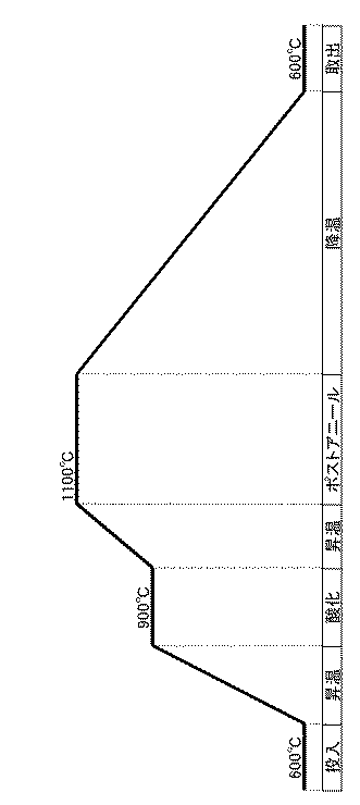
また、比較例3において、作製したSOIウェーハにRTA処理と犠牲酸化処理(熱酸化+HF溶液による熱酸化膜除去)を行ったが、第1及び第2の犠牲酸化処理では、熱酸化の終了後に連続的にポストアニール(100%Ar、1100℃、2時間)を実施した。図3に、比較例3の犠牲酸化処理における熱酸化及びポストアニールの温度プロファイルを示す。
比較例4では、第2のRTA処理の代わりにバッチ式熱処理炉によるArアニール(100%Ar、1200℃、1時間)を実施した。
製造したSOIウェーハについて、クロムレスの選択エッチング液でSOI層表面を30nmエッチングし、光学顕微鏡でエッチピット密度を測定した。
[スリップ発生率]
各実施例、比較例の熱処理条件でSOIウェーハを100枚処理し、スリップ不良の限度見本と比較してスリップ不良と判断されたものの比率を調べた。
[表面粗さ]
第2の犠牲酸化処理後のSOI層表面をAFMにより測定した(測定領域30μm角)。
以上の評価結果を表1に示す。
なお、実施例5,6は、熱処理による剥離を行っているため、表面粗さが実施例1〜4に比べてやや大きな値となったが、剥離直後の表面粗さと比較すると十分に低減されており、エッチピット、スリップ発生率は、実施例1〜4と同等レベルであった。
比較例2では、RTA処理の温度が1100℃未満であるため、ダメージの除去が不十分となり、950℃の熱酸化でもOSFが発生し、SOI層に欠陥(エッチピット)が多発した。
比較例4では、第2のRTA処理の代わりにバッチ式熱処理炉による高温Arアニールを実施したため、更にスリップの発生率が悪化し、実施例1〜6に比べて2倍程度となった。
13…イオン注入層、 14…埋め込み酸化膜、 15…貼り合わせSOIウェーハ、
16…SOI層。
Claims (4)
- シリコン単結晶からなるボンドウェーハの表面から水素イオン、希ガスイオンの少なくとも一種類のガスイオンをイオン注入して該ボンドウェーハ内部にイオン注入層を形成し、前記ボンドウェーハのイオン注入された側の表面とベースウェーハの表面とを絶縁膜を介して貼り合わせた後、前記ボンドウェーハの一部を前記イオン注入層で剥離して、前記ベースウェーハ上にSOI層を有する貼り合わせSOIウェーハを製造する方法であって、
前記剥離後の貼り合わせSOIウェーハに対して、第1のRTA処理を行った後、第1の犠牲酸化処理を行い、その後、第2のRTA処理を行った後、第2の犠牲酸化処理を行う工程を有し、
前記第1及び第2のRTA処理を、水素ガス含有雰囲気下、1100℃以上の温度で行い、前記第1及び第2の犠牲酸化処理において、900℃以上1000℃以下の温度でバッチ式熱処理炉による熱酸化のみを行うことによって前記SOI層表面に熱酸化膜を形成した後、該熱酸化膜を除去する処理を行うことを特徴とする貼り合わせSOIウェーハの製造方法。 - 前記第1及び第2の犠牲酸化処理における熱酸化の温度を、950℃以上とすることを特徴とする請求項1に記載の貼り合わせSOIウェーハの製造方法。
- 前記ボンドウェーハと前記ベースウェーハの少なくとも一方の表面にプラズマ処理を施した後に前記絶縁膜を介して貼り合わせた後、前記ボンドウェーハの一部を前記イオン注入層で機械的な外力を用いて剥離することを特徴とする請求項1又は請求項2に記載の貼り合わせSOIウェーハの製造方法。
- 前記第1及び第2のRTA処理を、1230℃以下の温度で行うことを特徴とする請求項1乃至請求項3のいずれか一項に記載の貼り合わせSOIウェーハの製造方法。
Priority Applications (6)
| Application Number | Priority Date | Filing Date | Title |
|---|---|---|---|
| JP2012001611A JP2013143407A (ja) | 2012-01-06 | 2012-01-06 | 貼り合わせsoiウェーハの製造方法 |
| US14/364,162 US9076840B2 (en) | 2012-01-06 | 2012-11-30 | Method for manufacturing a bonded SOI wafer |
| KR1020147018404A KR20140121392A (ko) | 2012-01-06 | 2012-11-30 | 접합 soi 웨이퍼의 제조방법 |
| PCT/JP2012/007690 WO2013102968A1 (ja) | 2012-01-06 | 2012-11-30 | 貼り合わせsoiウェーハの製造方法 |
| EP12864102.4A EP2802001A4 (en) | 2012-01-06 | 2012-11-30 | METHOD FOR PRODUCING A BONDED SILICON ON ISOLATOR (SOI) WAFERS |
| CN201280065462.0A CN104025254A (zh) | 2012-01-06 | 2012-11-30 | 贴合soi晶片的制造方法 |
Applications Claiming Priority (1)
| Application Number | Priority Date | Filing Date | Title |
|---|---|---|---|
| JP2012001611A JP2013143407A (ja) | 2012-01-06 | 2012-01-06 | 貼り合わせsoiウェーハの製造方法 |
Publications (1)
| Publication Number | Publication Date |
|---|---|
| JP2013143407A true JP2013143407A (ja) | 2013-07-22 |
Family
ID=48745045
Family Applications (1)
| Application Number | Title | Priority Date | Filing Date |
|---|---|---|---|
| JP2012001611A Pending JP2013143407A (ja) | 2012-01-06 | 2012-01-06 | 貼り合わせsoiウェーハの製造方法 |
Country Status (6)
| Country | Link |
|---|---|
| US (1) | US9076840B2 (ja) |
| EP (1) | EP2802001A4 (ja) |
| JP (1) | JP2013143407A (ja) |
| KR (1) | KR20140121392A (ja) |
| CN (1) | CN104025254A (ja) |
| WO (1) | WO2013102968A1 (ja) |
Cited By (3)
| Publication number | Priority date | Publication date | Assignee | Title |
|---|---|---|---|---|
| JP2014232806A (ja) * | 2013-05-29 | 2014-12-11 | 信越半導体株式会社 | 貼り合わせウェーハの製造方法 |
| JP2016082093A (ja) * | 2014-10-17 | 2016-05-16 | 信越半導体株式会社 | 貼り合わせウェーハの製造方法 |
| KR20160134661A (ko) | 2014-03-18 | 2016-11-23 | 신에쯔 한도타이 가부시키가이샤 | 접합웨이퍼의 제조방법 |
Families Citing this family (8)
| Publication number | Priority date | Publication date | Assignee | Title |
|---|---|---|---|---|
| JP6200273B2 (ja) * | 2013-10-17 | 2017-09-20 | 信越半導体株式会社 | 貼り合わせウェーハの製造方法 |
| JP6380245B2 (ja) * | 2015-06-15 | 2018-08-29 | 信越半導体株式会社 | Soiウェーハの製造方法 |
| JP6531743B2 (ja) * | 2016-09-27 | 2019-06-19 | 信越半導体株式会社 | 貼り合わせsoiウェーハの製造方法 |
| CN106601615B (zh) * | 2016-12-27 | 2020-05-15 | 上海新傲科技股份有限公司 | 提高键合强度的退火方法 |
| FR3093858B1 (fr) * | 2019-03-15 | 2021-03-05 | Soitec Silicon On Insulator | Procédé de transfert d’une couche utile sur un substrat support |
| FR3093860B1 (fr) * | 2019-03-15 | 2021-03-05 | Soitec Silicon On Insulator | Procédé de transfert d’une couche utile sur un substrat support |
| CN116387241A (zh) * | 2023-04-21 | 2023-07-04 | 中芯先锋集成电路制造(绍兴)有限公司 | 绝缘体上半导体衬底的制造方法及半导体器件的制造方法 |
| CN117096012B (zh) * | 2023-08-22 | 2024-03-26 | 中环领先半导体科技股份有限公司 | 一种氧化膜、硅片及其制备方法 |
Citations (3)
| Publication number | Priority date | Publication date | Assignee | Title |
|---|---|---|---|---|
| JP2003510799A (ja) * | 1999-08-20 | 2003-03-18 | エス オー イ テク シリコン オン インシュレータ テクノロジース | マイクロエレクトロニクス用基板の処理方法及び該方法により得られた基板 |
| WO2007074550A1 (ja) * | 2005-12-27 | 2007-07-05 | Shin-Etsu Chemical Co., Ltd. | Soiウェーハの製造方法及びsoiウェーハ |
| WO2010106101A1 (en) * | 2009-03-18 | 2010-09-23 | S.O.I.Tec Silicon On Insulator Technologies | Finishing method for a substrate of "silicon-on-insulator" soi type |
Family Cites Families (11)
| Publication number | Priority date | Publication date | Assignee | Title |
|---|---|---|---|---|
| FR2681472B1 (fr) | 1991-09-18 | 1993-10-29 | Commissariat Energie Atomique | Procede de fabrication de films minces de materiau semiconducteur. |
| JPH11307472A (ja) | 1998-04-23 | 1999-11-05 | Shin Etsu Handotai Co Ltd | 水素イオン剥離法によってsoiウエーハを製造する方法およびこの方法で製造されたsoiウエーハ |
| JP2000124092A (ja) | 1998-10-16 | 2000-04-28 | Shin Etsu Handotai Co Ltd | 水素イオン注入剥離法によってsoiウエーハを製造する方法およびこの方法で製造されたsoiウエーハ |
| US6846718B1 (en) * | 1999-10-14 | 2005-01-25 | Shin-Etsu Handotai Co., Ltd. | Method for producing SOI wafer and SOI wafer |
| EP1408551B1 (en) | 2001-07-17 | 2014-07-02 | Shin-Etsu Handotai Co., Ltd. | Method for producing bonding wafer |
| EP1652230A2 (fr) | 2003-07-29 | 2006-05-03 | S.O.I.Tec Silicon on Insulator Technologies | Procede d' obtention d' une couche mince de qualite accrue par co-implantation et recuit thermique |
| CN101027768B (zh) | 2004-09-21 | 2010-11-03 | S.O.I.Tec绝缘体上硅技术公司 | 根据避免气泡形成和限制粗糙度的条件来进行共注入步骤的薄层转移方法 |
| DE602004022882D1 (de) | 2004-12-28 | 2009-10-08 | Soitec Silicon On Insulator | Ner geringen dichte von löchern |
| FR2895563B1 (fr) * | 2005-12-22 | 2008-04-04 | Soitec Silicon On Insulator | Procede de simplification d'une sequence de finition et structure obtenue par le procede |
| JP5135935B2 (ja) * | 2007-07-27 | 2013-02-06 | 信越半導体株式会社 | 貼り合わせウエーハの製造方法 |
| JP5263509B2 (ja) * | 2008-09-19 | 2013-08-14 | 信越半導体株式会社 | 貼り合わせウェーハの製造方法 |
-
2012
- 2012-01-06 JP JP2012001611A patent/JP2013143407A/ja active Pending
- 2012-11-30 CN CN201280065462.0A patent/CN104025254A/zh active Pending
- 2012-11-30 US US14/364,162 patent/US9076840B2/en active Active
- 2012-11-30 EP EP12864102.4A patent/EP2802001A4/en not_active Withdrawn
- 2012-11-30 KR KR1020147018404A patent/KR20140121392A/ko not_active Application Discontinuation
- 2012-11-30 WO PCT/JP2012/007690 patent/WO2013102968A1/ja active Application Filing
Patent Citations (3)
| Publication number | Priority date | Publication date | Assignee | Title |
|---|---|---|---|---|
| JP2003510799A (ja) * | 1999-08-20 | 2003-03-18 | エス オー イ テク シリコン オン インシュレータ テクノロジース | マイクロエレクトロニクス用基板の処理方法及び該方法により得られた基板 |
| WO2007074550A1 (ja) * | 2005-12-27 | 2007-07-05 | Shin-Etsu Chemical Co., Ltd. | Soiウェーハの製造方法及びsoiウェーハ |
| WO2010106101A1 (en) * | 2009-03-18 | 2010-09-23 | S.O.I.Tec Silicon On Insulator Technologies | Finishing method for a substrate of "silicon-on-insulator" soi type |
Cited By (4)
| Publication number | Priority date | Publication date | Assignee | Title |
|---|---|---|---|---|
| JP2014232806A (ja) * | 2013-05-29 | 2014-12-11 | 信越半導体株式会社 | 貼り合わせウェーハの製造方法 |
| KR20160134661A (ko) | 2014-03-18 | 2016-11-23 | 신에쯔 한도타이 가부시키가이샤 | 접합웨이퍼의 제조방법 |
| US9773694B2 (en) | 2014-03-18 | 2017-09-26 | Shin-Etsu Handotai Co., Ltd. | Method for manufacturing bonded wafer |
| JP2016082093A (ja) * | 2014-10-17 | 2016-05-16 | 信越半導体株式会社 | 貼り合わせウェーハの製造方法 |
Also Published As
| Publication number | Publication date |
|---|---|
| EP2802001A4 (en) | 2015-09-16 |
| US9076840B2 (en) | 2015-07-07 |
| US20140322895A1 (en) | 2014-10-30 |
| EP2802001A1 (en) | 2014-11-12 |
| WO2013102968A1 (ja) | 2013-07-11 |
| KR20140121392A (ko) | 2014-10-15 |
| CN104025254A (zh) | 2014-09-03 |
Similar Documents
| Publication | Publication Date | Title |
|---|---|---|
| WO2013102968A1 (ja) | 貼り合わせsoiウェーハの製造方法 | |
| JP5673572B2 (ja) | 貼り合わせsoiウェーハの製造方法 | |
| JP4421652B2 (ja) | Soiウェーハの製造方法 | |
| JP2009032972A (ja) | 貼り合わせウエーハの製造方法 | |
| JP2006210899A (ja) | Soiウエーハの製造方法及びsoiウェーハ | |
| TWI573173B (zh) | Method for manufacturing conformable SOI wafers | |
| TWI685019B (zh) | 絕緣體上矽晶圓的製造方法 | |
| JP2003347176A (ja) | 貼り合わせウェーハの製造方法 | |
| KR102095383B1 (ko) | 접합 웨이퍼의 제조방법 | |
| WO2016059748A1 (ja) | 貼り合わせウェーハの製造方法 | |
| JP2006202989A (ja) | Soiウエーハの製造方法及びsoiウェーハ | |
| JP2009283582A (ja) | 貼り合わせウェーハの製造方法及び貼り合わせウェーハ | |
| JP6500845B2 (ja) | 貼り合わせウェーハの製造方法 | |
| JP5703920B2 (ja) | 貼り合わせウェーハの製造方法 | |
| KR20160013037A (ko) | 접합 웨이퍼의 제조방법 | |
| JP5673180B2 (ja) | 貼り合わせウェーハの製造方法 | |
| JP5368000B2 (ja) | Soi基板の製造方法 | |
| JP6136786B2 (ja) | 貼り合わせウェーハの製造方法 | |
| JP2014212172A (ja) | 貼り合わせウェーハの製造方法 |
Legal Events
| Date | Code | Title | Description |
|---|---|---|---|
| A621 | Written request for application examination |
Free format text: JAPANESE INTERMEDIATE CODE: A621 Effective date: 20131212 |
|
| A131 | Notification of reasons for refusal |
Free format text: JAPANESE INTERMEDIATE CODE: A131 Effective date: 20150217 |
|
| A521 | Written amendment |
Free format text: JAPANESE INTERMEDIATE CODE: A523 Effective date: 20150326 |
|
| A02 | Decision of refusal |
Free format text: JAPANESE INTERMEDIATE CODE: A02 Effective date: 20150616 |
|
| A521 | Written amendment |
Free format text: JAPANESE INTERMEDIATE CODE: A523 Effective date: 20150710 |
|
| A911 | Transfer to examiner for re-examination before appeal (zenchi) |
Free format text: JAPANESE INTERMEDIATE CODE: A911 Effective date: 20150818 |
|
| A912 | Re-examination (zenchi) completed and case transferred to appeal board |
Free format text: JAPANESE INTERMEDIATE CODE: A912 Effective date: 20151002 |