WO2015129092A1 - 表示又は照明装置、および絶縁膜の形成方法 - Google Patents
表示又は照明装置、および絶縁膜の形成方法 Download PDFInfo
- Publication number
- WO2015129092A1 WO2015129092A1 PCT/JP2014/077042 JP2014077042W WO2015129092A1 WO 2015129092 A1 WO2015129092 A1 WO 2015129092A1 JP 2014077042 W JP2014077042 W JP 2014077042W WO 2015129092 A1 WO2015129092 A1 WO 2015129092A1
- Authority
- WO
- WIPO (PCT)
- Prior art keywords
- group
- insulating film
- display
- electrode
- resin
- Prior art date
- Legal status (The legal status is an assumption and is not a legal conclusion. Google has not performed a legal analysis and makes no representation as to the accuracy of the status listed.)
- Ceased
Links
Images
Classifications
-
- G—PHYSICS
- G03—PHOTOGRAPHY; CINEMATOGRAPHY; ANALOGOUS TECHNIQUES USING WAVES OTHER THAN OPTICAL WAVES; ELECTROGRAPHY; HOLOGRAPHY
- G03F—PHOTOMECHANICAL PRODUCTION OF TEXTURED OR PATTERNED SURFACES, e.g. FOR PRINTING, FOR PROCESSING OF SEMICONDUCTOR DEVICES; MATERIALS THEREFOR; ORIGINALS THEREFOR; APPARATUS SPECIALLY ADAPTED THEREFOR
- G03F7/00—Photomechanical, e.g. photolithographic, production of textured or patterned surfaces, e.g. printing surfaces; Materials therefor, e.g. comprising photoresists; Apparatus specially adapted therefor
- G03F7/004—Photosensitive materials
- G03F7/022—Quinonediazides
- G03F7/023—Macromolecular quinonediazides; Macromolecular additives, e.g. binders
-
- H—ELECTRICITY
- H10—SEMICONDUCTOR DEVICES; ELECTRIC SOLID-STATE DEVICES NOT OTHERWISE PROVIDED FOR
- H10D—INORGANIC ELECTRIC SEMICONDUCTOR DEVICES
- H10D86/00—Integrated devices formed in or on insulating or conducting substrates, e.g. formed in silicon-on-insulator [SOI] substrates or on stainless steel or glass substrates
- H10D86/40—Integrated devices formed in or on insulating or conducting substrates, e.g. formed in silicon-on-insulator [SOI] substrates or on stainless steel or glass substrates characterised by multiple TFTs
- H10D86/421—Integrated devices formed in or on insulating or conducting substrates, e.g. formed in silicon-on-insulator [SOI] substrates or on stainless steel or glass substrates characterised by multiple TFTs having a particular composition, shape or crystalline structure of the active layer
- H10D86/423—Integrated devices formed in or on insulating or conducting substrates, e.g. formed in silicon-on-insulator [SOI] substrates or on stainless steel or glass substrates characterised by multiple TFTs having a particular composition, shape or crystalline structure of the active layer comprising semiconductor materials not belonging to the Group IV, e.g. InGaZnO
-
- G—PHYSICS
- G03—PHOTOGRAPHY; CINEMATOGRAPHY; ANALOGOUS TECHNIQUES USING WAVES OTHER THAN OPTICAL WAVES; ELECTROGRAPHY; HOLOGRAPHY
- G03F—PHOTOMECHANICAL PRODUCTION OF TEXTURED OR PATTERNED SURFACES, e.g. FOR PRINTING, FOR PROCESSING OF SEMICONDUCTOR DEVICES; MATERIALS THEREFOR; ORIGINALS THEREFOR; APPARATUS SPECIALLY ADAPTED THEREFOR
- G03F7/00—Photomechanical, e.g. photolithographic, production of textured or patterned surfaces, e.g. printing surfaces; Materials therefor, e.g. comprising photoresists; Apparatus specially adapted therefor
- G03F7/004—Photosensitive materials
-
- G—PHYSICS
- G03—PHOTOGRAPHY; CINEMATOGRAPHY; ANALOGOUS TECHNIQUES USING WAVES OTHER THAN OPTICAL WAVES; ELECTROGRAPHY; HOLOGRAPHY
- G03F—PHOTOMECHANICAL PRODUCTION OF TEXTURED OR PATTERNED SURFACES, e.g. FOR PRINTING, FOR PROCESSING OF SEMICONDUCTOR DEVICES; MATERIALS THEREFOR; ORIGINALS THEREFOR; APPARATUS SPECIALLY ADAPTED THEREFOR
- G03F7/00—Photomechanical, e.g. photolithographic, production of textured or patterned surfaces, e.g. printing surfaces; Materials therefor, e.g. comprising photoresists; Apparatus specially adapted therefor
- G03F7/004—Photosensitive materials
- G03F7/022—Quinonediazides
- G03F7/023—Macromolecular quinonediazides; Macromolecular additives, e.g. binders
- G03F7/0233—Macromolecular quinonediazides; Macromolecular additives, e.g. binders characterised by the polymeric binders or the macromolecular additives other than the macromolecular quinonediazides
-
- G—PHYSICS
- G03—PHOTOGRAPHY; CINEMATOGRAPHY; ANALOGOUS TECHNIQUES USING WAVES OTHER THAN OPTICAL WAVES; ELECTROGRAPHY; HOLOGRAPHY
- G03F—PHOTOMECHANICAL PRODUCTION OF TEXTURED OR PATTERNED SURFACES, e.g. FOR PRINTING, FOR PROCESSING OF SEMICONDUCTOR DEVICES; MATERIALS THEREFOR; ORIGINALS THEREFOR; APPARATUS SPECIALLY ADAPTED THEREFOR
- G03F7/00—Photomechanical, e.g. photolithographic, production of textured or patterned surfaces, e.g. printing surfaces; Materials therefor, e.g. comprising photoresists; Apparatus specially adapted therefor
- G03F7/004—Photosensitive materials
- G03F7/022—Quinonediazides
- G03F7/023—Macromolecular quinonediazides; Macromolecular additives, e.g. binders
- G03F7/0233—Macromolecular quinonediazides; Macromolecular additives, e.g. binders characterised by the polymeric binders or the macromolecular additives other than the macromolecular quinonediazides
- G03F7/0236—Condensation products of carbonyl compounds and phenolic compounds, e.g. novolak resins
-
- G—PHYSICS
- G03—PHOTOGRAPHY; CINEMATOGRAPHY; ANALOGOUS TECHNIQUES USING WAVES OTHER THAN OPTICAL WAVES; ELECTROGRAPHY; HOLOGRAPHY
- G03F—PHOTOMECHANICAL PRODUCTION OF TEXTURED OR PATTERNED SURFACES, e.g. FOR PRINTING, FOR PROCESSING OF SEMICONDUCTOR DEVICES; MATERIALS THEREFOR; ORIGINALS THEREFOR; APPARATUS SPECIALLY ADAPTED THEREFOR
- G03F7/00—Photomechanical, e.g. photolithographic, production of textured or patterned surfaces, e.g. printing surfaces; Materials therefor, e.g. comprising photoresists; Apparatus specially adapted therefor
- G03F7/004—Photosensitive materials
- G03F7/039—Macromolecular compounds which are photodegradable, e.g. positive electron resists
-
- G—PHYSICS
- G03—PHOTOGRAPHY; CINEMATOGRAPHY; ANALOGOUS TECHNIQUES USING WAVES OTHER THAN OPTICAL WAVES; ELECTROGRAPHY; HOLOGRAPHY
- G03F—PHOTOMECHANICAL PRODUCTION OF TEXTURED OR PATTERNED SURFACES, e.g. FOR PRINTING, FOR PROCESSING OF SEMICONDUCTOR DEVICES; MATERIALS THEREFOR; ORIGINALS THEREFOR; APPARATUS SPECIALLY ADAPTED THEREFOR
- G03F7/00—Photomechanical, e.g. photolithographic, production of textured or patterned surfaces, e.g. printing surfaces; Materials therefor, e.g. comprising photoresists; Apparatus specially adapted therefor
- G03F7/26—Processing photosensitive materials; Apparatus therefor
-
- H—ELECTRICITY
- H10—SEMICONDUCTOR DEVICES; ELECTRIC SOLID-STATE DEVICES NOT OTHERWISE PROVIDED FOR
- H10D—INORGANIC ELECTRIC SEMICONDUCTOR DEVICES
- H10D86/00—Integrated devices formed in or on insulating or conducting substrates, e.g. formed in silicon-on-insulator [SOI] substrates or on stainless steel or glass substrates
- H10D86/40—Integrated devices formed in or on insulating or conducting substrates, e.g. formed in silicon-on-insulator [SOI] substrates or on stainless steel or glass substrates characterised by multiple TFTs
- H10D86/60—Integrated devices formed in or on insulating or conducting substrates, e.g. formed in silicon-on-insulator [SOI] substrates or on stainless steel or glass substrates characterised by multiple TFTs wherein the TFTs are in active matrices
-
- H—ELECTRICITY
- H10—SEMICONDUCTOR DEVICES; ELECTRIC SOLID-STATE DEVICES NOT OTHERWISE PROVIDED FOR
- H10K—ORGANIC ELECTRIC SOLID-STATE DEVICES
- H10K59/00—Integrated devices, or assemblies of multiple devices, comprising at least one organic light-emitting element covered by group H10K50/00
- H10K59/10—OLED displays
- H10K59/12—Active-matrix OLED [AMOLED] displays
- H10K59/121—Active-matrix OLED [AMOLED] displays characterised by the geometry or disposition of pixel elements
- H10K59/1213—Active-matrix OLED [AMOLED] displays characterised by the geometry or disposition of pixel elements the pixel elements being TFTs
-
- H—ELECTRICITY
- H10—SEMICONDUCTOR DEVICES; ELECTRIC SOLID-STATE DEVICES NOT OTHERWISE PROVIDED FOR
- H10K—ORGANIC ELECTRIC SOLID-STATE DEVICES
- H10K59/00—Integrated devices, or assemblies of multiple devices, comprising at least one organic light-emitting element covered by group H10K50/00
- H10K59/10—OLED displays
- H10K59/12—Active-matrix OLED [AMOLED] displays
- H10K59/122—Pixel-defining structures or layers, e.g. banks
-
- H—ELECTRICITY
- H10—SEMICONDUCTOR DEVICES; ELECTRIC SOLID-STATE DEVICES NOT OTHERWISE PROVIDED FOR
- H10K—ORGANIC ELECTRIC SOLID-STATE DEVICES
- H10K59/00—Integrated devices, or assemblies of multiple devices, comprising at least one organic light-emitting element covered by group H10K50/00
- H10K59/10—OLED displays
- H10K59/12—Active-matrix OLED [AMOLED] displays
- H10K59/123—Connection of the pixel electrodes to the thin film transistors [TFT]
-
- H—ELECTRICITY
- H10—SEMICONDUCTOR DEVICES; ELECTRIC SOLID-STATE DEVICES NOT OTHERWISE PROVIDED FOR
- H10K—ORGANIC ELECTRIC SOLID-STATE DEVICES
- H10K59/00—Integrated devices, or assemblies of multiple devices, comprising at least one organic light-emitting element covered by group H10K50/00
- H10K59/10—OLED displays
- H10K59/12—Active-matrix OLED [AMOLED] displays
- H10K59/126—Shielding, e.g. light-blocking means over the TFTs
Definitions
- the present invention relates to a display or lighting device and a method for forming an insulating film. More specifically, the present invention is directed to a substrate, a first electrode provided on the substrate, an insulating film formed on the first electrode so as to partially expose the first electrode, and the first electrode.
- the present invention relates to a display or lighting device having a second electrode provided as a result, and a method for forming the insulating film.
- a liquid crystal display which is a non-light emitting type is widespread.
- an electroluminescent display which is a self-luminous display is known.
- an organic electroluminescence (EL) element using electroluminescence by an organic compound is expected as a light emitting element provided in a next-generation lighting device in addition to a light emitting element provided in a display.
- an organic EL display or lighting device has an insulating film such as a flattening film and a partition partitioning a pixel (light emitting element).
- an insulating film is generally formed using a radiation sensitive resin composition (see, for example, Patent Documents 1 and 2).
- the film thickness of the insulating film at the boundary where the insulating film exposes the first electrode is gradually increased from the center of the first electrode toward the edge, that is, the cross section is in order.
- a technique for forming a taper is disclosed (see, for example, Patent Document 3).
- Patent Document 4 proposes an example in which a polycrystalline thin film of an oxide made of In, Ga, and Zn (hereinafter also abbreviated as “IGZO”) is used as a semiconductor layer of a TFT.
- IGZO an oxide made of In, Ga, and Zn
- Patent Documents 4 and 5 an amorphous IGZO film is proposed.
- An example in which a thin film is used for a semiconductor layer of a TFT has been proposed.
- IGZO is known to suffer light degradation due to natural light, lighting, manufacturing processes, and the like. For this reason, when a TFT including a semiconductor layer made of a material having a large light deterioration such as IGZO is used as a driving element for a display or lighting device, particularly a driving element for an organic EL element, from the viewpoint of preventing light deterioration of IGZO, As a characteristic of the above-described insulating film, it is required to impart light shielding properties from ultraviolet to visible light. However, many insulating films that are currently used are transparent, for example, in the wavelength region of 300 to 400 nm, and a light blocking function is required.
- the present invention relates to a display or lighting device having, as a driving element, a thin film transistor including a semiconductor layer made of a material having high photodegradation, such as IGZO, or the like. It is an object to provide a lighting device.
- the present inventors have intensively studied to solve the above problems. As a result, the inventors have found that the above problems can be solved by adopting the following configuration, and have completed the present invention.
- the present invention relates to the following [1] to [19], for example.
- a TFT substrate including an oxide semiconductor containing one or more elements selected from In, Ga, Sn, Ti, Nb, Sb, and Zn, and a semiconductor layer constituting the TFT provided on the TFT substrate
- a first electrode connected to the TFT and formed on the first electrode so as to partially expose the first electrode, and a total light transmittance in a range of 0 to 15% at a wavelength of 300 to 400 nm.
- the insulating film is an insulating film formed of a radiation sensitive material, and the radiation sensitive
- the conductive material is (A) a polymer other than the following resin (C), (B) a photosensitive agent, and (C) at least one resin selected from a novolak resin, a resole resin, and a condensate of a resole resin. Containing said radiation sensitive
- the content of the resin (C) in the material is the polymer (A) 2 ⁇ 200 parts by weight per 100 parts by weight, display or lighting device.
- Polymer (A) is polyimide (A1), polyimide precursor (A2), acrylic resin (A3), polysiloxane (A4), polybenzoxazole (A5-1), and polybenzoxazole.
- Polymer (A) is composed of polysiloxane (A4), polybenzoxazole (A5-1), precursor of polybenzoxazole (A5-2), polyolefin (A6), and cardo resin (A7).
- R 1 is a divalent group having a hydroxyl group
- X is a tetravalent organic group.
- R 1 represents a hydrogen atom, an alkyl group having 1 to 10 carbon atoms, an alkenyl group having 2 to 10 carbon atoms, an aryl group-containing group having 6 to 15 carbon atoms, or an epoxy ring having 2 to 15 carbon atoms.
- R 2 is a hydrogen atom
- X 1 is a tetravalent organic group having an aromatic ring
- Y 1 is a divalent organic group.
- a first electrode provided on the TFT substrate and connected to the TFT, an organic light emitting layer formed on the first electrode in a region partitioned by the partition, and provided on the organic light emitting layer
- the TFT substrate is a TFT substrate having a support substrate, a TFT provided on the support substrate corresponding to the organic EL element, and a planarizing layer covering the TFT, and the partition wall The at least edge portion of the first electrode is covered, and the partition is formed on the planarizing layer so as to be disposed at least above the semiconductor layer of the TFT.
- the display or illumination device according to [14].
- the first electrode is formed on the planarization layer, and the first electrode is connected to the TFT via a wiring formed in a through hole penetrating the planarization layer. 15].
- the insulating film is formed on the TFT substrate so as to be disposed at least above the semiconductor layer, and when projected from above the TFT substrate, 50% of the area of the semiconductor layer.
- a display or lighting device having, as a driving element, a thin film transistor including a semiconductor layer made of a material with large photodegradation such as IGZO, the photodegradation of the material with use of these devices is suppressed.
- a display or lighting device can be provided.
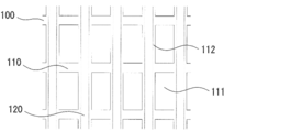
- FIG. 1 is a plan view showing an example of the shape of the insulating film.
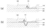
- FIG. 2 is a cross-sectional view illustrating a forward tapered shape as a cross-sectional shape of the insulating film.
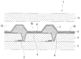
- FIG. 3 is a cross-sectional view schematically showing the structure of the main part of the organic EL device.
- the semiconductor layer constituting the TFT is a layer containing an oxide semiconductor containing one or more elements selected from In, Ga, Sn, Ti, Nb, Sb, and Zn.
- the total light transmittance of the insulating film is 0 to 15% at a wavelength of 300 to 400 nm.
- the display or lighting device is generically called “device”.
- Examples of the display device of the present invention include a liquid crystal display (LCD), an electrochromic display (ECD), an electroluminescent display (ELD), and particularly an organic EL display.
- LCD liquid crystal display
- ECD electrochromic display
- ELD electroluminescent display
- organic EL illumination is mentioned, for example.
- the TFT substrate, the first electrode, and the second electrode are, for example, specific examples described in the column of “organic EL display device and organic EL lighting device” described later (support substrate and TFT, anode, cathode). ) Can be exemplified.
- the insulating film is formed so as to cover at least a part of the first electrode and partially expose the first electrode.
- the insulating film is preferably formed so as to cover the edge portion of the first electrode.
- FIG. 1 An example of the shape of the insulating film is shown in FIG.
- a first electrode 110 formed in a stripe shape is formed on the TFT substrate 100, and an insulating film 120 is formed on the TFT substrate 100 and the first electrode 110 so as to partially expose the first electrode 110.
- the exposed portion of the first electrode 110 is also referred to as “opening 111”.
- the insulating film 120 is formed so as to cover the edge portion 112 of the first electrode 110.
- the opening 111 can correspond to one light emitting region, that is, a pixel.
- the cross-sectional shape of the insulating film is preferably a forward tapered shape at the boundary portion where the first electrode is exposed.
- the “forward taper shape” means that an angle ⁇ formed by the slope 121 of the boundary portion where the first electrode 110 is exposed in the insulating film 120 and the first electrode surface 113, for example, the angle ⁇ in FIG. 2 is less than 90 °.
- the angle ⁇ is also referred to as “taper angle ⁇ ”.
- the taper angle ⁇ is preferably 80 ° or less, more preferably 5 to 60 °, and more preferably 10 to 45 °.
- the cross-sectional shape of the insulating film at the boundary portion is a forward taper shape, even when the organic light emitting layer and the second electrode are formed after the insulating film is formed, these films are smooth at the boundary portion. Thus, unevenness of the film thickness due to the level difference can be reduced, and a light-emitting device having stable characteristics can be obtained.
- the thickness of the insulating film is not particularly limited, but is preferably 0.3 to 15.0 ⁇ m, more preferably 0.5 to 10.0 ⁇ m in view of light shielding properties and ease of film formation and patterning. More preferably, the thickness is 1.0 to 5.0 ⁇ m.
- the insulating film is formed so as to straddle adjacent first electrodes, for example. For this reason, the insulating film is required to have good electrical insulation.
- the volume resistivity of the insulating film is preferably 10 10 ⁇ ⁇ cm or more, more preferably 10 12 ⁇ ⁇ cm or more.
- the insulating film has a total light transmittance of 0 to 15% at a wavelength of 300 to 400 nm, preferably 0 to 10%, particularly preferably 0 to 6%. That is, the maximum value of the total light transmittance at a wavelength of 300 to 400 nm is 15% or less, preferably 10% or less, and particularly preferably 6% or less.
- the total light transmittance can be measured using, for example, a spectrophotometer (“150-20 type double beam” manufactured by Hitachi, Ltd.).
- the insulating film is, for example, a partition wall that partitions the surface of the TFT substrate into a plurality of regions, and pixels are formed in the plurality of regions.
- the insulating film (partition wall) is preferably formed on the TFT substrate so as to be disposed at least above the semiconductor layer, from the viewpoint of light shielding with respect to the semiconductor layer included in the TFT.
- “upward” is a direction from the TFT substrate toward the second electrode.
- the insulating film exposing the first electrode has a light shielding property at the wavelength.
- the insulating film functions as a light-shielding film. Photodegradation of the semiconductor layer due to use or the like can be suppressed.
- the semiconductor layer constituting the TFT is a layer containing an oxide semiconductor containing one or more elements selected from In, Ga, Sn, Ti, Nb, Sb and Zn.
- oxide semiconductor containing one or more elements selected from In, Ga, Sn, Ti, Nb, Sb and Zn examples include a single crystal oxide, a polycrystalline oxide, an amorphous oxide, and a mixture thereof.
- an oxide semiconductor containing one or more elements selected from In, Ga, Sn, Ti, Nb, Sb, and Zn for example, a quaternary system such as an In—Sn—Ga—Zn—O-based oxide semiconductor Metal oxide: In-Ga-Zn-O-based oxide semiconductor, In-Sn-Zn-O-based oxide semiconductor, In-Al-Zn-O-based oxide semiconductor, Sn-Ga-Zn-O-based oxide Ternary metal oxides such as semiconductors, Al—Ga—Zn—O-based oxide semiconductors, Sn—Al—Zn—O-based oxide semiconductors; In—Zn—O-based oxide semiconductors, Sn—Zn—O-based semiconductors Oxide semiconductors, Al—Zn—O-based oxide semiconductors, Zn—Mg—O-based oxide semiconductors, Sn—Mg—O-based oxide semiconductors, In—Mg—O-based oxide semiconductors, In—Ga—O Binary metal oxides such as In-based materials;
- the semiconductor layer constituting the TFT is the above oxide semiconductor layer, particularly when the semiconductor layer is an oxide semiconductor layer made of an In—Ga—Zn—O-based oxide semiconductor (IGZO semiconductor). Photodegradation can be prevented.
- IGZO semiconductor In—Ga—Zn—O-based oxide semiconductor
- the apparatus of the present invention includes a first electrode provided on the TFT substrate and connected to the TFT, an organic light emitting layer formed on the first electrode in a region partitioned by the partition, and an organic light emitting layer
- An organic EL device having an organic EL element including the second electrode provided on the top is preferable.
- the TFT substrate includes, for example, a support substrate, a TFT provided on the support substrate corresponding to the organic EL element, and a planarization layer covering the TFT.
- the first electrode is formed on the planarization layer, and is connected to the TFT via a wiring formed in a through hole penetrating the planarization layer.
- the insulating film (partition wall) having a light shielding property is preferably formed on the first electrode and the planarization layer so as to partially expose the first electrode.
- the insulating film exposing the first electrode can be formed using, for example, a radiation sensitive material.
- the radiation-sensitive material includes a positive type in which the solubility in a developer is increased by exposure and the exposed part is removed, and a negative type in which the exposed part is cured and the non-exposed part is removed.
- a coating film formed from a radiation-sensitive material usually, light is strongly absorbed at the surface portion of the coating film, and the amount of absorption tends to decrease toward the inside of the coating film.
- the solubility of the surface portion of the coating film is larger than the internal solubility, and in the negative type, the opposite tendency tends to occur.
- the cross-sectional shape of the boundary portion of the insulating film is preferably forward tapered, it is preferable to form a pattern using a positive radiation sensitive material.
- the radiation-sensitive material can be used for forming the insulating film in the display or lighting device of the present invention.
- the radiation sensitive material preferably comprises a polymer (A), a photosensitizer (B), and at least one resin (C) selected from a novolac resin, a resole resin, and a condensate of a resole resin. contains.
- the radiation sensitive material may contain a cross-linking agent (D) or a solvent (E) as a suitable component. Moreover, the said radiation sensitive material may contain another arbitrary component in the range which does not impair the effect of this invention.
- the above-mentioned radiation-sensitive material has high radiation sensitivity, and by using the material, an insulating film having an excellent pattern shape can be formed, and it is possible to meet demands for a narrow pitch pattern. Further, an insulating film having low water absorption can be formed by using the above material.
- the polymer (A) is preferably an alkali-soluble polymer other than the resin (C).
- the alkali-soluble in the polymer (A) means that the polymer (A) can be dissolved in an alkali solution, for example, an aqueous 2.38 mass% tetramethylammonium hydroxide solution.
- polymer (A) examples include polyimide (A1), polyimide precursor (A2), acrylic resin (A3), polysiloxane (A4), polybenzoxazole (A5-1), and polybenzoxazole.
- examples thereof include at least one polymer selected from the precursor (A5-2), the polyolefin (A6), and the cardo resin (A7).
- the weight average molecular weight (Mw) in terms of polystyrene of the polymer (A) is preferably 2,000 to 500,000, preferably 3,000 to 100,000, as measured by gel permeation chromatography (GPC). More preferred is 4,000 to 50,000.
- Mw is not less than the lower limit of the above range, an insulating film having sufficient mechanical properties tends to be obtained.
- the Mw is not more than the upper limit of the above range, the solubility of the polymer (A) in the solvent or developer tends to be excellent.
- the content of the polymer (A) is preferably 10 to 80% by mass, more preferably 20 to 70% by mass, and further preferably 30 to 60% by mass with respect to 100% by mass of the total solid content in the radiation-sensitive material. preferable.
- the polyimide (A1) preferably has a structural unit represented by the formula (A1).
- R 1 is a divalent group having a hydroxyl group
- X is a tetravalent organic group
- R 1 examples include a divalent group represented by the formula (a1).
- R 2 is a single bond, oxygen atom, sulfur atom, sulfonyl group, carbonyl group, methylene group, dimethylmethylene group or bis (trifluoromethyl) methylene group;
- R 3 is independently A hydrogen atom, a formyl group, an acyl group or an alkyl group; However, at least one of R 3 is a hydrogen atom.
- n1 and n2 are each independently an integer of 0 to 2. However, at least one of n1 and n2 is 1 or 2. When the total of n1 and n2 is 2 or more, the plurality of R 3 may be the same or different.
- examples of the acyl group include groups having 2 to 20 carbon atoms such as an acetyl group, a propionyl group, a butyryl group, and an isobutyryl group;
- examples of the alkyl group include a methyl group, an ethyl group, and n- Examples thereof include groups having 1 to 20 carbon atoms such as propyl group, isopropyl group, n-butyl group, n-pentyl group, n-hexyl group, n-octyl group, n-decyl group and n-dodecyl group.
- the divalent group represented by the formula (a1) is preferably a divalent group having 1 to 4 hydroxyl groups, and more preferably a divalent group having 2 hydroxyl groups.
- Examples of the divalent group having 1 to 4 hydroxyl groups represented by the formula (a1) include a divalent group represented by the following formula. In the following formula, two “-” extending from the aromatic ring represent a bond.
- Examples of the tetravalent organic group represented by X include a tetravalent aliphatic hydrocarbon group, a tetravalent aromatic hydrocarbon group, and a group represented by the following formula (1).
- X is preferably a tetravalent organic group derived from tetracarboxylic dianhydride. Among these, a group represented by the following formula (1) is preferable.
- Ar is each independently a trivalent aromatic hydrocarbon group
- A is a direct bond or a divalent group.
- the divalent group include an oxygen atom, a sulfur atom, a sulfonyl group, a carbonyl group, a methylene group, a dimethylmethylene group, and a bis (trifluoromethyl) methylene group.
- the carbon number of the tetravalent aliphatic hydrocarbon group is usually 4 to 30, preferably 8 to 24.
- the carbon number of the tetravalent aromatic hydrocarbon group and the trivalent aromatic hydrocarbon group in the above formula (1) is usually 6-30, preferably 6-24.
- Examples of the tetravalent aliphatic hydrocarbon group include a chain hydrocarbon group, an alicyclic hydrocarbon group, and an aliphatic hydrocarbon group containing an aromatic ring in at least a part of the molecular structure.
- tetravalent chain hydrocarbon group examples include tetravalent groups derived from chain hydrocarbons such as n-butane, n-pentane, n-hexane, n-octane, n-decane, and n-dodecane. Can be mentioned.
- Examples of the tetravalent alicyclic hydrocarbon group include monocyclic hydrocarbons such as cyclobutane, cyclopentane, cyclopentene, methylcyclopentane, cyclohexane, cyclohexene, and cyclooctane; bicyclo [2.2.1] heptane, bicyclo Bicycles such as [3.1.1] heptane, bicyclo [3.1.1] hept-2-ene, bicyclo [2.2.2] octane, bicyclo [2.2.2] oct-5-ene formula hydrocarbons; tricyclo [5.2.1.0 2,6] decane, tricyclo [5.2.1.0 2, 6] deca-4-ene, adamantane, tetracyclo [6.2.1.1 3 , 6 . 0 2,7 ] tetravalent groups derived from tricyclic or higher hydrocarbons such as dodecane.
- monocyclic hydrocarbons such as cycl
- aliphatic hydrocarbon group containing an aromatic ring in at least a part of the molecular structure for example, a group in which the number of benzene nuclei contained in the group is 3 or less is preferable, and one group is particularly preferable. More specifically, tetravalent groups derived from 1-ethyl-6-methyl-1,2,3,4-tetrahydronaphthalene, 1-ethyl-1,2,3,4-tetrahydronaphthalene and the like can be mentioned. .
- the tetravalent group derived from the above hydrocarbon is a tetravalent group formed by removing four hydrogen atoms from the above hydrocarbon.
- the excluded portion of the four hydrogen atoms is a portion where a tetracarboxylic dianhydride structure can be formed when the four hydrogen atoms are substituted with four carboxyl groups.
- the tetravalent aliphatic hydrocarbon group is preferably a tetravalent group represented by the following formula.
- four “-” s extending from the chain hydrocarbon group and the alicyclic ring represent a bond.
- Examples of the tetravalent aromatic hydrocarbon group and the group represented by the above formula (1) include a tetravalent group represented by the following formula. In the following formula, four “-” extending from the aromatic ring indicate a bond.
- a polyimide (A1) can be obtained by imidation of the polyimide precursor (A2) demonstrated below.
- the imidization here may proceed completely or partially. In other words, the imidation ratio may not be 100%. Therefore, the polyimide (A1) further has at least one selected from the structural unit represented by the formula (A2-1) and the structural unit represented by the formula (A2-2), which will be described below. May be.
- the imidation ratio is preferably 5% or more, more preferably 7.5% or more, and further preferably 10% or more.
- the upper limit value of the imidization rate is preferably 50%, more preferably 30%.
- the total content of the structural units represented by the formula (A1), formula (A2-1), and formula (A2-2) is usually 50% by mass or more, preferably 60% by mass or more. Preferably it is 70 mass% or more, Most preferably, it is 80 mass% or more.
- the polyimide precursor (A2) is a compound that can generate a polyimide (A1), preferably a polyimide (A1) having a structural unit represented by the formula (A1), by dehydration and cyclization (imidization).
- Examples of the polyimide precursor (A2) include polyamic acid and polyamic acid derivatives.
- the polyamic acid has a structural unit represented by the formula (A2-1).
- R 1 is a divalent group having a hydroxyl group
- X is a tetravalent organic group.
- Examples of the divalent group having a hydroxyl group represented by R 1 and the tetravalent organic group represented by X include the same groups as those exemplified as R 1 and X in the formula (A1).
- the content of the structural unit represented by the formula (A2-1) is usually 50% by mass or more, preferably 60% by mass or more, more preferably 70% by mass or more, and particularly preferably 80% by mass or more. is there.
- the polyamic acid derivative is a derivative synthesized by esterification of polyamic acid or the like.
- the polyamic acid derivative include a polymer in which the hydrogen atom of the carboxyl group in the structural unit represented by the formula (A2-1) of the polyamic acid is substituted with another group, and a polyamic acid ester is preferable.
- the polyamic acid ester is a polymer in which at least a part of the carboxyl group of the polyamic acid is esterified.
- Examples of the polyamic acid ester include a polymer having a structural unit represented by the formula (A2-2) capable of producing a polyimide (A1) having the structural unit represented by the formula (A1).
- R 1 is a divalent group having a hydroxyl group
- X is a tetravalent organic group
- R 4 is independently an alkyl group having 1 to 5 carbon atoms.
- Examples of the divalent group having a hydroxyl group represented by R 1 and the tetravalent organic group represented by X include the same groups as those exemplified as R 1 and X in the formula (A1).
- Examples of the alkyl group having 1 to 5 carbon atoms represented by R 4 include a methyl group, an ethyl group, and a propyl group.
- the content of the structural unit represented by the formula (A2-2) is usually 50% by mass or more, preferably 60% by mass or more, more preferably 70% by mass or more, and particularly preferably 80% by mass or more. It is.
- the polyamic acid which is a polyimide precursor (A2) can be obtained, for example, by polymerizing a tetracarboxylic dianhydride, a diamine having a hydroxyl group and a diamine containing another diamine as required.
- the proportion of these used is, for example, 0.3 to 4 mol, preferably approximately equimolar, of the total diamine to 1 mol of the tetracarboxylic dianhydride.
- the mixed solution of the tetracarboxylic dianhydride and the total diamine is preferably heated at 50 ° C. to 200 ° C. for 1 hour to 24 hours.
- the tetracarboxylic dianhydride and the diamine having a hydroxyl group are also referred to as “acid dianhydride (A1-1) and“ diamine (A1-2) ”, respectively, and the other diamine is referred to as“ diamine (A1- 2 ') ".
- Polyamic acid may be synthesized by dissolving diamine (A1-2) in a polymerization solvent and then reacting diamine (A1-2) with acid dianhydride (A1-1).
- the anhydride (A1-1) may be dissolved in a polymerization solvent, and then the acid dianhydride (A1-1) and the diamine (A1-2) may be reacted.
- the polyamic acid derivative which is a polyimide precursor (A2) can be synthesized by esterifying the carboxyl group of the polyamic acid.
- a well-known method is applicable.
- the polyimide (A1) can be synthesized, for example, by synthesizing a polyamic acid by the above method and then dehydrating and cyclizing (imidizing) the polyamic acid; and a polyamic acid derivative is synthesized by the above method. Then, it can also synthesize
- the imidization reaction of the polyamic acid and the polyamic acid derivative a known method such as a heat imidization reaction or a chemical imidization reaction can be applied.
- a heating imidization reaction it is preferable to heat the solution containing the polyamic acid and / or the polyamic acid derivative at 120 ° C. to 210 ° C. for 1 hour to 16 hours.
- the imidization reaction may be carried out while removing water in the system using an azeotropic solvent such as toluene, xylene, mesitylene or the like, if necessary.
- dicarboxylic acid such as maleic anhydride is used as an end-capping agent for sealing the end groups of polyimide, polyamic acid and polyamic acid derivatives.
- Anhydrides may be used.
- Acid dianhydride (A1-1) is, for example, an acid dianhydride represented by the formula (a2).
- X is a tetravalent organic group.
- Examples of the tetravalent organic group represented by X include the same groups as those exemplified as X in formula (A1).
- the diamine (A1-2) is, for example, a diamine represented by the formula (a3).
- R 1 is a divalent group having a hydroxyl group.
- the divalent group having a hydroxyl group represented by R 1, include those similar to the groups exemplified as R 1 in the formula (A1).
- diamine (A1-2) In addition to the diamine (A1-2), another diamine (A1-2 ') other than the (A1-2) may be used.
- the other diamine (A1-2 ′) include at least one diamine selected from an aromatic diamine and an aliphatic diamine having no hydroxyl group.
- the polyimide (A1) further has a structural unit in which R 1 in the formulas (A1), (A2-1) and (A2-2) is replaced with the residue of the other diamine (A1-2 ′). It may be.
- the polyimide precursor (A2) further has a structural unit in which R 1 in the formulas (A2-1) and (A2-2) is replaced with the residue of the other diamine (A1-2 ′). You may do it.
- polymerization solvent used for the synthesis of the polyimide (A1) and the polyimide precursor (A2)
- these synthesis raw materials and the above (A1) and (A2) can be dissolved, and a low water-absorbing solvent is preferable.
- a polymerization solvent the solvent similar to the solvent illustrated as the solvent (E) mentioned later can be used.
- the step of dissolving can be eliminated. Thereby, the productivity of the apparatus of the present invention can be improved.
- the polyimide (A1) and the polyimide precursor (A2) preferably have the above specific structure having a hydroxyl group, and thereby have excellent solubility in the solvent (E) described later. Therefore, these polymers are also soluble in a low water-absorbing solvent other than N-methylpyrrolidone (NMP), for example, the solvent (E) described later.
- NMP N-methylpyrrolidone
- the insulating film formed from the radiation-sensitive material can have a lower water absorption.
- Acrylic resin (A3) is, for example, at least selected from (meth) acrylic acid alkyl ester, (meth) acrylic acid alicyclic group-containing ester, and (meth) acrylic acid aryl group-containing ester.
- One monomer A is mentioned.
- examples of the monomer constituting the above (A3) include at least one acid group-containing monomer B selected from unsaturated monocarboxylic acid, unsaturated dicarboxylic acid, and unsaturated dicarboxylic anhydride.
- a monomer which comprises the said (A3) at least 1 chosen from the hydroxyalkyl ester of (meth) acrylic acid, the epoxy-group-containing ester of (meth) acrylic acid, and the oxetanyl group-containing ester of (meth) acrylic acid. Also included are the functional group-containing monomers C of the species.
- Examples of the (meth) acrylic acid alkyl ester include methyl (meth) acrylate, ethyl (meth) acrylate, n-butyl (meth) acrylate, sec-butyl (meth) acrylate, isopropyl (meth) acrylate, t-butyl (
- Examples of the alicyclic group-containing ester of (meth) acrylic acid include monocyclic hydrocarbon group-containing esters such as cyclohexyl (meth) acrylate and 2-methylcyclohexyl (meth) acrylate, Examples thereof include polycyclic group-containing esters such as cyclopentanyl (meth) acrylate, dicyclopentanyloxyethyl (meth) acrylate, and isoboronyl (meth) acrylate;
- examples of aryl group-containing esters of (meth) acrylic acid include , Phenyl (meth) ac Rate, benzyl (meth)
- Examples of the unsaturated monocarboxylic acid include (meth) acrylic acid, crotonic acid, 2- (meth) acryloyloxyethyl succinic acid; examples of the unsaturated dicarboxylic acid include maleic acid, fumaric acid, citracone Acid, mesaconic acid, itaconic acid; unsaturated dicarboxylic acid anhydrides include, for example, maleic anhydride and itaconic anhydride.
- Examples of the hydroxyalkyl ester of (meth) acrylic acid include 2-hydroxyethyl methacrylate and 2-hydroxypropyl methacrylate; examples of the epoxy group-containing ester of (meth) acrylic acid include glycidyl (meth) acrylate.
- the content of the structural unit derived from the monomer A is usually 5% by mass or more, preferably 10 to 85% by mass, more preferably 15 to 75% by mass.
- the content of the structural unit derived from B is usually 5 to 70% by mass, preferably 10 to 60% by mass, more preferably 15 to 50% by mass, and the content of the structural unit derived from the functional group-containing monomer C is included.
- the amount is usually 90% by mass or less, preferably 5 to 80% by mass, more preferably 10 to 70% by mass.
- the total content of structural units derived from the epoxy group-containing ester of (meth) acrylic acid and the oxetanyl group-containing ester of (meth) acrylic acid is 10 to 70% by mass. Is more preferable, and more preferably 20 to 50% by mass.
- this structural unit is in the above range, the curing reaction proceeds sufficiently when the coating film formed from the radiation-sensitive material is heated, and the resulting pattern tends to have sufficient heat resistance and surface hardness, as well as sensitivity.
- the storage stability of the radioactive material also tends to be excellent.
- acrylic resin (A3) examples include diesters of unsaturated dicarboxylic acids such as diethyl maleate, diethyl fumarate and diethyl itaconate; styrene, ⁇ -methyl styrene, o-methyl styrene, m-methyl styrene Styrene monomers such as p-methylstyrene, vinyltoluene, and p-methoxystyrene can also be used.
- diesters of unsaturated dicarboxylic acids such as diethyl maleate, diethyl fumarate and diethyl itaconate
- styrene ⁇ -methyl styrene
- o-methyl styrene o-methyl styrene
- m-methyl styrene Styrene monomers such as p-methylstyrene, vinyltoluene, and p-methoxysty
- Examples of the solvent used for synthesizing the acrylic resin (A3) include alcohols such as methanol and ethanol; ethers such as tetrahydrofuran; glycol ethers such as ethylene glycol monomethyl ether and propylene glycol monomethyl ether; ethylene glycol monomethyl.
- Glycol ether acetates such as ether acetate and propylene glycol monomethyl ether acetate; other examples include aromatic hydrocarbons, ketones, and esters.
- the acrylic resin (A3) can be synthesized, for example, by radical polymerization of the above monomer.
- a radical polymerization initiator can be used, for example, 2,2′-azobisisobutyronitrile, 2,2′-azobis- (2,4-dimethylvaleronitrile), 2,2 Azo compounds such as' -azobis- (4-methoxy-2,4-dimethylvaleronitrile); benzoyl peroxide, lauroyl peroxide, t-butylperoxypivalate, 1,1-bis- (t-butylperoxy) cyclohexane, etc.
- examples include organic peroxides and hydrogen peroxide.
- a peroxide and a reducing agent may be combined to form a redox type initiator.
- Polysiloxane (A4) examples include polysiloxane obtained by reacting an organosilane represented by the formula (a4).
- R 1 is a hydrogen atom, an alkyl group having 1 to 10 carbon atoms, an alkenyl group having 2 to 10 carbon atoms, an aryl group-containing group having 6 to 15 carbon atoms, or an epoxy ring having 2 to 15 carbon atoms group, or the alkyl group formed by substituting a substituent one or more hydrogen atoms contained in the group (substituents) may be the same or different each when R 1 is more;
- R 2 is A hydrogen atom, an alkyl group having 1 to 6 carbon atoms, an acyl group having 1 to 6 carbon atoms, or an aryl group having 6 to 15 carbon atoms, and when there are a plurality of R 2 s , they may be the same or different;
- n Is an integer from 0 to 3.
- the substituent is at least one selected from, for example, a halogen atom, an amino group, a hydroxyl group, a mercapto group, an isocyanate group, and a (meth) acryloyloxy group.
- alkyl group and its substituent examples include, for example, methyl group, ethyl group, n-propyl group, isopropyl group, n-butyl group, t-butyl group, n-hexyl group, n-decyl group, trifluoromethyl group, 2,2,2-trifluoroethyl group, 3,3,3-trifluoropropyl group, 3-aminopropyl group, 3-mercaptopropyl group, 3-isocyanatopropyl group, 3- (meth) acryloyloxypropyl group Can be mentioned.
- alkenyl group examples include a vinyl group.
- aryl group-containing group examples include aryl groups such as a phenyl group, tolyl group, and naphthyl group; hydroxyaryl groups such as a p-hydroxyphenyl group; aralkyl groups such as a benzyl group and a phenethyl group; 1- (p-hydroxyphenyl) A hydroxyaralkyl group such as an ethyl group or 2- (p-hydroxyphenyl) ethyl group; a 4-hydroxy-5- (p-hydroxyphenylcarbonyloxy) pentyl group.
- Examples of the epoxy ring-containing group include a 3-glycidoxypropyl group and a 2- (3,4-epoxycyclohexyl) ethyl group.
- acyl group examples include an acetyl group.
- Examples of the aryl group include a phenyl group.
- N in the formula (a4) is an integer of 0 to 3.
- organosilane examples include tetrafunctional silanes such as tetramethoxysilane, tetraethoxysilane, tetraacetoxysilane, and tetraphenoxysilane; methyltrimethoxysilane, methyltriethoxysilane, methyltriisopropoxysilane, and methyltrin-butoxysilane.
- Organosilane may be used alone or in combination of two or more.
- the content of the phenyl group contained in the polysiloxane (A4) is preferably 20 to 70 mol, more preferably 35 to 55 moles.
- the phenyl group content is less than or equal to the above upper limit value, an insulating film having a high hardness tends to be obtained, and when the phenyl group content is greater than or equal to the lower limit value, an insulating film having a high crack resistance tends to be obtained. It is in.
- the content of the phenyl group is determined, for example, by measuring the 29 Si-nuclear magnetic resonance spectrum of polysiloxane (A4), and the peak area of Si to which the phenyl group is bonded and the peak area of Si to which the phenyl group is not bonded. It can be obtained from the ratio.
- Polysiloxane (A4) can be obtained, for example, by hydrolyzing and partially condensing the organosilane described above.
- a general method can be used for hydrolysis and partial condensation. For example, a solvent, water and, if necessary, a catalyst are added to organosilane, and the mixture is heated and stirred. During the stirring, hydrolysis by-products such as alcohol and condensation by-products such as water may be distilled off as necessary.
- the reaction temperature is not particularly limited, but is usually in the range of 0 ° C to 150 ° C.
- the reaction time is not particularly limited, but is usually in the range of 1 to 10 hours.
- the solvent examples include acetol, 3-hydroxy-3-methyl-2-butanone, 4-hydroxy-3-methyl-2-butanone, 5-hydroxy-2-pentanone, 4-hydroxy-4-methyl-2- Hydroxyl group-containing ketones such as pentanone (diacetone alcohol); ethyl lactate, butyl lactate, propylene glycol monomethyl ether, propylene glycol monoethyl ether, propylene glycol mono n-propyl ether, propylene glycol mono n-butyl ether, propylene glycol mono t- Examples include butyl ether, 3-methoxy-1-butanol, and 3-methyl-3-methoxy-1-butanol. Of these, diacetone alcohol is particularly preferably used.
- a solvent may be used individually by 1 type, or may be used in combination of 2 or more type.
- the amount of the solvent added is preferably 10 to 1000 parts by mass with respect to 100 parts by mass of the organosilane.
- the amount of water used for the hydrolysis reaction is preferably 0.5 to 2 mol with respect to 1 mol of hydrolyzable group.
- Examples of the catalyst include an acid catalyst and a base catalyst.
- Examples of the acid catalyst include hydrochloric acid, nitric acid, sulfuric acid, hydrofluoric acid, phosphoric acid, acetic acid, trifluoroacetic acid, formic acid, polyvalent carboxylic acid or anhydride thereof, and ion exchange resin.
- Base catalysts include triethylamine, tripropylamine, tributylamine, tripentylamine, trihexylamine, triheptylamine, trioctylamine, diethylamine, triethanolamine, diethanolamine, sodium hydroxide, potassium hydroxide, amino groups
- Examples include alkoxysilanes and ion exchange resins.
- the addition amount of the catalyst is preferably 0.01 to 10 parts by mass with respect to 100 parts by mass of the organosilane.
- the polybenzoxazole (A5-1) preferably has a structural unit represented by the formula (a5-1).
- the structural unit represented by the formula (a5-1) is also referred to as “structural unit (a5-1)”.
- X 1 is a tetravalent organic group having an aromatic ring
- Y 1 is a divalent organic group.
- X 1 is preferably a tetravalent group containing at least one aromatic ring, more preferably a group having a linear structure, and 1 to 4 aromatic rings. And a group having two aromatic rings is particularly preferable.
- Polybenzoxazole (A5-1) having such a structure is excellent in rigidity.
- the aromatic ring contained in X 1 may be either a substituted or unsubstituted ring.
- substituents include —OH, —COOH, an alkyl group, an alkoxy group, and an alicyclic hydrocarbon group.
- N and O bonded to X 1 are bonded to adjacent carbon atoms on the aromatic ring in X 1 to form a benzoxazole ring, for example.
- the plurality of aromatic rings may form any structure of a linked polycyclic system and a condensed polycyclic system, but form a linked polycyclic structure. It is preferable.
- Polybenzoxazole (A5-1) having such a structure is excellent in both light shielding properties and rigidity.
- the total number of carbon atoms in X 1 is preferably 6 to 24, more preferably 6 to 20, and still more preferably 6 to 18. Thereby, the said effect can be exhibited more notably.
- Examples of the structure of X 1 include a monocyclic structure such as a benzene ring, a condensed polycyclic structure such as a naphthalene ring, and a linked polycyclic structure such as a group represented by the formula (g1). Among these, the group represented by the formula (g1) is preferable.
- Ar 1 is each independently a trivalent aromatic hydrocarbon group, and R 1 is a direct bond or a divalent group.
- the trivalent aromatic hydrocarbon group for example, include a benzene ring, an alkyl group, an alkoxy group may have a substituent such as an alicyclic hydrocarbon group, substituted in the two Ar 1
- the groups may be bonded to each other to form a divalent group such as a carbonyl group that bridges two Ar 1 groups.
- divalent group examples include an oxygen atom, a sulfur atom, a sulfonyl group, a carbonyl group, a methylene group, a dimethylmethylene group, a bis (trifluoromethyl) methylene group, and a phenylene group.
- X 1 examples include, for example, a tetravalent group represented by the following formula.
- a tetravalent group represented by the following formula.
- four “-” s extending from the aromatic ring represent a bond.
- Y 1 is preferably a divalent group containing at least one ring selected from an alicyclic ring and an aromatic ring, and has 1 to 4 aromatic rings A group is more preferred, and a group having two aromatic rings is particularly preferred.
- Polybenzoxazole (A5-1) having such a structure is excellent in rigidity and light resistance.
- the alicyclic ring and aromatic ring contained in Y 1 may be either substituted or unsubstituted rings.
- substituents include —OH, —COOH, an alkyl group, an alkoxy group, an alkoxycarbonyl group, and an alicyclic hydrocarbon group.
- the plurality of rings may form any structure of a linked polycyclic system and a condensed polycyclic system, but form a linked polycyclic system structure.
- the plurality of rings may form any structure of a linked polycyclic system and a condensed polycyclic system, but form a linked polycyclic system structure.
- Polybenzoxazole (A5-1) having such a structure is excellent in both light shielding properties and rigidity.
- the total number of carbon atoms in Y 1 is preferably 4 to 24, more preferably 4 to 15, and still more preferably 6 to 12. Thereby, the said effect can be exhibited more notably.
- Examples of the structure of Y 1 include aromatic structures such as a monocyclic structure such as a benzene ring, a condensed polycyclic structure such as a naphthalene ring, and a linked polycyclic structure such as a group represented by the formula (g2).
- aromatic structures such as a monocyclic structure such as a benzene ring, a condensed polycyclic structure such as a naphthalene ring, and a linked polycyclic structure such as a group represented by the formula (g2).
- Ar 2 is each independently a divalent aromatic hydrocarbon group, and R 2 is a direct bond or a divalent group.
- the divalent aromatic hydrocarbon group for example, include a benzene ring, an alkyl group, an alkoxy group may have a substituent such as an alicyclic hydrocarbon group, substituted in the two Ar 2
- the groups may be bonded to each other to form a divalent group such as a carbonyl group that bridges two Ar 2 .
- divalent group examples include an oxygen atom, a sulfur atom, a sulfonyl group, a carbonyl group, a methylene group, a dimethylmethylene group, a bis (trifluoromethyl) methylene group, and a phenylene group.
- Y 1 examples include a divalent group represented by the following formula.
- two “-” extending from the aromatic ring and the alicyclic ring represent a bond.
- Polybenzoxazole (A5-1) can be obtained by cyclization reaction of polybenzoxazole precursor (A5-2) described below.
- the cyclization reaction here may proceed completely or partially. That is, the cyclization rate may not be 100%. Therefore, the polybenzoxazole (A5-1) may further have a structural unit represented by the formula (a5-2) described below.
- the structural unit represented by the formula (a5-2) is also referred to as “structural unit (a5-2)”.
- the cyclization rate is preferably 5% or more, more preferably 7.5% or more, and further preferably 10% or more.
- the upper limit of the cyclization rate is preferably 50%, more preferably 30%. When the cyclization rate is within the above range, it is preferable from the viewpoint of heat resistance and solubility of the exposed portion in the developer.
- the cyclization rate can be measured, for example, as follows. First, the infrared absorption spectrum of polybenzoxazole is measured to confirm the presence of an absorption peak (near 1557 cm ⁇ 1 , 1574 cm ⁇ 1 ) of the benzoxazole ring. Next, after heat-treating the polybenzoxazole at 350 ° C. for 1 hour, an infrared absorption spectrum is measured again. The peak intensity around 1554 cm ⁇ 1 before and after heat treatment is compared.
- the infrared absorption spectrum for example, “NICOLET6700FT-IR” (manufactured by Thermo Electron) is used.
- the total content of the structural units (a5-1) and (a5-2) is usually 50% by mass or more, preferably 60% by mass or more, more preferably 70% by mass or more. Especially preferably, it is 80 mass% or more.
- Polybenzoxazole precursor (A5-2) is dehydrated and cyclized to produce polybenzoxazole (A5-1), preferably polybenzoxazole (A5-1) having a structural unit (a5-1). It is a compound that can be The precursor (A5-2) has, for example, a structural unit represented by the formula (a5-2).
- X 1 is a tetravalent organic group having an aromatic ring, preferably a tetravalent group containing at least one aromatic ring. N and OH bonded to X 1 are bonded to adjacent carbon atoms on the same aromatic ring.
- Y 1 is a divalent organic group, preferably a divalent group containing at least one ring selected from an alicyclic ring and an aromatic ring.
- the divalent organic group represented by tetravalent organic group and Y 1 represented by X 1 include the same groups as the groups exemplified as X 1 and Y 1 in each formula (a5-1) It is done.
- the content of the structural unit (a5-2) is usually 50% by mass or more, preferably 60% by mass or more, more preferably 70% by mass or more, and particularly preferably 80% by mass. % Or more.
- the polybenzoxazole precursor (A5-1) can be obtained, for example, by polymerizing at least one selected from dicarboxylic acids, diesters thereof and dihalides and diamines having two hydroxyl groups.
- an active ester dicarboxylic acid derivative obtained by previously reacting a dicarboxylic acid with 1-hydroxybenzotriazole or the like may be used as the diester.
- the use ratio is, for example, 0.5 to 4 moles, preferably 1 to 2 moles of the diamine with respect to 1 mole of the total of the dicarboxylic acid, diester and dihalide.
- the mixed solution is preferably heated at 50 ° C. to 200 ° C. for 1 hour to 72 hours.
- Polybenzoxazole (A5-1) is synthesized, for example, by synthesizing polybenzoxazole precursor (A5-2) by the above method and then dehydrating and cyclizing this polybenzoxazole precursor (A5-2). can do.
- the solution containing the polybenzoxazole precursor (A5-2) is preferably heated at 150 ° C. to 400 ° C. for 1 hour to 16 hours. If necessary, it may be carried out while removing water in the system using an azeotropic solvent such as toluene, xylene, mesitylene and the like.
- the terminal blocking agent include dicarboxylic acid anhydrides such as maleic anhydride and 5-norbornene-2,3-dicarboxylic acid anhydride.
- the terminal amino group contained in the precursor is sealed as an amide using a terminal blocking agent. It is preferable.
- Examples of the polyolefin (A6) include a cyclic olefin polymer having a protic polar group.
- the protic polar group refers to an atomic group in which a hydrogen atom is directly bonded to an atom belonging to Group 15 or Group 16 of the periodic table.
- the atom belonging to Group 15 or 16 of the periodic table is preferably an atom belonging to the second or third period of Group 15 or 16 of the periodic table, and more preferably an oxygen atom, nitrogen atom or sulfur An atom, particularly preferably an oxygen atom.
- protic polar group examples include polar groups having an oxygen atom such as a hydroxyl group, a carboxyl group (hydroxycarbonyl group), a sulfonic acid group, and a phosphoric acid group; a primary amino group, a secondary amino group, and a primary group
- examples include polar groups having nitrogen atoms such as amide groups and secondary amide groups (imide groups); polar groups having sulfur atoms such as thiol groups.
- a polar group having an oxygen atom is preferable, more preferably a hydroxyl group or a carboxyl group, still more preferably a phenolic hydroxyl group or a carboxyl group, and particularly preferably a carboxyl group.
- examples of polar groups other than protic polar groups include, for example, acyloxy groups, alkoxycarbonyl groups, aryloxycarbonyl groups, halogen atoms, cyano groups, alkoxy groups, tertiary amino groups, (meth) Examples include acryloyl group, carbonyl group, sulfonyl group, N-substituted imide group, epoxy group, carbonyloxycarbonyl group (dicarboxylic acid anhydride structure).
- an acyloxy group, an alkoxycarbonyl group, an aryloxycarbonyl group, an N-substituted imide group, a halogen atom and a cyano group are preferable, and an acyloxy group, an alkoxycarbonyl group, an aryloxycarbonyl group and an N-substituted imide group are more preferable.
- N-substituted imide groups are particularly preferred.
- the cyclic olefin polymer is a homopolymer or copolymer of a cyclic olefin having a cyclic structure such as an alicyclic ring or an aromatic ring and a carbon-carbon double bond.
- the cyclic olefin polymer may have a structural unit derived from a monomer other than the cyclic olefin.
- monomer A unit the structural unit derived from monomer A is also referred to as “monomer A unit”.
- the content ratio of the cyclic olefin unit in all the structural units of the cyclic olefin polymer is usually 30 to 100% by mass, preferably 50 to 100% by mass, more preferably 70 to 100% by mass.
- the ratio of the monomer unit having a protic polar group to the other monomer unit is generally 100/0 to 10/90, preferably 90/10 to 20/80, and more preferably 80/20 to 30/70 in terms of mass ratio.
- the protic polar group may be bonded to the cyclic olefin unit or may be bonded to a monomer unit other than the cyclic olefin unit. Bonding is preferred.
- Examples of the monomer that forms the cyclic olefin polymer having a protic polar group include, for example, a cyclic olefin (a) having a protic polar group, a cyclic olefin (b) having a polar group other than the protic polar group, and polar Examples thereof include a cyclic olefin having no group (c) and a monomer (d) other than the cyclic olefin.
- the monomer (d) may have a protic polar group or other polar group, and may not have a polar group at all.
- the cyclic olefins (a) to (c) are also referred to as “monomers (a) to (c)”, respectively.
- the cyclic olefin polymer having a protic polar group includes a monomer (a), at least one selected from the monomer (b) and the monomer (c), and a monomer (if necessary) d), and more preferably, the monomer (a), the monomer (b) and, if necessary, the monomer (d).
- Examples of the monomer (a) include cyclic olefins represented by the following formula.
- R a1 to R a4 each independently represents a hydrogen atom or —X n —R a5 .
- X is a divalent organic group.
- n is 0 or 1.
- R a5 is an alkyl group, an aromatic group, or the above-described protic polar group, and each of the alkyl group and the aromatic group may have a substituent.
- At least one of R a1 to R a4 is a —X n —R a5 group in which R a5 is a protic polar group.
- m is an integer of 0 to 2, preferably 0 or 1.
- Examples of the divalent organic group in X include an alkylene group having 1 to 18 carbon atoms such as a methylene group and an ethylene group, and an arylene group having 6 to 24 carbon atoms such as a phenylene group.
- the alkyl group for R a5 is, for example, a linear or branched alkyl group having 1 to 18 carbon atoms, and specific examples thereof include a methyl group, an ethyl group, an n-propyl group, and an isopropyl group.
- the aromatic group in R 5 is, for example, an aromatic group having 6 to 24 carbon atoms, and specific examples thereof include an aryl group such as a phenyl group and an aralkyl group such as a benzyl group.
- R a1 is preferably a carboxyl group or a hydroxyaryl group having 6 to 24 carbon atoms such as a hydroxyphenyl group, and more preferably a carboxyl group.
- R a2 is preferably a hydrogen atom, an alkyl group having 1 to 18 carbon atoms such as a methyl group, or a carboxyalkyl group having 2 to 18 carbon atoms such as a carboxymethyl group.
- R a3 and R a4 are preferably hydrogen atoms.
- Examples of the monomer (a) include 8-carboxytetracyclo [4.4.0.1 2,5 . 1 7,10 ] dodeca-3-ene.
- Monomer (a) may be used alone or in combination of two or more.
- Examples of the monomer (b) include cyclic olefins represented by the following formula.
- R b1 is a polar group other than the above-mentioned protic polar group, preferably an acyloxy group having 2 to 12 carbon atoms such as an acetoxy group, a methoxycarbonyl group, an ethoxycarbonyl group, n- Allyl having 7 to 24 carbon atoms such as an alkoxycarbonyl group having 2 to 12 carbon atoms such as propoxycarbonyl group, isopropoxycarbonyl group, n-butoxycarbonyl group and 2,2,2-trifluoroethoxycarbonyl group, and phenoxycarbonyl group A roxycarbonyl group, a cyano group, or a halogen atom such as a chlorine atom; R b2 is a hydrogen atom or an alkyl group having 1 to 18 carbon atoms such as a methyl group. R b3 and R b4 are hydrogen atoms. m is an integer of 0 to 2, preferably 0 or
- R b1 to R b4 in any combination, together with the two carbon atoms to which they are bonded, form a 3- to 5-membered heterocyclic structure containing an oxygen atom or a nitrogen atom as a ring constituent atom. Also good.
- Examples of the 3-membered heterocyclic structure include an epoxy structure.
- dicarboxylic anhydride structure [—C ( ⁇ O) —O—C ( ⁇ O) —]
- dicarboximide structure [—C ( ⁇ O) —NR b5 —C ( ⁇ O )-]
- R b5 is an aryl group having 6 to 24 carbon atoms such as a phenyl group, a naphthyl group, or an anthracenyl group.
- a dicarboximide structure is preferable.
- Examples of the monomer (b) include N-phenyl- (5-norbornene-2,3-dicarboximide).
- Monomer (b) may be used alone or in combination of two or more.
- Examples of the monomer (c) include bicyclo [2.2.1] hept-2-ene (common name: norbornene), 5-ethyl-bicyclo [2.2.1] hept-2-ene, Butyl-bicyclo [2.2.1] hept-2-ene, 5-ethylidene-bicyclo [2.2.1] hept-2-ene, 5-methylidene-bicyclo [2.2.1] hept-2 -Ene, 5-vinyl-bicyclo [2.2.1] hept-2-ene, tricyclo [4.3.0.1 2,5 ] deca-3,7-diene (common name: dicyclopentadiene), tetracyclo [8.4.0.1 11,14.
- Monomer (c) may be used alone or in combination of two or more.
- Examples of monomers (d) other than cyclic olefins include chain olefins.
- chain olefins include ethylene; propylene, 1-butene, 1-pentene, 1-hexene, 3-methyl-1-butene, 3-methyl-1-pentene, 3-ethyl-1-pentene, 4- Methyl-1-pentene, 4-methyl-1-hexene, 4,4-dimethyl-1-hexene, 4,4-dimethyl-1-pentene, 4-ethyl-1-hexene, 3-ethyl-1-hexene, ⁇ -olefins having 2 to 20 carbon atoms such as 1-octene, 1-decene, 1-dodecene, 1-tetradecene, 1-hexadecene, 1-octadecene, 1-eicocene, etc .; 1,4-hexadiene, 4-methyl-1 , 4-hexadiene, 5-
- Monomer (d) may be used alone or in combination of two or more.
- the cyclic olefin polymer having a protic polar group can be obtained by polymerizing the monomer (a) with at least one monomer selected from the monomers (b) to (d), if desired. it can.
- the polymer obtained by polymerization may be further hydrogenated. Hydrogenated polymers are also included in cyclic olefin polymers having a protic polar group.
- a polymerization method for polymerizing the monomer (a) together with at least one monomer selected from the monomers (b) to (d) as desired may be in accordance with a conventional method. Examples include a ring polymerization method and an addition polymerization method.
- polymerization catalyst for example, a metal complex such as molybdenum, ruthenium, or osmium is preferably used. These polymerization catalysts may be used individually by 1 type, and may be used in combination of 2 or more type.
- the amount of the polymerization catalyst is usually from 1: 100 to 1: 2,000,000, preferably from 1: 500 to 1: 1,000,000, more preferably, as a molar ratio of metal compound to cyclic olefin in the polymerization catalyst. Is in the range of 1: 1,000 to 1: 500,000.
- the hydrogenation of the polymer obtained by polymerizing the above monomers is usually carried out using a hydrogenation catalyst.
- a hydrogenation catalyst for example, those generally used for hydrogenation of olefin compounds can be used. Specific examples include Ziegler type homogeneous catalysts, noble metal complex catalysts, and supported noble metal catalysts.
- hydrogenation catalysts no side reactions such as modification of functional groups occur, and carbon-carbon unsaturated bonds in the polymer can be selectively hydrogenated, so that noble metal complex catalysts such as rhodium and ruthenium are used.
- noble metal complex catalysts such as rhodium and ruthenium are used.
- a nitrogen-containing heterocyclic carbene compound having a high electron donating property or a ruthenium catalyst coordinated with a phosphine is particularly preferable.
- a cyclic olefin polymer having a protic polar group can also be obtained by introducing a protic polar group into a cyclic olefin polymer having no protic polar group using a known modifier and hydrogenating the polymer if desired. Obtainable. Hydrogenation may be performed on the polymer before introduction of the protic polar group. Moreover, the cyclic olefin polymer having a protic polar group may be further modified to introduce a protic polar group.
- the cyclic olefin polymer having no protic polar group is obtained, for example, by polymerizing at least one monomer selected from monomers (b) to (c) and, if necessary, the monomer (d). Can be obtained.
- a compound having a protic polar group and a reactive carbon-carbon unsaturated bond in one molecule is usually used.
- examples of such compounds include acrylic acid, methacrylic acid, angelic acid, tiglic acid, oleic acid, elaidic acid, erucic acid, brassic acid, maleic acid, fumaric acid, citraconic acid, mesaconic acid, itaconic acid, and atropic acid.
- Unsaturated carboxylic acids such as cinnamic acid; allyl alcohol, methyl vinyl methanol, crotyl alcohol, methallyl alcohol, 1-phenylethen-1-ol, 2-propen-1-ol, 3-buten-1-ol 3-buten-2-ol, 3-methyl-3-buten-1-ol, 3-methyl-2-buten-1-ol, 2-methyl-3-buten-2-ol, 2-methyl-3 Insaturation of buten-1-ol, 4-penten-1-ol, 4-methyl-4-penten-1-ol, 2-hexen-1-ol, etc. Alcohol and the like.
- the modification reaction of the cyclic olefin polymer using the above modifier may be carried out in accordance with a conventional method, and is usually performed in the presence of a radical generator.
- cyclic olefin polymer having a protic polar group for example, a polymer having a structural unit represented by the formula (A6-1) is preferable, and the structural unit represented by the formula (A6-1) and the formula (A6 A polymer having a structural unit represented by -2) is more preferred.
- R a1 to R a4 and m have the same meanings as the same symbols in formula (a6-1).
- R b1 to R b4 and m have the same meanings as the same symbols in formula (b6-1).
- the cardo resin (A7) is a resin having a cardo structure.
- the cardo structure refers to a skeletal structure in which two cyclic structures are bonded to ring carbon atoms constituting the cyclic structure.
- As a general structure of the cardo structure a structure in which two aromatic rings (eg, benzene ring) are bonded to the 9th-position carbon atom of the fluorene ring can be mentioned.
- the cardo resin it is preferable to use a cardo resin having at least one group selected from a carboxyl group and a phenolic hydroxyl group from the viewpoint of alkali solubility.
- skeleton structure in which two cyclic structures are bonded to the ring carbon atoms constituting the cyclic structure include a 9,9-bis (phenyl) fluorene skeleton, a 9,9-bis (hydroxyphenyl) fluorene skeleton, 9 , 9-bis (cyanophenyl or aminoalkylphenyl) fluorene skeleton, 9,9-bis (phenyl) fluorene skeleton having an epoxy group, 9,9-bis (phenyl) fluorene skeleton having a (meth) acryl group .
- the cardo resin is formed by polymerizing a skeleton having the cardo structure by a reaction between functional groups bonded thereto.
- a cardo resin has, for example, a structure in which a main chain and a cyclic structure that is a bulky side chain are connected by one element (cardo structure), and has a cyclic structure in a direction substantially perpendicular to the main chain. .
- the cardo resin is, for example, a polymer obtained by polymerizing a monomer having a cardo structure, but may be a copolymer with another copolymerizable monomer.
- the polymerization method of the monomer may be according to a conventional method, and for example, a ring-opening polymerization method or an addition polymerization method is employed.
- Examples of the cardo resin include a monomer polymer having a cardo structure.
- Examples of the monomer having a cardo structure include cardo structures such as 9,9-bis (4-glycidyloxyphenyl) fluorene and 9,9-bis [4- (2-glycidyloxyethoxy) phenyl] fluorene.
- cardo structures such as 9,9-bis (4-glycidyloxyphenyl) fluorene and 9,9-bis [4- (2-glycidyloxyethoxy) phenyl] fluorene.
- -Containing epoxy compound cardostructure-containing (meth) acrylic compound such as a compound represented by the following formula; 9,9-bis (4-hydroxyphenyl) fluorene, 9,9-bis (4-hydroxy-3-methylphenyl)
- cardio structure-containing bisphenols such as fluorene.
- A is an alkylene group having 2 to 6 carbon atoms such as an ethylene group or a propylene group, and the alkylene group may have a hydroxy group, such as a 2-hydroxy-1,3-propanediyl group.
- R is a hydrogen atom or a methyl group, and p and q are integers of 1 to 30.
- the monomer having the cardo structure exemplified above is at least one selected from a carboxyl group and a phenolic hydroxyl group on the fluorene ring or on the aromatic ring bonded to the 9-position carbon atom of the fluorene ring. You may have the following group.
- polyester compounds having a cardo structure such as Ogsol CR-TR1, Ogzol CR-TR2, Ogzol CR-TR3, Ogzol CR-TR4, Ogzol CR-TR5, Ogzol CR-TR6 manufactured by Osaka Gas Chemical Co., Ltd. It is done.
- Photosensitive agent (B) examples include a photo acid generator and a photo radical polymerization initiator.
- a radiation sensitive material can exhibit a radiation sensitive characteristic by containing a photosensitive agent (B), and can have favorable radiation sensitivity.
- the photosensitive agent (B) may be used alone or in combination of two or more.
- the content of the photosensitive agent (B) in the radiation sensitive material is usually 5 to 100 parts by weight, preferably 10 to 65 parts by weight, more preferably 15 to 60 parts by weight with respect to 100 parts by weight of the polymer (A). Part by mass.
- the photoacid generator is a compound that generates an acid by a treatment including irradiation of radiation.
- radiation include visible light, ultraviolet light, far ultraviolet light, X-rays, and charged particle beams.
- Examples of the photoacid generator include quinonediazide compounds, oxime sulfonate compounds, onium salts, N-sulfonyloxyimide compounds, halogen-containing compounds, diazomethane compounds, sulfone compounds, sulfonic acid ester compounds, and carboxylic acid ester compounds. By using these compounds, a material exhibiting positive radiation sensitive characteristics can be obtained.
- a quinonediazide compound, an oxime sulfonate compound, an onium salt, and a sulfonate compound are preferable, a quinonediazide compound and an oximesulfonate compound are more preferable, and a quinonediazide compound is particularly preferable.
- the quinonediazide compound generates carboxylic acid by processing including irradiation with radiation and development using an aqueous alkali solution.
- Examples of the quinonediazide compound include a condensate of a phenolic compound or an alcoholic compound (hereinafter also referred to as “host nucleus”) and 1,2-naphthoquinonediazidesulfonic acid halide.
- mother nucleus examples include trihydroxybenzophenone, tetrahydroxybenzophenone, pentahydroxybenzophenone, hexahydroxybenzophenone, poly (hydroxyphenyl) alkane, and other mother nuclei.
- trihydroxybenzophenone examples include 2,3,4-trihydroxybenzophenone and 2,4,6-trihydroxybenzophenone.
- tetrahydroxybenzophenone examples include 2,2 ′, 4,4′-tetrahydroxybenzophenone, 2,3,4,3′-tetrahydroxybenzophenone, 2,3,4,4′-tetrahydroxybenzophenone, 2, Examples include 3,4,2′-tetrahydroxy-4′-methylbenzophenone and 2,3,4,4′-tetrahydroxy-3′-methoxybenzophenone.
- pentahydroxybenzophenone examples include 2,3,4,2 ', 6'-pentahydroxybenzophenone.
- hexahydroxybenzophenone examples include 2,4,6,3 ', 4', 5'-hexahydroxybenzophenone and 3,4,5,3 ', 4', 5'-hexahydroxybenzophenone.
- poly (hydroxyphenyl) alkane examples include bis (2,4-dihydroxyphenyl) methane, bis (p-hydroxyphenyl) methane, tris (p-hydroxyphenyl) methane, 1,1,1-tris (p- Hydroxyphenyl) ethane, bis (2,3,4-trihydroxyphenyl) methane, 2,2-bis (2,3,4-trihydroxyphenyl) propane, 1,1,3-tris (2,5-dimethyl) -4-hydroxyphenyl) -3-phenylpropane, 4,4 '-[1- ⁇ 4- (1- [4-hydroxyphenyl] -1-methylethyl) phenyl ⁇ ethylidene] bisphenol, bis (2,5- Dimethyl-4-hydroxyphenyl) -2-hydroxyphenylmethane, 3,3,3 ′, 3′-tetramethyl-1,1′-spiro Indene -5,6,7,5 ', 6', 7'-hex
- mother nuclei include, for example, 2-methyl-2- (2,4-dihydroxyphenyl) -4- (4-hydroxyphenyl) -7-hydroxychroman, 1- [1- ⁇ 3- (1- [ 4-hydroxyphenyl] -1-methylethyl) -4,6-dihydroxyphenyl ⁇ -1-methylethyl] -3- [1- ⁇ 3- (1- [4-hydroxyphenyl] -1-methylethyl)- 4,6-dihydroxyphenyl ⁇ -1-methylethyl] benzene, 4,6-bis ⁇ 1- (4-hydroxyphenyl) -1-methylethyl ⁇ -1,3-dihydroxybenzene.
- 1,2-naphthoquinone diazide sulfonic acid halide 1,2-naphthoquinone diazide sulfonic acid chloride is preferable.
- 1,2-naphthoquinonediazide sulfonic acid chloride include 1,2-naphthoquinonediazide-4-sulfonic acid chloride, 1,2-naphthoquinonediazide-5-sulfonic acid chloride, and 1,2-naphthoquinonediazide-chloride. 5-sulfonic acid chloride is preferred.
- condensation reaction In the condensation reaction of a phenolic compound or an alcoholic compound (mother nucleus) and 1,2-naphthoquinonediazidesulfonic acid halide, preferably 30 to 85 moles relative to the number of OH groups in the phenolic compound or alcoholic compound. %, More preferably 1,2-naphthoquinonediazide sulfonic acid halide corresponding to 50 to 70 mol% can be used.
- the condensation reaction can be carried out by a known method.
- quinonediazide compound examples include 1,2-naphthoquinonediazidesulfonic acid amides in which the exemplified ester bond of the mother nucleus is changed to an amide bond, for example, 2,3,4-triaminobenzophenone-1,2-naphthoquinonediazide-4- Sulfonamide and the like are also preferably used.
- oxime sulfonate compound examples include compounds described in JP 2011-227106 A, JP 2012-234148 A, JP 2013-054125 A, and the like.
- onium salt examples include, for example, Japanese Patent No. 5208573, Japanese Patent No. 5397152, Japanese Patent No. 5413124, Japanese Patent Application Laid-Open No. 2004-210525, Japanese Patent Application Laid-Open No. 2008-129623, Japanese Patent Application Laid-Open No. 2010-215616, and Japanese Patent Application No. 2013-2013. And compounds described in publications such as No. 228526.
- Photo radical polymerization initiator By using a radical photopolymerization initiator as the photosensitive agent (B) and using a crosslinking agent (D) such as a polymerizable carbon-carbon double bond-containing compound, which will be described later, a material that exhibits negative radiation sensitive properties is obtained. Obtainable.
- radical photopolymerization initiator examples include 2,2′-bis (2,4-dichlorophenyl) -4,5,4 ′, 5′-tetraphenyl-1,2′-biimidazole, 2,2′- Bis (2-chlorophenyl) -4,5,4 ′, 5′-tetraphenyl-1,2′-biimidazole, 2,2′-bis (2,4-dichlorophenyl) -4,5,4 ′, 5 '-Tetraphenyl-1,2'-biimidazole, 2,2'-bis (2,4-dimethylphenyl) -4,5,4', 5'-tetraphenyl-1,2'-biimidazole, 2 , 2'-bis (2-methylphenyl) -4,5,4 ', 5'-tetraphenyl-1,2'-biimidazole, 2,2'-diphenyl-4,5,4', 5'- Biimid
- the resin (C) is at least one selected from a novolak resin, a resole resin, and a condensate of a resole resin.
- a novolak resin is preferable because it has good alkali solubility (developability).
- Resin (C) is a substance that develops color when heated.
- the coating film itself formed from the radiation-sensitive material containing the resin (C) does not have a light-shielding property at a wavelength of 300 to 400 nm before the exposure. It is presumed that the resin (C) is ketoized and the obtained insulating film has a light shielding property at the wavelength.
- the light shielding property is not imparted at a heating temperature of about 60 to 130 ° C. during pre-baking, and the light shielding property can be imparted at a temperature of about 300 ° C. or less exceeding the heating temperature of 130 ° C. during post-baking. .
- novolak resins examples include novolak resins having a structural unit represented by the formula (C1).
- A is a divalent aromatic group having a phenolic hydroxyl group
- R 1 is a methylene group, an alkylene group having 2 to 30 carbon atoms, or a divalent alicyclic group having 4 to 30 carbon atoms.
- One hydrogen atom of the methylene group may be substituted with a cyclopentadienyl group, an aromatic ring, a group containing an aromatic ring, or a heterocyclic ring having a nitrogen atom, a sulfur atom, an oxygen atom, or the like. Good.
- alkylene group having 2 to 30 carbon atoms in R 1 examples include ethylene group, propylene group, butylene group, pentylene group, hexylene group, octylene group, nonylene group, decylene group, undecylene group, dodecylene group, tetradecylene group, hexadecylene.
- Examples of the divalent alicyclic hydrocarbon group having 4 to 30 carbon atoms in R 1 include a cyclobutanediyl group, a cyclopentanediyl group, a cyclohexanediyl group, and a cyclooctanediyl group.
- Examples of the aralkylene group having 7 to 30 carbon atoms in R 1 include a benzylene group, a phenethylene group, a benzylpropylene group, and a naphthylene methylene group.
- Examples of the group represented by —R 2 —Ar—R 2 — in R 1 include a group represented by —CH 2 —Ph—CH 2 — (Ph is a phenylene group).
- Examples of the divalent aromatic group having a phenolic hydroxyl group in A include a benzene ring having a phenolic hydroxyl group and a condensed polycyclic aromatic group having a phenolic hydroxyl group.
- the condensed polycyclic aromatic group having a phenolic hydroxyl group is, for example, a group in which part or all of the hydrogen atoms bonded to the aromatic ring carbon contained in the condensed polycyclic aromatic hydrocarbon group are substituted with hydroxyl groups. is there.
- Examples of the condensed polycyclic aromatic hydrocarbon group include a naphthalene ring, an anthracene ring, and a phenanthrene ring.
- the divalent aromatic group having a phenolic hydroxyl group is specifically represented by the formula (c1-1), the formula (c1-2), the formula (c1-3) or the formula (c1-4). A divalent group is preferred.
- A1 is an integer from 1 to 4.
- b1 is an integer of 0 to 3.
- a2 to a5 and b2 to b5 are each independently an integer of 0 to 4.
- a6 and b6 are integers of 0-2.
- a2 + a3 is an integer from 1 to 6
- b2 + b3 is an integer from 0 to 5
- a2 + a3 + b2 + b3 is an integer from 1 to 6
- a4 + a5 + a6 is an integer from 1 to 8
- b4 + b5 + b6 is 0 or more It is an integer of 7 or less
- a4 + a5 + a6 + b4 + b5 + b6 is an integer of 1 or more and 8 or less.
- A1, a2 + a3, a4 + a5 + a6 are each preferably an integer of 1 to 3.
- R is a hydrocarbon group having 1 to 20 carbon atoms, preferably 1 to 10 carbon atoms, or an alkoxy group having 1 to 20 carbon atoms, preferably 1 to 10 carbon atoms. May be different.
- the hydrocarbon group include alkyl groups such as a methyl group, a propyl group, an isopropyl group, and a t-butyl group.
- the alkoxy group include a methoxy group.
- the bonding positions of —OH and —R are not particularly limited, and the bonding positions of two —R 1 — are not particularly limited.
- two —R 1 — may be bonded to different benzene nuclei (for example, the following formula (1)), or may be bonded to the same benzene nuclei (for example, the following formula (2)).
- * is a bond.
- the following formulas (1) and (2) are specific examples of the formula (c1-2), but the same applies to the formulas (c1-3) and (c1-4). For convenience, substituents on the benzene nucleus are omitted.
- the bonding position to —R 1 — is preferably, for example, the o-position and / or the p-position with respect to the hydroxyl group contained in A.
- A is preferably a group represented by the formula (c1-2), the formula (c1-3) or the formula (c1-4) from the viewpoint of imparting light-shielding properties and heat resistance and alkali developability.
- a group represented by c1-2) or formula (c1-3) is more preferred.
- the resin (C) is preferably a novolak resin because it has good alkali solubility (developability). By containing an alkali-soluble novolak resin in the radiation-sensitive material, a radiation-sensitive material with good resolution can be obtained.
- the novolak resin can be obtained, for example, by condensing phenols and aldehydes in the presence of an acid catalyst and distilling off unreacted components as necessary. As reaction conditions, phenols and aldehydes are usually reacted at 60 to 200 ° C. for about 1 to 20 hours in a solvent. For example, it can be synthesized by the methods described in JP-B-47-15111, JP-A-63-238129, and the like.
- the resole resin can be obtained, for example, by condensing phenols and aldehydes in the presence of a base catalyst and distilling off unreacted components as necessary. As reaction conditions, phenols and aldehydes are usually reacted at 40 to 120 ° C. for about 1 to 20 hours in a solvent. Thus, for example, an aromatic ring in the phenol, aldehyde groups derived from: resol (Example -R 1 -OH, R 1 has the same meaning as R 1 in the formula (C1)) is bonded A resin can be obtained.
- the condensate of the resole resin can be obtained by advancing the dehydration condensation reaction by adding heat or acid to the resole resin.
- This reaction proceeds by dehydration condensation of groups derived from aldehydes contained in the resole resin.
- the reaction proceeds by heating, the resol resin or a solution thereof is usually reacted at 60 to 200 ° C. for about 1 to 20 hours.
- the resole resin and its condensate can be synthesized by, for example, the methods described in Japanese Patent No. 3889274, Japanese Patent No. 4013111, Japanese Patent Application Laid-Open No. 2010-111013, and the like.
- phenols include: Compounds having 1 to 4 hydroxyl groups, preferably 1 to 3 and having 1 benzene nucleus, specifically phenol, orthocresol, metacresol, paracresol, 2,3-dimethylphenol, 2, 5-dimethylphenol, 3,4-dimethylphenol, 3,5-dimethylphenol, 2,4-dimethylphenol, 2,6-dimethylphenol, 2,3,5-trimethylphenol, 2,3,6-trimethylphenol 2-t-butylphenol, 3-t-butylphenol, 4-t-butylphenol, 2-methylresorcinol, 4-methylresorcinol, 5-methylresorcinol, 4-t-butylcatechol, 2-methoxyphenol, 3-methoxyphenol 2-propylphenol, 3-propylphenol, 4 Propyl phenol, 2-isopropyl phenol, 2-methoxy-5-methylphenol, 2-t-butyl-5-methylphenol, 2-isopropyl-5-methylphenol, 5-isopropyl-2-methylphenol; Compounds having 1
- aldehydes examples include formaldehyde, paraformaldehyde, acetaldehyde, benzaldehyde, and terephthalaldehyde.
- the amount of aldehyde used is usually 0.3 mol or more, preferably 0.4 to 3 mol, more preferably 0.5 to 2 mol, relative to 1 mol of phenols. It is.
- Examples of the acid catalyst in the synthesis of the novolak resin include hydrochloric acid, paratoluenesulfonic acid, and trifluoromethanesulfonic acid.
- Examples of the base catalyst in the synthesis of the resole resin include aqueous ammonia and tertiary amine.
- the weight average molecular weight (Mw) in terms of polystyrene of the resin (C) is usually 100 to 50,000, preferably 150 to 10,000, more preferably as measured by gel permeation chromatography (GPC). Is 500 to 6,000.
- Resin (C) having Mw in the above range is preferable in terms of light shielding properties and resolution.
- the Mw of the novolak resin is preferably 500 to 50,000, more preferably 700 to 5,000, and still more preferably 800 to 3,000.
- Resin (C) may be used alone or in combination of two or more.
- the content of the resin (C) is usually 2 to 200 parts by weight, preferably 3 to 160 parts by weight, more preferably 4 to 140 parts by weight with respect to 100 parts by weight of the polymer (A). Part by mass, particularly preferably 10 to 100 parts by mass.
- the content of the resin (C) is not less than the lower limit of the above range, the effect of imparting light-shielding properties and developability based on the resin (C) is easily exhibited.
- the content of the resin (C) is not more than the upper limit of the above range, there is little possibility that the low water absorption and the heat resistance of the insulating film will deteriorate.
- the crosslinking agent (D) is a compound having a crosslinkable functional group.
- a crosslinking agent (D) the compound which has a 2 or more crosslinkable functional group in 1 molecule is mentioned, for example.
- the organic EL element deteriorates when the organic light emitting layer comes into contact with moisture. Is preferably reduced. Further, by using a photoradical polymerization initiator as the photosensitizer (B) and a polymerizable carbon-carbon double bond-containing compound as the crosslinking agent (D), a negative radiation sensitive material can be obtained.
- crosslinkable functional groups include isocyanate groups and blocked isocyanate groups, oxetanyl groups, glycidyl ether groups, glycidyl ester groups, glycidyl amino groups, methoxymethyl groups, ethoxymethyl groups, benzyloxymethyl groups, acetoxymethyl groups, benzoic groups.
- crosslinking agent (D) examples include oxetanyl group-containing compounds, bisphenol A-based epoxy compounds, bisphenol F-based epoxy compounds, bisphenol S-based epoxy compounds, novolac resin-based epoxy compounds, resole resin-based epoxy compounds, and poly (hydroxystyrene).
- oxetanyl group-containing compound examples include 4,4-bis [(3-ethyl-3-oxetanyl) methyl] biphenyl, 3,7-bis (3-oxetanyl) -5-oxanonane, 3,3 ′-[1 , 3- (2-Methylenyl) propanediylbis (oxymethylene)] bis (3-ethyloxetane), 1,4-bis [(3-ethyl-3-oxetanyl) methoxymethyl] benzene, 1,2-bis [ (3-Ethyl-3-oxetanyl) methoxymethyl] ethane, 1,3-bis [(3-ethyl-3-oxetanyl) methoxymethyl] propane, ethylene glycol bis [(3-ethyl-3-oxetanyl) methyl] ether Dicyclopentenyl bis [(3-ethyl-3-oxetanyl) methyl] ether
- oxetanyl group-containing compound examples include a reaction product of dipentaerythritol hexakis [(3-ethyl-3-oxetanyl) methyl] ether and caprolactone, dipentaerythritol pentakis [(3-ethyl-3-oxetanyl) Reaction product of methyl] ether and caprolactone, ditrimethylolpropanetetrakis [(3-ethyl-3-oxetanyl) methyl] ether, bisphenol A bis [(3-ethyl-3-oxetanyl) methyl] ether and ethylene oxide Reaction product, reaction product of bisphenol A bis [(3-ethyl-3-oxetanyl) methyl] ether and propylene oxide, hydrogenated bisphenol A bis [(3-ethyl-3-oxetanyl) methyl] ether and ethylene oxide Reaction product of hydrogenated bisphenol A bis [[(
- crosslinking agent (D) examples include a compound having a group in which an isocyanate group is blocked by a protective group.
- the said compound is also called "block isocyanate compound.”
- a group in which an isocyanate group is blocked with a protective group is also referred to as a “blocked isocyanate group”.
- Examples of the blocked isocyanate compound include JP2013-225031, JP51332096, JP5071686, JP2013-223859, JP51999752, JP200341185, Examples thereof include compounds described in Japanese Patent No. 4879557 and Japanese Patent Application Laid-Open No. 2006-119441.
- Examples of the polymerizable carbon-carbon double bond-containing compound include polyfunctional (meth) acrylic acid esters, and specifically include ethylene glycol di (meth) acrylate, diethylene glycol di (meth) acrylate, polyethylene glycol diester. (Meth) acrylate, propylene glycol di (meth) acrylate, butylene glycol di (meth) acrylate, hexanediol di (meth) acrylate, cyclohexanedimethanol di (meth) acrylate, bisphenol A alkylene oxide di (meth) acrylate, bisphenol F Alkylene oxide di (meth) acrylate, trimethylolpropane tri (meth) acrylate, ditrimethylolpropane tetra (meth) acrylate, glycerol tri (meth) acrylate , Pentaerythritol tetra (meth) acrylate, dipentaerythritol penta (me
- the crosslinking agent (D) may be used alone or in combination of two or more.
- the content of the crosslinking agent (D) is usually 1 to 210 parts by weight, preferably 4 to 160 parts by weight, more preferably 10 to 10 parts by weight with respect to 100 parts by weight of the polymer (A). 150 parts by mass, more preferably 15 to 100 parts by mass.
- the content of the crosslinking agent (D) is not less than the lower limit of the above range, the low water absorption of the insulating film tends to be improved.
- the content of the crosslinking agent (D) is not more than the upper limit of the above range, the heat resistance of the insulating film tends to be improved.
- solvent (E) The solvent (E) can be used to make the radiation sensitive material liquid.
- diethylene glycol monoalkyl ether examples include diethylene glycol monomethyl ether and diethylene glycol monoethyl ether.
- diethylene glycol dialkyl ether examples include diethylene glycol dimethyl ether, diethylene glycol diethyl ether, and diethylene glycol ethyl methyl ether.
- ethylene glycol monoalkyl ether examples include ethylene glycol monomethyl ether and ethylene glycol monoethyl ether.
- ethylene glycol monoalkyl ether acetate examples include ethylene glycol monomethyl ether acetate, ethylene glycol monoethyl ether acetate, and ethylene glycol monobutyl ether acetate.
- diethylene glycol monoalkyl ether acetate examples include diethylene glycol monomethyl ether acetate, diethylene glycol monoethyl ether acetate, and diethylene glycol monobutyl ether acetate.
- propylene glycol monoalkyl ether acetate examples include propylene glycol monomethyl ether acetate, propylene glycol monoethyl ether acetate, propylene glycol monopropyl ether acetate, and propylene glycol monobutyl ether acetate.
- propylene glycol monoalkyl ether examples include propylene glycol monomethyl ether, propylene glycol monoethyl ether, propylene glycol monopropyl ether, and propylene glycol monobutyl ether.
- propylene glycol monoalkyl ether propionate examples include propylene glycol monomethyl ether propionate, propylene glycol monoethyl ether propionate, propylene glycol monopropyl ether propionate, and propylene glycol monobutyl ether propionate.
- triethylene glycol dialkyl ether examples include triethylene glycol dimethyl ether.
- hydroxy group-containing ketone examples include acetol, 3-hydroxy-3-methyl-2-butanone, 4-hydroxy-3-methyl-2-butanone, 5-hydroxy-2-pentanone, 4-hydroxy-4-methyl- 2-pentanone (diacetone alcohol) is mentioned.
- cyclic ether or cyclic ester examples include ⁇ -butyrolactone, tetrahydrofuran, and dioxane.
- amide solvents such as N, N, 2-trimethylpropionamide, 3-butoxy-N, N-dimethylpropanamide, 3-methoxy-N, N-dimethylpropanamide, 3- Examples also include hexyloxy-N, N-dimethylpropanamide, isopropoxy-N-isopropyl-propionamide, n-butoxy-N-isopropyl-propionamide and the like.
- Examples of the solvent (E) include propylene glycol monomethyl ether acetate (hereinafter also referred to as “PGMEA”), propylene glycol monomethyl ether (hereinafter also referred to as “PGME”), diethylene glycol ethyl methyl ether (hereinafter also referred to as “EDM”), diacetone alcohol. (Hereinafter also referred to as “DAA”) and ⁇ -butyrolactone (hereinafter also referred to as “BL”) are particularly preferred.
- ⁇ -butyrolactone is preferably used as the solvent (E), and a mixed solvent containing BL is preferable.
- the BL content is preferably 70% by mass or less, more preferably 20 to 60% by mass, based on 100% by mass of the total amount of the solvent (E).
- BL is preferably used in combination with at least one selected from PGMEA, PGME, EDM and DAA.
- solvent (E) in addition to the above-exemplified solvents, alcohol solvents such as methanol, ethanol, propanol and butanol; aromatic hydrocarbon solvents such as toluene and xylene can be used together as necessary.
- alcohol solvents such as methanol, ethanol, propanol and butanol
- aromatic hydrocarbon solvents such as toluene and xylene
- the solvent exemplified above as the solvent (E) has a low water absorption compared to NMP. Therefore, the above material can be prepared using a low water absorption solvent without using NMP having high water absorption. As a result, the material can exhibit low water absorption. Since the solvent exemplified as the solvent (E) has high safety, the safety of the material can be improved.
- the insulating film formed from the above material can have low water absorption. Therefore, the above material can be suitably used for forming an insulating film included in the organic EL element.
- Solvent (E) may be used alone or in combination of two or more.
- the content of the solvent (E) is such that the solid content concentration of the material is usually 5 to 60% by mass, preferably 10 to 50% by mass, more preferably 15 to 40% by mass.
- solid content means all components other than a solvent (E).
- the radiation-sensitive material contains other optional components such as an adhesion assistant (F) and a surfactant (G) as necessary within the range not impairing the effects of the present invention in addition to the above essential components and suitable components. May be.
- Other optional components may be used alone or in combination of two or more.
- the adhesion aid (F) is a component that improves the adhesion between a film forming object such as a substrate and the insulating film.
- the adhesion assistant (F) is particularly useful for improving the adhesion between the inorganic substrate and the insulating film.
- the inorganic substance include silicon compounds such as silicon, silicon oxide, and silicon nitride; and metals such as gold, copper, and aluminum.
- a functional silane coupling agent is preferable.
- functional silane coupling agents include silane coupling agents having reactive substituents such as carboxyl groups, halogen atoms, vinyl groups, methacryloyl groups, isocyanate groups, epoxy groups, oxetanyl groups, amino groups, and thiol groups. Can be mentioned.
- Examples of the functional silane coupling agent include N-phenyl-3-aminopropyltrimethoxysilane, trimethoxysilylbenzoic acid, ⁇ -methacryloxypropyltrimethoxysilane, vinyltriacetoxysilane, vinyltrimethoxysilane, ⁇ - Isocyanatopropyltriethoxysilane, ⁇ -glycidoxypropyltrimethoxysilane, ⁇ -glycidoxypropylalkyldialkoxysilane, ⁇ -chloropropyltrialkoxysilane, ⁇ -mercaptopropyltrialkoxysilane, ⁇ - (3,4- (Epoxycyclohexyl) ethyltrimethoxysilane.
- N-phenyl-3-aminopropyltrimethoxysilane, ⁇ -glycidoxypropyltrimethoxysilane, ⁇ -glycidoxypropylalkyldialkoxysilane, ⁇ - (3,4-epoxycyclohexyl) ethyltrimethoxy Silane and ⁇ -methacryloxypropyltrimethoxysilane are preferred.
- the content of the adhesion assistant (F) in the radiation sensitive material is preferably 20 parts by mass or less, more preferably 0.01 to 20 parts by mass with respect to 100 parts by mass of the polymer (A).
- Surfactant (G) is a component which improves the film-forming property of a radiation sensitive material.
- the radiation-sensitive material can improve the surface smoothness of the coating film, and as a result, the film thickness uniformity of the insulating film can be further improved.
- the surfactant (G) include a fluorine-based surfactant and a silicone-based surfactant.
- surfactant (G) examples include specific examples described in JP-A No. 2003-015278 and JP-A No. 2013-231869.
- the content of the surfactant (G) in the radiation-sensitive material is preferably 20 parts by mass or less, more preferably 0.01 to 15 parts by mass, and still more preferably 0 with respect to 100 parts by mass of the polymer (A). .05 to 10 parts by mass.
- the radiation-sensitive material can be prepared, for example, by mixing the solvent (E) with essential components such as the polymer (A), the photosensitive agent (B), and the resin (C) and other optional components. Moreover, in order to remove dust, after mixing each component uniformly, you may filter the obtained mixture with a filter.
- the method for forming an insulating film included in the display or lighting device of the present invention includes a step 1 of forming a coating film on a substrate using the radiation-sensitive material described above, and a step 2 of irradiating at least a part of the coating film with radiation. Step 3 for developing the coating film irradiated with the radiation, and Step 4 for heating the developed coating film.
- an insulating film having excellent light shielding properties and a forward tapered shape at the boundary can be formed on the TFT substrate.
- an insulating film having a fine and elaborate pattern can be easily formed by forming a pattern by exposure, development, and heating using the characteristics.
- a radiation-sensitive material is applied to the substrate surface, and the coating film is formed by removing the solvent (E), preferably by pre-baking.
- the film thickness of the coating film is preferably 0.3 to 15.0 ⁇ m, more preferably 0.5 to 10.0 ⁇ m, and still more preferably 1.0 to 5.0 ⁇ m after pre-baking. it can.
- the substrate examples include a resin substrate, a glass substrate, and a silicon wafer.
- the substrate further includes, for example, a TFT substrate on which TFTs and wirings thereof are formed in an organic EL element being manufactured.
- the coating film is formed on the TFT substrate.
- Examples of the method of applying the radiation sensitive material include a spray method, a roll coating method, a spin coating method, a slit die coating method, a bar coating method, and an ink jet method. Among these coating methods, spin coating and slit die coating are preferable.
- the pre-baking conditions vary depending on the composition of the radiation-sensitive material, but for example, the heating temperature is 60 to 130 ° C. and the heating time is about 30 seconds to 15 minutes.
- the pre-bake is preferably performed at a temperature at which the light shielding property based on the resin (C) is not imparted to the coating film.
- step 2 the coating film formed in step 1 is irradiated with radiation through a mask having a predetermined pattern.
- the radiation used at this time include visible light, ultraviolet light, far ultraviolet light, X-rays, and charged particle beams.
- visible light include g-line (wavelength 436 nm) and h-line (wavelength 405 nm).
- ultraviolet rays include i-line (wavelength 365 nm).
- Examples of the far ultraviolet light include laser light from a KrF excimer laser.
- X-rays include, for example, synchrotron radiation.
- Examples of the charged particle beam include an electron beam.
- the exposure dose is preferably 6000 mJ / cm 2 or less, and preferably 20 to 2000 mJ / cm 2 .
- step 3 the coating film irradiated with radiation in step 2 is developed.
- a radiation irradiated part is removed, and when a negative type radiation sensitive material is used, a non-irradiated part is removed, and a desired pattern is formed. Can be formed.
- an alkaline aqueous solution is preferable.
- alkaline compound contained in the alkaline aqueous solution examples include sodium hydroxide, potassium hydroxide, sodium carbonate, sodium silicate, sodium metasilicate, ammonia, ethylamine, n-propylamine, diethylamine, diethylaminoethanol, di-n-propyl.
- the concentration of the alkaline compound in the alkaline aqueous solution is preferably from 0.1% by mass to 5% by mass from the viewpoint of obtaining appropriate developability.
- an aqueous solution in which an appropriate amount of a water-soluble organic solvent or surfactant such as methanol or ethanol is added to an alkaline aqueous solution, or an aqueous solution in which a small amount of various organic solvents for dissolving a radiation-sensitive material is added in an alkaline aqueous solution is used.
- the organic solvent in the latter aqueous solution the same solvent as the solvent (E) for obtaining the polymer (A) or the radiation sensitive material can be used.
- Examples of the developing method include a liquid piling method, a dipping method, a rocking dipping method, and a shower method.
- the development time varies depending on the composition of the radiation-sensitive material, but is usually about 10 seconds to 180 seconds. Following such development processing, for example, washing with running water is performed for 30 seconds to 90 seconds, and then air drying is performed with compressed air or compressed nitrogen, for example, so that a desired pattern can be formed.
- Step 4 After Step 3, an insulating film is obtained by performing a heat treatment (post-bake treatment) on the coating film using a heating device such as a hot plate or an oven.
- the heating temperature in this heat treatment is, for example, more than 130 ° C. and not more than 300 ° C.
- the heating time is, for example, 5 minutes to 90 minutes, depending on the type of heating equipment.
- a step baking method or the like in which a heating process is performed twice or more can also be used.
- a hot plate or an oven can be used for the heat treatment.
- the heat treatment in the above temperature range gives the insulating film a light shielding property such that the total light transmittance at a wavelength of 300 to 400 nm is 15% or less, preferably 10% or less, particularly preferably 6% or less. In this manner, an insulating film having a target pattern can be formed on the substrate.
- the patterned coating film may be rinsed or decomposed.
- the rinse treatment it is preferable to wash the coating film using the low water-absorbing solvent mentioned as the solvent (E).
- the photosensitive agent (B) remaining in the coating film can be decomposed by irradiating the entire surface with radiation (post-exposure) from a high-pressure mercury lamp or the like.
- the amount of exposure in this post-exposure is preferably about 1000 to 5000 mJ / cm 2 .
- the insulating film thus obtained has a light-shielding property against light having a wavelength of 300 to 400 nm and has a low water absorption because the constituent material has a low water absorption structure. It is possible to treat with the compound.
- the insulating film exhibits good characteristics in terms of heat resistance, patterning properties, radiation sensitivity, resolution, and the like.
- the said insulating film can be used suitably as an insulating film as a protective film or a planarization film
- FIG. 3 is a cross-sectional view schematically showing the structure of the main part of the organic EL display or illumination device (hereinafter also simply referred to as “organic EL device”) according to the present invention.
- the organic EL device 1 in FIG. 3 is an active matrix organic EL device having a plurality of pixels formed in a matrix.
- the organic EL device 1 may be either a top emission type or a bottom emission type.
- the property of the material constituting each member, such as transparency, is appropriately selected according to the top emission type and the bottom emission type.
- the organic EL device 1 includes a support substrate 2, a thin film transistor (hereinafter also referred to as “TFT”) 3, a first insulating film 4, an anode 5 as a first electrode, a through hole 6, a second insulating film 7, and an organic light emitting layer. 8.
- a cathode 9 as a second electrode, a passivation film 10 and a sealing substrate 11 are provided.
- the second insulating film 7 the above-described insulating film is used.
- the support substrate 2 is made of an insulating material.
- the insulating material for example, transparent resins such as highly transparent polyethylene terephthalate, polyethylene naphthalate, and polyimide, and glass materials such as alkali-free glass are preferable.
- any insulator can be used as the insulating material, and the above-described transparent resin and glass material can be used.
- the TFT 3 is an active element of each pixel portion and is formed on the support substrate 2.
- the TFT 3 includes a gate electrode, a gate insulating film, a semiconductor layer, a source electrode, and a drain electrode.
- the present invention is not limited to the bottom gate type in which the gate insulating film and the semiconductor layer are sequentially provided on the gate electrode, and may be the top gate type in which the gate insulating film and the gate electrode are sequentially provided on the semiconductor layer.
- the semiconductor layer can be formed using the above-described oxide semiconductor containing one or more elements selected from In, Ga, Sn, Ti, Nb, Sb, and Zn.
- the second insulating film 7 partition wall
- light generated from the organic light emitting layer 8 can be prevented or reduced from reaching the semiconductor layer. Therefore, it is possible to use a semiconductor layer made of IGZO or the like that is easily photodegraded.
- the first insulating film 4 is a flattening film that plays a role of flattening surface irregularities due to the TFT 3.
- the first insulating film 4 is formed so as to cover the entire TFT 3.
- the first insulating film 4 may be formed using the radiation-sensitive material described above, or may be formed using a conventionally known radiation-sensitive material.
- the film thickness of the first insulating film 4 is preferably increased so as to exhibit an excellent function as a planarizing film.
- the film thickness of the first insulating film 4 is preferably 1 ⁇ m to 5 ⁇ m.
- the first insulating film 4 can be formed by the method described in the above-described insulating film forming method.
- the anode 5 forms a pixel electrode.
- the anode 5 is formed on the first insulating film 4 with a conductive material.
- the organic EL device 1 is a bottom emission type, the anode 5 is required to be transparent. Therefore, as the material of the anode 5, highly transparent ITO (Indium Tin Oxide), IZO (Indium Zinc Oxide), and tin oxide are preferable.
- the organic EL device 1 is a top emission type, the anode 5 is required to have light reflectivity.
- APC alloy silver, palladium, copper alloy
- ARA silver, rubidium, gold alloy
- MoCr mobdenum and chromium alloy
- NiCr nickel and nickel having high light reflectivity
- the through hole 6 is formed to connect the anode 5 and the drain electrode of the TFT 3.
- the anode 5 and the drain electrode of the TFT 3 are connected by wiring formed in the through hole 6.
- the second insulating film 7 serves as a partition (bank) having a recess 70 that defines the arrangement region of the organic light emitting layer 8.
- the second insulating film 7 is formed so as to cover a part of the anode 5 and to expose a part of the anode 5.
- the second insulating film 7 has a forward tapered shape in cross section at the boundary portion where the anode 5 is exposed.
- the second insulating film 7 can be formed using the above-described radiation-sensitive material by the method described in the insulating film forming method.
- the second insulating film 7 can be formed by patterning the coating film by exposure / development so that a plurality of recesses 70 in which the organic light emitting layer 8 is formed are arranged in a matrix in a plan view. .
- the second insulating film 7 is preferably formed so as to fill the through hole 6.
- the insulating film formed on the first insulating film 4 and the insulating film formed in the through-hole 6 allow light generated from the organic light emitting layer 8 to enter the semiconductor layer of the TFT 3. It becomes a defensive wall that prevents or reduces reaching. Further, when there are two or more through holes 6 corresponding to one TFT 3, it is possible to further prevent or reduce the light generated from the organic light emitting layer 8 from reaching the semiconductor layer of the TFT 3.
- the second insulating film 7 is formed on the first insulating film 4 so as to be disposed at least above the semiconductor layer of the TFT 3.
- “upward” is a direction from the support substrate 2 toward the sealing substrate 11. Since the second insulating film 7 has a light shielding property, light generated from the organic light emitting layer 8 can be prevented or reduced from reaching the semiconductor layer.
- the thickness of the second insulating film 7 (the distance between the uppermost surface of the second insulating film 7 and the lowermost surface of the organic light emitting layer 8) is preferably 0.3 to 15.0 ⁇ m, and preferably 0.5 to 10. 0 ⁇ m is more preferable, and 1.0 to 5.0 ⁇ m is more preferable.
- Organic light emitting layer 8 emits light when an electric field is applied.
- the organic light emitting layer 8 is a layer containing an organic light emitting material that emits electroluminescence.
- the organic light emitting layer 8 is formed on the anode 5 in a region defined by the second insulating film 7, that is, a recess 70. In this way, by forming the organic light emitting layer 8 in the recess 70, the periphery of the organic light emitting layer 8 is surrounded by the second insulating film 7, and adjacent pixels can be partitioned.
- the organic light emitting layer 8 is formed in contact with the anode 5 at the recess 70 of the second insulating film 7.
- the thickness of the organic light emitting layer 8 is preferably 50 nm to 100 nm.
- the thickness of the organic light emitting layer 8 means the distance from the bottom surface of the organic light emitting layer 8 on the anode 5 to the top surface of the organic light emitting layer 8 on the anode 5.
- a hole injection layer and / or a hole transport layer may be disposed between the anode 5 and the organic light emitting layer 8, and an electron transport layer and / or an electron between the organic light emitting layer 8 and the cathode 9.
- An injection layer may be disposed.
- the cathode 9 is formed so as to cover a plurality of pixels in common, and serves as a common electrode of the organic EL device 1.
- the cathode 9 is made of a conductive member.
- the cathode 9 is preferably a visible light transmissive electrode, and examples thereof include an ITO electrode and an IZO electrode.
- the cathode 9 does not need to be a visible light transmissive electrode.
- examples of the constituent material of the cathode 9 include barium (Ba), barium oxide (BaO), aluminum (Al), and an alloy containing Al.
- the passivation film 10 suppresses intrusion of moisture and oxygen into the organic EL element.
- the passivation film 10 is provided on the cathode 9.
- the sealing substrate 11 seals the main surface on which the organic light emitting layer 8 is disposed (the surface opposite to the support substrate 2 in the TFT substrate).
- the sealing substrate 11 include glass substrates such as non-alkali glass substrates.
- the main surface on which the organic light emitting layer 8 is disposed is preferably sealed with the sealing substrate 11 through the sealing layer 12 using a sealing agent applied in the vicinity of the outer peripheral edge of the TFT substrate.
- the sealing layer 12 can be, for example, a layer of an inert gas such as dried nitrogen gas or a layer of a filling material such as an adhesive.
- the second insulating film 7 since the second insulating film 7 has a light shielding property with respect to light having a wavelength of 300 to 400 nm, it is possible to suppress light deterioration of the semiconductor layer due to use of the device. it can. Further, the first insulating film 4 and the second insulating film 7 can be formed using a radiation-sensitive material having low water absorption, and in the process of forming these insulating films 4 and 7, low water absorption It is possible to perform a treatment such as cleaning using a sexual material.
- the content of the phenyl group in the polysiloxane (A1) is determined by measuring the 29 Si-nuclear magnetic resonance spectrum using “JNM-ECS400” (manufactured by JEOL Ltd.), and the peak of Si to which the phenyl group is bonded. It calculated
- reaction product solution was dropped into a large amount of methanol to solidify the reaction product.
- the coagulated product was washed with water, redissolved in 200 g of tetrahydrofuran, and coagulated again with a large amount of methanol.
- the obtained coagulated product was vacuum-dried at 60 ° C. for 48 hours to obtain the desired copolymer. Thereafter, a copolymer solution was prepared using propylene glycol monomethyl ether acetate so that the solid content concentration was about 35% by mass.
- the weight average molecular weight (Mw) of the obtained polymer (A-2) was 10,000.
- the flask was immersed in an oil bath at 70 ° C. and stirred for 1 hour, and then the temperature of the oil bath was raised to 115 ° C. over 30 minutes.
- the internal temperature of the solution reached 100 ° C., and was then heated and stirred for 2 hours (internal temperature was 100 to 110 ° C.).
- a total of 115 parts of methanol and water as by-products were distilled off.
- Diacetone alcohol is added to the resulting diacetone alcohol solution of the polymer (A-5) so that the concentration of the polymer (A-5) is 35% by mass, and the diacetone of the polymer (A-5) is added.
- An alcohol solution was obtained.
- the weight average molecular weight (Mw) of the obtained polymer (A-5) was 5000, and the phenyl group content per 100 mol of Si atoms was 35 mol.
- a polymer (A-6) A polymer solution containing ') was obtained.
- 0.1 part of bis (tricyclohexylphosphine) ethoxymethyleneruthenium dichloride as a hydrogenation catalyst was added, and hydrogen was dissolved at a pressure of 4 MPa for 5 hours to proceed the hydrogenation reaction.
- 1 part was added, and hydrogen was dissolved at 150 ° C. under a pressure of 4 MPa for 3 hours while stirring.
- the solution is taken out, filtered through a fluororesin filter having a pore size of 0.2 ⁇ m to separate the activated carbon, and hydrogen containing the polymer (A-6) which is a hydride of the polymer (A-6 ′) is obtained. 490 parts of an additional reaction solution was obtained.
- the hydrogenation reaction solution containing the polymer (A-6) thus obtained had a solid content concentration of 21% by mass, and the yield of the polymer (A-6) was 102 parts.
- the obtained hydrogenation reaction solution of the polymer (A-6) was concentrated by a rotary evaporator, and the solid content concentration was adjusted to 35% by mass to obtain a solution of the polymer (A-6).
- the weight average molecular weight (Mw) of the obtained polymer (A-6) was 4000.
- a novolak resin (C-1) comprising a structural unit represented by the following formula.
- the obtained novolak resin (C-1) had a weight average molecular weight (Mw) of 2000.
- the obtained novolak resin (C-2) had a weight average molecular weight (Mw) of 1500.
- the polymers (A) used for the preparation of the radiation-sensitive material are the synthesis examples A1 to A6 and the polymers (A-1) to (A-7) of the preparation example A7, and the resin (C) is the synthesis example C1 to C5 novolak resins (C-1) to (C-5), and the photosensitive agent (B), the crosslinking agent (D), the solvent (E), the adhesion assistant (F) and the surfactant (G) are: It is as follows.
- B-1 4,4 ′-[1- [4- [1- [4-hydroxyphenyl] -1-methylethyl] phenyl] ethylidene] bisphenol (1.0 mol) and 1,2-naphthoquinonediazide-5 -Condensation product with sulfonic acid chloride (2.0 mol) (Toyo Gosei Co., Ltd.)
- B-2 2- (Dimethylamino) -2-[(4-methylphenyl) methyl] -1- [4- (4-morpholinyl) phenyl] -1-butanone (“IRG-379EG” manufactured by BASF)
- D-1 4,4-bis [(3-ethyl-3-oxetanyl) methyl] biphenyl (“OXBP” from Ube Industries)
- D-2 “C-357” from Gunei Chemical Industry Co., Ltd.
- the negative materials obtained in Preparation Examples 24-29 and 32-33 were applied on a silicon substrate, and then on a hot plate at 120 ° C. Pre-baked for 2 minutes to form a coating film.
- the coating film was exposed using an exposure machine (Nikon i-line stepper “NSR-2005i10D”) through a pattern mask having a predetermined pattern at an exposure amount of 300 mJ / cm 2 at a wavelength of 365 nm. Thereafter, development was carried out using a 2.38 mass% aqueous solution of tetramethylammonium hydroxide at 25 ° C.
- the total light transmittance was measured in the wavelength range of 300 nm to 780 nm using a spectrophotometer (“150-20 type double beam” manufactured by Hitachi, Ltd.), and the wavelength of 300 to The total light transmittance at 400 nm was determined.
- the light shielding property is “excellent” when the maximum total light transmittance at a wavelength of 300 to 400 nm is 6% or less, and “good” when it exceeds 6% and 10% or less, and exceeds 10% and 15%. In the following cases, it was set as “slightly good”, and when it exceeded 15%, it was set as “bad”.
- ⁇ Taper angle and film thickness> In the ⁇ patterning> insulating film, the vertical cross-sectional shape in the direction perpendicular to the plurality of through-hole lines was observed with SEM (Hitachi High-Technology “SU3500”). The taper angle of the insulating film was determined from this SEM image. In each evaluation, the film thickness of the insulating film was similarly determined from the SEM image.
- This insulating film was heated from normal temperature to 200 ° C. at a temperature rising rate of 30 ° C./min using Thermal Desorption Spectroscopy (“TDS1200” manufactured by ESCO) at a vacuum degree of 1.0 ⁇ 10 ⁇ 9 Pa.
- TDS1200 Thermal Desorption Spectroscopy
- the integrated value [A ⁇ sec] of the total peak intensity from 60 ° C. to 200 ° C. was taken to evaluate the water absorption.
- the water absorption is “excellent” when the integrated value [A ⁇ sec] of the total peak intensity at 60 ° C.
- ⁇ Heat resistance> In the same manner as in the evaluation of ⁇ Water Absorption>, an insulating film is formed using a radiation-sensitive material, and this insulating film is measured from 100 ° C. using a thermogravimetric apparatus (“TGA2950” manufactured by TA Instruments). The TGA measurement was performed at 500 ° C. (in the air, the heating rate was 10 ° C./min) to obtain the 5% weight loss temperature. The heat resistance was defined as “excellent” when the 5% weight loss temperature exceeded 350 ° C., “good” when 350 ° C. to 330 ° C., and “poor” when below 330 ° C.
- the TFT substrate was formed by the following procedure. First, a molybdenum film was formed on a glass substrate by sputtering, and a gate electrode was formed by photolithography using a resist and etching. Next, a silicon oxide film was formed by sputtering on the entire surface of the glass substrate and on the upper layer of the gate electrode to form a gate insulating film. An InGaZnO-based amorphous oxide film (InGaZnO 4 ) was formed on the gate insulating film by sputtering, and a semiconductor layer was formed by photolithography and etching using a resist.
- InGaZnO-based amorphous oxide film InGaZnO 4
- a molybdenum film was formed on the semiconductor layer by sputtering, and a source electrode and a drain electrode were formed by photolithography and etching using a resist. Finally, a silicon oxide film was formed by sputtering on the entire surface of the substrate and on the upper layer of the source electrode and drain electrode to obtain a passivation film, thereby obtaining a TFT substrate.
- the radiation sensitive material obtained in the above preparation example was applied on the TFT substrate, then pre-baked on a hot plate at 120 ° C. for 2 minutes, and then hot plate
- the insulating film having the film thickness shown in Table 2 was formed by post-baking at 250 ° C. for 60 minutes.
- the device characteristics were evaluated as switching response characteristics.
- the switching response characteristic was evaluated by measuring the ON / OFF ratio.
- the ON / OFF ratio was calculated by measuring the current flowing between the source electrode and the drain electrode with a voltage applied to the gate electrode using a prober and a semiconductor parameter analyzer. Specifically, the drain electrode is set to +10 V under the condition that the semiconductor layer is irradiated with white light having an illuminance of 30000 lux centered at a wavelength of 450 nm or 500 nm from above the insulating film formed of the radiation-sensitive material.
- the ratio of the current value when the voltage applied to the gate electrode is +10 V and ⁇ 10 V when the source electrode is 0 V is defined as the ON / OFF ratio.
- the switching response characteristic that is, the element characteristic, was “good” when the ON / OFF ratio was 1.0 ⁇ 10 5 or more, and “bad” when it was less than 1.0 ⁇ 10 5 .
- TFT reliability refers to changes in Id-Vg characteristics (amount of change in threshold voltage Vth) when an electrical stress is applied between the gate electrode and the source electrode, when the evaluation element is irradiated with light and when light is not irradiated. It was evaluated by comparing with.
- the electrical stress is applied by keeping the potential of the source electrode of the evaluation element at 0 V, the potential of the drain electrode at +10 V, and applying the voltage between the source electrode and the drain electrode, and the potential Vg of the gate electrode at ⁇ 20 V. To + 20V.
- the potential Vg of the gate electrode is changed, the current Id flowing between the drain electrode and the source electrode is plotted to obtain the Id-Vg characteristic.
- the voltage at which the current value is ON is set to the threshold voltage Vth.
- the TFT reliability is assumed to be “excellent”. TFT reliability is “good” when it is suppressed to 3 times or more and less than 1.6 times, and TFT reliability is “slightly good” when it is suppressed to 1.6 times or more and less than 2 times. The TFT reliability is determined to be “bad” when it is twice or more.
- the radiation sensitive materials of Preparation Examples 1 to 29 were excellent in patternability, pattern shape, low water absorption and heat resistance.
- the insulating film formed in Examples 1 to 37 has a light-shielding property and has a forward tapered shape. An element using this insulating film and a semiconductor layer that is easily deteriorated by light has element characteristics (even in a light irradiation environment). Excellent switching response characteristics and TFT reliability).
- the insulating film formed in Comparative Example 1 is inferior in light shielding property
- the insulating film formed in Comparative Examples 2 and 4 is inferior in patterning property, pattern shape, light shielding property, low water absorption and heat resistance.
- the insulating films formed in 3 and 5 are inferior in patternability, pattern shape, and low water absorption, and elements using these insulating films and light-degradable semiconductor layers have element characteristics (switching response characteristics) in a light irradiation environment. , TFT reliability).
Landscapes
- Physics & Mathematics (AREA)
- General Physics & Mathematics (AREA)
- Spectroscopy & Molecular Physics (AREA)
- Engineering & Computer Science (AREA)
- Microelectronics & Electronic Packaging (AREA)
- Geometry (AREA)
- Electroluminescent Light Sources (AREA)
- Materials For Photolithography (AREA)
- Thin Film Transistor (AREA)
Abstract
Description

[5]ポリシロキサン(A4)が、式(a4)で表されるオルガノシランを反応させて得られるポリシロキサンである前記[2]または[3]に記載の表示又は照明装置。

[6]ポリベンゾオキサゾール(A5-1)が、式(a5-1)で表される構造単位を有する前記[2]または[3]に記載の表示又は照明装置。

[7]ポリベンゾオキサゾールの前駆体(A5-2)が、式(a5-2)で表される構造単位を有する前記[2]または[3]に記載の表示又は照明装置。

[8]感光剤(B)が、光酸発生剤または光ラジカル重合開始剤である前記[1]~[7]のいずれか1項に記載の表示又は照明装置。
感放射線性材料は、本発明の表示又は照明装置における上記絶縁膜の形成に用いることができる。前記感放射線性材料は、好ましくは、重合体(A)と、感光剤(B)と、ノボラック樹脂、レゾール樹脂、およびレゾール樹脂の縮合物から選択される少なくとも1種の樹脂(C)とを含有する。
重合体(A)は、樹脂(C)以外の、アルカリ可溶性重合体であることが好ましい。重合体(A)においてアルカリ可溶性とは、アルカリ溶液、例えば、2.38質量%テトラメチルアンモニウムヒドロキシド水溶液に溶解可能であることを意味する。
ポリイミド(A1)は、式(A1)で表される構造単位を有することが好ましい。
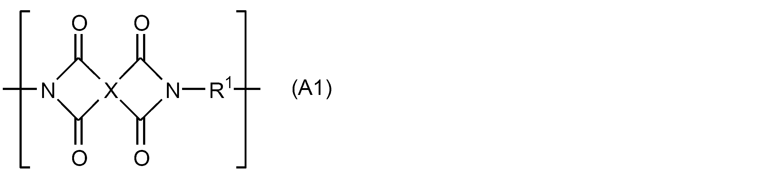
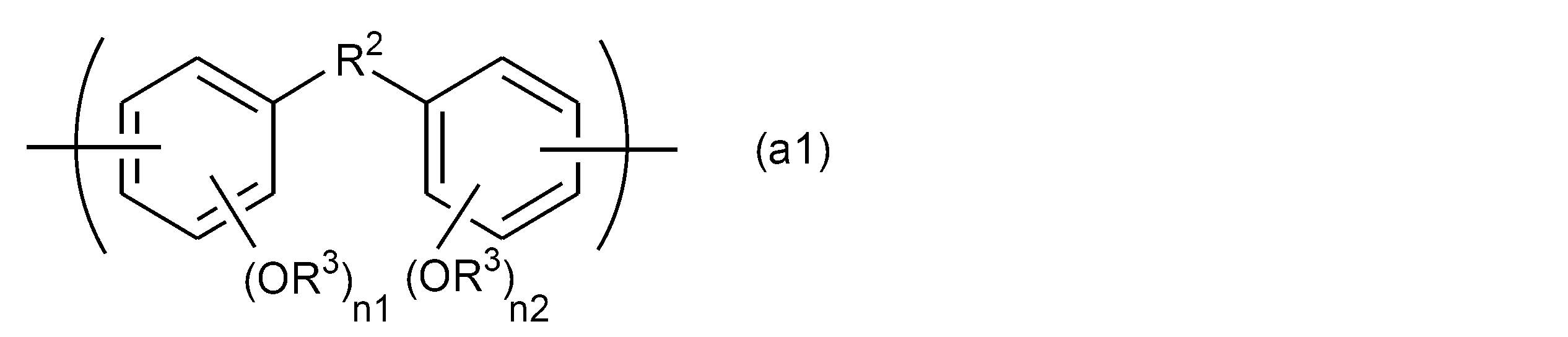
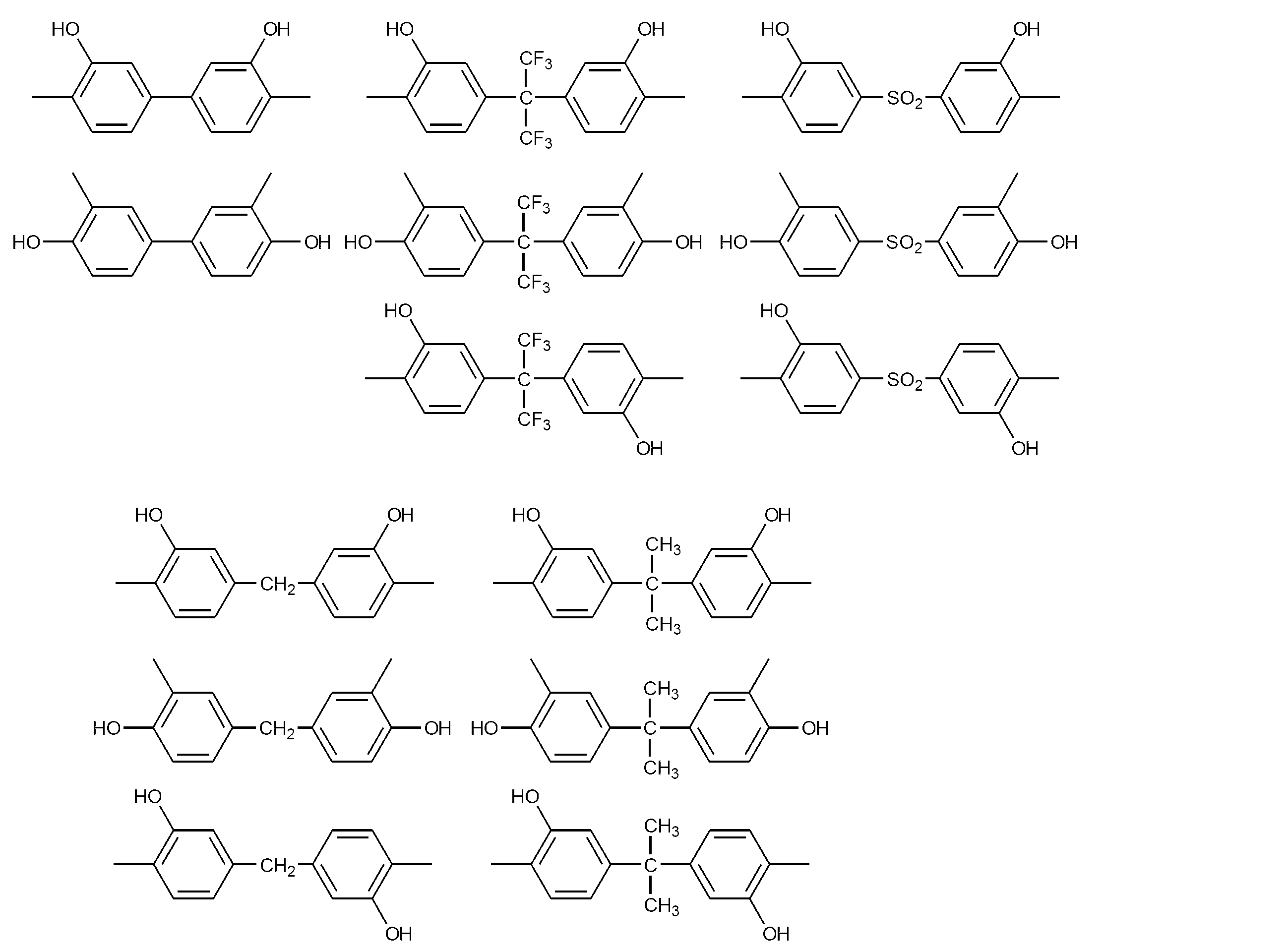



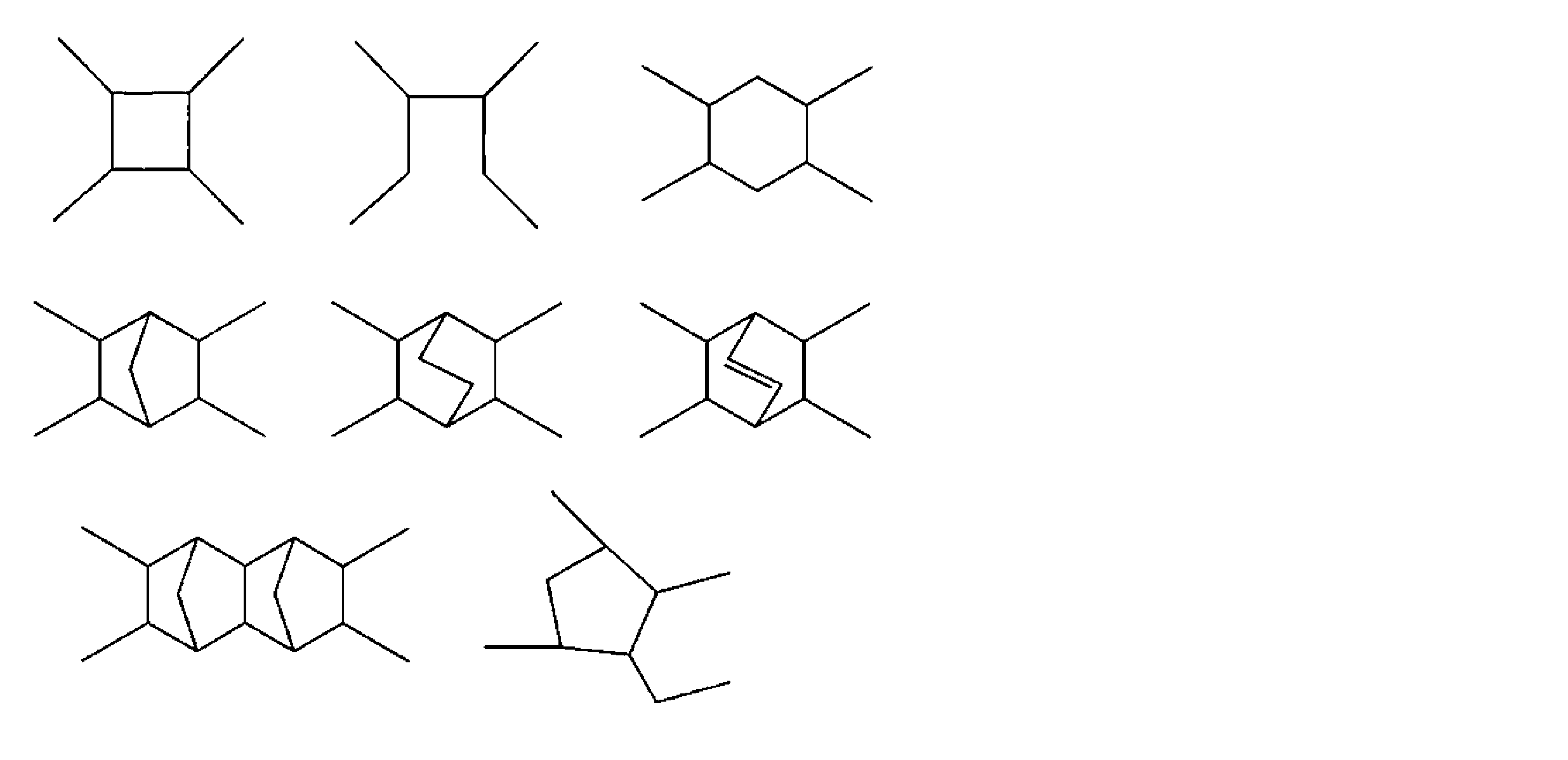

ポリイミド前駆体(A2)は、脱水・環化(イミド化)によって、ポリイミド(A1)、好ましくは式(A1)で表される構造単位を有するポリイミド(A1)を生成することができる化合物である。ポリイミド前駆体(A2)としては、例えば、ポリアミック酸およびポリアミック酸誘導体が挙げられる。
ポリアミック酸は、式(A2-1)で表される構造単位を有する。
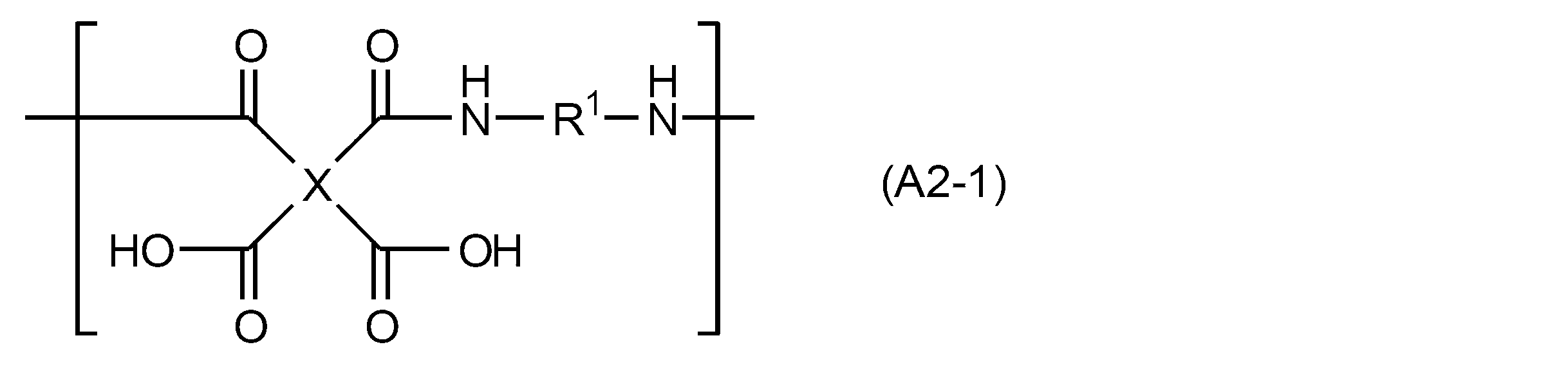
ポリアミック酸誘導体は、ポリアミック酸のエステル化等により合成される誘導体である。ポリアミック酸誘導体としては、例えば、ポリアミック酸が有する式(A2-1)で表される構造単位中のカルボキシル基の水素原子を他の基に置換した重合体が挙げられ、ポリアミック酸エステルが好ましい。

ポリイミド前駆体(A2)であるポリアミック酸は、例えば、テトラカルボン酸二無水物と、水酸基を有するジアミン及び必要に応じて他のジアミンを含むジアミンとを重合させることにより、得ることができる。これらの使用割合は、例えば前記テトラカルボン酸二無水物1モルに対して前記の全ジアミンを0.3~4モル、好ましくは略等モルである。前記重合において、前記テトラカルボン酸二無水物および前記の全ジアミンの混合溶液を50℃~200℃、1時間~24時間加熱することが好ましい。
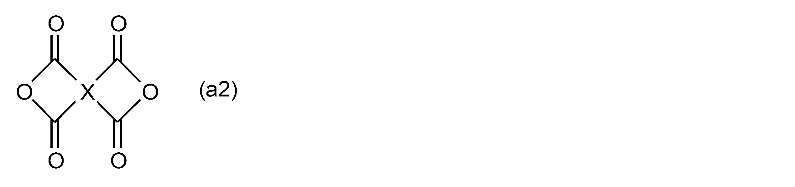

アクリル樹脂(A3)を構成するモノマーとしては、例えば、(メタ)アクリル酸アルキルエステル、(メタ)アクリル酸の脂環式基含有エステル、および(メタ)アクリル酸のアリール基含有エステルから選ばれる少なくとも1種のモノマーAが挙げられる。
ポリシロキサン(A4)としては、例えば、式(a4)で表されるオルガノシランを反応させて得られるポリシロキサンが挙げられる。

ポリベンゾオキサゾール(A5-1)は、式(a5-1)で表される構造単位を有することが好ましい。以下、式(a5-1)で表される構造単位を「構造単位(a5-1)」ともいう。


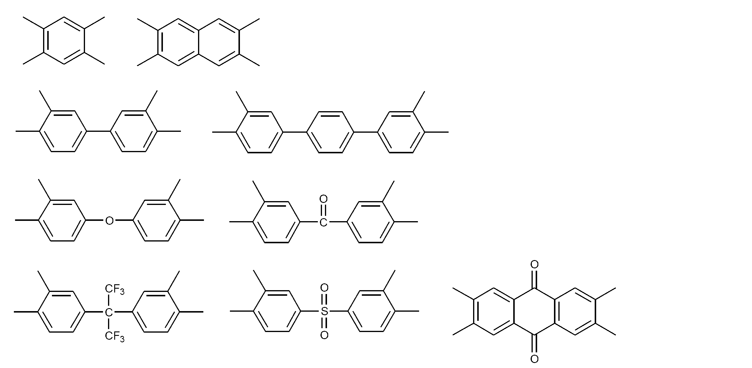


ポリベンゾオキサゾール前駆体(A5-2)は、脱水・環化によって、ポリベンゾオキサゾール(A5-1)、好ましくは構造単位(a5-1)を有するポリベンゾオキサゾール(A5-1)を生成することができる化合物である。前駆体(A5-2)は、例えば、式(a5-2)で表される構造単位を有する。

ポリベンゾオキサゾール前駆体(A5-1)は、例えば、ジカルボン酸、そのジエステル体およびそのジハライド体から選ばれる少なくとも1種と、水酸基を2つ有するジアミンとを重合させることにより、得ることができる。なお、反応収率を高めるため、ジエステルとして、ジカルボン酸と1-ヒドロキシベンゾトリアゾール等とを予め反応させた活性エステル型のジカルボン酸誘導体を用いてもよい。
ポリオレフィン(A6)としては、例えば、プロトン性極性基を有する環状オレフィン重合体が挙げられる。プロトン性極性基とは、周期律表第15族または第16族に属する原子に水素原子が直接結合している原子団をいう。周期律表第15族または第16族に属する原子は、好ましくは周期律表第15族または第16族の第2または第3周期に属する原子であり、より好ましくは酸素原子、窒素原子または硫黄原子であり、特に好ましくは酸素原子である。



カルド樹脂(A7)とは、カルド構造を有する樹脂である。カルド構造とは、環状構造を構成している環炭素原子に2つの環状構造が結合した骨格構造をいう。カルド構造の一般的な構造としては、フルオレン環の9位の炭素原子に2つの芳香環(例:ベンゼン環)が結合した構造が挙げられる。

感光剤(B)としては、例えば、光酸発生剤、光ラジカル重合開始剤が挙げられる。感放射線性材料は、感光剤(B)を含有することで、感放射線特性を発揮することができ、かつ良好な放射線感度を有することができる。
光酸発生剤は、放射線の照射を含む処理によって酸を発生する化合物である。放射線としては、例えば、可視光線、紫外線、遠紫外線、X線、荷電粒子線が挙げられる。
キノンジアジド化合物は、放射線の照射およびアルカリ水溶液を用いた現像を含む処理によってカルボン酸を発生する。キノンジアジド化合物としては、例えば、フェノール性化合物またはアルコール性化合物(以下「母核」ともいう)と、1,2-ナフトキノンジアジドスルホン酸ハライドとの縮合物が挙げられる。
オキシムスルホネート化合物の具体例としては、例えば、特開2011-227106、特開2012-234148、特開2013-054125等の公報に記載された化合物が挙げられる。オニウム塩の具体例としては、例えば、特許第5208573号、特許第5397152号、特許第5413124号、特開2004-2110525号、特開2008-129423号、特開2010-215616号および特開2013-228526号等の公報に記載された化合物が挙げられる。
感光剤(B)として光ラジカル重合開始剤を用い、後述する、重合性炭素-炭素二重結合含有化合物等の架橋剤(D)を用いることで、ネガ型の感放射線特性を発揮する材料を得ることができる。
樹脂(C)は、ノボラック樹脂、レゾール樹脂、およびレゾール樹脂の縮合物から選択される少なくとも1種である。これらの中でも、良好なアルカリ可溶性(現像性)を有することから、ノボラック樹脂が好ましい。

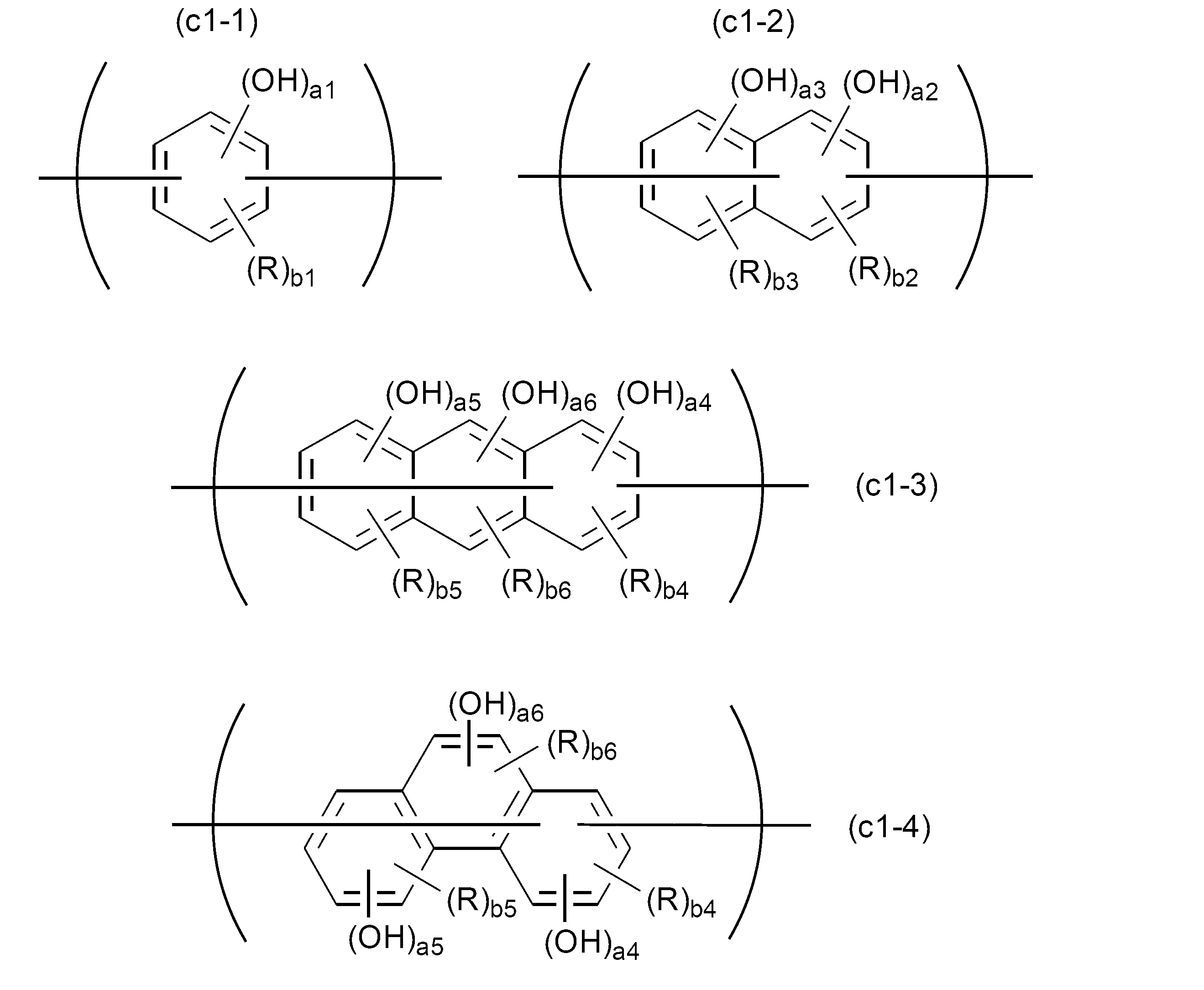

水酸基数が1~4であり、好ましくは1~3であり、かつベンゼン核数が1の化合物、具体的にはフェノール、オルトクレゾール、メタクレゾール、パラクレゾール、2,3-ジメチルフェノール、2,5-ジメチルフェノール、3,4-ジメチルフェノール、3,5-ジメチルフェノール、2,4-ジメチルフェノール、2,6-ジメチルフェノール、2,3,5-トリメチルフェノール、2,3,6-トリメチルフェノール、2-t-ブチルフェノール、3-t-ブチルフェノール、4-t-ブチルフェノール、2-メチルレゾルシノール、4-メチルレゾルシノール、5-メチルレゾルシノール、4-t-ブチルカテコール、2-メトキシフェノール、3-メトキシフェノール、2-プロピルフェノール、3-プロピルフェノール、4-プロピルフェノール、2-イソプロピルフェノール、2-メトキシ-5-メチルフェノール、2-t-ブチル-5-メチルフェノール、2-イソプロピル-5-メチルフェノール、5-イソプロピル-2-メチルフェノール;
水酸基数が1~6であり、好ましくは1~3であり、かつベンゼン核数が2の化合物(ナフタレン型化合物)、具体的には1-ナフトール、2-ナフトール等のモノヒドロキシナフタレン、1,2-ジヒドロキシナフタレン、1,3-ジヒドロキシナフタレン、1,4-ジヒドロキシナフタレン、1,5-ジヒドロキシナフタレン、1,6-ジヒドロキシナフタレン、1,7-ジヒドロキシナフタレン、1,8-ジヒドロキシナフタレン、2,3-ジヒドロキシナフタレン、2,6-ジヒドロキシナフタレン、2,7-ジヒドロキシナフタレン等のジヒドロキシナフタレン;
水酸基数が1~8であり、好ましくは1~3であり、かつベンゼン核数が3の化合物(アントラセン型化合物またはフェナントレン型化合物)、具体的には1-ヒドロキシアントラセン、2-ヒドロキシアントラセン、9-ヒドロキシアントラセン等のモノヒドロキシアントラセン、1,4-ジヒドロキシアントラセン、9,10-ジヒドロキシアントラセン等のジヒドロキシアントラセン、1,2,10-トリヒドロキシアントラセン、1,8,9-トリヒドロキシアントラセン、1,2,7-トリヒドロキシアントラセン等のトリヒドロキシアントラセン、1-ヒドロキシフェナントレン等のヒドロキシフェナントレン;
が挙げられる。
架橋剤(D)は、架橋性官能基を有する化合物である。架橋剤(D)としては、例えば、1分子中に2個以上の架橋性官能基を有する化合物が挙げられる。
溶剤(E)は、感放射線性材料を液状とするために使用することができる。
感放射線性材料は、上記必須成分および好適成分に加え、本発明の効果を損なわない範囲で、必要に応じて密着助剤(F)、界面活性剤(G)等のその他の任意成分を含有してもよい。その他の任意成分は、単独で使用しても2種以上を併用してもよい。
密着助剤(F)は、基板等の膜形成対象物と絶縁膜との接着性を向上させる成分である。密着助剤(F)は、特に無機物の基板と絶縁膜との接着性を向上させるために有用である。無機物としては、例えば、シリコン、酸化シリコン、窒化シリコン等のシリコン化合物;金、銅、アルミニウム等の金属が挙げられる。
界面活性剤(G)は、感放射線性材料の塗膜形成性を高める成分である。感放射線性材料は、界面活性剤(G)を含有することで、塗膜の表面平滑性を向上でき、その結果、絶縁膜の膜厚均一性をより向上できる。界面活性剤(G)としては、例えば、フッ素系界面活性剤、シリコーン系界面活性剤が挙げられる。
感放射線性材料は、例えば溶剤(E)に、重合体(A)、感光剤(B)、樹脂(C)等の必須成分、その他の任意成分を混合することによって調製することができる。また、ゴミを取り除くために、各成分を均一に混合した後、得られた混合物をフィルター等で濾過してもよい。
本発明の表示又は照明装置が有する絶縁膜の形成方法は、上述した感放射線性材料を用いて基板上に塗膜を形成する工程1、前記塗膜の少なくとも一部に放射線を照射する工程2、前記放射線が照射された塗膜を現像する工程3、および前記現像された塗膜を加熱する工程4を有する。
工程1では、感放射線性材料を基板表面に塗布し、好ましくはプレベークを行うことにより溶剤(E)を除去することで、塗膜を形成する。前記塗膜の膜厚としては、プレベーク後の値として、好ましくは0.3~15.0μm、より好ましくは0.5~10.0μm、さらに好ましくは1.0~5.0μmとすることができる。
工程2では、工程1で形成された塗膜に、所定のパターンを有するマスクを介して、放射線を照射する。このときに用いられる放射線としては、例えば、可視光線、紫外線、遠紫外線、X線、荷電粒子線が挙げられる。可視光線としては、例えば、g線(波長436nm)、h線(波長405nm)が挙げられる。紫外線としては、例えば、i線(波長365nm)が挙げられる。遠紫外線としては、例えば、KrFエキシマレーザによるレーザ光が挙げられる。X線としては、例えば、シンクロトロン放射線が挙げられる。荷電粒子線としては、例えば、電子線が挙げられる。
工程3では、工程2で放射線を照射した塗膜の現像を行う。これにより、例えば、ポジ型の感放射線性材料を用いた場合は放射線の照射部分を除去し、ネガ型の感放射線性材料を用いた場合は放射線の非照射部分を除去し、所望のパターンを形成することができる。現像処理に用いられる現像液としては、アルカリ水溶液が好ましい。
工程4では、工程3の後に、ホットプレート、オーブン等の加熱装置を用いて、塗膜に対する加熱処理(ポストベーク処理)を行うことで絶縁膜を得る。この加熱処理における加熱温度は、例えば、130℃を超えて300℃以下であり、加熱時間は、加熱機器の種類により異なるが、例えば、5分間~90分間である。この際に、2回以上の加熱工程を行うステップベーク法等を用いることもできる。加熱処理には、例えば、ホットプレート、オーブンを使用することができる。
以下、本発明の表示又は照明装置として、有機EL表示又は照明装置を具体例にとって、図3を参照しつつ説明する。図3は、本発明に係る有機EL表示又は照明装置(以下、単に「有機EL装置」ともいう)の主要部の構造を模式的に示す断面図である。
重合体(A)および樹脂(C)の重量平均分子量(Mw)および分子量分布(Mw/Mn)は、ゲルパーミエーションクロマトグラフィー(GPC)法により、以下の条件で測定した。
・標準物質:ポリスチレン換算
・装置 :東ソー(株)製、商品名:HLC-8020
・カラム :東ソー(株)製ガードカラムHXL-H、TSK gel G7000HXL、TSK gel GMHXL 2本、TSK gel G2000HXLを順次連結したもの
・溶媒 :テトラヒドロフラン
・サンプル濃度:0.7質量%
・注入量 :70μL
・流速 :1mL/min
[NMR分析]
ポリシロキサン(A1)中のフェニル基の含有量は、「JNM-ECS400」(日本電子(株)製)を用いて29Si-核磁気共鳴スペクトルを測定し、そのフェニル基が結合したSiのピーク面積とフェニル基が結合していないSiのピーク面積との比から求めた。
[合成例A1]重合体(A-1)の合成(ポリイミド)
3口フラスコに重合溶剤としてのγ-ブチロラクトン390gを加えた後、ジアミン化合物としての2,2’-ビス(3-アミノ-4-ヒドロキシフェニル)ヘキサフルオロプロパン120gを重合溶剤中に加えた。ジアミン化合物を重合溶剤に溶解させた後、酸二無水物としての4,4’-オキシジフタル酸二無水物71gを加えた。その後、60℃で1時間反応させた後、末端封止剤としての無水マレイン酸19gを加え、60℃で更に1時間反応させた後、昇温して180℃で4時間反応させた。重合体(A-1)を含む固形分濃度が約35質量%のポリイミド溶液を約600g得た。得られた重合体(A-1)のMwは8000であった。
フラスコ内を窒素置換した後、2,2’-アゾビスイソブチロニトリル5.0gを溶解したプロピレングリコールモノメチルエーテルアセテート溶液250.0gを仕込んだ。引き続きメタクリル酸20.0g、ジシクロペンタニルメタクリレート45.0gおよび3-エチル-3-メタクリロイルオキシメチルオキセタン30.0gを仕込んだ後、ゆるやかに攪拌を始めた。溶液の温度を80℃に上昇させ、この温度を5時間保持した後、100℃で1時間加熱させて重合を終結させた。その後、反応生成溶液を多量のメタノールに滴下し反応物を凝固させた。この凝固物を水洗後、テトラヒドロフラン200gに再溶解し、多量のメタノールで再度、凝固させた。
モノマーとして2-メタクリロイロキシエチルコハク酸20.0g、ジシクロペンタニルメタクリレート45.0gおよび3,4-エポキシシクロヘキシルメチルメタクリレート30.0gを用いたこと以外は合成例A2と同様に行った。得られた重合体(A-3)の重量平均分子量(Mw)は20000であった。
ジフェニルエーテル-4,4’-ジカルボン酸1モルと1-ヒドロキシベンゾトリアゾール2モルとを反応させて得られたジカルボン酸誘導体443.2g(0.90モル)と、ヘキサフルオロ-2,2-ビス(3-アミノ-4-ヒドロキシフェニル)プロパン366.3部(1.00モル)とを温度計、攪拌機、原料投入口、乾燥窒素ガス導入管を備えた4つ口のセパラブルフラスコに入れ、N-メチル-2-ピロリドン3000部を加えて溶解させた。その後オイルバスを用いて75℃にて16時間反応させた。
500mLの三口フラスコに、メチルトリメトキシシランを63.39部(0.55mol)、フェニルトリメトキシシランを69.41部(0.35mol)、2-(3,4-エポキシシクロヘキシル)エチルトリメトキシシランを24.64部(0.1mol)、ジアセトンアルコールを150.36部仕込み、室温で攪拌しながら、水55.8部にリン酸0.338部(仕込みモノマーに対して0.2質量%)を溶かしたリン酸水溶液を10分かけて添加した。その後、フラスコを70℃のオイルバスに浸けて1時間攪拌した後、オイルバスを30分かけて115℃まで昇温した。昇温開始1時間後に溶液の内温が100℃に到達し、そこから2時間加熱攪拌した(内温は100~110℃)。反応中に副生成物であるメタノールおよび水が合計115部留出した。得られた重合体(A-5)のジアセトンアルコール溶液に、重合体(A-5)濃度が35質量%となるようにジアセトンアルコールを加えて、重合体(A-5)のジアセトンアルコール溶液を得た。得られた重合体(A-5)の重量平均分子量(Mw)は5000であり、Si原子100モルに対するフェニル基含有量は35モルであった。
窒素置換した1000mLオートクレーブに、8-カルボキシテトラシクロ[4.4.0.12,5.17,10]ドデカ-3-エン60部、N-フェニル-(5-ノルボルネン-2,3-ジカルボキシイミド)40部、1,5-ヘキサジエン2.8部、(1,3-ジメシチルイミダゾリジン-2-イリデン)(トリシクロヘキシルホスフィン)ベンジリデンルテニウムジクロリド0.05部およびジエチレングリコールエチルメチルエーテル400部を仕込み、撹拌下に80℃で2時間重合反応を行って、重合体(A-6’)を含有する重合体溶液を得た。この重合体溶液に、水素添加触媒としてビス(トリシクロヘキシルホスフィン)エトキシメチレンルテニウムジクロリド0.1部を加え、水素を4MPaの圧力で5時間溶存させて、水素添加反応を進行させたのち、活性炭粉末1部を添加し、撹拌しつつ150℃で水素を4MPaの圧力で3時間溶存させた。次いで、溶液を取り出して、孔径0.2μmのフッ素樹脂製フィルターでろ過して活性炭を分離して、重合体(A-6’)の水素化物である重合体(A-6)を含有する水素添加反応溶液490部を得た。ここで得られた重合体(A-6)を含有する水素添加反応溶液の固形分濃度は21質量%であり、重合体(A-6)の収量は102部であった。得られた重合体(A-6)の水素添加反応溶液をロータリーエバポレーターで濃縮し、固形分濃度を35質量%に調整して、重合体(A-6)の溶液を得た。得られた重合体(A-6)の重量平均分子量(Mw)は4000であった。
カルド樹脂のプロピレングリコールモノメチルエーテル溶液であるCR-TR5(大阪ガスケミカル(株)製)は、固形分52.7質量%、固形分酸価135KOHmg/gの製品である。CR-TR5を100部計量し、プロピレングリコールモノメチルエーテルを50.57部添加攪拌した。このようにして固形分濃度が35質量%のカルド樹脂溶液(A-7)を得た。
[合成例C1]ノボラック樹脂(C-1)の合成
温度計、冷却管、分留管、撹拌器を取り付けたフラスコに、1-ナフトール144.2g(1.0モル)、メチルイソブチルケトン400g、水96gおよび92質量%パラホルムアルデヒド32.6g(ホルムアルデヒド換算で1.0モル)を仕込んだ。続いて攪拌しながらパラトルエンスルホン酸3.4gを加えた。その後、100℃で8時間反応させた。反応終了後に純水200gを加え、系内の溶液を分液ロートに移して水層を有機層から分離除去した。次いで洗浄水が中性を示すまで水洗後、有機層から溶媒を加熱減圧下に除去し、下記式で表される構造単位からなるノボラック樹脂(C-1)を140g得た。得られたノボラック樹脂(C-1)の重量平均分子量(Mw)は2000であった。
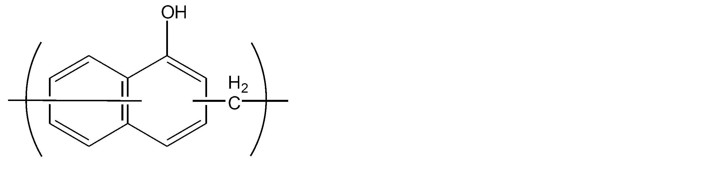
温度計、冷却管、分留管、撹拌器を取り付けたフラスコに、1-ナフトール144.2g(1.0モル)、テレフタルアルデヒド134.1g(1.0モル)、トリフロロメタンスルホン酸3.0gを装入し、攪拌を行いながら150~160℃で4時間反応を行った。反応終了後に純水200gを加え、系内の溶液を分液ロートに移して水層を有機層から分離除去した。次いで洗浄水が中性を示すまで水洗後、有機層から溶媒を加熱減圧下に除去し、下記式で表される構造単位からなるノボラック樹脂(C-2)を220g得た。得られたノボラック樹脂(C-2)の重量平均分子量(Mw)は1500であった。

原料成分および酸触媒としてテレフタルアルデヒド134.1g(1.0モル)と1,6-ジヒドロキシナフタレン160.2g(1.0モル)、トリフロロメタンスルホン酸3.0gを用いたこと以外は合成例C2と同様に行った。下記式で表される構造単位からなるノボラック樹脂(C-3)を230g得た。得られたノボラック樹脂(C-3)の重量平均分子量(Mw)は1000であった。

原料成分として1-ヒドロキシアントラセン194.2g(1.0モル)、メチルイソブチルケトン400g、水96gおよび92質量%パラホルムアルデヒド32.6g(ホルムアルデヒド換算で1.0モル)を用いたこと以外は合成例C1と同様に行った。下記式で表される構造単位からなるノボラック樹脂(C-4)を180g得た。得られたノボラック樹脂(C-4)の重量平均分子量(Mw)は2000であった。
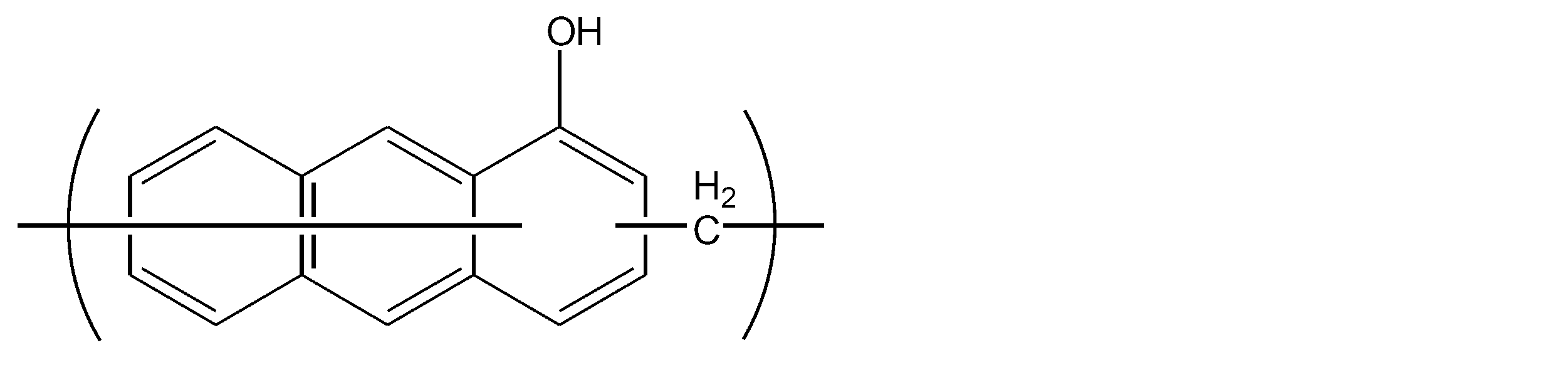
原料成分として1,4-ジヒドロキシアントラセン210.2g(1.0モル)、メチルイソブチルケトン400g、水96gおよび92質量%パラホルムアルデヒド32.6g(ホルムアルデヒド換算で1.0モル)を用いたこと以外は合成例C1と同様に行った。下記式で表される構造単位からなるノボラック樹脂(C-5)を190g得た。得られたノボラック樹脂(C-5)の重量平均分子量(Mw)は3000であった。
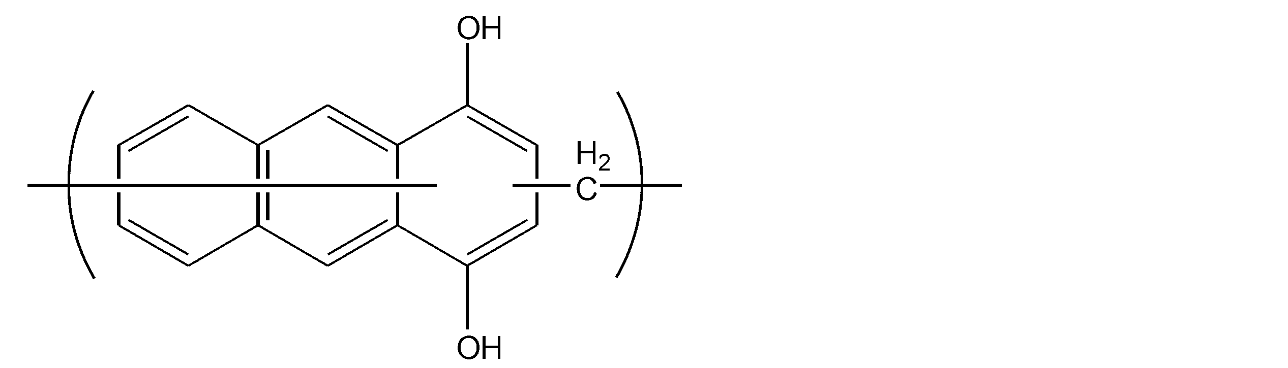
感放射線性材料の調製に用いた重合体(A)は合成例A1~A6、調製例A7の重合体(A-1)~(A-7)であり、樹脂(C)は合成例C1~C5のノボラック樹脂(C-1)~(C-5)であり、感光剤(B)、架橋剤(D)、溶剤(E)、密着助剤(F)および界面活性剤(G)は、下記の通りである。
B-1:4,4’-[1-[4-[1-[4-ヒドロキシフェニル]-1-メチルエチル]フェニル]エチリデン]ビスフェノール(1.0モル)と1,2-ナフトキノンジアジド-5-スルホン酸クロリド(2.0モル)との縮合物(東洋合成工業(株))
B-2:2-(ジメチルアミノ)-2-[(4-メチルフェニル)メチル]-1-[4-(4-モルホリニル)フェニル]-1-ブタノン(BASF製の「IRG-379EG」)
架橋剤(D)
D-1:4,4-ビス[(3-エチル-3-オキセタニル)メチル]ビフェニル(宇部興産社の「OXBP」)
D-2:群栄化学工業社の「C-357」
D-3:東亞合成社の「M-405」
溶剤(E)
E-1:γ-ブチロラクトン(BL)、プロピレングリコールモノメチルエーテルアセテート(PGMEA)およびプロピレングリコールモノメチルエーテル(PGME)の質量比で30:20:50の混合溶剤
DAA:ジアセトンアルコール
EDM:ジエチレングリコールエチルメチルエーテル
密着助剤(F)
F-1:N-フェニル-3-アミノプロピルトリメトキシシラン
(信越化学工業(株)製の「KBM-573」)
界面活性剤(G)
G-1:シリコーン系界面活性剤
(東レダウコーニング社製の「SH8400」)
[調製例1]
合成例A1の重合体(A-1)を含む重合体溶液(重合体(A-1)25部(固形分)に相当する量)に、(B-1)10部、(C-1)40部、(D-1)15部、(D-2)5部、(F-1)4部、(G-1)1部、および(E-1)を混合し、固形分濃度が25質量%となるようにするとともに、口径0.2μmのメンブランフィルタで濾過して、ポジ型材料1を調製した。
表1に示す種類および配合量の各成分を用いたこと以外は調製例1と同様にして、ポジ材料2~23および30~31、ネガ型材料24~29および32~33を調製した。

調製例1~33の感放射線性材料1~33を用いて、以下に説明する方法により絶縁膜および有機EL素子を作製した。得られた絶縁膜のパターニング性、LWR(Line Width Roughtness)、遮光性、テーパー角度、吸水性および耐熱性を、また得られた有機EL素子の素子特性を、それぞれ下記方法で評価した。
クリーントラック(東京エレクトロン社製:Mark VZ)を用いて、シリコン基板上に調製例1~23および30~31で得られたポジ型材料を塗布した後、ホットプレート上で120℃にて2分間プレベークして、塗膜を形成した。この塗膜に対して、露光機(Nikon社のi線ステッパー「NSR-2005i10D」)を用い、所定のパターンを有するパターンマスクを介して波長365nmにおける露光量100mJ/cm2で露光した。その後、2.38質量%テトラメチルアンモニウムヒドロキシド水溶液を用いて25℃にて80秒間液盛り法で現像し、超純水で1分間流水洗浄を行い、乾燥させて、シリコン基板上に5μmスクエアの複数のスルーホールが列状に並ぶパターンを有する塗膜を形成した。この塗膜をホットプレート上で250℃にて60分間ポストベークして、前記パターンおよび表2に記載の膜厚を有する絶縁膜を形成した。
上記<パターニング性>にて形成された、ポストベーク前の塗膜の線幅5μmスクエアパターンを、走査型電子顕微鏡(SEM;日立ハイテクノロジー社の「SU3500」)を用い、パターン上部から観察し、任意の10点において線幅を測定した。線幅の測定値の3シグマ値(ばらつき)をLWR(μm)とした。このLWRの値が0.4μm以下の場合には「優良」とし、0.4μmを超えて0.8μm以下の場合には「良好」とし、0.8μmを超える場合には「不良」とした。
クリーントラック(東京エレクトロン社製:Mark VZ)を用いて、ガラス基板(コーニング社の「コーニング7059」)上に上記調製例で得られた感放射線性材料を塗布した後、ホットプレート上で120℃にて2分間プレベーク後、ホットプレート上で250℃にて60分間ポストベークして、表2に記載の膜厚を有する絶縁膜を形成した。
上記<パターニング性>の絶縁膜において、複数のスルーホールのラインと直交する方向の垂直断面形状をSEM(日立ハイテクノロジー社の「SU3500」)で観察した。このSEM画像から、絶縁膜のテーパー角度を決定した。各評価において、同様にSEM画像から、絶縁膜の膜厚を決定した。
クリーントラック(東京エレクトロン社製:Mark VZ)を用いて、シリコン基板上に上記調製例で得られた感放射線性材料を塗布した後、ホットプレート上で120℃にて2分間プレベーク後、ホットプレート上で250℃にて60分間ポストベークして、膜厚3.0μmを有する絶縁膜を形成した。
<吸水性>の評価と同様にして感放射線性材料を用いて絶縁膜を形成し、この絶縁膜について、熱重量測定装置(TAインスツルメント社の「TGA2950」)を用いて、100℃から500℃においてTGA測定(空気下、昇温速度10℃/分)を行うことで5%重量減少温度を求めた。耐熱性は、5%重量減少温度が350℃を超える場合に「優良」、350~330℃の場合に「良好」、330℃以下の場合に「不良」とした。
ガラス基板(コーニング社の「コーニング7059」)を用い、このガラス基板上にTFTを形成したTFT基板を作製した後に、このTFT基板上に絶縁膜を形成して評価用素子を作製した。この評価用素子について、素子特性の評価を行った。
素子特性はスイッチング応答特性として評価した。スイッチング応答特性は、ON/OFF比を測定することで評価した。ON/OFF比は、プローバおよび半導体パラメーターアナライザーを用いて、ゲート電極に電圧を印可した状態でソース電極-ドレイン電極間に流れる電流を測定することで算出した。具体的には、半導体層に対して上記感放射線性材料から形成された絶縁膜の上方から波長450nmまたは500nmを中心とした照度30000ルックスの白色光を照射した条件下において、ドレイン電極をプラス10V、ソース電極を0Vとした場合にゲート電極に印可された電圧がプラス10Vとマイナス10Vの時の電流値の比をON/OFF比とした。スイッチング応答特性、すなわち素子特性は、ON/OFF比が1.0×105以上の場合に「良好」、1.0×105未満の場合に「不良」とした。
TFT信頼性は、ゲート電極-ソース電極間に電気的なストレスを印可した際のId-Vg特性の変化(閾値電圧Vthの変化量)を、評価用素子に対する光照射時と光非照射時とで比較することによって評価した。
電気的なストレスの印可は、評価用素子のソース電極の電位を0V、ドレイン電極の電位を+10Vに保ち、ソース電極-ドレイン電極間に電圧を印可した状態で、ゲート電極の電位Vgを-20Vから+20Vまで変化させることで行った。このようにゲート電極の電位Vgを変化させた際、ドレイン電極-ソース電極間に流れる電流Idをプロットすることで、Id-Vg特性を得た。このId-Vg特性においては、電流値がONとなる電圧を閾値電圧Vthに設定した。
電気的なストレスは、ゲート電極-ソース電極間に、+20Vの正電圧及び-20Vの負電圧をそれぞれ12時間ずつ印加することで与えた。このような電気的なストレスは、評価用素子の半導体層に対して上記感放射線性材料から形成された絶縁膜の上方から波長450nmまたは500nmを中心とした照度30000ルックスの白色光を照射した条件下、および半導体層に対して光を照射しない条件下のそれぞれについて行った。閾値電圧Vthの変化量は、光照射条件および光非照射条件のそれぞれについて、Id-Vg特性から算出した。そして、光照射時の閾値電圧Vthの変化量が、光非照射時の閾値電圧Vthの変化量の1.3倍未満に抑えられている場合にTFT信頼性が「優良」であるとし、1.3倍以上1.6倍未満に抑えられている場合にTFT信頼性が「良好」であるとし、1.6倍以上2倍未満に抑えられている場合にTFT信頼性が「やや良好」であるとし、2倍以上の場合にTFT信頼性が「不良」であるとした。

Claims (19)
- TFTを構成する半導体層が、In、Ga、Sn、Ti、Nb、SbおよびZnから選択される1種以上の元素を含む酸化物半導体を含有するTFT基板と、
TFT基板上に設けられ、且つ前記TFTと接続された第1電極と、
第1電極を部分的に露出させるように第1電極上に形成された、全光線透過率が波長300~400nmにおいて0~15%の範囲にある絶縁膜と、
第1電極に対向して設けられた第2電極と
を有する表示又は照明装置であり、
前記絶縁膜が、感放射線性材料から形成された絶縁膜であり、
前記感放射線性材料が、
(A)下記樹脂(C)以外の重合体と、
(B)感光剤と、
(C)ノボラック樹脂、レゾール樹脂、およびレゾール樹脂の縮合物
から選択される少なくとも1種の樹脂と
を含有し、
前記感放射線性材料における樹脂(C)の含有量が、重合体(A)100質量部に対して2~200質量部である、
表示又は照明装置。 - 重合体(A)が、ポリイミド(A1)、前記ポリイミドの前駆体(A2)、アクリル樹脂(A3)、ポリシロキサン(A4)、ポリベンゾオキサゾール(A5-1)、前記ポリベンゾオキサゾールの前駆体(A5-2)、ポリオレフィン(A6)、およびカルド樹脂(A7)から選択される少なくとも1種である請求項1に記載の表示又は照明装置。
- 重合体(A)が、ポリシロキサン(A4)、ポリベンゾオキサゾール(A5-1)、前記ポリベンゾオキサゾールの前駆体(A5-2)、ポリオレフィン(A6)、およびカルド樹脂(A7)から選択される少なくとも1種である請求項1に記載の表示又は照明装置。
- ポリイミド(A1)が、式(A1)で表される構造単位を有する請求項2に記載の表示又は照明装置。
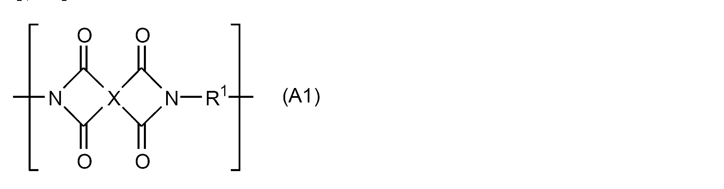
- ポリシロキサン(A4)が、式(a4)で表されるオルガノシランを反応させて得られるポリシロキサンである請求項2または3に記載の表示又は照明装置。

- ポリベンゾオキサゾール(A5-1)が、式(a5-1)で表される構造単位を有する請求項2または3に記載の表示又は照明装置。
- ポリベンゾオキサゾールの前駆体(A5-2)が、式(a5-2)で表される構造単位を有する請求項2または3に記載の表示又は照明装置。

- 感光剤(B)が、光酸発生剤または光ラジカル重合開始剤である請求項1~7のいずれか1項に記載の表示又は照明装置。
- 樹脂(C)が、ノボラック樹脂である請求項1~8のいずれか1項に記載の表示又は照明装置。
- 前記絶縁膜が第1電極を露出させる、前記絶縁膜の境界部分における断面形状が、順テーパー状である請求項1~9のいずれか1項に記載の表示又は照明装置。
- 前記絶縁膜の膜厚が、0.3~15.0μmである請求項1~10のいずれか1項に記載の表示又は照明装置。
- 前記絶縁膜が第1電極の少なくともエッジ部を被覆するように形成され、前記絶縁膜の境界部分における断面形状が順テーパー状である請求項1~11のいずれか1項に記載の表示又は照明装置。
- 前記絶縁膜が、前記TFT基板の面上を複数の領域に区画する隔壁であり、
前記複数の領域にそれぞれ形成された画素を有する
請求項1~12のいずれか1項に記載の表示又は照明装置。 - 前記TFT基板上に設けられ且つ前記TFTと接続された第1電極と、前記隔壁により区画された領域において且つ第1電極上に形成された有機発光層と、有機発光層上に設けられた第2電極とを含む有機EL素子を有する請求項13に記載の表示又は照明装置。
- 前記TFT基板が、支持基板と、前記支持基板上において前記有機EL素子に対応して設けられたTFTと、前記TFTを被覆する平坦化層とを有するTFT基板であり、
前記隔壁が、第1電極の少なくともエッジ部を被覆しており、且つ前記隔壁が、前記TFTが有する半導体層の上方に少なくとも配置されるように、前記平坦化層上に形成されている
ことを特徴とする請求項14に記載の表示又は照明装置。 - 前記第1電極が前記平坦化層上に形成されており、前記第1電極が前記平坦化層を貫通するスルーホールに形成された配線を介して前記TFTと接続されている請求項15に記載の表示又は照明装置。
- 前記絶縁膜が、前記半導体層の上方に少なくとも配置されるように、TFT基板上に形成されており、TFT基板の上方から投影的に見た場合に、半導体層の面積の50%以上が前記絶縁膜と重複している請求項1~16のいずれか1項に記載の表示又は照明装置。
- 請求項1に記載の感放射線性材料を用いてTFT基板上に塗膜を形成する工程1、前記塗膜の少なくとも一部に放射線を照射する工程2、前記放射線が照射された塗膜を現像する工程3、および前記現像された塗膜を加熱して、全光線透過率が波長300~400nmにおいて0~15%の範囲にある絶縁膜を形成する工程4を有する請求項1に記載の表示又は照明装置が有する絶縁膜の形成方法。
- 工程1における加熱温度が60~130℃であり、工程4における加熱温度が130℃を超えて300℃以下である請求項18に記載の絶縁膜の形成方法。
Priority Applications (3)
| Application Number | Priority Date | Filing Date | Title |
|---|---|---|---|
| CN201480072069.3A CN105874882A (zh) | 2014-02-28 | 2014-10-09 | 显示或照明装置及绝缘膜的形成方法 |
| JP2016504992A JP6443436B2 (ja) | 2014-02-28 | 2014-10-09 | 表示又は照明装置、および絶縁膜の形成方法 |
| KR1020167015597A KR101852050B1 (ko) | 2014-02-28 | 2014-10-09 | 유기 el 장치 및 절연막의 형성 방법 |
Applications Claiming Priority (2)
| Application Number | Priority Date | Filing Date | Title |
|---|---|---|---|
| JP2014-038335 | 2014-02-28 | ||
| JP2014038335A JP5613851B1 (ja) | 2014-02-28 | 2014-02-28 | 表示又は照明装置 |
Publications (1)
| Publication Number | Publication Date |
|---|---|
| WO2015129092A1 true WO2015129092A1 (ja) | 2015-09-03 |
Family
ID=52574683
Family Applications (1)
| Application Number | Title | Priority Date | Filing Date |
|---|---|---|---|
| PCT/JP2014/077042 Ceased WO2015129092A1 (ja) | 2014-02-28 | 2014-10-09 | 表示又は照明装置、および絶縁膜の形成方法 |
Country Status (5)
| Country | Link |
|---|---|
| JP (2) | JP5613851B1 (ja) |
| KR (1) | KR101852050B1 (ja) |
| CN (1) | CN105874882A (ja) |
| TW (1) | TWI609239B (ja) |
| WO (1) | WO2015129092A1 (ja) |
Cited By (7)
| Publication number | Priority date | Publication date | Assignee | Title |
|---|---|---|---|---|
| JP2019023728A (ja) * | 2015-09-30 | 2019-02-14 | 東レ株式会社 | ネガ型感光性樹脂組成物、硬化膜、硬化膜を具備する素子及び表示装置、並びにその製造方法 |
| TWI705301B (zh) * | 2018-05-16 | 2020-09-21 | 南韓商三星Sdi股份有限公司 | 感光性樹脂組成物、感光性樹脂層以及電子裝置 |
| JP2020173431A (ja) * | 2019-04-09 | 2020-10-22 | 旭化成株式会社 | ネガ型感光性樹脂組成物、ポリイミドの製造方法および硬化レリーフパターンの製造方法 |
| JP2020532044A (ja) * | 2017-08-24 | 2020-11-05 | 京東方科技集團股▲ふん▼有限公司Boe Technology Group Co.,Ltd. | 表示基板および表示装置 |
| US11587994B2 (en) | 2019-01-03 | 2023-02-21 | Chengdu Boe Optoelectronics Technology Co., Ltd. | Method for manufacturing pixel definition layer and display panel, and display panel |
| KR20240161633A (ko) | 2022-03-11 | 2024-11-12 | 도레이 카부시키가이샤 | 감광성 수지 조성물, 경화물, 경화물의 제조 방법, 유기 el 표시 장치 및 표시 장치 |
| KR20250125970A (ko) | 2022-12-21 | 2025-08-22 | 도레이 카부시키가이샤 | 감광성 수지 조성물, 경화물, 유기 el 표시 장치, 표시 장치 및 페놀 화합물 |
Families Citing this family (14)
| Publication number | Priority date | Publication date | Assignee | Title |
|---|---|---|---|---|
| CN106062631B (zh) | 2014-03-20 | 2019-11-22 | 日本瑞翁株式会社 | 放射线敏感性树脂组合物及电子部件 |
| US20170082923A1 (en) * | 2014-06-12 | 2017-03-23 | Dic Corporation | Photosensitive composition for permanent films, resist material and coating film |
| CN106462062B (zh) * | 2014-08-12 | 2020-02-14 | Jsr株式会社 | 元件、绝缘膜及其制造方法以及感放射线性树脂组合物 |
| KR102038838B1 (ko) * | 2014-12-19 | 2019-11-26 | 제이에스알 가부시끼가이샤 | 발광 장치 및 그의 제조 방법, 격벽의 제조 방법, 그리고 감방사선성 재료 |
| WO2016129113A1 (ja) * | 2015-02-13 | 2016-08-18 | パイオニア株式会社 | 発光装置の製造方法 |
| CN109661696B (zh) * | 2016-09-05 | 2021-04-13 | 夏普株式会社 | 有源矩阵基板及其制造方法 |
| CN109716235B (zh) * | 2016-09-20 | 2022-11-18 | 太阳控股株式会社 | 正型感光性树脂组合物、干膜、固化物、印刷电路板及半导体元件 |
| TWI600168B (zh) | 2016-11-02 | 2017-09-21 | 律勝科技股份有限公司 | 薄膜電晶體的積層體結構 |
| CN106848086B (zh) * | 2017-04-20 | 2018-07-13 | 京东方科技集团股份有限公司 | 有机发光二极管及其制备方法、显示装置 |
| TWI803315B (zh) * | 2017-08-01 | 2023-05-21 | 日商旭化成股份有限公司 | 半導體裝置及其製造方法 |
| CN109585506A (zh) * | 2018-11-22 | 2019-04-05 | 武汉华星光电技术有限公司 | 具有照明功能的oled显示设备 |
| TWI753592B (zh) * | 2020-09-30 | 2022-01-21 | 臺灣永光化學工業股份有限公司 | 聚醯亞胺正型光阻組成物及其用途 |
| CN120731242A (zh) * | 2023-02-22 | 2025-09-30 | 东进世美肯株式会社 | 用于制备碱溶性树脂的组合物、由其制备的碱溶性树脂及包含其的感光性树脂组合物 |
| TWI913135B (zh) * | 2025-03-14 | 2026-01-21 | 奇美實業股份有限公司 | 負型感光性樹脂組成物及光阻圖案的形成方法 |
Citations (6)
| Publication number | Priority date | Publication date | Assignee | Title |
|---|---|---|---|---|
| JPS5627140A (en) * | 1979-08-01 | 1981-03-16 | Siemens Ag | Thermally stabilized positive resist and preparation of thermally stable relief structure using same |
| JP2007183534A (ja) * | 2005-12-30 | 2007-07-19 | Cheil Industries Inc | 感光性樹脂組成物及びこれを用いたブラックマトリックス |
| JP2010108927A (ja) * | 2008-09-30 | 2010-05-13 | Mitsubishi Chemicals Corp | 有機電界発光素子、該有機電界発光素子の製造方法、有機el表示装置および有機el照明 |
| JP2012133153A (ja) * | 2010-12-22 | 2012-07-12 | Toray Ind Inc | 感光性樹脂組成物、それを用いた硬化膜、半導体装置の製造方法および半導体装置 |
| JP2012234748A (ja) * | 2011-05-06 | 2012-11-29 | Jsr Corp | 有機el表示素子および有機el表示素子の製造方法 |
| JP2013232314A (ja) * | 2012-04-27 | 2013-11-14 | Jsr Corp | 感放射線性樹脂組成物、絶縁膜および有機el素子 |
Family Cites Families (15)
| Publication number | Priority date | Publication date | Assignee | Title |
|---|---|---|---|---|
| JP4982927B2 (ja) | 2000-06-28 | 2012-07-25 | 東レ株式会社 | 表示装置 |
| JP4164562B2 (ja) | 2002-09-11 | 2008-10-15 | 独立行政法人科学技術振興機構 | ホモロガス薄膜を活性層として用いる透明薄膜電界効果型トランジスタ |
| TW595254B (en) * | 2002-03-29 | 2004-06-21 | Sanyo Electric Co | Electroluminescense display device |
| EP2413366B1 (en) | 2004-03-12 | 2017-01-11 | Japan Science And Technology Agency | A switching element of LCDs or organic EL displays |
| JP2008191367A (ja) * | 2007-02-05 | 2008-08-21 | Sumitomo Chemical Co Ltd | 感放射線性樹脂組成物 |
| JP5339087B2 (ja) * | 2007-08-10 | 2013-11-13 | 住友ベークライト株式会社 | ポジ型感光性樹脂組成物、硬化膜、保護膜、絶縁膜および半導体装置 |
| WO2009104680A1 (ja) * | 2008-02-22 | 2009-08-27 | 日本化薬株式会社 | 感放射線性樹脂組成物、その硬化物及び該組成物を用いた層間絶縁膜及び光学用デバイス |
| JP2010062120A (ja) * | 2008-08-06 | 2010-03-18 | Mitsubishi Chemicals Corp | 有機電界発光素子の隔壁用感光性組成物および有機電界発光表示装置 |
| JP5343664B2 (ja) | 2009-03-30 | 2013-11-13 | Jsr株式会社 | 感放射線性樹脂組成物、有機el表示素子用隔壁及び絶縁膜、並びにその形成方法 |
| JP5305267B2 (ja) * | 2009-08-04 | 2013-10-02 | 株式会社ジャパンディスプレイ | 有機el装置 |
| JP2011107476A (ja) | 2009-11-18 | 2011-06-02 | Panasonic Corp | 電子デバイスの製造方法 |
| JP2011181592A (ja) * | 2010-02-26 | 2011-09-15 | Technology Research Association For Advanced Display Materials | アクティブマトリクス表示装置及びアクティブマトリクス表示装置の製造方法 |
| JP5970865B2 (ja) * | 2012-03-05 | 2016-08-17 | 大日本印刷株式会社 | 薄膜素子用基板、薄膜素子、有機エレクトロルミネッセンス表示装置、および電子ペーパー |
| JP6155823B2 (ja) * | 2012-07-12 | 2017-07-05 | Jsr株式会社 | 有機el素子、感放射線性樹脂組成物および硬化膜 |
| JP2013214533A (ja) * | 2013-07-17 | 2013-10-17 | Mitsubishi Chemicals Corp | 有機el照明 |
-
2014
- 2014-02-28 JP JP2014038335A patent/JP5613851B1/ja active Active
- 2014-10-09 WO PCT/JP2014/077042 patent/WO2015129092A1/ja not_active Ceased
- 2014-10-09 JP JP2016504992A patent/JP6443436B2/ja active Active
- 2014-10-09 CN CN201480072069.3A patent/CN105874882A/zh active Pending
- 2014-10-09 KR KR1020167015597A patent/KR101852050B1/ko active Active
- 2014-10-16 TW TW103135761A patent/TWI609239B/zh active
Patent Citations (6)
| Publication number | Priority date | Publication date | Assignee | Title |
|---|---|---|---|---|
| JPS5627140A (en) * | 1979-08-01 | 1981-03-16 | Siemens Ag | Thermally stabilized positive resist and preparation of thermally stable relief structure using same |
| JP2007183534A (ja) * | 2005-12-30 | 2007-07-19 | Cheil Industries Inc | 感光性樹脂組成物及びこれを用いたブラックマトリックス |
| JP2010108927A (ja) * | 2008-09-30 | 2010-05-13 | Mitsubishi Chemicals Corp | 有機電界発光素子、該有機電界発光素子の製造方法、有機el表示装置および有機el照明 |
| JP2012133153A (ja) * | 2010-12-22 | 2012-07-12 | Toray Ind Inc | 感光性樹脂組成物、それを用いた硬化膜、半導体装置の製造方法および半導体装置 |
| JP2012234748A (ja) * | 2011-05-06 | 2012-11-29 | Jsr Corp | 有機el表示素子および有機el表示素子の製造方法 |
| JP2013232314A (ja) * | 2012-04-27 | 2013-11-14 | Jsr Corp | 感放射線性樹脂組成物、絶縁膜および有機el素子 |
Cited By (8)
| Publication number | Priority date | Publication date | Assignee | Title |
|---|---|---|---|---|
| JP2019023728A (ja) * | 2015-09-30 | 2019-02-14 | 東レ株式会社 | ネガ型感光性樹脂組成物、硬化膜、硬化膜を具備する素子及び表示装置、並びにその製造方法 |
| JP2020532044A (ja) * | 2017-08-24 | 2020-11-05 | 京東方科技集團股▲ふん▼有限公司Boe Technology Group Co.,Ltd. | 表示基板および表示装置 |
| TWI705301B (zh) * | 2018-05-16 | 2020-09-21 | 南韓商三星Sdi股份有限公司 | 感光性樹脂組成物、感光性樹脂層以及電子裝置 |
| US11587994B2 (en) | 2019-01-03 | 2023-02-21 | Chengdu Boe Optoelectronics Technology Co., Ltd. | Method for manufacturing pixel definition layer and display panel, and display panel |
| JP2020173431A (ja) * | 2019-04-09 | 2020-10-22 | 旭化成株式会社 | ネガ型感光性樹脂組成物、ポリイミドの製造方法および硬化レリーフパターンの製造方法 |
| JP7592393B2 (ja) | 2019-04-09 | 2024-12-02 | 旭化成株式会社 | ネガ型感光性樹脂組成物、ポリイミドの製造方法および硬化レリーフパターンの製造方法 |
| KR20240161633A (ko) | 2022-03-11 | 2024-11-12 | 도레이 카부시키가이샤 | 감광성 수지 조성물, 경화물, 경화물의 제조 방법, 유기 el 표시 장치 및 표시 장치 |
| KR20250125970A (ko) | 2022-12-21 | 2025-08-22 | 도레이 카부시키가이샤 | 감광성 수지 조성물, 경화물, 유기 el 표시 장치, 표시 장치 및 페놀 화합물 |
Also Published As
| Publication number | Publication date |
|---|---|
| TWI609239B (zh) | 2017-12-21 |
| TW201533524A (zh) | 2015-09-01 |
| KR20160118216A (ko) | 2016-10-11 |
| JPWO2015129092A1 (ja) | 2017-03-30 |
| JP6443436B2 (ja) | 2018-12-26 |
| JP5613851B1 (ja) | 2014-10-29 |
| CN105874882A (zh) | 2016-08-17 |
| KR101852050B1 (ko) | 2018-04-25 |
Similar Documents
| Publication | Publication Date | Title |
|---|---|---|
| JP6443436B2 (ja) | 表示又は照明装置、および絶縁膜の形成方法 | |
| TWI746650B (zh) | 樹脂組成物、硬化膜、半導體裝置及其等之製造方法 | |
| TWI688826B (zh) | 感光性著色樹脂組成物、耐熱性著色樹脂膜之製造方法及顯示裝置 | |
| JP5617275B2 (ja) | 感放射線性樹脂組成物、樹脂膜、積層体及び電子部品 | |
| JP6155823B2 (ja) | 有機el素子、感放射線性樹脂組成物および硬化膜 | |
| CN109863206B (zh) | 树脂组合物、树脂片材、固化膜、有机el显示装置、半导体电子部件及半导体器件 | |
| CN106462062B (zh) | 元件、绝缘膜及其制造方法以及感放射线性树脂组合物 | |
| JP7547727B2 (ja) | 樹脂組成物、樹脂シート、硬化膜、硬化膜の製造方法、半導体装置および表示装置 | |
| JP6447242B2 (ja) | 感放射線性樹脂組成物、絶縁膜及びその製造方法、並びに有機el素子 | |
| JPWO2017159476A1 (ja) | 硬化膜およびポジ型感光性樹脂組成物 | |
| JP2016167447A (ja) | 発光装置および感放射線性材料 | |
| CN106909028B (zh) | 感光性树脂组成物、保护膜以及液晶显示元件 | |
| CN1955843A (zh) | 感光性树脂组合物 | |
| CN101059653A (zh) | 感光性树脂组合物 | |
| JP2016018691A (ja) | 表示又は照明装置 | |
| TW201348296A (zh) | 感放射線性樹脂組成物、絕緣膜及有機el元件 | |
| CN1828416A (zh) | 感光性树脂组合物 | |
| JP2010199390A (ja) | 薄膜トランジスタの製造方法、及び薄膜トランジスタ並びに表示装置 | |
| CN115066980B (zh) | 有机el显示装置及其制造方法、固化物的制造方法 | |
| JP7083455B2 (ja) | 化合物、樹脂、組成物及びパターン形成方法 | |
| TW202026758A (zh) | 感光性樹脂組成物、樹脂片材、硬化膜、有機el顯示裝置、半導體電子零件、半導體裝置及有機el顯示裝置之製造方法 | |
| WO2023095785A1 (ja) | 感光性樹脂組成物、硬化物、有機el表示装置、半導体装置および硬化物の製造方法 | |
| JP2015215397A (ja) | 感放射線性樹脂組成物、絶縁膜及びその製造方法、並びに有機el素子 | |
| US20250172873A1 (en) | Photosensitive resin composition, cured article, method for manufacturing cured article, organic el display device, and display device | |
| CN118749088A (zh) | 正型感光性树脂组合物、固化物、有机el显示装置、固化物的制造方法 |
Legal Events
| Date | Code | Title | Description |
|---|---|---|---|
| 121 | Ep: the epo has been informed by wipo that ep was designated in this application |
Ref document number: 14883566 Country of ref document: EP Kind code of ref document: A1 |
|
| ENP | Entry into the national phase |
Ref document number: 2016504992 Country of ref document: JP Kind code of ref document: A |
|
| ENP | Entry into the national phase |
Ref document number: 20167015597 Country of ref document: KR Kind code of ref document: A |
|
| NENP | Non-entry into the national phase |
Ref country code: DE |
|
| 122 | Ep: pct application non-entry in european phase |
Ref document number: 14883566 Country of ref document: EP Kind code of ref document: A1 |