WO2015037508A1 - プラズマ処理装置 - Google Patents
プラズマ処理装置 Download PDFInfo
- Publication number
- WO2015037508A1 WO2015037508A1 PCT/JP2014/073311 JP2014073311W WO2015037508A1 WO 2015037508 A1 WO2015037508 A1 WO 2015037508A1 JP 2014073311 W JP2014073311 W JP 2014073311W WO 2015037508 A1 WO2015037508 A1 WO 2015037508A1
- Authority
- WO
- WIPO (PCT)
- Prior art keywords
- gas
- plasma
- shower plate
- gas supply
- drooping member
- Prior art date
- Legal status (The legal status is an assumption and is not a legal conclusion. Google has not performed a legal analysis and makes no representation as to the accuracy of the status listed.)
- Ceased
Links
Images









Classifications
-
- C—CHEMISTRY; METALLURGY
- C23—COATING METALLIC MATERIAL; COATING MATERIAL WITH METALLIC MATERIAL; CHEMICAL SURFACE TREATMENT; DIFFUSION TREATMENT OF METALLIC MATERIAL; COATING BY VACUUM EVAPORATION, BY SPUTTERING, BY ION IMPLANTATION OR BY CHEMICAL VAPOUR DEPOSITION, IN GENERAL; INHIBITING CORROSION OF METALLIC MATERIAL OR INCRUSTATION IN GENERAL
- C23C—COATING METALLIC MATERIAL; COATING MATERIAL WITH METALLIC MATERIAL; SURFACE TREATMENT OF METALLIC MATERIAL BY DIFFUSION INTO THE SURFACE, BY CHEMICAL CONVERSION OR SUBSTITUTION; COATING BY VACUUM EVAPORATION, BY SPUTTERING, BY ION IMPLANTATION OR BY CHEMICAL VAPOUR DEPOSITION, IN GENERAL
- C23C16/00—Chemical coating by decomposition of gaseous compounds, without leaving reaction products of surface material in the coating, i.e. chemical vapour deposition [CVD] processes
- C23C16/44—Chemical coating by decomposition of gaseous compounds, without leaving reaction products of surface material in the coating, i.e. chemical vapour deposition [CVD] processes characterised by the method of coating
- C23C16/50—Chemical coating by decomposition of gaseous compounds, without leaving reaction products of surface material in the coating, i.e. chemical vapour deposition [CVD] processes characterised by the method of coating using electric discharges
- C23C16/511—Chemical coating by decomposition of gaseous compounds, without leaving reaction products of surface material in the coating, i.e. chemical vapour deposition [CVD] processes characterised by the method of coating using electric discharges using microwave discharges
-
- C—CHEMISTRY; METALLURGY
- C23—COATING METALLIC MATERIAL; COATING MATERIAL WITH METALLIC MATERIAL; CHEMICAL SURFACE TREATMENT; DIFFUSION TREATMENT OF METALLIC MATERIAL; COATING BY VACUUM EVAPORATION, BY SPUTTERING, BY ION IMPLANTATION OR BY CHEMICAL VAPOUR DEPOSITION, IN GENERAL; INHIBITING CORROSION OF METALLIC MATERIAL OR INCRUSTATION IN GENERAL
- C23C—COATING METALLIC MATERIAL; COATING MATERIAL WITH METALLIC MATERIAL; SURFACE TREATMENT OF METALLIC MATERIAL BY DIFFUSION INTO THE SURFACE, BY CHEMICAL CONVERSION OR SUBSTITUTION; COATING BY VACUUM EVAPORATION, BY SPUTTERING, BY ION IMPLANTATION OR BY CHEMICAL VAPOUR DEPOSITION, IN GENERAL
- C23C16/00—Chemical coating by decomposition of gaseous compounds, without leaving reaction products of surface material in the coating, i.e. chemical vapour deposition [CVD] processes
- C23C16/44—Chemical coating by decomposition of gaseous compounds, without leaving reaction products of surface material in the coating, i.e. chemical vapour deposition [CVD] processes characterised by the method of coating
- C23C16/455—Chemical coating by decomposition of gaseous compounds, without leaving reaction products of surface material in the coating, i.e. chemical vapour deposition [CVD] processes characterised by the method of coating characterised by the method used for introducing gases into reaction chamber or for modifying gas flows in reaction chamber
- C23C16/45563—Gas nozzles
- C23C16/45574—Nozzles for more than one gas
-
- C—CHEMISTRY; METALLURGY
- C23—COATING METALLIC MATERIAL; COATING MATERIAL WITH METALLIC MATERIAL; CHEMICAL SURFACE TREATMENT; DIFFUSION TREATMENT OF METALLIC MATERIAL; COATING BY VACUUM EVAPORATION, BY SPUTTERING, BY ION IMPLANTATION OR BY CHEMICAL VAPOUR DEPOSITION, IN GENERAL; INHIBITING CORROSION OF METALLIC MATERIAL OR INCRUSTATION IN GENERAL
- C23C—COATING METALLIC MATERIAL; COATING MATERIAL WITH METALLIC MATERIAL; SURFACE TREATMENT OF METALLIC MATERIAL BY DIFFUSION INTO THE SURFACE, BY CHEMICAL CONVERSION OR SUBSTITUTION; COATING BY VACUUM EVAPORATION, BY SPUTTERING, BY ION IMPLANTATION OR BY CHEMICAL VAPOUR DEPOSITION, IN GENERAL
- C23C16/00—Chemical coating by decomposition of gaseous compounds, without leaving reaction products of surface material in the coating, i.e. chemical vapour deposition [CVD] processes
- C23C16/44—Chemical coating by decomposition of gaseous compounds, without leaving reaction products of surface material in the coating, i.e. chemical vapour deposition [CVD] processes characterised by the method of coating
- C23C16/455—Chemical coating by decomposition of gaseous compounds, without leaving reaction products of surface material in the coating, i.e. chemical vapour deposition [CVD] processes characterised by the method of coating characterised by the method used for introducing gases into reaction chamber or for modifying gas flows in reaction chamber
- C23C16/45563—Gas nozzles
- C23C16/45565—Shower nozzles
-
- H—ELECTRICITY
- H01—ELECTRIC ELEMENTS
- H01J—ELECTRIC DISCHARGE TUBES OR DISCHARGE LAMPS
- H01J37/00—Discharge tubes with provision for introducing objects or material to be exposed to the discharge, e.g. for the purpose of examination or processing thereof
- H01J37/32—Gas-filled discharge tubes
- H01J37/32009—Arrangements for generation of plasma specially adapted for examination or treatment of objects, e.g. plasma sources
- H01J37/32192—Microwave generated discharge
-
- H—ELECTRICITY
- H01—ELECTRIC ELEMENTS
- H01J—ELECTRIC DISCHARGE TUBES OR DISCHARGE LAMPS
- H01J37/00—Discharge tubes with provision for introducing objects or material to be exposed to the discharge, e.g. for the purpose of examination or processing thereof
- H01J37/32—Gas-filled discharge tubes
- H01J37/32009—Arrangements for generation of plasma specially adapted for examination or treatment of objects, e.g. plasma sources
- H01J37/32192—Microwave generated discharge
- H01J37/32211—Means for coupling power to the plasma
- H01J37/3222—Antennas
-
- H—ELECTRICITY
- H01—ELECTRIC ELEMENTS
- H01J—ELECTRIC DISCHARGE TUBES OR DISCHARGE LAMPS
- H01J37/00—Discharge tubes with provision for introducing objects or material to be exposed to the discharge, e.g. for the purpose of examination or processing thereof
- H01J37/32—Gas-filled discharge tubes
- H01J37/32431—Constructional details of the reactor
- H01J37/3244—Gas supply means
-
- B—PERFORMING OPERATIONS; TRANSPORTING
- B05—SPRAYING OR ATOMISING IN GENERAL; APPLYING FLUENT MATERIALS TO SURFACES, IN GENERAL
- B05B—SPRAYING APPARATUS; ATOMISING APPARATUS; NOZZLES
- B05B1/00—Nozzles, spray heads or other outlets, with or without auxiliary devices such as valves, heating means
- B05B1/005—Nozzles or other outlets specially adapted for discharging one or more gases
-
- B—PERFORMING OPERATIONS; TRANSPORTING
- B05—SPRAYING OR ATOMISING IN GENERAL; APPLYING FLUENT MATERIALS TO SURFACES, IN GENERAL
- B05B—SPRAYING APPARATUS; ATOMISING APPARATUS; NOZZLES
- B05B1/00—Nozzles, spray heads or other outlets, with or without auxiliary devices such as valves, heating means
- B05B1/14—Nozzles, spray heads or other outlets, with or without auxiliary devices such as valves, heating means with multiple outlet openings; with strainers in or outside the outlet opening
-
- H—ELECTRICITY
- H01—ELECTRIC ELEMENTS
- H01J—ELECTRIC DISCHARGE TUBES OR DISCHARGE LAMPS
- H01J2237/00—Discharge tubes exposing object to beam, e.g. for analysis treatment, etching, imaging
- H01J2237/32—Processing objects by plasma generation
- H01J2237/33—Processing objects by plasma generation characterised by the type of processing
- H01J2237/332—Coating
-
- H—ELECTRICITY
- H10—SEMICONDUCTOR DEVICES; ELECTRIC SOLID-STATE DEVICES NOT OTHERWISE PROVIDED FOR
- H10P—GENERIC PROCESSES OR APPARATUS FOR THE MANUFACTURE OR TREATMENT OF DEVICES COVERED BY CLASS H10
- H10P14/00—Formation of materials, e.g. in the shape of layers or pillars
- H10P14/20—Formation of materials, e.g. in the shape of layers or pillars of semiconductor materials
- H10P14/24—Formation of materials, e.g. in the shape of layers or pillars of semiconductor materials using chemical vapour deposition [CVD]
-
- H—ELECTRICITY
- H10—SEMICONDUCTOR DEVICES; ELECTRIC SOLID-STATE DEVICES NOT OTHERWISE PROVIDED FOR
- H10P—GENERIC PROCESSES OR APPARATUS FOR THE MANUFACTURE OR TREATMENT OF DEVICES COVERED BY CLASS H10
- H10P14/00—Formation of materials, e.g. in the shape of layers or pillars
- H10P14/20—Formation of materials, e.g. in the shape of layers or pillars of semiconductor materials
- H10P14/34—Deposited materials, e.g. layers
- H10P14/3402—Deposited materials, e.g. layers characterised by the chemical composition
- H10P14/3404—Deposited materials, e.g. layers characterised by the chemical composition being Group IVA materials
- H10P14/3411—Silicon, silicon germanium or germanium
-
- H—ELECTRICITY
- H10—SEMICONDUCTOR DEVICES; ELECTRIC SOLID-STATE DEVICES NOT OTHERWISE PROVIDED FOR
- H10P—GENERIC PROCESSES OR APPARATUS FOR THE MANUFACTURE OR TREATMENT OF DEVICES COVERED BY CLASS H10
- H10P14/00—Formation of materials, e.g. in the shape of layers or pillars
- H10P14/60—Formation of materials, e.g. in the shape of layers or pillars of insulating materials
- H10P14/63—Formation of materials, e.g. in the shape of layers or pillars of insulating materials characterised by the formation processes
- H10P14/6326—Deposition processes
- H10P14/6328—Deposition from the gas or vapour phase
- H10P14/6334—Deposition from the gas or vapour phase using decomposition or reaction of gaseous or vapour phase compounds, i.e. chemical vapour deposition
- H10P14/6336—Deposition from the gas or vapour phase using decomposition or reaction of gaseous or vapour phase compounds, i.e. chemical vapour deposition in the presence of a plasma [PECVD]
-
- H—ELECTRICITY
- H10—SEMICONDUCTOR DEVICES; ELECTRIC SOLID-STATE DEVICES NOT OTHERWISE PROVIDED FOR
- H10P—GENERIC PROCESSES OR APPARATUS FOR THE MANUFACTURE OR TREATMENT OF DEVICES COVERED BY CLASS H10
- H10P14/00—Formation of materials, e.g. in the shape of layers or pillars
- H10P14/60—Formation of materials, e.g. in the shape of layers or pillars of insulating materials
- H10P14/66—Formation of materials, e.g. in the shape of layers or pillars of insulating materials characterised by the type of materials
- H10P14/668—Formation of materials, e.g. in the shape of layers or pillars of insulating materials characterised by the type of materials the materials being characterised by the deposition precursor materials
- H10P14/6681—Formation of materials, e.g. in the shape of layers or pillars of insulating materials characterised by the type of materials the materials being characterised by the deposition precursor materials the precursor containing a compound comprising Si
- H10P14/6682—Formation of materials, e.g. in the shape of layers or pillars of insulating materials characterised by the type of materials the materials being characterised by the deposition precursor materials the precursor containing a compound comprising Si the compound being a silane, e.g. disilane, methylsilane or chlorosilane
-
- H—ELECTRICITY
- H10—SEMICONDUCTOR DEVICES; ELECTRIC SOLID-STATE DEVICES NOT OTHERWISE PROVIDED FOR
- H10P—GENERIC PROCESSES OR APPARATUS FOR THE MANUFACTURE OR TREATMENT OF DEVICES COVERED BY CLASS H10
- H10P14/00—Formation of materials, e.g. in the shape of layers or pillars
- H10P14/60—Formation of materials, e.g. in the shape of layers or pillars of insulating materials
- H10P14/69—Inorganic materials
- H10P14/694—Inorganic materials composed of nitrides
- H10P14/6943—Inorganic materials composed of nitrides containing silicon
- H10P14/69433—Inorganic materials composed of nitrides containing silicon the material being a silicon nitride not containing oxygen, e.g. SixNy or SixByNz
Definitions
- the present invention relates to a plasma processing apparatus including a shower plate that supplies a predetermined gas into a processing container.
- Plasma treatment is an indispensable technology for manufacturing semiconductor devices.
- Due to the demand for higher integration and higher speed of LSI further fine processing of semiconductor elements constituting the LSI is required.
- Patent Document 1 a microwave is transmitted to a coaxial tube and radiated into a processing vessel, and a plasma generating gas is excited by electric field energy of a surface wave of the microwave, whereby a low plasma temperature and a high plasma density are obtained.
- Plasma processing apparatuses that generate surface wave plasma have been proposed.
- the ceiling portion in order to radiate microwaves from the coaxial tube into the processing container, the ceiling portion has a structure in which a surface wave plasma and an antenna are sandwiched between dielectric plates such as quartz.
- the processing gas is supplied into the processing container from the side wall of the processing container.
- the gas since the gas was supplied from other than the ceiling, the gas flow could not be controlled, and it was difficult to perform good plasma control.
- Patent Document 2 a technique is proposed in which a shower plate made of a dielectric material having a large number of gas discharge holes is provided under the antenna, and a processing gas is introduced vertically into the processing container via the shower plate. Yes. As a result, a vertical gas flow is formed in the processing container to supply the processing gas uniformly, and uniform plasma is formed.
- the present inventors investigated this point, and it was confirmed that the electron temperature was particularly high in the vicinity of the microwave radiation hole (slot) formed in the shower plate. Therefore, it is surmised that the excessive decomposition of the source gas occurs in the vicinity of the slot formed in the shower plate.
- the microwave output supplied to the antenna may be reduced.
- the output of the microwave is lowered, there is a problem that excitation of the gas for generating the plasma becomes insufficient and stable plasma cannot be formed.
- the present invention has been made in view of the above points, and in a plasma processing apparatus that has a shower plate for introducing gas into a processing vessel and generates surface wave plasma by microwaves, a film is formed in a gas hole of the shower plate.
- the purpose of this is to suppress generation and to generate plasma efficiently.
- the present invention has a plasma generating antenna having a shower plate for supplying a first gas and a second gas in a processing vessel, and is provided on the surface of the shower plate by supplying a microwave.
- the second gas supply port, the first gas supply port is disposed on the inner side of the outer surface of the hanging member, and the second gas supply port is positioned on the outer surface of the hanging member. It is arranged on the side.
- the first gas supply port is provided on the inner side of the outer surface of the drooping member, the first gas does not pass through the region of the shower plate outer periphery where the electron temperature is high. . Therefore, for example, even when a source gas is used as the second gas, the source gas can be prevented from being excessively decomposed by the surface wave plasma. As a result, it is possible to suppress deposits due to reaction generation and gas phase reaction in the gas holes of the shower plate. Moreover, since the outer side surface of the drooping member spreads outward from the upper end portion toward the lower end portion, the microwave is reflected laterally or obliquely upward on the outer side surface of the drooping member. As a result, the electric field strength in the vicinity of the outer surface of the drooping member is increased, and the second gas supplied from the second gas supply port can be efficiently excited to generate plasma.
- a plasma processing apparatus having a shower plate for introducing gas into a processing vessel and generating surface wave plasma by microwaves, deposits generated by reaction generation and gas phase reaction in the gas holes of the shower plate Can be suppressed and plasma can be generated efficiently.
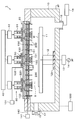
- FIG. 1 is a longitudinal sectional view schematically showing a plasma processing apparatus 1.
- the plasma processing apparatus 1 will be described by taking as an example a CVD apparatus that performs a film forming process as a plasma process on a semiconductor wafer W (hereinafter referred to as a wafer W).
- the plasma processing apparatus 1 includes a processing container 10 that plasma-processes a wafer W inside an airtightly held interior.
- the processing container 10 has a substantially cylindrical shape with an open upper surface, and is made of a metal such as aluminum.
- the processing container 10 is grounded.
- a susceptor 11 on which the wafer W is placed is provided at the bottom of the processing container 10.
- the susceptor 11 is supported by the support member 12 via an insulator 12 a and is installed at the bottom of the processing container 10. Thereby, the susceptor 11 is electrically insulated from the processing container 10.
- Examples of the material of the susceptor 11 and the support member 12 include aluminum whose surfaces are anodized (anodized).
- a high frequency power supply 14 for bias is connected to the susceptor 11 via a matching unit 13.
- the high frequency power supply 14 applies a high frequency power for bias to the susceptor 11, whereby ions in the plasma are attracted to the wafer W side.
- the susceptor 11 includes an electrostatic chuck for electrostatically attracting the wafer W, a temperature control mechanism, a gas flow path for supplying a heat transfer gas to the back surface of the wafer W, and the wafer. Lift pins or the like that move up and down when transporting W may be provided.
- An exhaust port 15 is provided at the bottom of the processing vessel 10, and an exhaust device 16 including a vacuum pump is connected to the exhaust port 15.
- an exhaust device 16 including a vacuum pump is connected to the exhaust port 15.
- the inside of the processing container 10 is exhausted, and the inside of the processing container 10 is depressurized to a desired degree of vacuum.
- a loading / unloading port 17 is formed on the side wall of the processing container 10, and the wafer W is loaded / unloaded by opening / closing a gate valve 18 that can open / close the loading / unloading port 17.
- a plasma generating antenna 20 (hereinafter referred to as “antenna 20”) capable of supplying a microwave while supplying gas into the processing container 10 is mounted.
- the antenna 20 is provided so as to close the opening at the top of the processing container 10. Thereby, a plasma space U is formed between the susceptor 11 and the antenna 20.
- a microwave transmission mechanism 30 for transmitting microwaves is connected to the upper part of the antenna 20 so as to transmit the microwaves output from the microwave output unit 40 to the antenna 20.
- the plasma processing apparatus 1 is provided with a control unit 500 as shown in FIG.
- the control unit 500 is a computer, for example, and has a program storage unit (not shown).
- the program storage unit stores a program for controlling the processing of the wafer W in the plasma processing apparatus 1.
- the program is recorded on a computer-readable storage medium such as a computer-readable hard disk (HD), flexible disk (FD), compact disk (CD), magnetic optical desk (MO), or memory card. Or installed in the control unit 500 from the storage medium.
- a computer-readable storage medium such as a computer-readable hard disk (HD), flexible disk (FD), compact disk (CD), magnetic optical desk (MO), or memory card.
- the microwave output unit 40 includes a microwave power supply 41, a microwave oscillator 42, an amplifier 43, and a distributor 44 that distributes the amplified microwaves into a plurality of parts.
- the microwave power supply 41 supplies power to the microwave oscillator 42.
- the microwave oscillator 42 oscillates, for example, a microwave having a predetermined frequency of 860 MHz by PLL.
- the amplifier 43 amplifies the oscillated microwave.
- the distributor 44 distributes the microwave amplified by the amplifier 43 while matching the impedance between the input side and the output side so that the loss of the microwave does not occur as much as possible.
- the microwave transmission mechanism 30 has a plurality of antenna modules 50 and microwave introduction mechanisms 51 that guide the microwaves distributed by the distributor 44 into the processing container. 2 schematically illustrates a state in which the microwave transmission mechanism 30 includes two antenna modules 50 and two microwave introduction mechanisms 51.
- the microwave transmission mechanism 30 has, for example, seven antenna modules 50, and the six antenna modules 50 have the same circumference, and one antenna module 50 is located at the top of the antenna 20 at the center. Is arranged.
- the antenna module 50 includes a phase shifter 52, a variable gain amplifier 53, a main amplifier 54 and an isolator 55, and transmits the microwave output from the microwave output unit 40 to the microwave introduction mechanism 51.
- the phase shifter 52 is configured to change the phase of the microwave, and by adjusting this, the radiation characteristic of the microwave can be modulated. According to this, the plasma distribution can be changed by controlling the directivity. Note that the phase shifter 52 need not be provided when such modulation of the radiation characteristic is not required.
- the variable gain amplifier 53 adjusts the power level of the microwave input to the main amplifier 54 and adjusts the plasma intensity.
- the main amplifier 54 constitutes a solid state amplifier.
- the solid state amplifier can be configured to include an input matching circuit, a semiconductor amplifying element, an output matching circuit, and a high Q resonance circuit which are not shown.
- the isolator 55 separates the reflected wave of the microwave reflected by the antenna 20 and returning to the main amplifier 54, and includes a circulator and a dummy load (coaxial terminator).
- the circulator guides the microwave reflected by the antenna 20 to the dummy load, and the dummy load converts the microwave reflected wave guided by the circulator into heat.
- FIG. 4 is an enlarged vertical cross-sectional view showing, for example, the schematic configuration of the left half of the microwave introduction mechanism 51 and the antenna 20 according to this embodiment.
- the microwave introduction mechanism 51 includes a coaxial tube 60 and a slow wave plate 70.
- the coaxial tube 60 has a coaxial waveguide composed of a cylindrical outer conductor 60a and a rod-shaped inner conductor 60b provided at the center thereof.
- the antenna 20 is provided at the lower end of the coaxial tube 60 via a slow wave plate 70.
- the inner conductor 60b is on the power supply side
- the outer conductor 60a is on the ground side.
- the coaxial tube 60 is provided with a tuner 80.
- the tuner 80 includes, for example, two slags 80a and constitutes a slag tuner.
- the slug 80a is configured as a plate-like body of a dielectric member, and is provided in an annular shape between the inner conductor 60b and the outer conductor 60a of the coaxial pipe 60.
- the tuner 80 adjusts the impedance of the coaxial tube 60 by moving the slug 80a up and down by a drive mechanism (not shown) based on a command from the control unit 500 described later.
- the slow wave plate 70 is provided adjacent to the lower surface of the coaxial tube 60.
- the slow wave plate 70 is formed of a disk-shaped dielectric member.
- the slow wave plate 70 transmits the microwave transmitted through the coaxial waveguide 60 and guides it to the antenna 20.
- the antenna 20 has a shower plate 100.
- the shower plate 100 is provided adjacent to the lower surface of the slow wave plate 70.
- the shower plate 100 has a substantially disk shape whose diameter is larger than that of the slow wave plate 70, and is formed of a conductor having high electrical conductivity such as aluminum or copper.
- the shower plate 100 is exposed to the plasma space U side of the processing vessel 10 and propagates surface waves to the exposed lower surface.
- the metal surface of the shower plate 100 is exposed to the plasma space U side.
- the surface wave propagating to the exposed lower surface is referred to as a metal surface wave.
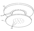
- the drooping member 101 has a substantially truncated cone shape having a circular bottom surface shape, and is formed of a conductor having high electrical conductivity such as aluminum or copper, like the shower plate 100.
- the outer surface of the drooping member 101 has, for example, a parabola shape that gradually spreads outward from its upper end surface toward its lower end surface, for example, with the contact point between the shower plate 100 and the outer surface of the drooping member 101 as the origin.
- the shower plate 100 has a configuration in which a substantially disk-shaped upper plate 110 and a substantially disk-shaped lower plate 120 are stacked one above the other.
- the upper plate 110 is formed with a gas flow path 130 that passes through the upper surface of the upper plate 110 and allows gas to flow in the radial direction of the upper plate 110.
- a first gas supply source 131 that supplies a first gas is connected to the gas flow path 130 via a supply pipe 132.
- the first gas may be a plurality of types of gases, or a mixed gas thereof.
- the first gas for example, monosilane gas (SiH4) as a source gas is used.
- a plurality of first gas supply ports 133 communicating with the gas flow path 130 are provided extending vertically upward at a position on the lower surface of the upper plate 110 and inside the outer surface of the drooping member 101.
- a plurality of slots 220 serving as microwave radiation holes through which microwaves pass are formed at positions different from the first gas supply port 133 of the upper plate 110.
- the shape of the drooping member 101 and the arrangement of the slots 220 are set so that an imaginary line drawn vertically downward from the center of the slot 220 intersects the outer surface of the drooping member 101.
- the slot 220 is arranged so that the center of the slot 220 is located inside the outer peripheral end portion of the lower surface of the hanging member 101 in a plan view.
- through-holes 150 penetrating the lower plate 120 in the vertical direction are formed at positions corresponding to the first gas supply ports 133 of the upper plate 110. Thereby, the first gas supplied from the first gas supply port 133 can reach the lower end surface of the lower plate 120 through the through hole 150.
- the slot 220 is formed at a position corresponding to the slot 220 of the upper plate 110 in the lower plate 120.
- a through hole 160 that communicates from the upper end surface to the lower end surface of the drooping member 101 is formed in the drooping member 101 at a position corresponding to the lower end of each through hole 150.
- the drooping member 101 is provided to protrude vertically downward from the lower end of the lower plate 120 by a predetermined length L. Therefore, the first gas supplied from the first gas supply source 131 to the gas flow path 130 passes through the plurality of through holes 160 from the position lower than the lower plate 120 by a predetermined length L from the processing container. 10 plasma spaces U are introduced.
- the lower plate 120 is formed with a gas flow path 140 that passes through the side surface thereof and distributes gas in the radial direction of the lower plate 120.
- a second gas supply source 141 that supplies a second gas is connected to the gas flow path 140 via a supply pipe 142.
- the second gas for example, nitrogen gas, argon gas, hydrogen gas, or a gas obtained by mixing these gases is used for generating plasma.
- the gas flow path 140 is provided completely independently of the gas flow path 130 so that the gas flowing through the gas flow path 140 and the gas flowing through the gas flow path 130 are not mixed in the shower plate 100. It has been.
- a plurality of second gas supply ports 151 communicating with the gas flow path 140 are vertically upward at a position on the lower surface of the lower plate 120 and outside the outer surface of the drooping member 101 and different from the slot 220. Stretched and provided. The second gas supplied from the second gas supply source 141 to the gas flow path 140 is introduced into the plasma space U of the processing vessel 10 from the lower surface of the lower plate 120 through each second gas supply port 151. .
- the plurality of slots 220 described above are provided at positions different from the gas flow paths 130 and 140, which are gas supply paths, the plurality of first gas supply ports 133, the second gas supply ports 151, and the through holes 150 and 160. And penetrates in a direction perpendicular to the radial direction of the shower plate 100.
- One end of the slot 220 is adjacent to the slow wave plate 70, and the other end is opened to the plasma space U side of the processing vessel 10.
- the microwave propagates through the coaxial tube 60, passes through the slow wave plate 70, passes through the plurality of slots 220, and is radiated into the processing container 10.
- the slot 220 may be filled with a dielectric such as quartz.
- the diameters of the through hole 160 and the second gas supply port 151 are sized so that the microwave radiated into the processing container 10 does not enter the inside of the through hole 160 and the second gas supply port 151. . In the present embodiment, it is 0.6 mm, for example. Further, the slot 220 and the first gas supply port 133, the second gas supply port 151, and the through holes 150 and 160 are completely separated in the shower plate 100. Thereby, abnormal discharge at the first gas supply port 133, the second gas supply port 151, and the through holes 150 and 160 can be prevented.
- the surface exposed to the plasma side of the shower plate 100 that is, the lower surface of the lower plate 120 and the surface of the hanging member 101 are coated with, for example, alumina (Al 2 O 3 ) or yttria (Y 2 O 3 ) by thermal spraying (see FIG. (Not shown).
- alumina Al 2 O 3
- Y 2 O 3 yttria
- FIG. 5 shows an example of a schematic positional relationship between the drooping member 101, the lower plate 120, the second gas supply port 151, and the through hole 160 formed in the drooping member 101. It is the perspective view which showed the state seen from diagonally downward. In FIG. 5, the description of the slot 220 is omitted.
- a plurality of through holes 160 provided in the drooping member 101 are arranged concentrically near the center of the drooping member 101. Further, as described above, the first gas supply port 133 and the through hole 150 are provided at positions corresponding to the through hole 160.
- the first gas supply port 133 and the through hole 150 are also concentrically arranged with the drooping member 101 as shown in FIG. 5, for example.
- a plurality of second gas supply ports 151 are arranged concentrically with the upper end portion of the drooping member 101, for example.
- the second gas supply port 151 is disposed at a position that is covered by the hanging member 101 and cannot be seen when the hanging member 101 is viewed from below, but is not necessarily visible by the hanging member 101. There is no need to place it.
- the configuration in the vicinity of the shower plate 100 and the hanging member 101 will be described together with the principle of the present invention.
- monosilane (SiH 4) used as a source gas when forming a film on the wafer W is decomposed into SiH 3, energy of about 8.75 eV or more is required.
- nitrogen gas used as plasma generating gas has a binding energy of about 9.91 eV. That is, in order to excite nitrogen gas and generate nitrogen plasma or nitrogen radicals, it is necessary to apply energy of about 9.91 eV or more. Therefore, the microwave output supplied to the antenna 20 in the microwave plasma processing in such a case is determined based on higher energy, that is, energy for exciting the plasma generating gas.
- the region near the lower end surface of the antenna 20 for example, a region within approximately 5 mm from the lower surface of the antenna,
- the electron temperature is higher than that in a region approximately 5 mm or more away from the lower surface.
- FIG. 6 shows a distribution of electron temperatures in the vicinity of the shower plate 100 in which the slots 220 are formed on the outer periphery.
- the vertical axis in FIG. 6 is the height in the processing container 10, and the horizontal axis is the distance in the horizontal direction from the central axis of the coaxial tube 60.
- the electron temperature distribution when the center of the slot 220 is approximately 35 mm from the central axis of the coaxial tube 60 is illustrated.
- the broken line shown in FIG. 6 is a boundary line at which the electron temperature becomes 1 eV.
- the electron temperature is higher than 1 eV in the region X closer to the slot 220 than the broken line (the region having a radius of about 35 mm with the slot 220 as the center), and the vicinity of the slot 220 is in the high electron temperature region. It represents that. That is, in the region X, the plasma generating gas and the source gas are actively ionized. Therefore, when both nitrogen gas as a gas for generating plasma and monosilane gas as a raw material gas are supplied from a shower plate as in the prior art, the nitrogen gas is decomposed in the region X where the electron temperature is high, and nitrogen ions and nitrogen atom radicals are generated. However, since the energy is not sufficient in the region where the electron temperature is low, highly reactive atomic nitrogen is hardly generated.
- the monosilane gas is decomposed into SiH3 also outside the region X, but since a large amount of SiH2 and SiH are generated in the region X where the electron temperature is high, excessive SiH2 and SiH are generated in the region X. Silicon was deposited and deposited on the gas supply port of the shower plate.
- the output of the microwave supplied to the antenna 20 may be lowered, thereby lowering the electron temperature in the region X.
- the microwave output is lowered for the purpose of preventing excessive generation of SiH 2 and SiH, a predetermined electron temperature for decomposing the plasma generating gas cannot be obtained. For this reason, there is a limit to reducing the output of the microwave.
- the present inventors pass the raw material gas supplied from the shower plate 100 through the region X where the electron temperature is high in order to suppress unnecessary reaction products and gas phase reaction deposits deposited on the gas supply port.
- the method of introducing into the processing container 10 without doing it was studied earnestly.
- the raw material gas is supplied into the processing container 10 from the side wall of the processing container 10 as in the prior art, it becomes difficult to control the flow of the gas in the processing container 10 and uniform plasma cannot be obtained.
- the present inventors individually provide gas flow paths 130 and 140 so that the plasma generating gas and the raw material gas are not mixed in the shower plate 100, and the plasma generating gas is further supplied to the region X or the region.
- the idea is that if the gas is supplied in the vicinity of X, while the source gas is supplied to a place away from the region X, excessive decomposition of the source gas can be avoided and the plasma generating gas can be excited efficiently.
- the inventors have come up with the idea that a hanging member 101 as shown in FIG.
- the present inventors first investigated the electric field strength in the vicinity of the shower plate 100.
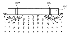
- 7 and 8 show the electric field intensity distribution and the direction in the vicinity of the shower plate 100 in which the slots 220 are formed on the outer periphery.
- 7 shows the electric field intensity distribution when only the shower plate 100 is provided
- FIG. 8 shows the electric field intensity distribution when the hanging member 101 is provided at the lower end of the shower plate 100.
- the size of the triangle represents the strength of the electric field strength
- the direction of the triangle represents the direction of the electric field.
- the electric field is mainly directed downward, but by providing the hanging member 101, the outside of the hanging member 101 is provided as shown in FIG. It was confirmed that the electric field strength in the lateral direction was increased near the side surface. From this, it is presumed that a high electron temperature is obtained in the vicinity of the outer surface of the drooping member 101. This is because the outer surface of the drooping member 101 spreads outward from the upper end portion toward the lower end portion, so that the microwave is reflected laterally or obliquely upward on the outer surface of the drooping member 101, and It is considered that the high energy state is formed in the vicinity of the outer side surface.
- FIG. 9 shows the distribution of the electron temperature in the vicinity of the shower plate 100 when the drooping member 101 is provided on the shower plate 100.
- the distance from the central axis of the coaxial tube 60 to the center of the slot 220 is approximately 35 mm as in the case of FIG. 6, and the radius of the lower surface of the hanging member 101 is approximately 45 mm.
- the region X in which the electron temperature is 1 eV or more is distributed in the vicinity of the slot 220 and on the outer surface of the drooping member 101, and on the lower surface of the drooping member 101, the electron temperature is approximately 1 eV or less. This can be confirmed from FIG.
- the microwave is reflected laterally or obliquely upward by the outer surface of the hanging member 101. It is assumed that the electric field strength in the vicinity of the outer surface of the hanging member is thereby increased.
- the second gas supply port 151 is disposed outside the outer surface of the drooping member 101, and the first gas supply port 133 and the through holes 150 and 160 are arranged from the outer surface of the drooping member 101.
- the plasma generating gas can be intensively supplied to the region X on the one hand, and the source gas that is easily decomposed can be introduced into the processing vessel 10 without passing through the region X on the other hand.
- the source gas can be prevented from being excessively decomposed in the region X, the generation of the precursor by the source gas can be suppressed, and the through-hole 160 and the second gas supply port 151 can be prevented from being blocked.
- the region X where the electron temperature is high is distributed outward from the outer surface of the drooping member 101.
- the bottom surface of the drooping member 101 The region X is also distributed at a position outside of. Therefore, as described above, the second gas supply port 151 does not necessarily have to be provided at a position that is covered with the hanging member 101 and cannot be seen when the hanging member 101 is viewed from below, and is located at the position facing the region X. As long as it is provided.
- the second gas supply port 151 is preferably provided at a position facing the vicinity of the focal point.
- the length L of the drooping member 101 is preferably at most the wavelength of the microwave introduced into the processing container 10 and more preferably at most 1 ⁇ 2 of the wavelength. According to the present inventors, by setting the length L of the drooping member 101 in this way, propagation of surface waves in the drooping member 101 is suppressed, and plasma is stably generated in the processing container 10. It has been confirmed that it is possible.
- the length L of the drooping member 101 is preferably set in a range of approximately 10 mm to 60 mm, and is set in a range of 20 mm to 40 mm. It is more preferable.
- the plasma processing apparatus 1 is based on the above knowledge. Next, processing performed using the plasma processing apparatus 1 will be described by taking a case where a silicon nitride film is formed on the wafer W as an example.
- the wafer W is loaded into the processing container 10 and placed on the susceptor 11. Then, a gas in which nitrogen gas, argon gas, and hydrogen gas are mixed as a plasma generating gas is introduced into the processing container 10 from the second gas supply source 141 through the lower plate 120 of the shower plate 100. Next, a microwave is output from the microwave output unit 40, and the microwave is introduced into the processing container 10 through the microwave transmission mechanism 30, the retardation plate 70, and the slot 220. Thereby, surface wave plasma is generated by the metal surface wave formed on the surfaces of the antenna 20 and the hanging member 101.
- a gas in which nitrogen gas, argon gas, and hydrogen gas are mixed as a plasma generating gas is introduced into the processing container 10 from the second gas supply source 141 through the lower plate 120 of the shower plate 100.
- a microwave is output from the microwave output unit 40, and the microwave is introduced into the processing container 10 through the microwave transmission mechanism 30, the retardation plate 70, and the slot 220. Thereby, surface wave plasma is generated by the metal surface wave formed on the surfaces
- the region X in the vicinity of the outer surface of the drooping member 101 provided with the slot 220 is in a high energy state, it is supplied from the second gas supply port 151 provided in the vicinity of the outer surface of the drooping member 101.
- the generated plasma generating gas is excited by high energy in this region X, and nitrogen radicals are efficiently generated.
- a monosilane gas as a source gas is introduced from the first gas supply source 131 into the processing container 10 through the first gas supply port 133 and the through holes 150 and 160.
- the monosilane gas introduced into the processing vessel 10 is excited by plasma and decomposed into SiH 3. At this time, since the monosilane gas is introduced into the plasma space U of the processing container 10 from the bottom surface of the drooping member 101, the monosilane gas does not pass through the region X where the electron temperature is high. As a result, reaction generation and gas phase reaction due to excess SiH 3 can be suppressed.
- the nitrogen radicals and SiH 3 reach the surface of the wafer W along with the gas flow vertically downward from the shower plate 100 toward the wafer W, and are deposited as silicon nitride on the upper surface of the wafer W. As a result, a silicon nitride film is formed on the upper surface of the wafer W.
- the first gas supply port 133 is provided inside the outer surface of the drooping member 101, the first gas is in the vicinity of the slot 220 formed in the shower plate 100. It does not pass through the region X where the electron temperature is high. Therefore, it is possible to avoid the monosilane gas from being excessively decomposed by the surface wave plasma. As a result, when plasma processing is performed on the wafer W using the shower plate 100, deposits generated by reaction generation and vapor phase reaction in gas holes such as the through-hole 160 and the second gas supply port 151 of the shower plate 100, In the embodiment, the formation of a silicon film can be suppressed.
- the shape of the drooping member 101 and the arrangement of the slots 220 are set so that the imaginary line drawn from the center of the slot 220 vertically downward from the center of the slot 220 intersects with the parabola. Therefore, the microwave is reflected laterally or obliquely upward on the outer surface of the drooping member 101. Therefore, the electric field strength in the vicinity of the outer surface of the drooping member 101 is increased, and a region X in a high energy state is formed on the outer surface of the drooping member 101. As a result, the second gas supplied from the second gas supply port is efficiently excited in the region X, so that plasma can be generated efficiently.
- the positional relationship between the slot 220 and the drooping member 101 is not necessarily limited to the contents of the present embodiment. Even if the slot 220 is located outside the parabolic shape on the outer surface of the drooping member 101, the slot Since the microwave introduced from 220 is reflected by the outer surface of the drooping member 101, a region having a high electric field strength can be formed in the vicinity of the outer surface of the drooping member 101.
- the electric field strength in the lateral direction is increased in the vicinity of the outer surface of the hanging member 101, for example, as shown in FIG.
- the electric field does not spread in the lateral direction from the shower plate, and the electric field in the region corresponding to the lower part of the coaxial tube 60 is present.
- the intensity tended to be relatively higher than the electric field intensity in other regions. As a result, the electric field strength in the processing container becomes non-uniform, and the uniformity of the plasma processing is limited.
- the hanging member 101 as in the present embodiment, it is possible to increase the electric field strength in the lateral direction and make the electric field strength distribution more uniform than in the past. Therefore, according to the plasma processing apparatus 1 according to the present embodiment, plasma processing with higher uniformity than before can be performed.
- the second gas supply source 141 that supplies a gas for generating plasma is connected to the gas flow path 140 of the lower plate 120.
- the first gas supply port 133 is provided only at a position corresponding to the drooping member 101, but the first gas supply port 133 is not located at a position corresponding to the drooping member 101.
- the second gas supply port 151 and the first gas supply port 133 may be arranged on the lower surface of the shower plate 100 so as to be substantially equidistant. Good.
- a through hole 150 is formed at a position corresponding to the first gas supply port 133 of the lower plate 120. In such a case, the first gas, which is the source gas, passes through the region of the lower surface of the lower plate 120 where the electron temperature is high.
- a supply nozzle 200 having a predetermined length may be provided at the lower end of the through hole 150.
- the length of the supply nozzle 200 is depicted as being equal to the length L of the drooping member 101, but the length of the supply nozzle 200 is not limited to the contents of the present embodiment.
- the length can be arbitrarily set as long as it passes through a region having a relatively high electron temperature within about 5 mm from the lower surface of the shower plate 100 as described above.
- the length of the supply nozzle 200 which is a projection, a surface wave propagates to the supply nozzle 200 and causes resonance, which may hinder the generation of uniform plasma in the plasma space U. Therefore, the length of the supply nozzle 200 is preferably about 1/16 to 3/16, more preferably about 1/8 of the wavelength of the microwave introduced into the processing container 10.
- the outer surface of the drooping member 101 has a parabolic shape, but the shape of the drooping member 101 is not limited to the contents of the present embodiment, and the outer surface is Any shape can be set as long as the shape spreads outward from the upper end toward the lower end.
- a substantially frustoconical drooping member 300 whose outer surface is formed linearly may be used.
- the tangential direction of the outer surface gradually increases.
- a drooping member 310 having a substantially quadratic curve shape that changes from an oblique direction to a vertical direction may be used.
- the microwave is laterally or obliquely upward on the outer surface of the drooping member 101. Since it is reflected in the direction, a high energy state can be formed in the vicinity of the outer surface of the hanging member 101.
- the through-hole 160 penetrating in the vertical direction is formed inside the hanging member 101.
- the through-hole 160 may extend in an oblique direction, for example, an excessive amount of source gas such as monosilane gas. If it is formed at a position that does not face the region X so as not to be decomposed, the shape can be arbitrarily set. Further, for example, as shown in FIG. 14, a gas chamber 101a communicating with the through hole 150 of the lower plate 120 is formed in the hanging member 101, and a through hole 160 is formed below the gas chamber 101a. Also good.
- the plurality of through holes 160 are formed in the vicinity of the central portion of the hanging member 101, and the first gas supply port 133 is also formed at a position corresponding to the through hole 160.
- the first gas supply port 133 and the through hole 160 are not limited to the contents of the present embodiment. From the viewpoint of suppressing excessive decomposition of the monosilane gas as the source gas, if there is a region where the electric field strength is weak or the electron temperature is low in the lower surface of the drooping member 101, the low electric field strength, low electron You may make it provide the through-hole 160 only in the area
- the region where the electric field strength is weakened is a position corresponding to the minimum value of the Bessel function obtained as a solution of the Bessel equation representing the electric field strength distribution on the lower surface of the drooping member 101, as will be described later. Exists.
- the region where the electric field strength becomes weak will be described.
- the inventors first measured the electric field intensity distribution on the lower surface of the drooping member 101 using a Langmuir probe and a spectrum analyzer. Specifically, a Langmuir probe (not shown) connected to a spectrum analyzer (not shown) is inserted from the outside of the processing container 10, and a position approximately 10 mm below the lower end surface of the drooping member 101 is placed on the bottom surface of the drooping member 101. Were scanned along the diameter direction. At this time, a microwave of 860 MHz was supplied from the microwave oscillator 42. The radius of the drooping member 101 is approximately 45 mm. The result is shown in FIG. The horizontal axis in FIG. 15 represents the position of the drooping member 101 in the radial direction, and the vertical axis represents the electric field strength.
- the inventors further examine the reason why such a field strength distribution is generated on the lower surface of the drooping member 101, and obtain the electric field strength distribution as a solution of the Bessel equation representing the electric field strength distribution on the lower surface of the drooping member 101. It was found that it corresponds to the Bessel function. Below, the method of calculating
- the inventors of the present invention thought that the surface wave propagating on the lower surface of the drooping member 101 is a cylindrical coordinate system model as shown in FIG. Specifically, a disc-shaped dielectric 251 having a predetermined thickness d is provided vertically below with respect to the bottom surface (lower surface) 250 of the hanging member 101 made of metal, and plasma 252 is formed on the lower surface of the dielectric 251. It is a state to be done.
- the radius of the cylindrical coordinate system is a.
- the dielectric 251 is a plasma sheath formed below the hanging member 101 and has a relative dielectric constant of 1.
- a surface wave is represented by the cylindrical coordinate system as shown in FIG.
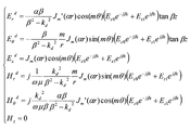
- the Maxwell equation showing a surface wave can be represented by the Bessel equation as shown, for example in FIG.
- Ez is the electric field strength in the vertical direction
- r is the coordinate in the radial direction
- k and ⁇ are the wave numbers of the microwaves.
- the outer peripheral end of the drooping member 101 is open. Therefore, when the equation of FIG. 17 is solved using the end of the plasma sheath, that is, the end of the dielectric 251 as the open end, Bessel As a solution of the equation, a Bessel function as shown in FIG. 18 is obtained.
- the distribution shown by the broken line in FIG. 19 is obtained.
- the horizontal axis in FIG. 15 represents the position of the drooping member 101 in the radial direction, and the vertical axis represents the electric field strength.
- the solid line in FIG. 19 is the actually measured electric field intensity distribution shown in FIG.
- the electric field strength distribution shown by the function of FIG. 18 has a local minimum point in the vicinity of a radius of about 20 mm, and is almost consistent with the measured data of the electric field strength distribution shown in FIG. It can be confirmed that it is a thing. From this result, it can be seen that the electric field strength distribution on the lower surface of the hanging member 101 according to the present embodiment is obtained by the Bessel function obtained as a solution of the Bessel equation.
- the electric field intensity distribution on the lower surface of the drooping member 101 has a minimum value on the circumference of a circle having a predetermined radius, that is, a radius of approximately 20 mm in this embodiment. Therefore, as described above, it is more preferable that the through hole 160 on the lower surface of the drooping member 101 and the first gas supply port 133 corresponding to the through hole 160 be provided at a position corresponding to the minimum value of the Bessel function. By doing so, the region X can be avoided and the source gas can be introduced into the processing vessel 10 through the region having a lower electric field strength on the lower surface of the drooping member 101.
- the drooping member 101 is necessarily configured to have a structure through which the first gas as the raw material gas passes.
- an annular hanging member having a hollow inside may be used, and the first gas may be supplied to the inside of the inner surface of the hanging member.
- a substantially annular hanging member 320 having an upper end and a lower end that are gradually increased in diameter downward is provided on the lower surface of the lower plate 120.
- a supply nozzle 321 extending vertically by a predetermined length is provided at the lower end of each through-hole 150 of the lower plate 120.
- the source gas can be introduced into the processing container 10 without passing through a region having a relatively high electron temperature within 5 mm from the lower surface of the shower plate 100.
- the length of the supply nozzle 321 is illustrated as being equal to the length L of the drooping member 320, but the length of the supply nozzle 321 is determined by the same method as that for the supply nozzle 200 described above. it can.
- the first gas supply source 131 and the second gas supply source are respectively connected to the gas flow path 130 of the upper plate 110 and the gas flow path 140 of the lower plate 120 via one supply pipes 132 and 142, respectively.
- the gas flow path 130 and the gas flow path 140 are formed as independent annular and concentric flow paths, and a plurality of supply pipes 132 and 142 are provided in each gas flow path. You may make it control the flow volume of the gas supplied to a path. By doing so, it becomes possible to control the supply amount of gas for each region of the lower plate 120.
- the supply amount of the source gas or the plasma generating gas is controlled in accordance with the electric field strength distribution, and the wafer W More uniform plasma treatment can be performed.
- the shower plate 100 is constituted by the upper plate 110 and the lower plate 120.
- the first gas gas flow path 130 and the second gas gas flow path 140 are different from each other.
- the configuration of the shower plate 100 is not limited to the present embodiment, and is arbitrarily set. Is possible.
- Plasma processing apparatus 10 Processing container 11 Susceptor 12 Support member 13 Matching device 14 High frequency power supply 30 Microwave transmission mechanism 40 Microwave output part 50 Antenna module 100 Shower plate 101 Watermelon member 110 Upper plate 120 Lower plate 130 Gas flow path 133 1st Gas supply port 140 Gas flow path 151 Second gas supply port 220 Slot 500 Controller U Plasma space W Wafer X region
Landscapes
- Chemical & Material Sciences (AREA)
- Engineering & Computer Science (AREA)
- Physics & Mathematics (AREA)
- Plasma & Fusion (AREA)
- Chemical Kinetics & Catalysis (AREA)
- General Chemical & Material Sciences (AREA)
- Materials Engineering (AREA)
- Mechanical Engineering (AREA)
- Metallurgy (AREA)
- Organic Chemistry (AREA)
- Analytical Chemistry (AREA)
- Plasma Technology (AREA)
- Chemical Vapour Deposition (AREA)
Abstract
Description
本願は、2013年9月11日に日本国に出願された特願2013-188665号、及び2014年6月9日に日本国に出願された特願2014-118531号に基づき、優先権を主張し、その内容をここに援用する。
10 処理容器
11 サセプタ
12 支持部材
13 整合器
14 高周波電源
30 マイクロ波伝送機構
40 マイクロ波出力部
50 アンテナモジュール
100 シャワープレート
101 スイカ部材
110 上部プレート
120 下部プレート
130 ガス流路
133 第1のガス供給口
140 ガス流路
151 第2のガス供給口
220 スロット
500 制御装置
U プラズマ空間
W ウェハ
X 領域
Claims (9)
- 処理容器内に第1のガスと第2のガスを供給するシャワープレートを備えたプラズマ発生用アンテナを有し、マイクロ波の供給によって前記シャワープレート表面に形成された表面波によりプラズマを形成して基板を処理するプラズマ処理装置であって、
前記シャワープレートの下端面から下方に突出する、導電体により構成された垂下部材を有し、
前記垂下部材の外側面は、上端部から下端部に向かって外側に広がり、
前記シャワープレートは、前記処理容器内に第1のガスを供給する複数の第1のガス供給口と第2のガスを供給する複数の第2のガス供給口とを備え、
前記第1のガス供給口は、前記垂下部材の外側面よりも内側に配置され、
前記第2のガス供給口は、前記垂下部材の外側面よりも外側に配置されている。 - 請求項1に記載のプラズマ処理装置において、
前記垂下部材の内部には、当該垂下部材の上端面から下端面に連通する貫通孔が形成され、
前記第1のガス供給口は、前記貫通孔に接続されている。 - 請求項1に記載のプラズマ処理装置において、
前記垂下部材の下面は円形であり、
前記第1のガス供給口は、Bessel方程式の解として得られる前記垂下部材の下端面における電界強度分布の極小値に相当する位置に設けられている。 - 請求項1に記載のプラズマ処理装置において、
前記垂下部材は環状に形成され、
前記第1のガス供給口は、前記垂下部材の内側面よりも内側に配置されている。 - 請求項4に記載のプラズマ処理装置において、
前記各第1のガス供給口には、前記シャワープレートの下面から鉛直下方に突出する複数の供給ノズルがそれぞれ接続されている。 - 請求項1に記載のプラズマ処理装置において、
前記垂下部材の外側面は、下に向かって次第に外側に広がる放物線形状である。 - 請求項1に記載のプラズマ処理装置において、
前記第1のガスは、前記第2のガスよりも、プラズマにより分解されやすいガスである。 - 請求項7に記載のプラズマ処理装置において、
前記第1のガスは原料ガスであり、前記第2のガスはプラズマ発生用のガスである。 - 請求項1に記載のプラズマ処理装置において、
前記シャワープレートには、前記処理容器内にマイクロ波を放射するマイクロ波放射孔が設けられ、
マイクロ波放射孔は、平面視において、前記垂下部材の外周端部よりも内側に位置するように配置されている。
Priority Applications (4)
| Application Number | Priority Date | Filing Date | Title |
|---|---|---|---|
| KR1020177028538A KR101831576B1 (ko) | 2013-09-11 | 2014-09-04 | 플라즈마 처리 장치 |
| US14/917,414 US10557200B2 (en) | 2013-09-11 | 2014-09-04 | Plasma processing device with shower plate having protrusion for suppressing film formation in gas holes of shower plate |
| KR1020167006190A KR101831537B1 (ko) | 2013-09-11 | 2014-09-04 | 플라즈마 처리 장치 |
| CN201480050227.5A CN105531800B (zh) | 2013-09-11 | 2014-09-04 | 等离子体处理装置 |
Applications Claiming Priority (4)
| Application Number | Priority Date | Filing Date | Title |
|---|---|---|---|
| JP2013-188665 | 2013-09-11 | ||
| JP2013188665 | 2013-09-11 | ||
| JP2014-118531 | 2014-06-09 | ||
| JP2014118531A JP6338462B2 (ja) | 2013-09-11 | 2014-06-09 | プラズマ処理装置 |
Publications (1)
| Publication Number | Publication Date |
|---|---|
| WO2015037508A1 true WO2015037508A1 (ja) | 2015-03-19 |
Family
ID=52665614
Family Applications (1)
| Application Number | Title | Priority Date | Filing Date |
|---|---|---|---|
| PCT/JP2014/073311 Ceased WO2015037508A1 (ja) | 2013-09-11 | 2014-09-04 | プラズマ処理装置 |
Country Status (6)
| Country | Link |
|---|---|
| US (1) | US10557200B2 (ja) |
| JP (1) | JP6338462B2 (ja) |
| KR (2) | KR101831537B1 (ja) |
| CN (1) | CN105531800B (ja) |
| TW (1) | TWI643236B (ja) |
| WO (1) | WO2015037508A1 (ja) |
Cited By (1)
| Publication number | Priority date | Publication date | Assignee | Title |
|---|---|---|---|---|
| CN110753994A (zh) * | 2017-08-08 | 2020-02-04 | 应用材料公司 | 用于处理腔室的多板面板 |
Families Citing this family (315)
| Publication number | Priority date | Publication date | Assignee | Title |
|---|---|---|---|---|
| US9394608B2 (en) | 2009-04-06 | 2016-07-19 | Asm America, Inc. | Semiconductor processing reactor and components thereof |
| US8802201B2 (en) | 2009-08-14 | 2014-08-12 | Asm America, Inc. | Systems and methods for thin-film deposition of metal oxides using excited nitrogen-oxygen species |
| US20130023129A1 (en) | 2011-07-20 | 2013-01-24 | Asm America, Inc. | Pressure transmitter for a semiconductor processing environment |
| US9017481B1 (en) | 2011-10-28 | 2015-04-28 | Asm America, Inc. | Process feed management for semiconductor substrate processing |
| US10714315B2 (en) | 2012-10-12 | 2020-07-14 | Asm Ip Holdings B.V. | Semiconductor reaction chamber showerhead |
| US20160376700A1 (en) | 2013-02-01 | 2016-12-29 | Asm Ip Holding B.V. | System for treatment of deposition reactor |
| JP6338462B2 (ja) * | 2013-09-11 | 2018-06-06 | 東京エレクトロン株式会社 | プラズマ処理装置 |
| US20150118416A1 (en) * | 2013-10-31 | 2015-04-30 | Semes Co., Ltd. | Substrate treating apparatus and method |
| US11015245B2 (en) | 2014-03-19 | 2021-05-25 | Asm Ip Holding B.V. | Gas-phase reactor and system having exhaust plenum and components thereof |
| US10858737B2 (en) | 2014-07-28 | 2020-12-08 | Asm Ip Holding B.V. | Showerhead assembly and components thereof |
| US9890456B2 (en) | 2014-08-21 | 2018-02-13 | Asm Ip Holding B.V. | Method and system for in situ formation of gas-phase compounds |
| US10941490B2 (en) | 2014-10-07 | 2021-03-09 | Asm Ip Holding B.V. | Multiple temperature range susceptor, assembly, reactor and system including the susceptor, and methods of using the same |
| JP6404111B2 (ja) * | 2014-12-18 | 2018-10-10 | 東京エレクトロン株式会社 | プラズマ処理装置 |
| US10276355B2 (en) | 2015-03-12 | 2019-04-30 | Asm Ip Holding B.V. | Multi-zone reactor, system including the reactor, and method of using the same |
| US10458018B2 (en) | 2015-06-26 | 2019-10-29 | Asm Ip Holding B.V. | Structures including metal carbide material, devices including the structures, and methods of forming same |
| US10211308B2 (en) | 2015-10-21 | 2019-02-19 | Asm Ip Holding B.V. | NbMC layers |
| US11139308B2 (en) | 2015-12-29 | 2021-10-05 | Asm Ip Holding B.V. | Atomic layer deposition of III-V compounds to form V-NAND devices |
| US10529554B2 (en) | 2016-02-19 | 2020-01-07 | Asm Ip Holding B.V. | Method for forming silicon nitride film selectively on sidewalls or flat surfaces of trenches |
| US10343920B2 (en) | 2016-03-18 | 2019-07-09 | Asm Ip Holding B.V. | Aligned carbon nanotubes |
| US10190213B2 (en) | 2016-04-21 | 2019-01-29 | Asm Ip Holding B.V. | Deposition of metal borides |
| US10865475B2 (en) | 2016-04-21 | 2020-12-15 | Asm Ip Holding B.V. | Deposition of metal borides and silicides |
| US10367080B2 (en) | 2016-05-02 | 2019-07-30 | Asm Ip Holding B.V. | Method of forming a germanium oxynitride film |
| US11453943B2 (en) | 2016-05-25 | 2022-09-27 | Asm Ip Holding B.V. | Method for forming carbon-containing silicon/metal oxide or nitride film by ALD using silicon precursor and hydrocarbon precursor |
| US10612137B2 (en) | 2016-07-08 | 2020-04-07 | Asm Ip Holdings B.V. | Organic reactants for atomic layer deposition |
| US9859151B1 (en) | 2016-07-08 | 2018-01-02 | Asm Ip Holding B.V. | Selective film deposition method to form air gaps |
| KR102532607B1 (ko) | 2016-07-28 | 2023-05-15 | 에이에스엠 아이피 홀딩 비.브이. | 기판 가공 장치 및 그 동작 방법 |
| US9887082B1 (en) | 2016-07-28 | 2018-02-06 | Asm Ip Holding B.V. | Method and apparatus for filling a gap |
| US9812320B1 (en) | 2016-07-28 | 2017-11-07 | Asm Ip Holding B.V. | Method and apparatus for filling a gap |
| US10643826B2 (en) | 2016-10-26 | 2020-05-05 | Asm Ip Holdings B.V. | Methods for thermally calibrating reaction chambers |
| US11532757B2 (en) | 2016-10-27 | 2022-12-20 | Asm Ip Holding B.V. | Deposition of charge trapping layers |
| US10714350B2 (en) | 2016-11-01 | 2020-07-14 | ASM IP Holdings, B.V. | Methods for forming a transition metal niobium nitride film on a substrate by atomic layer deposition and related semiconductor device structures |
| US10229833B2 (en) | 2016-11-01 | 2019-03-12 | Asm Ip Holding B.V. | Methods for forming a transition metal nitride film on a substrate by atomic layer deposition and related semiconductor device structures |
| KR102546317B1 (ko) | 2016-11-15 | 2023-06-21 | 에이에스엠 아이피 홀딩 비.브이. | 기체 공급 유닛 및 이를 포함하는 기판 처리 장치 |
| KR102762543B1 (ko) * | 2016-12-14 | 2025-02-05 | 에이에스엠 아이피 홀딩 비.브이. | 기판 처리 장치 |
| US11447861B2 (en) | 2016-12-15 | 2022-09-20 | Asm Ip Holding B.V. | Sequential infiltration synthesis apparatus and a method of forming a patterned structure |
| US11581186B2 (en) | 2016-12-15 | 2023-02-14 | Asm Ip Holding B.V. | Sequential infiltration synthesis apparatus |
| KR102700194B1 (ko) | 2016-12-19 | 2024-08-28 | 에이에스엠 아이피 홀딩 비.브이. | 기판 처리 장치 |
| US10269558B2 (en) | 2016-12-22 | 2019-04-23 | Asm Ip Holding B.V. | Method of forming a structure on a substrate |
| US10867788B2 (en) | 2016-12-28 | 2020-12-15 | Asm Ip Holding B.V. | Method of forming a structure on a substrate |
| US11390950B2 (en) | 2017-01-10 | 2022-07-19 | Asm Ip Holding B.V. | Reactor system and method to reduce residue buildup during a film deposition process |
| US10468261B2 (en) | 2017-02-15 | 2019-11-05 | Asm Ip Holding B.V. | Methods for forming a metallic film on a substrate by cyclical deposition and related semiconductor device structures |
| US10790118B2 (en) * | 2017-03-16 | 2020-09-29 | Mks Instruments, Inc. | Microwave applicator with solid-state generator power source |
| US10529563B2 (en) | 2017-03-29 | 2020-01-07 | Asm Ip Holdings B.V. | Method for forming doped metal oxide films on a substrate by cyclical deposition and related semiconductor device structures |
| KR102457289B1 (ko) | 2017-04-25 | 2022-10-21 | 에이에스엠 아이피 홀딩 비.브이. | 박막 증착 방법 및 반도체 장치의 제조 방법 |
| US10892156B2 (en) | 2017-05-08 | 2021-01-12 | Asm Ip Holding B.V. | Methods for forming a silicon nitride film on a substrate and related semiconductor device structures |
| US10770286B2 (en) | 2017-05-08 | 2020-09-08 | Asm Ip Holdings B.V. | Methods for selectively forming a silicon nitride film on a substrate and related semiconductor device structures |
| US10886123B2 (en) | 2017-06-02 | 2021-01-05 | Asm Ip Holding B.V. | Methods for forming low temperature semiconductor layers and related semiconductor device structures |
| US12040200B2 (en) | 2017-06-20 | 2024-07-16 | Asm Ip Holding B.V. | Semiconductor processing apparatus and methods for calibrating a semiconductor processing apparatus |
| US11306395B2 (en) | 2017-06-28 | 2022-04-19 | Asm Ip Holding B.V. | Methods for depositing a transition metal nitride film on a substrate by atomic layer deposition and related deposition apparatus |
| KR20190009245A (ko) | 2017-07-18 | 2019-01-28 | 에이에스엠 아이피 홀딩 비.브이. | 반도체 소자 구조물 형성 방법 및 관련된 반도체 소자 구조물 |
| US11018002B2 (en) | 2017-07-19 | 2021-05-25 | Asm Ip Holding B.V. | Method for selectively depositing a Group IV semiconductor and related semiconductor device structures |
| US10541333B2 (en) | 2017-07-19 | 2020-01-21 | Asm Ip Holding B.V. | Method for depositing a group IV semiconductor and related semiconductor device structures |
| US11374112B2 (en) | 2017-07-19 | 2022-06-28 | Asm Ip Holding B.V. | Method for depositing a group IV semiconductor and related semiconductor device structures |
| US10590535B2 (en) | 2017-07-26 | 2020-03-17 | Asm Ip Holdings B.V. | Chemical treatment, deposition and/or infiltration apparatus and method for using the same |
| TWI815813B (zh) | 2017-08-04 | 2023-09-21 | 荷蘭商Asm智慧財產控股公司 | 用於分配反應腔內氣體的噴頭總成 |
| US10692741B2 (en) | 2017-08-08 | 2020-06-23 | Asm Ip Holdings B.V. | Radiation shield |
| US10770336B2 (en) | 2017-08-08 | 2020-09-08 | Asm Ip Holding B.V. | Substrate lift mechanism and reactor including same |
| US11139191B2 (en) | 2017-08-09 | 2021-10-05 | Asm Ip Holding B.V. | Storage apparatus for storing cassettes for substrates and processing apparatus equipped therewith |
| US11769682B2 (en) | 2017-08-09 | 2023-09-26 | Asm Ip Holding B.V. | Storage apparatus for storing cassettes for substrates and processing apparatus equipped therewith |
| US11830730B2 (en) | 2017-08-29 | 2023-11-28 | Asm Ip Holding B.V. | Layer forming method and apparatus |
| US11295980B2 (en) | 2017-08-30 | 2022-04-05 | Asm Ip Holding B.V. | Methods for depositing a molybdenum metal film over a dielectric surface of a substrate by a cyclical deposition process and related semiconductor device structures |
| US11056344B2 (en) | 2017-08-30 | 2021-07-06 | Asm Ip Holding B.V. | Layer forming method |
| KR102491945B1 (ko) | 2017-08-30 | 2023-01-26 | 에이에스엠 아이피 홀딩 비.브이. | 기판 처리 장치 |
| KR102401446B1 (ko) | 2017-08-31 | 2022-05-24 | 에이에스엠 아이피 홀딩 비.브이. | 기판 처리 장치 |
| JP6960813B2 (ja) * | 2017-09-20 | 2021-11-05 | 東京エレクトロン株式会社 | グラフェン構造体の形成方法および形成装置 |
| KR102630301B1 (ko) | 2017-09-21 | 2024-01-29 | 에이에스엠 아이피 홀딩 비.브이. | 침투성 재료의 순차 침투 합성 방법 처리 및 이를 이용하여 형성된 구조물 및 장치 |
| US10844484B2 (en) | 2017-09-22 | 2020-11-24 | Asm Ip Holding B.V. | Apparatus for dispensing a vapor phase reactant to a reaction chamber and related methods |
| US10658205B2 (en) | 2017-09-28 | 2020-05-19 | Asm Ip Holdings B.V. | Chemical dispensing apparatus and methods for dispensing a chemical to a reaction chamber |
| US10403504B2 (en) | 2017-10-05 | 2019-09-03 | Asm Ip Holding B.V. | Method for selectively depositing a metallic film on a substrate |
| US10923344B2 (en) | 2017-10-30 | 2021-02-16 | Asm Ip Holding B.V. | Methods for forming a semiconductor structure and related semiconductor structures |
| US10910262B2 (en) | 2017-11-16 | 2021-02-02 | Asm Ip Holding B.V. | Method of selectively depositing a capping layer structure on a semiconductor device structure |
| US11022879B2 (en) | 2017-11-24 | 2021-06-01 | Asm Ip Holding B.V. | Method of forming an enhanced unexposed photoresist layer |
| TWI791689B (zh) | 2017-11-27 | 2023-02-11 | 荷蘭商Asm智慧財產控股私人有限公司 | 包括潔淨迷你環境之裝置 |
| JP7214724B2 (ja) | 2017-11-27 | 2023-01-30 | エーエスエム アイピー ホールディング ビー.ブイ. | バッチ炉で利用されるウェハカセットを収納するための収納装置 |
| US10872771B2 (en) | 2018-01-16 | 2020-12-22 | Asm Ip Holding B. V. | Method for depositing a material film on a substrate within a reaction chamber by a cyclical deposition process and related device structures |
| TWI799494B (zh) | 2018-01-19 | 2023-04-21 | 荷蘭商Asm 智慧財產控股公司 | 沈積方法 |
| KR102695659B1 (ko) | 2018-01-19 | 2024-08-14 | 에이에스엠 아이피 홀딩 비.브이. | 플라즈마 보조 증착에 의해 갭 충진 층을 증착하는 방법 |
| US11018047B2 (en) | 2018-01-25 | 2021-05-25 | Asm Ip Holding B.V. | Hybrid lift pin |
| USD880437S1 (en) | 2018-02-01 | 2020-04-07 | Asm Ip Holding B.V. | Gas supply plate for semiconductor manufacturing apparatus |
| US11081345B2 (en) | 2018-02-06 | 2021-08-03 | Asm Ip Holding B.V. | Method of post-deposition treatment for silicon oxide film |
| US10896820B2 (en) | 2018-02-14 | 2021-01-19 | Asm Ip Holding B.V. | Method for depositing a ruthenium-containing film on a substrate by a cyclical deposition process |
| US11685991B2 (en) | 2018-02-14 | 2023-06-27 | Asm Ip Holding B.V. | Method for depositing a ruthenium-containing film on a substrate by a cyclical deposition process |
| US10731249B2 (en) | 2018-02-15 | 2020-08-04 | Asm Ip Holding B.V. | Method of forming a transition metal containing film on a substrate by a cyclical deposition process, a method for supplying a transition metal halide compound to a reaction chamber, and related vapor deposition apparatus |
| KR102636427B1 (ko) | 2018-02-20 | 2024-02-13 | 에이에스엠 아이피 홀딩 비.브이. | 기판 처리 방법 및 장치 |
| US10975470B2 (en) | 2018-02-23 | 2021-04-13 | Asm Ip Holding B.V. | Apparatus for detecting or monitoring for a chemical precursor in a high temperature environment |
| US11473195B2 (en) | 2018-03-01 | 2022-10-18 | Asm Ip Holding B.V. | Semiconductor processing apparatus and a method for processing a substrate |
| US11629406B2 (en) | 2018-03-09 | 2023-04-18 | Asm Ip Holding B.V. | Semiconductor processing apparatus comprising one or more pyrometers for measuring a temperature of a substrate during transfer of the substrate |
| US11114283B2 (en) | 2018-03-16 | 2021-09-07 | Asm Ip Holding B.V. | Reactor, system including the reactor, and methods of manufacturing and using same |
| KR102646467B1 (ko) | 2018-03-27 | 2024-03-11 | 에이에스엠 아이피 홀딩 비.브이. | 기판 상에 전극을 형성하는 방법 및 전극을 포함하는 반도체 소자 구조 |
| US11230766B2 (en) | 2018-03-29 | 2022-01-25 | Asm Ip Holding B.V. | Substrate processing apparatus and method |
| US11088002B2 (en) | 2018-03-29 | 2021-08-10 | Asm Ip Holding B.V. | Substrate rack and a substrate processing system and method |
| KR102501472B1 (ko) | 2018-03-30 | 2023-02-20 | 에이에스엠 아이피 홀딩 비.브이. | 기판 처리 방법 |
| KR102600229B1 (ko) | 2018-04-09 | 2023-11-10 | 에이에스엠 아이피 홀딩 비.브이. | 기판 지지 장치, 이를 포함하는 기판 처리 장치 및 기판 처리 방법 |
| TWI843623B (zh) | 2018-05-08 | 2024-05-21 | 荷蘭商Asm Ip私人控股有限公司 | 藉由循環沉積製程於基板上沉積氧化物膜之方法及相關裝置結構 |
| US12025484B2 (en) | 2018-05-08 | 2024-07-02 | Asm Ip Holding B.V. | Thin film forming method |
| US12272527B2 (en) | 2018-05-09 | 2025-04-08 | Asm Ip Holding B.V. | Apparatus for use with hydrogen radicals and method of using same |
| KR20190129718A (ko) | 2018-05-11 | 2019-11-20 | 에이에스엠 아이피 홀딩 비.브이. | 기판 상에 피도핑 금속 탄화물 막을 형성하는 방법 및 관련 반도체 소자 구조 |
| KR102596988B1 (ko) | 2018-05-28 | 2023-10-31 | 에이에스엠 아이피 홀딩 비.브이. | 기판 처리 방법 및 그에 의해 제조된 장치 |
| TWI840362B (zh) | 2018-06-04 | 2024-05-01 | 荷蘭商Asm Ip私人控股有限公司 | 水氣降低的晶圓處置腔室 |
| US11718913B2 (en) | 2018-06-04 | 2023-08-08 | Asm Ip Holding B.V. | Gas distribution system and reactor system including same |
| US11286562B2 (en) | 2018-06-08 | 2022-03-29 | Asm Ip Holding B.V. | Gas-phase chemical reactor and method of using same |
| US10797133B2 (en) | 2018-06-21 | 2020-10-06 | Asm Ip Holding B.V. | Method for depositing a phosphorus doped silicon arsenide film and related semiconductor device structures |
| KR102568797B1 (ko) | 2018-06-21 | 2023-08-21 | 에이에스엠 아이피 홀딩 비.브이. | 기판 처리 시스템 |
| US11499222B2 (en) | 2018-06-27 | 2022-11-15 | Asm Ip Holding B.V. | Cyclic deposition methods for forming metal-containing material and films and structures including the metal-containing material |
| TWI871083B (zh) | 2018-06-27 | 2025-01-21 | 荷蘭商Asm Ip私人控股有限公司 | 用於形成含金屬材料之循環沉積製程 |
| US10612136B2 (en) | 2018-06-29 | 2020-04-07 | ASM IP Holding, B.V. | Temperature-controlled flange and reactor system including same |
| KR102686758B1 (ko) | 2018-06-29 | 2024-07-18 | 에이에스엠 아이피 홀딩 비.브이. | 박막 증착 방법 및 반도체 장치의 제조 방법 |
| US10388513B1 (en) | 2018-07-03 | 2019-08-20 | Asm Ip Holding B.V. | Method for depositing silicon-free carbon-containing film as gap-fill layer by pulse plasma-assisted deposition |
| US10755922B2 (en) | 2018-07-03 | 2020-08-25 | Asm Ip Holding B.V. | Method for depositing silicon-free carbon-containing film as gap-fill layer by pulse plasma-assisted deposition |
| US10767789B2 (en) | 2018-07-16 | 2020-09-08 | Asm Ip Holding B.V. | Diaphragm valves, valve components, and methods for forming valve components |
| US11053591B2 (en) | 2018-08-06 | 2021-07-06 | Asm Ip Holding B.V. | Multi-port gas injection system and reactor system including same |
| US10883175B2 (en) | 2018-08-09 | 2021-01-05 | Asm Ip Holding B.V. | Vertical furnace for processing substrates and a liner for use therein |
| US10829852B2 (en) | 2018-08-16 | 2020-11-10 | Asm Ip Holding B.V. | Gas distribution device for a wafer processing apparatus |
| US11430674B2 (en) | 2018-08-22 | 2022-08-30 | Asm Ip Holding B.V. | Sensor array, apparatus for dispensing a vapor phase reactant to a reaction chamber and related methods |
| US11024523B2 (en) | 2018-09-11 | 2021-06-01 | Asm Ip Holding B.V. | Substrate processing apparatus and method |
| KR102707956B1 (ko) | 2018-09-11 | 2024-09-19 | 에이에스엠 아이피 홀딩 비.브이. | 박막 증착 방법 |
| US11049751B2 (en) | 2018-09-14 | 2021-06-29 | Asm Ip Holding B.V. | Cassette supply system to store and handle cassettes and processing apparatus equipped therewith |
| CN110970344B (zh) | 2018-10-01 | 2024-10-25 | Asmip控股有限公司 | 衬底保持设备、包含所述设备的系统及其使用方法 |
| US11232963B2 (en) | 2018-10-03 | 2022-01-25 | Asm Ip Holding B.V. | Substrate processing apparatus and method |
| KR102592699B1 (ko) | 2018-10-08 | 2023-10-23 | 에이에스엠 아이피 홀딩 비.브이. | 기판 지지 유닛 및 이를 포함하는 박막 증착 장치와 기판 처리 장치 |
| KR102546322B1 (ko) | 2018-10-19 | 2023-06-21 | 에이에스엠 아이피 홀딩 비.브이. | 기판 처리 장치 및 기판 처리 방법 |
| KR102605121B1 (ko) | 2018-10-19 | 2023-11-23 | 에이에스엠 아이피 홀딩 비.브이. | 기판 처리 장치 및 기판 처리 방법 |
| USD948463S1 (en) | 2018-10-24 | 2022-04-12 | Asm Ip Holding B.V. | Susceptor for semiconductor substrate supporting apparatus |
| US12378665B2 (en) | 2018-10-26 | 2025-08-05 | Asm Ip Holding B.V. | High temperature coatings for a preclean and etch apparatus and related methods |
| US11087997B2 (en) | 2018-10-31 | 2021-08-10 | Asm Ip Holding B.V. | Substrate processing apparatus for processing substrates |
| KR102748291B1 (ko) | 2018-11-02 | 2024-12-31 | 에이에스엠 아이피 홀딩 비.브이. | 기판 지지 유닛 및 이를 포함하는 기판 처리 장치 |
| US11572620B2 (en) | 2018-11-06 | 2023-02-07 | Asm Ip Holding B.V. | Methods for selectively depositing an amorphous silicon film on a substrate |
| US11031242B2 (en) | 2018-11-07 | 2021-06-08 | Asm Ip Holding B.V. | Methods for depositing a boron doped silicon germanium film |
| US10847366B2 (en) | 2018-11-16 | 2020-11-24 | Asm Ip Holding B.V. | Methods for depositing a transition metal chalcogenide film on a substrate by a cyclical deposition process |
| US10818758B2 (en) | 2018-11-16 | 2020-10-27 | Asm Ip Holding B.V. | Methods for forming a metal silicate film on a substrate in a reaction chamber and related semiconductor device structures |
| US12040199B2 (en) | 2018-11-28 | 2024-07-16 | Asm Ip Holding B.V. | Substrate processing apparatus for processing substrates |
| US11217444B2 (en) | 2018-11-30 | 2022-01-04 | Asm Ip Holding B.V. | Method for forming an ultraviolet radiation responsive metal oxide-containing film |
| KR102636428B1 (ko) | 2018-12-04 | 2024-02-13 | 에이에스엠 아이피 홀딩 비.브이. | 기판 처리 장치를 세정하는 방법 |
| US11158513B2 (en) | 2018-12-13 | 2021-10-26 | Asm Ip Holding B.V. | Methods for forming a rhenium-containing film on a substrate by a cyclical deposition process and related semiconductor device structures |
| JP7504584B2 (ja) | 2018-12-14 | 2024-06-24 | エーエスエム・アイピー・ホールディング・ベー・フェー | 窒化ガリウムの選択的堆積を用いてデバイス構造体を形成する方法及びそのためのシステム |
| TWI866480B (zh) | 2019-01-17 | 2024-12-11 | 荷蘭商Asm Ip 私人控股有限公司 | 藉由循環沈積製程於基板上形成含過渡金屬膜之方法 |
| KR102727227B1 (ko) | 2019-01-22 | 2024-11-07 | 에이에스엠 아이피 홀딩 비.브이. | 기판 처리 장치 |
| CN111524788B (zh) | 2019-02-01 | 2023-11-24 | Asm Ip私人控股有限公司 | 氧化硅的拓扑选择性膜形成的方法 |
| TWI845607B (zh) | 2019-02-20 | 2024-06-21 | 荷蘭商Asm Ip私人控股有限公司 | 用來填充形成於基材表面內之凹部的循環沉積方法及設備 |
| TWI873122B (zh) | 2019-02-20 | 2025-02-21 | 荷蘭商Asm Ip私人控股有限公司 | 填充一基板之一表面內所形成的一凹槽的方法、根據其所形成之半導體結構、及半導體處理設備 |
| KR20200102357A (ko) | 2019-02-20 | 2020-08-31 | 에이에스엠 아이피 홀딩 비.브이. | 3-d nand 응용의 플러그 충진체 증착용 장치 및 방법 |
| KR102626263B1 (ko) | 2019-02-20 | 2024-01-16 | 에이에스엠 아이피 홀딩 비.브이. | 처리 단계를 포함하는 주기적 증착 방법 및 이를 위한 장치 |
| TWI842826B (zh) | 2019-02-22 | 2024-05-21 | 荷蘭商Asm Ip私人控股有限公司 | 基材處理設備及處理基材之方法 |
| KR102782593B1 (ko) | 2019-03-08 | 2025-03-14 | 에이에스엠 아이피 홀딩 비.브이. | SiOC 층을 포함한 구조체 및 이의 형성 방법 |
| KR102858005B1 (ko) | 2019-03-08 | 2025-09-09 | 에이에스엠 아이피 홀딩 비.브이. | 실리콘 질화물 층을 선택적으로 증착하는 방법, 및 선택적으로 증착된 실리콘 질화물 층을 포함하는 구조체 |
| KR102762833B1 (ko) | 2019-03-08 | 2025-02-04 | 에이에스엠 아이피 홀딩 비.브이. | SiOCN 층을 포함한 구조체 및 이의 형성 방법 |
| JP2020167398A (ja) | 2019-03-28 | 2020-10-08 | エーエスエム・アイピー・ホールディング・ベー・フェー | ドアオープナーおよびドアオープナーが提供される基材処理装置 |
| KR102809999B1 (ko) | 2019-04-01 | 2025-05-19 | 에이에스엠 아이피 홀딩 비.브이. | 반도체 소자를 제조하는 방법 |
| KR102897355B1 (ko) | 2019-04-19 | 2025-12-08 | 에이에스엠 아이피 홀딩 비.브이. | 층 형성 방법 및 장치 |
| KR20200125453A (ko) | 2019-04-24 | 2020-11-04 | 에이에스엠 아이피 홀딩 비.브이. | 기상 반응기 시스템 및 이를 사용하는 방법 |
| KR102869364B1 (ko) | 2019-05-07 | 2025-10-10 | 에이에스엠 아이피 홀딩 비.브이. | 비정질 탄소 중합체 막을 개질하는 방법 |
| KR102929471B1 (ko) | 2019-05-07 | 2026-02-20 | 에이에스엠 아이피 홀딩 비.브이. | 딥 튜브가 있는 화학물질 공급원 용기 |
| KR102929472B1 (ko) | 2019-05-10 | 2026-02-20 | 에이에스엠 아이피 홀딩 비.브이. | 표면 상에 재료를 증착하는 방법 및 본 방법에 따라 형성된 구조 |
| JP7598201B2 (ja) | 2019-05-16 | 2024-12-11 | エーエスエム・アイピー・ホールディング・ベー・フェー | ウェハボートハンドリング装置、縦型バッチ炉および方法 |
| JP7612342B2 (ja) | 2019-05-16 | 2025-01-14 | エーエスエム・アイピー・ホールディング・ベー・フェー | ウェハボートハンドリング装置、縦型バッチ炉および方法 |
| USD975665S1 (en) | 2019-05-17 | 2023-01-17 | Asm Ip Holding B.V. | Susceptor shaft |
| USD947913S1 (en) | 2019-05-17 | 2022-04-05 | Asm Ip Holding B.V. | Susceptor shaft |
| USD935572S1 (en) | 2019-05-24 | 2021-11-09 | Asm Ip Holding B.V. | Gas channel plate |
| USD922229S1 (en) | 2019-06-05 | 2021-06-15 | Asm Ip Holding B.V. | Device for controlling a temperature of a gas supply unit |
| KR20200141002A (ko) | 2019-06-06 | 2020-12-17 | 에이에스엠 아이피 홀딩 비.브이. | 배기 가스 분석을 포함한 기상 반응기 시스템을 사용하는 방법 |
| KR102918757B1 (ko) | 2019-06-10 | 2026-01-28 | 에이에스엠 아이피 홀딩 비.브이. | 석영 에피택셜 챔버를 세정하는 방법 |
| KR20200143254A (ko) | 2019-06-11 | 2020-12-23 | 에이에스엠 아이피 홀딩 비.브이. | 개질 가스를 사용하여 전자 구조를 형성하는 방법, 상기 방법을 수행하기 위한 시스템, 및 상기 방법을 사용하여 형성되는 구조 |
| USD944946S1 (en) | 2019-06-14 | 2022-03-01 | Asm Ip Holding B.V. | Shower plate |
| USD931978S1 (en) | 2019-06-27 | 2021-09-28 | Asm Ip Holding B.V. | Showerhead vacuum transport |
| KR102911421B1 (ko) | 2019-07-03 | 2026-01-12 | 에이에스엠 아이피 홀딩 비.브이. | 기판 처리 장치용 온도 제어 조립체 및 이를 사용하는 방법 |
| JP7499079B2 (ja) * | 2019-07-09 | 2024-06-13 | エーエスエム・アイピー・ホールディング・ベー・フェー | 同軸導波管を用いたプラズマ装置、基板処理方法 |
| CN112216646B (zh) | 2019-07-10 | 2026-02-10 | Asmip私人控股有限公司 | 基板支撑组件及包括其的基板处理装置 |
| KR102895115B1 (ko) | 2019-07-16 | 2025-12-03 | 에이에스엠 아이피 홀딩 비.브이. | 기판 처리 장치 |
| KR102860110B1 (ko) | 2019-07-17 | 2025-09-16 | 에이에스엠 아이피 홀딩 비.브이. | 실리콘 게르마늄 구조를 형성하는 방법 |
| TWI826704B (zh) | 2019-07-17 | 2023-12-21 | 荷蘭商Asm Ip私人控股有限公司 | 自由基輔助引燃電漿系統和方法 |
| US11643724B2 (en) | 2019-07-18 | 2023-05-09 | Asm Ip Holding B.V. | Method of forming structures using a neutral beam |
| KR102903090B1 (ko) | 2019-07-19 | 2025-12-19 | 에이에스엠 아이피 홀딩 비.브이. | 토폴로지-제어된 비정질 탄소 중합체 막을 형성하는 방법 |
| TWI839544B (zh) | 2019-07-19 | 2024-04-21 | 荷蘭商Asm Ip私人控股有限公司 | 形成形貌受控的非晶碳聚合物膜之方法 |
| CN112309843B (zh) | 2019-07-29 | 2026-01-23 | Asmip私人控股有限公司 | 实现高掺杂剂掺入的选择性沉积方法 |
| KR20210015655A (ko) | 2019-07-30 | 2021-02-10 | 에이에스엠 아이피 홀딩 비.브이. | 기판 처리 장치 및 방법 |
| CN112309900B (zh) | 2019-07-30 | 2025-11-04 | Asmip私人控股有限公司 | 基板处理设备 |
| CN112309899B (zh) | 2019-07-30 | 2025-11-14 | Asmip私人控股有限公司 | 基板处理设备 |
| US11587814B2 (en) | 2019-07-31 | 2023-02-21 | Asm Ip Holding B.V. | Vertical batch furnace assembly |
| US11227782B2 (en) | 2019-07-31 | 2022-01-18 | Asm Ip Holding B.V. | Vertical batch furnace assembly |
| US11587815B2 (en) | 2019-07-31 | 2023-02-21 | Asm Ip Holding B.V. | Vertical batch furnace assembly |
| KR20210018759A (ko) | 2019-08-05 | 2021-02-18 | 에이에스엠 아이피 홀딩 비.브이. | 화학물질 공급원 용기를 위한 액체 레벨 센서 |
| KR20210018761A (ko) | 2019-08-09 | 2021-02-18 | 에이에스엠 아이피 홀딩 비.브이. | 냉각 장치를 포함한 히터 어셈블리 및 이를 사용하는 방법 |
| USD965044S1 (en) | 2019-08-19 | 2022-09-27 | Asm Ip Holding B.V. | Susceptor shaft |
| USD965524S1 (en) | 2019-08-19 | 2022-10-04 | Asm Ip Holding B.V. | Susceptor support |
| JP7810514B2 (ja) | 2019-08-21 | 2026-02-03 | エーエスエム・アイピー・ホールディング・ベー・フェー | 成膜原料混合ガス生成装置及び成膜装置 |
| USD940837S1 (en) | 2019-08-22 | 2022-01-11 | Asm Ip Holding B.V. | Electrode |
| KR20210024423A (ko) | 2019-08-22 | 2021-03-05 | 에이에스엠 아이피 홀딩 비.브이. | 홀을 구비한 구조체를 형성하기 위한 방법 |
| USD979506S1 (en) | 2019-08-22 | 2023-02-28 | Asm Ip Holding B.V. | Insulator |
| USD949319S1 (en) | 2019-08-22 | 2022-04-19 | Asm Ip Holding B.V. | Exhaust duct |
| USD930782S1 (en) | 2019-08-22 | 2021-09-14 | Asm Ip Holding B.V. | Gas distributor |
| KR102928101B1 (ko) | 2019-08-23 | 2026-02-13 | 에이에스엠 아이피 홀딩 비.브이. | 비스(디에틸아미노)실란을 사용하여 peald에 의해 개선된 품질을 갖는 실리콘 산화물 막을 증착하기 위한 방법 |
| US11286558B2 (en) | 2019-08-23 | 2022-03-29 | Asm Ip Holding B.V. | Methods for depositing a molybdenum nitride film on a surface of a substrate by a cyclical deposition process and related semiconductor device structures including a molybdenum nitride film |
| KR102868968B1 (ko) | 2019-09-03 | 2025-10-10 | 에이에스엠 아이피 홀딩 비.브이. | 칼코지나이드 막 및 상기 막을 포함한 구조체를 증착하기 위한 방법 및 장치 |
| KR102806450B1 (ko) | 2019-09-04 | 2025-05-12 | 에이에스엠 아이피 홀딩 비.브이. | 희생 캡핑 층을 이용한 선택적 증착 방법 |
| KR102733104B1 (ko) | 2019-09-05 | 2024-11-22 | 에이에스엠 아이피 홀딩 비.브이. | 기판 처리 장치 |
| US12469693B2 (en) | 2019-09-17 | 2025-11-11 | Asm Ip Holding B.V. | Method of forming a carbon-containing layer and structure including the layer |
| US11562901B2 (en) | 2019-09-25 | 2023-01-24 | Asm Ip Holding B.V. | Substrate processing method |
| CN112593212B (zh) | 2019-10-02 | 2023-12-22 | Asm Ip私人控股有限公司 | 通过循环等离子体增强沉积工艺形成拓扑选择性氧化硅膜的方法 |
| TWI846953B (zh) | 2019-10-08 | 2024-07-01 | 荷蘭商Asm Ip私人控股有限公司 | 基板處理裝置 |
| KR102948143B1 (ko) | 2019-10-08 | 2026-04-07 | 에이에스엠 아이피 홀딩 비.브이. | 활성 종을 이용하기 위한 가스 분배 어셈블리를 포함한 반응기 시스템 및 이를 사용하는 방법 |
| TW202128273A (zh) | 2019-10-08 | 2021-08-01 | 荷蘭商Asm Ip私人控股有限公司 | 氣體注入系統、及將材料沉積於反應室內之基板表面上的方法 |
| TWI846966B (zh) | 2019-10-10 | 2024-07-01 | 荷蘭商Asm Ip私人控股有限公司 | 形成光阻底層之方法及包括光阻底層之結構 |
| US12009241B2 (en) | 2019-10-14 | 2024-06-11 | Asm Ip Holding B.V. | Vertical batch furnace assembly with detector to detect cassette |
| TWI834919B (zh) | 2019-10-16 | 2024-03-11 | 荷蘭商Asm Ip私人控股有限公司 | 氧化矽之拓撲選擇性膜形成之方法 |
| US11637014B2 (en) | 2019-10-17 | 2023-04-25 | Asm Ip Holding B.V. | Methods for selective deposition of doped semiconductor material |
| KR102845724B1 (ko) | 2019-10-21 | 2025-08-13 | 에이에스엠 아이피 홀딩 비.브이. | 막을 선택적으로 에칭하기 위한 장치 및 방법 |
| US11996292B2 (en) | 2019-10-25 | 2024-05-28 | Asm Ip Holding B.V. | Methods for filling a gap feature on a substrate surface and related semiconductor structures |
| US11646205B2 (en) | 2019-10-29 | 2023-05-09 | Asm Ip Holding B.V. | Methods of selectively forming n-type doped material on a surface, systems for selectively forming n-type doped material, and structures formed using same |
| KR102890638B1 (ko) | 2019-11-05 | 2025-11-25 | 에이에스엠 아이피 홀딩 비.브이. | 도핑된 반도체 층을 갖는 구조체 및 이를 형성하기 위한 방법 및 시스템 |
| US11501968B2 (en) | 2019-11-15 | 2022-11-15 | Asm Ip Holding B.V. | Method for providing a semiconductor device with silicon filled gaps |
| KR102861314B1 (ko) | 2019-11-20 | 2025-09-17 | 에이에스엠 아이피 홀딩 비.브이. | 기판의 표면 상에 탄소 함유 물질을 증착하는 방법, 상기 방법을 사용하여 형성된 구조물, 및 상기 구조물을 형성하기 위한 시스템 |
| KR20210065848A (ko) | 2019-11-26 | 2021-06-04 | 에이에스엠 아이피 홀딩 비.브이. | 제1 유전체 표면과 제2 금속성 표면을 포함한 기판 상에 타겟 막을 선택적으로 형성하기 위한 방법 |
| CN112951697B (zh) | 2019-11-26 | 2025-07-29 | Asmip私人控股有限公司 | 基板处理设备 |
| CN112885692B (zh) | 2019-11-29 | 2025-08-15 | Asmip私人控股有限公司 | 基板处理设备 |
| CN120432376A (zh) | 2019-11-29 | 2025-08-05 | Asm Ip私人控股有限公司 | 基板处理设备 |
| JP7527928B2 (ja) | 2019-12-02 | 2024-08-05 | エーエスエム・アイピー・ホールディング・ベー・フェー | 基板処理装置、基板処理方法 |
| KR20210070898A (ko) | 2019-12-04 | 2021-06-15 | 에이에스엠 아이피 홀딩 비.브이. | 기판 처리 장치 |
| US11885013B2 (en) | 2019-12-17 | 2024-01-30 | Asm Ip Holding B.V. | Method of forming vanadium nitride layer and structure including the vanadium nitride layer |
| CN113000233B (zh) * | 2019-12-18 | 2022-09-02 | 中微半导体设备(上海)股份有限公司 | 等离子体反应器及其气体喷嘴 |
| KR102943768B1 (ko) | 2019-12-19 | 2026-03-26 | 에이에스엠 아이피 홀딩 비.브이. | 기판 상의 갭 피처를 충진하는 방법 및 이와 관련된 반도체 소자 구조 |
| TWI887322B (zh) | 2020-01-06 | 2025-06-21 | 荷蘭商Asm Ip私人控股有限公司 | 反應器系統、抬升銷、及處理方法 |
| JP7730637B2 (ja) | 2020-01-06 | 2025-08-28 | エーエスエム・アイピー・ホールディング・ベー・フェー | ガス供給アセンブリ、その構成要素、およびこれを含む反応器システム |
| US11993847B2 (en) | 2020-01-08 | 2024-05-28 | Asm Ip Holding B.V. | Injector |
| KR102882467B1 (ko) | 2020-01-16 | 2025-11-05 | 에이에스엠 아이피 홀딩 비.브이. | 고 종횡비 피처를 형성하는 방법 |
| KR102675856B1 (ko) | 2020-01-20 | 2024-06-17 | 에이에스엠 아이피 홀딩 비.브이. | 박막 형성 방법 및 박막 표면 개질 방법 |
| TWI889744B (zh) | 2020-01-29 | 2025-07-11 | 荷蘭商Asm Ip私人控股有限公司 | 污染物捕集系統、及擋板堆疊 |
| TW202513845A (zh) | 2020-02-03 | 2025-04-01 | 荷蘭商Asm Ip私人控股有限公司 | 半導體裝置結構及其形成方法 |
| KR20210100010A (ko) | 2020-02-04 | 2021-08-13 | 에이에스엠 아이피 홀딩 비.브이. | 대형 물품의 투과율 측정을 위한 방법 및 장치 |
| US11776846B2 (en) | 2020-02-07 | 2023-10-03 | Asm Ip Holding B.V. | Methods for depositing gap filling fluids and related systems and devices |
| KR102916725B1 (ko) | 2020-02-13 | 2026-01-23 | 에이에스엠 아이피 홀딩 비.브이. | 수광 장치를 포함하는 기판 처리 장치 및 수광 장치의 교정 방법 |
| KR20210103953A (ko) | 2020-02-13 | 2021-08-24 | 에이에스엠 아이피 홀딩 비.브이. | 가스 분배 어셈블리 및 이를 사용하는 방법 |
| US11781243B2 (en) | 2020-02-17 | 2023-10-10 | Asm Ip Holding B.V. | Method for depositing low temperature phosphorous-doped silicon |
| TWI895326B (zh) | 2020-02-28 | 2025-09-01 | 荷蘭商Asm Ip私人控股有限公司 | 專用於零件清潔的系統 |
| KR102943116B1 (ko) | 2020-03-04 | 2026-03-23 | 에이에스엠 아이피 홀딩 비.브이. | 반응기 시스템용 정렬 고정구 |
| KR20210116240A (ko) | 2020-03-11 | 2021-09-27 | 에이에스엠 아이피 홀딩 비.브이. | 조절성 접합부를 갖는 기판 핸들링 장치 |
| US11876356B2 (en) | 2020-03-11 | 2024-01-16 | Asm Ip Holding B.V. | Lockout tagout assembly and system and method of using same |
| KR102775390B1 (ko) | 2020-03-12 | 2025-02-28 | 에이에스엠 아이피 홀딩 비.브이. | 타겟 토폴로지 프로파일을 갖는 층 구조를 제조하기 위한 방법 |
| US12173404B2 (en) | 2020-03-17 | 2024-12-24 | Asm Ip Holding B.V. | Method of depositing epitaxial material, structure formed using the method, and system for performing the method |
| KR102755229B1 (ko) | 2020-04-02 | 2025-01-14 | 에이에스엠 아이피 홀딩 비.브이. | 박막 형성 방법 |
| TWI887376B (zh) | 2020-04-03 | 2025-06-21 | 荷蘭商Asm Ip私人控股有限公司 | 半導體裝置的製造方法 |
| TWI888525B (zh) | 2020-04-08 | 2025-07-01 | 荷蘭商Asm Ip私人控股有限公司 | 用於選擇性蝕刻氧化矽膜之設備及方法 |
| KR20210128343A (ko) | 2020-04-15 | 2021-10-26 | 에이에스엠 아이피 홀딩 비.브이. | 크롬 나이트라이드 층을 형성하는 방법 및 크롬 나이트라이드 층을 포함하는 구조 |
| US11821078B2 (en) | 2020-04-15 | 2023-11-21 | Asm Ip Holding B.V. | Method for forming precoat film and method for forming silicon-containing film |
| US11996289B2 (en) | 2020-04-16 | 2024-05-28 | Asm Ip Holding B.V. | Methods of forming structures including silicon germanium and silicon layers, devices formed using the methods, and systems for performing the methods |
| KR102901748B1 (ko) | 2020-04-21 | 2025-12-17 | 에이에스엠 아이피 홀딩 비.브이. | 기판을 처리하기 위한 방법 |
| KR20210132600A (ko) | 2020-04-24 | 2021-11-04 | 에이에스엠 아이피 홀딩 비.브이. | 바나듐, 질소 및 추가 원소를 포함한 층을 증착하기 위한 방법 및 시스템 |
| KR102934380B1 (ko) | 2020-04-24 | 2026-03-05 | 에이에스엠 아이피 홀딩 비.브이. | 바나듐 보라이드 및 바나듐 포스파이드 층을 포함한 구조체를 형성하는 방법 |
| KR102866804B1 (ko) | 2020-04-24 | 2025-09-30 | 에이에스엠 아이피 홀딩 비.브이. | 냉각 가스 공급부를 포함한 수직형 배치 퍼니스 어셈블리 |
| TW202539998A (zh) | 2020-04-24 | 2025-10-16 | 荷蘭商Asm Ip私人控股有限公司 | 包含釩化合物之組成物與容器及用於穩定釩化合物之方法及系統 |
| CN113555279A (zh) | 2020-04-24 | 2021-10-26 | Asm Ip私人控股有限公司 | 形成含氮化钒的层的方法及包含其的结构 |
| KR102783898B1 (ko) | 2020-04-29 | 2025-03-18 | 에이에스엠 아이피 홀딩 비.브이. | 고체 소스 전구체 용기 |
| KR20210134869A (ko) | 2020-05-01 | 2021-11-11 | 에이에스엠 아이피 홀딩 비.브이. | Foup 핸들러를 이용한 foup의 빠른 교환 |
| JP7726664B2 (ja) | 2020-05-04 | 2025-08-20 | エーエスエム・アイピー・ホールディング・ベー・フェー | 基板を処理するための基板処理システム |
| JP7736446B2 (ja) | 2020-05-07 | 2025-09-09 | エーエスエム・アイピー・ホールディング・ベー・フェー | 同調回路を備える反応器システム |
| KR102788543B1 (ko) | 2020-05-13 | 2025-03-27 | 에이에스엠 아이피 홀딩 비.브이. | 반응기 시스템용 레이저 정렬 고정구 |
| KR102936676B1 (ko) | 2020-05-15 | 2026-03-10 | 에이에스엠 아이피 홀딩 비.브이. | 다중 전구체를 사용하여 실리콘 게르마늄 균일도를 제어하기 위한 방법 |
| KR102905441B1 (ko) | 2020-05-19 | 2025-12-30 | 에이에스엠 아이피 홀딩 비.브이. | 기판 처리 장치 |
| KR20210145079A (ko) | 2020-05-21 | 2021-12-01 | 에이에스엠 아이피 홀딩 비.브이. | 기판을 처리하기 위한 플랜지 및 장치 |
| KR102795476B1 (ko) | 2020-05-21 | 2025-04-11 | 에이에스엠 아이피 홀딩 비.브이. | 다수의 탄소 층을 포함한 구조체 및 이를 형성하고 사용하는 방법 |
| TWI873343B (zh) | 2020-05-22 | 2025-02-21 | 荷蘭商Asm Ip私人控股有限公司 | 用於在基材上形成薄膜之反應系統 |
| KR20210146802A (ko) | 2020-05-26 | 2021-12-06 | 에이에스엠 아이피 홀딩 비.브이. | 붕소 및 갈륨을 함유한 실리콘 게르마늄 층을 증착하는 방법 |
| TWI876048B (zh) | 2020-05-29 | 2025-03-11 | 荷蘭商Asm Ip私人控股有限公司 | 基板處理方法 |
| TW202212620A (zh) | 2020-06-02 | 2022-04-01 | 荷蘭商Asm Ip私人控股有限公司 | 處理基板之設備、形成膜之方法、及控制用於處理基板之設備之方法 |
| KR20210156219A (ko) | 2020-06-16 | 2021-12-24 | 에이에스엠 아이피 홀딩 비.브이. | 붕소를 함유한 실리콘 게르마늄 층을 증착하는 방법 |
| TWI908816B (zh) | 2020-06-24 | 2025-12-21 | 荷蘭商Asm Ip私人控股有限公司 | 形成含矽層之方法 |
| TWI873359B (zh) | 2020-06-30 | 2025-02-21 | 荷蘭商Asm Ip私人控股有限公司 | 基板處理方法 |
| US12431354B2 (en) | 2020-07-01 | 2025-09-30 | Asm Ip Holding B.V. | Silicon nitride and silicon oxide deposition methods using fluorine inhibitor |
| KR102707957B1 (ko) | 2020-07-08 | 2024-09-19 | 에이에스엠 아이피 홀딩 비.브이. | 기판 처리 방법 |
| KR20220010438A (ko) | 2020-07-17 | 2022-01-25 | 에이에스엠 아이피 홀딩 비.브이. | 포토리소그래피에 사용하기 위한 구조체 및 방법 |
| TWI878570B (zh) | 2020-07-20 | 2025-04-01 | 荷蘭商Asm Ip私人控股有限公司 | 用於沉積鉬層之方法及系統 |
| KR20220011092A (ko) | 2020-07-20 | 2022-01-27 | 에이에스엠 아이피 홀딩 비.브이. | 전이 금속층을 포함하는 구조체를 형성하기 위한 방법 및 시스템 |
| TW202219303A (zh) | 2020-07-27 | 2022-05-16 | 荷蘭商Asm Ip私人控股有限公司 | 薄膜沉積製程 |
| KR20220020210A (ko) | 2020-08-11 | 2022-02-18 | 에이에스엠 아이피 홀딩 비.브이. | 기판 상에 티타늄 알루미늄 카바이드 막 구조체 및 관련 반도체 구조체를 증착하는 방법 |
| KR102915124B1 (ko) | 2020-08-14 | 2026-01-19 | 에이에스엠 아이피 홀딩 비.브이. | 기판 처리 방법 |
| US12040177B2 (en) | 2020-08-18 | 2024-07-16 | Asm Ip Holding B.V. | Methods for forming a laminate film by cyclical plasma-enhanced deposition processes |
| TWI911263B (zh) | 2020-08-25 | 2026-01-11 | 荷蘭商Asm Ip私人控股有限公司 | 清潔基板的方法、選擇性沉積的方法、及反應器系統 |
| TW202534193A (zh) | 2020-08-26 | 2025-09-01 | 荷蘭商Asm Ip私人控股有限公司 | 形成金屬氧化矽層及金屬氮氧化矽層的方法 |
| TWI911265B (zh) | 2020-08-27 | 2026-01-11 | 荷蘭商Asm Ip私人控股有限公司 | 形成圖案化結構的方法、操控機械特性的方法、及裝置結構 |
| TWI904232B (zh) | 2020-09-10 | 2025-11-11 | 荷蘭商Asm Ip私人控股有限公司 | 沉積間隙填充流體之方法及相關系統和裝置 |
| USD990534S1 (en) | 2020-09-11 | 2023-06-27 | Asm Ip Holding B.V. | Weighted lift pin |
| KR20220036866A (ko) | 2020-09-16 | 2022-03-23 | 에이에스엠 아이피 홀딩 비.브이. | 실리콘 산화물 증착 방법 |
| USD1012873S1 (en) | 2020-09-24 | 2024-01-30 | Asm Ip Holding B.V. | Electrode for semiconductor processing apparatus |
| TWI889903B (zh) | 2020-09-25 | 2025-07-11 | 荷蘭商Asm Ip私人控股有限公司 | 基板處理方法 |
| US12009224B2 (en) | 2020-09-29 | 2024-06-11 | Asm Ip Holding B.V. | Apparatus and method for etching metal nitrides |
| TW202229612A (zh) | 2020-10-06 | 2022-08-01 | 荷蘭商Asm Ip私人控股有限公司 | 在部件的側壁上形成氮化矽的方法及系統 |
| KR20220045900A (ko) | 2020-10-06 | 2022-04-13 | 에이에스엠 아이피 홀딩 비.브이. | 실리콘 함유 재료를 증착하기 위한 증착 방법 및 장치 |
| CN114293174A (zh) | 2020-10-07 | 2022-04-08 | Asm Ip私人控股有限公司 | 气体供应单元和包括气体供应单元的衬底处理设备 |
| KR102855834B1 (ko) | 2020-10-14 | 2025-09-04 | 에이에스엠 아이피 홀딩 비.브이. | 단차형 구조 상에 재료를 증착하는 방법 |
| KR102873665B1 (ko) | 2020-10-15 | 2025-10-17 | 에이에스엠 아이피 홀딩 비.브이. | 반도체 소자의 제조 방법, 및 ether-cat을 사용하는 기판 처리 장치 |
| TW202217037A (zh) | 2020-10-22 | 2022-05-01 | 荷蘭商Asm Ip私人控股有限公司 | 沉積釩金屬的方法、結構、裝置及沉積總成 |
| TW202223136A (zh) | 2020-10-28 | 2022-06-16 | 荷蘭商Asm Ip私人控股有限公司 | 用於在基板上形成層之方法、及半導體處理系統 |
| TW202229620A (zh) | 2020-11-12 | 2022-08-01 | 特文特大學 | 沉積系統、用於控制反應條件之方法、沉積方法 |
| TW202229795A (zh) | 2020-11-23 | 2022-08-01 | 荷蘭商Asm Ip私人控股有限公司 | 具注入器之基板處理設備 |
| TW202235649A (zh) | 2020-11-24 | 2022-09-16 | 荷蘭商Asm Ip私人控股有限公司 | 填充間隙之方法與相關之系統及裝置 |
| TW202235675A (zh) | 2020-11-30 | 2022-09-16 | 荷蘭商Asm Ip私人控股有限公司 | 注入器、及基板處理設備 |
| KR20220077875A (ko) | 2020-12-02 | 2022-06-09 | 에이에스엠 아이피 홀딩 비.브이. | 샤워헤드 어셈블리용 세정 고정구 |
| US12255053B2 (en) | 2020-12-10 | 2025-03-18 | Asm Ip Holding B.V. | Methods and systems for depositing a layer |
| US12159788B2 (en) | 2020-12-14 | 2024-12-03 | Asm Ip Holding B.V. | Method of forming structures for threshold voltage control |
| CN114639631A (zh) | 2020-12-16 | 2022-06-17 | Asm Ip私人控股有限公司 | 跳动和摆动测量固定装置 |
| TW202232639A (zh) | 2020-12-18 | 2022-08-16 | 荷蘭商Asm Ip私人控股有限公司 | 具有可旋轉台的晶圓處理設備 |
| KR20220090438A (ko) | 2020-12-22 | 2022-06-29 | 에이에스엠 아이피 홀딩 비.브이. | 전이금속 증착 방법 |
| TW202226899A (zh) | 2020-12-22 | 2022-07-01 | 荷蘭商Asm Ip私人控股有限公司 | 具匹配器的電漿處理裝置 |
| KR20220090435A (ko) | 2020-12-22 | 2022-06-29 | 에이에스엠 아이피 홀딩 비.브이. | 전구체 캡슐, 용기 및 방법 |
| TW202233887A (zh) * | 2021-02-03 | 2022-09-01 | 美商Mks儀器公司 | 利用微波輻射能量對原子層沉積製程進行微波輔助表面化學退火的微波系統 |
| USD981973S1 (en) | 2021-05-11 | 2023-03-28 | Asm Ip Holding B.V. | Reactor wall for substrate processing apparatus |
| USD980813S1 (en) | 2021-05-11 | 2023-03-14 | Asm Ip Holding B.V. | Gas flow control plate for substrate processing apparatus |
| USD980814S1 (en) | 2021-05-11 | 2023-03-14 | Asm Ip Holding B.V. | Gas distributor for substrate processing apparatus |
| USD1023959S1 (en) | 2021-05-11 | 2024-04-23 | Asm Ip Holding B.V. | Electrode for substrate processing apparatus |
| US12594537B2 (en) | 2021-07-19 | 2026-04-07 | Epirus, Inc. | Systems and methods for decomposition of molecules |
| USD990441S1 (en) | 2021-09-07 | 2023-06-27 | Asm Ip Holding B.V. | Gas flow control plate |
| JP7632975B2 (ja) * | 2021-09-17 | 2025-02-19 | 東京エレクトロン株式会社 | プラズマ処理装置及びプラズマ処理方法 |
| USD1099184S1 (en) | 2021-11-29 | 2025-10-21 | Asm Ip Holding B.V. | Weighted lift pin |
| USD1060598S1 (en) | 2021-12-03 | 2025-02-04 | Asm Ip Holding B.V. | Split showerhead cover |
| JP2024079879A (ja) * | 2022-12-01 | 2024-06-13 | 東京エレクトロン株式会社 | プラズマ処理装置 |
| CN117457467B (zh) * | 2023-12-19 | 2024-04-19 | 哈尔滨工业大学 | 等离子体腔室阵列成像监测装置及空间不均匀性校准方法 |
Citations (3)
| Publication number | Priority date | Publication date | Assignee | Title |
|---|---|---|---|---|
| JP2005167227A (ja) * | 2003-11-11 | 2005-06-23 | Ibiden Co Ltd | ガス噴出ヘッド、その製法、半導体製造装置及び耐食性材料 |
| JP2008066413A (ja) * | 2006-09-05 | 2008-03-21 | Tokyo Electron Ltd | シャワーヘッド構造及びこれを用いた処理装置 |
| JP2010153531A (ja) * | 2008-12-25 | 2010-07-08 | Hitachi Kokusai Electric Inc | 半導体製造装置 |
Family Cites Families (26)
| Publication number | Priority date | Publication date | Assignee | Title |
|---|---|---|---|---|
| US5807792A (en) * | 1996-12-18 | 1998-09-15 | Siemens Aktiengesellschaft | Uniform distribution of reactants in a device layer |
| US6576062B2 (en) * | 2000-01-06 | 2003-06-10 | Tokyo Electron Limited | Film forming apparatus and film forming method |
| US7220937B2 (en) * | 2000-03-17 | 2007-05-22 | Applied Materials, Inc. | Plasma reactor with overhead RF source power electrode with low loss, low arcing tendency and low contamination |
| JP2002299331A (ja) * | 2001-03-28 | 2002-10-11 | Tadahiro Omi | プラズマ処理装置 |
| JP3969081B2 (ja) | 2001-12-14 | 2007-08-29 | 東京エレクトロン株式会社 | プラズマ処理装置 |
| KR100497748B1 (ko) * | 2002-09-17 | 2005-06-29 | 주식회사 무한 | 반도체소자 제조용 원자층 증착 장치 및 원자층 증착 방법 |
| JP4532897B2 (ja) | 2003-12-26 | 2010-08-25 | 財団法人国際科学振興財団 | プラズマ処理装置、プラズマ処理方法及び製品の製造方法 |
| US8083853B2 (en) | 2004-05-12 | 2011-12-27 | Applied Materials, Inc. | Plasma uniformity control by gas diffuser hole design |
| US8074599B2 (en) * | 2004-05-12 | 2011-12-13 | Applied Materials, Inc. | Plasma uniformity control by gas diffuser curvature |
| JP4503356B2 (ja) * | 2004-06-02 | 2010-07-14 | 東京エレクトロン株式会社 | 基板処理方法および半導体装置の製造方法 |
| US7718030B2 (en) * | 2005-09-23 | 2010-05-18 | Tokyo Electron Limited | Method and system for controlling radical distribution |
| JP5068458B2 (ja) * | 2006-01-18 | 2012-11-07 | 東京エレクトロン株式会社 | プラズマ処理装置およびプラズマ処理方法 |
| KR100849929B1 (ko) | 2006-09-16 | 2008-08-26 | 주식회사 피에조닉스 | 반응 기체의 분사 속도를 적극적으로 조절하는 샤워헤드를구비한 화학기상 증착 방법 및 장치 |
| US8715455B2 (en) * | 2007-02-06 | 2014-05-06 | Tokyo Electron Limited | Multi-zone gas distribution system for a treatment system |
| CN101451237B (zh) * | 2007-11-30 | 2012-02-08 | 中微半导体设备(上海)有限公司 | 具有多个等离子体反应区域的包括多个处理平台的等离子体反应室 |
| JP5202050B2 (ja) | 2008-03-14 | 2013-06-05 | 東京エレクトロン株式会社 | シャワーヘッド及び基板処理装置 |
| JP5253932B2 (ja) * | 2008-09-04 | 2013-07-31 | 東京エレクトロン株式会社 | 成膜装置、基板処理装置、成膜方法及び記憶媒体 |
| JP5328685B2 (ja) * | 2010-01-28 | 2013-10-30 | 三菱電機株式会社 | プラズマ処理装置及びプラズマ処理方法 |
| CN102918932B (zh) * | 2010-09-09 | 2015-04-08 | 东京毅力科创株式会社 | 微波导入机构、微波等离子体源和微波等离子体处理装置 |
| JP2012216525A (ja) * | 2011-03-31 | 2012-11-08 | Tokyo Electron Ltd | プラズマ処理装置及びプラズマ発生用アンテナ |
| US20130071581A1 (en) * | 2011-09-20 | 2013-03-21 | Jonghoon Baek | Plasma monitoring and minimizing stray capacitance |
| KR101854738B1 (ko) | 2012-01-09 | 2018-06-20 | 주성엔지니어링(주) | 박막 증착 장치, 플라즈마 발생 장치, 및 박막 증착 방법 |
| GB201214370D0 (en) * | 2012-08-13 | 2012-09-26 | Element Six Ltd | Thick polycrystalline synthetic diamond wafers for heat spreading applications and microwave plasma chemical vapour deposition synthesis techniques |
| JP6096547B2 (ja) | 2013-03-21 | 2017-03-15 | 東京エレクトロン株式会社 | プラズマ処理装置及びシャワープレート |
| JP6338462B2 (ja) * | 2013-09-11 | 2018-06-06 | 東京エレクトロン株式会社 | プラズマ処理装置 |
| US9275840B2 (en) * | 2014-01-25 | 2016-03-01 | Yuri Glukhoy | Method for providing uniform distribution of plasma density in a plasma treatment apparatus |
-
2014
- 2014-06-09 JP JP2014118531A patent/JP6338462B2/ja active Active
- 2014-09-04 KR KR1020167006190A patent/KR101831537B1/ko active Active
- 2014-09-04 KR KR1020177028538A patent/KR101831576B1/ko active Active
- 2014-09-04 CN CN201480050227.5A patent/CN105531800B/zh active Active
- 2014-09-04 US US14/917,414 patent/US10557200B2/en active Active
- 2014-09-04 WO PCT/JP2014/073311 patent/WO2015037508A1/ja not_active Ceased
- 2014-09-11 TW TW103131343A patent/TWI643236B/zh active
Patent Citations (3)
| Publication number | Priority date | Publication date | Assignee | Title |
|---|---|---|---|---|
| JP2005167227A (ja) * | 2003-11-11 | 2005-06-23 | Ibiden Co Ltd | ガス噴出ヘッド、その製法、半導体製造装置及び耐食性材料 |
| JP2008066413A (ja) * | 2006-09-05 | 2008-03-21 | Tokyo Electron Ltd | シャワーヘッド構造及びこれを用いた処理装置 |
| JP2010153531A (ja) * | 2008-12-25 | 2010-07-08 | Hitachi Kokusai Electric Inc | 半導体製造装置 |
Cited By (2)
| Publication number | Priority date | Publication date | Assignee | Title |
|---|---|---|---|---|
| CN110753994A (zh) * | 2017-08-08 | 2020-02-04 | 应用材料公司 | 用于处理腔室的多板面板 |
| JP2020530654A (ja) * | 2017-08-08 | 2020-10-22 | アプライド マテリアルズ インコーポレイテッドApplied Materials,Incorporated | 処理チャンバ用のマルチプレートフェースプレート |
Also Published As
| Publication number | Publication date |
|---|---|
| JP2015079735A (ja) | 2015-04-23 |
| KR101831537B1 (ko) | 2018-02-22 |
| TW201528320A (zh) | 2015-07-16 |
| TWI643236B (zh) | 2018-12-01 |
| CN105531800B (zh) | 2017-09-05 |
| JP6338462B2 (ja) | 2018-06-06 |
| US10557200B2 (en) | 2020-02-11 |
| KR20160055146A (ko) | 2016-05-17 |
| KR101831576B1 (ko) | 2018-02-22 |
| CN105531800A (zh) | 2016-04-27 |
| KR20170123692A (ko) | 2017-11-08 |
| US20160222516A1 (en) | 2016-08-04 |
Similar Documents
| Publication | Publication Date | Title |
|---|---|---|
| JP6338462B2 (ja) | プラズマ処理装置 | |
| JP6404111B2 (ja) | プラズマ処理装置 | |
| JP6096547B2 (ja) | プラズマ処理装置及びシャワープレート | |
| US9991097B2 (en) | Plasma processing apparatus | |
| JP5438205B2 (ja) | プラズマ処理装置用の天板及びプラズマ処理装置 | |
| WO2016002547A1 (ja) | 基板処理装置 | |
| JP4677918B2 (ja) | プラズマ処理装置及びプラズマ処理方法 | |
| US20170309452A1 (en) | Plasma processing apparatus and gas introduction mechanism | |
| JP4093212B2 (ja) | プラズマ処理装置 | |
| JP2000260747A (ja) | 平面アンテナ部材、これを用いたプラズマ処理装置及びプラズマ処理方法 | |
| JP4910396B2 (ja) | プラズマ処理装置 | |
| JP2008182102A (ja) | 天板部材及びこれを用いたプラズマ処理装置 | |
| JP2018006256A (ja) | マイクロ波プラズマ処理装置 | |
| JP6700128B2 (ja) | マイクロ波プラズマ処理装置 |
Legal Events
| Date | Code | Title | Description |
|---|---|---|---|
| WWE | Wipo information: entry into national phase |
Ref document number: 201480050227.5 Country of ref document: CN |
|
| 121 | Ep: the epo has been informed by wipo that ep was designated in this application |
Ref document number: 14843308 Country of ref document: EP Kind code of ref document: A1 |
|
| ENP | Entry into the national phase |
Ref document number: 20167006190 Country of ref document: KR Kind code of ref document: A |
|
| WWE | Wipo information: entry into national phase |
Ref document number: 14917414 Country of ref document: US |
|
| NENP | Non-entry into the national phase |
Ref country code: DE |
|
| 122 | Ep: pct application non-entry in european phase |
Ref document number: 14843308 Country of ref document: EP Kind code of ref document: A1 |