WO2015012264A1 - 銅及び/又は銅酸化物分散体、並びに該分散体を用いて形成された導電膜 - Google Patents
銅及び/又は銅酸化物分散体、並びに該分散体を用いて形成された導電膜 Download PDFInfo
- Publication number
- WO2015012264A1 WO2015012264A1 PCT/JP2014/069321 JP2014069321W WO2015012264A1 WO 2015012264 A1 WO2015012264 A1 WO 2015012264A1 JP 2014069321 W JP2014069321 W JP 2014069321W WO 2015012264 A1 WO2015012264 A1 WO 2015012264A1
- Authority
- WO
- WIPO (PCT)
- Prior art keywords
- dispersion
- copper
- mass
- conductive film
- less
- Prior art date
- Legal status (The legal status is an assumption and is not a legal conclusion. Google has not performed a legal analysis and makes no representation as to the accuracy of the status listed.)
- Ceased
Links
Images
Classifications
-
- H—ELECTRICITY
- H01—ELECTRIC ELEMENTS
- H01B—CABLES; CONDUCTORS; INSULATORS; SELECTION OF MATERIALS FOR THEIR CONDUCTIVE, INSULATING OR DIELECTRIC PROPERTIES
- H01B5/00—Non-insulated conductors or conductive bodies characterised by their form
- H01B5/14—Non-insulated conductors or conductive bodies characterised by their form comprising conductive layers or films on insulating-supports
-
- H—ELECTRICITY
- H10—SEMICONDUCTOR DEVICES; ELECTRIC SOLID-STATE DEVICES NOT OTHERWISE PROVIDED FOR
- H10D—INORGANIC ELECTRIC SEMICONDUCTOR DEVICES
- H10D64/00—Electrodes of devices having potential barriers
- H10D64/20—Electrodes characterised by their shapes, relative sizes or dispositions
- H10D64/27—Electrodes not carrying the current to be rectified, amplified, oscillated or switched, e.g. gates
- H10D64/311—Gate electrodes for field-effect devices
- H10D64/411—Gate electrodes for field-effect devices for FETs
- H10D64/511—Gate electrodes for field-effect devices for FETs for IGFETs
- H10D64/517—Gate electrodes for field-effect devices for FETs for IGFETs characterised by the conducting layers
-
- C—CHEMISTRY; METALLURGY
- C09—DYES; PAINTS; POLISHES; NATURAL RESINS; ADHESIVES; COMPOSITIONS NOT OTHERWISE PROVIDED FOR; APPLICATIONS OF MATERIALS NOT OTHERWISE PROVIDED FOR
- C09C—TREATMENT OF INORGANIC MATERIALS, OTHER THAN FIBROUS FILLERS, TO ENHANCE THEIR PIGMENTING OR FILLING PROPERTIES ; PREPARATION OF CARBON BLACK ; PREPARATION OF INORGANIC MATERIALS WHICH ARE NO SINGLE CHEMICAL COMPOUNDS AND WHICH ARE MAINLY USED AS PIGMENTS OR FILLERS
- C09C1/00—Treatment of specific inorganic materials other than fibrous fillers; Preparation of carbon black
- C09C1/62—Metallic pigments or fillers
- C09C1/627—Copper
-
- C—CHEMISTRY; METALLURGY
- C09—DYES; PAINTS; POLISHES; NATURAL RESINS; ADHESIVES; COMPOSITIONS NOT OTHERWISE PROVIDED FOR; APPLICATIONS OF MATERIALS NOT OTHERWISE PROVIDED FOR
- C09D—COATING COMPOSITIONS, e.g. PAINTS, VARNISHES OR LACQUERS; FILLING PASTES; CHEMICAL PAINT OR INK REMOVERS; INKS; CORRECTING FLUIDS; WOODSTAINS; PASTES OR SOLIDS FOR COLOURING OR PRINTING; USE OF MATERIALS THEREFOR
- C09D11/00—Inks
- C09D11/02—Printing inks
- C09D11/03—Printing inks characterised by features other than the chemical nature of the binder
- C09D11/037—Printing inks characterised by features other than the chemical nature of the binder characterised by the pigment
-
- C—CHEMISTRY; METALLURGY
- C09—DYES; PAINTS; POLISHES; NATURAL RESINS; ADHESIVES; COMPOSITIONS NOT OTHERWISE PROVIDED FOR; APPLICATIONS OF MATERIALS NOT OTHERWISE PROVIDED FOR
- C09D—COATING COMPOSITIONS, e.g. PAINTS, VARNISHES OR LACQUERS; FILLING PASTES; CHEMICAL PAINT OR INK REMOVERS; INKS; CORRECTING FLUIDS; WOODSTAINS; PASTES OR SOLIDS FOR COLOURING OR PRINTING; USE OF MATERIALS THEREFOR
- C09D11/00—Inks
- C09D11/52—Electrically conductive inks
-
- H—ELECTRICITY
- H01—ELECTRIC ELEMENTS
- H01B—CABLES; CONDUCTORS; INSULATORS; SELECTION OF MATERIALS FOR THEIR CONDUCTIVE, INSULATING OR DIELECTRIC PROPERTIES
- H01B1/00—Conductors or conductive bodies characterised by the conductive materials; Selection of materials as conductors
- H01B1/20—Conductive material dispersed in non-conductive organic material
- H01B1/22—Conductive material dispersed in non-conductive organic material the conductive material comprising metals or alloys
-
- H—ELECTRICITY
- H05—ELECTRIC TECHNIQUES NOT OTHERWISE PROVIDED FOR
- H05K—PRINTED CIRCUITS; CASINGS OR CONSTRUCTIONAL DETAILS OF ELECTRIC APPARATUS; MANUFACTURE OF ASSEMBLAGES OF ELECTRICAL COMPONENTS
- H05K1/00—Printed circuits
- H05K1/02—Details
- H05K1/09—Use of materials for the conductive, e.g. metallic pattern
- H05K1/092—Dispersed materials, e.g. conductive pastes or inks
-
- H—ELECTRICITY
- H10—SEMICONDUCTOR DEVICES; ELECTRIC SOLID-STATE DEVICES NOT OTHERWISE PROVIDED FOR
- H10D—INORGANIC ELECTRIC SEMICONDUCTOR DEVICES
- H10D30/00—Field-effect transistors [FET]
- H10D30/60—Insulated-gate field-effect transistors [IGFET]
- H10D30/67—Thin-film transistors [TFT]
- H10D30/6729—Thin-film transistors [TFT] characterised by the electrodes
- H10D30/6737—Thin-film transistors [TFT] characterised by the electrodes characterised by the electrode materials
- H10D30/6739—Conductor-insulator-semiconductor electrodes
-
- H—ELECTRICITY
- H10—SEMICONDUCTOR DEVICES; ELECTRIC SOLID-STATE DEVICES NOT OTHERWISE PROVIDED FOR
- H10D—INORGANIC ELECTRIC SEMICONDUCTOR DEVICES
- H10D30/00—Field-effect transistors [FET]
- H10D30/60—Insulated-gate field-effect transistors [IGFET]
- H10D30/67—Thin-film transistors [TFT]
- H10D30/674—Thin-film transistors [TFT] characterised by the active materials
- H10D30/6755—Oxide semiconductors, e.g. zinc oxide, copper aluminium oxide or cadmium stannate
-
- H—ELECTRICITY
- H10—SEMICONDUCTOR DEVICES; ELECTRIC SOLID-STATE DEVICES NOT OTHERWISE PROVIDED FOR
- H10D—INORGANIC ELECTRIC SEMICONDUCTOR DEVICES
- H10D64/00—Electrodes of devices having potential barriers
- H10D64/20—Electrodes characterised by their shapes, relative sizes or dispositions
- H10D64/23—Electrodes carrying the current to be rectified, amplified, oscillated or switched, e.g. sources, drains, anodes or cathodes
- H10D64/251—Source or drain electrodes for field-effect devices
-
- H—ELECTRICITY
- H10—SEMICONDUCTOR DEVICES; ELECTRIC SOLID-STATE DEVICES NOT OTHERWISE PROVIDED FOR
- H10D—INORGANIC ELECTRIC SEMICONDUCTOR DEVICES
- H10D64/00—Electrodes of devices having potential barriers
- H10D64/60—Electrodes characterised by their materials
- H10D64/62—Electrodes ohmically coupled to a semiconductor
-
- C—CHEMISTRY; METALLURGY
- C01—INORGANIC CHEMISTRY
- C01P—INDEXING SCHEME RELATING TO STRUCTURAL AND PHYSICAL ASPECTS OF SOLID INORGANIC COMPOUNDS
- C01P2004/00—Particle morphology
- C01P2004/01—Particle morphology depicted by an image
- C01P2004/03—Particle morphology depicted by an image obtained by SEM
-
- C—CHEMISTRY; METALLURGY
- C01—INORGANIC CHEMISTRY
- C01P—INDEXING SCHEME RELATING TO STRUCTURAL AND PHYSICAL ASPECTS OF SOLID INORGANIC COMPOUNDS
- C01P2006/00—Physical properties of inorganic compounds
- C01P2006/40—Electric properties
Definitions
- the present invention relates to a copper and / or copper oxide dispersion that is stable over time, a conductive film stack in which conductive films formed using the dispersion are stacked, and a transistor including the conductive film as an electrode.
- the dispersion of the present invention can be used as a coating material, and copper and / or copper oxide fine particles are easily reduced to give metallic copper, so that it can be used as a conductive material precursor.
- a conventional circuit board with conductive wiring on a substrate is manufactured by applying a photoresist or the like on a substrate on which a metal foil is bonded, exposing a desired circuit pattern, and forming a pattern by chemical etching. It was. With this conventional circuit board manufacturing method, a high-performance conductive substrate can be manufactured. However, the conventional method of manufacturing a circuit board has many drawbacks such as a large number of steps and is complicated and requires a photoresist material. On the other hand, a method of printing a pattern directly on a substrate with a paint in which a metal or metal oxide is dispersed has attracted attention. Such a method of printing a pattern directly on a substrate does not require the use of a photoresist or the like, and is a highly productive method.
- Patent Document 1 proposes a cuprous oxide dispersion containing cuprous oxide fine particles having an average secondary particle size of 80 nm or less and a polyhydric alcohol having 10 or less carbon atoms.
- this cuprous oxide dispersion has high stability, and it is possible to form a copper thin film by coating and baking on a substrate.
- the dispersibility of the cuprous oxide dispersion in which cuprous oxide fine particles are dispersed in polyethylene glycol together with diethylene glycol, which is a dispersion medium is not impaired even when left overnight.
- this dispersion is applied on a glass plate to form a copper thin film having a thickness of 2.5 ⁇ m and a volume resistivity of 8 ⁇ 10 ⁇ 5 ⁇ cm (see Patent Document 1, Examples 3 and 6).
- Patent Document 2 proposes a metal oxide dispersion containing metal oxide fine particles having an average primary particle size of 20 to 100 nm, a dispersion medium, and a dispersant. According to Patent Document 2, since this dispersion has a high concentration and a high dispersibility and has a low viscosity, it can impart ink jet suitability. However, a technique for efficiently producing a higher performance conductive substrate has not yet been established. Therefore, a technique for efficiently manufacturing transistors by directly pattern-printing electrodes, semiconductors, and insulating films on a substrate has not yet been established.
- the reverse printing method is suitable for forming a fine pattern, but a copper and / or copper oxide dispersion having dispersibility and coating properties necessary for the reverse printing method has not been put to practical use.
- the problem to be solved by the present invention is a copper and / or copper oxide dispersion that exhibits excellent stability against aging and can form a fine patterned conductive film, such copper and / or It is providing the electrically conductive film laminated body which laminated
- the dispersion medium is a copper and / or copper oxide dispersion having a predetermined composition and component concentration, and this copper and / or Or it discovered that the said subject could be solved by printing a copper oxide dispersion, and based on this knowledge, this invention is completed.
- the present invention is as follows.
- a transistor including a gate electrode, a source electrode, a drain electrode, an insulating layer, and a semiconductor layer, wherein at least one of the gate electrode, the source electrode, and the drain electrode is the above-mentioned [1]
- the transistor which is a conductive film according to any one of [4] to [4] or a conductive film formed by reversal printing of the dispersion according to any of [5] to [12].
- the copper and / or copper oxide dispersion according to the present invention is excellent in dispersion stability and coating properties, it can be applied to reversal printing and has a fine patterned coating film on a substrate. Can be formed. Therefore, the copper and / or copper oxide dispersion according to the present invention is suitably used for applications such as paints, metal wiring materials, and conductive materials.
- the conductive film transistor according to the present invention has a fine patterned electrode (high-definition copper electrode) formed by a printing process of copper and / or a copper oxide dispersion, It is suitably used for applications.
- the dispersion of the present embodiment contains copper and / or copper oxide fine particles in a dispersion medium in an amount of 0.50 mass% to 60 mass%, and at least the following (1) to (4): (1) a surface energy regulator, (2) an organic compound having a phosphate group, (3) 0.050 mass% or more and 10 mass% or less of a solvent having a vapor pressure of 0.010 Pa or more and less than 20 Pa at 20 ° C, (4) contains a solvent having a vapor pressure at 20 ° C. of 20 Pa or more and 150 hPa or less. That is, the dispersion of this embodiment is characterized by containing at least copper and / or copper oxide fine particles, a surface energy adjusting agent, an organic compound having a phosphate group, and a dispersion medium.
- the viscosity at 25 ° C. of the dispersion of the present embodiment is not particularly limited, but the shear rate measured using a cone-plate type viscometer is 1 ⁇ 10 ⁇ 1 s ⁇ 1 to 1 ⁇ 10 2 s ⁇ 1. Is preferably 100 mPa ⁇ s or less, more preferably 30 mPa ⁇ s or less.
- the viscosity at 25 ° C. is preferably 100 mPa ⁇ s or less from the viewpoint of easy formation of a uniform coating film during printing.
- the surface free energy in 25 degreeC of the dispersion of this embodiment Preferably it is 40 mN / m or less, More preferably, it is 35 mN / m or less, More preferably, it is 30 mN / m or less.
- the surface free energy at 25 ° C. is preferably 40 mN / m or less from the viewpoint of wettability of the dispersion to the blanket. The surface free energy can be measured using a contact angle meter.
- the copper and / or copper oxide dispersion of the present embodiment includes a surface energy adjusting agent in order to improve coatability. Thereby, when forming the dispersion coating film on a blanket, the smoothness of the applied dispersion coating film is improved, and a more uniform coating film is obtained.
- Specific examples of the surface energy adjusting agent include Triton X-45, Triton X-100, Triton X, Triton A-20, Triton X-15, Triton X-114, Triton X-405, Tween # 20, and Tween # 40.
- fluorine-containing surfactants are particularly preferable.
- the addition amount of the surface energy adjusting agent is not particularly limited, but is preferably 0.010% by mass or more and 2.0% by mass or less, more preferably 0.10 to 1.5% by mass in the total dispersion.
- the content is 0.010% by mass or more, the dispersion coating film tends to be uniform and uneven.
- the dispersion coating film is uniform and does not cause unevenness.
- the conductive film obtained by firing there is no residue derived from the surface energy adjusting agent, and the addition amount is 2.0% by mass or less in order to improve the conductivity. It is preferable that
- the dispersant contained in the dispersion according to this embodiment is an organic compound having a phosphate group.
- Phosphoric acid groups are adsorbed on copper and / or copper oxide fine particles and suppress aggregation by steric hindrance effect.
- the number average molecular weight of the dispersant is not particularly limited, but is preferably 300 to 30,000. If it is 300 or more, the dispersion stability of the resulting dispersion tends to increase, and if it is 30000 or less, firing is easier.
- dispersant examples include “Disperbyk-142”, “Disperbyk-145”, “Disperbyk-110”, “Disperbyk-111”, “Disperbyk-180”, “Byk-9076” manufactured by BYK Chemie “Plysurf M208F” and “Plisurf DBS” manufactured by Kogyo Seiyaku may be mentioned. These may be used alone or in combination.
- the content of the organic compound having a phosphate group contained in the dispersion of the present embodiment with respect to the total dispersion is 0.10% by mass to 20% by mass, preferably 0.20% by mass to 15% by mass, More preferably, it is 1.0 mass% or more and 8.0 mass% or less.
- this content rate exceeds 20 mass%, in the electrically conductive film obtained by baking, the residue derived from a dispersing agent will increase and there exists a tendency for electroconductivity to worsen.
- the content is preferably 0.10% by mass or more.
- the dispersion medium used in the dispersion of this embodiment is a mixture of (3): a solvent having a vapor pressure of 0.010 Pa or more and less than 20 Pa at 20 ° C. and (4): a solvent having a vapor pressure of 20 Pa or more and 150 hPa or less at 20 ° C. including.
- a coating film is formed by reversal printing described later, it is important that a part of (3) remains on the blanket and the dispersion coating film is in a semi-dry state.
- (4) contributes to the improvement of the dispersion stability in the air
- the vapor pressure at 20 ° C. of (3) is 0.010 Pa or more and less than 20 Pa, preferably 0.05 Pa or more and less than 16 Pa, more preferably 0.1 Pa or more and less than 14 Pa.
- the vapor pressure is preferably less than 20 Pa.
- the vapor pressure is preferably 0.010 Pa or more in order to suppress the residual that cannot be removed by the baking treatment described later and cannot be removed, from deteriorating the conductivity.
- the vapor pressure at 20 ° C. of (4) is 20 Pa or more and 150 hPa or less, preferably 100 Pa or more and 100 hPa or less, more preferably 300 Pa or more and 20 hPa or less. Even if the volatilization rate of the solvent is high, the vapor pressure is preferably 150 hPa or less in order to easily stabilize the content of copper and / or copper oxide fine particles in the dispersion. The vapor pressure is preferably 20 Pa or more in order to make the time required for the dispersion coating film to be in a semi-dry state.
- the content of (3) contained in the dispersion according to this embodiment is 0.050% by mass or more and 10% by mass or less, preferably 0.10% by mass or more and 9.0% by mass or less, and more preferably. Is 0.20 mass% or more and 8.0 mass% or less.
- the content of 0.050% by mass is preferable because a proper drying speed is obtained in the air, and printing failure does not occur. Moreover, it is preferable that it is 10 mass% or less so that the residue which could not be removed by the baking processing mentioned later does not deteriorate electroconductivity.
- (3) include propylene glycol monomethyl ether acetate, 3 methoxy-3-methyl-butyl acetate, ethoxyethyl propionate, propylene glycol monomethyl ether, propylene glycol monoethyl ether, propylene glycol monopropyl ether, propylene glycol Tertiary butyl ether, dipropylene glycol monomethyl ether, ethylene glycol butyl ether, ethylene glycol ethyl ether, ethylene glycol methyl ether, xylene, mesitylene, ethylbenzene, octane, nonane, decane, ethylene glycol, 1,2-propylene glycol, 1,3- Butylene glycol, 2-pentanediol, 4,2-methylpentane-2,4-diol, , 5-hexanediol, 2,4-heptanediol, 2-ethylhexane-1,3
- polyhydric alcohols having 10 or less carbon atoms are more preferred. These polyhydric alcohols may be used alone or in combination. When the carbon number of the polyhydric alcohol exceeds 10, the dispersibility of the copper and / or copper oxide fine particles may be lowered.
- Specific examples of (4) include ethyl acetate, normal propyl acetate, isopropyl acetate, pentane, hexane, cyclohexane, methylcyclohexane, toluene, methyl ethyl ketone, methyl isobutyl ketone, dimethyl carbonate, methanol, ethanol, n-propanol, i-propanol.
- monoalcohols having 10 or less carbon atoms are more preferable.
- monoalcohols having 10 or less carbon atoms ethanol, n-propanol, i-propanol, n-butanol, i-butanol, sec-butanol, and t-butanol are more preferable because dispersibility, volatility, and viscosity are particularly suitable. .
- These monoalcohols may be used alone or in combination.
- the number of carbon atoms of the monoalcohol exceeds 10, the number of carbon atoms of the monoalcohol is preferably 10 or less in order to suppress a decrease in dispersibility of the copper and / or copper oxide fine particles.
- the dispersion of this embodiment contains copper and / or copper oxide fine particles.
- copper and / or copper oxide include copper, cuprous oxide, cupric oxide, copper oxide having other oxidation numbers, core / core having copper and shell having copper oxide / Examples thereof include particles having a shell structure. These may contain metal salts and metal complexes as small amounts of impurities. Of these, cuprous oxide and cupric oxide are preferred because they tend to have excellent dispersibility. Cuprous oxide is particularly preferable because it tends to be sintered at a low temperature. These may be used alone or in combination.
- the average secondary particle size of the copper and / or copper oxide fine particles contained in the dispersion of the present embodiment is not particularly limited, but is preferably 500 nm or less, more preferably 200 nm or less, and even more preferably 80 nm or less. .
- the average secondary particle size is an aggregate formed by a plurality of primary particles of copper and / or copper oxide particles. It is preferable that the average secondary particle size is 500 nm or less because a fine pattern tends to be easily formed on the substrate.
- the preferable range of the average primary particle size of the primary particles constituting the secondary particles is 100 nm or less, more preferably 50 nm or less, and still more preferably 20 nm or less.
- the firing temperature described later tends to be lowered.
- the reason why low-temperature firing is possible is considered to be that the smaller the particle size of the metal fine particles, the greater the surface energy and the lower the melting point.
- the content of copper and / or copper oxide particles in the dispersion of the present embodiment is 0.50 mass% or more and 60 mass% or less, preferably 1.0 to 60 mass%, more preferably in the total dispersion. Is 5.0 to 50% by mass. There exists a tendency for the direction whose content rate is 60 mass% or less to become easy to suppress aggregation of copper and / or a copper oxide particle.
- the content of 0.50% by mass or more is preferable because the conductive film obtained by firing does not become thin and the conductivity tends to be good.
- a commercial item may be used for copper and / or a copper oxide fine particle, and you may synthesize
- Commercially available products include cupric oxide fine particles having an average primary particle size of 50 nm manufactured by CIK Nanotech. Examples of the synthesis method include the following methods. (1) Water and a copper acetylacetonate complex are added to a polyol solvent, once the organic copper compound is dissolved by heating, then water necessary for the reaction is added afterwards, and the temperature is further raised to reduce the organic copper temperature. The method of heat reduction which heats with. (2) A method in which an organic copper compound (copper-N-nitrosophenylhydroxylamine complex) is heated at a high temperature of about 300 ° C.
- a method of reducing a copper salt dissolved in an aqueous solution with hydrazine is preferable because the operation is simple and copper and / or copper oxide having a small particle diameter can be obtained.
- the copper and / or copper oxide dispersion is prepared by mixing the aforementioned copper and / or copper oxide fine particles, a dispersion medium, a dispersant, and a surface energy adjusting agent in a predetermined ratio, for example, an ultrasonic method, a mixer, and the like. It can be prepared by carrying out dispersion treatment using a method, a three-roll method, a two-roll method, an attritor, a Banbury mixer, a paint shaker, a kneader, a homogenizer, a ball mill, a sand mill and the like.
- additives can be added to the dispersion as needed.
- the additive in addition to the surface energy adjusting agent described above, a reducing agent, an organic binder, and the like can be used.
- the viscosity and surface energy of the dispersion can be adjusted by the concentration of the aforementioned copper and / or copper oxide, dispersant, dispersion medium, surface energy adjusting agent, and other additives.
- the conductive film laminate of the present embodiment is characterized by containing copper formed using the above-described dispersion of copper and / or copper oxide of the present invention.
- the area of the conductive film laminate viewed from the upper surface in the thickness direction of the laminate of the present embodiment is characterized by having a diameter of 7 inches or more in terms of a circle, more preferably 10 inches or more, and further preferably 13 inches or more.
- Print method There are no particular restrictions on the method of forming a coating film by printing a dispersion on a substrate. Screen printing, spray coating, spin coating, slit coating, die coating, bar coating, knife coating, offset printing, reverse printing, flexographic printing Methods such as inkjet printing, dispenser printing, gravure direct printing, and gravure offset printing can be used. Of these printing methods, reverse printing is preferable from the viewpoint that higher-definition patterning can be performed. Further, according to the method of the present embodiment, the coating liquid can be directly printed on the substrate in a desired pattern, so that the productivity can be remarkably improved as compared with the method using a conventional photoresist. it can. In addition, a conductive film laminate having a diameter of 7 inches or more that is difficult to produce by conventional photolithography can be produced by the method of this embodiment.
- the dispersion of this embodiment can form a patterned coating film on a substrate by reverse printing.
- a dispersion coating film having a uniform thickness is formed on the surface of a blanket.
- the blanket surface material is usually composed of silicone rubber, and the dispersion should adhere well to the silicone rubber to form a uniform dispersion coating. Therefore, it is desirable to select the viscosity and surface free energy of the dispersion within the above-mentioned ranges.
- the surface of the blanket having a uniform dispersion coating film formed thereon is pressed and brought into contact with the relief printing plate, and a part of the dispersion coating film on the blanket surface is adhered and transferred to the surface of the projection of the relief printing plate.
- a printed pattern is formed on the dispersion coating film remaining on the surface of the blanket.
- the blanket in this state is pressed against the surface of the substrate to be printed, and the dispersion coating film remaining on the blanket is transferred to form a patterned coating film.
- the firing in the method for producing a conductive film according to the present embodiment is not particularly limited as long as the metal or metal compound fine particles can be fused to form a metal fine particle sintered film.
- Firing in the method for producing a conductive film of the present invention may be performed, for example, in a firing furnace, or using plasma, a heating catalyst, ultraviolet rays, vacuum ultraviolet rays, electron beams, infrared lamp annealing, flash lamp annealing, laser, or the like. May be.
- the obtained sintered film is easily oxidized, it is preferable to heat-treat the dispersion coating film in a non-oxidizing atmosphere.
- the non-oxidizing atmosphere is an atmosphere that does not contain an oxidizing gas such as oxygen, and includes an inert atmosphere and a reducing atmosphere.
- the inert atmosphere is an atmosphere filled with an inert gas such as argon, helium, neon or nitrogen.
- the reducing atmosphere refers to an atmosphere in which a reducing gas such as hydrogen or carbon monoxide exists.
- the dispersion coating film may be fired as a closed system by filling these gases into a firing furnace. Alternatively, the dispersion coating film may be fired while flowing these gases using a firing furnace as a flow system.
- the dispersion coating film is fired in a non-oxidizing atmosphere
- the firing may be performed in a pressurized atmosphere or a reduced pressure atmosphere.
- the firing temperature is not particularly limited, but is preferably 20 ° C. or higher and 400 ° C. or lower, more preferably 50 ° C. or higher and 300 ° C. or lower, and further preferably 80 ° C. or higher and 200 ° C. or lower.
- the temperature of 400 ° C. or lower is preferable because a substrate having low heat resistance can be used.
- the temperature of 20 ° C. or higher is preferable because the formation of the sintered film proceeds sufficiently and the conductivity tends to be good.
- the conductive film of the present embodiment is obtained by forming a patterned coating film on the substrate using the above-described copper or copper oxide dispersion of the present invention and performing a baking treatment.
- a patterned coating film on the substrate using the above-described copper or copper oxide dispersion of the present invention and performing a baking treatment.
- it is 0.010 to 100 micrometer, More preferably, it is 0.050 to 50 micrometer, More preferably, it is the range of 0.10 to 20 micrometer. When it is smaller than 0.010 ⁇ m, the surface resistance tends to increase.
- wire width of the said electrically conductive film Preferably it is 0.10 to 30 micrometers, More preferably, it is 0.50 to 20 micrometers, More preferably, it is 1.0 to 10 micrometers. If it is 0.10 ⁇ m or more, there is a tendency that disconnection is difficult.
- the minimum space width of the conductive film is not particularly limited, but is preferably 0.10 to 30 ⁇ m, more preferably 0.50 to 20 ⁇ m, and further preferably 1.0 to 10 ⁇ m. When it is 0.10 ⁇ m or more, there is a tendency that short-circuiting is difficult.
- the volume resistivity of the conductive film of the present embodiment is not particularly limited, but is preferably 1.0 ⁇ 10 ⁇ 4 ⁇ ⁇ cm or less.
- the transistor of this embodiment includes a gate electrode, a source electrode, a drain electrode, an insulating layer, and a semiconductor layer. At least one of these electrodes is a patterned conductive film formed by the reverse printing process of the copper or copper oxide dispersion described above.
- At least one of the gate electrode, the source electrode, and the drain electrode in the transistor of this embodiment has the conductive pattern of the conductive film. From the viewpoint of electrode conductivity and productivity, a copper electrode patterned by reversal printing of the above-described copper and / or copper oxide dispersion is preferred.
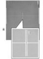
- FIG. 1 shows a schematic diagram of a source electrode and a drain electrode. There is no restriction
- a polymer or the like can be used.
- the patterning method include a sputtering method, a pulse laser deposition method, a vacuum evaporation method, a CVD method, a photolithography method, and a lift-off method in addition to the above-described printing method.
- the semiconductor material is not particularly limited, but it is desirable to use an organic semiconductor material or an oxide semiconductor material in order to use a flexible substrate.
- an organic semiconductor material is preferable.
- an oxide semiconductor material may be used as long as the semiconductor layer can be formed by a printing method.
- Organic semiconductor materials include high molecular organic semiconductor materials such as polythiophene, polyallylamine, fluorenebithiophene copolymers, and derivatives thereof, and small molecules such as pentacene, tetracene, copper phthalocyanine, perylene, and derivatives thereof. Organic semiconductor materials can be used.
- Carbon compounds such as carbon nanotubes or fullerenes, semiconductor nanoparticle dispersions, and the like can also be used as the material for the semiconductor layer.
- These organic semiconductor materials can be dissolved or dispersed in an aromatic solvent such as toluene and used as an ink-like solution or dispersion.
- the printing method of the organic semiconductor is not particularly limited, and screen printing, spray coating, spin coating, slit coating, die coating, bar coating, knife coating, offset printing, reverse printing, flexographic printing, inkjet printing, dispenser printing, gravure direct printing, A method such as gravure offset printing can be used.
- flexographic printing since the above-mentioned organic semiconductor has low solubility in a solvent, flexographic printing, reversal printing, ink jet printing, and dispenser printing suitable for printing a low viscosity solution are desirable.
- flexographic printing is most preferable because the printing time is short and the amount of ink used is small.
- an oxide containing one or more elements of zinc, indium, tin, tungsten, magnesium, and gallium can be given.
- Known materials such as zinc oxide, indium oxide, indium zinc oxide, tin oxide, tungsten oxide, and zinc gallium indium oxide (In—Ga—Zn—O) can be mentioned, but are not limited to these materials.
- the structure of these materials may be any of single crystal, polycrystal, microcrystal, crystal / amorphous mixed crystal, nanocrystal scattered amorphous, and amorphous.
- a pattern is formed using a photolithography method, a lift-off method, or the like.
- a more preferable pattern formation method is a method in which a dispersion in which an oxide semiconductor material is dispersed in a solvent is formed by a printing method.
- the printing method the same method as described in the organic semiconductor printing method can be used.
- the material of the gate insulating layer is not particularly limited, but generally used polymer solutions such as polyvinyl phenol, polymethyl methacrylate, polyimide, polyvinyl alcohol, parylene, fluororesin, epoxy resin, alumina, silica gel, etc.
- Inorganic particles such as silicon oxide, silicon nitride, silicon oxynitride, aluminum oxide, tantalum oxide, yttrium oxide, hafnium oxide, hafnium aluminate, zirconia oxide, and titanium oxide.
- thin film films such as PET, PEN, and PES, can also be used as an insulating film.
- a method for forming the gate insulating layer is not particularly limited, and a vacuum deposition method, a sputtering method, a dry method such as CVD, a wet method such as spin coating and a slit die, and a laminate method can be appropriately used.
- the substrate is not particularly limited, and examples thereof include soda lime glass, alkali-free glass, borosilicate glass, high strain point glass, quartz glass, and other inorganic materials such as alumina and silica, and polymer materials. It may be paper. Also, ordinary soda lime glass having low heat resistance can be used. In the present invention, a polymer material such as plastic or paper can be used as the substrate, and the transistor of the present invention is particularly useful in that a resin film can be used.
- Resin films used as substrates include polyimide, polyamide, polyamideimide, polyethylene terephthalate (PET), polyethylene naphthalate (PEN), polyphenylene sulfide, polyether ether ketone, polyether sulfone, polycarbonate, polyether imide, epoxy resin, phenol Examples thereof include resins, glass-epoxy resins, polyphenylene ethers, acrylic resins, polyolefins such as polyethylene and polypropylene, and liquid crystalline polymer compounds. Among these, polyethylene terephthalate (PET) and polyethylene naphthalate (PEN) are preferable.
- the thickness of the substrate is not particularly limited, but in the case of a plastic substrate such as a resin film, it is usually in the range of 10 ⁇ m to 300 ⁇ m. When the thickness is 10 ⁇ m or more, deformation of the substrate is suppressed when the conductive pattern is formed, which is preferable in terms of shape stability of the formed conductive pattern. Moreover, when it is 300 micrometers or less, when winding-up processing is performed continuously, it is suitable at the point of a softness
- a sealing layer, a light shielding layer, and the like can be suitably provided in the transistor of this embodiment as necessary.
- the material for the sealing layer can be selected from the same material as that for the gate insulating layer.
- As the light shielding layer a material in which a light shielding material such as carbon black is dispersed in the material described in the gate material can be used. Therefore, these formation methods can be the same as those for the gate insulating layer.
- Example 1 After 80 g of copper acetate (II) (manufactured by Wako Pure Chemical Industries) was dissolved in a mixed solvent of 800 g of water and 400 g of 1,2-propylene glycol (manufactured by Wako Pure Chemical Industries), 24 g of hydrazine (manufactured by Wako Pure Chemical Industries) was added and stirred. The supernatant and precipitate were separated by centrifugation. Dispersbyk-145 (manufactured by Big Chemie) 6.0 g and n-butanol (manufactured by Wako Pure Chemical Industries, Ltd.) 24 g were added to 43 g of the resulting precipitate, and dispersed using a homogenizer.
- II copper acetate
- Example 2 To 0.20 g of the concentrated dispersion obtained in Example 1, 0.78 g of n-butanol, 0.010 g of 1,2-propylene glycol and 0.010 g of Surflon S-611 (manufactured by Seimi Chemical) were added, and a homogenizer was used. By dispersing, a cuprous oxide dispersion was obtained. The average secondary particle size was 30 nm. This dispersion was applied onto a PEN substrate (manufactured by Teijin DuPont) by reverse printing in a pattern of source and drain electrodes, and then heated and fired at 0.8 kW for 300 seconds using a microwave plasma baking machine, and a conductive film was laminated. A source electrode and a drain electrode were obtained.
- PEN substrate manufactured by Teijin DuPont
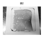
- the obtained pattern is shown in FIG.
- the area of the conductive film laminate was 900 cm 2 .
- An organic semiconductor p-BTTT-C16 (manufactured by MERCK) was printed on the channel portion between the source electrode and the drain electrode by an ink jet method to form a semiconductor layer.
- Cytop (manufactured by Asahi Glass Co., Ltd.) was applied by spin coating so as to cover the organic semiconductor, the source electrode, and the drain electrode, thereby forming an insulating film.
- the cuprous oxide dispersion is applied to the insulating film in a pattern of a gate electrode by reversal printing, and heated and fired at 0.8 kW for 300 seconds using a microwave plasma baking machine to form a gate electrode.
- a transistor having a copper electrode was obtained.
- the electrode portion had a film thickness of 0.10 ⁇ m, a minimum line width of 5.0 ⁇ m, a minimum space width of 5.0 ⁇ m, and a volume resistivity of 12 ⁇ 10 ⁇ 6 ⁇ ⁇ cm.
- the mobility of the semiconductor was 2.0 ⁇ 10 ⁇ 2 cm 2 / (V ⁇ s). The results of dispersion and printing are shown in Table 1 below.
- Example 3 By adding 0.10 g of n-butanol, 0.080 g of 1,2-propylene glycol and Surflon S-6110.020 g to 0.80 g of the concentrated dispersion obtained in Example 1, the mixture was dispersed using a homogenizer to oxidize. A cuprous dispersion was obtained. The average secondary particle size was 50 nm. Using this dispersion, a transistor having a copper electrode was obtained in the same manner as in Example 2. The film thickness of the electrode part was 0.40 ⁇ m, the minimum line width was 5.0 ⁇ m, and the minimum space width was 5.0 ⁇ m. The volume resistivity of the electrode part was 14 ⁇ 10 ⁇ 6 ⁇ cm. The mobility of the semiconductor was 1.0 ⁇ 10 ⁇ 2 cm 2 / (V ⁇ s). The results of dispersion and printing are shown in Table 1 below.
- Example 4 By adding 0.97 g of n-butanol, 2.0 mg of 1,2-propylene glycol and Surflon S-616.0 mg to 0.020 g of the concentrated dispersion obtained in Example 1, the mixture was dispersed using a homogenizer to oxidize. A cuprous dispersion was obtained. The average secondary particle size was 20 nm. Using this dispersion, a transistor having a copper electrode was obtained in the same manner as in Example 2. The electrode portion had a thickness of 0.030 ⁇ m, a minimum line width of 5.0 ⁇ m, a minimum space width of 5.0 ⁇ m, and a volume resistivity of 14 ⁇ 10 ⁇ 6 ⁇ cm. The mobility of the semiconductor was 1.0 ⁇ 10 ⁇ 2 cm 2 / (V ⁇ s). The results of dispersion and printing are shown in Table 1 below.
- Example 5 To 0.20 g of the concentrated dispersion obtained in Example 1, 0.060 g of Disperbyk-145 (manufactured by Big Chemie), 0.72 g of n-butanol, 0.010 g of 1,2-propylene glycol and Surflon S-611 (manufactured by Seimi Chemical) ) 0.010 g was added and dispersed using a homogenizer to obtain a cuprous oxide dispersion. The average secondary particle size was 40 nm. Using this dispersion, a transistor having a copper electrode was obtained in the same manner as in Example 2.
- the electrode portion had a film thickness of 0.10 ⁇ m, a minimum line width of 5.0 ⁇ m, a minimum space width of 5.0 ⁇ m, and a volume resistivity of 22 ⁇ 10 ⁇ 6 ⁇ ⁇ cm.
- the mobility of the semiconductor was 6.0 ⁇ 10 ⁇ 3 cm 2 / (V ⁇ s). The results of dispersion and printing are shown in Table 1 below.
- Example 6 To 0.20 g of the concentrated dispersion obtained in Example 1, 0.13 g of Disperbyk-145 (manufactured by Big Chemie), 0.65 g of n-butanol, 0.010 g of 1,2-propylene glycol and Surflon S-611 (manufactured by Seimi Chemical) ) 0.010 g was added and dispersed using a homogenizer to obtain a cuprous oxide dispersion. The average secondary particle size was 50 nm. Using this dispersion, a transistor having a copper electrode was obtained in the same manner as in Example 2.
- the electrode portion had a film thickness of 0.10 ⁇ m, a minimum line width of 5.0 ⁇ m, a minimum space width of 5.0 ⁇ m, and a volume resistivity of 500 ⁇ 10 ⁇ 6 ⁇ ⁇ cm.
- the mobility of the semiconductor was 2.0 ⁇ 10 ⁇ 3 cm 2 / (V ⁇ s). The results of dispersion and printing are shown in Table 1 below.
- Example 7 CIK Nanotech's cupric oxide fine particles 0.30g, Disperbyk-145 (manufactured by Big Chemie) 0.060g, n-butanol 0.61g, 1,2-propylene glycol 0.020g and Surflon S-611 (manufactured by Seimi Chemical) ) 0.010 g was added and dispersed using a homogenizer to obtain a cuprous oxide dispersion.
- the average secondary particle size was 200 nm.
- a transistor having a copper electrode was obtained in the same manner as in Example 2.
- the minimum line width was 5.0 ⁇ m
- the minimum space width was 5.0 ⁇ m
- the volume resistivity was 32 ⁇ 10 ⁇ 6 ⁇ cm.
- the mobility of the semiconductor was 4.0 ⁇ 10 ⁇ 3 cm 2 / (V ⁇ s). The results of dispersion and printing are shown in Table 1 below.
- Example 8 CIK Nanotech's cupric oxide fine particles 0.50g, Disperbyk-145 (Big Chemie) 0.10g, n-butanol 0.33g, 1,2-propylene glycol 0.070g, and Surflon S-611 (Seimi Chemical) (Product made) 1.0 mg was added and dispersed using a homogenizer to obtain a cuprous oxide dispersion. The average secondary particle size was 30 nm. Using this dispersion, a transistor having a copper electrode was obtained in the same manner as in Example 2.
- the film thickness of the electrode part was 0.50 ⁇ m, the minimum line width was 5.0 ⁇ m, the minimum space width was 5.0 ⁇ m, and the volume resistivity was 44 ⁇ 10 ⁇ 6 ⁇ cm.
- the mobility of the semiconductor was 2.0 ⁇ 10 ⁇ 3 cm 2 / (V ⁇ s). The results of dispersion and printing are shown in Table 1 below.
- Example 1 In the same procedure as in Example 1, Dispersbyk-145 (manufactured by Big Chemie) was not added, and 60 g of a concentrated dispersion containing 30 g of cuprous oxide fine particles and 30 g of n-butanol was obtained. To 0.40 g of this concentrated dispersion, 0.53 g of n-butanol, 0.060 g of 1,2-propylene glycol and 0.010 g of Surflon S-611 (manufactured by Seimi Chemical) were added, and dispersion was attempted using a homogenizer. Since the dispersant Disperbyk-145 (manufactured by Big Chemie) was not contained, it aggregated in the atmosphere. The average secondary particle size was 900 nm and could not be used for reversal printing. Since the source electrode and the drain electrode could not be printed on the substrate with this dispersion, the volume resistivity of the electrode could not be measured.
- a cuprous oxide dispersion is obtained by adding 0.32 g of n-butanol and 0.080 g of 1,2-propylene glycol to 0.60 g of the concentrated dispersion obtained in Example 1, and dispersing using a homogenizer. It was. The average secondary particle size was 40 nm.
- the transistor according to the present invention has a fine patterned electrode formed by a printing process of copper or a copper oxide dispersion. Therefore, the transistor according to the present invention is suitably used for applications such as high-performance electronic devices.
Landscapes
- Chemical & Material Sciences (AREA)
- Organic Chemistry (AREA)
- Engineering & Computer Science (AREA)
- Dispersion Chemistry (AREA)
- Materials Engineering (AREA)
- Wood Science & Technology (AREA)
- Life Sciences & Earth Sciences (AREA)
- Physics & Mathematics (AREA)
- Spectroscopy & Molecular Physics (AREA)
- General Chemical & Material Sciences (AREA)
- Microelectronics & Electronic Packaging (AREA)
- Chemical Kinetics & Catalysis (AREA)
- Thin Film Transistor (AREA)
- Conductive Materials (AREA)
- Non-Insulated Conductors (AREA)
- Electrodes Of Semiconductors (AREA)
- Electroluminescent Light Sources (AREA)
Priority Applications (7)
| Application Number | Priority Date | Filing Date | Title |
|---|---|---|---|
| KR1020157034234A KR101849446B1 (ko) | 2013-07-23 | 2014-07-22 | 구리 및/또는 구리 산화물 분산체, 및 이 분산체를 이용하여 형성된 도전막 |
| US14/906,422 US10424648B2 (en) | 2013-07-23 | 2014-07-22 | Copper and/or copper oxide dispersion, and electroconductive film formed using dispersion |
| KR1020187006001A KR102117579B1 (ko) | 2013-07-23 | 2014-07-22 | 구리 및/또는 구리 산화물 분산체, 및 이 분산체를 이용하여 형성된 도전막 |
| CN201480040975.5A CN105393312B (zh) | 2013-07-23 | 2014-07-22 | 铜和/或铜氧化物分散体、以及使用该分散体形成的导电膜 |
| EP14829560.3A EP3026677B1 (en) | 2013-07-23 | 2014-07-22 | Copper and/or copper oxide dispersion, and method for electroconductive film using dispersion |
| JP2015528290A JP6175500B2 (ja) | 2013-07-23 | 2014-07-22 | 銅及び/又は銅酸化物分散体、並びに該分散体を用いて形成された導電膜 |
| US16/540,446 US20190371901A1 (en) | 2013-07-23 | 2019-08-14 | Copper and/or copper oxide dispersion, and electroconductive film formed using dispersion |
Applications Claiming Priority (2)
| Application Number | Priority Date | Filing Date | Title |
|---|---|---|---|
| JP2013-152799 | 2013-07-23 | ||
| JP2013152799 | 2013-07-23 |
Related Child Applications (2)
| Application Number | Title | Priority Date | Filing Date |
|---|---|---|---|
| US14/906,422 A-371-Of-International US10424648B2 (en) | 2013-07-23 | 2014-07-22 | Copper and/or copper oxide dispersion, and electroconductive film formed using dispersion |
| US16/540,446 Division US20190371901A1 (en) | 2013-07-23 | 2019-08-14 | Copper and/or copper oxide dispersion, and electroconductive film formed using dispersion |
Publications (1)
| Publication Number | Publication Date |
|---|---|
| WO2015012264A1 true WO2015012264A1 (ja) | 2015-01-29 |
Family
ID=52393299
Family Applications (1)
| Application Number | Title | Priority Date | Filing Date |
|---|---|---|---|
| PCT/JP2014/069321 Ceased WO2015012264A1 (ja) | 2013-07-23 | 2014-07-22 | 銅及び/又は銅酸化物分散体、並びに該分散体を用いて形成された導電膜 |
Country Status (6)
| Country | Link |
|---|---|
| US (2) | US10424648B2 (enExample) |
| EP (1) | EP3026677B1 (enExample) |
| JP (2) | JP6175500B2 (enExample) |
| KR (2) | KR101849446B1 (enExample) |
| CN (1) | CN105393312B (enExample) |
| WO (1) | WO2015012264A1 (enExample) |
Cited By (9)
| Publication number | Priority date | Publication date | Assignee | Title |
|---|---|---|---|---|
| JP2017069198A (ja) * | 2015-09-29 | 2017-04-06 | 三ツ星ベルト株式会社 | 導電性ペースト及び導電膜付基板の製造方法 |
| WO2019017363A1 (ja) | 2017-07-18 | 2019-01-24 | 旭化成株式会社 | 導電性パターン領域を有する構造体及びその製造方法、積層体及びその製造方法、並びに、銅配線 |
| WO2019022230A1 (ja) | 2017-07-27 | 2019-01-31 | 旭化成株式会社 | 酸化銅インク及びこれを用いた導電性基板の製造方法、塗膜を含む製品及びこれを用いた製品の製造方法、導電性パターン付製品の製造方法、並びに、導電性パターン付製品 |
| JP2019090110A (ja) * | 2017-11-10 | 2019-06-13 | 旭化成株式会社 | 導電性パターン領域付構造体及びその製造方法 |
| JP2019210469A (ja) * | 2018-05-30 | 2019-12-12 | 旭化成株式会社 | インクジェット用酸化銅インク及びこれを用いて導電性パターンを付与した導電性基板の製造方法 |
| JPWO2018169012A1 (ja) * | 2017-03-16 | 2020-01-16 | 旭化成株式会社 | 分散体並びにこれを用いた導電性パターン付構造体の製造方法及び導電性パターン付構造体 |
| US11328835B2 (en) | 2017-03-16 | 2022-05-10 | Asahi Kasei Kabushiki Kaisha | Dispersing element, method for manufacturing structure with conductive pattern using the same, and structure with conductive pattern |
| US11520451B2 (en) | 2018-07-30 | 2022-12-06 | Asahi Kasei Kabushiki Kaisha | Conductive film and conductive film roll, electronic paper, touch panel and flat-panel display comprising the same |
| US11877391B2 (en) | 2018-07-30 | 2024-01-16 | Asahi Kasei Kabushiki Kaisha | Conductive film and conductive film roll, electronic paper, touch panel and flat-panel display comprising the same |
Families Citing this family (8)
| Publication number | Priority date | Publication date | Assignee | Title |
|---|---|---|---|---|
| CN103451682B (zh) * | 2013-09-16 | 2017-06-06 | 北京科技大学 | 一种含钛可溶阳极熔盐电解提取金属钛的方法 |
| WO2015152625A1 (ko) * | 2014-04-01 | 2015-10-08 | 전자부품연구원 | 광 소결용 잉크 조성물, 그를 이용한 배선기판 및 그의 제조 방법 |
| IL247113B (en) * | 2016-08-04 | 2018-02-28 | Copprint Tech Ltd | Formulations and processes for making a high conductivity copper pattern |
| US10812974B2 (en) * | 2017-05-06 | 2020-10-20 | Vmware, Inc. | Virtual desktop client connection continuity |
| US11512214B2 (en) | 2017-11-14 | 2022-11-29 | Showa Denko Materials Co., Ltd. | Composition containing organic solvents with different vapor pressures, conductor made from composition, method for manufacturing conductor, and structure comprising conductor |
| JP7176847B2 (ja) * | 2018-03-15 | 2022-11-22 | 旭化成株式会社 | 分散体、塗膜を含む製品、導電性パターン付き構造体の製造方法、及び、導電性パターン付き構造体 |
| JP7099867B2 (ja) * | 2018-05-16 | 2022-07-12 | 日本化学工業株式会社 | 光焼結型組成物及びそれを用いた導電膜の形成方法 |
| CN118222142B (zh) * | 2024-05-22 | 2024-07-19 | 汕头大学 | 一种多功能水性涂料及其制备方法与应用 |
Citations (8)
| Publication number | Priority date | Publication date | Assignee | Title |
|---|---|---|---|---|
| JP2005015628A (ja) | 2003-06-26 | 2005-01-20 | Asahi Kasei Corp | 酸化第一銅コロイド分散液 |
| WO2008111484A1 (ja) * | 2007-03-15 | 2008-09-18 | Dic Corporation | 凸版反転印刷用導電性インキ |
| JP2010129790A (ja) * | 2008-11-27 | 2010-06-10 | Tokyo Electron Ltd | 成膜方法 |
| WO2012115475A2 (ko) * | 2011-02-25 | 2012-08-30 | 한화케미칼 주식회사 | 오프셋 또는 리버스-오프셋 인쇄용 전도성 잉크 조성물 |
| JP2012216425A (ja) | 2011-03-31 | 2012-11-08 | Dainippon Printing Co Ltd | 金属酸化物微粒子分散体、導電性基板及びその製造方法 |
| JP2013503234A (ja) * | 2009-08-28 | 2013-01-31 | エルジー・ケム・リミテッド | 導電性金属インク組成物および導電性パターンの形成方法 |
| WO2013073200A1 (ja) * | 2011-11-14 | 2013-05-23 | 石原薬品株式会社 | 銅微粒子分散液、導電膜形成方法及び回路基板 |
| JP2013109966A (ja) * | 2011-11-21 | 2013-06-06 | Hitachi Chemical Co Ltd | 酸化銅ペースト及び金属銅層の製造方法 |
Family Cites Families (57)
| Publication number | Priority date | Publication date | Assignee | Title |
|---|---|---|---|---|
| US2091800A (en) * | 1931-09-15 | 1937-08-31 | Rohm & Haas | Method of hydrogenating esters |
| US3213145A (en) * | 1960-03-28 | 1965-10-19 | Standard Oil Co | Catalytic hydrogenation of esters of aromatic monocarboxylic acids to aryl-substituted methanols |
| JP2526989B2 (ja) * | 1988-05-20 | 1996-08-21 | 三菱瓦斯化学株式会社 | 芳香族多価アルコ―ルの製造方法 |
| US5158849A (en) * | 1990-10-25 | 1992-10-27 | Custom Papers Group Inc. | Composition useful in transparent conductive coatings |
| US5855818A (en) * | 1995-01-27 | 1999-01-05 | Rogers Corporation | Electrically conductive fiber filled elastomeric foam |
| TW505685B (en) * | 1997-09-05 | 2002-10-11 | Mitsubishi Materials Corp | Transparent conductive film and composition for forming same |
| US5855820A (en) * | 1997-11-13 | 1999-01-05 | E. I. Du Pont De Nemours And Company | Water based thick film conductive compositions |
| MY125159A (en) * | 1998-09-14 | 2006-07-31 | Mitsubishi Materials Corp | Fine metal particle-dispersion solution and conductive film using the same |
| JP3545974B2 (ja) * | 1999-08-16 | 2004-07-21 | 日本パーカライジング株式会社 | 金属材料のりん酸塩化成処理方法 |
| US7858818B2 (en) * | 2001-01-31 | 2010-12-28 | Momentive Performance Materials Inc. | Nanosized copper catalyst precursors for the direct synthesis of trialkoxysilanes |
| WO2003051562A1 (en) * | 2001-12-18 | 2003-06-26 | Asahi Kasei Kabushiki Kaisha | Metal oxide dispersion |
| US8252961B2 (en) * | 2002-04-22 | 2012-08-28 | The Curators Of The University Of Missouri | Method of producing lower alcohols from glycerol |
| US7663004B2 (en) * | 2002-04-22 | 2010-02-16 | The Curators Of The University Of Missouri | Method of producing lower alcohols from glycerol |
| US20100009540A1 (en) * | 2002-09-25 | 2010-01-14 | Asahi Glass Company Limited | Polishing compound, its production process and polishing method |
| CN100488339C (zh) * | 2003-05-16 | 2009-05-13 | 播磨化成株式会社 | 形成微细铜颗粒烧结产物类的微细形状导电体的方法 |
| JP4407311B2 (ja) * | 2004-02-20 | 2010-02-03 | セイコーエプソン株式会社 | 薄膜トランジスタの製造方法 |
| US7238654B2 (en) * | 2004-05-17 | 2007-07-03 | Phibro-Tech, Inc. | Compatibilizing surfactant useful with slurries of copper particles |
| US8980135B2 (en) * | 2004-08-31 | 2015-03-17 | Sumitomo Metal Mining Co., Ltd. | Electroconductive particle, visible light transmitting particle-dispersed electrical conductor and manufacturing method thereof, transparent electroconductive thin film and manufacturing method thereof, transparent electroconductive article that uses the same, and infrared-shielding article |
| US7771625B2 (en) * | 2004-11-29 | 2010-08-10 | Dainippon Ink And Chemicals, Inc. | Method for producing surface-treated silver-containing powder and silver paste using surface-treated silver-containing powder |
| WO2006076611A2 (en) * | 2005-01-14 | 2006-07-20 | Cabot Corporation | Production of metal nanoparticles |
| KR20070118096A (ko) * | 2005-02-24 | 2007-12-13 | 로이 에이. 페리아나 | 탄화수소의 작용기화된 생성물로의 전환을 위한 촉매시스템 |
| DE102005043242A1 (de) * | 2005-09-09 | 2007-03-15 | Basf Ag | Dispersion zum Aufbringen einer Metallschicht |
| JP4839767B2 (ja) * | 2005-10-14 | 2011-12-21 | 東洋インキScホールディングス株式会社 | 金属微粒子分散体の製造方法、該方法で製造された金属微粒子分散体を用いた導電性インキ、および導電性パターン。 |
| US8084401B2 (en) * | 2006-01-25 | 2011-12-27 | Clearwater International, Llc | Non-volatile phosphorus hydrocarbon gelling agent |
| US8337726B2 (en) * | 2006-07-28 | 2012-12-25 | Furukawa Electric Co., Ltd. | Fine particle dispersion and method for producing fine particle dispersion |
| JP2008144010A (ja) * | 2006-12-08 | 2008-06-26 | Konica Minolta Holdings Inc | 樹脂組成物の製造方法及び樹脂組成物フィルム |
| US7976733B2 (en) * | 2007-11-30 | 2011-07-12 | Xerox Corporation | Air stable copper nanoparticle ink and applications therefor |
| US20090214764A1 (en) * | 2008-02-26 | 2009-08-27 | Xerox Corporation | Metal nanoparticles stabilized with a bident amine |
| US8506849B2 (en) * | 2008-03-05 | 2013-08-13 | Applied Nanotech Holdings, Inc. | Additives and modifiers for solvent- and water-based metallic conductive inks |
| US20110139228A1 (en) * | 2008-08-27 | 2011-06-16 | Mitsubishi Materials Corporation | Transparent electroconductive film for solar cell, composition for transparent electroconductive film and multi-junction solar cell |
| JP5531504B2 (ja) * | 2009-08-25 | 2014-06-25 | Dic株式会社 | 銀ナノ粒子を用いる接合体の製造方法、及び接合体 |
| KR20120102599A (ko) * | 2009-09-18 | 2012-09-18 | 스미또모 가가꾸 가부시키가이샤 | 은-공액 화합물 복합체 |
| US9497859B2 (en) * | 2009-09-30 | 2016-11-15 | Dai Nippon Printing Co., Ltd. | Metal microparticle dispersion, process for production of electrically conductive substrate, and electrically conductive substrate |
| US9272970B2 (en) * | 2010-07-09 | 2016-03-01 | Celanese International Corporation | Hydrogenolysis of ethyl acetate in alcohol separation processes |
| BR112013003336B1 (pt) * | 2010-08-12 | 2020-12-01 | Mitsui Chemicals, Inc | bactéria produtora de álcool isopropílico e método de produção de álcool isopropílico |
| ES2453217T3 (es) * | 2010-12-21 | 2014-04-04 | Agfa-Gevaert | Dispersión que contiene nanopartículas metálicas, de óxido de metal o de precursor de metal |
| WO2012135997A1 (zh) * | 2011-04-02 | 2012-10-11 | 中国科学院化学研究所 | 在含有疏水性的硅柱的硅片表面构筑微电极对阵列的方法 |
| JP2013004309A (ja) * | 2011-06-16 | 2013-01-07 | Toyota Motor Corp | 金属ナノ粒子ペースト |
| JP6035887B2 (ja) * | 2011-06-21 | 2016-11-30 | セントラル硝子株式会社 | ポジ型レジスト組成物 |
| JP2013008907A (ja) * | 2011-06-27 | 2013-01-10 | Hitachi Chem Co Ltd | 導電性ペースト用酸化銅粉末、導電性ペースト用酸化銅粉末の製造方法、導電性ペースト及びこれを用いて得られる銅配線層 |
| FR2980791A1 (fr) * | 2011-10-03 | 2013-04-05 | Rhodia Operations | Procede de preparation d'un melange d'alcools |
| TW201339279A (zh) * | 2011-11-24 | 2013-10-01 | Showa Denko Kk | 導電圖型形成方法及藉由光照射或微波加熱的導電圖型形成用組成物 |
| US20140342177A1 (en) * | 2011-12-07 | 2014-11-20 | Duke University | Synthesis of cupronickel nanowires and their application in transparent conducting films |
| KR101391697B1 (ko) * | 2011-12-14 | 2014-05-07 | 제일모직주식회사 | 이방성 도전 필름용 조성물 및 이를 이용한 이방성 도전 필름 |
| KR101403865B1 (ko) * | 2011-12-16 | 2014-06-10 | 제일모직주식회사 | 이방성 도전 필름용 조성물, 이방성 도전 필름 및 반도체 장치 |
| KR101355855B1 (ko) * | 2011-12-19 | 2014-01-29 | 제일모직주식회사 | 이방성 도전 필름 |
| KR101355856B1 (ko) * | 2011-12-26 | 2014-01-27 | 제일모직주식회사 | 이방 전도성 접착 필름용 조성물 및 이를 이용한 이방 전도성 접착 필름 |
| US9664009B2 (en) * | 2012-04-04 | 2017-05-30 | Weatherford Technologies, LLC | Apparatuses, systems, and methods for forming in-situ gel pills to lift liquids from horizontal wells |
| US9496069B2 (en) * | 2012-07-19 | 2016-11-15 | Nof Corporation | Silver nanoparticles, method for producing same, silver nanoparticle dispersion liquid, and base provided with silver material |
| WO2014052482A1 (en) * | 2012-09-25 | 2014-04-03 | University Of Connecticut Office Of Economic Development | Mesoporous metal oxides and processes for preparation thereof |
| US9972413B2 (en) * | 2012-10-15 | 2018-05-15 | Dai Nippon Printing Co., Ltd. | Metal particle dispersion for electroconductive substrates, method for producing the same, and method for producing an electroconductive substrate |
| US9953740B2 (en) * | 2012-10-18 | 2018-04-24 | Dai Nippon Printing Co., Ltd. | Dispersant, metal particle dispersion for electroconductive substrates, and method for producing electroconductive substrate |
| WO2014065242A1 (ja) * | 2012-10-24 | 2014-05-01 | 独立行政法人物質・材料研究機構 | 導電性ポリマー-金属複合体と基材との付着体及びその形成方法、導電性ポリマー-金属複合体分散液、その製造方法及びその塗布方法、並びに穴を導電性材料で充填する方法 |
| US20140127409A1 (en) * | 2012-11-06 | 2014-05-08 | Takuya Harada | Method for producing fine particle dispersion |
| MY170550A (en) * | 2013-02-19 | 2019-08-16 | Rescurve Llc | Production of higher alcohols |
| JP5700864B2 (ja) * | 2013-05-15 | 2015-04-15 | 石原ケミカル株式会社 | 銅微粒子分散液、導電膜形成方法及び回路基板 |
| HK1221714A1 (zh) * | 2013-07-02 | 2017-06-09 | Ut 巴特勒有限公司 | 具有至少三個碳原子的醇到烴混合原料的催化轉化 |
-
2014
- 2014-07-22 EP EP14829560.3A patent/EP3026677B1/en active Active
- 2014-07-22 KR KR1020157034234A patent/KR101849446B1/ko active Active
- 2014-07-22 JP JP2015528290A patent/JP6175500B2/ja active Active
- 2014-07-22 WO PCT/JP2014/069321 patent/WO2015012264A1/ja not_active Ceased
- 2014-07-22 KR KR1020187006001A patent/KR102117579B1/ko active Active
- 2014-07-22 US US14/906,422 patent/US10424648B2/en active Active
- 2014-07-22 CN CN201480040975.5A patent/CN105393312B/zh active Active
-
2017
- 2017-05-15 JP JP2017096322A patent/JP6496351B2/ja active Active
-
2019
- 2019-08-14 US US16/540,446 patent/US20190371901A1/en not_active Abandoned
Patent Citations (8)
| Publication number | Priority date | Publication date | Assignee | Title |
|---|---|---|---|---|
| JP2005015628A (ja) | 2003-06-26 | 2005-01-20 | Asahi Kasei Corp | 酸化第一銅コロイド分散液 |
| WO2008111484A1 (ja) * | 2007-03-15 | 2008-09-18 | Dic Corporation | 凸版反転印刷用導電性インキ |
| JP2010129790A (ja) * | 2008-11-27 | 2010-06-10 | Tokyo Electron Ltd | 成膜方法 |
| JP2013503234A (ja) * | 2009-08-28 | 2013-01-31 | エルジー・ケム・リミテッド | 導電性金属インク組成物および導電性パターンの形成方法 |
| WO2012115475A2 (ko) * | 2011-02-25 | 2012-08-30 | 한화케미칼 주식회사 | 오프셋 또는 리버스-오프셋 인쇄용 전도성 잉크 조성물 |
| JP2012216425A (ja) | 2011-03-31 | 2012-11-08 | Dainippon Printing Co Ltd | 金属酸化物微粒子分散体、導電性基板及びその製造方法 |
| WO2013073200A1 (ja) * | 2011-11-14 | 2013-05-23 | 石原薬品株式会社 | 銅微粒子分散液、導電膜形成方法及び回路基板 |
| JP2013109966A (ja) * | 2011-11-21 | 2013-06-06 | Hitachi Chemical Co Ltd | 酸化銅ペースト及び金属銅層の製造方法 |
Non-Patent Citations (1)
| Title |
|---|
| See also references of EP3026677A4 |
Cited By (27)
| Publication number | Priority date | Publication date | Assignee | Title |
|---|---|---|---|---|
| JP2017069198A (ja) * | 2015-09-29 | 2017-04-06 | 三ツ星ベルト株式会社 | 導電性ペースト及び導電膜付基板の製造方法 |
| JP2021185269A (ja) * | 2017-03-16 | 2021-12-09 | 旭化成株式会社 | 分散体並びにこれを用いた導電性パターン付構造体の製造方法及び導電性パターン付構造体 |
| JP7477581B2 (ja) | 2017-03-16 | 2024-05-01 | 旭化成株式会社 | 分散体並びにこれを用いた導電性パターン付構造体の製造方法及び導電性パターン付構造体 |
| JP2023027058A (ja) * | 2017-03-16 | 2023-03-01 | 旭化成株式会社 | 分散体並びにこれを用いた導電性パターン付構造体の製造方法及び導電性パターン付構造体 |
| JP7201755B2 (ja) | 2017-03-16 | 2023-01-10 | 旭化成株式会社 | 分散体並びにこれを用いた導電性パターン付構造体の製造方法及び導電性パターン付構造体 |
| JP7104687B2 (ja) | 2017-03-16 | 2022-07-21 | 旭化成株式会社 | 分散体並びにこれを用いた導電性パターン付構造体の製造方法及び導電性パターン付構造体 |
| JPWO2018169012A1 (ja) * | 2017-03-16 | 2020-01-16 | 旭化成株式会社 | 分散体並びにこれを用いた導電性パターン付構造体の製造方法及び導電性パターン付構造体 |
| US11328835B2 (en) | 2017-03-16 | 2022-05-10 | Asahi Kasei Kabushiki Kaisha | Dispersing element, method for manufacturing structure with conductive pattern using the same, and structure with conductive pattern |
| US11270809B2 (en) | 2017-03-16 | 2022-03-08 | Asahi Kasei Kabushiki Kaisha | Dispersing element, method for manufacturing structure with conductive pattern using the same, and structure with conductive pattern |
| KR20200015609A (ko) | 2017-07-18 | 2020-02-12 | 아사히 가세이 가부시키가이샤 | 도전성 패턴 영역을 갖는 구조체 및 그 제조 방법, 적층체 및 그 제조 방법, 그리고 구리 배선 |
| WO2019017363A1 (ja) | 2017-07-18 | 2019-01-24 | 旭化成株式会社 | 導電性パターン領域を有する構造体及びその製造方法、積層体及びその製造方法、並びに、銅配線 |
| US11109492B2 (en) | 2017-07-18 | 2021-08-31 | Asahi Kasei Kabushiki Kaisha | Structure including electroconductive pattern regions, method for producing same, stack, method for producing same, and copper wiring |
| WO2019022230A1 (ja) | 2017-07-27 | 2019-01-31 | 旭化成株式会社 | 酸化銅インク及びこれを用いた導電性基板の製造方法、塗膜を含む製品及びこれを用いた製品の製造方法、導電性パターン付製品の製造方法、並びに、導電性パターン付製品 |
| JP7403512B2 (ja) | 2017-07-27 | 2023-12-22 | 旭化成株式会社 | 酸化銅インク及びこれを用いた導電性基板の製造方法、塗膜を含む製品及びこれを用いた製品の製造方法、導電性パターン付製品の製造方法、並びに、導電性パターン付製品 |
| JP7076591B2 (ja) | 2017-07-27 | 2022-05-27 | 旭化成株式会社 | 酸化銅インク及びこれを用いた導電性基板の製造方法、塗膜を含む製品及びこれを用いた製品の製造方法、導電性パターン付製品の製造方法、並びに、導電性パターン付製品 |
| JP2021077648A (ja) * | 2017-07-27 | 2021-05-20 | 旭化成株式会社 | 酸化銅インク及びこれを用いた導電性基板の製造方法、塗膜を含む製品及びこれを用いた製品の製造方法、導電性パターン付製品の製造方法、並びに、導電性パターン付製品 |
| JP2022008655A (ja) * | 2017-07-27 | 2022-01-13 | 旭化成株式会社 | 酸化銅インク及びこれを用いた導電性基板の製造方法、塗膜を含む製品及びこれを用いた製品の製造方法、導電性パターン付製品の製造方法、並びに、導電性パターン付製品 |
| US12202996B2 (en) | 2017-07-27 | 2025-01-21 | Asahi Kasei Kabushiki Kaisha | Copper oxide ink and method for producing conductive substrate using same, product containing coating film and method for producing product using same, method for producing product with conductive pattern, and product with conductive pattern |
| JP2022048151A (ja) * | 2017-07-27 | 2022-03-25 | 旭化成株式会社 | 酸化銅インク及びこれを用いた導電性基板の製造方法、塗膜を含む製品及びこれを用いた製品の製造方法、導電性パターン付製品の製造方法、並びに、導電性パターン付製品 |
| US11760895B2 (en) | 2017-07-27 | 2023-09-19 | Asahi Kasei Kabushiki Kaisha | Copper oxide ink and method for producing conductive substrate using same, product containing coating film and method for producing product using same, method for producing product with conductive pattern, and product with conductive pattern |
| JP2019090110A (ja) * | 2017-11-10 | 2019-06-13 | 旭化成株式会社 | 導電性パターン領域付構造体及びその製造方法 |
| JP2019210469A (ja) * | 2018-05-30 | 2019-12-12 | 旭化成株式会社 | インクジェット用酸化銅インク及びこれを用いて導電性パターンを付与した導電性基板の製造方法 |
| JP7263124B2 (ja) | 2018-05-30 | 2023-04-24 | 旭化成株式会社 | インクジェット用酸化銅インク及びこれを用いて導電性パターンを付与した導電性基板の製造方法 |
| US11520451B2 (en) | 2018-07-30 | 2022-12-06 | Asahi Kasei Kabushiki Kaisha | Conductive film and conductive film roll, electronic paper, touch panel and flat-panel display comprising the same |
| US11877391B2 (en) | 2018-07-30 | 2024-01-16 | Asahi Kasei Kabushiki Kaisha | Conductive film and conductive film roll, electronic paper, touch panel and flat-panel display comprising the same |
| US11635863B2 (en) | 2018-07-30 | 2023-04-25 | Asahi Kasei Kabushiki Kaisha | Conductive film and conductive film roll, electronic paper, touch panel and flat-panel display comprising the same |
| US11620028B2 (en) | 2018-07-30 | 2023-04-04 | Asahi Kasei Kabushiki Kaisha | Conductive film and conductive film roll, electronic paper, touch panel and flat-panel display comprising the same |
Also Published As
| Publication number | Publication date |
|---|---|
| US20160155814A1 (en) | 2016-06-02 |
| JP2017143309A (ja) | 2017-08-17 |
| JPWO2015012264A1 (ja) | 2017-03-02 |
| CN105393312B (zh) | 2018-01-02 |
| JP6175500B2 (ja) | 2017-08-02 |
| EP3026677A4 (en) | 2016-07-27 |
| KR101849446B1 (ko) | 2018-04-16 |
| EP3026677B1 (en) | 2018-04-11 |
| US10424648B2 (en) | 2019-09-24 |
| US20190371901A1 (en) | 2019-12-05 |
| CN105393312A (zh) | 2016-03-09 |
| KR102117579B1 (ko) | 2020-06-01 |
| KR20180024039A (ko) | 2018-03-07 |
| KR20160003840A (ko) | 2016-01-11 |
| JP6496351B2 (ja) | 2019-04-03 |
| EP3026677A1 (en) | 2016-06-01 |
Similar Documents
| Publication | Publication Date | Title |
|---|---|---|
| JP6496351B2 (ja) | 銅及び/又は銅酸化物分散体、並びに該分散体を用いて形成された導電膜 | |
| Song et al. | All inkjet-printed electronics based on electrochemically exfoliated two-dimensional metal, semiconductor, and dielectric | |
| Garlapati et al. | Printed electronics based on inorganic semiconductors: From processes and materials to devices | |
| Scheideler et al. | Low‐temperature‐processed printed metal oxide transistors based on pure aqueous inks | |
| Ko et al. | Functionalized MXene ink enables environmentally stable printed electronics | |
| CN104205340B (zh) | 导电薄膜、用于形成导电薄膜的涂布液、场效应晶体管、以及用于生产场效应晶体管的方法 | |
| CN101501821A (zh) | 制造电子电路部件的方法 | |
| CN105358640B (zh) | 导电膜形成用组合物和导电膜的制造方法 | |
| US9486996B2 (en) | Gravure printing process using silver nanoparticle inks for high quality conductive features | |
| JP4795412B2 (ja) | 導電材の形成方法、該形成方法により形成された導電材、及び該導電材を有するデバイス | |
| KR20140073613A (ko) | 그래핀 조성물 및 그를 이용한 전극을 포함하는 유기전자소자 | |
| JP2018041697A (ja) | 分散体及びプリント配線基板製造用基板 | |
| KR101654133B1 (ko) | 그래핀 조성물 및 그를 이용한 전극을 포함하는 유기전자소자 | |
| CN112635102A (zh) | 复合导电薄膜及其制备方法以及薄膜晶体管 | |
| Jeong et al. | Printed Cu source/drain electrode capped by CuO hole injection layer for organic thin film transistors | |
| JP5578078B2 (ja) | 機能性層の製造方法 | |
| KR102753693B1 (ko) | 2차원 물질 분산액을 이용하여 잉크젯 프린팅된 반도체 소자 및 이의 제조방법 | |
| KR20160014409A (ko) | 도전성 잉크 조성물, 도전체 및 전자 소자 | |
| JP7263124B2 (ja) | インクジェット用酸化銅インク及びこれを用いて導電性パターンを付与した導電性基板の製造方法 | |
| Moon et al. | Non-vacuum room temperature-processed sintering method of molybdenum pattern by intense pulsed light irradiation for high-performance electronic devices | |
| EP3223328B1 (en) | Organic photovoltaic cell and manufacturing method thereof | |
| Wu et al. | Development of silver nanoparticle ink for printed electronics | |
| JP2010103345A (ja) | 機能性層の製造方法及び電子デバイス | |
| Park et al. | Functionalized MXene Ink Enables Environmentally Stable Printed Electronics | |
| KR20230140119A (ko) | 전기유체역학 프린팅용 콜로이드성 맥신 잉크 및 이의 제조방법 |
Legal Events
| Date | Code | Title | Description |
|---|---|---|---|
| WWE | Wipo information: entry into national phase |
Ref document number: 201480040975.5 Country of ref document: CN |
|
| 121 | Ep: the epo has been informed by wipo that ep was designated in this application |
Ref document number: 14829560 Country of ref document: EP Kind code of ref document: A1 |
|
| ENP | Entry into the national phase |
Ref document number: 2015528290 Country of ref document: JP Kind code of ref document: A |
|
| ENP | Entry into the national phase |
Ref document number: 20157034234 Country of ref document: KR Kind code of ref document: A |
|
| WWE | Wipo information: entry into national phase |
Ref document number: 14906422 Country of ref document: US |
|
| WWE | Wipo information: entry into national phase |
Ref document number: 2014829560 Country of ref document: EP |
|
| NENP | Non-entry into the national phase |
Ref country code: DE |