WO2015012264A1 - Dispersion de cuivre et/ou d'oxyde de cuivre, et membrane conductrice formée à l'aide de celle-ci - Google Patents
Dispersion de cuivre et/ou d'oxyde de cuivre, et membrane conductrice formée à l'aide de celle-ci Download PDFInfo
- Publication number
- WO2015012264A1 WO2015012264A1 PCT/JP2014/069321 JP2014069321W WO2015012264A1 WO 2015012264 A1 WO2015012264 A1 WO 2015012264A1 JP 2014069321 W JP2014069321 W JP 2014069321W WO 2015012264 A1 WO2015012264 A1 WO 2015012264A1
- Authority
- WO
- WIPO (PCT)
- Prior art keywords
- dispersion
- copper
- mass
- conductive film
- less
- Prior art date
Links
- QPLDLSVMHZLSFG-UHFFFAOYSA-N Copper oxide Chemical compound [Cu]=O QPLDLSVMHZLSFG-UHFFFAOYSA-N 0.000 title claims abstract description 82
- RYGMFSIKBFXOCR-UHFFFAOYSA-N Copper Chemical compound [Cu] RYGMFSIKBFXOCR-UHFFFAOYSA-N 0.000 title claims abstract description 78
- 239000005751 Copper oxide Substances 0.000 title claims abstract description 40
- 229910000431 copper oxide Inorganic materials 0.000 title claims abstract description 40
- 239000006185 dispersion Substances 0.000 title claims description 145
- 239000012789 electroconductive film Substances 0.000 title abstract 6
- 239000010949 copper Substances 0.000 claims abstract description 72
- 229910052802 copper Inorganic materials 0.000 claims abstract description 72
- 239000000758 substrate Substances 0.000 claims abstract description 42
- 239000002904 solvent Substances 0.000 claims abstract description 21
- 150000002894 organic compounds Chemical class 0.000 claims abstract description 13
- 125000002467 phosphate group Chemical group [H]OP(=O)(O[H])O[*] 0.000 claims abstract description 12
- 238000007639 printing Methods 0.000 claims description 74
- 229960004643 cupric oxide Drugs 0.000 claims description 42
- 239000004065 semiconductor Substances 0.000 claims description 36
- 239000010419 fine particle Substances 0.000 claims description 30
- BERDEBHAJNAUOM-UHFFFAOYSA-N copper(I) oxide Inorganic materials [Cu]O[Cu] BERDEBHAJNAUOM-UHFFFAOYSA-N 0.000 claims description 28
- KRFJLUBVMFXRPN-UHFFFAOYSA-N cuprous oxide Chemical group [O-2].[Cu+].[Cu+] KRFJLUBVMFXRPN-UHFFFAOYSA-N 0.000 claims description 28
- 229940112669 cuprous oxide Drugs 0.000 claims description 28
- 125000004432 carbon atom Chemical group C* 0.000 claims description 17
- 239000003795 chemical substances by application Substances 0.000 claims description 11
- 150000005846 sugar alcohols Polymers 0.000 claims description 10
- 239000004094 surface-active agent Substances 0.000 claims description 7
- 239000011737 fluorine Substances 0.000 claims description 5
- 229910052731 fluorine Inorganic materials 0.000 claims description 5
- YCKRFDGAMUMZLT-UHFFFAOYSA-N Fluorine atom Chemical compound [F] YCKRFDGAMUMZLT-UHFFFAOYSA-N 0.000 claims description 3
- 125000001153 fluoro group Chemical group F* 0.000 claims description 2
- 239000003607 modifier Substances 0.000 abstract description 2
- 238000010030 laminating Methods 0.000 abstract 2
- 230000001747 exhibiting effect Effects 0.000 abstract 1
- 239000011859 microparticle Substances 0.000 abstract 1
- 230000002123 temporal effect Effects 0.000 abstract 1
- 239000010408 film Substances 0.000 description 90
- 238000000034 method Methods 0.000 description 54
- LRHPLDYGYMQRHN-UHFFFAOYSA-N N-Butanol Chemical compound CCCCO LRHPLDYGYMQRHN-UHFFFAOYSA-N 0.000 description 44
- 239000011248 coating agent Substances 0.000 description 38
- 238000000576 coating method Methods 0.000 description 38
- DNIAPMSPPWPWGF-UHFFFAOYSA-N Propylene glycol Chemical compound CC(O)CO DNIAPMSPPWPWGF-UHFFFAOYSA-N 0.000 description 37
- 239000000463 material Substances 0.000 description 28
- 239000011163 secondary particle Substances 0.000 description 22
- 239000000126 substance Substances 0.000 description 20
- 239000012298 atmosphere Substances 0.000 description 17
- 238000010304 firing Methods 0.000 description 14
- 239000002270 dispersing agent Substances 0.000 description 11
- 239000002612 dispersion medium Substances 0.000 description 9
- -1 i-pentanol Chemical compound 0.000 description 9
- 239000011112 polyethylene naphthalate Substances 0.000 description 9
- 230000000052 comparative effect Effects 0.000 description 8
- 229910052751 metal Inorganic materials 0.000 description 8
- 239000002184 metal Substances 0.000 description 8
- 239000002245 particle Substances 0.000 description 8
- 229920003207 poly(ethylene-2,6-naphthalate) Polymers 0.000 description 7
- XLYOFNOQVPJJNP-UHFFFAOYSA-N water Substances O XLYOFNOQVPJJNP-UHFFFAOYSA-N 0.000 description 7
- VYPSYNLAJGMNEJ-UHFFFAOYSA-N Silicium dioxide Chemical compound O=[Si]=O VYPSYNLAJGMNEJ-UHFFFAOYSA-N 0.000 description 6
- YXFVVABEGXRONW-UHFFFAOYSA-N Toluene Chemical compound CC1=CC=CC=C1 YXFVVABEGXRONW-UHFFFAOYSA-N 0.000 description 6
- MTHSVFCYNBDYFN-UHFFFAOYSA-N diethylene glycol Chemical compound OCCOCCO MTHSVFCYNBDYFN-UHFFFAOYSA-N 0.000 description 6
- 239000011164 primary particle Substances 0.000 description 6
- LFQSCWFLJHTTHZ-UHFFFAOYSA-N Ethanol Chemical compound CCO LFQSCWFLJHTTHZ-UHFFFAOYSA-N 0.000 description 5
- 239000007789 gas Substances 0.000 description 5
- 238000004519 manufacturing process Methods 0.000 description 5
- 230000001590 oxidative effect Effects 0.000 description 5
- 239000005020 polyethylene terephthalate Substances 0.000 description 5
- 229920000139 polyethylene terephthalate Polymers 0.000 description 5
- 229920000136 polysorbate Polymers 0.000 description 5
- OAKJQQAXSVQMHS-UHFFFAOYSA-N Hydrazine Chemical compound NN OAKJQQAXSVQMHS-UHFFFAOYSA-N 0.000 description 4
- DKGAVHZHDRPRBM-UHFFFAOYSA-N Tert-Butanol Chemical compound CC(C)(C)O DKGAVHZHDRPRBM-UHFFFAOYSA-N 0.000 description 4
- 239000000654 additive Substances 0.000 description 4
- BTANRVKWQNVYAZ-UHFFFAOYSA-N butan-2-ol Chemical compound CCC(C)O BTANRVKWQNVYAZ-UHFFFAOYSA-N 0.000 description 4
- 239000000203 mixture Substances 0.000 description 4
- 238000007645 offset printing Methods 0.000 description 4
- 229920002120 photoresistant polymer Polymers 0.000 description 4
- BDERNNFJNOPAEC-UHFFFAOYSA-N propan-1-ol Chemical compound CCCO BDERNNFJNOPAEC-UHFFFAOYSA-N 0.000 description 4
- 239000011347 resin Substances 0.000 description 4
- 229920005989 resin Polymers 0.000 description 4
- 238000004528 spin coating Methods 0.000 description 4
- ZWEHNKRNPOVVGH-UHFFFAOYSA-N 2-Butanone Chemical compound CCC(C)=O ZWEHNKRNPOVVGH-UHFFFAOYSA-N 0.000 description 3
- XEKOWRVHYACXOJ-UHFFFAOYSA-N Ethyl acetate Chemical compound CCOC(C)=O XEKOWRVHYACXOJ-UHFFFAOYSA-N 0.000 description 3
- LYCAIKOWRPUZTN-UHFFFAOYSA-N Ethylene glycol Chemical compound OCCO LYCAIKOWRPUZTN-UHFFFAOYSA-N 0.000 description 3
- PEDCQBHIVMGVHV-UHFFFAOYSA-N Glycerine Chemical compound OCC(O)CO PEDCQBHIVMGVHV-UHFFFAOYSA-N 0.000 description 3
- OKKJLVBELUTLKV-UHFFFAOYSA-N Methanol Chemical compound OC OKKJLVBELUTLKV-UHFFFAOYSA-N 0.000 description 3
- 238000004220 aggregation Methods 0.000 description 3
- 230000002776 aggregation Effects 0.000 description 3
- 230000015572 biosynthetic process Effects 0.000 description 3
- 239000004020 conductor Substances 0.000 description 3
- 239000013078 crystal Substances 0.000 description 3
- 239000003822 epoxy resin Substances 0.000 description 3
- 239000011521 glass Substances 0.000 description 3
- 238000007641 inkjet printing Methods 0.000 description 3
- 229910044991 metal oxide Inorganic materials 0.000 description 3
- 150000004706 metal oxides Chemical class 0.000 description 3
- VLKZOEOYAKHREP-UHFFFAOYSA-N n-Hexane Chemical compound CCCCCC VLKZOEOYAKHREP-UHFFFAOYSA-N 0.000 description 3
- 239000003973 paint Substances 0.000 description 3
- 238000000206 photolithography Methods 0.000 description 3
- 229920000647 polyepoxide Polymers 0.000 description 3
- 239000000047 product Substances 0.000 description 3
- 239000000243 solution Substances 0.000 description 3
- 238000004544 sputter deposition Methods 0.000 description 3
- 239000010409 thin film Substances 0.000 description 3
- 238000001771 vacuum deposition Methods 0.000 description 3
- PUPZLCDOIYMWBV-UHFFFAOYSA-N (+/-)-1,3-Butanediol Chemical compound CC(O)CCO PUPZLCDOIYMWBV-UHFFFAOYSA-N 0.000 description 2
- YIWUKEYIRIRTPP-UHFFFAOYSA-N 2-ethylhexan-1-ol Chemical compound CCCCC(CC)CO YIWUKEYIRIRTPP-UHFFFAOYSA-N 0.000 description 2
- QPRQEDXDYOZYLA-UHFFFAOYSA-N 2-methylbutan-1-ol Chemical compound CCC(C)CO QPRQEDXDYOZYLA-UHFFFAOYSA-N 0.000 description 2
- XKRFYHLGVUSROY-UHFFFAOYSA-N Argon Chemical compound [Ar] XKRFYHLGVUSROY-UHFFFAOYSA-N 0.000 description 2
- IJGRMHOSHXDMSA-UHFFFAOYSA-N Atomic nitrogen Chemical compound N#N IJGRMHOSHXDMSA-UHFFFAOYSA-N 0.000 description 2
- OKTJSMMVPCPJKN-UHFFFAOYSA-N Carbon Chemical compound [C] OKTJSMMVPCPJKN-UHFFFAOYSA-N 0.000 description 2
- 239000005749 Copper compound Substances 0.000 description 2
- YNQLUTRBYVCPMQ-UHFFFAOYSA-N Ethylbenzene Chemical compound CCC1=CC=CC=C1 YNQLUTRBYVCPMQ-UHFFFAOYSA-N 0.000 description 2
- GYHNNYVSQQEPJS-UHFFFAOYSA-N Gallium Chemical compound [Ga] GYHNNYVSQQEPJS-UHFFFAOYSA-N 0.000 description 2
- RZKSECIXORKHQS-UHFFFAOYSA-N Heptan-3-ol Chemical compound CCCCC(O)CC RZKSECIXORKHQS-UHFFFAOYSA-N 0.000 description 2
- KFZMGEQAYNKOFK-UHFFFAOYSA-N Isopropanol Chemical compound CC(C)O KFZMGEQAYNKOFK-UHFFFAOYSA-N 0.000 description 2
- AMQJEAYHLZJPGS-UHFFFAOYSA-N N-Pentanol Chemical compound CCCCCO AMQJEAYHLZJPGS-UHFFFAOYSA-N 0.000 description 2
- OFBQJSOFQDEBGM-UHFFFAOYSA-N Pentane Chemical compound CCCCC OFBQJSOFQDEBGM-UHFFFAOYSA-N 0.000 description 2
- ISWSIDIOOBJBQZ-UHFFFAOYSA-N Phenol Chemical compound OC1=CC=CC=C1 ISWSIDIOOBJBQZ-UHFFFAOYSA-N 0.000 description 2
- 229920001609 Poly(3,4-ethylenedioxythiophene) Polymers 0.000 description 2
- 239000004695 Polyether sulfone Substances 0.000 description 2
- 239000004642 Polyimide Substances 0.000 description 2
- HCHKCACWOHOZIP-UHFFFAOYSA-N Zinc Chemical compound [Zn] HCHKCACWOHOZIP-UHFFFAOYSA-N 0.000 description 2
- XLOMVQKBTHCTTD-UHFFFAOYSA-N Zinc monoxide Chemical compound [Zn]=O XLOMVQKBTHCTTD-UHFFFAOYSA-N 0.000 description 2
- MCMNRKCIXSYSNV-UHFFFAOYSA-N Zirconium dioxide Chemical compound O=[Zr]=O MCMNRKCIXSYSNV-UHFFFAOYSA-N 0.000 description 2
- PNEYBMLMFCGWSK-UHFFFAOYSA-N aluminium oxide Inorganic materials [O-2].[O-2].[O-2].[Al+3].[Al+3] PNEYBMLMFCGWSK-UHFFFAOYSA-N 0.000 description 2
- 238000000137 annealing Methods 0.000 description 2
- QVGXLLKOCUKJST-UHFFFAOYSA-N atomic oxygen Chemical compound [O] QVGXLLKOCUKJST-UHFFFAOYSA-N 0.000 description 2
- KBPLFHHGFOOTCA-UHFFFAOYSA-N caprylic alcohol Natural products CCCCCCCCO KBPLFHHGFOOTCA-UHFFFAOYSA-N 0.000 description 2
- 239000003638 chemical reducing agent Substances 0.000 description 2
- 238000005229 chemical vapour deposition Methods 0.000 description 2
- 150000001879 copper Chemical class 0.000 description 2
- 150000001880 copper compounds Chemical class 0.000 description 2
- OPQARKPSCNTWTJ-UHFFFAOYSA-L copper(ii) acetate Chemical compound [Cu+2].CC([O-])=O.CC([O-])=O OPQARKPSCNTWTJ-UHFFFAOYSA-L 0.000 description 2
- DIOQZVSQGTUSAI-UHFFFAOYSA-N decane Chemical compound CCCCCCCCCC DIOQZVSQGTUSAI-UHFFFAOYSA-N 0.000 description 2
- 238000000151 deposition Methods 0.000 description 2
- SWXVUIWOUIDPGS-UHFFFAOYSA-N diacetone alcohol Chemical compound CC(=O)CC(C)(C)O SWXVUIWOUIDPGS-UHFFFAOYSA-N 0.000 description 2
- 238000010586 diagram Methods 0.000 description 2
- 238000007607 die coating method Methods 0.000 description 2
- 238000010017 direct printing Methods 0.000 description 2
- 229910052733 gallium Inorganic materials 0.000 description 2
- 238000010438 heat treatment Methods 0.000 description 2
- 229910003437 indium oxide Inorganic materials 0.000 description 2
- PJXISJQVUVHSOJ-UHFFFAOYSA-N indium(iii) oxide Chemical compound [O-2].[O-2].[O-2].[In+3].[In+3] PJXISJQVUVHSOJ-UHFFFAOYSA-N 0.000 description 2
- 229910010272 inorganic material Inorganic materials 0.000 description 2
- 239000011147 inorganic material Substances 0.000 description 2
- ZXEKIIBDNHEJCQ-UHFFFAOYSA-N isobutanol Chemical compound CC(C)CO ZXEKIIBDNHEJCQ-UHFFFAOYSA-N 0.000 description 2
- UAEPNZWRGJTJPN-UHFFFAOYSA-N methylcyclohexane Chemical compound CC1CCCCC1 UAEPNZWRGJTJPN-UHFFFAOYSA-N 0.000 description 2
- BKIMMITUMNQMOS-UHFFFAOYSA-N nonane Chemical compound CCCCCCCCC BKIMMITUMNQMOS-UHFFFAOYSA-N 0.000 description 2
- TVMXDCGIABBOFY-UHFFFAOYSA-N octane Chemical compound CCCCCCCC TVMXDCGIABBOFY-UHFFFAOYSA-N 0.000 description 2
- 239000001301 oxygen Substances 0.000 description 2
- 229910052760 oxygen Inorganic materials 0.000 description 2
- 238000000059 patterning Methods 0.000 description 2
- 229920003023 plastic Polymers 0.000 description 2
- 239000004033 plastic Substances 0.000 description 2
- 229920001467 poly(styrenesulfonates) Polymers 0.000 description 2
- 229920006393 polyether sulfone Polymers 0.000 description 2
- 229920001721 polyimide Polymers 0.000 description 2
- 229920000642 polymer Polymers 0.000 description 2
- 239000002861 polymer material Substances 0.000 description 2
- 239000002244 precipitate Substances 0.000 description 2
- 238000012545 processing Methods 0.000 description 2
- 238000005096 rolling process Methods 0.000 description 2
- 238000007650 screen-printing Methods 0.000 description 2
- 238000007789 sealing Methods 0.000 description 2
- 229920002379 silicone rubber Polymers 0.000 description 2
- 239000004945 silicone rubber Substances 0.000 description 2
- 239000005361 soda-lime glass Substances 0.000 description 2
- 238000005507 spraying Methods 0.000 description 2
- 238000010345 tape casting Methods 0.000 description 2
- 229910052725 zinc Inorganic materials 0.000 description 2
- 239000011701 zinc Substances 0.000 description 2
- CUNWUEBNSZSNRX-RKGWDQTMSA-N (2r,3r,4r,5s)-hexane-1,2,3,4,5,6-hexol;(z)-octadec-9-enoic acid Chemical compound OC[C@H](O)[C@@H](O)[C@H](O)[C@H](O)CO.OC[C@H](O)[C@@H](O)[C@H](O)[C@H](O)CO.CCCCCCCC\C=C/CCCCCCCC(O)=O.CCCCCCCC\C=C/CCCCCCCC(O)=O.CCCCCCCC\C=C/CCCCCCCC(O)=O CUNWUEBNSZSNRX-RKGWDQTMSA-N 0.000 description 1
- 229940058015 1,3-butylene glycol Drugs 0.000 description 1
- FJLUATLTXUNBOT-UHFFFAOYSA-N 1-Hexadecylamine Chemical compound CCCCCCCCCCCCCCCCN FJLUATLTXUNBOT-UHFFFAOYSA-N 0.000 description 1
- JOLQKTGDSGKSKJ-UHFFFAOYSA-N 1-ethoxypropan-2-ol Chemical compound CCOCC(C)O JOLQKTGDSGKSKJ-UHFFFAOYSA-N 0.000 description 1
- ARXJGSRGQADJSQ-UHFFFAOYSA-N 1-methoxypropan-2-ol Chemical compound COCC(C)O ARXJGSRGQADJSQ-UHFFFAOYSA-N 0.000 description 1
- GQCZPFJGIXHZMB-UHFFFAOYSA-N 1-tert-Butoxy-2-propanol Chemical compound CC(O)COC(C)(C)C GQCZPFJGIXHZMB-UHFFFAOYSA-N 0.000 description 1
- RWLALWYNXFYRGW-UHFFFAOYSA-N 2-Ethyl-1,3-hexanediol Chemical compound CCCC(O)C(CC)CO RWLALWYNXFYRGW-UHFFFAOYSA-N 0.000 description 1
- XNWFRZJHXBZDAG-UHFFFAOYSA-N 2-METHOXYETHANOL Chemical compound COCCO XNWFRZJHXBZDAG-UHFFFAOYSA-N 0.000 description 1
- IDOQDZANRZQBTP-UHFFFAOYSA-N 2-[2-(2,4,4-trimethylpentan-2-yl)phenoxy]ethanol Chemical compound CC(C)(C)CC(C)(C)C1=CC=CC=C1OCCO IDOQDZANRZQBTP-UHFFFAOYSA-N 0.000 description 1
- POAOYUHQDCAZBD-UHFFFAOYSA-N 2-butoxyethanol Chemical compound CCCCOCCO POAOYUHQDCAZBD-UHFFFAOYSA-N 0.000 description 1
- ZNQVEEAIQZEUHB-UHFFFAOYSA-N 2-ethoxyethanol Chemical compound CCOCCO ZNQVEEAIQZEUHB-UHFFFAOYSA-N 0.000 description 1
- TZYRSLHNPKPEFV-UHFFFAOYSA-N 2-ethyl-1-butanol Chemical compound CCC(CC)CO TZYRSLHNPKPEFV-UHFFFAOYSA-N 0.000 description 1
- CETWDUZRCINIHU-UHFFFAOYSA-N 2-heptanol Chemical compound CCCCCC(C)O CETWDUZRCINIHU-UHFFFAOYSA-N 0.000 description 1
- MSXVEPNJUHWQHW-UHFFFAOYSA-N 2-methylbutan-2-ol Chemical compound CCC(C)(C)O MSXVEPNJUHWQHW-UHFFFAOYSA-N 0.000 description 1
- YWUBYMHOWLEHGB-UHFFFAOYSA-N 2-methylpentane-2,4-diol Chemical compound CC(O)CC(C)(C)O.CC(O)CC(C)(C)O YWUBYMHOWLEHGB-UHFFFAOYSA-N 0.000 description 1
- BRRVXFOKWJKTGG-UHFFFAOYSA-N 3,3,5-trimethylcyclohexanol Chemical compound CC1CC(O)CC(C)(C)C1 BRRVXFOKWJKTGG-UHFFFAOYSA-N 0.000 description 1
- QCAHUFWKIQLBNB-UHFFFAOYSA-N 3-(3-methoxypropoxy)propan-1-ol Chemical compound COCCCOCCCO QCAHUFWKIQLBNB-UHFFFAOYSA-N 0.000 description 1
- JSGVZVOGOQILFM-UHFFFAOYSA-N 3-methoxy-1-butanol Chemical compound COC(C)CCO JSGVZVOGOQILFM-UHFFFAOYSA-N 0.000 description 1
- LDMRLRNXHLPZJN-UHFFFAOYSA-N 3-propoxypropan-1-ol Chemical compound CCCOCCCO LDMRLRNXHLPZJN-UHFFFAOYSA-N 0.000 description 1
- MQWCXKGKQLNYQG-UHFFFAOYSA-N 4-methylcyclohexan-1-ol Chemical compound CC1CCC(O)CC1 MQWCXKGKQLNYQG-UHFFFAOYSA-N 0.000 description 1
- 229920000178 Acrylic resin Polymers 0.000 description 1
- 239000004925 Acrylic resin Substances 0.000 description 1
- XMWRBQBLMFGWIX-UHFFFAOYSA-N C60 fullerene Chemical class C12=C3C(C4=C56)=C7C8=C5C5=C9C%10=C6C6=C4C1=C1C4=C6C6=C%10C%10=C9C9=C%11C5=C8C5=C8C7=C3C3=C7C2=C1C1=C2C4=C6C4=C%10C6=C9C9=C%11C5=C5C8=C3C3=C7C1=C1C2=C4C6=C2C9=C5C3=C12 XMWRBQBLMFGWIX-UHFFFAOYSA-N 0.000 description 1
- NJAYEMCTCWPFTF-UHFFFAOYSA-N CCCCCCO.CCCC(C)CO Chemical compound CCCCCCO.CCCC(C)CO NJAYEMCTCWPFTF-UHFFFAOYSA-N 0.000 description 1
- UGFAIRIUMAVXCW-UHFFFAOYSA-N Carbon monoxide Chemical compound [O+]#[C-] UGFAIRIUMAVXCW-UHFFFAOYSA-N 0.000 description 1
- XDTMQSROBMDMFD-UHFFFAOYSA-N Cyclohexane Chemical compound C1CCCCC1 XDTMQSROBMDMFD-UHFFFAOYSA-N 0.000 description 1
- HXQPUEQDBSPXTE-UHFFFAOYSA-N Diisobutylcarbinol Chemical compound CC(C)CC(O)CC(C)C HXQPUEQDBSPXTE-UHFFFAOYSA-N 0.000 description 1
- UFHFLCQGNIYNRP-UHFFFAOYSA-N Hydrogen Chemical compound [H][H] UFHFLCQGNIYNRP-UHFFFAOYSA-N 0.000 description 1
- 229920000106 Liquid crystal polymer Polymers 0.000 description 1
- FYYHWMGAXLPEAU-UHFFFAOYSA-N Magnesium Chemical compound [Mg] FYYHWMGAXLPEAU-UHFFFAOYSA-N 0.000 description 1
- NTIZESTWPVYFNL-UHFFFAOYSA-N Methyl isobutyl ketone Chemical compound CC(C)CC(C)=O NTIZESTWPVYFNL-UHFFFAOYSA-N 0.000 description 1
- UIHCLUNTQKBZGK-UHFFFAOYSA-N Methyl isobutyl ketone Natural products CCC(C)C(C)=O UIHCLUNTQKBZGK-UHFFFAOYSA-N 0.000 description 1
- ZOKXTWBITQBERF-UHFFFAOYSA-N Molybdenum Chemical compound [Mo] ZOKXTWBITQBERF-UHFFFAOYSA-N 0.000 description 1
- CTQNGGLPUBDAKN-UHFFFAOYSA-N O-Xylene Chemical compound CC1=CC=CC=C1C CTQNGGLPUBDAKN-UHFFFAOYSA-N 0.000 description 1
- NBIIXXVUZAFLBC-UHFFFAOYSA-N Phosphoric acid Chemical group OP(O)(O)=O NBIIXXVUZAFLBC-UHFFFAOYSA-N 0.000 description 1
- RVGRUAULSDPKGF-UHFFFAOYSA-N Poloxamer Chemical compound C1CO1.CC1CO1 RVGRUAULSDPKGF-UHFFFAOYSA-N 0.000 description 1
- 239000004696 Poly ether ether ketone Substances 0.000 description 1
- 229920001665 Poly-4-vinylphenol Polymers 0.000 description 1
- 239000004952 Polyamide Substances 0.000 description 1
- 239000004962 Polyamide-imide Substances 0.000 description 1
- 239000004697 Polyetherimide Substances 0.000 description 1
- 239000004698 Polyethylene Substances 0.000 description 1
- 239000002202 Polyethylene glycol Substances 0.000 description 1
- 239000004734 Polyphenylene sulfide Substances 0.000 description 1
- 239000004743 Polypropylene Substances 0.000 description 1
- 239000004372 Polyvinyl alcohol Substances 0.000 description 1
- 229910052581 Si3N4 Inorganic materials 0.000 description 1
- XUIMIQQOPSSXEZ-UHFFFAOYSA-N Silicon Chemical compound [Si] XUIMIQQOPSSXEZ-UHFFFAOYSA-N 0.000 description 1
- BQCADISMDOOEFD-UHFFFAOYSA-N Silver Chemical compound [Ag] BQCADISMDOOEFD-UHFFFAOYSA-N 0.000 description 1
- NWGKJDSIEKMTRX-AAZCQSIUSA-N Sorbitan monooleate Chemical compound CCCCCCCC\C=C/CCCCCCCC(=O)OC[C@@H](O)[C@H]1OC[C@H](O)[C@H]1O NWGKJDSIEKMTRX-AAZCQSIUSA-N 0.000 description 1
- IYFATESGLOUGBX-YVNJGZBMSA-N Sorbitan monopalmitate Chemical compound CCCCCCCCCCCCCCCC(=O)OC[C@@H](O)[C@H]1OC[C@H](O)[C@H]1O IYFATESGLOUGBX-YVNJGZBMSA-N 0.000 description 1
- HVUMOYIDDBPOLL-XWVZOOPGSA-N Sorbitan monostearate Chemical compound CCCCCCCCCCCCCCCCCC(=O)OC[C@@H](O)[C@H]1OC[C@H](O)[C@H]1O HVUMOYIDDBPOLL-XWVZOOPGSA-N 0.000 description 1
- PRXRUNOAOLTIEF-ADSICKODSA-N Sorbitan trioleate Chemical compound CCCCCCCC\C=C/CCCCCCCC(=O)OC[C@@H](OC(=O)CCCCCCC\C=C/CCCCCCCC)[C@H]1OC[C@H](O)[C@H]1OC(=O)CCCCCCC\C=C/CCCCCCCC PRXRUNOAOLTIEF-ADSICKODSA-N 0.000 description 1
- XBDYBAVJXHJMNQ-UHFFFAOYSA-N Tetrahydroanthracene Natural products C1=CC=C2C=C(CCCC3)C3=CC2=C1 XBDYBAVJXHJMNQ-UHFFFAOYSA-N 0.000 description 1
- ATJFFYVFTNAWJD-UHFFFAOYSA-N Tin Chemical compound [Sn] ATJFFYVFTNAWJD-UHFFFAOYSA-N 0.000 description 1
- GWEVSGVZZGPLCZ-UHFFFAOYSA-N Titan oxide Chemical compound O=[Ti]=O GWEVSGVZZGPLCZ-UHFFFAOYSA-N 0.000 description 1
- 229920004890 Triton X-100 Polymers 0.000 description 1
- 239000013504 Triton X-100 Substances 0.000 description 1
- 229920004929 Triton X-114 Polymers 0.000 description 1
- 229920004923 Triton X-15 Polymers 0.000 description 1
- 229920004896 Triton X-405 Polymers 0.000 description 1
- 229920004897 Triton X-45 Polymers 0.000 description 1
- LWZFANDGMFTDAV-BURFUSLBSA-N [(2r)-2-[(2r,3r,4s)-3,4-dihydroxyoxolan-2-yl]-2-hydroxyethyl] dodecanoate Chemical compound CCCCCCCCCCCC(=O)OC[C@@H](O)[C@H]1OC[C@H](O)[C@H]1O LWZFANDGMFTDAV-BURFUSLBSA-N 0.000 description 1
- 230000000996 additive effect Effects 0.000 description 1
- 230000032683 aging Effects 0.000 description 1
- 229910052782 aluminium Inorganic materials 0.000 description 1
- XAGFODPZIPBFFR-UHFFFAOYSA-N aluminium Chemical compound [Al] XAGFODPZIPBFFR-UHFFFAOYSA-N 0.000 description 1
- 239000007864 aqueous solution Substances 0.000 description 1
- 229910052786 argon Inorganic materials 0.000 description 1
- 239000003849 aromatic solvent Substances 0.000 description 1
- 239000011230 binding agent Substances 0.000 description 1
- 239000005388 borosilicate glass Substances 0.000 description 1
- 235000019437 butane-1,3-diol Nutrition 0.000 description 1
- 229910052799 carbon Inorganic materials 0.000 description 1
- 239000006229 carbon black Substances 0.000 description 1
- 150000001722 carbon compounds Chemical class 0.000 description 1
- 229910002091 carbon monoxide Inorganic materials 0.000 description 1
- 239000002041 carbon nanotube Substances 0.000 description 1
- 229910021393 carbon nanotube Inorganic materials 0.000 description 1
- 239000003054 catalyst Substances 0.000 description 1
- 238000005119 centrifugation Methods 0.000 description 1
- 238000003486 chemical etching Methods 0.000 description 1
- 238000006243 chemical reaction Methods 0.000 description 1
- 150000001875 compounds Chemical class 0.000 description 1
- 238000007796 conventional method Methods 0.000 description 1
- 229920001577 copolymer Polymers 0.000 description 1
- 229940108928 copper Drugs 0.000 description 1
- ZKXWKVVCCTZOLD-UHFFFAOYSA-N copper;4-hydroxypent-3-en-2-one Chemical compound [Cu].CC(O)=CC(C)=O.CC(O)=CC(C)=O ZKXWKVVCCTZOLD-UHFFFAOYSA-N 0.000 description 1
- ZAOSPOSBUDIHMH-UHFFFAOYSA-N copper;n-hydroxy-n-phenylnitrous amide Chemical compound [Cu].O=NN(O)C1=CC=CC=C1 ZAOSPOSBUDIHMH-UHFFFAOYSA-N 0.000 description 1
- HPXRVTGHNJAIIH-UHFFFAOYSA-N cyclohexanol Chemical compound OC1CCCCC1 HPXRVTGHNJAIIH-UHFFFAOYSA-N 0.000 description 1
- MWKFXSUHUHTGQN-UHFFFAOYSA-N decan-1-ol Chemical compound CCCCCCCCCCO MWKFXSUHUHTGQN-UHFFFAOYSA-N 0.000 description 1
- 230000002542 deteriorative effect Effects 0.000 description 1
- 238000011161 development Methods 0.000 description 1
- 230000018109 developmental process Effects 0.000 description 1
- 238000010790 dilution Methods 0.000 description 1
- 239000012895 dilution Substances 0.000 description 1
- IEJIGPNLZYLLBP-UHFFFAOYSA-N dimethyl carbonate Chemical compound COC(=O)OC IEJIGPNLZYLLBP-UHFFFAOYSA-N 0.000 description 1
- SZXQTJUDPRGNJN-UHFFFAOYSA-N dipropylene glycol Chemical compound OCCCOCCCO SZXQTJUDPRGNJN-UHFFFAOYSA-N 0.000 description 1
- 238000001035 drying Methods 0.000 description 1
- 230000000694 effects Effects 0.000 description 1
- 238000010894 electron beam technology Methods 0.000 description 1
- UHKJHMOIRYZSTH-UHFFFAOYSA-N ethyl 2-ethoxypropanoate Chemical compound CCOC(C)C(=O)OCC UHKJHMOIRYZSTH-UHFFFAOYSA-N 0.000 description 1
- 238000002474 experimental method Methods 0.000 description 1
- 238000011049 filling Methods 0.000 description 1
- 239000011888 foil Substances 0.000 description 1
- 229910003472 fullerene Inorganic materials 0.000 description 1
- PCHJSUWPFVWCPO-UHFFFAOYSA-N gold Chemical compound [Au] PCHJSUWPFVWCPO-UHFFFAOYSA-N 0.000 description 1
- 229910052737 gold Inorganic materials 0.000 description 1
- 239000010931 gold Substances 0.000 description 1
- 229910052735 hafnium Inorganic materials 0.000 description 1
- 229910000449 hafnium oxide Inorganic materials 0.000 description 1
- WIHZLLGSGQNAGK-UHFFFAOYSA-N hafnium(4+);oxygen(2-) Chemical compound [O-2].[O-2].[Hf+4] WIHZLLGSGQNAGK-UHFFFAOYSA-N 0.000 description 1
- RBTKNAXYKSUFRK-UHFFFAOYSA-N heliogen blue Chemical compound [Cu].[N-]1C2=C(C=CC=C3)C3=C1N=C([N-]1)C3=CC=CC=C3C1=NC([N-]1)=C(C=CC=C3)C3=C1N=C([N-]1)C3=CC=CC=C3C1=N2 RBTKNAXYKSUFRK-UHFFFAOYSA-N 0.000 description 1
- 239000001307 helium Substances 0.000 description 1
- 229910052734 helium Inorganic materials 0.000 description 1
- SWQJXJOGLNCZEY-UHFFFAOYSA-N helium atom Chemical compound [He] SWQJXJOGLNCZEY-UHFFFAOYSA-N 0.000 description 1
- XVEOUOTUJBYHNL-UHFFFAOYSA-N heptane-2,4-diol Chemical compound CCCC(O)CC(C)O XVEOUOTUJBYHNL-UHFFFAOYSA-N 0.000 description 1
- QNVRIHYSUZMSGM-UHFFFAOYSA-N hexan-2-ol Chemical compound CCCCC(C)O QNVRIHYSUZMSGM-UHFFFAOYSA-N 0.000 description 1
- ACCCMOQWYVYDOT-UHFFFAOYSA-N hexane-1,1-diol Chemical compound CCCCCC(O)O ACCCMOQWYVYDOT-UHFFFAOYSA-N 0.000 description 1
- SVTBMSDMJJWYQN-UHFFFAOYSA-N hexylene glycol Natural products CC(O)CC(C)(C)O SVTBMSDMJJWYQN-UHFFFAOYSA-N 0.000 description 1
- 239000001257 hydrogen Substances 0.000 description 1
- 229910052739 hydrogen Inorganic materials 0.000 description 1
- 230000001771 impaired effect Effects 0.000 description 1
- 239000012535 impurity Substances 0.000 description 1
- 229910052738 indium Inorganic materials 0.000 description 1
- APFVFJFRJDLVQX-UHFFFAOYSA-N indium atom Chemical compound [In] APFVFJFRJDLVQX-UHFFFAOYSA-N 0.000 description 1
- AMGQUBHHOARCQH-UHFFFAOYSA-N indium;oxotin Chemical compound [In].[Sn]=O AMGQUBHHOARCQH-UHFFFAOYSA-N 0.000 description 1
- 239000011261 inert gas Substances 0.000 description 1
- 239000010954 inorganic particle Substances 0.000 description 1
- 238000009413 insulation Methods 0.000 description 1
- JMMWKPVZQRWMSS-UHFFFAOYSA-N isopropanol acetate Natural products CC(C)OC(C)=O JMMWKPVZQRWMSS-UHFFFAOYSA-N 0.000 description 1
- 229940011051 isopropyl acetate Drugs 0.000 description 1
- GWYFCOCPABKNJV-UHFFFAOYSA-M isovalerate Chemical compound CC(C)CC([O-])=O GWYFCOCPABKNJV-UHFFFAOYSA-M 0.000 description 1
- 239000007788 liquid Substances 0.000 description 1
- 229910052749 magnesium Inorganic materials 0.000 description 1
- 239000011777 magnesium Substances 0.000 description 1
- 230000008018 melting Effects 0.000 description 1
- 238000002844 melting Methods 0.000 description 1
- 239000012528 membrane Substances 0.000 description 1
- AUHZEENZYGFFBQ-UHFFFAOYSA-N mesitylene Substances CC1=CC(C)=CC(C)=C1 AUHZEENZYGFFBQ-UHFFFAOYSA-N 0.000 description 1
- 125000001827 mesitylenyl group Chemical group [H]C1=C(C(*)=C(C([H])=C1C([H])([H])[H])C([H])([H])[H])C([H])([H])[H] 0.000 description 1
- 150000002736 metal compounds Chemical class 0.000 description 1
- 239000007769 metal material Substances 0.000 description 1
- XVTQAXXMUNXFMU-UHFFFAOYSA-N methyl 2-(3-oxo-2-pyridin-2-yl-1h-pyrazol-5-yl)acetate Chemical compound N1C(CC(=O)OC)=CC(=O)N1C1=CC=CC=N1 XVTQAXXMUNXFMU-UHFFFAOYSA-N 0.000 description 1
- GYNNXHKOJHMOHS-UHFFFAOYSA-N methyl-cycloheptane Natural products CC1CCCCCC1 GYNNXHKOJHMOHS-UHFFFAOYSA-N 0.000 description 1
- 239000013081 microcrystal Substances 0.000 description 1
- 239000012046 mixed solvent Substances 0.000 description 1
- 238000002156 mixing Methods 0.000 description 1
- 229910052750 molybdenum Inorganic materials 0.000 description 1
- 239000011733 molybdenum Substances 0.000 description 1
- YKYONYBAUNKHLG-UHFFFAOYSA-N n-Propyl acetate Natural products CCCOC(C)=O YKYONYBAUNKHLG-UHFFFAOYSA-N 0.000 description 1
- 239000002159 nanocrystal Substances 0.000 description 1
- 239000002105 nanoparticle Substances 0.000 description 1
- 229910052754 neon Inorganic materials 0.000 description 1
- GKAOGPIIYCISHV-UHFFFAOYSA-N neon atom Chemical compound [Ne] GKAOGPIIYCISHV-UHFFFAOYSA-N 0.000 description 1
- 229910052757 nitrogen Inorganic materials 0.000 description 1
- QGLKJKCYBOYXKC-UHFFFAOYSA-N nonaoxidotritungsten Chemical compound O=[W]1(=O)O[W](=O)(=O)O[W](=O)(=O)O1 QGLKJKCYBOYXKC-UHFFFAOYSA-N 0.000 description 1
- SJWFXCIHNDVPSH-UHFFFAOYSA-N octan-2-ol Chemical compound CCCCCCC(C)O SJWFXCIHNDVPSH-UHFFFAOYSA-N 0.000 description 1
- OEIJHBUUFURJLI-UHFFFAOYSA-N octane-1,8-diol Chemical compound OCCCCCCCCO OEIJHBUUFURJLI-UHFFFAOYSA-N 0.000 description 1
- 229920002113 octoxynol Polymers 0.000 description 1
- 230000003647 oxidation Effects 0.000 description 1
- 238000007254 oxidation reaction Methods 0.000 description 1
- TWNQGVIAIRXVLR-UHFFFAOYSA-N oxo(oxoalumanyloxy)alumane Chemical compound O=[Al]O[Al]=O TWNQGVIAIRXVLR-UHFFFAOYSA-N 0.000 description 1
- SIWVEOZUMHYXCS-UHFFFAOYSA-N oxo(oxoyttriooxy)yttrium Chemical compound O=[Y]O[Y]=O SIWVEOZUMHYXCS-UHFFFAOYSA-N 0.000 description 1
- BPUBBGLMJRNUCC-UHFFFAOYSA-N oxygen(2-);tantalum(5+) Chemical compound [O-2].[O-2].[O-2].[O-2].[O-2].[Ta+5].[Ta+5] BPUBBGLMJRNUCC-UHFFFAOYSA-N 0.000 description 1
- SLIUAWYAILUBJU-UHFFFAOYSA-N pentacene Chemical compound C1=CC=CC2=CC3=CC4=CC5=CC=CC=C5C=C4C=C3C=C21 SLIUAWYAILUBJU-UHFFFAOYSA-N 0.000 description 1
- JYVLIDXNZAXMDK-UHFFFAOYSA-N pentan-2-ol Chemical compound CCCC(C)O JYVLIDXNZAXMDK-UHFFFAOYSA-N 0.000 description 1
- 125000002080 perylenyl group Chemical group C1(=CC=C2C=CC=C3C4=CC=CC5=CC=CC(C1=C23)=C45)* 0.000 description 1
- CSHWQDPOILHKBI-UHFFFAOYSA-N peryrene Natural products C1=CC(C2=CC=CC=3C2=C2C=CC=3)=C3C2=CC=CC3=C1 CSHWQDPOILHKBI-UHFFFAOYSA-N 0.000 description 1
- WVDDGKGOMKODPV-ZQBYOMGUSA-N phenyl(114C)methanol Chemical compound O[14CH2]C1=CC=CC=C1 WVDDGKGOMKODPV-ZQBYOMGUSA-N 0.000 description 1
- 229920001993 poloxamer 188 Polymers 0.000 description 1
- 229920001992 poloxamer 407 Polymers 0.000 description 1
- 229920000083 poly(allylamine) Polymers 0.000 description 1
- 229920003208 poly(ethylene sulfide) Polymers 0.000 description 1
- 229920003229 poly(methyl methacrylate) Polymers 0.000 description 1
- 229920000052 poly(p-xylylene) Polymers 0.000 description 1
- 229920002647 polyamide Polymers 0.000 description 1
- 229920002312 polyamide-imide Polymers 0.000 description 1
- 229920000767 polyaniline Polymers 0.000 description 1
- 239000004417 polycarbonate Substances 0.000 description 1
- 229920000515 polycarbonate Polymers 0.000 description 1
- 229920002530 polyetherether ketone Polymers 0.000 description 1
- 229920001601 polyetherimide Polymers 0.000 description 1
- 229920000573 polyethylene Polymers 0.000 description 1
- 229920001223 polyethylene glycol Polymers 0.000 description 1
- 239000004926 polymethyl methacrylate Substances 0.000 description 1
- 229920005862 polyol Polymers 0.000 description 1
- 229920000098 polyolefin Polymers 0.000 description 1
- 150000003077 polyols Chemical class 0.000 description 1
- 229920001955 polyphenylene ether Polymers 0.000 description 1
- 229920000069 polyphenylene sulfide Polymers 0.000 description 1
- 229920001155 polypropylene Polymers 0.000 description 1
- 239000011970 polystyrene sulfonate Substances 0.000 description 1
- 229960002796 polystyrene sulfonate Drugs 0.000 description 1
- 229920000123 polythiophene Polymers 0.000 description 1
- 229920002451 polyvinyl alcohol Polymers 0.000 description 1
- 239000002243 precursor Substances 0.000 description 1
- 238000002360 preparation method Methods 0.000 description 1
- 229940090181 propyl acetate Drugs 0.000 description 1
- LLHKCFNBLRBOGN-UHFFFAOYSA-N propylene glycol methyl ether acetate Chemical compound COCC(C)OC(C)=O LLHKCFNBLRBOGN-UHFFFAOYSA-N 0.000 description 1
- 239000003223 protective agent Substances 0.000 description 1
- 230000007261 regionalization Effects 0.000 description 1
- 238000011160 research Methods 0.000 description 1
- 150000003839 salts Chemical class 0.000 description 1
- 239000004576 sand Substances 0.000 description 1
- 229910002027 silica gel Inorganic materials 0.000 description 1
- 239000000741 silica gel Substances 0.000 description 1
- 229910052710 silicon Inorganic materials 0.000 description 1
- 239000010703 silicon Substances 0.000 description 1
- 239000000377 silicon dioxide Substances 0.000 description 1
- HQVNEWCFYHHQES-UHFFFAOYSA-N silicon nitride Chemical compound N12[Si]34N5[Si]62N3[Si]51N64 HQVNEWCFYHHQES-UHFFFAOYSA-N 0.000 description 1
- 229910052814 silicon oxide Inorganic materials 0.000 description 1
- 229910052709 silver Inorganic materials 0.000 description 1
- 239000004332 silver Substances 0.000 description 1
- 150000003384 small molecules Chemical class 0.000 description 1
- 238000003980 solgel method Methods 0.000 description 1
- 235000011067 sorbitan monolaureate Nutrition 0.000 description 1
- 239000003381 stabilizer Substances 0.000 description 1
- 239000006228 supernatant Substances 0.000 description 1
- 238000001308 synthesis method Methods 0.000 description 1
- 229910001936 tantalum oxide Inorganic materials 0.000 description 1
- IFLREYGFSNHWGE-UHFFFAOYSA-N tetracene Chemical compound C1=CC=CC2=CC3=CC4=CC=CC=C4C=C3C=C21 IFLREYGFSNHWGE-UHFFFAOYSA-N 0.000 description 1
- 229910052718 tin Inorganic materials 0.000 description 1
- 239000011135 tin Substances 0.000 description 1
- XOLBLPGZBRYERU-UHFFFAOYSA-N tin dioxide Chemical compound O=[Sn]=O XOLBLPGZBRYERU-UHFFFAOYSA-N 0.000 description 1
- 229910001887 tin oxide Inorganic materials 0.000 description 1
- OGIDPMRJRNCKJF-UHFFFAOYSA-N titanium oxide Inorganic materials [Ti]=O OGIDPMRJRNCKJF-UHFFFAOYSA-N 0.000 description 1
- ZIBGPFATKBEMQZ-UHFFFAOYSA-N triethylene glycol Chemical compound OCCOCCOCCO ZIBGPFATKBEMQZ-UHFFFAOYSA-N 0.000 description 1
- WFKWXMTUELFFGS-UHFFFAOYSA-N tungsten Chemical compound [W] WFKWXMTUELFFGS-UHFFFAOYSA-N 0.000 description 1
- 229910052721 tungsten Inorganic materials 0.000 description 1
- 239000010937 tungsten Substances 0.000 description 1
- 229910001930 tungsten oxide Inorganic materials 0.000 description 1
- MDYZKJNTKZIUSK-UHFFFAOYSA-N tyloxapol Chemical compound O=C.C1CO1.CC(C)(C)CC(C)(C)C1=CC=C(O)C=C1 MDYZKJNTKZIUSK-UHFFFAOYSA-N 0.000 description 1
- NQPDZGIKBAWPEJ-UHFFFAOYSA-N valeric acid Chemical compound CCCCC(O)=O NQPDZGIKBAWPEJ-UHFFFAOYSA-N 0.000 description 1
- 239000008096 xylene Substances 0.000 description 1
- YVTHLONGBIQYBO-UHFFFAOYSA-N zinc indium(3+) oxygen(2-) Chemical compound [O--].[Zn++].[In+3] YVTHLONGBIQYBO-UHFFFAOYSA-N 0.000 description 1
- 239000011787 zinc oxide Substances 0.000 description 1
Images
Classifications
-
- H—ELECTRICITY
- H01—ELECTRIC ELEMENTS
- H01L—SEMICONDUCTOR DEVICES NOT COVERED BY CLASS H10
- H01L29/00—Semiconductor devices specially adapted for rectifying, amplifying, oscillating or switching and having potential barriers; Capacitors or resistors having potential barriers, e.g. a PN-junction depletion layer or carrier concentration layer; Details of semiconductor bodies or of electrodes thereof ; Multistep manufacturing processes therefor
- H01L29/40—Electrodes ; Multistep manufacturing processes therefor
- H01L29/41—Electrodes ; Multistep manufacturing processes therefor characterised by their shape, relative sizes or dispositions
- H01L29/423—Electrodes ; Multistep manufacturing processes therefor characterised by their shape, relative sizes or dispositions not carrying the current to be rectified, amplified or switched
- H01L29/42312—Gate electrodes for field effect devices
- H01L29/42316—Gate electrodes for field effect devices for field-effect transistors
- H01L29/4232—Gate electrodes for field effect devices for field-effect transistors with insulated gate
- H01L29/42372—Gate electrodes for field effect devices for field-effect transistors with insulated gate characterised by the conducting layer, e.g. the length, the sectional shape or the lay-out
-
- H—ELECTRICITY
- H01—ELECTRIC ELEMENTS
- H01B—CABLES; CONDUCTORS; INSULATORS; SELECTION OF MATERIALS FOR THEIR CONDUCTIVE, INSULATING OR DIELECTRIC PROPERTIES
- H01B5/00—Non-insulated conductors or conductive bodies characterised by their form
- H01B5/14—Non-insulated conductors or conductive bodies characterised by their form comprising conductive layers or films on insulating-supports
-
- C—CHEMISTRY; METALLURGY
- C09—DYES; PAINTS; POLISHES; NATURAL RESINS; ADHESIVES; COMPOSITIONS NOT OTHERWISE PROVIDED FOR; APPLICATIONS OF MATERIALS NOT OTHERWISE PROVIDED FOR
- C09C—TREATMENT OF INORGANIC MATERIALS, OTHER THAN FIBROUS FILLERS, TO ENHANCE THEIR PIGMENTING OR FILLING PROPERTIES ; PREPARATION OF CARBON BLACK ; PREPARATION OF INORGANIC MATERIALS WHICH ARE NO SINGLE CHEMICAL COMPOUNDS AND WHICH ARE MAINLY USED AS PIGMENTS OR FILLERS
- C09C1/00—Treatment of specific inorganic materials other than fibrous fillers; Preparation of carbon black
- C09C1/62—Metallic pigments or fillers
- C09C1/627—Copper
-
- C—CHEMISTRY; METALLURGY
- C09—DYES; PAINTS; POLISHES; NATURAL RESINS; ADHESIVES; COMPOSITIONS NOT OTHERWISE PROVIDED FOR; APPLICATIONS OF MATERIALS NOT OTHERWISE PROVIDED FOR
- C09D—COATING COMPOSITIONS, e.g. PAINTS, VARNISHES OR LACQUERS; FILLING PASTES; CHEMICAL PAINT OR INK REMOVERS; INKS; CORRECTING FLUIDS; WOODSTAINS; PASTES OR SOLIDS FOR COLOURING OR PRINTING; USE OF MATERIALS THEREFOR
- C09D11/00—Inks
- C09D11/02—Printing inks
- C09D11/03—Printing inks characterised by features other than the chemical nature of the binder
- C09D11/037—Printing inks characterised by features other than the chemical nature of the binder characterised by the pigment
-
- C—CHEMISTRY; METALLURGY
- C09—DYES; PAINTS; POLISHES; NATURAL RESINS; ADHESIVES; COMPOSITIONS NOT OTHERWISE PROVIDED FOR; APPLICATIONS OF MATERIALS NOT OTHERWISE PROVIDED FOR
- C09D—COATING COMPOSITIONS, e.g. PAINTS, VARNISHES OR LACQUERS; FILLING PASTES; CHEMICAL PAINT OR INK REMOVERS; INKS; CORRECTING FLUIDS; WOODSTAINS; PASTES OR SOLIDS FOR COLOURING OR PRINTING; USE OF MATERIALS THEREFOR
- C09D11/00—Inks
- C09D11/52—Electrically conductive inks
-
- H—ELECTRICITY
- H01—ELECTRIC ELEMENTS
- H01B—CABLES; CONDUCTORS; INSULATORS; SELECTION OF MATERIALS FOR THEIR CONDUCTIVE, INSULATING OR DIELECTRIC PROPERTIES
- H01B1/00—Conductors or conductive bodies characterised by the conductive materials; Selection of materials as conductors
- H01B1/20—Conductive material dispersed in non-conductive organic material
- H01B1/22—Conductive material dispersed in non-conductive organic material the conductive material comprising metals or alloys
-
- H—ELECTRICITY
- H01—ELECTRIC ELEMENTS
- H01L—SEMICONDUCTOR DEVICES NOT COVERED BY CLASS H10
- H01L29/00—Semiconductor devices specially adapted for rectifying, amplifying, oscillating or switching and having potential barriers; Capacitors or resistors having potential barriers, e.g. a PN-junction depletion layer or carrier concentration layer; Details of semiconductor bodies or of electrodes thereof ; Multistep manufacturing processes therefor
- H01L29/40—Electrodes ; Multistep manufacturing processes therefor
- H01L29/41—Electrodes ; Multistep manufacturing processes therefor characterised by their shape, relative sizes or dispositions
- H01L29/417—Electrodes ; Multistep manufacturing processes therefor characterised by their shape, relative sizes or dispositions carrying the current to be rectified, amplified or switched
- H01L29/41725—Source or drain electrodes for field effect devices
-
- H—ELECTRICITY
- H01—ELECTRIC ELEMENTS
- H01L—SEMICONDUCTOR DEVICES NOT COVERED BY CLASS H10
- H01L29/00—Semiconductor devices specially adapted for rectifying, amplifying, oscillating or switching and having potential barriers; Capacitors or resistors having potential barriers, e.g. a PN-junction depletion layer or carrier concentration layer; Details of semiconductor bodies or of electrodes thereof ; Multistep manufacturing processes therefor
- H01L29/40—Electrodes ; Multistep manufacturing processes therefor
- H01L29/43—Electrodes ; Multistep manufacturing processes therefor characterised by the materials of which they are formed
- H01L29/45—Ohmic electrodes
-
- H—ELECTRICITY
- H01—ELECTRIC ELEMENTS
- H01L—SEMICONDUCTOR DEVICES NOT COVERED BY CLASS H10
- H01L29/00—Semiconductor devices specially adapted for rectifying, amplifying, oscillating or switching and having potential barriers; Capacitors or resistors having potential barriers, e.g. a PN-junction depletion layer or carrier concentration layer; Details of semiconductor bodies or of electrodes thereof ; Multistep manufacturing processes therefor
- H01L29/40—Electrodes ; Multistep manufacturing processes therefor
- H01L29/43—Electrodes ; Multistep manufacturing processes therefor characterised by the materials of which they are formed
- H01L29/49—Metal-insulator-semiconductor electrodes, e.g. gates of MOSFET
- H01L29/4908—Metal-insulator-semiconductor electrodes, e.g. gates of MOSFET for thin film semiconductor, e.g. gate of TFT
-
- H—ELECTRICITY
- H01—ELECTRIC ELEMENTS
- H01L—SEMICONDUCTOR DEVICES NOT COVERED BY CLASS H10
- H01L29/00—Semiconductor devices specially adapted for rectifying, amplifying, oscillating or switching and having potential barriers; Capacitors or resistors having potential barriers, e.g. a PN-junction depletion layer or carrier concentration layer; Details of semiconductor bodies or of electrodes thereof ; Multistep manufacturing processes therefor
- H01L29/66—Types of semiconductor device ; Multistep manufacturing processes therefor
- H01L29/68—Types of semiconductor device ; Multistep manufacturing processes therefor controllable by only the electric current supplied, or only the electric potential applied, to an electrode which does not carry the current to be rectified, amplified or switched
- H01L29/76—Unipolar devices, e.g. field effect transistors
- H01L29/772—Field effect transistors
- H01L29/78—Field effect transistors with field effect produced by an insulated gate
- H01L29/786—Thin film transistors, i.e. transistors with a channel being at least partly a thin film
- H01L29/7869—Thin film transistors, i.e. transistors with a channel being at least partly a thin film having a semiconductor body comprising an oxide semiconductor material, e.g. zinc oxide, copper aluminium oxide, cadmium stannate
-
- H—ELECTRICITY
- H05—ELECTRIC TECHNIQUES NOT OTHERWISE PROVIDED FOR
- H05K—PRINTED CIRCUITS; CASINGS OR CONSTRUCTIONAL DETAILS OF ELECTRIC APPARATUS; MANUFACTURE OF ASSEMBLAGES OF ELECTRICAL COMPONENTS
- H05K1/00—Printed circuits
- H05K1/02—Details
- H05K1/09—Use of materials for the conductive, e.g. metallic pattern
- H05K1/092—Dispersed materials, e.g. conductive pastes or inks
-
- C—CHEMISTRY; METALLURGY
- C01—INORGANIC CHEMISTRY
- C01P—INDEXING SCHEME RELATING TO STRUCTURAL AND PHYSICAL ASPECTS OF SOLID INORGANIC COMPOUNDS
- C01P2004/00—Particle morphology
- C01P2004/01—Particle morphology depicted by an image
- C01P2004/03—Particle morphology depicted by an image obtained by SEM
-
- C—CHEMISTRY; METALLURGY
- C01—INORGANIC CHEMISTRY
- C01P—INDEXING SCHEME RELATING TO STRUCTURAL AND PHYSICAL ASPECTS OF SOLID INORGANIC COMPOUNDS
- C01P2006/00—Physical properties of inorganic compounds
- C01P2006/40—Electric properties
Definitions
- the present invention relates to a copper and / or copper oxide dispersion that is stable over time, a conductive film stack in which conductive films formed using the dispersion are stacked, and a transistor including the conductive film as an electrode.
- the dispersion of the present invention can be used as a coating material, and copper and / or copper oxide fine particles are easily reduced to give metallic copper, so that it can be used as a conductive material precursor.
- a conventional circuit board with conductive wiring on a substrate is manufactured by applying a photoresist or the like on a substrate on which a metal foil is bonded, exposing a desired circuit pattern, and forming a pattern by chemical etching. It was. With this conventional circuit board manufacturing method, a high-performance conductive substrate can be manufactured. However, the conventional method of manufacturing a circuit board has many drawbacks such as a large number of steps and is complicated and requires a photoresist material. On the other hand, a method of printing a pattern directly on a substrate with a paint in which a metal or metal oxide is dispersed has attracted attention. Such a method of printing a pattern directly on a substrate does not require the use of a photoresist or the like, and is a highly productive method.
- Patent Document 1 proposes a cuprous oxide dispersion containing cuprous oxide fine particles having an average secondary particle size of 80 nm or less and a polyhydric alcohol having 10 or less carbon atoms.
- this cuprous oxide dispersion has high stability, and it is possible to form a copper thin film by coating and baking on a substrate.
- the dispersibility of the cuprous oxide dispersion in which cuprous oxide fine particles are dispersed in polyethylene glycol together with diethylene glycol, which is a dispersion medium is not impaired even when left overnight.
- this dispersion is applied on a glass plate to form a copper thin film having a thickness of 2.5 ⁇ m and a volume resistivity of 8 ⁇ 10 ⁇ 5 ⁇ cm (see Patent Document 1, Examples 3 and 6).
- Patent Document 2 proposes a metal oxide dispersion containing metal oxide fine particles having an average primary particle size of 20 to 100 nm, a dispersion medium, and a dispersant. According to Patent Document 2, since this dispersion has a high concentration and a high dispersibility and has a low viscosity, it can impart ink jet suitability. However, a technique for efficiently producing a higher performance conductive substrate has not yet been established. Therefore, a technique for efficiently manufacturing transistors by directly pattern-printing electrodes, semiconductors, and insulating films on a substrate has not yet been established.
- the reverse printing method is suitable for forming a fine pattern, but a copper and / or copper oxide dispersion having dispersibility and coating properties necessary for the reverse printing method has not been put to practical use.
- the problem to be solved by the present invention is a copper and / or copper oxide dispersion that exhibits excellent stability against aging and can form a fine patterned conductive film, such copper and / or It is providing the electrically conductive film laminated body which laminated
- the dispersion medium is a copper and / or copper oxide dispersion having a predetermined composition and component concentration, and this copper and / or Or it discovered that the said subject could be solved by printing a copper oxide dispersion, and based on this knowledge, this invention is completed.
- the present invention is as follows.
- a transistor including a gate electrode, a source electrode, a drain electrode, an insulating layer, and a semiconductor layer, wherein at least one of the gate electrode, the source electrode, and the drain electrode is the above-mentioned [1]
- the transistor which is a conductive film according to any one of [4] to [4] or a conductive film formed by reversal printing of the dispersion according to any of [5] to [12].
- the copper and / or copper oxide dispersion according to the present invention is excellent in dispersion stability and coating properties, it can be applied to reversal printing and has a fine patterned coating film on a substrate. Can be formed. Therefore, the copper and / or copper oxide dispersion according to the present invention is suitably used for applications such as paints, metal wiring materials, and conductive materials.
- the conductive film transistor according to the present invention has a fine patterned electrode (high-definition copper electrode) formed by a printing process of copper and / or a copper oxide dispersion, It is suitably used for applications.
- the dispersion of the present embodiment contains copper and / or copper oxide fine particles in a dispersion medium in an amount of 0.50 mass% to 60 mass%, and at least the following (1) to (4): (1) a surface energy regulator, (2) an organic compound having a phosphate group, (3) 0.050 mass% or more and 10 mass% or less of a solvent having a vapor pressure of 0.010 Pa or more and less than 20 Pa at 20 ° C, (4) contains a solvent having a vapor pressure at 20 ° C. of 20 Pa or more and 150 hPa or less. That is, the dispersion of this embodiment is characterized by containing at least copper and / or copper oxide fine particles, a surface energy adjusting agent, an organic compound having a phosphate group, and a dispersion medium.
- the viscosity at 25 ° C. of the dispersion of the present embodiment is not particularly limited, but the shear rate measured using a cone-plate type viscometer is 1 ⁇ 10 ⁇ 1 s ⁇ 1 to 1 ⁇ 10 2 s ⁇ 1. Is preferably 100 mPa ⁇ s or less, more preferably 30 mPa ⁇ s or less.
- the viscosity at 25 ° C. is preferably 100 mPa ⁇ s or less from the viewpoint of easy formation of a uniform coating film during printing.
- the surface free energy in 25 degreeC of the dispersion of this embodiment Preferably it is 40 mN / m or less, More preferably, it is 35 mN / m or less, More preferably, it is 30 mN / m or less.
- the surface free energy at 25 ° C. is preferably 40 mN / m or less from the viewpoint of wettability of the dispersion to the blanket. The surface free energy can be measured using a contact angle meter.
- the copper and / or copper oxide dispersion of the present embodiment includes a surface energy adjusting agent in order to improve coatability. Thereby, when forming the dispersion coating film on a blanket, the smoothness of the applied dispersion coating film is improved, and a more uniform coating film is obtained.
- Specific examples of the surface energy adjusting agent include Triton X-45, Triton X-100, Triton X, Triton A-20, Triton X-15, Triton X-114, Triton X-405, Tween # 20, and Tween # 40.
- fluorine-containing surfactants are particularly preferable.
- the addition amount of the surface energy adjusting agent is not particularly limited, but is preferably 0.010% by mass or more and 2.0% by mass or less, more preferably 0.10 to 1.5% by mass in the total dispersion.
- the content is 0.010% by mass or more, the dispersion coating film tends to be uniform and uneven.
- the dispersion coating film is uniform and does not cause unevenness.
- the conductive film obtained by firing there is no residue derived from the surface energy adjusting agent, and the addition amount is 2.0% by mass or less in order to improve the conductivity. It is preferable that
- the dispersant contained in the dispersion according to this embodiment is an organic compound having a phosphate group.
- Phosphoric acid groups are adsorbed on copper and / or copper oxide fine particles and suppress aggregation by steric hindrance effect.
- the number average molecular weight of the dispersant is not particularly limited, but is preferably 300 to 30,000. If it is 300 or more, the dispersion stability of the resulting dispersion tends to increase, and if it is 30000 or less, firing is easier.
- dispersant examples include “Disperbyk-142”, “Disperbyk-145”, “Disperbyk-110”, “Disperbyk-111”, “Disperbyk-180”, “Byk-9076” manufactured by BYK Chemie “Plysurf M208F” and “Plisurf DBS” manufactured by Kogyo Seiyaku may be mentioned. These may be used alone or in combination.
- the content of the organic compound having a phosphate group contained in the dispersion of the present embodiment with respect to the total dispersion is 0.10% by mass to 20% by mass, preferably 0.20% by mass to 15% by mass, More preferably, it is 1.0 mass% or more and 8.0 mass% or less.
- this content rate exceeds 20 mass%, in the electrically conductive film obtained by baking, the residue derived from a dispersing agent will increase and there exists a tendency for electroconductivity to worsen.
- the content is preferably 0.10% by mass or more.
- the dispersion medium used in the dispersion of this embodiment is a mixture of (3): a solvent having a vapor pressure of 0.010 Pa or more and less than 20 Pa at 20 ° C. and (4): a solvent having a vapor pressure of 20 Pa or more and 150 hPa or less at 20 ° C. including.
- a coating film is formed by reversal printing described later, it is important that a part of (3) remains on the blanket and the dispersion coating film is in a semi-dry state.
- (4) contributes to the improvement of the dispersion stability in the air
- the vapor pressure at 20 ° C. of (3) is 0.010 Pa or more and less than 20 Pa, preferably 0.05 Pa or more and less than 16 Pa, more preferably 0.1 Pa or more and less than 14 Pa.
- the vapor pressure is preferably less than 20 Pa.
- the vapor pressure is preferably 0.010 Pa or more in order to suppress the residual that cannot be removed by the baking treatment described later and cannot be removed, from deteriorating the conductivity.
- the vapor pressure at 20 ° C. of (4) is 20 Pa or more and 150 hPa or less, preferably 100 Pa or more and 100 hPa or less, more preferably 300 Pa or more and 20 hPa or less. Even if the volatilization rate of the solvent is high, the vapor pressure is preferably 150 hPa or less in order to easily stabilize the content of copper and / or copper oxide fine particles in the dispersion. The vapor pressure is preferably 20 Pa or more in order to make the time required for the dispersion coating film to be in a semi-dry state.
- the content of (3) contained in the dispersion according to this embodiment is 0.050% by mass or more and 10% by mass or less, preferably 0.10% by mass or more and 9.0% by mass or less, and more preferably. Is 0.20 mass% or more and 8.0 mass% or less.
- the content of 0.050% by mass is preferable because a proper drying speed is obtained in the air, and printing failure does not occur. Moreover, it is preferable that it is 10 mass% or less so that the residue which could not be removed by the baking processing mentioned later does not deteriorate electroconductivity.
- (3) include propylene glycol monomethyl ether acetate, 3 methoxy-3-methyl-butyl acetate, ethoxyethyl propionate, propylene glycol monomethyl ether, propylene glycol monoethyl ether, propylene glycol monopropyl ether, propylene glycol Tertiary butyl ether, dipropylene glycol monomethyl ether, ethylene glycol butyl ether, ethylene glycol ethyl ether, ethylene glycol methyl ether, xylene, mesitylene, ethylbenzene, octane, nonane, decane, ethylene glycol, 1,2-propylene glycol, 1,3- Butylene glycol, 2-pentanediol, 4,2-methylpentane-2,4-diol, , 5-hexanediol, 2,4-heptanediol, 2-ethylhexane-1,3
- polyhydric alcohols having 10 or less carbon atoms are more preferred. These polyhydric alcohols may be used alone or in combination. When the carbon number of the polyhydric alcohol exceeds 10, the dispersibility of the copper and / or copper oxide fine particles may be lowered.
- Specific examples of (4) include ethyl acetate, normal propyl acetate, isopropyl acetate, pentane, hexane, cyclohexane, methylcyclohexane, toluene, methyl ethyl ketone, methyl isobutyl ketone, dimethyl carbonate, methanol, ethanol, n-propanol, i-propanol.
- monoalcohols having 10 or less carbon atoms are more preferable.
- monoalcohols having 10 or less carbon atoms ethanol, n-propanol, i-propanol, n-butanol, i-butanol, sec-butanol, and t-butanol are more preferable because dispersibility, volatility, and viscosity are particularly suitable. .
- These monoalcohols may be used alone or in combination.
- the number of carbon atoms of the monoalcohol exceeds 10, the number of carbon atoms of the monoalcohol is preferably 10 or less in order to suppress a decrease in dispersibility of the copper and / or copper oxide fine particles.
- the dispersion of this embodiment contains copper and / or copper oxide fine particles.
- copper and / or copper oxide include copper, cuprous oxide, cupric oxide, copper oxide having other oxidation numbers, core / core having copper and shell having copper oxide / Examples thereof include particles having a shell structure. These may contain metal salts and metal complexes as small amounts of impurities. Of these, cuprous oxide and cupric oxide are preferred because they tend to have excellent dispersibility. Cuprous oxide is particularly preferable because it tends to be sintered at a low temperature. These may be used alone or in combination.
- the average secondary particle size of the copper and / or copper oxide fine particles contained in the dispersion of the present embodiment is not particularly limited, but is preferably 500 nm or less, more preferably 200 nm or less, and even more preferably 80 nm or less. .
- the average secondary particle size is an aggregate formed by a plurality of primary particles of copper and / or copper oxide particles. It is preferable that the average secondary particle size is 500 nm or less because a fine pattern tends to be easily formed on the substrate.
- the preferable range of the average primary particle size of the primary particles constituting the secondary particles is 100 nm or less, more preferably 50 nm or less, and still more preferably 20 nm or less.
- the firing temperature described later tends to be lowered.
- the reason why low-temperature firing is possible is considered to be that the smaller the particle size of the metal fine particles, the greater the surface energy and the lower the melting point.
- the content of copper and / or copper oxide particles in the dispersion of the present embodiment is 0.50 mass% or more and 60 mass% or less, preferably 1.0 to 60 mass%, more preferably in the total dispersion. Is 5.0 to 50% by mass. There exists a tendency for the direction whose content rate is 60 mass% or less to become easy to suppress aggregation of copper and / or a copper oxide particle.
- the content of 0.50% by mass or more is preferable because the conductive film obtained by firing does not become thin and the conductivity tends to be good.
- a commercial item may be used for copper and / or a copper oxide fine particle, and you may synthesize
- Commercially available products include cupric oxide fine particles having an average primary particle size of 50 nm manufactured by CIK Nanotech. Examples of the synthesis method include the following methods. (1) Water and a copper acetylacetonate complex are added to a polyol solvent, once the organic copper compound is dissolved by heating, then water necessary for the reaction is added afterwards, and the temperature is further raised to reduce the organic copper temperature. The method of heat reduction which heats with. (2) A method in which an organic copper compound (copper-N-nitrosophenylhydroxylamine complex) is heated at a high temperature of about 300 ° C.
- a method of reducing a copper salt dissolved in an aqueous solution with hydrazine is preferable because the operation is simple and copper and / or copper oxide having a small particle diameter can be obtained.
- the copper and / or copper oxide dispersion is prepared by mixing the aforementioned copper and / or copper oxide fine particles, a dispersion medium, a dispersant, and a surface energy adjusting agent in a predetermined ratio, for example, an ultrasonic method, a mixer, and the like. It can be prepared by carrying out dispersion treatment using a method, a three-roll method, a two-roll method, an attritor, a Banbury mixer, a paint shaker, a kneader, a homogenizer, a ball mill, a sand mill and the like.
- additives can be added to the dispersion as needed.
- the additive in addition to the surface energy adjusting agent described above, a reducing agent, an organic binder, and the like can be used.
- the viscosity and surface energy of the dispersion can be adjusted by the concentration of the aforementioned copper and / or copper oxide, dispersant, dispersion medium, surface energy adjusting agent, and other additives.
- the conductive film laminate of the present embodiment is characterized by containing copper formed using the above-described dispersion of copper and / or copper oxide of the present invention.
- the area of the conductive film laminate viewed from the upper surface in the thickness direction of the laminate of the present embodiment is characterized by having a diameter of 7 inches or more in terms of a circle, more preferably 10 inches or more, and further preferably 13 inches or more.
- Print method There are no particular restrictions on the method of forming a coating film by printing a dispersion on a substrate. Screen printing, spray coating, spin coating, slit coating, die coating, bar coating, knife coating, offset printing, reverse printing, flexographic printing Methods such as inkjet printing, dispenser printing, gravure direct printing, and gravure offset printing can be used. Of these printing methods, reverse printing is preferable from the viewpoint that higher-definition patterning can be performed. Further, according to the method of the present embodiment, the coating liquid can be directly printed on the substrate in a desired pattern, so that the productivity can be remarkably improved as compared with the method using a conventional photoresist. it can. In addition, a conductive film laminate having a diameter of 7 inches or more that is difficult to produce by conventional photolithography can be produced by the method of this embodiment.
- the dispersion of this embodiment can form a patterned coating film on a substrate by reverse printing.
- a dispersion coating film having a uniform thickness is formed on the surface of a blanket.
- the blanket surface material is usually composed of silicone rubber, and the dispersion should adhere well to the silicone rubber to form a uniform dispersion coating. Therefore, it is desirable to select the viscosity and surface free energy of the dispersion within the above-mentioned ranges.
- the surface of the blanket having a uniform dispersion coating film formed thereon is pressed and brought into contact with the relief printing plate, and a part of the dispersion coating film on the blanket surface is adhered and transferred to the surface of the projection of the relief printing plate.
- a printed pattern is formed on the dispersion coating film remaining on the surface of the blanket.
- the blanket in this state is pressed against the surface of the substrate to be printed, and the dispersion coating film remaining on the blanket is transferred to form a patterned coating film.
- the firing in the method for producing a conductive film according to the present embodiment is not particularly limited as long as the metal or metal compound fine particles can be fused to form a metal fine particle sintered film.
- Firing in the method for producing a conductive film of the present invention may be performed, for example, in a firing furnace, or using plasma, a heating catalyst, ultraviolet rays, vacuum ultraviolet rays, electron beams, infrared lamp annealing, flash lamp annealing, laser, or the like. May be.
- the obtained sintered film is easily oxidized, it is preferable to heat-treat the dispersion coating film in a non-oxidizing atmosphere.
- the non-oxidizing atmosphere is an atmosphere that does not contain an oxidizing gas such as oxygen, and includes an inert atmosphere and a reducing atmosphere.
- the inert atmosphere is an atmosphere filled with an inert gas such as argon, helium, neon or nitrogen.
- the reducing atmosphere refers to an atmosphere in which a reducing gas such as hydrogen or carbon monoxide exists.
- the dispersion coating film may be fired as a closed system by filling these gases into a firing furnace. Alternatively, the dispersion coating film may be fired while flowing these gases using a firing furnace as a flow system.
- the dispersion coating film is fired in a non-oxidizing atmosphere
- the firing may be performed in a pressurized atmosphere or a reduced pressure atmosphere.
- the firing temperature is not particularly limited, but is preferably 20 ° C. or higher and 400 ° C. or lower, more preferably 50 ° C. or higher and 300 ° C. or lower, and further preferably 80 ° C. or higher and 200 ° C. or lower.
- the temperature of 400 ° C. or lower is preferable because a substrate having low heat resistance can be used.
- the temperature of 20 ° C. or higher is preferable because the formation of the sintered film proceeds sufficiently and the conductivity tends to be good.
- the conductive film of the present embodiment is obtained by forming a patterned coating film on the substrate using the above-described copper or copper oxide dispersion of the present invention and performing a baking treatment.
- a patterned coating film on the substrate using the above-described copper or copper oxide dispersion of the present invention and performing a baking treatment.
- it is 0.010 to 100 micrometer, More preferably, it is 0.050 to 50 micrometer, More preferably, it is the range of 0.10 to 20 micrometer. When it is smaller than 0.010 ⁇ m, the surface resistance tends to increase.
- wire width of the said electrically conductive film Preferably it is 0.10 to 30 micrometers, More preferably, it is 0.50 to 20 micrometers, More preferably, it is 1.0 to 10 micrometers. If it is 0.10 ⁇ m or more, there is a tendency that disconnection is difficult.
- the minimum space width of the conductive film is not particularly limited, but is preferably 0.10 to 30 ⁇ m, more preferably 0.50 to 20 ⁇ m, and further preferably 1.0 to 10 ⁇ m. When it is 0.10 ⁇ m or more, there is a tendency that short-circuiting is difficult.
- the volume resistivity of the conductive film of the present embodiment is not particularly limited, but is preferably 1.0 ⁇ 10 ⁇ 4 ⁇ ⁇ cm or less.
- the transistor of this embodiment includes a gate electrode, a source electrode, a drain electrode, an insulating layer, and a semiconductor layer. At least one of these electrodes is a patterned conductive film formed by the reverse printing process of the copper or copper oxide dispersion described above.
- At least one of the gate electrode, the source electrode, and the drain electrode in the transistor of this embodiment has the conductive pattern of the conductive film. From the viewpoint of electrode conductivity and productivity, a copper electrode patterned by reversal printing of the above-described copper and / or copper oxide dispersion is preferred.
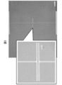
- FIG. 1 shows a schematic diagram of a source electrode and a drain electrode. There is no restriction
- a polymer or the like can be used.
- the patterning method include a sputtering method, a pulse laser deposition method, a vacuum evaporation method, a CVD method, a photolithography method, and a lift-off method in addition to the above-described printing method.
- the semiconductor material is not particularly limited, but it is desirable to use an organic semiconductor material or an oxide semiconductor material in order to use a flexible substrate.
- an organic semiconductor material is preferable.
- an oxide semiconductor material may be used as long as the semiconductor layer can be formed by a printing method.
- Organic semiconductor materials include high molecular organic semiconductor materials such as polythiophene, polyallylamine, fluorenebithiophene copolymers, and derivatives thereof, and small molecules such as pentacene, tetracene, copper phthalocyanine, perylene, and derivatives thereof. Organic semiconductor materials can be used.
- Carbon compounds such as carbon nanotubes or fullerenes, semiconductor nanoparticle dispersions, and the like can also be used as the material for the semiconductor layer.
- These organic semiconductor materials can be dissolved or dispersed in an aromatic solvent such as toluene and used as an ink-like solution or dispersion.
- the printing method of the organic semiconductor is not particularly limited, and screen printing, spray coating, spin coating, slit coating, die coating, bar coating, knife coating, offset printing, reverse printing, flexographic printing, inkjet printing, dispenser printing, gravure direct printing, A method such as gravure offset printing can be used.
- flexographic printing since the above-mentioned organic semiconductor has low solubility in a solvent, flexographic printing, reversal printing, ink jet printing, and dispenser printing suitable for printing a low viscosity solution are desirable.
- flexographic printing is most preferable because the printing time is short and the amount of ink used is small.
- an oxide containing one or more elements of zinc, indium, tin, tungsten, magnesium, and gallium can be given.
- Known materials such as zinc oxide, indium oxide, indium zinc oxide, tin oxide, tungsten oxide, and zinc gallium indium oxide (In—Ga—Zn—O) can be mentioned, but are not limited to these materials.
- the structure of these materials may be any of single crystal, polycrystal, microcrystal, crystal / amorphous mixed crystal, nanocrystal scattered amorphous, and amorphous.
- a pattern is formed using a photolithography method, a lift-off method, or the like.
- a more preferable pattern formation method is a method in which a dispersion in which an oxide semiconductor material is dispersed in a solvent is formed by a printing method.
- the printing method the same method as described in the organic semiconductor printing method can be used.
- the material of the gate insulating layer is not particularly limited, but generally used polymer solutions such as polyvinyl phenol, polymethyl methacrylate, polyimide, polyvinyl alcohol, parylene, fluororesin, epoxy resin, alumina, silica gel, etc.
- Inorganic particles such as silicon oxide, silicon nitride, silicon oxynitride, aluminum oxide, tantalum oxide, yttrium oxide, hafnium oxide, hafnium aluminate, zirconia oxide, and titanium oxide.
- thin film films such as PET, PEN, and PES, can also be used as an insulating film.
- a method for forming the gate insulating layer is not particularly limited, and a vacuum deposition method, a sputtering method, a dry method such as CVD, a wet method such as spin coating and a slit die, and a laminate method can be appropriately used.
- the substrate is not particularly limited, and examples thereof include soda lime glass, alkali-free glass, borosilicate glass, high strain point glass, quartz glass, and other inorganic materials such as alumina and silica, and polymer materials. It may be paper. Also, ordinary soda lime glass having low heat resistance can be used. In the present invention, a polymer material such as plastic or paper can be used as the substrate, and the transistor of the present invention is particularly useful in that a resin film can be used.
- Resin films used as substrates include polyimide, polyamide, polyamideimide, polyethylene terephthalate (PET), polyethylene naphthalate (PEN), polyphenylene sulfide, polyether ether ketone, polyether sulfone, polycarbonate, polyether imide, epoxy resin, phenol Examples thereof include resins, glass-epoxy resins, polyphenylene ethers, acrylic resins, polyolefins such as polyethylene and polypropylene, and liquid crystalline polymer compounds. Among these, polyethylene terephthalate (PET) and polyethylene naphthalate (PEN) are preferable.
- the thickness of the substrate is not particularly limited, but in the case of a plastic substrate such as a resin film, it is usually in the range of 10 ⁇ m to 300 ⁇ m. When the thickness is 10 ⁇ m or more, deformation of the substrate is suppressed when the conductive pattern is formed, which is preferable in terms of shape stability of the formed conductive pattern. Moreover, when it is 300 micrometers or less, when winding-up processing is performed continuously, it is suitable at the point of a softness
- a sealing layer, a light shielding layer, and the like can be suitably provided in the transistor of this embodiment as necessary.
- the material for the sealing layer can be selected from the same material as that for the gate insulating layer.
- As the light shielding layer a material in which a light shielding material such as carbon black is dispersed in the material described in the gate material can be used. Therefore, these formation methods can be the same as those for the gate insulating layer.
- Example 1 After 80 g of copper acetate (II) (manufactured by Wako Pure Chemical Industries) was dissolved in a mixed solvent of 800 g of water and 400 g of 1,2-propylene glycol (manufactured by Wako Pure Chemical Industries), 24 g of hydrazine (manufactured by Wako Pure Chemical Industries) was added and stirred. The supernatant and precipitate were separated by centrifugation. Dispersbyk-145 (manufactured by Big Chemie) 6.0 g and n-butanol (manufactured by Wako Pure Chemical Industries, Ltd.) 24 g were added to 43 g of the resulting precipitate, and dispersed using a homogenizer.
- II copper acetate
- Example 2 To 0.20 g of the concentrated dispersion obtained in Example 1, 0.78 g of n-butanol, 0.010 g of 1,2-propylene glycol and 0.010 g of Surflon S-611 (manufactured by Seimi Chemical) were added, and a homogenizer was used. By dispersing, a cuprous oxide dispersion was obtained. The average secondary particle size was 30 nm. This dispersion was applied onto a PEN substrate (manufactured by Teijin DuPont) by reverse printing in a pattern of source and drain electrodes, and then heated and fired at 0.8 kW for 300 seconds using a microwave plasma baking machine, and a conductive film was laminated. A source electrode and a drain electrode were obtained.
- PEN substrate manufactured by Teijin DuPont
- the obtained pattern is shown in FIG.
- the area of the conductive film laminate was 900 cm 2 .
- An organic semiconductor p-BTTT-C16 (manufactured by MERCK) was printed on the channel portion between the source electrode and the drain electrode by an ink jet method to form a semiconductor layer.
- Cytop (manufactured by Asahi Glass Co., Ltd.) was applied by spin coating so as to cover the organic semiconductor, the source electrode, and the drain electrode, thereby forming an insulating film.
- the cuprous oxide dispersion is applied to the insulating film in a pattern of a gate electrode by reversal printing, and heated and fired at 0.8 kW for 300 seconds using a microwave plasma baking machine to form a gate electrode.
- a transistor having a copper electrode was obtained.
- the electrode portion had a film thickness of 0.10 ⁇ m, a minimum line width of 5.0 ⁇ m, a minimum space width of 5.0 ⁇ m, and a volume resistivity of 12 ⁇ 10 ⁇ 6 ⁇ ⁇ cm.
- the mobility of the semiconductor was 2.0 ⁇ 10 ⁇ 2 cm 2 / (V ⁇ s). The results of dispersion and printing are shown in Table 1 below.
- Example 3 By adding 0.10 g of n-butanol, 0.080 g of 1,2-propylene glycol and Surflon S-6110.020 g to 0.80 g of the concentrated dispersion obtained in Example 1, the mixture was dispersed using a homogenizer to oxidize. A cuprous dispersion was obtained. The average secondary particle size was 50 nm. Using this dispersion, a transistor having a copper electrode was obtained in the same manner as in Example 2. The film thickness of the electrode part was 0.40 ⁇ m, the minimum line width was 5.0 ⁇ m, and the minimum space width was 5.0 ⁇ m. The volume resistivity of the electrode part was 14 ⁇ 10 ⁇ 6 ⁇ cm. The mobility of the semiconductor was 1.0 ⁇ 10 ⁇ 2 cm 2 / (V ⁇ s). The results of dispersion and printing are shown in Table 1 below.
- Example 4 By adding 0.97 g of n-butanol, 2.0 mg of 1,2-propylene glycol and Surflon S-616.0 mg to 0.020 g of the concentrated dispersion obtained in Example 1, the mixture was dispersed using a homogenizer to oxidize. A cuprous dispersion was obtained. The average secondary particle size was 20 nm. Using this dispersion, a transistor having a copper electrode was obtained in the same manner as in Example 2. The electrode portion had a thickness of 0.030 ⁇ m, a minimum line width of 5.0 ⁇ m, a minimum space width of 5.0 ⁇ m, and a volume resistivity of 14 ⁇ 10 ⁇ 6 ⁇ cm. The mobility of the semiconductor was 1.0 ⁇ 10 ⁇ 2 cm 2 / (V ⁇ s). The results of dispersion and printing are shown in Table 1 below.
- Example 5 To 0.20 g of the concentrated dispersion obtained in Example 1, 0.060 g of Disperbyk-145 (manufactured by Big Chemie), 0.72 g of n-butanol, 0.010 g of 1,2-propylene glycol and Surflon S-611 (manufactured by Seimi Chemical) ) 0.010 g was added and dispersed using a homogenizer to obtain a cuprous oxide dispersion. The average secondary particle size was 40 nm. Using this dispersion, a transistor having a copper electrode was obtained in the same manner as in Example 2.
- the electrode portion had a film thickness of 0.10 ⁇ m, a minimum line width of 5.0 ⁇ m, a minimum space width of 5.0 ⁇ m, and a volume resistivity of 22 ⁇ 10 ⁇ 6 ⁇ ⁇ cm.
- the mobility of the semiconductor was 6.0 ⁇ 10 ⁇ 3 cm 2 / (V ⁇ s). The results of dispersion and printing are shown in Table 1 below.
- Example 6 To 0.20 g of the concentrated dispersion obtained in Example 1, 0.13 g of Disperbyk-145 (manufactured by Big Chemie), 0.65 g of n-butanol, 0.010 g of 1,2-propylene glycol and Surflon S-611 (manufactured by Seimi Chemical) ) 0.010 g was added and dispersed using a homogenizer to obtain a cuprous oxide dispersion. The average secondary particle size was 50 nm. Using this dispersion, a transistor having a copper electrode was obtained in the same manner as in Example 2.
- the electrode portion had a film thickness of 0.10 ⁇ m, a minimum line width of 5.0 ⁇ m, a minimum space width of 5.0 ⁇ m, and a volume resistivity of 500 ⁇ 10 ⁇ 6 ⁇ ⁇ cm.
- the mobility of the semiconductor was 2.0 ⁇ 10 ⁇ 3 cm 2 / (V ⁇ s). The results of dispersion and printing are shown in Table 1 below.
- Example 7 CIK Nanotech's cupric oxide fine particles 0.30g, Disperbyk-145 (manufactured by Big Chemie) 0.060g, n-butanol 0.61g, 1,2-propylene glycol 0.020g and Surflon S-611 (manufactured by Seimi Chemical) ) 0.010 g was added and dispersed using a homogenizer to obtain a cuprous oxide dispersion.
- the average secondary particle size was 200 nm.
- a transistor having a copper electrode was obtained in the same manner as in Example 2.
- the minimum line width was 5.0 ⁇ m
- the minimum space width was 5.0 ⁇ m
- the volume resistivity was 32 ⁇ 10 ⁇ 6 ⁇ cm.
- the mobility of the semiconductor was 4.0 ⁇ 10 ⁇ 3 cm 2 / (V ⁇ s). The results of dispersion and printing are shown in Table 1 below.
- Example 8 CIK Nanotech's cupric oxide fine particles 0.50g, Disperbyk-145 (Big Chemie) 0.10g, n-butanol 0.33g, 1,2-propylene glycol 0.070g, and Surflon S-611 (Seimi Chemical) (Product made) 1.0 mg was added and dispersed using a homogenizer to obtain a cuprous oxide dispersion. The average secondary particle size was 30 nm. Using this dispersion, a transistor having a copper electrode was obtained in the same manner as in Example 2.
- the film thickness of the electrode part was 0.50 ⁇ m, the minimum line width was 5.0 ⁇ m, the minimum space width was 5.0 ⁇ m, and the volume resistivity was 44 ⁇ 10 ⁇ 6 ⁇ cm.
- the mobility of the semiconductor was 2.0 ⁇ 10 ⁇ 3 cm 2 / (V ⁇ s). The results of dispersion and printing are shown in Table 1 below.
- Example 1 In the same procedure as in Example 1, Dispersbyk-145 (manufactured by Big Chemie) was not added, and 60 g of a concentrated dispersion containing 30 g of cuprous oxide fine particles and 30 g of n-butanol was obtained. To 0.40 g of this concentrated dispersion, 0.53 g of n-butanol, 0.060 g of 1,2-propylene glycol and 0.010 g of Surflon S-611 (manufactured by Seimi Chemical) were added, and dispersion was attempted using a homogenizer. Since the dispersant Disperbyk-145 (manufactured by Big Chemie) was not contained, it aggregated in the atmosphere. The average secondary particle size was 900 nm and could not be used for reversal printing. Since the source electrode and the drain electrode could not be printed on the substrate with this dispersion, the volume resistivity of the electrode could not be measured.
- a cuprous oxide dispersion is obtained by adding 0.32 g of n-butanol and 0.080 g of 1,2-propylene glycol to 0.60 g of the concentrated dispersion obtained in Example 1, and dispersing using a homogenizer. It was. The average secondary particle size was 40 nm.
- the transistor according to the present invention has a fine patterned electrode formed by a printing process of copper or a copper oxide dispersion. Therefore, the transistor according to the present invention is suitably used for applications such as high-performance electronic devices.
Landscapes
- Engineering & Computer Science (AREA)
- Chemical & Material Sciences (AREA)
- Microelectronics & Electronic Packaging (AREA)
- Power Engineering (AREA)
- Physics & Mathematics (AREA)
- Organic Chemistry (AREA)
- Condensed Matter Physics & Semiconductors (AREA)
- General Physics & Mathematics (AREA)
- Computer Hardware Design (AREA)
- Ceramic Engineering (AREA)
- Dispersion Chemistry (AREA)
- Life Sciences & Earth Sciences (AREA)
- Materials Engineering (AREA)
- Wood Science & Technology (AREA)
- Spectroscopy & Molecular Physics (AREA)
- Chemical Kinetics & Catalysis (AREA)
- General Chemical & Material Sciences (AREA)
- Thin Film Transistor (AREA)
- Conductive Materials (AREA)
- Non-Insulated Conductors (AREA)
- Electrodes Of Semiconductors (AREA)
Abstract
Priority Applications (7)
| Application Number | Priority Date | Filing Date | Title |
|---|---|---|---|
| CN201480040975.5A CN105393312B (zh) | 2013-07-23 | 2014-07-22 | 铜和/或铜氧化物分散体、以及使用该分散体形成的导电膜 |
| JP2015528290A JP6175500B2 (ja) | 2013-07-23 | 2014-07-22 | 銅及び/又は銅酸化物分散体、並びに該分散体を用いて形成された導電膜 |
| KR1020157034234A KR101849446B1 (ko) | 2013-07-23 | 2014-07-22 | 구리 및/또는 구리 산화물 분산체, 및 이 분산체를 이용하여 형성된 도전막 |
| US14/906,422 US10424648B2 (en) | 2013-07-23 | 2014-07-22 | Copper and/or copper oxide dispersion, and electroconductive film formed using dispersion |
| KR1020187006001A KR102117579B1 (ko) | 2013-07-23 | 2014-07-22 | 구리 및/또는 구리 산화물 분산체, 및 이 분산체를 이용하여 형성된 도전막 |
| EP14829560.3A EP3026677B1 (fr) | 2013-07-23 | 2014-07-22 | Dispersion de cuivre et/ou d'oxyde de cuivre, méthode pour formation d'une couche électro-conductrice à l'aide de la dispersion |
| US16/540,446 US20190371901A1 (en) | 2013-07-23 | 2019-08-14 | Copper and/or copper oxide dispersion, and electroconductive film formed using dispersion |
Applications Claiming Priority (2)
| Application Number | Priority Date | Filing Date | Title |
|---|---|---|---|
| JP2013152799 | 2013-07-23 | ||
| JP2013-152799 | 2013-07-23 |
Related Child Applications (2)
| Application Number | Title | Priority Date | Filing Date |
|---|---|---|---|
| US14/906,422 A-371-Of-International US10424648B2 (en) | 2013-07-23 | 2014-07-22 | Copper and/or copper oxide dispersion, and electroconductive film formed using dispersion |
| US16/540,446 Division US20190371901A1 (en) | 2013-07-23 | 2019-08-14 | Copper and/or copper oxide dispersion, and electroconductive film formed using dispersion |
Publications (1)
| Publication Number | Publication Date |
|---|---|
| WO2015012264A1 true WO2015012264A1 (fr) | 2015-01-29 |
Family
ID=52393299
Family Applications (1)
| Application Number | Title | Priority Date | Filing Date |
|---|---|---|---|
| PCT/JP2014/069321 WO2015012264A1 (fr) | 2013-07-23 | 2014-07-22 | Dispersion de cuivre et/ou d'oxyde de cuivre, et membrane conductrice formée à l'aide de celle-ci |
Country Status (6)
| Country | Link |
|---|---|
| US (2) | US10424648B2 (fr) |
| EP (1) | EP3026677B1 (fr) |
| JP (2) | JP6175500B2 (fr) |
| KR (2) | KR102117579B1 (fr) |
| CN (1) | CN105393312B (fr) |
| WO (1) | WO2015012264A1 (fr) |
Cited By (9)
| Publication number | Priority date | Publication date | Assignee | Title |
|---|---|---|---|---|
| JP2017069198A (ja) * | 2015-09-29 | 2017-04-06 | 三ツ星ベルト株式会社 | 導電性ペースト及び導電膜付基板の製造方法 |
| WO2019017363A1 (fr) | 2017-07-18 | 2019-01-24 | 旭化成株式会社 | Structure comprenant des régions à motif électroconducteur, son procédé de production, stratifié, son procédé de production et câblage en cuivre |
| WO2019022230A1 (fr) | 2017-07-27 | 2019-01-31 | 旭化成株式会社 | Encre à base d'oxyde de cuivre et procédé de production d'un substrat conducteur mettant en œuvre ladite encre, produit contenant un film de revêtement et procédé de production de produit correspondant, procédé de production de produit à motif conducteur, et produit à motif conducteur |
| JP2019090110A (ja) * | 2017-11-10 | 2019-06-13 | 旭化成株式会社 | 導電性パターン領域付構造体及びその製造方法 |
| JP2019210469A (ja) * | 2018-05-30 | 2019-12-12 | 旭化成株式会社 | インクジェット用酸化銅インク及びこれを用いて導電性パターンを付与した導電性基板の製造方法 |
| JPWO2018169012A1 (ja) * | 2017-03-16 | 2020-01-16 | 旭化成株式会社 | 分散体並びにこれを用いた導電性パターン付構造体の製造方法及び導電性パターン付構造体 |
| US11328835B2 (en) | 2017-03-16 | 2022-05-10 | Asahi Kasei Kabushiki Kaisha | Dispersing element, method for manufacturing structure with conductive pattern using the same, and structure with conductive pattern |
| US11520451B2 (en) | 2018-07-30 | 2022-12-06 | Asahi Kasei Kabushiki Kaisha | Conductive film and conductive film roll, electronic paper, touch panel and flat-panel display comprising the same |
| US11877391B2 (en) | 2018-07-30 | 2024-01-16 | Asahi Kasei Kabushiki Kaisha | Conductive film and conductive film roll, electronic paper, touch panel and flat-panel display comprising the same |
Families Citing this family (7)
| Publication number | Priority date | Publication date | Assignee | Title |
|---|---|---|---|---|
| CN103451682B (zh) * | 2013-09-16 | 2017-06-06 | 北京科技大学 | 一种含钛可溶阳极熔盐电解提取金属钛的方法 |
| WO2015152625A1 (fr) * | 2014-04-01 | 2015-10-08 | 전자부품연구원 | Composition d'encre de frittage par la lumière, carte de câblage l'utilisant et son procédé de fabrication |
| IL247113B (en) * | 2016-08-04 | 2018-02-28 | Copprint Tech Ltd | Formulations and processes for making a high conductivity copper pattern |
| US10812974B2 (en) * | 2017-05-06 | 2020-10-20 | Vmware, Inc. | Virtual desktop client connection continuity |
| CN111344814B (zh) * | 2017-11-14 | 2021-11-16 | 昭和电工材料株式会社 | 组合物、导体及其制造方法、以及结构体 |
| JP7176847B2 (ja) * | 2018-03-15 | 2022-11-22 | 旭化成株式会社 | 分散体、塗膜を含む製品、導電性パターン付き構造体の製造方法、及び、導電性パターン付き構造体 |
| JP7099867B2 (ja) * | 2018-05-16 | 2022-07-12 | 日本化学工業株式会社 | 光焼結型組成物及びそれを用いた導電膜の形成方法 |
Citations (8)
| Publication number | Priority date | Publication date | Assignee | Title |
|---|---|---|---|---|
| JP2005015628A (ja) | 2003-06-26 | 2005-01-20 | Asahi Kasei Corp | 酸化第一銅コロイド分散液 |
| WO2008111484A1 (fr) * | 2007-03-15 | 2008-09-18 | Dic Corporation | Encre conductrice pour une impression en transparence typographique |
| JP2010129790A (ja) * | 2008-11-27 | 2010-06-10 | Tokyo Electron Ltd | 成膜方法 |
| WO2012115475A2 (fr) * | 2011-02-25 | 2012-08-30 | 한화케미칼 주식회사 | Composition d'encre conductrice pour impression offset ou offset inverse |
| JP2012216425A (ja) | 2011-03-31 | 2012-11-08 | Dainippon Printing Co Ltd | 金属酸化物微粒子分散体、導電性基板及びその製造方法 |
| JP2013503234A (ja) * | 2009-08-28 | 2013-01-31 | エルジー・ケム・リミテッド | 導電性金属インク組成物および導電性パターンの形成方法 |
| WO2013073200A1 (fr) * | 2011-11-14 | 2013-05-23 | 石原薬品株式会社 | Dispersion de particules de cuivre, procédé de formation d'un film conducteur et substrat de circuit |
| JP2013109966A (ja) * | 2011-11-21 | 2013-06-06 | Hitachi Chemical Co Ltd | 酸化銅ペースト及び金属銅層の製造方法 |
Family Cites Families (57)
| Publication number | Priority date | Publication date | Assignee | Title |
|---|---|---|---|---|
| US2091800A (en) * | 1931-09-15 | 1937-08-31 | Rohm & Haas | Method of hydrogenating esters |
| US3213145A (en) * | 1960-03-28 | 1965-10-19 | Standard Oil Co | Catalytic hydrogenation of esters of aromatic monocarboxylic acids to aryl-substituted methanols |
| JP2526989B2 (ja) * | 1988-05-20 | 1996-08-21 | 三菱瓦斯化学株式会社 | 芳香族多価アルコ―ルの製造方法 |
| US5158849A (en) * | 1990-10-25 | 1992-10-27 | Custom Papers Group Inc. | Composition useful in transparent conductive coatings |
| US5855818A (en) * | 1995-01-27 | 1999-01-05 | Rogers Corporation | Electrically conductive fiber filled elastomeric foam |
| TW505685B (en) * | 1997-09-05 | 2002-10-11 | Mitsubishi Materials Corp | Transparent conductive film and composition for forming same |
| US5855820A (en) * | 1997-11-13 | 1999-01-05 | E. I. Du Pont De Nemours And Company | Water based thick film conductive compositions |
| MY125159A (en) * | 1998-09-14 | 2006-07-31 | Mitsubishi Materials Corp | Fine metal particle-dispersion solution and conductive film using the same |
| JP3545974B2 (ja) * | 1999-08-16 | 2004-07-21 | 日本パーカライジング株式会社 | 金属材料のりん酸塩化成処理方法 |
| US7858818B2 (en) * | 2001-01-31 | 2010-12-28 | Momentive Performance Materials Inc. | Nanosized copper catalyst precursors for the direct synthesis of trialkoxysilanes |
| US7674401B2 (en) * | 2001-12-18 | 2010-03-09 | Asahi Kasei Kabushiki Kaisha | Method of producing a thin conductive metal film |
| US7663004B2 (en) * | 2002-04-22 | 2010-02-16 | The Curators Of The University Of Missouri | Method of producing lower alcohols from glycerol |
| US8252961B2 (en) * | 2002-04-22 | 2012-08-28 | The Curators Of The University Of Missouri | Method of producing lower alcohols from glycerol |
| US20100009540A1 (en) * | 2002-09-25 | 2010-01-14 | Asahi Glass Company Limited | Polishing compound, its production process and polishing method |
| CN100488339C (zh) * | 2003-05-16 | 2009-05-13 | 播磨化成株式会社 | 形成微细铜颗粒烧结产物类的微细形状导电体的方法 |
| JP4407311B2 (ja) * | 2004-02-20 | 2010-02-03 | セイコーエプソン株式会社 | 薄膜トランジスタの製造方法 |
| US7238654B2 (en) * | 2004-05-17 | 2007-07-03 | Phibro-Tech, Inc. | Compatibilizing surfactant useful with slurries of copper particles |
| US8980135B2 (en) * | 2004-08-31 | 2015-03-17 | Sumitomo Metal Mining Co., Ltd. | Electroconductive particle, visible light transmitting particle-dispersed electrical conductor and manufacturing method thereof, transparent electroconductive thin film and manufacturing method thereof, transparent electroconductive article that uses the same, and infrared-shielding article |
| US7771625B2 (en) * | 2004-11-29 | 2010-08-10 | Dainippon Ink And Chemicals, Inc. | Method for producing surface-treated silver-containing powder and silver paste using surface-treated silver-containing powder |
| US20060189113A1 (en) * | 2005-01-14 | 2006-08-24 | Cabot Corporation | Metal nanoparticle compositions |
| EA200701792A1 (ru) * | 2005-02-24 | 2008-02-28 | Рой А. Периана | Новые каталитические системы для превращения углеводородов в функционализированные продукты |
| DE102005043242A1 (de) * | 2005-09-09 | 2007-03-15 | Basf Ag | Dispersion zum Aufbringen einer Metallschicht |
| JP4839767B2 (ja) * | 2005-10-14 | 2011-12-21 | 東洋インキScホールディングス株式会社 | 金属微粒子分散体の製造方法、該方法で製造された金属微粒子分散体を用いた導電性インキ、および導電性パターン。 |
| US8084401B2 (en) * | 2006-01-25 | 2011-12-27 | Clearwater International, Llc | Non-volatile phosphorus hydrocarbon gelling agent |
| US8337726B2 (en) * | 2006-07-28 | 2012-12-25 | Furukawa Electric Co., Ltd. | Fine particle dispersion and method for producing fine particle dispersion |
| JP2008144010A (ja) * | 2006-12-08 | 2008-06-26 | Konica Minolta Holdings Inc | 樹脂組成物の製造方法及び樹脂組成物フィルム |
| US7976733B2 (en) * | 2007-11-30 | 2011-07-12 | Xerox Corporation | Air stable copper nanoparticle ink and applications therefor |
| US20090214764A1 (en) * | 2008-02-26 | 2009-08-27 | Xerox Corporation | Metal nanoparticles stabilized with a bident amine |
| US8506849B2 (en) * | 2008-03-05 | 2013-08-13 | Applied Nanotech Holdings, Inc. | Additives and modifiers for solvent- and water-based metallic conductive inks |
| DE112009002056T5 (de) * | 2008-08-27 | 2011-07-14 | Mitsubishi Materials Corporation | Transparenter elektrisch leitfähiger Film für Solarzellen, Zusammensetzung für transparente elektrisch leitfähige Filme und Mehrfach-Solarzellen |
| JP5531504B2 (ja) * | 2009-08-25 | 2014-06-25 | Dic株式会社 | 銀ナノ粒子を用いる接合体の製造方法、及び接合体 |
| TW201127520A (en) * | 2009-09-18 | 2011-08-16 | Sumitomo Chemical Co | Silver-conjugated compound composite |
| CN104588643B (zh) * | 2009-09-30 | 2017-08-29 | 大日本印刷株式会社 | 金属微粒分散体、导电性基板的制造方法及导电性基板 |
| US9272970B2 (en) * | 2010-07-09 | 2016-03-01 | Celanese International Corporation | Hydrogenolysis of ethyl acetate in alcohol separation processes |
| TWI531649B (zh) * | 2010-08-12 | 2016-05-01 | 三井化學股份有限公司 | 藉由破壞gntR而改善生產力之異丙醇生產細菌 |
| EP2468827B1 (fr) * | 2010-12-21 | 2014-03-12 | Agfa-Gevaert | Dispersion comportant des nanoparticules métalliques, d'oxyde métallique ou de précurseur métallique |
| WO2012135997A1 (fr) * | 2011-04-02 | 2012-10-11 | 中国科学院化学研究所 | Procédé de formation d'ensembles de paires de microélectrodes sur une surface de substrat de silicium comprenant des piliers de silicium hydrophobes |
| JP2013004309A (ja) * | 2011-06-16 | 2013-01-07 | Toyota Motor Corp | 金属ナノ粒子ペースト |
| JP6035887B2 (ja) * | 2011-06-21 | 2016-11-30 | セントラル硝子株式会社 | ポジ型レジスト組成物 |
| JP2013008907A (ja) * | 2011-06-27 | 2013-01-10 | Hitachi Chem Co Ltd | 導電性ペースト用酸化銅粉末、導電性ペースト用酸化銅粉末の製造方法、導電性ペースト及びこれを用いて得られる銅配線層 |
| FR2980791A1 (fr) * | 2011-10-03 | 2013-04-05 | Rhodia Operations | Procede de preparation d'un melange d'alcools |
| TW201339279A (zh) * | 2011-11-24 | 2013-10-01 | Showa Denko Kk | 導電圖型形成方法及藉由光照射或微波加熱的導電圖型形成用組成物 |
| US20140342177A1 (en) * | 2011-12-07 | 2014-11-20 | Duke University | Synthesis of cupronickel nanowires and their application in transparent conducting films |
| KR101391697B1 (ko) * | 2011-12-14 | 2014-05-07 | 제일모직주식회사 | 이방성 도전 필름용 조성물 및 이를 이용한 이방성 도전 필름 |
| KR101403865B1 (ko) * | 2011-12-16 | 2014-06-10 | 제일모직주식회사 | 이방성 도전 필름용 조성물, 이방성 도전 필름 및 반도체 장치 |
| KR101355855B1 (ko) * | 2011-12-19 | 2014-01-29 | 제일모직주식회사 | 이방성 도전 필름 |
| KR101355856B1 (ko) * | 2011-12-26 | 2014-01-27 | 제일모직주식회사 | 이방 전도성 접착 필름용 조성물 및 이를 이용한 이방 전도성 접착 필름 |
| US9664009B2 (en) * | 2012-04-04 | 2017-05-30 | Weatherford Technologies, LLC | Apparatuses, systems, and methods for forming in-situ gel pills to lift liquids from horizontal wells |
| JP6191606B2 (ja) * | 2012-07-19 | 2017-09-06 | 日油株式会社 | 銀ナノ微粒子、その製造方法、銀ナノ微粒子分散液及び銀要素形成基材 |
| WO2014052482A1 (fr) * | 2012-09-25 | 2014-04-03 | University Of Connecticut Office Of Economic Development | Oxydes métalliques mésoporeux et procédés de préparation de ceux-ci |
| WO2014061556A1 (fr) * | 2012-10-15 | 2014-04-24 | 大日本印刷株式会社 | Dispersion de particules métalliques destinée à un substrat conducteur, son procédé de production et procédé de production d'un substrat conducteur |
| US9953740B2 (en) * | 2012-10-18 | 2018-04-24 | Dai Nippon Printing Co., Ltd. | Dispersant, metal particle dispersion for electroconductive substrates, and method for producing electroconductive substrate |
| JP6120289B2 (ja) * | 2012-10-24 | 2017-04-26 | 国立研究開発法人物質・材料研究機構 | 導電性ポリマー−金属複合体と基材との付着体及びその形成方法、導電性ポリマー−金属複合体分散液の製造方法 |
| US20140127409A1 (en) * | 2012-11-06 | 2014-05-08 | Takuya Harada | Method for producing fine particle dispersion |
| MY170550A (en) * | 2013-02-19 | 2019-08-16 | Rescurve Llc | Production of higher alcohols |
| JP5700864B2 (ja) * | 2013-05-15 | 2015-04-15 | 石原ケミカル株式会社 | 銅微粒子分散液、導電膜形成方法及び回路基板 |
| BR112015032871B1 (pt) * | 2013-07-02 | 2021-07-06 | Ut-Battelle, Llc | métodos para produzir um componente de mistura de hidrocarbonetos |
-
2014
- 2014-07-22 WO PCT/JP2014/069321 patent/WO2015012264A1/fr active Application Filing
- 2014-07-22 US US14/906,422 patent/US10424648B2/en active Active
- 2014-07-22 EP EP14829560.3A patent/EP3026677B1/fr active Active
- 2014-07-22 JP JP2015528290A patent/JP6175500B2/ja active Active
- 2014-07-22 KR KR1020187006001A patent/KR102117579B1/ko active IP Right Grant
- 2014-07-22 KR KR1020157034234A patent/KR101849446B1/ko active IP Right Grant
- 2014-07-22 CN CN201480040975.5A patent/CN105393312B/zh active Active
-
2017
- 2017-05-15 JP JP2017096322A patent/JP6496351B2/ja active Active
-
2019
- 2019-08-14 US US16/540,446 patent/US20190371901A1/en not_active Abandoned
Patent Citations (8)
| Publication number | Priority date | Publication date | Assignee | Title |
|---|---|---|---|---|
| JP2005015628A (ja) | 2003-06-26 | 2005-01-20 | Asahi Kasei Corp | 酸化第一銅コロイド分散液 |
| WO2008111484A1 (fr) * | 2007-03-15 | 2008-09-18 | Dic Corporation | Encre conductrice pour une impression en transparence typographique |
| JP2010129790A (ja) * | 2008-11-27 | 2010-06-10 | Tokyo Electron Ltd | 成膜方法 |
| JP2013503234A (ja) * | 2009-08-28 | 2013-01-31 | エルジー・ケム・リミテッド | 導電性金属インク組成物および導電性パターンの形成方法 |
| WO2012115475A2 (fr) * | 2011-02-25 | 2012-08-30 | 한화케미칼 주식회사 | Composition d'encre conductrice pour impression offset ou offset inverse |
| JP2012216425A (ja) | 2011-03-31 | 2012-11-08 | Dainippon Printing Co Ltd | 金属酸化物微粒子分散体、導電性基板及びその製造方法 |
| WO2013073200A1 (fr) * | 2011-11-14 | 2013-05-23 | 石原薬品株式会社 | Dispersion de particules de cuivre, procédé de formation d'un film conducteur et substrat de circuit |
| JP2013109966A (ja) * | 2011-11-21 | 2013-06-06 | Hitachi Chemical Co Ltd | 酸化銅ペースト及び金属銅層の製造方法 |
Non-Patent Citations (1)
| Title |
|---|
| See also references of EP3026677A4 |
Cited By (26)
| Publication number | Priority date | Publication date | Assignee | Title |
|---|---|---|---|---|
| JP2017069198A (ja) * | 2015-09-29 | 2017-04-06 | 三ツ星ベルト株式会社 | 導電性ペースト及び導電膜付基板の製造方法 |
| JP2021185269A (ja) * | 2017-03-16 | 2021-12-09 | 旭化成株式会社 | 分散体並びにこれを用いた導電性パターン付構造体の製造方法及び導電性パターン付構造体 |
| JP7477581B2 (ja) | 2017-03-16 | 2024-05-01 | 旭化成株式会社 | 分散体並びにこれを用いた導電性パターン付構造体の製造方法及び導電性パターン付構造体 |
| JP2023027058A (ja) * | 2017-03-16 | 2023-03-01 | 旭化成株式会社 | 分散体並びにこれを用いた導電性パターン付構造体の製造方法及び導電性パターン付構造体 |
| JP7201755B2 (ja) | 2017-03-16 | 2023-01-10 | 旭化成株式会社 | 分散体並びにこれを用いた導電性パターン付構造体の製造方法及び導電性パターン付構造体 |
| JP7104687B2 (ja) | 2017-03-16 | 2022-07-21 | 旭化成株式会社 | 分散体並びにこれを用いた導電性パターン付構造体の製造方法及び導電性パターン付構造体 |
| JPWO2018169012A1 (ja) * | 2017-03-16 | 2020-01-16 | 旭化成株式会社 | 分散体並びにこれを用いた導電性パターン付構造体の製造方法及び導電性パターン付構造体 |
| US11328835B2 (en) | 2017-03-16 | 2022-05-10 | Asahi Kasei Kabushiki Kaisha | Dispersing element, method for manufacturing structure with conductive pattern using the same, and structure with conductive pattern |
| US11270809B2 (en) | 2017-03-16 | 2022-03-08 | Asahi Kasei Kabushiki Kaisha | Dispersing element, method for manufacturing structure with conductive pattern using the same, and structure with conductive pattern |
| KR20200015609A (ko) | 2017-07-18 | 2020-02-12 | 아사히 가세이 가부시키가이샤 | 도전성 패턴 영역을 갖는 구조체 및 그 제조 방법, 적층체 및 그 제조 방법, 그리고 구리 배선 |
| WO2019017363A1 (fr) | 2017-07-18 | 2019-01-24 | 旭化成株式会社 | Structure comprenant des régions à motif électroconducteur, son procédé de production, stratifié, son procédé de production et câblage en cuivre |
| US11109492B2 (en) | 2017-07-18 | 2021-08-31 | Asahi Kasei Kabushiki Kaisha | Structure including electroconductive pattern regions, method for producing same, stack, method for producing same, and copper wiring |
| WO2019022230A1 (fr) | 2017-07-27 | 2019-01-31 | 旭化成株式会社 | Encre à base d'oxyde de cuivre et procédé de production d'un substrat conducteur mettant en œuvre ladite encre, produit contenant un film de revêtement et procédé de production de produit correspondant, procédé de production de produit à motif conducteur, et produit à motif conducteur |
| US11760895B2 (en) | 2017-07-27 | 2023-09-19 | Asahi Kasei Kabushiki Kaisha | Copper oxide ink and method for producing conductive substrate using same, product containing coating film and method for producing product using same, method for producing product with conductive pattern, and product with conductive pattern |
| JP7076591B2 (ja) | 2017-07-27 | 2022-05-27 | 旭化成株式会社 | 酸化銅インク及びこれを用いた導電性基板の製造方法、塗膜を含む製品及びこれを用いた製品の製造方法、導電性パターン付製品の製造方法、並びに、導電性パターン付製品 |
| JP2021077648A (ja) * | 2017-07-27 | 2021-05-20 | 旭化成株式会社 | 酸化銅インク及びこれを用いた導電性基板の製造方法、塗膜を含む製品及びこれを用いた製品の製造方法、導電性パターン付製品の製造方法、並びに、導電性パターン付製品 |
| JP2022008655A (ja) * | 2017-07-27 | 2022-01-13 | 旭化成株式会社 | 酸化銅インク及びこれを用いた導電性基板の製造方法、塗膜を含む製品及びこれを用いた製品の製造方法、導電性パターン付製品の製造方法、並びに、導電性パターン付製品 |
| JP2022048151A (ja) * | 2017-07-27 | 2022-03-25 | 旭化成株式会社 | 酸化銅インク及びこれを用いた導電性基板の製造方法、塗膜を含む製品及びこれを用いた製品の製造方法、導電性パターン付製品の製造方法、並びに、導電性パターン付製品 |
| JP7403512B2 (ja) | 2017-07-27 | 2023-12-22 | 旭化成株式会社 | 酸化銅インク及びこれを用いた導電性基板の製造方法、塗膜を含む製品及びこれを用いた製品の製造方法、導電性パターン付製品の製造方法、並びに、導電性パターン付製品 |
| JP2019090110A (ja) * | 2017-11-10 | 2019-06-13 | 旭化成株式会社 | 導電性パターン領域付構造体及びその製造方法 |
| JP2019210469A (ja) * | 2018-05-30 | 2019-12-12 | 旭化成株式会社 | インクジェット用酸化銅インク及びこれを用いて導電性パターンを付与した導電性基板の製造方法 |
| JP7263124B2 (ja) | 2018-05-30 | 2023-04-24 | 旭化成株式会社 | インクジェット用酸化銅インク及びこれを用いて導電性パターンを付与した導電性基板の製造方法 |
| US11520451B2 (en) | 2018-07-30 | 2022-12-06 | Asahi Kasei Kabushiki Kaisha | Conductive film and conductive film roll, electronic paper, touch panel and flat-panel display comprising the same |
| US11635863B2 (en) | 2018-07-30 | 2023-04-25 | Asahi Kasei Kabushiki Kaisha | Conductive film and conductive film roll, electronic paper, touch panel and flat-panel display comprising the same |
| US11877391B2 (en) | 2018-07-30 | 2024-01-16 | Asahi Kasei Kabushiki Kaisha | Conductive film and conductive film roll, electronic paper, touch panel and flat-panel display comprising the same |
| US11620028B2 (en) | 2018-07-30 | 2023-04-04 | Asahi Kasei Kabushiki Kaisha | Conductive film and conductive film roll, electronic paper, touch panel and flat-panel display comprising the same |
Also Published As
| Publication number | Publication date |
|---|---|
| EP3026677A4 (fr) | 2016-07-27 |
| EP3026677B1 (fr) | 2018-04-11 |
| JPWO2015012264A1 (ja) | 2017-03-02 |
| EP3026677A1 (fr) | 2016-06-01 |
| CN105393312A (zh) | 2016-03-09 |
| JP6496351B2 (ja) | 2019-04-03 |
| KR20180024039A (ko) | 2018-03-07 |
| US20160155814A1 (en) | 2016-06-02 |
| KR20160003840A (ko) | 2016-01-11 |
| JP6175500B2 (ja) | 2017-08-02 |
| KR102117579B1 (ko) | 2020-06-01 |
| JP2017143309A (ja) | 2017-08-17 |
| US20190371901A1 (en) | 2019-12-05 |
| US10424648B2 (en) | 2019-09-24 |
| KR101849446B1 (ko) | 2018-04-16 |
| CN105393312B (zh) | 2018-01-02 |
Similar Documents
| Publication | Publication Date | Title |
|---|---|---|
| JP6496351B2 (ja) | 銅及び/又は銅酸化物分散体、並びに該分散体を用いて形成された導電膜 | |
| Scheideler et al. | Low‐temperature‐processed printed metal oxide transistors based on pure aqueous inks | |
| Garlapati et al. | Printed electronics based on inorganic semiconductors: From processes and materials to devices | |
| Shao et al. | Recent progress on jet printing of oxide-based thin film transistors | |
| Han et al. | High performance metal oxide field-effect transistors with a reverse offset printed Cu source/drain electrode | |
| US9486996B2 (en) | Gravure printing process using silver nanoparticle inks for high quality conductive features | |
| Jeong et al. | Printed Cu source/drain electrode capped by CuO hole injection layer for organic thin film transistors | |
| Ko et al. | Functionalized MXene ink enables environmentally stable printed electronics | |
| JP4795412B2 (ja) | 導電材の形成方法、該形成方法により形成された導電材、及び該導電材を有するデバイス | |
| KR101654133B1 (ko) | 그래핀 조성물 및 그를 이용한 전극을 포함하는 유기전자소자 | |
| TW201620837A (zh) | 銀微粒子分散物、墨水組成物、銀電極及薄膜電晶體 | |
| KR20110080776A (ko) | 단분자가 도핑된 단일 벽 탄소 나노튜브 및 이를 이용한 박막 트랜지스터 | |
| JP5578078B2 (ja) | 機能性層の製造方法 | |
| Moon et al. | Non-vacuum room temperature-processed sintering method of molybdenum pattern by intense pulsed light irradiation for high-performance electronic devices | |
| Moon et al. | Intense pulsed light annealing of solution-based indium–gallium–zinc–oxide semiconductors with printed Ag source and drain electrodes for bottom gate thin film transistors | |
| EP3223328B1 (fr) | Cellule photovoltaïque organique et son procédé de fabrication | |
| KR20160014409A (ko) | 도전성 잉크 조성물, 도전체 및 전자 소자 | |
| Liu et al. | Fabrication of an organic thin-film transistor by inkjet printing | |
| Wu et al. | Development of silver nanoparticle ink for printed electronics | |
| JP7263124B2 (ja) | インクジェット用酸化銅インク及びこれを用いて導電性パターンを付与した導電性基板の製造方法 | |
| Park et al. | Functionalized MXene Ink Enables Environmentally Stable Printed Electronics | |
| KR20230140118A (ko) | 알코올 분산성이 우수한 표면개질된 맥신 입자, 이를 포함하는 응집 저항성이 우수한 콜로이드성 맥신 잉크 및 이의 제조방법 | |
| KR20230140119A (ko) | 전기유체역학 프린팅용 콜로이드성 맥신 잉크 및 이의 제조방법 | |
| CN112635102A (zh) | 复合导电薄膜及其制备方法以及薄膜晶体管 | |
| 雍穎瓊 | Copper Fine Particles for Electroconductive Materials |
Legal Events
| Date | Code | Title | Description |
|---|---|---|---|
| WWE | Wipo information: entry into national phase |
Ref document number: 201480040975.5 Country of ref document: CN |
|
| 121 | Ep: the epo has been informed by wipo that ep was designated in this application |
Ref document number: 14829560 Country of ref document: EP Kind code of ref document: A1 |
|
| ENP | Entry into the national phase |
Ref document number: 2015528290 Country of ref document: JP Kind code of ref document: A |
|
| ENP | Entry into the national phase |
Ref document number: 20157034234 Country of ref document: KR Kind code of ref document: A |
|
| WWE | Wipo information: entry into national phase |
Ref document number: 14906422 Country of ref document: US |
|
| WWE | Wipo information: entry into national phase |
Ref document number: 2014829560 Country of ref document: EP |
|
| NENP | Non-entry into the national phase |
Ref country code: DE |