WO2014132872A1 - 酸化ニオブスパッタリングターゲット、その製造方法及び酸化ニオブ膜 - Google Patents
酸化ニオブスパッタリングターゲット、その製造方法及び酸化ニオブ膜 Download PDFInfo
- Publication number
- WO2014132872A1 WO2014132872A1 PCT/JP2014/054004 JP2014054004W WO2014132872A1 WO 2014132872 A1 WO2014132872 A1 WO 2014132872A1 JP 2014054004 W JP2014054004 W JP 2014054004W WO 2014132872 A1 WO2014132872 A1 WO 2014132872A1
- Authority
- WO
- WIPO (PCT)
- Prior art keywords
- niobium oxide
- sputtering target
- powder
- sputtering
- sintered body
- Prior art date
- Legal status (The legal status is an assumption and is not a legal conclusion. Google has not performed a legal analysis and makes no representation as to the accuracy of the status listed.)
- Ceased
Links
Images

Classifications
-
- C—CHEMISTRY; METALLURGY
- C23—COATING METALLIC MATERIAL; COATING MATERIAL WITH METALLIC MATERIAL; CHEMICAL SURFACE TREATMENT; DIFFUSION TREATMENT OF METALLIC MATERIAL; COATING BY VACUUM EVAPORATION, BY SPUTTERING, BY ION IMPLANTATION OR BY CHEMICAL VAPOUR DEPOSITION, IN GENERAL; INHIBITING CORROSION OF METALLIC MATERIAL OR INCRUSTATION IN GENERAL
- C23C—COATING METALLIC MATERIAL; COATING MATERIAL WITH METALLIC MATERIAL; SURFACE TREATMENT OF METALLIC MATERIAL BY DIFFUSION INTO THE SURFACE, BY CHEMICAL CONVERSION OR SUBSTITUTION; COATING BY VACUUM EVAPORATION, BY SPUTTERING, BY ION IMPLANTATION OR BY CHEMICAL VAPOUR DEPOSITION, IN GENERAL
- C23C14/00—Coating by vacuum evaporation, by sputtering or by ion implantation of the coating forming material
- C23C14/22—Coating by vacuum evaporation, by sputtering or by ion implantation of the coating forming material characterised by the process of coating
- C23C14/34—Sputtering
- C23C14/3407—Cathode assembly for sputtering apparatus, e.g. Target
- C23C14/3414—Metallurgical or chemical aspects of target preparation, e.g. casting, powder metallurgy
-
- C—CHEMISTRY; METALLURGY
- C04—CEMENTS; CONCRETE; ARTIFICIAL STONE; CERAMICS; REFRACTORIES
- C04B—LIME, MAGNESIA; SLAG; CEMENTS; COMPOSITIONS THEREOF, e.g. MORTARS, CONCRETE OR LIKE BUILDING MATERIALS; ARTIFICIAL STONE; CERAMICS; REFRACTORIES; TREATMENT OF NATURAL STONE
- C04B35/00—Shaped ceramic products characterised by their composition; Ceramics compositions; Processing powders of inorganic compounds preparatory to the manufacturing of ceramic products
- C04B35/01—Shaped ceramic products characterised by their composition; Ceramics compositions; Processing powders of inorganic compounds preparatory to the manufacturing of ceramic products based on oxide ceramics
- C04B35/495—Shaped ceramic products characterised by their composition; Ceramics compositions; Processing powders of inorganic compounds preparatory to the manufacturing of ceramic products based on oxide ceramics based on vanadium, niobium, tantalum, molybdenum or tungsten oxides or solid solutions thereof with other oxides, e.g. vanadates, niobates, tantalates, molybdates or tungstates
-
- C—CHEMISTRY; METALLURGY
- C04—CEMENTS; CONCRETE; ARTIFICIAL STONE; CERAMICS; REFRACTORIES
- C04B—LIME, MAGNESIA; SLAG; CEMENTS; COMPOSITIONS THEREOF, e.g. MORTARS, CONCRETE OR LIKE BUILDING MATERIALS; ARTIFICIAL STONE; CERAMICS; REFRACTORIES; TREATMENT OF NATURAL STONE
- C04B35/00—Shaped ceramic products characterised by their composition; Ceramics compositions; Processing powders of inorganic compounds preparatory to the manufacturing of ceramic products
- C04B35/622—Forming processes; Processing powders of inorganic compounds preparatory to the manufacturing of ceramic products
- C04B35/626—Preparing or treating the powders individually or as batches ; preparing or treating macroscopic reinforcing agents for ceramic products, e.g. fibres; mechanical aspects section B
- C04B35/62605—Treating the starting powders individually or as mixtures
- C04B35/62645—Thermal treatment of powders or mixtures thereof other than sintering
- C04B35/6265—Thermal treatment of powders or mixtures thereof other than sintering involving reduction or oxidation
-
- C—CHEMISTRY; METALLURGY
- C04—CEMENTS; CONCRETE; ARTIFICIAL STONE; CERAMICS; REFRACTORIES
- C04B—LIME, MAGNESIA; SLAG; CEMENTS; COMPOSITIONS THEREOF, e.g. MORTARS, CONCRETE OR LIKE BUILDING MATERIALS; ARTIFICIAL STONE; CERAMICS; REFRACTORIES; TREATMENT OF NATURAL STONE
- C04B35/00—Shaped ceramic products characterised by their composition; Ceramics compositions; Processing powders of inorganic compounds preparatory to the manufacturing of ceramic products
- C04B35/622—Forming processes; Processing powders of inorganic compounds preparatory to the manufacturing of ceramic products
- C04B35/64—Burning or sintering processes
- C04B35/645—Pressure sintering
- C04B35/6455—Hot isostatic pressing
-
- C—CHEMISTRY; METALLURGY
- C23—COATING METALLIC MATERIAL; COATING MATERIAL WITH METALLIC MATERIAL; CHEMICAL SURFACE TREATMENT; DIFFUSION TREATMENT OF METALLIC MATERIAL; COATING BY VACUUM EVAPORATION, BY SPUTTERING, BY ION IMPLANTATION OR BY CHEMICAL VAPOUR DEPOSITION, IN GENERAL; INHIBITING CORROSION OF METALLIC MATERIAL OR INCRUSTATION IN GENERAL
- C23C—COATING METALLIC MATERIAL; COATING MATERIAL WITH METALLIC MATERIAL; SURFACE TREATMENT OF METALLIC MATERIAL BY DIFFUSION INTO THE SURFACE, BY CHEMICAL CONVERSION OR SUBSTITUTION; COATING BY VACUUM EVAPORATION, BY SPUTTERING, BY ION IMPLANTATION OR BY CHEMICAL VAPOUR DEPOSITION, IN GENERAL
- C23C14/00—Coating by vacuum evaporation, by sputtering or by ion implantation of the coating forming material
- C23C14/06—Coating by vacuum evaporation, by sputtering or by ion implantation of the coating forming material characterised by the coating material
- C23C14/08—Oxides
- C23C14/083—Oxides of refractory metals or yttrium
-
- C—CHEMISTRY; METALLURGY
- C04—CEMENTS; CONCRETE; ARTIFICIAL STONE; CERAMICS; REFRACTORIES
- C04B—LIME, MAGNESIA; SLAG; CEMENTS; COMPOSITIONS THEREOF, e.g. MORTARS, CONCRETE OR LIKE BUILDING MATERIALS; ARTIFICIAL STONE; CERAMICS; REFRACTORIES; TREATMENT OF NATURAL STONE
- C04B2235/00—Aspects relating to ceramic starting mixtures or sintered ceramic products
- C04B2235/02—Composition of constituents of the starting material or of secondary phases of the final product
- C04B2235/30—Constituents and secondary phases not being of a fibrous nature
- C04B2235/32—Metal oxides, mixed metal oxides, or oxide-forming salts thereof, e.g. carbonates, nitrates, (oxy)hydroxides, chlorides
- C04B2235/3231—Refractory metal oxides, their mixed metal oxides, or oxide-forming salts thereof
- C04B2235/3251—Niobium oxides, niobates, tantalum oxides, tantalates, or oxide-forming salts thereof
- C04B2235/3253—Substoichiometric niobium or tantalum oxides, e.g. NbO
-
- C—CHEMISTRY; METALLURGY
- C04—CEMENTS; CONCRETE; ARTIFICIAL STONE; CERAMICS; REFRACTORIES
- C04B—LIME, MAGNESIA; SLAG; CEMENTS; COMPOSITIONS THEREOF, e.g. MORTARS, CONCRETE OR LIKE BUILDING MATERIALS; ARTIFICIAL STONE; CERAMICS; REFRACTORIES; TREATMENT OF NATURAL STONE
- C04B2235/00—Aspects relating to ceramic starting mixtures or sintered ceramic products
- C04B2235/65—Aspects relating to heat treatments of ceramic bodies such as green ceramics or pre-sintered ceramics, e.g. burning, sintering or melting processes
- C04B2235/658—Atmosphere during thermal treatment
- C04B2235/6581—Total pressure below 1 atmosphere, e.g. vacuum
Definitions
- the present invention relates to a niobium oxide sputtering target suitable for use in forming a niobium oxide film having a high refractive index by direct current (DC) sputtering, a manufacturing method thereof, and a film formation using the niobium oxide sputtering target. And related niobium oxide films.
- a solar cell using an oxide semiconductor sensitized with an organic dye without using silicon is known as a photoelectric conversion material.
- a metal oxide semiconductor to which a spectral sensitizing dye is adsorbed is used as an oxide semiconductor for a photoelectric conversion material.
- niobium oxide is known as the metal oxide (for example, patents). References 1 to 3).
- the optical application of niobium oxide film is not limited to thin-film solar cells, but is also started from a single-layer heat ray reflective glass or antireflection film, and a spectroscopic system that selectively reflects or transmits light of a specific wavelength. It covers a wide range of fields such as multilayer antireflection coatings, reflection enhancement coatings, interference filters, polarizing films designed to have excellent characteristics.
- a film with various functions such as conductivity and heat ray reflection such as transparent conductive film, metal, and conductive ceramics on a part of the multilayer film, functions such as antistatic, heat ray reflection, and electromagnetic wave cut are provided. It is also considered to use a multilayer film.
- this niobium oxide film In the formation of this niobium oxide film, a large area substrate is often required in the manufacture of thin film solar cells, flat displays, etc., and a film forming method by sputtering is used. Further, among the sputtering film forming methods, the DC sputtering method using direct current discharge is most suitable for forming a film with a large area.
- the film formation rate of the thin film obtained by this method is extremely slow, and therefore there is a large manufacturing problem that the productivity is low and the cost is high.
- Nb 2 O 5 powder is filled into a hot press mold made of carbon, and kept in an argon atmosphere at a temperature in the range of 1100 ° C. to 1400 ° C. for 1 hour. It has been proposed to produce a niobium oxide sputtering target from a sintered body obtained by pressing (see, for example, Patent Document 4). Although this niobium oxide sputtering target is composed of niobium oxide, this niobium oxide is slightly oxygen deficient compared to the stoichiometric composition, so its specific resistance is 0.45 ⁇ cm or less, and DC sputtering. It is possible to form a film by the method.
- a sputtering target made of a niobium oxide sintered body is produced by hot pressing, the hot pressing is performed only in a uniaxial direction and is performed in an inert gas atmosphere.
- the hot pressing is performed only in a uniaxial direction and is performed in an inert gas atmosphere.
- a sputtering target comprising a niobium oxide sintered body obtained by hot-pressing niobium oxide having a relative density of 90% or more and an average crystal grain size of 5 to 20 ⁇ m is provided as an example. It has been proposed (see, for example, Patent Document 5). As another example, an oxide sputtering target in which a reduced oxide is formed by plasma spraying has been proposed (see, for example, Patent Document 6). All of these sputtering targets have conductivity and have a low surface resistance value, so that the film formation rate is increased as compared with normal reactive DC sputtering, and they are suitable for DC sputtering.
- Japanese Laid-Open Patent Publication No. 2000-111393 A) Japanese Unexamined Patent Publication No. 2003-123853 (A) Japanese Unexamined Patent Publication No. 2010-271720 (A) Japanese Unexamined Patent Publication No. 2005-256175 (A) Japanese Unexamined Patent Publication No. 2002-338354 (A) Japanese Unexamined Patent Publication No. 2003-98340 (A)
- the sputtering target proposed in Patent Document 5 is manufactured through three stages: a raw powder calcining step, a main firing step, and a hot isostatic pressing (HIP) step in a reducing atmosphere. poor. Furthermore, since reduction processing is performed after obtaining a sintered body that has already been sintered and has a high density, an unreduced portion may remain inside the target as in the case of Patent Document 4 above. There is.
- restoration type oxide sputtering target proposed by the said patent document 6 forms a reduction
- the specific resistance inside a target is low. Although it is low, a sputtering target by a thermal spraying method generally cannot obtain a high density and high quality.
- a sputtering target having a thickness exceeding 5 mm is produced, unevenness due to stress or the like occurs in the thickness direction, and thus there is a problem that stable DC sputtering cannot be performed.
- the present invention is composed of oxygen-deficient niobium oxide (Nb 2 O 5 -x ) in the thickness direction (erosion depth direction) of the sputtering target, and has a target specific resistance in the entire thickness direction.
- An object of the present invention is to provide a niobium oxide sputtering target that is low and always capable of stable DC sputtering and can improve the film formation rate, and a method for manufacturing the same.
- the inventors focused on the fact that the specific resistance of the target is low at the target surface and higher as it goes into the target.
- the niobium oxide powder is previously reduced to produce niobium oxide in an oxygen-deficient state (Nb 2 O 5 -x ), It has been found that by sintering this as a raw material powder, a niobium oxide sputtering target that has a low target specific resistance in the entire thickness direction and can always perform stable DC sputtering can be obtained.
- niobium oxide powder (Nb 2 O 5 powder) is subjected to a reduction treatment in a reducing atmosphere (for example, a high-temperature firing treatment with a carbon crucible, or a reducing gas containing hydrogen, carbon monoxide, etc. Heat treatment), niobium oxide powder (Nb 2 O 5-x powder) in an oxygen deficient state was prepared, and the obtained Nb 2 O 5-x powder was used as a raw material powder. According to the sintering conditions, a sintered body made of niobium oxide (Nb 2 O 5-x ) was obtained.
- the target specific resistance could be lowered throughout the target thickness direction, and a niobium oxide film using this niobium oxide sputtering target could be formed.
- stable DC sputtering was always possible.
- niobium oxide (Nb 12 O 29 ) with higher conductivity is produced when niobium oxide powder (Nb 2 O 5 powder) is reduced.
- the Nb 12 O 29 phase is dispersed and distributed in the sintered body obtained by sintering the niobium oxide powder containing niobium oxide (Nb 12 O 29 ), and the presence of this phase depends on the target specific resistance. The knowledge that it contributes to further decline was obtained.
- the niobium oxide sputtering target according to the present invention is a niobium oxide sintered body, and has a specific resistance of 0.001 to 0.05 ⁇ ⁇ cm throughout the thickness direction of the niobium oxide sintered body. It is characterized by that.
- the niobium oxide sintered body of the niobium oxide sputtering target of (1) has an average crystal grain size of niobium oxide crystal grains of 100 ⁇ m or less.
- the maximum difference in specific resistance in the target thickness direction is 0.02 ⁇ ⁇ cm or less, and in the sputtering surface.
- the maximum difference in specific resistance is 0.02 ⁇ ⁇ cm or less.
- a method for producing a niobium oxide sputtering target according to the present invention comprises a reduction process in which niobium oxide powder is reduced to obtain an oxygen-deficient niobium oxide powder, and the obtained oxygen-deficient niobium oxide powder is sintered in a non-oxidizing atmosphere. And a sintering step of obtaining a sintered body by bonding.
- the niobium oxide powder is heat-treated at 500 ° C.
- the method for producing a niobium oxide sputtering target according to (7) or (8) includes a mixing step for reducing variation in oxygen content of the obtained oxygen-deficient niobium oxide powder before the sintering step. It is characterized by that.
- a crystal grain size of the oxygen-deficient niobium oxide powder is 100 ⁇ m or less.
- the niobium oxide film of the present invention is formed by sputtering using the niobium oxide sputtering target described in any one of (1) to (6).
- the niobium oxide sputtering target is composed of a sintered body obtained by sintering niobium oxide in an oxygen deficient state.
- Ordinary niobium oxide (Nb 2 O 5 ) does not exhibit electrical conductivity.
- an oxygen-deficient niobium oxide (Nb 2 O 5 -x ) powder is produced, It becomes conductive. By adjusting this oxygen deficiency x, the specific resistance of the niobium oxide powder changes.
- the obtained sintered body exhibits a low specific resistance throughout the thickness direction of the sintered body. It will be.
- the specific resistance is 0.05 to 0.001 ⁇ ⁇ cm to enable direct current (DC) sputtering. Is preferred.
- the average crystal grain size of the niobium oxide crystal grains in the niobium oxide sintered body in the niobium oxide sputtering target of the present invention is 100 ⁇ m or less. If this average crystal grain size is large, abnormal discharge occurs frequently during sputtering, and stable DC sputtering cannot be performed. Therefore, the average crystal grain size is set to 100 ⁇ m or less.
- the target composition of the niobium oxide sputtering target of the present invention is Cr, Ce, Zr, Hf, Y, Mo, W , Si, Al, B, etc. can be added.
- a reduction process in which niobium oxide powder is reduced to obtain an oxygen-deficient niobium oxide powder, and the obtained oxygen-deficient niobium oxide powder is sintered in a non-oxidizing atmosphere. And a sintering step of obtaining a sintered body.
- this reduction treatment step for example, commercially available niobium oxide powder (Nb 2 O 5 powder) is placed in a carbon crucible, and the temperature is 500 to 1100 ° C. under predetermined reduction conditions, that is, in vacuum or in an inert gas.
- the reduction treatment was performed by heating for 3 to 5 hours to prepare niobium oxide (Nb 2 O 5 -x ) powder in an oxygen deficient state.
- the particle size of the niobium oxide powder (Nb 2 O 5 powder) is 2 to 25 ⁇ m is preferable.
- the obtained reduced powder was mixed at a rotational speed of 80 to 120 rpm for 1 to 3 hours in a dry ball mill apparatus in order to reduce variation in the oxygen content of the oxygen-deficient niobium oxide powder as necessary. Thereafter, the obtained Nb 2 O 5-x powder was classified through a sieve having an opening of 32 to 600 ⁇ m so that the average particle size was 100 ⁇ m or less.
- the Nb 2 O 5-x powder obtained in the reduction step is used as a raw material powder, and this raw material powder is filled into a mold, and predetermined sintering conditions, that is, the inside of the vacuum chamber is set to 10 -2 After exhausting to the ultimate vacuum pressure of Torr (1.3 Pa), sintering is performed at a holding temperature of 800 to 1300 ° C. for 2 to 3 hours and a pressure of 20 to 60 MPa, so that niobium oxide in an oxygen deficient state (Nb 2 O A sintered body according to 5-x ) was produced. The sintered body was machined into a predetermined shape to produce a niobium oxide sputtering target.
- any of hot pressing (HP), hot isostatic pressing (HIP method), or normal pressure sintering in a reducing atmosphere can be used.
- the niobium oxide film of the present invention is formed by sputtering using the niobium oxide sputtering target of the present invention.
- the sintered body of the niobium oxide sputtering target is obtained by sintering niobium oxide (Nb 2 O 5 -x ) in an oxygen deficient state
- the thickness direction (erosion) of the target In the entire depth direction, it is composed of oxygen-deficient niobium oxide (Nb 2 O 5 -x ), and further, the highly conductive Nb 12 O 29 phase is also dispersed. Since the target specific resistance can be lowered and uniform within the target, stable DC sputtering is always possible, and the sputtering film formation rate can be improved by reducing the target specific resistance. Contributes to productivity improvement.
- niobium oxide sputtering target and the manufacturing method thereof according to the present invention will be specifically described below with reference to examples.
- the niobium oxide powder (Nb 2 O 5-x powder) and the zirconia balls that have become oxygen deficient by this reduction treatment are placed in a poly container (polyethylene pot), and 1-3 hours in a dry ball mill apparatus. Mixing was performed at a rotational speed of 80 to 120 rpm. Thereafter, the obtained Nb 2 O 5-x powder was classified through a sieve having an opening of 32 to 600 ⁇ m so that the average particle size was 100 ⁇ m or less.
- Nb 2 O 5-x powder thus obtained was used as a raw material powder, and this raw material powder was filled into a mold, and the inside of the vacuum chamber was 10 ⁇ 2 according to the sintering method and sintering conditions shown in Table 2.
- hot pressing (HP) at a holding temperature of 900 to 1200 ° C. for 2 to 3 hours and a pressure of 15 to 50 MPa makes niobium oxide (Nb 2 O 5-x
- the sintered compact by this was produced.
- the sintered body was machined to produce niobium oxide sputtering targets of Examples 1, 4, 7, and 9 having a diameter of 152.4 mm.
- the obtained Nb 2 O 5-x powder was used as a raw material powder, and hot isostatic pressing (HIP) was performed at a holding temperature of 800 to 1200 ° C. for 2 to 3 hours and a pressure of 35 to 60 MPa, so that niobium oxide (Nb 2 O 5-x ) was obtained, and niobium oxide sputtering targets of Examples 2, 3, 5, and 8 were produced. Further, the obtained Nb 2 O 5-x powder was used as a raw material powder, sintered at a holding temperature of 1200 ° C. for 5 hours in a reducing atmosphere, and sintered with niobium oxide (Nb 2 O 5-x ). The body was obtained and the niobium oxide sputtering target of Example 6 was produced.
- HIP hot isostatic pressing
- Comparative Example 1 In order to compare with the niobium oxide sputtering target of the examples, the niobium oxide sputtering targets of Comparative Examples 1 to 3 were prepared.
- a niobium oxide sputtering target was manufactured by sintering a commercially available niobium oxide powder (Nb 2 O 5 powder).
- the powder was sintered by hot pressing.
- Comparative Example 2 sintering was performed by a hot isostatic pressing method.
- a commercially available niobium oxide powder (Nb 2 O 5 powder) was heated in a carbon crucible at a temperature of 300 ° C. for 5 hours for reduction treatment, and the resulting niobium oxide powder was obtained. (Nb 2 O 5-x powder) was hot pressed to produce a sintered body.
- the above steps 1 to 4 were repeated three times, and the obtained oxygen deficiency x
- the average value was defined as the amount of oxygen deficiency.
- the oxygen deficiency x represents the total amount of oxygen deficient in the reduced niobium oxide powder, and the oxygen deficient niobium oxide was represented by the chemical formula: Nb 2 O 5-x .
- the above results are shown in the “reduced powder oxygen deficiency” column of Table 1.
- the amount of oxygen vacancies was measured for the niobium oxide sputtering targets of Examples 1 to 9 and Comparative Examples 1 to 3. The measurement was performed by the following procedure. In measuring the oxygen deficiency of the sputtering target, the obtained sintered body was pulverized in an agate mortar, the obtained powder was processed in the same manner as described above, and the oxygen deficiency x was calculated using the above formula. Asked. The above results are shown in the column “Sintered body oxygen deficiency” in Table 2.
- FIG. 2 shows an element distribution image obtained by EPMA (field emission electron beam probe) for an example of the niobium oxide sputtering target according to the present invention. From the three photographs in the figure, it is possible to observe the distribution of the composition image (COMP image), Nb, and O.
- the element distribution image by EPMA is originally a color image, but in the photograph of FIG. 2, it is converted into a black and white image. Therefore, the whiter in the photograph, the higher the concentration of the element. ing.
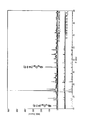
- the graph of the XRD analysis result about an example of the niobium oxide sputtering target according to the present invention is shown in FIG. According to this graph, it can be seen that a peak attributed to the peak derived from the (4 0 0) plane and (14 0 0) of the Nb 12 O 29 phase is detected.
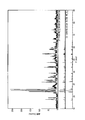
- a graph of the XRD analysis result is shown in FIG. 4, but no peak derived from the Nb 12 O 29 phase is detected.
- the resistance measurement device was used to measure the entire area from the processed surface (surface) to the thickness direction of the sintered body (corresponding to the erosion depth). The specific resistance was measured.
- a niobium oxide sputtering target having a diameter of 152.4 mm ⁇ thickness of 10 mm was produced by the above-described manufacturing method, and was cut from the surface (0 mm) to 2 mm, 4 mm, 5 mm, 6 mm, and 8 mm in the erosion depth direction. The specific resistance of was measured. The above results are shown in Table 3.
- Comparative Examples 1 to 3 since it was overrange, it was set to “out of measurement range”, and after that, measurement was not performed, so “ ⁇ ” was shown.
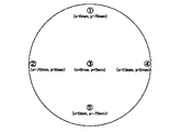
- specific resistances at five locations within the target sputtering surface as shown in FIG. 1 were measured. The maximum difference (difference between the highest value and the lowest value) at each measurement point was calculated for the in-plane direction of the sputtering surface. The above results are shown in Table 4.
- Comparative Examples 1 to 3 since it was overrange, it was set to “out of measurement range”, and after that, measurement was not performed, so “ ⁇ ” was shown.
- a specific resistance ( ⁇ ⁇ cm) was measured by a four-probe method using a low resistivity meter (Loresta-GP) manufactured by Mitsubishi Chemical Corporation.
- the measurement temperature was 23 ⁇ 5 ° C., and the humidity was 50 ⁇ 20%.
- niobium oxide sputtering targets of Examples 1 to 9 and Comparative Examples 1 to 3 a niobium oxide film was formed by sputtering, and the film formation rate was measured.
- the thickness of the formed niobium oxide film was measured, and the film formation rate (nm / sec) was calculated. The above results are shown in the “Sputtering characteristics” column of Table 5.
- niobium oxide sputtering target having a diameter of 152.4 mm and a thickness of 10 mm was produced by the above-described manufacturing method. did.
- DC sputtering is performed until the erosion depth from the surface portion (0 mm) of the niobium oxide sputtering target to the erosion portion (the portion scraped by sputtering in the thickness direction) becomes 2 mm, 4 mm, 5 mm, 6 mm, and 8 mm. went.
- the case where DC sputtering could be continued was indicated as “ ⁇ ”
- the case where no discharge occurred or abnormal discharge occurred frequently and DC sputtering could not be applied was indicated as “X”.
- “ ⁇ ” is added after the DC sputtering can no longer be performed. The result is shown in the column “Evaluation of DC Sputterability (Erosion Depth)” in Table 5.
- each of the niobium oxide sputtering targets of Examples 1 to 9 is made of niobium oxide in an oxygen deficient state (Nb 2 O 5 -x ), and further, conductive It is confirmed that the highly reliable Nb 12 O 29 phase is dispersed, and the specific resistance is in the range of 0.001 to 0.05 ⁇ ⁇ cm throughout the target thickness direction.
- the maximum difference in specific resistance in the direction can be 0.02 ⁇ ⁇ cm or less, and the specific resistance is in the range of 0.001 to 0.05 ⁇ ⁇ cm over the entire area of the target sputtering surface.
- the maximum difference in in-plane specific resistance on the target sputtering surface could be 0.02 ⁇ ⁇ cm or less. Therefore, in the niobium oxide sputtering targets of Examples 1 to 9, since the target specific resistance can be uniformly reduced over the entire region in the target thickness direction and within the sputtering surface, only stable DC sputtering is always possible. In addition, it was found that the film formation rate of sputtering can be improved by lowering the target specific resistance.
- the niobium oxide sputtering targets of Comparative Examples 1 and 2 were sintered as they were using raw niobium oxide powder (Nb 2 O 5 powder) as a raw material powder, and thus were not reduced.
- raw niobium oxide powder Nb 2 O 5 powder
- oxygen-deficient niobium oxide (Nb 2 O 5 -x ) with a small amount of oxygen deficiency generated during sintering is only generated partway in the thickness direction, and in particular, Nb 12 O 29 Since no phase was present, the target specific resistance could not be reduced uniformly throughout the target thickness direction and within the sputtering surface.
- the temperature which is the reduction condition for the reduction treatment, was 300 ° C.
- oxygen deficient niobium oxide (Nb 2 O 5 -x ) with a small amount of oxygen deficiency was generated, and in particular, the Nb 12 O 29 phase. Therefore, the specific resistance of the target could not be reduced uniformly throughout the target thickness direction and within the sputtering surface. None of the niobium oxide sputtering targets of Comparative Examples 1 to 3 could perform DC sputtering in the middle, and even if DC sputtering could be performed, the film formation rate was not improved.
- a niobium oxide sputtering target in which the average crystal grain size of the niobium oxide crystal grains in the niobium oxide sintered body was 100 ⁇ m or less was manufactured.
- the reduced powder of Example 1 in the first example was used as an example.
- this reduced powder is a niobium oxide powder (Nb 2 O 5 -x powder) that has been subjected to a reduction treatment on the niobium oxide powder (Nb 2 O 5 powder) to be in an oxygen deficient state.
- the oxygen deficiency in the reduced powder was measured by the same procedure as in the first example.
- the reduced powder and zirconia balls were placed in a plastic container (polyethylene pot) and mixed at a rotational speed of 80 to 120 rpm for 1 to 3 hours in a dry ball mill. Thereafter, the obtained Nb 2 O 5-x powder was classified through a sieve having an opening of 32 to 600 ⁇ m so that the average particle diameter was 2 to 100 ⁇ m.
- the “reduced powder average particle diameter ( ⁇ m)” column shows the average particle diameters of the reduced powders of Examples 10 to 14.
- the reduced powder (Nb 2 O 5-x powder) thus obtained was used as a raw material powder, and this raw material powder was filled in a mold in the same manner as in the first example, and the firing powder shown in Table 7 was used.
- niobium oxide (Nb 2 O 5-x ) by hot pressing (HP) at a holding temperature of 900 to 1200 ° C. for 2 to 3 hours and a pressure of 15 to 50 MPa according to the sintering method and sintering conditions
- the sintered bodies of Examples 10 to 14 were produced.
- the sintered body was machined to produce niobium oxide sputtering targets of Examples 10 to 14 having a diameter of 152.4 mm.
- the amount of oxygen vacancies was measured in the same procedure as in the first example.
- the oxygen deficiency x was determined by the above formula.
- the results are shown in the “sintered body oxygen deficient Nb 2 O 5-x ” column of Table 7.
- the presence or absence of the Nb 12 O 29 phase was evaluated by XRD, and the result is shown in the column “Presence / absence of sintered body Nb 12 O 29 phase” in Table 7.
- the niobium oxide crystal grain size was measured for the niobium oxide sputtering targets of Examples 10 to 14.
- each niobium oxide sputtering target was sampled at five locations, and using EBSD (Electron Back Scatter Diffraction ⁇ Patterns), the analysis data (OIM data collection manufactured by TSL) was used at each location.
- the crystal grain size of was measured. The obtained values were averaged to obtain an average crystal grain size. The result is shown in the column “Sintered body average crystal grain size ( ⁇ m)” in Table 7.
- the thickness direction of the sintered body (corresponding to the erosion depth) from the processed surface (surface).
- the specific resistance of the entire region was measured with a resistance measuring device.
- the niobium oxide sputtering target produced by the above-described production method was shaved from the surface (0 mm) to 2 mm, 4 mm, 5 mm, 6 mm, and 8 mm in the erosion depth direction, and the specific resistance there was measured.
- the above results are shown in Table 8.
- the specific resistances at five locations in the target sputtering surface as shown in FIG. 1 were measured.
- the maximum difference (difference between the highest value and the lowest value) at each measurement point was calculated for the in-plane direction of the sputtering surface.
- Table 9 The above results are shown in Table 9.
- niobium oxide sputtering target of Examples 10 to 14 Using the obtained niobium oxide sputtering target of Examples 10 to 14, a niobium oxide film was formed by sputtering, and the film formation rate was measured. In the same manner as in the first example, the thickness of the formed niobium oxide film was measured, and the film formation rate (nm / sec) was calculated. The result is shown in the “Sputtering characteristic deposition rate (nm / sec)” column of Table 10.
- the obtained niobium oxide sputtering targets of Examples 10 to 14 were evaluated for the possibility of DC sputtering.
- the erosion depth from the target surface portion (0 mm) to the erosion portion is 2 mm.
- DC sputtering was performed until 4 mm, 5 mm, 6 mm, and 8 mm.
- ⁇ a case where DC sputtering can be continued at each erosion depth.
- the results are shown in the “DC sputtering availability evaluation (erosion depth)” column of Table 10.
- the niobium oxide in the oxygen deficient state (Nb 2 O 5 ⁇ x ) and a highly conductive Nb 12 O 29 phase is confirmed to be dispersed, and the specific resistance is 0.001 to 0 throughout the target thickness direction. .05 ⁇ ⁇ cm, the maximum difference in specific resistance in the thickness direction can be 0.02 ⁇ ⁇ cm or less, and the specific resistance is 0.001 to all over the target sputtering surface.
- the maximum difference in the in-plane specific resistance at the target sputtering surface can be 0.02 ⁇ ⁇ cm or less, and particularly the average of niobium oxide crystal grains.
- Akiratsubu diameter confirmed that it is 100 ⁇ m or less, the abnormal number of discharges during sputtering was also found to be suppressed. Therefore, in the niobium oxide sputtering targets of Examples 10 to 14, the target specific resistance can be uniformly reduced over the entire area in the target thickness direction and within the sputtering surface, and the number of abnormal discharges can be reduced. It has been found that not only stable DC sputtering is possible, but also the sputtering deposition rate can be improved by lowering the target specific resistance.
- the shape of the sintered body was not particularly limited. However, if the sintered body is made of oxygen-deficient niobium oxide (Nb 2 O 5-x ) according to the present invention, Since a low specific resistance can be realized in the entire region in the thickness direction, the shape may be a flat plate or a cylinder. More specifically, the sintered body may have a disk shape, a rectangular plate shape, a polygonal plate shape, a plate shape such as an elliptical plate shape, or a cylindrical shape.
- the thickness direction of a sintered body or the thickness direction of a sputtering target means a depth direction from a surface on which an ionized element collides during sputtering.
- the sputtering film formation rate can be improved, and the productivity of the niobium oxide film can be improved.
Landscapes
- Chemical & Material Sciences (AREA)
- Engineering & Computer Science (AREA)
- Ceramic Engineering (AREA)
- Manufacturing & Machinery (AREA)
- Materials Engineering (AREA)
- Organic Chemistry (AREA)
- Structural Engineering (AREA)
- Inorganic Chemistry (AREA)
- Chemical Kinetics & Catalysis (AREA)
- Mechanical Engineering (AREA)
- Metallurgy (AREA)
- Physics & Mathematics (AREA)
- Thermal Sciences (AREA)
- Physical Vapour Deposition (AREA)
- Compositions Of Oxide Ceramics (AREA)
- Powder Metallurgy (AREA)
Priority Applications (2)
| Application Number | Priority Date | Filing Date | Title |
|---|---|---|---|
| KR1020157022703A KR20150120996A (ko) | 2013-02-26 | 2014-02-20 | 산화 니오브 스퍼터링 타깃, 그 제조 방법 및 산화 니오브막 |
| CN201480010227.2A CN105074046A (zh) | 2013-02-26 | 2014-02-20 | 氧化铌溅射靶、其制造方法及氧化铌膜 |
Applications Claiming Priority (4)
| Application Number | Priority Date | Filing Date | Title |
|---|---|---|---|
| JP2013035575 | 2013-02-26 | ||
| JP2013-035575 | 2013-02-26 | ||
| JP2014-023246 | 2014-02-10 | ||
| JP2014023246A JP6403087B2 (ja) | 2013-02-26 | 2014-02-10 | 酸化ニオブスパッタリングターゲット及びその製造方法 |
Publications (1)
| Publication Number | Publication Date |
|---|---|
| WO2014132872A1 true WO2014132872A1 (ja) | 2014-09-04 |
Family
ID=51428143
Family Applications (1)
| Application Number | Title | Priority Date | Filing Date |
|---|---|---|---|
| PCT/JP2014/054004 Ceased WO2014132872A1 (ja) | 2013-02-26 | 2014-02-20 | 酸化ニオブスパッタリングターゲット、その製造方法及び酸化ニオブ膜 |
Country Status (5)
| Country | Link |
|---|---|
| JP (1) | JP6403087B2 (enExample) |
| KR (1) | KR20150120996A (enExample) |
| CN (1) | CN105074046A (enExample) |
| TW (1) | TWI603938B (enExample) |
| WO (1) | WO2014132872A1 (enExample) |
Cited By (3)
| Publication number | Priority date | Publication date | Assignee | Title |
|---|---|---|---|---|
| WO2016056352A1 (ja) * | 2014-10-06 | 2016-04-14 | Jx金属株式会社 | ニオブ酸化物焼結体及び該焼結体からなるスパッタリングターゲット並びにニオブ酸化物焼結体の製造方法 |
| JP2016188164A (ja) * | 2015-03-30 | 2016-11-04 | 東ソー株式会社 | 酸化物焼結体及びその製造方法 |
| CN110467462A (zh) * | 2019-08-09 | 2019-11-19 | 宁夏中色新材料有限公司 | 一种高致密低电阻氧化铌旋转靶材及其制备方法 |
Families Citing this family (3)
| Publication number | Priority date | Publication date | Assignee | Title |
|---|---|---|---|---|
| CN105506737B (zh) * | 2015-12-28 | 2018-02-09 | 常州瞻驰光电科技有限公司 | 一种非化学计量比氧化铌多晶镀膜材料及其生长技术 |
| CN110963529B (zh) * | 2018-09-30 | 2021-12-07 | 中国科学院上海硅酸盐研究所 | 一种纯相的铌的低价态氧化物纳米粉体及其制备方法和应用 |
| WO2020195121A1 (ja) | 2019-03-26 | 2020-10-01 | Jx金属株式会社 | ニオブスパッタリングターゲット |
Citations (2)
| Publication number | Priority date | Publication date | Assignee | Title |
|---|---|---|---|---|
| JP2002338354A (ja) * | 2001-05-18 | 2002-11-27 | Kyocera Corp | 酸化ニオブ焼結体とその製造方法及びこれを用いたスパッタリングターゲット |
| JP2004059965A (ja) * | 2002-07-25 | 2004-02-26 | Toshiba Corp | スパッタリングターゲットおよびその製造方法 |
Family Cites Families (16)
| Publication number | Priority date | Publication date | Assignee | Title |
|---|---|---|---|---|
| JP2915177B2 (ja) * | 1990-11-30 | 1999-07-05 | 株式会社日立製作所 | スパッタリングターゲットの製造方法及びこの方法によって製造されたスパッタリングターゲット |
| JP2000113913A (ja) * | 1998-10-02 | 2000-04-21 | Sumitomo Osaka Cement Co Ltd | 色素増感型太陽電池 |
| JP2003098340A (ja) * | 2001-09-21 | 2003-04-03 | Asahi Glass Co Ltd | 光学多層干渉膜とその製造方法および光学多層干渉膜を用いたフィルター |
| JP2003123853A (ja) * | 2001-10-11 | 2003-04-25 | Bridgestone Corp | 有機色素増感型金属酸化物半導体電極及びその製造方法、並びにこの半導体電極を有する太陽電池 |
| JP4670097B2 (ja) * | 2005-04-27 | 2011-04-13 | Agcセラミックス株式会社 | ターゲットおよび該ターゲットによる高屈折率膜の製造方法 |
| CN101851740A (zh) * | 2009-04-02 | 2010-10-06 | 宜兴佰伦光电材料科技有限公司 | 用于磁控溅射镀膜的导电Nb2O5-x靶材及生产方法 |
| CN101864555A (zh) * | 2009-04-14 | 2010-10-20 | 上海高展金属材料有限公司 | 一种导电的氧化铌靶材、制备方法及其应用 |
| TWI385814B (zh) * | 2009-05-25 | 2013-02-11 | Ind Tech Res Inst | 光電致變色元件及其製作方法 |
| KR101137913B1 (ko) * | 2009-11-12 | 2012-05-03 | 삼성코닝정밀소재 주식회사 | 다상 Nb0x 스퍼터링 타겟 및 그 제조방법 |
| JP5249963B2 (ja) * | 2010-02-01 | 2013-07-31 | 三井金属鉱業株式会社 | セラミックス−金属複合材料からなるスパッタリングターゲット材およびスパッタリングターゲット |
| KR101967945B1 (ko) * | 2010-04-26 | 2019-04-10 | 제이엑스금속주식회사 | Sb-Te기 합금 소결체 스퍼터링 타깃 |
| JP2012126619A (ja) * | 2010-12-16 | 2012-07-05 | Sumitomo Chemical Co Ltd | 酸化亜鉛焼結体およびその製造方法 |
| JP5630416B2 (ja) * | 2011-03-23 | 2014-11-26 | 住友金属鉱山株式会社 | Cu−Ga合金スパッタリングターゲットの製造方法及びCu−Ga合金粉末の製造方法 |
| JP5501306B2 (ja) * | 2011-08-18 | 2014-05-21 | 出光興産株式会社 | In−Ga−Zn−O系スパッタリングターゲット |
| JP2012017258A (ja) * | 2011-10-05 | 2012-01-26 | Idemitsu Kosan Co Ltd | In−Ga−Zn系酸化物スパッタリングターゲット |
| CN102659405B (zh) * | 2012-04-06 | 2014-02-26 | 西北稀有金属材料研究院 | 高密度氧化铌溅射靶材的制备方法 |
-
2014
- 2014-02-10 JP JP2014023246A patent/JP6403087B2/ja not_active Expired - Fee Related
- 2014-02-20 CN CN201480010227.2A patent/CN105074046A/zh active Pending
- 2014-02-20 KR KR1020157022703A patent/KR20150120996A/ko not_active Withdrawn
- 2014-02-20 WO PCT/JP2014/054004 patent/WO2014132872A1/ja not_active Ceased
- 2014-02-21 TW TW103105848A patent/TWI603938B/zh not_active IP Right Cessation
Patent Citations (2)
| Publication number | Priority date | Publication date | Assignee | Title |
|---|---|---|---|---|
| JP2002338354A (ja) * | 2001-05-18 | 2002-11-27 | Kyocera Corp | 酸化ニオブ焼結体とその製造方法及びこれを用いたスパッタリングターゲット |
| JP2004059965A (ja) * | 2002-07-25 | 2004-02-26 | Toshiba Corp | スパッタリングターゲットおよびその製造方法 |
Cited By (5)
| Publication number | Priority date | Publication date | Assignee | Title |
|---|---|---|---|---|
| WO2016056352A1 (ja) * | 2014-10-06 | 2016-04-14 | Jx金属株式会社 | ニオブ酸化物焼結体及び該焼結体からなるスパッタリングターゲット並びにニオブ酸化物焼結体の製造方法 |
| JPWO2016056352A1 (ja) * | 2014-10-06 | 2017-04-27 | Jx金属株式会社 | ニオブ酸化物焼結体及び該焼結体からなるスパッタリングターゲット並びにニオブ酸化物焼結体の製造方法 |
| US10593524B2 (en) | 2014-10-06 | 2020-03-17 | Jx Nippon Mining & Metals Corporation | Niobium oxide sintered compact, sputtering target formed from said sintered compact, and method of producing niobium oxide sintered compact |
| JP2016188164A (ja) * | 2015-03-30 | 2016-11-04 | 東ソー株式会社 | 酸化物焼結体及びその製造方法 |
| CN110467462A (zh) * | 2019-08-09 | 2019-11-19 | 宁夏中色新材料有限公司 | 一种高致密低电阻氧化铌旋转靶材及其制备方法 |
Also Published As
| Publication number | Publication date |
|---|---|
| JP2014194072A (ja) | 2014-10-09 |
| JP6403087B2 (ja) | 2018-10-10 |
| TW201439032A (zh) | 2014-10-16 |
| KR20150120996A (ko) | 2015-10-28 |
| TWI603938B (zh) | 2017-11-01 |
| CN105074046A (zh) | 2015-11-18 |
Similar Documents
| Publication | Publication Date | Title |
|---|---|---|
| JP4850378B2 (ja) | スパッタリングターゲット、透明導電性酸化物、およびスパッタリングターゲットの製造方法 | |
| JP6403087B2 (ja) | 酸化ニオブスパッタリングターゲット及びその製造方法 | |
| JP4552950B2 (ja) | ターゲット用酸化物焼結体、その製造方法、それを用いた透明導電膜の製造方法、及び得られる透明導電膜 | |
| JP5330469B2 (ja) | スパッタリングターゲット、透明導電膜及び透明電極 | |
| Zhang et al. | Application of ZrB2 thin film as a low emissivity film at high temperature | |
| JP4960244B2 (ja) | 酸化物材料、及びスパッタリングターゲット | |
| US20120205242A1 (en) | Cu-In-Ga-Se QUATERNARY ALLOY SPUTTERING TARGET | |
| JP2012515260A (ja) | ZnAlターゲットの作製方法およびそれにより作製されたZnAlターゲット | |
| CN105637114B (zh) | 溅射靶及溅射靶的制造方法 | |
| Liu et al. | Effect of nitrogen partial pressure on the TCR of magnetron sputtered indium tin oxide thin films at high temperatures | |
| JP6023920B1 (ja) | 酸化物焼結体、酸化物スパッタリングターゲット及び酸化物薄膜 | |
| KR20130023399A (ko) | Cu-In-Ga-Se 4 원계 합금 스퍼터링 타겟 | |
| JP7715152B2 (ja) | Cr-Si-C系焼結体 | |
| JP7580391B2 (ja) | 酸化モリブデン含有層を製造するためのスパッタリングターゲット | |
| Liao et al. | Characterization of sputtered iridium dioxide thin films | |
| JP2011074479A (ja) | 透明導電性酸化亜鉛系薄膜製造用のイオンプレーティング用ターゲット、および透明導電性酸化亜鉛系薄膜 | |
| WO2014168073A1 (ja) | 酸化物スパッタリングターゲット、その製造方法及び光記録媒体用保護膜 | |
| JP2016017196A (ja) | Ti酸化物スパッタリングターゲット及びその製造方法 | |
| JP5000230B2 (ja) | 酸化ランタン含有酸化物ターゲット | |
| JP5870768B2 (ja) | スパッタリングターゲットおよびその製造方法 | |
| JP2015074789A (ja) | 酸化ニオブ系スパッタリングターゲット及びその製造方法 | |
| JP2003342068A (ja) | 酸化物焼結体 | |
| WO2019187269A1 (ja) | 酸化物焼結体、スパッタリングターゲットおよび透明導電膜 | |
| JP2025097483A (ja) | クロムシリサイド膜及びその製造方法 | |
| Kuo et al. | Effects of growth parameters on surface-morphological, structural and electrical properties of Mo films by RF magnetron sputtering |
Legal Events
| Date | Code | Title | Description |
|---|---|---|---|
| WWE | Wipo information: entry into national phase |
Ref document number: 201480010227.2 Country of ref document: CN |
|
| 121 | Ep: the epo has been informed by wipo that ep was designated in this application |
Ref document number: 14757054 Country of ref document: EP Kind code of ref document: A1 |
|
| ENP | Entry into the national phase |
Ref document number: 20157022703 Country of ref document: KR Kind code of ref document: A |
|
| NENP | Non-entry into the national phase |
Ref country code: DE |
|
| 122 | Ep: pct application non-entry in european phase |
Ref document number: 14757054 Country of ref document: EP Kind code of ref document: A1 |