WO2014129126A1 - スイッチング電源装置 - Google Patents
スイッチング電源装置 Download PDFInfo
- Publication number
- WO2014129126A1 WO2014129126A1 PCT/JP2014/000557 JP2014000557W WO2014129126A1 WO 2014129126 A1 WO2014129126 A1 WO 2014129126A1 JP 2014000557 W JP2014000557 W JP 2014000557W WO 2014129126 A1 WO2014129126 A1 WO 2014129126A1
- Authority
- WO
- WIPO (PCT)
- Prior art keywords
- power supply
- circuit
- terminal
- switching
- voltage
- Prior art date
Links
Images


Classifications
-
- H—ELECTRICITY
- H02—GENERATION; CONVERSION OR DISTRIBUTION OF ELECTRIC POWER
- H02M—APPARATUS FOR CONVERSION BETWEEN AC AND AC, BETWEEN AC AND DC, OR BETWEEN DC AND DC, AND FOR USE WITH MAINS OR SIMILAR POWER SUPPLY SYSTEMS; CONVERSION OF DC OR AC INPUT POWER INTO SURGE OUTPUT POWER; CONTROL OR REGULATION THEREOF
- H02M3/00—Conversion of dc power input into dc power output
- H02M3/22—Conversion of dc power input into dc power output with intermediate conversion into ac
- H02M3/24—Conversion of dc power input into dc power output with intermediate conversion into ac by static converters
- H02M3/28—Conversion of dc power input into dc power output with intermediate conversion into ac by static converters using discharge tubes with control electrode or semiconductor devices with control electrode to produce the intermediate ac
- H02M3/325—Conversion of dc power input into dc power output with intermediate conversion into ac by static converters using discharge tubes with control electrode or semiconductor devices with control electrode to produce the intermediate ac using devices of a triode or a transistor type requiring continuous application of a control signal
- H02M3/335—Conversion of dc power input into dc power output with intermediate conversion into ac by static converters using discharge tubes with control electrode or semiconductor devices with control electrode to produce the intermediate ac using devices of a triode or a transistor type requiring continuous application of a control signal using semiconductor devices only
- H02M3/33507—Conversion of dc power input into dc power output with intermediate conversion into ac by static converters using discharge tubes with control electrode or semiconductor devices with control electrode to produce the intermediate ac using devices of a triode or a transistor type requiring continuous application of a control signal using semiconductor devices only with automatic control of the output voltage or current, e.g. flyback converters
- H02M3/33523—Conversion of dc power input into dc power output with intermediate conversion into ac by static converters using discharge tubes with control electrode or semiconductor devices with control electrode to produce the intermediate ac using devices of a triode or a transistor type requiring continuous application of a control signal using semiconductor devices only with automatic control of the output voltage or current, e.g. flyback converters with galvanic isolation between input and output of both the power stage and the feedback loop
-
- H—ELECTRICITY
- H02—GENERATION; CONVERSION OR DISTRIBUTION OF ELECTRIC POWER
- H02M—APPARATUS FOR CONVERSION BETWEEN AC AND AC, BETWEEN AC AND DC, OR BETWEEN DC AND DC, AND FOR USE WITH MAINS OR SIMILAR POWER SUPPLY SYSTEMS; CONVERSION OF DC OR AC INPUT POWER INTO SURGE OUTPUT POWER; CONTROL OR REGULATION THEREOF
- H02M1/00—Details of apparatus for conversion
- H02M1/0003—Details of control, feedback or regulation circuits
- H02M1/0032—Control circuits allowing low power mode operation, e.g. in standby mode
-
- Y—GENERAL TAGGING OF NEW TECHNOLOGICAL DEVELOPMENTS; GENERAL TAGGING OF CROSS-SECTIONAL TECHNOLOGIES SPANNING OVER SEVERAL SECTIONS OF THE IPC; TECHNICAL SUBJECTS COVERED BY FORMER USPC CROSS-REFERENCE ART COLLECTIONS [XRACs] AND DIGESTS
- Y02—TECHNOLOGIES OR APPLICATIONS FOR MITIGATION OR ADAPTATION AGAINST CLIMATE CHANGE
- Y02B—CLIMATE CHANGE MITIGATION TECHNOLOGIES RELATED TO BUILDINGS, e.g. HOUSING, HOUSE APPLIANCES OR RELATED END-USER APPLICATIONS
- Y02B70/00—Technologies for an efficient end-user side electric power management and consumption
- Y02B70/10—Technologies improving the efficiency by using switched-mode power supplies [SMPS], i.e. efficient power electronics conversion e.g. power factor correction or reduction of losses in power supplies or efficient standby modes
Definitions
- the present invention relates to a switching power supply apparatus and an apparatus connection state detection circuit for controlling an output voltage by switching an input voltage through a switching element.
- Patent Document 1 Japanese Patent Application Laid-Open Publication No. 2007-14397 (Patent Document 1), which is a conventional technique, detects the presence or absence of a load on the AC adapter and stops the operation of the switching power supply device when the output side is in a no-load state, thereby reducing power consumption.
- Patent Document 1 Japanese Patent Application Laid-Open Publication No. 2007-14397
- a power storage component such as a primary battery or a secondary battery as the power source of the load device.
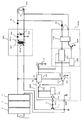
- FIG. 22 shows a configuration example of a conventional switching power supply device in which the operation of the switching power supply device is stopped when the output side is in a no-load state, and the operation is resumed when a voltage is applied from the load device to the output side. .
- the operation of this switching power supply device will be briefly described below.
- a no-load detection signal is output from the output control circuit 911 via the coupler circuit 906. Is input to the power on / off circuit 905.
- the drive control circuit 901 controls the drive circuit 902 so as to stop the operation of the switching element 7. Then, the output voltage of the switching power supply device becomes zero.
- a switching power supply eg, AC adapter
- a load device eg, a notebook computer
- the switching operation of the switching power supply is stopped to reduce power consumption.
- the switching power supply device is connected to the load device and a voltage is applied from a power storage component (for example, a battery) of the load device, the switching power supply device can realize a system for starting power supply.
- the present invention solves the above-described problems, and provides a switching power supply device that can be activated regardless of the state of a power storage component such as a primary battery or a secondary battery, and a device connection state detection circuit that constitutes the switching power supply device.
- Switching power supply comprising: an input / output conversion circuit for supplying power to the power supply; and a switching control circuit having an off mode for controlling the switching operation of the second switching element and stopping the switching operation in response to a signal input to the OFF terminal
- a first rectifier circuit connected between the input / output conversion circuit and the output terminal, a transformer having one end of the secondary winding connected to the output terminal, and a first rectifier connected to the primary winding of the transformer.
- One switching element a pulse generator for supplying a pulse signal to the gate terminal of the first switching element, and a transistor in response to the pulse signal.
- a device connection state detection circuit comprising a waveform detection circuit that detects a voltage or current generated in the winding of the coil, compares it with a preset reference value, and outputs an output signal according to the comparison result to the OFF terminal. It is characterized by.
- the device connection state detection circuit detects the connection state between the power supply system and the load device even when there is no power of the primary battery or the secondary battery mounted on the secondary side of the switching power supply device or the load device. be able to.
- FIG. 7 is a circuit diagram illustrating a configuration example of a pulse generator according to the first embodiment of the present disclosure.
- FIG. 7 is a circuit diagram illustrating a configuration example of a switching power supply device and a device connection state detection circuit according to another example of the fourth embodiment of the present disclosure.
- a circuit diagram showing a configuration example of a waveform detection circuit according to a second embodiment of the present disclosure A circuit diagram showing an example of composition of a transformer concerning Embodiment 2 of this indication.
- Timing chart showing operation of the switching power supply according to the second embodiment of the present disclosure Timing chart showing operation of the switching power supply according to the third embodiment of the present disclosure
- Timing chart showing operation of the switching power supply according to the fourth embodiment of the present disclosure Timing chart showing operation of a switching power supply according to another example of Embodiment 4 of the present disclosure
- Timing chart showing operation of the switching power supply according to the first modification of the second embodiment of the present disclosure The circuit diagram which shows the example of 1 structure of the switching power supply device and apparatus connection state detection circuit which concern on Embodiment 5 of this indication Timing chart showing operation during normal operation of the switching power supply according to the fifth embodiment of the present disclosure Timing chart showing operation at the time of protection operation of the switching power supply according to the fifth embodiment of the present disclosure
- the circuit diagram which shows the structural example of the switching power supply apparatus and apparatus connection state detection circuit which concern on Embodiment 6 of this indication Timing chart showing operation of the switching power supply according to the sixth embodiment of the present disclosure The circuit diagram which shows the example of 1 structure of the switching power supply device and apparatus connection state detection circuit which concern on Embodiment 7 of this indication Timing chart showing operation of the pulse generator according to the seventh embodiment of the present disclosure
- the circuit diagram which shows the example of 1 structure of the switching power supply device and apparatus connection state detection circuit which concern on Embodiment 8 of this indication The circuit diagram showing the example of 1 composition of the off mode
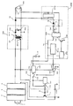
- FIG. 1 is a circuit diagram showing a configuration example of the switching power supply device and the device connection state detection circuit according to the first embodiment.
- an input AC voltage from a commercial power source 1 is input to an input / output conversion circuit 300 as an input DC voltage through an input filter circuit 2, an input rectifier circuit 3, and an input smoothing circuit 4.
- the input / output conversion circuit 300 is arranged to convert an input voltage that has been input into a desired output voltage.
- the transformer 301 includes a power conversion transformer 301, a diode 302, and a smoothing capacitor 303.
- the transformer 301 includes a primary winding 301a and a secondary winding 301b, and the primary winding 301a and the secondary winding 301b.
- the polarity is in the opposite direction.
- This switching power supply device is a flyback type.
- the switching element 7 is connected to the primary winding 301a, and ON / OFF switching control is performed by inputting the OUT terminal output signal of the switching control circuit 100 to the control electrode (gate) of the switching element 7.
- the switching control circuit 100 has five terminals, ie, a Vin terminal, a VDD terminal, a GND terminal, an OUT terminal, and an OFF terminal as external input / output terminals.
- the switching control circuit includes a pulse width control circuit 101, a drive circuit 102, an off mode detector 103, a reference voltage source 104, an off mode switch 105, a regulator 106, and the like.
- the Vin terminal is a power supply terminal of the switching control circuit 100, and power is supplied from a line from which an input DC voltage of the input smoothing circuit is output.
- the power input from the Vin terminal is input to the regulator 106, and power is supplied to the circuits in the switching control circuit 100 via the regulator 106.
- the GND terminal is connected to the low potential side of the input smoothing circuit and serves as a voltage reference for the primary side.
- the OUT terminal is a terminal connected to the gate of the switching element 7 via the resistor 6.
- the VDD terminal is a reference voltage terminal for the switching control circuit 100.
- a capacitor 17 is connected to the VDD terminal. During operation, a charging current flows from the VDD terminal to the capacitor 17 and the voltage of the capacitor 17 rises. The voltage is controlled by the switching control circuit 100 so that this voltage becomes constant at the reference voltage.
- the OFF terminal is a terminal for inputting an off mode signal output from the device connection state detection circuit 200A and switching between the off mode and the normal operation.
- the output terminal 16 includes two terminals, that is, a terminal that outputs an output voltage output from the input / output conversion circuit 300 and a secondary side GND terminal.
- the load device 400 is an electronic device such as a notebook computer or a tablet computer, and can be attached to and detached from the output terminal 16.
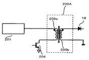
- the device connection state detection circuit 200A is arranged to detect whether the output terminal 16 and the load device 400 are connected or not, and includes a VDD terminal, an OFF terminal, a GND terminal of the switching control circuit 100, The output terminal 16 is connected to the anode of the diode 18.
- FIG. 1 it comprises a load device connection terminal 5, a waveform detection circuit 201, a transformer 202, a pulse generator 203, and a switching element 204.
- the waveform detection circuit 201 includes, for example, a resistor 206, a resistor 207, and a capacitor 208 like the waveform detection circuit 201A in FIG. 2A.
- the transformer 202 has, for example, a primary winding 209a and a secondary winding 209b like the transformer 202A in FIG. 2B, and the polarities of the primary winding 209a and the secondary winding 209b are in the forward direction.
- the pulse generator 203 includes resistors 233, 234, 235, 238, 239, 240, a capacitor 236, an operational amplifier 237, and a voltage comparator 241 as in the pulse generator 203A of FIG. 2C, for example. Since this circuit is a generally known pulse generation circuit, a detailed description of its operation is omitted.
- the switching element 204 is turned on / off by the output pulse of the pulse generator 203 being input to the control electrode (gate) of the switching element 204.
- a transistor such as a MOSFET is used as the switching element 204.
- the diode 15 is arranged to prevent a signal for detecting the connection state between the output terminal 16 and the load device 400 from flowing into the input / output conversion circuit 300, and the anode of the diode 15 is connected to the secondary output of the input / output conversion circuit 300.
- the cathode of the diode 15 is connected to the output terminal 16.
- the diode 18 is arranged to prevent the output current from the input / output conversion circuit 300 from flowing into the transformer 202, the anode of the diode 18 is connected to the load device connection terminal 5, and the cathode of the diode 18 is connected to the cathode of the diode 15 and the output. Connected between terminals 16.
- Power is supplied from the VDD terminal of the switching control circuit 100 to the device connection state detection circuit 200A.
- the capacitor 208 of the waveform detection circuit 201 is charged with electric charge from the VDD terminal via the resistor 206.
- the pulse generator 203 outputs a monitoring pulse to the gate of the switching element 204.
- the switching element 204 becomes conductive.
- a primary side current Ip which is a combination of the excitation current Ie and the secondary side current Is that flows through the secondary winding 209b transmitted through the transformer 202, flows through the primary winding 209a.
- This secondary side current Is changes with the impedance of the load device 400.
- the number of turns of the primary winding 209a is Np
- the number of turns of the secondary winding 209b is Ns
- the inductance value of the primary winding 209a is Lp
- the voltage input to the primary winding 209a is Vp
- the secondary winding 209b Assuming that the output voltage is Vs, the forward voltage of the diode 18 is Vfd, the output voltage of the output terminal 16 is Vo, the impedance of the load device 400 is Z, and the time that the gate of the switching element 204 is conductive is Ton
- Ton the time that the gate of the switching element 204 is conductive
- Is> 0 in order to transmit the secondary current Is to the primary current Ip, so that Vs ⁇ Vfd ⁇ Vo> 0. It is necessary to set Ns, Np, and Vp.
- the waveform detection circuit 201 Since the change in the secondary side current Is is reflected in the primary side current Ip as shown in (Equation 1), the waveform detection circuit 201 includes the output terminal 16 and the load device 400 according to the change in the primary side current Ip. It detects whether it is in a connected state.
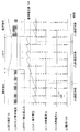
- FIG. 3 is a timing chart showing the operation of the switching power supply device in FIG.
- the value of the impedance Z is preferably about several mohms to several hundreds ohms.
- the secondary current Is flows through the secondary winding 209b. It is transmitted to the primary winding 209a and synthesized with the primary current Ip. The electric charge accumulated in the capacitor 208 is discharged by the primary side current Ip (FIG. 3 (e)).
- the capacitor 208 is charged via the resistor 206 from the VDD terminal. At this time, it is preferable that the resistance values of the resistors 206 and 207 are set so that the capacitor 208 is charged with about several hundred nA.
- the waveform detection circuit 201 sets the OFF terminal voltage to a value lower than the reference voltage source 104 of the off mode detector 103.
- the off-mode detector 103 outputs an L-level signal (FIG. 3C), and the switching control circuit 100 controls the off-mode switch 105 to the conductive state, so that the switching element 7 maintains the switching operation.
- FIG. 3B the switching power supply device continues normal operation.
- the OFF terminal voltage is applied until the charging from the VDD terminal and the discharging by the primary side current Ip are balanced. rises.
- the pulse width is preferably several ⁇ s to several tens ⁇ s.
- the pulse generator 203 is preferably controlled so as to output the monitoring pulse at a cycle of about 0.2 Hz to 60 Hz.
- the switching control circuit 100 controls the off mode switch 105 to be cut off and the switching operation of the switching element 7 to be stopped. Then, the output voltage Vo (FIG. 3A) decreases to 0V, and the power consumption of the switching power supply device is reduced.
- the off mode power is supplied to the regulator 106 from the Vin terminal, and power is supplied to the off mode detector 103 via the regulator 106.
- the off-mode detector 103 continues to control to turn off the off-mode switch 105 even in the off-mode.
- the secondary side current Is flows to the closed circuit, and the secondary side current Is is combined with the primary side current Ip. Then, since the electric charge discharged from the capacitor 208 by the primary side current Ip becomes larger than the electric charge charged in the capacitor 208, the OFF terminal voltage decreases. When the OFF terminal voltage decreases and becomes lower than the reference voltage source 104 of the off-mode detector 103, the switching control circuit 100 controls the off-mode switch 105 to the conductive state, so that the switching element 7 starts the switching operation and operates normally. Continue.
- the electric charge may not be accumulated in the power storage component such as the primary battery or the secondary battery mounted on the load device 400.
- the power storage component such as the primary battery or the secondary battery mounted on the load device 400.
- An example is when the laptop battery is empty.
- the switching power supply device has the output terminal 16 and the load device 400 connected to each other even when the secondary battery of the switching power supply device or the power of the secondary battery mounted on the load device 400 is not present.
- the connection state can be detected, and the off-mode control of the switching power supply device can be performed.
- the pulse generator 203 may be included in the switching control circuit 100. Further, by arranging and adjusting the capacitor 236 outside, it is possible to easily generate a monitoring pulse with a long period.
- the switching power supply according to the second embodiment has a configuration of the transformer 205, a configuration of the waveform detection circuit 201, and a connection between the waveform detection circuit 201 and the transformer 205 in the device connection state detection circuit 200B. Different.
- FIG. 4A shows an example of the switching power supply according to the second embodiment.
- the waveform detection circuit 201 includes, for example, a voltage comparator 211, a constant current source 213, a waveform detection circuit 201B in FIG.
- the capacitor 214, PchMOSFET 215, NchMOSFET 216, voltage comparator 217, and reference voltage sources 212 and 218 are included.
- the transformer 205 is composed of a primary winding 210a and a secondary winding 210b, for example, like the transformer 205A in FIG. 5B, and the polarities of the primary winding 210a and the secondary winding 210b are opposite to each other.
- the device connection state detection circuit 200B detects the connection state between the output terminal 16 and the load device 400. Therefore, hereinafter, when the output terminal 16 is connected to the load device 400, the output A case where the terminal 16 and the load device 400 shift to the disconnected state and a case where the output terminal 16 and the load device 400 shift to the connected state will be described.
- FIG. 6A is a timing chart showing the operation of the switching power supply device in FIG. 4A.
- the secondary current Is2 flows in the secondary winding 210b (FIG. 6A (g)), the voltage Vs2 is generated, and the reflected voltage Vor is generated in the primary winding 210a.
- the number of turns of the primary winding 210a is Np2
- the number of turns of the secondary winding 210b is Ns2
- the voltage input to the primary winding 210a is Vp2
- the inductance value of the primary winding 210a is Lp2
- the inductance value of the secondary winding 210b is Assuming that Ls2, the time during which the switching element 204 is in the non-conductive state is Toff2, and the output voltage increase caused by the excitation energy Ep2 by the device connection state detection circuit 200B and the diode 18 is ⁇ Vo, the following relational expression is established.
- Ip2 (Vp2 / Lp2) ⁇ Ton2 (Formula 5)
- Ep2 Lp2 ⁇ (Ip2) 2 /2 ( Equation 6)
- Vor Np2 / Ns2 / (Vs2 + Vfd)
- Is2 Np / Ns ⁇ Ip2 ⁇ Ton2-Vs2 / Ls2 ⁇ Toff2 (Formula 9)
- Ep2 (Cpc / 2) ⁇ ⁇ (Vo + ⁇ Vo) 2 ⁇ Vo 2 ⁇ (Formula 12) That is, the excitation energy Ep2 (formula 6) generated by the primary side is accumulated in the capacitor on the secondary side and converted into (formula 12).
- drain voltage Vd2 is generated at the drain terminal of the switching element 204 during the period Tor (FIG. 6A (f)).
- the drain voltage Vd2 is expressed by the following equation.
- Vd2 Vp2 + Vor (Formula 13) Whether or not the output terminal 16 is connected to the load device 400 is detected from the difference in the voltage waveform of Vor included in the drain voltage Vd2.
- the reference voltage source 218 of the voltage comparator 217 is set higher than the drain voltage Vd2 in the connection state with the load device 400.
- an L level signal is output from the voltage comparator 217, and the voltage at the Va point becomes the L level (FIG. 6A (e)).
- This L level signal is input to the gates of the Pch MOSFET 215 and the Nch MOSFET 216, the Pch MOSFET 215 is turned on, and the Nch MOSFET 216 is turned off.
- an L level signal is input to the OFF terminal (FIG. 6A (c)), and the switching control circuit 100 controls the off mode switch 105 to the conductive state, so that the switching element 7 maintains the switching operation (FIG. 6). 6A (b)), the switching power supply device continues normal operation.
- the circuit including the secondary winding 210b and the load device 400 becomes an open circuit, and the capacitance connected to the output terminal 16 is a cable or pattern parasitic. Only capacity. As a result, the output voltage increase ⁇ Vo due to the excitation energy Ep2 appears as a relatively large value.
- the voltage comparator 217 When the drain voltage Vd2 rises and becomes higher than the reference voltage source 218 of the voltage comparator 217, the voltage comparator 217 outputs an H level signal.
- the H level signal is input to the gates of the Pch MOSFET 215 and the Nch MOSFET 216, the Pch MOSFET 215 is turned off, and the Nch MOSFET 216 is turned on.
- an H level signal is input to the OFF terminal, and the switching control circuit 100 controls the off mode switch 105 to be cut off and stops the switching operation of the switching element 7.
- the output voltage Vo (FIG. 6A (a)) falls to 0V, and the power consumption of a switching power supply device is reduced.
- the impedance Z2 includes a capacitance Cpc.
- an L level signal is input to the OFF terminal, and the switching control circuit 100 controls the off mode switch 105 to be in a conductive state, and starts the switching operation of the switching element 7.
- the switching power supply device can output the secondary battery of the switching power supply device or the load battery 400 even when there is no power of the primary battery or the secondary battery as in the first embodiment.
- the connection state between the terminal 16 and the load device 400 can be detected, and the off-mode control of the switching power supply device can be performed.
- Modification 1 of Embodiment 2 The switching power supply according to the first modification of the second embodiment is different in the configuration of the waveform detection circuit 201 from the second embodiment.
- the waveform detection circuit 201 includes, for example, voltage comparators 219, 225, and 231; Pch MOSFETs 221 and 227; Nch MOSFETs 222 and 228; constant current sources 223 and 229; and capacitors 224 and 230, as in the waveform detection circuit 201C of FIG. , Reference voltage sources 220, 226, and 232.
- the waveform detection circuit 201B detects the connection between the output terminal 16 and the load device 400 based on the difference in the voltage of the reflected voltage Vor
- the waveform detection circuit 201C outputs the difference in the time when the reflected voltage Vor is generated. The difference is that the connection between the terminal 16 and the load device 400 is detected.
- FIG. 8 is a timing chart showing the operation of the switching power supply according to the first modification of the second embodiment.
- the voltage comparator 219 receives the drain voltage Vd2 of the switching element 204 expressed by (Equation 11) and compares it with the reference voltage source 220. In order to compare the difference in voltage waveform of the reflected voltage Vor, the voltage value Vth of the reference voltage source 220 needs to be set as Vp2 + Vor> Vth> Vp2.
- the H level signal is input to the gates of the Pch MOSFET 227 and the Nch MOSFET 228, the Pch MOSFET 227 is turned off, and the Nch MOSFET 228 is turned on.
- the Nch MOSFET 228 becomes conductive, the charge of the capacitor 230 is discharged via the Nch MOSFET 228, and when the voltage at the point Vf (FIG. 8D) becomes lower than the reference voltage source 232 of the voltage comparator 231, the voltage comparator 231 Since the output is maintained at the L level, the OFF terminal voltage is also maintained at the L level (FIG. 8C).
- the switching control circuit 100 controls the off-mode switch 105 to the conductive state, the switching element 7 maintains the switching operation (FIG. 8B), and the switching power supply device continues the normal operation.
- the primary current Ip2 (FIG. 8 (j)) flows and accumulates in the primary winding 210a. Since the excitation energy Ep2 is not transmitted to the secondary winding 210b, the excitation energy Ep2 is consumed by increasing the drain voltage Vd2 (FIG. 8 (h)).
- the Nch MOSFET 222 becomes conductive. Therefore, when the charge stored in the capacitor 224 is discharged through the Nch MOSFET 222 and the voltage at the point Vd becomes lower than the reference voltage source 226 of the voltage comparator 225, the voltage The comparator 225 is an L level signal. To output. Then, this L level signal is input to the gates of the Pch MOSFET 227 and the Nch MOSFET 228, the Pch MOSFET 227 is turned on, and the Nch MOSFET 228 is turned off.
- the switching control circuit 100 controls the off-mode switch 105 to the non-conducting state, so that the switching element 7 stops the switching operation. Then, the switching power supply device shifts to the off mode. Then, the output voltage Vo (FIG. 8A) decreases to 0V.
- the voltage comparator 219 When the drain voltage Vd2 becomes larger than the voltage value Vth of the reference voltage source 220, the voltage comparator 219 outputs an L level signal. This L level signal is input to the gates of the Pch MOSFET 221 and the Nch MOSFET 222, the Pch MOSFET 221 is turned on, and the Nch MOSFET 222 is turned off.
- the H level signal is input to the gates of the Pch MOSFET 227 and the Nch MOSFET 228, the Pch MOSFET 227 is turned off, and the Nch MOSFET 228 is turned on.
- the Nch MOSFET 228 becomes conductive, the charge of the capacitor 230 is discharged via the Nch MOSFET 228, and when the voltage at the point Vf becomes lower than the reference voltage source 232 of the voltage comparator 231, the output of the voltage comparator 231 is maintained at the L level. Therefore, the OFF terminal voltage is also maintained at the L level.
- the switching control circuit 100 controls the off mode switch 105 to the conductive state, the switching element 7 starts the switching operation, and the switching power supply device shifts to the normal operation.
- the switching power supply device can output the secondary battery of the switching power supply device or the load battery 400 even when there is no power of the primary battery or the secondary battery as in the first embodiment.
- the connection state between the terminal 16 and the load device 400 can be detected, and the off-mode control of the switching power supply device can be performed.
- the switching power supply according to the third embodiment includes a diode 15 that is a first rectifier circuit, a device connection state detection circuit 200B, and a diode that is a second rectifier circuit, as compared with the switching power supply apparatus according to the second embodiment.
- the connection with 18 is different.
- FIG. 4B shows an example of the switching power supply according to the third embodiment.
- one end of the load device connection terminal 5 of the device connection state detection circuit 200B is connected to the cathode side of the diode 15 that is the first rectifier circuit, that is, the output terminal via the diode 18 that is the second rectifier circuit.
- the other end is connected to the anode side of the diode 15 that is the first rectifier circuit.
- the device connection state detection circuit 200B detects a potential difference (reverse voltage) appearing at both ends of the diode 15 by being connected to both ends of the diode 15.
- the transformer 205 includes a primary winding 210a and a secondary winding 210b as in the transformer 205A in FIG. 5B, and the polarities of the primary winding 210a and the secondary winding 210b are reversed. It has become.
- FIG. 6B is a timing chart showing the operation of the switching power supply device of Embodiment 3 in FIG. 4B.
- Ep2 (Cpc / 2) ⁇ ⁇ Vo 2 (Formula 15) (Expression 14) represents the difference from (Expression 11) in the second embodiment.
- the reflected voltage Vor does not include the term of the output voltage Vo.
- ⁇ Vo is sufficiently smaller than the output voltage Vo because the excitation energy Ep2 is set to be sufficiently smaller than the capacitance Cpc.
- the switching power supply device can output the secondary battery of the switching power supply device or the load battery 400 even when there is no primary battery or secondary battery power, as in the second embodiment.
- the connection state between the terminal 16 and the load device 400 can be detected, and the off-mode control of the switching power supply device can be performed.
- the load device 400 can be connected with higher accuracy. An unconnected state can be detected.
- the switching power supply according to the fourth embodiment is different in the configuration of the device connection state detection circuit 200E.
- FIG. 4C shows an example of the switching power supply according to the fourth embodiment.
- the device connection state detection circuit 200E includes a load device connection terminal 5, a waveform detection circuit (transmission unit) 201b, a waveform detection circuit (reception unit) 201a, a transformer 205, a pulse generator 203, and a switching element. 204.
- the waveform detection circuit (transmission unit) 201b includes, for example, a shunt regulator and a photodiode.
- the waveform detection circuit ( A light load detection signal is output to the receiver 201a.
- the waveform detection circuit (reception unit) 201a includes a phototransistor and inputs a light load detection signal to the OFF terminal.
- the waveform detection circuit is separated into the waveform detection circuit (reception unit) 201a and the waveform detection circuit (transmission unit) 201b, and the connection / disconnection state of the load device 400 is determined on the secondary side.
- the direct detection is different from the second embodiment.
- FIG. 6C is a timing chart showing the operation of the switching power supply device of Embodiment 4 in FIG. 4C.
- whether the load device 400 is connected or not is determined by comparison with a reference level set for the output voltage Vo.
- a pulse voltage is generated in the output voltage Vo (FIG. 6C (a)) in synchronization with the secondary current.
- this pulse voltage exceeds the reference voltage set by the waveform detection circuit (transmission unit) 201b, a coupler current flows through the photocoupler (FIG. 6C (d)), and the photocoupler emits light, and the waveform detection circuit (reception unit) 201a. Is transmitted to.
- the photocoupler emits light and detects the load device connection state by the pulse voltage supplied to the waveform detection circuit on the secondary side. It can be detected with accuracy.
- FIG. 4D shows another example of the fourth embodiment.
- FIG. 6D is a timing chart showing the operation of the switching power supply device according to the fourth embodiment shown in FIG. 4D.
- one end of the load device connection terminal 5 of the device connection state detection circuit 200E is connected to the cathode of the diode 15 that is the first rectifier circuit via the diode 18 that is the second rectifier circuit.
- the other end is connected to the anode side of the diode 15 as the first rectifier circuit.
- the device connection state detection circuit 200E detects a potential difference (reverse voltage) appearing at both ends of the diode 15 by being connected to both ends of the diode 15.
- the device connection state detection circuit 200E is not affected by the excitation energy supplied from the switching control circuit 100 and the input / output conversion circuit 300, as in the third embodiment.
- the connection / disconnection state of the load device 400 can be detected with higher accuracy.
- the switching power supply according to the fifth embodiment is different from the first embodiment in the configuration of the switching control circuit 150 and in that the output voltage detection circuit 20 and the photocoupler 19 are arranged.
- FIG. 9 shows an example of the switching power supply according to the fifth embodiment.
- the switching control circuit 150 is configured by adding a protection circuit 107, an AND circuit 108, and an FB terminal, and the connection of the output destination of the off-mode detector 103 is different. Different.
- the FB terminal is a terminal for controlling a switching operation when a feedback signal output from the output voltage detection circuit 20 is input via the photocoupler 19.
- the output voltage detection circuit 20 is connected to the output voltage line of the input / output conversion circuit 300, and generates a feedback signal according to the output voltage value.
- the protection circuit 107 is connected to the pulse width control circuit 101, the AND circuit 108, and the regulator 106.
- the output of the off mode detector 103 is input to the AND circuit 108.
- the output voltage detection circuit 20 controls the current to flow out from the FB terminal of the switching control circuit 150 as a feedback signal when the output voltage value becomes equal to or higher than the specified voltage set by the output voltage detection circuit 20. With this feedback signal, the pulse width control circuit 101 changes, for example, the on-duty of the switching element 7 to an appropriate state, and maintains the output voltage at the specified voltage.
- the input / output conversion circuit 300 when the output voltage on the secondary side of the input / output conversion circuit 300 becomes abnormally higher or lower than the specified output value during normal operation, for example, the input / output conversion circuit 300 outputs 20V.
- a feedback signal is generated and input to the FB terminal via the photocoupler 19. Further, this feedback signal is input to the protection circuit 107, and the protection circuit 107 controls the pulse width control circuit 101 so as to stop the switching operation of the switching element 7.
- FIG. 10A is a timing chart illustrating an operation during a normal operation of the switching power supply according to the fifth embodiment of the present disclosure.
- the off-mode detector 103 inputs an L level signal to the AND circuit 108 (FIG. 10A (d)).
- the protection circuit 107 inputs an H level signal (FIG. 10A (e)) to the AND circuit 108. Since an L level signal is input to the AND circuit 108, the AND circuit 108 outputs an L level signal (FIG. 10A (c)), and the switching control circuit 150 controls the off mode switch 105 to be in a conductive state. Thus, the switching operation of the switching element 7 is maintained, and the switching power supply device continues normal operation.
- the off mode detector 103 inputs an H level signal to the AND circuit 108. Since the protection circuit 107 inputs an H level signal to the AND circuit 108 during normal operation, the AND circuit 108 outputs an H level signal, and the switching control circuit 150 controls the off mode switch 105 to be in a cut-off state. To do.
- FIG. 10B is a timing chart illustrating an operation during a protection operation of the switching power supply device according to the fifth embodiment of the present disclosure.
- the switching control circuit 150 controls to stop the switching operation of the switching element 7 (FIG. 10). 10B (b)), the output voltage Vo drops to 0V. Further, since the protection circuit 107 inputs an L level signal to the AND circuit 108 (FIG. 10B (e)), the AND circuit 108 outputs an L level signal regardless of the signal input from the off-mode detector 103. (FIG. 10B (c)). Then, the switching control circuit 150 always maintains the off mode switch 105 in a conductive state.
- the device connection state detection circuit 200A detects that the output terminal 16 and the load device 400 are not connected, and inputs a voltage higher than the reference voltage source 104 of the off mode detector 103 to the OFF terminal ( 10B (f)), even when the off-mode detector 103 outputs an H level signal (FIG. 10B (d)), the switching control circuit 150 maintains the protection state by the protection circuit 107.
- the switching power supply according to the present embodiment shifts to the off mode during normal operation, the power supply to the circuit blocks that do not need to be operated, including the protection circuit 107 inside the switching control circuit 150, is cut off. The power consumption of the switching control circuit 150 itself is reduced. Furthermore, when an abnormality is detected, the protection state is maintained by controlling so as not to shift to the off mode, and the safety of the switching power supply device can be ensured.
- the protection circuit 107 may detect that the temperature of the device connection state detection circuit has risen abnormally, and the switching control circuit 150 may be controlled to stop the switching operation of the switching element 7.
- the switching power supply according to the sixth embodiment is different from the fifth embodiment in the configuration of the switching control circuit 151.
- FIG. 11 shows an example of the switching power supply according to the sixth embodiment.
- the switching control circuit 151 is different from the switching control circuit 150 in FIG. 9 in that the protection circuit 107 and the AND circuit 108 are not provided, and the OR circuit 109, the RS latch circuit 110, and the time detection circuit 111 are arranged. .
- the time detection circuit 111 is arranged to detect the drive signal of the drive circuit 102, and is connected to the output unit of the drive circuit 102, the set terminal (S terminal) of the RS latch circuit 110, and the regulator 106.
- the RS latch circuit 110 is a NOR type RS latch circuit.
- the output of the off-mode detector 103 is input to the reset terminal (R terminal), and the output of the time detection circuit 111 is connected to the set terminal (S terminal).
- the output terminal (Q terminal) is connected to the OR circuit 109.
- the time detection circuit 111 detects the drive signal of the drive circuit 102, and if the drive signal is not detected for a certain period, generates a light load detection signal and inputs it to the S terminal of the RS latch circuit 110.
- the light load detection signal is a pulse signal.
- FIG. 12 is a timing chart showing the operation of the switching power supply device in FIG.
- the switching element current flows at regular intervals, that is, drive signals are output from the drive circuit 102 at regular intervals.
- the time detection circuit 111 outputs an L level signal. This L level signal is input to the S terminal of the RS latch circuit 110.
- the device connection state detection circuit 200A controls the OFF terminal voltage (FIG. 12G) of the off mode detector 103 to be lower than that of the reference voltage source 104. Therefore, the off mode detector 103 outputs an L level signal (FIG. 12 (f)). This L level signal is input to the R terminal of the RS latch circuit 110.
- an L level signal is output from the Q terminal of the RS latch circuit 110.
- the L level signal is input to the OR circuit 109.
- an L level signal output from the off mode detector 103 is also input to the OR circuit 109, and an L level signal is output from the OR circuit 109.
- the switching control circuit 151 controls the off mode switch 105 to be in a conductive state, maintains the switching operation of the switching element 7, and the switching power supply device continues normal operation.
- the pulse width control circuit 101 controls switching so that the switching cycle of the switching element 7 becomes longer via the drive circuit 102.
- the time detection circuit 111 outputs a light load detection signal (FIG. 12E) when the drive signal output from the drive circuit 102 is not detected for a certain period.
- a light load detection signal (FIG. 12E) when the drive signal output from the drive circuit 102 is not detected for a certain period.
- the OFF terminal voltage (FIG. 12G) is controlled to be lower than the reference voltage source 104 by the device connection state detection circuit 200A, an L level signal is output from the off mode detector 103. Yes.
- a light load detection signal is input to the S terminal of the RS latch circuit 110, and an L level signal is input to the R terminal, so that an H level signal is output from the Q terminal (FIG. 12). (D)).
- an H level signal is input from the Q terminal and an L level signal is input from the off-mode detector 103 to the OR circuit 109, an H level signal is output from the OR circuit 109 (FIG. 12 ( c)).
- the switching control circuit 151 turns off the off mode switch 105, stops the switching operation of the switching element 7, and the switching power supply device shifts to the off mode. Then, the output voltage Vo (FIG. 12A) is reduced to 0V.
- an H level signal is input from the off mode detector 103 to the R terminal of the RS latch circuit 110. Is done. As a result, an L level signal is output from the Q terminal of the RS latch circuit 110.
- the OR circuit 109 receives an L level signal from the Q terminal, an H level signal from the off-mode detector 103, and an H level signal from the OR circuit 109. Therefore, the switching control circuit 151 Maintains the off-mode switch 105 in the shut-off state, stops the switching operation of the switching element 7, and the switching power supply device continues in the off-mode.
- the OFF terminal voltage is controlled to be lower than that of the reference voltage source 104 by the device connection state detection circuit 200A. Since an L level signal is input to the S terminal and the R terminal of the RS latch circuit 110, an L level signal is output from the Q terminal. Further, since an L level signal is input from the Q terminal and an L level signal is input from the off-mode detector 103 to the OR circuit 109, an L level signal is output from the OR circuit 109. As a result, the switching control circuit 151 controls the off mode switch 105 to be in a conductive state, so that the switching element 7 starts a switching operation, and the switching power supply device shifts to a normal operation.
- the same effects as those of the first embodiment can be obtained, and further, when the oscillation cycle of the switching element 7 becomes longer, it is possible to shift to the off mode. It is possible to enter the off mode before the voltage becomes higher than the reference voltage source 104.
- the switching power supply according to the seventh embodiment differs from the first embodiment in the configuration of the pulse generator 203B in the device connection state detection circuit 200C.
- FIG. 13 shows an example of the switching power supply according to the seventh embodiment.
- the input voltage of the commercial power source 1 is input to the pulse generator 203B.
- the pulse generator 203B detects a point (zero cross point) where the AC voltage of the commercial frequency crosses 0V ((b) in FIG. 14A) and outputs a monitoring pulse. It controls so that it may produce
- the monitoring pulses are generated at intervals of 100 Hz.
- the pulse generator may be controlled to generate a monitoring pulse after detecting the zero cross point n times (FIG. 14B (b)).
- FIG. 14B (a) For example, when the frequency of the commercial frequency is 50 Hz, if the zero-cross point is detected 100 times and then controlled so as to generate the monitoring pulse, the frequency of the monitoring pulse becomes 1 Hz.
- the monitoring pulse cycle can be easily set by using the commercial frequency.
- the switching power supply according to the eighth embodiment is different from that of the first embodiment in that the resistor 501, the off-mode control circuit 500, and the photocoupler 22 are arranged, and the device connection state detection circuit 200D has a pulse.
- the configuration of the generator 203C is different.
- FIG. 15 shows an example of the switching power supply according to the eighth embodiment.
- One end of the resistor 501 is connected to the cathode of the diode 302, and the other end is connected to the anode of the diode 15.
- the off-mode control circuit 500 is connected to the connection point between the diode 302 and the resistor 501, the connection point between the diode 15 and the resistor 501, and the photocoupler 22, and according to the power supplied from the input / output conversion circuit 300 to the load device 400, An off mode release signal is generated.
- the off mode control circuit 500 includes a voltage comparator 503, a reference voltage source 504, an amplifier 505, an Nch MOSFET 502, and a Zener diode 506, for example, as in the off mode control circuit 500A of FIG.
- the pulse generator 203C is connected to the VDD terminal, the OFF terminal, the gate of the switching element 204, and the photocoupler 22.
- FIG. 17 is a timing chart showing the operation of the switching power supply device in FIG.
- the off mode control circuit 500 ⁇ / b> A detects the current supplied from the input / output conversion circuit 300 to the load device 400 by the amplifier 505 via the resistor 501.
- the amplifier 505 inputs a voltage higher than that of the reference voltage source 504 to the voltage comparator 503, and the voltage comparator 503 outputs an H level signal.
- this H-level signal is input to the gate of the Nch MOSFET 502, the Nch MOSFET 502 becomes conductive and generates an off-mode release signal (FIG. 17 (e)).
- the photocoupler 22 When the off mode release signal is input to the photocoupler 22, the photocoupler 22 operates. The electric charge stored in the capacitor 208 is discharged, and the OFF terminal voltage decreases (FIG. 17 (f)), and is maintained to be lower than the reference voltage source 104 of the off-mode detector 103. Then, the off mode detector 103 outputs an L level signal (FIG. 17D).
- the switching control circuit 100 controls the off-mode switch 105 to be in a conductive state, maintains the switching operation of the switching element 7 (FIG. 17B), and the switching power supply device continues normal operation.
- the pulse generator 203C When the pulse generator 203C detects that the OFF terminal voltage is lower than the reference voltage source 104, the pulse generator 203C is controlled not to generate a monitoring pulse (FIG. 17 (i)).
- the off-mode control circuit 500A A voltage lower than that of the voltage source 504 is input to the voltage comparator 503, and the voltage comparator 503 outputs an L level signal.
- this L level signal is input to the gate of the Nch MOSFET 502, the Nch MOSFET 502 becomes non-conductive and stops generating the off-mode release signal.
- the operation of the photocoupler 22 is stopped, the capacitor 208 is charged with the electric charge via the resistor 206, the OFF terminal voltage rises, and becomes higher than the reference voltage source 104 of the off mode detector 103.
- the pulse width control circuit 101 controls the switching operation of the switching element 7 so as to be thinned out (intermittent operation).
- the switching control circuit 100 controls the off-mode switch 105 to the cutoff state, stops the switching operation of the switching element 7, and the switching power supply shifts to the off mode. Then, the output voltage Vo (FIG. 17A) decreases to 0V.
- the regulator 106 stops the current supply to the VDD terminal (FIG. 17C).
- VDD terminal voltage drops to VDDL
- the current supply is started, and when the voltage reaches VDDH, the current supply is stopped again.
- the pulse generator 203C detects that the OFF terminal voltage is higher than that of the reference voltage source 104, and starts generating the monitoring pulse when the VDD terminal voltage reaches VDDL.
- the generation period of the monitoring pulse is determined by the capacitance value of the capacitor 17, the amount of current supplied to the capacitor 17, and the discharge current from the capacitor 17. By adjusting the capacitance value of the capacitor 17, a monitoring pulse having a long period can be generated.
- the OFF mode is set by setting the lower limit value of the OFF terminal voltage so that it does not fall below the reference voltage source 104 of the OFF mode detector 103. maintain.
- a monitoring pulse is generated from the pulse generator 203C, and when the monitoring pulse is input to the gate of the switching element 204, the switching element 204 becomes conductive.
- the secondary current Is (FIG. 17 (h)) flows and is combined with the primary current Ip.
- the electric charge charged in the capacitor 208 is discharged by the primary side current Ip.
- the pulse generator 203C stops generating the monitoring pulse. Further, the switching control circuit 100 controls the off mode switch 105 to be in a conductive state, and starts the switching operation of the switching element 7.
- the off-mode control circuit 500A detects that the power supplied from the input / output conversion circuit 300 to the load device 400 has increased, and the off-mode control circuit 500A is turned off when the output voltage Vo increases and becomes higher than the zener voltage of the zener diode 506. A mode release signal is generated.
- the off mode release signal is input to the photocoupler 22, and the photocoupler 22 operates.
- the photocoupler discharges the electric charge stored in the capacitor 208 and maintains the OFF terminal voltage so that it is lower than the reference voltage source 104 of the off mode detector 103.
- the switching control circuit 100 controls the off mode switch 105 to the conductive state, maintains the switching operation of the switching element 7, and the switching power supply device continues the normal operation.
- the zener diode 506 is installed to control the off-mode release signal not to be generated unless the output voltage Vo rises above a certain value. For example, when an unstable operation is performed such that the output voltage does not rise above a certain value, an off-mode release signal is not generated, so that the switching operation of the switching element 7 occurs when the OFF terminal voltage becomes higher than the reference voltage source 104. Stops. As a result, when an abnormality occurs during startup or when shifting from the off mode to the normal operation, an unstable operation can be avoided and the switching power supply device can be brought into a stopped state.
- the generation of the monitoring pulse can be stopped during normal operation, and when the power supplied from the input / output conversion circuit 300 to the load device 400 is small, for example, The power consumed by the pulse generator during operation can be suppressed.
- the generation period of the monitoring pulse in the off mode can be easily set.
- the switching power supply according to the ninth embodiment is different from the first embodiment in that the diode 15 and the diode 18 are not disposed, the configuration of the output terminal 16A, the load device 400A, the transformer 202 and the output terminal 16A. Connection is different.
- FIG. 18 shows an example of the switching power supply according to the ninth embodiment.
- the load device 400A includes, for example, a load device 400 and a resistor 410.
- the output terminal 16 ⁇ / b> A includes three terminals of the output terminal 16 and the signal terminal 23.
- One end of the load device connection terminal 5 is connected to the secondary side GND terminal, and the other end is connected to the signal terminal 23.
- the device connection state detection circuit 200 ⁇ / b> A detects the connection state between the output terminal 16 and the load device 400 using the impedance Z of the load device 400 between the output terminals 16.
- the device connection state detection circuit 200A performs detection based on the impedance of the resistor 410 between the signal terminal 23 and the secondary side GND terminal of the output terminal 16.
- the value of the resistor 410 is preferably about several mohms to several hundreds ohms.
- the diode 15 and the diode 18 which are necessary in the first and second embodiments can be made unnecessary, and further, by changing the resistance value.
- the impedance Z can be easily set.
- the switching power supply according to the tenth embodiment is different from the first embodiment in the configuration of the first rectifier circuit, and has a circuit configuration using a PchMOSFET 601 instead of the diode 15. Further, the configuration of the switching control circuit 170 and the point that the output voltage detection circuit 20 and the photocoupler 19 are arranged are different.
- FIG. 20 shows an example of the first rectifier circuit and its peripheral circuits of the switching power supply according to the tenth embodiment.
- the switching control circuit 170 is configured by adding an on / off control circuit 120 and an FB terminal, and the driving circuit 102A is turned on with the pulse width control circuit 101. The difference is that the off control circuit 120 is connected.
- the FB terminal is a terminal for controlling a switching operation when a feedback signal output from the output voltage detection circuit 20 is input via the photocoupler 19.
- the output voltage detection circuit 20 is connected to the output voltage line of the input / output conversion circuit 300, and generates a feedback signal according to the output voltage value.
- the output voltage detection circuit 20 controls the current to flow out from the FB terminal connected to the switching control circuit 170 as a feedback signal when the output voltage value exceeds the specified voltage set by the output voltage detection circuit 20. With this feedback signal, the pulse width control circuit 101 changes, for example, the on-duty of the switching element 7 to an appropriate state, and maintains the output voltage at the specified voltage.
- the outflow current from the FB terminal increases, and the on / off control circuit 120 connected to the FB terminal outputs an oscillation stop signal or a frequency reduction signal to the drive circuit 102A, and the switching element 7 switching frequency is reduced.
- the first rectifier circuit 15b includes a Pch MOSFET 601, an Nch MOSFET 602, resistors 603, 604, 606, and 607, a capacitor 608, and a diode 605.
- the PchMOSFET 601 is connected between the input / output conversion circuit 300 and the output terminal 16, and the drain terminal of the NchMOSFET 602 is connected to the gate of the PchMOSFET 601 through the resistor 604.
- the resistor 603 is connected between the gate and the source of the Pch MOSFET 601. When the Nch MOSFET 602 is turned on, a voltage between gs of the Pch MOSFET 601 is generated by the resistor 603 and the resistor 604, and the Pch MOSFET 601 becomes conductive.
- a capacitor 608 and resistors 606 and 607 connected in series are connected to the gate of the Nch MOSFET 602.
- the diode 605 has an anode connected to the secondary winding of the transformer 301 and a cathode connected to the gate terminal of the Nch MOSFET 602 via the resistor 606.
- FIG. 21 shows the operation of each part in the tenth embodiment.
- the gate voltage of the Nch MOSFET 602 is held at a constant voltage value higher than the threshold voltage of the Nch MOSFET 602.
- the Nch MOSFET 602 is turned on, the gs voltage of the Pch MOSFET 601 becomes equal to or higher than the threshold voltage of the Pch MOSFET 601 by the resistors 603 and 604, and the Pch MOSFET 601 is turned on.
- the gate voltage of the Nch MOSFET 602 is gradually decreased to be lower than the threshold voltage of the Nch MOSFET 602, and the Nch MOSFET 602 is turned off. Is turned off.
- the rectifier circuit 15b conducts with a low resistance at a heavy load and cuts off at a light load.
- the load device 400 When the load device 400 is not connected, if it is a switching power supply device provided with a feedback function from the secondary side, it is determined that the load is light, and the switching operation is controlled so as to reduce the output.
- the PchMOSFET 601 when the load device 400 is in the connected state, the PchMOSFET 601 conducts and transmits the output of the input / output conversion circuit 300 to the load device 400 with low loss, and the load device 400 is in the disconnected state.
- the Pch MOSFET 601 When a light load is detected, the Pch MOSFET 601 is cut off, and the device connection state can be detected by the device connection state detection circuit 200A.
- the switching power supply device has been described based on the embodiments, the present invention is not limited to these embodiments. Unless it deviates from the gist of the present disclosure, various modifications conceived by those skilled in the art in the embodiment and forms constructed by combining components in different embodiments are also included in the scope of the present disclosure. .
- a configuration in which the device connection state detection circuit 200A of the first embodiment is replaced with the device connection state detection circuit 200B of the second embodiment is also included in the scope of the present disclosure, and the same effect is produced.
- the configuration in which the pulse generator 203B of the seventh embodiment is replaced with the pulse generators 203 and 203C described in the first to sixth and eighth to tenth embodiments is also included in the scope of the present disclosure. An effect is produced.
- the first rectifier circuit 15b of the tenth embodiment includes a configuration in which the diode 15 described in the first to ninth embodiments is replaced within the scope of the present disclosure, and the same effect is achieved.
- the output terminal 16A and the load device 400A according to the ninth embodiment are also included in the scope of the present disclosure, and the same effect is obtained by replacing the output terminal 16 and the load device 400 described in the first and second embodiments. Is played.
- the semiconductor device 180A including the switching control circuit 100 and the pulse generator 203 provided in the switching power supply device according to Embodiment 1 is also included in the scope of the present disclosure. .
- the semiconductor device 180B including the switching control circuit 100, the pulse generator 203, and the switching element 204 provided in the switching power supply device according to Embodiment 1 is also disclosed in the present disclosure. Included in the range.
- the semiconductor device 180C provided with the switching control circuit 100, the pulse generator 203, and the waveform detection circuit 201 provided in the switching power supply device according to the first embodiment is also provided. It is included in the scope of disclosure.
- Each processing unit included in the semiconductor device is typically realized as an integrated circuit. These may be individually made into one chip, or may be made into one chip so as to include a part or all of them.
- the integrated circuit may be realized by a microprocessor and a program in addition to the dedicated circuit.
- An FPGA Field Programmable Gate Array
- a reconfigurable processor that can reconfigure circuit cell connections and settings may be used.
- the switching power supply device and the device connection state detection circuit of the present disclosure can stop the switching operation of the switching power supply device during standby, reduce the power consumption of the switching power supply device, and further, the waveform detection circuit, the transformer, and the pulse generator
- a device connection state detection circuit composed of the above it can be started even when there is no electric charge in the power storage component such as a primary battery or a secondary battery, and an AC-DC converter or DC-DC built in the electronic device. It can be effectively applied to switching power supplies such as converters and external AC adapters.
Landscapes
- Engineering & Computer Science (AREA)
- Power Engineering (AREA)
- Dc-Dc Converters (AREA)
Priority Applications (3)
| Application Number | Priority Date | Filing Date | Title |
|---|---|---|---|
| CN201480009433.1A CN105009436B (zh) | 2013-02-20 | 2014-02-04 | 开关电源装置 |
| JP2015501312A JP6191020B2 (ja) | 2013-02-20 | 2014-02-04 | スイッチング電源装置 |
| US14/820,529 US9496795B2 (en) | 2013-02-20 | 2015-08-06 | Switching power supply apparatus |
Applications Claiming Priority (4)
| Application Number | Priority Date | Filing Date | Title |
|---|---|---|---|
| JP2013-030711 | 2013-02-20 | ||
| JP2013030711 | 2013-02-20 | ||
| JP2013173694 | 2013-08-23 | ||
| JP2013-173694 | 2013-08-23 |
Related Child Applications (1)
| Application Number | Title | Priority Date | Filing Date |
|---|---|---|---|
| US14/820,529 Continuation US9496795B2 (en) | 2013-02-20 | 2015-08-06 | Switching power supply apparatus |
Publications (1)
| Publication Number | Publication Date |
|---|---|
| WO2014129126A1 true WO2014129126A1 (ja) | 2014-08-28 |
Family
ID=51390933
Family Applications (1)
| Application Number | Title | Priority Date | Filing Date |
|---|---|---|---|
| PCT/JP2014/000557 WO2014129126A1 (ja) | 2013-02-20 | 2014-02-04 | スイッチング電源装置 |
Country Status (4)
| Country | Link |
|---|---|
| US (1) | US9496795B2 (zh) |
| JP (1) | JP6191020B2 (zh) |
| CN (1) | CN105009436B (zh) |
| WO (1) | WO2014129126A1 (zh) |
Cited By (5)
| Publication number | Priority date | Publication date | Assignee | Title |
|---|---|---|---|---|
| WO2016059750A1 (ja) * | 2014-10-14 | 2016-04-21 | パナソニックIpマネジメント株式会社 | スイッチング電源装置 |
| JP2016135092A (ja) * | 2015-01-16 | 2016-07-25 | 台達電子工業股▲ふん▼有限公司 | 電力変換装置及びその制御方法 |
| JP2016158385A (ja) * | 2015-02-24 | 2016-09-01 | コニカミノルタ株式会社 | 電源制御装置及び画像形成装置 |
| KR20160117703A (ko) * | 2015-03-30 | 2016-10-11 | 매그나칩 반도체 유한회사 | 소비전력 저감형 전력변환장치 |
| TWI751489B (zh) * | 2020-02-11 | 2022-01-01 | 宏碁股份有限公司 | 充電系統和充電裝置 |
Families Citing this family (17)
| Publication number | Priority date | Publication date | Assignee | Title |
|---|---|---|---|---|
| TWI479294B (zh) * | 2013-04-18 | 2015-04-01 | Asustek Comp Inc | 電源適配器 |
| KR20150054222A (ko) * | 2013-11-11 | 2015-05-20 | 삼성전자주식회사 | 전원공급 방법 및 장치 |
| CN205213093U (zh) | 2014-09-28 | 2016-05-04 | 嘉兴山蒲照明电器有限公司 | 整流滤波电路、灯及led直管灯 |
| US10502372B2 (en) | 2015-03-10 | 2019-12-10 | Jiaxing Super Lighting Electric Appliance Co., Ltd | LED tube lamp |
| US10560989B2 (en) | 2014-09-28 | 2020-02-11 | Jiaxing Super Lighting Electric Appliance Co., Ltd | LED tube lamp |
| US9897265B2 (en) | 2015-03-10 | 2018-02-20 | Jiaxing Super Lighting Electric Appliance Co., Ltd. | LED tube lamp having LED light strip |
| US11028973B2 (en) | 2015-03-10 | 2021-06-08 | Jiaxing Super Lighting Electric Appliance Co., Ltd. | Led tube lamp |
| US11754232B2 (en) | 2015-03-10 | 2023-09-12 | Jiaxing Super Lighting Electric Appliance Co., Ltd. | LED lamp and power source module thereof related applications |
| JP6554308B2 (ja) * | 2015-04-17 | 2019-07-31 | ローム株式会社 | バスコントローラおよび電源装置、電源アダプタ |
| US11035526B2 (en) | 2015-12-09 | 2021-06-15 | Jiaxing Super Lighting Electric Appliance Co., Ltd. | LED tube lamp |
| CN206386705U (zh) * | 2016-01-22 | 2017-08-08 | 嘉兴山蒲照明电器有限公司 | 一种led直管灯 |
| JP6641208B2 (ja) * | 2016-03-18 | 2020-02-05 | Ntn株式会社 | 入力電圧制御装置 |
| JP6644909B2 (ja) * | 2016-11-12 | 2020-02-12 | 株式会社ExaScaler | 液浸冷却用電子機器、及び電源ユニット、並びに冷却システム |
| JP2019075914A (ja) * | 2017-10-18 | 2019-05-16 | オンキヨー株式会社 | スイッチング電源、及び、増幅装置 |
| JP2019126124A (ja) * | 2018-01-12 | 2019-07-25 | キヤノン株式会社 | 電源装置及び画像形成装置 |
| DE102019005450A1 (de) * | 2018-08-13 | 2020-02-13 | Avago Technologies lnternational Sales Pte. Limited | Verfahren und Vorrichtung für eine integrierte Batterieversorgungsregelung |
| CN116088362B (zh) * | 2022-11-01 | 2023-09-01 | 深圳市谷粒科技有限公司 | 一种器件微功耗智能控制装置、方法、系统及介质 |
Citations (3)
| Publication number | Priority date | Publication date | Assignee | Title |
|---|---|---|---|---|
| JPH05252662A (ja) * | 1992-02-27 | 1993-09-28 | Nec Corp | スイッチング電源 |
| JP2012105379A (ja) * | 2010-11-05 | 2012-05-31 | Brother Ind Ltd | 電源システム及び画像形成装置 |
| JP2012147664A (ja) * | 2009-02-12 | 2012-08-02 | Apple Inc | 自動モードスイッチングを備えた電力変換器 |
Family Cites Families (10)
| Publication number | Priority date | Publication date | Assignee | Title |
|---|---|---|---|---|
| JP2002247847A (ja) | 2001-02-20 | 2002-08-30 | Internatl Business Mach Corp <Ibm> | Acアダプタ、電源供給装置、電気機器、および電源供給装置の制御方法 |
| US6577512B2 (en) * | 2001-05-25 | 2003-06-10 | Koninklijke Philips Electronics N.V. | Power supply for LEDs |
| KR100667468B1 (ko) * | 2002-09-04 | 2007-01-10 | 산켄덴키 가부시키가이샤 | Dc-dc 변환기 |
| JP2004187355A (ja) | 2002-11-29 | 2004-07-02 | Fujitsu Ltd | 電源制御方法、電流・電圧変換回路及び電子装置 |
| TWI328149B (en) * | 2006-01-09 | 2010-08-01 | System General Corp | A power converter for activating a pfc circuit with feed-forward voltage compensation |
| US8102679B2 (en) * | 2008-08-15 | 2012-01-24 | Infineon Technologies Ag | Utilization of a multifunctional pin to control a switched-mode power converter |
| JP5353119B2 (ja) * | 2008-08-26 | 2013-11-27 | サンケン電気株式会社 | スイッチング電源装置 |
| US8305004B2 (en) * | 2009-06-09 | 2012-11-06 | Stmicroelectronics, Inc. | Apparatus and method for constant power offline LED driver |
| US8369111B2 (en) * | 2010-08-02 | 2013-02-05 | Power Integrations, Inc. | Ultra low standby consumption in a high power power converter |
| US8897038B2 (en) * | 2012-07-31 | 2014-11-25 | Dialog Semiconductor Inc. | Switching power converter dynamic load detection |
-
2014
- 2014-02-04 WO PCT/JP2014/000557 patent/WO2014129126A1/ja active Application Filing
- 2014-02-04 JP JP2015501312A patent/JP6191020B2/ja active Active
- 2014-02-04 CN CN201480009433.1A patent/CN105009436B/zh active Active
-
2015
- 2015-08-06 US US14/820,529 patent/US9496795B2/en active Active
Patent Citations (3)
| Publication number | Priority date | Publication date | Assignee | Title |
|---|---|---|---|---|
| JPH05252662A (ja) * | 1992-02-27 | 1993-09-28 | Nec Corp | スイッチング電源 |
| JP2012147664A (ja) * | 2009-02-12 | 2012-08-02 | Apple Inc | 自動モードスイッチングを備えた電力変換器 |
| JP2012105379A (ja) * | 2010-11-05 | 2012-05-31 | Brother Ind Ltd | 電源システム及び画像形成装置 |
Cited By (8)
| Publication number | Priority date | Publication date | Assignee | Title |
|---|---|---|---|---|
| WO2016059750A1 (ja) * | 2014-10-14 | 2016-04-21 | パナソニックIpマネジメント株式会社 | スイッチング電源装置 |
| JPWO2016059750A1 (ja) * | 2014-10-14 | 2017-07-27 | パナソニックIpマネジメント株式会社 | スイッチング電源装置 |
| JP2016135092A (ja) * | 2015-01-16 | 2016-07-25 | 台達電子工業股▲ふん▼有限公司 | 電力変換装置及びその制御方法 |
| US9882468B2 (en) | 2015-01-16 | 2018-01-30 | Delta Electronics Inc. | Power conversion device and controlling method thereof |
| JP2016158385A (ja) * | 2015-02-24 | 2016-09-01 | コニカミノルタ株式会社 | 電源制御装置及び画像形成装置 |
| KR20160117703A (ko) * | 2015-03-30 | 2016-10-11 | 매그나칩 반도체 유한회사 | 소비전력 저감형 전력변환장치 |
| KR102321012B1 (ko) * | 2015-03-30 | 2021-11-02 | 매그나칩 반도체 유한회사 | 소비전력 저감형 전력변환장치 |
| TWI751489B (zh) * | 2020-02-11 | 2022-01-01 | 宏碁股份有限公司 | 充電系統和充電裝置 |
Also Published As
| Publication number | Publication date |
|---|---|
| US20150349651A1 (en) | 2015-12-03 |
| CN105009436B (zh) | 2018-06-12 |
| US9496795B2 (en) | 2016-11-15 |
| CN105009436A (zh) | 2015-10-28 |
| JPWO2014129126A1 (ja) | 2017-02-02 |
| JP6191020B2 (ja) | 2017-09-06 |
Similar Documents
| Publication | Publication Date | Title |
|---|---|---|
| JP6191020B2 (ja) | スイッチング電源装置 | |
| US9444353B2 (en) | Isolated power converter and associated switching power supply | |
| JP6597239B2 (ja) | スイッチング電源装置 | |
| JP4687958B2 (ja) | Dc−dcコンバータ | |
| JP6132921B2 (ja) | 極低入力電圧で動作可能なフライバックコンバータ | |
| JP6796136B2 (ja) | スイッチング電源装置および半導体装置 | |
| US20130141947A1 (en) | Switching power supply | |
| JP2017147854A (ja) | スイッチング電源装置 | |
| JP5319137B2 (ja) | Dcdc変換器、及びこれに用いた電圧検出装置 | |
| JP6557074B2 (ja) | ドライブ回路およびモジュール | |
| JP2010124572A (ja) | スイッチング電源装置 | |
| JP2010035299A (ja) | スイッチング電源装置 | |
| WO2010125751A1 (ja) | スイッチング電源装置 | |
| JP2018019589A (ja) | 絶縁同期整流型dc/dcコンバータ、同期整流コントローラ、シャントレギュレータ回路、電源アダプタおよび電子機器 | |
| JP2020137171A (ja) | スイッチング電源の制御装置 | |
| TWI438600B (zh) | 斷電延遲電路及電源供應系統 | |
| TWI431909B (zh) | 電源供應裝置 | |
| JP2011200034A (ja) | スイッチング電源装置 | |
| JP2013070576A (ja) | スイッチング電源装置 | |
| US9871457B2 (en) | Switching power supply device | |
| JP5360992B2 (ja) | スイッチング電源の制御回路 | |
| JP5660575B2 (ja) | 制御回路およびスイッチング電源装置 | |
| JPWO2019073608A1 (ja) | 蓄電池装置及び起動検出回路 | |
| JP5360991B2 (ja) | スイッチング電源の制御回路 | |
| JP2013188099A (ja) | 電流共振回路の制御回路、及び電流共振回路の制御方法 |
Legal Events
| Date | Code | Title | Description |
|---|---|---|---|
| 121 | Ep: the epo has been informed by wipo that ep was designated in this application |
Ref document number: 14753726 Country of ref document: EP Kind code of ref document: A1 |
|
| ENP | Entry into the national phase |
Ref document number: 2015501312 Country of ref document: JP Kind code of ref document: A |
|
| NENP | Non-entry into the national phase |
Ref country code: DE |
|
| 122 | Ep: pct application non-entry in european phase |
Ref document number: 14753726 Country of ref document: EP Kind code of ref document: A1 |