WO2014129126A1 - Switching power supply apparatus - Google Patents
Switching power supply apparatus Download PDFInfo
- Publication number
- WO2014129126A1 WO2014129126A1 PCT/JP2014/000557 JP2014000557W WO2014129126A1 WO 2014129126 A1 WO2014129126 A1 WO 2014129126A1 JP 2014000557 W JP2014000557 W JP 2014000557W WO 2014129126 A1 WO2014129126 A1 WO 2014129126A1
- Authority
- WO
- WIPO (PCT)
- Prior art keywords
- power supply
- circuit
- terminal
- switching
- voltage
- Prior art date
Links
Images


Classifications
-
- H—ELECTRICITY
- H02—GENERATION; CONVERSION OR DISTRIBUTION OF ELECTRIC POWER
- H02M—APPARATUS FOR CONVERSION BETWEEN AC AND AC, BETWEEN AC AND DC, OR BETWEEN DC AND DC, AND FOR USE WITH MAINS OR SIMILAR POWER SUPPLY SYSTEMS; CONVERSION OF DC OR AC INPUT POWER INTO SURGE OUTPUT POWER; CONTROL OR REGULATION THEREOF
- H02M3/00—Conversion of dc power input into dc power output
- H02M3/22—Conversion of dc power input into dc power output with intermediate conversion into ac
- H02M3/24—Conversion of dc power input into dc power output with intermediate conversion into ac by static converters
- H02M3/28—Conversion of dc power input into dc power output with intermediate conversion into ac by static converters using discharge tubes with control electrode or semiconductor devices with control electrode to produce the intermediate ac
- H02M3/325—Conversion of dc power input into dc power output with intermediate conversion into ac by static converters using discharge tubes with control electrode or semiconductor devices with control electrode to produce the intermediate ac using devices of a triode or a transistor type requiring continuous application of a control signal
- H02M3/335—Conversion of dc power input into dc power output with intermediate conversion into ac by static converters using discharge tubes with control electrode or semiconductor devices with control electrode to produce the intermediate ac using devices of a triode or a transistor type requiring continuous application of a control signal using semiconductor devices only
- H02M3/33507—Conversion of dc power input into dc power output with intermediate conversion into ac by static converters using discharge tubes with control electrode or semiconductor devices with control electrode to produce the intermediate ac using devices of a triode or a transistor type requiring continuous application of a control signal using semiconductor devices only with automatic control of the output voltage or current, e.g. flyback converters
- H02M3/33523—Conversion of dc power input into dc power output with intermediate conversion into ac by static converters using discharge tubes with control electrode or semiconductor devices with control electrode to produce the intermediate ac using devices of a triode or a transistor type requiring continuous application of a control signal using semiconductor devices only with automatic control of the output voltage or current, e.g. flyback converters with galvanic isolation between input and output of both the power stage and the feedback loop
-
- H—ELECTRICITY
- H02—GENERATION; CONVERSION OR DISTRIBUTION OF ELECTRIC POWER
- H02M—APPARATUS FOR CONVERSION BETWEEN AC AND AC, BETWEEN AC AND DC, OR BETWEEN DC AND DC, AND FOR USE WITH MAINS OR SIMILAR POWER SUPPLY SYSTEMS; CONVERSION OF DC OR AC INPUT POWER INTO SURGE OUTPUT POWER; CONTROL OR REGULATION THEREOF
- H02M1/00—Details of apparatus for conversion
- H02M1/0003—Details of control, feedback or regulation circuits
- H02M1/0032—Control circuits allowing low power mode operation, e.g. in standby mode
-
- Y—GENERAL TAGGING OF NEW TECHNOLOGICAL DEVELOPMENTS; GENERAL TAGGING OF CROSS-SECTIONAL TECHNOLOGIES SPANNING OVER SEVERAL SECTIONS OF THE IPC; TECHNICAL SUBJECTS COVERED BY FORMER USPC CROSS-REFERENCE ART COLLECTIONS [XRACs] AND DIGESTS
- Y02—TECHNOLOGIES OR APPLICATIONS FOR MITIGATION OR ADAPTATION AGAINST CLIMATE CHANGE
- Y02B—CLIMATE CHANGE MITIGATION TECHNOLOGIES RELATED TO BUILDINGS, e.g. HOUSING, HOUSE APPLIANCES OR RELATED END-USER APPLICATIONS
- Y02B70/00—Technologies for an efficient end-user side electric power management and consumption
- Y02B70/10—Technologies improving the efficiency by using switched-mode power supplies [SMPS], i.e. efficient power electronics conversion e.g. power factor correction or reduction of losses in power supplies or efficient standby modes
Definitions
- the present invention relates to a switching power supply apparatus and an apparatus connection state detection circuit for controlling an output voltage by switching an input voltage through a switching element.
- Patent Document 1 Japanese Patent Application Laid-Open Publication No. 2007-14397 (Patent Document 1), which is a conventional technique, detects the presence or absence of a load on the AC adapter and stops the operation of the switching power supply device when the output side is in a no-load state, thereby reducing power consumption.
- Patent Document 1 Japanese Patent Application Laid-Open Publication No. 2007-14397
- a power storage component such as a primary battery or a secondary battery as the power source of the load device.
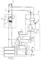
- FIG. 22 shows a configuration example of a conventional switching power supply device in which the operation of the switching power supply device is stopped when the output side is in a no-load state, and the operation is resumed when a voltage is applied from the load device to the output side. .
- the operation of this switching power supply device will be briefly described below.
- a no-load detection signal is output from the output control circuit 911 via the coupler circuit 906. Is input to the power on / off circuit 905.
- the drive control circuit 901 controls the drive circuit 902 so as to stop the operation of the switching element 7. Then, the output voltage of the switching power supply device becomes zero.
- a switching power supply eg, AC adapter
- a load device eg, a notebook computer
- the switching operation of the switching power supply is stopped to reduce power consumption.
- the switching power supply device is connected to the load device and a voltage is applied from a power storage component (for example, a battery) of the load device, the switching power supply device can realize a system for starting power supply.
- the present invention solves the above-described problems, and provides a switching power supply device that can be activated regardless of the state of a power storage component such as a primary battery or a secondary battery, and a device connection state detection circuit that constitutes the switching power supply device.
- Switching power supply comprising: an input / output conversion circuit for supplying power to the power supply; and a switching control circuit having an off mode for controlling the switching operation of the second switching element and stopping the switching operation in response to a signal input to the OFF terminal
- a first rectifier circuit connected between the input / output conversion circuit and the output terminal, a transformer having one end of the secondary winding connected to the output terminal, and a first rectifier connected to the primary winding of the transformer.
- One switching element a pulse generator for supplying a pulse signal to the gate terminal of the first switching element, and a transistor in response to the pulse signal.
- a device connection state detection circuit comprising a waveform detection circuit that detects a voltage or current generated in the winding of the coil, compares it with a preset reference value, and outputs an output signal according to the comparison result to the OFF terminal. It is characterized by.
- the device connection state detection circuit detects the connection state between the power supply system and the load device even when there is no power of the primary battery or the secondary battery mounted on the secondary side of the switching power supply device or the load device. be able to.
- FIG. 7 is a circuit diagram illustrating a configuration example of a pulse generator according to the first embodiment of the present disclosure.
- FIG. 7 is a circuit diagram illustrating a configuration example of a switching power supply device and a device connection state detection circuit according to another example of the fourth embodiment of the present disclosure.
- a circuit diagram showing a configuration example of a waveform detection circuit according to a second embodiment of the present disclosure A circuit diagram showing an example of composition of a transformer concerning Embodiment 2 of this indication.
- Timing chart showing operation of the switching power supply according to the second embodiment of the present disclosure Timing chart showing operation of the switching power supply according to the third embodiment of the present disclosure
- Timing chart showing operation of the switching power supply according to the fourth embodiment of the present disclosure Timing chart showing operation of a switching power supply according to another example of Embodiment 4 of the present disclosure
- Timing chart showing operation of the switching power supply according to the first modification of the second embodiment of the present disclosure The circuit diagram which shows the example of 1 structure of the switching power supply device and apparatus connection state detection circuit which concern on Embodiment 5 of this indication Timing chart showing operation during normal operation of the switching power supply according to the fifth embodiment of the present disclosure Timing chart showing operation at the time of protection operation of the switching power supply according to the fifth embodiment of the present disclosure
- the circuit diagram which shows the structural example of the switching power supply apparatus and apparatus connection state detection circuit which concern on Embodiment 6 of this indication Timing chart showing operation of the switching power supply according to the sixth embodiment of the present disclosure The circuit diagram which shows the example of 1 structure of the switching power supply device and apparatus connection state detection circuit which concern on Embodiment 7 of this indication Timing chart showing operation of the pulse generator according to the seventh embodiment of the present disclosure
- the circuit diagram which shows the example of 1 structure of the switching power supply device and apparatus connection state detection circuit which concern on Embodiment 8 of this indication The circuit diagram showing the example of 1 composition of the off mode
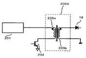
- FIG. 1 is a circuit diagram showing a configuration example of the switching power supply device and the device connection state detection circuit according to the first embodiment.
- an input AC voltage from a commercial power source 1 is input to an input / output conversion circuit 300 as an input DC voltage through an input filter circuit 2, an input rectifier circuit 3, and an input smoothing circuit 4.
- the input / output conversion circuit 300 is arranged to convert an input voltage that has been input into a desired output voltage.
- the transformer 301 includes a power conversion transformer 301, a diode 302, and a smoothing capacitor 303.
- the transformer 301 includes a primary winding 301a and a secondary winding 301b, and the primary winding 301a and the secondary winding 301b.
- the polarity is in the opposite direction.
- This switching power supply device is a flyback type.
- the switching element 7 is connected to the primary winding 301a, and ON / OFF switching control is performed by inputting the OUT terminal output signal of the switching control circuit 100 to the control electrode (gate) of the switching element 7.
- the switching control circuit 100 has five terminals, ie, a Vin terminal, a VDD terminal, a GND terminal, an OUT terminal, and an OFF terminal as external input / output terminals.
- the switching control circuit includes a pulse width control circuit 101, a drive circuit 102, an off mode detector 103, a reference voltage source 104, an off mode switch 105, a regulator 106, and the like.
- the Vin terminal is a power supply terminal of the switching control circuit 100, and power is supplied from a line from which an input DC voltage of the input smoothing circuit is output.
- the power input from the Vin terminal is input to the regulator 106, and power is supplied to the circuits in the switching control circuit 100 via the regulator 106.
- the GND terminal is connected to the low potential side of the input smoothing circuit and serves as a voltage reference for the primary side.
- the OUT terminal is a terminal connected to the gate of the switching element 7 via the resistor 6.
- the VDD terminal is a reference voltage terminal for the switching control circuit 100.
- a capacitor 17 is connected to the VDD terminal. During operation, a charging current flows from the VDD terminal to the capacitor 17 and the voltage of the capacitor 17 rises. The voltage is controlled by the switching control circuit 100 so that this voltage becomes constant at the reference voltage.
- the OFF terminal is a terminal for inputting an off mode signal output from the device connection state detection circuit 200A and switching between the off mode and the normal operation.
- the output terminal 16 includes two terminals, that is, a terminal that outputs an output voltage output from the input / output conversion circuit 300 and a secondary side GND terminal.
- the load device 400 is an electronic device such as a notebook computer or a tablet computer, and can be attached to and detached from the output terminal 16.
- the device connection state detection circuit 200A is arranged to detect whether the output terminal 16 and the load device 400 are connected or not, and includes a VDD terminal, an OFF terminal, a GND terminal of the switching control circuit 100, The output terminal 16 is connected to the anode of the diode 18.
- FIG. 1 it comprises a load device connection terminal 5, a waveform detection circuit 201, a transformer 202, a pulse generator 203, and a switching element 204.
- the waveform detection circuit 201 includes, for example, a resistor 206, a resistor 207, and a capacitor 208 like the waveform detection circuit 201A in FIG. 2A.
- the transformer 202 has, for example, a primary winding 209a and a secondary winding 209b like the transformer 202A in FIG. 2B, and the polarities of the primary winding 209a and the secondary winding 209b are in the forward direction.
- the pulse generator 203 includes resistors 233, 234, 235, 238, 239, 240, a capacitor 236, an operational amplifier 237, and a voltage comparator 241 as in the pulse generator 203A of FIG. 2C, for example. Since this circuit is a generally known pulse generation circuit, a detailed description of its operation is omitted.
- the switching element 204 is turned on / off by the output pulse of the pulse generator 203 being input to the control electrode (gate) of the switching element 204.
- a transistor such as a MOSFET is used as the switching element 204.
- the diode 15 is arranged to prevent a signal for detecting the connection state between the output terminal 16 and the load device 400 from flowing into the input / output conversion circuit 300, and the anode of the diode 15 is connected to the secondary output of the input / output conversion circuit 300.
- the cathode of the diode 15 is connected to the output terminal 16.
- the diode 18 is arranged to prevent the output current from the input / output conversion circuit 300 from flowing into the transformer 202, the anode of the diode 18 is connected to the load device connection terminal 5, and the cathode of the diode 18 is connected to the cathode of the diode 15 and the output. Connected between terminals 16.
- Power is supplied from the VDD terminal of the switching control circuit 100 to the device connection state detection circuit 200A.
- the capacitor 208 of the waveform detection circuit 201 is charged with electric charge from the VDD terminal via the resistor 206.
- the pulse generator 203 outputs a monitoring pulse to the gate of the switching element 204.
- the switching element 204 becomes conductive.
- a primary side current Ip which is a combination of the excitation current Ie and the secondary side current Is that flows through the secondary winding 209b transmitted through the transformer 202, flows through the primary winding 209a.
- This secondary side current Is changes with the impedance of the load device 400.
- the number of turns of the primary winding 209a is Np
- the number of turns of the secondary winding 209b is Ns
- the inductance value of the primary winding 209a is Lp
- the voltage input to the primary winding 209a is Vp
- the secondary winding 209b Assuming that the output voltage is Vs, the forward voltage of the diode 18 is Vfd, the output voltage of the output terminal 16 is Vo, the impedance of the load device 400 is Z, and the time that the gate of the switching element 204 is conductive is Ton
- Ton the time that the gate of the switching element 204 is conductive
- Is> 0 in order to transmit the secondary current Is to the primary current Ip, so that Vs ⁇ Vfd ⁇ Vo> 0. It is necessary to set Ns, Np, and Vp.
- the waveform detection circuit 201 Since the change in the secondary side current Is is reflected in the primary side current Ip as shown in (Equation 1), the waveform detection circuit 201 includes the output terminal 16 and the load device 400 according to the change in the primary side current Ip. It detects whether it is in a connected state.
- FIG. 3 is a timing chart showing the operation of the switching power supply device in FIG.
- the value of the impedance Z is preferably about several mohms to several hundreds ohms.
- the secondary current Is flows through the secondary winding 209b. It is transmitted to the primary winding 209a and synthesized with the primary current Ip. The electric charge accumulated in the capacitor 208 is discharged by the primary side current Ip (FIG. 3 (e)).
- the capacitor 208 is charged via the resistor 206 from the VDD terminal. At this time, it is preferable that the resistance values of the resistors 206 and 207 are set so that the capacitor 208 is charged with about several hundred nA.
- the waveform detection circuit 201 sets the OFF terminal voltage to a value lower than the reference voltage source 104 of the off mode detector 103.
- the off-mode detector 103 outputs an L-level signal (FIG. 3C), and the switching control circuit 100 controls the off-mode switch 105 to the conductive state, so that the switching element 7 maintains the switching operation.
- FIG. 3B the switching power supply device continues normal operation.
- the OFF terminal voltage is applied until the charging from the VDD terminal and the discharging by the primary side current Ip are balanced. rises.
- the pulse width is preferably several ⁇ s to several tens ⁇ s.
- the pulse generator 203 is preferably controlled so as to output the monitoring pulse at a cycle of about 0.2 Hz to 60 Hz.
- the switching control circuit 100 controls the off mode switch 105 to be cut off and the switching operation of the switching element 7 to be stopped. Then, the output voltage Vo (FIG. 3A) decreases to 0V, and the power consumption of the switching power supply device is reduced.
- the off mode power is supplied to the regulator 106 from the Vin terminal, and power is supplied to the off mode detector 103 via the regulator 106.
- the off-mode detector 103 continues to control to turn off the off-mode switch 105 even in the off-mode.
- the secondary side current Is flows to the closed circuit, and the secondary side current Is is combined with the primary side current Ip. Then, since the electric charge discharged from the capacitor 208 by the primary side current Ip becomes larger than the electric charge charged in the capacitor 208, the OFF terminal voltage decreases. When the OFF terminal voltage decreases and becomes lower than the reference voltage source 104 of the off-mode detector 103, the switching control circuit 100 controls the off-mode switch 105 to the conductive state, so that the switching element 7 starts the switching operation and operates normally. Continue.
- the electric charge may not be accumulated in the power storage component such as the primary battery or the secondary battery mounted on the load device 400.
- the power storage component such as the primary battery or the secondary battery mounted on the load device 400.
- An example is when the laptop battery is empty.
- the switching power supply device has the output terminal 16 and the load device 400 connected to each other even when the secondary battery of the switching power supply device or the power of the secondary battery mounted on the load device 400 is not present.
- the connection state can be detected, and the off-mode control of the switching power supply device can be performed.
- the pulse generator 203 may be included in the switching control circuit 100. Further, by arranging and adjusting the capacitor 236 outside, it is possible to easily generate a monitoring pulse with a long period.
- the switching power supply according to the second embodiment has a configuration of the transformer 205, a configuration of the waveform detection circuit 201, and a connection between the waveform detection circuit 201 and the transformer 205 in the device connection state detection circuit 200B. Different.
- FIG. 4A shows an example of the switching power supply according to the second embodiment.
- the waveform detection circuit 201 includes, for example, a voltage comparator 211, a constant current source 213, a waveform detection circuit 201B in FIG.
- the capacitor 214, PchMOSFET 215, NchMOSFET 216, voltage comparator 217, and reference voltage sources 212 and 218 are included.
- the transformer 205 is composed of a primary winding 210a and a secondary winding 210b, for example, like the transformer 205A in FIG. 5B, and the polarities of the primary winding 210a and the secondary winding 210b are opposite to each other.
- the device connection state detection circuit 200B detects the connection state between the output terminal 16 and the load device 400. Therefore, hereinafter, when the output terminal 16 is connected to the load device 400, the output A case where the terminal 16 and the load device 400 shift to the disconnected state and a case where the output terminal 16 and the load device 400 shift to the connected state will be described.
- FIG. 6A is a timing chart showing the operation of the switching power supply device in FIG. 4A.
- the secondary current Is2 flows in the secondary winding 210b (FIG. 6A (g)), the voltage Vs2 is generated, and the reflected voltage Vor is generated in the primary winding 210a.
- the number of turns of the primary winding 210a is Np2
- the number of turns of the secondary winding 210b is Ns2
- the voltage input to the primary winding 210a is Vp2
- the inductance value of the primary winding 210a is Lp2
- the inductance value of the secondary winding 210b is Assuming that Ls2, the time during which the switching element 204 is in the non-conductive state is Toff2, and the output voltage increase caused by the excitation energy Ep2 by the device connection state detection circuit 200B and the diode 18 is ⁇ Vo, the following relational expression is established.
- Ip2 (Vp2 / Lp2) ⁇ Ton2 (Formula 5)
- Ep2 Lp2 ⁇ (Ip2) 2 /2 ( Equation 6)
- Vor Np2 / Ns2 / (Vs2 + Vfd)
- Is2 Np / Ns ⁇ Ip2 ⁇ Ton2-Vs2 / Ls2 ⁇ Toff2 (Formula 9)
- Ep2 (Cpc / 2) ⁇ ⁇ (Vo + ⁇ Vo) 2 ⁇ Vo 2 ⁇ (Formula 12) That is, the excitation energy Ep2 (formula 6) generated by the primary side is accumulated in the capacitor on the secondary side and converted into (formula 12).
- drain voltage Vd2 is generated at the drain terminal of the switching element 204 during the period Tor (FIG. 6A (f)).
- the drain voltage Vd2 is expressed by the following equation.
- Vd2 Vp2 + Vor (Formula 13) Whether or not the output terminal 16 is connected to the load device 400 is detected from the difference in the voltage waveform of Vor included in the drain voltage Vd2.
- the reference voltage source 218 of the voltage comparator 217 is set higher than the drain voltage Vd2 in the connection state with the load device 400.
- an L level signal is output from the voltage comparator 217, and the voltage at the Va point becomes the L level (FIG. 6A (e)).
- This L level signal is input to the gates of the Pch MOSFET 215 and the Nch MOSFET 216, the Pch MOSFET 215 is turned on, and the Nch MOSFET 216 is turned off.
- an L level signal is input to the OFF terminal (FIG. 6A (c)), and the switching control circuit 100 controls the off mode switch 105 to the conductive state, so that the switching element 7 maintains the switching operation (FIG. 6). 6A (b)), the switching power supply device continues normal operation.
- the circuit including the secondary winding 210b and the load device 400 becomes an open circuit, and the capacitance connected to the output terminal 16 is a cable or pattern parasitic. Only capacity. As a result, the output voltage increase ⁇ Vo due to the excitation energy Ep2 appears as a relatively large value.
- the voltage comparator 217 When the drain voltage Vd2 rises and becomes higher than the reference voltage source 218 of the voltage comparator 217, the voltage comparator 217 outputs an H level signal.
- the H level signal is input to the gates of the Pch MOSFET 215 and the Nch MOSFET 216, the Pch MOSFET 215 is turned off, and the Nch MOSFET 216 is turned on.
- an H level signal is input to the OFF terminal, and the switching control circuit 100 controls the off mode switch 105 to be cut off and stops the switching operation of the switching element 7.
- the output voltage Vo (FIG. 6A (a)) falls to 0V, and the power consumption of a switching power supply device is reduced.
- the impedance Z2 includes a capacitance Cpc.
- an L level signal is input to the OFF terminal, and the switching control circuit 100 controls the off mode switch 105 to be in a conductive state, and starts the switching operation of the switching element 7.
- the switching power supply device can output the secondary battery of the switching power supply device or the load battery 400 even when there is no power of the primary battery or the secondary battery as in the first embodiment.
- the connection state between the terminal 16 and the load device 400 can be detected, and the off-mode control of the switching power supply device can be performed.
- Modification 1 of Embodiment 2 The switching power supply according to the first modification of the second embodiment is different in the configuration of the waveform detection circuit 201 from the second embodiment.
- the waveform detection circuit 201 includes, for example, voltage comparators 219, 225, and 231; Pch MOSFETs 221 and 227; Nch MOSFETs 222 and 228; constant current sources 223 and 229; and capacitors 224 and 230, as in the waveform detection circuit 201C of FIG. , Reference voltage sources 220, 226, and 232.
- the waveform detection circuit 201B detects the connection between the output terminal 16 and the load device 400 based on the difference in the voltage of the reflected voltage Vor
- the waveform detection circuit 201C outputs the difference in the time when the reflected voltage Vor is generated. The difference is that the connection between the terminal 16 and the load device 400 is detected.
- FIG. 8 is a timing chart showing the operation of the switching power supply according to the first modification of the second embodiment.
- the voltage comparator 219 receives the drain voltage Vd2 of the switching element 204 expressed by (Equation 11) and compares it with the reference voltage source 220. In order to compare the difference in voltage waveform of the reflected voltage Vor, the voltage value Vth of the reference voltage source 220 needs to be set as Vp2 + Vor> Vth> Vp2.
- the H level signal is input to the gates of the Pch MOSFET 227 and the Nch MOSFET 228, the Pch MOSFET 227 is turned off, and the Nch MOSFET 228 is turned on.
- the Nch MOSFET 228 becomes conductive, the charge of the capacitor 230 is discharged via the Nch MOSFET 228, and when the voltage at the point Vf (FIG. 8D) becomes lower than the reference voltage source 232 of the voltage comparator 231, the voltage comparator 231 Since the output is maintained at the L level, the OFF terminal voltage is also maintained at the L level (FIG. 8C).
- the switching control circuit 100 controls the off-mode switch 105 to the conductive state, the switching element 7 maintains the switching operation (FIG. 8B), and the switching power supply device continues the normal operation.
- the primary current Ip2 (FIG. 8 (j)) flows and accumulates in the primary winding 210a. Since the excitation energy Ep2 is not transmitted to the secondary winding 210b, the excitation energy Ep2 is consumed by increasing the drain voltage Vd2 (FIG. 8 (h)).
- the Nch MOSFET 222 becomes conductive. Therefore, when the charge stored in the capacitor 224 is discharged through the Nch MOSFET 222 and the voltage at the point Vd becomes lower than the reference voltage source 226 of the voltage comparator 225, the voltage The comparator 225 is an L level signal. To output. Then, this L level signal is input to the gates of the Pch MOSFET 227 and the Nch MOSFET 228, the Pch MOSFET 227 is turned on, and the Nch MOSFET 228 is turned off.
- the switching control circuit 100 controls the off-mode switch 105 to the non-conducting state, so that the switching element 7 stops the switching operation. Then, the switching power supply device shifts to the off mode. Then, the output voltage Vo (FIG. 8A) decreases to 0V.
- the voltage comparator 219 When the drain voltage Vd2 becomes larger than the voltage value Vth of the reference voltage source 220, the voltage comparator 219 outputs an L level signal. This L level signal is input to the gates of the Pch MOSFET 221 and the Nch MOSFET 222, the Pch MOSFET 221 is turned on, and the Nch MOSFET 222 is turned off.
- the H level signal is input to the gates of the Pch MOSFET 227 and the Nch MOSFET 228, the Pch MOSFET 227 is turned off, and the Nch MOSFET 228 is turned on.
- the Nch MOSFET 228 becomes conductive, the charge of the capacitor 230 is discharged via the Nch MOSFET 228, and when the voltage at the point Vf becomes lower than the reference voltage source 232 of the voltage comparator 231, the output of the voltage comparator 231 is maintained at the L level. Therefore, the OFF terminal voltage is also maintained at the L level.
- the switching control circuit 100 controls the off mode switch 105 to the conductive state, the switching element 7 starts the switching operation, and the switching power supply device shifts to the normal operation.
- the switching power supply device can output the secondary battery of the switching power supply device or the load battery 400 even when there is no power of the primary battery or the secondary battery as in the first embodiment.
- the connection state between the terminal 16 and the load device 400 can be detected, and the off-mode control of the switching power supply device can be performed.
- the switching power supply according to the third embodiment includes a diode 15 that is a first rectifier circuit, a device connection state detection circuit 200B, and a diode that is a second rectifier circuit, as compared with the switching power supply apparatus according to the second embodiment.
- the connection with 18 is different.
- FIG. 4B shows an example of the switching power supply according to the third embodiment.
- one end of the load device connection terminal 5 of the device connection state detection circuit 200B is connected to the cathode side of the diode 15 that is the first rectifier circuit, that is, the output terminal via the diode 18 that is the second rectifier circuit.
- the other end is connected to the anode side of the diode 15 that is the first rectifier circuit.
- the device connection state detection circuit 200B detects a potential difference (reverse voltage) appearing at both ends of the diode 15 by being connected to both ends of the diode 15.
- the transformer 205 includes a primary winding 210a and a secondary winding 210b as in the transformer 205A in FIG. 5B, and the polarities of the primary winding 210a and the secondary winding 210b are reversed. It has become.
- FIG. 6B is a timing chart showing the operation of the switching power supply device of Embodiment 3 in FIG. 4B.
- Ep2 (Cpc / 2) ⁇ ⁇ Vo 2 (Formula 15) (Expression 14) represents the difference from (Expression 11) in the second embodiment.
- the reflected voltage Vor does not include the term of the output voltage Vo.
- ⁇ Vo is sufficiently smaller than the output voltage Vo because the excitation energy Ep2 is set to be sufficiently smaller than the capacitance Cpc.
- the switching power supply device can output the secondary battery of the switching power supply device or the load battery 400 even when there is no primary battery or secondary battery power, as in the second embodiment.
- the connection state between the terminal 16 and the load device 400 can be detected, and the off-mode control of the switching power supply device can be performed.
- the load device 400 can be connected with higher accuracy. An unconnected state can be detected.
- the switching power supply according to the fourth embodiment is different in the configuration of the device connection state detection circuit 200E.
- FIG. 4C shows an example of the switching power supply according to the fourth embodiment.
- the device connection state detection circuit 200E includes a load device connection terminal 5, a waveform detection circuit (transmission unit) 201b, a waveform detection circuit (reception unit) 201a, a transformer 205, a pulse generator 203, and a switching element. 204.
- the waveform detection circuit (transmission unit) 201b includes, for example, a shunt regulator and a photodiode.
- the waveform detection circuit ( A light load detection signal is output to the receiver 201a.
- the waveform detection circuit (reception unit) 201a includes a phototransistor and inputs a light load detection signal to the OFF terminal.
- the waveform detection circuit is separated into the waveform detection circuit (reception unit) 201a and the waveform detection circuit (transmission unit) 201b, and the connection / disconnection state of the load device 400 is determined on the secondary side.
- the direct detection is different from the second embodiment.
- FIG. 6C is a timing chart showing the operation of the switching power supply device of Embodiment 4 in FIG. 4C.
- whether the load device 400 is connected or not is determined by comparison with a reference level set for the output voltage Vo.
- a pulse voltage is generated in the output voltage Vo (FIG. 6C (a)) in synchronization with the secondary current.
- this pulse voltage exceeds the reference voltage set by the waveform detection circuit (transmission unit) 201b, a coupler current flows through the photocoupler (FIG. 6C (d)), and the photocoupler emits light, and the waveform detection circuit (reception unit) 201a. Is transmitted to.
- the photocoupler emits light and detects the load device connection state by the pulse voltage supplied to the waveform detection circuit on the secondary side. It can be detected with accuracy.
- FIG. 4D shows another example of the fourth embodiment.
- FIG. 6D is a timing chart showing the operation of the switching power supply device according to the fourth embodiment shown in FIG. 4D.
- one end of the load device connection terminal 5 of the device connection state detection circuit 200E is connected to the cathode of the diode 15 that is the first rectifier circuit via the diode 18 that is the second rectifier circuit.
- the other end is connected to the anode side of the diode 15 as the first rectifier circuit.
- the device connection state detection circuit 200E detects a potential difference (reverse voltage) appearing at both ends of the diode 15 by being connected to both ends of the diode 15.
- the device connection state detection circuit 200E is not affected by the excitation energy supplied from the switching control circuit 100 and the input / output conversion circuit 300, as in the third embodiment.
- the connection / disconnection state of the load device 400 can be detected with higher accuracy.
- the switching power supply according to the fifth embodiment is different from the first embodiment in the configuration of the switching control circuit 150 and in that the output voltage detection circuit 20 and the photocoupler 19 are arranged.
- FIG. 9 shows an example of the switching power supply according to the fifth embodiment.
- the switching control circuit 150 is configured by adding a protection circuit 107, an AND circuit 108, and an FB terminal, and the connection of the output destination of the off-mode detector 103 is different. Different.
- the FB terminal is a terminal for controlling a switching operation when a feedback signal output from the output voltage detection circuit 20 is input via the photocoupler 19.
- the output voltage detection circuit 20 is connected to the output voltage line of the input / output conversion circuit 300, and generates a feedback signal according to the output voltage value.
- the protection circuit 107 is connected to the pulse width control circuit 101, the AND circuit 108, and the regulator 106.
- the output of the off mode detector 103 is input to the AND circuit 108.
- the output voltage detection circuit 20 controls the current to flow out from the FB terminal of the switching control circuit 150 as a feedback signal when the output voltage value becomes equal to or higher than the specified voltage set by the output voltage detection circuit 20. With this feedback signal, the pulse width control circuit 101 changes, for example, the on-duty of the switching element 7 to an appropriate state, and maintains the output voltage at the specified voltage.
- the input / output conversion circuit 300 when the output voltage on the secondary side of the input / output conversion circuit 300 becomes abnormally higher or lower than the specified output value during normal operation, for example, the input / output conversion circuit 300 outputs 20V.
- a feedback signal is generated and input to the FB terminal via the photocoupler 19. Further, this feedback signal is input to the protection circuit 107, and the protection circuit 107 controls the pulse width control circuit 101 so as to stop the switching operation of the switching element 7.
- FIG. 10A is a timing chart illustrating an operation during a normal operation of the switching power supply according to the fifth embodiment of the present disclosure.
- the off-mode detector 103 inputs an L level signal to the AND circuit 108 (FIG. 10A (d)).
- the protection circuit 107 inputs an H level signal (FIG. 10A (e)) to the AND circuit 108. Since an L level signal is input to the AND circuit 108, the AND circuit 108 outputs an L level signal (FIG. 10A (c)), and the switching control circuit 150 controls the off mode switch 105 to be in a conductive state. Thus, the switching operation of the switching element 7 is maintained, and the switching power supply device continues normal operation.
- the off mode detector 103 inputs an H level signal to the AND circuit 108. Since the protection circuit 107 inputs an H level signal to the AND circuit 108 during normal operation, the AND circuit 108 outputs an H level signal, and the switching control circuit 150 controls the off mode switch 105 to be in a cut-off state. To do.
- FIG. 10B is a timing chart illustrating an operation during a protection operation of the switching power supply device according to the fifth embodiment of the present disclosure.
- the switching control circuit 150 controls to stop the switching operation of the switching element 7 (FIG. 10). 10B (b)), the output voltage Vo drops to 0V. Further, since the protection circuit 107 inputs an L level signal to the AND circuit 108 (FIG. 10B (e)), the AND circuit 108 outputs an L level signal regardless of the signal input from the off-mode detector 103. (FIG. 10B (c)). Then, the switching control circuit 150 always maintains the off mode switch 105 in a conductive state.
- the device connection state detection circuit 200A detects that the output terminal 16 and the load device 400 are not connected, and inputs a voltage higher than the reference voltage source 104 of the off mode detector 103 to the OFF terminal ( 10B (f)), even when the off-mode detector 103 outputs an H level signal (FIG. 10B (d)), the switching control circuit 150 maintains the protection state by the protection circuit 107.
- the switching power supply according to the present embodiment shifts to the off mode during normal operation, the power supply to the circuit blocks that do not need to be operated, including the protection circuit 107 inside the switching control circuit 150, is cut off. The power consumption of the switching control circuit 150 itself is reduced. Furthermore, when an abnormality is detected, the protection state is maintained by controlling so as not to shift to the off mode, and the safety of the switching power supply device can be ensured.
- the protection circuit 107 may detect that the temperature of the device connection state detection circuit has risen abnormally, and the switching control circuit 150 may be controlled to stop the switching operation of the switching element 7.
- the switching power supply according to the sixth embodiment is different from the fifth embodiment in the configuration of the switching control circuit 151.
- FIG. 11 shows an example of the switching power supply according to the sixth embodiment.
- the switching control circuit 151 is different from the switching control circuit 150 in FIG. 9 in that the protection circuit 107 and the AND circuit 108 are not provided, and the OR circuit 109, the RS latch circuit 110, and the time detection circuit 111 are arranged. .
- the time detection circuit 111 is arranged to detect the drive signal of the drive circuit 102, and is connected to the output unit of the drive circuit 102, the set terminal (S terminal) of the RS latch circuit 110, and the regulator 106.
- the RS latch circuit 110 is a NOR type RS latch circuit.
- the output of the off-mode detector 103 is input to the reset terminal (R terminal), and the output of the time detection circuit 111 is connected to the set terminal (S terminal).
- the output terminal (Q terminal) is connected to the OR circuit 109.
- the time detection circuit 111 detects the drive signal of the drive circuit 102, and if the drive signal is not detected for a certain period, generates a light load detection signal and inputs it to the S terminal of the RS latch circuit 110.
- the light load detection signal is a pulse signal.
- FIG. 12 is a timing chart showing the operation of the switching power supply device in FIG.
- the switching element current flows at regular intervals, that is, drive signals are output from the drive circuit 102 at regular intervals.
- the time detection circuit 111 outputs an L level signal. This L level signal is input to the S terminal of the RS latch circuit 110.
- the device connection state detection circuit 200A controls the OFF terminal voltage (FIG. 12G) of the off mode detector 103 to be lower than that of the reference voltage source 104. Therefore, the off mode detector 103 outputs an L level signal (FIG. 12 (f)). This L level signal is input to the R terminal of the RS latch circuit 110.
- an L level signal is output from the Q terminal of the RS latch circuit 110.
- the L level signal is input to the OR circuit 109.
- an L level signal output from the off mode detector 103 is also input to the OR circuit 109, and an L level signal is output from the OR circuit 109.
- the switching control circuit 151 controls the off mode switch 105 to be in a conductive state, maintains the switching operation of the switching element 7, and the switching power supply device continues normal operation.
- the pulse width control circuit 101 controls switching so that the switching cycle of the switching element 7 becomes longer via the drive circuit 102.
- the time detection circuit 111 outputs a light load detection signal (FIG. 12E) when the drive signal output from the drive circuit 102 is not detected for a certain period.
- a light load detection signal (FIG. 12E) when the drive signal output from the drive circuit 102 is not detected for a certain period.
- the OFF terminal voltage (FIG. 12G) is controlled to be lower than the reference voltage source 104 by the device connection state detection circuit 200A, an L level signal is output from the off mode detector 103. Yes.
- a light load detection signal is input to the S terminal of the RS latch circuit 110, and an L level signal is input to the R terminal, so that an H level signal is output from the Q terminal (FIG. 12). (D)).
- an H level signal is input from the Q terminal and an L level signal is input from the off-mode detector 103 to the OR circuit 109, an H level signal is output from the OR circuit 109 (FIG. 12 ( c)).
- the switching control circuit 151 turns off the off mode switch 105, stops the switching operation of the switching element 7, and the switching power supply device shifts to the off mode. Then, the output voltage Vo (FIG. 12A) is reduced to 0V.
- an H level signal is input from the off mode detector 103 to the R terminal of the RS latch circuit 110. Is done. As a result, an L level signal is output from the Q terminal of the RS latch circuit 110.
- the OR circuit 109 receives an L level signal from the Q terminal, an H level signal from the off-mode detector 103, and an H level signal from the OR circuit 109. Therefore, the switching control circuit 151 Maintains the off-mode switch 105 in the shut-off state, stops the switching operation of the switching element 7, and the switching power supply device continues in the off-mode.
- the OFF terminal voltage is controlled to be lower than that of the reference voltage source 104 by the device connection state detection circuit 200A. Since an L level signal is input to the S terminal and the R terminal of the RS latch circuit 110, an L level signal is output from the Q terminal. Further, since an L level signal is input from the Q terminal and an L level signal is input from the off-mode detector 103 to the OR circuit 109, an L level signal is output from the OR circuit 109. As a result, the switching control circuit 151 controls the off mode switch 105 to be in a conductive state, so that the switching element 7 starts a switching operation, and the switching power supply device shifts to a normal operation.
- the same effects as those of the first embodiment can be obtained, and further, when the oscillation cycle of the switching element 7 becomes longer, it is possible to shift to the off mode. It is possible to enter the off mode before the voltage becomes higher than the reference voltage source 104.
- the switching power supply according to the seventh embodiment differs from the first embodiment in the configuration of the pulse generator 203B in the device connection state detection circuit 200C.
- FIG. 13 shows an example of the switching power supply according to the seventh embodiment.
- the input voltage of the commercial power source 1 is input to the pulse generator 203B.
- the pulse generator 203B detects a point (zero cross point) where the AC voltage of the commercial frequency crosses 0V ((b) in FIG. 14A) and outputs a monitoring pulse. It controls so that it may produce
- the monitoring pulses are generated at intervals of 100 Hz.
- the pulse generator may be controlled to generate a monitoring pulse after detecting the zero cross point n times (FIG. 14B (b)).
- FIG. 14B (a) For example, when the frequency of the commercial frequency is 50 Hz, if the zero-cross point is detected 100 times and then controlled so as to generate the monitoring pulse, the frequency of the monitoring pulse becomes 1 Hz.
- the monitoring pulse cycle can be easily set by using the commercial frequency.
- the switching power supply according to the eighth embodiment is different from that of the first embodiment in that the resistor 501, the off-mode control circuit 500, and the photocoupler 22 are arranged, and the device connection state detection circuit 200D has a pulse.
- the configuration of the generator 203C is different.
- FIG. 15 shows an example of the switching power supply according to the eighth embodiment.
- One end of the resistor 501 is connected to the cathode of the diode 302, and the other end is connected to the anode of the diode 15.
- the off-mode control circuit 500 is connected to the connection point between the diode 302 and the resistor 501, the connection point between the diode 15 and the resistor 501, and the photocoupler 22, and according to the power supplied from the input / output conversion circuit 300 to the load device 400, An off mode release signal is generated.
- the off mode control circuit 500 includes a voltage comparator 503, a reference voltage source 504, an amplifier 505, an Nch MOSFET 502, and a Zener diode 506, for example, as in the off mode control circuit 500A of FIG.
- the pulse generator 203C is connected to the VDD terminal, the OFF terminal, the gate of the switching element 204, and the photocoupler 22.
- FIG. 17 is a timing chart showing the operation of the switching power supply device in FIG.
- the off mode control circuit 500 ⁇ / b> A detects the current supplied from the input / output conversion circuit 300 to the load device 400 by the amplifier 505 via the resistor 501.
- the amplifier 505 inputs a voltage higher than that of the reference voltage source 504 to the voltage comparator 503, and the voltage comparator 503 outputs an H level signal.
- this H-level signal is input to the gate of the Nch MOSFET 502, the Nch MOSFET 502 becomes conductive and generates an off-mode release signal (FIG. 17 (e)).
- the photocoupler 22 When the off mode release signal is input to the photocoupler 22, the photocoupler 22 operates. The electric charge stored in the capacitor 208 is discharged, and the OFF terminal voltage decreases (FIG. 17 (f)), and is maintained to be lower than the reference voltage source 104 of the off-mode detector 103. Then, the off mode detector 103 outputs an L level signal (FIG. 17D).
- the switching control circuit 100 controls the off-mode switch 105 to be in a conductive state, maintains the switching operation of the switching element 7 (FIG. 17B), and the switching power supply device continues normal operation.
- the pulse generator 203C When the pulse generator 203C detects that the OFF terminal voltage is lower than the reference voltage source 104, the pulse generator 203C is controlled not to generate a monitoring pulse (FIG. 17 (i)).
- the off-mode control circuit 500A A voltage lower than that of the voltage source 504 is input to the voltage comparator 503, and the voltage comparator 503 outputs an L level signal.
- this L level signal is input to the gate of the Nch MOSFET 502, the Nch MOSFET 502 becomes non-conductive and stops generating the off-mode release signal.
- the operation of the photocoupler 22 is stopped, the capacitor 208 is charged with the electric charge via the resistor 206, the OFF terminal voltage rises, and becomes higher than the reference voltage source 104 of the off mode detector 103.
- the pulse width control circuit 101 controls the switching operation of the switching element 7 so as to be thinned out (intermittent operation).
- the switching control circuit 100 controls the off-mode switch 105 to the cutoff state, stops the switching operation of the switching element 7, and the switching power supply shifts to the off mode. Then, the output voltage Vo (FIG. 17A) decreases to 0V.
- the regulator 106 stops the current supply to the VDD terminal (FIG. 17C).
- VDD terminal voltage drops to VDDL
- the current supply is started, and when the voltage reaches VDDH, the current supply is stopped again.
- the pulse generator 203C detects that the OFF terminal voltage is higher than that of the reference voltage source 104, and starts generating the monitoring pulse when the VDD terminal voltage reaches VDDL.
- the generation period of the monitoring pulse is determined by the capacitance value of the capacitor 17, the amount of current supplied to the capacitor 17, and the discharge current from the capacitor 17. By adjusting the capacitance value of the capacitor 17, a monitoring pulse having a long period can be generated.
- the OFF mode is set by setting the lower limit value of the OFF terminal voltage so that it does not fall below the reference voltage source 104 of the OFF mode detector 103. maintain.
- a monitoring pulse is generated from the pulse generator 203C, and when the monitoring pulse is input to the gate of the switching element 204, the switching element 204 becomes conductive.
- the secondary current Is (FIG. 17 (h)) flows and is combined with the primary current Ip.
- the electric charge charged in the capacitor 208 is discharged by the primary side current Ip.
- the pulse generator 203C stops generating the monitoring pulse. Further, the switching control circuit 100 controls the off mode switch 105 to be in a conductive state, and starts the switching operation of the switching element 7.
- the off-mode control circuit 500A detects that the power supplied from the input / output conversion circuit 300 to the load device 400 has increased, and the off-mode control circuit 500A is turned off when the output voltage Vo increases and becomes higher than the zener voltage of the zener diode 506. A mode release signal is generated.
- the off mode release signal is input to the photocoupler 22, and the photocoupler 22 operates.
- the photocoupler discharges the electric charge stored in the capacitor 208 and maintains the OFF terminal voltage so that it is lower than the reference voltage source 104 of the off mode detector 103.
- the switching control circuit 100 controls the off mode switch 105 to the conductive state, maintains the switching operation of the switching element 7, and the switching power supply device continues the normal operation.
- the zener diode 506 is installed to control the off-mode release signal not to be generated unless the output voltage Vo rises above a certain value. For example, when an unstable operation is performed such that the output voltage does not rise above a certain value, an off-mode release signal is not generated, so that the switching operation of the switching element 7 occurs when the OFF terminal voltage becomes higher than the reference voltage source 104. Stops. As a result, when an abnormality occurs during startup or when shifting from the off mode to the normal operation, an unstable operation can be avoided and the switching power supply device can be brought into a stopped state.
- the generation of the monitoring pulse can be stopped during normal operation, and when the power supplied from the input / output conversion circuit 300 to the load device 400 is small, for example, The power consumed by the pulse generator during operation can be suppressed.
- the generation period of the monitoring pulse in the off mode can be easily set.
- the switching power supply according to the ninth embodiment is different from the first embodiment in that the diode 15 and the diode 18 are not disposed, the configuration of the output terminal 16A, the load device 400A, the transformer 202 and the output terminal 16A. Connection is different.
- FIG. 18 shows an example of the switching power supply according to the ninth embodiment.
- the load device 400A includes, for example, a load device 400 and a resistor 410.
- the output terminal 16 ⁇ / b> A includes three terminals of the output terminal 16 and the signal terminal 23.
- One end of the load device connection terminal 5 is connected to the secondary side GND terminal, and the other end is connected to the signal terminal 23.
- the device connection state detection circuit 200 ⁇ / b> A detects the connection state between the output terminal 16 and the load device 400 using the impedance Z of the load device 400 between the output terminals 16.
- the device connection state detection circuit 200A performs detection based on the impedance of the resistor 410 between the signal terminal 23 and the secondary side GND terminal of the output terminal 16.
- the value of the resistor 410 is preferably about several mohms to several hundreds ohms.
- the diode 15 and the diode 18 which are necessary in the first and second embodiments can be made unnecessary, and further, by changing the resistance value.
- the impedance Z can be easily set.
- the switching power supply according to the tenth embodiment is different from the first embodiment in the configuration of the first rectifier circuit, and has a circuit configuration using a PchMOSFET 601 instead of the diode 15. Further, the configuration of the switching control circuit 170 and the point that the output voltage detection circuit 20 and the photocoupler 19 are arranged are different.
- FIG. 20 shows an example of the first rectifier circuit and its peripheral circuits of the switching power supply according to the tenth embodiment.
- the switching control circuit 170 is configured by adding an on / off control circuit 120 and an FB terminal, and the driving circuit 102A is turned on with the pulse width control circuit 101. The difference is that the off control circuit 120 is connected.
- the FB terminal is a terminal for controlling a switching operation when a feedback signal output from the output voltage detection circuit 20 is input via the photocoupler 19.
- the output voltage detection circuit 20 is connected to the output voltage line of the input / output conversion circuit 300, and generates a feedback signal according to the output voltage value.
- the output voltage detection circuit 20 controls the current to flow out from the FB terminal connected to the switching control circuit 170 as a feedback signal when the output voltage value exceeds the specified voltage set by the output voltage detection circuit 20. With this feedback signal, the pulse width control circuit 101 changes, for example, the on-duty of the switching element 7 to an appropriate state, and maintains the output voltage at the specified voltage.
- the outflow current from the FB terminal increases, and the on / off control circuit 120 connected to the FB terminal outputs an oscillation stop signal or a frequency reduction signal to the drive circuit 102A, and the switching element 7 switching frequency is reduced.
- the first rectifier circuit 15b includes a Pch MOSFET 601, an Nch MOSFET 602, resistors 603, 604, 606, and 607, a capacitor 608, and a diode 605.
- the PchMOSFET 601 is connected between the input / output conversion circuit 300 and the output terminal 16, and the drain terminal of the NchMOSFET 602 is connected to the gate of the PchMOSFET 601 through the resistor 604.
- the resistor 603 is connected between the gate and the source of the Pch MOSFET 601. When the Nch MOSFET 602 is turned on, a voltage between gs of the Pch MOSFET 601 is generated by the resistor 603 and the resistor 604, and the Pch MOSFET 601 becomes conductive.
- a capacitor 608 and resistors 606 and 607 connected in series are connected to the gate of the Nch MOSFET 602.
- the diode 605 has an anode connected to the secondary winding of the transformer 301 and a cathode connected to the gate terminal of the Nch MOSFET 602 via the resistor 606.
- FIG. 21 shows the operation of each part in the tenth embodiment.
- the gate voltage of the Nch MOSFET 602 is held at a constant voltage value higher than the threshold voltage of the Nch MOSFET 602.
- the Nch MOSFET 602 is turned on, the gs voltage of the Pch MOSFET 601 becomes equal to or higher than the threshold voltage of the Pch MOSFET 601 by the resistors 603 and 604, and the Pch MOSFET 601 is turned on.
- the gate voltage of the Nch MOSFET 602 is gradually decreased to be lower than the threshold voltage of the Nch MOSFET 602, and the Nch MOSFET 602 is turned off. Is turned off.
- the rectifier circuit 15b conducts with a low resistance at a heavy load and cuts off at a light load.
- the load device 400 When the load device 400 is not connected, if it is a switching power supply device provided with a feedback function from the secondary side, it is determined that the load is light, and the switching operation is controlled so as to reduce the output.
- the PchMOSFET 601 when the load device 400 is in the connected state, the PchMOSFET 601 conducts and transmits the output of the input / output conversion circuit 300 to the load device 400 with low loss, and the load device 400 is in the disconnected state.
- the Pch MOSFET 601 When a light load is detected, the Pch MOSFET 601 is cut off, and the device connection state can be detected by the device connection state detection circuit 200A.
- the switching power supply device has been described based on the embodiments, the present invention is not limited to these embodiments. Unless it deviates from the gist of the present disclosure, various modifications conceived by those skilled in the art in the embodiment and forms constructed by combining components in different embodiments are also included in the scope of the present disclosure. .
- a configuration in which the device connection state detection circuit 200A of the first embodiment is replaced with the device connection state detection circuit 200B of the second embodiment is also included in the scope of the present disclosure, and the same effect is produced.
- the configuration in which the pulse generator 203B of the seventh embodiment is replaced with the pulse generators 203 and 203C described in the first to sixth and eighth to tenth embodiments is also included in the scope of the present disclosure. An effect is produced.
- the first rectifier circuit 15b of the tenth embodiment includes a configuration in which the diode 15 described in the first to ninth embodiments is replaced within the scope of the present disclosure, and the same effect is achieved.
- the output terminal 16A and the load device 400A according to the ninth embodiment are also included in the scope of the present disclosure, and the same effect is obtained by replacing the output terminal 16 and the load device 400 described in the first and second embodiments. Is played.
- the semiconductor device 180A including the switching control circuit 100 and the pulse generator 203 provided in the switching power supply device according to Embodiment 1 is also included in the scope of the present disclosure. .
- the semiconductor device 180B including the switching control circuit 100, the pulse generator 203, and the switching element 204 provided in the switching power supply device according to Embodiment 1 is also disclosed in the present disclosure. Included in the range.
- the semiconductor device 180C provided with the switching control circuit 100, the pulse generator 203, and the waveform detection circuit 201 provided in the switching power supply device according to the first embodiment is also provided. It is included in the scope of disclosure.
- Each processing unit included in the semiconductor device is typically realized as an integrated circuit. These may be individually made into one chip, or may be made into one chip so as to include a part or all of them.
- the integrated circuit may be realized by a microprocessor and a program in addition to the dedicated circuit.
- An FPGA Field Programmable Gate Array
- a reconfigurable processor that can reconfigure circuit cell connections and settings may be used.
- the switching power supply device and the device connection state detection circuit of the present disclosure can stop the switching operation of the switching power supply device during standby, reduce the power consumption of the switching power supply device, and further, the waveform detection circuit, the transformer, and the pulse generator
- a device connection state detection circuit composed of the above it can be started even when there is no electric charge in the power storage component such as a primary battery or a secondary battery, and an AC-DC converter or DC-DC built in the electronic device. It can be effectively applied to switching power supplies such as converters and external AC adapters.
Abstract
Disclosed is a switching power supply apparatus that is provided with an apparatus connection state detection circuit which detects, in a power supply system having a load apparatus connection terminal, a connection state of the load apparatus connection terminal. The apparatus connection state detection circuit is provided with a transformer, a switch element, a pulse generator, and a waveform detection circuit. The waveform detection circuit detects a voltage or a current generated in a primary coil or a secondary coil of the transformer corresponding to operations of pulse signals, compares the voltage or the current with a previously set reference value, and outputs, to an OFF terminal, an output signal corresponding to the comparison results.
Description
本発明は、入力電圧に対してスイッチング素子を通じてスイッチングすることにより出力電圧を制御するスイッチング電源装置および機器接続状態検出回路に関する。
The present invention relates to a switching power supply apparatus and an apparatus connection state detection circuit for controlling an output voltage by switching an input voltage through a switching element.
近年、エネルギー問題などの環境問題が注目され、スイッチング電源装置等の電源供給装置の待機電力削減が強く望まれている。例えば、ACアダプタや充電器において、負荷機器が接続されていない状態等、スイッチング電源装置から電力供給が不要な場合に出力電圧を低下させて、消費電力を削減するシステムが提案されている。
In recent years, environmental problems such as energy problems have attracted attention, and reduction of standby power of power supply devices such as switching power supply devices is strongly desired. For example, in an AC adapter or a charger, a system has been proposed that reduces power consumption by reducing the output voltage when power supply from a switching power supply device is not required, such as when a load device is not connected.
従来技術である特開2007-143397号公報(特許文献1)では、ACアダプタの負荷の有無を検知し、出力側が無負荷状態のときにスイッチング電源装置の動作を停止させて、消費電力を削減し、さらに、出力側に接続される負荷機器から電圧が印加されると動作を再開させて電源供給を開始する技術が提案されている。
Japanese Patent Application Laid-Open Publication No. 2007-14397 (Patent Document 1), which is a conventional technique, detects the presence or absence of a load on the AC adapter and stops the operation of the switching power supply device when the output side is in a no-load state, thereby reducing power consumption. In addition, there has been proposed a technique for restarting the operation and starting the power supply when a voltage is applied from a load device connected to the output side.
負荷機器の電源としては、一次電池や二次電池などの蓄電部品を用いることが考えられる。
It is conceivable to use a power storage component such as a primary battery or a secondary battery as the power source of the load device.
図22に、出力側が無負荷状態のときにスイッチング電源装置の動作を停止させて、出力側に負荷機器から電圧が印加されると動作を再開させる、従来のスイッチング電源装置の一構成例を示す。以下、このスイッチング電源装置の動作を簡単に説明する。
FIG. 22 shows a configuration example of a conventional switching power supply device in which the operation of the switching power supply device is stopped when the output side is in a no-load state, and the operation is resumed when a voltage is applied from the load device to the output side. . The operation of this switching power supply device will be briefly described below.
二次側の負荷機器912の負荷状態を、抵抗909を介して出力制御回路911で監視し、無負荷状態を検出した場合は、出力制御回路911からカプラ回路906を介して、無負荷検出信号が電源オンオフ回路905に入力される。そして、電源オンオフ回路905から動作停止信号がスイッチング制御回路900のドライブ制御回路901に入力されると、ドライブ制御回路901はスイッチング素子7の動作を停止するようにドライブ回路902を制御する。そして、スイッチング電源装置の出力電圧はゼロになる。
When the load state of the load device 912 on the secondary side is monitored by the output control circuit 911 via the resistor 909 and a no-load state is detected, a no-load detection signal is output from the output control circuit 911 via the coupler circuit 906. Is input to the power on / off circuit 905. When an operation stop signal is input from the power on / off circuit 905 to the drive control circuit 901 of the switching control circuit 900, the drive control circuit 901 controls the drive circuit 902 so as to stop the operation of the switching element 7. Then, the output voltage of the switching power supply device becomes zero.
スイッチング電源装置の動作を再開させる場合は、出力電圧がゼロの時に、負荷機器912の蓄電部(図には明記していない)から出力端子16を介して電圧を印加し、出力電圧がゼロでないことを出力制御回路911が検出する。そして、その電圧を電源として、出力制御回路911はフォトカプラ910を介して、再起動信号を電源オンオフ回路905に入力する。それと同時に、一定期間、電源オンオフ回路905から動作停止信号の生成を止める。電源オンオフ回路905から動作開始信号がドライブ制御回路901に入力されると、ドライブ制御回路901はスイッチング素子7の動作を開始するようにドライブ回路902を制御する。
When restarting the operation of the switching power supply device, when the output voltage is zero, a voltage is applied from the power storage unit (not shown in the figure) of the load device 912 via the output terminal 16, and the output voltage is not zero. The output control circuit 911 detects this. Then, the output control circuit 911 inputs a restart signal to the power on / off circuit 905 via the photocoupler 910 using the voltage as a power source. At the same time, the generation of the operation stop signal from the power on / off circuit 905 is stopped for a certain period. When an operation start signal is input from the power on / off circuit 905 to the drive control circuit 901, the drive control circuit 901 controls the drive circuit 902 to start the operation of the switching element 7.
この技術を用いれば、例えば、負荷機器(例えばノートパソコン)にスイッチング電源装置(例えばACアダプタ)が接続されていない時(無負荷状態)は、スイッチング電源装置のスイッチング動作を停止させ消費電力を削減すること(オフモード)ができ、スイッチング電源装置が負荷機器に接続され、負荷機器の蓄電部品(例えばバッテリー)から電圧が印加されると、スイッチング電源装置は電源供給を開始させるシステムが実現できる。
If this technology is used, for example, when a switching power supply (eg, AC adapter) is not connected to a load device (eg, a notebook computer) (no load state), the switching operation of the switching power supply is stopped to reduce power consumption. When the switching power supply device is connected to the load device and a voltage is applied from a power storage component (for example, a battery) of the load device, the switching power supply device can realize a system for starting power supply.
しかし、上述のシステムには次のような課題がある。
However, the above system has the following problems.
動作を停止したスイッチング電源装置を、再び動作させるために負荷機器の蓄電部から電圧を印加し、さらに再起動信号を二次側から一次側へ伝達するためにフォトカプラを使用している。しかし、負荷機器に搭載されている一次電池や二次電池などの蓄電部品に蓄積されている電荷が空になった場合、電圧を印加することやフォトカプラを動作させることができなくなる。その場合、スイッチング電源装置を負荷機器に接続し、スイッチング電源装置を起動させようとしても、動作を停止させた状態を維持して通常動作へ移行できないという致命的な問題が生じる。
In order to operate the switching power supply device that has stopped operating again, a voltage is applied from the power storage unit of the load device, and a photocoupler is used to transmit a restart signal from the secondary side to the primary side. However, when the electric charge stored in the power storage component such as the primary battery or the secondary battery mounted on the load device becomes empty, it becomes impossible to apply a voltage or operate the photocoupler. In that case, even if the switching power supply device is connected to the load device and the switching power supply device is started, a fatal problem that the operation is stopped and the normal operation cannot be performed occurs.
本発明は、上記のような問題を解決するものであり、一次電池や二次電池などの蓄電部品の状態に関係なく起動できるスイッチング電源装置およびそれを構成する機器接続状態検出回路を提供する。
The present invention solves the above-described problems, and provides a switching power supply device that can be activated regardless of the state of a power storage component such as a primary battery or a secondary battery, and a device connection state detection circuit that constitutes the switching power supply device.
入力電圧が供給される第二のスイッチング素子と、負荷機器と装脱着可能な出力端子と、第二のスイッチング素子によりスイッチングされた入力電圧を出力電圧に変換し、出力端子に接続された負荷機器に電力を供給する入出力変換回路と、第二のスイッチング素子のスイッチング動作を制御し、OFF端子に入力される信号に応じてスイッチング動作を停止するオフモードを有するスイッチング制御回路とを備えるスイッチング電源装置において、入出力変換回路と出力端子との間に接続された第一の整流回路と、二次巻線の一端が出力端子に接続されたトランスと、トランスの一次巻線に接続された第一のスイッチング素子と、第一のスイッチング素子のゲート端子にパルス信号を供給するパルス発生器と、パルス信号に応じてトランスの巻線に発生する電圧、または電流を検出し、あらかじめ設定された基準値と比較し、比較結果に応じた出力信号をOFF端子に出力する波形検出回路からなる機器接続状態検出回路を備えることを特徴とする。
A second switching element to which an input voltage is supplied, an output terminal that can be attached to and detached from the load device, and a load device that converts the input voltage switched by the second switching element into an output voltage and is connected to the output terminal Switching power supply comprising: an input / output conversion circuit for supplying power to the power supply; and a switching control circuit having an off mode for controlling the switching operation of the second switching element and stopping the switching operation in response to a signal input to the OFF terminal In the device, a first rectifier circuit connected between the input / output conversion circuit and the output terminal, a transformer having one end of the secondary winding connected to the output terminal, and a first rectifier connected to the primary winding of the transformer. One switching element, a pulse generator for supplying a pulse signal to the gate terminal of the first switching element, and a transistor in response to the pulse signal. A device connection state detection circuit comprising a waveform detection circuit that detects a voltage or current generated in the winding of the coil, compares it with a preset reference value, and outputs an output signal according to the comparison result to the OFF terminal. It is characterized by.
本構成によれば、スイッチング電源装置の二次側や負荷機器に搭載された一次電池や二次電池の電力が無い場合でも、機器接続状態検出回路は電源システムと負荷機器の接続状態を検出することができる。
According to this configuration, the device connection state detection circuit detects the connection state between the power supply system and the load device even when there is no power of the primary battery or the secondary battery mounted on the secondary side of the switching power supply device or the load device. be able to.
(実施の形態1)
本開示の実施の形態1のスイッチング電源装置、機器接続状態検出回路を説明する。 (Embodiment 1)
A switching power supply device and a device connection state detection circuit according to the first embodiment of the present disclosure will be described.
本開示の実施の形態1のスイッチング電源装置、機器接続状態検出回路を説明する。 (Embodiment 1)
A switching power supply device and a device connection state detection circuit according to the first embodiment of the present disclosure will be described.
図1は本実施の形態1のスイッチング電源装置、機器接続状態検出回路の一構成例を示す回路図である。
FIG. 1 is a circuit diagram showing a configuration example of the switching power supply device and the device connection state detection circuit according to the first embodiment.
図1において、商用電源1からの入力交流電圧が、入力フィルタ回路2、入力整流回路3、入力平滑回路4を経て、入力直流電圧として入出力変換回路300に入力されている。
In FIG. 1, an input AC voltage from a commercial power source 1 is input to an input / output conversion circuit 300 as an input DC voltage through an input filter circuit 2, an input rectifier circuit 3, and an input smoothing circuit 4.
入出力変換回路300は入力された入力電圧を所望の出力電圧に変換するために配置される。例えば、図1のように電力変換用のトランス301、ダイオード302、平滑コンデンサ303から成り、トランス301は一次巻線301aと二次巻線301bを有し、一次巻線301aと二次巻線301bの極性は逆方向になっている。このスイッチング電源装置はフライバック型である。
The input / output conversion circuit 300 is arranged to convert an input voltage that has been input into a desired output voltage. For example, as shown in FIG. 1, the transformer 301 includes a power conversion transformer 301, a diode 302, and a smoothing capacitor 303. The transformer 301 includes a primary winding 301a and a secondary winding 301b, and the primary winding 301a and the secondary winding 301b. The polarity is in the opposite direction. This switching power supply device is a flyback type.
一次巻線301aにはスイッチング素子7が接続されており、スイッチング制御回路100のOUT端子出力信号がスイッチング素子7の制御電極(ゲート)に入力されることで、オンオフのスイッチング制御がなされる。
The switching element 7 is connected to the primary winding 301a, and ON / OFF switching control is performed by inputting the OUT terminal output signal of the switching control circuit 100 to the control electrode (gate) of the switching element 7.
また、スイッチング制御回路100は、外部入出力端子として、Vin端子、VDD端子、GND端子、OUT端子、及びOFF端子の5つの端子を有している。スイッチング制御回路は、例えば、図1のように、パルス幅制御回路101、駆動回路102、オフモード検出器103、基準電圧源104、オフモードスイッチ105、レギュレータ106などから構成される。
Further, the switching control circuit 100 has five terminals, ie, a Vin terminal, a VDD terminal, a GND terminal, an OUT terminal, and an OFF terminal as external input / output terminals. As shown in FIG. 1, the switching control circuit includes a pulse width control circuit 101, a drive circuit 102, an off mode detector 103, a reference voltage source 104, an off mode switch 105, a regulator 106, and the like.
Vin端子は、スイッチング制御回路100の電源端子であり、入力平滑回路の入力直流電圧が出力されるラインから電力が供給される。Vin端子から入力された電力は、レギュレータ106に入力され、レギュレータ106を介して、スイッチング制御回路100内の回路に電力が供給される。
The Vin terminal is a power supply terminal of the switching control circuit 100, and power is supplied from a line from which an input DC voltage of the input smoothing circuit is output. The power input from the Vin terminal is input to the regulator 106, and power is supplied to the circuits in the switching control circuit 100 via the regulator 106.
GND端子は、入力平滑回路の低電位側に接続され、一次側の電圧基準となっている。
The GND terminal is connected to the low potential side of the input smoothing circuit and serves as a voltage reference for the primary side.
OUT端子は、スイッチング素子7のゲートに抵抗6を介して接続される端子である。
The OUT terminal is a terminal connected to the gate of the switching element 7 via the resistor 6.
VDD端子は、スイッチング制御回路100の基準電圧用端子である。VDD端子にはコンデンサ17が接続され、動作中はVDD端子からコンデンサ17に充電電流が流れ込みコンデンサ17の電圧が上昇する。この電圧が基準電圧で一定になるようにスイッチング制御回路100により制御される。
The VDD terminal is a reference voltage terminal for the switching control circuit 100. A capacitor 17 is connected to the VDD terminal. During operation, a charging current flows from the VDD terminal to the capacitor 17 and the voltage of the capacitor 17 rises. The voltage is controlled by the switching control circuit 100 so that this voltage becomes constant at the reference voltage.
OFF端子は、機器接続状態検出回路200Aから出力されるオフモード信号が入力され、オフモードと通常動作を切り替えるための端子である。
The OFF terminal is a terminal for inputting an off mode signal output from the device connection state detection circuit 200A and switching between the off mode and the normal operation.
出力端子16は、入出力変換回路300から出力される出力電圧を出力する端子と、二次側GND端子の2端子で構成される。
The output terminal 16 includes two terminals, that is, a terminal that outputs an output voltage output from the input / output conversion circuit 300 and a secondary side GND terminal.
負荷機器400は、例えばノートパソコンや、タブレットパソコンなどの電子機器であり、出力端子16と装脱着可能である。
The load device 400 is an electronic device such as a notebook computer or a tablet computer, and can be attached to and detached from the output terminal 16.
機器接続状態検出回路200Aは、出力端子16と負荷機器400が接続状態であるか非接続状態であるかを検出するために配置され、スイッチング制御回路100のVDD端子、OFF端子、GND端子と、そして、出力端子16、ダイオード18のアノードに接続される。
The device connection state detection circuit 200A is arranged to detect whether the output terminal 16 and the load device 400 are connected or not, and includes a VDD terminal, an OFF terminal, a GND terminal of the switching control circuit 100, The output terminal 16 is connected to the anode of the diode 18.
例えば図1のように、負荷機器接続端子5、波形検出回路201、トランス202、パルス発生器203、スイッチング素子204から成る。
For example, as shown in FIG. 1, it comprises a load device connection terminal 5, a waveform detection circuit 201, a transformer 202, a pulse generator 203, and a switching element 204.
波形検出回路201は、例えば、図2Aの波形検出回路201Aのように抵抗206、抵抗207、コンデンサ208で構成される。
The waveform detection circuit 201 includes, for example, a resistor 206, a resistor 207, and a capacitor 208 like the waveform detection circuit 201A in FIG. 2A.
トランス202は、例えば、図2Bのトランス202Aのように一次巻線209aと二次巻線209bを有し、一次巻線209aと二次巻線209bの極性は順方向になっている。
The transformer 202 has, for example, a primary winding 209a and a secondary winding 209b like the transformer 202A in FIG. 2B, and the polarities of the primary winding 209a and the secondary winding 209b are in the forward direction.
パルス発生器203は、例えば、図2Cのパルス発生器203Aのように、抵抗233、234、235、238、239、240、コンデンサ236、オペアンプ237、電圧比較器241で構成される。この回路は、一般的に知られているパルス発生回路であるので、動作の詳細な説明は省略する。
The pulse generator 203 includes resistors 233, 234, 235, 238, 239, 240, a capacitor 236, an operational amplifier 237, and a voltage comparator 241 as in the pulse generator 203A of FIG. 2C, for example. Since this circuit is a generally known pulse generation circuit, a detailed description of its operation is omitted.
スイッチング素子204はパルス発生器203の出力パルスがスイッチング素子204の制御電極(ゲート)に入力されることで、オンオフのスイッチング制御がなされる。スイッチング素子204は例えば、MOSFETなどのトランジスタを使用する。
The switching element 204 is turned on / off by the output pulse of the pulse generator 203 being input to the control electrode (gate) of the switching element 204. For example, a transistor such as a MOSFET is used as the switching element 204.
ダイオード15は、出力端子16と負荷機器400の接続状態を検出する信号が入出力変換回路300へ流入することを防ぐために配置され、ダイオード15のアノードは入出力変換回路300の二次側出力に接続され、ダイオード15のカソードは出力端子16に接続される。
The diode 15 is arranged to prevent a signal for detecting the connection state between the output terminal 16 and the load device 400 from flowing into the input / output conversion circuit 300, and the anode of the diode 15 is connected to the secondary output of the input / output conversion circuit 300. The cathode of the diode 15 is connected to the output terminal 16.
ダイオード18は入出力変換回路300からの出力電流がトランス202に流入することを防ぐために配置され、ダイオード18のアノードは負荷機器接続端子5に接続され、ダイオード18のカソードはダイオード15のカソードと出力端子16の間に接続される。
The diode 18 is arranged to prevent the output current from the input / output conversion circuit 300 from flowing into the transformer 202, the anode of the diode 18 is connected to the load device connection terminal 5, and the cathode of the diode 18 is connected to the cathode of the diode 15 and the output. Connected between terminals 16.
以上のように構成された図1に示すスイッチング電源装置および機器接続状態検出回路の動作を説明する。
The operation of the switching power supply device and device connection state detection circuit shown in FIG. 1 configured as described above will be described.
商用電源1から交流電圧が入力フィルタ回路2を介して入力されると、入力整流回路3と入力平滑回路4とにより、整流および平滑化されて、直流電圧に変換される。この直流電圧からスイッチング制御回路100へ起動電流が供給され、スイッチング制御回路100が動作可能な状態になると、スイッチング素子7をスイッチングさせる制御が開始され、入出力変換回路300から、出力端子16を介して負荷機器400に電力が供給される。
When an AC voltage is input from the commercial power source 1 via the input filter circuit 2, it is rectified and smoothed by the input rectifier circuit 3 and the input smoothing circuit 4 and converted to a DC voltage. When a starting current is supplied from the DC voltage to the switching control circuit 100 and the switching control circuit 100 becomes operable, control for switching the switching element 7 is started, and the input / output conversion circuit 300 is connected via the output terminal 16. Thus, electric power is supplied to the load device 400.
スイッチング制御回路100のVDD端子から、機器接続状態検出回路200Aに電力が供給される。波形検出回路201のコンデンサ208には、VDD端子から抵抗206を介して電荷が充電される。パルス発生器203はVDD端子から電流が供給されると、監視パルスをスイッチング素子204のゲートに出力する。監視パルスがスイッチング素子204のゲートに入力されると、スイッチング素子204は導通状態になる。
Power is supplied from the VDD terminal of the switching control circuit 100 to the device connection state detection circuit 200A. The capacitor 208 of the waveform detection circuit 201 is charged with electric charge from the VDD terminal via the resistor 206. When a current is supplied from the VDD terminal, the pulse generator 203 outputs a monitoring pulse to the gate of the switching element 204. When the monitoring pulse is input to the gate of the switching element 204, the switching element 204 becomes conductive.
スイッチング素子204が導通状態になると、一次巻線209aには、励磁電流Ieとトランス202を介して伝達される二次巻線209bに流れる二次側電流Isが合成された一次側電流Ipが流れる。この二次側電流Isは、負荷機器400のインピーダンスで変化する。
When the switching element 204 becomes conductive, a primary side current Ip, which is a combination of the excitation current Ie and the secondary side current Is that flows through the secondary winding 209b transmitted through the transformer 202, flows through the primary winding 209a. . This secondary side current Is changes with the impedance of the load device 400.
ここで、一次巻線209aの巻数をNp、二次巻線209bの巻数をNs、一次巻線209aのインダクタンス値をLp、一次巻線209aに入力される電圧をVp、二次巻線209bから出力される電圧をVs、ダイオード18の順方向電圧をVfd、出力端子16の出力電圧をVo、負荷機器400のインピーダンスをZ、スイッチング素子204のゲートが導通している時間をTonとすると以下の関係式が成り立つ。
Here, the number of turns of the primary winding 209a is Np, the number of turns of the secondary winding 209b is Ns, the inductance value of the primary winding 209a is Lp, the voltage input to the primary winding 209a is Vp, and the secondary winding 209b Assuming that the output voltage is Vs, the forward voltage of the diode 18 is Vfd, the output voltage of the output terminal 16 is Vo, the impedance of the load device 400 is Z, and the time that the gate of the switching element 204 is conductive is Ton The relational expression holds.
Ip=Ie+Is (式1)
Ie=(Vp/Lp)・Ton (式2)
Is=(Vs-Vfd-Vo)/Z (式3)
Vs=(Ns/Np)・Vp (式4)
出力端子16と負荷機器400が接続状態の場合に、二次側電流Isを一次側電流Ipに伝達するにはIs>0である必要があるため、Vs-Vfd-Vo>0となるようにNs、Np、Vpを設定する必要がある。 Ip = Ie + Is (Formula 1)
Ie = (Vp / Lp) · Ton (Formula 2)
Is = (Vs−Vfd−Vo) / Z (Formula 3)
Vs = (Ns / Np) · Vp (Formula 4)
When theoutput terminal 16 and the load device 400 are connected, it is necessary that Is> 0 in order to transmit the secondary current Is to the primary current Ip, so that Vs−Vfd−Vo> 0. It is necessary to set Ns, Np, and Vp.
Ie=(Vp/Lp)・Ton (式2)
Is=(Vs-Vfd-Vo)/Z (式3)
Vs=(Ns/Np)・Vp (式4)
出力端子16と負荷機器400が接続状態の場合に、二次側電流Isを一次側電流Ipに伝達するにはIs>0である必要があるため、Vs-Vfd-Vo>0となるようにNs、Np、Vpを設定する必要がある。 Ip = Ie + Is (Formula 1)
Ie = (Vp / Lp) · Ton (Formula 2)
Is = (Vs−Vfd−Vo) / Z (Formula 3)
Vs = (Ns / Np) · Vp (Formula 4)
When the
例えば、Vp=5V、巻数比Ns/Np=5、Vfd=1V、Vo=20V、Z=100ohmとすると、(式4)より、Vs=25Vとなり、さらに(式3)よりIs=0.04Aとなる。
For example, if Vp = 5V, turns ratio Ns / Np = 5, Vfd = 1V, Vo = 20V, Z = 100 ohm, Vs = 25V from (Equation 4) and Is = 0.04A from (Equation 3). It becomes.
出力端子16と負荷機器400が非接続状態の場合は、出力端子16間のインピーダンスはZ=∞と考えてよく、(式3)よりIs=0Aとなる。
When the output terminal 16 and the load device 400 are not connected, the impedance between the output terminals 16 may be considered as Z = ∞, and Is = 0A from (Equation 3).
この二次側電流Isの変化が(式1)に示すように一次側電流Ipに反映されるので、この一次側電流Ipの変化に応じて波形検出回路201は出力端子16と負荷機器400が接続状態であるか否かを検出する。
Since the change in the secondary side current Is is reflected in the primary side current Ip as shown in (Equation 1), the waveform detection circuit 201 includes the output terminal 16 and the load device 400 according to the change in the primary side current Ip. It detects whether it is in a connected state.
ここで、波形検出回路201の動作を出力端子16が負荷機器400と接続状態の場合、出力端子16と負荷機器400が非接続状態へ移行する場合、出力端子16と負荷機器400が非接続状態から接続状態へ移行する場合に分けて説明をする。
Here, in the operation of the waveform detection circuit 201, when the output terminal 16 is connected to the load device 400, when the output terminal 16 and the load device 400 are shifted to the disconnected state, the output terminal 16 and the load device 400 are not connected. A description will be given separately for the case of shifting from the connection state to the connection state.
図3は、図1におけるスイッチング電源装置の動作を表すタイミングチャートである。
FIG. 3 is a timing chart showing the operation of the switching power supply device in FIG.
まず、出力端子16が負荷機器400と接続状態の場合について説明する(図3の(A)の期間)。
First, the case where the output terminal 16 is connected to the load device 400 will be described (period (A) in FIG. 3).
出力端子16が負荷機器400と接続している場合は、二次巻線209bと負荷機器400を含む閉回路が形成され、負荷機器400によるインピーダンスZが存在している。出力端子16と負荷機器400の接続状態の差異を検出するには、インピーダンスZの値としては数mohm~数百ohm程度であることが好ましい。
When the output terminal 16 is connected to the load device 400, a closed circuit including the secondary winding 209b and the load device 400 is formed, and the impedance Z due to the load device 400 exists. In order to detect a difference in the connection state between the output terminal 16 and the load device 400, the value of the impedance Z is preferably about several mohms to several hundreds ohms.
パルス発生器203から出力される監視パルス(図3(g))がスイッチング素子204のゲートに入力されると、二次巻線209bに二次側電流Is(図3(f))が流れ、一次巻線209aに伝達され、一次側電流Ipに合成される。コンデンサ208に蓄積された電荷は、一次側電流Ip(図3(e))によって放電される。次の監視パルスが入力されるまでは、VDD端子から抵抗206を介してコンデンサ208に電荷が充電される。このとき、コンデンサ208には数百nA程度で充電されるように抵抗206と抵抗207の抵抗値を設定していることが好ましい。これにより、一次側電流Ipによる放電される電荷が、VDD端子から充電される電荷よりも多くなるため、波形検出回路201はOFF端子電圧をオフモード検出器103の基準電圧源104よりも低い値に維持する(図3(d))。この結果、オフモード検出器103はLレベルの信号を出力し(図3(c))、スイッチング制御回路100はオフモードスイッチ105を導通状態に制御するので、スイッチング素子7はスイッチング動作を維持し(図3(b))、スイッチング電源装置は通常動作を継続する。
When the monitoring pulse (FIG. 3 (g)) output from the pulse generator 203 is input to the gate of the switching element 204, the secondary current Is (FIG. 3 (f)) flows through the secondary winding 209b. It is transmitted to the primary winding 209a and synthesized with the primary current Ip. The electric charge accumulated in the capacitor 208 is discharged by the primary side current Ip (FIG. 3 (e)). Until the next monitoring pulse is input, the capacitor 208 is charged via the resistor 206 from the VDD terminal. At this time, it is preferable that the resistance values of the resistors 206 and 207 are set so that the capacitor 208 is charged with about several hundred nA. As a result, the electric charge discharged by the primary side current Ip becomes larger than the electric charge charged from the VDD terminal, so that the waveform detection circuit 201 sets the OFF terminal voltage to a value lower than the reference voltage source 104 of the off mode detector 103. (FIG. 3D). As a result, the off-mode detector 103 outputs an L-level signal (FIG. 3C), and the switching control circuit 100 controls the off-mode switch 105 to the conductive state, so that the switching element 7 maintains the switching operation. (FIG. 3B), the switching power supply device continues normal operation.
次に、出力端子16と負荷機器400が非接続状態に移行する場合を説明する(図3(A)から(B)に移行する期間)。
Next, a case where the output terminal 16 and the load device 400 shift to a non-connected state will be described (period in which the shift from FIG. 3A to FIG. 3B).
出力端子16が負荷機器400と接続状態から非接続状態になると、二次巻線209bと負荷機器400を含む閉回路が開回路となるため、出力端子16間のインピーダンスZはZ=∞と考えてよいので二次側電流IsはIs=0となり、(式1)よりIp=Ieとなる。
When the output terminal 16 changes from the connected state to the load device 400, the closed circuit including the secondary winding 209b and the load device 400 becomes an open circuit, so that the impedance Z between the output terminals 16 is considered as Z = ∞. Therefore, the secondary side current Is becomes Is = 0, and Ip = Ie from (Equation 1).
このとき、励磁電流Ieによる放電よりも、VDD端子からコンデンサ208への充電が大きくなるように設定しておけば、VDD端子からの充電と、一次側電流Ipによる放電がつり合うところまでOFF端子電圧が上昇する。
At this time, if the charging from the VDD terminal to the capacitor 208 is set to be larger than the discharging by the exciting current Ie, the OFF terminal voltage is applied until the charging from the VDD terminal and the discharging by the primary side current Ip are balanced. Rises.
このとき、励磁電流Ieによるコンデンサ208の電荷の放電によって、OFF端子電圧の上昇が妨げられる恐れがある。そこで、励磁電流Ieの影響を抑えるためには、監視パルスが方形波の場合は、数μs~数十μsのパルス幅であることが好ましい。また、パルス発生器203は、監視パルスを0.2Hz~60Hz程度の周期で出力するように制御することが好ましい。
At this time, the discharge of the capacitor 208 by the exciting current Ie may disturb the rise of the OFF terminal voltage. Therefore, in order to suppress the influence of the excitation current Ie, when the monitoring pulse is a square wave, the pulse width is preferably several μs to several tens μs. The pulse generator 203 is preferably controlled so as to output the monitoring pulse at a cycle of about 0.2 Hz to 60 Hz.
そして、OFF端子電圧がオフモード検出器103の基準電圧源104よりも高くなると、スイッチング制御回路100はオフモードスイッチ105を遮断状態にし、スイッチング素子7のスイッチング動作を停止するように制御する。そして、出力電圧Vo(図3(a))が0Vに低下し、スイッチング電源装置の消費電力が削減される。
Then, when the OFF terminal voltage becomes higher than the reference voltage source 104 of the off mode detector 103, the switching control circuit 100 controls the off mode switch 105 to be cut off and the switching operation of the switching element 7 to be stopped. Then, the output voltage Vo (FIG. 3A) decreases to 0V, and the power consumption of the switching power supply device is reduced.
また、オフモード時もVin端子から、レギュレータ106には電力が供給され、レギュレータ106を介して、オフモード検出器103に電力が供給される。オフモード検出器103はオフモード時もオフモードスイッチ105を遮断するように制御し続ける。
Also in the off mode, power is supplied to the regulator 106 from the Vin terminal, and power is supplied to the off mode detector 103 via the regulator 106. The off-mode detector 103 continues to control to turn off the off-mode switch 105 even in the off-mode.
次に、出力端子16が負荷機器400と非接続状態から接続状態に移行する場合を説明する(図3の(B)から(C)に移行する期間)。
Next, the case where the output terminal 16 shifts from the disconnected state to the connected state with the load device 400 will be described (period of shifting from (B) to (C) in FIG. 3).
出力端子16と負荷機器400が非接続状態から接続状態に移行すると、トランス202Aの二次巻線209bと負荷機器400を含む閉回路が形成され、負荷機器400によるインピーダンスZが存在する。
When the output terminal 16 and the load device 400 shift from the disconnected state to the connected state, a closed circuit including the secondary winding 209b of the transformer 202A and the load device 400 is formed, and the impedance Z due to the load device 400 exists.
そのため、監視パルスが入力されると、二次側電流Isが閉回路に流れ、二次側電流Isが一次側電流Ipに合成される。そして、一次側電流Ipによりコンデンサ208から放電される電荷が、コンデンサ208に充電される電荷よりも多くなるので、OFF端子電圧が低下する。OFF端子電圧が低下し、オフモード検出器103の基準電圧源104よりも低くなると、スイッチング制御回路100はオフモードスイッチ105を導通状態に制御するので、スイッチング素子7はスイッチング動作を開始し通常動作を継続する。
Therefore, when the monitoring pulse is input, the secondary side current Is flows to the closed circuit, and the secondary side current Is is combined with the primary side current Ip. Then, since the electric charge discharged from the capacitor 208 by the primary side current Ip becomes larger than the electric charge charged in the capacitor 208, the OFF terminal voltage decreases. When the OFF terminal voltage decreases and becomes lower than the reference voltage source 104 of the off-mode detector 103, the switching control circuit 100 controls the off-mode switch 105 to the conductive state, so that the switching element 7 starts the switching operation and operates normally. Continue.
このとき、負荷機器400に搭載された一次電池や二次電池などの蓄電部品に電荷が蓄積されていなくてもよい。例えば、ノートパソコンのバッテリーが空になっている場合があげられる。
At this time, the electric charge may not be accumulated in the power storage component such as the primary battery or the secondary battery mounted on the load device 400. An example is when the laptop battery is empty.
このように、本実施の形態のスイッチング電源装置は、スイッチング電源装置の二次側や負荷機器400に搭載された一次電池や二次電池の電力が無い場合でも、出力端子16と負荷機器400の接続状態を検出することができ、スイッチング電源装置のオフモード制御を行うことができる。
As described above, the switching power supply device according to the present embodiment has the output terminal 16 and the load device 400 connected to each other even when the secondary battery of the switching power supply device or the power of the secondary battery mounted on the load device 400 is not present. The connection state can be detected, and the off-mode control of the switching power supply device can be performed.
なお、パルス発生器203は、スイッチング制御回路100に含まれてもよい。また、コンデンサ236を外部に配置し調整することで、監視パルスを長周期で発生させることが容易にできる。
Note that the pulse generator 203 may be included in the switching control circuit 100. Further, by arranging and adjusting the capacitor 236 outside, it is possible to easily generate a monitoring pulse with a long period.
(実施の形態2)
次に、本開示の実施の形態2のスイッチング電源装置を説明する。 (Embodiment 2)
Next, the switching power supply device according to the second embodiment of the present disclosure will be described.
次に、本開示の実施の形態2のスイッチング電源装置を説明する。 (Embodiment 2)
Next, the switching power supply device according to the second embodiment of the present disclosure will be described.
実施の形態2に係るスイッチング電源装置は、実施の形態1と比較して、機器接続状態検出回路200Bにおいて、トランス205の構成、波形検出回路201の構成、波形検出回路201とトランス205の接続が異なる。
Compared with the first embodiment, the switching power supply according to the second embodiment has a configuration of the transformer 205, a configuration of the waveform detection circuit 201, and a connection between the waveform detection circuit 201 and the transformer 205 in the device connection state detection circuit 200B. Different.
図4Aは、実施の形態2に係るスイッチング電源装置における一例を示したものであり、波形検出回路201は、例えば図5Aの波形検出回路201Bのように、電圧比較器211、定電流源213、コンデンサ214、PchMOSFET215、NchMOSFET216、電圧比較器217、基準電圧源212、218から構成される。
FIG. 4A shows an example of the switching power supply according to the second embodiment. The waveform detection circuit 201 includes, for example, a voltage comparator 211, a constant current source 213, a waveform detection circuit 201B in FIG. The capacitor 214, PchMOSFET 215, NchMOSFET 216, voltage comparator 217, and reference voltage sources 212 and 218 are included.
トランス205は、例えば図5Bのトランス205Aのように、一次巻線210aと二次巻線210bで構成され、一次巻線210aと二次巻線210bの極性が逆方向になっている。
The transformer 205 is composed of a primary winding 210a and a secondary winding 210b, for example, like the transformer 205A in FIG. 5B, and the polarities of the primary winding 210a and the secondary winding 210b are opposite to each other.
以下では、図1に示す実施の形態1のスイッチング電源装置と同じ構成要素には同じ参照符号を付して説明を省略し、実施の形態1と異なる点を中心に動作を説明する。
In the following, the same components as those in the switching power supply according to the first embodiment shown in FIG. 1 are denoted by the same reference numerals, description thereof is omitted, and the operation will be described focusing on differences from the first embodiment.
実施の形態1と異なる点は、機器接続状態検出回路200Bが出力端子16と負荷機器400の接続状態を検出する方法であるので、以下、出力端子16が負荷機器400と接続状態の場合、出力端子16と負荷機器400が非接続状態へ移行する場合、出力端子16と負荷機器400が接続状態へ移行する場合について説明する。
The difference from the first embodiment is that the device connection state detection circuit 200B detects the connection state between the output terminal 16 and the load device 400. Therefore, hereinafter, when the output terminal 16 is connected to the load device 400, the output A case where the terminal 16 and the load device 400 shift to the disconnected state and a case where the output terminal 16 and the load device 400 shift to the connected state will be described.
また、図6Aは、図4Aにおけるスイッチング電源装置の動作を示したタイミングチャートである。
FIG. 6A is a timing chart showing the operation of the switching power supply device in FIG. 4A.
出力端子16が負荷機器400と接続状態の場合について説明する(図6A(A)の期間)。
The case where the output terminal 16 is connected to the load device 400 will be described (period of FIG. 6A (A)).
出力端子16が負荷機器400と接続している場合は、二次巻線210bと負荷機器400を含む閉回路が形成され、負荷機器400によるインピーダンスZ2が存在している。
When the output terminal 16 is connected to the load device 400, a closed circuit including the secondary winding 210b and the load device 400 is formed, and the impedance Z2 due to the load device 400 exists.
パルス発生器203から出力された監視パルス(図6A(i))がスイッチング素子204のゲートに入力され、スイッチング素子204が導通状態になると、一次巻線210aには、一次側電流Ip2が流れる(図6A(h))。そして、スイッチング素子204のゲートに監視パルスが入力されている期間Ton2の間に、一次巻線210aには励磁エネルギーEp2が蓄えられる。そして、スイッチング素子204が非導通状態になると、一次巻線210aに蓄えられた励磁エネルギーEp2が、二次巻線210bを介して二次側に伝達される。
When the monitoring pulse (FIG. 6A (i)) output from the pulse generator 203 is input to the gate of the switching element 204 and the switching element 204 becomes conductive, the primary current Ip2 flows through the primary winding 210a ( FIG. 6A (h)). Then, during the period Ton2 in which the monitoring pulse is input to the gate of the switching element 204, the excitation energy Ep2 is stored in the primary winding 210a. When switching element 204 is turned off, excitation energy Ep2 stored in primary winding 210a is transmitted to the secondary side via secondary winding 210b.
このとき、二次巻線210bに二次側電流Is2が流れ(図6A(g))、電圧Vs2が発生し、一次巻線210aには反射電圧Vorが発生する。
At this time, the secondary current Is2 flows in the secondary winding 210b (FIG. 6A (g)), the voltage Vs2 is generated, and the reflected voltage Vor is generated in the primary winding 210a.
一次巻線210aの巻数をNp2、二次巻線210bの巻数をNs2、一次巻線210aに入力される電圧をVp2、一次巻線210aのインダクタンス値をLp2、二次巻線210bのインダクタンス値をLs2、スイッチング素子204が非導通状態となっている時間をToff2、機器接続状態検出回路200Bとダイオード18による励磁エネルギーEp2が引き起こす出力電圧上昇分をΔVoとすると、以下の関係式が成り立つ。
The number of turns of the primary winding 210a is Np2, the number of turns of the secondary winding 210b is Ns2, the voltage input to the primary winding 210a is Vp2, the inductance value of the primary winding 210a is Lp2, and the inductance value of the secondary winding 210b is Assuming that Ls2, the time during which the switching element 204 is in the non-conductive state is Toff2, and the output voltage increase caused by the excitation energy Ep2 by the device connection state detection circuit 200B and the diode 18 is ΔVo, the following relational expression is established.
Ip2 = (Vp2/Lp2)・Ton2 (式5)
Ep2 = Lp2・(Ip2)2/2 (式6)
Vor = Np2/Ns2・(Vs2+Vfd) (式7)
Vs2 = Is2・Z2 = Vo+ΔVo (式8)
Is2 = Np/Ns・Ip2・Ton2-Vs2/Ls2・Toff2 (式9)
(式9)においてIs2≧0Aであり、反射電圧が発生している時間Torは、Is2=0、Toff2=Torとして計算すると次式になる。 Ip2 = (Vp2 / Lp2) · Ton2 (Formula 5)
Ep2 = Lp2 · (Ip2) 2 /2 ( Equation 6)
Vor = Np2 / Ns2 / (Vs2 + Vfd) (Formula 7)
Vs2 = Is2 · Z2 = Vo + ΔVo (Formula 8)
Is2 = Np / Ns · Ip2 · Ton2-Vs2 / Ls2 · Toff2 (Formula 9)
In (Equation 9), Is2 ≧ 0A, and the time Tor when the reflected voltage is generated is calculated as follows when Is2 = 0 and Toff2 = Tor.
Tor = Np/Ns・Ip2・Ton2・Ls2/Vs2 (式10)
Vor = Np2/Ns2・(Vo+Vfd+ΔVo) (式11)
さらに、負荷機器400のインピーダンスを容量Cpcと定義するならば、励磁エネルギーEp2は以下で表される。 Tor = Np / Ns · Ip2 · Ton2 · Ls2 / Vs2 (Formula 10)
Vor = Np2 / Ns2 / (Vo + Vfd + ΔVo) (Formula 11)
Further, if the impedance of theload device 400 is defined as a capacitance Cpc, the excitation energy Ep2 is expressed as follows.
Vor = Np2/Ns2・(Vo+Vfd+ΔVo) (式11)
さらに、負荷機器400のインピーダンスを容量Cpcと定義するならば、励磁エネルギーEp2は以下で表される。 Tor = Np / Ns · Ip2 · Ton2 · Ls2 / Vs2 (Formula 10)
Vor = Np2 / Ns2 / (Vo + Vfd + ΔVo) (Formula 11)
Further, if the impedance of the
Ep2=(Cpc/2)・{(Vo+ΔVo)2-Vo2} (式12)
つまり、一次側が生成する励磁エネルギーEp2(式6)が二次側で容量に蓄積されて(式12)に変換される。 Ep2 = (Cpc / 2) · {(Vo + ΔVo) 2 −Vo 2 } (Formula 12)
That is, the excitation energy Ep2 (formula 6) generated by the primary side is accumulated in the capacitor on the secondary side and converted into (formula 12).
つまり、一次側が生成する励磁エネルギーEp2(式6)が二次側で容量に蓄積されて(式12)に変換される。 Ep2 = (Cpc / 2) · {(Vo + ΔVo) 2 −Vo 2 } (Formula 12)
That is, the excitation energy Ep2 (formula 6) generated by the primary side is accumulated in the capacitor on the secondary side and converted into (formula 12).
ここで、(式6)において、Lp2、Ip2が一定である場合、Ep2は一定となる。(式12)より、Voが等しい条件では、Cpcが大きいと、ΔVoが小さくなり、Cpcが小さいと、ΔVoが大きくなる。
Here, in (Formula 6), when Lp2 and Ip2 are constant, Ep2 is constant. From (Equation 12), under the condition where Vo is equal, if Cpc is large, ΔVo is small, and if Cpc is small, ΔVo is large.
スイッチング素子204が非導通状態になると、Torの期間は、スイッチング素子204のドレイン端子にはドレイン電圧Vd2が発生する(図6A(f))。ドレイン電圧Vd2は次式で表される。
When the switching element 204 is turned off, a drain voltage Vd2 is generated at the drain terminal of the switching element 204 during the period Tor (FIG. 6A (f)). The drain voltage Vd2 is expressed by the following equation.
Vd2 =Vp2+Vor (式13)
このドレイン電圧Vd2に含まれるVorの電圧波形の差から出力端子16が負荷機器400と接続状態であるか否かを検出する。 Vd2 = Vp2 + Vor (Formula 13)
Whether or not theoutput terminal 16 is connected to the load device 400 is detected from the difference in the voltage waveform of Vor included in the drain voltage Vd2.
このドレイン電圧Vd2に含まれるVorの電圧波形の差から出力端子16が負荷機器400と接続状態であるか否かを検出する。 Vd2 = Vp2 + Vor (Formula 13)
Whether or not the
電圧比較器217の基準電圧源218は、負荷機器400との接続状態におけるドレイン電圧Vd2よりも高く設定してある。
The reference voltage source 218 of the voltage comparator 217 is set higher than the drain voltage Vd2 in the connection state with the load device 400.
そのとき、電圧比較器217からはLレベルの信号が出力され、Va点の電圧はLレベルになる(図6A(e))。このLレベルの信号がPchMOSFET215とNchMOSFET216のゲートに入力され、PchMOSFET215は導通状態となり、NchMOSFET216は非導通状態となる。
At that time, an L level signal is output from the voltage comparator 217, and the voltage at the Va point becomes the L level (FIG. 6A (e)). This L level signal is input to the gates of the Pch MOSFET 215 and the Nch MOSFET 216, the Pch MOSFET 215 is turned on, and the Nch MOSFET 216 is turned off.
PchMOSFET215が導通状態となると、定電流源213からPchMOSFET215を介してコンデンサ214に電荷が蓄えられ、Vb点の電圧(図6A(d))が電圧比較器211の基準電圧源212よりも高くなると、電圧比較器211の出力はLレベルに維持される。
When the PchMOSFET 215 becomes conductive, electric charge is stored in the capacitor 214 from the constant current source 213 via the PchMOSFET 215, and when the voltage at the point Vb (FIG. 6A (d)) becomes higher than the reference voltage source 212 of the voltage comparator 211, The output of the voltage comparator 211 is maintained at the L level.
その結果、OFF端子にはLレベルの信号が入力され(図6A(c))、スイッチング制御回路100はオフモードスイッチ105を導通状態に制御するので、スイッチング素子7はスイッチング動作を維持し(図6A(b))、スイッチング電源装置は通常動作を継続する。
As a result, an L level signal is input to the OFF terminal (FIG. 6A (c)), and the switching control circuit 100 controls the off mode switch 105 to the conductive state, so that the switching element 7 maintains the switching operation (FIG. 6). 6A (b)), the switching power supply device continues normal operation.
出力端子16と負荷機器400が非接続状態へ移行する場合について説明する(図6A(A)から(B)に移行する期間)。
A case where the output terminal 16 and the load device 400 shift to a non-connected state will be described (period in which the transition from FIG. 6A (A) to (B) is performed).
出力端子16が負荷機器400と接続状態から非接続状態になると、二次巻線210bと負荷機器400を含む回路が開回路となり、出力端子16に接続される容量は、ケーブルや、パターンの寄生容量のみとなる。その結果、励磁エネルギーEp2による出力電圧上昇分ΔVoは比較的大きい値となって現れる。
When the output terminal 16 is switched from the connected state to the load device 400, the circuit including the secondary winding 210b and the load device 400 becomes an open circuit, and the capacitance connected to the output terminal 16 is a cable or pattern parasitic. Only capacity. As a result, the output voltage increase ΔVo due to the excitation energy Ep2 appears as a relatively large value.
ドレイン電圧Vd2が上昇し、電圧比較器217の基準電圧源218よりも高くなると、電圧比較器217からはHレベルの信号が出力される。
When the drain voltage Vd2 rises and becomes higher than the reference voltage source 218 of the voltage comparator 217, the voltage comparator 217 outputs an H level signal.
このHレベルの信号がPchMOSFET215とNchMOSFET216のゲートに入力され、PchMOSFET215は非導通状態となり、NchMOSFET216は導通状態となる。
The H level signal is input to the gates of the Pch MOSFET 215 and the Nch MOSFET 216, the Pch MOSFET 215 is turned off, and the Nch MOSFET 216 is turned on.
NchMOSFET216が導通状態となると、NchMOSFET216を介してコンデンサ214の電荷が放電され、Vb点の電圧が電圧比較器211の基準電圧源212よりも低くなると、電圧比較器211の出力はHレベルに維持される。
When the Nch MOSFET 216 becomes conductive, the charge of the capacitor 214 is discharged through the Nch MOSFET 216, and when the voltage at the point Vb becomes lower than the reference voltage source 212 of the voltage comparator 211, the output of the voltage comparator 211 is maintained at the H level. The
その結果、OFF端子にはHレベルの信号が入力され、スイッチング制御回路100はオフモードスイッチ105を遮断状態にし、スイッチング素子7のスイッチング動作を停止するように制御する。そして、出力電圧Vo(図6A(a))が0Vに低下し、スイッチング電源装置の消費電力が削減される。
As a result, an H level signal is input to the OFF terminal, and the switching control circuit 100 controls the off mode switch 105 to be cut off and stops the switching operation of the switching element 7. And the output voltage Vo (FIG. 6A (a)) falls to 0V, and the power consumption of a switching power supply device is reduced.
出力端子16と負荷機器400が接続状態へ移行する場合について説明する(図6Aの(B)から(C)に移行する期間)。
A case where the output terminal 16 and the load device 400 shift to the connected state will be described (period in which the shift from (B) to (C) in FIG. 6A).
出力端子16が負荷機器400と接続されると、二次巻線210bと負荷機器400を含む閉回路が形成され、閉回路には負荷機器400によるインピーダンスZ2が存在する。ここでインピーダンスZ2は、容量Cpcも含む。
When the output terminal 16 is connected to the load device 400, a closed circuit including the secondary winding 210b and the load device 400 is formed, and the impedance Z2 due to the load device 400 exists in the closed circuit. Here, the impedance Z2 includes a capacitance Cpc.
パルス発生器203から出力された監視パルスがスイッチング素子204のゲートに入力され、スイッチング素子204が導通状態になり、監視パルスの入力が終わってスイッチング素子204が非導通状態になると、出力端子16に接続された負荷機器400の容量Cpcが接続されるため、(式12)により、容量Cpcが十分に大きい場合、励磁エネルギーEp2による出力電圧上昇分ΔVoは小さい値となって現れ、出力電圧Voに対して、無視できる程度の値となる。
When the monitoring pulse output from the pulse generator 203 is input to the gate of the switching element 204, the switching element 204 becomes conductive, and when the monitoring pulse is input and the switching element 204 becomes non-conductive, the output terminal 16 is connected. Since the capacitance Cpc of the connected load device 400 is connected, according to (Equation 12), when the capacitance Cpc is sufficiently large, the output voltage increase ΔVo due to the excitation energy Ep2 appears as a small value, and the output voltage Vo On the other hand, the value is negligible.
そして、スイッチング素子204のドレイン電圧Vd2が電圧比較器217の基準電圧源218よりも低くなると、電圧比較器217からはLレベルの信号が出力される。このLレベルの信号がPchMOSFET215とNchMOSFET216のゲートに入力され、PchMOSFET215は導通状態となり、NchMOSFET216は非導通状態となる。
When the drain voltage Vd2 of the switching element 204 becomes lower than the reference voltage source 218 of the voltage comparator 217, an L level signal is output from the voltage comparator 217. This L level signal is input to the gates of the Pch MOSFET 215 and the Nch MOSFET 216, the Pch MOSFET 215 is turned on, and the Nch MOSFET 216 is turned off.
PchMOSFET215が導通状態となると、定電流源213からPchMOSFET215を介してコンデンサ214に電荷が蓄えられ、Vb点の電圧が電圧比較器211の基準電圧源212よりも高くなると、電圧比較器211の出力はLレベルに維持される。
When the Pch MOSFET 215 becomes conductive, electric charge is stored in the capacitor 214 from the constant current source 213 via the Pch MOSFET 215, and when the voltage at the point Vb becomes higher than the reference voltage source 212 of the voltage comparator 211, the output of the voltage comparator 211 is Maintained at L level.
その結果、OFF端子にはLレベルの信号が入力され、スイッチング制御回路100はオフモードスイッチ105を導通状態に制御し、スイッチング素子7のスイッチング動作を開始させる。
As a result, an L level signal is input to the OFF terminal, and the switching control circuit 100 controls the off mode switch 105 to be in a conductive state, and starts the switching operation of the switching element 7.
このように、本実施の形態のスイッチング電源装置は、実施の形態1と同様、スイッチング電源装置の二次側や負荷機器400に搭載された一次電池や二次電池の電力が無い場合でも、出力端子16と負荷機器400の接続状態を検出することができ、スイッチング電源装置のオフモード制御を行うことができる。
As described above, the switching power supply device according to the present embodiment can output the secondary battery of the switching power supply device or the load battery 400 even when there is no power of the primary battery or the secondary battery as in the first embodiment. The connection state between the terminal 16 and the load device 400 can be detected, and the off-mode control of the switching power supply device can be performed.
(実施の形態2の変形例1)
実施の形態2の変形例1に係るスイッチング電源装置は、実施の形態2と比較して、波形検出回路201の構成が異なる。 (Modification 1 of Embodiment 2)
The switching power supply according to the first modification of the second embodiment is different in the configuration of thewaveform detection circuit 201 from the second embodiment.
実施の形態2の変形例1に係るスイッチング電源装置は、実施の形態2と比較して、波形検出回路201の構成が異なる。 (
The switching power supply according to the first modification of the second embodiment is different in the configuration of the
波形検出回路201は、例えば、図7の波形検出回路201Cのように、電圧比較器219、225、231と、PchMOSFET221、227とNchMOSFET222、228と定電流源223、229と、コンデンサ224、230と、基準電圧源220、226、232から構成される。
The waveform detection circuit 201 includes, for example, voltage comparators 219, 225, and 231; Pch MOSFETs 221 and 227; Nch MOSFETs 222 and 228; constant current sources 223 and 229; and capacitors 224 and 230, as in the waveform detection circuit 201C of FIG. , Reference voltage sources 220, 226, and 232.
以下、実施の形態2と異なる点を中心に動作を説明する。
Hereinafter, the operation will be described focusing on differences from the second embodiment.
波形検出回路201Bが反射電圧Vorの電圧の高低差で出力端子16と負荷機器400の接続を検出していたのに対して、波形検出回路201Cは、反射電圧Vorの発生する時間の差で出力端子16と負荷機器400の接続を検出する点が異なる。
Whereas the waveform detection circuit 201B detects the connection between the output terminal 16 and the load device 400 based on the difference in the voltage of the reflected voltage Vor, the waveform detection circuit 201C outputs the difference in the time when the reflected voltage Vor is generated. The difference is that the connection between the terminal 16 and the load device 400 is detected.
ここで、波形検出回路201Cの動作を出力端子16が負荷機器400と接続状態の場合、出力端子16と負荷機器400が非接続状態へ移行する場合、出力端子16と負荷機器400が非接続状態から接続状態へ移行する場合に分けて説明をする。
Here, in the operation of the waveform detection circuit 201C, when the output terminal 16 is connected to the load device 400, when the output terminal 16 and the load device 400 are shifted to the disconnected state, the output terminal 16 and the load device 400 are not connected. A description will be given separately for the case of shifting from the connection state to the connection state.
図8は、本実施の形態2の変形例1に係るスイッチング電源装置の動作を示したタイミングチャートである。
FIG. 8 is a timing chart showing the operation of the switching power supply according to the first modification of the second embodiment.
まず、出力端子16が負荷機器400と接続状態の場合について説明する(図8(A)の期間)。
First, a case where the output terminal 16 is connected to the load device 400 will be described (period of FIG. 8A).
電圧比較器219には(式11)で表される、スイッチング素子204のドレイン電圧Vd2が入力され、基準電圧源220と比較される。反射電圧Vorの電圧波形の差を比較するために、基準電圧源220の電圧値VthはVp2+Vor>Vth>Vp2で設定される必要がある。
The voltage comparator 219 receives the drain voltage Vd2 of the switching element 204 expressed by (Equation 11) and compares it with the reference voltage source 220. In order to compare the difference in voltage waveform of the reflected voltage Vor, the voltage value Vth of the reference voltage source 220 needs to be set as Vp2 + Vor> Vth> Vp2.
ドレイン電圧Vd2が基準電圧源220の電圧値Vthよりも大きくなると、電圧比較器219からLレベルの信号が出力され、Vc点の電圧はLレベルになる(図8(g))。このLレベルの信号がPchMOSFET221とNchMOSFET222のゲートに入力され、PchMOSFET221は導通状態となり、NchMOSFET222は非導通状態となる。
When the drain voltage Vd2 becomes larger than the voltage value Vth of the reference voltage source 220, an L level signal is output from the voltage comparator 219, and the voltage at the point Vc becomes L level (FIG. 8 (g)). This L level signal is input to the gates of the Pch MOSFET 221 and the Nch MOSFET 222, the Pch MOSFET 221 is turned on, and the Nch MOSFET 222 is turned off.
PchMOSFET221が導通状態となると、定電流源223からPchMOSFET221を介してコンデンサ224に電荷が蓄えられ、Vd点(図8(f))の電圧が電圧比較器225の基準電圧源226よりも高くなると、電圧比較器225の出力はHレベルに維持され、Ve点はHレベルになる(図8(e))。
When the Pch MOSFET 221 becomes conductive, charges are stored in the capacitor 224 from the constant current source 223 via the Pch MOSFET 221, and when the voltage at the point Vd (FIG. 8 (f)) becomes higher than the reference voltage source 226 of the voltage comparator 225, The output of the voltage comparator 225 is maintained at the H level, and the Ve point becomes the H level (FIG. 8 (e)).
このHレベルの信号がPchMOSFET227とNchMOSFET228のゲートに入力され、PchMOSFET227は非導通状態となり、NchMOSFET228は導通状態となる。NchMOSFET228が導通状態となると、NchMOSFET228を介してコンデンサ230の電荷が放電され、Vf点(図8(d))の電圧が電圧比較器231の基準電圧源232よりも低くなると、電圧比較器231の出力はLレベルに維持されるので、OFF端子電圧もLレベルに維持される(図8(c))。
The H level signal is input to the gates of the Pch MOSFET 227 and the Nch MOSFET 228, the Pch MOSFET 227 is turned off, and the Nch MOSFET 228 is turned on. When the Nch MOSFET 228 becomes conductive, the charge of the capacitor 230 is discharged via the Nch MOSFET 228, and when the voltage at the point Vf (FIG. 8D) becomes lower than the reference voltage source 232 of the voltage comparator 231, the voltage comparator 231 Since the output is maintained at the L level, the OFF terminal voltage is also maintained at the L level (FIG. 8C).
これにより、スイッチング制御回路100はオフモードスイッチ105を導通状態に制御するので、スイッチング素子7はスイッチング動作を維持し(図8(b))、スイッチング電源装置は通常動作を継続する。
Thereby, since the switching control circuit 100 controls the off-mode switch 105 to the conductive state, the switching element 7 maintains the switching operation (FIG. 8B), and the switching power supply device continues the normal operation.
次に、出力端子16と負荷機器400が非接続状態へ移行する場合について説明する(図8の(A)から(B)に移行する期間)。
Next, a case where the output terminal 16 and the load device 400 shift to a disconnected state will be described (period in which the transition from (A) to (B) in FIG. 8).
出力端子16と負荷機器400が非接続状態へ移行すると、出力端子16間のインピーダンスZはZ=∞と考えてよいので、二次側電流Is2は流れなくなる(図8(i))。
When the output terminal 16 and the load device 400 shift to the disconnected state, the impedance Z between the output terminals 16 may be considered as Z = ∞, so that the secondary current Is2 does not flow (FIG. 8 (i)).
その結果、スイッチング素子204のゲートに監視パルス(図8(k))が入力されている期間Ton2の間に、一次巻線210aに一次側電流Ip2(図8(j))が流れて蓄積された励磁エネルギーEp2が二次巻線210b側に伝達されないため、励磁エネルギーEp2はドレイン電圧Vd2(図8(h))を上昇させることで消費される。
As a result, during the period Ton2 in which the monitoring pulse (FIG. 8 (k)) is input to the gate of the switching element 204, the primary current Ip2 (FIG. 8 (j)) flows and accumulates in the primary winding 210a. Since the excitation energy Ep2 is not transmitted to the secondary winding 210b, the excitation energy Ep2 is consumed by increasing the drain voltage Vd2 (FIG. 8 (h)).
ドレイン電圧Vd2が基準電圧源220の電圧値Vthよりも大きくなると、電圧比較器219からLレベルの信号が出力され、このLレベルの信号がPchMOSFET221とNchMOSFET222のゲートに入力され、PchMOSFET221は導通状態となり、NchMOSFET222は非導通状態となる。
When the drain voltage Vd2 becomes larger than the voltage value Vth of the reference voltage source 220, an L level signal is output from the voltage comparator 219, and this L level signal is input to the gates of the PchMOSFET 221 and the NchMOSFET 222, and the PchMOSFET 221 becomes conductive. , NchMOSFET 222 is turned off.
PchMOSFET221が導通状態となると、定電流源223からPchMOSFET221を介してコンデンサ224に電荷が蓄えられ、Vd点の電圧が上昇する。しかし、励磁エネルギーEp2が消費される期間は、出力端子16と負荷機器400が接続状態の時には反射電圧Vorが発生している期間よりも短いので、電圧比較器225の基準電圧源226よりも高くなる前に、ドレイン電圧Vd2が基準電圧源220の電圧値Vthよりも小さくなり、電圧比較器219からHレベルの信号が出力され、このHレベルの信号がPchMOSFET221とNchMOSFET222のゲートに入力され、PchMOSFET221は非導通状態となり、NchMOSFET222は導通状態となるので、コンデンサ224に蓄えられた電荷が、NchMOSFET222を介して放電され、Vd点の電圧が電圧比較器225の基準電圧源226よりも低くなると、電圧比較器225はLレベルの信号を出力する。そして、このLレベルの信号がPchMOSFET227とNchMOSFET228のゲートに入力され、PchMOSFET227は導通状態となり、NchMOSFET228は非導通状態となる。PchMOSFET227が導通状態となると、PchMOSFET227を介してコンデンサ230に電荷が蓄えられ、Vf点の電圧が電圧比較器231の基準電圧源232よりも高くなると、電圧比較器231の出力はHレベルに維持されるのでOFF端子電圧もHレベルに維持される。
When the PchMOSFET 221 becomes conductive, electric charge is stored in the capacitor 224 from the constant current source 223 via the PchMOSFET 221, and the voltage at the point Vd rises. However, the period during which the excitation energy Ep2 is consumed is shorter than the period in which the reflected voltage Vor is generated when the output terminal 16 and the load device 400 are connected, and thus is higher than the reference voltage source 226 of the voltage comparator 225. Before the drain voltage Vd2 becomes smaller than the voltage value Vth of the reference voltage source 220, an H level signal is output from the voltage comparator 219, and this H level signal is input to the gates of the PchMOSFET 221 and the NchMOSFET 222. Becomes non-conductive, and the Nch MOSFET 222 becomes conductive. Therefore, when the charge stored in the capacitor 224 is discharged through the Nch MOSFET 222 and the voltage at the point Vd becomes lower than the reference voltage source 226 of the voltage comparator 225, the voltage The comparator 225 is an L level signal. To output. Then, this L level signal is input to the gates of the Pch MOSFET 227 and the Nch MOSFET 228, the Pch MOSFET 227 is turned on, and the Nch MOSFET 228 is turned off. When the Pch MOSFET 227 becomes conductive, electric charge is stored in the capacitor 230 via the Pch MOSFET 227, and when the voltage at the point Vf becomes higher than the reference voltage source 232 of the voltage comparator 231, the output of the voltage comparator 231 is maintained at the H level. Therefore, the OFF terminal voltage is also maintained at the H level.
OFF端子電圧がオフモード検出器103の基準電圧源104よりも高い値になると、これにより、スイッチング制御回路100はオフモードスイッチ105を非導通状態に制御するので、スイッチング素子7はスイッチング動作を停止し、スイッチング電源装置はオフモードに移行する。そして、出力電圧Vo(図8(a))が0Vに低下する。
When the OFF terminal voltage becomes higher than the reference voltage source 104 of the off-mode detector 103, the switching control circuit 100 controls the off-mode switch 105 to the non-conducting state, so that the switching element 7 stops the switching operation. Then, the switching power supply device shifts to the off mode. Then, the output voltage Vo (FIG. 8A) decreases to 0V.
次に、出力端子16と負荷機器400が非接続状態から接続状態へ移行する場合について説明する(図8の(B)から(C)に移行する期間)。
Next, the case where the output terminal 16 and the load device 400 are shifted from the non-connected state to the connected state will be described (period of shifting from (B) to (C) in FIG. 8).
出力端子16が負荷機器400と接続されると、二次巻線210bと負荷機器400を含む閉回路が形成され、閉回路には負荷機器400によるインピーダンスZ2が存在する。
When the output terminal 16 is connected to the load device 400, a closed circuit including the secondary winding 210b and the load device 400 is formed, and the impedance Z2 due to the load device 400 exists in the closed circuit.
ドレイン電圧Vd2が基準電圧源220の電圧値Vthよりも大きくなると、電圧比較器219からLレベルの信号が出力される。このLレベルの信号がPchMOSFET221とNchMOSFET222のゲートに入力され、PchMOSFET221は導通状態となり、NchMOSFET222は非導通状態となる。
When the drain voltage Vd2 becomes larger than the voltage value Vth of the reference voltage source 220, the voltage comparator 219 outputs an L level signal. This L level signal is input to the gates of the Pch MOSFET 221 and the Nch MOSFET 222, the Pch MOSFET 221 is turned on, and the Nch MOSFET 222 is turned off.
PchMOSFET221が導通状態となると、定電流源223からPchMOSFET221を介してコンデンサ224に電荷が蓄えられ、Vd点の電圧が電圧比較器225の基準電圧源226よりも高くなると、電圧比較器225の出力はHレベルに維持される。
When the Pch MOSFET 221 becomes conductive, electric charge is stored in the capacitor 224 from the constant current source 223 via the Pch MOSFET 221, and when the voltage at the point Vd becomes higher than the reference voltage source 226 of the voltage comparator 225, the output of the voltage comparator 225 is Maintained at H level.
このHレベルの信号がPchMOSFET227とNchMOSFET228のゲートに入力され、PchMOSFET227は非導通状態となり、NchMOSFET228は導通状態となる。NchMOSFET228が導通状態となると、NchMOSFET228を介してコンデンサ230の電荷が放電され、Vf点の電圧が電圧比較器231の基準電圧源232よりも低くなると、電圧比較器231の出力はLレベルに維持されるのでOFF端子電圧もLレベルに維持される。
The H level signal is input to the gates of the Pch MOSFET 227 and the Nch MOSFET 228, the Pch MOSFET 227 is turned off, and the Nch MOSFET 228 is turned on. When the Nch MOSFET 228 becomes conductive, the charge of the capacitor 230 is discharged via the Nch MOSFET 228, and when the voltage at the point Vf becomes lower than the reference voltage source 232 of the voltage comparator 231, the output of the voltage comparator 231 is maintained at the L level. Therefore, the OFF terminal voltage is also maintained at the L level.
これにより、スイッチング制御回路100はオフモードスイッチ105を導通状態に制御するので、スイッチング素子7はスイッチング動作を開始し、スイッチング電源装置は通常動作に移行する。
Thereby, since the switching control circuit 100 controls the off mode switch 105 to the conductive state, the switching element 7 starts the switching operation, and the switching power supply device shifts to the normal operation.
このように、本実施の形態のスイッチング電源装置は、実施の形態1と同様、スイッチング電源装置の二次側や負荷機器400に搭載された一次電池や二次電池の電力が無い場合でも、出力端子16と負荷機器400の接続状態を検出することができ、スイッチング電源装置のオフモード制御を行うことができる。
As described above, the switching power supply device according to the present embodiment can output the secondary battery of the switching power supply device or the load battery 400 even when there is no power of the primary battery or the secondary battery as in the first embodiment. The connection state between the terminal 16 and the load device 400 can be detected, and the off-mode control of the switching power supply device can be performed.
(実施の形態3)
次に、本開示の実施の形態3のスイッチング電源装置を説明する。 (Embodiment 3)
Next, a switching power supply device according to a third embodiment of the present disclosure will be described.
次に、本開示の実施の形態3のスイッチング電源装置を説明する。 (Embodiment 3)
Next, a switching power supply device according to a third embodiment of the present disclosure will be described.
実施の形態3に係るスイッチング電源装置は、実施の形態2のスイッチング電源装置と比較して、第一の整流回路であるダイオード15と、機器接続状態検出回路200B、第二の整流回路であるダイオード18との接続が異なる。
The switching power supply according to the third embodiment includes a diode 15 that is a first rectifier circuit, a device connection state detection circuit 200B, and a diode that is a second rectifier circuit, as compared with the switching power supply apparatus according to the second embodiment. The connection with 18 is different.
図4Bは、実施の形態3に係るスイッチング電源装置における一例を示したものである。
FIG. 4B shows an example of the switching power supply according to the third embodiment.
以下では、図4Aに示す実施の形態2のスイッチング電源装置と同じ構成要素には同じ参照符号を付して説明を省略し、実施の形態2と異なる点を中心に動作を説明する。
In the following, the same components as those in the switching power supply apparatus according to the second embodiment shown in FIG. 4A are denoted by the same reference numerals, description thereof is omitted, and the operation will be described focusing on the differences from the second embodiment.
図4Bにおいて、機器接続状態検出回路200Bの負荷機器接続端子5は、一端が、第二の整流回路であるダイオード18を介して、第一の整流回路であるダイオード15のカソード側、すなわち出力端子16との接続点に接続され、他端が第一の整流回路であるダイオード15のアノード側に接続される。
4B, one end of the load device connection terminal 5 of the device connection state detection circuit 200B is connected to the cathode side of the diode 15 that is the first rectifier circuit, that is, the output terminal via the diode 18 that is the second rectifier circuit. The other end is connected to the anode side of the diode 15 that is the first rectifier circuit.
すなわち、機器接続状態検出回路200Bは、ダイオード15の両端に接続されることにより、ダイオード15の両端に現れる電位差(逆方向電圧)を検出する。
That is, the device connection state detection circuit 200B detects a potential difference (reverse voltage) appearing at both ends of the diode 15 by being connected to both ends of the diode 15.
トランス205は、実施の形態2と同様に、図5Bのトランス205Aのように、一次巻線210aと二次巻線210bで構成され、一次巻線210aと二次巻線210bの極性が逆方向になっている。
Similarly to the second embodiment, the transformer 205 includes a primary winding 210a and a secondary winding 210b as in the transformer 205A in FIG. 5B, and the polarities of the primary winding 210a and the secondary winding 210b are reversed. It has become.
図6Bは、図4Bにおける実施の形態3のスイッチング電源装置の動作を示したタイミングチャートである。
FIG. 6B is a timing chart showing the operation of the switching power supply device of Embodiment 3 in FIG. 4B.
出力端子16が負荷機器400と接続状態の場合について説明する(図6B(A)の期間)。
The case where the output terminal 16 is connected to the load device 400 will be described (period of FIG. 6B (A)).
出力端子16が負荷機器400と接続されている場合は、トランス205の二次巻線と負荷機器400とトランス301の二次巻線を含む閉回路が形成され、負荷機器400によるインピーダンスZ2が存在している。
When the output terminal 16 is connected to the load device 400, a closed circuit including the secondary winding of the transformer 205 and the secondary winding of the load device 400 and the transformer 301 is formed, and the impedance Z2 due to the load device 400 exists. is doing.
パルス発生器203から出力された監視パルス(図6B(h))がスイッチング素子204のゲートに入力され、スイッチング素子204が導通状態になると、一次巻線210aには、一次側電流Ip2が流れる(図6B(g))。そして、スイッチング素子204のゲートに監視パルスが入力されている期間Ton2の間に、一次巻線210aには励磁エネルギーEp2が蓄えられる。そして、スイッチング素子204が非導通状態になると、一次巻線210aに蓄えられた励磁エネルギーEp2が、二次巻線210bを介して二次側に伝達される。
When the monitoring pulse (FIG. 6B (h)) output from the pulse generator 203 is input to the gate of the switching element 204 and the switching element 204 becomes conductive, the primary current Ip2 flows through the primary winding 210a ( FIG. 6B (g)). Then, during the period Ton2 in which the monitoring pulse is input to the gate of the switching element 204, the excitation energy Ep2 is stored in the primary winding 210a. When switching element 204 is turned off, excitation energy Ep2 stored in primary winding 210a is transmitted to the secondary side via secondary winding 210b.
このとき、二次巻線210bに二次側電流Is2は負荷機器400に流れるので(図6B(f))、電圧Vs2は発生しない。一次巻線210aには反射電圧Vorが発生しないので(図6B(e))、機器接続状態検出回路200Bは接続状態と認識し、スイッチング動作は継続する(図6B(b))。
At this time, since the secondary side current Is2 flows through the load device 400 in the secondary winding 210b (FIG. 6B (f)), the voltage Vs2 is not generated. Since the reflected voltage Vor is not generated in the primary winding 210a (FIG. 6B (e)), the device connection state detection circuit 200B recognizes the connection state, and the switching operation continues (FIG. 6B (b)).
次に、出力端子16と負荷機器400が非接続状態へ移行する場合について説明する(図6A、図6B、図6C、図6Dの(A)から(B)に移行する期間)。
Next, the case where the output terminal 16 and the load device 400 shift to a non-connected state will be described (period when shifting from (A) to (B) in FIGS. 6A, 6B, 6C, and 6D).
出力端子16が負荷機器400と接続状態から非接続状態になると、二次巻線210bと負荷機器400を含む閉回路が開回路となるため、出力端子16間のインピーダンスZはZ=∞と考えてよいので二次側電流IsはIs=0となる。このとき、このときダイオード15に逆方向電圧が発生し(図6D(d))、二次巻線210bに反射電圧Vorが発生する。機器接続状態検出回路200Bとダイオード18による励磁エネルギーEp2が引き起こす出力電圧上昇分をΔVoとすると、
Vor=(Ns/Np)・(ΔVo+Vfd) (式14)
負荷機器400のインピーダンスを容量Cpcと定義するならば、励磁エネルギーEp2は以下で表される。 When theoutput terminal 16 is switched from the connected state to the load device 400, the closed circuit including the secondary winding 210b and the load device 400 becomes an open circuit, so that the impedance Z between the output terminals 16 is considered as Z = ∞. Therefore, the secondary side current Is becomes Is = 0. At this time, a reverse voltage is generated in the diode 15 (FIG. 6D (d)), and a reflected voltage Vor is generated in the secondary winding 210b. If the output voltage rise caused by the excitation energy Ep2 by the device connection state detection circuit 200B and the diode 18 is ΔVo,
Vor = (Ns / Np) · (ΔVo + Vfd) (Formula 14)
If the impedance of theload device 400 is defined as a capacitance Cpc, the excitation energy Ep2 is expressed as follows.
Vor=(Ns/Np)・(ΔVo+Vfd) (式14)
負荷機器400のインピーダンスを容量Cpcと定義するならば、励磁エネルギーEp2は以下で表される。 When the
Vor = (Ns / Np) · (ΔVo + Vfd) (Formula 14)
If the impedance of the
Ep2=(Cpc/2)・ΔVo2 (式15)
(式14)が実施の形態2における(式11)との違いを表している。 Ep2 = (Cpc / 2) · ΔVo 2 (Formula 15)
(Expression 14) represents the difference from (Expression 11) in the second embodiment.
(式14)が実施の形態2における(式11)との違いを表している。 Ep2 = (Cpc / 2) · ΔVo 2 (Formula 15)
(Expression 14) represents the difference from (Expression 11) in the second embodiment.
(式14)に示すように、実施の形態3におけるスイッチング電源装置では、反射電圧Vorは、出力電圧Voの項を含まない。
As shown in (Formula 14), in the switching power supply device according to the third embodiment, the reflected voltage Vor does not include the term of the output voltage Vo.
負荷機器400が接続状態の場合においては、励磁エネルギーEp2が容量Cpcよりも十分に小さくなるように設定されているため、ΔVoは出力電圧Voに比べ十分に小さくなる。
When the load device 400 is connected, ΔVo is sufficiently smaller than the output voltage Vo because the excitation energy Ep2 is set to be sufficiently smaller than the capacitance Cpc.
負荷機器400が非接続状態の場合においては、出力端子16間の容量は寄生容量のみとなるため、ΔVoは比較的大きくなり、図6B(a)に示すようにスパイク電圧状になって現れる。
When the load device 400 is not connected, the capacitance between the output terminals 16 is only a parasitic capacitance, so ΔVo is relatively large and appears as a spike voltage as shown in FIG. 6B (a).
このように、本実施の形態のスイッチング電源装置は、実施の形態2と同様、スイッチング電源装置の二次側や負荷機器400に搭載された一次電池や二次電池の電力が無い場合でも、出力端子16と負荷機器400の接続状態を検出することができ、スイッチング電源装置のオフモード制御を行うことができる。
As described above, the switching power supply device according to the present embodiment can output the secondary battery of the switching power supply device or the load battery 400 even when there is no primary battery or secondary battery power, as in the second embodiment. The connection state between the terminal 16 and the load device 400 can be detected, and the off-mode control of the switching power supply device can be performed.
さらには、実施の形態2に比べ、機器接続状態検出回路200Bがスイッチング制御回路100と入出力変換回路300から供給されるエネルギーの影響を受けないために、より高精度に負荷機器400の接続、非接続状態を検出することができる。
Furthermore, since the device connection state detection circuit 200B is not affected by the energy supplied from the switching control circuit 100 and the input / output conversion circuit 300 as compared with the second embodiment, the load device 400 can be connected with higher accuracy. An unconnected state can be detected.
(実施の形態4)
次に、本開示の実施の形態4のスイッチング電源装置を説明する。 (Embodiment 4)
Next, a switching power supply device according to a fourth embodiment of the present disclosure will be described.
次に、本開示の実施の形態4のスイッチング電源装置を説明する。 (Embodiment 4)
Next, a switching power supply device according to a fourth embodiment of the present disclosure will be described.
実施の形態4に係るスイッチング電源装置は、機器接続状態検出回路200Eの構成が異なる。
The switching power supply according to the fourth embodiment is different in the configuration of the device connection state detection circuit 200E.
図4Cは、実施の形態4に係るスイッチング電源装置における一例を示したものである。
FIG. 4C shows an example of the switching power supply according to the fourth embodiment.
以下では、図4Aに示す実施の形態2のスイッチング電源装置と同じ構成要素には同じ参照符号を付して説明を省略し、実施の形態2と異なる点を中心に動作を説明する。
In the following, the same components as those in the switching power supply apparatus according to the second embodiment shown in FIG. 4A are denoted by the same reference numerals, description thereof is omitted, and the operation will be described focusing on the differences from the second embodiment.
機器接続状態検出回路200Eは、例えば、図4Cのように、負荷機器接続端子5、波形検出回路(送信部)201b、波形検出回路(受信部)201a、トランス205、パルス発生器203、スイッチング素子204から成る。
For example, as shown in FIG. 4C, the device connection state detection circuit 200E includes a load device connection terminal 5, a waveform detection circuit (transmission unit) 201b, a waveform detection circuit (reception unit) 201a, a transformer 205, a pulse generator 203, and a switching element. 204.
波形検出回路(送信部)201bは、例えば、シャントレギュレータとフォトダイオードで構成され、波形検出回路に入力される電圧が、設定された値よりも大きくなると、フォトダイオードを介して、波形検出回路(受信部)201aに軽負荷検出信号を出力する。波形検出回路(受信部)201aは、フォトトランジスタを備え、軽負荷検出信号をOFF端子に入力する。
The waveform detection circuit (transmission unit) 201b includes, for example, a shunt regulator and a photodiode. When the voltage input to the waveform detection circuit becomes larger than a set value, the waveform detection circuit ( A light load detection signal is output to the receiver 201a. The waveform detection circuit (reception unit) 201a includes a phototransistor and inputs a light load detection signal to the OFF terminal.
このように、実施の形態4では、波形検出回路を波形検出回路(受信部)201aと波形検出回路(送信部)201bとに分離させ、負荷機器400の接続、非接続状態を二次側で直接検出している点が実施の形態2と異なる。
As described above, in the fourth embodiment, the waveform detection circuit is separated into the waveform detection circuit (reception unit) 201a and the waveform detection circuit (transmission unit) 201b, and the connection / disconnection state of the load device 400 is determined on the secondary side. The direct detection is different from the second embodiment.
図6Cは、図4Cにおける実施の形態4のスイッチング電源装置の動作を示したタイミングチャートである。実施の形態4では、負荷機器400の接続、非接続状態は、出力電圧Voに対して設定された基準レベルとの比較で判定される。
FIG. 6C is a timing chart showing the operation of the switching power supply device of Embodiment 4 in FIG. 4C. In the fourth embodiment, whether the load device 400 is connected or not is determined by comparison with a reference level set for the output voltage Vo.
パルス発生器203から出力された監視パルス(図6C(g))がスイッチング素子204のゲートに入力され、スイッチング素子204が導通状態になると、一次巻線210aには、一次側電流Ip2が流れる(図6C(f))。そして、スイッチング素子204のゲートに監視パルスが入力されている期間Ton2の間に、一次巻線210aには励磁エネルギーEp2が蓄えられる。そして、スイッチング素子204が非導通状態になると、一次巻線210aに蓄えられた励磁エネルギーEp2が、二次巻線210bを介して二次側に伝達される。
When the monitoring pulse (FIG. 6C (g)) output from the pulse generator 203 is input to the gate of the switching element 204 and the switching element 204 becomes conductive, the primary current Ip2 flows through the primary winding 210a ( FIG. 6C (f)). Then, during the period Ton2 in which the monitoring pulse is input to the gate of the switching element 204, the excitation energy Ep2 is stored in the primary winding 210a. When switching element 204 is turned off, excitation energy Ep2 stored in primary winding 210a is transmitted to the secondary side via secondary winding 210b.
このとき、二次巻線210bに二次側電流Is2が流れる(図6C(e))。
At this time, the secondary current Is2 flows through the secondary winding 210b (FIG. 6C (e)).
負荷機器が非接続状態であるとき、出力電圧Vo(図6C(a))には、この二次側電流に同期してパルス電圧が発生する。このパルス電圧が波形検出回路(送信部)201bの設定された基準電圧を超えると、フォトカプラにカプラ電流が流れ(図6C(d))フォトカプラが発光し、波形検出回路(受信部)201aに伝達される。
When the load device is not connected, a pulse voltage is generated in the output voltage Vo (FIG. 6C (a)) in synchronization with the secondary current. When this pulse voltage exceeds the reference voltage set by the waveform detection circuit (transmission unit) 201b, a coupler current flows through the photocoupler (FIG. 6C (d)), and the photocoupler emits light, and the waveform detection circuit (reception unit) 201a. Is transmitted to.
すなわち、二次側に一次電池や二次電池の電力が無い場合でも、二次側の波形検出回路に供給されるパルス電圧によって、フォトカプラが発光して負荷機器接続状態を検出するため、高精度に検出することができる。
That is, even when there is no primary battery or secondary battery power on the secondary side, the photocoupler emits light and detects the load device connection state by the pulse voltage supplied to the waveform detection circuit on the secondary side. It can be detected with accuracy.
さらに、図4Dは、実施の形態4の別の例を示す。
Further, FIG. 4D shows another example of the fourth embodiment.
図6Dは、図4Dの実施の形態4のスイッチング電源装置の動作を示したタイミングチャートである。
FIG. 6D is a timing chart showing the operation of the switching power supply device according to the fourth embodiment shown in FIG. 4D.
実施の形態3と同じ様に、機器接続状態検出回路200Eの負荷機器接続端子5は、一端が、第二の整流回路であるダイオード18を介して、第一の整流回路であるダイオード15のカソード側、すなわち出力端子16との接続点に接続され、他端が第一の整流回路であるダイオード15のアノード側に接続される。
As in the third embodiment, one end of the load device connection terminal 5 of the device connection state detection circuit 200E is connected to the cathode of the diode 15 that is the first rectifier circuit via the diode 18 that is the second rectifier circuit. The other end is connected to the anode side of the diode 15 as the first rectifier circuit.
すなわち、機器接続状態検出回路200Eは、ダイオード15の両端に接続されることにより、ダイオード15の両端に現れる電位差(逆方向電圧)を検出する。
That is, the device connection state detection circuit 200E detects a potential difference (reverse voltage) appearing at both ends of the diode 15 by being connected to both ends of the diode 15.
このように、本実施の形態のスイッチング電源装置は、実施の形態3と同様、機器接続状態検出回路200Eがスイッチング制御回路100と入出力変換回路300から供給される励磁エネルギーの影響を受けないために、より高精度に負荷機器400の接続、非接続状態を検出することができる。
As described above, in the switching power supply according to the present embodiment, the device connection state detection circuit 200E is not affected by the excitation energy supplied from the switching control circuit 100 and the input / output conversion circuit 300, as in the third embodiment. In addition, the connection / disconnection state of the load device 400 can be detected with higher accuracy.
(実施の形態5)
次に、本開示の実施の形態5のスイッチング電源装置を説明する。 (Embodiment 5)
Next, a switching power supply device according to a fifth embodiment of the present disclosure will be described.
次に、本開示の実施の形態5のスイッチング電源装置を説明する。 (Embodiment 5)
Next, a switching power supply device according to a fifth embodiment of the present disclosure will be described.
実施の形態5に係るスイッチング電源装置は、実施の形態1と比較して、スイッチング制御回路150の構成、及び、出力電圧検出回路20とフォトカプラ19が配置されている点が異なる。
The switching power supply according to the fifth embodiment is different from the first embodiment in the configuration of the switching control circuit 150 and in that the output voltage detection circuit 20 and the photocoupler 19 are arranged.
図9は、実施の形態5に係るスイッチング電源装置における一例を示したものである。
FIG. 9 shows an example of the switching power supply according to the fifth embodiment.
スイッチング制御回路150は、図1のスイッチング制御回路100と比較して、保護回路107、AND回路108、FB端子が追加して構成されている点、及びオフモード検出器103の出力先の接続が異なる。
Compared with the switching control circuit 100 of FIG. 1, the switching control circuit 150 is configured by adding a protection circuit 107, an AND circuit 108, and an FB terminal, and the connection of the output destination of the off-mode detector 103 is different. Different.
FB端子は、出力電圧検出回路20から出力されるフィードバック信号がフォトカプラ19を介して入力され、スイッチング動作を制御するための端子である。
The FB terminal is a terminal for controlling a switching operation when a feedback signal output from the output voltage detection circuit 20 is input via the photocoupler 19.
出力電圧検出回路20は、入出力変換回路300の出力電圧ラインに接続され、出力電圧値に応じてフィードバック信号を生成する。
The output voltage detection circuit 20 is connected to the output voltage line of the input / output conversion circuit 300, and generates a feedback signal according to the output voltage value.
保護回路107は、パルス幅制御回路101、AND回路108、及びレギュレータ106に接続される。
The protection circuit 107 is connected to the pulse width control circuit 101, the AND circuit 108, and the regulator 106.
オフモード検出器103の出力はAND回路108に入力される。
The output of the off mode detector 103 is input to the AND circuit 108.
以下では、図1に示す実施の形態1のスイッチング電源装置と同じ構成要素には同じ参照符号を付して説明を省略し、実施の形態1と異なる点を中心に動作を説明する。
In the following, the same components as those in the switching power supply according to the first embodiment shown in FIG. 1 are denoted by the same reference numerals, description thereof is omitted, and the operation will be described focusing on differences from the first embodiment.
出力電圧検出回路20は、出力電圧値が出力電圧検出回路20で設定された規定電圧以上になると、フィードバック信号としてスイッチング制御回路150のFB端子から電流を流出するよう制御する。このフィードバック信号によって、パルス幅制御回路101は、スイッチング素子7の、例えば、オンデューティを適切な状態に変化させ、出力電圧を規定電圧で維持する。
The output voltage detection circuit 20 controls the current to flow out from the FB terminal of the switching control circuit 150 as a feedback signal when the output voltage value becomes equal to or higher than the specified voltage set by the output voltage detection circuit 20. With this feedback signal, the pulse width control circuit 101 changes, for example, the on-duty of the switching element 7 to an appropriate state, and maintains the output voltage at the specified voltage.
また、通常動作時に、入出力変換回路300の二次側の出力電圧が規定の出力値よりも異常に高くなった場合や、低くなった場合、例えば入出力変換回路300が20Vを出力するように設定されている場合に、40V(過電圧)や0V(過負荷)が出力されるとフィードバック信号を生成し、フォトカプラ19を介してFB端子に入力する。さらに、このフィードバック信号は保護回路107に入力され、保護回路107はスイッチング素子7のスイッチング動作を停止させるように、パルス幅制御回路101を制御する。
Further, when the output voltage on the secondary side of the input / output conversion circuit 300 becomes abnormally higher or lower than the specified output value during normal operation, for example, the input / output conversion circuit 300 outputs 20V. When 40 V (overvoltage) or 0 V (overload) is output, a feedback signal is generated and input to the FB terminal via the photocoupler 19. Further, this feedback signal is input to the protection circuit 107, and the protection circuit 107 controls the pulse width control circuit 101 so as to stop the switching operation of the switching element 7.
ここで、通常動作時と保護動作時におけるオフモードの移行の違いについて説明する。
Here, the difference in the off mode transition during normal operation and protection operation will be described.
まず、通常動作時におけるオフモードの移行について説明する。
First, the transition to off mode during normal operation will be described.
図10Aは、本開示の実施の形態5に係るスイッチング電源装置の通常動作時の動作を示すタイミングチャートである。
FIG. 10A is a timing chart illustrating an operation during a normal operation of the switching power supply according to the fifth embodiment of the present disclosure.
通常動作時は、機器接続状態検出回路200Aが、出力端子16と負荷機器400が接続状態であることを検出していると、オフモード検出器103の基準電圧源104よりも低い電圧をOFF端子に入力し(図10A(f))、オフモード検出器103はLレベルの信号をAND回路108に入力する(図10A(d))。また、保護回路107はHレベルの信号(図10A(e))をAND回路108に入力する。そして、AND回路108に、Lレベルの信号が入力されるので、AND回路108はLレベルの信号を出力し(図10A(c))、スイッチング制御回路150はオフモードスイッチ105を導通状態に制御し、スイッチング素子7のスイッチング動作を維持し、スイッチング電源装置は通常動作が継続する。
During normal operation, when the device connection state detection circuit 200A detects that the output terminal 16 and the load device 400 are connected, a voltage lower than the reference voltage source 104 of the off mode detector 103 is set to the OFF terminal. (FIG. 10A (f)), the off-mode detector 103 inputs an L level signal to the AND circuit 108 (FIG. 10A (d)). In addition, the protection circuit 107 inputs an H level signal (FIG. 10A (e)) to the AND circuit 108. Since an L level signal is input to the AND circuit 108, the AND circuit 108 outputs an L level signal (FIG. 10A (c)), and the switching control circuit 150 controls the off mode switch 105 to be in a conductive state. Thus, the switching operation of the switching element 7 is maintained, and the switching power supply device continues normal operation.
次に、機器接続状態検出回路200Aが、出力端子16と負荷機器400が非接続状態であることを検出すると、オフモード検出器103の基準電圧源104よりも高い電圧をOFF端子に入力し、オフモード検出器103はHレベルの信号をAND回路108に入力する。保護回路107は、通常動作時はHレベルの信号をAND回路108に入力しているので、AND回路108はHレベルの信号を出力し、スイッチング制御回路150はオフモードスイッチ105を遮断状態に制御する。
Next, when the device connection state detection circuit 200A detects that the output terminal 16 and the load device 400 are not connected, a voltage higher than the reference voltage source 104 of the off mode detector 103 is input to the OFF terminal, The off mode detector 103 inputs an H level signal to the AND circuit 108. Since the protection circuit 107 inputs an H level signal to the AND circuit 108 during normal operation, the AND circuit 108 outputs an H level signal, and the switching control circuit 150 controls the off mode switch 105 to be in a cut-off state. To do.
そして、スイッチング素子7のスイッチング動作が停止し(図10A(b))、スイッチング電源装置はオフモードに移行する。そして、出力電圧Vo(図10A(a))が0Vに低下する。そして、スイッチング制御回路150内部の保護回路107を含む、動作が不要な回路ブロックへの電力供給を遮断し、スイッチング電源装置の消費電力を削減する。
Then, the switching operation of the switching element 7 is stopped (FIG. 10A (b)), and the switching power supply device shifts to the off mode. Then, the output voltage Vo (FIG. 10A (a)) decreases to 0V. Then, power supply to the circuit blocks that do not require operation, including the protection circuit 107 inside the switching control circuit 150, is cut off, and the power consumption of the switching power supply device is reduced.
次に、保護動作時の動作について説明する。
Next, the operation during the protection operation will be described.
図10Bは、本開示の実施の形態5に係るスイッチング電源装置の保護動作時の動作を示すタイミングチャートである。
FIG. 10B is a timing chart illustrating an operation during a protection operation of the switching power supply device according to the fifth embodiment of the present disclosure.
出力電圧Vo(図10B(a))が規定の出力値よりも高くなり、保護回路107が異常状態を検出すると、スイッチング制御回路150はスイッチング素子7のスイッチング動作を停止するように制御し(図10B(b))、出力電圧Voは0Vに低下する。さらに、保護回路107はAND回路108にLレベルの信号を入力するので(図10B(e))、AND回路108はオフモード検出器103から入力される信号に関係なくLレベルの信号を出力する(図10B(c))。すると、スイッチング制御回路150はオフモードスイッチ105を常に導通状態に維持する。そのため、出力端子16と負荷機器400が非接続状態になったことを機器接続状態検出回路200Aが検出し、オフモード検出器103の基準電圧源104よりも高い電圧をOFF端子に入力して(図10B(f))、オフモード検出器103がHレベルの信号を出力しても(図10B(d))、スイッチング制御回路150は保護回路107によって保護状態を維持する。
When the output voltage Vo (FIG. 10B (a)) becomes higher than the specified output value and the protection circuit 107 detects an abnormal state, the switching control circuit 150 controls to stop the switching operation of the switching element 7 (FIG. 10). 10B (b)), the output voltage Vo drops to 0V. Further, since the protection circuit 107 inputs an L level signal to the AND circuit 108 (FIG. 10B (e)), the AND circuit 108 outputs an L level signal regardless of the signal input from the off-mode detector 103. (FIG. 10B (c)). Then, the switching control circuit 150 always maintains the off mode switch 105 in a conductive state. Therefore, the device connection state detection circuit 200A detects that the output terminal 16 and the load device 400 are not connected, and inputs a voltage higher than the reference voltage source 104 of the off mode detector 103 to the OFF terminal ( 10B (f)), even when the off-mode detector 103 outputs an H level signal (FIG. 10B (d)), the switching control circuit 150 maintains the protection state by the protection circuit 107.
このように、本実施の形態のスイッチング電源装置は、通常動作時にオフモード移行した場合は、スイッチング制御回路150内部の保護回路107を含む、動作が不要な回路ブロックへの電力供給を遮断し、スイッチング制御回路150自体の消費電力を削減する。さらに、異常を検出した場合には、オフモードに移行しないように制御することで保護状態を維持し、スイッチング電源装置の安全性を確保することができる。
As described above, when the switching power supply according to the present embodiment shifts to the off mode during normal operation, the power supply to the circuit blocks that do not need to be operated, including the protection circuit 107 inside the switching control circuit 150, is cut off. The power consumption of the switching control circuit 150 itself is reduced. Furthermore, when an abnormality is detected, the protection state is maintained by controlling so as not to shift to the off mode, and the safety of the switching power supply device can be ensured.
なお、保護回路107は機器接続状態検出回路の温度が異常に上昇したことを検出して、スイッチング制御回路150はスイッチング素子7のスイッチング動作を停止するように制御されてもよい。
Note that the protection circuit 107 may detect that the temperature of the device connection state detection circuit has risen abnormally, and the switching control circuit 150 may be controlled to stop the switching operation of the switching element 7.
(実施の形態6)
次に、本開示の実施の形態6のスイッチング電源装置を説明する。 (Embodiment 6)
Next, a switching power supply device according to a sixth embodiment of the present disclosure will be described.
次に、本開示の実施の形態6のスイッチング電源装置を説明する。 (Embodiment 6)
Next, a switching power supply device according to a sixth embodiment of the present disclosure will be described.
実施の形態6に係るスイッチング電源装置は、実施の形態5と比較して、スイッチング制御回路151の構成が異なる。
The switching power supply according to the sixth embodiment is different from the fifth embodiment in the configuration of the switching control circuit 151.
図11は、実施の形態6に係るスイッチング電源装置における一例を示したものである。
FIG. 11 shows an example of the switching power supply according to the sixth embodiment.
スイッチング制御回路151は、図9のスイッチング制御回路150と比較して、保護回路107、AND回路108がなく、OR回路109、RSラッチ回路110及び、時間検出回路111が配置されている点が異なる。
The switching control circuit 151 is different from the switching control circuit 150 in FIG. 9 in that the protection circuit 107 and the AND circuit 108 are not provided, and the OR circuit 109, the RS latch circuit 110, and the time detection circuit 111 are arranged. .
時間検出回路111は、駆動回路102の駆動信号を検知するために配置され、駆動回路102の出力部、RSラッチ回路110のセット端子(S端子)、レギュレータ106に接続される。
The time detection circuit 111 is arranged to detect the drive signal of the drive circuit 102, and is connected to the output unit of the drive circuit 102, the set terminal (S terminal) of the RS latch circuit 110, and the regulator 106.
RSラッチ回路110は、NOR型のRSラッチ回路であり、リセット端子(R端子)にはオフモード検出器103の出力が入力され、セット端子(S端子)には時間検出回路111の出力が接続され、出力端子(Q端子)はOR回路109に接続される。
The RS latch circuit 110 is a NOR type RS latch circuit. The output of the off-mode detector 103 is input to the reset terminal (R terminal), and the output of the time detection circuit 111 is connected to the set terminal (S terminal). The output terminal (Q terminal) is connected to the OR circuit 109.
以下では、図9に示す実施の形態5のスイッチング電源装置と同じ構成要素には同じ参照符号を付して説明を省略し、実施の形態5と異なる点を中心に動作を説明する。
In the following, the same components as those in the switching power supply apparatus according to the fifth embodiment shown in FIG. 9 are denoted by the same reference numerals and the description thereof is omitted, and the operation will be described focusing on differences from the fifth embodiment.
また、機器接続状態検出回路200Aの動作に関しては、実施の形態1で説明したのでここでは省略する。
Since the operation of the device connection state detection circuit 200A has been described in the first embodiment, it is omitted here.
時間検出回路111は、駆動回路102の駆動信号を検出し、駆動信号が一定期間検出されないと、軽負荷検出信号を生成し、RSラッチ回路110のS端子に入力する。軽負荷検出信号はパルス信号である。
The time detection circuit 111 detects the drive signal of the drive circuit 102, and if the drive signal is not detected for a certain period, generates a light load detection signal and inputs it to the S terminal of the RS latch circuit 110. The light load detection signal is a pulse signal.
以下、出力端子16が負荷機器400と接続状態の場合、出力端子16と負荷機器400が非接続状態へ移行する場合、出力端子16と負荷機器400が接続状態へ移行する場合について説明する。
Hereinafter, a case where the output terminal 16 is connected to the load device 400, a case where the output terminal 16 and the load device 400 are transferred to a disconnected state, and a case where the output terminal 16 and the load device 400 are transferred to a connected state will be described.
また、図12は、図11におけるスイッチング電源装置の動作を示したタイミングチャートである。
FIG. 12 is a timing chart showing the operation of the switching power supply device in FIG.
出力端子16が負荷機器400と接続状態の場合について説明する(図12(A)の期間)。
A case where the output terminal 16 is connected to the load device 400 will be described (period of FIG. 12A).
この期間は、スイッチング素子電流(図12(b))が一定間隔で流れる、つまり、駆動回路102から、一定間隔で駆動信号が出力されている。このとき、時間検出回路111は、Lレベルの信号を出力する。このLレベルの信号は、RSラッチ回路110のS端子に入力される。
During this period, the switching element current (FIG. 12B) flows at regular intervals, that is, drive signals are output from the drive circuit 102 at regular intervals. At this time, the time detection circuit 111 outputs an L level signal. This L level signal is input to the S terminal of the RS latch circuit 110.
また、このとき、機器接続状態検出回路200Aは、オフモード検出器103のOFF端子電圧(図12(g))を、基準電圧源104より低くなるように制御しているため、オフモード検出器103はLレベルの信号を出力する(図12(f))。このLレベルの信号はRSラッチ回路110のR端子に入力される。
At this time, the device connection state detection circuit 200A controls the OFF terminal voltage (FIG. 12G) of the off mode detector 103 to be lower than that of the reference voltage source 104. Therefore, the off mode detector 103 outputs an L level signal (FIG. 12 (f)). This L level signal is input to the R terminal of the RS latch circuit 110.
そして、RSラッチ回路110のQ端子からは、Lレベルの信号が出力される。そして、このLレベルの信号は、OR回路109に入力される。
Then, an L level signal is output from the Q terminal of the RS latch circuit 110. The L level signal is input to the OR circuit 109.
さらに、OR回路109には、オフモード検出器103から出力されるLレベルの信号も入力され、OR回路109からはLレベルの信号が出力される。
Furthermore, an L level signal output from the off mode detector 103 is also input to the OR circuit 109, and an L level signal is output from the OR circuit 109.
そして、スイッチング制御回路151はオフモードスイッチ105を導通状態に制御し、スイッチング素子7のスイッチング動作を維持させ、スイッチング電源装置は通常動作を継続する。
Then, the switching control circuit 151 controls the off mode switch 105 to be in a conductive state, maintains the switching operation of the switching element 7, and the switching power supply device continues normal operation.
次に、出力端子16と負荷機器400が非接続状態へ移行する場合について説明する(図12の(A)から(B)へ移行する期間)。
Next, the case where the output terminal 16 and the load device 400 shift to the non-connected state will be described (period in which the shift from (A) to (B) in FIG. 12).
出力端子16が負荷機器400と非接続状態になると、入出力変換回路300から負荷機器400へ負荷電流が供給されなくなる。そして、出力電圧検出回路20から出力されるフィードバック信号により、パルス幅制御回路101は、駆動回路102を介してスイッチング素子7のスイッチング周期が長くなるようにスイッチングを制御する。
When the output terminal 16 is disconnected from the load device 400, load current is not supplied from the input / output conversion circuit 300 to the load device 400. Then, based on the feedback signal output from the output voltage detection circuit 20, the pulse width control circuit 101 controls switching so that the switching cycle of the switching element 7 becomes longer via the drive circuit 102.
時間検出回路111は、駆動回路102から出力される駆動信号が一定期間検出されないと、軽負荷検出信号(図12(e))を出力する。このとき、OFF端子電圧(図12(g))は、機器接続状態検出回路200Aにより基準電圧源104よりも低く制御されているので、オフモード検出器103からはLレベルの信号が出力されている。この結果、RSラッチ回路110のS端子には、軽負荷検出信号が入力され、R端子にはLレベルの信号が入力されるので、Q端子からはHレベルの信号が出力される(図12(d))。
The time detection circuit 111 outputs a light load detection signal (FIG. 12E) when the drive signal output from the drive circuit 102 is not detected for a certain period. At this time, since the OFF terminal voltage (FIG. 12G) is controlled to be lower than the reference voltage source 104 by the device connection state detection circuit 200A, an L level signal is output from the off mode detector 103. Yes. As a result, a light load detection signal is input to the S terminal of the RS latch circuit 110, and an L level signal is input to the R terminal, so that an H level signal is output from the Q terminal (FIG. 12). (D)).
さらに、OR回路109には、Q端子からHレベルの信号と、オフモード検出器103からLレベルの信号が入力されるので、OR回路109からはHレベルの信号が出力される(図12(c))。その結果、スイッチング制御回路151はオフモードスイッチ105を遮断状態にし、スイッチング素子7のスイッチング動作を停止し、スイッチング電源装置はオフモードに移行する。そして、出力電圧Vo(図12(a))が0Vに低下する。
Further, since an H level signal is input from the Q terminal and an L level signal is input from the off-mode detector 103 to the OR circuit 109, an H level signal is output from the OR circuit 109 (FIG. 12 ( c)). As a result, the switching control circuit 151 turns off the off mode switch 105, stops the switching operation of the switching element 7, and the switching power supply device shifts to the off mode. Then, the output voltage Vo (FIG. 12A) is reduced to 0V.
そして、さらに機器接続状態検出回路200AによりOFF端子電圧が、基準電圧源104よりも大きくなるように制御されると、オフモード検出器103からRSラッチ回路110のR端子にHレベルの信号が入力される。その結果、RSラッチ回路110のQ端子はLレベルの信号が出力される。そして、OR回路109には、Q端子からLレベルの信号と、オフモード検出器103からHレベルの信号が入力され、OR回路109からはHレベルの信号が出力されるため、スイッチング制御回路151はオフモードスイッチ105を遮断状態に維持し、スイッチング素子7のスイッチング動作を停止し、スイッチング電源装置はオフモードを継続する。
When the device connection state detection circuit 200A further controls the OFF terminal voltage to be higher than that of the reference voltage source 104, an H level signal is input from the off mode detector 103 to the R terminal of the RS latch circuit 110. Is done. As a result, an L level signal is output from the Q terminal of the RS latch circuit 110. The OR circuit 109 receives an L level signal from the Q terminal, an H level signal from the off-mode detector 103, and an H level signal from the OR circuit 109. Therefore, the switching control circuit 151 Maintains the off-mode switch 105 in the shut-off state, stops the switching operation of the switching element 7, and the switching power supply device continues in the off-mode.
次に、出力端子16と負荷機器400が接続状態へ移行する場合について説明する(図12の(B)から(C)へ移行する期間)。
Next, the case where the output terminal 16 and the load device 400 shift to the connected state will be described (period of shifting from (B) to (C) in FIG. 12).
出力端子16が負荷機器400と接続状態になると、機器接続状態検出回路200Aにより、OFF端子電圧は基準電圧源104よりも低く制御される。そして、RSラッチ回路110のS端子とR端子にはLレベルの信号が入力されるので、Q端子からはLレベルの信号が出力される。さらに、OR回路109には、Q端子からLレベルの信号と、オフモード検出器103からLレベルの信号が入力されるので、OR回路109からはLレベルの信号が出力される。その結果、スイッチング制御回路151はオフモードスイッチ105を導通状態に制御するので、スイッチング素子7はスイッチング動作を開始し、スイッチング電源装置は通常動作に移行する。
When the output terminal 16 is connected to the load device 400, the OFF terminal voltage is controlled to be lower than that of the reference voltage source 104 by the device connection state detection circuit 200A. Since an L level signal is input to the S terminal and the R terminal of the RS latch circuit 110, an L level signal is output from the Q terminal. Further, since an L level signal is input from the Q terminal and an L level signal is input from the off-mode detector 103 to the OR circuit 109, an L level signal is output from the OR circuit 109. As a result, the switching control circuit 151 controls the off mode switch 105 to be in a conductive state, so that the switching element 7 starts a switching operation, and the switching power supply device shifts to a normal operation.
このように、本実施の形態のスイッチング電源装置でも、実施の形態1と同様の効果が得られ、さらに、スイッチング素子7の発振周期が長くなると、オフモードに移行することができるので、OFF端子電圧が基準電圧源104よりも高くなる前にオフモードに移行することができる。
Thus, even with the switching power supply device of the present embodiment, the same effects as those of the first embodiment can be obtained, and further, when the oscillation cycle of the switching element 7 becomes longer, it is possible to shift to the off mode. It is possible to enter the off mode before the voltage becomes higher than the reference voltage source 104.
(実施の形態7)
次に、本開示の実施の形態7のスイッチング電源装置を説明する。 (Embodiment 7)
Next, a switching power supply device according to a seventh embodiment of the present disclosure will be described.
次に、本開示の実施の形態7のスイッチング電源装置を説明する。 (Embodiment 7)
Next, a switching power supply device according to a seventh embodiment of the present disclosure will be described.
実施の形態7に係るスイッチング電源装置は、機器接続状態検出回路200Cにおいて、実施の形態1と比較して、パルス発生器203Bの構成が異なる。
The switching power supply according to the seventh embodiment differs from the first embodiment in the configuration of the pulse generator 203B in the device connection state detection circuit 200C.
図13は、実施の形態7に係るスイッチング電源装置における一例を示したものである。
FIG. 13 shows an example of the switching power supply according to the seventh embodiment.
以下では、図1に示す実施の形態1のスイッチング電源装置と同じ構成要素には同じ参照符号を付して説明を省略し、実施の形態1と異なる点を中心に動作を説明する。
In the following, the same components as those in the switching power supply according to the first embodiment shown in FIG. 1 are denoted by the same reference numerals, description thereof is omitted, and the operation will be described focusing on differences from the first embodiment.
パルス発生器203Bには、商用電源1の入力電圧が入力される。パルス発生器203Bは、例えば図14(A)に示すように、商用周波数の交流電圧が0Vを横切る点(ゼロクロス点)を検出して(図14(A)の(b))、監視パルスを生成するように制御する(図14(A)の(a))。例えば、商用周波数の周波数が50Hzの場合は、監視パルスは100Hzの間隔で生成される。
The input voltage of the commercial power source 1 is input to the pulse generator 203B. For example, as shown in FIG. 14A, the pulse generator 203B detects a point (zero cross point) where the AC voltage of the commercial frequency crosses 0V ((b) in FIG. 14A) and outputs a monitoring pulse. It controls so that it may produce | generate ((a) of FIG. 14 (A)). For example, when the commercial frequency is 50 Hz, the monitoring pulses are generated at intervals of 100 Hz.
また、図14(B)に示すように、パルス発生器はゼロクロス点をn回検出してから(図14(B)の(b))、監視パルスを生成するように制御されてもよい(図14(B)の(a))。例えば、商用周波数の周波数が50Hzの場合、ゼロクロス点を100回検出してから、監視パルスを発生するように制御すると、監視パルスの周波数は1Hzになる。
Further, as shown in FIG. 14B, the pulse generator may be controlled to generate a monitoring pulse after detecting the zero cross point n times (FIG. 14B (b)). FIG. 14B (a)). For example, when the frequency of the commercial frequency is 50 Hz, if the zero-cross point is detected 100 times and then controlled so as to generate the monitoring pulse, the frequency of the monitoring pulse becomes 1 Hz.
このように、本実施の形態によるパルス発生器203Bによれば、商用周波数を利用することで、容易に監視パルス周期を設定することができる。
Thus, according to the pulse generator 203B according to the present embodiment, the monitoring pulse cycle can be easily set by using the commercial frequency.
(実施の形態8)
次に、本開示の実施の形態8のスイッチング電源装置を説明する。 (Embodiment 8)
Next, a switching power supply device according to an eighth embodiment of the present disclosure will be described.
次に、本開示の実施の形態8のスイッチング電源装置を説明する。 (Embodiment 8)
Next, a switching power supply device according to an eighth embodiment of the present disclosure will be described.
実施の形態8に係るスイッチング電源装置は、実施の形態1と比較して、抵抗501、オフモード制御回路500、及びフォトカプラ22が配置されている点と、機器接続状態検出回路200Dにおいて、パルス発生器203Cの構成が異なる。
The switching power supply according to the eighth embodiment is different from that of the first embodiment in that the resistor 501, the off-mode control circuit 500, and the photocoupler 22 are arranged, and the device connection state detection circuit 200D has a pulse. The configuration of the generator 203C is different.
図15は、実施の形態8に係るスイッチング電源装置における一例を示したものである。
FIG. 15 shows an example of the switching power supply according to the eighth embodiment.
抵抗501の一端はダイオード302のカソードに接続され、もう一端はダイオード15のアノードに接続される。
One end of the resistor 501 is connected to the cathode of the diode 302, and the other end is connected to the anode of the diode 15.
オフモード制御回路500はダイオード302と抵抗501の接続点、ダイオード15と抵抗501の接続点、及びフォトカプラ22に接続され、入出力変換回路300から負荷機器400へ供給される電力に応じて、オフモード解除信号を生成する。
The off-mode control circuit 500 is connected to the connection point between the diode 302 and the resistor 501, the connection point between the diode 15 and the resistor 501, and the photocoupler 22, and according to the power supplied from the input / output conversion circuit 300 to the load device 400, An off mode release signal is generated.
オフモード制御回路500は、例えば、図16のオフモード制御回路500Aのように、電圧比較器503、基準電圧源504、増幅器505、NchMOSFET502、ツェナーダイオード506で構成される。
The off mode control circuit 500 includes a voltage comparator 503, a reference voltage source 504, an amplifier 505, an Nch MOSFET 502, and a Zener diode 506, for example, as in the off mode control circuit 500A of FIG.
パルス発生器203CはVDD端子、OFF端子、スイッチング素子204のゲート、フォトカプラ22に接続される。
The pulse generator 203C is connected to the VDD terminal, the OFF terminal, the gate of the switching element 204, and the photocoupler 22.
以下では、図1に示す実施の形態1のスイッチング電源装置と同じ構成要素には同じ参照符号を付して説明を省略し、実施の形態1と異なる点を中心に動作を説明する。
In the following, the same components as those in the switching power supply according to the first embodiment shown in FIG. 1 are denoted by the same reference numerals, description thereof is omitted, and the operation will be described focusing on differences from the first embodiment.
図17は、図15におけるスイッチング電源装置の動作を表すタイミングチャートである。
FIG. 17 is a timing chart showing the operation of the switching power supply device in FIG.
まず、出力端子16と負荷機器400が接続状態である場合について説明する(図17(A)の期間)。
First, a case where the output terminal 16 and the load device 400 are in a connected state will be described (period of FIG. 17A).
オフモード制御回路500Aは、入出力変換回路300から負荷機器400に供給される電流を、抵抗501を介して増幅器505で検出する。そして、供給される電流が大きい場合は、増幅器505は基準電圧源504よりも高い電圧を電圧比較器503に入力し、電圧比較器503はHレベルの信号を出する。このHレベルの信号が、NchMOSFET502のゲートに入力されると、NchMOSFET502は導通状態となり、オフモード解除信号(図17(e))を生成する。
The off mode control circuit 500 </ b> A detects the current supplied from the input / output conversion circuit 300 to the load device 400 by the amplifier 505 via the resistor 501. When the supplied current is large, the amplifier 505 inputs a voltage higher than that of the reference voltage source 504 to the voltage comparator 503, and the voltage comparator 503 outputs an H level signal. When this H-level signal is input to the gate of the Nch MOSFET 502, the Nch MOSFET 502 becomes conductive and generates an off-mode release signal (FIG. 17 (e)).
オフモード解除信号がフォトカプラ22に入力されると、フォトカプラ22が動作する。コンデンサ208に蓄えられた電荷を放電し、OFF端子電圧が低下し(図17(f))、オフモード検出器103の基準電圧源104よりも低くなるように維持する。そして、オフモード検出器103はLレベルの信号を出力する(図17(d))。
When the off mode release signal is input to the photocoupler 22, the photocoupler 22 operates. The electric charge stored in the capacitor 208 is discharged, and the OFF terminal voltage decreases (FIG. 17 (f)), and is maintained to be lower than the reference voltage source 104 of the off-mode detector 103. Then, the off mode detector 103 outputs an L level signal (FIG. 17D).
そして、スイッチング制御回路100はオフモードスイッチ105を導通状態に制御し、スイッチング素子7のスイッチング動作を維持させ(図17(b))、スイッチング電源装置は通常動作を継続する。
Then, the switching control circuit 100 controls the off-mode switch 105 to be in a conductive state, maintains the switching operation of the switching element 7 (FIG. 17B), and the switching power supply device continues normal operation.
そして、パルス発生器203Cは、OFF端子電圧が基準電圧源104よりも低いことを検出すると、監視パルスを生成しないように制御される(図17(i))。
When the pulse generator 203C detects that the OFF terminal voltage is lower than the reference voltage source 104, the pulse generator 203C is controlled not to generate a monitoring pulse (FIG. 17 (i)).
次に、出力端子16と負荷機器400が非接続状態に移行する場合について説明する(図17の(A)から(B)に移行する期間)。
Next, a case where the output terminal 16 and the load device 400 shift to a disconnected state will be described (period in which the transition from (A) to (B) in FIG. 17).
オフモード制御回路500Aは、入出力変換回路300から負荷機器400に供給される電流が非常に小さくなる場合、例えば、出力端子16と負荷機器400が非接続状態になる場合は、増幅器505は基準電圧源504よりも低い電圧を電圧比較器503に入力し、電圧比較器503はLレベルの信号を出する。このLレベルの信号が、NchMOSFET502のゲートに入力されると、NchMOSFET502は非導通状態となり、オフモード解除信号の生成を停止する。
When the current supplied from the input / output conversion circuit 300 to the load device 400 becomes very small, for example, when the output terminal 16 and the load device 400 are not connected, the off-mode control circuit 500A A voltage lower than that of the voltage source 504 is input to the voltage comparator 503, and the voltage comparator 503 outputs an L level signal. When this L level signal is input to the gate of the Nch MOSFET 502, the Nch MOSFET 502 becomes non-conductive and stops generating the off-mode release signal.
そして、フォトカプラ22の動作が停止し、コンデンサ208には、抵抗206を介して電荷が充電され、OFF端子電圧が上昇し、オフモード検出器103の基準電圧源104よりも高くなる。
Then, the operation of the photocoupler 22 is stopped, the capacitor 208 is charged with the electric charge via the resistor 206, the OFF terminal voltage rises, and becomes higher than the reference voltage source 104 of the off mode detector 103.
また、入出力変換回路300から負荷機器400に供給される電流が小さくなるにつれて、パルス幅制御回路101は、スイッチング素子7のスイッチング動作を、間引くように制御する(間欠動作)。
Further, as the current supplied from the input / output conversion circuit 300 to the load device 400 becomes smaller, the pulse width control circuit 101 controls the switching operation of the switching element 7 so as to be thinned out (intermittent operation).
その結果、スイッチング制御回路100はオフモードスイッチ105を遮断状態に制御し、スイッチング素子7のスイッチング動作を停止させ、スイッチング電源はオフモードに移行する。そして、出力電圧Vo(図17(a))は0Vに低下する。
As a result, the switching control circuit 100 controls the off-mode switch 105 to the cutoff state, stops the switching operation of the switching element 7, and the switching power supply shifts to the off mode. Then, the output voltage Vo (FIG. 17A) decreases to 0V.
オフモードに移行すると、レギュレータ106は、VDD端子への電流供給を停止する(図17(c))。そして、VDD端子電圧がVDDLまで低下すると、電流供給を開始し、VDDHに到達すると、再び電流供給を停止するように制御する。
When shifting to the off mode, the regulator 106 stops the current supply to the VDD terminal (FIG. 17C). When the VDD terminal voltage drops to VDDL, the current supply is started, and when the voltage reaches VDDH, the current supply is stopped again.
このように制御することで、オフモード時のスイッチング制御回路100が消費する電力を削減することができる。
By controlling in this way, the power consumed by the switching control circuit 100 in the off mode can be reduced.
パルス発生器203Cは、OFF端子電圧が基準電圧源104よりも高いことを検出し、かつ、VDD端子電圧がVDDLに達した時に監視パルスの生成を開始する。
The pulse generator 203C detects that the OFF terminal voltage is higher than that of the reference voltage source 104, and starts generating the monitoring pulse when the VDD terminal voltage reaches VDDL.
監視パルスの発生周期は、コンデンサ17の容量値、コンデンサ17への電流供給量、コンデンサ17からの放電電流で決定される。コンデンサ17の容量値を、調整することで、長周期の監視パルスを生成することができる。
The generation period of the monitoring pulse is determined by the capacitance value of the capacitor 17, the amount of current supplied to the capacitor 17, and the discharge current from the capacitor 17. By adjusting the capacitance value of the capacitor 17, a monitoring pulse having a long period can be generated.
監視パルスの生成が開始すると、コンデンサ208に蓄積された電荷は、一次巻線209aに流れる一次側電流Ip(図17(g))によって放電されるが、トランス202の巻数比(Np/Ns)、監視パルスのオン時間Ton、一次巻線209aのL値を調整することで、OFF端子電圧の下限値がオフモード検出器103の基準電圧源104を下回らないように設定することでオフモードを維持する。
When the generation of the monitoring pulse is started, the electric charge accumulated in the capacitor 208 is discharged by the primary side current Ip (FIG. 17 (g)) flowing through the primary winding 209a, but the turns ratio (Np / Ns) of the transformer 202 By adjusting the ON time Ton of the monitoring pulse and the L value of the primary winding 209a, the OFF mode is set by setting the lower limit value of the OFF terminal voltage so that it does not fall below the reference voltage source 104 of the OFF mode detector 103. maintain.
次に、出力端子16と負荷機器400が接続状態に移行する場合について説明する(図17の(B)から(C)に移行する期間)。
Next, the case where the output terminal 16 and the load device 400 shift to the connected state will be described (period in which the shift from (B) to (C) in FIG. 17).
出力端子16と負荷機器400が接続状態になってから、パルス発生器203Cから監視パルスが生成され、監視パルスがスイッチング素子204のゲートに入力されると、スイッチング素子204が導通状態になり、二次側電流Is(図17(h))が流れ、一次側電流Ipに合成される。この一次側電流Ipによって、コンデンサ208に充電された、電荷が放電される。OFF端子電圧が低下し、オフモード検出器103の基準電圧源104よりも低くなると、パルス発生器203Cは監視パルスの生成を止める。さらに、スイッチング制御回路100はオフモードスイッチ105を導通状態に制御し、スイッチング素子7のスイッチング動作を開始させる。
After the output terminal 16 and the load device 400 are connected to each other, a monitoring pulse is generated from the pulse generator 203C, and when the monitoring pulse is input to the gate of the switching element 204, the switching element 204 becomes conductive. The secondary current Is (FIG. 17 (h)) flows and is combined with the primary current Ip. The electric charge charged in the capacitor 208 is discharged by the primary side current Ip. When the OFF terminal voltage decreases and becomes lower than the reference voltage source 104 of the off-mode detector 103, the pulse generator 203C stops generating the monitoring pulse. Further, the switching control circuit 100 controls the off mode switch 105 to be in a conductive state, and starts the switching operation of the switching element 7.
オフモード制御回路500Aは、入出力変換回路300から負荷機器400に供給される電力が大きくなったことを検出し、かつ、出力電圧Voが上昇し、ツェナーダイオード506のツェナー電圧よりも大きくなるとオフモード解除信号を生成する。
The off-mode control circuit 500A detects that the power supplied from the input / output conversion circuit 300 to the load device 400 has increased, and the off-mode control circuit 500A is turned off when the output voltage Vo increases and becomes higher than the zener voltage of the zener diode 506. A mode release signal is generated.
オフモード解除信号がフォトカプラ22に入力され、フォトカプラ22が動作する。フォトカプラはコンデンサ208に蓄えられた電荷を放電し、OFF端子電圧が低下し、オフモード検出器103の基準電圧源104よりも低くなるように維持する。
The off mode release signal is input to the photocoupler 22, and the photocoupler 22 operates. The photocoupler discharges the electric charge stored in the capacitor 208 and maintains the OFF terminal voltage so that it is lower than the reference voltage source 104 of the off mode detector 103.
その結果、スイッチング制御回路100はオフモードスイッチ105を導通状態に制御し、スイッチング素子7のスイッチング動作を維持させ、スイッチング電源装置は通常動作を継続する。
As a result, the switching control circuit 100 controls the off mode switch 105 to the conductive state, maintains the switching operation of the switching element 7, and the switching power supply device continues the normal operation.
ツェナーダイオード506は出力電圧Voが一定値以上に上昇しないと、オフモード解除信号が生成されないように制御するために設置される。例えば、出力電圧が一定値以上に上昇しないような不安定動作をする場合には、オフモード解除信号が生成されないので、OFF端子電圧が、基準電圧源104よりも大きくなるとスイッチング素子7のスイッチング動作は停止する。これにより、起動時や、オフモードから通常動作に移行する際に異常が発生した場合は、不安定な動作を避け、スイッチング電源装置を停止状態にすることができる。
The zener diode 506 is installed to control the off-mode release signal not to be generated unless the output voltage Vo rises above a certain value. For example, when an unstable operation is performed such that the output voltage does not rise above a certain value, an off-mode release signal is not generated, so that the switching operation of the switching element 7 occurs when the OFF terminal voltage becomes higher than the reference voltage source 104. Stops. As a result, when an abnormality occurs during startup or when shifting from the off mode to the normal operation, an unstable operation can be avoided and the switching power supply device can be brought into a stopped state.
このように、本実施の形態によるスイッチング電源であれば、通常動作時は監視パルスのパルス発生を止めることができ、入出力変換回路300から負荷機器400に供給する電力が小さい時、例えば、通常動作時にパルス発生器が消費する電力を抑えることができる。また、オフモード時の監視パルスの発生周期を容易に設定することができる。
Thus, with the switching power supply according to the present embodiment, the generation of the monitoring pulse can be stopped during normal operation, and when the power supplied from the input / output conversion circuit 300 to the load device 400 is small, for example, The power consumed by the pulse generator during operation can be suppressed. In addition, the generation period of the monitoring pulse in the off mode can be easily set.
(実施の形態9)
次に、本開示の実施の形態9のスイッチング電源装置を説明する。 (Embodiment 9)
Next, a switching power supply device according to a ninth embodiment of the present disclosure will be described.
次に、本開示の実施の形態9のスイッチング電源装置を説明する。 (Embodiment 9)
Next, a switching power supply device according to a ninth embodiment of the present disclosure will be described.
実施の形態9に係るスイッチング電源装置は、実施の形態1と比較して、ダイオード15、ダイオード18が配置されていない点と、出力端子16A、負荷機器400Aの構成、トランス202と出力端子16Aの接続が異なる。
The switching power supply according to the ninth embodiment is different from the first embodiment in that the diode 15 and the diode 18 are not disposed, the configuration of the output terminal 16A, the load device 400A, the transformer 202 and the output terminal 16A. Connection is different.
図18は、実施の形態9に係るスイッチング電源装置における一例を示したものである。
FIG. 18 shows an example of the switching power supply according to the ninth embodiment.
負荷機器400Aは、例えば負荷機器400と抵抗410で構成される。
The load device 400A includes, for example, a load device 400 and a resistor 410.
出力端子16Aは、出力端子16と、信号端子23の三端子で構成される。
The output terminal 16 </ b> A includes three terminals of the output terminal 16 and the signal terminal 23.
負荷機器接続端子5の一端は二次側GND端子に接続され、もう一端は信号端子23に接続される。
One end of the load device connection terminal 5 is connected to the secondary side GND terminal, and the other end is connected to the signal terminal 23.
以下では、図1に示す実施の形態1のスイッチング電源装置と同じ構成要素には同じ参照符号を付して説明を省略し、実施の形態1と異なる点を中心に動作を説明する。
In the following, the same components as those in the switching power supply according to the first embodiment shown in FIG. 1 are denoted by the same reference numerals, description thereof is omitted, and the operation will be described focusing on differences from the first embodiment.
機器接続状態検出回路200Aは、実施の形態1では、出力端子16と負荷機器400の接続状態を、出力端子16間の負荷機器400のインピーダンスZで検出していた。
In the first embodiment, the device connection state detection circuit 200 </ b> A detects the connection state between the output terminal 16 and the load device 400 using the impedance Z of the load device 400 between the output terminals 16.
本実施の形態では機器接続状態検出回路200Aは、信号端子23と出力端子16の二次側GND端子間の抵抗410のインピーダンスで検出を行う。出力端子16と負荷機器400Aの接続状態の差異を検出するには、抵抗410の値は、数mohm~数百ohm程度であることが好ましい。
In the present embodiment, the device connection state detection circuit 200A performs detection based on the impedance of the resistor 410 between the signal terminal 23 and the secondary side GND terminal of the output terminal 16. In order to detect a difference in the connection state between the output terminal 16 and the load device 400A, the value of the resistor 410 is preferably about several mohms to several hundreds ohms.
このように、本実施の形態による信号端子23を追加する構成にすれば、実施の形態1~2で必要であったダイオード15、ダイオード18を不要にすることができ、さらに抵抗値の変更によりインピーダンスZの設定も容易にできる。
As described above, when the signal terminal 23 according to the present embodiment is added, the diode 15 and the diode 18 which are necessary in the first and second embodiments can be made unnecessary, and further, by changing the resistance value. The impedance Z can be easily set.
(実施の形態10)
次に、本開示の実施の形態10のスイッチング電源装置を説明する。 (Embodiment 10)
Next, a switching power supply device according to a tenth embodiment of the present disclosure will be described.
次に、本開示の実施の形態10のスイッチング電源装置を説明する。 (Embodiment 10)
Next, a switching power supply device according to a tenth embodiment of the present disclosure will be described.
実施の形態10に係るスイッチング電源装置は、実施の形態1と比較して、第一の整流回路の構成が異なり、ダイオード15のかわりに、PchMOSFET601を用いた回路構成となる。また、スイッチング制御回路170の構成、及び、出力電圧検出回路20とフォトカプラ19が配置されている点が異なる。
The switching power supply according to the tenth embodiment is different from the first embodiment in the configuration of the first rectifier circuit, and has a circuit configuration using a PchMOSFET 601 instead of the diode 15. Further, the configuration of the switching control circuit 170 and the point that the output voltage detection circuit 20 and the photocoupler 19 are arranged are different.
図20は、実施の形態10に係るスイッチング電源装置の第一の整流回路とその周辺の回路の一例を示したものである。
FIG. 20 shows an example of the first rectifier circuit and its peripheral circuits of the switching power supply according to the tenth embodiment.
スイッチング制御回路170は、図1のスイッチング制御回路100と比較して、オン・オフ制御回路120、とFB端子が追加して構成されている点、及び駆動回路102Aにパルス幅制御回路101とオン・オフ制御回路120が接続されている点が異なる。
Compared with the switching control circuit 100 of FIG. 1, the switching control circuit 170 is configured by adding an on / off control circuit 120 and an FB terminal, and the driving circuit 102A is turned on with the pulse width control circuit 101. The difference is that the off control circuit 120 is connected.
FB端子は、出力電圧検出回路20から出力されるフィードバック信号がフォトカプラ19を介して入力され、スイッチング動作を制御するための端子である。
The FB terminal is a terminal for controlling a switching operation when a feedback signal output from the output voltage detection circuit 20 is input via the photocoupler 19.
出力電圧検出回路20は、入出力変換回路300の出力電圧ラインに接続され、出力電圧値に応じてフィードバック信号を生成する。
The output voltage detection circuit 20 is connected to the output voltage line of the input / output conversion circuit 300, and generates a feedback signal according to the output voltage value.
以下では、図1に示す実施の形態1のスイッチング電源装置と同じ構成要素には同じ参照符号を付して説明を省略し、実施の形態1と異なる点を中心に動作を説明する。
In the following, the same components as those in the switching power supply according to the first embodiment shown in FIG. 1 are denoted by the same reference numerals, description thereof is omitted, and the operation will be described focusing on differences from the first embodiment.
出力電圧検出回路20は、出力電圧値が出力電圧検出回路20で設定された規定電圧以上になると、フィードバック信号としてスイッチング制御回路170に接続されたFB端子から電流を流出するよう制御する。このフィードバック信号によって、パルス幅制御回路101は、スイッチング素子7の、例えば、オンデューティを適切な状態に変化させ、出力電圧を規定電圧で維持する。
The output voltage detection circuit 20 controls the current to flow out from the FB terminal connected to the switching control circuit 170 as a feedback signal when the output voltage value exceeds the specified voltage set by the output voltage detection circuit 20. With this feedback signal, the pulse width control circuit 101 changes, for example, the on-duty of the switching element 7 to an appropriate state, and maintains the output voltage at the specified voltage.
また、負荷が軽くなると、FB端子からの流出電流が大きくなり、FB端子に接続されたオン・オフ制御回路120が、発振停止信号、もしくは、周波数低下信号を駆動回路102Aに出力し、スイッチング素子7のスイッチング周波数が低下する。
When the load is lightened, the outflow current from the FB terminal increases, and the on / off control circuit 120 connected to the FB terminal outputs an oscillation stop signal or a frequency reduction signal to the drive circuit 102A, and the switching element 7 switching frequency is reduced.
第一の整流回路15bは、PchMOSFET601と、NchMOSFET602、抵抗603、604、606、607、コンデンサ608、ダイオード605により構成される。
The first rectifier circuit 15b includes a Pch MOSFET 601, an Nch MOSFET 602, resistors 603, 604, 606, and 607, a capacitor 608, and a diode 605.
PchMOSFET601は、入出力変換回路300と出力端子16との間に接続され、NchMOSFET602のドレイン端子は、抵抗604を介してPchMOSFET601のゲートに接続される。抵抗603は、PchMOSFET601のゲート・ソース間に接続され、NchMOSFET602がオンになったとき、抵抗603と抵抗604により、PchMOSFET601のg-s間電圧が発生し、PchMOSFET601が導通する。
The PchMOSFET 601 is connected between the input / output conversion circuit 300 and the output terminal 16, and the drain terminal of the NchMOSFET 602 is connected to the gate of the PchMOSFET 601 through the resistor 604. The resistor 603 is connected between the gate and the source of the Pch MOSFET 601. When the Nch MOSFET 602 is turned on, a voltage between gs of the Pch MOSFET 601 is generated by the resistor 603 and the resistor 604, and the Pch MOSFET 601 becomes conductive.
NchMOSFET602のゲートには、コンデンサ608と、直列接続された抵抗606、607が接続される。ダイオード605は、アノードが、トランス301の二次巻線に接続され、カソードが抵抗606を介して、NchMOSFET602のゲート端子に接続される。
A capacitor 608 and resistors 606 and 607 connected in series are connected to the gate of the Nch MOSFET 602. The diode 605 has an anode connected to the secondary winding of the transformer 301 and a cathode connected to the gate terminal of the Nch MOSFET 602 via the resistor 606.
図21は、実施の形態10における、各部の動作を示す。
FIG. 21 shows the operation of each part in the tenth embodiment.
負荷機器400が通常負荷状態であるときは、スイッチング制御回路170のスイッチング周波数が大きいため、NchMOSFET602のゲート電圧は、NchMOSFET602のしきい値電圧よりも高い一定電圧値で保持される。
When the load device 400 is in a normal load state, since the switching frequency of the switching control circuit 170 is large, the gate voltage of the Nch MOSFET 602 is held at a constant voltage value higher than the threshold voltage of the Nch MOSFET 602.
NchMOSFET602はオンとなり、PchMOSFET601のg-s間電圧は、抵抗603と抵抗604によってPchMOSFET601のしきい値電圧以上となり、PchMOSFET601がオンする。
The Nch MOSFET 602 is turned on, the gs voltage of the Pch MOSFET 601 becomes equal to or higher than the threshold voltage of the Pch MOSFET 601 by the resistors 603 and 604, and the Pch MOSFET 601 is turned on.
負荷機器400が軽負荷状態となり、スイッチング制御回路170のスイッチング周波数が小さくなると、NchMOSFET602のゲート電圧が、徐々に低下し、NchMOSFET602のしきい値電圧よりも低下し、NchMOSFET602がオフとなり、結果、PchMOSFET601はオフとなる。
When the load device 400 is in a light load state and the switching frequency of the switching control circuit 170 is decreased, the gate voltage of the Nch MOSFET 602 is gradually decreased to be lower than the threshold voltage of the Nch MOSFET 602, and the Nch MOSFET 602 is turned off. Is turned off.
すなわち、整流回路15bは、重負荷時には、低抵抗で導通し、軽負荷時には遮断する。
That is, the rectifier circuit 15b conducts with a low resistance at a heavy load and cuts off at a light load.
負荷機器400が非接続時には、二次側からのフィードバック機能を備えたスイッチング電源装置であれば、軽負荷と判断し、出力を絞るようにスイッチング動作を制御する。
When the load device 400 is not connected, if it is a switching power supply device provided with a feedback function from the secondary side, it is determined that the load is light, and the switching operation is controlled so as to reduce the output.
例えば、負荷機器400が非接続になる直前状態が、重負荷状態であったとしても、すぐに、軽負荷状態に移行する。
For example, even if the state immediately before the load device 400 is disconnected is a heavy load state, it immediately shifts to a light load state.
したがって、実施の形態10に示すように、負荷機器400が接続状態では、PchMOSFET601が導通して、低損失で入出力変換回路300の出力を負荷機器400に電送し、負荷機器400が非接続状態になり、軽負荷が検出されると、PchMOSFET601が遮断して、機器接続状態検出回路200Aによる機器接続状態検出を可能にする。
Therefore, as shown in the tenth embodiment, when the load device 400 is in the connected state, the PchMOSFET 601 conducts and transmits the output of the input / output conversion circuit 300 to the load device 400 with low loss, and the load device 400 is in the disconnected state. When a light load is detected, the Pch MOSFET 601 is cut off, and the device connection state can be detected by the device connection state detection circuit 200A.
以上、本発明に係るスイッチング電源装置について、実施の形態に基づいて説明したが、本発明は、これらの実施の形態に限定されるものではない。本開示の趣旨を逸脱しない限り、当業者が思いつく各種変形を当該実施の形態に施したものや、異なる実施の形態における構成要素を組み合わせて構築される形態も、本開示の範囲内に含まれる。
As mentioned above, although the switching power supply device according to the present invention has been described based on the embodiments, the present invention is not limited to these embodiments. Unless it deviates from the gist of the present disclosure, various modifications conceived by those skilled in the art in the embodiment and forms constructed by combining components in different embodiments are also included in the scope of the present disclosure. .
例えば、実施の形態1の機器接続状態検出回路200Aを、実施の形態2の機器接続状態検出回路200Bに置き換えた構成も、本開示の範囲に含まれ、同様の効果が奏される。
For example, a configuration in which the device connection state detection circuit 200A of the first embodiment is replaced with the device connection state detection circuit 200B of the second embodiment is also included in the scope of the present disclosure, and the same effect is produced.
また、実施の形態7のパルス発生器203Bは、実施の形態1~6、及び8~10に記載されたパルス発生器203、203Cと置き換えた構成も、本開示の範囲に含まれ、同様の効果が奏される。
Further, the configuration in which the pulse generator 203B of the seventh embodiment is replaced with the pulse generators 203 and 203C described in the first to sixth and eighth to tenth embodiments is also included in the scope of the present disclosure. An effect is produced.
また、実施の形態10の第一の整流回路15bは、実施の形態1~9に記載されたダイオード15と置き換えた構成も、本開示の範囲に含まれ、同様の効果が奏される。
Also, the first rectifier circuit 15b of the tenth embodiment includes a configuration in which the diode 15 described in the first to ninth embodiments is replaced within the scope of the present disclosure, and the same effect is achieved.
また、実施の形態9の出力端子16Aと負荷機器400Aは実施の形態1~2に記載された、出力端子16、負荷機器400と置き換えた構成も、本開示の範囲に含まれ、同様の効果が奏される。
Further, the output terminal 16A and the load device 400A according to the ninth embodiment are also included in the scope of the present disclosure, and the same effect is obtained by replacing the output terminal 16 and the load device 400 described in the first and second embodiments. Is played.
また、図19Aに示すスイッチング電源装置のように、実施の形態1に係るスイッチング電源装置に備えられる、スイッチング制御回路100と、パルス発生器203を備えた半導体装置180Aも本開示の範囲に含まれる。
Further, as in the switching power supply device shown in FIG. 19A, the semiconductor device 180A including the switching control circuit 100 and the pulse generator 203 provided in the switching power supply device according to Embodiment 1 is also included in the scope of the present disclosure. .
また、図19Bに示すスイッチング電源装置のように、実施の形態1に係るスイッチング電源装置に備えられる、スイッチング制御回路100、パルス発生器203、及びスイッチング素子204を備えた半導体装置180Bも本開示の範囲に含まれる。
Further, as in the switching power supply device shown in FIG. 19B, the semiconductor device 180B including the switching control circuit 100, the pulse generator 203, and the switching element 204 provided in the switching power supply device according to Embodiment 1 is also disclosed in the present disclosure. Included in the range.
また、図19Cに示すスイッチング電源装置のように、実施の形態1に係るスイッチング電源装置に備えられる、スイッチング制御回路100と、パルス発生器203と、波形検出回路201を備えた半導体装置180Cも本開示の範囲に含まれる。
Further, as in the switching power supply device shown in FIG. 19C, the semiconductor device 180C provided with the switching control circuit 100, the pulse generator 203, and the waveform detection circuit 201 provided in the switching power supply device according to the first embodiment is also provided. It is included in the scope of disclosure.
また、上記半導体装置に含まれる各処理部は、典型的には集積回路として実現される。これらは個別に1チップ化されてもよいし、一部又は全てを含むように1チップ化されてもよい。
Each processing unit included in the semiconductor device is typically realized as an integrated circuit. These may be individually made into one chip, or may be made into one chip so as to include a part or all of them.
また、集積回路化は、専用回路の他にもマイクロプロセッサとプログラムで実現してもよい。回路セルの接続や設定を再構成可能なFPGA(Field Programmable Gate Array)とリコンフィギュラブル・プロセッサを利用してもよい。
Further, the integrated circuit may be realized by a microprocessor and a program in addition to the dedicated circuit. An FPGA (Field Programmable Gate Array) and a reconfigurable processor that can reconfigure circuit cell connections and settings may be used.
さらには、半導体技術の進歩又は派生する別技術により置き換わる集積回路化の技術が登場すれば、当然、その技術を用いて各処理部の集積化を行ってもよい。化合物半導体、酸化物半導体、有機半導体、バイオ技術の適用等が可能性として考えられる。
Furthermore, if integrated circuit technology appears to replace semiconductor technology or other derived technology, the processing units may naturally be integrated using that technology. Application of compound semiconductors, oxide semiconductors, organic semiconductors, biotechnology, etc. are considered as possibilities.
本開示のスイッチング電源装置および機器接続状態検出回路は、スタンバイ時にはスイッチング電源装置のスイッチング動作を停止し、スイッチング電源装置の消費電力を削減することができ、さらに、波形検出回路とトランスとパルス発生器から構成される機器接続状態検出回路を設けることで、一次電池や二次電池などの蓄電部品に電荷がない状態でも起動できるものであり、電子機器に内蔵されたAC-DCコンバータやDC-DCコンバータ、外付けのACアダプタなどのスイッチング電源装置等に対して、有効に適応できる。
The switching power supply device and the device connection state detection circuit of the present disclosure can stop the switching operation of the switching power supply device during standby, reduce the power consumption of the switching power supply device, and further, the waveform detection circuit, the transformer, and the pulse generator By providing a device connection state detection circuit composed of the above, it can be started even when there is no electric charge in the power storage component such as a primary battery or a secondary battery, and an AC-DC converter or DC-DC built in the electronic device. It can be effectively applied to switching power supplies such as converters and external AC adapters.
1 商用電源
2 入力フィルタ回路
3 入力整流回路
4 入力平滑回路
5 負荷機器接続端子
6,206,207,233,234,235,238,239,240,410,501,603,604,606,607,909 抵抗
7,204 スイッチング素子
15,18,302,605 ダイオード
16,16A 出力端子
17,208,214,224,230,236,608 コンデンサ
19,22,910 フォトカプラ
20 出力電圧検出回路
23 信号端子
100,150,151,170,900 スイッチング制御回路
101 パルス幅制御回路
102,102A 駆動回路
103 オフモード検出器
104,212,218,220,226,232,504 基準電圧源
105 オフモードスイッチ
106 レギュレータ
107 保護回路
108 AND回路
109 OR回路
110 RSラッチ回路
111 時間検出回路
120 オン・オフ制御回路
180A,180B,180C 半導体装置
200A,200B,200C,200D,200E 機器接続状態検出回路
201,201A,201B,201C 波形検出回路
201a 波形検出回路(受信部)
201b 波形検出回路(送信部)
202,202A,205,205A,301 トランス
203,203A,203B,203C パルス発生器
209a,210a,301a 一次巻線
209b,210b,301b 二次巻線
211,217,219,225,231,241,503 電圧比較器
213,223,229 定電流源
215,221,227,601 PchMOSFET
216,222,228,502,602 NchMOSFET
237 オペアンプ
300 入出力変換回路
303 平滑コンデンサ
400,400A,912 負荷機器
500,500A オフモード制御回路
505 増幅器
506 ツェナーダイオード
901 ドライブ制御回路
902 ドライブ回路
905 電源オンオフ回路
906 カプラ回路
911 出力制御回路 DESCRIPTION OFSYMBOLS 1 Commercial power supply 2 Input filter circuit 3 Input rectifier circuit 4 Input smoothing circuit 5 Load apparatus connection terminal 6,206,207,233,234,235,238,239,240,410,501,603,604,606,607, 909 Resistance 7,204 Switching element 15, 18, 302, 605 Diode 16, 16A Output terminal 17, 208, 214, 224, 230, 236, 608 Capacitor 19, 22, 910 Photocoupler 20 Output voltage detection circuit 23 Signal terminal 100 , 150, 151, 170, 900 Switching control circuit 101 Pulse width control circuit 102, 102A Drive circuit 103 Off mode detector 104, 212, 218, 220, 226, 232, 504 Reference voltage source 105 Off mode switch 106 Regulator 1 07 Protection circuit 108 AND circuit 109 OR circuit 110 RS latch circuit 111 Time detection circuit 120 On / off control circuit 180A, 180B, 180C Semiconductor device 200A, 200B, 200C, 200D, 200E Device connection state detection circuit 201, 201A, 201B, 201C Waveform detection circuit 201a Waveform detection circuit (receiver)
201b Waveform detection circuit (transmission unit)
202, 202A, 205, 205A, 301 Transformers 203, 203A, 203B, 203C Pulse generators 209a, 210a, 301a Primary windings 209b, 210b, 301b Secondary windings 211, 217, 219, 225, 231, 241, 503 Voltage comparator 213, 223, 229 Constant current source 215, 221, 227, 601 PchMOSFET
216, 222, 228, 502, 602 Nch MOSFET
237Operational amplifier 300 Input / output conversion circuit 303 Smoothing capacitor 400, 400A, 912 Load device 500, 500A Off mode control circuit 505 Amplifier 506 Zener diode 901 Drive control circuit 902 Drive circuit 905 Power on / off circuit 906 Coupler circuit 911 Output control circuit
2 入力フィルタ回路
3 入力整流回路
4 入力平滑回路
5 負荷機器接続端子
6,206,207,233,234,235,238,239,240,410,501,603,604,606,607,909 抵抗
7,204 スイッチング素子
15,18,302,605 ダイオード
16,16A 出力端子
17,208,214,224,230,236,608 コンデンサ
19,22,910 フォトカプラ
20 出力電圧検出回路
23 信号端子
100,150,151,170,900 スイッチング制御回路
101 パルス幅制御回路
102,102A 駆動回路
103 オフモード検出器
104,212,218,220,226,232,504 基準電圧源
105 オフモードスイッチ
106 レギュレータ
107 保護回路
108 AND回路
109 OR回路
110 RSラッチ回路
111 時間検出回路
120 オン・オフ制御回路
180A,180B,180C 半導体装置
200A,200B,200C,200D,200E 機器接続状態検出回路
201,201A,201B,201C 波形検出回路
201a 波形検出回路(受信部)
201b 波形検出回路(送信部)
202,202A,205,205A,301 トランス
203,203A,203B,203C パルス発生器
209a,210a,301a 一次巻線
209b,210b,301b 二次巻線
211,217,219,225,231,241,503 電圧比較器
213,223,229 定電流源
215,221,227,601 PchMOSFET
216,222,228,502,602 NchMOSFET
237 オペアンプ
300 入出力変換回路
303 平滑コンデンサ
400,400A,912 負荷機器
500,500A オフモード制御回路
505 増幅器
506 ツェナーダイオード
901 ドライブ制御回路
902 ドライブ回路
905 電源オンオフ回路
906 カプラ回路
911 出力制御回路 DESCRIPTION OF
201b Waveform detection circuit (transmission unit)
202, 202A, 205, 205A, 301
216, 222, 228, 502, 602 Nch MOSFET
237
Claims (10)
- 入力電圧が供給される第二のスイッチング素子と、
負荷機器に接続される出力端子と、
前記第二のスイッチング素子によりスイッチングされた前記入力電圧を出力電圧に変換し、前記出力端子に出力する入出力変換回路と、
前記第二のスイッチング素子のスイッチング動作を制御し、OFF端子に入力される信号に応じてスイッチング動作を停止するオフモードを有するスイッチング制御回路と
を備えるスイッチング電源装置において、
前記入出力変換回路と前記出力端子との間に接続された第一の整流回路と、
二次巻線の一端が第二の整流回路を通して前記出力端子の一方の端子に接続されたトランスと、
前記トランスの一次巻線に接続された第一のスイッチング素子と、
前記第一のスイッチング素子のゲート端子にパルス信号を供給するパルス発生器と、
前記パルス信号の動作に応じて前記トランスの一次巻線、または二次巻線に発生する電圧、または電流を検出し、あらかじめ設定された基準値と比較し、比較結果に応じた出力信号を前記OFF端子に出力する波形検出回路
を備えることを特徴とする、スイッチング電源装置。 A second switching element to which an input voltage is supplied;
An output terminal connected to the load device;
An input / output conversion circuit that converts the input voltage switched by the second switching element into an output voltage and outputs the output voltage to the output terminal;
In a switching power supply device comprising a switching control circuit having an off mode for controlling a switching operation of the second switching element and stopping the switching operation in response to a signal input to an OFF terminal.
A first rectifier circuit connected between the input / output conversion circuit and the output terminal;
A transformer in which one end of the secondary winding is connected to one terminal of the output terminal through a second rectifier circuit;
A first switching element connected to the primary winding of the transformer;
A pulse generator for supplying a pulse signal to a gate terminal of the first switching element;
The voltage or current generated in the primary winding or secondary winding of the transformer according to the operation of the pulse signal is detected, compared with a preset reference value, and the output signal according to the comparison result is A switching power supply device comprising a waveform detection circuit that outputs to an OFF terminal. - 前記波形検出回路が、
前記トランスの一次巻線に接続され、前記トランスの一次巻線に発生する電圧、または電流を検出し、あらかじめ設定された基準値と比較し、比較結果に応じた出力信号を前記OFF端子に出力することを特徴とする請求項1に記載のスイッチング電源装置。 The waveform detection circuit is
Connected to the primary winding of the transformer, detects the voltage or current generated in the primary winding of the transformer, compares it with a preset reference value, and outputs an output signal according to the comparison result to the OFF terminal The switching power supply device according to claim 1. - 前記波形検出回路が、
前記トランスの二次巻線に接続され、フォトカプラの発光ダイオード部を含む波形検出回路送信部と、
前記OFF端子に接続され、前記フォトカプラのフォトトランジスタ部を含む波形検出回路受信部からなり、
前記波形検出回路送信部で前記トランスの二次巻線の電圧、または電流を検出し、あらかじめ設定された基準値と比較し、比較結果に応じた出力信号を前記波形検出回路受信部から前記OFF端子に出力することを特徴とする請求項1に記載のスイッチング電源装置。 The waveform detection circuit is
A waveform detection circuit transmission unit connected to the secondary winding of the transformer and including a light-emitting diode unit of a photocoupler;
A waveform detection circuit receiving unit connected to the OFF terminal and including a phototransistor unit of the photocoupler;
The waveform detection circuit transmission unit detects the voltage or current of the secondary winding of the transformer, compares it with a preset reference value, and outputs an output signal corresponding to the comparison result from the waveform detection circuit reception unit to the OFF The switching power supply device according to claim 1, wherein the switching power supply device outputs to a terminal. - 前記トランスの二次巻線の他端が、前記出力端子の他方の端子に接続されたことを特徴とする請求項1から3のいずれか1つに記載のスイッチング電源装置。 4. The switching power supply device according to claim 1, wherein the other end of the secondary winding of the transformer is connected to the other terminal of the output terminal. 5.
- 前記トランスの二次巻線の他端が、前記入出力変換回路と前記第一の整流回路の接続点に接続されることを特徴とする請求項1から3のいずれか1つに記載のスイッチング電源装置。 4. The switching according to claim 1, wherein the other end of the secondary winding of the transformer is connected to a connection point between the input / output conversion circuit and the first rectifier circuit. 5. Power supply.
- 前記第一の整流回路がダイオードであることを特徴とする請求項1から5のいずれか1つに記載のスイッチング電源装置。 6. The switching power supply device according to claim 1, wherein the first rectifier circuit is a diode.
- 前記第一の整流回路がトランジスタからなり、前記トランジスタが前記負荷機器で消費される電力があらかじめ設定された電力基準値より少ない時に遮断制御されることを特徴とする請求項1から5のいずれか1つに記載のスイッチング電源装置。 6. The cutoff control according to claim 1, wherein the first rectifier circuit is formed of a transistor, and the transistor is controlled to be cut off when power consumed by the load device is less than a preset power reference value. The switching power supply device according to one.
- 前記パルス発生器の動作が前記オフモード時のみ発振することを特徴とする請求項1から7のいずれか1つに記載のスイッチング電源装置。 8. The switching power supply device according to claim 1, wherein the operation of the pulse generator oscillates only in the off mode. 9.
- 前記パルス発生器の発振周波数が商用周波数と同じ、もしくはそれよりも低い、ことを特徴とする請求項1から7のいずれか1つに記載のスイッチング電源装置。 8. The switching power supply device according to claim 1, wherein an oscillation frequency of the pulse generator is the same as or lower than a commercial frequency. 9.
- 前記スイッチング電源装置の異常時に前記第二のスイッチング素子のスイッチング動作を停止させ、さらに前記スイッチング制御回路が前記オフモードにならないように制御する保護回路を備える、ことを特徴とする請求項1から7のいずれか1つに記載のスイッチング電源装置。 8. A protection circuit that stops the switching operation of the second switching element when the switching power supply device is abnormal and further controls the switching control circuit so as not to enter the off mode. The switching power supply device according to any one of the above.
Priority Applications (3)
| Application Number | Priority Date | Filing Date | Title |
|---|---|---|---|
| JP2015501312A JP6191020B2 (en) | 2013-02-20 | 2014-02-04 | Switching power supply |
| CN201480009433.1A CN105009436B (en) | 2013-02-20 | 2014-02-04 | Switching power unit |
| US14/820,529 US9496795B2 (en) | 2013-02-20 | 2015-08-06 | Switching power supply apparatus |
Applications Claiming Priority (4)
| Application Number | Priority Date | Filing Date | Title |
|---|---|---|---|
| JP2013-030711 | 2013-02-20 | ||
| JP2013030711 | 2013-02-20 | ||
| JP2013173694 | 2013-08-23 | ||
| JP2013-173694 | 2013-08-23 |
Related Child Applications (1)
| Application Number | Title | Priority Date | Filing Date |
|---|---|---|---|
| US14/820,529 Continuation US9496795B2 (en) | 2013-02-20 | 2015-08-06 | Switching power supply apparatus |
Publications (1)
| Publication Number | Publication Date |
|---|---|
| WO2014129126A1 true WO2014129126A1 (en) | 2014-08-28 |
Family
ID=51390933
Family Applications (1)
| Application Number | Title | Priority Date | Filing Date |
|---|---|---|---|
| PCT/JP2014/000557 WO2014129126A1 (en) | 2013-02-20 | 2014-02-04 | Switching power supply apparatus |
Country Status (4)
| Country | Link |
|---|---|
| US (1) | US9496795B2 (en) |
| JP (1) | JP6191020B2 (en) |
| CN (1) | CN105009436B (en) |
| WO (1) | WO2014129126A1 (en) |
Cited By (5)
| Publication number | Priority date | Publication date | Assignee | Title |
|---|---|---|---|---|
| WO2016059750A1 (en) * | 2014-10-14 | 2016-04-21 | パナソニックIpマネジメント株式会社 | Switching power supply device |
| JP2016135092A (en) * | 2015-01-16 | 2016-07-25 | 台達電子工業股▲ふん▼有限公司 | Power conversion apparatus and control method thereof |
| JP2016158385A (en) * | 2015-02-24 | 2016-09-01 | コニカミノルタ株式会社 | Power supply controller and image forming apparatus |
| KR20160117703A (en) * | 2015-03-30 | 2016-10-11 | 매그나칩 반도체 유한회사 | Power consumption reduced type Power converter |
| TWI751489B (en) * | 2020-02-11 | 2022-01-01 | 宏碁股份有限公司 | Charging system and charging device |
Families Citing this family (16)
| Publication number | Priority date | Publication date | Assignee | Title |
|---|---|---|---|---|
| TWI479294B (en) * | 2013-04-18 | 2015-04-01 | Asustek Comp Inc | Power adaptor apparatus |
| KR20150054222A (en) * | 2013-11-11 | 2015-05-20 | 삼성전자주식회사 | A device and method fot supplying the power |
| CN205979248U (en) | 2014-09-28 | 2017-02-22 | 嘉兴山蒲照明电器有限公司 | LED (Light -emitting diode) straight lamp |
| US10560989B2 (en) | 2014-09-28 | 2020-02-11 | Jiaxing Super Lighting Electric Appliance Co., Ltd | LED tube lamp |
| US10502372B2 (en) | 2015-03-10 | 2019-12-10 | Jiaxing Super Lighting Electric Appliance Co., Ltd | LED tube lamp |
| US11028973B2 (en) | 2015-03-10 | 2021-06-08 | Jiaxing Super Lighting Electric Appliance Co., Ltd. | Led tube lamp |
| US11754232B2 (en) | 2015-03-10 | 2023-09-12 | Jiaxing Super Lighting Electric Appliance Co., Ltd. | LED lamp and power source module thereof related applications |
| US9897265B2 (en) | 2015-03-10 | 2018-02-20 | Jiaxing Super Lighting Electric Appliance Co., Ltd. | LED tube lamp having LED light strip |
| JP6554308B2 (en) * | 2015-04-17 | 2019-07-31 | ローム株式会社 | Bus controller, power supply, and power adapter |
| US11035526B2 (en) | 2015-12-09 | 2021-06-15 | Jiaxing Super Lighting Electric Appliance Co., Ltd. | LED tube lamp |
| JP6641208B2 (en) * | 2016-03-18 | 2020-02-05 | Ntn株式会社 | Input voltage controller |
| WO2018087905A1 (en) * | 2016-11-12 | 2018-05-17 | 株式会社ExaScaler | Electronic device for liquid immersion cooling, power supply unit, and cooling system |
| JP2019075914A (en) * | 2017-10-18 | 2019-05-16 | オンキヨー株式会社 | Switching power supply and amplifying device |
| JP2019126124A (en) * | 2018-01-12 | 2019-07-25 | キヤノン株式会社 | Power supply device and image forming apparatus |
| US11507119B2 (en) * | 2018-08-13 | 2022-11-22 | Avago Technologies International Sales Pte. Limited | Method and apparatus for integrated battery supply regulation and transient suppression |
| CN116088362B (en) * | 2022-11-01 | 2023-09-01 | 深圳市谷粒科技有限公司 | Device micro-power consumption intelligent control device, method, system and medium |
Citations (3)
| Publication number | Priority date | Publication date | Assignee | Title |
|---|---|---|---|---|
| JPH05252662A (en) * | 1992-02-27 | 1993-09-28 | Nec Corp | Switching power supply |
| JP2012105379A (en) * | 2010-11-05 | 2012-05-31 | Brother Ind Ltd | Power supply system and image forming apparatus |
| JP2012147664A (en) * | 2009-02-12 | 2012-08-02 | Apple Inc | Power converter with automatic mode switching |
Family Cites Families (10)
| Publication number | Priority date | Publication date | Assignee | Title |
|---|---|---|---|---|
| JP2002247847A (en) | 2001-02-20 | 2002-08-30 | Internatl Business Mach Corp <Ibm> | Ac adaptor, power supply unit, electrical apparatus, and controlling method for power supply unit |
| US6577512B2 (en) * | 2001-05-25 | 2003-06-10 | Koninklijke Philips Electronics N.V. | Power supply for LEDs |
| WO2004023633A1 (en) * | 2002-09-04 | 2004-03-18 | Sanken Electric Co., Ltd. | Dc-dc converter |
| JP2004187355A (en) | 2002-11-29 | 2004-07-02 | Fujitsu Ltd | Power supply control method, current/voltage conversion circuit, and electronic device |
| TWI328149B (en) * | 2006-01-09 | 2010-08-01 | System General Corp | A power converter for activating a pfc circuit with feed-forward voltage compensation |
| US8102679B2 (en) * | 2008-08-15 | 2012-01-24 | Infineon Technologies Ag | Utilization of a multifunctional pin to control a switched-mode power converter |
| JP5353119B2 (en) * | 2008-08-26 | 2013-11-27 | サンケン電気株式会社 | Switching power supply |
| US8305004B2 (en) * | 2009-06-09 | 2012-11-06 | Stmicroelectronics, Inc. | Apparatus and method for constant power offline LED driver |
| US8369111B2 (en) * | 2010-08-02 | 2013-02-05 | Power Integrations, Inc. | Ultra low standby consumption in a high power power converter |
| US8897038B2 (en) * | 2012-07-31 | 2014-11-25 | Dialog Semiconductor Inc. | Switching power converter dynamic load detection |
-
2014
- 2014-02-04 WO PCT/JP2014/000557 patent/WO2014129126A1/en active Application Filing
- 2014-02-04 CN CN201480009433.1A patent/CN105009436B/en active Active
- 2014-02-04 JP JP2015501312A patent/JP6191020B2/en active Active
-
2015
- 2015-08-06 US US14/820,529 patent/US9496795B2/en active Active
Patent Citations (3)
| Publication number | Priority date | Publication date | Assignee | Title |
|---|---|---|---|---|
| JPH05252662A (en) * | 1992-02-27 | 1993-09-28 | Nec Corp | Switching power supply |
| JP2012147664A (en) * | 2009-02-12 | 2012-08-02 | Apple Inc | Power converter with automatic mode switching |
| JP2012105379A (en) * | 2010-11-05 | 2012-05-31 | Brother Ind Ltd | Power supply system and image forming apparatus |
Cited By (8)
| Publication number | Priority date | Publication date | Assignee | Title |
|---|---|---|---|---|
| WO2016059750A1 (en) * | 2014-10-14 | 2016-04-21 | パナソニックIpマネジメント株式会社 | Switching power supply device |
| JPWO2016059750A1 (en) * | 2014-10-14 | 2017-07-27 | パナソニックIpマネジメント株式会社 | Switching power supply |
| JP2016135092A (en) * | 2015-01-16 | 2016-07-25 | 台達電子工業股▲ふん▼有限公司 | Power conversion apparatus and control method thereof |
| US9882468B2 (en) | 2015-01-16 | 2018-01-30 | Delta Electronics Inc. | Power conversion device and controlling method thereof |
| JP2016158385A (en) * | 2015-02-24 | 2016-09-01 | コニカミノルタ株式会社 | Power supply controller and image forming apparatus |
| KR20160117703A (en) * | 2015-03-30 | 2016-10-11 | 매그나칩 반도체 유한회사 | Power consumption reduced type Power converter |
| KR102321012B1 (en) * | 2015-03-30 | 2021-11-02 | 매그나칩 반도체 유한회사 | Power consumption reduced type Power converter |
| TWI751489B (en) * | 2020-02-11 | 2022-01-01 | 宏碁股份有限公司 | Charging system and charging device |
Also Published As
| Publication number | Publication date |
|---|---|
| CN105009436A (en) | 2015-10-28 |
| JP6191020B2 (en) | 2017-09-06 |
| US9496795B2 (en) | 2016-11-15 |
| CN105009436B (en) | 2018-06-12 |
| JPWO2014129126A1 (en) | 2017-02-02 |
| US20150349651A1 (en) | 2015-12-03 |
Similar Documents
| Publication | Publication Date | Title |
|---|---|---|
| JP6191020B2 (en) | Switching power supply | |
| US9444353B2 (en) | Isolated power converter and associated switching power supply | |
| JP6597239B2 (en) | Switching power supply | |
| JP4687958B2 (en) | DC-DC converter | |
| JP6132921B2 (en) | Flyback converter that can operate with extremely low input voltage | |
| JP6796136B2 (en) | Switching power supply and semiconductor device | |
| JP2017147854A (en) | Switching power source device | |
| JP5319137B2 (en) | DCDC converter and voltage detection device used therefor | |
| JP6557074B2 (en) | Drive circuits and modules | |
| JP2010124572A (en) | Switching power supply | |
| JP2010035299A (en) | Switching power supply device | |
| WO2010125751A1 (en) | Switching power supply device | |
| JP2018019589A (en) | Isolation synchronous rectification type dc/dc converter, synchronous rectification controller, shunt regulator circuit, power supply adapter, and electronic device | |
| JP2020137171A (en) | Control apparatus of switching power supply | |
| TWI438600B (en) | Power off delay circuit and power supply system | |
| TWI431909B (en) | Power supply | |
| CN203660911U (en) | Flyback AC-DC converter | |
| JP2011200034A (en) | Switching power supply apparatus | |
| US9871457B2 (en) | Switching power supply device | |
| JP5360992B2 (en) | Switching power supply control circuit | |
| JP5660575B2 (en) | Control circuit and switching power supply | |
| JPWO2019073608A1 (en) | Storage battery device and start-up detection circuit | |
| JP5360991B2 (en) | Switching power supply control circuit | |
| JP2013188099A (en) | Control circuit for current resonance circuit and control method for current resonance circuit | |
| CN117060731A (en) | Controller of power conversion circuit and switching power supply |
Legal Events
| Date | Code | Title | Description |
|---|---|---|---|
| 121 | Ep: the epo has been informed by wipo that ep was designated in this application |
Ref document number: 14753726 Country of ref document: EP Kind code of ref document: A1 |
|
| ENP | Entry into the national phase |
Ref document number: 2015501312 Country of ref document: JP Kind code of ref document: A |
|
| NENP | Non-entry into the national phase |
Ref country code: DE |
|
| 122 | Ep: pct application non-entry in european phase |
Ref document number: 14753726 Country of ref document: EP Kind code of ref document: A1 |