WO2014103541A1 - 電子部品及びその製造方法 - Google Patents
電子部品及びその製造方法 Download PDFInfo
- Publication number
- WO2014103541A1 WO2014103541A1 PCT/JP2013/080526 JP2013080526W WO2014103541A1 WO 2014103541 A1 WO2014103541 A1 WO 2014103541A1 JP 2013080526 W JP2013080526 W JP 2013080526W WO 2014103541 A1 WO2014103541 A1 WO 2014103541A1
- Authority
- WO
- WIPO (PCT)
- Prior art keywords
- layer
- mask
- electronic component
- electrode layer
- manufacturing
- Prior art date
- Legal status (The legal status is an assumption and is not a legal conclusion. Google has not performed a legal analysis and makes no representation as to the accuracy of the status listed.)
- Ceased
Links
Images






Classifications
-
- H—ELECTRICITY
- H05—ELECTRIC TECHNIQUES NOT OTHERWISE PROVIDED FOR
- H05K—PRINTED CIRCUITS; CASINGS OR CONSTRUCTIONAL DETAILS OF ELECTRIC APPARATUS; MANUFACTURE OF ASSEMBLAGES OF ELECTRICAL COMPONENTS
- H05K3/00—Apparatus or processes for manufacturing printed circuits
- H05K3/0011—Working of insulating substrates or insulating layers
- H05K3/0044—Mechanical working of the substrate, e.g. drilling or punching
- H05K3/0052—Depaneling, i.e. dividing a panel into circuit boards; Working of the edges of circuit boards
-
- H—ELECTRICITY
- H05—ELECTRIC TECHNIQUES NOT OTHERWISE PROVIDED FOR
- H05K—PRINTED CIRCUITS; CASINGS OR CONSTRUCTIONAL DETAILS OF ELECTRIC APPARATUS; MANUFACTURE OF ASSEMBLAGES OF ELECTRICAL COMPONENTS
- H05K3/00—Apparatus or processes for manufacturing printed circuits
- H05K3/22—Secondary treatment of printed circuits
- H05K3/24—Reinforcing of the conductive pattern
- H05K3/244—Finish plating of conductors, especially of copper conductors, e.g. for pads or lands
-
- H—ELECTRICITY
- H05—ELECTRIC TECHNIQUES NOT OTHERWISE PROVIDED FOR
- H05K—PRINTED CIRCUITS; CASINGS OR CONSTRUCTIONAL DETAILS OF ELECTRIC APPARATUS; MANUFACTURE OF ASSEMBLAGES OF ELECTRICAL COMPONENTS
- H05K2201/00—Indexing scheme relating to printed circuits covered by H05K1/00
- H05K2201/09—Shape and layout
- H05K2201/09009—Substrate related
- H05K2201/0909—Preformed cutting or breaking line
-
- H—ELECTRICITY
- H05—ELECTRIC TECHNIQUES NOT OTHERWISE PROVIDED FOR
- H05K—PRINTED CIRCUITS; CASINGS OR CONSTRUCTIONAL DETAILS OF ELECTRIC APPARATUS; MANUFACTURE OF ASSEMBLAGES OF ELECTRICAL COMPONENTS
- H05K3/00—Apparatus or processes for manufacturing printed circuits
- H05K3/22—Secondary treatment of printed circuits
- H05K3/24—Reinforcing of the conductive pattern
- H05K3/245—Reinforcing conductive patterns made by printing techniques or by other techniques for applying conductive pastes, inks or powders; Reinforcing other conductive patterns by such techniques
- H05K3/246—Reinforcing conductive paste, ink or powder patterns by other methods, e.g. by plating
-
- H—ELECTRICITY
- H10—SEMICONDUCTOR DEVICES; ELECTRIC SOLID-STATE DEVICES NOT OTHERWISE PROVIDED FOR
- H10W—GENERIC PACKAGES, INTERCONNECTIONS, CONNECTORS OR OTHER CONSTRUCTIONAL DETAILS OF DEVICES COVERED BY CLASS H10
- H10W72/00—Interconnections or connectors in packages
- H10W72/071—Connecting or disconnecting
- H10W72/072—Connecting or disconnecting of bump connectors
Definitions
- the present invention relates to an electronic component separated from a multi-piece substrate and an electronic component manufacturing method for obtaining individual electronic components by separating the multi-piece substrate.
- An electrode layer is formed for each electronic component on a multi-cavity substrate, and then, for example, a plating layer is formed on the electrode layer. This is to improve the wettability of a conductive material (solder or the like) used when mounting these electronic components after being separated into individual electronic components.
- connection wiring is formed between circuit boards (for example, electrodes of electronic components), and all circuit boards (for example, electrodes of all electronic components) are electrically connected, and then the plating process is performed.
- a method shown in FIG. 15 is conceivable as a method of electrically connecting the electrodes of all the electronic components by forming connection wiring between the electrodes of the electronic components.
- a case is assumed in which four electrodes 102 are arranged in a matrix for each electronic component 100 unit.
- the separation grooves 108 are formed in advance on the multi-chip substrate 106, the pad pattern 104 is formed at the intersection of the separation grooves 108.
- the separation groove 108 is a groove for separating the electronic component 100 unit.
- the plating layer is formed on the entire surface of each electrode layer and also on the entire surface of the pad pattern 104 connected to the electrode layer. In other words, a large amount of plating layer is formed even in portions that are not originally required, and the consumption of plating increases. This leads to an increase in cost.
- a plating layer is formed on the entire surface of the electrode 102, the following problems may occur in the subsequent mounting process.
- a conductive material for example, a solder layer
- the conductive material may protrude laterally due to mounting pressure, and the conductive materials may contact each other and short-circuit.
- the above-described problem is likely to occur. Therefore, there is a limit to downsizing and high integration of the electronic component 100.
- the multi-chip substrate 106 is separated and separated into a large number of electronic parts 100, and then transported to the inspection process.
- the above-described method has a problem that it takes time and labor to transport a large number of electronic components 100 to the inspection process and to place a large number of electronic components 100 on a jig, resulting in an increase in man-hours and an increase in cost.
- the present invention has been made in consideration of such problems, and an object thereof is to provide an electronic component having the following effects. That is, the electronic component provided by the present invention can prevent a short circuit due to contact between conductive materials, and can reduce the consumption of plating, and the electronic component can be reduced in size, highly integrated, and reduced in cost. Can be realized.
- An electronic component according to the first aspect of the present invention is formed on a substrate, an electrode layer formed on the substrate, and an upper surface of the electrode layer, and has an upper surface area smaller than an upper surface area of the electrode layer. A portion of the upper surface of the electrode layer including at least a part of the outer periphery of the electrode layer is exposed from the plating layer.
- the upper surface shape of the electrode layer may be a polygon, and the portion exposed from the plating layer may include at least one side of the outer periphery of the electrode layer. Good.
- a method of manufacturing an electronic component according to a second aspect of the present invention includes an electrode layer forming step of forming an electrode layer for each electronic component on an original plate, and electrically connecting the electrode layers between the electrode layers.
- the method includes a step of performing a characteristic inspection and a separation step of separating the original plate into a plurality of electronic components.
- the mask forming step may be formed by overlapping the mask with a part of the electrode layer.
- a plurality of grooves for separating into the plurality of electronic components in the separation step may be formed in advance on one or both main surfaces of the original plate.
- the plurality of grooves include a plurality of first grooves arranged in one direction of the original plate and a plurality of second grooves arranged in another direction different from the one direction of the original plate. You may have.
- a groove for separating the plurality of electronic components in the separation step is formed in advance on the other main surface of the original plate.
- the mask may be formed on a portion corresponding to the groove on the main surface.
- the plurality of grooves include a plurality of first grooves arranged in one direction of the original plate and a plurality of second grooves arranged in another direction different from the one direction of the original plate.
- the mask forming step may form the mask in a portion corresponding to the first groove or a portion corresponding to the second groove on the other main surface of the original plate.
- 1A and 1B show an example in which four rectangular electrode layers 14 are arranged in a matrix on the mounting surface 13 of the first electronic component 10A.
- the number and arrangement form of the electrode layers 14 are arbitrary, but it is preferable to form the arrangement along at least one side of the mounting surface 13 of the first electronic component 10A.
- a conductive material 18 for example, a solder layer or a conductive adhesive
- the conductive material 18 protrudes in the lateral direction due to the pressure on mounting.
- the portion including at least a part of the outer periphery of the electrode layer 14 is exposed from the plating layer 16, so that the conductive material 18 only protrudes from the exposed portion 14 b of the electrode layer 14. It is suppressed that it protrudes outside the outer periphery of 14.
- the protrusion of the conductive material 18 is reliably stopped at the exposed portion 14b of the electrode layer 14, and the protrusion of the conductive material 18 to the outside of the electrode layer 14 is reliably prevented. be able to.
- the upper surface 14a of the electrode layer 14 has a plating layer 16 having an upper surface area smaller than the upper surface area of the electrode layer 14. Therefore, unlike the conventional example having the plating layer on the entire upper surface of the electrode layer 14, the consumption of plating can be reduced.
- the portion where the electrode layer 14 is exposed serves as a refuge for the excess of the conductive material 18 applied during mounting, it is possible to prevent the electrode layer 14 from protruding.
- the portion including at least one side is exposed without including the entire outer periphery of the outer periphery of the electrode layer 14, the effect of reducing the consumption of plating as compared with the first electronic component 10A. Becomes lower.
- a third electronic component 10C an electronic component according to the third embodiment (hereinafter referred to as a third electronic component 10C) will be described with reference to FIGS. 4A and 4B.
- the position of the exposed portion 14b may be different for each of the plurality of electrode layers 14, or may be different for each electrode layer 14. Of course, you may form the exposed part 14b in the same position in all the electrode layers 14. FIG. Further, among the sides of each electrode layer 14, a part of one side closest to the side of the substrate 12 or a part including a part of one side farthest may be exposed.
- the plating layer 16 having an upper surface area smaller than the upper surface area of the electrode layer 14 is provided on the upper surface 14 a of the electrode layer 14. Therefore, unlike the conventional example having the plating layer on the entire upper surface of the electrode layer 14, the consumption of plating can be reduced.
- the portion where the electrode layer 14 is exposed serves as a refuge for the excess of the conductive material 18 applied during mounting, it is possible to prevent the electrode layer 14 from protruding.
- FIG. 5A and FIG. 5B a large number of electronic components 10 are separated from each other on one main surface 24a for taking out a large number of electronic components 10 by separating them.
- a plurality of grooves (break lines 26) for separating the parts 10 are formed.
- FIG. 5A shows an example in which the break lines 26 are formed in a lattice shape by forming a plurality of break lines 26 in the horizontal direction and the vertical direction on one main surface 24a of the multi-chip substrate 24. .
- the part of each lattice defined by the lattice-like break line 26 becomes the electronic component 10.
- the material constituting the multi-cavity substrate 24 include alumina, beryllia, aluminum nitride, boron nitride, and silicon nitride.
- a first mask 30A (see FIG. 7B) having a conductive portion for electrically connecting the electrode layers 14 is formed (mask forming step).
- the first mask 30A is formed on the break line 26 extending in the lateral direction.
- the first mask 30A is formed so as to overlap each part of the electrode layer 14 facing each other with the break line 26 extending in the lateral direction interposed therebetween.
- the first mask 30A includes a first conductive layer 32a that becomes a conductive portion, and a first mask layer 34a made of an electrically insulating material that covers the first conductive layer 32a.
- Examples of the material constituting the first conductive layer 32a include thermosetting conductive silver paste, photosensitive silver paste, silver nano paste, and gold nano paste.
- Examples of the material constituting the first mask layer 34a include a photosensitive resist, a thermosetting resist, and other organic protective materials.
- the first mask 30A is formed by first forming the first conductive layer 32a on the break line 26 extending in the lateral direction, for example, by screen printing or the like. . At this time, it is formed so as to overlap each part of the electrode layer 14 facing each other with the break line 26 extending in the lateral direction interposed therebetween. By forming the first conductive layer 32a, all the electrode layers 14 are electrically connected through the first conductive layer 32a.
- a first mask layer 34a covering the first conductive layer 32a is formed by, for example, screen printing or the like. Also in this case, it is formed so as to overlap each part of the electrode layer 14 facing each other with the break line 26 extending in the lateral direction and covering the first conductive layer 32a. That is, the exposed first conductive layer 32a is covered with the first mask layer 34a from the upper surface to the side surface.
- a plating layer 16 is formed on all the electrode layers 14 electrically connected by the first mask 30A (plating step).
- the plating layer 16 include Sn, Cu, Zn, Ni, Au, and combinations thereof.
- the plating layer 16 is formed in a portion of each electrode layer 14 exposed from the first mask 30A (particularly, the first mask layer 34a). That is, the plating layer 16 is not formed on the entire surface of the electrode layer 14, and the plating layer 16 having an upper surface area smaller than the upper surface area of the electrode layer 14 is formed on the electrode layer 14.
- the plating solution does not enter the first conductive layer 32a.
- the plating layer 16 having an upper surface area smaller than the upper surface area of the electrode layer 14 can be reliably formed on the electrode layer 14.
- the first mask 30A is removed (mask removal step). For example, it can be performed by peeling (peeling) the end portion of the first mask layer 34a with a jig. Therefore, the adhesion between the multi-chip substrate 24 and the first conductive layer 32a is preferably lower than the adhesion between the first conductive layer 32a and the first mask layer 34a. Thereby, the first mask 30A can be reliably peeled off without leaving a residue of the first conductive layer 32a.
- the first conductive layer 32a also enters the break line 26, and the multi-chip substrate 24 and the first conductive layer 24 are brought into contact with the so-called anchor effect. Adhesion with the layer 32a is enhanced. Therefore, in anticipation of this, it is preferable to increase the adhesion between the first conductive layer 32a and the first mask layer 34a.
- the plating layer 16 having an upper surface area smaller than the upper surface area of the electrode layer 14 is formed on the upper surface 14a of the electrode layer 14.
- a portion of the upper surface 14 a of the electrode layer 14 including at least a part of the outer periphery of the electrode layer 14 is exposed from the plating layer 16.
- the configuration is the same as the relationship between the electrode layer 14 and the plating layer 16 in the second electronic component 10 ⁇ / b> B illustrated in FIG. 3A.
- each electronic component 10 is inspected in the state of the multi-piece substrate 24.
- the plating layer 16 is formed on all the electrode layers 14 without forming a conventional pad pattern.
- each electronic component 10 is electrically independent, the characteristic inspection of each electronic component 10 can be performed in the state of the multi-piece substrate 24. For this reason, it is not necessary to carry a labor for transporting a large number of electronic components 10 to the inspection process, a labor for installing a large number of electronic components 10 on a jig, and the like.
- the multi-cavity substrate 24 is separated into a large number of electronic components 10 (separation process). In this case, a large number of second electronic components 10B are produced.
- the characteristic inspection of the electronic component 10 unit in the state of the multi-cavity substrate 24, not only can the characteristic inspection of the electronic component 10 unit be performed, but also a short circuit due to contact between the conductive materials 18 can be prevented, In addition, the consumption of plating can be reduced. A large number of electronic components 10 capable of realizing miniaturization, high integration, and cost reduction can be manufactured. The yield and productivity of the electronic component 10 are also improved.
- a plurality of break lines 26 are formed on one main surface 24a of the multi-piece substrate 24 (see FIGS. 5A and 5B).
- a plurality of electrode layers 14 are formed on one main surface 24a of the multi-piece substrate 24 in units of electronic components 10 (units of the electronic components 10), for example, by screen printing. (Refer to FIG. 5A and FIG. 5B: electrode layer forming step).
- a second mask 30B having a conductive portion for electrically connecting the electrode layers 14 is formed (see FIG. 11B: mask forming step).
- the second mask 30B is formed so as to overlap each part of the electrode layer 14 facing each other with the break line 26 extending in the lateral direction therebetween.
- the structure of the second mask 30B and the formation procedure of the second mask 30B are different from the case of the first mask 30A.
- the second mask 30B includes a second mask layer 34b made of an electrically insulating material or a conductive material, and a second conductive layer 32b serving as a conductive portion that covers the second mask layer 34b.
- a second mask layer 34b made of an electrically insulating material or a conductive material
- a second conductive layer 32b serving as a conductive portion that covers the second mask layer 34b.
- the material constituting the second mask layer 34b include a photosensitive resist, a thermosetting resist, and other organic protective materials.
- the material constituting the second conductive layer 32b include a thermosetting conductive silver paste, a photosensitive silver paste, a silver nano paste, and a gold nano paste.
- the second mask layer 34b is formed on the break line 26 extending in the lateral direction, for example, by screen printing or the like. At this time, it is formed so as to overlap each part of the electrode layer 14 facing each other with the break line 26 extending in the lateral direction interposed therebetween. Thereafter, a second conductive layer 32b covering the second mask layer 34b is formed by, for example, screen printing. Also in this case, it is formed so as to overlap each part of the electrode layer 14 facing each other with the break line 26 extending in the lateral direction and covering the second mask layer 34b. That is, the exposed second mask layer 34b is covered with the second conductive layer 32b from the upper surface to the side surface. By forming the second conductive layer 32b, all the electrode layers 14 are electrically connected through the second conductive layer 32b.
- the plating layer 16 is formed on all the electrode layers 14 electrically connected by the second mask 30B (plating step). At this time, the plating layer 16 is formed in a portion of each electrode layer 14 exposed from the second mask 30B (particularly, the second conductive layer 32b). That is, the plating layer 16 is not formed on the entire surface of the electrode layer 14, and the plating layer 16 having an upper surface area smaller than the upper surface area of the electrode layer 14 is formed on the electrode layer 14.
- the plating layer 16 is also formed on the second conductive layer 32b of the second mask 30B. In particular, since the second mask layer 34b is covered with the second conductive layer 32b from the upper surface to the side surface, the plating solution does not enter the second mask layer 34b.
- the plating layer 16 having an upper surface area smaller than the upper surface area of the electrode layer 14 can be reliably formed on the electrode layer 14.
- the second mask 30B is removed (mask removal process).
- the second mask layer 34b can be removed together with the second conductive layer 32b and the plating layer 16 thereon (lift-off) by peeling (peeling) the end portion of the second mask layer 34b with a jig.
- methods such as decomposing and dissolving the second mask layer 34b with a liquid or reducing the adhesion between the multi-cavity substrate 24 and the second mask layer 34b in advance can be preferably employed.
- the plating layer 16 having an upper surface area smaller than the upper surface area of the electrode layer 14 is formed on the upper surface 14a of the electrode layer 14 as in the first manufacturing method. It is formed. At the same time, a portion of the upper surface 14 a of the electrode layer 14 including at least a part of the outer periphery of the electrode layer 14 is exposed from the plating layer 16.
- each electronic component 10 is inspected in the state of the multi-piece substrate 24.
- the multi-chip substrate 24 is separated into a large number of electronic components 10 (separation process).
- a third manufacturing method an electronic component manufacturing method (hereinafter referred to as a third manufacturing method) according to a third embodiment will be described with reference to FIGS. 13A to 14B.
- a plurality of break lines 26 are formed on one main surface 24a of the multi-piece substrate 24.
- a plurality of electrode layers 14 are formed on each major surface 24a of the multi-piece substrate 24 in units of 10 electronic components (units of the electronic components 10) by, for example, screen printing (electrode layer forming step).
- a third mask 30C having a conductive portion that electrically connects the electrode layers 14 is formed (mask forming step).
- the third mask 30C is formed so as to overlap each part of the electrode layer 14 facing each other with the break line 26 extending in the lateral direction therebetween.
- the structure of the third mask 30C and the formation procedure of the third mask 30C are different from those of the first mask 30A and the second mask 30B.
- the third mask 30C includes a third mask layer 34c made of an electrically insulating material or a conductive material, and a third conductive layer 32c serving as a conductive portion that covers the third mask layer 34c. And an insulating layer 36 covering the third conductive layer 32c.
- the material constituting the third mask layer 34c include a photosensitive resist, a thermosetting resist, and other organic protective materials.
- the material constituting the third conductive layer 32c include a thermosetting conductive silver paste, a photosensitive silver paste, a silver nano paste, and a gold nano paste.
- the material constituting the insulating layer 36 include a photosensitive resist, a thermosetting resist, and other organic protective materials.
- the third mask 30C is formed by first forming the third mask layer 34c on the break line 26 extending in the horizontal direction by, for example, screen printing or the like. At this time, it is formed so as to overlap each part of the electrode layer 14 facing each other with the break line 26 extending in the lateral direction interposed therebetween. Thereafter, a third conductive layer 32c covering the third mask layer 34c is formed by, for example, screen printing. Also in this case, it is formed so as to overlap each part of the electrode layer 14 facing each other with the break line 26 extending in the lateral direction therebetween and covering the third mask layer 34c. That is, the exposed third mask layer 34c is covered with the third conductive layer 32c from the upper surface to the side surface.
- the third conductive layer 32c By forming the third conductive layer 32c, all the electrode layers 14 are electrically connected through the third conductive layer 32c. Further, the insulating layer 36 that covers the third conductive layer 32c is formed by, for example, screen printing. Also in this case, it is formed so as to overlap each part of the electrode layer 14 facing each other with the break line 26 extending in the lateral direction and covering the third conductive layer 32c. That is, the exposed third conductive layer 32c is covered with the insulating layer 36 from the upper surface to the side surface.
- the plating layer 16 is formed on all the electrode layers 14 electrically connected by the third mask 30C (plating step). At this time, the plating layer 16 is formed in a portion of each electrode layer 14 exposed from the third mask 30C (particularly, the insulating layer 36). That is, the plating layer 16 is not formed on the entire surface of the electrode layer 14, and the plating layer 16 having an upper surface area smaller than the upper surface area of the electrode layer 14 is formed on the electrode layer 14. Note that the plating layer 16 is not formed on the insulating layer 36 of the third mask 30C.
- the plating solution is used for the third conductive layer 32c and the third conductive layer 32c. There is no penetration into the mask layer 34c.
- the plating layer 16 having an upper surface area smaller than the upper surface area of the electrode layer 14 can be reliably formed on the electrode layer 14.
- the third mask 30C is removed (mask removal step).
- the third mask layer 34c can be removed together with the third conductive layer 32c and the insulating layer 36 (lift-off) by peeling (peeling) the end portion of the third mask layer 34c with a jig.
- methods such as decomposing and dissolving the third mask layer 34c with a liquid or the like, or reducing the adhesion between the multi-cavity substrate 24 and the third mask layer 34c in advance can be preferably employed.
- an upper surface area smaller than the upper surface area of the electrode layer 14 is formed on the upper surface 14a of the electrode layer 14 as in the first manufacturing method and the second manufacturing method.
- the plating layer 16 is formed.
- a portion of the upper surface 14 a of the electrode layer 14 including at least a part of the outer periphery of the electrode layer 14 is exposed from the plating layer 16.
- each electronic component 10 is inspected in the state of the multi-piece substrate 24.
- the multi-chip substrate 24 is separated into a large number of electronic components 10 (separation process).
- the third manufacturing method in the state of the multi-cavity substrate 24, not only can the characteristic inspection of the electronic component 10 unit be performed, but also a short circuit due to contact between the conductive materials 18 can be prevented, In addition, the consumption of plating can be reduced. A large number of electronic components 10 capable of realizing miniaturization, high integration, and cost reduction can be manufactured. The yield and productivity of the electronic component 10 are also improved.
- the break line 26 is formed on one main surface 24a of the multi-chip substrate 24.
- the break line 26 may be formed on the other main surface.
- the break line 26 may be formed on the other main surface without forming the break line 26 on the one main surface 24a of the multi-chip substrate 24. Further, the break line 26 may not be formed on one main surface 24a and the other main surface. In these cases, it is not necessary to consider the anchor effect due to the break line 26 for the adhesion of the first mask 30A to the third mask 30C.
Landscapes
- Engineering & Computer Science (AREA)
- Manufacturing & Machinery (AREA)
- Microelectronics & Electronic Packaging (AREA)
- Manufacturing Of Printed Wiring (AREA)
- Fixed Capacitors And Capacitor Manufacturing Machines (AREA)
Abstract
本発明は、電子部品及びその製造方法に関する。本発明は、基板(12)と、基板(12)上に形成された電極層(14)と、電極層(14)の上面(14a)に形成され、電極層(14)の上面面積よりも小さい上面面積を有するめっき層(16)とを有する。電極層(14)の上面(14a)のうち、該電極層(14)の外周の少なくとも一部を含む部分がめっき層(16)から露出している。
Description
本発明は、多数個取り基板から分離された電子部品及び多数個取り基板を分離して個々の電子部品を得る電子部品の製造方法に関する。
多数個取り基板に、電子部品単位にそれぞれ電極層を形成した後、電極層上に例えばめっき層を形成するようにしている。これは、個々の電子部品に分離した後に、これら電子部品の実装の際に用いられる導電材(半田等)の濡れ性を良好にするためである。
そして、電極層上にめっき層を形成する方法として、例えば特開平10-265995号公報に示す方法がある。この方法は、回路基板(例えば電子部品の電極)間に接続配線を形成して、全ての回路基板(例えば全ての電子部品の電極)を電気的に接続してからめっき処理を行う。
そのため、電子部品単位の特性検査を行う場合、多数個取り基板を分離して、多数の電子部品としてから特性検査を行うようにしている。
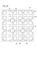
ところで、例えば電子部品の電極間に接続配線を形成して、全ての電子部品の電極を電気的に接続する方法としては、例えば図15に示す方法が考えられる。先ず、電子部品100単位に4つの電極102がマトリクス状に配列形成された場合を想定する。この場合、電子部品100単位に四隅に隣接する電子部品100の電極102と導通をとるための例えば円形のパッドパターン104(導通パターン)を形成することが考えられる。例えば多数個取り基板106に予め分離用の溝108を形成している場合は、これら分離用の溝108の交差部にパッドパターン104が形成される。分離用の溝108とは、電子部品100単位に分離するための溝である。
その後、電解めっきを行うと、めっき層は、各電極層全面に形成されると共に、電極層につながるパッドパターン104全面にも形成される。つまり、本来、必要のない部分にも多量のめっき層が形成され、めっきの消費量が多くなる。これは、コスト増につながる。
また、電極102全面にめっき層が形成されると、その後の実装工程で以下のような問題が生じるおそれがある。例えばめっき層上に導電材(例えば半田層)を形成して、配線基板等に実装する場合、実装上の圧力によって導電材が横方向にはみ出し、導電材同士で接触し、短絡するおそれがある。特に、電極102間の隙間が狭い集積度の高い電子部品100の場合、上述の問題が顕著に生じるものと思われる。従って、電子部品100の小型化、高集積化には限界がある。もちろん、その後の工程で、導電材同士が接触した部分を分離する工程を追加することが考えられるが、さらなるコスト増となる。
また、電子部品100単位に特性検査を行う場合、多数個取り基板106を分離して多数の電子部品100に分離した後、検査工程に搬送して行うこととなる。しかし、分離された電子部品100単位に特性検査を行うことは煩雑である。そこで、一旦、多数の電子部品100をそれぞれ電子部品100同士が導通しないように、例えば仕切り板を有する治具上に揃えて設置してから、個々の特性検査を行う。
そのため、上述した方法では、多数の電子部品100を検査工程に搬送する手間と、多数の電子部品100を治具上に設置する手間がかかり、工数が増え、コスト増につながるという問題がある。
他の方法としては、電極102間を導通するためのパッドパターン104を形成せずに、電極102上に無電解めっきにてめっき層を形成することが考えられる。しかし、無電解めっきを適用した場合には、めっき硬度が高くなってしまうため、その後の工程で品質不具合が発生してしまう。この問題が回避困難であるため、電解めっきを選定することが主流となっている。
本発明はこのような課題を考慮してなされたものであり、下記効果を奏する電子部品を提供することを目的とする。すなわち、本発明で提供される電子部品は、導電材同士の接触による短絡を防止でき、しかも、めっきの消費量の低減を図ることができ、電子部品の小型化、高集積化、コストの低減化を実現させることができる。
また、本発明の他の目的は、下記効果を奏する電子部品の製造方法を提供する。すなわち、多数個取り基板の状態で、電子部品単位の特性検査を行うことが可能であるばかりでなく、導電材同士の接触による短絡を防止でき、しかも、めっきの消費量の低減を図ることができる。小型化、高集積化、コストの低減化を実現させることができる電子部品を作製することができる。
[1] 第1の本発明に係る電子部品は、基板と、前記基板上に形成された電極層と、前記電極層の上面に形成され、前記電極層の上面面積よりも小さい上面面積を有するめっき層と、を有し、前記電極層の上面のうち、該電極層の外周の少なくとも一部を含む部分が前記めっき層から露出していることを特徴とする。
[2] 第1の本発明において、前記めっき層から露出している前記部分は、前記電極層の外周全てを含んでもよい。
[3] 第1の本発明において、前記電極層の上面形状が多角形であって、前記めっき層から露出している前記部分は、前記電極層の外周のうち、少なくとも1つの辺を含んでもよい。
[4] 第1の本発明において、前記電極層の上面形状が多角形であって、前記めっき層から露出している前記部分は、前記電極層の外周のうち、1つの辺の一部を含んでもよい。
[5] 第1の本発明において、前記めっき層は、電子部品の実装の際に用いられる導電材の濡れ性が、前記電極層よりも優れていることが好ましい。
[6] 第2の本発明に係る電子部品の製造方法は、原板上に、電子部品単位にそれぞれ電極層を形成する電極層形成工程と、前記電極層間に、前記電極層間を電気的に接続する導通部を有するマスクを形成するマスク形成工程と、前記マスクによって電気的に接続された前記電極層上にめっき層を形成するめっき工程と、前記マスクを取り除くマスク除去工程と、前記原板の状態で、特性検査を行う工程と、前記原板を分離して複数の電子部品とする分離工程と、を有することを特徴とする。
[7] 第2の本発明において、前記マスク形成工程は、前記マスクを前記電極層の一部にオーバーラップさせて形成してもよい。
[8] 第2の本発明において、前記マスク形成工程で形成される前記マスクは、前記導通部となる導電層と、前記導電層を被覆するマスク層と、を有し、前記マスク形成工程は、前記電極層間に、前記導電層を形成する工程と、前記導電層を被覆する前記マスク層を形成する工程と、を有してもよい。
[9] 第2の本発明において、前記マスク形成工程で形成される前記マスクは、マスク層と、該マスク層上に形成される前記導通部となる導電層と、を有し、前記マスク形成工程は、前記電極層間に、前記マスク層を形成する工程と、前記電極層間を電気的に接続するように前記マスク層上に前記導電層を形成する工程と、を有し、前記マスク除去工程は、前記導電層上に形成された前記めっき層と共に、前記マスクを取り除いてもよい。
[10] 第2の本発明において、前記マスク形成工程で形成される前記マスクは、マスク層と、該マスク層上に形成される前記導通部となる導電層と、該導電層を被覆する絶縁層とを有し、前記マスク形成工程は、前記電極層間に、前記マスク層を形成する工程と、前記電極層間を電気的に接続するように前記マスク層上に前記導電層を形成する工程と、前記導電層を被覆する前記絶縁層を形成する工程と、を有してもよい。
[11] 第2の本発明において、前記原板の一方又は両方の主面に、前記分離工程において前記複数の電子部品に分離するための複数の溝が予め形成されていてもよい。
[12] この場合、前記複数の溝は、前記原板の一方向に配列された複数の第1溝と、前記原板の前記一方向とは異なる他方向に配列された複数の第2溝とを有してもよい。
[13] 第2の本発明において、前記原板の他方の主面に、前記分離工程において前記複数の電子部品に分離するための溝が予め形成され、前記マスク形成工程は、前記原板の一方の主面上であって前記溝に対応した部分に前記マスクを形成してもよい。
[14] この場合、複数の前記溝は、前記原板の一方向に配列された複数の第1溝と、前記原板の前記一方向とは異なる他方向に配列された複数の第2溝とを有し、前記マスク形成工程は、前記原板の前記他方の主面における前記第1溝に対応した部分あるいは前記第2溝に対応した部分に前記マスクを形成してもよい。
本発明に係る電子部品によれば、導電材同士の接触による短絡を防止でき、しかも、めっきの消費量の低減を図ることができ、電子部品の小型化、高集積化、コストの低減化を実現させることができる。
また、本発明に係る電子部品の製造方法によれば、多数個取り基板の状態で、電子部品単位の特性検査を行うことが可能であるばかりでなく、導電材同士の接触による短絡を防止でき、しかも、めっきの消費量の低減を図ることができる。小型化、高集積化、コストの低減化を実現させることができる電子部品を製造することができる。
以下、本発明に係る電子部品及びその製造方法の実施の形態例を図1A~図14Bを参照しながら説明する。
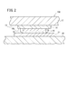
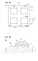
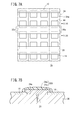
先ず、第1の本実施の形態に係る電子部品(以下、第1電子部品10Aと記す)は、図1A及び図1Bに示すように、例えば立方体あるいは直方体等の立体形状を有する基板12と、該基板12の実装面13(配線基板等に実装される面)に形成された1以上の電極層14と、電極層14の上面14aに形成され、且つ、該電極層14の上面面積よりも小さい上面面積を有するめっき層16とを有し、電極層14の上面14aのうち、該電極層14の外周の少なくとも一部を含む部分がめっき層16から露出している。図1A及び図1Bの例では、第1電子部品10Aの実装面13に対して、4つの矩形状の電極層14がマトリクス状に配列形成された例を示している。もちろん、電極層14の数、配列形態は任意であるが、第1電子部品10Aの実装面13における少なくとも1つの辺に沿って配列形成することが好ましい。
そして、この第1電子部品10Aにおいて、電極層14の上面14aのうち、めっき層16から露出している部分(露出部分14b)は、電極層14の外周全てを含む。図1A及び図1Bの例では、各電極層14の上面形状が例えば正方形状であり、各めっき層16の上面形状が電極層14の上面形状の相似形であって、且つ、上面面積が電極層14よりも小さいとされている。もちろん、電極層14の上面形状とめっき層16の上面形状とが相似形でなくてもよい。例えば電極層14の上面形状が正方形状、めっき層16の上面形状が長方形状であってもよいし、その逆の組み合わせでもよい。また、例えば電極層14の上面形状が円形状(もしくは楕円形状)、めっき層16の上面形状が矩形状であってもよいし、その逆の組み合わせでもよい。また、電極層14とめっき層16の上面形状の一部が湾曲されていてもよい。
この第1電子部品10Aにおいては、電極層14の上面14aに、該電極層14の上面面積よりも小さい上面面積を有するめっき層16を有することから、電極層14の上面全面にめっき層を有する従来例と異なり、めっきの消費量を低減させることができる。これは、製造コストの低減化につながる。
また、図2に示すように、その後の実装工程、例えばめっき層16上に導電材18(例えば半田層や導電性接着剤)を塗布して、配線基板20の端子21等に実装する場合、実装上の圧力によって導電材18が横方向にはみ出す。しかし、第1電子部品10Aでは、電極層14の外周の少なくとも一部を含む部分がめっき層16から露出しているため、導電材18は電極層14の露出部分14bにはみ出すだけで、電極層14の外周よりも外側にはみ出すことが抑制される。この場合、電極層14における導電材18の濡れ性が、めっき層16より劣っていれば、導電材18のはみ出しは、電極層14の露出部分14bにて停止することとなる。つまり、電極層14の露出部分14bは、実装時における導電材18の塗布余剰分の逃げ場となるため、電極層14外へのはみ出しを防ぐことができる。しかも、第1電子部品10Aは、電極層14の外周全てを含む部分が露出している。そのため、導電材18が四方にはみ出しても、確実に、電極層14の露出部分14bにて、導電材18のはみ出しが停止し、導電材18の電極層14外へのはみ出しを確実に防止することができる。
これにより、電極層14間の隙間が狭い集積度の高い電子部品であっても、電極間での短絡を防止することができ、電子部品の小型化、高集積化を実現させることができる。従来は、導電材同士が接触した部分を分離する工程が必要になる場合もあったが、この第1電子部品10Aでは、導電材18同士が接触することが回避されるため、このような分離工程が不要となる。その結果、めっきの消費量の低減とも相まって、コストの低減化を図ることができる。
次に、第2の本実施の形態に係る電子部品(以下、第2電子部品10Bと記す)について図3A及び図3Bを参照しながら説明する。
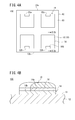
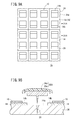
この第2電子部品10Bは、図3A及び図3Bに示すように、上述した第1電子部品10Aとほぼ同様の構成を有するが、以下の点で異なる。すなわち、電極層14の上面形状が多角形であって、めっき層16から露出している部分(露出部分14b)が、電極層14の外周のうち、外周の全てを含むことなく、少なくとも1つの辺を含む。
露出部分14bの位置は、複数の電極層14毎に異ならせてもよいし、各電極層14毎に異ならせてもよい。もちろん、全ての電極層14において同じ位置に露出部分14bを形成してもよいし、各電極層14の辺のうち、基板12の辺に最も近接する辺、あるいは最も遠い辺を含む部分を露出させてもよい。
図3A及び図3Bに、その一例を示す。すなわち、マトリクス状に配列された4つの電極層14のうち、基板12の1つの辺(第1辺12a)寄りに形成された2つの電極層14は、該第1辺12aに最も近接する辺22aを含む部分が露出している。基板12の他の1つの辺(第1辺12aに対向する第2辺12b)寄りに形成された2つの電極層14は、該第2辺12bに最も近接する辺22bを含む部分が露出している。
この第2電子部品10Bにおいても、電極層14の上面14aに、該電極層14の上面面積よりも小さい上面面積を有するめっき層16を有する。そのため、電極層14の上面全面にめっき層を有する従来例と異なり、めっきの消費量を低減させることができる。
また、電極層14が露出した部分(露出部分14b)が、実装時における導電材18の塗布余剰分の逃げ場となるため、電極層14外へのはみ出しを防ぐことができる。この場合、電極層14の外周のうち、外周の全てを含むことなく、少なくとも1つの辺を含む部分が露出しているため、第1電子部品10Aと比して、めっきの消費量の低減効果は低くなる。しかし、多数個取り基板で電子部品を作製する際に、作り易いという効果がある。これについては後述する。
次に、第3の本実施の形態に係る電子部品(以下、第3電子部品10Cと記す)について図4A及び図4Bを参照しながら説明する。
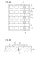
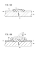
この第3電子部品10Cは、図4A及び図4Bに示すように、上述した第1電子部品10Aとほぼ同様の構成を有するが、以下の点で異なる。すなわち、電極層14の上面形状が多角形であって、めっき層16から露出している部分(露出部分14b)が、電極層14の外周のうち、外周の全てを含むことなく、1つの辺の一部を含む。
露出部分14bの位置は、複数の電極層14毎に異ならせてもよいし、各電極層14毎に異ならせてもよい。もちろん、全ての電極層14において同じ位置に露出部分14bを形成してもよい。また、各電極層14の辺のうち、基板12の辺に最も近接する1つの辺の一部、あるいは最も遠い1つの辺の一部を含む部分を露出させてもよい。
図4A及び図4Bに、その一例を示す。すなわち、マトリクス状に配列された4つの電極層14のうち、基板12の第1辺12a寄りに形成された2つの電極層14は、該第1辺12aに最も近接する1つの辺22aの一部を含む部分が露出している。基板12の第2辺12b寄りに形成された2つの電極層14は、該第2辺12bに最も近接する1つの辺22bの一部を含む部分が露出している。
この第3電子部品10Cにおいても、電極層14の上面14aに、該電極層14の上面面積よりも小さい上面面積を有するめっき層16を有する。そのため、電極層14の上面全面にめっき層を有する従来例と異なり、めっきの消費量を低減させることができる。
また、電極層14が露出した部分(露出部分14b)が、実装時における導電材18の塗布余剰分の逃げ場となるため、電極層14外へのはみ出しを防ぐことができる。
なお、上述した第2電子部品10B及び第3電子部品10Cにおいては、電極層14の上面形状を多角形としたが、多角形以外でもよいことはもちろんである。
次に、本実施の形態に係る電子部品の製造方法について説明する。
最初に、第1の本実施の形態に係る製造方法(第1製造方法)について図5A~図10Bを参照しながら説明する。
先ず、図5A及び図5Bに示すように、分離することによって多数個の電子部品10を取り出すための多数個取り基板24(原板)の一主面24aに、後の分離工程において多数個の電子部品10に分離するための複数の溝(ブレイクライン26)を形成する。図5Aの例では、多数個取り基板24の一主面24aに対して、横方向と縦方向にそれぞれ複数のブレイクライン26を形成することによって、ブレイクライン26を格子状に形成した例を示す。この格子状のブレイクライン26で区画される各格子の部分がそれぞれ電子部品10となる。多数個取り基板24を構成する材料としては、例えばアルミナ、ベリリア、窒化アルミニウム、窒化ホウ素、窒化珪素等を挙げることができる。
その後、多数個取り基板24の一主面24aに、電子部品10単位(電子部品10の区画単位)にそれぞれ複数の電極層14を例えばスクリーン印刷等によって形成する(電極層形成工程)。例えば電子部品10単位に、4つの矩形状の電極層14をマトリクス状に配列形成する。電極層14を構成する材料としては、例えばタングステン、モリブデン、マンガン等を挙げることができる。
その後、図6A~図7Bに示すように、電極層14間を電気的に接続する導通部を有する第1マスク30A(図7B参照)を形成する(マスク形成工程)。例えば横方向に延在するブレイクライン26上に第1マスク30Aを形成する。このとき、第1マスク30Aを、横方向に延在するブレイクライン26を間に挟んで対向する電極層14の各一部にオーバーラップさせて形成する。第1マスク30Aは、図7Bに示すように、導通部となる第1導電層32aと、第1導電層32aを被覆する電気的絶縁材料による第1マスク層34aとを有する。第1導電層32aを構成する材料としては、例えば熱硬化型導電性銀ペースト、感光性銀ペースト、銀ナノペースト、金ナノペースト等を挙げることができる。第1マスク層34aを構成する材料としては、例えば感光性レジスト、熱硬化型レジスト、その他有機系の保護材等を挙げることができる。
第1マスク30Aの形成方法は、具体的には、図6A及び図6Bに示すように、先ず、横方向に延在するブレイクライン26上に第1導電層32aを例えばスクリーン印刷等によって形成する。このとき、横方向に延在するブレイクライン26を間に挟んで対向する電極層14の各一部にオーバーラップさせて形成する。この第1導電層32aの形成によって、全ての電極層14が第1導電層32aを介して電気的に接続されることになる。
その後、図7A及び図7Bに示すように、第1導電層32aを被覆する第1マスク層34aを例えばスクリーン印刷等によって形成する。この場合も、横方向に延在するブレイクライン26を間に挟んで対向する電極層14の各一部にオーバーラップさせ、且つ、第1導電層32aを被覆するように形成する。すなわち、露出する第1導電層32aの上面から側面にかけて第1マスク層34aで被覆する。
その後、図8A及び図8Bに示すように、第1マスク30Aによって電気的に接続された全ての電極層14上にめっき層16を形成する(めっき工程)。めっき層16は、Sn、Cu、Zn、Ni、Au及びこの組み合わせ等を挙げることができる。このとき、各電極層14のうち、それぞれ第1マスク30A(特に、第1マスク層34a)から露出する部分にめっき層16が形成される。すなわち、電極層14全面にめっき層16は形成されず、電極層14上には、電極層14の上面面積よりも小さい上面面積を有するめっき層16が形成される。特に、第1導電層32aの上面から側面にかけて第1マスク層34aで被覆したので、めっき液が第1導電層32aまで浸入することがない。確実に、電極層14上に、電極層14の上面面積よりも小さい上面面積を有するめっき層16を形成することができる。
その後、図9A及び図9Bに示すように、第1マスク30Aを取り除く(マスク除去工程)。例えば第1マスク層34aの端部を治具で挟んで引き剥がす(ピールする)ことにより行うことができる。従って、多数個取り基板24と第1導電層32aとの密着力は、第1導電層32aと第1マスク層34aとの密着力よりも低いことが好ましい。これにより、第1導電層32aの残渣を残すことなく、第1マスク30Aを確実に引き剥がすことができる。特に、多数個取り基板24の一主面24aにブレイクライン26を設けた場合は、ブレイクライン26内にも第1導電層32aが入り込み、いわゆるアンカー効果で、多数個取り基板24と第1導電層32aとの密着力が高められる。そのため、これを見越して、第1導電層32aと第1マスク層34aとの密着力を高めておくことが好ましい。
そして、このマスク除去工程で、第1マスク30Aを取り除くことによって、電極層14の上面14aに、電極層14の上面面積よりも小さい上面面積を有するめっき層16が形成される。それと共に、電極層14の上面14aのうち、該電極層14の外周の少なくとも一部を含む部分が、めっき層16から露出した状態となる。特に、電子部品10単位で見ると、例えば図3Aに示す第2電子部品10Bにおける電極層14とめっき層16との関係と同じ形態となる。
その後、図10Aに示すように、多数個取り基板24の状態で、各電子部品10の特性検査を行う。上述したマスク形成工程及びマスク除去工程によって、従来のようなパッドパターンを形成することなく、全ての電極層14上にめっき層16が形成される。しかも、各電子部品10が電気的に独立していることから、多数個取り基板24の状態で、各電子部品10の特性検査を行うことができる。そのため、従来において必要であった多数の電子部品10を検査工程に搬送する手間や、多数の電子部品10を治具上に設置する手間等が不要となる。
その後、図10Bに示すように、多数個取り基板24を分離して、多数個の電子部品10とする(分離工程)。この場合、多数個の第2電子部品10Bが作製されることとなる。
このように、第1製造方法においては、多数個取り基板24の状態で、電子部品10単位の特性検査を行うことが可能であるばかりでなく、導電材18同士の接触による短絡を防止でき、しかも、めっきの消費量の低減を図ることができる。小型化、高集積化、コストの低減化を実現させることができる多数個の電子部品10を作製することができる。電子部品10の歩留まり、生産性も向上する。
次に、第2の実施の形態に係る電子部品の製造方法(以下、第2製造方法と記す)について図11A~図12Bを参照しながら説明する。
先ず、上述した第1製造方法と同様に、多数個取り基板24の一主面24aに、複数のブレイクライン26を形成する(図5A及び図5B参照)。
その後、上述した第1製造方法と同様に、多数個取り基板24の一主面24aに、電子部品10単位(電子部品10の区画単位)にそれぞれ複数の電極層14を例えばスクリーン印刷等によって形成する(図5A及び図5B参照:電極層形成工程)。
その後、図11A及び11Bに示すように、電極層14間を電気的に接続する導通部を有する第2マスク30Bを形成する(図11B参照:マスク形成工程)。この場合、第1製造方法と同様に、第2マスク30Bを、横方向に延在するブレイクライン26を間に挟んで対向する電極層14の各一部にオーバーラップさせて形成する。特に、この第2製造方法では、第2マスク30Bの構造及び第2マスク30Bの形成手順が第1マスク30Aの場合と異なる。
すなわち、第2マスク30Bは、図11Bに示すように、電気的絶縁材料や導電材料による第2マスク層34bと、該第2マスク層34bを被覆する導通部となる第2導電層32bとを有する。第2マスク層34bを構成する材料としては、例えば感光性レジスト、熱硬化型レジスト、その他有機系の保護材等を挙げることができる。第2導電層32bを構成する材料としては、例えば熱硬化型導電性銀ペースト、感光性銀ペースト、銀ナノペースト、金ナノペースト等を挙げることができる。
そして、第2マスク30Bの形成方法は、具体的には、図11Aに示すように、先ず、横方向に延在するブレイクライン26上に第2マスク層34bを例えばスクリーン印刷等によって形成する。このとき、横方向に延在するブレイクライン26を間に挟んで対向する電極層14の各一部にオーバーラップさせて形成する。その後、第2マスク層34bを被覆する第2導電層32bを例えばスクリーン印刷等によって形成する。この場合も、横方向に延在するブレイクライン26を間に挟んで対向する電極層14の各一部にオーバーラップさせ、且つ、第2マスク層34bを被覆するように形成する。すなわち、露出する第2マスク層34bの上面から側面にかけて第2導電層32bで被覆する。この第2導電層32bの形成によって、全ての電極層14が第2導電層32bを介して電気的に接続されることになる。
その後、図12Aに示すように、第2マスク30Bによって電気的に接続された全ての電極層14上にめっき層16を形成する(めっき工程)。このとき、各電極層14のうち、それぞれ第2マスク30B(特に、第2導電層32b)から露出する部分にめっき層16が形成される。すなわち、電極層14全面にめっき層16は形成されず、電極層14上には、電極層14の上面面積よりも小さい上面面積を有するめっき層16が形成される。なお、第2マスク30Bの第2導電層32b上にもめっき層16が形成される。特に、第2マスク層34bの上面から側面にかけて第2導電層32bで被覆したので、めっき液が第2マスク層34bまで浸入することがない。確実に、電極層14上に、電極層14の上面面積よりも小さい上面面積を有するめっき層16を形成することができる。
その後、図12Bに示すように、第2マスク30Bを取り除く(マスク除去工程)。例えば第2マスク層34bの端部を治具で挟んで引き剥がす(ピールする)ことにより、その上の第2導電層32b及びめっき層16と共に除去することができる(リフトオフ)。その他、第2マスク層34bを液体等で分解、溶解したり、予め多数個取り基板24と第2マスク層34bとの密着力を低減しておく等の方法を好ましく採用することができる。
そして、このマスク除去工程で、第2マスク30Bを取り除くことによって、第1製造方法と同様に、電極層14の上面14aに、電極層14の上面面積よりも小さい上面面積を有するめっき層16が形成される。それと共に、電極層14の上面14aのうち、該電極層14の外周の少なくとも一部を含む部分がめっき層16から露出した状態となる。
その後、図10Aに示すように、多数個取り基板24の状態で、各電子部品10の特性検査を行う。その後、図10Bに示すように、多数個取り基板24を分離して、多数個の電子部品10とする(分離工程)。
このように、第2製造方法においても、多数個取り基板24の状態で、電子部品10単位の特性検査を行うことが可能であるばかりでなく、導電材18同士の接触による短絡を防止でき、しかも、めっきの消費量の低減を図ることができる。小型化、高集積化、コストの低減化を実現させることができる多数個の電子部品10を作製することができる。電子部品の歩留まり、生産性も向上する。
次に、第3の実施の形態に係る電子部品の製造方法(以下、第3製造方法と記す)について図13A~図14Bを参照しながら説明する。
先ず、上述した第1製造方法と同様に、多数個取り基板24の一主面24aに、複数のブレイクライン26を形成する。その後、多数個取り基板24の一主面24aに、電子部品10単位(電子部品10の区画単位)にそれぞれ複数の電極層14を例えばスクリーン印刷等によって形成する(電極層形成工程)。
そして、図13A及び図13Bに示すように、電極層14間を電気的に接続する導通部を有する第3マスク30Cを形成する(マスク形成工程)。この場合、第2製造方法と同様に、第3マスク30Cを、横方向に延在するブレイクライン26を間に挟んで対向する電極層14の各一部にオーバーラップさせて形成する。特に、この第3製造方法では、第3マスク30Cの構造及び第3マスク30Cの形成手順が第1マスク30A及び第2マスク30Bの場合と異なる。
すなわち、第3マスク30Cは、図13Bに示すように、電気的絶縁材料や導電材料による第3マスク層34cと、該第3マスク層34cを被覆する導通部となる第3導電層32cと、第3導電層32cを被覆する絶縁層36とを有する。第3マスク層34cを構成する材料としては、例えば感光性レジスト、熱硬化型レジスト、その他有機系の保護材等を挙げることができる。第3導電層32cを構成する材料としては、例えば熱硬化型導電性銀ペースト、感光性銀ペースト、銀ナノペースト、金ナノペースト等を挙げることができる。絶縁層36を構成する材料としては、例えば感光性レジスト、熱硬化型レジスト、その他有機系の保護材等を挙げることができる。
そして、第3マスク30Cの形成方法は、具体的には、図13Aに示すように、先ず、横方向に延在するブレイクライン26上に第3マスク層34cを例えばスクリーン印刷等によって形成する。このとき、横方向に延在するブレイクライン26を間に挟んで対向する電極層14の各一部にオーバーラップさせて形成する。その後、第3マスク層34cを被覆する第3導電層32cを例えばスクリーン印刷等によって形成する。この場合も、横方向に延在するブレイクライン26を間に挟んで対向する電極層14の各一部にオーバーラップさせ、且つ、第3マスク層34cを被覆するように形成する。すなわち、露出する第3マスク層34cの上面から側面にかけて第3導電層32cで被覆する。この第3導電層32cの形成によって、全ての電極層14が第3導電層32cを介して電気的に接続されることになる。さらに、第3導電層32cを被覆する絶縁層36を例えばスクリーン印刷等によって形成する。この場合も、横方向に延在するブレイクライン26を間に挟んで対向する電極層14の各一部にオーバーラップさせ、且つ、第3導電層32cを被覆するように形成する。すなわち、露出する第3導電層32cの上面から側面にかけて絶縁層36で被覆する。
その後、図14Aに示すように、第3マスク30Cによって電気的に接続された全ての電極層14上にめっき層16を形成する(めっき工程)。このとき、各電極層14のうち、それぞれ第3マスク30C(特に、絶縁層36)から露出する部分にめっき層16が形成される。すなわち、電極層14全面にめっき層16は形成されず、電極層14上には、電極層14の上面面積よりも小さい上面面積を有するめっき層16が形成される。なお、第3マスク30Cの絶縁層36上にはめっき層16は形成されない。特に、第3マスク層34cの上面から側面にかけて第3導電層32cで被覆し、第3導電層32cの上面から側面にかけて絶縁層36で被覆したので、めっき液が第3導電層32cや第3マスク層34cまで浸入することがない。確実に、電極層14上に、電極層14の上面面積よりも小さい上面面積を有するめっき層16を形成することができる。
その後、図14Bに示すように、第3マスク30Cを取り除く(マスク除去工程)。例えば第3マスク層34cの端部を治具で挟んで引き剥がす(ピールする)ことにより、その上の第3導電層32c及び絶縁層36と共に除去することができる(リフトオフ)。その他、第3マスク層34cを液体等で分解、溶解したり、予め多数個取り基板24と第3マスク層34cとの密着力を低減しておく等の方法を好ましく採用することができる。
そして、このマスク除去工程で、第3マスク30Cを取り除くことによって、第1製造方法及び第2製造方法と同様に、電極層14の上面14aに、電極層14の上面面積よりも小さい上面面積を有するめっき層16が形成される。それと共に、電極層14の上面14aのうち、該電極層14の外周の少なくとも一部を含む部分がめっき層16から露出した状態となる。
その後、図10Aに示すように、多数個取り基板24の状態で、各電子部品10の特性検査を行う。その後、図10Bに示すように、多数個取り基板24を分離して、多数個の電子部品10とする(分離工程)。
このように、第3製造方法においても、多数個取り基板24の状態で、電子部品10単位の特性検査を行うことが可能であるばかりでなく、導電材18同士の接触による短絡を防止でき、しかも、めっきの消費量の低減を図ることができる。小型化、高集積化、コストの低減化を実現させることができる多数個の電子部品10を作製することができる。電子部品10の歩留まり、生産性も向上する。
上述の例では、多数個取り基板24の一主面24aにブレイクライン26を形成した例を示したが、他主面にもブレイクライン26を形成してもよい。
その他、図示しないが、多数個取り基板24の一主面24aにブレイクライン26を形成せずに、他主面にブレイクライン26を形成してもよい。また、一主面24a及び他主面共にブレイクライン26を形成しなくてもよい。これらの場合、第1マスク30A~第3マスク30Cの密着力について、ブレイクライン26によるアンカー効果を考慮する必要がなくなる。
なお、本発明に係る電子部品及びその製造方法は、上述の実施の形態に限らず、本発明の要旨を逸脱することなく、種々の構成を採り得ることはもちろんである。
Claims (14)
- 基板(12)と、
前記基板(12)上に形成された電極層(14)と、
前記電極層(14)の上面に形成され、前記電極層(14)の上面面積よりも小さい上面面積を有するめっき層(16)と、を有し、
前記電極層(14)の上面のうち、該電極層(14)の外周の少なくとも一部を含む部分が前記めっき層(16)から露出していることを特徴とする電子部品。 - 請求項1記載の電子部品において、
前記めっき層(16)から露出している前記部分は、前記電極層(14)の外周全てを含むことを特徴とする電子部品。 - 請求項1記載の電子部品において、
前記電極層(14)の上面形状が多角形であって、
前記めっき層(16)から露出している前記部分は、前記電極層(14)の外周のうち、少なくとも1つの辺を含むことを特徴とする電子部品。 - 請求項1記載の電子部品において、
前記電極層(14)の上面形状が多角形であって、
前記めっき層(16)から露出している前記部分は、前記電極層(14)の外周のうち、1つの辺の一部を含むことを特徴とする電子部品。 - 請求項1~4のいずれか1項に記載の電子部品において、
前記めっき層(16)は、電子部品の実装の際に用いられる導電材(18)の濡れ性が、前記電極層(14)よりも優れていることを特徴とする電子部品。 - 原板(24)上に、電子部品単位にそれぞれ電極層(14)を形成する電極層形成工程と、
前記電極層(14)間に、前記電極層(14)間を電気的に接続する導通部を有するマスクを形成するマスク形成工程と、
前記マスクによって電気的に接続された前記電極層(14)上にめっき層(16)を形成するめっき工程と、
前記マスクを取り除くマスク除去工程と、
前記原板(24)の状態で、特性検査を行う工程と、
前記原板(24)を分離して複数の電子部品とする分離工程と、を有することを特徴とする電子部品の製造方法。 - 請求項6記載の電子部品の製造方法において、
前記マスク形成工程は、
前記マスクを前記電極層(14)の一部にオーバーラップさせて形成することを特徴とする電子部品の製造方法。 - 請求項6又は7記載の電子部品の製造方法において、
前記マスク形成工程で形成される前記マスクは、前記導通部となる導電層(32a)と、前記導電層(32a)を被覆するマスク層(34a)と、を有し、
前記マスク形成工程は、
前記電極層(14)間に、前記導電層(32a)を形成する工程と、
前記導電層(32a)を被覆する前記マスク層(34a)を形成する工程と、を有することを特徴とする電子部品の製造方法。 - 請求項6又は7記載の電子部品の製造方法において、
前記マスク形成工程で形成される前記マスクは、マスク層(34b)と、該マスク層(34b)上に形成される前記導通部となる導電層(32b)と、を有し、
前記マスク形成工程は、
前記電極層(14)間に、前記マスク層(34b)を形成する工程と、
前記電極層(14)間を電気的に接続するように前記マスク層(34b)上に前記導電層(32b)を形成する工程と、を有し、
前記マスク除去工程は、前記導電層(32b)上に形成された前記めっき層(16)と共に、前記マスクを取り除くことを特徴とする電子部品の製造方法。 - 請求項6又は7記載の電子部品の製造方法において、
前記マスク形成工程で形成される前記マスクは、マスク層(34c)と、該マスク層(34c)上に形成される前記導通部となる導電層(32c)と、該導電層(32c)を被覆する絶縁層(36)とを有し、
前記マスク形成工程は、
前記電極層(14)間に、前記マスク層(34c)を形成する工程と、
前記電極層(14)間を電気的に接続するように前記マスク層(34c)上に前記導電層(32c)を形成する工程と、
前記導電層(32c)を被覆する前記絶縁層(36)を形成する工程と、を有することを特徴とする電子部品の製造方法。 - 請求項6~10のいずれか1項に記載の電子部品の製造方法において、
前記原板(24)の一方又は両方の主面に、前記分離工程において前記複数の電子部品に分離するための複数の溝(26)が予め形成されることを特徴とする電子部品の製造方法。 - 請求項11記載の電子部品の製造方法において、
前記複数の溝(26)は、前記原板(24)の一方向に配列された複数の第1溝と、前記原板(24)の前記一方向とは異なる他方向に配列された複数の第2溝とを有することを特徴とする電子部品の製造方法。 - 請求項6~10のいずれか1項に記載の電子部品の製造方法において、
前記原板(24)の他方の主面に、前記分離工程において前記複数の電子部品に分離するための溝(26)が予め形成され、
前記マスク形成工程は、前記原板(24)の一方の主面上であって前記溝(26)に対応した部分に前記マスクを形成することを特徴とする電子部品の製造方法。 - 請求項13記載の電子部品の製造方法において、
複数の前記溝(26)は、前記原板(24)の一方向に配列された複数の第1溝と、前記原板(24)の前記一方向とは異なる他方向に配列された複数の第2溝とを有し、
前記マスク形成工程は、前記原板(24)の前記他方の主面における前記第1溝に対応した部分あるいは前記第2溝に対応した部分に前記マスクを形成することを特徴とする電子部品の製造方法。
Priority Applications (2)
| Application Number | Priority Date | Filing Date | Title |
|---|---|---|---|
| CN201380066834.6A CN104919906B (zh) | 2012-12-27 | 2013-11-12 | 电子部件及其制造方法 |
| JP2014554225A JP6366509B2 (ja) | 2012-12-27 | 2013-11-12 | 電子部品及びその製造方法 |
Applications Claiming Priority (2)
| Application Number | Priority Date | Filing Date | Title |
|---|---|---|---|
| JP2012284787 | 2012-12-27 | ||
| JP2012-284787 | 2012-12-27 |
Publications (1)
| Publication Number | Publication Date |
|---|---|
| WO2014103541A1 true WO2014103541A1 (ja) | 2014-07-03 |
Family
ID=51020639
Family Applications (1)
| Application Number | Title | Priority Date | Filing Date |
|---|---|---|---|
| PCT/JP2013/080526 Ceased WO2014103541A1 (ja) | 2012-12-27 | 2013-11-12 | 電子部品及びその製造方法 |
Country Status (3)
| Country | Link |
|---|---|
| JP (1) | JP6366509B2 (ja) |
| CN (1) | CN104919906B (ja) |
| WO (1) | WO2014103541A1 (ja) |
Cited By (1)
| Publication number | Priority date | Publication date | Assignee | Title |
|---|---|---|---|---|
| JP2019149452A (ja) * | 2018-02-27 | 2019-09-05 | 京セラ株式会社 | 電子素子実装用基板、電子素子実装用母基板、電子装置および電子モジュール |
Citations (3)
| Publication number | Priority date | Publication date | Assignee | Title |
|---|---|---|---|---|
| JPS6387795A (ja) * | 1986-09-30 | 1988-04-19 | 株式会社 アサヒ化学研究所 | 基板に導電回路を形成する方法 |
| JPH0258890A (ja) * | 1988-08-25 | 1990-02-28 | Murata Mfg Co Ltd | 銅張積層板 |
| JP2011249526A (ja) * | 2010-05-26 | 2011-12-08 | Kyocera Corp | 多数個取り配線基板 |
Family Cites Families (23)
| Publication number | Priority date | Publication date | Assignee | Title |
|---|---|---|---|---|
| JPS5938758B2 (ja) * | 1977-07-13 | 1984-09-19 | セイコーインスツルメンツ株式会社 | 部分メツキ用マスキング板 |
| DE3240387C1 (de) * | 1982-11-02 | 1983-11-17 | Klaus 5650 Solingen Grah | Abdeckband fuer galvanische Prozesse |
| JPS59163889A (ja) * | 1983-03-08 | 1984-09-14 | 松下電器産業株式会社 | 基板上導体への部分的めつき形成方法 |
| JPS59145569U (ja) * | 1983-03-18 | 1984-09-28 | 沖電気工業株式会社 | 部分電気メツキ治具 |
| JPS62210688A (ja) * | 1986-03-11 | 1987-09-16 | 日本碍子株式会社 | セラミツクパツケ−ジの部分めつき方法及びその装置 |
| JPS62296595A (ja) * | 1986-06-17 | 1987-12-23 | 松下電器産業株式会社 | 印刷配線回路板の選択めつき方法 |
| JPS63114081A (ja) * | 1986-07-22 | 1988-05-18 | セイコーインスツルメンツ株式会社 | 配線パタ−ンの構造 |
| JPH04208593A (ja) * | 1990-12-03 | 1992-07-30 | Nec Corp | 厚膜印刷基板 |
| US5133118A (en) * | 1991-08-06 | 1992-07-28 | Sheldahl, Inc. | Surface mounted components on flex circuits |
| JPH05183259A (ja) * | 1991-12-27 | 1993-07-23 | Ibiden Co Ltd | 高密度プリント配線板の製造方法 |
| JP3301188B2 (ja) * | 1993-12-27 | 2002-07-15 | 株式会社村田製作所 | 積層電子部品、その製造方法およびその特性測定方法 |
| JP3368645B2 (ja) * | 1993-12-27 | 2003-01-20 | 株式会社村田製作所 | 積層電子部品、その製造方法およびその特性測定方法 |
| US5773764A (en) * | 1996-08-28 | 1998-06-30 | Motorola, Inc. | Printed circuit board panel |
| JPH10233568A (ja) * | 1997-02-20 | 1998-09-02 | Sony Corp | プリント配線基板の製造方法及びこれに用いるメッキ用治具 |
| JP2001068823A (ja) * | 1999-08-25 | 2001-03-16 | Sumitomo Metal Electronics Devices Inc | 多数個取り基板及び回路基板 |
| JP4605945B2 (ja) * | 2001-06-28 | 2011-01-05 | 京セラ株式会社 | 多数個取り配線基板、電子装置の製造方法 |
| DE10335182B4 (de) * | 2003-07-30 | 2007-03-01 | Infineon Technologies Ag | Anordnung zur Verbesserung der Modulzuverlässigkeit |
| JP2005057120A (ja) * | 2003-08-06 | 2005-03-03 | Renesas Technology Corp | 電子部品の製造方法 |
| JP4564820B2 (ja) * | 2004-06-11 | 2010-10-20 | 日本特殊陶業株式会社 | 多数個取り配線基板およびその製造方法 |
| TWI243440B (en) * | 2004-09-07 | 2005-11-11 | Siliconware Precision Industries Co Ltd | Nickel/gold pad structure of semiconductor package and fabrication method thereof |
| JP4533248B2 (ja) * | 2005-06-03 | 2010-09-01 | 新光電気工業株式会社 | 電子装置 |
| JP4788754B2 (ja) * | 2008-10-15 | 2011-10-05 | パナソニック株式会社 | 部品内蔵配線基板および部品内蔵配線基板の製造方法 |
| JP5321833B2 (ja) * | 2009-09-28 | 2013-10-23 | 株式会社村田製作所 | 部品内蔵基板の製造方法 |
-
2013
- 2013-11-12 CN CN201380066834.6A patent/CN104919906B/zh active Active
- 2013-11-12 JP JP2014554225A patent/JP6366509B2/ja active Active
- 2013-11-12 WO PCT/JP2013/080526 patent/WO2014103541A1/ja not_active Ceased
Patent Citations (3)
| Publication number | Priority date | Publication date | Assignee | Title |
|---|---|---|---|---|
| JPS6387795A (ja) * | 1986-09-30 | 1988-04-19 | 株式会社 アサヒ化学研究所 | 基板に導電回路を形成する方法 |
| JPH0258890A (ja) * | 1988-08-25 | 1990-02-28 | Murata Mfg Co Ltd | 銅張積層板 |
| JP2011249526A (ja) * | 2010-05-26 | 2011-12-08 | Kyocera Corp | 多数個取り配線基板 |
Cited By (1)
| Publication number | Priority date | Publication date | Assignee | Title |
|---|---|---|---|---|
| JP2019149452A (ja) * | 2018-02-27 | 2019-09-05 | 京セラ株式会社 | 電子素子実装用基板、電子素子実装用母基板、電子装置および電子モジュール |
Also Published As
| Publication number | Publication date |
|---|---|
| JP6366509B2 (ja) | 2018-08-01 |
| CN104919906A (zh) | 2015-09-16 |
| CN104919906B (zh) | 2018-04-03 |
| JPWO2014103541A1 (ja) | 2017-01-12 |
Similar Documents
| Publication | Publication Date | Title |
|---|---|---|
| CN104051408B (zh) | 模块及其制造方法 | |
| JP5071084B2 (ja) | 配線用基板とそれを用いた積層用半導体装置および積層型半導体モジュール | |
| JP5861260B2 (ja) | 半導体装置の製造方法及び半導体装置 | |
| JP2008047917A (ja) | 電子部品内蔵型多層印刷配線基板及びその製造方法 | |
| US20170033037A1 (en) | Packaging substrate | |
| US20100032196A1 (en) | Multilayer wiring board, semiconductor package and method of manufacturing the same | |
| US20150303073A1 (en) | Method of fabricating a packaging substrate | |
| JP4070470B2 (ja) | 半導体装置用多層回路基板及びその製造方法並びに半導体装置 | |
| JP2009194079A (ja) | 半導体装置用配線基板とその製造方法及びそれを用いた半導体装置 | |
| JP2009071299A (ja) | 配線基板 | |
| JP6505521B2 (ja) | 配線基板、半導体装置及び配線基板の製造方法 | |
| JP5383407B2 (ja) | 多数個取り配線基板 | |
| US10219380B2 (en) | Electronic device module and manufacturing method thereof | |
| JP6366509B2 (ja) | 電子部品及びその製造方法 | |
| US9433108B2 (en) | Method of fabricating a circuit board structure having an embedded electronic element | |
| JP5475077B2 (ja) | 配線基板およびその製造方法 | |
| JP4708915B2 (ja) | 封止型プリント基板の製造方法 | |
| JP5690892B2 (ja) | コアレス多層配線基板及びその製造方法 | |
| JP2006005035A (ja) | 電子部品収納用セラミックパッケージ集合体およびセラミックパッケージ | |
| KR102117481B1 (ko) | 인쇄회로기판 및 그 제조방법 | |
| KR20100088336A (ko) | 더미패턴을 갖는 인쇄회로기판, 및 이를 포함하는 인쇄회로기판 패널 어레이 | |
| JP4738220B2 (ja) | 複数個取り配線基板 | |
| JP2008192654A (ja) | 電子部品収納用パッケージ、複数個取り電子部品収納用パッケージおよび電子装置、ならびにこれらの気密性判定方法 | |
| JP5997197B2 (ja) | 配線基板 | |
| JP4552979B2 (ja) | 半導体装置及びその製造方法、回路基板並びに電子機器 |
Legal Events
| Date | Code | Title | Description |
|---|---|---|---|
| 121 | Ep: the epo has been informed by wipo that ep was designated in this application |
Ref document number: 13869239 Country of ref document: EP Kind code of ref document: A1 |
|
| ENP | Entry into the national phase |
Ref document number: 2014554225 Country of ref document: JP Kind code of ref document: A |
|
| NENP | Non-entry into the national phase |
Ref country code: DE |
|
| 122 | Ep: pct application non-entry in european phase |
Ref document number: 13869239 Country of ref document: EP Kind code of ref document: A1 |