WO2013105350A1 - 半導体装置とその製造方法 - Google Patents
半導体装置とその製造方法 Download PDFInfo
- Publication number
- WO2013105350A1 WO2013105350A1 PCT/JP2012/080624 JP2012080624W WO2013105350A1 WO 2013105350 A1 WO2013105350 A1 WO 2013105350A1 JP 2012080624 W JP2012080624 W JP 2012080624W WO 2013105350 A1 WO2013105350 A1 WO 2013105350A1
- Authority
- WO
- WIPO (PCT)
- Prior art keywords
- insulating layer
- trench
- semiconductor device
- electrode
- region
- Prior art date
Links
- 239000004065 semiconductor Substances 0.000 title claims abstract description 211
- 238000004519 manufacturing process Methods 0.000 title claims description 29
- 239000000758 substrate Substances 0.000 claims abstract description 67
- 230000002093 peripheral effect Effects 0.000 claims description 53
- 229910052751 metal Inorganic materials 0.000 claims description 49
- 239000002184 metal Substances 0.000 claims description 49
- 238000005530 etching Methods 0.000 claims description 16
- 238000000034 method Methods 0.000 claims description 8
- 238000005520 cutting process Methods 0.000 claims description 4
- 230000000873 masking effect Effects 0.000 claims description 2
- 238000009413 insulation Methods 0.000 abstract 2
- 239000010410 layer Substances 0.000 description 167
- 230000004048 modification Effects 0.000 description 39
- 238000012986 modification Methods 0.000 description 39
- 230000005684 electric field Effects 0.000 description 24
- 239000003990 capacitor Substances 0.000 description 18
- 239000012535 impurity Substances 0.000 description 14
- 150000002500 ions Chemical class 0.000 description 14
- 238000009792 diffusion process Methods 0.000 description 9
- 210000000746 body region Anatomy 0.000 description 8
- 230000015556 catabolic process Effects 0.000 description 7
- 229910052581 Si3N4 Inorganic materials 0.000 description 5
- 229910004298 SiO 2 Inorganic materials 0.000 description 5
- 230000000694 effects Effects 0.000 description 5
- HQVNEWCFYHHQES-UHFFFAOYSA-N silicon nitride Chemical compound N12[Si]34N5[Si]62N3[Si]51N64 HQVNEWCFYHHQES-UHFFFAOYSA-N 0.000 description 5
- 238000005516 engineering process Methods 0.000 description 4
- 239000000463 material Substances 0.000 description 4
- 229910021420 polycrystalline silicon Inorganic materials 0.000 description 4
- 229920005591 polysilicon Polymers 0.000 description 4
- 229910052782 aluminium Inorganic materials 0.000 description 2
- XAGFODPZIPBFFR-UHFFFAOYSA-N aluminium Chemical compound [Al] XAGFODPZIPBFFR-UHFFFAOYSA-N 0.000 description 2
- 238000009826 distribution Methods 0.000 description 2
- 230000000903 blocking effect Effects 0.000 description 1
- 239000012141 concentrate Substances 0.000 description 1
- 239000004020 conductor Substances 0.000 description 1
- 238000001312 dry etching Methods 0.000 description 1
- 238000000059 patterning Methods 0.000 description 1
- 239000002356 single layer Substances 0.000 description 1
- 238000003892 spreading Methods 0.000 description 1
- 238000004544 sputter deposition Methods 0.000 description 1
Images


Classifications
-
- H—ELECTRICITY
- H01—ELECTRIC ELEMENTS
- H01L—SEMICONDUCTOR DEVICES NOT COVERED BY CLASS H10
- H01L29/00—Semiconductor devices adapted for rectifying, amplifying, oscillating or switching, or capacitors or resistors with at least one potential-jump barrier or surface barrier, e.g. PN junction depletion layer or carrier concentration layer; Details of semiconductor bodies or of electrodes thereof ; Multistep manufacturing processes therefor
- H01L29/02—Semiconductor bodies ; Multistep manufacturing processes therefor
- H01L29/06—Semiconductor bodies ; Multistep manufacturing processes therefor characterised by their shape; characterised by the shapes, relative sizes, or dispositions of the semiconductor regions ; characterised by the concentration or distribution of impurities within semiconductor regions
- H01L29/0603—Semiconductor bodies ; Multistep manufacturing processes therefor characterised by their shape; characterised by the shapes, relative sizes, or dispositions of the semiconductor regions ; characterised by the concentration or distribution of impurities within semiconductor regions characterised by particular constructional design considerations, e.g. for preventing surface leakage, for controlling electric field concentration or for internal isolations regions
- H01L29/0607—Semiconductor bodies ; Multistep manufacturing processes therefor characterised by their shape; characterised by the shapes, relative sizes, or dispositions of the semiconductor regions ; characterised by the concentration or distribution of impurities within semiconductor regions characterised by particular constructional design considerations, e.g. for preventing surface leakage, for controlling electric field concentration or for internal isolations regions for preventing surface leakage or controlling electric field concentration
- H01L29/0611—Semiconductor bodies ; Multistep manufacturing processes therefor characterised by their shape; characterised by the shapes, relative sizes, or dispositions of the semiconductor regions ; characterised by the concentration or distribution of impurities within semiconductor regions characterised by particular constructional design considerations, e.g. for preventing surface leakage, for controlling electric field concentration or for internal isolations regions for preventing surface leakage or controlling electric field concentration for increasing or controlling the breakdown voltage of reverse biased devices
- H01L29/0615—Semiconductor bodies ; Multistep manufacturing processes therefor characterised by their shape; characterised by the shapes, relative sizes, or dispositions of the semiconductor regions ; characterised by the concentration or distribution of impurities within semiconductor regions characterised by particular constructional design considerations, e.g. for preventing surface leakage, for controlling electric field concentration or for internal isolations regions for preventing surface leakage or controlling electric field concentration for increasing or controlling the breakdown voltage of reverse biased devices by the doping profile or the shape or the arrangement of the PN junction, or with supplementary regions, e.g. junction termination extension [JTE]
- H01L29/063—Reduced surface field [RESURF] pn-junction structures
-
- H—ELECTRICITY
- H01—ELECTRIC ELEMENTS
- H01L—SEMICONDUCTOR DEVICES NOT COVERED BY CLASS H10
- H01L29/00—Semiconductor devices adapted for rectifying, amplifying, oscillating or switching, or capacitors or resistors with at least one potential-jump barrier or surface barrier, e.g. PN junction depletion layer or carrier concentration layer; Details of semiconductor bodies or of electrodes thereof ; Multistep manufacturing processes therefor
- H01L29/40—Electrodes ; Multistep manufacturing processes therefor
- H01L29/402—Field plates
- H01L29/404—Multiple field plate structures
-
- H—ELECTRICITY
- H01—ELECTRIC ELEMENTS
- H01L—SEMICONDUCTOR DEVICES NOT COVERED BY CLASS H10
- H01L29/00—Semiconductor devices adapted for rectifying, amplifying, oscillating or switching, or capacitors or resistors with at least one potential-jump barrier or surface barrier, e.g. PN junction depletion layer or carrier concentration layer; Details of semiconductor bodies or of electrodes thereof ; Multistep manufacturing processes therefor
- H01L29/40—Electrodes ; Multistep manufacturing processes therefor
- H01L29/402—Field plates
- H01L29/407—Recessed field plates, e.g. trench field plates, buried field plates
-
- H—ELECTRICITY
- H01—ELECTRIC ELEMENTS
- H01L—SEMICONDUCTOR DEVICES NOT COVERED BY CLASS H10
- H01L29/00—Semiconductor devices adapted for rectifying, amplifying, oscillating or switching, or capacitors or resistors with at least one potential-jump barrier or surface barrier, e.g. PN junction depletion layer or carrier concentration layer; Details of semiconductor bodies or of electrodes thereof ; Multistep manufacturing processes therefor
- H01L29/66—Types of semiconductor device ; Multistep manufacturing processes therefor
- H01L29/66007—Multistep manufacturing processes
- H01L29/66075—Multistep manufacturing processes of devices having semiconductor bodies comprising group 14 or group 13/15 materials
- H01L29/66227—Multistep manufacturing processes of devices having semiconductor bodies comprising group 14 or group 13/15 materials the devices being controllable only by the electric current supplied or the electric potential applied, to an electrode which does not carry the current to be rectified, amplified or switched, e.g. three-terminal devices
- H01L29/66234—Bipolar junction transistors [BJT]
- H01L29/66325—Bipolar junction transistors [BJT] controlled by field-effect, e.g. insulated gate bipolar transistors [IGBT]
- H01L29/66333—Vertical insulated gate bipolar transistors
- H01L29/66348—Vertical insulated gate bipolar transistors with a recessed gate
-
- H—ELECTRICITY
- H01—ELECTRIC ELEMENTS
- H01L—SEMICONDUCTOR DEVICES NOT COVERED BY CLASS H10
- H01L29/00—Semiconductor devices adapted for rectifying, amplifying, oscillating or switching, or capacitors or resistors with at least one potential-jump barrier or surface barrier, e.g. PN junction depletion layer or carrier concentration layer; Details of semiconductor bodies or of electrodes thereof ; Multistep manufacturing processes therefor
- H01L29/66—Types of semiconductor device ; Multistep manufacturing processes therefor
- H01L29/68—Types of semiconductor device ; Multistep manufacturing processes therefor controllable by only the electric current supplied, or only the electric potential applied, to an electrode which does not carry the current to be rectified, amplified or switched
- H01L29/70—Bipolar devices
- H01L29/72—Transistor-type devices, i.e. able to continuously respond to applied control signals
- H01L29/739—Transistor-type devices, i.e. able to continuously respond to applied control signals controlled by field-effect, e.g. bipolar static induction transistors [BSIT]
- H01L29/7393—Insulated gate bipolar mode transistors, i.e. IGBT; IGT; COMFET
- H01L29/7395—Vertical transistors, e.g. vertical IGBT
- H01L29/7396—Vertical transistors, e.g. vertical IGBT with a non planar surface, e.g. with a non planar gate or with a trench or recess or pillar in the surface of the emitter, base or collector region for improving current density or short circuiting the emitter and base regions
- H01L29/7397—Vertical transistors, e.g. vertical IGBT with a non planar surface, e.g. with a non planar gate or with a trench or recess or pillar in the surface of the emitter, base or collector region for improving current density or short circuiting the emitter and base regions and a gate structure lying on a slanted or vertical surface or formed in a groove, e.g. trench gate IGBT
-
- H—ELECTRICITY
- H01—ELECTRIC ELEMENTS
- H01L—SEMICONDUCTOR DEVICES NOT COVERED BY CLASS H10
- H01L29/00—Semiconductor devices adapted for rectifying, amplifying, oscillating or switching, or capacitors or resistors with at least one potential-jump barrier or surface barrier, e.g. PN junction depletion layer or carrier concentration layer; Details of semiconductor bodies or of electrodes thereof ; Multistep manufacturing processes therefor
- H01L29/66—Types of semiconductor device ; Multistep manufacturing processes therefor
- H01L29/68—Types of semiconductor device ; Multistep manufacturing processes therefor controllable by only the electric current supplied, or only the electric potential applied, to an electrode which does not carry the current to be rectified, amplified or switched
- H01L29/76—Unipolar devices, e.g. field effect transistors
- H01L29/772—Field effect transistors
- H01L29/78—Field effect transistors with field effect produced by an insulated gate
- H01L29/7801—DMOS transistors, i.e. MISFETs with a channel accommodating body or base region adjoining a drain drift region
- H01L29/7802—Vertical DMOS transistors, i.e. VDMOS transistors
- H01L29/7811—Vertical DMOS transistors, i.e. VDMOS transistors with an edge termination structure
-
- H—ELECTRICITY
- H01—ELECTRIC ELEMENTS
- H01L—SEMICONDUCTOR DEVICES NOT COVERED BY CLASS H10
- H01L29/00—Semiconductor devices adapted for rectifying, amplifying, oscillating or switching, or capacitors or resistors with at least one potential-jump barrier or surface barrier, e.g. PN junction depletion layer or carrier concentration layer; Details of semiconductor bodies or of electrodes thereof ; Multistep manufacturing processes therefor
- H01L29/66—Types of semiconductor device ; Multistep manufacturing processes therefor
- H01L29/68—Types of semiconductor device ; Multistep manufacturing processes therefor controllable by only the electric current supplied, or only the electric potential applied, to an electrode which does not carry the current to be rectified, amplified or switched
- H01L29/76—Unipolar devices, e.g. field effect transistors
- H01L29/772—Field effect transistors
- H01L29/78—Field effect transistors with field effect produced by an insulated gate
- H01L29/7801—DMOS transistors, i.e. MISFETs with a channel accommodating body or base region adjoining a drain drift region
- H01L29/7802—Vertical DMOS transistors, i.e. VDMOS transistors
- H01L29/7813—Vertical DMOS transistors, i.e. VDMOS transistors with trench gate electrode, e.g. UMOS transistors
-
- H—ELECTRICITY
- H01—ELECTRIC ELEMENTS
- H01L—SEMICONDUCTOR DEVICES NOT COVERED BY CLASS H10
- H01L29/00—Semiconductor devices adapted for rectifying, amplifying, oscillating or switching, or capacitors or resistors with at least one potential-jump barrier or surface barrier, e.g. PN junction depletion layer or carrier concentration layer; Details of semiconductor bodies or of electrodes thereof ; Multistep manufacturing processes therefor
- H01L29/02—Semiconductor bodies ; Multistep manufacturing processes therefor
- H01L29/06—Semiconductor bodies ; Multistep manufacturing processes therefor characterised by their shape; characterised by the shapes, relative sizes, or dispositions of the semiconductor regions ; characterised by the concentration or distribution of impurities within semiconductor regions
- H01L29/0603—Semiconductor bodies ; Multistep manufacturing processes therefor characterised by their shape; characterised by the shapes, relative sizes, or dispositions of the semiconductor regions ; characterised by the concentration or distribution of impurities within semiconductor regions characterised by particular constructional design considerations, e.g. for preventing surface leakage, for controlling electric field concentration or for internal isolations regions
- H01L29/0607—Semiconductor bodies ; Multistep manufacturing processes therefor characterised by their shape; characterised by the shapes, relative sizes, or dispositions of the semiconductor regions ; characterised by the concentration or distribution of impurities within semiconductor regions characterised by particular constructional design considerations, e.g. for preventing surface leakage, for controlling electric field concentration or for internal isolations regions for preventing surface leakage or controlling electric field concentration
- H01L29/0611—Semiconductor bodies ; Multistep manufacturing processes therefor characterised by their shape; characterised by the shapes, relative sizes, or dispositions of the semiconductor regions ; characterised by the concentration or distribution of impurities within semiconductor regions characterised by particular constructional design considerations, e.g. for preventing surface leakage, for controlling electric field concentration or for internal isolations regions for preventing surface leakage or controlling electric field concentration for increasing or controlling the breakdown voltage of reverse biased devices
- H01L29/0615—Semiconductor bodies ; Multistep manufacturing processes therefor characterised by their shape; characterised by the shapes, relative sizes, or dispositions of the semiconductor regions ; characterised by the concentration or distribution of impurities within semiconductor regions characterised by particular constructional design considerations, e.g. for preventing surface leakage, for controlling electric field concentration or for internal isolations regions for preventing surface leakage or controlling electric field concentration for increasing or controlling the breakdown voltage of reverse biased devices by the doping profile or the shape or the arrangement of the PN junction, or with supplementary regions, e.g. junction termination extension [JTE]
- H01L29/0619—Semiconductor bodies ; Multistep manufacturing processes therefor characterised by their shape; characterised by the shapes, relative sizes, or dispositions of the semiconductor regions ; characterised by the concentration or distribution of impurities within semiconductor regions characterised by particular constructional design considerations, e.g. for preventing surface leakage, for controlling electric field concentration or for internal isolations regions for preventing surface leakage or controlling electric field concentration for increasing or controlling the breakdown voltage of reverse biased devices by the doping profile or the shape or the arrangement of the PN junction, or with supplementary regions, e.g. junction termination extension [JTE] with a supplementary region doped oppositely to or in rectifying contact with the semiconductor containing or contacting region, e.g. guard rings with PN or Schottky junction
-
- H—ELECTRICITY
- H01—ELECTRIC ELEMENTS
- H01L—SEMICONDUCTOR DEVICES NOT COVERED BY CLASS H10
- H01L29/00—Semiconductor devices adapted for rectifying, amplifying, oscillating or switching, or capacitors or resistors with at least one potential-jump barrier or surface barrier, e.g. PN junction depletion layer or carrier concentration layer; Details of semiconductor bodies or of electrodes thereof ; Multistep manufacturing processes therefor
- H01L29/02—Semiconductor bodies ; Multistep manufacturing processes therefor
- H01L29/06—Semiconductor bodies ; Multistep manufacturing processes therefor characterised by their shape; characterised by the shapes, relative sizes, or dispositions of the semiconductor regions ; characterised by the concentration or distribution of impurities within semiconductor regions
- H01L29/0603—Semiconductor bodies ; Multistep manufacturing processes therefor characterised by their shape; characterised by the shapes, relative sizes, or dispositions of the semiconductor regions ; characterised by the concentration or distribution of impurities within semiconductor regions characterised by particular constructional design considerations, e.g. for preventing surface leakage, for controlling electric field concentration or for internal isolations regions
- H01L29/0607—Semiconductor bodies ; Multistep manufacturing processes therefor characterised by their shape; characterised by the shapes, relative sizes, or dispositions of the semiconductor regions ; characterised by the concentration or distribution of impurities within semiconductor regions characterised by particular constructional design considerations, e.g. for preventing surface leakage, for controlling electric field concentration or for internal isolations regions for preventing surface leakage or controlling electric field concentration
- H01L29/0638—Semiconductor bodies ; Multistep manufacturing processes therefor characterised by their shape; characterised by the shapes, relative sizes, or dispositions of the semiconductor regions ; characterised by the concentration or distribution of impurities within semiconductor regions characterised by particular constructional design considerations, e.g. for preventing surface leakage, for controlling electric field concentration or for internal isolations regions for preventing surface leakage or controlling electric field concentration for preventing surface leakage due to surface inversion layer, e.g. with channel stopper
Abstract
Description
図14に示すように、変形例1のトレンチ電極42(42a~42c)は、X方向の幅がそれぞれ同一でない点で実施例2のトレンチ電極41と異なる。なお、トレンチ電極42は、隣接するトレンチ電極42の対向する面同士の間隔が略均等となるように配置される。この構成によっても、変形例1の半導体装置は、実施例2の半導体装置10aと同様の作用効果を有する。
図15に示すように、変形例2の半導体装置は、絶縁層58の上面に複数の電極74が形成されている点で実施例2の半導体装置10aと異なる。電極74は、絶縁層58の上面に形成され、絶縁層58の上面から突出しているトレンチ電極41に接触しないように配置されている。これにより、隣接する電極74同士でもコンデンサが形成される。この構成によれば、外来電荷が絶縁層58の上面に付着することを物理的に抑制するとともに、電極74により形成されるコンデンサにより、外来電荷が絶縁層58内に進入することを電気的に抑制することができる。従って、外来電荷に起因して耐圧が低下することをより抑制することができる。なお、電極74は、例えば、電極54,64を形成する金属と同一の金属(例えば、アルミニウム)により形成されるが、電極74を形成する物質はこれに限られない。例えば、電極74は、ポリシリコンにより形成してもよい。
図16に示すように、変形例3の半導体装置は、絶縁層58の上面に半導電性のシリコン窒化膜(いわゆるSInSiN膜)78が形成されている点で実施例2の半導体装置10aと異なる。半導電性シリコン窒化膜78は、電極54と電極64の間に位置しており、絶縁層58の上面に接触するとともに、電極54の一方の側面の少なくとも一部、及び電極64の一方の側面の少なくとも一部と接触するように形成されている。即ち、半導電性シリコン窒化膜78は、トレンチ電極41bを覆うように形成され、電極54,64に接続されている。この構成によれば、外来電荷が絶縁層58の上面に付着することを抑制することができ、外来電荷に起因して耐圧が低下することを抑制することができる。
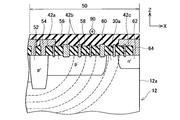
図17に示すように、変形例4の半導体装置は、トレンチ電極41の下部に複数のp型拡散層80が形成されている点で実施例2の半導体装置10aと異なる。p型拡散層80は、リサーフ領域56及び周辺ドリフト領域30aに露出しているトレンチ電極41a、41bの下部に形成されている。即ち、p型拡散層80は、端部n型領域62に露出しているトレンチ電極41cの下部には形成されていない。p型拡散層80の不純物濃度は、リサーフ領域56のp型不純物濃度よりも高い。この構成によれば、電気力線が複数のp型拡散層80を回避して表面側へ抜ける。このため、トレンチ電極41a、41bの下端のコーナ部は曲線状でなくてもよく、例えば略直角であってもよい。
図19に示すように、変形例1のトレンチ電極44(44a1~44c1、44b2)は、X方向の幅がそれぞれ等しくない点で実施例3のトレンチ電極43と異なる。この場合でも、トレンチ電極44は、隣接するトレンチ電極44の対向する面同士の間隔が略均等となるように配置される。この構成によっても、実施例3の半導体装置10bと同様の作用効果を奏することができる。
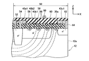
図20に示すように、変形例2のトレンチ電極45(45a1~45c1、45b2)は、Z方向の幅がそれぞれ等しくない点で実施例3のトレンチ電極43と異なる。なお、各トレンチ電極43は、その上端又は下端の少なくとも一方が、絶縁層58の上面又は下面にそれぞれ露出している。この構成によっても、実施例3の半導体装置10bと同様の作用効果を奏することができる。
図21に示すように、変形例3の半導体装置は、絶縁層58の上面に複数の電極82が形成されている点で実施例3の半導体装置10bと異なる。電極82は、絶縁層58の上面から突出している上側トレンチ電極43に接触しないように形成されている。これにより、隣接する電極82同士がコンデンサを形成する。この構成によれば、外来電荷が絶縁層58の上面に付着することを物理的に抑制するとともに、電極82により形成されるコンデンサにより、外来電荷が絶縁層58内に進入することを電気的に抑制することができる。従って、外来電荷に起因して耐圧が低下することをより抑制することができる。なお電極82は、例えばアルミニウムやポリシリコン等により形成されるが、電極82を形成する物質はこれに限られない。
図22に示すように、変形例4の半導体装置は、絶縁層58の上面に半導電性のシリコン窒化膜(いわゆるSInSiN膜)86が形成されている点で実施例3の半導体装置10bと異なる。半導電性シリコン窒化膜86は、図16に示す変形例と同様、電極54と電極64の間に位置し、上側トレンチ電極43b1を覆うように形成されている。この構成によれば、外来電荷が絶縁層58の上面に付着することを抑制することができ、外来電荷に起因して耐圧が低下することを抑制することができる。
図23に示すように、変形例5の半導体装置は、下側トレンチ電極43b2の下部に複数のp型拡散層88が形成されている点で実施例3の半導体装置10bと異なる。p型拡散層88は、リサーフ領域56及び周辺ドリフト領域30aに露出している下側トレンチ電極43b2の下部に形成されている。p型拡散層88の不純物濃度は、リサーフ領域56のp型不純物濃度よりも高い。この構成によれば、電気力線が複数のp型拡散層80を回避して表面側へ抜ける。このため、トレンチ電極43b2の下端のコーナ部は曲線状でなくてもよい。
Claims (10)
- 半導体基板12を有する半導体装置10であって、
半導体基板12が、
半導体素子が形成されているアクティブ領域20と、
アクティブ領域20と半導体基板12の端面12aとの間の外周領域50、
を有しており、
外周領域50の少なくとも一部の上面に、絶縁層58が形成されており、
絶縁層58内に、半導体基板12の厚み方向における幅がアクティブ領域20から半導体基板12の端面12aに向かう方向における幅よりも大きい複数のフローティング電極40が、アクティブ領域20から半導体基板12の端面12aに向かう方向に沿って間隔を隔てて配置されている、
半導体装置。 - 絶縁層58内に配置されるフローティング電極41~45は、前記絶縁層58の上面または下面の少なくとも一方の面に露出していることを特徴とする請求項1に記載の半導体装置。
- 前記絶縁層58を前記厚み方向に直交する平面で切断した任意の断面において、アクティブ領域20から半導体基板12の端面12aに向かう任意の直線上に、少なくとも1つのフローティング電極41~45が存在することを特徴とする請求項1に記載の半導体装置。
- フローティング電極40は、前記絶縁層58の上面に露出しており、前記絶縁層58の下面には露出していないことを特徴とする、請求項1又は2に記載の半導体装置。
- フローティング電極41~42は、前記絶縁層58の上面及び下面に露出していることを特徴とする、請求項1から3のいずれか一項に記載の半導体装置。
- 絶縁層58内に配置される複数のフローティング電極43~45は、前記絶縁層58の上面に露出している第1フローティング電極43a1~43c1、44a1~44c1、45a1~45c1と、前記絶縁層58の下面に露出している第2フローティング電極43b2、44b2、45b2とを有しており、第1フローティング電極43a1~43c1、44a1~44c1、45a1~45c1と第2フローティング電極43b2、44b2、45b2が交互に配置されていることを特徴とする、請求項1又は2に記載の半導体装置。
- フローティング電極41~45をその長手方向と直交する平面で切断した断面において、フローティング電極41~45の下面と側面のコーナ部が曲線状となっていることを特徴とする、請求項1から6のいずれか一項に記載の半導体装置。
- 半導体装置の製造方法であって、
半導体基板のうちの半導体素子が形成されるアクティブ領域と半導体装置の端面となる箇所との間の外周領域上に絶縁層を形成する工程と、
絶縁層に、半導体基板の厚み方向における幅がアクティブ領域から半導体基板の端面となる箇所に向かう方向における幅よりも大きい複数のトレンチを、アクティブ領域から半導体装置の端面となる箇所に向かう方向に沿って間隔を隔てて形成する工程と、
絶縁層上に金属層を形成する工程と、
トレンチの上部の金属層をマスクしていない状態で、各トレンチ内に金属層が残存し、かつ、各トレンチ内の金属層が互いに分離されるように金属層をエッチングする工程、
を有する製造方法。 - 絶縁層を形成する工程では、アクティブ領域上にも絶縁層を形成し、
金属層を形成する工程の前に、アクティブ領域上の絶縁層にコンタクトホールを形成する工程をさらに有し、
金属層を形成する工程では、コンタクトホール内にも金属層を形成し、
金属層をエッチングする工程は、コンタクトホールの上部の金属層をマスクした状態で行う、
請求項8の製造方法。 - トレンチを形成する工程と、コンタクトホールを形成する工程を、共通のエッチングにより行う請求項9に記載の製造方法。
Priority Applications (4)
| Application Number | Priority Date | Filing Date | Title |
|---|---|---|---|
| CN201280066749.5A CN104040720B (zh) | 2012-01-12 | 2012-11-27 | 半导体装置及其制造方法 |
| US14/372,103 US9385188B2 (en) | 2012-01-12 | 2012-11-27 | Semiconductor device with termination region having floating electrodes in an insulating layer |
| JP2013553204A JP5772987B2 (ja) | 2012-01-12 | 2012-11-27 | 半導体装置とその製造方法 |
| EP12865395.3A EP2804214B1 (en) | 2012-01-12 | 2012-11-27 | Semiconductor device comprising a termination structure |
Applications Claiming Priority (2)
| Application Number | Priority Date | Filing Date | Title |
|---|---|---|---|
| JP2012003877 | 2012-01-12 | ||
| JP2012-003877 | 2012-01-12 |
Publications (1)
| Publication Number | Publication Date |
|---|---|
| WO2013105350A1 true WO2013105350A1 (ja) | 2013-07-18 |
Family
ID=48781313
Family Applications (1)
| Application Number | Title | Priority Date | Filing Date |
|---|---|---|---|
| PCT/JP2012/080624 WO2013105350A1 (ja) | 2012-01-12 | 2012-11-27 | 半導体装置とその製造方法 |
Country Status (5)
| Country | Link |
|---|---|
| US (1) | US9385188B2 (ja) |
| EP (1) | EP2804214B1 (ja) |
| JP (1) | JP5772987B2 (ja) |
| CN (1) | CN104040720B (ja) |
| WO (1) | WO2013105350A1 (ja) |
Cited By (6)
| Publication number | Priority date | Publication date | Assignee | Title |
|---|---|---|---|---|
| JP2015032664A (ja) * | 2013-08-01 | 2015-02-16 | 住友電気工業株式会社 | ワイドバンドギャップ半導体装置 |
| WO2015040675A1 (ja) * | 2013-09-17 | 2015-03-26 | 株式会社日立製作所 | 半導体装置、電力変換装置、鉄道車両、および半導体装置の製造方法 |
| US9412809B2 (en) | 2013-02-15 | 2016-08-09 | Toyota Jidosha Kabushiki Kaisha | Semiconductor device and manufacturing method thereof |
| JP2016171272A (ja) * | 2015-03-16 | 2016-09-23 | 株式会社東芝 | 半導体装置 |
| JP2018078169A (ja) * | 2016-11-08 | 2018-05-17 | ローム株式会社 | 電子部品 |
| DE102014005879B4 (de) | 2014-04-16 | 2021-12-16 | Infineon Technologies Ag | Vertikale Halbleitervorrichtung |
Families Citing this family (17)
| Publication number | Priority date | Publication date | Assignee | Title |
|---|---|---|---|---|
| CN104205334B (zh) * | 2012-03-05 | 2017-09-01 | 三菱电机株式会社 | 半导体装置 |
| JP2014204038A (ja) * | 2013-04-08 | 2014-10-27 | 三菱電機株式会社 | 半導体装置及びその製造方法 |
| KR20150030799A (ko) * | 2013-09-12 | 2015-03-23 | 매그나칩 반도체 유한회사 | 반도체 소자 및 그 제조 방법 |
| JP6340200B2 (ja) * | 2014-01-27 | 2018-06-06 | ルネサスエレクトロニクス株式会社 | 半導体装置およびその製造方法 |
| US9397213B2 (en) | 2014-08-29 | 2016-07-19 | Freescale Semiconductor, Inc. | Trench gate FET with self-aligned source contact |
| US9553184B2 (en) * | 2014-08-29 | 2017-01-24 | Nxp Usa, Inc. | Edge termination for trench gate FET |
| CN105990408A (zh) * | 2015-02-02 | 2016-10-05 | 无锡华润上华半导体有限公司 | 横向绝缘栅双极型晶体管 |
| US9680003B2 (en) | 2015-03-27 | 2017-06-13 | Nxp Usa, Inc. | Trench MOSFET shield poly contact |
| US9806186B2 (en) * | 2015-10-02 | 2017-10-31 | D3 Semiconductor LLC | Termination region architecture for vertical power transistors |
| CN105762181A (zh) * | 2016-03-04 | 2016-07-13 | 李思敏 | 一种多晶硅发射极晶体管及其制造方法 |
| JP6588363B2 (ja) * | 2016-03-09 | 2019-10-09 | トヨタ自動車株式会社 | スイッチング素子 |
| JP6804379B2 (ja) | 2017-04-24 | 2020-12-23 | 三菱電機株式会社 | 半導体装置 |
| CN110571153B (zh) * | 2018-06-05 | 2023-02-21 | 比亚迪半导体股份有限公司 | 半导体功率器件及其终端区的制备方法 |
| JP2020105590A (ja) * | 2018-12-27 | 2020-07-09 | キオクシア株式会社 | 基板処理装置および基板処理方法 |
| JP7335190B2 (ja) * | 2020-03-23 | 2023-08-29 | 株式会社東芝 | 半導体装置 |
| US11538934B2 (en) * | 2021-01-12 | 2022-12-27 | Sanken Electric Co., Ltd. | Semiconductor device having a group of trenches in an active region and a mesa portion |
| US11777027B2 (en) * | 2021-06-29 | 2023-10-03 | Sanken Electric Co., Ltd. | Semiconductor device |
Citations (7)
| Publication number | Priority date | Publication date | Assignee | Title |
|---|---|---|---|---|
| JP2001111034A (ja) * | 1999-10-07 | 2001-04-20 | Fuji Electric Co Ltd | プレーナ型半導体装置 |
| JP2003188381A (ja) * | 2001-12-21 | 2003-07-04 | Denso Corp | 半導体装置 |
| JP2005209983A (ja) | 2004-01-26 | 2005-08-04 | Mitsubishi Electric Corp | 半導体装置 |
| JP2007123570A (ja) * | 2005-10-28 | 2007-05-17 | Toyota Industries Corp | 半導体装置 |
| JP2008187125A (ja) * | 2007-01-31 | 2008-08-14 | Toshiba Corp | 半導体装置 |
| JP2011040773A (ja) * | 2010-10-04 | 2011-02-24 | Mitsubishi Electric Corp | 半導体装置 |
| JP2011077202A (ja) * | 2009-09-29 | 2011-04-14 | Fuji Electric Holdings Co Ltd | 半導体装置 |
Family Cites Families (16)
| Publication number | Priority date | Publication date | Assignee | Title |
|---|---|---|---|---|
| US5607718A (en) * | 1993-03-26 | 1997-03-04 | Kabushiki Kaisha Toshiba | Polishing method and polishing apparatus |
| JPH09283754A (ja) * | 1996-04-16 | 1997-10-31 | Toshiba Corp | 高耐圧半導体装置 |
| JP3958404B2 (ja) * | 1997-06-06 | 2007-08-15 | 三菱電機株式会社 | 横型高耐圧素子を有する半導体装置 |
| JP3850146B2 (ja) * | 1998-07-07 | 2006-11-29 | 三菱電機株式会社 | 分離構造とその分離構造を備える半導体装置 |
| US7368785B2 (en) * | 2005-05-25 | 2008-05-06 | United Microelectronics Corp. | MOS transistor device structure combining Si-trench and field plate structures for high voltage device |
| JP5050329B2 (ja) | 2005-08-26 | 2012-10-17 | サンケン電気株式会社 | トレンチ構造半導体装置及びその製造方法 |
| JP2008227474A (ja) * | 2007-02-13 | 2008-09-25 | Toshiba Corp | 半導体装置 |
| JP5315638B2 (ja) * | 2007-07-24 | 2013-10-16 | サンケン電気株式会社 | 半導体装置 |
| JP5358963B2 (ja) * | 2008-02-04 | 2013-12-04 | 富士電機株式会社 | 半導体装置およびその製造方法 |
| CN101414635B (zh) * | 2008-12-01 | 2010-08-11 | 西安电子科技大学 | 凹槽绝缘栅型栅-漏复合场板功率器件及其制作方法 |
| CN102177587B (zh) * | 2008-12-10 | 2013-08-14 | 丰田自动车株式会社 | 半导体装置 |
| JP5391447B2 (ja) | 2009-04-06 | 2014-01-15 | 三菱電機株式会社 | 半導体装置およびその製造方法 |
| JP5376365B2 (ja) * | 2009-04-16 | 2013-12-25 | 三菱電機株式会社 | 半導体装置 |
| JP5543758B2 (ja) * | 2009-11-19 | 2014-07-09 | ルネサスエレクトロニクス株式会社 | 半導体装置 |
| JP2011159903A (ja) * | 2010-02-03 | 2011-08-18 | Rohm Co Ltd | 半導体装置 |
| CN102214689B (zh) | 2010-04-06 | 2012-11-07 | 上海华虹Nec电子有限公司 | 超级结器件的终端保护结构及其制造方法 |
-
2012
- 2012-11-27 CN CN201280066749.5A patent/CN104040720B/zh not_active Expired - Fee Related
- 2012-11-27 US US14/372,103 patent/US9385188B2/en active Active
- 2012-11-27 JP JP2013553204A patent/JP5772987B2/ja not_active Expired - Fee Related
- 2012-11-27 EP EP12865395.3A patent/EP2804214B1/en active Active
- 2012-11-27 WO PCT/JP2012/080624 patent/WO2013105350A1/ja active Application Filing
Patent Citations (7)
| Publication number | Priority date | Publication date | Assignee | Title |
|---|---|---|---|---|
| JP2001111034A (ja) * | 1999-10-07 | 2001-04-20 | Fuji Electric Co Ltd | プレーナ型半導体装置 |
| JP2003188381A (ja) * | 2001-12-21 | 2003-07-04 | Denso Corp | 半導体装置 |
| JP2005209983A (ja) | 2004-01-26 | 2005-08-04 | Mitsubishi Electric Corp | 半導体装置 |
| JP2007123570A (ja) * | 2005-10-28 | 2007-05-17 | Toyota Industries Corp | 半導体装置 |
| JP2008187125A (ja) * | 2007-01-31 | 2008-08-14 | Toshiba Corp | 半導体装置 |
| JP2011077202A (ja) * | 2009-09-29 | 2011-04-14 | Fuji Electric Holdings Co Ltd | 半導体装置 |
| JP2011040773A (ja) * | 2010-10-04 | 2011-02-24 | Mitsubishi Electric Corp | 半導体装置 |
Cited By (7)
| Publication number | Priority date | Publication date | Assignee | Title |
|---|---|---|---|---|
| US9412809B2 (en) | 2013-02-15 | 2016-08-09 | Toyota Jidosha Kabushiki Kaisha | Semiconductor device and manufacturing method thereof |
| JP2015032664A (ja) * | 2013-08-01 | 2015-02-16 | 住友電気工業株式会社 | ワイドバンドギャップ半導体装置 |
| WO2015040675A1 (ja) * | 2013-09-17 | 2015-03-26 | 株式会社日立製作所 | 半導体装置、電力変換装置、鉄道車両、および半導体装置の製造方法 |
| DE102014005879B4 (de) | 2014-04-16 | 2021-12-16 | Infineon Technologies Ag | Vertikale Halbleitervorrichtung |
| JP2016171272A (ja) * | 2015-03-16 | 2016-09-23 | 株式会社東芝 | 半導体装置 |
| JP2018078169A (ja) * | 2016-11-08 | 2018-05-17 | ローム株式会社 | 電子部品 |
| US11094443B2 (en) | 2016-11-08 | 2021-08-17 | Rohm Co., Ltd. | Electronic component |
Also Published As
| Publication number | Publication date |
|---|---|
| EP2804214B1 (en) | 2021-02-24 |
| JPWO2013105350A1 (ja) | 2015-05-11 |
| EP2804214A4 (en) | 2015-03-18 |
| EP2804214A1 (en) | 2014-11-19 |
| US9385188B2 (en) | 2016-07-05 |
| CN104040720B (zh) | 2016-12-14 |
| US20140374871A1 (en) | 2014-12-25 |
| JP5772987B2 (ja) | 2015-09-02 |
| CN104040720A (zh) | 2014-09-10 |
Similar Documents
| Publication | Publication Date | Title |
|---|---|---|
| JP5772987B2 (ja) | 半導体装置とその製造方法 | |
| US9559195B2 (en) | Semiconductor device | |
| TWI649872B (zh) | 半導體裝置 | |
| JP6666671B2 (ja) | 半導体装置 | |
| JP5701802B2 (ja) | 電力用半導体装置 | |
| WO2011155394A1 (ja) | 半導体装置および半導体装置の製造方法 | |
| JP5640969B2 (ja) | 半導体素子 | |
| JP7223543B2 (ja) | 半導体装置 | |
| JP2013149761A (ja) | 半導体装置 | |
| JP6193163B2 (ja) | 絶縁ゲート型半導体装置 | |
| WO2013128833A1 (ja) | 半導体装置 | |
| KR20180134542A (ko) | 반도체 장치 | |
| JP6463338B2 (ja) | 半導体装置 | |
| WO2014162498A1 (ja) | トレンチゲート電極を利用するigbt | |
| US10204980B2 (en) | Semiconductor device and manufacturing method of the same | |
| KR100904785B1 (ko) | 박형층 실리콘 온 인슐레이터(soi) 디바이스 | |
| JP2006186108A (ja) | 半導体装置 | |
| JP6854598B2 (ja) | 半導体装置 | |
| JP2017022185A (ja) | 半導体装置及びその製造方法 | |
| JP6334438B2 (ja) | 半導体装置 | |
| US10374076B2 (en) | Shield indent trench termination for shielded gate MOSFETs | |
| JP7291679B2 (ja) | 半導体装置 | |
| TWI511294B (zh) | 半導體裝置及其製造方法 | |
| CN117080245A (zh) | 一种功率半导体器件及其制备方法 | |
| TW202327108A (zh) | 半導體裝置 |
Legal Events
| Date | Code | Title | Description |
|---|---|---|---|
| 121 | Ep: the epo has been informed by wipo that ep was designated in this application |
Ref document number: 12865395 Country of ref document: EP Kind code of ref document: A1 |
|
| ENP | Entry into the national phase |
Ref document number: 2013553204 Country of ref document: JP Kind code of ref document: A |
|
| NENP | Non-entry into the national phase |
Ref country code: DE |
|
| WWE | Wipo information: entry into national phase |
Ref document number: 14372103 Country of ref document: US |
|
| WWE | Wipo information: entry into national phase |
Ref document number: 2012865395 Country of ref document: EP |