WO2013103141A1 - パッシベーション膜付半導体基板及びその製造方法、並びに太陽電池素子及びその製造方法 - Google Patents
パッシベーション膜付半導体基板及びその製造方法、並びに太陽電池素子及びその製造方法 Download PDFInfo
- Publication number
- WO2013103141A1 WO2013103141A1 PCT/JP2012/084160 JP2012084160W WO2013103141A1 WO 2013103141 A1 WO2013103141 A1 WO 2013103141A1 JP 2012084160 W JP2012084160 W JP 2012084160W WO 2013103141 A1 WO2013103141 A1 WO 2013103141A1
- Authority
- WO
- WIPO (PCT)
- Prior art keywords
- passivation film
- semiconductor substrate
- forming
- composition
- electrode
- Prior art date
- Legal status (The legal status is an assumption and is not a legal conclusion. Google has not performed a legal analysis and makes no representation as to the accuracy of the status listed.)
- Ceased
Links
Images


Classifications
-
- H—ELECTRICITY
- H10—SEMICONDUCTOR DEVICES; ELECTRIC SOLID-STATE DEVICES NOT OTHERWISE PROVIDED FOR
- H10F—INORGANIC SEMICONDUCTOR DEVICES SENSITIVE TO INFRARED RADIATION, LIGHT, ELECTROMAGNETIC RADIATION OF SHORTER WAVELENGTH OR CORPUSCULAR RADIATION
- H10F71/00—Manufacture or treatment of devices covered by this subclass
- H10F71/129—Passivating
-
- C—CHEMISTRY; METALLURGY
- C08—ORGANIC MACROMOLECULAR COMPOUNDS; THEIR PREPARATION OR CHEMICAL WORKING-UP; COMPOSITIONS BASED THEREON
- C08K—Use of inorganic or non-macromolecular organic substances as compounding ingredients
- C08K5/00—Use of organic ingredients
- C08K5/56—Organo-metallic compounds, i.e. organic compounds containing a metal-to-carbon bond
-
- C—CHEMISTRY; METALLURGY
- C09—DYES; PAINTS; POLISHES; NATURAL RESINS; ADHESIVES; COMPOSITIONS NOT OTHERWISE PROVIDED FOR; APPLICATIONS OF MATERIALS NOT OTHERWISE PROVIDED FOR
- C09D—COATING COMPOSITIONS, e.g. PAINTS, VARNISHES OR LACQUERS; FILLING PASTES; CHEMICAL PAINT OR INK REMOVERS; INKS; CORRECTING FLUIDS; WOODSTAINS; PASTES OR SOLIDS FOR COLOURING OR PRINTING; USE OF MATERIALS THEREFOR
- C09D101/00—Coating compositions based on cellulose, modified cellulose, or cellulose derivatives
- C09D101/08—Cellulose derivatives
- C09D101/26—Cellulose ethers
- C09D101/28—Alkyl ethers
-
- H—ELECTRICITY
- H10—SEMICONDUCTOR DEVICES; ELECTRIC SOLID-STATE DEVICES NOT OTHERWISE PROVIDED FOR
- H10F—INORGANIC SEMICONDUCTOR DEVICES SENSITIVE TO INFRARED RADIATION, LIGHT, ELECTROMAGNETIC RADIATION OF SHORTER WAVELENGTH OR CORPUSCULAR RADIATION
- H10F10/00—Individual photovoltaic cells, e.g. solar cells
- H10F10/10—Individual photovoltaic cells, e.g. solar cells having potential barriers
- H10F10/14—Photovoltaic cells having only PN homojunction potential barriers
-
- H—ELECTRICITY
- H10—SEMICONDUCTOR DEVICES; ELECTRIC SOLID-STATE DEVICES NOT OTHERWISE PROVIDED FOR
- H10F—INORGANIC SEMICONDUCTOR DEVICES SENSITIVE TO INFRARED RADIATION, LIGHT, ELECTROMAGNETIC RADIATION OF SHORTER WAVELENGTH OR CORPUSCULAR RADIATION
- H10F10/00—Individual photovoltaic cells, e.g. solar cells
- H10F10/10—Individual photovoltaic cells, e.g. solar cells having potential barriers
- H10F10/14—Photovoltaic cells having only PN homojunction potential barriers
- H10F10/146—Back-junction photovoltaic cells, e.g. having interdigitated base-emitter regions on the back side
-
- H—ELECTRICITY
- H10—SEMICONDUCTOR DEVICES; ELECTRIC SOLID-STATE DEVICES NOT OTHERWISE PROVIDED FOR
- H10F—INORGANIC SEMICONDUCTOR DEVICES SENSITIVE TO INFRARED RADIATION, LIGHT, ELECTROMAGNETIC RADIATION OF SHORTER WAVELENGTH OR CORPUSCULAR RADIATION
- H10F71/00—Manufacture or treatment of devices covered by this subclass
- H10F71/128—Annealing
-
- H—ELECTRICITY
- H10—SEMICONDUCTOR DEVICES; ELECTRIC SOLID-STATE DEVICES NOT OTHERWISE PROVIDED FOR
- H10F—INORGANIC SEMICONDUCTOR DEVICES SENSITIVE TO INFRARED RADIATION, LIGHT, ELECTROMAGNETIC RADIATION OF SHORTER WAVELENGTH OR CORPUSCULAR RADIATION
- H10F77/00—Constructional details of devices covered by this subclass
- H10F77/20—Electrodes
- H10F77/206—Electrodes for devices having potential barriers
- H10F77/211—Electrodes for devices having potential barriers for photovoltaic cells
-
- H—ELECTRICITY
- H10—SEMICONDUCTOR DEVICES; ELECTRIC SOLID-STATE DEVICES NOT OTHERWISE PROVIDED FOR
- H10F—INORGANIC SEMICONDUCTOR DEVICES SENSITIVE TO INFRARED RADIATION, LIGHT, ELECTROMAGNETIC RADIATION OF SHORTER WAVELENGTH OR CORPUSCULAR RADIATION
- H10F77/00—Constructional details of devices covered by this subclass
- H10F77/30—Coatings
- H10F77/306—Coatings for devices having potential barriers
- H10F77/311—Coatings for devices having potential barriers for photovoltaic cells
-
- Y—GENERAL TAGGING OF NEW TECHNOLOGICAL DEVELOPMENTS; GENERAL TAGGING OF CROSS-SECTIONAL TECHNOLOGIES SPANNING OVER SEVERAL SECTIONS OF THE IPC; TECHNICAL SUBJECTS COVERED BY FORMER USPC CROSS-REFERENCE ART COLLECTIONS [XRACs] AND DIGESTS
- Y02—TECHNOLOGIES OR APPLICATIONS FOR MITIGATION OR ADAPTATION AGAINST CLIMATE CHANGE
- Y02E—REDUCTION OF GREENHOUSE GAS [GHG] EMISSIONS, RELATED TO ENERGY GENERATION, TRANSMISSION OR DISTRIBUTION
- Y02E10/00—Energy generation through renewable energy sources
- Y02E10/50—Photovoltaic [PV] energy
- Y02E10/547—Monocrystalline silicon PV cells
-
- Y—GENERAL TAGGING OF NEW TECHNOLOGICAL DEVELOPMENTS; GENERAL TAGGING OF CROSS-SECTIONAL TECHNOLOGIES SPANNING OVER SEVERAL SECTIONS OF THE IPC; TECHNICAL SUBJECTS COVERED BY FORMER USPC CROSS-REFERENCE ART COLLECTIONS [XRACs] AND DIGESTS
- Y02—TECHNOLOGIES OR APPLICATIONS FOR MITIGATION OR ADAPTATION AGAINST CLIMATE CHANGE
- Y02P—CLIMATE CHANGE MITIGATION TECHNOLOGIES IN THE PRODUCTION OR PROCESSING OF GOODS
- Y02P70/00—Climate change mitigation technologies in the production process for final industrial or consumer products
- Y02P70/50—Manufacturing or production processes characterised by the final manufactured product
Definitions
- the present invention relates to a semiconductor substrate with a passivation film and a manufacturing method thereof, and a solar cell element and a manufacturing method thereof.
- n-type diffusion layer is uniformly formed by performing several tens of minutes at 800 ° C. to 900 ° C.
- n-type diffusion layers are formed not only on the front surface, which is the light receiving surface, but also on the side surface and the back surface. Therefore, side etching is performed to remove the n-type diffusion layer on the side surface.
- the n-type diffusion layer on the back surface needs to be converted into a p + -type diffusion layer. Therefore, an aluminum paste is applied to the entire back surface, and this is sintered to form an aluminum electrode, whereby an n-type diffusion layer is converted to a p + -type diffusion layer and an ohmic contact is obtained.
- the aluminum electrode formed from the aluminum paste has low conductivity. Therefore, in order to reduce the sheet resistance, the aluminum electrode formed on the entire back surface usually has to have a thickness of about 10 ⁇ m to 20 ⁇ m after sintering. Furthermore, since the thermal expansion coefficient differs greatly between silicon and aluminum, a large internal stress is generated in the silicon substrate during the sintering and cooling process, causing damage to crystal grain boundaries, increasing crystal defects, and warping. .
- Such a passivation effect is generally called a field effect, and an aluminum oxide (Al 2 O 3 ) film or the like has been proposed as a material having a negative fixed charge (see, for example, Japanese Patent No. 4767110).
- Such a passivation film is generally formed by a method such as an ALD (Atomic Layer Deposition) method or a CVD (Chemical Vapor Deposition) method (see, for example, Journal of Applied Physics, 104 (2008), 113703).
- ALD Atomic Layer Deposition
- CVD Chemical Vapor Deposition
- an aluminum electrode is formed on a semiconductor substrate in a predetermined pattern before the passivation film is formed, and then the aluminum electrode is formed. It is desirable to form a passivation film only in a region on a semiconductor substrate that is not present.
- the low ALD method and the CVD method described in Journal of Applied Physics, 104 (2008), 113703; Thin Solid Films, 517 (2009), 6327-6330; Chinese Physics Letters, 26 (2009), 088102.
- the passivation film in a region where an electrode having a predetermined pattern is formed on the semiconductor substrate is removed by drilling or etching, and then It was necessary to go through a complicated process of forming an electrode in the removed portion. Such a complicated manufacturing process has been a major obstacle to industrial use.
- the present invention has been made in view of the above-described conventional problems, and manufacture of a semiconductor substrate with a passivation film capable of forming a semiconductor substrate passivation film having an excellent passivation effect into a desired shape by a simple technique. It is an object to provide a method and a method for manufacturing a solar cell element.
- the step of forming the electrode includes a step of forming an electrode-forming composition layer by applying an electrode-forming composition on a semiconductor substrate, and a step of heat-treating the electrode-forming composition layer.
- composition for forming a passivation film according to any one of ⁇ 1> to ⁇ 3>, wherein the composition for forming a passivation film includes a compound represented by the following general formula (I) as the organoaluminum compound and a resin.
- a method for manufacturing a semiconductor substrate with a passivation film is a compound represented by the following general formula (I) as the organoaluminum compound and a resin.
- each R 1 independently represents an alkyl group having 1 to 8 carbon atoms.
- n represents an integer of 0 to 3.
- X 2 and X 3 each independently represent an oxygen atom or a methylene group.
- R 2 , R 3 and R 4 each independently represents a hydrogen atom or an alkyl group having 1 to 8 carbon atoms]
- n is an integer of 1 to 3
- R 4 is each independently a hydrogen atom or an alkyl group having 1 to 4 carbon atoms.
- ⁇ 7> A semiconductor substrate with a passivation film manufactured by the manufacturing method according to any one of ⁇ 1> to ⁇ 6>.
- ⁇ 8> forming an electrode on at least one layer selected from the group consisting of the p-type layer and the n-type layer on a semiconductor substrate having a pn junction formed by joining a p-type layer and an n-type layer; Forming a composition layer on one or both surfaces of the semiconductor substrate on which the electrode is formed using a passivation film forming composition containing an organoaluminum compound; and heat-treating the composition layer. And a step of forming a passivation film.
- the step of forming the electrode includes a step of applying an electrode forming composition on a semiconductor substrate to form an electrode forming composition layer, and sintering the electrode forming composition layer to form an electrode.
- each R 1 independently represents an alkyl group having 1 to 8 carbon atoms.
- n represents an integer of 0 to 3.
- X 2 and X 3 each independently represent an oxygen atom or a methylene group.
- R 2 , R 3 and R 4 each independently represents a hydrogen atom or an alkyl group having 1 to 8 carbon atoms]
- n is an integer of 1 to 3
- R 4 is independently a hydrogen atom or an alkyl group having 1 to 4 carbon atoms. Manufacturing method of solar cell element.
- ⁇ 14> A solar cell element produced by the production method according to any one of ⁇ 8> to ⁇ 13>.
- a method for manufacturing a semiconductor substrate with a passivation film and a method for manufacturing a solar cell element capable of forming a semiconductor substrate passivation film having an excellent passivation effect into a desired shape by a simple method is provided. Can do.
- the term “process” is not limited to an independent process, and is included in the term if the intended purpose of the process is achieved even when it cannot be clearly distinguished from other processes. .
- a numerical range indicated using “to” indicates a range including the numerical values described before and after “to” as the minimum value and the maximum value, respectively.
- the content of each component in the composition is the total amount of the plurality of substances present in the composition unless there is a specific notice when there are a plurality of substances corresponding to each component in the composition. Means.
- the method for producing a semiconductor substrate with a passivation film according to the present invention comprises a step of forming an electrode on a semiconductor substrate, and a composition for forming a passivation film containing an organoaluminum compound on the surface of the semiconductor substrate on which the electrode is formed. Providing a composition layer, and heat-treating the composition layer to form a passivation film.
- the manufacturing method may further include other steps as necessary.
- a semiconductor substrate having a desired shape and formed with a passivation film exhibiting an excellent passivation effect can be manufactured by a simple process.
- the electrode may be formed on the semiconductor substrate prior to the formation of the passivation film, and the semiconductor in which at least the passivation film is not formed after the passivation film is formed on the semiconductor substrate.
- An electrode may be formed in a region on the substrate. In the manufacturing method of the present invention, it is preferable that the electrode is formed on the semiconductor substrate prior to the formation of the passivation film.
- a heat treatment may be performed at a temperature higher than the heat treatment temperature at the time of forming the passivation film.
- the sintering for forming the electrode is performed after forming the passivation film as in the conventional method of manufacturing a semiconductor substrate with a passivation film, even if an amorphous aluminum oxide layer is formed as the passivation film, the temperature is high. There is a possibility that the aluminum oxide is changed from an amorphous state to a crystalline state by sintering at.
- the passivation film can be formed after the electrode is formed in the manufacturing method of the present invention, the aluminum oxide layer as the passivation film can be easily maintained in an amorphous state with a more excellent passivation effect.
- the passivation effect of the semiconductor substrate is obtained by measuring the effective lifetime of minority carriers in the semiconductor substrate provided with the semiconductor substrate passivation film by using a device such as WT-2000PVN manufactured by Nippon Semilab Co., Ltd. It can be evaluated by measuring by the microwave conductive decay method.
- the effective lifetime ⁇ is expressed by the following equation (A) by the bulk lifetime ⁇ b inside the semiconductor substrate and the surface lifetime ⁇ s of the semiconductor substrate surface.
- A the effective lifetime ⁇
- the surface state density on the surface of the semiconductor substrate is small, ⁇ s increases, and as a result, the effective lifetime ⁇ increases.
- the bulk lifetime ⁇ b is increased and the effective lifetime ⁇ is increased. That is, by measuring the effective lifetime ⁇ , the interface characteristics of the passivation film / semiconductor substrate and the internal characteristics of the semiconductor substrate such as dangling bonds can be evaluated.
- the semiconductor substrate used in the production method of the present invention is not particularly limited, and can be appropriately selected from those usually used according to the purpose.
- the semiconductor substrate is not particularly limited as long as p-type impurities or n-type impurities are diffused (doped) into silicon, germanium, or the like. Of these, a silicon substrate is preferable.
- the semiconductor substrate may be a p-type semiconductor substrate or an n-type semiconductor substrate. Among these, from the viewpoint of the passivation effect, it is preferable that the surface on which the passivation film is formed is a semiconductor substrate that is a p-type layer.
- the p-type layer on the semiconductor substrate is a p-type layer derived from the p-type semiconductor substrate
- the p-type layer is formed on the n-type semiconductor substrate or the p-type semiconductor substrate as a p-type diffusion layer or a p + -type diffusion layer. It may be.
- the thickness of the semiconductor substrate is not particularly limited and can be appropriately selected according to the purpose. For example, it can be 50 ⁇ m to 1000 ⁇ m, and preferably 75 ⁇ m to 750 ⁇ m. By forming a passivation film on a semiconductor substrate having a thickness of 50 ⁇ m to 1000 ⁇ m, a passivation effect can be obtained more effectively.
- the step of forming the electrode includes a step of forming an electrode forming composition layer by applying an electrode forming composition onto a semiconductor substrate, and a step of sintering the electrode forming composition layer to form an electrode. It is preferable to have. Thereby, an electrode can be formed on a semiconductor substrate with high productivity by a simple method. Furthermore, since it is possible to form electrodes prior to the formation of the passivation film, the range of selection of electrode formation conditions is widened, and electrodes having desired characteristics can be efficiently formed.
- the electrode forming composition can be appropriately selected from those usually used as necessary.
- Specific examples of the electrode forming composition include silver pastes, aluminum pastes, copper pastes, and the like that are commercially available for solar cell electrodes from various companies.
- the composition for electrode formation forms an electrode formation composition layer on a semiconductor substrate
- a printing method such as screen printing, an ink jet method, and the like can be given.
- a dipping method, a spin method, a brush coating, a spray method, a doctor blade method, a roll coater method, or the like may be used.
- the amount of the electrode-forming composition applied onto the semiconductor substrate is not particularly limited, and can be appropriately selected according to the shape of the electrode to be formed.
- the shape of the electrode to be formed is not particularly limited, and can be appropriately selected according to the purpose.
- the electrode forming composition layer formed on the semiconductor substrate is sintered to form an electrode.
- the sintering conditions are appropriately selected according to the electrode forming composition to be used.
- the temperature can be set at 600 ° C. to 850 ° C. for 1 second to 60 seconds.
- a composition for forming a semiconductor substrate passivation film containing an organoaluminum compound is applied on the surface of the semiconductor substrate on which the electrodes are formed to form a composition layer in a desired shape.
- the shape of the composition layer formed by the composition for forming a semiconductor substrate passivation film is not particularly limited, and can be appropriately selected as necessary.
- the step is preferably performed in a region where no electrode is formed on the semiconductor substrate, that is, a region where the semiconductor substrate and the electrode are not in contact with each other. As a result, an increase in the contact resistance of the electrode is suppressed, and a passivation film can be formed by a simpler method.
- the details of the composition for forming a semiconductor substrate passivation film will be described later.
- the method for forming the composition layer on the semiconductor substrate by applying the composition for forming a passivation film is not particularly limited as long as the composition layer can be formed into a desired shape, and is appropriately selected from known coating methods as necessary. It can be selected and used. Specifically, a printing method such as screen printing, an ink jet method, and the like can be given. When a mask material, an etching method, or the like is used in combination, a dipping method, a spin method, a brush coating, a spray method, a doctor blade method, a roll coater method, or the like may be used.
- the application amount of the composition for forming a passivation film on the semiconductor substrate is not particularly limited. For example, it is preferable to select appropriately so that the thickness of the passivation film to be formed becomes a film thickness described later.
- the manufacturing method further includes a step of applying an alkaline aqueous solution on the semiconductor substrate before the step of forming the composition layer. That is, it is preferable to wash the surface of the semiconductor substrate with an alkaline aqueous solution before applying the composition for forming a passivation film on the semiconductor substrate. By washing with an alkaline aqueous solution, organic substances, particles, and the like present on the surface of the semiconductor substrate can be removed, and the passivation effect is further improved.
- the semiconductor substrate is immersed in a mixed solution of ammonia water and hydrogen peroxide solution and treated at 60 ° C. to 80 ° C., whereby organic substances, particles, and the like can be removed and washed.
- the washing time is preferably 10 seconds to 10 minutes, more preferably 30 seconds to 5 minutes.
- a passivation film can be formed on a semiconductor substrate by heat-treating a composition layer formed of the composition for forming a passivation film to form a heat-treated material layer derived from the composition layer on the semiconductor substrate.
- the heat treatment conditions for the composition layer are not particularly limited as long as the organoaluminum compound contained in the composition layer can be converted into aluminum oxide (Al 2 O 3 ) which is the heat treatment product. Among these, it is preferable that the heat treatment conditions allow the formation of an amorphous Al 2 O 3 layer having no specific crystal structure.
- the semiconductor substrate passivation film is composed of an amorphous Al 2 O 3 layer, the semiconductor substrate passivation film can be more effectively charged with a negative charge, and a more excellent passivation effect can be obtained.
- This heat treatment step can be divided into a drying step and an annealing step.
- a passivation effect cannot be obtained after the drying step, but a passivation effect can be obtained after the annealing step.
- the annealing temperature is preferably 400 ° C. to 900 ° C., more preferably 450 ° C. to 800 ° C.
- the annealing time can be appropriately selected according to the annealing temperature and the like. For example, it can be 0.1 to 10 hours, and preferably 0.2 to 5 hours.
- the thickness of the passivation film produced by the production method is not particularly limited and can be appropriately selected according to the purpose. For example, it is preferably 5 nm to 50 ⁇ m, preferably 10 nm to 30 ⁇ m, and more preferably 15 nm to 20 ⁇ m.
- the film thickness of the formed passivation film is measured by a conventional method using a stylus type step / surface shape measuring device (for example, manufactured by Ambios).
- the shape of the passivation film is not particularly limited, and can be a desired shape as necessary.
- the passivation film may be formed on the entire surface of the semiconductor substrate, or may be formed only on a part of the region.
- the method for manufacturing a semiconductor substrate with a passivation film includes a step of drying a composition layer formed from the composition for forming a passivation film, after applying the composition for forming a passivation film and before the step of forming the passivation film. May further be included.
- a passivation film having a more uniform passivation effect can be formed by drying the composition layer.
- the step of drying the composition layer is not particularly limited as long as at least a part of the solvent that may be included in the composition for forming a passivation film can be removed.
- the drying treatment can be, for example, a drying treatment at 30 ° C. to 250 ° C. for 1 minute to 60 minutes, and is preferably a drying treatment at 40 ° C. to 220 ° C. for 3 minutes to 40 minutes.
- the drying treatment may be performed under normal pressure or under reduced pressure.
- a passivation film may be formed on the semiconductor substrate prior to the step of forming the electrode.
- the electrode is formed under the condition that the aluminum oxide formed as the passivation film does not change from the amorphous state to the crystalline state. Specifically, the following manufacturing method may be used.
- a passivation film forming composition containing an organoaluminum compound is applied on a semiconductor substrate to form a composition layer in a desired shape.
- the shape of the composition layer formed by the composition for forming a passivation film is not particularly limited and can be appropriately selected as necessary. In particular, it is preferably a step of selectively applying to a region other than the region where electrode formation is scheduled on the semiconductor substrate, and selectively applying to a region other than the region where the semiconductor substrate and electrode are scheduled to contact. More preferably, it is a process. Thus, after the passivation film is formed, the electrode can be formed in a desired shape. The details of the composition for forming a passivation film will be described later.
- the method for forming the composition layer on the semiconductor substrate by applying the composition for forming a passivation film is not particularly limited as long as the composition layer can be formed into a desired shape. If necessary, from a known coating method or the like. It can be appropriately selected and used. Specifically, a printing method such as screen printing, an ink jet method, and the like can be given. When a mask material, an etching method, or the like is used in combination, a dipping method, a spin method, a brush coating, a spray method, a doctor blade method, a roll coater method, or the like may be used.
- the amount of the composition for forming a passivation film on the semiconductor substrate is not particularly limited. For example, it is preferable to select appropriately so that the thickness of the passivation film to be formed becomes a film thickness described later.
- the manufacturing method further includes a step of applying an alkaline aqueous solution on the semiconductor substrate before the step of forming the composition layer. That is, it is preferable to wash the surface of the semiconductor substrate with an alkaline aqueous solution before applying the composition for forming a passivation film on the semiconductor substrate. By washing with an alkaline aqueous solution, organic substances, particles, and the like present on the surface of the semiconductor substrate can be removed, and the passivation effect is further improved.
- the organic substance and particles can be removed and washed by immersing the semiconductor substrate in a mixed solution of ammonia water and hydrogen peroxide water and treating at 60 ° C. to 80 ° C.
- the washing time is preferably 10 seconds to 10 minutes, more preferably 30 seconds to 5 minutes.
- a passivation layer is formed on the semiconductor substrate by heat-treating the composition layer formed of the semiconductor substrate passivation film-forming composition on the semiconductor substrate to form a heat-treated material layer derived from the composition layer. can do.
- the heat treatment conditions for the composition layer are not particularly limited as long as the organoaluminum compound contained in the composition layer can be converted into aluminum oxide (Al 2 O 3 ) which is the heat treatment product. Among these, it is preferable that the heat treatment conditions allow the formation of an amorphous Al 2 O 3 layer having no specific crystal structure.
- the semiconductor substrate passivation film is composed of an amorphous Al 2 O 3 layer, the semiconductor substrate passivation film can effectively have a negative charge, and a more excellent passivation effect can be obtained.
- the annealing temperature is preferably 400 ° C. to 900 ° C., more preferably 450 ° C. to 800 ° C.
- the annealing time can be appropriately selected according to the annealing temperature and the like. For example, it can be 0.1 to 10 hours, and preferably 0.2 to 5 hours.
- the thickness of the passivation film produced by the production method is not particularly limited and can be appropriately selected according to the purpose. For example, it is preferably 5 nm to 50 ⁇ m, preferably 10 nm to 30 ⁇ m, and more preferably 15 nm to 20 ⁇ m.
- the film thickness of the formed passivation film is measured by a conventional method using a stylus type step / surface shape measuring device (for example, manufactured by Ambios).
- the step of forming the electrode on the semiconductor substrate includes the step of forming the electrode forming composition layer by applying the electrode forming composition on the semiconductor substrate, and the electrode forming composition layer by sintering the electrode forming composition layer. It is preferable to include the process to do.
- the step of forming the electrode-forming composition layer is preferably a step of applying the electrode-forming composition to at least a region on the semiconductor substrate on which the passivation film is not formed.
- the electrode forming composition can be appropriately selected from those usually used as necessary.
- Specific examples of the electrode forming composition include silver pastes, aluminum pastes, copper pastes, and the like that are commercially available for solar cell electrodes from various companies.
- the method for forming the electrode forming composition layer on the semiconductor substrate is not particularly limited as long as it can be formed into a desired shape, and can be appropriately selected from known coating methods and the like as necessary. Specifically, a printing method such as screen printing, an ink jet method, and the like can be given. When a mask material, an etching method, or the like is used in combination, a dipping method, a spin method, a brush coating, a spray method, a doctor blade method, a roll coater method, or the like may be used.
- the amount of the electrode-forming composition applied onto the semiconductor substrate is not particularly limited, and can be appropriately selected according to the shape of the electrode to be formed.
- the manufacturing method preferably further includes a step of applying an alkaline aqueous solution on the semiconductor substrate before the step of forming the composition layer.
- the electrode forming composition layer formed on the semiconductor substrate is sintered to form an electrode.
- the conditions for the sintering treatment are preferably selected as appropriate according to the composition for forming an electrode within a range in which aluminum oxide formed as a passivation film does not change from an amorphous state to a crystalline state. For example, if sintering is performed at 600 ° C. to 850 ° C. for 1 second to 60 seconds, almost no change to the crystalline state occurs.
- the composition prior to electrode formation, the composition is applied to the passivation film-forming composition on the semiconductor substrate and dried for the purpose of removing the solvent, and then the composition layer is annealed.
- the electrode forming composition layer may be formed by applying an electrode forming composition layer on the semiconductor substrate. In this case, whichever comes first may be the order of the step of forming the electrode by sintering the electrode forming composition layer and the step of forming the passivation film by heat-treating the composition layer for forming the passivation film. Or may be simultaneous.
- the semiconductor substrate with a passivation film manufactured by the above manufacturing method can be applied to a solar cell element, a light emitting diode element and the like.
- the solar cell element excellent in conversion efficiency can be obtained by applying to a solar cell element.
- the passivation film-forming composition contains at least one organoaluminum compound, but preferably further contains at least one resin, and includes at least one organoaluminum compound represented by the following general formula (I): More preferably, at least one kind of resin is included.
- the composition for forming a passivation film may further contain other components as necessary.
- each R 1 independently represents an alkyl group having 1 to 8 carbon atoms.
- n represents an integer of 0 to 3.
- X 2 and X 3 each independently represent an oxygen atom or a methylene group.
- R 2 , R 3 and R 4 each independently represents a hydrogen atom or an alkyl group having 1 to 8 carbon atoms.
- a plurality of groups represented by the same symbol may be the same or different. Since the composition for forming a passivation film contains a specific organoaluminum compound and a resin, it is possible to easily form a composition layer in a desired shape. Therefore, a passivation film is selectively formed in a desired region. It is excellent in pattern forming ability. Moreover, since it comprises a specific organoaluminum compound, it is excellent in storage stability over time.
- the stability of the composition for forming a passivation film can be evaluated by a change in viscosity over time.
- the composition for forming a passivation film immediately after preparation has a shear viscosity ( ⁇ 0 ) at a shear rate of 1.0 s ⁇ 1 and a composition for forming a passivation film after storage at 25 ° C. for 30 days.
- the shear viscosity ( ⁇ 30 ) at a shear rate of 1.0 s ⁇ 1 can be evaluated by, for example, the rate of change in viscosity (%) over time.
- the rate of change in viscosity (%) over time is obtained by dividing the absolute value of the difference in shear viscosity immediately after preparation and 30 days later by the shear viscosity immediately after preparation, and is specifically calculated by the following equation.
- the viscosity change rate of the composition for forming a passivation film is preferably 30% or less, more preferably 20% or less, and still more preferably 10% or less.
- Viscosity change rate (%)
- the composition for forming a passivation film preferably contains at least one organoaluminum compound represented by the general formula (I).
- the organoaluminum compound is a compound called aluminum alkoxide, aluminum chelate or the like, and preferably has an aluminum chelate structure in addition to the aluminum alkoxide structure. Further, as described in Nippon Seramikkusu Kyokai Gakujitsu Ronbunshi, 97 (1989) 369-399, the organoaluminum compound is converted into aluminum oxide (Al 2 O 3 ) by heat treatment.
- a passivation film having an excellent passivation effect can be formed by including the organoaluminum compound represented by the general formula (I) in the composition for forming a passivation film as follows. .
- Aluminum oxide formed by heat-treating a composition for forming a passivation film containing an organoaluminum compound having a specific structure is likely to be in an amorphous state, causing defects such as aluminum atoms, and large negative fixation near the interface with the semiconductor substrate. It is thought that it can have a charge.
- This large negative fixed charge generates an electric field in the vicinity of the interface of the semiconductor substrate, so that the concentration of minority carriers can be reduced, and as a result, the recombination rate of carriers at the interface is suppressed, resulting in an excellent passivation effect. It is considered that a passivation film having the following can be formed.
- Tetracoordinate aluminum oxide is considered to have a structure in which the center of silicon dioxide (SiO 2 ) is isomorphously substituted from silicon to aluminum, and is formed as a negative charge source at the interface between silicon dioxide and aluminum oxide like zeolite and clay. It has been known.
- the state of the formed aluminum oxide can be confirmed by measuring an X-ray diffraction spectrum (XRD, X-ray diffraction). For example, it can be confirmed that the XRD has an amorphous structure by not showing a specific reflection pattern.
- the negative fixed charge of aluminum oxide can be evaluated by a CV method (Capacitance Voltage measurement).
- the surface state density obtained from the CV method for the heat-treated material layer containing aluminum oxide formed from the passivation film forming composition is higher than that of the aluminum oxide layer formed by ALD or CVD method. May be large.
- the passivation film formed from the composition for forming a passivation film has a large electric field effect and a decrease in minority carrier concentration, thereby increasing the surface lifetime ⁇ s. Therefore, the surface state density is not a relative problem.
- each R 1 independently represents an alkyl group having 1 to 8 carbon atoms.
- the alkyl group represented by R 1 may be linear or branched. Specific examples of the alkyl group represented by R 1 include methyl group, ethyl group, propyl group, isopropyl group, butyl group, isobutyl group, sec-butyl group, t-butyl group, hexyl group, octyl group, and ethylhexyl group.
- Etc is methyl group, ethyl group, propyl group, isopropyl group, butyl group, isobutyl group, sec-butyl group, t-butyl group, hexyl group, octyl group, and ethylhexyl group.
- the alkyl group represented by R 1 is preferably an unsubstituted alkyl group having 1 to 8 carbon atoms from the viewpoint of storage stability and a passivation effect, and is an unsubstituted alkyl group having 1 to 4 carbon atoms. More preferably.
- n represents an integer of 0 to 3. n is preferably an integer of 1 to 3 and more preferably 1 or 3 from the viewpoint of storage stability.
- X 2 and X 3 each independently represent an oxygen atom or a methylene group. From the viewpoint of storage stability, it is preferable that at least one of X 2 and X 3 is an oxygen atom.
- R 2 , R 3 and R 4 in the general formula (I) each independently represent a hydrogen atom or an alkyl group having 1 to 8 carbon atoms. The alkyl group represented by R 2 , R 3 and R 4 may be linear or branched.
- alkyl group represented by R 2 , R 3 and R 4 include a methyl group, an ethyl group, a propyl group, an isopropyl group, a butyl group, an isobutyl group, a sec-butyl group, a t-butyl group, and a hexyl group.
- R 2 and R 3 are each independently preferably a hydrogen atom or an unsubstituted alkyl group having 1 to 8 carbon atoms, and preferably a hydrogen atom or 1 to 4 carbon atoms.
- the unsubstituted alkyl group is more preferable.
- R 4 is preferably a hydrogen atom or an unsubstituted alkyl group having 1 to 8 carbon atoms from the viewpoint of storage stability and a passivation effect, and is a hydrogen atom or an unsubstituted alkyl group having 1 to 4 carbon atoms. More preferably.
- the organoaluminum compound represented by the general formula (I) is a compound in which n is 0 and R 1 is independently an alkyl group having 1 to 4 carbon atoms from the viewpoint of storage stability and a passivation effect, and n is 1 to 3, R 1 is independently an alkyl group having 1 to 4 carbon atoms, at least one of X 2 and X 3 is an oxygen atom, and R 2 and R 3 are each independently It is preferably at least one selected from the group consisting of a hydrogen atom or an alkyl group having 1 to 4 carbon atoms, and R 4 is a hydrogen atom or an alkyl group having 1 to 4 carbon atoms, and n is 0.
- R 1 is an unsubstituted alkyl group having 1 to 4 carbon atoms, and n is 1 ⁇ 3, R 1 is an unsubstituted alkyl group having 1 to 4 carbon atoms, X 2 and X at least one of the 3 is an oxygen atom, wherein R 2 or R 3 binds to atom is an alkyl group having 1 to 4 carbon atoms, when X 2 or X 3 is a methylene group, R 2 or R 3 binds to the methylene groups is a hydrogen atom, R 4 is more preferably at least one selected from the group consisting of compounds each having a hydrogen atom.
- the aluminum trialkoxide which is an organoaluminum compound represented by the general formula (I) and n is 0, include trimethoxyaluminum, triethoxyaluminum (aluminum ethylate), triisopropoxyaluminum (aluminum isopropylate), Examples thereof include trisec-butoxyaluminum (aluminum sec-butyrate), monosec-butoxy-diisopropoxyaluminum (monosec-butoxyaluminum diisopropylate), tritert-butoxyaluminum, and tri-n-butoxyaluminum.
- the organoaluminum compound represented by the general formula (I) and n is 1 to 3 can be prepared by mixing the aluminum trialkoxide with a compound having a specific structure having two carbonyl groups.
- a commercially available aluminum chelate compound may also be used.
- the aluminum trialkoxide and the compound having two carbonyl groups are mixed, at least a part of the alkoxide group of the aluminum trialkoxide is substituted with the compound having two carbonyl groups to form an aluminum chelate structure.
- a solvent may be present, or heat treatment or addition of a catalyst may be performed.
- the compound having a specific structure having two carbonyl groups is preferably at least one selected from the group consisting of ⁇ -diketone compounds, ⁇ -ketoester compounds, and malonic acid diesters from the viewpoint of storage stability.
- Specific examples of the compound having a specific structure having two carbonyl groups include acetylacetone, 3-methyl-2,4-pentanedione, 2,3-pentanedione, 3-ethyl-2,4-pentanedione, 3- Butyl-2,4-pentanedione, 2,2,6,6-tetramethyl-3,5-heptanedione, 2,6-dimethyl-3,5-heptanedione, 6-methyl-2,4-heptanedione ⁇ -diketone compounds such as: methyl acetoacetate, ethyl acetoacetate, propyl acetoacetate, isobutyl acetoacetate, butyl acetoacetate, tert
- the number of aluminum chelate structures is not particularly limited as long as it is 1 to 3. Among these, 1 or 3 is preferable from the viewpoint of storage stability.
- the number of aluminum chelate structures can be controlled, for example, by appropriately adjusting the ratio of mixing the aluminum trialkoxide and the compound having two carbonyl groups. Moreover, you may select suitably the compound which has a desired structure from a commercially available aluminum chelate compound.
- organoaluminum compounds represented by the general formula (I) from the viewpoint of reactivity during heat treatment and storage stability as a composition, specifically, an organoaluminum compound in which n is 1 to 3 may be used.
- an organoaluminum compound in which n is 1 to 3 may be used.
- at least one selected from the group consisting of aluminum ethyl acetoacetate diisopropylate, aluminum tris (ethyl acetoacetate), aluminum monoacetylacetonate bis (ethyl acetoacetate) and aluminum tris (acetylacetonate) is used. More preferably, aluminum ethyl acetoacetate diisopropylate is more preferably used.
- an aluminum chelate structure in the organoaluminum compound can be confirmed by a commonly used analysis method. For example, it can be confirmed using an infrared spectrum, a nuclear magnetic resonance spectrum, a melting point, or the like.
- the content of the organoaluminum compound contained in the composition for forming a passivation film can be appropriately selected as necessary.
- the content of the organoaluminum compound can be 1% by mass to 70% by mass in the composition for forming a passivation film, and is 3% by mass to 60% by mass. It is preferably 5% by mass to 50% by mass, more preferably 10% by mass to 30% by mass.
- the organoaluminum may be liquid or solid and is not particularly limited.
- Passivation formed by being a compound with good stability at room temperature, good stability or solubility at room temperature, and good solubility or dispersibility from the viewpoint of passivation effect and storage stability The uniformity of the film is further improved, and a desired passivation effect can be stably obtained.
- the composition for forming a passivation film preferably contains at least one resin.
- the shape stability of the composition layer formed by applying the composition for forming a passivation film on a semiconductor substrate is further improved, and the passivation film is formed in the region where the composition layer is formed. It can be formed more selectively in a desired shape.
- the type of resin is not particularly limited.
- the resin is preferably a resin whose viscosity can be adjusted within a range in which a good pattern can be formed when the composition for forming a passivation film is applied onto a semiconductor substrate.
- the resin include: polyvinyl alcohol resin; polyacrylamide resin; polyvinyl amide resin; polyvinyl pyrrolidone resin; polyethylene oxide resin; polysulfonic acid resin; acrylamide alkyl sulfonic acid resin; cellulose; Cellulose and gelatin derivatives; starch and starch derivatives; sodium alginate; xanthan and xanthan derivatives; gua and gua derivatives; scleroglucan and scleroglucan derivatives; tragacanth and tragacanth derivatives; ) Acrylic acid resin, alkyl (meth) acrylate resin, dimethylaminoethyl (meth) acrylic Over DOO of the resin (meth) acrylic acid ester resin (me)
- the molecular weight of these resins is not particularly limited, and is preferably adjusted as appropriate in view of the desired viscosity of the composition.
- the weight average molecular weight of the resin is preferably 100 to 10,000,000, more preferably 1,000 to 5,000,000, from the viewpoints of storage stability and pattern formation.
- the weight average molecular weight of resin is calculated
- the content of the resin in the composition for forming a semiconductor substrate passivation film can be appropriately selected as necessary.
- the resin content is, for example, preferably 0.1% by mass to 30% by mass in the composition for forming a substrate passivation film. From the viewpoint of expressing thixotropy that facilitates pattern formation, the resin content is more preferably 1% by mass to 25% by mass, and more preferably 1.5% by mass to 20% by mass. More preferably, the content is 1.5% by mass to 10% by mass.
- the content ratio of the organoaluminum compound and the resin in the passivation film forming composition can be appropriately selected as necessary.
- the content ratio of the resin to the organoaluminum compound is preferably 0.001 to 1000, and preferably 0.01 to 100. More preferably, it is 0.1 to 1.
- the composition for forming a passivation film preferably contains a solvent.
- the adjustment of the viscosity becomes easier, the applicability is further improved, and a more uniform heat-treated product layer can be formed.
- the solvent is not particularly limited and can be appropriately selected as necessary.
- the solvent is not particularly limited and can be appropriately selected as necessary. Among them, a solvent that can dissolve the organoaluminum compound and the resin to give a uniform solution is preferable, and more preferably includes at least one organic solvent.
- the solvent include acetone, methyl ethyl ketone, methyl-n-propyl ketone, methyl isopropyl ketone, methyl-n-butyl ketone, methyl isobutyl ketone, methyl-n-pentyl ketone, methyl-n-hexyl ketone, diethyl ketone, Ketone solvents such as propyl ketone, diisobutyl ketone, trimethylnonanone, cyclohexanone, cyclopentanone, methylcyclohexanone, 2,4-pentanedione, acetonylacetone; diethyl ether, methyl ethyl ether, methyl-n-propyl ether, diisopropyl ether , Tetrahydrofuran, methyltetrahydrofuran, dioxane, dimethyldioxane, ethylene glycol dimethyl ether, ethylene
- the solvent preferably contains at least one selected from the group consisting of a terpene solvent, an ester solvent, and an alcohol solvent, from the viewpoints of impartability to a semiconductor substrate and pattern formability, and consists of a terpene solvent. More preferably, it contains at least one selected from the group.
- the content of the solvent in the composition for forming a passivation film is determined in consideration of impartability, pattern formability, and storage stability.
- the content of the solvent is preferably 5% by mass to 98% by mass in the composition for forming a passivation film, and preferably 10% by mass to 95% by mass in the composition for forming a passivation film, from the viewpoint of the impartability of the composition and the pattern formability. More preferably.
- the content of the acidic compound and the basic compound is preferably 1% by mass or less in the composition for forming a passivation film, respectively, from the viewpoint of storage stability, and 0.1% by mass. % Or less is more preferable.
- Examples of the acidic compound include Bronsted acid and Lewis acid. Specific examples include inorganic acids such as hydrochloric acid and nitric acid, and organic acids such as acetic acid. Examples of basic compounds include Bronsted bases and Lewis bases. Specific examples include inorganic bases such as alkali metal hydroxides and alkaline earth metal hydroxides, and organic bases such as trialkylamine and pyridine.
- the viscosity of the composition for forming a passivation film is not particularly limited, and can be appropriately selected depending on a method for applying the composition to a semiconductor substrate.
- the pressure may be 0.01 Pa ⁇ s to 10,000 Pa ⁇ s.
- it is preferably 0.1 Pa ⁇ s to 1000 Pa ⁇ s.
- the viscosity is measured at 25 ° C. and a shear rate of 1.0 s ⁇ 1 using a rotary shear viscometer.
- the shear viscosity of the composition for forming a passivation film is not particularly limited.
- thixotropic index is calculated by dividing the shear viscosity eta 2 of the shear viscosity eta 1 at a shear rate of 10s -1 at shear rate of 1s -1 ( ⁇ 1 / ⁇ 2 ) is 1.05 to 100 is preferable, and 1.1 to 50 is more preferable.
- the shear viscosity is measured at a temperature of 25 ° C. using a rotary shear viscometer equipped with a cone plate (diameter 50 mm, cone angle 1 °).
- the method for producing the composition for forming a semiconductor substrate passivation film there is no particular limitation on the method for producing the composition for forming a semiconductor substrate passivation film.
- it can be produced by mixing an organoaluminum compound, a resin and, if necessary, a solvent by a commonly used mixing method.
- a solvent by a commonly used mixing method.
- you may manufacture by mixing this and an organoaluminum compound.
- the organoaluminum compound may be prepared by mixing aluminum alkoxide and a compound capable of forming a chelate with aluminum. At that time, a solvent may be appropriately used or heat treatment may be performed.
- the composition for forming a passivation film may be produced by mixing the organoaluminum compound thus prepared and a resin or a solution containing a resin.
- the components contained in the composition for forming a passivation film and the content of each component are determined by thermal analysis such as TG / DTA, spectral analysis such as NMR and IR, and chromatographic analysis such as HPLC and GPC. Can be confirmed.
- a semiconductor substrate with a passivation film of the present invention is manufactured by the above-described manufacturing method, and includes a semiconductor substrate and a heat treatment product layer of a passivation film forming composition provided on the semiconductor substrate and containing an organoaluminum compound.
- the semiconductor substrate with a passivation film exhibits an excellent passivation effect by having a passivation film that is a layer made of a heat-treated product of the composition for forming a passivation film.
- the semiconductor substrate with a passivation film can be applied to a solar cell element, a light emitting diode element or the like.
- the solar cell element excellent in conversion efficiency can be obtained by applying to a solar cell element.
- the method for manufacturing a solar cell element of the present invention is performed on at least one layer selected from the group consisting of a p-type layer and an n-type layer on a semiconductor substrate having a pn junction formed by joining a p-type layer and an n-type layer. And forming a composition layer by applying a passivation film forming composition containing an organoaluminum compound on one or both of the surfaces of the semiconductor substrate on which the electrode is formed. And a step of heat-treating the composition layer to form a passivation film.
- the method for manufacturing the solar cell element may further include other steps as necessary.
- a solar cell element having a semiconductor substrate passivation film having an excellent passivation effect and excellent in conversion efficiency can be manufactured by a simple method. Furthermore, the semiconductor substrate passivation film can be formed on the semiconductor substrate on which the electrodes are formed so as to have a desired shape, and the productivity of the solar cell element is excellent.
- the step of forming the electrode may be performed prior to the step of forming the composition layer, or may be performed after the step of forming the composition layer or forming the passivation film. From the viewpoint of obtaining a more excellent passivation effect, the step of forming the electrode is also preferably performed prior to the step of forming the composition layer.
- the step of forming an electrode on at least one layer selected from the group consisting of a p-type layer and an n-type layer can be appropriately selected from commonly used electrode forming methods.
- an electrode can be formed by applying a paste for forming an electrode such as a silver paste or an aluminum paste to a desired region on a semiconductor substrate and sintering it as necessary.
- the details of the electrode forming method are as described above.
- the surface of the semiconductor substrate on which the passivation film is provided may be a p-type layer or an n-type layer. Among these, a p-type layer is preferable from the viewpoint of conversion efficiency.
- the details of the method of forming a passivation film using the composition for forming a passivation film are the same as the method for manufacturing a semiconductor substrate with a passivation film described above, and the preferred embodiments are also the same.
- the thickness of the semiconductor substrate passivation film formed on the semiconductor substrate is not particularly limited and can be appropriately selected depending on the purpose. For example, it is preferably 5 nm to 50 ⁇ m, preferably 10 nm to 30 ⁇ m, and more preferably 15 nm to 20 ⁇ m.
- the solar cell element of the present invention is manufactured by the method for manufacturing a solar cell element, and is formed on a semiconductor substrate in which a p-type layer and an n-type layer are pn-junction, and on the entire surface or a part of the semiconductor substrate.
- a passivation film which is a heat treatment product layer of a composition for forming a passivation film containing an organoaluminum compound, and disposed on one or more layers selected from the group consisting of the p-type layer and the n-type layer of the semiconductor substrate Electrode.
- the solar cell element may further include other components as necessary.
- the solar cell element of this invention is excellent in conversion efficiency by having the passivation film formed by the manufacturing method of the said solar cell element.
- FIG. 1 is a cross-sectional view schematically showing an exemplary process for producing a solar cell element having a semiconductor substrate passivation film according to the present embodiment.
- this process diagram does not limit the present invention.
- an n + -type diffusion layer 2 is formed in the vicinity of the surface, and an antireflection film 3 is formed on the outermost surface.
- the antireflection film 3 include a silicon nitride film and a titanium oxide film.
- a surface protective film such as silicon oxide may further exist between the antireflection film 3 and the p-type semiconductor substrate 1.
- a material for forming the back electrode 5 such as an aluminum electrode paste is applied to a partial region of the back surface and then sintered to form the back electrode 5 and a p-type semiconductor substrate. 1, aluminum atoms are diffused into p + type diffusion layer 4.
- the electrode 7 is applied to the light-receiving surface side and then heat-treated to form the surface electrode 7.
- those containing glass powder having a fire-through property as an electrode forming paste, reaches through the antireflective film 3, as shown in FIG. 1 (c), on the n + -type diffusion layer 2, the surface electrode 7 can be formed to obtain an ohmic contact.
- a composition for forming a passivation film is formed on the p-type layer on the back surface other than the region where the back electrode 5 is formed to form a composition layer.
- the application can be performed, for example, by screen printing.
- the passivation layer 6 is formed by heat-treating the composition layer formed on the p-type layer.
- the back electrode formed from aluminum or the like can have a point contact structure, and the warpage of the substrate can be reduced. Furthermore, by using the composition for forming a passivation film, a passivation film can be formed with excellent productivity only on the p-type layer other than the region where the electrode is formed.
- FIG. 1D shows a method of forming a passivation film only on the back surface portion.
- a passivation film forming composition is applied to the side surface, and this is heat-treated.
- a passivation film may be further formed on the side surface (edge) of the semiconductor substrate 1 (not shown).
- the solar cell element excellent in power generation efficiency can be manufactured.
- the semiconductor substrate passivation film may be formed by applying and heat-treating the composition for forming a semiconductor substrate passivation film of the present invention only on the side surface without forming the semiconductor substrate passivation film on the back surface portion.
- an electrode such as aluminum may be formed in a desired region by vapor deposition or the like.
- FIG. 2 is a cross-sectional view schematically showing another process example of a method for manufacturing a solar cell element having a passivation film according to the present embodiment.
- FIG. 2 shows that after forming a p + -type diffusion layer using an aluminum electrode paste or a p-type diffusion layer forming composition capable of forming a p + -type diffusion layer by thermal diffusion treatment, the aluminum electrode paste is baked.
- the process drawing including the process of removing the heat-treated product of the binder or the p + -type diffusion layer forming composition will be described as a cross-sectional view.
- the p-type diffusion layer forming composition include a composition containing an acceptor element-containing substance and a glass component.
- an n + -type diffusion layer 2 is formed in the vicinity of the surface of the p-type semiconductor substrate 1, and an antireflection film 3 is formed on the surface.
- the antireflection film 3 include a silicon nitride film and a titanium oxide film.
- the p + -type diffusion layer 4 is formed by applying a p + -type diffusion layer forming composition to a partial region of the back surface and then performing heat treatment.
- a heat treatment product 8 of a composition for forming a p + type diffusion layer is formed on the p + type diffusion layer 4.
- an aluminum electrode paste may be used instead of the p-type diffusion layer forming composition.
- an aluminum electrode 8 is formed on the p + type diffusion layer 4.
- the heat treatment product 8 or the aluminum electrode 8 of the p-type diffusion layer forming composition formed on the p + -type diffusion layer 4 is removed by a technique such as etching.
- the electrode forming paste is selectively applied to the light receiving surface (front surface) and a part of the back surface and then sintered, and the surface electrode 7 is applied to the light receiving surface (front surface).
- the back electrode 5 is formed on the back surface.
- the electrode forming paste for forming the back electrode 5 is not limited to the aluminum electrode paste, but may be a silver electrode paste or the like. An electrode paste capable of forming a lower resistance electrode can also be used. As a result, the power generation efficiency can be further increased.
- a composition for forming a passivation film is formed on the p-type layer on the back surface other than the region where the back electrode 5 is formed to form a composition layer.
- the application can be performed by a coating method such as screen printing.
- the passivation layer 6 is formed by heat-treating the composition layer formed on the p-type layer.
- FIG. 2E shows a method of forming a passivation film only on the back surface portion, but in addition to the back surface side of the p-type semiconductor substrate 1, a passivation film forming material is applied to the side surface and heat-treated.
- a passivation film may be further formed on the side surface (edge) of the semiconductor substrate 1 (not shown).
- the passivation film may be formed by applying a passivation film forming composition only to the side surface without forming the passivation film on the back surface portion and heat-treating the composition.
- the composition for forming a passivation film is particularly effective when used in a place where there are many crystal defects such as side surfaces.
- an electrode such as aluminum may be formed in a desired region by vapor deposition or the like.
- a p-type semiconductor substrate having an n + -type diffusion layer formed on the light-receiving surface has been described.
- an n-type semiconductor substrate having a p + -type diffusion layer formed on the light-receiving surface is described.
- a solar cell element can be produced.
- an n + type diffusion layer is formed on the back side.
- the composition for forming a passivation film can also be used to form a passivation film 6 on the light receiving surface side or the back surface side of a back electrode type solar cell element in which an electrode is disposed only on the back surface side as shown in FIG.
- a passivation film 6 and an antireflection film 3 are formed on the surface.
- the antireflection film 3 a silicon nitride film, a titanium oxide film, or the like is known.
- the semiconductor substrate passivation film 6 is formed by applying a passivation film forming composition and heat-treating it.
- a back electrode 5 is provided on each of the p + -type diffusion layer 4 and the n + -type diffusion layer 2, and a passivation film 6 is formed in a region where no back-side electrode is formed.
- the p + -type diffusion layer 4 can be formed by applying a heat treatment after applying the p-type diffusion layer forming composition or the aluminum electrode paste to a desired region as described above.
- the n + -type diffusion layer 2 can be formed, for example, by applying a composition for forming an n-type diffusion layer capable of forming an n + -type diffusion layer by thermal diffusion treatment to a desired region and then performing a heat treatment. Examples of the composition for forming an n-type diffusion layer include a composition containing a donor element-containing material and a glass component.
- the back electrode 5 provided on each of the p + type diffusion layer 4 and the n + type diffusion layer 2 can be formed using a commonly used electrode forming paste such as a silver electrode paste.
- the back electrode 5 provided on the p + -type diffusion layer 4 may be an aluminum electrode formed with the p + -type diffusion layer 4 using aluminum electrode paste.
- the passivation film 6 provided on the back surface can be formed by applying a composition for forming a passivation film to a region where the back electrode 5 is not provided, and subjecting this to a baking heat treatment.
- the passivation film 6 may be formed not only on the back surface of the semiconductor substrate 1 but also on the side surfaces (not shown).
- the power generation efficiency is excellent. Furthermore, since the passivation film is formed in the region where the back electrode is not formed, the conversion efficiency is further improved.
- FIG. 4 shows process drawing which shows typically another example of the manufacturing method of the solar cell element which has a passivation film concerning this embodiment as sectional drawing.
- the electrodes are formed after the front electrode 7 and the back electrode 5 are formed simultaneously or sequentially on the p-type semiconductor substrate 1 having the antireflection film 3 and the n + -type diffusion layer 2 by sintering.
- a passivation film-forming composition is applied to an area where there is no passivation film to form a passivation film.
- an n + -type diffusion layer 2 is formed near the surface, and an antireflection film 3 is formed on the outermost surface.
- the antireflection film 3 include a silicon nitride film and a titanium oxide film.
- a surface protective film such as silicon oxide may further exist between the antireflection film 3 and the p-type semiconductor substrate 1.
- a material for forming the back electrode 5 such as an aluminum electrode paste is applied to a partial region of the back surface. Further, an electrode forming paste is applied to the light receiving surface side. This is sintered to form the back electrode 5 and to diffuse aluminum atoms in the p-type semiconductor substrate 1 to form the p + -type diffusion layer 4.
- the surface electrode 7 is formed. By using those containing glass powder having a fire-through property as an electrode forming paste, it reaches through the antireflective film 3, as shown in FIG. 4 (b), on the n + -type diffusion layer 2, the surface electrode 7 can be formed to obtain an ohmic contact.
- a composition layer is formed by applying a composition for forming a plate passivation film on the p-type layer on the back surface other than the region where the back electrode 5 is formed.
- the application can be performed, for example, by screen printing.
- the passivation layer 6 is formed by heat-treating the composition layer formed on the p-type layer.
- FIG. 5 is a cross-sectional view schematically showing another process example of a method for manufacturing a solar cell element having a passivation film according to the present embodiment.
- a composition for forming a semiconductor substrate passivation film is applied to form a composition layer.
- an n + -type diffusion layer 2 is formed near the surface, and an antireflection film 3 is formed on the outermost surface.
- the antireflection film 3 include a silicon nitride film and a titanium oxide film.
- a surface protective film such as silicon oxide may further exist between the antireflection film 3 and the p-type semiconductor substrate 1.
- a composition for forming a passivation film is formed on the p-type layer on the back surface other than the region where the back electrode 5 is to be formed, thereby forming a composition layer.
- the application can be performed, for example, by screen printing.
- the passivation layer 6 is formed by heat-treating the composition layer formed on the p-type layer.
- a material for forming the back electrode 5 such as an aluminum electrode paste is applied to a partial region of the back surface.
- an electrode forming paste is applied to the light receiving surface side. This is sintered to form the back electrode 5 and to diffuse aluminum atoms in the p-type semiconductor substrate 1 to form the p + -type diffusion layer 4.
- the surface electrode 7 is formed. Either may be applied first in the order of application of these electrode forming pastes. Sintering may be performed simultaneously, or the electrodes may be formed by sintering in the applied order. Further, by using a paste containing a glass powder having fire-through property as the electrode forming paste of the electrode 7, as shown in FIG. 5 (c), the antireflection film 3 is penetrated and the n + type diffusion layer 2 is formed. On the top surface, the surface electrode 7 is formed to obtain an ohmic contact.
- the solar cell includes at least one of the solar cell elements, and is configured by arranging a wiring material on the electrode of the solar cell element. If necessary, the solar cell may be constituted by connecting a plurality of solar cell elements via a wiring material and further sealing with a sealing material.
- the wiring material and the sealing material are not particularly limited, and can be appropriately selected from those usually used in the industry. There is no restriction
- Example 1> (Preparation of composition for forming a semiconductor substrate passivation film) An organoaluminum compound solution was prepared by mixing 2.00 g of trisec-butoxyaluminum and 2.01 g of terpineol. Separately, 5.00 g of ethyl cellulose and 95.02 g of terpineol were mixed and stirred at 150 ° C. for 1 hour to prepare an ethyl cellulose solution. 2.16 g of the obtained organoaluminum compound solution and 3.00 g of an ethylcellulose solution were mixed to prepare a composition 1 for forming a semiconductor substrate passivation film as a colorless transparent solution. The content of ethyl cellulose in the composition 1 for forming a semiconductor substrate passivation film was 2.9%, and the content of the organoaluminum compound was 21%.
- a single crystal p-type silicon substrate manufactured by SUMCO, 50 mm square, thickness: 625 ⁇ m
- the silicon substrate was pre-treated by dipping and cleaning at 70 ° C. for 5 minutes using an RCA cleaning solution (Frontier Cleaner-A01 manufactured by Kanto Chemical). Then, it applied to the whole surface so that the film thickness after drying might be set to 5 micrometers using the screen printing method on the silicon substrate which pre-processed the semiconductor substrate passivation film forming composition 1 obtained above at 150 degreeC. Drying was performed for 3 minutes. Next, after annealing at 550 ° C. for 1 hour, the substrate was allowed to cool at room temperature to prepare an evaluation substrate. The thickness of the formed passivation film was 0.35 ⁇ m.
- the effective lifetime ( ⁇ s) of the evaluation substrate obtained above was measured at room temperature by the reflected microwave photoelectric attenuation method using a lifetime measurement apparatus (WT-2000PVN manufactured by Nippon Semi-Lab).
- the effective lifetime of the region to which the composition for forming a semiconductor substrate passivation film of the obtained evaluation substrate was applied was 111 ⁇ s.
- the shear viscosity of the semiconductor substrate passivation film-forming composition 1 prepared above was measured immediately after preparation (within 12 hours) on a rotary shear viscometer (MCR301 manufactured by Anton Paar) and a cone plate (diameter 50 mm, cone angle 1 °). ) And a temperature of 25 ° C. and shear rates of 1.0 s ⁇ 1 and 10 s ⁇ 1 , respectively.
- the shear viscosity ( ⁇ 1 ) at a shear rate of 1.0 s ⁇ 1 was 16.0 Pa ⁇ s
- the shear viscosity ( ⁇ 2 ) at a shear rate of 10 s ⁇ 1 was 5.7 Pa ⁇ s.
- the thixo ratio ( ⁇ 1 / ⁇ 2 ) when the shear viscosity was 1.0 s ⁇ 1 and 10 s ⁇ 1 was 2.8.
- the shear viscosity of the semiconductor substrate passivation film-forming composition 1 prepared above was measured immediately after preparation (within 12 hours) and after storage at 25 ° C. for 30 days.
- the shear viscosity was measured by attaching a cone plate (diameter 50 mm, cone angle 1 °) to Anton Paar MCR301 at a temperature of 25 ° C. and a shear rate of 1.0 s ⁇ 1 .
- Example 2 4.79 g of trisec-butoxyaluminum, 2.56 g of ethyl acetoacetate and 4.76 g of terpineol were mixed and stirred at 25 ° C. for 1 hour to obtain an organoaluminum compound solution. Separately, 12.02 g of ethyl cellulose and 88.13 g of terpineol were mixed and stirred at 150 ° C. for 1 hour to prepare an ethyl cellulose solution. Next, 2.93 g of an organoaluminum compound solution and 2.82 g of an ethylcellulose solution were mixed to prepare a colorless transparent solution, thereby preparing a semiconductor substrate passivation film forming composition 2. The content of ethyl cellulose in the composition for forming a semiconductor substrate passivation film 2 was 5.9%, and the content of the organoaluminum compound was 21%.
- a passivation film was formed on a pretreated silicon substrate and evaluated in the same manner as in Example 1 except that the semiconductor substrate passivation film forming composition 2 prepared above was used.
- the effective lifetime was 144 ⁇ s.
- the shear viscosity of the semiconductor substrate passivation film-forming composition 2 prepared above was measured immediately after the preparation (within 12 hours) on a rotary shear viscometer (MCR301 manufactured by Anton Paar) with a cone plate (diameter 50 mm, cone angle 1 °). ) And a temperature of 25 ° C. and shear rates of 1.0 s ⁇ 1 and 10 s ⁇ 1 , respectively.
- the shear viscosity ( ⁇ 1 ) at a shear rate of 1.0 s ⁇ 1 was 41.5 Pa ⁇ s
- the shear viscosity ( ⁇ 2 ) at a shear rate of 10 s ⁇ 1 was 28.4 Pa ⁇ s. .
- the thixo ratio ( ⁇ 1 / ⁇ 2 ) was 1.5 when the shear viscosity was 1.0 s ⁇ 1 and 10 s ⁇ 1 .
- the infrared spectrum of the organoaluminum compound in the organoaluminum compound solution obtained above was measured using Excalibur FTS-3000 manufactured by Bio-Rad Laboratories. As a result, absorption characteristic of oxygen-carbon bonds coordinated to tetracoordinated aluminum is observed near 1600 cm ⁇ 1 , and absorption characteristic of carbon-carbon bonds of 6-membered ring complexes is observed near 1500 cm ⁇ 1. It was confirmed that an aluminum chelate was formed.
- Example 3 4.96 g of trisec-butoxyaluminum, 3.23 g of diethylmalonic acid, and 5.02 g of terpineol were mixed and stirred at 25 ° C. for 1 hour to obtain an organoaluminum compound solution. 2.05 g of the obtained organoaluminum compound solution and 2.00 g of an ethylcellulose solution prepared in the same manner as in Example 2 were mixed to prepare a composition 3 for forming a semiconductor substrate passivation film as a colorless transparent solution. The content of ethyl cellulose in the composition 3 for forming a semiconductor substrate passivation film was 5.9%, and the content of the organoaluminum compound was 20%.
- a passivation film was formed on a pretreated silicon substrate and evaluated in the same manner as in Example 1 except that the semiconductor substrate passivation film-forming composition 3 prepared above was used.
- the effective lifetime was 96 ⁇ s.
- a rotary shear viscometer (MCR301 manufactured by Anton Paar) was placed on a cone plate (diameter 50 mm, cone angle 1 °). And was measured at a temperature of 25 ° C.
- the shear viscosity ( ⁇ 1 ) at a shear rate of 1.0 s ⁇ 1 is 90.7 Pa ⁇ s
- the shear viscosity ( ⁇ 2 ) at a shear rate of 10 s ⁇ 1 is 37.4 Pa ⁇ s
- the shear viscosity was 10.4 Pa ⁇ s under the condition of 100 s ⁇ 1 .
- the thixo ratio ( ⁇ 1 / ⁇ 2 ) when the shear viscosity was 1.0 s ⁇ 1 and 10 s ⁇ 1 was 2.43.
- the shear viscosity immediately after preparation of the semiconductor substrate passivation film-forming composition 3 prepared above was 90.7 Pa ⁇ s at a temperature of 25 ° C., a shear rate of 1.0 s ⁇ 1 , and 97.1 Pa after storage at 25 ° C. for 30 days. ⁇ It was s. Therefore, the viscosity change rate indicating storage stability was 7%.
- the infrared spectrum of the organoaluminum compound in the organoaluminum compound solution obtained above was measured using Excalibur FTS-3000 manufactured by Bio-Rad Laboratories. As a result, absorption characteristic of oxygen-carbon bonds coordinated to tetracoordinated aluminum is observed near 1600 cm ⁇ 1 , and absorption characteristic of carbon-carbon bonds of 6-membered ring complexes is observed near 1500 cm ⁇ 1. It was confirmed that an aluminum chelate was formed.
- Example 4 a pretreated silicon substrate was prepared in the same manner as in Example 3 except that the composition 3 for forming a semiconductor substrate passivation film was applied to a silicon substrate by screen printing in a strip shape having a width of 100 ⁇ m and an interval of 2 mm. A passivation film was formed thereon and evaluated in the same manner.
- the effective lifetime in the region to which the composition for forming a semiconductor substrate passivation film 3 was applied was 90 ⁇ s.
- region to which the composition 3 for semiconductor substrate passivation film formation was not provided was 25 microseconds.
- Example 5 An aluminum paste (PVG solutions, PVG-AD-02) was applied to a silicon substrate pretreated in the same manner as in Example 1 in a strip shape with a width of about 200 ⁇ m and an interval of 2 mm by applying 400 ° C. for 10 seconds.
- the aluminum electrode having a thickness of 20 ⁇ m was formed by sintering at 850 ° C. for 10 seconds and 650 ° C. for 10 seconds.
- the composition 3 for forming a semiconductor substrate passivation film prepared as described above was applied only to a region where no electrode was formed by screen printing, and dried at 150 ° C. for 3 minutes. Next, after annealing at 550 ° C.
- the substrate was allowed to cool at room temperature to form a passivation film, thereby producing an evaluation substrate.
- the effective lifetime of the region where the passivation film was formed was 90 ⁇ s.
- the foreign material derived from the passivation film formation composition 3 was not observed on the surface of the aluminum electrode.
- Example 6 100.02 g of ethyl cellulose and 400.13 g of terpineol were mixed and stirred at 150 ° C. for 1 hour to prepare a 10% ethyl cellulose solution. Separately, 9.71 g of ethyl acetoacetate aluminum diisopropylate (trade name: ALCH manufactured by Kawaken Fine Chemical Co., Ltd.) and 4.50 g of terpineol are mixed, and then 15.03 g of 10% ethylcellulose solution is mixed. Then, a passivation film-forming composition 6 was prepared as a colorless and transparent solution.
- ethyl acetoacetate aluminum diisopropylate trade name: ALCH manufactured by Kawaken Fine Chemical Co., Ltd.
- the content of ethyl cellulose in the passivation film forming composition 6 was 5.1%, and the content of the organoaluminum compound was 33.2%.
- a passivation film was formed on a pretreated silicon substrate and evaluated in the same manner as in Example 1 except that the composition 6 for forming a passivation film prepared above was used.
- the effective lifetime was 121 ⁇ s.
- the shear viscosity of the composition 6 for forming a passivation film prepared above was measured in the same manner as described above. Immediately after preparation (within 12 hours), a rotary shear viscometer (MCR301 manufactured by Anton Paar) was equipped with a cone plate (diameter 50 mm, cone angle 1 °), at a temperature of 25 ° C., a shear rate of 1.0 s ⁇ 1 and Each measurement was performed under the condition of 10s- 1 .
- the shear viscosity ( ⁇ 1 ) at a shear rate of 1.0 s ⁇ 1 was 81.0 Pa ⁇ s
- the shear viscosity ( ⁇ 2 ) at a shear rate of 10 s ⁇ 1 was 47.7 Pa ⁇ s.
- the thixo ratio ( ⁇ 1 / ⁇ 2 ) when the shear viscosity was 1.0 s ⁇ 1 and 10 s ⁇ 1 was 1.7.
- the shear viscosity immediately after preparation of the passivation film forming composition 6 prepared above was 81.0 Pa ⁇ s at a temperature of 25 ° C., a shear rate of 1.0 s ⁇ 1 , and 80.7 Pa ⁇ s after being stored at 25 ° C. for 30 days. Met. Therefore, the rate of change in viscosity showing storage stability was 0.4%.
- Print blur Evaluation of printing bleeding was performed by patterning the prepared composition 6 for forming a passivation film on a silicon substrate using a screen printing method, and comparing the pattern shape immediately after printing with the pattern shape after heat treatment. .
- a screen mask plate having an opening pattern opposite to that of an electrode forming screen mask plate having circular dot-shaped openings 14 and non-openings 12 as shown in FIG. 6 (FIG. 6).
- the dot diameter La of the dot-shaped opening 14 is 368 ⁇ m
- the dot interval Lb is 0.5 mm.
- the printing bleeding refers to a phenomenon in which a composition layer formed from a composition for forming a passivation film printed on a silicon substrate spreads in the surface direction of the silicon substrate as compared with the used plate.
- a passivation film was formed as follows.
- the composition 6 for forming a passivation film prepared above was applied to the entire surface of the region corresponding to the non-opening 12 in FIG. 6 by a printing method. Thereafter, the silicon substrate provided with the passivation film forming composition 6 was heated at 150 ° C. for 3 minutes to evaporate the solvent, and then dried. Next, the silicon substrate on which the composition layer was formed was annealed at a temperature of 700 ° C. for 10 minutes, and then allowed to cool at room temperature to form a passivation film. The thickness of the formed passivation film was 0.55 ⁇ m.
- the evaluation of printing bleeding is based on the diameter of the dot-shaped opening in the passivation film formed on the substrate after the heat treatment, that is, the opening corresponding to the opening 14 in FIG. 6 and the area where the passivation film is not formed.
- the measurement measured the diameter of the opening part 10 points, and computed the diameter of the opening part after heat processing as the average value.
- the rate of decrease in the diameter of the opening after the heat treatment is evaluated as less than 10% A, evaluated as 10% or more and less than 30%, evaluated as B, 30% or more.
- the printing blur was evaluated as C. If evaluation is A or B, it is favorable as a composition for forming a passivation film.
- the print bleeding evaluation of the composition 6 for forming a passivation film obtained above was A.
- the composition 6 for forming a passivation film obtained above was printed on the entire surface of the region corresponding to the non-opening portion 12 in FIG. 6 on a silicon substrate using a screen printing method. Thereafter, the silicon substrate provided with the passivation film forming composition 6 was heated at 150 ° C. for 3 minutes to evaporate the solvent, and then dried. Next, after annealing for 10 minutes at a temperature of 550 ° C., the film was allowed to cool at room temperature to form a passivation film. The thickness of the formed passivation film was 0.57 ⁇ m.
- a commercially available aluminum electrode paste (PVG-AD-02, manufactured by PVG Solutions) was applied to the entire surface of the silicon substrate on which the passivation film was formed by screen printing. At this time, the printing conditions of the aluminum electrode paste were appropriately adjusted so that the film thickness of the back surface collecting electrode after sintering was 30 ⁇ m. After the electrode paste was printed, it was heated for 5 minutes at a temperature of 150 ° C., and the solvent was evaporated to perform a drying process. Subsequently, an electrode was formed by sintering using a tunnel furnace (single-line transfer W / B tunnel furnace, manufactured by Noritake Co., Ltd.) in the atmosphere under the conditions of a maximum sintering temperature of 800 ° C. and a holding time of 10 seconds. .
- a tunnel furnace single-line transfer W / B tunnel furnace, manufactured by Noritake Co., Ltd.
- the formation state of the aluminum electrode in the dot-like opening where the passivation film was not formed on the silicon substrate was examined. Specifically, the cross section corresponding to the dot diameter of the dot-shaped opening of the silicon substrate on which the aluminum electrode was formed was observed using a scanning electron microscope (manufactured by Philips, XL30). In cross-sectional observation, a numerical value (%) obtained by dividing the total length of the portion where the silicon substrate and the aluminum electrode are in direct contact by the dot diameter was obtained as a contact rate, and the electrode formability was evaluated according to the following evaluation criteria.
- the electrode formability of the composition 6 for forming a passivation film was A.
- B The contact ratio between the silicon substrate and the aluminum electrode was 70% or more and less than 90%.
- C The contact ratio between the silicon substrate and the aluminum electrode was less than 70%.
- Example 7 10.12 g of ethyl acetoacetate aluminum diisopropylate and 25.52 g of terpineol were mixed, and then 34.70 g of the 10% ethylcellulose solution prepared in Example 6 was mixed to form a colorless transparent solution for forming a passivation film.
- Composition 7 was prepared. The content rate in the composition 7 for forming a passivation film of ethyl cellulose was 4.9%, and the content rate of the organoaluminum compound was 14.4%.
- a passivation film was formed on a pretreated silicon substrate and evaluated in the same manner as in Example 1 except that the composition 7 for forming a passivation film prepared above was used.
- the effective lifetime was 95 ⁇ s.
- the shear viscosity ( ⁇ 1 ) at a shear rate of 1.0 s ⁇ 1 was 43.4 Pa ⁇ s
- the shear viscosity ( ⁇ 2 ) at a shear rate of 10 s ⁇ 1 was 27.3 Pa ⁇ s.
- the thixo ratio ( ⁇ 1 / ⁇ 2 ) was 1.6 when the shear viscosity was 1.0 s ⁇ 1 and 10 s ⁇ 1 .
- the shear viscosity immediately after preparation of the composition 7 for forming a passivation film prepared above was 43.4 Pa ⁇ s at a temperature of 25 ° C., a shear rate of 1.0 s ⁇ 1 at 43.4 Pa ⁇ s, and stored at 25 ° C. for 30 days. Met. Accordingly, the viscosity change rate indicating storage stability was 3%.
- Electrode formation The electrode formability of the composition 7 for forming a passivation film was A.
- a semiconductor substrate passivation film was prepared by mixing 5.53 g of ethyl acetoacetate aluminum diisopropylate and 6.07 g of terpineol, and then mixing 9.93 g of the 10% ethylcellulose solution prepared in Example 6 to obtain a colorless transparent solution.
- a forming composition 8 was prepared. The content of ethyl cellulose in the composition 8 for forming a semiconductor substrate passivation film was 4.6%, and the content of the organoaluminum compound was 25.7%.
- a passivation film was formed on a pretreated silicon substrate and evaluated in the same manner as in Example 1 except that the semiconductor substrate passivation film forming composition 8 prepared above was used.
- the effective lifetime was 110 ⁇ s.
- the shear viscosity ( ⁇ 1 ) at a shear rate of 1.0 s ⁇ 1 was 38.5 Pa ⁇ s
- the shear viscosity ( ⁇ 2 ) at a shear rate of 10 s ⁇ 1 was 28.1 Pa ⁇ s.
- the thixo ratio ( ⁇ 1 / ⁇ 2 ) was 1.6 when the shear viscosity was 1.0 s ⁇ 1 and 10 s ⁇ 1 .
- the shear viscosity immediately after preparation of the passivation film-forming composition 8 was 38.5 Pa ⁇ s at a temperature of 25 ° C., a shear rate of 1.0 s ⁇ 1 , and 39.7 Pa ⁇ s after storage at 25 ° C. for 30 days. Accordingly, the viscosity change rate indicating storage stability was 3%.
- Electrode formation The electrode formability of the composition 8 for forming a passivation film was A.
- Example 9 20.18 g of ethyl cellulose and 480.22 g of terpineol were mixed and stirred at 150 ° C. for 1 hour to prepare a 4% ethyl cellulose solution. 5.09 g of ethyl acetoacetate aluminum diisopropylate, 5.32 g of 4% ethylcellulose solution, aluminum hydroxide particles (HP-360, Showa Denko, particle size (D50%) is 3.2 ⁇ m, purity is 99. 0%) was mixed with 11.34 g as a white suspension to prepare a semiconductor substrate passivation film forming composition 9. The content of ethyl cellulose in composition 9 for forming a semiconductor substrate passivation film was 1.0%, and the content of the organoaluminum compound was 23.4%.
- a passivation film was formed on a pretreated silicon substrate and evaluated in the same manner as in Example 1 except that the semiconductor substrate passivation film forming composition 9 prepared above was used.
- the effective lifetime was 84 ⁇ s.
- the shear viscosity ( ⁇ 1 ) at a shear rate of 1.0 s ⁇ 1 was 33.5 Pa ⁇ s
- the shear viscosity ( ⁇ 2 ) at a shear rate of 10 s ⁇ 1 was 25.6 Pa ⁇ s.
- the thixo ratio ( ⁇ 1 / ⁇ 2 ) was 1.3 when the shear viscosity was 1.0 s ⁇ 1 and 10 s ⁇ 1 .
- Electrode formation The electrode forming property of the composition 9 for forming a passivation film was A.
- Example 10 5.18 g of ethyl acetoacetate aluminum diisopropylate and 5.03 g of 4% ethylcellulose solution, silicon oxide particles (Aerosil 200, manufactured by Nippon Aerosil Co., Ltd., average particle size 12 nm, surface modified with hydroxy groups) 2.90 g of terpineol and 6.89 g of terpineol were mixed as a white suspension to prepare a semiconductor substrate passivation film forming composition 10.
- the content of ethyl cellulose in the composition 9 for forming a semiconductor substrate passivation film was 1.0%, and the content of the organoaluminum compound was 25.9%.
- a passivation film was formed on a pretreated silicon substrate and evaluated in the same manner as in Example 1 except that the semiconductor substrate passivation film forming composition 10 prepared above was used.
- the effective lifetime was 97 ⁇ s.
- the shear viscosity of the semiconductor substrate passivation film-forming composition 9 prepared above was measured immediately after the preparation (within 12 hours) on a rotary shear viscometer (MCR301 manufactured by Anton Paar) and a cone plate (diameter 50 mm, cone angle 1 °). ) And a temperature of 25 ° C. and shear rates of 1.0 s ⁇ 1 and 10 s ⁇ 1 , respectively.
- the shear viscosity ( ⁇ 1 ) at a shear rate of 1.0 s ⁇ 1 was 48.3 Pa ⁇ s
- the shear viscosity ( ⁇ 2 ) at a shear rate of 10 s ⁇ 1 was 32.9 Pa ⁇ s. .
- the thixo ratio ( ⁇ 1 / ⁇ 2 ) was 1.5 when the shear viscosity was 1.0 s ⁇ 1 and 10 s ⁇ 1 .
- the shear viscosity immediately after preparation of the semiconductor substrate passivation film-forming composition 9 prepared above was 25.degree. C., 48.3 Pa.s at a shear rate of 1.0 s.sup.- 1 and 50.1 Pa after storage at 25.degree. C. for 30 days. ⁇ It was s. Therefore, the viscosity change rate indicating storage stability was 4%.
- Electrode formation The electrode-forming property of the composition 10 for forming a passivation film was A.
- Example 1 a substrate for evaluation was prepared and the effective lifetime was measured and evaluated in the same manner as in Example 1 except that the composition 1 for forming a semiconductor substrate passivation film was not applied.
- the effective lifetime was 20 ⁇ s.
- a passivation film was formed on a silicon substrate pretreated in the same manner as in Example 1 except that the composition C2 prepared above was used, and evaluated in the same manner. The effective lifetime was 21 ⁇ s.
- a colorless and transparent composition C3 was prepared by mixing 2.01 g of tetraethoxysilane, 1.99 g of terpineol and 4.04 g of an ethylcellulose solution prepared in the same manner as in Example 2.
- a passivation film was formed on a silicon substrate in the same manner as in Example 1 except that the composition C3 prepared above was used, and evaluated in the same manner.
- the effective lifetime was 23 ⁇ s.
- a passivation film was formed on a silicon substrate on which an aluminum electrode was formed in the same manner as in Example 5 except that the composition C4 prepared above was used, and evaluated in the same manner.
- the effective lifetime of the region where the passivation film was formed was 110 ⁇ s.
- the foreign material derived from the semiconductor substrate passivation film formation composition C4 was observed on the surface of the aluminum electrode.
- the shear viscosity immediately after preparation of the semiconductor substrate passivation film-forming composition C4 prepared above was 25 ° C., 67.5 Pa ⁇ s at a shear rate of 1.0 s ⁇ 1 , and 36000 Pa ⁇ s after storage at 25 ° C. for 30 days. Met.
- a semiconductor substrate passivation film having an excellent passivation effect can be formed by using the composition for forming a semiconductor substrate passivation film of the present invention. Moreover, it turns out that the composition for semiconductor substrate passivation film formation of this invention is excellent in storage stability. Furthermore, it can be seen that by using the composition for forming a semiconductor substrate passivation film of the present invention, the semiconductor substrate passivation film can be formed into a desired shape by a simple process.
Landscapes
- Chemical & Material Sciences (AREA)
- Organic Chemistry (AREA)
- Life Sciences & Earth Sciences (AREA)
- Engineering & Computer Science (AREA)
- Materials Engineering (AREA)
- Medicinal Chemistry (AREA)
- Chemical Kinetics & Catalysis (AREA)
- Health & Medical Sciences (AREA)
- Wood Science & Technology (AREA)
- Polymers & Plastics (AREA)
- Photovoltaic Devices (AREA)
- Formation Of Insulating Films (AREA)
- Sustainable Development (AREA)
- Sustainable Energy (AREA)
- Compositions Of Macromolecular Compounds (AREA)
- Crystallography & Structural Chemistry (AREA)
- Electrodes Of Semiconductors (AREA)
- Organic Low-Molecular-Weight Compounds And Preparation Thereof (AREA)
- Internal Circuitry In Semiconductor Integrated Circuit Devices (AREA)
Description
まず、光閉じ込め効果を促して高効率化を図るよう、受光面側にテクスチャー構造を形成したp型シリコン基板を準備し、続いてオキシ塩化リン(POCl3)、窒素、酸素の混合ガス雰囲気において800℃~900℃で数十分の処理を行って一様にn型拡散層を形成する。この従来の方法では、混合ガスを用いてリンの拡散を行うため、受光面である表面のみならず、側面、裏面にもn型拡散層が形成される。そのため、側面のn型拡散層を除去するためのサイドエッチングを行う。また、裏面のn型拡散層はp+型拡散層へ変換する必要がある。そのため裏面全体にアルミニウムペーストを塗布し、これを焼結してアルミニウム電極を形成することで、n型拡散層をp+型拡散層にするのと同時に、オーミックコンタクトを得ている。
このような受光面とは反対側(以下、「裏面側」ともいう)にポイントコンタクト構造を有する太陽電池の場合、アルミニウム電極以外の部分の表面において、少数キャリアの再結合速度を抑制する必要がある。そのための裏面側用の半導体基板パッシベーション膜(以下、単に「パッシベーション膜」ともいう)として、SiO2膜などが提案されている(例えば、特開2004-6565号公報参照)。このような酸化膜を形成することによるパッシベーション効果としては、シリコン基板の裏面表層部シリコン原子の未結合手を終端させ、再結合の原因となる表面準位密度を低減させる効果がある。
このようなパッシベーション膜は、一般的にはALD(Atomic Layer Deposition)法やCVD(Chemical Vapor Depositon)法等の方法で形成される(例えば、Journal of Applied Physics、104(2008)、113703参照)。また半導体基板上に酸化アルミニウム膜を形成する簡便な手法として、ゾルゲル法による手法が提案されている(例えば、Thin Solid Films、517(2009)、6327-6330;Chinese Physics Letters、26(2009)、088102参照)。
<1> 半導体基板上に電極を形成する工程と、前記半導体基板の前記電極が形成される面上に、有機アルミニウム化合物を含むパッシベーション膜形成用組成物を付与して組成物層を形成する工程と、前記組成物層を熱処理して、パッシベーション膜を形成する工程と、を有するパッシベーション膜付き半導体基板の製造方法。

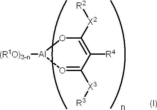
本発明のパッシベーション膜付き半導体基板の製造方法は、半導体基板上に電極を形成する工程と、前記半導体基板の前記電極が形成される面上に、有機アルミニウム化合物を含むパッシベーション膜形成用組成物を付与して組成物層を形成する工程と、前記組成物層を熱処理してパッシベーション膜を形成する工程とを有する。前記製造方法は必要に応じてその他の工程を更に有していてもよい。
半導体基板の電極が形成される面上に、有機アルミニウム化合物を含むパッシベーション膜形成用組成物を所望の形状となるようにパターン状に付与し、これを熱処理してパッシベーション膜を形成することで、所望の形状を有し、優れたパッシベーション効果を示すパッシベーション膜が形成された半導体基板を簡便な工程で製造することができる。
1/τ=1/τb+1/τs (A)
尚、実効ライフタイムが長いほど少数キャリアの再結合速度が遅いことを示す。また実効ライフタイムが長い半導体基板を用いて太陽電池素子を構成することで、変換効率が向上する。
半導体基板上への電極形成用組成物の付与量は特に制限されず、形成する電極の形状等に応じて適宜選択することができる。さらに形成される電極の形状は特に制限されず、目的に応じて適宜選択することができる。
半導体基板上へのパッシベーション膜形成用組成物の付与量は特に制限されない。例えば、形成されるパッシベーション膜の膜厚が後述する膜厚となるように適宜選択することが好ましい。
組成物層の熱処理条件は、組成物層に含まれる有機アルミニウム化合物をその熱処理物である酸化アルミニウム(Al2O3)に変換可能であれば特に制限されない。中でも特定の結晶構造を持たないアモルファス状のAl2O3層を形成可能な熱処理条件であることが好ましい。半導体基板パッシベーション膜がアモルファス状のAl2O3層で構成されることで、半導体基板パッシベーション膜に負電荷をより効果的に持たせることができ、より優れたパッシベーション効果を得ることができる。この熱処理工程は、乾燥工程とアニーリング工程に分けることもできる。乾燥工程後ではパッシベーション効果は得られないが、アニーリング工程後にパッシベーション効果を得ることができる。具体的に、アニーリング温度は400℃~900℃が好ましく、450℃~800℃がより好ましい。またアニーリング時間はアニーリング温度等に応じて適宜選択できる。例えば、0.1時間~10時間とすることができ、0.2時間~5時間であることが好ましい。
なお、形成されたパッシベーション膜の膜厚は、触針式段差・表面形状測定装置(例えば、Ambios社製)を用いて常法により測定される。
前記パッシベーション膜形成用組成物は、有機アルミニウム化合物の少なくとも1種を含むが、樹脂の少なくとも1種を更に含むことが好ましく、下記一般式(I)で表される有機アルミニウム化合物の少なくとも1種と、樹脂の少なくとも1種とを含むことがより好ましい。パッシベーション膜形成用組成物は必要に応じてその他の成分を更に含んでいてもよい。

パッシベーション膜形成用組成物が特定の有機アルミニウム化合物と樹脂とを含むことで、所望の形状に組成物層を形成することが容易に可能なため、所望の領域に選択的にパッシベーション膜を形成することができるというパターン形成性に優れる。また特定の有機アルミニウム化合物を含んで構成されているため、経時的な保存安定性に優れる。
粘度変化率(%)=|η30-η0|/η0×100 (式)
前記パッシベーション膜形成用組成物は前記一般式(I)で表される有機アルミニウム化合物の少なくとも1種を含むことが好ましい。前記有機アルミニウム化合物は、アルミニウムアルコキシド、アルミニウムキレートなどと呼ばれる化合物であり、アルミニウムアルコキシド構造に加えてアルミニウムキレート構造を有していることが好ましい。また、Nippon Seramikkusu Kyokai Gakujitsu Ronbunshi、97(1989)369-399にも記載されているように、前記有機アルミニウム化合物は熱処理により酸化アルミニウム(Al2O3)となる。
特定構造の有機アルミニウム化合物を含有するパッシベーション膜形成用組成物を熱処理することにより形成される酸化アルミニウムはアモルファス状態となりやすく、アルミニウム原子の欠陥等が生じて半導体基板との界面付近に大きな負の固定電荷をもつことができると考えられる。この大きな負の固定電荷が半導体基板の界面近辺で電界を発生することで少数キャリアの濃度を低下させることができ、結果的に界面でのキャリア再結合速度が抑制されるため、優れたパッシベーション効果を有するパッシベーション膜を形成することができると考えられる。
一般式(I)におけるR2、R3及びR4はそれぞれ独立して水素原子又は炭素数1~8のアルキル基を表す。R2、R3及びR4で表されるアルキル基は直鎖状であっても分岐鎖状であってもよい。R2、R3及びR4で表されるアルキル基として具体的には、メチル基、エチル基、プロピル基、イソプロピル基、ブチル基、イソブチル基、sec-ブチル基、t-ブチル基、ヘキシル基、オクチル基、エチルヘキシル基等を挙げることができる。
前記パッシベーション膜形成用組成物は、樹脂の少なくとも1種を含むことが好ましい。樹脂を含むことで、前記パッシベーション膜形成用組成物が半導体基板上に付与されて形成される組成物層の形状安定性がより向上し、パッシベーション膜を前記組成物層が形成された領域に、所望の形状でより選択的に形成することができる。
前記樹脂の半導体基板パッシベーション膜形成用組成物中の含有率は、必要に応じて適宜選択することができる。樹脂の含有率は、例えば基板パッシベーション膜形成用組成物中に0.1質量%~30質量%であることが好ましい。パターン形成をより容易にするようなチキソ性を発現させる観点から、樹脂の含有率は、1質量%~25質量%であることがより好ましく、1.5質量%~20質量%であることがより好ましく、1.5質量%~10質量%であることがさらに好ましい。
前記パッシベーション膜形成用組成物は溶媒を含むことが好ましい。パッシベーション膜形成用組成物が溶媒を含有することで、粘度の調整がより容易になり、付与性がより向上すると共により均一な熱処理物層を形成することができる。前記溶媒としては特に制限されず、必要に応じて適宜選択することができる。前記溶媒としては特に制限されず、必要に応じて適宜選択することができる。中でも前記有機アルミニウム化合物、及び前記樹脂を溶解して均一な溶液を与えることができる溶媒が好ましく、有機溶剤の少なくとも1種を含むことがより好ましい。
本発明のパッシベーション膜付き半導体基板は、前記製造方法で製造されたものであり、半導体基板と、前記半導体基板上に設けられ、有機アルミニウム化合物を含むパッシベーション膜形成用組成物の熱処理物層とを有する。また前記パッシベーション膜付き半導体基板は、前記パッシベーション膜形成用組成物の熱処理物からなる層であるパッシベーション膜を有することで優れたパッシベーション効果を示す。
本発明の太陽電池素子の製造方法は、p型層及びn型層が接合されてなるpn接合を有する半導体基板上のp型層及びn型層からなる群より選択される少なくとも1つの層上に電極を形成する工程と、前記半導体基板の前記電極が形成される面の一方又は両方の面上に、有機アルミニウム化合物を含むパッシベーション膜形成用組成物を付与して組成物層を形成する工程と、前記組成物層を熱処理してパッシベーション膜を形成する工程とを有する。前記太陽電池素子の製造方法は、必要に応じてその他の工程を更に有していてもよい。
前記パッシベーション膜形成用組成物を用いてパッシベーション膜を形成する方法の詳細は、既述のパッシベーション膜付き半導体基板の製造方法と同様であり、好ましい態様も同様である。
前記半導体基板上に形成される半導体基板パッシベーション膜の厚みは特に制限されず、目的に応じて適宜選択することができる。例えば、5nm~50μmであることが好ましく、10nm~30μmであることが好ましく、15nm~20μmであることが更に好ましい。
本発明の太陽電池素子は、前記太陽電池素子の製造方法によって製造されたものであり、p型層及びn型層がpn接合されてなる半導体基板と、前記半導体基板上の全面又は一部に設けられた有機アルミニウム化合物を含むパッシベーション膜形成用組成物の熱処理物層であるパッシベーション膜と、前記半導体基板の前記p型層及びn型層からなる群より選択される1以上の層上に配置された電極とを有する。前記太陽電池素子は、必要に応じてその他の構成要素を更に有していてもよい。
本発明の太陽電池素子は、前記太陽電池素子の製造方法によって形成されたパッシベーション膜を有することで、変換効率に優れる。
太陽電池素子の形状や大きさに制限はない。例えば、一辺が125mm~156mmの正方形であることが好ましい。
図1は、本実施形態にかかる半導体基板パッシベーション膜を有する太陽電池素子の製造方法の一例を模式的に示す工程図を断面図として示したものである。但し、この工程図は本発明をなんら制限するものではない。
さらにまた、裏面部分に半導体基板パッシベーション膜を形成せず、側面のみに本発明の半導体基板パッシベーション膜形成用組成物を塗布、熱処理して半導体基板パッシベーション膜を形成してもよい。本発明の半導体基板パッシベーション膜形成用組成物は、側面のような結晶欠陥が多い場所に使用すると、その効果が特に大きい。
ここでp型拡散層形成用組成物に代えて、アルミニウム電極ペーストを用いてもよい。アルミニウム電極ペーストを用いた場合には、p+型拡散層4上にはアルミニウム電極8が形成される。
また裏面電極が形成される領域にはすでにp+型拡散層4が形成されているため、裏面電極5を形成する電極形成用ペーストには、アルミニウム電極ペーストに限定されず、銀電極ペースト等のより低抵抗な電極を形成可能な電極用ペーストを用いることもできる。これにより、さらに発電効率を高めることも可能になる。
さらにまた、裏面部分にパッシベーション膜を形成せず、側面のみにパッシベーション膜形成用組成物を付与し、これを熱処理してパッシベーション膜を形成してもよい。前記パッシベーション膜形成用組成物は、側面のような結晶欠陥が多い場所に使用すると、その効果が特に大きい。
図3に概略断面図を示すように、p型半導体基板1の受光面側には、表面近傍にn+型拡散層2が形成され、その表面にパッシベーション膜6及び反射防止膜3が形成されている。反射防止膜3としては、窒化ケイ素膜、酸化チタン膜などが知られている。また半導体基板パッシベーション膜6は、パッシベーション膜形成用組成物を付与し、これを熱処理して形成される。
p+型拡散層4は、上述のようにp型拡散層形成用組成物又はアルミニウム電極ペーストを所望の領域に塗布した後に熱処理することで形成することができる。またn+型拡散層2は、例えば熱拡散処理によりn+型拡散層を形成可能なn型拡散層形成用組成物を所望の領域に塗布した後に熱処理することで形成することができる。
ここでn型拡散層形成用組成物としては例えば、ドナー元素含有物質とガラス成分とを含む組成物を挙げることができる。
また、p+型拡散層4上に設けられる裏面電極5は、アルミニウム電極ペーストを用いてp+型拡散層4と共に形成されるアルミニウム電極であってもよい。
裏面に設けられるパッシベーション膜6は、パッシベーション膜形成用組成物を裏面電極5が設けられていない領域に付与し、これを焼成熱処理することで形成することができる。
またパッシベーション膜6は半導体基板1の裏面のみならず、さらに側面にも形成してよい(図示せず)。
太陽電池は、前記太陽電池素子の少なくとも1つを含み、太陽電池素子の電極上にタ配線材料が配置されて構成される。太陽電池はさらに必要に応じて、配線材料を介して複数の太陽電池素子が連結され、さらに封止材で封止されて構成されていてもよい。
前記配線材料及び封止材としては特に制限されず、当業界で通常用いられているものから適宜選択することができる。
前記太陽電池の大きさに制限はない。0.5m2~3m2であることが好ましい。
(半導体基板パッシベーション膜形成用組成物の調製)
トリsec-ブトキシアルミニウムを2.00g、テルピネオールを2.01g混合し有機アルミニウム化合物溶液を調製した。これとは別にエチルセルロースを5.00g、テルピネオールを95.02g混合し、150℃で1時間攪拌してエチルセルロース溶液を調製した。得られた有機アルミニウム化合物溶液を2.16gと、エチルセルロース溶液を3.00g混合して無色透明の溶液として、半導体基板パッシベーション膜形成用組成物1を調製した。エチルセルロースの半導体基板パッシベーション膜形成用組成物1中の含有率は2.9%、有機アルミニウム化合物の含有率は21%となった。
半導体基板として、表面がミラー形状の単結晶型p型シリコン基板(SUMCO製、50mm角、厚さ:625μm)を用いた。シリコン基板をRCA洗浄液(関東化学製Frontier Cleaner-A01)を用いて70℃にて5分間、浸漬洗浄し、前処理を行った。
その後、上記で得られた半導体基板パッシベーション膜形成用組成物1を前処理したシリコン基板上にスクリーン印刷法を用いて、乾燥後の膜厚が5μmとなるように全面に付与し、150℃で3分間乾燥処理した。次いで550℃で1時間アニーリングした後、室温で放冷して評価用基板を作製した。形成されたパッシベーション膜の膜厚は0.35μmであった。
上記で得られた評価用基板の実効ライフタイム(μs)を、ライフタイム測定装置(日本セミラボ製WT-2000PVN)を用いて、室温で反射マイクロ波光電導減衰法により測定した。得られた評価用基板の半導体基板パッシベーション膜形成用組成物を付与した領域の実効ライフタイムは、111μsであった。
(チキソ比)
上記で調製した半導体基板パッシベーション膜形成用組成物1のせん断粘度を、調製直後(12時間以内)に、回転式せん断粘度計(AntonPaar社製MCR301)に、コーンプレート(直径50mm、コーン角1°)を装着し、温度25℃で、せん断速度1.0s-1及び10s-1の条件でそれぞれ測定した。
せん断速度が1.0s-1の条件でのせん断粘度(η1)は16.0Pa・s、せん断速度が10s-1の条件でのせん断粘度(η2)は5.7Pa・sとなった。せん断粘度が1.0s-1と10s-1の場合でのチキソ比(η1/η2)は2.8となった。
上記で調製した半導体基板パッシベーション膜形成用組成物1のせん断粘度を、調製直後(12時間以内)及び25℃で30日間保存後にそれぞれ測定した。せん断粘度の測定はAntonPaar社MCR301に、コーンプレート(直径50mm、コーン角1°)を装着し、温度25℃、せん断速度1.0s-1で行なった。
25℃におけるせん断粘度は、調製直後(η0)は16.0Pa・s、25℃で30日間保存した後(η30)は17.3Pa・sであった。従って、下式で算出される粘度変化率(%)は、8%であった。
粘度変化率(%)=|η30-η0|/η0×100 (式)
トリsec-ブトキシアルミニウムを4.79g、アセト酢酸エチルを2.56g、テルピネオールを4.76g混合し、25℃で1時間攪拌して有機アルミニウム化合物溶液を得た。これとは別にエチルセルロースを12.02g、テルピネオールを88.13g混合し、150℃で1時間攪拌してエチルセルロース溶液を調製した。次に有機アルミニウム化合物溶液を2.93g、エチルセルロース溶液を2.82g混合して無色透明の溶液として、半導体基板パッシベーション膜形成用組成物2を調製した。エチルセルロースの半導体基板パッシベーション膜形成用組成物2中の含有率は5.9%、有機アルミニウム化合物の含有率は21%となった。
上記で調製した半導体基板パッシベーション膜形成用組成物2のせん断粘度を、調製直後(12時間以内)に、回転式せん断粘度計(AntonPaar社製MCR301)に、コーンプレート(直径50mm、コーン角1°)を装着し、温度25℃で、せん断速度1.0s-1及び10s-1の条件でそれぞれ測定した。
せん断速度が1.0s-1の条件でのせん断粘度(η1)は41.5Pa・s、せん断速度が10s-1の条件でのせん断粘度(η2)は28.4Pa・sとなった。せん断粘度が1.0s-1と10s-1の場合でのチキソ比(η1/η2)は1.5となった。
上記で調製した半導体基板パッシベーション膜形成用組成物2の調製直後のせん断粘度は温度25℃、せん断速度1.0s-1で41.5Pa・s、25℃で30日間保存した後は43.2Pa・sであった。従って、保存安定性を示す粘度変化率は4%であった。
その結果、4配位アルミニウムに配位した酸素-炭素結合に特徴的な吸収が1600cm-1付近に、6員環錯体の炭素-炭素結合に特徴的な吸収が1500cm-1付近にそれぞれ観察され、アルミニウムキレートが形成されていることが確認された。
トリsec-ブトキシアルミニウムを4.96g、ジエチルマロン酸を3.23g、テルピネオールを5.02g混合し、25℃で1時間攪拌して有機アルミニウム化合物溶液を得た。得られた有機アルミニウム化合物溶液を2.05g、実施例2と同様にして調製したエチルセルロース溶液を2.00g混合して無色透明の溶液として、半導体基板パッシベーション膜形成用組成物3を調製した。エチルセルロースの半導体基板パッシベーション膜形成用組成物3中の含有率は5.9%、有機アルミニウム化合物の含有率は20%となった。
上記で調製した半導体基板パッシベーション膜形成用組成物3のせん断粘度を調製直後(12時間以内)に、回転式せん断粘度計(AntonPaar社製MCR301)に、コーンプレート(直径50mm、コーン角1°)を装着し、温度25℃で測定した。
せん断速度が1.0s-1の条件でのせん断粘度(η1)は90.7Pa・s、せん断速度が10s-1の条件でのせん断粘度(η2)は37.4Pa・s、せん断速度が100s-1の条件でせん断粘度は10.4Pa・sとなった。せん断粘度が1.0s-1と10s-1の場合でのチキソ比(η1/η2)は2.43となった。
上記で調製した半導体基板パッシベーション膜形成用組成物3の調製直後のせん断粘度は温度25℃、せん断速度1.0s-1で90.7Pa・s、25℃で30日間保存した後は97.1Pa・sであった。従って、保存安定性を示す粘度変化率は7%であった。
その結果、4配位アルミニウムに配位した酸素-炭素結合に特徴的な吸収が1600cm-1付近に、6員環錯体の炭素-炭素結合に特徴的な吸収が1500cm-1付近にそれぞれ観察され、アルミニウムキレートが形成されていることが確認された。
実施例3において、半導体基板パッシベーション膜形成用組成物3をシリコン基板上にスクリーン印刷で100μm幅、間隔2mmの短冊状に付与したこと以外は、実施例3と同様にして、前処理したシリコン基板上にパッシベーション膜を形成し、同様にして評価した。
半導体基板パッシベーション膜形成用組成物3が付与された領域における実効ライフタイムは、90μsであった。また半導体基板パッシベーション膜形成用組成物3が付与されていない領域における実効ライフタイムは、25μsであった。
実施例1と同様にして前処理したシリコン基板上に、スクリーン印刷でアルミペースト(PVG solutions社製、PVG-AD-02)を幅約200μm、間隔2mmで短冊状に付与し、400℃10秒間、850℃10秒間、650℃10秒間で焼結して厚み20μmのアルミニウム電極を形成した。
次に、上記で調製した半導体基板パッシベーション膜形成用組成物3をスクリーン印刷で、電極が形成されていない領域にのみ付与し、150℃で3分間乾燥処理した。次いで550℃で1時間アニーリングした後、室温で放冷してパッシベーション膜を形成し評価用基板を作製した。
パッシベーション膜を形成した領域の実効ライフタイムは90μsであった。またアルミニウム電極の表面には、パッシベーション膜形成用組成物3に由来する異物は観察されなかった。
エチルセルロースを100.02gとテルピネオールを400.13g混合し、150℃で1時間攪拌して10%エチルセルロース溶液を調製した。これとは別に、エチルアセトアセテートアルミニウムジイソプロピレート(川研ファインケミカル社製、商品名:ALCH)を9.71gと、テルピネオールを4.50g混合し、次に10%エチルセルロース溶液を15.03g混合して無色透明の溶液として、パッシベーション膜形成用組成物6を調製した。エチルセルロースのパッシベーション膜形成用組成物6中の含有率は5.1%、有機アルミニウム化合物の含有率は33.2%となった。
上記で調製したパッシベーション膜形成用組成物6を用いたこと以外は、実施例1と同様にして、前処理したシリコン基板上にパッシベーション膜を形成し、同様にして評価した。実効ライフタイムは、121μsであった。
上記で調製したパッシベーション膜形成用組成物6のせん断粘度を、上記と同様にして測定した。調製直後(12時間以内)に、回転式せん断粘度計(AntonPaar社製MCR301)に、コーンプレート(直径50mm、コーン角1°)を装着し、温度25℃で、せん断速度1.0s-1及び10s-1の条件でそれぞれ測定した。
せん断速度が1.0s-1の条件でのせん断粘度(η1)は81.0Pa・s、せん断速度が10s-1の条件でのせん断粘度(η2)は47.7Pa・sとなった。せん断粘度が1.0s-1と10s-1の場合でのチキソ比(η1/η2)は1.7となった。
上記で調製したパッシベーション膜形成用組成物6の調製直後のせん断粘度は温度25℃、せん断速度1.0s-1で81.0Pa・s、25℃で30日間保存した後は80.7Pa・sであった。従って、保存安定性を示す粘度変化率は0.4%であった。
印刷滲みの評価は、調製したパッシベーション膜形成用組成物6を、シリコン基板上にスクリーン印刷法を用いてパターン形成し、印刷直後のパターン形状と熱処理後のパターン形状とを比較することで行った。スクリーン印刷法には、図6に示すような円形のドット状の開口部14と非開口部12を有する電極形成用のスクリーンマスク版とは、逆の開口部パターンを有するスクリーンマスク版(図6のドット状の開口部14が非開口部となる版)を用いた。図4に示すスクリーンマスク版では、ドット状の開口部14のドット径Laが368μm、ドット間隔Lbが0.5mmである。なお、前記印刷滲みとは、シリコン基板上に印刷したパッシベーション膜形成用組成物から形成された組成物層が、用いた版に比べて、シリコン基板の面方向に広がる現象をいう。
上記で得られたパッシベーション膜形成用組成物6の印刷滲み評価はAであった。
上記で得られたパッシベーション膜形成用組成物6を、シリコン基板上にスクリーン印刷法を用いて、図6の非開口部12に対応する領域の全面に印刷した。その後、パッシベーション膜形成用組成物6を付与したシリコン基板を150℃で3分間加熱し、溶剤を蒸散させることで乾燥処理した。次いで550℃の温度で10分間アニーリングした後、室温で放冷して、パッシベーション膜を形成した。形成されたパッシベーション膜の膜厚は0.57μmであった。
続いて、トンネル炉(1列搬送W/Bトンネル炉、ノリタケ社製)を用いて大気中雰囲気下、焼結最高温度800℃、保持時間10秒の条件で焼結を行って電極を形成した。
-評価基準-
A:シリコン基板とアルミニウム電極の接触率が90%以上であった。
B:シリコン基板とアルミニウム電極の接触率が70%以上90%未満であった。
C:シリコン基板とアルミニウム電極の接触率が70%未満であった。
エチルアセトアセテートアルミニウムジイソプロピレートを10.12gと、テルピネオールを25.52g混合し、次に実施例6で作製した10%エチルセルロース溶液を34.70g混合して無色透明の溶液として、パッシベーション膜形成用組成物7を調製した。エチルセルロースのパッシベーション膜形成用組成物7中の含有率は4.9%、有機アルミニウム化合物の含有率は14.4%となった。
せん断速度が1.0s-1の条件でのせん断粘度(η1)は43.4Pa・s、せん断速度が10s-1の条件でのせん断粘度(η2)は27.3Pa・sとなった。せん断粘度が1.0s-1と10s-1の場合でのチキソ比(η1/η2)は1.6となった。
上記で調製したパッシベーション膜形成用組成物7の調製直後のせん断粘度は温度25℃、せん断速度1.0s-1で43.4Pa・s、25℃で30日間保存した後は44.5Pa・sであった。従って、保存安定性を示す粘度変化率は3%であった。
半導体基板パッシベーション膜形成用組成物7の印刷滲み評価はAであった。
パッシベーション膜形成用組成物7の電極形成性はAであった。
エチルアセトアセテートアルミニウムジイソプロピレートを5.53gと、テルピネオールを6.07g混合し、次に実施例6で作製した10%エチルセルロース溶液を9.93g混合して無色透明の溶液として、半導体基板パッシベーション膜形成用組成物8を調製した。エチルセルロースの半導体基板パッシベーション膜形成用組成物8中の含有率は4.6%、有機アルミニウム化合物の含有率は25.7%となった。
せん断速度が1.0s-1の条件でのせん断粘度(η1)は38.5Pa・s、せん断速度が10s-1の条件でのせん断粘度(η2)は28.1Pa・sとなった。せん断粘度が1.0s-1と10s-1の場合でのチキソ比(η1/η2)は1.6となった。
パッシベーション膜形成用組成物8の調製直後のせん断粘度は温度25℃、せん断速度1.0s-1で38.5Pa・s、25℃で30日間保存した後は39.7Pa・sであった。従って、保存安定性を示す粘度変化率は3%であった。
パッシベーション膜形成用組成物8の印刷滲み評価はAであった。
パッシベーション膜形成用組成物8の電極形成性はAであった。
エチルセルロースを20.18gとテルピネオールを480.22g混合し、150℃で1時間攪拌して4%エチルセルロース溶液を調製した。エチルアセトアセテートアルミニウムジイソプロピレートを5.09gと、4%エチルセルロース溶液を5.32gと、水酸化アルミニウム粒子(HP-360、昭和電工製、粒子径(D50%)は3.2μm、純度99.0%)を11.34gとを混合して白色の懸濁液として、半導体基板パッシベーション膜形成用組成物9を調製した。エチルセルロースの半導体基板パッシベーション膜形成用組成物9中の含有率は1.0%、有機アルミニウム化合物の含有率は23.4%となった。
せん断速度が1.0s-1の条件でのせん断粘度(η1)は33.5Pa・s、せん断速度が10s-1の条件でのせん断粘度(η2)は25.6Pa・sとなった。せん断粘度が1.0s-1と10s-1の場合でのチキソ比(η1/η2)は1.3となった。
上記で調製した半導体基板パッシベーション膜形成用組成物9の調製直後のせん断粘度は温度25℃、せん断速度1.0s-1で33.5Pa・s、25℃で30日間保存した後は36.3Pa・sであった。従って、保存安定性を示す粘度変化率は8%であった。
パッシベーション膜形成用組成物9の印刷滲み評価はAであった。
パッシベーション膜形成用組成物9の電極形成性はAであった。
エチルアセトアセテートアルミニウムジイソプロピレートを5.18gと、4%エチルセルロース溶液を5.03gと、酸化ケイ素粒子(アエロジル200、日本アエロジル社製、平均粒子径12nm、表面がヒドロキシ基で修飾されている)を2.90gと、テルピネオールを6.89gを混合して白色の懸濁液として、半導体基板パッシベーション膜形成用組成物10を調製した。エチルセルロースの半導体基板パッシベーション膜形成用組成物9中の含有率は1.0%、有機アルミニウム化合物の含有率は25.9%となった。
上記で調製した半導体基板パッシベーション膜形成用組成物9のせん断粘度を、調製直後(12時間以内)に、回転式せん断粘度計(AntonPaar社製MCR301)に、コーンプレート(直径50mm、コーン角1°)を装着し、温度25℃で、せん断速度1.0s-1及び10s-1の条件でそれぞれ測定した。
せん断速度が1.0s-1の条件でのせん断粘度(η1)は48.3Pa・s、せん断速度が10s-1の条件でのせん断粘度(η2)は32.9Pa・sとなった。せん断粘度が1.0s-1と10s-1の場合でのチキソ比(η1/η2)は1.5となった。
上記で調製した半導体基板パッシベーション膜形成用組成物9の調製直後のせん断粘度は温度25℃、せん断速度1.0s-1で48.3Pa・s、25℃で30日間保存した後は50.1Pa・sであった。従って、保存安定性を示す粘度変化率は4%であった。
パッシベーション膜形成用組成物10の印刷滲み評価はAであった。
パッシベーション膜形成用組成物10の電極形成性はAであった。
実施例1において、半導体基板パッシベーション膜形成用組成物1の塗布を行わなかったこと以外は実施例1と同様にして、評価用基板を作製し、実効ライフタイムを測定して評価した。実効ライフタイムは、20μsであった。
Al2O3粒子(高純度化学社製、平均粒子径1μm)を2.00g、テルピネオールを1.98g、実施例2と同様にして調製したエチルセルロース溶液を3.98g混合して無色透明の組成物C2を調製した。
上記で調製した組成物C2を用いたこと以外は、実施例1と同様にして前処理したシリコン基板上にパッシベーション膜を形成し、同様にして評価した。実効ライフタイムは、21μsであった。
テトラエトキシシランを2.01g、テルピネオールを1.99g、実施例2と同様にして調製したエチルセルロース溶液を4.04g混合して無色透明の組成物C3を調製した。
上記で調製した組成物C3を用いたこと以外は、実施例1と同様にしてシリコン基板上にパッシベーション膜を形成し、同様にして評価した。実効ライフタイムは、23μsであった。
トリイソプロポキシアルミニウムを8.02g、精製水36.03g、濃硝酸(d=1.41)を0.15g混合し、100℃で1時間攪拌して組成物C4を調製した。
上記で調製した組成物C4を用いたこと以外は、実施例5と同様にしてアルミニウム電極を形成したシリコン基板上にパッシベーション膜を形成し、同様にして評価した。
パッシベーション膜を形成した領域の実効ライフタイムは、110μsであった。またアルミニウム電極の表面には、半導体基板パッシベーション膜形成用組成物C4に由来する異物が観察された。
上記で調製した半導体基板パッシベーション膜形成用組成物C4の調製直後のせん断粘度は温度25℃、せん断速度1.0s-1で67.5Pa・s、25℃で30日間保存した後は36000Pa・sであった。

本明細書に記載された全ての文献、特許出願、および技術規格は、個々の文献、特許出願、および技術規格が参照により取り込まれることが具体的かつ個々に記された場合と同程度に、本明細書に参照により取り込まれる。
Claims (14)
- 半導体基板上に電極を形成する工程と、
前記半導体基板の前記電極が形成される面上に、有機アルミニウム化合物を含むパッシベーション膜形成用組成物を付与して組成物層を形成する工程と、
前記組成物層を熱処理してパッシベーション膜を形成する工程と、
を有するパッシベーション膜付き半導体基板の製造方法。 - 前記半導体基板パッシベーション膜形成用組成物を付与して形成される組成物層が、前記半導体基板上の電極が形成されない領域に形成される請求項1に記載のパッシベーション膜付き半導体基板の製造方法。
- 前記電極を形成する工程は、半導体基板上に電極形成用組成物を付与して電極形成用組成物層を形成する工程と、
前記電極形成用組成物層を熱処理する工程と、
を有する請求項1又は請求項2に記載のパッシベーション膜付き半導体基板の製造方法。 - 前記パッシベーション膜形成用組成物は、前記有機アルミニウム化合物として下記一般式(I)で表される化合物と、樹脂とを含む請求項1~請求項3のいずれか1項に記載のパッシベーション膜付き半導体基板の製造方法。

[式中、R1はそれぞれ独立して炭素数1~8のアルキル基を表す。nは0~3の整数を表す。X2及びX3はそれぞれ独立して酸素原子又はメチレン基を表す。R2、R3及びR4はそれぞれ独立して水素原子又は炭素数1~8のアルキル基を表す] - 前記一般式(I)においてR1がそれぞれ独立して炭素数1~4のアルキル基である請求項4に記載のパッシベーション膜付き半導体基板の製造方法。
- 前記一般式(I)においてnが1~3の整数であり、R4がそれぞれ独立して水素原子又は炭素数1~4のアルキル基である請求項4又は請求項5に記載のパッシベーション膜付き半導体基板の製造方法。
- 請求項1~請求項6のいずれか1項に記載の製造方法で製造されるパッシベーション膜付き半導体基板。
- p型層及びn型層が接合されてなるpn接合を有する半導体基板上の前記p型層及びn型層からなる群より選ばれる少なくとも1つの層上に電極を形成する工程と、
前記半導体基板の前記電極が形成される面の一方又は両方の面上に、有機アルミニウム化合物を含む半導体基板パッシベーション膜形成用組成物を付与して組成物層を形成する工程と、
前記組成物層を熱処理してパッシベーション膜を形成する工程と、
を有する太陽電池素子の製造方法。 - 前記半導体基板パッシベーション膜形成用組成物は、前記半導体基板上の電極が形成されない領域に付与される請求項8に記載の太陽電池素子の製造方法。
- 前記電極を形成する工程は、電極形成用組成物を半導体基板上に付与して電極形成用組成物層を形成する工程と、
前記電極形成用組成物層を熱処理する工程と、
を有する請求項8又は請求項9に記載の太陽電池素子の製造方法。 - 前記半導体基板パッシベーション膜形成用組成物は、前記有機アルミニウム化合物として下記一般式(I)で表される化合物と、樹脂とを含む請求項8~請求項10のいずれか1項に記載の太陽電池素子の製造方法。

[式中、R1はそれぞれ独立して炭素数1~8のアルキル基を表す。nは0~3の整数を表す。X2及びX3はそれぞれ独立して酸素原子又はメチレン基を表す。R2、R3及びR4はそれぞれ独立して水素原子又は炭素数1~8のアルキル基を表す] - 前記一般式(I)においてR1がそれぞれ独立して炭素数1~4のアルキル基である請求項11に記載の太陽電池素子の製造方法。
- 前記一般式(I)においてnが1~3の整数であり、R4がそれぞれ独立して水素原子又は炭素数1~4のアルキル基である請求項11又は請求項12に記載の太陽電池素子の製造方法。
- 請求項8~請求項13のいずれか1項に記載の製造方法で製造される太陽電池素子。
Priority Applications (3)
| Application Number | Priority Date | Filing Date | Title |
|---|---|---|---|
| KR1020147019203A KR20140117400A (ko) | 2012-01-06 | 2012-12-28 | 패시베이션막이 있는 반도체 기판과 그 제조 방법, 및 태양전지 소자와 그 제조 방법 |
| US14/370,630 US20150303317A1 (en) | 2012-01-06 | 2012-12-28 | Semiconductor substrate provided with passivation film and production method, and photovoltaic cell element and production method therefor |
| CN201280066119.8A CN104040701B (zh) | 2012-01-06 | 2012-12-28 | 带钝化膜的半导体基板及其制造方法、以及太阳能电池元件及其制造方法 |
Applications Claiming Priority (2)
| Application Number | Priority Date | Filing Date | Title |
|---|---|---|---|
| JP2012001653 | 2012-01-06 | ||
| JP2012-001653 | 2012-01-06 |
Publications (1)
| Publication Number | Publication Date |
|---|---|
| WO2013103141A1 true WO2013103141A1 (ja) | 2013-07-11 |
Family
ID=48745201
Family Applications (1)
| Application Number | Title | Priority Date | Filing Date |
|---|---|---|---|
| PCT/JP2012/084160 Ceased WO2013103141A1 (ja) | 2012-01-06 | 2012-12-28 | パッシベーション膜付半導体基板及びその製造方法、並びに太陽電池素子及びその製造方法 |
Country Status (6)
| Country | Link |
|---|---|
| US (1) | US20150303317A1 (ja) |
| JP (2) | JPWO2013103141A1 (ja) |
| KR (1) | KR20140117400A (ja) |
| CN (2) | CN104040701B (ja) |
| TW (2) | TWI624958B (ja) |
| WO (1) | WO2013103141A1 (ja) |
Cited By (4)
| Publication number | Priority date | Publication date | Assignee | Title |
|---|---|---|---|---|
| JP2015106589A (ja) * | 2013-11-28 | 2015-06-08 | 日立化成株式会社 | パッシベーション層付半導体基板の製造方法、パッシベーション層付半導体基板、太陽電池素子の製造方法及び太陽電池素子 |
| JP2015115488A (ja) * | 2013-12-12 | 2015-06-22 | 日立化成株式会社 | パッシベーション層形成用組成物、パッシベーション層付半導体基板、パッシベーション層付半導体基板の製造方法、太陽電池素子、太陽電池素子の製造方法及び太陽電池 |
| JP2015144243A (ja) * | 2013-12-25 | 2015-08-06 | 東京応化工業株式会社 | 表面被覆膜の形成方法及び表面被覆膜を有する太陽電池 |
| CN106356413A (zh) * | 2016-09-06 | 2017-01-25 | 浙江晶科能源有限公司 | 一种薄晶体硅电池及其制备方法 |
Families Citing this family (2)
| Publication number | Priority date | Publication date | Assignee | Title |
|---|---|---|---|---|
| CN104716270A (zh) * | 2015-03-16 | 2015-06-17 | 上海和辉光电有限公司 | 一种薄膜封装结构和具有该结构的有机发光装置 |
| CN111809214B (zh) * | 2019-04-12 | 2022-03-22 | 平顶山市美伊金属制品有限公司 | 一种氧化后基材表面毛孔的封闭方法 |
Citations (7)
| Publication number | Priority date | Publication date | Assignee | Title |
|---|---|---|---|---|
| JPS5818973A (ja) * | 1981-07-27 | 1983-02-03 | Semiconductor Energy Lab Co Ltd | 光電変換装置作製方法 |
| JPS5823486A (ja) * | 1981-08-04 | 1983-02-12 | Toshiba Corp | 太陽電池の製造方法 |
| JPH06125103A (ja) * | 1991-08-26 | 1994-05-06 | Canon Inc | 太陽電池モジュール |
| JP2007287821A (ja) * | 2006-04-14 | 2007-11-01 | Jsr Corp | アルミナ膜形成方法 |
| JP2009283549A (ja) * | 2008-05-20 | 2009-12-03 | Mitsubishi Electric Corp | 太陽電池セルの製造方法および太陽電池モジュールの製造方法 |
| JP2010040741A (ja) * | 2008-08-05 | 2010-02-18 | Konica Minolta Holdings Inc | 電子デバイス用の絶縁膜形成方法、電子デバイスの製造方法、薄膜トランジスタの製造方法、絶縁膜、電子デバイス及び薄膜トランジスタ |
| JP2011216845A (ja) * | 2010-03-18 | 2011-10-27 | Ricoh Co Ltd | 絶縁膜形成用インク、絶縁膜の製造方法及び半導体装置の製造方法 |
Family Cites Families (33)
| Publication number | Priority date | Publication date | Assignee | Title |
|---|---|---|---|---|
| JPS5133567A (ja) * | 1974-09-17 | 1976-03-22 | Hitachi Ltd | Sankaaruminiumumakuojusuruhandotaisochi no seizohoho |
| JPS5568637A (en) * | 1978-11-20 | 1980-05-23 | Hitachi Ltd | Manufacture of semiconductor device |
| US4772672A (en) * | 1986-05-15 | 1988-09-20 | Kansai Paint Company, Limited | Curable compositions and method of curing same |
| US4753856A (en) * | 1987-01-02 | 1988-06-28 | Dow Corning Corporation | Multilayer ceramic coatings from silicate esters and metal oxides |
| US5516596A (en) * | 1994-12-19 | 1996-05-14 | Dow Corning Corporation | Method of forming a composite, article and composition |
| CA2232857C (en) * | 1995-10-05 | 2003-05-13 | Jalal Salami | Structure and fabrication process for self-aligned locally deep-diffused emitter (salde) solar cell |
| EP0974629A4 (en) * | 1997-04-11 | 2000-06-28 | Kaneka Corp | CURABLE COMPOSITION FOR COATINGS AND ARTICLES COATED WITH THIS COMPOSITION |
| JP3939408B2 (ja) * | 1997-09-30 | 2007-07-04 | Azエレクトロニックマテリアルズ株式会社 | 低誘電率シリカ質膜 |
| JP4329145B2 (ja) * | 1999-01-08 | 2009-09-09 | Jsr株式会社 | 膜形成用組成物の製造方法 |
| JP2000319530A (ja) * | 1999-05-13 | 2000-11-21 | Asahi Chem Ind Co Ltd | 半導体素子用組成物 |
| JP2002154184A (ja) * | 2000-08-07 | 2002-05-28 | Jsr Corp | 透明導電性シート |
| JP2003179240A (ja) * | 2001-12-10 | 2003-06-27 | Sharp Corp | 太陽電池およびその製造方法 |
| JP2004006565A (ja) * | 2002-04-16 | 2004-01-08 | Sharp Corp | 太陽電池とその製造方法 |
| JP4611617B2 (ja) * | 2002-04-26 | 2011-01-12 | 株式会社カネカ | 発光ダイオード |
| CN1206743C (zh) * | 2003-04-03 | 2005-06-15 | 上海交通大学 | 一种晶体硅太阳电池的制作方法 |
| JP3790242B2 (ja) * | 2003-09-26 | 2006-06-28 | 株式会社東芝 | 半導体装置及びその製造方法 |
| JP2006054353A (ja) * | 2004-08-13 | 2006-02-23 | Az Electronic Materials Kk | フラットバンドシフトの少ないシリカ質膜およびその製造法 |
| JP2007031696A (ja) * | 2005-06-10 | 2007-02-08 | Hitachi Chem Co Ltd | 樹脂組成物、シリカ系被膜及びその製造方法、積層体、並びに、電子部品 |
| JP4530980B2 (ja) * | 2005-08-26 | 2010-08-25 | 東京応化工業株式会社 | 膜形成用材料およびパターン形成方法 |
| CN101316902A (zh) * | 2005-11-04 | 2008-12-03 | 三井金属矿业株式会社 | 镍油墨及用该镍油墨形成的导体膜 |
| WO2007063721A1 (ja) * | 2005-11-30 | 2007-06-07 | Sumitomo Bakelite Co., Ltd. | ポジ型感光性樹脂組成物、およびそれを用いた半導体装置及び表示装置 |
| JP4767110B2 (ja) * | 2006-06-30 | 2011-09-07 | シャープ株式会社 | 太陽電池、および太陽電池の製造方法 |
| JP2008138159A (ja) * | 2006-11-07 | 2008-06-19 | Hitachi Chem Co Ltd | 樹脂組成物及びこれを用いた半導体装置 |
| JP5059499B2 (ja) * | 2007-06-29 | 2012-10-24 | 協立化学産業株式会社 | 基板にポジパターンを形成する方法及びその方法で使用されるネガパターン形成用組成物 |
| US8309844B2 (en) * | 2007-08-29 | 2012-11-13 | Ferro Corporation | Thick film pastes for fire through applications in solar cells |
| JP2011501442A (ja) * | 2007-10-17 | 2011-01-06 | フエロ コーポレーション | 片側裏面コンタクト太陽電池用誘電体コーティング |
| JP4718584B2 (ja) * | 2008-07-01 | 2011-07-06 | ヤスハラケミカル株式会社 | ポリシラザン溶解用処理液、およびこれを用いた半導体装置の製造方法 |
| JP5058184B2 (ja) * | 2009-01-23 | 2012-10-24 | 三菱電機株式会社 | 光起電力装置の製造方法 |
| US20100186808A1 (en) * | 2009-01-27 | 2010-07-29 | Peter Borden | Plating through tunnel dielectrics for solar cell contact formation |
| JP5290398B2 (ja) * | 2009-03-04 | 2013-09-18 | 日本碍子株式会社 | 超音波洗浄方法、及び超音波洗浄装置 |
| JP2011171270A (ja) * | 2010-01-25 | 2011-09-01 | Hitachi Chem Co Ltd | 電極用ペースト組成物および太陽電池 |
| CN102122674B (zh) * | 2011-01-14 | 2013-01-09 | 中国科学院上海技术物理研究所 | 一种晶体硅太阳电池及其制备方法 |
| WO2012119684A2 (de) * | 2011-03-08 | 2012-09-13 | Merck Patent Gmbh | Aluminiumoxid basierte metallisierungsbarriere |
-
2012
- 2012-12-28 KR KR1020147019203A patent/KR20140117400A/ko not_active Ceased
- 2012-12-28 CN CN201280066119.8A patent/CN104040701B/zh not_active Expired - Fee Related
- 2012-12-28 WO PCT/JP2012/084160 patent/WO2013103141A1/ja not_active Ceased
- 2012-12-28 CN CN201610532491.3A patent/CN106024918A/zh active Pending
- 2012-12-28 TW TW101150799A patent/TWI624958B/zh not_active IP Right Cessation
- 2012-12-28 JP JP2013552432A patent/JPWO2013103141A1/ja active Pending
- 2012-12-28 TW TW105141655A patent/TWI613835B/zh not_active IP Right Cessation
- 2012-12-28 US US14/370,630 patent/US20150303317A1/en not_active Abandoned
-
2016
- 2016-10-27 JP JP2016210829A patent/JP2017076802A/ja active Pending
Patent Citations (7)
| Publication number | Priority date | Publication date | Assignee | Title |
|---|---|---|---|---|
| JPS5818973A (ja) * | 1981-07-27 | 1983-02-03 | Semiconductor Energy Lab Co Ltd | 光電変換装置作製方法 |
| JPS5823486A (ja) * | 1981-08-04 | 1983-02-12 | Toshiba Corp | 太陽電池の製造方法 |
| JPH06125103A (ja) * | 1991-08-26 | 1994-05-06 | Canon Inc | 太陽電池モジュール |
| JP2007287821A (ja) * | 2006-04-14 | 2007-11-01 | Jsr Corp | アルミナ膜形成方法 |
| JP2009283549A (ja) * | 2008-05-20 | 2009-12-03 | Mitsubishi Electric Corp | 太陽電池セルの製造方法および太陽電池モジュールの製造方法 |
| JP2010040741A (ja) * | 2008-08-05 | 2010-02-18 | Konica Minolta Holdings Inc | 電子デバイス用の絶縁膜形成方法、電子デバイスの製造方法、薄膜トランジスタの製造方法、絶縁膜、電子デバイス及び薄膜トランジスタ |
| JP2011216845A (ja) * | 2010-03-18 | 2011-10-27 | Ricoh Co Ltd | 絶縁膜形成用インク、絶縁膜の製造方法及び半導体装置の製造方法 |
Cited By (4)
| Publication number | Priority date | Publication date | Assignee | Title |
|---|---|---|---|---|
| JP2015106589A (ja) * | 2013-11-28 | 2015-06-08 | 日立化成株式会社 | パッシベーション層付半導体基板の製造方法、パッシベーション層付半導体基板、太陽電池素子の製造方法及び太陽電池素子 |
| JP2015115488A (ja) * | 2013-12-12 | 2015-06-22 | 日立化成株式会社 | パッシベーション層形成用組成物、パッシベーション層付半導体基板、パッシベーション層付半導体基板の製造方法、太陽電池素子、太陽電池素子の製造方法及び太陽電池 |
| JP2015144243A (ja) * | 2013-12-25 | 2015-08-06 | 東京応化工業株式会社 | 表面被覆膜の形成方法及び表面被覆膜を有する太陽電池 |
| CN106356413A (zh) * | 2016-09-06 | 2017-01-25 | 浙江晶科能源有限公司 | 一种薄晶体硅电池及其制备方法 |
Also Published As
| Publication number | Publication date |
|---|---|
| TWI624958B (zh) | 2018-05-21 |
| US20150303317A1 (en) | 2015-10-22 |
| CN104040701A (zh) | 2014-09-10 |
| TW201712887A (zh) | 2017-04-01 |
| TWI613835B (zh) | 2018-02-01 |
| TW201330305A (zh) | 2013-07-16 |
| JPWO2013103141A1 (ja) | 2015-05-11 |
| CN106024918A (zh) | 2016-10-12 |
| CN104040701B (zh) | 2018-01-26 |
| KR20140117400A (ko) | 2014-10-07 |
| JP2017076802A (ja) | 2017-04-20 |
Similar Documents
| Publication | Publication Date | Title |
|---|---|---|
| JP2017076802A (ja) | パッシベーション膜付半導体基板及びその製造方法、並びに太陽電池素子及びその製造方法 | |
| JPWO2014014110A1 (ja) | パッシベーション層形成用組成物、パッシベーション層付半導体基板、パッシベーション層付半導体基板の製造方法、太陽電池素子、太陽電池素子の製造方法及び太陽電池 | |
| WO2014010743A1 (ja) | パッシベーション層形成用組成物、パッシベーション層付半導体基板及びその製造方法、太陽電池素子及びその製造方法、並びに太陽電池 | |
| JP6673372B2 (ja) | パッシベーション膜形成用組成物、パッシベーション膜付半導体基板及びその製造方法、並びに太陽電池素子及びその製造方法 | |
| JP6295673B2 (ja) | パッシベーション層付半導体基板、パッシベーション層形成用塗布型材料及び太陽電池素子 | |
| JP2015135858A (ja) | パッシベーション膜付半導体基板及びその製造方法、並びにそれを用いた太陽電池素子及びその製造方法 | |
| JPWO2014014108A1 (ja) | パッシベーション層形成用組成物、パッシベーション層付半導体基板、パッシベーション層付半導体基板の製造方法、太陽電池素子、太陽電池素子の製造方法及び太陽電池 | |
| WO2014010745A1 (ja) | 太陽電池素子及びその製造方法 | |
| JP6330661B2 (ja) | パッシベーション層形成用組成物、パッシベーション層付半導体基板及びその製造方法、並びに太陽電池素子及びその製造方法 | |
| JP2014157871A (ja) | パッシベーション膜形成用組成物、パッシベーション膜付半導体基板及びその製造方法、並びに太陽電池素子及びその製造方法 | |
| JP5522328B1 (ja) | パッシベーション層形成用組成物、パッシベーション層付半導体基板、パッシベーション層付半導体基板の製造方法、太陽電池素子、太陽電池素子の製造方法及び太陽電池 | |
| JP6630997B2 (ja) | パッシベーション層保護層形成用組成物、太陽電池素子及びその製造方法並びに太陽電池 | |
| JP6424422B2 (ja) | パッシベーション層付半導体基板の製造方法、パッシベーション層付半導体基板、太陽電池素子の製造方法及び太陽電池素子 | |
| WO2016002901A1 (ja) | パッシベーション層形成用組成物、パッシベーション層付半導体基板及びその製造方法、太陽電池素子及びその製造方法、並びに太陽電池 | |
| JP6107033B2 (ja) | 半導体基板パッシベーション膜形成用組成物、パッシベーション膜付半導体基板及びその製造方法、並びに太陽電池素子及びその製造方法 | |
| JP2015115488A (ja) | パッシベーション層形成用組成物、パッシベーション層付半導体基板、パッシベーション層付半導体基板の製造方法、太陽電池素子、太陽電池素子の製造方法及び太陽電池 | |
| JP2014072450A (ja) | 半導体基板パッシベーション膜形成用組成物、パッシベーション膜付半導体基板及びその製造方法、並びに太陽電池素子及びその製造方法 | |
| JP2014072436A (ja) | 半導体基板パッシベーション膜形成用組成物、パッシベーション膜付半導体基板及びその製造方法、並びに太陽電池素子及びその製造方法 |
Legal Events
| Date | Code | Title | Description |
|---|---|---|---|
| 121 | Ep: the epo has been informed by wipo that ep was designated in this application |
Ref document number: 12864035 Country of ref document: EP Kind code of ref document: A1 |
|
| ENP | Entry into the national phase |
Ref document number: 2013552432 Country of ref document: JP Kind code of ref document: A |
|
| WWE | Wipo information: entry into national phase |
Ref document number: 14370630 Country of ref document: US |
|
| ENP | Entry into the national phase |
Ref document number: 20147019203 Country of ref document: KR Kind code of ref document: A |
|
| NENP | Non-entry into the national phase |
Ref country code: DE |
|
| 122 | Ep: pct application non-entry in european phase |
Ref document number: 12864035 Country of ref document: EP Kind code of ref document: A1 |