WO2013051708A1 - 異方性導電接着剤及びその製造方法、発光装置及びその製造方法 - Google Patents
異方性導電接着剤及びその製造方法、発光装置及びその製造方法 Download PDFInfo
- Publication number
- WO2013051708A1 WO2013051708A1 PCT/JP2012/076011 JP2012076011W WO2013051708A1 WO 2013051708 A1 WO2013051708 A1 WO 2013051708A1 JP 2012076011 W JP2012076011 W JP 2012076011W WO 2013051708 A1 WO2013051708 A1 WO 2013051708A1
- Authority
- WO
- WIPO (PCT)
- Prior art keywords
- light
- anisotropic conductive
- conductive adhesive
- metal layer
- reflective
- Prior art date
- Legal status (The legal status is an assumption and is not a legal conclusion. Google has not performed a legal analysis and makes no representation as to the accuracy of the status listed.)
- Ceased
Links
Images
Classifications
-
- H—ELECTRICITY
- H01—ELECTRIC ELEMENTS
- H01B—CABLES; CONDUCTORS; INSULATORS; SELECTION OF MATERIALS FOR THEIR CONDUCTIVE, INSULATING OR DIELECTRIC PROPERTIES
- H01B1/00—Conductors or conductive bodies characterised by the conductive materials; Selection of materials as conductors
- H01B1/20—Conductive material dispersed in non-conductive organic material
- H01B1/22—Conductive material dispersed in non-conductive organic material the conductive material comprising metals or alloys
-
- H—ELECTRICITY
- H10—SEMICONDUCTOR DEVICES; ELECTRIC SOLID-STATE DEVICES NOT OTHERWISE PROVIDED FOR
- H10H—INORGANIC LIGHT-EMITTING SEMICONDUCTOR DEVICES HAVING POTENTIAL BARRIERS
- H10H20/00—Individual inorganic light-emitting semiconductor devices having potential barriers, e.g. light-emitting diodes [LED]
- H10H20/80—Constructional details
- H10H20/84—Coatings, e.g. passivation layers or antireflective coatings
- H10H20/841—Reflective coatings, e.g. dielectric Bragg reflectors
-
- C—CHEMISTRY; METALLURGY
- C09—DYES; PAINTS; POLISHES; NATURAL RESINS; ADHESIVES; COMPOSITIONS NOT OTHERWISE PROVIDED FOR; APPLICATIONS OF MATERIALS NOT OTHERWISE PROVIDED FOR
- C09J—ADHESIVES; NON-MECHANICAL ASPECTS OF ADHESIVE PROCESSES IN GENERAL; ADHESIVE PROCESSES NOT PROVIDED FOR ELSEWHERE; USE OF MATERIALS AS ADHESIVES
- C09J11/00—Features of adhesives not provided for in group C09J9/00, e.g. additives
-
- C—CHEMISTRY; METALLURGY
- C09—DYES; PAINTS; POLISHES; NATURAL RESINS; ADHESIVES; COMPOSITIONS NOT OTHERWISE PROVIDED FOR; APPLICATIONS OF MATERIALS NOT OTHERWISE PROVIDED FOR
- C09J—ADHESIVES; NON-MECHANICAL ASPECTS OF ADHESIVE PROCESSES IN GENERAL; ADHESIVE PROCESSES NOT PROVIDED FOR ELSEWHERE; USE OF MATERIALS AS ADHESIVES
- C09J9/00—Adhesives characterised by their physical nature or the effects produced, e.g. glue sticks
-
- H—ELECTRICITY
- H10—SEMICONDUCTOR DEVICES; ELECTRIC SOLID-STATE DEVICES NOT OTHERWISE PROVIDED FOR
- H10H—INORGANIC LIGHT-EMITTING SEMICONDUCTOR DEVICES HAVING POTENTIAL BARRIERS
- H10H20/00—Individual inorganic light-emitting semiconductor devices having potential barriers, e.g. light-emitting diodes [LED]
- H10H20/80—Constructional details
- H10H20/85—Packages
- H10H20/857—Interconnections, e.g. lead-frames, bond wires or solder balls
-
- H—ELECTRICITY
- H01—ELECTRIC ELEMENTS
- H01L—SEMICONDUCTOR DEVICES NOT COVERED BY CLASS H10
- H01L2224/00—Indexing scheme for arrangements for connecting or disconnecting semiconductor or solid-state bodies and methods related thereto as covered by H01L24/00
- H01L2224/01—Means for bonding being attached to, or being formed on, the surface to be connected, e.g. chip-to-package, die-attach, "first-level" interconnects; Manufacturing methods related thereto
- H01L2224/10—Bump connectors; Manufacturing methods related thereto
- H01L2224/15—Structure, shape, material or disposition of the bump connectors after the connecting process
- H01L2224/16—Structure, shape, material or disposition of the bump connectors after the connecting process of an individual bump connector
- H01L2224/161—Disposition
- H01L2224/16151—Disposition the bump connector connecting between a semiconductor or solid-state body and an item not being a semiconductor or solid-state body, e.g. chip-to-substrate, chip-to-passive
- H01L2224/16221—Disposition the bump connector connecting between a semiconductor or solid-state body and an item not being a semiconductor or solid-state body, e.g. chip-to-substrate, chip-to-passive the body and the item being stacked
- H01L2224/16225—Disposition the bump connector connecting between a semiconductor or solid-state body and an item not being a semiconductor or solid-state body, e.g. chip-to-substrate, chip-to-passive the body and the item being stacked the item being non-metallic, e.g. insulating substrate with or without metallisation
-
- H—ELECTRICITY
- H01—ELECTRIC ELEMENTS
- H01L—SEMICONDUCTOR DEVICES NOT COVERED BY CLASS H10
- H01L2224/00—Indexing scheme for arrangements for connecting or disconnecting semiconductor or solid-state bodies and methods related thereto as covered by H01L24/00
- H01L2224/01—Means for bonding being attached to, or being formed on, the surface to be connected, e.g. chip-to-package, die-attach, "first-level" interconnects; Manufacturing methods related thereto
- H01L2224/26—Layer connectors, e.g. plate connectors, solder or adhesive layers; Manufacturing methods related thereto
- H01L2224/31—Structure, shape, material or disposition of the layer connectors after the connecting process
- H01L2224/32—Structure, shape, material or disposition of the layer connectors after the connecting process of an individual layer connector
- H01L2224/321—Disposition
- H01L2224/32151—Disposition the layer connector connecting between a semiconductor or solid-state body and an item not being a semiconductor or solid-state body, e.g. chip-to-substrate, chip-to-passive
- H01L2224/32221—Disposition the layer connector connecting between a semiconductor or solid-state body and an item not being a semiconductor or solid-state body, e.g. chip-to-substrate, chip-to-passive the body and the item being stacked
- H01L2224/32225—Disposition the layer connector connecting between a semiconductor or solid-state body and an item not being a semiconductor or solid-state body, e.g. chip-to-substrate, chip-to-passive the body and the item being stacked the item being non-metallic, e.g. insulating substrate with or without metallisation
-
- H—ELECTRICITY
- H01—ELECTRIC ELEMENTS
- H01L—SEMICONDUCTOR DEVICES NOT COVERED BY CLASS H10
- H01L2224/00—Indexing scheme for arrangements for connecting or disconnecting semiconductor or solid-state bodies and methods related thereto as covered by H01L24/00
- H01L2224/01—Means for bonding being attached to, or being formed on, the surface to be connected, e.g. chip-to-package, die-attach, "first-level" interconnects; Manufacturing methods related thereto
- H01L2224/42—Wire connectors; Manufacturing methods related thereto
- H01L2224/47—Structure, shape, material or disposition of the wire connectors after the connecting process
- H01L2224/48—Structure, shape, material or disposition of the wire connectors after the connecting process of an individual wire connector
- H01L2224/4805—Shape
- H01L2224/4809—Loop shape
- H01L2224/48091—Arched
-
- H—ELECTRICITY
- H01—ELECTRIC ELEMENTS
- H01L—SEMICONDUCTOR DEVICES NOT COVERED BY CLASS H10
- H01L2224/00—Indexing scheme for arrangements for connecting or disconnecting semiconductor or solid-state bodies and methods related thereto as covered by H01L24/00
- H01L2224/01—Means for bonding being attached to, or being formed on, the surface to be connected, e.g. chip-to-package, die-attach, "first-level" interconnects; Manufacturing methods related thereto
- H01L2224/42—Wire connectors; Manufacturing methods related thereto
- H01L2224/47—Structure, shape, material or disposition of the wire connectors after the connecting process
- H01L2224/48—Structure, shape, material or disposition of the wire connectors after the connecting process of an individual wire connector
- H01L2224/481—Disposition
- H01L2224/48151—Connecting between a semiconductor or solid-state body and an item not being a semiconductor or solid-state body, e.g. chip-to-substrate, chip-to-passive
- H01L2224/48221—Connecting between a semiconductor or solid-state body and an item not being a semiconductor or solid-state body, e.g. chip-to-substrate, chip-to-passive the body and the item being stacked
- H01L2224/48225—Connecting between a semiconductor or solid-state body and an item not being a semiconductor or solid-state body, e.g. chip-to-substrate, chip-to-passive the body and the item being stacked the item being non-metallic, e.g. insulating substrate with or without metallisation
- H01L2224/48227—Connecting between a semiconductor or solid-state body and an item not being a semiconductor or solid-state body, e.g. chip-to-substrate, chip-to-passive the body and the item being stacked the item being non-metallic, e.g. insulating substrate with or without metallisation connecting the wire to a bond pad of the item
-
- H—ELECTRICITY
- H01—ELECTRIC ELEMENTS
- H01L—SEMICONDUCTOR DEVICES NOT COVERED BY CLASS H10
- H01L2224/00—Indexing scheme for arrangements for connecting or disconnecting semiconductor or solid-state bodies and methods related thereto as covered by H01L24/00
- H01L2224/01—Means for bonding being attached to, or being formed on, the surface to be connected, e.g. chip-to-package, die-attach, "first-level" interconnects; Manufacturing methods related thereto
- H01L2224/42—Wire connectors; Manufacturing methods related thereto
- H01L2224/47—Structure, shape, material or disposition of the wire connectors after the connecting process
- H01L2224/49—Structure, shape, material or disposition of the wire connectors after the connecting process of a plurality of wire connectors
- H01L2224/491—Disposition
- H01L2224/49105—Connecting at different heights
- H01L2224/49107—Connecting at different heights on the semiconductor or solid-state body
-
- H—ELECTRICITY
- H01—ELECTRIC ELEMENTS
- H01L—SEMICONDUCTOR DEVICES NOT COVERED BY CLASS H10
- H01L2224/00—Indexing scheme for arrangements for connecting or disconnecting semiconductor or solid-state bodies and methods related thereto as covered by H01L24/00
- H01L2224/73—Means for bonding being of different types provided for in two or more of groups H01L2224/10, H01L2224/18, H01L2224/26, H01L2224/34, H01L2224/42, H01L2224/50, H01L2224/63, H01L2224/71
- H01L2224/732—Location after the connecting process
- H01L2224/73201—Location after the connecting process on the same surface
- H01L2224/73203—Bump and layer connectors
- H01L2224/73204—Bump and layer connectors the bump connector being embedded into the layer connector
-
- H—ELECTRICITY
- H01—ELECTRIC ELEMENTS
- H01L—SEMICONDUCTOR DEVICES NOT COVERED BY CLASS H10
- H01L2224/00—Indexing scheme for arrangements for connecting or disconnecting semiconductor or solid-state bodies and methods related thereto as covered by H01L24/00
- H01L2224/73—Means for bonding being of different types provided for in two or more of groups H01L2224/10, H01L2224/18, H01L2224/26, H01L2224/34, H01L2224/42, H01L2224/50, H01L2224/63, H01L2224/71
- H01L2224/732—Location after the connecting process
- H01L2224/73251—Location after the connecting process on different surfaces
- H01L2224/73265—Layer and wire connectors
-
- H—ELECTRICITY
- H01—ELECTRIC ELEMENTS
- H01L—SEMICONDUCTOR DEVICES NOT COVERED BY CLASS H10
- H01L2924/00—Indexing scheme for arrangements or methods for connecting or disconnecting semiconductor or solid-state bodies as covered by H01L24/00
- H01L2924/06—Polymers
- H01L2924/078—Adhesive characteristics other than chemical
- H01L2924/0781—Adhesive characteristics other than chemical being an ohmic electrical conductor
- H01L2924/07811—Extrinsic, i.e. with electrical conductive fillers
-
- H—ELECTRICITY
- H10—SEMICONDUCTOR DEVICES; ELECTRIC SOLID-STATE DEVICES NOT OTHERWISE PROVIDED FOR
- H10H—INORGANIC LIGHT-EMITTING SEMICONDUCTOR DEVICES HAVING POTENTIAL BARRIERS
- H10H20/00—Individual inorganic light-emitting semiconductor devices having potential barriers, e.g. light-emitting diodes [LED]
- H10H20/80—Constructional details
- H10H20/85—Packages
- H10H20/855—Optical field-shaping means, e.g. lenses
- H10H20/856—Reflecting means
Definitions
- the present invention relates to an anisotropic conductive adhesive, and more particularly to a technique of an anisotropic conductive adhesive used for flip chip mounting of a semiconductor element such as an LED (light emitting diode) on a wiring board.
- FIG. 3A shows a mounting method by wire bonding.
- the LED chip 103 is placed on the wiring substrate 102 with the first and second electrodes 104, 105 of the LED chip 103 facing upward (opposite the wiring substrate 102). It is fixed by die bond adhesives 110 and 111. Then, the first and second pattern electrodes 107 and 109 on the wiring substrate 102 and the first and second electrodes 104 and 105 of the LED chip 103 are electrically connected by bonding wires 106 and 108, respectively.
- FIG. 3B shows a mounting method using a conductive paste.
- the first and second electrodes 104, 105 and the wiring are connected to the first and second electrodes 104, 105 of the LED chip 103 toward the wiring substrate 102 side.
- the first and second pattern electrodes 124 and 125 of the substrate 102 are electrically connected to each other by, for example, conductive pastes 122 and 123 such as copper paste, and the LED chip 103 is connected to the wiring substrate 102 by the sealing resins 126 and 127. Glue on top.
- FIG. 3C shows a mounting method using an anisotropic conductive adhesive.
- the first and second electrodes 104 and 105 in the state where the first and second electrodes 104 and 105 of the LED chip 103 are directed to the wiring substrate 102 side,
- the bumps 132 and 133 provided on the first and second pattern electrodes 124 and 125 of the wiring substrate 102 are electrically connected by the conductive particles 135 in the anisotropic conductive adhesive 134 and are anisotropic.
- the LED chip 103 is bonded onto the wiring substrate 102 by the insulating adhesive resin 136 in the conductive adhesive 134.
- the bonding wires 106 and 108 made of gold absorb light having a wavelength of, for example, 400 to 500 nm, so that the light emission efficiency is lowered.
- the die bond adhesives 110 and 111 are cured using an oven, the curing time is long and it is difficult to improve the production efficiency.
- the adhesive strength of only the conductive pastes 122 and 123 is weak, and reinforcement with the sealing resins 126 and 127 is required.
- Luminous efficiency is reduced by diffusion of light into the conductive pastes 122 and 123 or absorption of light within the conductive pastes 122 and 123.
- the sealing resins 126 and 127 are cured using an oven, the curing time is long and it is difficult to improve the production efficiency.
- the color of the conductive particles 135 in the anisotropic conductive adhesive 134 is brown, the color of the insulating adhesive resin 136 is also brown. Luminous efficiency is reduced by absorbing light in the conductive conductive adhesive 134.
- an anisotropic layer that suppresses light absorption and does not decrease luminous efficiency by forming a conductive layer using silver (Ag) having high light reflectance and low electrical resistance. It has also been proposed to provide a conductive conductive adhesive.
- an Ag-based thin film alloy excellent in reflectance, corrosion resistance, and migration resistance has also been proposed. If this Ag-based thin film alloy is coated on the surface of the conductive particles, the corrosion resistance and migration resistance will be improved, but if this Ag-based thin film alloy is used as the outermost layer and nickel is used for the underlayer, for example, the reflectance of nickel Is lower than Ag, there is a problem that the reflectivity of the entire conductive particle is lowered.
- the present invention has been made in consideration of such problems of the conventional technology, and the object of the present invention is to use conductive particles having a silver-based metal as a conductive layer, have high light reflectivity, and be excellent. Another object of the present invention is to provide a technique for an anisotropic conductive adhesive having migration resistance.
- the present invention made to achieve the above object is an anisotropic conductive adhesive containing light reflective conductive particles in an insulating adhesive resin, wherein the light reflective conductive particles are: A light reflective metal layer made of a metal having a reflectance of 60% or more at a peak wavelength of 460 nm is formed on the surface of the resin particle serving as a nucleus, and a coating layer made of a silver alloy is further formed on the surface of the light reflective metal layer. It is formed.
- the light-reflective metal layer is also effective when it is made of one or more metals selected from the group consisting of nickel, gold, and silver.
- the present invention is also a method for producing any of the above-mentioned anisotropic conductive adhesives, wherein the method comprises the step of forming the light-reflective metal layer by a plating method. It is. Furthermore, the present invention includes a wiring board having a pair of connection electrodes, and a light emitting element having a connection electrode corresponding to each of the connection electrodes to be a pair of the wiring boards, and any one of the anisotropic conductive adhesives described above The light emitting element is bonded onto the wiring board by an agent, and the connection electrode of the light emitting element is electrically connected to the corresponding connection electrode of the wiring board through the conductive particles of the anisotropic conductive adhesive. Connected light emitting devices.
- the present invention provides a wiring board having a pair of connection electrodes and a light emitting element having a connection electrode corresponding to each of the connection electrodes of the wiring board, and the connection electrode of the wiring board and the light emitting element
- any one of the anisotropic conductive adhesives described above is arranged between the light emitting element and the light emitting element, and the light emitting element is thermocompression bonded to the wiring board. It is a manufacturing method of the light emitting element which has the process to do.
- a light-reflective metal layer made of a metal having a reflectance at a peak wavelength of 460 nm of 60% or more is formed on the surface of resin particles that are the conductive particles of the anisotropic conductive adhesive. Since the surface of the light reflective metal layer is formed with a coating layer made of a silver alloy having a high reflectance like the light reflective metal layer, the absorption of light by the anisotropic conductive adhesive is minimized. be able to. As a result, a light emitting device capable of efficiently extracting light without reducing the light emission efficiency of the light emitting element by mounting the light emitting element on the wiring board using the anisotropic conductive adhesive of the present invention. Can be provided.
- the anisotropic conductive adhesive of the present invention can improve the migration resistance because the coating layer made of a silver alloy that hardly causes migration is formed on the surface of the light reflective metal layer.
- the method of the present invention it is possible to manufacture a light emitting device that exhibits the above-described remarkable effects by a simple and quick process of arranging an anisotropic conductive adhesive and a thermocompression bonding process. It can be greatly improved.
- an anisotropic conductive adhesive that uses conductive particles having a silver-based metal as a conductive layer, has high light reflectance, and has excellent migration resistance.
- a paste-like anisotropic conductive adhesive can be preferably applied.
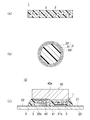
- FIG. 1A is a cross-sectional view schematically showing the configuration of the anisotropic conductive adhesive according to the present invention
- FIG. 1B is an enlarged cross-sectional view showing the configuration of the conductive particles used in the present invention.
- 1 (c) is a cross-sectional view showing a configuration of an embodiment of a light emitting device according to the present invention.
- the anisotropic conductive adhesive 1 of the present invention comprises a plurality of conductive particles 3 dispersed in an insulating adhesive resin 2.
- the insulating adhesive resin 2 is not particularly limited, but from the viewpoint of excellent transparency, adhesiveness, heat resistance, mechanical strength, and electrical insulation, an epoxy resin, A composition containing the curing agent can be suitably used.
- the epoxy resin is an alicyclic epoxy compound, a heterocyclic epoxy compound, a hydrogenated epoxy compound, or the like.
- Preferred examples of the alicyclic epoxy compound include those having two or more epoxy groups in the molecule. These may be liquid or solid.
- glycidyl hexahydrobisphenol A 3,4-epoxycyclohexenylmethyl-3 ′, 4′-epoxycyclohexene carboxylate, and the like.
- glycidyl hexahydrobisphenol A, 3,4-epoxycyclohexenylmethyl-3 ′, 4 can be used because it is possible to ensure light transmission suitable for mounting LED elements on the cured product and excellent quick curing properties.
- '-Epoxycyclohexenecarboxylate can be preferably used.
- heterocyclic epoxy compound examples include an epoxy compound having a triazine ring, and 1,3,5-tris (2,3-epoxypropyl) -1,3,5-triazine-2,4 is particularly preferable. , 6- (1H, 3H, 5H) -trione.
- hydrogenated epoxy compound hydrogenated products of the above-described alicyclic epoxy compounds and heterocyclic epoxy compounds, and other known hydrogenated epoxy resins can be used. In addition to these epoxy compounds, other epoxy resins may be used in combination as long as the effects of the present invention are not impaired.
- the curing agent examples include acid anhydrides, imidazole compounds, and dicyan.
- acid anhydrides that are difficult to discolor the curing agent particularly alicyclic acid anhydride curing agents, can be preferably used.
- alicyclic acid anhydride curing agents can be preferably used.
- methylhexahydrophthalic anhydride etc. can be mentioned preferably.
- the amount of each used increases the amount of uncured epoxy compound if there is too little alicyclic acid anhydride type curing agent. If the amount is too large, corrosion of the adherend material tends to be accelerated due to the influence of the excess curing agent. It can be used at a ratio of 105 parts by mass.
- the conductive particles 3 of the present invention have resin particles 30 serving as nuclei, a light reflective metal layer 31 is formed on the surface of the resin particles 30, and a silver alloy is further formed on the surface of the light reflective metal layer 31.
- a covering layer 32 made of is formed.
- the resin particles 30 are not particularly limited. However, from the viewpoint of obtaining high conduction reliability, for example, a resin made of a crosslinked polystyrene type, a benzoguanamine type, a nylon type, a PMMA (polymethacrylate) type, or the like. Particles can be suitably used.
- the size of the resin particles 30 is not particularly limited, but from the viewpoint of obtaining high conduction reliability, those having an average particle size of 3 ⁇ m to 5 ⁇ m can be suitably used.
- the light-reflective metal layer 31 formed on the surface of the resin particle 30 is made of a metal material having a reflectance at a peak wavelength of 460 nm, which is a peak wavelength of blue light, of 60% or more, more preferably a reflectance of 95% or more.
- Examples of the material of the light-reflective metal layer 31 include a silver (Ag) layer made of a single layer, and a gold (Au) layer formed on the surface of a nickel (Ni) layer.
- silver from the viewpoint of further improving the reflectance.
- the method of forming the light reflective metal layer 31 is not particularly limited, but it is preferable to employ a plating method from the viewpoint of further improving the reflectance by smoothing the surface.
- the thickness of the light reflective metal layer 31 is not particularly limited, but is preferably set to 0.05 ⁇ m or more from the viewpoint of securing a desired reflectance.
- the coating layer 32 formed on the surface of the light reflective metal layer 31 is made of an alloy mainly composed of silver (referred to as “silver alloy” in this specification).
- the silver alloy of the coating layer 32 is preferably one having a silver ratio in the metal of 95% by weight or more.
- the ratio of silver in the metal of the light reflective metal layer 31 is larger than the ratio of the coating layer 32 in the metal.
- a metal contained in addition to silver for example, Bi, Ti, Zr, Hf, V, Nb, Ta, Cr, Mo, W, Fe, Ru, Co, Rh, Ir, Ni, Examples thereof include Pd, Pt, Cu, Au, Zn, Al, Ga, In, Si, Ge, and Sn.
- the material of the coating layer 32 is made of a material having a reflectance of 60% or more, more preferably a reflectance of 90% or more at a peak wavelength of 460 nm, which is the peak wavelength of blue light. Is preferred.
- the method for forming the coating layer 32 is not particularly limited, but from the viewpoint of uniformly coating the silver alloy, it is preferable to employ a sputtering method.
- the sputtering method is one of methods for forming a thin film on an object, and is performed in a vacuum containing a sputtering gas such as argon.
- a glow discharge is generated by applying a voltage between the film formation target and the sputtering target in a state where the inside of the container is evacuated. Electrons and ions generated thereby collide with the target at a high speed, so that particles of the target material are blown off, and the particles (sputtered particles) adhere to the surface of the film formation target to form a thin film.
- fine particles dispersed up to primary particles are set in a container in the apparatus, and the fine particles are flowed by rotating the container. That is, by sputtering the fine particles in such a fluid state, the sputtered particles of the target material collide with the entire surface of each fine particle, and a thin film can be formed on the entire surface of each fine particle.
- known sputtering methods including a bipolar sputtering method, a magnetron sputtering method, a high frequency sputtering method, and a reactive sputtering method can be employed.
- the thickness of the coating layer 32 is not particularly limited, but is preferably set to 0.07 ⁇ m or more from the viewpoint of ensuring desired migration resistance.
- the content of the conductive particles 3 with respect to the insulating adhesive resin 2 is not particularly limited, but in view of ensuring light reflectivity, migration resistance, and insulation, the insulating adhesive resin
- the conductive particles 3 are preferably contained in an amount of 1 part by weight to 100 parts by weight with respect to 100 parts by weight of 2.
- the conductive particles 3 dispersed in a predetermined solvent are added to and mixed with a solution in which a predetermined epoxy resin or the like is dissolved, and then a binder paste. To prepare.
- this binder paste is coated on a release film such as a polyester film, and after drying, the cover film is laminated and an anisotropic conductive film having a desired thickness is laminated. An adhesive film is obtained.
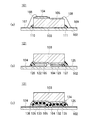
- the light emitting device 10 of the present embodiment is configured by mounting a wiring board 20 made of, for example, ceramics, and a light emitting element 40 on the wiring board 20.
- first and second connection electrodes 21 and 22 are formed in a predetermined pattern shape on the wiring board 20 as a pair of connection electrodes, for example, by silver plating.
- convex terminal portions 21b and 22b made of stud bumps, for example, are provided at adjacent ends of the first and second connection electrodes 21 and 22, respectively.
- the light emitting element 40 for example, an LED (light emitting diode) that emits visible light having a peak wavelength of 400 nm to 500 nm is used.
- the present invention can suitably use a blue LED having a peak wavelength of around 460 nm.
- the light emitting element 40 has a main body 40a formed in, for example, a rectangular shape, and first and second connection electrodes 41 and 42, which are an anode electrode and a cathode electrode, are provided on one surface.
- the terminal portions 21b and 22b of the first and second connection electrodes 21 and 22 of the wiring board 20 and the first and second connection electrodes 41 and 42 of the light emitting element 40 are arranged to face each other.
- the size and the shape are set so that the connection portions face each other.
- the light emitting element 40 is bonded onto the wiring board 20 with the cured anisotropic conductive adhesive 1.
- first and second connection electrodes 41, 42 of the light emitting element 40 correspond to the corresponding first and second connection electrodes 21 of the wiring substrate 20 via the conductive particles 3 of the anisotropic conductive adhesive 1, 22 (terminal portions 21b, 22b) are electrically connected to each other.
- the first connection electrode 41 of the light emitting element 40 is electrically connected to the terminal portion 21b of the first connection electrode 21 of the wiring board 20 by the contact of the conductive particles 3, and the first connection electrode 41 of the light emitting element 40 is also connected.
- the two connection electrodes 42 are electrically connected to the terminal portions 22 b of the second connection electrodes 22 of the wiring board 20 by contact of the conductive particles 3.
- first connection electrode 21 of the wiring board 20 and the first connection electrode 41 of the light emitting element 40, and the second connection electrode 22 of the wiring board 20 and the second connection electrode 42 of the light emitting element 40 are They are insulated from each other by the insulating adhesive resin 2 in the anisotropic conductive adhesive 1.
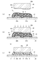
- FIG. 2A to 2C are diagrams showing an embodiment of a manufacturing process of the light emitting device of the present invention.
- the wiring board 20 having the first and second connection electrodes 21 and 22 to be paired and the first and second connection electrodes 21 and 22 of the wiring board 20 are respectively provided.
- a light emitting element 40 having corresponding first and second connection electrodes 41 and 42 is prepared.
- the uncured paste-like anisotropic conductive adhesive 1a is disposed so as to cover the terminal portions 21b, 22b of the first and second connection electrodes 21, 22 of the wiring board 20.
- the uncured anisotropic conductive adhesive 1a is in the form of a film
- the uncured anisotropic conductive adhesive 1a is removed from the first and second wiring boards 20 by a pasting device (not shown), for example. Affixed to a predetermined position on the surface on which the two connection electrodes 21 and 22 are provided.
- the light emitting element 40 is placed on the uncured anisotropic conductive adhesive 1a, and the light emitting side surface of the light emitting element 40, that is, The surface 40b opposite to the side on which the first and second connection electrodes 41 and 42 are provided is pressurized and heated at a predetermined pressure and temperature.
- the insulating adhesive resin 2a of the uncured anisotropic conductive adhesive 1a is cured, and the light emitting element 40 is applied by the adhesive force of the cured anisotropic conductive adhesive 1 as shown in FIG. Is bonded and fixed onto the wiring board 20.
- thermocompression bonding step a plurality of terminal portions 21b and 22b of the first and second connection electrodes 21 and 22 of the wiring board 20 and a plurality of first and second connection electrodes 41 and 42 of the light emitting element 40 are provided.
- the conductive particles 3 are in contact with each other and pressurized, and as a result, the first connection electrode 41 of the light emitting element 40, the first connection electrode 21 of the wiring substrate 20, and the second connection electrode 42 of the light emitting element 40.
- the second connection electrode 22 of the wiring board 20 are electrically connected to each other.
- the first connection electrode 21 of the wiring board 20 and the first connection electrode 41 of the light emitting element 40, and the second connection electrode 22 of the wiring board 20 and the second connection electrode 42 of the light emitting element 40 are In this state, the insulating conductive resin 1 in the anisotropic conductive adhesive 1 is insulated from each other. And the target light-emitting device 10 is obtained by the above process.
- the conductive particles 3 of the anisotropic conductive adhesive 1 are light made of a metal having a reflectance at a peak wavelength of 460 nm of 60% or more on the surface of the resin particle 30 serving as a nucleus. Since the reflective metal layer 31 is formed and the coating layer 32 made of a silver alloy having a high reflectivity is formed on the surface of the light reflective metal layer 31 in the same manner as the light reflective metal layer 31, it is anisotropic. The light absorption by the conductive conductive adhesive 1 can be minimized.
- the light emitting element 40 is mounted on the wiring substrate 20 using the anisotropic conductive adhesive 1 of the present embodiment, light can be efficiently extracted without reducing the light emission efficiency of the light emitting element 40.
- the light emitting device 10 capable of performing the above can be provided.
- anisotropic conductive adhesive 1 of the present embodiment improves the migration resistance because the coating layer 32 made of a silver alloy that hardly migrates is formed on the surface of the light reflective metal layer 31. be able to.
- the light emitting device 10 can be manufactured by a simple and quick process of arranging the anisotropic conductive adhesive 1 and a thermocompression bonding process, so that the production efficiency is greatly improved. Can be improved.
- the present invention is not limited to the above-described embodiment, and various changes can be made.
- the light emitting device 10 shown in FIG. 1C and FIG. 2C is schematically shown by simplifying the shape and size thereof, and the shape and size of the wiring substrate and the connection electrode of the light emitting element. The number and the like can be changed as appropriate.
- the present invention can be applied not only to a blue light emitting element having a peak wavelength of around 460 nm, but also to light emitting elements having various peak wavelengths. However, the present invention is most effective when applied to a light emitting device having a peak wavelength of around 460 nm.
- ⁇ Preparation of adhesive composition 50 parts by weight of an epoxy resin (TEPIC manufactured by Nissan Chemical Industries, Ltd.), 50 parts by weight of methylhexahydrophthalic anhydride (MH-700 manufactured by Shin Nippon Chemical Co., Ltd.) as a curing agent, 2 parts by weight of a curing accelerator (2E4MZ manufactured by Shikoku Chemical)
- An adhesive composition was prepared using parts and toluene as a solvent.
- Example particle 1 A light-reflective metal layer made of silver (Ag) having a thickness of 0.3 ⁇ m on the surface of resin particles made of a crosslinked acrylic resin having an average particle diameter of 5 ⁇ m (Art Pearl J-6P manufactured by Negami Kogyo Co., Ltd.) by electroless plating. Formed. In this case, (Presa RGA-14 manufactured by Uemura Kogyo Co., Ltd.) was used as the plating solution. A coating layer made of a silver alloy having a thickness of 0.13 ⁇ m was formed on the surface of the light reflective metal layer by sputtering. In this case, a powder sputtering apparatus manufactured by Kyoritsu Co., Ltd.
- This Ag ⁇ Nd ⁇ Cu alloy target contains Ag: Nd: Cu in the range of 98.84 to 99.07: 0.36 to 0.44: 0.57 to 0.72% by weight.
- Example particle 2 A light-reflective metal layer made of nickel / gold with a thickness of 0.13 ⁇ m was formed on the surface of the resin particles by electroless plating. Further, the thickness of the coating layer made of the silver alloy was set to 0.4 ⁇ m. Except that, Example Particle 2 was prepared under the same conditions as Example Particle 1.
- Example particle 3 was prepared under the same conditions as Example particle 2 except that the thickness of the coating layer made of nickel / gold was 0.13 ⁇ m.
- Example particle 4 was prepared under the same conditions as Example particle 1 except that the thickness of the coating layer made of the silver alloy was 0.05 ⁇ m.
- Example particles 5 were prepared under the same conditions as Example particles 3 except that a light-reflective metal layer made of only nickel was formed on the surface of the resin particles by electroless plating.
- Comparative Example Particle 2 was prepared under the same conditions as Example Particle 5 except that a coating layer made of gold (Au) having a thickness of 0.3 ⁇ m was formed.
- Example 1 to 5 and Comparative Example 1 were mixed with 15 parts by weight of the above-described Example Particles 1 to 5 and Comparative Example Particles 1 to 3, respectively, with respect to 100 parts by weight of the above-mentioned adhesive composition (excluding the solvent).
- An anisotropic conductive adhesive of ⁇ 3 was obtained.
- Example 1 As is clear from Table 1, the cured resin using the anisotropic conductive adhesive of Example 1 showed a reflectance of 38%, and on the pure silver light-reflecting metal layer shown in Comparative Example 1. A value equivalent to that using conductive particles without a coating layer was exhibited. Further, when the appearance of the LED element mounting module produced using the anisotropic conductive adhesive of Example 1 was observed, no dendrite was confirmed after the high temperature and high humidity test for 500 hours, and the migration resistance was also good. It was. Furthermore, the electrical characteristics did not change from the initial state, and the conduction reliability was good.
- Example 2 The resin cured product using the anisotropic conductive adhesive of Example 2 in which the light-reflective metal layer of the conductive particles is made of nickel / gold plating has a reflectance of 30%, which is equivalent to that of Example 1. Although it was not, it was a practical level. Moreover, about the external appearance observation of the LED element mounting module produced using the anisotropic conductive adhesive of Example 2, dendrite was not confirmed after the high temperature high humidity test of 500 hours, and the migration resistance was also favorable. . Furthermore, the electrical characteristics did not change from the initial state, and the conduction reliability was good.
- Example 3 The light-reflective metal layer of the conductive particles is made of nickel / gold plating, and the thickness of the coating layer of Example 3 where the thickness of the coating layer is thinner than that of Example 2 shows a reflectance of 24%. It was not practical, but it was a practical level. Moreover, about the external appearance observation of the LED element mounting module produced using the anisotropic conductive adhesive of Example 3, a dendrite was not confirmed after the high temperature high humidity test of 500 hours, and the migration resistance was also favorable. . Furthermore, the electrical characteristics did not change from the initial state, and the conduction reliability was good.
- Example 4 The light-reflective metal layer of the conductive particles is made of pure silver, and the coating layer of Example 4 whose thickness is thinner than that of Example 1 has a reflectance of 26%, and the outermost layer shown in Comparative Example 1 is pure silver. The value which is inferior to that using the conductive particles is shown. Moreover, about the external appearance observation of the LED element mounting module produced using the anisotropic conductive adhesive of Example 4, dendrite was not confirmed after the high temperature high humidity test for 500 hours, and the migration resistance was also favorable. . Furthermore, the electrical characteristics did not change from the initial state, and the conduction reliability was good.
- Example 5 The light reflective layer of Example 5 using conductive particles made of nickel as the metal layer had a reflectance of 39% and was the same as that of Example 1, but the appearance was observed after a 500 hour high temperature and high humidity test. In Example 1, it can be said that Example 1 is superior in that dendrite was confirmed.
Landscapes
- Chemical & Material Sciences (AREA)
- Organic Chemistry (AREA)
- Physics & Mathematics (AREA)
- Dispersion Chemistry (AREA)
- Spectroscopy & Molecular Physics (AREA)
- Led Device Packages (AREA)
- Adhesives Or Adhesive Processes (AREA)
- Conductive Materials (AREA)
Priority Applications (4)
| Application Number | Priority Date | Filing Date | Title |
|---|---|---|---|
| EP12838614.1A EP2765173A4 (en) | 2011-10-07 | 2012-10-05 | ANISOTROPER CONDUCTIVE ADHESIVE AND PRODUCTION PROCESS THEREFOR AND LIGHT EMITTING DEVICE AND METHOD OF MANUFACTURING THEREOF |
| CN201280060251.8A CN104039914B (zh) | 2011-10-07 | 2012-10-05 | 各向异性导电粘接剂及其制造方法、发光装置及其制造方法 |
| KR1020147011209A KR102010103B1 (ko) | 2011-10-07 | 2012-10-05 | 이방성 도전 접착제 및 그의 제조 방법, 발광 장치 및 그의 제조 방법 |
| US14/246,618 US20140217450A1 (en) | 2011-10-07 | 2014-04-07 | Anisotropic conductive adhesive and method for manufacturing same, and light-emitting device and method for manufacturing same |
Applications Claiming Priority (2)
| Application Number | Priority Date | Filing Date | Title |
|---|---|---|---|
| JP2011-222498 | 2011-10-07 | ||
| JP2011222498A JP5916334B2 (ja) | 2011-10-07 | 2011-10-07 | 異方性導電接着剤及びその製造方法、発光装置及びその製造方法 |
Related Child Applications (1)
| Application Number | Title | Priority Date | Filing Date |
|---|---|---|---|
| US14/246,618 Continuation US20140217450A1 (en) | 2011-10-07 | 2014-04-07 | Anisotropic conductive adhesive and method for manufacturing same, and light-emitting device and method for manufacturing same |
Publications (1)
| Publication Number | Publication Date |
|---|---|
| WO2013051708A1 true WO2013051708A1 (ja) | 2013-04-11 |
Family
ID=48043861
Family Applications (1)
| Application Number | Title | Priority Date | Filing Date |
|---|---|---|---|
| PCT/JP2012/076011 Ceased WO2013051708A1 (ja) | 2011-10-07 | 2012-10-05 | 異方性導電接着剤及びその製造方法、発光装置及びその製造方法 |
Country Status (7)
| Country | Link |
|---|---|
| US (1) | US20140217450A1 (enExample) |
| EP (1) | EP2765173A4 (enExample) |
| JP (1) | JP5916334B2 (enExample) |
| KR (1) | KR102010103B1 (enExample) |
| CN (1) | CN104039914B (enExample) |
| TW (1) | TWI559334B (enExample) |
| WO (1) | WO2013051708A1 (enExample) |
Cited By (6)
| Publication number | Priority date | Publication date | Assignee | Title |
|---|---|---|---|---|
| WO2013157552A1 (ja) * | 2012-04-17 | 2013-10-24 | デクセリアルズ株式会社 | 異方性導電接着剤及びその製造方法、発光装置及びその製造方法 |
| JP2014159499A (ja) * | 2013-02-19 | 2014-09-04 | Dexerials Corp | 異方性導電接着剤、発光装置及び異方性導電接着剤の製造方法 |
| WO2015141343A1 (ja) * | 2014-03-19 | 2015-09-24 | デクセリアルズ株式会社 | 異方性導電接着剤 |
| JP6566178B1 (ja) * | 2018-03-01 | 2019-08-28 | 住友ベークライト株式会社 | ペースト状接着剤組成物及び半導体装置 |
| WO2019167819A1 (ja) * | 2018-03-01 | 2019-09-06 | 住友ベークライト株式会社 | ペースト状接着剤組成物及び半導体装置 |
| TWI861003B (zh) * | 2018-07-09 | 2024-11-11 | 日商日亞化學工業股份有限公司 | 發光裝置及其製造方法 |
Families Citing this family (26)
| Publication number | Priority date | Publication date | Assignee | Title |
|---|---|---|---|---|
| US9269681B2 (en) * | 2012-11-16 | 2016-02-23 | Qualcomm Incorporated | Surface finish on trace for a thermal compression flip chip (TCFC) |
| JP6288072B2 (ja) * | 2013-02-27 | 2018-03-07 | 日亜化学工業株式会社 | 発光装置、発光素子実装方法及び発光素子用実装装置 |
| KR20160061339A (ko) * | 2013-09-26 | 2016-05-31 | 데쿠세리아루즈 가부시키가이샤 | 발광 장치, 이방성 도전 접착제, 발광 장치 제조 방법 |
| TWI707484B (zh) | 2013-11-14 | 2020-10-11 | 晶元光電股份有限公司 | 發光裝置 |
| JP6324746B2 (ja) * | 2014-02-03 | 2018-05-16 | デクセリアルズ株式会社 | 接続体、接続体の製造方法、電子機器 |
| WO2016047950A1 (en) * | 2014-09-26 | 2016-03-31 | Seoul Viosys Co., Ltd. | Light emitting device and method of fabricating the same |
| WO2016183844A1 (en) * | 2015-05-21 | 2016-11-24 | Goertek.Inc | Transferring method, manufacturing method, device and electronic apparatus of micro-led |
| DE102015112967A1 (de) * | 2015-08-06 | 2017-02-09 | Osram Opto Semiconductors Gmbh | Verfahren zum Herstellen eines optoelektronischen Bauelements und optoelektronisches Bauelement |
| JP2017157724A (ja) * | 2016-03-02 | 2017-09-07 | デクセリアルズ株式会社 | 表示装置及びその製造方法、並びに発光装置及びその製造方法 |
| DE102016106494A1 (de) * | 2016-04-08 | 2017-10-12 | Osram Opto Semiconductors Gmbh | Optoelektronisches bauelement und verfahren zum herstellen eines optoelektronischen bauelements |
| KR102555383B1 (ko) * | 2016-12-07 | 2023-07-12 | 엘지디스플레이 주식회사 | 유기발광소자를 이용한 조명장치 및 그 제조방법 |
| US11355469B2 (en) * | 2017-12-28 | 2022-06-07 | Showa Denko Materials Co., Ltd. | Connection structure and method for producing same |
| JP7160302B2 (ja) * | 2018-01-31 | 2022-10-25 | 三国電子有限会社 | 接続構造体および接続構造体の作製方法 |
| JP7185252B2 (ja) | 2018-01-31 | 2022-12-07 | 三国電子有限会社 | 接続構造体の作製方法 |
| JP7046351B2 (ja) | 2018-01-31 | 2022-04-04 | 三国電子有限会社 | 接続構造体の作製方法 |
| JP7093639B2 (ja) * | 2018-02-06 | 2022-06-30 | 三菱マテリアル株式会社 | 銀被覆樹脂粒子 |
| TWI671921B (zh) * | 2018-09-14 | 2019-09-11 | 頎邦科技股份有限公司 | 晶片封裝構造及其晶片 |
| JP7366337B2 (ja) * | 2018-12-25 | 2023-10-23 | 日亜化学工業株式会社 | 光源装置の製造方法および光源装置 |
| EP3675190B1 (en) | 2018-12-25 | 2023-05-03 | Nichia Corporation | Method of manufacturing light source device and light source device |
| TWI690102B (zh) * | 2019-01-04 | 2020-04-01 | 友達光電股份有限公司 | 發光裝置及其製造方法 |
| JP7298256B2 (ja) * | 2019-04-11 | 2023-06-27 | 株式会社レゾナック | 導電粒子 |
| JP7292669B2 (ja) * | 2019-04-11 | 2023-06-19 | 株式会社レゾナック | 導電粒子の製造方法 |
| KR102862766B1 (ko) * | 2019-05-29 | 2025-09-22 | 삼성전자주식회사 | 마이크로 엘이디 디스플레이 및 이의 제작 방법 |
| CN111574937B (zh) * | 2020-05-15 | 2021-10-08 | 武汉华星光电半导体显示技术有限公司 | 一种异方性导电胶、显示面板及显示装置 |
| DE102021120689A1 (de) * | 2021-08-09 | 2023-02-09 | OSRAM Opto Semiconductors Gesellschaft mit beschränkter Haftung | Transferverfahren für optoelektronsiche halbleiterbauelemete |
| KR20240038495A (ko) * | 2022-09-16 | 2024-03-25 | 삼성전자주식회사 | 고반사율 이방성 도전 필름 및 이를 포함하는 디스플레이 모듈 |
Citations (13)
| Publication number | Priority date | Publication date | Assignee | Title |
|---|---|---|---|---|
| JPH05152464A (ja) | 1991-11-25 | 1993-06-18 | Sumitomo Bakelite Co Ltd | 光半導体封止用エポキシ樹脂組成物 |
| JP2001234152A (ja) * | 2000-02-24 | 2001-08-28 | Sumitomo Metal Mining Co Ltd | 導電性接着剤 |
| WO2002013205A1 (en) * | 2000-08-04 | 2002-02-14 | Sekisui Chemical Co., Ltd. | Conductive fine particles, method for plating fine particles, and substrate structural body |
| JP2002260446A (ja) * | 2001-02-27 | 2002-09-13 | Sekisui Chem Co Ltd | 導電性微粒子及び導電接続構造体 |
| JP2003026763A (ja) | 2001-07-13 | 2003-01-29 | New Japan Chem Co Ltd | エポキシ樹脂組成物 |
| JP2005120375A (ja) | 2003-10-14 | 2005-05-12 | Bayer Ag | 精製されたエラストマーの製造方法、及び精製されたエラストマー、及び前記のエラストマーから得られる製品 |
| JP2005330327A (ja) * | 2004-05-18 | 2005-12-02 | Sumitomo Metal Mining Co Ltd | エポキシ樹脂組成物及びそれを用いた光半導体用接着剤 |
| WO2006018995A1 (ja) * | 2004-08-05 | 2006-02-23 | Sekisui Chemical Co., Ltd. | 導電性微粒子、導電性微粒子の製造方法、及び、無電解銀メッキ液 |
| JP2007131677A (ja) * | 2005-11-08 | 2007-05-31 | Sumitomo Metal Mining Co Ltd | エポキシ樹脂接着組成物及びそれを用いた光半導体用接着剤 |
| JP2007258324A (ja) * | 2006-03-22 | 2007-10-04 | Matsushita Electric Ind Co Ltd | 発光装置の製造方法および発光装置 |
| JP2008266671A (ja) | 2007-04-16 | 2008-11-06 | Sony Corp | 銀系薄膜合金 |
| WO2011030621A1 (ja) * | 2009-09-14 | 2011-03-17 | ソニーケミカル&インフォメーションデバイス株式会社 | 光反射性異方性導電接着剤及び発光装置 |
| JP2012164484A (ja) * | 2011-02-04 | 2012-08-30 | Nippon Shokubai Co Ltd | 導電性微粒子 |
Family Cites Families (13)
| Publication number | Priority date | Publication date | Assignee | Title |
|---|---|---|---|---|
| JPH07157720A (ja) * | 1993-12-03 | 1995-06-20 | Sumitomo Bakelite Co Ltd | 異方導電フィルム |
| JP3284262B2 (ja) * | 1996-09-05 | 2002-05-20 | セイコーエプソン株式会社 | 液晶表示装置及びそれを用いた電子機器 |
| DE69826476T2 (de) * | 1997-07-04 | 2005-01-20 | Nippon Zeon Co., Ltd. | Klebstoff für halbleiterbauteile |
| US5990498A (en) * | 1997-09-16 | 1999-11-23 | Polaroid Corporation | Light-emitting diode having uniform irradiance distribution |
| WO2004105009A1 (ja) * | 2003-05-22 | 2004-12-02 | Ricoh Company, Ltd. | 光記録媒体 |
| JP4293187B2 (ja) * | 2003-06-25 | 2009-07-08 | 日立化成工業株式会社 | 回路接続材料、これを用いたフィルム状回路接続材料、回路部材の接続構造及びその製造方法 |
| JP5430093B2 (ja) * | 2008-07-24 | 2014-02-26 | デクセリアルズ株式会社 | 導電性粒子、異方性導電フィルム、及び接合体、並びに、接続方法 |
| EP2338053A1 (en) * | 2008-09-12 | 2011-06-29 | Modpro AB | Detection method and device based on nanoparticle aggregation |
| JP5526698B2 (ja) * | 2009-10-16 | 2014-06-18 | デクセリアルズ株式会社 | 光反射性導電粒子、異方性導電接着剤及び発光装置 |
| JP2011186414A (ja) * | 2010-02-12 | 2011-09-22 | Sony Corp | 光学素子、日射遮蔽装置、建具、窓材および光学素子の製造方法 |
| JP5745776B2 (ja) * | 2010-03-15 | 2015-07-08 | デクセリアルズ株式会社 | 光学積層体および建具 |
| JP5586300B2 (ja) * | 2010-03-31 | 2014-09-10 | デクセリアルズ株式会社 | 機能性積層体及び機能性構造体 |
| JP5609716B2 (ja) * | 2011-03-07 | 2014-10-22 | デクセリアルズ株式会社 | 光反射性異方性導電接着剤及び発光装置 |
-
2011
- 2011-10-07 JP JP2011222498A patent/JP5916334B2/ja active Active
-
2012
- 2012-10-05 EP EP12838614.1A patent/EP2765173A4/en not_active Withdrawn
- 2012-10-05 KR KR1020147011209A patent/KR102010103B1/ko active Active
- 2012-10-05 WO PCT/JP2012/076011 patent/WO2013051708A1/ja not_active Ceased
- 2012-10-05 CN CN201280060251.8A patent/CN104039914B/zh active Active
- 2012-10-05 TW TW101136830A patent/TWI559334B/zh active
-
2014
- 2014-04-07 US US14/246,618 patent/US20140217450A1/en not_active Abandoned
Patent Citations (13)
| Publication number | Priority date | Publication date | Assignee | Title |
|---|---|---|---|---|
| JPH05152464A (ja) | 1991-11-25 | 1993-06-18 | Sumitomo Bakelite Co Ltd | 光半導体封止用エポキシ樹脂組成物 |
| JP2001234152A (ja) * | 2000-02-24 | 2001-08-28 | Sumitomo Metal Mining Co Ltd | 導電性接着剤 |
| WO2002013205A1 (en) * | 2000-08-04 | 2002-02-14 | Sekisui Chemical Co., Ltd. | Conductive fine particles, method for plating fine particles, and substrate structural body |
| JP2002260446A (ja) * | 2001-02-27 | 2002-09-13 | Sekisui Chem Co Ltd | 導電性微粒子及び導電接続構造体 |
| JP2003026763A (ja) | 2001-07-13 | 2003-01-29 | New Japan Chem Co Ltd | エポキシ樹脂組成物 |
| JP2005120375A (ja) | 2003-10-14 | 2005-05-12 | Bayer Ag | 精製されたエラストマーの製造方法、及び精製されたエラストマー、及び前記のエラストマーから得られる製品 |
| JP2005330327A (ja) * | 2004-05-18 | 2005-12-02 | Sumitomo Metal Mining Co Ltd | エポキシ樹脂組成物及びそれを用いた光半導体用接着剤 |
| WO2006018995A1 (ja) * | 2004-08-05 | 2006-02-23 | Sekisui Chemical Co., Ltd. | 導電性微粒子、導電性微粒子の製造方法、及び、無電解銀メッキ液 |
| JP2007131677A (ja) * | 2005-11-08 | 2007-05-31 | Sumitomo Metal Mining Co Ltd | エポキシ樹脂接着組成物及びそれを用いた光半導体用接着剤 |
| JP2007258324A (ja) * | 2006-03-22 | 2007-10-04 | Matsushita Electric Ind Co Ltd | 発光装置の製造方法および発光装置 |
| JP2008266671A (ja) | 2007-04-16 | 2008-11-06 | Sony Corp | 銀系薄膜合金 |
| WO2011030621A1 (ja) * | 2009-09-14 | 2011-03-17 | ソニーケミカル&インフォメーションデバイス株式会社 | 光反射性異方性導電接着剤及び発光装置 |
| JP2012164484A (ja) * | 2011-02-04 | 2012-08-30 | Nippon Shokubai Co Ltd | 導電性微粒子 |
Non-Patent Citations (1)
| Title |
|---|
| See also references of EP2765173A4 |
Cited By (9)
| Publication number | Priority date | Publication date | Assignee | Title |
|---|---|---|---|---|
| WO2013157552A1 (ja) * | 2012-04-17 | 2013-10-24 | デクセリアルズ株式会社 | 異方性導電接着剤及びその製造方法、発光装置及びその製造方法 |
| JP2013221104A (ja) * | 2012-04-17 | 2013-10-28 | Dexerials Corp | 異方性導電接着剤及びその製造方法、発光装置及びその製造方法 |
| JP2014159499A (ja) * | 2013-02-19 | 2014-09-04 | Dexerials Corp | 異方性導電接着剤、発光装置及び異方性導電接着剤の製造方法 |
| WO2015141343A1 (ja) * | 2014-03-19 | 2015-09-24 | デクセリアルズ株式会社 | 異方性導電接着剤 |
| JP2015178555A (ja) * | 2014-03-19 | 2015-10-08 | デクセリアルズ株式会社 | 異方性導電接着剤 |
| US9670385B2 (en) | 2014-03-19 | 2017-06-06 | Dexerials Corporation | Anisotropic conductive adhesive |
| JP6566178B1 (ja) * | 2018-03-01 | 2019-08-28 | 住友ベークライト株式会社 | ペースト状接着剤組成物及び半導体装置 |
| WO2019167819A1 (ja) * | 2018-03-01 | 2019-09-06 | 住友ベークライト株式会社 | ペースト状接着剤組成物及び半導体装置 |
| TWI861003B (zh) * | 2018-07-09 | 2024-11-11 | 日商日亞化學工業股份有限公司 | 發光裝置及其製造方法 |
Also Published As
| Publication number | Publication date |
|---|---|
| CN104039914A (zh) | 2014-09-10 |
| TWI559334B (zh) | 2016-11-21 |
| CN104039914B (zh) | 2016-08-24 |
| EP2765173A1 (en) | 2014-08-13 |
| KR20140084076A (ko) | 2014-07-04 |
| EP2765173A4 (en) | 2015-04-29 |
| TW201331955A (zh) | 2013-08-01 |
| KR102010103B1 (ko) | 2019-08-12 |
| JP2013082784A (ja) | 2013-05-09 |
| JP5916334B2 (ja) | 2016-05-11 |
| US20140217450A1 (en) | 2014-08-07 |
Similar Documents
| Publication | Publication Date | Title |
|---|---|---|
| JP5916334B2 (ja) | 異方性導電接着剤及びその製造方法、発光装置及びその製造方法 | |
| JP5965199B2 (ja) | 異方性導電接着剤及びその製造方法、発光装置及びその製造方法 | |
| JP5985414B2 (ja) | 異方性導電接着剤、発光装置及び異方性導電接着剤の製造方法 | |
| CN102576798B (zh) | 光反射性导电颗粒、各向异性导电粘合剂和发光装置 | |
| JP6347635B2 (ja) | 異方性導電接着剤 | |
| CN102859673B (zh) | 光反射性各向异性导电粘接剂及发光装置 | |
| JPWO2012144033A1 (ja) | 光反射性導電粒子、異方性導電接着剤及び発光装置 | |
| JP2014160708A (ja) | 異方性導電接着剤、発光装置及び異方性導電接着剤の製造方法 | |
| JP2014030026A (ja) | 異方性導電接着剤及び発光装置 | |
| JP5785306B2 (ja) | 光反射性異方性導電接着剤及び発光装置 |
Legal Events
| Date | Code | Title | Description |
|---|---|---|---|
| 121 | Ep: the epo has been informed by wipo that ep was designated in this application |
Ref document number: 12838614 Country of ref document: EP Kind code of ref document: A1 |
|
| NENP | Non-entry into the national phase |
Ref country code: DE |
|
| WWE | Wipo information: entry into national phase |
Ref document number: 2012838614 Country of ref document: EP |
|
| ENP | Entry into the national phase |
Ref document number: 20147011209 Country of ref document: KR Kind code of ref document: A |