WO2013038929A1 - 含ケイ素四員環構造を有する有機電界発光素子用材料及び有機電界発光素子 - Google Patents
含ケイ素四員環構造を有する有機電界発光素子用材料及び有機電界発光素子 Download PDFInfo
- Publication number
- WO2013038929A1 WO2013038929A1 PCT/JP2012/072272 JP2012072272W WO2013038929A1 WO 2013038929 A1 WO2013038929 A1 WO 2013038929A1 JP 2012072272 W JP2012072272 W JP 2012072272W WO 2013038929 A1 WO2013038929 A1 WO 2013038929A1
- Authority
- WO
- WIPO (PCT)
- Prior art keywords
- group
- carbon atoms
- organic
- organic electroluminescent
- layer
- Prior art date
Links
- DKPHVTPRFGJEJD-UHFFFAOYSA-N CCS(c1ccccc1)(c1ccccc1)N(c([n](c1ccccc11)-c2ccccc2)c1-c1ccccc1)[SiH](c1ccccc1)c1cccc(-c(cccc2)c2-[n](c2ccccc22)c(N)c2-c2ccccc2)c1 Chemical compound CCS(c1ccccc1)(c1ccccc1)N(c([n](c1ccccc11)-c2ccccc2)c1-c1ccccc1)[SiH](c1ccccc1)c1cccc(-c(cccc2)c2-[n](c2ccccc22)c(N)c2-c2ccccc2)c1 DKPHVTPRFGJEJD-UHFFFAOYSA-N 0.000 description 1
- LEJUFQYBFGJUKY-UHFFFAOYSA-N CCc(cc1)cc2c1ccc(N1[Si](c3ccccc3)(c3ccccc3)N(c3ccc(ccc(CC)c4)c4n3)[Si]1(c1ccccc1)c1ccccc1)n2 Chemical compound CCc(cc1)cc2c1ccc(N1[Si](c3ccccc3)(c3ccccc3)N(c3ccc(ccc(CC)c4)c4n3)[Si]1(c1ccccc1)c1ccccc1)n2 LEJUFQYBFGJUKY-UHFFFAOYSA-N 0.000 description 1
- ZOPYRPURRRJLKB-UHFFFAOYSA-N c(cc1)ccc1-c([o]c1ccccc11)c1N1[Si](c2ccccc2)(c2ccccc2)N(c2c(-c3ccccc3)[o]c3ccccc23)[Si]1(c1ccccc1)c1ccccc1 Chemical compound c(cc1)ccc1-c([o]c1ccccc11)c1N1[Si](c2ccccc2)(c2ccccc2)N(c2c(-c3ccccc3)[o]c3ccccc23)[Si]1(c1ccccc1)c1ccccc1 ZOPYRPURRRJLKB-UHFFFAOYSA-N 0.000 description 1
- MKDXLBNOXNIWFP-UHFFFAOYSA-N c(cc1)ccc1-c1ccc(ccc(N2[Si+](c3ccccc3)(c3ccccc3)N(c3ccc(ccc(-c4ccccc4)c4)c4n3)[Si]2(c2ccccc2)c2ccccc2)n2)c2c1 Chemical compound c(cc1)ccc1-c1ccc(ccc(N2[Si+](c3ccccc3)(c3ccccc3)N(c3ccc(ccc(-c4ccccc4)c4)c4n3)[Si]2(c2ccccc2)c2ccccc2)n2)c2c1 MKDXLBNOXNIWFP-UHFFFAOYSA-N 0.000 description 1
- MMKXMUAODRAVOG-UHFFFAOYSA-N c(cc1)ccc1-c1cccc2c1ccc(N1[Si+](c3ccccc3)(c3ccccc3)N(c3nc4cccc(-c5ccccc5)c4cc3)[Si]1(c1ccccc1)c1ccccc1)n2 Chemical compound c(cc1)ccc1-c1cccc2c1ccc(N1[Si+](c3ccccc3)(c3ccccc3)N(c3nc4cccc(-c5ccccc5)c4cc3)[Si]1(c1ccccc1)c1ccccc1)n2 MMKXMUAODRAVOG-UHFFFAOYSA-N 0.000 description 1
- DJRAKVFVXSNJBP-UHFFFAOYSA-N c(cc1)ccc1C(c1c2cccc1)=S=C2N1[Si+](c2ccccc2)(c2ccccc2)N(C(c2c3cccc2)=S=C3c2ccccc2)[Si]1(c1ccccc1)c1ccccc1 Chemical compound c(cc1)ccc1C(c1c2cccc1)=S=C2N1[Si+](c2ccccc2)(c2ccccc2)N(C(c2c3cccc2)=S=C3c2ccccc2)[Si]1(c1ccccc1)c1ccccc1 DJRAKVFVXSNJBP-UHFFFAOYSA-N 0.000 description 1
- WUWZPXKZOXVFTI-UHFFFAOYSA-N c(cc1)ccc1[Si]1(c2ccccc2)N(c2nc3cccc(-[n]4c(cccc5)c5c5c4cccc5)c3cc2)[Si+](c2ccccc2)(c2ccccc2)N1c(cc1)nc2c1c(-[n]1c(cccc3)c3c3c1cccc3)ccc2 Chemical compound c(cc1)ccc1[Si]1(c2ccccc2)N(c2nc3cccc(-[n]4c(cccc5)c5c5c4cccc5)c3cc2)[Si+](c2ccccc2)(c2ccccc2)N1c(cc1)nc2c1c(-[n]1c(cccc3)c3c3c1cccc3)ccc2 WUWZPXKZOXVFTI-UHFFFAOYSA-N 0.000 description 1
Images


Classifications
-
- H—ELECTRICITY
- H10—SEMICONDUCTOR DEVICES; ELECTRIC SOLID-STATE DEVICES NOT OTHERWISE PROVIDED FOR
- H10K—ORGANIC ELECTRIC SOLID-STATE DEVICES
- H10K85/00—Organic materials used in the body or electrodes of devices covered by this subclass
- H10K85/40—Organosilicon compounds, e.g. TIPS pentacene
-
- C—CHEMISTRY; METALLURGY
- C07—ORGANIC CHEMISTRY
- C07F—ACYCLIC, CARBOCYCLIC OR HETEROCYCLIC COMPOUNDS CONTAINING ELEMENTS OTHER THAN CARBON, HYDROGEN, HALOGEN, OXYGEN, NITROGEN, SULFUR, SELENIUM OR TELLURIUM
- C07F7/00—Compounds containing elements of Groups 4 or 14 of the Periodic System
- C07F7/02—Silicon compounds
- C07F7/08—Compounds having one or more C—Si linkages
- C07F7/10—Compounds having one or more C—Si linkages containing nitrogen having a Si-N linkage
-
- C—CHEMISTRY; METALLURGY
- C09—DYES; PAINTS; POLISHES; NATURAL RESINS; ADHESIVES; COMPOSITIONS NOT OTHERWISE PROVIDED FOR; APPLICATIONS OF MATERIALS NOT OTHERWISE PROVIDED FOR
- C09B—ORGANIC DYES OR CLOSELY-RELATED COMPOUNDS FOR PRODUCING DYES, e.g. PIGMENTS; MORDANTS; LAKES
- C09B57/00—Other synthetic dyes of known constitution
-
- C—CHEMISTRY; METALLURGY
- C09—DYES; PAINTS; POLISHES; NATURAL RESINS; ADHESIVES; COMPOSITIONS NOT OTHERWISE PROVIDED FOR; APPLICATIONS OF MATERIALS NOT OTHERWISE PROVIDED FOR
- C09K—MATERIALS FOR MISCELLANEOUS APPLICATIONS, NOT PROVIDED FOR ELSEWHERE
- C09K11/00—Luminescent, e.g. electroluminescent, chemiluminescent materials
- C09K11/06—Luminescent, e.g. electroluminescent, chemiluminescent materials containing organic luminescent materials
-
- H—ELECTRICITY
- H05—ELECTRIC TECHNIQUES NOT OTHERWISE PROVIDED FOR
- H05B—ELECTRIC HEATING; ELECTRIC LIGHT SOURCES NOT OTHERWISE PROVIDED FOR; CIRCUIT ARRANGEMENTS FOR ELECTRIC LIGHT SOURCES, IN GENERAL
- H05B33/00—Electroluminescent light sources
- H05B33/12—Light sources with substantially two-dimensional radiating surfaces
- H05B33/14—Light sources with substantially two-dimensional radiating surfaces characterised by the chemical or physical composition or the arrangement of the electroluminescent material, or by the simultaneous addition of the electroluminescent material in or onto the light source
-
- H—ELECTRICITY
- H10—SEMICONDUCTOR DEVICES; ELECTRIC SOLID-STATE DEVICES NOT OTHERWISE PROVIDED FOR
- H10K—ORGANIC ELECTRIC SOLID-STATE DEVICES
- H10K85/00—Organic materials used in the body or electrodes of devices covered by this subclass
- H10K85/60—Organic compounds having low molecular weight
- H10K85/649—Aromatic compounds comprising a hetero atom
- H10K85/657—Polycyclic condensed heteroaromatic hydrocarbons
- H10K85/6576—Polycyclic condensed heteroaromatic hydrocarbons comprising only sulfur in the heteroaromatic polycondensed ring system, e.g. benzothiophene
-
- C—CHEMISTRY; METALLURGY
- C09—DYES; PAINTS; POLISHES; NATURAL RESINS; ADHESIVES; COMPOSITIONS NOT OTHERWISE PROVIDED FOR; APPLICATIONS OF MATERIALS NOT OTHERWISE PROVIDED FOR
- C09K—MATERIALS FOR MISCELLANEOUS APPLICATIONS, NOT PROVIDED FOR ELSEWHERE
- C09K2211/00—Chemical nature of organic luminescent or tenebrescent compounds
- C09K2211/10—Non-macromolecular compounds
- C09K2211/1018—Heterocyclic compounds
- C09K2211/1025—Heterocyclic compounds characterised by ligands
- C09K2211/1044—Heterocyclic compounds characterised by ligands containing two nitrogen atoms as heteroatoms
- C09K2211/1055—Heterocyclic compounds characterised by ligands containing two nitrogen atoms as heteroatoms with other heteroatoms
-
- C—CHEMISTRY; METALLURGY
- C09—DYES; PAINTS; POLISHES; NATURAL RESINS; ADHESIVES; COMPOSITIONS NOT OTHERWISE PROVIDED FOR; APPLICATIONS OF MATERIALS NOT OTHERWISE PROVIDED FOR
- C09K—MATERIALS FOR MISCELLANEOUS APPLICATIONS, NOT PROVIDED FOR ELSEWHERE
- C09K2211/00—Chemical nature of organic luminescent or tenebrescent compounds
- C09K2211/10—Non-macromolecular compounds
- C09K2211/1018—Heterocyclic compounds
- C09K2211/1025—Heterocyclic compounds characterised by ligands
- C09K2211/1092—Heterocyclic compounds characterised by ligands containing sulfur as the only heteroatom
-
- H—ELECTRICITY
- H10—SEMICONDUCTOR DEVICES; ELECTRIC SOLID-STATE DEVICES NOT OTHERWISE PROVIDED FOR
- H10K—ORGANIC ELECTRIC SOLID-STATE DEVICES
- H10K2101/00—Properties of the organic materials covered by group H10K85/00
- H10K2101/10—Triplet emission
-
- H—ELECTRICITY
- H10—SEMICONDUCTOR DEVICES; ELECTRIC SOLID-STATE DEVICES NOT OTHERWISE PROVIDED FOR
- H10K—ORGANIC ELECTRIC SOLID-STATE DEVICES
- H10K50/00—Organic light-emitting devices
- H10K50/10—OLEDs or polymer light-emitting diodes [PLED]
- H10K50/11—OLEDs or polymer light-emitting diodes [PLED] characterised by the electroluminescent [EL] layers
-
- H—ELECTRICITY
- H10—SEMICONDUCTOR DEVICES; ELECTRIC SOLID-STATE DEVICES NOT OTHERWISE PROVIDED FOR
- H10K—ORGANIC ELECTRIC SOLID-STATE DEVICES
- H10K85/00—Organic materials used in the body or electrodes of devices covered by this subclass
- H10K85/60—Organic compounds having low molecular weight
- H10K85/649—Aromatic compounds comprising a hetero atom
- H10K85/654—Aromatic compounds comprising a hetero atom comprising only nitrogen as heteroatom
-
- H—ELECTRICITY
- H10—SEMICONDUCTOR DEVICES; ELECTRIC SOLID-STATE DEVICES NOT OTHERWISE PROVIDED FOR
- H10K—ORGANIC ELECTRIC SOLID-STATE DEVICES
- H10K85/00—Organic materials used in the body or electrodes of devices covered by this subclass
- H10K85/60—Organic compounds having low molecular weight
- H10K85/649—Aromatic compounds comprising a hetero atom
- H10K85/657—Polycyclic condensed heteroaromatic hydrocarbons
- H10K85/6572—Polycyclic condensed heteroaromatic hydrocarbons comprising only nitrogen in the heteroaromatic polycondensed ring system, e.g. phenanthroline or carbazole
-
- H—ELECTRICITY
- H10—SEMICONDUCTOR DEVICES; ELECTRIC SOLID-STATE DEVICES NOT OTHERWISE PROVIDED FOR
- H10K—ORGANIC ELECTRIC SOLID-STATE DEVICES
- H10K85/00—Organic materials used in the body or electrodes of devices covered by this subclass
- H10K85/60—Organic compounds having low molecular weight
- H10K85/649—Aromatic compounds comprising a hetero atom
- H10K85/657—Polycyclic condensed heteroaromatic hydrocarbons
- H10K85/6574—Polycyclic condensed heteroaromatic hydrocarbons comprising only oxygen in the heteroaromatic polycondensed ring system, e.g. cumarine dyes
Definitions
- the present invention relates to a material for an organic electroluminescent device having a silicon-containing four-membered ring structure and an organic electroluminescent device using the same, and more specifically, a thin film that emits light by applying an electric field to a light emitting layer made of an organic compound.
- Type devices include
- An object of this invention is to provide the practically useful organic EL element which has high efficiency and high drive stability in view of the said present condition, and a compound suitable for it.
- the present invention relates to a material for an organic electroluminescence device comprising a silicon-containing four-membered ring compound represented by the general formula (1).
- each X independently represents nitrogen or phosphorus
- each L independently represents an n + 1 valent aromatic hydrocarbon group having 6 to 24 carbon atoms or an aromatic heterocyclic ring having 3 to 19 carbon atoms.
- at least one is an aromatic heterocyclic group having 3 to 19 carbon atoms.
- the present invention also relates to a material for an organic electroluminescent device comprising a compound in which two L's in the general formula (1) are both n + 1 valent aromatic heterocyclic groups having 3 to 19 carbon atoms. It is preferably a heterocyclic group.
- the organic layer containing the compound represented by the general formula (1) is at least one selected from the group consisting of a light emitting layer, an electron transport layer, a hole transport layer, an electron blocking layer, and a hole blocking layer.
- the present invention relates to an organic electroluminescent element which is one layer.
- the organic layer containing the compound represented by the general formula (1) is an organic electroluminescent element which is a light emitting layer containing a phosphorescent dopant.
- the organic electroluminescent element material of the present invention is a silicon-containing four-membered ring compound represented by the general formula (1).
- X represents nitrogen or phosphorus each independently.
- both Xs are nitrogen or both phosphorus, more preferably both are nitrogen.
- n + 1 valent groups formed by removing n + 1 hydrogen from benzene, indene, naphthalene, acenaphthylene, fluorene, phenanthrene, anthracene, fluoranthene, triphenylene, pyrene, chrysene, tetracene, perylene, pentacene, tetraphenylene. More preferred is an n + 1 valent group generated by removing n + 1 hydrogen from benzene, naphthalene, fluorene, phenanthrene, anthracene, fluoranthene, triphenylene, or pyrene.
- L is an n + 1 valent aromatic hydrocarbon group or aromatic heterocyclic group, but since A 1 or A 2 is a substituent, L is understood to be a group having no other substituent.
- the alkyl group may have a substituent, and when these have a substituent, examples of the substituent include a cycloalkyl group having 3 to 11 carbon atoms, an aromatic hydrocarbon group having 6 to 18 carbon atoms, and a carbon number. 3 to 18 aromatic heterocyclic groups.
- the total number of substituents is 1-6. Preferably it is 1 to 4, more preferably 1 to 2. Moreover, when it has two or more substituents, they may be the same or different.
- cycloalkyl group in A 1 to A 6 include a cyclopropyl group, a cyclobutyl group, a cyclopentyl group, a cyclohexyl group, a cycloheptyl group, a cyclooctyl group, a cyclohexyl group, and a decahydronaphthyl group, preferably Examples include a cyclohexyl group and a cyclohexyl group.
- the cycloalkyl group may have a substituent, and when these have a substituent, the substituent may be an alkyl group having 1 to 10 carbon atoms, an aromatic hydrocarbon group having 6 to 18 carbon atoms, or a carbon number. 3 to 18 aromatic heterocyclic groups.
- the total number of substituents is 1-6. Preferably it is 1 to 4, more preferably 1 to 2. Moreover, when it has two or more substituents, they may be the same or different.
- the cycloalkyl group has 3 to 30 carbon atoms, preferably 4 to 14 carbon atoms.
- alkenyl group or alkynyl group examples include an ethylenyl group, a propylenyl group, a butenyl group, a pentenyl group, a hexenyl group, a heptenyl group, an octenyl group, an acetylenyl group, a propynyl group, a butynyl group, and a pentynyl group.
- an ethylenyl group, a propylenyl group, a butenyl group, an acetylenyl group, and a propynyl group are mentioned.
- the alkenyl group and alkynyl group may be linear or branched.
- the alkenyl group or alkynyl group may have a substituent.
- substituents include a cycloalkyl group having 3 to 11 carbon atoms and an aromatic hydrocarbon group having 6 to 18 carbon atoms. Or an aromatic heterocyclic group having 3 to 18 carbon atoms.
- the alkenyl group or alkynyl group has 2 to 30 carbon atoms, preferably 2 to 14 carbon atoms.
- aromatic hydrocarbon group or the aromatic heterocyclic group examples include benzene, pentalene, indene, naphthalene, azulene, heptalene, octalene, indacene, acenaphthylene, phenalene, phenanthrene, anthracene, tridene, fluoranthene.
- the number of linked rings is preferably 2 to 6, more preferably 2 to 3, and the linked aromatic rings may be the same. It may be different.
- the bonding position of A 1 to A 6 bonded to Si or L is not limited, and it may be a terminal ring or a central ring of the linked aromatic rings.
- the aromatic ring is a generic term for an aromatic hydrocarbon ring and an aromatic heterocyclic ring. When the linked aromatic ring contains at least one heterocyclic ring, it is included in the aromatic heterocyclic group.
- the monovalent group generated by connecting a plurality of aromatic rings is represented by the following formula, for example.
- Ar 1 to Ar 6 represent a substituted or unsubstituted aromatic ring.
- Specific examples of the group formed by connecting a plurality of the aromatic rings include, for example, biphenyl, terphenyl, bipyridine, bipyrimidine, vitriazine, terpyridine, bistriazylbenzene, dicarbazolylbenzene, carbazolylbiphenyl, dicarbazolylbiphenyl.
- the aromatic hydrocarbon group or aromatic heterocyclic group may have a substituent, and when these have a substituent, the substituent may be an alkyl group having 1 to 10 carbon atoms, or a group having 3 to 10 carbon atoms.
- An alkyl group having 1 to 4 carbon atoms, a cycloalkyl group having 3 to 6 carbon atoms, or an amino group having 6 to 15 carbon atoms is preferable.
- the aromatic group branched and linked is not treated as a substituent.
- a 1 to A 6 are aromatic hydrocarbon groups or aromatic heterocyclic groups and have a substituent
- the total number of substituents is 1 to 6.
- it is 1 to 4, more preferably 1 to 2.
- it may be the same or different.
- the amino group is a monovalent group having 2 to 30 carbon atoms represented by the following formula (4).
- each B is independently hydrogen, an alkyl group having 1 to 10 carbon atoms, a cycloalkyl group having 3 to 10 carbon atoms, an aromatic hydrocarbon group having 6 to 18 carbon atoms, or 3 to 18 carbon atoms.
- the total number of carbon atoms contained in the two B is 2 to 30.
- alkyl group represented by B examples include methyl group, ethyl group, propyl group, butyl group, pentyl group, hexyl group, heptyl group, octyl group, nonyl group, decyl group and the like. Preferred are methyl group, ethyl group, propyl group, butyl group, pentyl group, hexyl group, heptyl group and octyl group.
- the alkyl group may be linear or branched.
- B being a cycloalkyl group include a cyclopropyl group, a cyclobutyl group, a cyclopentyl group, a cyclohexyl group, a cycloheptyl group, a cyclooctyl group, a methylcyclohexyl group, and the like, and preferably a cyclohexyl group.
- aromatic hydrocarbon group or aromatic heterocyclic group represented by B include phenyl group, naphthyl group, phenanthryl group, pyridyl group, pyrimidyl group, triazyl group, quinolyl group, carbazolyl group and the like.
- they are a phenyl group, a naphthyl group, a pyridyl group, and a quinolyl group, and more preferably a phenyl group or a naphthyl group.
- B is an aromatic hydrocarbon group or an aromatic heterocyclic group
- substituents when having a substituent, the substituent may be an alkyl group having 1 to 4 carbon atoms, a carbon number A cycloalkyl group having 3 to 6 carbon atoms, an alkoxy group having 1 to 2 carbon atoms, and an acetyl group.
- the organic EL element of the present invention is an organic EL element using the organic EL element material of the present invention.
- the organic EL device of the present invention includes at least one organic layer, and at least one of the organic layers contains the silicon-containing four-membered ring compound.
- the organic EL element of the present invention is an organic EL element in which an anode, an organic layer including a light emitting layer, and a cathode are laminated on a substrate, and the organic EL of the present invention is formed on any one or more of the organic layers. Contains elemental materials.
- FIG. 1 is a cross-sectional view showing a structural example of a general organic EL device used in the present invention, wherein 1 is a substrate, 2 is an anode, 3 is a hole injection layer, 4 is a hole transport layer, and 5 is a light emitting layer. , 6 represents an electron transport layer, and 7 represents a cathode.
- the organic EL device of the present invention may have an exciton blocking layer adjacent to the light emitting layer, and may have an electron blocking layer between the light emitting layer and the hole injection layer.
- the exciton blocking layer can be inserted on either the anode side or the cathode side of the light emitting layer, or both can be inserted simultaneously.
- the organic EL device of the present invention has a substrate, an anode, a light emitting layer and a cathode as essential layers, but it is preferable to have a hole injecting and transporting layer and an electron injecting and transporting layer in layers other than the essential layers, and further emit light. It is preferable to have a hole blocking layer between the layer and the electron injecting and transporting layer.
- the hole injection / transport layer means either or both of a hole injection layer and a hole transport layer
- the electron injection / transport layer means either or both of an electron injection layer and an electron transport layer.
- an electrode material made of a metal, an alloy, an electrically conductive compound, or a mixture thereof having a high work function (4 eV or more) is preferably used.
- electrode materials include metals such as Au, and conductive transparent materials such as CuI, indium tin oxide (ITO), SnO 2 and ZnO.
- conductive transparent materials such as CuI, indium tin oxide (ITO), SnO 2 and ZnO.
- an amorphous material such as IDIXO (In 2 O 3 —ZnO) that can form a transparent conductive film may be used.
- these electrode materials may be formed into a thin film by a method such as vapor deposition or sputtering, and a pattern having a desired shape may be formed by a photolithography method, or when the pattern accuracy is not required (about 100 ⁇ m or more) ), A pattern may be formed through a mask having a desired shape when the electrode material is deposited or sputtered. Or when using the substance which can be apply
- a mixture of an electron injecting metal and a second metal which is a stable metal having a larger work function than this for example, a magnesium / silver mixture
- Suitable are a magnesium / aluminum mixture, a magnesium / indium mixture, an aluminum / aluminum oxide (Al 2 O 3 ) mixture, a lithium / aluminum mixture, aluminum and the like.
- the cathode can be produced by forming a thin film of these electrode materials by a method such as vapor deposition or sputtering.
- the sheet resistance as the cathode is preferably several hundred ⁇ / ⁇ or less, and the film thickness is usually selected in the range of 10 nm to 5 ⁇ m, preferably 50 to 200 nm.
- the light emission luminance is improved, which is convenient.
- the light emitting layer may be either a fluorescent light emitting layer or a phosphorescent light emitting layer, but is preferably a phosphorescent light emitting layer.
- the fluorescent light emitting material may be at least one kind of fluorescent light emitting material, but it is preferable to use the fluorescent light emitting material as a fluorescent light emitting dopant and include a host material. .
- the organic EL device material of the present invention can be used as the fluorescent light-emitting material in the light-emitting layer.
- other fluorescent light-emitting materials can be used. it can.
- Other fluorescent light-emitting materials are known from many patent documents and the like, and can be selected from them.
- benzoxazole derivatives benzimidazole derivatives, benzothiazole derivatives, styrylbenzene derivatives, polyphenyl derivatives, diphenylbutadiene derivatives, tetraphenylbutadiene derivatives, naphthalimide derivatives, coumarin derivatives, condensed aromatic compounds, perinone derivatives, oxadiazole derivatives, Oxazine derivatives, aldazine derivatives, pyralidine derivatives, cyclopentadiene derivatives, bisstyrylanthracene derivatives, quinacridone derivatives, pyrrolopyridine derivatives, thiadiazolopyridine derivatives, cyclopentadiene derivatives, styrylamine derivatives, diketopyrrolopyrrole derivatives, aromatic dimethylidine compounds, Represented by metal complexes of 8-quinolinol derivatives, metal complexes of pyromethene derivatives, rare earth complexes
- an organic EL element injects electric charges into a luminescent material from both an anode and a cathode, generates an excited luminescent material, and emits light.
- a charge injection type organic EL element it is said that 25% of the generated excitons are excited to the excited singlet state and the remaining 75% are excited to the excited triplet state.
- a specific fluorescent substance emits fluorescence after energy transition to an excited triplet state due to intersystem crossing, etc., and then crossed back to an excited singlet state by triplet-triplet annihilation or absorption of thermal energy. It is known to express thermally activated delayed fluorescence.
- An organic EL device using the compound of the present invention can also exhibit delayed fluorescence. In this case, both fluorescence emission and delayed fluorescence emission can be included. However, light emission from the host material may be partly or partly emitted.
- the light emitting layer is a phosphorescent light emitting layer
- a phosphorescent light emitting dopant and a host material are included.
- the phosphorescent dopant material preferably contains an organometallic complex containing at least one metal selected from ruthenium, rhodium, palladium, silver, rhenium, osmium, iridium, platinum and gold. Specific examples include compounds described in the following patent publications and the like, but are not limited to these compounds. The numbers of patent gazettes and the like are described below.
- Preferable phosphorescent dopants include complexes such as Ir (ppy) 3 having a noble metal element such as Ir as a central metal, complexes such as Ir (bt) 2 ⁇ acac3, and complexes such as PtOEt3. Specific examples of these complexes are shown below, but are not limited to the following compounds.
- the amount of the phosphorescent dopant contained in the light emitting layer is preferably in the range of 0.1 to 50% by weight. More preferably, it is 1 to 30% by weight.
- the host material in the light emitting layer it is preferable to use the organic EL device material of the present invention.
- the material used for the light emitting layer may be a host material other than the compound of the present invention.
- a plurality of known host materials may be used in combination.
- a known host compound that can be used is preferably a compound that has a hole transporting ability or an electron transporting ability, prevents the emission of light from becoming longer, and has a high glass transition temperature.
- Such other host materials are known from a large number of patent documents and can be selected from them.
- Specific examples of the host material are not particularly limited, but include indole derivatives, carbazole derivatives, indolocarbazole derivatives, triazole derivatives, oxazole derivatives, oxadiazole derivatives, imidazole derivatives, polyarylalkane derivatives, pyrazoline derivatives, Pyrazolone derivatives, phenylenediamine derivatives, arylamine derivatives, amino-substituted chalcone derivatives, styrylanthracene derivatives, fluorenone derivatives, hydrazone derivatives, stilbene derivatives, silazane derivatives, aromatic tertiary amine compounds, styrylamine compounds, aromatic dimethylidene compounds, porphyrins Compounds, anthraquinodimethane derivatives, anthrone derivatives, diphenylquinone derivatives, thiopyran dioxide derivative
- the injection layer is a layer provided between the electrode and the organic layer for lowering the driving voltage and improving the luminance of light emission.
- the injection layer can be provided as necessary.
- the organic EL device material of the present invention can be used. However, when the material is used in any other organic layer, any one of conventionally known compounds is selected. Can be used.
- the hole blocking layer has a function of an electron transport layer in a broad sense, and is composed of a hole blocking material that has a function of transporting electrons and has a very small ability to transport holes, and transports holes while transporting electrons. The probability of recombination of electrons and holes can be improved by blocking.
- the organic EL device material of the present invention for the positive hole blocking layer
- a known hole blocking layer material may be used when the compound is used for any other organic layer.
- the material of the electron carrying layer mentioned later can be used as needed.
- the electron blocking layer is made of a material that has a function of transporting holes and has a very small ability to transport electrons.
- the electron blocking layer blocks the electrons while transporting holes, and the probability of recombination of electrons and holes. Can be improved.
- the organic EL device material of the present invention is preferably used. However, when the material is used for any other organic layer, the material for the hole transport layer described later is required. Can be used accordingly.
- the thickness of the electron blocking layer is preferably 3 to 100 nm, more preferably 5 to 30 nm.
- the organic EL device material of the present invention can be used as the material for the exciton blocking layer.
- any of conventionally known compounds can be used. Can be selected and used. Examples thereof include 1,3-dicarbazolylbenzene (mCP) and bis (2-methyl-8-quinolinolato) -4-phenylphenolatoaluminum (III) (BAlq).
- Examples of known hole transport materials that can be used include porphyrin compounds, aromatic tertiary amine compounds, styrylamine compounds, triazole derivatives, oxadiazole derivatives, imidazole derivatives, polyarylalkane derivatives, pyrazoline derivatives and pyrazolone derivatives, amino acids
- Substituted chalcone derivatives, oxazole derivatives, styrylanthracene derivatives, fluorenone derivatives, hydrazone derivatives, stilbene derivatives, silazane derivatives, aniline-based copolymers, and conductive polymer oligomers, particularly thiophene oligomers include porphyrin compounds, aromatics It is preferable to use a tertiary amine compound and a styrylamine compound, and it is more preferable to use an aromatic tertiary amine compound.
- the electron transport layer is made of a material having a function of transporting electrons, and the electron transport layer can be provided as a single layer or a plurality of layers.
- an electron transport material (which may also serve as a hole blocking material), it is sufficient if it has a function of transmitting electrons injected from the cathode to the light emitting layer. It is preferable to use the organic EL device material of the present invention for the electron transport layer, but when using the material for any other organic layer, select any one of conventionally known compounds. Examples thereof include nitro-substituted fluorene derivatives, diphenylquinone derivatives, thiopyrandioxide derivatives, carbodiimides, fluorenylidenemethane derivatives, anthraquinodimethane and anthrone derivatives, oxadiazole derivatives, and the like.
- the chalcogen-containing aromatic compound used in the present invention was synthesized by the route shown below.
- corresponds to the number attached
- intermediate A-225 g (0.12 mol), Raney nickel 6.25 g, hydrazine monohydrate 50 g (0.16 mol), and THF 150 ml were added and stirred at 80 ° C. Thereto was added 50 g (0.16 mol) of hydrazine monohydrate, and the mixture was stirred at 80 ° C. for 13 hours.
- the reaction solution was cooled to room temperature, the inorganic salt was filtered off, and then the solvent was distilled off under reduced pressure. The obtained residue was purified by column chromatography to obtain 14.3 g (0.078 mol, yield 65%) of intermediate A-3.
- Example 9 Each thin film was laminated at a vacuum degree of 4.0 ⁇ 10 ⁇ 5 Pa by a vacuum deposition method on a glass substrate on which an anode made of ITO having a thickness of 110 nm was formed.
- copper phthalocyanine (CuPC) was formed to a thickness of 25 nm on ITO.
- NPB 4,4′-bis [N- (1-naphthyl) -N-phenylamino] biphenyl
- the compound (1-4) as the host material and tris (2-phenylpyridine) iridium (III) (Ir (ppy) 3 ) as the phosphorescent dopant are deposited on the hole transport layer.
- the light emitting layer was formed by co-evaporation to a thickness of 40 nm.
- the concentration of Ir (ppy) 3 in the light emitting layer was 10.0 wt%.
- tris (8-hydroxyquinolinato) aluminum (III) (Alq3) was formed to a thickness of 20 nm as an electron transport layer.
- lithium fluoride (LiF) was formed to a thickness of 1.0 nm as an electron injection layer.
- aluminum (Al) was formed as an electrode to a thickness of 70 nm to produce an organic EL element.
- the organic EL element had the light emission characteristics as shown in Table 1.
- Table 1 the luminance, voltage, and luminous efficiency show values at 10 mA / cm 2 .
- the maximum wavelength of the device emission spectrum was 530 nm, and it was found that light was emitted from Ir (ppy) 3 .
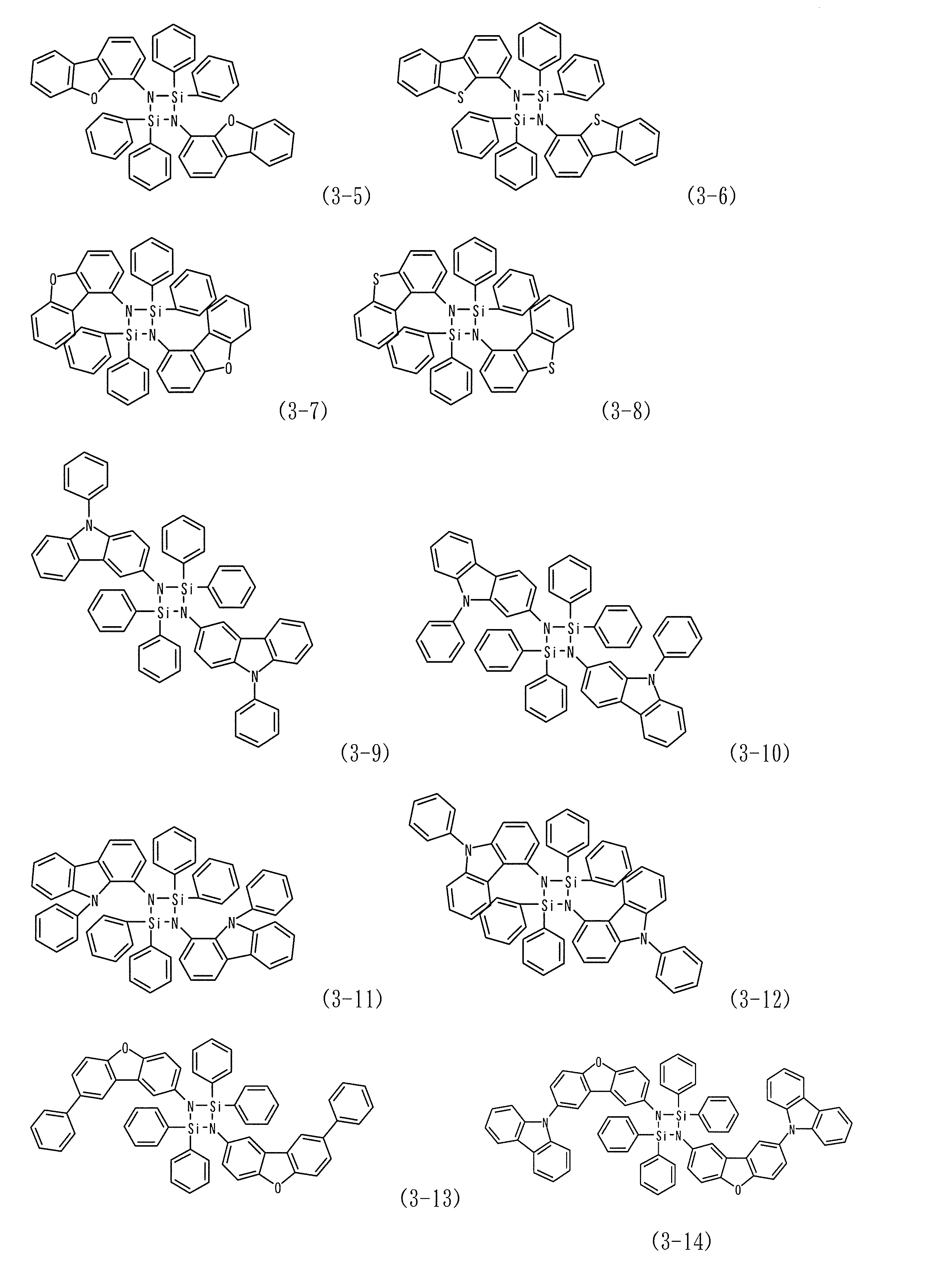
- Examples 10 to 16 As the host material of the light emitting layer of Example 9, instead of the compound (1-4), the compounds (3-3), (1-25), (2-15), (1-19), (3-11) , (1-8) or (2-19) was used to produce an organic EL device in the same manner as in Example 9.
- the maximum wavelength of the emission spectrum of each device was 530 nm, and it was found that light emission from Ir (ppy) 3 was obtained.
- the respective emission characteristics are shown in Table 1.
- the silicon-containing four-membered ring compound used in the organic electroluminescent device of the present invention has a balance of various energy values of ionization potential, electron affinity, and triplet excitation energy by introducing an aromatic heterocyclic group into this skeleton. It is considered that by separating HOMO and LUMO, which are molecular orbitals responsible for hole and electron mobility, it is possible to have high charge resistance and good charge balance.
Abstract
Description


本発明の有機EL素子は、基板に支持されていることが好ましい。この基板については、特に制限はなく、従来から有機EL素子に慣用されているものであればよく、例えば、ガラス、透明プラスチック、石英などからなるものを用いることができる。
有機EL素子における陽極としては、仕事関数の大きい(4eV以上)金属、合金、電気伝導性化合物及びこれらの混合物を電極物質とするものが好ましく用いられる。このような電極物質の具体例としてはAu等の金属、CuI、インジウムチンオキシド(ITO)、SnO2、ZnO等の導電性透明材料が挙げられる。また、IDIXO(In2O3-ZnO)等非晶質で透明導電膜を作製可能な材料を用いてもよい。陽極はこれらの電極物質を蒸着やスパッタリング等の方法により、薄膜を形成させ、フォトリソグラフィー法で所望の形状のパターンを形成してもよく、あるいはパターン精度をあまり必要としない場合は(100μm以上程度)、上記電極物質の蒸着やスパッタリング時に所望の形状のマスクを介してパターンを形成してもよい。あるいは、有機導電性化合物のように塗布可能な物質を用いる場合には、印刷方式、コーティング方式等湿式成膜法を用いることもできる。この陽極より発光を取り出す場合には、透過率を10%より大きくすることが望ましく、また陽極としてのシート抵抗は数百Ω/□以下が好ましい。更に膜厚は材料にもよるが、通常10~1000nm、好ましくは10~200nmの範囲で選ばれる。
一方、陰極としては、仕事関数の小さい(4eV以下)金属(電子注入性金属と称する)、合金、電気伝導性化合物及びこれらの混合物を電極物質とするものが用いられる。このような電極物質の具体例としては、ナトリウム、ナトリウム-カリウム合金、マグネシウム、リチウム、マグネシウム/銅混合物、マグネシウム/銀混合物、マグネシウム/アルミニウム混合物、マグネシウム/インジウム混合物、アルミニウム/酸化アルミニウム(Al2O3)混合物、インジウム、リチウム/アルミニウム混合物、希土類金属等が挙げられる。これらの中で、電子注入性及び酸化等に対する耐久性の点から、電子注入性金属とこれより仕事関数の値が大きく安定な金属である第二金属との混合物、例えば、マグネシウム/銀混合物、マグネシウム/アルミニウム混合物、マグネシウム/インジウム混合物、アルミニウム/酸化アルミニウム(Al2O3)混合物、リチウム/アルミニウム混合物、アルミニウム等が好適である。陰極はこれらの電極物質を蒸着やスパッタリング等の方法により薄膜を形成させることにより、作製することができる。また、陰極としてのシート抵抗は数百Ω/□以下が好ましく、膜厚は通常10nm~5μm、好ましくは50~200nmの範囲で選ばれる。なお、発光した光を透過させるため、有機EL素子の陽極又は陰極のいずれか一方が、透明又は半透明であれば発光輝度が向上し好都合である。
発光層は蛍光発光層、燐光発光層のいずれでも良いが、燐光発光層であることが好ましい。


注入層とは、駆動電圧低下や発光輝度向上のために電極と有機層間に設けられる層のことで、正孔注入層と電子注入層があり、陽極と発光層又は正孔輸送層の間、及び陰極と発光層又は電子輸送層との間に存在させてもよい。注入層は必要に応じて設けることができる。注入材料としては、本発明の有機EL素子用材料を用いることができるが、該材料を他の何れかの有機層に使用する場合は、従来公知の化合物の中から任意のものを選択して用いることができる。
正孔阻止層とは広い意味では電子輸送層の機能を有し、電子を輸送する機能を有しつつ正孔を輸送する能力が著しく小さい正孔阻止材料からなり、電子を輸送しつつ正孔を阻止することで電子と正孔の再結合確率を向上させることができる。
電子阻止層とは、正孔を輸送する機能を有しつつ電子を輸送する能力が著しく小さい材料から成り、正孔を輸送しつつ電子を阻止することで電子と正孔が再結合する確率を向上させることができる。
励起子阻止層とは、発光層内で正孔と電子が再結合することにより生じた励起子が電荷輸送層に拡散することを阻止するための層であり、本層の挿入により励起子を効率的に発光層内に閉じ込めることが可能となり、素子の発光効率を向上させることができる。励起子阻止層は発光層に隣接して陽極側、陰極側のいずれにも挿入することができ、両方同時に挿入することも可能である。
正孔輸送層とは正孔を輸送する機能を有する正孔輸送材料からなり、正孔輸送層は単層又は複数層設けることができる。
電子輸送層とは電子を輸送する機能を有する材料からなり、電子輸送層は単層又は複数層設けることができる。
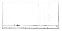
化合物(1-4)の合成

APCI-TOFMS, m/z 879 [M+H]+ 、1H-NMR測定結果(測定溶媒:THF-d8)を図2に示す。
化合物(3-3)の合成

APCI-TOFMS, m/z 727 [M+H]+ 、1H-NMR測定結果(測定溶媒:THF-d8)を図3に示す。
化合物(1-25)の合成

APCI-TOFMS, m/z 1037 [M+H]+
化合物(2-15)の合成

APCI-TOFMS, m/z 801 [M+H]+
化合物(1-19)の合成
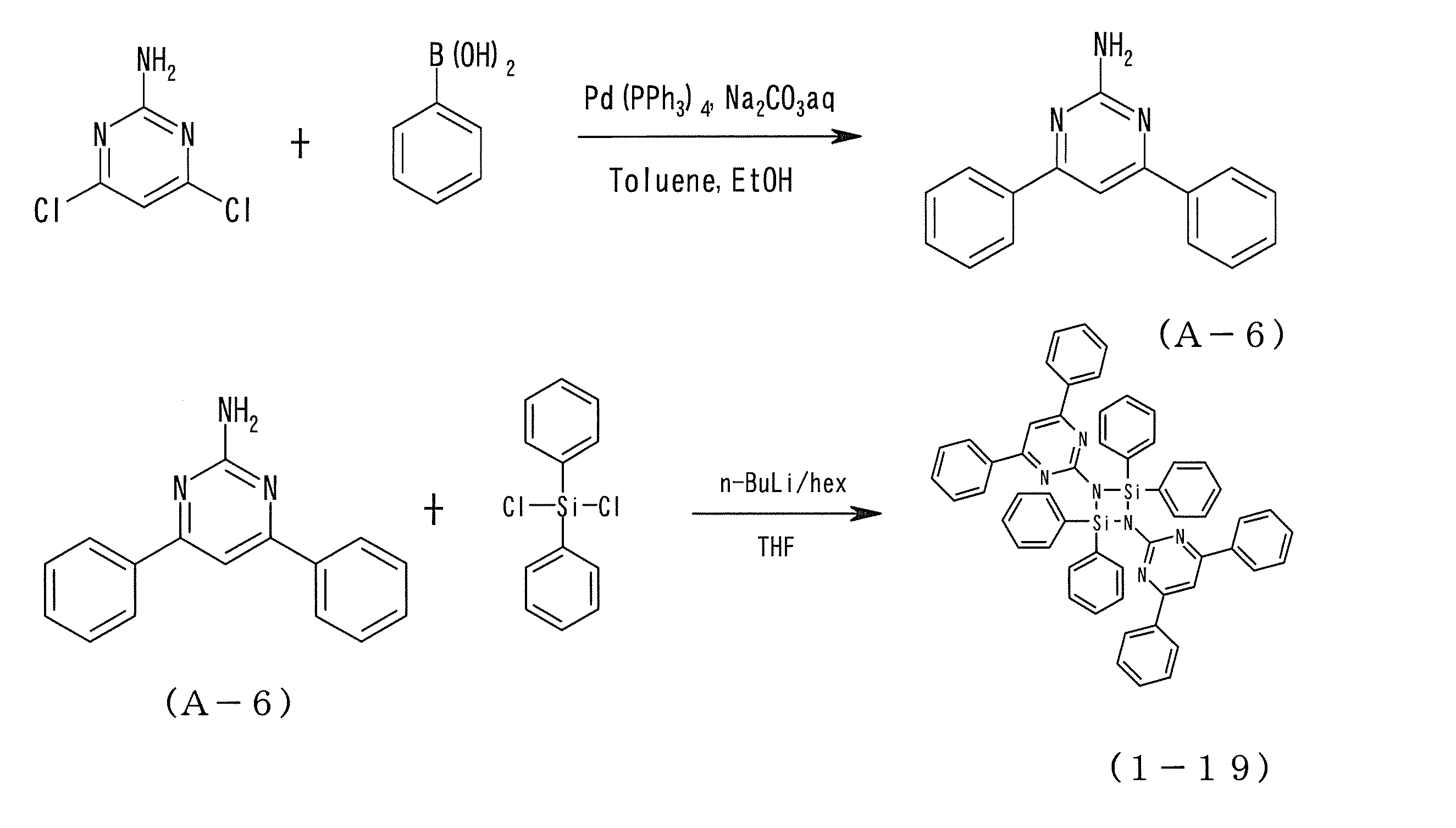
APCI-TOFMS, m/z 855 [M+H]+
化合物(3-11)の合成

APCI-TOFMS, m/z 877 [M+H]+
化合物(1-8)の合成

APCI-TOFMS, m/z 853 [M+H]+
化合物(2-19)の合成

APCI-TOFMS, m/z 811 [M+H]+
膜厚110 nmのITOからなる陽極が形成されたガラス基板上に、各薄膜を真空蒸着法にて、真空度4.0×10⁻⁵ Paで積層した。まず、ITO上に銅フタロシアニン(CuPC)を25 nmの厚さに形成した。次に、正孔輸送層として4, 4'-ビス[N-(1-ナフチル)-N-フェニルアミノ]ビフェニル(NPB)を40 nmの厚さに形成した。次に、正孔輸送層上に、ホスト材料としての化合物(1-4)と、燐光発光ドーパントとしてのトリス(2-フェニルピリジン)イリジウム(III)(Ir(ppy)3)とを異なる蒸着源から、共蒸着し、40 nmの厚さに発光層を形成した。発光層中のIr(ppy)3の濃度は10.0 wt%であった。次に、電子輸送層としてトリス(8-ヒドロキシキノリナト)アルミニウム(III)(Alq3)を20 nmの厚さに形成した。更に、電子輸送層上に、電子注入層としてフッ化リチウム(LiF)を1.0 nmの厚さに形成した。最後に、電子注入層上に、電極としてアルミニウム(Al)を70 nmの厚さに形成し、有機EL素子を作成した。
実施例9の発光層のホスト材料として、化合物(1-4)に代えて化合物(3-3)、(1-25)、(2-15)、(1-19)、(3-11)、(1-8)、又は(2-19)を用いた以外は実施例9と同様にして有機EL素子を作成した。各々の素子発光スペクトルの極大波長は530 nmであり、Ir(ppy)3からの発光が得られていることがわかった。各々の発光特性を表1に示す。
実施例9における発光層のホスト材料としてCBPを用いた以外は実施例9と同様にして有機EL素子を作成した。素子発光スペクトルの極大波長は535 nmであり、Ir(ppy)3からの発光が得られていると同定された。表1に発光特性を示す。

Claims (8)
- 一般式(1)で表される含ケイ素四員環化合物からなることを特徴とする有機電界発光素子用材料。
式(1)中、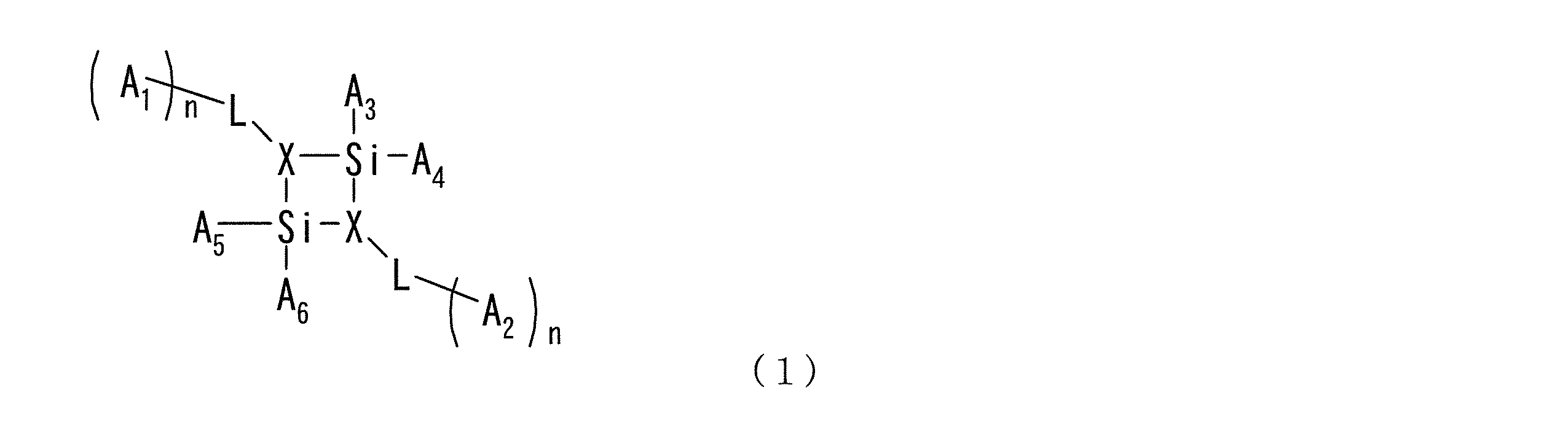
Xはそれぞれ独立して窒素又はリンを示し、
Lはそれぞれ独立してn+1価の炭素数6~24の芳香族炭化水素基又は炭素数3~19の芳香族複素環基を示し、少なくとも1つは炭素数3~19の芳香族複素環基であり、
A1~A6は、それぞれ独立して炭素数1~30のアルキル基、炭素数3~30のシクロアルキル基、炭素数2~30のアルケニル基、炭素数2~30のアルキニル基、炭素数6~50の芳香族炭化水素基、炭素数3~50の芳香族複素環基又は炭素数2~30のアミノ基を示し、
nはそれぞれ独立して0~3の整数を示す。 - 一般式(1)において、2つのXがいずれも窒素、又はいずれもリンである請求項1に記載の有機電界発光素子用材料。
- 一般式(1)において、2つのXがいずれも窒素である請求項1に記載の有機電界発光素子用材料。
- 一般式(1)において、2つのLがいずれもn+1価の炭素数3~19の芳香族複素環基である請求項3に記載の有機電界発光素子用材料。
- 一般式(1)において、2つのLが同一の芳香族複素環基である請求項4に記載の有機電界発光素子用材料。
- 基板上に、陽極、有機層及び陰極が積層されてなる有機電界発光素子において、請求項1~5のいずれかに記載の有機電界発光素子用材料を含む有機層を有することを特徴とする有機電界発光素子。
- 有機電界発光素子用材料を含む有機層が、発光層、電子輸送層、正孔輸送層、電子阻止層および正孔阻止層からなる群から選ばれる少なくとも一つの層である請求項6に記載の有機電界発光素子。
- 有機電界発光素子用材料を含む有機層が、燐光発光ドーパントを含有する発光層であることを特徴とする請求項6に記載の有機電界発光素子。
Priority Applications (4)
| Application Number | Priority Date | Filing Date | Title |
|---|---|---|---|
| EP12831426.7A EP2762483A1 (en) | 2011-09-12 | 2012-08-31 | Organic electroluminescent element material having silicon-containing four membered ring structure, and organic electroluminescent element |
| US14/240,608 US20140203270A1 (en) | 2011-09-12 | 2012-08-31 | Organic electroluminescent element material having silicon-containing four membered ring structure, and organic electroluminescent element |
| CN201280044043.9A CN103814035A (zh) | 2011-09-12 | 2012-08-31 | 具有含硅四元环构造的有机场致发光元件用材料及有机场致发光元件 |
| KR1020147009387A KR20140076572A (ko) | 2011-09-12 | 2012-08-31 | 함규소 4원환구조를 가지는 유기전계발광 소자용 재료 및 유기전계발광 소자 |
Applications Claiming Priority (2)
| Application Number | Priority Date | Filing Date | Title |
|---|---|---|---|
| JP2011198703 | 2011-09-12 | ||
| JP2011-198703 | 2011-09-12 |
Publications (1)
| Publication Number | Publication Date |
|---|---|
| WO2013038929A1 true WO2013038929A1 (ja) | 2013-03-21 |
Family
ID=47883161
Family Applications (1)
| Application Number | Title | Priority Date | Filing Date |
|---|---|---|---|
| PCT/JP2012/072272 WO2013038929A1 (ja) | 2011-09-12 | 2012-08-31 | 含ケイ素四員環構造を有する有機電界発光素子用材料及び有機電界発光素子 |
Country Status (7)
| Country | Link |
|---|---|
| US (1) | US20140203270A1 (ja) |
| EP (1) | EP2762483A1 (ja) |
| JP (1) | JPWO2013038929A1 (ja) |
| KR (1) | KR20140076572A (ja) |
| CN (1) | CN103814035A (ja) |
| TW (1) | TW201326189A (ja) |
| WO (1) | WO2013038929A1 (ja) |
Cited By (1)
| Publication number | Priority date | Publication date | Assignee | Title |
|---|---|---|---|---|
| JP2015048343A (ja) * | 2013-09-03 | 2015-03-16 | 株式会社日本触媒 | 窒化ケイ素膜原料、およびこの原料から得られた窒化ケイ素膜 |
Families Citing this family (3)
| Publication number | Priority date | Publication date | Assignee | Title |
|---|---|---|---|---|
| US8978162B2 (en) * | 2010-10-01 | 2015-03-17 | Banom, Inc. | Cut resistant garment |
| EP3908576B1 (en) * | 2019-01-08 | 2023-03-08 | Basf Se | A process for the preparation of uv absorbers |
| EP3908633A1 (en) | 2019-01-08 | 2021-11-17 | Basf Se | A process for the preparation of triazine intermediates and a process for the preparation of uv absorbers thereof |
Citations (93)
| Publication number | Priority date | Publication date | Assignee | Title |
|---|---|---|---|---|
| US3140288A (en) | 1962-02-02 | 1964-07-07 | Minnesota Mining & Mfg | Cyclodisilazane compounds |
| JPS63190343A (ja) * | 1987-02-03 | 1988-08-05 | Fujitsu Ltd | 半導体装置の絶縁膜形成方法 |
| WO1990014744A1 (en) | 1989-05-18 | 1990-11-29 | Eastman Kodak Company | Electroluminescent device with silazane-containing luminescent zone |
| JP2001313178A (ja) | 2000-04-28 | 2001-11-09 | Pioneer Electronic Corp | 有機エレクトロルミネッセンス素子 |
| JP2002117978A (ja) | 2000-07-17 | 2002-04-19 | Fuji Photo Film Co Ltd | 発光素子及びイリジウム錯体 |
| JP2003073387A (ja) | 2001-09-04 | 2003-03-12 | Canon Inc | 金属配位化合物及び有機発光素子 |
| JP2003123982A (ja) | 2001-08-07 | 2003-04-25 | Fuji Photo Film Co Ltd | 発光素子及び新規イリジウム錯体 |
| JP2003515897A (ja) | 1999-12-01 | 2003-05-07 | ザ、トラスティーズ オブ プリンストン ユニバーシティ | 有機led用燐光性ドーパントとしての式l2mxの錯体 |
| JP2003133074A (ja) | 2001-02-01 | 2003-05-09 | Fuji Photo Film Co Ltd | 遷移金属錯体及び発光素子 |
| JP2003253128A (ja) | 2002-02-28 | 2003-09-10 | Jsr Corp | 発光性組成物 |
| JP2003253129A (ja) | 2002-02-28 | 2003-09-10 | Jsr Corp | 発光性組成物 |
| JP2003253145A (ja) | 2002-02-28 | 2003-09-10 | Jsr Corp | 発光性組成物 |
| JP2003272861A (ja) | 2002-03-12 | 2003-09-26 | Konica Corp | 有機エレクトロルミネッセンス素子及びそれを用いた表示装置 |
| JP2004506305A (ja) | 2000-08-11 | 2004-02-26 | ザ、トラスティーズ オブ プリンストン ユニバーシティ | 有機金属化合物及び放射移行有機電気燐光体 |
| JP2004059433A (ja) | 2001-06-15 | 2004-02-26 | Sanyo Electric Co Ltd | 発光性有機金属化合物及び発光素子 |
| JP2004111193A (ja) | 2002-09-18 | 2004-04-08 | Konica Minolta Holdings Inc | 有機エレクトロルミネッセンス素子及び表示装置 |
| WO2004045001A2 (en) | 2002-11-08 | 2004-05-27 | Universal Display Corporation | Organic light emitting materials and devices |
| WO2004045000A2 (en) | 2002-11-06 | 2004-05-27 | Universal Display Corporation | Organic light emitting materials and devices |
| JP2004155709A (ja) | 2002-11-06 | 2004-06-03 | Toyota Central Res & Dev Lab Inc | 有機金属錯体化合物及びこれを用いた有機発光素子 |
| JP2004319438A (ja) | 2003-03-28 | 2004-11-11 | Konica Minolta Holdings Inc | 有機エレクトロルミネッセンス素子、表示装置、照明装置及びロジウム錯体化合物 |
| JP2005038847A (ja) | 2003-06-26 | 2005-02-10 | Samsung Sdi Co Ltd | 有機金属錯体およびこれを採用した有機電界発光素子 |
| JP2005082598A (ja) | 2003-09-06 | 2005-03-31 | Samsung Sdi Co Ltd | 二核有機金属錯体及びそれを利用した有機電界発光素子 |
| US20050119485A1 (en) | 2002-11-06 | 2005-06-02 | Brown Cory S. | Organometallic compounds for use in electroluminescent devices |
| JP2005139185A (ja) | 2003-11-06 | 2005-06-02 | Samsung Sdi Co Ltd | 有機金属錯体及びこれを用いた有機電界発光素子 |
| JP2005187473A (ja) | 2003-12-24 | 2005-07-14 | Samsung Sdi Co Ltd | ニ核有機金属錯体及びこれを利用した有機電界発光素子 |
| JP2005220136A (ja) | 2004-02-02 | 2005-08-18 | Samsung Sdi Co Ltd | イリジウム化合物及びそれを利用した有機電界発光素子 |
| WO2005076380A2 (en) | 2004-02-03 | 2005-08-18 | Universal Display Corporation | Oleds utilizing multidentate ligand systems |
| US20050214576A1 (en) | 2000-08-11 | 2005-09-29 | Sergey Lamansky | Organometallic compounds and emission-shifting organic electrophosphorescence |
| US20050260448A1 (en) | 2004-05-18 | 2005-11-24 | Chun Lin | Novel organometallic compounds for use in electroluminescent devices |
| US20050260449A1 (en) | 2004-05-18 | 2005-11-24 | Robert Walters | Complexes with tridentate ligands |
| WO2005113704A2 (en) | 2004-05-18 | 2005-12-01 | The University Of Southern California | Luminescent compounds with carbene ligands |
| JP2006050596A (ja) | 2004-07-06 | 2006-02-16 | Canon Inc | データ処理方法、データ処理装置、ディザパターン製造方法およびディザパターン |
| JP2006063080A (ja) | 2004-08-28 | 2006-03-09 | Samsung Sdi Co Ltd | シクロメタル化遷移金属錯体及びこれを利用した有機電界発光素子 |
| JP2006093542A (ja) | 2004-09-27 | 2006-04-06 | Fuji Photo Film Co Ltd | 発光素子 |
| JP2006513278A (ja) | 2002-08-16 | 2006-04-20 | ザ ユニバーシティ オブ サザン カリフォルニア | 有機発光材料及びデバイス |
| JP2006104132A (ja) | 2004-10-06 | 2006-04-20 | Toppan Printing Co Ltd | 有機金属錯体、および発光材料、並びに発光素子 |
| JP2006104201A (ja) | 2004-10-01 | 2006-04-20 | Samsung Sdi Co Ltd | シクロメタル化遷移金属錯体及びこれを用いた有機電界発光素子 |
| JP2006111623A (ja) | 2004-10-11 | 2006-04-27 | Samsung Sdi Co Ltd | シクロメタル化遷移金属錯体及びこれを用いた有機電界発光素子 |
| WO2006046980A1 (en) | 2004-07-06 | 2006-05-04 | Universal Display Corporation | Organic light emitting materials and devices |
| JP2006131524A (ja) | 2004-11-04 | 2006-05-25 | Fuji Photo Film Co Ltd | 有機金属錯体、発光性固体、有機el素子及び有機elディスプレイ |
| JP2006131561A (ja) | 2004-11-08 | 2006-05-25 | Idemitsu Kosan Co Ltd | 金属錯体化合物 |
| JP2006517517A (ja) * | 2002-11-14 | 2006-07-27 | アドバンスド テクノロジー マテリアルズ,インコーポレイテッド | ケイ素、窒化ケイ素、二酸化ケイ素および/またはオキシ窒化ケイ素を含むフィルムのようなケイ素含有フィルムの低温蒸着のための組成物および方法 |
| JP2006213720A (ja) | 2005-02-03 | 2006-08-17 | Samsung Sdi Co Ltd | 有機金属錯体及びこれを用いた有機電界発光素子 |
| JP2006261623A (ja) | 2004-09-22 | 2006-09-28 | Fuji Photo Film Co Ltd | 有機電界発光素子 |
| WO2006100888A1 (ja) | 2005-03-22 | 2006-09-28 | Konica Minolta Holdings, Inc. | 有機el素子用材料、有機el素子、表示装置及び照明装置 |
| JP2006290891A (ja) | 2005-04-12 | 2006-10-26 | Samsung Sdi Co Ltd | シリル置換シクロメタル化遷移金属錯体およびこれを用いた有機電界発光素子 |
| JP2006298899A (ja) | 2005-04-21 | 2006-11-02 | Samsung Sdi Co Ltd | ホスト用化合物とドーパント用化合物が連結された有機金属化合物、およびこれを利用した有機電界発光素子及びその製造方法 |
| JP2006303394A (ja) | 2005-04-25 | 2006-11-02 | Fuji Photo Film Co Ltd | 有機電界発光素子 |
| JP2006303383A (ja) | 2005-04-25 | 2006-11-02 | Fuji Photo Film Co Ltd | 有機電界発光素子 |
| JP2006298900A (ja) | 2005-04-21 | 2006-11-02 | Samsung Sdi Co Ltd | ホスト用化合物とドーパント用化合物が連結された有機金属化合物、およびこれを利用した有機電界発光素子及びその製造方法 |
| JP2006310479A (ja) | 2005-04-27 | 2006-11-09 | Fuji Photo Film Co Ltd | 有機電界発光素子 |
| JP2007002080A (ja) | 2005-06-23 | 2007-01-11 | Konica Minolta Holdings Inc | 有機エレクトロルミネッセンス素子材料、有機エレクトロルミネッセンス素子、表示装置及び照明装置 |
| WO2007004380A1 (ja) | 2005-07-01 | 2007-01-11 | Konica Minolta Holdings, Inc. | 有機エレクトロルミネッセンス素子材料、有機エレクトロルミネッセンス素子、表示装置及び照明装置 |
| JP2007009009A (ja) | 2005-06-29 | 2007-01-18 | Konica Minolta Holdings Inc | 有機エレクトロルミネッセンス素子材料、有機エレクトロルミネッセンス素子、表示装置及び照明装置 |
| WO2007018067A1 (ja) | 2005-08-05 | 2007-02-15 | Idemitsu Kosan Co., Ltd. | 遷移金属錯体化合物及びそれを用いた有機エレクトロルミネッセンス素子 |
| WO2007023659A1 (ja) | 2005-08-25 | 2007-03-01 | Konica Minolta Holdings, Inc. | 有機エレクトロルミネッセンス素子材料、有機エレクトロルミネッセンス素子、表示装置及び照明装置 |
| JP2007088105A (ja) | 2005-09-20 | 2007-04-05 | Fujifilm Corp | 有機電界発光素子 |
| WO2007058080A1 (ja) | 2005-11-17 | 2007-05-24 | Idemitsu Kosan Co., Ltd. | 金属錯体化合物及びそれを用いた有機エレクトロルミネッセンス素子 |
| WO2007058104A1 (ja) | 2005-11-17 | 2007-05-24 | Idemitsu Kosan Co., Ltd. | 金属錯体化合物及びそれを用いた有機エレクトロルミネッセンス素子 |
| JP2007522126A (ja) | 2004-01-26 | 2007-08-09 | ユニバーサル ディスプレイ コーポレーション | 改善された電界発光安定性 |
| WO2007095118A2 (en) | 2006-02-10 | 2007-08-23 | Universal Display Corporation | METAL COMPLEXES OF CYCLOMETALLATED IMIDAZO[1,2-f]PHENANTHRIDINE AND DIIMIDAZO[1,2-A:1',2'-C]QUINAZOLINE LIGANDS AND ISOELECTRONIC AND BENZANNULATED ANALOGS THEREOF |
| JP2007227948A (ja) | 2007-03-29 | 2007-09-06 | Konica Minolta Holdings Inc | 有機エレクトロルミネッセンス素子及びそれを用いた表示装置 |
| JP2007258550A (ja) | 2006-03-24 | 2007-10-04 | Fujifilm Corp | 有機電界発光素子 |
| JP2007324309A (ja) | 2006-05-31 | 2007-12-13 | Fujifilm Corp | 有機電界発光素子 |
| JP2008037848A (ja) | 2006-08-10 | 2008-02-21 | Takasago Internatl Corp | 白金錯体及び発光素子 |
| JP2008505925A (ja) | 2004-07-07 | 2008-02-28 | ユニバーサル ディスプレイ コーポレイション | 安定で効率的なエレクトロルミネセンス材料 |
| WO2008035664A1 (fr) | 2006-09-20 | 2008-03-27 | Konica Minolta Holdings, Inc. | Matériau de dispositif électroluminescent organique, dispositif électroluminescent organique, dispositif d'affichage et d'éclairage |
| JP2008091906A (ja) | 2007-09-26 | 2008-04-17 | Konica Minolta Holdings Inc | 有機エレクトロルミネッセンス素子 |
| WO2008050733A1 (fr) | 2006-10-24 | 2008-05-02 | Ube Industries, Ltd. | Complexe de l'or, procédé pour la production du complexe de l'or et élément électroluminescent ultraviolet organique utilisant le complexe de l'or |
| WO2008054584A1 (en) | 2006-11-03 | 2008-05-08 | Universal Display Corporation | Improved stability oled materials and devices |
| JP2008133212A (ja) | 2006-11-28 | 2008-06-12 | Canon Inc | 金属錯体化合物、電界発光素子及び表示装置 |
| JP2008239565A (ja) | 2007-03-28 | 2008-10-09 | Idemitsu Kosan Co Ltd | イリジウム錯体とその製造法及びそれを用いた有機エレクトロルミネッセンス |
| US20080261076A1 (en) | 2007-03-08 | 2008-10-23 | Universal Display Corporation | Phosphorescent materials |
| JP2008270737A (ja) | 2007-03-23 | 2008-11-06 | Fujifilm Corp | 有機電界発光素子 |
| JP2008266163A (ja) | 2007-04-17 | 2008-11-06 | Idemitsu Kosan Co Ltd | 遷移金属錯体化合物及びそれを用いた有機エレクトロルミネッセンス素子 |
| WO2008140657A1 (en) | 2007-05-10 | 2008-11-20 | Universal Display Corporation | Organometallic compounds having host and dopant functionalities |
| JP2008542203A (ja) | 2005-05-06 | 2008-11-27 | ユニバーサル ディスプレイ コーポレイション | 安定oled材料及び改善された安定性を有するデバイス |
| WO2008156879A1 (en) | 2007-06-20 | 2008-12-24 | Universal Display Corporation | Blue phosphorescent imidazophenanthridine materials |
| JP2008311607A (ja) | 2007-05-16 | 2008-12-25 | Konica Minolta Holdings Inc | 有機エレクトロルミネッセンス素子、有機エレクトロルミネッセンス素子材料、表示装置及び照明装置 |
| JP2009019121A (ja) | 2007-07-12 | 2009-01-29 | Konica Minolta Holdings Inc | 有機エレクトロルミネッセンス材料、有機エレクトロルミネッセンス素子、表示装置及び照明装置 |
| JP2009046601A (ja) | 2007-08-21 | 2009-03-05 | Konica Minolta Holdings Inc | 有機エレクトロルミネッセンス素子材料、有機エレクトロルミネッセンス素子、表示装置及び照明装置 |
| JP2009057367A (ja) | 2007-08-03 | 2009-03-19 | Idemitsu Kosan Co Ltd | 金属錯体化合物、有機エレクトロルミネッセンス素子用材料及びそれを用いた有機エレクトロルミネッセンス素子 |
| JP2009057304A (ja) | 2007-08-30 | 2009-03-19 | Mitsubishi Chemicals Corp | 金属錯体及び有機電界発光素子 |
| WO2009046266A1 (en) | 2007-10-04 | 2009-04-09 | Universal Display Corporation | Complexes with tridentate ligands |
| JP2009096800A (ja) | 2007-09-25 | 2009-05-07 | Fujifilm Corp | 有機電界発光素子 |
| JP2009114369A (ja) | 2007-11-08 | 2009-05-28 | Konica Minolta Holdings Inc | 有機エレクトロルミネッセンス材料、有機エレクトロルミネッセンス素子、表示装置及び照明装置 |
| WO2009073245A1 (en) | 2007-12-06 | 2009-06-11 | Universal Display Corporation | Light-emitting organometallic complexes |
| JP2009161524A (ja) | 2007-12-14 | 2009-07-23 | Fujifilm Corp | 白金錯体化合物及びこれを用いた有機電界発光素子 |
| JP2009532546A (ja) | 2006-04-07 | 2009-09-10 | ソルヴェイ(ソシエテ アノニム) | 発光物質 |
| JP2009536681A (ja) | 2006-05-08 | 2009-10-15 | イー・アイ・デュポン・ドウ・ヌムール・アンド・カンパニー | エレクトロルミネセンスビス−シクロメタレート化イリジウム化合物およびかかる化合物で作製されたデバイス |
| JP2009542026A (ja) | 2006-06-26 | 2009-11-26 | ビーエーエスエフ ソシエタス・ヨーロピア | 架橋カルベン配位子を有するPtとPdのビスカルベン錯体及びテトラカルベン錯体のOLED内での利用 |
| JP2009286716A (ja) | 2008-05-28 | 2009-12-10 | Sumitomo Seika Chem Co Ltd | イリジウム錯体 |
| JP2010083852A (ja) | 2008-10-03 | 2010-04-15 | Wakayama Univ | 金属錯体の製造方法、金属錯体および有機電界発光素子 |
Family Cites Families (2)
| Publication number | Priority date | Publication date | Assignee | Title |
|---|---|---|---|---|
| US7531679B2 (en) * | 2002-11-14 | 2009-05-12 | Advanced Technology Materials, Inc. | Composition and method for low temperature deposition of silicon-containing films such as films including silicon nitride, silicon dioxide and/or silicon-oxynitride |
| JP4362461B2 (ja) * | 2004-11-05 | 2009-11-11 | 三星モバイルディスプレイ株式會社 | 有機電界発光素子 |
-
2012
- 2012-08-31 US US14/240,608 patent/US20140203270A1/en not_active Abandoned
- 2012-08-31 WO PCT/JP2012/072272 patent/WO2013038929A1/ja active Application Filing
- 2012-08-31 JP JP2013533609A patent/JPWO2013038929A1/ja active Pending
- 2012-08-31 EP EP12831426.7A patent/EP2762483A1/en not_active Withdrawn
- 2012-08-31 KR KR1020147009387A patent/KR20140076572A/ko not_active Application Discontinuation
- 2012-08-31 CN CN201280044043.9A patent/CN103814035A/zh active Pending
- 2012-09-11 TW TW101133128A patent/TW201326189A/zh unknown
Patent Citations (93)
| Publication number | Priority date | Publication date | Assignee | Title |
|---|---|---|---|---|
| US3140288A (en) | 1962-02-02 | 1964-07-07 | Minnesota Mining & Mfg | Cyclodisilazane compounds |
| JPS63190343A (ja) * | 1987-02-03 | 1988-08-05 | Fujitsu Ltd | 半導体装置の絶縁膜形成方法 |
| WO1990014744A1 (en) | 1989-05-18 | 1990-11-29 | Eastman Kodak Company | Electroluminescent device with silazane-containing luminescent zone |
| JP2003515897A (ja) | 1999-12-01 | 2003-05-07 | ザ、トラスティーズ オブ プリンストン ユニバーシティ | 有機led用燐光性ドーパントとしての式l2mxの錯体 |
| JP2001313178A (ja) | 2000-04-28 | 2001-11-09 | Pioneer Electronic Corp | 有機エレクトロルミネッセンス素子 |
| JP2002117978A (ja) | 2000-07-17 | 2002-04-19 | Fuji Photo Film Co Ltd | 発光素子及びイリジウム錯体 |
| US20050214576A1 (en) | 2000-08-11 | 2005-09-29 | Sergey Lamansky | Organometallic compounds and emission-shifting organic electrophosphorescence |
| JP2004506305A (ja) | 2000-08-11 | 2004-02-26 | ザ、トラスティーズ オブ プリンストン ユニバーシティ | 有機金属化合物及び放射移行有機電気燐光体 |
| JP2003133074A (ja) | 2001-02-01 | 2003-05-09 | Fuji Photo Film Co Ltd | 遷移金属錯体及び発光素子 |
| JP2004059433A (ja) | 2001-06-15 | 2004-02-26 | Sanyo Electric Co Ltd | 発光性有機金属化合物及び発光素子 |
| JP2003123982A (ja) | 2001-08-07 | 2003-04-25 | Fuji Photo Film Co Ltd | 発光素子及び新規イリジウム錯体 |
| JP2003073387A (ja) | 2001-09-04 | 2003-03-12 | Canon Inc | 金属配位化合物及び有機発光素子 |
| JP2003253129A (ja) | 2002-02-28 | 2003-09-10 | Jsr Corp | 発光性組成物 |
| JP2003253145A (ja) | 2002-02-28 | 2003-09-10 | Jsr Corp | 発光性組成物 |
| JP2003253128A (ja) | 2002-02-28 | 2003-09-10 | Jsr Corp | 発光性組成物 |
| JP2003272861A (ja) | 2002-03-12 | 2003-09-26 | Konica Corp | 有機エレクトロルミネッセンス素子及びそれを用いた表示装置 |
| JP2006513278A (ja) | 2002-08-16 | 2006-04-20 | ザ ユニバーシティ オブ サザン カリフォルニア | 有機発光材料及びデバイス |
| JP2004111193A (ja) | 2002-09-18 | 2004-04-08 | Konica Minolta Holdings Inc | 有機エレクトロルミネッセンス素子及び表示装置 |
| US20050119485A1 (en) | 2002-11-06 | 2005-06-02 | Brown Cory S. | Organometallic compounds for use in electroluminescent devices |
| JP2004155709A (ja) | 2002-11-06 | 2004-06-03 | Toyota Central Res & Dev Lab Inc | 有機金属錯体化合物及びこれを用いた有機発光素子 |
| WO2004045000A2 (en) | 2002-11-06 | 2004-05-27 | Universal Display Corporation | Organic light emitting materials and devices |
| WO2004045001A2 (en) | 2002-11-08 | 2004-05-27 | Universal Display Corporation | Organic light emitting materials and devices |
| JP2006517517A (ja) * | 2002-11-14 | 2006-07-27 | アドバンスド テクノロジー マテリアルズ,インコーポレイテッド | ケイ素、窒化ケイ素、二酸化ケイ素および/またはオキシ窒化ケイ素を含むフィルムのようなケイ素含有フィルムの低温蒸着のための組成物および方法 |
| JP2004319438A (ja) | 2003-03-28 | 2004-11-11 | Konica Minolta Holdings Inc | 有機エレクトロルミネッセンス素子、表示装置、照明装置及びロジウム錯体化合物 |
| JP2005038847A (ja) | 2003-06-26 | 2005-02-10 | Samsung Sdi Co Ltd | 有機金属錯体およびこれを採用した有機電界発光素子 |
| JP2005082598A (ja) | 2003-09-06 | 2005-03-31 | Samsung Sdi Co Ltd | 二核有機金属錯体及びそれを利用した有機電界発光素子 |
| JP2005139185A (ja) | 2003-11-06 | 2005-06-02 | Samsung Sdi Co Ltd | 有機金属錯体及びこれを用いた有機電界発光素子 |
| JP2005187473A (ja) | 2003-12-24 | 2005-07-14 | Samsung Sdi Co Ltd | ニ核有機金属錯体及びこれを利用した有機電界発光素子 |
| JP2007522126A (ja) | 2004-01-26 | 2007-08-09 | ユニバーサル ディスプレイ コーポレーション | 改善された電界発光安定性 |
| JP2005220136A (ja) | 2004-02-02 | 2005-08-18 | Samsung Sdi Co Ltd | イリジウム化合物及びそれを利用した有機電界発光素子 |
| WO2005076380A2 (en) | 2004-02-03 | 2005-08-18 | Universal Display Corporation | Oleds utilizing multidentate ligand systems |
| US20050260449A1 (en) | 2004-05-18 | 2005-11-24 | Robert Walters | Complexes with tridentate ligands |
| WO2005113704A2 (en) | 2004-05-18 | 2005-12-01 | The University Of Southern California | Luminescent compounds with carbene ligands |
| US20050260448A1 (en) | 2004-05-18 | 2005-11-24 | Chun Lin | Novel organometallic compounds for use in electroluminescent devices |
| WO2006046980A1 (en) | 2004-07-06 | 2006-05-04 | Universal Display Corporation | Organic light emitting materials and devices |
| JP2006050596A (ja) | 2004-07-06 | 2006-02-16 | Canon Inc | データ処理方法、データ処理装置、ディザパターン製造方法およびディザパターン |
| JP2008505925A (ja) | 2004-07-07 | 2008-02-28 | ユニバーサル ディスプレイ コーポレイション | 安定で効率的なエレクトロルミネセンス材料 |
| JP2006063080A (ja) | 2004-08-28 | 2006-03-09 | Samsung Sdi Co Ltd | シクロメタル化遷移金属錯体及びこれを利用した有機電界発光素子 |
| JP2006261623A (ja) | 2004-09-22 | 2006-09-28 | Fuji Photo Film Co Ltd | 有機電界発光素子 |
| JP2006093542A (ja) | 2004-09-27 | 2006-04-06 | Fuji Photo Film Co Ltd | 発光素子 |
| JP2006104201A (ja) | 2004-10-01 | 2006-04-20 | Samsung Sdi Co Ltd | シクロメタル化遷移金属錯体及びこれを用いた有機電界発光素子 |
| JP2006104132A (ja) | 2004-10-06 | 2006-04-20 | Toppan Printing Co Ltd | 有機金属錯体、および発光材料、並びに発光素子 |
| JP2006111623A (ja) | 2004-10-11 | 2006-04-27 | Samsung Sdi Co Ltd | シクロメタル化遷移金属錯体及びこれを用いた有機電界発光素子 |
| JP2006131524A (ja) | 2004-11-04 | 2006-05-25 | Fuji Photo Film Co Ltd | 有機金属錯体、発光性固体、有機el素子及び有機elディスプレイ |
| JP2006131561A (ja) | 2004-11-08 | 2006-05-25 | Idemitsu Kosan Co Ltd | 金属錯体化合物 |
| JP2006213720A (ja) | 2005-02-03 | 2006-08-17 | Samsung Sdi Co Ltd | 有機金属錯体及びこれを用いた有機電界発光素子 |
| WO2006100888A1 (ja) | 2005-03-22 | 2006-09-28 | Konica Minolta Holdings, Inc. | 有機el素子用材料、有機el素子、表示装置及び照明装置 |
| JP2006290891A (ja) | 2005-04-12 | 2006-10-26 | Samsung Sdi Co Ltd | シリル置換シクロメタル化遷移金属錯体およびこれを用いた有機電界発光素子 |
| JP2006298899A (ja) | 2005-04-21 | 2006-11-02 | Samsung Sdi Co Ltd | ホスト用化合物とドーパント用化合物が連結された有機金属化合物、およびこれを利用した有機電界発光素子及びその製造方法 |
| JP2006298900A (ja) | 2005-04-21 | 2006-11-02 | Samsung Sdi Co Ltd | ホスト用化合物とドーパント用化合物が連結された有機金属化合物、およびこれを利用した有機電界発光素子及びその製造方法 |
| JP2006303394A (ja) | 2005-04-25 | 2006-11-02 | Fuji Photo Film Co Ltd | 有機電界発光素子 |
| JP2006303383A (ja) | 2005-04-25 | 2006-11-02 | Fuji Photo Film Co Ltd | 有機電界発光素子 |
| JP2006310479A (ja) | 2005-04-27 | 2006-11-09 | Fuji Photo Film Co Ltd | 有機電界発光素子 |
| JP2008542203A (ja) | 2005-05-06 | 2008-11-27 | ユニバーサル ディスプレイ コーポレイション | 安定oled材料及び改善された安定性を有するデバイス |
| JP2007002080A (ja) | 2005-06-23 | 2007-01-11 | Konica Minolta Holdings Inc | 有機エレクトロルミネッセンス素子材料、有機エレクトロルミネッセンス素子、表示装置及び照明装置 |
| JP2007009009A (ja) | 2005-06-29 | 2007-01-18 | Konica Minolta Holdings Inc | 有機エレクトロルミネッセンス素子材料、有機エレクトロルミネッセンス素子、表示装置及び照明装置 |
| WO2007004380A1 (ja) | 2005-07-01 | 2007-01-11 | Konica Minolta Holdings, Inc. | 有機エレクトロルミネッセンス素子材料、有機エレクトロルミネッセンス素子、表示装置及び照明装置 |
| WO2007018067A1 (ja) | 2005-08-05 | 2007-02-15 | Idemitsu Kosan Co., Ltd. | 遷移金属錯体化合物及びそれを用いた有機エレクトロルミネッセンス素子 |
| WO2007023659A1 (ja) | 2005-08-25 | 2007-03-01 | Konica Minolta Holdings, Inc. | 有機エレクトロルミネッセンス素子材料、有機エレクトロルミネッセンス素子、表示装置及び照明装置 |
| JP2007088105A (ja) | 2005-09-20 | 2007-04-05 | Fujifilm Corp | 有機電界発光素子 |
| WO2007058080A1 (ja) | 2005-11-17 | 2007-05-24 | Idemitsu Kosan Co., Ltd. | 金属錯体化合物及びそれを用いた有機エレクトロルミネッセンス素子 |
| WO2007058104A1 (ja) | 2005-11-17 | 2007-05-24 | Idemitsu Kosan Co., Ltd. | 金属錯体化合物及びそれを用いた有機エレクトロルミネッセンス素子 |
| WO2007095118A2 (en) | 2006-02-10 | 2007-08-23 | Universal Display Corporation | METAL COMPLEXES OF CYCLOMETALLATED IMIDAZO[1,2-f]PHENANTHRIDINE AND DIIMIDAZO[1,2-A:1',2'-C]QUINAZOLINE LIGANDS AND ISOELECTRONIC AND BENZANNULATED ANALOGS THEREOF |
| JP2007258550A (ja) | 2006-03-24 | 2007-10-04 | Fujifilm Corp | 有機電界発光素子 |
| JP2009532546A (ja) | 2006-04-07 | 2009-09-10 | ソルヴェイ(ソシエテ アノニム) | 発光物質 |
| JP2009536681A (ja) | 2006-05-08 | 2009-10-15 | イー・アイ・デュポン・ドウ・ヌムール・アンド・カンパニー | エレクトロルミネセンスビス−シクロメタレート化イリジウム化合物およびかかる化合物で作製されたデバイス |
| JP2007324309A (ja) | 2006-05-31 | 2007-12-13 | Fujifilm Corp | 有機電界発光素子 |
| JP2009542026A (ja) | 2006-06-26 | 2009-11-26 | ビーエーエスエフ ソシエタス・ヨーロピア | 架橋カルベン配位子を有するPtとPdのビスカルベン錯体及びテトラカルベン錯体のOLED内での利用 |
| JP2008037848A (ja) | 2006-08-10 | 2008-02-21 | Takasago Internatl Corp | 白金錯体及び発光素子 |
| WO2008035664A1 (fr) | 2006-09-20 | 2008-03-27 | Konica Minolta Holdings, Inc. | Matériau de dispositif électroluminescent organique, dispositif électroluminescent organique, dispositif d'affichage et d'éclairage |
| WO2008050733A1 (fr) | 2006-10-24 | 2008-05-02 | Ube Industries, Ltd. | Complexe de l'or, procédé pour la production du complexe de l'or et élément électroluminescent ultraviolet organique utilisant le complexe de l'or |
| WO2008054584A1 (en) | 2006-11-03 | 2008-05-08 | Universal Display Corporation | Improved stability oled materials and devices |
| JP2008133212A (ja) | 2006-11-28 | 2008-06-12 | Canon Inc | 金属錯体化合物、電界発光素子及び表示装置 |
| US20080261076A1 (en) | 2007-03-08 | 2008-10-23 | Universal Display Corporation | Phosphorescent materials |
| JP2008270737A (ja) | 2007-03-23 | 2008-11-06 | Fujifilm Corp | 有機電界発光素子 |
| JP2008239565A (ja) | 2007-03-28 | 2008-10-09 | Idemitsu Kosan Co Ltd | イリジウム錯体とその製造法及びそれを用いた有機エレクトロルミネッセンス |
| JP2007227948A (ja) | 2007-03-29 | 2007-09-06 | Konica Minolta Holdings Inc | 有機エレクトロルミネッセンス素子及びそれを用いた表示装置 |
| JP2008266163A (ja) | 2007-04-17 | 2008-11-06 | Idemitsu Kosan Co Ltd | 遷移金属錯体化合物及びそれを用いた有機エレクトロルミネッセンス素子 |
| WO2008140657A1 (en) | 2007-05-10 | 2008-11-20 | Universal Display Corporation | Organometallic compounds having host and dopant functionalities |
| JP2008311607A (ja) | 2007-05-16 | 2008-12-25 | Konica Minolta Holdings Inc | 有機エレクトロルミネッセンス素子、有機エレクトロルミネッセンス素子材料、表示装置及び照明装置 |
| WO2008156879A1 (en) | 2007-06-20 | 2008-12-24 | Universal Display Corporation | Blue phosphorescent imidazophenanthridine materials |
| JP2009019121A (ja) | 2007-07-12 | 2009-01-29 | Konica Minolta Holdings Inc | 有機エレクトロルミネッセンス材料、有機エレクトロルミネッセンス素子、表示装置及び照明装置 |
| JP2009057367A (ja) | 2007-08-03 | 2009-03-19 | Idemitsu Kosan Co Ltd | 金属錯体化合物、有機エレクトロルミネッセンス素子用材料及びそれを用いた有機エレクトロルミネッセンス素子 |
| JP2009046601A (ja) | 2007-08-21 | 2009-03-05 | Konica Minolta Holdings Inc | 有機エレクトロルミネッセンス素子材料、有機エレクトロルミネッセンス素子、表示装置及び照明装置 |
| JP2009057304A (ja) | 2007-08-30 | 2009-03-19 | Mitsubishi Chemicals Corp | 金属錯体及び有機電界発光素子 |
| JP2009096800A (ja) | 2007-09-25 | 2009-05-07 | Fujifilm Corp | 有機電界発光素子 |
| JP2008091906A (ja) | 2007-09-26 | 2008-04-17 | Konica Minolta Holdings Inc | 有機エレクトロルミネッセンス素子 |
| WO2009046266A1 (en) | 2007-10-04 | 2009-04-09 | Universal Display Corporation | Complexes with tridentate ligands |
| JP2009114369A (ja) | 2007-11-08 | 2009-05-28 | Konica Minolta Holdings Inc | 有機エレクトロルミネッセンス材料、有機エレクトロルミネッセンス素子、表示装置及び照明装置 |
| WO2009073245A1 (en) | 2007-12-06 | 2009-06-11 | Universal Display Corporation | Light-emitting organometallic complexes |
| JP2009161524A (ja) | 2007-12-14 | 2009-07-23 | Fujifilm Corp | 白金錯体化合物及びこれを用いた有機電界発光素子 |
| JP2009286716A (ja) | 2008-05-28 | 2009-12-10 | Sumitomo Seika Chem Co Ltd | イリジウム錯体 |
| JP2010083852A (ja) | 2008-10-03 | 2010-04-15 | Wakayama Univ | 金属錯体の製造方法、金属錯体および有機電界発光素子 |
Non-Patent Citations (4)
| Title |
|---|
| APPLIED PHYSICS LETTERS, vol. 82, 2003, pages 2422 - 2424 |
| APPLIED PHYSICS LETTERS, vol. 83, 2003, pages 569 - 571 |
| LUTZ M. ENGLEHARDT ET AL.: "Hypervalent Silicon via Thermolysis of a Cadmiun Amide: Thermally Stable Magnesium and Zinc Amides [ML2], L = N(8- Quinolyl)(SiMe3)", J. CHEM. SOC., CHEM.COMMUN., 1991, pages 930 - 932, XP055144578 * |
| PETER C. JUNK ET AL.: "Synthesis and structural characterization of a pyridyl- substituted cyclodisilazane [(6-Me-Apy)2 (p-SiMe)2];(6-Me-ApyH2=6-methyl-2-amino- pyridine)", INORGANICA CHIMICA ACTA, vol. 357, 2004, pages 2195 - 2198, XP055144575 * |
Cited By (1)
| Publication number | Priority date | Publication date | Assignee | Title |
|---|---|---|---|---|
| JP2015048343A (ja) * | 2013-09-03 | 2015-03-16 | 株式会社日本触媒 | 窒化ケイ素膜原料、およびこの原料から得られた窒化ケイ素膜 |
Also Published As
| Publication number | Publication date |
|---|---|
| EP2762483A1 (en) | 2014-08-06 |
| JPWO2013038929A1 (ja) | 2015-03-26 |
| CN103814035A (zh) | 2014-05-21 |
| TW201326189A (zh) | 2013-07-01 |
| KR20140076572A (ko) | 2014-06-20 |
| US20140203270A1 (en) | 2014-07-24 |
Similar Documents
| Publication | Publication Date | Title |
|---|---|---|
| JP6153522B2 (ja) | 有機電界発光素子用材料及び有機電界発光素子 | |
| JP5581341B2 (ja) | 有機電界発光素子 | |
| JP5775520B2 (ja) | 有機電界発光素子 | |
| JP5395161B2 (ja) | 有機電界発光素子 | |
| JP5399418B2 (ja) | 有機電界発光素子 | |
| JP6360796B2 (ja) | 有機電界発光素子用材料及びこれを用いた有機電界発光素子 | |
| JP5953237B2 (ja) | 有機電界発光素子 | |
| JP5778756B2 (ja) | 含窒素芳香族化合物及び有機電界発光素子 | |
| JP6647283B2 (ja) | 有機電界発光素子用材料及びこれを用いた有機電界発光素子 | |
| JP6169078B2 (ja) | 有機電界発光素子 | |
| JP5577122B2 (ja) | 有機電界発光素子 | |
| EP3125325B1 (en) | Organic-electroluminescent-element material and organic electroluminescent element using it | |
| JP6310850B2 (ja) | 有機電界発光素子用材料及びこれを用いた有機電界発光素子 | |
| JP6402177B2 (ja) | 有機電界発光素子用材料及びこれを用いた有機電界発光素子 | |
| WO2013038929A1 (ja) | 含ケイ素四員環構造を有する有機電界発光素子用材料及び有機電界発光素子 |
Legal Events
| Date | Code | Title | Description |
|---|---|---|---|
| 121 | Ep: the epo has been informed by wipo that ep was designated in this application |
Ref document number: 12831426 Country of ref document: EP Kind code of ref document: A1 |
|
| ENP | Entry into the national phase |
Ref document number: 2013533609 Country of ref document: JP Kind code of ref document: A |
|
| WWE | Wipo information: entry into national phase |
Ref document number: 14240608 Country of ref document: US |
|
| WWE | Wipo information: entry into national phase |
Ref document number: 2012831426 Country of ref document: EP |
|
| NENP | Non-entry into the national phase |
Ref country code: DE |
|
| ENP | Entry into the national phase |
Ref document number: 20147009387 Country of ref document: KR Kind code of ref document: A |