WO2013022051A1 - 多孔質構造体及びその製造方法 - Google Patents
多孔質構造体及びその製造方法 Download PDFInfo
- Publication number
- WO2013022051A1 WO2013022051A1 PCT/JP2012/070280 JP2012070280W WO2013022051A1 WO 2013022051 A1 WO2013022051 A1 WO 2013022051A1 JP 2012070280 W JP2012070280 W JP 2012070280W WO 2013022051 A1 WO2013022051 A1 WO 2013022051A1
- Authority
- WO
- WIPO (PCT)
- Prior art keywords
- target material
- porous structure
- dye
- cnt
- solar cell
- Prior art date
Links
- 238000004519 manufacturing process Methods 0.000 title claims description 103
- 239000013077 target material Substances 0.000 claims abstract description 385
- 239000000463 material Substances 0.000 claims abstract description 162
- 239000011148 porous material Substances 0.000 claims abstract description 26
- OKTJSMMVPCPJKN-UHFFFAOYSA-N Carbon Chemical compound [C] OKTJSMMVPCPJKN-UHFFFAOYSA-N 0.000 claims description 435
- 239000002041 carbon nanotube Substances 0.000 claims description 400
- 108090000765 processed proteins & peptides Proteins 0.000 claims description 363
- 229910021393 carbon nanotube Inorganic materials 0.000 claims description 356
- 230000027455 binding Effects 0.000 claims description 217
- 108020001507 fusion proteins Proteins 0.000 claims description 207
- 102000037865 fusion proteins Human genes 0.000 claims description 205
- 239000000758 substrate Substances 0.000 claims description 185
- GWEVSGVZZGPLCZ-UHFFFAOYSA-N Titan oxide Chemical compound O=[Ti]=O GWEVSGVZZGPLCZ-UHFFFAOYSA-N 0.000 claims description 169
- OGIDPMRJRNCKJF-UHFFFAOYSA-N titanium oxide Inorganic materials [Ti]=O OGIDPMRJRNCKJF-UHFFFAOYSA-N 0.000 claims description 147
- 229920001184 polypeptide Polymers 0.000 claims description 131
- 238000006243 chemical reaction Methods 0.000 claims description 109
- 239000002131 composite material Substances 0.000 claims description 109
- 108090000623 proteins and genes Proteins 0.000 claims description 104
- 102000004169 proteins and genes Human genes 0.000 claims description 96
- 239000002243 precursor Substances 0.000 claims description 78
- 238000000034 method Methods 0.000 claims description 72
- 102000004196 processed proteins & peptides Human genes 0.000 claims description 69
- 229910052799 carbon Inorganic materials 0.000 claims description 51
- XLOMVQKBTHCTTD-UHFFFAOYSA-N Zinc monoxide Chemical compound [Zn]=O XLOMVQKBTHCTTD-UHFFFAOYSA-N 0.000 claims description 50
- VYPSYNLAJGMNEJ-UHFFFAOYSA-N Silicium dioxide Chemical compound O=[Si]=O VYPSYNLAJGMNEJ-UHFFFAOYSA-N 0.000 claims description 49
- 239000003575 carbonaceous material Substances 0.000 claims description 47
- 239000002923 metal particle Substances 0.000 claims description 44
- BASFCYQUMIYNBI-UHFFFAOYSA-N platinum Chemical compound [Pt] BASFCYQUMIYNBI-UHFFFAOYSA-N 0.000 claims description 42
- 229910010272 inorganic material Inorganic materials 0.000 claims description 41
- 239000011147 inorganic material Substances 0.000 claims description 41
- 230000001235 sensitizing effect Effects 0.000 claims description 41
- 229910052814 silicon oxide Inorganic materials 0.000 claims description 40
- 238000010304 firing Methods 0.000 claims description 38
- 229940031182 nanoparticles iron oxide Drugs 0.000 claims description 37
- 239000008151 electrolyte solution Substances 0.000 claims description 32
- 230000008569 process Effects 0.000 claims description 26
- 238000007789 sealing Methods 0.000 claims description 25
- 239000011787 zinc oxide Substances 0.000 claims description 24
- AQCDIIAORKRFCD-UHFFFAOYSA-N cadmium selenide Chemical compound [Cd]=[Se] AQCDIIAORKRFCD-UHFFFAOYSA-N 0.000 claims description 20
- PXHVJJICTQNCMI-UHFFFAOYSA-N Nickel Chemical compound [Ni] PXHVJJICTQNCMI-UHFFFAOYSA-N 0.000 claims description 18
- KDLHZDBZIXYQEI-UHFFFAOYSA-N Palladium Chemical compound [Pd] KDLHZDBZIXYQEI-UHFFFAOYSA-N 0.000 claims description 18
- UQSXHKLRYXJYBZ-UHFFFAOYSA-N Iron oxide Chemical compound [Fe]=O UQSXHKLRYXJYBZ-UHFFFAOYSA-N 0.000 claims description 16
- 229910052697 platinum Inorganic materials 0.000 claims description 16
- PCHJSUWPFVWCPO-UHFFFAOYSA-N gold Chemical compound [Au] PCHJSUWPFVWCPO-UHFFFAOYSA-N 0.000 claims description 13
- 229910052737 gold Inorganic materials 0.000 claims description 13
- 239000010931 gold Substances 0.000 claims description 13
- 239000000203 mixture Substances 0.000 claims description 13
- RYGMFSIKBFXOCR-UHFFFAOYSA-N Copper Chemical compound [Cu] RYGMFSIKBFXOCR-UHFFFAOYSA-N 0.000 claims description 12
- 108050000784 Ferritin Proteins 0.000 claims description 12
- 102000008857 Ferritin Human genes 0.000 claims description 12
- BQCADISMDOOEFD-UHFFFAOYSA-N Silver Chemical compound [Ag] BQCADISMDOOEFD-UHFFFAOYSA-N 0.000 claims description 12
- 229910052782 aluminium Inorganic materials 0.000 claims description 12
- XAGFODPZIPBFFR-UHFFFAOYSA-N aluminium Chemical compound [Al] XAGFODPZIPBFFR-UHFFFAOYSA-N 0.000 claims description 12
- 239000010941 cobalt Substances 0.000 claims description 12
- GUTLYIVDDKVIGB-UHFFFAOYSA-N cobalt atom Chemical compound [Co] GUTLYIVDDKVIGB-UHFFFAOYSA-N 0.000 claims description 12
- 229910052802 copper Inorganic materials 0.000 claims description 12
- 239000010949 copper Substances 0.000 claims description 12
- 239000004332 silver Substances 0.000 claims description 12
- 229910052709 silver Inorganic materials 0.000 claims description 12
- WUPHOULIZUERAE-UHFFFAOYSA-N 3-(oxolan-2-yl)propanoic acid Chemical compound OC(=O)CCC1CCCO1 WUPHOULIZUERAE-UHFFFAOYSA-N 0.000 claims description 11
- XMWRBQBLMFGWIX-UHFFFAOYSA-N C60 fullerene Chemical class C12=C3C(C4=C56)=C7C8=C5C5=C9C%10=C6C6=C4C1=C1C4=C6C6=C%10C%10=C9C9=C%11C5=C8C5=C8C7=C3C3=C7C2=C1C1=C2C4=C6C4=C%10C6=C9C9=C%11C5=C5C8=C3C3=C7C1=C1C2=C4C6=C2C9=C5C3=C12 XMWRBQBLMFGWIX-UHFFFAOYSA-N 0.000 claims description 11
- 229910052980 cadmium sulfide Inorganic materials 0.000 claims description 11
- 229910017052 cobalt Inorganic materials 0.000 claims description 11
- 239000002082 metal nanoparticle Substances 0.000 claims description 11
- 229910003472 fullerene Inorganic materials 0.000 claims description 10
- 229910021389 graphene Inorganic materials 0.000 claims description 10
- 229910002804 graphite Inorganic materials 0.000 claims description 10
- 239000010439 graphite Substances 0.000 claims description 10
- VYZAMTAEIAYCRO-UHFFFAOYSA-N Chromium Chemical compound [Cr] VYZAMTAEIAYCRO-UHFFFAOYSA-N 0.000 claims description 9
- OAICVXFJPJFONN-UHFFFAOYSA-N Phosphorus Chemical compound [P] OAICVXFJPJFONN-UHFFFAOYSA-N 0.000 claims description 9
- CLBRCZAHAHECKY-UHFFFAOYSA-N [Co].[Pt] Chemical compound [Co].[Pt] CLBRCZAHAHECKY-UHFFFAOYSA-N 0.000 claims description 9
- 229910052804 chromium Inorganic materials 0.000 claims description 9
- 239000011651 chromium Substances 0.000 claims description 9
- WPBNNNQJVZRUHP-UHFFFAOYSA-L manganese(2+);methyl n-[[2-(methoxycarbonylcarbamothioylamino)phenyl]carbamothioyl]carbamate;n-[2-(sulfidocarbothioylamino)ethyl]carbamodithioate Chemical compound [Mn+2].[S-]C(=S)NCCNC([S-])=S.COC(=O)NC(=S)NC1=CC=CC=C1NC(=S)NC(=O)OC WPBNNNQJVZRUHP-UHFFFAOYSA-L 0.000 claims description 9
- 229910052763 palladium Inorganic materials 0.000 claims description 9
- 229910052698 phosphorus Inorganic materials 0.000 claims description 9
- 239000011574 phosphorus Substances 0.000 claims description 9
- 229910052759 nickel Inorganic materials 0.000 claims description 8
- PFNQVRZLDWYSCW-UHFFFAOYSA-N (fluoren-9-ylideneamino) n-naphthalen-1-ylcarbamate Chemical compound C12=CC=CC=C2C2=CC=CC=C2C1=NOC(=O)NC1=CC=CC2=CC=CC=C12 PFNQVRZLDWYSCW-UHFFFAOYSA-N 0.000 claims description 7
- 229910052688 Gadolinium Inorganic materials 0.000 claims description 7
- 229910052770 Uranium Inorganic materials 0.000 claims description 7
- XEIPQVVAVOUIOP-UHFFFAOYSA-N [Au]=S Chemical compound [Au]=S XEIPQVVAVOUIOP-UHFFFAOYSA-N 0.000 claims description 7
- 229910052790 beryllium Inorganic materials 0.000 claims description 7
- ATBAMAFKBVZNFJ-UHFFFAOYSA-N beryllium atom Chemical compound [Be] ATBAMAFKBVZNFJ-UHFFFAOYSA-N 0.000 claims description 7
- 230000004927 fusion Effects 0.000 claims description 7
- UIWYJDYFSGRHKR-UHFFFAOYSA-N gadolinium atom Chemical compound [Gd] UIWYJDYFSGRHKR-UHFFFAOYSA-N 0.000 claims description 7
- 229910000428 cobalt oxide Inorganic materials 0.000 claims description 6
- IVMYJDGYRUAWML-UHFFFAOYSA-N cobalt(ii) oxide Chemical compound [Co]=O IVMYJDGYRUAWML-UHFFFAOYSA-N 0.000 claims description 5
- 229910052738 indium Inorganic materials 0.000 claims description 4
- 108091005573 modified proteins Proteins 0.000 claims description 4
- 102000035118 modified proteins Human genes 0.000 claims description 4
- 230000001376 precipitating effect Effects 0.000 claims description 4
- 206010070834 Sensitisation Diseases 0.000 claims description 3
- APFVFJFRJDLVQX-UHFFFAOYSA-N indium atom Chemical compound [In] APFVFJFRJDLVQX-UHFFFAOYSA-N 0.000 claims description 3
- 230000008313 sensitization Effects 0.000 claims description 3
- 239000007772 electrode material Substances 0.000 claims description 2
- JFALSRSLKYAFGM-UHFFFAOYSA-N uranium(0) Chemical compound [U] JFALSRSLKYAFGM-UHFFFAOYSA-N 0.000 claims 2
- 230000001699 photocatalysis Effects 0.000 abstract description 7
- 230000004931 aggregating effect Effects 0.000 abstract description 2
- 210000004027 cell Anatomy 0.000 description 178
- 239000010936 titanium Substances 0.000 description 104
- 239000000243 solution Substances 0.000 description 88
- 235000018102 proteins Nutrition 0.000 description 78
- LFQSCWFLJHTTHZ-UHFFFAOYSA-N Ethanol Chemical compound CCO LFQSCWFLJHTTHZ-UHFFFAOYSA-N 0.000 description 74
- 229910052710 silicon Inorganic materials 0.000 description 68
- 239000010703 silicon Substances 0.000 description 68
- 239000007769 metal material Substances 0.000 description 67
- XUIMIQQOPSSXEZ-UHFFFAOYSA-N Silicon Chemical compound [Si] XUIMIQQOPSSXEZ-UHFFFAOYSA-N 0.000 description 66
- 239000010410 layer Substances 0.000 description 61
- RTAQQCXQSZGOHL-UHFFFAOYSA-N Titanium Chemical compound [Ti] RTAQQCXQSZGOHL-UHFFFAOYSA-N 0.000 description 60
- 239000000975 dye Substances 0.000 description 60
- 229910052719 titanium Inorganic materials 0.000 description 59
- XLYOFNOQVPJJNP-UHFFFAOYSA-N water Substances O XLYOFNOQVPJJNP-UHFFFAOYSA-N 0.000 description 46
- 239000010408 film Substances 0.000 description 44
- 239000002210 silicon-based material Substances 0.000 description 39
- 125000003275 alpha amino acid group Chemical group 0.000 description 38
- 230000005540 biological transmission Effects 0.000 description 37
- 239000000126 substance Substances 0.000 description 32
- 125000000539 amino acid group Chemical group 0.000 description 31
- 239000002244 precipitate Substances 0.000 description 31
- 241000588724 Escherichia coli Species 0.000 description 30
- 229910052751 metal Inorganic materials 0.000 description 30
- 230000006870 function Effects 0.000 description 29
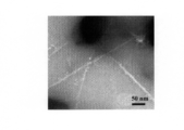
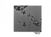
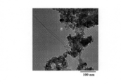
- 238000001000 micrograph Methods 0.000 description 29
- 239000002184 metal Substances 0.000 description 27
- 230000015572 biosynthetic process Effects 0.000 description 26
- 239000000872 buffer Substances 0.000 description 26
- 238000010586 diagram Methods 0.000 description 25
- 238000010438 heat treatment Methods 0.000 description 24
- 102100025450 DNA replication factor Cdt1 Human genes 0.000 description 23
- 101000914265 Homo sapiens DNA replication factor Cdt1 Proteins 0.000 description 23
- UFHFLCQGNIYNRP-UHFFFAOYSA-N Hydrogen Chemical compound [H][H] UFHFLCQGNIYNRP-UHFFFAOYSA-N 0.000 description 23
- QKNYBSVHEMOAJP-UHFFFAOYSA-N 2-amino-2-(hydroxymethyl)propane-1,3-diol;hydron;chloride Chemical compound Cl.OCC(N)(CO)CO QKNYBSVHEMOAJP-UHFFFAOYSA-N 0.000 description 21
- 229910010413 TiO 2 Inorganic materials 0.000 description 19
- 239000007853 buffer solution Substances 0.000 description 19
- 210000004899 c-terminal region Anatomy 0.000 description 19
- 230000001976 improved effect Effects 0.000 description 19
- 108091033319 polynucleotide Proteins 0.000 description 19
- 102000040430 polynucleotide Human genes 0.000 description 19
- 239000002157 polynucleotide Substances 0.000 description 19
- 239000012460 protein solution Substances 0.000 description 19
- FAPWRFPIFSIZLT-UHFFFAOYSA-M Sodium chloride Chemical compound [Na+].[Cl-] FAPWRFPIFSIZLT-UHFFFAOYSA-M 0.000 description 18
- 239000002773 nucleotide Substances 0.000 description 16
- 125000003729 nucleotide group Chemical group 0.000 description 16
- 238000006467 substitution reaction Methods 0.000 description 16
- 241000894006 Bacteria Species 0.000 description 15
- XEEYBQQBJWHFJM-UHFFFAOYSA-N Iron Chemical compound [Fe] XEEYBQQBJWHFJM-UHFFFAOYSA-N 0.000 description 15
- 239000004065 semiconductor Substances 0.000 description 15
- 238000000576 coating method Methods 0.000 description 14
- 229910052739 hydrogen Inorganic materials 0.000 description 14
- 239000001257 hydrogen Substances 0.000 description 14
- 239000006228 supernatant Substances 0.000 description 14
- 239000007864 aqueous solution Substances 0.000 description 13
- 239000002609 medium Substances 0.000 description 13
- 150000002736 metal compounds Chemical class 0.000 description 13
- 230000035772 mutation Effects 0.000 description 13
- 239000002245 particle Substances 0.000 description 13
- 239000012134 supernatant fraction Substances 0.000 description 13
- 238000009210 therapy by ultrasound Methods 0.000 description 13
- 235000001014 amino acid Nutrition 0.000 description 12
- 239000007788 liquid Substances 0.000 description 12
- 239000002105 nanoparticle Substances 0.000 description 12
- 239000008057 potassium phosphate buffer Substances 0.000 description 12
- 238000001556 precipitation Methods 0.000 description 12
- 239000003566 sealing material Substances 0.000 description 12
- XOLBLPGZBRYERU-UHFFFAOYSA-N tin dioxide Chemical compound O=[Sn]=O XOLBLPGZBRYERU-UHFFFAOYSA-N 0.000 description 12
- 229910001887 tin oxide Inorganic materials 0.000 description 12
- HSFWRNGVRCDJHI-UHFFFAOYSA-N alpha-acetylene Natural products C#C HSFWRNGVRCDJHI-UHFFFAOYSA-N 0.000 description 11
- 229940024606 amino acid Drugs 0.000 description 11
- 150000001413 amino acids Chemical group 0.000 description 11
- 239000012298 atmosphere Substances 0.000 description 11
- 239000011248 coating agent Substances 0.000 description 11
- 125000002534 ethynyl group Chemical group [H]C#C* 0.000 description 11
- 108020004414 DNA Proteins 0.000 description 10
- 241000186781 Listeria Species 0.000 description 10
- 239000003054 catalyst Substances 0.000 description 10
- 230000000694 effects Effects 0.000 description 10
- 238000002156 mixing Methods 0.000 description 10
- 239000000047 product Substances 0.000 description 10
- CSCPPACGZOOCGX-UHFFFAOYSA-N Acetone Chemical compound CC(C)=O CSCPPACGZOOCGX-UHFFFAOYSA-N 0.000 description 9
- 241000186216 Corynebacterium Species 0.000 description 9
- 238000005119 centrifugation Methods 0.000 description 9
- 239000002086 nanomaterial Substances 0.000 description 9
- 239000011780 sodium chloride Substances 0.000 description 9
- AVKUERGKIZMTKX-NJBDSQKTSA-N ampicillin Chemical compound C1([C@@H](N)C(=O)N[C@H]2[C@H]3SC([C@@H](N3C2=O)C(O)=O)(C)C)=CC=CC=C1 AVKUERGKIZMTKX-NJBDSQKTSA-N 0.000 description 8
- 229960000723 ampicillin Drugs 0.000 description 8
- 239000013078 crystal Substances 0.000 description 8
- 239000013612 plasmid Substances 0.000 description 8
- 229920000642 polymer Polymers 0.000 description 8
- 108091008146 restriction endonucleases Proteins 0.000 description 8
- 238000004626 scanning electron microscopy Methods 0.000 description 8
- LIVNPJMFVYWSIS-UHFFFAOYSA-N silicon monoxide Chemical compound [Si-]#[O+] LIVNPJMFVYWSIS-UHFFFAOYSA-N 0.000 description 8
- 239000000725 suspension Substances 0.000 description 8
- 239000013076 target substance Substances 0.000 description 8
- 238000004458 analytical method Methods 0.000 description 7
- 150000001875 compounds Chemical class 0.000 description 7
- 238000001816 cooling Methods 0.000 description 7
- 229910052742 iron Inorganic materials 0.000 description 7
- 125000005647 linker group Chemical group 0.000 description 7
- 229930182817 methionine Natural products 0.000 description 7
- 239000011259 mixed solution Substances 0.000 description 7
- 239000011368 organic material Substances 0.000 description 7
- 230000001590 oxidative effect Effects 0.000 description 7
- 235000012239 silicon dioxide Nutrition 0.000 description 7
- 238000000527 sonication Methods 0.000 description 7
- 238000010186 staining Methods 0.000 description 7
- 238000003786 synthesis reaction Methods 0.000 description 7
- 239000004408 titanium dioxide Substances 0.000 description 7
- 239000013598 vector Substances 0.000 description 7
- ZCYVEMRRCGMTRW-UHFFFAOYSA-N 7553-56-2 Chemical compound [I] ZCYVEMRRCGMTRW-UHFFFAOYSA-N 0.000 description 6
- WEVYAHXRMPXWCK-UHFFFAOYSA-N Acetonitrile Chemical compound CC#N WEVYAHXRMPXWCK-UHFFFAOYSA-N 0.000 description 6
- 238000008416 Ferritin Methods 0.000 description 6
- DHMQDGOQFOQNFH-UHFFFAOYSA-N Glycine Chemical compound NCC(O)=O DHMQDGOQFOQNFH-UHFFFAOYSA-N 0.000 description 6
- OKKJLVBELUTLKV-UHFFFAOYSA-N Methanol Chemical compound OC OKKJLVBELUTLKV-UHFFFAOYSA-N 0.000 description 6
- KJTLSVCANCCWHF-UHFFFAOYSA-N Ruthenium Chemical compound [Ru] KJTLSVCANCCWHF-UHFFFAOYSA-N 0.000 description 6
- HCHKCACWOHOZIP-UHFFFAOYSA-N Zinc Chemical compound [Zn] HCHKCACWOHOZIP-UHFFFAOYSA-N 0.000 description 6
- 239000000853 adhesive Substances 0.000 description 6
- 230000001070 adhesive effect Effects 0.000 description 6
- 230000008859 change Effects 0.000 description 6
- KZCYIWWNWWRLBQ-UHFFFAOYSA-P diazanium 3-methanidylbutan-2-one titanium(2+) dihydrate Chemical compound [NH4+].[NH4+].O.O.[Ti++].CC([CH2-])C([CH2-])=O.CC([CH2-])C([CH2-])=O KZCYIWWNWWRLBQ-UHFFFAOYSA-P 0.000 description 6
- 238000002149 energy-dispersive X-ray emission spectroscopy Methods 0.000 description 6
- 239000013604 expression vector Substances 0.000 description 6
- 239000011521 glass Substances 0.000 description 6
- 239000011630 iodine Substances 0.000 description 6
- 229910052740 iodine Inorganic materials 0.000 description 6
- 229910044991 metal oxide Inorganic materials 0.000 description 6
- 150000004706 metal oxides Chemical class 0.000 description 6
- 239000002114 nanocomposite Substances 0.000 description 6
- 230000003647 oxidation Effects 0.000 description 6
- 238000007254 oxidation reaction Methods 0.000 description 6
- 238000002360 preparation method Methods 0.000 description 6
- 235000004252 protein component Nutrition 0.000 description 6
- 238000000746 purification Methods 0.000 description 6
- 229910052707 ruthenium Inorganic materials 0.000 description 6
- 239000010409 thin film Substances 0.000 description 6
- LWIHDJKSTIGBAC-UHFFFAOYSA-K tripotassium phosphate Chemical compound [K+].[K+].[K+].[O-]P([O-])([O-])=O LWIHDJKSTIGBAC-UHFFFAOYSA-K 0.000 description 6
- 238000000108 ultra-filtration Methods 0.000 description 6
- 229910052725 zinc Inorganic materials 0.000 description 6
- 239000011701 zinc Substances 0.000 description 6
- JKMHFZQWWAIEOD-UHFFFAOYSA-N 2-[4-(2-hydroxyethyl)piperazin-1-yl]ethanesulfonic acid Chemical compound OCC[NH+]1CCN(CCS([O-])(=O)=O)CC1 JKMHFZQWWAIEOD-UHFFFAOYSA-N 0.000 description 5
- 239000007995 HEPES buffer Substances 0.000 description 5
- FFEARJCKVFRZRR-BYPYZUCNSA-N L-methionine Chemical compound CSCC[C@H](N)C(O)=O FFEARJCKVFRZRR-BYPYZUCNSA-N 0.000 description 5
- 238000002441 X-ray diffraction Methods 0.000 description 5
- 239000002253 acid Substances 0.000 description 5
- 238000010306 acid treatment Methods 0.000 description 5
- 239000003990 capacitor Substances 0.000 description 5
- 238000012790 confirmation Methods 0.000 description 5
- 230000001877 deodorizing effect Effects 0.000 description 5
- 238000000151 deposition Methods 0.000 description 5
- 229920006332 epoxy adhesive Polymers 0.000 description 5
- -1 hydroxide ions Chemical class 0.000 description 5
- 229910003437 indium oxide Inorganic materials 0.000 description 5
- PJXISJQVUVHSOJ-UHFFFAOYSA-N indium(iii) oxide Chemical compound [O-2].[O-2].[O-2].[In+3].[In+3] PJXISJQVUVHSOJ-UHFFFAOYSA-N 0.000 description 5
- 239000008204 material by function Substances 0.000 description 5
- 239000002073 nanorod Substances 0.000 description 5
- 239000000843 powder Substances 0.000 description 5
- 239000010453 quartz Substances 0.000 description 5
- 238000000926 separation method Methods 0.000 description 5
- 150000003377 silicon compounds Chemical class 0.000 description 5
- 239000002904 solvent Substances 0.000 description 5
- XJDNKRIXUMDJCW-UHFFFAOYSA-J titanium tetrachloride Chemical compound Cl[Ti](Cl)(Cl)Cl XJDNKRIXUMDJCW-UHFFFAOYSA-J 0.000 description 5
- DNYWZCXLKNTFFI-UHFFFAOYSA-N uranium Chemical compound [U][U][U][U][U][U][U][U][U][U][U][U][U][U][U][U][U][U][U][U][U][U][U][U][U][U][U][U][U][U][U][U][U][U][U][U][U][U][U][U][U][U][U][U][U][U][U][U][U][U][U][U][U][U][U][U][U][U][U][U][U][U][U][U][U][U][U][U][U][U][U][U][U][U][U][U][U][U][U][U][U][U][U][U][U][U][U][U][U][U][U][U][U][U][U][U][U][U][U][U][U][U][U][U][U][U][U][U][U][U][U][U][U][U] DNYWZCXLKNTFFI-UHFFFAOYSA-N 0.000 description 5
- 229910052724 xenon Inorganic materials 0.000 description 5
- FHNFHKCVQCLJFQ-UHFFFAOYSA-N xenon atom Chemical compound [Xe] FHNFHKCVQCLJFQ-UHFFFAOYSA-N 0.000 description 5
- NWONKYPBYAMBJT-UHFFFAOYSA-L zinc sulfate Chemical compound [Zn+2].[O-]S([O-])(=O)=O NWONKYPBYAMBJT-UHFFFAOYSA-L 0.000 description 5
- 229910000368 zinc sulfate Inorganic materials 0.000 description 5
- 229960001763 zinc sulfate Drugs 0.000 description 5
- OYPRJOBELJOOCE-UHFFFAOYSA-N Calcium Chemical compound [Ca] OYPRJOBELJOOCE-UHFFFAOYSA-N 0.000 description 4
- VTYYLEPIZMXCLO-UHFFFAOYSA-L Calcium carbonate Chemical compound [Ca+2].[O-]C([O-])=O VTYYLEPIZMXCLO-UHFFFAOYSA-L 0.000 description 4
- 241000186226 Corynebacterium glutamicum Species 0.000 description 4
- 102000012410 DNA Ligases Human genes 0.000 description 4
- 108010061982 DNA Ligases Proteins 0.000 description 4
- COLNVLDHVKWLRT-QMMMGPOBSA-N L-phenylalanine Chemical compound OC(=O)[C@@H](N)CC1=CC=CC=C1 COLNVLDHVKWLRT-QMMMGPOBSA-N 0.000 description 4
- 108091034117 Oligonucleotide Proteins 0.000 description 4
- QAOWNCQODCNURD-UHFFFAOYSA-N Sulfuric acid Chemical compound OS(O)(=O)=O QAOWNCQODCNURD-UHFFFAOYSA-N 0.000 description 4
- 230000009471 action Effects 0.000 description 4
- 230000000844 anti-bacterial effect Effects 0.000 description 4
- 230000003373 anti-fouling effect Effects 0.000 description 4
- YHWCPXVTRSHPNY-UHFFFAOYSA-N butan-1-olate;titanium(4+) Chemical compound [Ti+4].CCCC[O-].CCCC[O-].CCCC[O-].CCCC[O-] YHWCPXVTRSHPNY-UHFFFAOYSA-N 0.000 description 4
- 229910052791 calcium Inorganic materials 0.000 description 4
- 239000011575 calcium Substances 0.000 description 4
- 239000007789 gas Substances 0.000 description 4
- AMWRITDGCCNYAT-UHFFFAOYSA-L hydroxy(oxo)manganese;manganese Chemical compound [Mn].O[Mn]=O.O[Mn]=O AMWRITDGCCNYAT-UHFFFAOYSA-L 0.000 description 4
- 230000001678 irradiating effect Effects 0.000 description 4
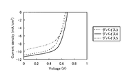
- 238000005259 measurement Methods 0.000 description 4
- 150000002739 metals Chemical class 0.000 description 4
- COLNVLDHVKWLRT-UHFFFAOYSA-N phenylalanine Natural products OC(=O)C(N)CC1=CC=CC=C1 COLNVLDHVKWLRT-UHFFFAOYSA-N 0.000 description 4
- 239000008363 phosphate buffer Substances 0.000 description 4
- 238000012545 processing Methods 0.000 description 4
- GQUJEMVIKWQAEH-UHFFFAOYSA-N titanium(III) oxide Chemical compound O=[Ti]O[Ti]=O GQUJEMVIKWQAEH-UHFFFAOYSA-N 0.000 description 4
- VXUYXOFXAQZZMF-UHFFFAOYSA-N titanium(IV) isopropoxide Chemical compound CC(C)O[Ti](OC(C)C)(OC(C)C)OC(C)C VXUYXOFXAQZZMF-UHFFFAOYSA-N 0.000 description 4
- 239000011800 void material Substances 0.000 description 4
- QGZKDVFQNNGYKY-UHFFFAOYSA-O Ammonium Chemical compound [NH4+] QGZKDVFQNNGYKY-UHFFFAOYSA-O 0.000 description 3
- UHOVQNZJYSORNB-UHFFFAOYSA-N Benzene Chemical compound C1=CC=CC=C1 UHOVQNZJYSORNB-UHFFFAOYSA-N 0.000 description 3
- 101710082494 DNA protection during starvation protein Proteins 0.000 description 3
- RTZKZFJDLAIYFH-UHFFFAOYSA-N Diethyl ether Chemical compound CCOCC RTZKZFJDLAIYFH-UHFFFAOYSA-N 0.000 description 3
- 241000588722 Escherichia Species 0.000 description 3
- XEKOWRVHYACXOJ-UHFFFAOYSA-N Ethyl acetate Chemical compound CCOC(C)=O XEKOWRVHYACXOJ-UHFFFAOYSA-N 0.000 description 3
- WSFSSNUMVMOOMR-UHFFFAOYSA-N Formaldehyde Chemical compound O=C WSFSSNUMVMOOMR-UHFFFAOYSA-N 0.000 description 3
- 239000004471 Glycine Substances 0.000 description 3
- QNAYBMKLOCPYGJ-REOHCLBHSA-N L-alanine Chemical compound C[C@H](N)C(O)=O QNAYBMKLOCPYGJ-REOHCLBHSA-N 0.000 description 3
- HNDVDQJCIGZPNO-YFKPBYRVSA-N L-histidine Chemical compound OC(=O)[C@@H](N)CC1=CN=CN1 HNDVDQJCIGZPNO-YFKPBYRVSA-N 0.000 description 3
- AGPKZVBTJJNPAG-WHFBIAKZSA-N L-isoleucine Chemical compound CC[C@H](C)[C@H](N)C(O)=O AGPKZVBTJJNPAG-WHFBIAKZSA-N 0.000 description 3
- QIVBCDIJIAJPQS-VIFPVBQESA-N L-tryptophane Chemical compound C1=CC=C2C(C[C@H](N)C(O)=O)=CNC2=C1 QIVBCDIJIAJPQS-VIFPVBQESA-N 0.000 description 3
- OUYCCCASQSFEME-QMMMGPOBSA-N L-tyrosine Chemical compound OC(=O)[C@@H](N)CC1=CC=C(O)C=C1 OUYCCCASQSFEME-QMMMGPOBSA-N 0.000 description 3
- KZSNJWFQEVHDMF-BYPYZUCNSA-N L-valine Chemical compound CC(C)[C@H](N)C(O)=O KZSNJWFQEVHDMF-BYPYZUCNSA-N 0.000 description 3
- 241000186805 Listeria innocua Species 0.000 description 3
- 239000012614 Q-Sepharose Substances 0.000 description 3
- 229910004298 SiO 2 Inorganic materials 0.000 description 3
- 241000194017 Streptococcus Species 0.000 description 3
- 238000003917 TEM image Methods 0.000 description 3
- LCKIEQZJEYYRIY-UHFFFAOYSA-N Titanium ion Chemical compound [Ti+4] LCKIEQZJEYYRIY-UHFFFAOYSA-N 0.000 description 3
- QIVBCDIJIAJPQS-UHFFFAOYSA-N Tryptophan Natural products C1=CC=C2C(CC(N)C(O)=O)=CNC2=C1 QIVBCDIJIAJPQS-UHFFFAOYSA-N 0.000 description 3
- KZSNJWFQEVHDMF-UHFFFAOYSA-N Valine Natural products CC(C)C(N)C(O)=O KZSNJWFQEVHDMF-UHFFFAOYSA-N 0.000 description 3
- 239000005083 Zinc sulfide Substances 0.000 description 3
- JLCPHMBAVCMARE-UHFFFAOYSA-N [3-[[3-[[3-[[3-[[3-[[3-[[3-[[3-[[3-[[3-[[3-[[5-(2-amino-6-oxo-1H-purin-9-yl)-3-[[3-[[3-[[3-[[3-[[3-[[5-(2-amino-6-oxo-1H-purin-9-yl)-3-[[5-(2-amino-6-oxo-1H-purin-9-yl)-3-hydroxyoxolan-2-yl]methoxy-hydroxyphosphoryl]oxyoxolan-2-yl]methoxy-hydroxyphosphoryl]oxy-5-(5-methyl-2,4-dioxopyrimidin-1-yl)oxolan-2-yl]methoxy-hydroxyphosphoryl]oxy-5-(6-aminopurin-9-yl)oxolan-2-yl]methoxy-hydroxyphosphoryl]oxy-5-(6-aminopurin-9-yl)oxolan-2-yl]methoxy-hydroxyphosphoryl]oxy-5-(6-aminopurin-9-yl)oxolan-2-yl]methoxy-hydroxyphosphoryl]oxy-5-(6-aminopurin-9-yl)oxolan-2-yl]methoxy-hydroxyphosphoryl]oxyoxolan-2-yl]methoxy-hydroxyphosphoryl]oxy-5-(5-methyl-2,4-dioxopyrimidin-1-yl)oxolan-2-yl]methoxy-hydroxyphosphoryl]oxy-5-(4-amino-2-oxopyrimidin-1-yl)oxolan-2-yl]methoxy-hydroxyphosphoryl]oxy-5-(5-methyl-2,4-dioxopyrimidin-1-yl)oxolan-2-yl]methoxy-hydroxyphosphoryl]oxy-5-(5-methyl-2,4-dioxopyrimidin-1-yl)oxolan-2-yl]methoxy-hydroxyphosphoryl]oxy-5-(6-aminopurin-9-yl)oxolan-2-yl]methoxy-hydroxyphosphoryl]oxy-5-(6-aminopurin-9-yl)oxolan-2-yl]methoxy-hydroxyphosphoryl]oxy-5-(4-amino-2-oxopyrimidin-1-yl)oxolan-2-yl]methoxy-hydroxyphosphoryl]oxy-5-(4-amino-2-oxopyrimidin-1-yl)oxolan-2-yl]methoxy-hydroxyphosphoryl]oxy-5-(4-amino-2-oxopyrimidin-1-yl)oxolan-2-yl]methoxy-hydroxyphosphoryl]oxy-5-(6-aminopurin-9-yl)oxolan-2-yl]methoxy-hydroxyphosphoryl]oxy-5-(4-amino-2-oxopyrimidin-1-yl)oxolan-2-yl]methyl [5-(6-aminopurin-9-yl)-2-(hydroxymethyl)oxolan-3-yl] hydrogen phosphate Polymers Cc1cn(C2CC(OP(O)(=O)OCC3OC(CC3OP(O)(=O)OCC3OC(CC3O)n3cnc4c3nc(N)[nH]c4=O)n3cnc4c3nc(N)[nH]c4=O)C(COP(O)(=O)OC3CC(OC3COP(O)(=O)OC3CC(OC3COP(O)(=O)OC3CC(OC3COP(O)(=O)OC3CC(OC3COP(O)(=O)OC3CC(OC3COP(O)(=O)OC3CC(OC3COP(O)(=O)OC3CC(OC3COP(O)(=O)OC3CC(OC3COP(O)(=O)OC3CC(OC3COP(O)(=O)OC3CC(OC3COP(O)(=O)OC3CC(OC3COP(O)(=O)OC3CC(OC3COP(O)(=O)OC3CC(OC3COP(O)(=O)OC3CC(OC3COP(O)(=O)OC3CC(OC3COP(O)(=O)OC3CC(OC3COP(O)(=O)OC3CC(OC3CO)n3cnc4c(N)ncnc34)n3ccc(N)nc3=O)n3cnc4c(N)ncnc34)n3ccc(N)nc3=O)n3ccc(N)nc3=O)n3ccc(N)nc3=O)n3cnc4c(N)ncnc34)n3cnc4c(N)ncnc34)n3cc(C)c(=O)[nH]c3=O)n3cc(C)c(=O)[nH]c3=O)n3ccc(N)nc3=O)n3cc(C)c(=O)[nH]c3=O)n3cnc4c3nc(N)[nH]c4=O)n3cnc4c(N)ncnc34)n3cnc4c(N)ncnc34)n3cnc4c(N)ncnc34)n3cnc4c(N)ncnc34)O2)c(=O)[nH]c1=O JLCPHMBAVCMARE-UHFFFAOYSA-N 0.000 description 3
- 238000010521 absorption reaction Methods 0.000 description 3
- 238000004887 air purification Methods 0.000 description 3
- 235000004279 alanine Nutrition 0.000 description 3
- 229910052793 cadmium Inorganic materials 0.000 description 3
- BDOSMKKIYDKNTQ-UHFFFAOYSA-N cadmium atom Chemical compound [Cd] BDOSMKKIYDKNTQ-UHFFFAOYSA-N 0.000 description 3
- 239000000969 carrier Substances 0.000 description 3
- 230000003197 catalytic effect Effects 0.000 description 3
- 239000004020 conductor Substances 0.000 description 3
- 239000002612 dispersion medium Substances 0.000 description 3
- 238000001035 drying Methods 0.000 description 3
- 239000013613 expression plasmid Substances 0.000 description 3
- IMBKASBLAKCLEM-UHFFFAOYSA-L ferrous ammonium sulfate (anhydrous) Chemical compound [NH4+].[NH4+].[Fe+2].[O-]S([O-])(=O)=O.[O-]S([O-])(=O)=O IMBKASBLAKCLEM-UHFFFAOYSA-L 0.000 description 3
- 239000000446 fuel Substances 0.000 description 3
- YBMRDBCBODYGJE-UHFFFAOYSA-N germanium oxide Inorganic materials O=[Ge]=O YBMRDBCBODYGJE-UHFFFAOYSA-N 0.000 description 3
- HNDVDQJCIGZPNO-UHFFFAOYSA-N histidine Natural products OC(=O)C(N)CC1=CN=CN1 HNDVDQJCIGZPNO-UHFFFAOYSA-N 0.000 description 3
- 230000002209 hydrophobic effect Effects 0.000 description 3
- AGPKZVBTJJNPAG-UHFFFAOYSA-N isoleucine Natural products CCC(C)C(N)C(O)=O AGPKZVBTJJNPAG-UHFFFAOYSA-N 0.000 description 3
- 229960000310 isoleucine Drugs 0.000 description 3
- 230000031700 light absorption Effects 0.000 description 3
- 230000033001 locomotion Effects 0.000 description 3
- 244000005700 microbiome Species 0.000 description 3
- 239000000178 monomer Substances 0.000 description 3
- VLKZOEOYAKHREP-UHFFFAOYSA-N n-Hexane Chemical compound CCCCCC VLKZOEOYAKHREP-UHFFFAOYSA-N 0.000 description 3
- 230000003287 optical effect Effects 0.000 description 3
- 229920000620 organic polymer Polymers 0.000 description 3
- PVADDRMAFCOOPC-UHFFFAOYSA-N oxogermanium Chemical compound [Ge]=O PVADDRMAFCOOPC-UHFFFAOYSA-N 0.000 description 3
- IYDGMDWEHDFVQI-UHFFFAOYSA-N phosphoric acid;trioxotungsten Chemical compound O=[W](=O)=O.O=[W](=O)=O.O=[W](=O)=O.O=[W](=O)=O.O=[W](=O)=O.O=[W](=O)=O.O=[W](=O)=O.O=[W](=O)=O.O=[W](=O)=O.O=[W](=O)=O.O=[W](=O)=O.O=[W](=O)=O.OP(O)(O)=O IYDGMDWEHDFVQI-UHFFFAOYSA-N 0.000 description 3
- 150000004032 porphyrins Chemical class 0.000 description 3
- 229910000160 potassium phosphate Inorganic materials 0.000 description 3
- 235000011009 potassium phosphates Nutrition 0.000 description 3
- 150000003839 salts Chemical class 0.000 description 3
- ZNJHFNUEQDVFCJ-UHFFFAOYSA-M sodium;2-[4-(2-hydroxyethyl)piperazin-1-yl]ethanesulfonic acid;hydroxide Chemical compound [OH-].[Na+].OCCN1CCN(CCS(O)(=O)=O)CC1 ZNJHFNUEQDVFCJ-UHFFFAOYSA-M 0.000 description 3
- 238000003860 storage Methods 0.000 description 3
- 239000004094 surface-active agent Substances 0.000 description 3
- JMXKSZRRTHPKDL-UHFFFAOYSA-N titanium ethoxide Chemical compound [Ti+4].CC[O-].CC[O-].CC[O-].CC[O-] JMXKSZRRTHPKDL-UHFFFAOYSA-N 0.000 description 3
- 238000002834 transmittance Methods 0.000 description 3
- OUYCCCASQSFEME-UHFFFAOYSA-N tyrosine Natural products OC(=O)C(N)CC1=CC=C(O)C=C1 OUYCCCASQSFEME-UHFFFAOYSA-N 0.000 description 3
- 239000004474 valine Substances 0.000 description 3
- 150000003752 zinc compounds Chemical class 0.000 description 3
- UGZADUVQMDAIAO-UHFFFAOYSA-L zinc hydroxide Chemical compound [OH-].[OH-].[Zn+2] UGZADUVQMDAIAO-UHFFFAOYSA-L 0.000 description 3
- 229910021511 zinc hydroxide Inorganic materials 0.000 description 3
- 229940007718 zinc hydroxide Drugs 0.000 description 3
- 229910052984 zinc sulfide Inorganic materials 0.000 description 3
- DRDVZXDWVBGGMH-UHFFFAOYSA-N zinc;sulfide Chemical compound [S-2].[Zn+2] DRDVZXDWVBGGMH-UHFFFAOYSA-N 0.000 description 3
- 108091032973 (ribonucleotides)n+m Proteins 0.000 description 2
- AZQWKYJCGOJGHM-UHFFFAOYSA-N 1,4-benzoquinone Chemical compound O=C1C=CC(=O)C=C1 AZQWKYJCGOJGHM-UHFFFAOYSA-N 0.000 description 2
- BSGHSLDKEDDYHI-UHFFFAOYSA-N 3-(2-ethylhexoxymethyl)heptane;titanium Chemical compound [Ti].CCCCC(CC)COCC(CC)CCCC BSGHSLDKEDDYHI-UHFFFAOYSA-N 0.000 description 2
- FWMNVWWHGCHHJJ-SKKKGAJSSA-N 4-amino-1-[(2r)-6-amino-2-[[(2r)-2-[[(2r)-2-[[(2r)-2-amino-3-phenylpropanoyl]amino]-3-phenylpropanoyl]amino]-4-methylpentanoyl]amino]hexanoyl]piperidine-4-carboxylic acid Chemical compound C([C@H](C(=O)N[C@H](CC(C)C)C(=O)N[C@H](CCCCN)C(=O)N1CCC(N)(CC1)C(O)=O)NC(=O)[C@H](N)CC=1C=CC=CC=1)C1=CC=CC=C1 FWMNVWWHGCHHJJ-SKKKGAJSSA-N 0.000 description 2
- IKHGUXGNUITLKF-UHFFFAOYSA-N Acetaldehyde Chemical compound CC=O IKHGUXGNUITLKF-UHFFFAOYSA-N 0.000 description 2
- QGZKDVFQNNGYKY-UHFFFAOYSA-N Ammonia Chemical compound N QGZKDVFQNNGYKY-UHFFFAOYSA-N 0.000 description 2
- 101100325749 Antirrhinum majus BALDH gene Proteins 0.000 description 2
- 239000004475 Arginine Substances 0.000 description 2
- JBRZTFJDHDCESZ-UHFFFAOYSA-N AsGa Chemical compound [As]#[Ga] JBRZTFJDHDCESZ-UHFFFAOYSA-N 0.000 description 2
- IJGRMHOSHXDMSA-UHFFFAOYSA-N Atomic nitrogen Chemical compound N#N IJGRMHOSHXDMSA-UHFFFAOYSA-N 0.000 description 2
- 241000193830 Bacillus <bacterium> Species 0.000 description 2
- 244000063299 Bacillus subtilis Species 0.000 description 2
- 235000014469 Bacillus subtilis Nutrition 0.000 description 2
- 241000589968 Borrelia Species 0.000 description 2
- 241000589562 Brucella Species 0.000 description 2
- 241000589876 Campylobacter Species 0.000 description 2
- HEDRZPFGACZZDS-UHFFFAOYSA-N Chloroform Chemical compound ClC(Cl)Cl HEDRZPFGACZZDS-UHFFFAOYSA-N 0.000 description 2
- QPLDLSVMHZLSFG-UHFFFAOYSA-N Copper oxide Chemical compound [Cu]=O QPLDLSVMHZLSFG-UHFFFAOYSA-N 0.000 description 2
- 239000005751 Copper oxide Substances 0.000 description 2
- 241000192093 Deinococcus Species 0.000 description 2
- GYHNNYVSQQEPJS-UHFFFAOYSA-N Gallium Chemical compound [Ga] GYHNNYVSQQEPJS-UHFFFAOYSA-N 0.000 description 2
- 229910001218 Gallium arsenide Inorganic materials 0.000 description 2
- WHUUTDBJXJRKMK-UHFFFAOYSA-N Glutamic acid Natural products OC(=O)C(N)CCC(O)=O WHUUTDBJXJRKMK-UHFFFAOYSA-N 0.000 description 2
- 239000006173 Good's buffer Substances 0.000 description 2
- MHAJPDPJQMAIIY-UHFFFAOYSA-N Hydrogen peroxide Chemical compound OO MHAJPDPJQMAIIY-UHFFFAOYSA-N 0.000 description 2
- XUJNEKJLAYXESH-REOHCLBHSA-N L-Cysteine Chemical compound SC[C@H](N)C(O)=O XUJNEKJLAYXESH-REOHCLBHSA-N 0.000 description 2
- ODKSFYDXXFIFQN-BYPYZUCNSA-P L-argininium(2+) Chemical compound NC(=[NH2+])NCCC[C@H]([NH3+])C(O)=O ODKSFYDXXFIFQN-BYPYZUCNSA-P 0.000 description 2
- CKLJMWTZIZZHCS-REOHCLBHSA-N L-aspartic acid Chemical compound OC(=O)[C@@H](N)CC(O)=O CKLJMWTZIZZHCS-REOHCLBHSA-N 0.000 description 2
- WHUUTDBJXJRKMK-VKHMYHEASA-N L-glutamic acid Chemical compound OC(=O)[C@@H](N)CCC(O)=O WHUUTDBJXJRKMK-VKHMYHEASA-N 0.000 description 2
- ROHFNLRQFUQHCH-YFKPBYRVSA-N L-leucine Chemical compound CC(C)C[C@H](N)C(O)=O ROHFNLRQFUQHCH-YFKPBYRVSA-N 0.000 description 2
- KDXKERNSBIXSRK-YFKPBYRVSA-N L-lysine Chemical compound NCCCC[C@H](N)C(O)=O KDXKERNSBIXSRK-YFKPBYRVSA-N 0.000 description 2
- AYFVYJQAPQTCCC-GBXIJSLDSA-N L-threonine Chemical compound C[C@@H](O)[C@H](N)C(O)=O AYFVYJQAPQTCCC-GBXIJSLDSA-N 0.000 description 2
- ROHFNLRQFUQHCH-UHFFFAOYSA-N Leucine Natural products CC(C)CC(N)C(O)=O ROHFNLRQFUQHCH-UHFFFAOYSA-N 0.000 description 2
- 208000016604 Lyme disease Diseases 0.000 description 2
- KDXKERNSBIXSRK-UHFFFAOYSA-N Lysine Natural products NCCCCC(N)C(O)=O KDXKERNSBIXSRK-UHFFFAOYSA-N 0.000 description 2
- 239000004472 Lysine Substances 0.000 description 2
- 241000186359 Mycobacterium Species 0.000 description 2
- 241000187480 Mycobacterium smegmatis Species 0.000 description 2
- 108091028043 Nucleic acid sequence Proteins 0.000 description 2
- 102000015636 Oligopeptides Human genes 0.000 description 2
- 108010038807 Oligopeptides Proteins 0.000 description 2
- 229920003171 Poly (ethylene oxide) Polymers 0.000 description 2
- 239000004793 Polystyrene Substances 0.000 description 2
- MTCFGRXMJLQNBG-UHFFFAOYSA-N Serine Natural products OCC(N)C(O)=O MTCFGRXMJLQNBG-UHFFFAOYSA-N 0.000 description 2
- BLRPTPMANUNPDV-UHFFFAOYSA-N Silane Chemical compound [SiH4] BLRPTPMANUNPDV-UHFFFAOYSA-N 0.000 description 2
- 229910006404 SnO 2 Inorganic materials 0.000 description 2
- 241000191940 Staphylococcus Species 0.000 description 2
- 241000193996 Streptococcus pyogenes Species 0.000 description 2
- PPBRXRYQALVLMV-UHFFFAOYSA-N Styrene Chemical compound C=CC1=CC=CC=C1 PPBRXRYQALVLMV-UHFFFAOYSA-N 0.000 description 2
- WYURNTSHIVDZCO-UHFFFAOYSA-N Tetrahydrofuran Chemical compound C1CCOC1 WYURNTSHIVDZCO-UHFFFAOYSA-N 0.000 description 2
- AYFVYJQAPQTCCC-UHFFFAOYSA-N Threonine Natural products CC(O)C(N)C(O)=O AYFVYJQAPQTCCC-UHFFFAOYSA-N 0.000 description 2
- 239000004473 Threonine Substances 0.000 description 2
- WGLPBDUCMAPZCE-UHFFFAOYSA-N Trioxochromium Chemical compound O=[Cr](=O)=O WGLPBDUCMAPZCE-UHFFFAOYSA-N 0.000 description 2
- 241000607598 Vibrio Species 0.000 description 2
- 229910021536 Zeolite Inorganic materials 0.000 description 2
- CMHKGULXIWIGBU-UHFFFAOYSA-N [Fe].[Pt] Chemical compound [Fe].[Pt] CMHKGULXIWIGBU-UHFFFAOYSA-N 0.000 description 2
- SAXPPRUNTRNAIO-UHFFFAOYSA-N [O-2].[O-2].[Ca+2].[Mn+2] Chemical compound [O-2].[O-2].[Ca+2].[Mn+2] SAXPPRUNTRNAIO-UHFFFAOYSA-N 0.000 description 2
- 238000007792 addition Methods 0.000 description 2
- GGKQIOFASHYUJZ-UHFFFAOYSA-N ametoctradin Chemical compound NC1=C(CCCCCCCC)C(CC)=NC2=NC=NN21 GGKQIOFASHYUJZ-UHFFFAOYSA-N 0.000 description 2
- 238000005571 anion exchange chromatography Methods 0.000 description 2
- ODKSFYDXXFIFQN-UHFFFAOYSA-N arginine Natural products OC(=O)C(N)CCCNC(N)=N ODKSFYDXXFIFQN-UHFFFAOYSA-N 0.000 description 2
- 235000003704 aspartic acid Nutrition 0.000 description 2
- 230000001580 bacterial effect Effects 0.000 description 2
- OQFSQFPPLPISGP-UHFFFAOYSA-N beta-carboxyaspartic acid Natural products OC(=O)C(N)C(C(O)=O)C(O)=O OQFSQFPPLPISGP-UHFFFAOYSA-N 0.000 description 2
- 239000012620 biological material Substances 0.000 description 2
- RPPBZEBXAAZZJH-UHFFFAOYSA-N cadmium telluride Chemical compound [Te]=[Cd] RPPBZEBXAAZZJH-UHFFFAOYSA-N 0.000 description 2
- 238000001354 calcination Methods 0.000 description 2
- 229910000019 calcium carbonate Inorganic materials 0.000 description 2
- 238000004422 calculation algorithm Methods 0.000 description 2
- 150000001720 carbohydrates Chemical class 0.000 description 2
- 235000014633 carbohydrates Nutrition 0.000 description 2
- 150000004649 carbonic acid derivatives Chemical class 0.000 description 2
- 150000001244 carboxylic acid anhydrides Chemical group 0.000 description 2
- 125000002843 carboxylic acid group Chemical group 0.000 description 2
- 239000000919 ceramic Substances 0.000 description 2
- 150000001805 chlorine compounds Chemical class 0.000 description 2
- 229910000423 chromium oxide Inorganic materials 0.000 description 2
- 229920001940 conductive polymer Polymers 0.000 description 2
- 229910000431 copper oxide Inorganic materials 0.000 description 2
- XUJNEKJLAYXESH-UHFFFAOYSA-N cysteine Natural products SCC(N)C(O)=O XUJNEKJLAYXESH-UHFFFAOYSA-N 0.000 description 2
- 235000018417 cysteine Nutrition 0.000 description 2
- 230000007423 decrease Effects 0.000 description 2
- 238000012217 deletion Methods 0.000 description 2
- 230000037430 deletion Effects 0.000 description 2
- 230000008021 deposition Effects 0.000 description 2
- 229910001873 dinitrogen Inorganic materials 0.000 description 2
- HNPSIPDUKPIQMN-UHFFFAOYSA-N dioxosilane;oxo(oxoalumanyloxy)alumane Chemical compound O=[Si]=O.O=[Al]O[Al]=O HNPSIPDUKPIQMN-UHFFFAOYSA-N 0.000 description 2
- 229940079593 drug Drugs 0.000 description 2
- 239000003814 drug Substances 0.000 description 2
- 239000003792 electrolyte Substances 0.000 description 2
- 150000004673 fluoride salts Chemical class 0.000 description 2
- 229910052733 gallium Inorganic materials 0.000 description 2
- 229910052732 germanium Inorganic materials 0.000 description 2
- GNPVGFCGXDBREM-UHFFFAOYSA-N germanium atom Chemical compound [Ge] GNPVGFCGXDBREM-UHFFFAOYSA-N 0.000 description 2
- 235000013922 glutamic acid Nutrition 0.000 description 2
- 239000004220 glutamic acid Substances 0.000 description 2
- 150000004676 glycans Chemical class 0.000 description 2
- 229910052735 hafnium Inorganic materials 0.000 description 2
- VBJZVLUMGGDVMO-UHFFFAOYSA-N hafnium atom Chemical compound [Hf] VBJZVLUMGGDVMO-UHFFFAOYSA-N 0.000 description 2
- 229910000449 hafnium oxide Inorganic materials 0.000 description 2
- WIHZLLGSGQNAGK-UHFFFAOYSA-N hafnium(4+);oxygen(2-) Chemical compound [O-2].[O-2].[Hf+4] WIHZLLGSGQNAGK-UHFFFAOYSA-N 0.000 description 2
- 125000002887 hydroxy group Chemical group [H]O* 0.000 description 2
- AMGQUBHHOARCQH-UHFFFAOYSA-N indium;oxotin Chemical compound [In].[Sn]=O AMGQUBHHOARCQH-UHFFFAOYSA-N 0.000 description 2
- 238000003780 insertion Methods 0.000 description 2
- 230000037431 insertion Effects 0.000 description 2
- 229910000765 intermetallic Inorganic materials 0.000 description 2
- 150000004694 iodide salts Chemical class 0.000 description 2
- 239000011133 lead Substances 0.000 description 2
- 229910000464 lead oxide Inorganic materials 0.000 description 2
- 229910052981 lead sulfide Inorganic materials 0.000 description 2
- 229940056932 lead sulfide Drugs 0.000 description 2
- VJPLIHZPOJDHLB-UHFFFAOYSA-N lead titanium Chemical compound [Ti].[Pb] VJPLIHZPOJDHLB-UHFFFAOYSA-N 0.000 description 2
- 150000002632 lipids Chemical class 0.000 description 2
- HSZCZNFXUDYRKD-UHFFFAOYSA-M lithium iodide Chemical compound [Li+].[I-] HSZCZNFXUDYRKD-UHFFFAOYSA-M 0.000 description 2
- 239000000696 magnetic material Substances 0.000 description 2
- 239000003550 marker Substances 0.000 description 2
- 230000001404 mediated effect Effects 0.000 description 2
- 238000002844 melting Methods 0.000 description 2
- 230000008018 melting Effects 0.000 description 2
- 125000001360 methionine group Chemical group N[C@@H](CCSC)C(=O)* 0.000 description 2
- 238000012986 modification Methods 0.000 description 2
- 230000004048 modification Effects 0.000 description 2
- 150000002772 monosaccharides Chemical class 0.000 description 2
- KELHQGOVULCJSG-UHFFFAOYSA-N n,n-dimethyl-1-(5-methylfuran-2-yl)ethane-1,2-diamine Chemical compound CN(C)C(CN)C1=CC=C(C)O1 KELHQGOVULCJSG-UHFFFAOYSA-N 0.000 description 2
- 102000039446 nucleic acids Human genes 0.000 description 2
- 108020004707 nucleic acids Proteins 0.000 description 2
- 150000007523 nucleic acids Chemical class 0.000 description 2
- 239000002777 nucleoside Substances 0.000 description 2
- 229920001542 oligosaccharide Polymers 0.000 description 2
- 150000002482 oligosaccharides Chemical class 0.000 description 2
- TWNQGVIAIRXVLR-UHFFFAOYSA-N oxo(oxoalumanyloxy)alumane Chemical compound O=[Al]O[Al]=O TWNQGVIAIRXVLR-UHFFFAOYSA-N 0.000 description 2
- YEXPOXQUZXUXJW-UHFFFAOYSA-N oxolead Chemical compound [Pb]=O YEXPOXQUZXUXJW-UHFFFAOYSA-N 0.000 description 2
- KYKLWYKWCAYAJY-UHFFFAOYSA-N oxotin;zinc Chemical compound [Zn].[Sn]=O KYKLWYKWCAYAJY-UHFFFAOYSA-N 0.000 description 2
- 239000011941 photocatalyst Substances 0.000 description 2
- 229920001432 poly(L-lactide) Polymers 0.000 description 2
- 229910021420 polycrystalline silicon Inorganic materials 0.000 description 2
- 229920001282 polysaccharide Polymers 0.000 description 2
- 239000005017 polysaccharide Substances 0.000 description 2
- 229920005591 polysilicon Polymers 0.000 description 2
- 229920000136 polysorbate Polymers 0.000 description 2
- 229920002223 polystyrene Polymers 0.000 description 2
- 238000003825 pressing Methods 0.000 description 2
- 239000002096 quantum dot Substances 0.000 description 2
- 150000003254 radicals Chemical class 0.000 description 2
- 230000035484 reaction time Effects 0.000 description 2
- 229920005989 resin Polymers 0.000 description 2
- 239000011347 resin Substances 0.000 description 2
- 230000000717 retained effect Effects 0.000 description 2
- 238000002864 sequence alignment Methods 0.000 description 2
- 229910000077 silane Inorganic materials 0.000 description 2
- 150000003376 silicon Chemical class 0.000 description 2
- HBMJWWWQQXIZIP-UHFFFAOYSA-N silicon carbide Chemical compound [Si+]#[C-] HBMJWWWQQXIZIP-UHFFFAOYSA-N 0.000 description 2
- 239000000377 silicon dioxide Substances 0.000 description 2
- 229920002379 silicone rubber Polymers 0.000 description 2
- 239000004945 silicone rubber Substances 0.000 description 2
- 238000001179 sorption measurement Methods 0.000 description 2
- 238000003756 stirring Methods 0.000 description 2
- 150000004763 sulfides Chemical class 0.000 description 2
- 229910052714 tellurium Inorganic materials 0.000 description 2
- PORWMNRCUJJQNO-UHFFFAOYSA-N tellurium atom Chemical compound [Te] PORWMNRCUJJQNO-UHFFFAOYSA-N 0.000 description 2
- 150000003609 titanium compounds Chemical class 0.000 description 2
- 230000014616 translation Effects 0.000 description 2
- CMPGARWFYBADJI-UHFFFAOYSA-L tungstic acid Chemical compound O[W](O)(=O)=O CMPGARWFYBADJI-UHFFFAOYSA-L 0.000 description 2
- 238000004506 ultrasonic cleaning Methods 0.000 description 2
- 238000005406 washing Methods 0.000 description 2
- 239000010457 zeolite Substances 0.000 description 2
- MTCFGRXMJLQNBG-REOHCLBHSA-N (2S)-2-Amino-3-hydroxypropansäure Chemical compound OC[C@H](N)C(O)=O MTCFGRXMJLQNBG-REOHCLBHSA-N 0.000 description 1
- IXNCIJOVUPPCOF-UHFFFAOYSA-N 2-ethylhexan-1-ol;titanium Chemical compound [Ti].CCCCC(CC)CO.CCCCC(CC)CO.CCCCC(CC)CO.CCCCC(CC)CO IXNCIJOVUPPCOF-UHFFFAOYSA-N 0.000 description 1
- NEEAGZFWIFOFCK-UHFFFAOYSA-J 2-oxidopropanoate titanium(4+) dihydroxide Chemical compound CC(O[Ti](O)(O)OC(C)C([O-])=O)C([O-])=O NEEAGZFWIFOFCK-UHFFFAOYSA-J 0.000 description 1
- RZVAJINKPMORJF-UHFFFAOYSA-N Acetaminophen Chemical compound CC(=O)NC1=CC=C(O)C=C1 RZVAJINKPMORJF-UHFFFAOYSA-N 0.000 description 1
- DCXYFEDJOCDNAF-UHFFFAOYSA-N Asparagine Natural products OC(=O)C(N)CC(N)=O DCXYFEDJOCDNAF-UHFFFAOYSA-N 0.000 description 1
- 240000006439 Aspergillus oryzae Species 0.000 description 1
- 235000002247 Aspergillus oryzae Nutrition 0.000 description 1
- ROFVEXUMMXZLPA-UHFFFAOYSA-N Bipyridyl Chemical compound N1=CC=CC=C1C1=CC=CC=N1 ROFVEXUMMXZLPA-UHFFFAOYSA-N 0.000 description 1
- 241000589969 Borreliella burgdorferi Species 0.000 description 1
- 241001148106 Brucella melitensis Species 0.000 description 1
- 241000589875 Campylobacter jejuni Species 0.000 description 1
- 102000052510 DNA-Binding Proteins Human genes 0.000 description 1
- 101710096438 DNA-binding protein Proteins 0.000 description 1
- 241000192091 Deinococcus radiodurans Species 0.000 description 1
- 101100064076 Deinococcus radiodurans (strain ATCC 13939 / DSM 20539 / JCM 16871 / LMG 4051 / NBRC 15346 / NCIMB 9279 / R1 / VKM B-1422) dps1 gene Proteins 0.000 description 1
- 101100064083 Deinococcus radiodurans (strain ATCC 13939 / DSM 20539 / JCM 16871 / LMG 4051 / NBRC 15346 / NCIMB 9279 / R1 / VKM B-1422) dps2 gene Proteins 0.000 description 1
- 241000196324 Embryophyta Species 0.000 description 1
- 241001198387 Escherichia coli BL21(DE3) Species 0.000 description 1
- 241001646716 Escherichia coli K-12 Species 0.000 description 1
- 241000701959 Escherichia virus Lambda Species 0.000 description 1
- KMTRUDSVKNLOMY-UHFFFAOYSA-N Ethylene carbonate Chemical compound O=C1OCCO1 KMTRUDSVKNLOMY-UHFFFAOYSA-N 0.000 description 1
- YCKRFDGAMUMZLT-UHFFFAOYSA-N Fluorine atom Chemical compound [F] YCKRFDGAMUMZLT-UHFFFAOYSA-N 0.000 description 1
- 241000233866 Fungi Species 0.000 description 1
- 235000000177 Indigofera tinctoria Nutrition 0.000 description 1
- ONIBWKKTOPOVIA-BYPYZUCNSA-N L-Proline Chemical compound OC(=O)[C@@H]1CCCN1 ONIBWKKTOPOVIA-BYPYZUCNSA-N 0.000 description 1
- DCXYFEDJOCDNAF-REOHCLBHSA-N L-asparagine Chemical compound OC(=O)[C@@H](N)CC(N)=O DCXYFEDJOCDNAF-REOHCLBHSA-N 0.000 description 1
- ZDXPYRJPNDTMRX-VKHMYHEASA-N L-glutamine Chemical compound OC(=O)[C@@H](N)CCC(N)=O ZDXPYRJPNDTMRX-VKHMYHEASA-N 0.000 description 1
- 241000186779 Listeria monocytogenes Species 0.000 description 1
- WHXSMMKQMYFTQS-UHFFFAOYSA-N Lithium Chemical compound [Li] WHXSMMKQMYFTQS-UHFFFAOYSA-N 0.000 description 1
- 241001465754 Metazoa Species 0.000 description 1
- VVQNEPGJFQJSBK-UHFFFAOYSA-N Methyl methacrylate Chemical compound COC(=O)C(C)=C VVQNEPGJFQJSBK-UHFFFAOYSA-N 0.000 description 1
- 102000016943 Muramidase Human genes 0.000 description 1
- 108010014251 Muramidase Proteins 0.000 description 1
- 102000008300 Mutant Proteins Human genes 0.000 description 1
- 108010021466 Mutant Proteins Proteins 0.000 description 1
- 108010062010 N-Acetylmuramoyl-L-alanine Amidase Proteins 0.000 description 1
- GRYLNZFGIOXLOG-UHFFFAOYSA-N Nitric acid Chemical compound O[N+]([O-])=O GRYLNZFGIOXLOG-UHFFFAOYSA-N 0.000 description 1
- CBENFWSGALASAD-UHFFFAOYSA-N Ozone Chemical compound [O-][O+]=O CBENFWSGALASAD-UHFFFAOYSA-N 0.000 description 1
- 239000004695 Polyether sulfone Substances 0.000 description 1
- 239000002202 Polyethylene glycol Substances 0.000 description 1
- 239000004642 Polyimide Substances 0.000 description 1
- 229920001213 Polysorbate 20 Polymers 0.000 description 1
- ONIBWKKTOPOVIA-UHFFFAOYSA-N Proline Natural products OC(=O)C1CCCN1 ONIBWKKTOPOVIA-UHFFFAOYSA-N 0.000 description 1
- OFOBLEOULBTSOW-UHFFFAOYSA-N Propanedioic acid Natural products OC(=O)CC(O)=O OFOBLEOULBTSOW-UHFFFAOYSA-N 0.000 description 1
- NRCMAYZCPIVABH-UHFFFAOYSA-N Quinacridone Chemical compound N1C2=CC=CC=C2C(=O)C2=C1C=C1C(=O)C3=CC=CC=C3NC1=C2 NRCMAYZCPIVABH-UHFFFAOYSA-N 0.000 description 1
- 238000001069 Raman spectroscopy Methods 0.000 description 1
- 101100402536 Rattus norvegicus Mrgpra gene Proteins 0.000 description 1
- 108020005091 Replication Origin Proteins 0.000 description 1
- 241000235070 Saccharomyces Species 0.000 description 1
- 240000004808 Saccharomyces cerevisiae Species 0.000 description 1
- 235000014680 Saccharomyces cerevisiae Nutrition 0.000 description 1
- 241000235060 Scheffersomyces stipitis Species 0.000 description 1
- 239000012506 Sephacryl® Substances 0.000 description 1
- 241000519995 Stachys sylvatica Species 0.000 description 1
- 241000191967 Staphylococcus aureus Species 0.000 description 1
- 108091081024 Start codon Proteins 0.000 description 1
- 241000194021 Streptococcus suis Species 0.000 description 1
- NINIDFKCEFEMDL-UHFFFAOYSA-N Sulfur Chemical compound [S] NINIDFKCEFEMDL-UHFFFAOYSA-N 0.000 description 1
- 239000004809 Teflon Substances 0.000 description 1
- 229920006362 Teflon® Polymers 0.000 description 1
- 239000004098 Tetracycline Substances 0.000 description 1
- 239000007983 Tris buffer Substances 0.000 description 1
- 241000607626 Vibrio cholerae Species 0.000 description 1
- 241000700605 Viruses Species 0.000 description 1
- 239000008351 acetate buffer Substances 0.000 description 1
- 230000002378 acidificating effect Effects 0.000 description 1
- 230000001476 alcoholic effect Effects 0.000 description 1
- 125000003545 alkoxy group Chemical group 0.000 description 1
- 229910021529 ammonia Inorganic materials 0.000 description 1
- BFNBIHQBYMNNAN-UHFFFAOYSA-N ammonium sulfate Chemical compound N.N.OS(O)(=O)=O BFNBIHQBYMNNAN-UHFFFAOYSA-N 0.000 description 1
- 229910052921 ammonium sulfate Inorganic materials 0.000 description 1
- 235000011130 ammonium sulphate Nutrition 0.000 description 1
- 125000003118 aryl group Chemical group 0.000 description 1
- 235000009582 asparagine Nutrition 0.000 description 1
- 229960001230 asparagine Drugs 0.000 description 1
- 238000000231 atomic layer deposition Methods 0.000 description 1
- QVGXLLKOCUKJST-UHFFFAOYSA-N atomic oxygen Chemical compound [O] QVGXLLKOCUKJST-UHFFFAOYSA-N 0.000 description 1
- 239000000987 azo dye Substances 0.000 description 1
- 108010027375 bacterioferritin Proteins 0.000 description 1
- 230000037429 base substitution Effects 0.000 description 1
- 229940038698 brucella melitensis Drugs 0.000 description 1
- FPCJKVGGYOAWIZ-UHFFFAOYSA-N butan-1-ol;titanium Chemical compound [Ti].CCCCO.CCCCO.CCCCO.CCCCO FPCJKVGGYOAWIZ-UHFFFAOYSA-N 0.000 description 1
- 238000004364 calculation method Methods 0.000 description 1
- 238000006555 catalytic reaction Methods 0.000 description 1
- 239000007979 citrate buffer Substances 0.000 description 1
- 238000004140 cleaning Methods 0.000 description 1
- 238000004440 column chromatography Methods 0.000 description 1
- 230000000295 complement effect Effects 0.000 description 1
- 239000000470 constituent Substances 0.000 description 1
- 238000010276 construction Methods 0.000 description 1
- 238000007796 conventional method Methods 0.000 description 1
- 238000012258 culturing Methods 0.000 description 1
- 238000013461 design Methods 0.000 description 1
- 239000002270 dispersing agent Substances 0.000 description 1
- 101150081397 dps gene Proteins 0.000 description 1
- 239000000428 dust Substances 0.000 description 1
- 238000005516 engineering process Methods 0.000 description 1
- 125000004185 ester group Chemical group 0.000 description 1
- 238000005530 etching Methods 0.000 description 1
- 210000003527 eukaryotic cell Anatomy 0.000 description 1
- 238000011156 evaluation Methods 0.000 description 1
- 238000000605 extraction Methods 0.000 description 1
- 238000001914 filtration Methods 0.000 description 1
- 239000010419 fine particle Substances 0.000 description 1
- 239000011737 fluorine Substances 0.000 description 1
- 229910052731 fluorine Inorganic materials 0.000 description 1
- 238000001641 gel filtration chromatography Methods 0.000 description 1
- 102000034238 globular proteins Human genes 0.000 description 1
- 108091005896 globular proteins Proteins 0.000 description 1
- ZDXPYRJPNDTMRX-UHFFFAOYSA-N glutamine Natural products OC(=O)C(N)CCC(N)=O ZDXPYRJPNDTMRX-UHFFFAOYSA-N 0.000 description 1
- 230000012010 growth Effects 0.000 description 1
- 238000000265 homogenisation Methods 0.000 description 1
- 238000009396 hybridization Methods 0.000 description 1
- 230000003301 hydrolyzing effect Effects 0.000 description 1
- GPRLSGONYQIRFK-UHFFFAOYSA-N hydron Chemical compound [H+] GPRLSGONYQIRFK-UHFFFAOYSA-N 0.000 description 1
- 238000010335 hydrothermal treatment Methods 0.000 description 1
- 125000002768 hydroxyalkyl group Chemical group 0.000 description 1
- 238000007654 immersion Methods 0.000 description 1
- 238000002847 impedance measurement Methods 0.000 description 1
- 230000006872 improvement Effects 0.000 description 1
- 229940097275 indigo Drugs 0.000 description 1
- COHYTHOBJLSHDF-UHFFFAOYSA-N indigo powder Natural products N1C2=CC=CC=C2C(=O)C1=C1C(=O)C2=CC=CC=C2N1 COHYTHOBJLSHDF-UHFFFAOYSA-N 0.000 description 1
- 230000006698 induction Effects 0.000 description 1
- 239000011261 inert gas Substances 0.000 description 1
- 238000002347 injection Methods 0.000 description 1
- 239000007924 injection Substances 0.000 description 1
- 230000003993 interaction Effects 0.000 description 1
- 150000002506 iron compounds Chemical class 0.000 description 1
- 238000005304 joining Methods 0.000 description 1
- 238000004898 kneading Methods 0.000 description 1
- 239000002346 layers by function Substances 0.000 description 1
- 239000011344 liquid material Substances 0.000 description 1
- 229910052744 lithium Inorganic materials 0.000 description 1
- 239000006166 lysate Substances 0.000 description 1
- 239000004325 lysozyme Substances 0.000 description 1
- 229960000274 lysozyme Drugs 0.000 description 1
- 235000010335 lysozyme Nutrition 0.000 description 1
- 239000006249 magnetic particle Substances 0.000 description 1
- 230000014759 maintenance of location Effects 0.000 description 1
- VZCYOOQTPOCHFL-UPHRSURJSA-N maleic acid Chemical compound OC(=O)\C=C/C(O)=O VZCYOOQTPOCHFL-UPHRSURJSA-N 0.000 description 1
- 239000011976 maleic acid Substances 0.000 description 1
- 239000011159 matrix material Substances 0.000 description 1
- 239000012528 membrane Substances 0.000 description 1
- DZVCFNFOPIZQKX-LTHRDKTGSA-M merocyanine Chemical compound [Na+].O=C1N(CCCC)C(=O)N(CCCC)C(=O)C1=C\C=C\C=C/1N(CCCS([O-])(=O)=O)C2=CC=CC=C2O\1 DZVCFNFOPIZQKX-LTHRDKTGSA-M 0.000 description 1
- 108020004999 messenger RNA Proteins 0.000 description 1
- 238000001465 metallisation Methods 0.000 description 1
- VUZPPFZMUPKLLV-UHFFFAOYSA-N methane;hydrate Chemical compound C.O VUZPPFZMUPKLLV-UHFFFAOYSA-N 0.000 description 1
- 239000012046 mixed solvent Substances 0.000 description 1
- 238000010369 molecular cloning Methods 0.000 description 1
- 239000002048 multi walled nanotube Substances 0.000 description 1
- 238000002703 mutagenesis Methods 0.000 description 1
- 231100000350 mutagenesis Toxicity 0.000 description 1
- 239000003471 mutagenic agent Substances 0.000 description 1
- 231100000707 mutagenic chemical Toxicity 0.000 description 1
- 230000003505 mutagenic effect Effects 0.000 description 1
- 210000004897 n-terminal region Anatomy 0.000 description 1
- LKKPNUDVOYAOBB-UHFFFAOYSA-N naphthalocyanine Chemical compound N1C(N=C2C3=CC4=CC=CC=C4C=C3C(N=C3C4=CC5=CC=CC=C5C=C4C(=N4)N3)=N2)=C(C=C2C(C=CC=C2)=C2)C2=C1N=C1C2=CC3=CC=CC=C3C=C2C4=N1 LKKPNUDVOYAOBB-UHFFFAOYSA-N 0.000 description 1
- 150000002816 nickel compounds Chemical class 0.000 description 1
- 229910000480 nickel oxide Inorganic materials 0.000 description 1
- 229910017604 nitric acid Inorganic materials 0.000 description 1
- 150000003833 nucleoside derivatives Chemical class 0.000 description 1
- 125000003835 nucleoside group Chemical group 0.000 description 1
- 239000003960 organic solvent Substances 0.000 description 1
- 229910052760 oxygen Inorganic materials 0.000 description 1
- 239000001301 oxygen Substances 0.000 description 1
- 239000006174 pH buffer Substances 0.000 description 1
- ISWSIDIOOBJBQZ-UHFFFAOYSA-N phenol group Chemical group C1(=CC=CC=C1)O ISWSIDIOOBJBQZ-UHFFFAOYSA-N 0.000 description 1
- 239000008055 phosphate buffer solution Substances 0.000 description 1
- 125000005499 phosphonyl group Chemical group 0.000 description 1
- 230000002165 photosensitisation Effects 0.000 description 1
- 239000003504 photosensitizing agent Substances 0.000 description 1
- 239000001007 phthalocyanine dye Substances 0.000 description 1
- 239000004033 plastic Substances 0.000 description 1
- 229920003023 plastic Polymers 0.000 description 1
- 229920003208 poly(ethylene sulfide) Polymers 0.000 description 1
- 229920003207 poly(ethylene-2,6-naphthalate) Polymers 0.000 description 1
- 229920003229 poly(methyl methacrylate) Polymers 0.000 description 1
- 229920006393 polyether sulfone Polymers 0.000 description 1
- 229920001223 polyethylene glycol Polymers 0.000 description 1
- 239000011112 polyethylene naphthalate Substances 0.000 description 1
- 229920000139 polyethylene terephthalate Polymers 0.000 description 1
- 239000005020 polyethylene terephthalate Substances 0.000 description 1
- 229920001721 polyimide Polymers 0.000 description 1
- 229920006254 polymer film Polymers 0.000 description 1
- 239000002861 polymer material Substances 0.000 description 1
- 239000004926 polymethyl methacrylate Substances 0.000 description 1
- 239000013460 polyoxometalate Substances 0.000 description 1
- 239000000256 polyoxyethylene sorbitan monolaurate Substances 0.000 description 1
- 235000010486 polyoxyethylene sorbitan monolaurate Nutrition 0.000 description 1
- 210000001236 prokaryotic cell Anatomy 0.000 description 1
- 230000001737 promoting effect Effects 0.000 description 1
- 230000009993 protective function Effects 0.000 description 1
- 239000001008 quinone-imine dye Substances 0.000 description 1
- 239000012857 radioactive material Substances 0.000 description 1
- 239000000941 radioactive substance Substances 0.000 description 1
- 230000006798 recombination Effects 0.000 description 1
- 238000005215 recombination Methods 0.000 description 1
- 230000004044 response Effects 0.000 description 1
- 229910052703 rhodium Inorganic materials 0.000 description 1
- 239000010948 rhodium Substances 0.000 description 1
- MHOVAHRLVXNVSD-UHFFFAOYSA-N rhodium atom Chemical compound [Rh] MHOVAHRLVXNVSD-UHFFFAOYSA-N 0.000 description 1
- 230000000630 rising effect Effects 0.000 description 1
- 238000012216 screening Methods 0.000 description 1
- 239000002356 single layer Substances 0.000 description 1
- 239000002109 single walled nanotube Substances 0.000 description 1
- 238000002741 site-directed mutagenesis Methods 0.000 description 1
- 239000001509 sodium citrate Substances 0.000 description 1
- NLJMYIDDQXHKNR-UHFFFAOYSA-K sodium citrate Chemical compound O.O.[Na+].[Na+].[Na+].[O-]C(=O)CC(O)(CC([O-])=O)C([O-])=O NLJMYIDDQXHKNR-UHFFFAOYSA-K 0.000 description 1
- 239000007787 solid Substances 0.000 description 1
- 241000894007 species Species 0.000 description 1
- 230000003595 spectral effect Effects 0.000 description 1
- 238000004611 spectroscopical analysis Methods 0.000 description 1
- 238000004544 sputter deposition Methods 0.000 description 1
- 230000000087 stabilizing effect Effects 0.000 description 1
- 229910001220 stainless steel Inorganic materials 0.000 description 1
- 239000010935 stainless steel Substances 0.000 description 1
- 230000001954 sterilising effect Effects 0.000 description 1
- 125000000542 sulfonic acid group Chemical group 0.000 description 1
- 229910052717 sulfur Inorganic materials 0.000 description 1
- 239000011593 sulfur Substances 0.000 description 1
- 230000003746 surface roughness Effects 0.000 description 1
- 238000004381 surface treatment Methods 0.000 description 1
- 229910052715 tantalum Inorganic materials 0.000 description 1
- GUVRBAGPIYLISA-UHFFFAOYSA-N tantalum atom Chemical compound [Ta] GUVRBAGPIYLISA-UHFFFAOYSA-N 0.000 description 1
- 229960002180 tetracycline Drugs 0.000 description 1
- 229930101283 tetracycline Natural products 0.000 description 1
- 235000019364 tetracycline Nutrition 0.000 description 1
- 150000003522 tetracyclines Chemical class 0.000 description 1
- YLQBMQCUIZJEEH-UHFFFAOYSA-N tetrahydrofuran Natural products C=1C=COC=1 YLQBMQCUIZJEEH-UHFFFAOYSA-N 0.000 description 1
- 229920001187 thermosetting polymer Polymers 0.000 description 1
- 125000003396 thiol group Chemical group [H]S* 0.000 description 1
- ANRHNWWPFJCPAZ-UHFFFAOYSA-M thionine Chemical compound [Cl-].C1=CC(N)=CC2=[S+]C3=CC(N)=CC=C3N=C21 ANRHNWWPFJCPAZ-UHFFFAOYSA-M 0.000 description 1
- VZCYOOQTPOCHFL-UHFFFAOYSA-N trans-butenedioic acid Natural products OC(=O)C=CC(O)=O VZCYOOQTPOCHFL-UHFFFAOYSA-N 0.000 description 1
- 230000005030 transcription termination Effects 0.000 description 1
- 238000012546 transfer Methods 0.000 description 1
- 238000011426 transformation method Methods 0.000 description 1
- 238000013519 translation Methods 0.000 description 1
- 230000014621 translational initiation Effects 0.000 description 1
- AAAQKTZKLRYKHR-UHFFFAOYSA-N triphenylmethane Chemical compound C1=CC=CC=C1C(C=1C=CC=CC=1)C1=CC=CC=C1 AAAQKTZKLRYKHR-UHFFFAOYSA-N 0.000 description 1
- LENZDBCJOHFCAS-UHFFFAOYSA-N tris Chemical compound OCC(N)(CO)CO LENZDBCJOHFCAS-UHFFFAOYSA-N 0.000 description 1
- 101150019416 trpA gene Proteins 0.000 description 1
- 238000009281 ultraviolet germicidal irradiation Methods 0.000 description 1
- 238000001771 vacuum deposition Methods 0.000 description 1
- 229940118696 vibrio cholerae Drugs 0.000 description 1
- 239000001018 xanthene dye Substances 0.000 description 1
Images


Classifications
-
- B—PERFORMING OPERATIONS; TRANSPORTING
- B82—NANOTECHNOLOGY
- B82Y—SPECIFIC USES OR APPLICATIONS OF NANOSTRUCTURES; MEASUREMENT OR ANALYSIS OF NANOSTRUCTURES; MANUFACTURE OR TREATMENT OF NANOSTRUCTURES
- B82Y10/00—Nanotechnology for information processing, storage or transmission, e.g. quantum computing or single electron logic
-
- H—ELECTRICITY
- H01—ELECTRIC ELEMENTS
- H01L—SEMICONDUCTOR DEVICES NOT COVERED BY CLASS H10
- H01L31/00—Semiconductor devices sensitive to infrared radiation, light, electromagnetic radiation of shorter wavelength or corpuscular radiation and specially adapted either for the conversion of the energy of such radiation into electrical energy or for the control of electrical energy by such radiation; Processes or apparatus specially adapted for the manufacture or treatment thereof or of parts thereof; Details thereof
- H01L31/18—Processes or apparatus specially adapted for the manufacture or treatment of these devices or of parts thereof
- H01L31/1884—Manufacture of transparent electrodes, e.g. TCO, ITO
-
- C—CHEMISTRY; METALLURGY
- C01—INORGANIC CHEMISTRY
- C01B—NON-METALLIC ELEMENTS; COMPOUNDS THEREOF; METALLOIDS OR COMPOUNDS THEREOF NOT COVERED BY SUBCLASS C01C
- C01B32/00—Carbon; Compounds thereof
- C01B32/15—Nano-sized carbon materials
- C01B32/158—Carbon nanotubes
-
- B—PERFORMING OPERATIONS; TRANSPORTING
- B82—NANOTECHNOLOGY
- B82Y—SPECIFIC USES OR APPLICATIONS OF NANOSTRUCTURES; MEASUREMENT OR ANALYSIS OF NANOSTRUCTURES; MANUFACTURE OR TREATMENT OF NANOSTRUCTURES
- B82Y30/00—Nanotechnology for materials or surface science, e.g. nanocomposites
-
- B—PERFORMING OPERATIONS; TRANSPORTING
- B82—NANOTECHNOLOGY
- B82Y—SPECIFIC USES OR APPLICATIONS OF NANOSTRUCTURES; MEASUREMENT OR ANALYSIS OF NANOSTRUCTURES; MANUFACTURE OR TREATMENT OF NANOSTRUCTURES
- B82Y40/00—Manufacture or treatment of nanostructures
-
- C—CHEMISTRY; METALLURGY
- C01—INORGANIC CHEMISTRY
- C01B—NON-METALLIC ELEMENTS; COMPOUNDS THEREOF; METALLOIDS OR COMPOUNDS THEREOF NOT COVERED BY SUBCLASS C01C
- C01B32/00—Carbon; Compounds thereof
- C01B32/15—Nano-sized carbon materials
- C01B32/158—Carbon nanotubes
- C01B32/16—Preparation
-
- C—CHEMISTRY; METALLURGY
- C01—INORGANIC CHEMISTRY
- C01B—NON-METALLIC ELEMENTS; COMPOUNDS THEREOF; METALLOIDS OR COMPOUNDS THEREOF NOT COVERED BY SUBCLASS C01C
- C01B32/00—Carbon; Compounds thereof
- C01B32/15—Nano-sized carbon materials
- C01B32/158—Carbon nanotubes
- C01B32/168—After-treatment
- C01B32/174—Derivatisation; Solubilisation; Dispersion in solvents
-
- C—CHEMISTRY; METALLURGY
- C01—INORGANIC CHEMISTRY
- C01G—COMPOUNDS CONTAINING METALS NOT COVERED BY SUBCLASSES C01D OR C01F
- C01G23/00—Compounds of titanium
- C01G23/04—Oxides; Hydroxides
- C01G23/047—Titanium dioxide
-
- C—CHEMISTRY; METALLURGY
- C01—INORGANIC CHEMISTRY
- C01G—COMPOUNDS CONTAINING METALS NOT COVERED BY SUBCLASSES C01D OR C01F
- C01G9/00—Compounds of zinc
- C01G9/02—Oxides; Hydroxides
-
- C—CHEMISTRY; METALLURGY
- C07—ORGANIC CHEMISTRY
- C07K—PEPTIDES
- C07K14/00—Peptides having more than 20 amino acids; Gastrins; Somatostatins; Melanotropins; Derivatives thereof
- C07K14/195—Peptides having more than 20 amino acids; Gastrins; Somatostatins; Melanotropins; Derivatives thereof from bacteria
-
- H—ELECTRICITY
- H01—ELECTRIC ELEMENTS
- H01G—CAPACITORS; CAPACITORS, RECTIFIERS, DETECTORS, SWITCHING DEVICES OR LIGHT-SENSITIVE DEVICES, OF THE ELECTROLYTIC TYPE
- H01G9/00—Electrolytic capacitors, rectifiers, detectors, switching devices, light-sensitive or temperature-sensitive devices; Processes of their manufacture
- H01G9/20—Light-sensitive devices
- H01G9/2027—Light-sensitive devices comprising an oxide semiconductor electrode
- H01G9/2031—Light-sensitive devices comprising an oxide semiconductor electrode comprising titanium oxide, e.g. TiO2
-
- H—ELECTRICITY
- H10—SEMICONDUCTOR DEVICES; ELECTRIC SOLID-STATE DEVICES NOT OTHERWISE PROVIDED FOR
- H10K—ORGANIC ELECTRIC SOLID-STATE DEVICES
- H10K85/00—Organic materials used in the body or electrodes of devices covered by this subclass
- H10K85/20—Carbon compounds, e.g. carbon nanotubes or fullerenes
- H10K85/221—Carbon nanotubes
- H10K85/225—Carbon nanotubes comprising substituents
-
- H—ELECTRICITY
- H10—SEMICONDUCTOR DEVICES; ELECTRIC SOLID-STATE DEVICES NOT OTHERWISE PROVIDED FOR
- H10K—ORGANIC ELECTRIC SOLID-STATE DEVICES
- H10K85/00—Organic materials used in the body or electrodes of devices covered by this subclass
- H10K85/761—Biomolecules or bio-macromolecules, e.g. proteins, chlorophyl, lipids or enzymes
-
- C—CHEMISTRY; METALLURGY
- C07—ORGANIC CHEMISTRY
- C07K—PEPTIDES
- C07K2319/00—Fusion polypeptide
-
- C—CHEMISTRY; METALLURGY
- C07—ORGANIC CHEMISTRY
- C07K—PEPTIDES
- C07K2319/00—Fusion polypeptide
- C07K2319/20—Fusion polypeptide containing a tag with affinity for a non-protein ligand
-
- C—CHEMISTRY; METALLURGY
- C07—ORGANIC CHEMISTRY
- C07K—PEPTIDES
- C07K2319/00—Fusion polypeptide
- C07K2319/70—Fusion polypeptide containing domain for protein-protein interaction
-
- H—ELECTRICITY
- H01—ELECTRIC ELEMENTS
- H01G—CAPACITORS; CAPACITORS, RECTIFIERS, DETECTORS, SWITCHING DEVICES OR LIGHT-SENSITIVE DEVICES, OF THE ELECTROLYTIC TYPE
- H01G9/00—Electrolytic capacitors, rectifiers, detectors, switching devices, light-sensitive or temperature-sensitive devices; Processes of their manufacture
- H01G9/20—Light-sensitive devices
- H01G9/2027—Light-sensitive devices comprising an oxide semiconductor electrode
- H01G9/204—Light-sensitive devices comprising an oxide semiconductor electrode comprising zinc oxides, e.g. ZnO
-
- H—ELECTRICITY
- H01—ELECTRIC ELEMENTS
- H01G—CAPACITORS; CAPACITORS, RECTIFIERS, DETECTORS, SWITCHING DEVICES OR LIGHT-SENSITIVE DEVICES, OF THE ELECTROLYTIC TYPE
- H01G9/00—Electrolytic capacitors, rectifiers, detectors, switching devices, light-sensitive or temperature-sensitive devices; Processes of their manufacture
- H01G9/20—Light-sensitive devices
- H01G9/2045—Light-sensitive devices comprising a semiconductor electrode comprising elements of the fourth group of the Periodic System (C, Si, Ge, Sn, Pb) with or without impurities, e.g. doping materials
-
- H—ELECTRICITY
- H01—ELECTRIC ELEMENTS
- H01M—PROCESSES OR MEANS, e.g. BATTERIES, FOR THE DIRECT CONVERSION OF CHEMICAL ENERGY INTO ELECTRICAL ENERGY
- H01M4/00—Electrodes
- H01M4/86—Inert electrodes with catalytic activity, e.g. for fuel cells
- H01M4/8605—Porous electrodes
-
- H—ELECTRICITY
- H10—SEMICONDUCTOR DEVICES; ELECTRIC SOLID-STATE DEVICES NOT OTHERWISE PROVIDED FOR
- H10K—ORGANIC ELECTRIC SOLID-STATE DEVICES
- H10K30/00—Organic devices sensitive to infrared radiation, light, electromagnetic radiation of shorter wavelength or corpuscular radiation
- H10K30/80—Constructional details
- H10K30/81—Electrodes
- H10K30/82—Transparent electrodes, e.g. indium tin oxide [ITO] electrodes
- H10K30/821—Transparent electrodes, e.g. indium tin oxide [ITO] electrodes comprising carbon nanotubes
-
- Y—GENERAL TAGGING OF NEW TECHNOLOGICAL DEVELOPMENTS; GENERAL TAGGING OF CROSS-SECTIONAL TECHNOLOGIES SPANNING OVER SEVERAL SECTIONS OF THE IPC; TECHNICAL SUBJECTS COVERED BY FORMER USPC CROSS-REFERENCE ART COLLECTIONS [XRACs] AND DIGESTS
- Y02—TECHNOLOGIES OR APPLICATIONS FOR MITIGATION OR ADAPTATION AGAINST CLIMATE CHANGE
- Y02E—REDUCTION OF GREENHOUSE GAS [GHG] EMISSIONS, RELATED TO ENERGY GENERATION, TRANSMISSION OR DISTRIBUTION
- Y02E10/00—Energy generation through renewable energy sources
- Y02E10/50—Photovoltaic [PV] energy
- Y02E10/542—Dye sensitized solar cells
-
- Y—GENERAL TAGGING OF NEW TECHNOLOGICAL DEVELOPMENTS; GENERAL TAGGING OF CROSS-SECTIONAL TECHNOLOGIES SPANNING OVER SEVERAL SECTIONS OF THE IPC; TECHNICAL SUBJECTS COVERED BY FORMER USPC CROSS-REFERENCE ART COLLECTIONS [XRACs] AND DIGESTS
- Y02—TECHNOLOGIES OR APPLICATIONS FOR MITIGATION OR ADAPTATION AGAINST CLIMATE CHANGE
- Y02E—REDUCTION OF GREENHOUSE GAS [GHG] EMISSIONS, RELATED TO ENERGY GENERATION, TRANSMISSION OR DISTRIBUTION
- Y02E10/00—Energy generation through renewable energy sources
- Y02E10/50—Photovoltaic [PV] energy
- Y02E10/549—Organic PV cells
-
- Y—GENERAL TAGGING OF NEW TECHNOLOGICAL DEVELOPMENTS; GENERAL TAGGING OF CROSS-SECTIONAL TECHNOLOGIES SPANNING OVER SEVERAL SECTIONS OF THE IPC; TECHNICAL SUBJECTS COVERED BY FORMER USPC CROSS-REFERENCE ART COLLECTIONS [XRACs] AND DIGESTS
- Y02—TECHNOLOGIES OR APPLICATIONS FOR MITIGATION OR ADAPTATION AGAINST CLIMATE CHANGE
- Y02E—REDUCTION OF GREENHOUSE GAS [GHG] EMISSIONS, RELATED TO ENERGY GENERATION, TRANSMISSION OR DISTRIBUTION
- Y02E60/00—Enabling technologies; Technologies with a potential or indirect contribution to GHG emissions mitigation
- Y02E60/30—Hydrogen technology
- Y02E60/50—Fuel cells
-
- Y—GENERAL TAGGING OF NEW TECHNOLOGICAL DEVELOPMENTS; GENERAL TAGGING OF CROSS-SECTIONAL TECHNOLOGIES SPANNING OVER SEVERAL SECTIONS OF THE IPC; TECHNICAL SUBJECTS COVERED BY FORMER USPC CROSS-REFERENCE ART COLLECTIONS [XRACs] AND DIGESTS
- Y02—TECHNOLOGIES OR APPLICATIONS FOR MITIGATION OR ADAPTATION AGAINST CLIMATE CHANGE
- Y02P—CLIMATE CHANGE MITIGATION TECHNOLOGIES IN THE PRODUCTION OR PROCESSING OF GOODS
- Y02P70/00—Climate change mitigation technologies in the production process for final industrial or consumer products
- Y02P70/50—Manufacturing or production processes characterised by the final manufactured product
Definitions
- the present invention relates to a porous structure. Specifically, the present invention relates to a porous structure having useful properties such as conductivity and photocatalytic properties, an electronic device using the porous structure as a functional material, and a method for producing the same.
- Non-Patent Document 1 when titanium oxide is irradiated with light, the energy of the light generates electrons having a reducing power and holes having an oxidizing power on the surface of the titanium oxide particles.
- radicals having strong oxidizing power can be generated by oxidizing hydroxide ions using the oxidizing power generated on the surface of the titanium oxide particles by the irradiated light.
- These radicals have a sterilizing function, a deodorizing function that decomposes odorous substances such as acetaldehyde and ammonia, an air purification function that decomposes harmful substances such as NOx and formaldehyde in the air, and a protective function that decomposes dust and the like. May have a soiling function.
- titanium oxide nanoparticles are produced by hydrolyzing a titanium ion complex (Patent Document 1). Further, a titanium oxide nanoparticle is deposited by using a pulse laser, a method of forming a titanium oxide nanoparticle, a titanium oxide nanoparticle film (Patent Document 3), or an atmospheric pressure atomic layer deposition method. A technique for forming a porous layer is known (Patent Document 4).
- Nanographite structures (carbon nanomaterials) having a carbon crystal structure such as carbon nanotubes (hereinafter referred to as CNT) and carbon nanophones can be combined with other nanomaterials in consideration of electrical characteristics and structure.
- the construction is expected to be applied to electrical functional materials, catalysts, and optical functional materials, and further to medical technology.
- Non-patent Documents 2 and 3 An example in which a hybrid material of CNT having a carbon crystal structure and titanium oxide is constructed to improve the electrical characteristics of a functional material using titanium oxide has been reported.
- a method for bonding titanium oxide to the surface of CNT an example in which CNT is acid-treated is known (Non-patent Documents 2 and 3).
- Non-Patent Document 4 when a peptide is used in particular, first, CNT is coated with a peptide by a CNT-binding peptide, and titanium is deposited on the surface of the CNT from the titanium complex by the activity of the titanium-binding peptide. By promoting the above, the periphery of the peptide is coated with titanium. Furthermore, titanium deposited by heating is oxidized to form titanium oxide, and CNT is coated with titanium oxide.
- Non-patent Document 5 a polypeptide capable of defining a lumen, which forms a 24-mer of ferritin capable of storing metal in the lumen, and titanium in this 24-mer of ferritin
- Dye-sensitized solar cells are attracting attention because they have high photoelectric conversion efficiency among solar cells using organic materials.
- the material having a photoelectric conversion function used in the dye-sensitized solar cell include a material in which a spectral sensitizing dye functioning as a photosensitizing dye having absorption in the visible light region is adsorbed on the surface of the semiconductor material.
- Non-patent Document 6 a technique for coating carbon nanotubes with titanium using polyoxometalate has been reported.
- Non-patent Document 7 As an example of a photoelectrode material of a dye-sensitized solar cell, an example in which a nanocomposite in which titanium dioxide is deposited on a plurality of CNTs bundled using a virus is known (Non-patent Document 7). .
- a functional material using, for example, titanium oxide disclosed by the above-described conventional technology does not have sufficient photocatalytic activity and electrical characteristics.
- a dye adsorption solution in which an sensitizing dye is dissolved in an organic solvent such as ethanol is added to several ⁇ m to This is performed by immersing a structure made of a porous semiconductor material having a thickness of about several tens of ⁇ m. Therefore, even if the structure made of a semiconductor material has a specific surface area and a surface roughness coefficient that can absorb a sufficient amount of a sensitizing dye, the surface area of the structure made of a porous semiconductor material is reduced. If there are no pores that can contribute to the increase, a sufficient amount of a sensitizing dye cannot actually be carried on a structure made of a porous semiconductor material.
- the present invention has been made in view of the above problems. As a result of intensive studies, the present inventors have found that a functional material excellent in photocatalytic activity, electrical characteristics, etc. can be produced by using a fusion protein multimer having a predetermined structure. It came to be completed.
- the present invention provides the following [1] to [40].
- [1] A first target material, and an aggregate in which the second target material is aggregated, which is attached to the first target material and is positioned so as to surround the first target material.
- Including A porous structure in which the aggregate includes a plurality of first pores that are unevenly distributed closer to the first target material of the aggregate and a plurality of second pores that are scattered in the aggregate.
- [2] The porous structure according to [1], wherein the first target material is a carbon material selected from the group consisting of carbon nanotubes, carbon nanophones, graphene sheets, fullerenes, and graphite.
- the metal particles are iron oxide, nickel, cobalt, manganese, phosphorus, uranium, beryllium, aluminum, cadmium sulfide, cadmium selenide, palladium, chromium, copper, silver, gadolinium complex, platinum cobalt, silicon oxide, oxidation
- the porous structure according to [4] which is a metal nanoparticle selected from the group consisting of cobalt, indium oxide, platinum, gold, gold sulfide, zinc selenide, and cadmium selenium.
- a multimer having a first peptide portion capable of binding to the first target material, a second peptide portion capable of binding to the second target material, and a lumen is formed on the first target material.
- a fusion protein multimer having a lumen comprising a fusion protein comprising a polypeptide portion capable of binding, and further binding the second target material or a precursor of the second target material to the fusion protein multimer.
- the complex is baked to extinguish the fusion protein multimer, and the first target material is deposited so as to surround the first target material.
- a step of forming an aggregate including a plurality of first hole portions unevenly distributed near the material and a plurality of second hole portions scattered.
- the step of preparing the complex is a step of preparing a complex in which the first target material and the precursor of the second target material are bound to the fusion protein multimer,
- the step of forming the aggregate comprises firing the complex to extinguish the fusion protein multimer, and using the precursor of the second target material as a second target material,
- the step of preparing the complex causes the precursor of the second target material to bind to the fusion protein multimer, and deposits the second target material around the first target material.
- the method for producing a porous structure according to [14] which is a process.
- the first target material is a carbon material selected from the group consisting of carbon nanotubes, carbon nanophones, graphene sheets, fullerenes, and graphite.
- the manufacturing method of the porous structure of description [17] The method for producing a porous structure according to any one of [13] to [16], wherein the second target material is titanium oxide or zinc oxide.
- the fusion protein multimer further comprises metal particles different from the first target material encapsulated in the lumen, The method for producing a porous structure according to any one of [13] to [17], wherein an aggregate further including the metal particles is formed in the first pore portion.
- the metal particles are iron oxide, nickel, cobalt, manganese, phosphorus, uranium, beryllium, aluminum, cadmium sulfide, cadmium selenide, palladium, chromium, copper, silver, gadolinium complex, platinum cobalt, silicon oxide, oxidation
- a method for manufacturing an electronic device comprising a step of forming a functional structure using the porous structure according to any one of [1] to [8] as a functional material.
- [22] preparing a substrate provided with a transparent electrode; A polypeptide capable of forming a multimer with a first target material, a first peptide portion capable of binding to the first target material, a second peptide portion capable of binding to the second target material, and a lumen
- a fusion protein multimer having a lumen, comprising a fusion protein containing a portion, is combined to form a conjugate, and the conjugate is bound to the second target material or a precursor of the second target material to form a complex
- a polypeptide capable of forming a multimer with a first target material, a first peptide portion capable of binding to the first target material, a second peptide portion capable of binding to the second target material, and a lumen A fusion protein multimer having a lumen, comprising a fusion protein containing a portion, is combined to form a conjugate, and the conjugate is bound to the second target material or a precursor of the second target material to form a complex And firing the complex to extinguish the fusion protein multimer, including the second target material, and surrounding the first target material to the first target material.
- the first target material is a carbon material selected from the group consisting of carbon nanotubes, carbon nanophones, graphene sheets, fullerenes, and graphite.
- the manufacturing method of the dye-sensitized solar cell of description [27] preparing a substrate provided with a transparent electrode; Arranging one or more carbon nanotubes as a first target material on the transparent electrode so as to extend in a thickness direction of the substrate; A polypeptide portion capable of forming a multimer having a first peptide portion capable of binding to the carbon nanotube, a second peptide portion capable of binding to a precursor of a second target material, and a lumen on the carbon nanotube.
- a fusion protein multimer having a lumen is bound to form a conjugate, and the conjugate is bound to the second target material or a precursor of the second target material. And a process of The mixture is baked to extinguish the fusion protein multimer, includes the second target material, and is attached to the carbon nanotube so as to surround the carbon nanotube.
- Forming on the transparent electrode a structure including a porous structure having an aggregate including a plurality of first hole portions unevenly distributed and a plurality of second hole portions scattered; Forming a photoelectrode by carrying a sensitizing dye in the porous structure; and
- the manufacturing method of a dye-sensitized solar cell including the process of inject
- a method for manufacturing a solar cell [30]
- the step of adsorbing the inorganic material on the substrate is a step of arranging and adsorbing the inorganic material-encapsulating protein on the silicon oxide film using the substrate on which the silicon oxide film is provided.
- the dye-sensitized solar cell according to [29] or [30], wherein the inorganic material-encapsulating protein is one or more proteins selected from ferritin protein, Dps protein, CDT protein, or modified proteins thereof. Manufacturing method.
- a dye-sensitized solar cell that can be obtained by the production method according to any one of [22] to [32].
- a substrate provided with a transparent electrode;
- a photoelectric conversion layer provided on the transparent electrode, the photoelectric conversion layer including a first target material and a second target material, the first target material being positioned so as to surround the first target material
- a porous structure that is attached to a target material and has a plurality of first holes that are unevenly distributed closer to the first target material, and an aggregate that includes a plurality of second holes that are scattered.
- the photoelectric conversion layer in which the porous structure carries a sensitizing dye, and A dye-sensitized solar cell comprising: a sealing portion that causes the photoelectrode and the counter electrode to face each other and seals the photoelectrode and the counter electrode so as to contact an electrolytic solution.
- a substrate provided with a transparent electrode;
- One or more carbon nanotubes as a first target material, the photoelectric conversion layer provided on the transparent electrode and arranged to extend in the thickness direction of the substrate, and the second target
- a plurality of first holes that are located on and surround the carbon nanotube, are unevenly distributed near the carbon nanotube, and a plurality of second holes that are scattered.
- the photoelectric conversion layer comprising a porous structure having an agglomerate having pores, the porous structure carrying a sensitizing dye;
- a dye-sensitized solar cell comprising: a sealing portion that causes the photoelectrode and the counter electrode to face each other and seals the photoelectrode and the counter electrode so as to contact an electrolytic solution.
- the first target material is a carbon material selected from the group consisting of carbon nanotubes, carbon nanophones, graphene sheets, fullerenes, and graphite.
- a method for producing a carbon nanotube array substrate wherein one or more carbon nanotubes are arranged to extend in a thickness direction, A carbon nanotube comprising a step of arranging and adsorbing two or more kinds of inorganic material-encapsulating proteins of different sizes on a substrate and a step of growing carbon nanotubes using the inorganic material encapsulated in the inorganic material-encapsulating protein as a seed Manufacturing method of array substrate.
- the porous structure of the present invention has excellent performance in terms of photocatalytic activity and electrical characteristics.
- the porous structure of the present invention can be suitably used for various electronic devices as a functional material having an antibacterial function, a deodorizing function, an air purification function, an antifouling function, a hydrogen generation function, and the like. Therefore, higher performance solar cells, semiconductor devices, and the like can be provided.
- the porous structure of the present invention is also useful as a functional material used in the fields of medical treatment, bioresearch, and the like.
- FIG. 1A is a schematic plan view of a porous structure.
- FIG. 1B is a schematic diagram (1) showing a cut end surface of the porous structure cut at a position indicated by a one-dot chain line of IB-IB in FIG. 1A.
- FIG. 1C is a schematic diagram (2) showing a cut end surface of the porous structure cut at the same position as in FIG. 1B.
- FIG. 1D is a schematic diagram (3) showing a cut end surface of the porous structure cut at the same position as in FIG. 1B.
- FIG. 1E is a schematic diagram (4) showing a cut end surface of the porous structure cut at the same position as in FIG. 1B.
- FIG. 2A is a schematic diagram (1) showing an embodiment of a dye-sensitized solar cell.
- FIG. 2B is a schematic diagram (2) showing the embodiment of the dye-sensitized solar cell.
- FIG. 3A is a schematic diagram (1) illustrating a production process of a dye-sensitized solar cell.
- FIG. 3B is a schematic diagram (2) illustrating the production process of the dye-sensitized solar cell.
- FIG. 3C is a schematic diagram (3) showing the production process of the dye-sensitized solar cell.
- FIG. 3D is a schematic diagram (4) illustrating a manufacturing process of the dye-sensitized solar cell.
- FIG. 4 is a transmission electron microscope image of a complex of CNHBP-Dps-TBP (CDT) and CNT.
- CDT CNHBP-Dps-TBP
- FIG. 5 is a diagram showing a black precipitate transmission electron microscope image obtained by adding a titanium precursor to a composite of CNHBP-Dps-TBP (CDT) and CNT.
- FIG. 6 is a diagram showing peaks obtained when EDS analysis is performed on each of the regions surrounded by Box 004 and Box 005 shown in FIG. 5.
- FIG. 7 is a transmission electron microscopic image of a black precipitate obtained by adding a titanium precursor to a composite of CNHBP-Dps-TBP (CDT) and CNT.
- FIG. 8 is a transmission electron microscope image of a black precipitate obtained by adding a titanium precursor to a composite of CNHBP-Dps-TBP (CDT) and CNT.
- FIG. 9 is a view showing a transmission electron microscope image of a black precipitate obtained by adding a titanium precursor to a solution in which CNTs are dispersed.
- FIG. 10 is a view showing a transmission electron microscope image of a complex of CNHBP-Dps-TBP (CDT) and CNT having iron oxide nanoparticles in the lumen.
- FIG. 11 is a transmission electron microscopic image of a black precipitate obtained by adding a titanium precursor to a complex of CNHBP-Dps-TBP (CDT) and CNT having iron oxide nanoparticles in the lumen. It is.
- FIG. 10 is a view showing a transmission electron microscope image of a black precipitate obtained by adding a titanium precursor to a complex of CNHBP-Dps-TBP (CDT) and CNT having iron oxide nanoparticles in the lumen. It is.
- FIG. 12 is a view showing a scanning electron microscope image of a structure obtained by firing a composite of CNHBP-Dps-TBP (CDT) coated with titanium and CNT.
- FIG. 13A is a transmission electron microscope image of a structure obtained by firing a composite of CNHBP-Dps-TBP (CDT) coated with titanium and CNT at 500 ° C.
- FIG. 13B is a transmission electron microscope image of a structure obtained by firing a composite of CNHBP-Dps-TBP (CDT) coated with titanium and CNT at 600 ° C.
- FIG. 13C is a diagram showing a transmission electron microscope image of a structure obtained by firing a composite of CNHBP-Dps-TBP (CDT) coated with titanium and CNT at 700 ° C.
- FIG. 13D is a diagram showing a transmission electron microscope image of a structure obtained by firing a composite of CNHBP-Dps-TBP (CDT) coated with titanium and CNT at 800 ° C.
- FIG. 14 is a diagram showing the results of XRD analysis of a structure obtained by firing a composite of CNHBP-Dps-TBP (CDT) coated with titanium and CNT.
- FIG. 15 is a graph (1) showing the current-voltage characteristics of the dye-sensitized solar cell.
- FIG. 16 is a graph (2) showing the current-voltage characteristics of the dye-sensitized solar cell.
- FIG. 17 is a graph (3) showing current-voltage characteristics of the dye-sensitized solar cell.
- FIG. 18 is a diagram showing a transmission electron microscope image of the obtained CcDT.
- FIG. 19 is a graph showing the result of confirming the binding between CcDT and CNT.
- FIG. 20 is a graph showing the results of confirming the bond between CcDT and titanium oxide.
- FIG. 21 is a diagram showing a transmission electron microscope image of CDZ.
- FIG. 22 is a diagram showing the formation of a white precipitate from a zinc sulfate aqueous solution by CDZ.
- FIG. 23 is a diagram showing a transmission electron microscope image of a complex in which CDZ and CNT are bonded.
- FIG. 24 is a graph (4) showing a current-voltage characteristic of the dye-sensitized solar cell.
- FIG. 25 is a graph (5) showing current-voltage characteristics of the dye-sensitized solar cell.
- FIG. 26 is a photograph of CNT synthesized on a silicon substrate subjected to SEM analysis.
- FIG. 27A is a photograph showing a transmission electron microscope image of a mixed solution of CDT and CNT.
- FIG. 27B is a photograph showing a transmission electron microscope image of a mixed solution of CDT and CNT.
- FIG. 28 is a photograph of CNT synthesized on a silicon substrate subjected to SEM analysis.
- FIG. 29A is a photograph of CNT synthesized with a ratio of CDT to TBF of 1: 1.
- FIG. 29B is a photograph of CNT synthesized with a ratio of CDT to TBF of 1: 2.
- FIG. 29C is a photograph of CNT synthesized with a ratio of CDT to TBF of 2: 1.
- FIG. 30 is a photograph obtained by SEM analysis of a composite of CNT and Fe—CD.
- FIG. 1A is a schematic plan view of a porous structure.
- FIG. 1B is a schematic diagram showing a cut end surface of the porous structure cut at a position indicated by a one-dot chain line in FIG. 1A.
- the porous structure 10 includes any first target material 20 selected from the group consisting of a metal material, a silicon material, and a carbon material, and the first target material 20.
- a plurality of first hole portions 32 that are unevenly distributed near the target material 20 and a plurality of second hole portions 34 that are scattered in the aggregate 30 are provided.
- the porous structure 10 has a long rod shape (bar shape).
- the average length L1 in the longitudinal direction of the porous structure 10 is preferably about 10 nm to 100 ⁇ m, and preferably 50 nm to 20 ⁇ m from the viewpoint of electrical characteristics and optical characteristics, considering application to an electronic device, for example. It is particularly preferred that
- the porous structure 10 has a first target material 20.
- the first target material 20 is located in the center of the diameter of the porous structure 10 in the direction orthogonal to the longitudinal direction of the porous structure 10.
- the first target material 20 examples include inorganic materials and organic materials, conductor materials, semiconductor materials, and magnetic materials.
- a metal material e.g, a silicon material, a carbon material, a low molecular compound (eg, a biological substance such as porphyrin, a radioactive substance, a fluorescent substance, a dye, a drug), a polymer (eg, Hydrophobic organic polymers or conductive polymers such as polymethyl methacrylate, polystyrene, polyethylene oxide or poly (L-lactic acid)), proteins (eg, oligopeptides or polypeptides), nucleic acids (eg, DNA or RNA, or nucleosides, nucleotides) , Oligonucleotides or polynucleotides), carbohydrates (eg monosaccharides, oligosaccharides or polysaccharides), lipids.
- a metal material e.g, a silicon material, a carbon material, a low molecular compound (e
- Examples of the metal material that is the first target material 20 include metals and metal compounds.
- Examples of the metal include titanium, chromium, zinc, lead, manganese, calcium, copper, calcium, germanium, aluminum, gallium, cadmium, iron, cobalt, gold, silver, platinum, palladium, hafnium, and tellurium.
- Examples of the metal compound include metal oxides, sulfides, carbonates, arsenides, chlorides, fluorides and iodides, and intermetallic compounds.
- Examples of metal oxides include various oxides. Such an oxide will be described by taking titanium oxide (titanium oxide) as an example.
- Examples of titanium oxide include titanium monoxide (CAS No. 12137-20-1) and titanium dioxide (CAS No. 13463-67).
- examples of the metal compound include titanium oxide, chromium oxide, zinc oxide, lead oxide, manganese oxide, zeolite, calcium carbonate, copper oxide, manganese calcium oxide, germanium oxide, aluminum oxide, as described above.
- examples include hafnium oxide, lead titanium zirconate, gallium arsenide, zinc sulfide, lead sulfide, cadmium sulfide, platinum iron, platinum cobalt, and cadmium tellurium.
- Examples of the silicon material that is the first target material 20 include silicon or a silicon compound.
- Examples of the silicon compound include silicon oxide (eg, silicon monoxide (SiO), silicon dioxide (SiO 2 )), silicon carbide (SiC), silane (SiH 4 ), and silicone rubber.
- the carbon material is the first target material 20, for example, carbon nano material (e.g., carbon nanotube (CNT), carbon nano Hong (CNH)), fullerene (e.g., C 60 fullerene), graphene sheets, graphite like It is done.
- carbon nano material e.g., carbon nanotube (CNT), carbon nano Hong (CNH)
- fullerene e.g., C 60 fullerene
- graphene sheets graphite like It is done.
- a material selected from the group consisting of a metal material, a silicon material, and a carbon material is preferable.
- the first target material 20 is preferably a carbon material selected from the group consisting of carbon nanotubes, carbon nanophones, graphene sheets, fullerenes, and graphite, and carbon nanotubes (CNT) are particularly preferable.
- CNTs are classified into single-walled carbon nanotubes, multi-walled carbon nanotubes, armchair carbon nanotubes, chiral carbon nanotubes, zigzag carbon tubes and the like from the viewpoint of shape. Moreover, CNT is classified into a metal type and a semiconductor type from the viewpoint of electrical characteristics.
- the CNT that can be used for the porous structure 10 is not particularly limited, and any suitable CNT can be selected in consideration of the characteristics required for the porous structure 10.
- CNTs having an average length D2 of various diameters (thicknesses) can be used.
- the diameter D2 and the aspect ratio of the CNT used for the porous structure 10 are not particularly limited.
- the CNT used for the porous structure 10 may have an average length L2 of about 10 nm to 100 ⁇ m in the longitudinal direction from the viewpoint of electrical characteristics and optical characteristics, considering application to an electronic device, for example.
- the thickness is preferably 50 nm to 20 ⁇ m.
- the aspect ratio (average length L2 in the longitudinal direction / average length D2 in the direction perpendicular to the longitudinal direction) of the CNT used in the porous structure 10 is preferably 5 to 50000.
- the average length L2 in the long direction and the average length D2 of the diameter in the direction orthogonal to the long direction can be measured, for example, by observation with an electron microscope.
- the porous structure 10 has an aggregate 30.
- the aggregate 30 is configured by aggregating (binding) a large number of second target materials.
- the aggregate 30 has a porous sponge shape.
- the second target material examples include inorganic materials and organic materials, conductor materials, semiconductor materials, and magnetic materials.
- target materials include metal materials, silicon materials, carbon materials, low-molecular compounds (eg, biological materials such as porphyrins, radioactive materials, fluorescent materials, dyes, drugs), polymers (eg, poly Hydrophobic organic polymer or conductive polymer such as methyl methacrylate, polystyrene, polyethylene oxide or poly (L-lactic acid)), protein (eg, oligopeptide or polypeptide), nucleic acid (eg, DNA or RNA, or nucleoside, nucleotide, Oligonucleotides or polynucleotides), carbohydrates (eg, monosaccharides, oligosaccharides or polysaccharides), and lipids.
- metal materials silicon materials, carbon materials, low-molecular compounds (eg, biological materials such as porphyrins, radioactive materials, fluorescent materials, dyes, drugs), polymers (eg, poly Hydropho
- Examples of the metal material include metals and metal compounds.
- Examples of the metal include titanium, chromium, zinc, lead, manganese, calcium, copper, calcium, germanium, aluminum, gallium, cadmium, iron, cobalt, gold, silver, platinum, palladium, hafnium, and tellurium.
- Examples of the metal compound include metal oxides, sulfides, carbonates, arsenides, chlorides, fluorides and iodides, and intermetallic compounds. Examples of metal oxides include various oxides.
- titanium oxide titanium oxide
- titanium oxide examples include titanium monoxide (CAS No. 12137-20-1) and titanium dioxide (CAS No. 13463-67). -7), titanium dioxide (anaters, anatase: CAS number 1317-70-0), titanium dioxide (rutile: 1317-80-2), dititanium trioxide (CAS number 1344-54-3).
- the metal compound examples include titanium oxide, chromium oxide, zinc oxide, lead oxide, manganese oxide, zeolite, calcium carbonate, copper oxide, manganese calcium oxide, germanium oxide, aluminum oxide, as described above. Examples include hafnium oxide, lead titanium zirconate, gallium arsenide, zinc sulfide, lead sulfide, cadmium sulfide, platinum iron, platinum cobalt, and cadmium tellurium.
- the metal material it is preferable to use a metal material that can be precipitated by the precipitation of a fusion protein (fusion protein multimer) used in the method for producing a porous structure. (Details will be described later.)
- Examples of the silicon material include silicon or a silicon compound.
- Examples of the silicon compound include silicon oxide (eg, silicon monoxide (SiO), silicon dioxide (SiO 2 )), silicon carbide (SiC), silane (SiH 4 ), and silicone rubber.
- the second target material is preferably titanium oxide or zinc oxide when the porous structure 10 is used as a functional material of a dye-sensitized solar cell.
- the crystal structure of titanium oxide and zinc oxide, which are the second target materials, is not particularly limited.
- the porous structure 10 containing titanium oxide as the second target material is applied to a dye-sensitized solar cell, at least one selected from the group consisting of anatase-type titanium oxide, rutile-type titanium oxide, and brookite-type titanium oxide. Those containing seeds are preferred, and anatase-type titanium oxide is more preferred from the viewpoint of activity against light.
- the crystal structure of titanium oxide can be measured by, for example, an X-ray diffraction method, a Raman spectroscopic analysis method or the like.
- the average particle diameter of titanium oxide as the second target material is that the sensitizing dye is easily adsorbed and light is efficiently absorbed. From the viewpoint, 10 nm to 100 nm is preferable, and 10 nm to 20 nm is more preferable.
- the average particle diameter of the zinc oxide is easy to adsorb the sensitizing dye. From the viewpoint of efficiently absorbing light, 20 nm to 500 nm is preferable. In addition, an average particle diameter can be measured by electron microscope (SEM) observation etc., for example.
- the second target material that can be included in the porous structure 10 may be not only one type but also two or more types.
- the porous structure 10 when used as a functional material of a storage battery, from the viewpoint of electrical characteristics, nickel, iron, cadmium, lithium, and a compound thereof (nickel compound, iron compound) are used as the second target material. Etc.) can be used.
- porous structure 10 when used as a functional material of a capacitor, titanium and its compound, tantalum and its compound, aluminum and its compound, etc. are used as the second target material from the viewpoint of electrical characteristics. obtain.
- the second target material is indium tin oxide (ITO), zinc tin oxide (ZTO), Fluorine doped tin oxide (FTO) or the like may be used.
- porous structure 10 when used as a functional material of a fuel cell, platinum or a compound thereof can be used as the second target material from the viewpoint of electrical characteristics and catalytic activity.
- the aggregate 30 is attached to the first target material 20 and is positioned so as to surround the first target material 20.
- the outer shape of the aggregate 30 coincides with the outer shape of the porous structure 10. That is, the aggregate 30 (porous structure 10) has a long rod-like shape with the first target material 20 as a core.
- the distance is set to any suitable distance (thickness T1) in consideration of the device (eg, storage battery, catalyst body) in which the porous structure 10 is used, characteristics required for the porous structure 10, and the like. it can.
- the thickness T1 of the aggregate 30 is preferably 5 nm to 1000 nm, and more preferably 10 nm to 100 nm.
- the thickness T1 of the aggregate 30 is preferably 5 nm to 500 nm, more preferably 10 nm to 500 nm from the viewpoint of preventing carrier recombination. 100 nm.
- the aspect ratio (average length L1 in the longitudinal direction / average length D1 in the direction perpendicular to the longitudinal direction) of the porous structure 10 is about 1 to 10,000.
- the aggregate 30 has a plurality of first hole portions 32.
- the plurality of first hole portions 32 are unevenly distributed closer to the first target material 20. That is, the plurality of first holes 32 are specifically located in the vicinity of the first target material 20.
- the plurality of first hole portions 32 are distances S1 from the surface of the first target material 20 of each of the plurality of first hole portions 32 (first orthogonal to the surface of the first target material 20).
- the distance between the surface of the first target material 20 and the outline of the first hole portion 32 in the direction passing through the center of one hole portion 32 is the same distance (equal distance).
- identical means substantially the same, and includes a slight difference that does not impair an essential function, and may include an unintended slight difference that may inevitably occur. Means that.
- the “same distance” means that the distance is substantially the same, and is a difference in distance that does not impair the function of the porous structure 10, for example, in the manufacturing process. It means that even if a difference in the generated distance appears when comparing the distances S ⁇ b> 1 for the first air holes 32, the distance difference is allowed.
- the first hole portion 32 has a substantially spherical shape.
- Each of the plurality of first hole portions 32 has substantially the same shape and diameter (diameter) D3.
- the shape and diameter D3 of the first pore portion 32 are derived from the shape of the fusion protein multimer used in the production process of the porous structure 10 (details will be described later).
- the diameter D3 of the first hole 32 is, for example, a diameter in the range of 5 nm to 15 nm when measured with a transmission electron microscope or a scanning electron microscope.
- the plurality of first hole portions 32 are usually present within the thickness of the aggregate 30. However, all or a part of the plurality of first hole portions 32 may open on at least one of the surface of the aggregate 30 and the surface of the first target material 20.
- the distance S1 to the interface between the agglomerate 30 and the aggregate 30 can be set to any suitable distance in consideration of characteristics required for the porous structure 10.
- the distance S1 is preferably, for example, 1 nm to 500 nm, and more preferably 5 nm to 100 nm in consideration of electrical characteristics such as conductivity, adhesion with the first target material 20 and the like.
- the distance S1 is preferably 1 nm to 500 nm in consideration of the lifetime and movement distance of carriers generated by light irradiation. More preferably, it is 100 nm.
- the aggregate 30 has a plurality of second hole portions 34.
- the plurality of second hole portions 34 are scattered in the aggregate 30. That is, the plurality of second hole portions 34 are randomly scattered throughout the aggregate 30.
- the shape of the plurality of second hole portions 34 is not uniform, and may have various shapes such as a substantially spherical shape and a rod shape.
- the sizes (diameters and lengths) of the plurality of second hole portions 34 are not uniform but nonuniform.
- the second hole part 34 and the first hole part 32 are not uniform in the shape and size of the outline of the second hole part 34, and are scattered throughout the aggregate 30.
- the first hole portion 32 has a substantially spherical shape whose contour shape is substantially the same, and all of the first hole portions 32 are substantially from the surface of the first target material 20. It can be distinguished by being unevenly distributed at equidistant positions.
- the second hole part 34 and the first hole part 32 can be distinguished by, for example, electron microscope (SEM) observation.
- SEM electron microscope
- the plurality of second hole portions 34 usually exist within the thickness of the aggregate 30. However, a part of the plurality of second hole portions 34 may open so as to reach at least one of the surface of the aggregate 30 and the surface of the first target material 20. Further, the second hole portion 34 may communicate with the first hole portion 32.
- the porous structure 10 of Embodiment 1 has a plurality of first pores 32 in the aggregate 30. Therefore, the surface area of the porous structure 10 can be extremely increased by the first pores 32, particularly within the thickness of the porous structure 10.
- the porous structure 10 in which the aggregate 30 is composed of titanium oxide and zinc oxide and the first target material 20 is CNT is used as the functional material of the dye-sensitized solar cell, it is incident. A large amount of electrons separated by the porous structure 10 carrying the sensitizing dye based on the light is quickly transmitted to the CNT without being recombined, and can be quickly taken out by the CNT.
- FIG. 1C is a schematic view showing a cut end surface of the porous structure as in FIG. 1B.
- the porous structure 10 of Embodiment 2 further includes metal particles 36 that are disposed in the first pores 32 and may be different from the second target material.
- the metal particles 36 may be bonded to the wall surface of the aggregate 30 that defines the first hole portion 32, or may be separated from the wall surface.
- all or a part of the metal particles 36 included in the porous structure 10 may be a thin film as the metal thin film 36a.
- the metal thin film 36 a may cover part or all of the wall surface defining the first hole portion 32 of the aggregate 30.
- the porous structure 10 has a porous sponge-like aggregate 30 made of a first target material 20 and a second target material.
- the aggregate 30 has a plurality of first hole portions 32 and a plurality of second hole portions 34.
- the components other than the metal particles 36 are the same as those already described in the first embodiment of the porous structure (1), and detailed description thereof will be omitted.
- the metal particles 36 are preferably iron oxide, nickel, cobalt, manganese, phosphorus, uranium, beryllium, aluminum, cadmium sulfide, cadmium selenide, palladium, chromium, copper, silver, gadolinium complex, platinum cobalt, silicon oxide, cobalt oxide.
- the metal particles 36 that can be used in the porous structure 10 are not particularly limited, and any suitable metal particles 36 can be selected in consideration of characteristics required for the porous structure 10.
- the porous structure 10 of Embodiment 2 is used as, for example, a functional material of a solar cell
- quantum dots that is, cadmium selenium, cadmium sulfide, zinc oxide, or the like can be used as the metal particles 36 having a light absorption capability.
- the porous structure 10 is used as a functional material of a semiconductor memory
- nickel, cobalt, or iron oxide can be used as the metal particles 36 whose charge state can be changed.
- the metal particles 36 that can be included in the porous structure 10 may be not only one type but also two or more types.
- the aggregate 30 has the metal particles 36 in the plurality of first hole portions 32. Therefore, in addition to the functions and effects described above obtained by the porous structure 10 of the first embodiment, the metal particles 36 can further enhance the function of the porous structure 10, or the visible light absorption ability, red New functions such as external light absorption ability and charge retention ability can be added.
- porous structure 10 of Embodiment 2 is used as a functional material of a quantum dot solar cell in particular, an electrode having absorption in a wide wavelength region can be obtained. Therefore, the photoelectric conversion efficiency can be further improved.
- FIG. 1D is a schematic view showing a cut end surface of the porous structure as in FIG. 1B.
- the porous structure 10 according to the third embodiment does not have the first target material 20.
- a region where the target material 20 was present is a third hole 38. That is, the porous structure 10 has the aggregate 30 which is a porous sponge-like shape made of the second target material.
- the aggregate 30 has a plurality of first hole portions 32 and a plurality of second hole portions 34. Since the constituent elements other than the third hole 38 are as described above, the same reference numerals are given and detailed description thereof is omitted.
- the third hole 38 is positioned in the center of the diameter of the porous structure 10 in the direction orthogonal to the longitudinal direction of the porous structure 10, and the length of the porous structure 10 is long. It has a rod-like shape extending in the scale direction.
- the diameter D2 and the aspect ratio of the third hole 38 are not particularly limited.
- the third hole 38 preferably has a diameter D2 of 1 nm to 20 nm, particularly preferably 5 nm to 10 nm, and an average length in the longitudinal direction of 10 nm to 100 ⁇ m, preferably 50 nm to It is especially preferable that it is 20 micrometers.
- the length L2 and the diameter D2 in the longitudinal direction of the third hole 38 can be measured by observation with an electron microscope, for example.
- the aggregate 30 has a third hole 38 in addition to the first hole 32 and the second hole 34. Therefore, according to the porous structure 10 of Embodiment 3, the surface area of the porous structure 10 can be further increased. Moreover, according to the porous structure 10 of Embodiment 3, since the light transmittance can be improved more, it can be used as a conductive material of a transparent electrode, for example. If the porous structure 10 of Embodiment 3 is used especially as a functional material of the electrode of a fuel cell or a solar cell, it can be set as the porous electrode which the light transmittance improved more. Therefore, catalyst activity and photoelectric conversion efficiency can be further improved.
- FIG. 1E is a schematic view showing a cut end surface of the porous structure as in FIG. 1B.
- the porous structure 10 of the fourth embodiment does not have the first target material 20 like the porous structure 10 of the third embodiment, and the porous structure 10 of the first embodiment.
- a region where the first target material 20 was present in the mass structure 10 is a third hole 38.
- the porous structure 10 of Embodiment 4 is arrange
- the aggregate 30 has metal particles 36 in the first hole portion 32 in addition to the third hole portion 38. Therefore, when the porous structure 10 of the fourth embodiment is used as a functional material for a semiconductor memory or a capacitor in particular, the storage capacity of the semiconductor memory can be further increased, or the electric capacity of the capacitor can be further increased.
- the porous structure 10 can be used as a catalyst, an antibacterial material, a deodorizing material, and an antifouling material.
- the porous structure 10 is used as a functional material of a functional layer of an electronic device (electronic element) such as a solar cell such as a dye-sensitized solar cell, a fuel cell, a hydrogen generator, a memory element, a capacitor, or a transistor. be able to.
- materials for solar cell electrodes such as functional materials for photoelectric conversion layers (photoelectrodes) of dye-sensitized solar cells, functional materials for dielectric layers of capacitors, functional materials for semiconductor layers of transistors, Is also useful as a functional material for electrodes (transparent electrodes) of these electronic devices.
- the porous structure 10 according to the embodiment described above can be used as a main component of the functional structure of the electronic device.
- the porous structure 10 can also be used as an additional (auxiliary) component in a functional structure.
- the porous structure When used as a material for an electrode of a solar cell, it can be used, for example, as a component contained in an electrode formed as a layer, or, for example, bonded (adhered) to the electrode, that is, electrically It can be used by being placed on the electrode by being connected.
- the porous structure 10 When the porous structure 10 is used as a functional material of a photoelectric conversion layer in a dye-sensitized solar cell, for example, the photoelectric conversion layer has the porous structure 10 as a component and about 0.1 wt% to 100 wt%. May be included.
- the porous structure 10 When the porous structure 10 is used as a functional material of a photocatalyst in, for example, an antibacterial material, a deodorizing material, or an antifouling material, the photocatalyst layer has the porous structure 10 as a component and 0.1 to 100 wt% % May be included.
- the coexisting main component may be different from the second target material and the precursor of the second target material.
- the method for producing the porous structure 10 includes the first target material 20, a first peptide portion that can bind to the first target material 20, a second peptide portion that can bind to the second target material, And a fusion protein multimer having a lumen, comprising a fusion protein comprising a polypeptide moiety capable of forming a multimer having a lumen, and the second target material or second Binding a precursor of a target material to prepare a complex in which the first target material 20 and the second target material or a second target material precursor are bound to the fusion protein multimer; , Firing the complex to extinguish the fusion protein multimer, and is attached to the first target material 20 so as to surround the first target material 20; 1 target material 20 And a step of forming an aggregate 30 comprising
- a first target material 20 and a fusion protein multimer are prepared.
- the fusion protein constituting the fusion protein multimer used in the method for producing the porous structure 10 includes a polypeptide portion that can form a multimer having a lumen, and a first target material that can bind to the first target material 20.
- a peptide moiety and a second peptide moiety that can bind to the second target material can be included.
- a specific configuration and production method of the fusion protein constituting the fusion protein multimer used in the production method of the porous structure 10 will be described below.
- polypeptide moiety capable of forming a multimer having a lumen refers to a polypeptide moiety having the ability to form a multimer having a space inside by association of the polypeptide moieties.
- polypeptide moieties include ferritin that can form a 24-mer with a lumen and ferritin-like protein that can form a multimer with a lumen.
- ferritin-like protein that can form a multimer having a lumen include Dps that can form a 12-mer having a lumen.
- the polypeptide portion capable of forming a multimer having a lumen may be a naturally occurring protein derived from any organism such as a microorganism, a plant and an animal, or may be a variant of a naturally occurring protein. Good.
- a polypeptide part capable of forming a multimer having a lumen may be simply referred to as a polypeptide part.
- the polypeptide moiety that can form a multimer with a lumen is Dps.
- Dps DNA-binding protein, started cells
- the term “Dps” used in the present invention refers to a protein capable of forming a 12-mer having a lumen.
- the term “Dps” includes naturally occurring Dps or variants thereof. As a naturally occurring Dps variant, like the naturally occurring Dps, when a 12-mer is formed, the N-terminal part and the C-terminal part thereof are preferably exposed on the surface of the 12-mer.
- Dps may be called NapA, bacterioferritin, Dlp or MrgA depending on the type of bacteria from which it is derived, and Dps has known subtypes such as DpsA, DpsB, Dps1, and Dps2. (See T. Haikarainen and A.C. Pagepagerion, Cell.Mol.Life Sci., 2010 vol.67, p.341). Accordingly, in the present invention, the term “Dps” is intended to include proteins referred to by these aliases.
- the microorganism that can produce Dps is not particularly limited.
- Examples of microorganisms capable of producing Dps include Listeria, Staphylococcus, Bacillus, Streptococcus, Vibrio, Escherichia, and Escherichia. (Brucella), Borrelia, Mycobacterium, Campylobacter, Thermosychococcus, Deinococcus, and Coribacterium, and Coribacterium Bacteria are mentioned.
- Examples of bacteria belonging to the genus Listeria include Listeria innocua and Listeria monocytogenes.
- bacteria belonging to the genus Staphylococcus include Staphylococcus aureus.
- bacteria belonging to the genus Bacillus include Bacillus subtilis.
- bacteria belonging to the genus Streptococcus include Streptococcus pyogenes (Streptococcus pyogenes) and Streptococcus swiss (Streptococcus suis).
- Examples of bacteria belonging to the genus Vibrio include Vibrio cholerae.
- bacteria belonging to the genus Escherichia include Escherichia coli.
- Examples of bacteria belonging to the genus Brucella include Brucella Melitensis.
- Examples of bacteria belonging to the genus Borrelia include Borrelia burgdorferi.
- Examples of the bacterium belonging to the genus Mycobacterium include Mycobacterium smegmatis (Mycobacterium smegmatis).
- Examples of the bacterium belonging to the genus Campylobacter include Campylobacter jejuni.
- Examples of the bacterium belonging to the genus Thermocinecococcus include Thermocinecococcus elongatas.
- Examples of bacteria belonging to the genus Deinococcus include Deinococcus radiodurans.
- Examples of bacteria belonging to the genus Corynebacterium include Corynebacterium glutamicum.
- Dps can be a protein consisting of an amino acid sequence that exhibits a percent similarity of 70% or more to the amino acid sequence of Dps derived from Listeria innocure, Escherichia coli or Corynebacterium gulmicum.
- the percent similarity of the amino acid sequence of Dps to the amino acid sequence of Dps derived from Listeria inocure, Escherichia coli or Corynebacterium gulmicum is preferably 75% or more, more preferably 80% or more, and even more preferably 85 % Or more, most preferably 90% or more, 95% or more, 96% or more, 97% or more, 98% or more, or 99% or more.
- Dps has five ⁇ -helix parts as secondary structures (A. Ilari et al., Nat. Struct. Biol., 2000, Vol. 7, p. 38., RA Grant et al. Nat. Struct Biol. 1998, Vol. 5, p. 294. and RR Crichton et al., 2010, Vol. 1800, p. From the viewpoint of maintaining the Dps function, it is important to maintain the secondary structure.
- a protein comprising an amino acid sequence showing a similarity percentage of 70% or more with respect to the amino acid sequence of Dps derived from Listeria innocure, Escherichia coli or Corynebacterium gulmicum
- the above secondary structure is used.
- a desired mutation can be introduced by a well-known mutagenesis method such as site-directed mutagenesis.
- Dps derived from Listeria innocure as an example, the relationship between the position of the amino acid residue of the amino acid sequence of SEQ ID NO: 4 and the secondary structure will be specifically described from the N-terminal side.
- (ii) to (vi) may be important for maintaining the ability to form a multimer having a lumen.
- Dps mutants may be prepared with further reference to the sequence alignment. Specifically, a person skilled in the art compares 1) a plurality of amino acid sequences of Dps (eg, the amino acid sequence represented by SEQ ID NO: 4 and other Dps amino acid sequences), and 2) is relatively conserved. And 3) areas that can play an important role in function from the relatively saved area and the relatively unstored area, respectively. In addition, since a region that cannot play an important role in the function can be predicted, the correlation between the structure and the function can be recognized.
- Dps eg, the amino acid sequence represented by SEQ ID NO: 4 and other Dps amino acid sequences
- a person skilled in the art can specify the position where the mutation should be introduced in the amino acid sequence of Dps even by the secondary structure information described above alone, and in the amino acid sequence of Dps by using the secondary structure information and the sequence alignment information together.
- the position of the amino acid residue to be mutated can be specified.
- the protein comprising an amino acid sequence showing a percent similarity of 70% or more to the amino acid sequence of Dps derived from Listeria innocure, Escherichia coli or Corynebacterium gulmicum is Listeria inocure, Escherichia coli.
- the mutation of one or several amino acid residues may be introduced into one region in the amino acid sequence, but may be introduced into a plurality of different regions.
- the number “one or several” relating to the mutation of amino acid residues of Dps is, for example, 1 to 50, preferably 1 to 30, more preferably 1 to 20, even more preferably 1 to 10, particularly preferably 1, 2, 3, 4 or 5.
- amino acid residue substitution may be a conservative substitution.
- conservative substitution refers to the replacement of a given amino acid residue with an amino acid residue having a similar side chain. Families of amino acid residues with similar side chains are well known in the art.
- such families include amino acids having basic side chains (eg, lysine, arginine, histidine), amino acids having acidic side chains (eg, aspartic acid, glutamic acid), amino acids having uncharged polar side chains (Eg, glycine, asparagine, glutamine, serine, threonine, tyrosine, cysteine), amino acids having non-polar side chains (eg, alanine, valine, leucine, isoleucine, proline, phenylalanine, methionine, tryptophan), ⁇ -branched side chain Amino acids (eg, threonine, valine, isoleucine), amino acids having aromatic side chains (eg, tyrosine, phenylalanine, tryptophan, histidine), amino acids having side groups containing hydroxyl groups (eg, alcoholic, phenolic) ( Example, serine, thread Nin, tyrosine), and amino acids (e.g.
- the conservative substitution of amino acids is preferably a substitution between aspartic acid and glutamic acid, a substitution between arginine and lysine and histidine, a substitution between tryptophan and phenylalanine, and between phenylalanine and valine. Or a substitution between leucine, isoleucine and alanine, and a substitution between glycine and alanine.
- the protein consisting of an amino acid sequence showing a percent similarity of 70% or more to the amino acid sequence of Dps derived from Listeria innocure, Escherichia coli or Corynebacterium gulmicum is SEQ ID NO: 3 or It may be a protein encoded by a polynucleotide that hybridizes under stringent conditions with a nucleotide sequence complementary to the nucleotide sequence represented by No. 28 and that retains the function of Dps. “Stringent conditions” refers to conditions under which so-called specific hybrids are formed and non-specific hybrids are not formed.
- polynucleotides having high homology for example, 70% or more, preferably 80% or more, More preferably, it is a condition in which polynucleotides having homology of 90% or more, even more preferably 95%, particularly preferably 98% or more hybridize, and polynucleotides having lower homology do not hybridize.
- such conditions include hybridization at about 45 ° C. in 6 ⁇ SSC (sodium chloride / sodium citrate), followed by 50 ⁇ 0.2 ⁇ SSC in 0.1% SDS. One or more washings at from 0 to 65 ° C. may be mentioned.
- Dps may be a protein consisting of an amino acid sequence that exhibits a percent identity greater than or equal to 70% relative to the amino acid sequence of Dps derived from Listeria innocure, Escherichia coli or Corynebacterium gulmicum. Good.
- the percent identity of the amino acid sequence of Dps is preferably 75% or more, more preferably 80% or more, even more preferably 85% or more, most preferably 90% or more, 95% or more, 96% or more, 97% or more, It may be 98% or more or 99% or more.
- Amino acid and nucleotide sequence homologies can be determined using, for example, the algorithm BLAST by Karlin and Altschul (Pro. Natl. Acad. Sci. USA, 90, 5873 (1993)), FASTA by Pearson (Methods Enzymol). , 183, 63 (1990)). Since programs called BLASTP and BLASTN have been developed based on this algorithm BLAST (see http://www.ncbi.nlm.nih.gov), these programs are used with default settings, and amino acid sequences and Nucleotide sequence homology may be calculated.
- first peptide moiety capable of binding to a first target material and “second peptide moiety capable of binding to a second target material” refer to a peptide having an affinity for any target material. A portion that has and can bind to the target material.
- the first peptide portion and the second peptide portion may be the same or different from each other. Since various peptides having affinity for various target materials are known, in the present invention, a moiety having such a peptide can be used as the peptide moiety.
- the first peptide portion and the second peptide portion may be simply referred to as peptide portions that can bind to the target material.
- a peptide moiety that can bind to a target material encompasses the terms “a first peptide moiety that can bind to a first target material” and “a second peptide moiety that can bind to a second target material”. Representations, and these representations are used interchangeably.
- the peptide moiety that can bind to the target material may have only one peptide that has affinity for any target material, or the same or different species that have affinity for any target material.
- a plurality of peptides (eg, 2, 3, 4, 5, 6 or several) may be included.
- the peptide moiety capable of binding to the target material has a plurality of heterogeneous peptides having affinity for any target material
- the peptide moiety may be a P1 peptide that can bind to carbon nanomaterial (SEQ ID NO: 13) and a P1R5 peptide (SSKKSGSYSSGSKSKRRILGGGGHSSYWYAAFNNKT (SEQ ID NO: 21)) that is a fusion peptide of R5 peptide (SEQ ID NO: 15) capable of binding to titanium material or silicon material can be used (eg, MJ Pender et al.). al., Nano Lett., 2006, vol. 6, No. 1, pp. 40-44).
- the plurality of peptides can be fused in any order in the peptide moiety. Fusion can be achieved via an amide bond. Fusion can be a direct amide bond, or a single amino acid residue (eg, methionine) or several (eg, 2-50, preferably 2-30, more preferably 2-20, More preferably, it can be achieved by an amide bond mediated by a peptide (peptide linker) consisting of 2 to 15, or 2 to 10, most preferably 2, 3, 4 or 5 amino acid residues. . Since various peptide linkers are known, such peptide linkers can be used.
- the peptide moiety capable of binding to the target material is not particularly limited as long as it has affinity for the target material as described above.
- Various peptides with affinity for target materials are known and have been developed.
- a peptide capable of binding to an inorganic material or an organic material has been developed by a technique such as screening using a phage.
- Peptides developed by such a technique include, for example, titanium and titanium oxide and silver (K. Sano et al., Langmuir, 2004, vol. 21, p. 3090., International Publication No. 2005/010031). ), Gold (S. Brown, Nat. Biotechnol., 1997, vol. 15.
- a peptide capable of binding to a metal can have a metallizing action, and a peptide capable of binding to a metal compound can have a precipitating action of a metal compound (K (Sano et al., Langmuir, 2004, vol. 21, p. 3090, M. Umetsu et al., Adv. Mater., 2005, vol. 17, p. 2571.). Therefore, when a peptide that can bind to a metal material (metal or metal compound) is used as a peptide moiety that can bind to a target material, the peptide that can bind to the metal material may have such a precipitation effect.
- Fusion of the polypeptide portion and the first and second peptide portions can be accomplished via an amide bond.
- Fusion can be a direct amide bond, or a single amino acid residue (eg, methionine) or several (eg, 2-50, preferably 2-30, more preferably 2-20, More preferably, it can be achieved by an amide bond mediated by a peptide (peptide linker) consisting of 2 to 15, or 2 to 10, most preferably 2, 3, 4 or 5 amino acid residues. . Since various peptide linkers are known, such peptide linkers can be used.
- the order in which the polypeptide portion and the first and second peptide portions are fused is not particularly limited.
- the N-terminal portion and the C-terminal portion of the polypeptide portion are the first and second peptides, respectively.
- the C-terminal part and N-terminal part (or N-terminal part and C-terminal part) of the part may be fused, or 2) the N-terminal part of the polypeptide part is fused with the C-terminal part of the first peptide part.
- the N-terminal part of the first peptide part may be further fused with the C-terminal part of the second peptide part, or 3) the C-terminal part of the polypeptide part is N of the first peptide part.
- the C-terminal part of the first peptide part may be further fused with the N-terminal part of the second peptide part.
- ferritin when ferritin is used as the polypeptide part, ferritin is preferably exposed to the above-mentioned 2) because its N-terminal part is exposed on the surface of the multimer and its C-terminal part is not exposed on the surface. Fused in order.
- Dps when Dps is used as the polypeptide part, Dps can be exposed on the surface of the multimer at both the N-terminal part and the C-terminal part. Can be fused.
- the fusion protein may have first and second peptide parts (one or more, respectively) on the N-terminal side and C-terminal side of the polypeptide part, respectively.
- first and second peptide parts one or more, respectively
- the C-terminal part of the first peptide part is fused with the N-terminal part of the polypeptide part
- the N-terminal part of the second peptide part is fused with the C-terminal part of the polypeptide part.
- the first peptide portion can be designed to have a methionine encoded by a translation initiation codon or a portion containing methionine at the N-terminus on the N-terminal side of the first peptide portion. Such a design may facilitate translation of the fusion protein.
- the number of peptide moieties containing methionine at the N-terminus is several (for example, 2 to 50, preferably 2 to 30, more preferably 2 to 20, even more preferably 2 to 15 or 2 to It may be a peptide consisting of 10 (most preferably 2, 3, 4 or 5) amino acid residues.
- the fusion protein can bind to target materials that differ in the first and second peptide moieties.
- the combination of target materials to which the first and second peptide moieties bind include a combination of an inorganic material and an organic material, a combination of two inorganic materials, and a combination of two organic materials. More specifically, such a combination includes a combination of a metal material and a silicon material, a combination of a metal material and a carbon material, a combination of a silicon material and a carbon material, a combination of two kinds of metal materials, and two kinds. And a combination of two carbon materials.
- the combination of the first and second peptide moieties can be a combination of peptide moieties that can bind to the target material as described above.
- the fusion protein can bind one of the first and second peptide moieties to a carbon material and the other to a metal material or a silicon material.
- the fusion protein of the present invention has a peptide portion that can bind to the carbon material as the first peptide portion, and a peptide portion that can bind to the metal material or silicon material as the second peptide portion.
- the first peptide portion has a peptide portion that can bind to a metal material or a silicon material
- the second peptide portion has a peptide portion that can bind to a carbon material.
- a peptide moiety capable of binding to a carbon material a peptide moiety capable of binding to a carbon nanomaterial such as carbon nanotube (CNT) or carbon nanophone (CNH) is preferable.
- a carbon nanomaterial such as carbon nanotube (CNT) or carbon nanophone (CNH)
- Examples of such a peptide moiety include DYFSSPYYEQLF (SEQ ID NO: 6) encoded by the nucleotide sequence of SEQ ID NO: 5, disclosed in Examples described later and JP-A No. 2004-121154, M.P. J. et al. Pender et al. , Nano Lett. 2006, vol. 6, no. 1, p.
- HSSYWYAFNNKT SEQ ID NO: 13
- YDPFHII SEQ ID NO: 14
- mutant peptides thereof eg, 1, 2, 3, Mutations such as conservative substitution of 4 or 5 amino acid residues, or peptides having one or more such amino acid sequences.
- Peptide moieties that can bind to metal materials include peptide moieties that can bind to titanium materials such as titanium or titanium compounds (eg, titanium oxide), and zinc materials such as zinc or zinc compounds (eg, zinc oxide).
- titanium materials such as titanium or titanium compounds (eg, titanium oxide)
- zinc materials such as zinc or zinc compounds (eg, zinc oxide).
- the resulting peptide moiety is preferred.
- examples of the peptide moiety that can bind to the titanium material include RKLPDA (SEQ ID NO: 8), M.I. J. et al. Pender et al. , Nano Lett. 2006, vol. 6, no. 1, p.
- SSKKSGSYSGSKSKRRIL SEQ ID NO: 15
- RKLPDAPGMHTW SEQ ID NO: 16
- RALPDA SEQ ID NO: 17
- mutant peptides thereof eg, one
- Mutations such as conservative substitutions of 2, 3, 4, or 5 amino acid residues
- peptides having one or more such amino acid sequences examples include the examples described later and Umet et al. , Adv. Mater.
- EAHVMHKVAPRPGGGSC SEQ ID NO: 30
- mutant peptides thereof eg, 1, 2, 3, 4 or 5 amino acid residues
- a peptide having one or more such amino acid sequences e.g, 1, 2, 3, 4 or 5 amino acid residues
- a peptide moiety capable of binding to silicon material a peptide moiety capable of binding to silicon or a silicon compound (eg, silicon oxide) is preferable.
- a silicon compound eg, silicon oxide
- examples of such a peptide moiety include RKLPDA (SEQ ID NO: 8), M.I., and the like disclosed in Examples described later and International Publication No. 2006/126595. J. et al. Pender et al. , Nano Lett. 2006, vol. 6, no. 1, p.
- SSKKSGSYSGSKSKRRIL SEQ ID NO: 15
- MSPHPHRPHSCR SEQ ID NO: 18
- TGRRRRLSCRLL SEQ ID NO: 19
- KPSHHHHTGAAN SEQ ID NO: 20
- Mutated peptides eg, mutations such as conservative substitution of 1, 2, 3, 4 or 5 amino acid residues, or peptides having one or more such amino acid sequences.
- the fusion protein is a protein consisting of or comprising an amino acid sequence showing 90% or more identity to the amino acid sequence represented by SEQ ID NO: 2, SEQ ID NO: 27 or SEQ ID NO: 32. May be.
- the percent identity of the amino acid sequence of the fusion protein with respect to the amino acid sequence represented by SEQ ID NO: 2, SEQ ID NO: 27 or SEQ ID NO: 32 is preferably 95% or more, more preferably 96% or more, and even more preferably 97% or more. Particularly preferably, it may be 98% or more or 99% or more.
- the fusion protein can be obtained from a transformant that expresses the fusion protein.
- This transformant can be prepared by preparing a fusion protein expression vector containing a polynucleotide encoding the fusion protein, and then introducing the expression vector into a host.
- hosts for expressing the fusion protein include various prokaryotic cells such as Escherichia coli, Escherichia coli, Corynebacterium, and Bacillus subtilis, and Saccharomyces. Examples include various eukaryotic cells including Saccharomyces cerevisiae, Pichia stipitis, Aspergillus oryzae.
- E. as the host to be transformed E. coli will be described in detail.
- Examples of E. coli include E. coli. E. coli K12 strain subspecies. E. coli JM109 strain, DH5 ⁇ strain, HB101 strain, BL21 (DE3) strain. Transformation methods and methods for selecting transformants are also described in Molecular Cloning: A Laboratory Manual, 3rd edition, Cold Spring Harbor press (2001/01/15) and the like. Hereinafter, the transformed E. coli was transformed. A method for producing E. coli and producing a fusion protein using the same will be described more specifically as an example.
- Promoters that express DNA encoding the fusion protein are usually E. coli. Promoters used for heterologous protein production in E. coli can be used. For example, T7 promoter, lac promoter, trp promoter, trc promoter, tac promoter, lambda phage PR promoter, PL promoter, T5 promoter, etc. Can be mentioned. Examples of the vector include pUC19, pUC18, pBR322, pHSG299, pHSG298, pHSG399, pHSG398, RSF1010, pACYC177, pACYC184, pMW119, pMW118, pMW219, pMW218, pQE30, and derivatives thereof.
- a terminator that is a transcription termination sequence may be linked downstream of the gene encoding the fusion protein.
- examples of such terminators include T7 terminator, fd phage terminator, T4 terminator, tetracycline resistance gene terminator, and E. coli trpA gene terminator.
- the gene encoding the fusion protein is E. coli.
- a so-called multicopy type is preferable, and a plasmid having a replication origin derived from ColE1, such as a pUC-type plasmid, a pBR322-type plasmid, or a derivative thereof can be mentioned.
- “derivative” means a plasmid that has been modified by base substitution, deletion, insertion, addition, and / or inversion.
- the “modification” includes modification by mutagen, mutation treatment by UV irradiation, or natural mutation.
- the vector preferably has a marker such as an ampicillin resistance gene for selection of transformants.
- a marker such as an ampicillin resistance gene for selection of transformants.
- an expression vector having a strong promoter is commercially available (eg, pUC system (manufactured by Takara Bio Inc.), pPROK system (manufactured by Clontech), pKK233-2 (manufactured by Clontech)).
- E. coli Using the obtained expression vector, E. coli.
- the resulting E. coli was transformed.
- the fusion protein is expressed.
- Examples of the medium include media usually used for culturing Escherichia coli, such as M9-casamino acid medium and LB medium. Conditions such as culture and production induction can be appropriately selected depending on the types of the marker, promoter, host fungus and the like of the vector used.
- the fusion protein is crushed (eg, sonication, homogenization) or lysed (eg, lysozyme treatment). Obtainable.
- a crushed product and lysate can be obtained as a purified protein, a crude purified protein, or a fusion protein-containing fraction by subjecting them to techniques such as extraction, precipitation, filtration, and column chromatography.
- a polynucleotide encoding the fusion protein as described above, an expression vector containing the polynucleotide, and a transformant containing the expression vector, which can be used to produce the fusion protein, will be described.
- a polynucleotide (sometimes simply referred to as a polynucleotide) that can be used to make a fusion protein binds to a polynucleotide portion that encodes a polypeptide portion that can form a multimer with a lumen, as well as a first target material A first polynucleotide portion that encodes a first peptide portion that can and a second polynucleotide portion that encodes a second peptide portion that can bind to a second target material. Since the polynucleotide encodes a fusion protein, the polynucleotide can be identified from various viewpoints based on the above-described explanation regarding the fusion protein.
- the polynucleotide is a polynucleotide consisting of or comprising a nucleotide sequence that exhibits 90% or more identity to the nucleotide sequence represented by SEQ ID NO: 1, SEQ ID NO: 26, or SEQ ID NO: 31 There may be.
- the percent nucleotide sequence identity of the polynucleotide relative to the nucleotide sequence represented by SEQ ID NO: 1 SEQ ID NO: 26 or SEQ ID NO: 31 is preferably 95% or more, more preferably 96% or more, even more preferably 97% or more, Particularly preferably, it may be 98% or more or 99% or more.
- a fusion protein multimer may have a lumen.
- the fusion protein constituting the fusion protein multimer is as described above. Fusion protein multimers can be formed autonomously by expressing the fusion protein.
- the number of monomer units constituting the fusion protein multimer can be determined by the type of polypeptide moiety in the fusion protein.
- the fusion protein multimer can be a 12-mer because it can have Dps as a polypeptide moiety that can form a multimer with a lumen.
- the fusion protein multimer may be a homomultimer composed of a single fusion protein as a monomer unit, but a plurality of different types (eg, 2, 3, 4, 5 or It may be a heteromultimer composed of 6 types of fusion proteins.
- the polypeptide portion in the fusion protein constituting the fusion protein multimer is preferably a single polypeptide portion, but the first peptide portion and the second peptide portion The peptide portion may be different between the fusion proteins constituting the fusion protein multimer.
- the two fusion proteins examples include the following: (I) Combination of first peptide part (a) -polypeptide part-second peptide part (b) and first peptide part (c) -polypeptide part-second peptide part (d) ; (Ii) Combination of first peptide part (a) -polypeptide part-second peptide part (b) and first peptide part (a) -polypeptide part-second peptide part (c) ; (Iii) Combination of first peptide part (a) -polypeptide part-second peptide part (b) and first peptide part (c) -polypeptide part-second peptide part (b) ; (Iv) Combination of first peptide part (I) Combination of first peptide part (a) -polypeptide part-second peptide part (b) and first peptide part (c) -polypeptide part-second peptide part (b) ; (
- peptide moieties eg, peptide moieties that can bind to different target materials.
- (I) is an embodiment using four types of peptide moieties, (ii) to (v) are embodiments using three types of peptide moieties, and (vi) to (viii) are two types of peptide moieties. In this embodiment, a peptide portion is used.
- a fusion protein multimer is composed of two types of fusion proteins, and as a peptide portion, a peptide portion that can be bound to a carbon material, and a metal material (eg, titanium or titanium compound, zinc or zinc compound)
- a metal material eg, titanium or titanium compound, zinc or zinc compound
- the combination of the two fusion proteins is as follows: Examples include: (I-1) Peptide moiety capable of binding to carbon material-polypeptide moiety-peptide moiety capable of binding to metal material or silicon material and peptide moiety capable of binding to first other material-second other material
- I-2 Peptide moiety capable of binding to metal material or silicon material-polypeptide moiety-peptide moiety capable of binding to carbon material and peptide moiety capable of binding to first other material-polypeptide moiety-second
- I-1 Peptide moiety capable of binding to carbon material-polypeptide moiety-peptide moiety capable of binding to metal material or silicon material
- Fusion protein multimers composed of different types of fusion proteins include, for example, a plurality of vectors that express different types of fusion proteins, or a single vector that expresses different types of fusion proteins (eg, polycistronic). Vectors capable of expressing mRNA) can be introduced into a single host cell, and then different types of fusion proteins can be expressed in a single host cell.
- Such a fusion protein multimer also includes a first fusion protein multimer composed of a single fusion protein and a single fusion protein (different from the fusion protein constituting the first fusion protein multimer). Can be obtained by allowing them to coexist in the same medium (eg, buffer solution) and allowing them to stand.
- the monomer of the fusion protein can be prepared, for example, by leaving the fusion protein multimer in a low pH buffer.
- a low pH buffer For details, see, for example, B.I. Zheng et al. , Nanotechnology, 2010, vol. 21, p. See 445602.
- the fusion protein multimer may contain a substance in its lumen.
- the substance may be encapsulated in the fusion protein multimer in the form of a complex or particle (eg, nanoparticle, magnetic particle).
- a complex or particle eg, nanoparticle, magnetic particle.
- Those skilled in the art will know the size of the lumen of the fusion protein multimer and the regions that can be involved in the uptake of substances in the fusion protein multimer (eg, C-terminal region: RM Kramer et al., 2004, J. Am (See Chem. Soc., Vol. 126, p. 13282), it is possible to appropriately select substances that can be included in the fusion protein multimer.
- Dps has a lumen of about 40 nm 3 to 60 nm 3 (diameter about 5 nm).
- the size (volume) of the substance that can be encapsulated in such a fusion protein multimer is, for example, 60 nm 3 or less, preferably 40 nm 3 or less, more preferably 20 nm 3 or less, even more preferably 10 nm 3 or less, most preferably It can be 5 nm 3 or less.
- a fusion protein multimer having a region with changed charge characteristics can also be used.
- the substance that can be encapsulated in the lumen of the fusion protein multimer include inorganic materials similar to the target material described above.
- examples of the substance that can be encapsulated in the fusion protein multimer include metal materials and silicon materials as described above.
- the substance that can be included in the fusion protein multimer is preferably a metal particle (metal nanoparticle) different from the second target material. More specifically, such materials include iron oxide, nickel, cobalt, manganese, phosphorus, uranium, beryllium, aluminum, cadmium sulfide, cadmium selenide, palladium, chromium, copper, silver, gadolinium complex, platinum cobalt. , Silicon oxide, cobalt oxide, indium oxide, platinum, gold, gold sulfide, zinc selenide, and cadmium selenium.
- the inclusion of the substance in the lumen of the fusion protein multimer can be carried out by a well-known method, for example, a method for encapsulating the substance in the lumen of the multimer of ferritin-like protein such as ferritin or Dps (eg, I. Yamashita et al., Chem., Lett., 2005. vol.33, p.1158).
- a method for encapsulating the substance in the lumen of the multimer of ferritin-like protein such as ferritin or Dps eg, I. Yamashita et al., Chem., Lett., 2005. vol.33, p.1158).
- the fusion protein multimer (or fusion protein) and the substance to be encapsulated coexist in a buffer solution such as a HEPES buffer, and then left at an appropriate temperature (eg, 0 ° C. to 37 ° C.).
- a buffer solution such as a HEPES buffer
- the fusion protein multimer When the fusion protein multimer contains a substance in the lumen, it includes a plurality of different types of multimers including a plurality of different types of substances (eg, 2, 3, 4, 5, or 6). It may be provided as a set. For example, if the fusion protein multimer is provided as a set of two multimers comprising two substances, such a set is a first fusion containing a first substance, each prepared separately. It can be obtained by combining a protein multimer and a second fusion protein multimer containing a second substance (different from the first substance). By combining various patterns of fusion proteins as described above and various patterns of inclusion substances as appropriate, it is possible to obtain fusion protein multimers that are extremely rich in diversity.
- the fusion protein multimer described above can be suitably used in the method for producing the porous structure 10.
- Step of preparing a complex in which a first target material and a second target material are bound to a fusion protein multimer First, a fusion protein multimer is prepared. When the fusion protein multimer further has the metal particles 36 already described with reference to FIGS. 1C and 1E, the metal particles 36 are encapsulated in the lumen of the fusion protein multimer at this stage.
- the fusion protein multimer (or fusion protein) and the substance to be encapsulated coexist in a buffer solution such as HEPES buffer, and then left at an appropriate temperature (eg, 0 ° C. to 37 ° C.).
- a buffer solution such as HEPES buffer
- an appropriate temperature eg, 0 ° C. to 37 ° C.
- Binding of the fusion protein multimer to the first target material 20 can be performed by a process suitable for the selected first target material 20.
- This step can also be performed using, for example, a fusion protein multimer that binds to a plurality of different second target materials.
- the binding between the fusion protein multimer and the first target material 20 can be performed, for example, by mixing the fusion protein multimer and the first target material 20 in water or a buffer solution.
- Examples of the buffer that can be used to bind the fusion protein multimer and the first target material 20 include a phosphate buffer and a Good buffer.
- the hydrogen ion concentration index (pH) of the buffer can be adjusted to any suitable range depending on the selected material.
- the pH should be in the range of about 6-9.
- a range of about 6 to 7 is more preferable.
- the buffer used for binding may further contain components such as sodium chloride (NaCl) and ammonium sulfate for the purpose of changing the surface charge and hydrophilicity of the fusion protein multimer, for example.
- NaCl sodium chloride
- ammonium sulfate for the purpose of changing the surface charge and hydrophilicity of the fusion protein multimer, for example.
- the protein component of the fusion protein multimer functions as a dispersing agent, so that it is not necessary to add other components such as a surfactant.
- the first target material 20 is, for example, CNT
- water or a buffer solution containing CNT and a fusion protein multimer at a suitable concentration is prepared, and further sonicated and combined to thereby produce a large amount of fusion protein.
- the body and the first target material 20 can be combined.
- a second target material is further bound to the fusion protein multimer to which the first target material 20 is bound.
- the binding of the additional second target material to the fusion protein multimer to which the first target material 20 is bound can be performed by a process suitable for the selected second target material.
- the binding of the second target material to the fusion protein multimer is performed by mixing the fusion protein multimer to which the first target material 20 is bound and the second target material in, for example, water, an aqueous ethanol solution, or a buffer solution. This can be done.
- a buffer that can be used to bind the second target material to the fusion protein multimer include a phosphate buffer and a Good buffer.
- the binding of the second target material to the fusion protein multimer may be performed by adjusting the conditions such as pH to any suitable range in consideration of the selected material, the catalytic activity of the fusion protein multimer, and the like.
- the conditions such as pH to any suitable range in consideration of the selected material, the catalytic activity of the fusion protein multimer, and the like.
- the buffer used for the binding of the second target material to the fusion protein multimer for example, adjusts the charge state of the fusion protein multimer, the second target material, or adjusts the dispersibility of the second target material.
- other components such as NaCl, polyethylene glycol, tween® 20 may be included. Further processing may be performed such as sonication, stirring, heating, cooling, etc. to facilitate mixing and bonding.
- the second target material is added and bound to water or a buffer solution containing a conjugate of CNT and a fusion protein multimer in a suitable concentration.
- the second target material can be further bound, and a complex in which the first target material 20 and the second target material are bound to the fusion protein multimer can be obtained.
- the second target substance precursor can be used instead of the second target substance.
- the precursor of the second target substance is a substance in which the selected precursor can become the second target substance by a catalyst such as a protein (fusion protein multimer), a functional peptide, an acid, or the like, or baking (heating)
- a catalyst such as a protein (fusion protein multimer), a functional peptide, an acid, or the like, or baking (heating)
- the precursor of the second target substance is, for example, titanium oxide
- the precursor of the second target substance is, for example, titanium (IV) bis (ammonium lactate) dihydroxide (Titanium (IV) bis (ammonium lactato) dihydroxide).
- titanium (IV) bis (ammonium lactate) dihydroxide Tianium (IV) bis (ammonium lactato) dihydroxide.
- Titanium 2-ethylhexyl oxide (Titanium (IV) 2-ethylhexyloxide), titanium ethoxide (Titanium ethoxide), titanium isopropoxide, titanium butoxide (Titanium n-butoxide, etc.) can be used.
- Titanium (IV) bis (ammonium lactato) dihydroxide, titanium ethoxide, titanium 2-ethylhexyl oxide, titanium isopropoxide and titanium butoxide are precursors of the second target material are biomolecules such as proteins and functional peptides Titanium oxide, which is the second target material, can be obtained by interaction with acid, acid treatment and heat treatment.
- the second target material or the precursor of the second target material and the lumen (and the metal particles 36 contained in the lumen) bound to the fusion protein multimer are the surface of the first target material 20. From the protein at a predetermined distance by the fusion protein multimer. That is, the lumens (metal particles 36) of the plurality of fusion protein multimers are substantially equidistant from the surface of the first target material 20 (corresponding to the distance S1 in FIGS. 1B to 1E). It is fixed at the position.
- the adjustment of the distance S1 is, for example, (1) adjusting the deposition conditions (reaction time, pH, etc.) of the second target material, (2) the length of the binding peptide that binds to the first target material 20, and / or Change the length of the linker between the binding peptide and the polypeptide part that can define the lumen (change the type of fusion protein). (3) First, use the fusion protein as the first step. After the second target material is deposited around the first target material 20 (the second target material deposited at this stage may not define the first hole portion 32), the second stage is further performed.
- a fusion protein that can bind to the second target material and that can define a lumen can be bound to the deposited second target material and a lumen can be defined around the first deposited second target material Analyzing a new second target material containing the fusion protein It can be done by letting it out.
- the precursor of the second target material and / or the second target material itself is The mixture is mixed with a solvent such as water or a buffer and supplied as a paste-like composition, for example, and the second target material precursor and / or the second target material itself is deposited around the first target material 20. You may let them.
- the peptide portion that can bind to, for example, a metal as the second target material can have a metallization action as described above, and bind to a metal compound. It is known that possible peptide moieties can have a metal compound precipitation effect.
- the peptide part that can be bound to the metal material is the peptide. It may have a depositing action for depositing a metal material in the vicinity of the periphery of the portion.
- the second target material or the precursor of the second target material is a metal material
- the second target material precursor and / or the second target material itself is further supplied to cause precipitation.
- the thickness T1 can be increased by performing the firing step.
- fusion protein fusion protein multimer
- a structure can be formed.
- This deposition can be carried out under any suitable conditions known in the art.
- precipitating the second target material and / or the second target material precursor for example, by adjusting the reaction time, the second target material and / or the second target material precursor concentration, and the like.
- the thickness T1 of the aggregate 30 can be controlled.
- the 2nd target material which is a metal material will be the surroundings of the 1st target material 20 at normal temperature (about 20 degreeC).
- the aggregate 30 can be formed by making it precipitate.
- any known suitable method can be used. Specifically, for example, a coating liquid (solution, suspension) that is a composition containing water or a buffer containing the composite is applied to a region where the aggregate 30 is to be formed. And a method of firing the formed film.
- a coating liquid solution, suspension
- the buffer solution for obtaining the coating solution containing the complex include an acetate buffer solution, a citrate buffer solution, and a glycine buffer solution.
- the coating liquid used for film formation is, for example, a second target material and / or a precursor of the second target material that does not additionally form a complex in order to control the thickness T1 of the aggregate 30. It may be comprised as a composition which contains further.
- the coating liquid used for film formation may further contain a surfactant such as tween (registered trademark) 20 as a component for the purpose of more effectively dispersing the composite, for example.
- Calcination of the composite can be performed by appropriately adjusting the temperature, time, atmosphere, and the like depending on the region where the aggregate 30 is to be formed, the type of the second target substance, and the like.
- Calcination of the composite can be performed, for example, in the air or in an inert gas atmosphere under conditions of about 50 ° C. to 800 ° C. and about 10 seconds to 12 hours.
- the firing of the composite can be performed once at a single temperature or twice or more by changing the temperature.
- Titanium (IV) bis (ammonium lactato) dihydroxide which is the precursor of the second target material described above, is oxidized mainly as anatase-type particles of interest by firing at a temperature of about 450 ° C. to 600 ° C., for example.
- the fusion protein multimer disappears, and a plurality of first hole portions 32 and a plurality of second hole portions 34 that are unevenly distributed closer to the first target material 20 are formed. That is, the plurality of first hole portions 32 (and the metal particles 36) are distances S1 from the surface of the first target material 20 of each of the plurality of first hole portions 32 (see FIGS. 1B to 1E). ) Are substantially the same and are arranged to surround the first target material 20.
- the size and shape of the second hole portion 34 are adjusted, for example, by appropriately changing the particle size, firing temperature, and firing time of the second target material and / or precursor of the second target material to be supplied. obtain. Further, for example, by adding a surfactant as a template or performing a hydrothermal treatment, the size of the second hole portion 34 can be adjusted to be further miniaturized.
- hole part 32 already demonstrated with reference to FIG. 1C and FIG. 1E it is more than melting
- a metal thin film 36a that may cover a part or all of the wall surface that defines the first pore portion 32 of the aggregate 30 by melting the metal particles 36 at a temperature of Good.
- heat treatment may be performed at a temperature of about 150 ° C. to 300 ° C.
- the first target material 20 is extinguished by this baking step, and the porous structure having the third void portion 38 instead of the first target material 20 already described with reference to FIGS. 1D and 1E. It may be the body 10.
- the firing process is performed at about 600 ° C. to 700 ° C. to eliminate the CNT, An aggregate 30 comprising particles of a second anatase-type second target material having a plurality of pores 38 can be formed.
- the porous structure 10 formed by the above steps can be stored as a single unit by being dissolved or suspended in a medium such as ethanol, and can be used in the next step.
- the porous structure 10 is manufactured through the above steps.
- the porous structure 10 further including the metal particles 36 in the first pores 32 is manufactured.
- FIG. 2A is a schematic view showing a cut end surface of the dye-sensitized solar cell.
- the dye-sensitized solar cell 100 according to Embodiment 1 includes a first substrate 52, a transparent electrode 62 provided on the first substrate 52, and the transparent electrode 62. It has the photoelectric conversion layer 70 provided. The photoelectric conversion layer 70 is combined with the transparent electrode 62 to constitute a photoelectrode.
- the photoelectric conversion layer 70 includes the porous structure 10 already described as a functional material.
- the porous structure 10 used in the first embodiment for example, CNT is used as the first target material 20, and for example, titanium oxide is used as the second target material, that is, the material of the aggregate 30.
- the structure 10 is preferred.
- a large number of sensitizing dyes 40 are carried on the surface of the porous structure 10.
- the dye-sensitized solar cell 100 includes a second substrate 54 and a counter electrode 64 provided on the second substrate 54.
- the counter electrode 64 is disposed so as to face the photoelectric conversion layer 70, that is, the photoelectrode.
- the photoelectric conversion layer 70 and the counter electrode 64 are arranged so as to be separated from each other, and a gap sandwiched between the photoelectric conversion layer 70 and the counter electrode 64 is filled with the electrolytic solution 80.
- the electrolytic solution 80 is sealed by a sealing portion 90 provided so as to be in contact with the transparent electrode 62 and the counter electrode 64, that is, to surround the electrolytic solution. That is, the gap is defined by the first substrate 52 provided with the photoelectric conversion layer 70, the second substrate 54 provided with the counter electrode 64, and the sealing portion 90.
- the first substrate 52 and the second substrate 54 are not particularly limited as long as the entire dye-sensitized solar cell 100 can be supported.
- Examples of the first substrate 52 and the second substrate 54 include glass; heat-resistant polymer films such as polyimide, PET, PEN, PES, and Teflon (registered trademark); stainless steel (SUS), aluminum plate, and the like. Metals, ceramics, etc. can be used alone or in a laminated structure. Since the first substrate 52 is a side on which light is incident, the first substrate 52 is preferably transparent or translucent, and more preferably has high transparency.
- Examples of the material of the transparent electrode 62 include indium tin oxide (ITO), zinc tin oxide (ZTO), fluorine-doped tin oxide (FTO), SnO 2 , In 2 O 3 , and ZnO.
- the material of the transparent electrode 62 itself may not be transparent.
- the transparent electrode 62 may be a porous layer using an opaque material, for example, and the transparent electrode 62 as a whole may be configured as a translucent structure.
- BCE back contact electrode
- the transparent electrode 62 can be formed of a single layer or a stacked layer in which a plurality of layers made of these materials are stacked.
- the first substrate 52 on which the transparent electrode 62 is formed in advance may be obtained from the market and used.
- the thickness of the photoelectric conversion layer 70 is not particularly limited.
- the thickness of the photoelectric conversion layer 70 is preferably about 0.5 ⁇ m to 20 ⁇ m, for example, in order to improve the light transmittance, conversion efficiency, and the like.
- the sensitizing dye 40 has an absorption wavelength in the visible light region and the infrared light region, and in order to be firmly adsorbed to the porous structure 10, for example, a carboxylic acid group, Those having an interlocking group such as a carboxylic acid anhydride group, an alkoxy group, a hydroxyl group, a hydroxyalkyl group, a sulfonic acid group, an ester group, a mercapto group, and a phosphonyl group are preferable, and in particular, a carboxylic acid group and a carboxylic acid anhydride group are included. More preferred.
- the interlock group is a group that provides an electrical bond that facilitates the movement of electrons between the excited sensitizing dye 40 and the porous structure 10.
- sensitizing dye 40 examples include ruthenium bipyridine dye, azo dye, quinone dye, quinone imine dye, quinacridone dye, squarylium dye, cyanine dye, merocyanine dye, triphenylmethane dye, xanthene dye, porphyrin dye, phthalocyanine dye, and berylene dye. , Indigo dyes, naphthalocyanine dyes, and the like.
- the counter electrode 64 can be formed using the same material as the transparent electrode 62 already described. Specific examples of the material of the counter electrode 64 include metals (eg, platinum, gold, silver, copper, aluminum, rhodium, indium) and conductive metal oxides (eg, ITO, SnO 2 ).
- the thickness of the counter electrode 64 is preferably about 3 nm to 10 ⁇ m. When the material is particularly a metal, it is preferably about 5 ⁇ m or less, and more preferably about 3 ⁇ m or less.
- the dye-sensitized solar cell 100 can be configured as a dye-sensitized solar cell of either a super straight type or a substrate type, for example.
- Embodiment 2 of dye-sensitized solar cell With reference to FIG. 2B, Embodiment 2 of a dye-sensitized solar cell is demonstrated.
- FIG. 2B is a schematic view showing a cut end surface of the dye-sensitized solar cell.
- symbol is attached
- the dye-sensitized solar cell 100 according to Embodiment 2 includes a first substrate 52, a transparent electrode 62 provided on the first substrate 52, and the transparent electrode 62. It has the photoelectric conversion layer 70 provided. The photoelectric conversion layer 70 is combined with the transparent electrode 62 to constitute a photoelectrode.
- the photoelectric conversion layer 70 includes the porous structure 10 already described as a functional material.
- the porous structure 10 used in the second embodiment for example, CNT is used as the first target material 20, and titanium oxide is used as the second target material, that is, the material of the aggregate 30.
- the structure 10 is preferred.
- the dye-sensitized solar cell 100 includes a second substrate 54 and a counter electrode 64 provided on the second substrate 54.
- the counter electrode 64 is disposed so as to face the photoelectric conversion layer 70.
- the plurality of porous structures 10 are arranged with one end in the longitudinal direction fixed to the transparent electrode 62.
- the plurality of porous structures 10 extend toward the counter electrode 64 substantially parallel to each other so that the longitudinal direction thereof is substantially parallel to the thickness direction of the first substrate 52.
- the arrangement of the plurality of porous structures 10 is not particularly limited.
- the plurality of porous structures 10 can be arranged, for example, in a matrix so that the plurality of porous structures 10 are equally spaced from each other.
- a large number of sensitizing dyes 40 are carried on the respective surfaces (pores) of the porous structure 10.
- the photoelectric conversion layer 70 and the counter electrode 64 are arranged so as to be separated from each other.
- a space that is sandwiched between the photoelectric conversion layer 70 and the counter electrode 64 is filled with the electrolytic solution 80.
- the gap filled with the electrolytic solution 80 is sealed by a sealing portion 90 provided so as to be in contact with the transparent electrode 62 and the counter electrode 64 so as to surround the gap.
- FIGS. 3A, 3B, 3C, and 3D are schematic views showing a manufacturing process of the dye-sensitized solar cell.
- the manufacturing method example 1 of the dye-sensitized solar cell 100 includes a step of preparing a substrate provided with the transparent electrode 62, a first peptide portion that can bind to the first target material 20, A fusion protein comprising a fusion protein comprising a second peptide moiety capable of binding to a second target material and a polypeptide moiety capable of forming a multimer having a lumen, wherein said fusion protein multimer having said lumen is bound and bound Forming a composite body by binding the combined body and the second target material or a precursor of the second target material, and placing the material containing the composite body on the transparent electrode 62 And firing the material on the transparent electrode to extinguish the fusion protein multimer, including a second target material, and surrounding the first target material 20 to the first target material 20.
- a first substrate 52 provided with a transparent electrode 62 is prepared.
- a substrate on which the transparent electrode 62 is formed in advance can be obtained on the market.
- the transparent electrode 62 may be formed on the first substrate 52 that can be obtained on the market by film formation by sputtering, vacuum deposition, or the like.
- Arbitrary suitable processing steps such as heat treatment and other surface treatment may be performed on the first substrate 52 provided with the prepared transparent electrode 62.
- the first substrate 52 having the transparent electrode 62 is immersed in a 40 mM titanium tetrachloride aqueous solution heated to 70 ° C. to 80 ° C. for about 30 minutes, and then washed with water or ethanol and dried. Is preferred. By performing this process, the photoelectric conversion efficiency can be further improved.
- the first target material 20, the first peptide portion that can bind to the first target material 20, and the second target material A fusion protein multimer having a lumen, prepared by a process as previously described, comprising a fusion protein comprising a second peptide portion capable of binding and a polypeptide portion capable of forming a multimer having a lumen; prepare.
- a fusion protein multimer is bound to a first target material (eg, CNT) to form a conjugate, and this conjugate and a second target material or a precursor of a second target material (eg, a precursor of titanium oxide)
- a second target material or a precursor of the second target material, a fusion protein multimer, and a first target by mixing and binding a certain titanium (IV) bis (ammonium lactato) dihydroxide)
- a composite with a material for example, CNT
- a paste-like material including the composite is placed on the transparent electrode 62.
- a paste-like material in which a composite, a second target material and / or a precursor of the second target material, and a dispersion medium to be added if necessary are mixed with a conventionally known coating method, etc.
- the film may be formed on the first substrate 52 by any suitable process.
- the final concentration of the complex of the second target material or the precursor of the second target material, the fusion protein multimer and the first target material is preferably less than 1% by weight. More preferably, the final concentration of the complex may be in the range of 0.06 wt% to 0.5 wt%, more preferably in the range of 0.1 wt% to 0.3 wt%, and even more preferably. May be in the range of 0.15 wt% to 0.25 wt%, particularly preferably in the range of 0.15 wt% to 0.2 wt%.
- “final concentration of the complex” means a complex of the second target material or the precursor of the second target material, the fusion protein multimer, and the first target material, and the paste-like material.
- Step of forming a structure including a porous structure on a transparent electrode In the same manner as the manufacturing process of the porous structure 10 described above, for example, a layer of a material formed on the transparent electrode 62 is baked. The fusion protein multimer disappears. In addition, when the precursor of the second target material is used by this firing, the precursor of the second target material is used as the second target material. ) By baking bis (ammonium lactato) dihydroxide, titanium oxide can be obtained. Alternatively, titanium butoxide can be used as a precursor of the second target material and baked to obtain titanium oxide as the second target material. Furthermore, it is also possible to obtain zinc oxide as the second target material by similarly firing using zinc hydroxide or zinc sulfate as a precursor of the second target material.
- This step includes a porous structure 10 having an aggregate 30 located around the first target material 20 and deposited on the first target material 20, that is, the porous structure 10.
- a layer structure photoelectric conversion layer
- a material including the porous structure 10 formed in advance is supplied onto the first substrate 52 including the transparent electrode 62 to form a structure including the porous structure 10.
- the porous structure 10 formed and isolated as described above is prepared.
- a material including the porous structure 10, the second target material and / or the precursor of the second target material is placed on the transparent electrode 62.
- the porous structure 10, the second target material and / or the precursor of the second target material, and a medium such as ethanol are mixed and coated on the transparent electrode 62. can do.
- This film forming step is performed by mixing the porous structure 10 and a paste containing a component such as a dispersion medium in addition to the second target material and / or the precursor of the second target material. It can also be set as the process of apply
- This heat treatment step can be a drying step which is performed at a temperature of about 120 ° C. for about 5 minutes, for example.
- a baking step may be further performed after this drying step.
- this firing step can be a step of using the precursor of the second target material as the second target material.
- This firing step can be performed, for example, as a step of firing at about 500 ° C. for about 30 minutes.
- Step of Forming Photoelectrode by Carrying Sensitizing Dye on Porous Structure the layer 70X including the formed porous structure 10 is then added to the sensitizing already described.
- the dye 40 is adsorbed. This step is performed, for example, as a step of immersing the layer 70X including the porous structure 10 in a liquid in which the sensitizing dye 40 is dissolved and dispersed, or applying this liquid to the layer including the porous structure 10. Can do.
- the solvent for dissolving and dispersing the sensitizing dye 40 is not particularly limited.
- the solvent include ethanol, acetone, diethyl ether, tetrahydrofuran, acetonitrile, chloroform, hexane, benzene, ethyl acetate and the like.
- the temperature and pressure of the liquid and the atmosphere when the layer 70X including the porous structure 10 is immersed in a liquid in which the sensitizing dye 40 is dissolved and dispersed are not particularly limited. Adsorption of the sensitizing dye 40 can be performed, for example, at about room temperature and under atmospheric pressure. The immersion time can be appropriately adjusted depending on the sensitizing dye 40 to be used, the type of solvent, the concentration of the solution, and the like. As shown in FIG. 3B, the photoelectric conversion layer 70 in which the sensitizing dye 40 is adsorbed on the porous structure 10 can be obtained by the above-described steps. In this way, the photoelectrode configured integrally by joining the transparent electrode 62 and the photoelectric conversion layer 70 is formed on the first substrate 52.
- a second substrate 54 on which the counter electrode 64 is formed is prepared.
- the counter electrode 64 and the photoelectric conversion layer 70 are arranged so as to overlap each other so as to face each other.
- an electrolytic solution 80 is injected into the gap sandwiched between the photoelectric conversion layer 70 and the counter electrode 64 and filled with the electrolytic solution 80.
- a sealing material 90X is provided so as to define a gap sandwiched between the photoelectric conversion layer 70 and the counter electrode 64.
- the sealing material 90X is provided so as to surround the gap, for example, in contact with the transparent electrode 62 and the counter electrode 64, leaving an inlet, so that the electrolytic solution 80 can be poured into the gap.
- the sealing material 90X can be provided in advance on the photoelectric conversion layer 70 side, or can be provided in advance on the counter electrode 64 side, and the photoelectric conversion layer 70 and the counter electrode 64 can be bonded to face each other.
- an adhesive material including a conventionally known plastic ultraviolet curable resin, thermosetting resin, or the like can be used.
- the electrolytic solution 80 is injected into the gap defined by the photoelectric conversion layer 70 (first substrate 52), the counter electrode 64 (second substrate 54), and the sealing material 90X. By doing so, the void is filled with the electrolytic solution 80.
- the injection port used for injecting the electrolytic solution 80 is closed with, for example, a sealing material 90X, and the sealing material 90X is processed by any suitable process according to the selected material such as an ultraviolet irradiation process or a heat treatment.
- the sealing portion 90 is used, and a region (gap) sandwiched between the photoelectric conversion layer 70 and the counter electrode 64 is filled with the electrolytic solution 80 and sealed with the sealing portion 90. That is, the photoelectric conversion layer 70 and the counter electrode 64 are sealed in the region filled with the electrolytic solution 80 by the sealing portion 90.
- the dye-sensitized solar cell is manufactured through the above steps.
- Production method example 2 of dye-sensitized solar cell is a method for producing a dye-sensitized solar cell having the configuration described with reference to FIG. 2B.
- a step of preparing a substrate provided with the transparent electrode 62, and one or more CNTs which are the first target material 20 are formed on the transparent electrode 62 with a thickness of the substrate. Arranging the CNTs to extend in a direction, and to the CNT, a first peptide portion capable of binding to the CNT, a second peptide portion capable of binding to a precursor of a second target material, and a lumen.
- a fusion protein comprising a polypeptide part capable of forming a multimer, and binding the fusion protein multimer having the lumen into a conjugate, and the conjugate and the second target material or the second target material
- the precursor is bound to form a complex, the complex is baked to extinguish the fusion protein multimer, includes the second target material, and is positioned to surround the periphery of the CNT.
- the porous structure 10 having an aggregate 30 comprising a plurality of first hole portions 32 that are deposited and unevenly distributed near the CNTs and a plurality of second hole portions 34 that are scattered,
- the step of forming on the electrode 62, the step of forming the photoelectrode by carrying the sensitizing dye 40 on the porous structure 10, the photoelectrode, and the counter electrode 64 are injected with the electrolytic solution 80. Sealing.
- the production method example 2 differs from the production method example 1 only in the step of placing the material containing the composite (2) on the transparent electrode, and instead of the step (2) in the production method example 1, the step (2′-1 ) And (2′-2) are performed.
- steps (2′-1) and (2′-2) performed in Manufacturing Method Example 2 will be described, and detailed description of the same steps as Manufacturing Method Example 1 will be omitted.
- (2′-1) A step of arranging one or more CNTs on the transparent electrode so as to extend in the thickness direction of the substrate. This step is based on a CNT manufacturing method disclosed in, for example, Japanese Patent Application Laid-Open No. 2001-181842. Can be implemented.
- This step includes, for example, (i) flowing a suspension of CNTs through a ceramic filter, arranging the CNTs on the surface of the filter, and transferring the arranged CNTs onto the transparent electrode 62; (ii) having a lumen.
- (iii) a step of adsorbing an inorganic material on the substrate, growing a carbon nanotube using the inorganic material as a seed to obtain a carbon nanotube array substrate, and transferring the carbon nanotube of the carbon nanotube array substrate onto the transparent electrode 62 Can be implemented.
- the above (iii) step will be described as a step of forming CNTs on a transparent electrode.
- a protein that can be retained in the lumen when an inorganic material (for example, iron nanoparticles) serving as a seed becomes a protein multimer is prepared.
- an inorganic material for example, iron nanoparticles
- a protein multimer for example, ferritin protein (TBF) fused with a titanium binding peptide (minTBP-1) can be used.
- the inorganic material is held in the protein multimer (inorganic material-containing protein).
- protein multimer inorganic material-containing protein.
- iron oxide nanoparticles are encapsulated in the lumen of a TBF multimer.
- an inorganic material as a seed is placed in the region where the CNTs are to be provided. That is, an inorganic material is adsorbed on the substrate.
- This step is preferably a step of arranging and adsorbing the inorganic material-encapsulating protein on the silicon oxide film using the substrate provided with the silicon oxide film.
- a protein multimer in which an inorganic material is encapsulated in a lumen is first adsorbed on a silicon oxide film of a substrate provided with a silicon oxide film.
- a solution (buffer solution) of a TBF multimer encapsulating iron oxide nanoparticles is adsorbed on a silicon oxide film.
- the inorganic material is left on the silicon oxide film.
- by performing UV-O 3 treatment it is possible to obtain a substrate in which only the protein component is removed and only the inorganic material is adsorbed on the surface of the silicon oxide film.
- This step may be performed as necessary, and a step of growing CNTs described later can be performed as it is without removing only the protein component from the substrate on which the TBF multimer encapsulating iron oxide nanoparticles is adsorbed.
- CNTs are grown (synthesized) on the silicon oxide film to form a CNT forest in which CNTs stand from the surface of the silicon oxide film.
- This CNT forest can be formed as follows. First, a substrate on which an inorganic material or a TBF multimer including an inorganic material is adsorbed on the surface of a silicon oxide film is heat-treated in a vacuum. This heat treatment can be performed at a temperature in the range of 500 ° C. to 800 ° C., preferably in the range of 600 ° C. to 700 ° C., for example.
- the heated substrate is allowed to stand (leave) in a hydrogen gas (H 2 ) atmosphere.
- This step can be performed at a hydrogen flow rate of preferably 10 sccm to 200 sccm and a reaction pressure of, for example, 60 Pa to 1.5 kPa (1500 Pa), preferably 200 Pa to 1.5 kPa.
- the inorganic material adsorbed on the silicon oxide film is activated.
- the substrate including the silicon oxide film on which the activated inorganic material is adsorbed is allowed to stand (stand) for a predetermined time in, for example, an acetylene gas (C 2 H 2 ) / hydrogen gas mixed atmosphere.
- the carbon nanotube array substrate is obtained by forming CNT forest by growing CNT on the silicon oxide film.
- the hydrogen flow rate is preferably in the range of 10 sccm to 200 sccm
- the acetylene flow rate is in the range of 10 sccm to 200 sccm, preferably in the range of 10 sccm to 50 sccm
- the reaction pressure is in the range of 60 Pa to 1.5 kPa, preferably 200 Pa.
- the partial pressure of acetylene in the range of 19 Pa to 400 Pa preferably in the range of 19 Pa to 350 Pa
- the reaction temperature in the range of 500 ° C. to 800 ° C., preferably in the range of 600 ° C. to 700 ° C. As can be done.
- a CNT forest when performing the step (ii), for example, the step of adsorbing the inorganic material to the transparent electrode 62 is performed in the same manner as the condition of the step (iii).
- a CNT forest can be formed by heating a substrate having a transparent electrode 62 in which a TBF multimer encapsulating an inorganic material is adsorbed on the surface of the transparent electrode 62 in a range of 500 ° C. to 600 ° C.
- the carbon nanotubes of the formed carbon nanotube array substrate are transferred onto the transparent electrode 62.
- This step is performed in, for example, Sci. Rep. 2: 368 doi: 10.1038 / srep00368 (2012), that is, a dry transfer method. Specifically, by first performing H 2 O etching on the carbon nanotube array substrate, the chemical bonding force between the inorganic material (catalyst particles) on the carbon nanotube array substrate and the synthesized carbon nanotubes is weakened. deep.
- the CNT forest of the carbon nanotube array substrate is opposed to the transparent electrode 62.
- the carbon nanotube array substrate and the substrate on which the transparent electrode 62 is formed are overlapped so that the CNT forest and the transparent electrode 62 are in contact with each other.
- the carbon nanotube array substrate is pressed against the transparent electrode 62 by pressing (pressing) the surface of the carbon nanotube array substrate opposite to the side where the CNT forest is formed.
- the CNT forest can be transferred onto the transparent electrode 62 by the above process
- the step of adsorbing the inorganic material on the substrate is a step of arranging and adsorbing two or more kinds of inorganic material-encapsulating proteins having different sizes on the substrate.
- the “size” means the diameter of the lumen of the inorganic material-containing protein.
- the lumen diameter of the inorganic material-encapsulating protein is generally in the range of about 4 nm to 20 nm, it is preferable to combine two or more inorganic material-encapsulating proteins having different sizes within this range.
- the size of the inorganic material-encapsulating protein only needs to be at least two different from each other, and the difference in size is not particularly limited, but the combination of two or more types of inorganic material-encapsulating protein is at least one type. It is preferable that the inorganic material-encapsulating protein has a combination that is approximately twice the size of the other at least one inorganic material-encapsulating protein.
- a combination of two or more kinds of inorganic material-encapsulating proteins for example, a combination of a TBF multimer and a CDT multimer can be mentioned.
- SWNTs single-walled CNTs
- two or more kinds of inorganic material-containing proteins having different sizes are used, and a substrate on which both of these are adsorbed on the surface of the silicon oxide film is vacuumed. It is preferable to heat-process in.
- the heat treatment can be performed at a temperature in the range of 500 ° C. to 800 ° C., preferably in the range of 600 ° C. to 700 ° C., for example.
- the ratio of the two types of protein multimers having different sizes adsorbed on the surface of the silicon oxide film can be performed preferably in the range of 0.5 to 2.0.
- the heated silicon oxide film is allowed to stand (stand) in a hydrogen gas (H 2 ) atmosphere.
- This step can be performed at a hydrogen flow rate of preferably 10 sccm to 200 sccm and a reaction pressure of, for example, 60 Pa to 1.5 kPa (1500 Pa), preferably 200 Pa to 1.5 kPa.
- the inorganic material adsorbed on the silicon oxide film is activated.
- the substrate including the silicon oxide film on which the activated inorganic material is adsorbed is allowed to stand (stand) for a predetermined time in, for example, an acetylene gas (C 2 H 2 ) / hydrogen gas mixed atmosphere.
- a CNT forest is formed by growing CNTs on the silicon oxide film.
- the hydrogen flow rate is preferably in the range of 10 sccm to 200 sccm
- the acetylene flow rate is in the range of 10 sccm to 200 sccm, preferably in the range of 10 sccm to 50 sccm
- the reaction pressure is in the range of 60 Pa to 1.5 kPa, preferably 200 Pa.
- the partial pressure of acetylene in the range of 19 Pa to 400 Pa preferably in the range of 19 Pa to 350 Pa
- the reaction temperature in the range of 500 ° C. to 800 ° C., preferably in the range of 600 ° C. to 700 ° C. As can be done.
- multi-walled CNTs having a larger diameter and less likely to deposit proteins in the subsequent process are mainly formed.
- the formed CNTs are single-walled CNTs, but the density of the CNTs on the substrate is lowered.
- two or more kinds of inorganic material-encapsulating proteins having different sizes for example, two types of TBF multimers having a larger size and CDT multimers having a smaller size can be used in a later step so that the protein can be used in a later step. It is possible to form a CNT forest with a higher density mainly including SWNTs having a small diameter that are easily deposited.
- (2′-2) Step of obtaining a complex by binding a fusion protein multimer to CNT and binding the conjugate to the second target material or the precursor of the second target material
- the fusion protein multimer is mixed with, for example, a buffer to obtain a liquid (paste-like) material, and this liquid material is supplied onto the transparent electrode 62 on which the grown CNTs are arranged by, for example, a coating method.
- the fusion protein multimer is bound to CNT to form a conjugate, and the second target material or the precursor of the second target material is mixed with a dispersion medium or the like to form a liquid and supplied by, for example, a coating method.
- the second target material or the precursor of the second target material is bound to the fusion protein multimer bound to the CNT to form a composite, and the second target material or second around the CNT as necessary.
- the target material It may be performed as a step of precipitating the body.
- the membrane structure formed in the same manner as the manufacturing process of the porous structure 10 already described is dried and then baked to extinguish the fusion protein multimer.
- the porous structure 10 having the aggregate 30 that is located so as to surround the first target material 20 and is attached to the first target material 20 can be formed.
- step (4) and the step (5) already described in the manufacturing method example 1 are performed in the same manner, whereby the dye-sensitized solar cell having the configuration already described with reference to FIG. 2B is manufactured.
- Example 1 Example of production of strain for expression of fusion protein CNHBP-Dps-TBP (CDT) N-terminal carbon nanophone-binding peptide (hereinafter referred to as CNHBP.
- CNHBP CNHBP-Dps-TBP
- TBP titanium oxide-binding peptide
- CNHBP-Dps-TBP or CDT Listeria innocua metal-encapsulating protein Dps fused with Publication No. 2005/010031
- a mixed solution of synthetic DNA (SEQ ID NO: 9 and SEQ ID NO: 10) was heated at 98 ° C. for 30 seconds and then annealed by quickly bringing it to 4 ° C.
- the synthetic DNA solution and L. pET20 (see K. Iwahor et al., Chem. lett., 2007, vol. 19, p. 3105) carrying the innocua Dps gene was completely digested with the restriction enzyme NdeI.
- the resulting DNA product is ligated with T4 DNA ligase (Takara Bio Inc., Japan) and encodes Dps with CNHBP fused to the N-terminus (hereinafter referred to as CNHBP-Dps, sometimes abbreviated as CD).
- CNHBP-Dps CNHBP-Dps, sometimes abbreviated as CD.
- a plasmid pET20-CD loaded with was obtained.
- PCR was performed using pET20-CD as template DNA and an oligonucleotide consisting of the nucleotide sequences of SEQ ID NO: 11 and SEQ ID NO: 12 as primers.
- PCR product was purified with Wizard SV Gel and PCR Clean-Up System (Promega, USA) and digested with restriction enzymes DpnI and BamHI. PCR products digested with restriction enzymes were self-ligated using T4 DNA ligase (Promega, USA).
- Example 2 Preparation Example of Fusion Protein CDT BL21 (DE3) / pET20-CDT was cultured at 37 ° C. in 5 mL of LB medium (100 mg / L (including ampicillin)). 18 hours after the start of the culture, the culture solution was inoculated into 3 L of fresh LB medium (100 mg / L (including ampicillin)), and BMS-10 / 05 (ABLE, Japan) was used at 37 ° C. for 24 hours. Cultured with shaking. The obtained cells were collected by centrifugation (5000 rpm, 5 minutes) and stored at ⁇ 80 ° C. Half of the frozen cells (6 g) was suspended in 40 mL of 50 mM TrisHCl buffer (pH 8.0).
- the suspension was subjected to ultrasonic pulse (200 W, Duty 45%) treatment at intervals of 1 second using Digital Sonifier 450 (Branson, USA) to disrupt the cells.
- the solution containing the disrupted cells was centrifuged at 15000 rpm for 15 minutes (JA-20, Beckman Coulter, USA), and the supernatant fraction was collected.
- the collected supernatant fraction was heated at 60 ° C. for 20 minutes, and immediately cooled after cooling on ice.
- the cooled supernatant fraction was centrifuged (JA-20) at 17000 rpm for 10 minutes, and the supernatant fraction was collected again (about 20 mL).
- the supernatant fraction was sterilized with a disk filter (Millex GP 0.22 ⁇ m, Millipore, USA). Then, the sterilized supernatant fraction was subjected to ultrafiltration concentration using Amicon-Ultra-15 (NMWL.50000, Millipore, USA) until the liquid volume became 10 mL to obtain a protein solution.
- the target protein CDT fraction was purified from the obtained protein solution using gel filtration chromatography. That is, 10 mL of protein solution was put on a HiPrep 26/60 Sephacryl S-300 High resolution column (GE healthcare, USA) equilibrated with Tris-HCl buffer (50 mM Tris-HCl solution (pH 8.0) containing 150 mM NaCl). Then, separation and purification were performed at a flow rate of 1.4 mL / min, and a fraction corresponding to CDT was collected.
- Tris-HCl buffer 50 mM Tris-HCl solution (pH 8.0) containing 150 mM NaCl
- the obtained protein solution was concentrated by ultrafiltration, and the buffer solution of the protein solution was replaced with 50 mM Tris-HCl buffer (pH 8.0). 10 mL of the protein solution was injected into a HiLoard 26/10 Q-Sepharose High Performance column (GE healthcare, USA) equilibrated with 50 mM Tris-HCl buffer (pH 8.0). Then, separation and purification are performed by applying a salt concentration gradient with 50 mM Tris-HCl buffer (pH 8.0) containing 0 mM to 500 mM NaCl at a flow rate of 4.0 mL / min, and the CDT fraction is purified to obtain CDT. It was. The following examples were carried out using the obtained CDT.
- Example 3 Preparation example of CNT / CDT composite
- a potassium phosphate buffer containing CNT and CDT [50 mM potassium phosphate (pH 6.0), 0. 5 mg / mL CDT and 0.3 mg / mL CNT (Sigma, 519308, carbon nanotube, single walled) were each prepared at final concentrations].
- ultrasonic pulses 200 W, Duty 20% for 1 second were added to the potassium phosphate buffer containing CDT at intervals of 3 seconds on ice for a total of 5 minutes.
- FIG. 4 is a transmission electron microscope image of a complex of CNHBP-Dps-TBP (CDT) and CNT. Photographing was performed by staining the complex with 3% phosphotungstic acid. As a result, it was found that CNHBP-Dps-TBP (CDT) and CNT form a complex.
- Example 4 Preparation example of CNT / CDT / Ti composite
- a titanium precursor Titanium (IV) bis (ammonium lactato) dihydroxide (final concentration of 2.5% by weight) SIGMA, 388165) was added and allowed to stand at room temperature (24 ° C.). And 30 minutes after starting the reaction and 15 hours after starting the reaction, the sample was centrifuged (15000 rpm, 5 minutes), and the precipitate was recovered. The resulting precipitate was washed 3 times with water and finally suspended in water. The obtained sample was analyzed with an electron microscope using a transmission electron microscope (JEM3100-FEF, 300 kV) without staining.
- JEM3100-FEF transmission electron microscope
- FIG. 5 is a transmission electron microscope image of a black precipitate obtained by adding a titanium precursor to a composite of CNHBP-Dps-TBP (CDT) and CNT.
- FIG. 6 is a diagram showing peaks obtained when EDS analysis is performed on each of the areas of Box 004 and Box 005 shown in FIG.
- FIG. 7 is a view showing a transmission electron microscope image of a black precipitate obtained by adding a titanium precursor to a composite of CNHBP-Dps-TBP (CDT) and CNT.
- FIG. 8 is a view showing a transmission electron microscope image of a black precipitate obtained by adding a titanium precursor to a complex of CNHBP-Dps-TBP (CDT) and CNT.
- CDT CNHBP-Dps-TBP
- FIG. 8 in the obtained transmission electron microscope image, CNTs having a diameter of about 5 nm could be observed inside a region containing titanium that has a high electron density and appears black.
- spherical protein CDT having a diameter of about 9 nm could be observed around the CNT.
- the distance (S1) between CDT and CNT in this composite was 1 nm to 10 nm.
- a titanium precursor was added to a solution containing only CNT and reacted in the same manner. Specifically, a final concentration of 3 mg / mg CNT (Sigma, 519308, carbon nanotube, single walled) was added to a final concentration of 50 mM potassium phosphate buffer (pH 6.0). The solution was subjected to ultrasonic treatment (200 W, Duty 20%) at intervals of 1 second using Digital Sonifier 450 (Branson, USA) on ice, and the ultrasonic treatment time was measured in a cycle in which the ultrasonic wave was stopped for 3 seconds. It was set to 5 minutes.
- Titanium precursor Titanium (IV) bis (ammonium lactato) dihydride was added to a solution containing only CNT subjected to ultrasonic treatment so as to have a final concentration of 2.5% by weight, and left at room temperature (24 ° C.).
- the sample 15 hours after the start of the reaction was centrifuged (15000 rpm, 5 minutes), and the precipitate was collected.
- the precipitate was washed 3 times with water and finally suspended in water.
- the obtained suspension was stained with 3% PTA and analyzed with an electron microscope using a transmission electron microscope (JEM2200-FS, 200 kV). The results are shown in FIG.
- FIG. 9 is a view showing a transmission electron microscope image of a black precipitate obtained by adding a titanium precursor to a solution in which CNTs are dispersed.
- Example 5 Binding of fusion protein CDT encapsulating metal particles and CNT
- iron oxide nanoparticles were formed in the lumen of a CDT multimer. That is, 1 mL of HEPES buffer containing CDT (80 mM HEPES-NaOH (pH 7.5), 0.5 mg / mL CDT, 1 mM each containing ammonium iron sulfate at a final concentration) was prepared and left at 4 ° C. for 3 hours. After standing, it was centrifuged (15000 rpm, 5 minutes), and the supernatant containing the protein was collected.
- HEPES buffer containing CDT 80 mM HEPES-NaOH (pH 7.5), 0.5 mg / mL CDT, 1 mM each containing ammonium iron sulfate at a final concentration
- the supernatant was ultrafiltered and concentrated with Amicon-Ultra-15 (NMWL.50000, Millipore, USA), and a buffer solution of a CDT multimer (Fe-CDT) solution having iron oxide nanoparticles in the lumen was added. Substitution with water gave a protein solution.
- a potassium phosphate buffer 50 mM potassium phosphate (pH 6.0), 0.3 mg / mL Fe-CDT, containing CNT) and a CDT multimer having iron oxide nanoparticles in the lumen, Each containing 0.3 mg / mL CNT at a final concentration).
- FIG. 10 is a transmission electron microscope image of a complex of CNHBP-Dps-TBP (CDT multimer) having iron oxide nanoparticles in the lumen and CNT. Transmission electron micrographs were taken with 3% TPA staining of the sample.
- Example 6 Preparation example of CNT / Fe-CDT / Ti composite
- titanium precursor Titanium (IV) bis ( ammonium lactato) dihydroxide SIGMA Aldrich, 388165
- SIGMA Aldrich 388165
- Samples 30 minutes and 15 hours after the start of the reaction were centrifuged (15000 rpm, 5 minutes) to recover the precipitate.
- the precipitate was washed three times with water and finally suspended in water to obtain a CNT / Fe-CDT / Ti aqueous solution.
- FIG. 11 shows a transmission electron microscope image of a black precipitate obtained by adding a titanium precursor to a complex of CNHBP-Dps-TBP (CDT multimer) and CNT having iron oxide nanoparticles in the lumen.
- FIG. 11 When a CNT / Fe-CDT / Ti aqueous solution was analyzed by TEM without staining, as shown in FIG. 11, a CDT multimer in which iron oxide nanoparticles were encapsulated in the lumen was observed in a black rod-shaped structure. We were able to. Further, the distance (S1) between CDT and CNT in this composite was 1 nm.
- This black rod-shaped structure could be presumed to contain titanium from the results of EDS analysis.
- the surface area of the titanium nanorod structure considered to be increased by the CDT multimer was analyzed. That is, from the TEM image of FIG. 11, 64 CDT multimers are encapsulated in a titanium nanorod structure having a length in the longitudinal direction of 102 nm and a diameter in a direction perpendicular to the longitudinal direction of 31 nm. I was able to estimate.
- the surface area of the titanium nanorod structure is 1.1 ⁇ 10 4 (nm 2 ).
- the total surface area of 64 CDT multimers is 1.6 ⁇ 10 4 (nm 2 ). That is, the surface area per 100 nm in the longitudinal direction of the titanium nanorod structure enclosing the CDT multimer observed this time is 2.6 ⁇ 10 4 (nm 2 ), and the CDT multimer is not encapsulated. It was estimated that the same titanium nanorod structure was 2.4 times larger than 1.1 ⁇ 10 4 (nm 2 ) which is the surface area per 100 nm in the longitudinal direction.
- iron oxide nanoparticles encapsulated in the CDT multimer could be introduced into the titanium film, nickel, cobalt, manganese, phosphorus, uranium, beryllium, aluminum, which are expected to be encapsulated in the CDT multimer.
- Metal nanoparticles such as cadmium sulfide, cadmium selenide, palladium, chromium, copper, silver, gadolinium complex, platinum cobalt, silicon oxide, cobalt oxide, indium oxide, platinum, gold, gold sulfide, zinc selenide, cadmium selenium Introduction into a titanium film or a titanium oxide film covering CNT is expected.
- FIG. 12 is a view showing a scanning electron microscope image of a structure obtained by heating a complex of CNHBP-Dps-TBP (CDT multimer) and CNT coated with titanium oxide. As a result, it was observed that a particulate structure and a film-like structure cover the periphery of the CNT observed in a fibrous form.
- the analysis by EDS suggested that the structure coated with CNTs was composed of titanium oxide.
- Example 7 CNT / Preparation Examples Introduction TiO 2 complex, 50 mM potassium phosphate buffer (pH 6.0) to a final concentration of 0.3 mg / mL CDT and 0.3mg / mL CNT (Sigma Corp., 519308, carbon nanotube , Single walled). Time for sonication in a cycle in which 40 mL of the obtained solution was subjected to ultrasonic treatment (200 W, 25%) for 1 second using Digital Sonifier 450 (Branson, USA) on ice and stopped for 3 seconds. Was processed for a total of 5 minutes. A thick element having a diameter of 10 mm was used for the ultrasonic treatment.
- the solution was transferred to a tube with a capacity of 50 mL and centrifuged at 8500 rpm for 10 minutes to remove CNT that did not bind to the CDT multimer.
- Titanium (IV) bis (ammonium lactato) dihydride (SIGMA, 388165) was added to the solution so that the final concentration was 2.5% by weight, and the mixture was allowed to stand at room temperature for 2 hours. Here, precipitation of aggregates was observed. Thereafter, the CNT / CDT / Ti complex was purified by centrifuging at 8500 rpm for 10 minutes in a centrifuge tube having a capacity of 50 mL, and collecting the precipitate.
- FIG. 13A, FIG. 13B, FIG. 13C, and FIG. 13D show transmission electron microscope images of structures obtained by heating a composite of CNHBP-Dps-TBP (CDT multimer) coated with titanium oxide and CNT.
- FIG. 13A, FIG. 13B, FIG. 13C, and FIG. 13D show transmission electron microscope images of structures obtained by heating a composite of CNHBP-Dps-TBP (CDT multimer) coated with titanium oxide and CNT.
- FIG. 13A when baked at 500 ° C., a large number of linear structures could be observed. As shown in FIG. 13B, almost no linear structures were observed when fired at 600 ° C. As shown in FIGS. 13C and 13D, no linear structures could be observed when fired at 700 ° C. or higher.
- FIG. 14 is a diagram showing the results of XRD analysis of a structure obtained by firing a complex of CNHBP-Dps-TBP (CDT) coated with titanium oxide and CNT at 450 ° C.
- Example 8 Production example 1 of photoelectric conversion element (dye-sensitized solar cell)
- the CNT / CDT / Ti composite obtained in Example 4 was used as a material for the photoelectric conversion layer of a photoelectric conversion element (dye-sensitized solar cell), and the influence on the characteristics of the dye-sensitized solar cell was evaluated.
- the dye-sensitized solar cell was produced by modifying the protocol of SOLARONIX (see David Martineau, Dye Solar Cells for Real, 02.09.02010) as follows.
- CNT (SWNT) / CDT / Ti was synthesized by 1 ml of the reaction solution by the above method, washed with water, and suspended in an ethanol solution.
- the CNT (SWNT) / CDT / Ti composite was kneaded into a titanium oxide paste (Ti-Nanoxide D, SOLARONIX) to obtain a material for a dye-sensitized solar cell.
- a mending that is cut to 5 mm and double bonded to both ends of an FTO substrate (fluorine-doped tin oxide, SOLARONIX), which is a transparent electrode substrate cut to 25 mm ⁇ 25 mm square.
- Tapes (3M company, thickness of about 100 ⁇ m) were attached to each. The distance between the tapes was 10 mm.
- a titanium oxide paste containing a CNT (SWNT) / CDT / Ti composite was placed between the tapes, spread flat using a slide glass, and allowed to stand at 30 ° C. for 30 minutes to dry the titanium oxide paste. .
- the substrate on which the titanium oxide paste was placed was placed in a firing furnace and baked at 450 ° C. for 30 minutes. The heating rate was 90 ° C./min. It cooled to 100 degrees C or less by natural cooling after baking.
- 1 mL of 0.2 g / L ruthenium (Ru) sensitizing dye solution N719, absolute ethanol solution, SOLARONIX
- a dye-sensitized solar cell was manufactured using a Pt electrode (counter electrode) obtained by coating the surface of a fluorine-doped tin oxide (FTO) film with platinum (Pt) having a thickness of 50 nm and a structure including the photoelectrode. .
- a sealing sheet (SX1170-25, SOLARONIX) was used as a sealing material and heated at 120 ° C. for 5 minutes using a hot plate. Further, Araldie Rapid (Showa Polymer Co., Ltd.), which is an epoxy adhesive, was attached to the adhesive surface that was not completely sealed, and sealed by leaving it at 30 ° C. for 2 hours. Finally, an iodine electrolyte solution (SOLARONIX) was added to obtain a dye-sensitized solar cell.
- FIG. 15 is a graph showing current-voltage characteristics of the dye-sensitized solar cell.
- the delay time when measuring the current-voltage characteristics was 0 second.
- the current-voltage characteristics of the dye-sensitized solar cell using the porous structure were extremely good.
- the short-circuit current density was 12 mA / cm 2 whereas the CNT (In a dye-sensitized solar cell (device 1 (+)) using a titanium oxide paste kneaded with SWNT) / CDT / Ti composite as a functional material of the photoelectrode, the short-circuit current density is 15 mA / cm 2 .
- the CNT (SWNT) / CDT / Ti composite as the functional material of the electrode, the amount of current increased by 25%.
- the photoelectric conversion efficiency ⁇ was improved by 1.4 times by using a titanium oxide paste kneaded with a CNT (SWNT) / CDT / Ti composite as a functional material of the photoelectrode.
- Example 9 Production example 2 of photoelectric conversion element (dye-sensitized solar cell)
- the CNT / CDT / Ti composite obtained in Example 4 was used as a material for the photoelectric conversion layer of a photoelectric conversion element (dye-sensitized solar cell), and the influence on the characteristics of the dye-sensitized solar cell was evaluated.
- the dye-sensitized solar cell was produced by modifying the protocol of SOLARONIX as follows.
- the solution was transferred to a 50 mL tube and centrifuged at 8500 rpm for 10 minutes to remove CNT (SWNT) that did not bind to CDT1.
- Ti [BALDH] Sigma Aldrich
- the CNT (SWNT) / CDT1 / Ti complex was purified by centrifuging at 8500 rpm for 10 minutes in a 50 mL centrifuge tube and collecting the precipitate.
- 40 mL of water was added, and it was washed by centrifuging at 8500 rpm for 30 minutes with a 50 mL centrifuge tube.
- the obtained CNT (SWNT) / TiO 2 composite was added to a titanium oxide paste (Ti-Nanoxide D, SOLARONIX) so that the final concentration was 0.5 g / L (device 4) or 5 g / L (device 5). Kneaded and used as a material for a dye-sensitized solar cell.
- a mending that is cut to 5 mm and double bonded to both ends of an FTO substrate (fluorine-doped tin oxide, SOLARONIX), which is a transparent electrode substrate cut to 25 mm ⁇ 25 mm square.
- Tapes (3M company, thickness of about 100 ⁇ m) were attached to each. The distance between the tapes was 5 mm.
- Titanium oxide pastes containing CNT (SWNT) / TiO 2 composites at various concentrations are placed between the tapes, spread flat using a slide glass, and allowed to stand at 30 ° C. for 30 minutes. Dried.
- the substrate on which the titanium oxide paste was placed was placed in a firing furnace and baked at 450 ° C. for 30 minutes. The heating rate was 90 ° C./min. It cooled to 100 degrees C or less by natural cooling after baking.
- 1 mL of 0.2 g / L ruthenium (Ru) sensitizing dye solution N719, absolute ethanol solution, SOLARONIX
- the electrode substrate dyed red by leaving it to stand for 24 hours was washed with ethanol to remove the dye not adsorbed on the titanium oxide surface, and it was left to stand for 10 minutes or more at room temperature to be dried to obtain a photoelectrode.
- a dye-sensitized solar cell was manufactured using a Pt electrode (counter electrode) obtained by coating the surface of a fluorine-doped tin oxide (FTO) film with platinum (Pt) having a thickness of 50 nm and a structure including the photoelectrode. .
- a sealing sheet (SX1170-25, SOLARONIX) was used as a sealing material and heated at 120 ° C. for 5 minutes using a hot plate. Further, Araldie Rapid (Showa Polymer Co., Ltd.), which is an epoxy adhesive, was attached to the adhesive surface that was not completely sealed, and sealed by leaving it at 60 ° C. for 1 hour. Finally, an iodine electrolyte solution (SOLARONIX) was added to obtain a dye-sensitized solar cell.
- the manufactured dye-sensitized solar cell was evaluated by irradiating light with an intensity of 100 mW / cm 2 with a xenon lamp. The results are shown in FIG. FIG. 16 is a graph showing current-voltage characteristics of the dye-sensitized solar cell. The delay time when measuring the current-voltage characteristics was 100 ms. As is clear from FIG. 16, the current-voltage characteristics of the dye-sensitized solar cell using the porous structure were extremely good.
- Example 10 Production example 3 of photoelectric conversion element (dye-sensitized solar cell)
- the CNT / CDT / Ti composite obtained in Example 4 was used as a material for the photoelectric conversion layer of a photoelectric conversion element (dye-sensitized solar cell), and the influence on the characteristics of the dye-sensitized solar cell was evaluated.
- the method for producing the dye-sensitized solar cell was performed by modifying the protocol of SOLARONIX.
- the solution was transferred to a 50 mL tube and centrifuged at 8500 rpm for 1 minute to remove CNT (SWNT) that did not bind to CDT1.
- Ti [BALDH] Sigma Aldrich
- the CNT (SWNT) / CDT1 / Ti composite was purified by centrifuging at 8500 rpm for 10 minutes in a 50 mL centrifuge tube and collecting the precipitate.
- 40 mL of water was added, and it was washed by centrifuging at 8500 rpm for 30 minutes with a 50 mL centrifuge tube.
- the obtained CNT (SWNT) / TiO 2 composite was kneaded in a titanium oxide paste (Ti-Nanoxide D, SOLARONIX) to a final concentration of 0.5 g / L, and a dye-sensitized solar cell (device 7) It was made of material.
- a photoelectric conversion layer an FTO substrate (fluorine-doped tin oxide, SOLARONIX), which is a transparent electrode substrate cut to a 25 mm ⁇ 25 mm square, is placed in a 40 mM titanium tetrachloride aqueous solution heated to 80 ° C. for 30 minutes. Soaked.
- the substrate was sequentially washed with water and ethanol, and a mending tape (3M company, thickness of about 100 ⁇ m) cut to 5 mm and double-bonded to each end was attached. The distance between the tapes was 5 mm.
- Titanium oxide pastes containing CNT (SWNT) / TiO 2 composites at various concentrations are placed between the tapes, flattened using a slide glass, and left at 120 ° C. for 5 minutes. Dried.
- the substrate on which the titanium oxide paste was placed was placed in a firing furnace and baked at 500 ° C. for 30 minutes. The heating rate was 90 ° C./min. It cooled to 100 degrees C or less by natural cooling after baking.
- 1 mL of 0.2 g / L ruthenium (Ru) sensitizing dye solution (N719, absolute ethanol solution, SOLARONIX) was applied to the baked substrate and left at room temperature for 24 hours.
- the electrode substrate dyed red by being allowed to stand for 24 hours was washed with ethanol to remove the dye not adsorbed on the titanium oxide surface and dried at room temperature for 10 minutes or more to obtain a photoelectrode.
- a dye-sensitized solar cell was manufactured using a Pt electrode (counter electrode) obtained by coating the surface of a fluorine-doped tin oxide (FTO) film with platinum (Pt) having a thickness of 50 nm and a structure including the photoelectrode. .
- a sealing sheet (SX1170-25, SOLARONIX) was used as a sealing material and heated at 120 ° C. for 5 minutes using a hot plate. Further, Araldie Rapid (Showa Polymer Co., Ltd.), which is an epoxy adhesive, was attached to the adhesive surface that was not completely sealed, and sealed by leaving it at 60 ° C. for 1 hour. Finally, an iodine electrolyte solution (SOLARONIX) was added to obtain a dye-sensitized solar cell.
- FIG. 17 is a graph showing current-voltage characteristics of the dye-sensitized solar cell.
- the delay time for measuring the current-voltage characteristics was 100 ms.
- the current-voltage characteristics of the dye-sensitized solar cell using the porous structure were extremely good.
- the characteristics of the dye-sensitized solar cell produced (device 7) and, as a control, the dye-sensitized solar cell (device 6) that does not contain a CNT (SWNT) / TiO 2 composite in the photoelectrode are the open circuit voltage Voc (V), The short-circuit current density Jsc (mA / cm 2 ), fill factor FF, and photoelectric conversion efficiency ⁇ (%) were evaluated.
- the results are shown in Table 3. That is, when an electrode made of a titanium oxide paste containing a CNT (SWNT) / TiO 2 composite at a concentration of 0.5 g / L was used, the photoelectric conversion efficiency was improved to 5.8%.
- Example 11 Production Example 3 of Photoelectric Conversion Element (Dye-Sensitized Solar Cell)
- the CNT / CDT / Ti composite obtained in Example 4 was used as a material for the photoelectric conversion layer of a photoelectric conversion element (dye-sensitized solar cell), and the influence on the characteristics of the dye-sensitized solar cell was evaluated.
- the method for producing the dye-sensitized solar cell was performed by modifying the protocol of SOLARONIX.
- CNT (SWNT) / CDT / Ti was synthesized in an amount of 1 mL by the same method as in the above example, washed with water, and then suspended in an ethanol solution. Kneaded into titanium oxide paste (Ti-Nanoxide D, SOLARONIX) so that the final concentration of the CNT (SWNT) / CDT / Ti composite is 0.2 wt% (titanium oxide: 10 wt% to 14 wt%). , Composite: 0.02 wt% to 0.03% wt), which was a material for a dye-sensitized solar cell.
- Ti-Nanoxide D SOLARONIX
- an FTO substrate fluorine-doped tin oxide, SOLARONIX
- SOLARONIX fluorine-doped tin oxide
- a mending tape 3M company, thickness of about 100 ⁇ m
- the titanium oxide paste containing the CNT (SWNT) / CDT / Ti composite is placed between the tapes, stretched flat using a slide glass, and left at 30 ° C. for 30 minutes to dry the titanium oxide paste. It was.
- the substrate on which the titanium oxide paste was placed was placed in a firing furnace and baked at 450 ° C. for 30 minutes. The heating rate was 90 ° C./min. After firing, it was naturally cooled and cooled to 100 ° C. or lower.
- the titanium oxide portion on the FTO substrate is cut into 5 mm ⁇ 10 mm square, and 1 mL of the substrate is applied to 0.2 g / L ruthenium (Ru) sensitizing dye solution (N719, absolute ethanol solution, SOLARONIX) at room temperature. Left for 24 hours.
- the electrode substrate dyed red by leaving it to stand for 24 hours was washed with ethanol to remove the dye not adsorbed on the titanium oxide surface and dried at room temperature to obtain a photoelectrode (corresponding to the device 8).
- a photoelectrode was prepared with a titanium oxide electrode containing 0.2% by weight of a CNT / titanium oxide composite synthesized by oxidation treatment (corresponding to the device 9), and 0.2% by weight.
- a photoelectrode was produced with a titanium oxide electrode containing CNT (corresponding to the device 10), and a photoelectrode was produced with a titanium oxide electrode not containing CNT (corresponding to the device 11).
- the synthesis of the CNT / titanium oxide composite by oxidation treatment was performed by referring to the method of a reference document (W. Wang et al. (2005) Journal of Molecular Catalysis A: Chemical, 235, 194-199.).
- a sealing sheet (SX1170-25, SOLARONIX) was used as a sealing material and heated at 120 ° C. for 5 minutes using a hot plate. Further, Araldie Rapid (Showa Polymer Co., Ltd.), which is an epoxy adhesive, was attached to the adhesive surface that was not completely sealed, and sealed by leaving it at 30 ° C. for 2 hours. Finally, an iodine electrolyte solution (SOLARONIX) was added to obtain a dye-sensitized solar cell.
- the manufactured dye-sensitized solar cells (device 8 to device 11) were evaluated by irradiating light with an intensity of 100 mW / cm 2 with a xenon lamp. The results are shown in FIG. FIG. 24 is a graph showing current-voltage characteristics of the dye-sensitized solar cell. The delay time for measuring the current-voltage characteristics was 100 ms.
- the current-voltage characteristics of the dye-sensitized solar cells (device 8, device 9, and device 10) provided with were good.
- the current-voltage characteristics of a dye-sensitized solar cell (device 8) using a composite of CNT synthesized with CDT1 and titanium oxide as a functional material of an electrode were extremely good.
- the dye-sensitized solar cell (device 11) having a photoelectrode formed with a titanium oxide paste containing a nanomaterial rather than the dye-sensitized solar cell (device 11) having a photoelectrode formed only with a titanium oxide paste.
- the solar cell (device 8, device 9, and device 10) a large short-circuit current density was measured.
- the amount of short-circuit current increased by 180%.
- the short-circuit current density of the dye-sensitized solar cell (device 8) using a composite of CNT synthesized with CDT1 and titanium oxide as the functional material of the electrode is CNT alone as the functional material of the electrode.
- impedance measurement was performed on device 8 and device 10.
- a potentiostat / galvanometer SP-50 Bio-Logic
- the measurement was performed by changing the frequency from 500 mHz to 10 kHz, and each resistance component was obtained from the phase of the response of the current value and the voltage value before and after the change.
- the sheet resistance of the substrate in the device 8 was 18 ⁇
- the sheet resistance of the substrate in the device 10 was 35 ⁇ .
- the resistance between the photoelectrode, the dye and the electrolyte interface was 10 ⁇ and 15 ⁇ . That is, by using a CNT (SWNT) / CDT / Ti composite as an electrode functional material, the sheet resistance component is reduced by 59%, the resistance between the photoelectrode and the dye, and the electrolyte interface is reduced by 33%. It has been found that the conductivity of is improved.
- the reason why the short-circuit current density is improved by introducing CNT into the titanium oxide electrode is that the CNT is generated as a path for the carrier, and before the carrier recombines and the amount of current decreases, the conductive film (FTO electrode) It was thought that it was able to move. Further, it was considered that by forming a composite of CNT and titanium oxide by CDT1 treatment or oxidation treatment, CNT and titanium oxide could be brought into close contact with each other, and the resistance between CNT and titanium oxide was lowered. Therefore, it was considered that the carriers generated around the titanium oxide moved to the CNT more efficiently than when the untreated CNT was introduced into the titanium oxide paste.
- the structure of the CNT is partially destroyed by the acid and the movement of carriers in the CNT is inhibited.
- CDT1 a composite of CNT and titanium oxide can be synthesized without damaging the structure of CNT.
- the surface area was improved by the pores derived from CDT1, and more dyes could be supported. Therefore, the CNT / titanium oxide composite synthesized using CDT1 generates more carrier than the CNT / titanium oxide composite synthesized by acid treatment, and the carrier moving speed in the CNT is higher. It was thought that a large short-circuit current was observed.
- photoelectric conversion efficiency ⁇ in a dye-sensitized solar cell (device 8) using a titanium oxide paste kneaded with a CNT (SWNT) / CDT / Ti composite as a functional material of a photoelectrode was 2.2 times higher than the photoelectric conversion efficiency ⁇ in a dye-sensitized solar cell (device 11) using a titanium oxide paste containing no CNT as a functional material of a photoelectrode.
- the dye-sensitized solar prepared in Example 8 was prepared by treating the FTO substrate with titanium tetrachloride or kneading the CNT (SWNT) / CDT / Ti composite at a final concentration of 0.2% by weight into the titanium oxide electrode. It was also confirmed that the short circuit current density and the photoelectric conversion efficiency ⁇ were improved as compared with the battery.
- Example 12 Production example 4 of photoelectric conversion element (dye-sensitized solar cell)
- the CNT / CDT / Ti composite obtained in Example 4 was used as a material for the photoelectric conversion layer of a photoelectric conversion element (dye-sensitized solar cell), and the influence on the characteristics of the dye-sensitized solar cell was evaluated.
- the method for producing the dye-sensitized solar cell was performed by modifying the protocol of SOLARONIX.
- CNT (SWNT) / CDT1 / Ti was synthesized by the same method as in the above example, washed with water, and suspended in an ethanol solution.
- the final concentration of the CNT (SWNT) / CDT / Ti composite is 0.1 wt% to 1 wt%, specifically, the final concentration of the CNT (SWNT) / CDT / Ti composite is 0.1 wt% (device 13 0.15% by weight (corresponding to device 14), 0.2% by weight (corresponding to device 15), 0.25% by weight (corresponding to device 16) ), 0.3 wt% (corresponding to device 17), 0.5 wt% (corresponding to device 18), 1.0 wt% (corresponding to device 19), 5.0 Kneaded into a titanium oxide paste (Ti-Nanoxide D, SOLARONIX) to give weight% (corresponding to device 20) and 0.06% by weight (corresponding to device 21), respectively, and dye sensitization
- an FTO substrate fluorine-doped tin oxide, SOLARONIX
- SOLARONIX fluorine-doped tin oxide
- a mending tape 3M company, thickness of about 100 ⁇ m
- Titanium oxide paste containing CNT (SWNT) / CDT1 / Ti composite at each concentration described above is placed between tapes, stretched flat using a slide glass, and left at 30 ° C. for 30 minutes, thereby allowing titanium oxide paste Was dried.
- the substrate on which the titanium oxide paste was placed was placed in a firing furnace and baked at 450 ° C. for 30 minutes. The heating rate was 90 ° C./min. After firing, it was naturally cooled and cooled to 100 ° C. or lower.
- the titanium oxide portion on the FTO substrate is cut into 5 mm ⁇ 10 mm square, and 1 mL of the substrate is applied to 0.2 g / L ruthenium (Ru) sensitizing dye solution (N719, absolute ethanol solution, SOLARONIX) at room temperature. Left for 24 hours.
- the electrode substrate dyed red by leaving it to stand for 24 hours was washed with ethanol to remove the dye not adsorbed on the titanium oxide surface and dried at room temperature to obtain a photoelectrode.
- a dye-sensitized solar cell was manufactured using a Pt electrode (counter electrode) obtained by coating the surface of a fluorine-doped tin oxide (FTO) film with platinum (Pt) having a thickness of 50 nm and a structure including the photoelectrode. .
- a sealing sheet (SX1170-25, SOLARONIX) was used as a sealing material and heated at 120 ° C. for 5 minutes using a hot plate. Further, Araldie Rapid (Showa Polymer Co., Ltd.), which is an epoxy adhesive, was attached to the adhesive surface that was not completely sealed, and sealed by leaving it at 30 ° C. for 2 hours. Finally, an iodine electrolyte solution (SOLARONIX) was added to obtain a dye-sensitized solar cell.
- the produced dye-sensitized solar cells (device 12 to device 21) were evaluated by irradiating light with an intensity of 100 mW / cm 2 with a xenon lamp.
- the evaluation results of the device 12, the device 13, the device 15, the device 17, and the device 18 are shown in FIG.
- FIG. 25 is a graph showing current-voltage characteristics of the dye-sensitized solar cell.
- the delay time for measuring the current-voltage characteristics was 100 ms.
- the current-voltage characteristics of the battery were good.
- Example 13 Preparation Example of Fusion Protein CcDT (1) Production of CcDT Expression Strain A mutant protein having the same properties as CDT was constructed using Dps derived from Corynebacterium glutamicum. PCR was performed using Corynebacterium glutamicum genomic DNA as a template and oligonucleotides consisting of the nucleotide sequences of SEQ ID NO: 24 and SEQ ID NO: 25 as primers.
- the obtained PCR product was purified with Wizard SV Gel and PCR Clean-Up System (Promega, USA) and digested with restriction enzymes NdeI and EcoRI.
- pET20b plasmid (Merck, Germany) was digested with restriction enzymes NdeI and BamHI.
- PCR products and plasmids digested with restriction enzymes were ligated using T4 DNA ligase (Promega, USA).
- T4 DNA ligase Promega, USA
- an expression plasmid (pET20-CcDT) carrying the gene encoding SEQ ID NO: 29) was constructed.
- PET20-CcDT was purified from the transformant using Wizard Plus Minipreps System (Promega, USA). Finally, BL21 (DE3) (Invitrogen, USA) was transformed with pET20-CDT to obtain a protein expression strain BL21 (DE3) / pET20-CcDT.
- BL21 (DE3) / pET20-CcDT was cultured at 37 ° C. in 1 mL of LB medium (containing 100 mg / L ampicillin). 18 hours after the start of the culture, the culture solution was inoculated into 100 mL of fresh LB medium (containing 100 mg / L ampicillin), and cultured with shaking at 37 ° C. for 24 hours using a 500 mL flask. The obtained bacterial cells were collected by centrifugation (6000 rpm, 5 minutes) and suspended in 5 mL of 50 mM TrisHCl buffer (pH 8.0). The suspension was sonicated to disrupt the cells.
- the solution containing the disrupted cells was centrifuged at 6000 rpm for 15 minutes, and the supernatant fraction was collected.
- the collected supernatant fraction was heated at 60 ° C. for 20 minutes, and immediately cooled on ice after the heat treatment.
- the cooled supernatant fraction was centrifuged at 6000 rpm for 15 minutes, and the supernatant was collected again (about 5 mL).
- the collected supernatant was sterilized with a disk filter (Millex GP 0.22 ⁇ m, Millipore, USA).
- the sterilized solution was subjected to ultrafiltration concentration using Amicon-Ultra-15 (NMWL.50000, Millipore, USA), and the buffer solution in which the protein was dissolved was trisHCl buffer solution (50 mM TrisHCl solution, pH 8.0). To obtain 2.5 mL of protein solution.
- anion exchange chromatography was used. That is, 2.5 mL of the protein solution was injected into a HiLoad 26/10 Q-Sepharose High Performance column (GE healthcare, USA) equilibrated with 50 mM TrisHCl buffer (pH 8.0). Then, separation and purification were performed by applying a salt concentration gradient with 50 mM TrisHCl buffer (pH 8.0) containing 0 mM to 500 mM NaCl at a flow rate of 4.0 mL / min, and fractions containing CcDT were collected.
- Example 14 Confirmation of formation of CcDT multimer
- the obtained CcDT was stained with 3% PTA (phosphorus tungstic acid) and subjected to transmission electron microscope analysis. The results are shown in FIG. FIG. 18 is a diagram showing a transmission electron microscope image of the obtained CcDT.
- CcDT has a diameter of about 9 nm and forms a cage-like multimer having a lumen, like CDT.
- Example 15 Confirmation of binding between fusion protein CcDT and carbon nanotubes Binding between CcDT and CNT was measured by the QCM method.
- a washing solution a solution prepared by mixing 98% (w / v) sulfuric acid and 30% (w / v) hydrogen peroxide solution in a ratio of 3 to 1
- the sensor surface was washed by rinsing with water.
- CNT was mixed with a 1% SDS solution so as to be 1 mg / mL
- 2 ⁇ L of a CNT solution prepared by ultrasonic treatment for 30 minutes was mounted on a gold electrode, and air-dried at room temperature.
- phosphate buffer A 50 mM potassium phosphate buffer, containing 0.001% (w / v) tween-20, pH 7.0).
- the CNT sensor was attached to the main body (Affinix QN, Initium), the phosphate buffer solution A was dropped onto the CNT sensor, and the sensor was allowed to stand at room temperature for 30 minutes to 1 hour, thereby stabilizing the frequency value of the sensor. After the frequency value was stabilized, CcDT was added so that the reaction solution volume was 500 ⁇ L and the final concentration was 1 mg / L, and the change in frequency was measured. The results are shown in FIG. FIG. 19 is a graph showing the result of confirming the binding between CcDT and CNT.
- CcDT1 solid line
- Dps-TBP having no CNHBP
- Example 16 Confirmation of binding between fusion protein CcDT and titanium oxide The binding between CcDT and titanium oxide was measured by the QCM method.
- a cleaning solution a solution obtained by mixing 98% (w / v) sulfuric acid and 30% (w / v) hydrogen peroxide solution in a ratio of 3 to 1
- the sensor surface was washed by rinsing with water.
- the titanium oxide sensor is attached to the main body (Affinix QN, Initium), and phosphate buffer B (50 mM potassium phosphate buffer, pH 7.0) is dropped onto the titanium oxide sensor and left at room temperature for 30 minutes to 1 hour. This stabilized the frequency value of the sensor.
- FIG. 20 is a graph showing the results of confirming the bond between CcDT and titanium oxide.
- CcDT1 solid line
- CNHBP-Dps CD: broken line
- Example 17 Production of fusion protein CNHBP-Dps-ZnO1 '(CDZ) expression strain A carbon nanophone-binding peptide (denoted as CNHBP; consisting of amino acid sequence DYFSSPYYEQLF (SEQ ID NO: 6) at the N-terminus. And a zinc oxide-binding (precipitated) peptide (denoted as ZnO1 ′; consisting of the amino acid sequence EAHVMHKVAPRPGGGSC (SEQ ID NO: 30)) Umetsu et al., Adv.
- CNHBP carbon nanophone-binding peptide
- ZnO1 ′ consisting of the amino acid sequence EAHVMHKVAPRPGGGSC (SEQ ID NO: 30)
- a Listeria innocua metal-encapsulating protein Dps (CNHBP-Dps-ZnO1 ′ or CDZ, SEQ ID NO: 31 and SEQ ID NO: 32) was constructed by the following procedure.
- pET20-CDT was used as template DNA, the nucleotide sequence of SEQ ID NO: 11, and tttGGATCCttaAcaATACaccTccAccAggAcGTGTggAgCAacTttAtgcatTacAtgTgcTtttattaggagtttttc (nucleotide consisting of a nucleotide consisting of SEQ ID NO: 33).
- the obtained PCR product was purified with Wizard SV Gel and PCR Clean-Up System (Promega, USA) and digested with restriction enzymes DpnI and BamHI. PCR products digested with restriction enzymes were self-ligated using T4 DNA ligase (Promega, USA).
- E. coli BL21 (DE3) (Nippon Gene, Japan)
- an expression plasmid carrying a gene encoding Dps (CDZ) in which a carbon nanophone-binding peptide is fused to the N-terminus and a zinc oxide-binding peptide is fused to the C-terminus BL21 (DE3) carrying (pET20-CDZ) was constructed.
- Example 18 Purification of fusion protein CDZ BL21 (DE3) / pET20-CDZ was inoculated into 100 mL of LB medium (containing 100 mg / L ampicillin), and cultured with shaking at 37 ° C. for 24 hours using a 500 mL flask. . The obtained cells were collected by centrifugation (6000 rpm, 5 minutes), and suspended in 5 mL of 50 mM TrisHCl buffer (pH 8.0). The suspension was sonicated to disrupt the cells. The solution was centrifuged at 6000 rpm for 15 minutes, and the supernatant fraction was collected. The recovered solution was heated at 60 ° C. for 20 minutes and immediately cooled on ice after heating.
- the cooled solution was centrifuged at 6000 rpm for 15 minutes, and the supernatant was collected again (about 5 mL).
- the supernatant was sterilized with a disk filter (Millex GP 0.22 ⁇ m, Millipore, USA).
- the sterilized solution was subjected to ultrafiltration concentration using Amicon-Ultra-15 (NMWL.50000, Millipore, USA), and the buffer solution in which the protein was dissolved was trisHCl buffer solution (50 mM TrisHCl solution, pH 8.0). To obtain 2.5 mL of protein solution.
- Anion exchange chromatography was used to purify CDZ from the resulting protein solution.
- Example 19 Confirmation of formation of CDZ multimer CDZ dissolved in 50 mM TrisHCl buffer (pH 8.0) before the buffer was replaced with pure water was stained with 3% PTA (phosphorus tungstic acid), and transmission electron Analysis was performed with a microscope. The results are shown in FIG. FIG. 21 is a diagram showing a transmission electron microscope image of CDZ. As a result, it was found that CDZ, like CDT, forms a multimer that defines a lumen having a diameter of about 9 nm.
- Example 20 Promotion of white precipitate formation from aqueous zinc sulfate solution by CDZ
- CDZ, CDT or CD dissolved in pure water was added to 0.1M zinc sulfate aqueous solution so that the final concentration was 0.1 mg / mL, respectively. did.
- the solution was allowed to stand at room temperature for 1 hour, and turbidity was measured using 600 nm light.
- FIG. FIG. 22 is a diagram showing the formation of a white precipitate from a zinc sulfate aqueous solution by CDZ.
- This white precipitate is considered to be zinc hydroxide or zinc oxide.
- Example 21 Confirmation of binding ability of CNHBP in CDZ
- CDZ and CNT Sigma, 519308, carbon nanotube, single walled
- a potassium phosphate buffer 50 mM, pH 6.0
- the obtained solution was subjected to ultrasonic treatment using a Digital Sonifier 450 (Branson, USA) to give an ultrasonic pulse (200 W, Duty 20%) for 1 second for a total of 5 minutes with an interval of 3 seconds.
- FIG. 23 is a view showing a transmission electron microscope image of a complex in which CDZ and CNT are bonded.
- Example 22 Formation of CNT forest Aiming at the production of CNT (SWNT) / TiO 2 electrodes arranged in a forest, synthesis of CNTs aligned in the forest (the formation of a CNT forest) was attempted.
- ferritin protein (TBF, T. Hayashi, et al., (2006) Nano Lett. Fused with a titanium-binding peptide (minTBP-1) and iron nanoparticles used as a catalyst for the formation of CNT forest. 6 515.).
- HEPES buffer solution containing purified TBF (80 mM HEPES-NaOH (pH 7.5), 0.5 mg / mL TBF, 2 mM each containing ammonium iron sulfate at final concentrations) was prepared, and left at 4 ° C. for 3 hours. did. After standing, it was centrifuged (15000 rpm, 5 minutes), and the supernatant containing the protein was collected.
- the supernatant was ultrafiltered and concentrated with Amicon-Ultra-15 (NMWL.50000, Millipore, USA), and a buffer solution of TBF multimer (Fe-TBF) solution containing iron oxide nanoparticles in the lumen. was replaced with TrisHCl buffer (50 mM, pH 8.0) to obtain a protein solution.
- Amicon-Ultra-15 NMWL.50000, Millipore, USA
- a buffer solution of TBF multimer (Fe-TBF) solution containing iron oxide nanoparticles in the lumen was replaced with TrisHCl buffer (50 mM, pH 8.0) to obtain a protein solution.
- iron oxide nanoparticles synthesized by the TBF multimer were adsorbed on the silicon substrate. That is, a silicon substrate on which a 3 nm thick silicon oxide film was mounted on a polysilicon wafer was cut into a 7 mm square. The cut silicon substrate was subjected to ultrasonic cleaning with acetone and methanol for 2 minutes, respectively, and finally with water 5 times. The cleaned silicon substrate was dried with nitrogen gas and then treated with UV-O 3 for 10 minutes. 10 ⁇ L of Fe-TBF solution (1.0 mg / mL Fe-TBF, 50 mM TrisHCl buffer, pH 8.0) was placed on the treated silicon substrate, and allowed to stand for 10 minutes to adsorb the Fe-TBF onto the silicon substrate.
- Fe-TBF solution 1.0 mg / mL Fe-TBF, 50 mM TrisHCl buffer, pH 8.0
- a silicon substrate having iron oxide nanoparticles adsorbed on the surface thereof was placed in a CVD furnace (manufactured by VIC International) to form a CNT forest. That is, this silicon substrate was put into a quartz tube of a CVD furnace and heated from 600 ° C. to 650 ° C. in a vacuum. The heated silicon substrate was allowed to stand in a hydrogen gas atmosphere (hydrogen flow rate 200 sccm, reaction pressure 1.5 kPa) for 5 minutes to activate the iron oxide nanoparticles on the silicon substrate. Subsequently, it was left for 20 minutes in an acetylene gas / hydrogen gas mixed atmosphere (acetylene flow rate 10 sccm, hydrogen flow rate 200 sccm, reaction pressure 1.5 kPa).
- FIG. 26 is a photograph of a silicon substrate subjected to SEM analysis without staining.
- a region indicated by a double arrow is a region where a CNT forest is formed.
- CNT Forest was able to synthesize iron oxide nanoparticles synthesized by TBF multimers using the conditions shown in Table 6 below as a catalyst.
- a CNT forest could be formed even without using UV-O 3 treatment and using a substrate from which the protein component of Fe-TBF adsorbed on the silicon substrate was not removed.
- Table 6 is a table showing examples of conditions under which formation (growth) of the CNT forest was confirmed.
- Tables 7 and 8 are tables showing examples of conditions under which CNT synthesis was confirmed.
- the silicon substrate with iron oxide nanoparticles adsorbed on the surface is heated to the CNT synthesis temperature, and then left at the pressure and hydrogen gas flow rate used for CNT synthesis for 5 minutes to activate the iron oxide nanoparticles adsorbed on the silicon substrate. Turned into. Then, it processed for 20 minutes on each condition shown by following Table 7 and Table 8, and grew CNT on the silicon substrate. Both temperature increase and temperature decrease were performed in vacuum.
- Example 23 Synthesis of a composite of synthesized CNT and CDT
- CDT is CNT. It is necessary to adsorb to CNTs constituting the forest. Therefore, the CNTs were peeled off from the silicon substrate on which the CNT forest was formed, the structure of the obtained CNTs was observed in detail, and the formation of a composite of CNT and CDT was observed.
- a silicon substrate on which a CNT forest formed at an acetylene flow rate of 10 sccm, a hydrogen flow rate of 200 sccm, a reaction pressure of 1.5 kPa, and a reaction temperature of 600 ° C. is placed in a 70% ethanol aqueous solution and subjected to ultrasonic treatment for 1 minute (1 s ON / 1 s).
- the CNTs were peeled from the silicon substrate by turning off and 20% duty. Subsequently, formation of a complex with CDT was attempted by a conventional method using the obtained CNT solution.
- a potassium phosphate buffer containing CNT and CDT [containing 50 mM potassium phosphate (pH 6.0), 0.1 mg / mL CDT, and 0.1 mg / mL CNT at final concentrations] was prepared. Using a Digital Sonifier 450 (Branson, USA), ultrasonic pulses (200 W, Duty 20%) for 1 second were added to the potassium phosphate buffer containing CDT at intervals of 3 seconds on ice for a total of 5 minutes.
- FIGS. 27A and 27B are photographic images showing transmission electron microscope images of a mixed solution of CDT and CNT. Photographing was performed by staining the sample with 3% phosphotungstic acid. It was found that the CNT synthesized under this condition was mixed with a thick CNT as shown in FIG. 27A and a thin CNT as shown in FIG. 27B. Further, it was possible to observe that CDT was bonded to the thin CNTs (see FIG. 27B). Since the columnar CNT synthesized by the method described above can also form a composite with CDT, the columnar CNT (SWNT) / TiO 2 composite is synthesized from the columnar CNT using CDT in the same manner as bulk CNT. It was suggested that it can be done.
- SWNT columnar CNT
- Example 24 Synthesis of thin CNT Since binding of CDT to the synthesized thin CNT was observed, formation of a CNT forest composed of thin CNT was attempted. Previous studies have pointed out that the thickness of the synthesized CNTs depends on the size of the iron nanoparticles used as a catalyst (M. Kumar and Y. Ando (2010) J. Nanoscience Nanotechnol., 10 , 3739,). Then, formation of a CNT forest was tried using CDT which can enclose the iron oxide nanoparticle smaller than TBF in a lumen
- CDT containing iron oxide nanoparticles in the lumen and TBF containing iron oxide nanoparticles in the lumen are mixed so as to be 1: 0, 1: 1, 1: 2, or 2: 1
- the suspension was suspended in Tris buffer (50 mM, pH 8.0) so that the total amount was 1 mg / mL.
- Tris buffer 50 mM, pH 8.0
- a silicon substrate on which a silicon oxide film having a thickness of 3 nm was mounted on a polysilicon wafer was cut into a 7 mm square.
- the cut silicon substrate was subjected to ultrasonic cleaning with acetone and methanol for 2 minutes, respectively, and finally with water 5 times.
- the cleaned silicon substrate was dried with nitrogen gas and then treated with UV-O 3 for 10 minutes.
- a silicon substrate having iron oxide nanoparticles adsorbed on the surface thereof was placed in a CVD furnace to form a CNT forest. That is, this silicon substrate was placed in a quartz tube of a CVD furnace and heated to 600 ° C. in a vacuum. The heated substrate was allowed to stand in a hydrogen gas atmosphere (hydrogen flow rate 200 sccm, reaction pressure 1.5 kPa) for 5 minutes to activate the iron oxide nanoparticles on the substrate. Subsequently, it was left for 20 minutes in an acetylene gas / hydrogen gas mixed atmosphere (acetylene flow rate 10 sccm, hydrogen flow rate 200 sccm, reaction pressure 1.5 kPa).
- FIG. 28 is a photograph obtained by SEM analysis of CNT synthesized with a ratio of CDT to TBF of 1: 1.
- a region indicated by a double arrow is a region where a CNT forest is formed.
- the substrate on which this CNT forest was formed was placed in a 70% ethanol aqueous solution and subjected to ultrasonic treatment for 1 minute (1s ON / 1s OFF, 20% Duty), thereby peeling the CNTs from the silicon substrate.
- FIGS. 29A, 29B, and 29C are photographs of CNT synthesized with a ratio of CDT to TBF of 1: 1.
- FIG. 29B is a photograph of CNT synthesized with a ratio of CDT to TBF of 1: 2.
- FIG. 29C is a photograph of CNT synthesized with a ratio of CDT to TBF of 2: 1.
- CNT forest formed using a mixed catalyst of CDT that encapsulates iron oxide nanoparticles in the lumen and TBF that encapsulates iron oxide nanoparticles in the lumen is found to contain many thin CNTs. It was.
- Example 25 Binding of protein to CNT It was examined whether CNHBP-Dps (CD) could bind to CNT synthesized on a silicon substrate with a ratio of CDT to TBF of 1: 2.
- CNHBP-Dps has a structure obtained by removing the titanium-binding peptide TBP from CNHBP-Dps-TBP, and was prepared as follows.
- BL21 (DE3) / pET20-CD was cultured at 37 ° C. in 5 mL of LB medium (containing 100 mg / L ampicillin). 18 hours after the start of culture, the obtained culture broth was inoculated into 3 L of fresh LB medium (100 mg / L containing ampicillin) and shaken at 37 ° C. for 24 hours using BMS-10 / 05 (Able, Japan). Cultured at last. The obtained bacterial cells were collected by centrifugation (5000 rpm, 5 minutes) and stored at ⁇ 80 ° C. A half amount (6 g) of the cells stored in a frozen state was suspended in 40 mL of 50 mM TrisHCl buffer (pH 8.0).
- the supernatant was sterilized with a disk filter (Millex GP 0.22 ⁇ m, Millipore, USA). Then, the sterilized supernatant was subjected to ultrafiltration concentration with Amicon-Ultra-15 (NMWL.50000, Millipore, USA) until the liquid volume became 10 mL to obtain a protein solution. Thereafter, NaCl is added to the protein solution to a final concentration of 0.5 M, and the mixture is centrifuged (JA-20) at 6000 rpm for 5 minutes, and then the supernatant is discarded, and the precipitate is washed with 50 mM Tris-HCl buffer (pH 8). 0.0). The CD was purified by repeating the operation three times.
- HEPES buffer containing CD 80 mM HEPES-NaOH (pH 7.5), 0.5 mg / mL CDT, 1 mM ammonium iron sulfate at a final concentration
- CD 80 mM HEPES-NaOH (pH 7.5), 0.5 mg / mL CDT, 1 mM ammonium iron sulfate at a final concentration
- HEPES buffer containing CD 80 mM HEPES-NaOH (pH 7.5), 0.5 mg / mL CDT, 1 mM ammonium iron sulfate at a final concentration
- the obtained solution was ultrafiltered and concentrated with Amicon-Ultra-15 (NMWL.50000, Millipore, USA), and the buffer of the CD multimer (Fe-CD) solution containing iron oxide nanoparticles in the lumen.
- the solution was replaced with water to obtain a protein solution.
- 10 ⁇ L of an aqueous solution containing Fe—CD (containing 30 volume% ethanol) is added to the CNT synthesized on the silicon substrate. Left at room temperature for minutes. Thereafter, it was washed with water and dried with a desiccator.
- the obtained substrate was analyzed by SEM. The results are shown in FIG. FIG. 30 is a photograph obtained by SEM analysis of the formed composite of CNT and Fe-CD.
Abstract
光触媒活性、電気的特性などに優れた機能性材料を提供する。多孔質構造体10は、第1の標的材料20と、該第1の標的材料に被着して、該第1の標的材料の周囲を取り囲むように位置している、第1の標的材料が凝集した凝集体30とを含み、前記凝集体が、該凝集体の前記第1の標的材料寄りに偏在する複数の第1の空孔部32、及び前記凝集体に散在する複数の第2の空孔部34を備える。
Description
本発明は、多孔質構造体に関する。具体的には、導電性、光触媒特性などの有用な特性を有する多孔質構造体、この多孔質構造体を機能性材料として用いた電子素子、及びこれらの製造方法に関する。
例えば、酸化チタンは、光が照射されることで、光のエネルギーにより酸化チタン粒子の表面に還元力を有する電子と酸化力を有する正孔とを発生する。これら電子の還元力及び正孔の酸化力を用いる機能性材料であって、抗菌機能、脱臭機能、大気浄化機能、防汚機能、水素発生機能、電荷分離機能などの機能を有する機能性材料としての応用が試みられている(非特許文献1)。
例えば、照射された光によって酸化チタン粒子の表面に発生した酸化力を用いて水酸化物イオンを酸化すれば、強い酸化力を有するラジカルを発生させることができる。このラジカルは、その酸化力によって、殺菌機能、アセトアルデヒド、アンモニアなどの臭気物質を分解する消臭機能、空気中のNOx、ホルムアルデヒドなどの有害物質を分解する大気浄化機能、そして埃などを分解する防汚機能を有し得る。
また、発生した酸化還元力を用いて水を電気分解し、酸素と水素とを発生させて、水素をクリーンなエネルギーとして利用することも試みられている。さらに、照射された光によって酸化チタン粒子で発生した電子を外部に取り出すことで、太陽電池として動作させることができる。
酸化チタンを用いた機能性材料の性能をより向上させるためには、酸化チタンを用いた機能性材料の表面積をより増大させたり、電気的特性をより向上させたりすることが考えられる。
すなわち、酸化チタンを用いた機能性材料の表面積を増大させることで、照射された光のエネルギーにより発生する還元力を有する電子と酸化力を有する正孔との総数を増加させることができる。また、導電性などの電気的特性を向上させることで、照射された光により励起した電子が正孔と再結合してしまう確率を低くすることができる。結果として、より多くの電荷を得ることができ、より強い酸化力を得ることができる。
酸化チタンを用いた機能性材料の表面積を向上させる方法として、酸化チタンを微細な粒子状にする技術が知られている。具体的には、チタンイオン錯体を加水分解することで、酸化チタンのナノ粒子を製造している(特許文献1)。さらに、パルスレーザーを用いて、酸化チタンのナノ粒子、酸化チタンのナノ粒子の膜を形成する方法(特許文献3)、大気圧原子層堆積法を用いて、酸化チタンのナノ粒子を堆積させて、多孔質層を形成する技術が知られている(特許文献4)。
カーボンナノチューブ(以下、CNTと称する。)、カーボンナノホンなどの炭素結晶構造を有するナノ黒鉛構造体(カーボンナノ材料)は、電気的特性及び構造を考慮して他のナノ材料との複合体を構築することで電気機能性材料、触媒、及び光機能性材料などへの応用、さらには医療技術などへの応用が期待されている。
炭素結晶構造を有するCNTと酸化チタンとのハイブリッド材料を構築して酸化チタンを用いた機能性材料の電気的特性を向上させた例が報告されている。酸化チタンをCNTの表面に結合させる方法としては、CNTを酸処理する例が知られている(非特許文献2、非特許文献3)。
酸化チタンをCNTの表面に結合させる方法としては、例えば、チタンフルオロ錯体を用いる析出反応により、カーボンナノ材料の表面に酸化チタンを析出させる方法が報告されている。また、酸処理を行わず、CNTと酸化チタンとを結合させる技術として、CNT結合性の材料と酸化チタン結合性の材料とを利用する方法が知られている。具体的には、スチレンとマレイン酸とで構成される混合ポリマー材料を用いて、CNTと酸化チタンなどの金属酸化物粒子とを結合させる技術(特許文献2)、CNT結合ペプチド及び酸化チタン結合ペプチドが融合した35個のアミノ酸残基からなるポリペプチドを用いることで、CNTの表面を酸化チタンで被膜し、CNTの電気的特性を変化させる技術(非特許文献4)が報告されている。
非特許文献4が開示するように、特にペプチドを用いた場合、まず、CNT結合ペプチドによりCNTをペプチドで被膜して、チタン結合ペプチドの活性により、チタン錯体からのCNTの表面へのチタンの析出を促進することで、ペプチドの周囲をチタンで被膜する。さらに、加熱することで析出したチタンを酸化して酸化チタンとして、CNTを酸化チタンで被膜している。
金属ナノ粒子を内包したチタン膜を形成するにあたり、内腔を画成し得るポリペプチドであって、内腔に金属を格納できるフェリチンの24量体を形成し、このフェリチンの24量体にチタン結合ペプチドを融合させたタンパク質を用いる例が知られている(非特許文献5)。
色素増感太陽電池は、有機材料を用いる太陽電池の中でも高い光電変換効率を有するため注目されている。この色素増感太陽電池に用いられる光電変換機能を有する材料としては、可視光領域に吸収を有する光増感色素として機能する分光増感色素を半導体材料の表面に吸着させた材料が挙げられる。
例えば、色素増感太陽電池の半導体材料として、チタンフルオロ錯体を用いる析出反応により、CNTの表面を酸化チタンで被覆した構造体を用いたり、この構造体のうちのCNTのみを焼失させた構造体を用いたりする例が知られている(特許文献5、特許文献6、特許文献7及び特許文献8)。
また、ポリオキソメタレート(polyoxometalate)を用いてカーボンナノチューブをチタンでコーティングする技術が、報告されている(非特許文献6)。
さらには色素増感太陽電池の光電極の材料として、ウイルスを用いて束ねられた複数本のCNTに、二酸化チタンを析出させたナノ複合体を用いる例が知られている(非特許文献7)。
また、ポリオキソメタレート(polyoxometalate)を用いてカーボンナノチューブをチタンでコーティングする技術が、報告されている(非特許文献6)。
さらには色素増感太陽電池の光電極の材料として、ウイルスを用いて束ねられた複数本のCNTに、二酸化チタンを析出させたナノ複合体を用いる例が知られている(非特許文献7)。
M.A.Fox and M.T.Dulay,Chem.Rev.,1993,vol.93,p.341.
D. Eder, Chem. Rev., 2010, Vol. 110, p. 1348.
A. Kongkanand et al., Nano Lett., 2007 Vol. 7 p.676.
M.J.Pender et al.,Nano Lett.,2006,vol.6,No.1,p.44.
K. Sano et al.,Nano Lett.,2007,vol.7,No.10,p.3200.
Bin Fei et al.,Nanotechnology,2006,vol.17,p.1589.
X. Dang et al., Nature Nanotechnology., 2011, Vol. 6, p. 377.
しかしながら、上述した従来の技術が開示する、例えば酸化チタンを用いた機能性材料では、光触媒活性、電気的特性などが十分ではない。
具体的には、機能性材料を製造するにあたり、酸処理のような化学処理を行った場合には、CNTの電気的特性が低下してしまうため、例えば酸化チタンと結合させた構造体を構築したとしても所望の電気的特性が得られない場合がある。
CNT結合ペプチドと酸化チタン結合ペプチドとが融合したポリペプチドを用いれば、CNTの化学処理等は必要ではないため、CNT自体の電気的特性は低下しない。しかしながら、ポリペプチドのサイズは小さいため、酸化チタンの表面積をより増大させ、光触媒活性、電気的特性などをさらに向上させることは困難であった。
色素増感太陽電池を製造するにあたり、半導体材料(機能性材料)に増感色素を吸着させる際には、エタノール等の有機溶媒に増感色素を溶解させた色素吸着用溶液に、数μm~数十μm程度の厚みを有する多孔性の半導体材料からなる構造体を浸漬させて行う。そのため、半導体材料からなる構造体が十分な量の増感色素が吸着できるとされる比表面積、表面荒さ係数を有していたとしても、多孔性の半導体材料からなる構造体の内部に表面積の増大に寄与し得る空孔部を有していなければ、多孔性の半導体材料からなる構造体に十分な量の増感色素を実際には坦持させることができない。
よって、光触媒活性、電気的特性等に優れ、また例えば増感色素をより多く坦持できる構成を備える機能性材料が求められている。
本発明は、上記課題に鑑みてなされたものである。本発明者らは、鋭意検討した結果、所定の構造を有する融合タンパク質多量体を用いることで、光触媒活性、電気的特性等に優れた機能性材料を製造し得ることなどを見出し、本発明を完成するに至った。
すなわち、本発明は下記の[1]~[40]を提供する。
[1] 第1の標的材料と、該第1の標的材料に被着して、該第1の標的材料の周囲を取り囲むように位置している、第2の標的材料が凝集した凝集体とを含み、
前記凝集体が、該凝集体の前記第1の標的材料寄りに偏在する複数の第1の空孔部、及び前記凝集体に散在する複数の第2の空孔部を備える、多孔質構造体。
[2] 前記第1の標的材料が、カーボンナノチューブ、カーボンナノホン、グラフェンシート、フラーレン、及びグラファイトからなる群から選択される炭素材料である、[1]に記載の多孔質構造体。
[3] 前記第2の標的材料が酸化チタン又は酸化亜鉛である、[1]又は[2]に記載の多孔質構造体。
[4] 前記第1の空孔部に配置されており、前記第2の標的材料とは異なる金属粒子をさらに含む、[1]~[3]のいずれか1つに記載の多孔質構造体。
[5] 前記金属粒子が、酸化鉄、ニッケル、コバルト、マンガン、リン、ウラン、ベリリウム、アルミニウム、硫化カドミウム、セレン化カドミウム、パラジウム、クロム、銅、銀、ガドリウム錯体、白金コバルト、酸化シリコン、酸化コバルト、酸化インジウム、白金、金、硫化金、セレン化亜鉛、及びカドミウムセレンからなる群から選択される金属ナノ粒子である、[4]に記載の多孔質構造体。
[6] 前記金属粒子が酸化鉄ナノ粒子である、[5]に記載の多孔質構造体。
[7] 前記第1の空孔部の径が5nm~15nmの範囲内である、[1]~[5]のいずれか1つに記載の多孔質構造体。
[8] 複数の前記第1の空孔部それぞれの前記第1の標的材料の表面からの距離が、1nm~500nmの範囲内であり、かつ同一である、[1]~[7]のいずれか1つに記載の多孔質構造体。
[9] [1]~[8]のいずれか1つに記載の多孔質構造体を機能性材料として含む、電子デバイス。
[10] 太陽電池である、[9]に記載の電子デバイス。
[11] 前記太陽電池が、前記多孔質構造体を電極の材料として、又は電極上に配置される機能性材料として含む、[10]に記載の電子デバイス。
[12] 色素増感太陽電池である、[11]に記載の電子デバイス。
[13] 第1の標的材料に、該第1の標的材料に結合し得る第1のペプチド部分、第2の標的材料に結合し得る第2のペプチド部分、及び内腔を有する多量体を形成し得るポリペプチド部分を含む融合タンパク質からなる、内腔を有する融合タンパク質多量体を結合させ、さらに前記融合タンパク質多量体に前記第2の標的材料又は第2の標的材料の前駆体を結合させて、前記融合タンパク質多量体に前記第1の標的材料と前記第2の標的材料又は第2の標的材料の前駆体とが結合した複合体を調製する工程と、
前記複合体を焼成して前記融合タンパク質多量体を消滅させて、前記第1の標的材料の周囲を取り囲むように位置して前記第1の標的材料に被着しており、前記第1の標的材料寄りに偏在する複数の第1の空孔部、及び散在する複数の第2の空孔部を備える凝集体を形成する工程と
を含む、多孔質構造体の製造方法。
[14] 前記複合体を調製する工程が、前記融合タンパク質多量体に前記第1の標的材料と前記第2の標的材料の前駆体とが結合した複合体を調製する工程であり、
前記凝集体を形成する工程が、前記複合体を焼成して前記融合タンパク質多量体を消滅させ、かつ前記第2の標的材料の前駆体を第2の標的材料とすることにより、前記凝集体を形成する工程である、[13]に記載の多孔質構造体の製造方法。
[15] 前記複合体を調製する工程が、前記融合タンパク質多量体に前記第2の標的材料の前駆体を結合させるとともに、前記第2の標的材料を前記第1の標的材料の周囲に析出させる工程である、[14]に記載の多孔質構造体の製造方法。
[16] 前記第1の標的材料が、カーボンナノチューブ、カーボンナノホン、グラフェンシート、フラーレン、及びグラファイトからなる群から選択される炭素材料である、[13]~[15]のいずれか1つに記載の多孔質構造体の製造方法。
[17] 前記第2の標的材料が酸化チタン又は酸化亜鉛である、[13]~[16]のいずれか1つに記載の多孔質構造体の製造方法。
[18] 前記融合タンパク質多量体が、前記内腔に内包された、前記第1の標的材料とは異なる金属粒子をさらに含み、
前記第1の空孔部に前記金属粒子をさらに含む凝集体が形成される、[13]~[17]のいずれか1つに記載の多孔質構造体の製造方法。
[19] 前記金属粒子が、酸化鉄、ニッケル、コバルト、マンガン、リン、ウラン、ベリリウム、アルミニウム、硫化カドミウム、セレン化カドミウム、パラジウム、クロム、銅、銀、ガドリウム錯体、白金コバルト、酸化シリコン、酸化コバルト、酸化インジウム、白金、金、硫化金、セレン化亜鉛、及びカドミウムセレンからなる群から選択される金属ナノ粒子である、[18]に記載の多孔質構造体の製造方法。
[20] 前記金属粒子が酸化鉄ナノ粒子である、[19]に記載の多孔質構造体の製造方法。
[21] [1]~[8]のいずれか1つに記載の多孔質構造体を機能性材料として用いて機能性の構造を形成する工程を含む、電子デバイスの製造方法。
[22] 透明電極を備えた基板を準備する工程と、
第1の標的材料に、第1の標的材料に結合し得る第1のペプチド部分、第2の標的材料に結合し得る第2のペプチド部分、及び内腔を有する多量体を形成し得るポリペプチド部分を含む融合タンパク質からなる、内腔を有する融合タンパク質多量体を結合させて結合体とし、該結合体と前記第2の標的材料又は第2の標的材料の前駆体とを結合させて複合体を得る工程と、
前記複合体を含む材料を、前記透明電極上に載せる工程と、
前記透明電極上の前記材料を焼成し、前記融合タンパク質多量体を消滅させて、前記第2の標的材料を含み、前記第1の標的材料の周囲を取り囲むように位置して前記第1の標的材料に被着しており、前記第1の標的材料寄りに偏在する複数の第1の空孔部、及び散在する複数の第2の空孔部を備える凝集体を有する多孔質構造体を含む構造を、前記透明電極上に形成する工程と、
前記多孔質構造体に増感色素を坦持させて光電極を形成する工程と、
前記光電極と、対向電極とを電解液を注入して封止する工程と
を含む、色素増感太陽電池の製造方法。
[23] 前記複合体の終濃度が1重量%未満となるように、前記多孔質構造体を含む構造を形成する、[22]に記載の色素増感太陽電池の製造方法。
[24] 前記複合体の終濃度が0.06重量%~0.5重量%の範囲となるように、前記多孔質構造体を含む構造を形成する、[23]に記載の色素増感太陽電池の製造方法。
[25] 透明電極を備えた基板を準備する工程と、
第1の標的材料に、第1の標的材料に結合し得る第1のペプチド部分、第2の標的材料に結合し得る第2のペプチド部分、及び内腔を有する多量体を形成し得るポリペプチド部分を含む融合タンパク質からなる、内腔を有する融合タンパク質多量体を結合させて結合体とし、該結合体と前記第2の標的材料又は第2の標的材料の前駆体とを結合させて複合体とし、該複合体を焼成して前記融合タンパク質多量体を消滅させて、前記第2の標的材料を含み、前記第1の標的材料の周囲を取り囲むように位置して前記第1の標的材料に被着しており、前記第1の標的材料寄りに偏在する複数の第1の空孔部、及び散在する複数の第2の空孔部を備える凝集体を有する多孔質構造体を形成する工程と、
前記多孔質構造体、前記第2の標的材料又は第2の標的材料の前駆体を含む材料を、前記透明電極上に載せる工程と、
前記透明電極上の前記材料を加熱処理して、前記透明電極上に前記多孔質構造体を含む構造を形成する工程と、
前記多孔質構造体に増感色素を坦持させて光電極を形成する工程と、
前記光電極と、対向電極とを電解液を注入して封止する工程と
を含む、色素増感太陽電池の製造方法。
[26] 前記第1の標的材料が、カーボンナノチューブ、カーボンナノホン、グラフェンシート、フラーレン、及びグラファイトからなる群から選択される炭素材料である、[22]~[25]のいずれか1つに記載の色素増感太陽電池の製造方法。
[27] 透明電極を備えた基板を準備する工程と、
前記透明電極上に、第1の標的材料である1以上のカーボンナノチューブを前記基板の厚み方向に延在するように配列させる工程と、
前記カーボンナノチューブに、該カーボンナノチューブに結合し得る第1のペプチド部分、第2の標的材料の前駆体に結合し得る第2のペプチド部分、及び内腔を有する多量体を形成し得るポリペプチド部分を含む融合タンパク質からなり、前記内腔を有する融合タンパク質多量体を結合させて結合体とし、該結合体と前記第2の標的材料又は第2の標的材料の前駆体とを結合させて複合体とする工程と、
前記混合物を焼成して前記融合タンパク質多量体を消滅させて、前記第2の標的材料を含み、前記カーボンナノチューブの周囲を取り囲むように位置して前記カーボンナノチューブに被着しており、前記カーボンナノチューブ寄りに偏在する複数の第1の空孔部、及び散在する複数の第2の空孔部を備える凝集体を有する多孔質構造体を含む構造を、前記透明電極上に形成する工程と、
前記多孔質構造体に増感色素を坦持させて光電極を形成する工程と、
前記光電極と、対向電極とを電解液を注入して封止する工程と
を含む、色素増感太陽電池の製造方法。
[28] 前記透明電極上に、第1の標的材料である1以上のカーボンナノチューブを前記基板の厚み方向に延在するように配列させる工程が、基板上に無機材料を吸着させる工程と、前記無機材料を種としてカーボンナノチューブを成長させてカーボンナノチューブ配列基板を得る工程と、該カーボンナノチューブ配列基板の前記カーボンナノチューブを透明電極上に転写する工程とを含む、[27]に記載の色素増感太陽電池の製造方法。
[29] 前記基板上に前記無機材料を吸着させる工程が、サイズの異なる2種以上の無機材料内包性タンパク質を基板上に配列させて吸着させる工程である、[28]に記載の色素増感太陽電池の製造方法。
[30] 前記基板上に前記無機材料を吸着させる工程が、前記基板がシリコン酸化膜が設けられた基板を用いて、前記無機材料内包性タンパク質を前記シリコン酸化膜上に配列させて吸着させる工程である、[29]に記載の色素増感太陽電池の製造方法。
[31] 前記無機材料内包性タンパク質が、フェリチンタンパク質、Dpsタンパク質、CDTタンパク質またはそれらの改変タンパク質から選ばれる1種以上のタンパク質である、[29]又は[30]に記載の色素増感太陽電池の製造方法。
[32] 前記第2の標的材料が酸化チタン又は酸化亜鉛である、[22]~[31]のいずれか1つに記載の色素増感太陽電池の製造方法。
[33] [22]~[32]のいずれか1つに記載の製造方法により、得ることができる色素増感太陽電池。
[34] 透明電極を備えた基板と、
前記透明電極上に設けられている光電変換層であって、第1の標的材料と、第2の標的材料を含み、前記第1の標的材料の周囲を取り囲むように位置して前記第1の標的材料に被着しており、前記第1の標的材料寄りに偏在する複数の第1の空孔部、及び散在する複数の第2の空孔部を備える凝集体とを有する多孔質構造体を含み、該多孔質構造体が増感色素を坦持している前記光電変換層と、
前記光電極と対向電極とを対向させ、かつ前記光電極及び前記対向電極が電解液に接触するように封止する封止部と
を含む、色素増感太陽電池。
[35] 透明電極を備えた基板と、
前記透明電極上に設けられている光電変換層であって、前記基板の厚み方向に延在するように配列させた、第1の標的材料である1以上のカーボンナノチューブと、前記第2の標的材料を含み、前記カーボンナノチューブの周囲を取り囲むように位置して前記カーボンナノチューブに被着しており、前記カーボンナノチューブ寄りに偏在する複数の第1の空孔部、及び散在する複数の第2の空孔部を備える凝集体とを有する多孔質構造体を含み、該多孔質構造体が増感色素を坦持している前記光電変換層と、
前記光電極と対向電極とを対向させ、かつ前記光電極及び前記対向電極が電解液に接触するように封止する封止部と
を含む、色素増感太陽電池。
[36] 前記第1の標的材料が、カーボンナノチューブ、カーボンナノホン、グラフェンシート、フラーレン、及びグラファイトからなる群から選択される炭素材料である、[33]に記載の色素増感太陽電池。
[37] 前記第2の標的材料が酸化チタン又は酸化亜鉛である、[34]~[36]のいずれか1つに記載の色素増感太陽電池。
[38] 1以上のカーボンナノチューブが厚み方向に延在するように配列された、カーボンナノチューブ配列基板の製法であって、
サイズの異なる2種以上の無機材料内包性タンパク質を基板上に配列し吸着させる工程と、前記無機材料内包性タンパク質に内包された無機材料を種としてカーボンナノチューブを成長させる工程とを含む、カーボンナノチューブ配列基板の製造方法。
[39] サイズの異なる2種以上の無機材料内包性タンパク質を基板上に配列し吸着させる工程が、シリコン酸化膜が設けられた基板を用いて、前記無機材料内包性タンパク質を前記シリコン酸化膜上に吸着させることにより行われる、[38]に記載のカーボンナノチューブ配列基板の製造方法。
[40] 前記無機材料内包性タンパク質が、フェリチンタンパク質、Dpsタンパク質、CDTタンパク質またはそれらの改変タンパク質から選ばれる1種以上のタンパク質である、[38]又は[39]に記載のカーボンナノチューブ配列基板の製造方法。
本発明の多孔質構造体は、光触媒活性、電気的特性などについて優れた性能を有している。本発明の多孔質構造体は、抗菌機能、脱臭機能、大気浄化機能、防汚機能、水素発生機能などを有する機能性材料として、種々の電子デバイスに好適に用い得る。よって、より高性能な太陽電池、半導体装置等を提供し得る。また、本発明の多孔質構造体は、医療、バイオ研究等の分野で用いられる機能性材料としても有用である。
以下、図面を参照しつつ本発明の実施形態について説明する。なお各図は、発明が理解できる程度に、構成要素の形状、大きさ及び配置が概略的に示されているに過ぎない。本発明は以下の記述によって限定されるものではなく、各構成要素は本発明の要旨を逸脱しない範囲において適宜変更可能である。
また以下の説明に用いる各図において、同様の構成要素については同一の符号を付して示し、重複する説明を省略する場合がある。
1.多孔質構造体の構成
(1)多孔質構造体の実施形態1
図1A及び図1Bを参照して、多孔質構造体の実施形態1について説明する。図1Aは、多孔質構造体の概略的な平面図である。図1Bは、図1AのIB-IB一点鎖線で示される位置で切断した多孔質構造体の切断端面を示す概略的な図である。
(1)多孔質構造体の実施形態1
図1A及び図1Bを参照して、多孔質構造体の実施形態1について説明する。図1Aは、多孔質構造体の概略的な平面図である。図1Bは、図1AのIB-IB一点鎖線で示される位置で切断した多孔質構造体の切断端面を示す概略的な図である。
図1A及び図1Bに示されるように、多孔質構造体10は、金属材料、シリコン材料及び炭素材料からなる群から選択されるいずれかの第1の標的材料20と、第1の標的材料20に被着して、第1の標的材料20の周囲を取り囲むように位置している、第2の標的材料が凝集した凝集体30とを含み、凝集体30が、凝集体30の第1の標的材料20寄りに偏在する複数の第1の空孔部32、及び凝集体30に散在する複数の第2の空孔部34を備える。
多孔質構造体10は、長尺のロッド状(棒状)の形状を有している。多孔質構造体10の長尺方向の平均長さL1は、例えば電子デバイスへの適用を考慮すると、電気的特性、光学的特性の観点から、10nm~100μm程度であることが好ましく、50nm~20μm程度であることが特に好ましい。
多孔質構造体10は、第1の標的材料20を有している。第1の標的材料20は多孔質構造体10の長尺方向と直交する方向の多孔質構造体10の径のほぼ中心に芯状に位置している。
第1の標的材料20としては、例えば、無機材料及び有機材料、あるいは導体材料、半導体材料及び磁性体材料が挙げられる。具体的には、第1の標的材料20としては、金属材料、シリコン材料、炭素材料、低分子化合物(例、ポルフィリン等の生体物質、放射性物質、蛍光物質、色素、薬物)、ポリマー(例、ポリメチルメタクリレート、ポリスチレン、ポリエチレンオキシド又はポリ(L-乳酸)等の疎水性有機ポリマー又は伝導性ポリマー)、タンパク質(例、オリゴペプチド又はポリペプチド)、核酸(例、DNA又はRNA、あるいはヌクレオシド、ヌクレオチド、オリゴヌクレオチド又はポリヌクレオチド)、糖質(例、モノサッカリド、オリゴサッカリド又はポリサッカリド)、脂質が挙げられる。
第1の標的材料20である金属材料としては、例えば、金属及び金属化合物が挙げられる。金属としては、例えば、チタン、クロム、亜鉛、鉛、マンガン、カルシウム、銅、カルシウム、ゲルマニウム、アルミニウム、ガリウム、カドミウム、鉄、コバルト、金、銀、プラチナ、パラジウム、ハフニウム、テルルが挙げられる。金属化合物としては、例えば、金属の酸化物、硫化物、炭酸化物、砒化物、塩化物、フッ化物及びヨウ化物、並びに金属間化合物が挙げられる。金属の酸化物としては、種々の酸化物が挙げられる。このような酸化物についてチタンの酸化物(酸化チタン)を例として説明すると、チタンの酸化物としては、例えば、一酸化チタン(CAS番号12137-20-1)、二酸化チタン(CAS番号13463-67-7)、二酸化チタン(アナタース、アナターゼ:CAS番号1317-70-0)、二酸化チタン(ルチル:1317-80-2)、三酸化二チタン(CAS番号1344-54-3)が挙げられる。より具体的には、金属化合物としては、上述したようなチタンの酸化物、酸化クロム、酸化亜鉛、酸化鉛、酸化マンガン、ゼオライト、炭酸カルシウム、酸化銅、酸化マンガンカルシウム、酸化ゲルマニウム、酸化アルミニウム、酸化ハフニウム、チタンジルコン酸鉛、砒化ガリウム、硫化亜鉛、硫化鉛、硫化カドミウム、白金鉄、白金コバルト、カドミウムテルルが挙げられる。
第1の標的材料20であるシリコン材料としては、例えば、シリコン又はシリコン化合物が挙げられる。シリコン化合物としては、例えば、シリコンの酸化物(例、一酸化ケイ素(SiO)、二酸化ケイ素(SiO2))、炭化ケイ素(SiC)、シラン(SiH4)、シリコーンゴムが挙げられる。
第1の標的材料20である炭素材料としては、例えば、カーボンナノ材料(例、カーボンナノチューブ(CNT)、カーボンナノホン(CNH))、フラーレン(例、C60フラーレン)、グラフェンシート、グラファイトが挙げられる。
第1の標的材料20の例としては、多孔質構造体10を電子デバイスに適用することを考慮すると、金属材料、シリコン材料及び炭素材料からなる群から選択される材料が好ましい。第1の標的材料20としては、カーボンナノチューブ、カーボンナノホン、グラフェンシート、フラーレン、及びグラファイトからなる群から選択される炭素材料が好ましく、カーボンナノチューブ(CNT)が特に好ましい。
本実施形態及び後述する実施形態では、第1の標的材料20としてCNTを用いる例を具体的に説明する。CNTは、形状の観点から、単層カーボンナノチューブ、多層カーボンナノチューブ、アームチェアカーボンナノチューブ、カイラルカーボンナノチューブ、ジグザグカーボンチューブ等に分類される。また、CNTは、電気的特性の観点から、金属型、半導体型に分類される。多孔質構造体10に用い得るCNTは特に限定されず、多孔質構造体10に求められる特性を考慮して、任意好適なCNTを選択することができる。
さらに、CNTとしては、種々の径(太さ)の平均長さD2を有するCNTが用いられ得る。多孔質構造体10に用いられるCNTの径D2及びアスペクト比は、特に限定されない。多孔質構造体10に用いられるCNTは、例えば電子デバイスに適用することを考慮すると、電気的特性、光学的特性の観点から、長尺方向の平均長さL2が10nm~100μm程度であることが好ましく、50nm~20μmであることが特に好ましい。多孔質構造体10に用いられるCNTのアスペクト比(長尺方向の平均長さL2/長尺方向に直交する方向の径の平均長さD2)は、5~50000であることが好ましい。長尺方向の平均長さL2及び長尺方向に直交する方向の径の平均長さD2は、例えば、電子顕微鏡による観察で測定することができる。
多孔質構造体10は、凝集体30を有している。凝集体30は、多数の第2の標的材料が連なって凝集(結合)することにより構成されている。凝集体30は多孔性のスポンジ状の形状を有している。
第2の標的材料の例としては、無機材料及び有機材料、あるいは導体材料、半導体材料及び磁性体材料が挙げられる。具体的には、このような標的材料としては、金属材料、シリコン材料、炭素材料、低分子化合物(例、ポルフィリン等の生体物質、放射性物質、蛍光物質、色素、薬物)、ポリマー(例、ポリメチルメタクリレート、ポリスチレン、ポリエチレンオキシド又はポリ(L-乳酸)等の疎水性有機ポリマー又は伝導性ポリマー)、タンパク質(例、オリゴペプチド又はポリペプチド)、核酸(例、DNA又はRNA、あるいはヌクレオシド、ヌクレオチド、オリゴヌクレオチド又はポリヌクレオチド)、糖質(例、モノサッカリド、オリゴサッカリド又はポリサッカリド)、脂質が挙げられる。
金属材料としては、例えば、金属及び金属化合物が挙げられる。金属としては、例えば、チタン、クロム、亜鉛、鉛、マンガン、カルシウム、銅、カルシウム、ゲルマニウム、アルミニウム、ガリウム、カドミウム、鉄、コバルト、金、銀、プラチナ、パラジウム、ハフニウム、テルルが挙げられる。金属化合物としては、例えば、金属の酸化物、硫化物、炭酸化物、砒化物、塩化物、フッ化物及びヨウ化物、並びに金属間化合物が挙げられる。金属の酸化物としては、種々の酸化物が挙げられる。
このような酸化物についてチタンの酸化物(酸化チタン)を例として説明すると、チタンの酸化物としては、例えば、一酸化チタン(CAS番号12137-20-1)、二酸化チタン(CAS番号13463-67-7)、二酸化チタン(アナタース、アナターゼ:CAS番号1317-70-0)、二酸化チタン(ルチル:1317-80-2)、三酸化二チタン(CAS番号1344-54-3)が挙げられる。より具体的には、金属化合物としては、上述したようなチタンの酸化物、酸化クロム、酸化亜鉛、酸化鉛、酸化マンガン、ゼオライト、炭酸カルシウム、酸化銅、酸化マンガンカルシウム、酸化ゲルマニウム、酸化アルミニウム、酸化ハフニウム、チタンジルコン酸鉛、砒化ガリウム、硫化亜鉛、硫化鉛、硫化カドミウム、白金鉄、白金コバルト、カドミウムテルルが挙げられる。
金属材料としては、多孔質構造体の製造方法に用いられる融合タンパク質(融合タンパク質多量体)の析出作用により析出し得る金属材料を用いることが好ましい。(詳細は後述する。)
シリコン材料としては、例えば、シリコン又はシリコン化合物が挙げられる。シリコン化合物としては、例えば、シリコンの酸化物(例、一酸化ケイ素(SiO)、二酸化ケイ素(SiO2))、炭化ケイ素(SiC)、シラン(SiH4)、シリコーンゴムが挙げられる。
第2の標的材料は、多孔質構造体10を色素増感太陽電池の機能性材料として用いる場合には、酸化チタン、酸化亜鉛が好ましい。
第2の標的材料である酸化チタン、酸化亜鉛の結晶構造は、特に限定されない。
第2の標的材料である酸化チタン、酸化亜鉛の結晶構造は、特に限定されない。
酸化チタンを第2の標的材料として含む多孔質構造体10を色素増感太陽電池に適用する場合には、アナターゼ型酸化チタン、ルチル型酸化チタン及びブルッカイト型酸化チタンよりなる群から選ばれる少なくとも1種を含むものが好ましく、光に対する活性という観点から、アナターゼ型酸化チタンがより好ましい。なお、酸化チタンの結晶構造は、例えば、X線回折法、ラマン分光分析法等により測定することができる。
多孔質構造体10が色素増感太陽電池に適用される場合には、第2の標的材料である酸化チタンの平均粒子径は、増感色素を吸着しやすく、光を効率的に吸収させるという観点から、10nm~100nmが好ましく、10nm~20nmがより好ましい。
また多孔質構造体10が色素増感太陽電池に適用される場合であって、第2の標的材料として酸化亜鉛を用いる場合には、酸化亜鉛の平均粒子径は、増感色素を吸着しやすく、光を効率的に吸収させるという観点から、20nm~500nmが好ましい。
なお、平均粒子径は、例えば、電子顕微鏡(SEM)観察等により測定することができる。
なお、平均粒子径は、例えば、電子顕微鏡(SEM)観察等により測定することができる。
多孔質構造体10が含み得る第2の標的材料は、1種類のみならず、2種類以上であってもよい。
多孔質構造体10を、例えば、蓄電池の機能性材料として用いる場合には、電気的特性の観点から、第2の標的材料としてニッケル、鉄、カドミウム、リチウム、これらと化合物(ニッケル化合物、鉄化合物など)を形成できる金属を用い得る。
多孔質構造体10を、例えば、キャパシタの機能性材料として用いる場合には、電気的特性の観点から、第2の標的材料としてチタン及びその化合物、タンタル及びその化合物、アルミニウム及びその化合物などを用い得る。
多孔質構造体10を、例えば、透明電極の機能性材料として用いる場合には、電気的特性の観点から、第2の標的材料としてインジウムスズ酸化物(ITO)、亜鉛スズ酸化物(ZTO)、フッ素ドープされたスズ酸化物(FTO)などを用い得る。
多孔質構造体10を、例えば、燃料電池の機能性材料として用いる場合には、電気的特性、触媒活性の観点から、第2の標的材料として白金やその化合物などを用い得る。
凝集体30は、第1の標的材料20に被着して、第1の標的材料20の周囲を取り囲むように位置している。凝集体30の外形は多孔質構造体10の外形と一致している。すなわち、凝集体30(多孔質構造体10)は、第1の標的材料20を芯とする長尺のロッド状の形状を有している。
凝集体30の厚さT1、すなわち多孔質構造体10の長尺方向に直交する方向の第1の標的材料20と凝集体30との界面から凝集体30(多孔質構造体10)の表面までの距離は、多孔質構造体10が用いられるデバイス(例、蓄電池、触媒体)、多孔質構造体10に求められる特性などを考慮して、任意好適な距離(厚さT1)とすることができる。凝集体30の厚さT1は、5nm~1000nmであることが好ましく、10nm~100nmであることがより好ましい。
多孔質構造体10を特に太陽電池の機能性材料として用いる場合には、凝集体30の厚さT1は、好ましくは5nm~500nmであり、より好ましくはキャリアの再結合を防止する観点から10nm~100nmである。
したがって、多孔質構造体10のアスペクト比(長尺方向の平均長さL1/長尺方向に直交する方向の径の平均長さD1)は、1~10000程度であることが好ましい。
凝集体30は、複数の第1の空孔部32を有している。複数の第1の空孔部32は、第1の標的材料20寄りに偏在している。すなわち、複数の第1の空孔部32は、第1の標的材料20の近傍に特異的に位置している。複数の第1の空孔部32は、複数の第1の空孔部32それぞれの第1の標的材料20の表面からの距離S1(第1の標的材料20の表面に対して直交して第1の空孔部32の中心を通る方向における、第1の標的材料20の表面と第1の空孔部32の輪郭との距離)が、いずれも、同一距離(等距離)だけとなる離間するように位置しており、かつ第1の標的材料20を取り囲むように配列している。
本明細書において「同一」とは、実質的に同一であることを意味しており、本質的な機能を損なわない程度の微差であって、不可避的に生じ得る意図しない微差を含み得ることを意味する。
ここで「同一距離」とは、距離が実質的に同一であることを意味しており、多孔質構造体10の機能を損なわない程度の距離の差であって、例えば製造工程において不可避的に生じる程度の距離の差が、第1の空孔部32それぞれについての距離S1を比較した場合に現れたとしても許容されることを意味する。
第1の空孔部32は、略球形の形状を有している。複数の第1の空孔部32は、いずれもほぼ同一の形状及び径(直径)D3を有している。第1の空孔部32の形状及び径D3は、多孔質構造体10の製造工程で用いられる融合タンパク質多量体の形状等に由来している(詳細は後述する)。第1の空孔部32の径D3は、その形状を例えば球とみた場合の直径が、透過型電子顕微鏡や走査型電子顕微鏡で測定した場合に5nm~15nmの範囲内程度である。
複数の第1の空孔部32は、通常、凝集体30の厚み内に存在する。しかしながら、複数の第1の空孔部32の全部又は一部が、凝集体30の表面及び第1の標的材料20の表面のうちの少なくとも一方に開口していてもよい。
第1の空孔部32と第1の標的材料20との距離S1、すなわち多孔質構造体10の長尺方向に直交する方向での第1の空孔部32と、第1の標的材料20と凝集体30との界面までの距離S1は、多孔質構造体10に求められる特性を考慮して、任意好適な距離とすることができる。距離S1は、導電性などの電気的特性、第1の標的材料20との密着性などを考慮すると、例えば1nm~500nmであることが好ましく、5nm~100nmであることがより好ましい。
距離S1は、多孔質構造体10を特に色素増感太陽電池に適用する場合には、光照射により生成したキャリアの寿命と移動距離とを考慮すると、1nm~500nmであることが好ましく、5nm~100nmであることがより好ましい。
凝集体30は、複数の第2の空孔部34を有している。複数の第2の空孔部34は、凝集体30に散在している。すなわち、複数の第2の空孔部34は、凝集体30の全体にランダムに散在している。
複数の第2の空孔部34の形状は一様でなく、略球形、ロッド状等種々の形状を有し得る。複数の第2の空孔部34のサイズ(径、長さ)も一様ではなく不均一である。第2の空孔部34と第1の空孔部32とは、第2の空孔部34は、その輪郭の形状、サイズが不均一であって、凝集体30の全体に散在しているのに対して、第1の空孔部32は、その輪郭の形状がほぼ同一である略球形であって、かつ第1の空孔部32のすべてが第1の標的材料20の表面からほぼ等距離の位置に特異的に偏在していることで区別され得る。
第2の空孔部34と第1の空孔部32とは、例えば、電子顕微鏡(SEM)観察等により区別することができる。
複数の第2の空孔部34は、通常、凝集体30の厚み内に存在する。しかしながら、複数の第2の空孔部34のうちの一部分が、凝集体30の表面及び第1の標的材料20の表面のうちの少なくとも一方に至るように開口していてもよい。また、第2の空孔部34は、第1の空孔部32と連通していてもよい。
実施形態1の多孔質構造体10は、凝集体30に複数の第1の空孔部32を有している。よって多孔質構造体10の表面積を、第1の空孔部32により、特に多孔質構造体10の厚み内において極めて大きくすることができる。
このような多孔質構造体10を特に色素増感太陽電池の機能性材料として用いれば、特に多孔質構造体10の厚み内において、第1の空孔部32により多量の増感色素を坦持させることができる。よって色素増感太陽電池の光電変換効率をより向上させることができる。
例えば、凝集体30が酸化チタン、酸化亜鉛で構成され、第1の標的材料20がCNTである多孔質構造体10を特に色素増感太陽電池の機能性材料として用いた場合には、入射された光に基づいて増感色素を坦持した多孔質構造体10で分離された多量の電子は再結合することなく速やかにCNTに伝達され、さらにCNTにより速やかに外部へ取り出すことができる。
(2)多孔質構造体の実施形態2
図1Cを参照して、多孔質構造体の実施形態2について説明する。図1Cは、図1Bと同様に多孔質構造体の切断端面を示す概略的な図である。
図1Cを参照して、多孔質構造体の実施形態2について説明する。図1Cは、図1Bと同様に多孔質構造体の切断端面を示す概略的な図である。
図1Cに示されるように、実施形態2の多孔質構造体10は、第1の空孔部32に配置されており、第2の標的材料とは異なっていてもよい金属粒子36をさらに含む。
金属粒子36は、第1の空孔部32を画成する凝集体30の壁面に接合していてもよいし、壁面から離間していてもよい。
金属粒子36は、第1の空孔部32を画成する凝集体30の壁面に接合していてもよいし、壁面から離間していてもよい。
さらに多孔質構造体10が含む金属粒子36の全部又は一部は、金属薄膜36aとして薄膜とされていてもよい。金属薄膜36aは、凝集体30のうちの第1の空孔部32を画成する壁面の一部又は全部を覆っていてもよい。
多孔質構造体10は、第1の標的材料20、第2の標的材料からなる多孔性のスポンジ状である凝集体30を有している。凝集体30は、複数の第1の空孔部32、複数の第2の空孔部34を有している。これら金属粒子36以外の構成要素については、(1)多孔質構造体の実施形態1において既に説明したとおりであるので詳細な説明は省略する。
金属粒子36は、好ましくは酸化鉄、ニッケル、コバルト、マンガン、リン、ウラン、ベリリウム、アルミニウム、硫化カドミウム、セレン化カドミウム、パラジウム、クロム、銅、銀、ガドリウム錯体、白金コバルト、酸化シリコン、酸化コバルト、酸化インジウム、白金、金、硫化金、セレン化亜鉛、及びカドミウムセレンからなる群から選択される金属ナノ粒子である。多孔質構造体10に用い得る金属粒子36は特に限定されず、多孔質構造体10に求められる特性を考慮して、任意好適な金属粒子36を選択し得る。
実施形態2の多孔質構造体10を、例えば、太陽電池の機能性材料として用いる場合には、光吸収能力のある金属粒子36として量子ドット、すなわちカドミウムセレン、硫化カドミウム、酸化亜鉛などを用い得る。多孔質構造体10を、例えば、半導体メモリの機能性材料として用いる場合には、荷電状態を変化させることができる金属粒子36としてニッケル、コバルト、酸化鉄を用い得る。
多孔質構造体10が含み得る金属粒子36は、1種類のみならず、2種類以上であってもよい。
多孔質構造体10が含み得る金属粒子36は、1種類のみならず、2種類以上であってもよい。
実施形態2の多孔質構造体10は、凝集体30が複数の第1の空孔部32に金属粒子36を有している。よって実施形態1の多孔質構造体10により得られる既に説明した作用効果に加え、金属粒子36により、多孔質構造体10の機能をより高めたり、多孔質構造体10に可視光吸収能、赤外光吸収能、電荷保持能などの新たな機能を付加したりすることができる。
実施形態2の多孔質構造体10を特に量子ドット型太陽電池の機能性材料として用いれば、広波長領域に吸収を有する電極を得ることができる。よって光電変換効率をより向上させることができる。
(3)多孔質構造体の実施形態3
図1Dを参照して、多孔質構造体の実施形態3について説明する。図1Dは、図1Bと同様に多孔質構造体の切断端面を示す概略的な図である。
図1Dを参照して、多孔質構造体の実施形態3について説明する。図1Dは、図1Bと同様に多孔質構造体の切断端面を示す概略的な図である。
図1Dに示されるように、実施形態3の多孔質構造体10は、第1の標的材料20を有しておらず、既に説明した実施形態1にかかる多孔質構造体10において、第1の標的材料20が存在していた領域が第3の空孔部38となっている。
すなわち、多孔質構造体10は、第2の標的材料からなる多孔性のスポンジ状の形状である凝集体30を有している。凝集体30は、複数の第1の空孔部32、複数の第2の空孔部34を有している。
これら第3の空孔部38以外の構成要素については、既に説明したとおりであるので同一の符号を付して詳細な説明は省略する。
すなわち、多孔質構造体10は、第2の標的材料からなる多孔性のスポンジ状の形状である凝集体30を有している。凝集体30は、複数の第1の空孔部32、複数の第2の空孔部34を有している。
これら第3の空孔部38以外の構成要素については、既に説明したとおりであるので同一の符号を付して詳細な説明は省略する。
第3の空孔部38は、多孔質構造体10の長尺方向と直交する方向の多孔質構造体10の径のほぼ中心に芯状に位置しており、かつ多孔質構造体10の長尺方向に延在する棒状の形状を有している。
第3の空孔部38の径D2及びアスペクト比は、特に限定されない。第3の空孔部38は、径D2が1nm~20nmであることが好ましく、5nm~10nmであることが特に好ましく、長尺方向の平均長さが10nm~100μmであることが好ましく、50nm~20μmであることが特に好ましい。第3の空孔部38の長尺方向の長さL2及び径D2は、例えば、電子顕微鏡による観察で測定することができる。
第3の空孔部38の径D2及びアスペクト比は、特に限定されない。第3の空孔部38は、径D2が1nm~20nmであることが好ましく、5nm~10nmであることが特に好ましく、長尺方向の平均長さが10nm~100μmであることが好ましく、50nm~20μmであることが特に好ましい。第3の空孔部38の長尺方向の長さL2及び径D2は、例えば、電子顕微鏡による観察で測定することができる。
実施形態3の多孔質構造体10は、凝集体30が第1の空孔部32及び第2の空孔部34に加えて第3の空孔部38を有している。よって実施形態3の多孔質構造体10によれば、多孔質構造体10の表面積をさらに増大させることができる。また、実施形態3の多孔質構造体10によれば、光の透過性をより向上させることができるため、例えば透明電極の導電性材料として用いることができる。実施形態3の多孔質構造体10を特に燃料電池や太陽電池の電極の機能性材料として用いれば、光の透過性がより向上した多孔質電極とすることができる。よって触媒活性や光電変換効率をより向上させることができる。
(4)多孔質構造体の実施形態4
図1Eを参照して、多孔質構造体の実施形態4について説明する。図1Eは、図1Bと同様に多孔質構造体の切断端面を示す概略的な図である。
図1Eを参照して、多孔質構造体の実施形態4について説明する。図1Eは、図1Bと同様に多孔質構造体の切断端面を示す概略的な図である。
図1Eに示されるように、実施形態4の多孔質構造体10は、実施形態3の多孔質構造体10と同様に、第1の標的材料20を有しておらず、実施形態1の多孔質構造体10において第1の標的材料20が存在していた領域が第3の空孔部38となっている。
また、実施形態4の多孔質構造体10は、実施形態2の多孔質構造体10と同様に、第1の空孔部32に配置されており、第2の標的材料とは異なる金属粒子36をさらに含む。
第3の空孔部38については実施形態3で、金属粒子36については実施形態2で、それぞれ既に説明したとおりであるのでこれらの詳細な説明は省略する。
実施形態4の多孔質構造体10は、凝集体30が第3の空孔部38に加えて、第1の空孔部32に金属粒子36を有している。よって実施形態4の多孔質構造体10を特に半導体メモリやキャパシタの機能性材料として用いれば、半導体メモリの記憶容量をより増加させたり、キャパシタの電気容量をより増大させたりすることができる。
2.多孔質構造体の利用の態様
多孔質構造体10は、触媒、抗菌材料、脱臭材料、防汚材料として用い得る。また、多孔質構造体10は、例えば色素増感太陽電池などの太陽電池、燃料電池、水素発生装置、メモリ素子、キャパシタ、トランジスタなどの電子デバイス(電子素子)の機能層の機能性材料として用いることができる。具体的には太陽電池の電極の材料、例えば色素増感太陽電池の光電変換層(光電極)の機能性材料、キャパシタの誘電体層の機能性材料、トランジスタの半導体層の機能性材料、さらにはこれらの電子デバイスの電極(透明電極)の機能性材料としても有用である。
多孔質構造体10は、触媒、抗菌材料、脱臭材料、防汚材料として用い得る。また、多孔質構造体10は、例えば色素増感太陽電池などの太陽電池、燃料電池、水素発生装置、メモリ素子、キャパシタ、トランジスタなどの電子デバイス(電子素子)の機能層の機能性材料として用いることができる。具体的には太陽電池の電極の材料、例えば色素増感太陽電池の光電変換層(光電極)の機能性材料、キャパシタの誘電体層の機能性材料、トランジスタの半導体層の機能性材料、さらにはこれらの電子デバイスの電極(透明電極)の機能性材料としても有用である。
既に説明した実施形態にかかる多孔質構造体10は、上記電子デバイスの機能性の構造の主要な成分として用い得る。また、多孔質構造体10は、機能性の構造における付加的な(補助的な)成分としても用い得る。
多孔質構造体を太陽電池の電極の材料として用いる場合には、例えば、層として形成される電極に含まれる成分として用いることができ、又は例えば、電極に接合(接着)させる、すなわち電気的に接続するなどして、電極上に配置して用いることができる。
多孔質構造体10を、例えば色素増感太陽電池における光電変換層の機能性材料として用いる場合には、光電変換層は多孔質構造体10を、成分として0.1重量%~100重量%程度含み得る。
また多孔質構造体10を、例えば抗菌材料や脱臭材料、防汚材料における光触媒の機能性材料として用いる場合には、光触媒層は多孔質構造体10を、成分として0.1重量%~100重量%程度含み得る。
多孔質構造体10を付加的な成分として用いる場合には、共存する主成分は、第2の標的材料、第2の標的材料の前駆体とは異なっていてもよい。
3.多孔質構造体の製造方法
次に上述した多孔質構造体10の製造方法について説明する。なお、既に説明した構成要素については、同一の符号を付してその詳細な説明を省略する。
多孔質構造体10の製造方法は、第1の標的材料20に、該第1の標的材料20に結合し得る第1のペプチド部分、第2の標的材料に結合し得る第2のペプチド部分、及び内腔を有する多量体を形成し得るポリペプチド部分を含む融合タンパク質からなる、内腔を有する融合タンパク質多量体を結合させ、さらに前記融合タンパク質多量体に前記第2の標的材料又は第2の標的材料の前駆体を結合させて、前記融合タンパク質多量体に前記第1の標的材料20と前記第2の標的材料又は第2の標的材料の前駆体とが結合した複合体を調製する工程と、前記複合体を焼成して前記融合タンパク質多量体を消滅させて、前記第1の標的材料20の周囲を取り囲むように位置して前記第1の標的材料20に被着しており、前記第1の標的材料20寄りに偏在する複数の第1の空孔部32、及び散在する複数の第2の空孔部34を備える凝集体30を形成する工程とを含む。
まず、第1の標的材料20及び融合タンパク質多量体を用意する。第1の標的材料20は任意好適な種々の材料を市場より入手して用い得る。
多孔質構造体10の製造方法に用いられる融合タンパク質多量体を構成する融合タンパク質は、内腔を有する多量体を形成し得るポリペプチド部分、並びに第1の標的材料20に結合し得る第1のペプチド部分及び第2の標的材料に結合し得る第2のペプチド部分を含み得る。
多孔質構造体10の製造方法に用いられる融合タンパク質多量体を構成する融合タンパク質の具体的な構成及び製造方法について以下に説明する。
多孔質構造体10の製造方法に用いられる融合タンパク質多量体を構成する融合タンパク質は、内腔を有する多量体を形成し得るポリペプチド部分、並びに第1の標的材料20に結合し得る第1のペプチド部分及び第2の標的材料に結合し得る第2のペプチド部分を含み得る。
多孔質構造体10の製造方法に用いられる融合タンパク質多量体を構成する融合タンパク質の具体的な構成及び製造方法について以下に説明する。
用語「内腔を有する多量体を形成し得るポリペプチド部分」とは、内部に空間を有する多量体を、ポリペプチド部分の会合によって形成する能力を有するポリペプチド部分をいう。このようなポリペプチド部分としては、幾つかのタンパク質が知られている。例えば、このようなポリペプチド部分としては、内腔を有する24量体を形成し得るフェリチン、及び内腔を有する多量体を形成し得るフェリチン様タンパク質が挙げられる。内腔を有する多量体を形成し得るフェリチン様タンパク質としては、例えば、内腔を有する12量体を形成し得るDpsが挙げられる。
内腔を有する多量体を形成し得るポリペプチド部分は、微生物、植物及び動物等の任意の生物に由来する、天然に生じるタンパク質であってよく、又は天然に生じるタンパク質の変異体であってもよい。以下、内腔を有する多量体を形成し得るポリペプチド部分を、単にポリペプチド部分と称する場合がある。
一実施形態では、内腔を有する多量体を形成し得るポリペプチド部分は、Dpsである。本発明で用いられる用語「Dps(DNA-binding protein from starved cells)」とは、内腔を有する12量体を形成し得るタンパク質をいう。用語「Dps」には、天然に生じるDps又はその変異体が含まれる。天然に生じるDpsの変異体としては、天然に生じるDpsと同様に、12量体を形成したときに、そのN末端部及びC末端部が12量体の表面に露出し得るものが好ましい。なお、Dpsは、それが由来する細菌の種類によってはNapA、バクテリオフェリチン、Dlp又はMrgAと呼称される場合があり、また、Dpsには、DpsA、DpsB、Dps1、Dps2等のサブタイプが知られている(T.Haikarainen and A.C.Papageorgion, Cell.Mol.Life Sci.,2010 vol.67,p.341を参照)。したがって、本発明では、用語「Dps」は、これらの別名で呼称されるタンパク質も含むものとする。
Dpsを産生し得る微生物は、特に限定されない。Dpsを産生し得る微生物としては、例えば、リステリア(Listeria)属、スタフィロコッカス(Staphylococcus)属、バチルス(Bacillus)属、ストレプトコッカス(Streptococcus)属、ビブリオ(Vibrio)属、エスケリシア(Escherichia)属、ブルセラ(Brucella)属、ボレリア(Borrelia)属、マイコバクテリウム(Mycobacterium)属、カンピロバクター(Campylobacter)属、サーモシネココッカス(Thermosynechococcus)属、デイノコッカス(Deinococcus)属、及びコリネバクテリウム(Corynebacterium)属に属する細菌が挙げられる。
リステリア属に属する細菌としては、例えば、リステリア・イノキュア(Listeria innocua)、リステリア・モノサイトゲネス(Listeria monocytogenes)が挙げられる。スタフィロコッカス属に属する細菌としては、例えば、スタフィロコッカス・アウレウス(Staphylococcus Aureus)が挙げられる。バチルス属に属する細菌としては、例えば、バチルス・サブチリス(Bacillus subtilis)が挙げられる。ストレプトコッカス属に属する細菌としては、例えば、ストレプトコッカス・ピオゲネス(Streptococcus pyogenes)、ストレプトコッカス スイス(Streptococcus suis)が挙げられる。ビブリオ属に属する細菌としては、例えば、ビブリオ・コレラ(Vibrio cholerae)が挙げられる。エスケリシア属に属する細菌としては、例えば、エスケリシア・コリ(Escherichia coli)が挙げられる。ブルセラ属に属する細菌としては、例えば、ブルセラ・メリテンシス(Brucella Melitensis)が挙げられる。ボレリア属に属する細菌としては、例えば、ボレリア・ブルグドルフェリ(Borrelia Burgdorferi)が挙げられる。マイコバクテリウム属に属する細菌としては、例えば、マイコバクテリウム・スメグマティス(Mycobacterium smegmatis)が挙げられる。カンピロバクター属に属する細菌としては、例えば、カンピロバクター・ジェジュニ(Campylobacter jejuni)が挙げられる。サーモシネココッカス属に属する細菌としては、例えば、サーモシネココッカス・エロンガタス(Thermosynechococcus Elongatus)が挙げられる。デイノコッカス属に属する細菌としては、例えば、デイノコッカス・ラディオデュランス(Deinococcus Radiodurans)が挙げられる。コリネバクテリウム(Corynebacterium)属に属する細菌としては、例えば、コリネバクテリウム・グルミカム(Corynebacterium glutamicum)が挙げられる。
好ましい実施形態では、Dpsは、リステリア・イノキュア、エスケリシア・コリ又はコリネバクテリウム・グルミカムに由来するDpsのアミノ酸配列に対して70%以上の類似性パーセントを示すアミノ酸配列からなるタンパク質であり得る。リステリア・イノキュア、エスケリシア・コリ又はコリネバクテリウム・グルミカムに由来するDpsのアミノ酸配列に対する、Dpsのアミノ酸配列の類似性パーセントは、好ましくは75%以上、より好ましくは80%以上、さらにより好ましくは85%以上、最も好ましくは90%以上、95%以上、96%以上、97%以上、98%以上又は99%以上であり得る。
Dpsは、二次構造として、5箇所のα-ヘリックス部分を有する(A.Ilari et al.,Nat.Struct.Biol.,2000,Vol.7,p.38.、R.A.Grant et al.Nat.Struct Biol.1998,Vol 5,p.294.及びR.R.Crichton et al.,2010,Vol.1800,p.706.を参照)。Dpsの機能の保持の観点からは、上記二次構造の維持が重要である。
したがって、例えば、リステリア・イノキュア、エスケリシア・コリ又はコリネバクテリウム・グルミカムに由来するDpsのアミノ酸配列に対して70%以上の類似性パーセントを示すアミノ酸配列からなるタンパク質を作製する場合、上記二次構造が維持されるように、部位特異的変異誘発法等の周知の変異導入法により所望の変異が導入され得る。リステリア・イノキュアに由来するDpsを例に挙げて、配列番号4のアミノ酸配列のアミノ酸残基の位置と、上記二次構造等との間の関係を、N末端側から具体的に説明すると、以下のとおりである:(i)1~8位のアミノ酸残基(12量体表面上に露出しているN末端領域);(ii)9~33位のアミノ酸残基(α-ヘリックス);(iii)39~66位のアミノ酸残基(α-ヘリックス);(iv)75~81位のアミノ酸残基(α-ヘリックス);(v)95~122位のアミノ酸残基(α-ヘリックス);(vi)126~149位のアミノ酸残基(α-ヘリックス);(vii)150~156位のアミノ酸残基(12量体表面上に露出しているC末端領域)。ここで、内腔を有する多量体を形成する能力の保持には、上記(i)~(vii)のうち、(ii)~(vi)が重要であり得る。DpsのN末端部の12量体表面上への露出には、DpsのN末端部に隣接するα-ヘリックスが12量体の外側に向いている必要があることから、(i)及び(ii)、特に(ii)が重要であり得る。DpsのC末端部の12量体表面上への露出には、DpsのC末端部に隣接するα-ヘリックスが12量体の外側に向いている必要があることから、(vi)及び(vii)、特に(vi)が重要であり得る。
したがって、上述した重要な領域中に存在するアミノ酸残基を変異させる場合には、保存的アミノ酸置換が好ましい。一方、上述した重要な領域以外の領域中に存在するアミノ酸残基を変異させる場合には、任意の変異が導入され得る。当業者は、これらの指針に基づき、天然に生じるDpsに対して、その機能が保持されるような所望の変異を導入することにより、天然に生じるDpsの変異体を容易に作製できる。
アミノ酸配列において変異を導入すべきアミノ酸残基の位置は、上述したとおり当業者に明らかであるが、配列アライメントをさらに参考にして、天然に生じるDpsの変異体を作製してもよい。具体的には、当業者は、1)複数のDpsのアミノ酸配列(例、配列番号4で表されるアミノ酸配列、及び他のDpsのアミノ酸配列)を比較し、2)相対的に保存されている領域、及び相対的に保存されていない領域を明らかにし、次いで、3)相対的に保存されている領域及び相対的に保存されていない領域から、それぞれ、機能に重要な役割を果たし得る領域及び機能に重要な役割を果たし得ない領域を予測できるので、構造と機能との相関性を認識できる。したがって、当業者は、上述した二次構造情報単独でも、Dpsのアミノ酸配列において変異を導入すべき位置を特定でき、また、二次構造情報及び配列アライメント情報を併用して、Dpsのアミノ酸配列において変異を導入すべきアミノ酸残基の位置を特定できる。
一実施形態では、リステリア・イノキュア、エスケリシア・コリ又はコリネバクテリウム・グルミカムに由来するDpsのアミノ酸配列に対して70%以上の類似性パーセントを示すアミノ酸配列からなるタンパク質は、リステリア・イノキュア、エスケリシア・コリ又はコリネバクテリウム・グルミカムに由来するDpsのアミノ酸配列において、1又は数個のアミノ酸残基の変異(例、欠失、置換、付加及び挿入)を含むアミノ酸配列からなり、かつDpsの機能を保持するタンパク質であり得る。1個又は数個のアミノ酸残基の変異は、アミノ酸配列中の1つの領域に導入されてもよいが、複数の異なる領域に導入されてもよい。Dpsのアミノ酸残基の変異に関する用語「1個又は数個」が示す数は、例えば、1個~50個、好ましくは1個~30個、より好ましくは1個~20個、さらにより好ましくは1個~10個、特に好ましくは1個、2個、3個、4個又は5個である。
アミノ酸残基が置換により変異される場合、アミノ酸残基の置換は、保存的置換であってもよい。本明細書中で用いられる場合、用語「保存的置換」とは、所定のアミノ酸残基を、類似の側鎖を有するアミノ酸残基で置換することをいう。類似の側鎖を有するアミノ酸残基のファミリーは、当該分野で周知である。例えば、このようなファミリーとしては、塩基性側鎖を有するアミノ酸(例、リジン、アルギニン、ヒスチジン)、酸性側鎖を有するアミノ酸(例、アスパラギン酸、グルタミン酸)、非荷電性極性側鎖を有するアミノ酸(例、グリシン、アスパラギン、グルタミン、セリン、スレオニン、チロシン、システイン)、非極性側鎖を有するアミノ酸(例、アラニン、バリン、ロイシン、イソロイシン、プロリン、フェニルアラニン、メチオニン、トリプトファン)、β位分岐側鎖を有するアミノ酸(例、スレオニン、バリン、イソロイシン)、芳香族側鎖を有するアミノ酸(例、チロシン、フェニルアラニン、トリプトファン、ヒスチジン)、ヒドロキシル基(例、アルコール性、フェノール性)含有側鎖を有するアミノ酸(例、セリン、スレオニン、チロシン)、及び硫黄含有側鎖を有するアミノ酸(例、システイン、メチオニン)が挙げられる。アミノ酸の保存的置換は、好ましくは、アスパラギン酸とグルタミン酸との間での置換、アルギニンとリジンとヒスチジンとの間での置換、トリプトファンとフェニルアラニンとの間での置換、フェニルアラニンとバリンとの間での置換、ロイシンとイソロイシンとアラニンとの間での置換、及びグリシンとアラニンとの間での置換であってもよい。
別の実施形態では、リステリア・イノキュア、エスケリシア・コリ又はコリネバクテリウム・グルミカムに由来するDpsのアミノ酸配列に対して70%以上の類似性パーセントを示すアミノ酸配列からなるタンパク質は、配列番号3又は配列番号28で表されるヌクレオチド配列に対して相補的なヌクレオチド配列とストリンジェントな条件下でハイブリダイズするポリヌクレオチドによりコードされ、かつDpsの機能を保持するタンパク質であってもよい。「ストリンジェントな条件」とは、いわゆる特異的なハイブリッドが形成され、非特異的なハイブリッドが形成されない条件をいう。このような条件を明確に数値化することは困難であるが、一例を示せば、相同性(例、同一性又は類似性)が高いポリヌクレオチド同士、例えば70%以上、好ましくは80%以上、より好ましくは90%以上、さらにより好ましくは95%、特に好ましくは98%以上の相同性を有するポリヌクレオチド同士がハイブリダイズし、それより低い相同性を示すポリヌクレオチド同士がハイブリダイズしない条件である。具体的には、このような条件としては、6×SSC(塩化ナトリウム/クエン酸ナトリウム)中、約45℃でのハイブリダイゼーション、続いて、0.2×SSC、0.1%SDS中、50℃~65℃での1又は2回以上の洗浄が挙げられる。
特定の実施形態では、Dpsは、リステリア・イノキュア、エスケリシア・コリ又はコリネバクテリウム・グルミカムに由来するDpsのアミノ酸配列に対して70%以上の同一性パーセントを示すアミノ酸配列からなるタンパク質であってもよい。Dpsのアミノ酸配列の同一性パーセントは、好ましくは75%以上、より好ましくは80%以上、さらにより好ましくは85%以上、最も好ましくは90%以上、95%以上、96%以上、97%以上、98%以上又は99%以上であってもよい。
アミノ酸配列及びヌクレオチド配列の相同性(例、同一性又は類似性)は、例えばKarlin及びAltschulによるアルゴリズムBLAST(Pro.Natl.Acad.Sci.USA,90,5873(1993))、PearsonによるFASTA(MethodsEnzymol.,183,63(1990))を用いて決定することができる。このアルゴリズムBLASTに基づいて、BLASTP、BLASTNとよばれるプログラムが開発されているので(http://www.ncbi.nlm.nih.gov参照)、これらのプログラムをデフォルト設定で用いて、アミノ酸配列及びヌクレオチド配列の相同性を計算してもよい。また、アミノ酸配列の相同性としては、例えば、Lipman-Pearson法を採用している株式会社ゼネティックスのソフトウェアGENETYX Ver7.0.9を使用し、ORFにコードされるポリペプチド部分全長を用いて、Unit Size to Compare=2の設定でSimilarityをpercentage計算させた際の数値を用いてもよい。アミノ酸配列及びヌクレオチド配列の相同性として、これらの計算で導き出される値のうち、最も低い値を採用してもよい。
用語「第1の標的材料に結合し得る第1のペプチド部分」及び「第2の標的材料に結合し得る第2のペプチド部分」とは、任意の標的材料に対して親和性を有するペプチドを有し、かつ当該標的材料に対して結合できる部分をいう。第1のペプチド部分及び第2のペプチド部分は、同じであっても、互いに異なっていてもよい。種々の標的材料に対して親和性を有する種々のペプチドが知られているので、本発明では、このようなペプチドを有する部分を、上記ペプチド部分として用いることができる。以下、第1のペプチド部分及び第2のペプチド部分を、単に、標的材料に結合し得るペプチド部分と称する場合がある。表現「標的材料に結合し得るペプチド部分」は、用語「第1の標的材料に結合し得る第1のペプチド部分」及び「第2の標的材料に結合し得る第2のペプチド部分」を包括する表現であり、また、これらの表現は交換可能に使用される。標的材料に結合し得るペプチド部分は、任意の標的材料に対して親和性を有する1個のペプチドのみを有していてもよいし、あるいは任意の標的材料に対して親和性を有する同種又は異種の複数(例、2個、3個、4個、5個又は6個等の数個)のペプチドを有していてもよい。例えば、標的材料に結合し得るペプチド部分が、任意の標的材料に対して親和性を有する異種の複数のペプチドを有する場合、当該ペプチド部分としては、カーボンナノ材料と結合し得るP1ペプチド(配列番号13)と、チタン材料又はシリコン材料に結合し得るR5ペプチド(配列番号15)との融合ペプチドであるP1R5ペプチド(SSKKSGSYSGSKGSKRRILGGGGHSSYWYAFNNKT(配列番号21))を用いることができる(例、M.J.Pender et al.,Nano Lett.,2006,vol.6,No.1,p.40-44を参照)。標的材料に結合し得るペプチド部分が上記のような複数のペプチドを有する場合、複数のペプチドは、当該ペプチド部分中に任意の順序で融合され得る。融合は、アミド結合を介して達成され得る。融合は、直接的なアミド結合、あるいは1個のアミノ酸残基(例、メチオニン)又は数個(例えば2個~50個、好ましくは2個~30個、より好ましくは2個~20個、さらにより好ましくは2個~15個又は2個~10個、最も好ましくは2個、3個、4個又は5個)のアミノ酸残基からなるペプチド(ペプチドリンカー)が介在したアミド結合により達成され得る。種々のペプチドリンカーが知られているので、このようなペプチドリンカーを使用することができる。
標的材料に結合し得るペプチド部分は、上述したような標的材料に対して親和性を有する限り特に限定されない。標的材料に対して親和性を有する種々のペプチドが知られており、また、開発されている。例えば、生体材料及び無機材料又は有機材料の複合体を作製することを目的として、無機材料又は有機材料に対して結合し得るペプチドが、ファージを用いたスクリーニング等の手法により開発されている。このような手法により開発されたペプチドとしては、例えば、チタン及びチタンの酸化物並びに銀(K.Sano et al.,Langmuir,2004,vol.21,p.3090.、国際公開第2005/010031号)、金(S.Brown,Nat.Biotechnol.,1997,vol.15.p.269.)、酸化亜鉛(K.Kjaergaard et al.,Appl.Environ.Microbiol.,2000,vol.66.p.10.、Umetsu et al.,Adv.Mater.,17,2571-2575(2005))、酸化ゲルマニウム(M.B.Dickerson et al.,Chem.Commun.,2004,vol.15.p.1776.)、硫化亜鉛及び硫化カドミウム(C.E.Flynn et al.,J.Mater.Chem.,2003,vol.13.p.2414.)等の金属材料に結合し得るペプチド;シリコン及びシリコンの酸化物(H.Chen et al.,Anal. Chem.,2006,vol.78,,p.4872、M.J.Pender et al.,Nano Lett.,2006,vol.6,No.1,p.40-44、K.Sano et al.,Langmuir,2004,vol.21,p.3090.、国際公開第2005/010031号)等のシリコン材料に結合し得るペプチド;カーボンナノチューブ(CNT)、カーボンナノホン(CNH)等の炭素材料に結合し得るペプチド(S.Wang et al.,Nat.Mater.,2003,vol.2,p.196.及び特開2004-121154号公報);ならびに疎水性有機ポリマー等のポリマーに結合し得るペプチド(特開2008-133194号公報)が挙げられる。したがって、本発明でも、標的材料に結合し得るペプチド部分として、このようなペプチドを使用することができる。
なお、金属に結合し得るペプチドは、金属の析出(mineralization)作用を有し得ること、及び金属化合物に結合し得るペプチドは、金属化合物の析出作用を有し得ることが知られている(K.Sano et al.,Langmuir,2004,vol.21,p.3090.、M.Umetsu et al.,Adv.Mater.,2005,vol.17,p.2571.)。したがって、標的材料に結合し得るペプチド部分として、金属材料(金属又は金属化合物)に結合し得るペプチドを用いる場合、金属材料に結合し得るペプチドは、このような析出作用を有し得る。
ポリペプチド部分、並びに第1及び第2のペプチド部分の融合は、アミド結合を介して達成され得る。融合は、直接的なアミド結合、あるいは1個のアミノ酸残基(例、メチオニン)又は数個(例えば2個~50個、好ましくは2個~30個、より好ましくは2個~20個、さらにより好ましくは2個~15個又は2個~10個、最も好ましくは2個、3個、4個又は5個)のアミノ酸残基からなるペプチド(ペプチドリンカー)が介在したアミド結合により達成され得る。種々のペプチドリンカーが知られているので、このようなペプチドリンカーを使用することができる。
融合タンパク質において、ポリペプチド部分、ならびに第1及び第2のペプチド部分が融合する順序は、特に限定されず、1)ポリペプチド部分のN末端部及びC末端部がそれぞれ第1及び第2のペプチド部分のC末端部及びN末端部(又はN末端部及びC末端部)と融合していてもよいし、あるいは2)ポリペプチド部分のN末端部が第1のペプチド部分のC末端部と融合し、かつ当該第1のペプチド部分のN末端部が第2のペプチド部分のC末端部とさらに融合していてもよく、又は3)ポリペプチド部分のC末端部が第1のペプチド部分のN末端部と融合し、かつ当該第1のペプチド部分のC末端部が第2のペプチド部分のN末端部とさらに融合していてもよい。例えば、ポリペプチド部分としてフェリチンを用いる場合、フェリチンはそのN末端部が多量体の表面上に露出され、そのC末端部は表面上に露出しないことから、好ましくは、フェリチンは、上記2)の順序で融合される。一方、ポリペプチド部分としてDpsを用いる場合、DpsはN末端部及びC末端部の両方が多量体の表面上に露出し得ることから、Dpsは、上記1)~3)のいずれかの順序で融合され得る。
好ましい実施形態では、融合タンパク質は、ポリペプチド部分のN末端側及びC末端側にそれぞれ第1及び第2のペプチド部分(それぞれ、1個又は複数個)を有し得る。換言すれば、第1のペプチド部分のC末端部は、ポリペプチド部分のN末端部と融合され、かつ、第2のペプチド部分のN末端部は、ポリペプチド部分のC末端部と融合される。
第1のペプチド部分は、翻訳開始コドンによりコードされるメチオニン、又はメチオニンをN末端に含む部分を、第1のペプチド部分のN末端側に有するように設計され得る。このような設計により、融合タンパク質の翻訳が促進され得る。メチオニンをN末端に含むペプチド部分は、数個(例えば2個~50個、好ましくは2個~30個、より好ましくは2個~20個、さらにより好ましくは2個~15個又は2個~10個、最も好ましくは2個、3個、4個又は5個)のアミノ酸残基からなるペプチドであり得る。
好ましい実施形態では、融合タンパク質は、第1及び第2のペプチド部分が異なる標的材料に結合し得る。第1及び第2のペプチド部分が結合する標的材料の組合せとしては、例えば、無機材料と有機材料との組合せ、2種の無機材料の組合せ、2種の有機材料の組合せが挙げられる。より具体的には、このような組合せとしては、金属材料とシリコン材料との組合せ、金属材料と炭素材料との組合せ、シリコン材料と炭素材料との組合せ、2種の金属材料の組合せ、2種のシリコン材料の組合せ、2種の炭素材料の組合せが挙げられる。したがって、第1及び第2のペプチド部分の組合せは、上述したような標的材料に結合し得るペプチド部分の組合せであり得る。
より好ましい実施形態では、融合タンパク質は、第1及び第2のペプチド部分の一方が炭素材料に結合し、かつ、他方が金属材料又はシリコン材料に結合し得る。換言すれば、本発明の融合タンパク質は、第1のペプチド部分として、炭素材料に結合し得るペプチド部分を有し、かつ、第2のペプチド部分として、金属材料又はシリコン材料に結合し得るペプチド部分を有するか、あるいは、第1のペプチド部分として、金属材料又はシリコン材料に結合し得るペプチド部分を有し、かつ、第2のペプチド部分として、炭素材料に結合し得るペプチド部分を有する。
炭素材料に結合し得るペプチド部分としては、カーボンナノチューブ(CNT)又はカーボンナノホン(CNH)等のカーボンナノ材料に結合し得るペプチド部分が好ましい。このようなペプチド部分としては、例えば、後述する実施例及び特開2004-121154号公報に開示される、配列番号5のヌクレオチド配列によりコードされるDYFSSPYYEQLF(配列番号6)、M.J.Pender et al.,Nano Lett.,2006,vol.6,No.1,p.40-44に開示されるHSSYWYAFNNKT(配列番号13)、ならびに特開2004-121154号公報に開示されるYDPFHII(配列番号14)、又はそれらの変異ペプチド(例、1個、2個、3個、4個又は5個のアミノ酸残基の保存的置換等の変異)、あるいはこのようなアミノ酸配列を1個又は複数有するペプチドが挙げられる。
金属材料に結合し得るペプチド部分としては、チタン又はチタン化合物(例、酸化チタン)等のチタン材料に結合し得るペプチド部分、および亜鉛または亜鉛化合物(例、酸化亜鉛)等の亜鉛材料に結合し得るペプチド部分が好ましい。チタン材料に結合し得るペプチド部分としては、例えば、後述する実施例及び国際公開第2006/126595号に開示されるRKLPDA(配列番号8)、M.J.Pender et al.,Nano Lett.,2006,vol.6,No.1,p.40-44に開示されるSSKKSGSYSGSKGSKRRIL(配列番号15)、ならびに国際公開第2006/126595号に開示されるRKLPDAPGMHTW(配列番号16)及びRALPDA(配列番号17)、又はそれらの変異ペプチド(例、1個、2個、3個、4個又は5個のアミノ酸残基の保存的置換等の変異)、あるいはこのようなアミノ酸配列を1個又は複数個有するペプチドが挙げられる。亜鉛材料に結合し得るペプチド部分としては、例えば、後述する実施例およびUmetsu et al.,Adv.Mater.,17,2571-2575(2005)に開示されるEAHVMHKVAPRPGGGSC(配列番号30)、又はそれらの変異ペプチド(例、1個、2個、3個、4個または5個のアミノ酸残基の保存的置換等の変異)、あるいはこのようなアミノ酸配列を1個または複数個有するペプチドが挙げられる。
シリコン材料に結合し得るペプチド部分としては、シリコン又はシリコン化合物(例、シリコンの酸化物)に結合し得るペプチド部分が好ましい。このようなペプチド部分としては、例えば、後述する実施例及び国際公開第2006/126595号に開示されるRKLPDA(配列番号8)、M.J.Pender et al.,Nano Lett.,2006,vol.6,No.1,p.40-44に開示されるSSKKSGSYSGSKGSKRRIL(配列番号15)、ならびに国際公開第2006/126595号に開示されるMSPHPHPRHHHT(配列番号18)、TGRRRRLSCRLL(配列番号19)、及びKPSHHHHHTGAN(配列番号20)、又はそれらの変異ペプチド(例、1個、2個、3個、4個又は5個のアミノ酸残基の保存的置換等の変異)、あるいはこのようなアミノ酸配列を1個又は複数個有するペプチドが挙げられる。
特定の実施形態では、融合タンパク質は、配列番号2、配列番号27又は配列番号32で表されるアミノ酸配列に対して90%以上の同一性を示すアミノ酸配列からなる、又はそれを含むタンパク質であってもよい。配列番号2、配列番号27又は配列番号32で表されるアミノ酸配列に対する、融合タンパク質のアミノ酸配列の同一性パーセントは、好ましくは95%以上、より好ましくは96%以上、さらにより好ましくは97%以上、特に好ましくは98%以上又は99%以上であってもよい。
融合タンパク質は、融合タンパク質を発現する形質転換体から得ることができる。この形質転換体は、融合タンパク質をコードするポリヌクレオチドを含む融合タンパク質の発現ベクターを作製し、次いで、この発現ベクターを宿主に導入することにより作製することができる。融合タンパク質を発現させるための宿主としては、例えば、エスケリシア・コリ(Escherichia coli)等のエスケリシア属細菌、コリネバクテリウム属細菌、及びバチルス・ズブチリス(Bacillus subtilis)をはじめとする種々の原核細胞、サッカロマイセス・セレビシエ(Saccharomyces cerevisiae)、ピヒア・スティピティス(Pichia stipitis)、アスペルギルス・オリゼ(Aspergillus oryzae)をはじめとする種々の真核細胞が挙げられる。
形質転換される宿主としてE.coliについて詳述すると、E.coliとしては、例えば、E.coli K12株亜種のE.coli JM109株、DH5α株、HB101株、BL21(DE3)株が挙げられる。形質転換方法、及び形質転換体を選別する方法は、Molecular Cloning: A Laboratory Manual, 3rd edition, Cold Spring Harbor press (2001/01/15)などにも記載されている。以下、形質転換されたE.coliを作製し、これを用いて融合タンパク質を製造する方法を、一例としてより具体的に説明する。
融合タンパク質をコードするDNAを発現させるプロモータとしては、通常E.coliにおける異種タンパク質生産に用いられるプロモータを使用することができ、例えば、T7プロモータ、lacプロモータ、trpプロモータ、trcプロモータ、tacプロモータ、ラムダファージのPRプロモータ、PLプロモータ、T5プロモータ等の強力なプロモータが挙げられる。ベクターとしては、例えば、pUC19、pUC18、pBR322、pHSG299、pHSG298、pHSG399、pHSG398、RSF1010、pACYC177、pACYC184、pMW119、pMW118、pMW219、pMW218、pQE30及びその誘導体が挙げられる。
また、融合タンパク質をコードする遺伝子の下流に、転写終結配列であるターミネータを連結してもよい。このようなターミネータとしては、例えば、T7ターミネータ、fdファージターミネータ、T4ターミネータ、テトラサイクリン耐性遺伝子のターミネータ、大腸菌trpA遺伝子のターミネータが挙げられる。
融合タンパク質をコードする遺伝子をE.coliに導入するためのベクターとしては、いわゆるマルチコピー型のものが好ましく、ColE1由来の複製開始点を有するプラスミド、例えばpUC系のプラスミド、pBR322系のプラスミドあるいはその誘導体が挙げられる。ここで、「誘導体」とは、塩基の置換、欠失、挿入、付加及び/又は逆位などによってプラスミドに改変を施したものを意味する。なお、ここでいう「改変」とは、変異剤、UV照射などによる変異処理、あるいは自然変異などによる改変をも含む。
ベクターは、形質転換体の選別のため、アンピシリン耐性遺伝子等のマーカーを有することが好ましい。このようなプラスミドとして、強力なプロモータを持つ発現ベクターが市販されている(例、pUC系(タカラバイオ社製)、pPROK系(クローンテック製)、pKK233-2(クローンテック製))。
得られた発現ベクターを用いてE.coliを形質転換し、得られたE.coliを培養すると、融合タンパク質が発現される。
培地としては、例えば、M9-カザミノ酸培地、LB培地など、大腸菌を培養するために通常用いる培地が挙げられる。培養及び生産誘導等の条件は、用いたベクターのマーカー、プロモータ、宿主菌等の種類に応じて適宜選択することができる。
融合タンパク質を回収するには、以下の方法などがある。融合タンパク質は、融合タンパク質を産生する形質転換体を回収した後、形質転換体を破砕(例、ソニケーション、ホモジナイゼーション)あるいは溶解(例、リゾチーム処理)することにより、破砕物及び溶解物として得ることができる。このような破砕物及び溶解物を、抽出、沈澱、濾過、カラムクロマトグラフィー等の手法に供することにより、精製タンパク質、粗精製タンパク質、又は融合タンパク質含有画分として得ることができる。
融合タンパク質の作製に用いることができる、上述したような融合タンパク質をコードするポリヌクレオチド、及び当該ポリヌクレオチドを含む発現ベクター、並びに当該発現ベクターを含む形質転換体について説明する。
融合タンパク質の作製に用いることができるポリヌクレオチド(単にポリヌクレオチドという場合がある)は、内腔を有する多量体を形成し得るポリペプチド部分をコードするポリヌクレオチド部分、並びに第1の標的材料に結合し得る第1のペプチド部分をコードする第1のポリヌクレオチド部分及び第2の標的材料に結合し得る第2のペプチド部分をコードする第2のポリヌクレオチド部分を含み得る。ポリヌクレオチドは、融合タンパク質をコードするので、融合タンパク質に関する上述した説明に基づいて、種々の観点から特定することができる。
特定の実施形態では、ポリヌクレオチドは、配列番号1、配列番号26又は配列番号31で表されるヌクレオチド配列に対して90%以上の同一性を示すヌクレオチド配列からなる、又はそれを含むポリヌクレオチドであってもよい。配列番号1配列番号26又は配列番号31で表されるヌクレオチド配列に対する、ポリヌクレオチドのヌクレオチド配列の同一性パーセントは、好ましくは95%以上、より好ましくは96%以上、さらにより好ましくは97%以上、特に好ましくは98%以上又は99%以上であってもよい。
融合タンパク質多量体について説明する。融合タンパク質多量体は、内腔を有し得る。融合タンパク質多量体を構成する融合タンパク質は、上述したとおりである。融合タンパク質多量体は、融合タンパク質を発現させることで、自律的に形成され得る。融合タンパク質多量体を構成する単量体単位の数は、融合タンパク質におけるポリペプチド部分の種類により決定され得る。好ましくは、融合タンパク質多量体は、内腔を有する多量体を形成し得るポリペプチド部分としてDpsを有し得ることから、12量体であり得る。
融合タンパク質多量体は、単量体単位として、単一の融合タンパク質から構成されるホモ多量体であってもよいが、異なる複数の種類(例、2種、3種、4種、5種又は6種)の融合タンパク質から構成されるヘテロ多量体であってもよい。融合タンパク質多量体では、多量体形成の観点から、融合タンパク質多量体を構成する融合タンパク質中のポリペプチド部分は単一のポリペプチド部分であることが好ましいが、第1のペプチド部分及び第2のペプチド部分は、融合タンパク質多量体を構成する融合タンパク質間で異なるものであってもよい。例えば、融合タンパク質多量体が2種の融合タンパク質から構成され、かつ当該融合タンパク質中のポリペプチド部分がそのN末端側及びC末端側にそれぞれ融合されたペプチド部分を有する場合、2種の融合タンパク質の組合せとしては、以下の例が挙げられる:
(i)第1のペプチド部分(a)-ポリペプチド部分-第2のペプチド部分(b)と、第1のペプチド部分(c)-ポリペプチド部分-第2のペプチド部分(d)との組合せ;
(ii)第1のペプチド部分(a)-ポリペプチド部分-第2のペプチド部分(b)と、第1のペプチド部分(a)-ポリペプチド部分-第2のペプチド部分(c)との組合せ;
(iii)第1のペプチド部分(a)-ポリペプチド部分-第2のペプチド部分(b)と、第1のペプチド部分(c)-ポリペプチド部分-第2のペプチド部分(b)との組合せ;
(iv)第1のペプチド部分(a)-ポリペプチド部分-第2のペプチド部分(b)と、第1のペプチド部分(c)-ポリペプチド部分-第2のペプチド部分(a)との組合せ;
(v)第1のペプチド部分(a)-ポリペプチド部分-第2のペプチド部分(a)と、第1のペプチド部分(b)-ポリペプチド部分-第2のペプチド部分(c)との組合せ;
(vi)第1のペプチド部分(a)-ポリペプチド部分-第2のペプチド部分(b)と、第1のペプチド部分(b)-ポリペプチド部分-第2のペプチド部分(a)との組合せ;
(vii)第1のペプチド部分(a)-ポリペプチド部分-第2のペプチド部分(a)と、第1のペプチド部分(a)-ポリペプチド部分-第2のペプチド部分(b)との組合せ;ならびに
(viii)第1のペプチド部分(a)-ポリペプチド部分-第2のペプチド部分(a)と、第1のペプチド部分(b)-ポリペプチド部分-第2のペプチド部分(a)との組合せ。
〔ここで、a~dは、異なるペプチド部分(例、異なる標的材料に結合し得るペプチド部分)であることを示す。(i)は、4種のペプチド部分を利用する態様であり、(ii)~(v)は、3種のペプチド部分を利用する態様であり、(vi)~(viii)は、2種のペプチド部分を利用する態様である。〕
具体的には、融合タンパク質多量体が2種の融合タンパク質から構成され、かつ、ペプチド部分として、炭素材料に結合し得るペプチド部分、及び金属材料(例、チタン又はチタン化合物、亜鉛又は亜鉛化合物)又はシリコン材料に結合し得るペプチド部分を少なくとも用いる場合には、融合タンパク質多量体を利用して作製されるデバイスの電気的特性等を変化させる観点から、2種の融合タンパク質の組合せとしては、以下の例が挙げられる:
(i-1)炭素材料に結合し得るペプチド部分-ポリペプチド部分-金属材料又はシリコン材料に結合し得るペプチド部分と、第1の他の材料に結合し得るペプチド部分-第2の他の材料に結合し得るペプチド部分との組合せ;
(i-2)金属材料又はシリコン材料に結合し得るペプチド部分-ポリペプチド部分-炭素材料に結合し得るペプチド部分と、第1の他の材料に結合し得るペプチド部分-ポリペプチド部分-第2の他の材料に結合し得るペプチド部分との組合せ;
(i-3)炭素材料に結合し得るペプチド部分-ポリペプチド部分-第1の他の材料に結合し得るペプチド部分と、金属材料又はシリコン材料に結合し得るペプチド部分-ポリペプチド部分-第2の他の材料に結合し得るペプチド部分との組合せ;
(i-4)炭素材料に結合し得るペプチド部分-ポリペプチド部分-第1の他の材料に結合し得るペプチド部分と、第2の他の材料に結合し得るペプチド部分-ポリペプチド部分-金属材料又はシリコン材料に結合し得るペプチド部分との組合せ;
(i-5)第1の他の材料に結合し得るペプチド部分-ポリペプチド部分-炭素材料に結合し得るペプチド部分と、金属材料又はシリコン材料に結合し得るペプチド部分-ポリペプチド部分-第2の他の材料に結合し得るペプチド部分との組合せ;
(i-6)第1の他の材料に結合し得るペプチド部分-ポリペプチド部分-第2の他の材料に結合し得るペプチド部分と、金属材料又はシリコン材料に結合し得るペプチド部分-ポリペプチド部分-炭素材料に結合し得るペプチド部分との組合せ;
(ii-1)炭素材料に結合し得るペプチド部分-ポリペプチド部分-金属材料又はシリコン材料に結合し得るペプチド部分と炭素材料に結合し得るペプチド部分-ポリペプチド部分-第1の他の材料に結合し得るペプチド部分との組合せ;
(ii-2)炭素材料に結合し得るペプチド部分-ポリペプチド部分-第1の他の材料に結合し得るペプチド部分と、炭素材料に結合し得るペプチド部分-ポリペプチド部分-金属材料又はシリコン材料に結合し得るペプチド部分との組合せ;
(ii-3)金属材料又はシリコン材料に結合し得るペプチド部分-ポリペプチド部分-炭素材料に結合し得るペプチド部分と、金属材料又はシリコン材料に結合し得るペプチド部分-ポリペプチド部分-第1の他の材料に結合し得るペプチド部分との組合せ;
(ii-4)金属材料又はシリコン材料に結合し得るペプチド部分-ポリペプチド部分-第1の他の材料に結合し得るペプチド部分と、金属材料又はシリコン材料に結合し得るペプチド部分-ポリペプチド部分-炭素材料に結合し得るペプチド部分との組合せ;
(ii-5)第1の他の材料に結合し得るペプチド部分-ポリペプチド部分-金属材料又はシリコン材料に結合し得るペプチド部分と、第1の他の材料に結合し得るペプチド部分-ポリペプチド部分-炭素材料に結合し得るペプチド部分との組合せ;
(ii-6)第1の他の材料に結合し得るペプチド部分-ポリペプチド部分-炭素材料に結合し得るペプチド部分と、第1の他の材料に結合し得るペプチド部分-ポリペプチド部分-金属材料又はシリコン材料に結合し得るペプチド部分との組合せ;
(iii-1)炭素材料に結合し得るペプチド部分-ポリペプチド部分-金属材料又はシリコン材料に結合し得るペプチド部分と、第1の他の材料に結合し得るペプチド部分-ポリペプチド部分-金属材料又はシリコン材料に結合し得るペプチド部分との組合せ;
(iii-2)炭素材料に結合し得るペプチド部分-ポリペプチド部分-第1の他の材料に結合し得るペプチド部分と、金属材料又はシリコン材料に結合し得るペプチド部分-ポリペプチド部分-第1の他の材料に結合し得るペプチド部分との組合せ;
(iii-3)金属材料又はシリコン材料に結合し得るペプチド部分-ポリペプチド部分-炭素材料に結合し得るペプチド部分と、第1の他の材料に結合し得るペプチド部分-ポリペプチド部分-炭素材料に結合し得るペプチド部分との組合せ;
(iii-4)金属材料又はシリコン材料に結合し得るペプチド部分-ポリペプチド部分-第1の他の材料に結合し得るペプチド部分と、炭素材料に結合し得るペプチド部分-ポリペプチド部分-第1の他の材料に結合し得るペプチド部分との組合せ;
(iii-5)第1の他の材料に結合し得るペプチド部分-ポリペプチド部分-金属材料又はシリコン材料に結合し得るペプチド部分と、炭素材料に結合し得るペプチド部分-ポリペプチド部分-金属材料又はシリコン材料に結合し得るペプチド部分との組合せ;
(iii-6)第1の他の材料に結合し得るペプチド部分-ポリペプチド部分-炭素材料に結合し得るペプチド部分と、金属材料又はシリコン材料に結合し得るペプチド部分-ポリペプチド部分-炭素材料に結合し得るペプチド部分との組合せ;
(iv-1)炭素材料に結合し得るペプチド部分-ポリペプチド部分-金属材料又はシリコン材料に結合し得るペプチド部分と、第1の他の材料に結合し得るペプチド部分-ポリペプチド部分-炭素材料に結合し得るペプチド部分との組合せ;
(iv-2)炭素材料に結合し得るペプチド部分-ポリペプチド部分-第1の他の材料に結合し得るペプチド部分と、金属材料又はシリコン材料に結合し得るペプチド部分-ポリペプチド部分-炭素材料に結合し得るペプチド部分との組合せ;
(iv-3)金属材料又はシリコン材料に結合し得るペプチド部分-ポリペプチド部分-炭素材料に結合し得るペプチド部分と、第1の他の材料に結合し得るペプチド部分-ポリペプチド部分-金属材料又はシリコン材料に結合し得るペプチド部分との組合せ;
(iv-4)金属材料又はシリコン材料に結合し得るペプチド部分-ポリペプチド部分-第1の他の材料に結合し得るペプチド部分と、炭素材料に結合し得るペプチド部分-ポリペプチド部分-金属材料又はシリコン材料に結合し得るペプチド部分との組合せ;
(iv-5)第1の他の材料に結合し得るペプチド部分-ポリペプチド部分-金属材料又はシリコン材料に結合し得るペプチド部分と、炭素材料に結合し得るペプチド部分-ポリペプチド部分-第1の他の材料に結合し得るペプチド部分との組合せ;
(iv-6)第1の他の材料に結合し得るペプチド部分-ポリペプチド部分-炭素材料に結合し得るペプチド部分と、金属材料又はシリコン材料に結合し得るペプチド部分-ポリペプチド部分-第1の他の材料に結合し得るペプチド部分との組合せ;
(v-1)炭素材料に結合し得るペプチド部分-ポリペプチド部分-炭素材料に結合し得るペプチド部分と、金属材料又はシリコン材料に結合し得るペプチド部分-ポリペプチド部分-第1の他の材料に結合し得るペプチド部分との組合せ;
(v-2)炭素材料に結合し得るペプチド部分-ポリペプチド部分-炭素材料に結合し得るペプチド部分と、第1の他の材料に結合し得るペプチド部分-ポリペプチド部分-金属材料又はシリコン材料に結合し得るペプチド部分との組合せ;
(v-3)金属材料又はシリコン材料に結合し得るペプチド部分-ポリペプチド部分-金属材料又はシリコン材料に結合し得るペプチド部分と、炭素材料に結合し得るペプチド部分-ポリペプチド部分-第1の他の材料に結合し得るペプチド部分との組合せ;
(v-4)金属材料又はシリコン材料に結合し得るペプチド部分-ポリペプチド部分-金属材料又はシリコン材料に結合し得るペプチド部分と、第1の他の材料に結合し得るペプチド部分-ポリペプチド部分-炭素材料に結合し得るペプチド部分との組合せ;
(v-5)第1の他の材料に結合し得るペプチド部分-ポリペプチド部分-第1の他の材料に結合し得るペプチド部分と、金属材料又はシリコン材料に結合し得るペプチド部分-ポリペプチド部分-炭素材料に結合し得るペプチド部分との組合せ;
(v-6)第1の他の材料に結合し得るペプチド部分-ポリペプチド部分-第1の他の材料に結合し得るペプチド部分と、炭素材料に結合し得るペプチド部分-ポリペプチド部分-金属材料又はシリコン材料に結合し得るペプチド部分との組合せ;
(vi)炭素材料に結合し得るペプチド部分-ポリペプチド部分-金属材料又はシリコン材料に結合し得るペプチド部分と、金属材料又はシリコン材料に結合し得るペプチド部分-ポリペプチド部分-炭素材料に結合し得るペプチド部分との組合せ;
(vii-1)炭素材料に結合し得るペプチド部分-ポリペプチド部分-炭素材料に結合し得るペプチド部分と、炭素材料に結合し得るペプチド部分-ポリペプチド部分-金属材料又はシリコン材料に結合し得るペプチド部分との組合せ;
(vii-2)金属材料又はシリコン材料に結合し得るペプチド部分-ポリペプチド部分-金属材料又はシリコン材料に結合し得るペプチド部分と、金属材料又はシリコン材料に結合し得るペプチド部分-ポリペプチド部分-炭素材料に結合し得るペプチド部分との組合せ;
(viii-1)炭素材料に結合し得るペプチド部分-ポリペプチド部分-炭素材料に結合し得るペプチド部分と、金属材料又はシリコン材料に結合し得るペプチド部分-ポリペプチド部分-炭素材料に結合し得るペプチド部分との組合せ;ならびに
(viii-2)金属材料又はシリコン材料に結合し得るペプチド部分-ポリペプチド部分-金属材料又はシリコン材料に結合し得るペプチド部分と、炭素材料に結合し得るペプチド部分-ポリペプチド部分-金属材料又はシリコン材料に結合し得るペプチド部分。
異なる複数の種類の融合タンパク質から構成される融合タンパク質多量体は、例えば、異なる種類の融合タンパク質を発現する複数のベクター、又は異なる種類の融合タンパク質を発現する単一のベクター(例、ポリシストロニックmRNAを発現し得るベクター)を、単一の宿主細胞に導入し、次いで、異なる種類の融合タンパク質を単一の宿主細胞中で発現させることにより、得ることができる。このような融合タンパク質多量体はまた、単一の融合タンパク質から構成される第1の融合タンパク質多量体と、単一の融合タンパク質(第1の融合タンパク質多量体を構成する融合タンパク質とは異なる)から構成される第2の単量体とを、同一の媒体(例、緩衝液)中で共存させ、放置することにより、得ることができる。融合タンパク質の単量体は、例えば、融合タンパク質多量体を、低pHの緩衝液下に放置することにより調製することができる。詳細については、例えば、B.Zheng et al.,Nanotechnology,2010,vol.21,p.445602を参照のこと。
融合タンパク質多量体は、その内腔中に物質を含んでいてもよい。物質は、錯体又は粒子(例、ナノ粒子、磁性粒子)のような形態で、融合タンパク質多量体中に内包されていてもよい。当業者は、融合タンパク質多量体の内腔のサイズ、及び融合タンパク質多量体における物質の取り込みに関与し得る領域(例、C末端の領域:R.M.Kramer et al.,2004,J.Am.Chem.Soc.,vol.126,p.13282を参照)中のアミノ酸残基の電荷特性等を考慮することにより、融合タンパク質多量体に内包され得る物質を適切に選択できる。例えば、ポリペプチド部分としてDpsを有する融合タンパク質多量体の場合、Dpsは、40nm3~60nm3(直径約5nm)程度の内腔を有する。
したがって、このような融合タンパク質多量体に内包され得る物質のサイズ(体積)は、例えば60nm3以下、好ましくは40nm3以下、より好ましくは20nm3以下、さらにより好ましくは10nm3以下、最も好ましくは5nm3以下であり得る。
また、融合タンパク質多量体における物質の取り込みに関与し得る領域中の電荷特性(例、正又は負に荷電し得る側鎖を有するアミノ酸残基の種類及び数)を変化させることにより、融合タンパク質多量体の内腔中への物質の取り込みをより促進できることが報告されているので(例、R.M.Kramer et al.,2004,J.Am.Chem.Soc.,vol.126,p.13282を参照)、本発明においても、電荷特性が変化された領域を有する融合タンパク質多量体を用いることができる。融合タンパク質多量体の内腔に内包され得る物質としては、例えば、上述した標的材料と同様の無機材料が挙げられる。具体的には、融合タンパク質多量体に内包され得る物質としては、上述したような金属材料、シリコン材料が挙げられる。融合タンパク質多量体に内包され得る物質としては、第2の標的材料とは異なる金属粒子(金属ナノ粒子)とするのが好ましい。より具体的には、このような物質としては、酸化鉄、ニッケル、コバルト、マンガン、リン、ウラン、ベリリウム、アルミニウム、硫化カドミウム、セレン化カドミウム、パラジウム、クロム、銅、銀、ガドリウム錯体、白金コバルト、酸化シリコン、酸化コバルト、酸化インジウム、白金、金、硫化金、セレン化亜鉛、カドミウムセレンが挙げられる。
融合タンパク質多量体の内腔中への物質の内包は、周知の方法により行うことができ、例えば、フェリチン又はDps等のフェリチン様タンパク質の多量体の内腔中への物質の内包方法(例、I.Yamashita et al.,Chem.,lett.,2005.vol.33,p.1158を参照)と同様にして行うことができる。具体的には、HEPES緩衝液等の緩衝液中に、融合タンパク質多量体(又は融合タンパク質)及び内包されるべき物質を共存させ、次いで適切な温度(例、0℃~37℃)で放置することにより、多量体の内腔中に物質を内包させることができる。
融合タンパク質多量体は、内腔中に物質を含む場合、異なる複数の種類(例、2種、3種、4種、5種又は6種)の物質を含む、異なる複数の種類の多量体のセットとして提供されてもよい。例えば、融合タンパク質多量体が2種の物質を含む2種の多量体のセットとして提供される場合、このようなセットは、各々別々に調製された、第1の物質を内包する第1の融合タンパク質多量体と、第2の物質(第1の物質とは異なる)を内包する第2の融合タンパク質多量体とを、組み合せることにより、得ることができる。上述したような融合タンパク質の多様なパターンと、内包物質の多様なパターンとを適宜組み合せることにより、非常に多様性に富む融合タンパク質多量体を得ることができる。
上述した融合タンパク質多量体は、好適に多孔質構造体10の製造方法に用いることができる。
上述した融合タンパク質多量体は、好適に多孔質構造体10の製造方法に用いることができる。
以下、製造工程について具体的に説明する。
(1)融合タンパク質多量体に第1の標的材料と第2の標的材料とが結合された複合体を調製する工程
まず、融合タンパク質多量体を準備する。融合タンパク質多量体が、図1C及び図1Eを参照して既に説明した金属粒子36をさらに有する場合には、この段階で融合タンパク質多量体の内腔に金属粒子36を内包させておく。
(1)融合タンパク質多量体に第1の標的材料と第2の標的材料とが結合された複合体を調製する工程
まず、融合タンパク質多量体を準備する。融合タンパク質多量体が、図1C及び図1Eを参照して既に説明した金属粒子36をさらに有する場合には、この段階で融合タンパク質多量体の内腔に金属粒子36を内包させておく。
既に説明したとおり、例えばHEPES緩衝液等の緩衝液中に、融合タンパク質多量体(又は融合タンパク質)及び内包されるべき物質を共存させ、次いで適切な温度(例、0℃~37℃)で放置することにより、融合タンパク質多量体の内腔に金属粒子36を内包させることができる。
次に、融合タンパク質多量体と第1の標的材料20とを結合させて、融合タンパク質多量体と第1の標的材料20とが結合した結合体を得る。融合タンパク質多量体と第1の標的材料20との結合は、選択された第1の標的材料20に適した工程により実施することができる。
この工程は、例えば、複数種類の異なる第2の標的材料に結合する融合タンパク質多量体を用いて実施することもできる。
融合タンパク質多量体と第1の標的材料20との結合は、例えば水や緩衝液中で融合タンパク質多量体と第1の標的材料20とを混合することにより行うことができる。
融合タンパク質多量体と第1の標的材料20とを結合させるために用いられ得る緩衝液としては、例えばリン酸緩衝液、グッド緩衝液が挙げられる。
緩衝液の水素イオン濃度指数(pH)は、選択された材料に応じて任意好適な範囲に調整することができる。第1の標的材料20として、特にCNTを用いる場合には、融合タンパク質多量体と第1の標的材料20との結合性をより良好にできるので、pHを6~9程度の範囲とするのが好ましく、6~7程度の範囲とするのがより好ましい。
結合に用いられる緩衝液は、例えば融合タンパク質多量体の表面電荷や親水度を変化させることを目的として、塩化ナトリウム(NaCl)、硫酸アンモニウムのような成分をさらに含み得る。
なお、第1の標的材料20として例えばCNTなどのナノ材料を用いる場合には、融合タンパク質多量体のタンパク質成分が分散剤として機能するため、界面活性剤などのその他の成分の添加を不要とすることもできる。
また、混合及び結合を促進するために、例えば超音波処理、攪拌などのさらなる処理を実施してもよい。
第1の標的材料20が例えばCNTである場合には、CNTと融合タンパク質多量体とを好適な濃度で含む水や緩衝液を調製し、さらに超音波処理して結合させることにより、融合タンパク質多量体と第1の標的材料20とを結合させることができる。
次いで、第1の標的材料20が結合した融合タンパク質多量体に、さらに第2の標的材料を結合させる。
第1の標的材料20が結合した融合タンパク質多量体へのさらなる第2の標的材料の結合は、選択された第2の標的材料に適した工程により行うことができる。
第1の標的材料20が結合した融合タンパク質多量体へのさらなる第2の標的材料の結合は、選択された第2の標的材料に適した工程により行うことができる。
融合タンパク質多量体への第2の標的材料の結合は、例えば水、エタノール水溶液、緩衝液中で第1の標的材料20が結合した融合タンパク質多量体と第2の標的材料とを混合して結合させることにより行うことができる。
融合タンパク質多量体に第2の標的材料を結合させるために用いられ得る緩衝液としては、例えばリン酸緩衝液、グッド緩衝液が挙げられる。
融合タンパク質多量体に第2の標的材料を結合させるために用いられ得る緩衝液としては、例えばリン酸緩衝液、グッド緩衝液が挙げられる。
第2の標的材料の融合タンパク質多量体への結合は、選択された材料、融合タンパク質多量体の触媒活性などを勘案してpHなどの条件を任意好適な範囲に調整して実施すればよい。第2の標的材料及びその前駆体として特に金属を用いる場合には、融合タンパク質多量体の触媒活性がより高くなる条件で実施することが好ましい。
第2の標的材料の融合タンパク質多量体への結合に用いられる緩衝液は、例えば融合タンパク質多量体、第2の標的材料の電荷状態を調整したり、第2の標的材料の分散性を調整したりすることを目的として、NaCl、ポリエチレングリコール、tween(登録商標)20などの他の成分をさらに含み得る。
また、混合及び結合を促進するために、超音波処理、攪拌、加熱、冷却などのさらなる処理を実施してもよい。
また、混合及び結合を促進するために、超音波処理、攪拌、加熱、冷却などのさらなる処理を実施してもよい。
第1の標的材料20が例えばCNTである場合には、CNTと融合タンパク質多量体とが結合した結合体を好適な濃度で含む水や緩衝液に、第2の標的材料を加えて結合させることにより、さらに第2の標的材料を結合させ、融合タンパク質多量体に第1の標的材料20と第2の標的材料とが結合された複合体を得ることができる。
この工程では、第2の標的物質の代わりに、第2の標的物質の前駆体を用いて実施することもできる。第2の標的物質の前駆体とは、選択された前駆体が、例えばタンパク質(融合タンパク質多量体)、機能性ペプチド、酸などの触媒によって第2の標的物質になり得る物質や、焼成(加熱処理)等の任意好適な処理を行うことにより、第2の標的物質になり得る物質をいう。
第2の標的物質が例えば酸化チタンである場合には、第2の標的物質の前駆体として、例えばチタン(IV)ビス(アンモニウムラクタト)ジヒドロキシド(Titanium(IV) bis(ammonium lactato)dihydroxide)、チタニウム2-エチルヘキシルオキシド(Titanium(IV) 2-ethylhexyloxide)、チタンエトキシド(Titanium ethoxide)、チタンイソプロポキシド(Titanium isopropoxide)、チタンブトシキド(Titanium n-butoxide)等を用いることができる。
第2の標的材料の前駆体であるチタン(IV)ビス(アンモニウムラクタト)ジヒドロキシド、チタンエトキシド、チタニウム2-エチルヘキシルオキシド、チタンイソプロポキシドやチタンブトシキドは、タンパク質、機能性ペプチドなどの生体分子との相互作用、酸処理、加熱処理により第2の標的材料である酸化チタンとなり得る。
以上の工程により、融合タンパク質多量体に結合した第2の標的材料又は第2の標的材料の前駆体、内腔(及び内腔に内包された金属粒子36)が第1の標的材料20の表面から所定の距離に、融合タンパク質多量体により固定されることとなる。すなわち、複数の融合タンパク質多量体が有する内腔(金属粒子36)それぞれは、第1の標的材料20の表面から実質的に等距離(図1B~図1Eにおける、距離S1に相当する。)離間した位置に固定される。
距離S1の調整は、例えば(1)第2の標的材料の析出条件(反応時間、pHなど)を調整する、(2)第1の標的材料20と結合する結合ペプチドの長さ、及び/又はこの結合ペプチドと内腔を画成し得るポリペプチド部分との間のリンカーの長さを変更する(融合タンパク質の種類を変更する)、(3)まず第1段階として融合タンパク質等を用いて第2の標的材料を第1の標的材料20の周囲に析出させた後(この段階で析出した第2の標的材料は第1の空孔部32を画成せずともよい。)、さらに第2段階として第2の標的材料に結合でき、かつ内腔を画成し得る融合タンパク質を析出した第2の標的材料に結合させ、はじめに析出した第2の標的材料の周囲に内腔を画成し得る融合タンパク質を内包する新たな第2の標的材料を析出させることにより行うことができる。
形成される凝集体30の厚さT1を増大させるために、融合タンパク質多量体に第2の標的材料を結合させる工程において、第2の標的材料の前駆体及び/又は第2の標的材料自体を水や緩衝液などの溶媒に混合して例えばペースト状の組成物にして供給し、第2の標的材料の前駆体及び/又は第2の標的材料自体を第1の標的材料20の周囲に析出させてもよい。
融合タンパク質(融合タンパク質多量体)のうち、第2の標的材料として例えば金属に結合し得るペプチド部分は、既に説明したとおり、金属の析出(mineralization)作用を有し得ること、及び金属化合物に結合し得るペプチド部分は、金属化合物の析出作用を有し得ることが知られている。
したがって、第2の標的材料に結合し得るペプチド部分として、金属材料(金属又は金属化合物)に結合し得る既に説明した構成のペプチド部分を用いれば、金属材料に結合し得るペプチド部分は、当該ペプチド部分の周辺近傍に金属材料を析出させる析出作用を有し得る。
第2の標的材料又は第2の標的材料の前駆体が金属材料である場合には、第2の標的材料の前駆体及び/又は第2の標的材料自体をさらに供給することで析出させ、後述の焼成工程を実施することにより厚さT1を増大させることができる。
このような析出作用を有する融合タンパク質(融合タンパク質多量体)を用いるため、析出のためのさらなる手段を必要とせず、より簡易な工程で多孔質構造体、ひいては多孔質構造体を含む機能性の構造を形成することができる。
この析出は、従来公知の任意好適な条件で実施することができる。第2の標的材料及び/又は第2の標的材料の前駆体を析出させるにあたり、例えば反応時間、第2の標的材料及び/又は第2の標的材料の前駆体の濃度などを調整することにより凝集体30の厚さT1を制御することができる。
なお、金属材料(金属又は金属化合物)に結合し得る既に説明した構成のペプチド部分を用いれば、金属材料である第2の標的材料を常温(20℃程度)で第1の標的材料20の周囲に析出させることにより、凝集体30を形成することができる。
(2)複合体を焼成して凝集体を形成する工程
次に、得られた複合体を焼成(加熱処理)して融合タンパク質多量体を消滅させる。この工程により、第1の標的材料20の周囲を取り囲むように位置して第1の標的材料20に被着している第2の標的材料を含む凝集体30が形成される。
次に、得られた複合体を焼成(加熱処理)して融合タンパク質多量体を消滅させる。この工程により、第1の標的材料20の周囲を取り囲むように位置して第1の標的材料20に被着している第2の標的材料を含む凝集体30が形成される。
複合体を焼成して凝集体30を形成するにあたり、公知の任意好適な方法を使用することができる。具体的には、例えば、凝集体30が形成されるべき領域に、複合体を含有する水や緩衝液を含む組成物である塗工液(溶液、懸濁液)を塗布して成膜し、形成された膜を焼成する方法が挙げられる。複合体を含有する塗工液を得るための緩衝液としては、例えば酢酸緩衝液、クエン酸緩衝液、グリシン緩衝液が挙げられる。
成膜に用いられる塗工液は、例えば凝集体30の厚さT1を制御するために、追加的に複合体を構成していない第2の標的材料及び/又は第2の標的材料の前駆体をさらに含む組成物として構成されていてもよい。また、成膜に用いられる塗工液は、例えば複合体をより効果的に分散させることを目的として、tween(登録商標)20のような界面活性剤を成分としてさらに含み得る。
複合体の焼成は、凝集体30が形成されるべき領域、第2の標的物質の種類等により、温度、時間、雰囲気等を適宜調整して実施することができる。
複合体の焼成は、例えば、大気下又は不活性ガス雰囲気下、50℃~800℃程度、10秒間~12時間程度の条件で行うことができる。複合体の焼成は、単一の温度で1回又は温度を変化させて2回以上行うこともできる。
上述した第2の標的材料の前駆体であるチタン(IV)ビス(アンモニウムラクタト)ジヒドロキシドは、例えば450℃~600℃程度の温度で焼成することにより目的とする主としてアナターゼ型粒子である酸化チタンとなり得る。
この工程により、融合タンパク質多量体が消滅して、第1の標的材料20寄りに偏在する複数の第1の空孔部32、及び複数の第2の空孔部34が形成される。すなわち、複数の第1の空孔部32(及び金属粒子36)が、複数の第1の空孔部32それぞれの第1の標的材料20の表面からの距離S1(図1B~図1E参照。)がいずれも実質的に同一となるように、かつ第1の標的材料20を取り囲むように配列される。
第2の空孔部34のサイズ、形状は、例えば供給される第2の標的材料及び/又は第2の標的材料の前駆体の粒径、焼成温度、焼成時間を適宜変更することにより調整し得る。また、例えば鋳型として界面活性剤を添加したり、水熱処理を実施したりすることにより、第2の空孔部34のサイズをより微小化する方向に調整し得る。
また、図1C及び図1Eを参照して既に説明した第1の空孔部32に金属粒子36を備える構成の多孔質構造体10を製造する場合には、選択された金属粒子36の融点以上の温度で加熱処理を行って、金属粒子36を溶融させ、凝集体30のうちの第1の空孔部32を画成する壁面の一部又は全部を覆っていてもよい金属薄膜36aとしてもよい。
金属薄膜36aを形成するにあたり、例えば、銀の粒子を金属薄膜36aとする場合には、150℃~300℃程度の温度で加熱処理すればよい。
金属薄膜36aを形成するにあたり、例えば、銀の粒子を金属薄膜36aとする場合には、150℃~300℃程度の温度で加熱処理すればよい。
さらに、第1の標的材料20をこの焼成工程により消滅させ、図1D及び図1Eを参照して既に説明した、第1の標的材料20の代わりに第3の空孔部38を有する多孔質構造体10とし得る。例えば、第1の標的材料20がCNTであり、第2の標的材料が酸化チタンである場合には、焼成工程を600℃~700℃程度で実施することにより、CNTを消滅させて、第3の空孔部38を有する主としてアナターゼ型の第2の標的材料の粒子を含む凝集体30を形成し得る。
以上の工程により形成された多孔質構造体10は、例えばエタノールなどの媒質に溶解させるか、又は懸濁させることにより単体とし保存することができ、また次工程に用い得る。
以上の工程により、多孔質構造体10が製造される。また、金属粒子36を融合タンパク質多量体に内包させた場合には、第1の空孔部32に金属粒子36をさらに含む多孔質構造体10が製造される。
以下に既に説明した多孔質構造体10を機能性材料として用いた機能性の構造を有する電子デバイス及びその製造方法の例として、色素増感太陽電池の構成及びその製造方法を説明する。
4.色素増感太陽電池の構成
(1)色素増感太陽電池の実施形態1
図2Aを参照して、色素増感太陽電池の実施形態1について説明する。図2Aは、色素増感太陽電池の切断端面を示す概略的な図である。
(1)色素増感太陽電池の実施形態1
図2Aを参照して、色素増感太陽電池の実施形態1について説明する。図2Aは、色素増感太陽電池の切断端面を示す概略的な図である。
図2Aに示されるように、実施形態1にかかる色素増感太陽電池100は、第1の基板52と、第1の基板52上に設けられている透明電極62と、この透明電極62上に設けられている光電変換層70を有している。光電変換層70は、透明電極62と組み合わされて光電極を構成する。
光電変換層70は、既に説明した多孔質構造体10を機能性材料として含んでいる。この実施形態1で用いられる多孔質構造体10としては、第1の標的材料20として例えばCNTが用いられ、第2の標的材料、すなわち凝集体30の材料として例えば酸化チタンが用いられている多孔質構造体10が好ましい。多孔質構造体10の表面には多数の増感色素40が坦持されている。
色素増感太陽電池100は、第2の基板54と、第2の基板54上に設けられている対向電極64とを有している。対向電極64は、光電変換層70、すなわち光電極と対向するように配置されている。
光電変換層70と対向電極64とは離間するように配置され、光電変換層70と対向電極64との間に挟まれる空隙には電解液80が満たされている。電解液80は、透明電極62と対向電極64とに接してこの空隙、すなわち電解液を取り囲むように設けられる封止部90により封止されている。すなわち、この空隙は、光電変換層70が設けられた第1の基板52と、対向電極64が設けられた第2の基板54と、封止部90とにより画成される。
第1の基板52及び第2の基板54としては、色素増感太陽電池100全体を支持し得ることを条件として特に限定されない。第1の基板52及び第2の基板54としては、例えば、ガラス;ポリイミド、PET、PEN、PES、テフロン(登録商標)等の耐熱性の高分子フィルム;ステンレス鋼(SUS)、アルミニウム板等の金属、セラミック等を単独又は積層構造で用いることができる。第1の基板52は、光を入射させる側であるので、透明又は半透明であることが好ましく、高い透明性を有することがより好ましい。
透明電極62の材料としては、例えばインジウムスズ酸化物(ITO)、亜鉛スズ酸化物(ZTO)、フッ素ドープスズ酸化物(FTO)、SnO2、In2O3、ZnOが挙げられる。
透明電極62の材料自体は透明でなくてもよい。透明電極62は、例えば不透明な材料を用いた多孔性の層とし、透明電極62全体として透光性の構造として構成してもよい。
また、色素増感太陽電池100においては、透明電極62の代わりに、Chem. Mat. 20[15](2008)4974-4979に記載されているような不透明な材料を用いて、光が入射する側の基板から離間するように形成される電極を備える、いわゆるBCE(back contact electrode)構造を採用することもできる。
また、色素増感太陽電池100においては、透明電極62の代わりに、Chem. Mat. 20[15](2008)4974-4979に記載されているような不透明な材料を用いて、光が入射する側の基板から離間するように形成される電極を備える、いわゆるBCE(back contact electrode)構造を採用することもできる。
透明電極62は、これらの材料からなる単層又は複数の層が積層された積層層により形成し得る。
透明電極62が予め形成されている第1の基板52を市場より入手して用いてもよい。
光電変換層70の厚さは、特に限定されない。光電変換層70の厚さは、光の透過性、変換効率等をより良好にするため、例えば0.5μm~20μm程度とするが好ましい。
増感色素40は、吸収波長が可視光領域及び赤外光領域にあるものであって、多孔質構造体10に強固に吸着させるために、増感色素40の分子中に例えばカルボン酸基、カルボン酸無水基、アルコキシ基、ヒドロキシル基、ヒドロキシアルキル基、スルホン酸基、エステル基、メルカプト基、ホスホニル基等のインターロック基を有するものが好ましく、なかでもカルボン酸基及びカルボン酸無水基を有するものがより好ましい。インターロック基とは、励起状態の増感色素40と多孔質構造体10との間の電子の移動を容易にする電気的結合を提供する基である。
増感色素40としては、例えばルテニウムビピリジン色素、アゾ色素、キノン色素、キノンイミン色素、キナクリドン色素、スクアリリウム色素、シアニン色素、メロシアニン色素、トリフェニルメタン色素、キサンテン色素、ポリフィリン色素、フタロシアニン色素、べリレン色素、インジゴ色素、ナフタロシアニン色素等が挙げられる。
対向電極64は、既に説明した透明電極62と同じ材料を用いて形成することができる。対向電極64の材料は、具体的には、金属(例、白金、金、銀、銅、アルミニウム、ロジウム、インジウム)、導電性金属酸化物(例、ITO、SnO2)が挙げられる。対向電極64の厚さは、3nm~10μm程度が好ましく、材料が特に金属の場合には、5μm程度以下が好ましく、3μm程度以下がより好ましい。
電解液80としては、例えば、アセトニトリルとエチレンカーボネートとの混合溶媒(体積比=1:4)に、ヨウ化リチウムとヨウ素を溶解させた液体を用い得る。
色素増感太陽電池100は、例えばスーパーストレート型、サブストレート型のいずれの型の色素増感太陽電池としても構成することができる。
(2)色素増感太陽電池の実施形態2
図2Bを参照して、色素増感太陽電池の実施形態2について説明する。図2Bは、色素増感太陽電池の切断端面を示す概略的な図である。なお、色素増感太陽電池の実施形態1と同様の構成については同一の符号を付してその詳細な説明を省略する。
図2Bを参照して、色素増感太陽電池の実施形態2について説明する。図2Bは、色素増感太陽電池の切断端面を示す概略的な図である。なお、色素増感太陽電池の実施形態1と同様の構成については同一の符号を付してその詳細な説明を省略する。
図2Bに示されるように、実施形態2にかかる色素増感太陽電池100は、第1の基板52と、第1の基板52上に設けられている透明電極62と、この透明電極62上に設けられている光電変換層70を有している。光電変換層70は、透明電極62と組み合わされて光電極を構成する。
光電変換層70は、既に説明した多孔質構造体10を機能性材料として含んでいる。この実施形態2で用いられる多孔質構造体10としては、第1の標的材料20として例えばCNTが用いられ、第2の標的材料、すなわち凝集体30の材料として例えば酸化チタンが用いられている多孔質構造体10が好ましい。
色素増感太陽電池100は、第2の基板54と、第2の基板54上に設けられている対向電極64とを有している。対向電極64は、光電変換層70と対向するように配置されている。
実施形態2では、複数の多孔質構造体10が、その長尺方向の一端が透明電極62に固定されて配列されている。複数の多孔質構造体10は、その長尺方向と第1の基板52の厚み方向とが略平行となるように、かつ互いに略平行に対向電極64に向かって延在している。
複数の多孔質構造体10の配列の態様は特に限定されない。複数の多孔質構造体10は、例えばマトリクス状に複数の多孔質構造体10同士が互いに等間隔となるように配列し得る。多孔質構造体10それぞれの表面(空孔部)には多数の増感色素40が坦持されている。
光電変換層70と対向電極64とは離間するように配置されている。光電変換層70と対向電極64との間に挟まれて存在する空隙には電解液80が満たされている。電解液80が満たされた空隙は、透明電極62と対向電極64とに接してこの空隙を取り囲むように設けられる封止部90により封止されている。
5.色素増感太陽電池の製造方法
色素増感太陽電池の製造方法例について、図3A、図3B、図3C及び図3Dを参照して説明する。図3A、図3B、図3C及び図3Dは、色素増感太陽電池の製造工程を示す概略的な図である。
色素増感太陽電池の製造方法例について、図3A、図3B、図3C及び図3Dを参照して説明する。図3A、図3B、図3C及び図3Dは、色素増感太陽電池の製造工程を示す概略的な図である。
5.1.色素増感太陽電池の製造方法例1
色素増感太陽電池100の製造方法例1は、透明電極62を備えた基板を準備する工程と、第1の標的材料20に、第1の標的材料20に結合し得る第1のペプチド部分、第2の標的材料に結合し得る第2のペプチド部分、及び内腔を有する多量体を形成し得るポリペプチド部分を含む融合タンパク質からなる、前記内腔を有する融合タンパク質多量体を結合させて結合体とし、該結合体と前記第2の標的材料又は第2の標的材料の前駆体とを結合させて複合体を得る工程と、前記複合体を含む材料を、前記透明電極62上に載せる工程と、前記透明電極上の前記材料を焼成し、前記融合タンパク質多量体を消滅させて、第2の標的材料を含み、前記第1の標的材料20の周囲を取り囲むように位置して前記第1の標的材料20に被着しており、前記第1の標的材料20寄りに偏在する複数の第1の空孔部32、及び散在する複数の第2の空孔部34を備える凝集体30を有する多孔質構造体10を含む構造を、前記透明電極62上に形成する工程と、前記多孔質構造体に増感色素を坦持させて光電極を形成する工程と、前記光電極を備える基板と、対向電極64とを電解液を注入して封止する工程とを含む。
色素増感太陽電池100の製造方法例1は、透明電極62を備えた基板を準備する工程と、第1の標的材料20に、第1の標的材料20に結合し得る第1のペプチド部分、第2の標的材料に結合し得る第2のペプチド部分、及び内腔を有する多量体を形成し得るポリペプチド部分を含む融合タンパク質からなる、前記内腔を有する融合タンパク質多量体を結合させて結合体とし、該結合体と前記第2の標的材料又は第2の標的材料の前駆体とを結合させて複合体を得る工程と、前記複合体を含む材料を、前記透明電極62上に載せる工程と、前記透明電極上の前記材料を焼成し、前記融合タンパク質多量体を消滅させて、第2の標的材料を含み、前記第1の標的材料20の周囲を取り囲むように位置して前記第1の標的材料20に被着しており、前記第1の標的材料20寄りに偏在する複数の第1の空孔部32、及び散在する複数の第2の空孔部34を備える凝集体30を有する多孔質構造体10を含む構造を、前記透明電極62上に形成する工程と、前記多孔質構造体に増感色素を坦持させて光電極を形成する工程と、前記光電極を備える基板と、対向電極64とを電解液を注入して封止する工程とを含む。
(1)透明電極を備えた基板を準備する工程
まず、透明電極62を備えた第1の基板52を準備する。この工程は、上述したように透明電極62が予め形成された基板を市場にて入手し得る。また、既に説明したように、市場にて入手し得る第1の基板52上に、透明電極62をスパッタ法、真空蒸着法等によって成膜することにより形成してもよい。
まず、透明電極62を備えた第1の基板52を準備する。この工程は、上述したように透明電極62が予め形成された基板を市場にて入手し得る。また、既に説明したように、市場にて入手し得る第1の基板52上に、透明電極62をスパッタ法、真空蒸着法等によって成膜することにより形成してもよい。
準備した透明電極62を備えた第1の基板52に対して、加熱処理、その他の表面処理などの任意好適な処理工程を行ってもよい。例えば透明電極62を備えた第1の基板52を70℃から80℃に加熱された40mMの四塩化チタン水溶液に30分間程度浸漬した後、水やエタノールで洗浄し、乾燥させる工程を実施するのが好ましい。かかる工程を実施することにより、光電変換効率をより向上させることができる。
(2)複合体を含む材料を、透明電極上に載せる工程
次に、第1の標的材料20と、この第1の標的材料20に結合し得る第1のペプチド部分、第2の標的材料に結合し得る第2のペプチド部分、及び内腔を有する多量体を形成し得るポリペプチド部分を含む融合タンパク質からなる、既に説明したとおりの工程により調製された、内腔を有する融合タンパク質多量体を準備する。
次に、第1の標的材料20と、この第1の標的材料20に結合し得る第1のペプチド部分、第2の標的材料に結合し得る第2のペプチド部分、及び内腔を有する多量体を形成し得るポリペプチド部分を含む融合タンパク質からなる、既に説明したとおりの工程により調製された、内腔を有する融合タンパク質多量体を準備する。
第1の標的材料(例、CNT)に融合タンパク質多量体を結合させて結合体とし、この結合体と第2の標的材料又は第2の標的材料の前駆体(例、酸化チタンの前駆体であるチタン(IV)ビス(アンモニウムラクタト)ジヒドロキシド)とを混合して結合させることで、第2の標的材料又は第2の標的材料の前駆体と、融合タンパク質多量体と、第1の標的材料(例、CNT)との複合体とし、この複合体を含む、例えばペースト状の材料を、透明電極62上に載せる。例えば、複合体、第2の標的材料及び/又は第2の標的材料の前駆体、加えて必要に応じて添加される分散媒などが混合されたペースト状の材料を、従来公知の塗布法などの任意好適な工程によって、第1の基板52上に塗布成膜すればよい。
第2の標的材料又は第2の標的材料の前駆体と融合タンパク質多量体と第1の標的材料との複合体の終濃度は、好ましくは1重量%未満とするのがよい。複合体の終濃度は、より好ましくは0.06重量%から0.5重量%の範囲としてもよく、さらに好ましくは0.1重量%から0.3重量%の範囲としてもよく、さらにより好ましくは0.15重量%から0.25重量%の範囲としてもよく、特に好ましくは0.15重量%から0.2重量%の範囲としてもよい。
ここで「複合体の終濃度」とは、第2の標的材料又は第2の標的材料の前駆体と融合タンパク質多量体と第1の標的材料との複合体と、上記ペースト状の材料中の第2の標的材料又は第2の標的材料の前駆体とのみにおける第2の標的材料又は第2の標的材料の前駆体と融合タンパク質多量体と第1の標的材料との複合体の濃度を意味しており、上記ペースト状の材料から溶媒を除去した場合に残存する固形物中の複合体の濃度、換言すると焼成工程により形成された凝集体において、この焼成工程により複合体が消滅しなかったと仮定したときに凝集体に含まれる複合体の割合を意味する。
複合体の終濃度を上記範囲内とすれば、形成された色素増感太陽電池の電気的特性をより向上させ、ひいては光電変換効率をより向上させ得る。
(3)多孔質構造体を含む構造を、透明電極上に形成する工程
既に説明した多孔質構造体10の製造工程と同様にして、例えば透明電極62上に成膜された材料の層を焼成して融合タンパク質多量体を消滅させる。またこの焼成により、第2の標的材料の前駆体を用いる場合には、第2の標的材料の前駆体を第2の標的材料とする、例えば塗布された酸化チタンの前駆体であるチタン(IV)ビス(アンモニウムラクタト)ジヒドロキシドを焼成することにより、酸化チタンとすることができる。またチタンブトキシドを第2の標的材料の前駆体として用いてこれを焼成することにより、第2の標的材料である酸化チタンとすることもできる。さらには第2の標的材料の前駆体として水酸化亜鉛や硫酸亜鉛を用いて同様に焼成することにより第2の標的材料である酸化亜鉛とすることもできる。
既に説明した多孔質構造体10の製造工程と同様にして、例えば透明電極62上に成膜された材料の層を焼成して融合タンパク質多量体を消滅させる。またこの焼成により、第2の標的材料の前駆体を用いる場合には、第2の標的材料の前駆体を第2の標的材料とする、例えば塗布された酸化チタンの前駆体であるチタン(IV)ビス(アンモニウムラクタト)ジヒドロキシドを焼成することにより、酸化チタンとすることができる。またチタンブトキシドを第2の標的材料の前駆体として用いてこれを焼成することにより、第2の標的材料である酸化チタンとすることもできる。さらには第2の標的材料の前駆体として水酸化亜鉛や硫酸亜鉛を用いて同様に焼成することにより第2の標的材料である酸化亜鉛とすることもできる。
この工程により、第1の標的材料20の周囲を取り囲むように位置して第1の標的材料20に被着している凝集体30を有する多孔質構造体10、すなわち多孔質構造体10を含む層構造(光電変換層)を、透明電極62上に形成することができる。
ここで、上記工程(2)及び(3)の変形例につき説明する。この変形例は、予め形成した多孔質構造体10を含む材料を、透明電極62を備えた第1の基板52上に供給して、多孔質構造体10を含む構造を形成する例である。
まず例えば既に説明した通り形成され単離された多孔質構造体10を準備する。次に多孔質構造体10、第2の標的材料及び/又は第2の標的材料の前駆体を含む材料を、透明電極62上に載せる。この工程は、例えば多孔質構造体10と、第2の標的材料及び/又は第2の標的材料の前駆体と、エタノールなどの媒質とを混合して透明電極62上に塗布成膜する工程とすることができる。この成膜工程は、多孔質構造体10と、第2の標的材料及び/又は第2の標的材料の前駆体に加えて分散媒などの成分を含むペーストとを混合して、得られた混合物を塗布成膜する工程とすることもできる。
次いで成膜された多孔質構造体10を含む膜構造を加熱処理する。この加熱処理工程は、例えば温度を120℃程度とし、5分間程度実施する乾燥工程とすることができる。
加熱処理工程として、この乾燥工程の後に、焼成工程をさらに実施してもよい。例えば第2の標的材料の前駆体を用いた場合には、この焼成工程を第2の標的材料の前駆体を第2の標的材料とする工程とすることができる。この焼成工程は、例えば温度を500℃程度とし、30分間程度焼成する工程として実施することができる。
以上の工程により、多孔質構造体10を含む構造(例、光電変換層などの層構造)を透明電極62上に形成することができる。
以上の工程により、多孔質構造体10を含む構造(例、光電変換層などの層構造)を透明電極62上に形成することができる。
(4)多孔質構造体に増感色素を坦持させて光電極を形成する工程
図3Aに示されるように、次いで、形成された多孔質構造体10を含む層70Xに、既に説明した増感色素40を吸着させる。この工程は、例えば多孔質構造体10を含む層70Xを、増感色素40を溶解、分散させた液体に浸漬するか、又はこの液体を多孔質構造体10を含む層に塗布する工程として実施し得る。
図3Aに示されるように、次いで、形成された多孔質構造体10を含む層70Xに、既に説明した増感色素40を吸着させる。この工程は、例えば多孔質構造体10を含む層70Xを、増感色素40を溶解、分散させた液体に浸漬するか、又はこの液体を多孔質構造体10を含む層に塗布する工程として実施し得る。
増感色素40を溶解、分散させる溶媒は、特に限定されない。溶媒としては、例えばエタノール、アセトン、ジエチルエーテル、テトラヒドロフラン、アセトニトリル、クロロホルム、ヘキサン、ベンゼン、酢酸エチル等が挙げられる。
多孔質構造体10を含む層70Xを、増感色素40が溶解、分散した液体に浸漬する場合の液体及び雰囲気の温度及び圧力は特に限定されない。増感色素40の吸着は、例えば室温程度、かつ大気圧下で行うことができる。浸漬時間は、使用する増感色素40、溶媒の種類、溶液の濃度等により適宜調整することができる。
図3Bに示されるように、以上の工程により、多孔質構造体10に増感色素40が吸着した光電変換層70を得ることができる。このようにして、透明電極62と光電変換層70とが接合されて一体的に構成される光電極が第1の基板52上に形成される。
図3Bに示されるように、以上の工程により、多孔質構造体10に増感色素40が吸着した光電変換層70を得ることができる。このようにして、透明電極62と光電変換層70とが接合されて一体的に構成される光電極が第1の基板52上に形成される。
(5)光電極と、対向電極とを電解液を注入して封止する工程
次に、対向電極64が形成された第2の基板54を準備する。対向電極64と光電変換層70とが離間して対向するようにこれらを重ね合わせて配置する。
次に、対向電極64が形成された第2の基板54を準備する。対向電極64と光電変換層70とが離間して対向するようにこれらを重ね合わせて配置する。
次いで、光電変換層70と対向電極64との間に挟まれる空隙には電解液80を注入して電解液80で満たす。
図3Cに示されるように、まず、光電変換層70と対向電極64との間に挟まれる空隙を画成するように、封止材料90Xを設ける。封止材料90Xは、電解液80が空隙に注入可能であるように、例えば注入口を残して透明電極62と対向電極64とに接してこの空隙を取り囲むように設けられる。封止材料90Xは、光電変換層70側に予め設けておくことができ、また対向電極64側に予め設けておいて、光電変換層70と対向電極64とを対向させて貼り合わせることができる。封止材料90Xとしては、従来公知の可塑性の紫外線硬化樹脂、熱硬化樹脂等を含む接着材を用い得る。
図3Cに示されるように、まず、光電変換層70と対向電極64との間に挟まれる空隙を画成するように、封止材料90Xを設ける。封止材料90Xは、電解液80が空隙に注入可能であるように、例えば注入口を残して透明電極62と対向電極64とに接してこの空隙を取り囲むように設けられる。封止材料90Xは、光電変換層70側に予め設けておくことができ、また対向電極64側に予め設けておいて、光電変換層70と対向電極64とを対向させて貼り合わせることができる。封止材料90Xとしては、従来公知の可塑性の紫外線硬化樹脂、熱硬化樹脂等を含む接着材を用い得る。
図3Dに示されるように、次に、電解液80を、光電変換層70(第1の基板52)と対向電極64(第2の基板54)と封止材料90Xが画成する空隙に注入することにより、空隙を電解液80で満たす。次いで電解液80を注入するのに用いた注入口を例えば封止材料90Xで塞いで、紫外線照射処理、加熱処理などの選択された材料に応じた任意好適な処理で処理して封止材料90Xを封止部90とし、光電変換層70と対向電極64との間に挟まれる領域(空隙)を電解液80で満たして封止部90により封止する。すなわち光電変換層70と対向電極64とを封止部90により電解液80で満たされた領域に封止する。
以上の工程により色素増感太陽電池が製造される。
以上の工程により色素増感太陽電池が製造される。
5.2.色素増感太陽電池の製造方法例2
製造方法例2は、図2Bを参照して説明した構成を有する色素増感太陽電池の製造方法である。
製造方法例2は、図2Bを参照して説明した構成を有する色素増感太陽電池の製造方法である。
色素増感太陽電池100の製造方法例2は、透明電極62を備えた基板を準備する工程と、前記透明電極62上に、第1の標的材料20である1以上のCNTを前記基板の厚み方向に延在するように配列させる工程と、前記CNTに、該CNTに結合し得る第1のペプチド部分、第2の標的材料の前駆体に結合し得る第2のペプチド部分、及び内腔を有する多量体を形成し得るポリペプチド部分を含む融合タンパク質からなり、前記内腔を有する融合タンパク質多量体を結合させて結合体とし、該結合体と前記第2の標的材料又は第2の標的材料の前駆体とを結合させて複合体とする工程と、前記複合体を焼成して前記融合タンパク質多量体を消滅させ、前記第2の標的材料を含み、前記CNTの周囲を取り囲むように位置して前記CNTに被着しており、前記CNT寄りに偏在する複数の第1の空孔部32、及び散在する複数の第2の空孔部34を備える凝集体30を有する多孔質構造体10を、前記透明電極62上に形成する工程と、前記多孔質構造体10に増感色素40を坦持させて光電極を形成する工程と、前記光電極と、対向電極64とを電解液80を注入して封止する工程とを含む。
製造方法例2は、製造方法例1における(2)複合体を含む材料を、透明電極上に載せる工程のみが異なり、製造方法例1における工程(2)の代わりに、工程(2’-1)及び(2’-2)が実施される。
以下、製造方法例2において実施される工程(2’-1)及び(2’-2)についてのみ説明して、製造方法例1と同様である工程については詳細な説明を省略する。
以下、製造方法例2において実施される工程(2’-1)及び(2’-2)についてのみ説明して、製造方法例1と同様である工程については詳細な説明を省略する。
(2’-1)透明電極上に、1以上のCNTを基板の厚み方向に延在するように配列させる工程
この工程は、例えば特開2001-181842号公報が開示するCNTの製造方法に基づいて実施し得る。
この工程は、例えば特開2001-181842号公報が開示するCNTの製造方法に基づいて実施し得る。
この工程は、例えば、(i)CNTの懸濁液をセラミックフィルタに流して、フィルタの表面にCNTを配列させ、配列したCNTを透明電極62上に転写する工程、(ii)内腔を有するタンパク質に無機材料を保持させて、無機材料を保持した複数のタンパク質を透明電極62上に配列させた後、タンパク質を除去して透明電極62上に残存する無機材料を種としてCNTを成長させる工程、又は(iii)基板上に無機材料を吸着させ、無機材料を種としてカーボンナノチューブを成長させてカーボンナノチューブ配列基板を得て、カーボンナノチューブ配列基板のカーボンナノチューブを透明電極62上に転写する工程として、実施し得る。
CNTを透明電極上に形成する工程として、上記(iii)工程について説明する。まず種となる無機材料(例えば、鉄ナノ粒子)をタンパク質多量体となったときにその内腔に保持できるタンパク質を用意する。このようなタンパク質としては、例えばチタン結合性ペプチド(minTBP-1)を融合させたフェリチンタンパク質(TBF)を用いることができる。
次に、タンパク質多量体(無機材料内包性タンパク質)に無機材料を保持させる。具体的には、TBF多量体の内腔に酸化鉄ナノ粒子を内包させる例が挙げられる。
続いて、種となる無機材料をCNTを設けるべき領域内に配置する。すなわち、基板上に無機材料を吸着させる。
この工程は、シリコン酸化膜が設けられた基板を用いて、無機材料内包性タンパク質をシリコン酸化膜上に配列させて吸着させる工程とすることが好ましい。この工程は、例えば、まずシリコン酸化膜が設けられた基板のうちのシリコン酸化膜上に、無機材料を内腔に内包したタンパク質多量体を吸着させる。具体的には、酸化鉄ナノ粒子を内包したTBF多量体の溶液(緩衝液)をシリコン酸化膜上に載せることにより吸着させる例が挙げられる。
次いで、シリコン酸化膜上に無機材料のみを残存させる。具体的には、例えばUV-O3処理することで、タンパク質成分のみを除去して、無機材料のみがシリコン酸化膜の表面に吸着している基板を得ることができる。この工程は必要に応じて行えばよく、酸化鉄ナノ粒子を内包したTBF多量体が吸着した基板からタンパク質成分のみを除去することなく、そのまま後述するCNTを成長させる工程を行うことができる。
次に、シリコン酸化膜上でCNTを成長させて(合成して)、シリコン酸化膜の表面からCNTが林立しているCNTフォレストを形成する。
このCNTフォレストの形成は、下記のとおり行うことができる。まず、無機材料、あるいは無機材料を内包したTBF多量体がシリコン酸化膜の表面に吸着している基板を真空中で加熱処理する。この加熱処理は、例えば500℃~800℃の範囲、好ましくは600℃~700℃の範囲の温度で行うことができる。
次いで、加熱された基板を水素ガス(H2)雰囲気下で静置(放置)する。この工程は、水素流量を好ましくは10sccm~200sccmの範囲とし、反応圧力を例えば60Pa~1.5kPa(1500Pa)の範囲、好ましくは200Pa~1.5kPaの範囲として行うことができる。この工程によりシリコン酸化膜に吸着している無機材料が活性化される。
続いて、活性化された無機材料が吸着しているシリコン酸化膜を備える基板を、例えばアセチレンガス(C2H2)/水素ガス混合雰囲気下で、所定時間、静置(放置)することで、シリコン酸化膜上でCNTを成長させることにより、CNTフォレストを形成することによりカーボンナノチューブ配列基板を得る。
この工程は、水素流量を好ましくは10sccm~200sccmの範囲とし、アセチレン流量を例えば10sccm~200sccmの範囲、好ましくは10sccm~50sccmの範囲とし、反応圧力を例えば60Pa~1.5kPaの範囲、好ましくは200Pa~1.5kPaの範囲とし、アセチレンの分圧を例えば19Pa~400Paの範囲、好ましくは19Pa~350Paの範囲とし、反応温度を例えば500℃~800℃の範囲、好ましくは600℃~700℃の範囲として行うことができる。
なお、CNTフォレストを形成するにあたり、上記(ii)工程を実施する場合には、例えば、無機材料の透明電極62への吸着工程までを上記(iii)工程の条件と同様にして行い、無機材料、あるいは無機材料を内包したTBF多量体が透明電極62の表面に吸着している透明電極62を備える基板を500℃~600℃の範囲で加熱することによりCNTフォレストを形成することができる。
次に、形成されたカーボンナノチューブ配列基板のカーボンナノチューブを透明電極62上に転写する。この工程は、例えばSci. Rep. 2:368 doi:10.1038/srep00368(2012)に記載されている方法、すなわちドライトランスファー法により行うことができる。
具体的には、まずカーボンナノチューブ配列基板に対してH2Oエッチングを行うことにより、カーボンナノチューブ配列基板上の無機材料(触媒粒子)と合成されたカーボンナノチューブとの化学的な結合力を弱めておく。次にカーボンナノチューブ配列基板のCNTフォレストを透明電極62と対向させる。次いでCNTフォレストと透明電極62とが接触するように、カーボンナノチューブ配列基板と透明電極62が形成された基板とを重ね合わせる。次にカーボンナノチューブ配列基板のCNTフォレストが形成されている側とは反対側の面から押圧(プレス)して透明電極62にカーボンナノチューブ配列基板を押しつける。以上の工程によりCNTフォレストを透明電極62上に転写することができる。
具体的には、まずカーボンナノチューブ配列基板に対してH2Oエッチングを行うことにより、カーボンナノチューブ配列基板上の無機材料(触媒粒子)と合成されたカーボンナノチューブとの化学的な結合力を弱めておく。次にカーボンナノチューブ配列基板のCNTフォレストを透明電極62と対向させる。次いでCNTフォレストと透明電極62とが接触するように、カーボンナノチューブ配列基板と透明電極62が形成された基板とを重ね合わせる。次にカーボンナノチューブ配列基板のCNTフォレストが形成されている側とは反対側の面から押圧(プレス)して透明電極62にカーボンナノチューブ配列基板を押しつける。以上の工程によりCNTフォレストを透明電極62上に転写することができる。
上述の基板上に無機材料を吸着させる工程は、サイズの異なる2種以上の無機材料内包性タンパク質を基板上に配列させて吸着させる工程とすることが好ましい。ここで「サイズ」とは、無機材料内包性タンパク質が有する内腔の径を意味する。
無機材料内包性タンパク質の内腔の径は、一般に4nmから20nm程度の範囲内であるので、この範囲内で互いに異なるサイズを有する2種以上の無機材料内包性タンパク質を組み合わせることが好ましい。無機材料内包性タンパク質のサイズは少なくとも2種が相互に異なってさえいればよく、サイズの差には特に制限はないが、2種以上の無機材料内包性タンパク質の組み合わせとしては、少なくとも1種の無機材料内包性タンパク質のサイズが、その他の少なくとも1種の無機材料内包性タンパク質のサイズの2倍程度のサイズとなるような組み合わせとすることが好ましい。2種以上の無機材料内包性タンパク質の好ましい組み合わせとしては、例えばTBF多量体及びCDT多量体の組み合わせが挙げられる。
単層CNT(SWNT)を含むCNTフォレストを合成するためには、サイズの異なる2種以上の無機材料内包性タンパク質を用いて、これらがいずれもシリコン酸化膜の表面に吸着している基板を真空中で加熱処理することが好ましい。
この加熱処理は、例えば500℃~800℃の範囲、好ましくは600℃~700℃の範囲の温度で行うことができる。
例えばサイズの異なる2種の無機材料内包性タンパク質を用いる場合には、シリコン酸化膜の表面に吸着しているサイズの異なる2種のタンパク質多量体(例えばTBF多量体、CDT多量体)の量比(サイズのより小さなタンパク質/サイズのより大きなタンパク質)を、好ましくは0.5から2.0の範囲として行うことができる。
次いで、加熱されたシリコン酸化膜を水素ガス(H2)雰囲気下で静置(放置)する。この工程は、水素流量を好ましくは10sccm~200sccmの範囲とし、反応圧力を例えば60Pa~1.5kPa(1500Pa)の範囲、好ましくは200Pa~1.5kPaの範囲として行うことができる。この工程によりシリコン酸化膜に吸着している無機材料が活性化される。
続いて、活性化された無機材料が吸着しているシリコン酸化膜を備える基板を、例えばアセチレンガス(C2H2)/水素ガス混合雰囲気下で、所定時間、静置(放置)することで、シリコン酸化膜上でCNTを成長させることにより、CNTフォレストを形成する。
この工程は、水素流量を好ましくは10sccm~200sccmの範囲とし、アセチレン流量を例えば10sccm~200sccmの範囲、好ましくは10sccm~50sccmの範囲とし、反応圧力を例えば60Pa~1.5kPaの範囲、好ましくは200Pa~1.5kPaの範囲とし、アセチレンの分圧を例えば19Pa~400Paの範囲、好ましくは19Pa~350Paの範囲とし、反応温度を例えば500℃~800℃の範囲、好ましくは600℃~700℃の範囲として行うことができる。
上記の工程において、例えばTBF多量体のみを用いた場合には、形成されるCNTが径がより大きく、かつ後の工程でタンパク質が被着しにくいMulti-Walled CNTが主として形成されてしまう。また例えばCDT多量体のみを用いた場合には、形成されるCNTはSingle-Walled CNTとなるものの、基板上におけるCNTの密度が低下してしまう。
しかしながら、このようにサイズの異なる2種以上の無機材料内包性タンパク質、例えばサイズがより大きなTBF多量体及びサイズがより小さいCDT多量体の2種類を混合して用いることにより、後の工程でタンパク質が被着し易い径の小さいSWNTを主として含む、より密度の高いCNTフォレストを形成することができる。
(2’-2)CNTに融合タンパク質多量体を結合させた結合体とし、この結合体と第2の標的材料又は第2の標的材料の前駆体とを結合させて複合体を得る工程
この工程は、まず融合タンパク質多量体を例えば緩衝液と混合して液状(ペースト状)の材料とし、成長したCNTが配列されている透明電極62上に、例えば塗布法などによりこの液状の材料を供給して、融合タンパク質多量体をCNTに結合させて結合体とし、さらに第2の標的材料又は第2の標的材料の前駆体を、分散媒などと混合して液状とし、例えば塗布法などにより供給して、CNTに結合した融合タンパク質多量体に第2の標的材料又は第2の標的材料の前駆体を結合させて複合体とし、さらに必要に応じてCNTの周りに第2の標的材料又は第2の標的材料の前駆体を析出させる工程として実施し得る。
この工程は、まず融合タンパク質多量体を例えば緩衝液と混合して液状(ペースト状)の材料とし、成長したCNTが配列されている透明電極62上に、例えば塗布法などによりこの液状の材料を供給して、融合タンパク質多量体をCNTに結合させて結合体とし、さらに第2の標的材料又は第2の標的材料の前駆体を、分散媒などと混合して液状とし、例えば塗布法などにより供給して、CNTに結合した融合タンパク質多量体に第2の標的材料又は第2の標的材料の前駆体を結合させて複合体とし、さらに必要に応じてCNTの周りに第2の標的材料又は第2の標的材料の前駆体を析出させる工程として実施し得る。
次に、既に説明した多孔質構造体10の製造工程と同様にして成膜された膜構造を乾燥させ、次いで焼成することにより融合タンパク質多量体を消滅させる。この工程により、第1の標的材料20の周囲を取り囲むように位置して第1の標的材料20に被着している凝集体30を有する多孔質構造体10を形成することができる。
引き続き、製造方法例1において既に説明した工程(4)及び工程(5)を同様にして実施することにより、図2Bを参照して既に説明した構成を有する色素増感太陽電池が製造される。
以下、本発明を実施例により詳細に説明する。これらの実施例により本発明はなんら限定されない。
実施例1:融合タンパク質CNHBP-Dps-TBP(CDT)発現用株の作製例
N末端にカーボンナノホン結合ペプチド(以下、CNHBPと表記する。アミノ酸配列:DYFSSPYYEQLF(配列番号6)からなる。国際公開第2006/068250号を参照)が融合され、C末端に酸化チタン結合ペプチド(以下、TBPと表記する。配列番号7のヌクレオチド配列でコードされるアミノ酸配列:RKLPDA(配列番号8)からなる。国際公開第2005/010031号を参照)が融合されたListeria innocuaの金属内包性タンパク質Dps(以下、CNHBP-Dps-TBPあるいはCDTと表記する。配列番号1)を下記の手順により構築した。
はじめに、合成DNA(配列番号9、配列番号10)の混合溶液を、98℃で30秒熱した後、速やかに4℃にすることでアニールさせた。その合成DNA溶液とL.innocuaのDps遺伝子が搭載されたpET20(K.Iwahori et al.,Chem.lett.,2007,vol.19,p.3105を参照)を各々制限酵素NdeIで完全消化した。
得られたDNA産物をT4 DNAリガーゼ(タカラバイオ社、日本)でライゲーションし、N末端にCNHBPが融合されたDps(以下、CNHBP-Dpsと表記し、CDと略す場合がある)をコードする遺伝子が搭載されたプラスミドpET20-CDを得た。続いて、pET20-CDを鋳型DNA、配列番号11及び配列番号12のヌクレオチド配列からなるオリゴヌクレオチドをプライマーとして用いてPCRを行った。
得られたPCR産物をWizard SV Gel and PCR Clean-Up System(Promega社、USA)で精製し、制限酵素DpnIとBamHIとで消化した。制限酵素で消化されたPCR産物を、T4 DNAリガーゼ(Promega社、USA)を用いてセルフライゲーションさせた。
セルフライゲーションされたPCR産物をE.coli JM109(タカラバイオ社、日本)に形質転換し、N末端にカーボンナノホン結合ペプチドが融合され、C末端にチタン結合ペプチドが融合されたDps(CDT)をコードする遺伝子が搭載された発現プラスミド(pET20-CDT)を保持したJM109を構築した。その形質転換株から、Wizard Plus Minipreps System(Promega社、USA)を用いて、pET20-CDTを精製した。最後にBL21(DE3)(invitorogen社、USA)をpET20-CDTで形質転換し、タンパク質発現用株BL21(DE3)/pET20-CDTとした。
実施例2:融合タンパク質CDTの調製例
BL21(DE3)/pET20-CDTを5mLのLB培地(100mg/L(アンピシリンを含む))にて37℃で培養した。培養を開始して18時間後に、培養液を新しいLB培地(100mg/L(アンピシリンを含む))3Lに植菌し、BMS-10/05(ABLE社、日本)を用いて37℃で24時間振とう培養した。得られた菌体を遠心分離(5000rpm、5分間)により回収して、-80℃で保存した。冷凍保存された菌体の半分の量(6g)を50mM TrisHCl緩衝液(pH8.0) 40mLで懸濁した。次に、その懸濁液にDigital Sonifier 450(Branson社、USA)を用いて1秒間隔の超音波パルス(200W、Duty 45%)処理を12分間行うことで、菌体を破砕した。破砕された菌体を含む溶液を15000rpmで15分間、遠心分離(JA-20、Beckmancoulter社、USA)して、上清画分を回収した。回収された上清画分を60℃で20分間加熱し、加熱後に速やかに氷上で冷却した。冷却された上清画分を17000rpmで10分間、遠心分離(JA-20)し、再度、上清画分を回収(約20mL)した。その上清画分をディスクフィルター(Millex GP 0.22μm、Millipore社、USA)で滅菌した。そして、滅菌された上清画分をAmicon-Ultra-15(NMWL.50000、Millipore社、USA)で液量が10mLになるまで限外ろ過濃縮し、タンパク質溶液を得た。
BL21(DE3)/pET20-CDTを5mLのLB培地(100mg/L(アンピシリンを含む))にて37℃で培養した。培養を開始して18時間後に、培養液を新しいLB培地(100mg/L(アンピシリンを含む))3Lに植菌し、BMS-10/05(ABLE社、日本)を用いて37℃で24時間振とう培養した。得られた菌体を遠心分離(5000rpm、5分間)により回収して、-80℃で保存した。冷凍保存された菌体の半分の量(6g)を50mM TrisHCl緩衝液(pH8.0) 40mLで懸濁した。次に、その懸濁液にDigital Sonifier 450(Branson社、USA)を用いて1秒間隔の超音波パルス(200W、Duty 45%)処理を12分間行うことで、菌体を破砕した。破砕された菌体を含む溶液を15000rpmで15分間、遠心分離(JA-20、Beckmancoulter社、USA)して、上清画分を回収した。回収された上清画分を60℃で20分間加熱し、加熱後に速やかに氷上で冷却した。冷却された上清画分を17000rpmで10分間、遠心分離(JA-20)し、再度、上清画分を回収(約20mL)した。その上清画分をディスクフィルター(Millex GP 0.22μm、Millipore社、USA)で滅菌した。そして、滅菌された上清画分をAmicon-Ultra-15(NMWL.50000、Millipore社、USA)で液量が10mLになるまで限外ろ過濃縮し、タンパク質溶液を得た。
次に、ゲルろ過クロマトグラフィーを用いて、得られたタンパク質溶液から目的タンパク質であるCDT画分を精製した。すなわち、Tris-HCl緩衝液(150mM NaClを含む50mM Tris-HCl溶液(pH8.0))で平衡化したHiPrep 26/60 Sephacryl S-300 High resolutionカラム(GE healthcare社、USA)にタンパク質溶液10mLを注入し、流速1.4mL/分で分離精製を行い、CDTに相当するフラクションを回収した。
次いで、得られたタンパク質溶液を限外ろ過濃縮し、タンパク質溶液の緩衝液を50mM Tris-HCl緩衝液(pH8.0)に置換した。そのタンパク質溶液10mLを、50mM Tris-HCl緩衝液(pH8.0)で平衡化されたHiLoard 26/10 Q-Sepharose High Performanceカラム(GE healthcare社、USA)に注入した。そして、流速4.0mL/分、0mMから500mM NaClを含む50mM Tris-HCl緩衝液(pH8.0)で塩濃度勾配をかけることで、分離精製を行い、CDT画分を精製してCDTを得た。得られたCDTを用いて以下の実施例を実施した。
実施例3:CNT/CDT複合体の調製例
CNTとCDTとのナノ複合体を形成するために、CNTとCDTとを含むリン酸カリウム緩衝液[50mM リン酸カリウム(pH6.0)、0.5mg/mLのCDT、及び0.3mg/mL CNT(Sigma社、519308, carbon nanotube, single walled)を各々終濃度で含む]を調製した。CDTを含むリン酸カリウム緩衝液に、Digital Sonifier 450(Branson社、USA)を用いて、氷上で、3秒間隔で1秒間の超音波パルス(200W、Duty 20%)を合計5分間加えた。超音波処理されたCDT-CNT混合溶液を遠心分離(15000rpm、5分間)し、多数のCDTがCNTに結合したCNT/CDT複合体を得た。
結果を図4に示す。図4は、CNHBP-Dps-TBP(CDT)とCNTとの複合体の透過型電子顕微鏡像を示す図である。撮影は、複合体を3%リンタングステン酸で染色して行った。結果として、CNHBP-Dps-TBP(CDT)とCNTとが複合体を形成していることがわかった。
実施例4:CNT/CDT/Ti複合体の調製例
得られたCNT/CDT複合体溶液に、終濃度2.5重量%となるようにチタン前駆体Titanium(IV) bis(ammonium lactato)dihydroxide(SIGMA社、388165)を加え、室温(24℃)で放置した。そして、反応を開始して30分後と反応を開始して15時間後のサンプルとを遠心分離(15000rpm、5分間)して、沈殿を回収した。得られた沈殿を水で3回洗浄し、最後に水に懸濁した。得られたサンプルを、透過型電子顕微鏡(JEM3100-FEF、300kV)にて、無染色で電子顕微鏡解析した。反応を開始して15時間後のサンプルについての電子顕微鏡解析の結果を図5に示す。図5は、CNHBP-Dps-TBP(CDT)とCNTとの複合体にチタン前駆体を添加して得られた黒い析出物の透過型電子顕微鏡像を示す図である。
得られたCNT/CDT複合体溶液に、終濃度2.5重量%となるようにチタン前駆体Titanium(IV) bis(ammonium lactato)dihydroxide(SIGMA社、388165)を加え、室温(24℃)で放置した。そして、反応を開始して30分後と反応を開始して15時間後のサンプルとを遠心分離(15000rpm、5分間)して、沈殿を回収した。得られた沈殿を水で3回洗浄し、最後に水に懸濁した。得られたサンプルを、透過型電子顕微鏡(JEM3100-FEF、300kV)にて、無染色で電子顕微鏡解析した。反応を開始して15時間後のサンプルについての電子顕微鏡解析の結果を図5に示す。図5は、CNHBP-Dps-TBP(CDT)とCNTとの複合体にチタン前駆体を添加して得られた黒い析出物の透過型電子顕微鏡像を示す図である。
結果として、黒い構造体を観察することができた。得られたサンプル(黒い構造体)を、透過型電子顕微鏡(JEM3100-FEF、300kV)を用いて、エネルギー分散型X線分析(EDS)による組成分析を行った。結果を図6に示す。図6は、図5に示されるBox004及びBox005の領域それぞれをEDS解析した場合に得られるピークを示す図である。
結果として、図5にBox004として示される領域の黒い構造体にはチタン原子が含まれることがわかった。他方、図5にBox005として示される黒い構造体のない領域ではチタン原子のピークは観察されなかった。
また、Box004及びBox005の両方で銅由来のピークが観察された。これは電子顕微鏡観察時にサンプルが載せられている銅製グリッドの成分が検出されたものと考えられる。
よって、チタン前駆体が添加されたCNT/CDTナノ複合体溶液を観察したときに見られる灰色の領域はチタン原子を含むことがわかった。
続いて、チタン前駆体が添加されたCNT/CDTナノ複合体溶液に含まれる構造物を、3%リンタングステン酸(PTA)染色し、透過型電子顕微鏡(JEM2200-FS、200kV)を使って、高倍率でTEM解析した。結果を図7に示す。図7は、CNHBP-Dps-TBP(CDT)とCNTとの複合体にチタン前駆体を添加して得られた黒い析出物の透過型電子顕微鏡像を示す図である。
続いて、チタン前駆体が添加されたCNT/CDTナノ複合体溶液に含まれる構造物を、3%リンタングステン酸(PTA)染色し、透過型電子顕微鏡(JEM2200-FS、200kV)を使って、高倍率でTEM解析した。結果を図7に示す。図7は、CNHBP-Dps-TBP(CDT)とCNTとの複合体にチタン前駆体を添加して得られた黒い析出物の透過型電子顕微鏡像を示す図である。
結果として、長尺方向の長さが1μm、長尺方向に直交する方向の直径が50nmから100nmの範囲のロッド状の構造体を確認することができた。
図8は、CNHBP-Dps-TBP(CDT)とCNTとの複合体にチタン前駆体を添加して得られた黒い析出物の透過型電子顕微鏡像を示す図である。図8に示されるように、得られた透過型電子顕微鏡像において、電子密度が濃く、黒く見えるチタンを含有する領域の内部には、直径5nm程度のCNTを観察することができた。また、CNTの周囲には直径9nm程度の球状のタンパク質CDTを観察することができた。また、この複合体での、CDTとCNTの距離(S1)は1nmから10nmであった。
対照として、CNTのみを含む溶液にチタン前駆体を加えて同様に反応させた。すなわち、終濃度50mM リン酸カリウム緩衝液(pH6.0)に終濃度3mg/mg CNT(Sigma社、519308, carbon nanotube, single walled)を加えた。その溶液に氷上でDigital Sonifier 450(Branson社、USA)を用いて1秒間隔で超音波(200W、Duty 20%)処理し、3秒間超音波を停止するサイクルで、超音波処理する時間が計5分間となるようにした。ここで超音波処理後に遠心分離をしてしまうとCNTがすべて沈殿してしまう危険があるため、遠心分離は行わなかった。超音波処理されたCNTのみの溶液に、終濃度2.5重量%となるようにチタン前駆体Titanium(IV) bis(ammonium lactato)dihydroxideを加え、室温(24℃)で放置した。反応を開始して15時間後のサンプルを遠心分離(15000rpm、5分間)し、沈殿を回収した。その沈殿を水で3回洗浄して、最後に水に懸濁した。得られた懸濁液を、3%PTA染色して透過型電子顕微鏡(JEM2200-FS、200kV)を用いて、電子顕微鏡解析した。結果を図9に示す。図9は、CNTが分散した溶液にチタン前駆体を添加して得られた黒い析出物の透過型電子顕微鏡像を示す図である。
結果として、CNTのみが分散した溶液では、図7で見られたCNTの周囲に特異的に存在するチタン原子に由来する黒い領域は観察されなかった。
すなわち、CNTと結合したCDTのチタン析出活性を利用することで、CNT/CDTの複合体(ナノ複合体)の周囲をチタンで被膜し、CNT/CDT/Tiの複合体(ナノ複合体)が合成できることがわかった。
すなわち、CNTと結合したCDTのチタン析出活性を利用することで、CNT/CDTの複合体(ナノ複合体)の周囲をチタンで被膜し、CNT/CDT/Tiの複合体(ナノ複合体)が合成できることがわかった。
実施例5:金属粒子を内包した融合タンパク質CDTとCNTとの結合
はじめに、CDT多量体の内腔中に酸化鉄ナノ粒子を形成した。すなわち、CDTを含むHEPES緩衝液(80mM HEPES-NaOH(pH7.5)、0.5mg/mL CDT、1mM 硫酸アンモニウム鉄を各々終濃度で含む)を1mL調製し、4℃で3時間放置した。放置後、遠心分離(15000rpm、5分間)して、タンパク質を含む上清を回収した。そして、その上清をAmicon-Ultra-15(NMWL.50000、Millipore社、USA)で限外ろ過濃縮し、酸化鉄ナノ粒子を内腔に持つCDT多量体(Fe-CDT)溶液の緩衝液を水に置換してタンパク質溶液を得た。そのタンパク質溶液を用いて、酸化鉄ナノ粒子を内腔に持つCDT多量体とCNTとを含むリン酸カリウム緩衝液(50mM リン酸カリウム(pH6.0)、0.3mg/mLのFe-CDT、0.3mg/mL CNTを各々終濃度で含む)を調製した。調製された溶液に、Digital Sonifier 450(Branson社、USA)を用いて氷上で、3秒間隔で1秒間の超音波パルス処理(200W、Duty 20%)を合計5分間行った。超音波パルス処理されたFe-CDT-CNT混合溶液を遠心分離(15000rpm、5分間)して、多数のCDT多量体がCNTに結合したCNT/Fe-CDT複合体を得た。結果を図10に示す。図10は、酸化鉄ナノ粒子を内腔に持つCNHBP-Dps-TBP(CDT多量体)とCNTとの複合体の透過型電子顕微鏡像を示す図である。透過型電子顕微鏡像は、サンプルを3%TPA染色して撮影された。
はじめに、CDT多量体の内腔中に酸化鉄ナノ粒子を形成した。すなわち、CDTを含むHEPES緩衝液(80mM HEPES-NaOH(pH7.5)、0.5mg/mL CDT、1mM 硫酸アンモニウム鉄を各々終濃度で含む)を1mL調製し、4℃で3時間放置した。放置後、遠心分離(15000rpm、5分間)して、タンパク質を含む上清を回収した。そして、その上清をAmicon-Ultra-15(NMWL.50000、Millipore社、USA)で限外ろ過濃縮し、酸化鉄ナノ粒子を内腔に持つCDT多量体(Fe-CDT)溶液の緩衝液を水に置換してタンパク質溶液を得た。そのタンパク質溶液を用いて、酸化鉄ナノ粒子を内腔に持つCDT多量体とCNTとを含むリン酸カリウム緩衝液(50mM リン酸カリウム(pH6.0)、0.3mg/mLのFe-CDT、0.3mg/mL CNTを各々終濃度で含む)を調製した。調製された溶液に、Digital Sonifier 450(Branson社、USA)を用いて氷上で、3秒間隔で1秒間の超音波パルス処理(200W、Duty 20%)を合計5分間行った。超音波パルス処理されたFe-CDT-CNT混合溶液を遠心分離(15000rpm、5分間)して、多数のCDT多量体がCNTに結合したCNT/Fe-CDT複合体を得た。結果を図10に示す。図10は、酸化鉄ナノ粒子を内腔に持つCNHBP-Dps-TBP(CDT多量体)とCNTとの複合体の透過型電子顕微鏡像を示す図である。透過型電子顕微鏡像は、サンプルを3%TPA染色して撮影された。
結果として、酸化鉄ナノ粒子を内腔に持つCNHBP-Dps-TBP(CDT多量体)とCNTとの複合体(CNT/Fe-CDT複合体)が得られていることが確認できた。
実施例6:CNT/Fe-CDT/Ti複合体の調製例
得られたCNT/Fe-CDT複合体溶液に、終濃度が2.5重量%となるようにチタン前駆体Titanium(IV) bis(ammonium lactato)dihydroxide(SIGMA Aldrich社、388165)を加え、室温(24℃)で放置した。反応を開始して30分後と15時間後のサンプルを遠心分離(15000rpm、5分間)して、沈殿を回収した。その沈殿を水で3回洗浄して、最後に水に懸濁することでCNT/Fe-CDT/Ti水溶液を得た。
得られたCNT/Fe-CDT複合体溶液に、終濃度が2.5重量%となるようにチタン前駆体Titanium(IV) bis(ammonium lactato)dihydroxide(SIGMA Aldrich社、388165)を加え、室温(24℃)で放置した。反応を開始して30分後と15時間後のサンプルを遠心分離(15000rpm、5分間)して、沈殿を回収した。その沈殿を水で3回洗浄して、最後に水に懸濁することでCNT/Fe-CDT/Ti水溶液を得た。
図11は、酸化鉄ナノ粒子を内腔に持つCNHBP-Dps-TBP(CDT多量体)とCNTとの複合体にチタン前駆体を添加して得られた黒い析出物の透過型電子顕微鏡像を示す図である。CNT/Fe-CDT/Ti水溶液を無染色でTEM解析したところ、図11に示されるように、黒いロッド状の構造体の中に、酸化鉄ナノ粒子を内腔に内包したCDT多量体を観察することができた。また、この複合体での、CDTとCNTの距離(S1)は1nmであった。
この黒いロッド状の構造体は、EDS解析の結果からチタンを含有するものと推測できた。このTEM像から、CDT多量体により増大したと考えられる、チタンナノロッド構造体の表面積について解析した。すなわち、図11のTEM像から、長尺方向の長さが102nmであり、長尺方向と直交する方向の直径が31nmであるチタンナノロッド構造体の中に64個のCDT多量体が内包されていると推定できた。チタンナノロッド構造体の表面積は、1.1×10⁴(nm2)である。そして、直径9nmであるCDT多量体の表面積は、254(nm2)であることから、CDT多量体64個分の表面積の合計は1.6×10⁴(nm2)である。すなわち、今回観察されたCDT多量体を内包するチタンナノロッド構造体の長尺方向の長さ100nm当りの表面積は2.6×10⁴(nm2)であり、CDT多量体が内包されていない場合の同様のチタンナノロッド構造体の長尺方向の長さ100nm当りの表面積である1.1×10⁴(nm2)よりも2.4倍大きいことが推定できた。
また、CDT多量体に内包された酸化鉄ナノ粒子をチタン膜に導入することができたことから、CDT多量体に内包させ得ると予測されるニッケル、コバルト、マンガン、リン、ウラン、ベリリウム、アルミニウム、硫化カドミウム、セレン化カドミウム、パラジウム、クロム、銅、銀、ガドリウム錯体、白金コバルト、酸化シリコン、酸化コバルト、酸化インジウム、白金、金、硫化金、セレン化亜鉛、カドミウムセレンなどの金属ナノ粒子のCNTを被膜するチタン膜、酸化チタン膜への導入が期待される。
続いて、CNT/Fe-CDT/Ti水溶液10μLを、UV/オゾン処理(115℃、5分間、1ml/min)された、厚さが10nmのSiO2膜で被膜されているシリコン基板に載せ、450℃で30分間加熱した。その後、室温で放置して冷却し、走査型電子顕微鏡(SEM)で解析した。結果を図12に示す。図12は、酸化チタンで被膜されたCNHBP-Dps-TBP(CDT多量体)とCNTとの複合体を加熱して得られた構造体の走査型電子顕微鏡像を示す図である。
結果として、繊維状に観察されるCNTの周囲を粒子状の構造体、膜状の構造体が覆っている様子が観察された。また、EDSによる分析から、CNTを被膜している構造体が酸化チタンにより構成されていることが示唆された。
結果として、繊維状に観察されるCNTの周囲を粒子状の構造体、膜状の構造体が覆っている様子が観察された。また、EDSによる分析から、CNTを被膜している構造体が酸化チタンにより構成されていることが示唆された。
実施例7:CNT/TiO2複合体の調製例
はじめに、50mM リン酸カリウム緩衝液(pH6.0)に終濃度0.3mg/mL CDT及び0.3mg/mL CNT(Sigma社、519308, carbon nanotube, single walled)を加えた。得られた溶液40mLに氷上でDigital Sonifier 450(Branson社、USA)を用いて、1秒間超音波(200W、25%)処理して、3秒間超音波を停止するサイクルで、超音波処理する時間が計5分間となるように処理した。超音波処理には直径10mmの太い素子を用いた。超音波処理後、容量50mLのチューブに溶液を移し変え、8500rpm、10分間遠心分離することで、CDT多量体と結合しなかったCNTを除去した。その溶液に、終濃度が2.5重量%となるようにTitanium(IV) bis(ammonium lactato)dihydroxide(SIGMA社、388165)を加え、室温で2時間放置した。ここで、凝集体の沈殿が観察された。その後、容量50mLの遠沈管で8500rpmで、10分間遠心分離して、沈殿を回収することで、CNT/CDT/Ti複合体を精製した。さらに、水を40mL加え、遠心分離することで洗浄し、最後に水を0.8mL加え、容量1.5mLのマイクロチューブに移した。得られたCNT/CDT/Ti複合体を含む溶液200μLを、石英ボードに載せ、450℃から800℃の範囲で(500℃、600℃、700℃及び800℃の各温度で)、30分間加熱した(昇温速度50℃/分)。
はじめに、50mM リン酸カリウム緩衝液(pH6.0)に終濃度0.3mg/mL CDT及び0.3mg/mL CNT(Sigma社、519308, carbon nanotube, single walled)を加えた。得られた溶液40mLに氷上でDigital Sonifier 450(Branson社、USA)を用いて、1秒間超音波(200W、25%)処理して、3秒間超音波を停止するサイクルで、超音波処理する時間が計5分間となるように処理した。超音波処理には直径10mmの太い素子を用いた。超音波処理後、容量50mLのチューブに溶液を移し変え、8500rpm、10分間遠心分離することで、CDT多量体と結合しなかったCNTを除去した。その溶液に、終濃度が2.5重量%となるようにTitanium(IV) bis(ammonium lactato)dihydroxide(SIGMA社、388165)を加え、室温で2時間放置した。ここで、凝集体の沈殿が観察された。その後、容量50mLの遠沈管で8500rpmで、10分間遠心分離して、沈殿を回収することで、CNT/CDT/Ti複合体を精製した。さらに、水を40mL加え、遠心分離することで洗浄し、最後に水を0.8mL加え、容量1.5mLのマイクロチューブに移した。得られたCNT/CDT/Ti複合体を含む溶液200μLを、石英ボードに載せ、450℃から800℃の範囲で(500℃、600℃、700℃及び800℃の各温度で)、30分間加熱した(昇温速度50℃/分)。
各温度で焼成された黒い粉体を3%PTA染色し、TEM解析した。結果を図12に示す。図13A、図13B、図13C及び図13Dは、酸化チタンで被膜されたCNHBP-Dps-TBP(CDT多量体)とCNTとの複合体を加熱して得られた構造体の透過型電子顕微鏡像を示す図である。
図13Aに示されるように500℃で焼成した場合には、多数の線状の構造体を観察することができた。図13Bに示されるように600℃で焼成した場合には、線状の構造体はほとんど観察できなかった。図13C及び図13Dに示されるように700℃以上で焼成した場合には線状の構造体はまったく観察できなかった。
さらに、得られた黒い粉体の結晶状態を調べるために、450℃で加熱された黒い粉体をX線回折(XRD)により解析した。結果を図14に示す。図14は、酸化チタンで被膜されたCNHBP-Dps-TBP(CDT)とCNTとの複合体を450℃で焼成して得られた構造体のXRD分析の結果を示す図である。
図14に示されるように、アナターゼ型TiO2結晶の(101)面、(200)面に特有のピークを観察することができた。
しかしながら、アナターゼ型TiO2結晶以外のピークも観察されたことから、TiOが混合していると推定された。同様にして、500℃、600℃で焼成された黒い粉体についてもXRD解析したところ、同様のピークパターンを示した。よって、少なくとも600℃以下で焼成された黒い粉体には、光触媒活性を持つアナターゼ型TiO2結晶が含まれていることが示唆された。
実施例8:光電変換素子(色素増感太陽電池)の製造例1
実施例4で得られたCNT/CDT/Ti複合体を光電変換素子(色素増感太陽電池)の光電変換層の材料として用い、色素増感太陽電池の特性に与える影響を評価した。色素増感太陽電池の作製は、SOLARONIX社のプロトコール(David Martineau、Dye Solar Cells for Real、02.09.2010参照)を下記の通り改変して行った。
実施例4で得られたCNT/CDT/Ti複合体を光電変換素子(色素増感太陽電池)の光電変換層の材料として用い、色素増感太陽電池の特性に与える影響を評価した。色素増感太陽電池の作製は、SOLARONIX社のプロトコール(David Martineau、Dye Solar Cells for Real、02.09.2010参照)を下記の通り改変して行った。
はじめに、上記方法にて、CNT(SWNT)/CDT/Tiを反応溶液1ml分合成し、水で洗浄後、エタノール溶液に懸濁した。そのCNT(SWNT)/CDT/Ti複合体を酸化チタンペースト(Ti-Nanoxide D、SOLARONIX社)に練りこみ、色素増感太陽電池の材料とした。光電変換層を形成するために、25mm×25mm角にカットされた透明電極基板であるFTO基板(fluorine-doped tin oxide、SOLARONIX社)の両端に、5mmにカットされ2重に貼り合わされたメンディングテープ(3M社、厚さ100μm程度)をそれぞれ貼り付けた。テープ同士間の距離は10mmとした。
テープ同士の間にCNT(SWNT)/CDT/Ti複合体を含有する酸化チタンペーストを載せ、スライドガラスを用いて平らに伸ばし、30℃で30分間放置することで、酸化チタンペーストを乾燥させた。酸化チタンペーストを載せた基板を焼成炉にいれ、450℃で30分間焼成した。昇温速度は、90℃/minとして行った。焼成後に自然冷却で100℃以下に冷却した。焼成された基板に、0.2g/L ルテニウム(Ru)増感色素溶液(N719、無水エタノール溶解液、SOLARONIX社)を1mLつけ、室温で24時間放置した。24時間放置することで赤く染まった部分をエタノールで洗い、ドライヤーで乾燥させて光電極とした。
フッ素ドープ酸化スズ(FTO)膜の表面を厚さ50nmの白金(Pt)でコーティングしたPt電極(対向電極)と、上記光電極を備えた構造体とを用いて色素増感太陽電池を作製した。
封止材として封止シート(SX1170-25、SOLARONIX社)を用い、ホットプレートを用いて、120℃で5分間加熱した。さらに、完全に封止されていない接着面に、エポキシ系接着剤であるアラルダイトラピッド(昭和高分子社)をつけ、30℃で2時間放置することで密封した。最後にヨウ素電解液(SOLARONIX社)を入れて色素増感太陽電池を得た。
製造された色素増感太陽電池に、キセノンランプで100mW/cm2の強さの光を照射して評価を行った。結果を図15に示す。図15は、色素増感太陽電池の電流-電圧特性を示すグラフである。なお、電流―電圧特性の測定時の遅延時間は0秒で行った。図15から明らかな通り、多孔質構造体を用いた色素増感太陽電池の電流―電圧特性は、極めて良好であった。
色素増感太陽電池の特性として、太陽電池において、照射光による入射エネルギーのうち、電力に変換された割合である光電変換効率(η(%))、電流が流れていないときの電圧である開放電圧(Voc(V))、電圧0V時に計測される電流密度である短絡電流密度(Jsc(mA/cm2))及び光電変換効率ηについての関係式:光電変換効率η=Jsc×Voc×FFにおけるフィルファクター(FF)を評価した。結果を表1に示す。
表1から明らかな通り、酸化チタンペーストのみで形成された光電極を備える色素増感太陽電池(デバイス2(-))では、短絡電流密度が12mA/cm2であったのに対し、CNT(SWNT)/CDT/Ti複合体を練りこんだ酸化チタンペーストを光電極の機能性材料として用いた色素増感太陽電池(デバイス1(+))では、短絡電流密度が15mA/cm2であり、CNT(SWNT)/CDT/Ti複合体を電極の機能性材料として用いたことにより、電流量が25%増加していた。さらに、光電変換効率ηは、CNT(SWNT)/CDT/Ti複合体を練りこんだ酸化チタンペーストを光電極の機能性材料として用いることで1.4倍向上していた。

実施例9:光電変換素子(色素増感太陽電池)の製造例2
実施例4で得られたCNT/CDT/Ti複合体を光電変換素子(色素増感太陽電池)の光電変換層の材料として用い、色素増感太陽電池の特性に与える影響を評価した。色素増感太陽電池の作製はSOLARONIX社のプロトコールを下記の通り改変して行った。
実施例4で得られたCNT/CDT/Ti複合体を光電変換素子(色素増感太陽電池)の光電変換層の材料として用い、色素増感太陽電池の特性に与える影響を評価した。色素増感太陽電池の作製はSOLARONIX社のプロトコールを下記の通り改変して行った。
はじめに、CNT(SWNT)/CDT/Tiを大量に合成するために、50mM リン酸カリウム緩衝液(pH6.0)に終濃度0.3mg/mLのCDT1及び0.3Mg/mLのCNT(SWNT、Sigma社、519308-250MG、carbon nanotube、single walled)を加えた。得られた溶液50mLに対し、氷上でDigital Sonifier 450 (Branson社、USA)を使い1秒間超音波(200W、25%)をかけ、3秒間超音波を停止するサイクルで、超音波を与える時間が計5分間となるように超音波処理した。超音波処理には直径10mmの太い素子を用いた。
超音波処理後、50mLのチューブに溶液を移し変え、8500rpmで10分間遠心分離することで、CDT1と結合しなかったCNT(SWNT)を除去した。その溶液に、終濃度2.5重量%となるようにTi[BALDH](Sigma Aldrich)を加え、室温で2時間放置した。その後、50mLの遠沈管で8500rpm、10分間遠心分離し、沈殿を回収することで、CNT(SWNT)/CDT1/Ti複合体を精製した。さらに、水を40mL加え、50mLの遠沈管で8500rpmで30分間遠心分離することで洗浄した。その沈殿に水を1mL加え、1.5mLマイクロチューブに移し、15000rpmで20分間遠心分離した。その沈殿を300μLのエタノールに分散させることでCNT(SWNT)/CDT1/Ti複合体を得た。この操作を2回実施し、合計100mLの反応溶液からCNT(SWNT)/CDT1/Ti複合体を得た。得られた複合体を含む溶液200μLを、石英ボードに載せ450℃で30分間加熱処理(昇温速度50℃/分)することでCNT(SWNT)/TiO2複合体を得た。得られたCNT(SWNT)/TiO2複合体は各々エタノール100μLに再懸濁し、回収した。
得られたCNT(SWNT)/TiO2複合体を酸化チタンペースト(Ti-Nanoxide D、SOLARONIX社)に、終濃度0.5g/L(デバイス4)あるいは5g/L(デバイス5)となるように練りこみ、色素増感太陽電池の材料とした。光電変換層を形成するために、25mm×25mm角にカットされた透明電極基板であるFTO基板(fluorine-doped tin oxide、SOLARONIX社)の両端に、5mmにカットされ2重に貼り合わされたメンディングテープ(3M社、厚さ100μm程度)をそれぞれ貼り付けた。テープ同士間の距離は5mmとした。
テープ同士の間に各濃度でCNT(SWNT)/TiO2複合体を含有する酸化チタンペーストをそれぞれ載せ、スライドガラスを用いて平らに伸ばし、30℃で30分間放置することで、酸化チタンペーストを乾燥させた。酸化チタンペーストを載せた基板を焼成炉にいれ、450℃で30分間焼成した。昇温速度は、90℃/minとして行った。焼成後に自然冷却で100℃以下に冷却した。焼成された基板に、0.2g/Lのルテニウム(Ru)増感色素溶液(N719、無水エタノール溶解液、SOLARONIX社)を1mLつけ、室温で24時間放置した。24時間放置することで赤く染まった電極基板をエタノールで洗い、酸化チタン表面に吸着しなかった色素を除去し、室温で10分以上放置することで乾燥させて光電極とした。
フッ素ドープ酸化スズ(FTO)膜の表面を厚さ50nmの白金(Pt)でコーティングしたPt電極(対向電極)と、上記光電極を備えた構造体とを用いて色素増感太陽電池を作製した。
封止材として封止シート(SX1170-25、SOLARONIX社)を用い、ホットプレートを用いて、120℃で5分間加熱した。さらに、完全に封止されていない接着面に、エポキシ系接着剤であるアラルダイトラピッド(昭和高分子社)をつけ、60℃で1時間放置することで密封した。最後にヨウ素電解液(SOLARONIX社)を入れて色素増感太陽電池を得た。
製造された色素増感太陽電池に、キセノンランプで100mW/cm2の強さの光を照射して評価を行った。結果を図16に示す。図16は、色素増感太陽電池の電流-電圧特性を示すグラフである。また、電流―電圧特性を測定する際の遅延時間は100m秒で行った。図16から明らかな通り、多孔質構造体を用いた色素増感太陽電池の電流―電圧特性は、極めて良好であった。
製造された色素増感太陽電池(デバイス4及びデバイス5)及び対照として光電極にCNT(SWNT)/TiO2複合体を含有しない色素増感太陽電池(デバイス3)の特性として、開放電圧Voc(V)、短絡電流密度Jsc(mA/cm2)、フィルファクターFF及び光電変換効率η(%)を評価した。結果を表2に示す。すなわち、CNT(SWNT)/TiO2複合体を0.5g/Lの濃度で含有する酸化チタンペーストで作製された電極を用いた場合、変換効率は4.7%にまで向上していた。

実施例10:光電変換素子(色素増感太陽電池)の製造例3
実施例4で得られたCNT/CDT/Ti複合体を光電変換素子(色素増感太陽電池)の光電変換層の材料として用い、色素増感太陽電池の特性に与える影響を評価した。色素増感太陽電池の作製方法はSOLARONIX社のプロトコールを改変して行った。
実施例4で得られたCNT/CDT/Ti複合体を光電変換素子(色素増感太陽電池)の光電変換層の材料として用い、色素増感太陽電池の特性に与える影響を評価した。色素増感太陽電池の作製方法はSOLARONIX社のプロトコールを改変して行った。
はじめに、CNT(SWNT)/CDT/Tiを大量に合成するために、50mMリン酸カリウム緩衝液(pH6.0)に終濃度0.3mg/mLのCDT1及び0.3mg/mLのCNT(SWNT、Sigma社、519308-250MG carbon nanotube, single walled)を加えた。得られた溶液50mLに氷上でDigital Sonifier 450 (Branson社、USA)を使い1秒間超音波(200W、25%)をかけ、3秒間超音波を停止するサイクルで、超音波を与える時間が計5分間となるように与えた。超音波処理には直径10mmの太い素子を用いた。
超音波処理後、50mLのチューブに溶液を移し変え、8500rpmで1分間遠心分離することで、CDT1と結合しなかったCNT(SWNT)を除去した。その溶液に、終濃度2.5重量%となるようにTi[BALDH](Sigma Aldrich)を加え、室温で2時間放置した。その後、50mLの遠沈管で8500rpmで10分間遠心分離し、沈殿を回収することで、CNT(SWNT)/CDT1/Ti複合体を精製した。さらに、水を40mL加え、50mLの遠沈管で8500rpm、30分間遠心分離することで洗浄した。その沈殿に水を1mL加え、1.5mLマイクロチューブに移し、15000rpmで20分間遠心分離した。その沈殿を300μLのエタノールに分散させることでCNT(SWNT)/CDT1/Ti複合体を得た。この操作を2回実施し、合計100mLの反応溶液からCNT(SWNT)/CDT1/Ti複合体を得た。得られた複合体を含む溶液200μLを、石英ボードに載せ450℃で30分間加熱(昇温速度50℃/分)することでCNT(SWNT)/TiO2複合体を得た。得られたCNT(SWNT)/TiO2複合体は各々エタノール100μLに再懸濁し、回収した。
得られたCNT(SWNT)/TiO2複合体を酸化チタンペースト(Ti-Nanoxide D、SOLARONIX社)に、終濃度0.5g/Lとなるように練りこみ、色素増感太陽電池(デバイス7)の材料とした。光電変換層を形成するために、25mm×25mm角にカットされた透明電極基板であるFTO基板(fluorine-doped tin oxide、SOLARONIX社)を80℃に加熱された40mMの四塩化チタン水溶液に30分間浸けた。その基板を水とエタノールとで順次洗浄し、その両端に5mmにカットされ2重に貼り合わされたメンディングテープ(3M社、厚さ100μm程度)をそれぞれ貼り付けた。テープ同士間の距離は5mmとした。
テープ同士の間に各濃度でCNT(SWNT)/TiO2複合体を含有する酸化チタンペーストをそれぞれ載せ、スライドガラスを用いて平らに伸ばし、120℃で5分間放置することで、酸化チタンペーストを乾燥させた。酸化チタンペーストを載せた基板を焼成炉にいれ、500℃で30分間焼成した。昇温速度は、90℃/minとして行った。焼成後に自然冷却で100℃以下に冷却した。焼成された基板に、0.2g/Lのルテニウム(Ru)増感色素溶液(N719、無水エタノール溶解液、SOLARONIX社)を1mLつけ、室温で24時間放置した。24時間放置することで赤く染まった電極基板をエタノールで洗い、酸化チタン表面に吸着しなかった色素を除去し、室温で10分間以上乾燥させて光電極とした。
フッ素ドープ酸化スズ(FTO)膜の表面を厚さ50nmの白金(Pt)でコーティングしたPt電極(対向電極)と、上記光電極を備えた構造体とを用いて色素増感太陽電池を作製した。
封止材として封止シート(SX1170-25、SOLARONIX社)を用い、ホットプレートを用いて、120℃で5分間加熱した。さらに、完全に封止されていない接着面に、エポキシ系接着剤であるアラルダイトラピッド(昭和高分子社)をつけ、60℃で1時間放置することで密封した。最後にヨウ素電解液(SOLARONIX社)を入れて色素増感太陽電池を得た。
製造された色素増感太陽電池に、キセノンランプで100mW/cm2の強さの光を照射して電流-電圧特性について評価を行った。結果を図17に示す。図17は、色素増感太陽電池の電流-電圧特性を示すグラフである。なお、電流―電圧特性を測定する際の遅延時間は100m秒で行った。図17から明らかな通り、多孔質構造体を用いた色素増感太陽電池の電流―電圧特性は、極めて良好であった。
製造された色素増感太陽電池(デバイス7)及び対照として光電極にCNT(SWNT)/TiO2複合体を含有しない色素増感太陽電池(デバイス6)の特性として、開放電圧Voc(V)、短絡電流密度Jsc(mA/cm2)、フィルファクターFF及び光電変換効率η(%)を評価した。結果を表3に示す。すなわち、CNT(SWNT)/TiO2複合体を0.5g/Lの濃度で含有する酸化チタンペーストで作製された電極を用いた場合、光電変換効率は5.8%にまで向上していた。
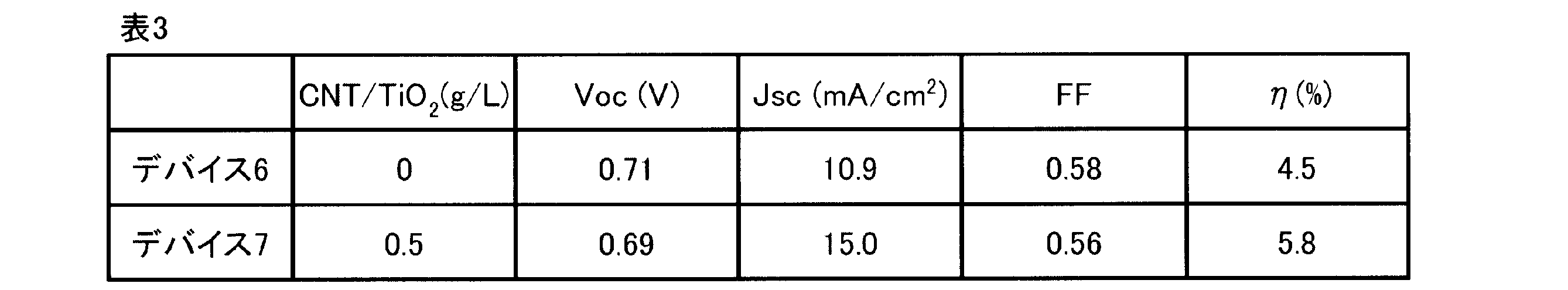
実施例11:光電変換素子(色素増感太陽電池)の製造例3
実施例4で得られたCNT/CDT/Ti複合体を光電変換素子(色素増感太陽電池)の光電変換層の材料として用い、色素増感太陽電池の特性に与える影響を評価した。色素増感太陽電池の作製方法はSOLARONIX社のプロトコールを改変して行った。
実施例4で得られたCNT/CDT/Ti複合体を光電変換素子(色素増感太陽電池)の光電変換層の材料として用い、色素増感太陽電池の特性に与える影響を評価した。色素増感太陽電池の作製方法はSOLARONIX社のプロトコールを改変して行った。
はじめに、上記実施例と同様の方法にて、CNT(SWNT)/CDT/Tiを反応溶液1mL分合成し、水で洗浄後、エタノール溶液に懸濁した。そのCNT(SWNT)/CDT/Ti複合体の終濃度が0.2重量%となるように酸化チタンペースト(Ti-Nanoxide D、SOLARONIX社)に練りこみ(酸化チタン:10重量%から14重量%、複合体:0.02重量%から0.03重量%)、色素増感太陽電池の材料とした。光電変換層を形成するために、25mmx25mmにカットされた透明電極基板であるFTO基板(fluorine-doped tin oxide、SOLARONIX社)を40mM 四塩化チタン水溶液に80℃で30分間つけ、そのFTO基板の両端に、5mmにカットされ2重に貼り合わされたメンディングテープ(3M社、厚さ100μm程度)をそれぞれ貼り付けた。テープ同士間の距離は5mmとした。
テープ同士の間に上記CNT(SWNT)/CDT/Ti複合体を含有する酸化チタンペーストを載せ、スライドガラスを用いて平らに伸ばし、30℃で30分間放置することで、酸化チタンペーストを乾燥させた。酸化チタンペーストを載せた基板を焼成炉にいれ、450℃で30分間焼成した。昇温速度は、90℃/minとして行った。焼成後に自然冷却して100℃以下に冷却した。冷却後、FTO基板上の酸化チタン部分を5mmx10mm角にカットし、その基板を0.2g/L ルテニウム(Ru)増感色素溶液(N719、無水エタノール溶解液、SOLARONIX社)に1mLつけ、室温で24時間放置した。24時間放置することで赤く染まった電極基板をエタノールで洗い、酸化チタン表面に吸着しなかった色素を除去し、室温で乾燥させて光電極とした(デバイス8に対応している)。
また、対照として、酸化処理により合成されたCNT/酸化チタン複合体を0.2重量%含有する酸化チタン電極で光電極を作製し(デバイス9に対応している)、0.2重量%でCNTを含有する酸化チタン電極で光電極を作製し(デバイス10に対応している)、CNTを含有しない酸化チタン電極で光電極を作製した(デバイス11に対応している)。酸化処理によるCNT/酸化チタン複合体の合成は参考文献(W.Wang et al.(2005) Journal of Molecular Catalysis A: Chemical,235,194-199.)の方法を参考にした。すなわち、エタノール200mL中に、チタンブトキシド溶液34mL(0.1mol)を加え、室温で30分間攪拌した。その後、硝酸(35重量%)を28mL加え、続いてCNTを適当量添加し、ゲル状になるまで一晩室温にて攪拌した。その後、沈殿物を遠心して回収し、80℃で一晩放置することで乾燥させてCNT/酸化チタン複合体を得た。
フッ素ドープ酸化スズ(FTO)膜の表面を厚さ50nmの白金(Pt)でコーティングしたPt電極(対向電極)と、上記光電極それぞれを備えた構造体とを用いて色素増感太陽電池を作製した。
封止材として封止シート(SX1170-25、SOLARONIX社)を用い、ホットプレートを用いて、120℃で5分間加熱した。さらに、完全に封止されていない接着面に、エポキシ系接着剤であるアラルダイトラピッド(昭和高分子社)をつけ、30℃で2時間放置することで密封した。最後にヨウ素電解液(SOLARONIX社)を入れて色素増感太陽電池を得た。
製造された色素増感太陽電池(デバイス8からデバイス11)に、キセノンランプで100mW/cm2の強さの光を照射して評価を行った。結果を図24に示す。図24は、色素増感太陽電池の電流-電圧特性を示すグラフである。なお、電流―電圧特性を測定する際の遅延時間は100m秒で行った。図24から明らかな通り、酸化チタンペーストのみで形成された光電極を備える色素増感太陽電池(デバイス11)の電流―電圧特性よりも、ナノ素材を含有する酸化チタンペーストで形成された光電極を備える色素増感太陽電池(デバイス8、デバイス9、およびデバイス10)の電流―電圧特性は、良好であった。特に、CDT1を用いて合成されたCNTと酸化チタンとの複合体を電極の機能性材料として用いた色素増感太陽電池(デバイス8)の電流―電圧特性は、極めて良好であった。
色素増感太陽電池の特性として、開放電圧Voc(V)、短絡電流密度Jsc(mA/cm2)、フィルファクターFF及び光電変換効率η(%)を評価した。結果を表4に示す。
表4から明らかな通り、酸化チタンペーストのみで形成された光電極を備える色素増感太陽電池(デバイス11)よりも、ナノ素材を含有する酸化チタンペーストで形成された光電極を備える色素増感太陽電池(デバイス8、デバイス9、およびデバイス10)では、大きな短絡電流密度が計測された。特に、CNT(SWNT)/CDT/Ti複合体を電極の機能性材料として用いることで、短絡電流量は180%増加していた。さらに、CDT1を用いて合成されたCNTと酸化チタンとの複合体を電極の機能性材料として用いた色素増感太陽電池(デバイス8)の短絡電流密度は、CNT単独で電極の機能性材料として用いた色素増感太陽電池(デバイス10)の短絡電流密度や酸化処理により合成されたCNTと酸化チタンの複合体を電極の機能性材料として用いた色素増感太陽電池(デバイス9)の短絡電流密度よりも大きかった。
続いて、デバイス8とデバイス10についてインピーダンス測定を行った。測定にはポテンショスタット/ガルバノメーター SP-50(Bio-Logic社)を用いた。測定は、周波数500mHzから10kHzまで変化させ、変化の前後における電流値、電圧値の応答の位相から各抵抗成分を求めた。
結果として、デバイス8における基板のシート抵抗は18Ωであり、デバイス10における基板のシート抵抗は35Ωであった。そして光電極と色素、電解質界面の抵抗は10Ωと15Ωであった。すなわち、CNT(SWNT)/CDT/Ti複合体を電極の機能性材料として用いることで、シート抵抗成分が59%、光電極と色素、電解質界面の抵抗は33%低減されており、酸化チタン電極の導電性が改善されることが分かった。
まず、CNTが酸化チタン電極に導入されることで短絡電流密度が向上した理由として、CNTが発生したキャリアの通り道となり、キャリアが再結合し電流量が低下する前に導電膜(FTO電極)に移動できたためと考えられた。また、CDT1処理や酸化処理によりCNTと酸化チタンとの複合体を形成させることで、CNTと酸化チタンとを密着させることができ、CNTおよび酸化チタン間の抵抗が低くなったと考えられた。そのため、無処理のCNTを酸化チタンペースト内に導入した場合よりも、酸化チタン周囲で発生したキャリアが効率よくCNTへと移動したと考えられた。酸処理により合成されたCNT/酸化チタン複合体では、酸によりCNTの構造が一部破壊され、CNT内のキャリアの移動が阻害されると考えられている。しかし、CDT1を用いればCNTの構造を傷つけることなくCNTと酸化チタンの複合体を合成することができる。さらに、CDT1由来の空孔により表面積が向上し、より多くの色素を担持できたと考えられた。そのため、酸処理により合成されたCNT/酸化チタン複合体よりも、CDT1を用いて合成されたCNT/酸化チタン複合体の方が、発生するキャリアの量が多く、さらにCNT内のキャリアの移動速度も維持されており、大きな短絡電流が観察されたと考えられた。
短絡電流密度が向上した結果、CNT(SWNT)/CDT/Ti複合体を練りこんだ酸化チタンペーストを光電極の機能性材料として用いた色素増感太陽電池(デバイス8)での光電変換効率ηは、CNTを含有しない酸化チタンペーストを光電極の機能性材料として用いた色素増感太陽電池(デバイス11)での光電変換効率ηの2.2倍向上していた。そして、作製された色素増感太陽電池のうち、CNT(SWNT)/CDT/Ti複合体を練りこんだ酸化チタンペーストを光電極の機能性材料として用いた色素増感太陽電池でもっとも高い光電変換効率が計測された。すなわち、CDT1を用いて、緩やかな条件で合成されたCNTと酸化チタンの複合体を用いることで、太陽電池の性能を向上させうることがわかった。
なお、FTO基板の四塩化チタン処理やCNT(SWNT)/CDT/Ti複合体を終濃度0.2重量%にて酸化チタン電極に練り込むことにより、実施例8で製造された色素増感太陽電池に比べ、短絡電流密度や光電変換効率ηの向上が認められることも確認された。

実施例12:光電変換素子(色素増感太陽電池)の製造例4
実施例4で得られたCNT/CDT/Ti複合体を光電変換素子(色素増感太陽電池)の光電変換層の材料として用い、色素増感太陽電池の特性に与える影響を評価した。色素増感太陽電池の作製方法はSOLARONIX社のプロトコールを改変して行った。
実施例4で得られたCNT/CDT/Ti複合体を光電変換素子(色素増感太陽電池)の光電変換層の材料として用い、色素増感太陽電池の特性に与える影響を評価した。色素増感太陽電池の作製方法はSOLARONIX社のプロトコールを改変して行った。
はじめに、上記実施例と同様の方法にて、CNT(SWNT)/CDT1/Tiを合成し、水で洗浄後、エタノール溶液に懸濁した。そのCNT(SWNT)/CDT/Ti複合体を終濃度0.1重量%から1重量%、具体的にはCNT(SWNT)/CDT/Ti複合体の終濃度が0.1重量%(デバイス13に対応している)、0.15重量%(デバイス14に対応している)、0.2重量%(デバイス15に対応している)、0.25重量%(デバイス16に対応している)、0.3重量%(デバイス17に対応している)、0.5重量%(デバイス18に対応している)、1.0重量%(デバイス19に対応している)、5.0重量%(デバイス20に対応している)及び0.06重量%(デバイス21に対応している)となるように酸化チタンペースト(Ti-Nanoxide D、SOLARONIX社)にそれぞれ練りこみ、色素増感太陽電池の材料とした。なお対照として、CNT(SWNT)/CDT1/Ti複合体を含有しない酸化チタンペーストも用いた(デバイス12に対応している)。光電変換層を形成するために、25mmx25mmにカットされた透明電極基板であるFTO基板(fluorine-doped tin oxide、SOLARONIX社)を40mM 四塩化チタン水溶液に80℃で30分間つけ、そのFTO基板の両端に、5mmにカットされ2重に貼り合わされたメンディングテープ(3M社、厚さ100μm程度)をそれぞれ貼り付けた。テープ同士間の距離は5mmとした。
テープ同士の間に上記各濃度でCNT(SWNT)/CDT1/Ti複合体を含有する酸化チタンペーストを載せ、スライドガラスを用いて平らに伸ばし、30℃で30分間放置することで、酸化チタンペーストを乾燥させた。酸化チタンペーストを載せた基板を焼成炉にいれ、450℃で30分間焼成した。昇温速度は、90℃/minとして行った。焼成後に自然冷却して100℃以下に冷却した。冷却後、FTO基板上の酸化チタン部分を5mmx10mm角にカットし、その基板を0.2g/L ルテニウム(Ru)増感色素溶液(N719、無水エタノール溶解液、SOLARONIX社)に1mLつけ、室温で24時間放置した。24時間放置することで赤く染まった電極基板をエタノールで洗い、酸化チタン表面に吸着しなかった色素を除去し、室温で乾燥させて光電極とした。
フッ素ドープ酸化スズ(FTO)膜の表面を厚さ50nmの白金(Pt)でコーティングしたPt電極(対向電極)と、上記光電極を備えた構造体とを用いて色素増感太陽電池を作製した。
封止材として封止シート(SX1170-25、SOLARONIX社)を用い、ホットプレートを用いて、120℃で5分間加熱した。さらに、完全に封止されていない接着面に、エポキシ系接着剤であるアラルダイトラピッド(昭和高分子社)をつけ、30℃で2時間放置することで密封した。最後にヨウ素電解液(SOLARONIX社)を入れて色素増感太陽電池を得た。
製造された色素増感太陽電池(デバイス12からデバイス21)に、キセノンランプで100mW/cm2の強さの光を照射して評価を行った。デバイス12、デバイス13、デバイス15、デバイス17、及びデバイス18の評価結果を図25に示す。図25は、色素増感太陽電池の電流-電圧特性を示すグラフである。なお、電流―電圧特性を測定する際の遅延時間は100m秒で行った。図25から明らかな通り、終濃度0.1重量%から0.5重量%の濃度でCNT(SWNT)/CDT1/Ti複合体を添加して形成された酸化チタン電極を用いた色素増感太陽電池の電流―電圧特性は、良好であった。
色素増感太陽電池の特性として、開放電圧Voc(V)、短絡電流密度Jsc(mA/cm2)、フィルファクターFF及び光電変換効率η(%)を評価した。結果を表5に示す。
色素増感太陽電池の特性として、開放電圧Voc(V)、短絡電流密度Jsc(mA/cm2)、フィルファクターFF及び光電変換効率η(%)を評価した。結果を表5に示す。
表5から明らかな通り、終濃度0.06重量%から0.5重量%の濃度でCNT(SWNT)/CDT1/Ti複合体を添加して形成された酸化チタン電極を用いた色素増感太陽電池(デバイス13、デバイス14、デバイス15、デバイス16、デバイス17、デバイス18およびデバイス19)では、光電変換効率の向上が観察された。特に、終濃度0.2重量%のCNT(SWNT)/CDT/Ti複合体を含有する酸化チタンペーストを用いた色素増感太陽電池(デバイス15)の場合、もっとも高い光電変換効率6.6%が測定された。
このように、CNT(SWNT)/CDT1/Ti複合体を所定量添加して酸化チタン電極を形成することで、色素増感太陽電池の性能を向上させうることがわかった。
このように、CNT(SWNT)/CDT1/Ti複合体を所定量添加して酸化チタン電極を形成することで、色素増感太陽電池の性能を向上させうることがわかった。

実施例13:融合タンパク質CcDTの調製例
(1)CcDT発現用株の作製
CDTと同様の性質を有する変異蛋白質をCorynebacterium glutamicum由来のDpsを用いて構築した。
Corynebacterium glutamicumのゲノムDNAを鋳型として、および配列番号24および配列番号25のヌクレオチド配列からなるオリゴヌクレオチドをプライマーとして用いてPCRを行った。
(1)CcDT発現用株の作製
CDTと同様の性質を有する変異蛋白質をCorynebacterium glutamicum由来のDpsを用いて構築した。
Corynebacterium glutamicumのゲノムDNAを鋳型として、および配列番号24および配列番号25のヌクレオチド配列からなるオリゴヌクレオチドをプライマーとして用いてPCRを行った。
得られたPCR産物をWizard SV Gel and PCR Clean-Up System(Promega社、USA)で精製し、制限酵素NdeIそしてEcoRIで消化した。
他方で、pET20bプラスミド(Merck社、ドイツ)を制限酵素NdeIそしてBamHIで消化した。
制限酵素で消化された、PCR産物及びプラスミドを、T4 DNAリガーゼ(Promega社、USA)を用いて結合させた。その結合させたDNAでE.coli JM109(タカラバイオ社、日本)を形質転換し、N末端にカーボンナノホン結合ペプチド(CNHBP)、C末端にチタン結合ペプチド(TBP)が融合されたCorynebacterium glutamicum由来のDps(CcDT、配列番号28および配列番号29)をコードする遺伝子が搭載された発現プラスミド(pET20-CcDT)を保持したJM109を構築した。
その形質転換株からWizard Plus Minipreps System(Promega社、USA)を使いpET20-CcDTを精製した。最後にBL21(DE3)(invitorogen社、USA)をpET20-CDTで形質転換し、タンパク質発現用株BL21(DE3)/pET20-CcDTとした。
(2)CcDTの精製
CcDTタンパク質を得るために、BL21(DE3)/pET20-CcDTを1mLのLB培地(100mg/L アンピシリンを含む)にて37℃で培養した。培養開始18時間後、その培養液を新しいLB培地(100mg/L アンピシリンを含む)100mLに植菌し、容量500mLフラスコを用いて37℃で24時間振とう培養した。得られた菌体を遠心分離(6000rpm、5分間)により回収し、50mM TrisHCl緩衝液(pH8.0) 5mLで懸濁した。その懸濁液を超音波処理して、菌体を破砕した。破砕された菌体を含む溶液を6000rpmで15分間、遠心分離し、上清画分を回収した。回収された上清画分を60℃で20分間加熱し、加熱処理終了後に速やかに氷上で冷却した。冷却された上清画分を6000rpmで15分間、遠心分離し、再度、上清を回収(約5mL)した。回収された上清をディスクフィルター(Millex GP 0.22μm、Millipore社、USA)で滅菌した。そして、滅菌された溶液をAmicon-Ultra-15(NMWL.50000、Millipore社、USA)で限外ろ過濃縮し、タンパク質が溶解している緩衝液をTrisHCl緩衝液(50mM TrisHCl溶液、pH8.0)に置換してタンパク質溶液2.5mLを得た。
CcDTタンパク質を得るために、BL21(DE3)/pET20-CcDTを1mLのLB培地(100mg/L アンピシリンを含む)にて37℃で培養した。培養開始18時間後、その培養液を新しいLB培地(100mg/L アンピシリンを含む)100mLに植菌し、容量500mLフラスコを用いて37℃で24時間振とう培養した。得られた菌体を遠心分離(6000rpm、5分間)により回収し、50mM TrisHCl緩衝液(pH8.0) 5mLで懸濁した。その懸濁液を超音波処理して、菌体を破砕した。破砕された菌体を含む溶液を6000rpmで15分間、遠心分離し、上清画分を回収した。回収された上清画分を60℃で20分間加熱し、加熱処理終了後に速やかに氷上で冷却した。冷却された上清画分を6000rpmで15分間、遠心分離し、再度、上清を回収(約5mL)した。回収された上清をディスクフィルター(Millex GP 0.22μm、Millipore社、USA)で滅菌した。そして、滅菌された溶液をAmicon-Ultra-15(NMWL.50000、Millipore社、USA)で限外ろ過濃縮し、タンパク質が溶解している緩衝液をTrisHCl緩衝液(50mM TrisHCl溶液、pH8.0)に置換してタンパク質溶液2.5mLを得た。
得られたタンパク質溶液からCcDTを精製するために、陰イオン交換クロマトグラフィーを用いた。すなわち、そのタンパク質溶液2.5mLを50mM TrisHCl緩衝液(pH8.0)で平衡化されたHiLoard 26/10 Q-Sepharose High Performanceカラム(GE healthcare社、USA)に注入した。そして、流速4.0mL/分、0mMから500mM NaClを含む50mM TrisHCl緩衝液(pH8.0)で塩濃度勾配をかけることで、分離精製を行い、CcDTを含む画分を回収した。
実施例14:CcDT多量体の形成の確認
得られたCcDTを3% PTA(リン・タングステン酸)染色し、透過型電子顕微鏡解析を行った。結果を図18に示す。図18は、得られたCcDTの透過型電子顕微鏡像を示す図である。
得られたCcDTを3% PTA(リン・タングステン酸)染色し、透過型電子顕微鏡解析を行った。結果を図18に示す。図18は、得られたCcDTの透過型電子顕微鏡像を示す図である。
図18に示されるように、結果として、CcDTは、CDTと同様に、直径9nm程度であり、内腔を有するカゴ状の多量体を形成していることがわかった。
実施例15:融合タンパク質CcDTとカーボンナノチューブとの結合の確認
CcDTとCNTとの結合をQCM法により測定した。はじめに、洗浄液(98%(w/v)硫酸と30%(w/v)過酸化水素水を3対1で混合した溶液)50μLを、測定用の金センサー上に乗せ5分間放置した後、水で洗い流すことでセンサー表面を洗浄した。また、CNTを1mg/mLとなるように1% SDS溶液と混合し、30分間超音波処理調製されたCNT溶液2μLを金電極上にマウントし、室温で自然乾燥した。乾燥後、水で2回洗浄し、結合しなかったCNTを洗い流した。さらに、リン酸緩衝液A(50mMリン酸カリウム緩衝液。0.001%(w/v) tween-20を含む。pH7.0)で1回洗浄した。
CcDTとCNTとの結合をQCM法により測定した。はじめに、洗浄液(98%(w/v)硫酸と30%(w/v)過酸化水素水を3対1で混合した溶液)50μLを、測定用の金センサー上に乗せ5分間放置した後、水で洗い流すことでセンサー表面を洗浄した。また、CNTを1mg/mLとなるように1% SDS溶液と混合し、30分間超音波処理調製されたCNT溶液2μLを金電極上にマウントし、室温で自然乾燥した。乾燥後、水で2回洗浄し、結合しなかったCNTを洗い流した。さらに、リン酸緩衝液A(50mMリン酸カリウム緩衝液。0.001%(w/v) tween-20を含む。pH7.0)で1回洗浄した。
CNTセンサーを本体(Affinix QN、Initium社)に取り付け、CNTセンサーにリン酸緩衝液Aを滴下し、30分間から1時間室温で放置することで、センサーの周波数値を安定させた。周波数値が安定した後、反応溶液量が500μL、終濃度が1mg/LとなるようにCcDTを添加し、周波数の変化を測定した。結果を図19に示す。図19は、CcDTとCNTとの結合を確認した結果を示すグラフである。
図19に示されるように、結果として、CNHBPを有するCcDT(CcDT1:実線)は、CNHBPを有しないDps-TBP(DT:破線)よりも、多くのCNTに結合することが観察できた。すなわち、CcDTは、DTよりも強いCNTへの結合能力を持つことがわかった。このCcDTのCNTへの結合能力はCNHBPによるものであると推測された。
実施例16:融合タンパク質CcDTと酸化チタンとの結合の確認
CcDTと酸化チタンの結合をQCM法により測定した。はじめに、洗浄液(98%(w/v)硫酸と30%(w/v)過酸化水素水を3対1で混合した溶液)50μLを、測定用の酸化チタンセンサー上に乗せ5分間放置した後、水で洗い流すことでセンサー表面を洗浄した。その酸化チタンセンサーを本体(Affinix QN、Initium社)に取り付け、酸化チタンセンサーにリン酸緩衝液B(50mM リン酸カリウム緩衝液。pH7.0)を滴下し、30分間から1時間室温で放置することで、センサーの周波数値を安定させた。周波数値が安定した後、反応溶液量が500μL、終濃度が1mg/LとなるようにCcDTを添加し、周波数の変化を測定した。結果を図20に示す。図20は、CcDTと酸化チタンとの結合を確認した結果を示すグラフである。
CcDTと酸化チタンの結合をQCM法により測定した。はじめに、洗浄液(98%(w/v)硫酸と30%(w/v)過酸化水素水を3対1で混合した溶液)50μLを、測定用の酸化チタンセンサー上に乗せ5分間放置した後、水で洗い流すことでセンサー表面を洗浄した。その酸化チタンセンサーを本体(Affinix QN、Initium社)に取り付け、酸化チタンセンサーにリン酸緩衝液B(50mM リン酸カリウム緩衝液。pH7.0)を滴下し、30分間から1時間室温で放置することで、センサーの周波数値を安定させた。周波数値が安定した後、反応溶液量が500μL、終濃度が1mg/LとなるようにCcDTを添加し、周波数の変化を測定した。結果を図20に示す。図20は、CcDTと酸化チタンとの結合を確認した結果を示すグラフである。
図20に示されるように、結果として、TBPを有するCcDT(CcDT1:実線)は、TBPを有しないCNHBP-Dps(CD:破線)よりも、多くの酸化チタンに結合することが観察できた。すなわち、CcDTは、CDよりも強い酸化チタンへの結合能力を持つことがわかった。このCcDTの酸化チタンへの結合能力はTBPによるものであると推測された。
実施例17:融合タンパク質CNHBP-Dps-ZnO1’(CDZ)発現用株の作製
N末端にカーボンナノホン結合ペプチド(CNHBPと表記;アミノ酸配列DYFSSPYYEQLF(配列番号6)からなる。国際公開第2006/068250号を参照)が融合され、C末端に酸化亜鉛結合(析出)ペプチド(ZnO1’と表記;アミノ酸配列EAHVMHKVAPRPGGGSC(配列番号30)からなる。Umetsu et al.,Adv.Mater.,17,2571-2575(2005)を参照)が融合されたListeria innocuaの金属内包性タンパク質Dps(CNHBP-Dps-ZnO1’あるいはCDZと表記、配列番号31及び配列番号32)を下記の手順により構築した。
N末端にカーボンナノホン結合ペプチド(CNHBPと表記;アミノ酸配列DYFSSPYYEQLF(配列番号6)からなる。国際公開第2006/068250号を参照)が融合され、C末端に酸化亜鉛結合(析出)ペプチド(ZnO1’と表記;アミノ酸配列EAHVMHKVAPRPGGGSC(配列番号30)からなる。Umetsu et al.,Adv.Mater.,17,2571-2575(2005)を参照)が融合されたListeria innocuaの金属内包性タンパク質Dps(CNHBP-Dps-ZnO1’あるいはCDZと表記、配列番号31及び配列番号32)を下記の手順により構築した。
はじめに、pET20-CDTを鋳型DNA、配列番号11のヌクレオチド配列およびtttGGATCCttaAcaACTAccTccAccAggAcGTggAgcAacTttAtgcatTacAtgTgcTtcttctaatggagcttttc(配列番号33)のヌクレオチド配列からなるオリゴヌクレオチドをプライマーとして用いてPCRを行った。得られたPCR産物をWizard SV Gel and PCR Clean-Up System(Promega社、USA)で精製し、制限酵素DpnIとBamHIで消化した。制限酵素で消化されたPCR産物を、T4 DNAリガーゼ(Promega社、USA)を用いてセルフライゲーションさせた。セルフライゲーションされたPCR産物をE.coli BL21(DE3)(ニッポンジーン社、日本)に形質転換し、N末端にカーボンナノホン結合ペプチド、C末端に酸化亜鉛結合ペプチドが融合されたDps(CDZ)をコードする遺伝子が搭載された発現プラスミド(pET20-CDZ)を保持したBL21(DE3)を構築した。
実施例18:融合タンパク質CDZの精製
BL21(DE3)/pET20-CDZをLB培地(100mg/Lのアンピシリンを含む)100mLに植菌し、容量500mLフラスコを用いて37℃で24時間振とう培養した。得られた菌体を遠心分離(6000rpm、5分間)して回収し、50mM TrisHCl緩衝液(pH8.0) 5mLで懸濁した。その懸濁液を超音波処理して、菌体を破砕した。その溶液を6000rpmで15分間、遠心分離し、上清画分を回収した。回収された溶液を60℃で20分間加熱し、加熱後に速やかに氷上で冷却した。冷却された溶液を6000rpmで15分間、遠心分離し、再度、上清を回収(約5mL)した。その上清をディスクフィルター(Millex GP 0.22μm、Millipore社、USA)で滅菌した。そして、滅菌された溶液をAmicon-Ultra-15(NMWL.50000、Millipore社、USA)で限外ろ過濃縮し、タンパク質が溶解している緩衝液をTrisHCl緩衝液(50mM TrisHCl溶液、pH8.0)に置換してタンパク質溶液2.5mLを得た。
得られたタンパク質溶液からCDZを精製するために、陰イオン交換クロマトグラフィーを用いた。すなわち、そのタンパク質溶液2.5mLを50mM TrisHCl緩衝液(pH8.0)で平衡化されたHiLoard 26/10 Q-Sepharose High Performanceカラム(GE healthcare社、USA)に注入した。そして、流速4.0mL/分、0mMから500mM NaClを含む50mM TrisHCl緩衝液(pH8.0)で塩濃度勾配をかけることで、分離精製を行い、CDZを含む画分を回収した。さらに、その回収された画分を、Amicon-Ultra-15(NMWL.50000、Millipore社、USA)で限外ろ過濃縮し、タンパク質が溶解している緩衝液を純水に置換してCDZ溶液を得た。
実施例19:CDZ多量体の形成の確認
緩衝液が純水置換される前の50mM TrisHCl緩衝液(pH8.0)に溶解したCDZを3% PTA(リン・タングステン酸)染色し、透過型電子顕微鏡で解析を行った。結果を図21に示す。図21は、CDZの透過型電子顕微鏡像を示す図である。その結果、CDZは、CDTと同様に、直径9nm程度の内腔を画成する多量体を形成していることがわかった。
緩衝液が純水置換される前の50mM TrisHCl緩衝液(pH8.0)に溶解したCDZを3% PTA(リン・タングステン酸)染色し、透過型電子顕微鏡で解析を行った。結果を図21に示す。図21は、CDZの透過型電子顕微鏡像を示す図である。その結果、CDZは、CDTと同様に、直径9nm程度の内腔を画成する多量体を形成していることがわかった。
実施例20:CDZによる硫酸亜鉛水溶液からの白色沈殿形成促進
はじめに、0.1M 硫酸亜鉛水溶液に、純水に溶解したCDZ、CDTあるいはCDをそれぞれ終濃度が0.1mg/mLとなるように添加した。その溶液を1時間室温で放置した後、600nmの光を用いて濁度を測定した。その結果を図22に示す。図22は、CDZによる硫酸亜鉛水溶液からの白色沈殿の形成を示す図である。CDZが添加された溶液では、白色沈殿の形成が顕著に促進された。この白色沈殿は、水酸化亜鉛あるいは酸化亜鉛と考えられる。一方、タンパク質を加えなかった溶液ではまったく沈殿が生じなかった。以上のことから、CDZは亜鉛化合物を沈殿させる活性があることが示唆された。なお、水酸化亜鉛は125℃程度で加熱されることで酸化亜鉛になることが知られている。
はじめに、0.1M 硫酸亜鉛水溶液に、純水に溶解したCDZ、CDTあるいはCDをそれぞれ終濃度が0.1mg/mLとなるように添加した。その溶液を1時間室温で放置した後、600nmの光を用いて濁度を測定した。その結果を図22に示す。図22は、CDZによる硫酸亜鉛水溶液からの白色沈殿の形成を示す図である。CDZが添加された溶液では、白色沈殿の形成が顕著に促進された。この白色沈殿は、水酸化亜鉛あるいは酸化亜鉛と考えられる。一方、タンパク質を加えなかった溶液ではまったく沈殿が生じなかった。以上のことから、CDZは亜鉛化合物を沈殿させる活性があることが示唆された。なお、水酸化亜鉛は125℃程度で加熱されることで酸化亜鉛になることが知られている。
実施例21:CDZ中のCNHBPの結合能の確認
CDZのN末端に融合されたカーボンナノホン結合ペプチド(CNHBP)の活性を調べた。リン酸カリウム緩衝液(50mM、pH6.0)に終濃度が0.3mg/mLとなるようにCDZとCNT(Sigma社、519308, carbon nanotube, single walled)とを各々加えた。得られた溶液に、Digital Sonifier 450(Branson社、USA)を用いて、1秒間の超音波パルス(200W、Duty 20%)を3秒間の間隔を空けながら計5分間与える超音波処理を行った。超音波処理されたCDZ-CNT混合溶液を遠心分離(15000rpm、5分間)し、上清に含まれるCDZとCNTとの複合体を3% PTAで染色し、透過型電子顕微鏡(JEM-2200FS、200kV)で観察を行った。結果を図23に示す。図23は、CDZとCNTとが結合した複合体の透過型電子顕微鏡像を示す図である。
CDZのN末端に融合されたカーボンナノホン結合ペプチド(CNHBP)の活性を調べた。リン酸カリウム緩衝液(50mM、pH6.0)に終濃度が0.3mg/mLとなるようにCDZとCNT(Sigma社、519308, carbon nanotube, single walled)とを各々加えた。得られた溶液に、Digital Sonifier 450(Branson社、USA)を用いて、1秒間の超音波パルス(200W、Duty 20%)を3秒間の間隔を空けながら計5分間与える超音波処理を行った。超音波処理されたCDZ-CNT混合溶液を遠心分離(15000rpm、5分間)し、上清に含まれるCDZとCNTとの複合体を3% PTAで染色し、透過型電子顕微鏡(JEM-2200FS、200kV)で観察を行った。結果を図23に示す。図23は、CDZとCNTとが結合した複合体の透過型電子顕微鏡像を示す図である。
結果として、N末端にCNHBPを有するCDZを含む溶液では、CNTの周囲にCDZが結合している様子が観察できた。すなわち、CDZはCNTに結合する活性を保持していることがわかった。
実施例22:CNTフォレストの形成
林状に並んだCNT(SWNT)/TiO2電極の作製を目指し、その基礎となる林状に並んだCNTの合成(CNTフォレストの形成)を試みた。
林状に並んだCNT(SWNT)/TiO2電極の作製を目指し、その基礎となる林状に並んだCNTの合成(CNTフォレストの形成)を試みた。
はじめに、CNTフォレストの形成時の触媒として使用される鉄ナノ粒子を、チタン結合性ペプチド(minTBP-1)を融合させたフェリチンタンパク質(TBF,T. Hayashi, et al., (2006) Nano Lett. 6 515.)を用いて調製した。すなわち、精製されたTBFを含むHEPES緩衝液(80mM HEPES-NaOH(pH7.5)、0.5mg/mL TBF、2mM 硫酸アンモニウム鉄を各々終濃度で含む)を1mL調製し、4℃で3時間放置した。放置後、遠心分離(15000rpm、5分間)して、タンパク質を含む上清を回収した。そして、その上清をAmicon-Ultra-15(NMWL.50000、Millipore社、USA)で限外ろ過濃縮し、酸化鉄ナノ粒子を内腔に内包するTBF多量体(Fe-TBF)溶液の緩衝液をTrisHCl緩衝液(50mM、pH8.0)に置換してタンパク質溶液を得た。
続いて、TBF多量体により合成された酸化鉄ナノ粒子をシリコン基板に吸着させた。すなわち、ポリシリコンウエハ上に3nmの厚さの酸化シリコン膜がマウントされたシリコン基板を7mm角にカットした。カットされたシリコン基板を、アセトンとメタノールとでそれぞれ2分間超音波洗浄し、最後に水で5回洗浄した。洗浄済みのシリコン基板を窒素ガスで乾燥させた後、10分間UV-O3処理した。処理されたシリコン基板にFe-TBF溶液(1.0mg/mL Fe-TBF、50mM TrisHCl緩衝液、pH8.0)を10μL載せ、10分間放置して、Fe-TBFをシリコン基板に吸着させた。遠心してシリコン基板に吸着しなかったFe-TBF溶液を除去し、50分間UV-O3処理することで、シリコン基板上に吸着したFe-TBFのうちタンパク質成分のみを除去することにより、酸化鉄ナノ粒子がその表面に吸着したシリコン基板を得た。
酸化鉄ナノ粒子がその表面に吸着したシリコン基板をCVD炉(VICインターナショナル社製)に入れ、CNTフォレストを形成した。すなわち、このシリコン基板をCVD炉の石英管の中に入れ、真空中で600℃から650℃に加熱した。加熱されたシリコン基板を水素ガス雰囲気下(水素流量200sccm、反応圧力1.5kPa)に5分間放置することで、シリコン基板上の酸化鉄ナノ粒子を活性化した。続いて、アセチレンガス/水素ガス混合雰囲気下(アセチレン流量10sccm、水素流量200sccm、反応圧力1.5kPa)に20分間放置した。
CVD炉で処理されたシリコン基板を無染色でSEM解析したところ、長さ15μm程度のCNTからなるCNTフォレストを確認することができた。結果を図26に示す。図26は、無染色でSEM解析したシリコン基板の写真図である。図26中、両矢印に示される領域がCNTフォレストが形成された領域である。
上記条件以外にもCNTフォレストは下記表6に示される条件を用いて、TBF多量体により合成された酸化鉄ナノ粒子を触媒として合成することができた。また、同様の条件を用いて、UV-O3処理せずに、シリコン基板上に吸着したFe-TBFのタンパク質成分が除去されていない基板を用いてもCNTフォレストを形成することができた。表6は、CNTフォレストの形成(成長)が確認された条件の例を示す表である。

また、下記表7及び表8に示される条件を用いることでフォレスト状ではないもののシリコン基板上でCNTを合成することができた。表7及び表8は、CNTの合成が確認された条件の例を示す表である。ここでは酸化鉄ナノ粒子が表面に吸着したシリコン基板をCNT合成温度まで加熱した後、CNT合成で使用した圧力、水素ガス流量で5分間放置し、シリコン基板上に吸着した酸化鉄ナノ粒子を活性化した。その後、下記表7及び表8に示される各条件で20分間処理し、シリコン基板上でCNTを成長させた。昇温及び降温はいずれも真空中で実施された。
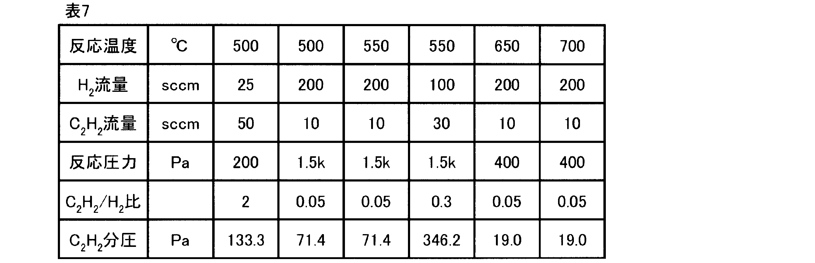
実施例23:合成されたCNTとCDTとの複合体の合成
上記の通り得られたCNTフォレストを加工して林状に並んだCNT(SWNT)/TiO2電極を得るためには、CDTがCNTフォレストを構成するCNTへ吸着する必要がある。そこで、CNTフォレストが形成されたシリコン基板からCNTを剥離し、得られたCNTの構造を詳細に観察するとともに、CNTとCDTとの複合体の形成を観察した。すなわち、アセチレン流量10sccm、水素流量200sccm、反応圧力1.5kPa、反応温度600℃で処理されたCNTフォレストが形成されたシリコン基板を70%エタノール水溶液に入れ、1分間超音波処理(1s ON/1s OFF、20% Duty)することでCNTをシリコン基板から剥離した。続いて、得られたCNT溶液を用いて定法によりCDTとの複合体の形成を試みた。すなわち、CNTとCDTとを含むリン酸カリウム緩衝液[50mM リン酸カリウム(pH6.0)、0.1mg/mLのCDT、及び0.1mg/mL CNTを各々終濃度で含む]を調製した。CDTを含むリン酸カリウム緩衝液に、Digital Sonifier 450(Branson社、USA)を用いて、氷上で、3秒間隔で1秒間の超音波パルス(200W、Duty 20%)を合計5分間加えた。
上記の通り得られたCNTフォレストを加工して林状に並んだCNT(SWNT)/TiO2電極を得るためには、CDTがCNTフォレストを構成するCNTへ吸着する必要がある。そこで、CNTフォレストが形成されたシリコン基板からCNTを剥離し、得られたCNTの構造を詳細に観察するとともに、CNTとCDTとの複合体の形成を観察した。すなわち、アセチレン流量10sccm、水素流量200sccm、反応圧力1.5kPa、反応温度600℃で処理されたCNTフォレストが形成されたシリコン基板を70%エタノール水溶液に入れ、1分間超音波処理(1s ON/1s OFF、20% Duty)することでCNTをシリコン基板から剥離した。続いて、得られたCNT溶液を用いて定法によりCDTとの複合体の形成を試みた。すなわち、CNTとCDTとを含むリン酸カリウム緩衝液[50mM リン酸カリウム(pH6.0)、0.1mg/mLのCDT、及び0.1mg/mL CNTを各々終濃度で含む]を調製した。CDTを含むリン酸カリウム緩衝液に、Digital Sonifier 450(Branson社、USA)を用いて、氷上で、3秒間隔で1秒間の超音波パルス(200W、Duty 20%)を合計5分間加えた。
結果を図27A及び図27Bに示す。図27A及び図27Bは、CDTとCNTとの混合溶液の透過型電子顕微鏡像を示す写真図である。撮影は、サンプルを3%リンタングステン酸で染色して行った。この条件で合成されたCNTは、図27Aに示されるような太いCNTと図27Bに示されるような細いCNTとが混合していることが分かった。また、細いCNTにはCDTが結合できている様子を観察することができた(図27B参照。)。既に説明した方法で合成された柱状のCNTもCDTと複合体を形成できることから、バルク状のCNTと同様に、CDTを用いて柱状のCNTから柱状のCNT(SWNT)/TiO2複合体が合成できることが示唆された。
実施例24:細いCNTの合成
合成された細いCNTへのCDTの結合が観察されたことから、細いCNTからなるCNTフォレストの形成を試みた。先行研究により、合成されるCNTの太さは触媒として使用される鉄ナノ粒子のサイズに左右されることが指摘されている(M. Kumar and Y. Ando (2010) J. Nanoscience Nanotechnol., 10, 3739,)。そこで、TBFよりも小さな酸化鉄ナノ粒子を内腔に内包できるCDTを用いてCNTフォレストの形成を試みた。すなわち、酸化鉄ナノ粒子を内腔に内包するCDTと酸化鉄ナノ粒子を内腔に内包するTBFを1:0、1:1,1:2、あるいは2:1となるように混合し、タンパク質総量が1mg/mLとなるようにトリス緩衝液(50mM、pH8.0)に懸濁した。続いて、ポリシリコンウエハ上に厚さが3nmの酸化シリコン膜がマウントされたシリコン基板を7mm角にカットした。カットされたシリコン基板を、アセトンとメタノールとでそれぞれ2分間超音波洗浄し、最後に水で5回洗浄した。洗浄されたシリコン基板を窒素ガスで乾燥させた後、10分間UV-O3処理した。処理されたシリコン基板に酸化鉄ナノ粒子を内腔に内包するCDTと酸化鉄ナノ粒子を内腔に内包するTBFを含む緩衝液10μLを載せ、10分間放置し、タンパク質をシリコン基板に吸着させた。遠心して、シリコン基板に吸着しなかったタンパク質溶液を除去し、50分間UV-O3処理することで、シリコン基板上にあるタンパク質成分のみを除去した。
合成された細いCNTへのCDTの結合が観察されたことから、細いCNTからなるCNTフォレストの形成を試みた。先行研究により、合成されるCNTの太さは触媒として使用される鉄ナノ粒子のサイズに左右されることが指摘されている(M. Kumar and Y. Ando (2010) J. Nanoscience Nanotechnol., 10, 3739,)。そこで、TBFよりも小さな酸化鉄ナノ粒子を内腔に内包できるCDTを用いてCNTフォレストの形成を試みた。すなわち、酸化鉄ナノ粒子を内腔に内包するCDTと酸化鉄ナノ粒子を内腔に内包するTBFを1:0、1:1,1:2、あるいは2:1となるように混合し、タンパク質総量が1mg/mLとなるようにトリス緩衝液(50mM、pH8.0)に懸濁した。続いて、ポリシリコンウエハ上に厚さが3nmの酸化シリコン膜がマウントされたシリコン基板を7mm角にカットした。カットされたシリコン基板を、アセトンとメタノールとでそれぞれ2分間超音波洗浄し、最後に水で5回洗浄した。洗浄されたシリコン基板を窒素ガスで乾燥させた後、10分間UV-O3処理した。処理されたシリコン基板に酸化鉄ナノ粒子を内腔に内包するCDTと酸化鉄ナノ粒子を内腔に内包するTBFを含む緩衝液10μLを載せ、10分間放置し、タンパク質をシリコン基板に吸着させた。遠心して、シリコン基板に吸着しなかったタンパク質溶液を除去し、50分間UV-O3処理することで、シリコン基板上にあるタンパク質成分のみを除去した。
酸化鉄ナノ粒子がその表面に吸着したシリコン基板をCVD炉に入れCNTフォレストの形成を行った。すなわち、このシリコン基板をCVD炉の石英管の中に入れ、真空中で600℃に加熱した。加熱された基板を水素ガス雰囲気下(水素流量200sccm、反応圧力1.5kPa)に5分間放置することで、基板上の酸化鉄ナノ粒子を活性化した。続いて、アセチレンガス/水素ガス混合雰囲気下(アセチレン流量10sccm、水素流量200sccm、反応圧力1.5kPa)に20分間放置した。
酸化鉄ナノ粒子を内腔に内包するCDTと酸化鉄ナノ粒子を内腔に内包するTBFとが1:1、1:2あるいは2:1で混合された溶液を用いた場合、CNTフォレストの形成が確認できた。結果を図28に示す。図28は、CDTとTBFとの比を1:1として合成したCNTをSEM解析した写真図である。図28中、両矢印に示される領域がCNTフォレストが形成された領域である。続いて、このCNTフォレストが形成された基板を70%エタノール水溶液に入れ、1分間超音波処理(1s ON/1s OFF、20% Duty)することでCNTをシリコン基板から剥離した。
得られたCNTの太さをTEM解析した。結果を図29A、図29B及び図29Cに示す。図29A、図29B及び図29Cに示されるように、図29Aは、CDTとTBFとの比を1:1として合成したCNTの写真図である。図29Bは、CDTとTBFとの比を1:2として合成したCNTの写真図である。図29Cは、CDTとTBFの比を2:1として合成したCNTの写真図である。
酸化鉄ナノ粒子を内腔に内包するCDTと酸化鉄ナノ粒子を内腔に内包するTBFとの混合触媒を用いて形成されたCNTフォレストにはいずれも細いCNTが多数含まれていることが分かった。
実施例25:CNTへのタンパク質の結合
CDTとTBFとの比を1:2としてシリコン基板上に合成されたCNTに対して、CNHBP-Dps(CD)が結合できるかどうかを調べた。CNHBP-Dpsは、CNHBP-Dps-TBPからチタン結合ペプチドTBPを除去した構造を有しており、下記のように調製した。
CDTとTBFとの比を1:2としてシリコン基板上に合成されたCNTに対して、CNHBP-Dps(CD)が結合できるかどうかを調べた。CNHBP-Dpsは、CNHBP-Dps-TBPからチタン結合ペプチドTBPを除去した構造を有しており、下記のように調製した。
BL21(DE3)/pET20-CDを5mLのLB培地(100mg/L アンピシリンを含む)にて37℃で培養した。培養開始後18時間で、得られた培養液を新しいLB培地(100mg/L アンピシリンを含む) 3Lに植菌し、BMS-10/05(ABLE社、日本)を用いて37℃で24時間振とう培養した。得られた菌体を遠心分離(5000rpm、5分間)して回収し、-80℃で保存した。冷凍保存された菌体の半分の量(6g)を50mM TrisHCl緩衝液(pH8.0) 40mLで懸濁した。次に、その懸濁液にDigital Sonifier 450(Branson社、USA)を使い、1秒間隔の超音波パルス(200W、Duty 45%)を12分間与えることで、菌体を破砕した。破砕された菌体を含む溶液を15000rpmで15分間、遠心分離(JA-20、Beckmancoulter社、USA)し、上清画分を回収した。回収された上清画分を60℃で20分間加熱し、加熱後は速やかに氷上で冷却した。冷却された上清画分を17000rpmで10分間、遠心分離(JA-20)し、再度、上清を回収(約20mL)した。その上清をディスクフィルター(Millex GP 0.22μm、Millipore社、USA)で滅菌した。そして、滅菌された上清をAmicon-Ultra-15(NMWL.50000、Millipore社、USA)で液量が10mLになるまで限外ろ過濃縮し、タンパク質溶液を得た。その後、そのタンパク質溶液に終濃度0.5MとなるようにNaClを加え、6000rpmで5分間、遠心分離(JA-20)した後、上清を捨て、沈殿物を50mM Tris-HCl緩衝液(pH8.0)に懸濁した。その作業を3回繰り返すことによりCDを精製した。
続いて、CDに金属粒子を内包させるために、CDを含むHEPES緩衝液(80mM HEPES-NaOH(pH7.5)、0.5mg/mL CDT、1mM 硫酸アンモニウム鉄を各々終濃度で含む)を1mL調製し、4℃で3時間放置した。放置後、遠心分離(15000rpm、5分間)し、上清を回収することで酸化鉄ナノ粒子を内腔に内包するCDを含む溶液を得た。得られた溶液をAmicon-Ultra-15(NMWL.50000、Millipore社、USA)で限外ろ過濃縮し、酸化鉄ナノ粒子を内腔に内包するCD多量体(Fe-CD)溶液のうちの緩衝液を水に置換してタンパク質溶液を得た。シリコン基板上に合成されたCNTとFe-CDとの複合体を形成させるために、シリコン基板上に合成されたCNTに、Fe-CDを含む水溶液(30体積% エタノール含有)10μLを加え、10分間室温で放置した。その後、水で洗浄し、デシケーターで乾燥させた。そして、得られた基板をSEM解析した。結果を図30に示す。図30は、形成されたCNTとFe-CDとの複合体をSEM解析した写真図である。
図30に示されるように、それぞれ酸化鉄ナノ粒子を内包するCDTとTBFとを1:2の混合比となるように混合することにより形成されたCNTとFe-CDとの複合体が観察できた。ここで、タンパク質は直接的にはSEM解析により観察できないが、鉄ナノ粒子などの金属ナノ粒子を内包するタンパク質を用いて、内部の金属ナノ粒子を観察することで、タンパク質の位置を間接的に観察することができる。特に今回用いたFe-CDでは直径5nm程度の小さなナノ粒子が、白い点となって観察されることが知られている。
このことは、CDやCDTに用いられているCNT結合ペプチドが、上記の工程により合成されたCNTを認識できることを示唆している。そして、タンパク質を用いてCNTに金属ナノ粒子を被着させることができることを示唆している。
10 多孔質構造体
20 第1の標的材料
30 凝集体
32 第1の空孔部
34 第2の空孔部
36 金属粒子
38 第3の空孔部
40 増感色素
52 第1の基板
54 第2の基板
62 透明電極
64 対向電極
70 光電変換層
80 電解液
90 封止部
100 色素増感太陽電池
20 第1の標的材料
30 凝集体
32 第1の空孔部
34 第2の空孔部
36 金属粒子
38 第3の空孔部
40 増感色素
52 第1の基板
54 第2の基板
62 透明電極
64 対向電極
70 光電変換層
80 電解液
90 封止部
100 色素増感太陽電池
Claims (40)
- 第1の標的材料と、該第1の標的材料に被着して、該第1の標的材料の周囲を取り囲むように位置している、第2の標的材料が凝集した凝集体とを含み、
前記凝集体が、該凝集体の前記第1の標的材料寄りに偏在する複数の第1の空孔部、及び前記凝集体に散在する複数の第2の空孔部を備える、多孔質構造体。 - 前記第1の標的材料が、カーボンナノチューブ、カーボンナノホン、グラフェンシート、フラーレン、及びグラファイトからなる群から選択される炭素材料である、請求項1に記載の多孔質構造体。
- 前記第2の標的材料が酸化チタン又は酸化亜鉛である、請求項1又は2に記載の多孔質構造体。
- 前記第1の空孔部に配置されており、前記第2の標的材料とは異なる金属粒子をさらに含む、請求項1~3のいずれか1項に記載の多孔質構造体。
- 前記金属粒子が、酸化鉄、ニッケル、コバルト、マンガン、リン、ウラン、ベリリウム、アルミニウム、硫化カドミウム、セレン化カドミウム、パラジウム、クロム、銅、銀、ガドリウム錯体、白金コバルト、酸化シリコン、酸化コバルト、酸化インジウム、白金、金、硫化金、セレン化亜鉛、及びカドミウムセレンからなる群から選択される金属ナノ粒子である、請求項4に記載の多孔質構造体。
- 前記金属粒子が酸化鉄ナノ粒子である、請求項5に記載の多孔質構造体。
- 前記第1の空孔部の径が5nm~15nmの範囲内である、請求項1~5のいずれか1項に記載の多孔質構造体。
- 複数の前記第1の空孔部それぞれの前記第1の標的材料の表面からの距離が、1nm~500nmの範囲内であり、かつ同一である、請求項1~7のいずれか1項に記載の多孔質構造体。
- 請求項1~8のいずれか1項に記載の多孔質構造体を機能性材料として含む、電子デバイス。
- 太陽電池である、請求項9に記載の電子デバイス。
- 前記太陽電池が、前記多孔質構造体を電極の材料として、又は電極上に配置される機能性材料として含む、請求項10に記載の電子デバイス。
- 色素増感太陽電池である、請求項11に記載の電子デバイス。
- 第1の標的材料に、該第1の標的材料に結合し得る第1のペプチド部分、第2の標的材料に結合し得る第2のペプチド部分、及び内腔を有する多量体を形成し得るポリペプチド部分を含む融合タンパク質からなる、内腔を有する融合タンパク質多量体を結合させ、さらに前記融合タンパク質多量体に前記第2の標的材料又は第2の標的材料の前駆体を結合させて、前記融合タンパク質多量体に前記第1の標的材料と前記第2の標的材料又は第2の標的材料の前駆体とが結合した複合体を調製する工程と、
前記複合体を焼成して前記融合タンパク質多量体を消滅させて、前記第1の標的材料の周囲を取り囲むように位置して前記第1の標的材料に被着しており、前記第1の標的材料寄りに偏在する複数の第1の空孔部、及び散在する複数の第2の空孔部を備える凝集体を形成する工程と
を含む、多孔質構造体の製造方法。 - 前記複合体を調製する工程が、前記融合タンパク質多量体に前記第1の標的材料と前記第2の標的材料の前駆体とが結合した複合体を調製する工程であり、
前記凝集体を形成する工程が、前記複合体を焼成して前記融合タンパク質多量体を消滅させ、かつ前記第2の標的材料の前駆体を第2の標的材料とすることにより、前記凝集体を形成する工程である、請求項13に記載の多孔質構造体の製造方法。 - 前記複合体を調製する工程が、前記融合タンパク質多量体に前記第2の標的材料の前駆体を結合させるとともに、前記第2の標的材料を前記第1の標的材料の周囲に析出させる工程である、請求項14に記載の多孔質構造体の製造方法。
- 前記第1の標的材料が、カーボンナノチューブ、カーボンナノホン、グラフェンシート、フラーレン、及びグラファイトからなる群から選択される炭素材料である、請求項13~15のいずれか1項に記載の多孔質構造体の製造方法。
- 前記第2の標的材料が酸化チタン又は酸化亜鉛である、請求項13~16のいずれか1項に記載の多孔質構造体の製造方法。
- 前記融合タンパク質多量体が、前記内腔に内包された、前記第1の標的材料とは異なる金属粒子をさらに含み、
前記第1の空孔部に前記金属粒子をさらに含む凝集体が形成される、請求項13~17のいずれか1項に記載の多孔質構造体の製造方法。 - 前記金属粒子が、酸化鉄、ニッケル、コバルト、マンガン、リン、ウラン、ベリリウム、アルミニウム、硫化カドミウム、セレン化カドミウム、パラジウム、クロム、銅、銀、ガドリウム錯体、白金コバルト、酸化シリコン、酸化コバルト、酸化インジウム、白金、金、硫化金、セレン化亜鉛、及びカドミウムセレンからなる群から選択される金属ナノ粒子である、請求項18に記載の多孔質構造体の製造方法。
- 前記金属粒子が酸化鉄ナノ粒子である、請求項19に記載の多孔質構造体の製造方法。
- 請求項1~8のいずれか1項に記載の多孔質構造体を機能性材料として用いて機能性の構造を形成する工程を含む、電子デバイスの製造方法。
- 透明電極を備えた基板を準備する工程と、
第1の標的材料に、第1の標的材料に結合し得る第1のペプチド部分、第2の標的材料に結合し得る第2のペプチド部分、及び内腔を有する多量体を形成し得るポリペプチド部分を含む融合タンパク質からなる、内腔を有する融合タンパク質多量体を結合させて結合体とし、該結合体と前記第2の標的材料又は第2の標的材料の前駆体とを結合させて複合体を得る工程と、
前記複合体を含む材料を、前記透明電極上に載せる工程と、
前記透明電極上の前記材料を焼成し、前記融合タンパク質多量体を消滅させて、前記第2の標的材料を含み、前記第1の標的材料の周囲を取り囲むように位置して前記第1の標的材料に被着しており、前記第1の標的材料寄りに偏在する複数の第1の空孔部、及び散在する複数の第2の空孔部を備える凝集体を有する多孔質構造体を含む構造を、前記透明電極上に形成する工程と、
前記多孔質構造体に増感色素を坦持させて光電極を形成する工程と、
前記光電極と、対向電極とを電解液を注入して封止する工程と
を含む、色素増感太陽電池の製造方法。 - 前記複合体の終濃度が1重量%未満となるように、前記多孔質構造体を含む構造を形成する、請求項22に記載の色素増感太陽電池の製造方法。
- 前記複合体の終濃度が0.06重量%~0.5重量%の範囲となるように、前記多孔質構造体を含む構造を形成する、請求項23に記載の色素増感太陽電池の製造方法。
- 透明電極を備えた基板を準備する工程と、
第1の標的材料に、第1の標的材料に結合し得る第1のペプチド部分、第2の標的材料に結合し得る第2のペプチド部分、及び内腔を有する多量体を形成し得るポリペプチド部分を含む融合タンパク質からなる、内腔を有する融合タンパク質多量体を結合させて結合体とし、該結合体と前記第2の標的材料又は第2の標的材料の前駆体とを結合させて複合体とし、該複合体を焼成して前記融合タンパク質多量体を消滅させて、前記第2の標的材料を含み、前記第1の標的材料の周囲を取り囲むように位置して前記第1の標的材料に被着しており、前記第1の標的材料寄りに偏在する複数の第1の空孔部、及び散在する複数の第2の空孔部を備える凝集体を有する多孔質構造体を形成する工程と、
前記多孔質構造体、前記第2の標的材料又は第2の標的材料の前駆体を含む材料を、前記透明電極上に載せる工程と、
前記透明電極上の前記材料を加熱処理して、前記透明電極上に前記多孔質構造体を含む構造を形成する工程と、
前記多孔質構造体に増感色素を坦持させて光電極を形成する工程と、
前記光電極と、対向電極とを電解液を注入して封止する工程と
を含む、色素増感太陽電池の製造方法。 - 前記第1の標的材料が、カーボンナノチューブ、カーボンナノホン、グラフェンシート、フラーレン、及びグラファイトからなる群から選択される炭素材料である、請求項22~25のいずれか1項に記載の色素増感太陽電池の製造方法。
- 透明電極を備えた基板を準備する工程と、
前記透明電極上に、第1の標的材料である1以上のカーボンナノチューブを前記基板の厚み方向に延在するように配列させる工程と、
前記カーボンナノチューブに、該カーボンナノチューブに結合し得る第1のペプチド部分、第2の標的材料の前駆体に結合し得る第2のペプチド部分、及び内腔を有する多量体を形成し得るポリペプチド部分を含む融合タンパク質からなり、前記内腔を有する融合タンパク質多量体を結合させて結合体とし、該結合体と前記第2の標的材料又は第2の標的材料の前駆体とを結合させて複合体とする工程と、
前記混合物を焼成して前記融合タンパク質多量体を消滅させて、前記第2の標的材料を含み、前記カーボンナノチューブの周囲を取り囲むように位置して前記カーボンナノチューブに被着しており、前記カーボンナノチューブ寄りに偏在する複数の第1の空孔部、及び散在する複数の第2の空孔部を備える凝集体を有する多孔質構造体を含む構造を、前記透明電極上に形成する工程と、
前記多孔質構造体に増感色素を坦持させて光電極を形成する工程と、
前記光電極と、対向電極とを電解液を注入して封止する工程と
を含む、色素増感太陽電池の製造方法。 - 前記透明電極上に、第1の標的材料である1以上のカーボンナノチューブを前記基板の厚み方向に延在するように配列させる工程が、基板上に無機材料を吸着させる工程と、前記無機材料を種としてカーボンナノチューブを成長させてカーボンナノチューブ配列基板を得る工程と、該カーボンナノチューブ配列基板の前記カーボンナノチューブを透明電極上に転写する工程とを含む、請求項27に記載の色素増感太陽電池の製造方法。
- 前記基板上に前記無機材料を吸着させる工程が、サイズの異なる2種以上の無機材料内包性タンパク質を基板上に配列させて吸着させる工程である、請求項28に記載の色素増感太陽電池の製造方法。
- 前記基板上に前記無機材料を吸着させる工程が、前記基板がシリコン酸化膜が設けられた基板を用いて、前記無機材料内包性タンパク質を前記シリコン酸化膜上に配列させて吸着させる工程である、請求項29に記載の色素増感太陽電池の製造方法。
- 前記無機材料内包性タンパク質が、フェリチンタンパク質、Dpsタンパク質、CDTタンパク質またはそれらの改変タンパク質から選ばれる1種以上のタンパク質である、請求項29又は30に記載の色素増感太陽電池の製造方法。
- 前記第2の標的材料が酸化チタン又は酸化亜鉛である、請求項22~31のいずれか1項に記載の色素増感太陽電池の製造方法。
- 請求項22~32のいずれか1項に記載の製造方法により、得ることができる色素増感太陽電池。
- 透明電極を備えた基板と、
前記透明電極上に設けられている光電変換層であって、第1の標的材料と、第2の標的材料を含み、前記第1の標的材料の周囲を取り囲むように位置して前記第1の標的材料に被着しており、前記第1の標的材料寄りに偏在する複数の第1の空孔部、及び散在する複数の第2の空孔部を備える凝集体とを有する多孔質構造体を含み、該多孔質構造体が増感色素を坦持している前記光電変換層と、
前記光電極と対向電極とを対向させ、かつ前記光電極及び前記対向電極が電解液に接触するように封止する封止部と
を含む、色素増感太陽電池。 - 透明電極を備えた基板と、
前記透明電極上に設けられている光電変換層であって、前記基板の厚み方向に延在するように配列させた、第1の標的材料である1以上のカーボンナノチューブと、前記第2の標的材料を含み、前記カーボンナノチューブの周囲を取り囲むように位置して前記カーボンナノチューブに被着しており、前記カーボンナノチューブ寄りに偏在する複数の第1の空孔部、及び散在する複数の第2の空孔部を備える凝集体とを有する多孔質構造体を含み、該多孔質構造体が増感色素を坦持している前記光電変換層と、
前記光電極と対向電極とを対向させ、かつ前記光電極及び前記対向電極が電解液に接触するように封止する封止部と
を含む、色素増感太陽電池。 - 前記第1の標的材料が、カーボンナノチューブ、カーボンナノホン、グラフェンシート、フラーレン、及びグラファイトからなる群から選択される炭素材料である、請求項33に記載の色素増感太陽電池。
- 前記第2の標的材料が酸化チタン又は酸化亜鉛である、請求項34~36のいずれか1項に記載の色素増感太陽電池。
- 1以上のカーボンナノチューブが厚み方向に延在するように配列された、カーボンナノチューブ配列基板の製法であって、
サイズの異なる2種以上の無機材料内包性タンパク質を基板上に配列し吸着させる工程と、前記無機材料内包性タンパク質に内包された無機材料を種としてカーボンナノチューブを成長させる工程とを含む、カーボンナノチューブ配列基板の製造方法。 - サイズの異なる2種以上の無機材料内包性タンパク質を基板上に配列し吸着させる工程が、シリコン酸化膜が設けられた基板を用いて、前記無機材料内包性タンパク質を前記シリコン酸化膜上に吸着させることにより行われる、請求項38に記載のカーボンナノチューブ配列基板の製造方法。
- 前記無機材料内包性タンパク質が、フェリチンタンパク質、Dpsタンパク質、CDTタンパク質またはそれらの改変タンパク質から選ばれる1種以上のタンパク質である、請求項38又は39に記載のカーボンナノチューブ配列基板の製造方法。
Priority Applications (5)
| Application Number | Priority Date | Filing Date | Title |
|---|---|---|---|
| CN201280038879.8A CN103732534B (zh) | 2011-08-08 | 2012-08-08 | 多孔性结构体及其制造方法 |
| JP2013528059A JP5983610B2 (ja) | 2011-08-08 | 2012-08-08 | 多孔質構造体及びその製造方法 |
| KR1020147003303A KR20140066158A (ko) | 2011-08-08 | 2012-08-08 | 다공질 구조체 및 그 제조 방법 |
| EP12821931.8A EP2743232A4 (en) | 2011-08-08 | 2012-08-08 | POROUS STRUCTURE AND METHOD FOR MANUFACTURING THE SAME |
| US14/176,543 US20140150855A1 (en) | 2011-08-08 | 2014-02-10 | Porous structure body and method for producing the same |
Applications Claiming Priority (4)
| Application Number | Priority Date | Filing Date | Title |
|---|---|---|---|
| JP2011-173229 | 2011-08-08 | ||
| JP2011173229 | 2011-08-08 | ||
| JP2011278816 | 2011-12-20 | ||
| JP2011-278816 | 2011-12-20 |
Related Child Applications (1)
| Application Number | Title | Priority Date | Filing Date |
|---|---|---|---|
| US14/176,543 Continuation US20140150855A1 (en) | 2011-08-08 | 2014-02-10 | Porous structure body and method for producing the same |
Publications (1)
| Publication Number | Publication Date |
|---|---|
| WO2013022051A1 true WO2013022051A1 (ja) | 2013-02-14 |
Family
ID=47668556
Family Applications (1)
| Application Number | Title | Priority Date | Filing Date |
|---|---|---|---|
| PCT/JP2012/070280 WO2013022051A1 (ja) | 2011-08-08 | 2012-08-08 | 多孔質構造体及びその製造方法 |
Country Status (6)
| Country | Link |
|---|---|
| US (1) | US20140150855A1 (ja) |
| EP (1) | EP2743232A4 (ja) |
| JP (1) | JP5983610B2 (ja) |
| KR (1) | KR20140066158A (ja) |
| CN (1) | CN103732534B (ja) |
| WO (1) | WO2013022051A1 (ja) |
Cited By (8)
| Publication number | Priority date | Publication date | Assignee | Title |
|---|---|---|---|---|
| CN103102398A (zh) * | 2013-02-21 | 2013-05-15 | 山东理工大学 | 一种利用纳米银浓缩分离Dps蛋白的方法 |
| CN103199126A (zh) * | 2013-03-19 | 2013-07-10 | 上海理工大学 | 石墨烯-氧化锌透明导电薄膜及其制备方法 |
| JP2015514653A (ja) * | 2012-01-19 | 2015-05-21 | ジェームズ ダーリング、マイケル | グラフェンナノ構造のdna画定エッチング法 |
| WO2015133030A1 (ja) * | 2014-03-05 | 2015-09-11 | シャープ株式会社 | 光電変換モジュールおよびそれを用いた電子機器 |
| JP2017224815A (ja) * | 2016-06-10 | 2017-12-21 | 味の素株式会社 | 複合材料 |
| CN109768263A (zh) * | 2019-03-01 | 2019-05-17 | 江苏赛清科技有限公司 | 一种锂电池用高容量复合负极材料及其制备方法 |
| TWI799268B (zh) * | 2022-05-16 | 2023-04-11 | 國立中正大學 | 介孔二氧化矽奈米粒的製備方法 |
| JP7440028B2 (ja) | 2019-01-08 | 2024-02-28 | 味の素株式会社 | 組成物 |
Families Citing this family (24)
| Publication number | Priority date | Publication date | Assignee | Title |
|---|---|---|---|---|
| US9493764B2 (en) | 2014-04-22 | 2016-11-15 | Korea Institute Of Science And Technology | Hybrid electronic sheets |
| US9226403B2 (en) * | 2014-04-22 | 2015-12-29 | Korea Institute Of Science And Technology | Hybrid electronic sheets |
| JP6497590B2 (ja) * | 2015-02-03 | 2019-04-10 | パナソニックIpマネジメント株式会社 | 水の分解方法、水分解装置および酸素生成用のアノード電極 |
| TWI547597B (zh) | 2015-08-20 | 2016-09-01 | 國立臺灣科技大學 | 一種用於電解水之觸媒結構及其製作方法 |
| US9780362B2 (en) * | 2015-10-30 | 2017-10-03 | Nissan North America, Inc. | Electrode having a selectively loaded matrix and method of manufacturing |
| CN106947435B (zh) * | 2016-01-07 | 2020-06-23 | 中国科学院苏州纳米技术与纳米仿生研究所 | 高导热纳米碳复合材料及其制备方法 |
| DE102016202459A1 (de) * | 2016-02-17 | 2017-08-17 | Wacker Chemie Ag | Kern-Schale-Kompositpartikel |
| CN106098405B (zh) * | 2016-06-14 | 2017-12-26 | 齐鲁工业大学 | 一种三维大米状TiO2/石墨烯复合水凝胶及其制备方法 |
| CN106571243B (zh) * | 2016-10-19 | 2018-03-20 | 上海应用技术大学 | 一种介孔氧化铁/氧化锰/碳复合纳米材料、制备方法及其应用 |
| CN106571241B (zh) * | 2016-10-19 | 2018-03-20 | 上海应用技术大学 | 一种介孔氧化钴/氧化锰/碳复合纳米材料、制备方法及其应用 |
| CN108878652A (zh) * | 2017-05-15 | 2018-11-23 | 松下知识产权经营株式会社 | 光电转换器件的制造方法 |
| AU2018361094A1 (en) * | 2017-10-30 | 2020-04-02 | Kotobuki Tsushou Co., Ltd. | Method for manufacturing molded filter body |
| KR102018223B1 (ko) * | 2018-02-20 | 2019-09-04 | 한국과학기술원 | 그래핀 폼 및 그 제조방법 |
| US11117801B2 (en) * | 2018-04-24 | 2021-09-14 | Imam Abdulrahman Bin Faisal University | Transparent electrode with a composite layer of a graphene layer and nanoparticles |
| CN108525656B (zh) * | 2018-05-03 | 2020-07-24 | 扬州工业职业技术学院 | 一种将苯酚氧化为对苯醌的微米花型复合催化剂及其应用 |
| CN111489897B (zh) * | 2019-01-25 | 2022-06-21 | 清华大学 | 光催化结构及其制备方法 |
| CN109994318B (zh) * | 2019-03-06 | 2021-01-26 | 湖南艾华集团股份有限公司 | 一种铝电解电容器及其制备方法 |
| CN110867565B (zh) * | 2019-07-26 | 2021-01-19 | 吉林大学 | 一种碳包覆硅和氧化锌复合电极材料的制备方法 |
| CN110648852B (zh) * | 2019-10-09 | 2021-02-26 | 温州大学 | 一种对电极和量子点敏化太阳能电池 |
| CN111057776B (zh) * | 2019-12-30 | 2022-05-20 | 广东省微生物研究所(广东省微生物分析检测中心) | 李斯特属和6种常见李斯特菌特异性新分子靶标及其快速检测方法 |
| WO2021177244A1 (ja) * | 2020-03-05 | 2021-09-10 | 株式会社寿ホールディングス | 炭素材及び炭素材の製造方法 |
| CN112326735B (zh) * | 2020-10-14 | 2023-01-10 | 滕州创感电子科技有限公司 | 一种室温半导体气体传感材料与传感器的制备方法 |
| CN112471798A (zh) * | 2020-11-27 | 2021-03-12 | 安徽银禾木业有限公司 | 一种环保实木板材及其加工方法 |
| CN112573491B (zh) * | 2020-12-18 | 2022-05-03 | 电子科技大学 | 一种类珊瑚状Pd4Se化合物的制备方法 |
Citations (14)
| Publication number | Priority date | Publication date | Assignee | Title |
|---|---|---|---|---|
| JP2001181842A (ja) | 1999-12-21 | 2001-07-03 | Matsushita Electric Ind Co Ltd | カーボンナノチューブ |
| JP2004121154A (ja) | 2002-10-04 | 2004-04-22 | Japan Found Cancer Res | ナノ黒鉛構造体に結合能を有するペプチド |
| WO2005010031A1 (ja) | 2003-07-30 | 2005-02-03 | Japan Science And Technology Agency | チタン、銀、シリコンに結合能を有するペプチド |
| WO2006068250A1 (ja) | 2004-12-24 | 2006-06-29 | Japan Science And Technology Agency | ナノ黒鉛構造体-金属ナノ粒子複合体 |
| WO2006126595A1 (ja) | 2005-05-27 | 2006-11-30 | Japan Science And Technology Agency | 機能性材料の三次元構造体 |
| WO2007074436A1 (en) | 2005-12-27 | 2007-07-05 | Joma International As | Methods for production of titanium oxide particles, and particles and preparations produced thereby |
| JP2008133194A (ja) | 2006-11-27 | 2008-06-12 | Japan Science & Technology Agency | タンパク質吸着阻害基材およびその用途 |
| WO2008118533A2 (en) | 2007-02-07 | 2008-10-02 | Imra America, Inc. | A method for depositing crystalline titania nanoparticles and films |
| WO2008127396A2 (en) | 2006-11-02 | 2008-10-23 | Ohio University | A solution synthesis of carbon nanotube/metal-containing nanoparticle conjugated assemblies |
| WO2009040499A1 (en) | 2007-09-26 | 2009-04-02 | Eastman Kodak Company | Method of patterning a mesoporous nano particulate layer |
| JP2010024135A (ja) | 2008-06-20 | 2010-02-04 | Osaka Gas Co Ltd | 多孔質酸化チタン組成物 |
| JP2010024134A (ja) | 2008-06-20 | 2010-02-04 | Osaka Gas Co Ltd | 多孔質酸化チタン被覆炭素材料組成物 |
| JP2010024133A (ja) | 2008-06-20 | 2010-02-04 | Osaka Gas Co Ltd | 酸化チタン被覆炭素繊維 |
| JP2010208941A (ja) | 2008-06-20 | 2010-09-24 | Osaka Gas Co Ltd | 酸化チタン構造体 |
Family Cites Families (8)
| Publication number | Priority date | Publication date | Assignee | Title |
|---|---|---|---|---|
| JPWO2004110930A1 (ja) * | 2003-06-12 | 2006-07-20 | 松下電器産業株式会社 | ナノ粒子含有複合多孔体およびその製造方法 |
| US20050151126A1 (en) * | 2003-12-31 | 2005-07-14 | Intel Corporation | Methods of producing carbon nanotubes using peptide or nucleic acid micropatterning |
| US7402743B2 (en) * | 2005-06-30 | 2008-07-22 | Body Harp Interactive Corporation | Free-space human interface for interactive music, full-body musical instrument, and immersive media controller |
| JP2008545026A (ja) * | 2005-07-01 | 2008-12-11 | シンベンション アーゲー | 多孔性網状化複合材料の作製のためのプロセス |
| CN102066243B (zh) * | 2008-06-20 | 2014-07-30 | 大阪瓦斯株式会社 | 钛氧化物包覆的碳纤维和多孔钛氧化物包覆的碳材料组合物 |
| JP2011014356A (ja) * | 2009-07-01 | 2011-01-20 | Sony Corp | 光電変換素子およびその製造方法ならびに電子機器 |
| JP4761327B2 (ja) * | 2010-01-12 | 2011-08-31 | シャープ株式会社 | 湿式太陽電池および湿式太陽電池モジュール |
| KR101286106B1 (ko) * | 2011-05-30 | 2013-07-16 | 한국과학기술연구원 | 화학적 박리를 이용한 그라핀의 제조방법 |
-
2012
- 2012-08-08 KR KR1020147003303A patent/KR20140066158A/ko active IP Right Grant
- 2012-08-08 CN CN201280038879.8A patent/CN103732534B/zh not_active Expired - Fee Related
- 2012-08-08 WO PCT/JP2012/070280 patent/WO2013022051A1/ja unknown
- 2012-08-08 EP EP12821931.8A patent/EP2743232A4/en not_active Withdrawn
- 2012-08-08 JP JP2013528059A patent/JP5983610B2/ja not_active Expired - Fee Related
-
2014
- 2014-02-10 US US14/176,543 patent/US20140150855A1/en not_active Abandoned
Patent Citations (14)
| Publication number | Priority date | Publication date | Assignee | Title |
|---|---|---|---|---|
| JP2001181842A (ja) | 1999-12-21 | 2001-07-03 | Matsushita Electric Ind Co Ltd | カーボンナノチューブ |
| JP2004121154A (ja) | 2002-10-04 | 2004-04-22 | Japan Found Cancer Res | ナノ黒鉛構造体に結合能を有するペプチド |
| WO2005010031A1 (ja) | 2003-07-30 | 2005-02-03 | Japan Science And Technology Agency | チタン、銀、シリコンに結合能を有するペプチド |
| WO2006068250A1 (ja) | 2004-12-24 | 2006-06-29 | Japan Science And Technology Agency | ナノ黒鉛構造体-金属ナノ粒子複合体 |
| WO2006126595A1 (ja) | 2005-05-27 | 2006-11-30 | Japan Science And Technology Agency | 機能性材料の三次元構造体 |
| WO2007074436A1 (en) | 2005-12-27 | 2007-07-05 | Joma International As | Methods for production of titanium oxide particles, and particles and preparations produced thereby |
| WO2008127396A2 (en) | 2006-11-02 | 2008-10-23 | Ohio University | A solution synthesis of carbon nanotube/metal-containing nanoparticle conjugated assemblies |
| JP2008133194A (ja) | 2006-11-27 | 2008-06-12 | Japan Science & Technology Agency | タンパク質吸着阻害基材およびその用途 |
| WO2008118533A2 (en) | 2007-02-07 | 2008-10-02 | Imra America, Inc. | A method for depositing crystalline titania nanoparticles and films |
| WO2009040499A1 (en) | 2007-09-26 | 2009-04-02 | Eastman Kodak Company | Method of patterning a mesoporous nano particulate layer |
| JP2010024135A (ja) | 2008-06-20 | 2010-02-04 | Osaka Gas Co Ltd | 多孔質酸化チタン組成物 |
| JP2010024134A (ja) | 2008-06-20 | 2010-02-04 | Osaka Gas Co Ltd | 多孔質酸化チタン被覆炭素材料組成物 |
| JP2010024133A (ja) | 2008-06-20 | 2010-02-04 | Osaka Gas Co Ltd | 酸化チタン被覆炭素繊維 |
| JP2010208941A (ja) | 2008-06-20 | 2010-09-24 | Osaka Gas Co Ltd | 酸化チタン構造体 |
Non-Patent Citations (40)
| Title |
|---|
| "Molecular Cloning: A Laboratory Manual", 15 January 2001, COLD SPRING HARBOR PRESS |
| A. ILARI ET AL., NAT. STRUCT. BIOL., vol. 7, 2000, pages 38 |
| A. KONGKANAND ET AL., NANO LETT., vol. 7, 2007, pages 676 |
| B. ZHENG ET AL., NANOTECHNOLOGY, vol. 21, 2010, pages 445602 |
| BIN FEI ET AL., NANOTECHNOLOGY, vol. 17, 2006, pages 1589 |
| BIN GAO ET AL.: "Photo-electro-catalysis enhancement on carbon nanotubes/titanium dioxide (CNTs/Ti02) composite prepared by a novel surfactant wrapping sol-gel method", APPLIED CATALYSIS B: ENVIRONMENTAL, vol. 85, 2008, pages 17 - 23, XP025693226 * |
| C. E. FLYNN ET AL., J. MATER. CHEM., vol. 13, 2003, pages 2414 |
| CHEM. MAT., vol. 20, no. 15, 2008, pages 4974 - 4979 |
| D. EDER, CHEM. REV., vol. 110, 2010, pages 1348 |
| DAVID MARTINEAU, DYE SOLAR CELLS FOR REAL, 9 February 2010 (2010-02-09) |
| H. CHEN ET AL., ANAL. CHEM., vol. 78, 2006, pages 4872 |
| I. YAMASHITA ET AL., CHEM., LETT., vol. 33, 2005, pages 1158 |
| ISAMU MORIGUCHI ET AL.: "Colloidal Crystal-Derived Nanoporous Electrode Materials of Cut SWNTs-Assembly and Ti02/SWNTs Nanocomposite", JOURNAL OF PHYSICAL CHEMISTRY B, vol. 112, no. 46, 2008, pages 14560 - 14565, XP055144068 * |
| K. IWAHORI ET AL., CHEM. LETT., vol. 19, 2007, pages 3105 |
| K. KJAERGAARD ET AL., APPL. ENVIRON. MICROBIOL., vol. 66, 2000, pages 10 |
| K. SANO ET AL., LANGMUIR, vol. 21, 2004, pages 3090 |
| K. SANO ET AL., NANO LETT., vol. 7, no. 10, 2007, pages 3200 |
| KARLIN; ALTSCHUL, PRO. NATL. ACAD. SCI. USA, vol. 90, 1993, pages 5873 |
| KEN-ICHI SANO ET AL.: "In Aqua Structuralization of a Three-Dimensional Configuration Using Biomolecules", NANO LETTERS, vol. 7, no. 10, 2007, pages 3200 - 3202, XP055119698 * |
| M. B. DICKERSON ET AL., CHEM. COMMUN., vol. 15, 2004, pages 1776 |
| M. J. PENDER ET AL., NANO LETT., vol. 6, no. 1, 2006, pages 40 - 44 |
| M. J. PENDER ET AL., NANO LETT., vol. 6, no. L, 2006, pages 40 - 44 |
| M. KUMAR; Y. ANDO, J. NANOSCIENCE NANOTECHNOL., vol. 10, 2010, pages 3739 |
| M. UMETSU ET AL., ADV. MATER., vol. 17, 2005, pages 2571 |
| M.A.FOX; M.T.DULAY, CHEM.REV., vol. 93, 1993, pages 341 |
| M.J.PENDER ET AL., NANO LETT., vol. 6, no. 1, 2006, pages 44 |
| MARK J. PENDER ET AL.: "Peptide-Mediated Formation of Single-Wall Carbon Nanotube Composites", NANO LETTERS, vol. 6, no. 1, 2006, pages 40 - 44, XP055119751 * |
| PEARSON, METHODS ENZYMOL., vol. 183, 1990, pages 63 |
| R. A. GRANT ET AL., NAT. STRUCT. BIOL., vol. 5, 1998, pages 294 |
| R. M. KRAMER ET AL., J. AM. CHEM. SOC., vol. 126, 2004, pages 13282 |
| R. R. CRICHTON ET AL., 2010, vol. 1800, pages 706 |
| S. BROWN, NAT. BIOTECHNOL., vol. 15, 1997, pages 269 |
| S. WANG ET AL., NAT. MATER., vol. 2, 2003, pages 196 |
| See also references of EP2743232A4 |
| T. HAIKARAINEN; A. C. PAPAGEORGION, CELL. MOL. LIFE SCI., vol. 67, 2010, pages 341 |
| T. HAYASHI ET AL., NANO LETT., vol. 6, 2006, pages 515 |
| UMETSU ET AL., ADV. MATER., vol. 17, 2005, pages 2571 - 2575 |
| W. WANG ET AL., JOURNAL OF MOLECULAR CATALYSIS A: CHEMICAL, vol. 235, 2005, pages 194 - 199 |
| X. DANG ET AL., NATURE NANOTECHNOLOGY, vol. 6, 2011, pages 377 |
| XIANGNAN DANG ET AL.: "Virus-templated self-assembled single-walled carbon nanotubes for highly efficient electron collection in photovoltaic devices", NATURE NANOTECHNOLOGY, vol. 6, no. 6, June 2011 (2011-06-01), pages 377 - 384, XP055064700 * |
Cited By (10)
| Publication number | Priority date | Publication date | Assignee | Title |
|---|---|---|---|---|
| JP2015514653A (ja) * | 2012-01-19 | 2015-05-21 | ジェームズ ダーリング、マイケル | グラフェンナノ構造のdna画定エッチング法 |
| CN103102398A (zh) * | 2013-02-21 | 2013-05-15 | 山东理工大学 | 一种利用纳米银浓缩分离Dps蛋白的方法 |
| CN103102398B (zh) * | 2013-02-21 | 2014-11-12 | 山东理工大学 | 一种利用纳米银浓缩分离Dps蛋白的方法 |
| CN103199126A (zh) * | 2013-03-19 | 2013-07-10 | 上海理工大学 | 石墨烯-氧化锌透明导电薄膜及其制备方法 |
| WO2015133030A1 (ja) * | 2014-03-05 | 2015-09-11 | シャープ株式会社 | 光電変換モジュールおよびそれを用いた電子機器 |
| JPWO2015133030A1 (ja) * | 2014-03-05 | 2017-04-06 | シャープ株式会社 | 光電変換モジュールおよびそれを用いた電子機器 |
| JP2017224815A (ja) * | 2016-06-10 | 2017-12-21 | 味の素株式会社 | 複合材料 |
| JP7440028B2 (ja) | 2019-01-08 | 2024-02-28 | 味の素株式会社 | 組成物 |
| CN109768263A (zh) * | 2019-03-01 | 2019-05-17 | 江苏赛清科技有限公司 | 一种锂电池用高容量复合负极材料及其制备方法 |
| TWI799268B (zh) * | 2022-05-16 | 2023-04-11 | 國立中正大學 | 介孔二氧化矽奈米粒的製備方法 |
Also Published As
| Publication number | Publication date |
|---|---|
| JP5983610B2 (ja) | 2016-09-06 |
| CN103732534B (zh) | 2016-09-28 |
| JPWO2013022051A1 (ja) | 2015-04-27 |
| KR20140066158A (ko) | 2014-05-30 |
| EP2743232A4 (en) | 2015-11-25 |
| CN103732534A (zh) | 2014-04-16 |
| EP2743232A1 (en) | 2014-06-18 |
| US20140150855A1 (en) | 2014-06-05 |
Similar Documents
| Publication | Publication Date | Title |
|---|---|---|
| JP5983610B2 (ja) | 多孔質構造体及びその製造方法 | |
| JP5949556B2 (ja) | 融合タンパク質 | |
| Zhang et al. | Rational design 2D/2D BiOBr/CDs/g-C3N4 Z-scheme heterojunction photocatalyst with carbon dots as solid-state electron mediators for enhanced visible and NIR photocatalytic activity: kinetics, intermediates, and mechanism insight | |
| Zhao et al. | Enhanced catalytic activities of surfactant-assisted exfoliated WS2 nanodots for hydrogen evolution | |
| Wu et al. | Recent advances in tungsten-oxide-based materials and their applications | |
| Mou et al. | Fabricating amorphous g-C3N4/ZrO2 photocatalysts by one-step pyrolysis for solar-driven ambient ammonia synthesis | |
| Wang et al. | Bidentate-complex-derived TiO 2/carbon dot photocatalysts: in situ synthesis, versatile heterostructures, and enhanced H 2 evolution | |
| Cao et al. | Preparation of Au-BiVO4 heterogeneous nanostructures as highly efficient visible-light photocatalysts | |
| Chen et al. | Graphene and its derivatives for the development of solar cells, photoelectrochemical, and photocatalytic applications | |
| Purbia et al. | Carbon-doped mesoporous anatase TiO2 multi-tubes nanostructures for highly improved visible light photocatalytic activity | |
| Ariga | Materials nanoarchitectonics in a two-dimensional world within a nanoscale distance from the liquid phase | |
| CN102482076A (zh) | 新型结构的碳纳米复合体及其制造方法 | |
| Lee et al. | Protein/peptide based nanomaterials for energy application | |
| Pan et al. | Metal-free SiOC/g-C3N4 heterojunction composites with efficient visible-light photocatalytic H2 production | |
| Inoue et al. | A novel bifunctional protein supramolecule for construction of carbon nanotube–titanium hybrid material | |
| Sher et al. | Carbon quantum dots conjugated with metal hybrid nanoparticles as advanced electrocatalyst for energy applications–A review | |
| Joshi et al. | TiB2 derived nanosheets co-immobilized with triangular gold nanoparticles elicit fast and stable photocatalytic hydrogen evolution | |
| Sun et al. | Cofactors-like peptide self-assembly exhibiting the enhanced catalytic activity in the peptide-metal nanocatalysts | |
| JP2017224815A (ja) | 複合材料 | |
| Inoue et al. | Thermo-stable carbon nanotube-TiO2 nanocompsite as electron highways in dye-sensitized solar cell produced by bio-nano-process | |
| Guo et al. | Platinum and Palladium Nanotubes Based on Genetically Engineered Elastin–Mimetic Fusion Protein‐Fiber Templates: Synthesis and Application in Lithium‐O2 Batteries | |
| JP5761716B2 (ja) | カーボン材料に金属微粒子が担持された金属微粒子担持体およびその製造方法 | |
| Janani et al. | Photovoltaics: Role of Nanotechnology in Dye‐Sensitized Solar Cells | |
| Fang et al. | Research advances of TiO2 nanotube array in environmental field | |
| Mehmood et al. | Semiconducting metal oxides-based electrodes as the photoanodes of dye-sensitized solar cells (DSSCs) |
Legal Events
| Date | Code | Title | Description |
|---|---|---|---|
| 121 | Ep: the epo has been informed by wipo that ep was designated in this application |
Ref document number: 12821931 Country of ref document: EP Kind code of ref document: A1 |
|
| ENP | Entry into the national phase |
Ref document number: 2013528059 Country of ref document: JP Kind code of ref document: A |
|
| ENP | Entry into the national phase |
Ref document number: 20147003303 Country of ref document: KR Kind code of ref document: A |
|
| NENP | Non-entry into the national phase |
Ref country code: DE |