WO2013015412A1 - 積層体、ガスバリアフィルム、及びこれらの製造方法 - Google Patents
積層体、ガスバリアフィルム、及びこれらの製造方法 Download PDFInfo
- Publication number
- WO2013015412A1 WO2013015412A1 PCT/JP2012/069158 JP2012069158W WO2013015412A1 WO 2013015412 A1 WO2013015412 A1 WO 2013015412A1 JP 2012069158 W JP2012069158 W JP 2012069158W WO 2013015412 A1 WO2013015412 A1 WO 2013015412A1
- Authority
- WO
- WIPO (PCT)
- Prior art keywords
- film
- layer
- substrate
- undercoat layer
- precursor
- Prior art date
Links
Images


Classifications
-
- C—CHEMISTRY; METALLURGY
- C23—COATING METALLIC MATERIAL; COATING MATERIAL WITH METALLIC MATERIAL; CHEMICAL SURFACE TREATMENT; DIFFUSION TREATMENT OF METALLIC MATERIAL; COATING BY VACUUM EVAPORATION, BY SPUTTERING, BY ION IMPLANTATION OR BY CHEMICAL VAPOUR DEPOSITION, IN GENERAL; INHIBITING CORROSION OF METALLIC MATERIAL OR INCRUSTATION IN GENERAL
- C23C—COATING METALLIC MATERIAL; COATING MATERIAL WITH METALLIC MATERIAL; SURFACE TREATMENT OF METALLIC MATERIAL BY DIFFUSION INTO THE SURFACE, BY CHEMICAL CONVERSION OR SUBSTITUTION; COATING BY VACUUM EVAPORATION, BY SPUTTERING, BY ION IMPLANTATION OR BY CHEMICAL VAPOUR DEPOSITION, IN GENERAL
- C23C16/00—Chemical coating by decomposition of gaseous compounds, without leaving reaction products of surface material in the coating, i.e. chemical vapour deposition [CVD] processes
- C23C16/22—Chemical coating by decomposition of gaseous compounds, without leaving reaction products of surface material in the coating, i.e. chemical vapour deposition [CVD] processes characterised by the deposition of inorganic material, other than metallic material
- C23C16/30—Deposition of compounds, mixtures or solid solutions, e.g. borides, carbides, nitrides
- C23C16/40—Oxides
- C23C16/403—Oxides of aluminium, magnesium or beryllium
-
- B—PERFORMING OPERATIONS; TRANSPORTING
- B32—LAYERED PRODUCTS
- B32B—LAYERED PRODUCTS, i.e. PRODUCTS BUILT-UP OF STRATA OF FLAT OR NON-FLAT, e.g. CELLULAR OR HONEYCOMB, FORM
- B32B9/00—Layered products comprising a layer of a particular substance not covered by groups B32B11/00 - B32B29/00
-
- C—CHEMISTRY; METALLURGY
- C23—COATING METALLIC MATERIAL; COATING MATERIAL WITH METALLIC MATERIAL; CHEMICAL SURFACE TREATMENT; DIFFUSION TREATMENT OF METALLIC MATERIAL; COATING BY VACUUM EVAPORATION, BY SPUTTERING, BY ION IMPLANTATION OR BY CHEMICAL VAPOUR DEPOSITION, IN GENERAL; INHIBITING CORROSION OF METALLIC MATERIAL OR INCRUSTATION IN GENERAL
- C23C—COATING METALLIC MATERIAL; COATING MATERIAL WITH METALLIC MATERIAL; SURFACE TREATMENT OF METALLIC MATERIAL BY DIFFUSION INTO THE SURFACE, BY CHEMICAL CONVERSION OR SUBSTITUTION; COATING BY VACUUM EVAPORATION, BY SPUTTERING, BY ION IMPLANTATION OR BY CHEMICAL VAPOUR DEPOSITION, IN GENERAL
- C23C16/00—Chemical coating by decomposition of gaseous compounds, without leaving reaction products of surface material in the coating, i.e. chemical vapour deposition [CVD] processes
- C23C16/02—Pretreatment of the material to be coated
- C23C16/0227—Pretreatment of the material to be coated by cleaning or etching
- C23C16/0245—Pretreatment of the material to be coated by cleaning or etching by etching with a plasma
-
- C—CHEMISTRY; METALLURGY
- C23—COATING METALLIC MATERIAL; COATING MATERIAL WITH METALLIC MATERIAL; CHEMICAL SURFACE TREATMENT; DIFFUSION TREATMENT OF METALLIC MATERIAL; COATING BY VACUUM EVAPORATION, BY SPUTTERING, BY ION IMPLANTATION OR BY CHEMICAL VAPOUR DEPOSITION, IN GENERAL; INHIBITING CORROSION OF METALLIC MATERIAL OR INCRUSTATION IN GENERAL
- C23C—COATING METALLIC MATERIAL; COATING MATERIAL WITH METALLIC MATERIAL; SURFACE TREATMENT OF METALLIC MATERIAL BY DIFFUSION INTO THE SURFACE, BY CHEMICAL CONVERSION OR SUBSTITUTION; COATING BY VACUUM EVAPORATION, BY SPUTTERING, BY ION IMPLANTATION OR BY CHEMICAL VAPOUR DEPOSITION, IN GENERAL
- C23C16/00—Chemical coating by decomposition of gaseous compounds, without leaving reaction products of surface material in the coating, i.e. chemical vapour deposition [CVD] processes
- C23C16/02—Pretreatment of the material to be coated
- C23C16/0272—Deposition of sub-layers, e.g. to promote the adhesion of the main coating
-
- C—CHEMISTRY; METALLURGY
- C23—COATING METALLIC MATERIAL; COATING MATERIAL WITH METALLIC MATERIAL; CHEMICAL SURFACE TREATMENT; DIFFUSION TREATMENT OF METALLIC MATERIAL; COATING BY VACUUM EVAPORATION, BY SPUTTERING, BY ION IMPLANTATION OR BY CHEMICAL VAPOUR DEPOSITION, IN GENERAL; INHIBITING CORROSION OF METALLIC MATERIAL OR INCRUSTATION IN GENERAL
- C23C—COATING METALLIC MATERIAL; COATING MATERIAL WITH METALLIC MATERIAL; SURFACE TREATMENT OF METALLIC MATERIAL BY DIFFUSION INTO THE SURFACE, BY CHEMICAL CONVERSION OR SUBSTITUTION; COATING BY VACUUM EVAPORATION, BY SPUTTERING, BY ION IMPLANTATION OR BY CHEMICAL VAPOUR DEPOSITION, IN GENERAL
- C23C16/00—Chemical coating by decomposition of gaseous compounds, without leaving reaction products of surface material in the coating, i.e. chemical vapour deposition [CVD] processes
- C23C16/22—Chemical coating by decomposition of gaseous compounds, without leaving reaction products of surface material in the coating, i.e. chemical vapour deposition [CVD] processes characterised by the deposition of inorganic material, other than metallic material
- C23C16/30—Deposition of compounds, mixtures or solid solutions, e.g. borides, carbides, nitrides
- C23C16/40—Oxides
- C23C16/405—Oxides of refractory metals or yttrium
-
- C—CHEMISTRY; METALLURGY
- C23—COATING METALLIC MATERIAL; COATING MATERIAL WITH METALLIC MATERIAL; CHEMICAL SURFACE TREATMENT; DIFFUSION TREATMENT OF METALLIC MATERIAL; COATING BY VACUUM EVAPORATION, BY SPUTTERING, BY ION IMPLANTATION OR BY CHEMICAL VAPOUR DEPOSITION, IN GENERAL; INHIBITING CORROSION OF METALLIC MATERIAL OR INCRUSTATION IN GENERAL
- C23C—COATING METALLIC MATERIAL; COATING MATERIAL WITH METALLIC MATERIAL; SURFACE TREATMENT OF METALLIC MATERIAL BY DIFFUSION INTO THE SURFACE, BY CHEMICAL CONVERSION OR SUBSTITUTION; COATING BY VACUUM EVAPORATION, BY SPUTTERING, BY ION IMPLANTATION OR BY CHEMICAL VAPOUR DEPOSITION, IN GENERAL
- C23C16/00—Chemical coating by decomposition of gaseous compounds, without leaving reaction products of surface material in the coating, i.e. chemical vapour deposition [CVD] processes
- C23C16/44—Chemical coating by decomposition of gaseous compounds, without leaving reaction products of surface material in the coating, i.e. chemical vapour deposition [CVD] processes characterised by the method of coating
- C23C16/455—Chemical coating by decomposition of gaseous compounds, without leaving reaction products of surface material in the coating, i.e. chemical vapour deposition [CVD] processes characterised by the method of coating characterised by the method used for introducing gases into reaction chamber or for modifying gas flows in reaction chamber
- C23C16/45523—Pulsed gas flow or change of composition over time
- C23C16/45525—Atomic layer deposition [ALD]
- C23C16/45555—Atomic layer deposition [ALD] applied in non-semiconductor technology
-
- C—CHEMISTRY; METALLURGY
- C23—COATING METALLIC MATERIAL; COATING MATERIAL WITH METALLIC MATERIAL; CHEMICAL SURFACE TREATMENT; DIFFUSION TREATMENT OF METALLIC MATERIAL; COATING BY VACUUM EVAPORATION, BY SPUTTERING, BY ION IMPLANTATION OR BY CHEMICAL VAPOUR DEPOSITION, IN GENERAL; INHIBITING CORROSION OF METALLIC MATERIAL OR INCRUSTATION IN GENERAL
- C23C—COATING METALLIC MATERIAL; COATING MATERIAL WITH METALLIC MATERIAL; SURFACE TREATMENT OF METALLIC MATERIAL BY DIFFUSION INTO THE SURFACE, BY CHEMICAL CONVERSION OR SUBSTITUTION; COATING BY VACUUM EVAPORATION, BY SPUTTERING, BY ION IMPLANTATION OR BY CHEMICAL VAPOUR DEPOSITION, IN GENERAL
- C23C28/00—Coating for obtaining at least two superposed coatings either by methods not provided for in a single one of groups C23C2/00 - C23C26/00 or by combinations of methods provided for in subclasses C23C and C25C or C25D
- C23C28/04—Coating for obtaining at least two superposed coatings either by methods not provided for in a single one of groups C23C2/00 - C23C26/00 or by combinations of methods provided for in subclasses C23C and C25C or C25D only coatings of inorganic non-metallic material
- C23C28/042—Coating for obtaining at least two superposed coatings either by methods not provided for in a single one of groups C23C2/00 - C23C26/00 or by combinations of methods provided for in subclasses C23C and C25C or C25D only coatings of inorganic non-metallic material including a refractory ceramic layer, e.g. refractory metal oxides, ZrO2, rare earth oxides
-
- B—PERFORMING OPERATIONS; TRANSPORTING
- B05—SPRAYING OR ATOMISING IN GENERAL; APPLYING FLUENT MATERIALS TO SURFACES, IN GENERAL
- B05D—PROCESSES FOR APPLYING FLUENT MATERIALS TO SURFACES, IN GENERAL
- B05D3/00—Pretreatment of surfaces to which liquids or other fluent materials are to be applied; After-treatment of applied coatings, e.g. intermediate treating of an applied coating preparatory to subsequent applications of liquids or other fluent materials
- B05D3/007—After-treatment
-
- B—PERFORMING OPERATIONS; TRANSPORTING
- B05—SPRAYING OR ATOMISING IN GENERAL; APPLYING FLUENT MATERIALS TO SURFACES, IN GENERAL
- B05D—PROCESSES FOR APPLYING FLUENT MATERIALS TO SURFACES, IN GENERAL
- B05D3/00—Pretreatment of surfaces to which liquids or other fluent materials are to be applied; After-treatment of applied coatings, e.g. intermediate treating of an applied coating preparatory to subsequent applications of liquids or other fluent materials
- B05D3/10—Pretreatment of surfaces to which liquids or other fluent materials are to be applied; After-treatment of applied coatings, e.g. intermediate treating of an applied coating preparatory to subsequent applications of liquids or other fluent materials by other chemical means
- B05D3/107—Post-treatment of applied coatings
-
- B—PERFORMING OPERATIONS; TRANSPORTING
- B05—SPRAYING OR ATOMISING IN GENERAL; APPLYING FLUENT MATERIALS TO SURFACES, IN GENERAL
- B05D—PROCESSES FOR APPLYING FLUENT MATERIALS TO SURFACES, IN GENERAL
- B05D3/00—Pretreatment of surfaces to which liquids or other fluent materials are to be applied; After-treatment of applied coatings, e.g. intermediate treating of an applied coating preparatory to subsequent applications of liquids or other fluent materials
- B05D3/14—Pretreatment of surfaces to which liquids or other fluent materials are to be applied; After-treatment of applied coatings, e.g. intermediate treating of an applied coating preparatory to subsequent applications of liquids or other fluent materials by electrical means
- B05D3/141—Plasma treatment
- B05D3/145—After-treatment
- B05D3/148—After-treatment affecting the surface properties of the coating
-
- B—PERFORMING OPERATIONS; TRANSPORTING
- B32—LAYERED PRODUCTS
- B32B—LAYERED PRODUCTS, i.e. PRODUCTS BUILT-UP OF STRATA OF FLAT OR NON-FLAT, e.g. CELLULAR OR HONEYCOMB, FORM
- B32B7/00—Layered products characterised by the relation between layers; Layered products characterised by the relative orientation of features between layers, or by the relative values of a measurable parameter between layers, i.e. products comprising layers having different physical, chemical or physicochemical properties; Layered products characterised by the interconnection of layers
- B32B7/04—Interconnection of layers
-
- C—CHEMISTRY; METALLURGY
- C08—ORGANIC MACROMOLECULAR COMPOUNDS; THEIR PREPARATION OR CHEMICAL WORKING-UP; COMPOSITIONS BASED THEREON
- C08K—Use of inorganic or non-macromolecular organic substances as compounding ingredients
- C08K3/00—Use of inorganic substances as compounding ingredients
- C08K3/01—Use of inorganic substances as compounding ingredients characterized by their specific function
- C08K3/013—Fillers, pigments or reinforcing additives
-
- C—CHEMISTRY; METALLURGY
- C09—DYES; PAINTS; POLISHES; NATURAL RESINS; ADHESIVES; COMPOSITIONS NOT OTHERWISE PROVIDED FOR; APPLICATIONS OF MATERIALS NOT OTHERWISE PROVIDED FOR
- C09J—ADHESIVES; NON-MECHANICAL ASPECTS OF ADHESIVE PROCESSES IN GENERAL; ADHESIVE PROCESSES NOT PROVIDED FOR ELSEWHERE; USE OF MATERIALS AS ADHESIVES
- C09J201/00—Adhesives based on unspecified macromolecular compounds
- C09J201/02—Adhesives based on unspecified macromolecular compounds characterised by the presence of specified groups, e.g. terminal or pendant functional groups
- C09J201/025—Adhesives based on unspecified macromolecular compounds characterised by the presence of specified groups, e.g. terminal or pendant functional groups containing nitrogen atoms
-
- C—CHEMISTRY; METALLURGY
- C09—DYES; PAINTS; POLISHES; NATURAL RESINS; ADHESIVES; COMPOSITIONS NOT OTHERWISE PROVIDED FOR; APPLICATIONS OF MATERIALS NOT OTHERWISE PROVIDED FOR
- C09J—ADHESIVES; NON-MECHANICAL ASPECTS OF ADHESIVE PROCESSES IN GENERAL; ADHESIVE PROCESSES NOT PROVIDED FOR ELSEWHERE; USE OF MATERIALS AS ADHESIVES
- C09J201/00—Adhesives based on unspecified macromolecular compounds
- C09J201/02—Adhesives based on unspecified macromolecular compounds characterised by the presence of specified groups, e.g. terminal or pendant functional groups
- C09J201/06—Adhesives based on unspecified macromolecular compounds characterised by the presence of specified groups, e.g. terminal or pendant functional groups containing oxygen atoms
- C09J201/08—Carboxyl groups
-
- C—CHEMISTRY; METALLURGY
- C09—DYES; PAINTS; POLISHES; NATURAL RESINS; ADHESIVES; COMPOSITIONS NOT OTHERWISE PROVIDED FOR; APPLICATIONS OF MATERIALS NOT OTHERWISE PROVIDED FOR
- C09J—ADHESIVES; NON-MECHANICAL ASPECTS OF ADHESIVE PROCESSES IN GENERAL; ADHESIVE PROCESSES NOT PROVIDED FOR ELSEWHERE; USE OF MATERIALS AS ADHESIVES
- C09J2400/00—Presence of inorganic and organic materials
- C09J2400/10—Presence of inorganic materials
-
- C—CHEMISTRY; METALLURGY
- C09—DYES; PAINTS; POLISHES; NATURAL RESINS; ADHESIVES; COMPOSITIONS NOT OTHERWISE PROVIDED FOR; APPLICATIONS OF MATERIALS NOT OTHERWISE PROVIDED FOR
- C09J—ADHESIVES; NON-MECHANICAL ASPECTS OF ADHESIVE PROCESSES IN GENERAL; ADHESIVE PROCESSES NOT PROVIDED FOR ELSEWHERE; USE OF MATERIALS AS ADHESIVES
- C09J2400/00—Presence of inorganic and organic materials
- C09J2400/20—Presence of organic materials
- C09J2400/22—Presence of unspecified polymer
-
- C—CHEMISTRY; METALLURGY
- C23—COATING METALLIC MATERIAL; COATING MATERIAL WITH METALLIC MATERIAL; CHEMICAL SURFACE TREATMENT; DIFFUSION TREATMENT OF METALLIC MATERIAL; COATING BY VACUUM EVAPORATION, BY SPUTTERING, BY ION IMPLANTATION OR BY CHEMICAL VAPOUR DEPOSITION, IN GENERAL; INHIBITING CORROSION OF METALLIC MATERIAL OR INCRUSTATION IN GENERAL
- C23C—COATING METALLIC MATERIAL; COATING MATERIAL WITH METALLIC MATERIAL; SURFACE TREATMENT OF METALLIC MATERIAL BY DIFFUSION INTO THE SURFACE, BY CHEMICAL CONVERSION OR SUBSTITUTION; COATING BY VACUUM EVAPORATION, BY SPUTTERING, BY ION IMPLANTATION OR BY CHEMICAL VAPOUR DEPOSITION, IN GENERAL
- C23C16/00—Chemical coating by decomposition of gaseous compounds, without leaving reaction products of surface material in the coating, i.e. chemical vapour deposition [CVD] processes
- C23C16/02—Pretreatment of the material to be coated
- C23C16/0227—Pretreatment of the material to be coated by cleaning or etching
-
- C—CHEMISTRY; METALLURGY
- C23—COATING METALLIC MATERIAL; COATING MATERIAL WITH METALLIC MATERIAL; CHEMICAL SURFACE TREATMENT; DIFFUSION TREATMENT OF METALLIC MATERIAL; COATING BY VACUUM EVAPORATION, BY SPUTTERING, BY ION IMPLANTATION OR BY CHEMICAL VAPOUR DEPOSITION, IN GENERAL; INHIBITING CORROSION OF METALLIC MATERIAL OR INCRUSTATION IN GENERAL
- C23C—COATING METALLIC MATERIAL; COATING MATERIAL WITH METALLIC MATERIAL; SURFACE TREATMENT OF METALLIC MATERIAL BY DIFFUSION INTO THE SURFACE, BY CHEMICAL CONVERSION OR SUBSTITUTION; COATING BY VACUUM EVAPORATION, BY SPUTTERING, BY ION IMPLANTATION OR BY CHEMICAL VAPOUR DEPOSITION, IN GENERAL
- C23C16/00—Chemical coating by decomposition of gaseous compounds, without leaving reaction products of surface material in the coating, i.e. chemical vapour deposition [CVD] processes
- C23C16/04—Coating on selected surface areas, e.g. using masks
-
- C—CHEMISTRY; METALLURGY
- C23—COATING METALLIC MATERIAL; COATING MATERIAL WITH METALLIC MATERIAL; CHEMICAL SURFACE TREATMENT; DIFFUSION TREATMENT OF METALLIC MATERIAL; COATING BY VACUUM EVAPORATION, BY SPUTTERING, BY ION IMPLANTATION OR BY CHEMICAL VAPOUR DEPOSITION, IN GENERAL; INHIBITING CORROSION OF METALLIC MATERIAL OR INCRUSTATION IN GENERAL
- C23C—COATING METALLIC MATERIAL; COATING MATERIAL WITH METALLIC MATERIAL; SURFACE TREATMENT OF METALLIC MATERIAL BY DIFFUSION INTO THE SURFACE, BY CHEMICAL CONVERSION OR SUBSTITUTION; COATING BY VACUUM EVAPORATION, BY SPUTTERING, BY ION IMPLANTATION OR BY CHEMICAL VAPOUR DEPOSITION, IN GENERAL
- C23C16/00—Chemical coating by decomposition of gaseous compounds, without leaving reaction products of surface material in the coating, i.e. chemical vapour deposition [CVD] processes
- C23C16/44—Chemical coating by decomposition of gaseous compounds, without leaving reaction products of surface material in the coating, i.e. chemical vapour deposition [CVD] processes characterised by the method of coating
- C23C16/455—Chemical coating by decomposition of gaseous compounds, without leaving reaction products of surface material in the coating, i.e. chemical vapour deposition [CVD] processes characterised by the method of coating characterised by the method used for introducing gases into reaction chamber or for modifying gas flows in reaction chamber
-
- Y—GENERAL TAGGING OF NEW TECHNOLOGICAL DEVELOPMENTS; GENERAL TAGGING OF CROSS-SECTIONAL TECHNOLOGIES SPANNING OVER SEVERAL SECTIONS OF THE IPC; TECHNICAL SUBJECTS COVERED BY FORMER USPC CROSS-REFERENCE ART COLLECTIONS [XRACs] AND DIGESTS
- Y10—TECHNICAL SUBJECTS COVERED BY FORMER USPC
- Y10T—TECHNICAL SUBJECTS COVERED BY FORMER US CLASSIFICATION
- Y10T428/00—Stock material or miscellaneous articles
- Y10T428/25—Web or sheet containing structurally defined element or component and including a second component containing structurally defined particles
- Y10T428/251—Mica
-
- Y—GENERAL TAGGING OF NEW TECHNOLOGICAL DEVELOPMENTS; GENERAL TAGGING OF CROSS-SECTIONAL TECHNOLOGIES SPANNING OVER SEVERAL SECTIONS OF THE IPC; TECHNICAL SUBJECTS COVERED BY FORMER USPC CROSS-REFERENCE ART COLLECTIONS [XRACs] AND DIGESTS
- Y10—TECHNICAL SUBJECTS COVERED BY FORMER USPC
- Y10T—TECHNICAL SUBJECTS COVERED BY FORMER US CLASSIFICATION
- Y10T428/00—Stock material or miscellaneous articles
- Y10T428/25—Web or sheet containing structurally defined element or component and including a second component containing structurally defined particles
- Y10T428/258—Alkali metal or alkaline earth metal or compound thereof
-
- Y—GENERAL TAGGING OF NEW TECHNOLOGICAL DEVELOPMENTS; GENERAL TAGGING OF CROSS-SECTIONAL TECHNOLOGIES SPANNING OVER SEVERAL SECTIONS OF THE IPC; TECHNICAL SUBJECTS COVERED BY FORMER USPC CROSS-REFERENCE ART COLLECTIONS [XRACs] AND DIGESTS
- Y10—TECHNICAL SUBJECTS COVERED BY FORMER USPC
- Y10T—TECHNICAL SUBJECTS COVERED BY FORMER US CLASSIFICATION
- Y10T428/00—Stock material or miscellaneous articles
- Y10T428/25—Web or sheet containing structurally defined element or component and including a second component containing structurally defined particles
- Y10T428/259—Silicic material
-
- Y—GENERAL TAGGING OF NEW TECHNOLOGICAL DEVELOPMENTS; GENERAL TAGGING OF CROSS-SECTIONAL TECHNOLOGIES SPANNING OVER SEVERAL SECTIONS OF THE IPC; TECHNICAL SUBJECTS COVERED BY FORMER USPC CROSS-REFERENCE ART COLLECTIONS [XRACs] AND DIGESTS
- Y10—TECHNICAL SUBJECTS COVERED BY FORMER USPC
- Y10T—TECHNICAL SUBJECTS COVERED BY FORMER US CLASSIFICATION
- Y10T428/00—Stock material or miscellaneous articles
- Y10T428/31504—Composite [nonstructural laminate]
- Y10T428/31551—Of polyamidoester [polyurethane, polyisocyanate, polycarbamate, etc.]
- Y10T428/31562—Next to polyamide [nylon, etc.]
-
- Y—GENERAL TAGGING OF NEW TECHNOLOGICAL DEVELOPMENTS; GENERAL TAGGING OF CROSS-SECTIONAL TECHNOLOGIES SPANNING OVER SEVERAL SECTIONS OF THE IPC; TECHNICAL SUBJECTS COVERED BY FORMER USPC CROSS-REFERENCE ART COLLECTIONS [XRACs] AND DIGESTS
- Y10—TECHNICAL SUBJECTS COVERED BY FORMER USPC
- Y10T—TECHNICAL SUBJECTS COVERED BY FORMER US CLASSIFICATION
- Y10T428/00—Stock material or miscellaneous articles
- Y10T428/31504—Composite [nonstructural laminate]
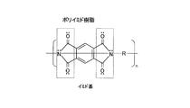
- Y10T428/31721—Of polyimide
-
- Y—GENERAL TAGGING OF NEW TECHNOLOGICAL DEVELOPMENTS; GENERAL TAGGING OF CROSS-SECTIONAL TECHNOLOGIES SPANNING OVER SEVERAL SECTIONS OF THE IPC; TECHNICAL SUBJECTS COVERED BY FORMER USPC CROSS-REFERENCE ART COLLECTIONS [XRACs] AND DIGESTS
- Y10—TECHNICAL SUBJECTS COVERED BY FORMER USPC
- Y10T—TECHNICAL SUBJECTS COVERED BY FORMER US CLASSIFICATION
- Y10T428/00—Stock material or miscellaneous articles
- Y10T428/31504—Composite [nonstructural laminate]
- Y10T428/31725—Of polyamide
- Y10T428/3175—Next to addition polymer from unsaturated monomer[s]
- Y10T428/31757—Polymer of monoethylenically unsaturated hydrocarbon
Definitions
- the present invention relates to a laminate in which an atomic layer deposition film is formed on the outer surface of a substrate, a gas barrier film formed by the laminate, and a method for producing these.
- CVD chemical vapor deposition
- PVD Physical Vapor Deposition
- PVD Typical examples of PVD include vacuum deposition and sputtering.
- sputtering is generally used to form high-quality thin films with high film quality and excellent film thickness uniformity, although the equipment cost is generally high. Therefore, it is widely applied to display devices such as liquid crystal displays.
- CVD is a method in which a raw material gas is introduced into a vacuum chamber, and one or two or more gases are decomposed or reacted on the substrate by thermal energy to grow a solid thin film. At this time, in order to promote the reaction at the time of film formation or to lower the reaction temperature, there are also those that use plasma and a catalyst (Catalyst) reaction together, such as PECVD (Plasma Enhanced Enhanced CVD), Cat-CVD, being called.
- PECVD Plasma Enhanced Enhanced CVD
- Cat-CVD Cat-CVD
- Such CVD is characterized by few film formation defects and is mainly applied to semiconductor device manufacturing processes such as gate insulating film formation.
- ALD Atomic Layer Deposition
- This ALD method is a method in which a substance adsorbed on the surface is formed one layer at a time by a chemical reaction on the surface, and is classified into the category of CVD.
- the ALD method is distinguished from general CVD by so-called CVD (general CVD) in which a thin film is grown by reacting on a base slope using a single gas or a plurality of gases simultaneously. is there.
- CVD general CVD
- the ALD method uses a precursor (TMA: Tri-MethylluminAluminum) or an active gas called a precursor and a reactive gas (also called a precursor in ALD) alternately.
- TMA Tri-MethylluminAluminum
- a precursor and a reactive gas also called a precursor in ALD
- a specific film formation method of the ALD method uses a so-called self-limiting effect in which, when the surface is covered with a certain gas in the surface adsorption on the substrate, no further gas adsorption occurs. When only one layer is adsorbed, the unreacted precursor is exhausted. Subsequently, a reactive gas is introduced, and the precursor is oxidized or reduced to obtain only one thin film having a desired composition, and then the reactive gas is exhausted. Such a process is defined as one cycle, and this cycle is repeated to grow a thin film. Therefore, in the ALD method, the thin film grows two-dimensionally.
- the ALD method is characterized in that it has fewer film-forming defects as compared with the conventional vacuum deposition method, sputtering, and the like, as well as general CVD. Therefore, it is expected to be applied to a wide range of fields such as the packaging field for foods and pharmaceuticals and the electronic parts field.
- the ALD method includes a method of using plasma to activate the reaction in the step of decomposing the second precursor and reacting with the first precursor adsorbed on the substrate.
- This method is called plasma activated ALD (PEALD: Plasma Enhanced ALD) or simply plasma ALD.
- the technology itself of the ALD method was developed in 1974 by Finnish Dr. Advocated by Tuomo Sumtola.
- the ALD method is capable of obtaining high-quality and high-density film formation, and is therefore being applied in the field of semiconductors such as gate insulating films.
- ITRS International Technology Roadmap for Semiconductors
- the ALD method has a characteristic that there is no oblique effect (a phenomenon in which sputtering particles are incident on the substrate surface obliquely to cause film formation variation) compared to other film formation methods, so that there is no gap for gas to enter. If so, film formation is possible.
- the ALD method can be applied to MEMS (Micro-Electro-Mechanical-Systems) related to the coating of lines and holes on a substrate having a high aspect ratio with a large depth to width ratio, as well as coating of three-dimensional structures. Expected.
- MEMS Micro-Electro-Mechanical-Systems
- the ALD method also has drawbacks. That is, in order to perform the ALD method, a special material is used and the cost is increased. However, the biggest drawback is that the film forming speed is low. For example, the film formation rate is about 5 to 10 times slower than a film formation method such as normal vacuum deposition or sputtering.
- the target for forming a thin film by the ALD method using the film forming method as described above is a small plate-like substrate such as a wafer or a photomask, or a substrate having a large area and no flexibility such as a glass plate. Or a substrate having a large area and flexibility such as a film.
- mass production facilities for forming thin films on these substrates have been proposed and put to practical use by various substrate handling methods depending on cost, ease of handling, film formation quality, etc. ing.
- a single substrate is supplied to a film forming apparatus to form a film, and then the wafer is replaced with the next substrate to form a film again, or a plurality of substrates are set together and all wafers are set.
- a batch type film forming apparatus for performing the same film forming.
- an in-line type film forming apparatus that performs film formation at the same time while sequentially transporting the substrate to a part serving as a film formation source.
- a so-called roll-to-roll coating film forming apparatus in which a flexible substrate is mainly unwound from a roll and film is formed while being conveyed, and the substrate is wound on another roll.
- the latter includes not only a flexible substrate but also a flexible coating sheet that can continuously convey a substrate to be deposited, or a web coating deposition apparatus that continuously deposits on a tray that is partially flexible.
- the film forming method and the substrate handling method using any of the film forming apparatuses a combination of film forming apparatuses having the fastest film forming speed is adopted in view of cost, quality, and ease of handling.
- a technique for forming a gas permeable barrier layer on a plastic substrate or a glass substrate by performing atomic layer deposition by the ALD method is disclosed (for example, see Patent Document 1).
- a light-emitting polymer is mounted on a flexible and light-transmitting plastic substrate, and atomic layer deposition is performed on the surface and side surfaces of the light-emitting polymer by ALD (top coating is applied). ).
- top coating is applied.
- laminates in which an atomic layer deposition film is provided on the outer surface of a substrate by the ALD method are widely known, and these laminates are preferably used for gas barrier films having gas barrier properties.
- the above-described laminates conventionally known have an atomic layer deposition film laminated on a polymer substrate, and the growth form is based on an inorganic crystal such as a conventional Si wafer. And found that there is a high possibility of being different.
- the substrate is an oxidized Si wafer, the precursor adsorption sites exist at a density approximately equal to the crystal lattice, and in many cases three-dimensional growth (island growth) during several cycles of atomic layer deposition.
- the film growth proceeds in the two-dimensional growth mode.
- the distribution density of the adsorption site of the precursor is low, and the adjacent nucleus contacts and becomes a continuous film by growing and expanding three-dimensionally using the isolated and adsorbed precursor as the nucleus. I found out.
- the period of the above three-dimensional growth is long, and the period until it becomes a continuous film and a dense film by two-dimensional growth is long. It means that there are fewer important parts. From the viewpoint of gas barrier properties, it is not preferable that there are few two-dimensionally grown portions. In other words, the conventional laminate may not have an ideal gas barrier property.
- the present invention has been made in view of such circumstances, and an object thereof is to provide a laminate having a high gas barrier property, a gas barrier film, and methods for producing them.
- the first aspect of the present invention is the substrate, the film-like or film-like undercoat layer formed on at least a part of the outer surface of the substrate, and the both sides in the thickness direction of the undercoat layer.
- An atomic layer deposition film formed on a surface opposite to the surface in contact with the substrate, wherein at least part of the precursor of the atomic layer deposition film is bonded to the undercoat layer, and the atomic layer deposition
- the film is a laminated body characterized by being formed in a film shape covering the undercoat layer.
- the undercoat layer may include a binder and an inorganic substance, and at least a part of the precursor of the atomic layer deposition film may be bonded to the inorganic substance contained in the undercoat layer.
- the binder may be an organic binder, and the main component of the undercoat layer may be the inorganic substance.
- the binder may be an inorganic binder, and the main component of the undercoat layer may be the inorganic substance.
- the binder may be an organic / inorganic hybrid binder, and the main component of the undercoat layer may be the inorganic substance.
- the inorganic material is exposed on a surface opposite to the surface in contact with the base material, and the precursor of the atomic layer deposition film is bonded to the exposed outer surface of the inorganic material. May be.
- the inorganic substance may be particulate inorganic particles.
- the inorganic substance may be a layered compound having a layered structure.
- the inorganic substance may be a sol or gel polymer.
- the undercoat layer may contain an organic polymer, and at least a part of the precursor of the atomic layer deposition film may be bonded to a functional group of the organic polymer contained in the undercoat layer. Good.
- the main component of the undercoat layer may be the organic polymer.
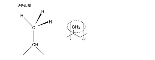
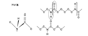
- the functional group of the organic polymer may have an O atom.
- the functional group having an O atom may be any one of an OH group, a COOH group, a COOR group, a COR group, an NCO group, and a SO 3 group.
- the functional group of the organic polymer may have an N atom.
- the functional group having an N atom may be an NH x group (X is an integer).
- the undercoat layer at least a part of the surface opposite to the surface in contact with the base material is surface-treated by plasma treatment or hydrolysis treatment, and the functional groups of the organic polymer are densified. Also good.
- the undercoat layer may contain an inorganic substance at least on the surface opposite to the surface in contact with the substrate.
- the second aspect of the present invention is a gas barrier film characterized in that the laminate of the first aspect is formed in a film shape.
- a part of the binder may be removed by plasma etching.
- the surface treatment of the undercoat layer may be performed by plasma etching or hydrolysis treatment to increase the density of the functional groups of the organic polymer.
- a method for producing a gas barrier film wherein the laminate produced by the method for producing a laminate according to the third aspect or the fourth aspect is formed into a film.
- the laminate and gas barrier film of the present invention have high gas barrier properties. Moreover, according to the manufacturing method of the laminated body and gas barrier film of this invention, a laminated body and gas barrier film with high gas barrier property can be manufactured.
- FIG. 1st Embodiment of this invention It is the flowchart which summarized the manufacturing process of the laminated body shown in FIG. It is the figure which compared the water vapor transmission rate about the laminated body of a present Example which has a gas barrier layer, and the laminated body of the comparative example which does not have a gas barrier layer. It is sectional drawing which shows the structure of the laminated body concerning 2nd Embodiment of this invention. It is a figure which shows the chemical formula of the functional group of an organic polymer, and shows a methyl group. It is a figure which shows the chemical formula of the functional group of an organic polymer, and shows a hydroxyl group.
- the laminate according to this embodiment has an undercoat layer between the base material and the atomic layer deposition film.
- This undercoat layer is a layer in which an inorganic substance is dispersed.
- the precursor of the atomic layer deposition film is a gaseous substance, and is easily bonded to the inorganic substance exposed on the surface of the undercoat layer.
- the precursors of the atomic layer deposition film bonded to each inorganic substance are bonded to each other. As a result, a two-dimensional atomic layer deposition film growing in the plane direction of the undercoat layer is generated.
- the undercoat layer the adsorption site density of the precursor is improved, so that the bond density between the atomic layer deposition layer and the undercoat layer is improved, and the atomic layer deposition layer can be applied to the undercoat layer and the substrate. This improves the adhesive strength.
- Laminates with atomic layer deposition films manufactured by atomic layer deposition are commercially produced as electronic component substrates such as thin-film wireless EL, displays, and semiconductor memory (DRAM), such as glass substrates and silicon substrates.
- ALD atomic layer deposition
- the base material of the laminate that is the subject of the present invention is a polymer base material having flexibility.
- the ALD process for polymer base materials has not been studied in detail. Therefore, assuming that the atomic layer deposition film grows in the same manner as the electronic component substrate, the polymer base material is approached to the laminate of the present invention while considering the growth process of the atomic layer deposition film on the polymer base material. Tried.
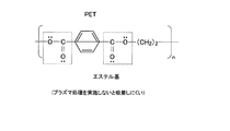
- an atomic layer deposition film on an electronic component substrate is considered to grow two-dimensionally, but in reality, an atomic layer deposition film on a polymer substrate (for example, PET: polyethylene terephthalate) grows two-dimensionally. Not done.
- a polymer substrate for example, PET: polyethylene terephthalate
- the main cause is considered to be “adsorption site density” and “adsorption site arrangement” on the polymer substrate. For these reasons, since the performance of the atomic layer deposition film is not sufficiently exhibited at a thin film thickness, the atomic layer deposition film needs to be 3 nm or 30 atomic layers or more.
- the density of the precursor adsorption sites in the ALD method which is the first cause, is considered as follows. That is, a gaseous precursor (TMA: metal-containing precursor such as Tri-Methyl Aluminum) or TiCL 4 is chemisorbed onto the surface of a polymer substrate (hereinafter sometimes simply referred to as a substrate). This is the first step of the ALD process. At this time, the reactivity of the functional group of the precursor and the base material and the density of the functional group greatly affect the chemical adsorption.
- TMA gaseous precursor
- TiCL 4 titanium-containing precursor
- the precursor in the atomic layer deposition film is adsorbed on the adsorption site.
- the precursor of the atomic layer deposition film can be adsorbed to functional groups such as OH and COOH groups of the polymer chain, but is difficult to adsorb to nonpolar parts such as alkyl groups. Therefore, plasma treatment is performed using a gas containing O 2 or N 2 for the purpose of increasing the adsorption power of the precursor, and functional groups are introduced onto the surface of the polymer substrate. However, depending on the type of polymer, the plasma treatment may cause breakage of the polymer chain. In this way, the portion where the polymer chain is broken has a lower physical strength and becomes a portion having a low cohesive force, forming a week boundary layer (an interface boundary layer having a weak adhesive force), leading to a decrease in the adhesive strength. . Therefore, the plasma treatment for introducing a functional group to the surface of the polymer substrate is limited in terms of adhesive strength.
- each adsorption site of a precursor is arrange
- the atomic layer deposition film grows three-dimensionally with the adsorption sites as nuclei.
- the atomic layer deposition film spreads in three dimensions for the precursor, and the precursor is sparsely adsorbed in places such as OH, so the atomic layer deposition film is columnar with an isolated nucleus at the center. Will grow into.
- an atomic layer volume film grown from isolated nuclei has a low bond density with the substrate and a high possibility of a low adhesion.
- the arrangement of the adsorption sites that is, the diffusion of the precursor
- a polymer film is a mixture of a crystalline region and an amorphous region. Therefore, in the non-crystalline region, there is a space where a polymer chain called free volume (free volume) does not exist, and gas diffuses and permeates through the space. The gaseous precursor also passes through the free volume space until it is adsorbed on the adsorption site.
- the precursor diffuses from the surface of the polymer substrate to the inside, adsorbs to the functional groups scattered three-dimensionally,
- the adsorption site becomes the nucleus of the atomic layer deposition film. Since these nuclei are scattered three-dimensionally, a three-dimensional growth mode is established until a certain nucleus contacts a neighboring nucleus to form a continuous film. Therefore, the period until it becomes a continuous film and becomes a dense film by two-dimensional growth is long, which means that the dense portion of the atomic layer deposition film in two-dimensional growth is reduced. Therefore, gas passes through the gaps in the atomic layer deposition film. Furthermore, the gas passes through the free volume space.
- the polymer in order to realize two points of (1) increasing the density of the adsorption site of the precursor and (2) preventing diffusion of the precursor to the polymer substrate, the polymer An undercoat layer containing an inorganic substance is provided on the substrate. That is, an undercoat layer containing an inorganic substance is provided on the polymer substrate prior to the ALD process in order to arrange the precursor adsorption sites at a high density on the surface of the polymer substrate in a two-dimensional manner. . In addition, in order to increase the density of the adsorption site of the precursor, the adsorption site of the inorganic substance having a high density is used.
- the gas containing the precursor is less likely to permeate the undercoat layer containing the inorganic substance. Moreover, since the adsorption site density is increased, the adhesion of the atomic layer deposition layer to the undercoat and the base material is improved.
- FIG. 1 is a cross-sectional view showing a configuration of a laminate according to an embodiment of the present invention.
- a laminate 1 includes a base material 2 formed of a polymer material, and a film-like or film-like undercoat layer (hereinafter referred to as a UC layer) 3 formed on the surface of the base material 2.
- an atomic layer deposition film (hereinafter referred to as an ALD film) 4 formed on the surface opposite to the surface in contact with the substrate 2 out of both surfaces in the thickness direction of the UC layer 3.
- the UC layer 3 has a configuration in which an inorganic substance (inorganic material) is added to a binder.
- the precursor of the ALD film 4 is formed in a film shape so that the ALD film 4 covers the UC layer 3 by being combined with mutual inorganic substances contained in the UC layer 3.
- the UC layer 3 is formed of a binder and an inorganic substance (inorganic material).
- an inorganic substance has a small free volume unlike a polymer.
- the inorganic substance does not have glass point transfer like a polymer, the characteristics do not change even in a high temperature process. That is, in the polymer, the non-crystalline part starts the Brownian motion above the glass point transfer, and the gas diffusion rate in the free volume increases, but the inorganic substance does not have such a phenomenon due to the glass point transfer.
- the inorganic substance used for the UC layer 3 is a layered compound. Therefore, the inorganic substance of such a layered compound is oriented almost parallel to the coating surface of the substrate 2. Further, all gases including the precursor gas in the ALD film 4 cannot diffuse inside the inorganic substance of the layered compound.
- the surface of the UC layer 3 is etched so that the surface of the inorganic substance of the layered compound is exposed. That is, the surface of the UC layer 3 is etched by performing plasma treatment in order to introduce a desired functional group into the surface of the inorganic substance of the layered compound in the UC layer 3 exposed on the substrate 2.
- the UC layer 3 having the above-described characteristics is provided on the surface of the polymer base material 2, precursor adsorption sites are arranged on the surface of the base material 2 at a high density.
- the inorganic substance of the layered compound in the UC layer 3 is arranged in parallel to the surface of the substrate 2. Therefore, since the UC layer 3 covers the surface area of the substrate 2 almost uniformly, the adsorption sites are two-dimensionally arranged, and the two-dimensional growth of the ALD film 4 is promoted. Further, since the inorganic substance portion of the layered compound in the UC layer 3 does not undergo glass transition unlike a general plastic polymer even when the process temperature of ALD for forming the ALD film 4 is high, stable ALD Film growth of the film 4 is performed.
- the binder of the UC layer 3 may be any of an organic binder, an inorganic binder, and a hybrid binder of an organic / inorganic mixture.
- the precursor of the ALD film 4 is appropriately bonded to the outer surface of the inorganic substance.
- the bonding strength with the precursor of the ALD film 4 can be increased by making the inorganic substance into a particulate or layered structure.
- an optimum bonding force is obtained by making the inorganic substance into a sol or gel polymer.
- a surface on which functional groups are arranged at a high density is formed, so that not only the ALD method but also other thin film growth methods (for example, vacuum deposition, sputtering, CVD, etc.) ), It can be expected to form a dense thin film by a growth mode with a high nuclear density.
- the laminated body 1 shown in FIG. 1 is implement
- this manufacturing process shows an example, Comprising: It is not limited to this content. That is, 1. If necessary, the polymer substrate 2 is subjected to plasma treatment or primer treatment. 2. An undercoat material (solution) for forming the UC layer 3 is prepared.
- an organic binder, an inorganic binder, or an inorganic / organic mixed hybrid binder, an inorganic substance (for example, inorganic particles), and a solvent are prepared.
- the organic binder polyester acrylate or urethane acrylate is used.
- a hydrolyzate of polyvinyl alcohol and metal alkoxide is used.
- a hydrolyzate of the above metal alkoxide (TEOS) can be used.
- Inorganic particles are prepared as an inorganic substance. At this time, the inorganic particles are prepared as spherical inorganic particles or those in which the inorganic particles are layered compounds. 4).
- the UC layer 3 is formed by an undercoat process using the above materials 2 to 3. 5. If necessary, the surface of the UC layer 3 is etched. 6).
- An ALD film 4 is formed by an atomic layer deposition method (ALD method). As a promotion plan for two-dimensional growth of the ALD film 4, it is desirable to contain a layered compound of an inorganic substance and silanol that serves as an adsorption site during the undercoat treatment.
- FIG. 2 is a flowchart summarizing the manufacturing process of the laminate 1 shown in FIG.
- a polymer base material 2 is placed on a thin film forming apparatus (semiconductor manufacturing apparatus or the like) (step S1).
- a film-like or film-like undercoat layer (UC layer) 3 made of a composite material of a binder and an inorganic substance is formed on the surface of the substrate 2 placed on the thin film forming apparatus (step S2).
- step S3 a part of the binder exposed on the surface of the UC layer 3 formed in step S2 (that is, the surface opposite to the surface in contact with the base material 2) is removed, and the inorganic material is exposed on the surface of the inorganic material. (Step S3). Then, the ALD film 4 is formed on the surface of the UC layer 3 so that the precursor of the atomic layer deposition film (ALD film) 4 is bonded to the inorganic substance exposed in step S3 (step S4).
- ALD film precursor of the atomic layer deposition film
- step S3 it is desirable to remove a part of the binder by plasma etching. That is, when an organic binder is used, since there is a possibility that an inorganic substance (inorganic particles) may be covered with the organic binder on the surface of the UC layer 3, the organic binder on the surface of the UC layer 3 is removed by plasma etching. There is a need. In this manner, since the ALD film 4 can be densely formed on the surface of the UC layer 3 by the steps S1 to S4, the gas barrier property of the stacked body 1 can be increased.
- each step may be performed in the same apparatus, or each step may be performed by another apparatus. Further, after step S3 and before step S4, the surface of the UC layer 3 from which the inorganic substance is exposed may be further subjected to plasma treatment to introduce a desired functional group.
- the inorganic compound (inorganic substance) used for the undercoat layer (UC layer) 3 will be described in detail.
- the radio material is selected with the following points in mind. That is, as an element for selecting an inorganic substance composed of inorganic particles, the shape of the inorganic particles includes nearly spherical particles and plate-like particles, and any particle can be used.
- the particle size (particle diameter) of the inorganic particles is 1 ⁇ m or less, preferably 0.1 ⁇ m or less, so that the smoothness of the substrate 2 is not affected.
- the size of the inorganic particles is sufficiently smaller than the wavelength of visible light so as to avoid the influence on the optical characteristics of the UC layer 3 (that is, light transmittance, haze: ratio of diffuse transmitted light to total transmitted light) as much as possible. Particle size is desirable.
- an aspect ratio (Z) of 50 or more and a thickness of 50 nm or less, preferably 20 nm or less is selected.
- Z L / a where L is the average particle diameter and a is the thickness of the material of the inorganic particles.
- coloring is not preferable from the viewpoint of transparent barrier coating.
- it is necessary to match the refractive index of the binder of the UC layer 3 and the inorganic particles. That is, in the UC layer 3, when the refractive index of the binder and the refractive index of the inorganic particles are significantly different, reflection at the interface of the UC layer 3 is increased. As a result, the light transmittance in the UC layer 3 is reduced and haze is increased.
- the dispersibility of the inorganic particles secondary agglomeration hardly occurs because of good dispersion in the binder. Further, when the inorganic substance is a layered compound, the affinity (intercalation: chemical bond) with the binder is good.
- the laminate 1 As for the stability of the inorganic particles, when the laminate 1 is used as a solar cell, a usage period of 20 to 30 years is assumed. Therefore, the laminate 1 is used for a long time at high temperature / high humidity and extremely low temperature. Even inorganic materials need to be chemically stable. In addition, about the safety
- inorganic substance used for the UC layer 3 is inorganic particles, for example, halloysite, calcium carbonate, silicic anhydride having a particle size larger than that of extender candidates, for example, kaolinite which is a kind of viscosity mineral , Hydrous silicic acid, or alumina.
- inorganic particles for example, halloysite, calcium carbonate, silicic anhydride having a particle size larger than that of extender candidates, for example, kaolinite which is a kind of viscosity mineral , Hydrous silicic acid, or alumina.
- the inorganic substance is a layered compound
- artificial clay fluorine phlogopite, fluorine tetrasilicon mica, teniolite, fluorine vermiculite, fluorine hectorite, hectorite, sapolite, stevensite, montmorillonite, beidellite, kaolinite, or flybon
- Graphene or a derivative thereof is selected in consideration of the affinity of the binder with the solvent.
- graphene alcohol dispersion Incubation Alliance GF3IPA-D1 or aqueous dispersion (Incubation Alliance GF3W1-D1)
- graphene An aqueous dispersion of oxide As the organic solvent binder, flaky graphene (Angston Materials, N002-PDR, etc.) may be appropriately dispersed in a solvent.
- the coating method when graphene or a derivative thereof is used as an inorganic substance is appropriately selected from bar coating, roll coating, slot die coating, gravure coating, etc. in consideration of the solid content of the coating solution, target coating amount, uniformity, etc. .
- the material selection method described above can be used as long as it has excellent mixing properties.
- lamellar viscous minerals include pyroferrite, talc, montmorillonite (overlapping with artificial clay), beidellite, nontronite, saponite, vermiculite, sericite, sea green stone, ceradonite, kaolinite, nacrite, dacite, halo.
- An inorganic substance such as site, antigolite, chrysotile, amesite, chroniteite, chamosite, chlorite, alevaldite, corrensite, or tosudite can also be used as a layered compound.
- the extender pigment other inorganic particles (spherical particles), a polycrystalline compound, zirconia, metal oxides such as titania, barium titanate, the general chemical formula, such as strontium titanate and the like MM'O X
- metal oxide containing two or more metal atoms M, M ′, etc.
- inorganic particles used for the UC layer 3 the following silica fine particles are generally used.
- Colloidal silica Snowtex XS (registered trademark) manufactured by Nissan Chemical Industries, Ltd.
- This colloidal silica is an ultra-small particle silica sol stabilized with Na, SiO 2 30%, particle diameter 4 to 6 nm, pH 9.0 to 10.0, viscosity 1.0 to 7.0 mPa ⁇ s. .
- Organosilica sol MEK-ST (registered trademark) manufactured by Nissan Chemical Industries, Ltd.
- This organosilica sol is a methyl ethyl ketone-dispersed silica sol having a SiO 2 content of 30%, a particle diameter of 10 to 20 nm, a viscosity of 1.0 to 5.0 mPa ⁇ s, and a water content of 0.5% or less.
- Reactive unusual shape silica fine particles DP1039SIV (registered trademark) manufactured by JGC Catalysts & Chemicals Co., Ltd.
- the reactive irregular shaped silica fine particles have an average primary particle size of 20 nm, an average number of connections of 3.5, an average secondary particle size of 55 nm, a solid content of 30%, a MIBK solvent, and a photocurable group that is a methacryloyl group.
- Reactive silica fine particles MIBK-SD (registered trademark) manufactured by Nissan Chemical Industries, Ltd.
- the reactive silica fine particles have an average primary particle size of 12 nm, a solid content of 30%, a MIBK solvent, and a photocurable group that is a methacryloyl group.
- Montmorillonite is used as the layered compound of the inorganic substance. That is, montmorillonite is a kind of mineral (silicate mineral) and belongs to the smectite group. Its chemical composition is (Na, Ca) 0.33 (Al, Mg) 2 Si 4 O 10 (OH) 2 . It is a monoclinic system of nH 2 O. This montmorillonite is one of the clay minerals and is contained in rocks that have undergone hydrothermal alteration.
- montmorillonite contained in the rock the one that has the property of turning wet litmus paper red is called acid clay.
- the name of Montmorillonite was named in 1847 after the place name of Montmorillon in France. Various characteristics of this montmorillonite will be described in ⁇ Appendix> below.
- Organic binder used for the UC layer 3 will be described.
- Organic binders are classified into water-based and solvent-based depending on the solvent used.
- the water-based organic binder include polyvinyl alcohol and polyethyleneimine.
- the solvent-based organic binder include acrylic ester, urethane acrylic, polyester acrylic, and polyether acrylic.
- Organic Binder for O-Atom-Containing Resin Preferred materials for the organic binder for O-atom-containing resin are as follows.
- the hydroxyl group (OH) -containing resin include polyvinyl alcohol, phenol resin, and polysaccharides.
- the polysaccharide includes cellulose derivatives such as cellulose, hydroxymethylcellulose, hydroxyethylcellulose, and carboxymethylcellulose, chitin, chitosan, and the like.
- COOH carbonyl group
- a carboxyvinyl polymer is also a preferable material.
- organic binders for O atom-containing resins include polyketone, polyetherketone, polyetheretherketone, aliphatic polyketone and the like of ketone group (CO) -containing resins.
- ester group (COO) -containing resins such as polyester resin, polycarbonate resin, liquid crystal polymer, polyethylene terephthalate (PET), polybutylene terephthalate (PBT), polyethylene naphthalate (PEN), boribylene naphthalate (PBN), polytrile Methylene terephthalate (PTT) or the like can also be used.
- an epoxy resin or an acrylic resin containing the above functional group may be used.
- organic binder of N-atom-containing resin Preferred materials for the organic binder of N-atom-containing resin are as follows.
- the imide group (CONHCO) -containing resin include polyimide, polyetherimide, polyamideimide, alicyclic polyimide, and solvent-soluble polyimide.
- alicyclic polyimides aromatic polyimides are usually obtained from aromatic tetracarboxylic acid anhydrides and aromatic diamines, but since they are not transparent, acid dianhydrides or diamines are used to make polyimides transparent. It is also possible to substitute an aliphatic group or an alicyclic group.
- Examples of the alicyclic carboxylic acid include 1,2,4,5-cyclohexanetetracarboxylic acid and 1,2,4,5-cyclopentanetetracarboxylic dianhydride.
- examples of the solvent-soluble polyimide include ⁇ -ptyrolactone, N, N-dimethylacetamide, and N-methyl-2-pyrrolidone.
- amide group (NHCO) -containing resins such as nylon-6, nylon-6,6, metaxylenediamine-adipic acid condensation polymer, polymethylmethacrylamide and the like.
- urethane resins such as isocyanate group (NHCOO) -containing resins. Urethane resin can also be used as an adhesion layer.
- amino group (NH) -containing resins can also be used.
- Organic binders for S atom-containing resins include the following. That is, examples thereof include polyethersulfone (PES), polysulfone (PSF), polyphenylsulfone (PPS), and the like, which are sulfonyl group (SO 2 ) -containing resins. Among these, PES and PSF are materials having high heat resistance. Furthermore, a polymer alloy, a polybutylene terephthalate polymer alloy, a polyphenylene sulfide polymer alloy, or the like can also be used as the organic binder. In the polymer alloy, the above polymer may be combined with a polymer (alloy, blend, or composite) as necessary.
- the organic / inorganic mixed hybrid binder / inorganic binder used in the UC layer 3 includes metal alkoxides (precursors of inorganic compounds), which are represented by R1 (M-OR2) as a general formula.
- Rl and R2 are organic groups having 1 to 8 carbon atoms, and M is a metal atom.
- the metal atom M is Si, Ti, Al, Zr, or the like.
- Examples of the metal atom M represented by Rl (Si-OR2) in Si include tetramethoxysilane, tetraethoxysilane, tetrapropoxysilane, tetraptoxysilane, methyltrimethoxysilane, methyltriethoxysilane, dimethyldimethoxysilane, Examples include dimethyldiethoxysilane.
- Examples of the metal atom M in which Zr is represented by R1 include tetramethoxyzirconium, tetraethoxyzirconium, tetraisopropoxyzirconium, and tetraptoxyzirconium.
- Examples of the metal atom M that is Ti and represented by Rl (Ti—OR 2) include tetramethoxytitanium, tetraethoxytitanium, tetraisopropoxytitanium, and tetrapoxytitanium.
- Examples of the metal atom M that is Al and represented by Rl include tetramethoxyaluminum, tetraethoxyaluminum, tetraisopropoxyaluminum, and tetraptoxyaluminum.
- montmorillonite used as the layered compound of the inorganic substance in the UC layer 3 will be described in detail.
- Montmorillonite the main component of bentonite, is a clay mineral classified as smectite, a kind of layered silicate mineral.
- the crystal structure of montmorillonite is composed of three layers of silicate tetrahedral layer-alumina octahedral layer-silicate tetrahedral layer, and the unit layer is about 10 mm (1 nm) thick and spreads about 0.1-1 ⁇ m. It is an extremely thin plate.
- Each crystal layer itself is negatively charged, but Na +, K +, Ca +, Mg +, etc.
- the shortage of charge is neutralized by sandwiching the cation, and montmorillonite becomes stable. Therefore, montmorillonite exists in a state where crystal layers overlap each other.
- the specific properties of montmorillonite are exhibited by the negative charge on the surface of the layer and the interlayer cations causing various actions.
- the ion exchange properties of montmorillonite As for the ion exchange properties of montmorillonite, the negative charge on the surface of the montmorillonite unit layer and the interlayer cation are weak, so when a solution containing other ions is used as a catalyst, the interlayer cation and the cation in the liquid are instantaneous. Cation exchange occurs. By measuring the amount of cations released into water, the amount of charge involved in the reaction of montmorillonite (ie, cation exchange capacity: CEC) can be determined. The cation exchange capacity varies depending on the pH and concentration of the solution, and montmorillonite is known to increase in cation exchange capacity when the pH is 6 or higher.
- montmorillonite has a layered structure, it has a very large surface area. Therefore, on the surface area, a hydrogen bond with an oxygen atom or a hydrogen group on the surface of the layer, an electrostatic bond with an interlayer negative charge or an interlayer cation between layers, and the like are exerted, thereby exhibiting an adsorption ability. Montmorillonite is particularly susceptible to polar molecules.
- montmorillonite has the action of adsorbing and swelling (swelling) when it comes into contact with water. This effect is caused by the interaction between interlayer cations and water molecules.
- the binding force between the negative charge on the unit layer surface of montmorillonite and the interlayer cation is weaker than the interaction energy between the interlayer cation and water molecule, so the interlayer cation is expanded by the force that attracts the water molecule. It is the mechanism of swelling. Basically, the swelling ends when the interaction between interlayer cations and water molecules reaches the limit.
- montmorillonite is stabilized in a state where it is layered, and its end portion is positively charged and the side portion is negatively charged.
- the layers are electrostatically bonded to each other to form a card house structure (a three-dimensional structure by electrical coupling).
- the force for forming the card house structure becomes resistance, and viscosity is generated in the montmorillonite dispersion.
- the dispersion gels, and when shear is applied, it returns to a viscous dispersion. This is the thixotropic mechanism.
- Montmorillonite is an organophilic pentonite that uses a cation exchange property and intercalates an organic agent between layers to enable dispersion in an organic solvent or resin.
- organic agent quaternary ammonium salts such as dimethyl distearyl ammonium salt and trimethyl stearyl ammonium salt are generally used.
- an ammonium salt having a pendyl group or a polyoxyethylene group may be used, or a phosphonium salt or an imidazolium salt may be used instead of an ammonium salt.
- Example Next, a specific example of a laminate including a gas barrier layer made of an atomic layer deposition film realized based on the above embodiment will be described.
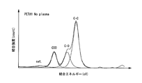
- ⁇ Gas barrier layer deposition method> A TiO 2 film was formed on the upper surface of the polymer substrate provided with the UC layer by ALD.
- the raw material gas was titanium tetrachloride (TiCl 4 ).
- the treatment pressure at that time was 10 to 50 Pa.
- the plasma gas excitation power source was a 13.56 MHz power source, and plasma discharge was performed in the ICP mode.
- the supply time of each gas was 60 msec for TiCl 4 and the process gas, 10 sec for the purge gas, and 3 sec for the reactive gas / discharge gas. Then, plasma discharge was generated in the ICP mode at the same time as the reaction gas and the discharge gas were supplied. The output power of the plasma discharge at this time was 250 watts. Further, as gas purge after plasma discharge, purge gases O 2 and N 2 were supplied for 10 seconds. The film forming temperature at this time was 90 ° C.
- the film formation rate of TiO 2 under the above cycle conditions was as follows. That is, since the unit film formation rate is about 0.9 mm / cycle, when the film formation process of 110 cycles was performed to form a film with a film thickness of 10 nm, the total film formation time was about 43 minutes.
- ⁇ Plasma etching> The upper surface provided with the UC layer on the polymer substrate was placed on a plasma asher device, and the binder on the surface of the UC layer was etched with oxygen plasma to expose the inorganic substance contained in the UC layer on the surface. The state of exposure was confirmed using SEM (electron microscope). Etching conditions were as follows: a barrel type plasma asher device was used, and the output of RF plasma (13.56 MHz) at that time was 500 w, the oxygen gas flow rate was 300 sccm, and the pressure was 50 Pa. The etching time was determined by confirming the exposed state of the inorganic substance.
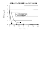
- FIG. 3 is a diagram comparing the water vapor transmission rate of the laminate of this example having a gas barrier layer and the laminate of a comparative example having no gas barrier layer. Therefore, the superiority of each embodiment will be described with reference to FIG.
- the laminate with the gas barrier layer realized based on the above embodiment was laminated with another polyethylene terephthalate (PET) stretch film using an adhesive, and the peel strength of the bonded product was measured. .
- oxygen plasma treatment output power: 300 watts, treatment time: 180 seconds
- a stretched film 100 ⁇ m thick
- PET polyethylene terephthalate
- a urethane-based adhesive Mitsubishi Chemicals A-315 / A-10 was applied to the oxygen plasma treated surface so as to have a dry weight of 3 g / cm 2 , dried, and bonded to the gas barrier layer laminate.
- the urethane adhesive was cured by storing in an oven at 40 ° C. for 4 days.
- ⁇ Peel test> The cured sample is cut into a test piece having a length of 300 mm and a width of 10 mm, and the peel strength is measured using an Instron type tensile tester with a T-type peel test method and a peel speed of 300 mm / min. did. The measured value of peel strength was the average value of 5 test pieces (N / 10 mm).
- Example 1 a UC layer was formed on a polymer substrate, and a TiO 2 thin film was formed thereon by the ALD method.
- a UC layer having a dry thickness of 1 ⁇ m was formed on the polymer substrate under the coating conditions of the undercoat agent. Note that in the oxygen plasma treatment, 100 sccm of O 2 was supplied as a plasma discharge gas, a 13.56 MHz power source was used as a plasma gas excitation power source, and plasma discharge was performed in ICP mode for 180 seconds.
- the UC layer (undercoat layer) was prepared by dissolving 500 g of polyvinyl alcohol (PVA) (Poval 117, manufactured by Kuraray Co., Ltd.) with saponification degree of 98-99% with ion-exchanged water so that the solid content was 5% by weight. Agitation) and 100 g of colloidal silica (Snowtex XS manufactured by Nissan Chemical Industries, Ltd.) were mixed and agitated. The undercoat layer was applied using a Mayer bar. The coated sample was dried in an oven at 105 ° C. for 5 minutes. At this time, plasma etching of the UC layer is not performed.
- PVA polyvinyl alcohol
- Example 2 As shown in Example 2 in FIG. 3, a stretched PET film (100 ⁇ m thickness) is prepared as a polymer substrate (substrate), and after oxygen plasma treatment is performed on one surface thereof, the same formulation as in Example 1 is used. The undercoat layer was formed on the substrate. Next, the polymer substrate on which the UC layer was formed was placed on a plasma asher device, and plasma etching of the UC layer surface was performed. The etching time at this time was 30 minutes. Thereafter, a TiO 2 thin film having a thickness of 10 nm was formed under the same conditions as in Example 1. Water vapor transmission rate (WVTR) was determined for samples of the thus laminated body obtained by forming a thin film of TiO 2.
- WVTR Water vapor transmission rate
- the measured value of WVTR at this time was 5.0 ⁇ 10 ⁇ 4 [g / m 2 / day].
- the peel strength of the sample laminated according to the above-described lamination conditions was measured according to the method of the peel test. The peel strength was 6.4 N / 10 mm.
- Example 3 As shown in Example 3 of FIG. 3, a stretched PET film (100 ⁇ m thickness) is prepared as a polymer substrate (substrate), and after oxygen plasma treatment is performed on one side thereof, the same formulation as in Example 1 is used. The undercoat layer was formed on the substrate. Next, the polymer substrate on which the UC layer was formed was placed on a plasma asher device, and plasma etching of the UC layer surface was performed. The etching time at this time was 30 minutes. Furthermore, the oxygen plasma treatment performed on the surface of the polymer substrate in Example 1 was performed under the same conditions on the surface of the UC layer subjected to plasma etching.
- a TiO 2 thin film having a thickness of 10 nm was formed under the same conditions as in Example 1.
- Water vapor transmission rate (WVTR) was determined for samples of the thus laminated body obtained by forming a thin film of TiO 2.
- the measured value of WVTR at this time was 5.0 ⁇ 10 ⁇ 4 [g / m 2 / day].
- the peel strength of the sample laminated according to the above-described lamination conditions was measured according to the method of the peel test. The peel strength was 6.5 N / 10 mm.
- Example 4 As shown in Example 4 of FIG. 3, after preparing a stretched PET film (100 ⁇ m thick) as a polymer substrate (substrate) and performing oxygen plasma treatment on one side, an undercoat layer of the following formulation: Then, a TiO 2 thin film having a thickness of 10 nm was formed under the same conditions as in Example 1.
- the UC layer undercoat layer
- 150 g of urethane binder (solid content 20%) and 100 g of organosilica sol MEK-ST manufactured by Nissan Chemical Industries, Ltd.
- WVTR Water vapor transmission rate
- Example 5 As shown in Example 5 in FIG. 3, a stretched PET film (100 ⁇ m thick) was prepared as a polymer substrate (substrate), and after oxygen plasma treatment was performed on one surface thereof, the same formulation as in Example 4 was used. The undercoat layer was formed on the substrate. Next, the polymer substrate on which the UC layer was formed was placed on a plasma asher device, and plasma etching of the UC layer surface was performed. The etching time at this time was 30 minutes. Thereafter, a TiO 2 thin film having a thickness of 10 nm was formed under the same conditions as in Example 1. Water vapor transmission rate (WVTR) was determined for samples of the thus laminated body obtained by forming a thin film of TiO 2.
- WVTR Water vapor transmission rate
- the measured value of WVTR at this time was 5.0 ⁇ 10 ⁇ 4 [g / m 2 / day].
- the peel strength of the sample laminated according to the above-described lamination conditions was measured according to the method of the peel test. The peel strength was 7.5 N / 10 mm.
- Example 6 As shown in Example 6 of FIG. 3, a stretched PET film (100 ⁇ m thickness) is prepared as a polymer substrate (substrate), and after oxygen plasma treatment is performed on one surface thereof, the same formulation as in Example 4 is used. The undercoat layer was formed on the substrate. Next, the polymer substrate on which the UC layer was formed was placed on a plasma asher device, and plasma etching of the UC layer surface was performed. The etching time at this time was 30 minutes. Furthermore, the oxygen plasma treatment performed on the surface of the polymer substrate in Example 1 was performed under the same conditions on the surface of the UC layer subjected to plasma etching.
- a TiO 2 thin film having a thickness of 10 nm was formed under the same conditions as in Example 1.
- Water vapor transmission rate (WVTR) was determined for samples of the thus laminated body obtained by forming a thin film of TiO 2.
- the measured value of WVTR at this time was 5.0 ⁇ 10 ⁇ 4 [g / m 2 / day].
- the peel strength of the sample laminated according to the above-described lamination conditions was measured according to the method of the peel test. The peel strength was 7.7 N / 10 mm.
- Example 7 As shown in Example 7 in FIG. 3, a stretched PET film (100 ⁇ m thickness) was prepared as a polymer substrate (substrate), and after oxygen plasma treatment was performed on one surface thereof, an undercoat layer having the following formulation was used. Then, a TiO 2 thin film having a thickness of 10 nm was formed under the same conditions as in Example 1.
- the UC layer (undercoat layer) was stirred by dissolving 500 g of polyvinyl alcohol (PVA) (Poval 117 manufactured by Kuraray Co., Ltd., saponification degree 98-99% with ion-exchanged water to a solid content of 5% by weight).
- PVA polyvinyl alcohol
- WVTR Water vapor transmission rate
- Example 8 As shown in Example 8 in FIG. 3, a stretched PET film (100 ⁇ m thick) was prepared as a polymer substrate (substrate), and after oxygen plasma treatment was performed on one surface thereof, the same formulation as in Example 7 was used. The undercoat layer was formed on the substrate, and then a TiO 2 thin film was formed to a thickness of 10 nm under the same conditions as in Example 1. At this time, both plasma etching of the UC layer and oxygen plasma treatment after the plasma etching were performed. Water vapor transmission rate (WVTR) was determined for samples of the thus laminated body obtained by forming a thin film of TiO 2. The measured value of WVTR at this time was 5.0 ⁇ 10 ⁇ 4 [g / m 2 / day]. The peel strength of the sample laminated according to the above-described lamination conditions was measured according to the method of the peel test. The peel strength was 6.1 N / 10 mm.
- Example 9 As shown in Example 9 of FIG. 3, a stretched PET film (100 ⁇ m thickness) was prepared as a polymer substrate (substrate), and after oxygen plasma treatment was performed on one surface thereof, the same formulation as in Example 7 was used. The undercoat layer was formed on the substrate, and then a TiO 2 thin film was formed to a thickness of 5 nm under the same conditions as in Example 1. At this time, plasma etching of the UC layer was performed, but oxygen plasma treatment after the plasma etching was not performed. Water vapor transmission rate (WVTR) was determined for samples of the thus laminated body obtained by forming a thin film of TiO 2.
- WVTR Water vapor transmission rate
- the measured value of WVTR at this time was 5.0 ⁇ 10 ⁇ 4 [g / m 2 / day].
- the peel strength of the sample laminated according to the above-described lamination conditions was measured according to the method of the peel test. The peel strength was 6.0 N / 10 mm.
- Example 10 As shown in Example 10 of FIG. 3, a stretched PET film (100 ⁇ m thick) was prepared as a polymer substrate (substrate), and after oxygen plasma treatment was performed on one surface thereof, the same formulation as in Example 7 was used. The undercoat layer was formed on the substrate, and then a TiO 2 thin film was formed to a thickness of 5 nm under the same conditions as in Example 1. At this time, both plasma etching of the UC layer and oxygen plasma treatment after the plasma etching were performed. Water vapor transmission rate (WVTR) was determined for samples of the thus laminated body obtained by forming a thin film of TiO 2. The measured value of WVTR at this time was 5.0 ⁇ 10 ⁇ 4 [g / m 2 / day]. The peel strength of the sample laminated according to the above-described lamination conditions was measured according to the method of the peel test. The peel strength was 6.1 N / 10 mm.
- ⁇ Comparative example 1> As shown in Comparative Example 1 in FIG. 3, a stretched PET film (100 ⁇ m thick) was prepared as a polymer substrate (substrate). Then, after performing oxygen plasma treatment on one side of the substrate, a thin film of TiO 2 was formed to a thickness of 10 nm under the same conditions as in Example 1 without performing undercoat treatment. Next, the water vapor transmission rate (WVTR) of the sample on which the TiO 2 thin film was formed was measured. The measured value of WVTR at this time was 5.2 ⁇ 10 ⁇ 3 [g / m 2 / day].
- WVTR water vapor transmission rate
- the peel strength of the sample laminated according to the above-described lamination conditions was measured according to the method of the peel test. The peel strength was 5.0 N / 10 mm.
- ⁇ Comparative example 2> As shown in Comparative Example 2 in FIG. 3, a stretched PET film (100 ⁇ m thick) was prepared as a polymer substrate (substrate). Then, after performing oxygen plasma treatment on one side of the base material, a thin film of TiO 2 was formed to a thickness of 20 nm under the same conditions as in Example 1 without performing undercoat treatment. Next, the water vapor transmission rate (WVTR) of the sample on which the TiO 2 thin film was formed was measured. The measured value of WVTR at this time was 5.3 ⁇ 10 ⁇ 3 [g / m 2 / day].
- WVTR water vapor transmission rate
- the peel strength of the sample laminated according to the above-described lamination conditions was measured according to the method of the peel test. The peel strength was 5.1 N / 10 mm.
- a stretched PET film (100 ⁇ m thick) was prepared as a polymer substrate (substrate).
- PVA polyvinyl alcohol
- 5% solution Poval 117 manufactured by Kuraray Co., Ltd., saponification degree 98-99% with ion exchange water to a solid content of 5% by weight
- the UC layer was applied by dissolving and stirring in the solution. The application was performed using a Mayer bar. The sample applied at this time was dried in an oven at 105 ° C. for 5 minutes. Thereafter, a TiO 2 thin film having a thickness of 10 nm was formed under the same conditions as in Example 1. That is, the UC layer of the laminate of Comparative Example 3 is only PVA, and there is no layered compound.
- the measured value was 3.8 ⁇ 10 ⁇ 3 [g / m 2 / day]. That is, the WVTR is slightly improved as compared with the case where the UC layer is not provided as in the first comparative example. However, the WVTR is deteriorated by almost one digit as compared with the case where an undercoat layer (UC layer) having a layered compound of an inorganic substance is provided as in this example.
- the peel strength of the sample laminated according to the above-described lamination conditions was measured according to the method of the peel test. The peel strength was 5.8 N / 10 mm.
- an ALD film is formed on the polymer substrate.
- a dense ALD film can be formed.
- the gas barrier property can be enhanced and the insulating properties of the polymer substrate can be improved.
- the polymer substrate can achieve desired performance even with a thin ALD film.
- the adhesive strength of the atomic layer deposition layer to the undercoat layer and the substrate is improved, a laminated product having a high peel strength can be obtained when laminated.
- the laminate according to this embodiment has an undercoat layer between the base material and the atomic layer deposition film.
- This undercoat layer is a layer containing an organic polymer, and the organic polymer has a binding site to which the precursor of the atomic layer deposition film is bonded. That is, the organic polymer contained in the undercoat layer has a large number of functional groups as bonding sites that are easily bonded to the precursor of the atomic layer deposition film. Accordingly, the precursors bonded to each functional group of the organic polymer are bonded to each other.
- an inorganic substance may be dispersed in the undercoat layer. That is, by adding an inorganic substance to the undercoat layer, the adsorption density of the precursor of the atomic layer deposition film can be further improved.
- the polymer substrate An undercoat layer containing an organic polymer is provided on the top. That is, an undercoat layer containing an organic polymer is formed on the polymer substrate prior to the ALD process in order to arrange the precursor adsorption sites at a high density on the surface of the polymer substrate.
- an inorganic substance is added to the undercoat layer.
- the laminate 101 of this embodiment has a UC layer 103 containing an organic polymer material instead of the UC layer 3 described in the first embodiment.
- the organic polymer contained in the UC layer 103 ensures an adsorption site for the precursor of the ALD film 4. That is, the organic polymer contained in the UC layer 103 has a functional group that can easily adsorb the precursor of the ALD film 4. Therefore, the ALD film 4 is formed in a film shape so as to cover the UC layer 103 by bonding the precursor of the ALD film 4 to the functional group of the organic polymer contained in the UC layer 103.
- an organic polymer having a functional group that is easily adsorbed by the precursor of the ALD film 4. is there.
- an organic polymer having a high functional group density is selected.
- the surface of the organic polymer is modified to increase the density of functional groups of the organic polymer.
- the adsorption density of the precursor can be increased by adding an inorganic compound to the organic polymer.
- FIG. 5A, 5B, and 5C are diagrams showing chemical formulas of functional groups of the organic polymer.
- FIG. 5A shows a methyl group
- FIG. 5B shows a hydroxyl group
- FIG. 5C shows an amide group.
- the initial growth of the ALD film deposition amount (that is, the adsorption rate of the precursor) is slow.
- the precursor is difficult to adsorb because the functional group is a methyl group, so PP is the organic polymer material used for the UC layer 103. It is not preferable.
- PVA having a hydroxyl group as shown in FIG. 5B as a functional group is used as the organic polymer material of the UC layer 103, the initial growth of the amount of ALD film (that is, the adsorption rate of the precursor) becomes faster. .
- the functional group is a hydroxyl group, so the precursor is slightly adsorbed. Therefore, PVA is an organic polymer material used for the UC layer 103. can do.
- nylon-6 having an amide group as shown in FIG. 5C as a functional group is used as the organic polymer material of the UC layer 103
- initial growth of the ALD film deposition amount (that is, the adsorption rate of the precursor) Will be considerably faster.
- the functional group is an amide group, so the precursor is very easily adsorbed, so nylon-6 is used for the UC layer 103. Desirable as an organic polymer material.
- the UC layer 103 PVA having a hydroxyl group that is easily adsorbed by the precursor, and more preferably nylon-6 having an amide group that is very easily adsorbed by the precursor. That is, the polarity of the functional group and the presence / absence of atoms that donate electrons are the key to the adsorption rate of the precursor. In other words, the polarity of the functional group and the presence / absence of atoms that donate electrons are the key to the selection of the organic polymer used for the UC layer 103.
- the adsorption of the precursor of the ALD film to PP is low. Since the film becomes sparse, the gas barrier property is lowered.
- nylon-6 having a functional group (amide group) that is easily adsorbed by the precursor of the ALD film is used for the UC layer 103, since the adsorptivity of the precursor of the ALD film to nylon-6 is high, Since the density of the ALD film at the boundary becomes higher, the gas barrier property is improved.
- the adsorption site density is increased, the adhesion of the atomic layer deposition layer to the undercoat and the base material is improved.
- the organic polymer material having a functional group that is easily adsorbed by the precursor of the ALD film includes a urethane resin having an isocyanate group, a polyimide resin having an imide group, a polyether sulfone having a sulfone group (PES), And polyethylene terephthalate (PET) having an ester group.
- FIG. 6 is a diagram showing a chemical formula of an isocyanate group which is a functional group of a urethane resin.
- FIG. 7 is a diagram illustrating a chemical formula of an imide group that is a functional group of a polyimide resin.
- FIG. 8 is a diagram showing a chemical formula of a sulfone group that is a functional group of PES.
- FIG. 9 is a diagram showing a chemical formula of an ester group which is a functional group of PET.
- the functional group of the organic polymer contained in the UC layer 103 preferably has O atoms or N atoms.
- the functional group having an O atom include OH group, COOH group, COOR group, COR group, NCO group, and SO 3 group.
- the functional group having an N atom is an NH x group (X is an integer).
- the functional group of the organic polymer contained in the UC layer 103 includes an atom having an unshared electron pair or an unpaired electron (dangling bond), a coordination bond with a precursor, and an intermolecular force (Vandel). Any functional group may be used as long as it has an interaction such as a bond due to (Warls force) or a hydrogen bond.
- FIG. 10 is a schematic diagram showing the bonding state of the precursor when an inorganic compound is added to the UC layer 103. That is, as shown in FIG. 10, when the inorganic compound 5 is added to the UC layer 103 of the organic polymer that is easily adsorbed by the precursor of the ALD film, the precursor 6 is bonded to the functional group of the organic polymer of the UC layer 103. At the same time, it also binds to the inorganic compound 5 added to the UC layer 103. As a result, the adsorption density of the precursor 6 can be further improved and the gas barrier property can be further improved.
- FIG. 11 is a flowchart summarizing the manufacturing process of the laminate 101 shown in FIG.
- the polymer base material 2 is placed on a thin film forming apparatus (semiconductor manufacturing apparatus or the like) (step S111).
- a film-like or film-like UC layer 103 containing an organic polymer is formed on the surface of the substrate 2 placed on the thin film forming apparatus (step S112).
- the surface of the UC layer 103 formed in step S12 (that is, the surface opposite to the surface in contact with the base material 2) is subjected to surface treatment to increase the density of the organic polymer functional groups contained in the UC layer 103.
- Step S113 the ALD film 4 is formed on the surface of the UC layer 103 so that the precursor of the ALD film 4 is bonded to the functional group of the organic polymer densified in step S13 (step S114).
- the functional groups of the organic polymer can be densified by performing surface treatment of the UC layer 103 by plasma etching or hydrolysis treatment as necessary.
- the ALD film 4 can be densely formed on the surface of the UC layer 103 by the above-described steps S111 to S114, so that the gas barrier property of the stacked body 101 can be increased.
- the gas barrier property of the laminate 101 can be further increased by surface-treating the UC layer 103 to increase the density of functional groups of the organic polymer.
- FIG. 12 shows the surface characteristics of the base material PET obtained by X-ray photoelectron spectroscopy without plasma treatment.
- FIG. 13 shows the surface characteristics of the base material PET subjected to plasma treatment, obtained by X-ray photoelectron spectroscopy.
- the horizontal axis represents the bond energy (eV)
- the vertical axis represents the bond strength (count) of the functional group.
- FIG. 12 is a characteristic diagram showing functional groups of the surface layer when the organic polymer “PET # 1” (polyethylene terephthalate-containing resin) is not subjected to plasma treatment.
- FIG. 13 is a characteristic diagram showing the functional groups of the surface layer when “PET # 1”, which is an organic polymer, is subjected to O 2 plasma treatment.
- the polymer surface is modified by plasma treatment of the substrate PET, and C—OH groups and COOH groups that did not appear before the plasma treatment appear, so that the functional groups are densified.
- the gas barrier property of the laminate is further improved.
- the ALD film grows two-dimensionally to obtain a dense film structure with high gas barrier properties. Can do.
- FIG. 14 is a characteristic diagram showing the relationship between the pretreatment conditions of TiO 2 of the ALD film and the gas barrier properties, with the horizontal axis representing plasma time [sec] and the vertical axis representing WVTR (water vapor transmission rate) [g / day / m 2. ] Is shown.
- the WVTR water vapor transmission rate
- FIG. 14 when the O 2 plasma treatment is not performed, the WVTR is 3.5 [g / day / m 2 ], but when the O 2 plasma treatment is performed, the WVTR is rapidly improved. That is, when the O 2 plasma treatment is performed for about 10 seconds or more, the WVTR is almost zero.
- the gas barrier property can be further improved by performing the O 2 plasma treatment.
- the gas barrier property can be improved by plasma treatment using N 2 , CO 2 , O 3 or the like as the plasma gas.
- Organic polymers are classified into water-based and solvent-based depending on the solvent used.
- examples of the water-based organic polymer include polyvinyl alcohol and polyethyleneimine.
- examples of the solvent-based organic polymer include acrylic ester, urethane acrylic, polyester acrylic, and polyether acrylic.
- Organic Polymer of O Atom-Containing Resin Preferred materials for the organic polymer of O atom-containing resin are as follows.
- the hydroxyl group (OH) -containing resin include polyvinyl alcohol, phenol resin, and polysaccharides.
- the polysaccharide includes cellulose derivatives such as cellulose, hydroxymethylcellulose, hydroxyethylcellulose, and carboxymethylcellulose, chitin, chitosan, and the like.
- COOH carbonyl group
- a carboxyvinyl polymer is also a preferable material.
- O atom-containing resins include polyketone, polyetherketone, polyetheretherketone, aliphatic polyketone and the like of ketone group (CO) -containing resins.
- ester group (COO) -containing resins such as polyester resin, polycarbonate resin, liquid crystal polymer, polyethylene terephthalate (PET), polybutylene terephthalate (PBT), polyethylene naphthalate (PEN), boribylene naphthalate (PBN), polytrile Methylene terephthalate (PTT) or the like can also be used.
- an epoxy resin or an acrylic resin containing the above functional group may be used.
- organic polymer of N atom-containing resin Preferred materials for the organic polymer of N atom-containing resin are as follows.
- the imide group (CONHCO) -containing resin include polyimide, polyetherimide, polyamideimide, alicyclic polyimide, and solvent-soluble polyimide.
- alicyclic polyimides aromatic polyimides are usually obtained from aromatic tetracarboxylic acid anhydrides and aromatic diamines, but since they are not transparent, acid dianhydrides or diamines are used to make polyimides transparent. It is also possible to substitute an aliphatic group or an alicyclic group.
- Examples of the alicyclic carboxylic acid include 1,2,4,5-cyclohexanetetracarboxylic acid and 1,2,4,5-cyclopentanetetracarboxylic dianhydride.
- examples of the solvent-soluble polyimide include ⁇ -ptyrolactone, N, N-dimethylacetamide, and N-methyl-2-pyrrolidone.
- amide group (NHCO) -containing resin such as nylon-6, nylon-6,6, metaxylenediamine-adipic acid condensation polymer, polymethylmethacrylamide, etc.
- urethane resins such as isocyanate group (NHCOO) -containing resins.
- Urethane resin can also be used as an adhesion layer.
- amino group (NH) -containing resins can also be used.
- Organic Polymer of S Atom-Containing Resin Materials that can be used as the organic polymer of S atom-containing resin include the following. That is, examples thereof include polyethersulfone (PES), polysulfone (PSF), polyphenylsulfone (PPS), and the like, which are sulfonyl group (SO 2 ) -containing resins. Among these, PES and PSF are materials having high heat resistance.
- polymer alloys, polybutylene terephthalate polymer alloys, polyphenylene sulfide polymer alloys, and the like can also be used as the organic polymer. In the polymer alloy, the above polymer may be combined with a polymer (alloy, blend, or composite) as necessary.
- an inorganic substance inorganic compound
- the adsorption density of the precursor of the ALD film is further improved. Therefore, the inorganic substance added to the UC layer will be described in detail.
- an inorganic substance added to the UC layer there is a metal alkoxide (precursor of an inorganic compound), which is represented by R1 (M-OR2) as a general formula.
- Rl and R2 are organic groups having 1 to 8 carbon atoms, and M is a metal atom.
- the metal atom M is Si, Ti, Al, Zr, or the like.
- Examples of the metal atom M represented by Rl (Si-OR2) in Si include tetramethoxysilane, tetraethoxysilane, tetrapropoxysilane, tetraptoxysilane, methyltrimethoxysilane, methyltriethoxysilane, dimethyldimethoxysilane, Examples include dimethyldiethoxysilane.
- Examples of the metal atom M in which Zr is represented by R1 include tetramethoxyzirconium, tetraethoxyzirconium, tetraisopropoxyzirconium, and tetraptoxyzirconium.
- Examples of the metal atom M that is Ti and represented by Rl (Ti—OR 2) include tetramethoxytitanium, tetraethoxytitanium, tetraisopropoxytitanium, and tetrapoxytitanium.
- Examples of the metal atom M that is Al and represented by Rl include tetramethoxyaluminum, tetraethoxyaluminum, tetraisopropoxyaluminum, and tetraptoxyaluminum.
- Example Next, a specific example of a laminate including a gas barrier layer made of an atomic layer deposition film realized based on the above embodiment will be described.
- ⁇ Gas barrier layer deposition method> 1 The upper surface having a UC layer deposition polymer substrate of Al 2 O 3, was formed an Al 2 O 3 film by atomic layer deposition (ALD) method.
- the source gas was trimethylaluminum (TMA).
- TMA trimethylaluminum
- the raw material gas at the same time, the O 2 and N 2 as a process gas, the O 2 and N 2 as the purge gas, the O 2 as the reaction gas and plasma discharge gas, respectively, was fed into the deposition chamber.
- the treatment pressure at that time was 10 to 50 Pa.
- the plasma gas excitation power source was a 13.56 MHz power source, and plasma discharge was performed in an ICP (Inductively Couple Plasma) mode.
- the supply time of each gas was set to 60 msec for TMA and process gas, 10 sec for purge gas, and 5 sec for reactive gas / discharge gas.
- plasma discharge was generated in the ICP mode.
- the output power of the plasma discharge at this time was 250 watts.
- purge gases O 2 and N 2 were supplied for 10 seconds.
- the film forming temperature at this time was 90 ° C.
- the deposition rate of Al 2 O 3 under the above cycle conditions was as follows. That is, since the unit film formation rate is 1.4 to 1.5 liters / cycle, when the film formation process of 70 cycles is performed to form a film with a film thickness of 10 nm, the total film formation time is about 30 min. It became.
- FIG. 15 is a diagram comparing the water vapor transmission rate of the laminate of this example having a gas barrier layer and the laminate of a comparative example having no gas barrier layer. Therefore, the superiority of each embodiment will be described with reference to FIG.
- the laminate with the gas barrier layer realized based on the above embodiment was laminated with another polyethylene terephthalate (PET) stretch film using an adhesive, and the peel strength of the bonded product was measured. .
- oxygen plasma treatment output power: 300 watts, treatment time: 180 seconds
- a stretched film 100 ⁇ m thick
- PET polyethylene terephthalate
- a urethane-based adhesive Mitsubishi Chemicals A-315 / A-10 was applied to the oxygen plasma treated surface so as to have a dry weight of 3 g / cm 2 , dried, and bonded to the gas barrier layer laminate.
- the urethane adhesive was cured by storing in an oven at 40 ° C. for 4 days.
- ⁇ Peel test> The cured sample is cut into a test piece having a length of 300 mm and a width of 10 mm, and the peel strength is measured using an Instron type tensile tester with a T-type peel test method and a peel speed of 300 mm / min. did. The measured value of peel strength was the average value of 5 test pieces (N / 10 mm).
- Example 1 a UC layer was formed on a polymer substrate, and an Al 2 O 3 thin film was formed thereon by the ALD method. That is, as shown in Example 1 in FIG. 15, a 100 ⁇ m-thick polyethylene terephthalate film (PET) having an easy-adhesion-treated surface on one side and an untreated surface (hereinafter referred to as a plane surface) on the other side is Oxygen plasma treatment (output power 300 watts, treatment time 180 seconds) was performed on the surface side.
- PET polyethylene terephthalate film
- Example 2 As shown in Example 2 in FIG. 15, a stretched PET film (100 ⁇ m thickness) was prepared as a polymer substrate (substrate), 150 g of urethane binder (solid content 20%) and organosilica sol (Nissan Chemical Industries ( A polyester urethane undercoat material was obtained by mixing and stirring 100 g of MEK-ST). Further, a polyester urethane undercoat material was applied on a PET film subjected to plasma treatment in the same manner as in Example 1 with a wire bar and dried at 100 ° C. for 1 minute to form a urethane-based undercoat layer having a thickness of 1 ⁇ m. Provided.
- Example 3 As shown in Example 3 in FIG. 15, a heat-resistant PET film (mictron; TORAY) having a thickness of 100 ⁇ m was used as a base material, and oxygen plasma treatment (output power 300 w, treatment time 180 seconds) was performed on the plane surface side. Next, a polyimide varnish was applied to the oxygen plasma-treated heat-resistant PET surface with a wire bar and dried at 200 ° C. for 30 minutes to provide a polyimide (PI) resin undercoat layer having a thickness of 1 ⁇ m. Then, a 10 nm Al 2 O 3 film was formed on the undercoat layer by the ALD method. At this time, the plasma treatment of the UC layer is not performed.
- PI polyimide
- WVTR was measured for the sample of the laminate on which the Al 2 O 3 thin film was formed.
- the measured value of WVTR at this time was 1.0 ⁇ 10 ⁇ 3 [g / m 2 / day].
- the peel strength of the sample laminated according to the above-described lamination conditions was measured according to the method of the peel test. The peel strength was 6.5 N / 10 mm.
- Example 4 As shown in Example 4 in FIG. 15, a 100 ⁇ m-thick PET film was used as a base material, and oxygen plasma treatment (output power 300 w, treatment time 180 seconds) was performed on the plane surface side. Next, an Al 2 O 3 film having a thickness of about 10 nm was formed on the plasma-treated PET surface by the ALD method. Thus, WVTR was measured for the sample of the laminate on which the Al 2 O 3 thin film was formed. The measured value of WVTR at this time was 2.1 ⁇ 10 ⁇ 3 [g / m 2 / day]. The peel strength of the sample laminated according to the above-described lamination conditions was measured according to the method of the peel test. The peel strength was 5.0 N / 10 mm.
- ⁇ Comparative example 1> As shown in Comparative Example 1 in FIG. 15, a stretched PET film (100 ⁇ m thick) was prepared as a polymer substrate (substrate). Then was 10nm deposited an Al 2 O 3 film by ALD method plane surface of the substrate. Thus, WVTR was measured for the sample of the laminate on which the Al 2 O 3 thin film was formed. The measured value of WVTR at this time was 7.3 ⁇ 10 ⁇ 3 [g / m 2 / day]. The peel strength of the sample laminated according to the above-described lamination conditions was measured according to the method of the peel test. The peel strength was 4.0 N / 10 mm.
- ⁇ Comparative example 2> As shown in Comparative Example 2 in FIG. 15, a stretched PET film (100 ⁇ m thick) was prepared as a polymer substrate (substrate). Then, oxygen plasma treatment (output power 300 w, treatment time 180 seconds) is performed on the plane surface side of the PET film, and polypropylene (PP) is applied on the oxygen plasma treatment surface and dried to form a 1 ⁇ m undercoat layer. Formed. Next, an Al 2 O 3 film having a thickness of 10 nm was formed by ALD. Thus, WVTR was measured for the sample of the laminate on which the Al 2 O 3 thin film was formed. The measured value of WVTR at this time was 3.6 ⁇ 10 ⁇ 1 [g / m 2 / day]. The peel strength of the sample laminated according to the above-described lamination conditions was measured according to the method of the peel test. The peel strength was 2.1 N / 10 mm.
- Example 1 to Example 4 by providing the undercoat layer with an organic polymer material having a functional group to which the precursor easily binds, compared to the case where the undercoat layer of Comparative Example 1 is not provided. In any case, the gas barrier properties are improved. In addition, as in Comparative Example 2, the gas barrier properties of the case where PP having a functional group that is difficult to bind to the precursor is provided in the undercoat layer is lower than that in Examples 1 to 4.
- an atomic layer volume film is formed after an undercoat layer (UC layer) containing an organic polymer is formed on a polymer substrate.
- ALD film atomic layer volume film
- UC layer undercoat layer
- a dense ALD film can be formed on the polymer substrate.
- the gas barrier property can be enhanced and the insulating properties of the polymer substrate can be improved.
- the polymer substrate can achieve desired performance even with a thin ALD film.
- the adhesive strength of the atomic layer deposition layer to the undercoat layer and the substrate is improved, a laminated product having a high peel strength can be obtained when laminated.
- PET polyethylene terephthalate
- oligomers precipitates oligomers by heating.
- the oligomer is precipitated on the surface of the PET substrate as a granular substance composed of components such as ethylene terephthalate cyclic trimer.
- particles having low adsorption sites that are not subjected to plasma treatment partially cover the substrate surface. From the viewpoint of atomic layer deposition, this is a factor that hinders the decrease in density of short adsorption sites and two-dimensional growth even if the amount is small.
- oligomer precipitation can be reduced, the adsorption site density can be kept high, and as a result, an ALD layer with high barrier properties can be formed.
- the laminate of the present invention can be used for electronic parts such as electroluminescence elements (EL elements), liquid crystal displays, and semiconductor wafers, as well as packaging films for pharmaceuticals and foods, packaging films for precision parts, etc. It can also be used effectively.
- EL elements electroluminescence elements
- liquid crystal displays liquid crystal displays
- semiconductor wafers as well as packaging films for pharmaceuticals and foods, packaging films for precision parts, etc. It can also be used effectively.
Landscapes
- Chemical & Material Sciences (AREA)
- Engineering & Computer Science (AREA)
- Metallurgy (AREA)
- Chemical Kinetics & Catalysis (AREA)
- Materials Engineering (AREA)
- Mechanical Engineering (AREA)
- Organic Chemistry (AREA)
- General Chemical & Material Sciences (AREA)
- Inorganic Chemistry (AREA)
- Physics & Mathematics (AREA)
- Plasma & Fusion (AREA)
- Ceramic Engineering (AREA)
- Laminated Bodies (AREA)
- Chemical Vapour Deposition (AREA)
Abstract
Description
本願は、2011年7月28日に、日本に出願された特願2011-165902及び特願2011-165901に基づき優先権を主張し、その内容をここに援用する。
また、前記の通り、二次元成長になるまでの期間が長いため緻密性が低い三次元成長部分が多くなるため、結合密度の低下だけでなく、原子層堆積膜の機械強度の低い部分が多くなるために接着強度が低くなる可能性が高い。
また、前記無機物質は層状構造の層状化合物であってもよい。
また、前記無機物質はゾル状もしくはゲル状の重合体であってもよい。
また、前記O原子を有する官能基は、OH基、COOH基、COOR基、COR基、NCO基、SO3基のいずれかであってもよい。
前記N原子を有する官能基は、NHx基(Xは整数)であってもよい。
本発明の第1実施形態について説明する。
本実施形態に係る積層体は、基材と原子層堆積膜との間にアンダーコート層を有している。このアンダーコート層は無機物質が分散された層である。また、原子層堆積膜の前駆体はガス状の物質であり、アンダーコート層の表面に露出された無機物質に結合しやすい。さらに、アンダーコート層の表面には、多数の無機物質が露出しているので、各無機物質に結合した原子層堆積膜の前駆体同士が、互いに結合する。これにより、アンダーコート層の面方向に成長する二次元状の原子層堆積膜が生じる。その結果、積層体の膜厚方向にガスが透過するような隙間が生じ難くなり、ガスバリア性の高い積層体を実現することができる。
また、前記のアンダーコート層を設けることで、前駆体の吸着サイト密度が向上するので、原子層堆積層とアンダーコート層間の結合密度が向上し、原子層堆積層のアンダーコート層および基材への接着強度が向上する。
原子層堆積法(ALD法)によって製造された原子層堆積膜を備えた積層体は、薄膜無線EL、ディスプレイ、半導体メモリ(DRAM)など、ガラス基板やシリコン基板などの電子部品基板として商業生産が行われている。一方、本発明の対象となる積層体の基材は、フレキシブル性を有する高分子基材が対象である。ところが、現状では、高分子基材に対するALD法のプロセスは詳細には研究されていないのが実情である。そこで、高分子基材が、電子部品基板と同様に原子層堆積膜が成長すると想定して、高分子基材に対する原子層堆積膜の成長過程を考察しながら、本発明の積層体へのアプローチを試みた。
R-OH+Al(CH3)3→R-O-Al(CH3)2+CH4↑ (1)
すなわち、式(1)において、高分子鎖に存在するOH基に前駆体が吸着する。
このように、孤立した核から成長した原子層体積膜は、基材との結合密度が低く、接着性も低くなる可能性が高い。
また、前記の通り、二次元成長になるまでの期間が長いため緻密性が低い三次元成長部分が多くなるため、結合密度の低下だけでなく、原子層堆積膜の機械強度の低い部分が多くなるために接着強度が低くなる可能性が高い。
また、吸着サイト密度が高くなるために、原子層堆積層のアンダーコート及び基材への接着性が向上する。
図1は、本発明の実施形態にかかる積層体の構成を示す断面図である。図1に示すように、積層体1は、高分子材料で形成された基材2と、基材2の表面に形成された膜状もしくはフィルム状のアンダーコート層(以下、UC層という)3と、UC層3の厚み方向の両面のうち基材2と接する面と反対側の面上に形成された原子層堆積膜(以下、ALD膜という)4とを備えている。なお、UC層3は、バインダーに無機物質(無機材料)が添加された構成となっている。また、ALD膜4の前駆体は、UC層3に含まれる相互の無機物質と結合して、ALD膜4がUC層3を覆うように膜状に形成されている。
図1に示す積層体1は次のような製造工程によって実現される。なお、この製造工程は一例を示すものであって、この内容に限定されるものではない。すなわち、
1.必要に応じて、高分子の基材2にプラズマ処理、またはプライマー処理を行う。
2.UC層3を形成するためのアンダーコート材料(溶液)を準備する。
ここでは、有機バインダー、無機バインダー、または無機・有機混合のハイブリッドバインダーと、無機物質(例えば、無機粒子)と、溶媒とを準備する。
なお、有機バインダーとしては、ポリエステルアクリレート、またはウレタンアクリレートを用いる。無機・有機混合のハイブリッドバインダーとしては、ポリビニルアルコールと金属アルコキシド(TEOS)の加水分解物を用いる。無機バインダーとしては、前記の金属アルコキシド(TEOS)の加水分解物などを用いることができる。
4.上記の2~3の材料を用いたアンダーコート処理によりUC層3を形成する。
5.必要に応じて、UC層3の表面のエッチング処理を行う。
6.原子層堆積法(ALD法)によってALD膜4を形成する。
なお、ALD膜4を二次元成長させるための促進案として、無機物質の層状化合物や吸着サイトとなるシラノールをアンダーコート処理時に含有させることが望ましい。
次に、アンダーコート層(UC層)3に用いられる無機化合物(無機物質)について詳細に説明する。無線物質は次の点に留意して選択される。すなわち、無機粒子からなる無機物質の選択要素としては、無機粒子の形状は、球状に近い粒子と板状の粒子とがあるが、いずれの粒子を使用することができる。
UC層3に用いられる無機物質を無機粒子とした場合の材料候補については、体質顔料の候補より、例えば、粘度鉱物の一種であるカオリナイトより粒径が大きい、ハロイサイト、炭酸カルシウム、無水ケイ酸、含水ケイ酸、またはアルミナなどが挙げられる。また、無機物質を層状化合物とした場合は、人工粘土、フッ素金雲母、フッ素四ケイ素雲母、テニオライト、フッ素バーミキュライト、フッ素ヘクトライト、ヘクトライト、サポライト、スチブンサイト、モンモリロナイト、バイデライト、カオリナイト、またはフライボンタイト、グラフェン及びその誘導体などが挙げられる。
グラフェン又はその誘導体は、バインダーの溶媒との親和性を考慮して選定される。例えば、PVAやアクリルの水性溶媒のバインダーを使用する場合、グラフェンのアルコール分散液((株)インキュベーション・アライアンス社 GF3IPA-D1)又は水分散液((株)インキュベーション・アライアンス社 GF3W1-D1)、グラフェン酸化物の水分散液(Angston Materials社、N002-PSなど)を選定してよい。有機溶媒系のバインダーにはフレーク状のグラフェン(Angston Materials社、N002-PDRなど)を溶媒に適宜分散させて用いてよい。
グラフェン又はその誘導体を無機物質として用いたときの塗布方法は、塗布液の固形分、目標塗布量、均一等適性などを考慮し、バーコート、ロールコート、スロットダイコート、グラビアコートなどから適宜選定する。なお、グラフェンおよびその誘導体をバインダーとの配合する場合、混合性に優れるものであれば上記の材料選定方法でも実施可能である。
次に、UC層3に用いられる市販の無機粒子の具体的な例について説明する。UC層3に用いられる無機粒子としては、一般的には、下記のようなシリカ微粒子が用いられる。
◎コロイダルシリカ:日産化学工業(株)製のスノーテックスXS(登録商標)
このコロイダルシリカは、Naで安定化された超小粒子系シリカゾルであり、SiO230%、粒子径4~6nm、pH9.0~10.0、粘度1.0~7.0mPa・sである。
◎オルガノシリカゾル:日産化学工業(株)製のMEK-ST(登録商標)
このオルガノシリカゾルは、メチルエチルケトン分散シリカゾルであって、SiO230%、粒子径10~20nm、粘度1.0~5.0mPa・s、水分0.5%以下である。
◎反応性異形シリカ微粒子:日揮触媒化成(株)製のDPlO39SIV(登録商標)
この反応性異形シリカ微粒子は、平均1次粒径20nm、平均連結数3.5個、平均2次粒径55nm、固形分30%、MIBK溶剤、光硬化性基はメタクリロイル基である。
◎反応性シリカ微粒子:日産化学工業(株)製のMIBK-SD(登録商標)
この反応性シリカ微粒子は、平均1次粒径12nm、固形分30%、MIBK溶剤、光硬化性基はメタクリロイル基である。
次に、UC層3に用いられる無機物質の層状化合物の具体的な例について説明する。無機物質の層状化合物としてはモンモリロナイトが用いられる。すなわち、モンモリロン石(Montmorillonite)は、鉱物(ケイ酸塩鉱物)の一種であって、スメクタイトグループに属する鉱物である。その化学組成は、(Na,Ca)0.33(Al,Mg)2Si4O10(OH)2.nH2Oの単斜晶系である。このモンモリロナイトは粘土鉱物の一つであって、熱水変質を受けた岩石に含まれる。その岩石に含まれるモンモリロナイトうち、濡らしたリトマス紙を赤く変色させる性質を持つものは酸性白土と呼ばれる。なお、モンモリロナイトの名前は、1847年にフランスのモンモリヨンの地名にちなんで命名された。このモンモリロナイトの諸特性については、後述の〈付記〉に記載する。
次に、UC層3に用いられる有機バインダーについて説明する。有機バインダーは使用される溶媒によって水系と溶剤系とに分類される。水系の有機バインダーとしては、ポリビニルアルコール、ポリエチレンイミンなどが挙げられる。また、溶剤系の有機バインダーとしては、アクリルエステル、ウレタンアクリル、ポリエステルアクリル、ポリエーテルアクリルなどが挙げられる。
1.O原子含有樹脂の有機バインダー
O原子含有樹脂の有機バインダーとして好ましい材料は、次のようなものである。水酸基(OH)含有樹脂として、ポリビニルアルコール、フェノール樹脂、多糖類などである。なお、多糖類は、セルロース、ヒドロキシメチルセルロース、ヒドロキシエチルセルロース、カルポキシメチルセルローズなどのセルロース誘導体、キチン、キトサンなどである。また、カルボニル基(COOH)含有樹脂として、カルボキシビニルポリマーなども好ましい材料である。
N原子含有樹脂の有機バインダーとして好ましい材料は、次のようなものである。イミド基(CONHCO)含有樹脂の、ポリイミド、ポリエーテルイミド、ポリアミドイミド、脂環族ポリイミド、溶剤可溶型ポリイミドなどである。なお、脂環族ポリイミドについては、通常は、芳香族ポリイミドは芳香族テトラカルボン酸無水物と芳香族ジアミンから得られるが、透明性がないため、ポリイミドの透明化として酸二無水物あるいはジアミンを脂肪族または脂環族に置き換えることも可能である。また、脂環族カルボン酸は、1,2,4,5-シクロへキサンテトラカルボン酸、1,2,4,5-シクロペンタンテトラカルボン酸二無水物などがある。さらに、溶剤可溶型ポリイミドとしては、γ-プチロラクトン、N,N-ジメチルアセトアミド、N-メチル-2-ピロリドンなどがある。
S原子含有樹脂の有機バインダーとして使用できる材料は、次のようなものがある。すなわち、スルホニル基(SO2)含有樹脂の、ポリエーテルスルフォン(PES)、ポリスルフォン(PSF)、ポリフェニルスルフォン(PPS)などである。このうち、PESとPSFは耐熱性が高い材料である。さらに、ポリマーアロイ、ポリブチレンテレフタレート系ポリマーアロイ、ポリフェニレンスルフイド系ポリマーアロイなども有機バインダーとして使用できる。なお、ポリマーアロイは、上記の高分子を必要に応じてポリマーの複合化(アロイ、ブレンド、コンボジット)してもよい。
UC層3に用いられる有機・無機混合のハイブリッドバインダー/無機バインダーとしては、金属アルコキシド(無機化合物の前駆体)があり、一般式としてR1(M-OR2)で表わされるものである。但し、Rl、R2は炭素数1~8の有機基、Mは金属原子である。なお、金属原子Mは、Si、Ti、Al、Zrなどである。
次に、UC層3における無機物質の層状化合物として用いられるモンモリロナイトについて詳細に説明する。ベントナイトの主成分であるモンモリロナイトは、層状ケイ酸塩鉱物の一種であるスメクタイトに分類される粘土鉱物である。モンモリロナイトの結晶構造は、ケイ酸四面体層-アルミナ八面体層-ケイ酸四面体層の3層が積み重なっており、その単位層は厚さ約10Å(1nm)、広がり約0.1~1μmという極めて薄い板状になっている。
次に、上記の実施形態に基づいて実現した原子層堆積膜によるガスバリア層を備えた積層体の具体的な実施例について説明する。
高分子基板にUC層を設けた上面に、ALD法によってTiO2膜を成膜した。このとき、原料ガスは四塩化チタン(TiCl4)とした。また、原料ガスと同時に、プロセスガスとしてN2を、パージガスとしてN2を、反応ガス兼プラズマ放電ガスとしてO2を、それぞれ、成膜室へ供給した。その際の処理圧力は10~50Paとした。さらに、プラズマガス励起用電源は13.56MHzの電源を用い、ICPモードでプラズマ放電を実施した。
高分子基板にUC層を設けた上面をプラズマアッシャー装置に載置し、酸素プラズマでUC層表面のバインダーをエッチングし、UC層に含まれる無機物質を表面に露出させた。露出の状態はSEM〈電子顕微鏡〉を用いて確認した。エッチングの条件は、バレル型のプラズマアッシャー装置を用い、その時のRFプラズマ(13.56MHz)の出力は500w、酸素ガス流量は300sccm、圧力は50Paで行った。エッチング時間は無機物質の露出状態を確認して決定した。
次に、上記の実施形態に基づいて実現したガスバリア層を備えた積層体の水蒸気透過率の実験結果について、幾つかの実施例を説明する。なお、ここで行った各実施例の実験結果は、上記の実施形態で実現した積層体のガスバリア性について、水蒸気透過度測定装置(モダンコントロール社製 MOCON Aquatran(登録商標))を用いて、40℃/90%RHの雰囲気で水蒸気透過率を測定したものである。図3は、ガスバリア層を有する本実施例の積層体とガスバリア層を有しない比較例の積層体について水蒸気透過率を比較した図である。したがって、図3を参照しながら各実施例の優位性について説明する。
上記の実施形態に基づいて実現したガスバリア層を備えた積層体を、接着剤を使用して他のポリエチレンテレフタレート(PET)の延伸フィルムとラミネートを行い、貼合物の剥離強度の測定を行った。ラミネートに先立ち、ガスバリア層を備えた積層体と貼合する相手方のポリエチレンテレフタレート(PET)の延伸フィルム(100μ厚)に酸素プラズマ処理(出力電力300watt、処理時間180秒)を実施した。次に、該酸素プラズマ処理面にウレタン系接着剤(三井化学 A-315/A-10)を乾燥重量が3g/cm2になるように塗布、乾燥を行い、ガスバリア層積層体と貼り合せ、40℃のオーブン中で4日間保存、ウレタン接着剤の硬化を行った。
前記の、硬化を行った試料を、長さ300mm×幅10mmの大きさの試験片に切り出し、インストロン型引張試験機を用い、T型剥離試験方法、剥離速度300mm/分で剥離強度を測定した。剥離強度の測定値は5個の試験片の平均値を(N/10mm)で示した。
実施例1では、高分子基材上にUC層を形成してその上にTiO2薄膜をALD法によって形成した。図3の実施例1に示すように、高分子基材(基材)としてポリエチレンテレフタレート(PET)の延伸フィルム(100μm厚)を用意し、その片面に酸素プラズマ処理を行った後に、次の処方のアンダーコート剤を塗布条件にて、高分子基材上にUC層を1μmの乾燥厚みで形成した。なお、酸素プラズマ処理は、プラズマ放電ガスとしてO2を100sccm供給し、プラズマガス励起用電源として13.56MHzの電源を用い、ICPモードでプラズマ放電を180sec実施した。
図3の実施例2に示すように、高分子基材(基材)としてPETの延伸フィルム(100μm厚)を用意し、その片面に酸素プラズマ処理を行った後に、実施例1と同様の処方のアンダーコート層を基材に形成した。次に、UC層を形成した高分子基材をプラズマアッシャー装置に載置し、UC層表面のプラズマエッチングを行った。このときのエッチング時間を30分とした。その後、実施例1と同様の条件でTiO2の薄膜を10nmの厚みに形成した。このようにしてTiO2の薄膜を形成した積層体の試料について水蒸気透過率(WVTR)を測定した。このときのWVTRの測定値は、5.0×10⁻⁴〔g/m2/day〕であった。前記のラミネート条件によってラミネートを行った試料を、前記の剥離試験の方法に従い剥離強度を測定した。剥離強度は6.4N/10mmであった。
図3の実施例3に示すように、高分子基材(基材)としてPETの延伸フィルム(100μm厚)を用意し、その片面に酸素プラズマ処理を行った後に、実施例1と同様の処方のアンダーコート層を基材に形成した。次に、UC層を形成した高分子基材をプラズマアッシャー装置に載置し、UC層表面のプラズマエッチングを行った。このときのエッチング時間を30分とした。さらに、プラズマエッチングを行ったUC層表面に対し、実施例1で高分子基材の表面に行った酸素プラズマ処理を、同じ条件で行った。その後、実施例1と同様の条件でTiO2の薄膜を10nmの厚みに形成した。このようにしてTiO2の薄膜を形成した積層体の試料について水蒸気透過率(WVTR)を測定した。このときのWVTRの測定値は、5.0×10⁻⁴〔g/m2/day〕であった。前記のラミネート条件によってラミネートを行った試料を、前記の剥離試験の方法に従い剥離強度を測定した。剥離強度は6.5N/10mmであった。
図3の実施例4に示すように、高分子基材(基材)としてPETの延伸フィルム(100μm厚)を用意し、その片面に酸素プラズマ処理を行った後に、次の処方のアンダーコート層を基材に形成した後、実施例1と同様の条件でTiO2の薄膜を10nmの厚みに形成した。UC層(アンダーコート層)は、ウレタン系バインダー(固形分20%)150gと、オルガノシリカゾル(日産化学工業(株)製のMEK-ST)100gとを混合して攪拌した。このとき、UC層のプラズマエッチングは行っていない。このようにしてTiO2の薄膜を形成した積層体の試料について水蒸気透過率(WVTR)を測定した。このときのWVTRの測定値は、5.0×10⁻⁴〔g/m2/day〕であった。前記のラミネート条件によってラミネートを行った試料を、前記の剥離試験の方法に従い剥離強度を測定した。剥離強度は7.0N/10mmであった。
図3の実施例5に示すように、高分子基材(基材)としてPETの延伸フィルム(100μm厚)を用意し、その片面に酸素プラズマ処理を行った後に、実施例4と同様の処方のアンダーコート層を基材に形成した。次に、UC層を形成した高分子基材をプラズマアッシャー装置に載置し、UC層表面のプラズマエッチングを行った。このときのエッチング時間を30分とした。その後、実施例1と同様の条件でTiO2の薄膜を10nmの厚みに形成した。このようにしてTiO2の薄膜を形成した積層体の試料について水蒸気透過率(WVTR)を測定した。このときのWVTRの測定値は、5.0×10⁻⁴〔g/m2/day〕であった。前記のラミネート条件によってラミネートを行った試料を、前記の剥離試験の方法に従い剥離強度を測定した。剥離強度は7.5N/10mmであった。
図3の実施例6に示すように、高分子基材(基材)としてPETの延伸フィルム(100μm厚)を用意し、その片面に酸素プラズマ処理を行った後に、実施例4と同様の処方のアンダーコート層を基材に形成した。次に、UC層を形成した高分子基材をプラズマアッシャー装置に載置し、UC層表面のプラズマエッチングを行った。このときのエッチング時間を30分とした。さらに、プラズマエッチングを行ったUC層表面に対し、実施例1で高分子基材の表面に行った酸素プラズマ処理を、同じ条件で行った。その後、実施例1と同様の条件でTiO2の薄膜を10nmの厚みに形成した。このようにしてTiO2の薄膜を形成した積層体の試料について水蒸気透過率(WVTR)を測定した。このときのWVTRの測定値は、5.0×10⁻⁴〔g/m2/day〕であった。前記のラミネート条件によってラミネートを行った試料を、前記の剥離試験の方法に従い剥離強度を測定した。剥離強度は7.7N/10mmであった。
図3の実施例7に示すように、高分子基材(基材)としてPETの延伸フィルム(100μm厚)を用意し、その片面に酸素プラズマ処理を行った後に、次の処方のアンダーコート層を基材に形成した後、実施例1と同様の条件でTiO2の薄膜を10nmの厚みに形成した。UC層(アンダーコート層)は、ポリビニルアルコール(PVA)500g(クラレ株式会社製のポバール117、ケン化度98-99%をイオン交換水で固形分5重量%となる様に溶解して攪拌した)と、モンモリロナイト25g(クニミネ工業製のクニピアF)とを混合して攪拌して層状化合物とした。このとき、UC層のプラズマエッチングは行ったが、プラズマエッチング後の酸素プラズマ処理は行わなかった。このようにしてTiO2の薄膜を形成した積層体の試料について水蒸気透過率(WVTR)を測定した。このときのWVTRの測定値は、5.0×10⁻⁴〔g/m2/day〕であった。前記のラミネート条件によってラミネートを行った試料を、前記の剥離試験の方法に従い剥離強度を測定した。剥離強度は6.0N/10mmであった。
図3の実施例8に示すように、高分子基材(基材)としてPETの延伸フィルム(100μm厚)を用意し、その片面に酸素プラズマ処理を行った後に、実施例7と同様の処方のアンダーコート層を基材に形成した後、実施例1と同様の条件でTiO2の薄膜を10nmの厚みに形成した。このとき、UC層のプラズマエッチング及びプラズマエッチング後の酸素プラズマ処理の両方を行った。このようにしてTiO2の薄膜を形成した積層体の試料について水蒸気透過率(WVTR)を測定した。このときのWVTRの測定値は、5.0×10⁻⁴〔g/m2/day〕であった。前記のラミネート条件によってラミネートを行った試料を、前記の剥離試験の方法に従い剥離強度を測定した。剥離強度は6.1N/10mmであった。
図3の実施例9に示すように、高分子基材(基材)としてPETの延伸フィルム(100μm厚)を用意し、その片面に酸素プラズマ処理を行った後に、実施例7と同様の処方のアンダーコート層を基材に形成した後、実施例1と同様の条件でTiO2の薄膜を5nmの厚みに形成した。このとき、UC層のプラズマエッチングは行ったが、プラズマエッチング後の酸素プラズマ処理は行わなかった。このようにしてTiO2の薄膜を形成した積層体の試料について水蒸気透過率(WVTR)を測定した。このときのWVTRの測定値は、5.0×10⁻⁴〔g/m2/day〕であった。前記のラミネート条件によってラミネートを行った試料を、前記の剥離試験の方法に従い剥離強度を測定した。剥離強度は6.0N/10mmであった。
図3の実施例10に示すように、高分子基材(基材)としてPETの延伸フィルム(100μm厚)を用意し、その片面に酸素プラズマ処理を行った後に、実施例7と同様の処方のアンダーコート層を基材に形成した後、実施例1と同様の条件でTiO2の薄膜を5nmの厚みに形成した。このとき、UC層のプラズマエッチング及びプラズマエッチング後の酸素プラズマ処理の両方を行った。このようにしてTiO2の薄膜を形成した積層体の試料について水蒸気透過率(WVTR)を測定した。このときのWVTRの測定値は、5.0×10⁻⁴〔g/m2/day〕であった。前記のラミネート条件によってラミネートを行った試料を、前記の剥離試験の方法に従い剥離強度を測定した。剥離強度は6.1N/10mmであった。
次に、本実施例に係るガスバリア層を備えた積層体にける水蒸気透過率の優位性を示すために、図3に示す比較例と対比してみる。
図3の比較例1に示すように、高分子基材(基材)としてPETの延伸フィルム(100μm厚)を用意した。そして、基材の片面に酸素プラズマ処理を行った後に、アンダーコート処理を行わずに、実施例1と同様の条件でTiO2の薄膜を10nmの厚みに形成した。次に、TiO2の薄膜を形成した試料の水蒸気透過率(WVTR)を測定した。このときのWVTRの測定値は、5.2×10⁻³〔g/m2/day〕であった。すなわち、高分子基材にUC層を形成しない状態で、ALD法によってTiO2の薄膜を形成した場合は、WVTRは1桁ほど悪化している。前記のラミネート条件によってラミネートを行った試料を、前記の剥離試験の方法に従い剥離強度を測定した。剥離強度は5.0N/10mmであった。
図3の比較例2に示すように、高分子基材(基材)としてPETの延伸フィルム(100μm厚)を用意した。そして、基材の片面に酸素プラズマ処理を行った後に、アンダーコート処理を行わずに、実施例1と同様の条件でTiO2の薄膜を20nmの厚みに形成した。次に、TiO2の薄膜を形成した試料の水蒸気透過率(WVTR)を測定した。このときのWVTRの測定値は、5.3×10⁻³〔g/m2/day〕であった。すなわち、高分子基材にUC層を形成しない状態で、ALD法によってTiO2の薄膜を形成した場合は、ALD層の膜厚を増加させてもWVTRは1桁ほど悪化していた。前記のラミネート条件によってラミネートを行った試料を、前記の剥離試験の方法に従い剥離強度を測定した。剥離強度は5.1N/10mmであった。
図3の比較例3に示すように、高分子基材(基材)としてPETの延伸フィルム(100μm厚)を用意した。そして、基材の片面に酸素プラズマ処理を行った後に、ポリビニルアルコール(PVA)5%溶液(クラレ株式会社製のポバール117、ケン化度98-99%をイオン交換水で固形分5重量%となる様な溶液)に溶解・攪拌してUC層を塗布した。なお、塗布はマイヤーバーを用いて行った。このとき塗布した試料は、105℃のオーブンで5分間乾燥を行った。その後、実施例1と同様の条件でTiO2の薄膜を10nm厚みに形成した。すなわち、比較例3の積層体のUC層はPVAのみであって層状化合物は存在しない。
以上述べたように、本発明の積層体によれば、高分子基材上に、無機物質を含有したアンダーコート層を形成した後に、ALD膜を形成することにより、該高分子基材上に緻密なALD膜を形成することができる。このようにして緻密なALD膜が形成されることにより、ガスバリア性を高くすることができると共に、高分子基材の絶縁特性を良好にすることができる。また、高分子基材上に緻密なALD膜が成長するために、高分子基材は、薄いALD膜の膜厚でも所望の性能を実現することができる。同時に原子層堆積層のアンダーコート層および基材への接着強度が向上するので、ラミネートした場合、剥離強度が高い貼合品が得られる。
次に、本発明の第2実施形態について説明する。なお、本実施形態では、上記第1実施形態で説明した構成要素と同様の構成要素には同一の符号を付し、重複する説明を省略する。
本実施形態に係る積層体は、基材と原子層堆積膜との間にアンダーコート層を有している。このアンダーコート層は有機高分子を含有する層であり、有機高分子は原子層堆積膜の前駆体が結合する結合部位を有している。すなわち、アンダーコート層に含有されている有機高分子は、原子層堆積膜の前駆体と結合しやすい結合部位として、多数の官能基を有している。したがって、有機高分子の各官能基に結合した前駆体同士は、互いに結合する。これによって、アンダーコート層の面方向に成長する二次元状の原子層堆積膜が生じる。その結果、積層体の膜厚方向にガスが透過するような隙間が生じ難くなり、ガスバリア性の高い積層体を実現することができる。なお、アンダーコート層には無機物質が分散されていてもよい。すなわち、アンダーコート層に無機物質が添加されていることにより、原子層堆積膜の前駆体の吸着密度をさらに向上させることができる。
図4に示すように、本実施形態の積層体101では、上述の第1実施形態で説明したUC層3に代えて、有機高分子の材料を含有するUC層103を有する。UC層103に含まれる有機高分子は、ALD膜4の前駆体の吸着サイトを確保している。すなわち、UC層103に含有されている有機高分子は、ALD膜4の前駆体が吸着しやすい官能基を有している。したがって、ALD膜4の前駆体が、UC層103に含有されている有機高分子の官能基に結合することにより、ALD膜4はUC層103を覆うように膜状に形成される。
また、吸着サイト密度が高くなるために、原子層堆積層のアンダーコート及び基材への接着性が向上する。
図11は、図4に示す積層体101の製造工程を要約したフローチャートである。図11において、まず、薄膜形成装置(半導体製造装置等)に高分子の基材2を載置する(ステップS111)。次に、薄膜形成装置に載置された基材2の表面に、有機高分子を含有する膜状もしくはフィルム状のUC層103を形成する(ステップS112)。
次に、UC層103に用いられる有機高分子について説明する。有機高分子は使用される溶媒によって水系と溶剤系とに分類される。水系の有機高分子としては、ポリビニルアルコール、ポリエチレンイミンなどが挙げられる。また、溶剤系の有機高分子としては、アクリルエステル、ウレタンアクリル、ポリエステルアクリル、ポリエーテルアクリルなどが挙げられる。
1.O原子含有樹脂の有機高分子
O原子含有樹脂の有機高分子として好ましい材料は、次のようなものである。水酸基(OH)含有樹脂として、ポリビニルアルコール、フェノール樹脂、多糖類などである。なお、多糖類は、セルロース、ヒドロキシメチルセルロース、ヒドロキシエチルセルロース、カルポキシメチルセルローズなどのセルロース誘導体、キチン、キトサンなどである。また、カルボニル基(COOH)含有樹脂として、カルボキシビニルポリマーなども好ましい材料である。
N原子含有樹脂の有機高分子として好ましい材料は、次のようなものである。イミド基(CONHCO)含有樹脂の、ポリイミド、ポリエーテルイミド、ポリアミドイミド、脂環族ポリイミド、溶剤可溶型ポリイミドなどである。なお、脂環族ポリイミドについては、通常は、芳香族ポリイミドは芳香族テトラカルボン酸無水物と芳香族ジアミンから得られるが、透明性がないため、ポリイミドの透明化として酸二無水物あるいはジアミンを脂肪族または脂環族に置き換えることも可能である。また、脂環族カルボン酸は、1,2,4,5-シクロへキサンテトラカルボン酸、1,2,4,5-シクロペンタンテトラカルボン酸二無水物などがある。さらに、溶剤可溶型ポリイミドとしては、γ-プチロラクトン、N,N-ジメチルアセトアミド、N-メチル-2-ピロリドンなどがある。
S原子含有樹脂の有機高分子として使用できる材料は、次のようなものがある。すなわち、スルホニル基(SO2)含有樹脂の、ポリエーテルスルフォン(PES)、ポリスルフォン(PSF)、ポリフェニルスルフォン(PPS)などである。このうち、PESとPSFは耐熱性が高い材料である。さらに、ポリマーアロイ、ポリブチレンテレフタレート系ポリマーアロイ、ポリフェニレンスルフイド系ポリマーアロイなども有機高分子として使用できる。なお、ポリマーアロイは、上記の高分子を必要に応じてポリマーの複合化(アロイ、ブレンド、コンボジット)してもよい。
前述したように、UC層103に無機物質(無機化合物)を添加すると、ALD膜の前駆体の吸着密度がさらに向上する。そこで、UC層に添加される無機物質について詳細に説明する。UC層に添加される無機物質としては、金属アルコキシド(無機化合物の前駆体)があり、一般式としてR1(M-OR2)で表わされるものである。但し、Rl、R2は炭素数1~8の有機基、Mは金属原子である。なお、金属原子Mは、Si、Ti、Al、Zrなどである。
次に、上記の実施形態に基づいて実現した原子層堆積膜によるガスバリア層を備えた積層体の具体的な実施例について説明する。
1.Al2O3の成膜
高分子基板にUC層を設けた上面に、原子層堆積法(ALD法)によってAl2O3膜を成膜した。このとき、原料ガスはトリメチルアルミニウム(TMA)とした。また、原料ガスと同時に、プロセスガスとしてO2とN2を、パージガスとしてO2とN2を、反応ガス兼プラズマ放電ガスとしてO2を、それぞれ、成膜室へ供給した。その際の処理圧力は10~50Paとした。さらに、プラズマガス励起用電源は13.56MHzの電源を用い、ICP(Inductively Couple Plasma)モードでプラズマ放電を実施した。
次に、上記の実施形態に基づいて実現したガスバリア層を備えた積層体の水蒸気透過率の実験結果について、幾つかの実施例を説明する。なお、ここで行った各実施例の実験結果は、上記の実施形態で実現した積層体のガスバリア性について、水蒸気透過度測定装置(モダンコントロール社製 MOCON Aquatran(登録商標))を用いて、40℃/90%RHの雰囲気で水蒸気透過率を測定したものである。図15は、ガスバリア層を有する本実施例の積層体とガスバリア層を有しない比較例の積層体について水蒸気透過率を比較した図である。したがって、図15を参照しながら各実施例の優位性について説明する。
上記の実施形態に基づいて実現したガスバリア層を備えた積層体を、接着剤を使用して他のポリエチレンテレフタレート(PET)の延伸フィルムとラミネートを行い、貼合物の剥離強度の測定を行った。ラミネートに先立ち、ガスバリア層を備えた積層体と貼合する相手方のポリエチレンテレフタレート(PET)の延伸フィルム(100μ厚)に酸素プラズマ処理(出力電力300watt、処理時間180秒)を実施した。次に、該酸素プラズマ処理面にウレタン系接着剤(三井化学 A-315/A-10)を乾燥重量が3g/cm2になるように塗布、乾燥を行い、ガスバリア層積層体と貼り合せ、40℃のオーブン中で4日間保存、ウレタン接着剤の硬化を行った。
前記の、硬化を行った試料を、長さ300mm×幅10mmの大きさの試験片に切り出し、インストロン型引張試験機を用い、T型剥離試験方法、剥離速度300mm/分で剥離強度を測定した。剥離強度の測定値は5個の試験片の平均値を(N/10mm)で示した。
実施例1では、高分子基材上にUC層を形成してその上にAl2O3薄膜をALD法によって形成した。すなわち、図15の実施例1に示すように、片面が易接着処理面、もう一方が未処理面(以下、プレーン面という)を有する100μm厚のポリエチレンテレフタレートフィルム(PET)を基材とし、プレーン面側に酸素プラズマ処理(出力電力300watt、処理時間180秒)を実施した。
図15の実施例2に示すように、高分子基材(基材)としてPETの延伸フィルム(100μm厚)を用意し、ウレタン系バインダー(固形分20%)150gとオルガノシリカゾル(日産化学工業(株)製のMEK-ST)100gを混合、攪拌することで、ポリエステルウレタンのアンダーコート材料を得た。さらに、実施例1と同様にプラズマ処理を施したPETのフィルム上にポリエステルウレタンのアンダーコート材料をワイヤーバーにより塗布し、100℃で1分間乾燥して、1μmの厚みのウレタン系アンダーコート層を設けた。
図15の実施例3に示すように、100μm厚の耐熱性PETフィルム(mictron;TORAY)を基材とし、プレーン面側に酸素プラズマ処理(出力電力300w、処理時間180秒)を実施した。ついで、酸素プラズマ処理した耐熱PET表面上にポリイミドワニスをワイヤーバーにより塗布、200℃で30分間乾燥し、厚み1μmのポリイミド(PI)樹脂のアンダーコート層を設けた。そして、このアンダーコート層上に10nmのAl2O3膜をALD法により成膜した。このとき、UC層のプラズマ処理は行っていない。このようにしてAl2O3の薄膜を形成した積層体の試料についてWVTRを測定した。このときのWVTRの測定値は、1.0×10⁻³〔g/m2/day〕であった。前記のラミネート条件によってラミネートを行った試料を、前記の剥離試験の方法に従い剥離強度を測定した。剥離強度は6.5N/10mmであった。
図15の実施例4に示すように、100μm厚のPETフィルムを基材とし、プレーン面側に酸素プラズマ処理(出力電力300w、処理時間180秒)を実施した。ついで、プラズマ処理をしたPET表面上にALD法にてAl2O3膜を約10nm成膜した。このようにしてAl2O3の薄膜を形成した積層体の試料についてWVTRを測定した。このときのWVTRの測定値は、2.1×10⁻³〔g/m2/day〕であった。前記のラミネート条件によってラミネートを行った試料を、前記の剥離試験の方法に従い剥離強度を測定した。剥離強度は5.0N/10mmであった。
次に、本実施例に係るガスバリア層を備えた積層体における水蒸気透過率の優位性を示すために、図15に示す比較例と対比してみる。
図15の比較例1に示すように、高分子基材(基材)としてPETの延伸フィルム(100μm厚)を用意した。そして、この基材のプレーン面側にALD法にてAl2O3膜を10nm成膜した。このようにしてAl2O3の薄膜を形成した積層体の試料についてWVTRを測定した。このときのWVTRの測定値は、7.3×10⁻³〔g/m2/day〕であった。前記のラミネート条件によってラミネートを行った試料を、前記の剥離試験の方法に従い剥離強度を測定した。剥離強度は4.0N/10mmであった。
図15の比較例2に示すように、高分子基材(基材)としてPETの延伸フィルム(100μm厚)を用意した。そして、このPETフィルムのプレーン面側に酸素プラズマ処理(出力電力300w、処理時間180秒)を実施し、酸素プラズマ処理面上にポリプロピレン(PP)を塗布して乾燥させ、1μmのアンダーコート層を形成した。次いで、ALD法にてAl2O3膜を10nm成膜した。このようにしてAl2O3の薄膜を形成した積層体の試料についてWVTRを測定した。このときのWVTRの測定値は、3.6×10⁻¹〔g/m2/day〕であった。前記のラミネート条件によってラミネートを行った試料を、前記の剥離試験の方法に従い剥離強度を測定した。剥離強度は2.1N/10mmであった。
以上述べたように、本発明の積層体によれば、高分子基材上に、有機高分子を含有したアンダーコート層(UC層)を形成した後に、原子層体積膜(ALD膜)を形成することにより、該高分子基材上に緻密なALD膜を形成することができる。このようにして緻密なALD膜が形成されることにより、ガスバリア性を高くすることができると共に、高分子基材の絶縁特性を良好にすることができる。また、高分子基材上に緻密なALD膜が成長するために、高分子基材は、薄いALD膜の膜厚でも所望の性能を実現することができる。同時に原子層堆積層のアンダーコート層および基材への接着強度が向上するので、ラミネートした場合、剥離強度が高い貼合品が得られる。
2 基材
3,103 アンダーコート層(UC層)
4 原子層堆積膜(ALD膜)
5 無機化合物
6 前駆体
Claims (15)
- 基材と、
前記基材の外面の少なくとも一部に形成された膜状もしくはフィルム状のアンダーコート層と、
前記アンダーコート層の厚み方向の両面のうち、前記基材と接する面と反対側の面上に形成された原子層堆積膜と、
を備え、
前記原子層堆積膜の前駆体の少なくとも一部が、前記アンダーコート層に結合し、前記原子層堆積膜は前記アンダーコート層を覆う膜状に形成されている
ことを特徴とする積層体。 - 請求項1に記載の積層体であって、
前記アンダーコート層はバインダーと無機物質とを有し、
前記原子層堆積膜の前駆体の少なくとも一部は、前記アンダーコート層に含まれる前記無機物質に結合する
ことを特徴とする積層体。 - 請求項2に記載の積層体であって、
前記バインダーは有機バインダー、無機バインダー、有機/無機混合のハイブリッドバインダーのいずれかであり、
前記アンダーコート層の主成分は前記無機物質である
ことを特徴とする積層体。 - 請求項2または請求項3のいずれか一項に記載の積層体であって、
前記基材と接する面と反対側の面上に前記無機物質の少なくとも一部が露出されており、露出されている前記無機物質の外面に前記原子層堆積膜の前駆体が結合することを特徴とする積層体。 - 請求項2から請求項4のいずれか一項に記載の積層体であって、
前記無機物質は粒子状の無機粒子、層状構造の層状化合物、ゾル状もしくはゲル状の重合体のいずれかであることを特徴とする積層体。 - 請求項1に記載の積層体であって、
前記アンダーコート層は、有機高分子を含有し、
前記原子層堆積膜の前駆体の少なくとも一部は、前記アンダーコート層に含有された前記有機高分子の官能基に結合し、
前記アンダーコート層の主成分は前記有機高分子である
ことを特徴とする積層体。 - 請求項6に記載の積層体であって、
前記有機高分子の官能基は、OH基、COOH基、COOR基、COR基、NCO基、SO3基、NHx基(Xは整数)のいずれかであることを特徴とする積層体。 - 請求項6から請求項7のいずれか一項に記載の積層体であって、
前記アンダーコート層は、前記基材と接する面と反対側の面の少なくとも一部が、プラズマ処理または加水分解処理によって表面処理され、前記有機高分子の官能基が高密度化されていることを特徴とする積層体。 - 請求項6から請求項8のいずれか一項に記載の積層体であって、
前記アンダーコート層は、少なくとも前記基材と接する面と反対側の面に無機物質が含まれていることを特徴とする積層体。 - 請求項1から請求項9のいずれか一項に記載の積層体がフィルム状に形成されていることを特徴とするガスバリアフィルム。
- 基材を載置する第1の工程と、
前記第1の工程で載置された基材の外面の少なくとも一部に、バインダーと無機物質とを有する膜状もしくはフィルム状のアンダーコート層を形成する第2の工程と、
前記第2の工程で形成されたアンダーコート層の厚み方向の両面のうち、前記基材と接する面と反対側の面上に露出している前記バインダーの一部を除去し、前記無機物質の少なくとも一部を該アンダーコート層の面上に露出させる第3の工程と、
原子層堆積膜の前駆体が、前記第3の工程で露出された無機物質に結合するように、前記アンダーコート層の厚み方向の両面のうち、前記基材と接する面と反対側の面上に前記原子層堆積膜を成膜する第4の工程と、
を含むことを特徴とする積層体の製造方法。 - 請求項11に記載の積層体の製造方法であって、
前記第3の工程では、プラズマエッチングにより前記バインダーの一部を除去することを特徴とする積層体の製造方法。 - 基材を載置する第1の工程と、
前記第1の工程で載置された基材の外面の少なくとも一部に、有機高分子を含有する膜状もしくはフィルム状のアンダーコート層を形成する第2の工程と、
前記第2の工程で形成されたアンダーコート層の厚み方向の両面のうち、前記基材と接する面と反対側の面の一部を表面処理し、前記有機高分子の官能基を高密度化させる第3の工程と、
原子層堆積膜の前駆体が、前記第3の工程で高密度化された前記有機高分子の官能基に結合するように、前記アンダーコート層の厚み方向の両面のうち、前記基材と接する面と反対側の面上に前記原子層堆積膜を成膜する第4の工程と、
を含むことを特徴とする積層体の製造方法。 - 請求項13に記載の積層体の製造方法であって、
前記第3の工程では、プラズマエッチングまたは加水分解処理により前記アンダーコート層の表面処理を行い、前記有機高分子の官能基を高密度化させることを特徴とする積層体の製造方法。 - 請求項11から請求項14のいずれか一項に記載の積層体の製造方法によって製造された積層体をフィルム状に形成することを特徴とするガスバリアフィルムの製造方法。
Priority Applications (5)
| Application Number | Priority Date | Filing Date | Title |
|---|---|---|---|
| CN201280037017.3A CN103732392B (zh) | 2011-07-28 | 2012-07-27 | 层叠体、阻气膜以及它们的制造方法 |
| JP2013525778A JP6251937B2 (ja) | 2011-07-28 | 2012-07-27 | 積層体、ガスバリアフィルム、及びこれらの製造方法 |
| EP12817350.7A EP2737996B1 (en) | 2011-07-28 | 2012-07-27 | Laminated body, gas barrier film, and method for producing laminated body and gas barrier film |
| KR1020137032757A KR101996684B1 (ko) | 2011-07-28 | 2012-07-27 | 적층체, 가스 배리어 필름, 및 이들의 제조 방법 |
| US14/164,867 US9574266B2 (en) | 2011-07-28 | 2014-01-27 | Laminate body, gas barrier film, and method of manufacturing the same |
Applications Claiming Priority (4)
| Application Number | Priority Date | Filing Date | Title |
|---|---|---|---|
| JP2011165902 | 2011-07-28 | ||
| JP2011-165902 | 2011-07-28 | ||
| JP2011165901 | 2011-07-28 | ||
| JP2011-165901 | 2011-07-28 |
Related Child Applications (1)
| Application Number | Title | Priority Date | Filing Date |
|---|---|---|---|
| US14/164,867 Continuation US9574266B2 (en) | 2011-07-28 | 2014-01-27 | Laminate body, gas barrier film, and method of manufacturing the same |
Publications (1)
| Publication Number | Publication Date |
|---|---|
| WO2013015412A1 true WO2013015412A1 (ja) | 2013-01-31 |
Family
ID=47601243
Family Applications (1)
| Application Number | Title | Priority Date | Filing Date |
|---|---|---|---|
| PCT/JP2012/069158 WO2013015412A1 (ja) | 2011-07-28 | 2012-07-27 | 積層体、ガスバリアフィルム、及びこれらの製造方法 |
Country Status (7)
| Country | Link |
|---|---|
| US (1) | US9574266B2 (ja) |
| EP (1) | EP2737996B1 (ja) |
| JP (1) | JP6251937B2 (ja) |
| KR (1) | KR101996684B1 (ja) |
| CN (1) | CN103732392B (ja) |
| TW (1) | TWI569972B (ja) |
| WO (1) | WO2013015412A1 (ja) |
Cited By (9)
| Publication number | Priority date | Publication date | Assignee | Title |
|---|---|---|---|---|
| WO2014061769A1 (ja) * | 2012-10-18 | 2014-04-24 | 凸版印刷株式会社 | 積層体、ガスバリアフィルム、及びこれらの製造方法 |
| WO2014156932A1 (ja) | 2013-03-27 | 2014-10-02 | 凸版印刷株式会社 | 積層体、バリアフィルム、及びこれらの製造方法 |
| JP2015116777A (ja) * | 2013-12-19 | 2015-06-25 | 凸版印刷株式会社 | 積層体、バリアフィルム、及びこれらの製造方法 |
| WO2015182706A1 (ja) * | 2014-05-29 | 2015-12-03 | 次世代化学材料評価技術研究組合 | 水蒸気透過度測定装置の校正用標準フィルム及びその製造方法、並びに校正用標準フィルムセット及びそれを利用した校正方法 |
| WO2016017690A1 (ja) * | 2014-07-29 | 2016-02-04 | 凸版印刷株式会社 | 積層体及びその製造方法、並びにガスバリアフィルム及びその製造方法 |
| JP2018503541A (ja) * | 2015-01-14 | 2018-02-08 | 日東電工株式会社 | 酸化グラフェンバリアフィルム |
| WO2018056401A1 (ja) * | 2016-09-23 | 2018-03-29 | 凸版印刷株式会社 | ガスバリア性光学フィルム及び有機elディスプレイ |
| US11560619B2 (en) | 2015-03-17 | 2023-01-24 | Toppan Printing Co., Ltd. | Laminate and method of producing the same, and gas barrier film and method of producing the same |
| US11670503B2 (en) * | 2015-03-20 | 2023-06-06 | Lam Research Corporation | Method of atomic layer deposition |
Families Citing this family (6)
| Publication number | Priority date | Publication date | Assignee | Title |
|---|---|---|---|---|
| KR101662231B1 (ko) * | 2014-07-18 | 2016-10-06 | 한국생산기술연구원 | 그라핀 옥사이드 및 클레이를 포함하는 막, 이의 제조방법 및 이의 산소 차단막으로서의 용도 |
| WO2016017857A1 (ko) * | 2014-07-31 | 2016-02-04 | 한국생산기술연구원 | 그라핀 옥사이드 및 클레이를 포함하는 막, 이의 제조방법 및 이의 산소 차단막으로서의 용도 |
| JP5795427B1 (ja) * | 2014-12-26 | 2015-10-14 | 竹本容器株式会社 | 被膜付き樹脂容器の製造方法及び樹脂容器被覆装置 |
| KR101742955B1 (ko) * | 2015-11-27 | 2017-06-05 | 주식회사 상보 | 배리어 필름 제조방법 및 배리어 필름 |
| KR102438137B1 (ko) * | 2015-12-02 | 2022-08-30 | 에스케이이노베이션 주식회사 | 내열성 및 셧다운 특성이 우수한 이차전지용 분리막 |
| WO2020050123A1 (ja) * | 2018-09-05 | 2020-03-12 | 株式会社トクヤマデンタル | 複合材料、硬化性組成物、及び硬化性組成物の製造方法 |
Citations (7)
| Publication number | Priority date | Publication date | Assignee | Title |
|---|---|---|---|---|
| JP2007090803A (ja) * | 2005-09-30 | 2007-04-12 | Fujifilm Corp | ガスバリアフィルム、並びに、これを用いた画像表示素子および有機エレクトロルミネッセンス素子 |
| JP2007516347A (ja) | 2003-05-16 | 2007-06-21 | イー・アイ・デュポン・ドウ・ヌムール・アンド・カンパニー | 原子層蒸着によって製造されたプラスチック基板用のバリアフィルム |
| JP2009052063A (ja) * | 2007-08-24 | 2009-03-12 | Dainippon Printing Co Ltd | ガスバリア膜の作製方法及び作製装置並びにガスバリアフィルム |
| JP2010242150A (ja) * | 2009-04-03 | 2010-10-28 | Toppan Printing Co Ltd | 成膜装置、成膜方法、ガスバリア性積層体、並びにガスバリア性フィルタ及び光学部材 |
| JP2011518055A (ja) * | 2008-04-17 | 2011-06-23 | デュポン テイジン フィルムズ ユー.エス.リミテッド パートナーシップ | コートされ、平坦化されるポリマーフィルム |
| JP2011173261A (ja) * | 2010-02-23 | 2011-09-08 | Toppan Printing Co Ltd | ガスバリアフィルムおよびその製造方法 |
| JP2012096431A (ja) * | 2010-11-01 | 2012-05-24 | Sony Corp | バリアフィルム及びその製造方法 |
Family Cites Families (25)
| Publication number | Priority date | Publication date | Assignee | Title |
|---|---|---|---|---|
| US4210699A (en) * | 1978-11-01 | 1980-07-01 | General Electric Company | Abrasion resistant silicone coated polycarbonate article |
| US5200272A (en) * | 1988-04-29 | 1993-04-06 | Miles Inc. | Process for metallizing substrate surfaces |
| US5137791A (en) * | 1990-09-13 | 1992-08-11 | Sheldahl Inc. | Metal-film laminate resistant to delamination |
| WO2000024527A1 (de) * | 1998-10-28 | 2000-05-04 | Ciba Specialty Chemicals Holding Inc. | Verfahren zur herstellung haftfester oberflächenbeschichtungen |
| DE19952040A1 (de) * | 1999-10-28 | 2001-05-03 | Inst Neue Mat Gemein Gmbh | Substrat mit einem abriebfesten Diffusionssperrschichtsystem |
| JP3453679B2 (ja) * | 2000-04-27 | 2003-10-06 | 大日本印刷株式会社 | 化粧材 |
| DE60303011T2 (de) * | 2002-01-29 | 2006-06-22 | Ciba Speciality Chemicals Holding Inc. | Verfahren zur herstellung von stark haftenden beschichtungen |
| JP4467868B2 (ja) * | 2002-06-19 | 2010-05-26 | 大日本印刷株式会社 | 高はっ水性積層体 |
| BR0317581A (pt) * | 2002-12-20 | 2005-11-22 | Ciba Sc Holding Ag | Processo para preparação de revestimentos reativos |
| EP1617467A4 (en) * | 2003-03-26 | 2009-12-16 | Riken | METHOD FOR MANUFACTURING DIELECTRIC INSULATING THIN FILM AND DIELECTRIC INSULATING MATERIAL |
| US7229703B2 (en) * | 2003-03-31 | 2007-06-12 | Dai Nippon Printing Co. Ltd. | Gas barrier substrate |
| MXPA05012091A (es) * | 2003-05-23 | 2006-02-08 | Ciba Sc Holding Ag | Recubrimientos superficiales fuertemente adherentes. |
| US20070128441A1 (en) * | 2003-08-04 | 2007-06-07 | Giorgio Macor | Process for the production of strongly adherent coatings |
| EP1651792A1 (en) * | 2003-08-04 | 2006-05-03 | Ciba SC Holding AG | Process for the production of strongly adherent coatings |
| WO2006014591A2 (en) * | 2004-07-08 | 2006-02-09 | Itn Energy Systems, Inc. | Permeation barriers for flexible electronics |
| WO2006067061A2 (en) * | 2004-12-22 | 2006-06-29 | Ciba Specialty Chemicals Holding Inc. | Process for the production of strongly adherent coatings |
| GB0505517D0 (en) * | 2005-03-17 | 2005-04-27 | Dupont Teijin Films Us Ltd | Coated polymeric substrates |
| GB0509648D0 (en) * | 2005-05-12 | 2005-06-15 | Dow Corning Ireland Ltd | Plasma system to deposit adhesion primer layers |
| JP2007270066A (ja) * | 2006-03-31 | 2007-10-18 | Fujifilm Corp | ポリエステルフィルムの下地処理方法及びそれを用いて製造したポリエステルフィルム製品 |
| KR100791557B1 (ko) * | 2006-11-03 | 2008-01-04 | 선우에이엠씨주식회사 | 플라스틱-금속박막 필름 및 그 제조방법 |
| US20110209901A1 (en) * | 2007-08-02 | 2011-09-01 | Dupont Teijin Films U.S. Limited Partnership | Coated polyester film |
| FI20095947A0 (fi) * | 2009-09-14 | 2009-09-14 | Beneq Oy | Monikerrospinnoite, menetelmä monikerrospinnoitteen valmistamiseksi, ja sen käyttötapoja |
| US8325644B2 (en) * | 2009-11-06 | 2012-12-04 | Qualcomm Incorporated | Mixed mode preamble design for signaling number of streams per client |
| EP2740593A4 (en) * | 2011-07-28 | 2015-04-15 | Toppan Printing Co Ltd | LAMINATE, GAS BARRIER FILM, PRODUCTION METHOD FOR LAMINATE AND DEVICE FOR PRODUCING LAMINATE |
| TWI592310B (zh) * | 2012-10-18 | 2017-07-21 | 凸版印刷股份有限公司 | 積層體、阻氣薄膜及其製造方法 |
-
2012
- 2012-07-27 CN CN201280037017.3A patent/CN103732392B/zh active Active
- 2012-07-27 JP JP2013525778A patent/JP6251937B2/ja active Active
- 2012-07-27 KR KR1020137032757A patent/KR101996684B1/ko active IP Right Grant
- 2012-07-27 WO PCT/JP2012/069158 patent/WO2013015412A1/ja active Application Filing
- 2012-07-27 TW TW101127105A patent/TWI569972B/zh active
- 2012-07-27 EP EP12817350.7A patent/EP2737996B1/en active Active
-
2014
- 2014-01-27 US US14/164,867 patent/US9574266B2/en active Active
Patent Citations (7)
| Publication number | Priority date | Publication date | Assignee | Title |
|---|---|---|---|---|
| JP2007516347A (ja) | 2003-05-16 | 2007-06-21 | イー・アイ・デュポン・ドウ・ヌムール・アンド・カンパニー | 原子層蒸着によって製造されたプラスチック基板用のバリアフィルム |
| JP2007090803A (ja) * | 2005-09-30 | 2007-04-12 | Fujifilm Corp | ガスバリアフィルム、並びに、これを用いた画像表示素子および有機エレクトロルミネッセンス素子 |
| JP2009052063A (ja) * | 2007-08-24 | 2009-03-12 | Dainippon Printing Co Ltd | ガスバリア膜の作製方法及び作製装置並びにガスバリアフィルム |
| JP2011518055A (ja) * | 2008-04-17 | 2011-06-23 | デュポン テイジン フィルムズ ユー.エス.リミテッド パートナーシップ | コートされ、平坦化されるポリマーフィルム |
| JP2010242150A (ja) * | 2009-04-03 | 2010-10-28 | Toppan Printing Co Ltd | 成膜装置、成膜方法、ガスバリア性積層体、並びにガスバリア性フィルタ及び光学部材 |
| JP2011173261A (ja) * | 2010-02-23 | 2011-09-08 | Toppan Printing Co Ltd | ガスバリアフィルムおよびその製造方法 |
| JP2012096431A (ja) * | 2010-11-01 | 2012-05-24 | Sony Corp | バリアフィルム及びその製造方法 |
Cited By (19)
| Publication number | Priority date | Publication date | Assignee | Title |
|---|---|---|---|---|
| WO2014061769A1 (ja) * | 2012-10-18 | 2014-04-24 | 凸版印刷株式会社 | 積層体、ガスバリアフィルム、及びこれらの製造方法 |
| US9809879B2 (en) | 2012-10-18 | 2017-11-07 | Toppan Printing Co., Ltd. | Laminate, gas barrier film, and manufacturing method therefor |
| JPWO2014156932A1 (ja) * | 2013-03-27 | 2017-02-16 | 凸版印刷株式会社 | 積層体、バリアフィルム、及びこれらの製造方法 |
| US9957613B2 (en) | 2013-03-27 | 2018-05-01 | Toppan Printing Co., Ltd. | Laminate, barrier film and method for manufacturing these |
| KR20150138227A (ko) | 2013-03-27 | 2015-12-09 | 도판 인사츠 가부시키가이샤 | 적층체, 배리어 필름 및 이들의 제조 방법 |
| KR102284405B1 (ko) * | 2013-03-27 | 2021-08-03 | 도판 인사츠 가부시키가이샤 | 적층체, 배리어 필름 및 이들의 제조 방법 |
| EP2979857A4 (en) * | 2013-03-27 | 2016-11-09 | Toppan Printing Co Ltd | LAMINATED BODY, BARRIER FILM, AND METHOD OF MANUFACTURING THE SAME |
| WO2014156932A1 (ja) | 2013-03-27 | 2014-10-02 | 凸版印刷株式会社 | 積層体、バリアフィルム、及びこれらの製造方法 |
| TWI643757B (zh) * | 2013-03-27 | 2018-12-11 | 日商凸版印刷股份有限公司 | Laminated body, barrier film, and manufacturing method thereof |
| JP2015116777A (ja) * | 2013-12-19 | 2015-06-25 | 凸版印刷株式会社 | 積層体、バリアフィルム、及びこれらの製造方法 |
| JP5890597B1 (ja) * | 2014-05-29 | 2016-03-22 | 次世代化学材料評価技術研究組合 | 水蒸気透過度測定装置の校正用標準フィルム及びその製造方法、並びに校正用標準フィルムセット及びそれを利用した校正方法 |
| WO2015182706A1 (ja) * | 2014-05-29 | 2015-12-03 | 次世代化学材料評価技術研究組合 | 水蒸気透過度測定装置の校正用標準フィルム及びその製造方法、並びに校正用標準フィルムセット及びそれを利用した校正方法 |
| US10196740B2 (en) | 2014-07-29 | 2019-02-05 | Toppan Printing Co., Ltd. | Laminate and method of manufacturing the same, and gas barrier film and method of manufacturing the same |
| KR20170038821A (ko) | 2014-07-29 | 2017-04-07 | 도판 인사츠 가부시키가이샤 | 적층체 및 그 제조 방법, 그리고 가스 배리어 필름 및 그 제조 방법 |
| WO2016017690A1 (ja) * | 2014-07-29 | 2016-02-04 | 凸版印刷株式会社 | 積層体及びその製造方法、並びにガスバリアフィルム及びその製造方法 |
| JP2018503541A (ja) * | 2015-01-14 | 2018-02-08 | 日東電工株式会社 | 酸化グラフェンバリアフィルム |
| US11560619B2 (en) | 2015-03-17 | 2023-01-24 | Toppan Printing Co., Ltd. | Laminate and method of producing the same, and gas barrier film and method of producing the same |
| US11670503B2 (en) * | 2015-03-20 | 2023-06-06 | Lam Research Corporation | Method of atomic layer deposition |
| WO2018056401A1 (ja) * | 2016-09-23 | 2018-03-29 | 凸版印刷株式会社 | ガスバリア性光学フィルム及び有機elディスプレイ |
Also Published As
| Publication number | Publication date |
|---|---|
| EP2737996A1 (en) | 2014-06-04 |
| CN103732392A (zh) | 2014-04-16 |
| US20140141255A1 (en) | 2014-05-22 |
| KR20140043747A (ko) | 2014-04-10 |
| EP2737996A4 (en) | 2015-04-15 |
| TWI569972B (zh) | 2017-02-11 |
| EP2737996B1 (en) | 2017-12-27 |
| JPWO2013015412A1 (ja) | 2015-02-23 |
| CN103732392B (zh) | 2015-11-25 |
| US9574266B2 (en) | 2017-02-21 |
| KR101996684B1 (ko) | 2019-07-04 |
| JP6251937B2 (ja) | 2017-12-27 |
| TW201315601A (zh) | 2013-04-16 |
Similar Documents
| Publication | Publication Date | Title |
|---|---|---|
| JP6251937B2 (ja) | 積層体、ガスバリアフィルム、及びこれらの製造方法 | |
| JP6508245B2 (ja) | 積層体、ガスバリアフィルム、及び積層体製造装置 | |
| Priolo et al. | Super gas barrier of transparent polymer− clay multilayer ultrathin films | |
| JP6508042B2 (ja) | 積層体、バリアフィルム、及びこれらの製造方法 | |
| US8999497B2 (en) | Barrier film for electronic device and method of manufacturing the same | |
| US20120301730A1 (en) | Barrier film for an electronic device, methods of manufacturing the same, and articles including the same | |
| JP2018083430A (ja) | 積層体、ガスバリアフィルム、及びこれらの製造方法 | |
| Yang et al. | Biodegradable layered double hydroxide/polymer films for efficient oxygen and water vapor barriers | |
| Shi et al. | Stretchable gas barrier films achieved by hydrogen‐bond self‐assembly of nano‐brick multilayers | |
| Palen et al. | Graphene oxide nanobrick wall for gas barrier and fire protection of polystyrene | |
| JP5938759B2 (ja) | 電子デバイス用バリアフィルムとその製造方法 |
Legal Events
| Date | Code | Title | Description |
|---|---|---|---|
| 121 | Ep: the epo has been informed by wipo that ep was designated in this application |
Ref document number: 12817350 Country of ref document: EP Kind code of ref document: A1 |
|
| ENP | Entry into the national phase |
Ref document number: 20137032757 Country of ref document: KR Kind code of ref document: A |
|
| ENP | Entry into the national phase |
Ref document number: 2013525778 Country of ref document: JP Kind code of ref document: A |
|
| NENP | Non-entry into the national phase |
Ref country code: DE |
|
| WWE | Wipo information: entry into national phase |
Ref document number: 2012817350 Country of ref document: EP |