WO2012014843A1 - パワー半導体ユニット、パワーモジュール、パワー半導体ユニットの製造方法およびパワーモジュールの製造方法 - Google Patents
パワー半導体ユニット、パワーモジュール、パワー半導体ユニットの製造方法およびパワーモジュールの製造方法 Download PDFInfo
- Publication number
- WO2012014843A1 WO2012014843A1 PCT/JP2011/066854 JP2011066854W WO2012014843A1 WO 2012014843 A1 WO2012014843 A1 WO 2012014843A1 JP 2011066854 W JP2011066854 W JP 2011066854W WO 2012014843 A1 WO2012014843 A1 WO 2012014843A1
- Authority
- WO
- WIPO (PCT)
- Prior art keywords
- power semiconductor
- electrode lead
- lead frame
- semiconductor unit
- heat radiating
- Prior art date
Links
Images


Classifications
-
- B—PERFORMING OPERATIONS; TRANSPORTING
- B60—VEHICLES IN GENERAL
- B60L—PROPULSION OF ELECTRICALLY-PROPELLED VEHICLES; SUPPLYING ELECTRIC POWER FOR AUXILIARY EQUIPMENT OF ELECTRICALLY-PROPELLED VEHICLES; ELECTRODYNAMIC BRAKE SYSTEMS FOR VEHICLES IN GENERAL; MAGNETIC SUSPENSION OR LEVITATION FOR VEHICLES; MONITORING OPERATING VARIABLES OF ELECTRICALLY-PROPELLED VEHICLES; ELECTRIC SAFETY DEVICES FOR ELECTRICALLY-PROPELLED VEHICLES
- B60L1/00—Supplying electric power to auxiliary equipment of vehicles
- B60L1/003—Supplying electric power to auxiliary equipment of vehicles to auxiliary motors, e.g. for pumps, compressors
-
- H—ELECTRICITY
- H01—ELECTRIC ELEMENTS
- H01L—SEMICONDUCTOR DEVICES NOT COVERED BY CLASS H10
- H01L23/00—Details of semiconductor or other solid state devices
- H01L23/48—Arrangements for conducting electric current to or from the solid state body in operation, e.g. leads, terminal arrangements ; Selection of materials therefor
- H01L23/488—Arrangements for conducting electric current to or from the solid state body in operation, e.g. leads, terminal arrangements ; Selection of materials therefor consisting of soldered or bonded constructions
- H01L23/495—Lead-frames or other flat leads
- H01L23/49568—Lead-frames or other flat leads specifically adapted to facilitate heat dissipation
-
- B—PERFORMING OPERATIONS; TRANSPORTING
- B60—VEHICLES IN GENERAL
- B60L—PROPULSION OF ELECTRICALLY-PROPELLED VEHICLES; SUPPLYING ELECTRIC POWER FOR AUXILIARY EQUIPMENT OF ELECTRICALLY-PROPELLED VEHICLES; ELECTRODYNAMIC BRAKE SYSTEMS FOR VEHICLES IN GENERAL; MAGNETIC SUSPENSION OR LEVITATION FOR VEHICLES; MONITORING OPERATING VARIABLES OF ELECTRICALLY-PROPELLED VEHICLES; ELECTRIC SAFETY DEVICES FOR ELECTRICALLY-PROPELLED VEHICLES
- B60L15/00—Methods, circuits, or devices for controlling the traction-motor speed of electrically-propelled vehicles
- B60L15/007—Physical arrangements or structures of drive train converters specially adapted for the propulsion motors of electric vehicles
-
- B—PERFORMING OPERATIONS; TRANSPORTING
- B60—VEHICLES IN GENERAL
- B60L—PROPULSION OF ELECTRICALLY-PROPELLED VEHICLES; SUPPLYING ELECTRIC POWER FOR AUXILIARY EQUIPMENT OF ELECTRICALLY-PROPELLED VEHICLES; ELECTRODYNAMIC BRAKE SYSTEMS FOR VEHICLES IN GENERAL; MAGNETIC SUSPENSION OR LEVITATION FOR VEHICLES; MONITORING OPERATING VARIABLES OF ELECTRICALLY-PROPELLED VEHICLES; ELECTRIC SAFETY DEVICES FOR ELECTRICALLY-PROPELLED VEHICLES
- B60L3/00—Electric devices on electrically-propelled vehicles for safety purposes; Monitoring operating variables, e.g. speed, deceleration or energy consumption
- B60L3/0023—Detecting, eliminating, remedying or compensating for drive train abnormalities, e.g. failures within the drive train
- B60L3/003—Detecting, eliminating, remedying or compensating for drive train abnormalities, e.g. failures within the drive train relating to inverters
-
- B—PERFORMING OPERATIONS; TRANSPORTING
- B60—VEHICLES IN GENERAL
- B60L—PROPULSION OF ELECTRICALLY-PROPELLED VEHICLES; SUPPLYING ELECTRIC POWER FOR AUXILIARY EQUIPMENT OF ELECTRICALLY-PROPELLED VEHICLES; ELECTRODYNAMIC BRAKE SYSTEMS FOR VEHICLES IN GENERAL; MAGNETIC SUSPENSION OR LEVITATION FOR VEHICLES; MONITORING OPERATING VARIABLES OF ELECTRICALLY-PROPELLED VEHICLES; ELECTRIC SAFETY DEVICES FOR ELECTRICALLY-PROPELLED VEHICLES
- B60L50/00—Electric propulsion with power supplied within the vehicle
- B60L50/10—Electric propulsion with power supplied within the vehicle using propulsion power supplied by engine-driven generators, e.g. generators driven by combustion engines
- B60L50/16—Electric propulsion with power supplied within the vehicle using propulsion power supplied by engine-driven generators, e.g. generators driven by combustion engines with provision for separate direct mechanical propulsion
-
- B—PERFORMING OPERATIONS; TRANSPORTING
- B60—VEHICLES IN GENERAL
- B60L—PROPULSION OF ELECTRICALLY-PROPELLED VEHICLES; SUPPLYING ELECTRIC POWER FOR AUXILIARY EQUIPMENT OF ELECTRICALLY-PROPELLED VEHICLES; ELECTRODYNAMIC BRAKE SYSTEMS FOR VEHICLES IN GENERAL; MAGNETIC SUSPENSION OR LEVITATION FOR VEHICLES; MONITORING OPERATING VARIABLES OF ELECTRICALLY-PROPELLED VEHICLES; ELECTRIC SAFETY DEVICES FOR ELECTRICALLY-PROPELLED VEHICLES
- B60L50/00—Electric propulsion with power supplied within the vehicle
- B60L50/50—Electric propulsion with power supplied within the vehicle using propulsion power supplied by batteries or fuel cells
- B60L50/60—Electric propulsion with power supplied within the vehicle using propulsion power supplied by batteries or fuel cells using power supplied by batteries
- B60L50/61—Electric propulsion with power supplied within the vehicle using propulsion power supplied by batteries or fuel cells using power supplied by batteries by batteries charged by engine-driven generators, e.g. series hybrid electric vehicles
-
- B—PERFORMING OPERATIONS; TRANSPORTING
- B60—VEHICLES IN GENERAL
- B60L—PROPULSION OF ELECTRICALLY-PROPELLED VEHICLES; SUPPLYING ELECTRIC POWER FOR AUXILIARY EQUIPMENT OF ELECTRICALLY-PROPELLED VEHICLES; ELECTRODYNAMIC BRAKE SYSTEMS FOR VEHICLES IN GENERAL; MAGNETIC SUSPENSION OR LEVITATION FOR VEHICLES; MONITORING OPERATING VARIABLES OF ELECTRICALLY-PROPELLED VEHICLES; ELECTRIC SAFETY DEVICES FOR ELECTRICALLY-PROPELLED VEHICLES
- B60L7/00—Electrodynamic brake systems for vehicles in general
- B60L7/10—Dynamic electric regenerative braking
- B60L7/14—Dynamic electric regenerative braking for vehicles propelled by ac motors
-
- H—ELECTRICITY
- H01—ELECTRIC ELEMENTS
- H01L—SEMICONDUCTOR DEVICES NOT COVERED BY CLASS H10
- H01L21/00—Processes or apparatus adapted for the manufacture or treatment of semiconductor or solid state devices or of parts thereof
- H01L21/02—Manufacture or treatment of semiconductor devices or of parts thereof
- H01L21/04—Manufacture or treatment of semiconductor devices or of parts thereof the devices having at least one potential-jump barrier or surface barrier, e.g. PN junction, depletion layer or carrier concentration layer
- H01L21/50—Assembly of semiconductor devices using processes or apparatus not provided for in a single one of the subgroups H01L21/06 - H01L21/326, e.g. sealing of a cap to a base of a container
- H01L21/56—Encapsulations, e.g. encapsulation layers, coatings
- H01L21/565—Moulds
-
- H—ELECTRICITY
- H01—ELECTRIC ELEMENTS
- H01L—SEMICONDUCTOR DEVICES NOT COVERED BY CLASS H10
- H01L23/00—Details of semiconductor or other solid state devices
- H01L23/34—Arrangements for cooling, heating, ventilating or temperature compensation ; Temperature sensing arrangements
- H01L23/46—Arrangements for cooling, heating, ventilating or temperature compensation ; Temperature sensing arrangements involving the transfer of heat by flowing fluids
- H01L23/473—Arrangements for cooling, heating, ventilating or temperature compensation ; Temperature sensing arrangements involving the transfer of heat by flowing fluids by flowing liquids
-
- H—ELECTRICITY
- H01—ELECTRIC ELEMENTS
- H01L—SEMICONDUCTOR DEVICES NOT COVERED BY CLASS H10
- H01L24/00—Arrangements for connecting or disconnecting semiconductor or solid-state bodies; Methods or apparatus related thereto
- H01L24/01—Means for bonding being attached to, or being formed on, the surface to be connected, e.g. chip-to-package, die-attach, "first-level" interconnects; Manufacturing methods related thereto
- H01L24/26—Layer connectors, e.g. plate connectors, solder or adhesive layers; Manufacturing methods related thereto
- H01L24/31—Structure, shape, material or disposition of the layer connectors after the connecting process
- H01L24/33—Structure, shape, material or disposition of the layer connectors after the connecting process of a plurality of layer connectors
-
- H—ELECTRICITY
- H01—ELECTRIC ELEMENTS
- H01L—SEMICONDUCTOR DEVICES NOT COVERED BY CLASS H10
- H01L24/00—Arrangements for connecting or disconnecting semiconductor or solid-state bodies; Methods or apparatus related thereto
- H01L24/01—Means for bonding being attached to, or being formed on, the surface to be connected, e.g. chip-to-package, die-attach, "first-level" interconnects; Manufacturing methods related thereto
- H01L24/34—Strap connectors, e.g. copper straps for grounding power devices; Manufacturing methods related thereto
- H01L24/36—Structure, shape, material or disposition of the strap connectors prior to the connecting process
- H01L24/37—Structure, shape, material or disposition of the strap connectors prior to the connecting process of an individual strap connector
-
- H—ELECTRICITY
- H01—ELECTRIC ELEMENTS
- H01L—SEMICONDUCTOR DEVICES NOT COVERED BY CLASS H10
- H01L24/00—Arrangements for connecting or disconnecting semiconductor or solid-state bodies; Methods or apparatus related thereto
- H01L24/01—Means for bonding being attached to, or being formed on, the surface to be connected, e.g. chip-to-package, die-attach, "first-level" interconnects; Manufacturing methods related thereto
- H01L24/34—Strap connectors, e.g. copper straps for grounding power devices; Manufacturing methods related thereto
- H01L24/39—Structure, shape, material or disposition of the strap connectors after the connecting process
- H01L24/40—Structure, shape, material or disposition of the strap connectors after the connecting process of an individual strap connector
-
- H—ELECTRICITY
- H01—ELECTRIC ELEMENTS
- H01L—SEMICONDUCTOR DEVICES NOT COVERED BY CLASS H10
- H01L24/00—Arrangements for connecting or disconnecting semiconductor or solid-state bodies; Methods or apparatus related thereto
- H01L24/73—Means for bonding being of different types provided for in two or more of groups H01L24/10, H01L24/18, H01L24/26, H01L24/34, H01L24/42, H01L24/50, H01L24/63, H01L24/71
-
- H—ELECTRICITY
- H02—GENERATION; CONVERSION OR DISTRIBUTION OF ELECTRIC POWER
- H02M—APPARATUS FOR CONVERSION BETWEEN AC AND AC, BETWEEN AC AND DC, OR BETWEEN DC AND DC, AND FOR USE WITH MAINS OR SIMILAR POWER SUPPLY SYSTEMS; CONVERSION OF DC OR AC INPUT POWER INTO SURGE OUTPUT POWER; CONTROL OR REGULATION THEREOF
- H02M7/00—Conversion of ac power input into dc power output; Conversion of dc power input into ac power output
- H02M7/003—Constructional details, e.g. physical layout, assembly, wiring or busbar connections
-
- H—ELECTRICITY
- H05—ELECTRIC TECHNIQUES NOT OTHERWISE PROVIDED FOR
- H05K—PRINTED CIRCUITS; CASINGS OR CONSTRUCTIONAL DETAILS OF ELECTRIC APPARATUS; MANUFACTURE OF ASSEMBLAGES OF ELECTRICAL COMPONENTS
- H05K7/00—Constructional details common to different types of electric apparatus
- H05K7/20—Modifications to facilitate cooling, ventilating, or heating
- H05K7/2089—Modifications to facilitate cooling, ventilating, or heating for power electronics, e.g. for inverters for controlling motor
- H05K7/20927—Liquid coolant without phase change
-
- B—PERFORMING OPERATIONS; TRANSPORTING
- B60—VEHICLES IN GENERAL
- B60L—PROPULSION OF ELECTRICALLY-PROPELLED VEHICLES; SUPPLYING ELECTRIC POWER FOR AUXILIARY EQUIPMENT OF ELECTRICALLY-PROPELLED VEHICLES; ELECTRODYNAMIC BRAKE SYSTEMS FOR VEHICLES IN GENERAL; MAGNETIC SUSPENSION OR LEVITATION FOR VEHICLES; MONITORING OPERATING VARIABLES OF ELECTRICALLY-PROPELLED VEHICLES; ELECTRIC SAFETY DEVICES FOR ELECTRICALLY-PROPELLED VEHICLES
- B60L2210/00—Converter types
- B60L2210/40—DC to AC converters
-
- B—PERFORMING OPERATIONS; TRANSPORTING
- B60—VEHICLES IN GENERAL
- B60L—PROPULSION OF ELECTRICALLY-PROPELLED VEHICLES; SUPPLYING ELECTRIC POWER FOR AUXILIARY EQUIPMENT OF ELECTRICALLY-PROPELLED VEHICLES; ELECTRODYNAMIC BRAKE SYSTEMS FOR VEHICLES IN GENERAL; MAGNETIC SUSPENSION OR LEVITATION FOR VEHICLES; MONITORING OPERATING VARIABLES OF ELECTRICALLY-PROPELLED VEHICLES; ELECTRIC SAFETY DEVICES FOR ELECTRICALLY-PROPELLED VEHICLES
- B60L2220/00—Electrical machine types; Structures or applications thereof
- B60L2220/10—Electrical machine types
- B60L2220/14—Synchronous machines
-
- B—PERFORMING OPERATIONS; TRANSPORTING
- B60—VEHICLES IN GENERAL
- B60L—PROPULSION OF ELECTRICALLY-PROPELLED VEHICLES; SUPPLYING ELECTRIC POWER FOR AUXILIARY EQUIPMENT OF ELECTRICALLY-PROPELLED VEHICLES; ELECTRODYNAMIC BRAKE SYSTEMS FOR VEHICLES IN GENERAL; MAGNETIC SUSPENSION OR LEVITATION FOR VEHICLES; MONITORING OPERATING VARIABLES OF ELECTRICALLY-PROPELLED VEHICLES; ELECTRIC SAFETY DEVICES FOR ELECTRICALLY-PROPELLED VEHICLES
- B60L2240/00—Control parameters of input or output; Target parameters
- B60L2240/10—Vehicle control parameters
- B60L2240/12—Speed
-
- B—PERFORMING OPERATIONS; TRANSPORTING
- B60—VEHICLES IN GENERAL
- B60L—PROPULSION OF ELECTRICALLY-PROPELLED VEHICLES; SUPPLYING ELECTRIC POWER FOR AUXILIARY EQUIPMENT OF ELECTRICALLY-PROPELLED VEHICLES; ELECTRODYNAMIC BRAKE SYSTEMS FOR VEHICLES IN GENERAL; MAGNETIC SUSPENSION OR LEVITATION FOR VEHICLES; MONITORING OPERATING VARIABLES OF ELECTRICALLY-PROPELLED VEHICLES; ELECTRIC SAFETY DEVICES FOR ELECTRICALLY-PROPELLED VEHICLES
- B60L2240/00—Control parameters of input or output; Target parameters
- B60L2240/10—Vehicle control parameters
- B60L2240/36—Temperature of vehicle components or parts
-
- B—PERFORMING OPERATIONS; TRANSPORTING
- B60—VEHICLES IN GENERAL
- B60L—PROPULSION OF ELECTRICALLY-PROPELLED VEHICLES; SUPPLYING ELECTRIC POWER FOR AUXILIARY EQUIPMENT OF ELECTRICALLY-PROPELLED VEHICLES; ELECTRODYNAMIC BRAKE SYSTEMS FOR VEHICLES IN GENERAL; MAGNETIC SUSPENSION OR LEVITATION FOR VEHICLES; MONITORING OPERATING VARIABLES OF ELECTRICALLY-PROPELLED VEHICLES; ELECTRIC SAFETY DEVICES FOR ELECTRICALLY-PROPELLED VEHICLES
- B60L2240/00—Control parameters of input or output; Target parameters
- B60L2240/40—Drive Train control parameters
- B60L2240/52—Drive Train control parameters related to converters
- B60L2240/525—Temperature of converter or components thereof
-
- H—ELECTRICITY
- H01—ELECTRIC ELEMENTS
- H01L—SEMICONDUCTOR DEVICES NOT COVERED BY CLASS H10
- H01L2224/00—Indexing scheme for arrangements for connecting or disconnecting semiconductor or solid-state bodies and methods related thereto as covered by H01L24/00
- H01L2224/01—Means for bonding being attached to, or being formed on, the surface to be connected, e.g. chip-to-package, die-attach, "first-level" interconnects; Manufacturing methods related thereto
- H01L2224/02—Bonding areas; Manufacturing methods related thereto
- H01L2224/04—Structure, shape, material or disposition of the bonding areas prior to the connecting process
- H01L2224/06—Structure, shape, material or disposition of the bonding areas prior to the connecting process of a plurality of bonding areas
- H01L2224/061—Disposition
- H01L2224/0618—Disposition being disposed on at least two different sides of the body, e.g. dual array
- H01L2224/06181—On opposite sides of the body
-
- H—ELECTRICITY
- H01—ELECTRIC ELEMENTS
- H01L—SEMICONDUCTOR DEVICES NOT COVERED BY CLASS H10
- H01L2224/00—Indexing scheme for arrangements for connecting or disconnecting semiconductor or solid-state bodies and methods related thereto as covered by H01L24/00
- H01L2224/01—Means for bonding being attached to, or being formed on, the surface to be connected, e.g. chip-to-package, die-attach, "first-level" interconnects; Manufacturing methods related thereto
- H01L2224/26—Layer connectors, e.g. plate connectors, solder or adhesive layers; Manufacturing methods related thereto
- H01L2224/28—Structure, shape, material or disposition of the layer connectors prior to the connecting process
- H01L2224/29—Structure, shape, material or disposition of the layer connectors prior to the connecting process of an individual layer connector
- H01L2224/29001—Core members of the layer connector
- H01L2224/29099—Material
- H01L2224/291—Material with a principal constituent of the material being a metal or a metalloid, e.g. boron [B], silicon [Si], germanium [Ge], arsenic [As], antimony [Sb], tellurium [Te] and polonium [Po], and alloys thereof
-
- H—ELECTRICITY
- H01—ELECTRIC ELEMENTS
- H01L—SEMICONDUCTOR DEVICES NOT COVERED BY CLASS H10
- H01L2224/00—Indexing scheme for arrangements for connecting or disconnecting semiconductor or solid-state bodies and methods related thereto as covered by H01L24/00
- H01L2224/01—Means for bonding being attached to, or being formed on, the surface to be connected, e.g. chip-to-package, die-attach, "first-level" interconnects; Manufacturing methods related thereto
- H01L2224/26—Layer connectors, e.g. plate connectors, solder or adhesive layers; Manufacturing methods related thereto
- H01L2224/31—Structure, shape, material or disposition of the layer connectors after the connecting process
- H01L2224/32—Structure, shape, material or disposition of the layer connectors after the connecting process of an individual layer connector
- H01L2224/321—Disposition
- H01L2224/32151—Disposition the layer connector connecting between a semiconductor or solid-state body and an item not being a semiconductor or solid-state body, e.g. chip-to-substrate, chip-to-passive
- H01L2224/32221—Disposition the layer connector connecting between a semiconductor or solid-state body and an item not being a semiconductor or solid-state body, e.g. chip-to-substrate, chip-to-passive the body and the item being stacked
- H01L2224/32245—Disposition the layer connector connecting between a semiconductor or solid-state body and an item not being a semiconductor or solid-state body, e.g. chip-to-substrate, chip-to-passive the body and the item being stacked the item being metallic
-
- H—ELECTRICITY
- H01—ELECTRIC ELEMENTS
- H01L—SEMICONDUCTOR DEVICES NOT COVERED BY CLASS H10
- H01L2224/00—Indexing scheme for arrangements for connecting or disconnecting semiconductor or solid-state bodies and methods related thereto as covered by H01L24/00
- H01L2224/01—Means for bonding being attached to, or being formed on, the surface to be connected, e.g. chip-to-package, die-attach, "first-level" interconnects; Manufacturing methods related thereto
- H01L2224/26—Layer connectors, e.g. plate connectors, solder or adhesive layers; Manufacturing methods related thereto
- H01L2224/31—Structure, shape, material or disposition of the layer connectors after the connecting process
- H01L2224/33—Structure, shape, material or disposition of the layer connectors after the connecting process of a plurality of layer connectors
-
- H—ELECTRICITY
- H01—ELECTRIC ELEMENTS
- H01L—SEMICONDUCTOR DEVICES NOT COVERED BY CLASS H10
- H01L2224/00—Indexing scheme for arrangements for connecting or disconnecting semiconductor or solid-state bodies and methods related thereto as covered by H01L24/00
- H01L2224/01—Means for bonding being attached to, or being formed on, the surface to be connected, e.g. chip-to-package, die-attach, "first-level" interconnects; Manufacturing methods related thereto
- H01L2224/34—Strap connectors, e.g. copper straps for grounding power devices; Manufacturing methods related thereto
- H01L2224/36—Structure, shape, material or disposition of the strap connectors prior to the connecting process
- H01L2224/37—Structure, shape, material or disposition of the strap connectors prior to the connecting process of an individual strap connector
- H01L2224/37001—Core members of the connector
- H01L2224/3701—Shape
- H01L2224/37011—Shape comprising apertures or cavities
-
- H—ELECTRICITY
- H01—ELECTRIC ELEMENTS
- H01L—SEMICONDUCTOR DEVICES NOT COVERED BY CLASS H10
- H01L2224/00—Indexing scheme for arrangements for connecting or disconnecting semiconductor or solid-state bodies and methods related thereto as covered by H01L24/00
- H01L2224/01—Means for bonding being attached to, or being formed on, the surface to be connected, e.g. chip-to-package, die-attach, "first-level" interconnects; Manufacturing methods related thereto
- H01L2224/34—Strap connectors, e.g. copper straps for grounding power devices; Manufacturing methods related thereto
- H01L2224/39—Structure, shape, material or disposition of the strap connectors after the connecting process
- H01L2224/40—Structure, shape, material or disposition of the strap connectors after the connecting process of an individual strap connector
- H01L2224/4005—Shape
- H01L2224/4007—Shape of bonding interfaces, e.g. interlocking features
-
- H—ELECTRICITY
- H01—ELECTRIC ELEMENTS
- H01L—SEMICONDUCTOR DEVICES NOT COVERED BY CLASS H10
- H01L2224/00—Indexing scheme for arrangements for connecting or disconnecting semiconductor or solid-state bodies and methods related thereto as covered by H01L24/00
- H01L2224/01—Means for bonding being attached to, or being formed on, the surface to be connected, e.g. chip-to-package, die-attach, "first-level" interconnects; Manufacturing methods related thereto
- H01L2224/34—Strap connectors, e.g. copper straps for grounding power devices; Manufacturing methods related thereto
- H01L2224/39—Structure, shape, material or disposition of the strap connectors after the connecting process
- H01L2224/40—Structure, shape, material or disposition of the strap connectors after the connecting process of an individual strap connector
- H01L2224/401—Disposition
- H01L2224/40135—Connecting between different semiconductor or solid-state bodies, i.e. chip-to-chip
- H01L2224/40137—Connecting between different semiconductor or solid-state bodies, i.e. chip-to-chip the bodies being arranged next to each other, e.g. on a common substrate
-
- H—ELECTRICITY
- H01—ELECTRIC ELEMENTS
- H01L—SEMICONDUCTOR DEVICES NOT COVERED BY CLASS H10
- H01L2224/00—Indexing scheme for arrangements for connecting or disconnecting semiconductor or solid-state bodies and methods related thereto as covered by H01L24/00
- H01L2224/01—Means for bonding being attached to, or being formed on, the surface to be connected, e.g. chip-to-package, die-attach, "first-level" interconnects; Manufacturing methods related thereto
- H01L2224/42—Wire connectors; Manufacturing methods related thereto
- H01L2224/44—Structure, shape, material or disposition of the wire connectors prior to the connecting process
- H01L2224/45—Structure, shape, material or disposition of the wire connectors prior to the connecting process of an individual wire connector
- H01L2224/45001—Core members of the connector
- H01L2224/45099—Material
- H01L2224/451—Material with a principal constituent of the material being a metal or a metalloid, e.g. boron (B), silicon (Si), germanium (Ge), arsenic (As), antimony (Sb), tellurium (Te) and polonium (Po), and alloys thereof
- H01L2224/45117—Material with a principal constituent of the material being a metal or a metalloid, e.g. boron (B), silicon (Si), germanium (Ge), arsenic (As), antimony (Sb), tellurium (Te) and polonium (Po), and alloys thereof the principal constituent melting at a temperature of greater than or equal to 400°C and less than 950°C
- H01L2224/45124—Aluminium (Al) as principal constituent
-
- H—ELECTRICITY
- H01—ELECTRIC ELEMENTS
- H01L—SEMICONDUCTOR DEVICES NOT COVERED BY CLASS H10
- H01L2224/00—Indexing scheme for arrangements for connecting or disconnecting semiconductor or solid-state bodies and methods related thereto as covered by H01L24/00
- H01L2224/01—Means for bonding being attached to, or being formed on, the surface to be connected, e.g. chip-to-package, die-attach, "first-level" interconnects; Manufacturing methods related thereto
- H01L2224/42—Wire connectors; Manufacturing methods related thereto
- H01L2224/47—Structure, shape, material or disposition of the wire connectors after the connecting process
- H01L2224/48—Structure, shape, material or disposition of the wire connectors after the connecting process of an individual wire connector
- H01L2224/4805—Shape
- H01L2224/4809—Loop shape
- H01L2224/48091—Arched
-
- H—ELECTRICITY
- H01—ELECTRIC ELEMENTS
- H01L—SEMICONDUCTOR DEVICES NOT COVERED BY CLASS H10
- H01L2224/00—Indexing scheme for arrangements for connecting or disconnecting semiconductor or solid-state bodies and methods related thereto as covered by H01L24/00
- H01L2224/01—Means for bonding being attached to, or being formed on, the surface to be connected, e.g. chip-to-package, die-attach, "first-level" interconnects; Manufacturing methods related thereto
- H01L2224/42—Wire connectors; Manufacturing methods related thereto
- H01L2224/47—Structure, shape, material or disposition of the wire connectors after the connecting process
- H01L2224/48—Structure, shape, material or disposition of the wire connectors after the connecting process of an individual wire connector
- H01L2224/481—Disposition
- H01L2224/48151—Connecting between a semiconductor or solid-state body and an item not being a semiconductor or solid-state body, e.g. chip-to-substrate, chip-to-passive
- H01L2224/48221—Connecting between a semiconductor or solid-state body and an item not being a semiconductor or solid-state body, e.g. chip-to-substrate, chip-to-passive the body and the item being stacked
- H01L2224/48245—Connecting between a semiconductor or solid-state body and an item not being a semiconductor or solid-state body, e.g. chip-to-substrate, chip-to-passive the body and the item being stacked the item being metallic
- H01L2224/48247—Connecting between a semiconductor or solid-state body and an item not being a semiconductor or solid-state body, e.g. chip-to-substrate, chip-to-passive the body and the item being stacked the item being metallic connecting the wire to a bond pad of the item
-
- H—ELECTRICITY
- H01—ELECTRIC ELEMENTS
- H01L—SEMICONDUCTOR DEVICES NOT COVERED BY CLASS H10
- H01L2224/00—Indexing scheme for arrangements for connecting or disconnecting semiconductor or solid-state bodies and methods related thereto as covered by H01L24/00
- H01L2224/73—Means for bonding being of different types provided for in two or more of groups H01L2224/10, H01L2224/18, H01L2224/26, H01L2224/34, H01L2224/42, H01L2224/50, H01L2224/63, H01L2224/71
- H01L2224/732—Location after the connecting process
- H01L2224/73201—Location after the connecting process on the same surface
- H01L2224/73215—Layer and wire connectors
-
- H—ELECTRICITY
- H01—ELECTRIC ELEMENTS
- H01L—SEMICONDUCTOR DEVICES NOT COVERED BY CLASS H10
- H01L2224/00—Indexing scheme for arrangements for connecting or disconnecting semiconductor or solid-state bodies and methods related thereto as covered by H01L24/00
- H01L2224/73—Means for bonding being of different types provided for in two or more of groups H01L2224/10, H01L2224/18, H01L2224/26, H01L2224/34, H01L2224/42, H01L2224/50, H01L2224/63, H01L2224/71
- H01L2224/732—Location after the connecting process
- H01L2224/73251—Location after the connecting process on different surfaces
- H01L2224/73265—Layer and wire connectors
-
- H—ELECTRICITY
- H01—ELECTRIC ELEMENTS
- H01L—SEMICONDUCTOR DEVICES NOT COVERED BY CLASS H10
- H01L2224/00—Indexing scheme for arrangements for connecting or disconnecting semiconductor or solid-state bodies and methods related thereto as covered by H01L24/00
- H01L2224/80—Methods for connecting semiconductor or other solid state bodies using means for bonding being attached to, or being formed on, the surface to be connected
- H01L2224/83—Methods for connecting semiconductor or other solid state bodies using means for bonding being attached to, or being formed on, the surface to be connected using a layer connector
- H01L2224/838—Bonding techniques
- H01L2224/83801—Soldering or alloying
- H01L2224/83815—Reflow soldering
-
- H—ELECTRICITY
- H01—ELECTRIC ELEMENTS
- H01L—SEMICONDUCTOR DEVICES NOT COVERED BY CLASS H10
- H01L2224/00—Indexing scheme for arrangements for connecting or disconnecting semiconductor or solid-state bodies and methods related thereto as covered by H01L24/00
- H01L2224/80—Methods for connecting semiconductor or other solid state bodies using means for bonding being attached to, or being formed on, the surface to be connected
- H01L2224/83—Methods for connecting semiconductor or other solid state bodies using means for bonding being attached to, or being formed on, the surface to be connected using a layer connector
- H01L2224/838—Bonding techniques
- H01L2224/8385—Bonding techniques using a polymer adhesive, e.g. an adhesive based on silicone, epoxy, polyimide, polyester
-
- H—ELECTRICITY
- H01—ELECTRIC ELEMENTS
- H01L—SEMICONDUCTOR DEVICES NOT COVERED BY CLASS H10
- H01L2224/00—Indexing scheme for arrangements for connecting or disconnecting semiconductor or solid-state bodies and methods related thereto as covered by H01L24/00
- H01L2224/80—Methods for connecting semiconductor or other solid state bodies using means for bonding being attached to, or being formed on, the surface to be connected
- H01L2224/84—Methods for connecting semiconductor or other solid state bodies using means for bonding being attached to, or being formed on, the surface to be connected using a strap connector
- H01L2224/848—Bonding techniques
- H01L2224/84801—Soldering or alloying
-
- H—ELECTRICITY
- H01—ELECTRIC ELEMENTS
- H01L—SEMICONDUCTOR DEVICES NOT COVERED BY CLASS H10
- H01L2224/00—Indexing scheme for arrangements for connecting or disconnecting semiconductor or solid-state bodies and methods related thereto as covered by H01L24/00
- H01L2224/80—Methods for connecting semiconductor or other solid state bodies using means for bonding being attached to, or being formed on, the surface to be connected
- H01L2224/84—Methods for connecting semiconductor or other solid state bodies using means for bonding being attached to, or being formed on, the surface to be connected using a strap connector
- H01L2224/848—Bonding techniques
- H01L2224/8485—Bonding techniques using a polymer adhesive, e.g. an adhesive based on silicone, epoxy, polyimide, polyester
-
- H—ELECTRICITY
- H01—ELECTRIC ELEMENTS
- H01L—SEMICONDUCTOR DEVICES NOT COVERED BY CLASS H10
- H01L23/00—Details of semiconductor or other solid state devices
- H01L23/48—Arrangements for conducting electric current to or from the solid state body in operation, e.g. leads, terminal arrangements ; Selection of materials therefor
- H01L23/488—Arrangements for conducting electric current to or from the solid state body in operation, e.g. leads, terminal arrangements ; Selection of materials therefor consisting of soldered or bonded constructions
- H01L23/495—Lead-frames or other flat leads
- H01L23/49575—Assemblies of semiconductor devices on lead frames
-
- H—ELECTRICITY
- H01—ELECTRIC ELEMENTS
- H01L—SEMICONDUCTOR DEVICES NOT COVERED BY CLASS H10
- H01L24/00—Arrangements for connecting or disconnecting semiconductor or solid-state bodies; Methods or apparatus related thereto
- H01L24/01—Means for bonding being attached to, or being formed on, the surface to be connected, e.g. chip-to-package, die-attach, "first-level" interconnects; Manufacturing methods related thereto
- H01L24/02—Bonding areas ; Manufacturing methods related thereto
- H01L24/04—Structure, shape, material or disposition of the bonding areas prior to the connecting process
- H01L24/06—Structure, shape, material or disposition of the bonding areas prior to the connecting process of a plurality of bonding areas
-
- H—ELECTRICITY
- H01—ELECTRIC ELEMENTS
- H01L—SEMICONDUCTOR DEVICES NOT COVERED BY CLASS H10
- H01L24/00—Arrangements for connecting or disconnecting semiconductor or solid-state bodies; Methods or apparatus related thereto
- H01L24/01—Means for bonding being attached to, or being formed on, the surface to be connected, e.g. chip-to-package, die-attach, "first-level" interconnects; Manufacturing methods related thereto
- H01L24/26—Layer connectors, e.g. plate connectors, solder or adhesive layers; Manufacturing methods related thereto
- H01L24/28—Structure, shape, material or disposition of the layer connectors prior to the connecting process
- H01L24/29—Structure, shape, material or disposition of the layer connectors prior to the connecting process of an individual layer connector
-
- H—ELECTRICITY
- H01—ELECTRIC ELEMENTS
- H01L—SEMICONDUCTOR DEVICES NOT COVERED BY CLASS H10
- H01L24/00—Arrangements for connecting or disconnecting semiconductor or solid-state bodies; Methods or apparatus related thereto
- H01L24/01—Means for bonding being attached to, or being formed on, the surface to be connected, e.g. chip-to-package, die-attach, "first-level" interconnects; Manufacturing methods related thereto
- H01L24/26—Layer connectors, e.g. plate connectors, solder or adhesive layers; Manufacturing methods related thereto
- H01L24/31—Structure, shape, material or disposition of the layer connectors after the connecting process
- H01L24/32—Structure, shape, material or disposition of the layer connectors after the connecting process of an individual layer connector
-
- H—ELECTRICITY
- H01—ELECTRIC ELEMENTS
- H01L—SEMICONDUCTOR DEVICES NOT COVERED BY CLASS H10
- H01L24/00—Arrangements for connecting or disconnecting semiconductor or solid-state bodies; Methods or apparatus related thereto
- H01L24/01—Means for bonding being attached to, or being formed on, the surface to be connected, e.g. chip-to-package, die-attach, "first-level" interconnects; Manufacturing methods related thereto
- H01L24/42—Wire connectors; Manufacturing methods related thereto
- H01L24/44—Structure, shape, material or disposition of the wire connectors prior to the connecting process
- H01L24/45—Structure, shape, material or disposition of the wire connectors prior to the connecting process of an individual wire connector
-
- H—ELECTRICITY
- H01—ELECTRIC ELEMENTS
- H01L—SEMICONDUCTOR DEVICES NOT COVERED BY CLASS H10
- H01L24/00—Arrangements for connecting or disconnecting semiconductor or solid-state bodies; Methods or apparatus related thereto
- H01L24/01—Means for bonding being attached to, or being formed on, the surface to be connected, e.g. chip-to-package, die-attach, "first-level" interconnects; Manufacturing methods related thereto
- H01L24/42—Wire connectors; Manufacturing methods related thereto
- H01L24/47—Structure, shape, material or disposition of the wire connectors after the connecting process
- H01L24/48—Structure, shape, material or disposition of the wire connectors after the connecting process of an individual wire connector
-
- H—ELECTRICITY
- H01—ELECTRIC ELEMENTS
- H01L—SEMICONDUCTOR DEVICES NOT COVERED BY CLASS H10
- H01L24/00—Arrangements for connecting or disconnecting semiconductor or solid-state bodies; Methods or apparatus related thereto
- H01L24/80—Methods for connecting semiconductor or other solid state bodies using means for bonding being attached to, or being formed on, the surface to be connected
- H01L24/83—Methods for connecting semiconductor or other solid state bodies using means for bonding being attached to, or being formed on, the surface to be connected using a layer connector
-
- H—ELECTRICITY
- H01—ELECTRIC ELEMENTS
- H01L—SEMICONDUCTOR DEVICES NOT COVERED BY CLASS H10
- H01L25/00—Assemblies consisting of a plurality of individual semiconductor or other solid state devices ; Multistep manufacturing processes thereof
- H01L25/03—Assemblies consisting of a plurality of individual semiconductor or other solid state devices ; Multistep manufacturing processes thereof all the devices being of a type provided for in the same subgroup of groups H01L27/00 - H01L33/00, or in a single subclass of H10K, H10N, e.g. assemblies of rectifier diodes
- H01L25/04—Assemblies consisting of a plurality of individual semiconductor or other solid state devices ; Multistep manufacturing processes thereof all the devices being of a type provided for in the same subgroup of groups H01L27/00 - H01L33/00, or in a single subclass of H10K, H10N, e.g. assemblies of rectifier diodes the devices not having separate containers
- H01L25/07—Assemblies consisting of a plurality of individual semiconductor or other solid state devices ; Multistep manufacturing processes thereof all the devices being of a type provided for in the same subgroup of groups H01L27/00 - H01L33/00, or in a single subclass of H10K, H10N, e.g. assemblies of rectifier diodes the devices not having separate containers the devices being of a type provided for in group H01L29/00
- H01L25/072—Assemblies consisting of a plurality of individual semiconductor or other solid state devices ; Multistep manufacturing processes thereof all the devices being of a type provided for in the same subgroup of groups H01L27/00 - H01L33/00, or in a single subclass of H10K, H10N, e.g. assemblies of rectifier diodes the devices not having separate containers the devices being of a type provided for in group H01L29/00 the devices being arranged next to each other
-
- H—ELECTRICITY
- H01—ELECTRIC ELEMENTS
- H01L—SEMICONDUCTOR DEVICES NOT COVERED BY CLASS H10
- H01L2924/00—Indexing scheme for arrangements or methods for connecting or disconnecting semiconductor or solid-state bodies as covered by H01L24/00
- H01L2924/0001—Technical content checked by a classifier
- H01L2924/00014—Technical content checked by a classifier the subject-matter covered by the group, the symbol of which is combined with the symbol of this group, being disclosed without further technical details
-
- H—ELECTRICITY
- H01—ELECTRIC ELEMENTS
- H01L—SEMICONDUCTOR DEVICES NOT COVERED BY CLASS H10
- H01L2924/00—Indexing scheme for arrangements or methods for connecting or disconnecting semiconductor or solid-state bodies as covered by H01L24/00
- H01L2924/01—Chemical elements
- H01L2924/01005—Boron [B]
-
- H—ELECTRICITY
- H01—ELECTRIC ELEMENTS
- H01L—SEMICONDUCTOR DEVICES NOT COVERED BY CLASS H10
- H01L2924/00—Indexing scheme for arrangements or methods for connecting or disconnecting semiconductor or solid-state bodies as covered by H01L24/00
- H01L2924/01—Chemical elements
- H01L2924/01006—Carbon [C]
-
- H—ELECTRICITY
- H01—ELECTRIC ELEMENTS
- H01L—SEMICONDUCTOR DEVICES NOT COVERED BY CLASS H10
- H01L2924/00—Indexing scheme for arrangements or methods for connecting or disconnecting semiconductor or solid-state bodies as covered by H01L24/00
- H01L2924/01—Chemical elements
- H01L2924/01013—Aluminum [Al]
-
- H—ELECTRICITY
- H01—ELECTRIC ELEMENTS
- H01L—SEMICONDUCTOR DEVICES NOT COVERED BY CLASS H10
- H01L2924/00—Indexing scheme for arrangements or methods for connecting or disconnecting semiconductor or solid-state bodies as covered by H01L24/00
- H01L2924/01—Chemical elements
- H01L2924/01014—Silicon [Si]
-
- H—ELECTRICITY
- H01—ELECTRIC ELEMENTS
- H01L—SEMICONDUCTOR DEVICES NOT COVERED BY CLASS H10
- H01L2924/00—Indexing scheme for arrangements or methods for connecting or disconnecting semiconductor or solid-state bodies as covered by H01L24/00
- H01L2924/01—Chemical elements
- H01L2924/01023—Vanadium [V]
-
- H—ELECTRICITY
- H01—ELECTRIC ELEMENTS
- H01L—SEMICONDUCTOR DEVICES NOT COVERED BY CLASS H10
- H01L2924/00—Indexing scheme for arrangements or methods for connecting or disconnecting semiconductor or solid-state bodies as covered by H01L24/00
- H01L2924/01—Chemical elements
- H01L2924/01029—Copper [Cu]
-
- H—ELECTRICITY
- H01—ELECTRIC ELEMENTS
- H01L—SEMICONDUCTOR DEVICES NOT COVERED BY CLASS H10
- H01L2924/00—Indexing scheme for arrangements or methods for connecting or disconnecting semiconductor or solid-state bodies as covered by H01L24/00
- H01L2924/01—Chemical elements
- H01L2924/01033—Arsenic [As]
-
- H—ELECTRICITY
- H01—ELECTRIC ELEMENTS
- H01L—SEMICONDUCTOR DEVICES NOT COVERED BY CLASS H10
- H01L2924/00—Indexing scheme for arrangements or methods for connecting or disconnecting semiconductor or solid-state bodies as covered by H01L24/00
- H01L2924/01—Chemical elements
- H01L2924/01047—Silver [Ag]
-
- H—ELECTRICITY
- H01—ELECTRIC ELEMENTS
- H01L—SEMICONDUCTOR DEVICES NOT COVERED BY CLASS H10
- H01L2924/00—Indexing scheme for arrangements or methods for connecting or disconnecting semiconductor or solid-state bodies as covered by H01L24/00
- H01L2924/01—Chemical elements
- H01L2924/01074—Tungsten [W]
-
- H—ELECTRICITY
- H01—ELECTRIC ELEMENTS
- H01L—SEMICONDUCTOR DEVICES NOT COVERED BY CLASS H10
- H01L2924/00—Indexing scheme for arrangements or methods for connecting or disconnecting semiconductor or solid-state bodies as covered by H01L24/00
- H01L2924/01—Chemical elements
- H01L2924/01079—Gold [Au]
-
- H—ELECTRICITY
- H01—ELECTRIC ELEMENTS
- H01L—SEMICONDUCTOR DEVICES NOT COVERED BY CLASS H10
- H01L2924/00—Indexing scheme for arrangements or methods for connecting or disconnecting semiconductor or solid-state bodies as covered by H01L24/00
- H01L2924/01—Chemical elements
- H01L2924/01082—Lead [Pb]
-
- H—ELECTRICITY
- H01—ELECTRIC ELEMENTS
- H01L—SEMICONDUCTOR DEVICES NOT COVERED BY CLASS H10
- H01L2924/00—Indexing scheme for arrangements or methods for connecting or disconnecting semiconductor or solid-state bodies as covered by H01L24/00
- H01L2924/013—Alloys
- H01L2924/014—Solder alloys
-
- H—ELECTRICITY
- H01—ELECTRIC ELEMENTS
- H01L—SEMICONDUCTOR DEVICES NOT COVERED BY CLASS H10
- H01L2924/00—Indexing scheme for arrangements or methods for connecting or disconnecting semiconductor or solid-state bodies as covered by H01L24/00
- H01L2924/10—Details of semiconductor or other solid state devices to be connected
- H01L2924/11—Device type
- H01L2924/12—Passive devices, e.g. 2 terminal devices
- H01L2924/1203—Rectifying Diode
-
- H—ELECTRICITY
- H01—ELECTRIC ELEMENTS
- H01L—SEMICONDUCTOR DEVICES NOT COVERED BY CLASS H10
- H01L2924/00—Indexing scheme for arrangements or methods for connecting or disconnecting semiconductor or solid-state bodies as covered by H01L24/00
- H01L2924/10—Details of semiconductor or other solid state devices to be connected
- H01L2924/11—Device type
- H01L2924/12—Passive devices, e.g. 2 terminal devices
- H01L2924/1204—Optical Diode
- H01L2924/12042—LASER
-
- H—ELECTRICITY
- H01—ELECTRIC ELEMENTS
- H01L—SEMICONDUCTOR DEVICES NOT COVERED BY CLASS H10
- H01L2924/00—Indexing scheme for arrangements or methods for connecting or disconnecting semiconductor or solid-state bodies as covered by H01L24/00
- H01L2924/10—Details of semiconductor or other solid state devices to be connected
- H01L2924/11—Device type
- H01L2924/13—Discrete devices, e.g. 3 terminal devices
- H01L2924/1304—Transistor
- H01L2924/1305—Bipolar Junction Transistor [BJT]
- H01L2924/13055—Insulated gate bipolar transistor [IGBT]
-
- H—ELECTRICITY
- H01—ELECTRIC ELEMENTS
- H01L—SEMICONDUCTOR DEVICES NOT COVERED BY CLASS H10
- H01L2924/00—Indexing scheme for arrangements or methods for connecting or disconnecting semiconductor or solid-state bodies as covered by H01L24/00
- H01L2924/10—Details of semiconductor or other solid state devices to be connected
- H01L2924/11—Device type
- H01L2924/13—Discrete devices, e.g. 3 terminal devices
- H01L2924/1304—Transistor
- H01L2924/1306—Field-effect transistor [FET]
- H01L2924/13091—Metal-Oxide-Semiconductor Field-Effect Transistor [MOSFET]
-
- H—ELECTRICITY
- H01—ELECTRIC ELEMENTS
- H01L—SEMICONDUCTOR DEVICES NOT COVERED BY CLASS H10
- H01L2924/00—Indexing scheme for arrangements or methods for connecting or disconnecting semiconductor or solid-state bodies as covered by H01L24/00
- H01L2924/15—Details of package parts other than the semiconductor or other solid state devices to be connected
- H01L2924/151—Die mounting substrate
- H01L2924/1515—Shape
- H01L2924/15151—Shape the die mounting substrate comprising an aperture, e.g. for underfilling, outgassing, window type wire connections
-
- H—ELECTRICITY
- H01—ELECTRIC ELEMENTS
- H01L—SEMICONDUCTOR DEVICES NOT COVERED BY CLASS H10
- H01L2924/00—Indexing scheme for arrangements or methods for connecting or disconnecting semiconductor or solid-state bodies as covered by H01L24/00
- H01L2924/15—Details of package parts other than the semiconductor or other solid state devices to be connected
- H01L2924/181—Encapsulation
- H01L2924/1815—Shape
-
- H—ELECTRICITY
- H01—ELECTRIC ELEMENTS
- H01L—SEMICONDUCTOR DEVICES NOT COVERED BY CLASS H10
- H01L2924/00—Indexing scheme for arrangements or methods for connecting or disconnecting semiconductor or solid-state bodies as covered by H01L24/00
- H01L2924/30—Technical effects
- H01L2924/301—Electrical effects
- H01L2924/30107—Inductance
-
- Y—GENERAL TAGGING OF NEW TECHNOLOGICAL DEVELOPMENTS; GENERAL TAGGING OF CROSS-SECTIONAL TECHNOLOGIES SPANNING OVER SEVERAL SECTIONS OF THE IPC; TECHNICAL SUBJECTS COVERED BY FORMER USPC CROSS-REFERENCE ART COLLECTIONS [XRACs] AND DIGESTS
- Y02—TECHNOLOGIES OR APPLICATIONS FOR MITIGATION OR ADAPTATION AGAINST CLIMATE CHANGE
- Y02T—CLIMATE CHANGE MITIGATION TECHNOLOGIES RELATED TO TRANSPORTATION
- Y02T10/00—Road transport of goods or passengers
- Y02T10/60—Other road transportation technologies with climate change mitigation effect
- Y02T10/62—Hybrid vehicles
-
- Y—GENERAL TAGGING OF NEW TECHNOLOGICAL DEVELOPMENTS; GENERAL TAGGING OF CROSS-SECTIONAL TECHNOLOGIES SPANNING OVER SEVERAL SECTIONS OF THE IPC; TECHNICAL SUBJECTS COVERED BY FORMER USPC CROSS-REFERENCE ART COLLECTIONS [XRACs] AND DIGESTS
- Y02—TECHNOLOGIES OR APPLICATIONS FOR MITIGATION OR ADAPTATION AGAINST CLIMATE CHANGE
- Y02T—CLIMATE CHANGE MITIGATION TECHNOLOGIES RELATED TO TRANSPORTATION
- Y02T10/00—Road transport of goods or passengers
- Y02T10/60—Other road transportation technologies with climate change mitigation effect
- Y02T10/64—Electric machine technologies in electromobility
-
- Y—GENERAL TAGGING OF NEW TECHNOLOGICAL DEVELOPMENTS; GENERAL TAGGING OF CROSS-SECTIONAL TECHNOLOGIES SPANNING OVER SEVERAL SECTIONS OF THE IPC; TECHNICAL SUBJECTS COVERED BY FORMER USPC CROSS-REFERENCE ART COLLECTIONS [XRACs] AND DIGESTS
- Y02—TECHNOLOGIES OR APPLICATIONS FOR MITIGATION OR ADAPTATION AGAINST CLIMATE CHANGE
- Y02T—CLIMATE CHANGE MITIGATION TECHNOLOGIES RELATED TO TRANSPORTATION
- Y02T10/00—Road transport of goods or passengers
- Y02T10/60—Other road transportation technologies with climate change mitigation effect
- Y02T10/70—Energy storage systems for electromobility, e.g. batteries
-
- Y—GENERAL TAGGING OF NEW TECHNOLOGICAL DEVELOPMENTS; GENERAL TAGGING OF CROSS-SECTIONAL TECHNOLOGIES SPANNING OVER SEVERAL SECTIONS OF THE IPC; TECHNICAL SUBJECTS COVERED BY FORMER USPC CROSS-REFERENCE ART COLLECTIONS [XRACs] AND DIGESTS
- Y02—TECHNOLOGIES OR APPLICATIONS FOR MITIGATION OR ADAPTATION AGAINST CLIMATE CHANGE
- Y02T—CLIMATE CHANGE MITIGATION TECHNOLOGIES RELATED TO TRANSPORTATION
- Y02T10/00—Road transport of goods or passengers
- Y02T10/60—Other road transportation technologies with climate change mitigation effect
- Y02T10/7072—Electromobility specific charging systems or methods for batteries, ultracapacitors, supercapacitors or double-layer capacitors
-
- Y—GENERAL TAGGING OF NEW TECHNOLOGICAL DEVELOPMENTS; GENERAL TAGGING OF CROSS-SECTIONAL TECHNOLOGIES SPANNING OVER SEVERAL SECTIONS OF THE IPC; TECHNICAL SUBJECTS COVERED BY FORMER USPC CROSS-REFERENCE ART COLLECTIONS [XRACs] AND DIGESTS
- Y02—TECHNOLOGIES OR APPLICATIONS FOR MITIGATION OR ADAPTATION AGAINST CLIMATE CHANGE
- Y02T—CLIMATE CHANGE MITIGATION TECHNOLOGIES RELATED TO TRANSPORTATION
- Y02T10/00—Road transport of goods or passengers
- Y02T10/60—Other road transportation technologies with climate change mitigation effect
- Y02T10/72—Electric energy management in electromobility
Abstract
Description
本発明の第2の態様によると、第1の態様のパワー半導体ユニットにおいて、凹凸段差は、放熱面の一部がモールド材の表面よりも窪んでおり、傾斜面は、放熱面の周囲を囲むように突出したモールド材の縁に形成された傾斜加工面から成るのが好ましい。
本発明の第3の態様によると、第1の態様のパワー半導体ユニットにおいて、凹凸段差は、放熱面の全体が前記モールド材の表面よりも突出しており、傾斜面は、モールド材の表面から突出した放熱面の縁に形成された面取り加工面から成るのが好ましい。
本発明の第4の態様によると、第1乃至3のいずれか一の態様に記載のパワー半導体ユニットにおいて、傾斜面の角度は110度以上180度未満である。
本発明の第5の態様によると、第1乃至4のいずれか一の態様に記載のパワー半導体ユニットにおいて、パワー半導体素子は電極を表裏両面に有し、電極リードフレームは、パワー半導体素子の裏面側の電極面が接合される第1の電極リードフレームと、パワー半導体素子の表面側の電極面が接合される第2の電極リードフレームとを有し、第1および第2の電極リードフレームの少なくとも一方の電極リードフレームに対して、傾斜面を成す段差側面が形成された凹凸段差を有するのが好ましい。
本発明の第6の態様によると、第5の態様のパワー半導体ユニットにおいて、第1および第2の電極リードフレームの少なくとも一方に形成され、放熱面から接合面に貫通する貫通孔と、溶融状態で貫通孔から電極面と接合面との隙間に注入され、凝固することにより電極面と接合面とを金属接合する金属接合体と、貫通孔が形成された電極リードフレームの放熱面に形成され、該電極リードフレームの端部から貫通孔に連通する溝と、を備え、貫通孔および溝は、モールド材によって覆われているのが好ましい。
本発明の第7の態様によると、第6の態様のパワー半導体ユニットにおいて、貫通孔は、接合面の縁領域を貫通するように形成されているのが好ましい。
本発明の第8の態様によると、パワーモジュールは、第5乃至7のいずれか一の態様に記載のパワー半導体ユニットと、外周面に放熱フィンが形成された対向する第1および第2の放熱壁を有し、第1の放熱壁の内周面と第1の電極リードフレームの放熱面とが対向し、かつ、第2の放熱壁の内周面と第2の電極リードフレームの放熱面とが対向するようにパワー半導体ユニットが内挿される有底の金属筒と、第1の放熱壁の内周面と第1の電極リードフレームの放熱面との間に密着して配置される第1の熱伝導性絶縁シートと、第2の放熱壁の内周面と第2の電極リードフレームの放熱面との間に密着して配置される第2の熱伝導性絶縁シートと、を備える。
本発明の第9の態様によると、第8の態様のパワーモジュールにおいて、金属筒は、第1の放熱壁の周囲に形成されて該放熱壁よりも肉厚の薄い第1の薄肉部と、第2の放熱壁の周囲に形成されて該放熱壁よりも肉厚の薄い第2の薄肉部とを有し、第1および第2の薄肉部は、第1および第2の放熱壁によってパワー半導体ユニットが挟持されるように塑性変形しているのが好ましい。
本発明の第10の態様によると、第8または9の態様のパワーモジュールにおいて、第1および第2の熱伝導性絶縁シートが、熱硬化性樹脂に熱伝導率が5W/mK以上の絶縁性無機材料を体積分率50%以上90%以下充填した高熱伝導層と、熱硬化性樹脂から成り、高熱伝導層の表裏両面に形成された高密着化層と、を備えているのが好ましい。
本発明の第11の態様によると、第10の態様のパワーモジュールにおいて、高密着化層は、熱硬化性樹脂としてエポキシ変性ポリアミドイミド樹脂を体積分率50%よりも多く含み、マトリクス樹脂としてのエポキシ変性ポリアミドイミド樹脂に平均粒径5μm以下のシリコーン樹脂がミクロ相分離された構造を有するのが好ましい。
本発明の第12の態様によると、パワー半導体ユニットの製造方法は、第2の態様に記載のパワー半導体ユニットの放熱面の周囲を囲むように突出したモールド材の縁領域をレーザー加工することにより、傾斜面を形成する。
本発明の第13の態様によると、パワー半導体ユニットの製造方法は、第3の態様に記載のパワー半導体ユニットに設けられた電極リードフレームの接合面に、パワー半導体素子の電極面を金属接合する第1の工程と、電極リードフレームの放熱面とトランスファーモールド金型との間に柔軟性離型シートを配置する第2の工程と、トランスファーモールド金型を電極リードフレームの放熱面に押圧して、放熱面を柔軟性離型シートに沈み込ませた状態でトランスファーモールドを行う第3の工程と、を有する。
本発明の第14の態様によると、パワーモジュールの製造方法は、温度140℃以下、加圧力2MPa以下、気圧10kPa以下および圧着時間15分以内という圧着条件で、第10または11の態様に記載のパワーモジュールに設けられたパワー半導体ユニットの第1および第2の電極リードフレームの放熱面に、第1および第2の熱伝導性絶縁シートを圧着する第1の圧着工程と、パワー半導体ユニットに圧着された第1および第2の熱伝導性絶縁シートに、温度130℃以上、加圧力5MPa以下、気圧10kPa以下およびの圧着時間5分以上という圧着条件で、第1および第2の放熱壁の各内周面を圧着する第2の圧着工程と、を有する。
-第1の実施の形態-
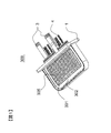
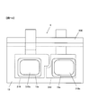
図1は、本発明によるパワーモジュールの外観を示す図である。パワーモジュール300は、スイッチング素子を含むようにトランスファーモールドされたパワー半導体ユニットを、金属筒1内に収納したものである。パワーモジュール300は、例えば、電気自動車やハイブリッド自動車等の電気車両に搭載される電力変換装置に用いられる。
度或いは過電圧から保護する。
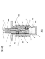
図21は、パワーモジュールの製造方法を説明する図である。まず、図21(a)に示すように、トランスファーモールドによって形成されたパワー半導体ユニット6の表裏両面に、すなわち、電極リードフレーム316,319の放熱面316s、319sおよび封止材13の表面に、絶縁シート10を圧着する。なお、図20に示した絶縁シート10の表裏両面には、作業性の観点から離型シートが貼られているが、圧着をする際には、絶縁シート10の片面側(パワー半導体ユニット6に対向しない方の面)の離型シートは残したままとする。その状態で、真空プレス機を用いて、温度130℃、加圧力1MPa、気圧10kPaの条件で1分間圧着する。
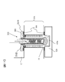
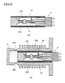
図22~図25を参照して本発明の第2の実施の形態について説明する。図22は、第2の実施の形態におけるパワーモジュール300Bの断面を模式的に示した図である。パワーモジュール300Bはと図12に示したパワーモジュール300との相違点は、電極リードフレーム7の形状が異なる点にある。以下では異なる点を中心に説明する。
(3)一方、図13(a)に示すように、放熱面7bの全体が封止材13の表面よりも突出している凹凸段差の場合には、傾斜面は、封止材13の表面13bから突出した放熱面7bの縁に形成された面取り加工面7aとされる。
日本国特許出願2010年第166705号(2010年7月26日出願)
Claims (14)
- パワー半導体素子と、
板状導電性部材で形成され、該板状導電性部材の表裏面の一方の面に、前記パワー半導体素子の電極面が金属接合される接合面が形成されるとともに、前記表裏面の他方の面に放熱面が形成されている電極リードフレームと、
前記放熱面の少なくとも一部が露出するように前記パワー半導体素子をモールドするモールド材と、を備えるパワー半導体ユニットであって、
絶縁シートを介して前記放熱面が放熱部材に熱接触して前記パワー半導体素子の熱が前記放熱部材へ放熱され、
前記放熱面の露出領域と該露出領域に隣接する前記モールド材の表面とは、いずれか一方が突出した凹凸段差を成し、
前記凹凸段差の凸側の面と凹側の面との間に形成された段差側面は、前記凸側の面との間の角度および前記凹側の面との間の角度がそれぞれ鈍角となるような傾斜面で構成されているパワー半導体ユニット。 - 請求項1に記載のパワー半導体ユニットにおいて、
前記凹凸段差は、前記放熱面の一部が前記モールド材の表面よりも窪んでおり、
前記傾斜面は、前記放熱面の周囲を囲むように突出した前記モールド材の縁に形成された傾斜加工面から成るパワー半導体ユニット。 - 請求項1に記載のパワー半導体ユニットにおいて、
前記凹凸段差は、前記放熱面の全体が前記モールド材の表面よりも突出しており、
前記傾斜面は、前記モールド材の表面から突出した前記放熱面の縁に形成された面取り加工面から成るパワー半導体ユニット。 - 請求項1乃至3のいずれか一項に記載のパワー半導体ユニットにおいて、
前記傾斜面の前記角度は110度以上180度未満であるパワー半導体ユニット。 - 請求項1乃至4のいずれか一項に記載のパワー半導体ユニットにおいて、
前記パワー半導体素子は前記電極を表裏両面に有し、
前記電極リードフレームは、前記パワー半導体素子の裏面側の電極面が接合される第1の電極リードフレームと、前記パワー半導体素子の表面側の電極面が接合される第2の電極リードフレームとを有し、
前記第1および第2の電極リードフレームの少なくとも一方の電極リードフレームに対して、前記傾斜面を成す段差側面が形成された凹凸段差を有するパワー半導体ユニット。 - 請求項5に記載のパワー半導体ユニットにおいて、
前記第1および第2の電極リードフレームの少なくとも一方に形成され、前記放熱面から前記接合面に貫通する貫通孔と、
溶融状態で前記貫通孔から前記電極面と前記接合面との隙間に注入され、凝固することにより電極面と接合面とを金属接合する金属接合体と、
前記貫通孔が形成された電極リードフレームの放熱面に形成され、該電極リードフレームの端部から前記貫通孔に連通する溝と、を備え、
前記貫通孔および溝は、前記モールド材によって覆われているパワー半導体ユニット。 - 請求項6に記載のパワー半導体ユニットにおいて、
前記貫通孔は、前記接合面の縁領域を貫通するように形成されているパワー半導体ユニット。 - 請求項5乃至7のいずれか一項に記載のパワー半導体ユニットと、
外周面に放熱フィンが形成された対向する第1および第2の放熱壁を有し、前記第1の放熱壁の内周面と前記第1の電極リードフレームの放熱面とが対向し、かつ、前記第2の放熱壁の内周面と前記第2の電極リードフレームの放熱面とが対向するように前記パワー半導体ユニットが内挿される有底の金属筒と、
前記第1の放熱壁の内周面と前記第1の電極リードフレームの放熱面との間に密着して配置される第1の熱伝導性絶縁シートと、
前記第2の放熱壁の内周面と前記第2の電極リードフレームの放熱面との間に密着して配置される第2の熱伝導性絶縁シートと、を備えたパワーモジュール。 - 請求項8に記載のパワーモジュールにおいて、
前記金属筒は、前記第1の放熱壁の周囲に形成されて該放熱壁よりも肉厚の薄い第1の薄肉部と、前記第2の放熱壁の周囲に形成されて該放熱壁よりも肉厚の薄い第2の薄肉部とを有し、
前記第1および第2の薄肉部は、前記第1および第2の放熱壁によって前記パワー半導体ユニットが挟持されるように塑性変形しているパワーモジュール。 - 請求項8または9に記載のパワーモジュールにおいて、
前記第1および第2の熱伝導性絶縁シートが、
熱硬化性樹脂に熱伝導率が5W/mK以上の絶縁性無機材料を体積分率50%以上90%以下充填した高熱伝導層と、
前記熱硬化性樹脂から成り、前記高熱伝導層の表裏両面に形成された高密着化層と、を備えているパワーモジュール。 - 請求項10に記載のパワーモジュールにおいて、
前記高密着化層は、前記熱硬化性樹脂としてエポキシ変性ポリアミドイミド樹脂を体積分率50%よりも多く含み、マトリクス樹脂としての前記エポキシ変性ポリアミドイミド樹脂に平均粒径5μm以下のシリコーン樹脂がミクロ相分離された構造を有するパワーモジュール。 - パワー半導体ユニットの製造方法であって、
請求項2に記載のパワー半導体ユニットの前記放熱面の周囲を囲むように突出した前記モールド材の縁領域をレーザー加工することにより、前記傾斜面を形成するパワー半導体ユニットの製造方法。 - パワー半導体ユニットの製造方法であって、
請求項3に記載のパワー半導体ユニットに設けられた前記電極リードフレームの前記接合面に、前記パワー半導体素子の電極面を金属接合する第1の工程と、
前記電極リードフレームの前記放熱面とトランスファーモールド金型との間に柔軟性離型シートを配置する第2の工程と、
前記トランスファーモールド金型を前記電極リードフレームの前記放熱面に押圧して、前記放熱面を前記柔軟性離型シートに沈み込ませた状態でトランスファーモールドを行う第3の工程と、を有するパワー半導体ユニットの製造方法。 - パワーモジュールの製造方法であって、
温度140℃以下、加圧力2MPa以下、気圧10kPa以下および圧着時間15分以内という圧着条件で、請求項10または11に記載のパワーモジュールに設けられた前記パワー半導体ユニットの前記第1および第2の電極リードフレームの放熱面に、前記第1および第2の熱伝導性絶縁シートを圧着する第1の圧着工程と、
前記パワー半導体ユニットに圧着された前記第1および第2の熱伝導性絶縁シートに、温度130℃以上、加圧力5MPa以下、気圧10kPa以下およびの圧着時間5分以上という圧着条件で、前記第1および第2の放熱壁の各内周面を圧着する第2の圧着工程と、を有するパワーモジュールの製造方法。
Priority Applications (3)
| Application Number | Priority Date | Filing Date | Title |
|---|---|---|---|
| EP11812432.0A EP2600398B1 (en) | 2010-07-26 | 2011-07-25 | Power module and production method for power module |
| CN201180036516.6A CN103069935B (zh) | 2010-07-26 | 2011-07-25 | 功率半导体组件、功率模块、功率半导体组件的制造方法和功率模块的制造方法 |
| US13/811,722 US8723306B2 (en) | 2010-07-26 | 2011-07-25 | Power semiconductor unit, power module, power semiconductor unit manufacturing method, and power module manufacturing method |
Applications Claiming Priority (2)
| Application Number | Priority Date | Filing Date | Title |
|---|---|---|---|
| JP2010166705A JP5437943B2 (ja) | 2010-07-26 | 2010-07-26 | パワー半導体ユニット、パワーモジュールおよびそれらの製造方法 |
| JP2010-166705 | 2010-07-26 |
Publications (1)
| Publication Number | Publication Date |
|---|---|
| WO2012014843A1 true WO2012014843A1 (ja) | 2012-02-02 |
Family
ID=45530051
Family Applications (1)
| Application Number | Title | Priority Date | Filing Date |
|---|---|---|---|
| PCT/JP2011/066854 WO2012014843A1 (ja) | 2010-07-26 | 2011-07-25 | パワー半導体ユニット、パワーモジュール、パワー半導体ユニットの製造方法およびパワーモジュールの製造方法 |
Country Status (5)
| Country | Link |
|---|---|
| US (1) | US8723306B2 (ja) |
| EP (1) | EP2600398B1 (ja) |
| JP (1) | JP5437943B2 (ja) |
| CN (1) | CN103069935B (ja) |
| WO (1) | WO2012014843A1 (ja) |
Cited By (4)
| Publication number | Priority date | Publication date | Assignee | Title |
|---|---|---|---|---|
| JPWO2013065182A1 (ja) * | 2011-11-04 | 2015-04-02 | トヨタ自動車株式会社 | パワーモジュール、電力変換装置および電動車両 |
| WO2016152258A1 (ja) * | 2015-03-23 | 2016-09-29 | 株式会社日立製作所 | 半導体装置 |
| JPWO2017175538A1 (ja) * | 2016-04-07 | 2018-12-20 | 日立オートモティブシステムズ株式会社 | ケース、半導体装置、ケースの製造方法 |
| US11848622B2 (en) | 2020-10-08 | 2023-12-19 | Kabushiki Kaisha Toshiba | Electronic device and power converter |
Families Citing this family (27)
| Publication number | Priority date | Publication date | Assignee | Title |
|---|---|---|---|---|
| JP4580997B2 (ja) | 2008-03-11 | 2010-11-17 | 日立オートモティブシステムズ株式会社 | 電力変換装置 |
| JP5581131B2 (ja) * | 2010-06-30 | 2014-08-27 | 日立オートモティブシステムズ株式会社 | パワーモジュール及びそれを用いた電力変換装置 |
| JP5520889B2 (ja) * | 2011-06-24 | 2014-06-11 | 日立オートモティブシステムズ株式会社 | パワー半導体モジュール及びそれを用いた電力変換装置 |
| US9788403B2 (en) | 2012-03-26 | 2017-10-10 | Koninklijke Philips N.V. | Medical imaging device |
| JP5634429B2 (ja) | 2012-03-30 | 2014-12-03 | 日立オートモティブシステムズ株式会社 | パワー半導体モジュール |
| JP2013258387A (ja) * | 2012-05-15 | 2013-12-26 | Rohm Co Ltd | パワーモジュール半導体装置 |
| JP6048238B2 (ja) * | 2012-06-04 | 2016-12-21 | 株式会社デンソー | 電子装置 |
| DE112013003222B4 (de) * | 2012-06-29 | 2021-08-19 | Denso Corporation | Halbleitervorrichtung und Halbleitervorrichtungsverbindungsstruktur |
| JP5941787B2 (ja) * | 2012-08-09 | 2016-06-29 | 日立オートモティブシステムズ株式会社 | パワーモジュールおよびパワーモジュールの製造方法 |
| JP6028808B2 (ja) * | 2012-11-09 | 2016-11-24 | 富士電機株式会社 | 半導体装置 |
| FR3002683B1 (fr) * | 2013-02-28 | 2016-11-04 | Alstom Technology Ltd | Convertisseur de puissance comportant une architecture de bras non-alignes |
| US20150138734A1 (en) * | 2013-11-18 | 2015-05-21 | Magna Electronics Inc. | 360 degree direct cooled power module |
| SG11201607469SA (en) | 2014-03-07 | 2016-10-28 | Asahi Glass Co Ltd | Mold release film and process for producing sealed body |
| JP6338547B2 (ja) * | 2015-03-31 | 2018-06-06 | オリンパス株式会社 | 成形回路部品、成形回路部品の製造方法および回路モジュール |
| US10099574B2 (en) * | 2015-04-15 | 2018-10-16 | Ford Global Technologies, Llc | Vehicle power module assemblies |
| DE112016006751B4 (de) | 2016-05-11 | 2022-04-28 | Hitachi Astemo, Ltd. | Leistungshalbleitermodul, Leistungsumsetzungsvorrichtung, die es verwendet, und Verfahren zum Herstellen der Leistungsumsetzungsvorrichtung |
| CN106985702A (zh) * | 2017-03-29 | 2017-07-28 | 浙江弗斯莱电动科技有限公司 | 一种新能源电机用电机控制器 |
| AU2018326242B2 (en) * | 2017-08-30 | 2021-12-09 | The Noco Company | Portable rechargeable battery jump starting device |
| DE102018203362A1 (de) * | 2018-03-07 | 2019-09-12 | Robert Bosch Gmbh | Kühleinrichtung zur Kühlung eines Leistungsbauelements |
| FR3079664B1 (fr) * | 2018-03-30 | 2020-04-24 | Institut Vedecom | Element modulaire de commutation de puissance et ensemble demontable de plusieurs elements modulaires |
| DE102018110361A1 (de) * | 2018-04-30 | 2019-10-31 | Hanon Systems | Montagebaugruppe mit bedrahteten elektronischen Leistungsbauteilen und deren Zusammenbau mit einem Motorgehäuse |
| WO2020021881A1 (ja) * | 2018-07-25 | 2020-01-30 | 株式会社デンソー | パワーモジュール及び電力変換装置 |
| CN111315182B (zh) * | 2018-12-12 | 2022-02-08 | 台达电子工业股份有限公司 | 整合式电子装置 |
| DE102019209829A1 (de) * | 2019-07-04 | 2021-01-07 | Audi Ag | Vorrichtung umfassend einen Kühlkörper und Kraftfahrzeug |
| CN114069819A (zh) * | 2020-08-07 | 2022-02-18 | 台达电子工业股份有限公司 | 具有三阶层切换电路的转换装置及三阶层切换电路的操作方法 |
| JP2023081051A (ja) * | 2021-11-30 | 2023-06-09 | 日立Astemo株式会社 | 半導体モジュール、電力変換装置、および半導体モジュールの製造方法 |
| JP2023124683A (ja) * | 2022-02-25 | 2023-09-06 | 日立Astemo株式会社 | 半導体装置及び電力変換装置 |
Citations (5)
| Publication number | Priority date | Publication date | Assignee | Title |
|---|---|---|---|---|
| JPH09153574A (ja) * | 1995-11-30 | 1997-06-10 | Mitsubishi Electric Corp | 半導体装置および半導体モジュール |
| JP2004303869A (ja) | 2003-03-31 | 2004-10-28 | Denso Corp | 半導体装置およびその製造方法 |
| JP2009200338A (ja) * | 2008-02-22 | 2009-09-03 | Renesas Technology Corp | 半導体装置の製造方法 |
| JP2011091259A (ja) * | 2009-10-23 | 2011-05-06 | Denso Corp | 半導体モジュールおよびその製造方法 |
| JP2011129818A (ja) * | 2009-12-21 | 2011-06-30 | Hitachi Ltd | 半導体装置及びその製造方法 |
Family Cites Families (10)
| Publication number | Priority date | Publication date | Assignee | Title |
|---|---|---|---|---|
| JP2928120B2 (ja) * | 1995-01-18 | 1999-08-03 | 日本電気株式会社 | 樹脂封止型半導体装置用リードフレームおよび樹脂封止型半導体装置の製造方法 |
| CN2255131Y (zh) * | 1995-12-25 | 1997-05-28 | 精华企业股份有限公司 | 供电子零件用的夹压式散热器 |
| US6143981A (en) * | 1998-06-24 | 2000-11-07 | Amkor Technology, Inc. | Plastic integrated circuit package and method and leadframe for making the package |
| US6703707B1 (en) * | 1999-11-24 | 2004-03-09 | Denso Corporation | Semiconductor device having radiation structure |
| DE10101086B4 (de) * | 2000-01-12 | 2007-11-08 | International Rectifier Corp., El Segundo | Leistungs-Moduleinheit |
| AT504250A2 (de) * | 2005-06-30 | 2008-04-15 | Fairchild Semiconductor | Halbleiterchip-packung und verfahren zur herstellung derselben |
| JP2009076658A (ja) * | 2007-09-20 | 2009-04-09 | Renesas Technology Corp | 半導体装置及びその製造方法 |
| US20090091021A1 (en) * | 2007-10-03 | 2009-04-09 | Matsushita Electric Industrial Co., Ltd. | Semiconductor device and method of manufacturing the same |
| JP4748173B2 (ja) * | 2008-03-04 | 2011-08-17 | 株式会社デンソー | 半導体モジュール及びその製造方法 |
| US8354303B2 (en) * | 2009-09-29 | 2013-01-15 | Texas Instruments Incorporated | Thermally enhanced low parasitic power semiconductor package |
-
2010
- 2010-07-26 JP JP2010166705A patent/JP5437943B2/ja active Active
-
2011
- 2011-07-25 EP EP11812432.0A patent/EP2600398B1/en active Active
- 2011-07-25 US US13/811,722 patent/US8723306B2/en active Active
- 2011-07-25 CN CN201180036516.6A patent/CN103069935B/zh active Active
- 2011-07-25 WO PCT/JP2011/066854 patent/WO2012014843A1/ja active Application Filing
Patent Citations (5)
| Publication number | Priority date | Publication date | Assignee | Title |
|---|---|---|---|---|
| JPH09153574A (ja) * | 1995-11-30 | 1997-06-10 | Mitsubishi Electric Corp | 半導体装置および半導体モジュール |
| JP2004303869A (ja) | 2003-03-31 | 2004-10-28 | Denso Corp | 半導体装置およびその製造方法 |
| JP2009200338A (ja) * | 2008-02-22 | 2009-09-03 | Renesas Technology Corp | 半導体装置の製造方法 |
| JP2011091259A (ja) * | 2009-10-23 | 2011-05-06 | Denso Corp | 半導体モジュールおよびその製造方法 |
| JP2011129818A (ja) * | 2009-12-21 | 2011-06-30 | Hitachi Ltd | 半導体装置及びその製造方法 |
Non-Patent Citations (1)
| Title |
|---|
| See also references of EP2600398A4 |
Cited By (6)
| Publication number | Priority date | Publication date | Assignee | Title |
|---|---|---|---|---|
| JPWO2013065182A1 (ja) * | 2011-11-04 | 2015-04-02 | トヨタ自動車株式会社 | パワーモジュール、電力変換装置および電動車両 |
| WO2016152258A1 (ja) * | 2015-03-23 | 2016-09-29 | 株式会社日立製作所 | 半導体装置 |
| JPWO2016152258A1 (ja) * | 2015-03-23 | 2017-09-28 | 株式会社日立製作所 | 半導体装置 |
| US10410945B2 (en) | 2015-03-23 | 2019-09-10 | Hitachi, Ltd. | Semiconductor device |
| JPWO2017175538A1 (ja) * | 2016-04-07 | 2018-12-20 | 日立オートモティブシステムズ株式会社 | ケース、半導体装置、ケースの製造方法 |
| US11848622B2 (en) | 2020-10-08 | 2023-12-19 | Kabushiki Kaisha Toshiba | Electronic device and power converter |
Also Published As
| Publication number | Publication date |
|---|---|
| US20130119525A1 (en) | 2013-05-16 |
| EP2600398A4 (en) | 2015-08-05 |
| CN103069935A (zh) | 2013-04-24 |
| CN103069935B (zh) | 2015-07-22 |
| EP2600398A1 (en) | 2013-06-05 |
| JP5437943B2 (ja) | 2014-03-12 |
| EP2600398B1 (en) | 2016-11-23 |
| US8723306B2 (en) | 2014-05-13 |
| JP2012028595A (ja) | 2012-02-09 |
Similar Documents
| Publication | Publication Date | Title |
|---|---|---|
| JP5437943B2 (ja) | パワー半導体ユニット、パワーモジュールおよびそれらの製造方法 | |
| JP5591396B2 (ja) | 半導体モジュール、および半導体モジュールの製造方法 | |
| US9246408B2 (en) | Power conversion apparatus | |
| JP5481148B2 (ja) | 半導体装置、およびパワー半導体モジュール、およびパワー半導体モジュールを備えた電力変換装置 | |
| JP5427745B2 (ja) | パワー半導体モジュール及びその製造方法 | |
| JP5492447B2 (ja) | パワーモジュール | |
| US9591789B2 (en) | Power semiconductor module and power module | |
| WO2013145881A1 (ja) | パワー半導体モジュール | |
| JP5879238B2 (ja) | パワー半導体モジュール | |
| WO2012117894A1 (ja) | パワー半導体モジュール,パワー半導体モジュールの製造方法及び電力変換装置 | |
| JP5486990B2 (ja) | パワーモジュール及びそれを用いた電力変換装置 | |
| JP2013027218A (ja) | 電力変換装置 | |
| JP6228888B2 (ja) | パワー半導体モジュール | |
| JP5975789B2 (ja) | パワー半導体モジュール | |
| CN111095537B (zh) | 半导体装置及具备该半导体装置的功率转换装置 | |
| JP5978324B2 (ja) | 電力変換装置 | |
| JP5948106B2 (ja) | パワー半導体モジュール及びそれを用いた電力変換装置 | |
| WO2020105556A1 (ja) | 半導体装置、電力変換装置及び半導体装置の製造方法 | |
| JP5687786B2 (ja) | 電力変換装置 | |
| JP6447914B2 (ja) | パワーモジュールの直流側配線基板及びその製造方法 | |
| JP2023124683A (ja) | 半導体装置及び電力変換装置 |
Legal Events
| Date | Code | Title | Description |
|---|---|---|---|
| WWE | Wipo information: entry into national phase |
Ref document number: 201180036516.6 Country of ref document: CN |
|
| 121 | Ep: the epo has been informed by wipo that ep was designated in this application |
Ref document number: 11812432 Country of ref document: EP Kind code of ref document: A1 |
|
| WWE | Wipo information: entry into national phase |
Ref document number: 13811722 Country of ref document: US |
|
| REEP | Request for entry into the european phase |
Ref document number: 2011812432 Country of ref document: EP |
|
| WWE | Wipo information: entry into national phase |
Ref document number: 2011812432 Country of ref document: EP |
|
| NENP | Non-entry into the national phase |
Ref country code: DE |