WO2012014256A1 - 有機el素子 - Google Patents
有機el素子 Download PDFInfo
- Publication number
- WO2012014256A1 WO2012014256A1 PCT/JP2010/004833 JP2010004833W WO2012014256A1 WO 2012014256 A1 WO2012014256 A1 WO 2012014256A1 JP 2010004833 W JP2010004833 W JP 2010004833W WO 2012014256 A1 WO2012014256 A1 WO 2012014256A1
- Authority
- WO
- WIPO (PCT)
- Prior art keywords
- organic
- tungsten
- peak
- hole injection
- oxide film
- Prior art date
- Legal status (The legal status is an assumption and is not a legal conclusion. Google has not performed a legal analysis and makes no representation as to the accuracy of the status listed.)
- Ceased
Links
Images





Classifications
-
- H—ELECTRICITY
- H05—ELECTRIC TECHNIQUES NOT OTHERWISE PROVIDED FOR
- H05B—ELECTRIC HEATING; ELECTRIC LIGHT SOURCES NOT OTHERWISE PROVIDED FOR; CIRCUIT ARRANGEMENTS FOR ELECTRIC LIGHT SOURCES, IN GENERAL
- H05B33/00—Electroluminescent light sources
- H05B33/12—Light sources with substantially two-dimensional [2D] radiating surfaces
- H05B33/22—Light sources with substantially two-dimensional [2D] radiating surfaces characterised by the chemical or physical composition or the arrangement of auxiliary dielectric or reflective layers
-
- H—ELECTRICITY
- H10—SEMICONDUCTOR DEVICES; ELECTRIC SOLID-STATE DEVICES NOT OTHERWISE PROVIDED FOR
- H10K—ORGANIC ELECTRIC SOLID-STATE DEVICES
- H10K50/00—Organic light-emitting devices
- H10K50/10—OLEDs or polymer light-emitting diodes [PLED]
- H10K50/17—Carrier injection layers
-
- H—ELECTRICITY
- H10—SEMICONDUCTOR DEVICES; ELECTRIC SOLID-STATE DEVICES NOT OTHERWISE PROVIDED FOR
- H10K—ORGANIC ELECTRIC SOLID-STATE DEVICES
- H10K71/00—Manufacture or treatment specially adapted for the organic devices covered by this subclass
-
- H—ELECTRICITY
- H10—SEMICONDUCTOR DEVICES; ELECTRIC SOLID-STATE DEVICES NOT OTHERWISE PROVIDED FOR
- H10K—ORGANIC ELECTRIC SOLID-STATE DEVICES
- H10K71/00—Manufacture or treatment specially adapted for the organic devices covered by this subclass
- H10K71/10—Deposition of organic active material
- H10K71/16—Deposition of organic active material using physical vapour deposition [PVD], e.g. vacuum deposition or sputtering
Definitions
- the present invention relates to an organic electroluminescent element (hereinafter referred to as “organic EL element”) which is an electroluminescent element, and more particularly to a technique for improving hole conduction efficiency in a hole injection layer.
- organic EL element organic electroluminescent element
- the organic EL element is a current-driven light emitting element and has a configuration in which a functional layer including a light emitting layer made of an organic material is provided between a pair of electrodes made of an anode and a cathode. Then, a voltage is applied between the electrode pair to recombine holes injected from the anode into the functional layer and electrons injected from the cathode into the functional layer, and light is emitted by the electroluminescence phenomenon generated thereby. Since organic EL elements perform self-light emission and have high visibility and are solid elements, and are excellent in vibration resistance, they are attracting attention as light emitting elements and light sources in various display devices.
- the organic EL element In order for the organic EL element to emit light with high luminance, it is important to efficiently inject carriers (holes and electrons) from the electrode to the functional layer. In general, in order to inject carriers efficiently, it is effective to provide an injection layer for lowering the energy barrier during injection between each electrode and the functional layer.
- an organic substance such as copper phthalocyanine or PEDOT (conductive polymer), or a metal oxide such as molybdenum oxide or tungsten oxide is used for the hole injection layer disposed between the functional layer and the anode.
- an organic substance such as a metal complex or oxadiazole, or a metal such as barium is used for the electron injection layer disposed between the functional layer and the cathode.
- Patent Document 1 an organic EL element using a metal oxide film made of a metal oxide such as molybdenum oxide or tungsten oxide as a hole injection layer, improvement in hole conduction efficiency and improvement in lifetime have been reported (Patent Document 1,). 2, Non-Patent Document 1).
- the metal oxide film As a method for forming the metal oxide film, a vapor deposition method or a sputtering method is generally used. In this case, considering the heat resistance of the layers already formed on the substrate when the metal oxide film is formed, the metal oxide film is usually formed at a low substrate temperature of 200 ° C. or lower. Has been done.
- Non-Patent Document 2 When film formation is performed at a low substrate temperature in the sputtering method, the thermal energy generated when the film formation gas reaches the film formation substrate is quickly absorbed by the film formation substrate, so the amorphous structure metal with less ordering An oxide film is easily formed. Furthermore, it has also been reported that when film formation is performed at a low substrate temperature, it is difficult to maintain film composition and film thickness uniformity (Non-Patent Document 2).
- the metal oxide film has an amorphous structure
- holes contributing to conduction of holes injected into the metal oxide film for example, parts similar to oxygen defects are scattered, and therefore hole conduction is performed mainly by hopping conduction. Is called.
- hopping conduction holes hop between scattered hole conduction sites, but in order to use this for driving an organic EL element, it is necessary to apply a high driving voltage to the organic EL element. There is a problem that the hole conduction efficiency is lowered.
- the present invention has been made in view of the above-described problems, and an object thereof is to provide an organic EL element employing a hole injection layer capable of obtaining a good hole conduction efficiency.
- an organic EL device includes a functional layer including an organic material between an anode and a cathode, and a hole injection layer for injecting holes into the functional layer.
- the hole injection layer is a metal oxide film containing a metal oxide, and the metal element constituting the metal oxide is in the state of the maximum valence that the metal element can take
- the metal oxide film is included in the metal oxide film in a state of a valence lower than the maximum valence, and the metal oxide film includes crystals of the metal oxide having a particle size on the order of nanometers. It is characterized by that.
- the hole injection layer is formed of a metal oxide film containing a metal oxide, and the metal element that forms the metal oxide is in a state of the maximum valence and the maximum
- the metal oxide film can have a structure similar to an oxygen defect serving as a hole conduction site.
- the crystal grain size of the metal oxide to a nanometer order, many crystal grain boundaries in which many structures similar to oxygen defects exist are formed in the metal oxide film.
- FIG. 1A is a schematic cross-sectional view showing a configuration of an organic EL element 1 according to an embodiment
- FIG. 2B is a partial enlarged view in the vicinity of a hole injection layer 3.
- W5p 3/2 by XPS measurement of the tungsten oxide film surface, W4f 5/2 illustrates a spectrum attributed to W4f 7/2.
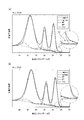
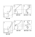
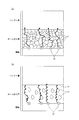
- Luminance change plots of sample A and sample E ((a), (b)) and enlarged views near the peak of normalized luminance appearing closest to the center point in each luminance change plot ((a1), (b1)) And (a2) and (b2) are diagrams showing the first derivative of each plot of (a1) and (b1). It is a figure which shows typically hole conduction in case a tungsten oxide film is (a) nanocrystal structure, and (b) hole conduction in the case where it is an amorphous structure.
- An organic EL device includes an organic EL device having a functional layer containing an organic material and a hole injection layer for injecting holes into the functional layer between an anode and a cathode.
- the hole injection layer is a metal oxide film containing a metal oxide, and the metal element constituting the metal oxide has a state of the maximum valence that the metal element can take and the maximum valence.
- the metal oxide film is included in the metal oxide film in a low valence state, and the metal oxide film includes a crystal of the metal oxide having a particle size on the order of nanometers.
- the hole injection layer according to one embodiment of the present invention is formed using a metal oxide crystal, and the metal element included in the metal oxide includes a state having a maximum valence and a state having a valence lower than the maximum valence. By doing so, the hole injection layer can have a structure similar to an oxygen defect.
- the crystal grain size of tungsten oxide to a nanometer order size, many crystal grain boundaries in which many structures similar to oxygen defects exist are formed in the tungsten oxide layer.
- the “size on the order of nanometers” refers to a size of about 3 to 10 nm, which is smaller than the film thickness of the hole injection layer.
- the metal oxide is tungsten oxide
- the metal element in the maximum valence state may be a hexavalent tungsten element, or the metal element having a valence lower than the maximum valence. May be a pentavalent tungsten element.
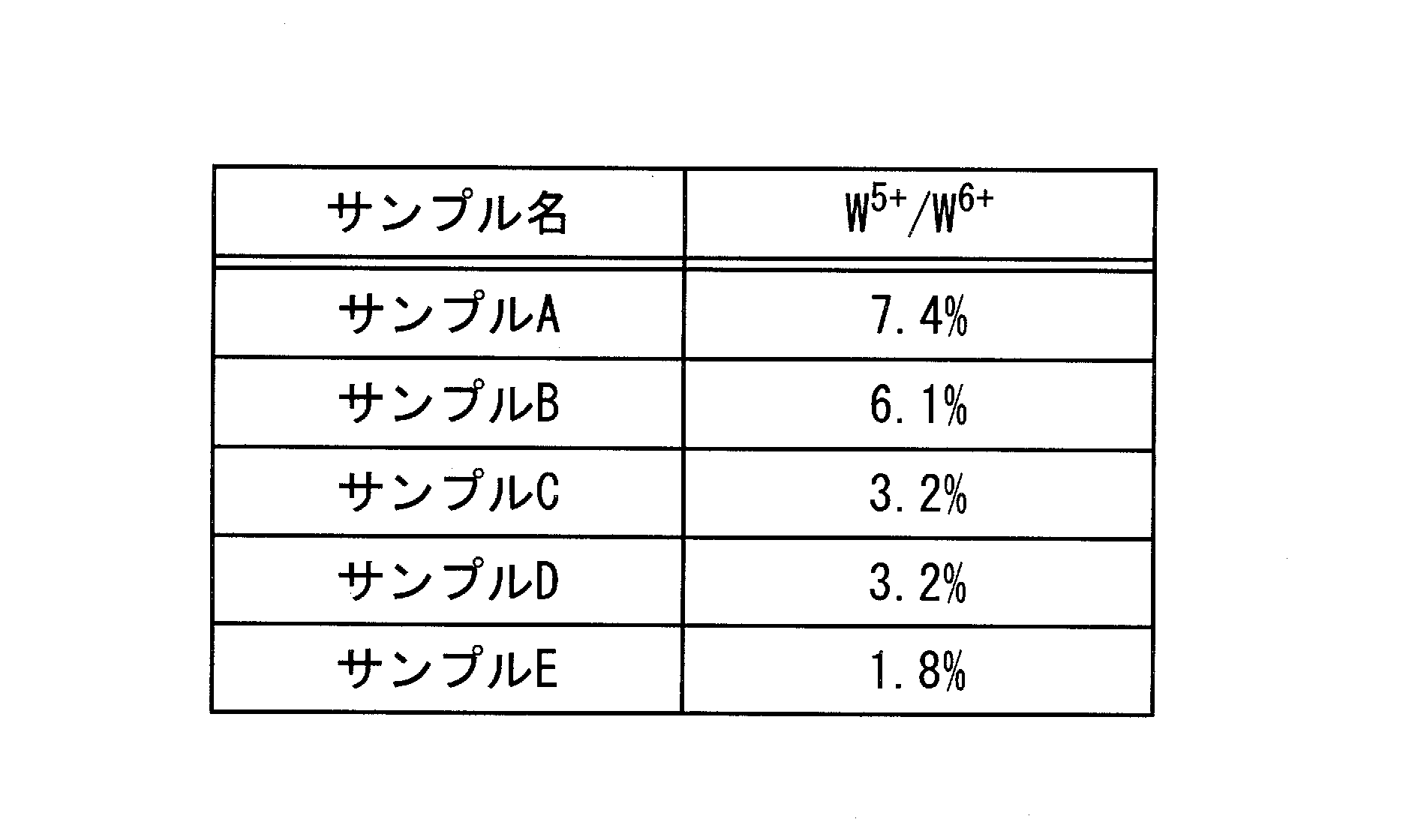
- W 5+ / W 6+ which is a value obtained by dividing the number of pentavalent tungsten atoms by the number of hexavalent tungsten atoms, may be 3.2% or more. By including 3.2% or more of pentavalent tungsten atoms with respect to hexavalent tungsten atoms, better hole conduction efficiency can be obtained.
- a second peak exists in a binding energy region lower than the first peak corresponding to the 4f 7/2 level of hexavalent tungsten, in other words, in a shallow energy level. It is good to do.
- the second peak may exist in a binding energy region that is 0.3 to 1.8 eV lower than the binding energy value of the first peak.
- the first peak corresponds to a peak of a hexavalent tungsten atom
- the second peak corresponds to a peak of a pentavalent tungsten atom.
- the area intensity of the second peak may be 3.2 to 7.4% with respect to the area intensity of the first peak.
- the ratio of the areas of the first peak and the second peak corresponds to the abundance ratio of hexavalent tungsten atoms and pentavalent tungsten atoms. That is, it indicates that pentavalent tungsten atoms are contained in a ratio of 3.2% to 7.4% with respect to hexavalent tungsten atoms.
- the lowest binding energy in the valence band means energy corresponding to the position of the upper end of the valence band from the vacuum level.
- the tungsten oxide film includes a plurality of crystals of the tungsten oxide having a particle size of 3 to 10 nanometers.
- a linear structure regularly arranged at intervals of .85 to 5.55 mm may appear.
- the bright portions are partially arranged in the same direction, so that the regularly arranged linear shape A structure appears. This regular linear structure suggests the presence of crystals in the nanometer order.
- a concentric pattern centering on the center point of the two-dimensional Fourier transform image may appear. If a nanometer order crystal exists, the concentric pattern as described above appears.
- one or more peaks of the normalized luminance appear. It is good.
- One normalized luminance peak in the plot corresponds to one concentric pattern.
- the difference between the distance corresponding to the position of the normalized luminance peak that appears closest to the center point in the plot and the distance corresponding to the rising position of the normalized luminance peak is a peak width
- the center The peak width may be smaller than 22 when the difference between the distance corresponding to the point and the distance corresponding to the peak of the normalized luminance that appears closest to the center point is 100.
- the peak of normalized luminance that appears at the distance closest to the center point corresponds to a concentric pattern based on the presence of crystals in the nanometer order. Further, the greater the amount of crystals in the nanometer order, the smaller the half-value width of this normalized luminance peak, that is, the smaller the normalized luminance width.
- the presence of crystals in the order of nanometers to such an extent that the peak width falls within a predetermined range makes it possible to obtain better hole conduction efficiency.
- the functional layer may contain an amine material.
- amine-based organic molecules since the electron density of HOMO is distributed around the unshared electron pair of the nitrogen atom, this portion becomes a hole injection site. Since the functional layer contains an amine-based material, hole injection sites can be formed on the functional layer side, so holes conducted from the hole injection layer can be efficiently injected into the functional layer. Become.
- the functional layer is any one of a hole transport layer that transports holes, a light-emitting layer that emits light by recombination of injected holes and electrons, and a buffer layer that is used for optical property adjustment or electronic block applications. It is good as well.
- the organic EL panel, the organic EL light emitting device, and the organic EL display device according to the present invention include the organic EL element having the above configuration.
- an organic EL panel, an organic EL light emitting device, and an organic EL display device that can obtain the same effects as described above can be configured.
- An organic EL device manufacturing method includes a first step of preparing an anode and a second step of forming a tungsten oxide film on the anode, the sputtering comprising argon gas and oxygen gas.
- the total pressure of the sputtering gas is 2.3 Pa to 7.0 Pa
- the ratio of the oxygen gas partial pressure to the total pressure of the sputtering gas is 50% to 70%.
- the tungsten element constituting the tungsten oxide film is included in the tungsten oxide film in a state of a maximum valence that the tungsten element can take and a state of a valence lower than the maximum valence.
- the tungsten oxide film may be formed so as to include a tungsten oxide crystal having a particle size of the order of nanometers.
- the total pressure / input power density may be smaller than 3.2 Pa ⁇ cm 2 / W.
- FIG. 1A is a schematic cross-sectional view showing the configuration of the organic EL element 1 according to the present embodiment
- FIG. 1B is a partially enlarged view in the vicinity of the hole injection layer 3.
- the organic EL element 1 is, for example, a coating type in which a functional layer is coated by a wet process, and a hole injection layer 3 and various functional layers containing an organic material having a predetermined function are laminated to each other. In the state, it has the structure interposed between the electrode pair which consists of the anode 2 and the cathode 6.
- FIG. 1 a coating type in which a functional layer is coated by a wet process, and a hole injection layer 3 and various functional layers containing an organic material having a predetermined function are laminated to each other. In the state, it has the structure interposed between the electrode pair which consists of the anode 2 and the cathode 6.
- the organic EL element 1 includes an anode 2, a hole injection layer 3, a buffer layer 4 (an example of a functional layer), and a light emitting layer 5 (functional layer) with respect to one main surface of a substrate 7.
- Example and a cathode 6 (consisting of a barium layer 6a and an aluminum layer 6b) are laminated in the same order.
- the substrate 7 is a portion that becomes a base material of the organic EL element 1, and includes, for example, alkali-free glass, soda glass, non-fluorescent glass, phosphate glass, borate glass, quartz, acrylic resin, styrene resin, and polycarbonate resin. , Epoxy resin, polyethylene, polyester, silicone resin, or an insulating material such as alumina.
- a TFT thin film transistor
- an anode 2 is formed thereon.
- the anode 2 is made of, for example, an ITO thin film having a thickness of 50 nm.
- the hole injection layer 3 is made of, for example, a tungsten oxide film (WOx) having a thickness of 30 nm. Tungsten oxide is a real number in the range of 2 ⁇ x ⁇ 3 in the composition formula WOx.
- the hole injection layer 3 is preferably made of tungsten oxide as much as possible, but may contain a trace amount of impurities to such an extent that it can be mixed at a normal level.
- the tungsten oxide film is formed under predetermined film forming conditions. Details of the predetermined film forming conditions will be described in detail in the section (Method of manufacturing organic EL element 1) and (Regarding film forming conditions of hole injection layer 3). Since the tungsten oxide film is formed under the predetermined film forming conditions, the tungsten oxide film includes a large number of crystals 9 of tungsten oxide as shown in FIG. Each crystal 9 is formed to have a particle size of nanometer order. For example, the hole injection layer 3 has a thickness of about 30 nm, whereas the crystal 9 has a grain size of about 3 to 10 nm.
- the crystal 9 having a particle size of the order of nanometers is referred to as “nanocrystal 9”, and the layer structure composed of the nanocrystal 9 is referred to as “nanocrystal structure”.
- the region other than the region having the nanocrystal structure in the hole injection layer 3 includes an amorphous structure.
- the tungsten atom (W) constituting the tungsten oxide has a state of a maximum valence that tungsten can take and a state of a valence lower than the maximum valence.
- the crystal structure of tungsten oxide is not uniform and includes a structure similar to an oxygen defect.
- the maximum valence that tungsten can take is a hexavalent state.
- tungsten oxides having a crystal structure having a structure similar to an oxygen defect it has been found that the valence of tungsten is a pentavalent state lower than the maximum valence.
- the tungsten oxide film is composed of tungsten atoms in various valence states such as the above maximum valence and valence lower than the maximum valence. The average valence of various valences.
- Non-Patent Document 3 there is a report that by taking a structure similar to an oxygen defect, hole conduction efficiency is improved by an electron level based on the structure (Non-Patent Document 3). Furthermore, as will be described with reference to FIG. 9, it is known that many structures similar to oxygen defects exist on the surface of the crystal.
- tungsten oxide it is possible to improve the hole conduction efficiency by distributing tungsten so as to have a hexavalent or pentavalent state and providing the hole injection layer 3 with a structure similar to oxygen defects. That is, since the holes supplied from the anode 2 to the hole injection layer 3 conduct oxygen defects existing at the crystal grain boundaries, the number of paths through which holes can be conducted can be increased by making the tungsten oxide film have a nanocrystal structure. , Leading to improved hole conduction efficiency. Therefore, the drive voltage for starting the organic EL element 1 can be lowered.
- the hole injection layer 3 is made of tungsten oxide having high chemical resistance, that is, hardly causing unnecessary chemical reaction. Therefore, even when the hole injection layer 3 is in contact with a solution or the like used in a process performed after the formation of the same layer, damage to the hole injection layer 3 due to dissolution, alteration, decomposition, or the like can be suppressed. . Thus, since the hole injection layer 3 is made of a material having high chemical resistance, it is possible to prevent the hole conduction performance of the hole injection layer 3 from being lowered.
- the hole injection layer 3 in the present embodiment includes both a case where the hole injection layer 3 is made of only tungsten oxide having a nanocrystal structure and a case where the hole injection layer 3 is made of both tungsten oxide having a nanocrystal structure and tungsten oxide having an amorphous structure. Shall be included.
- the nanocrystal structure is preferably present in the whole hole injection layer 3, but is located at a single point between the interface between the anode 2 and the hole injection layer 3 and the interface between the hole injection layer 3 and the buffer layer 4. However, if the grain boundaries are connected, holes from the lower end to the upper end of the hole injection layer 3 can be conducted.
- Non-Patent Document 1 shows that hole conductivity is improved by crystallizing a tungsten oxide film by annealing at 450 ° C.
- Non-Patent Document 1 does not show practicality for mass production of large organic EL panels, including the influence on other layers such as a substrate on which a hole injection layer is formed. Further, it has not been shown that tungsten oxide nanocrystals having oxygen defects are positively formed in the hole injection layer.
- the hole injection layer according to the present invention is made of a tungsten oxide film that hardly causes a chemical reaction, is stable, and can withstand a mass production process of a large organic EL panel. Furthermore, the present invention is greatly different from the prior art in that excellent hole conductivity and hole injection efficiency are realized by actively making oxygen defects present in the tungsten oxide film.
- the organic EL element 1 includes a functional layer that performs the required function necessary for the organic EL element 1.
- the functional layer in the present invention includes any of a hole transport layer that transports holes, a light emitting layer that emits light by recombination of injected holes and electrons, a buffer layer that is used for optical property adjustment or electronic block applications, etc. Or a combination of two or more of these layers, or a layer including all of these layers.
- the buffer layer 4 and the light emitting layer 5 are included as functional layers will be described.
- the buffer layer 4 may be, for example, TFB (poly (9,9-di-n-octylfluorene-alt- (1,4-phenylene-((4-sec-butylphenyl) imino), which is an amine organic polymer having a thickness of 20 nm. ) -1,4-phenylene)).
- TFB poly (9,9-di-n-octylfluorene-alt- (1,4-phenylene-((4-sec-butylphenyl) imino
- the buffer layer 4 By configuring the buffer layer 4 with amine organic molecules, holes conducted from the hole injection layer 3 can be efficiently injected into a functional layer formed above the buffer layer 4. That is, in the amine-based organic molecule, the electron density of HOMO is distributed around the unshared electron pair of the nitrogen atom, so this portion becomes a hole injection site. Since the buffer layer 4 contains amine organic molecules, hole injection sites can be formed on the buffer layer 4 side.
- the light emitting layer 5 is made of, for example, F8BT (poly (9,9-di-n-octylfluorene-alt-benzothiazole)) which is an organic polymer having a thickness of 70 nm.
- F8BT poly (9,9-di-n-octylfluorene-alt-benzothiazole)
- the light emitting layer 5 is not limited to the structure made of this material, and can be configured to include a known organic material.
- the cathode 6 is formed by, for example, stacking a barium layer 6a having a thickness of 5 nm and an aluminum layer 6b having a thickness of 100 nm.
- a DC power source 8 is connected to the anode 2 and the cathode 6 described above, and power is supplied to the organic EL element 1 from the outside.
- the substrate 7 is placed in the chamber of the sputter deposition apparatus. Then, a predetermined sputtering gas is introduced into the chamber, and the anode 2 made of ITO having a thickness of 50 nm is formed based on the reactive sputtering method.
- the hole injection layer 3 is formed, but it is preferable to form the hole injection layer 3 by a reactive sputtering method.
- metallic tungsten is used as a target
- argon gas is used as a sputtering gas
- oxygen gas is used as a reactive gas in the chamber.
- argon is ionized by a high voltage and collides with the target.
- metallic tungsten released by the sputtering phenomenon reacts with oxygen gas to become tungsten oxide, and a tungsten oxide film is formed on the anode 2.
- the total pressure of the sputtering gas composed of argon gas and oxygen gas is 2.3 Pa to 7.0 Pa
- the oxygen gas partial pressure with respect to the total pressure of the sputtering gas is 50% or more and 70% or less.
- closing electric power per unit area of the target is at 1.5 W / cm 2 or more 6.0 W / cm 2 or less
- the total pressure of the sputtering gas in the input power density It is preferable to set the total pressure / power density, which is a divided value, to be greater than 0.7 Pa ⁇ cm 2 / W. Under such film formation conditions, a tungsten oxide film having a nanocrystal structure is formed.
- the tungsten oxide constituting the hole injection layer 3 has high chemical resistance. Therefore, even when the hole injection layer 3 is in contact with a solution or the like used in the subsequent steps, damage to the hole injection layer 3 due to dissolution, alteration, decomposition, or the like can be suppressed.
- a composition ink containing an amine-based organic molecular material is dropped on the surface of the hole injection layer 3 by, for example, a wet process using a spin coating method or an inkjet method, and the solvent is volatilized and removed. Thereby, the buffer layer 4 is formed.
- a composition ink containing an organic light emitting material is dropped on the surface of the buffer layer 4 by the same method, and the solvent is volatilized and removed. Thereby, the light emitting layer 5 is formed.
- the formation method of the buffer layer 4 and the light emitting layer 5 is not limited to this, It is well-known methods, such as methods other than a spin coat method and an inkjet method, for example, gravure printing method, dispenser method, nozzle coating method, intaglio printing, letterpress printing, etc.
- the ink may be dropped and applied by a method.
- a barium layer 6a and an aluminum layer 6b are formed on the surface of the light emitting layer 5 by vacuum deposition. Thereby, the cathode 6 is formed.
- a sealing layer is further provided on the surface of the cathode 6 or the entire organic EL element 1 is spatially separated.
- a sealing can that is isolated from the outside can be provided.
- the sealing layer can be formed of a material such as SiN (silicon nitride) or SiON (silicon oxynitride), and is provided so as to internally seal the organic EL element 1.
- the sealing can can be formed of the same material as that of the substrate 7, for example, and a getter that adsorbs moisture and the like is provided in the sealed space.
- the organic EL element 1 is completed through the above steps.
- tungsten oxide constituting the hole injection layer 3 is formed under predetermined film formation conditions, so that the hole conductivity is improved by intentionally making the hole injection layer 3 have a nanocrystal structure.
- the organic EL element 1 can be driven at a low voltage.
- the predetermined film forming conditions will be described in detail.
- a DC magnetron sputtering apparatus was used as the sputtering apparatus, and the target was metallic tungsten.
- the substrate temperature was not controlled. It is considered that it is preferable to form the film under conditions using a reactive sputtering method in which the sputtering gas is composed of argon gas, the reactive gas is composed of oxygen gas, and each gas has an equivalent flow rate.
- the formation method of the hole injection layer 3 is not limited to this, It can also form into a film by methods other than sputtering method, for example, well-known methods, such as a vapor deposition method and CVD method.
- the upper limit of the total sputtering gas pressure is 4.7 Pa, but it has been separately confirmed that the same tendency is exhibited up to at least 7.0 Pa.
- the ratio of the partial pressure of oxygen gas to the total sputtering gas pressure is set to 50%, but it has been confirmed that the driving voltage is reduced at least 50% to 70%.
- the input power density in (3) changes the number and energy of tungsten atoms or tungsten atom clusters to be sputtered. That is, by lowering the input power density, the number of tungsten to be sputtered can be reduced, and tungsten deposited on the substrate can be deposited with low energy, and a film formation at a low deposition rate can be expected.
- the total pressure during film formation of (1) changes the mean free path until tungsten atoms or tungsten atom clusters sputtered and released into the gas phase arrive at the film formation substrate.
- the film formation condition (4) by the total pressure (Pa) at the time of film formation / input power density (W / cm 2 ) as an index for determining the film formation rate of tungsten atoms.
- the total pressure / power density is 0.78 Pa ⁇ cm 2 / W or more, and it is necessary to be larger than 0.7 Pa ⁇ cm 2 / W according to the experimental conditions described later. More surely, it is considered preferable to be 0.8 Pa ⁇ cm 2 / W or more.
- the upper limit value of the total pressure / power density is 3.13 Pa ⁇ cm 2 / W or less in the experimental conditions, and is considered to be smaller than 3.2 Pa ⁇ cm 2 / W. Although it is considered to be preferably 3.1 Pa ⁇ cm 2 / W or less, as described above, it is considered that the upper limit value is not necessarily limited in terms of the film formation rate.
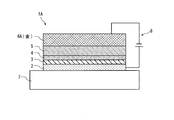
- a hole-only element 1A as shown in FIG. 2 was fabricated as an evaluation device.
- the hole-only element 1A is obtained by replacing the cathode 6 in the organic EL element 1 of FIG. 1 with a cathode 6A made of gold.
- a cathode 6A made of gold having a thickness of 100 nm were sequentially stacked.
- the hole injection layer 3 was formed by a reactive sputtering method using a DC magnetron sputtering apparatus.
- the gas in the chamber was composed of at least one of argon gas and oxygen gas, and metallic tungsten was used as the target.
- the substrate temperature was not controlled, and the total pressure was adjusted by the flow rate of each gas.
- Table 1 a hole-only device 1A was fabricated under five film formation conditions A to E. As shown in Table 1, the total pressure and input power density were changed depending on each film forming condition.
- the partial pressures of argon gas and oxygen gas in the chamber are 50%, respectively.
- the hole-only element 1A formed under the film formation condition A is HOD-A
- the hole-only element 1A formed under the film formation condition B is HOD-B
- the hole-only element 1A formed under the film formation condition C is HOD
- the hole-only element 1A formed under the film formation condition D is referred to as HOD-D
- the hole-only element 1A formed under the film formation condition E is referred to as HOD-E.
- Each Hall-only element produced was connected to a DC power supply 8 and a voltage was applied. The applied voltage at this time was changed, and the current value that flowed according to the voltage value was converted to a value (current density) per unit area of the element.
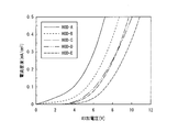
- FIG. 3 is a device characteristic diagram showing a relationship curve between applied voltage and current density of each hole-only element.
- the vertical axis represents current density (mA / cm 2 )
- the horizontal axis represents applied voltage (V).
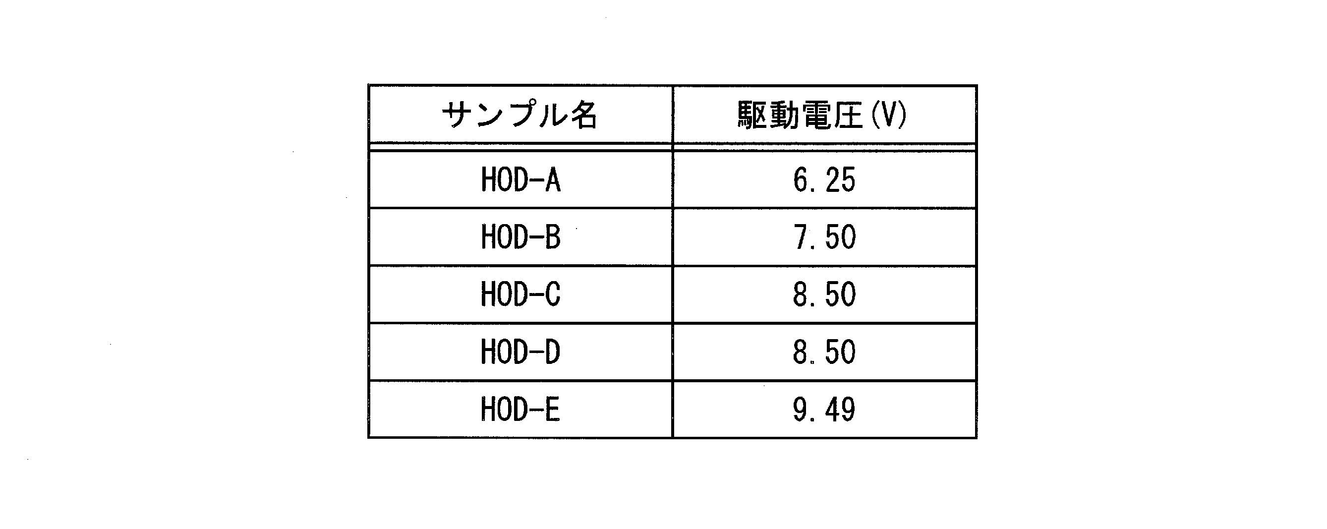
- Table 2 shows the driving voltage values of the samples HOD-A to HOD-E obtained by the experiment.
- the “drive voltage” in Table 2 is an applied voltage at a current density of 0.3 mA / cm 2 , which is a practical specific value.
- HOD-A to HOD-E are more conductive in holes than HOD-E produced under conditions where the total pressure during film formation is reduced and the input power density is maximized. It can be seen that the efficiency is excellent.
- the hole-only element 1A has the same configuration as the organic EL element 1 (FIG. 1) that actually operates except the cathode 6A. . Therefore, also in the organic EL element 1, the film formation condition dependence of the hole conduction efficiency from the hole injection layer 3 to the buffer layer 4 is essentially the same as that of the hole only element 1A. In order to confirm this, an organic EL element 1 using a hole injection layer 3 formed under each film forming condition A to E was manufactured.
- the organic EL element 1 formed under the film forming condition A is BPD-A
- the organic EL element 1 formed under the film forming condition B is BPD-B
- the organic EL element 1 formed under the film forming condition C is BPD.
- the organic EL element 1 formed under the film forming condition D is referred to as BPD-D
- the organic EL element 1 formed under the film forming condition E is referred to as BPD-E.
- each of the produced organic EL elements has an anode 2 made of an ITO thin film having a thickness of 50 nm formed on a substrate 7, and a hole injection layer 3 made of tungsten oxide having a thickness of 30 nm on the anode 2.
- a buffer layer 4 made of TFB with a thickness of 20 nm, a light emitting layer 5 made of F8BT with a thickness of 70 nm, a cathode 6 made of barium with a thickness of 5 nm and aluminum with a thickness of 100 nm were sequentially laminated.
- the produced organic EL elements 1 under the deposition conditions A to E were connected to a DC power source 8 and a voltage was applied. The applied voltage at this time was changed, and the current value that flowed according to the voltage value was converted to a value (current density) per unit area of the element.
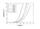
- FIG. 4 is a device characteristic diagram showing a relationship curve between applied voltage and current density of each organic EL element.
- the vertical axis represents current density (mA / cm 2 )
- the horizontal axis represents applied voltage (V).
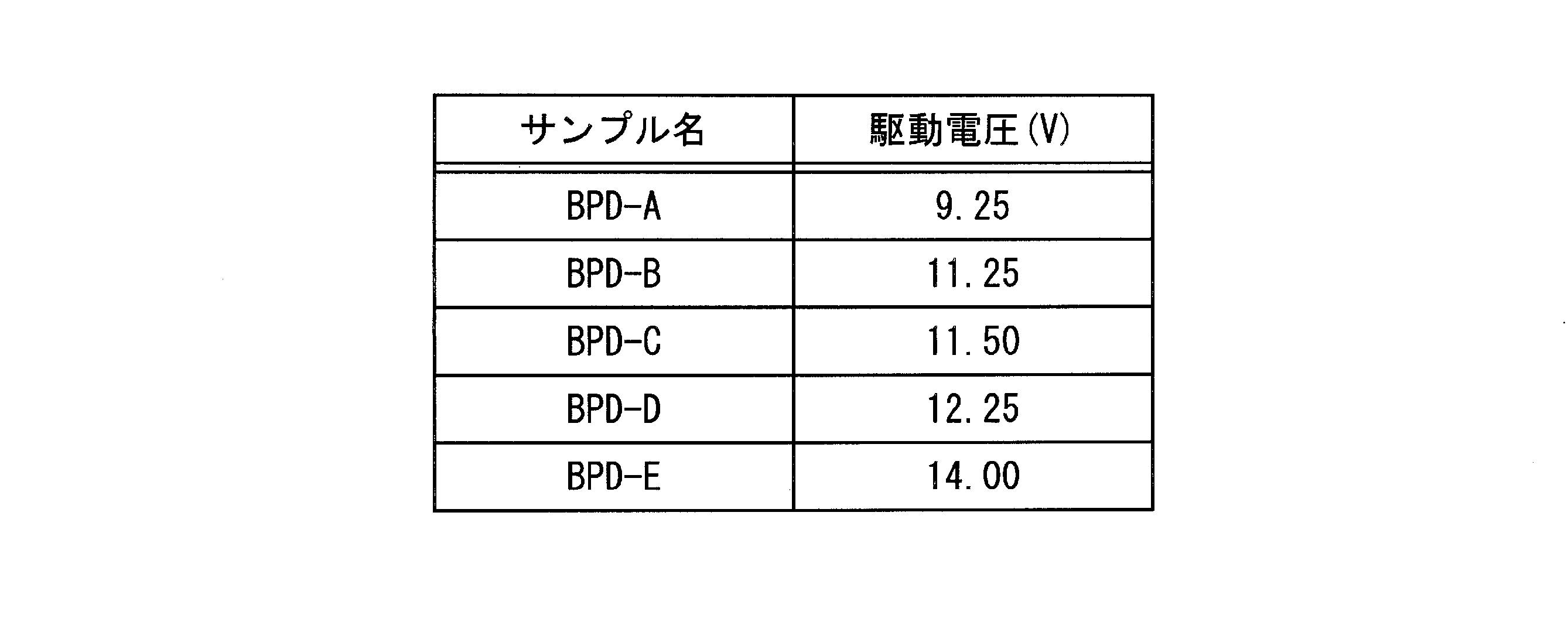
- Table 3 shows the drive voltage values of the samples BOD-A to BOD-E obtained by the experiment. “Drive voltage” in Table 3 is an applied voltage at a current density of 8 mA / cm 2 , which is a practical specific value.
- BPD-E has the slowest rise in current density-applied voltage curve compared with other organic EL elements, and the highest applied voltage is required to obtain a high current density. It was confirmed that. This is the same tendency as the hole-only elements HOD-A to HOD-E having the same film forming conditions.
- the film formation condition dependency of the hole conduction efficiency of the hole injection layer 3 is also acting in the organic EL element 1 as in the case of the hole only element 1A. That is, by performing film formation under film formation conditions in the range of film formation conditions A, B, C, and D, the hole conduction efficiency from the hole injection layer 3 to the buffer layer 4 is improved, thereby driving at a low voltage. Is confirmed to be realized.
- the input power condition is represented by the input power density as shown in Table 1.
- Table 1 the input power density satisfies the above conditions according to the size of the magnet on the back surface of the target.
- the hole injection layer 3 made of a tungsten oxide film having excellent hole conduction efficiency can be obtained. Note that the total pressure and the oxygen partial pressure do not depend on the apparatus, the target size, and the target magnet size.
- the substrate temperature is not intentionally set in a sputtering apparatus arranged in a room temperature environment. Therefore, at least the substrate temperature before film formation is room temperature. However, the substrate temperature may increase by several tens of degrees Celsius during film formation.
- the inventor of this application has confirmed by another experiment that the drive voltage rises conversely when the oxygen partial pressure is increased too much. Therefore, the oxygen partial pressure is desirably 50% to 70%.
- an organic EL element having a hole injection layer produced under film formation conditions A, B, C, and D is preferable for low voltage driving, and more preferably an organic EL element produced under film formation conditions A and B. It is.
- an organic EL element including a hole injection layer manufactured under film forming conditions A, B, C, and D is an object of the present application.
- HXPES hard X-ray photoelectron spectroscopy
- XPS measurement conditions are as follows. During the measurement, no charge up occurred.
- Samples for XPS measurement were prepared under the film formation conditions A to E shown in Table 1.
- a 30 nm thick hole injection layer 3 was formed on the ITO conductive substrate formed on glass by the reactive sputtering method to obtain a sample for XPS measurement.
- the XPS measurement samples prepared under the film formation conditions A, B, C, D, and E are referred to as Sample A, Sample B, Sample C, Sample D, and Sample E, respectively.
- XPS measurement was performed on the surface of each hole injection layer 3 of Samples A to E. The resulting spectrum is shown in FIG.
- the horizontal axis in FIG. 5 indicates the binding energy, which corresponds to the energy of photoelectrons existing at each level when the X-ray is used as a reference, and the left direction is a positive direction.
- the vertical axis represents the photoelectron intensity and corresponds to the number of observed photoelectrons.
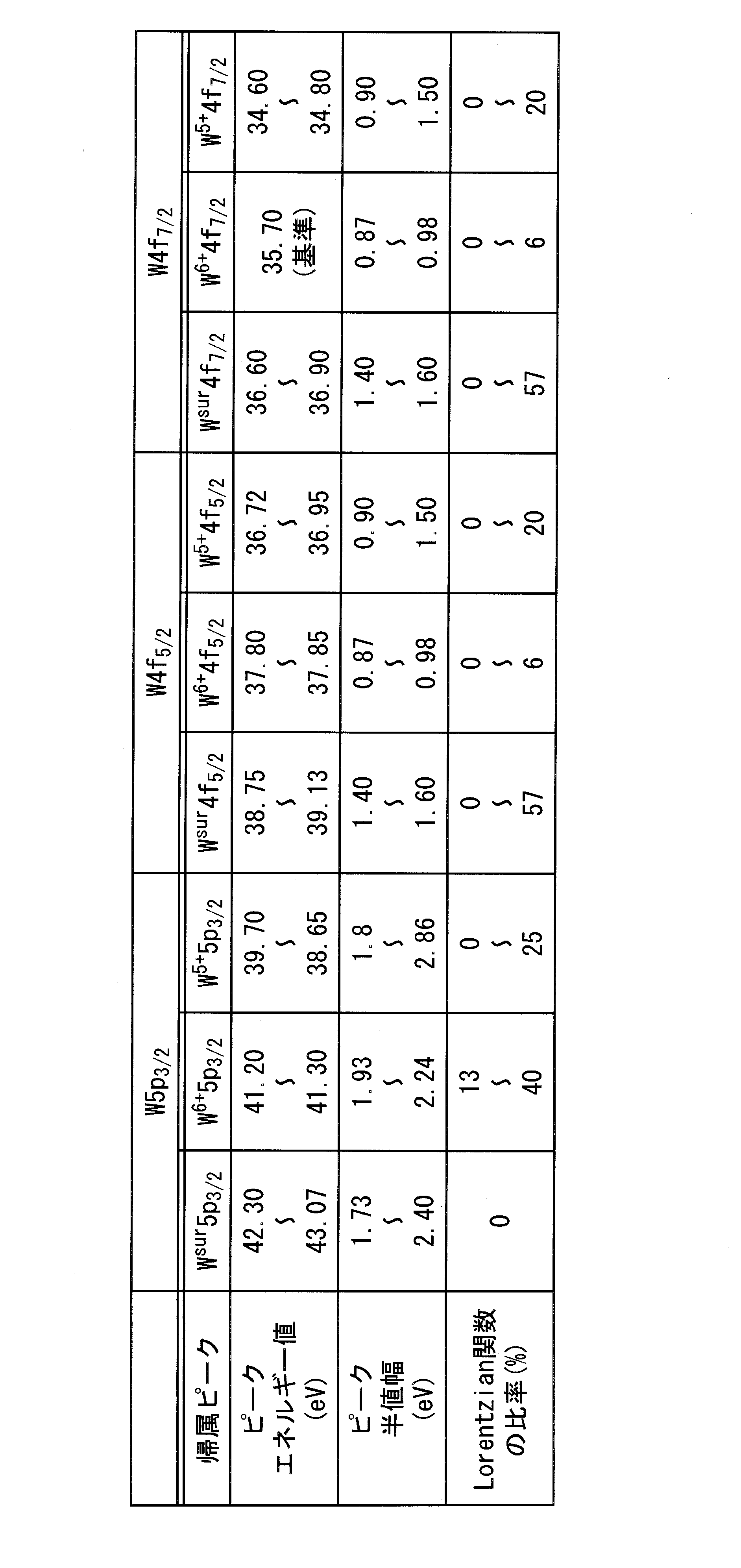
- three peaks are observed, and each peak is 5p 3/2 level (W5p 3/2 ), 4f 5/2 level (W4f 5 level) of tungsten from the left to the right in the figure. / 2 ) assigned to the peak corresponding to the 4f 7/2 level (W4f 7/2 ).
- Peak fitting analysis was performed on the peaks assigned to W5p 3/2 , W4f 5/2 and W4f 7/2 of the spectrum of sample E as a comparative example and the spectrum of sample A. Peak fitting analysis was performed as follows.
- FIG. 6A shows the analysis result of sample A
- FIG. 6B shows the analysis result of sample E.
- broken lines are measured spectra (corresponding to the spectrum of FIG. 5), and two-dot chain lines (surface) are the surface photoelectron peaks W sur 5p 3/2 , W sur 4f 5/2 , W sur.
- Spectrum assigned to 4f 7/2 dotted line (W 6+ ) is assigned to hexavalent surface defect levels W 6+ 5p 3/2 , W 6+ 4f 7/2 , (W 6+ 4f 5/2 )
- the dotted line (W 5+ ) is a spectrum attributed to pentavalent surface defect levels W 5+ 5p 3/2 , W 5+ 4f 5/2 , W 5+ 4f 7/2 .
- the solid line (fit) is a spectrum obtained by adding the two-dot chain line, the dotted line, and the one-dot chain line.
- the peak attributed to pentavalent tungsten indicated by the alternate long and short dash line was considered to originate only from tungsten in the pentavalent state.
- the spectrum attributed to each level of 5p 3/2 , 4f 5/2 , 4f 7/2 is a peak due to photoelectrons from the surface of the hole injection layer 3.
- the sum of the hexavalent tungsten peak (W 6+ ) included in the depth at which photoelectrons are detected in the hole injection layer 3 and the pentavalent tungsten peak (W 5+ ) included in the same depth are added. It can be seen that this is configured.
- W 5+ / W 6+ which is the ratio of the number of pentavalent tungsten elements to the number of hexavalent tungsten elements in Samples A to E. This abundance ratio was calculated by dividing the area intensity of the W 5+ (dashed line) peak in the spectrum obtained by the peak fitting analysis of each sample by the area intensity of the W 6+ (dotted line) peak.
- the abundance ratio of the number of hexavalent tungsten atoms and the number of pentavalent tungsten atoms is expressed by the ratio of the area intensity of the W 6+ peak to the area intensity of the W 5+ peak in W4f 7/2 .
- the ratio of the integrated intensity of the integrated intensity and W 6+ 4f 7/2 of W 5+ 4f 7/2 in W4f 7/2 is the same value even if W5p, the W4f 5/2 Have confirmed. Therefore, in the following discussion, it was decided to use only the peak attributed to W4f 7/2 .
- Table 5 shows W 5+ / W 6+ of Samples A to E.
- Tungsten oxide deposited under the above-mentioned deposition conditions A to D has a binding energy 1.8 to 3.6 eV lower than the uppermost valence band, that is, the lowest binding energy in the valence band in its electronic state. Occupied levels exist in the region. This occupied level corresponds to the highest occupied level of the hole injection layer 3, that is, its binding energy range is closest to the Fermi surface of the hole injection layer 3. Hereinafter, this occupied level is referred to as “occupied level near the Fermi surface”.
- the existence of the occupied level in the vicinity of the Fermi surface makes a so-called interface level connection at the stacked interface between the hole injection layer 3 and the buffer layer 4, and the binding energy of the highest occupied orbit of the buffer layer 4 is It becomes almost equal to the binding energy of the occupied level in the vicinity of the Fermi surface of the injection layer 3. That is, the presence of this occupied level can suppress the hole injection barrier between the hole injection layer 3 and the buffer layer 4 to be small. As a result, better hole conduction efficiency can be obtained, and driving at a low voltage is possible.
- substantially equal and “interface state connection was made” here means that the lowest binding energy at the occupied level in the vicinity of the Fermi surface at the interface between the hole injection layer 3 and the buffer layer 4; This means that the difference from the lowest binding energy in the highest occupied orbit is within a range of ⁇ 0.3 eV.
- the “interface” here refers to a region including the surface of the hole injection layer 3 and the buffer layer 4 at a distance within 0.3 nm from the surface.
- the occupied level in the vicinity of the Fermi surface is preferably present in the whole hole injection layer 3, but it may be present at least at the interface with the buffer layer 4.
- the UPS spectrum reflects the state of the occupied level such as the valence band from the surface of the measurement object to a depth of several nm. Therefore, in this experiment, the state of the occupied level in the surface layer of the hole injection layer 3 was observed using UPS measurement.
- UPS measurement conditions are as follows. Note that no charge-up occurred during the measurement.
- FIG. 7 shows a UPS spectrum of the surface of the hole injection layer 3 in Sample A.
- the origin of the binding energy on the horizontal axis is the Fermi surface of the substrate 7, and the left direction is the positive direction.
- each occupied level of the hole injection layer 3 will be described with reference to FIG.
- the largest and steep rise is uniquely determined.
- a tangent line passing through the rising inflection point is defined as a line (i), and an intersection with the horizontal axis is defined as a point (iii).
- the UPS spectrum of tungsten oxide is divided into a region (A) located on the high bond energy side from the point (iii) and a region (A) located on the low bond energy side (that is, the Fermi surface side).
- the ratio of the number of tungsten atoms to oxygen atoms was approximately 1: 3 in both samples A and E. Specifically, it was performed by estimating the composition ratio of tungsten and oxygen from the surface of the hole injection layer 3 to a depth of several nm.
- the hole injection layer 3 has a basic structure of atomic arrangement based on tungsten trioxide at least within a range of several nanometers from the surface (details will be described in the next section). It is thought to have. Accordingly, the region (a) in FIG. 7 is an occupied level derived from the basic structure, and corresponds to a so-called valence band.
- this inventor measured the X-ray absorption fine structure (XAFS) of the hole injection layer 3, and confirmed that the said basic structure was formed in any of the samples A and E.
- XAFS X-ray absorption fine structure
- the region (a) in FIG. 7 corresponds to the band gap between the valence band and the conduction band, but as this UPS spectrum shows, this region is different from the valence band in tungsten oxide. It is known that there may be a number of occupied levels. This is a level derived from another structure different from the above basic structure, and is a so-called inter-gap level (in-gap level). state or gap state).
- FIG. 8 shows a UPS spectrum in the region (A) of each hole injection layer 3 in Samples A and E.
- the intensity of the spectrum shown in FIG. 8 was normalized by the peak top value of the peak (ii) located 3-4 eV higher than the point (iii) in FIG. 8 also shows the point (iii) at the same horizontal axis position as the point (iii) in FIG.
- the horizontal axis is expressed as a relative value (relative binding energy) with respect to the point (iii), and the binding energy decreases from left to right (Fermi surface side).
- a region having a binding energy lower by about 2.0 to 3.2 eV from the point (iii) is a region where the raised structure is relatively easy to confirm and the raised portion is relatively steep. It can be said that it is particularly important.
- FIG. 9 is a diagram for explaining the structure of the surface of the tungsten oxide film.
- tungsten trioxide (WO 3 ) will be described as an example of tungsten oxide.
- a single crystal of tungsten oxide has a rutile structure in which oxygen atoms are bonded to tungsten atoms in octahedral coordination as a basic structure.
- the tungsten trioxide single crystal is shown in a rutile structure for simplification, but actually has a distorted rutile structure.
- Non-Patent Document 4 a structure in which some tungsten atoms (a) are not periodically terminated as shown in FIG. 9 by first-principles calculation, rather than all tungsten atoms at grain boundaries being terminated by oxygen atoms. Is disclosed to be more energetically stable. It is reported that the reason is that when all tungsten atoms at the grain boundaries are terminated with oxygen atoms, the electrical repulsion between the terminal oxygen atoms increases and becomes unstable. That is, at the crystal grain boundary, the surface having a structure (a) similar to an oxygen defect is more stable.
- a tungsten atom terminated with an oxygen atom that is, a tungsten atom having no structure (a) similar to an oxygen defect corresponds to a hexavalent tungsten atom.
- a tungsten atom not terminated with an oxygen atom that is, a tungsten atom having a structure (a) similar to an oxygen defect corresponds to a pentavalent tungsten atom (including a pentavalent or higher valence of less than 6).
- the pentavalent tungsten atom is considered to have a structure having an unshared electron pair by eliminating one of the octahedrally coordinated oxygen atoms. That is, it is considered that the pentavalent tungsten atom donates its own unshared electron pair to the hole, and thus the pentavalent tungsten atom that donated the electron has a hole.
- the supply of unshared electron pairs existing in pentavalent tungsten atoms is continuously generated by the bias voltage applied to the hole injection layer, so that holes move in a low potential direction, and electrons move in a high potential direction, thereby conducting hole conduction. Is considered to occur.
- the hole injection layer 3 having a high W 5+ / W 6+ value as in sample A, that is, a high ratio of pentavalent tungsten atoms has many hole conduction paths, and is driven at a low voltage by hole conduction at a low voltage. As a result, excellent hole conduction efficiency can be exhibited in the organic EL element.
- the tungsten oxide film constituting the hole injection layer 3 has a nanocrystal structure. This nanocrystal structure is formed by adjusting the film forming conditions. Details are described below.
- the tungsten oxide layer in the sample for TEM observation was formed by a reactive sputtering method using a DC magnetron sputtering apparatus under the conditions shown in Table 1.
- a hole injection layer 3 having a thickness of 30 nm was formed on the ITO conductive substrate formed on glass by the reactive sputtering method.
- the TEM observation samples prepared under the film forming conditions A, B, C, D, and E are referred to as Sample A, Sample B, Sample C, Sample D, and Sample E, respectively.
- the TEM observation is performed after confirming that the samples A, B, C, and D contain pentavalent tungsten atoms by the previous XPS measurement.
- TEM observation is performed by slicing the thickness of the surface to be observed.
- the thickness in the depth direction from the cross section of the tungsten oxide film is sampled by using a focused ion beam (FIB) apparatus, and thinned to about 100 nm.
- FIB focused ion beam
- FIG. 10 the TEM observation photograph of the cross section of the hole injection layer 3 of sample A, B, C, D, E is shown. The scale of the photograph follows the scale bar described in the photograph, and the display size of the TEM photograph is displayed at 560 ⁇ 560 pixels. In addition, the TEM observation photograph shown in FIG. 10 displays an average of 256 gradations from a black dark part to a light bright part.
- any one of the nanocrystals is shown by a white line frame.
- this outline is not an exact thing but an illustration to the last. This is because it is difficult to specify an accurate contour because the TEM photograph actually includes not only the outermost surface but also the lower layer.
- the size of one nanocrystal illustrated by a white frame is about 3 to 10 nm.
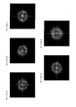
- FIG. 11 shows the result of two-dimensional Fourier transform of the TEM observation photograph shown in FIG. 10 as a two-dimensional Fourier transform image.
- the two-dimensional Fourier transform image shown in FIG. 11 is a distribution showing the reciprocal lattice space of the TEM observation photograph shown in FIG. Specifically, the two-dimensional Fourier transform image shown in FIG. 11 was subjected to Fourier transform on the TEM photograph shown in FIG. 10 using image processing software “LAview Version # 1.77”. From the Fourier change image shown in FIG. 11, in the samples A, B, C, and D, three or two concentric bright parts centering on the center point of the Fourier transform image are confirmed.
- the concentric bright portions of the Fourier transform images confirmed in the samples A, B, C, and D have an unclear circle in the sample E.
- the “ambiguousness” of the concentric bright portions qualitatively indicates the breakdown of the structural order in the hole injection layer 3 shown in FIG. That is, Samples A, B, C, and D in which the circular bright portion can be clearly confirmed have high order, and Sample E shows that the order is broken.
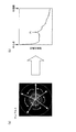
- FIG. 12 is a diagram showing an outline of the creation method, and shows sample A as an example.
- the brightness is measured with respect to the distance from the center point of the Fourier transform image to the outer periphery of the photograph in the X-axis direction by rotating the center point of the Fourier transform image by 1 °.
- the graph shown in FIG. 12B was drawn by accumulating and dividing by 360.
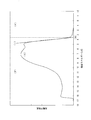
- FIGS. 13 and 14 show luminance change plots for samples A, B, C, D, and E.
- FIG. In the luminance change plots for samples A, B, C, D, and E, it can be seen that each sample has a peak indicated by P1 separately from the high-intensity part at the center point.
- peak P1 the peak of the normalized luminance that appears closest to the center point in the luminance change plot.
- the peak P1 in the samples A, B, C, and D had a sharp convex shape compared to the peak P1 in the sample E.
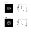
- FIG. 15 is a diagram showing an outline of the evaluation method, and shows sample A and sample E as examples.
- FIGS. 15A and 15B are luminance change plots of sample A and sample E, respectively, and FIGS. 15A1 and 15B1 are enlarged views near the peak P1 of each sample.
- the “peak width L of the peak P1” indicated by L in FIGS. 15A1 and 15B1 is used as an index indicating the “sharpness” of the peak P1.
- FIGS. 15A1 and 15B1 are first-order differentiated and shown in FIGS. 15A2 and 15B2.
- 15A and 15B the horizontal axis value corresponding to the peak top of the peak P1 and the horizontal axis value corresponding to the position where the differential intensity first becomes 0 from the peak top toward the center point.
- the peak width L is defined as the difference between the two.
- Table 6 shows the values of the peak width L in the samples A, B, C, D, and E when normalized with the horizontal axis value corresponding to the center point of the Fourier transform image and the peak top of the peak P1 being 100.
- the value of the peak width L shown in Table 6 shows the clarity of the concentric bright part closest to the center value of the Fourier transform image shown in FIG. 11, and the smaller the value of the peak width L, the more concentric bright part. This indicates that there is little spread, that is, the regularity in the TEM photograph of the hole injection layer 3 shown in FIG. 10 is high. On the contrary, as the value of the peak width L increases, it is shown that the concentric bright part closest to the center of the Fourier transform image shown in FIG. 11 has a spread, that is, the hole shown in FIG. It shows that the regularity of the fine structure in the TEM photograph of the injection layer 3 is broken.
- the single crystal of tungsten oxide is considered to have a distorted rutile structure in which the oxygen atom is octahedrally coordinated with the tungsten atom as a basic structure.
- the nanocrystal structure is constituted by a large number of such single crystals, that is, nanocrystals.
- the inside of the nanocrystal structure is a distorted rutile structure like the inside of the single crystal, and is considered to be a highly regular structure. Therefore, it should be considered that pentavalent tungsten atoms are present not on the inside of the nanocrystals but on the surfaces of the nanocrystals.
- the rutile structure described above exists with order in part, but the rutile structure does not have order in most part of the film. It is thought that. In the portion having an amorphous structure, although the rutile structure does not have order, the rutile structure is connected to the whole film, and there are few disconnected portions cutting the arrangement of the rutile structure. Therefore, there are few grain boundaries in which many oxygen defects exist, and as a result, the ratio of pentavalent tungsten atoms becomes low. For this reason, it is thought that low voltage driving is difficult to realize because there are few sites that serve as hole conduction paths.
- the rutile structure has ordering throughout the film. Exist. The part with the order is thought to be derived from nanocrystals. In the portion where the nanocrystal exists, the rutile structure has order, but there are many broken portions of the rutile structure. This discontinuity corresponds to the crystal grain boundary of the nanocrystal. Oxygen deficiency, that is, oxygen vacancies occur at the grain boundaries, and the amount of pentavalent tungsten atoms increases accordingly. As a result, it is considered that the number of sites serving as hole conduction paths increases and low voltage driving is realized.
- a single crystal of tungsten oxide is considered to have a distorted rutile structure in which oxygen atoms are bonded to tungsten atoms in octahedral coordination as a basic structure.
- this rutile structure is formed into a film without order, an amorphous structure is formed, and when the rutile structure is formed into a film with order, a nanocrystal structure is considered.
- pentavalent tungsten atoms are present in the tungsten oxide film
- one of the oxygen atoms that are octahedrally coordinated to the tungsten atoms disappears, so that the tungsten atoms have a structure having an unshared electron pair.
- the pentavalent tungsten atom donates its own unshared electron pair to the tungsten atom having a hole, and the pentavalent tungsten atom that has donated the unshared electron pair has a hole.
- the supply of unshared electron pairs existing in pentavalent tungsten atoms is continuously generated by the bias voltage applied to the hole injection layer, so that holes move in a low potential direction, and electrons move in a high potential direction, thereby conducting hole conduction. Is considered to occur. Therefore, the more pentavalent tungsten atoms are contained, the more tungsten atoms contribute to hole conduction, and the hole conduction efficiency is improved. However, containing many pentavalent tungsten atoms is not a necessary and sufficient condition for improving hole conductivity. The reason for this will be described with reference to FIG.
- FIG. 16B is a conceptual diagram showing how the holes 10 are conducted by hopping conduction, and shows the conduction of the holes 10 in the case of an amorphous structure.
- the part indicated by 11 in the figure is a crystalline part (segregated crystal 11) in which the rutile structure has order, and the surface of the segregated crystal 11 has many pentavalent tungsten atoms.
- the rutile structure is not ordered and is an amorphous part, and there are not many pentavalent tungsten atoms as much as the surface of the segregated crystal 11.
- FIG. 16A is a conceptual diagram showing how the holes 10 are conducted through the surface of the nanocrystal, and shows the conduction of the holes 10 in the case of the nanocrystal structure.
- the nanocrystal structure as shown in the figure, since the rutile structure exists in order, the entire film is finely crystalline, and the hole conduction mode is different from that of the amorphous film.
- the pentavalent tungsten atoms are present on the surface portions of the nanocrystals 9, and this surface portion becomes the hole conducting portion.
- the holes 10 can be conducted with a low voltage because the surface portions serving as the hole conducting portions are connected.
- the structure of the metal oxide film having good hole conductivity includes (1) the existence of a portion that becomes a hole conduction portion and (2) the increase of the portion that becomes a grain boundary. Thus, it is considered necessary to form overlapping electron orbits that contribute to hole conduction. That is, (1) a metal element having a valence state lower than the maximum valence that the metal element can take and (2) a metal oxide film having a nanocrystal structure is suitable for hole conduction. It can be said.
- the hole injection layer 3 also reduces the drive voltage by reducing the hole injection barrier formed at the interface between the anode 2 and the hole injection layer 3 and the hole injection barrier formed at the interface between the hole injection layer 3 and the buffer layer 4. It is possible to plan.
- the hole conduction energy value was analyzed using UPS measurement for the tungsten oxide film manufactured with the same hole injection layer 3 as BPD-D and BPD-E shown in Table 3 having different hole injection characteristics. As shown in FIG.
- BPD-D and BPD-E showed a difference in driving voltage of about 2 V at a current density of 10 mA / cm 2 , but there was no difference in the hole conduction energy value due to UPS. That is, the difference in hole injection voltage between BPD-D and BPD-E is that a hole injection barrier formed at the interface between the anode 2 and the hole injection layer 3 and a hole formed at the interface between the hole injection layer 3 and the buffer layer 4 are used. It was confirmed that it was not caused by the difference in the injection barrier but due to the film structure of the hole injection layer described above.
- the tungsten oxide film formed by DC sputtering is shown as an example of the hole injection layer, but the film forming method and oxide metal species are not limited thereto. Examples of other film forming methods include vapor deposition and CVD.
- the hole injection layer is formed of tungsten oxide.
- metal oxide such as molybdenum oxide (MoOx) or molybdenum-tungsten oxide (MoxWyOz) is used. It can also be composed of a metal, a metal nitride or a metal oxynitride.
- the organic EL device according to one embodiment of the present invention is not limited to a configuration using a single device.
- An organic EL light-emitting device can be configured by integrating a plurality of organic EL elements as pixels on a substrate.
- Such an organic EL light-emitting device can be implemented by appropriately setting the film thickness of each layer in each element, and can be used as, for example, a lighting device.
- An organic EL panel can be configured by arranging a plurality of organic EL elements 1 corresponding to red, green, and blue pixels.
- a coating process such as an inkjet method
- the bank it is possible to prevent the inks made of the light emitting layer materials corresponding to the respective colors from being mixed with each other in the coating process.
- the bank formation process for example, a bank material made of a photosensitive resist material is applied to the surface of the hole injection layer, pre-baked, and then exposed using a pattern mask, and an uncured excess bank material is developed with a developer.
- the present invention is also applicable to a hole injection layer made of a metal oxide that has undergone such a bank formation process.
- the organic EL panel can also be applied to an organic EL display device.
- the organic EL display device can be used for an organic EL display, for example.
- the differential intensity becomes 0 at the rising position of the peak P1 first from the peak top of the peak P1 in FIGS. 15 (a2) and 15 (b2) toward the center point. Points.
- the method for determining the rising position of the peak P1 is not limited to this. For example, taking the graph (a1) in FIG. 15 as an example, the average value of the normalized luminance near the rising position of the peak P1 is taken as the base line, and the intersection of the base line and the peak P1 is taken as the rising position of P1. You can also.
- the organic EL element according to an aspect of the present invention may have a so-called bottom emission type configuration or a so-called top emission type configuration.
- the organic EL element of the present invention can be suitably used for an organic EL device used for home or public facilities, various display devices for business use, television devices, displays for portable electronic devices, and the like.
Landscapes
- Physics & Mathematics (AREA)
- Optics & Photonics (AREA)
- Electroluminescent Light Sources (AREA)
Abstract
Description
本発明の一態様である有機EL素子は、陽極と陰極との間に、有機材料を含んでなる機能層と、前記機能層にホールを注入するためのホール注入層と、を有する有機EL素子であって、前記ホール注入層は金属酸化物を含む金属酸化物膜であり、前記金属酸化物を構成する金属元素は、当該金属元素が取り得る最大価数の状態および当該最大価数よりも低い価数の状態で前記金属酸化物膜に含まれ、かつ、前記金属酸化物膜は、粒径がナノメートルオーダーの大きさである前記金属酸化物の結晶を含む構成とした。
〈有機EL素子の構成〉
図1(a)は、本実施の形態に係る有機EL素子1の構成を示す模式的な断面図であり、図1(b)はホール注入層3付近の部分拡大図である。
基板7は有機EL素子1の基材となる部分であり、例えば、無アルカリガラス、ソーダガラス、無蛍光ガラス、燐酸系ガラス、硼酸系ガラス、石英、アクリル系樹脂、スチレン系樹脂、ポリカーボネート系樹脂、エポキシ系樹脂、ポリエチレン、ポリエステル、シリコーン系樹脂、またはアルミナ等の絶縁性材料のいずれかで形成することができる。
ホール注入層3は、例えば、厚さ30nmの酸化タングステン膜(WOx)からなる。酸化タングステンは、その組成式WOxにおいて、xが概ね2<x<3の範囲における実数である。ホール注入層3はできるだけ酸化タングステンのみで構成されることが望ましいが、通常レベルで混入し得る程度に、微量の不純物が含まれていてもよい。
有機EL素子1はホール注入層3以外にも、有機EL素子1に必要な、所要機能を果たす機能層が存在する。本発明における機能層は、ホールを輸送するホール輸送層、注入されたホールと電子とが再結合することにより発光する発光層、光学特性の調整または電子ブロックの用途に用いられるバッファ層等のいずれか、もしくはこれらの層を2層以上の組み合わせた層、またはこれらの層の全てを含む層を指す。本実施の形態では、機能層として、バッファ層4および発光層5を含む例を説明する。
陰極6は、例えば、厚さ5nmのバリウム層6aと、厚さ100nmのアルミニウム層6bを積層して構成される。前述した陽極2および陰極6には直流電源8が接続され、外部より有機EL素子1に給電されるようになっている。
次に、図1に基づき有機EL素子1の全体的な製造方法を例示する。
(ホール注入層3の成膜条件について)
本実施の形態では、ホール注入層3を構成する酸化タングステンを所定の成膜条件で成膜することで、ホール注入層3にナノクリスタル構造を意図的に存在させることによりホール伝導性を向上させ、有機EL素子1を低電圧駆動できるようにしている。この所定の成膜条件について詳細に説明する。
ここで、スパッタ成膜における成膜レートは、上述した(1)~(4)の条件に依存すると考えられる。そして、後述する実験を行った結果、(1)~(4)が上記の数値範囲を取る場合、駆動電圧が低減されることを確認しており、このことにより、結晶性の高い酸化タングステン膜が得られていることになる。
また、上記(2)に関し、スパッタガス全圧に対する酸素ガス分圧の割合は50%に設定されているが、少なくとも50%以上70%以下において、駆動電圧の低減が確認されている。

本実施の形態の有機EL素子1のホール注入層3を構成する酸化タングステンには、上述したナノクリスタル構造が存在している。このナノクリスタル構造は、先の実験で示した成膜条件の調整により形成されるものである。詳細を以下に述べる。
測定」と記載する。)実験を行った。ここで、一般に硬X線光電子分光スペクトル(以
下、単に「XPSスペクトル」と記載する。)は、測定対象物の表面と、光電子を取り出す検出器において光電子を検出する方向とがなす角度によって、膜の平均価数を反映する情報深さが決まる。そこで本実験では、XPS測定における光電子検出方向と、酸化タングステン膜の表面のなす角度が40°となる条件で測定を行い、酸化タングステン膜の厚み方向の平均の価数の状態を観察するものとした。
使用機器 :R-4000(VG-SCIENTA社製)
光源 :シンクロトロン放射光(7856eV)
バイアス :なし
出射角 :基板表面とのなす角が40°
測定点間隔:0.05eV
表1に示すA~Eの各成膜条件でXPS測定用のサンプルを作製した。ガラス上に成膜されたITO導電性基板の上に、厚さ30nmのホール注入層3を、前記の反応性スパッタ法により成膜することにより、XPS測定用のサンプルとした。以降、成膜条件A、B、C、D、Eで作製したXPS測定用サンプルを、それぞれサンプルA、サンプルB、サンプルC、サンプルD、サンプルEと称する。続いて、サンプルA~Eの各ホール注入層3の表面に対してXPS測定を行った。その結果のスペクトルを図5に示す。
ピークフィッティング解析は以下のようにして行った。
前述の成膜条件A~Dで成膜した酸化タングステンには、その電子状態において、価電子帯の上端、すなわち価電子帯で最も低い結合エネルギーよりも、1.8~3.6eV低い結合エネルギー領域内に占有準位が存在している。この占有準位がホール注入層3の最高占有準位に該当し、すなわち、その結合エネルギー範囲はホール注入層3のフェルミ面に最も近い。以降、この占有準位を「フェルミ面近傍の占有準位」と称する。
使用機器 :走査型X線光電子分光分析装置 PHI5000 VersaPro
be(アルバック・ファイ社製)
光源 :He I線
バイアス:なし
出射角 :基板法線方向
測定点間隔:0.05eV
図7に、サンプルAにおけるホール注入層3表面のUPSスペクトルを示す。横軸の結合エネルギーの原点は基板7のフェルミ面とし、左方向を正の向きとした。以下、図7を用いて、ホール注入層3の各占有準位について説明する。
stateあるいはgap state)である。
図9は酸化タングステン膜表面の構造を説明するための図である。ここでは酸化タングステンとして三酸化タングステン(WO3)を例に挙げて説明する。図9に示すように、酸化タングステンの単結晶は、酸素原子がタングステン原子に対し8面体配位で結合したルチル構造を基本構造に持つ。なお、図9では、単純化のために三酸化タングステン単結晶をルチル構造で示しているが、実際は歪んだルチル構造である。
ホール注入層3を構成する酸化タングステン膜には、ナノクリスタル構造が存在している。このナノクリスタル構造は、成膜条件の調整により形成されるものである。詳細を以下に述べる。
使用機器:Quanta200(FEI社製)
加速電圧:30kV(最終仕上げ5kV)
薄片膜厚:~50nm
(TEM観察条件)
使用機器:トプコンEM-002B(トプコンテクノハウス社製)
観察方法:高分解能電子顕微鏡法
加速電圧:200kV
図10に、サンプルA、B、C、D、Eのホール注入層3断面のTEM観察写真を示す。写真のスケールは、写真内に記載したスケールバーに従い、TEM写真の表示サイズは560×560ピクセルで表示している。また、図10で示すTEM観察写真は、黒暗部から薄明部までを256階調に平均分割し表示している。

一方、成膜条件A~Dで作製した酸化タングステン膜においては、膜全体においてルチル構造が秩序性を持って存在している。その秩序性を持った部分がナノクリスタルに由来するものと考えられる。ナノクリスタルが存在する部分では、ルチル構造が秩序性を有しているものの、ルチル構造の断絶部分が多く存在する。この断絶部分がナノクリスタルの結晶粒界に相当する。結晶粒界では酸素の不足、つまり酸素欠陥が生じ、それに伴って5価のタングステン原子の量が多くなる。結果として、ホール伝導経路となる部位が増え、低電圧駆動が実現されるものと考えられる。
上述しているように、酸化タングステンの単結晶は酸素原子がタングステン原子に対し8面体配位で結合した、歪んだルチル構造を基本構造としていると考えられる。このルチル構造が秩序性を持たずに膜化した場合はアモルファス構造となり、ルチル構造が秩序性を持って膜化した場合はナノクリスタル構造になると考えられる。
(1)上記実施の形態においては、ホール注入層としてDCスパッタで成膜した酸化タングステン膜を例として示したが、成膜方法および酸化物金属種はそれに限定されない。他の成膜方法としては例えば蒸着法、CVD法等が挙げられる。また、上記実施の形態においては、ホール注入層を酸化タングステンで構成する例を説明したが、酸化タングステン以外にも、例えば、酸化モリブデン(MoOx)、モリブデン-タングステン酸化物(MoxWyOz)等の金属酸化物、金属窒化物又は金属酸窒化物で構成することもできる。
を、有機EL表示装置に適用することもできる。有機EL表示装置は、例えば、有機ELディスプレイ等に利用することが可能である。
1A ホールオンリー素子
2 陽極
3 ホール注入層
4 バッファ層(機能層)
5 発光層(機能層)
6 陰極
6a バリウム層
6b アルミニウム層
6A 陰極(金層)
7 基板
8 直流電源
9 ナノクリタル
10 ホール
11 偏析した結晶
12 アモルファス部分
Claims (22)
- 陽極と陰極との間に、有機材料を含んでなる機能層と、前記機能層にホールを注入するためのホール注入層と、を有する有機EL素子であって、
前記ホール注入層は金属酸化物膜であり、
前記金属酸化物を構成する金属元素は、当該金属元素が取り得る最大価数の状態および当該最大価数よりも低い価数の状態で前記金属酸化物膜に含まれ、かつ、
前記金属酸化物膜は、粒径がナノメートルオーダーの大きさである前記金属酸化物の結晶を含む
ことを特徴とする有機EL素子。 - 前記金属酸化物は酸化タングステンであり、
前記最大価数の状態の前記金属元素は6価のタングステン元素である、
ことを特徴とする請求項1に記載の有機EL素子。 - 前記最大価数よりも低い価数の前記金属元素は、5価のタングステン元素である
ことを特徴とする請求項2に記載の有機EL素子。 - 前記5価のタングステン元素の原子数を、前記6価のタングステン元素の原子数で割った値であるW5+/W6+が3.2%以上である
ことを特徴とする請求項3に記載の有機EL素子。 - 前記W5+/W6+が3.2%以上7.4%以下である
ことを特徴とする請求項4に記載の有機EL素子。 - 前記酸化タングステン膜表面の硬X線光電子分光スペクトルにおいて、6価のタングステンの4f7/2準位に対応した第1ピークよりも低い結合エネルギー領域に第2ピークが存在する
ことを特徴とする請求項2に記載の有機EL素子。 - 前記第2ピークは、前記第1ピークの結合エネルギー値よりも0.3~1.8eV低い結合エネルギー領域に存在する
ことを特徴とする請求項6に記載の有機EL素子。 - 前記第2ピークの面積強度は、前記第1ピークの面積強度に対して、3.2~7.4%である
ことを特徴とする請求項6、7のいずれか一項に記載の有機EL素子。 - 前記最大価数よりも低い価数の状態のタングステン元素の存在によって、前記ホール注入層のバンド構造には、価電子帯で最も低い結合エネルギーよりも1.8~3.6eV低い結合エネルギー領域内に占有準位を有している
ことを特徴とする請求項2~8のいずれか一項に記載の有機EL素子。 - 前記酸化タングステン膜は、粒径が3~10ナノメートルの大きさである前記酸化タングステンの結晶を複数個含む
ことを特徴とする請求項2~9のいずれか一項に記載の有機EL素子。 - 前記酸化タングステン膜断面の透過型電子顕微鏡観察による格子像において、1.85~5.55Åの間隔で規則的に配列した線状構造が現れる
ことを特徴とする請求項2~10のいずれか一項に記載の有機EL素子。 - 前記格子像の2次元フーリエ変換像において、当該2次元フーリエ変換像の中心点を中心とした同心円状の模様が現れる
ことを特徴とする請求項11に記載の有機EL素子。 - 前記中心点からの距離と、前記距離における前記2次元フーリエ変換像の輝度を規格化した数値である規格化輝度との関係を表すプロットにおいて、前記規格化輝度のピークが1以上現れる
ことを特徴とする請求項12に記載の有機EL素子。 - 前記プロットにおける前記中心点から最も近くに現れる前記規格化輝度のピークの位置に対応する前記距離と、前記規格化輝度のピークの立ち上がり位置に対応する前記距離との差をピーク幅とし、
前記中心点に対応する前記距離と、前記中心点から最も近くに現れる前記規格化輝度のピークに対応する前記距離との差を100とした時の前記ピーク幅が22よりも小さい
ことを特徴とする請求項13に記載の有機EL素子。 - 前記機能層は、アミン系材料を含んでいることを特徴とする請求項1~14のいずれか一項に記載の有機EL素子。
- 前記機能層は、ホールを輸送するホール輸送層、注入されたホールと電子とが再結合することにより発光する発光層、光学特性の調整又は電子ブロックの用途に用いられるバッファ層のいずれかである
ことを特徴とする請求項1~15のいずれか一項に記載の有機EL素子。 - 請求項1~16のいずれか一項に記載の有機EL素子を備える有機ELパネル。
- 請求項1~16のいずれか一項に記載の有機EL素子を備える有機EL発光装置。
- 請求項1~16のいずれか一項に記載の有機EL素子を備える有機EL表示装置。
- 陽極を準備する第1工程と、
前記陽極上に酸化タングステン膜を成膜する第2工程であって、アルゴンガスと酸素ガスからなるスパッタガス、および、タングステンからなるターゲットを用い、前記スパッタガスの全圧が2.3Pa以上7.0Pa以下であるとともに、前記スパッタガスの全圧に対する前記酸素ガス分圧の割合が50%以上70%以下であり、かつ、前記ターゲットの単位面積当たりの投入電力である投入電力密度が1.5W/cm2以上6.0W/cm2以下であり、かつ、前記スパッタガスの全圧を投入電力密度で割った値である全圧/投入電力密度が0.7Pa・cm2/Wよりも大きい成膜条件下で酸化タングステン膜を成膜する第2工程と、
前記成膜された酸化タングステン膜上に有機材料を含んでなる機能層を形成する第3工程と、
前記機能層の上方に、陰極を形成する第4工程と、
を含むことを特徴とする有機EL素子の製造方法。 - 前記第2工程において、
前記酸化タングステン膜を構成するタングステン元素が、前記タングステン元素が取り得る最大価数の状態および前記最大価数よりも低い価数の状態で前記酸化タングステン膜に含まれるように、かつ、粒径がナノメートルオーダーの大きさである酸化タングステンの結晶が含まれるように、前記酸化タングステン膜を成膜する
ことを特徴とする請求項20に記載の有機EL素子の製造方法。 - 前記第2工程は、前記全圧/投入電力密度が3.2Pa・cm2/Wよりも小さい
ことを特徴とする請求項20に記載の有機EL素子の製造方法。
Priority Applications (4)
| Application Number | Priority Date | Filing Date | Title |
|---|---|---|---|
| PCT/JP2010/004833 WO2012014256A1 (ja) | 2010-07-30 | 2010-07-30 | 有機el素子 |
| JP2012526194A JP5624141B2 (ja) | 2010-07-30 | 2010-07-30 | 有機el素子 |
| CN201080068298.XA CN103026523B (zh) | 2010-07-30 | 2010-07-30 | 有机el元件 |
| US13/736,419 US9490445B2 (en) | 2010-07-30 | 2013-01-08 | Organic el element, organic el panel, organic el light-emitting apparatus, organic el display apparatus, and method of manufacturing organic el element |
Applications Claiming Priority (1)
| Application Number | Priority Date | Filing Date | Title |
|---|---|---|---|
| PCT/JP2010/004833 WO2012014256A1 (ja) | 2010-07-30 | 2010-07-30 | 有機el素子 |
Related Child Applications (1)
| Application Number | Title | Priority Date | Filing Date |
|---|---|---|---|
| US13/736,419 Continuation US9490445B2 (en) | 2010-07-30 | 2013-01-08 | Organic el element, organic el panel, organic el light-emitting apparatus, organic el display apparatus, and method of manufacturing organic el element |
Publications (1)
| Publication Number | Publication Date |
|---|---|
| WO2012014256A1 true WO2012014256A1 (ja) | 2012-02-02 |
Family
ID=45529508
Family Applications (1)
| Application Number | Title | Priority Date | Filing Date |
|---|---|---|---|
| PCT/JP2010/004833 Ceased WO2012014256A1 (ja) | 2010-07-30 | 2010-07-30 | 有機el素子 |
Country Status (4)
| Country | Link |
|---|---|
| US (1) | US9490445B2 (ja) |
| JP (1) | JP5624141B2 (ja) |
| CN (1) | CN103026523B (ja) |
| WO (1) | WO2012014256A1 (ja) |
Families Citing this family (15)
| Publication number | Priority date | Publication date | Assignee | Title |
|---|---|---|---|---|
| JP5861210B2 (ja) | 2011-07-15 | 2016-02-16 | 株式会社Joled | 有機発光素子 |
| US9065069B2 (en) | 2011-07-15 | 2015-06-23 | Joled Inc. | Method for producing organic light-emitting element |
| JP5793569B2 (ja) | 2011-07-15 | 2015-10-14 | 株式会社Joled | 有機発光素子の製造方法 |
| JP6387547B2 (ja) | 2012-03-02 | 2018-09-12 | 株式会社Joled | 有機el素子とその製造方法、および金属酸化物膜の成膜方法 |
| US9035293B2 (en) * | 2012-04-18 | 2015-05-19 | Joled Inc. | Organic el device including a mixed hole injection layer |
| WO2013161165A1 (ja) | 2012-04-27 | 2013-10-31 | パナソニック株式会社 | 有機el素子、およびそれを備える有機elパネル、有機el発光装置、有機el表示装置 |
| WO2013161166A1 (ja) | 2012-04-27 | 2013-10-31 | パナソニック株式会社 | 有機el素子、およびそれを備える有機elパネル、有機el発光装置、有機el表示装置 |
| TWI657586B (zh) * | 2018-03-06 | 2019-04-21 | 日商旭化成股份有限公司 | 半導體膜,及使用該半導體膜之半導體元件,以及分散液 |
| KR102820733B1 (ko) * | 2020-08-21 | 2025-06-16 | 삼성디스플레이 주식회사 | 유기발광 다이오드 및 그 제조방법 |
| KR20220090667A (ko) * | 2020-12-22 | 2022-06-30 | 삼성디스플레이 주식회사 | 발광 소자 및 이를 포함한 전자 장치 |
| CN116670743A (zh) * | 2020-12-29 | 2023-08-29 | 株式会社半导体能源研究所 | 显示装置的制造方法 |
| CN113054124A (zh) * | 2021-02-20 | 2021-06-29 | 京东方科技集团股份有限公司 | 一种有机发光器件、显示装置、制作方法以及存储介质 |
| US20240243234A1 (en) * | 2021-10-11 | 2024-07-18 | Beijing Boe Technology Development Co., Ltd. | Display panel and method for manufacturing the same, display apparatus |
| US12604650B2 (en) * | 2021-12-20 | 2026-04-14 | Semiconductor Energy Laboratory Co., Ltd. | Method for manufacturing light-emitting element and light-emitting device using photolithography technique |
| JP7838899B2 (ja) * | 2022-06-07 | 2026-04-01 | 東京エレクトロン株式会社 | 基板処理方法及び基板処理装置 |
Citations (5)
| Publication number | Priority date | Publication date | Assignee | Title |
|---|---|---|---|---|
| JP2008177557A (ja) * | 2006-12-21 | 2008-07-31 | Semiconductor Energy Lab Co Ltd | 発光素子及び発光装置 |
| JP2008270731A (ja) * | 2007-03-23 | 2008-11-06 | Toppan Printing Co Ltd | 有機el素子およびそれを備えた表示装置 |
| JP2009277788A (ja) * | 2008-05-13 | 2009-11-26 | Panasonic Corp | 有機エレクトロルミネッセント素子およびその製造方法 |
| JP2010021138A (ja) * | 2008-06-09 | 2010-01-28 | Panasonic Corp | 有機エレクトロルミネッセント装置およびその製造方法 |
| JP2010021162A (ja) * | 2007-12-10 | 2010-01-28 | Panasonic Corp | 有機elデバイスおよびelディスプレイパネル、ならびにそれらの製造方法 |
Family Cites Families (96)
| Publication number | Priority date | Publication date | Assignee | Title |
|---|---|---|---|---|
| US5443922A (en) | 1991-11-07 | 1995-08-22 | Konica Corporation | Organic thin film electroluminescence element |
| JPH05163488A (ja) | 1991-12-17 | 1993-06-29 | Konica Corp | 有機薄膜エレクトロルミネッセンス素子 |
| US5294869A (en) | 1991-12-30 | 1994-03-15 | Eastman Kodak Company | Organic electroluminescent multicolor image display device |
| US5688551A (en) | 1995-11-13 | 1997-11-18 | Eastman Kodak Company | Method of forming an organic electroluminescent display panel |
| DE69729394T2 (de) | 1996-11-29 | 2005-06-02 | Idemitsu Kosan Co. Ltd. | Organische elektrolumineszente Vorrichtung |
| JPH10162959A (ja) | 1996-11-29 | 1998-06-19 | Idemitsu Kosan Co Ltd | 有機エレクトロルミネッセンス素子 |
| JP3782245B2 (ja) | 1998-10-28 | 2006-06-07 | Tdk株式会社 | 有機el表示装置の製造装置及び製造方法 |
| US6309801B1 (en) | 1998-11-18 | 2001-10-30 | U.S. Philips Corporation | Method of manufacturing an electronic device comprising two layers of organic-containing material |
| JP4198253B2 (ja) | 1999-02-02 | 2008-12-17 | 出光興産株式会社 | 有機エレクトロルミネッセンス素子およびその製造方法 |
| US7153592B2 (en) | 2000-08-31 | 2006-12-26 | Fujitsu Limited | Organic EL element and method of manufacturing the same, organic EL display device using the element, organic EL material, and surface emission device and liquid crystal display device using the material |
| JP2002075661A (ja) | 2000-08-31 | 2002-03-15 | Fujitsu Ltd | 有機el素子及び有機el表示装置 |
| TWI257496B (en) | 2001-04-20 | 2006-07-01 | Toshiba Corp | Display device and method of manufacturing the same |
| JP2002318556A (ja) | 2001-04-20 | 2002-10-31 | Toshiba Corp | アクティブマトリクス型平面表示装置およびその製造方法 |
| US8058797B2 (en) | 2001-05-18 | 2011-11-15 | Cambridge University Technical Services Limited | Electroluminescent device |
| JP2003007460A (ja) | 2001-06-22 | 2003-01-10 | Sony Corp | 表示装置の製造方法および表示装置 |
| JP3823916B2 (ja) | 2001-12-18 | 2006-09-20 | セイコーエプソン株式会社 | 表示装置及び電子機器並びに表示装置の製造方法 |
| JP2003264083A (ja) | 2002-03-08 | 2003-09-19 | Sharp Corp | 有機led素子とその製造方法 |
| US7086917B2 (en) | 2002-08-12 | 2006-08-08 | National Research Council Of Canada | Photoresist mask/smoothing layer ensuring the field homogeneity and better step-coverage in OLED displays |
| JP4165173B2 (ja) | 2002-10-15 | 2008-10-15 | 株式会社デンソー | 有機el素子の製造方法 |
| TWI330269B (en) * | 2002-12-27 | 2010-09-11 | Semiconductor Energy Lab | Separating method |
| JP2004228355A (ja) | 2003-01-23 | 2004-08-12 | Seiko Epson Corp | 絶縁膜基板の製造方法、絶縁膜基板の製造装置及び絶縁膜基板並びに電気光学装置の製造方法及び電気光学装置 |
| JP2004234901A (ja) | 2003-01-28 | 2004-08-19 | Seiko Epson Corp | ディスプレイ基板、有機el表示装置、ディスプレイ基板の製造方法および電子機器 |
| ATE401672T1 (de) | 2003-05-12 | 2008-08-15 | Cambridge Entpr Ltd | Herstellung einer polymeren vorrichtung |
| EP1629544B1 (en) | 2003-05-12 | 2008-11-19 | Cambridge Enterprise Limited | Polymer transistor |
| JP2005012173A (ja) | 2003-05-28 | 2005-01-13 | Seiko Epson Corp | 膜パターン形成方法、デバイス及びデバイスの製造方法、電気光学装置、並びに電子機器 |
| JP2004363170A (ja) | 2003-06-02 | 2004-12-24 | Seiko Epson Corp | 導電パターンの形成方法、電気光学装置、電気光学装置の製造方法および電子機器 |
| JP2005203339A (ja) | 2003-12-16 | 2005-07-28 | Matsushita Electric Ind Co Ltd | 有機エレクトロルミネッセント素子およびその製造方法 |
| US20090160325A1 (en) | 2003-12-16 | 2009-06-25 | Panasonic Corporation | Organic electroluminescent device and method for manufacturing the same |
| KR20060110323A (ko) | 2003-12-16 | 2006-10-24 | 마츠시타 덴끼 산교 가부시키가이샤 | 유기 전기발광 소자 및 그 제조 방법 |
| JP2005203340A (ja) | 2003-12-16 | 2005-07-28 | Matsushita Electric Ind Co Ltd | 有機エレクトロルミネッセント素子 |
| JP4857521B2 (ja) | 2004-01-09 | 2012-01-18 | セイコーエプソン株式会社 | 電気光学装置の製造方法、電気光学装置、及び電子機器 |
| JP4002949B2 (ja) | 2004-03-17 | 2007-11-07 | 独立行政法人科学技術振興機構 | 両面発光有機elパネル |
| JP2005268099A (ja) | 2004-03-19 | 2005-09-29 | Mitsubishi Electric Corp | 有機el表示パネル、有機el表示装置、および有機el表示パネルの製造方法 |
| JP4645064B2 (ja) | 2004-05-19 | 2011-03-09 | セイコーエプソン株式会社 | 電気光学装置の製造方法 |
| CN100490213C (zh) | 2004-05-27 | 2009-05-20 | 精工爱普生株式会社 | 滤色片基板的制造方法、电光学装置及其制造方法、电子设备 |
| JP4161956B2 (ja) * | 2004-05-27 | 2008-10-08 | セイコーエプソン株式会社 | カラーフィルタ基板の製造方法、電気光学装置の製造方法、電気光学装置、電子機器 |
| US7211456B2 (en) | 2004-07-09 | 2007-05-01 | Au Optronics Corporation | Method for electro-luminescent display fabrication |
| JP2006185869A (ja) | 2004-12-28 | 2006-07-13 | Asahi Glass Co Ltd | 有機電界発光素子及びその製造方法 |
| JP2006253443A (ja) | 2005-03-11 | 2006-09-21 | Seiko Epson Corp | 有機el装置、その製造方法および電子機器 |
| JP2006294261A (ja) | 2005-04-05 | 2006-10-26 | Fuji Electric Holdings Co Ltd | 有機el発光素子およびその製造方法 |
| JP2006344459A (ja) | 2005-06-08 | 2006-12-21 | Sony Corp | 転写方法および転写装置 |
| TWI307612B (en) | 2005-04-27 | 2009-03-11 | Sony Corp | Transfer method and transfer apparatus |
| US7994711B2 (en) | 2005-08-08 | 2011-08-09 | Semiconductor Energy Laboratory Co., Ltd. | Light emitting device and manufacturing method thereof |
| JP2007073499A (ja) | 2005-08-08 | 2007-03-22 | Semiconductor Energy Lab Co Ltd | 発光装置およびその作製方法 |
| GB0517195D0 (en) | 2005-08-23 | 2005-09-28 | Cambridge Display Tech Ltd | Molecular electronic device structures and fabrication methods |
| JP2007095606A (ja) | 2005-09-30 | 2007-04-12 | Seiko Epson Corp | 有機el装置、その製造方法、及び電子機器 |
| JP4318689B2 (ja) | 2005-12-09 | 2009-08-26 | 出光興産株式会社 | n型無機半導体、n型無機半導体薄膜及びその製造方法 |
| JP2007214066A (ja) | 2006-02-13 | 2007-08-23 | Seiko Epson Corp | 有機エレクトロルミネセンス装置の製造方法 |
| JP2007288074A (ja) | 2006-04-19 | 2007-11-01 | Matsushita Electric Ind Co Ltd | 有機エレクトロルミネッセント素子およびその製造方法 |
| JP2007288071A (ja) | 2006-04-19 | 2007-11-01 | Matsushita Electric Ind Co Ltd | 有機エレクトロルミネッセント素子およびその製造方法、それを用いた表示装置、露光装置 |
| US20070241665A1 (en) | 2006-04-12 | 2007-10-18 | Matsushita Electric Industrial Co., Ltd. | Organic electroluminescent element, and manufacturing method thereof, as well as display device and exposure apparatus using the same |
| JP2007287353A (ja) | 2006-04-12 | 2007-11-01 | Matsushita Electric Ind Co Ltd | 有機エレクトロルミネッセント素子の製造方法およびそれを用いて作成された有機エレクトロルミネッセント素子 |
| JP2008041747A (ja) | 2006-08-02 | 2008-02-21 | Matsushita Electric Ind Co Ltd | 有機エレクトロルミネッセント発光装置およびその製造方法 |
| US20070290604A1 (en) | 2006-06-16 | 2007-12-20 | Matsushita Electric Industrial Co., Ltd. | Organic electroluminescent device and method of producing the same |
| KR101252005B1 (ko) * | 2006-06-22 | 2013-04-08 | 삼성전자주식회사 | 나노결정 입자를 함유하는 박막 및 그의 제조방법 |
| JP4915650B2 (ja) | 2006-08-25 | 2012-04-11 | パナソニック株式会社 | 有機エレクトロルミネッセンス素子 |
| JP2008091072A (ja) | 2006-09-29 | 2008-04-17 | Seiko Epson Corp | 電気光学装置、およびその製造方法 |
| US7622371B2 (en) * | 2006-10-10 | 2009-11-24 | Hewlett-Packard Development Company, L.P. | Fused nanocrystal thin film semiconductor and method |
| JP4915913B2 (ja) | 2006-11-13 | 2012-04-11 | パナソニック株式会社 | 有機エレクトロルミネッセンス素子 |
| JP2008140724A (ja) | 2006-12-05 | 2008-06-19 | Toppan Printing Co Ltd | 有機el素子の製造方法および有機el素子 |
| EP1953840A3 (en) * | 2007-01-31 | 2012-04-11 | Panasonic Corporation | Piezoelectric thin film device and piezoelectric thin film device manufacturing method and inkjet head and inkjet recording apparatus |
| US8471461B2 (en) | 2007-03-29 | 2013-06-25 | Dai Nippon Printing Co., Ltd. | Organic electroluminescent device and method for producing the same |
| JP2009004347A (ja) | 2007-05-18 | 2009-01-08 | Toppan Printing Co Ltd | 有機el表示素子の製造方法及び有機el表示素子 |
| KR100919352B1 (ko) | 2007-05-30 | 2009-09-25 | 파나소닉 주식회사 | 유기 el 디스플레이 패널 및 그 제조 방법 |
| JP4280301B2 (ja) | 2007-05-31 | 2009-06-17 | パナソニック株式会社 | 有機el素子、およびその製造方法 |
| US8628986B2 (en) | 2007-07-31 | 2014-01-14 | Sumitomo Chemical Company, Limited | Organic electroluminescent element and method for manufacturing the same |
| JP5001745B2 (ja) | 2007-08-10 | 2012-08-15 | 住友化学株式会社 | 有機エレクトロルミネッセンス素子及び製造方法 |
| JP2009048960A (ja) | 2007-08-23 | 2009-03-05 | Canon Inc | 電極洗浄処理方法 |
| JP2009058897A (ja) | 2007-09-03 | 2009-03-19 | Hitachi Displays Ltd | 表示装置 |
| JP4439589B2 (ja) | 2007-12-28 | 2010-03-24 | パナソニック株式会社 | 有機elデバイスおよび有機elディスプレイパネル、ならびにそれらの製造方法 |
| JP4418525B2 (ja) | 2008-02-28 | 2010-02-17 | パナソニック株式会社 | 有機elディスプレイパネル |
| JP2009218156A (ja) | 2008-03-12 | 2009-09-24 | Casio Comput Co Ltd | Elパネル及びelパネルの製造方法 |
| JP5267246B2 (ja) | 2008-03-26 | 2013-08-21 | 凸版印刷株式会社 | 有機エレクトロルミネッセンス素子及びその製造方法並びに有機エレクトロルミネッセンス表示装置 |
| JP2009239180A (ja) | 2008-03-28 | 2009-10-15 | Sumitomo Chemical Co Ltd | 有機エレクトロルミネッセンス素子 |
| KR101509283B1 (ko) * | 2008-04-28 | 2015-04-06 | 다이니폰 인사츠 가부시키가이샤 | 정공 주입 수송층을 갖는 디바이스, 및 그 제조 방법, 및 정공 주입 수송층 형성용 잉크 |
| JP4678421B2 (ja) | 2008-05-16 | 2011-04-27 | ソニー株式会社 | 表示装置 |
| JP4975064B2 (ja) | 2008-05-28 | 2012-07-11 | パナソニック株式会社 | 発光装置及びその製造方法 |
| JP2008241238A (ja) | 2008-05-28 | 2008-10-09 | Mitsubishi Electric Corp | 冷凍空調装置及び冷凍空調装置の制御方法 |
| GB0811199D0 (en) * | 2008-06-18 | 2008-07-23 | Cambridge Entpr Ltd | Electro-optic diode devices |
| JP5199773B2 (ja) | 2008-07-30 | 2013-05-15 | 住友化学株式会社 | 有機エレクトロルミネッセンス素子およびその製造方法 |
| JP4723692B2 (ja) | 2008-09-19 | 2011-07-13 | パナソニック株式会社 | 有機エレクトロルミネッセンス素子及びその製造方法 |
| JP5138542B2 (ja) | 2008-10-24 | 2013-02-06 | パナソニック株式会社 | 有機エレクトロルミネッセンス素子及びその製造方法 |
| JP2011040167A (ja) | 2008-11-12 | 2011-02-24 | Panasonic Corp | 表示装置およびその製造方法 |
| JP2010123716A (ja) | 2008-11-19 | 2010-06-03 | Fujifilm Corp | 有機電界発光素子 |
| JP4856753B2 (ja) | 2008-12-10 | 2012-01-18 | パナソニック株式会社 | 光学素子および光学素子を具備する表示装置の製造方法 |
| KR101251725B1 (ko) | 2008-12-18 | 2013-04-05 | 파나소닉 주식회사 | 유기 일렉트로 루미네슨스 표시 장치 및 그 제조 방법 |
| JP2010161185A (ja) | 2009-01-08 | 2010-07-22 | Ulvac Japan Ltd | 有機el表示装置、有機el表示装置の製造方法 |
| EP2398084B1 (en) | 2009-02-10 | 2018-06-06 | Joled Inc. | Light-emitting element, light-emitting device comprising light-emitting element, and method for manufacturing light-emitting element |
| EP2398085B1 (en) | 2009-02-10 | 2018-06-27 | Joled Inc. | Light-emitting element, display device, and method for manufacturing light-emitting element |
| WO2011013523A1 (en) | 2009-07-31 | 2011-02-03 | Semiconductor Energy Laboratory Co., Ltd. | Semiconductor device and method for manufacturing the same |
| JP5437736B2 (ja) | 2009-08-19 | 2014-03-12 | パナソニック株式会社 | 有機el素子 |
| WO2012017501A1 (ja) * | 2010-08-06 | 2012-02-09 | パナソニック株式会社 | 有機el素子およびその製造方法 |
| WO2012017495A1 (ja) * | 2010-08-06 | 2012-02-09 | パナソニック株式会社 | 有機el素子およびその製造方法 |
| WO2012017503A1 (ja) | 2010-08-06 | 2012-02-09 | パナソニック株式会社 | 有機el素子 |
| WO2012017502A1 (ja) * | 2010-08-06 | 2012-02-09 | パナソニック株式会社 | 有機el素子およびその製造方法 |
| JP5676652B2 (ja) * | 2011-01-21 | 2015-02-25 | パナソニック株式会社 | 有機el素子 |
-
2010
- 2010-07-30 JP JP2012526194A patent/JP5624141B2/ja active Active
- 2010-07-30 CN CN201080068298.XA patent/CN103026523B/zh active Active
- 2010-07-30 WO PCT/JP2010/004833 patent/WO2012014256A1/ja not_active Ceased
-
2013
- 2013-01-08 US US13/736,419 patent/US9490445B2/en active Active
Patent Citations (5)
| Publication number | Priority date | Publication date | Assignee | Title |
|---|---|---|---|---|
| JP2008177557A (ja) * | 2006-12-21 | 2008-07-31 | Semiconductor Energy Lab Co Ltd | 発光素子及び発光装置 |
| JP2008270731A (ja) * | 2007-03-23 | 2008-11-06 | Toppan Printing Co Ltd | 有機el素子およびそれを備えた表示装置 |
| JP2010021162A (ja) * | 2007-12-10 | 2010-01-28 | Panasonic Corp | 有機elデバイスおよびelディスプレイパネル、ならびにそれらの製造方法 |
| JP2009277788A (ja) * | 2008-05-13 | 2009-11-26 | Panasonic Corp | 有機エレクトロルミネッセント素子およびその製造方法 |
| JP2010021138A (ja) * | 2008-06-09 | 2010-01-28 | Panasonic Corp | 有機エレクトロルミネッセント装置およびその製造方法 |
Also Published As
| Publication number | Publication date |
|---|---|
| CN103026523B (zh) | 2015-12-09 |
| US20130126840A1 (en) | 2013-05-23 |
| US9490445B2 (en) | 2016-11-08 |
| JPWO2012014256A1 (ja) | 2013-09-09 |
| JP5624141B2 (ja) | 2014-11-12 |
| CN103026523A (zh) | 2013-04-03 |
Similar Documents
| Publication | Publication Date | Title |
|---|---|---|
| JP5624141B2 (ja) | 有機el素子 | |
| JP5612691B2 (ja) | 有機el素子およびその製造方法 | |
| JP5612693B2 (ja) | 有機el素子およびその製造方法 | |
| JP5676652B2 (ja) | 有機el素子 | |
| JP5612692B2 (ja) | 有機el素子およびその製造方法 | |
| WO2012153445A1 (ja) | 有機el表示パネルおよび有機el表示装置 | |
| JP5861210B2 (ja) | 有機発光素子 | |
| JP5793569B2 (ja) | 有機発光素子の製造方法 | |
| JP5612503B2 (ja) | 有機発光装置 | |
| JP5793570B2 (ja) | 有機発光素子の製造方法 | |
| JP2012174712A (ja) | 有機発光素子 | |
| JP2012174346A (ja) | 有機発光装置 |
Legal Events
| Date | Code | Title | Description |
|---|---|---|---|
| WWE | Wipo information: entry into national phase |
Ref document number: 201080068298.X Country of ref document: CN |
|
| 121 | Ep: the epo has been informed by wipo that ep was designated in this application |
Ref document number: 10855267 Country of ref document: EP Kind code of ref document: A1 |
|
| WWE | Wipo information: entry into national phase |
Ref document number: 2012526194 Country of ref document: JP |
|
| NENP | Non-entry into the national phase |
Ref country code: DE |
|
| 122 | Ep: pct application non-entry in european phase |
Ref document number: 10855267 Country of ref document: EP Kind code of ref document: A1 |