WO2011052719A1 - ペリレンテトラカルボキシジイミド誘導体 - Google Patents
ペリレンテトラカルボキシジイミド誘導体 Download PDFInfo
- Publication number
- WO2011052719A1 WO2011052719A1 PCT/JP2010/069277 JP2010069277W WO2011052719A1 WO 2011052719 A1 WO2011052719 A1 WO 2011052719A1 JP 2010069277 W JP2010069277 W JP 2010069277W WO 2011052719 A1 WO2011052719 A1 WO 2011052719A1
- Authority
- WO
- WIPO (PCT)
- Prior art keywords
- propylamine
- organic
- perylene
- alkyl group
- derivative
- Prior art date
Links
- AZNXLKZNTQCCGV-UHFFFAOYSA-N CC(C12)(C=CC(C(N(CCCOC)C3=O)=O)=C1C3=CC=C2c(c1c23)ccc2C(N2CCCOC)=O)c1ccc3C2=O Chemical compound CC(C12)(C=CC(C(N(CCCOC)C3=O)=O)=C1C3=CC=C2c(c1c23)ccc2C(N2CCCOC)=O)c1ccc3C2=O AZNXLKZNTQCCGV-UHFFFAOYSA-N 0.000 description 1
Images
Classifications
-
- C—CHEMISTRY; METALLURGY
- C07—ORGANIC CHEMISTRY
- C07D—HETEROCYCLIC COMPOUNDS
- C07D221/00—Heterocyclic compounds containing six-membered rings having one nitrogen atom as the only ring hetero atom, not provided for by groups C07D211/00 - C07D219/00
- C07D221/02—Heterocyclic compounds containing six-membered rings having one nitrogen atom as the only ring hetero atom, not provided for by groups C07D211/00 - C07D219/00 condensed with carbocyclic rings or ring systems
- C07D221/04—Ortho- or peri-condensed ring systems
- C07D221/18—Ring systems of four or more rings
-
- C—CHEMISTRY; METALLURGY
- C09—DYES; PAINTS; POLISHES; NATURAL RESINS; ADHESIVES; COMPOSITIONS NOT OTHERWISE PROVIDED FOR; APPLICATIONS OF MATERIALS NOT OTHERWISE PROVIDED FOR
- C09B—ORGANIC DYES OR CLOSELY-RELATED COMPOUNDS FOR PRODUCING DYES, e.g. PIGMENTS; MORDANTS; LAKES
- C09B5/00—Dyes with an anthracene nucleus condensed with one or more heterocyclic rings with or without carbocyclic rings
- C09B5/62—Cyclic imides or amidines of peri-dicarboxylic acids of the anthracene, benzanthrene, or perylene series
-
- H—ELECTRICITY
- H10—SEMICONDUCTOR DEVICES; ELECTRIC SOLID-STATE DEVICES NOT OTHERWISE PROVIDED FOR
- H10K—ORGANIC ELECTRIC SOLID-STATE DEVICES
- H10K10/00—Organic devices specially adapted for rectifying, amplifying, oscillating or switching; Organic capacitors or resistors having a potential-jump barrier or a surface barrier
- H10K10/40—Organic transistors
- H10K10/46—Field-effect transistors, e.g. organic thin-film transistors [OTFT]
- H10K10/462—Insulated gate field-effect transistors [IGFETs]
- H10K10/484—Insulated gate field-effect transistors [IGFETs] characterised by the channel regions
-
- H—ELECTRICITY
- H10—SEMICONDUCTOR DEVICES; ELECTRIC SOLID-STATE DEVICES NOT OTHERWISE PROVIDED FOR
- H10K—ORGANIC ELECTRIC SOLID-STATE DEVICES
- H10K85/00—Organic materials used in the body or electrodes of devices covered by this subclass
- H10K85/60—Organic compounds having low molecular weight
- H10K85/615—Polycyclic condensed aromatic hydrocarbons, e.g. anthracene
- H10K85/621—Aromatic anhydride or imide compounds, e.g. perylene tetra-carboxylic dianhydride or perylene tetracarboxylic di-imide
Definitions
- the present invention relates to a perylene tetracarboxydiimide derivative having a specific substituent.
- perylene pigment derivatives have been used as organic semiconductor materials used to form organic thin film solar cells, organic transistors, or organic photoconductors.
- perylene pigment derivatives have excellent semiconductor properties, such as perylene derivatives (Patent Document 1) in which part of the perylene skeleton is cyanated to improve semiconductor properties, and fluorinated alkyl groups.
- Patent Document 2 Perylene derivatives with improved durability by introduction
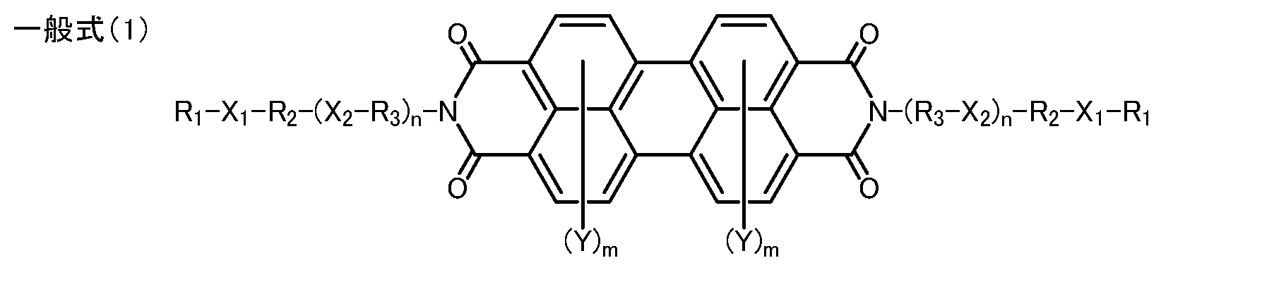
- the present inventors have studied to improve an organic semiconductor material used for an organic thin film solar cell, an organic transistor, an organic photoconductor, etc., and represented by the following general formula (1), general formula (2), or formula (3).
- the perylene tetracarboxydiimide derivative having a specific substituent is found to have excellent properties, leading to the present invention.
- the present invention provides a perylene tetracarboxydiimide derivative characterized by having a specific substituent represented by the following general formula (1), general formula (2), or formula (3).
- R 1 represents a branched alkyl group having 1 to 20 carbon atoms
- R 2 represents a branched alkyl group having 2 to 6 carbon atoms
- R 3 represents a branched alkyl group having 2 to 6 carbon atoms
- X 1 and X 2 represent a hetero atom selected from an oxygen atom, a sulfur atom and a selenium atom
- Y represents a halogen atom or a cyano group.
- M represents a number from 0 to 4
- n represents a number from 0 to 2, respectively.
- R 1 is a straight chain alkyl group having 1 to 20 carbon atoms
- R 2 is a straight chain alkyl group having 2 to 6 carbon atoms
- R 3 is a straight chain group having 2 to 6 carbon atoms.
- a chain alkyl group, X 1 and X 2 are oxygen atoms
- Y is a halogen atom or a cyano group
- m is a number from 0 to 4
- n is a number from 0 to 2.
- a perylenetetracarboxydiimide derivative that exhibits excellent semiconductor characteristics, has excellent durability when used as a thin film, has high solubility in organic solvents, and can be applied to useful organic semiconductor materials.
- the infrared absorption spectrum of the exemplary compound 1 The infrared absorption spectrum of the exemplary compound 2.
- the perylene tetracarboxydiimide derivative having a specific substituent of the present invention can be synthesized by a known method.
- perylenetetracarboxylic acid anhydride may be reacted with a corresponding amine in a high boiling organic solvent to introduce a specific substituent characterizing the present invention.
- the perylenetetracarboxydiimide derivative of the present invention can also be obtained by once converting perylenetetracarboxydiimide into a potassium salt and then introducing a specific substituent by reacting with a corresponding alkyl halide.
- amine component used when synthesizing the perylene tetracarboxydiimide derivative of the present invention the following may be mentioned.
- Examples of the perylene tetracarboxylic acid anhydride used when synthesizing the perylene tetracarboxydiimide derivative of the present invention include the following.
- perylene tetracarboxydiimide derivative when used for an organic solar cell, an organic photo semiconductor or an organic transistor, it is often deposited on a substrate under a high vacuum, which is a general method. This is because one of the major factors is that perylene tetracarboxydiimide derivatives known so far are almost insoluble in organic solvents.
- the perylene tetracarboxydiimide derivative having a specific substituent of the present invention is relatively soluble in an organic solvent, unlike a conventional derivative.
- the derivative of the present invention can be subjected to purification means such as column chromatography at the time of production, and when applied to an organic semiconductor material, it is dissolved in an organic solvent and spin-coated.
- the solubility property in an organic solvent means that the application of a perylene tetracarboxydiimide derivative to an organic semiconductor material is drastically improved.
- the perylene tetracarboxydiimide derivative of the present invention having a specific substituent as exemplified above is relatively soluble in, for example, an organic solvent as described below.
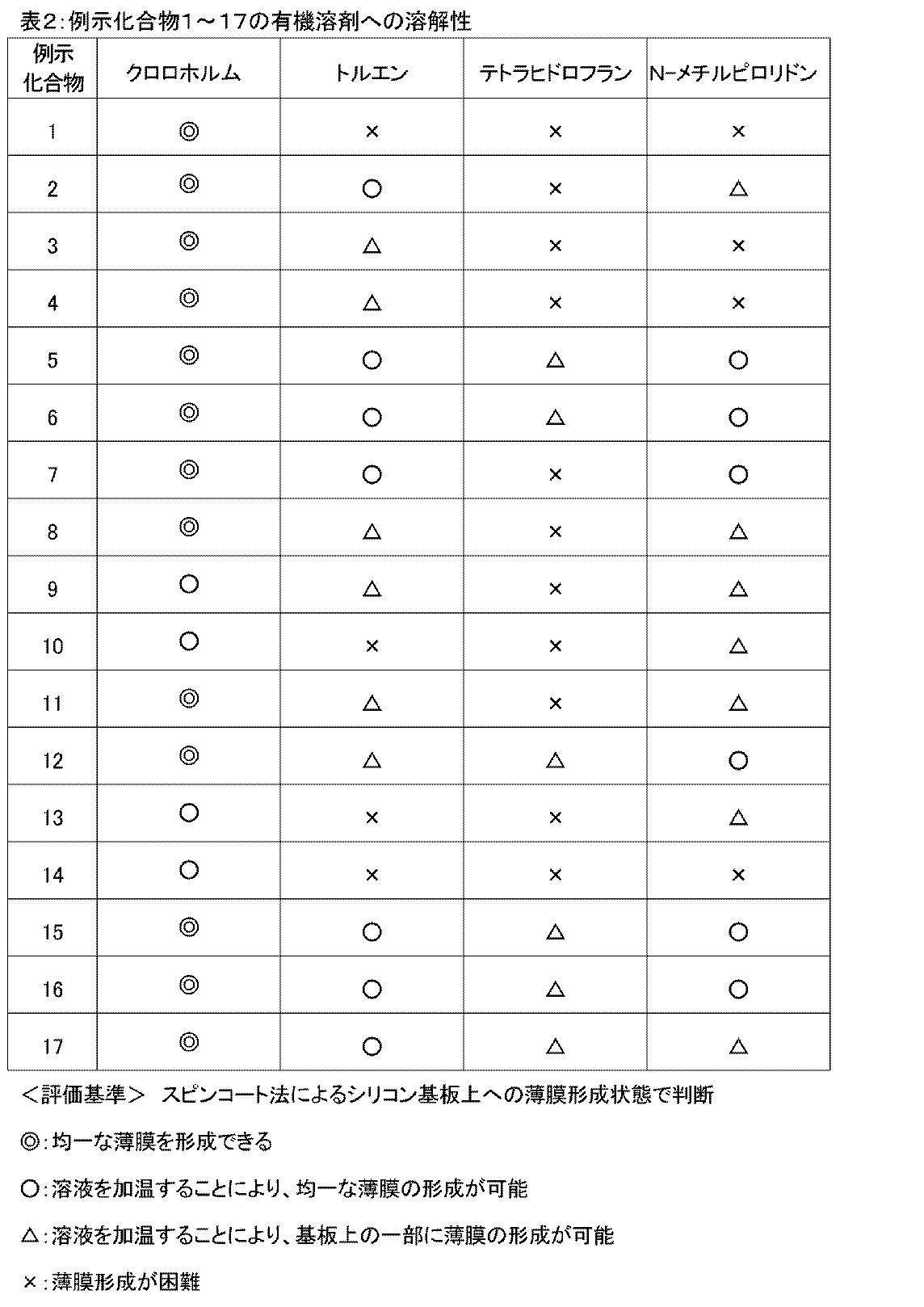
- organic solvent for example, halogen hydrocarbon solvents such as chloroform, dichloroethane, chlorobenzene, dichlorobenzene, trichlorobenzene, chloronaphthalene, ketone solvents such as acetone, methyl ethyl ketone, methyl isobutyl ketone, ester solvents such as ethyl acetate, butyl acetate, diethyl ether, Ether solvents such as dioxane and tetrahydrofuran, aromatic hydrocarbon solvents such as toluene, xylene and ethylbenzene, aprotic polar solvents such as sulfolane, N, N-dimethylformamide, N-methyl-2-pyrrolidone and di
- the perylene tetracarboxydiimide derivative of the present invention can be made into a solution having an appropriate concentration by using an organic solvent as mentioned above alone or in combination. Therefore, according to the perylene tetracarboxydiimide derivative of the present invention, by using the solution, a solution coating method such as a spin coating method that cannot be used with a conventional derivative can be applied. A uniform thin film can be formed. Further, since the perylenetetracarboxydiimide derivative of the present invention has sufficient semiconductor properties, the formed thin film functions as a good organic semiconductor thin film used for, for example, an organic thin film solar cell, an organic transistor, or an organic photoconductor. To be.
- each of the exemplified compounds 1 to 17 mentioned above is applied onto a silicon substrate by spin coating using each organic solvent. It was judged by the state of thin film formation. The results are shown in Table 2. As a result, although there is a slight difference depending on the chain length of the alkyl group in the general formula (1) and the hetero atom, it shows good solubility in organic solvents and a solution coating method such as a spin coating method should be applied. Is confirmed to be possible.
- Example 1 Synthesis of Exemplified Compound 1
- 3.92 g of perylenetetracarboxylic anhydride and 9.72 g of 3- (n-dodecyloxy) -n-propylamine were dispersed in 40 g of imidazole and stirred at 160 ° C. for 4 hours under a nitrogen stream. After cooling, the mixture was filtered, and the residue was washed with methanol / dilute hydrochloric acid and then water.
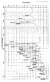
- FIG. 1 shows an infrared absorption spectrum.
- Example 2 Synthesis of Exemplified Compound 2 The same as Example 1 except that 9.72 g of 3- (n-dodecyloxy) -n-propylamine used in Example 1 was replaced with 5.24 g of 3- (n-butyloxy) -n-propylamine.
- 4.95 g of N, N′-bis (3- (n-butyloxy) -n-propyl) -3,4: 9,10-perylenetetracarboxydiimide was obtained as Exemplified Compound 2 (yield). 80%).
- combination example compound 2 is as showing below, By these analysis, it was confirmed that the example compound 2 is said compound.
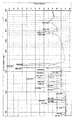
- FIG. 2 shows an infrared absorption spectrum.
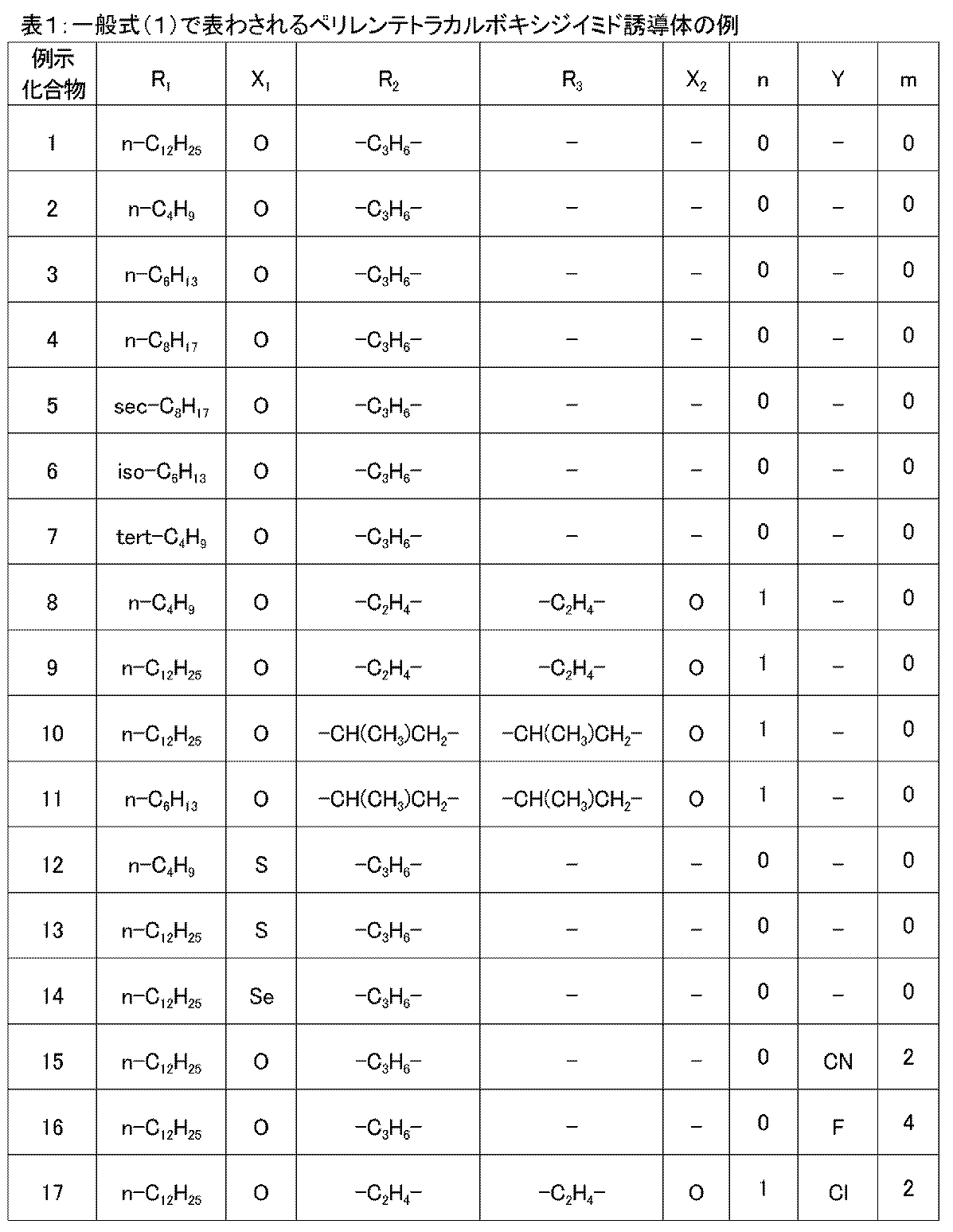
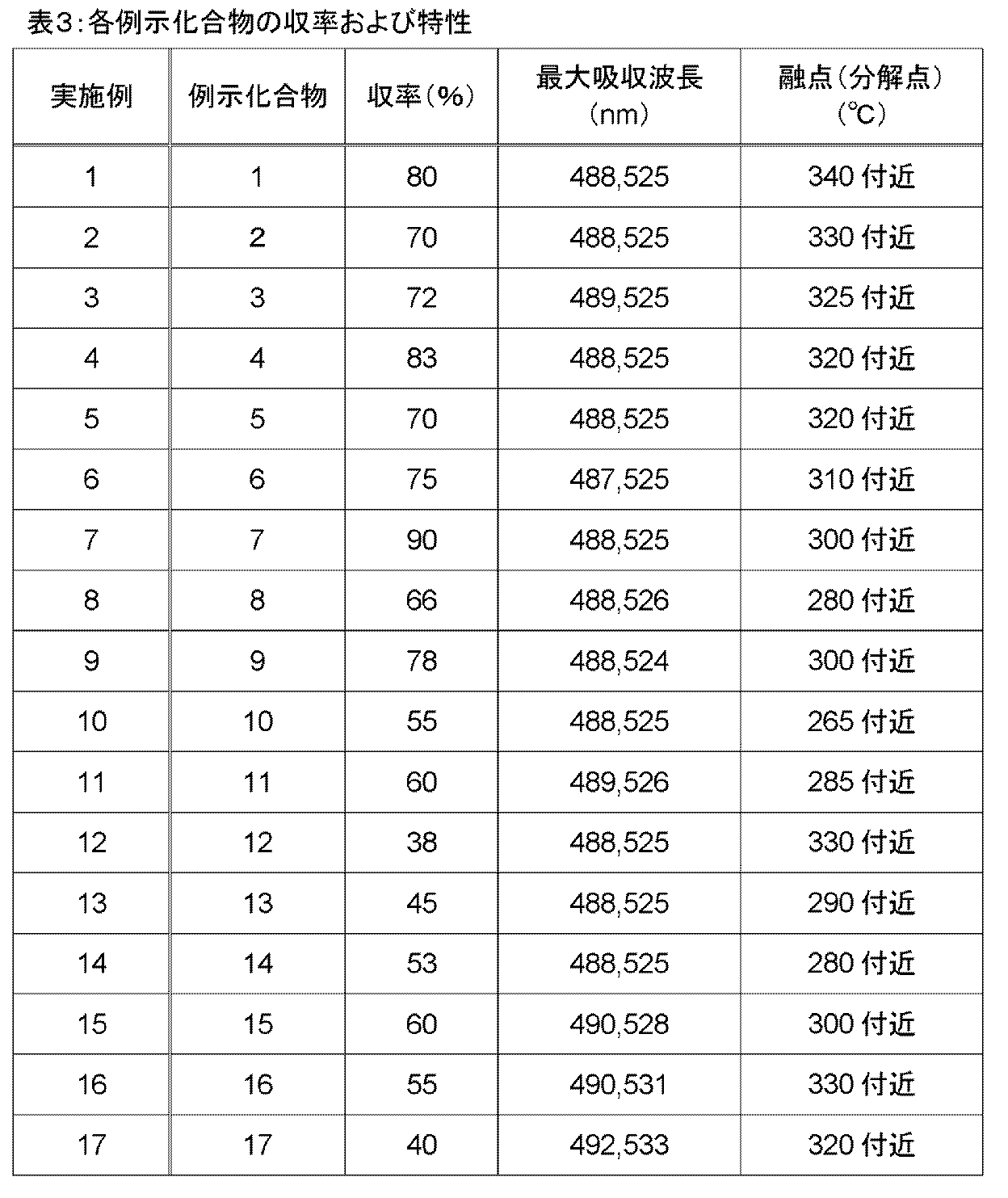
- Examples 3 to 17 Exemplified compounds 3 to 17 whose structures were previously shown in Table 1 were synthesized in the same manner as in Examples 1 and 2, respectively. The yield, melting point, and maximum absorption wavelength in the ultraviolet / visible light absorption spectrum of each compound obtained are shown in Table 3. The maximum absorption wavelength was also measured for the exemplary compounds 1 and 2 obtained in Examples 1 and 2, and the results were shown together with the yield and melting point. The ultraviolet and visible light absorption spectra of Exemplified Compounds 3 to 17 were almost the same as Exemplified Compounds 1 and 2.
- Table 3 below shows the yield, maximum absorption wavelength and melting point of Exemplified Compounds 1 to 17 synthesized in each Example.
- the drain voltage and the drain current at different gate voltages were measured.
- a clear saturation region was observed in the drain current-drain voltage curve, which indicates that the transistor is driven as a field effect transistor having typical n-type characteristics.
- the electron mobility calculated from this curve was 3.3 ⁇ 10 ⁇ 2 cm 2 / Vs, and the threshold voltage value was 15V.
- the transistor characteristics of the transistor obtained above were measured in the same manner as in Reference Example 1. As a result, it was shown that it is driven as a field effect transistor having typical n-type characteristics. Further, the electron mobility is 0.40 cm 2 / Vs, the threshold voltage value is 16 V, and it is confirmed that the semiconductor characteristics superior to those obtained when the thin film is formed by the vacuum deposition method of Reference Example 1 are obtained. did.
- a perylenetetracarboxydiimide derivative that exhibits excellent semiconductor characteristics and has excellent durability when used as a thin film and can be applied to useful organic semiconductor materials.
- the above-described perylenetetracarboxydiimide derivative provided by the present invention exhibits solubility in an organic solvent, a thin film or the like can be formed by a solution method, and its practicality is extremely high. It is expected.
Abstract
Description


[実施例1]
(例示化合物1の合成)
ペリレンテトラカルボン酸無水物3.92gと、3-(n-ドデシルオキシ)-n-プロピルアミン9.72gとをイミダゾール40g中に分散させ、窒素気流下160℃で4時間攪拌した。冷却後、濾過し、濾物をメタノール・希塩酸、次いで水の順に洗浄した。その後、濾物を乾燥して5.90gの、下記式(3)で示されるN,N'-ビス(3-(n-ドデシルオキシ)-n-プロピル)-3,4:9,10-ペリレンテトラカルボキシジイミドを、例示化合物1として得た(収率70%)。
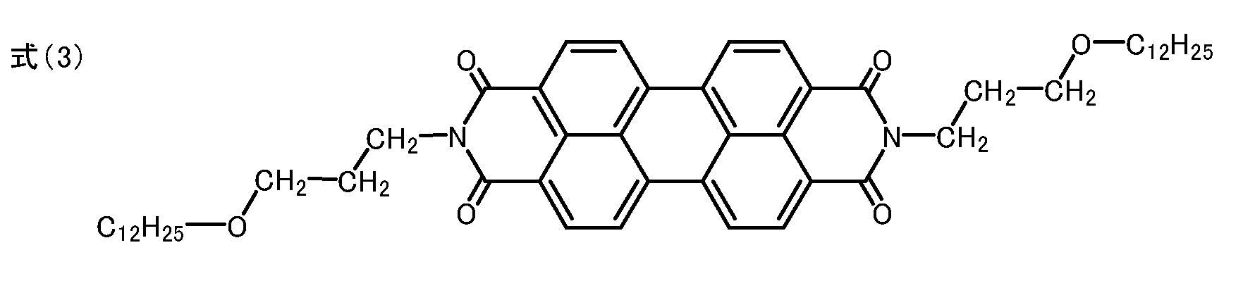
融点:330℃付近(分解)
元素分析値()内は理論値:C;76.88%(76.92%)、H;8.30%(8.37%)、N;3.25%(3.32%)
図1に赤外吸収スペクトルを示す。
(例示化合物2の合成)
実施例1で使用した3-(n-ドデシルオキシ)-n-プロピルアミン9.72gを、3-(n-ブチルオキシ)-n-プロピルアミン5.24gに代えた以外は実施例1と同様の方法で、例示化合物2として、4.95gの、N,N'-ビス(3-(n-ブチルオキシ)-n-プロピル)-3,4:9,10-ペリレンテトラカルボキシジイミドを得た(収率80%)。合成した例示化合物2についての各分析結果は以下に示す通りであり、これらの分析によって、例示化合物2は、上記の化合物であることを確認した。
融点:340℃付近(分解)
元素分析値()内は理論値:C;73.81%(73.77%)、H;6.15%(6.19%)、N;4.49%(4.53%)
図2に赤外吸収スペクトルを示す。
実施例1および2と同様の方法で、先に表1中に構造を示した例示化合物3~17をそれぞれ合成した。そして、得られた各化合物の収率、融点、紫外・可視光吸収スペクトルにおける最大吸収波長を表3に示した。実施例1および2で得た例示化合物1、2についても最大吸収波長を測定し、結果を収率および融点とともに示した。例示化合物3~17の紫外・可視光吸収スペクトルは、例示化合物1、2とほぼ同様であった。
[参考例1]
例示化合物1(N,N'-ビス(3-(n-ドデシルオキシ)-n-プロピル)-3,4:9,10-ペリレンテトラカルボキシジイミド)を用いた有機薄膜トランジスタの作製
まず、ゲート絶縁体層となる酸化シリコン膜(厚さ200nm)を表面に有するシリコン基板を用意した。実施例1で得た例示化合物1からなる有機半導体薄膜は、酸化シリコン膜上に真空蒸着法(蒸着レート2[nm/sec])により、厚さ30nmとなるように成膜した。次に、シャドーマスクを介して、ソース/ドレイン電極として金電極のパターンを形成し(30nm)、トップコンタクト型有機薄膜トランジスタを作成した。このときの、チャネル長、チャネル幅は、それぞれ100μm、2000μmとした。
参考例1で用いた例示化合物1をクロロホルムに濃度0.25%となるように溶解し、該溶液を用いて、スピンコーター(1,500回転/分,40秒)にて、ITO電極を表面に有する酸化膜付シリコン基板上に有機半導体薄膜を形成し、真空中において140℃、1時間の減圧乾燥を行った。
本参考例では、参考例1で使用した例示化合物1に変えて、実施例2で得た例示化合物2(N,N'-ビス(3-(n-ブチルオキシ)-n-プロピル)-3,4:9,10-ペリレンテトラカルボキシジイミド)を使用した。
参考例1と同様に例示化合物2よりなる有機半導体層を有するトップコンタクト型有機薄膜トランジスタを作成した。そして、典型的なn型特性を有する電界効果トランジスタとして駆動することが示された。また、電子移動度は、3.8×10⁻³cm2/Vs、しきい電圧値は10Vであった。
Claims (3)
- 下記一般式(1)で示されることを特徴とするペリレンテトラカルボキシジイミド誘導体。
(ただし、一般式(1)中、R1は炭素数が1~20である分岐してもよいアルキル基を、R2は炭素数が2~6である分岐してもよいアルキル基を、R3は炭素数が2~6である分岐してもよいアルキル基を、X1およびX2は酸素原子、硫黄原子およびセレン原子から選択されるヘテロ原子を、Yはハロゲン原子或いはシアノ基を、mは0~4の数を、そしてnは0~2の数を、それぞれ示す。)
- 下記一般式(2)で示されることを特徴とするペリレンテトラカルボキシジイミド誘導体。
(ただし、一般式(2)中、R1は炭素数1~20の直鎖アルキル基を、R2は炭素数2~6の直鎖アルキル基を、R3は炭素数2~6の直鎖アルキル基を、X1およびX2は酸素原子を、Yはハロゲン原子或いはシアノ基を、mは0~4の数を、そしてnは0~2の数を、それぞれ示す。)
- 下記式(3)で示されることを特徴とするペリレンテトラカルボキシジイミド誘導体。

Priority Applications (4)
| Application Number | Priority Date | Filing Date | Title |
|---|---|---|---|
| KR20127013355A KR101491888B1 (ko) | 2009-10-29 | 2010-10-29 | 페릴렌 테트라카르복시디이미드 유도체 |
| JP2011538496A JP5643215B2 (ja) | 2009-10-29 | 2010-10-29 | ペリレンテトラカルボキシジイミド誘導体 |
| CN201080047762.7A CN102574806B (zh) | 2009-10-29 | 2010-10-29 | 苝四甲酰二亚胺衍生物 |
| EP10826849.1A EP2471778B1 (en) | 2009-10-29 | 2010-10-29 | Perylene tetracarboxydiimide derivative |
Applications Claiming Priority (2)
| Application Number | Priority Date | Filing Date | Title |
|---|---|---|---|
| JP2009249127 | 2009-10-29 | ||
| JP2009-249127 | 2009-10-29 |
Publications (1)
| Publication Number | Publication Date |
|---|---|
| WO2011052719A1 true WO2011052719A1 (ja) | 2011-05-05 |
Family
ID=43922140
Family Applications (1)
| Application Number | Title | Priority Date | Filing Date |
|---|---|---|---|
| PCT/JP2010/069277 WO2011052719A1 (ja) | 2009-10-29 | 2010-10-29 | ペリレンテトラカルボキシジイミド誘導体 |
Country Status (6)
| Country | Link |
|---|---|
| EP (1) | EP2471778B1 (ja) |
| JP (1) | JP5643215B2 (ja) |
| KR (1) | KR101491888B1 (ja) |
| CN (1) | CN102574806B (ja) |
| TW (1) | TWI431005B (ja) |
| WO (1) | WO2011052719A1 (ja) |
Cited By (5)
| Publication number | Priority date | Publication date | Assignee | Title |
|---|---|---|---|---|
| WO2012160521A1 (en) * | 2011-05-24 | 2012-11-29 | Ecole Polytechnique Federale De Lausanne (Epfl) | Color conversion films comprising polymer-substituted organic fluorescent dyes |
| WO2013024026A1 (en) * | 2011-08-12 | 2013-02-21 | Basf Se | Fluorinated perylene-based semiconducting materials |
| JP2014519490A (ja) * | 2011-05-11 | 2014-08-14 | ビーエーエスエフ ソシエタス・ヨーロピア | ハロゲン化ペリレンベースの半導体材料 |
| JPWO2016035640A1 (ja) * | 2014-09-01 | 2017-04-27 | 富士フイルム株式会社 | 有機半導体膜形成用組成物、有機半導体膜、及び有機半導体素子 |
| JP2019106401A (ja) * | 2017-12-08 | 2019-06-27 | 住友化学株式会社 | 光電変換素子 |
Families Citing this family (1)
| Publication number | Priority date | Publication date | Assignee | Title |
|---|---|---|---|---|
| CN104557931B (zh) * | 2013-10-25 | 2016-08-17 | 济南大学 | N-吡啶基苝四甲酰二亚胺的制备及其光催化制氢性能 |
Citations (11)
| Publication number | Priority date | Publication date | Assignee | Title |
|---|---|---|---|---|
| JPS5167328A (en) * | 1974-10-31 | 1976-06-10 | Basf Ag | Periren 3*4*9100 tetorakarubonsanjiimidokei no shinkisenryonoseiho |
| US4156757A (en) * | 1976-08-13 | 1979-05-29 | Basf Aktiengesellschaft | Electrically conductive perylene derivatives |
| JPS5774361A (en) * | 1980-08-22 | 1982-05-10 | Bbc Brown Boveri & Cie | Liquid crystal mixture and novel bichromophoric coloring matter |
| JPS57176046A (en) * | 1981-03-20 | 1982-10-29 | Basf Ag | Recording material for electronic photograph and its manufacture |
| DE3235526A1 (de) * | 1982-09-25 | 1984-03-29 | Basf Ag, 6700 Ludwigshafen | Verfahren zur flaechenmaessigen konzentrierung von licht |
| JPS6089485A (ja) * | 1983-08-27 | 1985-05-20 | バスフ アクチェン ゲゼルシャフト | テトラクロルペリレン−3,4,9,10−テトラカルボン酸ジイミド |
| DE3413418A1 (de) * | 1984-04-10 | 1985-10-17 | Basf Ag, 6700 Ludwigshafen | Farbstofflaser |
| JP2007527114A (ja) | 2004-01-26 | 2007-09-20 | ノースウエスタン ユニバーシティ | ペリレンn型半導体及び関連装置 |
| JP2008524846A (ja) | 2004-12-17 | 2008-07-10 | イーストマン コダック カンパニー | 薄膜トランジスタのためのn型半導体材料 |
| CN101353349A (zh) * | 2007-07-25 | 2009-01-28 | 中国科学院化学研究所 | 全氟烷基链取代的苝-3,4:9,10-四羧酸二酰亚胺类化合物及其制备方法 |
| WO2009118742A1 (en) * | 2008-03-26 | 2009-10-01 | Yeda Research And Development Co. Ltd | Doubly reduced perylene-diimides and supramolecular polymers derived from perylene-diimides |
Family Cites Families (1)
| Publication number | Priority date | Publication date | Assignee | Title |
|---|---|---|---|---|
| EP0047027A1 (de) * | 1980-08-22 | 1982-03-10 | BBC Aktiengesellschaft Brown, Boveri & Cie. | Flüssigkristallmischung |
-
2010
- 2010-10-29 WO PCT/JP2010/069277 patent/WO2011052719A1/ja active Application Filing
- 2010-10-29 JP JP2011538496A patent/JP5643215B2/ja active Active
- 2010-10-29 CN CN201080047762.7A patent/CN102574806B/zh active Active
- 2010-10-29 TW TW099137147A patent/TWI431005B/zh active
- 2010-10-29 KR KR20127013355A patent/KR101491888B1/ko active IP Right Grant
- 2010-10-29 EP EP10826849.1A patent/EP2471778B1/en active Active
Patent Citations (11)
| Publication number | Priority date | Publication date | Assignee | Title |
|---|---|---|---|---|
| JPS5167328A (en) * | 1974-10-31 | 1976-06-10 | Basf Ag | Periren 3*4*9100 tetorakarubonsanjiimidokei no shinkisenryonoseiho |
| US4156757A (en) * | 1976-08-13 | 1979-05-29 | Basf Aktiengesellschaft | Electrically conductive perylene derivatives |
| JPS5774361A (en) * | 1980-08-22 | 1982-05-10 | Bbc Brown Boveri & Cie | Liquid crystal mixture and novel bichromophoric coloring matter |
| JPS57176046A (en) * | 1981-03-20 | 1982-10-29 | Basf Ag | Recording material for electronic photograph and its manufacture |
| DE3235526A1 (de) * | 1982-09-25 | 1984-03-29 | Basf Ag, 6700 Ludwigshafen | Verfahren zur flaechenmaessigen konzentrierung von licht |
| JPS6089485A (ja) * | 1983-08-27 | 1985-05-20 | バスフ アクチェン ゲゼルシャフト | テトラクロルペリレン−3,4,9,10−テトラカルボン酸ジイミド |
| DE3413418A1 (de) * | 1984-04-10 | 1985-10-17 | Basf Ag, 6700 Ludwigshafen | Farbstofflaser |
| JP2007527114A (ja) | 2004-01-26 | 2007-09-20 | ノースウエスタン ユニバーシティ | ペリレンn型半導体及び関連装置 |
| JP2008524846A (ja) | 2004-12-17 | 2008-07-10 | イーストマン コダック カンパニー | 薄膜トランジスタのためのn型半導体材料 |
| CN101353349A (zh) * | 2007-07-25 | 2009-01-28 | 中国科学院化学研究所 | 全氟烷基链取代的苝-3,4:9,10-四羧酸二酰亚胺类化合物及其制备方法 |
| WO2009118742A1 (en) * | 2008-03-26 | 2009-10-01 | Yeda Research And Development Co. Ltd | Doubly reduced perylene-diimides and supramolecular polymers derived from perylene-diimides |
Non-Patent Citations (7)
| Title |
|---|
| CHE, Y. ET AL.: "Enhancing One-Dimensional Charge Transport through Intermolecular n-Electron Delocalization: Conductivity Improvement for Organic Nanobelts", JOURNAL OF THE AMERICAN CHEMICAL SOCIETY, vol. 129, no. 20, 2007, pages 6354 - 6355, XP008154038 * |
| FISCHER, C. M. ET AL.: "Microstructured gold/ Langmuir-Blodgett film/gold tunneling junctions", APPLIED PHYSICS LETTERS, vol. 66, no. 24, 1995, pages 3331 - 3, XP008154040 * |
| GREGG, B.A. ET AL.: "Doping molecular emiconductors. n-Type doping of a liquid crystalperylene diimide", JOURNAL OF THE AMERICAN CHEMICAL SOCIETY, vol. 123, no. 32, 2001, pages 7959 - 7960, XP008154037 * |
| HERRIKHUYZEN, V.J. ET AL.: "Synthesis of n-Type Perylene Bisimide Derivatives and Their Orthogonal Self-Assembly with p-Type Oligo (p-phenylene vinylene)s", JOURNAL OF THE AMERICAN CHEMICAL SOCIETY, vol. 126, no. 32, 2004, pages 10021 - 10027, XP008154034 * |
| SAMUDRALA, R. ET AL.: "Synthesis of a non- cationic, water-soluble perylenetetracarboxylic diimide and its interactions with G-quadruplex- forming DNA", BIOORGANIC & MEDICINAL CHEMISTRY, vol. 15, no. 1, 2007, pages 186 - 193, XP008154043 * |
| See also references of EP2471778A4 |
| SHIRMAN, E. ET AL.: "Stable Aromatic Dianion in Water", JOURNAL OF PHYSICAL CHEMISTRY B, vol. 112, no. 30, 2008, pages 8855 - 8858, XP008154048 * |
Cited By (10)
| Publication number | Priority date | Publication date | Assignee | Title |
|---|---|---|---|---|
| JP2014519490A (ja) * | 2011-05-11 | 2014-08-14 | ビーエーエスエフ ソシエタス・ヨーロピア | ハロゲン化ペリレンベースの半導体材料 |
| TWI598349B (zh) * | 2011-05-11 | 2017-09-11 | 巴地斯顏料化工廠 | 以鹵化苝為基質之半導體材料 |
| WO2012160521A1 (en) * | 2011-05-24 | 2012-11-29 | Ecole Polytechnique Federale De Lausanne (Epfl) | Color conversion films comprising polymer-substituted organic fluorescent dyes |
| US8986842B2 (en) | 2011-05-24 | 2015-03-24 | Ecole Polytechnique Federale De Lausanne (Epfl) | Color conversion films comprising polymer-substituted organic fluorescent dyes |
| WO2013024026A1 (en) * | 2011-08-12 | 2013-02-21 | Basf Se | Fluorinated perylene-based semiconducting materials |
| CN103764787A (zh) * | 2011-08-12 | 2014-04-30 | 巴斯夫欧洲公司 | 氟化苝基半导体材料 |
| JP2014529593A (ja) * | 2011-08-12 | 2014-11-13 | ビーエーエスエフ ソシエタス・ヨーロピアBasf Se | フッ素化ペリレンベースの半導体材料 |
| JPWO2016035640A1 (ja) * | 2014-09-01 | 2017-04-27 | 富士フイルム株式会社 | 有機半導体膜形成用組成物、有機半導体膜、及び有機半導体素子 |
| JP2019106401A (ja) * | 2017-12-08 | 2019-06-27 | 住友化学株式会社 | 光電変換素子 |
| JP6995596B2 (ja) | 2017-12-08 | 2022-01-14 | 住友化学株式会社 | 光電変換素子 |
Also Published As
| Publication number | Publication date |
|---|---|
| JP5643215B2 (ja) | 2014-12-17 |
| TWI431005B (zh) | 2014-03-21 |
| KR20120085856A (ko) | 2012-08-01 |
| EP2471778A4 (en) | 2013-04-17 |
| CN102574806A (zh) | 2012-07-11 |
| EP2471778B1 (en) | 2019-05-08 |
| EP2471778A1 (en) | 2012-07-04 |
| TW201124413A (en) | 2011-07-16 |
| CN102574806B (zh) | 2014-07-02 |
| JPWO2011052719A1 (ja) | 2013-03-21 |
| KR101491888B1 (ko) | 2015-02-09 |
Similar Documents
| Publication | Publication Date | Title |
|---|---|---|
| JP5643215B2 (ja) | ペリレンテトラカルボキシジイミド誘導体 | |
| JP5665137B2 (ja) | 有機半導体材料、有機半導体薄膜および有機薄膜トランジスタ | |
| Reghu et al. | Air stable electron-transporting and ambipolar bay substituted perylene bisimides | |
| Usol’tseva et al. | Mix-substituted phthalocyanines of a “push–pull”-type and their metal complexes as prospective nanostructured materials for optoelectronics | |
| CN1980791A (zh) | 苝n-型半导体和相关器件 | |
| Haisch et al. | Soluble alkyl‐and alkoxy‐substituted titaniumoxo phthalocyanines: Synthesis and photoconductivity | |
| JP5438363B2 (ja) | バンドギャップが広いことを特徴とする有機半導体材料 | |
| CN101485007A (zh) | 生产有机场效应晶体管的方法 | |
| Bilgiçli et al. | Nonperipheral tetra phthalocyanines bearing alkyl chain moiety; Synthesis, characterization and fabrication of the OFET based on phthalocyanine | |
| WO2012137853A1 (ja) | ペリレンテトラカルボン酸ビスイミド誘導体、n-型半導体、n-型半導体の製造方法、および電子装置 | |
| JP5613948B2 (ja) | 有機半導体微粒子材料、有機半導体薄膜、有機半導体膜形成用分散液および有機半導体薄膜の製造方法 | |
| JP2010016212A (ja) | 有機薄膜光電変換素子とその製造方法 | |
| Raboui et al. | Axially phenoxylated aluminum phthalocyanines and their application in organic photovoltaic cells | |
| US20080277649A1 (en) | Field Effect Transistor and Method of Producing Same | |
| Chen et al. | Langmuir–Blodgett film of new phthalocyanine containing oxadiazol groups and its application in field-effect transistor | |
| JP2010045186A (ja) | フタロシアニン前駆体及びその製造方法、フタロシアニンの製造方法、並びにフタロシアニン膜の製造方法 | |
| CN109942585B (zh) | 一种有机半导体材料、制备方法、场效应晶体管器件及其制作方法 | |
| CN109897055B (zh) | 一种基于联二咔唑和苝二酰亚胺的有机化合物及其制备方法和应用 | |
| Melville et al. | Functionalization of commercial pigment Hostasol Red GG for incorporation into organic thin-film transistors | |
| WO2015111605A1 (ja) | 有機トランジスタ、化合物、非発光性有機半導体デバイス用有機半導体材料、有機トランジスタ用材料、非発光性有機半導体デバイス用塗布溶液、非発光性有機半導体デバイス用有機半導体膜 | |
| WO2015016344A1 (ja) | 化合物、有機トランジスタ及びその応用 | |
| Novakova et al. | Tetra (pyrazino [2, 3-b] pyrazino) porphyrazines: Synthesis, absorption, photophysical and electrochemical properties of strongly electron-deficient macrocycles | |
| RU2723014C1 (ru) | Способ получения дибензо[f,h]фуразано[3,4-b]хиноксалина и его замещенных производных, обладающих зарядотранспортными полупроводниковыми свойствами | |
| JP5638319B2 (ja) | 有機薄膜形成材料、有機薄膜、該薄膜の製造方法、有機薄膜素子およびn型の有機薄膜トランジスタ | |
| US7067652B2 (en) | Copper phthalocyanine/iodine intermolecular compound and process for the production thereof |
Legal Events
| Date | Code | Title | Description |
|---|---|---|---|
| WWE | Wipo information: entry into national phase |
Ref document number: 201080047762.7 Country of ref document: CN |
|
| 121 | Ep: the epo has been informed by wipo that ep was designated in this application |
Ref document number: 10826849 Country of ref document: EP Kind code of ref document: A1 |
|
| WWE | Wipo information: entry into national phase |
Ref document number: 2011538496 Country of ref document: JP |
|
| WWE | Wipo information: entry into national phase |
Ref document number: 2010826849 Country of ref document: EP |
|
| NENP | Non-entry into the national phase |
Ref country code: DE |
|
| ENP | Entry into the national phase |
Ref document number: 20127013355 Country of ref document: KR Kind code of ref document: A |