WO2010137419A1 - 基準周波数発生装置 - Google Patents
基準周波数発生装置 Download PDFInfo
- Publication number
- WO2010137419A1 WO2010137419A1 PCT/JP2010/056765 JP2010056765W WO2010137419A1 WO 2010137419 A1 WO2010137419 A1 WO 2010137419A1 JP 2010056765 W JP2010056765 W JP 2010056765W WO 2010137419 A1 WO2010137419 A1 WO 2010137419A1
- Authority
- WO
- WIPO (PCT)
- Prior art keywords
- signal
- reference frequency
- controlled oscillator
- frequency generator
- digitally controlled
- Prior art date
Links
- 230000007613 environmental effect Effects 0.000 claims description 17
- 230000001360 synchronised effect Effects 0.000 claims description 15
- 230000006870 function Effects 0.000 description 21
- 230000008859 change Effects 0.000 description 19
- 230000004048 modification Effects 0.000 description 12
- 238000012986 modification Methods 0.000 description 12
- 238000010586 diagram Methods 0.000 description 11
- 230000010355 oscillation Effects 0.000 description 11
- 238000000034 method Methods 0.000 description 8
- 239000004065 semiconductor Substances 0.000 description 6
- 239000013078 crystal Substances 0.000 description 5
- 238000004519 manufacturing process Methods 0.000 description 4
- 230000000694 effects Effects 0.000 description 3
- 230000008569 process Effects 0.000 description 3
- 238000004891 communication Methods 0.000 description 2
- 230000003111 delayed effect Effects 0.000 description 2
- 230000006872 improvement Effects 0.000 description 2
- 238000010615 ring circuit Methods 0.000 description 2
- 230000035939 shock Effects 0.000 description 2
- 230000009471 action Effects 0.000 description 1
- 239000003990 capacitor Substances 0.000 description 1
- 238000006243 chemical reaction Methods 0.000 description 1
- 230000009467 reduction Effects 0.000 description 1
- 230000000630 rising effect Effects 0.000 description 1
Images


Classifications
-
- H—ELECTRICITY
- H03—ELECTRONIC CIRCUITRY
- H03L—AUTOMATIC CONTROL, STARTING, SYNCHRONISATION OR STABILISATION OF GENERATORS OF ELECTRONIC OSCILLATIONS OR PULSES
- H03L7/00—Automatic control of frequency or phase; Synchronisation
- H03L7/06—Automatic control of frequency or phase; Synchronisation using a reference signal applied to a frequency- or phase-locked loop
- H03L7/08—Details of the phase-locked loop
- H03L7/14—Details of the phase-locked loop for assuring constant frequency when supply or correction voltages fail or are interrupted
-
- H—ELECTRICITY
- H03—ELECTRONIC CIRCUITRY
- H03L—AUTOMATIC CONTROL, STARTING, SYNCHRONISATION OR STABILISATION OF GENERATORS OF ELECTRONIC OSCILLATIONS OR PULSES
- H03L7/00—Automatic control of frequency or phase; Synchronisation
- H03L7/06—Automatic control of frequency or phase; Synchronisation using a reference signal applied to a frequency- or phase-locked loop
- H03L7/08—Details of the phase-locked loop
- H03L7/085—Details of the phase-locked loop concerning mainly the frequency- or phase-detection arrangement including the filtering or amplification of its output signal
-
- H—ELECTRICITY
- H03—ELECTRONIC CIRCUITRY
- H03L—AUTOMATIC CONTROL, STARTING, SYNCHRONISATION OR STABILISATION OF GENERATORS OF ELECTRONIC OSCILLATIONS OR PULSES
- H03L7/00—Automatic control of frequency or phase; Synchronisation
- H03L7/06—Automatic control of frequency or phase; Synchronisation using a reference signal applied to a frequency- or phase-locked loop
- H03L7/08—Details of the phase-locked loop
- H03L7/099—Details of the phase-locked loop concerning mainly the controlled oscillator of the loop
- H03L7/0995—Details of the phase-locked loop concerning mainly the controlled oscillator of the loop the oscillator comprising a ring oscillator
- H03L7/0996—Selecting a signal among the plurality of phase-shifted signals produced by the ring oscillator
-
- H—ELECTRICITY
- H03—ELECTRONIC CIRCUITRY
- H03L—AUTOMATIC CONTROL, STARTING, SYNCHRONISATION OR STABILISATION OF GENERATORS OF ELECTRONIC OSCILLATIONS OR PULSES
- H03L2207/00—Indexing scheme relating to automatic control of frequency or phase and to synchronisation
- H03L2207/50—All digital phase-locked loop
Definitions
- the present invention relates to a reference frequency generator.
- a voltage-controlled oscillator is known as an oscillator that can change the frequency of an output signal.
- the voltage controlled oscillator is an oscillator that can change an output frequency in accordance with an input control voltage.
- a voltage controlled oscillator Voltage Controlled Crystal Oscillator, VCXO
- FV characteristic the control voltage vs. oscillation frequency characteristic
- the FV characteristics change according to the temperature change as described above, and the FV characteristics also change with the passage of time, so the voltage controlled oscillator alone outputs a highly accurate signal. It is difficult to do.
- a high-precision reference signal obtained from a GPS (Global Positioning System) receiver or the like and a signal output from a voltage-controlled oscillator
- the voltage controlled oscillator is controlled so as to be synchronized with a signal obtained by dividing the signal), and a highly accurate signal is output.
- Non-Patent Document 1 discloses a reference frequency generator having this kind of self-running control function.
- the reference frequency generator of Non-Patent Document 1 stores the elapsed time and temperature and the FV characteristics under the circumstances while synchronizing with the reference signal. When the reference signal cannot be acquired, the FV characteristic is estimated from the stored information, and the voltage-controlled oscillator is self-running to output the reference frequency signal.
- Non-Patent Document 1 As described above, a voltage-controlled oscillator using a crystal resonator changes its FV characteristics over time, and there is a limit to accurately estimate this. Therefore, in the configuration of Non-Patent Document 1, there is room for improvement in that the frequency and phase errors increase as time elapses after the start of self-running control. Furthermore, it is difficult to say that a voltage-controlled oscillator equipped with a crystal resonator can be used in a harsh environment. It was. In addition, the voltage controlled oscillator with a thermostatic chamber is expensive, and improvement is demanded in that it is difficult to reduce the size.
- the present invention has been made in view of the above circumstances, and an object of the present invention is to be able to output a high-precision reference frequency signal over a long period of time even if the reference signal cannot be acquired, and to be used at a low price with a wide operating temperature range.
- the object is to provide a frequency generator.
- the reference frequency generator includes a synchronization circuit, a detector, a storage unit, and a control unit.
- the synchronization circuit controls the digitally controlled oscillator by a first control signal obtained based on a reference signal.
- the detector detects an environmental value indicating an environment in which the digitally controlled oscillator is used.
- storage part can memorize
- the control unit determines a second control signal based on the environment value detected by the detector and the correspondence stored in the storage unit, and controls the digitally controlled oscillator .
- the digitally controlled oscillator can be controlled with high accuracy by the first control signal of the synchronization circuit.
- the control unit can control the digitally controlled oscillator with high accuracy based on the second control signal.
- the digitally controlled oscillator can be composed of a semiconductor, the usable temperature range is wide and the structure can be made resistant to vibration and shock. Furthermore, it is possible to make the configuration in which the characteristics of the digitally controlled oscillator hardly change over time.
- the correspondence relationship stored in the storage unit is obtained in a state where the reference signal and the signal output from the digitally controlled oscillator are synchronized by the synchronization circuit. It is preferable.
- the digitally controlled oscillator can be controlled with better accuracy when the reference signal cannot be obtained.
- the digitally controlled oscillator preferably includes a delay element.
- the digitally controlled oscillator is preferably a ring oscillator.
- the digitally controlled oscillator can be easily configured with a digital circuit, so that the configuration can be more suitable for miniaturization and mass production.
- the detector detects at least one of a voltage value and a temperature as an environmental value.
- the second control signal can be determined by obtaining the correspondence relation regarding the environmental factors that easily affect the characteristics of the digitally controlled oscillator.
- the synchronization circuit preferably includes a phase comparator that measures a phase difference between the reference signal and a signal output from the digitally controlled oscillator by using TDC.
- phase comparator can be easily configured with a digital circuit, so that it is possible to achieve downsizing and power saving.
- the TDC preferably measures the phase difference using a delay amount of a phase comparison delay element.
- phase difference can be measured with high accuracy by using the delay element for phase comparison with a minute delay amount.
- the correspondence relationship is stored in the storage unit before the reference frequency generation device is operated for the first time.
- control unit can determine the second control signal and control the digitally controlled oscillator.
- the storage contents of the storage unit can be updated with the correspondence newly obtained during operation of the reference frequency generation device.
- the signal output from the digitally controlled oscillator is preferably a reference frequency signal.
- the synchronization circuit includes a voltage controlled oscillator that outputs a signal synchronized with a signal output from the digitally controlled oscillator, and the signal output from the voltage controlled oscillator is a reference frequency signal.
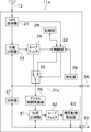
- FIG. 1 is a block diagram schematically showing a reference frequency generator according to an embodiment.
- the specific circuit diagram of the phase comparator of this embodiment Explanatory drawing which shows notionally the method of measuring a phase difference using the delay element for phase comparisons of the phase comparator of this embodiment.
- the block diagram which shows schematically the reference frequency generator of a 1st modification.
- the block diagram which shows roughly the reference frequency generator of a 2nd modification.
- FIG. 1 is a block diagram schematically showing a reference frequency generator 11 of this embodiment.
- FIG. 2 is a specific circuit diagram of the digitally controlled oscillator 26 of the present embodiment.
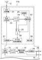
- FIG. 3 is a specific circuit diagram of the phase comparator 23 of the present embodiment.
- FIG. 4 is an explanatory diagram conceptually showing a method of measuring a phase difference using the phase comparison delay element 52 of the phase comparator 23 of the present embodiment.
- the reference frequency generator 11 of the present embodiment is used for a mobile phone base station, a terrestrial digital broadcasting transmitter station, a WiMAX (Worldwide Interoperability for Microwave Access) communication facility, and the like.
- the reference frequency generator 11 functions as a master clock generator, and provides a reference frequency signal to some device on the user side connected to the reference frequency generator 11. Below, the structure of each part of the reference frequency generator 11 is demonstrated.
- the reference frequency generator 11 of the present embodiment includes a GPS receiver 21, a digitally controlled oscillator 26, a frequency divider 27, a phase comparator 23, a loop filter 24, and a detector 28.
- the control unit 22 and the switch circuit 25 are provided as main components.
- a GPS antenna 12 installed outside the reference frequency generator 11 is electrically connected to the GPS receiver 21.
- the GPS receiver 21 performs positioning calculation based on the positioning signal received by the GPS antenna 12, and generates a reference signal (pulse signal once per second) based on the positioning calculation.
- This 1 Hz reference signal is appropriately calibrated in the GPS receiver 21 so as to be accurately synchronized with 1 second of Coordinated Universal Time (UTC). As shown in FIG. 1, this reference signal is input to the phase comparator 23.
- the digitally controlled oscillator 26 is composed of an oscillation circuit capable of generating a signal, and is configured to be able to change the output frequency by an external control signal.
- the signal output by the digital control oscillator 26 is input to the frequency divider 27.
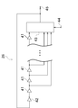
- the digitally controlled oscillator 26 of the present embodiment is made of a semiconductor, and specifically, is configured as a ring oscillator that generates a signal from a phase conversion element and a delay element connected in a ring shape.
- the ring oscillator includes a plurality of delay elements 41, an inverter 42, and a selector 43 as shown in FIG.
- the number of inverters 42 is not limited to one, and an odd number may be arranged.
- a signal that has passed through the first delay element 41 (the leftmost delay element 41 in FIG. 2) is output to the second delay element 41 and the selector. 43 is output.
- the signal that has passed through the second delay element 41 is output to the third delay element 41 and also to the selector 43.
- the above configuration is repeatedly arranged.
- a signal that has passed through the rightmost delay element 41 in FIG. 2 is output only to the selector 43.
- the selector 43 includes the same number of delay signal input units (not shown) as the number of delay elements 41.
- the selector 43 selects one of the delay signal input units based on the control signal input from the control signal input terminal 44, and outputs the signal input from the delay signal input unit to the subsequent stage.
- the selection by the selector 43 corresponds to selecting which delay element 41 out of the plurality of stages of delay elements 41 arranged in series, and in the following description, “the number of delay element stages is set. Referred to as “select”.
- performing the above selection so that the signal having passed through n delay elements 41 is output from the selector 43 is particularly referred to as “selecting the number of n delay element stages”.
- the signal alternatively selected by the selector 43 is output from the signal output terminal 45 to the frequency divider 27 and returned to the first delay element 41 through the inverter 42.
- the inverter 42 inverts the signal level from H to L or from L to H.
- the signal whose output is inverted passes through the delay element 41 and the selector 43 as described above, and is output to the signal output terminal 45.
- the output from the selector 43 is inverted by the inverter 42 and then returned to the first delay element 41 again.
- an alternating signal whose signal level is switched to H, L, H, L,... can be generated and output to the signal output terminal 45. Further, the frequency of the alternating signal can be adjusted by selecting the number of delay element stages by the selector 43.
- the frequency divider 27 is configured to divide and convert the signal input from the digitally controlled oscillator 26 from a high frequency to a low frequency, and to output the obtained phase comparison signal to the phase comparator 23. .
- the frequency divider 27 divides the 10 MHz signal output from the digitally controlled oscillator 26 by a frequency division ratio of 1 / 10,000,000. The phase comparison signal is generated.
- the phase comparator 23 is configured to measure a phase difference from a phase comparison signal using TDC (Time to Digital Converter) and output a signal (phase difference signal) based on the phase difference.
- TDC Time to Digital Converter
- the phase difference signal output from the phase comparator 23 is input to the loop filter 24.
- the phase comparator 23 of the present embodiment includes a delay element, and is configured as a phase comparator that measures a phase difference using the delay amount of the delay element.
- the phase comparator 23 includes a plurality of flip-flops 51, a plurality of phase comparison delay elements 52, and a phase difference signal calculation unit 53.
- the phase comparison signal (replica signal) obtained by dividing the signal output from the digital control oscillator 26 by the frequency divider 27 is input from the replica signal input terminal 54.
- the reference signal output from the GPS receiver 21 is input from the reference signal input terminal 55.
- the input replica signal is input to the first flip-flop 51 (the leftmost flip-flop 51 in FIG. 3) and the first phase comparison delay element 52 (the leftmost phase comparison in FIG. 3). Output to the delay element 52). Similarly, the replica signal that has passed through the first phase comparison delay element 52 is output to the second flip-flop 51 and to the second phase comparison delay element 52. In the TDC, the above configuration is repeated many times. The replica signal that has passed through the right-end phase comparison delay element 52 in FIG. 3 is output only to the right-end flip-flop 51 in FIG.
- each phase comparison delay element 52 Due to the signal delay action of each phase comparison delay element 52, the delay of the phase comparison delay element 52 is required to input a replica signal to a certain flip-flop 51 and then input a replica signal to the next flip-flop 51. There is a time lag for the amount.
- the reference signal is simultaneously input to the plurality of flip-flops 51.
- Each flip-flop 51 sets the signal level (H or L) input from the phase comparison delay element 52 to the flip-flop 51 when the reference signal rises (timing when the signal output changes from L to H). And output to the phase difference signal calculation unit 53. Then, until the reference signal rises again, the output from the flip-flop 51 to the phase difference signal calculation unit 53 maintains the previous signal output (output of the replica signal at the time of the previous reference signal rise).
- the phase difference signal calculation unit 53 examines the output signal of each flip-flop 51 to grasp the phase difference between the reference signal and the replica signal based on the delay amount per one of the phase comparison delay elements 52. be able to.
- the phase difference signal calculation unit 53 calculates the phase difference and outputs a signal (phase difference signal) based on the phase difference to the phase difference signal output terminal 56. This phase difference signal is output from the phase difference signal output terminal 56 to the loop filter 24.
- each phase comparison delay element 52 (interval between broken lines in FIG. 4) is equal.
- the replica signal and the reference signal are converted to a pulse wave once per second, and only the rising portion of one pulse is extracted and illustrated in FIG.
- the waveform shown in FIG. 4 shows the signal input (H or L) at each time.
- D0 to D6 are signals input to each flip-flop 51, and replica signals are input in order from the smallest number.
- the waveform of D0 rises at the same time as the replica signal is input to the replica signal input terminal 54.
- signals D1 to D6 are delayed compared to the replica signal due to the influence of the signal passing through the phase comparison delay element 52 1 to 6 times.
- the flip-flop 51 outputs the replica signal input to the flip-flop 51 when the reference signal rises (when it changes from L to H). Therefore, when the signal outputs of the flip-flops 51 corresponding to D0 to D6 are represented by Q0 to Q6, Q0 to Q4 are H, and Q5 and Q6 are L.
- the phase difference signal calculation unit 53 calculates the phase difference based on the above result and the delay amount of the phase comparison delay element 52.
- the delay amount of the phase comparison delay element 52 a value obtained in advance in the process of synchronizing the signal of the digital control oscillator 26 with the reference signal generated by the GPS receiver 21 is used. That is, when the phase of the signal output from the digitally controlled oscillator 26 is delayed by, for example, x stages of the delay element 41, the change in the phase difference measured in the TDC corresponds to how many stages of the phase comparison delay element 52. If it is known, the delay amount per one phase comparison delay element 52 can be accurately obtained (since the delay amount per delay element 41 is obtained by the following formula).
- the loop filter 24 shown in FIG. 1 is configured to determine a synchronization control signal (first control signal) based on the phase difference signal and output the synchronization control signal.
- This synchronization control signal is input to the digitally controlled oscillator 26 via the switch circuit 25.
- the digitally controlled oscillator 26 outputs a signal having a frequency based on the synchronization control signal output from the loop filter 24. As described above, the frequency of the signal output from the digitally controlled oscillator 26 is appropriately adjusted so that the phase of the phase comparison signal output from the frequency divider 27 matches the phase of the reference signal.
- the synchronization control signal from the loop filter 24 is also input to the control unit 22.
- the detector 28 is configured to detect an environmental value indicating an environment where the digitally controlled oscillator 26 is used.
- the environmental value detected by the detector 28 is input to the control unit 22.
- the detector 28 of this embodiment is configured as a voltage sensor and a temperature sensor, and is configured to detect a voltage value and a temperature at which the digitally controlled oscillator 26 is used as an environmental value.
- the voltage to be detected by the voltage sensor may be the voltage of the power source that supplies power to the digitally controlled oscillator 26 or the internal voltage of the digitally controlled oscillator 26.
- the control unit 22 is for controlling the frequency output from the digitally controlled oscillator 26, and includes a CPU as a calculation unit. Further, the control unit 22 monitors whether or not the reference signal is stably supplied from the GPS receiver 21. If it is determined that the reference signal is supplied, the control unit 22 transmits a switching control signal to the switch circuit 25 to connect the loop filter 24 and the digitally controlled oscillator 26.
- the storage unit 29 is configured to store various data necessary for the control unit 22 to control the digitally controlled oscillator 26, for example, environment-related control information described later.
- the loop filter 24 and the digitally controlled oscillator 26 are connected by the switch circuit 25 while the GPS receiver 21 receives a positioning signal from a GPS satellite and generates a reference signal. Then, a loop of the PLL circuit 31 is formed, and the digital control oscillator 26 is controlled so that the signal output from the digital control oscillator 26 is synchronized with the reference signal. In this manner, the reference frequency signal is output from the first output terminal 33, and the timing signal obtained by dividing the reference frequency signal is output from the second output terminal 34, respectively.
- the characteristics of the digitally controlled oscillator 26 change due to environmental changes. That is, even when the digital control oscillator 26 is controlled by the same control signal to output a signal, the output signal is different if the voltage or temperature changes.
- the signal output from the digitally controlled oscillator 26 is controlled to be synchronized with the reference signal from the GPS receiver 21. Therefore, as long as the GPS receiver 21 generates a reference signal and the PLL is locked to the reference signal, even if the characteristics of the digitally controlled oscillator 26 change due to environmental changes, the reference frequency generator The reference frequency signal output from 11 is kept constant.
- a state in which the signal output from the digitally controlled oscillator 26 is locked by the reference signal and the synchronization circuit may be referred to as a “steady state”.
- control value a new synchronization control signal (control value) is given from the loop filter 24 to the digitally controlled oscillator 26 so as to cancel the change in the characteristics.
- the frequency and phase of the output signal of the digitally controlled oscillator 26 are kept constant.
- environment-related control information information indicating the relationship between the control value for controlling the digital control oscillator 26 and the environment value at that time in order to keep the output of the digital control oscillator 26 constant. Called.
- This environment-related control information is obtained after the system is in the steady state at the time of factory shipment of the reference frequency generator 11 and at the time of actual operation after shipment. That is, in a steady state, the signal output from the digitally controlled oscillator 26 is synchronized with a highly accurate reference signal. In this state, the control unit 22 stores the correspondence between the voltage value and temperature detected by the detector 28 and the control value included in the synchronization control signal determined by the loop filter 24 as environment-related control information.
- This environment-related control information is used when determining a self-running control signal described later.
- control when the GPS receiver 21 cannot receive a positioning signal from a GPS satellite and cannot generate a reference signal will be described.
- the control unit 22 detects that the reference signal is not input, the control unit 22 transmits a switching control signal for connecting the control unit 22 and the digitally controlled oscillator 26 to the switch circuit 25 and shifts to the self-running control.
- the control unit 22 determines a free-running control signal (second control signal) for controlling the digitally controlled oscillator 26.
- the self-running control signal is input to the digitally controlled oscillator 26 via the switch circuit 25 switched by receiving the switching control signal.
- the digitally controlled oscillator 26 outputs a signal based on the self-running control signal from the control unit 22.
- the control unit 22 obtains a control value by applying the voltage value and temperature detected by the detector 28 to the environment-related control information (specifically, the correspondence relationship described above). Based on this, a self-running control signal is generated. Therefore, since the free-running control signal corresponding to the voltage and temperature is given to the digitally controlled oscillator 26, the reference frequency signal can be generated with good accuracy even during the free-running control.
- a signal output from the digitally controlled oscillator 26 may be referred to as an oscillation signal, and the frequency of the oscillation signal may be referred to as an oscillation frequency.
- the function represented by this equation is referred to as a delay characteristic function.
- the delay characteristic function as the environment-related control information is determined at the time of factory shipment of the reference frequency generation device 11 and is corrected at any time during operation of the device after shipment.
- the operator first sets the temperature and voltage value conditions of the digitally controlled oscillator 26 to appropriate values and can receive GPS radio waves satisfactorily.
- the reference frequency generator 11 is actually operated.
- the ring oscillator selects N stages as the number of delay element stages M times out of (M + 1) times, and selects (N + 1) stages for the remaining one time in accordance with the synchronization control signal from the loop filter 24.
- the phase difference detected by the phase comparator 23 becomes zero (the reference signal and the oscillation signal are synchronized).
- control unit 22 determines that synchronization by the PLL circuit 31 has been obtained (becomes a steady state), and obtains an average value n of the number of delay element stages at that time.
- the obtained T value is stored in an appropriate storage unit together with the temperature and voltage value at that time.
- the control part 22 will memorize
- T V representing the change in delay amount due to a voltage value
- the control unit 22 learns by automatically obtaining the delay characteristic function obtained as described above, and stores it in the storage unit 29.
- the delay characteristic function stored in the storage unit 29 in this way is an initial value, and the delay characteristic function is appropriately corrected after the operation of the reference frequency generator 11 is started. That is, if a steady state is obtained in the reference frequency generator 11, the relationship between the delay amount T of the delay element 41 and the voltage value and temperature can be obtained in the same manner as described above. Can be calculated. The stored contents of the storage unit 29 are updated with the newly obtained delay characteristic function. Through the continuous learning process as described above, the current characteristics of the digitally controlled oscillator 26 can be constantly reflected in the delay characteristic function.
- the phase comparator 23, the loop filter 24, the switch circuit 25, the digitally controlled oscillator 26 (ring oscillator), the frequency divider 27, the control unit 22, and the storage unit 29 are provided on the FPGA as a semiconductor. It is built as a circuit. Therefore, the effects of downsizing, cost reduction, and power consumption are remarkable.
- the reference frequency generation device 11 includes the PLL circuit 31, the detector 28, the control unit 22, and the storage unit 29.
- the PLL circuit 31 controls the digitally controlled oscillator 26 by a synchronization control signal obtained based on the reference signal output from the GPS receiver 21.
- the detector 28 detects a value (environment value) indicating the voltage and temperature at which the digitally controlled oscillator 26 is used.
- the storage unit 29 can store a correspondence relationship between the synchronization control signal and the voltage and temperature when the synchronization control signal is determined.
- the control unit 22 determines the free-running control signal based on the voltage and temperature detected by the detector 28 and the correspondence stored in the storage unit, and controls the digital control oscillator 26. To do.
- the usable temperature range is wide and the structure can withstand vibration and shock.
- the digitally controlled oscillator 26 made of semiconductor does not change with time, the frequency accuracy can be maintained well over a long period of time even when self-running control is performed.
- the correspondence relationship stored in the storage unit is a state in which the reference signal and the output signal output from the digital control oscillator 26 are synchronized by the PLL circuit 31 (the steady state State).
- the digitally controlled oscillator 26 includes a delay element 41.
- the digitally controlled oscillator 26 is configured as a ring oscillator.
- the digitally controlled oscillator 26 can be configured to be easily realized by a digital control circuit, so that the configuration can be further improved for downsizing and mass production.
- the detector 28 detects a voltage value and a temperature.
- the PLL circuit 31 includes a phase comparator 23 that measures the phase difference between the reference signal and the signal output from the digitally controlled oscillator 26 using TDC.
- phase comparator 23 can also be configured to be easily realized by a digital control circuit, so that it can be configured more suitable for miniaturization and mass production.
- the TDC measures the phase difference using the delay amount of the phase comparison delay element 52.
- phase difference can be measured with high accuracy by using the phase comparison delay element 52 having a minute delay amount.
- the correspondence relationship is stored in the storage unit 29 before the device is operated for the first time.
- control unit 22 can determine the self-running control signal and control the digitally controlled oscillator 26.
- the storage content of the storage unit 29 can be updated with the correspondence relationship newly obtained during operation of the reference frequency generation device 11.
- the signal output from the digitally controlled oscillator 26 is output from the first output terminal 33 as a reference frequency signal.
- FIG. 5 is a block diagram schematically showing a reference frequency generator 11a of a first modification.
- the same or similar members as those in the above-described embodiment may be denoted by the same reference numerals in the drawings, and description thereof may be omitted.
- the reference frequency generator 11a of the first modified example includes a sub PLL circuit (sub sync circuit) between the digital control oscillator 26 and the frequency divider 27 in the reference frequency generator 11 of the above embodiment. ).
- This sub PLL circuit constitutes a part of the PLL circuit 31a of the reference frequency generator 11a, and includes a phase comparator 61, a loop filter 62, and a voltage controlled oscillator 63 as main components. .
- the voltage controlled oscillator 63 is a VCXO using a crystal resonator as a resonator, and is configured to be able to change the output frequency according to the level of the voltage applied from the outside.
- the voltage controlled oscillator 63 can also be configured as a constant temperature bath voltage controlled oscillator.
- the signal output from the digitally controlled oscillator 26 is output to the phase comparator 61 of the sub PLL circuit.
- the phase comparator 61 measures the phase difference between the signal output from the digitally controlled oscillator 26 and the signal output from the voltage controlled oscillator 63.
- the phase difference measured by the phase comparator 61 is output to the loop filter 62 as a phase difference signal.
- the loop filter 62 determines a control voltage signal based on this phase difference signal. Then, the loop filter 62 controls the voltage controlled oscillator 63 with this control voltage signal, and generates a signal having the same phase and the same frequency as the signal output from the digital controlled oscillator 26 from the voltage controlled oscillator 63.
- a signal output from the voltage controlled oscillator 63 is output to the outside as a reference frequency signal from the first output terminal 33 and also output to the frequency divider 27.
- the signal divided by the frequency divider 27 is output from the second output terminal 34 to the outside as a timing signal.
- the PLL circuit 31a includes the voltage controlled oscillator 63 that outputs a signal synchronized with the signal output from the digitally controlled oscillator 26.
- a signal output from the voltage controlled oscillator 63 is output from the first output terminal 33 as a reference frequency signal.
- the jitter contained in the output signal of the digitally controlled oscillator 26 can be removed, and a stable reference frequency signal can be output.
- FIG. 6 is a block diagram schematically showing a reference frequency generator 11b of a second modification.
- the reference frequency generating device 11b of the second modified example has a portion corresponding to the GPS receiver in the conventional reference frequency generating device (portion shown by a chain line in FIG. 6) as the reference shown in FIG.
- the configuration corresponding to the frequency generator 11 is replaced.
- the reference frequency generator 11b of the present modification includes a phase comparator 71, a loop filter 72, a voltage controlled oscillator 73, and a frequency divider 74 as main components. Note that the configuration surrounded by the chain line in FIG. 6 is exactly the same as that in FIG.
- the signal output from the digitally controlled oscillator 26 is frequency-divided by the frequency divider 27 and then input to the phase comparator 71.
- the phase comparator 71 measures the phase difference between the signal input from the frequency divider 27 and the signal obtained by dividing the signal output from the voltage controlled oscillator 73 by the frequency divider 74.
- the phase difference measured by the phase comparator 71 is output to the loop filter 72 as a phase difference signal.
- the loop filter 72 determines a control voltage signal to the voltage controlled oscillator 73 so that the signals divided by the two frequency dividers 27 and 74 have the same phase and the same frequency. .
- the loop filter 72 controls the voltage controlled oscillator 73 with this control voltage signal to generate a reference frequency signal.
- the signal output from the voltage controlled oscillator 73 is output from the first output terminal 75 to the outside as a reference frequency signal and also output to the frequency divider 74.
- the signal divided by the frequency divider 74 is output from the second output terminal 76 to the outside as a timing signal.
- This configuration makes it possible to easily and inexpensively change to a configuration excellent in self-running control by using most of the existing configuration without greatly changing the existing configuration.
- the phase comparator 71 is configured with an FPGA or the like in the conventional reference frequency generator, the configuration of FIG. 6 is realized without adding or changing hardware by resetting the circuit on the FPGA. It is also possible.
- a stable signal without jitter can be output to the outside.
- the reference frequency generator 11 of the above embodiment is configured to generate a reference signal based on a signal from a GPS satellite, but can be changed as appropriate as long as the configuration uses a GNSS (Global Navigation Satellite System). .
- GNSS Global Navigation Satellite System
- it can be changed to a configuration in which a reference signal is generated based on a signal from a GLONASS satellite or a GALILEO satellite.
- GLONASS Global Navigation Satellite System
- GALILEO satellite Global Navigation Satellite System
- the GPS receiver 21 is arranged outside the reference frequency generator 11, the reference signal is generated outside the own device, and is output to the own device.
- the digitally controlled oscillator 26 is not limited to a ring oscillator, and is a digitized oscillator. If the characteristic can be calculated from an environmental value, another digitally controlled oscillator (for example, one using a capacitor or the like) is used. You can also. In this case, the environment-related control information is in accordance with the characteristics of the digital control oscillator.
- the digitally controlled oscillator may be a numerically controlled oscillator or a digitally controlled oscillator excluding the numerically controlled oscillator.
- the loop filter 24 can be changed to a configuration that outputs a synchronous control signal by a controller including at least one of P control, I control, and D control.
- the PLL circuit 31 is configured to control the digitally controlled oscillator 26 in synchronization with the supplied reference signal
- other synchronous circuits FLL circuit, DLL circuit, etc.
- the environment-related control information can be obtained only at the time of factory shipment, stored in the storage unit 29, and not updated when the apparatus is in operation. In this case, since the learning process can be omitted, the load on the control unit 22 in the steady state can be reduced.
- the delay characteristic function is not calculated by actually changing the voltage value or temperature.
- the delay characteristic function calculated theoretically from the design value or the delay calculated by experience The characteristic function can be changed to be stored in the storage unit 29. In this case, setting work at the time of factory shipment can be simplified.
- the detector 28 may be changed to measure only one of them instead of measuring both the voltage value and the temperature. Moreover, you may comprise so that the value regarding another environmental factor may be measured.
- the storage unit 29 stores the correspondence relationship between the voltage value and temperature and the control value included in the synchronization control signal. However, for the same voltage value and temperature, a control value different from that stored previously is digitally stored. A case where the signal is supplied to the controlled oscillator 26 is also conceivable. In this case, the storage content of the storage unit 29 can be updated to the latest correspondence relationship, or the previous correspondence relationship can be continued without updating the storage unit 29.
- a plurality of control values are obtained for the same voltage value and temperature
- values obtained by performing various calculations such as obtaining an average can be stored as a correspondence relationship.
- the average value can be calculated by selecting only control values that satisfy a predetermined condition.
- the variation of the plurality of control values obtained with respect to the same voltage value and temperature is large, the average value is obtained as described above and the update of the storage contents of the storage unit 29 is continued. It is also possible to stop updating the stored contents.
- the environment-related control information is stored in the storage unit 29 in the form of a function, but may be stored in the form of a lookup table, for example.
- the control values corresponding to the voltage values and temperature points obtained discretely may be obtained by line interpolation or surface interpolation.
- all delay elements are regarded as the same delay amount.
- delay elements can be grouped, and the above relationship can be obtained individually for each group. In this case, individual differences in delay elements can be taken into account to some extent, so that more stable control is possible.
- the phase comparator 23, the loop filter 24, the switch circuit 25, the digitally controlled oscillator 26 (ring oscillator), the frequency divider 27, the control unit 22, and the storage unit 29 are not limited to the FPGA, but other programmable logic devices (for example, it can be configured to be set as a circuit on an ASIC). Further, when the GPS receiver 21 includes an ASIC for positioning calculation or the like, the above configuration can be changed as a circuit on the ASIC. In this case, further downsizing and lower power consumption can be achieved. Is possible. However, it is needless to say that the above configuration may be realized by an integrated circuit such as a normal IC.
Landscapes
- Stabilization Of Oscillater, Synchronisation, Frequency Synthesizers (AREA)
Abstract
Description
21 GPS受信機
22 制御部
23 位相比較器
24 ループフィルタ
26 デジタル制御発振器
27 分周器
29 記憶部
31 PLL回路(同期回路)
Claims (11)
- リファレンス信号に基づいて得られた第1制御信号によってデジタル制御発振器を制御する同期回路と、
前記デジタル制御発振器が使用される環境を示す環境値を検出する検出器と、
前記第1制御信号の制御値と、前記第1制御信号を決定したときの前記環境値と、の対応関係を記憶可能な記憶部と、
前記リファレンス信号が取得できなくなると、前記検出器が検出した環境値及び前記記憶部に記憶される対応関係に基づいて第2制御信号を決定し、前記デジタル制御発振器を制御する制御部と、
を備えることを特徴とする基準周波数発生装置。 - 請求項1に記載の基準周波数発生装置であって、
前記記憶部に記憶される対応関係は、前記リファレンス信号と、前記デジタル制御発振器が出力する信号と、が前記同期回路によって同期した状態で求められたものであることを特徴とする基準周波数発生装置。 - 請求項1又は2に記載の基準周波数発生装置であって、
前記デジタル制御発振器は遅延素子を備えることを特徴とする基準周波数発生装置。 - 請求項3に記載の基準周波数発生装置であって、
前記デジタル制御発振器はリングオシレータであることを特徴とする基準周波数発生装置。 - 請求項1から4までの何れか一項に記載の基準周波数発生装置であって、
前記検出器は、環境値として電圧値及び温度のうち少なくとも一方を検出することを特徴とする基準周波数発生装置。 - 請求項1から5までの何れか一項に記載の基準周波数発生装置であって、
前記同期回路は、前記リファレンス信号と、前記デジタル制御発振器が出力する信号と、の位相差をTDCを使用して計測する位相比較器を備えることを特徴とする基準周波数発生装置。 - 請求項6に記載の基準周波数発生装置であって、
前記TDCは、前記位相差を位相比較用遅延素子の遅延量を用いて計測することを特徴とする基準周波数発生装置。 - 請求項1から7までの何れか一項に記載の基準周波数発生装置であって、
基準周波数発生装置が初めて稼動する前の段階で、前記記憶部に前記対応関係が記憶されていることを特徴とする基準周波数発生装置。 - 請求項1から8までの何れか一項に記載の基準周波数発生装置であって、
前記記憶部の記憶内容は、基準周波数発生装置の稼動中に新しく得られた前記対応関係で更新可能であることを特徴とする基準周波数発生装置。 - 請求項1から9までの何れか一項に記載の基準周波数発生装置であって、
前記デジタル制御発振器が出力する信号を基準周波数信号とすることを特徴とする基準周波数発生装置。 - 請求項1から9までの何れか一項に記載の基準周波数発生装置であって、
前記同期回路は、前記デジタル制御発振器が出力する信号に同期した信号を出力する電圧制御発振器を備え、
前記電圧制御発振器が出力する信号を基準周波数信号とすることを特徴とする基準周波数発生装置。
Priority Applications (4)
| Application Number | Priority Date | Filing Date | Title |
|---|---|---|---|
| US13/257,845 US8497717B2 (en) | 2009-05-25 | 2010-04-15 | Reference frequency generating device |
| EP10780376.9A EP2437395B1 (en) | 2009-05-25 | 2010-04-15 | Reference frequency generator device |
| KR1020117030841A KR101699103B1 (ko) | 2009-05-25 | 2010-04-15 | 기준 주파수 발생 장치 |
| CN201080015220.1A CN102388536B (zh) | 2009-05-25 | 2010-04-15 | 基准频率产生装置 |
Applications Claiming Priority (2)
| Application Number | Priority Date | Filing Date | Title |
|---|---|---|---|
| JP2009-125727 | 2009-05-25 | ||
| JP2009125727A JP5159704B2 (ja) | 2009-05-25 | 2009-05-25 | 基準周波数発生装置 |
Publications (1)
| Publication Number | Publication Date |
|---|---|
| WO2010137419A1 true WO2010137419A1 (ja) | 2010-12-02 |
Family
ID=43222538
Family Applications (1)
| Application Number | Title | Priority Date | Filing Date |
|---|---|---|---|
| PCT/JP2010/056765 WO2010137419A1 (ja) | 2009-05-25 | 2010-04-15 | 基準周波数発生装置 |
Country Status (6)
| Country | Link |
|---|---|
| US (1) | US8497717B2 (ja) |
| EP (1) | EP2437395B1 (ja) |
| JP (1) | JP5159704B2 (ja) |
| KR (1) | KR101699103B1 (ja) |
| CN (1) | CN102388536B (ja) |
| WO (1) | WO2010137419A1 (ja) |
Cited By (2)
| Publication number | Priority date | Publication date | Assignee | Title |
|---|---|---|---|---|
| US20120286880A1 (en) * | 2010-01-13 | 2012-11-15 | Shinya Kowada | Reference frequency generating device |
| WO2016147729A1 (ja) * | 2015-03-16 | 2016-09-22 | 古野電気株式会社 | ダイレクトデジタルシンセサイザ、基準信号発生装置、及び信号出力方法 |
Families Citing this family (14)
| Publication number | Priority date | Publication date | Assignee | Title |
|---|---|---|---|---|
| US8330644B2 (en) * | 2010-07-14 | 2012-12-11 | The United States Of America As Represented By The Administrator Of The National Aeronautics And Space Administration | Expandable and reconfigurable instrument node arrays |
| US8704571B2 (en) | 2011-11-14 | 2014-04-22 | Rockwell Automation Technologies, Inc. | Phase-locked-loop with quadrature tracking filter for synchronizing an electric grid |
| KR101478663B1 (ko) * | 2013-04-18 | 2015-01-02 | 이문숙 | Gnss 기반의 다중 pll 모듈의 위상 제어 장치 및 방법 |
| JP2014230029A (ja) * | 2013-05-21 | 2014-12-08 | 日本電波工業株式会社 | 発振装置 |
| JP6231406B2 (ja) * | 2014-02-28 | 2017-11-15 | 株式会社日立製作所 | リングオシレータ、センサ、リングオシレータの制御方法、測定方法、プログラム及び記録媒体 |
| CN104022778B (zh) * | 2014-06-24 | 2017-06-27 | 瑞斯康达科技发展股份有限公司 | 一种模拟锁相环电路及其信号处理方法 |
| JP6296932B2 (ja) * | 2014-07-18 | 2018-03-20 | 株式会社東芝 | 遅延回路 |
| JP6382342B2 (ja) * | 2014-12-08 | 2018-08-29 | 古野電気株式会社 | 基準信号発生装置 |
| WO2017149978A1 (ja) * | 2016-03-01 | 2017-09-08 | 古野電気株式会社 | 基準信号発生装置及び基準信号発生方法 |
| JP6681231B2 (ja) * | 2016-03-17 | 2020-04-15 | 古野電気株式会社 | 基準信号発生装置及び基準信号発生方法 |
| JP2020010206A (ja) * | 2018-07-10 | 2020-01-16 | セイコーエプソン株式会社 | 回路装置、発振器、クロック信号生成装置、電子機器及び移動体 |
| US10727844B1 (en) * | 2019-05-31 | 2020-07-28 | Silicon Laboratories Inc. | Reference clock frequency change handling in a phase-locked loop |
| JP7421353B2 (ja) * | 2020-02-03 | 2024-01-24 | 日本電波工業株式会社 | 発振装置およびシンセサイザシステム |
| EP4040191A1 (de) * | 2020-02-20 | 2022-08-10 | 2pi-Labs GmbH | Radarsystem und synchronisationsverfahren |
Citations (5)
| Publication number | Priority date | Publication date | Assignee | Title |
|---|---|---|---|---|
| JPH02100518A (ja) * | 1988-10-07 | 1990-04-12 | Nec Corp | デイジタル処理形位相同期発振器 |
| JPH0450935U (ja) * | 1990-09-06 | 1992-04-28 | ||
| JP2000286698A (ja) * | 1999-01-26 | 2000-10-13 | Furuno Electric Co Ltd | 周波数信号および周期パルス信号発生装置 |
| JP2002217722A (ja) * | 2001-01-22 | 2002-08-02 | Maspro Denkoh Corp | 基準周波数発生装置 |
| JP2009105651A (ja) * | 2007-10-23 | 2009-05-14 | Panasonic Corp | Pll回路及び無線通信システム |
Family Cites Families (22)
| Publication number | Priority date | Publication date | Assignee | Title |
|---|---|---|---|---|
| JPS57176845A (en) * | 1981-04-23 | 1982-10-30 | Mitsubishi Electric Corp | Phase synchronizing oscillator |
| JP2538866B2 (ja) * | 1985-10-14 | 1996-10-02 | 日本電信電話株式会社 | デイジタル位相同期発振器 |
| JPH0450935A (ja) | 1990-06-15 | 1992-02-19 | Nikon Corp | カメラのバッテリチェック装置 |
| US5068628A (en) * | 1990-11-13 | 1991-11-26 | Level One Communications, Inc. | Digitally controlled timing recovery loop |
| JP2808967B2 (ja) * | 1992-02-28 | 1998-10-08 | 日本電気株式会社 | クロックホールドオーバ回路 |
| JP2000315945A (ja) * | 1999-04-30 | 2000-11-14 | Nec Corp | デジタル位相ロックループ回路 |
| JP2001274678A (ja) | 2000-03-28 | 2001-10-05 | Toshiba Corp | デジタル位相同期ループ回路 |
| US6633186B1 (en) * | 2000-04-17 | 2003-10-14 | Intel Corporation | Speed-locked loop to provide speed information based on die operating conditions |
| JP2002151956A (ja) * | 2000-11-08 | 2002-05-24 | Toyo Commun Equip Co Ltd | 周波数校正機能付き圧電発振器 |
| US6734741B2 (en) | 2001-04-25 | 2004-05-11 | Texas Instruments Incorporated | Frequency synthesizer with digitally-controlled oscillator |
| US7483508B2 (en) * | 2001-11-27 | 2009-01-27 | Texas Instruments Incorporated | All-digital frequency synthesis with non-linear differential term for handling frequency perturbations |
| JP2004088721A (ja) * | 2002-06-26 | 2004-03-18 | Nec Saitama Ltd | 位相同期方法及び位相同期回路 |
| JP2004104228A (ja) * | 2002-09-05 | 2004-04-02 | Matsushita Electric Ind Co Ltd | 信号処理装置および信号処理方法、デルタ・シグマ変調型分数分周pll周波数シンセサイザ、無線通信機器、デルタ・シグマ変調型d/a変換器 |
| US6909336B1 (en) * | 2003-09-03 | 2005-06-21 | National Semiconductor Corporation | Discrete-time amplitude control of voltage-controlled oscillator |
| US7336134B1 (en) * | 2004-06-25 | 2008-02-26 | Rf Micro Devices, Inc. | Digitally controlled oscillator |
| US7787563B2 (en) * | 2004-12-08 | 2010-08-31 | Texas Instruments Incorporated | Transmitter for wireless applications incorporation spectral emission shaping sigma delta modulator |
| JP4468196B2 (ja) * | 2005-02-03 | 2010-05-26 | 富士通株式会社 | デジタルpll回路 |
| EP1882304B1 (en) * | 2005-05-10 | 2018-08-15 | Texas Instruments Incorporated | Fast hopping frequency synthesizer using an all digital phased locked loop (adpll) |
| CN100512011C (zh) * | 2005-10-21 | 2009-07-08 | 华为技术有限公司 | 一种模拟锁相环实现保持功能的系统和方法 |
| US8411788B2 (en) * | 2005-11-18 | 2013-04-02 | Qualcomm, Incorporated | Digital transmitters for wireless communication |
| US7692500B1 (en) * | 2007-07-19 | 2010-04-06 | Marvell International, Ltd. | Apparatus and methods for mixed analog-digital frequency synthesizing and modulation |
| US8339165B2 (en) * | 2009-12-07 | 2012-12-25 | Qualcomm Incorporated | Configurable digital-analog phase locked loop |
-
2009
- 2009-05-25 JP JP2009125727A patent/JP5159704B2/ja not_active Expired - Fee Related
-
2010
- 2010-04-15 CN CN201080015220.1A patent/CN102388536B/zh not_active Expired - Fee Related
- 2010-04-15 US US13/257,845 patent/US8497717B2/en not_active Expired - Fee Related
- 2010-04-15 WO PCT/JP2010/056765 patent/WO2010137419A1/ja active Application Filing
- 2010-04-15 KR KR1020117030841A patent/KR101699103B1/ko active IP Right Grant
- 2010-04-15 EP EP10780376.9A patent/EP2437395B1/en not_active Not-in-force
Patent Citations (5)
| Publication number | Priority date | Publication date | Assignee | Title |
|---|---|---|---|---|
| JPH02100518A (ja) * | 1988-10-07 | 1990-04-12 | Nec Corp | デイジタル処理形位相同期発振器 |
| JPH0450935U (ja) * | 1990-09-06 | 1992-04-28 | ||
| JP2000286698A (ja) * | 1999-01-26 | 2000-10-13 | Furuno Electric Co Ltd | 周波数信号および周期パルス信号発生装置 |
| JP2002217722A (ja) * | 2001-01-22 | 2002-08-02 | Maspro Denkoh Corp | 基準周波数発生装置 |
| JP2009105651A (ja) * | 2007-10-23 | 2009-05-14 | Panasonic Corp | Pll回路及び無線通信システム |
Non-Patent Citations (2)
| Title |
|---|
| HP SMARTCLOCK: "Technology-Application Note 1279", 1998, HEWLETT-PACKARD COMPANY, pages: 5 - 15 |
| See also references of EP2437395A4 |
Cited By (4)
| Publication number | Priority date | Publication date | Assignee | Title |
|---|---|---|---|---|
| US20120286880A1 (en) * | 2010-01-13 | 2012-11-15 | Shinya Kowada | Reference frequency generating device |
| US8736394B2 (en) * | 2010-01-13 | 2014-05-27 | Furuno Electric Co., Ltd. | Reference frequency generating device |
| WO2016147729A1 (ja) * | 2015-03-16 | 2016-09-22 | 古野電気株式会社 | ダイレクトデジタルシンセサイザ、基準信号発生装置、及び信号出力方法 |
| JPWO2016147729A1 (ja) * | 2015-03-16 | 2017-12-07 | 古野電気株式会社 | ダイレクトデジタルシンセサイザ、基準信号発生装置、及び信号出力方法 |
Also Published As
| Publication number | Publication date |
|---|---|
| US8497717B2 (en) | 2013-07-30 |
| CN102388536A (zh) | 2012-03-21 |
| JP2010273299A (ja) | 2010-12-02 |
| JP5159704B2 (ja) | 2013-03-13 |
| KR20120030451A (ko) | 2012-03-28 |
| EP2437395A4 (en) | 2014-08-20 |
| KR101699103B1 (ko) | 2017-01-23 |
| US20120007642A1 (en) | 2012-01-12 |
| CN102388536B (zh) | 2015-04-01 |
| EP2437395B1 (en) | 2018-10-31 |
| EP2437395A1 (en) | 2012-04-04 |
Similar Documents
| Publication | Publication Date | Title |
|---|---|---|
| JP5159704B2 (ja) | 基準周波数発生装置 | |
| US5629649A (en) | Frequency standard generator synchronized with satellite or other communication network reference clocks | |
| CN107425851B (zh) | 频率补偿器、电子设备和频率补偿方法 | |
| US10320509B2 (en) | Fail safe clock buffer and clock generator | |
| JP5899244B2 (ja) | 基準周波数発生装置、及び正弦波出力方法 | |
| JP4846788B2 (ja) | データ信号発生装置 | |
| US8698568B2 (en) | Automatic self-calibrated oscillation method and apparatus using the same | |
| JP2017118371A5 (ja) | タイミング信号生成装置および電子機器 | |
| RU2011153501A (ru) | Устройство и способ выбора оптимального источника для упорядочения гетеродина | |
| CN113031428B (zh) | 实时时钟装置以及电子设备 | |
| JP2012242190A (ja) | 基準信号発生装置及び基準信号発生方法 | |
| JP5072115B2 (ja) | 基準周波数発生器 | |
| JP2002217722A (ja) | 基準周波数発生装置 | |
| JP2010088071A (ja) | 基準信号発生装置 | |
| JP5573867B2 (ja) | クロック位相同期化装置およびクロック位相同期化方法 | |
| JP4699250B2 (ja) | 無線装置 | |
| JP2017153024A (ja) | 基準周波数発生装置 | |
| JP2008079261A (ja) | 標準信号発生器及び標準信号発生システム | |
| JP5039073B2 (ja) | 基準周波数発生装置 | |
| JP2002214323A (ja) | 基準周波数発生装置 | |
| JP3528916B2 (ja) | 位相同期発振器 | |
| US20230077120A1 (en) | Time synchronization device, time synchronization system, and time synchronizationmethod | |
| JP3246459B2 (ja) | 刻時同期方法及び刻時同期回路 | |
| JP2000004152A (ja) | 時間周波数基準信号発生器及び基準時間周波数発生装置及びこれを用いる基準時刻発生装置 | |
| JPWO2017149978A1 (ja) | 基準信号発生装置及び基準信号発生方法 |
Legal Events
| Date | Code | Title | Description |
|---|---|---|---|
| WWE | Wipo information: entry into national phase |
Ref document number: 201080015220.1 Country of ref document: CN |
|
| 121 | Ep: the epo has been informed by wipo that ep was designated in this application |
Ref document number: 10780376 Country of ref document: EP Kind code of ref document: A1 |
|
| WWE | Wipo information: entry into national phase |
Ref document number: 2010780376 Country of ref document: EP |
|
| WWE | Wipo information: entry into national phase |
Ref document number: 13257845 Country of ref document: US |
|
| NENP | Non-entry into the national phase |
Ref country code: DE |
|
| ENP | Entry into the national phase |
Ref document number: 20117030841 Country of ref document: KR Kind code of ref document: A |