WO2010116974A1 - 光電変換装置および撮像装置 - Google Patents
光電変換装置および撮像装置 Download PDFInfo
- Publication number
- WO2010116974A1 WO2010116974A1 PCT/JP2010/056173 JP2010056173W WO2010116974A1 WO 2010116974 A1 WO2010116974 A1 WO 2010116974A1 JP 2010056173 W JP2010056173 W JP 2010056173W WO 2010116974 A1 WO2010116974 A1 WO 2010116974A1
- Authority
- WO
- WIPO (PCT)
- Prior art keywords
- pixel
- signal
- photoelectric conversion
- electrode
- conversion device
- Prior art date
- Legal status (The legal status is an assumption and is not a legal conclusion. Google has not performed a legal analysis and makes no representation as to the accuracy of the status listed.)
- Ceased
Links
Images



































Classifications
-
- H—ELECTRICITY
- H04—ELECTRIC COMMUNICATION TECHNIQUE
- H04N—PICTORIAL COMMUNICATION, e.g. TELEVISION
- H04N9/00—Details of colour television systems
- H04N9/64—Circuits for processing colour signals
- H04N9/646—Circuits for processing colour signals for image enhancement, e.g. vertical detail restoration, cross-colour elimination, contour correction, chrominance trapping filters
-
- G—PHYSICS
- G06—COMPUTING OR CALCULATING; COUNTING
- G06F—ELECTRIC DIGITAL DATA PROCESSING
- G06F16/00—Information retrieval; Database structures therefor; File system structures therefor
- G06F16/40—Information retrieval; Database structures therefor; File system structures therefor of multimedia data, e.g. slideshows comprising image and additional audio data
- G06F16/43—Querying
- G06F16/435—Filtering based on additional data, e.g. user or group profiles
-
- H—ELECTRICITY
- H04—ELECTRIC COMMUNICATION TECHNIQUE
- H04N—PICTORIAL COMMUNICATION, e.g. TELEVISION
- H04N21/00—Selective content distribution, e.g. interactive television or video on demand [VOD]
- H04N21/20—Servers specifically adapted for the distribution of content, e.g. VOD servers; Operations thereof
- H04N21/25—Management operations performed by the server for facilitating the content distribution or administrating data related to end-users or client devices, e.g. end-user or client device authentication, learning user preferences for recommending movies
- H04N21/254—Management at additional data server, e.g. shopping server, rights management server
- H04N21/2543—Billing, e.g. for subscription services
-
- H—ELECTRICITY
- H04—ELECTRIC COMMUNICATION TECHNIQUE
- H04N—PICTORIAL COMMUNICATION, e.g. TELEVISION
- H04N21/00—Selective content distribution, e.g. interactive television or video on demand [VOD]
- H04N21/20—Servers specifically adapted for the distribution of content, e.g. VOD servers; Operations thereof
- H04N21/25—Management operations performed by the server for facilitating the content distribution or administrating data related to end-users or client devices, e.g. end-user or client device authentication, learning user preferences for recommending movies
- H04N21/258—Client or end-user data management, e.g. managing client capabilities, user preferences or demographics, processing of multiple end-users preferences to derive collaborative data
- H04N21/25866—Management of end-user data
-
- H—ELECTRICITY
- H04—ELECTRIC COMMUNICATION TECHNIQUE
- H04N—PICTORIAL COMMUNICATION, e.g. TELEVISION
- H04N21/00—Selective content distribution, e.g. interactive television or video on demand [VOD]
- H04N21/20—Servers specifically adapted for the distribution of content, e.g. VOD servers; Operations thereof
- H04N21/25—Management operations performed by the server for facilitating the content distribution or administrating data related to end-users or client devices, e.g. end-user or client device authentication, learning user preferences for recommending movies
- H04N21/258—Client or end-user data management, e.g. managing client capabilities, user preferences or demographics, processing of multiple end-users preferences to derive collaborative data
- H04N21/25866—Management of end-user data
- H04N21/25891—Management of end-user data being end-user preferences
-
- H—ELECTRICITY
- H04—ELECTRIC COMMUNICATION TECHNIQUE
- H04N—PICTORIAL COMMUNICATION, e.g. TELEVISION
- H04N21/00—Selective content distribution, e.g. interactive television or video on demand [VOD]
- H04N21/20—Servers specifically adapted for the distribution of content, e.g. VOD servers; Operations thereof
- H04N21/27—Server based end-user applications
- H04N21/274—Storing end-user multimedia data in response to end-user request, e.g. network recorder
- H04N21/2743—Video hosting of uploaded data from client
-
- H—ELECTRICITY
- H04—ELECTRIC COMMUNICATION TECHNIQUE
- H04N—PICTORIAL COMMUNICATION, e.g. TELEVISION
- H04N21/00—Selective content distribution, e.g. interactive television or video on demand [VOD]
- H04N21/20—Servers specifically adapted for the distribution of content, e.g. VOD servers; Operations thereof
- H04N21/27—Server based end-user applications
- H04N21/278—Content descriptor database or directory service for end-user access
-
- H—ELECTRICITY
- H04—ELECTRIC COMMUNICATION TECHNIQUE
- H04N—PICTORIAL COMMUNICATION, e.g. TELEVISION
- H04N21/00—Selective content distribution, e.g. interactive television or video on demand [VOD]
- H04N21/40—Client devices specifically adapted for the reception of or interaction with content, e.g. set-top-box [STB]; Operations thereof
- H04N21/41—Structure of client; Structure of client peripherals
- H04N21/422—Input-only peripherals, i.e. input devices connected to specially adapted client devices, e.g. global positioning system [GPS]
- H04N21/4223—Cameras
-
- H—ELECTRICITY
- H04—ELECTRIC COMMUNICATION TECHNIQUE
- H04N—PICTORIAL COMMUNICATION, e.g. TELEVISION
- H04N21/00—Selective content distribution, e.g. interactive television or video on demand [VOD]
- H04N21/40—Client devices specifically adapted for the reception of or interaction with content, e.g. set-top-box [STB]; Operations thereof
- H04N21/45—Management operations performed by the client for facilitating the reception of or the interaction with the content or administrating data related to the end-user or to the client device itself, e.g. learning user preferences for recommending movies, resolving scheduling conflicts
- H04N21/4508—Management of client data or end-user data
- H04N21/4532—Management of client data or end-user data involving end-user characteristics, e.g. viewer profile, preferences
-
- H—ELECTRICITY
- H04—ELECTRIC COMMUNICATION TECHNIQUE
- H04N—PICTORIAL COMMUNICATION, e.g. TELEVISION
- H04N21/00—Selective content distribution, e.g. interactive television or video on demand [VOD]
- H04N21/40—Client devices specifically adapted for the reception of or interaction with content, e.g. set-top-box [STB]; Operations thereof
- H04N21/45—Management operations performed by the client for facilitating the reception of or the interaction with the content or administrating data related to the end-user or to the client device itself, e.g. learning user preferences for recommending movies, resolving scheduling conflicts
- H04N21/458—Scheduling content for creating a personalised stream, e.g. by combining a locally stored advertisement with an incoming stream; Updating operations, e.g. for OS modules ; time-related management operations
-
- H—ELECTRICITY
- H04—ELECTRIC COMMUNICATION TECHNIQUE
- H04N—PICTORIAL COMMUNICATION, e.g. TELEVISION
- H04N21/00—Selective content distribution, e.g. interactive television or video on demand [VOD]
- H04N21/40—Client devices specifically adapted for the reception of or interaction with content, e.g. set-top-box [STB]; Operations thereof
- H04N21/47—End-user applications
- H04N21/472—End-user interface for requesting content, additional data or services; End-user interface for interacting with content, e.g. for content reservation or setting reminders, for requesting event notification, for manipulating displayed content
- H04N21/47205—End-user interface for requesting content, additional data or services; End-user interface for interacting with content, e.g. for content reservation or setting reminders, for requesting event notification, for manipulating displayed content for manipulating displayed content, e.g. interacting with MPEG-4 objects, editing locally
-
- H—ELECTRICITY
- H04—ELECTRIC COMMUNICATION TECHNIQUE
- H04N—PICTORIAL COMMUNICATION, e.g. TELEVISION
- H04N21/00—Selective content distribution, e.g. interactive television or video on demand [VOD]
- H04N21/40—Client devices specifically adapted for the reception of or interaction with content, e.g. set-top-box [STB]; Operations thereof
- H04N21/47—End-user applications
- H04N21/475—End-user interface for inputting end-user data, e.g. personal identification number [PIN], preference data
- H04N21/4756—End-user interface for inputting end-user data, e.g. personal identification number [PIN], preference data for rating content, e.g. scoring a recommended movie
-
- H—ELECTRICITY
- H04—ELECTRIC COMMUNICATION TECHNIQUE
- H04N—PICTORIAL COMMUNICATION, e.g. TELEVISION
- H04N21/00—Selective content distribution, e.g. interactive television or video on demand [VOD]
- H04N21/40—Client devices specifically adapted for the reception of or interaction with content, e.g. set-top-box [STB]; Operations thereof
- H04N21/47—End-user applications
- H04N21/475—End-user interface for inputting end-user data, e.g. personal identification number [PIN], preference data
- H04N21/4758—End-user interface for inputting end-user data, e.g. personal identification number [PIN], preference data for providing answers, e.g. voting
-
- H—ELECTRICITY
- H04—ELECTRIC COMMUNICATION TECHNIQUE
- H04N—PICTORIAL COMMUNICATION, e.g. TELEVISION
- H04N21/00—Selective content distribution, e.g. interactive television or video on demand [VOD]
- H04N21/40—Client devices specifically adapted for the reception of or interaction with content, e.g. set-top-box [STB]; Operations thereof
- H04N21/47—End-user applications
- H04N21/482—End-user interface for programme selection
- H04N21/4828—End-user interface for programme selection for searching programme descriptors
-
- H—ELECTRICITY
- H04—ELECTRIC COMMUNICATION TECHNIQUE
- H04N—PICTORIAL COMMUNICATION, e.g. TELEVISION
- H04N21/00—Selective content distribution, e.g. interactive television or video on demand [VOD]
- H04N21/80—Generation or processing of content or additional data by content creator independently of the distribution process; Content per se
- H04N21/81—Monomedia components thereof
- H04N21/812—Monomedia components thereof involving advertisement data
-
- H—ELECTRICITY
- H04—ELECTRIC COMMUNICATION TECHNIQUE
- H04N—PICTORIAL COMMUNICATION, e.g. TELEVISION
- H04N21/00—Selective content distribution, e.g. interactive television or video on demand [VOD]
- H04N21/80—Generation or processing of content or additional data by content creator independently of the distribution process; Content per se
- H04N21/85—Assembly of content; Generation of multimedia applications
- H04N21/854—Content authoring
-
- H—ELECTRICITY
- H04—ELECTRIC COMMUNICATION TECHNIQUE
- H04N—PICTORIAL COMMUNICATION, e.g. TELEVISION
- H04N23/00—Cameras or camera modules comprising electronic image sensors; Control thereof
- H04N23/20—Cameras or camera modules comprising electronic image sensors; Control thereof for generating image signals from infrared radiation only
- H04N23/21—Cameras or camera modules comprising electronic image sensors; Control thereof for generating image signals from infrared radiation only from near infrared [NIR] radiation
-
- H—ELECTRICITY
- H04—ELECTRIC COMMUNICATION TECHNIQUE
- H04N—PICTORIAL COMMUNICATION, e.g. TELEVISION
- H04N23/00—Cameras or camera modules comprising electronic image sensors; Control thereof
- H04N23/50—Constructional details
- H04N23/54—Mounting of pick-up tubes, electronic image sensors, deviation or focusing coils
-
- H—ELECTRICITY
- H04—ELECTRIC COMMUNICATION TECHNIQUE
- H04N—PICTORIAL COMMUNICATION, e.g. TELEVISION
- H04N25/00—Circuitry of solid-state image sensors [SSIS]; Control thereof
- H04N25/10—Circuitry of solid-state image sensors [SSIS]; Control thereof for transforming different wavelengths into image signals
- H04N25/11—Arrangement of colour filter arrays [CFA]; Filter mosaics
- H04N25/13—Arrangement of colour filter arrays [CFA]; Filter mosaics characterised by the spectral characteristics of the filter elements
- H04N25/133—Arrangement of colour filter arrays [CFA]; Filter mosaics characterised by the spectral characteristics of the filter elements including elements passing panchromatic light, e.g. filters passing white light
-
- H—ELECTRICITY
- H04—ELECTRIC COMMUNICATION TECHNIQUE
- H04N—PICTORIAL COMMUNICATION, e.g. TELEVISION
- H04N25/00—Circuitry of solid-state image sensors [SSIS]; Control thereof
- H04N25/10—Circuitry of solid-state image sensors [SSIS]; Control thereof for transforming different wavelengths into image signals
- H04N25/11—Arrangement of colour filter arrays [CFA]; Filter mosaics
- H04N25/13—Arrangement of colour filter arrays [CFA]; Filter mosaics characterised by the spectral characteristics of the filter elements
- H04N25/135—Arrangement of colour filter arrays [CFA]; Filter mosaics characterised by the spectral characteristics of the filter elements based on four or more different wavelength filter elements
-
- H—ELECTRICITY
- H04—ELECTRIC COMMUNICATION TECHNIQUE
- H04N—PICTORIAL COMMUNICATION, e.g. TELEVISION
- H04N25/00—Circuitry of solid-state image sensors [SSIS]; Control thereof
- H04N25/50—Control of the SSIS exposure
- H04N25/57—Control of the dynamic range
- H04N25/58—Control of the dynamic range involving two or more exposures
- H04N25/581—Control of the dynamic range involving two or more exposures acquired simultaneously
- H04N25/585—Control of the dynamic range involving two or more exposures acquired simultaneously with pixels having different sensitivities within the sensor, e.g. fast or slow pixels or pixels having different sizes
-
- H—ELECTRICITY
- H04—ELECTRIC COMMUNICATION TECHNIQUE
- H04N—PICTORIAL COMMUNICATION, e.g. TELEVISION
- H04N25/00—Circuitry of solid-state image sensors [SSIS]; Control thereof
- H04N25/70—SSIS architectures; Circuits associated therewith
-
- H—ELECTRICITY
- H04—ELECTRIC COMMUNICATION TECHNIQUE
- H04N—PICTORIAL COMMUNICATION, e.g. TELEVISION
- H04N25/00—Circuitry of solid-state image sensors [SSIS]; Control thereof
- H04N25/70—SSIS architectures; Circuits associated therewith
- H04N25/76—Addressed sensors, e.g. MOS or CMOS sensors
- H04N25/7795—Circuitry for generating timing or clock signals
-
- H—ELECTRICITY
- H04—ELECTRIC COMMUNICATION TECHNIQUE
- H04N—PICTORIAL COMMUNICATION, e.g. TELEVISION
- H04N25/00—Circuitry of solid-state image sensors [SSIS]; Control thereof
- H04N25/70—SSIS architectures; Circuits associated therewith
- H04N25/76—Addressed sensors, e.g. MOS or CMOS sensors
- H04N25/78—Readout circuits for addressed sensors, e.g. output amplifiers or A/D converters
-
- H—ELECTRICITY
- H10—SEMICONDUCTOR DEVICES; ELECTRIC SOLID-STATE DEVICES NOT OTHERWISE PROVIDED FOR
- H10F—INORGANIC SEMICONDUCTOR DEVICES SENSITIVE TO INFRARED RADIATION, LIGHT, ELECTROMAGNETIC RADIATION OF SHORTER WAVELENGTH OR CORPUSCULAR RADIATION
- H10F39/00—Integrated devices, or assemblies of multiple devices, comprising at least one element covered by group H10F30/00, e.g. radiation detectors comprising photodiode arrays
- H10F39/011—Manufacture or treatment of image sensors covered by group H10F39/12
- H10F39/026—Wafer-level processing
-
- H—ELECTRICITY
- H10—SEMICONDUCTOR DEVICES; ELECTRIC SOLID-STATE DEVICES NOT OTHERWISE PROVIDED FOR
- H10F—INORGANIC SEMICONDUCTOR DEVICES SENSITIVE TO INFRARED RADIATION, LIGHT, ELECTROMAGNETIC RADIATION OF SHORTER WAVELENGTH OR CORPUSCULAR RADIATION
- H10F39/00—Integrated devices, or assemblies of multiple devices, comprising at least one element covered by group H10F30/00, e.g. radiation detectors comprising photodiode arrays
- H10F39/10—Integrated devices
- H10F39/12—Image sensors
- H10F39/18—Complementary metal-oxide-semiconductor [CMOS] image sensors; Photodiode array image sensors
- H10F39/189—X-ray, gamma-ray or corpuscular radiation imagers
-
- H—ELECTRICITY
- H10—SEMICONDUCTOR DEVICES; ELECTRIC SOLID-STATE DEVICES NOT OTHERWISE PROVIDED FOR
- H10F—INORGANIC SEMICONDUCTOR DEVICES SENSITIVE TO INFRARED RADIATION, LIGHT, ELECTROMAGNETIC RADIATION OF SHORTER WAVELENGTH OR CORPUSCULAR RADIATION
- H10F39/00—Integrated devices, or assemblies of multiple devices, comprising at least one element covered by group H10F30/00, e.g. radiation detectors comprising photodiode arrays
- H10F39/10—Integrated devices
- H10F39/12—Image sensors
- H10F39/191—Photoconductor image sensors
-
- H—ELECTRICITY
- H10—SEMICONDUCTOR DEVICES; ELECTRIC SOLID-STATE DEVICES NOT OTHERWISE PROVIDED FOR
- H10F—INORGANIC SEMICONDUCTOR DEVICES SENSITIVE TO INFRARED RADIATION, LIGHT, ELECTROMAGNETIC RADIATION OF SHORTER WAVELENGTH OR CORPUSCULAR RADIATION
- H10F39/00—Integrated devices, or assemblies of multiple devices, comprising at least one element covered by group H10F30/00, e.g. radiation detectors comprising photodiode arrays
- H10F39/80—Constructional details of image sensors
- H10F39/803—Pixels having integrated switching, control, storage or amplification elements
-
- H—ELECTRICITY
- H10—SEMICONDUCTOR DEVICES; ELECTRIC SOLID-STATE DEVICES NOT OTHERWISE PROVIDED FOR
- H10F—INORGANIC SEMICONDUCTOR DEVICES SENSITIVE TO INFRARED RADIATION, LIGHT, ELECTROMAGNETIC RADIATION OF SHORTER WAVELENGTH OR CORPUSCULAR RADIATION
- H10F39/00—Integrated devices, or assemblies of multiple devices, comprising at least one element covered by group H10F30/00, e.g. radiation detectors comprising photodiode arrays
- H10F39/80—Constructional details of image sensors
- H10F39/805—Coatings
- H10F39/8053—Colour filters
-
- H—ELECTRICITY
- H10—SEMICONDUCTOR DEVICES; ELECTRIC SOLID-STATE DEVICES NOT OTHERWISE PROVIDED FOR
- H10F—INORGANIC SEMICONDUCTOR DEVICES SENSITIVE TO INFRARED RADIATION, LIGHT, ELECTROMAGNETIC RADIATION OF SHORTER WAVELENGTH OR CORPUSCULAR RADIATION
- H10F39/00—Integrated devices, or assemblies of multiple devices, comprising at least one element covered by group H10F30/00, e.g. radiation detectors comprising photodiode arrays
- H10F39/80—Constructional details of image sensors
- H10F39/805—Coatings
- H10F39/8057—Optical shielding
-
- H—ELECTRICITY
- H10—SEMICONDUCTOR DEVICES; ELECTRIC SOLID-STATE DEVICES NOT OTHERWISE PROVIDED FOR
- H10F—INORGANIC SEMICONDUCTOR DEVICES SENSITIVE TO INFRARED RADIATION, LIGHT, ELECTROMAGNETIC RADIATION OF SHORTER WAVELENGTH OR CORPUSCULAR RADIATION
- H10F39/00—Integrated devices, or assemblies of multiple devices, comprising at least one element covered by group H10F30/00, e.g. radiation detectors comprising photodiode arrays
- H10F39/011—Manufacture or treatment of image sensors covered by group H10F39/12
- H10F39/022—Manufacture or treatment of image sensors covered by group H10F39/12 of image sensors having active layers comprising only Group II-VI materials, e.g. CdS, ZnS or CdTe
-
- H—ELECTRICITY
- H10—SEMICONDUCTOR DEVICES; ELECTRIC SOLID-STATE DEVICES NOT OTHERWISE PROVIDED FOR
- H10F—INORGANIC SEMICONDUCTOR DEVICES SENSITIVE TO INFRARED RADIATION, LIGHT, ELECTROMAGNETIC RADIATION OF SHORTER WAVELENGTH OR CORPUSCULAR RADIATION
- H10F39/00—Integrated devices, or assemblies of multiple devices, comprising at least one element covered by group H10F30/00, e.g. radiation detectors comprising photodiode arrays
- H10F39/011—Manufacture or treatment of image sensors covered by group H10F39/12
- H10F39/024—Manufacture or treatment of image sensors covered by group H10F39/12 of coatings or optical elements
-
- H—ELECTRICITY
- H10—SEMICONDUCTOR DEVICES; ELECTRIC SOLID-STATE DEVICES NOT OTHERWISE PROVIDED FOR
- H10F—INORGANIC SEMICONDUCTOR DEVICES SENSITIVE TO INFRARED RADIATION, LIGHT, ELECTROMAGNETIC RADIATION OF SHORTER WAVELENGTH OR CORPUSCULAR RADIATION
- H10F39/00—Integrated devices, or assemblies of multiple devices, comprising at least one element covered by group H10F30/00, e.g. radiation detectors comprising photodiode arrays
- H10F39/10—Integrated devices
- H10F39/12—Image sensors
- H10F39/18—Complementary metal-oxide-semiconductor [CMOS] image sensors; Photodiode array image sensors
-
- H—ELECTRICITY
- H10—SEMICONDUCTOR DEVICES; ELECTRIC SOLID-STATE DEVICES NOT OTHERWISE PROVIDED FOR
- H10F—INORGANIC SEMICONDUCTOR DEVICES SENSITIVE TO INFRARED RADIATION, LIGHT, ELECTROMAGNETIC RADIATION OF SHORTER WAVELENGTH OR CORPUSCULAR RADIATION
- H10F39/00—Integrated devices, or assemblies of multiple devices, comprising at least one element covered by group H10F30/00, e.g. radiation detectors comprising photodiode arrays
- H10F39/80—Constructional details of image sensors
- H10F39/802—Geometry or disposition of elements in pixels, e.g. address-lines or gate electrodes
-
- H—ELECTRICITY
- H10—SEMICONDUCTOR DEVICES; ELECTRIC SOLID-STATE DEVICES NOT OTHERWISE PROVIDED FOR
- H10F—INORGANIC SEMICONDUCTOR DEVICES SENSITIVE TO INFRARED RADIATION, LIGHT, ELECTROMAGNETIC RADIATION OF SHORTER WAVELENGTH OR CORPUSCULAR RADIATION
- H10F39/00—Integrated devices, or assemblies of multiple devices, comprising at least one element covered by group H10F30/00, e.g. radiation detectors comprising photodiode arrays
- H10F39/80—Constructional details of image sensors
- H10F39/806—Optical elements or arrangements associated with the image sensors
- H10F39/8063—Microlenses
-
- H—ELECTRICITY
- H10—SEMICONDUCTOR DEVICES; ELECTRIC SOLID-STATE DEVICES NOT OTHERWISE PROVIDED FOR
- H10F—INORGANIC SEMICONDUCTOR DEVICES SENSITIVE TO INFRARED RADIATION, LIGHT, ELECTROMAGNETIC RADIATION OF SHORTER WAVELENGTH OR CORPUSCULAR RADIATION
- H10F77/00—Constructional details of devices covered by this subclass
- H10F77/10—Semiconductor bodies
- H10F77/12—Active materials
- H10F77/126—Active materials comprising only Group I-III-VI chalcopyrite materials, e.g. CuInSe2, CuGaSe2 or CuInGaSe2 [CIGS]
Definitions
- the present invention relates to a photoelectric conversion device and an imaging device, and particularly to a photoelectric conversion device and an imaging device provided with a photoelectric conversion film.
- CMOS Complementary Metal Oxide Semiconductor
- a photoelectric conversion unit is provided in a silicon substrate, and it is necessary to transmit light to the substrate surface.
- CMOS Complementary Metal Oxide Semiconductor
- an unnecessary current is generated, and the image quality may be deteriorated.
- Patent Document 1 discloses a solid-state imaging device as described below as a technique for preventing problems caused by light incidence. That is, a photoelectric conversion element that generates and accumulates charges corresponding to at least incident light and a charge transfer unit that transfers signal charges generated and accumulated by the photoelectric conversion elements are provided on the semiconductor substrate. A transfer electrode for the charge transfer portion and a light shielding film having an opening corresponding to the light receiving region of the photoelectric conversion element are provided on the semiconductor substrate via at least a gate insulating film. Further, a transparent insulating film is provided in a region corresponding to the light receiving region of the photoelectric conversion element on the gate insulating film. The inner peripheral shape of the opening of the light shielding film is embedded along the outer peripheral shape of the transparent insulating film, and the lower surface of the opening is disposed in direct contact with the gate insulating film.
- the image sensor is provided with a plurality of pixel circuits arranged in a plurality of rows and a plurality of columns.
- Each pixel circuit includes a photoelectric conversion element that outputs a current having a value corresponding to the amount of incident light, a capacitor, a transfer transistor connected between the photoelectric conversion element and the capacitor, and a pixel having a level corresponding to a voltage between terminals of the capacitor. And an amplifying transistor for generating a signal.
- pixel signal readout methods include an XY address readout method of sequentially reading out a plurality of pixel signals generated by a plurality of pixel circuits one row at a time while exposing all pixel circuits, and applying a predetermined time to all pixel circuits.
- XY address readout method of sequentially reading out a plurality of pixel signals generated by a plurality of pixel circuits one row at a time while exposing all pixel circuits, and applying a predetermined time to all pixel circuits.
- There is a global shutter system in which a plurality of pixel signals generated by a plurality of pixel circuits are sequentially read out one by one after exposure in a lump see, for example, JP 2008-42714 A (Patent Document 2)).
- Patent Document 3 discloses the following configuration. That is, the pixels are diagonally arranged, and the odd-numbered vertical signal line group is wired for each column of the odd-numbered pixels in the pixel array, and the even-numbered vertical signal line group is wired for each column of the even-numbered pixels.
- a column processing circuit group an even-numbered column processing circuit group connected to the even-numbered row vertical signal line group and adding pixel signals between columns, and each column processing circuit of the odd-numbered column processing circuit group and the even-numbered column Column selection means for selecting each column processing circuit of the processing circuit group;
- an image sensor is provided with an effective imaging portion and an optical black portion.
- the effective imaging unit is provided with a plurality of pixels, and each pixel includes a photodiode and a readout circuit for reading out a photocurrent generated in the photodiode.
- the optical black portion is provided with a pixel having the same configuration as the effective imaging portion and covered with a light shielding layer.
- the readout circuit of the pixel in the optical black portion reads out the black current generated by the photodiode when there is no incident light.
- the photocurrent read out by the pixels of the effective imaging unit is corrected based on the black current read out by the pixels of the optical black part.
- the effective imaging unit there is a method of making a difference between the characteristics of the photodiode and the characteristics of the optical black portion photodiode (see, for example, Japanese Patent Laid-Open No. 6-151806 (Patent Document 4)).
- CIGS compound semiconductor
- a transparent electrode is formed on the surface of the CIGS thin film, and a plurality of pixel electrodes are formed on the back surface of the CIGS thin film.
- the CIGS thin film is irradiated with light, an amount of electron-hole pairs corresponding to the amount of light is generated. Holes, that is, positive charges among the electron-hole pairs generated in the CIGS thin film flow to the readout circuit via the pixel electrode.
- the CIGS thin film is separated into a plurality of CIGS layers by etching, a transparent electrode is formed on the surface of each CIGS layer, and a pixel electrode is formed on the back surface of each CIGS layer (for example, refer to JP 2007-123721 A (Patent Document 5).
- Non-Patent Document 1 discloses techniques for displaying various measurement objects on a screen.
- Non-Patent Document 3 discloses a spectral characteristic table of an image sensor using a CMOS image sensor and CIGS.
- a stacked solid-state imaging device in which a photoelectric conversion film is provided on a silicon substrate via a wiring layer or the like like a solid-state imaging device using CIGS, light that has not been absorbed in the photoelectric conversion film and the wiring layer, In addition, when light passing through gaps such as the photoelectric conversion film and the wiring layer is incident on a transistor provided on the silicon substrate, an unnecessary current may be generated to deteriorate image quality.
- the charge obtained by photoelectric conversion is very small, so that a capacity for storing the charge and taking out the stored charge as a voltage is required.
- This capacity is obtained by providing a transistor on a silicon substrate, for example. For this reason, in a conventional solid-state imaging device, a space for providing a transistor in a silicon substrate is required, and it is difficult to reduce the size.
- Patent Document 1 does not disclose a configuration for solving such a problem.
- the XY address reading method disclosed in Patent Document 2 has a problem in that an image is distorted when a high-speed moving body is photographed because the time for reading out a pixel signal from the pixel circuit differs for each row.
- the global shutter system has a problem that the current leaks from the photoelectric conversion element to the capacitor through the transfer transistor during the readout period, and the level of the pixel signal changes.
- a main object of the present invention is to provide a photoelectric conversion device and an imaging device capable of preventing deterioration of image quality by shielding light incident on a semiconductor substrate and reducing the size.
- Another object of the present invention is to provide a photoelectric conversion device capable of realizing a global shutter system.
- the photoelectric conversion device includes a semiconductor substrate, an insulating layer provided on the semiconductor substrate, a first electrode provided on the insulating layer, and a light received on the first electrode.
- Another photoelectric conversion device sequentially selects a plurality of pixel circuits arranged in a plurality of rows and a plurality of columns, and a plurality of rows one by one in a first period, and a plurality of pixels in a second period. And a row selection circuit that sequentially selects rows one by one.
- Each pixel circuit includes a photoelectric conversion element that outputs a current having a value corresponding to the amount of incident light, a first capacitor connected between a first node and a reference voltage line, a second node, and a reference voltage. And a second capacitor connected between the first line and the first node at a start of the first period, and a second node at the start of the second period.
- a first reset circuit that resets to a predetermined voltage, and the output node and the first node of the photoelectric conversion element are connected in the first period, and the output node and the second node of the photoelectric conversion element in the second period Is activated when a corresponding row is selected by the row selection circuit, and the first period depends on the voltage of the second node charged by the output current of the photoelectric conversion element
- the photoelectric conversion device further includes a readout circuit that reads out the first and second pixel signals generated by the signal generation circuit of each pixel circuit.
- the first and second planar electrodes constituting the capacitor are provided in the insulating layer under the photoelectric conversion film, the image quality can be improved by shielding the light incident on the semiconductor substrate. Deterioration can be prevented and downsizing can be achieved.
- the first pixel signal in the first period, is generated based on the voltage of the second capacitor while flowing the output current of the photoelectric conversion element through the reset first capacitor.
- the second pixel signal is generated based on the voltage of the first capacitor while flowing the output current of the photoelectric conversion element through the reset second capacitor. Therefore, a global shutter system can be realized. Further, it is possible to prevent the output current of the photoelectric conversion element from flowing into the second capacitor during the first period, or the output current of the photoelectric conversion element from flowing into the first capacitor during the second period, The level change of the pixel signal can be prevented.
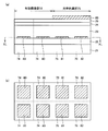
- FIG. 5 is a diagram schematically showing a cross-sectional structure and operation of the pixel array shown in FIG. 4. It is the figure which looked at the pixel array shown in FIG. 5 from the upper part. It is a figure which shows the cross-section of the principal part of the pixel array shown in FIG. 4 in detail. It is a perspective view of the principal part of the pixel array shown in FIG. FIG.
- FIG. 3 is a diagram illustrating an example of a circuit for one pixel in the pixel array illustrated in FIG. 2. It is a block diagram which shows the whole structure of the photoelectric conversion apparatus by Embodiment 2 of this invention. It is a circuit diagram which shows the structure of the pixel shown in FIG. 12 is a time chart illustrating an operation of the photoelectric conversion device illustrated in FIGS. 10 and 11. It is a figure which shows the principal part of the pixel array shown in FIG. FIG. 12 illustrates a layout of the transistor illustrated in FIG. 11. It is a figure which shows the example of a change of Embodiment 2. FIG. It is a figure which shows typically the cross-sectional structure and operation
- FIG. 10 is a diagram schematically showing a configuration and operation of a modified example of the third embodiment. It is a figure which shows other operation
- FIG. It is a figure which shows other operation
- FIG. It is a figure which shows schematically the structure of the other modification of Embodiment 3.
- FIG. It is a figure which shows schematically the structure of the other modification of Embodiment 3.
- FIG. 30 is a diagram schematically showing a cross-sectional structure and operation of the pixel array shown in FIG. 29. It is a figure which shows the color arrangement
- FIG. 16 is a diagram illustrating a change example of the color arrangement of the color filter for one pixel in the imaging apparatus according to the fourth embodiment.
- FIG. 36 is a diagram showing interlace processing and interleaving processing in the modification example shown in FIG. 35.
- FIG. 10 is a diagram illustrating another modification of the color arrangement of the color filter for one pixel in the imaging apparatus according to the fourth embodiment.
- FIG. 16 is a diagram illustrating still another modification of the color arrangement of the color filter for one pixel in the imaging apparatus according to Embodiment 4. It is a top view which shows the structure of the pixel array of the photoelectric conversion apparatus by Embodiment 5 of this invention.
- FIG. 40 is a cross-sectional view showing the main parts of the pixel array shown in FIG. 39. 41 is a diagram schematically showing the configuration and operation of the pixel array shown in FIG. 40.
- FIG. FIG. 42 is a circuit block diagram showing a configuration of a photoelectric conversion device including the pixel array shown in FIGS. 39 to 41.
- FIG. 43 is a circuit diagram showing a configuration of a pixel shown in FIG. 42.
- FIG. 10 is a cross-sectional view showing a modified example of the fifth embodiment.
- 45 is a diagram schematically showing the configuration and operation of the pixel array shown in FIG. 44.
- FIG. It is a figure which shows the structure of the pixel of the photoelectric conversion apparatus which concerns on Embodiment 6 of this invention.
- 47 is a diagram showing a circuit configuration of the differential amplifier shown in FIG. 46.
- FIG. FIG. 48 is a diagram showing in detail a cross-sectional structure of a main part of the pixel array shown in FIG. 47.
- FIG. 10 is a diagram illustrating a circuit configuration of a differential amplifier according to a modification of the sixth embodiment. It is a figure which shows the cross-section of the principal part of the pixel array shown in FIG. 49 in detail.
- FIG. 52 is a diagram schematically showing a cross-sectional structure and an operation of the pixel array shown in FIG. 51. It is the figure which looked at the pixel array shown in FIG. 51 from upper direction.
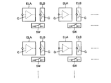
- 10 is a diagram illustrating a relationship between a pixel electrode and a switch in a photoelectric conversion device according to Embodiment 7.
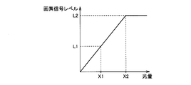
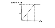
- FIG. FIG. 55 is a graph showing a relationship between an incident light amount and a read signal level in the photoelectric conversion device shown in FIG. 54.
- FIG. 52 is a graph showing a relationship between an incident light amount and a pixel signal level in the photoelectric conversion device shown in FIG.
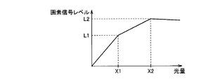
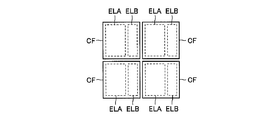
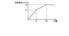
- FIG. 52 is a graph showing another relationship between the incident light amount and the pixel signal level in the photoelectric conversion device shown in FIG. 51. It is the figure which looked at the photoelectric conversion apparatus shown in FIG. 51 from upper direction. It is the figure which looked at the pixel electrode in the example of a change of the photoelectric conversion apparatus which concerns on Embodiment 7 from upper direction. It is the figure which looked at the pixel electrode in the other modification of the photoelectric conversion apparatus which concerns on Embodiment 7 from upper direction. It is a figure which shows the relationship between the pixel electrode and switch in the photoelectric conversion apparatus which concerns on Embodiment 8 of this invention. It is a figure which shows the switch setting in one pixel electrode group. FIG.
- FIG. 62 is a graph showing a relationship between an incident light amount and a pixel signal level in the photoelectric conversion device shown in FIG. 61.
- FIG. 62 is a graph showing another relationship between the incident light amount and the pixel signal level in the photoelectric conversion device shown in FIG. 61.
- FIG. 62 is a diagram illustrating another setting example of switches in one pixel electrode group of the photoelectric conversion device illustrated in FIG. 61.
- FIG. 62 is a diagram illustrating another setting example of switches in one pixel electrode group of the photoelectric conversion device illustrated in FIG. 61.
- FIG. 10 is a diagram illustrating a modification example of the photoelectric conversion device according to the eighth embodiment.
- FIG. 10 is a diagram illustrating a modification example of the photoelectric conversion device according to the eighth embodiment.
- FIG. 25 is a diagram illustrating another setting example of the switch SWK in the pixel electrode group of a modification example of the photoelectric conversion device according to the eighth embodiment. It is sectional drawing which shows the principal part of the pixel array of the image sensor by Embodiment 9 of this invention.
- FIG. 70 is a diagram schematically showing the configuration and operation of the pixel array shown in FIG. 69.
- FIG. 38 shows a comparative example of the ninth embodiment.
- FIG. 38 is a diagram illustrating a modification example of the ninth embodiment. It is sectional drawing which shows the other modification of Embodiment 9.
- FIG. FIG. 38 is a cross-sectional view showing still another modification example of the ninth embodiment.
- FIG. 75 is a diagram schematically showing the configuration and operation of the pixel array shown in FIG. 74.
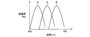
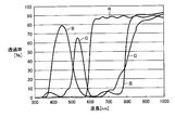
- FIG. 77 is a diagram showing the transmittance of a color filter in the imaging device shown in FIG. 76.
- 77 is a flowchart defining an operation procedure when the imaging apparatus shown in FIG. 76 captures a subject.
- FIG. 77 is a diagram conceptually illustrating an operation procedure when the imaging device illustrated in FIG. 76 captures a subject.
- 76 is a time chart showing an operation procedure when the imaging apparatus shown in FIG. 76 irradiates light on a subject.
- 76 is a time chart showing an operation procedure when the imaging apparatus shown in FIG. 76 generates an image of a subject.
- FIG. 77 is a diagram showing the transmittance of a color filter in the imaging device shown in FIG. 76.
- 77 is a flowchart defining an operation procedure when the imaging apparatus shown in FIG. 76 captures a subject.
- FIG. 77 is a diagram conceptually illustrating an operation procedure when the imaging device illustrated in FIG. 76 captures a subject.
- FIG. 77 is a diagram showing optical characteristics of the imaging device shown in FIG. 76. It is a figure which shows the applied wavelength for medical use. 32 is a flowchart defining an operation procedure when the imaging apparatus according to the modification of the tenth embodiment captures a subject.
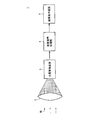
- FIG. 1 is a diagram showing a configuration of an imaging apparatus 1 according to Embodiment 1 of the present invention.
- the imaging device 1 includes a lens 2, a photoelectric conversion device 3, an image signal processing unit 4, and an image display device 5.
- the imaging device 1 images a subject and displays it on the screen. More specifically, the lens 2 collects light from the subject on the photoelectric conversion device 3.
- the photoelectric conversion device 3 converts the light received from the lens 2 into a pixel signal that is an electrical signal and outputs the pixel signal to the image signal processing unit 4.
- the image signal processing unit 4 performs various signal processing such as interpolation processing, color processing, and correction processing on the pixel signal of each pixel received from the photoelectric conversion device 3 to generate an image signal, and outputs the image signal to the image display device 5.
- the image display device 5 displays an image based on the image signal received from the image signal processing unit 4.
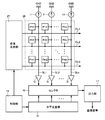
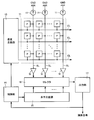
- FIG. 2 is a diagram showing a configuration of the photoelectric conversion apparatus according to Embodiment 1 of the present invention.
- the photoelectric conversion device 3 includes a pixel array 10, a plurality of load circuits 11, a plurality of amplifiers Q, a vertical scanning unit 13, a control unit 14, a horizontal scanning unit 15, and a selector 16. And an output unit 17.
- the pixel array 10 includes a plurality of pixels P arranged in a plurality of rows and a plurality of columns.
- the rows and columns of the plurality of pixels P arranged in a matrix are also referred to as pixel rows and pixel columns, respectively.
- the pixel array 10 further includes a control signal line CL provided corresponding to each pixel row and a signal line SL provided corresponding to each pixel column.
- each signal line SL is connected to the supply node of the ground voltage GND through the load circuit 11.
- the load circuit 11 has a predetermined resistance value.
- the other end of each signal line SL is connected to the input terminal of the amplifier Q.
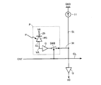
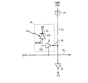
- FIG. 3 is a diagram showing a configuration of the pixel P according to Embodiment 1 of the present invention.
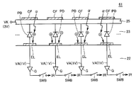
- pixel P includes a photodiode PD, a readout circuit G, and a switch SWB.
- a cathode voltage VK is applied to the cathode of the photodiode PD
- an anode voltage VA is applied to the anode of the photodiode PD.
- Read circuit G is, for example, an amplifier, and outputs current IR having a level corresponding to the amount of charge flowing in from photodiode PD as a signal to corresponding signal line SL.
- the switch SWB switches whether to output the current IR from the read circuit G to the corresponding signal line SL based on the control signal CNT received via the corresponding control signal line CL.
- the signal line SL transmits a signal from the readout circuit G. That is, the voltage level of the signal line SL is the product of the current IR from the readout circuit G and the resistance value of the load circuit 11.
- the amplifier Q amplifies the voltage of the corresponding signal line SL. Therefore, the output voltage VD of the amplifier Q changes according to the amount of light ⁇ incident on the photodiode PD.
- the vertical scanning unit 13 sequentially selects a plurality of pixel rows one by one based on the vertical scanning signal supplied from the control unit 14, and passes through the control signal line CL of the selected pixel row.
- a control signal CNT is applied to each switch SWB in the pixel row.
- a current of a level corresponding to the amount of incident light is output from each pixel P of the selected pixel row to the corresponding signal line SL, and each signal line SL is charged to a voltage corresponding to the amount of incident light.
- the voltage of each signal line SL is amplified by the amplifier Q and supplied to the selector 16.
- the horizontal scanning unit 15 sequentially selects each pixel column one by one during a period when one pixel row is selected by the vertical scanning unit 13 based on the horizontal scanning signal given from the control unit 14.
- the selector 16 selects the output voltage VD of the amplifier Q corresponding to the pixel column selected by the horizontal scanning unit 15 and transmits it to the output unit 17.
- the output unit 17 generates a pixel signal, that is, a signal indicating the amount of light received by the pixel P based on the output voltage VD of the amplifier Q given through the selector 16, and outputs the signal to the image signal processing unit 4 and the control unit 14.
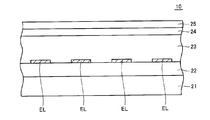
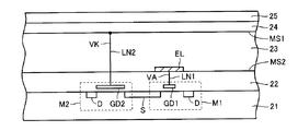
- FIG. 4 is a diagram showing a cross-sectional structure of a main part of the pixel array 10 according to the first embodiment of the present invention.
- pixel array 10 includes a semiconductor substrate 21, a readout circuit layer 22, a plurality of pixel electrodes EL, a CIGS thin film 23, a CdS (cadmium sulfide) layer 24, and a transparent electrode 25. .
- a readout circuit layer 22 is formed on the surface of the semiconductor substrate 21.
- the read circuit layer 22 is an insulating layer and includes a MOS (Metal Oxide Semiconductor) transistor, a capacitor, a wiring, a via hole, and the like.
- MOS Metal Oxide Semiconductor
- a plurality of rectangular pixel electrodes EL are arranged on the surface of the readout circuit layer 22 at a predetermined interval.
- the plurality of pixel electrodes EL are arranged in a plurality of rows and a plurality of columns.
- Each pixel electrode EL is made of, for example, Mo (molybdenum).
- a CIGS thin film 23 is formed so as to cover the plurality of pixel electrodes EL, and a CdS layer 24 and a transparent electrode 25 are laminated on the surface of the CIGS thin film 23 in this order.
- CIGS thin film 23 is a p-type compound semiconductor thin film having a thickness of 1.7 ⁇ m, for example.
- the CdS layer 24 is a buffer layer, and its thickness is, for example, 50 nm.
- the transparent electrode 25 is a low-resistance n-type ZnO film and has a thickness of 1 ⁇ m, for example. Therefore, a PN junction is formed by the CIGS thin film 23 and the transparent electrode 25.
- the transparent electrode 25 is formed on the first main surface of the CIGS thin film 23 that is a photoelectric conversion film via the CdS layer 24 that is a buffer layer, and a plurality of pixel electrodes EL are formed on the second main surface of the CIGS thin film 23.
- Each pixel electrode EL corresponds to the pixel P.
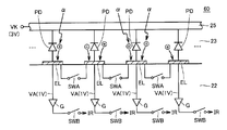
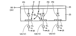
- FIG. 5 is a diagram schematically showing a cross-sectional structure and operation of the pixel array according to Embodiment 1 of the present invention.
- FIG. 6 is a view of the pixel array according to the first embodiment of the present invention as viewed from above.
- pixel array 10 further includes a plurality of switches SWB.
- the readout circuit G is provided corresponding to the pixel electrode EL, and is formed below the corresponding pixel electrode EL in the readout circuit layer 22 shown in FIG. That is, the readout circuit G is provided on the opposite side of the CIGS thin film 23 with respect to the corresponding pixel electrode EL. Thereby, miniaturization of the photoelectric conversion device 3 can be achieved.
- the readout circuit G applies an anode voltage VA of 1 V, for example, to the corresponding pixel electrode EL. Further, a cathode voltage VK of, for example, 3V higher than the anode voltage VA is applied to the transparent electrode 25. As a result, a depletion layer is formed between each pixel electrode EL and the transparent electrode 25, and a region between each pixel electrode EL and the transparent electrode 25 operates as a photodiode PD.
- the pixel electrode EL serves as the anode of the photodiode PD, and the transparent electrode 25 serves as the cathode of the photodiode PD.
- the readout circuit G outputs a current IR having a level corresponding to the amount of charge flowing into the corresponding pixel electrode EL.
- Switch SWB is provided corresponding to read circuit G in read circuit layer 22, and includes a first terminal connected to the output terminal of corresponding read circuit G, and a second terminal connected to corresponding signal line SL. Have.
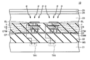
- FIG. 7 is a diagram showing in detail the cross-sectional structure of the main part of the pixel array 10 according to the first embodiment of the present invention.
- FIG. 8 is a perspective view of a main part of the pixel array 10 according to the first embodiment of the present invention.
- pixel array 10 further includes a wiring LN, a planar electrode CTM, a planar electrode CBM, a via hole T, and a MOS transistor TR1.
- the wiring LN, the planar electrode CTM, and the planar electrode CBM are made of, for example, aluminum.
- Semiconductor substrate 21 has a main surface MS.
- Read circuit layer 22 is provided on main surface MS.
- the CIGS thin film 23 is provided on the main surface MS via the readout circuit layer 22 and converts received light into electric charges.
- the pixel electrode EL is provided on the surface of the CIGS thin film 23 and receives charges converted by the CIGS thin film 23.
- the wiring LN is provided in the readout circuit layer 22 and electrically connects the pixel electrode EL and the semiconductor substrate 21.
- the planar electrode CTM is provided in the readout circuit layer 22 and is electrically connected to the pixel electrode EL.
- a plurality of wirings LN and planar electrodes CTM are provided corresponding to the pixel electrodes EL.
- the planar electrode CBM is provided to face the planar electrode CTM at a distance in the readout circuit layer 22.
- a capacitance CP is formed between the planar electrode CTM and the planar electrode CBM. The capacitance CP is proportional to the area of the opposing region of the planar electrode CTM and the planar electrode CBM.
- the planar electrode CBM is provided to face the main surface MS of the semiconductor substrate 21.
- the planar electrode CBM and the main surface MS are provided substantially parallel to each other.
- the planar electrode CTM and the planar electrode CBM are provided substantially in parallel with each other.
- the wiring LN is provided below the corresponding pixel electrode EL, and is electrically connected to the pixel electrode EL through the via hole T.
- the planar electrode CTM is provided below the wiring LN and is electrically connected to the pixel electrode EL via the via hole T and the wiring LN.
- a plurality of via holes T are provided in parallel between the pixel electrode EL and the wiring LN and between the wiring LN and the planar electrode CTM. With such a configuration, the wiring resistance due to the via hole T can be reduced.
- the MOS transistor TR1 is provided in a region under the planar electrode CBM in the semiconductor substrate 21 and the readout circuit layer 22.
- the planar electrode CTM is separated for each pixel.
- the planar electrode CBM extends across a plurality of pixels. That is, the planar electrode CBM is integrally provided so as to face each planar electrode CTM with a gap. For this reason, the capacitance CP for charge accumulation is defined by the area of the planar electrode CTM.
- the charge photoelectrically converted in the CIGS thin film 23 is accumulated in the capacitor CP, and the accumulated charge is given to the MOS transistor TR1 in the semiconductor substrate 21 through the wiring LN.
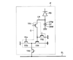
- FIG. 9 is a diagram illustrating an example of a circuit for one pixel in the pixel array 10 according to the first embodiment of the present invention.
- pixel P includes photodiode PD, wiring LN, planar electrode CTM, planar electrode CBM, readout circuit G, and MOS transistor TR5.
- Read circuit G includes MOS transistors TR1 to TR4.
- MOS transistor TR1 has a gate, a drain connected to the wiring LN, a source connected to the source of the MOS transistor TR2 and a gate of the MOS transistor TR4.
- MOS transistor TR2 has a gate, a drain connected to a node to which a predetermined voltage such as a ground voltage is supplied, and a source connected to the source of MOS transistor TR1.
- MOS transistor TR4 has a gate connected to the source of MOS transistor TR1, a drain connected to the node supplied with the power supply voltage, and a source connected to the drain of MOS transistor TR3.
- MOS transistor TR3 has a gate supplied with bias voltage Vbs, a drain connected to the source of MOS transistor TR4, and a source connected to a node supplied with a ground voltage.
- MOS transistor TR5 has a drain connected to the drain of MOS transistor TR3, a gate, and a source connected to signal line SL.
- MOS transistors TR3 and TR4 constitute a source follower circuit.
- a bias voltage Vbs is applied to the gate of the MOS transistor TR3, whereby the MOS transistor TR3 operates as a resistance element.
- the MOS transistor TR3 corresponds to the load circuit 11 described above, and in the readout circuit G shown in FIG. 9, a voltage corresponding to the amount of electric charge flowing in from the photodiode PD is used as a signal and the corresponding signal line SL. Is output to.
- the MOS transistor TR5 corresponds to the above-described switch SWB, and switches whether to output a signal from the readout circuit G to the signal line SL.
- the control unit 14 controls the vertical scanning unit 13 to give a control signal to the gates of the MOS transistors TR1, TR4, and TR5, and reads out charges from the pixel P.
- control unit 14 first reads the reset potential. That is, the MOS transistor TR5 is turned on. Then, by turning on the MOS transistor TR2, the charge stored in the gate capacitance of the MOS transistor TR4 and the wiring capacitance connected to the gate is released. At this time, the MOS transistor TR1 is turned off to prevent the electric charge stored in the capacitor CP from flowing to the MOS transistor TR4 side.
- the MOS transistor TR2 is turned off and the MOS transistor TR1 is turned on.
- the charge stored in the capacitor CP flows to the gate of the MOS transistor TR4, and a voltage corresponding to the charge stored in the capacitor CP is output to the signal line SL.
- the MOS transistor TR5 is turned off. Further, by turning on the MOS transistor TR2, the charge stored in the gate capacitance of the MOS transistor TR4 and the wiring capacitance connected to the gate is released. Then, the MOS transistor TR1 is turned off, the charge is stored again in the capacitor CP, and the charge stored in the capacitor CP is stopped so as not to flow to the MOS transistor TR4 side.
- a space for providing a transistor for storing electric charge obtained by photoelectric conversion is required in a silicon substrate, and it is difficult to reduce the size.
- an unnecessary current is generated, and the image quality may be deteriorated.
- a solid-state imaging device used for a CMOS image sensor or the like it is necessary to make light incident on a silicon substrate. Therefore, it is not preferable to provide a capacitor in a wiring layer or the like on the silicon substrate.
- a capacitor in the stacked configuration using a CIGS thin film or the like, light does not have to be incident on the silicon substrate, so that a capacitor can be provided not in the silicon substrate but in the insulating layer, that is, the wiring layer. Can be formed of the same material as the wiring.
- the photoelectric conversion device is provided in the readout circuit layer 22, provided in the readout circuit layer 22, and a wiring LN that electrically connects the pixel electrode EL and the semiconductor substrate 21, A planar electrode CTM electrically connected to the pixel electrode EL, and a planar electrode CBM provided in the readout circuit layer 22 so as to face the planar electrode CTM with a space therebetween.
- the arrangement of the wiring LN, the planar electrode CTM, and the planar electrode CBM in the pixel array 10 according to the first embodiment of the present invention is not limited to that shown in FIGS. If the planar electrode CTM and the planar electrode CBM are opposed to each other, it is possible to form a capacitor and block light incident on the semiconductor substrate 21. Further, by providing either the planar electrode CTM or the planar electrode CBM so as to face the semiconductor substrate 21, light incident on the semiconductor substrate 21 can be further blocked.
- the planar electrode CBM is configured to extend across a plurality of pixels, but is not limited thereto.
- the planar electrode CBM may be separated for each pixel.
- the pixel array 10 according to the first exemplary embodiment of the present invention is configured to include a CIGS thin film
- the present invention is not limited to this. It may be a photoelectric conversion thin film or a photoelectric conversion thick film, and for example, a structure including a compound semiconductor thin film other than a CIGS thin film and an organic semiconductor thin film may be used. Further, the present invention is not limited to the photoelectric conversion device but can be applied to a photo sensor, a line sensor, and the like.
- the photoelectric conversion device includes a pixel array 26 as shown in FIG.
- the pixel array 26 is provided corresponding to m rows and m ⁇ n pixels P11 to Pmn arranged in m rows and n columns (where m and n are integers of 2 or more), respectively. It includes control signal line groups CL1 to CLm and signal lines SL1 to SLn provided corresponding to n columns, respectively.
- the pixel P is controlled by a plurality of signals given through the corresponding control signal line group CL, and has a pixel current at a level corresponding to the incident light amount and a reference current corresponding to the pixel current when the incident light amount is zero. The signals are sequentially output to the corresponding signal lines SL.
- each signal line SL is connected to the ground voltage GND line through the load circuit 11.
- the load circuit 11 has a predetermined resistance value.
- the other end of each signal line SL is connected to the input node of amplifier Q.
- the amplifier Q amplifies the voltage of the corresponding signal line SL.
- the signal line SL has a product voltage of the output current of the pixel P in the selected row of the corresponding column and the resistance value of the load circuit 11.
- the voltage of the signal line SL is amplified by the amplifier Q.
- the photoelectric conversion device includes a vertical scanning unit 27, a control unit 14, a horizontal scanning unit 15, a selector 16, and an output unit 17.
- the vertical scanning unit 27 operates in accordance with the vertical scanning signal supplied from the control unit 14, sequentially selects m rows of the pixel array 26 one by one, and each pixel in the row via the control signal line group CL of the selected row. A plurality of signals are given to P. As a result, a current is output from each pixel P in the selected row to the corresponding signal line SL, and each signal line SL is charged to a product voltage of the output current of the pixel P and the resistance value of the load circuit 11. The voltage of each signal line SL is amplified by the amplifier Q and supplied to the selector 16.
- the horizontal scanning unit 15 operates in accordance with a horizontal scanning signal given from the control unit 14, and sequentially selects n columns one by one within a period in which one row is selected by the vertical scanning unit 27.
- the selector 16 transmits the output voltage of the amplifier Q corresponding to the column selected by the horizontal scanning unit 15 to the output unit 17.
- the output unit 17 generates an image signal based on the output voltage of the amplifier Q given through the selector 16.
- the image signal is given to the image display device. An image of the subject of the photoelectric conversion device is displayed on the screen of the image display device.
- the pixel P11 in the first row and the first column includes N-channel MOS transistors 30 to 38, a photodiode 39, and capacitors 40 and 41, as shown in FIG.
- the cathode of the photodiode 39 receives the first power supply voltage VDD, and its anode is connected to the node N1.
- the photodiode 39 causes a current having a value corresponding to the amount of incident light to flow to the node N1.
- the drain of the transistor 30 receives the second power supply voltage VDR, its gate receives the reset signal RC1, and its source is connected to the node N1.
- the second power supply voltage VDR is a predetermined voltage that is lower than the first power supply voltage VDD and higher than the ground voltage GND.
- the capacitor 40 is connected between the node N2 and the line of the ground voltage GND.
- Capacitor 41 is connected between node N3 and the line of ground voltage GND.
- Transistor 31 is connected between nodes N1 and N2, and has its gate receiving transfer signal TA1.
- Transistor 32 is connected between nodes N1 and N3, and has a gate receiving transfer signal TB1.
- Transfer signals TA1 and TB1 are alternately set to “H” level at a predetermined cycle.
- the reset signal RC1 is set to the “H” level during the period in which the transfer signal TA1 is “H”
- the transistors 30 and 31 are turned on and the nodes N1 and N2 are reset to the second power supply voltage VDR.
- the reset signal RC1 is set to the “L” level during the period in which the transfer signal TA1 is at the “H” level, the transistor 30 is turned off and the transistor 31 is turned on, and the capacitor 40 is charged by the output current of the photodiode 39. Is done.
- the transistors 30 and 32 are turned on and the nodes N1 and N3 are reset to the second power supply voltage VDR.
- the reset signal RC1 is set to the “L” level during the period in which the transfer signal TB1 is at the “H” level, the transistor 30 is turned off and the transistor 32 is turned on, and the capacitor 41 is charged by the output current of the photodiode 39. Is done.
- Transistor 34 has a drain receiving second power supply voltage VDR, a gate receiving reset signal RB1, and a source connected to node N3.
- the transistor 33 When the reset signal RA1 is set to the “H” level during the period when the transfer signal TA1 is at the “L” level, the transistor 33 is turned on, and the node N2 is reset to the second power supply voltage VDR.
- the reset signal RB1 When the reset signal RB1 is set to the “H” level during the period in which the transfer signal TB1 is at the “L” level, the transistor 34 is turned on and the node N3 is reset to the second power supply voltage VDR.
- the drain of the transistor 35 receives the second power supply voltage VDR, and its gate is connected to the node N2.
- the drain of the transistor 37 is connected to the source of the transistor 35, the gate thereof receives a selection signal SA1, and the source thereof is connected to the corresponding signal line SL1.
- the first power supply voltage VDD may be applied to the drain of the transistor 35 instead of the second power supply voltage VDR.
- the transistor 37 becomes conductive and the voltage of the node N2
- the pixel current of a level corresponding to the current flows from the line of the second power supply voltage VDR to the corresponding signal line SL1 via the transistors 35 and 37.
- the transistor 37 becomes conductive and the second power supply voltage A reference current of a level corresponding to VDR flows from the line of the second power supply voltage VDR to the corresponding signal line SL1 via the transistors 35 and 37.
- the drain of the transistor 36 receives the second power supply voltage VDR, and its gate is connected to the node N3.
- the drain of transistor 38 is connected to the source of transistor 36, its gate receives selection signal SB1, and its source is connected to corresponding signal line SL1.
- the first power supply voltage VDD may be applied to the drain of the transistor 35 instead of the second power supply voltage VDR.
- the transistor 38 becomes conductive and the voltage of the node N3 A pixel current of a level corresponding to the current flows from the line of the second power supply voltage VDR to the corresponding signal line SL1 via the transistors 36 and 38.
- the transistor 38 is turned on, and the second power supply voltage A reference current of a level corresponding to VDR flows from the second power supply voltage VDR line to the corresponding signal line SL1 via the transistors 36 and 38.
- the signals RA1, RB1, RC1, TA1, TB1, SA1, and SB1 are supplied to the pixel P11 through the corresponding control signal line group CL1.
- Each of the other pixels P12 to P1n in the first row has the same configuration as the pixel P11. However, the sources of the transistors 37 and 38 of the pixels P12 to P1n are connected to the signal lines SL2 to SLn, respectively.
- the pixels P21 to P2n in the second row have the same configuration as the pixels P11 to P1n, respectively.
- signals RA2, RB2, RC2, TA2, TB2, SA2, and SB2 are supplied to each of the pixels P21 to P2n from the control signal line group CL2.
- the pixels Pm1 to Pmn in the m-th row have the same configuration as the pixels P11 to P1n, respectively. However, signals RAm, RBm, RCm, TAm, TBm, SAm, and SBm are supplied to the pixels Pm1 to Pmn from the control signal line group CLm.
- FIG. 12 is a time chart showing the global shutter operation of the photoelectric conversion device. However, in FIG. 12, only the operation of the pixels P in the first row and the second row is shown.
- transfer signals TA1 to TAm and transfer signals TB1 to TBm are alternately set to the “H” level at a constant cycle.
- the transfer signals TA1 to TAm are lowered from the “H” level to the “L” level, and the transfer signals TB1 to TBm are raised from the “L” level to the “H” level.
- the transistors 31 of all the pixels P11 to Pmn are turned off and the transistor 32 is turned on.
- the reset signals RC1 to RCm are raised to the “H” level for a predetermined time.
- the transistors 30 of all the pixels P11 to Pmn are turned on for a predetermined time, and the nodes N1 and N3 are reset to the second power supply voltage VDR.
- the reset signals RC1 to RCm are lowered to the “L” level, the output current of the photodiode 39 flows into the node N3 via the transistor 32 in all the pixels P11 to Pmn, and charging of the capacitor 41 is started. The charging of the capacitor 41 is continued while the transfer signals TB1 to TBm are at the “H” level.
- the pixels P11 to P1n in the first row are selected by the vertical scanning unit 27, the selection signal SA1 is raised to “H” level for a predetermined time, and the transistors 37 of the pixels P11 to P1n are turned on. .
- the node N2 is charged during a period (t0 to t1) when the transfer signals TA1 to TAm are at the “H” level, and the voltage at the node N2 is at a level corresponding to the amount of light incident on the photodiode 39 of each pixel P. It has become.
- a pixel current having a value corresponding to the voltage of the node N2 flows from the line of the second power supply voltage VDR to the signal line SL via the transistors 35 and 37, and the voltage of the signal line SL becomes a level corresponding to the pixel current.
- the voltages of the signal lines SL1 to SLn are given to the output unit 17 via the amplifier Q and the selector 16 shown in FIG.
- the reset signal RA1 is raised to “H” level for a predetermined time, and the transistors 33 of the pixels P11 to P1n are turned on.
- the node N2 of the pixels P11 to P1n is reset to the second power supply voltage VDR.
- the selection signal SA1 is raised to “H” level for a predetermined time, and the transistors 37 of the pixels P11 to P1n are turned on.
- a reference current having a value corresponding to the voltage of the node N2 flows from the second power supply voltage VDR line to the signal line SL via the transistors 35 and 37, and the voltage of the signal line SL is The level rises according to the reference current.
- the voltages of the signal lines SL1 to SLn are given to the output unit 17 via the amplifier Q and the selector 16 shown in FIG.
- the pixels P21 to P2n in the second row are selected by the vertical scanning unit 27, the selection signal SA2 is raised to “H” level for a predetermined time, and the transistors 37 of the pixels P21 to P2n are turned on. .
- the node N2 is charged during a period (t0 to t1) when the transfer signals TA1 to TAm are at the “H” level, and the voltage at the node N2 is at a level corresponding to the amount of light incident on the photodiode 39 of each pixel P. It has become.
- a pixel current having a value corresponding to the voltage of the node N2 flows from the line of the second power supply voltage VDR to the signal line SL via the transistors 35 and 37, and the voltage of the signal line SL becomes a level corresponding to the pixel current.
- the voltages of the signal lines SL1 to SLn are given to the output unit 17 via the amplifier Q and the selector 16 shown in FIG.
- the reset signal RA2 is raised to “H” level for a predetermined time, and the transistors 33 of the pixels P21 to P2n are turned on. As a result, the node N2 of the pixels P21 to P2n is reset to the second power supply voltage VDR.
- the selection signal SA2 is raised to “H” level for a predetermined time, and the transistors 37 of the pixels P21 to P2n are turned on.
- a reference current having a value corresponding to the voltage of the node N2 flows from the second power supply voltage VDR line to the signal line SL via the transistors 35 and 37, and the voltage of the signal line SL is The level rises according to the reference current.
- the voltages of the signal lines SL1 to SLn are given to the output unit 17 via the amplifier Q and the selector 16 shown in FIG.
- a pixel current at a level corresponding to the voltage at the node N2 and a level reference according to the second power supply voltage VDR The current is output to the signal line SL, and the voltage of the signal line SL is supplied to the output unit 17 via the amplifier Q and the selector 16.
- the transfer signals TA1 to TAm are raised from the “L” level to the “H” level and the transfer signals TB1 to TBb are lowered from the “H” level to the “L” level.
- the transistors 32 of all the pixels P11 to Pmn are turned off and the transistor 31 is turned on.
- the reset signals RC1 to RCm are raised to the “H” level for a predetermined time.
- the transistors 30 of all the pixels P11 to Pmn are turned on for a predetermined time, and the nodes N1 and N2 are reset to the second power supply voltage VDR.
- the reset signals RC1 to RCm fall to the “L” level
- the output current of the photodiode 39 flows into the node N2 via the transistor 31 in all the pixels P11 to Pmn, and charging of the capacitor 40 is started. Charging of the capacitor 40 is continued while the transfer signals TA1 to TAm are at the “H” level.
- the pixels P11 to P1n in the first row are selected by the vertical scanning unit 27, the selection signal SB1 is raised to “H” level for a predetermined time, and the transistors 38 of the pixels P11 to P1n are turned on. .
- the node N3 is charged during a period (t1 to t9) when the transfer signals TB1 to TBm are at the “H” level, and the voltage of the node N3 is a level corresponding to the amount of light incident on the photodiode 39 of each pixel portion P. It has become.
- a pixel current having a value corresponding to the voltage of the node N3 flows from the line of the second power supply voltage VDR to the signal line SL via the transistors 36 and 38, and the voltage of the signal line SL becomes a level corresponding to the pixel current.
- the voltages of the signal lines SL1 to SLn are given to the output unit 17 via the amplifier Q and the selector 16 shown in FIG.
- the reset signal RB1 is raised to “H” level for a predetermined time, and the transistors 34 of the pixels P11 to P1n are turned on.
- the node N3 of the pixels P11 to P1n is reset to the second power supply voltage VDR.
- the selection signal SB1 is raised to “H” level for a predetermined time, and the transistors 38 of the pixels P11 to P1n are turned on.
- a reference current having a value corresponding to the voltage of the node N3 flows from the second power supply voltage VDR line to the signal line SL via the transistors 36 and 38, and the voltage of the signal line SL is The level rises according to the reference current.
- the voltages of the signal lines SL1 to SLn are given to the output unit 17 via the amplifier Q and the selector 16 shown in FIG.
- the pixels P21 to P2n in the second row are selected by the vertical scanning unit 27, the selection signal SB2 is raised to “H” level for a predetermined time, and the transistors 38 of the pixels P21 to P2n are turned on. .
- the node N3 is charged during a period (t1 to t9) when the transfer signals TB1 to TBm are at the “H” level, and the voltage at the node N3 is set to a level corresponding to the amount of light incident on the photodiode 39 of each pixel P. It has become.
- a pixel current having a value corresponding to the voltage of the node N3 flows from the line of the second power supply voltage VDR to the signal line SL via the transistors 36 and 38, and the voltage of the signal line SL becomes a level corresponding to the pixel current.
- the voltages of the signal lines SL1 to SLn are given to the output unit 17 via the amplifier Q and the selector 16 shown in FIG.
- the reset signal RB2 is raised to “H” level for a predetermined time, and the transistors 34 of the pixels P21 to P2n are turned on.
- the node N3 of the pixels P21 to P2n is reset to the second power supply voltage VDR.
- the selection signal SB2 is raised to “H” level for a predetermined time, and the transistors 38 of the pixels P21 to P2n are turned on.
- a reference current having a value corresponding to the voltage of the node N3 flows from the second power supply voltage VDR line to the signal line SL via the transistors 36 and 38, and the voltage of the signal line SL is The level rises according to the reference current.
- the voltages of the signal lines SL1 to SLn are given to the output unit 17 via the amplifier Q and the selector 16 shown in FIG.
- a pixel current at a level corresponding to the voltage of the node N2 and a level reference according to the second power supply voltage VDR The current is output to the signal line SL, and the voltage of the signal line SL is supplied to the output unit 17 via the amplifier Q and the selector 16.
- the output unit 17 generates an image signal based on the voltage signal given through the selector 16.
- the current of the level corresponding to the voltage of the node N3 is signaled while the output current of the photodiode 39 is supplied to the reset node N2.
- the transfer signal TB1 is in the “H” level while flowing through the line SL
- a current at a level corresponding to the voltage at the node N2 is passed through the signal line SL while the output current of the photodiode 39 is passed through the reset node N3. Therefore, the output current of the photodiode 39 can be prevented from flowing to the node N3 (or N2) during the period when the transfer signal TA1 (or TB1) is at the “H” level.
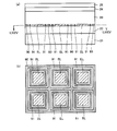
- FIG. 13A is a cross-sectional view showing a main part of the pixel array 26, and FIG. 13B is a cross-sectional view taken along line XIIIB-XIIIB in FIG. 13A.
- the pixel array 26 includes a p-type silicon substrate 50.
- a read circuit layer 51 is formed on the surface of the p-type silicon substrate 50.
- the read circuit layer 51 includes N-channel MOS transistors 30 to 38, capacitors 40 and 41, wirings, insulating layers, contact holes, and the like.
- a plurality of pixel electrodes 52 are arranged in a plurality of rows and a plurality of columns at predetermined intervals.
- Each pixel electrode 52 is provided corresponding to the pixel P, and is formed of Mo in a square shape.
- a CIGS thin film 53 is formed so as to cover the plurality of pixel electrodes 52, and a CdS layer 54 and a transparent electrode 55 are laminated on the surface of the CIGS thin film 53.
- CIGS is an abbreviation for Cu (In x , Ga (1-x) ) Se 2 (0 ⁇ x ⁇ 1).
- CIGS thin film 53 is a p-type compound semiconductor thin film having a thickness of 1.7 ⁇ m, for example.
- the CdS layer 54 is a buffer layer formed of an n-type compound semiconductor thin film and has a thickness of, for example, 50 nm.
- the transparent electrode 55 is, for example, a ZnO film and has a thickness of, for example, 1 ⁇ m. Therefore, a PN junction is formed by the CIGS thin film 53 and the transparent electrode 55.
- the CIGS thin film 53 that is a photoelectric conversion film is divided into a plurality of pixel regions, and the transparent electrode 55 is formed on the surface of the CIGS thin film 53 via the CdS layer 54 that is a buffer layer.
- a pixel electrode 52 is formed in the pixel region. Each pixel electrode 52 becomes an anode of the photodiode 39, and the transparent electrode 55 becomes a cathode of the photodiode 39.
- a first power supply voltage VDD is applied to the transparent electrode 55, and a second power supply voltage VDR lower than the first power supply voltage VDD is applied to each pixel electrode 52.
- FIG. 14 is a diagram showing a layout of the transistors 30 to 38 belonging to one pixel P in the readout circuit layer 51.
- gates 30g to 38g of transistors 30 to 38 are formed on the surface of a p-type silicon substrate 50.
- Each of the gates 31g to 38g extends in the X direction in FIG. 14, and the gate 30g extends in the Y direction in FIG.
- the gates 37g, 35g, 33g, 31g, 32g, 34g, 36g, and 38g are arranged at predetermined intervals in the Y direction in this order.
- the gate 30g is disposed at a position away from the center between the gates 31g and 32g by a predetermined distance in the X direction.
- a T-shaped n-type impurity diffusion region 50a is formed on the surface of the p-type silicon substrate 50 so as to connect the central portions of all the gates 30g to 38g.
- the n-type impurity diffusion region 50a on one side of the gates 30g to 38g serves as the drains of the transistors 30 to 38, respectively.
- the n-type impurity diffusion region 50a on the other side of the gates 30g to 38g serves as the sources of the transistors 30 to 38, respectively.
- the drain of the transistor 30 (the n-type impurity diffusion region 50a on the right side in FIG. 14 of the gate 30g) is connected to the line of the second power supply voltage VDR via the contact hole CH1.
- the source of the transistor 30 and the drains of the transistors 31 and 32 (the n-type impurity diffusion region 50a between the gates 30g to 32g) are connected to the node N1 and the anode of the photodiode 39 through the contact hole CH2.
- the sources of the transistors 31 and 33 are connected to the node N2 and the capacitor 40 through the contact hole CH3.
- Sources of transistors 32 and 34 are connected to node N3 and capacitor 41 through contact hole CH4.
- the drains of the transistors 33 and 35 are connected to the line of the second power supply voltage VDR through the contact hole CH5.
- the drains of the transistors 34 and 36 are connected to the line of the second power supply voltage VDR through the contact hole CH6.
- the source of the transistor 37 (the n-type impurity diffusion region 30a on the upper side in FIG. 14 of the gate 37g) is connected to the signal line SL through the contact hole CH7.
- the source of the transistor 38 (the n-type impurity diffusion region 50a on the lower side of the gate 38g in FIG. 14) is connected to the signal line SL through the contact hole CH8.
- the transistors 30 to 34 are disposed below the pixel electrode 52.
- FIG. 15 is a diagram showing a modification of the second embodiment, and is a diagram contrasted with FIG.
- gates 30g to 38g of transistors 30 to 38 are formed on the surface of a p-type silicon substrate 50.
- Each of the gates 30g, 31g, 34g, 35g, and 38g extends in the X direction in FIG. 15, and each of the gates 32g, 33g, 36g, and 37g extends in the Y direction in FIG.
- the gates 31g, 32g, and 30g are arranged in a U shape, the gates 31g to 34g are arranged in a cross shape, the gates 33g to 36g are arranged in a square shape, and the gates 35g to 38g are arranged in a cross shape.
- An 8-shaped n-type impurity diffusion region 50a is formed on the surface of the p-type silicon substrate 50 so as to connect the central portions of all the gates 30g to 38g.
- the n-type impurity diffusion region 50a on one side of the gates 30g to 38g serves as the drains of the transistors 30 to 38, respectively.
- the drain of the transistor 30 (the n-type impurity diffusion region 50a on the lower side of the gate 30g in FIG. 15) is connected to the line of the second power supply voltage VDR via the contact hole CH1.
- the source of the transistor 30 and the drains of the transistors 31 and 32 (the n-type impurity diffusion region 50a between the gates 30g to 32g) are connected to the node N1 and the anode of the photodiode 39 through the contact hole CH2.
- the sources of the transistors 31 and 33 are connected to the node N2 and the capacitor 40 through the contact hole CH3.
- Sources of transistors 32 and 34 are connected to node N3 and capacitor 41 through contact hole CH4.
- the drains of the transistors 33 to 36 are connected to the line of the second power supply voltage VDR via the contact hole CH5.
- the sources of the transistors 37 and 38 are connected to the signal line SL through the contact hole CH6.
- the transistors 30 to 38 are disposed below the pixel electrode 52.
- An ordinary CMOS image sensor includes, for example, a plurality of photoelectric conversion elements and a plurality of amplifiers provided corresponding to the photoelectric conversion elements and amplifying charges from the corresponding photoelectric conversion elements.
- the output of each amplifier is used to generate a pixel signal, and in low illumination, a combination of the outputs of each amplifier is used to generate a pixel signal, thereby obtaining a good image even at low illumination. That is, when a signal and noise are added by synthesizing the outputs of the amplifiers, the signal increases by a factor of 2, and the noise increases by the mean square. For this reason, the S / N (Signal to Noise) ratio of the pixel signal is improved.
- Such a method is also employed in a CCD (Charge Coupled Device) image sensor.
- Patent Document 3 does not disclose a configuration for solving such a problem.
- an object of the third embodiment is to provide a photoelectric conversion device and an imaging device capable of greatly improving image quality.
- FIG. 16 is a diagram schematically showing a cross-sectional structure and operation of the pixel array 60 according to the third embodiment of the present invention, and is a diagram contrasted with FIG.
- FIG. 17 is a view of the pixel array 60 according to the third embodiment of the present invention as viewed from above, and is a view compared with FIG.
- the pixel array 60 is obtained by adding a plurality of switches SWA to the pixel array 10.
- the readout circuit G is provided corresponding to the pixel electrode EL, and is formed below the corresponding pixel electrode EL in the readout circuit layer 22. That is, the readout circuit G is provided on the opposite side of the CIGS thin film 23 with respect to the corresponding pixel electrode EL. Thereby, miniaturization of the photoelectric conversion device can be achieved.
- Read circuit G applies an anode voltage VA of, for example, 1 V to the corresponding pixel electrode EL during a read operation. Further, a cathode voltage VK of, for example, 3V higher than the anode voltage VA is applied to the transparent electrode 25. As a result, a depletion layer is formed between each pixel electrode EL and the transparent electrode 25, and a region between each pixel electrode EL and the transparent electrode 25 operates as a photodiode PD.
- the pixel electrode EL serves as the anode of the photodiode PD, and the transparent electrode 25 serves as the cathode of the photodiode PD.
- the readout circuit G outputs a current IR having a level corresponding to the amount of charge flowing into the corresponding pixel electrode EL.
- the switches SWA and SWB are provided at positions facing each other across the corresponding pixel electrode EL in the extending direction of the CIGS thin film 23.
- the switch SWA is provided in the readout circuit layer 22 and is connected between the pixel electrodes EL.
- Switch SWB is provided corresponding to read circuit G in read circuit layer 22, and has a first terminal connected to the output terminal of corresponding read circuit G, and a second terminal connected to corresponding read signal line SL.
- FIG. 18 is a diagram showing the relationship between the pixel electrode and the switch in the photoelectric conversion device according to Embodiment 3 of the present invention.
- FIG. 18 representatively shows part of a circuit corresponding to pixels in a plurality of rows and columns, and the operation of these circuits will be mainly described.
- the pixel array 60 includes a plurality of pixel electrodes EL arranged in n rows and n columns.
- the first, second,..., Nth pixel rows are referred to as pixel row 1, pixel row 2,..., Pixel row n, respectively, and the first, second,.
- These pixel columns are referred to as pixel column 1, pixel column 2,..., Pixel column n, respectively.
- n is a natural number of 3 or more.
- the readout signal lines SL1, SL2, SL3, and SL4 are provided corresponding to the pixel columns 1 to 4, respectively. These signal lines correspond to the aforementioned read signal lines SL.
- the amplifiers Q1, Q2, Q3, and Q4 are connected to the other ends of the read signal lines SL1, SL2, SL3, and SL4, respectively. These amplifiers correspond to the amplifier Q described above.
- the switches SWA11, SWA12, SWA13 are provided corresponding to the pixel row 1
- the switches SWA21, SWA22, SWA23 are provided corresponding to the pixel row 2
- the switches SWAn1, SWAn2, SWAn3 correspond to the pixel row n. Is provided.
- the switch SWA11 is connected between the pixel electrode EL11 and the pixel electrode EL12
- the switch SWA12 is connected between the pixel electrode EL12 and the pixel electrode EL13
- the switch SWA13 is connected between the pixel electrode EL13 and the pixel electrode EL14.
- the switch SWA21 is connected between the pixel electrode EL21 and the pixel electrode EL22
- the switch SWA22 is connected between the pixel electrode EL22 and the pixel electrode EL23
- the switch SWA23 is connected between the pixel electrode EL23 and the pixel electrode EL24.
- the switch SWAn1 is connected between the pixel electrode ELn1 and the pixel electrode ELn2, the switch SWAn2 is connected between the pixel electrode ELn2 and the pixel electrode ELn3, and the switch SWAn3 is connected between the pixel electrode ELn3 and the pixel electrode ELn4. ing.
- control unit 14 detects the amount of light incident on the photoelectric conversion device based on, for example, the pixel signal received from the output unit 17, and operates at normal illuminance and at low illuminance based on the detection result. Switch.
- the vertical scanning unit 13 selects the pixel row 1 based on the vertical scanning signal supplied from the control unit 14, and turns on the switches SWB11, SWB12, SWB13, and SWB14 of the selected pixel row 1. Further, the vertical scanning unit 13 turns off each switch SWB corresponding to a pixel row that is not selected, and turns off all the switches SWA.
- Currents corresponding to the respective levels are output, and the read signal lines SL1, SL2, SL3 and SL4 are charged to a voltage corresponding to the amount of incident light.
- the voltages on read signal lines SL1, SL2, SL3, and SL4 are amplified by amplifiers Q1 to Q4 and applied to selector 16.
- the horizontal scanning unit 15 changes the pixel columns 1, 2, 3, 4,... During the period when the pixel row 1 is selected by the vertical scanning unit 13 based on the horizontal scanning signal given from the control unit 14. Select one column at a time.
- the selector 16 selects the output voltage VD of the amplifier Q corresponding to the pixel column selected by the horizontal scanning unit 15 and transmits it to the output unit 17.
- the vertical scanning unit 13 sequentially selects pixel row 2 to pixel row n one by one based on the vertical scanning signal provided from the control unit 14, and the horizontal scanning unit 15 is provided from the control unit 14. Based on the horizontal scanning signal, the pixel columns 1 to n are sequentially selected one by one. As a result, the same operation as in the pixel row 1 is repeated, and readout signals corresponding to all the pixels in the pixel array 60 are output to the output unit 17.
- the vertical scanning unit 13 selects the pixel row 1 based on the vertical scanning signal given from the control unit 14, and turns on every other switch SWA of the selected pixel row 1. More specifically, the vertical scanning unit 13 turns on the switches SWA11 and SWA13 and turns off the switch SWA12. The vertical scanning unit 13 turns on every other switch SWB of the selected pixel row 1. More specifically, the vertical scanning unit 13 turns on the switches SWB11 and SWB13 and turns off the switches SWB12 and SWB14. Further, the vertical scanning unit 13 turns off each switch SWA and each switch SWB corresponding to the pixel row that is not selected.
- a current of a level corresponding to the sum of the incident light amount of the photodiode PD corresponding to the pixel electrode EL11 and the incident light amount of the photodiode PD corresponding to the pixel electrode EL12 is output from the read circuit G11 to the read signal line SL1.
- the signal line SL1 is charged to a voltage of a level corresponding to the total amount of incident light.
- a current having a level corresponding to the sum of the incident light amount of the photodiode PD corresponding to the pixel electrode EL13 and the incident light amount of the photodiode PD corresponding to the pixel electrode EL14 is output from the read circuit G13 to the read signal line SL3, and the read signal
- the line SL3 is charged to a voltage having a level corresponding to the total amount of incident light.
- the voltages of read signal lines SL1 and SL3 are amplified by amplifiers Q1 and Q3, respectively, and are supplied to selector 16.
- the horizontal scanning unit 15 sequentially switches every other pixel column one by one during the period when the pixel row 1 is selected by the vertical scanning unit 13.
- the pixel columns 1, 3, 5,... Are sequentially selected one by one.
- the selector 16 selects the output voltage VD of the amplifier Q corresponding to the pixel column selected by the horizontal scanning unit 15 and transmits it to the output unit 17.
- the vertical scanning unit 13 sequentially selects pixel row 2 to pixel row n one by one based on the vertical scanning signal provided from the control unit 14, and the horizontal scanning unit 15 is provided from the control unit 14.
- every other pixel column 1 to pixel column n is sequentially selected one by one.
- the same operation as in the pixel row 1 is repeated.
- each pixel electrode EL is short-circuited by the switch SWA, and the area of the pixel electrode for reading out the electric charge generated in the CIGS thin film 23 can be expanded, thereby improving the sensitivity of the photoelectric conversion device. Can do.
- the control unit 14 is configured to synthesize charges from two pixel electrodes at low illuminance, but is not limited thereto, and is configured to synthesize charges from three or more pixel electrodes. There may be.
- the vertical scanning unit 13 turns off every two switches SWA of the selected pixel row 1 based on a horizontal scanning signal supplied from the control unit 14. . That is, the switches SWA11 and SWA12 are turned on, the switch SWA13 is turned off, the switch SWA14 and the switches SWA15 and SWA16 (not shown) are turned on, and the switch SWA17 (not shown) is turned off.
- the vertical scanning unit 13 turns on every second switch SWB of the selected pixel row 1.
- the vertical scanning unit 13 turns off each switch SWA and each switch SWB corresponding to the pixel row that is not selected.
- the horizontal scanning unit 15 sequentially shifts every two pixel columns one by one during the period when one pixel row is selected by the vertical scanning unit 13 based on the horizontal scanning signal given from the control unit 14. Select, that is, select pixels 1, 4, 7,.
- the selector 16 selects the output voltage VD of the amplifier Q corresponding to the pixel column selected by the horizontal scanning unit 15 and transmits it to the output unit 17.
- the output of each amplifier is used to generate a pixel signal during normal times, and the output of each amplifier is combined to generate a pixel signal when the illumination is low.
- the effect of improving the S / N ratio of the pixel signal is low, and there is a problem that a significant improvement in image quality cannot be expected.
- the photoelectric conversion device includes a CIGS thin film 23 that converts received light into electric charges, and a plurality of charges that are provided on the surface of the CIGS thin film 23 and receive the electric charges converted by the CIGS thin film 23.
- a plurality of switches SWB for switching whether or not to output a readout signal received from the readout circuit G, and a switch SWA connected between the pixel electrodes EL.
- 19 and 20 are diagrams schematically showing a configuration of a modification example of the photoelectric conversion device according to the third embodiment of the present invention.
- two switches SWA are connected between adjacent pixel electrodes EL in the pixel row.
- the other two switches SWA are connected between adjacent pixel electrodes EL in the pixel column.
- Two readout circuits G are provided corresponding to the pixel columns.
- the switch SWA connected between adjacent pixel electrodes EL in the pixel column is turned on, and the switch SWA connected between adjacent pixel electrodes EL in the pixel row is turned off. Also, each switch SWB is turned on. Thereby, the charges received by the two pixel electrodes EL are combined to generate two pixel signals.
- the switch SWA connected between adjacent pixel electrodes EL in the pixel column is turned on, and the switch SWA connected between adjacent pixel electrodes EL in the pixel row is turned on.
- any one of the switches SWB is turned on.
- the charges from the four pixel electrodes EL are combined to generate one pixel signal.
- 21 and 22 are diagrams schematically showing a configuration of another modification of the photoelectric conversion device according to Embodiment 3 of the present invention.
- the six switches SWA are connected between adjacent pixel electrodes EL in the pixel row.
- the other six switches SWA are connected between adjacent pixel electrodes EL in the pixel column.
- Three readout circuits G are provided corresponding to the pixel columns.
- each switch SWA connected between adjacent pixel electrodes EL in the pixel column is turned on, and each switch SWA connected between adjacent pixel electrodes EL in the pixel row is turned on.
- the switch SWB is turned off and each switch SWB is turned on.
- each switch SWA connected between adjacent pixel electrodes EL in the pixel column is turned on, and each switch SWA connected between adjacent pixel electrodes EL in the pixel row is turned on. Also, one of the switches SWB is turned on.
- the image quality at the time of low illuminance can be further improved as compared with the photoelectric conversion device according to Embodiment 3 of the present invention. Can do.
- FIG. 23 is a diagram showing a configuration of another modification of the pixel electrode according to Embodiment 3 of the present invention.
- this modified example has a configuration in which each pixel electrode EL shown in FIGS. 19 and 20 is disposed at an angle of, for example, 45 degrees.
- FIG. 24 is a diagram showing a configuration of another modification of the pixel electrode according to Embodiment 3 of the present invention.
- the two pixel electrodes ELA make a half turn in a rectangular shape and face each other.
- the two rectangular pixel electrodes ELB are provided in a space formed by the two pixel electrodes ELA and face each other.
- the two switches SWA are connected between the pixel electrodes ELA and ELB facing each other.
- FIG. 25 is a diagram showing a configuration of another modification of the pixel electrode according to Embodiment 3 of the present invention.
- each pixel electrode EL has a hexagonal shape.
- the three switches SWA are respectively connected between adjacent pixel electrodes EL.
- FIG. 26 is a diagram showing a configuration of another modification of the pixel electrode according to Embodiment 3 of the present invention.
- the four pixel electrodes ELA have an octagonal shape.
- the four pixel electrodes ELB have a quadrangular shape.
- the four switches SWA are connected between adjacent pixel electrodes ELA and ELB, respectively.
- FIG. 27 is a diagram showing a configuration of another modification of the pixel electrode according to Embodiment 3 of the present invention.
- two pixel electrodes ELA make a half turn in a circular shape and face each other.
- the two semicircular pixel electrodes ELB are provided in a space formed by the two pixel electrodes ELA and face each other.
- the two switches SWA are connected between the pixel electrodes ELA and ELB facing each other.
- FIG. 28 is a diagram showing a configuration of another modification of the pixel electrode according to Embodiment 3 of the present invention.
- rectangular pixel electrodes ELA and rectangular pixel electrodes ELB smaller than pixel electrodes ELA are alternately arranged in the pixel row direction.
- the pixel array 60 according to Embodiment 3 of the present invention is configured to include a CIGS thin film
- the present invention is not limited to this. It may be a photoelectric conversion thin film or a photoelectric conversion thick film, and for example, a structure including a compound semiconductor thin film other than a CIGS thin film and an organic semiconductor thin film may be used. Further, the present invention is not limited to the photoelectric conversion device but can be applied to a photo sensor, a line sensor, and the like.
- the pixel array 60 is configured to include a plurality of pixels P arranged in a plurality of rows and a plurality of columns, the present invention is not limited to this.
- the pixel array 60 includes two pixels P, the switch SWA is connected between the pixel electrodes EL in the two pixels P, and the control unit 14 turns on the switch SWA and 2 connected to the switch SWA.
- the switch SWB corresponding to one of the pixel electrodes EL is turned on and the switch SWB corresponding to the other pixel electrode EL is turned off, the switch SWA is turned off, and each pixel electrode EL It is sufficient that the control for selectively turning on the switch SWB corresponding to is performed.
- the switch SWA is connected between adjacent pixel electrodes in the pixel row, but is not limited thereto.
- the switch SWA may be configured to be connected between adjacent pixel electrodes in the pixel column.
- the control unit 14 synthesizes charges from a plurality of adjacent pixel electrodes in the pixel column at the time of low illuminance.
- a solid-state imaging device that adopts a general single-plate colorization method includes, for example, an IR cut filter that blocks near-infrared light in the near-infrared region with a wavelength of 700 nm (nanometer) to 1000 nm, and RGB with a Bayer array A color filter.
- the IR cut filter and the RGB color filter are combined to operate as a color camera, and at low illumination such as nighttime, the IR cut filter is removed from the optical axis and operates as a monochrome camera.
- Patent Document 3 does not disclose a configuration for solving such a problem.
- an object of the fourth embodiment is to provide an imaging device and a photoelectric conversion device that can be used for both a color camera and a monochrome camera, prevent an increase in manufacturing cost, and can be downsized. .
- FIG. 29 is a diagram showing a cross-sectional structure of a main part of the pixel array 61 of the imaging device according to the fourth embodiment of the present invention, and is a diagram contrasted with FIG.
- a pixel array 61 includes a semiconductor substrate 21, a readout circuit layer 22, a plurality of pixel electrodes EL, a CIGS thin film 23, a CdS (cadmium sulfide) layer 24, a transparent electrode 25, a color A filter unit CFU is included.
- a color filter unit CFU is provided on the opposite side of the pixel electrode EL with respect to the surface of the transparent electrode 25, that is, the CIGS thin film 23.
- the color filter unit CFU includes a plurality of color filters CF.
- the color filter CF is provided corresponding to each pixel electrode EL.
- FIG. 30 is a diagram schematically showing a cross-sectional structure and operation of the pixel array 61 according to Embodiment 4 of the present invention.
- the readout circuit G is provided corresponding to the pixel electrode EL, and is formed below the corresponding pixel electrode EL in the readout circuit layer 22 shown in FIG. That is, the readout circuit G is provided on the opposite side of the CIGS thin film 23 with respect to the corresponding pixel electrode EL. Thereby, miniaturization of the photoelectric conversion device can be achieved.
- Read circuit G applies an anode voltage VA of, for example, 1 V to the corresponding pixel electrode EL during a read operation. Further, a cathode voltage VK of, for example, 3V higher than the anode voltage VA is applied to the transparent electrode 25. As a result, a depletion layer is formed between each pixel electrode EL and the transparent electrode 25, and a region between each pixel electrode EL and the transparent electrode 25 operates as a photodiode PD.
- the pixel electrode EL serves as the anode of the photodiode PD, and the transparent electrode 25 serves as the cathode of the photodiode PD.
- the readout circuit G outputs a current IR having a level corresponding to the amount of charge flowing into the corresponding pixel electrode EL.
- Switch SWB is provided corresponding to read circuit G in read circuit layer 22, and has a first terminal connected to the output terminal of corresponding read circuit G, and a second terminal connected to corresponding read signal line SL.
- FIG. 31 is a diagram showing the color arrangement of the color filter for one pixel in the imaging apparatus according to Embodiment 4 of the present invention.
- the color filter unit CFU includes four color filters CF arranged in a Bayer array. That is, the color filter unit CFU includes a W (white) color filter CF, a Ye (yellow) color filter CF, a Cy (cyan) color filter CF, and a Bk (black) color filter CF.
- the color filter unit CFU is provided with a black color filter having transmission characteristics in the near infrared region.
- the black color filter has a characteristic of transmitting near-infrared light while hardly transmitting visible light having a wavelength of 400 nm to 700 nm.
- the light transmitted through the color filter unit CFU includes mid-infrared light and far-infrared light.
- the wavelength of light photoelectrically converted in the CIGS thin film 23 is approximately 1300 nm or less
- the readout signal output from the readout circuit G is an electrical signal corresponding to the wavelength component in the near infrared region.
- FIG. 32 is a diagram showing the transmittance of white, yellow and cyan color filters.
- the yellow and cyan color filters transmit light of that color in the visible light region and also transmit light in the near infrared region.
- the white color filter transmits visible light and near infrared light.
- the imaging device operates as an RGB color filter color camera by using white, yellow, and cyan during normal times such as daytime.
- the imaging device operates as a monochrome camera by using white, yellow, cyan, and black at low illumination such as at night.
- W, Ye, Cy, and Bk indicate electric signals obtained by converting the light from the lens 2 through white, yellow, cyan, and black color filters and converting them. That is, it shows a read signal from the aforementioned read circuit G.
- R, G, and B represent electric signals corresponding to red, green, and blue wavelength components
- IR represents an electric signal corresponding to a wavelength component in the near infrared region.
- W, Ye, Cy, and Bk have color components represented by the following equations.
- the image signal processing unit 4 calculates electrical signals R, G, and B for obtaining an RGB color image according to the following formula.
- G W ⁇ R ⁇ B ⁇ Bk More specifically, G is derived as follows.
- the luminance signal Y for obtaining an RGB color image is calculated according to the following formula.
- the image signal processing unit 4 calculates a signal B / W for obtaining a black and white image according to the following equation.
- FIG. 33 is a diagram showing the transmittance of red, green, and blue color filters.
- the image signal processing unit 4 uses a color filter having a color arrangement as shown in FIG. 31 to perform NTSC interlace processing and interleave processing for the number of VGA pixels at a reading speed of 60 fps (frame / second). It can. Thereby, an RGB color image realized by an RGB color filter having transmission characteristics as shown in FIG. 33 can be obtained.
- the image signal processing unit 4 obtains a wavelength component in the near infrared region from a black color filter.
- the configuration using the RGB color filter has high color reproducibility, but the light utilization rate is poor.
- the configuration using the four color filters is inferior in daytime compared to the configuration using the RGB color filters, but has a high light utilization rate.
- the overall performance of the camera and the monochrome camera is improved.
- FIG. 34 is a diagram showing the spectral distribution of sunlight.
- sunlight has a large temporal change in the intensity of light in the visible light region, a small temporal change in the intensity of light in the near infrared region, and the intensity of light in a wavelength of 1000 nm or more. There is very little change.
- the configuration using the four color filters can obtain a light utilization rate that is almost comparable to the RGB filter from morning to noon and evening. Furthermore, the sensitivity in the near infrared region is improved at night, and the light utilization rate can be increased.
- the organic thin film has low sensitivity in the near infrared region unlike the CIGS thin film.
- the imaging device according to Embodiment 4 of the present invention that uses a CIGS thin film as a photoelectric conversion film, light in the near infrared region can be satisfactorily received, and good light receiving characteristics can be obtained even at low illuminance. Both a monochrome camera and a monochrome camera can be realized with high performance.
- FIG. 35 is a diagram showing a change example of the color arrangement of the color filter for one pixel in the imaging apparatus according to Embodiment 4 of the present invention.
- FIG. 36 is a diagram showing interlace processing and interleave processing in the modified example shown in FIG.
- the color filter unit CFU includes four color filters, a W (white) color filter CF, a Ye (yellow) color filter CF, a Cy (cyan) color filter CF, And a Bk (black) color filter CF.
- a white color filter and a black color filter are arranged in the horizontal direction. This arrangement is used, for example, when the number of pixels in the vertical direction is large.
- 30 fps interlace processing can be performed at a reading speed of 60 fps (frame / second). That is, the vertical resolution can be improved as compared with the configuration shown in FIG.
- FIG. 37 is a diagram showing a modification example of the color arrangement of the color filter for one pixel in the imaging apparatus according to Embodiment 4 of the present invention.
- a white color filter and a black color filter are arranged in the vertical direction. This arrangement is used, for example, when the number of pixels in the horizontal direction is large.
- FIG. 38 is a diagram showing a change example of the color arrangement of the color filter for one pixel in the imaging apparatus according to Embodiment 4 of the present invention.
- color filter unit CFU includes four color filters CF arranged in a Bayer array. That is, the color filter unit CFU includes a W (white) color filter CF, a Ye (yellow) color filter CF, a Cy (cyan) color filter CF, and a Gr (green) color filter CF.
- the light utilization factor can be further improved by using the green color filter instead of black.
- the near-infrared light receiving characteristic can be further improved by using a black color filter instead of green. That is, the imaging apparatus according to Embodiment 4 of the present invention uses the CIGS thin film as the photoelectric conversion film, and thus has an advantage that light in the near-infrared region can be favorably received. This advantage can be further enhanced by using a black color filter instead.
- a color image and a monochrome image can be obtained by only signal processing using four color filters.
- a mechanical structure for disposing the filter on the optical axis and removing it from the optical axis is not necessary.
- the pixel array 61 according to Embodiment 4 of the present invention is configured to include a CIGS thin film
- the present invention is not limited to this. Any structure including a compound semiconductor thin film or a compound semiconductor thick film may be used. Further, the present invention is not limited to the photoelectric conversion device but can be applied to a photo sensor, a line sensor, and the like.
- the color filter for one pixel in the color filter unit CFU has four colors, but the present invention is not limited to this.
- the configuration is not limited to four colors, and a configuration in which five or more color filters are provided for each pixel may be used.
- the image sensor is provided with an effective imaging unit and an optical black part, and the photocurrent read out by the pixel of the effective imaging unit is corrected based on the black current read out by the pixel of the optical black part. Is done.
- a main object of the present invention is to provide a photoelectric conversion device capable of easily eliminating the level difference between the black current of the effective imaging unit and the black current of the optical black unit.
- FIG. 39 is a plan view showing the configuration of the pixel array 71 of the photoelectric conversion apparatus according to Embodiment 5 of the present invention.
- the pixel array 71 is equally divided into a plurality of rectangular regions arranged in a plurality of rows and a plurality of columns. In practice, there are a large number of areas, but in FIG. 39, an area of 9 rows and 9 columns is schematically shown.
- a plurality of areas at the center of the pixel array 71 are used as the effective imaging unit 72, and an area around the effective imaging unit 72 is used as the optical black unit 73.
- each area of the effective imaging unit 72 is used as a pixel area 74
- each inner area of the plurality of areas of the optical black portion 73 is used as a separation area 75
- each outer area is used as a pixel area 76. Is done.
- one separation region 75 is provided between the pixel regions 74 and 76, but two or more separation regions 75 may be provided between the pixel regions 74 and 76.
- one pixel region 76 is provided outside the separation region 75, but two or more pixel regions 76 may be provided.
- FIG. 40 (a) is a cross-sectional view showing the main part of the pixel array 71
- FIG. 40 (b) is a cross-sectional view taken along the XLB-XLB line of FIG. 40 (a).
- the pixel array 71 includes a semiconductor substrate 21.
- a readout circuit layer 22 is formed on the surface of the semiconductor substrate 21.
- the read circuit layer 22 includes a MOS transistor, a capacitor, a wiring, an insulating layer, a via hole, and the like.
- a rectangular electrode is formed at the center of each rectangular region on the surface of the readout circuit layer 22.
- Each electrode is made of Mo.
- Each electrode in the pixel region 74 is used as a pixel electrode 80
- each electrode in the separation region 75 is used as a separation electrode 81
- each electrode in the pixel region 76 is used as a pixel electrode 82.
- a common CIGS thin film 23 is formed on the effective imaging section 72 and the optical black section 73 so as to cover all the electrodes 80 to 82, and the CdS layer 24 and the transparent electrode 25 are laminated on the surface of the CIGS thin film 23.
- the CIGS thin film 23 is made of Cu (In x , Ga (1-x) ) Se 2 (0 ⁇ x ⁇ 1).
- CIGS thin film 23 is a p-type compound semiconductor thin film, and has a thickness of 1.7 ⁇ m, for example.
- the CdS layer 24 is a buffer layer formed of an n-type compound semiconductor thin film, and has a thickness of 50 nm, for example.
- the transparent electrode 25 is, for example, a ZnO film and has a thickness of, for example, 1 ⁇ m. Therefore, a PN junction is formed by the CIGS thin film 23 and the transparent electrode 25.
- a light shielding layer 83 is formed on the surface of the transparent electrode 25 in the optical black portion 73.
- the light shielding layer 83 is made of aluminum, and blocks light from entering the CIGS thin film 23 of the optical black portion 73.
- the CIGS thin film 23 is divided into a pixel region 74, a separation region 75, and a pixel region 76, and a pixel electrode 80, a separation electrode 81, and a pixel are respectively formed on the pixel region 74, the separation region 75, and the pixel region 76 on the back surface of the CIGS thin film 23.
- An electrode 82 is formed.
- the transparent electrode 25 is formed on the surface of the CIGS thin film 23 via the CdS layer 24 which is a buffer layer, and the light shielding layer 83 is formed on the surface of the transparent electrode 25 in the optical black portion 73.
- FIG. 41 is a diagram schematically showing the configuration and operation of the pixel array 71 shown in FIG. Note that the CdS layer 24 that is a buffer layer is not shown.
- a readout circuit G is provided corresponding to each of the pixel electrodes 80 and 82.
- the readout circuit G is formed under the corresponding pixel electrode 80 or 82 in the readout circuit layer 22 of FIG.
- the read circuit G applies an anode voltage VA (for example, 1 V) to the corresponding pixel electrode 80 or 82 during the read operation, and outputs a current having a level corresponding to the amount of charge flowing into the corresponding pixel electrode 80 or 82. .
- VA anode voltage
- a cathode voltage VK (for example, 3V) higher than the anode voltage VA is applied to the transparent electrode 25, and a bias voltage VB (in this case, 1V) of the same level as the anode voltage VA is applied to the separation electrode 81.
- a depletion layer is formed between each of the electrodes 80 to 82 and the transparent electrode 25, and a region between each of the electrodes 80 to 82 and the transparent electrode 25 operates as a photodiode PD.
- Each of the electrodes 80 to 82 serves as an anode of the photodiode PD
- the transparent electrode 25 serves as a cathode of the photodiode PD.
- an amount of electron-hole pairs corresponding to the temperature is generated regardless of whether or not the light ⁇ is incident, and the generated holes, that is, positive charges are applied to the neighboring electrodes 80, 81 or 82. Inflow.
- This current is a black current.
- the black current is amplified by the readout circuit G to become a current Id.
- a part of the photocurrent generated in the pixel region 74 at the end of the effective imaging unit 72 flows into the separation electrode 81, but does not flow into the pixel electrode 82.
- FIG. 42 is a circuit block diagram showing the overall configuration of the photoelectric conversion apparatus.
- the photoelectric conversion device includes the pixel array 71 shown in FIG.
- the pixel array 71 includes a plurality of pixels P arranged in a plurality of rows and a plurality of columns, a plurality of control signal lines CL provided corresponding to the plurality of rows, and a plurality of signals provided corresponding to the plurality of columns, respectively.
- the pixel P at the center of the pixel array 71 is used to detect the photocurrent, and the surrounding pixels P are used to detect the black current.
- each signal line SL is connected to the ground voltage GND line through the load circuit 11.
- the load circuit 11 has a predetermined resistance value.
- the other end of each signal line SL is connected to the input node of amplifier Q.
- the amplifier Q amplifies the voltage of the corresponding signal line SL.
- the pixel P includes a photodiode PD and a readout circuit G as shown in FIG.
- the photodiode PD is formed by the pixel electrode 80 (or 82), the CIGS thin film 23, the CdS layer 24, and the transparent electrode 25, as described with reference to FIGS.
- the pixel electrode 80 (or 82) constitutes the anode of the photodiode PD
- the transparent electrode 25 constitutes the cathode of the photodiode PD.
- a cathode voltage VK is applied to the cathode of the photodiode PD
- an anode voltage VA is applied to its anode.
- the read circuit G is controlled by a control signal CNT supplied via a corresponding control signal line CL, and outputs a current IR having a level corresponding to the amount of charge flowing in from the photodiode PD to the corresponding signal line SL.
- the signal line SL is a product voltage of the output current IR of the readout circuit G and the resistance value of the load circuit 11.
- the voltage of the signal line SL is amplified by the amplifier Q. Therefore, the output voltage VD of the amplifier Q changes according to the amount of charge generated in the photodiode PD.
- the photoelectric conversion device includes a vertical scanning unit 13, a control unit 14, a horizontal scanning unit 15, a selector 16, and an output unit 17.
- the operations of the vertical scanning unit 13, the control unit 14, the horizontal scanning unit 15, and the selector 16 are as described with reference to FIG.
- the output unit 17 generates an image signal based on the output voltage VD of the amplifier Q given through the selector 16.
- the output unit 17 corrects the voltage VD read from the pixel P of the effective imaging unit 72 based on the voltage VD read from the pixel P of the optical black unit 73.
- the image signal is given to the image display device. An image of the subject of the photoelectric conversion device is displayed on the screen of the image display device.
- the CIGS thin film 23 is formed in common in the effective imaging section 72 and the optical black section 73, and effective imaging is performed between the pixel electrode 80 of the effective imaging section 72 and the pixel electrode 82 of the optical black section 73.
- a separation electrode 81 is provided to prevent current generated in the portion 72 from flowing to the pixel electrode 82. Therefore, the difference in level between the black current of the effective imaging unit 72 and the black current of the optical black unit 73 can be easily eliminated.
- FIG. 44 (a) is a cross-sectional view showing a main part of a pixel array according to a modification of the fifth embodiment
- FIG. 44 (b) is a cross-sectional view taken along line XLIVB-XLIVB in FIG. 44 (a).
- FIG. 45 is a diagram schematically showing the configuration and operation of the pixel array shown in FIGS. 44 (a) and 44 (b).
- this pixel array is different from the pixel arrays of FIGS. 40 (a) (b) and 41 in that the separation electrode 81, the CIGS thin film 23, and the CdS in the separation region 75 are different.
- the layer 24 is replaced with a strip-shaped insulating film 84.
- the insulating film 84 is made of, for example, SiO 2 and is formed in an annular shape so as to surround the effective imaging unit 72. Therefore, the current generated in the effective imaging unit 72 is prevented from flowing to the pixel electrode 82.
- the present invention includes a compound semiconductor thin film other than a CIGS thin film, an organic semiconductor thin film, and a photoelectric conversion.
- the present invention can also be applied to a photoelectric conversion device using a thin film or a photoelectric conversion thick film.
- the present invention can be applied not only to a photoelectric conversion device but also to a photo sensor or a line sensor.
- a photodiode is formed on a silicon substrate, and in the pixel region for one pixel on the silicon substrate, a photodiode and a plurality of readout circuits that read out electric charges from the photodiode and output a current are configured. And a transistor.
- an amplifier that amplifies the current output from the readout circuit is disposed outside the pixel region.
- a source follower circuit is arranged at the output stage of the readout circuit that reads out the electric charge from the photodiode and outputs a current, but the source follower circuit has a narrow output range. For this reason, it is conceivable to provide a differential amplifier having a wide output range as a readout circuit.
- the anode of a photodiode is connected to one input terminal of the differential amplifier and a bias voltage is supplied to the other input terminal. Then, negative feedback is applied to the differential amplifier to operate it in an imaginary short state.
- the bias voltage since it is necessary to apply a reverse voltage to the photodiode, it is necessary to set the bias voltage smaller than the voltage supplied to the cathode of the photodiode.
- Patent Document 1 does not disclose a configuration for solving such a problem.
- An object of the present invention is to provide a photoelectric conversion device and an imaging device that can be miniaturized in a configuration in which a differential amplifier for amplifying a photoelectrically converted electric signal is provided in each pixel region. It is.
- FIG. 46 is a diagram showing a configuration of the pixel P according to the sixth embodiment of the present invention.
- pixel P includes a photodiode PD, a differential amplifier 85, a capacitor C, a switch SWG, and a switch SWB.
- a cathode voltage VK is applied to the cathode of the photodiode PD
- an anode voltage VA is applied to the anode of the photodiode PD.
- the differential amplifier 85, the capacitor C, and the switch SWG constitute a readout circuit G.
- the differential amplifier 85 When the light ⁇ from the lens 2 enters the photodiode PD, an amount of charge corresponding to the amount of light flows to the differential amplifier 85.
- the differential amplifier 85 amplifies the charge flowing from the photodiode PD, that is, an electric signal, generates a voltage VD, and outputs it as a read signal to the corresponding read signal line SL. Therefore, the output voltage VD of the differential amplifier 85 changes according to the amount of light ⁇ incident on the photodiode PD. In this way, by outputting the amplified readout signal from the pixel P, the range of levels that the readout signal can take is widened, so that the light receiving accuracy can be improved.
- the differential amplifier 85 includes a non-inverting input connected to the anode of the photodiode PD, an inverting input terminal connected to the first terminal of the capacitor C and the first terminal of the switch SWG, and a cathode of the photodiode PD. And an output terminal connected to the second terminal of the capacitor C and the second terminal of the switch SWG.
- the differential amplifier 85 is negatively fed back by the capacitor C.
- the capacitor C stores the charge from the photodiode PD.
- the output voltage of the differential amplifier 85 is lowered.
- a read signal having a level corresponding to the amount of charge in capacitor C, that is, the amount of light ⁇ is generated. Further, by turning on the switch SWG, the charge in the capacitor C is discharged, and then, by turning off the switch SWG, the charge is again accumulated in the capacitor C.
- the switch SWB switches whether to output the read signal from the differential amplifier 85 to the corresponding read signal line SL based on the control signal CNT received via the corresponding control signal line CL.
- Read signal line SL transmits a read signal from differential amplifier 85 to selector 16.
- the vertical scanning unit 13 shown in FIG. 2 sequentially selects a plurality of pixel rows one by one on the basis of the vertical scanning signal given from the control unit 14, and the pixels are connected via the control signal line CL of the selected pixel row.
- a control signal CNT is applied to each switch SWB in the row.
- a read signal having a level corresponding to the amount of incident light is output from each pixel P of the selected pixel row to the corresponding read signal line SL, and is supplied to the selector 16.
- the horizontal scanning unit 15 sequentially selects a plurality of pixel columns one by one during a period in which one pixel row is selected by the vertical scanning unit 13 based on a horizontal scanning signal given from the control unit 14.
- the selector 16 selects a read signal corresponding to the pixel column selected by the horizontal scanning unit 15 and transmits it to the output unit 17.
- the output unit 17 generates a pixel signal, that is, a signal indicating the amount of light received by the pixel P based on the readout signal given through the selector 16, and outputs the signal to the image signal processing unit 4 and the control unit 14.
- FIG. 47 is a diagram showing a circuit configuration of the differential amplifier 85 according to the sixth embodiment of the present invention.
- differential amplifier 85 includes N channel MOS transistors M 1 and M 2, P channel MOS transistors M 3 and M 4, a current source IS, and an output circuit 86.
- the P-channel MOS transistor M3 has a source connected to a node to which a power supply voltage is supplied, and a gate and a drain connected to each other.
- P-channel MOS transistor M4 has a source connected to the node supplied with the power supply voltage, a gate connected to the gate of P-channel MOS transistor M3, a drain of N-channel MOS transistor M2, and an input node of output circuit 86.
- N-channel MOS transistor M1 has a drain connected to the drain of P-channel MOS transistor M3, a source connected to current source IS, a first terminal of capacitor C, a first terminal of switch SWG, and an anode of photodiode PD. And a gate connected to the gate.
- N-channel MOS transistor M2 has a drain connected to the drain of P-channel MOS transistor M4, a source connected to current source IS, and a gate connected to the cathode of photodiode PD.
- a second terminal of the capacitor C and a second terminal of the switch SWG are connected to the output node of the output circuit 86.
- the gate of the N-channel MOS transistor M1 corresponds to the inverting input terminal of the differential amplifier 85
- the gate of the N-channel MOS transistor M2 corresponds to the non-inverting input terminal of the differential amplifier 85.
- the output circuit 86 is provided for adjusting the output of the differential amplifier 85, and outputs a voltage VD corresponding to the drain voltage of the N-channel MOS transistor M2.
- FIG. 48 is a diagram showing in detail the cross-sectional structure of the main part of the pixel array according to Embodiment 6 of the present invention.
- drain region D and source region S of N-channel MOS transistors M1 and M2 are formed on semiconductor substrate 21.
- gate electrodes GD1 and GD2 of N-channel MOS transistors M1 and M2 are provided.
- the gate electrode GD1 of the N-channel MOS transistor M1 is connected to the pixel electrode EL via the wiring LN1.
- the wiring LN2 extends from the differential amplifier 85 in a direction to the region of the CIGS thin film 23 facing the differential amplifier 85, and electrically connects the non-inverting input terminal of the differential amplifier 85 and the main surface MS1. That is, the gate electrode GD2 of the N-channel MOS transistor M2 is connected to the main surface MS1 of the CIGS thin film 23 via the wiring LN2.
- the N-channel MOS transistors M1 and M2 have different sizes. That is, the area of gate electrode GD1 of N channel MOS transistor M1 in the extending direction of main surface MS2 of CIGS thin film 23 is smaller than that of gate electrode GD2 of N channel MOS transistor M2.
- the differential amplifier 85 does not enter an imaginary short state but operates so that the potential of the inverting input terminal is lower than that of the non-inverting input terminal. That is, the voltage at the inverting input terminal of the differential amplifier 85 becomes smaller than the voltage at the non-inverting input terminal of the differential amplifier G.
- the anode voltage VA of the photodiode PD becomes smaller than the cathode voltage VK, and a reverse bias is applied to the photodiode PD.
- the photoelectric conversion device according to Embodiment 6 of the present invention is provided corresponding to the pixel electrode EL, provided on the opposite side of the CIGS thin film 23 with respect to the corresponding pixel electrode EL, and electrically connected to the pixel electrode EL.
- the differential amplifier 85 is provided. The differential amplifier 85 operates so that the voltage at the inverting input terminal is smaller than the voltage at the non-inverting input terminal.
- the present invention is not limited to this. It may be a photoelectric conversion thin film or a photoelectric conversion thick film, and for example, a structure including a compound semiconductor thin film other than a CIGS thin film and an organic semiconductor thin film may be used. Further, the present invention is not limited to the photoelectric conversion device but can be applied to a photo sensor, a line sensor, and the like.
- This modified example relates to a photoelectric conversion device in which the configuration of the differential amplifier is changed as compared with the photoelectric conversion device according to the sixth embodiment.
- the contents other than those described below are the same as those of the photoelectric conversion device according to Embodiment 6.
- FIG. 49 is a diagram showing a circuit configuration of the differential amplifier 87 according to this modification.
- FIG. 50 is a diagram showing in detail the cross-sectional structure of the main part of the pixel array according to this modification.
- differential amplifier 87 further includes a P-channel MOS transistor M5 as compared with differential amplifier 85 according to the sixth embodiment.
- the P channel MOS transistor M5 is connected in parallel with the P channel MOS transistor M3. More specifically, P channel MOS transistor M5 has a source connected to a node to which a power supply voltage is supplied, and a gate and a drain connected to each other, and these gate and source are connected to P channel MOS transistor M3. Connected to the gate and source.
- N-channel MOS transistors M1 and M2 are substantially the same size. That is, the area of gate electrode GD1 of N channel MOS transistor M1 in the extending direction of main surface MS2 is substantially the same as gate electrode GD2 of N channel MOS transistor M2.
- the P channel MOS transistors M3 to M5 are approximately the same size.
- the differential amplifier 87 does not enter an imaginary short state, but operates so that the potential of the inverting input terminal is lower than that of the non-inverting input terminal. That is, the voltage at the inverting input terminal of the differential amplifier 87 becomes smaller than the voltage at the non-inverting input terminal of the differential amplifier G.
- the anode voltage VA of the photodiode PD becomes smaller than the cathode voltage VK, and a reverse bias is applied to the photodiode PD.
- Patent Document 3 does not disclose a configuration for solving such a problem.
- an object of the seventh embodiment is to provide a photoelectric conversion device and an imaging device that can widen a dynamic range and prevent deterioration in image quality.
- the configuration and operation of the imaging apparatus according to Embodiment 7 of the present invention are as described with reference to FIG. Further, the configuration and operation of the photoelectric conversion device are as described in FIG.
- the configuration of the pixel P is as described with reference to FIG.
- FIG. 51 is a diagram showing a cross-sectional structure of the main part of the pixel array according to Embodiment 7 of the present invention.
- the pixel array includes a semiconductor substrate 21, a readout circuit layer 22, a plurality of pixel electrodes ELA and ELB, a CIGS thin film 23, a CdS (cadmium sulfide) layer 24, and a transparent electrode 25.
- a semiconductor substrate 21 a readout circuit layer 22
- ELA and ELB a plurality of pixel electrodes ELA and ELB
- CIGS thin film 23 a CdS (cadmium sulfide) layer 24
- a transparent electrode 25 a transparent electrode 25.
- a readout circuit layer 22 is formed on the surface of the semiconductor substrate 21.
- Read circuit layer 22 includes a MOS transistor, a capacitor, a wiring, an insulating layer, a via hole, and the like.
- One pixel electrode ELA and one pixel electrode ELB are provided close to each other on the surface of the CIGS thin film 23.
- the pixel electrode ELA is larger in size, that is, the area in the extending direction of the CIGS thin film 23 than the pixel electrode ELB.
- each of the pixel electrode ELA and the pixel electrode ELB is also referred to as a pixel electrode EL.
- a plurality of rectangular pixel electrodes EL are arranged on the surface of the readout circuit layer 22 at a predetermined interval.
- the plurality of pixel electrodes EL are arranged in a plurality of rows and a plurality of columns.
- Each pixel electrode EL is made of, for example, Mo (molybdenum).
- a CIGS thin film 23 is formed so as to cover the plurality of pixel electrodes EL, and a CdS layer 24 and a transparent electrode 25 are laminated on the surface of the CIGS thin film 23 in this order.
- CIGS thin film 23 is a p-type compound semiconductor thin film having a thickness of 1.7 ⁇ m, for example.
- the CdS layer 24 is a buffer layer, and its thickness is, for example, 50 nm.
- the transparent electrode 25 is a low-resistance n-type ZnO film and has a thickness of 1 ⁇ m, for example. Therefore, a PN junction is formed by the CIGS thin film 23 and the transparent electrode 25.
- the transparent electrode 25 is formed on the first main surface of the CIGS thin film 23 that is the photoelectric conversion film via the CdS layer 24 that is the buffer layer, and a plurality of pixels corresponding to each pixel are formed on the second main surface of the CIGS thin film 23.
- a pixel electrode EL is formed.
- FIG. 52 is a diagram schematically showing a cross-sectional structure and operation of a pixel array according to Embodiment 7 of the present invention.
- FIG. 53 is a view of the pixel array according to the seventh embodiment of the present invention as viewed from above.
- read circuit G is provided corresponding to pixel electrode EL, and is formed below corresponding pixel electrode EL in read circuit layer 22 shown in FIG. That is, the readout circuit G is provided on the opposite side of the CIGS thin film 23 with respect to the corresponding pixel electrode EL. Thereby, miniaturization of the photoelectric conversion device can be achieved.
- Read circuit G applies an anode voltage VA of, for example, 1 V to the corresponding pixel electrode EL during a read operation. Further, a cathode voltage VK of, for example, 3V higher than the anode voltage VA is applied to the transparent electrode 25. As a result, a depletion layer is formed between each pixel electrode EL and the transparent electrode 25, and a region between each pixel electrode EL and the transparent electrode 25 operates as a photodiode PD.
- the pixel electrode EL serves as the anode of the photodiode PD, and the transparent electrode 25 serves as the cathode of the photodiode PD.
- the readout circuit G outputs a current IR having a level corresponding to the amount of charge flowing into the corresponding pixel electrode EL.
- switch SW is provided corresponding to read circuit G in read circuit layer 22, and includes a first terminal connected to the output terminal of corresponding read circuit G, and a corresponding read signal line. And a second terminal connected to SL.
- FIG. 54 is a diagram showing the relationship between the pixel electrode and the switch in the photoelectric conversion device according to Embodiment 7 of the present invention.
- FIG. 54 representatively shows part of a circuit corresponding to pixels in a plurality of rows and a plurality of columns, and the operation of these circuits will be mainly described.
- the pixel array includes a plurality of pixel electrodes EL arranged in n rows and n columns.
- the first, second,..., Nth pixel rows are referred to as pixel row 1, pixel row 2,..., Pixel row n, respectively, and the first, second,.
- These pixel columns are referred to as pixel column 1, pixel column 2,..., Pixel column n, respectively.
- n is a natural number of 3 or more.
- the pixel electrodes ELA11, ELB11, ELA12, ELB12,... Correspond to the pixel row 1, the pixel electrodes ELA21, ELB21, ELA22, ELB22, ... correspond to the pixel row 2, and the pixel electrodes ELAn1, ELBn1, ELAn2, ELBn2,. ... Corresponds to pixel row n. Further, the pixel electrodes ELA11, ELA21, ..., ELAn1 correspond to the pixel column 1, the pixel electrodes ELB11, ELB21, ..., ELBn1 correspond to the pixel column 2, and the pixel electrodes ELA12, ELA22, ..., ELAn2 correspond to the pixel column 3, respectively.
- the pixel electrodes ELB12, ELB22,..., ELBn2 correspond to the pixel column 4. These pixel electrodes correspond to the aforementioned pixel electrodes ELA and ELB.
- each of the pixel electrodes ELA11, ELA12, ELA21, ELA22, ELAn1, and ELAn2 is also referred to as a pixel electrode ELA
- each of the pixel electrodes ELB11, ELB12, ELB21, ELB22, ELBn1, and ELBn2 is also referred to as a pixel electrode ELB.
- the readout circuits GA11, GB11, GA12, GB12,... The readout circuits GA21, GB21, GA22, GB22,. , Switches SWA21, SWB21, SWA22, SWB22,..., And switches SWAn1, SWBn1, SWAn2, SWBn2,. These switches correspond to the aforementioned switches SWA and SWB.
- Read signal lines SLA1, SLB1, SLA2, and SLB2 are provided corresponding to the pixel columns 1 to 4, respectively. These signal lines correspond to the aforementioned read signal lines SL.
- the amplifiers QA1, QB1, QA2, and QB2 are connected to the other ends of the read signal lines SLA1, SLB1, SLA2, and SLB2, respectively. These amplifiers correspond to the amplifier Q described above.
- the vertical scanning unit 13 selects the pixel row 1 based on the vertical scanning signal given from the control unit 14, and turns on the switches SWA11, SWB11, SWA12, and SWB12 of the selected pixel row 1. Further, the vertical scanning unit 13 turns off each switch SWB corresponding to a pixel row that is not selected.
- Currents corresponding to the respective levels are output, and the read signal lines SLA1, SLB1, SLA2 and SLB2 are charged to a voltage corresponding to the amount of incident light.
- the voltages on the read signal lines SLA1, SLB1, SLA2, and SLB2 are amplified by the amplifiers QA1, QB1, QA2, and QB2 and applied to the selector 16, respectively.
- the horizontal scanning unit 15 changes the pixel columns 1, 2, 3, 4,... During the period when the pixel row 1 is selected by the vertical scanning unit 13 based on the horizontal scanning signal given from the control unit 14. Select one column at a time.
- the selector 16 selects the output voltage VD of the amplifier Q corresponding to the pixel column selected by the horizontal scanning unit 15 and transmits it to the output unit 17.
- the vertical scanning unit 13 sequentially selects pixel row 2 to pixel row n one by one based on the vertical scanning signal provided from the control unit 14, and the horizontal scanning unit 15 is provided from the control unit 14. Based on the horizontal scanning signal, the pixel columns 1 to n are sequentially selected one by one. As a result, the same operation as in the pixel row 1 is repeated, and readout signals corresponding to all the pixels in the pixel array are output to the output unit 17.
- the output unit 17 detects the amount of light incident on the photoelectric conversion device based on the readout signal, and switches the readout signal to be used based on the detection result.
- FIG. 55 is a graph showing the relationship between the amount of incident light and the read signal level in the photoelectric conversion device according to Embodiment 7 of the present invention.
- GL indicates a read signal generated based on the charge received by the pixel electrode ELA
- GS indicates a read signal generated based on the charge received by the pixel electrode ELB.
- the readout signal output from readout circuit G that receives charges from pixel electrode ELA having a large area is saturated when the amount of light ⁇ is X1 or more.
- the readout signal output from the readout circuit G that receives charges from the pixel electrode ELB having a small area is saturated when the light quantity of the light ⁇ becomes X2 or more, which is X1 or more.
- the output unit 17 selects a readout signal based on the charge from the pixel electrode ELA when the amount of received light is less than X1, and based on the charge from the pixel electrode ELB when the amount of received light is X1 or more. Select the read signal.
- output unit 17 reads out received from amplifier QA1 corresponding to pixel electrode ELA11 in pixel row 1 when the amount of received light is less than X1 and pixel row 1 is selected. A signal is selected, and a pixel signal is generated based on the selected readout signal. Next, the output unit 17 selects the read signal received from the amplifier QA2 corresponding to the pixel electrode ELA12 in the pixel row 1, and generates a pixel signal based on the selected read signal. As described above, the output unit 17 sequentially selects the readout signal corresponding to each pixel electrode ELA and generates the pixel signal during the period when the pixel row 1 is selected by the vertical scanning unit 13. That is, the pixel signal is generated based on the readout signal corresponding to the pixel columns 1, 3, 5,.
- the output unit 17 selects and selects the readout signal received from the amplifier QB1 corresponding to the pixel electrode ELB11 of the pixel row 1 when the received light amount is X1 or more and the pixel row 1 is selected. A pixel signal is generated based on the read signal.
- the output unit 17 selects the readout signal received from the amplifier QB2 corresponding to the pixel electrode ELB12 in the pixel row 1, and generates a pixel signal based on the selected readout signal.
- the output unit 17 sequentially selects the readout signal corresponding to each pixel electrode ELB and generates the pixel signal during the period when the pixel row 1 is selected by the vertical scanning unit 13. That is, the pixel signal is generated based on the readout signal corresponding to the pixel columns 2, 4, 6,.
- pixel row 2 to pixel row n are sequentially selected one by one, and the output unit 17 sequentially selects each readout signal corresponding to the pixel electrode ELA or ELB. As a result, the same operation as in the pixel row 1 is repeated.
- FIG. 56 is a graph showing the relationship between the amount of incident light and the pixel signal level in the photoelectric conversion device according to Embodiment 7 of the present invention.
- output unit (signal processing unit) 17 generates a pixel signal based on each readout signal received from each readout circuit G via each amplifier Q and the size of each pixel electrode. That is, the output unit 17 generates a pixel signal by correcting the readout signal from the pixel electrode selected by the control unit 14 based on the size of the selected pixel electrode.
- the output unit 17 outputs a pixel signal having the level of the selected read signal.
- the output unit 17 selects the read signal corresponding to the pixel electrode ELB and sets the level of the selected read signal (size of the pixel electrode ELA / pixel electrode ELB).
- the output unit 17 selects a readout signal based on the charge from the pixel electrode ELA when the amount of received light is less than X1, and outputs the charge from the pixel electrode ELA and the pixel electrode ELB when the amount of received light is X1 or more. A read signal based on is selected.
- output unit 17 reads out received from amplifier QA1 corresponding to pixel electrode ELA11 in pixel row 1 when the amount of received light is less than X1 and pixel row 1 is selected. A signal is selected, and a pixel signal is generated based on the selected readout signal. Next, the output unit 17 selects the read signal received from the amplifier QA2 corresponding to the pixel electrode ELA12 in the pixel row 1, and generates a pixel signal based on the selected read signal. As described above, the output unit 17 sequentially selects the readout signal corresponding to each pixel electrode ELA and generates the pixel signal during the period when the pixel row 1 is selected by the vertical scanning unit 13. That is, the pixel signal is generated based on the readout signal corresponding to the pixel columns 1, 3, 5,.
- pixel row 2 to pixel row n are sequentially selected one by one, and the output unit 17 sequentially selects each readout signal corresponding to the pixel electrode ELA. As a result, the same operation as in the pixel row 1 is repeated.
- the output unit 17 receives the readout signals received from the amplifiers QA1 and QB1 corresponding to the pixel electrodes ELA11 and ELB11 of the pixel row 1. A pixel signal is generated based on each selected readout signal. Next, the output unit 17 selects read signals received from the amplifiers QA2 and QB2 corresponding to the pixel electrodes ELA12 and ELB12 in the pixel row 1, and generates a pixel signal based on each selected read signal.
- the output unit 17 sequentially selects the readout signals corresponding to the pixel electrodes ELA and ELB and generates the pixel signal during the period in which the pixel row 1 is selected by the vertical scanning unit 13. That is, the pixel signal is generated based on the readout signal corresponding to the pixel columns 1, 2, 3,.
- pixel row 2 to pixel row n are sequentially selected one by one, and the output unit 17 sequentially selects the readout signals corresponding to the pixel electrodes ELA and ELB. As a result, the same operation as in the pixel row 1 is repeated.
- FIG. 57 is a graph showing the relationship between the amount of incident light and the pixel signal level in the photoelectric conversion device according to Embodiment 7 of the present invention.
- output unit 17 generates a pixel signal based on each readout signal received from each readout circuit G via each amplifier Q and the size of each pixel electrode. In other words, the output unit 17 selects any one of the plurality of readout signals, generates an image signal based on the selected readout signal, and selects and selects the plurality of readout signals. The operation of generating the pixel signal is selectively performed by combining the plurality of readout signals.
- the output unit 17 selects a readout signal corresponding to the pixel electrode ELA that is a large electrode, and outputs a pixel signal having the level of the selected readout signal.
- the output unit 17 selects the readout signal corresponding to the pixel electrode ELA and the pixel electrode ELB, and synthesizes the selected readout signals, that is, corresponds to the pixel electrode ELA.
- a pixel signal having a level obtained by adding the level of the readout signal and the level of the readout signal corresponding to the pixel electrode ELB is output.
- the photoelectric conversion device uses electrodes of different sizes. For example, when the amount of received light is small, an electrical signal from the large electrode is selected and the amount of received light is large. Selects the electrical signal from the small electrode.
- the electrical signal from the large electrode is selected, and when the amount of received light is large, the electrical signal from the small electrode and the large electrode is synthesized.
- the sensitivity can be improved by using a large electrode when the amount of received light is small, and saturation of pixel signals can be suppressed by using the small electrode when the amount of received light is large. Can do. Further, since charges generated in the CIGS thin film 23 are accumulated for the same time length in the large electrode and the small electrode, and a pixel signal is generated based on each electric signal obtained thereby, even when a fast-moving subject is imaged. Since it is possible to prevent the image from being shifted, the dynamic range can be expanded even for a high-speed image.
- the electrical signals from the large electrode and the small electrode are selected or synthesized, even when the electrical separation between the large electrode and the small electrode is not sufficient, it is possible to prevent the deterioration of the electrical signal due to this.
- the output unit 17 may be configured to switch the selection of the readout signal according to the amount of received light for one screen, that is, for each pixel processing of the entire pixel array, or may be configured to switch in the middle of one screen. Good.
- the output unit 17 may be configured to output a pixel signal that is an analog signal based on a readout signal that is an analog signal, or may be configured to output a pixel signal that is a digital signal by performing analog / digital conversion. It may be.
- FIG. 58 is a view of the photoelectric conversion device according to Embodiment 7 of the present invention as viewed from above.
- the photoelectric conversion device further includes a color filter CF.
- the color filter CF is provided on the opposite side of the pixel electrode EL with respect to the CIGS thin film 23, and is arranged in a Bayer array.
- the color filter CF includes an R (red) filter region, a B (blue) filter region, a Gr (green) filter region, and a Gb (green) filter region.
- Gr and Gb represent green colors arranged in the same rows as R and B, respectively.
- a plurality of sets of pixel electrodes ELA and ELB are provided for each region corresponding to the same pixel and the same color of the color filter CF.
- Electrodes of different sizes are made to correspond to the same pixel and the same color of the color filter. Then, the charges generated in the CIGS thin film 23 are accumulated for the same length of time in each electrode, and a pixel signal is generated based on each electric signal obtained thereby, thereby preventing the synthesis of electric signals of different colors. be able to. Thereby, it becomes easy to handle color images, and a good color image can be obtained. Further, in the conventional method, since images of subjects at different times are synthesized, moire (interference fringes) may occur. However, in the photoelectric conversion device according to Embodiment 7 of the present invention, since the charge accumulation time lengths of the large electrode and the small electrode are the same, generation of moire (interference fringes) can be prevented.
- FIG. 59 is a view of the pixel electrode in the modified example of the photoelectric conversion device according to the seventh embodiment as viewed from above.
- the pixel electrode ELA circulates in a rectangular shape.
- the rectangular pixel electrode ELB is provided in a space formed by the pixel electrode ELA.
- FIG. 60 is a view of the pixel electrode in the modified example of the photoelectric conversion device according to the seventh embodiment as viewed from above.
- the pixel electrode ELA is rectangular and has a circular space inside.
- the circular pixel electrode ELB is provided in a space formed by the pixel electrode ELA.
- the eighth embodiment relates to a photoelectric conversion device in which each pixel electrode has substantially the same size as the photoelectric conversion device according to the seventh embodiment.
- the contents other than those described below are the same as those of the photoelectric conversion device according to Embodiment 7.
- FIG. 61 is a diagram showing the relationship between the pixel electrode and the switch in the photoelectric conversion device according to Embodiment 8 of the present invention.
- FIG. 61 representatively shows part of a circuit corresponding to pixels in a plurality of rows and a plurality of columns, and the operation of these circuits will be mainly described.
- the pixel array includes a plurality of pixel electrodes EL arranged in n rows and n columns.
- the photoelectric conversion device includes a pixel electrode group including four pixel electrodes EL each having a pixel array having substantially the same size in the extending direction of the CIGS thin film 23. Includes multiple.
- the four pixel electrodes EL of each pixel electrode group are provided close to each other on the surface of the CIGS thin film 23. Further, these pixel electrode groups are provided for each region corresponding to the same pixel and the same color of the color filter CF.
- the pixel array includes a plurality of switches SWK and a plurality of switches SWL.
- n is an even number of 4 or more.
- the readout circuit G is provided for every two pixel rows. More specifically, the readout circuits G21, G22, G23, and G24 are connected to the pixel electrodes EL21, EL22, EL23, and EL24, respectively.
- the readout circuits Gn1, Gn2, Gn3, Gn4 are connected to the pixel electrodes ELn1, ELn2, ELn3, ELn4, respectively. These readout circuits correspond to the readout circuit G in the photoelectric conversion device according to Embodiment 7 of the present invention.
- the switch SWL is provided corresponding to the readout circuit G.
- switches SWL21, SWL22, SWL23, SWL24 switch whether to output the read signals received from read circuits G21, G22, G23, G24 to the corresponding read signal lines.
- Switches SWLn1, SWLn2, SWLn3, SWLn4 switch whether to output the read signals received from read circuits Gn1, Gn2, Gn3, Gn4 to the corresponding read signal lines.
- These switches SWL correspond to the switches SWB in the photoelectric conversion device according to Embodiment 7 of the present invention.
- the readout signal lines SL1, SL2, SL3, and SL4 are provided corresponding to the pixel columns 1 to 4, respectively. These signal lines correspond to read signal lines SL in the photoelectric conversion device according to Embodiment 7 of the present invention.
- the amplifiers Q1, Q2, Q3, and Q4 are connected to the other ends of the read signal lines SL1, SL2, SL3, and SL4, respectively. These amplifiers correspond to the amplifier Q in the photoelectric conversion device according to Embodiment 7 of the present invention.
- the switch SWK is connected between the pixel electrodes EL so that the pixel electrodes EL in the pixel electrode group can be electrically connected to each other via the switch SWK. More specifically, the switch SWK11 is connected between the pixel electrode EL11 and the pixel electrode EL12, and the switch SWK12 is connected between the pixel electrode EL13 and the pixel electrode EL14.
- the switch SWK21 is connected between the pixel electrode EL21 and the pixel electrode EL22, and the switch SWK22 is connected between the pixel electrode EL23 and the pixel electrode EL24.
- the switch SWKn1 is connected between the pixel electrode ELn1 and the pixel electrode ELn2, and the switch SWKn2 is connected between the pixel electrode ELn3 and the pixel electrode ELn4.
- the switch SWK11S is connected between the pixel electrode EL11 and the pixel electrode EL21.
- the switch SWK21S is connected between the pixel electrode EL12 and the pixel electrode EL22.
- the switch SWK12S is connected between the pixel electrode EL13 and the pixel electrode EL23.
- the switch SWK22S is connected between the pixel electrode EL14 and the pixel electrode EL24.
- the vertical scanning unit 13 selects the pixel rows 1 and 2 based on the vertical scanning signal supplied from the control unit 14, and turns on the switches SWL21, SWL22, SWL23, and SWL24 of the selected pixel rows 1 and 2. Further, the vertical scanning unit 13 turns off each switch SWL corresponding to a pixel row that is not selected.
- control unit 14 controls the on / off of the plurality of switches SWK, thereby comprising different numbers of pixel electrodes EL including the pixel electrodes EL connected to the readout circuit G, and electrically connecting each other via the switches SWK. Create multiple unconnected groups. Then, in a set including a plurality of pixel electrodes EL, the control unit 14 electrically connects the plurality of pixel electrodes EL to each other via the switch SWK.
- the vertical scanning unit 13 turns on the switches SWK11 and SWK11S, turns off the switches SWK21 and SWK21S, and turns on the switches SWK12 and SWK12S based on the vertical scanning signal supplied from the control unit 14.
- the switches SWK22 and SWK22S are turned off.
- FIG. 62 is a diagram showing switch settings in one pixel electrode group. Referring to FIG. 62, by setting the switch SWK as described above, a group A of three pixel electrodes including pixel electrodes electrically connected to each other via the switch SWK and connected to the readout circuit G; A group B including one pixel electrode connected to the readout circuit G is formed. Groups A and B are not electrically connected to each other via switch SWK.
- a level corresponding to the total amount of incident light of the photodiode PD corresponding to the pixel electrodes EL11, EL12, EL21 from the readout circuit G21 of the selected pixel rows 1 and 2 to the readout signal line SL1.
- a current is output, and a current having a level corresponding to the amount of light incident on the photodiode PD corresponding to the pixel electrode EL22 is output from the read circuit G22 to the read signal line SL2.
- a current having a level corresponding to the total amount of incident light of the photodiode PD corresponding to the pixel electrodes EL13, EL14, EL23 is output from the readout circuit G23 of the selected pixel rows 1 and 2 to the readout signal line SL3.
- a current of a level corresponding to the amount of incident light of the photodiode PD corresponding to the pixel electrode EL24 is output from the circuit G24 to the readout signal line SL4.
- the read signal lines SL1, SL2, SL3, and SL4 are charged to a voltage of a level corresponding to the amount of incident light.
- the voltages on read signal lines SL1, SL2, SL3, and SL4 are amplified by amplifiers Q1 to Q4 and applied to selector 16.
- the horizontal scanning unit 15 based on the horizontal scanning signal given from the control unit 14, during the period in which the pixel rows 1 and 2 are selected by the vertical scanning unit 13, .. Are sequentially selected one by one.
- the selector 16 selects the output voltage VD of the amplifier Q corresponding to the pixel column selected by the horizontal scanning unit 15 and transmits it to the output unit 17.
- the vertical scanning unit 13 sequentially selects pixel row 3 to pixel row n two by two based on the vertical scanning signal provided from the control unit 14, and the horizontal scanning unit 15 is provided from the control unit 14. Based on the horizontal scanning signal, the pixel columns 1 to n are sequentially selected one by one. As a result, the same operation as in the pixel rows 1 and 2 is repeated, and readout signals corresponding to all the pixels in the pixel array are output to the output unit 17.
- the output unit 17 detects the amount of light incident on the photoelectric conversion device based on the readout signal, and switches the readout signal to be used based on the detection result. That is, the output unit 17 selects a read signal based on the charges from the pixel electrodes in group A when the amount of received light is less than X1, and outputs from the pixel electrodes in group B when the amount of received light is X1 or more. A read signal based on charge is selected.
- the output unit 17 receives the charges from the three pixel electrodes EL11, EL12, EL21 when the amount of received light is less than X1 and the pixel rows 1 and 2 are selected. Is selected, and a pixel signal is generated based on the selected read signal. Next, the output unit 17 selects a readout signal from the readout circuit G23 that receives charges from the three pixel electrodes EL13, EL14, and EL23, and generates a pixel signal based on the selected readout signal.
- the output unit 17 sequentially selects the readout signals corresponding to the three pixel electrodes that are electrically connected to each other during the period in which the pixel rows 1 and 2 are selected by the vertical scanning unit 13, and outputs the pixel signal. Is generated.
- the output unit 17 selects a readout signal from the readout circuit G22 that receives charges from one pixel electrode EL22 when the amount of received light is X1 or more and the pixel rows 1 and 2 are selected. A pixel signal is generated based on the selected readout signal.
- the output unit 17 selects a readout signal from the readout circuit G24 that receives charges from one pixel electrode EL24, and generates a pixel signal based on the selected readout signal.
- the output unit 17 sequentially outputs the readout signals corresponding to one pixel electrode that is not electrically connected to the other pixel electrodes during the period in which the pixel rows 1 and 2 are selected by the vertical scanning unit 13. Select to generate a pixel signal.
- pixel row 3 to pixel row n are sequentially selected two by two, and the output unit 17 sequentially selects the readout signals corresponding to the three pixel electrodes EL or one pixel electrode EL. As a result, the same operation as in the pixel row 1 is repeated.
- FIG. 63 is a graph showing the relationship between the amount of incident light and the pixel signal level in the photoelectric conversion device according to Embodiment 8 of the present invention.
- output unit 17 generates a pixel signal based on each readout signal received from each readout circuit G via each amplifier Q and on / off state of each switch SWK. That is, the output unit 17 generates a pixel signal by correcting the readout signal corresponding to the selected group of pixel electrodes based on the number of pixel electrodes belonging to the selected group.
- the output unit 17 outputs a pixel signal having the level of the selected read signal.
- the output unit 17 selects the read signal corresponding to the electrode group B, and sets the level of the selected read signal (the pixel electrode EL belonging to the electrode group A).
- the pixel signal having a level multiplied by (number / number of pixel electrodes EL belonging to electrode group B) is output.
- the output unit 17 outputs a pixel signal having a level that is four times the level of the readout signal corresponding to the selected group B.
- the output unit 17 selects a read signal based on charges from the group A when the amount of received light is less than X1, and reads signals based on charges from the group A and group B when the amount of received light is equal to or greater than X1. Select.
- the output unit 17 receives the charges from the three pixel electrodes EL11, EL12, EL21 when the amount of received light is less than X1 and the pixel rows 1 and 2 are selected. Is selected, and a pixel signal is generated based on the selected read signal. Next, the output unit 17 selects a readout signal from the readout circuit G23 that receives charges from the three pixel electrodes EL13, EL14, and EL23, and generates a pixel signal based on the selected readout signal.
- the output unit 17 sequentially selects the readout signals corresponding to the three pixel electrodes that are electrically connected to each other during the period in which the pixel rows 1 and 2 are selected by the vertical scanning unit 13, and outputs the pixel signal. Is generated.
- the output unit 17 has a readout signal from the readout circuit G21 that receives charges from the three pixel electrodes EL11, EL12, and EL21 when the received light amount is X1 or more and the pixel row 1 is selected.
- a readout signal from the readout circuit G22 that receives charges from one pixel electrode EL22 is selected, and a pixel signal is generated based on the selected readout signal.
- the output unit 17 selects a readout signal from the readout circuit G23 that receives charges from the three pixel electrodes EL13, EL14, and EL23 and a readout signal from the readout circuit G24 that receives charges from one pixel electrode EL24.
- a pixel signal is generated based on the selected readout signal.
- the output unit 17 is electrically connected to the readout signal corresponding to the three pixel electrodes electrically connected to each other and the other pixel electrodes while the pixel rows 1 and 2 are selected by the vertical scanning unit 13.
- Each readout signal corresponding to one pixel electrode that is not connected to each other is sequentially selected to generate a pixel signal.
- pixel row 3 to pixel row n are sequentially selected two by two, and the output unit 17 sequentially selects and synthesizes the readout signals corresponding to the three pixel electrodes EL and one pixel electrode EL. As a result, the same operation as in the pixel row 1 is repeated.
- FIG. 64 is a graph showing the relationship between the amount of incident light and the pixel signal level in the photoelectric conversion device according to Embodiment 8 of the present invention.
- output unit 17 generates a pixel signal based on each readout signal received from each readout circuit G via each amplifier Q and the on / off state of each switch SWK. That is, the output unit 17 selects any one of a plurality of groups, generates a pixel signal based on a readout signal corresponding to the selected group, and selects a plurality of the plurality of groups, and selects the selected plurality of groups. An operation of generating a pixel signal is selectively performed by combining a plurality of readout signals corresponding to the groups.
- the output unit 17 selects a readout signal corresponding to the group A having a large number of pixel electrodes, and outputs a pixel signal having the level of the selected readout signal.
- the output unit 17 selects a readout signal corresponding to the group A having a small number of pixel electrodes and the group B having a large number of pixel electrodes, and corresponds to the selected electrode group A.
- a pixel signal having a level obtained by adding the levels of the readout signal and the readout signal corresponding to the electrode group B is output.
- the sensitivity is improved by using the readout signal corresponding to the group having a large number of electrodes, and when the amount of received light is large, the number of electrodes is increased. Since the saturation of pixel signals can be suppressed using readout signals corresponding to a small number of groups, the dynamic range can be expanded. Further, the charges generated in the CIGS thin film 23 are accumulated for the same length of time in the electrodes in the group A and the electrodes in the group B, and pixel signals are generated based on the electric signals obtained thereby. Since it is possible to prevent the image from being shifted even in the case of imaging, the dynamic range can be expanded even for high-speed images.
- the electrical signals from the large electrode and the small electrode are selected or synthesized, even when the electrical separation between the large electrode and the small electrode is not sufficient, it is possible to prevent the deterioration of the electrical signal due to this.
- the manufacturing can be simplified as compared with the photoelectric conversion device according to Embodiment 7 of the present invention.
- the photoelectric conversion device according to Embodiment 7 of the present invention does not require the switch SWK connected between the pixel electrodes, so that the configuration is simplified compared to the photoelectric conversion device according to Embodiment 8 of the present invention. Can be achieved.
- FIG. 65 is a diagram showing another setting example of the switches in one pixel electrode group of the photoelectric conversion device according to Embodiment 8 of the present invention.
- adjacent pixel electrodes EL11 and EL21 in the pixel column are electrically connected to readout circuit G21 via switch SWK, and adjacent pixel electrodes EL12 and EL22 in the pixel column are switched to readout circuit G22. Electrical connection is made via SWK. At this time, the switches SWL21 and SWL22 corresponding to the read circuits G21 and G22 are turned on.
- the readout signal based on the charge received by the two pixel electrodes and the readout signal based on the charge received by the other two pixel electrodes can be processed as separate signals. Thereby, the resolution of the screen can be increased instead of increasing the dynamic range.
- FIG. 66 is a diagram showing another setting example of switches in one pixel electrode group of the photoelectric conversion device according to Embodiment 8 of the present invention.
- pixel electrodes EL11, EL12, EL21, and EL22 are electrically connected to readout circuit G21 via switch SWK. At this time, the switch SWL21 corresponding to the read circuit G21 is turned on, and the switch SWL22 corresponding to the read circuit G22 is turned off.
- the readout circuit corresponding to one pixel electrode among the pixel electrodes can be used. That is, the influence of noise in the readout circuit corresponding to each pixel electrode can be suppressed to only one readout circuit.
- the voltage transmitted to the output unit 17, that is, the signal component of the readout signal can be improved by a factor of the number of pixel electrodes to be combined, and the noise component of the readout signal transmitted to the output unit 17 can be suppressed to only one readout circuit. can do. Therefore, the read signal S / N (Signal to Noise) ratio, that is, the S / N ratio of the pixel signal can be greatly improved, so that the image quality can be greatly improved.
- FIG. 67 is a diagram showing a modification of the photoelectric conversion device according to Embodiment 8 of the present invention.
- the pixel array in this modification includes a plurality of pixel electrode groups including nine pixel electrodes EL having substantially the same size in the extending direction of CIGS thin film 23.
- Nine pixel electrodes EL of each pixel electrode group are provided close to each other on the surface of the CIGS thin film 23. Further, these pixel electrode groups are provided for each region corresponding to the same pixel and the same color of the color filter CF.
- the pixel array includes a plurality of switches SWK.
- a group A of five pixel electrodes including the pixel electrodes that are electrically connected to each other via the switch SWK and connected to the readout circuit G, and via the switch SWK A group B of three pixel electrodes including pixel electrodes electrically connected to each other and connected to the readout circuit G and a group C including one pixel electrode connected to the readout circuit G are formed.
- the control unit 14 turns on each switch SWL corresponding to each readout circuit corresponding to the groups A, B, and C.
- the output unit 17 selects the readout signal corresponding to the electrode group A when the illumination is low, and selects the readout signal corresponding to the electrode group B and the readout signal corresponding to the electrode group C in this order as the amount of received light increases. .
- the output unit 17 selects a readout signal corresponding to the electrode group A at low illuminance, and combines the readout signal corresponding to the electrode group A and the readout signal corresponding to the electrode group B when the amount of received light increases.
- the readout signals corresponding to the electrode groups A, B and C are synthesized.
- the dynamic range can be further expanded as compared with the photoelectric conversion device according to Embodiment 8 of the present invention.
- FIG. 68 is a diagram showing another setting example of the switch SWK in the pixel electrode group in the modification example of the photoelectric conversion device according to the eighth embodiment of the present invention.
- the influence of noise in the readout circuit corresponding to each group can be suppressed to only one readout circuit, so that the S / N ratio of the readout signal, that is, the S / N ratio of the pixel signal is greatly improved. Therefore, the image quality can be greatly improved.
- the pixel electrode group is configured to include four pixel electrodes. However, even if the pixel electrode group is configured to include three pixel electrodes, 2 By dividing into a group consisting of one pixel electrode and a group consisting of one pixel electrode, the dynamic range can be expanded.
- the output unit 17 may be configured to switch the selection of the readout signal according to the amount of received light for one screen, that is, for each pixel process of the entire pixel array, or may be configured to switch in the middle of one screen. Good.
- the output unit 17 may be configured to output a pixel signal that is an analog signal based on a readout signal that is an analog signal, or may be configured to output a pixel signal that is a digital signal by performing analog / digital conversion. It may be.
- a transparent electrode is formed on the surface of the CIGS thin film, and a plurality of pixel electrodes are formed on the back surface of the CIGS thin film.
- the CIGS thin film is irradiated with light, an amount of electron-hole pairs corresponding to the amount of light is generated. Holes, that is, positive charges among the electron-hole pairs generated in the CIGS thin film flow to the readout circuit via the pixel electrode.
- the CIGS thin film is separated into a plurality of CIGS layers by etching, a transparent electrode is formed on the surface of each CIGS layer, and a pixel electrode is formed on the back surface of each CIGS layer.
- the main object of the invention of the ninth embodiment is to provide a photoelectric conversion device with high image resolution and small variation in pixel sensitivity.
- FIG. 69 (a) is a cross-sectional view showing the main parts of the pixel array of the photoelectric conversion device according to Embodiment 9 of the present invention.
- FIG. 69B is a cross-sectional view taken along line LXIX-LXIX in FIG. 69A and 69B, the pixel array includes a semiconductor substrate 21.
- a readout circuit layer 22 is formed on the surface of the semiconductor substrate 21.
- the read circuit layer 22 includes a MOS transistor, a capacitor, a wiring, an insulating layer, a via hole, and the like.
- a plurality of pixel electrodes EL are arranged on the surface of the readout circuit layer 22 at a predetermined interval.
- the plurality of pixel electrodes EL are arranged in a plurality of rows and a plurality of columns.
- a separation electrode 90 is formed on the surface of the readout circuit layer 22 so as to surround each pixel electrode EL.
- a grid-like separation electrode 90 is formed on the surface of the readout circuit layer 22, and a square pixel electrode EL is formed at the center of each square-shaped region surrounded by the separation electrode 90.
- Each of the electrodes EL and 90 is made of Mo.
- a CIGS thin film 23 is formed so as to cover the plurality of pixel electrodes EL and the separation electrode 90, and a CdS layer 24 and a transparent electrode 25 are laminated on the surface of the CIGS thin film 23.
- CIGS thin film 23 is a p-type compound semiconductor thin film, and has a thickness of 1.7 ⁇ m, for example.
- the CdS layer 24 is a buffer layer formed of an n-type compound semiconductor thin film, and has a thickness of 50 nm, for example.
- the transparent electrode 25 is, for example, a ZnO film and has a thickness of, for example, 1 ⁇ m. Therefore, a PN junction is formed by the CIGS thin film 23 and the transparent electrode 25.
- the CIGS thin film 23 that is a photoelectric conversion film is divided into a plurality of pixel regions, and the transparent electrode 25 is formed on the surface of the CIGS thin film 23 via the CdS layer 24 that is a buffer layer.
- a pixel electrode EL is formed in the pixel region, and a separation electrode 90 is formed on the back surface of the CIGS thin film 23 so as to surround each pixel electrode EL.
- FIG. 70 is a diagram schematically showing the configuration and operation of the pixel array shown in FIGS. 69 (a) and 69 (b). Note that the CdS layer 24 that is a buffer layer is not shown.
- a readout circuit G is provided corresponding to each pixel electrode EL.
- the readout circuit G is formed under the corresponding pixel electrode EL in the readout circuit layer 22 of FIG.
- the read circuit G applies an anode voltage VA (for example, 1 V) to the corresponding pixel electrode EL, and outputs a current IR having a level corresponding to the amount of charge flowing into the corresponding pixel electrode EL.
- VA anode voltage
- a cathode voltage VK (for example, 3V) higher than the anode voltage VA is applied to the transparent electrode 25, and a bias voltage VB (in this case, 3V) of the same level as the cathode voltage VK is applied to the separation electrode 90.
- a depletion layer is formed between each pixel electrode EL and the transparent electrode 25, and the region between each pixel electrode EL and the transparent electrode 25 operates as a photodiode PD.
- Each pixel electrode EL serves as an anode of the photodiode PD, and the transparent electrode 25 serves as a cathode of the photodiode PD.
- no depletion layer is formed between the transparent electrode 25 and the separation electrode 90, and the region between the transparent electrode 25 and the separation electrode 90 operates as a resistance element.
- the separation electrode 90 is formed so as to surround each pixel electrode EL, it is possible to prevent positive charges generated in each pixel region from flowing into other pixel regions. High image resolution can be obtained.
- the bias voltage VB may be set to a voltage (for example, 0 V) lower than the anode voltage VA, and the charge may be strongly discharged by the separation electrode 90.
- the saturation of the level of the output current IR of the readout circuit G can be prevented, and photography can be performed even when the subject is bright.
- FIG. 73 (a) is a cross-sectional view showing a modification of the ninth embodiment
- FIG. 73 (b) is a cross-sectional view taken along line LXXIII-LXXIII in FIG. 73 (a).
- a plurality of color filters CF are formed on the surface of the transparent electrode 25.
- the plurality of color filters CF are respectively disposed above the plurality of pixel electrodes EL.
- Each color filter CF is colored in any one of red (R), green (G), and blue (B).
- R, G, and B are arranged in a predetermined order.
- a color image sensor can be configured.
- FIG. 74 (a) is a cross-sectional view showing another modification of the ninth embodiment
- FIG. 74 (b) is a cross-sectional view taken along line LXXIVB-LXXIVB in FIG. 74 (a).
- an annular auxiliary electrode 91 is provided in a region between each pixel electrode EL and the separation electrode 90 so as to surround the pixel electrode EL.
- a bias voltage VBB (for example, 0 V) lower than the anode voltage VA is applied to the auxiliary electrode 91.
- the overall configuration of the photoelectric conversion device is as described in FIG.
- the configuration of the pixel P is as shown in FIG.
- the present invention includes a compound semiconductor thin film other than a CIGS thin film, an organic semiconductor thin film, a photoelectric conversion thin film, Or it is applicable also to the image sensor using a photoelectric conversion thick film. Further, the present invention is not limited to an image sensor but can be applied to a photo sensor or a line sensor.
- a conventional imaging device for obtaining a color image and a near infrared (NIR) image includes, for example, a prism having a spectral filter function for separating visible light and near infrared light, and a visible light passing through the prism.
- Such a configuration is called a two-plate imaging method.
- Patent Document 3 and Non-Patent Documents 1 to 4 do not disclose a configuration for solving such a problem.
- Patent Document 3 and Non-Patent Documents 1 to 4 describe a color image and a near-infrared image.
- a configuration for enhancing the visibility of an image when simultaneously displaying the image on one screen is not disclosed.
- an object of the tenth embodiment is to improve the visibility of an image when simultaneously displaying a color image and a near-infrared image on one screen, to prevent an increase in manufacturing cost, and to reduce the size. It is an object of the present invention to provide an imaging device capable of performing
- FIG. 76 is a diagram showing the configuration of the imaging apparatus 100 according to Embodiment 10 of the present invention.
- imaging apparatus 100 includes photoelectric conversion unit 101, image signal processing unit 102, display unit 103, control unit 104, lens 105, storage units 111 to 114, and light emitting elements X1 to X1.
- the light emitting elements X1 to X4 are, for example, LEDs (Light Emitting Diodes).
- the imaging apparatus 100 images a subject and displays it on the screen. More specifically, the light emitting elements X1 to X4 sequentially irradiate the subject with light having different wavelengths under the control of the control unit 104.
- the lens 105 collects light from the subject on the photoelectric conversion unit 101.
- the photoelectric conversion unit 101 converts the light received from the lens 105 into a pixel signal that is an electrical signal and outputs the pixel signal to the image signal processing unit 102.
- the image signal processing unit 102 performs various signal processing such as interpolation processing, color processing, and correction processing on the pixel signal of each pixel received from the photoelectric conversion unit 101 to generate an image signal.
- the image signal processing unit 102 temporarily stores the image signals generated when the subject is irradiated with light from the light emitting elements X1 to X4 in the storage units 111 to 114, respectively, and based on these image signals, the combined image signal Is generated and output to the display unit 103.
- the display unit 103 displays an image based on the composite image signal received from the image signal processing unit 102.
- the configuration of the photoelectric conversion unit 101 is as shown in FIG.
- the configuration of the pixel P is as shown in FIG.
- the configuration and operation of the pixel array are as shown in FIGS.
- FIG. 77 is a diagram showing the transmittance of the color filter in the imaging apparatus according to Embodiment 10 of the present invention.
- FIG. 77 shows the transmittance when the color filter CF is a primary color filter (RGB color filter).
- a color image can be obtained by irradiating a subject with white light and passing through color filter CF.
- the color filter CF has characteristics similar to those in the case where no filter is present for near-infrared light, the imaging apparatus 100 operates as a near-infrared camera and can obtain a monochrome image.
- FIG. 78 is a flowchart defining an operation procedure when the imaging apparatus according to the tenth embodiment of the present invention photographs a subject.
- imaging device 100 irradiates the subject with white light from light emitting element X1 (step S1).
- the imaging apparatus 100 acquires a color image by converting light from the subject into a pixel signal, that is, an electric signal (step S2).
- the imaging apparatus 100 irradiates the subject with near-infrared light NIR1 from the light emitting element X2 (step S3).
- the imaging apparatus 100 converts the light from the subject into a pixel signal, that is, an electric signal, and acquires a black and white image (step S4).
- the imaging apparatus 100 performs the operations in steps S3 and S4 in order for the light emitting elements X3 (NIR2) and X4 (NIR3).
- the imaging apparatus 100 selects a color that can be displayed in the color image for each black and white image acquired in step S4, that is, for each of the near-infrared lights NIR1 to NIR3 (step S5).
- the imaging apparatus 100 converts the three black-and-white images corresponding to the near-infrared lights NIR1 to NIR3 into a selected color (the color selected in step S5) and a black pseudo color image, respectively (step S6).
- the imaging apparatus 100 generates a composite image that reflects the selected color portion of each pseudo color image in the color image acquired in step S2 (step S7), and displays this composite image (step S8).
- FIG. 79 is a diagram conceptually showing an operation procedure when the imaging apparatus according to Embodiment 10 of the present invention photographs a subject.
- FIG. 80 is a time chart showing an operation procedure when the imaging apparatus according to the tenth embodiment of the present invention irradiates light on a subject.
- FIG. 81 is a time chart showing an operation procedure when the imaging apparatus according to Embodiment 10 of the present invention generates an image of a subject.
- VD shown in FIGS. 80 and 81 is a timing signal generated by the control unit 104, for example, and is a signal having a processing time per screen as one cycle.
- imaging apparatus 100 performs lighting of light emitting elements, charge accumulation, charge reading, generation of pixel signals, writing to a storage unit, and reading from a storage unit. Are performed in parallel.
- the imaging device 100 turns on the white light LED, that is, the light emitting element X1. Further, the imaging apparatus 100 accumulates charges in the sensor, that is, accumulates charges converted in the photodiode PD of the pixel P. At this time, an operation of reading out electric charges is performed as parallel processing, but the accumulation of electric charges corresponding to white light is not completed, and this reading operation is invalid.
- the imaging apparatus 100 turns on the LED of the near infrared light NIR1, that is, the light emitting element X2. Further, the imaging apparatus 100 accumulates charges in the sensor, that is, accumulates charges converted in the photodiode PD of the pixel P. Further, the imaging apparatus 100 reads out the electric charge corresponding to the white light that has been accumulated, generates a color image signal, and writes it in the storage unit 111.
- the imaging device 100 turns on the LED of the near infrared light NIR2, that is, the light emitting element X3. Further, the imaging apparatus 100 accumulates charges in the sensor, that is, accumulates charges converted in the photodiode PD of the pixel P. In addition, the imaging apparatus 100 reads out the charge corresponding to the near-infrared light NIR1 that has been accumulated, generates a black and white image signal (NIR1), and writes it in the storage unit 112.
- NIR1 black and white image signal
- the imaging apparatus 100 turns on the LED of the near infrared light NIR3, that is, the light emitting element X4. Further, the imaging apparatus 100 accumulates charges in the sensor, that is, accumulates charges converted in the photodiode PD of the pixel P. In addition, the imaging apparatus 100 reads out the electric charge corresponding to the near-infrared light NIR ⁇ b> 2 whose accumulation has been completed, generates a monochrome image signal (NIR ⁇ b> 2), and writes it in the storage unit 113.
- NIR ⁇ b> 2 a monochrome image signal
- the imaging apparatus 100 turns on the white light LED, that is, the light emitting element X1. Further, the imaging apparatus 100 accumulates charges in the sensor, that is, accumulates charges converted in the photodiode PD of the pixel P. In addition, the imaging apparatus 100 reads out the electric charge corresponding to the near-infrared light NIR3 that has been accumulated, generates a monochrome image signal (NIR3), and writes it in the storage unit 114.
- NIR3 monochrome image signal
- the imaging apparatus 100 repeats the operations at timings T2 to T5.
- the imaging apparatus 100 generates a composite color image after the first timing T5. That is, at timing T5, the imaging apparatus 100 has a color image signal already stored in the storage unit 111, a monochrome image signal (NIR1) already stored in the storage unit 112, and a monochrome image already stored in the storage unit 113.
- the image signal (NIR2) and the monochrome image signal (NIR3) newly stored in the storage unit 114 are read out to generate a composite image signal.
- the image capturing apparatus 100 newly stores the color image signal stored in the storage unit 111, the monochrome image signal (NIR1) already stored in the storage unit 112, and the monochrome image already stored in the storage unit 113.
- the image signal (NIR2) and the monochrome image signal (NIR3) already stored in the storage unit 114 are read out to generate a composite image signal.
- the imaging apparatus 100 detects the color image signal already stored in the storage unit 111, the monochrome image signal (NIR1) newly stored in the storage unit 112, and the monochrome image already stored in the storage unit 113.
- the image signal (NIR2) and the monochrome image signal (NIR3) already stored in the storage unit 114 are read out to generate a composite image signal.
- the imaging apparatus 100 detects the color image signal already stored in the storage unit 111, the monochrome image signal (NIR1) already stored in the storage unit 112, and the monochrome image newly stored in the storage unit 113.
- the image signal (NIR2) and the monochrome image signal (NIR3) already stored in the storage unit 114 are read out to generate a composite image signal.
- the exposure times of the light emitting elements X1 to X4 are set to be equal. However, it is also possible to adjust the sensitivity of light of each wavelength by adjusting the exposure times of the light emitting elements X1 to X4. .
- FIG. 82 is a diagram showing optical characteristics of the imaging apparatus according to Embodiment 10 of the present invention.
- G1 represents the sensitivity of the CIGS thin film 23
- G2 represents the absorption coefficient of HbO 2
- G3 represents the absorption coefficient of Hb.
- imaging apparatus 100 has 410 nm (B1ch) and 450 nm (B2ch) as wavelengths corresponding to blue, 545 nm (Gch) as wavelengths corresponding to green, and 600 nm (R1ch) as wavelengths corresponding to red. ), 660 nm (R2ch) light emitting elements, and these light emitting elements are used as the light emitting element X1 that emits white light.
- the imaging apparatus 100 includes, for example, light emitting elements having wavelengths in the near infrared region of 780 nm (IR1), 850 nm (IR3), 945 nm (IR4), 1050 nm (IR6), 1070 nm (IR7), and 1200 nm (IR8).
- IR1 near infrared region
- IR3 780 nm
- IR4 945 nm
- 1050 nm IR6
- IR7 1070 nm
- 1200 nm 1200 nm
- the imaging device 100 is used, for example, to image a human artery and vein.
- a light emitting element corresponding to the near infrared region a light emitting element having a wavelength included in the range of the window A of the living body, that is, a wavelength included in the wavelength range passing through the living body is selected. Since there is a lot of HbO 2 in the artery and a lot of Hb in the vein, by selecting a wavelength that increases the ratio of HbO 2 and Hb from the graphs G2 and G3, the artery and Veins can be distinguished and displayed accurately.
- light emitting elements of 780 nm (IR1), 850 nm (IR3), and 945 nm (IR4) are selected as the light emitting elements X2, X3, and X4.
- the image signal processing unit 102 in the imaging device 100 converts each monochrome image signal corresponding to IR2 to IR4 into a plurality of pseudo color image signals indicating different transmission color and black images of the color filter CF.
- a monochrome image obtained when the subject is irradiated with IR1 light is converted into a red and black pseudo color image
- a monochrome image obtained when the subject is irradiated with IR3 light is green.
- a black pseudo color image is converted
- a black and white image obtained when the subject is irradiated with IR4 light is converted into a blue and black pseudo color image. Note that the luminance difference in the black and white image can be reflected in the luminance differences of red, blue, and green, respectively.
- the image signal processing unit 102 in the imaging device 100 sets a selected color in a portion in the image indicated by the color image signal corresponding to the portion that is the selected color (the color selected in step S5) in the image indicated in the pseudo color image signal.
- a composite image signal indicating an image is generated. That is, a composite image is generated by overwriting the color image obtained when the subject is irradiated with white light with the red, green, and blue portions of these pseudo color images.
- the image signal processing unit 102 indicates an image in which the portion of the image indicated by the color image signal is a composite color of each selected color when the portion corresponding to the selected color overlaps in the image indicated by each pseudo color image signal.
- a composite image signal is generated. As a result, it is possible to display a composite image in which arteries are displayed in red and veins in turquoise in the human body.
- the color selected by the image signal processing unit 102 can be changed by the user by register setting or the like. As a result, it is possible to display an appropriate image according to the application of the imaging apparatus.
- FIG. 83 is a diagram showing applied wavelengths for medical use.
- Bch is 415 nm (390 nm to 445 nm) for narrow band imaging (Narrow band imaging; NBI)
- Gch is 540 nm (530 nm to 550 nm) for narrow band filtering endoscope (narrow band imaging; NBI) application
- Rch is an application to measure the ratio of HbO 2 and Hb at 660 nm
- IR1 is an optical topography application at 780 nm
- IR2 is an application to measure the ratio of HbO 2 and Hb at 805 nm
- And sentinel lymph node fluoroscopy optical topography application at 840 nm
- IR3 is application to measure the ratio of HbO 2 and Hb at 880 nm
- IR4 is application to measure water at 965 nm
- IR5 is 1020 nm For measuring the ratio of HbO 2 and Hb and for measuring ice at 1025
- the imaging apparatus 100 by providing light emitting elements with various wavelengths as shown in FIG. 82, it is possible to cope with medical applied wavelengths as shown in FIG.
- the imaging apparatus 100 can be applied to multispectral measurement of the ratio of HbO 2 and Hb, skin measurement, blood vessel visualization camera, and blood glucose level measurement (glucose measurement) in which the imaging range is 800 nm to 1100 nm.
- the sensitivity in the near infrared region is low. Therefore, a prism for separating visible light and near infrared light, a color image and Two imaging elements for near-infrared images and two image signal processing units for generating image signals for color images and near-infrared images are required.
- a CIGS thin film having a wide sensitivity range from visible light to near infrared light that is, 400 nm to 1300 nm is used. That is, by using a CIGS thin film that is highly sensitive to light in the near-infrared region, a prism for separating visible light and near-infrared light becomes unnecessary, and for color images and near-infrared light. It is possible to share an image pickup device for an image and to share an image signal processing unit for generating image signals for color images and near-infrared images.
- Non-Patent Document 1 ice crystals are visualized using a black and white image of 1025 nm in the near infrared region.
- the obtained image is a black and white image and does not always have a sufficient image quality as a composition image.
- the spectral sensitivity region of a CCD is 700 nm to 1100 nm, and the general characteristics are that the sensitivity deteriorates from 700 nm or more, and 1100 nm is the limit value. For this reason, it is difficult to obtain a good image signal of 1025 nm with a conventional imaging device.
- NBI uses 390 nm to 445 nm as Bch and 530 nm to 550 nm as Gch, and light of these wavelengths is visible light.
- Non-Patent Document 3 it is difficult to select two wavelengths of significant near-infrared light with a CCD CMOS sensor as compared with a sensor using a CIGS thin film.
- the CCD CMOS sensor has a spectral sensitivity region of 700 nm to 1100 nm, and has a sensitivity of about 60% at 700 nm with respect to a relative sensitivity of 100%.
- the CIGS sensor has good sensitivity in the range of 700 nm to 1300 nm, has a sensitivity of about 90% at 700 nm with respect to the relative sensitivity of 100%, and is nearly twice that of the CCD CMOS sensor. High sensitivity.
- the CIGS sensor is nearly four times as sensitive as the CCD CMOS sensor near 900 nm.
- the image signal processing unit 102 outputs a color image signal based on the readout signals output from the plurality of readout circuits G when the subject is irradiated with light from the white light emitting element.
- a black and white image signal is generated based on readout signals output from the plurality of readout circuits G when the subject is irradiated with light from the near-infrared light emitting element.
- the image signal processing unit 102 selects a displayable color in the color image, converts the monochrome image signal into a pseudo color image signal indicating the selected color and a black image, and based on the color image signal and the pseudo color image signal. To generate a composite image signal indicating one image.
- a user can view a color image and a pseudo color image showing useful information simultaneously on one screen, so that an image with high visibility can be obtained and a large amount of information can be obtained without a sense of incongruity. be able to. Since such an image can be realized by one optical system, an inexpensive and useful imaging device can be provided.
- the imaging apparatus is configured to include a light emitting element that emits near-infrared light
- the present invention is not limited to this.
- the imaging device does not include the near-infrared light emitting elements X2 to X4, and the image signal processing unit 102 irradiates the subject with light from the light-emitting element X1.
- a monochrome image signal may be generated based on readout signals output from the plurality of readout circuits G.
- the imaging apparatus includes a light emitting element that emits near infrared light
- the number of light emitting elements that emit near infrared light is not limited to three, and may be any number.
- the pixel array according to the tenth embodiment of the present invention is configured to include the CIGS thin film, the present invention is not limited to this. Similar to the CIGS thin film, any structure including a compound semiconductor thin film or a compound semiconductor thick film having a wide range of sensitivity may be used.
- the image signal processing unit 102 searches for a color that can be displayed in a color image and does not exist in the image indicated by the color image signal, and obtains a monochrome image signal.
- a configuration may be used in which a pseudo color image signal indicating a searched color and black image is converted.
- the image signal processing unit 102 creates a coordinate system having B (blue) -Y (luminance) as the horizontal axis and R (red) -Y (luminance) as the vertical axis. P image signals are plotted, and colors corresponding to coordinates not plotted in this coordinate system are assigned to monochrome images corresponding to the light emitting elements X2 to X4.
- the image signal processing unit 102 calculates and aggregates the chromaticity in the color image obtained by the light emitting element X1, and the black and white colors corresponding to the light emitting elements X2 to X4 respectively correspond to the colors that are separated from each other in the color image. Allocate to an image.
- the present invention includes, for example, an imaging device for FA (Factory Automation) inspection, a medical color / NIR multiband imaging device such as a stomach camera and a capsule endoscope, a security monitoring camera for performing vein authentication, a human skin monitoring, and the like.
- the present invention can be applied to an in-vehicle color / NIR multiband imaging device to be performed, an agricultural imaging device to perform sugar content measurement, and the like.
- the present invention can be applied to color imaging devices such as foods, organisms, biotechnology, moisture, and ice crystals.
- the present modification example relates to an imaging apparatus in which an image generation method is changed as compared with the imaging apparatus according to the tenth embodiment.
- the contents other than those described below are the same as those of the imaging apparatus according to the tenth embodiment.
- FIG. 84 is a flowchart that defines an operation procedure when the imaging apparatus according to the present modification photographs a subject.
- the imaging apparatus irradiates the subject with white light from light emitting element X1 (step S11).
- the imaging device converts light from the subject into a pixel signal, that is, an electrical signal. More specifically, the imaging device generates electrical signals corresponding to red, green, and blue wavelength components, that is, an R signal, a G signal, and a B signal. Then, the imaging apparatus obtains the luminance component of the color image by calculating the luminance signal Y from the R signal, the G signal, and the B signal (step S12).
- the imaging device irradiates the subject with near infrared light NIR1 from the light emitting element X2 (step S13).
- the imaging apparatus obtains a monochrome image by converting light from the subject into a pixel signal, that is, an electrical signal, that is, calculates a monochrome image signal (NIR1) corresponding to the near-infrared light NIR1 (step S14). .
- the imaging apparatus irradiates the subject with near infrared light NIR2 from the light emitting element X3 (step S13).
- the imaging apparatus obtains a monochrome image by converting light from the subject into a pixel signal, that is, an electrical signal, that is, calculates a monochrome image signal (NIR2) corresponding to the near-infrared light NIR2 (step S14).
- a monochrome image signal NIR2
- the imaging device generates a composite image signal based on the luminance signal and the two monochrome image signals corresponding to the near-infrared light NIR1 and NIR2. More specifically, if the inverted signal of the monochrome image signal (NIR1) is NIRINV1, and the inverted signal of the monochrome image signal (NIR2) is NIRINV2, the imaging device calculates NIRINV1-Y and NIRINV2-Y (step S15). .
- the imaging apparatus uses NIRINV1-Y, NIRINV2-Y, and Y as combined image signals (step S16), and displays an image indicated by the combined image signal (step S17). That is, the imaging apparatus applies pseudo-colorization by applying NIRINV1-Y, NIRINV2-Y, and Y to colorization processing using color difference signals, that is, processing using RY, BY, and Y signals as image signals. Do.
- the display unit 103 provides a vector monitor that can be easily recognized, for example, in a coordinate system in which the vertical axis is BY and the horizontal axis is RY. Thereby, significant identification and digitization of the sample (converting the vector into a scalar quantity and a phase) are performed.
- a MOS imaging device using a CIGS thin film has a wide spectral sensitivity region of 400 nm to 1300 nm, and is a favorable imaging device as a near infrared sensor.
- Near-infrared light has a wavelength range of 700 nm to 1200 nm and has a high transmittance with respect to a living body, and is said to be a “light window in a living body”.
- This near-infrared light passes through muscles, fats, bones, etc., and is absorbed by Hb and melanin.
- the absorbance of Hb and melanin peaks for light of 890 nm.
- the absorbance of water and ice peaks for light at 956 nm and 1025 nm, respectively.
- the imaging apparatus In the imaging apparatus, visible light and near-infrared light are effectively color-imaged and visualized including near-infrared light that cannot be seen by humans. That is, the luminance component Y is acquired by the light emitting element X1 that emits white light, and a black and white image of visible light is obtained.
- a light emitting element X2 that emits light of 956 nm and a light emitting element X3 that emits light of 1025 nm are used.
- the image signal processing unit 102 is a signal indicating a difference between a signal obtained by inverting the monochrome image signal (NIR1) and the luminance signal, and a difference between the signal obtained by inverting the monochrome image signal (NIR2) and the luminance signal.
- a luminance signal are generated as a composite image signal. That is, in the black and white image obtained when the subject is irradiated with the light emitting element X2 and the black and white image obtained when the subject is irradiated with the light emitting element X3, the observation target is black. Therefore, these monochrome image signals are inverted. Generate a signal.
- the image signal processing unit 102 may be configured not to invert the monochrome image signal. That is, the image signal processing unit 102 combines a signal indicating the difference between the monochrome image signal (NIR1) and the luminance signal, a signal indicating the difference between the monochrome image signal (NIR2) and the luminance signal, and the luminance signal into one image. Even with the configuration of generating as an image signal, it is possible to improve the visibility of the image. However, the configuration in which the black and white image signal is inverted is a configuration that is more effective in that the visibility can be further enhanced by coloring the observation target.
- the imaging apparatus in the imaging apparatus according to this modification, two significant wavelength regions to be colored are selected and combined with a luminance signal of a normal color image to obtain a pseudo color image. Thereby, comparison recognition becomes easy and a significant pseudo color image can be obtained.
- the imaging apparatus is configured to generate a black and white image signal corresponding to two near-infrared lights, but is not limited thereto.
- the configuration may be such that black and white image signals corresponding to three or more near-infrared lights are generated and a composite image signal is obtained based on these black and white image signals and luminance signals.
- a calculation result obtained by adding a plurality of black and white image signals may be used as an R signal or a B signal.
- Non-Patent Document 2 colorization is performed with respect to Hb absorption or the like by B signal and G signal, but this colorization is not significant.
- Non-Patent Document 4 Since 2000, as shown in Non-Patent Document 4, Hb measurement using near-infrared light has been put into practical use, and venous oxygenation index (VOI) measurement is performed using the difference in absorption characteristics between HbO 2 and Hb. Has been done.
- VOI venous oxygenation index
- the imaging apparatus With the imaging apparatus according to the present modification, it is possible to easily realize colorization and numerical conversion of the index.
- three wavelengths of 660 nm, 805 nm, and 880 nm are used, but the difference in absorption characteristics between HbO 2 and Hb is significant even at 1000 nm or more.
- an LED that emits light having a wavelength of 1010 nm to 1025 nm is used as the light emitting element X3.
- 805 nm and 880 nm correspond to the light emitting element X1 that is a white LED
- an LED that emits light of 660 nm is used as the light emitting element X2.
- HbO 2 ⁇ Hb
- the difference between the obtained image signal and the luminance signal is BY.
- the difference between the obtained image signal and the luminance signal is R ⁇ Y.
- the obtained image signal is converted into a white image signal. As described above, a significant pseudo color image can be obtained.
Landscapes
- Engineering & Computer Science (AREA)
- Multimedia (AREA)
- Signal Processing (AREA)
- Databases & Information Systems (AREA)
- Physics & Mathematics (AREA)
- Human Computer Interaction (AREA)
- Spectroscopy & Molecular Physics (AREA)
- Health & Medical Sciences (AREA)
- Toxicology (AREA)
- Computer Graphics (AREA)
- Theoretical Computer Science (AREA)
- Marketing (AREA)
- Business, Economics & Management (AREA)
- Computer Security & Cryptography (AREA)
- Data Mining & Analysis (AREA)
- General Engineering & Computer Science (AREA)
- General Physics & Mathematics (AREA)
- Solid State Image Pick-Up Elements (AREA)
- Transforming Light Signals Into Electric Signals (AREA)
- Indication In Cameras, And Counting Of Exposures (AREA)
- Color Television Image Signal Generators (AREA)
- Studio Devices (AREA)
Abstract
Description
図1は、本発明の実施の形態1に係る撮像装置1の構成を示す図である。
図2を参照して、光電変換装置3は、画素アレイ10と、複数の負荷回路11と、複数のアンプQと、垂直走査部13と、制御部14と、水平走査部15と、セレクタ16と、出力部17とを備える。
図3を参照して、画素Pは、フォトダイオードPDと、読出回路Gと、スイッチSWBとを含む。フォトダイオードPDのカソードにはカソード電圧VKが印加され、フォトダイオードPDのアノードにはアノード電圧VAが印加される。
この発明の実施の形態2による光電変換装置は、図10に示すように、画素アレイ26を備える。画素アレイ26は、m行n列(ただし、m,nの各々は2以上の整数である)に配列されたm×n個の画素P11~Pmnと、それぞれm行に対応して設けられた制御信号線群CL1~CLmと、それぞれn列に対応して設けられた信号線SL1~SLnとを含む。画素Pは、対応の制御信号線群CLを介して与えられる複数の信号によって制御され、入射光量に応じたレベルの画素電流と、入射光量がゼロの場合の画素電流に相当する基準電流とを対応の信号線SLに順次出力する。
ところで、通常のCMOSイメージセンサは、たとえば、複数の光電変換素子と、光電変換素子に対応して設けられ、対応の光電変換素子からの電荷を増幅する複数のアンプとを備える。そして、通常時は各アンプの出力を画素信号の生成に用い、低照度時は各アンプの出力を合成したものを画素信号の生成に用いることにより、低照度時でも良好な画像を得る。すなわち、各アンプの出力を合成することにより信号およびノイズを加算していくと、信号は倍で増えていき、ノイズは2乗平均で増えていく。このため、画素信号のS/N(Signal to Noise)比が良好になる。このような方法は、CCD(Charge Coupled Device)イメージセンサでも採用されている。
垂直走査部13は、まず、制御部14から与えられる垂直走査信号に基づいて、画素行1を選択し、選択した画素行1のスイッチSWB11,SWB12,SWB13,SWB14をオンする。また、垂直走査部13は、選択していない画素行に対応する各スイッチSWBをオフし、また、すべてのスイッチSWAをオフする。
次に、光電変換装置に入射する光の量が通常レベルより少ない低照度時について説明する。
図23を参照して、この変更例は、図19および図20に示す各画素電極ELをたとえば45度斜めに配置した構成である。
図24を参照して、2つの画素電極ELAは、矩形状に半周回し、かつ互いに対向している。また、2つの矩形状の画素電極ELBは、2つの画素電極ELAによって形成される空間に設けられ、互いに対向している。2つのスイッチSWAは、互いに対向する画素電極ELAおよびELB間にそれぞれ接続されている。
図25を参照して、各画素電極ELは、六角形の形状を有している。3つのスイッチSWAは、隣り合う画素電極EL間にそれぞれ接続されている。
図26を参照して、4つの画素電極ELAは、八角形の形状を有している。また、4つの画素電極ELBは、四角形の形状を有している。4つのスイッチSWAは、隣り合う画素電極ELAおよびELB間にそれぞれ接続されている。
図27を参照して、2つの画素電極ELAは、円状に半周回し、かつ互いに対向している。また、2つの半円状の画素電極ELBは、2つの画素電極ELAによって形成される空間に設けられ、互いに対向している。2つのスイッチSWAは、互いに対向する画素電極ELAおよびELB間にそれぞれ接続されている。
図28を参照して、矩形状の画素電極ELAと、画素電極ELAより小さい矩形状の画素電極ELBとが、画素行方向に交互に配置されている。
ところで、一般的な単板カラー化方式を採用する固体撮像装置は、たとえば、700nm(ナノメータ)~1000nmの波長の近赤外領域における近赤外光を遮断するIRカットフィルタと、ベイヤー配列のRGBカラーフィルタとを備える。そして、昼間等の通常時はIRカットフィルタおよびRGBカラーフィルタを組み合わせてカラーカメラとして動作し、夜間等の低照度時はIRカットフィルタを光軸から取り外して白黒カメラとして動作する。
W=R+G+B+IR
Ye=R+G+IR
Cy=G+B+IR
Bk=IR
この関係に基づき、画像信号処理部4は、以下の式に従って、RGBカラー画像を得るための電気信号R、G,およびBを算出する。
G=W-R-B-Bk
より詳細には、Gは、以下のように導出される。
W-R-B-Bk
=ΔW+Cy+Ye-Bk
=-(R+G+B+IR)+(G+B+IR)+(R+G+IR)
=G+IR-IR
=G
R=W-Cy
より詳細には、Rは、以下のように導出される。
W-Cy
=R+G+B+IR-(G+B+IR)
=R
B=W-Ye
より詳細には、Bは、以下のように導出される。
W-Ye
=R+G+B+IR-(R+G+IR)
=B
すなわち、信号W,信号Ye,信号Cy,信号Bkは、それぞれIR(近赤外線領域)成分を含むが、これらのIR成分は相殺されるため、信号W,信号Ye,信号Cy,信号Bkに基づいて信号R、G,およびBを得ることができる。
Y=W+IR+Cy+IR+Ye+IR=2×R+3×G+2×B+3×IR
また、画像信号処理部4は、白黒画像を得るための信号B/Wを以下の式に従って算出する。
B/W=W+Cy+Ye+Bk=2×R+3×G+2×B+4×IR
図33は、レッド、グリーン、ブルーのカラーフィルタの透過率を示す図である。
図34を参照して、太陽光は、可視光領域で光の強弱の時間変化が大きく、近赤外領域で光の強弱の時間変化が少なく、また、1000nm以上の波長では光の強弱の時間変化が非常に少ない。
ところで、イメージセンサには、有効撮像部と光学的黒部が設けられており、有効撮像部の画素で読み出された光電流は、光学的黒部の画素で読み出された黒電流に基づいて補正される。
なお、以上の実施の形態5では、本願発明がCIGS薄膜を用いた光電変換装置に適用された場合について説明したが、本願発明は、CIGS薄膜以外の化合物半導体薄膜や、有機半導体薄膜、光電変換薄膜、あるいは光電変換厚膜を用いた光電変換装置にも適用可能である。また、本願発明は、光電変換装置に限らず、フォトセンサやラインセンサにも適用可能である。
一般に、固体撮像素子では、シリコン基板においてフォトダイオードが形成され、シリコン基板における1画素分の画素領域において、フォトダイオードと、フォトダイオードからの電荷を読み出して電流を出力する読出回路を構成する複数のトランジスタとが配置される。そして、フォトダイオードの受光面積を確保するために、読出回路から出力された電流を増幅するアンプは画素領域外に配置される。
図46を参照して、画素Pは、フォトダイオードPDと、差動増幅器85と、キャパシタCと、スイッチSWGと、スイッチSWBとを含む。フォトダイオードPDのカソードにはカソード電圧VKが印加され、フォトダイオードPDのアノードにはアノード電圧VAが印加される。差動増幅器85、キャパシタC、およびスイッチSWGは、読出回路Gを構成する。
図47を参照して、差動増幅器85は、NチャネルMOSトランジスタM1,M2と、PチャネルMOSトランジスタM3,M4と、電流源ISと、出力回路86とを含む。
ところで、このような固体撮像装置では、受光量のダイナミックレンジを拡大するために、たとえば、光電変換素子からの電荷を蓄積する時間長の異なる複数の期間においてそれぞれ得られた電気信号を合成する方法が採用されている。
図51を参照して、画素アレイは、半導体基板21と、読出回路層22と、複数の画素電極ELAおよびELBと、CIGS薄膜23と、CdS(硫化カドミウム)層24と、透明電極25とを含む。
出力部17は、受光量がX1未満である場合には画素電極ELAからの電荷に基づく読出信号を選択し、受光量がX1以上である場合には画素電極ELAおよび画素電極ELBからの電荷に基づく読出信号を選択する。
図58を参照して、光電変換装置は、さらに、カラーフィルタCFを含む。
本実施の形態8は、実施の形態7に係る光電変換装置と比べて各画素電極が略同じサイズを有する光電変換装置に関する。以下で説明する内容以外は実施の形態7に係る光電変換装置と同様である。
図62を参照して、上記のようなスイッチSWKの設定により、スイッチSWKを介して互いに電気的に接続され、かつ読出回路Gに接続された画素電極を含む3つの画素電極のグループAと、読出回路Gに接続された1つの画素電極を含むグループBとがつくられる。グループAおよびBは、スイッチSWKを介して互いに電気的に接続されていない。
to Noise)比すなわち画素信号のS/N比を大幅に改善することができることから、画質を大幅に向上させることができる。
図67を参照して、この変更例における画素アレイは、CIGS薄膜23の延在方向におけるサイズが略同じである9つの画素電極ELからなる画素電極群を複数含む。各画素電極群の9つの画素電極ELは、CIGS薄膜23の表面において互いに近接して設けられている。また、これらの画素電極群は、カラーフィルタCFの同一画素かつ同一色に対応する領域ごとに設けられている。また、画素アレイは、複数のスイッチSWKを含む。
ところで、従来の第1のイメージセンサでは、CIGS薄膜の表面に透明電極が形成され、CIGS薄膜の裏面に複数の画素電極が形成されている。CIGS薄膜に光が照射されると、光量に応じた量の電子-正孔対が発生する。CIGS薄膜に発生した電子-正孔対のうちの正孔すなわち正電荷は、画素電極を介して読出回路に流れる。
カラー画像および近赤外(Near Infrared:NIR)画像を得るための従来の撮像装置は、たとえば、可視光と近赤外光とを分離する分光フィルタ機能を有するプリズムと、このプリズムを通過した可視光に基づいてカラー画像を生成するカラー撮像部と、このプリズムを通過した近赤外光に基づいて近赤外画像を生成する近赤外撮像部とを備える。このような構成は、2板撮像方式と呼ばれている。
図76を参照して、撮像装置100は、光電変換部101と、画像信号処理部102と、表示部103と、制御部104と、レンズ105と、記憶部111~114と、発光素子X1~X4とを備える。発光素子X1~X4は、たとえばLED(Light Emitting Diode)である。
Claims (25)
- 半導体基板と、
前記半導体基板上に設けられた絶縁層と、
前記絶縁層上に設けられた第1の電極と、
前記第1の電極上に設けられ、受けた光を電荷に変換する光電変換膜と、
前記第1の電極と前記半導体基板との間に接続された配線と、
前記絶縁層内に設けられ、前記第1の電極に接続された第1の面状電極と、
前記絶縁層内において前記第1の面状電極と前記半導体基板の間に設けられた第2の面状電極とを備える、光電変換装置。 - 前記第1および第2の面状電極間に形成される容量に前記光電変換膜で変換された電荷が蓄積され、前記蓄積された電荷は前記配線を通して前記半導体基板に与えられる、請求の範囲第1項に記載の光電変換装置。
- さらに、前記半導体基板の表面に形成され、前記配線を介して与えられる前記電荷に基づいて読出信号を出力する読出回路を備える、請求の範囲第1項に記載の光電変換装置。
- さらに、前記光電変換膜上に設けられた第2の電極を備える、請求の範囲第1項に記載の光電変換装置。
- 前記第2の電極は透明電極である、請求の範囲第4項に記載の光電変換装置。
- 前記第2の電極はZnOを含む、請求の範囲第5項に記載の光電変換装置。
- さらに、前記光電変換膜と前記第2の電極との間に設けられたバッファ層を備える、請求の範囲第1項に記載の光電変換装置。
- 前記バッファ層はCdSを含む、請求の範囲第7項に記載の光電変換装置。
- 前記第1の電極は複数設けられ、
前記配線および前記第1の面状電極は各第1の電極に対応して設けられ、
前記第2の面状電極は複数の前記第1の面状電極に共通に設けられ、
各第1の面状電極と前記第2の面状電極は、所定の間隔を開けて互いに対向して設けられている、請求の範囲第1項に記載の光電変換装置。 - 前記第1および第2の面状電極は互いに対向して設けられ、
前記第2の面状電極と前記半導体基板は互いに対向して設けられている、請求の範囲第1項に記載の光電変換装置。 - 前記光電変換膜はCu(Inx,Ga(1-x))Se2(0≦x≦1)を含む、請求の範囲第1項に記載の光電変換装置。
- 前記第1の電極はMoを含む、請求の範囲第1項に記載の光電変換装置。
- 前記配線の一部は前記第1の電極と前記第1の面状電極との間に設けられ、
さらに、前記第1の電極と前記配線の一部とを接続する第1のビアホールと、
前記配線の一部と前記第1の面状電極を接続する第2のビアホールとを備える、請求の範囲第1項に記載の光電変換装置。 - 前記第1のビアホールは複数設けられ、
前記第2のビアホールは複数設けられている、請求の範囲第13項に記載の光電変換装置。 - 請求の範囲第1項に記載の光電変換装置と、
被写体からの光を集光して前記光電変換膜に与えるレンズとを備える、撮像装置。 - 複数行複数列に配置され、各々が入射光量に応じたレベルの信号を出力する複数の画素と、各行に対応して設けられた制御信号線と、各列に対応して設けられた読出信号線とを含む画素アレイと、
前記複数行を1行ずつ順次選択し、選択した行の制御信号線を介してその行の各画素を活性化させる垂直走査部と、
前記垂直走査部によって1行が選択されている間に前記複数列を1列ずつ順次選択する水平走査部と、
前記水平走査部によって選択された列の読出信号線を介して、前記垂直走査部によって活性化された画素の出力信号を読み出す読出回路とを備え、
前記画素アレイは、
半導体基板と、
前記半導体基板上に設けられた絶縁層と、
前記絶縁層上に複数行複数列に設けられた複数の画素電極と、
前記複数の画素電極上に設けられ、受けた光を電荷に変換する光電変換膜と、
各画素電極に対応して設けられ、対応の画素電極と前記半導体基板との間に接続された配線と、
各画素電極に対応して前記絶縁層内に設けられ、対応の画素電極に接続された第1の面状電極と、
前記複数の画素電極に共通に設けられ、前記絶縁層内において複数の前記面状電極と第1の面状電極と前記半導体基板の間に設けられた第2の面状電極とを備える、撮像装置。 - さらに、被写体からの光を集光して前記画素アレイに与えるレンズを備える、請求の範囲第16項に記載の撮像装置。
- 半導体基板と、
前記半導体基板上に設けられた絶縁層と、
前記絶縁層上に設けられた第1および第2の電極と、
前記第1および第2の電極上に設けられ、受けた光を電荷に変換する光電変換膜と、
前記第1の電極と前記半導体基板との間に接続された第1の配線と、
前記半導体基板に形成され、前記第1の配線に接続された第1のトランジスタと、
前記絶縁層内に設けられ、前記第1のトランジスタと接続された第1の面状電極と、
前記絶縁層内において前記第1の面状電極と前記半導体基板との間に設けられた第2の面状電極と、
前記第2の電極と前記半導体基板との間に接続された第2の配線と、
前記半導体基板に形成され、前記第2の配線に接続された第2のトランジスタと、
前記絶縁層内に設けられ、前記第2のトランジスタと接続された第3の面状電極と、
前記絶縁層内において前記第3の面状電極と前記半導体基板との間に設けられた第4の面状電極とを備える、光電変換装置。 - 前記第1および第2の面状電極によって第1のキャパシタが形成され、
前記第3および第4の面状電極によって第2のキャパシタが形成され、
さらに、第1の期間は前記光電変換膜で発生した電荷によって充電された前記第1のキャパシタの電圧に応じたレベルの第1の画素信号を生成し、第2の期間は前記光電変換膜で発生した電荷によって充電された前記第2のキャパシタの電圧に応じたレベルの第2の画素信号を生成する信号発生回路を備える、請求の範囲第18項に記載の光電変換装置。 - さらに、前記第1の期間の開始時に前記第1のキャパシタに現れる電圧を予め定められた電圧にリセットし、前記第2の期間の開始時に前記第2のキャパシタに現れる電圧を予め定められた電圧にリセットする第1のリセット回路を備える、請求の範囲第19項に記載の光電変換装置。
- 前記第1のリセット回路は、
一方端子が前記予め定められた電圧を受け、他方端子が前記第1のキャパシタに接続される第1のスイッチと、
一方端子が前記予め定められた電圧を受け、他方端子が前記第2のキャパシタに接続される第2のスイッチとを含む、請求の範囲第20項に記載の光電変換装置。 - さらに、前記第1の期間は、前記信号発生回路によって前記第1の画素信号が生成された後に前記第2のキャパシタの電圧を前記予め定められた電圧にリセットし、前記第2の期間は、前記信号発生回路によって前記第2の画素信号が生成された後に前記第1のキャパシタの電圧を前記予め定められた電圧にリセットする第2のリセット回路を備え、
前記信号発生回路は、さらに、前記第1の期間は、前記第2のリセット回路によってリセットされた前記第2のキャパシタの電圧に応じたレベルの第1の基準信号を生成し、前記第2の期間は、前記第2のリセット回路によってリセットされた前記第1のキャパシタの電圧に応じたレベルの第2の基準信号を生成する、請求の範囲第20項に記載の光電変換装置。 - 複数行複数列に配置された複数の画素回路と、
第1の期間内に前記複数行を1行ずつ順次選択し、第2の期間内に前記複数行を1行ずつ順次選択する行選択回路とを備え、
各画素回路は、
入射光量に応じた値の電流を出力する光電変換素子と、
第1のノードと基準電圧のラインとの間に接続された第1のキャパシタと、
第2のノードと前記基準電圧のラインとの間に接続された第2のキャパシタと、
前記第1の期間の開始時に前記第1のノードを予め定められた電圧にリセットし、前記第2の期間の開始時に前記第2のノードを前記予め定められた電圧にリセットする第1のリセット回路と、
前記第1の期間は前記光電変換素子の出力ノードと前記第1のノードとを接続し、前記第2の期間は前記光電変換素子の出力ノードと前記第2のノードとを接続する切換回路と、
前記行選択回路によって対応の行が選択されている場合に活性化され、前記第1の期間は、前記光電変換素子の出力電流によって充電された前記第2のノードの電圧に応じたレベルの第1の画素信号を生成し、前記第2の期間は、前記光電変換素子の出力電流によって充電された前記第1のノードの電圧に応じたレベルの第2の画素信号を生成する信号発生回路とを含み、
さらに、各画素回路の前記信号発生回路で生成された前記第1および第2の画素信号を読み出す読出回路を備える、光電変換装置。 - 前記第1のリセット回路は、一方電極が前記予め定められた電圧を受け、他方電極が前記光電変換素子の出力ノードに接続され、前記第1および第2の期間の各々の開始時に所定時間だけ導通するスイッチング素子を含む、請求の範囲第23項に記載の光電変換装置。
- 各画素回路は、さらに、前記第1の期間は、前記信号発生回路によって前記第1の画素信号が生成された後に前記第2のノードを前記予め定められた電圧にリセットし、前記第2の期間は、前記信号発生回路によって前記第2の画素信号が生成された後に前記第1のノードを前記予め定められた電圧にリセットする第2のリセット回路を含み、
前記信号発生回路は、さらに、前記第1の期間は、前記第2のリセット回路によってリセットされた前記第2のノードの電圧に応じたレベルの第1の基準信号を生成し、前記第2の期間は、前記第2のリセット回路によってリセットされた前記第1のノードの電圧に応じたレベルの第2の基準信号を生成し、
前記読出回路は、さらに、各画素回路の前記信号発生回路で生成された前記第1および第2の基準号を読み出す、請求の範囲第23項に記載の光電変換装置。
Priority Applications (4)
| Application Number | Priority Date | Filing Date | Title |
|---|---|---|---|
| JP2011508355A JP5547717B2 (ja) | 2009-04-07 | 2010-04-05 | 光電変換装置および撮像装置 |
| US13/262,853 US8901541B2 (en) | 2009-04-07 | 2010-04-05 | Photoelectric conversion device and image pick-up device |
| US14/549,666 US9350957B2 (en) | 2009-04-07 | 2014-11-21 | Photoelectric conversion device and image pick-up device |
| US15/145,032 US9628739B2 (en) | 2009-04-07 | 2016-05-03 | Photoelectric conversion device and image pick-up device |
Applications Claiming Priority (18)
| Application Number | Priority Date | Filing Date | Title |
|---|---|---|---|
| JP2009093139 | 2009-04-07 | ||
| JP2009-093143 | 2009-04-07 | ||
| JP2009-093139 | 2009-04-07 | ||
| JP2009093143 | 2009-04-07 | ||
| JP2009102254 | 2009-04-20 | ||
| JP2009102255 | 2009-04-20 | ||
| JP2009102257 | 2009-04-20 | ||
| JP2009102258 | 2009-04-20 | ||
| JP2009-102257 | 2009-04-20 | ||
| JP2009-102255 | 2009-04-20 | ||
| JP2009-102256 | 2009-04-20 | ||
| JP2009102256 | 2009-04-20 | ||
| JP2009-102254 | 2009-04-20 | ||
| JP2009-102258 | 2009-04-20 | ||
| JP2009154493 | 2009-06-30 | ||
| JP2009-154493 | 2009-06-30 | ||
| JP2009254775 | 2009-11-06 | ||
| JP2009-254775 | 2009-11-06 |
Related Child Applications (2)
| Application Number | Title | Priority Date | Filing Date |
|---|---|---|---|
| US13/262,853 A-371-Of-International US8901541B2 (en) | 2009-04-07 | 2010-04-05 | Photoelectric conversion device and image pick-up device |
| US14/549,666 Continuation US9350957B2 (en) | 2009-04-07 | 2014-11-21 | Photoelectric conversion device and image pick-up device |
Publications (1)
| Publication Number | Publication Date |
|---|---|
| WO2010116974A1 true WO2010116974A1 (ja) | 2010-10-14 |
Family
ID=42936257
Family Applications (1)
| Application Number | Title | Priority Date | Filing Date |
|---|---|---|---|
| PCT/JP2010/056173 Ceased WO2010116974A1 (ja) | 2009-04-07 | 2010-04-05 | 光電変換装置および撮像装置 |
Country Status (3)
| Country | Link |
|---|---|
| US (3) | US8901541B2 (ja) |
| JP (4) | JP5547717B2 (ja) |
| WO (1) | WO2010116974A1 (ja) |
Cited By (31)
| Publication number | Priority date | Publication date | Assignee | Title |
|---|---|---|---|---|
| JP2014067887A (ja) * | 2012-09-26 | 2014-04-17 | Canon Inc | 光電変換装置、光電変換装置の駆動方法、撮像システム |
| JP2014115191A (ja) * | 2012-12-10 | 2014-06-26 | Nikon Vision Co Ltd | 測距装置 |
| JP2014127945A (ja) * | 2012-12-27 | 2014-07-07 | Rohm Co Ltd | 検査システム、検査方法、画素回路及びイメージセンサ |
| WO2014175223A1 (ja) * | 2013-04-22 | 2014-10-30 | ローム株式会社 | 癌診断装置、診断システム、診断装置 |
| WO2014178277A1 (ja) * | 2013-05-01 | 2014-11-06 | オリンパス株式会社 | 固体撮像装置 |
| JP2014212801A (ja) * | 2013-04-22 | 2014-11-17 | ローム株式会社 | 癌診断装置 |
| EP2608530A3 (en) * | 2011-12-22 | 2015-08-26 | Fujifilm Corporation | Radiographic image detector, radiographic imaging apparatus, radiographic imaging system |
| WO2015159704A1 (ja) * | 2014-04-16 | 2015-10-22 | ローム株式会社 | 光学的イメージング医療システム及びカメラ |
| JP2016033981A (ja) * | 2014-07-31 | 2016-03-10 | キヤノン株式会社 | 固体撮像素子および撮像システム |
| JP2016086407A (ja) * | 2014-10-23 | 2016-05-19 | パナソニックIpマネジメント株式会社 | 撮像装置および画像取得装置 |
| WO2016104177A1 (ja) * | 2014-12-26 | 2016-06-30 | ソニー株式会社 | 固体撮像素子およびその製造方法、並びに電子機器 |
| JP2016127265A (ja) * | 2014-12-26 | 2016-07-11 | パナソニックIpマネジメント株式会社 | 撮像装置 |
| JP2016197617A (ja) * | 2015-04-02 | 2016-11-24 | パナソニックIpマネジメント株式会社 | 撮像装置 |
| JP2017005051A (ja) * | 2015-06-08 | 2017-01-05 | パナソニックIpマネジメント株式会社 | 撮像装置および撮像モジュール |
| JP2017103428A (ja) * | 2015-12-04 | 2017-06-08 | キヤノン株式会社 | 撮像装置、および、撮像システム |
| JP2017103429A (ja) * | 2015-12-04 | 2017-06-08 | キヤノン株式会社 | 撮像装置、および、撮像システム |
| WO2017169883A1 (ja) * | 2016-03-31 | 2017-10-05 | ソニー株式会社 | 固体撮像素子、および電子機器 |
| WO2018155183A1 (ja) * | 2017-02-21 | 2018-08-30 | ソニーセミコンダクタソリューションズ株式会社 | 撮像素子および電子機器 |
| WO2018163720A1 (ja) * | 2017-03-10 | 2018-09-13 | ソニーセミコンダクタソリューションズ株式会社 | 撮像素子および撮像装置 |
| US10141367B2 (en) | 2016-11-30 | 2018-11-27 | Canon Kabushiki Kaisha | Photoelectric conversion apparatus and photoelectric conversion system |
| JP2019165258A (ja) * | 2019-06-25 | 2019-09-26 | パナソニックIpマネジメント株式会社 | 撮像装置 |
| US10453898B2 (en) | 2014-12-26 | 2019-10-22 | Sony Semiconductor Solutions Corporation | Solid state image sensor pixel electrode below a photoelectronic conversion film |
| WO2020008801A1 (ja) * | 2018-07-03 | 2020-01-09 | ソニーセミコンダクタソリューションズ株式会社 | 撮像素子及び固体撮像装置 |
| RU2720316C1 (ru) * | 2018-04-26 | 2020-04-28 | Кэнон Кабусики Кайся | Устройство формирования изображений, система формирования изображений и подвижный объект |
| JP2020074462A (ja) * | 2020-01-29 | 2020-05-14 | キヤノン株式会社 | 固体撮像素子および撮像システム |
| US10720457B2 (en) | 2014-10-23 | 2020-07-21 | Panasonic Intellectual Property Management Co., Ltd. | Imaging device and image acquisition device |
| JP2021007161A (ja) * | 2015-07-08 | 2021-01-21 | パナソニックIpマネジメント株式会社 | 撮像装置 |
| JP2022027844A (ja) * | 2016-03-01 | 2022-02-14 | ソニーグループ株式会社 | 撮像素子、積層型撮像素子及び固体撮像装置、並びに、固体撮像装置の駆動方法 |
| JPWO2022130835A1 (ja) * | 2020-12-15 | 2022-06-23 | ||
| US11653116B2 (en) | 2014-12-26 | 2023-05-16 | Panasonic Intellectual Property Management Co., Ltd. | Imaging device including signal line and unit pixel cell including charge storage region |
| JP2025026594A (ja) * | 2015-04-09 | 2025-02-21 | 株式会社半導体エネルギー研究所 | 半導体装置 |
Families Citing this family (34)
| Publication number | Priority date | Publication date | Assignee | Title |
|---|---|---|---|---|
| JP5547717B2 (ja) * | 2009-04-07 | 2014-07-16 | ローム株式会社 | 光電変換装置および撮像装置 |
| JP5637816B2 (ja) * | 2010-10-29 | 2014-12-10 | キヤノン株式会社 | 撮像装置、放射線撮影装置および放射線撮影システム |
| JP5872912B2 (ja) * | 2011-01-21 | 2016-03-01 | 株式会社半導体エネルギー研究所 | 発光装置 |
| US9343497B2 (en) * | 2012-09-20 | 2016-05-17 | Semiconductor Components Industries, Llc | Imagers with stacked integrated circuit dies |
| JP5950166B2 (ja) * | 2013-03-25 | 2016-07-13 | ソニー株式会社 | 情報処理システム、および情報処理システムの情報処理方法、撮像装置および撮像方法、並びにプログラム |
| IL230517A0 (en) * | 2014-01-19 | 2014-04-30 | Mantisvision Ltd | Synchronization of 3D imaging devices |
| US9204074B2 (en) * | 2014-03-28 | 2015-12-01 | Himax Imaging Limited | Multi-mode operation pixel design for pixel performance improvement |
| WO2015188146A2 (en) * | 2014-06-05 | 2015-12-10 | Edward Hartley Sargent | Sensors and systems for the capture of scenes and events in space and time |
| CN106537898B (zh) * | 2014-07-25 | 2020-07-28 | 株式会社半导体能源研究所 | 成像装置 |
| JP2016134688A (ja) * | 2015-01-16 | 2016-07-25 | ローム株式会社 | 画像補正装置、撮像装置、及び、補正テーブル作成方法 |
| JP6465666B2 (ja) * | 2015-01-22 | 2019-02-06 | 日本放送協会 | 固体撮像素子の製造方法 |
| JP6465665B2 (ja) * | 2015-01-22 | 2019-02-06 | 日本放送協会 | 固体撮像素子およびその製造方法 |
| TWI710124B (zh) * | 2015-01-30 | 2020-11-11 | 日商半導體能源研究所股份有限公司 | 成像裝置及電子裝置 |
| JP6520308B2 (ja) * | 2015-03-30 | 2019-05-29 | 株式会社ニコン | 撮像素子 |
| CN106161346B (zh) * | 2015-03-30 | 2019-09-20 | 阿里巴巴集团控股有限公司 | 图片合成方法及装置 |
| WO2016178287A1 (ja) * | 2015-05-07 | 2016-11-10 | オリンパス株式会社 | 半導体装置 |
| TWI692859B (zh) | 2015-05-15 | 2020-05-01 | 日商新力股份有限公司 | 固體攝像裝置及其製造方法、以及電子機器 |
| JP6700673B2 (ja) * | 2015-05-15 | 2020-05-27 | キヤノン株式会社 | 撮像装置、撮像システム |
| JP6780421B2 (ja) * | 2016-03-01 | 2020-11-04 | ソニー株式会社 | 撮像素子、積層型撮像素子及び固体撮像装置、並びに、固体撮像装置の駆動方法 |
| JP6789643B2 (ja) | 2016-03-04 | 2020-11-25 | キヤノン株式会社 | 撮像装置 |
| JP6788873B2 (ja) * | 2017-03-27 | 2020-11-25 | パナソニックIpマネジメント株式会社 | 固体撮像素子及びそれを用いたイメージングシステム |
| CN107314813B (zh) * | 2017-08-14 | 2018-12-21 | 京东方科技集团股份有限公司 | 光强检测单元、光强检测方法和显示装置 |
| CN108111784B (zh) * | 2017-12-22 | 2020-06-26 | 成都先锋材料有限公司 | 一种生物活体影像监控系统 |
| KR20190085258A (ko) | 2018-01-10 | 2019-07-18 | 삼성전자주식회사 | 이미지 센서 |
| CN108965654B (zh) * | 2018-02-11 | 2020-12-25 | 浙江宇视科技有限公司 | 基于单传感器的双光谱摄像机系统和图像处理方法 |
| US10739189B2 (en) * | 2018-08-09 | 2020-08-11 | Ouster, Inc. | Multispectral ranging/imaging sensor arrays and systems |
| US11473970B2 (en) | 2018-08-09 | 2022-10-18 | Ouster, Inc. | Subpixel apertures for channels in a scanning sensor array |
| JP7196582B2 (ja) * | 2018-08-10 | 2022-12-27 | 株式会社リコー | 読取装置、画像形成装置および読取方法 |
| KR102650661B1 (ko) * | 2018-10-02 | 2024-03-25 | 삼성전자주식회사 | 듀얼 이미지 센서 |
| EP3886183B1 (en) | 2018-11-19 | 2023-06-14 | Panasonic Intellectual Property Management Co., Ltd. | Imaging device and imaging system |
| JP7286465B2 (ja) * | 2019-08-02 | 2023-06-05 | キヤノン株式会社 | 有機化合物及び有機発光素子 |
| JP2021057885A (ja) | 2019-09-26 | 2021-04-08 | パナソニックIpマネジメント株式会社 | 撮像装置およびその駆動方法 |
| KR20230024761A (ko) * | 2021-08-12 | 2023-02-21 | 에스케이하이닉스 주식회사 | 이미지 센싱 장치 |
| TWI869765B (zh) * | 2022-05-26 | 2025-01-11 | 大陸商廣州印芯半導體技術有限公司 | 影像感測結構及包含該影像感測結構之影像感測裝置 |
Citations (6)
| Publication number | Priority date | Publication date | Assignee | Title |
|---|---|---|---|---|
| JP2000513443A (ja) * | 1996-06-18 | 2000-10-10 | セルモトレックス,コーポレーション | 撮像装置 |
| JP2001313384A (ja) * | 2000-04-28 | 2001-11-09 | Shimadzu Corp | 放射線検出器 |
| JP2002236054A (ja) * | 2001-02-07 | 2002-08-23 | Sharp Corp | 電磁波検出器 |
| JP2004172377A (ja) * | 2002-11-20 | 2004-06-17 | Shimadzu Corp | 放射線検出器及び放射線撮像装置 |
| JP2005295336A (ja) * | 2004-04-01 | 2005-10-20 | Hamamatsu Photonics Kk | 受光部および固体撮像装置 |
| WO2008093834A1 (ja) * | 2007-02-02 | 2008-08-07 | Rohm Co., Ltd. | 固体撮像装置およびその製造方法 |
Family Cites Families (39)
| Publication number | Priority date | Publication date | Assignee | Title |
|---|---|---|---|---|
| JPH0226867U (ja) * | 1988-08-05 | 1990-02-21 | ||
| JPH02143560A (ja) * | 1988-11-25 | 1990-06-01 | Toshiba Corp | 積層型固体撮像装置 |
| JPH04134863A (ja) * | 1990-09-27 | 1992-05-08 | Toshiba Corp | 光導電膜積層型固体撮像装置 |
| JPH06151806A (ja) | 1992-11-05 | 1994-05-31 | Sony Corp | 固体撮像装置 |
| US5724152A (en) * | 1993-01-01 | 1998-03-03 | Canon Kabushiki Kaisha | Image reading apparatus and image processing apparatus for reading optical information of visible and non-visible light |
| JPH06310699A (ja) * | 1993-04-22 | 1994-11-04 | Olympus Optical Co Ltd | 積層型固体撮像装置 |
| US5528043A (en) | 1995-04-21 | 1996-06-18 | Thermotrex Corporation | X-ray image sensor |
| JPH1197664A (ja) * | 1997-09-20 | 1999-04-09 | Semiconductor Energy Lab Co Ltd | 電子機器およびその作製方法 |
| JP3667220B2 (ja) * | 1999-10-05 | 2005-07-06 | キヤノン株式会社 | 固体撮像装置、撮像システム及び固体撮像装置の駆動方法 |
| JP4662616B2 (ja) * | 2000-10-18 | 2011-03-30 | パナソニック株式会社 | 太陽電池 |
| JP3984814B2 (ja) * | 2001-10-29 | 2007-10-03 | キヤノン株式会社 | 撮像素子、その撮像素子を用いた放射線撮像装置及びそれを用いた放射線撮像システム |
| JP4066669B2 (ja) * | 2002-02-18 | 2008-03-26 | 株式会社ニコン | 撮像装置 |
| JP2003247809A (ja) * | 2002-02-26 | 2003-09-05 | Olympus Optical Co Ltd | 距離情報入力装置 |
| JP3728260B2 (ja) * | 2002-02-27 | 2005-12-21 | キヤノン株式会社 | 光電変換装置及び撮像装置 |
| JP4449298B2 (ja) | 2002-03-06 | 2010-04-14 | ソニー株式会社 | 固体撮像素子の製造方法および固体撮像素子 |
| JP4080812B2 (ja) * | 2002-08-09 | 2008-04-23 | 浜松ホトニクス株式会社 | 可視並びに不可視領域の色度計測が可能なシステム |
| US20050182328A1 (en) | 2002-08-09 | 2005-08-18 | Hamamatsu Photonics K.K. | System enabling chromaticity measurement in the visible and invisible ranges |
| JP2005124756A (ja) * | 2003-10-22 | 2005-05-19 | Olympus Corp | 内視鏡用画像処理装置 |
| JP4449627B2 (ja) * | 2004-07-27 | 2010-04-14 | ソニー株式会社 | 固体撮像装置 |
| JP4491323B2 (ja) * | 2004-10-22 | 2010-06-30 | 富士フイルム株式会社 | 光電変換膜積層型カラー固体撮像装置 |
| KR100603397B1 (ko) * | 2004-11-18 | 2006-07-20 | 삼성에스디아이 주식회사 | 유기 박막 트랜지스터 및 이를 구비한 평판 디스플레이 장치 |
| JP4678172B2 (ja) * | 2004-11-22 | 2011-04-27 | 株式会社豊田中央研究所 | 撮像装置 |
| JP4349310B2 (ja) | 2004-12-27 | 2009-10-21 | ソニー株式会社 | 固体撮像素子の駆動方法、固体撮像素子および撮像装置 |
| JP2006186118A (ja) * | 2004-12-28 | 2006-07-13 | Sony Corp | 固体撮像素子、固体撮像素子の製造方法および撮像装置 |
| JP4604751B2 (ja) * | 2005-02-10 | 2011-01-05 | ソニー株式会社 | 固体撮像素子 |
| JP2007123721A (ja) | 2005-10-31 | 2007-05-17 | Rohm Co Ltd | 光電変換装置の製造方法および光電変換装置 |
| US7541067B2 (en) * | 2006-04-13 | 2009-06-02 | Solopower, Inc. | Method and apparatus for continuous processing of buffer layers for group IBIIIAVIA solar cells |
| US7382030B1 (en) * | 2006-07-25 | 2008-06-03 | Rf Micro Devices, Inc. | Integrated metal shield for a field effect transistor |
| JP2008042714A (ja) | 2006-08-09 | 2008-02-21 | Olympus Corp | 固体撮像装置 |
| US8111286B2 (en) | 2006-09-28 | 2012-02-07 | Fujifilm Corporation | Image processing apparatus, endoscope, and computer readable medium |
| JP5171004B2 (ja) * | 2006-09-28 | 2013-03-27 | 富士フイルム株式会社 | 画像処理装置、内視鏡装置、及び画像処理プログラム |
| JP5167677B2 (ja) * | 2007-04-12 | 2013-03-21 | ソニー株式会社 | 固体撮像装置、固体撮像装置の駆動方法、固体撮像装置の信号処理方法および撮像装置 |
| US7671270B2 (en) * | 2007-07-30 | 2010-03-02 | Emcore Solar Power, Inc. | Solar cell receiver having an insulated bypass diode |
| JP5128207B2 (ja) * | 2007-08-31 | 2013-01-23 | シリコン ヒフェ ベー.フェー. | 画像処理装置及び画像処理方法、画像処理プログラム |
| JP5184016B2 (ja) | 2007-09-12 | 2013-04-17 | オンセミコンダクター・トレーディング・リミテッド | 撮像装置 |
| JP2010146185A (ja) * | 2008-12-17 | 2010-07-01 | Sharp Corp | 画像処理装置、画像読取装置、画像送信装置、画像処理方法、プログラムおよびその記録媒体 |
| JP5547717B2 (ja) * | 2009-04-07 | 2014-07-16 | ローム株式会社 | 光電変換装置および撮像装置 |
| JP4611447B1 (ja) * | 2010-01-29 | 2011-01-12 | 富士フイルム株式会社 | 光電変換素子の製造方法 |
| US9456159B1 (en) * | 2015-09-23 | 2016-09-27 | Semiconductor Components Industries, Llc | Pixels with an active reset circuit in CMOS image sensors |
-
2010
- 2010-04-05 JP JP2011508355A patent/JP5547717B2/ja not_active Expired - Fee Related
- 2010-04-05 US US13/262,853 patent/US8901541B2/en active Active
- 2010-04-05 WO PCT/JP2010/056173 patent/WO2010116974A1/ja not_active Ceased
-
2014
- 2014-05-14 JP JP2014100629A patent/JP5855700B2/ja not_active Expired - Fee Related
- 2014-11-21 US US14/549,666 patent/US9350957B2/en not_active Expired - Fee Related
-
2015
- 2015-12-08 JP JP2015239559A patent/JP6063030B2/ja not_active Expired - Fee Related
-
2016
- 2016-05-03 US US15/145,032 patent/US9628739B2/en active Active
- 2016-12-14 JP JP2016242477A patent/JP2017059855A/ja active Pending
Patent Citations (6)
| Publication number | Priority date | Publication date | Assignee | Title |
|---|---|---|---|---|
| JP2000513443A (ja) * | 1996-06-18 | 2000-10-10 | セルモトレックス,コーポレーション | 撮像装置 |
| JP2001313384A (ja) * | 2000-04-28 | 2001-11-09 | Shimadzu Corp | 放射線検出器 |
| JP2002236054A (ja) * | 2001-02-07 | 2002-08-23 | Sharp Corp | 電磁波検出器 |
| JP2004172377A (ja) * | 2002-11-20 | 2004-06-17 | Shimadzu Corp | 放射線検出器及び放射線撮像装置 |
| JP2005295336A (ja) * | 2004-04-01 | 2005-10-20 | Hamamatsu Photonics Kk | 受光部および固体撮像装置 |
| WO2008093834A1 (ja) * | 2007-02-02 | 2008-08-07 | Rohm Co., Ltd. | 固体撮像装置およびその製造方法 |
Cited By (63)
| Publication number | Priority date | Publication date | Assignee | Title |
|---|---|---|---|---|
| EP2608530A3 (en) * | 2011-12-22 | 2015-08-26 | Fujifilm Corporation | Radiographic image detector, radiographic imaging apparatus, radiographic imaging system |
| EP3096513A1 (en) * | 2011-12-22 | 2016-11-23 | FUJIFILM Corporation | Radiographic image detector, radiographic imaging apparatus, radiographic imaging system |
| EP3343902A1 (en) * | 2011-12-22 | 2018-07-04 | FUJIFILM Corporation | Radiographic image detector, radiographic imaging apparatus, radiographic imaging system |
| JP2014067887A (ja) * | 2012-09-26 | 2014-04-17 | Canon Inc | 光電変換装置、光電変換装置の駆動方法、撮像システム |
| JP2014115191A (ja) * | 2012-12-10 | 2014-06-26 | Nikon Vision Co Ltd | 測距装置 |
| JP2014127945A (ja) * | 2012-12-27 | 2014-07-07 | Rohm Co Ltd | 検査システム、検査方法、画素回路及びイメージセンサ |
| WO2014175223A1 (ja) * | 2013-04-22 | 2014-10-30 | ローム株式会社 | 癌診断装置、診断システム、診断装置 |
| JP2014212801A (ja) * | 2013-04-22 | 2014-11-17 | ローム株式会社 | 癌診断装置 |
| US20160077008A1 (en) * | 2013-04-22 | 2016-03-17 | Rohm Co., Ltd. | Cancer diagnostic device, diagnostic system, and diagnostic device |
| US10184894B2 (en) | 2013-04-22 | 2019-01-22 | Rohm Co., Ltd. | Cancer diagnostic device, diagnostic system, and diagnostic device |
| JP2014220559A (ja) * | 2013-05-01 | 2014-11-20 | オリンパス株式会社 | 固体撮像装置 |
| WO2014178277A1 (ja) * | 2013-05-01 | 2014-11-06 | オリンパス株式会社 | 固体撮像装置 |
| US9583521B2 (en) | 2013-05-01 | 2017-02-28 | Olympus Corporation | Solid-state image pickup device |
| WO2015159704A1 (ja) * | 2014-04-16 | 2015-10-22 | ローム株式会社 | 光学的イメージング医療システム及びカメラ |
| JP2016033981A (ja) * | 2014-07-31 | 2016-03-10 | キヤノン株式会社 | 固体撮像素子および撮像システム |
| JP2016086407A (ja) * | 2014-10-23 | 2016-05-19 | パナソニックIpマネジメント株式会社 | 撮像装置および画像取得装置 |
| US10720457B2 (en) | 2014-10-23 | 2020-07-21 | Panasonic Intellectual Property Management Co., Ltd. | Imaging device and image acquisition device |
| US11532652B2 (en) | 2014-10-23 | 2022-12-20 | Panasonic Intellectual Property Management Co., Ltd. | Imaging device and image acquisition device |
| US11653116B2 (en) | 2014-12-26 | 2023-05-16 | Panasonic Intellectual Property Management Co., Ltd. | Imaging device including signal line and unit pixel cell including charge storage region |
| US10453898B2 (en) | 2014-12-26 | 2019-10-22 | Sony Semiconductor Solutions Corporation | Solid state image sensor pixel electrode below a photoelectronic conversion film |
| US10903279B2 (en) | 2014-12-26 | 2021-01-26 | Sony Semiconductor Solutions Corporation | Solid state image sensor pixel electrode below a photoelectric conversion film |
| JP2017228804A (ja) * | 2014-12-26 | 2017-12-28 | パナソニックIpマネジメント株式会社 | 撮像装置 |
| WO2016104177A1 (ja) * | 2014-12-26 | 2016-06-30 | ソニー株式会社 | 固体撮像素子およびその製造方法、並びに電子機器 |
| US12160673B2 (en) | 2014-12-26 | 2024-12-03 | Panasonic Intellectual Property Management Co., Ltd. | Imaging device including signal line and unit pixel cell including charge storage region |
| US11223786B2 (en) | 2014-12-26 | 2022-01-11 | Panasonic Intellectual Property Management Co., Ltd. | Imaging device including signal line and unit pixel cell including charge storage region |
| JP2016127265A (ja) * | 2014-12-26 | 2016-07-11 | パナソニックIpマネジメント株式会社 | 撮像装置 |
| JP2016197617A (ja) * | 2015-04-02 | 2016-11-24 | パナソニックIpマネジメント株式会社 | 撮像装置 |
| US10490591B2 (en) | 2015-04-02 | 2019-11-26 | Panasonic Intellectual Property Management Co., Ltd. | Imaging device comprising multilayer wiring structure and capacitance element capable of having relatively large capacitance value |
| JP2025026594A (ja) * | 2015-04-09 | 2025-02-21 | 株式会社半導体エネルギー研究所 | 半導体装置 |
| US10199408B2 (en) | 2015-06-08 | 2019-02-05 | Panasonic Intellectual Property Management Co., Ltd. | Imaging device including first and second pixels |
| JP2017005051A (ja) * | 2015-06-08 | 2017-01-05 | パナソニックIpマネジメント株式会社 | 撮像装置および撮像モジュール |
| JP7199039B2 (ja) | 2015-07-08 | 2023-01-05 | パナソニックIpマネジメント株式会社 | 撮像装置 |
| US11793008B2 (en) | 2015-07-08 | 2023-10-17 | Panasonic Intellectual Property Management Co., Ltd. | Imaging device |
| JP2021007161A (ja) * | 2015-07-08 | 2021-01-21 | パナソニックIpマネジメント株式会社 | 撮像装置 |
| JP2017103428A (ja) * | 2015-12-04 | 2017-06-08 | キヤノン株式会社 | 撮像装置、および、撮像システム |
| JP2017103429A (ja) * | 2015-12-04 | 2017-06-08 | キヤノン株式会社 | 撮像装置、および、撮像システム |
| JP2022027844A (ja) * | 2016-03-01 | 2022-02-14 | ソニーグループ株式会社 | 撮像素子、積層型撮像素子及び固体撮像装置、並びに、固体撮像装置の駆動方法 |
| JP7347487B2 (ja) | 2016-03-01 | 2023-09-20 | ソニーグループ株式会社 | 撮像素子、積層型撮像素子及び固体撮像装置、並びに、固体撮像装置の駆動方法 |
| CN108886045A (zh) * | 2016-03-31 | 2018-11-23 | 索尼公司 | 固态成像装置和电子设备 |
| US10764523B2 (en) | 2016-03-31 | 2020-09-01 | Sony Corporation | Solid-state imaging device and electronic apparatus |
| CN108886045B (zh) * | 2016-03-31 | 2023-06-20 | 索尼公司 | 固态成像装置和电子设备 |
| WO2017169883A1 (ja) * | 2016-03-31 | 2017-10-05 | ソニー株式会社 | 固体撮像素子、および電子機器 |
| CN116779625A (zh) * | 2016-03-31 | 2023-09-19 | 索尼公司 | 固态成像装置和电子设备 |
| US11218656B2 (en) | 2016-03-31 | 2022-01-04 | Sony Corporation | Solid-state imaging device and electronic apparatus |
| US10141367B2 (en) | 2016-11-30 | 2018-11-27 | Canon Kabushiki Kaisha | Photoelectric conversion apparatus and photoelectric conversion system |
| JPWO2018155183A1 (ja) * | 2017-02-21 | 2019-12-12 | ソニーセミコンダクタソリューションズ株式会社 | 撮像素子および電子機器 |
| CN110291636A (zh) * | 2017-02-21 | 2019-09-27 | 索尼半导体解决方案公司 | 成像器件和电子装置 |
| WO2018155183A1 (ja) * | 2017-02-21 | 2018-08-30 | ソニーセミコンダクタソリューションズ株式会社 | 撮像素子および電子機器 |
| US11069739B2 (en) | 2017-02-21 | 2021-07-20 | Sony Semiconductor Solutions Corporation | Imaging device and electronic apparatus |
| US11290668B2 (en) | 2017-03-10 | 2022-03-29 | Sony Semiconductor Solutions Corporation | Imaging element and imaging apparatus |
| WO2018163720A1 (ja) * | 2017-03-10 | 2018-09-13 | ソニーセミコンダクタソリューションズ株式会社 | 撮像素子および撮像装置 |
| US11063076B2 (en) | 2018-04-26 | 2021-07-13 | Canon Kabushiki Kaisha | Imaging apparatus, imaging system, and mobile object having pixels with different saturation charge quantities |
| RU2720316C1 (ru) * | 2018-04-26 | 2020-04-28 | Кэнон Кабусики Кайся | Устройство формирования изображений, система формирования изображений и подвижный объект |
| JPWO2020008801A1 (ja) * | 2018-07-03 | 2021-08-02 | ソニーセミコンダクタソリューションズ株式会社 | 撮像素子及び固体撮像装置 |
| US11563058B2 (en) | 2018-07-03 | 2023-01-24 | Sony Semiconductor Solutions Corporation | Imaging device and solid-state image sensor |
| US11793009B2 (en) | 2018-07-03 | 2023-10-17 | Sony Semiconductor Solutions Corporation | Imaging device and solid-state image sensor |
| JP7391844B2 (ja) | 2018-07-03 | 2023-12-05 | ソニーセミコンダクタソリューションズ株式会社 | 固体撮像装置 |
| US12150323B2 (en) | 2018-07-03 | 2024-11-19 | Sony Semiconductor Solutions Corporation | Imaging device and solid-state image sensor |
| WO2020008801A1 (ja) * | 2018-07-03 | 2020-01-09 | ソニーセミコンダクタソリューションズ株式会社 | 撮像素子及び固体撮像装置 |
| JP2019165258A (ja) * | 2019-06-25 | 2019-09-26 | パナソニックIpマネジメント株式会社 | 撮像装置 |
| JP7071416B2 (ja) | 2020-01-29 | 2022-05-18 | キヤノン株式会社 | 固体撮像素子および撮像システム |
| JP2020074462A (ja) * | 2020-01-29 | 2020-05-14 | キヤノン株式会社 | 固体撮像素子および撮像システム |
| JPWO2022130835A1 (ja) * | 2020-12-15 | 2022-06-23 |
Also Published As
| Publication number | Publication date |
|---|---|
| JP5855700B2 (ja) | 2016-02-09 |
| JP2017059855A (ja) | 2017-03-23 |
| US9350957B2 (en) | 2016-05-24 |
| US20120086095A1 (en) | 2012-04-12 |
| US9628739B2 (en) | 2017-04-18 |
| JP5547717B2 (ja) | 2014-07-16 |
| JP6063030B2 (ja) | 2017-01-18 |
| US20150097966A1 (en) | 2015-04-09 |
| JP2016067034A (ja) | 2016-04-28 |
| JP2014195296A (ja) | 2014-10-09 |
| US8901541B2 (en) | 2014-12-02 |
| US20160249000A1 (en) | 2016-08-25 |
| JPWO2010116974A1 (ja) | 2012-10-18 |
Similar Documents
| Publication | Publication Date | Title |
|---|---|---|
| JP6063030B2 (ja) | 撮像装置 | |
| JP6758747B2 (ja) | 固体撮像装置および電子機器 | |
| US9172877B2 (en) | Image pickup unit and electronic apparatus | |
| CN102956655B (zh) | 图像传感器、成像装置和活体成像装置 | |
| CN111900180B (zh) | 固态成像装置和电子设备 | |
| US9287302B2 (en) | Solid-state imaging device | |
| US8525905B2 (en) | Solid-state imaging device, color filter arrangement method therefor and image recording apparatus | |
| US20110109776A1 (en) | Imaging device and imaging apparatus | |
| CN108352395B (zh) | 固态摄像装置和电子设备 | |
| JP2011166477A (ja) | 固体撮像素子及び画像入力装置 | |
| US20200235166A1 (en) | Solid-state imaging device and electronic apparatus | |
| JP4966618B2 (ja) | 撮像素子及び内視鏡装置 | |
| US9716867B2 (en) | Color filter array and image sensor having the same | |
| JP5171004B2 (ja) | 画像処理装置、内視鏡装置、及び画像処理プログラム | |
| JP4764794B2 (ja) | 画像処理装置、内視鏡装置、及び画像処理プログラム | |
| US8964071B2 (en) | Solid-state imaging device, camera module, and imaging method having first and second green pixel cells | |
| JP4951303B2 (ja) | 内視鏡用撮像素子 | |
| JP6589071B2 (ja) | 撮像装置、内視鏡および内視鏡システム |
Legal Events
| Date | Code | Title | Description |
|---|---|---|---|
| 121 | Ep: the epo has been informed by wipo that ep was designated in this application |
Ref document number: 10761673 Country of ref document: EP Kind code of ref document: A1 |
|
| ENP | Entry into the national phase |
Ref document number: 2011508355 Country of ref document: JP Kind code of ref document: A |
|
| NENP | Non-entry into the national phase |
Ref country code: DE |
|
| WWE | Wipo information: entry into national phase |
Ref document number: 13262853 Country of ref document: US |
|
| 122 | Ep: pct application non-entry in european phase |
Ref document number: 10761673 Country of ref document: EP Kind code of ref document: A1 |