WO2010067835A1 - ワイドバンドギャップ半導体を積層した複合基板の製造方法 - Google Patents
ワイドバンドギャップ半導体を積層した複合基板の製造方法 Download PDFInfo
- Publication number
- WO2010067835A1 WO2010067835A1 PCT/JP2009/070656 JP2009070656W WO2010067835A1 WO 2010067835 A1 WO2010067835 A1 WO 2010067835A1 JP 2009070656 W JP2009070656 W JP 2009070656W WO 2010067835 A1 WO2010067835 A1 WO 2010067835A1
- Authority
- WO
- WIPO (PCT)
- Prior art keywords
- band gap
- substrate
- wide band
- gap semiconductor
- bonded wafer
- Prior art date
Links
- 239000000758 substrate Substances 0.000 title claims abstract description 170
- 239000004065 semiconductor Substances 0.000 title claims abstract description 85
- 238000000034 method Methods 0.000 title claims abstract description 34
- 238000004519 manufacturing process Methods 0.000 title claims abstract description 33
- 239000002131 composite material Substances 0.000 title description 2
- 238000005468 ion implantation Methods 0.000 claims abstract description 37
- 239000010409 thin film Substances 0.000 claims abstract description 27
- 238000010438 heat treatment Methods 0.000 claims abstract description 19
- 150000002500 ions Chemical class 0.000 claims abstract description 17
- 239000013078 crystal Substances 0.000 claims abstract description 13
- 230000004913 activation Effects 0.000 claims abstract description 11
- JMASRVWKEDWRBT-UHFFFAOYSA-N Gallium nitride Chemical compound [Ga]#N JMASRVWKEDWRBT-UHFFFAOYSA-N 0.000 claims description 25
- CBENFWSGALASAD-UHFFFAOYSA-N Ozone Chemical compound [O-][O+]=O CBENFWSGALASAD-UHFFFAOYSA-N 0.000 claims description 19
- 125000004429 atom Chemical group 0.000 claims description 18
- XLOMVQKBTHCTTD-UHFFFAOYSA-N Zinc monoxide Chemical compound [Zn]=O XLOMVQKBTHCTTD-UHFFFAOYSA-N 0.000 claims description 17
- 229910052710 silicon Inorganic materials 0.000 claims description 17
- 239000010703 silicon Substances 0.000 claims description 17
- 229910002601 GaN Inorganic materials 0.000 claims description 16
- -1 hydrogen atom ions Chemical class 0.000 claims description 12
- 229910052594 sapphire Inorganic materials 0.000 claims description 10
- 239000010980 sapphire Substances 0.000 claims description 10
- 239000001257 hydrogen Substances 0.000 claims description 9
- 229910052739 hydrogen Inorganic materials 0.000 claims description 9
- 239000010408 film Substances 0.000 claims description 8
- 238000010884 ion-beam technique Methods 0.000 claims description 8
- HBMJWWWQQXIZIP-UHFFFAOYSA-N silicon carbide Chemical compound [Si+]#[C-] HBMJWWWQQXIZIP-UHFFFAOYSA-N 0.000 claims description 8
- VYPSYNLAJGMNEJ-UHFFFAOYSA-N silicon dioxide Inorganic materials O=[Si]=O VYPSYNLAJGMNEJ-UHFFFAOYSA-N 0.000 claims description 8
- 239000011787 zinc oxide Substances 0.000 claims description 8
- 239000010453 quartz Substances 0.000 claims description 7
- 229910010271 silicon carbide Inorganic materials 0.000 claims description 7
- XLYOFNOQVPJJNP-UHFFFAOYSA-N water Substances O XLYOFNOQVPJJNP-UHFFFAOYSA-N 0.000 claims description 7
- 229910052724 xenon Inorganic materials 0.000 claims description 7
- FHNFHKCVQCLJFQ-UHFFFAOYSA-N xenon atom Chemical group [Xe] FHNFHKCVQCLJFQ-UHFFFAOYSA-N 0.000 claims description 7
- PMHQVHHXPFUNSP-UHFFFAOYSA-M copper(1+);methylsulfanylmethane;bromide Chemical compound Br[Cu].CSC PMHQVHHXPFUNSP-UHFFFAOYSA-M 0.000 claims description 6
- 238000009832 plasma treatment Methods 0.000 claims description 6
- UFHFLCQGNIYNRP-UHFFFAOYSA-N Hydrogen Chemical compound [H][H] UFHFLCQGNIYNRP-UHFFFAOYSA-N 0.000 claims description 5
- 229910003460 diamond Inorganic materials 0.000 claims description 5
- 239000010432 diamond Substances 0.000 claims description 5
- 239000011521 glass Substances 0.000 claims description 5
- 230000001678 irradiating effect Effects 0.000 claims description 3
- 229910004298 SiO 2 Inorganic materials 0.000 claims description 2
- PNEYBMLMFCGWSK-UHFFFAOYSA-N aluminium oxide Inorganic materials [O-2].[O-2].[O-2].[Al+3].[Al+3] PNEYBMLMFCGWSK-UHFFFAOYSA-N 0.000 claims description 2
- 238000000137 annealing Methods 0.000 claims description 2
- 235000012431 wafers Nutrition 0.000 claims 16
- 150000001793 charged compounds Chemical class 0.000 claims 1
- 239000007789 gas Substances 0.000 description 17
- 239000010410 layer Substances 0.000 description 17
- XUIMIQQOPSSXEZ-UHFFFAOYSA-N Silicon Chemical compound [Si] XUIMIQQOPSSXEZ-UHFFFAOYSA-N 0.000 description 15
- 238000001994 activation Methods 0.000 description 10
- 230000035939 shock Effects 0.000 description 9
- XKRFYHLGVUSROY-UHFFFAOYSA-N Argon Chemical compound [Ar] XKRFYHLGVUSROY-UHFFFAOYSA-N 0.000 description 8
- 230000001133 acceleration Effects 0.000 description 6
- 238000010521 absorption reaction Methods 0.000 description 4
- 229910052786 argon Inorganic materials 0.000 description 4
- 125000002887 hydroxy group Chemical group [H]O* 0.000 description 4
- 238000002834 transmittance Methods 0.000 description 4
- 230000000052 comparative effect Effects 0.000 description 3
- 230000007547 defect Effects 0.000 description 3
- GPRLSGONYQIRFK-UHFFFAOYSA-N hydron Chemical compound [H+] GPRLSGONYQIRFK-UHFFFAOYSA-N 0.000 description 3
- 239000000463 material Substances 0.000 description 3
- 238000000678 plasma activation Methods 0.000 description 3
- 239000000126 substance Substances 0.000 description 3
- MYMOFIZGZYHOMD-UHFFFAOYSA-N Dioxygen Chemical compound O=O MYMOFIZGZYHOMD-UHFFFAOYSA-N 0.000 description 2
- MCMNRKCIXSYSNV-UHFFFAOYSA-N Zirconium dioxide Chemical compound O=[Zr]=O MCMNRKCIXSYSNV-UHFFFAOYSA-N 0.000 description 2
- 238000004140 cleaning Methods 0.000 description 2
- 238000011109 contamination Methods 0.000 description 2
- 238000005336 cracking Methods 0.000 description 2
- 230000006378 damage Effects 0.000 description 2
- 230000002950 deficient Effects 0.000 description 2
- 230000032798 delamination Effects 0.000 description 2
- 238000010586 diagram Methods 0.000 description 2
- 229910001882 dioxygen Inorganic materials 0.000 description 2
- 230000000694 effects Effects 0.000 description 2
- 239000001307 helium Substances 0.000 description 2
- 229910052734 helium Inorganic materials 0.000 description 2
- SWQJXJOGLNCZEY-UHFFFAOYSA-N helium atom Chemical compound [He] SWQJXJOGLNCZEY-UHFFFAOYSA-N 0.000 description 2
- 238000002513 implantation Methods 0.000 description 2
- 239000012535 impurity Substances 0.000 description 2
- 239000004973 liquid crystal related substance Substances 0.000 description 2
- 230000010355 oscillation Effects 0.000 description 2
- 230000001590 oxidative effect Effects 0.000 description 2
- 239000004033 plastic Substances 0.000 description 2
- PIGFYZPCRLYGLF-UHFFFAOYSA-N Aluminum nitride Chemical compound [Al]#N PIGFYZPCRLYGLF-UHFFFAOYSA-N 0.000 description 1
- IJGRMHOSHXDMSA-UHFFFAOYSA-N Atomic nitrogen Chemical compound N#N IJGRMHOSHXDMSA-UHFFFAOYSA-N 0.000 description 1
- 239000004696 Poly ether ether ketone Substances 0.000 description 1
- 230000003213 activating effect Effects 0.000 description 1
- 229910021417 amorphous silicon Inorganic materials 0.000 description 1
- QVGXLLKOCUKJST-UHFFFAOYSA-N atomic oxygen Chemical compound [O] QVGXLLKOCUKJST-UHFFFAOYSA-N 0.000 description 1
- 230000005465 channeling Effects 0.000 description 1
- 238000006243 chemical reaction Methods 0.000 description 1
- 230000001427 coherent effect Effects 0.000 description 1
- 238000002109 crystal growth method Methods 0.000 description 1
- 238000002425 crystallisation Methods 0.000 description 1
- 230000008025 crystallization Effects 0.000 description 1
- 229910001873 dinitrogen Inorganic materials 0.000 description 1
- 238000002474 experimental method Methods 0.000 description 1
- 239000012530 fluid Substances 0.000 description 1
- 229910052736 halogen Inorganic materials 0.000 description 1
- 150000002367 halogens Chemical class 0.000 description 1
- 238000001027 hydrothermal synthesis Methods 0.000 description 1
- 239000011261 inert gas Substances 0.000 description 1
- 238000002347 injection Methods 0.000 description 1
- 239000007924 injection Substances 0.000 description 1
- 238000009413 insulation Methods 0.000 description 1
- 239000007788 liquid Substances 0.000 description 1
- 230000004807 localization Effects 0.000 description 1
- 238000010297 mechanical methods and process Methods 0.000 description 1
- 229910052751 metal Inorganic materials 0.000 description 1
- 239000002184 metal Substances 0.000 description 1
- 238000002156 mixing Methods 0.000 description 1
- 239000000203 mixture Substances 0.000 description 1
- 239000001301 oxygen Substances 0.000 description 1
- 229910052760 oxygen Inorganic materials 0.000 description 1
- 229920002530 polyetherether ketone Polymers 0.000 description 1
- 238000000926 separation method Methods 0.000 description 1
- 229910052814 silicon oxide Inorganic materials 0.000 description 1
- 238000004544 sputter deposition Methods 0.000 description 1
- 230000006641 stabilisation Effects 0.000 description 1
- 238000011105 stabilization Methods 0.000 description 1
- 239000002344 surface layer Substances 0.000 description 1
- 238000009736 wetting Methods 0.000 description 1
Images

Classifications
-
- H—ELECTRICITY
- H01—ELECTRIC ELEMENTS
- H01L—SEMICONDUCTOR DEVICES NOT COVERED BY CLASS H10
- H01L21/00—Processes or apparatus adapted for the manufacture or treatment of semiconductor or solid state devices or of parts thereof
- H01L21/02—Manufacture or treatment of semiconductor devices or of parts thereof
- H01L21/04—Manufacture or treatment of semiconductor devices or of parts thereof the devices having potential barriers, e.g. a PN junction, depletion layer or carrier concentration layer
- H01L21/18—Manufacture or treatment of semiconductor devices or of parts thereof the devices having potential barriers, e.g. a PN junction, depletion layer or carrier concentration layer the devices having semiconductor bodies comprising elements of Group IV of the Periodic Table or AIIIBV compounds with or without impurities, e.g. doping materials
- H01L21/185—Joining of semiconductor bodies for junction formation
- H01L21/187—Joining of semiconductor bodies for junction formation by direct bonding
-
- H—ELECTRICITY
- H01—ELECTRIC ELEMENTS
- H01L—SEMICONDUCTOR DEVICES NOT COVERED BY CLASS H10
- H01L21/00—Processes or apparatus adapted for the manufacture or treatment of semiconductor or solid state devices or of parts thereof
- H01L21/02—Manufacture or treatment of semiconductor devices or of parts thereof
- H01L21/04—Manufacture or treatment of semiconductor devices or of parts thereof the devices having potential barriers, e.g. a PN junction, depletion layer or carrier concentration layer
- H01L21/18—Manufacture or treatment of semiconductor devices or of parts thereof the devices having potential barriers, e.g. a PN junction, depletion layer or carrier concentration layer the devices having semiconductor bodies comprising elements of Group IV of the Periodic Table or AIIIBV compounds with or without impurities, e.g. doping materials
- H01L21/26—Bombardment with radiation
- H01L21/263—Bombardment with radiation with high-energy radiation
- H01L21/265—Bombardment with radiation with high-energy radiation producing ion implantation
-
- H—ELECTRICITY
- H01—ELECTRIC ELEMENTS
- H01L—SEMICONDUCTOR DEVICES NOT COVERED BY CLASS H10
- H01L21/00—Processes or apparatus adapted for the manufacture or treatment of semiconductor or solid state devices or of parts thereof
- H01L21/70—Manufacture or treatment of devices consisting of a plurality of solid state components formed in or on a common substrate or of parts thereof; Manufacture of integrated circuit devices or of parts thereof
- H01L21/71—Manufacture of specific parts of devices defined in group H01L21/70
- H01L21/76—Making of isolation regions between components
- H01L21/762—Dielectric regions, e.g. EPIC dielectric isolation, LOCOS; Trench refilling techniques, SOI technology, use of channel stoppers
- H01L21/7624—Dielectric regions, e.g. EPIC dielectric isolation, LOCOS; Trench refilling techniques, SOI technology, use of channel stoppers using semiconductor on insulator [SOI] technology
- H01L21/76251—Dielectric regions, e.g. EPIC dielectric isolation, LOCOS; Trench refilling techniques, SOI technology, use of channel stoppers using semiconductor on insulator [SOI] technology using bonding techniques
- H01L21/76254—Dielectric regions, e.g. EPIC dielectric isolation, LOCOS; Trench refilling techniques, SOI technology, use of channel stoppers using semiconductor on insulator [SOI] technology using bonding techniques with separation/delamination along an ion implanted layer, e.g. Smart-cut, Unibond
-
- H—ELECTRICITY
- H01—ELECTRIC ELEMENTS
- H01L—SEMICONDUCTOR DEVICES NOT COVERED BY CLASS H10
- H01L21/00—Processes or apparatus adapted for the manufacture or treatment of semiconductor or solid state devices or of parts thereof
- H01L21/02—Manufacture or treatment of semiconductor devices or of parts thereof
- H01L21/04—Manufacture or treatment of semiconductor devices or of parts thereof the devices having potential barriers, e.g. a PN junction, depletion layer or carrier concentration layer
- H01L21/18—Manufacture or treatment of semiconductor devices or of parts thereof the devices having potential barriers, e.g. a PN junction, depletion layer or carrier concentration layer the devices having semiconductor bodies comprising elements of Group IV of the Periodic Table or AIIIBV compounds with or without impurities, e.g. doping materials
- H01L21/20—Deposition of semiconductor materials on a substrate, e.g. epitaxial growth solid phase epitaxy
Definitions
- the present invention relates to a method for manufacturing a composite substrate in which wide band gap semiconductors are stacked.
- silicon carbide SiC (2.9 eV to 3.0 eV)
- gallium nitride GaN (3.4 eV)
- zinc oxide ZnO (3.37 eV)
- diamond (5.47 eV)
- aluminum nitride AlN (6.0 eV)
- GaN is deposited by heteroepi growth than single crystal sapphire or single crystal SiC, but there are many defects due to the difference in lattice constant, and it is difficult to apply to power semiconductor devices, high performance lasers, etc. .
- the method for producing the highest quality crystal is a crystal growth method such as a hydrothermal synthesis method, and the one cut from the bulk crystal produced by this method (wafer) has the highest quality. It is known to be good. However, it takes a long time to grow crystals, so that the price is very high and the use is not widespread. However, what is actually used as a device is a limited region of several hundred nm to several um from the surface layer, and it can be said that the method of reducing the cost by transferring these bulk crystals thinly onto the handle substrate is a natural idea.
- a SOITEC method As a typical thin film transfer method, there is a SOITEC method.
- a semiconductor substrate (donor substrate) that has been previously implanted with hydrogen ions at room temperature is bonded to a substrate (handle substrate) that serves as a support substrate, and a high temperature Heat treatment is performed at about 500 ° C., and a large number of micro bubbles called microcavities are generated at the ion implantation interface to perform separation, and the semiconductor thin film is transferred to the handle substrate.
- SiGen method Another method is called a SiGen method, which is similarly bonded to a semiconductor substrate and a handle substrate that have been pre-implanted with hydrogen ions after both surfaces are activated by plasma treatment and then mechanically bonded.
- impact is applied and peeling is performed at the hydrogen ion implantation interface.
- thin film transfer depends on a mechanical method (such as impact)
- the thin film transfer of a thin semiconductor substrate having a small diameter has a problem that the substrate is damaged at the time of transfer due to insufficient mechanical strength.
- An object of the present invention is to provide a low-cost bonded wafer manufacturing method capable of transferring a bulk crystal of a wide band gap semiconductor to a handle substrate as thinly as possible without causing damage to the substrate.
- a method for manufacturing a bonded wafer according to the present invention is a method for manufacturing a bonded wafer by forming a wide band gap semiconductor thin film layer on the surface of a handle substrate, and has a wide band gap of 2.8 eV or more. Ions are implanted from the surface of the semiconductor substrate to form an ion implantation layer, and the surface activation process is performed on at least one of the surface of the handle substrate and the ion implantation surface of the wide band gap semiconductor substrate. A step of bonding the surface of the wide band gap semiconductor substrate and the surface of the handle substrate to obtain a bonded body, a step of applying a heat treatment at 150 ° C.
- the bonded body From the semiconductor substrate side or handle substrate side of the wide band gap semiconductor substrate.
- the interface of the ion implantation layer formed on the wide band gap semiconductor substrate can be effectively and efficiently embrittled without depending on mechanical impact, and a bulk crystal of a wide band gap semiconductor can be realized. Since it can be transferred to the handle substrate as thinly as possible, the cost can be reduced. In addition, it is possible to prevent the occurrence of wafer cracking or chipping, peeling of the bonded surface, and the like due to the difference in thermal expansion coefficient between the wide band gap semiconductor substrate and the handle substrate.
- the present invention is a method of manufacturing a bonded wafer by forming a wide band gap semiconductor thin film on the surface of a handle substrate.
- the wide band gap semiconductor substrate taken up in the present invention is transparent or has a transmittance of 70% or more for light in the entire visible wavelength range (450 nm to 700 nm) or at least in the long wavelength range from the high band gap. It is known.
- the wide band gap semiconductor include, but are not limited to, silicon carbide (SiC), gallium nitride (GaN), zinc oxide (ZnO), diamond, and aluminum nitride (AlN). Is considered to be applicable to a semiconductor of 2.8 eV or higher.
- the upper limit of the band gap can be set to, for example, 6.5 eV as a guideline that the properties as a semiconductor disappears and the insulating properties increase when the band gap is further increased.
- the band gap means a forbidden band width of a pure semiconductor, and is a value that does not consider an impurity level formed by mixing impurities. In this specification, the value of the band gap was obtained by changing the wavelength of the absorption edge to energy.
- the diameter of the wide band gap semiconductor substrate is 25 mm to 100 mm, and the thickness is not particularly limited, but if it is a thin wafer of 1 mm or less in the vicinity of a normal SEMI / JEIDA standard, easy to handle.
- the handle substrate is not particularly limited as long as it can support the wide band gap semiconductor thin film, and examples thereof include silicon, silicon with an oxide film, alumina, non-single crystal aluminum nitride, silicon carbide, glass, quartz, and sapphire. It is done. When visible light irradiation is performed from the handle substrate side in the visible light irradiation step described later, it is desirable that energy loss be small in the visible light wavelength region to be irradiated, and the transmittance in the visible light region is 70.
- the substrate is not particularly limited as long as it is at least% of the substrate, but glass, quartz, or sapphire is preferred because it is excellent in insulation and transparency.
- the diameter of the handle substrate is usually 25 to 100 mm, and the thickness is not particularly limited. However, a thin wafer of 1 mm or less near the normal SEMI / JEIDA standard is easy to handle because of handling. .
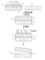
- ions are implanted from the surface 5 of the wide band gap semiconductor substrate 1 to form the ion implantation layer 2, and then a surface activation process is performed on each bonding surface. Then, the surface 5 of the wide band gap semiconductor substrate and the handle substrate 3 are bonded together to obtain a bonded body 6. Details of the ion implantation will be described later.
- a thickness of about 50nm on top of the wide bandgap substrate may be used those with a SiO 2 film. In that case, the effect that the bonding strength in a bonding process increases is acquired.
- Examples of the surface activation treatment include ozone water treatment, UV ozone treatment, ion beam treatment, and plasma treatment.
- the mechanism for increasing the binding force by surface activation has not been completely clarified, but can be explained as follows.
- ozone water treatment, UV ozone treatment, and the like activation is performed by decomposing organic substances on the surface with ozone and increasing OH groups on the surface.
- ion beam treatment and plasma treatment are activated by exposing highly reactive dangling bonds (dangling bonds) on the wafer surface or by adding OH groups to the dangling bonds. .
- the surface activation can be confirmed by looking at the degree of hydrophilicity (wetting).
- a wide band gap semiconductor substrate and / or handle substrate is placed in a chamber, a plasma gas is introduced under reduced pressure, and then exposed to a high frequency plasma of about 100 W for about 5 to 10 seconds. Is plasma treated.
- a plasma gas when processing a wide band gap semiconductor substrate, oxygen gas plasma is oxidized when meta is oxidized, hydrogen gas, argon gas, or a mixed gas thereof or hydrogen gas and helium when not oxidized.
- a gas mixture can be used. Any gas may be used when processing the handle substrate.
- organic substances on the surface of the wide band gap semiconductor substrate and / or handle substrate are oxidized and removed, and the OH groups on the surface are increased and activated.
- the four processes are more preferably performed on both the ion-implanted surface of the wide band gap semiconductor substrate and the bonding surface of the handle substrate, but only one of them may be performed.
- the obtained bonded body 6 is subjected to heat treatment at 150 ° C. or higher and 400 ° C. or lower.
- the reason for performing the heat treatment is to prevent the introduction of crystal defects due to a shift in the bonding interface 9 due to a rapid temperature rise when the bonding interface 9 becomes a high temperature by visible light irradiation in a subsequent process.
- the reason why the temperature is set to 150 ° C. or more and 400 ° C. or less is that the bonding strength may not be increased if the temperature is less than 150 ° C., and if the temperature exceeds 400 ° C., the bonded substrate may be damaged.
- an appropriate temperature when the handle substrate 3 is quartz or glass is 150 ° C.
- the heat treatment may be performed in two or more stages by changing the temperature within the appropriate temperature range.
- the heat treatment time is preferably 12 hours to 72 hours depending on the temperature to some extent.
- visible light refers to light having a maximum wavelength in a wavelength region of 450 to 700 nm, and a wavelength having a high transmittance of the wide band gap semiconductor substrate 1 is appropriately selected. Visible light may be either coherent light or incoherent light. Usually, in this wavelength range, the semiconductor substrate 1 is transparent and has a very low absorption coefficient.
- the hydrogen ion implantation site absorbs light in this wavelength range, the chemical reaction is accelerated inside, and as a result, the entire surface of the substrate is overheated. Therefore, embrittlement occurs at the interface of the ion implantation layer 2, and a part of the wide band gap semiconductor thin film 4 is transferred to the handle substrate 3, so that the bonded wafer 8 can be formed.
- lasers that can be used in the visible light wavelength region include a green laser with a wavelength of 532 nm and a red laser with a wavelength of 633 nm, which are used for crystallization of amorphous silicon for liquid crystal, and the second of Nd: YAG lasers.
- the irradiation method at this time is not particularly limited, but if the entire substrate is heated, the substrate is damaged by warpage, and therefore a method that can finish the process before the entire substrate is heated. desirable.
- the ion implantation of a wide band gap semiconductor substrate that can be irradiated from the semiconductor substrate 1 side but is bonded with light in the visible light region (wavelength 450 nm to 700 nm).
- the handle substrate is made of a substrate having a low energy loss and a transmittance of 70% or more in the visible light region until reaching the layer, for example, quartz, glass, sapphire, etc.
- FIG. It is also possible to irradiate from the handle substrate 3 side as shown in FIG.
- the handle substrate is made of an opaque material such as silicon, irradiation from the wide band gap semiconductor substrate 1 side is essential.
- the semiconductor substrate 1 Since most of the wavelength range of the visible light passes through the semiconductor substrate 1 and is absorbed only at the ion implantation location, the entire transparent substrate is not heated, and energy is given only to the location where the energy is required (ion implantation location). Can be an ideal way.
- the ion implantation site is sufficiently brittle, thin film transfer can be performed without imposing a burden on the substrate.
- the irradiation conditions of the laser when the oscillation frequency output 50 W ⁇ 100W use one of 25 mJ @ 3 kHz, the irradiation energy per unit area, is empirically 0.4J / cm 2 ⁇ 1.6J / cm 2 Is desirable. If it is less than 0.4 J / cm 2 , embrittlement at the ion implantation interface may not occur. If it exceeds 1.6 J / cm 2 , embrittlement may be too strong and the substrate may be damaged. is there. Irradiation scans a spot-like laser beam on the wafer, so it is difficult to define the time, but it is desirable that the irradiation energy after the treatment falls within the above range.
- RTA used in a semiconductor process or the like is also a useful method.
- RTA is capable of quickly raising and lowering the temperature from 50 ° C./second to 150 ° C./second, and is an excellent method that can complete the process before heating the entire substrate. In this case, it is important that only the vicinity of the ion implantation interface is heated to such an extent that thermal delamination does not occur. Since the heat source used for normal RTA is a halogen lamp, it is suitable as a visible light irradiation source.
- a xenon flash lamp can be applied as the visible light.
- irradiation may be performed through a wavelength filter that cuts light outside the visible light range.
- a filter that blocks a wavelength range other than the visible wavelength range that is transparent to the wide band gap substrate is also effective for process stabilization.
- a mechanical shock is applied to the end of the joined body 6 and the vicinity of the bonding surface 9 to obtain a xenon lamp. It is desirable that the thermal shock caused by light irradiation causes the ion implantation interface to break down from the mechanical shock starting point at the end to the entire bonded substrate.
- peeling may be performed by applying a mechanical impact to the interface of the ion implantation layer.
- a mechanical impact to the interface of the ion implantation layer for example, a jet of a fluid such as a gas or a liquid may be sprayed continuously or intermittently from the side surface of the wafer, or a peeling device may be used.
- the method is not particularly limited as long as mechanical peeling occurs.
- the peeling instrument is capable of applying a mechanical impact from the side surface of the hydrogen ion implanted layer of the joined body 6 that has been heat-treated at a temperature of 150 ° C.
- a scissor-shaped sharp tool or a device having a scissor-shaped sharp blade is plastic (for example, polyetheretherketone) or zirconia. Silicon, diamond, etc. can be used, and metal etc. can also be used because it does not stick to contamination. If you are particular about contamination, plastic may be used. A blade such as scissors may be used as a wedge-shaped sharp tool.
- ions are implanted from one surface 5 of the wide band gap semiconductor substrate 1 to form the ion implantation layer 2.
- a predetermined dose of hydrogen ions (H + ) or hydrogen molecular ions (H 2 + ) is implanted with an implantation energy that can form the ion implantation layer 2 at a desired depth from the surface.
- the implantation energy can be 50 to 100 keV.
- the dose of hydrogen ions (H + ) implanted into the wide band gap semiconductor substrate 1 is preferably 5.0 ⁇ 10 16 atoms / cm 2 to 3.0 ⁇ 10 17 atoms / cm 2 . If it is less than 5.0 ⁇ 10 16 atoms / cm 2 , the interface may not be embrittled. If it exceeds 2.0 ⁇ 10 17 atoms / cm 2 , bubbles are transferred during heat treatment after bonding. It may become defective. When hydrogen molecular ions (H 2 + ) are used as implanted ions, the dose is preferably 2.5 ⁇ 10 15 atoms / cm 2 to 1.5 ⁇ 10 17 atoms / cm 2 .
- the interface may not be embrittled. If it exceeds 1.0 ⁇ 10 17 atoms / cm 2 , bubbles are transferred during heat treatment after bonding. It may become defective. Further, if an insulating film such as a silicon oxide film of about several nm to 500 nm is formed on the surface of the wide band gap semiconductor substrate 1 in advance and hydrogen ions or hydrogen molecular ions are implanted therethrough, channeling of the implanted ions is performed. The effect of suppressing is acquired.
- the surface activation treatment include plasma treatment and ozone treatment.
- a gas for plasma when processing a wide band gap semiconductor substrate, when oxidizing the surface, plasma of oxygen gas, when not oxidizing, hydrogen gas, argon gas, or a mixed gas thereof or hydrogen gas and helium gas
- the mixed gas can be used. Any gas may be used when processing the handle substrate.
- organic substances on the surface of the wide band gap semiconductor substrate and / or handle substrate are oxidized and removed, and OH groups on the surface are increased and activated.
- the treatment is preferably performed on both the ion-implanted surface of the wide band gap semiconductor substrate and the bonding surface of the handle substrate, but only one of them may be performed.
- a wide bandgap semiconductor substrate and / or handle substrate cleaned by RCA cleaning or the like was placed in a chamber introduced with air, and a plasma gas such as nitrogen gas or argon gas was introduced. Then, the surface is subjected to ozone treatment by generating high-frequency plasma and converting atmospheric oxygen into ozone. Either or both of plasma treatment and ozone treatment can be performed.
- the bonded wafer obtained by the above-described bonded wafer manufacturing method is also included in the present invention.
- Application examples of the bonded wafer include a substrate for an electro-optical device such as a liquid crystal device, a power semiconductor or a short wavelength laser substrate, and the like.
- Example 1 H 2 + ions were implanted into a GaN substrate with a diameter of 50 mm at an acceleration voltage of 75 KeV and a dose of 1.35 ⁇ 10 17 atoms / cm 2 . Subsequently, a silicon substrate having a diameter of 50 mm serving as a handle substrate was prepared, and ozone water treatment, UV ozone treatment, ion beam treatment, and plasma activation treatment were performed on both substrates. Bonding was performed at room temperature, and after heat treatment at 250 degrees for 24 hours, irradiation was performed from the transparent GaN substrate side with a 532 nm laser. The irradiation energy is about 0.5 J / cm 2 .
- the GaN thin film could be transferred to the silicon substrate by lightly applying a mechanical shock to the bonding interface after irradiation. At this time, the transferred GaN had a thickness of 290 nm. This revealed that the quality of the transferred film does not depend on the type of activation.
- Example 2 H 2 + ions were implanted into a GaN substrate with a diameter of 50 mm at an acceleration voltage of 75 KeV and a dose of 1.35 ⁇ 10 17 atoms / cm 2 . Subsequently, a silicon substrate having a diameter of 50 mm serving as a handle substrate was prepared, and an ion beam activation process was performed on both substrates. Bonding was performed at room temperature, and heat treatment was performed at 250 degrees for 24 hours. A total of three similar substrates were prepared, and then visible light was irradiated from the transparent substrate side (quartz side) with a green laser (wavelength 532 nm), RTA, and flash lamp.
- a green laser wavelength 532 nm
- the laser irradiation conditions at this time were an output of 75 W and an oscillation frequency of 25 mJ @ 3 kHz.
- the entire surface of the substrate was irradiated so as to be 1.2 J / cm 2 .
- the temperature was arranged in the direction of observing the bonding interface from the GaN side with a pyrometer. At this time, the temperature near the bonding interface can be observed. The temperature was raised to 350 ° pyrometer at a heating rate of 5 ° C./second, and the power was cut as soon as it reached, and the substrate was cooled.
- irradiation was performed with a pulse width of 1 m (millisecond) second.
- the GaN thin film could be transferred to the silicon substrate by applying a light mechanical impact to the bonding interface after irradiation. At this time, the transferred GaN had a thickness of 750 nm. When three samples were visually observed, no significant difference was found. Thus, it has been found that the quality of the transferred film does not depend on the type of visible light irradiation.
- Comparative Example 1 H 2 + ions were implanted into a GaN substrate with a diameter of 50 mm at an acceleration voltage of 75 KeV and a dose of 1.35 ⁇ 10 17 atoms / cm 2 . Subsequently, a silicon substrate having a diameter of 50 mm serving as a handle substrate was prepared, and ion beam treatment was performed on both substrates. After bonding at 200 ° C. and heat treatment at 250 ° C. for 24 hours, irradiation was performed from the transparent GaN substrate side using a 532 nm laser on a 200 ° C. hot plate. The irradiation energy is about 0.5 J / cm 2 . The GaN thin film could be transferred to the silicon substrate by lightly applying a mechanical shock to the bonding interface after irradiation. At this time, the transferred GaN had a thickness of 290 nm.
- Comparative Example 2 H + ions were implanted into a GaN substrate having a diameter of 50 mm with an acceleration voltage of 75 KeV and a dose of 1.35 ⁇ 10 17 atoms / cm 2 . Subsequently, a silicon substrate having a diameter of 50 mm serving as a handle substrate was prepared, and ion beam treatment was performed on both substrates. After bonding at 200 ° C. and heat treatment at 250 ° C. for 24 hours, irradiation was performed from the transparent GaN substrate side using a 532 nm laser on a hot plate at 250 ° C. The irradiation energy is about 0.5 J / cm 2 .
- the GaN thin film could be transferred to the silicon substrate by lightly applying a mechanical shock to the bonding interface after irradiation. At this time, the transferred GaN had a thickness of 290 nm. From Comparative Examples 1 and 2, it is considered that the bonding temperature and the degree of freedom in temperature during irradiation are high.
- Example 3 H + ions were implanted into a ZnO substrate having a diameter of 50 mm at an acceleration voltage of 80 KeV and a dose of 9.5 ⁇ 10 16 atoms / cm 2 . Subsequently, a silicon substrate having a diameter of 50 mm serving as a handle substrate was prepared, and plasma activation treatment was performed on both substrates. After bonding at room temperature and heat treatment at 250 ° C. for 24 hours, irradiation was performed from the transparent ZnO substrate side with a Xe flash lamp. The pulse width was about 1 millisecond. The ZnO thin film could be transferred to the silicon substrate by lightly applying a mechanical impact to the bonded interface after irradiation. At this time, the transferred ZnO had a thickness of 550 nm.
- Example 4 H 2 + ions were implanted into a GaN substrate with a diameter of 50 mm at an acceleration voltage of 75 KeV and a dose of 1.35 ⁇ 10 17 atoms / cm 2 . Subsequently, a 50 mm diameter sapphire substrate serving as a handle substrate was prepared, and plasma activation treatment was performed on both substrates. Bonding was performed at room temperature, and after heat treatment at 150 ° C. for 24 hours and 250 ° C. for 24 hours, irradiation was performed from the sapphire substrate side with a Xe flash lamp. The pulse width was about 1 millisecond. After irradiation, the GaN thin film could be transferred to the sapphire substrate by applying a light mechanical shock to the bonding interface. At this time, the transferred GaN had a thickness of 290 nm.
Landscapes
- Engineering & Computer Science (AREA)
- Physics & Mathematics (AREA)
- Microelectronics & Electronic Packaging (AREA)
- General Physics & Mathematics (AREA)
- Manufacturing & Machinery (AREA)
- Computer Hardware Design (AREA)
- Condensed Matter Physics & Semiconductors (AREA)
- Power Engineering (AREA)
- High Energy & Nuclear Physics (AREA)
- Health & Medical Sciences (AREA)
- Toxicology (AREA)
- Recrystallisation Techniques (AREA)
- Pressure Welding/Diffusion-Bonding (AREA)
- Crystals, And After-Treatments Of Crystals (AREA)
Priority Applications (4)
| Application Number | Priority Date | Filing Date | Title |
|---|---|---|---|
| AU2009325425A AU2009325425B2 (en) | 2008-12-11 | 2009-12-10 | Method for manufacturing composite substrate on which wide bandgap semiconductor is laminated |
| EP09831939.5A EP2357660B1 (en) | 2008-12-11 | 2009-12-10 | Method for manufacturing composite substrate on which wide bandgap semiconductor is laminated |
| CN200980150180.9A CN102246267B (zh) | 2008-12-11 | 2009-12-10 | 层叠有宽带隙半导体的复合基板的制造方法 |
| US13/130,627 US8546245B2 (en) | 2008-12-11 | 2009-12-10 | Method for manufacturing composite substrate comprising wide bandgap semiconductor layer |
Applications Claiming Priority (4)
| Application Number | Priority Date | Filing Date | Title |
|---|---|---|---|
| JP2008315566 | 2008-12-11 | ||
| JP2008-315566 | 2008-12-11 | ||
| JP2009-278561 | 2009-12-08 | ||
| JP2009278561A JP5389627B2 (ja) | 2008-12-11 | 2009-12-08 | ワイドバンドギャップ半導体を積層した複合基板の製造方法 |
Publications (1)
| Publication Number | Publication Date |
|---|---|
| WO2010067835A1 true WO2010067835A1 (ja) | 2010-06-17 |
Family
ID=42242822
Family Applications (1)
| Application Number | Title | Priority Date | Filing Date |
|---|---|---|---|
| PCT/JP2009/070656 WO2010067835A1 (ja) | 2008-12-11 | 2009-12-10 | ワイドバンドギャップ半導体を積層した複合基板の製造方法 |
Country Status (8)
Cited By (3)
| Publication number | Priority date | Publication date | Assignee | Title |
|---|---|---|---|---|
| WO2011160950A1 (en) | 2010-06-24 | 2011-12-29 | Soitec | Method for preparing a substrate by implantation and irradiation |
| WO2013009222A1 (en) * | 2011-07-13 | 2013-01-17 | Yury Georgievich Shreter | Method of laser separation of the epitaxial film or of the epitaxial film layer from the growth substrate of the epitaxial semiconductor structure (variations) |
| JP2023501646A (ja) * | 2019-11-14 | 2023-01-18 | ファーウェイ デジタル パワー テクノロジーズ カンパニー リミテッド | 半導体基板、その製造方法、及び半導体装置 |
Families Citing this family (23)
| Publication number | Priority date | Publication date | Assignee | Title |
|---|---|---|---|---|
| JP5417399B2 (ja) | 2011-09-15 | 2014-02-12 | 信越化学工業株式会社 | 複合ウェーハの製造方法 |
| FR2984597B1 (fr) * | 2011-12-20 | 2016-07-29 | Commissariat Energie Atomique | Fabrication d’une structure souple par transfert de couches |
| JP5884585B2 (ja) * | 2012-03-21 | 2016-03-15 | 住友電気工業株式会社 | 炭化珪素半導体装置の製造方法 |
| JP5491680B1 (ja) * | 2012-07-18 | 2014-05-14 | 日本碍子株式会社 | 複合ウェハー及びその製法 |
| KR102104147B1 (ko) | 2012-07-25 | 2020-04-23 | 신에쓰 가가꾸 고교 가부시끼가이샤 | 하이브리드 기판의 제조 방법 및 하이브리드 기판 |
| WO2014104098A1 (ja) * | 2012-12-26 | 2014-07-03 | 日本碍子株式会社 | 複合基板、その製法及び弾性波デバイス |
| JP6347553B2 (ja) * | 2013-05-31 | 2018-06-27 | 日本碍子株式会社 | 複合基板用支持基板および複合基板 |
| JP6165127B2 (ja) * | 2014-12-22 | 2017-07-19 | 三菱重工工作機械株式会社 | 半導体装置及び半導体装置の製造方法 |
| JP6396852B2 (ja) * | 2015-06-02 | 2018-09-26 | 信越化学工業株式会社 | 酸化物単結晶薄膜を備えた複合ウェーハの製造方法 |
| JP6454606B2 (ja) * | 2015-06-02 | 2019-01-16 | 信越化学工業株式会社 | 酸化物単結晶薄膜を備えた複合ウェーハの製造方法 |
| JP6396853B2 (ja) | 2015-06-02 | 2018-09-26 | 信越化学工業株式会社 | 酸化物単結晶薄膜を備えた複合ウェーハの製造方法 |
| JP6396854B2 (ja) * | 2015-06-02 | 2018-09-26 | 信越化学工業株式会社 | 酸化物単結晶薄膜を備えた複合ウェーハの製造方法 |
| JP6632462B2 (ja) * | 2016-04-28 | 2020-01-22 | 信越化学工業株式会社 | 複合ウェーハの製造方法 |
| JP6387375B2 (ja) | 2016-07-19 | 2018-09-05 | 株式会社サイコックス | 半導体基板 |
| CN107785235A (zh) * | 2016-08-31 | 2018-03-09 | 沈阳硅基科技有限公司 | 一种在基板上制造薄膜的方法 |
| RU2699606C1 (ru) * | 2016-11-28 | 2019-09-06 | Федеральное государственное автономное образовательное учреждение высшего образования "Национальный исследовательский Нижегородский государственный университет им. Н.И. Лобачевского" | Способ ионно-лучевого синтеза нитрида галлия в кремнии |
| CN107326435A (zh) * | 2017-07-28 | 2017-11-07 | 西安交通大学 | 一种生长GaN的SiC衬底的剥离方法 |
| US10510532B1 (en) * | 2018-05-29 | 2019-12-17 | Industry-University Cooperation Foundation Hanyang University | Method for manufacturing gallium nitride substrate using the multi ion implantation |
| KR101969679B1 (ko) * | 2018-07-27 | 2019-04-16 | 한양대학교 산학협력단 | Soi 웨이퍼와 열처리 공정을 이용한 박막 형성 및 전사 방법 |
| CN111883651A (zh) * | 2020-07-23 | 2020-11-03 | 奥趋光电技术(杭州)有限公司 | 一种制备高质量氮化铝模板的方法 |
| EP4455375A1 (en) | 2021-12-21 | 2024-10-30 | Shin-Etsu Handotai Co., Ltd. | Nitride semiconductor substrate and method for manufacturing nitride semiconductor substrate |
| CN117476831B (zh) * | 2023-12-20 | 2024-03-19 | 青禾晶元(晋城)半导体材料有限公司 | Led外延片及其制备方法、led芯片及其制备方法 |
| US20250254943A1 (en) * | 2024-02-02 | 2025-08-07 | Wolfspeed, Inc. | Power Semiconductor Devices with Stacked Layers |
Citations (5)
| Publication number | Priority date | Publication date | Assignee | Title |
|---|---|---|---|---|
| JP2002033465A (ja) * | 2000-05-10 | 2002-01-31 | Ion Engineering Research Institute Corp | 半導体薄膜の形成方法 |
| JP2004140266A (ja) * | 2002-10-18 | 2004-05-13 | Ishikawajima Harima Heavy Ind Co Ltd | 薄膜層ウェハ製造方法、及び薄膜層ウェハ |
| JP2005252244A (ja) * | 2004-02-03 | 2005-09-15 | Ishikawajima Harima Heavy Ind Co Ltd | 半導体基板の製造方法 |
| JP2007019482A (ja) * | 2005-06-07 | 2007-01-25 | Fujifilm Holdings Corp | 機能性膜含有構造体、及び、機能性膜の製造方法 |
| JP2008277552A (ja) * | 2007-04-27 | 2008-11-13 | Shin Etsu Chem Co Ltd | 貼り合わせ基板の製造方法 |
Family Cites Families (10)
| Publication number | Priority date | Publication date | Assignee | Title |
|---|---|---|---|---|
| US6071795A (en) * | 1998-01-23 | 2000-06-06 | The Regents Of The University Of California | Separation of thin films from transparent substrates by selective optical processing |
| FR2817395B1 (fr) * | 2000-11-27 | 2003-10-31 | Soitec Silicon On Insulator | Procede de fabrication d'un substrat notamment pour l'optique, l'electronique ou l'optoelectronique et substrat obtenu par ce procede |
| US6562127B1 (en) * | 2002-01-16 | 2003-05-13 | The United States Of America As Represented By The Secretary Of The Navy | Method of making mosaic array of thin semiconductor material of large substrates |
| JP2003347176A (ja) * | 2002-03-20 | 2003-12-05 | Shin Etsu Handotai Co Ltd | 貼り合わせウェーハの製造方法 |
| EP1482548B1 (en) | 2003-05-26 | 2016-04-13 | Soitec | A method of manufacturing a wafer |
| JP5358159B2 (ja) | 2004-02-03 | 2013-12-04 | 株式会社半導体エネルギー研究所 | 半導体薄膜層を有する基板の製造方法 |
| WO2006082467A1 (en) | 2005-02-01 | 2006-08-10 | S.O.I.Tec Silicon On Insulator Technologies | Substrate for crystal growing a nitride semiconductor |
| EP1889289B1 (en) | 2005-06-07 | 2011-03-30 | FUJIFILM Corporation | Functional film containing structure and method of manufacturing functional film |
| JP5042506B2 (ja) * | 2006-02-16 | 2012-10-03 | 信越化学工業株式会社 | 半導体基板の製造方法 |
| JP5064695B2 (ja) * | 2006-02-16 | 2012-10-31 | 信越化学工業株式会社 | Soi基板の製造方法 |
-
2009
- 2009-12-08 JP JP2009278561A patent/JP5389627B2/ja active Active
- 2009-12-10 AU AU2009325425A patent/AU2009325425B2/en not_active Ceased
- 2009-12-10 EP EP09831939.5A patent/EP2357660B1/en active Active
- 2009-12-10 CN CN200980150180.9A patent/CN102246267B/zh active Active
- 2009-12-10 US US13/130,627 patent/US8546245B2/en active Active
- 2009-12-10 KR KR1020117012761A patent/KR101607725B1/ko active Active
- 2009-12-10 WO PCT/JP2009/070656 patent/WO2010067835A1/ja active Application Filing
- 2009-12-11 TW TW098142557A patent/TWI482198B/zh active
Patent Citations (5)
| Publication number | Priority date | Publication date | Assignee | Title |
|---|---|---|---|---|
| JP2002033465A (ja) * | 2000-05-10 | 2002-01-31 | Ion Engineering Research Institute Corp | 半導体薄膜の形成方法 |
| JP2004140266A (ja) * | 2002-10-18 | 2004-05-13 | Ishikawajima Harima Heavy Ind Co Ltd | 薄膜層ウェハ製造方法、及び薄膜層ウェハ |
| JP2005252244A (ja) * | 2004-02-03 | 2005-09-15 | Ishikawajima Harima Heavy Ind Co Ltd | 半導体基板の製造方法 |
| JP2007019482A (ja) * | 2005-06-07 | 2007-01-25 | Fujifilm Holdings Corp | 機能性膜含有構造体、及び、機能性膜の製造方法 |
| JP2008277552A (ja) * | 2007-04-27 | 2008-11-13 | Shin Etsu Chem Co Ltd | 貼り合わせ基板の製造方法 |
Cited By (11)
| Publication number | Priority date | Publication date | Assignee | Title |
|---|---|---|---|---|
| WO2011160950A1 (en) | 2010-06-24 | 2011-12-29 | Soitec | Method for preparing a substrate by implantation and irradiation |
| FR2961719A1 (fr) * | 2010-06-24 | 2011-12-30 | Soitec Silicon On Insulator | Procede de traitement d'une piece en un materiau compose |
| CN102986019A (zh) * | 2010-06-24 | 2013-03-20 | 索泰克公司 | 通过注入和照射制备衬底的方法 |
| JP2013533621A (ja) * | 2010-06-24 | 2013-08-22 | ソイテック | 注入および照射により基板を調製する方法 |
| US8759196B2 (en) | 2010-06-24 | 2014-06-24 | Soitec | Method for preparing a substrate by implantation and irradiation |
| KR101770678B1 (ko) * | 2010-06-24 | 2017-08-23 | 소이텍 | 주입 및 조사에 의해 기판을 제조하는 방법 |
| WO2013009222A1 (en) * | 2011-07-13 | 2013-01-17 | Yury Georgievich Shreter | Method of laser separation of the epitaxial film or of the epitaxial film layer from the growth substrate of the epitaxial semiconductor structure (variations) |
| US9337025B2 (en) | 2011-07-13 | 2016-05-10 | Yury Georgievich Shreter | Method of laser separation of the epitaxial film or of the epitaxial film layer from the growth substrate of the epitaxial semiconductor structure (variations) |
| US9966296B2 (en) | 2011-07-13 | 2018-05-08 | Yury Georgievich Shreter | Method of laser separation of the epitaxial film or the epitaxial film layer from the growth substrate of the epitaxial semiconductor structure (variations) |
| JP2023501646A (ja) * | 2019-11-14 | 2023-01-18 | ファーウェイ デジタル パワー テクノロジーズ カンパニー リミテッド | 半導体基板、その製造方法、及び半導体装置 |
| JP7416935B2 (ja) | 2019-11-14 | 2024-01-17 | ファーウェイ デジタル パワー テクノロジーズ カンパニー リミテッド | 半導体基板、その製造方法、及び半導体装置 |
Also Published As
| Publication number | Publication date |
|---|---|
| US8546245B2 (en) | 2013-10-01 |
| EP2357660B1 (en) | 2014-09-03 |
| TWI482198B (zh) | 2015-04-21 |
| KR20110099008A (ko) | 2011-09-05 |
| AU2009325425A1 (en) | 2010-06-17 |
| CN102246267A (zh) | 2011-11-16 |
| EP2357660A1 (en) | 2011-08-17 |
| US20110227068A1 (en) | 2011-09-22 |
| JP2010161355A (ja) | 2010-07-22 |
| CN102246267B (zh) | 2016-04-27 |
| AU2009325425B2 (en) | 2014-10-02 |
| TW201104726A (en) | 2011-02-01 |
| KR101607725B1 (ko) | 2016-03-30 |
| EP2357660A4 (en) | 2012-06-20 |
| JP5389627B2 (ja) | 2014-01-15 |
Similar Documents
| Publication | Publication Date | Title |
|---|---|---|
| JP5389627B2 (ja) | ワイドバンドギャップ半導体を積層した複合基板の製造方法 | |
| JP5455595B2 (ja) | 貼り合わせウェーハの製造方法 | |
| JP5420968B2 (ja) | 貼り合わせウェーハの製造方法 | |
| JP5496608B2 (ja) | Soi基板の作製方法 | |
| KR102599962B1 (ko) | 산화물 단결정 박막을 구비한 복합 웨이퍼의 제조 방법 | |
| KR102658526B1 (ko) | 산화물 단결정 박막을 구비한 복합 웨이퍼의 제조 방법 | |
| JP5643509B2 (ja) | 応力を低減したsos基板の製造方法 | |
| WO2010137588A1 (ja) | 界面近傍における欠陥密度が低いsos基板 | |
| WO2010137587A1 (ja) | 表面欠陥密度が少ないsos基板 | |
| JP5496540B2 (ja) | 半導体基板の作製方法 | |
| JP4594121B2 (ja) | Soiウエーハの製造方法及びsoiウエーハ |
Legal Events
| Date | Code | Title | Description |
|---|---|---|---|
| WWE | Wipo information: entry into national phase |
Ref document number: 200980150180.9 Country of ref document: CN |
|
| 121 | Ep: the epo has been informed by wipo that ep was designated in this application |
Ref document number: 09831939 Country of ref document: EP Kind code of ref document: A1 |
|
| WWE | Wipo information: entry into national phase |
Ref document number: 13130627 Country of ref document: US |
|
| WWE | Wipo information: entry into national phase |
Ref document number: 2009325425 Country of ref document: AU |
|
| ENP | Entry into the national phase |
Ref document number: 20117012761 Country of ref document: KR Kind code of ref document: A |
|
| WWE | Wipo information: entry into national phase |
Ref document number: 2009831939 Country of ref document: EP |
|
| NENP | Non-entry into the national phase |
Ref country code: DE |
|
| ENP | Entry into the national phase |
Ref document number: 2009325425 Country of ref document: AU Date of ref document: 20091210 Kind code of ref document: A |