JP6387375B2 - 半導体基板 - Google Patents
半導体基板 Download PDFInfo
- Publication number
- JP6387375B2 JP6387375B2 JP2016141782A JP2016141782A JP6387375B2 JP 6387375 B2 JP6387375 B2 JP 6387375B2 JP 2016141782 A JP2016141782 A JP 2016141782A JP 2016141782 A JP2016141782 A JP 2016141782A JP 6387375 B2 JP6387375 B2 JP 6387375B2
- Authority
- JP
- Japan
- Prior art keywords
- interface
- single crystal
- sic
- atoms
- layer
- Prior art date
- Legal status (The legal status is an assumption and is not a legal conclusion. Google has not performed a legal analysis and makes no representation as to the accuracy of the status listed.)
- Active
Links
- 239000000758 substrate Substances 0.000 title claims description 109
- 239000004065 semiconductor Substances 0.000 title claims description 23
- IJGRMHOSHXDMSA-UHFFFAOYSA-N Atomic nitrogen Chemical compound N#N IJGRMHOSHXDMSA-UHFFFAOYSA-N 0.000 claims description 114
- 239000013078 crystal Substances 0.000 claims description 93
- 125000004429 atom Chemical group 0.000 claims description 64
- 229910052757 nitrogen Inorganic materials 0.000 claims description 61
- 229910052710 silicon Inorganic materials 0.000 claims description 31
- XUIMIQQOPSSXEZ-UHFFFAOYSA-N Silicon Chemical compound [Si] XUIMIQQOPSSXEZ-UHFFFAOYSA-N 0.000 claims description 30
- 229910052799 carbon Inorganic materials 0.000 claims description 30
- OKTJSMMVPCPJKN-UHFFFAOYSA-N Carbon Chemical compound [C] OKTJSMMVPCPJKN-UHFFFAOYSA-N 0.000 claims description 28
- 239000010703 silicon Substances 0.000 claims description 28
- 239000002131 composite material Substances 0.000 claims description 19
- 239000000203 mixture Substances 0.000 claims description 19
- OAICVXFJPJFONN-UHFFFAOYSA-N Phosphorus Chemical compound [P] OAICVXFJPJFONN-UHFFFAOYSA-N 0.000 claims description 8
- 229910052698 phosphorus Inorganic materials 0.000 claims description 8
- 239000011574 phosphorus Substances 0.000 claims description 8
- 125000004432 carbon atom Chemical group C* 0.000 claims 2
- 239000010410 layer Substances 0.000 description 98
- 229910010271 silicon carbide Inorganic materials 0.000 description 69
- HBMJWWWQQXIZIP-UHFFFAOYSA-N silicon carbide Chemical compound [Si+]#[C-] HBMJWWWQQXIZIP-UHFFFAOYSA-N 0.000 description 50
- 238000000034 method Methods 0.000 description 32
- 230000008569 process Effects 0.000 description 18
- 238000010586 diagram Methods 0.000 description 12
- 238000010438 heat treatment Methods 0.000 description 9
- 238000004519 manufacturing process Methods 0.000 description 9
- 125000004433 nitrogen atom Chemical group N* 0.000 description 9
- 238000005036 potential barrier Methods 0.000 description 7
- 230000007547 defect Effects 0.000 description 6
- 239000001257 hydrogen Substances 0.000 description 6
- 229910052739 hydrogen Inorganic materials 0.000 description 6
- 230000008859 change Effects 0.000 description 5
- 230000000694 effects Effects 0.000 description 5
- 230000005641 tunneling Effects 0.000 description 5
- XKRFYHLGVUSROY-UHFFFAOYSA-N Argon Chemical compound [Ar] XKRFYHLGVUSROY-UHFFFAOYSA-N 0.000 description 4
- 239000012535 impurity Substances 0.000 description 4
- 239000000463 material Substances 0.000 description 4
- 230000007246 mechanism Effects 0.000 description 4
- 239000000126 substance Substances 0.000 description 4
- UFHFLCQGNIYNRP-UHFFFAOYSA-N Hydrogen Chemical compound [H][H] UFHFLCQGNIYNRP-UHFFFAOYSA-N 0.000 description 3
- 238000004458 analytical method Methods 0.000 description 3
- 239000000969 carrier Substances 0.000 description 3
- -1 hydrogen ions Chemical class 0.000 description 3
- 238000002347 injection Methods 0.000 description 3
- 239000007924 injection Substances 0.000 description 3
- 238000005468 ion implantation Methods 0.000 description 3
- 238000005259 measurement Methods 0.000 description 3
- 230000007935 neutral effect Effects 0.000 description 3
- ZOXJGFHDIHLPTG-UHFFFAOYSA-N Boron Chemical compound [B] ZOXJGFHDIHLPTG-UHFFFAOYSA-N 0.000 description 2
- XAGFODPZIPBFFR-UHFFFAOYSA-N aluminium Chemical compound [Al] XAGFODPZIPBFFR-UHFFFAOYSA-N 0.000 description 2
- 229910052782 aluminium Inorganic materials 0.000 description 2
- 229910052786 argon Inorganic materials 0.000 description 2
- 230000004888 barrier function Effects 0.000 description 2
- 229910052796 boron Inorganic materials 0.000 description 2
- 150000001875 compounds Chemical class 0.000 description 2
- 230000007423 decrease Effects 0.000 description 2
- 238000002149 energy-dispersive X-ray emission spectroscopy Methods 0.000 description 2
- 238000005516 engineering process Methods 0.000 description 2
- 239000007789 gas Substances 0.000 description 2
- 238000002513 implantation Methods 0.000 description 2
- 238000005304 joining Methods 0.000 description 2
- 230000004048 modification Effects 0.000 description 2
- 238000012986 modification Methods 0.000 description 2
- 229910002601 GaN Inorganic materials 0.000 description 1
- 229910052581 Si3N4 Inorganic materials 0.000 description 1
- 238000002679 ablation Methods 0.000 description 1
- 230000001133 acceleration Effects 0.000 description 1
- 230000003213 activating effect Effects 0.000 description 1
- 229910052785 arsenic Inorganic materials 0.000 description 1
- RQNWIZPPADIBDY-UHFFFAOYSA-N arsenic atom Chemical compound [As] RQNWIZPPADIBDY-UHFFFAOYSA-N 0.000 description 1
- 230000015572 biosynthetic process Effects 0.000 description 1
- 239000002800 charge carrier Substances 0.000 description 1
- 238000004140 cleaning Methods 0.000 description 1
- 230000000052 comparative effect Effects 0.000 description 1
- 238000005520 cutting process Methods 0.000 description 1
- 230000003247 decreasing effect Effects 0.000 description 1
- 238000009792 diffusion process Methods 0.000 description 1
- 238000002474 experimental method Methods 0.000 description 1
- 125000004435 hydrogen atom Chemical group [H]* 0.000 description 1
- GPRLSGONYQIRFK-UHFFFAOYSA-N hydron Chemical compound [H+] GPRLSGONYQIRFK-UHFFFAOYSA-N 0.000 description 1
- 150000002500 ions Chemical class 0.000 description 1
- 229910021421 monocrystalline silicon Inorganic materials 0.000 description 1
- 230000000737 periodic effect Effects 0.000 description 1
- 229910021420 polycrystalline silicon Inorganic materials 0.000 description 1
- 238000012805 post-processing Methods 0.000 description 1
- 239000010453 quartz Substances 0.000 description 1
- 229910052594 sapphire Inorganic materials 0.000 description 1
- 239000010980 sapphire Substances 0.000 description 1
- 238000000926 separation method Methods 0.000 description 1
- VYPSYNLAJGMNEJ-UHFFFAOYSA-N silicon dioxide Inorganic materials O=[Si]=O VYPSYNLAJGMNEJ-UHFFFAOYSA-N 0.000 description 1
- HQVNEWCFYHHQES-UHFFFAOYSA-N silicon nitride Chemical compound N12[Si]34N5[Si]62N3[Si]51N64 HQVNEWCFYHHQES-UHFFFAOYSA-N 0.000 description 1
- 238000001179 sorption measurement Methods 0.000 description 1
- 239000002344 surface layer Substances 0.000 description 1
- 230000007704 transition Effects 0.000 description 1
- 238000003949 trap density measurement Methods 0.000 description 1
Images


Classifications
-
- H—ELECTRICITY
- H01—ELECTRIC ELEMENTS
- H01L—SEMICONDUCTOR DEVICES NOT COVERED BY CLASS H10
- H01L21/00—Processes or apparatus adapted for the manufacture or treatment of semiconductor or solid state devices or of parts thereof
- H01L21/02—Manufacture or treatment of semiconductor devices or of parts thereof
- H01L21/04—Manufacture or treatment of semiconductor devices or of parts thereof the devices having at least one potential-jump barrier or surface barrier, e.g. PN junction, depletion layer or carrier concentration layer
- H01L21/18—Manufacture or treatment of semiconductor devices or of parts thereof the devices having at least one potential-jump barrier or surface barrier, e.g. PN junction, depletion layer or carrier concentration layer the devices having semiconductor bodies comprising elements of Group IV of the Periodic System or AIIIBV compounds with or without impurities, e.g. doping materials
- H01L21/185—Joining of semiconductor bodies for junction formation
- H01L21/187—Joining of semiconductor bodies for junction formation by direct bonding
-
- H—ELECTRICITY
- H01—ELECTRIC ELEMENTS
- H01L—SEMICONDUCTOR DEVICES NOT COVERED BY CLASS H10
- H01L21/00—Processes or apparatus adapted for the manufacture or treatment of semiconductor or solid state devices or of parts thereof
- H01L21/02—Manufacture or treatment of semiconductor devices or of parts thereof
- H01L21/04—Manufacture or treatment of semiconductor devices or of parts thereof the devices having at least one potential-jump barrier or surface barrier, e.g. PN junction, depletion layer or carrier concentration layer
- H01L21/18—Manufacture or treatment of semiconductor devices or of parts thereof the devices having at least one potential-jump barrier or surface barrier, e.g. PN junction, depletion layer or carrier concentration layer the devices having semiconductor bodies comprising elements of Group IV of the Periodic System or AIIIBV compounds with or without impurities, e.g. doping materials
- H01L21/185—Joining of semiconductor bodies for junction formation
-
- H—ELECTRICITY
- H01—ELECTRIC ELEMENTS
- H01L—SEMICONDUCTOR DEVICES NOT COVERED BY CLASS H10
- H01L29/00—Semiconductor devices adapted for rectifying, amplifying, oscillating or switching, or capacitors or resistors with at least one potential-jump barrier or surface barrier, e.g. PN junction depletion layer or carrier concentration layer; Details of semiconductor bodies or of electrodes thereof ; Multistep manufacturing processes therefor
- H01L29/02—Semiconductor bodies ; Multistep manufacturing processes therefor
- H01L29/12—Semiconductor bodies ; Multistep manufacturing processes therefor characterised by the materials of which they are formed
- H01L29/16—Semiconductor bodies ; Multistep manufacturing processes therefor characterised by the materials of which they are formed including, apart from doping materials or other impurities, only elements of Group IV of the Periodic System
- H01L29/1608—Silicon carbide
-
- H—ELECTRICITY
- H01—ELECTRIC ELEMENTS
- H01L—SEMICONDUCTOR DEVICES NOT COVERED BY CLASS H10
- H01L21/00—Processes or apparatus adapted for the manufacture or treatment of semiconductor or solid state devices or of parts thereof
- H01L21/02—Manufacture or treatment of semiconductor devices or of parts thereof
- H01L21/02002—Preparing wafers
-
- H—ELECTRICITY
- H01—ELECTRIC ELEMENTS
- H01L—SEMICONDUCTOR DEVICES NOT COVERED BY CLASS H10
- H01L21/00—Processes or apparatus adapted for the manufacture or treatment of semiconductor or solid state devices or of parts thereof
- H01L21/02—Manufacture or treatment of semiconductor devices or of parts thereof
- H01L21/02104—Forming layers
- H01L21/02365—Forming inorganic semiconducting materials on a substrate
- H01L21/02367—Substrates
- H01L21/0237—Materials
- H01L21/02373—Group 14 semiconducting materials
- H01L21/02378—Silicon carbide
-
- H—ELECTRICITY
- H01—ELECTRIC ELEMENTS
- H01L—SEMICONDUCTOR DEVICES NOT COVERED BY CLASS H10
- H01L21/00—Processes or apparatus adapted for the manufacture or treatment of semiconductor or solid state devices or of parts thereof
- H01L21/02—Manufacture or treatment of semiconductor devices or of parts thereof
- H01L21/02104—Forming layers
- H01L21/02365—Forming inorganic semiconducting materials on a substrate
- H01L21/02518—Deposited layers
- H01L21/02587—Structure
- H01L21/0259—Microstructure
- H01L21/02595—Microstructure polycrystalline
-
- H—ELECTRICITY
- H01—ELECTRIC ELEMENTS
- H01L—SEMICONDUCTOR DEVICES NOT COVERED BY CLASS H10
- H01L21/00—Processes or apparatus adapted for the manufacture or treatment of semiconductor or solid state devices or of parts thereof
- H01L21/02—Manufacture or treatment of semiconductor devices or of parts thereof
- H01L21/02104—Forming layers
- H01L21/02365—Forming inorganic semiconducting materials on a substrate
- H01L21/02518—Deposited layers
- H01L21/02587—Structure
- H01L21/0259—Microstructure
- H01L21/02598—Microstructure monocrystalline
-
- H—ELECTRICITY
- H01—ELECTRIC ELEMENTS
- H01L—SEMICONDUCTOR DEVICES NOT COVERED BY CLASS H10
- H01L29/00—Semiconductor devices adapted for rectifying, amplifying, oscillating or switching, or capacitors or resistors with at least one potential-jump barrier or surface barrier, e.g. PN junction depletion layer or carrier concentration layer; Details of semiconductor bodies or of electrodes thereof ; Multistep manufacturing processes therefor
- H01L29/02—Semiconductor bodies ; Multistep manufacturing processes therefor
- H01L29/04—Semiconductor bodies ; Multistep manufacturing processes therefor characterised by their crystalline structure, e.g. polycrystalline, cubic or particular orientation of crystalline planes
-
- H—ELECTRICITY
- H01—ELECTRIC ELEMENTS
- H01L—SEMICONDUCTOR DEVICES NOT COVERED BY CLASS H10
- H01L2924/00—Indexing scheme for arrangements or methods for connecting or disconnecting semiconductor or solid-state bodies as covered by H01L24/00
- H01L2924/01—Chemical elements
- H01L2924/01006—Carbon [C]
-
- H—ELECTRICITY
- H01—ELECTRIC ELEMENTS
- H01L—SEMICONDUCTOR DEVICES NOT COVERED BY CLASS H10
- H01L2924/00—Indexing scheme for arrangements or methods for connecting or disconnecting semiconductor or solid-state bodies as covered by H01L24/00
- H01L2924/01—Chemical elements
- H01L2924/01007—Nitrogen [N]
-
- H—ELECTRICITY
- H01—ELECTRIC ELEMENTS
- H01L—SEMICONDUCTOR DEVICES NOT COVERED BY CLASS H10
- H01L2924/00—Indexing scheme for arrangements or methods for connecting or disconnecting semiconductor or solid-state bodies as covered by H01L24/00
- H01L2924/01—Chemical elements
- H01L2924/01014—Silicon [Si]
-
- H—ELECTRICITY
- H01—ELECTRIC ELEMENTS
- H01L—SEMICONDUCTOR DEVICES NOT COVERED BY CLASS H10
- H01L2924/00—Indexing scheme for arrangements or methods for connecting or disconnecting semiconductor or solid-state bodies as covered by H01L24/00
- H01L2924/01—Chemical elements
- H01L2924/01015—Phosphorus [P]
Landscapes
- Engineering & Computer Science (AREA)
- Microelectronics & Electronic Packaging (AREA)
- Power Engineering (AREA)
- Condensed Matter Physics & Semiconductors (AREA)
- General Physics & Mathematics (AREA)
- Physics & Mathematics (AREA)
- Computer Hardware Design (AREA)
- Manufacturing & Machinery (AREA)
- Chemical & Material Sciences (AREA)
- Crystallography & Structural Chemistry (AREA)
- Ceramic Engineering (AREA)
- Materials Engineering (AREA)
- Recrystallisation Techniques (AREA)
- Crystals, And After-Treatments Of Crystals (AREA)
Description
界面層の厚さは0.25ナノメートル以上であってもよい。
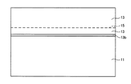
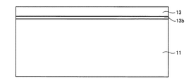
図2に、本実施例に係る接合基板10の斜視図を示す。接合基板10は略円盤状に形成されている。接合基板10は、下側に配置された支持基板11と、支持基板11の上面に貼り合わされた単結晶層13とを備えている。単結晶層13は、例えば、化合物半導体(例:6H−SiC、4H−SiC、GaN、AlN)の単結晶によって形成されていてもよい。また例えば、単元素半導体(例:Si、C)の単結晶によって形成されていてもよい。
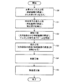
本実施例に係る接合基板10の製造方法を、図1〜図8を用いて説明する。本実施例では、例として、支持基板11が多結晶3C−SiCであり、単結晶層13が単結晶4H−SiCである場合を説明する。また、本明細書に記載の製造フローを、水素原子のアブレーションによる剥離技術を用いて実施する場合を説明する。
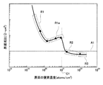
なお、SiCの原子密度は、9.6×10²²(atoms/cm3)程度であるため、1×1021(atoms/cm3)の窒素濃度は、1(atomic%)の窒素原子の比率に対応する。また、1×1022(atoms/cm3)の窒素濃度は、10(atomic%)の窒素原子の比率に対応する。
ステップS1で窒素の導入量を変化させた場合における界面抵抗の変化を、図9を用いて説明する。測定対象は、本明細書に記載の接合方法により接合された、4H−SiCの単結晶層13および多結晶3C−SiCの支持基板11である。図9において、縦軸は界面抵抗(Ω・cm2)である。横軸は、単結晶層13と支持基板11の界面における窒素濃度(atoms/cm3)である。また、目標とする界面抵抗値を、目標抵抗値A1と定義している。
また、TEMを用いて、界面層13cの厚さを測定した。ステップS1で導入される窒素の量を変化させた場合における、界面層13cの厚さの変化を測定した。界面層13cの窒素濃度が1×10²²(atoms/cm3)である場合には、界面層13cの厚さは3.6〜3.9(ナノメートル)程度であった。なお、界面層13cの厚さを決定するパラメータは、窒素の導入量に限られず、多数存在する。例えば、窒素を導入する際のエネルギー量によっても、界面層13cの厚さは変化する。従って、上記の界面層13cの厚さは、一例である。
本明細書に記載されている接合方法で作成された接合基板10の、界面層13cにおける、窒素濃度プロファイルを分析した。分析に用いられた接合基板10は、多結晶3C−SiCの支持基板11と4H−SiCの単結晶層13とを、界面層13cを介して接合させた基板である。また、界面層13cの窒素濃度が1×10²²(atoms/cm3)である場合の窒素濃度プロファイルを分析した。 界面層13cの厚さは3.6〜3.9ナノメートルの範囲内であった。
多結晶3C−SiCの支持基板11と4H−SiCの単結晶層13とを、界面層13cを介して接合させることができる。界面層13cは、通常用いられる条件を超えて窒素が過剰に導入されていることで、化学組成が、炭化ケイ素(SiC)から、炭素、シリコンおよび窒素を含んだ複合材料へ変化している層である。また、結晶構造が、SiCから変化している層である。これにより、多結晶3C−SiCの支持基板11と、4H−SiCの単結晶層13とを直接に接合させる場合に比して、界面抵抗を小さくすることができる。
以上、本発明の実施例について詳細に説明したが、これらは例示に過ぎず、特許請求の範囲を限定するものではない。特許請求の範囲に記載の技術には、以上に例示した具体例を様々に変形、変更したものが含まれる。
Claims (11)
- 単結晶SiC基板と、多結晶SiC基板と、を備える半導体基板であって、
前記単結晶SiC基板と前記多結晶SiC基板とが界面層を介して接合しており、
前記界面層は炭素およびシリコンを含んだ複合材料であり、
前記界面層は、1×10²¹(atoms/cm3)以上のシリコン(Si)原子を含んでおり、
前記複合材料の元素の組成比において、シリコンの割合が炭素よりも多いことを特徴とする半導体基板。 - 単結晶SiC基板と、多結晶SiC基板と、を備える半導体基板であって、
前記単結晶SiC基板と前記多結晶SiC基板とが界面層を介して接合しており、
前記界面層は炭素およびシリコンを含んだ複合材料であり、
前記界面層は、1×10²¹(atoms/cm3)以上の炭素(C)原子を含んでおり、
前記複合材料の元素の組成比において、炭素の割合がシリコンよりも多いことを特徴とする半導体基板。 - 前記界面層の厚さは0.25ナノメートル以上であることを特徴とする請求項1または2に記載の半導体基板。
- 前記界面層は炭素、シリコンおよび窒素を含んだ複合材料であることを特徴とする請求項1〜3の何れか1項に記載の半導体基板。
- 前記界面層は、炭素、シリコンおよびリンを含んだ複合材料であることを特徴とする請求項1〜4の何れか1項に記載の半導体基板。
- 前記界面層は1×10²²(atoms/cm3)以上の前記シリコン原子を含んでいることを特徴とする請求項1に記載の半導体基板。
- 前記界面層の元素の組成比において、前記シリコン原子の比率は10(atomic%)以上であることを特徴とする請求項1または6に記載の半導体基板。
- 前記界面層は1×10²²(atoms/cm3)以上の前記炭素原子を含んでいることを特徴とする請求項2に記載の半導体基板。
- 前記界面層の元素の組成比において、前記炭素原子の比率は10(atomic%)以上であることを特徴とする請求項2または8に記載の半導体基板。
- 前記単結晶SiC基板は、4H−SiCであることを特徴とする請求項1〜9の何れか1項に記載の半導体基板。
- 前記多結晶SiC基板は、3C−SiCであることを特徴とする請求項1〜10の何れか1項に記載の半導体基板。
Priority Applications (6)
| Application Number | Priority Date | Filing Date | Title |
|---|---|---|---|
| JP2016141782A JP6387375B2 (ja) | 2016-07-19 | 2016-07-19 | 半導体基板 |
| KR1020197004382A KR102035122B1 (ko) | 2016-07-19 | 2017-07-13 | 반도체 기판 |
| PCT/JP2017/025600 WO2018016417A1 (ja) | 2016-07-19 | 2017-07-13 | 半導体基板 |
| EP17830936.5A EP3489990B1 (en) | 2016-07-19 | 2017-07-13 | Semiconductor substrate |
| CN201780044382.XA CN109478495B (zh) | 2016-07-19 | 2017-07-13 | 半导体基板 |
| US16/319,053 US10680068B2 (en) | 2016-07-19 | 2017-07-13 | Semiconductor substrate |
Applications Claiming Priority (1)
| Application Number | Priority Date | Filing Date | Title |
|---|---|---|---|
| JP2016141782A JP6387375B2 (ja) | 2016-07-19 | 2016-07-19 | 半導体基板 |
Publications (3)
| Publication Number | Publication Date |
|---|---|
| JP2018014372A JP2018014372A (ja) | 2018-01-25 |
| JP2018014372A5 JP2018014372A5 (ja) | 2018-03-08 |
| JP6387375B2 true JP6387375B2 (ja) | 2018-09-05 |
Family
ID=60992092
Family Applications (1)
| Application Number | Title | Priority Date | Filing Date |
|---|---|---|---|
| JP2016141782A Active JP6387375B2 (ja) | 2016-07-19 | 2016-07-19 | 半導体基板 |
Country Status (6)
| Country | Link |
|---|---|
| US (1) | US10680068B2 (ja) |
| EP (1) | EP3489990B1 (ja) |
| JP (1) | JP6387375B2 (ja) |
| KR (1) | KR102035122B1 (ja) |
| CN (1) | CN109478495B (ja) |
| WO (1) | WO2018016417A1 (ja) |
Cited By (3)
| Publication number | Priority date | Publication date | Assignee | Title |
|---|---|---|---|---|
| WO2021060516A1 (ja) | 2019-09-27 | 2021-04-01 | 東海カーボン株式会社 | 多結晶SiC成形体 |
| WO2021060518A1 (ja) | 2019-09-27 | 2021-04-01 | 東海カーボン株式会社 | 多結晶SiC成形体 |
| WO2021060515A1 (ja) | 2019-09-27 | 2021-04-01 | 東海カーボン株式会社 | 多結晶SiC成形体及びその製造方法 |
Families Citing this family (8)
| Publication number | Priority date | Publication date | Assignee | Title |
|---|---|---|---|---|
| WO2021092862A1 (zh) * | 2019-11-14 | 2021-05-20 | 华为技术有限公司 | 半导体衬底及其制造方法、半导体器件 |
| JP7400389B2 (ja) * | 2019-11-21 | 2023-12-19 | 住友金属鉱山株式会社 | 炭化珪素多結晶膜、炭化珪素多結晶膜の製造方法および炭化珪素多結晶膜の成膜装置 |
| FR3123759B1 (fr) * | 2021-06-03 | 2023-06-23 | Soitec Silicon On Insulator | Procede de fabrication d’une structure semi-conductrice comprenant une couche utile en carbure de silicium aux proprietes electriques ameliorees |
| CN113658849A (zh) * | 2021-07-06 | 2021-11-16 | 华为技术有限公司 | 复合衬底及其制备方法、半导体器件、电子设备 |
| FR3130296B1 (fr) * | 2021-12-14 | 2023-11-03 | Soitec Silicon On Insulator | Procede de fabrication d’une structure semi-conductrice comprenant un substrat de carbure de silicium polycristallin et une couche active de carbure de silicium monocristallin |
| CN114864529A (zh) * | 2022-05-18 | 2022-08-05 | 北京青禾晶元半导体科技有限责任公司 | 一种碳化硅复合基板及其制造方法与应用 |
| JP2024025064A (ja) * | 2022-08-10 | 2024-02-26 | 株式会社サイコックス | SiC単結晶転写用複合基板、SiC単結晶転写用複合基板の製造方法、およびSiC接合基板の製造方法 |
| JP7359399B1 (ja) * | 2022-08-29 | 2023-10-11 | 株式会社サイコックス | 半導体基板および半導体基板の製造方法 |
Family Cites Families (18)
| Publication number | Priority date | Publication date | Assignee | Title |
|---|---|---|---|---|
| US6328796B1 (en) * | 1999-02-01 | 2001-12-11 | The United States Of America As Represented By The Secretary Of The Navy | Single-crystal material on non-single-crystalline substrate |
| US6563133B1 (en) | 2000-08-09 | 2003-05-13 | Ziptronix, Inc. | Method of epitaxial-like wafer bonding at low temperature and bonded structure |
| EP1901345A1 (en) * | 2006-08-30 | 2008-03-19 | Siltronic AG | Multilayered semiconductor wafer and process for manufacturing the same |
| JP4906451B2 (ja) * | 2006-09-15 | 2012-03-28 | コバレントマテリアル株式会社 | SiC焼結体の接合体、SiC焼結体の接合体の接合方法 |
| JP5213096B2 (ja) | 2007-03-23 | 2013-06-19 | 学校法人関西学院 | 単結晶炭化ケイ素の液相エピタキシャル成長方法、単結晶炭化ケイ素基板の製造方法、及び単結晶炭化ケイ素基板 |
| JP5446148B2 (ja) | 2008-07-02 | 2014-03-19 | 富士電機株式会社 | 炭化珪素半導体装置の製造方法 |
| JP5455595B2 (ja) | 2008-12-11 | 2014-03-26 | 信越化学工業株式会社 | 貼り合わせウェーハの製造方法 |
| JP5389627B2 (ja) | 2008-12-11 | 2014-01-15 | 信越化学工業株式会社 | ワイドバンドギャップ半導体を積層した複合基板の製造方法 |
| JP5420968B2 (ja) | 2009-05-07 | 2014-02-19 | 信越化学工業株式会社 | 貼り合わせウェーハの製造方法 |
| JP5464544B2 (ja) * | 2009-05-12 | 2014-04-09 | 学校法人関西学院 | エピタキシャル成長層付き単結晶SiC基板、炭素供給フィード基板、及び炭素ナノ材料付きSiC基板 |
| EP2490247A1 (en) * | 2009-10-13 | 2012-08-22 | Sumitomo Electric Industries, Ltd. | Silicon carbide substrate manufacturing method and silicon carbide substrate |
| JPWO2011052320A1 (ja) * | 2009-10-30 | 2013-03-14 | 住友電気工業株式会社 | 炭化珪素基板の製造方法および炭化珪素基板 |
| JP5540349B2 (ja) | 2009-12-02 | 2014-07-02 | 学校法人関西学院 | 半導体ウエハの製造方法 |
| JP5624777B2 (ja) | 2010-03-05 | 2014-11-12 | 昭和電工株式会社 | 炭化珪素種結晶の固定方法及び炭化珪素単結晶の製造方法 |
| JP2011246315A (ja) * | 2010-05-28 | 2011-12-08 | Sumitomo Electric Ind Ltd | 炭化珪素基板およびその製造方法 |
| JP5477302B2 (ja) | 2011-01-06 | 2014-04-23 | 株式会社デンソー | 炭化珪素半導体基板の製造方法および炭化珪素半導体装置の製造方法 |
| JP6156252B2 (ja) * | 2014-05-16 | 2017-07-05 | 株式会社豊田自動織機 | 半導体基板の製造方法および半導体基板 |
| CN106489187B (zh) * | 2014-07-10 | 2019-10-25 | 株式会社希克斯 | 半导体基板和半导体基板的制造方法 |
-
2016
- 2016-07-19 JP JP2016141782A patent/JP6387375B2/ja active Active
-
2017
- 2017-07-13 KR KR1020197004382A patent/KR102035122B1/ko active IP Right Grant
- 2017-07-13 WO PCT/JP2017/025600 patent/WO2018016417A1/ja unknown
- 2017-07-13 CN CN201780044382.XA patent/CN109478495B/zh active Active
- 2017-07-13 EP EP17830936.5A patent/EP3489990B1/en active Active
- 2017-07-13 US US16/319,053 patent/US10680068B2/en active Active
Cited By (5)
| Publication number | Priority date | Publication date | Assignee | Title |
|---|---|---|---|---|
| WO2021060516A1 (ja) | 2019-09-27 | 2021-04-01 | 東海カーボン株式会社 | 多結晶SiC成形体 |
| WO2021060518A1 (ja) | 2019-09-27 | 2021-04-01 | 東海カーボン株式会社 | 多結晶SiC成形体 |
| WO2021060515A1 (ja) | 2019-09-27 | 2021-04-01 | 東海カーボン株式会社 | 多結晶SiC成形体及びその製造方法 |
| KR20220068992A (ko) | 2019-09-27 | 2022-05-26 | 도까이 카본 가부시끼가이샤 | 다결정 SiC 성형체 및 그 제조 방법 |
| KR20220074864A (ko) | 2019-09-27 | 2022-06-03 | 도까이 카본 가부시끼가이샤 | 다결정 SiC 성형체 |
Also Published As
| Publication number | Publication date |
|---|---|
| CN109478495B (zh) | 2020-10-02 |
| EP3489990B1 (en) | 2021-05-26 |
| US10680068B2 (en) | 2020-06-09 |
| CN109478495A (zh) | 2019-03-15 |
| US20200006493A1 (en) | 2020-01-02 |
| EP3489990A1 (en) | 2019-05-29 |
| KR20190021475A (ko) | 2019-03-05 |
| KR102035122B1 (ko) | 2019-10-22 |
| JP2018014372A (ja) | 2018-01-25 |
| EP3489990A4 (en) | 2020-01-15 |
| WO2018016417A1 (ja) | 2018-01-25 |
Similar Documents
| Publication | Publication Date | Title |
|---|---|---|
| JP6387375B2 (ja) | 半導体基板 | |
| EP3168862B1 (en) | Semiconductor substrate and semiconductor substrate production method | |
| JP2009088223A (ja) | 炭化珪素半導体基板およびそれを用いた炭化珪素半導体装置 | |
| JP5011493B2 (ja) | 炭化珪素半導体素子の製造方法 | |
| JP4879507B2 (ja) | バイポーラ型半導体装置の順方向電圧回復方法、積層欠陥縮小方法およびバイポーラ型半導体装置 | |
| US10541307B2 (en) | Diode with an oxygen concentration region | |
| EP2551891B1 (en) | Semiconductor device and method for producing same | |
| CN104781918A (zh) | 半导体外延晶片的制造方法、半导体外延晶片以及固体摄像元件的制造方法 | |
| WO2008015766A1 (en) | Method for recovering forward voltage of bipolar semiconductor device, method for reducing lamination defect and bipolar semiconductor device | |
| WO2013099424A1 (ja) | 炭化珪素半導体装置の製造方法 | |
| JP4645641B2 (ja) | SiCショットキーダイオードの製造方法 | |
| CN109994376B (zh) | 碳化硅衬底上形成的欧姆接触结构及其形成方法 | |
| JP7359399B1 (ja) | 半導体基板および半導体基板の製造方法 | |
| JP2007027630A (ja) | バイポーラ型半導体装置およびその製造方法 | |
| JP2003347235A (ja) | 半導体装置の製造方法 | |
| TW202416346A (zh) | 半導體基板及半導體基板之製造方法 | |
| Jennings et al. | Bow Free 4 ″Diameter 3C-SiC Epilayers Formed upon Wafer-Bonded Si/SiC Substrates | |
| US20230298887A1 (en) | Process for working a wafer of 4h-sic material to form a 3c-sic layer in direct contact with the 4h-sic material | |
| JP2010062219A (ja) | 炭化シリコンの製造方法 | |
| Saddow et al. | Implant anneal process for activating ion implanted regions in SiC epitaxial layers | |
| Isaacs-Smith et al. | Implant Anneal Process for Activating Ion Implanted Regions in SiC Epitaxial Layers | |
| JP2008118043A (ja) | 半導体装置の製造方法および半導体製造装置 |
Legal Events
| Date | Code | Title | Description |
|---|---|---|---|
| A521 | Request for written amendment filed |
Free format text: JAPANESE INTERMEDIATE CODE: A523 Effective date: 20180112 |
|
| A621 | Written request for application examination |
Free format text: JAPANESE INTERMEDIATE CODE: A621 Effective date: 20180112 |
|
| A871 | Explanation of circumstances concerning accelerated examination |
Free format text: JAPANESE INTERMEDIATE CODE: A871 Effective date: 20180112 |
|
| A975 | Report on accelerated examination |
Free format text: JAPANESE INTERMEDIATE CODE: A971005 Effective date: 20180116 |
|
| A131 | Notification of reasons for refusal |
Free format text: JAPANESE INTERMEDIATE CODE: A131 Effective date: 20180313 |
|
| A521 | Request for written amendment filed |
Free format text: JAPANESE INTERMEDIATE CODE: A523 Effective date: 20180427 |
|
| TRDD | Decision of grant or rejection written | ||
| A01 | Written decision to grant a patent or to grant a registration (utility model) |
Free format text: JAPANESE INTERMEDIATE CODE: A01 Effective date: 20180717 |
|
| A61 | First payment of annual fees (during grant procedure) |
Free format text: JAPANESE INTERMEDIATE CODE: A61 Effective date: 20180813 |
|
| R150 | Certificate of patent or registration of utility model |
Ref document number: 6387375 Country of ref document: JP Free format text: JAPANESE INTERMEDIATE CODE: R150 |
|
| R250 | Receipt of annual fees |
Free format text: JAPANESE INTERMEDIATE CODE: R250 |
|
| R250 | Receipt of annual fees |
Free format text: JAPANESE INTERMEDIATE CODE: R250 |
|
| R250 | Receipt of annual fees |
Free format text: JAPANESE INTERMEDIATE CODE: R250 |