JP5496540B2 - 半導体基板の作製方法 - Google Patents
半導体基板の作製方法 Download PDFInfo
- Publication number
- JP5496540B2 JP5496540B2 JP2009100931A JP2009100931A JP5496540B2 JP 5496540 B2 JP5496540 B2 JP 5496540B2 JP 2009100931 A JP2009100931 A JP 2009100931A JP 2009100931 A JP2009100931 A JP 2009100931A JP 5496540 B2 JP5496540 B2 JP 5496540B2
- Authority
- JP
- Japan
- Prior art keywords
- semiconductor layer
- single crystal
- layer
- crystal semiconductor
- substrate
- Prior art date
- Legal status (The legal status is an assumption and is not a legal conclusion. Google has not performed a legal analysis and makes no representation as to the accuracy of the status listed.)
- Expired - Fee Related
Links
- 239000004065 semiconductor Substances 0.000 title claims description 319
- 239000000758 substrate Substances 0.000 title claims description 176
- 238000000034 method Methods 0.000 title claims description 66
- 238000004519 manufacturing process Methods 0.000 title claims description 23
- 239000013078 crystal Substances 0.000 claims description 153
- 239000007789 gas Substances 0.000 claims description 57
- 150000002500 ions Chemical class 0.000 claims description 51
- 238000010438 heat treatment Methods 0.000 claims description 50
- UFHFLCQGNIYNRP-UHFFFAOYSA-N Hydrogen Chemical compound [H][H] UFHFLCQGNIYNRP-UHFFFAOYSA-N 0.000 claims description 36
- 239000001257 hydrogen Substances 0.000 claims description 33
- 229910052739 hydrogen Inorganic materials 0.000 claims description 33
- BLRPTPMANUNPDV-UHFFFAOYSA-N Silane Chemical compound [SiH4] BLRPTPMANUNPDV-UHFFFAOYSA-N 0.000 claims description 18
- 229910000077 silane Inorganic materials 0.000 claims description 18
- 238000005229 chemical vapour deposition Methods 0.000 claims description 8
- 230000001678 irradiating effect Effects 0.000 claims description 4
- 239000010410 layer Substances 0.000 description 324
- 229910052710 silicon Inorganic materials 0.000 description 32
- 239000010703 silicon Substances 0.000 description 32
- XUIMIQQOPSSXEZ-UHFFFAOYSA-N Silicon Chemical compound [Si] XUIMIQQOPSSXEZ-UHFFFAOYSA-N 0.000 description 31
- 229910021421 monocrystalline silicon Inorganic materials 0.000 description 16
- 239000007790 solid phase Substances 0.000 description 16
- 238000005468 ion implantation Methods 0.000 description 15
- 230000008569 process Effects 0.000 description 15
- 239000011521 glass Substances 0.000 description 14
- 238000000926 separation method Methods 0.000 description 14
- 230000015572 biosynthetic process Effects 0.000 description 13
- IJGRMHOSHXDMSA-UHFFFAOYSA-N Atomic nitrogen Chemical compound N#N IJGRMHOSHXDMSA-UHFFFAOYSA-N 0.000 description 11
- 230000001133 acceleration Effects 0.000 description 11
- 239000012298 atmosphere Substances 0.000 description 11
- 230000007547 defect Effects 0.000 description 11
- 238000011282 treatment Methods 0.000 description 11
- VYPSYNLAJGMNEJ-UHFFFAOYSA-N Silicium dioxide Chemical compound O=[Si]=O VYPSYNLAJGMNEJ-UHFFFAOYSA-N 0.000 description 9
- 229910052581 Si3N4 Inorganic materials 0.000 description 8
- 238000010884 ion-beam technique Methods 0.000 description 8
- HQVNEWCFYHHQES-UHFFFAOYSA-N silicon nitride Chemical compound N12[Si]34N5[Si]62N3[Si]51N64 HQVNEWCFYHHQES-UHFFFAOYSA-N 0.000 description 8
- 229910052814 silicon oxide Inorganic materials 0.000 description 8
- 238000000151 deposition Methods 0.000 description 7
- 230000008021 deposition Effects 0.000 description 7
- 230000008018 melting Effects 0.000 description 7
- 238000002844 melting Methods 0.000 description 7
- 238000005268 plasma chemical vapour deposition Methods 0.000 description 7
- QVGXLLKOCUKJST-UHFFFAOYSA-N atomic oxygen Chemical compound [O] QVGXLLKOCUKJST-UHFFFAOYSA-N 0.000 description 6
- 239000012535 impurity Substances 0.000 description 6
- 239000000463 material Substances 0.000 description 6
- 239000001301 oxygen Substances 0.000 description 6
- 229910052760 oxygen Inorganic materials 0.000 description 6
- 229910052757 nitrogen Inorganic materials 0.000 description 5
- 230000008439 repair process Effects 0.000 description 5
- 125000004429 atom Chemical group 0.000 description 4
- 230000000052 comparative effect Effects 0.000 description 4
- GPRLSGONYQIRFK-UHFFFAOYSA-N hydron Chemical compound [H+] GPRLSGONYQIRFK-UHFFFAOYSA-N 0.000 description 4
- 230000007246 mechanism Effects 0.000 description 4
- 239000010936 titanium Substances 0.000 description 4
- 238000001947 vapour-phase growth Methods 0.000 description 4
- 238000001237 Raman spectrum Methods 0.000 description 3
- 239000004020 conductor Substances 0.000 description 3
- 230000000694 effects Effects 0.000 description 3
- -1 hydrogen ions Chemical class 0.000 description 3
- 239000007791 liquid phase Substances 0.000 description 3
- 150000001282 organosilanes Chemical class 0.000 description 3
- 229910052721 tungsten Inorganic materials 0.000 description 3
- 239000010937 tungsten Substances 0.000 description 3
- 239000012808 vapor phase Substances 0.000 description 3
- XKRFYHLGVUSROY-UHFFFAOYSA-N Argon Chemical compound [Ar] XKRFYHLGVUSROY-UHFFFAOYSA-N 0.000 description 2
- KRHYYFGTRYWZRS-UHFFFAOYSA-N Fluorane Chemical compound F KRHYYFGTRYWZRS-UHFFFAOYSA-N 0.000 description 2
- PXHVJJICTQNCMI-UHFFFAOYSA-N Nickel Chemical compound [Ni] PXHVJJICTQNCMI-UHFFFAOYSA-N 0.000 description 2
- RTAQQCXQSZGOHL-UHFFFAOYSA-N Titanium Chemical compound [Ti] RTAQQCXQSZGOHL-UHFFFAOYSA-N 0.000 description 2
- 239000002585 base Substances 0.000 description 2
- 230000008859 change Effects 0.000 description 2
- 238000006243 chemical reaction Methods 0.000 description 2
- 238000001678 elastic recoil detection analysis Methods 0.000 description 2
- 230000005684 electric field Effects 0.000 description 2
- 229910052736 halogen Inorganic materials 0.000 description 2
- 150000002366 halogen compounds Chemical class 0.000 description 2
- 150000002367 halogens Chemical class 0.000 description 2
- 239000001307 helium Substances 0.000 description 2
- 229910052734 helium Inorganic materials 0.000 description 2
- SWQJXJOGLNCZEY-UHFFFAOYSA-N helium atom Chemical compound [He] SWQJXJOGLNCZEY-UHFFFAOYSA-N 0.000 description 2
- 150000002431 hydrogen Chemical class 0.000 description 2
- 230000006872 improvement Effects 0.000 description 2
- 239000012212 insulator Substances 0.000 description 2
- 230000010354 integration Effects 0.000 description 2
- 239000002346 layers by function Substances 0.000 description 2
- 239000007769 metal material Substances 0.000 description 2
- 239000000203 mixture Substances 0.000 description 2
- 239000012299 nitrogen atmosphere Substances 0.000 description 2
- 239000002994 raw material Substances 0.000 description 2
- 230000008929 regeneration Effects 0.000 description 2
- 238000011069 regeneration method Methods 0.000 description 2
- 239000010979 ruby Substances 0.000 description 2
- 229910001750 ruby Inorganic materials 0.000 description 2
- 238000005001 rutherford backscattering spectroscopy Methods 0.000 description 2
- 238000004544 sputter deposition Methods 0.000 description 2
- 229910052715 tantalum Inorganic materials 0.000 description 2
- GUVRBAGPIYLISA-UHFFFAOYSA-N tantalum atom Chemical compound [Ta] GUVRBAGPIYLISA-UHFFFAOYSA-N 0.000 description 2
- 229910052719 titanium Inorganic materials 0.000 description 2
- WFKWXMTUELFFGS-UHFFFAOYSA-N tungsten Chemical compound [W] WFKWXMTUELFFGS-UHFFFAOYSA-N 0.000 description 2
- JBRZTFJDHDCESZ-UHFFFAOYSA-N AsGa Chemical compound [As]#[Ga] JBRZTFJDHDCESZ-UHFFFAOYSA-N 0.000 description 1
- KZBUYRJDOAKODT-UHFFFAOYSA-N Chlorine Chemical compound ClCl KZBUYRJDOAKODT-UHFFFAOYSA-N 0.000 description 1
- VYZAMTAEIAYCRO-UHFFFAOYSA-N Chromium Chemical compound [Cr] VYZAMTAEIAYCRO-UHFFFAOYSA-N 0.000 description 1
- RYGMFSIKBFXOCR-UHFFFAOYSA-N Copper Chemical compound [Cu] RYGMFSIKBFXOCR-UHFFFAOYSA-N 0.000 description 1
- YCKRFDGAMUMZLT-UHFFFAOYSA-N Fluorine atom Chemical compound [F] YCKRFDGAMUMZLT-UHFFFAOYSA-N 0.000 description 1
- 229910001218 Gallium arsenide Inorganic materials 0.000 description 1
- GPXJNWSHGFTCBW-UHFFFAOYSA-N Indium phosphide Chemical compound [In]#P GPXJNWSHGFTCBW-UHFFFAOYSA-N 0.000 description 1
- ZOKXTWBITQBERF-UHFFFAOYSA-N Molybdenum Chemical compound [Mo] ZOKXTWBITQBERF-UHFFFAOYSA-N 0.000 description 1
- CBENFWSGALASAD-UHFFFAOYSA-N Ozone Chemical compound [O-][O+]=O CBENFWSGALASAD-UHFFFAOYSA-N 0.000 description 1
- 229910000577 Silicon-germanium Inorganic materials 0.000 description 1
- NRTOMJZYCJJWKI-UHFFFAOYSA-N Titanium nitride Chemical class [Ti]#N NRTOMJZYCJJWKI-UHFFFAOYSA-N 0.000 description 1
- 238000005411 Van der Waals force Methods 0.000 description 1
- LEVVHYCKPQWKOP-UHFFFAOYSA-N [Si].[Ge] Chemical compound [Si].[Ge] LEVVHYCKPQWKOP-UHFFFAOYSA-N 0.000 description 1
- 229910052783 alkali metal Inorganic materials 0.000 description 1
- 150000001340 alkali metals Chemical class 0.000 description 1
- 229910052784 alkaline earth metal Inorganic materials 0.000 description 1
- 150000001342 alkaline earth metals Chemical class 0.000 description 1
- 239000005407 aluminoborosilicate glass Substances 0.000 description 1
- 239000005354 aluminosilicate glass Substances 0.000 description 1
- 229910052786 argon Inorganic materials 0.000 description 1
- 229910052788 barium Inorganic materials 0.000 description 1
- DSAJWYNOEDNPEQ-UHFFFAOYSA-N barium atom Chemical compound [Ba] DSAJWYNOEDNPEQ-UHFFFAOYSA-N 0.000 description 1
- 230000008901 benefit Effects 0.000 description 1
- 239000005388 borosilicate glass Substances 0.000 description 1
- UIZLQMLDSWKZGC-UHFFFAOYSA-N cadmium helium Chemical compound [He].[Cd] UIZLQMLDSWKZGC-UHFFFAOYSA-N 0.000 description 1
- 230000015556 catabolic process Effects 0.000 description 1
- 239000000919 ceramic Substances 0.000 description 1
- 229910052804 chromium Inorganic materials 0.000 description 1
- 239000011651 chromium Substances 0.000 description 1
- 150000001875 compounds Chemical class 0.000 description 1
- 239000000470 constituent Substances 0.000 description 1
- 238000011109 contamination Methods 0.000 description 1
- 229910052802 copper Inorganic materials 0.000 description 1
- 239000010949 copper Substances 0.000 description 1
- 229910001873 dinitrogen Inorganic materials 0.000 description 1
- PZPGRFITIJYNEJ-UHFFFAOYSA-N disilane Chemical compound [SiH3][SiH3] PZPGRFITIJYNEJ-UHFFFAOYSA-N 0.000 description 1
- 238000005530 etching Methods 0.000 description 1
- 238000001704 evaporation Methods 0.000 description 1
- 229910052731 fluorine Inorganic materials 0.000 description 1
- 239000011737 fluorine Substances 0.000 description 1
- 150000002222 fluorine compounds Chemical class 0.000 description 1
- 229910052732 germanium Inorganic materials 0.000 description 1
- GNPVGFCGXDBREM-UHFFFAOYSA-N germanium atom Chemical compound [Ge] GNPVGFCGXDBREM-UHFFFAOYSA-N 0.000 description 1
- PCHJSUWPFVWCPO-UHFFFAOYSA-N gold Chemical compound [Au] PCHJSUWPFVWCPO-UHFFFAOYSA-N 0.000 description 1
- 229910052737 gold Inorganic materials 0.000 description 1
- 239000010931 gold Substances 0.000 description 1
- 229910021480 group 4 element Inorganic materials 0.000 description 1
- 125000002887 hydroxy group Chemical group [H]O* 0.000 description 1
- 230000001771 impaired effect Effects 0.000 description 1
- 239000007943 implant Substances 0.000 description 1
- 239000011261 inert gas Substances 0.000 description 1
- 239000004973 liquid crystal related substance Substances 0.000 description 1
- 229910052751 metal Inorganic materials 0.000 description 1
- 239000002184 metal Substances 0.000 description 1
- 229910052750 molybdenum Inorganic materials 0.000 description 1
- 239000011733 molybdenum Substances 0.000 description 1
- 229910052759 nickel Inorganic materials 0.000 description 1
- 150000004767 nitrides Chemical class 0.000 description 1
- 229910052756 noble gas Inorganic materials 0.000 description 1
- 230000006911 nucleation Effects 0.000 description 1
- 238000010899 nucleation Methods 0.000 description 1
- 230000010355 oscillation Effects 0.000 description 1
- 230000003647 oxidation Effects 0.000 description 1
- 238000007254 oxidation reaction Methods 0.000 description 1
- 230000035515 penetration Effects 0.000 description 1
- 239000012071 phase Substances 0.000 description 1
- 238000009832 plasma treatment Methods 0.000 description 1
- 238000005498 polishing Methods 0.000 description 1
- 238000007517 polishing process Methods 0.000 description 1
- 239000011241 protective layer Substances 0.000 description 1
- 239000010453 quartz Substances 0.000 description 1
- 230000005855 radiation Effects 0.000 description 1
- 238000011084 recovery Methods 0.000 description 1
- 239000003870 refractory metal Substances 0.000 description 1
- 230000003252 repetitive effect Effects 0.000 description 1
- 229910052594 sapphire Inorganic materials 0.000 description 1
- 239000010980 sapphire Substances 0.000 description 1
- 238000004904 shortening Methods 0.000 description 1
- 150000003376 silicon Chemical class 0.000 description 1
- HBMJWWWQQXIZIP-UHFFFAOYSA-N silicon carbide Chemical compound [Si+]#[C-] HBMJWWWQQXIZIP-UHFFFAOYSA-N 0.000 description 1
- 229910010271 silicon carbide Inorganic materials 0.000 description 1
- 239000002356 single layer Substances 0.000 description 1
- 238000009751 slip forming Methods 0.000 description 1
- 238000005507 spraying Methods 0.000 description 1
- 229910001220 stainless steel Inorganic materials 0.000 description 1
- 239000010935 stainless steel Substances 0.000 description 1
- 239000000126 substance Substances 0.000 description 1
- MZLGASXMSKOWSE-UHFFFAOYSA-N tantalum nitride Chemical class [Ta]#N MZLGASXMSKOWSE-UHFFFAOYSA-N 0.000 description 1
- 230000008719 thickening Effects 0.000 description 1
- 238000004506 ultrasonic cleaning Methods 0.000 description 1
- 238000007740 vapor deposition Methods 0.000 description 1
Images


Classifications
-
- H—ELECTRICITY
- H01—ELECTRIC ELEMENTS
- H01L—SEMICONDUCTOR DEVICES NOT COVERED BY CLASS H10
- H01L21/00—Processes or apparatus adapted for the manufacture or treatment of semiconductor or solid state devices or of parts thereof
- H01L21/02—Manufacture or treatment of semiconductor devices or of parts thereof
- H01L21/02104—Forming layers
- H01L21/02365—Forming inorganic semiconducting materials on a substrate
- H01L21/02518—Deposited layers
- H01L21/02521—Materials
- H01L21/02524—Group 14 semiconducting materials
- H01L21/02532—Silicon, silicon germanium, germanium
-
- H—ELECTRICITY
- H01—ELECTRIC ELEMENTS
- H01L—SEMICONDUCTOR DEVICES NOT COVERED BY CLASS H10
- H01L21/00—Processes or apparatus adapted for the manufacture or treatment of semiconductor or solid state devices or of parts thereof
- H01L21/02—Manufacture or treatment of semiconductor devices or of parts thereof
- H01L21/02104—Forming layers
- H01L21/02365—Forming inorganic semiconducting materials on a substrate
- H01L21/02612—Formation types
- H01L21/02617—Deposition types
- H01L21/0262—Reduction or decomposition of gaseous compounds, e.g. CVD
-
- H—ELECTRICITY
- H01—ELECTRIC ELEMENTS
- H01L—SEMICONDUCTOR DEVICES NOT COVERED BY CLASS H10
- H01L21/00—Processes or apparatus adapted for the manufacture or treatment of semiconductor or solid state devices or of parts thereof
- H01L21/02—Manufacture or treatment of semiconductor devices or of parts thereof
- H01L21/02104—Forming layers
- H01L21/02365—Forming inorganic semiconducting materials on a substrate
- H01L21/02656—Special treatments
- H01L21/02664—Aftertreatments
- H01L21/02667—Crystallisation or recrystallisation of non-monocrystalline semiconductor materials, e.g. regrowth
- H01L21/02675—Crystallisation or recrystallisation of non-monocrystalline semiconductor materials, e.g. regrowth using laser beams
- H01L21/02686—Pulsed laser beam
-
- H—ELECTRICITY
- H01—ELECTRIC ELEMENTS
- H01L—SEMICONDUCTOR DEVICES NOT COVERED BY CLASS H10
- H01L21/00—Processes or apparatus adapted for the manufacture or treatment of semiconductor or solid state devices or of parts thereof
- H01L21/70—Manufacture or treatment of devices consisting of a plurality of solid state components formed in or on a common substrate or of parts thereof; Manufacture of integrated circuit devices or of parts thereof
- H01L21/71—Manufacture of specific parts of devices defined in group H01L21/70
- H01L21/76—Making of isolation regions between components
- H01L21/762—Dielectric regions, e.g. EPIC dielectric isolation, LOCOS; Trench refilling techniques, SOI technology, use of channel stoppers
- H01L21/7624—Dielectric regions, e.g. EPIC dielectric isolation, LOCOS; Trench refilling techniques, SOI technology, use of channel stoppers using semiconductor on insulator [SOI] technology
- H01L21/76251—Dielectric regions, e.g. EPIC dielectric isolation, LOCOS; Trench refilling techniques, SOI technology, use of channel stoppers using semiconductor on insulator [SOI] technology using bonding techniques
- H01L21/76254—Dielectric regions, e.g. EPIC dielectric isolation, LOCOS; Trench refilling techniques, SOI technology, use of channel stoppers using semiconductor on insulator [SOI] technology using bonding techniques with separation/delamination along an ion implanted layer, e.g. Smart-cut, Unibond
Landscapes
- Engineering & Computer Science (AREA)
- Physics & Mathematics (AREA)
- Condensed Matter Physics & Semiconductors (AREA)
- General Physics & Mathematics (AREA)
- Manufacturing & Machinery (AREA)
- Computer Hardware Design (AREA)
- Microelectronics & Electronic Packaging (AREA)
- Power Engineering (AREA)
- Chemical & Material Sciences (AREA)
- Crystallography & Structural Chemistry (AREA)
- Optics & Photonics (AREA)
- Recrystallisation Techniques (AREA)
Description
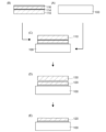
本実施の形態では、開示する発明の一態様に係る半導体基板の作製方法の一例について、図1乃至図3を参照して説明する。
・加速電圧 10kV以上100kV以下(好ましくは30kV以上80kV以下)
・ドーズ量 1×10¹⁶/cm2以上4×1016/cm2以下
・ビーム電流密度 2μA/cm2以上(好ましくは5μA/cm2以上、より好ましくは10μA/cm2以上)
本実施の形態では、第1の単結晶半導体層の下部に、電極(又は配線)として機能する導電層を設ける場合について図4を参照して説明する。なお、実施の形態1と重複する部分についての詳細は省略する。
・成膜法:プラズマCVD
・原料ガス:シラン(4sccm)+水素(400sccm)
・電力(周波数):15W(60MHz)
・圧力:100Pa
・電極間隔:20mm
・ガラス基板温度:280℃
・膜厚:20nm
・成膜法:プラズマCVD
・原料ガス:シラン(25sccm)+水素(150sccm)
・電力(周波数):30W(27MHz)
・圧力:66.6Pa
・電極間隔:25mm
・ガラス基板温度:280℃
・膜厚:480nm
(比較例)
110 単結晶半導体基板
112 絶縁層
114 損傷領域
116 絶縁層
118 導電層
120 単結晶半導体層
122A 半導体層
122B 半導体層
124 単結晶半導体層
124A 下層領域
124B 上層領域
130 単結晶半導体基板
140 イオンビーム
Claims (6)
- 単結晶半導体基板にイオンを照射して前記単結晶半導体基板中に損傷領域を形成し、
前記単結晶半導体基板上に絶縁層を形成し、
前記絶縁層と支持基板を密着させて前記単結晶半導体基板と前記支持基板を貼り合わせ、
前記損傷領域において前記単結晶半導体基板を分離させることにより、前記支持基板上に第1の単結晶半導体層を形成し、
前記第1の単結晶半導体層上に、結晶性を有する第1の半導体層を形成し、
前記第1の半導体層上に、前記第1の半導体層とは異なる条件により前記第1の半導体層に比較して低い結晶性を有する第2の半導体層を形成し、
熱処理により前記第1の半導体層及び前記第2の半導体層の結晶性を向上させて、第2の単結晶半導体層を形成することを特徴とする半導体基板の作製方法。 - 単結晶半導体基板にイオンを照射して前記単結晶半導体基板中に損傷領域を形成し、
支持基板上に絶縁層を形成し、
前記単結晶半導体基板と前記絶縁層を密着させて前記単結晶半導体基板と前記支持基板を貼り合わせ、
前記損傷領域において前記単結晶半導体基板を分離させることにより、前記支持基板上に第1の単結晶半導体層を形成し、
前記第1の単結晶半導体層上に、結晶性を有する第1の半導体層を形成し、
前記第1の半導体層上に、前記第1の半導体層とは異なる条件により前記第1の半導体層に比較して低い結晶性を有する第2の半導体層を形成し、
熱処理により前記第1の半導体層及び前記第2の半導体層の結晶性を向上させて、第2の単結晶半導体層を形成することを特徴とする半導体基板の作製方法。 - 請求項1または請求項2において、
前記イオンとして、水素を含む原料ガスにより生成されるイオンを用いることを特徴とする半導体基板の作製方法。 - 請求項1乃至3のいずれか一において、
前記第1の半導体層に比較して水素濃度が高くなるように前記第2の半導体層を形成することを特徴とする半導体基板の作製方法。 - 請求項1乃至4のいずれか一において、
前記第1の半導体層を、その厚さが10nm以上50nm以下となるように形成し、
前記第2の半導体層を、その厚さが300nm以上となるように形成することを特徴とする半導体基板の作製方法。 - 請求項1乃至5のいずれか一において、
前記第1の半導体層を、シラン系ガスに対する水素ガスの流量比を50倍以上とするプラズマ化学気相成長法により形成することを特徴とする半導体基板の作製方法。
Priority Applications (1)
| Application Number | Priority Date | Filing Date | Title |
|---|---|---|---|
| JP2009100931A JP5496540B2 (ja) | 2008-04-24 | 2009-04-17 | 半導体基板の作製方法 |
Applications Claiming Priority (3)
| Application Number | Priority Date | Filing Date | Title |
|---|---|---|---|
| JP2008113320 | 2008-04-24 | ||
| JP2008113320 | 2008-04-24 | ||
| JP2009100931A JP5496540B2 (ja) | 2008-04-24 | 2009-04-17 | 半導体基板の作製方法 |
Publications (3)
| Publication Number | Publication Date |
|---|---|
| JP2009283922A JP2009283922A (ja) | 2009-12-03 |
| JP2009283922A5 JP2009283922A5 (ja) | 2012-03-08 |
| JP5496540B2 true JP5496540B2 (ja) | 2014-05-21 |
Family
ID=41215417
Family Applications (1)
| Application Number | Title | Priority Date | Filing Date |
|---|---|---|---|
| JP2009100931A Expired - Fee Related JP5496540B2 (ja) | 2008-04-24 | 2009-04-17 | 半導体基板の作製方法 |
Country Status (2)
| Country | Link |
|---|---|
| US (1) | US8349702B2 (ja) |
| JP (1) | JP5496540B2 (ja) |
Families Citing this family (6)
| Publication number | Priority date | Publication date | Assignee | Title |
|---|---|---|---|---|
| JP5755931B2 (ja) | 2010-04-28 | 2015-07-29 | 株式会社半導体エネルギー研究所 | 半導体膜の作製方法、電極の作製方法、2次電池の作製方法、および太陽電池の作製方法 |
| JP5819614B2 (ja) * | 2011-02-02 | 2015-11-24 | 信越化学工業株式会社 | Soiウェーハの製造方法 |
| JPWO2012111616A1 (ja) * | 2011-02-15 | 2014-07-07 | 住友電気工業株式会社 | 保護膜付複合基板、および半導体デバイスの製造方法 |
| US8524572B2 (en) * | 2011-10-06 | 2013-09-03 | Micron Technology, Inc. | Methods of processing units comprising crystalline materials, and methods of forming semiconductor-on-insulator constructions |
| US9444019B1 (en) * | 2015-09-21 | 2016-09-13 | Epistar Corporation | Method for reusing a substrate for making light-emitting device |
| FR3091619B1 (fr) | 2019-01-07 | 2021-01-29 | Commissariat Energie Atomique | Procédé de guérison avant transfert d’une couche semi-conductrice |
Family Cites Families (20)
| Publication number | Priority date | Publication date | Assignee | Title |
|---|---|---|---|---|
| JPS61202417A (ja) * | 1985-03-06 | 1986-09-08 | Oki Electric Ind Co Ltd | シリコンエピタキシヤル層の形成方法 |
| JPS6248014A (ja) * | 1985-08-28 | 1987-03-02 | Sony Corp | 半導体層の固相成長方法 |
| JPH02100315A (ja) * | 1988-10-07 | 1990-04-12 | Fuji Electric Co Ltd | 結晶質シリコン膜の生成方法 |
| JPH03101121A (ja) * | 1989-09-13 | 1991-04-25 | Sanyo Electric Co Ltd | Soi構造の形成方法 |
| FR2681472B1 (fr) | 1991-09-18 | 1993-10-29 | Commissariat Energie Atomique | Procede de fabrication de films minces de materiau semiconducteur. |
| JPH1174209A (ja) * | 1997-08-27 | 1999-03-16 | Denso Corp | 半導体基板の製造方法 |
| JPH1140786A (ja) | 1997-07-18 | 1999-02-12 | Denso Corp | 半導体基板及びその製造方法 |
| US6534380B1 (en) | 1997-07-18 | 2003-03-18 | Denso Corporation | Semiconductor substrate and method of manufacturing the same |
| JPH1197379A (ja) | 1997-07-25 | 1999-04-09 | Denso Corp | 半導体基板及び半導体基板の製造方法 |
| JPH11121310A (ja) | 1997-10-09 | 1999-04-30 | Denso Corp | 半導体基板の製造方法 |
| JP3358550B2 (ja) * | 1998-07-07 | 2002-12-24 | 信越半導体株式会社 | Soiウエーハの製造方法ならびにこの方法で製造されるsoiウエーハ |
| JP3485081B2 (ja) * | 1999-10-28 | 2004-01-13 | 株式会社デンソー | 半導体基板の製造方法 |
| EP1482549B1 (en) * | 2003-05-27 | 2011-03-30 | S.O.I. Tec Silicon on Insulator Technologies S.A. | Method of fabrication of a heteroepitaxial microstructure |
| WO2003096385A2 (en) * | 2002-05-07 | 2003-11-20 | Asm America, Inc. | Silicon-on-insulator structures and methods |
| JP2004103855A (ja) | 2002-09-10 | 2004-04-02 | Canon Inc | 基板及びその製造方法 |
| US7538010B2 (en) * | 2003-07-24 | 2009-05-26 | S.O.I.Tec Silicon On Insulator Technologies | Method of fabricating an epitaxially grown layer |
| JP4554180B2 (ja) | 2003-09-17 | 2010-09-29 | ソニー株式会社 | 薄膜半導体デバイスの製造方法 |
| EP2002484A4 (en) | 2006-04-05 | 2016-06-08 | Silicon Genesis Corp | METHOD AND STRUCTURE FOR MANUFACTURING PHOTOVOLTAIC CELLS USING A LAYER TRANSFER PROCESS |
| FR2917232B1 (fr) | 2007-06-06 | 2009-10-09 | Soitec Silicon On Insulator | Procede de fabrication d'une structure pour epitaxie sans zone d'exclusion. |
| US7947523B2 (en) | 2008-04-25 | 2011-05-24 | Semiconductor Energy Laboratory Co., Ltd. | Method for manufacturing photoelectric conversion device |
-
2009
- 2009-04-17 JP JP2009100931A patent/JP5496540B2/ja not_active Expired - Fee Related
- 2009-04-20 US US12/426,305 patent/US8349702B2/en not_active Expired - Fee Related
Also Published As
| Publication number | Publication date |
|---|---|
| US20090269906A1 (en) | 2009-10-29 |
| US8349702B2 (en) | 2013-01-08 |
| JP2009283922A (ja) | 2009-12-03 |
Similar Documents
| Publication | Publication Date | Title |
|---|---|---|
| JP5110772B2 (ja) | 半導体薄膜層を有する基板の製造方法 | |
| JP5389627B2 (ja) | ワイドバンドギャップ半導体を積層した複合基板の製造方法 | |
| CN101562153B (zh) | 半导体装置及半导体装置的制造方法 | |
| JP5420968B2 (ja) | 貼り合わせウェーハの製造方法 | |
| JP5917036B2 (ja) | Soi基板の作製方法 | |
| JP5496540B2 (ja) | 半導体基板の作製方法 | |
| JP5706670B2 (ja) | Soi基板の作製方法 | |
| KR101642335B1 (ko) | 반도체 기판의 제조방법 | |
| JP5417399B2 (ja) | 複合ウェーハの製造方法 | |
| JP2011040729A (ja) | 半導体基板の作製方法および半導体装置 | |
| JP2010161359A (ja) | 貼り合わせウェーハの製造方法 | |
| US8043937B2 (en) | Method for manufacturing semiconductor substrate | |
| JP5559984B2 (ja) | 半導体装置の作製方法 | |
| JP5681354B2 (ja) | Soi基板の作製方法 | |
| JP2012160713A (ja) | Soi基板の作製方法 | |
| JP2011077506A (ja) | Soi基板の作製方法およびsoi基板 | |
| JP4624812B2 (ja) | Soiウエーハの製造方法 | |
| JP4594121B2 (ja) | Soiウエーハの製造方法及びsoiウエーハ | |
| JP2014195026A (ja) | 複合基板 | |
| JP5358159B2 (ja) | 半導体薄膜層を有する基板の製造方法 | |
| TW202439404A (zh) | 半導體基板的製造方法、半導體基板、及半導體裝置 | |
| JP5669439B2 (ja) | 半導体基板の作製方法 |
Legal Events
| Date | Code | Title | Description |
|---|---|---|---|
| A521 | Written amendment |
Free format text: JAPANESE INTERMEDIATE CODE: A523 Effective date: 20120118 |
|
| A621 | Written request for application examination |
Free format text: JAPANESE INTERMEDIATE CODE: A621 Effective date: 20120118 |
|
| A131 | Notification of reasons for refusal |
Free format text: JAPANESE INTERMEDIATE CODE: A131 Effective date: 20131029 |
|
| A977 | Report on retrieval |
Free format text: JAPANESE INTERMEDIATE CODE: A971007 Effective date: 20131031 |
|
| A521 | Written amendment |
Free format text: JAPANESE INTERMEDIATE CODE: A523 Effective date: 20131204 |
|
| TRDD | Decision of grant or rejection written | ||
| A01 | Written decision to grant a patent or to grant a registration (utility model) |
Free format text: JAPANESE INTERMEDIATE CODE: A01 Effective date: 20140225 |
|
| A61 | First payment of annual fees (during grant procedure) |
Free format text: JAPANESE INTERMEDIATE CODE: A61 Effective date: 20140305 |
|
| R150 | Certificate of patent or registration of utility model |
Ref document number: 5496540 Country of ref document: JP Free format text: JAPANESE INTERMEDIATE CODE: R150 |
|
| R250 | Receipt of annual fees |
Free format text: JAPANESE INTERMEDIATE CODE: R250 |
|
| LAPS | Cancellation because of no payment of annual fees |