WO2010032456A1 - 半導体記憶装置および半導体記憶装置の製造方法 - Google Patents
半導体記憶装置および半導体記憶装置の製造方法 Download PDFInfo
- Publication number
- WO2010032456A1 WO2010032456A1 PCT/JP2009/004653 JP2009004653W WO2010032456A1 WO 2010032456 A1 WO2010032456 A1 WO 2010032456A1 JP 2009004653 W JP2009004653 W JP 2009004653W WO 2010032456 A1 WO2010032456 A1 WO 2010032456A1
- Authority
- WO
- WIPO (PCT)
- Prior art keywords
- plug
- insulating layer
- hole
- metal plug
- forming
- Prior art date
- Legal status (The legal status is an assumption and is not a legal conclusion. Google has not performed a legal analysis and makes no representation as to the accuracy of the status listed.)
- Ceased
Links
Images













Classifications
-
- H—ELECTRICITY
- H10—SEMICONDUCTOR DEVICES; ELECTRIC SOLID-STATE DEVICES NOT OTHERWISE PROVIDED FOR
- H10B—ELECTRONIC MEMORY DEVICES
- H10B53/00—Ferroelectric RAM [FeRAM] devices comprising ferroelectric memory capacitors
- H10B53/10—Ferroelectric RAM [FeRAM] devices comprising ferroelectric memory capacitors characterised by the top-view layout
-
- H—ELECTRICITY
- H10—SEMICONDUCTOR DEVICES; ELECTRIC SOLID-STATE DEVICES NOT OTHERWISE PROVIDED FOR
- H10B—ELECTRONIC MEMORY DEVICES
- H10B53/00—Ferroelectric RAM [FeRAM] devices comprising ferroelectric memory capacitors
- H10B53/30—Ferroelectric RAM [FeRAM] devices comprising ferroelectric memory capacitors characterised by the memory core region
-
- H—ELECTRICITY
- H10—SEMICONDUCTOR DEVICES; ELECTRIC SOLID-STATE DEVICES NOT OTHERWISE PROVIDED FOR
- H10D—INORGANIC ELECTRIC SEMICONDUCTOR DEVICES
- H10D1/00—Resistors, capacitors or inductors
- H10D1/60—Capacitors
- H10D1/68—Capacitors having no potential barriers
- H10D1/682—Capacitors having no potential barriers having dielectrics comprising perovskite structures
-
- H—ELECTRICITY
- H10—SEMICONDUCTOR DEVICES; ELECTRIC SOLID-STATE DEVICES NOT OTHERWISE PROVIDED FOR
- H10D—INORGANIC ELECTRIC SEMICONDUCTOR DEVICES
- H10D1/00—Resistors, capacitors or inductors
- H10D1/60—Capacitors
- H10D1/68—Capacitors having no potential barriers
- H10D1/682—Capacitors having no potential barriers having dielectrics comprising perovskite structures
- H10D1/688—Capacitors having no potential barriers having dielectrics comprising perovskite structures comprising barrier layers to prevent diffusion of hydrogen or oxygen
-
- H—ELECTRICITY
- H10—SEMICONDUCTOR DEVICES; ELECTRIC SOLID-STATE DEVICES NOT OTHERWISE PROVIDED FOR
- H10D—INORGANIC ELECTRIC SEMICONDUCTOR DEVICES
- H10D1/00—Resistors, capacitors or inductors
- H10D1/60—Capacitors
- H10D1/68—Capacitors having no potential barriers
- H10D1/692—Electrodes
-
- H—ELECTRICITY
- H10—SEMICONDUCTOR DEVICES; ELECTRIC SOLID-STATE DEVICES NOT OTHERWISE PROVIDED FOR
- H10D—INORGANIC ELECTRIC SEMICONDUCTOR DEVICES
- H10D1/00—Resistors, capacitors or inductors
- H10D1/60—Capacitors
- H10D1/68—Capacitors having no potential barriers
- H10D1/692—Electrodes
- H10D1/711—Electrodes having non-planar surfaces, e.g. formed by texturisation
-
- H—ELECTRICITY
- H10—SEMICONDUCTOR DEVICES; ELECTRIC SOLID-STATE DEVICES NOT OTHERWISE PROVIDED FOR
- H10P—GENERIC PROCESSES OR APPARATUS FOR THE MANUFACTURE OR TREATMENT OF DEVICES COVERED BY CLASS H10
- H10P14/00—Formation of materials, e.g. in the shape of layers or pillars
- H10P14/60—Formation of materials, e.g. in the shape of layers or pillars of insulating materials
- H10P14/61—Formation of materials, e.g. in the shape of layers or pillars of insulating materials using masks
-
- H—ELECTRICITY
- H10—SEMICONDUCTOR DEVICES; ELECTRIC SOLID-STATE DEVICES NOT OTHERWISE PROVIDED FOR
- H10P—GENERIC PROCESSES OR APPARATUS FOR THE MANUFACTURE OR TREATMENT OF DEVICES COVERED BY CLASS H10
- H10P14/00—Formation of materials, e.g. in the shape of layers or pillars
- H10P14/60—Formation of materials, e.g. in the shape of layers or pillars of insulating materials
- H10P14/63—Formation of materials, e.g. in the shape of layers or pillars of insulating materials characterised by the formation processes
- H10P14/6326—Deposition processes
- H10P14/6328—Deposition from the gas or vapour phase
- H10P14/6329—Deposition from the gas or vapour phase using physical ablation of a target, e.g. physical vapour deposition or pulsed laser deposition
-
- H—ELECTRICITY
- H10—SEMICONDUCTOR DEVICES; ELECTRIC SOLID-STATE DEVICES NOT OTHERWISE PROVIDED FOR
- H10P—GENERIC PROCESSES OR APPARATUS FOR THE MANUFACTURE OR TREATMENT OF DEVICES COVERED BY CLASS H10
- H10P14/00—Formation of materials, e.g. in the shape of layers or pillars
- H10P14/60—Formation of materials, e.g. in the shape of layers or pillars of insulating materials
- H10P14/63—Formation of materials, e.g. in the shape of layers or pillars of insulating materials characterised by the formation processes
- H10P14/6326—Deposition processes
- H10P14/6328—Deposition from the gas or vapour phase
- H10P14/6334—Deposition from the gas or vapour phase using decomposition or reaction of gaseous or vapour phase compounds, i.e. chemical vapour deposition
-
- H—ELECTRICITY
- H10—SEMICONDUCTOR DEVICES; ELECTRIC SOLID-STATE DEVICES NOT OTHERWISE PROVIDED FOR
- H10P—GENERIC PROCESSES OR APPARATUS FOR THE MANUFACTURE OR TREATMENT OF DEVICES COVERED BY CLASS H10
- H10P14/00—Formation of materials, e.g. in the shape of layers or pillars
- H10P14/60—Formation of materials, e.g. in the shape of layers or pillars of insulating materials
- H10P14/63—Formation of materials, e.g. in the shape of layers or pillars of insulating materials characterised by the formation processes
- H10P14/6326—Deposition processes
- H10P14/6328—Deposition from the gas or vapour phase
- H10P14/6334—Deposition from the gas or vapour phase using decomposition or reaction of gaseous or vapour phase compounds, i.e. chemical vapour deposition
- H10P14/6336—Deposition from the gas or vapour phase using decomposition or reaction of gaseous or vapour phase compounds, i.e. chemical vapour deposition in the presence of a plasma [PECVD]
-
- H—ELECTRICITY
- H10—SEMICONDUCTOR DEVICES; ELECTRIC SOLID-STATE DEVICES NOT OTHERWISE PROVIDED FOR
- H10P—GENERIC PROCESSES OR APPARATUS FOR THE MANUFACTURE OR TREATMENT OF DEVICES COVERED BY CLASS H10
- H10P14/00—Formation of materials, e.g. in the shape of layers or pillars
- H10P14/60—Formation of materials, e.g. in the shape of layers or pillars of insulating materials
- H10P14/69—Inorganic materials
- H10P14/692—Inorganic materials composed of oxides, glassy oxides or oxide-based glasses
- H10P14/6921—Inorganic materials composed of oxides, glassy oxides or oxide-based glasses containing silicon
- H10P14/69215—Inorganic materials composed of oxides, glassy oxides or oxide-based glasses containing silicon the material being a silicon oxide, e.g. SiO2
-
- H—ELECTRICITY
- H10—SEMICONDUCTOR DEVICES; ELECTRIC SOLID-STATE DEVICES NOT OTHERWISE PROVIDED FOR
- H10P—GENERIC PROCESSES OR APPARATUS FOR THE MANUFACTURE OR TREATMENT OF DEVICES COVERED BY CLASS H10
- H10P14/00—Formation of materials, e.g. in the shape of layers or pillars
- H10P14/60—Formation of materials, e.g. in the shape of layers or pillars of insulating materials
- H10P14/69—Inorganic materials
- H10P14/692—Inorganic materials composed of oxides, glassy oxides or oxide-based glasses
- H10P14/6938—Inorganic materials composed of oxides, glassy oxides or oxide-based glasses the material containing at least one metal element, e.g. metal oxides, metal oxynitrides or metal oxycarbides
- H10P14/6939—Inorganic materials composed of oxides, glassy oxides or oxide-based glasses the material containing at least one metal element, e.g. metal oxides, metal oxynitrides or metal oxycarbides characterised by the metal
- H10P14/69391—Inorganic materials composed of oxides, glassy oxides or oxide-based glasses the material containing at least one metal element, e.g. metal oxides, metal oxynitrides or metal oxycarbides characterised by the metal the material containing aluminium, e.g. Al2O3
-
- H—ELECTRICITY
- H10—SEMICONDUCTOR DEVICES; ELECTRIC SOLID-STATE DEVICES NOT OTHERWISE PROVIDED FOR
- H10P—GENERIC PROCESSES OR APPARATUS FOR THE MANUFACTURE OR TREATMENT OF DEVICES COVERED BY CLASS H10
- H10P14/00—Formation of materials, e.g. in the shape of layers or pillars
- H10P14/60—Formation of materials, e.g. in the shape of layers or pillars of insulating materials
- H10P14/69—Inorganic materials
- H10P14/694—Inorganic materials composed of nitrides
- H10P14/6943—Inorganic materials composed of nitrides containing silicon
- H10P14/69433—Inorganic materials composed of nitrides containing silicon the material being a silicon nitride not containing oxygen, e.g. SixNy or SixByNz
-
- H—ELECTRICITY
- H10—SEMICONDUCTOR DEVICES; ELECTRIC SOLID-STATE DEVICES NOT OTHERWISE PROVIDED FOR
- H10W—GENERIC PACKAGES, INTERCONNECTIONS, CONNECTORS OR OTHER CONSTRUCTIONAL DETAILS OF DEVICES COVERED BY CLASS H10
- H10W20/00—Interconnections in chips, wafers or substrates
- H10W20/01—Manufacture or treatment
- H10W20/031—Manufacture or treatment of conductive parts of the interconnections
- H10W20/032—Manufacture or treatment of conductive parts of the interconnections of conductive barrier, adhesion or liner layers
- H10W20/033—Manufacture or treatment of conductive parts of the interconnections of conductive barrier, adhesion or liner layers in openings in dielectrics
- H10W20/037—Manufacture or treatment of conductive parts of the interconnections of conductive barrier, adhesion or liner layers in openings in dielectrics the barrier, adhesion or liner layers being on top of a main fill metal
-
- H—ELECTRICITY
- H10—SEMICONDUCTOR DEVICES; ELECTRIC SOLID-STATE DEVICES NOT OTHERWISE PROVIDED FOR
- H10W—GENERIC PACKAGES, INTERCONNECTIONS, CONNECTORS OR OTHER CONSTRUCTIONAL DETAILS OF DEVICES COVERED BY CLASS H10
- H10W20/00—Interconnections in chips, wafers or substrates
- H10W20/01—Manufacture or treatment
- H10W20/031—Manufacture or treatment of conductive parts of the interconnections
- H10W20/032—Manufacture or treatment of conductive parts of the interconnections of conductive barrier, adhesion or liner layers
- H10W20/046—Manufacture or treatment of conductive parts of the interconnections of conductive barrier, adhesion or liner layers the barrier, adhesion or liner layers being associated with interconnections of capacitors
Definitions
- the present invention relates to a semiconductor memory device and a manufacturing method thereof.
- a ferroelectric memory (FeRAM: Ferroelectric Random Access Memory) equipped with a ferroelectric capacitor is known as a non-volatile memory that can retain stored contents even when power supply is shut off.
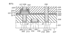
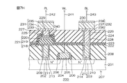
- a conventional ferroelectric memory is manufactured through the following manufacturing process, for example. 7A to 7H are schematic cross-sectional views showing a conventional method of manufacturing a ferroelectric memory in the order of steps.
- an N + type region 202 and an N + type region 203 are formed by implanting N type impurities into the surface layer portion of a P type silicon substrate 201. . Then, by thermal oxidation treatment and patterning techniques, to the surface of the silicon substrate 201, the gate insulating film 204 across the N + -type region 202 to the N + -type region 203 is formed. Next, polysilicon doped with impurities at a high concentration (doped polysilicon) is deposited on the silicon substrate 201 by a CVD method and patterned to form the gate electrode 205 on the gate insulating film 204. .
- silicon oxide is deposited on the silicon substrate 201 by a CVD method, and the deposited silicon oxide is etched back, whereby a sidewall 206 surrounding the sidewall of the gate electrode 205 is formed.
- MOSFET 207 including (Semiconductor) is formed.
- a first insulating layer 208 made of silicon oxide is stacked on the silicon substrate 201 by a CVD method.
- the first insulating layer 208 is patterned.
- a drain contact hole 209 reaching the N + -type region 202 (drain region) from the upper surface of the first insulating layer 208 is formed.
- a source contact hole 210 reaching the N + type region 203 (source region) is formed from the upper surface of the first insulating layer 208.
- a conductive material containing titanium is deposited by sputtering so as to cover the inner surfaces of the drain contact hole 209 and the source contact hole 210 and further cover the upper surface of the first insulating layer 208.
- tungsten is deposited by CVD so as to fill the drain contact hole 209 and the source contact hole 210.
- the conductive material containing titanium and tungsten are polished by CMP until the upper surface of tungsten and the upper surface of the first insulating layer 208 are flush with each other.
- the drain contact plug 213 embedded in the drain contact hole 209 is formed via the barrier film 211.
- a source contact plug 214 embedded in the source contact hole 210 is formed via the barrier film 212.
- the drain contact plug 213 is electrically connected to the N + type region 202 (drain region) through the barrier film 211.
- the source contact plug 214 is electrically connected to the N + -type region 203 (source region) through the barrier film 212.
- a lower conductive material film 215 made of a conductive material containing Ir (iridium) and a ferroelectric made of PZT (lead zirconate titanate) are formed on the first insulating layer 208 by sputtering.
- a material film 216 and an upper conductive material film 217 made of a conductive material containing Ir (iridium) are stacked in this order. Thereby, the stacked structure 239 is formed on the first insulating layer 208.
- a hard mask 240 made of TiN is formed on a portion of the stacked structure 239 on the drain contact plug 213. Then, the laminated structure 239 is etched through the hard mask 240 at an etching temperature of 300 ° C. or higher.
- the ferroelectric capacitor 221 including the lower electrode 218, the ferroelectric film 219, and the upper electrode 220 is formed on the drain contact plug 213.
- the lower electrode 218 of the ferroelectric capacitor 221 is electrically connected to the N + type region 202 (drain region) through the drain contact plug 213 by contacting the drain contact plug 213. Note that the hard mask 240 thinned by etching remains on the upper electrode 220.
- alumina is deposited on the first insulating layer 208 by sputtering, and SiN is further deposited by PECVD.
- a first hydrogen barrier film 222 and a second hydrogen barrier film 223 are formed to protect the ferroelectric capacitor 221 from hydrogen.
- a second insulating layer 224 made of silicon oxide is stacked on the second hydrogen barrier film 223 by CVD.
- the second insulating layer 224 is polished by a CMP process, and the upper surface of the second insulating layer 224 is planarized. Then, as shown in FIG. 7F, the second insulating layer 224, the second hydrogen barrier film 223, and the first hydrogen barrier film 222 are patterned. As a result, a PL wiring via hole 225 reaching the hard mask 240 from the upper surface of the second insulating layer 224 is formed. Also, a BL wiring via hole 226 reaching the source contact plug 214 from the upper surface of the second insulating layer 224 is formed.
- a conductive material containing titanium is deposited by sputtering so as to cover the inner surfaces of the PL wiring via hole 225 and the BL wiring via hole 226 and further cover the upper surface of the second insulating layer 224.
- tungsten is deposited by CVD so as to fill the PL wiring via hole 225 and the BL wiring via hole 226.
- the conductive material containing titanium and tungsten are polished by CMP until the upper surface of tungsten and the upper surface of the second insulating layer 224 are flush with each other.
- the PL wiring plug 229 embedded in the PL wiring via hole 225 is formed through the barrier film 227.
- a BL wiring plug 230 embedded in the BL wiring via hole 226 is formed through the barrier film 228.
- the PL wiring plug 229 is electrically connected to the upper electrode 220 through the barrier film 227 and the hard mask 240.
- the BL wiring plug 230 is electrically connected to the source contact plug 214 via the barrier film 228.
- a conductive material containing titanium, a conductive material containing aluminum, and a conductive material containing titanium are stacked on the second insulating layer 224 and patterned by sputtering.
- the PL wiring 231 (wiring having a three-layer structure of the titanium layer 233, the aluminum layer 234, and the titanium layer 235) electrically connected to the PL wiring plug 229, and the BL wiring BL wiring 232 (wiring having a three-layer structure of titanium layer 236, aluminum layer 237, and titanium layer 238) that is electrically connected to wiring plug 230 is formed.
- the word line 241 is connected to the gate electrode 205, the plate line 242 is connected to the PL wiring 231, and the bit line 243 is connected to the BL wiring 232.
- a ferroelectric memory 200 on which the ferroelectric capacitor 221 is mounted is obtained.
- miniaturization of a ferroelectric memory has been promoted. For example, miniaturization by reducing the area (capacitor area) of a ferroelectric capacitor mounted on the memory is considered. Ir and Pt used as the material for the lower electrode and the upper electrode, and PZT used as the material for the ferroelectric film are difficult to be etched. Therefore, under normal dry etching conditions, the side surface of the ferroelectric capacitor is not affected even if the stacked structure in which the lower electrode material, the ferroelectric film material and the upper electrode material are stacked is etched in the vertical direction. It becomes an inclined surface instead of a vertical surface with respect to the lamination interface. If the side surface of the ferroelectric capacitor can be brought close to a plane perpendicular to the laminated interface, the capacitor area can be reduced without reducing the capacitance of the ferroelectric capacitor.
- the laminated structure 239 is etched at high temperature (for example, etching at a temperature of 300 ° C. or higher) through the heat-resistant hard mask 240.
- high temperature for example, etching at a temperature of 300 ° C. or higher
- the source contact plug 214 disposed below the etched portion of the stacked structure 239 may cause abnormal etching that is etched together with the stacked structure 239. If the source contact plug 214 is abnormally etched, a conduction failure is caused between the source contact plug 214 and the BL wiring plug 230, thereby reducing the reliability of the ferroelectric memory 200.
- An object of the present invention is to provide a semiconductor memory device that can be miniaturized without abnormally etching a second metal plug different from the first metal plug connected to the ferroelectric capacitor, and a method for manufacturing the same. It is in.
- a semiconductor memory device is formed on an insulating layer, a ferroelectric capacitor formed on the insulating layer and having a lower electrode, a ferroelectric film, and an upper electrode, and the insulating layer.
- An interlayer insulating film having an opening in a portion where the ferroelectric capacitor is disposed; a first metal plug embedded in the insulating layer and connected to the lower electrode through the opening; Outside the dielectric capacitor, a second metal plug embedded in the insulating layer is provided.
- This semiconductor memory device is a method for manufacturing a semiconductor memory device including, for example, a ferroelectric capacitor having a lower electrode, a ferroelectric film, and an upper electrode, and a first metal plug and a second metal plug are embedded in an insulating layer.
- a method for manufacturing a semiconductor memory device including a ferroelectric capacitor having a lower electrode, a ferroelectric film, and an upper electrode, the step of embedding a first metal plug and a second metal plug in an insulating layer; Forming an interlayer insulating film on the insulating layer; forming an opening in the interlayer insulating film to expose the first metal plug; and after forming the opening, the material of the lower electrode, A step of sequentially depositing a material of the ferroelectric film and a material of the upper electrode to form a deposited structure, and a portion other than the remaining portion so as to leave a part of the deposited structure on the opening It can be manufactured by a method for manufacturing a semiconductor memory device, comprising a step of forming the ferroelectric capacitor by removing it by etching.
- an interlayer insulating film is formed on the insulating layer.
- An opening for exposing the first metal plug is formed in the interlayer insulating film.
- the first metal plug is exposed through the opening of the interlayer insulating film, while the second metal plug is covered with the interlayer insulating film.
- a part of the deposited structure formed on the interlayer insulating film is removed by etching, whereby a ferroelectric capacitor is formed.
- the second metal plug is covered with the interlayer insulating film. Therefore, even if the deposited structure is etched at a high temperature, abnormal etching of the second metal plug can be prevented by the protection by the interlayer insulating film. As a result, it is possible to suppress the occurrence of poor conduction between the second metal plug and the connection body connected to the second metal plug, and it is possible to suppress a decrease in reliability.
- the side surface of the ferroelectric capacitor appearing by etching can be made to be a vertical surface with respect to the stacked interface of the ferroelectric capacitor or a steep slope close to the vertical surface.
- the area of the ferroelectric capacitor can be reduced, so that the semiconductor memory device can be miniaturized.
- the upper surface of the first metal plug and the upper surface of the second metal plug are preferably flush with each other.
- the step of embedding the first metal plug and the second metal plug in the insulating layer the step of forming the first through hole and the second through hole in the insulating layer,
- the plug material is deposited on the insulating layer so as to fill the first through hole and the second through hole, and the plug material is flush with the upper surface of the plug material and the upper surface of the insulating layer.
- the manufacturing process of the semiconductor memory device is simplified. Can do.
- a semiconductor memory device includes an insulating layer having a first through hole and a second through hole, and an insulating layer formed on the insulating layer so as to cover the first through hole.
- a ferroelectric capacitor having a body film and an upper electrode, a first metal plug embedded in the first through hole and electrically connected to the lower electrode, and a second metal embedded in the second through hole Of the plug, the first metal plug and the second metal plug are made of a conductive material that covers at least the upper surface of the second metal plug and has an etching selectivity with respect to the material of the lower electrode and the upper electrode.
- a conductive cap is made of a conductive material that covers at least the upper surface of the second metal plug and has an etching selectivity with respect to the material of the lower electrode and the upper electrode.
- At least the upper surface of the second metal plug is made of a conductive material having an etching selectivity with respect to the material of the lower electrode and the upper electrode. Covered by.
- the upper surface of the second metal plug is protected by the conductive cap. Therefore, even if the lower electrode, the ferroelectric film, and the upper electrode are formed at a high temperature, abnormal etching of the second metal plug can be prevented by protection with the conductive cap. As a result, it is possible to suppress the occurrence of poor conduction between the second metal plug and the connection body connected to the second metal plug, and it is possible to suppress a decrease in reliability.
- the side surface of the ferroelectric capacitor that appears by etching is perpendicular to the stacked interface of the ferroelectric capacitor. It can be a steep slope close to a plane or vertical plane. As a result, the area of the ferroelectric capacitor can be reduced, so that the semiconductor memory device can be miniaturized.
- This semiconductor memory device is a method for manufacturing a semiconductor memory device including, for example, a ferroelectric capacitor having a lower electrode, a ferroelectric film, and an upper electrode, and a first metal plug and a second metal plug are embedded in an insulating layer.
- the conductive cap is preferably made of a conductive nitride.
- the conductive nitride used for the conductive cap is, for example, a conductive material containing noble metal (specifically, Au-based material, Ag-based material, Pt-based material, Pd-based material, Rh-based material, Ir-based material, It has a large etching selectivity with respect to the lower electrode and the upper electrode made of Ru-based material and Os-based material. Therefore, in this aspect, abnormal etching of the second metal plug can be effectively prevented.
- the first metal plug and the second metal plug are embedded up to a middle portion of the first through hole and the second through hole, respectively, and the conductive cap includes the insulating cap. It is preferable to be embedded in the first through hole and the second through hole so as to be flush with the surface of the layer. According to this configuration, the first metal plug and the conductive cap are embedded in the first through hole. A second metal plug and a conductive cap are embedded in the second through hole. That is, the structures embedded in the first through hole and the second through hole have the same structure.
- the semiconductor memory device is a method of manufacturing a semiconductor memory device including a ferroelectric capacitor having a lower electrode, a ferroelectric film, and an upper electrode, for example, and includes a first through hole and an insulating layer.
- the first metal Forming a conductive plug covering the lugs and the upper surfaces of the second metal plugs, and depositing the material of the lower electrode, the material of the ferroelectric film, and the material of the upper electrode in order on the insulating layer;
- the metal material in the through hole is partially removed, so that the first metal plug and the second metal plug are removed. Is formed. Then, after these plugs are formed, the first through hole and the second through hole are filled with a conductive material having an etching selectivity with respect to the lower electrode and the upper electrode, whereby the first metal plug and the second metal A conductive plug that covers the upper surface of the plug and is flush with the surface of the insulating layer is formed.
- the step of forming the first metal plug and the step of forming the second metal plug are performed in parallel, and the step of forming each conductive plug covering the upper surface of these plugs is also performed in parallel with each other. Therefore, the manufacturing process of the semiconductor memory device can be simplified.
- FIG. 1 is a schematic plan view of a ferroelectric memory according to a first embodiment of the present invention.
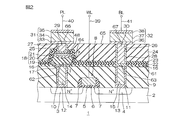
- FIG. 2 is a cross-sectional view of the ferroelectric memory of FIG. 1 and a cut surface taken along a cutting line II-II.
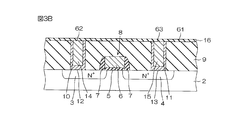
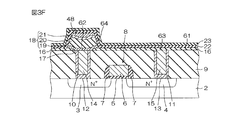
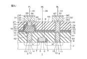
- FIG. 3 is a schematic cross-sectional view showing the method of manufacturing the ferroelectric memory in FIG. 2 in the order of steps.
- FIG. 3B is a cross-sectional view showing a step subsequent to FIG. 3A.
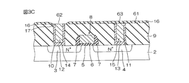
- FIG. 3C is a cross-sectional view showing the next step of FIG. 3B.
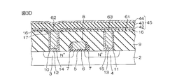
- FIG. 3D is a cross-sectional view showing a step subsequent to FIG. 3C. It is sectional drawing which shows the process following FIG. 3D. It is sectional drawing which shows the process following FIG. 3E.
- FIG. 3F is a cross-sectional view showing a step subsequent to FIG. 3G. It is sectional drawing which shows the process following FIG. 3H.
- FIG. 3D is a cross-sectional view showing a step subsequent to FIG. 3I.
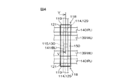
- FIG. 6 is a schematic plan view of a ferroelectric memory according to a second embodiment of the present invention.
- FIG. 5 is a cross-sectional view of the ferroelectric memory of FIG. 4 and is a cut surface taken along a cutting line VV.
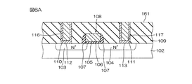
- FIG. 6 is a schematic cross-sectional view showing a method of manufacturing the ferroelectric memory of FIG. 5 in order of steps.
- FIG. 6B is a cross-sectional view showing a step subsequent to FIG.
- FIG. 6A is a cross-sectional view showing a step subsequent to FIG. 6B.
- FIG. 6D is a cross-sectional view showing a step subsequent to FIG. 6C. It is sectional drawing which shows the process of FIG. 6D.
- FIG. 6E is a cross-sectional view showing a step subsequent to FIG. 6E.
- FIG. 6D is a cross-sectional view showing a step subsequent to FIG. 6F.
- FIG. 6G is a cross-sectional view showing a step subsequent to FIG. 6G.
- FIG. 6D is a cross-sectional view showing a step subsequent to FIG. 6H.
- FIG. 6D is a cross-sectional view showing a step subsequent to FIG. 6I.
- FIG. 6I is a cross-sectional view showing a step subsequent to FIG. 6I.
- FIG. 6D is a cross-sectional view showing a step subsequent to FIG. 6J. It is typical sectional drawing which shows the manufacturing method of the conventional ferroelectric memory in order of a process.
- FIG. 7B is a cross-sectional view showing a step subsequent to FIG. 7A.
- FIG. 7B is a cross-sectional view showing a step subsequent to FIG. 7B.
- FIG. 7D is a cross-sectional view showing a step subsequent to FIG. 7C.
- FIG. 7D is a cross-sectional view showing a step subsequent to FIG. 7D.
- FIG. 7E is a cross-sectional view showing a step subsequent to FIG. 7E.
- FIG. 7D is a cross-sectional view showing a step subsequent to FIG. 7F.
- FIG. 7B is a cross-sectional view showing a step subsequent to FIG. 7G.
- FIG. 1 is a schematic plan view of a ferroelectric memory according to the first embodiment of the present invention.
- FIG. 2 is a cross-sectional view of the ferroelectric memory shown in FIG.
- a ferroelectric memory 1 as a semiconductor memory device is a non-volatile memory that can retain stored contents even when a power supply is cut off.
- the ferroelectric memory 1 includes a P-type silicon substrate 2. On the silicon substrate 2, for example, a plurality of rectangular active regions 50 in plan view are formed. The outline of the active region 50 is indicated by a bold line in FIG. The active regions 50 are arranged in a matrix that is aligned in the longitudinal direction and in a direction orthogonal to the longitudinal direction.
- each active region 50 a plurality of memory cells (two in this embodiment) that hold 1-bit information are formed.
- FIG. 2 shows one of the plurality of memory cells.
- Each memory cell has a 1T1C type cell structure in which one ferroelectric capacitor 18 (C) and one MOSFET 8 (T) are arranged in a stacked relationship.
- an N + -type drain region 3 and an N + -type source region 4 are formed on the surface layer portion of the silicon substrate 2 with a space therebetween as shown in FIG. ing.
- the source region 4 is a region common to the MOSFETs 8 of the two memory cells, and is formed in the center of the active region 50 in plan view.
- the drain region 3 is formed corresponding to the MOSFET 8 of each memory cell in each of one end and the other end of the active region 50 in plan view.
- a gate insulating film 5 extending from the drain region 3 to the source region 4 is formed on the surface of the silicon substrate 2.
- the gate insulating film 5 is made of, for example, silicon oxide.
- a gate electrode 6 made of, for example, polysilicon doped with impurities (doped polysilicon) is formed on the gate insulating film 5.
- a side wall 7 is formed on the side wall of the gate electrode 6 so as to be in close contact with the entire circumference.
- the sidewall 7 is made of, for example, silicon oxide.
- the ferroelectric memory 1 includes the MOSFET 8 having the gate electrode 6 (Metal), the gate insulating film 5 (Oxide), and the silicon substrate 2 (Semiconductor) including the drain region 3 and the source region 4. It has been.
- a first insulating layer 9 is stacked on the silicon substrate 2.
- the first insulating layer 9 is made of, for example, silicon oxide.
- the thickness of the first insulating layer 9 is, for example, 0.4 to 0.9 ⁇ m.
- a drain contact hole 10 reaching the drain region 3 from the upper surface 61 of the first insulating layer 9 is formed at a portion facing the drain region 3.
- a drain contact plug 14 made of a metal material such as tungsten is embedded in the drain contact hole 10. The drain contact plug 14 as the first metal plug fills the drain contact hole 10 until the upper surface 62 thereof is flush with the upper surface 61 of the first insulating layer 9.
- a barrier film 12 is interposed between the inner surface (the side surface formed by the first insulating layer 9 and the bottom surface formed by the silicon substrate 2) and the drain contact plug 14.
- the barrier film 12 is made of, for example, a conductive material containing titanium (for example, TiN, Ti, etc.). By interposing the conductive barrier film 12, the drain contact plug 14 is electrically connected (contacted) to the drain region 3 through the barrier film 12.
- a source contact hole 11 reaching the source region 4 from the upper surface 61 of the first insulating layer 9 is formed at a portion facing the source region 4.
- a source contact plug 15 made of a metal material such as tungsten is embedded in the source contact hole 11.
- the source contact plug 15 as the second metal plug fills the source contact hole 11 until the upper surface 63 thereof is flush with the upper surface 61 of the first insulating layer 9. Since the upper surface 63 of the source contact plug 15 is flush with the upper surface 61 of the first insulating layer 9, the upper surface 63 of the source contact plug 15 and the upper surface 62 of the drain contact plug 14 are flush with each other.
- a barrier film 13 is interposed between the inner surface (the side surface formed by the first insulating layer 9 and the bottom surface formed by the silicon substrate 2) and the source contact plug 15.
- the barrier film 13 is made of, for example, a conductive material containing titanium (for example, TiN, Ti, etc.). By interposing the conductive barrier film 13, the source contact plug 15 is electrically connected (contacted) to the source region 4 through the barrier film 13.
- an interlayer insulating film 16 interposed between the first insulating layer 9 and the second insulating layer 24 (described later) is formed on the first insulating layer 9.
- the thickness of the interlayer insulating film 16 is smaller than the thickness of the first insulating layer 9 and is, for example, 0.05 to 0.2 ⁇ m.
- An opening 17 that exposes the entire upper surface 62 of the drain contact plug 14 is formed in a portion of the interlayer insulating film 16 that faces the drain contact plug 14.
- the ferroelectric capacitor 18 is disposed on the opening 17 of the interlayer insulating film 16, that is, a position that overlaps the drain contact plug 14 in a plan view and does not overlap the source contact plug 15.
- the ferroelectric capacitor 18 includes a lower electrode 19, an upper electrode 21, and a ferroelectric film 20 sandwiched between the lower electrode 19 and the upper electrode 21.
- the lower electrode 19 is made of a conductive material containing noble metal (specifically, Au-based material, Ag-based material, Pt-based material, Pd-based material, Rh-based material, Ir-based material, Ru-based material, Os-based material). Become.
- the thickness of the lower electrode 19 is, for example, 0.05 to 0.2 ⁇ m.
- the lower electrode 19 enters the opening 17 and is in contact with the upper surface 62 of the drain contact plug 14. As a result, the lower electrode 19 is electrically connected to the drain region 3 via the drain contact plug 14.
- the upper electrode 21 is made of a conductive material containing a noble metal.
- the thickness of the upper electrode 21 is, for example, the same thickness as that of the lower electrode 19 (for example, 0.05 to 0.2 ⁇ m).
- the ferroelectric film 20 is made of a ferroelectric material.
- the ferroelectric material is not particularly limited as long as it is a material that can store charges even when no voltage is applied.
- the thickness of the ferroelectric film 20 is, for example, 0.05 to 0.2 ⁇ m.
- the ferroelectric capacitor 18 formed by laminating the lower electrode 19, the ferroelectric film 20, and the upper electrode 21 is formed in, for example, a mesa shape (a trapezoidal shape in a sectional view).
- a TiN film 48 is laminated on the upper electrode 21 of the ferroelectric capacitor 18.
- a first hydrogen barrier film 22 made of Al 2 O 3 (alumina) and a second hydrogen barrier film 23 made of SiN (silicon nitride) are sequentially stacked.
- a second insulating layer 24 is stacked on the second hydrogen barrier film 23.
- the second insulating layer 24 is made of, for example, silicon oxide.
- the thickness of the second insulating layer 24 is, for example, the same thickness as the first insulating layer 9 (for example, 0.4 to 0.9 ⁇ m).
- a PL wiring via hole 25 that penetrates from the upper surface 65 of the second insulating layer 24 and reaches the TiN film 48 is formed. ing.
- a PL wiring plug 29 made of a metal material such as tungsten is embedded in the PL wiring via hole 25. The PL wiring plug 29 fills the PL wiring via hole 25 until its upper surface 66 is flush with the upper surface 65 of the second insulating layer 24.
- a barrier film 27 is interposed between the inner surface (the side surface formed by the second insulating layer 24 and the bottom surface formed by the TiN film 48) and the PL wiring plug 29.
- the barrier film 27 is made of, for example, a conductive material containing titanium (for example, TiN, Ti, etc.).
- the PL wiring plug 29 is electrically connected (contacted) to the upper electrode 21 through the barrier film 27 and the TiN film 48.
- a BL wiring plug 30 made of a metal material such as tungsten is buried in the BL wiring via hole 26. The BL wiring plug 30 fills the BL wiring via hole 26 until the upper surface 67 thereof is flush with the upper surface 65 of the second insulating layer 24.
- a barrier film 28 is formed between the inner surface of the BL wiring via hole 26 (the side surface formed by the second insulating layer 24 and the bottom surface formed by the source contact plug 15) and the BL wiring plug 30.
- the barrier film 28 is made of, for example, a conductive material containing titanium (for example, TiN, Ti, etc.). By interposing the conductive barrier film 28, the BL wiring plug 30 is electrically connected (contacted) to the source contact plug 15 through the barrier film 27.
- the PL wiring 31 is a wiring connected to the plate line 40 provided in the ferroelectric memory 1, and is, for example, a titanium layer 33 made of a conductive material containing titanium and an aluminum made of a conductive material containing aluminum.
- the layer 34 and the titanium layer 35 made of a conductive material containing titanium are formed in a three-layer structure.
- the BL wiring 32 is a wiring connected to the bit line 41 provided in the ferroelectric memory 1, for example, a titanium layer 36 made of a conductive material containing titanium and an aluminum made of a conductive material containing aluminum.
- the layer 37 has a three-layer structure including a titanium layer 38 made of a conductive material containing titanium.
- the ferroelectric memory 1 is provided with a word line 39, a plate line 40, and a bit line 41.
- the word line 39 extends in a direction orthogonal to the longitudinal direction of the active region 50 at a position facing each channel region between each drain region 3 and the source region 4.
- the word line 39 is connected to the gate electrode 6.
- the plate line 40 extends in a direction perpendicular to the longitudinal direction of the active region 50 above the upper electrode 21.
- the plate line 40 is connected to the PL wiring 31.
- the bit line 41 extends in the longitudinal direction of the active region 50 above the active region 50.
- the bit line 41 is connected to the BL wiring 32.
- the memory cell is selected by the word line 39 and a voltage is applied between the bit line 41 and the plate line 40, whereby the ferroelectric capacitor 18 of the selected memory cell is changed from the upper electrode 21 to the lower electrode 19.
- 3A to 3J are schematic cross-sectional views showing the manufacturing method of the ferroelectric memory of FIG. 2 in the order of steps.
- N + -type drain region 3 and N + -type source region 4 are formed by implanting N-type impurities into the surface layer portion of silicon substrate 2.
- a thermal oxide film (not shown) is formed on the silicon substrate 2 by thermal oxidation, and this thermal oxide film is patterned.
- the gate insulating film 5 extending over the drain region 3 and the source region 4 is formed.
- polysilicon doped with impurities is deposited by CVD on the silicon substrate 2 on which the gate insulating film 5 is formed, and this doped polysilicon is patterned. Thereby, the gate electrode 6 is formed on the gate insulating film 5.
- silicon oxide is deposited on the silicon substrate 2 by a CVD method, and this silicon oxide is etched back. Thereby, a sidewall 7 surrounding the side wall of the gate electrode 6 is formed.
- a MOSFET 8 having the gate electrode 6 (Metal), the gate insulating film 5 (Oxide), and the silicon substrate 2 (Semiconductor) including the drain region 3 and the source region 4 is formed.
- the first insulating layer 9 is formed by depositing silicon oxide on the silicon substrate 2 by the CVD method.
- the first insulating layer 9 is patterned by a known patterning technique, whereby the drain contact hole 10 and the source contact hole 11 are simultaneously formed in the first insulating layer 9.
- a conductive material containing titanium is deposited by sputtering so as to cover the entire inner surfaces of the drain contact hole 10 and the source contact hole 11 and further cover the upper surface 61 of the first insulating layer 9.
- tungsten is deposited by the CVD method so as to fill the drain contact hole 10 and the source contact hole 11.
- the conductive material containing titanium and tungsten are polished by CMP until the upper surface of the deposited tungsten and the upper surface 61 of the first insulating layer 9 are flush with each other.
- the barrier film 12 is formed, and the drain contact plug 14 embedded in the drain contact hole 10 is formed through the barrier film 12.
- a barrier film 13 is formed, and a source contact plug 15 embedded in the source contact hole 11 is formed simultaneously with the drain contact plug 14 via the barrier film 13.
- the upper surface 62 of the drain contact plug 14 and the upper surface 63 of the source contact plug 15 are flush with the upper surface 61 of the first insulating layer 9.
- an interlayer insulating film 16 is laminated on the first insulating layer 9 as shown in FIG. 3B.
- the portion of the interlayer insulating film 16 facing the drain contact plug 14 is removed by a known patterning technique. Thereby, as shown in FIG. 3C, an opening 17 exposing the upper surface 62 of the drain contact plug 14 is formed.
- the material film 44 is sequentially deposited on the interlayer insulating film 16 to form a deposited structure 45.
- a heat-resistant hard mask 46 (for example, TiN) is formed in a portion on the opening 17 (portion on the drain contact plug 14) in the deposition structure 45.
- the deposited structure 45 is etched through the hard mask 46 perpendicularly to the stacked interface at an etching temperature of, for example, 300 ° C.
- the deposited structure 45 is removed except for the remaining portion so that a portion thereof remains on the opening 17.
- the hard mask 46 thinned by etching remains as a TiN film 48 on the upper electrode 21 of the ferroelectric capacitor 18.
- Al 2 O 3 alumina
- SiN silicon nitride
- FIG. 3F the first hydrogen barrier film 22 and the second hydrogen barrier film 23 are formed so as to cover the interlayer insulating film 16 and further cover the entire surface of the ferroelectric capacitor 18.
- a second insulating layer 24 made of silicon oxide is laminated on the second hydrogen barrier film 23 by CVD, as shown in FIG. 3G.
- H hydrogen
- the reduction of oxygen in the ferroelectric film 20 by the carrier gas can be prevented. Therefore, the characteristic deterioration of the ferroelectric film 20 can be suppressed.
- the second insulating layer 24 is polished by a CMP process, and the surface of the second insulating layer 24 is planarized. Then, as shown in FIG. 3H, the second insulating layer 24, the second hydrogen barrier film 23, and the first hydrogen barrier film 22 are patterned by a known patterning technique to expose the TiN film 48. The via hole 25 and the BL wiring via hole 26 exposing the upper surface 63 of the source contact plug 15 are formed simultaneously.
- a conductive material containing titanium is deposited by sputtering so as to cover the inner surfaces of the PL wiring via hole 25 and the BL wiring via hole 26 and further cover the upper surface 65 of the second insulating layer 24.
- tungsten is deposited by CVD so as to fill the PL wiring via hole 25 and the BL wiring via hole 26.
- the titanium-containing material and tungsten are polished by CMP until the upper surface of the deposited tungsten and the upper surface 65 of the second insulating layer 24 are flush with each other.
- the barrier film 27 is formed, and the PL wiring plug 29 embedded in the PL wiring via hole 25 is formed through the barrier film 27.
- the barrier film 28 is formed, and the BL wiring plug 30 embedded in the BL wiring via hole 26 is formed simultaneously with the PL wiring plug 29 through the barrier film 28.
- the upper surface 66 of the PL wiring plug 29 and the upper surface 67 of the BL wiring plug 30 are flush with the upper surface 65 of the second insulating layer 24.
- a conductive material containing titanium, a conductive material containing aluminum, and a conductive material containing titanium are stacked on the second insulating layer 24 and patterned by sputtering.
- the PL wiring 31 (wiring having a three-layer structure of the titanium layer 33, the aluminum layer 34 and the titanium layer 35) electrically connected to the PL wiring plug 29, and the BL wiring
- a BL wiring 32 (wiring having a three-layer structure of a titanium layer 36, an aluminum layer 37, and a titanium layer 38) that is electrically connected to the wiring plug 30 is formed at the same time.
- the word line 39 is connected to the gate electrode 6, the plate line 40 is connected to the PL wiring 31, and the bit line 41 is connected to the BL wiring 32.
- the ferroelectric memory 1 on which the ferroelectric capacitor 18 is mounted is obtained.
- the interlayer insulating film 16 is laminated on the first insulating layer 9. Then, by patterning the interlayer insulating film 16, a portion of the interlayer insulating film 16 facing the drain contact plug 14 is removed, and an opening 17 is formed. As a result, the drain contact plug 14 is exposed through the opening 17 of the interlayer insulating film 16, while the source contact plug 15 is covered with the interlayer insulating film 16.
- a deposited structure 45 is formed on the interlayer insulating film 16, and a heat-resistant hard mask 46 is formed on a part of the deposited structure 45 (a portion on the opening 17). Then, the deposited structure 45 is etched through the hard mask 46, whereby the ferroelectric capacitor 18 is formed. During the etching of the deposited structure 45, the source contact plug 15 is covered with the interlayer insulating film 16. Therefore, even when the deposited structure 45 is etched at a high temperature of 300 ° C. or higher as described above, the abnormal etching of the source contact plug 15 can be prevented by the protection by the interlayer insulating film 16. As a result, it is possible to suppress the occurrence of poor conduction between the source contact plug 15 and the BL wiring plug 30 connected to the source contact plug 15, and to suppress a decrease in reliability.
- the side surface 64 of the ferroelectric capacitor 18 can be a steep slope with respect to the stacked interface I on the opening 17. As a result, the area of the ferroelectric capacitor 18 can be reduced, so that the ferroelectric memory 1 can be miniaturized.
- the drain contact plug 14 and the source contact plug 15 are simultaneously formed. Then, after tungsten is deposited so as to fill these contact holes, the tungsten is polished by CMP until the upper surface of tungsten and the upper surface 61 of the first insulating layer 9 are flush with each other. By this polishing, the drain contact plug 14 and the source contact plug 15 whose upper surfaces 62 and 63 are flush with each other are simultaneously formed (see FIG. 3A).
- FIG. 4 is a schematic plan view of a ferroelectric memory according to the second embodiment of the present invention.
- FIG. 5 is a cross-sectional view of the ferroelectric memory of FIG. 4, and is a cross section taken along the cutting line VV.
- a ferroelectric memory 101 as a semiconductor memory device is a non-volatile memory capable of holding stored contents even when a power supply is cut off.
- the ferroelectric memory 101 includes a P-type silicon substrate 102.
- the silicon substrate 102 for example, a plurality of rectangular active regions 150 in plan view are formed.
- the outline of the active region 150 is indicated by a bold line in FIG.
- the active regions 150 are arranged in a matrix that is aligned in the longitudinal direction and in a direction orthogonal to the longitudinal direction.
- each active area 150 a plurality of memory cells (two in this embodiment) that hold 1-bit information are formed.
- FIG. 5 shows one of a plurality of memory cells.
- Each memory cell has a 1T1C type cell structure in which one ferroelectric capacitor 118 (C) and one MOSFET 108 (T) are arranged in a stacked relationship.
- an N + type drain region 103 and an N + type source region 104 are formed on the surface layer portion of the silicon substrate 102 at an interval.
- the source region 104 is a region common to the MOSFETs 108 of the two memory cells, and is formed at the center of the active region 150 in plan view.
- the drain region 103 is formed at one end and the other end of the active region 150 in plan view, corresponding to the MOSFET 108 of each memory cell.
- a gate insulating film 105 extending from the drain region 103 to the source region 104 is formed on the surface of the silicon substrate 102.
- the gate insulating film 105 is made of, for example, silicon oxide.
- a gate electrode 106 made of polysilicon doped with impurities (doped polysilicon) is formed on the gate insulating film 105.
- a sidewall 107 is formed on the side wall of the gate electrode 106 so as to be in close contact with the entire periphery thereof.
- the sidewall 107 is made of, for example, silicon oxide.
- the ferroelectric memory 101 includes the MOSFET 108 having the gate electrode 106 (Metal), the gate insulating film 105 (Oxide), and the silicon substrate 102 (Semiconductor) including the drain region 103 and the source region 104. It has been.
- a first insulating layer 109 is stacked on the silicon substrate 102.
- the first insulating layer 109 is made of, for example, silicon oxide. Further, the thickness of the first insulating layer 109 is, for example, 0.4 to 0.9 ⁇ m.
- a drain contact hole 110 reaching the drain region 103 from the upper surface 161 of the first insulating layer 109 is formed at a portion facing the drain region 103.
- a drain contact plug 114 is embedded in the drain contact hole 110.
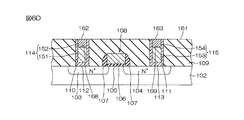
- the drain contact plug 114 covers the main body plug 151 buried in the middle of the drain contact hole 110 in the depth direction and the upper surface 168 of the main body plug 151, and the upper surface 162 is flush with the upper surface 161 of the first insulating layer 109.
- a cap plug 152 that completely fills the drain contact hole 110.
- the main body plug 151 as the first metal plug is made of a metal material such as tungsten, for example.
- the cap plug 152 as a conductive cap is a conductive material having an etching selectivity with respect to the material of the lower electrode 119 and the upper electrode 121 described later, for example, TiN (titanium nitride), TaN (tantalum nitride), WN (nitrided). Conductive nitride such as tungsten), polysilicon doped with impurities (doped polysilicon), carbon and the like.
- a barrier film 112 is interposed between the inner surface (the side surface formed by the first insulating layer 109 and the bottom surface formed by the silicon substrate 102) and the drain contact plug 114.
- the barrier film 112 is made of, for example, a conductive material containing titanium (for example, TiN, Ti, etc.). By interposing the conductive barrier film 112, the drain contact plug 114 is electrically connected (contacted) to the drain region 103 through the barrier film 112.
- a source contact hole 111 reaching the source region 104 from the upper surface 161 of the first insulating layer 109 is formed at a portion facing the source region 104.
- a source contact plug 115 is embedded in the source contact hole 111.
- the source contact plug 115 covers the body plug 153 embedded in the middle of the depth direction of the source contact hole 111 and the upper surface 169 of the body plug 153, and the upper surface 163 is flush with the upper surface 161 of the first insulating layer 109.
- a cap plug 154 that completely fills the source contact hole 111.
- the upper surface 163 of the cap plug 154 is flush with the upper surface 161 of the first insulating layer 109, the upper surface of the source contact plug 115 (the upper surface 163 of the cap plug 154) and the upper surface of the drain contact plug 114 (the cap plug 152). It is flush with the upper surface 162).
- the main body plug 153 as the second metal plug is made of a metal material such as tungsten, for example.
- the cap plug 154 as a conductive cap is made of the same material as the cap plug 152 described above, for example.
- a barrier film 113 is interposed between the inner surface (the side surface formed by the first insulating layer 109 and the bottom surface formed by the silicon substrate 102) and the source contact plug 115.
- the barrier film 113 is made of, for example, a conductive material containing titanium (for example, TiN, Ti, etc.).
- the source contact plug 115 is electrically connected (contacted) to the source region 104 through the barrier film 113.
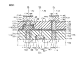
- a ferroelectric capacitor 118 is disposed at a portion facing the drain contact plug 114. That is, the ferroelectric capacitor 118 is arranged at a position that overlaps the drain contact plug 114 in a plan view and does not overlap the source contact plug 115.
- the ferroelectric capacitor 118 includes a lower electrode 119, an upper electrode 121, and a ferroelectric film 120 sandwiched between the lower electrode 119 and the upper electrode 121.
- the lower electrode 119 is made of a conductive material containing noble metal (specifically, Au-based material, Ag-based material, Pt-based material, Pd-based material, Rh-based material, Ir-based material, Ru-based material, Os-based material). Become.
- the thickness of the lower electrode 119 is, for example, 0.05 to 0.25 ⁇ m.
- the lower electrode 119 is in contact with the upper surface 162 of the drain contact plug 114. As a result, the lower electrode 119 is electrically connected to the drain region 103 via the drain contact plug 114.
- the upper electrode 121 is made of a conductive material containing a noble metal.
- the thickness of the upper electrode 121 is, for example, the same thickness as the lower electrode 119 (for example, 0.05 to 0.25 ⁇ m).
- the ferroelectric film 120 is made of a ferroelectric material.
- the ferroelectric material is not particularly limited as long as it is a material that can store charges even when no voltage is applied.
- the thickness of the ferroelectric film 120 is, for example, 0.1 to 0.2 ⁇ m.
- the ferroelectric capacitor 118 formed by laminating the lower electrode 119, the ferroelectric film 120, and the upper electrode 121 is formed in, for example, a mesa shape (a trapezoidal shape in a sectional view).
- a TiN film 148 is stacked on the upper electrode 121 of the ferroelectric capacitor 118.
- first hydrogen barrier film 122 made of Al 2 O 3 (alumina) and a second hydrogen barrier film 123 made of SiN (silicon nitride) are sequentially stacked.
- a second insulating layer 124 is stacked on the second hydrogen barrier film 123.
- the second insulating layer 124 is made of, for example, silicon oxide.
- the thickness of the second insulating layer 124 is, for example, the same thickness as the first insulating layer 109 (for example, 0.4 to 0.9 ⁇ m).
- a PL wiring via hole 125 that penetrates from the upper surface 165 of the second insulating layer 124 and reaches the TiN film 148 is formed. ing.
- a PL wiring plug 129 made of a metal material such as tungsten is embedded in the PL wiring via hole 125. The PL wiring plug 129 fills the PL wiring via hole 125 until the upper surface 166 thereof is flush with the upper surface 165 of the second insulating layer 124.
- a barrier film 127 is interposed between the inner surface (the side surface formed by the second insulating layer 124 and the bottom surface formed by the TiN film 148) and the PL wiring plug 129.
- the barrier film 127 is made of, for example, a conductive material containing titanium (for example, TiN, Ti, etc.).
- the PL wiring plug 129 is electrically connected (contacted) to the upper electrode 121 through the barrier film 127 and the TiN film 148.
- the second insulating layer 124, the second hydrogen barrier film 123, and the first hydrogen barrier film 122 penetrate the BL from the upper surface 165 of the second insulating layer 124 and reach the source contact plug 115. Is formed.
- a BL wiring plug 130 made of a metal material such as tungsten is embedded in the BL wiring via hole 126. The BL wiring plug 130 fills the BL wiring via hole 126 until the upper surface 167 thereof is flush with the upper surface 165 of the second insulating layer 124.
- a barrier film 128 is formed between the inner surface (the side surface formed by the second insulating layer 124 and the bottom surface formed by the source contact plug 115) and the BL wiring plug 130 in the BL wiring via hole 126.
- the barrier film 128 is made of, for example, a conductive material containing titanium (for example, TiN, Ti, etc.). With the conductive barrier film 128 interposed, the BL wiring plug 130 is electrically connected (contacted) to the source contact plug 115 through the barrier film 127.
- the PL wiring 131 is a wiring connected to the plate line 140 provided in the ferroelectric memory 101.
- the titanium layer 133 made of a conductive material containing titanium and the aluminum made of a conductive material containing aluminum.
- the BL wiring 132 is a wiring connected to the bit line 141 provided in the ferroelectric memory 101, for example, a titanium layer 136 made of a conductive material containing titanium and an aluminum made of a conductive material containing aluminum.
- the layer 137 has a three-layer structure including a titanium layer 138 made of a conductive material containing titanium.
- the ferroelectric memory 101 includes a word line 139, a plate line 140, and a bit line 141.
- the word line 139 extends in a direction orthogonal to the longitudinal direction of the active region 150 at a position facing each channel region between each drain region 103 and source region 104.
- the word line 139 is connected to the gate electrode 106.
- the plate line 140 extends above the upper electrode 121 in a direction orthogonal to the longitudinal direction of the active region 150.
- the plate line 140 is connected to the PL wiring 131.
- the bit line 141 extends in the longitudinal direction of the active region 150 above the active region 150.
- the bit line 141 is connected to the BL wiring 132.
- a memory cell is selected by the word line 139, and a voltage is applied between the bit line 141 and the plate line 140, whereby the ferroelectric capacitor 118 of the selected memory cell is changed from the upper electrode 121 to the lower electrode 119.
- 6A to 6K are schematic cross-sectional views showing the manufacturing method of the ferroelectric memory of FIG. 5 in the order of steps.
- N + -type drain region 103 and N + -type source region 104 are formed by implanting N-type impurities into the surface layer portion of silicon substrate 102.
- a thermal oxide film (not shown) is formed on the silicon substrate 102 by thermal oxidation, and this thermal oxide film is patterned.
- a gate insulating film 105 extending over the drain region 103 and the source region 104 is formed.
- polysilicon doped with impurities is deposited on the silicon substrate 102 on which the gate insulating film 105 is formed by a CVD method, and the doped polysilicon is patterned. Thereby, the gate electrode 106 is formed on the gate insulating film 105.
- silicon oxide is deposited on the silicon substrate 102 by CVD, and this silicon oxide is etched back. As a result, a sidewall 107 surrounding the side wall of the gate electrode 106 is formed.
- a MOSFET 108 having a gate electrode 106 (Metal), a gate insulating film 105 (Oxide), and a silicon substrate 102 (Semiconductor) including a drain region 103 and a source region 104 is formed.
- the first insulating layer 109 is formed by depositing silicon oxide on the silicon substrate 102 by the CVD method. Next, the first insulating layer 109 is patterned by a known patterning technique, whereby the drain contact hole 110 and the source contact hole 111 are simultaneously formed in the first insulating layer 109.
- a conductive material containing titanium is deposited by sputtering so as to cover the entire inner surfaces of the drain contact hole 110 and the source contact hole 111 and further cover the upper surface 161 of the first insulating layer 109.
- tungsten is deposited by CVD so as to fill the drain contact hole 110 and the source contact hole 111.
- the conductive material containing titanium and tungsten are polished by CMP until the upper surface of the deposited tungsten and the upper surface 161 of the first insulating layer 109 are flush with each other.
- the barrier film 112 is formed, and the drain-side metal plug 116 embedded in the drain contact hole 110 is formed through the barrier film 112.
- the barrier film 113 is formed, and the source side metal plug 117 embedded in the source contact hole 111 is formed simultaneously with the drain side metal plug 116 via the barrier film 113.
- drain side metal plug 116 and the source side metal plug 117 are removed by a known etching technique.
- the drain-side main body plug 151 and the source-side main body plug 153 embedded in the middle of the drain contact hole 110 and the middle of the source contact hole 111 are formed.
- the cap is formed by filling the body plugs 151 and 153 in the drain contact hole 110 and the source contact hole 111 and covering the upper surface 161 of the first insulating layer 109 by sputtering.
- Cap material 147 which is the material of plug 152 and cap plug 154, is deposited. Thereafter, the cap material 147 is polished by CMP until the upper surface of the deposited cap material 147 and the upper surface 161 of the first insulating layer 109 are flush with each other.
- the cap plug 152 covering the upper surface 168 of the main body plug 151 and the cap plug 154 covering the upper surface 169 of the main body plug 153 are formed simultaneously.
- the drain contact plug 114 and the source contact plug 115 buried in the drain contact hole 110 and the source contact hole 111, respectively, via the barrier films 112 and 113 are simultaneously formed.
- a lower conductive material film 142 made of a conductive material containing a noble metal
- a ferroelectric material film 143 made of a ferroelectric material
- an upper conductive material made of a conductive material containing a noble metal.
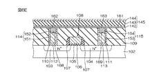
- a material film 144 is sequentially deposited on the first insulating layer 109 to form a deposition structure 145.
- a heat-resistant hard mask 146 (for example, TiN) is formed on the portion of the deposited structure 145 on the drain contact plug 114.
- the deposited structure 145 is etched through the hard mask 146 perpendicularly to the stacked interface at an etching temperature of 300 ° C.
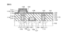
- the hard mask 146 thinned by etching remains as a TiN film 148 on the upper electrode 121 of the ferroelectric capacitor 118.
- H hydrogen
- the reduction of oxygen in the ferroelectric film 120 by the carrier gas can be prevented. Therefore, the characteristic deterioration of the ferroelectric film 120 can be suppressed.
- the second insulating layer 124 is polished by a CMP process, and the surface of the second insulating layer 124 is planarized. Then, as shown in FIG. 6I, the second insulating layer 124, the second hydrogen barrier film 123, and the first hydrogen barrier film 122 are patterned by a known patterning technique, thereby exposing the TiN film 148. A via hole 125 and a BL wiring via hole 126 exposing the upper surface 163 of the source contact plug 115 are formed simultaneously.
- a conductive material containing titanium is deposited by sputtering so as to cover the inner surfaces of the PL wiring via hole 125 and the BL wiring via hole 126 and further cover the upper surface 165 of the second insulating layer 124.
- tungsten is deposited by CVD so as to fill the PL wiring via hole 125 and the BL wiring via hole 126.
- the titanium-containing material and tungsten are polished by CMP until the upper surface of the deposited tungsten and the upper surface 165 of the second insulating layer 124 are flush with each other.
- the barrier film 127 is formed, and the PL wiring plug 129 embedded in the PL wiring via hole 125 is formed through the barrier film 127.
- the barrier film 128 is formed, and the BL wiring plug 130 embedded in the BL wiring via hole 126 is formed simultaneously with the PL wiring plug 129 via the barrier film 128.
- the upper surface 166 of the PL wiring plug 129 and the upper surface 167 of the BL wiring plug 130 are flush with the upper surface 165 of the second insulating layer 124.
- a conductive material containing titanium, a conductive material containing aluminum, and a conductive material containing titanium are stacked on the second insulating layer 124 and patterned by sputtering.
- the PL wiring 131 (wiring having a three-layer structure of the titanium layer 133, the aluminum layer 134, and the titanium layer 135) electrically connected to the PL wiring plug 129
- the BL wiring A BL wiring 132 (a wiring having a three-layer structure of a titanium layer 136, an aluminum layer 137, and a titanium layer 138) that is electrically connected to the wiring plug 130 is formed.
- the word line 139 is connected to the gate electrode 106, the plate line 140 is connected to the PL wiring 131, and the bit line 141 is connected to the BL wiring 132.
- the ferroelectric memory 101 on which the ferroelectric capacitor 118 is mounted is obtained.
- the upper surface 169 of the source-side main body plug 153 is covered with the cap plug 154.
- the cap plug 154 By covering with the cap plug 154, the upper surface 169 of the main body plug 153 is protected by the cap plug 154.
- the deposition structure 145 is formed on the first insulating layer 109, and a part of the deposition structure 145 (the part on the drain contact plug 114) is formed. Then, a heat-resistant hard mask 146 is formed. Then, the deposited structure 145 is etched through the hard mask 146, whereby the ferroelectric capacitor 118 is formed.
- the main body plug 153 is covered with the cap plug 154 when the deposited structure 145 is etched.
- the cap plug 154 is made of a conductive material having an etching selectivity with respect to the lower electrode 119 and the upper electrode 121 as described above. Therefore, even when the deposited structure 145 is etched at a high temperature of 300 ° C. or higher as described above, the abnormal etching of the main body plug 153 can be prevented by the protection by the cap plug 154. As a result, the occurrence of poor conduction between the source contact plug 115 constituted by the main body plug 153 and the cap plug 154 and the BL wiring plug 130 connected to the source contact plug 115 can be suppressed. The decrease can be suppressed.
- the cap plug 154 is a conductive nitride
- the etching selectivity can be increased with respect to the lower electrode 119 and the upper electrode 121, so that abnormal etching of the main body plug 153 can be effectively prevented.
- the side surface 164 of the ferroelectric capacitor 118 can be made steep with respect to the stacked interface I by etching the deposited structure 145 at a high temperature. As a result, the area of the ferroelectric capacitor 118 can be reduced, so that the ferroelectric memory 101 can be miniaturized.
- a main body plug 151 and a cap plug 152 are embedded in the drain contact hole 110.
- a main body plug 153 and a cap plug 154 are embedded in the source contact hole 111. That is, the structures embedded in the drain contact hole 110 and the source contact hole 111 have the same structure. Therefore, regarding the formation of the drain contact plug 114 and the source contact plug 115, the drain contact hole 110 and the source contact hole 111 are formed at the same time, and the drain side metal plug 116 and the source side metal plug 117 filling the contact holes are formed. (See FIG. 6A). Next, by etching these plugs, a drain-side body plug 151 and a source-side body plug 153 are formed simultaneously (see FIG. 6B).
- a conductive cap material 147 that fills the main body plugs 151 and 153 in the drain contact hole 110 and the source contact hole 111 is deposited (see FIG. 6C), and the cap material 147 is polished by a CMP process.
- the drain-side cap plug 152 and the source-side cap plug 154 are simultaneously formed, and the drain contact plug 114 and the source contact plug 115 are simultaneously formed (see FIG. 6D).
- the step of forming the drain-side main body plug 151 and the step of forming the source-side main body plug 153 are performed in parallel, and the drain-side cap plug 152 covering the upper surface 168 of the main body plug 151 is further provided. And the step of forming the source-side cap plug 154 covering the upper surface 169 of the main body plug 153 are performed in parallel. Therefore, the manufacturing process of the ferroelectric memory 101 can be simplified.
- this invention can also be implemented with another form.
- a configuration in which the conductivity type of each semiconductor portion of the ferroelectric memories 1 and 101 is inverted may be employed. That is, in the ferroelectric memories 1 and 101, the P-type portion may be N-type and the N-type portion may be P-type.
- each memory cell of the ferroelectric memories 1 and 101 may be, for example, a 2T2C type as long as a ferroelectric capacitor and a MOSFET are combined.
- the drain contact plug 114 may not have the cap plug 152.
- the body plug 151 may be formed by filling the drain contact hole 110 with a metal material such as tungsten until the upper surface 168 thereof is flush with the upper surface 161 of the first insulating layer 109.
- the source contact plug 115 may not have the cap plug 154, but in this case, the conductive material having an etching selectivity with respect to the lower electrode 119 and the upper electrode 121 is formed on the upper surface of the source contact plug 115. What is necessary is just to coat
Landscapes
- Semiconductor Memories (AREA)
- Engineering & Computer Science (AREA)
- Chemical & Material Sciences (AREA)
- Physics & Mathematics (AREA)
- Power Engineering (AREA)
- Materials Engineering (AREA)
- Optics & Photonics (AREA)
- Plasma & Fusion (AREA)
- Chemical Kinetics & Catalysis (AREA)
Abstract
Description
図7A~図7Hは、従来の強誘電体メモリの製造方法を工程順に示す模式的な断面図である。
その後、CVD法により、図7Eに示すように、第2水素バリア膜223上に、酸化シリコンからなる第2絶縁層224が積層される。
こうして、図7Hに示すように、強誘電体キャパシタ221を搭載する強誘電体メモリ200が得られる。
下部電極および上部電極の材料として使用されるIrやPt、および強誘電体膜の材料として使用されるPZTは、エッチングされにくい。そのため、通常のドライエッチングの条件では、下部電極の材料、強誘電体膜の材料および上部電極の材料が積層されてなる積層構造物を垂直方向にエッチングしても、強誘電体キャパシタの側面が積層界面に対して垂直面とならずに傾斜面となる。この強誘電体キャパシタの側面を、積層界面に対して垂直面に近づけることができれば、強誘電体キャパシタの容量を下げることなく、キャパシタ面積を縮小することができる。
しかし、高温エッチング時に、積層構造物239のエッチング部分の下方に配置されるソースコンタクトプラグ214が、積層構造物239とともにエッチングされる異常エッチングを生じる場合がある。ソースコンタクトプラグ214が異常エッチングされると、ソースコンタクトプラグ214とBL用配線プラグ230との間に導通不良を引き起こし、それによって強誘電体メモリ200の信頼性が低下する。
この状態で、層間絶縁膜上に形成された堆積構造物の一部(層間絶縁膜の開口上に残存する部分以外の部分)がエッチングで除去されることにより、強誘電体キャパシタが形成される。
また、上記半導体記憶装置では、前記第1金属プラグの上面と前記第2金属プラグの上面とが面一であることが好ましい。
このように、第1金属プラグを形成するための複数の工程と、第2金属プラグを形成するための複数の工程とが並行して行なわれるので、半導体記憶装置の製造工程を簡略化することができる。
そのため、高温下で、下部電極、強誘電体膜および上部電極が成形されても、導電性キャップによる保護により、第2金属プラグの異常エッチングを防止することができる。その結果、第2金属プラグと、これに接続される接続体との間における導通不良の発生を抑制することができ、信頼性の低下を抑制することができる。
導電性キャップに用いられる導電性窒化物は、たとえば、貴金属を含有する導電材料(具体的には、Au系材料、Ag系材料、Pt系材料、Pd系材料、Rh系材料、Ir系材料、Ru系材料、Os系材料)からなる下部電極および上部電極に対して大きなエッチング選択比を有する。したがって、この態様では、第2金属プラグの異常エッチングを効果的に防止することができる。
この構成によれば、第1貫通孔に、第1金属プラグおよび導電性キャップが埋め込まれている。また、第2貫通孔に、第2金属プラグおよび導電性キャップが埋め込まれている。つまり、第1貫通孔および第2貫通孔に埋め込まれた構造物が同じ構造である。
図1は、本発明の第1の実施形態に係る強誘電体メモリの模式的な平面図である。図2は、図1の強誘電体メモリの断面図であり、切断線II-IIでの切断面である。
半導体記憶装置としての強誘電体メモリ1は、供給電源が遮断されても記憶内容を保持することのできる不揮発性メモリである。
シリコン基板2上には、たとえば、複数の平面視長方形状のアクティブ領域50が形成されている。アクティブ領域50の輪郭は、図1では、太線で示されている。アクティブ領域50は、その長手方向および長手方向と直交する方向に整列するマトリクス状に配置されている。
各メモリセルは、1つの強誘電体キャパシタ18(C)と、1つのMOSFET8(T)とが積層関係に配置される、1T1C型セル構造を有している。
アクティブ領域50(各メモリセル)において、シリコン基板2の表層部には、図2に示すように、N+型のドレイン領域3と、N+型のソース領域4とが間隔を空けて形成されている。なお、ソース領域4は、2つのメモリセルのMOSFET8に共通の領域とされており、平面視において、アクティブ領域50の中央部に形成されている。一方、ドレイン領域3は、平面視において、アクティブ領域50の一端部および他端部のそれぞれに、各メモリセルのMOSFET8に対応して形成されている。
ゲート絶縁膜5上には、たとえば、不純物がドープされたポリシリコン(ドープトポリシリコン)からなるゲート電極6が形成されている。
ゲート電極6の側壁には、その全周にわたって密着するサイドウォール7が形成されている。サイドウォール7は、たとえば、酸化シリコンからなる。
シリコン基板2上には、第1絶縁層9が積層されている。第1絶縁層9は、たとえば、酸化シリコンからなる。また、第1絶縁層9の厚さは、たとえば、0.4~0.9μmである。
ドレインコンタクトホール10には、タングステンなどの金属材料からなるドレインコンタクトプラグ14が埋設されている。第1金属プラグとしてのドレインコンタクトプラグ14は、その上面62が第1絶縁層9の上面61と面一になるまでドレインコンタクトホール10を埋め尽くしている。
導電性のバリア膜12が介在されることにより、ドレインコンタクトプラグ14は、バリア膜12を介して、ドレイン領域3に電気的に接続(コンタクト)されることとなる。
ソースコンタクトホール11には、タングステンなどの金属材料からなるソースコンタクトプラグ15が埋設されている。第2金属プラグとしてのソースコンタクトプラグ15は、その上面63が第1絶縁層9の上面61と面一になるまでソースコンタクトホール11を埋め尽くしている。ソースコンタクトプラグ15の上面63が第1絶縁層9の上面61と面一であることにより、ソースコンタクトプラグ15の上面63と、ドレインコンタクトプラグ14の上面62とは、面一となっている。
導電性のバリア膜13が介在されることにより、ソースコンタクトプラグ15は、バリア膜13を介して、ソース領域4に電気的に接続(コンタクト)されることとなる。
強誘電体キャパシタ18は、下部電極19と、上部電極21と、下部電極19と上部電極21とにより挟まれた強誘電体膜20とを備えている。
強誘電体膜20は、強誘電体材料からなる。強誘電体材料としては、電圧が印加されていなくても電荷を貯蔵可能な特性を有する材料であれば特に制限されず、たとえば、チタン酸ジルコン酸鉛(Pb(Zr,Ti)O3:PZT)、タンタル酸ビスマスストロンチウム(SrBi2Ta2O9:SBT)、チタン酸ビスマスランタン(Bi,La)4Ti3O12:BLT)、チタン酸バリウム(BaTiO3)など、公知のものが挙げられる。また、強誘電体膜20の厚さは、たとえば、0.05~0.2μmである。
強誘電体キャパシタ18の上部電極21上には、TiN膜48が積層されている。
第2水素バリア膜23上には、第2絶縁層24が積層されている。第2絶縁層24は、たとえば、酸化シリコンからなる。また、第2絶縁層24の厚さは、たとえば、第1絶縁層9と同じ厚さ(たとえば、0.4~0.9μm)である。
PL用配線ビアホール25には、タングステンなどの金属材料からなるPL用配線プラグ29が埋設されている。PL用配線プラグ29は、その上面66が第2絶縁層24の上面65と面一になるまでPL用配線ビアホール25を埋め尽くしている。
導電性のバリア膜27が介在されることにより、PL用配線プラグ29は、バリア膜27およびTiN膜48を介して、上部電極21に電気的に接続(コンタクト)されることとなる。
BL用配線ビアホール26には、タングステンなどの金属材料からなるBL用配線プラグ30が埋設されている。BL用配線プラグ30は、その上面67が第2絶縁層24の上面65と面一になるまでBL用配線ビアホール26を埋め尽くしている。
導電性のバリア膜28が介在されることにより、BL用配線プラグ30は、バリア膜27を介して、ソースコンタクトプラグ15に電気的に接続(コンタクト)されることとなる。
PL用配線31は、強誘電体メモリ1に備えられるプレート線40に接続される配線であって、たとえば、チタンを含有する導電材料からなるチタン層33と、アルミニウムを含有する導電材料からなるアルミニウム層34と、チタンを含有する導電材料からなるチタン層35との3層構造で形成されている。
また、強誘電体メモリ1には、ワード線39、プレート線40およびビット線41が備えられている。
プレート線40は、上部電極21の上方において、アクティブ領域50の長手方向と直交する方向に延びている。プレート線40はPL用配線31に接続されている。
そして、ワード線39によりメモリセルを選択し、ビット線41とプレート線40との間に電圧を印加することにより、選択されたメモリセルの強誘電体キャパシタ18が、上部電極21から下部電極19へ向かう方向もしくはその反対方向に分極する。この分極方向を判別することによって、当該メモリセルに対して1ビット情報(0もしくは1の情報)を書き込むことができる。
図3A~図3Jは、図2の強誘電体メモリの製造方法を工程順に示す模式的な断面図である。
次に、スパッタ法により、ドレインコンタクトホール10およびソースコンタクトホール11の内面全域を覆い、さらに第1絶縁層9の上面61を覆うように、チタンを含有する導電材料が堆積される。そして、CVD法により、ドレインコンタクトホール10およびソースコンタクトホール11を埋め尽くすようにタングステンが堆積される。その後、CMP処理により、堆積されたタングステンの上面と第1絶縁層9の上面61とが面一になるまで、チタンを含有する導電材料およびタングステンが研磨される。こうして、図3Aに示すように、バリア膜12が形成されるとともに、このバリア膜12を介して、ドレインコンタクトホール10に埋設されたドレインコンタクトプラグ14が形成される。また、バリア膜13が形成されるとともに、このバリア膜13を介して、ソースコンタクトホール11に埋設されたソースコンタクトプラグ15が、ドレインコンタクトプラグ14と同時に形成される。ドレインコンタクトプラグ14の上面62およびソースコンタクトプラグ15の上面63は、第1絶縁層9の上面61と面一となる。
次に、公知のパターニング技術により、層間絶縁膜16のドレインコンタクトプラグ14に対向する部分が除去される。これにより、図3Cに示すように、ドレインコンタクトプラグ14の上面62を露出させる開口17が形成される。
続いて、堆積構造物45における開口17上の部分(ドレインコンタクトプラグ14上の部分)に、耐熱性のあるハードマスク46(たとえば、TiN)が形成される。そして、このハードマスク46を介して、たとえば、300℃以上、好ましくは、350~450℃のエッチング温度で、堆積構造物45がその積層界面に対して垂直にエッチングされる。これにより、堆積構造物45は、その一部が開口17上に残存するように、その残存部分以外の部分が除去される。こうして、図3Eに示すように、開口17上における積層界面Iに対して傾斜角度a(たとえば、a=75~85°)で傾斜する側面64を有するメサ形状の強誘電体キャパシタ18が形成される。なお、強誘電体キャパシタ18の上部電極21上には、図3Fに示すように、エッチングにより薄くなったハードマスク46がTiN膜48として残存する。
その後、CVD法により、図3Gに示すように、第2水素バリア膜23上に、酸化シリコンからなる第2絶縁層24が積層される。このとき、強誘電体キャパシタ18の表面全域が第1水素バリア膜22および第2水素バリア膜23により覆われているので、第2絶縁層24の形成方法として、H(水素)をキャリヤガスとして用いるCVD法が採用されても、キャリヤガスによる強誘電体膜20中の酸素の還元を防止することができる。したがって、強誘電体膜20の特性劣化を抑制することができる。
こうして、図3Jに示すように、強誘電体キャパシタ18を搭載する強誘電体メモリ1が得られる。
以上のように、上記の製造方法では、第1絶縁層9に、ドレインコンタクトプラグ14およびソースコンタクトプラグ15が埋設された後、第1絶縁層9上に層間絶縁膜16が積層される。そして、層間絶縁膜16がパターニングされることにより、層間絶縁膜16のドレインコンタクトプラグ14に対向する部分が除去されて、開口17が形成される。これにより、ドレインコンタクトプラグ14が層間絶縁膜16の開口17を介して露出する一方、ソースコンタクトプラグ15が層間絶縁膜16により覆われる。
堆積構造物45のエッチング時、ソースコンタクトプラグ15が層間絶縁膜16により覆われている。そのため、上記のように300℃以上の高温で、堆積構造物45がエッチングされても、層間絶縁膜16による保護により、ソースコンタクトプラグ15の異常エッチングを防止することができる。その結果、ソースコンタクトプラグ15と、これに接続されるBL用配線プラグ30との間における導通不良の発生を抑制することができ、信頼性の低下を抑制することができる。
また、ドレインコンタクトプラグ14およびソースコンタクトプラグ15の形成に関して、ドレインコンタクトホール10およびソースコンタクトホール11が同時に形成される。そして、これらコンタクトホールを埋め尽くすようにタングステンが堆積された後、タングステンの上面と第1絶縁層9の上面61とが面一になるまで、タングステンがCMP処理により研磨される。この研磨によって、それらの上面62,63が互いに面一をなすドレインコンタクトプラグ14およびソースコンタクトプラグ15が同時に形成される(図3A参照)。
図4は、本発明の第2の実施形態に係る強誘電体メモリの模式的な平面図である。図5は、図4の強誘電体メモリの断面図であり、切断線V-Vでの切断面である。
強誘電体メモリ101は、図5に示すように、P型のシリコン基板102を備えている。
シリコン基板102上には、たとえば、複数の平面視長方形状のアクティブ領域150が形成されている。アクティブ領域150の輪郭は、図4では、太線で示されている。アクティブ領域150は、その長手方向および長手方向と直交する方向に整列するマトリクス状に配置されている。
各メモリセルは、1つの強誘電体キャパシタ118(C)と、1つのMOSFET108(T)とが積層関係に配置される、1T1C型セル構造を有している。
アクティブ領域150(各メモリセル)において、シリコン基板102の表層部には、図5に示すように、N+型のドレイン領域103と、N+型のソース領域104とが間隔を空けて形成されている。なお、ソース領域104は、2つのメモリセルのMOSFET108に共通の領域とされており、平面視において、アクティブ領域150の中央部に形成されている。一方、ドレイン領域103は、平面視において、アクティブ領域150の一端部および他端部のそれぞれに、各メモリセルのMOSFET108に対応して形成されている。
ゲート絶縁膜105上には、たとえば、不純物がドープされたポリシリコン(ドープトポリシリコン)からなるゲート電極106が形成されている。
このように、強誘電体メモリ101には、ゲート電極106(Metal)と、ゲート絶縁膜105(Oxide)と、ドレイン領域103およびソース領域104を含むシリコン基板102(Semiconductor)とを有するMOSFET108が備えられている。
第1絶縁層109において、ドレイン領域103に対向する部分には、第1絶縁層109の上面161からドレイン領域103に達するドレインコンタクトホール110が形成されている。
導電性キャップとしてのキャッププラグ152は、後述する下部電極119および上部電極121の材料に対してエッチング選択比を有する導電性材料、たとえば、TiN(窒化チタン)、TaN(窒化タンタル)、WN(窒化タングステン)などの導電性窒化物、不純物がドープされたポリシリコン(ドープトポリシリコン)、カーボンなどからなる。
導電性のバリア膜112が介在されることにより、ドレインコンタクトプラグ114は、バリア膜112を介して、ドレイン領域103に電気的に接続(コンタクト)されることとなる。
ソースコンタクトホール111には、ソースコンタクトプラグ115が埋設されている。ソースコンタクトプラグ115は、ソースコンタクトホール111の深さ方向途中部まで埋め込まれた本体プラグ153と、本体プラグ153の上面169を覆い、その上面163が第1絶縁層109の上面161と面一になるまでソースコンタクトホール111を埋め尽くすキャッププラグ154とを有している。キャッププラグ154の上面163が第1絶縁層109の上面161と面一であることにより、ソースコンタクトプラグ115の上面(キャッププラグ154の上面163)と、ドレインコンタクトプラグ114の上面(キャッププラグ152の上面162)とは、面一となっている。
導電性キャップとしてのキャッププラグ154は、たとえば、上記したキャッププラグ152と同様の材料からなる。
また、ソースコンタクトホール111において、その内面(第1絶縁層109がなす側面およびシリコン基板102がなす底面)とソースコンタクトプラグ115との間には、バリア膜113が介在されている。バリア膜113は、たとえば、チタンを含有する導電材料(たとえば、TiN、Tiなど)からなる。
第1絶縁層109上には、ドレインコンタクトプラグ114に対向する部分に、強誘電体キャパシタ118が配置されている。つまり、強誘電体キャパシタ118は、平面視でドレインコンタクトプラグ114に重なる位置であって、ソースコンタクトプラグ115に重ならない位置に配置されている。
下部電極119は、貴金属を含有する導電材料(具体的には、Au系材料、Ag系材料、Pt系材料、Pd系材料、Rh系材料、Ir系材料、Ru系材料、Os系材料)からなる。また、下部電極119の厚さは、たとえば、0.05~0.25μmである。下部電極119は、ドレインコンタクトプラグ114の上面162に接触している。これにより、下部電極119は、ドレインコンタクトプラグ114を介して、ドレイン領域103に電気的に接続されることとなる。
強誘電体膜120は、強誘電体材料からなる。強誘電体材料としては、電圧が印加されていなくても電荷を貯蔵可能な特性を有する材料であれば特に制限されず、たとえば、チタン酸ジルコン酸鉛(Pb(Zr,Ti)O3:PZT)、タンタル酸ビスマスストロンチウム(SrBi2Ta2O9:SBT)、チタン酸ビスマスランタン(Bi,La)4Ti3O12:BLT)、チタン酸バリウム(BaTiO3)など、公知のものが挙げられる。また、強誘電体膜120の厚さは、たとえば、0.1~0.2μmである。
強誘電体キャパシタ118の上部電極121上には、TiN膜148が積層されている。
第2水素バリア膜123上には、第2絶縁層124が積層されている。第2絶縁層124は、たとえば、酸化シリコンからなる。また、第2絶縁層124の厚さは、たとえば、第1絶縁層109と同じ厚さ(たとえば、0.4~0.9μm)である。
PL用配線ビアホール125には、タングステンなどの金属材料からなるPL用配線プラグ129が埋設されている。PL用配線プラグ129は、その上面166が第2絶縁層124の上面165と面一になるまでPL用配線ビアホール125を埋め尽くしている。
導電性のバリア膜127が介在されることにより、PL用配線プラグ129は、バリア膜127およびTiN膜148を介して、上部電極121に電気的に接続(コンタクト)されることとなる。
BL用配線ビアホール126には、タングステンなどの金属材料からなるBL用配線プラグ130が埋設されている。BL用配線プラグ130は、その上面167が第2絶縁層124の上面165と面一になるまでBL用配線ビアホール126を埋め尽くしている。
導電性のバリア膜128が介在されることにより、BL用配線プラグ130は、バリア膜127を介して、ソースコンタクトプラグ115に電気的に接続(コンタクト)されることとなる。
PL用配線131は、強誘電体メモリ101に備えられるプレート線140に接続される配線であって、たとえば、チタンを含有する導電材料からなるチタン層133と、アルミニウムを含有する導電材料からなるアルミニウム層134と、チタンを含有する導電材料からなるチタン層135との3層構造で形成されている。
また、強誘電体メモリ101には、ワード線139、プレート線140およびビット線141が備えられている。
プレート線140は、上部電極121の上方において、アクティブ領域150の長手方向と直交する方向に延びている。プレート線140はPL用配線131に接続されている。
そして、ワード線139によりメモリセルを選択し、ビット線141とプレート線140との間に電圧を印加することにより、選択されたメモリセルの強誘電体キャパシタ118が、上部電極121から下部電極119へ向かう方向もしくはその反対方向に分極する。この分極方向を判別することによって、当該メモリセルに対して1ビット情報(0もしくは1の情報)を書き込むことができる。
図6A~図6Kは、図5の強誘電体メモリの製造方法を工程順に示す模式的な断面図である。
その後、CMP処理により、堆積されたキャップ材料147の上面と第1絶縁層109の上面161とが面一になるまで、キャップ材料147が研磨される。こうして、図6Dに示すように、本体プラグ151の上面168を覆うキャッププラグ152と、本体プラグ153の上面169を覆うキャッププラグ154とが同時に形成される。これにより、各バリア膜112,113を介してドレインコンタクトホール110およびソースコンタクトホール111にそれぞれ埋設された、ドレインコンタクトプラグ114およびソースコンタクトプラグ115が同時に形成される。
続いて、堆積構造物145におけるドレインコンタクトプラグ114上の部分に、耐熱性のあるハードマスク146(たとえば、TiN)が形成される。そして、このハードマスク146を介して、たとえば、300℃以上、好ましくは、350~450℃のエッチング温度で、堆積構造物145がその積層界面に対して垂直にエッチングされる。これにより、堆積構造物145は、その一部がドレインコンタクトプラグ114上に残存するように、その残存部分以外の部分が除去される。こうして、図6Fに示すように、その積層界面Iに対して傾斜角度a(たとえば、a=75~85°)で傾斜する側面164を有するメサ形状の強誘電体キャパシタ118が形成される。なお、強誘電体キャパシタ118の上部電極121上には、図6Gに示すように、エッチングにより薄くなったハードマスク146がTiN膜148として残存する。
その後、CVD法により、図6Hに示すように、第2水素バリア膜123上に、酸化シリコンからなる第2絶縁層124が積層される。このとき、強誘電体キャパシタ118の表面全域が第1水素バリア膜122および第2水素バリア膜123により覆われているので、第2絶縁層124の形成方法として、H(水素)をキャリヤガスとして用いるCVD法が採用されても、キャリヤガスによる強誘電体膜120中の酸素の還元を防止することができる。したがって、強誘電体膜120の特性劣化を抑制することができる。
こうして、図6Kに示すように、強誘電体キャパシタ118を搭載する強誘電体メモリ101が得られる。
以上のように、強誘電体メモリ101では、ソース側の本体プラグ153の上面169は、キャッププラグ154により覆われている。キャッププラグ154で覆われることにより、本体プラグ153の上面169は、キャッププラグ154により保護されている。
また、堆積構造物145を高温エッチングすることにより、強誘電体キャパシタ118の側面164を、積層界面Iに対して急斜面にすることができる。その結果、強誘電体キャパシタ118の面積を縮小することができるので、強誘電体メモリ101の微細化を図ることができる。
したがって、ドレインコンタクトプラグ114およびソースコンタクトプラグ115の形成に関して、ドレインコンタクトホール110およびソースコンタクトホール111が同時に形成され、これらコンタクトホールを埋め尽くすドレイン側金属プラグ116およびソース側金属プラグ117が形成される(図6A参照)。次いで、これらプラグがエッチングされることによって、ドレイン側の本体プラグ151およびソース側の本体プラグ153が同時に形成される(図6B参照)。
たとえば、強誘電体メモリ1,101の各半導体部分の導電型を反転した構成が採用されてもよい。すなわち、強誘電体メモリ1,101において、P型の部分がN型であり、N型の部分がP型であってもよい。
また、ドレインコンタクトプラグ114は、キャッププラグ152を有していなくてもよい。この場合、ドレインコンタクトホール110に、その上面168と第1絶縁層109の上面161とが面一になるまでタングステンなどの金属材料を埋め尽くすことにより、本体プラグ151を形成すればよい。
本発明の実施形態について詳細に説明してきたが、これらは本発明の技術的内容を明らかにするために用いられた具体例に過ぎず、本発明はこれらの具体例に限定して解釈されるべきではなく、本発明の精神および範囲は添付の請求の範囲によってのみ限定される。
Claims (9)
- 絶縁層と、
前記絶縁層上に形成され、下部電極、強誘電体膜および上部電極を有する強誘電体キャパシタと、
前記絶縁層上に形成され、前記強誘電体キャパシタが配置される部分に開口を有する層間絶縁膜と、
前記絶縁層に埋設され、前記開口を介して前記下部電極に接続される第1金属プラグと、
平面視で前記強誘電体キャパシタ外において、前記絶縁層に埋設された第2金属プラグとを備える、半導体記憶装置。 - 前記第1金属プラグの上面と前記第2金属プラグの上面とが面一である、請求項1に記載の半導体記憶装置。
- 第1貫通孔および第2貫通孔を有する絶縁層と、
前記第1貫通孔を覆うように前記絶縁層上に形成され、下部電極、強誘電体膜および上部電極を有する強誘電体キャパシタと、
前記第1貫通孔に埋め込まれ、前記下部電極に電気的に接続される第1金属プラグと、
前記第2貫通孔に埋め込まれた第2金属プラグと、
前記第1金属プラグおよび前記第2金属プラグのうち、少なくとも前記第2金属プラグの上面を覆い、前記下部電極および前記上部電極の材料に対してエッチング選択比を有する導電性材料からなる導電性キャップとを備える、半導体記憶装置。 - 前記導電性キャップが導電性窒化物からなる、請求項3に記載の半導体記憶装置。
- 前記第1金属プラグおよび前記第2金属プラグは、それぞれ前記第1貫通孔および前記第2貫通孔の途中部まで埋め込まれており、
前記導電性キャップは、前記絶縁層の表面と面一となるように前記第1貫通孔および前記第2貫通孔に埋め込まれている、請求項3に記載の半導体記憶装置。 - 下部電極、強誘電体膜および上部電極を有する強誘電体キャパシタを備える半導体記憶装置の製造方法であって、
絶縁層に第1金属プラグおよび第2金属プラグを埋設する工程と、
前記第1金属プラグに対する電気的なコンタクト部分を確保しつつ、少なくとも前記第2金属プラグを被覆する被覆層を形成する工程と、
前記被覆層の形成後、前記下部電極の材料、前記強誘電体膜の材料および前記上部電極の材料を順に堆積させて堆積構造物を形成する工程と、
前記堆積構造物の一部を前記第1金属プラグ上に残存させるように、当該残存部分以外の部分をエッチングで除去することにより、前記強誘電体キャパシタを形成する工程とを含む、半導体記憶装置の製造方法。 - 前記被覆層を形成する工程が、前記絶縁層上に層間絶縁膜を成膜する工程と、前記層間絶縁膜に、前記第1金属プラグを露出させる開口を形成する工程とを含み、
前記強誘電体キャパシタを形成する工程が、前記堆積構造物の一部を前記開口上に残存させるように、その残存部分以外の部分をエッチングで除去する工程を含む、請求項6に記載の半導体記憶装置の製造方法。 - 絶縁層に第1金属プラグおよび第2金属プラグを埋設する工程が、前記絶縁層に、第1貫通孔および第2貫通孔を形成する工程と、前記第1貫通孔および前記第2貫通孔を埋め尽くすように、前記絶縁層上にプラグ材料を堆積させる工程と、前記プラグ材料の上面と前記絶縁層の上面とが面一になるまで、前記プラグ材料の前記第1貫通孔および前記第2貫通孔外の部分を除去することにより、前記第1金属プラグおよび前記第2金属プラグを形成する工程とを含む、請求項7に記載の半導体記憶装置の製造方法。
- 絶縁層に第1金属プラグおよび第2金属プラグを埋設する工程が、前記絶縁層に、第1貫通孔および第2貫通孔を形成する工程と、前記第1貫通孔および前記第2貫通孔を金属材料で埋め尽くす工程と、前記金属材料をエッチングで部分的に除去することにより、前記第1貫通孔の途中部まで埋め込まれた第1金属プラグと、前記第2貫通孔の途中部まで埋め込まれた第2金属プラグとを形成する工程を含み、
前記被覆層を形成する工程が、前記第1金属プラグおよび前記第2金属プラグの形成後、前記下部電極および前記上部電極の材料に対してエッチング選択比を有する導電性材料を用いて前記第1貫通孔および前記第2貫通孔を埋め尽くすことにより、前記第1金属プラグおよび前記第2金属プラグの各上面を覆う導電性プラグを形成する工程を含む、請求項6に記載の半導体記憶装置の製造方法。
Priority Applications (5)
| Application Number | Priority Date | Filing Date | Title |
|---|---|---|---|
| US13/119,070 US8981440B2 (en) | 2008-09-16 | 2009-09-16 | Semiconductor storage device and method for manufacturing the semiconductor storage device |
| JP2010529638A JP5667875B2 (ja) | 2008-09-16 | 2009-09-16 | 半導体記憶装置および半導体記憶装置の製造方法 |
| US14/615,455 US9362295B2 (en) | 2008-09-16 | 2015-02-06 | Semiconductor storage device and method for manufacturing the semiconductor storage device |
| US15/146,299 US9607998B2 (en) | 2008-09-16 | 2016-05-04 | Semiconductor storage device and method for manufacturing the semiconductor storage device |
| US15/447,100 US9847338B2 (en) | 2008-09-16 | 2017-03-01 | Semiconductor storage device and method for manufacturing the semiconductor storage device |
Applications Claiming Priority (4)
| Application Number | Priority Date | Filing Date | Title |
|---|---|---|---|
| JP2008236647 | 2008-09-16 | ||
| JP2008236648 | 2008-09-16 | ||
| JP2008-236648 | 2008-09-16 | ||
| JP2008-236647 | 2008-09-16 |
Related Child Applications (2)
| Application Number | Title | Priority Date | Filing Date |
|---|---|---|---|
| US13/119,070 A-371-Of-International US8981440B2 (en) | 2008-09-16 | 2009-09-16 | Semiconductor storage device and method for manufacturing the semiconductor storage device |
| US14/615,455 Continuation US9362295B2 (en) | 2008-09-16 | 2015-02-06 | Semiconductor storage device and method for manufacturing the semiconductor storage device |
Publications (1)
| Publication Number | Publication Date |
|---|---|
| WO2010032456A1 true WO2010032456A1 (ja) | 2010-03-25 |
Family
ID=42039304
Family Applications (1)
| Application Number | Title | Priority Date | Filing Date |
|---|---|---|---|
| PCT/JP2009/004653 Ceased WO2010032456A1 (ja) | 2008-09-16 | 2009-09-16 | 半導体記憶装置および半導体記憶装置の製造方法 |
Country Status (3)
| Country | Link |
|---|---|
| US (4) | US8981440B2 (ja) |
| JP (1) | JP5667875B2 (ja) |
| WO (1) | WO2010032456A1 (ja) |
Cited By (4)
| Publication number | Priority date | Publication date | Assignee | Title |
|---|---|---|---|---|
| JP2016053209A (ja) * | 2014-09-04 | 2016-04-14 | ローム株式会社 | 水素バリア膜 |
| JP2016526798A (ja) * | 2013-06-27 | 2016-09-05 | サイプレス セミコンダクター コーポレーション | F−ramの製造方法 |
| JP2017123388A (ja) * | 2016-01-06 | 2017-07-13 | 富士通セミコンダクター株式会社 | 半導体装置及びその製造方法 |
| WO2022084801A1 (ja) * | 2020-10-20 | 2022-04-28 | 株式会社半導体エネルギー研究所 | 強誘電体デバイス、半導体装置 |
Families Citing this family (28)
| Publication number | Priority date | Publication date | Assignee | Title |
|---|---|---|---|---|
| JP5667875B2 (ja) * | 2008-09-16 | 2015-02-12 | ローム株式会社 | 半導体記憶装置および半導体記憶装置の製造方法 |
| US8304863B2 (en) * | 2010-02-09 | 2012-11-06 | International Business Machines Corporation | Electromigration immune through-substrate vias |
| US8964448B2 (en) | 2012-08-09 | 2015-02-24 | Micron Technology, Inc. | Memory cells having a plurality of resistance variable materials |
| KR102188883B1 (ko) * | 2013-12-13 | 2020-12-14 | 삼성전자주식회사 | 반도체 소자 및 그 제조 방법 |
| US9691971B2 (en) * | 2014-12-30 | 2017-06-27 | GlobalFoundries, Inc. | Integrated circuits including magnetic tunnel junctions for magnetoresistive random-access memory and methods for fabricating the same |
| US20170092753A1 (en) | 2015-09-29 | 2017-03-30 | Infineon Technologies Austria Ag | Water and Ion Barrier for III-V Semiconductor Devices |
| KR20170055716A (ko) * | 2015-11-12 | 2017-05-22 | 에스케이하이닉스 주식회사 | 전자 장치 및 그 제조 방법 |
| US10062630B2 (en) | 2015-12-31 | 2018-08-28 | Infineon Technologies Austria Ag | Water and ion barrier for the periphery of III-V semiconductor dies |
| US10269824B2 (en) * | 2017-04-01 | 2019-04-23 | Intel Corporation | Non-volatile memory structures having multi-layer conductive channels |
| KR102546639B1 (ko) | 2017-11-21 | 2023-06-23 | 삼성전자주식회사 | 반도체 장치 |
| US10741417B2 (en) * | 2017-11-30 | 2020-08-11 | Taiwan Semiconductor Manufacturing Co., Ltd. | Method for forming interconnect structure |
| JP2019161163A (ja) * | 2018-03-16 | 2019-09-19 | 東芝メモリ株式会社 | 磁気デバイス |
| US11183503B2 (en) * | 2019-07-31 | 2021-11-23 | Taiwan Semiconductor Manufacturing Company, Ltd. | Memory cell having top and bottom electrodes defining recesses |
| US11462471B2 (en) | 2019-09-30 | 2022-10-04 | Taiwan Semiconductor Manufacturing Company, Ltd. | Middle-of-line interconnect structure and manufacturing method |
| DE102020110480B4 (de) | 2019-09-30 | 2024-06-27 | Taiwan Semiconductor Manufacturing Co., Ltd. | Middle-of-Line-Interconnect-Struktur und Herstellungsverfahren |
| KR102650428B1 (ko) * | 2019-11-06 | 2024-03-25 | 에스케이하이닉스 주식회사 | 반도체 메모리 장치 |
| US12272731B2 (en) * | 2020-09-22 | 2025-04-08 | Taiwan Semiconductor Manufacturing Company, Ltd. | Middle-of-line interconnect structure and manufacturing method |
| US11950430B2 (en) * | 2020-10-30 | 2024-04-02 | Ferroelectric Memory Gmbh | Memory cell, capacitive memory structure, and methods thereof |
| US12137572B2 (en) * | 2021-02-26 | 2024-11-05 | Taiwan Semiconductor Manufacturing Company, Ltd. | Ferroelectric memory device and method of manufacturing the same |
| JP2022143319A (ja) * | 2021-03-17 | 2022-10-03 | キオクシア株式会社 | 半導体装置およびその製造方法 |
| US11832451B1 (en) | 2021-08-06 | 2023-11-28 | Kepler Computing Inc. | High density ferroelectric random access memory (FeRAM) devices and methods of fabrication |
| US11942133B2 (en) | 2021-09-02 | 2024-03-26 | Kepler Computing Inc. | Pedestal-based pocket integration process for embedded memory |
| US12069866B2 (en) | 2021-09-02 | 2024-08-20 | Kepler Computing Inc. | Pocket integration process for embedded memory |
| US12525543B1 (en) | 2021-10-01 | 2026-01-13 | Kepler Computing Inc. | Integration process for fabricating embedded memory |
| US12477745B2 (en) * | 2021-12-13 | 2025-11-18 | Ferroelectric Memory Gmbh | Memory cell including spontaneously polarizable capacitor structure |
| US11869928B2 (en) | 2021-12-14 | 2024-01-09 | Kepler Computing Inc. | Dual hydrogen barrier layer for memory devices |
| US11961877B1 (en) | 2021-12-14 | 2024-04-16 | Kepler Computing Inc. | Dual hydrogen barrier layer for trench capacitors integrated with low density film for logic structures |
| US12324163B1 (en) * | 2022-03-15 | 2025-06-03 | Kepler Computing Inc. | Planar capacitors with shared electrode and methods of fabrication |
Citations (2)
| Publication number | Priority date | Publication date | Assignee | Title |
|---|---|---|---|---|
| JP2001217400A (ja) * | 1999-12-22 | 2001-08-10 | Texas Instr Inc <Ti> | 半導体デバイスにおける下層の導電性プラグ及びコンタクトに対する導電性バリア層の接着を強化する方法 |
| JP2007036126A (ja) * | 2005-07-29 | 2007-02-08 | Fujitsu Ltd | 半導体装置とその製造方法 |
Family Cites Families (26)
| Publication number | Priority date | Publication date | Assignee | Title |
|---|---|---|---|---|
| US2986301A (en) * | 1957-02-18 | 1961-05-30 | Ben Hur Mfg Company | Insulated wall construction |
| JPH09139480A (ja) * | 1995-01-27 | 1997-05-27 | Toshiba Corp | 薄膜キャパシタおよびこれを用いた半導体記憶装置 |
| TW392282B (en) * | 1998-01-20 | 2000-06-01 | Nanya Technology Corp | Manufacturing method for cylindrical capacitor |
| TW410402B (en) * | 1998-02-06 | 2000-11-01 | Sony Corp | Dielectric capacitor and method of manufacturing same, and dielectric memeory using same |
| US6066868A (en) * | 1999-03-31 | 2000-05-23 | Radiant Technologies, Inc. | Ferroelectric based memory devices utilizing hydrogen barriers and getters |
| US6548343B1 (en) * | 1999-12-22 | 2003-04-15 | Agilent Technologies Texas Instruments Incorporated | Method of fabricating a ferroelectric memory cell |
| JP4651169B2 (ja) | 2000-08-31 | 2011-03-16 | 富士通株式会社 | 半導体装置及びその製造方法 |
| JP4481464B2 (ja) * | 2000-09-20 | 2010-06-16 | 株式会社東芝 | 半導体記憶装置及びその製造方法 |
| KR100395766B1 (ko) * | 2001-02-12 | 2003-08-25 | 삼성전자주식회사 | 강유전체 기억 소자 및 그 형성 방법 |
| US6734477B2 (en) | 2001-08-08 | 2004-05-11 | Agilent Technologies, Inc. | Fabricating an embedded ferroelectric memory cell |
| KR100536590B1 (ko) * | 2002-09-11 | 2005-12-14 | 삼성전자주식회사 | 강유전체 커패시터 및 그 제조 방법 |
| JP4601896B2 (ja) | 2002-10-30 | 2010-12-22 | 富士通セミコンダクター株式会社 | 半導体装置及びその製造方法 |
| US6940111B2 (en) * | 2002-11-29 | 2005-09-06 | Infineon Technologies Aktiengesellschaft | Radiation protection in integrated circuits |
| US7132300B2 (en) * | 2003-06-30 | 2006-11-07 | Matsushita Electric Industrial Co., Ltd. | Method for forming ferroelectric film and semiconductor device |
| JP3961994B2 (ja) * | 2003-07-28 | 2007-08-22 | 株式会社東芝 | 半導体記憶装置 |
| US20050145908A1 (en) * | 2003-12-30 | 2005-07-07 | Moise Theodore S.Iv | High polarization ferroelectric capacitors for integrated circuits |
| JP2006086292A (ja) | 2004-09-15 | 2006-03-30 | Toshiba Corp | 半導体記憶装置およびその製造方法 |
| CN101151729A (zh) * | 2005-03-30 | 2008-03-26 | 富士通株式会社 | 半导体装置及其制造方法 |
| JP2006302975A (ja) * | 2005-04-15 | 2006-11-02 | Toshiba Corp | 半導体装置及びその製造方法 |
| JP4766924B2 (ja) * | 2005-05-30 | 2011-09-07 | パナソニック株式会社 | 半導体記憶装置及びその製造方法 |
| JP2007081378A (ja) * | 2005-08-17 | 2007-03-29 | Fujitsu Ltd | 半導体装置とその製造方法、および薄膜装置 |
| JP2007150025A (ja) * | 2005-11-29 | 2007-06-14 | Seiko Epson Corp | 強誘電体メモリの製造方法 |
| JP4661572B2 (ja) * | 2005-12-12 | 2011-03-30 | セイコーエプソン株式会社 | 強誘電体メモリ、及び強誘電体メモリの製造方法 |
| JP5242044B2 (ja) | 2006-11-29 | 2013-07-24 | セイコーエプソン株式会社 | 強誘電体メモリ装置とその製造方法 |
| JP2008218782A (ja) * | 2007-03-06 | 2008-09-18 | Seiko Epson Corp | 半導体装置及びその製造方法 |
| JP5667875B2 (ja) * | 2008-09-16 | 2015-02-12 | ローム株式会社 | 半導体記憶装置および半導体記憶装置の製造方法 |
-
2009
- 2009-09-16 JP JP2010529638A patent/JP5667875B2/ja active Active
- 2009-09-16 WO PCT/JP2009/004653 patent/WO2010032456A1/ja not_active Ceased
- 2009-09-16 US US13/119,070 patent/US8981440B2/en active Active
-
2015
- 2015-02-06 US US14/615,455 patent/US9362295B2/en active Active
-
2016
- 2016-05-04 US US15/146,299 patent/US9607998B2/en active Active
-
2017
- 2017-03-01 US US15/447,100 patent/US9847338B2/en active Active
Patent Citations (2)
| Publication number | Priority date | Publication date | Assignee | Title |
|---|---|---|---|---|
| JP2001217400A (ja) * | 1999-12-22 | 2001-08-10 | Texas Instr Inc <Ti> | 半導体デバイスにおける下層の導電性プラグ及びコンタクトに対する導電性バリア層の接着を強化する方法 |
| JP2007036126A (ja) * | 2005-07-29 | 2007-02-08 | Fujitsu Ltd | 半導体装置とその製造方法 |
Cited By (7)
| Publication number | Priority date | Publication date | Assignee | Title |
|---|---|---|---|---|
| JP2016526798A (ja) * | 2013-06-27 | 2016-09-05 | サイプレス セミコンダクター コーポレーション | F−ramの製造方法 |
| JP2016053209A (ja) * | 2014-09-04 | 2016-04-14 | ローム株式会社 | 水素バリア膜 |
| JP2017123388A (ja) * | 2016-01-06 | 2017-07-13 | 富士通セミコンダクター株式会社 | 半導体装置及びその製造方法 |
| WO2022084801A1 (ja) * | 2020-10-20 | 2022-04-28 | 株式会社半導体エネルギー研究所 | 強誘電体デバイス、半導体装置 |
| JPWO2022084801A1 (ja) * | 2020-10-20 | 2022-04-28 | ||
| JP7713464B2 (ja) | 2020-10-20 | 2025-07-25 | 株式会社半導体エネルギー研究所 | 強誘電体デバイス、半導体装置 |
| US12471290B2 (en) | 2020-10-20 | 2025-11-11 | Semiconductor Energy Laboratory Co., Ltd. | Ferroelectric device and semiconductor device |
Also Published As
| Publication number | Publication date |
|---|---|
| JPWO2010032456A1 (ja) | 2012-02-09 |
| US20110169135A1 (en) | 2011-07-14 |
| US8981440B2 (en) | 2015-03-17 |
| US9362295B2 (en) | 2016-06-07 |
| US20170179139A1 (en) | 2017-06-22 |
| JP5667875B2 (ja) | 2015-02-12 |
| US20150155288A1 (en) | 2015-06-04 |
| US9607998B2 (en) | 2017-03-28 |
| US9847338B2 (en) | 2017-12-19 |
| US20160247810A1 (en) | 2016-08-25 |
Similar Documents
| Publication | Publication Date | Title |
|---|---|---|
| JP5667875B2 (ja) | 半導体記憶装置および半導体記憶装置の製造方法 | |
| US8039884B2 (en) | Semiconductor device having a contact hole with a curved cross-section and its manufacturing method | |
| US6737694B2 (en) | Ferroelectric memory device and method of forming the same | |
| KR100407575B1 (ko) | 강유전체 메모리 장치 및 그 형성 방법 | |
| US7812385B2 (en) | Ferroelectric capacitor device and method with optimum hysteresis characteristics | |
| US11075209B2 (en) | Semiconductor device including an electrode lower layer and an electrode upper layer and method of manufacturing semiconductor device | |
| US20090068763A1 (en) | Method for manufacturing semiconductor device and its manufacturing method | |
| US20080020492A1 (en) | Ferroelectric memory and its manufacturing method | |
| US7629636B2 (en) | Semiconductor device and manufacturing method thereof | |
| JP2009099767A (ja) | 半導体記憶装置およびその製造方法 | |
| KR20040023227A (ko) | 강유전체 커패시터 및 그 제조 방법 | |
| US20060043452A1 (en) | Ferroelectric memory and its manufacturing method | |
| KR100832104B1 (ko) | 반도체 메모리 장치 및 그 형성 방법 | |
| JP2010040905A (ja) | 半導体装置およびその製造方法 | |
| JP2014103426A (ja) | 半導体装置およびその製造方法 | |
| KR100583961B1 (ko) | 복수개의 박스형 강유전체 커패시터들을 제조하는 방법 | |
| JP2006066796A (ja) | 強誘電体メモリ及びその製造方法 | |
| JP2006203069A (ja) | 半導体記憶装置及びその製造方法 | |
| JP2011134783A (ja) | 半導体装置及びその製造方法 |
Legal Events
| Date | Code | Title | Description |
|---|---|---|---|
| 121 | Ep: the epo has been informed by wipo that ep was designated in this application |
Ref document number: 09814301 Country of ref document: EP Kind code of ref document: A1 |
|
| WWE | Wipo information: entry into national phase |
Ref document number: 2010529638 Country of ref document: JP |
|
| WWE | Wipo information: entry into national phase |
Ref document number: 13119070 Country of ref document: US |
|
| NENP | Non-entry into the national phase |
Ref country code: DE |
|
| 122 | Ep: pct application non-entry in european phase |
Ref document number: 09814301 Country of ref document: EP Kind code of ref document: A1 |