WO2010029635A1 - 金属配線の形成方法、及び金属配線を備えた電子部品 - Google Patents
金属配線の形成方法、及び金属配線を備えた電子部品 Download PDFInfo
- Publication number
- WO2010029635A1 WO2010029635A1 PCT/JP2008/066472 JP2008066472W WO2010029635A1 WO 2010029635 A1 WO2010029635 A1 WO 2010029635A1 JP 2008066472 W JP2008066472 W JP 2008066472W WO 2010029635 A1 WO2010029635 A1 WO 2010029635A1
- Authority
- WO
- WIPO (PCT)
- Prior art keywords
- metal
- group
- fine particles
- metal wiring
- forming
- Prior art date
- Legal status (The legal status is an assumption and is not a legal conclusion. Google has not performed a legal analysis and makes no representation as to the accuracy of the status listed.)
- Ceased
Links
Images
Classifications
-
- H—ELECTRICITY
- H05—ELECTRIC TECHNIQUES NOT OTHERWISE PROVIDED FOR
- H05K—PRINTED CIRCUITS; CASINGS OR CONSTRUCTIONAL DETAILS OF ELECTRIC APPARATUS; MANUFACTURE OF ASSEMBLAGES OF ELECTRICAL COMPONENTS
- H05K3/00—Apparatus or processes for manufacturing printed circuits
- H05K3/38—Improvement of the adhesion between the insulating substrate and the metal
- H05K3/389—Improvement of the adhesion between the insulating substrate and the metal by the use of a coupling agent, e.g. silane
-
- H—ELECTRICITY
- H05—ELECTRIC TECHNIQUES NOT OTHERWISE PROVIDED FOR
- H05K—PRINTED CIRCUITS; CASINGS OR CONSTRUCTIONAL DETAILS OF ELECTRIC APPARATUS; MANUFACTURE OF ASSEMBLAGES OF ELECTRICAL COMPONENTS
- H05K3/00—Apparatus or processes for manufacturing printed circuits
- H05K3/10—Apparatus or processes for manufacturing printed circuits in which conductive material is applied to the insulating support in such a manner as to form the desired conductive pattern
- H05K3/18—Apparatus or processes for manufacturing printed circuits in which conductive material is applied to the insulating support in such a manner as to form the desired conductive pattern using precipitation techniques to apply the conductive material
- H05K3/181—Apparatus or processes for manufacturing printed circuits in which conductive material is applied to the insulating support in such a manner as to form the desired conductive pattern using precipitation techniques to apply the conductive material by electroless plating
- H05K3/182—Apparatus or processes for manufacturing printed circuits in which conductive material is applied to the insulating support in such a manner as to form the desired conductive pattern using precipitation techniques to apply the conductive material by electroless plating characterised by the patterning method
- H05K3/185—Apparatus or processes for manufacturing printed circuits in which conductive material is applied to the insulating support in such a manner as to form the desired conductive pattern using precipitation techniques to apply the conductive material by electroless plating characterised by the patterning method by making a catalytic pattern by photo-imaging
-
- H—ELECTRICITY
- H05—ELECTRIC TECHNIQUES NOT OTHERWISE PROVIDED FOR
- H05K—PRINTED CIRCUITS; CASINGS OR CONSTRUCTIONAL DETAILS OF ELECTRIC APPARATUS; MANUFACTURE OF ASSEMBLAGES OF ELECTRICAL COMPONENTS
- H05K3/00—Apparatus or processes for manufacturing printed circuits
- H05K3/10—Apparatus or processes for manufacturing printed circuits in which conductive material is applied to the insulating support in such a manner as to form the desired conductive pattern
- H05K3/102—Apparatus or processes for manufacturing printed circuits in which conductive material is applied to the insulating support in such a manner as to form the desired conductive pattern by bonding of conductive powder, i.e. metallic powder
Definitions
- the present invention relates to a method for forming a metal wiring using a compound having an ethoxysilane group or a methoxysilane group and a thiol group, and an electronic component including the metal wiring.
- conductive elements such as wiring, contacts, and electrodes are formed of a metal material.
- these conductive elements such as wirings have been patterned by a photolithography technique and an etching technique by forming a metal thin film by vapor deposition or sputtering using a vacuum apparatus.
- a metal thin film is formed by plating.
- electroless plating capable of precision processing has attracted attention as a technique for creating miniaturized and complicated metal wiring.
- display panels As typified by liquid crystal displays and organic EL displays, display panels have become thinner in recent years, and electronic components (for example, circuit boards, electronic devices such as transistors and capacitors) mounted on the panels have been accompanied by this trend. There is a demand for thinner devices. In addition to display panels such as computers and portable devices, there are many electronic devices that are becoming thinner. Therefore, in addition to miniaturization and complexity, there is an increasing demand for thinning the wiring, contacts, electrodes, and other conductive elements formed in the electronic component.
- electronic components for example, circuit boards, electronic devices such as transistors and capacitors
- One of the metal wiring materials is gold (Au), which has excellent conductivity and durability. Since it was difficult to directly plate Au on the substrate, in the past, a base metal layer such as Ni or Cu was first formed on the substrate by plating, and the surface of the base metal was replaced with Au. In general, two-step plating in which Au is thickened by plating using the above catalytic action is performed. In this case, since the base metal is not completely replaced, it has a two-layer structure with Au, and there is a limit to thinning, and the process is complicated. Therefore, in order to meet the demand for thinning, it is necessary to develop a new technique capable of forming an ultrathin single layer wiring.
- Au gold
- Patent Document 1 discloses a method for forming a gate electrode of an organic thin film transistor.
- this method after immersing a resin substrate in an alkoxysilylalkylene triazine dithiol (TASTD) solution and drying by heating, the OH group on the substrate reacts with the alkoxysilyl group of TASTD, and the dithiol triazinyl group is formed on the substrate.
- TASTD alkoxysilylalkylene triazine dithiol
- Fig. 1 combine. Further, by irradiating a specific place with light by a mask method or a reduction projection method, a surface having selectivity for supporting a catalyst is formed on the substrate. Then, after the substrate is immersed in an aqueous Pd and Sn salt solution to support Pd and Sn, Au is grown on the catalyst support surface to form a gate electrode by performing electroless plating.
- Patent Document 2 reported by the same applicant as Patent Document 1 uses a triazine dithiol having an alkoxysilane group to form a catalyst-supporting surface on a solid surface. It is described that after dipping in a Pd catalyst solution to carry Pd, the copper is deposited by dipping in a reducing copper aqueous solution for plastic plating.
- Pd is supported by immersing a substrate in a Pd salt solution in which Pd serving as a catalyst is dissolved after forming a catalyst supporting surface composed of a dithioltriazinyl group. ing.
- a salt solution of Pd is used as the catalyst solution, but the problem may become apparent when a catalyst solution in which metal fine particles are dispersed is used. That is, in order to realize an ultra-thin Au single layer wiring, when a solution in which Au fine particles acting as an autocatalyst are dispersed is used as a catalyst solution, the fine particles are aggregated in the catalyst solution, and the Au fine particles are formed on the substrate. It may not be uniformly supported on the top.
- Patent Document 3 a technique for suppressing the aggregation of fine particles is also known in the past (for example, see Patent Document 3).
- Patent Document 3 discloses a method of forming a circuit by carrying precious metal fine particles serving as a catalyst on a substrate and performing electroless plating.
- a substrate on which a pattern is formed with both a hydrophilic portion and a water repellent portion by patterning with a silane coupling agent is immersed in a catalyst solution in which noble metal fine particles serving as a catalyst are dispersed, and the substrate Metal fine particles are supported on the hydrophilic portion.
- the use of a catalyst solution containing a thiol compound and noble metal fine particles prevents the noble metal fine particles from aggregating in the solution.
- the surface of the noble metal fine particles is coated with the thiol compound disclosed in Patent Document 3, the aggregation of the fine particles can be suppressed, but the adsorption action to the substrate is also limited, and the catalyst is not sufficiently supported. Or, even if it is carried, it may easily fall off. Furthermore, since the noble metal fine particles are physically adsorbed on the substrate, it is considered that the adhesion of the metal film to the substrate is low.
- the above-mentioned problem is given as an example of the problem to be solved by the present invention. Accordingly, as an object of the present invention, there is provided a method for forming a metal wiring capable of producing an ultrathin single-layer wiring, and an electronic component including a metal wiring composed of an ultrathin single-layer wiring. As an example.
- Another object of the present invention is to suppress the aggregation of metal fine particles used as a catalyst, or metal fine particles forming the wiring, and promote the bonding to the substrate,
- An example is to provide an electronic component manufactured by the above method.
- the method for forming a metal wiring according to the present invention is a method for forming a thin-film metal wiring using a compound having an ethoxysilane group or a methoxysilane group and a thiol group, as described in claim 1.
- Silanol produced by chemically bonding the thiol group of the compound to prepare a large number of metal fine particles whose surface is previously coated with the compound and hydrolyzing the ethoxysilane group or methoxysilane group
- a step of fixing the metal fine particles to the base surface by chemically bonding a group to the base surface on which the metal wiring is to be formed.
- An electronic device is characterized in that, as described in claim 10, the electronic device includes a metal wiring formed by the method described in any one of claims 1-9.
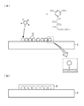
- the method for forming a metal wiring according to the present embodiment includes an ethoxysilane group (—SiOC 2 H 5 ) or a methoxysilane group (—SiOCH 3 ) and a thiol group (—SH). And a thiol group is chemically bonded to the surface of the metal fine particle M to prepare a dispersion solution of the metal fine particle M whose surface is coated with the compound R in advance.
- a thiol group is chemically bonded to the surface of the metal fine particle M to prepare a dispersion solution of the metal fine particle M whose surface is coated with the compound R in advance.
- the substrate 1 on which the metal wiring is to be formed is immersed in the dispersion solution, or the dispersion solution is applied to the substrate 1 to chemically bond the ethoxysilane group or methoxysilane group of the compound R to the substrate 1.
- metal wiring does not simply mean wiring, but includes wiring, contacts, electrodes, and all conductive elements formed in a thin film with a metal material. It is understood.
- the metal fine particles M chemically bonded to the substrate surface as described above are subjected to plating treatment (preferably electroless plating) performed in the second step, as schematically shown in FIG. It can be used as a catalyst, and the substrate 1 is immersed in a plating bath to thicken the same kind of metal as that of the metal fine particles M, so that it has a required thickness (that is, required conductive properties) and has a very thin single layer metal.
- the wiring 2 can be formed.
- the type of metal grown on the substrate by the plating process is not necessarily the same as the metal fine particles, and a metal different from the metal fine particles can be grown.
- the metal wiring is formed only by the metal fine particles bonded to the substrate surface by adjusting one or more of the size, shape and concentration in the dispersion solution of the metal fine particles without performing the plating process of the second step. It is also possible to form In this case, there is an advantage that the plating process can be omitted and the process can be simplified. In addition, in order to improve the intensity
- the material of the substrate is not particularly limited.
- a glass substrate preferably a non-alkali glass substrate
- a silicon substrate preferably a ceramic substrate, or a polyimide resin
- an epoxy resin preferably a polycarbonate resin, polyethylene terephthalate (PET), polyethylene naphthalate (PEN), polyethersal
- a resin substrate made of a resin material such as phon (PES), polyolefin (PO), or liquid crystal polymer can be given.
- a substrate made of a material having a hydroxyl group (OH group) and / or a carbonyl group (COOH group) on the surface is used, or surface treatment is performed to form (or increase) an OH group and / or a COOH group.
- OH groups and / or COOH groups are present on the substrate surface, the reaction between silanol groups generated from ethoxysilane groups or methoxysilane groups and OH groups and / or COOH groups is promoted, and the chemical formulas —Si—O— and / or The metal fine particles can be stably fixed to the substrate by a bond represented by —Si—OOC—.
- the surface treatment for forming OH groups include UV ozone treatment, oxygen plasma treatment, alkali cleaning, and boiling treatment.
- surface treatment for forming COOH groups include UV ozone treatment, acid oxygen plasma treatment, and corona discharge treatment. It is desirable to treat the resin substrate so as to form a COOH group.
- the surface (base surface) on which the metal wiring is to be formed is not limited to the substrate surface such as a printed circuit board, but an inorganic transistor, an organic transistor, an organic EL element, an inorganic EL element, Substrates for electronic devices such as capacitors, inorganic solar cells, organic solar cells, and the surface of interlayer insulating layers, organic semiconductor layers, gate insulating layers, and inorganic semiconductor layers in organic / inorganic TFTs (Thin Film Transistors), for example It may be the surface.
- the desired patterning of the metal wiring is performed by chemical or physical masking on the area not forming the metal wiring so that the metal fine particles are selectively bonded only to the area where the metal wiring is to be formed.
- This can be realized by performing processing.
- the chemical masking process there is a method using a coupling agent described later in detail.
- a photoresist is applied on a substrate, exposed or drawn, and developed to form a patterned resist mask, or an inorganic mask is formed on the substrate. There are methods.
- patterning may be performed by a photolithography technique and an etching technique.
- the metal fine particles may be formed of a metal having conductivity and / or catalytic action, and the type of metal is not particularly limited in the present embodiment.
- the metal having a catalytic action gold (Au), nickel (Ni), cobalt (Co), iron (Fe), copper (Cu), silver (Ag), which are metals having an autocatalytic action, Examples thereof include any one selected from rhodium (Rh), palladium (Pd), and platinum (Pt), or two or more alloys selected from these.
- the size and / or shape of the metal fine particles are not limited as long as they can be dispersed in the solution, but it is preferable to use nanoparticles or microparticles in consideration of dispersibility in the solution.
- metal fine particles when metal fine particles are used as a catalyst for plating, for example, it is preferable to use ultra fine particles having an average particle diameter of about 1 nm to 10 nm because the metal wiring can be thinned.
- a compound having both an ethoxysilane group (—SiOC 2 H 5 ) or a methoxysilane group (—SiOCH 3 ) and a thiol group (—SH) is used as the compound coated on the surface of the metal fine particles.
- a triethoxysilane group (—Si (OC 2 H 5 ) 3 ) or a trimethoxysilane group (—Si (OCH 3 ) 3 ) is preferable.
- an organic substance or an inorganic substance may be sufficient.
- an ethoxysilane group or a thiol compound derivative in which a methoxysilane group is introduced into a thiol compound can be given.
- a triazine thiol derivative that can be represented by the following chemical formula [Chemical Formula 2] can be given.
- Either one of chemical formulas (a) and (b) may be included, or both may be included.
- a triazine dithiol derivative that can be represented by the following chemical formula [Chemical Formula 3] is preferable.
- the following chemical formula shows an example of 1,2,3-triazine, it may be an isomer of 1,2,4-triazine or 1,3,5-triazine.
- the triazine thiol derivative is not limited, and mercaptopropyltrimethoxysilane (MPS) which is a thiol-containing silane coupling agent may be used.
- MPS mercaptopropyltrimethoxysilane
- the above-mentioned thiol compound derivative, mercaptopropyltrimethoxysilane (MPS), etc. may use a commercially available thing, and may manufacture using a well-known technique.
- Y is an ethoxy group (C 2 H 5 O-) or methoxy group (CH 3 O-)
- X is, CH 3 -, C 2 H 5 -, nC 3 H 7 -, iC 3 H 7 -, nC 4 H 9 -, iC 4 H 9 - or tC 4 H 9 - a and, M is an alkali metal Na, Li, K or Ce, etc.
- the above-described solvent for dispersing the metal fine particles may be any solvent that can dissolve the compound to be coated on the surface of the metal fine particles and can be dispersed without dissolving the metal fine particles.
- a solvent in the case of using a triazine thiol derivative ethanol can be given as an example.
- the concentration of the metal fine particles and the compound to be coated can be appropriately adjusted according to the kind of the selected metal and compound, but preferably the concentration of the metal fine particles is 1 wt% to 5 wt%, and the concentration of the compound is 0.1 wt%. % To 2 wt%.
- the metal fine particles and the compound to be coated are added and stirred in a solvent to cause both to react and bond the thiol group to the surface of the metal fine particles.
- the hydrolysis reaction of the ethoxysilane group or the methoxysilane group proceeds in the solvent to generate a silanol group (—SiOH). Therefore, the solvent preferably contains moisture for hydrolysis.
- —Si (OC 2 H 5 ) 3 —Si (OH) 3 is generated.
- metal fine particles whose surface is coated with a compound can be obtained through such a simple process.
- the metal fine particles may be generated by dissolving a metal salt as a raw material of the metal fine particles in a solvent and performing a reduction treatment to precipitate the metal.
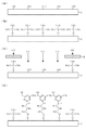
- FIG. 2 is a process diagram schematically showing a preferred example of a process of forming a metal wiring.
- FIG. 2 shows an example in which a triazine dithiol derivative represented by the chemical formula [Chemical Formula 3] is prepared and Au single-layer wiring is formed on an alkali-free glass substrate for convenience of explanation.
- the present invention is not limited to this.
- metal wiring is formed only on the upper surface of the substrate is shown.
- metal wiring can be formed on both the upper and lower surfaces of the substrate.
- the glass substrate 1 is washed in order to remove dirt, fats and oils, and then surface treatment such as UV ozone treatment is performed to form (or increase) OH groups (FIG. 2A).
- a silane coupling process is performed on the surface of the substrate 1 using a known organosilane compound.
- organic silane compound used as the silane coupling agent organic disilazane such as hexamethyldisilazane (HMDS), organic chlorosilane such as octadecyltrichlorosilane (OTS)), and other alkoxysilanes may be used.
- FIG. 2B shows an example in which a silane coupling process is performed using HMDS and reacted with an OH group formed on the surface of the substrate 1 to form a trimethylsilanol self-assembled monolayer (SAM film). It is shown.
- SAM film trimethylsilanol self-assembled monolayer
- Such a silane coupling treatment is, for example, a liquid phase treatment in which a solution containing a silane coupling agent is applied and dried, or a substrate is exposed to a silane coupling agent vapor atmosphere and baked at a predetermined temperature. Performed by vapor phase processing.
- the region where the metal wiring is to be formed is irradiated with ultraviolet rays (UV) through the photomask 3 (FIG. 2C).
- UV ultraviolet rays
- the light source an excimer UV lamp, a mercury lamp, a xenon lamp, an ultraviolet LED, or the like can be used.
- the SAM film in the region irradiated with the ultraviolet rays is decomposed and removed.
- a region where the metal wiring is to be formed is exposed, and a state where the SAM film remains in a region where the metal wiring is not formed is formed.
- the ultraviolet rays may be irradiated by a known drawing technique.
- the substrate 1 is immersed in a dispersion solution of Au fine particles coated with a triazine dithiol derivative, or the dispersion solution is applied to the substrate, whereby the Au fine particles coated with the triazine dithiol derivative are decomposed into the SAM film. It selectively couple
- the temperature of the dispersion solution in which the substrate 1 is immersed is heated to 50 to 70 ° C.
- the immersion time is preferably 1 h to 3 h.
- the Au is thickened by electroless plating to form the Au single-layer wiring 2 on the substrate (see FIG. 1B).
- the thickness of the wiring 2 can be controlled, for example, by adjusting the plating time, temperature, plating solution composition, and the like. A thickness of 30 to 200 nm is preferable in order to ensure necessary conductive characteristics and meet the demand for thinning.
- the electroless plating solution for thickening Au includes a metal salt containing Au, a reducing agent, and a reaction aid added as necessary.
- a metal salt containing Au a metal salt containing Au
- a reducing agent a reaction aid added as necessary.
- sodium gold sulfite and potassium sulfite such as Na 3 Au (SO 3 ) 2 as a gold complex salt of sulfite
- sodium thiosulfate such as Na 3 Au (S 2 O 3 ) 2 as a gold complex of thiosulfate and Potassium thiosulfate, sodium chloroaurate and potassium chloroaurate as salts of chloroauric acid, thiourea gold hydrochloride and thiourea gold perchlorate as thiourea gold complex
- gold sodium thiomalate and thioapple as thiomalate gold complex
- Examples include oxygold potassium.
- gold sources may be used alone or in combination of two or more. Examples include potassium gold sulfite and sodium gold thiosulfate.
- a common reducing agent can be used as a reducing agent having catalytic activity for gold.
- ascorbate such as sodium ascorbate or hydroxylamine and hydroxylamine hydrochloride
- hydroxylamine salts such as hydroxylamine sulfate or hydroxylamine derivatives such as hydroxylamine-O-sulfonic acid or hydrazine
- amine borane compounds such as sodium borohydride, borohydride compounds such as sodium borohydride, saccharides such as glucose, and hypophosphites.
- reaction aid for example, an inorganic acid such as sulfuric acid, hydrochloric acid or phosphoric acid, a hydroxide salt such as sodium hydroxide or potassium hydroxide, and as a crystal grain shape adjuster, polyethylene glycol or the like
- inorganic acid such as sulfuric acid, hydrochloric acid or phosphoric acid
- hydroxide salt such as sodium hydroxide or potassium hydroxide
- crystal grain shape adjuster polyethylene glycol or the like
- brighteners include thallium, copper, antimony and lead.
- metal fine particles whose surfaces are coated with a thiol compound having an ethoxysilane group or a methoxysilane group are prepared in advance, and further generated by hydrolyzing the ethoxysilane group or the methoxysilane group.
- the metal fine particles can be chemically fixed to the substrate surface.
- metal fine particles have a high surface activity and thus easily aggregate in a dispersion solution.
- the surface activity is lowered by coating with a thiol compound in advance to suppress aggregation.
- a thiol compound having an ethoxysilane group or a methoxysilane group is used, and a silanol group is generated by hydrolysis. This promotes chemical bonding to the substrate surface.
- a large number of metal fine particles can be sufficiently and uniformly fixed to the substrate surface.
- metal fine particles chemically bonded to the substrate surface via a thiol compound have higher adhesion to the substrate than when simply physically adsorbed.
- the metal fine particles are used as a catalyst and the same kind of metal is thickened by electroless plating, it is possible to form an extremely thin single-layer metal wiring, and the metal wiring with high adhesion to the substrate. Can be formed.
- the present inventors have confirmed that it is possible to reduce the film thickness to about 30 nm, which was difficult to achieve with the prior art. This effect can be obtained in the same manner even when a different metal is thickened by electroless plating.
- metal fine particles are selectively attached only to a portion where the metal wiring is to be formed, so that a metal wiring having a desired pattern can be obtained. Can be formed.
- the metal fine particles are attached only to the necessary parts by masking in advance, so that it is possible to prevent faults such as leakage due to the metal fine particles adhering to unnecessary parts, and to reduce the manufacturing cost. It is also possible to make it easier.
Landscapes
- Engineering & Computer Science (AREA)
- Manufacturing & Machinery (AREA)
- Microelectronics & Electronic Packaging (AREA)
- Chemical & Material Sciences (AREA)
- Chemical Kinetics & Catalysis (AREA)
- Chemically Coating (AREA)
- Manufacturing Of Printed Wiring (AREA)
Abstract
Description
R 被覆する化合物
1 基板
2 金属配線


Claims (11)
- エトキシシラン基又はメトキシシラン基と、チオール基とを有する化合物を利用して薄膜状の金属配線を形成する方法であって、
前記化合物のチオール基が化学的に結合することにより、表面が予め前記化合物で被覆された金属微粒子の多数を準備し、前記エトキシシラン基又はメトキシシラン基を加水分解させることで生成させたシラノール基を、金属配線を形成しようとする下地面に化学的に結合させることによって前記金属微粒子を下地面に固着させる工程、を含むことを特徴とする金属配線の形成方法。 - 前記下地面に固着させた金属微粒子を触媒にしてさらに無電解メッキを行い、前記金属微粒子と同種の金属を厚付けして単層金属配線を形成することを特徴とする請求項1に記載の金属配線の形成方法。
- 前記下地面に固着させた金属微粒子を触媒にしてさらに無電解メッキを行い、前記金属微粒子とは異種の金属を厚付けして金属配線を形成することを特徴とする請求項1に記載の金属配線の形成方法。
- 粒子径が100nm~500nmの金属微粒子を用いることで、前記下地面に固着させた金属微粒子のみで単層金属配線を形成することを特徴とする請求項1に記載の金属配線の形成方法。
- 前記化合物は、下記の化学式(a)及び/又は(b)で表すことのできるトリアジンチオール誘導体を含むことを特徴とする請求項1~4のいずれか1項に記載の金属配線の形成方法。

- 前記下地面に自己組織化単分子膜(SAM膜)を形成し、パターン開口部を有するマスクを介在させて露光するか又は描画して、前記パターンに対応する領域のSAM膜を選択的に分解・除去する工程をさらに含み、
前記SAM膜が除去された領域に対して前記金属微粒子を固着させてパターニングされた金属配線を形成することを特徴とする請求項1~5のいずれか1項に記載の金属配線の形成方法。 - 前記エトキシシラン基又はメトキシシラン基が加水分解して生成されるシラノール基が、前記下地面の水酸基及び/又はカルボキシル基と反応して結合することを特徴とする請求項1~6のいずれか1項に記載の金属配線の形成方法。
- 前記下地面は、ガラス基板,樹脂基板,シリコン基板,又はセラミックス基板の表面、或いは層間絶縁層,有機半導体層,無機半導体層,又はゲート絶縁膜の表面であることを特徴とする請求項1~7のいずれか1項に記載の金属配線の形成方法。
- 前記金属微粒子は、金(Au),ニッケル(Ni),コバルト(Co),鉄(Fe),銅(Cu),銀(Ag),ロジウム(Rh),パラジウム(Pd),白金(Pt)から選択されるいずれか一種、又は二種以上の合金からなることを特徴とする請求項1~8のいずれか1項に記載の金属配線の形成方法。
- 前記請求項1~9のいずれか1項に記載の方法によって形成された金属配線を備えていることを特徴とする電子部品。
- 前記電子部品は、電子機器に実装される回路基板,無機トランジスタ,有機トランジスタ,有機EL素子,無機EL素子,コンデンサ,無機太陽電池,有機太陽電池のいずれかであることを特徴とする請求項10に記載の電子部品。
Priority Applications (3)
| Application Number | Priority Date | Filing Date | Title |
|---|---|---|---|
| US13/063,588 US20110168430A1 (en) | 2008-09-11 | 2008-09-11 | Method of forming metal wiring and electronic part including metal wiring |
| PCT/JP2008/066472 WO2010029635A1 (ja) | 2008-09-11 | 2008-09-11 | 金属配線の形成方法、及び金属配線を備えた電子部品 |
| JP2010528572A JPWO2010029635A1 (ja) | 2008-09-11 | 2008-09-11 | 金属配線の形成方法、及び金属配線を備えた電子部品 |
Applications Claiming Priority (1)
| Application Number | Priority Date | Filing Date | Title |
|---|---|---|---|
| PCT/JP2008/066472 WO2010029635A1 (ja) | 2008-09-11 | 2008-09-11 | 金属配線の形成方法、及び金属配線を備えた電子部品 |
Publications (1)
| Publication Number | Publication Date |
|---|---|
| WO2010029635A1 true WO2010029635A1 (ja) | 2010-03-18 |
Family
ID=42004903
Family Applications (1)
| Application Number | Title | Priority Date | Filing Date |
|---|---|---|---|
| PCT/JP2008/066472 Ceased WO2010029635A1 (ja) | 2008-09-11 | 2008-09-11 | 金属配線の形成方法、及び金属配線を備えた電子部品 |
Country Status (3)
| Country | Link |
|---|---|
| US (1) | US20110168430A1 (ja) |
| JP (1) | JPWO2010029635A1 (ja) |
| WO (1) | WO2010029635A1 (ja) |
Cited By (11)
| Publication number | Priority date | Publication date | Assignee | Title |
|---|---|---|---|---|
| JP2012109323A (ja) * | 2010-11-16 | 2012-06-07 | Alps Electric Co Ltd | 皮膜のパターンの形成方法 |
| JP2013087347A (ja) * | 2011-10-20 | 2013-05-13 | Ngk Insulators Ltd | 貴金属被膜およびその製造方法 |
| WO2014045972A1 (ja) * | 2012-09-20 | 2014-03-27 | Dic株式会社 | 導電性材料及びその製造方法 |
| JP2016157639A (ja) * | 2015-02-25 | 2016-09-01 | コニカミノルタ株式会社 | 透明電極基板とその製造方法、電子デバイス及び有機elデバイス |
| JP2017031458A (ja) * | 2015-07-31 | 2017-02-09 | 学校法人関東学院 | 導電層付プラスチック基板及びその製造方法 |
| US10037398B2 (en) | 2016-04-21 | 2018-07-31 | International Business Machines Corporation | Pattern decomposition method for wiring patterns with chemoepitaxy based directed self assembly |
| WO2018180869A1 (ja) * | 2017-03-31 | 2018-10-04 | 東京エレクトロン株式会社 | めっき処理方法、めっき処理システム及び記憶媒体 |
| WO2020003880A1 (ja) * | 2018-06-26 | 2020-01-02 | Dic株式会社 | プリント配線板用積層体及びそれを用いたプリント配線板 |
| JP2020023734A (ja) * | 2018-08-07 | 2020-02-13 | 株式会社豊光社 | めっき処理されたガラス基材の製造方法 |
| US11315885B2 (en) | 2018-02-27 | 2022-04-26 | Dic Corporation | Electronic component package including stacked shield layers and method for producing same |
| JP2022145295A (ja) * | 2021-03-19 | 2022-10-03 | 地方独立行政法人 岩手県工業技術センター | 三次元成形回路部品の製造方法 |
Families Citing this family (7)
| Publication number | Priority date | Publication date | Assignee | Title |
|---|---|---|---|---|
| JP5456129B1 (ja) * | 2012-09-28 | 2014-03-26 | 田中貴金属工業株式会社 | めっき処理のための触媒粒子を担持する基板の処理方法 |
| US9773989B2 (en) * | 2013-12-03 | 2017-09-26 | National University Corporation Yamagata University | Method for producing metal thin film and conductive structure |
| JP2015115335A (ja) * | 2013-12-09 | 2015-06-22 | イビデン株式会社 | プリント配線板及びプリント配線板の製造方法 |
| JP2015115334A (ja) * | 2013-12-09 | 2015-06-22 | イビデン株式会社 | プリント配線板及びプリント配線板の製造方法 |
| JP6181006B2 (ja) * | 2014-07-09 | 2017-08-16 | 東京エレクトロン株式会社 | めっき前処理方法、めっき処理システムおよび記憶媒体 |
| US11818849B1 (en) * | 2023-04-21 | 2023-11-14 | Yield Engineering Systems, Inc. | Increasing adhesion of metal-organic interfaces by silane vapor treatment |
| US11919036B1 (en) * | 2023-04-21 | 2024-03-05 | Yield Engineering Systems, Inc. | Method of improving the adhesion strength of metal-organic interfaces in electronic devices |
Citations (6)
| Publication number | Priority date | Publication date | Assignee | Title |
|---|---|---|---|---|
| JP2000039737A (ja) * | 1998-07-21 | 2000-02-08 | Nippon Shokubai Co Ltd | 被覆金属粒子およびこれを用いた電子写真用トナー |
| JP2001284798A (ja) * | 2000-03-31 | 2001-10-12 | Seiko Epson Corp | 薄膜パタ−ンの製造方法および微細構造体 |
| JP2003078235A (ja) * | 2001-08-04 | 2003-03-14 | Pohang Eng College | プラスチック基板上の金属微細パターンの形成方法 |
| JP2006165574A (ja) * | 2004-12-07 | 2006-06-22 | Samsung Sdi Co Ltd | 表示装置用基板の製造方法および表示装置用基板 |
| JP2007084850A (ja) * | 2005-09-20 | 2007-04-05 | Daiwa Fine Chemicals Co Ltd (Laboratory) | 回路パターン形成方法 |
| JP2007220883A (ja) * | 2006-02-16 | 2007-08-30 | Kagawa Univ | 配線およびその製造方法とそれらを用いた電子部品および電子機器 |
Family Cites Families (18)
| Publication number | Priority date | Publication date | Assignee | Title |
|---|---|---|---|---|
| JPS63227784A (ja) * | 1987-03-16 | 1988-09-22 | Toyobo Co Ltd | 無電解めつき触媒の付与方法 |
| JPH0756867B2 (ja) * | 1988-09-28 | 1995-06-14 | 松下電器産業株式会社 | 金属超薄膜およびその製造法 |
| JPH0781189B2 (ja) * | 1987-12-21 | 1995-08-30 | 松下電器産業株式会社 | 金属超薄膜の製造方法およびパターン形成方法 |
| JP3378023B2 (ja) * | 1991-04-18 | 2003-02-17 | ジオ−センターズ・インコーポレイテツド | 固体基板に高解像度パターンを形成する方法 |
| WO2001049898A1 (en) * | 2000-01-07 | 2001-07-12 | Nikko Materials Co., Ltd. | Method for metal plating, pre-treating agent, and semiconductor wafer and semiconductor device using the same |
| CN1261618C (zh) * | 2000-04-25 | 2006-06-28 | 株式会社日矿材料 | 镀覆用预处理剂和使用它的金属镀覆方法 |
| KR100803186B1 (ko) * | 2000-12-15 | 2008-02-14 | 디 아리조나 보드 오브 리전츠 | 나노입자 함유 전구체를 사용한 금속의 패턴형성 방법 |
| JP4078424B2 (ja) * | 2003-09-29 | 2008-04-23 | 独立行政法人産業技術総合研究所 | 微細構造化金属酸化物薄膜及びその作製方法 |
| JP2006057167A (ja) * | 2004-08-23 | 2006-03-02 | Toyota Motor Corp | めっき配線形成方法 |
| JP4512825B2 (ja) * | 2005-02-07 | 2010-07-28 | 国立大学法人岩手大学 | 水溶性アルコキシシラン含有トリアジンジチオール金属塩及びその製造方法、並びにそれを用いた固体表面への反応性付与方法及び表面反応性固体 |
| JP2006287077A (ja) * | 2005-04-04 | 2006-10-19 | Sankyo Kasei Co Ltd | 回路基板の製造方法 |
| JP4817733B2 (ja) * | 2005-07-06 | 2011-11-16 | 富士通株式会社 | 金属表面処理液、積層体および積層体の製造方法 |
| JP4660761B2 (ja) * | 2005-07-06 | 2011-03-30 | 国立大学法人岩手大学 | プリント配線基板とその製造方法 |
| KR100970067B1 (ko) * | 2005-09-15 | 2010-07-16 | 닛코킨조쿠 가부시키가이샤 | 스루홀을 가진 프린트 배선 기판에의 무전해 도금용 촉매,및 그 촉매를 이용하여 처리된 스루홀을 가진 프린트 배선기판 |
| JP5076139B2 (ja) * | 2005-09-28 | 2012-11-21 | 国立大学法人岩手大学 | 樹脂とゴムとを接着するための分子接着剤,樹脂とゴムとの接着方法及び樹脂とゴムとの接着複合製品 |
| JP4734637B2 (ja) * | 2005-11-10 | 2011-07-27 | 国立大学法人岩手大学 | 表面反応性固体,表面反応性固体の製造方法,表面反応性固体を用いた配線基板及び配線基板の製造方法 |
| JP5135575B2 (ja) * | 2006-08-28 | 2013-02-06 | 国立大学法人岩手大学 | 機能性分子接着剤と分子接着性樹脂表面とその作成法並びに樹脂めっき製品もしくはプリント配線板の製造法 |
| JPWO2008032839A1 (ja) * | 2006-09-15 | 2010-01-28 | 宇部日東化成株式会社 | 金属層被覆基材およびその製造方法 |
-
2008
- 2008-09-11 WO PCT/JP2008/066472 patent/WO2010029635A1/ja not_active Ceased
- 2008-09-11 JP JP2010528572A patent/JPWO2010029635A1/ja active Pending
- 2008-09-11 US US13/063,588 patent/US20110168430A1/en not_active Abandoned
Patent Citations (6)
| Publication number | Priority date | Publication date | Assignee | Title |
|---|---|---|---|---|
| JP2000039737A (ja) * | 1998-07-21 | 2000-02-08 | Nippon Shokubai Co Ltd | 被覆金属粒子およびこれを用いた電子写真用トナー |
| JP2001284798A (ja) * | 2000-03-31 | 2001-10-12 | Seiko Epson Corp | 薄膜パタ−ンの製造方法および微細構造体 |
| JP2003078235A (ja) * | 2001-08-04 | 2003-03-14 | Pohang Eng College | プラスチック基板上の金属微細パターンの形成方法 |
| JP2006165574A (ja) * | 2004-12-07 | 2006-06-22 | Samsung Sdi Co Ltd | 表示装置用基板の製造方法および表示装置用基板 |
| JP2007084850A (ja) * | 2005-09-20 | 2007-04-05 | Daiwa Fine Chemicals Co Ltd (Laboratory) | 回路パターン形成方法 |
| JP2007220883A (ja) * | 2006-02-16 | 2007-08-30 | Kagawa Univ | 配線およびその製造方法とそれらを用いた電子部品および電子機器 |
Cited By (18)
| Publication number | Priority date | Publication date | Assignee | Title |
|---|---|---|---|---|
| JP2012109323A (ja) * | 2010-11-16 | 2012-06-07 | Alps Electric Co Ltd | 皮膜のパターンの形成方法 |
| JP2013087347A (ja) * | 2011-10-20 | 2013-05-13 | Ngk Insulators Ltd | 貴金属被膜およびその製造方法 |
| WO2014045972A1 (ja) * | 2012-09-20 | 2014-03-27 | Dic株式会社 | 導電性材料及びその製造方法 |
| CN104662198A (zh) * | 2012-09-20 | 2015-05-27 | Dic株式会社 | 导电性材料及其制造方法 |
| CN104662198B (zh) * | 2012-09-20 | 2017-06-13 | Dic株式会社 | 导电性材料及其制造方法 |
| JP2016157639A (ja) * | 2015-02-25 | 2016-09-01 | コニカミノルタ株式会社 | 透明電極基板とその製造方法、電子デバイス及び有機elデバイス |
| JP2017031458A (ja) * | 2015-07-31 | 2017-02-09 | 学校法人関東学院 | 導電層付プラスチック基板及びその製造方法 |
| US10037398B2 (en) | 2016-04-21 | 2018-07-31 | International Business Machines Corporation | Pattern decomposition method for wiring patterns with chemoepitaxy based directed self assembly |
| WO2018180869A1 (ja) * | 2017-03-31 | 2018-10-04 | 東京エレクトロン株式会社 | めっき処理方法、めっき処理システム及び記憶媒体 |
| JPWO2018180869A1 (ja) * | 2017-03-31 | 2020-02-06 | 東京エレクトロン株式会社 | めっき処理方法、めっき処理システム及び記憶媒体 |
| US11315885B2 (en) | 2018-02-27 | 2022-04-26 | Dic Corporation | Electronic component package including stacked shield layers and method for producing same |
| WO2020003880A1 (ja) * | 2018-06-26 | 2020-01-02 | Dic株式会社 | プリント配線板用積層体及びそれを用いたプリント配線板 |
| JP6667119B1 (ja) * | 2018-06-26 | 2020-03-18 | Dic株式会社 | プリント配線板用積層体及びそれを用いたプリント配線板 |
| KR20210023791A (ko) * | 2018-06-26 | 2021-03-04 | 디아이씨 가부시끼가이샤 | 프린트 배선판용 적층체 및 그것을 사용한 프린트 배선판 |
| KR102770638B1 (ko) * | 2018-06-26 | 2025-02-24 | 디아이씨 가부시끼가이샤 | 프린트 배선판용 적층체 및 그것을 사용한 프린트 배선판 |
| JP2020023734A (ja) * | 2018-08-07 | 2020-02-13 | 株式会社豊光社 | めっき処理されたガラス基材の製造方法 |
| JP2022145295A (ja) * | 2021-03-19 | 2022-10-03 | 地方独立行政法人 岩手県工業技術センター | 三次元成形回路部品の製造方法 |
| JP7437658B2 (ja) | 2021-03-19 | 2024-02-26 | 地方独立行政法人 岩手県工業技術センター | 三次元成形回路部品の製造方法 |
Also Published As
| Publication number | Publication date |
|---|---|
| US20110168430A1 (en) | 2011-07-14 |
| JPWO2010029635A1 (ja) | 2012-02-02 |
Similar Documents
| Publication | Publication Date | Title |
|---|---|---|
| WO2010029635A1 (ja) | 金属配線の形成方法、及び金属配線を備えた電子部品 | |
| JP3503546B2 (ja) | 金属パターンの形成方法 | |
| KR100841170B1 (ko) | 저저항 금속 배선 형성방법, 금속 배선 구조 및 이를이용하는 표시장치 | |
| US9932676B2 (en) | Pretreatment solution for electroless plating and electroless plating method | |
| JP2002348680A (ja) | 金属膜パターンおよびその製造方法 | |
| CN101035413A (zh) | 布线基板的制造方法 | |
| CN117916083B (zh) | 层叠体的制造方法 | |
| WO2004024984A1 (ja) | 金属めっき方法および前処理剤 | |
| JP2004296424A (ja) | 金属層の形成方法、金属層、及び金属層を用いた表示装置 | |
| US11319334B2 (en) | Site-selective metal plating onto a package dielectric | |
| US20090021563A1 (en) | System And Method For Depositing A Seed Layer | |
| CN101035414A (zh) | 布线基板的制造方法 | |
| JP4628914B2 (ja) | 回路パターン形成方法 | |
| CN117966136B (zh) | 一种激光辅助化学镀制备精细陶瓷电路板的方法 | |
| CN101035416A (zh) | 布线基板的制造方法 | |
| JP4445711B2 (ja) | 金属酸化物パターン形成方法及び金属配線パターン形成方法 | |
| KR100445314B1 (ko) | 유기금속 화합물에 의한 고전도 금속의 배선 형성방법 | |
| CN101488461A (zh) | 不用光刻胶和贵金属活化剂的线路板及其种子层制作方法 | |
| US7488570B2 (en) | Method of forming metal pattern having low resistivity | |
| KR101507155B1 (ko) | 구리 무전해 도금을 위한 은 시드층의 형성방법 | |
| CN115119393A (zh) | 用于化学镀铜的自组装图案化陶瓷基板及其制备方法和应用 | |
| JP3675708B2 (ja) | 金属層の形成方法 | |
| CN100470340C (zh) | 薄膜晶体管印刷制程方法 | |
| JPWO2006057242A1 (ja) | 遷移金属の還元方法、それを用いたケイ素含有重合体の表面処理方法、遷移金属微粒子の製造方法、物品および配線基板の製造方法 | |
| JP5343012B2 (ja) | シリコーンゴム表面への金属固定方法 |
Legal Events
| Date | Code | Title | Description |
|---|---|---|---|
| 121 | Ep: the epo has been informed by wipo that ep was designated in this application |
Ref document number: 08810524 Country of ref document: EP Kind code of ref document: A1 |
|
| WWE | Wipo information: entry into national phase |
Ref document number: 2010528572 Country of ref document: JP |
|
| WWE | Wipo information: entry into national phase |
Ref document number: 13063588 Country of ref document: US |
|
| NENP | Non-entry into the national phase |
Ref country code: DE |
|
| 122 | Ep: pct application non-entry in european phase |
Ref document number: 08810524 Country of ref document: EP Kind code of ref document: A1 |