WO2009128359A1 - ガラス積層体、支持体付き表示装置用パネルおよびこれらの製造方法 - Google Patents
ガラス積層体、支持体付き表示装置用パネルおよびこれらの製造方法 Download PDFInfo
- Publication number
- WO2009128359A1 WO2009128359A1 PCT/JP2009/057084 JP2009057084W WO2009128359A1 WO 2009128359 A1 WO2009128359 A1 WO 2009128359A1 JP 2009057084 W JP2009057084 W JP 2009057084W WO 2009128359 A1 WO2009128359 A1 WO 2009128359A1
- Authority
- WO
- WIPO (PCT)
- Prior art keywords
- glass substrate
- resin layer
- thin glass
- outer frame
- main surface
- Prior art date
Links
Images


Classifications
-
- B—PERFORMING OPERATIONS; TRANSPORTING
- B32—LAYERED PRODUCTS
- B32B—LAYERED PRODUCTS, i.e. PRODUCTS BUILT-UP OF STRATA OF FLAT OR NON-FLAT, e.g. CELLULAR OR HONEYCOMB, FORM
- B32B17/00—Layered products essentially comprising sheet glass, or glass, slag, or like fibres
- B32B17/06—Layered products essentially comprising sheet glass, or glass, slag, or like fibres comprising glass as the main or only constituent of a layer, next to another layer of a specific material
- B32B17/10—Layered products essentially comprising sheet glass, or glass, slag, or like fibres comprising glass as the main or only constituent of a layer, next to another layer of a specific material of synthetic resin
-
- B—PERFORMING OPERATIONS; TRANSPORTING
- B32—LAYERED PRODUCTS
- B32B—LAYERED PRODUCTS, i.e. PRODUCTS BUILT-UP OF STRATA OF FLAT OR NON-FLAT, e.g. CELLULAR OR HONEYCOMB, FORM
- B32B7/00—Layered products characterised by the relation between layers; Layered products characterised by the relative orientation of features between layers, or by the relative values of a measurable parameter between layers, i.e. products comprising layers having different physical, chemical or physicochemical properties; Layered products characterised by the interconnection of layers
- B32B7/04—Interconnection of layers
- B32B7/06—Interconnection of layers permitting easy separation
-
- G—PHYSICS
- G02—OPTICS
- G02F—OPTICAL DEVICES OR ARRANGEMENTS FOR THE CONTROL OF LIGHT BY MODIFICATION OF THE OPTICAL PROPERTIES OF THE MEDIA OF THE ELEMENTS INVOLVED THEREIN; NON-LINEAR OPTICS; FREQUENCY-CHANGING OF LIGHT; OPTICAL LOGIC ELEMENTS; OPTICAL ANALOGUE/DIGITAL CONVERTERS
- G02F1/00—Devices or arrangements for the control of the intensity, colour, phase, polarisation or direction of light arriving from an independent light source, e.g. switching, gating or modulating; Non-linear optics
- G02F1/01—Devices or arrangements for the control of the intensity, colour, phase, polarisation or direction of light arriving from an independent light source, e.g. switching, gating or modulating; Non-linear optics for the control of the intensity, phase, polarisation or colour
- G02F1/13—Devices or arrangements for the control of the intensity, colour, phase, polarisation or direction of light arriving from an independent light source, e.g. switching, gating or modulating; Non-linear optics for the control of the intensity, phase, polarisation or colour based on liquid crystals, e.g. single liquid crystal display cells
- G02F1/133—Constructional arrangements; Operation of liquid crystal cells; Circuit arrangements
- G02F1/1333—Constructional arrangements; Manufacturing methods
- G02F1/133302—Rigid substrates, e.g. inorganic substrates
Definitions
- the present invention includes a glass laminate including a glass substrate used for a liquid crystal display device, an organic EL display device and the like, a display device-equipped panel including the same, a display device panel formed using the same, and the display device panel
- the present invention relates to a display device, a glass laminate, and a method for manufacturing a display device panel.
- LCD liquid crystal display devices
- OLED organic EL display devices
- weight reduction and thinning of display devices are important issues.
- the glass substrate is etched using hydrofluoric acid or the like, and further physically polished as necessary. A thinning method is performed.
- the glass substrate is thinned by performing an etching process or the like before forming the display device member on the surface of the glass substrate, the strength of the glass substrate is lowered and the amount of deflection is increased. Therefore, the problem that it cannot process in the existing manufacturing line arises.
- the glass substrate is thinned by performing an etching process after forming the display device member on the surface of the glass substrate, the fineness formed on the surface of the glass substrate in the process of forming the display device member on the surface of the glass substrate. A problem of obvious scratches, that is, a problem of generation of etch pits occurs.
- a thin glass substrate (hereinafter also referred to as “thin glass substrate”) is referred to as another glass substrate (hereinafter also referred to as “supporting glass substrate”).
- another glass substrate hereinafter also referred to as “supporting glass substrate”.
- Patent Document 1 a glass substrate for products and a reinforcing glass substrate are bonded and integrated using electrostatic adsorption force or vacuum adsorption force between the glass substrates, and a display device using the product glass substrate is disclosed.
- Patent Document 2 describes a method for manufacturing a liquid crystal display device in which the ends of a substrate and a support of a liquid crystal display device are bonded using a glass frit adhesive, and then an electrode pattern or the like is formed.
- Patent Document 3 describes a method for manufacturing a substrate for a display device, which includes a step of irradiating a laser beam to at least the vicinity of the peripheral surface of two glass substrates to fuse the two glass substrates. .
- substrate transfer is performed by attaching a substrate to a substrate transfer jig in which an adhesive layer is provided on a support, and transferring the substrate transfer jig through a manufacturing process of a liquid crystal display element.
- a manufacturing method of a liquid crystal display device is described in which liquid crystal display element formation processing is sequentially performed on a substrate attached to a jig for use, and the substrate is peeled off from the substrate carrying jig after completing a predetermined process.
- Patent Document 5 discloses that an electrode substrate for a liquid crystal display element is subjected to a predetermined process on the electrode substrate for a liquid crystal display element using a jig in which an ultraviolet curable pressure-sensitive adhesive is provided on a support, and then cured with an ultraviolet ray.
- a method for producing a liquid crystal display element comprising: irradiating a mold adhesive with ultraviolet rays to reduce the adhesive strength of the ultraviolet curable adhesive and peeling the liquid crystal display element electrode substrate from the jig.
- Patent Document 6 describes a transport method in which a thin plate is temporarily fixed to a support plate with an adhesive material, a peripheral portion of the adhesive material is sealed with a seal material, and the support plate on which the thin plate is temporarily fixed is transported. .
- Patent Document 7 discloses a thin glass laminate obtained by laminating a thin glass substrate and a supporting glass substrate, and the thin glass and the supporting glass have easy peelability and non-adhesiveness.
- a thin glass laminate characterized by being laminated via a silicone resin layer is described.
- Patent Document 8 discloses that a protective glass substrate and a TFT array substrate are laminated in advance using a release paper silicone, and the protective glass substrate is peeled after the display device is assembled.
- the thin glass laminated body as described in patent document 7 may generate
- the gas can be generated even during heat treatment at a relatively low temperature of about 100 to 350 ° C. The generation of the gas is not preferable because it may contaminate the vacuum processing process equipment and the like.
- the heat treatment temperature is higher, for example, when it exceeds about 400 ° C., the end portion of the silicone resin layer that is in contact with the outside air may be oxidized and deteriorated. If it does so, easy peelability with a thin glass substrate will be lost, and also there exists a possibility that it may peel from a support glass substrate.
- the silicone resin layer may be whitened by oxidation, generating powdery SiO 2 , and contaminating heat treatment process equipment and the like. Further, when the resin layer deteriorates in this way, it becomes difficult to reuse the supporting glass substrate with the resin layer separated from the thin glass substrate with another thin glass substrate as a support.
- the present invention has been made in view of the above problems. In other words, it suppresses the occurrence of glass defects caused by foreign matters such as bubbles and dust mixed between glass substrates, and can be processed in an existing production line without generating etch pits. It aims at providing the glass laminated body which can be isolate
- the panel for display apparatuses aims at providing the panel for display apparatuses with a support body containing such a glass laminated body. It is another object of the present invention to provide a display device panel and a display device which are formed using such a support-equipped display device panel. Furthermore, it aims at providing the manufacturing method of the said glass laminated body or the said panel for display apparatuses with a support body.
- the present inventor has intensively studied in order to solve the above problems, and has completed the present invention.
- the present invention relates to the following (1) to (14).
- a thin glass substrate having a first main surface and a second main surface, A supporting glass substrate having a first main surface and a second main surface; and a glass laminate having a resin layer and an outer frame layer disposed between the thin glass substrate and the supporting glass substrate,
- the resin layer is fixed to the first main surface of the supporting glass substrate, has an easy peelability to the first main surface of the thin glass substrate, and is in close contact with the first main surface of the thin glass substrate.
- the method for producing a glass laminate according to (11) further includes a step of forming a display device member on the second main surface of the thin glass substrate in the obtained glass laminate. Of manufacturing panel for display device.
- the manufacturing method according to (12) further includes a separation step of separating the thin glass substrate and the supporting glass substrate in the obtained display device-equipped display device panel. Production method.
- the present invention it is possible to suppress the occurrence of glass defects due to foreign matters such as bubbles and dust mixed between glass substrates, and it is possible to process in an existing production line without generating etch pits, and to adhere thin glass
- a glass laminate that can easily separate the substrate and the resin layer can be provided.
- the glass laminated body which suppresses generation
- a preferred embodiment provides a glass laminate in which the resin layer between the thin glass substrate and the supporting glass substrate is hardly oxidized and hardly deteriorates even when the heat treatment temperature is relatively high (over 400 ° C.). can do.
- the panel for display apparatuses with a support containing such a glass laminated body can be provided.
- the display apparatus formed using such a display apparatus panel with a support body can be provided.
- the manufacturing method of the said glass laminated body or the said panel for display apparatuses with a support body can be provided.
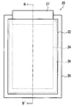
- FIG. 1 is a schematic front view showing one embodiment of the laminate of the present invention.
- FIG. 2 is a schematic cross-sectional view showing one embodiment of the laminate of the present invention.
- FIG. 3 is a schematic front view showing another embodiment of the laminate of the present invention.
- FIG. 4 is a schematic cross-sectional view showing another embodiment of the laminate of the present invention.
- FIG. 5 is a schematic cross-sectional view for explaining a method of peeling the supporting glass substrate of the laminate of the present invention.
- the present invention provides a thin glass substrate having a first main surface and a second main surface, a supporting glass substrate having a first main surface and a second main surface, and between the thin glass substrate and the supporting glass substrate.
- a glass laminate having a resin layer and an outer frame layer disposed, wherein the resin layer is fixed to a first main surface of the supporting glass substrate, and is easily peeled from the first main surface of the thin glass substrate.
- the resin layer is in close contact with the first main surface of the thin glass substrate, and the outer frame layer is on the first main surface of the support glass substrate so that the resin layer does not contact the outside air.
- a glass laminate is also referred to as “a laminate of the present invention”.
- FIG. 1 is a schematic front view showing an embodiment of the laminate of the present invention
- FIG. 2 is a cross-sectional view (schematic cross-sectional view) taken along line AA ′.
- this mode is also referred to as “mode 1”.
- the laminate 10 of the present invention has a thin glass substrate 12, a resin layer 14, an outer frame layer 16, and a supporting glass substrate 18.
- the thin glass substrate 12 and the supporting glass substrate 18 are laminated with the resin layer 14 and the outer frame layer 16 interposed therebetween. Further, as shown in FIG.
- the thin glass substrate 12, the resin layer 14, and the support glass substrate 18 are each rectangular, and the main surface area of the thin glass substrate 12 is larger than the main surface area of the resin layer 14. However, it is slightly smaller than the main surface area of the supporting glass substrate 18.
- the thin glass substrate 12 is positioned so as to be included inside the supporting glass substrate 18, and the resin layer 14 and the outer frame layer 16 are positioned so as to be included inside the thin glass substrate 12. ing.
- the outer frame layer 16 when viewed from the front, the outer frame layer 16 exists in the vicinity of the outer edge (outer region) of the thin glass substrate 12 like a frame surrounding the outer side of the resin layer 14. As shown in FIG. 2, the outer frame layer 16 is fixed to the first main surface of the thin glass substrate 12 and the first main surface of the support glass substrate 18. Therefore, the resin layer 14 existing inside thereof does not come into contact with outside air. When the outer frame layer 16 does not exist, the end surface 14 ⁇ of the resin layer 14 comes into contact with the outside air. When viewed from the front, the TFT array and the like are formed inside the outer frame layer, and the TFT array and the formation region of the outer frame layer overlap with each other so that they cannot be seen.
- an outer frame layer is formed on the first main surface of the thin glass substrate corresponding to the region excluding the effective region for forming the TFT array and the like on the second main surface of the thin glass substrate. is required. This is to prevent the TFT array or the like from being damaged by laser irradiation as will be described later.
- the resin layer 14 is fixed to the first main surface of the support glass substrate 18, and has easy peelability from the first main surface which is one main surface of the thin glass substrate 12.
- the thin glass substrate 12 is in close contact with the first main surface.
- the end surface 14 ⁇ of the resin layer 14 and the end surface 16 ⁇ on the inner side of the outer frame layer 16 are in contact with each other.
- Such a glass laminate of aspect 1 hardly generates gas during heat treatment. This is because the gas generated from the resin layer 14 does not diverge to the outside because the outer frame layer 16 exists. Moreover, if it is set as the preferable aspect mentioned later, even if the heat processing temperature is comparatively high temperature (over about 400 degreeC), the resin layer between a thin glass substrate and a support glass substrate cannot be easily oxidized, and it is hard to deteriorate. This is because the outer frame layer 16 blocks contact between the outside air and the end surface 14 ⁇ of the resin layer 14.
- the thin glass substrate will be described.
- the thickness, shape, size, physical properties (heat shrinkage, surface shape, chemical resistance, etc.), composition, etc. of the thin glass substrate are not particularly limited.
- a conventional glass substrate for a display device such as an LCD or OLED It may be the same.
- the thin glass substrate is preferably a TFT array glass substrate.
- the thickness of the thin glass substrate is preferably less than 0.7 mm, more preferably 0.5 mm or less, and further preferably 0.4 mm or less. Further, it is preferably 0.05 mm or more, more preferably 0.07 mm or more, and further preferably 0.1 mm or more.
- the shape of the thin glass is not limited, but is preferably rectangular.
- the size of the thin glass is not limited, but for example, in the case of a rectangle, it may be 100 to 2000 mm ⁇ 100 to 2000 mm, and more preferably 500 to 1000 mm ⁇ 500 to 1000 mm.
- the thickness of the thin glass is expressed by the average value of the values measured at 9 points in the plane using a laser focus displacement meter, and the size is a value obtained by measuring the short side and the long side using a steel ruler. Shall mean. The same applies to the thickness and size of the supporting glass substrate described later.
- the laminate of the present invention can easily peel the thin glass substrate and the supporting glass substrate.
- properties of the thin glass substrate such as thermal shrinkage, surface shape, chemical resistance, etc. are not particularly limited, and vary depending on the type of display device to be manufactured. Moreover, it is preferable that the thermal contraction rate of the said thin glass substrate is small. Specifically, it is preferable to use one having a linear expansion coefficient of 500 ⁇ 10 ⁇ 7 / ° C. or less, which is an index of heat shrinkage rate.
- the linear expansion coefficient is more preferably 300 ⁇ 10 ⁇ 7 / ° C. or less, more preferably 200 ⁇ 10 ⁇ 7 / ° C. or less, and more preferably 100 ⁇ 10 ⁇ 7 / ° C. or less. More preferably, it is 45 ⁇ 10 ⁇ 7 / ° C. or less. This is because a high-definition display device cannot be made if the heat shrinkage rate is large.
- a linear expansion coefficient means a thing prescribed
- the composition of the thin glass substrate may be the same as that of alkali glass or non-alkali glass, for example.
- alkali-free glass is preferable because of its low thermal shrinkage rate.
- the support glass substrate will be described.
- the supporting glass substrate supports the thin glass substrate through the resin layer and reinforces the strength of the thin glass substrate.
- the thickness, shape, size, physical properties (heat shrinkage rate, surface shape, chemical resistance, etc.), composition, etc. of the supporting glass substrate are not particularly limited.
- the thickness of a support glass substrate is not specifically limited, It is preferable that it is the thickness which can be processed with the present production line.
- the thickness is preferably 0.1 to 1.1 mm, more preferably 0.3 to 0.8 mm, and still more preferably 0.4 to 0.7 mm.
- the thickness of the supporting glass substrate and the resin layer The sum with the thickness is 0.4 mm.
- the current production line is most commonly designed to process a glass substrate having a thickness of 0.7 mm.
- the thickness of a thin glass substrate is 0.4 mm
- the supporting glass The sum of the thickness of the substrate and the thickness of the resin layer is 0.3 mm.
- the thickness of the supporting glass substrate is preferably thicker than that of the thin glass substrate.
- the shape of the supporting glass substrate is not limited, but is preferably rectangular.
- the size of the supporting glass substrate is not limited, but is preferably about the same as that of the thin glass substrate, and is slightly larger than the glass substrate (each of which is about 0.05 to 10 mm larger in the vertical direction or the horizontal direction). preferable.
- the reason is that it is easy to protect the end portion of the thin glass substrate from the contact of an alignment device such as a positioning pin at the time of manufacturing a panel for a display device, and that the thin glass substrate and the supporting glass substrate are more easily separated. Because it can.
- the supporting glass substrate may have a linear expansion coefficient that is substantially the same as or different from that of the thin glass substrate. Substantially the same is preferable in that the thin glass substrate or the supporting glass substrate is less likely to warp when the laminate of the present invention is heat-treated.
- the difference in linear expansion coefficient between the thin glass substrate and the supporting glass substrate is preferably 300 ⁇ 10 ⁇ 7 / ° C. or less, more preferably 100 ⁇ 10 ⁇ 7 / ° C. or less, and 50 ⁇ 10 ⁇ 7 / ° C. More preferably, it is not higher than ° C.
- the composition of the supporting glass substrate may be the same as that of alkali glass or non-alkali glass, for example. Among these, alkali-free glass is preferable because of its low thermal shrinkage rate.
- the resin layer will be described.
- the resin layer is fixed to the first main surface of the support glass substrate. And although the resin layer is closely_contact
- the resin layer and the thin glass substrate are not attached by the adhesive force that the adhesive has, and the force caused by the van der Waals force between the solid molecules, that is, the adhesive force. It is considered attached.
- the thickness of the resin layer is not particularly limited.
- the thickness is preferably 1 to 100 ⁇ m, more preferably 5 to 30 ⁇ m, and even more preferably 7 to 20 ⁇ m. This is because when the thickness of the resin layer is in such a range, the thin glass substrate and the resin layer are sufficiently adhered. Moreover, even if bubbles or foreign substances are present, it is possible to suppress the occurrence of distortion defects in the thin glass substrate. On the other hand, if the resin layer is too thick, it takes time and materials to form the resin layer, which is not economical.
- the thickness of the resin layer means an average value of values obtained by measuring nine points in a plane using a laser focus displacement meter. The same applies to the thickness of the outer frame layer described later.
- the resin layer may consist of two or more layers.
- the thickness of the resin layer means the total thickness of all the layers.
- the kind of resin which forms each layer may differ. The same applies to the outer frame layer described later.
- the surface tension of the surface of the resin layer relative to the first main surface of the thin glass substrate is preferably 30 mN / m or less, more preferably 25 mN / m or less, and 22 mN / m or less. Is more preferable. This is because such surface tension can be more easily peeled off from the thin glass substrate, and at the same time, the close contact with the thin glass substrate becomes sufficient.
- the resin layer is preferably made of a material having a glass transition point lower than room temperature (about 25 ° C.) or a material having no glass transition point.
- the resin layer has heat resistance.
- the glass laminate having the resin layer is subjected to heat treatment.
- the adhesiveness with a thin glass substrate will become low when the elasticity modulus of a resin layer is too high, it is unpreferable. On the other hand, if the elastic modulus is too low, the easy peelability is lowered, which is not preferable.
- the type of resin forming the resin layer is not particularly limited.
- acrylic resin, polyolefin resin, polyurethane resin, and silicone resin can be used. Two kinds of resins can be mixed and used. Of these, silicone resins are preferred. This is because the silicone resin is excellent in heat resistance and easy to peel from a thin glass substrate. It is also preferable that the silicone resin layer is not easily deteriorated even if it is treated at, for example, about 400 ° C. for about 1 hour. Further, since the silicone resin undergoes a condensation reaction with the silanol group on the surface of the supporting glass substrate, the silicone resin layer is easily fixed to the surface (first main surface) of the supporting glass substrate.
- the resin layer is preferably made of silicone for release paper among silicone resins, and is preferably a cured product thereof.
- the silicone for release paper is mainly composed of silicone containing linear dimethylpolysiloxane in the molecule.
- the resin layer formed by curing the composition containing the main agent and the crosslinking agent on the surface (first main surface) of the supporting glass substrate using a catalyst, a photopolymerization initiator, etc. has excellent easy peelability. Since it has, it is preferable. In addition, since the flexibility is high, even if foreign matters such as bubbles and dust are mixed between the thin glass substrate and the resin layer, it is preferable because the occurrence of distortion defects of the thin glass substrate can be suppressed.
- Such release paper silicones are classified into condensation reaction type silicones, addition reaction type silicones, ultraviolet ray curable silicones, and electron beam curable silicones depending on the curing mechanism, and any of them can be used.
- addition reaction type silicone is preferable. This is because the curing reaction is easy, the degree of easy peeling is good when the resin layer is formed, and the heat resistance is also high.
- the silicone for release paper is classified into a solvent type, an emulsion type, and a solventless type, and any type can be used.
- a solventless type is preferable. This is because productivity, safety, and environmental characteristics are excellent. Further, it does not contain a solvent that causes foaming at the time of curing at the time of forming the resin layer, that is, at the time of heat curing, ultraviolet curing, or electron beam curing, so that bubbles are unlikely to remain in the resin layer.
- KNS-320A, KS-847, and TPR6700 are silicones that contain a main agent and a crosslinking agent in advance.
- the silicone resin forming the resin layer has a property that the components in the silicone resin layer are difficult to migrate to the thin glass substrate, that is, low silicone migration.
- the outer frame layer will be described.
- the outer frame layer has a band shape, and is sandwiched between the thin glass substrate and the supporting glass substrate. Moreover, it exists like a frame surrounding the outside of the resin layer on the support glass substrate. Further, it is fixed to a thin glass substrate and a supporting glass substrate. Therefore, the resin layer is difficult to come into contact with the outside air. It is preferable to form the resin layer so as not to come into contact with the outside air.
- the end surface 14 ⁇ of the resin layer 14 and the inner end surface 16 ⁇ of the outer frame layer 16 are in contact, but they are not in contact, and the end surface of the resin layer and the outer frame layer There may be an air gap between the inner end face of each other. However, it is preferable that there are few or almost no voids. This is because the resin layer is less likely to be oxidized when the laminate of the present invention is heat-treated at a relatively high temperature (over 400 ° C.).
- the width of the outer frame layer is not particularly limited, but is preferably 0.5 to 10 mm, more preferably 1 to 5 mm, and further preferably 1.5 to 3.0 mm. With such a width, the resin layer is less likely to come into contact with the outside air. Moreover, it peels easily when peeling the said thin glass substrate and the said support glass substrate. If the width of the outer frame layer is too wide, peeling may be difficult. For example, in a method of irradiating laser light, which is a preferable peeling method described later, there is a possibility that a long time is required for peeling.
- the thickness of the outer frame layer is not particularly limited. Although it may be the same as the resin layer, it is preferably slightly thicker, more preferably 5 to 20 ⁇ m thick. It is preferable that the outer frame layer is slightly thicker than the resin layer because the thin glass substrate, the outer frame layer, and the support glass substrate are easily adhered to each other. Moreover, when the thickness of the outer frame layer is too thicker than the thickness of the resin layer, the thin glass substrate, the resin layer, and the support glass substrate are difficult to adhere to each other, and in the process of manufacturing the laminate of the present invention. The thin glass substrate or the supporting glass substrate may be damaged. When the thickness of the resin layer is 5 to 100 ⁇ m, the thickness of the outer frame layer is preferably 5 to 120 ⁇ m, and the outer frame layer is more preferably 5 to 20 ⁇ m thicker.
- the material of the outer frame layer is not particularly limited, but the laminated body of the present invention is a material having a low mass reduction ratio even when heat treatment for forming a TFT array on the second main surface of the thin glass substrate is performed.
- a material having a mass reduction ratio of 5% by mass or less when heat-treated at 400 ° C. is preferable. That is, it is preferable that the material has a 5% heating mass loss temperature of 400 ° C. or higher.
- the temperature is more preferably 425 ° C. or higher, and further preferably 450 ° C. or higher.
- Such a material is preferable because even if the laminate of the present invention is subjected to a heating step, it is difficult to cause a change in shape such as melting.
- the 5% heating mass decrease temperature means a temperature when the temperature of the sample is increased by 10 ° C. per minute under a mixed air stream and the mass of the sample reaches 95% of the initial sample mass.
- the material of the outer frame layer include, for example, a polyimide resin, a silicone resin, and an inorganic material.
- the material which mixed 2 or more of these may be sufficient. It is preferable that the material is at least one selected from the group consisting of a polyimide resin, a silicone resin, and an inorganic material and has a 5% heating mass loss temperature of 400 ° C. or higher.
- examples of the silicone resin include linear ones, ladder-like ones, and bowl-like ones. Of these, a ladder-like one or a bowl-like one is preferable. This is because the heat resistance is high. Moreover, the silicone resin which has an alkyl group and an aryl group as a substituent may be sufficient, and since the heat resistance is high, the silicone resin in which a silicon atom has an aryl group is preferable.
- examples of the inorganic material include various oxides and nitrides.
- examples thereof include oxides and nitrides of Al, Si, C, Mg, and B.
- Specific examples include alumina, silica, graphite, magnesia, boron nitride, and aluminum nitride. It may contain silicate compounds such as sodium metasilicate and potassium silicate, and aluminum phosphate as a main agent and further as a binder.
- the outer frame layer may further contain an inorganic filler such as alumina, silica, talc, or glass fiber.
- an inorganic filler such as alumina, silica, talc, or glass fiber.
- the content of these is preferably 5 to 80% by mass, more preferably 10 to 70% by mass, and further preferably 20 to 50% by mass.
- the laminate of the present invention has such a thin glass substrate, a supporting glass substrate, a resin layer, and an outer frame layer.
- the laminate of the present invention preferably further has a sheet. This is because the thin glass substrate and the supporting glass substrate can be easily separated by pulling the sheet. A specific peeling method using a sheet will be described later.
- the laminate of the present invention having a sheet will be described with reference to FIGS. Hereinafter, this mode is also referred to as “mode 2”.
- the laminated body of this invention of this aspect 2 differs in having a sheet
- FIG. 3 is a schematic front view showing another embodiment of the laminate of the present invention
- FIG. 4 is a BB ′ cross-sectional view (schematic cross-sectional view) thereof.
- the laminate 20 of the present invention has a thin glass substrate 22, a resin layer 24, an outer frame layer 26, a sheet 27, and a supporting glass substrate 28.
- the thin glass substrate 22 and the supporting glass substrate 28 are laminated with the resin layer 24, the outer frame layer 26, and the sheet 27 interposed therebetween.
- the thin glass substrate 22, the resin layer 24, and the supporting glass substrate 28 are each rectangular, and the sheet 27 is also rectangular.
- the resin layer 24 is surrounded on the outside by an outer frame layer 26 and a sheet 27.
- the outer frame layer 26 is fixed to the thin glass substrate 22 and the supporting glass substrate 28.
- the sheet 27 is in close contact with the thin glass substrate 22 and the supporting glass substrate 28. Therefore, the resin layer 24 existing inside them does not come into contact with the outside air.
- the end surface 24 ⁇ of the resin layer 24 comes into contact with the outside air.
- the sheet 27 is present at a position overlapping one side of the four sides of the laminate 20 of the present invention when viewed from the front.
- a part (27 a) of the sheet 27 is sandwiched between the thin glass substrate 22 and the supporting glass substrate 28. Furthermore, it has a portion (27b) which is not sandwiched and is not in contact with the thin glass substrate 22 or the supporting glass substrate 28.
- seat 27 has the part 27c which is in contact with one board
- the sheet 26 and the resin layer 24 do not overlap, and the end surface 24 ⁇ of the resin layer 24 and the end surface 27 ⁇ of the sheet 27 are in contact with each other.
- the laminate of the present invention may be an embodiment having such a sheet and may be another embodiment different from this.
- the size of the sheet viewed from the front may be smaller than that in FIG.
- the thing of the aspect which has two or more sheets may be sufficient.
- the sheet may be present at each of the positions overlapping two or more of the four sides of the laminate of the present invention.
- the sheet will be described.
- the sheet exists between the thin glass substrate and the supporting glass substrate, and a part of the sheet is sandwiched between the glass substrates. And at least one part of the part (remaining part) which is not pinched
- seat is not specifically limited, It is preferable that it is a rectangle like said aspect 2.
- the size and surface area of the sheet are not particularly limited. For example it may in the case of the rectangle the size of one sheet to a 1 ⁇ 4000 cm 2, is preferably 2 ⁇ 2000 cm 2, more preferably 4 ⁇ 1000 cm 2.
- the size of the portion of the sheet that is sandwiched between the thin glass substrate and the support glass substrate is not particularly limited.
- this portion when this portion is rectangular, it may be 10 to 2000 mm ⁇ 0.5 to 100 mm, preferably 20 to 1000 mm ⁇ 0.5 to 100 mm, and more preferably 20 to 1000 mm ⁇ 1 to 50 mm.
- the side orthogonal to the side of the laminate of the present invention if the above aspect 2, the side parallel to the cross section shown in FIG.
- the length of the portion indicated by “27a” in the case of aspect 2 may be 10 to 2000 mm, preferably 20 to 1000 mm, more preferably 40 to 1000 mm. preferable.
- the area of this portion may be 0.5 to 2000 cm 2 , preferably 1 to 1000 cm 2 , more preferably 2 to 500 cm 2 . In such a range, when the display device member is formed on the second main surface of the thin glass substrate, the area of the portion suitable for the formation on the thin glass substrate can be relatively large. preferable.
- the “size of the sandwiched portion” of the sheet here is, for example, in the case of the above-described aspect 2, of the two main surfaces of the portion 27a on the side facing the support glass substrate 28. It shall mean the area of the main surface.
- the size of the portion of the sheet that is not sandwiched between the thin glass substrate and the support glass substrate (remaining portion) and that is not in contact with the thin glass substrate or the support glass substrate is particularly limited.
- this portion when this portion is rectangular, it may be 10 to 2000 mm ⁇ 0.5 to 100 mm, preferably 20 to 1000 mm ⁇ 0.5 to 100 mm, and more preferably 20 to 1000 mm ⁇ 1 to 50 mm.
- the length of the side for example, the side parallel to the cross section shown in FIG.
- the length of the portion indicated by “27b”) may be 10 to 2000 mm, preferably 20 to 1000 mm, and more preferably 40 to 1000 mm.
- the area may be 0.5 to 2000 cm 2 , preferably 1 to 1000 cm 2 , and more preferably 2 to 500 cm 2 . Such a range is preferable in that it does not become an obstacle when the display device member is formed on the second main surface of the thin glass substrate.
- the “part of the portion (remaining portion) that is not sandwiched and is not in contact with the thin glass substrate or the supporting glass substrate” of the sheet referred to here is, for example, in the case of the above-described aspect 2 If so, the area of the main surface of the two main surfaces of the portion 27b that is in contact with the first main surface of the support glass substrate 28 at the end portion is meant.
- the size of the portion of the sheet that is not sandwiched between the thin glass substrate and the support glass substrate and that is in contact with the thin glass substrate or the support glass substrate is not particularly limited. For example, it may be 0 to 2000 cm 2 , preferably 0 to 1000 cm 2 , more preferably 0 to 500 cm 2 . Such a range is inevitably determined by the difference in size between the thin glass substrate and the supporting glass substrate and the location where the sheet is placed.
- the “27c portion of the sheet that is not sandwiched and is in contact with the thin glass substrate or the support glass substrate” Of the two main surfaces the area of the main surface in contact with the first main surface of the support glass substrate 28 is meant.
- the sheet is preferably fixed to the first main surface of the supporting glass substrate. Moreover, it is more preferable that “the portion of the sheet sandwiched between the thin glass substrate and the support glass substrate” described above is fixed to the first main surface of the support glass substrate. This is because peeling between the thin glass substrate and the supporting glass substrate becomes easier.
- the method for fixing the sheet to the first main surface of the supporting glass substrate is not limited. Any method that does not easily peel off may be used. For example, it can be fixed using an adhesive or a sticking agent. Examples of the adhesive include urethane-based, acrylic-based, epoxy-based, and silicone-based adhesives. Further, an inorganic adhesive may be used. Among these, epoxy-based, acrylic-based, and silicone-based adhesives or inorganic adhesives are preferable. This is because the heat resistance is high.
- the thickness of the sheet is not particularly limited. Although it may be the same as the resin layer, it is preferably slightly thicker, more preferably 5 to 20 ⁇ m thick. It is preferable that the sheet is slightly thicker than the resin layer because the thin glass substrate, the sheet, and the supporting glass substrate are easily adhered to each other. Further, if the thickness of the sheet is too thicker than the thickness of the resin layer, the thin glass substrate, the resin layer and the support glass substrate are difficult to adhere, and in the process of producing the laminate of the present invention, There is a risk of damaging the thin glass substrate or the supporting glass substrate. When the thickness of the resin layer is 5 to 100 ⁇ m, the thickness of the sheet is preferably 5 to 120 ⁇ m, and the sheet is more preferably 5 to 20 ⁇ m thicker.
- the material of the sheet is not particularly limited, but is preferably made of an organic resin or a metal.
- organic resins an organic resin having a 5% heating mass loss temperature of 200 ° C. or higher is preferable. This temperature is more preferably 250 ° C. or higher, and further preferably 300 ° C. or higher. This is because even when the laminate of the present invention is subjected to a heating step, it is difficult for a form change such as melting to occur.
- organic resins having a 5% heating mass loss temperature of 200 ° C. or higher include polysulfone, polyethersulfone, polyphenylene sulfide, polyamideimide, polyetherimide, polyetheretherketone, polyimide, polyallyl ester, polycarbonate, and polytetrafluoroethylene. And fluororesin.
- the sheet is preferably an organic resin film having a 5% heating mass loss temperature of 200 ° C. or higher.
- the sheet may be made of only the resin as described above, but may further contain an inorganic filler such as alumina, silica, talc, and glass fiber.
- the content of these is preferably 5 to 80% by mass, more preferably 10 to 70% by mass, and further preferably 20 to 50% by mass.
- the material of the sheet is a metal, aluminum, gold, copper, and stainless steel are particularly preferable. This is because the heat resistance is high.
- the laminate of the present invention may include the thin glass substrate, the supporting glass substrate, the resin layer, and the outer frame layer, and may further include a sheet.
- the panel for a display device with a support according to the present invention has a member for a display device on the second main surface of the thin glass substrate in the laminate according to the present invention.
- This display device-equipped panel can be obtained by forming a display device member on the second main surface of the thin glass substrate in the laminate of the present invention.
- the display device member means various circuit patterns, such as a light emitting layer, a protective layer, a color filter, a liquid crystal, a transparent electrode made of ITO, etc. on a surface of a glass substrate for a display device such as a conventional LCD or OLED. .
- the display device-equipped panel according to the present invention preferably has a TFT array (hereinafter simply referred to as “array”) formed on the second main surface of the thin glass substrate of the laminate of the present invention. .
- array hereinafter simply referred to as “array”
- the display device panel with a support of the present invention for example, the display device panel with a support of the present invention in which the array is formed on the second main surface of the thin glass substrate, and another color filter is formed.
- a glass substrate for example, a glass substrate having a thickness of 0.3 mm or more is also included.
- a display device panel can be obtained from such a support-equipped display device panel.
- a display device panel having a display device member and a thin glass substrate by peeling a thin glass substrate and a resin layer fixed to the support glass substrate from the support-equipped display device panel by a method as described later. Can be obtained.
- a display device can be obtained from such a display device panel.
- the display device include an LCD and an OLED.
- Examples of LCD include TN type, STN type, FE type, TFT type, and MIM type.
- the manufacturing method of the laminated body of this invention is demonstrated.
- the resin layer formation process which forms and fixes the said resin layer in the inner side area
- it is a manufacturing method of the glass laminated body.
- such a production method is also referred to as a “production method of the present invention”.
- a thin glass substrate and a supporting glass substrate are prepared.
- the manufacturing method of a thin glass substrate and a support glass substrate is not specifically limited.
- it can be produced by a conventionally known method.
- it can be obtained by melting a conventionally known glass raw material to form a molten glass and then forming it into a plate shape by a float method, a fusion method, a down draw method, a slot down method, a redraw method or the like.
- a resin layer is formed in the inner region of the surface (first main surface) of the support glass substrate thus manufactured.
- the inner region means a region on the first main surface of the supporting glass substrate and inside the outer region described later.
- a method of adhering a film-like resin to the surface of a supporting glass substrate can be mentioned.
- a method of performing a surface modification treatment (priming treatment) to give a high adhesive force to the surface of the film and adhering to the first main surface of the supporting glass substrate can be mentioned.
- the method of coating the resin composition used as a resin layer on the 1st main surface of a support glass substrate by a well-known method for example is mentioned.
- Known methods include spray coating, die coating, spin coating, dip coating, roll coating, bar coating, screen printing, and gravure coating. From such a method, it can select suitably according to a kind to a resin composition.
- a solventless release paper silicone is used as the resin composition
- a die coating method, a spin coating method or a screen printing method is preferred.
- the coating amount is preferably 1 to 100 g / m 2 , and more preferably 5 to 20 g / m 2 .
- a resin composition containing a silicone (main agent) containing a linear dimethylpolysiloxane in the molecule, a crosslinking agent and a catalyst is known, such as the spray coating method described above.
- the coating is performed on the supporting glass substrate by the method described above, followed by heat curing.
- the heating and curing conditions vary depending on the blending amount of the catalyst. For example, when 2 parts by weight of a platinum-based catalyst is blended with respect to 100 parts by weight of the total amount of the main agent and the crosslinking agent, 50 to 250 ° C. in the atmosphere, The reaction is preferably carried out at 100 ° C to 200 ° C.
- the reaction time is 5 to 60 minutes, preferably 10 to 30 minutes.
- the reaction temperature and the reaction time are as described above because no unreacted silicone component remains in the silicone resin layer. If the reaction time is too long or the reaction temperature is too high, the oxidative decomposition of the silicone resin occurs at the same time, and a low molecular weight silicone component is produced, which may increase the silicone transferability. It is preferable to allow the curing reaction to proceed as much as possible so that an unreacted silicone component does not remain in the silicone resin layer in order to improve the peelability after the heat treatment.
- the silicone resin layer is formed on the support glass substrate after heat-curing the release paper silicone coated on the support glass substrate to form a silicone resin layer.
- Laminate a thin glass substrate.
- the silicone for release paper by heating, the cured silicone resin is chemically bonded to the surface of the supporting glass substrate.
- the silicone resin layer is bonded to the surface of the supporting glass substrate by the anchor effect. By these actions, the silicone resin layer is firmly fixed to the supporting glass substrate.
- the outer frame layer forming step will be described. After forming the resin layer on the first main surface of the supporting glass substrate by the resin layer forming process as described above, or before or while forming the resin layer, in the outer region on the first main surface of the supporting glass substrate An outer frame layer is formed and fixed.
- the outer region is on the first main surface of the supporting glass substrate, and when the laminate of the present invention is viewed from the front (for example, as shown in FIG. 1), it is more than the outer edge of the thin glass substrate. Is a region included inside, and further means a region near the outer edge of the thin glass substrate. Specifically, for example, when viewed from the front, an area of 0.5 to 100 mm, preferably 0.5 to 50 mm, more preferably 0.5 to 10 mm, and still more preferably 0 inward from the edge of the thin glass substrate. .5-5 mm is the outer region. If the thin glass substrate is large, the size of this region may be large.
- examples of a method for forming the outer frame layer on the first main surface of the supporting glass substrate include the following methods.
- a method of forming an outer frame layer by discharging a material while moving a dispenser along the outer peripheral portion of the resin layer includes the following methods.
- a thin glass substrate and a supporting glass substrate are brought into close contact with each other through the resin layer to form a glass laminate, and then a material is injected from the outer peripheral portion of the glass laminate by a capillary phenomenon under normal pressure or vacuum. Forming the outer frame layer.
- a thin glass substrate and a supporting glass substrate are adhered to each other via the resin layer to form a glass laminate, and then an outer frame is formed so as to cover the exposed portion of the resin layer by vapor deposition, sputtering, chemical vapor deposition, or the like.
- a method of forming a layer A method of forming an outer frame layer at the end of the resin layer by vapor deposition, sputtering, chemical vapor deposition or the like after forming the resin layer on the supporting glass substrate.
- an outer frame layer made of a polyimide resin a polyamic acid varnish that is a precursor thereof is applied onto a supporting glass substrate by a known method such as the above-mentioned screen printing method, and then heat-cured, An outer frame layer can be obtained.
- a resin layer is formed on the first main surface of the supporting glass substrate by the method as described above, and a thin glass substrate is laminated on the surface of the resin layer.
- the thin glass substrate and the resin layer are brought into close contact with the resin layer by a force caused by van der Waals force between the adjacent solid molecules that are very close to each other, that is, an adhesive force.
- the supporting glass substrate and the thin glass substrate can be held in a laminated state.
- the method for laminating the thin glass substrate on the surface of the resin layer fixed to the supporting glass substrate is not particularly limited. For example, it can implement using a well-known method. For example, after laminating a thin glass substrate on the surface of the resin layer under a normal pressure environment, a method of pressure bonding the resin layer and the thin glass substrate using a roll or a press can be mentioned. It is preferable because the resin layer and the thin glass substrate are more closely adhered by pressure bonding with a roll or a press. Further, it is preferable because bubbles mixed between the resin layer and the thin glass substrate are easily removed by pressure bonding with a roll or a press.
- an outer frame layer and a thin glass substrate can be closely_contact
- an outer frame layer made of an inorganic material is formed in the outer frame layer forming step, it is preferable that the thin glass substrate is brought into close contact before the time elapses after the outer frame layer is formed. This is because the adhesion between the first main surface of the thin glass substrate and the outer frame layer becomes stronger, and the outer frame layer can be more firmly fixed to the first main surface of the thin glass substrate.
- an adhesive or the like is applied to the surface of the outer frame layer that is in close contact with the first main surface of the thin glass substrate, and then the thin glass substrate is adhered to the outer frame layer. May be fixed.
- the surface of the thin glass substrate is sufficiently washed and laminated in an environment with a high degree of cleanliness. Even if a foreign substance enters between the resin layer and the thin glass substrate, the resin layer is deformed, so the flatness of the surface of the thin glass substrate is not affected. However, the higher the cleanness, the better the flatness. Therefore, it is preferable.
- the sheet is formed on the first main surface of the supporting glass substrate and / or on the surface of the resin layer before the adhesion step.
- the method for attaching the sheet include a method of bonding the sheet to the surface of the supporting glass substrate. Specifically, a method of surface modification treatment for imparting a high adhesive force to the surface of the sheet and adhering to the first main surface of the supporting glass substrate can be mentioned.
- the laminate of the present invention can be produced.
- the manufacturing method of the panel for display apparatuses with a support body of this invention comprises the process of forming the member for display apparatuses in the 2nd main surface of the said thin glass substrate in the laminated body of this invention.
- the display device member is formed on the second main surface of the thin glass substrate in the laminate of the present invention manufactured as described above.
- the display device member is not particularly limited.
- an array or a color filter included in the LCD can be mentioned.
- a transparent electrode, a hole injection layer, a hole transport layer, a light emitting layer, and an electron transport layer included in the OLED can be given.
- a method of forming such a display device member is not particularly limited, and may be the same as a conventionally known method.
- a step of forming an array on a conventionally known glass substrate, a step of forming a color filter, a glass substrate on which the array is formed, and a glass substrate on which the color filter is formed It may be the same as various processes such as a bonding process (array / color filter bonding process). More specifically, examples of the processing performed in these steps include pure water cleaning, drying, film formation, resist coating, exposure, development, etching, and resist removal. Furthermore, as a process performed after implementing an array color filter bonding process, there exists a liquid-crystal injection
- a process for forming an organic EL structure on the second main surface of a thin glass substrate a process of forming a transparent electrode, a hole injection layer, a hole transport layer, Various processes such as a process for depositing a light emitting layer / electron transport layer and the like, a sealing process, and the like are performed. Specifically, for example, a film forming process, a vapor deposition process, and an adhesion of a sealing plate are performed. Processing and the like.
- the laminate with a support of the present invention can be produced.
- the display device panel of the present invention includes a separation step of separating the thin glass substrate and the support glass substrate in the support-equipped display device panel obtained by the manufacturing method as described above.
- the method for separating the thin glass substrate and the supporting glass substrate is not particularly limited. For example, it suffices to apply a force for pulling the thin glass substrate vertically away from the support glass substrate, and a razor blade or the like is used to trigger peeling, or a fluid such as air to the end surface of the laminate of the present invention. Can be peeled off. Moreover, it is also preferable that the outer edge is peeled off by irradiating a laser beam. Moreover, if the laminated body of this invention is the case of the aspect 2 which has the above-mentioned sheet
- the method of separating the thin glass substrate and the supporting glass substrate by irradiating the outer frame layer with laser light is preferable because it can be easily peeled off.
- the outer frame layer is melted or oxidatively decomposed by irradiating the outer frame layer with laser light through the thin glass substrate and / or the support glass substrate (preferably through the support glass substrate)
- the thin glass substrate Since the adhesive force between the glass substrate and the supporting glass substrate is weakened, both glass substrates can be easily peeled off. It is preferable to apply the above-described method using a razor or the method of spraying a fluid after irradiating a laser beam because it can be more easily peeled off.
- the laser light one that has high transparency in a thin glass substrate or a supporting glass substrate and is easily absorbed by the outer frame layer is preferable.
- YAG or YVO 4 laser fundamental wave (1064 nm) or its double wave (532 nm) laser light semiconductor diode laser (650 to 905 nm for AlGaAs, etc.), Ti-doped sapphire laser (660 to 986 nm), He—Ne Examples thereof include lasers (543 to 633 nm) and various excimer lasers.
- Laser light can be applied to the outer frame layer through the thin glass substrate and / or the support glass substrate (preferably through the support glass substrate) using, for example, a laser irradiation apparatus. If it does so, the adhesive force of the said thin glass substrate and the said support glass substrate will weaken by the oxidation and decomposition
- the outer frame layer when the outer frame layer is destroyed by irradiation with laser light, a residue of the outer frame layer may be generated. In this case, it can be removed by chemical treatment with an organic solvent, acid or alkali, or scrub cleaning treatment after peeling.
- the remaining part of the sheet (the part not sandwiched between both glass substrates) in the display device panel with a support is pulled to separate the thin glass substrate and the supporting glass substrate. be able to.
- a specific peeling method will be described with reference to FIG.
- the surface plate 51 is placed on a horizontal surface plate 51 with the thin glass substrate 52 facing down and the supporting glass substrate 58 facing up, and the second main surface of the thin glass substrate 52 is flat.
- the sheet 57 is pulled upward as shown in FIG. 7, and the supporting glass substrate 58 is lifted.
- a gap is formed at the interface between the thin glass substrate 52 and the resin layer 54, and the air layer enters the interface from this point, and peeling proceeds.
- it is more preferable to blow air toward the gap because the peeling phenomenon at the interface is more likely to proceed.
- the support portion of the laminate with the support of the present invention is peeled off and further processed as necessary to obtain the display device panel of the present invention.
- Example 1 A glass laminate substantially similar to the glass laminate of Embodiment 1 described with reference to FIGS. 1 and 2 described above was produced by the following method. The only difference from Embodiment 1 is the size of the thin glass substrate and the supporting glass substrate. In the glass laminate of aspect 1, the thin glass substrate 12 has a smaller principal surface area than the support glass substrate 18, but in the glass laminate produced in Example 1, the sizes of both glass substrates are the same.
- a supporting glass substrate (Asahi Glass Co., Ltd., AN100) having a length of 720 mm, a width of 600 mm, a plate thickness of 0.4 mm, and a linear expansion coefficient of 38 ⁇ 10 ⁇ 7 / ° C. is cleaned with pure water and UV to clean the surface. did.
- a polyamic acid solution (“U-Varnish-S” manufactured by Ube Industries, Ltd., 18% by mass, N-methyl-2-pyrrolidone solution), which is a polyimide precursor, is applied to all the outer regions having a width of 5 mm.
- Printed by screen printing Here, the polyamic acid solution was printed so as to be in contact with the end of the silicone resin layer formed in the inner region.
- the WET thickness of the polyamic acid solution was 160 ⁇ m.
- the thickness of the outer frame layer was 20 ⁇ m.
- the silicone resin layer formed in the inner side area did not change at all by this heating.
- the first main surface (later contacted with a silicone resin layer) of a thin glass substrate (Asahi Glass Co., Ltd., AN100) having a length of 720 mm, a width of 600 mm, a plate thickness of 0.3 mm, and a linear expansion coefficient of 38 ⁇ 10 ⁇ 7 / ° C.
- the side surface was cleaned with pure water and UV.
- the surface of the silicone resin layer of the supporting glass substrate and the thin glass substrate were bonded together at room temperature by a vacuum press to obtain a glass laminate. In this way, two “glass laminates A” which are one embodiment of the laminate of the present invention were produced.
- glass laminate A-2 Another glass laminate A that has not been heat-treated is referred to as “glass laminate A-1.”
- the glass laminate A-1 and the glass laminate A-2 were subjected to the following peel test 1 to evaluate the peelability.
- ⁇ Peel test 1> The glass laminate was placed on a surface plate so that the supporting glass substrate was on the upper side and the thin glass substrate was on the lower side, and the thin glass substrate was vacuum-adsorbed on the surface plate. Next, in this state, YVO 4 laser light was irradiated from the upper side to the outer frame layer through the supporting glass substrate. And all the outer frame layers were carbonized and destroyed.
- a Q-switch YVO 4 laser device manufactured by LASERTEC was used for laser irradiation. The laser light irradiation conditions were as follows: wavelength: 1064 nm, output: 1 W, spot diameter: 30 ⁇ m, frequency: 50 kHz, scan speed: 250 mm / s, scan: 3 times.
- the laser beam is moved in the width direction of the outer frame layer while being spot-irradiated, and the same position in the width direction is reciprocated 1.5 times, and then once in the direction perpendicular to the width direction (that is, the longitudinal direction of the outer frame layer).
- the laser beam irradiation position is moved by the irradiation spot diameter (30 ⁇ m), and the same position in the width direction is reciprocated 1.5 times.
- the entire outer frame layer was irradiated with laser light.
- the supporting glass substrate was pulled vertically upward.
- Such a peel test 1 was performed on each of the glass laminate A-1 and the glass laminate A-2, and in any glass laminate, from the end to the interface between the silicone resin layer and the thin glass substrate. An air layer was formed, and the air layer spread, and the supporting glass substrate with the silicone resin layer and the thin glass substrate could be easily peeled off. Moreover, the residue of the outer frame layer adhering to the surface of the thin glass substrate after peeling could be easily removed by scrub cleaning using alcohol. Further, the end portion of the silicone resin layer of the glass laminate A-2 was not oxidized.
- glass laminate B-1 that was not heat-treated and “glass laminate B-2” that was heat-treated were obtained. Separately, the glass laminate B was heated from room temperature to 450 ° C. under high vacuum (1.0 ⁇ 10 ⁇ 5 Pa), but no gas was generated from the glass laminate B.
- the thin glass substrate was in close contact with the silicone resin layer without bubbles, and had no convex defects and good smoothness. Further, when the above peel test 1 was performed on each of the glass laminate B-1 and the glass laminate B-2, it was possible to peel easily as in the case of Example 1, and the end face of the silicone resin layer Was also sound. The residue could also be removed by the same scrub cleaning.
- Example 3 was the same as Example 1, except that the supporting glass substrate, resin layer, outer frame layer, and thin glass substrate differed in type, size, thickness, and the like.
- a glass substrate (AN100, manufactured by Asahi Glass Co., Ltd.) having a length of 720 mm, a width of 600 mm, a thickness of 0.6 mm, and a linear expansion coefficient of 38 ⁇ 10 ⁇ 7 / ° C. was used.
- linear polyorganosiloxane having a vinyl group at both ends (trade name “8500” manufactured by Arakawa Chemical Industries, Ltd.) and methyl having a hydrosilyl group in the molecule Hydrogen polysiloxane (trade name “12031” manufactured by Arakawa Chemical Industries, Ltd.) was used.
- This is mixed with a platinum-based catalyst (trade name “CAT12070”, manufactured by Arakawa Chemical Industries, Ltd.) to prepare a mixture, which is 700 mm long and 580 mm wide, and is applied by a screen printer (coating A work amount of 20 g / m 2 ) was heated and cured in the air at 180 ° C.
- the mixing ratio of the linear polyorganosiloxane and the methylhydrogen polysiloxane was adjusted so that the molar ratio of hydrosilyl group to vinyl group was 1/1.
- the platinum-based catalyst was added in an amount of 5 parts by mass with respect to a total of 100 parts by mass of the linear polyorganosiloxane and methyl hydrogen polysiloxane.
- a paste-like substance Ceramer Bond 835 (containing zirconia as a main agent and a silicate compound as a binder), which is a paste-like substance, was used. And using the dispenser, the paste was apply
- a glass substrate As a thin glass substrate, a glass substrate (AN100 manufactured by Asahi Glass Co., Ltd.) having a length of 720 mm, a width of 600 mm, a thickness of 0.1 mm, and a linear expansion coefficient of 50 ⁇ 10 ⁇ 7 / ° C. was used. After the first main surface of the thin glass substrate was cleaned by pure water cleaning and UV cleaning, the surface of the silicone resin layer of the supporting glass substrate and the thin glass substrate were bonded together at room temperature by a vacuum press. Then, the paste was crushed and extended on both glass substrates, and the thickness became 20 ⁇ m. Then, when it heated in air
- a “glass laminate C-1” that was not heat-treated and a “glass laminate C-2” that was heat-treated were obtained.
- the glass laminate C is separately heated from room temperature to 450 ° C. under high vacuum (1.0 ⁇ 10 ⁇ 5 Pa).
- high vacuum 1.0 ⁇ 10 ⁇ 5 Pa
- no gas was generated from the glass laminate C.
- the thin glass substrate was in close contact with the silicone resin layer without bubbles, and had no convex defects and good smoothness.
- the above peel test 1 was performed on each of the glass laminate C-1 and the glass laminate C-2.
- the laser beam irradiation output was set to 7 W instead of 1 W.
- Example 4 an LCD is manufactured using the glass laminate C-1 obtained in Example 3. Two glass laminates C-1 are prepared, and one is subjected to an array forming process to form an array on the second main surface of the thin glass substrate. The remaining one sheet is subjected to a color filter forming process to form a color filter on the second main surface of the thin glass substrate. After laminating the glass laminate on which the array is formed and the glass laminate on which the color filter is formed, each supporting glass substrate is separated by irradiating the outer frame layer with each side and destroying it. To do. On the surface of the thin glass substrate after separation, there is no damage that leads to a decrease in strength.
- the glass substrate is cut and divided into 168 cells having a length of 51 mm and a width of 38 mm, and then a liquid crystal injection step and an injection port sealing step are performed to form a liquid crystal cell.
- a step of attaching a polarizing plate to the formed liquid crystal cell is performed, and then a module formation step is performed to obtain an LCD.
- the LCD obtained in this way does not have a problem in characteristics.
- Example 5 an LCD is manufactured using the glass laminate A-1 obtained in Example 1.
- Two glass laminates A-1 are prepared, and one is subjected to an array forming process to form an array on the second main surface of the thin glass substrate.
- the remaining one sheet is subjected to a color filter forming process to form a color filter on the second main surface of the thin glass substrate.
- the supporting glass substrate is separated from each other by irradiating the outer frame layer with the laser beam one by one and destroying it. .
- the surface of the thin glass substrate after separation is not damaged so as to reduce the strength.
- each thin glass substrate is set to 0.15 mm by chemical etching. Etch pits that cause optical problems are not observed on the surface of the thin glass substrate after the chemical etching treatment.
- the thin glass substrate is cut and divided into 168 cells of 51 mm in length ⁇ 38 mm in width, and then a liquid crystal injection step and an injection port sealing step are performed to form a liquid crystal cell.
- a step of attaching a polarizing plate to the formed liquid crystal cell is performed, and then a module formation step is performed to obtain an LCD.
- the LCD obtained in this way does not have a problem in characteristics.
- Example 6 an LCD is manufactured using the glass laminate B-1 obtained in Example 2 and a non-alkali glass substrate (AN-100 manufactured by Asahi Glass) having a thickness of 0.7 mm.
- a glass laminate is prepared and used in a color filter forming step to form a color filter on the second main surface of the thin glass substrate of the glass laminate.
- the alkali-free glass substrate is subjected to an array forming process to form an array on one main surface.
- the glass laminate on which the color filter is formed and the non-alkali glass substrate on which the array is formed are bonded to each other, and then the outer frame layer is irradiated with laser light one side at a time to break the glass laminate to the supporting glass. Separate the substrate.
- the separated support glass substrate is divided into 168 cells of 51 mm length ⁇ 38 mm width using a laser cutter or a scribe-break method. Thereafter, a liquid crystal injection step and an injection port sealing step are performed to form a liquid crystal cell. A step of attaching a polarizing plate to the formed liquid crystal cell is performed, and then a module formation step is performed to obtain an LCD.
- the LCD obtained in this way does not have a problem in characteristics.
- Example 7 an OLED is manufactured using the glass laminate C-1 obtained in Example 3.
- a thin glass sheet of a glass laminate that is provided for a step of forming a transparent electrode, a step of forming an auxiliary electrode, a step of depositing a hole injection layer, a hole transport layer, a light emitting layer, an electron transport layer, and the like, and a step of sealing them
- An organic EL structure is formed on the substrate.
- the supporting glass substrate is separated by irradiating the outer frame layer with laser light one side at a time for destruction. The surface of the thin glass substrate after separation is not damaged so as to reduce the strength.
- the thin glass substrate was cut using a laser cutter or a scribe-break method, and divided into 288 cells of 41 mm in length and 30 mm in width, and then the glass substrate on which the organic EL structure was formed and the counter substrate were separated. Assemble and perform module formation process to create OLED. There is no problem in characteristics of the OLED obtained in this way.
- Example 1 A test was performed in the same manner as in Example 1 except that the outer frame layer was not formed and the size of the resin layer having a length of 710 mm and a width of 590 mm was changed to a length of 715 mm and a width of 595 mm.
- the obtained “glass laminate X-1” and the heat-treated “glass laminate X-2” according to Comparative Example 1 were in close contact with the silicone resin layer without generating bubbles. There was no convex defect and smoothness was good. Further, the glass laminate X-1 and the glass laminate X-2 were subjected to the peeling test 2 shown below.
- ⁇ Peeling test 2> The glass laminate was placed on a surface plate so that the supporting glass substrate was on the upper side and the thin glass substrate was on the lower side, and the thin glass substrate was vacuum-adsorbed on the surface plate. Then, a sharp razor was applied between the thin glass substrate and the resin layer to pry off the edge of the interface and gradually peeled off the edge. As a result, an air layer is formed from the end at the interface between the silicone resin layer and the thin glass substrate, and the air layer spreads, and the supporting glass substrate with the silicone resin layer and the thin glass substrate can be easily peeled off. did it.
- the silicone resin layer in the glass laminate X-2 that was heat-treated was whitened by oxidation of about 5 mm from the end face.
- the silica powder is scattered, which may contaminate the formation process of the display device.
- the present invention it is possible to suppress the occurrence of glass defects due to foreign matters such as bubbles and dust mixed between glass substrates, and it is possible to process in an existing production line without generating etch pits, and to adhere thin glass A glass laminate that can easily separate the substrate and the resin layer can be provided.
Landscapes
- Laminated Bodies (AREA)
- Liquid Crystal (AREA)
- Devices For Indicating Variable Information By Combining Individual Elements (AREA)
- Electroluminescent Light Sources (AREA)
Priority Applications (4)
| Application Number | Priority Date | Filing Date | Title |
|---|---|---|---|
| EP09732700A EP2273475A1 (en) | 2008-04-17 | 2009-04-06 | Glass laminate, display panel with support, method for producing glass laminate and method for manufacturing display panel with support |
| CN2009801135516A CN102007524B (zh) | 2008-04-17 | 2009-04-06 | 玻璃层叠体、带支撑体的显示装置用面板及它们的制造方法 |
| JP2010508174A JPWO2009128359A1 (ja) | 2008-04-17 | 2009-04-06 | ガラス積層体、支持体付き表示装置用パネルおよびこれらの製造方法 |
| US12/905,071 US20110026236A1 (en) | 2008-04-17 | 2010-10-14 | Glass laminate, display panel with support, method for producing glass laminate and method for manufacturing display panel with support |
Applications Claiming Priority (2)
| Application Number | Priority Date | Filing Date | Title |
|---|---|---|---|
| JP2008108169 | 2008-04-17 | ||
| JP2008-108169 | 2008-04-17 |
Related Child Applications (1)
| Application Number | Title | Priority Date | Filing Date |
|---|---|---|---|
| US12/905,071 Continuation US20110026236A1 (en) | 2008-04-17 | 2010-10-14 | Glass laminate, display panel with support, method for producing glass laminate and method for manufacturing display panel with support |
Publications (1)
| Publication Number | Publication Date |
|---|---|
| WO2009128359A1 true WO2009128359A1 (ja) | 2009-10-22 |
Family
ID=41199055
Family Applications (1)
| Application Number | Title | Priority Date | Filing Date |
|---|---|---|---|
| PCT/JP2009/057084 WO2009128359A1 (ja) | 2008-04-17 | 2009-04-06 | ガラス積層体、支持体付き表示装置用パネルおよびこれらの製造方法 |
Country Status (7)
| Country | Link |
|---|---|
| US (1) | US20110026236A1 (ko) |
| EP (1) | EP2273475A1 (ko) |
| JP (1) | JPWO2009128359A1 (ko) |
| KR (1) | KR20110007134A (ko) |
| CN (1) | CN102007524B (ko) |
| TW (1) | TW201000309A (ko) |
| WO (1) | WO2009128359A1 (ko) |
Cited By (20)
| Publication number | Priority date | Publication date | Assignee | Title |
|---|---|---|---|---|
| WO2011048978A1 (ja) * | 2009-10-20 | 2011-04-28 | 旭硝子株式会社 | ガラス積層体、支持体付き表示装置用パネル、表示装置用パネル、表示装置、およびこれらの製造方法 |
| JP2011162432A (ja) * | 2010-01-12 | 2011-08-25 | Nippon Electric Glass Co Ltd | ガラスフィルム積層体及びその製造方法並びにガラスフィルムの製造方法 |
| JP2011251470A (ja) * | 2010-06-02 | 2011-12-15 | Lintec Corp | 積層体、それに用いる樹脂シート及び該積層体の用途 |
| JP2011251502A (ja) * | 2010-06-04 | 2011-12-15 | Lintec Corp | 積層体、それに用いる樹脂シート及び該積層体の用途 |
| CN102690066A (zh) * | 2011-03-22 | 2012-09-26 | 京东方科技集团股份有限公司 | 一种玻璃基板的固定方法 |
| WO2013008540A1 (ja) * | 2011-07-14 | 2013-01-17 | 東京応化工業株式会社 | 積層体、分離方法、及び製造方法 |
| US20130029075A1 (en) * | 2010-05-26 | 2013-01-31 | Asahi Glass Company, Limited | Transparent plate having adhesive layer, display device and processes for their production |
| US20130273266A1 (en) * | 2010-12-08 | 2013-10-17 | Asahi Glass Company, Limited | Adhesive layer-equipped transparent surface material, display device and processes for their production |
| WO2014192560A1 (ja) * | 2013-05-28 | 2014-12-04 | 旭硝子株式会社 | 樹脂層付き支持基材およびその製造方法、ガラス積層体およびその製造方法、電子デバイスの製造方法 |
| JP2015083373A (ja) * | 2013-09-18 | 2015-04-30 | 株式会社半導体エネルギー研究所 | 積層体の作製装置 |
| JP2015116694A (ja) * | 2013-12-17 | 2015-06-25 | 旭硝子株式会社 | 樹脂層付き支持基板の製造方法、ガラス積層体の製造方法、電子デバイスの製造方法 |
| JP2015116698A (ja) * | 2013-12-17 | 2015-06-25 | 旭硝子株式会社 | ガラス積層体の製造方法、電子デバイスの製造方法 |
| JP2015532004A (ja) * | 2012-08-22 | 2015-11-05 | コーニング インコーポレイテッド | フレキシブルガラス基板の処理 |
| JP2016521247A (ja) * | 2013-05-15 | 2016-07-21 | コーニング インコーポレイテッド | ガラス構造体ならびにガラス構造体の製造および加工方法 |
| US9500890B2 (en) | 2013-11-15 | 2016-11-22 | Samsung Display Co., Ltd. | Method of manufacturing device substrate and display device manufactured using the same |
| JPWO2014181855A1 (ja) * | 2013-05-10 | 2017-02-23 | 日本電気硝子株式会社 | ガラスフィルムの製造方法及び電子デバイスの製造方法 |
| US10730147B2 (en) | 2016-11-11 | 2020-08-04 | Lg Chem, Ltd. | Method of forming pattern for a large area liquid crystal device |
| US10953636B2 (en) | 2015-12-21 | 2021-03-23 | AGC Inc. | Laminated plate |
| CN112571892A (zh) * | 2020-11-19 | 2021-03-30 | 河北光兴半导体技术有限公司 | 层叠玻璃板以及层叠玻璃板的制造方法 |
| CN113451196A (zh) * | 2021-06-16 | 2021-09-28 | 江西沃格光电股份有限公司 | 用于支撑减薄玻璃的背板、减薄玻璃及其制备方法和显示装置 |
Families Citing this family (50)
| Publication number | Priority date | Publication date | Assignee | Title |
|---|---|---|---|---|
| JPWO2011010489A1 (ja) * | 2009-07-23 | 2012-12-27 | 旭硝子株式会社 | 封着材料層付きガラス部材の製造方法及び製造装置、並びに電子デバイスの製造方法 |
| JP5615134B2 (ja) | 2010-04-30 | 2014-10-29 | 日東電工株式会社 | 透明基板の製造方法 |
| JP5757292B2 (ja) | 2010-12-08 | 2015-07-29 | 旭硝子株式会社 | 粘着層付き透明面材、表示装置およびそれらの製造方法 |
| CN102637577B (zh) * | 2011-04-02 | 2015-08-05 | 京东方科技集团股份有限公司 | 一种显示器件的制备方法 |
| CN103492173B (zh) * | 2011-04-22 | 2015-05-20 | 旭硝子株式会社 | 层叠体、其制造方法和用途 |
| KR101799937B1 (ko) * | 2011-05-12 | 2017-11-22 | 엘지디스플레이 주식회사 | 경량 박형의 액정표시장치의 제조 방법 |
| KR102043657B1 (ko) * | 2011-05-13 | 2019-11-12 | 니폰 덴키 가라스 가부시키가이샤 | 적층체, 적층체의 절단 방법, 적층체의 가공 방법, 및 취성 판상물의 절단 장치 및 절단 방법 |
| TWI449006B (zh) * | 2011-10-05 | 2014-08-11 | Ind Tech Res Inst | 複合式顯示裝置 |
| JP5961366B2 (ja) * | 2011-11-28 | 2016-08-02 | 東芝機械株式会社 | ワーク設置装置およびワーク設置方法 |
| JP5798020B2 (ja) | 2011-12-01 | 2015-10-21 | 東芝機械株式会社 | ワーク設置装置およびワーク設置方法 |
| KR101880710B1 (ko) | 2011-12-01 | 2018-07-24 | 엘지디스플레이 주식회사 | 경량 박형의 액정표시장치 제조방법 |
| US10543662B2 (en) | 2012-02-08 | 2020-01-28 | Corning Incorporated | Device modified substrate article and methods for making |
| KR101941448B1 (ko) * | 2012-02-29 | 2019-01-23 | 엘지디스플레이 주식회사 | 경량 박형의 액정표시장치 제조방법 |
| CN102707477B (zh) * | 2012-06-04 | 2015-07-08 | 昆山龙腾光电有限公司 | 液晶显示面板的制造方法 |
| KR20150046219A (ko) * | 2012-08-22 | 2015-04-29 | 코닝 인코포레이티드 | 플렉시블 유리 기판의 가공방법 및 플렉시블 유리 기판 및 캐리어 기판을 포함하는 기판 스택 |
| JP5887245B2 (ja) * | 2012-10-03 | 2016-03-16 | 株式会社ジャパンディスプレイ | 表示装置の製造方法 |
| US9340443B2 (en) | 2012-12-13 | 2016-05-17 | Corning Incorporated | Bulk annealing of glass sheets |
| TWI617437B (zh) | 2012-12-13 | 2018-03-11 | 康寧公司 | 促進控制薄片與載體間接合之處理 |
| US10014177B2 (en) | 2012-12-13 | 2018-07-03 | Corning Incorporated | Methods for processing electronic devices |
| US10086584B2 (en) | 2012-12-13 | 2018-10-02 | Corning Incorporated | Glass articles and methods for controlled bonding of glass sheets with carriers |
| CN105658594B (zh) * | 2013-03-15 | 2019-01-04 | 康宁股份有限公司 | 玻璃片的整体退火 |
| TWI631019B (zh) | 2013-04-19 | 2018-08-01 | 美商康寧公司 | 形成積層玻璃結構之方法 |
| WO2014201665A1 (en) | 2013-06-20 | 2014-12-24 | Schott Glass Technologies (Suzhou) Co. Ltd. | Bonded article of thin glass on support substrate, preparation method and use thereof |
| US9599852B1 (en) | 2013-08-05 | 2017-03-21 | Lensvector, Inc. | Manufacturing of liquid crystal lenses using carrier substrate |
| TWI476739B (zh) * | 2013-09-25 | 2015-03-11 | Au Optronics Corp | 顯示模組 |
| US10510576B2 (en) | 2013-10-14 | 2019-12-17 | Corning Incorporated | Carrier-bonding methods and articles for semiconductor and interposer processing |
| KR20150057806A (ko) | 2013-11-20 | 2015-05-28 | 삼성디스플레이 주식회사 | 표시 패널의 제조 방법 |
| JP2015108735A (ja) * | 2013-12-05 | 2015-06-11 | 旭硝子株式会社 | 電子デバイスの製造方法 |
| JP6770432B2 (ja) * | 2014-01-27 | 2020-10-14 | コーニング インコーポレイテッド | 薄いシートの担体との制御された結合のための物品および方法 |
| SG11201608442TA (en) | 2014-04-09 | 2016-11-29 | Corning Inc | Device modified substrate article and methods for making |
| JP2015211162A (ja) * | 2014-04-28 | 2015-11-24 | 旭硝子株式会社 | ガラス部材の製造方法、ガラス部材、およびガラスインターポーザ |
| KR20170102239A (ko) * | 2014-12-26 | 2017-09-08 | 아사히 가라스 가부시키가이샤 | 유리 적층체, 전자 디바이스의 제조 방법, 유리 적층체의 제조 방법, 유리판 곤포체 |
| CN106154609A (zh) * | 2015-04-09 | 2016-11-23 | 鸿富锦精密工业(深圳)有限公司 | 液晶显示面板制造方法 |
| WO2016187186A1 (en) | 2015-05-19 | 2016-11-24 | Corning Incorporated | Articles and methods for bonding sheets with carriers |
| CN117534339A (zh) | 2015-06-26 | 2024-02-09 | 康宁股份有限公司 | 包含板材和载体的方法和制品 |
| CN105271790A (zh) * | 2015-11-18 | 2016-01-27 | 湖南普照爱伯乐平板显示器件有限公司 | 一种柔性玻璃的制作方法 |
| TW202216444A (zh) | 2016-08-30 | 2022-05-01 | 美商康寧公司 | 用於片材接合的矽氧烷電漿聚合物 |
| TWI810161B (zh) | 2016-08-31 | 2023-08-01 | 美商康寧公司 | 具以可控制式黏結的薄片之製品及製作其之方法 |
| KR20190075103A (ko) * | 2016-10-25 | 2019-06-28 | 코닝 인코포레이티드 | 코팅을 위한 유리, 유리-세라믹 및 세라믹 기판을 위치 정하고 고정시키기 위한 방법 및 장치 |
| CN106773207B (zh) * | 2016-12-26 | 2020-01-17 | 武汉华星光电技术有限公司 | 显示面板的制造方法 |
| TWI808956B (zh) * | 2016-12-28 | 2023-07-21 | 日商Agc股份有限公司 | 積層體、附聚矽氧樹脂層之支持基材、附聚矽氧樹脂層之樹脂基板、及電子器件之製造方法 |
| KR102609759B1 (ko) * | 2017-09-27 | 2023-12-06 | 니폰 덴키 가라스 가부시키가이샤 | 광학막이 부착된 유리판 및 그 제조 방법 |
| JP7431160B2 (ja) | 2017-12-15 | 2024-02-14 | コーニング インコーポレイテッド | 基板を処理するための方法および結合されたシートを含む物品を製造するための方法 |
| KR20200108139A (ko) * | 2019-03-06 | 2020-09-17 | 삼성디스플레이 주식회사 | 표시 장치 및 그 제조 방법 |
| CN112297546A (zh) * | 2019-07-24 | 2021-02-02 | 东旭光电科技股份有限公司 | 显示面板的制备方法 |
| CN111221173B (zh) * | 2019-11-06 | 2021-07-06 | 惠州市华星光电技术有限公司 | 一种背光模组及显示装置 |
| KR20220015268A (ko) * | 2020-07-30 | 2022-02-08 | 코닝 인코포레이티드 | 유리 라미네이션 물품의 제조 장치 및 이를 사용한 유리 라미네이션 물품의 제조 방법 |
| US20230339214A1 (en) * | 2020-09-21 | 2023-10-26 | Corning Incorporated | Glass-glass laminate and method of manufacturing and cutting the same |
| KR20220039548A (ko) * | 2020-09-21 | 2022-03-29 | 코닝 인코포레이티드 | 유리-유리 라미네이트, 그 제조 및 절단 방법들 |
| CN114141810A (zh) * | 2021-11-30 | 2022-03-04 | 深圳市华星光电半导体显示技术有限公司 | 显示基板的制备方法、显示面板 |
Citations (13)
| Publication number | Priority date | Publication date | Assignee | Title |
|---|---|---|---|---|
| JPS5854316A (ja) | 1981-09-25 | 1983-03-31 | Sharp Corp | 液晶表示装置の製造方法 |
| JPH0886993A (ja) | 1994-07-18 | 1996-04-02 | Sharp Corp | 基板搬送用治具及びそれを用いた液晶表示素子の製造方法 |
| JPH09105896A (ja) | 1995-10-13 | 1997-04-22 | Sharp Corp | 液晶表示素子製造用治具及びそれを用いた液晶表示素子の製造方法 |
| JP2000241804A (ja) | 1999-02-23 | 2000-09-08 | Nec Kagoshima Ltd | 表示装置製造用治具及びそれを用いた表示装置の製造方法 |
| JP2000252342A (ja) | 1999-03-01 | 2000-09-14 | Seiko Epson Corp | 薄板の搬送方法および液晶パネルの製造方法 |
| JP2003066858A (ja) * | 2001-08-23 | 2003-03-05 | Sony Corp | 薄膜デバイス基板の製造方法 |
| JP2003216068A (ja) | 2002-01-28 | 2003-07-30 | Matsushita Electric Ind Co Ltd | 表示装置と表示装置用基板及びその製造方法 |
| JP2005222789A (ja) * | 2004-02-05 | 2005-08-18 | Nishiyama Stainless Chem Kk | 有機エレクトロルミネッセンスディスプレイ(以下、有機eld)パネルの製造方法、および、有機eldパネル用ガラス基板の薄型化方法 |
| JP2006220757A (ja) * | 2005-02-08 | 2006-08-24 | Asahi Glass Co Ltd | 薄板ガラス積層体及び薄板ガラス積層体を用いた表示装置の製造方法 |
| WO2007018028A1 (ja) | 2005-08-09 | 2007-02-15 | Asahi Glass Company, Limited | 薄板ガラス積層体及び薄板ガラス積層体を用いた表示装置の製造方法 |
| JP2007326358A (ja) * | 2006-05-08 | 2007-12-20 | Asahi Glass Co Ltd | 薄板ガラス積層体、薄板ガラス積層体を用いた表示装置の製造方法および、支持ガラス基板 |
| WO2008007622A1 (fr) | 2006-07-12 | 2008-01-17 | Asahi Glass Company, Limited | substrat de verre avec verre de protection, processus de fabrication d'UN affichage EN utilisant un SUBSTRAT DE VERRE AVEC VERRE DE PROTECTION, et silicone pour papier détachable |
| JP2008108169A (ja) | 2006-10-27 | 2008-05-08 | Matsushita Electric Ind Co Ltd | ガス遮断装置 |
Family Cites Families (4)
| Publication number | Priority date | Publication date | Assignee | Title |
|---|---|---|---|---|
| CN100472747C (zh) * | 2002-03-05 | 2009-03-25 | 株式会社日立工业设备技术 | 真空中的衬底保持方法和装置、液晶显示装置制造方法 |
| CN1759638A (zh) * | 2003-03-10 | 2006-04-12 | 日本板硝子株式会社 | 显示面板及其制造方法 |
| JP2006301127A (ja) * | 2005-04-18 | 2006-11-02 | Fuji Photo Film Co Ltd | 光記録媒体及びその製造方法、並びに、光記録媒体の記録方法及び光記録媒体の再生方法 |
| TW200801077A (en) * | 2006-05-01 | 2008-01-01 | Sekisui Chemical Co Ltd | Sintered resin product and electronic device comprising the same |
-
2009
- 2009-04-06 JP JP2010508174A patent/JPWO2009128359A1/ja not_active Withdrawn
- 2009-04-06 EP EP09732700A patent/EP2273475A1/en not_active Withdrawn
- 2009-04-06 CN CN2009801135516A patent/CN102007524B/zh not_active Expired - Fee Related
- 2009-04-06 WO PCT/JP2009/057084 patent/WO2009128359A1/ja active Application Filing
- 2009-04-06 KR KR1020107023106A patent/KR20110007134A/ko not_active Application Discontinuation
- 2009-04-14 TW TW098112359A patent/TW201000309A/zh unknown
-
2010
- 2010-10-14 US US12/905,071 patent/US20110026236A1/en not_active Abandoned
Patent Citations (13)
| Publication number | Priority date | Publication date | Assignee | Title |
|---|---|---|---|---|
| JPS5854316A (ja) | 1981-09-25 | 1983-03-31 | Sharp Corp | 液晶表示装置の製造方法 |
| JPH0886993A (ja) | 1994-07-18 | 1996-04-02 | Sharp Corp | 基板搬送用治具及びそれを用いた液晶表示素子の製造方法 |
| JPH09105896A (ja) | 1995-10-13 | 1997-04-22 | Sharp Corp | 液晶表示素子製造用治具及びそれを用いた液晶表示素子の製造方法 |
| JP2000241804A (ja) | 1999-02-23 | 2000-09-08 | Nec Kagoshima Ltd | 表示装置製造用治具及びそれを用いた表示装置の製造方法 |
| JP2000252342A (ja) | 1999-03-01 | 2000-09-14 | Seiko Epson Corp | 薄板の搬送方法および液晶パネルの製造方法 |
| JP2003066858A (ja) * | 2001-08-23 | 2003-03-05 | Sony Corp | 薄膜デバイス基板の製造方法 |
| JP2003216068A (ja) | 2002-01-28 | 2003-07-30 | Matsushita Electric Ind Co Ltd | 表示装置と表示装置用基板及びその製造方法 |
| JP2005222789A (ja) * | 2004-02-05 | 2005-08-18 | Nishiyama Stainless Chem Kk | 有機エレクトロルミネッセンスディスプレイ(以下、有機eld)パネルの製造方法、および、有機eldパネル用ガラス基板の薄型化方法 |
| JP2006220757A (ja) * | 2005-02-08 | 2006-08-24 | Asahi Glass Co Ltd | 薄板ガラス積層体及び薄板ガラス積層体を用いた表示装置の製造方法 |
| WO2007018028A1 (ja) | 2005-08-09 | 2007-02-15 | Asahi Glass Company, Limited | 薄板ガラス積層体及び薄板ガラス積層体を用いた表示装置の製造方法 |
| JP2007326358A (ja) * | 2006-05-08 | 2007-12-20 | Asahi Glass Co Ltd | 薄板ガラス積層体、薄板ガラス積層体を用いた表示装置の製造方法および、支持ガラス基板 |
| WO2008007622A1 (fr) | 2006-07-12 | 2008-01-17 | Asahi Glass Company, Limited | substrat de verre avec verre de protection, processus de fabrication d'UN affichage EN utilisant un SUBSTRAT DE VERRE AVEC VERRE DE PROTECTION, et silicone pour papier détachable |
| JP2008108169A (ja) | 2006-10-27 | 2008-05-08 | Matsushita Electric Ind Co Ltd | ガス遮断装置 |
Cited By (24)
| Publication number | Priority date | Publication date | Assignee | Title |
|---|---|---|---|---|
| WO2011048978A1 (ja) * | 2009-10-20 | 2011-04-28 | 旭硝子株式会社 | ガラス積層体、支持体付き表示装置用パネル、表示装置用パネル、表示装置、およびこれらの製造方法 |
| US9156230B2 (en) | 2010-01-12 | 2015-10-13 | Nippon Electric Glass Co., Ltd. | Glass film laminate without adhesive |
| JP2011162432A (ja) * | 2010-01-12 | 2011-08-25 | Nippon Electric Glass Co Ltd | ガラスフィルム積層体及びその製造方法並びにガラスフィルムの製造方法 |
| KR101899412B1 (ko) * | 2010-01-12 | 2018-09-17 | 니폰 덴키 가라스 가부시키가이샤 | 유리 필름 적층체와 그 제조 방법 및 유리 필름의 제조 방법 |
| US20130029075A1 (en) * | 2010-05-26 | 2013-01-31 | Asahi Glass Company, Limited | Transparent plate having adhesive layer, display device and processes for their production |
| JP2011251470A (ja) * | 2010-06-02 | 2011-12-15 | Lintec Corp | 積層体、それに用いる樹脂シート及び該積層体の用途 |
| JP2011251502A (ja) * | 2010-06-04 | 2011-12-15 | Lintec Corp | 積層体、それに用いる樹脂シート及び該積層体の用途 |
| US20130273266A1 (en) * | 2010-12-08 | 2013-10-17 | Asahi Glass Company, Limited | Adhesive layer-equipped transparent surface material, display device and processes for their production |
| CN102690066A (zh) * | 2011-03-22 | 2012-09-26 | 京东方科技集团股份有限公司 | 一种玻璃基板的固定方法 |
| WO2013008540A1 (ja) * | 2011-07-14 | 2013-01-17 | 東京応化工業株式会社 | 積層体、分離方法、及び製造方法 |
| JP2013022731A (ja) * | 2011-07-14 | 2013-02-04 | Tokyo Ohka Kogyo Co Ltd | 積層体、分離方法、及び製造方法 |
| JP2015532004A (ja) * | 2012-08-22 | 2015-11-05 | コーニング インコーポレイテッド | フレキシブルガラス基板の処理 |
| JPWO2014181855A1 (ja) * | 2013-05-10 | 2017-02-23 | 日本電気硝子株式会社 | ガラスフィルムの製造方法及び電子デバイスの製造方法 |
| JP2016521247A (ja) * | 2013-05-15 | 2016-07-21 | コーニング インコーポレイテッド | ガラス構造体ならびにガラス構造体の製造および加工方法 |
| JPWO2014192560A1 (ja) * | 2013-05-28 | 2017-02-23 | 旭硝子株式会社 | 樹脂層付き支持基材およびその製造方法、ガラス積層体およびその製造方法、電子デバイスの製造方法 |
| WO2014192560A1 (ja) * | 2013-05-28 | 2014-12-04 | 旭硝子株式会社 | 樹脂層付き支持基材およびその製造方法、ガラス積層体およびその製造方法、電子デバイスの製造方法 |
| JP2015083373A (ja) * | 2013-09-18 | 2015-04-30 | 株式会社半導体エネルギー研究所 | 積層体の作製装置 |
| US9500890B2 (en) | 2013-11-15 | 2016-11-22 | Samsung Display Co., Ltd. | Method of manufacturing device substrate and display device manufactured using the same |
| JP2015116698A (ja) * | 2013-12-17 | 2015-06-25 | 旭硝子株式会社 | ガラス積層体の製造方法、電子デバイスの製造方法 |
| JP2015116694A (ja) * | 2013-12-17 | 2015-06-25 | 旭硝子株式会社 | 樹脂層付き支持基板の製造方法、ガラス積層体の製造方法、電子デバイスの製造方法 |
| US10953636B2 (en) | 2015-12-21 | 2021-03-23 | AGC Inc. | Laminated plate |
| US10730147B2 (en) | 2016-11-11 | 2020-08-04 | Lg Chem, Ltd. | Method of forming pattern for a large area liquid crystal device |
| CN112571892A (zh) * | 2020-11-19 | 2021-03-30 | 河北光兴半导体技术有限公司 | 层叠玻璃板以及层叠玻璃板的制造方法 |
| CN113451196A (zh) * | 2021-06-16 | 2021-09-28 | 江西沃格光电股份有限公司 | 用于支撑减薄玻璃的背板、减薄玻璃及其制备方法和显示装置 |
Also Published As
| Publication number | Publication date |
|---|---|
| US20110026236A1 (en) | 2011-02-03 |
| JPWO2009128359A1 (ja) | 2011-08-04 |
| EP2273475A1 (en) | 2011-01-12 |
| CN102007524A (zh) | 2011-04-06 |
| TW201000309A (en) | 2010-01-01 |
| KR20110007134A (ko) | 2011-01-21 |
| CN102007524B (zh) | 2013-07-31 |
Similar Documents
| Publication | Publication Date | Title |
|---|---|---|
| WO2009128359A1 (ja) | ガラス積層体、支持体付き表示装置用パネルおよびこれらの製造方法 | |
| JP5024087B2 (ja) | ガラス積層体、支持体付き表示装置用パネル、およびそれらの製造方法 | |
| JP5790392B2 (ja) | 電子デバイスの製造方法 | |
| JP5796449B2 (ja) | 電子デバイスの製造方法、樹脂層付きキャリア基板の製造方法 | |
| WO2010079688A1 (ja) | ガラス積層体およびその製造方法 | |
| KR101538835B1 (ko) | 적층체의 제조 방법 및 적층체 | |
| JP2009186916A (ja) | 表示装置用パネルの製造方法 | |
| JP5029523B2 (ja) | ガラス積層体、支持体付き表示装置用パネル、表示装置用パネル、表示装置およびこれらの製造方法 | |
| WO2010110087A1 (ja) | 電子デバイスの製造方法 | |
| WO2008007622A1 (fr) | substrat de verre avec verre de protection, processus de fabrication d'UN affichage EN utilisant un SUBSTRAT DE VERRE AVEC VERRE DE PROTECTION, et silicone pour papier détachable | |
| JP5637140B2 (ja) | ガラス積層体、支持体付き表示装置用パネル、表示装置用パネル、表示装置、およびこれらの製造方法 | |
| WO2014092015A1 (ja) | 電子デバイスの製造方法およびガラス積層体の製造方法 | |
| WO2007018028A1 (ja) | 薄板ガラス積層体及び薄板ガラス積層体を用いた表示装置の製造方法 | |
| WO2007129554A1 (ja) | 薄板ガラス積層体、薄板ガラス積層体を用いた表示装置の製造方法および、支持ガラス基板 | |
| WO2012060199A1 (ja) | 積層体、支持板付き表示装置用パネル、表示装置用パネル、および表示装置 | |
| WO2013054792A1 (ja) | 密着性樹脂層付き電子デバイスの製造方法 | |
| JP2015532004A (ja) | フレキシブルガラス基板の処理 | |
| WO2015166880A1 (ja) | ガラス積層体、樹脂層付きガラス基板、樹脂層付き支持基材 | |
| JP2010052994A (ja) | ガラス積層体、表示装置用パネル及び表示装置、並びにそれらの製造方法 |
Legal Events
| Date | Code | Title | Description |
|---|---|---|---|
| WWE | Wipo information: entry into national phase |
Ref document number: 200980113551.6 Country of ref document: CN |
|
| 121 | Ep: the epo has been informed by wipo that ep was designated in this application |
Ref document number: 09732700 Country of ref document: EP Kind code of ref document: A1 |
|
| ENP | Entry into the national phase |
Ref document number: 2010508174 Country of ref document: JP Kind code of ref document: A |
|
| WWE | Wipo information: entry into national phase |
Ref document number: 2009732700 Country of ref document: EP |
|
| ENP | Entry into the national phase |
Ref document number: 20107023106 Country of ref document: KR Kind code of ref document: A |
|
| NENP | Non-entry into the national phase |
Ref country code: DE |