USRE47641E1 - Semiconductor device with super junction region - Google Patents
Semiconductor device with super junction region Download PDFInfo
- Publication number
- USRE47641E1 USRE47641E1 US15/249,157 US201615249157A USRE47641E US RE47641 E1 USRE47641 E1 US RE47641E1 US 201615249157 A US201615249157 A US 201615249157A US RE47641 E USRE47641 E US RE47641E
- Authority
- US
- United States
- Prior art keywords
- conductivity type
- semiconductor layer
- type semiconductor
- region portion
- layer
- Prior art date
- Legal status (The legal status is an assumption and is not a legal conclusion. Google has not performed a legal analysis and makes no representation as to the accuracy of the status listed.)
- Expired - Lifetime, expires
Links
- 239000004065 semiconductor Substances 0.000 title claims abstract description 369
- 230000015556 catabolic process Effects 0.000 claims abstract description 53
- 230000005684 electric field Effects 0.000 claims abstract description 10
- 239000012535 impurity Substances 0.000 claims description 76
- 238000005520 cutting process Methods 0.000 description 27
- 238000000034 method Methods 0.000 description 24
- 230000012010 growth Effects 0.000 description 17
- 239000013078 crystal Substances 0.000 description 15
- 238000002347 injection Methods 0.000 description 13
- 239000007924 injection Substances 0.000 description 13
- 150000002500 ions Chemical class 0.000 description 13
- 239000011295 pitch Substances 0.000 description 12
- 230000008569 process Effects 0.000 description 12
- 230000007423 decrease Effects 0.000 description 10
- 238000004519 manufacturing process Methods 0.000 description 10
- 238000009792 diffusion process Methods 0.000 description 8
- 230000002093 peripheral effect Effects 0.000 description 4
- 230000002238 attenuated effect Effects 0.000 description 3
- 239000002019 doping agent Substances 0.000 description 3
- 230000000694 effects Effects 0.000 description 3
- 239000000463 material Substances 0.000 description 3
- 239000000758 substrate Substances 0.000 description 3
- 230000008901 benefit Effects 0.000 description 2
- 230000000903 blocking effect Effects 0.000 description 2
- 239000012141 concentrate Substances 0.000 description 2
- 229910021420 polycrystalline silicon Inorganic materials 0.000 description 2
- 229920005591 polysilicon Polymers 0.000 description 2
- 230000007480 spreading Effects 0.000 description 2
- 238000003892 spreading Methods 0.000 description 2
- PIGFYZPCRLYGLF-UHFFFAOYSA-N Aluminum nitride Chemical compound [Al]#N PIGFYZPCRLYGLF-UHFFFAOYSA-N 0.000 description 1
- JMASRVWKEDWRBT-UHFFFAOYSA-N Gallium nitride Chemical compound [Ga]#N JMASRVWKEDWRBT-UHFFFAOYSA-N 0.000 description 1
- XUIMIQQOPSSXEZ-UHFFFAOYSA-N Silicon Chemical compound [Si] XUIMIQQOPSSXEZ-UHFFFAOYSA-N 0.000 description 1
- 230000003466 anti-cipated effect Effects 0.000 description 1
- 238000013459 approach Methods 0.000 description 1
- 238000004364 calculation method Methods 0.000 description 1
- 150000001875 compounds Chemical class 0.000 description 1
- 229910003460 diamond Inorganic materials 0.000 description 1
- 239000010432 diamond Substances 0.000 description 1
- 239000006185 dispersion Substances 0.000 description 1
- 238000000407 epitaxy Methods 0.000 description 1
- 230000005669 field effect Effects 0.000 description 1
- -1 for example Substances 0.000 description 1
- 239000007792 gaseous phase Substances 0.000 description 1
- 229910052751 metal Inorganic materials 0.000 description 1
- 239000002184 metal Substances 0.000 description 1
- 229910044991 metal oxide Inorganic materials 0.000 description 1
- 150000004706 metal oxides Chemical class 0.000 description 1
- 230000009467 reduction Effects 0.000 description 1
- 230000004044 response Effects 0.000 description 1
- 229910052710 silicon Inorganic materials 0.000 description 1
- 239000010703 silicon Substances 0.000 description 1
- HBMJWWWQQXIZIP-UHFFFAOYSA-N silicon carbide Chemical compound [Si+]#[C-] HBMJWWWQQXIZIP-UHFFFAOYSA-N 0.000 description 1
- 238000004088 simulation Methods 0.000 description 1
- 238000003860 storage Methods 0.000 description 1
Images


Classifications
-
- H—ELECTRICITY
- H01—ELECTRIC ELEMENTS
- H01L—SEMICONDUCTOR DEVICES NOT COVERED BY CLASS H10
- H01L29/00—Semiconductor devices adapted for rectifying, amplifying, oscillating or switching, or capacitors or resistors with at least one potential-jump barrier or surface barrier, e.g. PN junction depletion layer or carrier concentration layer; Details of semiconductor bodies or of electrodes thereof ; Multistep manufacturing processes therefor
- H01L29/66—Types of semiconductor device ; Multistep manufacturing processes therefor
- H01L29/68—Types of semiconductor device ; Multistep manufacturing processes therefor controllable by only the electric current supplied, or only the electric potential applied, to an electrode which does not carry the current to be rectified, amplified or switched
- H01L29/76—Unipolar devices, e.g. field effect transistors
- H01L29/772—Field effect transistors
- H01L29/78—Field effect transistors with field effect produced by an insulated gate
- H01L29/7801—DMOS transistors, i.e. MISFETs with a channel accommodating body or base region adjoining a drain drift region
- H01L29/7802—Vertical DMOS transistors, i.e. VDMOS transistors
- H01L29/7811—Vertical DMOS transistors, i.e. VDMOS transistors with an edge termination structure
-
- H—ELECTRICITY
- H01—ELECTRIC ELEMENTS
- H01L—SEMICONDUCTOR DEVICES NOT COVERED BY CLASS H10
- H01L29/00—Semiconductor devices adapted for rectifying, amplifying, oscillating or switching, or capacitors or resistors with at least one potential-jump barrier or surface barrier, e.g. PN junction depletion layer or carrier concentration layer; Details of semiconductor bodies or of electrodes thereof ; Multistep manufacturing processes therefor
- H01L29/02—Semiconductor bodies ; Multistep manufacturing processes therefor
- H01L29/06—Semiconductor bodies ; Multistep manufacturing processes therefor characterised by their shape; characterised by the shapes, relative sizes, or dispositions of the semiconductor regions ; characterised by the concentration or distribution of impurities within semiconductor regions
- H01L29/0603—Semiconductor bodies ; Multistep manufacturing processes therefor characterised by their shape; characterised by the shapes, relative sizes, or dispositions of the semiconductor regions ; characterised by the concentration or distribution of impurities within semiconductor regions characterised by particular constructional design considerations, e.g. for preventing surface leakage, for controlling electric field concentration or for internal isolations regions
- H01L29/0607—Semiconductor bodies ; Multistep manufacturing processes therefor characterised by their shape; characterised by the shapes, relative sizes, or dispositions of the semiconductor regions ; characterised by the concentration or distribution of impurities within semiconductor regions characterised by particular constructional design considerations, e.g. for preventing surface leakage, for controlling electric field concentration or for internal isolations regions for preventing surface leakage or controlling electric field concentration
- H01L29/0611—Semiconductor bodies ; Multistep manufacturing processes therefor characterised by their shape; characterised by the shapes, relative sizes, or dispositions of the semiconductor regions ; characterised by the concentration or distribution of impurities within semiconductor regions characterised by particular constructional design considerations, e.g. for preventing surface leakage, for controlling electric field concentration or for internal isolations regions for preventing surface leakage or controlling electric field concentration for increasing or controlling the breakdown voltage of reverse biased devices
- H01L29/0615—Semiconductor bodies ; Multistep manufacturing processes therefor characterised by their shape; characterised by the shapes, relative sizes, or dispositions of the semiconductor regions ; characterised by the concentration or distribution of impurities within semiconductor regions characterised by particular constructional design considerations, e.g. for preventing surface leakage, for controlling electric field concentration or for internal isolations regions for preventing surface leakage or controlling electric field concentration for increasing or controlling the breakdown voltage of reverse biased devices by the doping profile or the shape or the arrangement of the PN junction, or with supplementary regions, e.g. junction termination extension [JTE]
- H01L29/063—Reduced surface field [RESURF] pn-junction structures
- H01L29/0634—Multiple reduced surface field (multi-RESURF) structures, e.g. double RESURF, charge compensation, cool, superjunction (SJ), 3D-RESURF, composite buffer (CB) structures
-
- H—ELECTRICITY
- H01—ELECTRIC ELEMENTS
- H01L—SEMICONDUCTOR DEVICES NOT COVERED BY CLASS H10
- H01L29/00—Semiconductor devices adapted for rectifying, amplifying, oscillating or switching, or capacitors or resistors with at least one potential-jump barrier or surface barrier, e.g. PN junction depletion layer or carrier concentration layer; Details of semiconductor bodies or of electrodes thereof ; Multistep manufacturing processes therefor
- H01L29/02—Semiconductor bodies ; Multistep manufacturing processes therefor
- H01L29/06—Semiconductor bodies ; Multistep manufacturing processes therefor characterised by their shape; characterised by the shapes, relative sizes, or dispositions of the semiconductor regions ; characterised by the concentration or distribution of impurities within semiconductor regions
- H01L29/0684—Semiconductor bodies ; Multistep manufacturing processes therefor characterised by their shape; characterised by the shapes, relative sizes, or dispositions of the semiconductor regions ; characterised by the concentration or distribution of impurities within semiconductor regions characterised by the shape, relative sizes or dispositions of the semiconductor regions or junctions between the regions
- H01L29/0692—Surface layout
- H01L29/0696—Surface layout of cellular field-effect devices, e.g. multicellular DMOS transistors or IGBTs
-
- H—ELECTRICITY
- H01—ELECTRIC ELEMENTS
- H01L—SEMICONDUCTOR DEVICES NOT COVERED BY CLASS H10
- H01L29/00—Semiconductor devices adapted for rectifying, amplifying, oscillating or switching, or capacitors or resistors with at least one potential-jump barrier or surface barrier, e.g. PN junction depletion layer or carrier concentration layer; Details of semiconductor bodies or of electrodes thereof ; Multistep manufacturing processes therefor
- H01L29/40—Electrodes ; Multistep manufacturing processes therefor
- H01L29/402—Field plates
-
- H—ELECTRICITY
- H01—ELECTRIC ELEMENTS
- H01L—SEMICONDUCTOR DEVICES NOT COVERED BY CLASS H10
- H01L29/00—Semiconductor devices adapted for rectifying, amplifying, oscillating or switching, or capacitors or resistors with at least one potential-jump barrier or surface barrier, e.g. PN junction depletion layer or carrier concentration layer; Details of semiconductor bodies or of electrodes thereof ; Multistep manufacturing processes therefor
- H01L29/66—Types of semiconductor device ; Multistep manufacturing processes therefor
- H01L29/66007—Multistep manufacturing processes
- H01L29/66075—Multistep manufacturing processes of devices having semiconductor bodies comprising group 14 or group 13/15 materials
- H01L29/66227—Multistep manufacturing processes of devices having semiconductor bodies comprising group 14 or group 13/15 materials the devices being controllable only by the electric current supplied or the electric potential applied, to an electrode which does not carry the current to be rectified, amplified or switched, e.g. three-terminal devices
- H01L29/66409—Unipolar field-effect transistors
- H01L29/66477—Unipolar field-effect transistors with an insulated gate, i.e. MISFET
- H01L29/66674—DMOS transistors, i.e. MISFETs with a channel accommodating body or base region adjoining a drain drift region
- H01L29/66712—Vertical DMOS transistors, i.e. VDMOS transistors
-
- H—ELECTRICITY
- H01—ELECTRIC ELEMENTS
- H01L—SEMICONDUCTOR DEVICES NOT COVERED BY CLASS H10
- H01L29/00—Semiconductor devices adapted for rectifying, amplifying, oscillating or switching, or capacitors or resistors with at least one potential-jump barrier or surface barrier, e.g. PN junction depletion layer or carrier concentration layer; Details of semiconductor bodies or of electrodes thereof ; Multistep manufacturing processes therefor
- H01L29/66—Types of semiconductor device ; Multistep manufacturing processes therefor
- H01L29/68—Types of semiconductor device ; Multistep manufacturing processes therefor controllable by only the electric current supplied, or only the electric potential applied, to an electrode which does not carry the current to be rectified, amplified or switched
- H01L29/76—Unipolar devices, e.g. field effect transistors
- H01L29/772—Field effect transistors
- H01L29/78—Field effect transistors with field effect produced by an insulated gate
- H01L29/7801—DMOS transistors, i.e. MISFETs with a channel accommodating body or base region adjoining a drain drift region
- H01L29/7802—Vertical DMOS transistors, i.e. VDMOS transistors
-
- H—ELECTRICITY
- H01—ELECTRIC ELEMENTS
- H01L—SEMICONDUCTOR DEVICES NOT COVERED BY CLASS H10
- H01L29/00—Semiconductor devices adapted for rectifying, amplifying, oscillating or switching, or capacitors or resistors with at least one potential-jump barrier or surface barrier, e.g. PN junction depletion layer or carrier concentration layer; Details of semiconductor bodies or of electrodes thereof ; Multistep manufacturing processes therefor
- H01L29/02—Semiconductor bodies ; Multistep manufacturing processes therefor
- H01L29/06—Semiconductor bodies ; Multistep manufacturing processes therefor characterised by their shape; characterised by the shapes, relative sizes, or dispositions of the semiconductor regions ; characterised by the concentration or distribution of impurities within semiconductor regions
- H01L29/0603—Semiconductor bodies ; Multistep manufacturing processes therefor characterised by their shape; characterised by the shapes, relative sizes, or dispositions of the semiconductor regions ; characterised by the concentration or distribution of impurities within semiconductor regions characterised by particular constructional design considerations, e.g. for preventing surface leakage, for controlling electric field concentration or for internal isolations regions
- H01L29/0642—Isolation within the component, i.e. internal isolation
- H01L29/0649—Dielectric regions, e.g. SiO2 regions, air gaps
- H01L29/0653—Dielectric regions, e.g. SiO2 regions, air gaps adjoining the input or output region of a field-effect device, e.g. the source or drain region
-
- H—ELECTRICITY
- H01—ELECTRIC ELEMENTS
- H01L—SEMICONDUCTOR DEVICES NOT COVERED BY CLASS H10
- H01L29/00—Semiconductor devices adapted for rectifying, amplifying, oscillating or switching, or capacitors or resistors with at least one potential-jump barrier or surface barrier, e.g. PN junction depletion layer or carrier concentration layer; Details of semiconductor bodies or of electrodes thereof ; Multistep manufacturing processes therefor
- H01L29/40—Electrodes ; Multistep manufacturing processes therefor
- H01L29/41—Electrodes ; Multistep manufacturing processes therefor characterised by their shape, relative sizes or dispositions
- H01L29/417—Electrodes ; Multistep manufacturing processes therefor characterised by their shape, relative sizes or dispositions carrying the current to be rectified, amplified or switched
- H01L29/41725—Source or drain electrodes for field effect devices
- H01L29/41741—Source or drain electrodes for field effect devices for vertical or pseudo-vertical devices
Definitions
- the present invention relates to a semiconductor device and a method of manufacturing a semiconductor device, and in particular, to a structure of a junction terminating region portion of a power semiconductor device which is suitable for a switching element for electric power.
- the MOSFET is a majority carrier device
- the MOSFET has an advantage that there is no minority carrier storage time and switching is fast.
- a device which has a high breakdown voltage is disadvantageous with respect to the ON-state resistance as compared with a bipolar device such as an IGBT (Insulated Gate Bipolar Transistor) or the like. This results from the fact that the higher the breakdown voltage a device has, the more the ON-state resistance of the MOSTFET increases, because it is necessary to make an n type base layer thicker and to make the impurity concentration lower in order to obtain a higher breakdown voltage in the MOSFET.
- the ON-state resistance of the power MOSFET greatly depends on the electrical resistance in a conductive layer (n type drift layer) portion. Further, the impurity concentration determining the electrical resistance at the n type drift layer cannot rise to greater than or equal to the limit, in accordance with the breakdown voltage of the pn junction which the p type base and the n type drift layer form. Therefore, a trade-off relationship exists between the device breakdown voltage and the ON-state resistance. It is important to improve this trade-off for a low electric power consumption device. In this trade-off, there is a limit which is determined by the material of the device, and this limit must be exceeded in order to realize a low ON-state resistance device exceeding existing power devices.
- a structure is known in which a resurf structure called a super junction structure is buried in an n type drift layer.
- a conventional power MOSFET having a super junction structure will be described with reference to FIG. 36 . Note that, in the following figures, like parts are denoted by like reference numerals, and detailed descriptions thereof will be omitted.
- FIG. 36 is a cross-sectional view showing a schematic structure of one example of a conventional power MOSFET.
- an n+ type drain layer 100 is formed on one surface of an n ⁇ type drift layer 102
- a drain electrode 40 is formed on the n+ type drain layer 100 .
- a plurality of p type base layers 108 are selectively formed in the other surface portion of the n ⁇ type drift layer 102
- n+ type source layers 110 are selectively formed in the surfaces of the respective p type base layers 108 .
- a gate electrode 114 is formed on the surface region of the n ⁇ type drift layer 102 which are sandwiched by the adjacent p type base layers 108 , the surfaces of the p type base layers 108 sandwiching the n ⁇ type drift layer 102 , and the surface region of the portions of the n+ type source layer 110 facing each other via the p type base layers 108 and the n ⁇ type drift layer 102 , with a gate insulating film 112 interposed therebetween.
- source electrodes 116 are respectively formed on the region of the surfaces of the n+ type source layer 110 and the surface of the p type base layer 108 so as to sandwich the gate electrode 114 .
- a p type drift layer 106 which is formed so as to form a resurf layer and is connected to the p type base layer 108 , is formed.
- the power MOSFET shown in FIG. 36 has a vertical type resurf structure in which the p type drift layers 106 and the portions of the n ⁇ type drift layers 102 sandwiched by these p type drift layers 106 are alternately repeated in the lateral direction.
- a depletion layer spreads at junctions between these p type drift layers 106 and n ⁇ type drift layers 102 . Even if the impurity concentration of the n ⁇ type drift layers 102 is made high, the n ⁇ type drift layers 102 and the p type drift layers 106 are completely depleted before breaking down. In accordance therewith, a breakdown voltage which is the same as that of the conventional MOSFET can be obtained.
- the impurity concentration of the n ⁇ type drift layer 102 does not depend on a breakdown voltage of the device, but it depends on the width of the p type drift layer 106 and the width of the n ⁇ type drift layer 102 itself between these p type drift layers 106 . If the width of the n ⁇ type drift layer 102 and the width of the p type drift layer 106 are made narrower, the impurity concentration of the n ⁇ type drift layer 102 can be made much higher, and a greater reduction of the ON-state resistance and a higher breakdown voltage can be achieved.
- the impurity concentrations of the n ⁇ type drift layer 102 and the p type drift layer 106 are important to determine the breakdown voltage and the ON-state resistance.
- the breakdown voltage at the terminating portion decreases, and an electric field locally concentrates at this place. As a result, there are cases in which the device is broken. In this way, there is the problem that a sufficiently high breakdown voltage cannot be obtained by the entire device in the prior art.
- the process margin for the breakdown voltage is determined by the difference in the impurity amounts between the n ⁇ type drift layer 102 and the p type drift layer 106 .
- the process margin becomes small.
- a semiconductor device comprising:
- a first—first conductivity type semiconductor layer which includes a cell region portion and a junction terminating region portion, the junction terminating region portion being a region portion which is positioned in an outer periphery of the cell region portion to maintain a breakdown voltage by extending a depletion layer to attenuate an electric field;
- first-second conductivity type semiconductor layers which are formed in the cell region portion of the first—first conductivity type semiconductor layer in substantially vertical directions to the one surface of the first—first conductivity type semiconductor layer, respectively, and which are periodically disposed in a first direction which is an arbitrary direction parallel to the one surface;
- a second—second conductivity type semiconductor layer which is selectively formed in the other surface portion of the first—first conductivity type semiconductor layer so as to contact the first-second conductivity type semiconductor layers;
- a second main electrode which is formed so as to contact the second—second conductivity type semiconductor layer and the third-first conductivity type semiconductor layer;
- control electrode which is formed on the surface of the first—first conductivity type semiconductor layer sandwiched by the adjacent second—second conductivity type semiconductor layers, the surface of the adjacent second—second conductivity type semiconductor layers and the surface of the third-first conductivity type semiconductor layer, with a gate insulating film interposed therebetween;
- third-second conductivity type semiconductor layers which are formed in the junction terminating region portion and are periodically disposed in at least one direction of the first direction and a second direction perpendicular to the first direction.
- first conductivity type semiconductor layer epitaxially growing the first conductivity type semiconductor layer on the first conductivity type semiconductor layer and the second conductivity type semiconductor layer such that the thickness of the first conductivity type semiconductor layer increases by a length which is substantially the same as a depth of the trench groove formed by the first process;
- FIG. 1 is a plan view showing a schematic structure of a first embodiment of a semiconductor device according to the present invention.
- FIG. 2 is a cross-sectional view taken along the cutting line A—A of the semiconductor device shown in FIG. 1 .
- FIG. 3 is a cross-sectional view taken along the cutting line B—B of the semiconductor device shown in FIG. 1 .
- FIG. 4 is a plan view showing a schematic structure of a second embodiment of a semiconductor device according to the present invention.
- FIG. 5 is a cross-sectional view taken along the cutting line A—A of the semiconductor device shown in FIG. 4 .
- FIG. 7 is a plan view showing a schematic structure of a third embodiment of a semiconductor device according to the present invention.
- FIG. 8 is a plan view showing a schematic structure of a fourth embodiment of a semiconductor device according to the present invention.
- FIG. 9 is a cross-sectional view taken along the cutting line A—A of the semiconductor device shown in FIG. 8 .
- FIG. 10 is a cross-sectional view showing a modified example of the semiconductor device shown in FIG. 8 .
- FIG. 11 is a plan view showing a schematic structure of a fifth embodiment of a semiconductor device according to the present invention.
- FIG. 12 is a cross-sectional view taken along the cutting line A—A of the semiconductor device shown in FIG. 11 .
- FIG. 13 is a plan view showing a schematic structure of a sixth embodiment of a semiconductor device according to the present invention.
- FIG. 14 is cross-sectional view taken along the cutting line A—A of the semiconductor device shown in FIG. 12 .
- FIG. 15 is cross-sectional view taken along the cutting line B—B of the semiconductor device shown in FIG. 12 .
- FIG. 16 is a plan view showing a modified example of the present embodiment shown in FIG. 12 .
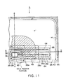
- FIG. 17 is a plan view showing a schematic structure of a seventh embodiment of a semiconductor device according to the present invention.
- FIG. 18 is a cross-sectional view taken along the cutting line A—A of the semiconductor device shown in FIG. 17 .
- FIG. 19 is a plan view showing a schematic structure of an eighth embodiment of a semiconductor device according to the present invention.
- FIG. 20 is a cross-sectional view taken along the cutting line A—A of the semiconductor device shown in FIG. 19 .
- FIG. 21 is a cross-sectional view taken along the cutting line B—B of the semiconductor device shown in FIG. 19 .
- FIG. 22 is a plan view showing a schematic structure of a ninth embodiment of a semiconductor device according to the present invention.
- FIG. 23 is a cross-sectional view taken along the cutting line A—A of the semiconductor device shown in FIG. 22 .
- FIG. 24 is a plan view showing a schematic structure of a tenth embodiment of a semiconductor device according to the present invention.
- FIG. 25 is a cross-sectional view taken along the cutting line A—A of the semiconductor device shown in FIG. 24 .
- FIG. 26 is across-sectional view taken along the cutting line B—B of the semiconductor device shown in FIG. 24 .
- FIG. 27 is a cross-sectional view showing a schematic structure of an eleventh embodiment of a semiconductor device according to the present invention.
- FIG. 28 is a graph showing relationships between a p type dopant amount and a breakdown voltage with respect to a cell region portion and a junction terminating region portion, respectively.
- FIG. 29 is a cross-sectional view showing a schematic structure of a twelfth embodiment of a semiconductor device according to the present invention.
- FIG. 30 is a graph showing changes in the breakdown voltage with respect to the impurity balance of a p type resurf layer and an n ⁇ type drift layer.
- FIG. 31 is a cross-sectional view showing a schematic structure of a thirteenth embodiment of a semiconductor device according to the present invention.
- FIG. 32 is a cross-sectional view showing a schematic structure of a fourteenth embodiment of a semiconductor device according to the present invention.
- FIG. 33 is a cross-sectional view showing a schematic structure of a fifteenth embodiment of a semiconductor device according to the present invention.
- FIG. 34 is a cross-sectional view showing a schematic structure of a sixteenth embodiment of a semiconductor device according to the present invention.
- FIGS. 35A through 35F are schematic cross-sectional views showing one embodiment of a method of manufacturing the semiconductor device according to the present invention.
- FIG. 36 is a cross-sectional view showing a schematic structure of a power MOSFET having a super junction structure in accordance with a prior art.
- the semiconductor device according to the present invention is not limited to a power MOSFET, and can be applied to an SBD or MPS diode having a super junction structure, a switching element such as an SIT, a JFET, an IGBT, or the like, and a complex element or an integrated element of the diodes and the switching elements.
- FIG. 1 is a plan view showing a schematic structure of a first embodiment of the semiconductor device according to the present invention.
- FIG. 2 and FIG. 3 are cross-sectional views of the semiconductor device of the present embodiment along taken along the cutting lines A—A and B—B of FIG. 1 , respectively.
- the semiconductor device 1 of the present embodiment is characterized in that n ⁇ type drift layers 26 and p-type drift layers 28 are formed not only in a cell region portion, but are formed also up to the vicinity of the periphery of a junction terminating region portion.
- the structure of the semiconductor device 1 of the present embodiment will be described in even more detail.
- the semiconductor device 1 of the present embodiment has an n+ type drain layer 20 , a drain electrode 40 , the n type drift layers 26 , the p type drift layers 28 , p type base layers 30 , an n+ type source layer 32 , a source electrode 38 , an insulated gate electrode 36 , and a fieldplate electrode 48 .
- the drain electrode 40 is formed on one surface of the n+ type drain layer 20 , and is formed on the bottom surface in FIG. 2 and FIG. 3 .
- the p type drift layers 28 are respectively structured in the n type semiconductor layers 26 so as to be in a striped shape from the boundary surface with the n+ type drain layer 20 up to the surface portion of the n type semiconductor layers 26 which represent the other surface portion, i.e., the top surface portion in FIG. 2 and FIG. 3 , of the n+ type drain layer 20 .
- the respective stripe-shaped p type drift layers 28 are arranged not only in the cell region portion, but also up to the junction terminating region portion at predetermined intervals in a predetermined direction which is horizontal to the surface of the n+ type drain layer 20 .
- Regions sandwiched between these p type drift layers 28 in the n type semiconductor layers 26 structure the n type drift layers 26 .
- the impurity concentration of both of the n type semiconductor layers 26 and the p type drift layers 28 for example, when each of their widths is 5 ⁇ m, the impurity concentration is about 4 ⁇ 10 15 cm ⁇ 3 , respectively, and when each of the widths is 1 ⁇ m, the impurity concentration is about 2 ⁇ 10 16 cm ⁇ 3 , respectively.
- the p type base layers 30 are selectively formed in the surface portion in the n type semiconductor layers 26 so as to connect to the p type drift layers 28 .
- the n+ type source layers 32 are selectively formed in the surface portion of the p type base layers 30 .
- the source electrodes 38 are formed so as to connect the adjacent n+ type source layer 32 on the surface of the p type base layer 30 and the p type base layer 30 sandwiched thereby.
- the insulated gate electrode 36 is disposed via an insulating film 34 above the surface of the n type drift layer 26 , the surface of the p type base layer 30 adjacent to the surface of the n type drift layer 26 , and the surface of the n+ source layer 32 contacting the p type base layer 30 , so as to be surrounded by the source electrodes 38 .
- the semiconductor device 1 constitutes an n channel MOSFET for electron injection in which the surface portion of the p type base layer 30 immediately under the insulated gate 36 is a channel region.
- a planer type gate structure is provided will be described.
- a trench type gate structure may be used. This point is the same for the following respective embodiments as well.
- the semiconductor device 1 also comprises a p type base layer 30 a which is formed so as to surround the cell region portion in the surface portion at the vicinity of the boundary with the cell region portion in the junction terminating region portion.
- the p type base layer 30 a is discretely connected to the p type drift layer 28 a which is closest to the cell region portion among the p type drift layers 28 a provided in the junction terminating region portion.
- an insulating film 46 is formed on the part other than a part of the p type base layer 30 a.
- a fieldplate electrode 48 is formed on the insulating film 46 so as to surround the cell region, and contacts the surface of the p type base layer 30 a, and is electrically connected to the source electrodes 38 .
- a high-concentration n+ type channel stopper layer 42 is formed on the surface portion of the n type drift layer 26 , and the electrode 44 is formed on the n+ channel stopper layer 42 .
- the broken lines in FIG. 2 and FIG. 3 denote equipotential lines, which are the result of a simulation in which calculation is carried out by using the conditions that the widths of the n type drift layer 26 and the p type drift layer 28 are 8 ⁇ m, the impurity concentrations thereof are 2 ⁇ 10 15 cm ⁇ 3 , and the thickness thereof are 50 ⁇ m.
- the depletion progresses from a side close to the cell region portion of the n type drift layer 26 a and the p type drift layer 28 a toward the periphery of the device, and in the horizontal direction, the depletion progresses over the boundary surface at the same time from the device peripheral portions of the drift layers 26 a and 28 a to the cell region portion.
- the structure of the n type drain layer 20 is not limited to the form shown in FIG. 1 through FIG. 3 , and for example, an epitaxial wafer substrate, a layer in which a predetermined depth of the epitaxial wafer substrate is subjected to thermal diffusion, a diffusion layer in which an impurity is subjected to thermal diffusion, or the like can be applied.
- the present embodiment is the two-layer structure of the n type drain layer 20 and the n type semiconductor layer 26 .
- an intermediate layer whose concentration continuously changes may be set between these two layers.
- the fieldplate electrode 48 is formed on the insulating film 46 having a uniform thickness.
- the present invention is not limited thereto, and for example, as in eleventh through sixteenth embodiments which will be described later, it may be set such that the thickness of the insulating film 46 is made to gradually become greater as the insulating film 46 approaches the peripheral portion.
- FIG. 4 is a plan view showing a schematic structure of a second embodiment of a semiconductor device according to the present invention.
- FIG. 5 and FIG. 6 are cross-sectional views of the semiconductor device of the present embodiment taken along the cutting lines A—A and B—B of FIG. 4 , respectively.
- the semiconductor device 2 of the present embodiment has, in place of the fieldplate electrode 48 which the semiconductor 1 shown in FIG. 1 has, a p ⁇ type resurf layer 52 which is connected to the p type base layer 30 a disposed so as to surround the cell region in the junction terminating region portion, and which is formed so as to further surround the p type base layer 30 a.
- the other structures of the semiconductor device 2 are substantially the same as those of the semiconductor device 1 shown in FIG. 1 .
- FIG. 7 is a plan view showing a schematic structure of a third embodiment of a semiconductor device according to the present invention. Note that a cross-sectional view taken along the cutting line A—A in the view is substantially the same as FIG. 2 .
- the semiconductor device 3 of the present embodiment is characterized in that p type drift layers 54 , 54 a have a circular plane shape, which is different from the above-described embodiments. Due to the p type drift layers being structured in such a shape, the depletion layers can be extended in all directions in a plane which is horizontal to the surface of the device.
- FIG. 7 although an example of circular patterns is shown, there may be polygonal patterns such as quadrangular patterns, hexagonal patterns, or the like. Further, it may be formed such that the n type drift layers 26 have a pattern. Further, in the same way as in the above-described second embodiment, a resurf layer can be applied in place of the fieldplate electrode 48 .
- FIG. 8 is a plan view showing a schematic structure of a fourth embodiment of a semiconductor device according to the present invention.
- FIG. 9 is a cross-sectional view of the semiconductor device of the present embodiment taken along the cutting line A—A of FIG. 8 .
- a semiconductor device 4 of the present embodiment has an n ⁇ type base layer 68 as the n type base layer in the junction terminating region portion, the concentration of the n ⁇ type base layer 68 being lower than that of the n type drift layer 26 in the cell region portion. Moreover, the semiconductor device 4 does not have drift layers in the junction terminating region portion other than a p type drift layer 27 which will be described later.
- the p type base layer 30 a and a plurality of p type guard ring layers 62 are selectively formed so as to surround the cell region portion in the surface portion of the n ⁇ type base layer 68 .
- the p type drift layer 27 is formed so as to correspond to the arrangement of the p type base layer 30 a, and thus, the p type base layer 30 a is connected to the drain electrode 40 via the drain layer 20 .
- a stable high breakdown voltage can be obtained by a single super junction structure surrounding the cell region portion and the p type guard ring layers 62 formed so as to surround the cell region portion in the same way in the surface portion of the periphery of the super junction structure.
- FIG. 10 A cross-sectional view of a modified example of the present embodiment is shown in FIG. 10 .
- a semiconductor device 4 ′ shown in the view has, in the junction terminating region portion, n type base layers 22 whose concentration is the same as that of the n type drift layer 26 in the cell region portion, and p type drift layers 29 are provided in the junction terminating region portion and are connected to p type guard ring layers 62 ′ which are selectively provided on the surface portion of the n type base layers 22 .
- a p type drift layer 29 ′ is formed so as to be exposed on the surface of the n type base layers 22 .
- FIG. 11 is a plan view showing a schematic structure of a fifth embodiment of a semiconductor device according to the present invention.
- FIG. 12 is a cross-sectional view of the semiconductor device of the present embodiment taken along the cutting line A—A of FIG. 11 . Note that the cross-sectional view taken along the cutting line B—B of FIG. 11 is the same as the FIG. 3 .
- the present embodiment provides a junction terminating regional structure which is suitable for a semiconductor device having an insulating film formed parallel to the horizontal direction in the n type drift layer 26 in the cell region portion.
- a trench groove 64 is formed in a horizontal direction in the n type drift layer 26 ( 26 a), and an insulating film 66 is formed therein.
- Such an insulating film can be manufactured by forming the stripe shaped trench grooves 64 so as to extend from the cell region portion to the junction terminating region portion on the substrate structured from, for example, a low-concentration n ⁇ type base layer 68 , and by applying thermal diffusion after an n type impurity and a p type impurity are introduced into the side walls of the trench grooves 64 by using a method such as an ion injection or the like.
- the n type drift layer 26 ( 26 a) and the p type drift layer 28 ( 28 a) are formed so as to surround the insulating film 66 . Accordingly, in the junction terminating region portion, the insulating film 66 and the both drift layers 26 a, 28 a extend in the horizontal direction up to the vicinity of the peripheral portion. However, the insulating film 66 and the drift layers are not formed in the vertical direction.
- the semiconductor device 5 of the present embodiment further comprises the field plate electrode 48 provided above the low-concentration n ⁇ type base layer 68 in the junction terminating region via the insulating film 46 so as to surround the cell region. Therefore, the depletion layer sufficiently extends, and a high breakdown voltage can be obtained.
- FIG. 13 is a plan view showing a schematic structure of a sixth embodiment of a semiconductor device of the present invention.
- FIG. 14 and FIG. 15 are cross-sectional views of the semiconductor device of the present embodiment taken along the cutting lines A—A, B—B of FIG. 13 .
- the insulating film 66 is formed only in the cell region portion, and does not extend to the junction terminating region portion. Moreover, in the junction terminating region portion of the semiconductor device 6 , both the n type drift layers and the p type drift layers are not formed.
- the n ⁇ type base layer 68 whose concentration is lower than that of the n type drift layer 26 is formed in the junction terminating region portion, and the p type base layer 30 a and a plurality of p type guard ring layers 62 are selectively formed so as to surround the cell region on the surface portion of the n ⁇ type base layer 68 .
- the source electrode 38 a contacts the surface of the p type base layer 30 a. Further, below the p type base layer 30 a, the p type drift layer 27 is formed so as to correspond to the arrangement of the p type base layer 30 a, and thereby the p type base layer 30 a is connected to the drain electrode 40 via the drain layer 20 . In accordance with such a structure of the junction terminating region portion, the semiconductor device 6 of the present embodiment can obtain a sufficiently high breakdown voltage.
- FIG. 16 is a plan view showing a modified example of the present embodiment.
- an insulating film 72 is formed also in a vertical direction only in the cell region portion, and then the insulating film 72 has a reticulated plan shape.
- Other structures of the semiconductor device 6 ′ are substantially the same as those of the semiconductor device 6 shown in FIG. 13 . Even when the insulating film 72 has such a structure in the cell region portion, the semiconductor device 6 ′ can obtain a sufficiently high breakdown voltage because the insulating film 72 does not extend to the junction terminating region portion and the p type guard ring layers 62 are formed in the junction terminating region portion.
- FIG. 17 is a plan view showing a schematic structure of a seventh embodiment of a semiconductor device according to the present invention.
- FIG. 18 is a cross-sectional view of the semiconductor device of the present embodiment taken along the cutting line A—A of FIG. 17 . Note that the cross-sectional view taken along the cutting line B—B of FIG. 17 is the same as FIG. 3 .
- a semiconductor device 7 of the present embodiment further comprises insulating films 76 formed in the vertical direction in the junction terminating region portion, and n type drift layers 166 and p type drift layers 168 which are respectively formed in the vertical direction in the junction terminating region portion and which are periodically disposed in the horizontal direction.
- the depletion layers sufficiently extend at the time of turning-off because the positive holes in the p type drift layers 168 are discharged in the vertical direction in the same way as in the horizontal direction, and a high breakdown voltage can thus be obtained.
- FIG. 19 is a plan view showing a schematic structure of an eighth embodiment of a semiconductor device according to the present invention.
- FIG. 20 and FIG. 21 are cross-sectional views of the semiconductor device of the present embodiment taken along the cutting lines A—A and B—B of FIG. 19 , respectively.
- the insulating films 76 and the drift layers 26 a, 28 a which are formed so as to extend from the cell region portion toward the junction terminating region portion, are periodically disposed in the vertical direction as well, and are formed up to the vicinity of the periphery of the junction terminating region portion. Further, on the surface portion of the junction terminating region portion, a p ⁇ type resurf layer 52 having a predetermined width is provided so as to surround the cell region. Moreover, electrodes 78 for voltage fixing are provided above or on the respective p type drift layers 28 a 4 through 28 a 7 periodically disposed in the vertical direction in the junction terminating region portion (see FIG. 20 ).
- Electrodes 78 are extendedly formed so as to bend in circular arcs having a center in common with the corner portion of a source electrode 38 a with a constant interval between one another, and so as to intersect the p type drift layers 28 al through 28 a 3 .
- the electrodes 78 are connected to these p type drift layers 28 a 1 through 28 a 3 at the extended portions (see FIG. 21 ).
- FIG. 22 is a plan view showing a schematic structure of a ninth embodiment of a semiconductor device according to the present invention.
- FIG. 23 is a cross-sectional view of the semiconductor device of the present embodiment taken along the cutting line A—A of FIG. 22 . Note that the cross-sectional view taken along the cutting line B—B of FIG. 22 is the same as FIG. 3 .
- insulating films 84 which are formed in stripe shapes in the respective horizontal directions in the junction terminating region portion and which are periodically disposed in the vertical direction, and n type drift layers 172 which are formed so as to surround the insulating films 84 , are respectively divided in the horizontal direction, and are formed so as to be lattice-shaped in a plan view.
- portions of the p type drift layers 178 in the horizontal directions are connected to one another in the vertical directions.
- positive holes are discharged at the time of turning-off.
- the semiconductor device 9 of the present embodiment comprises a fieldplate electrode 48 which is formed so as to connect to the p type base layer 30 a formed so as to surround the cell region and which is formed so as to extend onto the insulating film 46 formed on the junction terminating region portion.
- a fieldplate electrode 48 which is formed so as to connect to the p type base layer 30 a formed so as to surround the cell region and which is formed so as to extend onto the insulating film 46 formed on the junction terminating region portion.
- FIG. 24 is a plan view showing a schematic structure of a tenth embodiment of a semiconductor device according to the present invention.
- FIG. 25 and FIG. 26 are cross-sectional views of the semiconductor device of the present embodiment taken along the cutting lines A—A and B—B of FIG. 24 , respectively.
- a semiconductor device 10 of the present embodiment comprises Resistive Field Plates RFPs (which are hereinafter called as RFPs) 50 which are made from semi-insulated polysilicon or the like and are formed in the junction terminating region portion so as to surround the cell region, in place of the p ⁇ type resurf layer 52 and the electrode 78 of the semiconductor device 8 shown in FIG. 19 .
- the RFPs 50 are, directly or via the p type base layer 30 in the vicinity of the boundary with the cell region, connected to the source electrode 38 a, and are connected to the p type drift layers 28 a.
- the p type drift layers 28 a 1 and 28 a 2 which correspond to the portion at which the p type drift layers 28 in the cell region portion are extended in the horizontal direction, contact the RFPs 50 over substantially the entire length thereof (see FIG. 26 ).
- the p type drift layers 28 a 4 through 28 a 7 which are periodically formed in the vertical direction in the junction terminating region portion, discretely contact the RFPs 50 over a width corresponding to the width of the cell region portion in the horizontal direction (see FIG. 25 ).
- FIG. 27 is a cross-sectional view showing a schematic structure of an eleventh embodiment of a semiconductor device according to the present invention.
- a vertical type power MOSFET 11 shown in FIG. 27 comprises a semiconductor layer 102 forming a n ⁇ base layer, an n+ drain layer 100 , a drain electrode 40 , a plurality of p type resurf layers 106 , 130 forming the super junction structure, p type base layers 108 , n+ type source layers 110 , gate electrodes 114 , and source electrodes 116 .
- the n+ type drain layer 100 is formed on one surface of the n ⁇ type base layer 102 , i.e., on the bottom surface in FIG. 27 , and the drain electrode 40 is formed on the n+ drain layer 100 .
- the p type resurf layers 106 , 130 are periodically disposed in a predetermined direction not only in the cell region portion but also in the junction terminating region portion, on the other surface portion of the n ⁇ type base layer 102 , i.e., the top surface portion in FIG. 27 . Thereby, a super junction structure is formed, and the p type resurf layer 106 functions as the p type drift layer 106 . Further, region portions sandwiched by these p type drift layers 106 of the n ⁇ type base layers 102 function as the n ⁇ type drift layer 102 .
- the p type base layer 108 is selectively formed so as to connect to the p type drift layer 106 at the surface portion of the n ⁇ type base layer 102 in the cell region portion.
- the n+ type source layer 110 is selectively diffusion-formed so as to have a striped plane shape in the surface portion of the p type base layer 108 .
- the p type base layer 108 is formed such that, for example, when its impurity concentration is about 3 ⁇ 10 17 cm ⁇ 3 , the depth is about 2.0 ⁇ m, and the n+ type source layer 110 is formed such that, for example, when its impurity concentration is about 1 ⁇ 10 20 cm ⁇ 3 , the depth is about 0.2 ⁇ m.
- the gate electrode 114 is formed via a gate insulating film 112 e.g. an Si oxide film 112 whose film thickness is 0.1 ⁇ m on the surface region from the surface of the n+ type source layer 110 and the surface of the p type base layer 108 up to the surface of the adjacent p type base layer 108 and the surface of the n+ type source layer 110 via the surface of the n ⁇ type drift layer 102 .
- the gate electrode 114 is formed so as to be a striped plane shape.
- the source electrode 116 is formed so as to be a striped plane shape on the surface region of the n+ type source layer 110 in the surface portion of the p type base layer 108 , the surface region of the p type base layer 108 , and the surface region of the adjacent n+ type source layer 110 .
- the source electrodes 116 are disposed so as to sandwich the gate electrode 114 .
- a conductive film 117 such as metal, polysilicon, or the like is formed via the insulating film 126 .
- a field plate structure is constituted in the junction terminating region portion.
- a field stopper 42 is provided on the surface portion of the periphery of the device, which is formed from an n layer and stops depletion.
- the super junction structure portion in the junction terminating region portion is rapidly depleted by the field plate 128 at the time of applying high voltage, and the junction terminating region portion then equivalently becomes a low impurity concentration layer. Therefore, the concentration of an electric field in the junction terminating region portion is suppressed, and a high breakdown voltage is maintained. Note that even if a resurf layer is formed on the surface portion in the junction terminating region portion, the super junction structure portion is rapidly depleted in the same way as the field plate. Therefore, the same effects can be obtained.
- the field plate 117 has a structure having an electric potential which is the same as the source electrode 116 . However, it is not limited to this structure, and the field plate 117 may be manufactured so as to have the same electric potential as the gate electrode 114 .
- the impurity amount of the p type drift layer 130 in the junction terminating region portion is greater than the impurity amount of the p type drift layer 106 in the cell region portion, decrease of breakdown voltage in the junction terminating region portion can be suppressed.
- the impurity amount of the p type drift layers 106 , 130 is a product of the width and the impurity concentration, respectively.
- the p type drift layer 130 in the junction terminating region portion is formed so as to have a width which is wider than that of the p type drift layer 106 in the cell region portion, the p type drift layer 130 is formed so as to have an impurity concentration which is the same as that of p type drift layer 106 .
- the impurity amount of the p type dopant in the junction terminating region portion increases, and as a result, decrease of breakdown voltage in the junction terminating region portion can be suppressed.
- the present invention is not limited to this structure.
- the width of the p type drift layer 106 in the cell region portion and the width of the p type drift layer 130 in the junction terminating region portion are made to be the same, and only the impurity concentration in the junction terminating region portion is made to be higher, the same effects can be obtained.
- FIG. 28 is a graph showing changes in breakdown voltage when the amount of the p type impurity is changed, with respect to the cell region portion and the junction terminating region portion, respectively.
- the abscissa of the graph is the ratio of the impurity amount Np of the p type drift layer with respect to the impurity amount Nn of the n ⁇ type drift layer.
- the highest breakdown voltage can be obtained when the impurity amount of the n ⁇ type drift layer and the impurity amount of the p type drift layer are equal (the unbalance is 0%), and if the impurity amount of the p type drift layer is relatively higher or lower, the breakdown voltage symmetrically decreases around the point of 0% in accordance with the proportion.
- the highest breakdown voltage can be obtained when the impurity amount of the p type drift layer is relatively 10% higher.
- the optimum impurity amounts of the p type drift layer in the cell region portion and in the junction terminating region portion are different from one another.
- the breakdown voltage in the junction terminating region portion decreases.
- the optimum impurity amount in the junction terminating region portion is higher than that in the cell region portion.
- the impurity amount of the p type drift layer in the cell region portion is optimally set to 80 to 120% of that of the n ⁇ type drift layer, including the process margin.
- the impurity amount of the p type drift layer in the junction terminating region portion is optimally set to 90 to 130% of that of the n ⁇ type drift layer, including the process margin. Therefore, the impurity amount of the p type drift layer at the terminating portion is preferably set to 75 to 163% of the impurity amount of the p type drift layer in the cell region portion.
- the impurity amount of the p type drift layer, at which the highest breakdown voltage can be obtained, is higher at the terminating portion. Therefore, the impurity amount of the p type drift layer at the terminating portion is more preferably set to 100 to 163% of the impurity amount in the cell region portion.
- the method for forming the super junction structure may be any of, for example, a method in which an ion injection and buried crystal growth are repeated, a method in which a trench groove is formed and buried epitaxy is carried out, and a method in which an ion injection is carried out from an oblique direction after a trench groove is formed.
- ion injection may be carried out individually in the cell region portion and in the junction terminating region portion, or an ion injection may be carried out at the same time in the cell region portion and the junction terminating region portion, with the mask opening width for ion injection being changed.
- the trench groove width or the mesa width may be varied in the cell region portion and the junction terminating region portion.
- the impurity amount of the p type drift layer is made to be the same in the cell region portion and in the junction terminating region portion, and the impurity amount of the n ⁇ type drift layer in the junction terminating region portion is made to be lower than that in the cell region portion, the same effects can be obtained.
- the semiconductor device 12 of the present embodiment is characterized in that the super junction structure is structured by p type drift layers whose cell pitches are different from one another in the cell region portion and the junction terminating region portion. Specifically, a cell pitch of a p type drift layer 132 in the junction terminating region portion is made to be narrower than that of the p type drift layer 106 in the cell region portion. Due to the cell width in the junction terminating region portion being made narrow, depletion in the junction terminating region portion then rapidly proceeds at the time of turning-off. As a result, a lowering of the breakdown voltage in the junction terminating region portion is suppressed.
- FIG. 30 is a graph showing changes in breakdown voltage with respect to the impurity balance between the p type drift layer and the n ⁇ type drift layer.
- the impurity concentration of the n ⁇ type drift layer is set to 2.5 ⁇ 10 15 cm ⁇ 3 . Comparing a case in which the cell pitch is 16 ⁇ m and a case in which the cell pitch is 8 ⁇ m, the decrease in the breakdown voltage is smaller with respect to the balance of the impurity in the case of 8 ⁇ m in which the cell pitch is narrower than 16 ⁇ m. Thereby, it can be understood that the margin with respect to the impurity concentration balance can be made larger by making the cell pitch narrower.
- the impurity amount of the p type drift layer at which the highest breakdown voltage is obtained is greater than the impurity amount of the n ⁇ type drift layer.
- the impurity amount of the p type drift layer in the junction terminating region portion is greater than that in the cell region portion.
- FIG. 31 is a cross-sectional view showing a schematic structure of a thirteenth embodiment of a semiconductor device according to the present invention.
- the semiconductor device 13 of the present embodiment is characterized in the shape of a p type drift layer 134 in the junction terminating region portion.
- the p type drift layer 134 is buried so as not to have a pillar-shaped cross-sectional shape as in the respective embodiments described above but so as to have a circular cross sectional shape. If the p type drift layer 134 structuring the super junction structure have such a circular cross sectional shape in the cell region portion, once it is depleted by turning-off in the p type drift layer, the depletion is maintained.
- the p type drift layers 134 in the junction terminating region portion does not affect the on operation of the semiconductor device 13 because the p type drift layers 134 in circular cross sectional shapes are formed only in the junction terminating region portion.
- the p type drift layer 134 of the present embodiment has a structure which can be obtained when diffusion after burying and growing is used in order to solve such a problem. Specifically, in accordance with diffusion after burying and growing, the concentration of the buried p layer is higher in the cell region portion and is lower in the junction terminating region portion. As a result, the upper and lower p layers are connected in the cell region portion, and the p type drift layer is formed in a pillar-shaped cross sectional shape.
- the respective buried layers are not connected, and have circular cross sectional shapes.
- the cell pitch in the junction terminating region portion is preferably set to a value greater than or equal to half of the cell pitch in the cell region portion.
- FIG. 32 is a cross-sectional view showing a schematic structure of a fourteenth embodiment of a semiconductor device according to the present invention.
- a semiconductor device 14 of the present embodiment is formed such that the cell width of the super junction structure in the junction terminating region portion is narrower than the cell width in the cell region portion, and is formed such that the mesa width of the p type drift layer 136 in the junction terminating region portion is relatively wider. Thereby, the impurity concentration of the p type drift layer 136 in the junction terminating region portion can be made higher than that in the cell region portion. With such a structure, lowering of the breakdown voltage in the junction terminating region portion can be suppressed in the semiconductor device 14 of the present embodiment.
- FIG. 33 is a cross-sectional view showing a schematic structure of a fifteenth embodiment of a semiconductor device according to the present invention.
- a semiconductor device 15 of the present embodiment is characterized in that it further comprises an n ⁇ type drift layer 142 provided between the super junction structure and the n+ drain layer 100 , and the n ⁇ type drift layer 142 and the super junction structure also constitute n type drift layers.
- the n ⁇ type drift layer 142 is formed so as to have an impurity concentration which is lower than that of the n ⁇ type drift layer 102 in the super junction structure.
- FIG. 34 is a cross-sectional view showing a schematic structure of a sixteenth embodiment of a semiconductor device according to the present invention.
- n type drift layers are constituted by the n ⁇ type drift layer 142 and the super junction structure.
- the n ⁇ type drift layer 142 has an impurity concentration which is lower than that of the n ⁇ type drift layer 102 in the super junction structure.
- the n ⁇ type semiconductor layer is further epitaxially grown so as to cover the n ⁇ type semiconductor layer 151 and the p ⁇ type semiconductor layer 158 , and an n ⁇ type semiconductor layer 160 having a film thickness which is the same as the film thickness of the p ⁇ type semiconductor layer 158 is formed ( FIG. 35D ).
- a trench groove 162 matching the trench groove 154 is formed in the n ⁇ type semiconductor layer 160 ( FIG. 35E ).
- the n ⁇ type semiconductor layer 164 is epitaxially grown so as to cover the n ⁇ type semiconductor layer 153 and the p ⁇ type semiconductor layer 158 ( FIG. 35F ).
- the super junction structure can thus be formed by a number of crystal growths which is less than that of the conventional process in which ion injection and buried crystal growth are repeated.
- the super junction structure can be formed by carrying out trench buried crystal growths twice.
- the present invention is not limited thereto.
- the trench buried crystal growth may be repeated three times or more with the aspect ratio per one time being set to one of third of a required aspect ratio.
- the super junction structures of the first time and the second time are formed in a striped shape and are formed so as to intersect one another, alignment can be exactly carried out.
- the present invention has been described above. However, the present invention is not limited to these embodiments, and can be modified and achieved within the scope and the sprits thereof.
- the super junction structure, the p type base layer, the n+ source layer, and the gate electrode are formed in striped shapes. However, they may be formed so as to be in lattice shapes or staggered shapes.
- vertical power MOSFETs using silicon (Si) serving as semiconductor materials have been described.
- Si silicon
- diamond can be used in addition to compound semiconductors such as silicon carbide (SiC), gallium nitride (GaN), aluminum nitride (AlN), or the like.
Abstract
A semiconductor device includes a first-conductivity-type semiconductor layer which includes a cell region portion and a junction terminating region portion. The junction terminating region portion is a region portion which is positioned in an outer periphery of the cell region portion to maintain a breakdown voltage by extending a depletion layer to attenuate an electric field.
Description
This application claims benefit of priority under 35USC § 119 to Japanese patent application No. 2002-74633, filed on Mar. 18, 2002, the contents of which are incorporated by reference herein.
1. Field of the Invention
The present invention relates to a semiconductor device and a method of manufacturing a semiconductor device, and in particular, to a structure of a junction terminating region portion of a power semiconductor device which is suitable for a switching element for electric power.
2. Related Background Art
In response to the demand to make electrical power equipment compact and high-performance in recent years in the power electronics field, performance improvements with respect to making lowering loss, increasing speed and improving the ruggedness have been carried out in addition to making them have a high breakdown voltage and making them able to handle great current in the power semiconductor devices. Among them, a power MOSFET (Metal Oxide Semiconductor Field Effect Transistor) has been established as a key device in the switching power source field or the like because of the high-speed switching performance thereof.
Because the MOSFET is a majority carrier device, the MOSFET has an advantage that there is no minority carrier storage time and switching is fast. However, on the other hand, because there is no electric conductivity modulation, a device which has a high breakdown voltage is disadvantageous with respect to the ON-state resistance as compared with a bipolar device such as an IGBT (Insulated Gate Bipolar Transistor) or the like. This results from the fact that the higher the breakdown voltage a device has, the more the ON-state resistance of the MOSTFET increases, because it is necessary to make an n type base layer thicker and to make the impurity concentration lower in order to obtain a higher breakdown voltage in the MOSFET.
The ON-state resistance of the power MOSFET greatly depends on the electrical resistance in a conductive layer (n type drift layer) portion. Further, the impurity concentration determining the electrical resistance at the n type drift layer cannot rise to greater than or equal to the limit, in accordance with the breakdown voltage of the pn junction which the p type base and the n type drift layer form. Therefore, a trade-off relationship exists between the device breakdown voltage and the ON-state resistance. It is important to improve this trade-off for a low electric power consumption device. In this trade-off, there is a limit which is determined by the material of the device, and this limit must be exceeded in order to realize a low ON-state resistance device exceeding existing power devices.
As one example of MOSFETs for solving this problem, a structure is known in which a resurf structure called a super junction structure is buried in an n type drift layer. A conventional power MOSFET having a super junction structure will be described with reference to FIG. 36 . Note that, in the following figures, like parts are denoted by like reference numerals, and detailed descriptions thereof will be omitted.
In an OFF-state, a depletion layer spreads at junctions between these p type drift layers 106 and n− type drift layers 102. Even if the impurity concentration of the n− type drift layers 102 is made high, the n− type drift layers 102 and the p type drift layers 106 are completely depleted before breaking down. In accordance therewith, a breakdown voltage which is the same as that of the conventional MOSFET can be obtained.
The impurity concentration of the n− type drift layer 102 does not depend on a breakdown voltage of the device, but it depends on the width of the p type drift layer 106 and the width of the n− type drift layer 102 itself between these p type drift layers 106. If the width of the n− type drift layer 102 and the width of the p type drift layer 106 are made narrower, the impurity concentration of the n− type drift layer 102 can be made much higher, and a greater reduction of the ON-state resistance and a higher breakdown voltage can be achieved.
At the time of designing such a MOSFET, the impurity concentrations of the n− type drift layer 102 and the p type drift layer 106 are important to determine the breakdown voltage and the ON-state resistance. In principle, due to the respective impurity concentrations of the n− type drift layer 102 and the p type resurf layer 106 being made equal, the impurity concentrations equivalently become zero, the high breakdown voltage can be obtained.
However, with respect to the semiconductor device having a conventional super junction structure, no structure has been developed which is effective for obtaining a high breakdown voltage in a blocking state (OFF-state) or at the time of turning-off at a junction terminating region portion which is positioned at the outer periphery of an element active region portion (hereinafter referred to as a cell region portion) and which is a region portion for maintaining the breakdown voltage by attenuating the electrical field by extending the depletion layers. Therefore, because the way of spreading of the depletion layers in the cell region portion and the junction terminating region portion are different from one another, the optimum impurity concentrations are different from one another. Accordingly, if the device is manufactured such that the impurity amounts in the cell region portion and the junction terminating region portion are the same, the breakdown voltage at the terminating portion decreases, and an electric field locally concentrates at this place. As a result, there are cases in which the device is broken. In this way, there is the problem that a sufficiently high breakdown voltage cannot be obtained by the entire device in the prior art.
Further, because there are dispersions among the processes at the time of actual manufacturing, it is difficult to make the respective impurity amounts of the n− type drift layer 102 and the p type drift layer 106 completely equal, and the breakdown voltage deteriorates in accordance therewith. Accordingly, it is necessary to carry out designing of the device in consideration of such a decrease of the breakdown voltage due to the process margin. In order to lower the ON-state resistance, it is effective to raise the impurity concentration of the n− type drift layer 102. On the other hand, the process margin for the breakdown voltage is determined by the difference in the impurity amounts between the n− type drift layer 102 and the p type drift layer 106. Therefore, when the impurity amount of the n− type drift layer 102 is increased, because the difference itself determining the process margin is not changed, the ratio between the allowed impurity amount and the impurity amount of the n− type drift layer 102 becomes small. Namely, the process margin becomes small.
According to a first aspect of the present invention, there is provided a semiconductor device comprising:
a first—first conductivity type semiconductor layer which includes a cell region portion and a junction terminating region portion, the junction terminating region portion being a region portion which is positioned in an outer periphery of the cell region portion to maintain a breakdown voltage by extending a depletion layer to attenuate an electric field;
a second-first conductivity type semiconductor layer which is formed on one surface of the first—first conductivity type semiconductor layer;
a first main electrode which is electrically connected to the second-first conductivity type semiconductor layer;
first-second conductivity type semiconductor layers which are formed in the cell region portion of the first—first conductivity type semiconductor layer in substantially vertical directions to the one surface of the first—first conductivity type semiconductor layer, respectively, and which are periodically disposed in a first direction which is an arbitrary direction parallel to the one surface;
a second—second conductivity type semiconductor layer which is selectively formed in the other surface portion of the first—first conductivity type semiconductor layer so as to contact the first-second conductivity type semiconductor layers;
a third-first conductivity type semiconductor layer which is selectively formed in the surface portion of the second—second conductivity type semiconductor layer;
a second main electrode which is formed so as to contact the second—second conductivity type semiconductor layer and the third-first conductivity type semiconductor layer;
a control electrode which is formed on the surface of the first—first conductivity type semiconductor layer sandwiched by the adjacent second—second conductivity type semiconductor layers, the surface of the adjacent second—second conductivity type semiconductor layers and the surface of the third-first conductivity type semiconductor layer, with a gate insulating film interposed therebetween; and
third-second conductivity type semiconductor layers which are formed in the junction terminating region portion and are periodically disposed in at least one direction of the first direction and a second direction perpendicular to the first direction.
According to a second aspect of the invention, there is provided a method of manufacturing a semiconductor device having a super junction structure with a first conductivity type semiconductor layer on which a trench groove whose aspect ratio is R is provided and a second conductivity type semiconductor layer which is buried in the trench groove, the method of manufacturing the semiconductor device comprising:
forming a trench groove having an aspect ratio of R/N (N is a natural number greater than 1) in a first conductivity type semiconductor layer;
epitaxially growing a second conductivity type semiconductor layer so as to bury the trench groove;
removing the second conductivity type semiconductor layer until a surface of the first conductivity type semiconductor layer is exposed;
epitaxially growing the first conductivity type semiconductor layer on the first conductivity type semiconductor layer and the second conductivity type semiconductor layer such that the thickness of the first conductivity type semiconductor layer increases by a length which is substantially the same as a depth of the trench groove formed by the first process;
selectively removing the first conductivity type semiconductor layer such that the second conductivity type semiconductor layer which is buried in the trench groove formed by the first process is exposed; and
repeating the epitaxially growing the second conductivity type semiconductor layer through selectively removing the first conductivity type semiconductor layer (N−1) times.
Several embodiments of the present invention will be described with reference to the drawings. Hereinafter, first, embodiments of a semiconductor device according to the present invention will be described, and finally, an embodiment of a method of manufacturing the semiconductor device according to the present invention will be described.
(A) Embodiments of the Semiconductor Device
Hereinafter, a power MOSFET having a super junction structure will be described. However, the semiconductor device according to the present invention is not limited to a power MOSFET, and can be applied to an SBD or MPS diode having a super junction structure, a switching element such as an SIT, a JFET, an IGBT, or the like, and a complex element or an integrated element of the diodes and the switching elements.
(1) First Embodiment
The semiconductor device 1 of the present embodiment has an n+ type drain layer 20, a drain electrode 40, the n type drift layers 26, the p type drift layers 28, p type base layers 30, an n+ type source layer 32, a source electrode 38, an insulated gate electrode 36, and a fieldplate electrode 48.
The drain electrode 40 is formed on one surface of the n+ type drain layer 20, and is formed on the bottom surface in FIG. 2 and FIG. 3 . The p type drift layers 28 are respectively structured in the n type semiconductor layers 26 so as to be in a striped shape from the boundary surface with the n+ type drain layer 20 up to the surface portion of the n type semiconductor layers 26 which represent the other surface portion, i.e., the top surface portion in FIG. 2 and FIG. 3 , of the n+ type drain layer 20. The respective stripe-shaped p type drift layers 28 are arranged not only in the cell region portion, but also up to the junction terminating region portion at predetermined intervals in a predetermined direction which is horizontal to the surface of the n+ type drain layer 20. Regions sandwiched between these p type drift layers 28 in the n type semiconductor layers 26 structure the n type drift layers 26. With respect to the widths and the impurity concentration of both of the n type semiconductor layers 26 and the p type drift layers 28, for example, when each of their widths is 5 μm, the impurity concentration is about 4×1015 cm−3, respectively, and when each of the widths is 1 μm, the impurity concentration is about 2×1016 cm−3, respectively.
The p type base layers 30 are selectively formed in the surface portion in the n type semiconductor layers 26 so as to connect to the p type drift layers 28. The n+ type source layers 32 are selectively formed in the surface portion of the p type base layers 30. The source electrodes 38 are formed so as to connect the adjacent n+ type source layer 32 on the surface of the p type base layer 30 and the p type base layer 30 sandwiched thereby. Moreover, the insulated gate electrode 36 is disposed via an insulating film 34 above the surface of the n type drift layer 26, the surface of the p type base layer 30 adjacent to the surface of the n type drift layer 26, and the surface of the n+ source layer 32 contacting the p type base layer 30, so as to be surrounded by the source electrodes 38. In accordance with such a structure, the semiconductor device 1 constitutes an n channel MOSFET for electron injection in which the surface portion of the p type base layer 30 immediately under the insulated gate 36 is a channel region. In the present embodiment, a case in which a planer type gate structure is provided will be described. However, a trench type gate structure may be used. This point is the same for the following respective embodiments as well.
The semiconductor device 1 also comprises a p type base layer 30a which is formed so as to surround the cell region portion in the surface portion at the vicinity of the boundary with the cell region portion in the junction terminating region portion. The p type base layer 30a is discretely connected to the p type drift layer 28a which is closest to the cell region portion among the p type drift layers 28a provided in the junction terminating region portion. On the surface of the junction terminating region portion, an insulating film 46 is formed on the part other than a part of the p type base layer 30a. A fieldplate electrode 48 is formed on the insulating film 46 so as to surround the cell region, and contacts the surface of the p type base layer 30a, and is electrically connected to the source electrodes 38. In the periphery of the junction terminating region, a high-concentration n+ type channel stopper layer 42 is formed on the surface portion of the n type drift layer 26, and the electrode 44 is formed on the n+ channel stopper layer 42.
The broken lines in FIG. 2 and FIG. 3 denote equipotential lines, which are the result of a simulation in which calculation is carried out by using the conditions that the widths of the n type drift layer 26 and the p type drift layer 28 are 8 μm, the impurity concentrations thereof are 2×1015 cm−3, and the thickness thereof are 50 μm.
When the semiconductor device 1 of the present embodiment turns off in a direction (the A—A direction of FIG. 1 , and hereinafter referred to as vertical direction) intersecting the stripe longitudinal direction (the B—B direction of FIG. 1 , and hereinafter referred to as the horizontal direction) of the drift layers 26 (26a), 28 (28a) in plan view, the depletion progresses from a side close to the cell region portion of the n type drift layer 26a and the p type drift layer 28a toward the periphery of the device, and in the horizontal direction, the depletion progresses over the boundary surface at the same time from the device peripheral portions of the drift layers 26a and 28a to the cell region portion. At this time, electrons are discharged to the drain electrode 40 via the n+ type drain layer 20 from the n type drift layer 26a, and on the other hand, positive holes are discharged to the source electrode 38 via the p type base layer 30a and to the fieldplate electrode 48 from the p type drift layer 28a. However, in the vertical direction, the positive holes are discharged so as to cross the junction between the n type drift layer 26a and the p type drift layer 28a. Moreover, in a blocking state (at the time when the device is off), because the intervals between the equipotential lines are made uniform by the fieldplate electrode 48, as shown in FIG. 2 and FIG. 3 , the electric field is attenuated thereby. As a result, the semiconductor device 1 can obtain a stable high breakdown voltage.
Note that the structure of the n type drain layer 20 is not limited to the form shown in FIG. 1 through FIG. 3 , and for example, an epitaxial wafer substrate, a layer in which a predetermined depth of the epitaxial wafer substrate is subjected to thermal diffusion, a diffusion layer in which an impurity is subjected to thermal diffusion, or the like can be applied. Further, the present embodiment is the two-layer structure of the n type drain layer 20 and the n type semiconductor layer 26. However, an intermediate layer whose concentration continuously changes may be set between these two layers. Further, in the present embodiment, as shown in FIG. 2 and FIG. 3 , the fieldplate electrode 48 is formed on the insulating film 46 having a uniform thickness. However, the present invention is not limited thereto, and for example, as in eleventh through sixteenth embodiments which will be described later, it may be set such that the thickness of the insulating film 46 is made to gradually become greater as the insulating film 46 approaches the peripheral portion. These points are the same for following second through tenth embodiments as well.
(2) Second Embodiment
The semiconductor device 2 of the present embodiment has, in place of the fieldplate electrode 48 which the semiconductor 1 shown in FIG. 1 has, a p− type resurf layer 52 which is connected to the p type base layer 30a disposed so as to surround the cell region in the junction terminating region portion, and which is formed so as to further surround the p type base layer 30a. The other structures of the semiconductor device 2 are substantially the same as those of the semiconductor device 1 shown in FIG. 1 .
As shown by the equipotential lines in FIG. 2 and FIG. 3 , also by providing such a p− type resurf layer 52, the electric field is attenuated at the time when the device is off. Therefore, a stable high breakdown voltage can be obtained.
(3) Third Embodiment
The semiconductor device 3 of the present embodiment is characterized in that p type drift layers 54, 54a have a circular plane shape, which is different from the above-described embodiments. Due to the p type drift layers being structured in such a shape, the depletion layers can be extended in all directions in a plane which is horizontal to the surface of the device.
Note that, in FIG. 7 , although an example of circular patterns is shown, there may be polygonal patterns such as quadrangular patterns, hexagonal patterns, or the like. Further, it may be formed such that the n type drift layers 26 have a pattern. Further, in the same way as in the above-described second embodiment, a resurf layer can be applied in place of the fieldplate electrode 48.
(4) Fourth Embodiment
Differently from the above-described first though third embodiments, a semiconductor device 4 of the present embodiment has an n− type base layer 68 as the n type base layer in the junction terminating region portion, the concentration of the n− type base layer 68 being lower than that of the n type drift layer 26 in the cell region portion. Moreover, the semiconductor device 4 does not have drift layers in the junction terminating region portion other than a p type drift layer 27 which will be described later. The p type base layer 30a and a plurality of p type guard ring layers 62 are selectively formed so as to surround the cell region portion in the surface portion of the n− type base layer 68. Below the p type base layer 30a, the p type drift layer 27 is formed so as to correspond to the arrangement of the p type base layer 30a, and thus, the p type base layer 30a is connected to the drain electrode 40 via the drain layer 20.
In this way, in accordance with the present embodiment, even when a plurality of drift layers are not provided in the junction terminating region portion, a stable high breakdown voltage can be obtained by a single super junction structure surrounding the cell region portion and the p type guard ring layers 62 formed so as to surround the cell region portion in the same way in the surface portion of the periphery of the super junction structure.
A cross-sectional view of a modified example of the present embodiment is shown in FIG. 10 . A semiconductor device 4′ shown in the view has, in the junction terminating region portion, n type base layers 22 whose concentration is the same as that of the n type drift layer 26 in the cell region portion, and p type drift layers 29 are provided in the junction terminating region portion and are connected to p type guard ring layers 62′ which are selectively provided on the surface portion of the n type base layers 22. Moreover, in the peripheral portion of the junction terminating region portion, a p type drift layer 29′ is formed so as to be exposed on the surface of the n type base layers 22. In accordance with these structures, a stable high breakdown voltage can be obtained because the equipotential lines spreading in the junction terminating region portion are made flat. As a result, a decrease of the breakdown voltage in the junction terminating region portion can be suppressed.
(5) Fifth Embodiment
The present embodiment provides a junction terminating regional structure which is suitable for a semiconductor device having an insulating film formed parallel to the horizontal direction in the n type drift layer 26 in the cell region portion.
As shown in FIG. 11 and FIG. 12 , in the semiconductor device 5 of the present embodiment, a trench groove 64 is formed in a horizontal direction in the n type drift layer 26 (26a), and an insulating film 66 is formed therein. Such an insulating film can be manufactured by forming the stripe shaped trench grooves 64 so as to extend from the cell region portion to the junction terminating region portion on the substrate structured from, for example, a low-concentration n− type base layer 68, and by applying thermal diffusion after an n type impurity and a p type impurity are introduced into the side walls of the trench grooves 64 by using a method such as an ion injection or the like. Thereby, the n type drift layer 26 (26a) and the p type drift layer 28 (28a) are formed so as to surround the insulating film 66. Accordingly, in the junction terminating region portion, the insulating film 66 and the both drift layers 26a, 28a extend in the horizontal direction up to the vicinity of the peripheral portion. However, the insulating film 66 and the drift layers are not formed in the vertical direction.
This is because that, if the insulating film 66 and the drift layers 26a, 28a are formed in the vertical direction, the positive holes in the p type drift layer 28a are not discharged at the time of turning-off because of the insulating film 66, and as a result, the depletion layer does not extend and an electric field concentrates at the cells at the outermost periphery, which may break the device.
As shown in FIG. 12 , the semiconductor device 5 of the present embodiment further comprises the field plate electrode 48 provided above the low-concentration n− type base layer 68 in the junction terminating region via the insulating film 46 so as to surround the cell region. Therefore, the depletion layer sufficiently extends, and a high breakdown voltage can be obtained.
(6) Sixth Embodiment
Differently from the fifth embodiment which is described above, with respect to a semiconductor device 6 of the present embodiment, the insulating film 66 is formed only in the cell region portion, and does not extend to the junction terminating region portion. Moreover, in the junction terminating region portion of the semiconductor device 6, both the n type drift layers and the p type drift layers are not formed. In the present embodiment, the n− type base layer 68 whose concentration is lower than that of the n type drift layer 26 is formed in the junction terminating region portion, and the p type base layer 30a and a plurality of p type guard ring layers 62 are selectively formed so as to surround the cell region on the surface portion of the n− type base layer 68. The source electrode 38a contacts the surface of the p type base layer 30a. Further, below the p type base layer 30a, the p type drift layer 27 is formed so as to correspond to the arrangement of the p type base layer 30a, and thereby the p type base layer 30a is connected to the drain electrode 40 via the drain layer 20. In accordance with such a structure of the junction terminating region portion, the semiconductor device 6 of the present embodiment can obtain a sufficiently high breakdown voltage.
(7) Seventh Embodiment
In addition to the structure of the semiconductor device 5 in the above mentioned fifth embodiment, a semiconductor device 7 of the present embodiment further comprises insulating films 76 formed in the vertical direction in the junction terminating region portion, and n type drift layers 166 and p type drift layers 168 which are respectively formed in the vertical direction in the junction terminating region portion and which are periodically disposed in the horizontal direction. In accordance with such a structure, the depletion layers sufficiently extend at the time of turning-off because the positive holes in the p type drift layers 168 are discharged in the vertical direction in the same way as in the horizontal direction, and a high breakdown voltage can thus be obtained.
(8) Eighth Embodiment
In the present embodiment, differently from the fifth embodiment shown in FIG. 11 , the insulating films 76 and the drift layers 26a, 28a, which are formed so as to extend from the cell region portion toward the junction terminating region portion, are periodically disposed in the vertical direction as well, and are formed up to the vicinity of the periphery of the junction terminating region portion. Further, on the surface portion of the junction terminating region portion, a p− type resurf layer 52 having a predetermined width is provided so as to surround the cell region. Moreover, electrodes 78 for voltage fixing are provided above or on the respective p type drift layers 28a4 through 28a7 periodically disposed in the vertical direction in the junction terminating region portion (see FIG. 20 ). These electrodes 78 are extendedly formed so as to bend in circular arcs having a center in common with the corner portion of a source electrode 38a with a constant interval between one another, and so as to intersect the p type drift layers 28al through 28a3. The electrodes 78 are connected to these p type drift layers 28a1 through 28a3 at the extended portions (see FIG. 21 ).
In the semiconductor device 8 of the present embodiment, with the structure described above, positive holes in the p type drift layers 28a4 through 28a7 periodically provided in the vertical direction are discharged via the electrodes 78 at the time of turning-off. Therefore, the depletion layers are uniformly extended in the two directions of the horizontal and the vertical directions. Thus, a high breakdown voltage can be maintained.
(9) Ninth Embodiment
Differently from the above-described eighth embodiment, in a semiconductor device 9 of the present embodiment, insulating films 84, which are formed in stripe shapes in the respective horizontal directions in the junction terminating region portion and which are periodically disposed in the vertical direction, and n type drift layers 172 which are formed so as to surround the insulating films 84, are respectively divided in the horizontal direction, and are formed so as to be lattice-shaped in a plan view. Thereby, portions of the p type drift layers 178 in the horizontal directions are connected to one another in the vertical directions. In accordance with the connecting structure of the p type drift layers 178 in the vertical direction, positive holes are discharged at the time of turning-off. Further, in the same way as in the first embodiment described above, the semiconductor device 9 of the present embodiment comprises a fieldplate electrode 48 which is formed so as to connect to the p type base layer 30a formed so as to surround the cell region and which is formed so as to extend onto the insulating film 46 formed on the junction terminating region portion. Thereby the electric field in the junction terminating region portion is attenuated. As a result, a sufficiently high breakdown voltage can be obtained.
(10) Tenth Embodiment
A semiconductor device 10 of the present embodiment comprises Resistive Field Plates RFPs (which are hereinafter called as RFPs) 50 which are made from semi-insulated polysilicon or the like and are formed in the junction terminating region portion so as to surround the cell region, in place of the p− type resurf layer 52 and the electrode 78 of the semiconductor device 8 shown in FIG. 19 . The RFPs 50 are, directly or via the p type base layer 30 in the vicinity of the boundary with the cell region, connected to the source electrode 38a, and are connected to the p type drift layers 28a. In particular, the p type drift layers 28a1 and 28a2, which correspond to the portion at which the p type drift layers 28 in the cell region portion are extended in the horizontal direction, contact the RFPs 50 over substantially the entire length thereof (see FIG. 26 ). Further, the p type drift layers 28a4 through 28a7, which are periodically formed in the vertical direction in the junction terminating region portion, discretely contact the RFPs 50 over a width corresponding to the width of the cell region portion in the horizontal direction (see FIG. 25 ).
With such a structure, a sufficient high breakdown voltage can be realized in the semiconductor device 10 because positive holes are discharged from the p type drift layers 28a to the source electrodes 38a via the RFPs 50 at the time of turning-off.
(11) Eleventh Embodiment
A vertical type power MOSFET 11 shown in FIG. 27 comprises a semiconductor layer 102 forming a n− base layer, an n+ drain layer 100, a drain electrode 40, a plurality of p type resurf layers 106, 130 forming the super junction structure, p type base layers 108, n+ type source layers 110, gate electrodes 114, and source electrodes 116.
The n+ type drain layer 100 is formed on one surface of the n− type base layer 102, i.e., on the bottom surface in FIG. 27 , and the drain electrode 40 is formed on the n+ drain layer 100.
The p type resurf layers 106, 130 are periodically disposed in a predetermined direction not only in the cell region portion but also in the junction terminating region portion, on the other surface portion of the n− type base layer 102, i.e., the top surface portion in FIG. 27 . Thereby, a super junction structure is formed, and the p type resurf layer 106 functions as the p type drift layer 106. Further, region portions sandwiched by these p type drift layers 106 of the n− type base layers 102 function as the n− type drift layer 102.
The p type base layer 108 is selectively formed so as to connect to the p type drift layer 106 at the surface portion of the n− type base layer 102 in the cell region portion. The n+ type source layer 110 is selectively diffusion-formed so as to have a striped plane shape in the surface portion of the p type base layer 108. The p type base layer 108 is formed such that, for example, when its impurity concentration is about 3×1017 cm−3, the depth is about 2.0 μm, and the n+ type source layer 110 is formed such that, for example, when its impurity concentration is about 1×1020 cm−3, the depth is about 0.2 μm.
The gate electrode 114 is formed via a gate insulating film 112 e.g. an Si oxide film 112 whose film thickness is 0.1 μm on the surface region from the surface of the n+ type source layer 110 and the surface of the p type base layer 108 up to the surface of the adjacent p type base layer 108 and the surface of the n+ type source layer 110 via the surface of the n− type drift layer 102. The gate electrode 114 is formed so as to be a striped plane shape. The source electrode 116 is formed so as to be a striped plane shape on the surface region of the n+ type source layer 110 in the surface portion of the p type base layer 108, the surface region of the p type base layer 108, and the surface region of the adjacent n+ type source layer 110. The source electrodes 116 are disposed so as to sandwich the gate electrode 114.
On the super junction structure in the junction terminating region portion of the vertical type power MOSFET 11, a conductive film 117 such as metal, polysilicon, or the like is formed via the insulating film 126. Thereby, a field plate structure is constituted in the junction terminating region portion. Note that a field stopper 42 is provided on the surface portion of the periphery of the device, which is formed from an n layer and stops depletion.
With such a structure, the super junction structure portion in the junction terminating region portion is rapidly depleted by the field plate 128 at the time of applying high voltage, and the junction terminating region portion then equivalently becomes a low impurity concentration layer. Therefore, the concentration of an electric field in the junction terminating region portion is suppressed, and a high breakdown voltage is maintained. Note that even if a resurf layer is formed on the surface portion in the junction terminating region portion, the super junction structure portion is rapidly depleted in the same way as the field plate. Therefore, the same effects can be obtained. In FIG. 27 , the field plate 117 has a structure having an electric potential which is the same as the source electrode 116. However, it is not limited to this structure, and the field plate 117 may be manufactured so as to have the same electric potential as the gate electrode 114.
Due to the impurity amount of the p type drift layer 130 in the junction terminating region portion being greater than the impurity amount of the p type drift layer 106 in the cell region portion, decrease of breakdown voltage in the junction terminating region portion can be suppressed. The impurity amount of the p type drift layers 106, 130 is a product of the width and the impurity concentration, respectively.
In FIG. 27 , although the p type drift layer 130 in the junction terminating region portion is formed so as to have a width which is wider than that of the p type drift layer 106 in the cell region portion, the p type drift layer 130 is formed so as to have an impurity concentration which is the same as that of p type drift layer 106. Thereby, the impurity amount of the p type dopant in the junction terminating region portion increases, and as a result, decrease of breakdown voltage in the junction terminating region portion can be suppressed.
Note that the present invention is not limited to this structure. For example, when the width of the p type drift layer 106 in the cell region portion and the width of the p type drift layer 130 in the junction terminating region portion are made to be the same, and only the impurity concentration in the junction terminating region portion is made to be higher, the same effects can be obtained.
The impurity amount of the p type drift layer in the cell region portion is optimally set to 80 to 120% of that of the n− type drift layer, including the process margin. The impurity amount of the p type drift layer in the junction terminating region portion is optimally set to 90 to 130% of that of the n− type drift layer, including the process margin. Therefore, the impurity amount of the p type drift layer at the terminating portion is preferably set to 75 to 163% of the impurity amount of the p type drift layer in the cell region portion. The impurity amount of the p type drift layer, at which the highest breakdown voltage can be obtained, is higher at the terminating portion. Therefore, the impurity amount of the p type drift layer at the terminating portion is more preferably set to 100 to 163% of the impurity amount in the cell region portion.
The method for forming the super junction structure may be any of, for example, a method in which an ion injection and buried crystal growth are repeated, a method in which a trench groove is formed and buried epitaxy is carried out, and a method in which an ion injection is carried out from an oblique direction after a trench groove is formed.
It is possible to increase the p type drift layer concentration in the junction terminating region portion in accordance with each method of forming the super junction structure.
In the method in which the super junction structure is formed by repeating ion injection and buried crystal growth, ion injection may be carried out individually in the cell region portion and in the junction terminating region portion, or an ion injection may be carried out at the same time in the cell region portion and the junction terminating region portion, with the mask opening width for ion injection being changed.
In the method in which, after a trench groove is formed, the trench groove interior is buried with crystal growth, or in the method in which the super junction structure is formed by carrying out ion injection or gaseous phase diffusion from an oblique direction, the trench groove width or the mesa width may be varied in the cell region portion and the junction terminating region portion.
Further, if the impurity amount of the p type drift layer is made to be the same in the cell region portion and in the junction terminating region portion, and the impurity amount of the n− type drift layer in the junction terminating region portion is made to be lower than that in the cell region portion, the same effects can be obtained.
(12) Twelfth Embodiment
The semiconductor device 12 of the present embodiment is characterized in that the super junction structure is structured by p type drift layers whose cell pitches are different from one another in the cell region portion and the junction terminating region portion. Specifically, a cell pitch of a p type drift layer 132 in the junction terminating region portion is made to be narrower than that of the p type drift layer 106 in the cell region portion. Due to the cell width in the junction terminating region portion being made narrow, depletion in the junction terminating region portion then rapidly proceeds at the time of turning-off. As a result, a lowering of the breakdown voltage in the junction terminating region portion is suppressed.
Moreover, focusing on the impurity amount balance between the n− type drift layer and the p type drift layer, even if the cell width is changed, the optimum impurity amount of the p type drift layer at which the highest breakdown voltage is obtained is greater than the impurity amount of the n− type drift layer. On the basis of this, it can be understood that, even in a case in which the cell width in the junction terminating region portion is made narrow, it is preferable that the impurity amount of the p type drift layer in the junction terminating region portion is greater than that in the cell region portion.
(13) Thirteenth Embodiment
The semiconductor device 13 of the present embodiment is characterized in the shape of a p type drift layer 134 in the junction terminating region portion. Specifically, the p type drift layer 134 is buried so as not to have a pillar-shaped cross-sectional shape as in the respective embodiments described above but so as to have a circular cross sectional shape. If the p type drift layer 134 structuring the super junction structure have such a circular cross sectional shape in the cell region portion, once it is depleted by turning-off in the p type drift layer, the depletion is maintained. However, in the present embodiment, the p type drift layers 134 in the junction terminating region portion does not affect the on operation of the semiconductor device 13 because the p type drift layers 134 in circular cross sectional shapes are formed only in the junction terminating region portion.
When the method in which ion injection and buried crystal growth are repeated is used in forming the super junction structure, if the cell pitch of the super junction structure in the junction terminating region portion is made narrow, the amount of dopant injecting ions is reduced in the terminating region. The p type drift layer 134 of the present embodiment has a structure which can be obtained when diffusion after burying and growing is used in order to solve such a problem. Specifically, in accordance with diffusion after burying and growing, the concentration of the buried p layer is higher in the cell region portion and is lower in the junction terminating region portion. As a result, the upper and lower p layers are connected in the cell region portion, and the p type drift layer is formed in a pillar-shaped cross sectional shape. But in the junction terminating region portion, the respective buried layers are not connected, and have circular cross sectional shapes. However, if the cell pitch is made too narrow in the junction terminating region portion, the p type drift layers which are adjacent to one another are connected to one another. Therefore, the cell pitch in the junction terminating region portion is preferably set to a value greater than or equal to half of the cell pitch in the cell region portion.
(14) Fourteenth Embodiment
(15) Fifteenth Embodiment
(16) Sixteenth Embodiment
(B) Embodiment of the Method of Manufacturing Semiconductor Device
In a conventional process in which ion injection and buried crystal growth are repeated, because the p type resurf layer (p type drift layer) is formed by diffusion, the crystal growth film thickness of one time cannot be made thick. Therefore, it is necessary to repeat ion injection and buried crystal growth five to seven times. Further, as another conventional process, there is a method in which the trench groove is buried with crystal growth after the trench groove is formed. In this case, the number of buried growths can be one time. However, such buried crystal growth has been difficult because the value of the aspect ratio of the trench groove anticipated in the super junction structure is high, specifically greater than or equal to 5.
As shown in FIGS. 35A through 35F , the manufacturing method of the present embodiment is characterized in that a trench buried crystal growth of low aspect ratio is repeated a plurality of times. Specifically, first, a trench groove 154 whose aspect ratio is half of the aspect ratio which will be finally required is formed in the n− type semiconductor layer 151 (FIG. 35A ), and a p− type semiconductor layer 156 is epitaxially grown so as to bury the trench groove 154 (FIG. 35B ). Next, the p− type semiconductor layer 156 is withdrawn back until the surface of the n− type semiconductor layer 151 is exposed, and a semiconductor layer 158 buried in the trench groove is obtained (FIG. 35C ). Thereafter, the n− type semiconductor layer is further epitaxially grown so as to cover the n− type semiconductor layer 151 and the p− type semiconductor layer 158, and an n− type semiconductor layer 160 having a film thickness which is the same as the film thickness of the p− type semiconductor layer 158 is formed (FIG. 35D ). Next, a trench groove 162 matching the trench groove 154 is formed in the n− type semiconductor layer 160 (FIG. 35E ). Finally, the n− type semiconductor layer 164 is epitaxially grown so as to cover the n− type semiconductor layer 153 and the p− type semiconductor layer 158 (FIG. 35F ). In accordance with the semiconductor device manufacturing method of the present embodiment, because buried growth can be carried out with relative easy, the super junction structure can thus be formed by a number of crystal growths which is less than that of the conventional process in which ion injection and buried crystal growth are repeated.
Note that, in the present embodiment, the super junction structure can be formed by carrying out trench buried crystal growths twice. However, the present invention is not limited thereto. For example, the trench buried crystal growth may be repeated three times or more with the aspect ratio per one time being set to one of third of a required aspect ratio. Further, if the super junction structures of the first time and the second time are formed in a striped shape and are formed so as to intersect one another, alignment can be exactly carried out.
Embodiments of the present invention have been described above. However, the present invention is not limited to these embodiments, and can be modified and achieved within the scope and the sprits thereof. For example, in the respective embodiments described above, the super junction structure, the p type base layer, the n+ source layer, and the gate electrode are formed in striped shapes. However, they may be formed so as to be in lattice shapes or staggered shapes. Furthermore, vertical power MOSFETs using silicon (Si) serving as semiconductor materials have been described. However, as other materials, for example, diamond can be used in addition to compound semiconductors such as silicon carbide (SiC), gallium nitride (GaN), aluminum nitride (AlN), or the like.
Claims (35)
1. A semiconductor device comprising:
a first—first conductivity type semiconductor layer which includes a cell region portion and a junction terminating region portion, said junction terminating region portion being a region portion which is positioned in an outer periphery of the cell region portion to maintain a breakdown voltage by extending a depletion layer to attenuate an electric field;
a second-first conductivity type semiconductor layer which is formed on one surface of the first—first conductivity type semiconductor layer;
a first main electrode which is electrically connected to the second-first conductivity type semiconductor layer;
first-second conductivity type semiconductor layers, which are formed in the cell region portion of the first—first conductivity type semiconductor layer to extend in substantially vertical directions to said one surface of the first—first conductivity type semiconductor layer, respectively, and which are periodically disposed in a first direction, which is an arbitrary direction parallel to said one surface;
a second—second conductivity type semiconductor layer which is selectively formed in the other surface portion of the first—first conductivity type semiconductor layer so as to contact the first-second conductivity type semiconductor layers;
a third-first conductivity type semiconductor layer which is selectively formed in the surface portion of the second—second conductivity type semiconductor layer;
a second main electrode which is formed so as to contact the second—second conductivity type semiconductor layer and the third-first conductivity type semiconductor layer;
a control electrode which is formed on the surface of the first—first conductivity type semiconductor layer sandwiched by the adjacent portions of the second—second conductivity type semiconductor layers layer, the surface of the adjacent portions of the second—second conductivity type semiconductor layers layer and the surface of the third-first conductivity type semiconductor layer, with a gate insulating film interposed therebetween; and
third-second conductivity type semiconductor layers which are formed in the junction terminating region portion and are periodically disposed in at least one direction of the first direction and a second direction perpendicular to the first direction;
a fourth-second conductivity type semiconductor layer which is formed in the vicinity of a boundary with the cell region portion in said junction terminating region portion; and
a fifth-second conductivity type semiconductor layer which is formed in the other surface portion of the first—first conductivity type semiconductor layer, wherein
the fourth-second conductivity type semiconductor layer is directly connected to the second main electrode.
2. The semiconductor device according to claim 1 , wherein the third-second conductivity type semiconductor layers are respectively formed in a direction which is substantially perpendicular to said one surface of the first—first conductivity type semiconductor layer.
3. The semiconductor device according to claim 1 , wherein the third second conductivity type semiconductor layers are formed so as to have a polygonal or circular cross-sectional shape.
4. The semiconductor device according to claim 1 , wherein at least one of the first-second conductivity type semiconductor layers and the third-second conductivity type semiconductor layers has a polygonal or circular plane shape.
5. The semiconductor device according to claim 1 , wherein the first-second conductivity type semiconductor layers and the third-second conductivity type semiconductor layers have a stripe-shaped plane shape.
6. The semiconductor device according to claim 1 , which further comprises an insulating film which is formed in at least any of the first-second conductivity type semiconductor layer, the third-second conductivity type semiconductor layer, a region portion of the first—first conductivity type semiconductor layers layer which region portion is sandwiched by the first-second conductivity type semiconductor layers, a region portion of the first—first conductivity type semiconductor layer which region portion is sandwiched by the third-second conductivity type semiconductor layers, a boundary surface between the first-second conductivity type semiconductor layers and the first—first conductivity type semiconductor layer, and a boundary surface between the third-second conductivity type semiconductor layers and the first—first conductivity type semiconductor layer.
7. The semiconductor device according to claim 6 , wherein said insulating film has a stripe-shaped plane shape.
8. The semiconductor device according to claim 7 , wherein said insulating films film is provided as plurality of portions that are positioned so as to be separated from one another at a predetermined intervals interval.
9. The semiconductor device according to claim 1 , wherein, assuming that an impurity amount of the third-second conductivity type semiconductor layers is N1 and that an impurity amount of the first-second conductivity type semiconductor layers is N2, N1 is greater than N2.
10. The semiconductor device according to claim 9 , wherein the ratio N1/N2 of the impurity amount N1 of the third-second conductivity type semiconductor layers and the impurity amount N2 of the first-second conductivity type semiconductor layers satisfies the following expression:
1<N1/N2<1.63.
1<N1/N2<1.63.
11. The semiconductor device according to claim 1 , wherein, assuming that an arrangement interval of the third-second conductivity type semiconductor layers is CP1 and that an arrangement interval of the first-second conductivity type semiconductor layers is CP2, CP1 is narrower than CP2.
12. The semiconductor device according to claim 11 , wherein the ratio CP2/CP1 of the arrangement interval CP1 of the third-second conductivity type semiconductor layers and the arrangement interval CP2 of the first-second conductivity type semiconductor layers satisfies the following expression:
1<CP2/CP1<2,.
1<CP2/CP1<2,.
13. The semiconductor device according to claim 1 , wherein the first—first conductivity type semiconductor layer is formed such that an impurity concentration in said junction terminating region portion is lower than an impurity concentration in the cell region portion.
14. The semiconductor device according to claim 1 , which further comprises a fourth-first conductivity type semiconductor layer which is provided between the first—first conductivity type semiconductor layer and the second-first conductivity type semiconductor layer, the impurity concentration of the fourth-first conductivity type semiconductor layer being lower than that of the first—first conductivity type semiconductor layer.
15. The semiconductor device according to claim 1 , which further comprises a fourth-second conductivity type semiconductor layer which is formed in the vicinity of a boundary with the cell region portion in said junction terminating region portion so as to surround the cell region portion and which is connected to the first main electrode and the second main electrode.
16. The semiconductor device according to claim 1 , which further comprises a junction terminating structure including a field plate electrode which is provided on the first—first conductivity type semiconductor layer in said junction terminating region portion with an insulating film interposed therebetween.
17. The semiconductor device according to claim 1 , which further comprises a junction terminating structure including a resurf layer which is formed in surface portions of the first—first conductivity type semiconductor layer and of the third-second conductivity type semiconductor layers in said junction terminating region portion.
18. The semiconductor device according to claim 1 , which further comprises a junction terminating structure including a plurality of guard ring layers which are formed in surface portions of the first—first conductivity type semiconductor layer in said junction terminating region portion, or in surface portions of the first—first conductivity type semiconductor layer and of the third-second conductivity type semiconductor layers.
19. The semiconductor device according to claim 1, wherein the fifth-second conductivity type semiconductor layer contacts at least one third-second conductivity type semiconductor layer.
20. The semiconductor device according to claim 1, wherein the fifth-second conductivity type semiconductor layer is a guard ring layer.
21. The semiconductor device according to claim 20, wherein the fifth-second conductivity type semiconductor layer is floating potential.
22. The semiconductor device according to claim 1, wherein the fifth-second conductivity type semiconductor layer is floating potential.
23. The semiconductor device according to claim 1, wherein the fifth-second conductivity type semiconductor layer has a first portion having a first impurity amount and a second portion having a second impurity amount, the first portion being at the other surface side of the fifth-second conductivity type semiconductor layer, the second portion being at the one surface side of the fifth-second conductivity type semiconductor layer, and the first impurity amount is greater than the second impurity amount.
24. The semiconductor device according to claim 1, wherein the third-second conductivity type semiconductor layer contacts the second-first conductivity type semiconductor layer.
25. The semiconductor device according to claim 1, wherein the third-second conductivity type semiconductor layers are disposed in the second direction.
26. The semiconductor device of claim 1, wherein third-second conductivity type semiconductor layer extends between portions of the first-first conductivity type semiconductor layer from the junction terminating region and into the cell region portion.
27. The semiconductor device of claim 1, wherein the fourth-second conductivity type semiconductor layer surrounds the cell region portion.
28. The semiconductor device of claim 27, wherein the second-second conductivity type semiconductor layer is spaced from the fourth-second conductivity type semiconductor layer.
29. A semiconductor device comprising:
a first-first conductivity type semiconductor layer which includes a cell region portion and a junction terminating region portion, said junction terminating region portion being a region portion which is positioned in an outer periphery of the cell region portion to maintain a breakdown voltage by extending a depletion layer;
a second-first conductivity type semiconductor layer which is formed on one surface of the first-first conductivity type semiconductor layer;
a first main electrode which is electrically connected to the second-first conductivity type semiconductor layer;
first-second conductivity type semiconductor layers, which are formed in the cell region portion of the first-first conductivity type semiconductor layer to extend in substantially vertical directions to said one surface of the first-first conductivity type semiconductor layer, respectively, and which are periodically disposed in a first direction, which is an arbitrary direction parallel to said one surface;
a second-second conductivity type semiconductor layer which is selectively formed in the other surface portion of the first-first conductivity type semiconductor layer so as to contact the first-second conductivity type semiconductor layers;
a third-first conductivity type semiconductor layer which is selectively formed in the surface portion of the second-second conductivity type semiconductor layer;
a second main electrode which is formed so as to contact the second-second conductivity type semiconductor layer and the third-first conductivity type semiconductor layer;
a control electrode which is formed on the surface of the first-first conductivity type semiconductor layer sandwiched by adjacent portions of the second-second conductivity type semiconductor layer, the surface of the adjacent portions of the second-second conductivity type semiconductor layer and the surface of the third-first conductivity type semiconductor layer, with a gate insulating film interposed therebetween;
third-second conductivity type semiconductor layers which are formed in the junction terminating region portion and are periodically disposed in at least one direction of the first direction and a second direction perpendicular to the first direction, at least one of the third-second conductivity type layers extending from the junction terminating region portion inwardly of the cell region portion; and
a fourth-second conductivity type semiconductor layer which is formed in the vicinity of a boundary with the cell region portion in said junction terminating region portion, and is directly connected to the second main electrode.
30. The semiconductor device of claim 29, wherein the portion of the at least one third-second conductivity type semiconductor layer extending from the junction terminating region portion inwardly of the cell region portion extends between either the third-first conductivity type semiconductor layer and the first main electrode or the second main electrode and the first main electrode.
31. The semiconductor device of claim 29, further comprising:
a first third-second conductivity type semiconductor layer extending from the junction terminating region portion inwardly of the cell region portion and between the third-first conductivity type semiconductor layer and the first main electrode; and
a second third-second conductivity type semiconductor layer spaced from the first third-second conductivity type semiconductor layer with a portion of the first-first conductivity type semiconductor layer disposed therebetween, the second third-second conductivity type semiconductor layer extending from the junction terminating region portion inwardly of the cell region portion and between the first main electrode and the second main electrode.
32. A semiconductor device, comprising:
a first semiconductor layer of a first conductivity type which includes a cell region portion and a junction terminating region portion, said junction terminating region portion being positioned in an outer periphery of the cell region portion and extending a depletion layer to the outer periphery of the cell region portion;
a second semiconductor layer of the first conductivity type which is formed on one surface of the first semiconductor layer;
a first main electrode which is electrically connected to the second semiconductor layer;
a plurality of third semiconductor layers of a second conductivity type, which are formed in the cell region portion of the first semiconductor layer to extend in substantially vertical directions to said one surface of the first semiconductor layer, respectively, and which are periodically disposed in a first direction, which is an arbitrary direction parallel to said one surface;
a fourth semiconductor layer of the second conductivity type which is selectively formed in the other surface portion of the first semiconductor layer so as to contact the third semiconductor layers;
a fifth semiconductor layer of the first conductivity type which is selectively formed in the surface portion of the fourth semiconductor layer;
a second main electrode which is formed so as to contact the fourth semiconductor layer and the fifth semiconductor layer;
a control electrode which is formed on the surface of the first semiconductor layer sandwiched by adjacent portions of the fourth semiconductor layer, the surface of the adjacent portions of the fourth semiconductor layer and the surface of the fifth semiconductor layer, with a gate insulating film interposed therebetween;
a plurality of sixth semiconductor layers of the second conductivity type, which are formed in the junction terminating region portion of the first semiconductor layer to extend in substantially vertical directions to said one surface of the first semiconductor layer, respectively, and which are periodically disposed in at least one direction of the first direction and a second direction perpendicular to the first direction; and
a seventh semiconductor layer of the second conductivity type formed in the vicinity of the boundary with the cell region portion in the junction terminating region portion, the seventh semiconductor layer being directly connected to the second main electrode, wherein
the junction terminating region portion comprises a field plate electrode which is provided on the first semiconductor layer with an insulating film interposed therebetween, and
the insulating film has a substantially uniform thickness.
33. A semiconductor device, comprising:
a first semiconductor layer of a first conductivity type which includes a cell region portion and a junction terminating region portion, said junction terminating region portion being positioned in an outer periphery of the cell region portion and extending a depletion layer to the outer periphery of the cell region portion;
a second semiconductor layer of the first conductivity type which is formed on one surface of the first-first conductivity type semiconductor layer;
a first main electrode which is electrically connected to the second semiconductor layer;
a plurality of third semiconductor layers of a second conductivity type, which are formed in the cell region portion of the first semiconductor layer to extend in substantially vertical directions to said one surface of the first semiconductor layer, respectively, and which are periodically disposed in a first direction, which is an arbitrary direction parallel to said one surface;
a fourth semiconductor layer of the second conductivity type which is selectively formed in the other surface portion of the first semiconductor layer so as to contact the third semiconductor layers;
a fifth semiconductor layer of the first conductivity type which is selectively formed in the surface portion of the fourth semiconductor layer;
a second main electrode which is formed so as to contact the fourth semiconductor layer and the fifth semiconductor layer;
a control electrode which is formed on the surface of the first semiconductor layer sandwiched by adjacent portions of the fourth semiconductor layer, the surface of the adjacent portions of the fourth semiconductor layer and the surface of the fifth semiconductor layer, with a gate insulating film interposed therebetween;
a plurality of sixth semiconductor layers of the second conductivity type, which are formed in the junction terminating region portion of the first semiconductor layer to extend in substantially vertical directions to said one surface of the first semiconductor layer, respectively, and which are periodically disposed in at least one direction of the first direction and a second direction perpendicular to the first direction;
a plurality of seventh semiconductor layers of the second conductivity type, each of which is selectively formed in the other surface portion of the first semiconductor layer in the junction terminating region portion; and
an eighth semiconductor layer of the second conductivity type formed in the vicinity of a boundary with the cell region portion in the junction terminating region portion and directly connected to the second main electrode.
34. The semiconductor device according to claim 33, wherein the plurality of seventh semiconductor layers are connected to the sixth semiconductor layers.
35. The semiconductor device according to claim 33, further comprising a ninth semiconductor layer of the second conductivity type which is formed in the other surface portion of the first semiconductor layer in the outer periphery of the junction terminating region portion and spaced away from the cell region portion in a substantially vertical direction to the surface of the first semiconductor layer.
Priority Applications (1)
| Application Number | Priority Date | Filing Date | Title |
|---|---|---|---|
| US15/249,157 USRE47641E1 (en) | 2002-03-18 | 2016-08-26 | Semiconductor device with super junction region |
Applications Claiming Priority (4)
| Application Number | Priority Date | Filing Date | Title |
|---|---|---|---|
| JP2002074633A JP3908572B2 (en) | 2002-03-18 | 2002-03-18 | Semiconductor element |
| JP2002-074633 | 2002-03-18 | ||
| US10/388,498 US6844592B2 (en) | 2002-03-18 | 2003-03-17 | Semiconductor device with super junction region |
| US15/249,157 USRE47641E1 (en) | 2002-03-18 | 2016-08-26 | Semiconductor device with super junction region |
Related Parent Applications (1)
| Application Number | Title | Priority Date | Filing Date |
|---|---|---|---|
| US10/388,498 Reissue US6844592B2 (en) | 2002-03-18 | 2003-03-17 | Semiconductor device with super junction region |
Publications (1)
| Publication Number | Publication Date |
|---|---|
| USRE47641E1 true USRE47641E1 (en) | 2019-10-08 |
Family
ID=28035316
Family Applications (3)
| Application Number | Title | Priority Date | Filing Date |
|---|---|---|---|
| US10/388,498 Ceased US6844592B2 (en) | 2002-03-18 | 2003-03-17 | Semiconductor device with super junction region |
| US11/002,638 Expired - Lifetime US7115475B2 (en) | 2002-03-18 | 2004-12-03 | Method of manufacturing semiconductor device |
| US15/249,157 Expired - Lifetime USRE47641E1 (en) | 2002-03-18 | 2016-08-26 | Semiconductor device with super junction region |
Family Applications Before (2)
| Application Number | Title | Priority Date | Filing Date |
|---|---|---|---|
| US10/388,498 Ceased US6844592B2 (en) | 2002-03-18 | 2003-03-17 | Semiconductor device with super junction region |
| US11/002,638 Expired - Lifetime US7115475B2 (en) | 2002-03-18 | 2004-12-03 | Method of manufacturing semiconductor device |
Country Status (3)
| Country | Link |
|---|---|
| US (3) | US6844592B2 (en) |
| JP (1) | JP3908572B2 (en) |
| CN (1) | CN1280914C (en) |
Families Citing this family (200)
| Publication number | Priority date | Publication date | Assignee | Title |
|---|---|---|---|---|
| CN1331238C (en) * | 2001-09-19 | 2007-08-08 | 株式会社东芝 | Semiconductor device and method for fabricating the same |
| JP3908572B2 (en) | 2002-03-18 | 2007-04-25 | 株式会社東芝 | Semiconductor element |
| JP3925319B2 (en) * | 2002-06-14 | 2007-06-06 | 富士電機デバイステクノロジー株式会社 | Semiconductor element |
| US7638841B2 (en) | 2003-05-20 | 2009-12-29 | Fairchild Semiconductor Corporation | Power semiconductor devices and methods of manufacture |
| US7023050B2 (en) * | 2003-07-11 | 2006-04-04 | Salama C Andre T | Super junction / resurf LDMOST (SJR-LDMOST) |
| US7170119B2 (en) * | 2003-08-20 | 2007-01-30 | Denso Corporation | Vertical type semiconductor device |
| US7501669B2 (en) | 2003-09-09 | 2009-03-10 | Cree, Inc. | Wide bandgap transistor devices with field plates |
| JP4253558B2 (en) * | 2003-10-10 | 2009-04-15 | 株式会社豊田中央研究所 | Semiconductor device |
| KR100994719B1 (en) * | 2003-11-28 | 2010-11-16 | 페어차일드코리아반도체 주식회사 | Superjunction semiconductor device |
| JP4867131B2 (en) * | 2004-01-15 | 2012-02-01 | 富士電機株式会社 | Semiconductor device and manufacturing method thereof |
| JP4904673B2 (en) * | 2004-02-09 | 2012-03-28 | 富士電機株式会社 | Semiconductor device and manufacturing method of semiconductor device |
| KR101042147B1 (en) * | 2004-03-26 | 2011-06-16 | 페어차일드코리아반도체 주식회사 | Superjunction semiconductor device |
| JP4865194B2 (en) | 2004-03-29 | 2012-02-01 | ルネサスエレクトロニクス株式会社 | Super junction semiconductor device |
| DE102004015921B4 (en) * | 2004-03-31 | 2006-06-14 | Infineon Technologies Ag | Semiconductor component to be controlled by field effect has connection zones for conductivity modes with electrodes and compensating zones |
| US7550783B2 (en) * | 2004-05-11 | 2009-06-23 | Cree, Inc. | Wide bandgap HEMTs with source connected field plates |
| US7573078B2 (en) * | 2004-05-11 | 2009-08-11 | Cree, Inc. | Wide bandgap transistors with multiple field plates |
| US9773877B2 (en) | 2004-05-13 | 2017-09-26 | Cree, Inc. | Wide bandgap field effect transistors with source connected field plates |
| JP2005340550A (en) * | 2004-05-28 | 2005-12-08 | Sanyo Electric Co Ltd | Semiconductor device |
| JP4454396B2 (en) * | 2004-06-08 | 2010-04-21 | 株式会社ブリヂストン | Raw tire molding method and raw tire cooling device used therefor |
| JP2005353991A (en) * | 2004-06-14 | 2005-12-22 | Sanyo Electric Co Ltd | Semiconductor device |
| JP2006005275A (en) * | 2004-06-21 | 2006-01-05 | Toshiba Corp | Semiconductor device for electric power |
| JP4967236B2 (en) | 2004-08-04 | 2012-07-04 | 富士電機株式会社 | Semiconductor element |
| CN100530679C (en) * | 2004-08-04 | 2009-08-19 | 富士电机电子技术株式会社 | Semiconductor device |
| JP4943639B2 (en) * | 2004-08-31 | 2012-05-30 | 株式会社豊田中央研究所 | Semiconductor device |
| JP2006140250A (en) * | 2004-11-11 | 2006-06-01 | Toshiba Corp | Semiconductor device and manufacturing method thereof |
| JP4940546B2 (en) * | 2004-12-13 | 2012-05-30 | 株式会社デンソー | Semiconductor device |
| JP4929594B2 (en) * | 2004-12-27 | 2012-05-09 | 富士電機株式会社 | Semiconductor device and manufacturing method of semiconductor device |
| JP4923414B2 (en) * | 2004-12-27 | 2012-04-25 | 富士電機株式会社 | Manufacturing method of semiconductor device |
| JP4860929B2 (en) * | 2005-01-11 | 2012-01-25 | ルネサスエレクトロニクス株式会社 | Semiconductor device and manufacturing method thereof |
| JP4825424B2 (en) * | 2005-01-18 | 2011-11-30 | 株式会社東芝 | Power semiconductor device |
| US11791385B2 (en) * | 2005-03-11 | 2023-10-17 | Wolfspeed, Inc. | Wide bandgap transistors with gate-source field plates |
| JP4840738B2 (en) * | 2005-03-15 | 2011-12-21 | 株式会社デンソー | Semiconductor device and manufacturing method thereof |
| JP2006269720A (en) * | 2005-03-24 | 2006-10-05 | Toshiba Corp | Semiconductor device and its fabrication process |
| JP2006278826A (en) * | 2005-03-30 | 2006-10-12 | Toshiba Corp | Semiconductor device and manufacturing method thereof |
| JP2006287127A (en) * | 2005-04-04 | 2006-10-19 | Fuji Electric Holdings Co Ltd | Semiconductor device and its manufacturing method |
| DE102005023026B4 (en) * | 2005-05-13 | 2016-06-16 | Infineon Technologies Ag | Power semiconductor device with plate capacitor structure |
| JP4997715B2 (en) * | 2005-05-18 | 2012-08-08 | 富士電機株式会社 | Semiconductor device and manufacturing method thereof |
| JP2008543044A (en) * | 2005-05-24 | 2008-11-27 | エヌエックスピー ビー ヴィ | Semiconductor device having termination structure |
| JP4921730B2 (en) * | 2005-06-20 | 2012-04-25 | 株式会社東芝 | Semiconductor device |
| US7462909B2 (en) | 2005-06-20 | 2008-12-09 | Kabushiki Kaisha Toshiba | Semiconductor device and method of fabricating the same |
| JP2007036213A (en) * | 2005-06-20 | 2007-02-08 | Toshiba Corp | Semiconductor element |
| JP4865260B2 (en) * | 2005-06-23 | 2012-02-01 | 株式会社豊田中央研究所 | Semiconductor device |
| US8084815B2 (en) * | 2005-06-29 | 2011-12-27 | Fairchild Korea Semiconductor Ltd. | Superjunction semiconductor device |
| JP2007012977A (en) * | 2005-07-01 | 2007-01-18 | Toshiba Corp | Semiconductor device |
| JP2007027313A (en) * | 2005-07-14 | 2007-02-01 | Nec Electronics Corp | Semiconductor device |
| KR20070015309A (en) * | 2005-07-30 | 2007-02-02 | 페어차일드코리아반도체 주식회사 | High voltage semiconductor device |
| JP5150048B2 (en) * | 2005-09-29 | 2013-02-20 | 株式会社デンソー | Manufacturing method of semiconductor substrate |
| JP2007103747A (en) * | 2005-10-06 | 2007-04-19 | Sumco Corp | Method of manufacturing semiconductor substrate |
| KR100950232B1 (en) * | 2005-10-06 | 2010-03-29 | 가부시키가이샤 섬코 | Method for manufacturing semiconductor substrate |
| US7554137B2 (en) * | 2005-10-25 | 2009-06-30 | Infineon Technologies Austria Ag | Power semiconductor component with charge compensation structure and method for the fabrication thereof |
| JP2007173418A (en) * | 2005-12-20 | 2007-07-05 | Toshiba Corp | Semiconductor device |
| JP5225546B2 (en) * | 2005-12-27 | 2013-07-03 | 株式会社豊田中央研究所 | Semiconductor device |
| US7709269B2 (en) * | 2006-01-17 | 2010-05-04 | Cree, Inc. | Methods of fabricating transistors including dielectrically-supported gate electrodes |
| US7592211B2 (en) | 2006-01-17 | 2009-09-22 | Cree, Inc. | Methods of fabricating transistors including supported gate electrodes |
| JP2007221024A (en) | 2006-02-20 | 2007-08-30 | Toshiba Corp | Semiconductor device |
| US7595542B2 (en) * | 2006-03-13 | 2009-09-29 | Fairchild Semiconductor Corporation | Periphery design for charge balance power devices |
| US7569875B2 (en) * | 2006-03-14 | 2009-08-04 | Kabushiki Kaisha Toyota Chuo Kenkyusho | Semiconductor device and a method for producing the same |
| JP5052025B2 (en) * | 2006-03-29 | 2012-10-17 | 株式会社東芝 | Power semiconductor device |
| US7592668B2 (en) * | 2006-03-30 | 2009-09-22 | Fairchild Semiconductor Corporation | Charge balance techniques for power devices |
| JP5342752B2 (en) * | 2006-05-16 | 2013-11-13 | 株式会社東芝 | Semiconductor device |
| JP5188037B2 (en) * | 2006-06-20 | 2013-04-24 | 株式会社東芝 | Semiconductor device |
| US7737469B2 (en) * | 2006-05-16 | 2010-06-15 | Kabushiki Kaisha Toshiba | Semiconductor device having superjunction structure formed of p-type and n-type pillar regions |
| JP5124999B2 (en) * | 2006-06-15 | 2013-01-23 | 富士電機株式会社 | Semiconductor device and manufacturing method thereof |
| JP4980663B2 (en) | 2006-07-03 | 2012-07-18 | ルネサスエレクトロニクス株式会社 | Semiconductor device and manufacturing method |
| DE102006047489B9 (en) * | 2006-10-05 | 2013-01-17 | Infineon Technologies Austria Ag | Semiconductor device |
| JP2008108962A (en) | 2006-10-26 | 2008-05-08 | Toshiba Corp | Semiconductor device |
| US8823057B2 (en) | 2006-11-06 | 2014-09-02 | Cree, Inc. | Semiconductor devices including implanted regions for providing low-resistance contact to buried layers and related devices |
| US8283699B2 (en) | 2006-11-13 | 2012-10-09 | Cree, Inc. | GaN based HEMTs with buried field plates |
| KR101279574B1 (en) * | 2006-11-15 | 2013-06-27 | 페어차일드코리아반도체 주식회사 | High voltage semiconductor device and method of fabricating the same |
| JP5196766B2 (en) * | 2006-11-20 | 2013-05-15 | 株式会社東芝 | Semiconductor device |
| US7692263B2 (en) | 2006-11-21 | 2010-04-06 | Cree, Inc. | High voltage GaN transistors |
| US7531888B2 (en) | 2006-11-30 | 2009-05-12 | Fairchild Semiconductor Corporation | Integrated latch-up free insulated gate bipolar transistor |
| JP2008187125A (en) * | 2007-01-31 | 2008-08-14 | Toshiba Corp | Semiconductor device |
| US20080203470A1 (en) * | 2007-02-28 | 2008-08-28 | Infineon Technologies Austria Ag | Lateral compensation component |
| JP2008227116A (en) | 2007-03-13 | 2008-09-25 | Renesas Technology Corp | Semiconductor device and its manufacturing method |
| JP4621708B2 (en) * | 2007-05-24 | 2011-01-26 | 株式会社東芝 | Semiconductor device and manufacturing method thereof |
| JP4564516B2 (en) * | 2007-06-21 | 2010-10-20 | 株式会社東芝 | Semiconductor device |
| JP2009004668A (en) * | 2007-06-25 | 2009-01-08 | Toshiba Corp | Semiconductor device |
| CN101345254A (en) * | 2007-07-12 | 2009-01-14 | 富士电机电子技术株式会社 | Semiconductor device |
| CN101868856B (en) * | 2007-09-21 | 2014-03-12 | 飞兆半导体公司 | Superjunction structures for power devices and methods of manufacture |
| US8012806B2 (en) * | 2007-09-28 | 2011-09-06 | Icemos Technology Ltd. | Multi-directional trenching of a die in manufacturing superjunction devices |
| JP5298488B2 (en) | 2007-09-28 | 2013-09-25 | 富士電機株式会社 | Semiconductor device |
| JP5198030B2 (en) * | 2007-10-22 | 2013-05-15 | 株式会社東芝 | Semiconductor element |
| US7846821B2 (en) * | 2008-02-13 | 2010-12-07 | Icemos Technology Ltd. | Multi-angle rotation for ion implantation of trenches in superjunction devices |
| JP2009289904A (en) * | 2008-05-28 | 2009-12-10 | Toshiba Corp | Semiconductor device |
| US20120273916A1 (en) | 2011-04-27 | 2012-11-01 | Yedinak Joseph A | Superjunction Structures for Power Devices and Methods of Manufacture |
| US8304829B2 (en) * | 2008-12-08 | 2012-11-06 | Fairchild Semiconductor Corporation | Trench-based power semiconductor devices with increased breakdown voltage characteristics |
| US8174067B2 (en) * | 2008-12-08 | 2012-05-08 | Fairchild Semiconductor Corporation | Trench-based power semiconductor devices with increased breakdown voltage characteristics |
| JP5571306B2 (en) * | 2008-12-17 | 2014-08-13 | ローム株式会社 | Semiconductor device |
| JP5566020B2 (en) * | 2008-12-22 | 2014-08-06 | 新電元工業株式会社 | Manufacturing method of trench Schottky barrier diode |
| IT1397574B1 (en) * | 2008-12-29 | 2013-01-16 | St Microelectronics Rousset | MULTI-DRAIN TYPE POWER SEMICONDUCTOR DEVICE AND RELATIVE ON-BOARD TERMINATION STRUCTURE |
| US8227855B2 (en) * | 2009-02-09 | 2012-07-24 | Fairchild Semiconductor Corporation | Semiconductor devices with stable and controlled avalanche characteristics and methods of fabricating the same |
| US8148749B2 (en) * | 2009-02-19 | 2012-04-03 | Fairchild Semiconductor Corporation | Trench-shielded semiconductor device |
| US8049276B2 (en) | 2009-06-12 | 2011-11-01 | Fairchild Semiconductor Corporation | Reduced process sensitivity of electrode-semiconductor rectifiers |
| JP2011018764A (en) * | 2009-07-08 | 2011-01-27 | Toshiba Corp | Semiconductor device |
| JP4998524B2 (en) * | 2009-07-24 | 2012-08-15 | サンケン電気株式会社 | Semiconductor device |
| WO2011013379A1 (en) * | 2009-07-31 | 2011-02-03 | Fuji Electric Systems Co., Ltd. | Semiconductor apparatus |
| JP5543758B2 (en) | 2009-11-19 | 2014-07-09 | ルネサスエレクトロニクス株式会社 | Semiconductor device |
| CN102097354A (en) * | 2009-12-15 | 2011-06-15 | 中芯国际集成电路制造(上海)有限公司 | Method for forming pressure resistant region of power device |
| WO2011087994A2 (en) * | 2010-01-12 | 2011-07-21 | Maxpower Semiconductor Inc. | Devices, components and methods combining trench field plates with immobile electrostatic charge |
| CN102136495B (en) * | 2010-01-25 | 2013-02-13 | 上海华虹Nec电子有限公司 | Structure of semiconductor high-voltage device and manufacturing method thereof |
| JP5537996B2 (en) * | 2010-03-03 | 2014-07-02 | 株式会社東芝 | Semiconductor device |
| JP2011216587A (en) * | 2010-03-31 | 2011-10-27 | Renesas Electronics Corp | Semiconductor device |
| CN101840933B (en) * | 2010-04-13 | 2011-11-23 | 苏州博创集成电路设计有限公司 | Super-junction metal oxide field effect transistor with surface buffering ring terminal structure |
| JP5901003B2 (en) | 2010-05-12 | 2016-04-06 | ルネサスエレクトロニクス株式会社 | Power semiconductor device |
| CN102315253A (en) * | 2010-06-30 | 2012-01-11 | 力士科技股份有限公司 | Layout design of semiconductor power device |
| IT1401755B1 (en) | 2010-08-30 | 2013-08-02 | St Microelectronics Srl | INTEGRATED ELECTRONIC DEVICE WITH VERTICAL CONDUCTION AND ITS MANUFACTURING METHOD. |
| IT1401756B1 (en) * | 2010-08-30 | 2013-08-02 | St Microelectronics Srl | INTEGRATED ELECTRONIC DEVICE WITH ON-BOARD TERMINATION STRUCTURE AND ITS MANUFACTURING METHOD. |
| IT1401754B1 (en) | 2010-08-30 | 2013-08-02 | St Microelectronics Srl | INTEGRATED ELECTRONIC DEVICE AND ITS MANUFACTURING METHOD. |
| JP5580150B2 (en) | 2010-09-09 | 2014-08-27 | 株式会社東芝 | Semiconductor device |
| CN102412260B (en) * | 2010-09-25 | 2014-07-09 | 上海华虹宏力半导体制造有限公司 | Terminal protection structure of super-junction semiconductor device and fabrication method thereof |
| JP2012074441A (en) * | 2010-09-28 | 2012-04-12 | Toshiba Corp | Semiconductor device for power |
| JP5664142B2 (en) | 2010-11-09 | 2015-02-04 | 富士電機株式会社 | Semiconductor device |
| TWI407568B (en) * | 2010-11-22 | 2013-09-01 | Sinopower Semiconductor Inc | Semiconductor device |
| JP2012134198A (en) * | 2010-12-20 | 2012-07-12 | Mitsubishi Electric Corp | Semiconductor device and manufacturing method of the same |
| JP5719167B2 (en) | 2010-12-28 | 2015-05-13 | ルネサスエレクトロニクス株式会社 | Semiconductor device |
| JP5691550B2 (en) * | 2011-01-21 | 2015-04-01 | サンケン電気株式会社 | Semiconductor device |
| JP2012186353A (en) * | 2011-03-07 | 2012-09-27 | Fuji Electric Co Ltd | Composite semiconductor device |
| US8673700B2 (en) | 2011-04-27 | 2014-03-18 | Fairchild Semiconductor Corporation | Superjunction structures for power devices and methods of manufacture |
| US8772868B2 (en) | 2011-04-27 | 2014-07-08 | Fairchild Semiconductor Corporation | Superjunction structures for power devices and methods of manufacture |
| US8836028B2 (en) | 2011-04-27 | 2014-09-16 | Fairchild Semiconductor Corporation | Superjunction structures for power devices and methods of manufacture |
| US8786010B2 (en) | 2011-04-27 | 2014-07-22 | Fairchild Semiconductor Corporation | Superjunction structures for power devices and methods of manufacture |
| KR101248664B1 (en) * | 2011-08-01 | 2013-03-28 | 주식회사 케이이씨 | Power semiconductor device |
| KR101248669B1 (en) * | 2011-08-01 | 2013-04-03 | 주식회사 케이이씨 | Power semiconductor device |
| JP2013038329A (en) * | 2011-08-10 | 2013-02-21 | Toshiba Corp | Semiconductor device |
| JP5999748B2 (en) | 2011-08-12 | 2016-09-28 | ルネサスエレクトロニクス株式会社 | Power MOSFET, IGBT and power diode |
| US8680613B2 (en) | 2012-07-30 | 2014-03-25 | Alpha And Omega Semiconductor Incorporated | Termination design for high voltage device |
| US9224852B2 (en) | 2011-08-25 | 2015-12-29 | Alpha And Omega Semiconductor Incorporated | Corner layout for high voltage semiconductor devices |
| US8785279B2 (en) | 2012-07-30 | 2014-07-22 | Alpha And Omega Semiconductor Incorporated | High voltage field balance metal oxide field effect transistor (FBM) |
| CN103000665B (en) * | 2011-09-08 | 2015-08-19 | 上海华虹宏力半导体制造有限公司 | Super-junction device and manufacture method |
| JP2013069786A (en) * | 2011-09-21 | 2013-04-18 | Toshiba Corp | Power semiconductor device |
| CN105789271B (en) | 2011-09-27 | 2019-01-01 | 株式会社电装 | Semiconductor devices |
| US8872278B2 (en) | 2011-10-25 | 2014-10-28 | Fairchild Semiconductor Corporation | Integrated gate runner and field implant termination for trench devices |
| CN103077970B (en) * | 2011-10-26 | 2015-10-14 | 上海华虹宏力半导体制造有限公司 | Super-junction device and manufacture method thereof |
| CN103165450B (en) * | 2011-12-09 | 2016-04-13 | 上海华虹宏力半导体制造有限公司 | The manufacture method of end ring |
| US20130200499A1 (en) * | 2012-02-03 | 2013-08-08 | Inergy Technology Inc. | Semiconductor device |
| JP2013175655A (en) * | 2012-02-27 | 2013-09-05 | Toshiba Corp | Power semiconductor device and method of manufacturing the same |
| CN104205334B (en) * | 2012-03-05 | 2017-09-01 | 三菱电机株式会社 | Semiconductor device |
| JP5701802B2 (en) | 2012-03-23 | 2015-04-15 | 株式会社東芝 | Power semiconductor device |
| US9087707B2 (en) * | 2012-03-26 | 2015-07-21 | Infineon Technologies Austria Ag | Semiconductor arrangement with a power transistor and a high voltage device integrated in a common semiconductor body |
| CN102623504B (en) * | 2012-03-29 | 2015-03-04 | 无锡新洁能股份有限公司 | Super junction semiconductor device with terminal structure and manufacture method thereof |
| JP6107156B2 (en) * | 2012-05-21 | 2017-04-05 | 富士電機株式会社 | Semiconductor device |
| JP5812029B2 (en) * | 2012-06-13 | 2015-11-11 | 株式会社デンソー | Silicon carbide semiconductor device and manufacturing method thereof |
| CN103515416B (en) * | 2012-06-26 | 2016-11-23 | 比亚迪股份有限公司 | A kind of chip structure and preparation method thereof |
| US9231100B2 (en) * | 2012-10-31 | 2016-01-05 | Infineon Technologies Austria Ag | Semiconductor device and method for manufacturing a semiconductor device |
| US9184277B2 (en) * | 2012-10-31 | 2015-11-10 | Infineon Technologies Austria Ag | Super junction semiconductor device comprising a cell area and an edge area |
| JP5655052B2 (en) * | 2012-11-05 | 2015-01-14 | 株式会社東芝 | Semiconductor device |
| US9536944B2 (en) | 2012-12-04 | 2017-01-03 | Denso Corporation | Semiconductor device and method of manufacturing same |
| US9385183B2 (en) * | 2012-12-06 | 2016-07-05 | Mitsubishi Electric Corporation | Semiconductor device |
| KR101403061B1 (en) * | 2012-12-12 | 2014-06-27 | 주식회사 케이이씨 | Power semiconductor device |
| US9583578B2 (en) * | 2013-01-31 | 2017-02-28 | Infineon Technologies Ag | Semiconductor device including an edge area and method of manufacturing a semiconductor device |
| US9070765B2 (en) * | 2013-02-06 | 2015-06-30 | Infineon Technologies Ag | Semiconductor device with low on resistance and high breakdown voltage |
| US20140231928A1 (en) * | 2013-02-18 | 2014-08-21 | Infineon Technologies Austria Ag | Super Junction Semiconductor Device with an Edge Area Having a Reverse Blocking Capability |
| TWI524524B (en) * | 2013-05-06 | 2016-03-01 | 台灣茂矽電子股份有限公司 | Manufacturing method and structure of power semiconductor device |
| US9847411B2 (en) | 2013-06-09 | 2017-12-19 | Cree, Inc. | Recessed field plate transistor structures |
| US9679981B2 (en) | 2013-06-09 | 2017-06-13 | Cree, Inc. | Cascode structures for GaN HEMTs |
| US9755059B2 (en) | 2013-06-09 | 2017-09-05 | Cree, Inc. | Cascode structures with GaN cap layers |
| US9112022B2 (en) * | 2013-07-31 | 2015-08-18 | Infineon Technologies Austria Ag | Super junction structure having a thickness of first and second semiconductor regions which gradually changes from a transistor area into a termination area |
| CN104638004B (en) * | 2013-11-15 | 2018-04-17 | 上海华虹宏力半导体制造有限公司 | The structure of super junction MOSFET element |
| CN103700697B (en) * | 2013-12-20 | 2016-05-25 | 西安芯派电子科技有限公司 | Longitudinally super-junction metal oxide field effect transistor |
| US9306034B2 (en) | 2014-02-24 | 2016-04-05 | Vanguard International Semiconductor Corporation | Method and apparatus for power device with multiple doped regions |
| JP5872621B2 (en) * | 2014-05-09 | 2016-03-01 | ルネサスエレクトロニクス株式会社 | Semiconductor device |
| JP6185440B2 (en) * | 2014-09-16 | 2017-08-23 | 株式会社東芝 | Semiconductor device |
| US9698256B2 (en) | 2014-09-24 | 2017-07-04 | Taiwan Semiconductor Manufacturing Co., Ltd. | Termination of super junction power MOSFET |
| DE102015202121B4 (en) | 2015-02-06 | 2017-09-14 | Infineon Technologies Ag | SiC based super-barrier semiconductor devices and methods of making them |
| US9876071B2 (en) * | 2015-02-28 | 2018-01-23 | Texas Instruments Incorporated | Structures to avoid floating RESURF layer in high voltage lateral devices |
| CN106158955A (en) * | 2015-03-30 | 2016-11-23 | 中芯国际集成电路制造(上海)有限公司 | Power semiconductor and forming method thereof |
| DE102015110484B4 (en) | 2015-06-30 | 2023-09-28 | Infineon Technologies Austria Ag | Semiconductor components and method for forming a semiconductor component |
| KR101574319B1 (en) | 2015-07-21 | 2015-12-14 | (주) 트리노테크놀로지 | Power semiconductor device with charge injection |
| US9806186B2 (en) * | 2015-10-02 | 2017-10-31 | D3 Semiconductor LLC | Termination region architecture for vertical power transistors |
| JP6448513B2 (en) | 2015-11-16 | 2019-01-09 | 株式会社東芝 | Semiconductor device |
| TWI581425B (en) * | 2015-11-24 | 2017-05-01 | Macroblock Inc | And a power semiconductor device having an edge terminal structure having a gradation concentration |
| CN108369963B (en) | 2015-12-15 | 2022-01-25 | 通用电气公司 | Edge termination design for silicon carbide super junction power devices |
| CN106887451B (en) * | 2015-12-15 | 2020-04-07 | 深圳尚阳通科技有限公司 | Super junction device and manufacturing method thereof |
| CN107305910B (en) * | 2016-04-21 | 2019-12-31 | 帅群微电子股份有限公司 | Super junction semiconductor assembly |
| TWI567978B (en) * | 2016-04-21 | 2017-01-21 | 帥群微電子股份有限公司 | Super-junction semiconductor device |
| CN106024863A (en) * | 2016-06-27 | 2016-10-12 | 电子科技大学 | High-voltage power device terminal structure |
| JP6740759B2 (en) * | 2016-07-05 | 2020-08-19 | 株式会社デンソー | Silicon carbide semiconductor device and manufacturing method thereof |
| CN109564932B (en) | 2016-08-08 | 2021-11-05 | 三菱电机株式会社 | Semiconductor device with a plurality of semiconductor chips |
| DE102016115759B4 (en) * | 2016-08-25 | 2018-06-28 | Infineon Technologies Austria Ag | METHOD FOR PRODUCING A SUPERJUNCTION SEMICONDUCTOR DEVICE AND SUPERJUNCTION SEMICONDUCTOR DEVICE |
| JP6574744B2 (en) | 2016-09-16 | 2019-09-11 | 株式会社東芝 | Semiconductor device |
| US10700191B2 (en) | 2016-09-16 | 2020-06-30 | Shindengen Electric Manufacturing Co., Ltd. | MOSFET and power conversion circuit |
| JP6847681B2 (en) | 2017-01-27 | 2021-03-24 | ローム株式会社 | Semiconductor device |
| US10580884B2 (en) * | 2017-03-08 | 2020-03-03 | D3 Semiconductor LLC | Super junction MOS bipolar transistor having drain gaps |
| TWI699887B (en) * | 2017-04-20 | 2020-07-21 | 聚積科技股份有限公司 | Power semiconductor device with segmented concentration |
| US11309412B1 (en) * | 2017-05-17 | 2022-04-19 | Northrop Grumman Systems Corporation | Shifting the pinch-off voltage of an InP high electron mobility transistor with a metal ring |
| JP6362154B1 (en) * | 2017-05-26 | 2018-07-25 | 新電元工業株式会社 | MOSFET and power conversion circuit |
| EP3490006A1 (en) | 2017-11-24 | 2019-05-29 | Nexperia B.V. | Semiconductor device with edge termination structure and method of manufacture |
| JP7073698B2 (en) | 2017-12-07 | 2022-05-24 | 富士電機株式会社 | Semiconductor devices and methods for manufacturing semiconductor devices |
| JP6552667B2 (en) * | 2018-04-11 | 2019-07-31 | ルネサスエレクトロニクス株式会社 | Manufacturing method of semiconductor device |
| DE112019001937T5 (en) * | 2018-04-13 | 2021-01-07 | Sumitomo Electric Industries, Ltd. | SEMI-CONDUCTOR DEVICE |
| JP7103154B2 (en) * | 2018-10-19 | 2022-07-20 | 株式会社デンソー | Semiconductor devices and their manufacturing methods |
| DE102018219994B4 (en) * | 2018-11-22 | 2020-11-05 | Fraunhofer-Gesellschaft zur Förderung der angewandten Forschung e.V. | RC snubber link with high dielectric strength |
| DE102018132435B4 (en) * | 2018-12-17 | 2021-01-21 | Infineon Technologies Austria Ag | Method for manufacturing a superjunction transistor device |
| JP7263286B2 (en) | 2020-03-24 | 2023-04-24 | 株式会社東芝 | semiconductor equipment |
| CN115812255A (en) | 2020-07-10 | 2023-03-17 | 住友电气工业株式会社 | Silicon carbide semiconductor device |
| CN111987147B (en) * | 2020-10-26 | 2021-03-09 | 江苏应能微电子有限公司 | Power semiconductor device |
| CN114464670B (en) * | 2022-04-11 | 2022-07-01 | 江苏长晶科技股份有限公司 | Super-junction MOSFET with ultra-low specific conductance and preparation method thereof |
| JP2024046441A (en) * | 2022-09-22 | 2024-04-03 | 株式会社東芝 | Semiconductor device and its manufacturing method |
| CN116247055B (en) * | 2023-05-12 | 2023-07-28 | 深圳市威兆半导体股份有限公司 | Semiconductor device with a semiconductor layer having a plurality of semiconductor layers |
Citations (24)
| Publication number | Priority date | Publication date | Assignee | Title |
|---|---|---|---|---|
| US5216275A (en) | 1991-03-19 | 1993-06-01 | University Of Electronic Science And Technology Of China | Semiconductor power devices with alternating conductivity type high-voltage breakdown regions |
| US5357125A (en) * | 1991-09-13 | 1994-10-18 | Fuji Electric Co., Ltd. | Power switching semiconductor device including SI thyristor and MOSFET connected in cascade |
| US5360746A (en) * | 1992-03-30 | 1994-11-01 | Mitsubishi Denki Kabushiki Kaisha | Method of fabricating a semiconductor device |
| US5438215A (en) | 1993-03-25 | 1995-08-01 | Siemens Aktiengesellschaft | Power MOSFET |
| US5801420A (en) * | 1994-09-08 | 1998-09-01 | Fuji Electric Co. Ltd. | Lateral semiconductor arrangement for power ICS |
| DE19840032C1 (en) | 1998-09-02 | 1999-11-18 | Siemens Ag | Semiconductor device for compensation element |
| JP2000269518A (en) | 1999-03-18 | 2000-09-29 | Toshiba Corp | Powering semiconductor device and method for forming semiconductor layer |
| JP2000277726A (en) | 1999-03-23 | 2000-10-06 | Toshiba Corp | High breakdown strength semiconductor element |
| JP2001015752A (en) | 1998-11-11 | 2001-01-19 | Fuji Electric Co Ltd | Superjunction semiconductor element and manufacture thereof |
| JP2001135819A (en) | 1999-08-23 | 2001-05-18 | Fuji Electric Co Ltd | Super-junction semiconductor element |
| JP2001298191A (en) | 2000-02-09 | 2001-10-26 | Fuji Electric Co Ltd | Semiconductor device |
| JP2001298190A (en) | 2000-02-09 | 2001-10-26 | Fuji Electric Co Ltd | Semiconductor device and manufacturing method thereof |
| US6423993B1 (en) * | 1999-02-09 | 2002-07-23 | Sony Corporation | Solid-state image-sensing device and method for producing the same |
| US20020171093A1 (en) * | 2001-03-15 | 2002-11-21 | Yasuhiko Onishi | Super-junction semiconductor device |
| US6674126B2 (en) * | 2001-02-09 | 2004-01-06 | Fuji Electric Co., Ltd. | Semiconductor device |
| US6677643B2 (en) * | 2000-03-17 | 2004-01-13 | Fuji Electric Co., Ltd. | Super-junction semiconductor device |
| US6693338B2 (en) | 2001-06-11 | 2004-02-17 | Kabushiki Kaisha Toshiba | Power semiconductor device having RESURF layer |
| US6693323B2 (en) * | 1999-10-21 | 2004-02-17 | Fuji Electric Co., Ltd. | Super-junction semiconductor device |
| US6700156B2 (en) * | 2002-04-26 | 2004-03-02 | Kabushiki Kaisha Toshiba | Insulated gate semiconductor device |
| US6700141B2 (en) * | 2000-10-20 | 2004-03-02 | Fuji Electric Co., Ltd. | Semiconductor device |
| US6740931B2 (en) | 2002-04-17 | 2004-05-25 | Kabushiki Kaisha Toshiba | Semiconductor device |
| US6768168B1 (en) * | 1995-03-14 | 2004-07-27 | Mitsubishi Denki Kabushiki Kaisha | Insulated gate semiconductor device with low on voltage and manufacturing method thereof |
| US6849900B2 (en) | 2003-04-16 | 2005-02-01 | Kabushiki Kaisha Toshiba | Semiconductor device |
| US7238576B2 (en) | 2002-04-01 | 2007-07-03 | Kabushiki Kaisha Toshiba | Semiconductor device and method of manufacturing the same |
Family Cites Families (3)
| Publication number | Priority date | Publication date | Assignee | Title |
|---|---|---|---|---|
| JP4450122B2 (en) * | 1999-11-17 | 2010-04-14 | 株式会社デンソー | Silicon carbide semiconductor device |
| JP4483001B2 (en) * | 2000-02-17 | 2010-06-16 | 富士電機システムズ株式会社 | Semiconductor element |
| JP3908572B2 (en) | 2002-03-18 | 2007-04-25 | 株式会社東芝 | Semiconductor element |
-
2002
- 2002-03-18 JP JP2002074633A patent/JP3908572B2/en not_active Expired - Fee Related
-
2003
- 2003-03-17 US US10/388,498 patent/US6844592B2/en not_active Ceased
- 2003-03-18 CN CNB031216978A patent/CN1280914C/en not_active Expired - Lifetime
-
2004
- 2004-12-03 US US11/002,638 patent/US7115475B2/en not_active Expired - Lifetime
-
2016
- 2016-08-26 US US15/249,157 patent/USRE47641E1/en not_active Expired - Lifetime
Patent Citations (29)
| Publication number | Priority date | Publication date | Assignee | Title |
|---|---|---|---|---|
| US5216275A (en) | 1991-03-19 | 1993-06-01 | University Of Electronic Science And Technology Of China | Semiconductor power devices with alternating conductivity type high-voltage breakdown regions |
| US5357125A (en) * | 1991-09-13 | 1994-10-18 | Fuji Electric Co., Ltd. | Power switching semiconductor device including SI thyristor and MOSFET connected in cascade |
| US5360746A (en) * | 1992-03-30 | 1994-11-01 | Mitsubishi Denki Kabushiki Kaisha | Method of fabricating a semiconductor device |
| US5438215A (en) | 1993-03-25 | 1995-08-01 | Siemens Aktiengesellschaft | Power MOSFET |
| US5801420A (en) * | 1994-09-08 | 1998-09-01 | Fuji Electric Co. Ltd. | Lateral semiconductor arrangement for power ICS |
| US6066863A (en) * | 1994-09-08 | 2000-05-23 | Fuji Electric Co., Ltd. | Lateral semiconductor arrangement for power IGS |
| US6768168B1 (en) * | 1995-03-14 | 2004-07-27 | Mitsubishi Denki Kabushiki Kaisha | Insulated gate semiconductor device with low on voltage and manufacturing method thereof |
| DE19840032C1 (en) | 1998-09-02 | 1999-11-18 | Siemens Ag | Semiconductor device for compensation element |
| WO2000014807A1 (en) | 1998-09-02 | 2000-03-16 | Siemens Aktiengesellschaft | High-voltage semiconductor component |
| US6630698B1 (en) | 1998-09-02 | 2003-10-07 | Infineon Ag | High-voltage semiconductor component |
| JP2001015752A (en) | 1998-11-11 | 2001-01-19 | Fuji Electric Co Ltd | Superjunction semiconductor element and manufacture thereof |
| US6423993B1 (en) * | 1999-02-09 | 2002-07-23 | Sony Corporation | Solid-state image-sensing device and method for producing the same |
| JP2000269518A (en) | 1999-03-18 | 2000-09-29 | Toshiba Corp | Powering semiconductor device and method for forming semiconductor layer |
| JP2000277726A (en) | 1999-03-23 | 2000-10-06 | Toshiba Corp | High breakdown strength semiconductor element |
| JP2001135819A (en) | 1999-08-23 | 2001-05-18 | Fuji Electric Co Ltd | Super-junction semiconductor element |
| US6693323B2 (en) * | 1999-10-21 | 2004-02-17 | Fuji Electric Co., Ltd. | Super-junction semiconductor device |
| JP2001298190A (en) | 2000-02-09 | 2001-10-26 | Fuji Electric Co Ltd | Semiconductor device and manufacturing method thereof |
| JP2001298191A (en) | 2000-02-09 | 2001-10-26 | Fuji Electric Co Ltd | Semiconductor device |
| US6724042B2 (en) * | 2000-02-09 | 2004-04-20 | Fuji Electric Co., Ltd. | Super-junction semiconductor device |
| US6677643B2 (en) * | 2000-03-17 | 2004-01-13 | Fuji Electric Co., Ltd. | Super-junction semiconductor device |
| US6700141B2 (en) * | 2000-10-20 | 2004-03-02 | Fuji Electric Co., Ltd. | Semiconductor device |
| US6674126B2 (en) * | 2001-02-09 | 2004-01-06 | Fuji Electric Co., Ltd. | Semiconductor device |
| US6696728B2 (en) * | 2001-03-15 | 2004-02-24 | Fuji Electric Co., Ltd. | Super-junction semiconductor device |
| US20020171093A1 (en) * | 2001-03-15 | 2002-11-21 | Yasuhiko Onishi | Super-junction semiconductor device |
| US6693338B2 (en) | 2001-06-11 | 2004-02-17 | Kabushiki Kaisha Toshiba | Power semiconductor device having RESURF layer |
| US7238576B2 (en) | 2002-04-01 | 2007-07-03 | Kabushiki Kaisha Toshiba | Semiconductor device and method of manufacturing the same |
| US6740931B2 (en) | 2002-04-17 | 2004-05-25 | Kabushiki Kaisha Toshiba | Semiconductor device |
| US6700156B2 (en) * | 2002-04-26 | 2004-03-02 | Kabushiki Kaisha Toshiba | Insulated gate semiconductor device |
| US6849900B2 (en) | 2003-04-16 | 2005-02-01 | Kabushiki Kaisha Toshiba | Semiconductor device |
Also Published As
| Publication number | Publication date |
|---|---|
| US20030222327A1 (en) | 2003-12-04 |
| US7115475B2 (en) | 2006-10-03 |
| US20050098826A1 (en) | 2005-05-12 |
| CN1280914C (en) | 2006-10-18 |
| CN1445860A (en) | 2003-10-01 |
| US6844592B2 (en) | 2005-01-18 |
| JP2003273355A (en) | 2003-09-26 |
| JP3908572B2 (en) | 2007-04-25 |
Similar Documents
| Publication | Publication Date | Title |
|---|---|---|
| USRE47641E1 (en) | Semiconductor device with super junction region | |
| US7586151B2 (en) | Insulated gate semiconductor device | |
| US8283720B2 (en) | Power semiconductor device | |
| US7479678B2 (en) | Semiconductor element and method of manufacturing the same | |
| US8035158B2 (en) | Semiconductor device | |
| US20060043480A1 (en) | Semiconductor device and fabrication method of the same | |
| US20060216896A1 (en) | Semiconductor device and method for manufacturing same | |
| JP2007116190A (en) | Semiconductor element and its manufacturing method | |
| US20070194364A1 (en) | Diode | |
| US20080246084A1 (en) | Power semiconductor device and method for producing the same | |
| US6949798B2 (en) | Semiconductor device | |
| US11552173B2 (en) | Silicon carbide device with trench gate | |
| US10199457B2 (en) | Silicon carbide semiconductor device | |
| JP3998454B2 (en) | Power semiconductor device | |
| KR102100863B1 (en) | SiC MOSFET power semiconductor device | |
| JP5571306B2 (en) | Semiconductor device | |
| US7538388B2 (en) | Semiconductor device with a super-junction | |
| US20220173227A1 (en) | Finfet power semiconductor devices | |
| US20230246102A1 (en) | Superjunction semiconductor device | |
| US20230045841A1 (en) | Semiconductor device and method of manufacturing a semiconductor device | |
| US20230290817A1 (en) | Silicon carbide semiconductor device | |
| US11430862B2 (en) | Superjunction semiconductor device including parallel PN structures and method of manufacturing thereof | |
| US20240021670A1 (en) | Power semiconductor device with an insulated trench gate electrode | |
| JP2006279064A (en) | Method of manufacturing semiconductor device | |
| KR20130021771A (en) | Semiconductor device |