US9224595B2 - Semiconductor optical element array and method of manufacturing the same - Google Patents
Semiconductor optical element array and method of manufacturing the same Download PDFInfo
- Publication number
- US9224595B2 US9224595B2 US13/061,425 US200913061425A US9224595B2 US 9224595 B2 US9224595 B2 US 9224595B2 US 200913061425 A US200913061425 A US 200913061425A US 9224595 B2 US9224595 B2 US 9224595B2
- Authority
- US
- United States
- Prior art keywords
- fine columnar
- optical element
- element array
- columnar crystals
- semiconductor
- Prior art date
- Legal status (The legal status is an assumption and is not a legal conclusion. Google has not performed a legal analysis and makes no representation as to the accuracy of the status listed.)
- Active, expires
Links
- 239000004065 semiconductor Substances 0.000 title claims abstract description 151
- 230000003287 optical effect Effects 0.000 title claims abstract description 47
- 238000004519 manufacturing process Methods 0.000 title description 22
- 239000013078 crystal Substances 0.000 claims abstract description 216
- 239000000758 substrate Substances 0.000 claims abstract description 86
- 150000004767 nitrides Chemical class 0.000 claims abstract description 40
- JMASRVWKEDWRBT-UHFFFAOYSA-N Gallium nitride Chemical compound [Ga]#N JMASRVWKEDWRBT-UHFFFAOYSA-N 0.000 claims description 64
- 229910002601 GaN Inorganic materials 0.000 claims description 61
- 239000010936 titanium Substances 0.000 claims description 22
- 229910052719 titanium Inorganic materials 0.000 claims description 19
- RTAQQCXQSZGOHL-UHFFFAOYSA-N Titanium Chemical compound [Ti] RTAQQCXQSZGOHL-UHFFFAOYSA-N 0.000 claims description 17
- PXHVJJICTQNCMI-UHFFFAOYSA-N Nickel Chemical compound [Ni] PXHVJJICTQNCMI-UHFFFAOYSA-N 0.000 claims description 9
- BASFCYQUMIYNBI-UHFFFAOYSA-N platinum Chemical compound [Pt] BASFCYQUMIYNBI-UHFFFAOYSA-N 0.000 claims description 8
- 239000010931 gold Substances 0.000 claims description 7
- 239000007769 metal material Substances 0.000 claims description 6
- XEEYBQQBJWHFJM-UHFFFAOYSA-N Iron Chemical compound [Fe] XEEYBQQBJWHFJM-UHFFFAOYSA-N 0.000 claims description 5
- 230000004888 barrier function Effects 0.000 claims description 5
- 229910052697 platinum Inorganic materials 0.000 claims description 4
- 239000003086 colorant Substances 0.000 claims description 3
- ZOKXTWBITQBERF-UHFFFAOYSA-N Molybdenum Chemical compound [Mo] ZOKXTWBITQBERF-UHFFFAOYSA-N 0.000 claims description 2
- 239000010941 cobalt Substances 0.000 claims description 2
- 229910017052 cobalt Inorganic materials 0.000 claims description 2
- GUTLYIVDDKVIGB-UHFFFAOYSA-N cobalt atom Chemical compound [Co] GUTLYIVDDKVIGB-UHFFFAOYSA-N 0.000 claims description 2
- PCHJSUWPFVWCPO-UHFFFAOYSA-N gold Chemical compound [Au] PCHJSUWPFVWCPO-UHFFFAOYSA-N 0.000 claims description 2
- 229910052737 gold Inorganic materials 0.000 claims description 2
- 229910052750 molybdenum Inorganic materials 0.000 claims description 2
- 239000011733 molybdenum Substances 0.000 claims description 2
- 229910052759 nickel Inorganic materials 0.000 claims description 2
- 229910052715 tantalum Inorganic materials 0.000 claims description 2
- GUVRBAGPIYLISA-UHFFFAOYSA-N tantalum atom Chemical compound [Ta] GUVRBAGPIYLISA-UHFFFAOYSA-N 0.000 claims description 2
- WFKWXMTUELFFGS-UHFFFAOYSA-N tungsten Chemical compound [W] WFKWXMTUELFFGS-UHFFFAOYSA-N 0.000 claims description 2
- 229910052721 tungsten Inorganic materials 0.000 claims description 2
- 239000010937 tungsten Substances 0.000 claims description 2
- 238000000034 method Methods 0.000 description 65
- 229910052751 metal Inorganic materials 0.000 description 17
- 239000002184 metal Substances 0.000 description 17
- 238000001451 molecular beam epitaxy Methods 0.000 description 17
- 238000009826 distribution Methods 0.000 description 16
- 239000010408 film Substances 0.000 description 15
- 238000001878 scanning electron micrograph Methods 0.000 description 15
- 230000007423 decrease Effects 0.000 description 14
- 238000010586 diagram Methods 0.000 description 14
- IJGRMHOSHXDMSA-UHFFFAOYSA-N Atomic nitrogen Chemical compound N#N IJGRMHOSHXDMSA-UHFFFAOYSA-N 0.000 description 12
- 239000010409 thin film Substances 0.000 description 12
- 229910002704 AlGaN Inorganic materials 0.000 description 11
- 230000002401 inhibitory effect Effects 0.000 description 9
- 229910052594 sapphire Inorganic materials 0.000 description 9
- 239000010980 sapphire Substances 0.000 description 9
- 239000000463 material Substances 0.000 description 8
- 238000005259 measurement Methods 0.000 description 7
- 238000005253 cladding Methods 0.000 description 6
- 229910052757 nitrogen Inorganic materials 0.000 description 6
- 238000001228 spectrum Methods 0.000 description 6
- 230000006798 recombination Effects 0.000 description 5
- 238000005215 recombination Methods 0.000 description 5
- 238000005136 cathodoluminescence Methods 0.000 description 4
- 238000005530 etching Methods 0.000 description 4
- 230000031700 light absorption Effects 0.000 description 4
- 238000006243 chemical reaction Methods 0.000 description 3
- PMHQVHHXPFUNSP-UHFFFAOYSA-M copper(1+);methylsulfanylmethane;bromide Chemical compound Br[Cu].CSC PMHQVHHXPFUNSP-UHFFFAOYSA-M 0.000 description 3
- 230000005284 excitation Effects 0.000 description 3
- 239000012535 impurity Substances 0.000 description 3
- AMGQUBHHOARCQH-UHFFFAOYSA-N indium;oxotin Chemical compound [In].[Sn]=O AMGQUBHHOARCQH-UHFFFAOYSA-N 0.000 description 3
- 238000010884 ion-beam technique Methods 0.000 description 3
- 238000001000 micrograph Methods 0.000 description 3
- 239000002245 particle Substances 0.000 description 3
- 239000002096 quantum dot Substances 0.000 description 3
- 238000010521 absorption reaction Methods 0.000 description 2
- 230000015572 biosynthetic process Effects 0.000 description 2
- 239000000969 carrier Substances 0.000 description 2
- 238000005229 chemical vapour deposition Methods 0.000 description 2
- 238000005424 photoluminescence Methods 0.000 description 2
- 229910052582 BN Inorganic materials 0.000 description 1
- PZNSFCLAULLKQX-UHFFFAOYSA-N Boron nitride Chemical compound N#B PZNSFCLAULLKQX-UHFFFAOYSA-N 0.000 description 1
- GYHNNYVSQQEPJS-UHFFFAOYSA-N Gallium Chemical compound [Ga] GYHNNYVSQQEPJS-UHFFFAOYSA-N 0.000 description 1
- VYPSYNLAJGMNEJ-UHFFFAOYSA-N Silicium dioxide Chemical compound O=[Si]=O VYPSYNLAJGMNEJ-UHFFFAOYSA-N 0.000 description 1
- XUIMIQQOPSSXEZ-UHFFFAOYSA-N Silicon Chemical compound [Si] XUIMIQQOPSSXEZ-UHFFFAOYSA-N 0.000 description 1
- ATJFFYVFTNAWJD-UHFFFAOYSA-N Tin Chemical compound [Sn] ATJFFYVFTNAWJD-UHFFFAOYSA-N 0.000 description 1
- GWEVSGVZZGPLCZ-UHFFFAOYSA-N Titan oxide Chemical compound O=[Ti]=O GWEVSGVZZGPLCZ-UHFFFAOYSA-N 0.000 description 1
- PNEYBMLMFCGWSK-UHFFFAOYSA-N aluminium oxide Inorganic materials [O-2].[O-2].[O-2].[Al+3].[Al+3] PNEYBMLMFCGWSK-UHFFFAOYSA-N 0.000 description 1
- 238000009835 boiling Methods 0.000 description 1
- 229910052593 corundum Inorganic materials 0.000 description 1
- 230000003247 decreasing effect Effects 0.000 description 1
- 230000000694 effects Effects 0.000 description 1
- 230000008030 elimination Effects 0.000 description 1
- 238000003379 elimination reaction Methods 0.000 description 1
- 229910052733 gallium Inorganic materials 0.000 description 1
- 239000007789 gas Substances 0.000 description 1
- 230000005484 gravity Effects 0.000 description 1
- 230000005764 inhibitory process Effects 0.000 description 1
- 150000002500 ions Chemical class 0.000 description 1
- 238000001459 lithography Methods 0.000 description 1
- 230000008018 melting Effects 0.000 description 1
- 238000002844 melting Methods 0.000 description 1
- 239000002086 nanomaterial Substances 0.000 description 1
- 239000002061 nanopillar Substances 0.000 description 1
- 239000002073 nanorod Substances 0.000 description 1
- 238000000059 patterning Methods 0.000 description 1
- 230000000704 physical effect Effects 0.000 description 1
- 239000002994 raw material Substances 0.000 description 1
- 238000000926 separation method Methods 0.000 description 1
- 229910052710 silicon Inorganic materials 0.000 description 1
- 239000010703 silicon Substances 0.000 description 1
- 229910052814 silicon oxide Inorganic materials 0.000 description 1
- 238000009751 slip forming Methods 0.000 description 1
- 229910052596 spinel Inorganic materials 0.000 description 1
- 239000011029 spinel Substances 0.000 description 1
- 230000002195 synergetic effect Effects 0.000 description 1
- OGIDPMRJRNCKJF-UHFFFAOYSA-N titanium oxide Inorganic materials [Ti]=O OGIDPMRJRNCKJF-UHFFFAOYSA-N 0.000 description 1
- 229910001845 yogo sapphire Inorganic materials 0.000 description 1
Images


Classifications
-
- B—PERFORMING OPERATIONS; TRANSPORTING
- B82—NANOTECHNOLOGY
- B82Y—SPECIFIC USES OR APPLICATIONS OF NANOSTRUCTURES; MEASUREMENT OR ANALYSIS OF NANOSTRUCTURES; MANUFACTURE OR TREATMENT OF NANOSTRUCTURES
- B82Y20/00—Nanooptics, e.g. quantum optics or photonic crystals
-
- H—ELECTRICITY
- H01—ELECTRIC ELEMENTS
- H01L—SEMICONDUCTOR DEVICES NOT COVERED BY CLASS H10
- H01L21/00—Processes or apparatus adapted for the manufacture or treatment of semiconductor or solid state devices or of parts thereof
- H01L21/02—Manufacture or treatment of semiconductor devices or of parts thereof
- H01L21/02104—Forming layers
- H01L21/02365—Forming inorganic semiconducting materials on a substrate
- H01L21/02367—Substrates
- H01L21/0237—Materials
- H01L21/0242—Crystalline insulating materials
-
- H—ELECTRICITY
- H01—ELECTRIC ELEMENTS
- H01L—SEMICONDUCTOR DEVICES NOT COVERED BY CLASS H10
- H01L21/00—Processes or apparatus adapted for the manufacture or treatment of semiconductor or solid state devices or of parts thereof
- H01L21/02—Manufacture or treatment of semiconductor devices or of parts thereof
- H01L21/02104—Forming layers
- H01L21/02365—Forming inorganic semiconducting materials on a substrate
- H01L21/02436—Intermediate layers between substrates and deposited layers
- H01L21/02439—Materials
- H01L21/02455—Group 13/15 materials
- H01L21/02458—Nitrides
-
- H—ELECTRICITY
- H01—ELECTRIC ELEMENTS
- H01L—SEMICONDUCTOR DEVICES NOT COVERED BY CLASS H10
- H01L21/00—Processes or apparatus adapted for the manufacture or treatment of semiconductor or solid state devices or of parts thereof
- H01L21/02—Manufacture or treatment of semiconductor devices or of parts thereof
- H01L21/02104—Forming layers
- H01L21/02365—Forming inorganic semiconducting materials on a substrate
- H01L21/02518—Deposited layers
- H01L21/02521—Materials
- H01L21/02538—Group 13/15 materials
- H01L21/0254—Nitrides
-
- H—ELECTRICITY
- H01—ELECTRIC ELEMENTS
- H01L—SEMICONDUCTOR DEVICES NOT COVERED BY CLASS H10
- H01L21/00—Processes or apparatus adapted for the manufacture or treatment of semiconductor or solid state devices or of parts thereof
- H01L21/02—Manufacture or treatment of semiconductor devices or of parts thereof
- H01L21/02104—Forming layers
- H01L21/02365—Forming inorganic semiconducting materials on a substrate
- H01L21/02518—Deposited layers
- H01L21/02587—Structure
- H01L21/0259—Microstructure
- H01L21/02603—Nanowires
-
- H—ELECTRICITY
- H01—ELECTRIC ELEMENTS
- H01L—SEMICONDUCTOR DEVICES NOT COVERED BY CLASS H10
- H01L21/00—Processes or apparatus adapted for the manufacture or treatment of semiconductor or solid state devices or of parts thereof
- H01L21/02—Manufacture or treatment of semiconductor devices or of parts thereof
- H01L21/02104—Forming layers
- H01L21/02365—Forming inorganic semiconducting materials on a substrate
- H01L21/02612—Formation types
- H01L21/02617—Deposition types
- H01L21/02636—Selective deposition, e.g. simultaneous growth of mono- and non-monocrystalline semiconductor materials
- H01L21/02639—Preparation of substrate for selective deposition
-
- H—ELECTRICITY
- H01—ELECTRIC ELEMENTS
- H01L—SEMICONDUCTOR DEVICES NOT COVERED BY CLASS H10
- H01L27/00—Devices consisting of a plurality of semiconductor or other solid-state components formed in or on a common substrate
- H01L27/15—Devices consisting of a plurality of semiconductor or other solid-state components formed in or on a common substrate including semiconductor components having potential barriers, specially adapted for light emission
- H01L27/153—Devices consisting of a plurality of semiconductor or other solid-state components formed in or on a common substrate including semiconductor components having potential barriers, specially adapted for light emission in a repetitive configuration, e.g. LED bars
-
- H—ELECTRICITY
- H01—ELECTRIC ELEMENTS
- H01L—SEMICONDUCTOR DEVICES NOT COVERED BY CLASS H10
- H01L29/00—Semiconductor devices specially adapted for rectifying, amplifying, oscillating or switching and having potential barriers; Capacitors or resistors having potential barriers, e.g. a PN-junction depletion layer or carrier concentration layer; Details of semiconductor bodies or of electrodes thereof ; Multistep manufacturing processes therefor
- H01L29/02—Semiconductor bodies ; Multistep manufacturing processes therefor
- H01L29/06—Semiconductor bodies ; Multistep manufacturing processes therefor characterised by their shape; characterised by the shapes, relative sizes, or dispositions of the semiconductor regions ; characterised by the concentration or distribution of impurities within semiconductor regions
- H01L29/0657—Semiconductor bodies ; Multistep manufacturing processes therefor characterised by their shape; characterised by the shapes, relative sizes, or dispositions of the semiconductor regions ; characterised by the concentration or distribution of impurities within semiconductor regions characterised by the shape of the body
- H01L29/0665—Semiconductor bodies ; Multistep manufacturing processes therefor characterised by their shape; characterised by the shapes, relative sizes, or dispositions of the semiconductor regions ; characterised by the concentration or distribution of impurities within semiconductor regions characterised by the shape of the body the shape of the body defining a nanostructure
- H01L29/0669—Nanowires or nanotubes
- H01L29/0676—Nanowires or nanotubes oriented perpendicular or at an angle to a substrate
-
- H—ELECTRICITY
- H01—ELECTRIC ELEMENTS
- H01L—SEMICONDUCTOR DEVICES NOT COVERED BY CLASS H10
- H01L31/00—Semiconductor devices sensitive to infrared radiation, light, electromagnetic radiation of shorter wavelength or corpuscular radiation and specially adapted either for the conversion of the energy of such radiation into electrical energy or for the control of electrical energy by such radiation; Processes or apparatus specially adapted for the manufacture or treatment thereof or of parts thereof; Details thereof
- H01L31/0248—Semiconductor devices sensitive to infrared radiation, light, electromagnetic radiation of shorter wavelength or corpuscular radiation and specially adapted either for the conversion of the energy of such radiation into electrical energy or for the control of electrical energy by such radiation; Processes or apparatus specially adapted for the manufacture or treatment thereof or of parts thereof; Details thereof characterised by their semiconductor bodies
- H01L31/0352—Semiconductor devices sensitive to infrared radiation, light, electromagnetic radiation of shorter wavelength or corpuscular radiation and specially adapted either for the conversion of the energy of such radiation into electrical energy or for the control of electrical energy by such radiation; Processes or apparatus specially adapted for the manufacture or treatment thereof or of parts thereof; Details thereof characterised by their semiconductor bodies characterised by their shape or by the shapes, relative sizes or disposition of the semiconductor regions
- H01L31/035209—Semiconductor devices sensitive to infrared radiation, light, electromagnetic radiation of shorter wavelength or corpuscular radiation and specially adapted either for the conversion of the energy of such radiation into electrical energy or for the control of electrical energy by such radiation; Processes or apparatus specially adapted for the manufacture or treatment thereof or of parts thereof; Details thereof characterised by their semiconductor bodies characterised by their shape or by the shapes, relative sizes or disposition of the semiconductor regions comprising a quantum structures
- H01L31/035227—Semiconductor devices sensitive to infrared radiation, light, electromagnetic radiation of shorter wavelength or corpuscular radiation and specially adapted either for the conversion of the energy of such radiation into electrical energy or for the control of electrical energy by such radiation; Processes or apparatus specially adapted for the manufacture or treatment thereof or of parts thereof; Details thereof characterised by their semiconductor bodies characterised by their shape or by the shapes, relative sizes or disposition of the semiconductor regions comprising a quantum structures the quantum structure being quantum wires, or nanorods
-
- H—ELECTRICITY
- H01—ELECTRIC ELEMENTS
- H01L—SEMICONDUCTOR DEVICES NOT COVERED BY CLASS H10
- H01L31/00—Semiconductor devices sensitive to infrared radiation, light, electromagnetic radiation of shorter wavelength or corpuscular radiation and specially adapted either for the conversion of the energy of such radiation into electrical energy or for the control of electrical energy by such radiation; Processes or apparatus specially adapted for the manufacture or treatment thereof or of parts thereof; Details thereof
- H01L31/0248—Semiconductor devices sensitive to infrared radiation, light, electromagnetic radiation of shorter wavelength or corpuscular radiation and specially adapted either for the conversion of the energy of such radiation into electrical energy or for the control of electrical energy by such radiation; Processes or apparatus specially adapted for the manufacture or treatment thereof or of parts thereof; Details thereof characterised by their semiconductor bodies
- H01L31/0352—Semiconductor devices sensitive to infrared radiation, light, electromagnetic radiation of shorter wavelength or corpuscular radiation and specially adapted either for the conversion of the energy of such radiation into electrical energy or for the control of electrical energy by such radiation; Processes or apparatus specially adapted for the manufacture or treatment thereof or of parts thereof; Details thereof characterised by their semiconductor bodies characterised by their shape or by the shapes, relative sizes or disposition of the semiconductor regions
- H01L31/035272—Semiconductor devices sensitive to infrared radiation, light, electromagnetic radiation of shorter wavelength or corpuscular radiation and specially adapted either for the conversion of the energy of such radiation into electrical energy or for the control of electrical energy by such radiation; Processes or apparatus specially adapted for the manufacture or treatment thereof or of parts thereof; Details thereof characterised by their semiconductor bodies characterised by their shape or by the shapes, relative sizes or disposition of the semiconductor regions characterised by at least one potential jump barrier or surface barrier
- H01L31/035281—Shape of the body
-
- H—ELECTRICITY
- H01—ELECTRIC ELEMENTS
- H01L—SEMICONDUCTOR DEVICES NOT COVERED BY CLASS H10
- H01L31/00—Semiconductor devices sensitive to infrared radiation, light, electromagnetic radiation of shorter wavelength or corpuscular radiation and specially adapted either for the conversion of the energy of such radiation into electrical energy or for the control of electrical energy by such radiation; Processes or apparatus specially adapted for the manufacture or treatment thereof or of parts thereof; Details thereof
- H01L31/04—Semiconductor devices sensitive to infrared radiation, light, electromagnetic radiation of shorter wavelength or corpuscular radiation and specially adapted either for the conversion of the energy of such radiation into electrical energy or for the control of electrical energy by such radiation; Processes or apparatus specially adapted for the manufacture or treatment thereof or of parts thereof; Details thereof adapted as photovoltaic [PV] conversion devices
- H01L31/06—Semiconductor devices sensitive to infrared radiation, light, electromagnetic radiation of shorter wavelength or corpuscular radiation and specially adapted either for the conversion of the energy of such radiation into electrical energy or for the control of electrical energy by such radiation; Processes or apparatus specially adapted for the manufacture or treatment thereof or of parts thereof; Details thereof adapted as photovoltaic [PV] conversion devices characterised by potential barriers
- H01L31/075—Semiconductor devices sensitive to infrared radiation, light, electromagnetic radiation of shorter wavelength or corpuscular radiation and specially adapted either for the conversion of the energy of such radiation into electrical energy or for the control of electrical energy by such radiation; Processes or apparatus specially adapted for the manufacture or treatment thereof or of parts thereof; Details thereof adapted as photovoltaic [PV] conversion devices characterised by potential barriers the potential barriers being only of the PIN type, e.g. amorphous silicon PIN solar cells
-
- H—ELECTRICITY
- H01—ELECTRIC ELEMENTS
- H01L—SEMICONDUCTOR DEVICES NOT COVERED BY CLASS H10
- H01L33/00—Semiconductor devices having potential barriers specially adapted for light emission; Processes or apparatus specially adapted for the manufacture or treatment thereof or of parts thereof; Details thereof
- H01L33/02—Semiconductor devices having potential barriers specially adapted for light emission; Processes or apparatus specially adapted for the manufacture or treatment thereof or of parts thereof; Details thereof characterised by the semiconductor bodies
- H01L33/16—Semiconductor devices having potential barriers specially adapted for light emission; Processes or apparatus specially adapted for the manufacture or treatment thereof or of parts thereof; Details thereof characterised by the semiconductor bodies with a particular crystal structure or orientation, e.g. polycrystalline, amorphous or porous
- H01L33/18—Semiconductor devices having potential barriers specially adapted for light emission; Processes or apparatus specially adapted for the manufacture or treatment thereof or of parts thereof; Details thereof characterised by the semiconductor bodies with a particular crystal structure or orientation, e.g. polycrystalline, amorphous or porous within the light emitting region
-
- H—ELECTRICITY
- H01—ELECTRIC ELEMENTS
- H01L—SEMICONDUCTOR DEVICES NOT COVERED BY CLASS H10
- H01L33/00—Semiconductor devices having potential barriers specially adapted for light emission; Processes or apparatus specially adapted for the manufacture or treatment thereof or of parts thereof; Details thereof
- H01L33/02—Semiconductor devices having potential barriers specially adapted for light emission; Processes or apparatus specially adapted for the manufacture or treatment thereof or of parts thereof; Details thereof characterised by the semiconductor bodies
- H01L33/20—Semiconductor devices having potential barriers specially adapted for light emission; Processes or apparatus specially adapted for the manufacture or treatment thereof or of parts thereof; Details thereof characterised by the semiconductor bodies with a particular shape, e.g. curved or truncated substrate
- H01L33/24—Semiconductor devices having potential barriers specially adapted for light emission; Processes or apparatus specially adapted for the manufacture or treatment thereof or of parts thereof; Details thereof characterised by the semiconductor bodies with a particular shape, e.g. curved or truncated substrate of the light emitting region, e.g. non-planar junction
-
- H—ELECTRICITY
- H01—ELECTRIC ELEMENTS
- H01S—DEVICES USING THE PROCESS OF LIGHT AMPLIFICATION BY STIMULATED EMISSION OF RADIATION [LASER] TO AMPLIFY OR GENERATE LIGHT; DEVICES USING STIMULATED EMISSION OF ELECTROMAGNETIC RADIATION IN WAVE RANGES OTHER THAN OPTICAL
- H01S5/00—Semiconductor lasers
- H01S5/02—Structural details or components not essential to laser action
- H01S5/0206—Substrates, e.g. growth, shape, material, removal or bonding
- H01S5/0213—Sapphire, quartz or diamond based substrates
-
- H—ELECTRICITY
- H01—ELECTRIC ELEMENTS
- H01S—DEVICES USING THE PROCESS OF LIGHT AMPLIFICATION BY STIMULATED EMISSION OF RADIATION [LASER] TO AMPLIFY OR GENERATE LIGHT; DEVICES USING STIMULATED EMISSION OF ELECTROMAGNETIC RADIATION IN WAVE RANGES OTHER THAN OPTICAL
- H01S5/00—Semiconductor lasers
- H01S5/10—Construction or shape of the optical resonator, e.g. extended or external cavity, coupled cavities, bent-guide, varying width, thickness or composition of the active region
- H01S5/1042—Optical microcavities, e.g. cavity dimensions comparable to the wavelength
-
- H—ELECTRICITY
- H01—ELECTRIC ELEMENTS
- H01S—DEVICES USING THE PROCESS OF LIGHT AMPLIFICATION BY STIMULATED EMISSION OF RADIATION [LASER] TO AMPLIFY OR GENERATE LIGHT; DEVICES USING STIMULATED EMISSION OF ELECTROMAGNETIC RADIATION IN WAVE RANGES OTHER THAN OPTICAL
- H01S5/00—Semiconductor lasers
- H01S5/10—Construction or shape of the optical resonator, e.g. extended or external cavity, coupled cavities, bent-guide, varying width, thickness or composition of the active region
- H01S5/18—Surface-emitting [SE] lasers, e.g. having both horizontal and vertical cavities
- H01S5/183—Surface-emitting [SE] lasers, e.g. having both horizontal and vertical cavities having only vertical cavities, e.g. vertical cavity surface-emitting lasers [VCSEL]
-
- H—ELECTRICITY
- H01—ELECTRIC ELEMENTS
- H01S—DEVICES USING THE PROCESS OF LIGHT AMPLIFICATION BY STIMULATED EMISSION OF RADIATION [LASER] TO AMPLIFY OR GENERATE LIGHT; DEVICES USING STIMULATED EMISSION OF ELECTROMAGNETIC RADIATION IN WAVE RANGES OTHER THAN OPTICAL
- H01S5/00—Semiconductor lasers
- H01S5/30—Structure or shape of the active region; Materials used for the active region
- H01S5/32—Structure or shape of the active region; Materials used for the active region comprising PN junctions, e.g. hetero- or double- heterostructures
- H01S5/3202—Structure or shape of the active region; Materials used for the active region comprising PN junctions, e.g. hetero- or double- heterostructures grown on specifically orientated substrates, or using orientation dependent growth
- H01S5/3203—Structure or shape of the active region; Materials used for the active region comprising PN junctions, e.g. hetero- or double- heterostructures grown on specifically orientated substrates, or using orientation dependent growth on non-planar substrates to create thickness or compositional variations
-
- H—ELECTRICITY
- H01—ELECTRIC ELEMENTS
- H01S—DEVICES USING THE PROCESS OF LIGHT AMPLIFICATION BY STIMULATED EMISSION OF RADIATION [LASER] TO AMPLIFY OR GENERATE LIGHT; DEVICES USING STIMULATED EMISSION OF ELECTROMAGNETIC RADIATION IN WAVE RANGES OTHER THAN OPTICAL
- H01S5/00—Semiconductor lasers
- H01S5/30—Structure or shape of the active region; Materials used for the active region
- H01S5/32—Structure or shape of the active region; Materials used for the active region comprising PN junctions, e.g. hetero- or double- heterostructures
- H01S5/323—Structure or shape of the active region; Materials used for the active region comprising PN junctions, e.g. hetero- or double- heterostructures in AIIIBV compounds, e.g. AlGaAs-laser, InP-based laser
- H01S5/32308—Structure or shape of the active region; Materials used for the active region comprising PN junctions, e.g. hetero- or double- heterostructures in AIIIBV compounds, e.g. AlGaAs-laser, InP-based laser emitting light at a wavelength less than 900 nm
- H01S5/32341—Structure or shape of the active region; Materials used for the active region comprising PN junctions, e.g. hetero- or double- heterostructures in AIIIBV compounds, e.g. AlGaAs-laser, InP-based laser emitting light at a wavelength less than 900 nm blue laser based on GaN or GaP
-
- H—ELECTRICITY
- H01—ELECTRIC ELEMENTS
- H01S—DEVICES USING THE PROCESS OF LIGHT AMPLIFICATION BY STIMULATED EMISSION OF RADIATION [LASER] TO AMPLIFY OR GENERATE LIGHT; DEVICES USING STIMULATED EMISSION OF ELECTROMAGNETIC RADIATION IN WAVE RANGES OTHER THAN OPTICAL
- H01S5/00—Semiconductor lasers
- H01S5/40—Arrangement of two or more semiconductor lasers, not provided for in groups H01S5/02 - H01S5/30
- H01S5/4025—Array arrangements, e.g. constituted by discrete laser diodes or laser bar
-
- H—ELECTRICITY
- H01—ELECTRIC ELEMENTS
- H01S—DEVICES USING THE PROCESS OF LIGHT AMPLIFICATION BY STIMULATED EMISSION OF RADIATION [LASER] TO AMPLIFY OR GENERATE LIGHT; DEVICES USING STIMULATED EMISSION OF ELECTROMAGNETIC RADIATION IN WAVE RANGES OTHER THAN OPTICAL
- H01S5/00—Semiconductor lasers
- H01S5/40—Arrangement of two or more semiconductor lasers, not provided for in groups H01S5/02 - H01S5/30
- H01S5/42—Arrays of surface emitting lasers
- H01S5/423—Arrays of surface emitting lasers having a vertical cavity
-
- Y—GENERAL TAGGING OF NEW TECHNOLOGICAL DEVELOPMENTS; GENERAL TAGGING OF CROSS-SECTIONAL TECHNOLOGIES SPANNING OVER SEVERAL SECTIONS OF THE IPC; TECHNICAL SUBJECTS COVERED BY FORMER USPC CROSS-REFERENCE ART COLLECTIONS [XRACs] AND DIGESTS
- Y02—TECHNOLOGIES OR APPLICATIONS FOR MITIGATION OR ADAPTATION AGAINST CLIMATE CHANGE
- Y02E—REDUCTION OF GREENHOUSE GAS [GHG] EMISSIONS, RELATED TO ENERGY GENERATION, TRANSMISSION OR DISTRIBUTION
- Y02E10/00—Energy generation through renewable energy sources
- Y02E10/50—Photovoltaic [PV] energy
- Y02E10/548—Amorphous silicon PV cells
Definitions
- the present invention relates to a semiconductor optical element array and a method of manufacturing the same.
- a group-III nitride semiconductor such as gallium nitride (GaN)
- GaN gallium nitride
- the semiconductor light emitting element is manufactured by forming a laminated structure made of a group-III nitride semiconductor on a substrate using a crystal growth technique, such as a metal organic chemical vapor deposition (MOCVD) method or a molecular beam epitaxy (MBE) method.
- MOCVD metal organic chemical vapor deposition
- MBE molecular beam epitaxy
- a known crystal growth technique such as MOCVD or MBE, has high controllability in the laminated direction when the laminated structure is formed.
- MOCVD Metal Organic Chemical Vapor Deposition
- MBE Metal Organic Chemical Vapor Deposition
- the crystal processing technique is roughly divided into a top-down type and a bottom-down type.
- the top-down type is a technique that processes a crystal to form a structure after crystal growth.
- the bottom-up type is a technique that processes a base substrate in advance before crystal growth and grows a crystal on the base substrate, thereby forming a structure simultaneous with the crystal growth.
- the top-down process has a problem in that a crystal is likely to be damaged by processing and particularly, when a microstructure is formed, the surface area of the microstructure increases. The bottom-up process can easily obtain both a microstructure and good crystal quality.
- Patent Document 1 Japanese Patent Application Laid-Open No. 2008-108924 discloses a method of forming nanometer-scaled fine columnar crystals (nanocolumns) on a substrate using the bottom-up process. In the method, a large number of island-shaped Fe particles are formed on a spinel substrate and GaN nanocolumns are grown from each Fe particle to the upper side of the substrate. For example, a method of forming the nanocolumns is disclosed in Non-patent Document 1 (M. Yoshizawa et al., Jpn. J. Appl. Phys., Vol. 36, No. 4B (1997) pp. L459-L462) or Non-patent Document 2 (H. Sekiguchi et al., Journal of Crystal Growth, 300 (2007) pp. 259-262) in addition to Patent Document 1.
- Non-patent Document 1 M. Yoshizawa et al., Jpn. J. Appl. Phys., Vol. 36, No. 4B
- Each of the GaN nanocolumns formed by the method disclosed in Patent Document 1 has a light emitting structure including an n-type layer, a light emitting layer and a p-type layer.
- a semiconductor light emitting element is formed by an aggregate of the GaN nanocolumns.
- each of the GaN nanocolumns is formed using the Fe particles arranged in an island shape on the substrate as nuclei, a variation in the position and shape of the GaN nanocolumns is likely to occur and it is difficult to regularly arrange the GaN nanocolumns.
- the variation may cause a variation in the characteristics of the semiconductor light emitting element. For example, a variation in the emission wavelength of the GaN nanocolumn occurs, which makes it difficult to obtain a desired emission color.
- the invention provides a semiconductor optical element array having a structure capable of controlling the position and shape of fine columnar crystals formed on a substrate with high accuracy to control the emission wavelength or light absorption wavelength of the fine columnar crystals and a method of manufacturing the same.
- the inventors focused attention on a process of forming a mask pattern having a plurality of opening portions on a substrate and selectively growing nanometer-order fine columnar crystals (referred to as “nanocolumns”, “nanorods” or “nanopillars”) made of a group-III nitride semiconductor from the opening portions, for the position control and shape control of the nanocolumns.
- nanocolumns nanometer-order fine columnar crystals
- nanocolumns nanometer-order fine columnar crystals
- a semiconductor optical element array including: a semiconductor substrate having a main surface in which a plurality of concave portions is formed; a mask pattern that is formed on the main surface of the semiconductor substrate and includes a plurality of opening portions provided immediately above the plurality of concave portions; a plurality of fine columnar crystals that is made of a group-III nitride semiconductor grown from the plurality of concave portions to an upper side of the mask pattern through the plurality of opening portions; an active layer or a light absorbing layer that is grown on each of the plurality of fine columnar crystals; and a semiconductor layer covering each of the active layers or the light absorbing layers.
- the semiconductor optical element array according to the invention includes the plurality of fine columnar crystals that is made of a group-III nitride semiconductor grown from the concave portions of the semiconductor substrate to the upper side of the mask pattern through the opening portions of the mask pattern. According to this structure, it is possible to control the diameter of the nanocolumn and obtain a semiconductor optical element array with a desired emission wavelength or absorption wavelength.
- the peak wavelength of light emitted may be determined such that it shifts to the long wavelength side as the diameter of each of the nanocolumns increases and it shifts to the long wavelength side as the diameter of each of the nanocolumns decreases.
- the diameter of the nanocolumn may be equal to or more than 10 nm and equal to or less than 1000 nm.
- a method of manufacturing a semiconductor optical element array includes: forming a mask pattern having a plurality of opening portions on a semiconductor substrate; etching the semiconductor substrate using the mask pattern as an etching mask to form a plurality of concave portions in a main surface of the semiconductor substrate; growing a plurality of fine columnar crystals from the concave portions to an upper side of the mask pattern through the opening portions; growing an active layer or a light absorbing layer on the fine columnar crystals; and forming a semiconductor layer covering the active layer or the light absorbing layer.
- the position of the fine columnar crystals formed on the semiconductor substrate by adjusting the position of the opening portions of the mask pattern.
- FIG. 1 ((A) to (D)) is cross-sectional views schematically illustrating a process of manufacturing a semiconductor element according to an embodiment of the invention.
- FIG. 2 is a diagram illustrating an example of the pattern of opening portions formed in a mask pattern.
- FIG. 3 is a diagram illustrating an example of the pattern of nanocolumns.
- FIGS. 4 ((A) and (B)) is diagrams schematically illustrating the sectional shape of the leading end of the nanocolumn along the center axis.
- FIG. 5 is a graph illustrating the relationship between the diameter of a concave portion formed in a template substrate and the emission wavelength of the nanocolumn.
- FIG. 6 is a graph illustrating the relationship between a PL emission wavelength and light intensity.
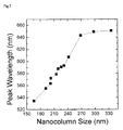
- FIG. 7 is a graph illustrating the relationship between the diameter of the nanocolumn (Nanocolumn Size) and a detected peak wavelength (Peak Wavelength).
- FIG. 8 is a graph illustrating the relationship between the depth of the concave portion (Nanohole depth) and a dose (Dose) when the concave portion is formed in the template substrate by a FIB method.
- FIG. 9 is a graph illustrating the relationship between a dose (Dose) and the diameter of the concave portion (Nanohole size) and the relationship between a dose (Dose) and the diameter of the nanocolumn (Nanocolumn size).
- FIG. 10 is a diagram illustrating the scanning electron microscope image of the nanocolumns regularly arranged in a square lattice.
- FIG. 11 is a scanning electron microscope image of the nanocolumns regularly arranged in a square lattice.
- FIG. 12 is a graph illustrating the measurement result of the spectrum of CL (cathodoluminescence) light emitted from the nanocolumn.
- FIG. 13 shows the SEM image ((A)) of the nanocolumns, as viewed from the upper side, and the CL images ((B) and (C)) of different wavelengths (cathodoluminescence images), as viewed from the upper side.
- FIG. 14 shows the SEM image ((A)) of the nanocolumn captured in the horizontal direction, and the cross-sectional CL images ((B) to (D)) of different wavelengths.
- FIG. 15 is a graph ((A)) illustrating the same CL spectrum as that shown in FIG. 12 , and a diagram ((B)) schematically illustrating the structure of the leading end of the nanocolumn.
- FIG. 16 is a graph illustrating the relationship between the diameter of the nanocolumn and the surface area of the nanocolumn and the relationship between the diameter of the nanocolumn and an emission peak wavelength.
- FIG. 17 is a graph illustrating the light intensity distribution of the nanocolumns with respect to a PL emission wavelength.
- FIG. 18 is a graph illustrating the relationship between the height of the leading end of the nanocolumn and the emission peak wavelength.
- FIG. 19 ((A) to (F)) is diagrams illustrating the SEM images of nanocolumn groups regularly arranged in a triangle lattice, as viewed from the upper side.
- FIG. 20 is a graph illustrating the measurement result of the light intensity distribution of the nanocolumn groups shown in FIG. 19 ((A) to (F)) with respect to the PL emission wavelength.
- FIG. 21 is a graph illustrating the relationship between a column period and the emission peak wavelength in the light intensity distribution shown in FIG. 20 .
- FIG. 22 is a diagram illustrating the SEM images of the nanocolumn groups regularly arranged in a triangle lattice, as viewed from the upper side.
- FIGS. 23 ((A) and (B)) is diagrams schematically illustrating a portion of the structure of a semiconductor light emitting element according to a second embodiment.
- FIG. 24 is a perspective view illustrating a portion of the structure of a semiconductor light emitting element according to a third embodiment of the invention.
- FIG. 25 is a perspective view illustrating a portion of the structure of the semiconductor light emitting element according to the third embodiment of the invention.
- FIGS. 1(A) to 1(D) are cross-sectional views schematically illustrating a process of manufacturing a semiconductor optical element array 10 according to an embodiment of the invention.
- FIG. 1(D) schematically shows the structure of the semiconductor optical element array 10 according to this embodiment.
- the semiconductor optical element array 10 includes a template substrate, a mask pattern 13 P having a plurality of opening portions, and a plurality of nanocolumns 23 .
- the template substrate is a semiconductor substrate obtained by epitaxially growing a group-III nitride semiconductor layer 12 P on a base substrate 11 , such as a sapphire substrate.
- a gallium nitride or aluminum nitride buffer layer (not shown) is grown on the base substrate 11 by a low-temperature process using a metal-organic chemical vapor deposition (MOCVD) method or an MBE method and the group-III nitride semiconductor layer is grown on the buffer layer, thereby forming the template substrate.
- MOCVD metal-organic chemical vapor deposition
- a plurality of concave portions 14 , . . . , 14 is formed on the main surface of the group-III nitride semiconductor layer 12 P.
- the mask pattern 13 P is formed on the main surface of the group-III nitride semiconductor layer 12 P and has the opening portions (hereinafter, referred to as mask opening portions) immediately above the plurality of concave portions 14 , . . . , 14 . That is, the concave portions 14 are formed so as to overlap the opening portions and be exposed from the opening portions.
- the semiconductor optical element array 10 includes a plurality of semiconductor elements (nanocolumns 23 ) each having a fine columnar crystal 20 , an active layer 21 that is provided on the fine columnar crystal 20 , and a semiconductor covering layer 22 that covers the active layer 21 .
- a plurality of fine columnar crystals 20 , . . . , 20 is made of a group-III nitride semiconductor that is grown from the concave portions 14 , . . . , 14 of the group-III nitride semiconductor layer 12 P to the upper side of the mask pattern 13 P through the mask opening portions.
- the active layer 21 is formed on the fine columnar crystal 20 and the semiconductor covering layer 22 is formed so as to cover the active layer 21 .
- the fine columnar crystal 20 , the active layer 21 , and the semiconductor covering layer 22 form the nanocolumns 23 .
- the fine columnar crystal 20 and the semiconductor covering layer 22 are made of a group-III nitride semiconductor such as gallium nitride (GaN).
- the fine columnar crystal 20 and the semiconductor covering layer 22 may be made of a quaternary mixed crystal material represented by a general formula Al x Ga y In 1-x-y N (0 ⁇ x ⁇ 1, 0 ⁇ y ⁇ 1, and 0 ⁇ x+y ⁇ 1) or boron nitride.
- the quaternary mixed crystal material has a wide band gap of 0.63 eV to 6.2 eV at a room temperature according to composition ratios x and y. Therefore, when the quaternary mixed crystal is used, it is possible to manufacture a light emitting diode or a laser diode covering from an ultraviolet range to an infrared range including a visible light range.
- the diameter of the fine columnar crystal 20 be equal to or more than 10 nm and equal to or less than 1000 nm.
- the diameter of the fine columnar crystal 20 is preferably equal to or less than 700 nm, more preferably, equal to or less than 650 nm, and more preferably, equal to or less than 600 nm.
- the diameter is equal to or less than 700 nm, particularly, equal to or less than 600 nm, it is easy to prevent the occurrence of threading dislocation.
- the diameter of the fine columnar crystal 20 is the diameter of a columnar portion 201 exposed from the mask opening portion.
- the diameter of the columnar portion 201 is the diameter of the column.
- the diameter of the columnar portion 201 means the length of a straight line having the largest length between two intersection points among the straight lines that pass through the center of gravity (the center of the plane) in a plan view of the columnar portion 201 from the surface side of the semiconductor substrate and intersect the columnar portion 201 at two points.
- the fine columnar crystal 20 includes the columnar portion 201 and a facet structure 202 that is provided at the leading end of the columnar portion 201 .
- the shape of the columnar portion 201 is not particularly limited. However, for example, the columnar portion 201 may have a cylindrical shape, a square pillar shape, or a hexagonal column shape.
- the fine columnar crystal 20 be made of a material having a hexagonal crystal structure in terms of the stability of manufacture.
- the active layer 21 is provided so as to cover the facet structure 202 of the fine columnar crystal 20 .
- the active layer 21 is made of, for example, InGaN, GaN, AlGaN, AlInGaN, InGaAsN, or InN.
- the active layer 21 may have, for example, a multiple quantum well (MQW) structure of InGaN/GaN (barrier layer: InGaN, and well layer: GaN), In x Ga 1-x N/In y Ga 1-y N (0 ⁇ x ⁇ 1, 0 ⁇ y ⁇ 1), GaN/AlGaN (barrier layer: AlGaN, and well layer: GaN), or Al x Ga 1-x N/Al y Ga 1-y N (0 ⁇ x ⁇ 1, 0 ⁇ y ⁇ 1), or a single quantum well (SQW) structure.
- the quantum well structure includes a quantum well layer and barrier layers having the quantum well layer interposed therebetween. The band gap of the barrier layer is more than that of the quantum well layer.
- the semiconductor covering layer 22 is provided on the active layer 21 and covers the entire active layer 21 .
- the peak wavelength of light emitted from the active layer 21 may be determined to a wavelength corresponding to the diameter ⁇ of the fine columnar crystal 20 immediately before the active layer 21 is formed.
- the peak wavelength of light emitted from the active layer 21 may be determined such that it shifts to the long wavelength side as the diameter A of each fine columnar crystal 20 increases and it shifts to the short wavelength side as the diameter ⁇ of each fine columnar crystal 20 decreases. That is, the peak wavelength of light emitted from the active layer 21 on the fine columnar crystal 20 with a large diameter ⁇ is more than that of light emitted from the active layer 21 on the fine columnar crystal 20 with a small diameter ⁇ .
- the diameter ⁇ of the fine columnar crystal 20 it is possible to obtain a desired emission wavelength by controlling the diameter ⁇ of the fine columnar crystal 20 . It is possible to set the diameter ⁇ of the fine columnar crystal 20 to a desired value by adjusting the diameter ⁇ ( FIG. 1(C) ) of each of the concave portions 14 formed in the group-III nitride semiconductor layer 12 P of the template substrate, which will be described below.
- the diameter ⁇ of the concave portion 14 depends on the size of the mask opening portion. Therefore, when the size of the mask opening portion is predetermined, it is possible to obtain the diameter ⁇ corresponding to the predetermined size.
- the peak wavelength of light emitted from the active layer 21 may be determined to a wavelength corresponding to the surface area of the leading end (facet structure 202 ) of the fine columnar crystal 20 of each of the nanocolumns 23 .
- the peak wavelength of light emitted from the active layer 21 may be determined such that it shifts to the long wavelength side as the surface area of the facet structure increases and it shifts to the short wavelength side as the surface area of the facet structure decreases. That is, the peak wavelength of light emitted from the active layer 21 on the fine columnar crystal 20 having the facet structure with a large surface area is more than that of light emitted from the active layer 21 on the fine columnar crystal 20 having the facet structure with a small surface area.
- the opening portions 13 g , . . . , 13 g formed in the mask pattern 13 P are periodically arranged in the in-plane direction of the mask pattern 13 P.
- the peak wavelength of light emitted from the active layer 21 on a plurality of fine columnar crystals 20 in the region in which the arrangement density of the opening portions is high is more than that of light emitted from the active layer 21 on a plurality of fine columnar crystals 20 in the region in which the arrangement density of the opening portions is low.
- the peak wavelength of light emitted from the active layer 21 may be determined such that it shifts to the long wavelength side as the in-plane density of the fine columnar crystals 20 , . . . , 20 increases and it shifts to the short wavelength side as the in-plane density of the fine columnar crystals 20 , . . . , 20 decreases.
- the in-plane density increases as the spatial period of the fine columnar crystals 20 , . . . , 20 is reduced, or the in-plane density increases as the diameter of the fine columnar crystals 20 increases.
- a gallium nitride or aluminum nitride buffer layer (not shown) is grown on the base substrate 11 by a low-temperature process using an MOCVD method or an MBE method, and the group-III nitride semiconductor layer 12 made of, for example, gallium nitride or aluminum nitride is grown on the buffer layer ( FIG. 1(A) ).
- the metal mask layer 13 including titanium (Ti) is formed in a predetermined region of the main surface of the template substrate ( FIG. 1(B) ).
- the metal mask layer 13 may be a natural oxide film of titanium or a titanium oxide film.
- the metal mask layer 13 is preferably made of titanium in terms of the selective growth of the fine columnar crystals 20 , but the material is not limited thereto.
- the metal mask layer 13 may be made of one or two or more kinds of metal materials selected from the group consisting of titanium (Ti), tantalum (Ta), iron (Fe), nickel (Ni), platinum (Pt), gold (Au), cobalt (Co), tungsten (W), and molybdenum (Mo).
- the metal mask layer 13 is patterned to form the mask pattern 13 P having a plurality of opening portions through which the surface of the group-III nitride semiconductor layer 12 P is exposed.
- the patterning may be performed by a lithography process. That is, the mask pattern 13 P may be obtained by forming a resist pattern on the metal mask layer 13 and performing etching using the resist pattern as an etching mask. Alternatively, the mask pattern 13 P may be formed by emitting a predetermined dose (the amount of ions emitted per unit area) of focused ion beams to the metal mask layer 13 using a FIB (Focused Ion Beam) method.
- FIB Fluorused Ion Beam
- the group-III nitride semiconductor layer 12 disposed immediately below the opening portions is processed as well as the metal mask layer 13 . Therefore, as shown in FIG. 1(C) , dot-shaped concave portions (holes) 14 , . . . , 14 are formed immediately below the opening portions of the mask pattern 13 P.
- the shape of the opening portion of the mask pattern 13 P in a top view is not particularly limited.
- the opening portion may have an axisymmetric shape, such as a circular shape or a polygonal shape, in addition to the square shape shown in FIG. 2 .
- the fine columnar crystals 20 , the active layers 21 , and the semiconductor covering layers 22 are continuously growth from the plurality of concave portions 14 to the upper side of the mask pattern 13 P through the mask opening portions by an MOCVD method or an MBE method ( FIG. 1(D) ).
- the fine columnar crystals 20 are grown in the horizontal direction along the in-plane direction of the template substrate at the same time as it is grown on the mask pattern 13 P. Therefore, the diameter ⁇ of the nanocolumn 23 is greater than the diameter ⁇ of the concave portion 14 .
- the semiconductor covering layer 22 is formed so as to cover the entire active layer 21 , the active layer 21 does not have any portion exposed to an external space. In other words, the active layer 21 is completely buried in the leading end of the nanocolumn 23 . Therefore, the formation of non-emission recombination potential due to the exposed portion is prevented, and it is possible to obtain high internal quantum efficiency.
- the diameter of the mask opening portion is reduced, the occurrence of threading dislocation is prevented at the beginning of the growth of the fine columnar crystals 20 . Thereafter, when the fine columnar crystal is grown in the horizontal direction to increase the diameter, it is possible to obtain a nanocolumn with a relatively large diameter (for example, a diameter of 1000 nm) without threading dislocation.
- a method of relatively increasing the amount of nitrogen supplied or a method of adding Al may be used to grow the fine columnar crystals 20 in the horizontal direction.
- FIGS. 4(A) and 4(B) are diagrams illustrating the sectional shape of the leading end of the fine columnar crystal 20 along the center axis.
- the leading end shown in FIG. 4(A) has a facet structure and includes an inclined plane, which is a semipolar plane 20 a of the wurtzite-type crystal structure, as a facet surface that is obliquely inclined.
- the leading end has a six-sided pyramid shape.
- the semipolar plane 20 a include the (10-1-1)-plane, the (10-1-3)-plane, the (11-22)-plane, the (11-24)-plane, and the (10-12)-plane.
- the leading end shown in FIG. 4(B) also has a facet structure and includes an inclined plane, which is the semipolar plane 20 a of the wurtzite-type crystal structure, and a flat polar plane 20 b as a facet surface that is obliquely inclined and a plane that faces upward.
- the shape of the leading end shown in FIG. 4(A) or the shape of the leading end shown in FIG. 4(B) is formed according to crystal growth conditions.
- the facet structure means a polyhedral structure having a facet surface that is inclined with respect to the horizontal plane of the base substrate 11 as a side surface.
- the leading end having the six-sided pyramid shape shown in FIG. 4(A) is likely to be formed.
- the leading end shown in FIG. 4(B) is likely to be formed.
- the diameter of the fine columnar crystal 20 is equal to or more than about 300 nm, it is possible to clearly form the flat polar plane 20 b at the leading end of the fine columnar crystal 20 , which depends on the crystal growth conditions.
- the diameter of the fine columnar crystal 20 is more than about 300 nm, the area of the flat polar plane 20 b increases.
- the growth conditions may be as follows: the fine columnar crystal 20 is grown under the condition that the effective supply rate of the active nitrogen is higher than that of the group-III metal.
- the fine columnar crystal 20 made of gallium nitride (GaN) is grown, in many cases, a GaN crystal is grown in a growth inhibitory region other than the mask opening portion at a crystal growth temperature of 600 degrees centigrade or more. As the growth temperature increases, the spatial density of the GaN crystal grown in the growth inhibitory region is reduced.
- GaN When the temperature is equal to or more than a predetermined value, GaN may not be grown in the growth inhibitory region.
- the temperature at which GaN is not grown in the growth inhibitory region depends on the amount or ratio of group-III metal and active nitrogen supplied. For example, the temperature is equal to or more than 850 degrees centigrade.
- MBE be performed under the following conditions in order to grow the fine columnar crystal 20 .
- the temperature is appropriately selected according to the kind of group-III nitride semiconductor to be grown, and is equal to or more than 350 degrees centigrade and equal to or less than 1200 degrees centigrade.
- a GaN crystal is grown, the temperature is preferably equal to or more than 400 degrees centigrade and equal to or less than 1000 degrees centigrade.
- the temperature is preferably equal to or more than 500 degrees centigrade and equal to or less than 1200 degrees centigrade.
- InN is grown, the temperature is preferably equal to or more than 350 degrees centigrade and equal to or less than 600 degrees centigrade.
- MBE is performed under nitrogen-rich conditions in the above-mentioned temperature range, it is possible to grow the fine columnar crystal 20 of a group-III nitride semiconductor.
- a region of the mask pattern 13 P in which the mask opening portion is not formed is a region (growth inhibitory region) in which the growth of the fine columnar crystal 20 is inhibited.
- growth inhibitory region a region in which the growth of the fine columnar crystal 20 is inhibited.
- Ti and Pt have a smaller number of non-bonded hands on the surface because of the strength of the covalent bond. For this reason, it is difficult to expect the facility of bonding and it is estimated that the start of the growth of the group-III nitride fine columnar crystal is inhibited.
- active nitrogen is emitted to the surface of the metal film independently or together with a group-III metal material.
- metal nitride for example, TiN or WN
- these metal nitrides are chemically stable, that is, there are a small number of active non-bonded hands on the surface, the bonding with Ga or GaN is weak. Therefore, it is also considered that, when a growth temperature is sufficiently high for the elimination of, for example, Ga or GaN from the surface, the supplied Ga or GaN is eliminated before it has a sufficient size to maintain crystal growth, and the growth of GaN is inhibited.
- the fine columnar crystal 20 formed on the surface of the mask pattern 13 P and the template substrate may vary depending on the material forming the template substrate or the mask pattern 13 P, the thickness of the mask pattern 13 P, or the growth conditions.
- the fine columnar crystal 20 is grown in a direction substantially vertical to the main surface of the template substrate or the surface of the mask pattern 13 P.
- the fine columnar crystal 20 that is made of a group-III nitride semiconductor grown by the method according to this embodiment is a single crystal having a columnar structure with a nanometer-order diameter ⁇ .
- the diameter of the fine columnar crystal 20 is set in the range of equal to or more than 10 nm and equal to or less than 1000 nm.
- the height of the fine columnar crystal 20 varies depending on the thickness of the mask pattern 13 P or the crystal growth conditions. For example, the height of the fine columnar crystal 20 is equal to or more than 0.2 ⁇ m and equal to or less than 5 ⁇ m.
- the thickness of the mask pattern 13 P is not particularly limited. It is preferable that the thickness of the mask pattern 13 P be equal to or more than 2 nm and equal to or less than 100 nm. However, the diameter and height of the fine columnar crystal 20 vary depending on the crystal growth conditions.
- the active layer 21 is formed on each of the fine columnar crystals 20 , and the semiconductor covering layer 22 is formed on the active layer 21 .
- the active layer 21 and the semiconductor covering layer 22 may be formed by the MOCVD method and the MBE method.
- the material forming the active layer 21 or the semiconductor covering layer 22 is also deposited on the mask pattern 13 P.
- the semiconductor covering layer 22 be grown in the horizontal direction to cover the side surface of the active layer 21 as well as the upper surface.
- FIG. 5 is a graph illustrating the relationship between the diameter ⁇ (hereinafter, referred to as a “hole size”) of the concave portion 14 formed in the group-III nitride semiconductor layer 12 P and the emission wavelength of the nanocolumn 23 .
- the manufacturing conditions of the nanocolumn 23 manufactured in order to obtain the graph shown in FIG. 5 are as follows.
- the GaN layer 12 P (thickness: about 3.5 ⁇ m) was grown on the (0001)-plane of the sapphire substrate 11 by the MOCVD method to form a template substrate.
- a titanium thin film (thickness: about 5 nm) was formed on the template substrate and a plurality of opening portions (spatial period (the distance between the centers of the opening portions): 400 nm) arranged in a triangle lattice was provided in the titanium thin film by the FIB method, thereby forming the mask pattern 13 P.
- the concave portions 14 were formed in the GaN layer 12 P.
- the GaN columnar crystals 20 (height: 2.5 ⁇ m) were grown from the concave portions 14 of the template substrate through the mask opening portions by an RF-MBE method at a temperature of 900 degrees centigrade. Then, the active layer 21 that had a multiple quantum well structure including an InGaN film (thickness: 1 nm) was formed on each of the fine columnar crystals 20 . Then, the GaN crystal semiconductor covering layer 22 (thickness: 10 nm) was formed on the active layer 21 .
- FIG. 5 is graph illustrating the measurement result.
- FIG. 6 is a graph illustrating the relationship between the PL emission wavelength (unit: nm) and light intensity (unit: arbitrary unit) measured for the semiconductor elements having nanocolumn sizes of 166 nm, 192 nm, 203 nm, 226 nm, 242 nm, 298 nm, and 236 nm.
- the manufacturing conditions of the nanocolumns 23 manufactured in order to obtain the graph are the same as those of the nanocolumns 23 manufactured in order to obtain the graph shown in FIG. 5 .
- FIG. 7 is a graph illustrating the relationship between the nanocolumn size and the detected peak wavelength. As can be seen from the graph, as the nanocolumn size increased, the peak wavelength increases, and as the nanocolumn size decreases, the peak wavelength decreases.
- the peak wavelength of light emitted from the active layer 21 shifts to the long wavelength side as the diameter ⁇ of the fine columnar crystal 20 immediately before the active layer 21 is formed increases, and the peak wavelength shifts to the short wavelength side as the diameter ⁇ of the fine columnar crystal 20 decreases.
- FIG. 8 is a graph illustrating the relationship between the depth of the concave portion 14 (nanohole depth (nm)) and a dose when the concave portion (hole) 14 is formed in the template substrate by the FIB method (dose (cm ⁇ 2 )).
- FIG. 9 is a graph illustrating the relationship between a dose (Dose (cm ⁇ 2 )) and the diameter of the concave portion 14 (nanohole size (nm)) and the relationship between a dose (dose (cm ⁇ 2 )) and the diameter of the nanocolumn 23 (nanocolumn size (nm)).
- the manufacturing conditions of the nanocolumn 23 manufactured in order to obtain the graphs shown in FIGS. 8 and 9 are as follows.
- the GaN layer 12 P (thickness: about 3.5 ⁇ m) was grown on the (0001)-plane of the sapphire substrate 11 by the MOCVD method to form a template substrate.
- a titanium thin film (thickness: about 5 nm) was formed on the template substrate and a plurality of opening portions was provided in the titanium thin film by the FIB method, thereby forming the mask pattern 13 P.
- the concave portions 14 were formed in the GaN layer 12 P.
- the GaN columnar crystals 20 (height: 2.5 ⁇ m) were grown from the concave portions 14 of the template substrate through the mask opening portions by the RF-MBE method at a temperature of 900 degrees centigrade. Then, the active layer 21 that had a multiple quantum well structure including an InGaN film (thickness: 1 nm) was formed on each of the fine columnar crystals 20 . Then, the GaN crystal semiconductor covering layer 22 (thickness: 10 nm) was formed on the active layer 21 .
- FIGS. 8 and 9 are graphs illustrating the measurement result.
- the depth of the concave portion 14 increases.
- the diameter of the concave portion 14 (nanohole size) increases and the diameter of the nanocolumn 23 (nanocolumn size) also increases. Therefore, it is understood that the diameter ⁇ of the columnar crystal 20 increases with an increase in the diameter of the concave portion 14 .
- FIGS. 10 and 11 are diagrams illustrating the scanning electron microscope images (SEM image) of the nanocolumns 23 , . . . , 23 that are regularly arranged in a square lattice and have different diameters.
- FIG. 10 shows the SEM image of the nanocolumns 23 , . . . , 23 , as viewed from the upper side
- FIG. 11 shows the SEM image of the nanocolumns 23 , . . . , 23 , as obliquely viewed.
- the nanocolumn groups shown in FIGS. 10 and 11 were formed by individually controlling the diameters of the concave portions 14 , . . . , 14 .
- FIG. 12 is a graph illustrating the measurement result of CL (cathodoluminescence) light emitted from the nanocolumn 23 .
- the horizontal axis corresponds to the emission wavelength and the vertical axis corresponds to CL intensity (arbitrary unit).
- FIG. 13(A) shows the SEM image of the nanocolumn 23 , as viewed from the upper side
- FIGS. 13(B) and 13(C) are diagrams illustrating the CL images (cathodoluminescence images) of different wavelengths of 405 nm and 510 nm, as viewed from the upper side.
- FIG. 14(A) shows the SEM image of the nanocolumn 23 captured in the horizontal direction
- FIG. 14(B) , 14 (C), and 14 (D) show the cross-sectional CL images (the cross-sectional CL images of the nanocolumn 23 shown in FIG. 14(A) ) of different wavelengths of 365 nm, 435 nm, and 500 nm.
- the manufacturing conditions of the nanocolumn 23 manufactured in order to obtain the graphs shown in FIG. 12 , FIGS. 13(A) to 13(C) , and FIGS. 14(A) to 14(D) are as follows.
- the GaN layer 12 P (thickness: about 3.5 ⁇ m) was grown on the (0001)-plane of the sapphire substrate 11 by the MOCVD method to form a template substrate.
- a titanium thin film (thickness: about 5 nm) was formed on the template substrate and a plurality of opening portions (spatial period: 400 nm) arranged in a triangle lattice was provided in the titanium thin film by the FIB method, thereby forming the mask pattern 13 P.
- the concave portions 14 were formed in the GaN layer 12 P.
- the GaN columnar crystals 20 (height: 1.8 ⁇ m and diameter: 180 nm to 495 nm) were grown from the concave portions 14 of the template substrate through the mask opening portions by the RF-MBE method at a temperature of 900 degrees centigrade.
- the active layer 21 that had a multiple quantum well structure including an InGaN film was formed on each of the fine columnar crystals 20 .
- the GaN crystal semiconductor covering layer 22 was formed on the active layer 21 .
- the peak of light emitted from GaN and two peaks of light emitted from InGaN are included in a CL intensity distribution.
- the CL image of the wavelength 405 nm shown in FIG. 13(B) shows that light is emitted from the entire active layer 21 of the nanocolumns 23 . It is considered that the CL image shows the emission of light from InGaN formed on the side surface (semipolar plane) 20 a ( FIG. 4(B) ) of the leading end of the fine columnar crystal 20 .
- the CL image of the wavelength 510 nm shown in FIG. 13(C) shows the emission of light from only the vicinity of the top of the active layer 21 of the nanocolumn 23 . It is considered that the CL image shows the emission of light from InGaN formed on the flat surface (polar plane) 20 b ( FIG. 4(B) ) of the leading end of the fine columnar crystal 20 .
- the cross-sectional CL image of the wavelength 365 nm shown in FIG. 14(B) shows the emission of light from GaN distributed in the entire nanocolumn 23 .
- the cross-sectional CL image of the wavelength 435 nm shown in FIG. 14(C) shows the emission of light from InGaN at the entire leading end of the nanocolumn 23 . It is considered that the cross-sectional CL image mainly shows the emission of light from InGaN formed on the side surface (semipolar plane) 20 a ( FIG. 4(B) ) of the leading end of the fine columnar crystal 20 .
- the cross-sectional CL image mainly shows the emission of light from InGaN formed on the flat surface (polar plane) 20 b ( FIG. 4(B) ) of the leading end of the fine columnar crystal 20 .
- the wavelength of light emitted from InGaN formed on the side surface (semipolar plane) 20 a of the leading end of the fine columnar crystal 20 is different from that of light emitted from InGaN formed on the flat surface (polar plane) 20 b of the leading end. It is considered that the reason is as follows.
- the InGaN crystal 21 t in the vicinity of the leading end may form a quantum dot. It is considered that this causes the difference between the wavelength of light emitted from InGaN formed on the side surface 20 a and the wavelength of light emitted from InGaN formed on the flat surface 20 b.
- Samples manufactured in order to obtain the CL intensity distribution shown in FIG. 12 were used to measure PL (photoluminescence) intensity.
- CW (Continuous Wave) light with a wavelength of 405 nm was used as excitation light.
- the density of the excitation light was 0.29 kW/cm 2 .
- the peak wavelength of a PL intensity distribution was 486.2 nm under a low temperature condition of 4 K and 486.7 nm under a high temperature condition of 300 K.
- the full width at half maximum (FWHM) of the PL intensity distribution corresponded to 151.3 meV under a low temperature condition of 4 K and corresponded to 187.2 meV under a high temperature condition of 300 K.
- the PL integrated intensity ratio of the low temperature condition and the high temperature condition that is, internal quantum efficiency was about 77% with respect to a wavelength of 486 nm, and very high crystallinity was obtained. It is considered that one of the reasons for high internal quantum efficiency is that the active layer 21 ( 21 s and 21 t ) is not exposed to the external space and the loss of injected carriers due to non-emission recombination is prevented. As shown in FIG. 15(B) , the InGaN crystals 21 s and 21 t with a narrow band gap are completely covered by GaN with a wide band gap and are buried in the nanocolumn 23 . Therefore, the InGaN crystals 21 s and 21 t are not exposed to the external space.
- non-emission recombination potential is prevented. If there is an exposed portion, a non-emission recombination potential is formed within the band gap of the surface of the exposed portion, and electrons and holes are recombined with each other through the non-emission recombination potential. As a result, emission efficiency is reduced.
- the nanocolumn 23 having the InGaN crystals 21 s and 21 t is described in this embodiment. However, the nanocolumn 23 may not have the InGaN crystal 21 t.
- the emission wavelength can also be controlled by the diameter of the nanocolumn. That is, it has been confirmed that the peak wavelength of light emitted from the active layer of the nanocolumn with a small diameter is smaller than that of light emitted from the active layer of the nanocolumn with a large diameter.
- FIG. 16 is a graph illustrating the relationship between the diameter (column size) of the nanocolumn 23 and the surface area of the facet structure of the leading end of the nanocolumn 23 and the relationship between the column size and an emission peak wavelength.
- the emission peak wavelength means a wavelength detected from the intensity distribution of PL light.
- symbol “ ⁇ ” indicates the measured value of the emission peak wavelength
- symbol “ ⁇ ” indicates the area of the flat surface (Surface C) of the leading end of the nanocolumn 23
- symbol “ ⁇ ” indicates the area of the inclined side surface (Surface Semi) of the leading end of the nanocolumn 23
- symbol “ ⁇ ” indicates the sum of the area of the flat surface and the area of the inclined side surface of the leading end of the nanocolumn 23 .
- the manufacturing conditions of the nanocolumn 23 manufactured in order to obtain the graph shown in FIG. 16 are as follows.
- the GaN layer 12 P (thickness: about 3.5 ⁇ m) was grown on the (0001)-plane of the sapphire substrate 11 by the MOCVD method to form a template substrate.
- a titanium thin film (thickness: about 5 nm) was formed on the template substrate and a plurality of opening portions (spatial period: 400 nm) arranged in a triangle lattice was provided in the titanium thin film by the FIB method, thereby forming the mask pattern 13 P.
- the concave portions 14 were formed in the GaN layer 12 P.
- the GaN columnar crystals 20 (height: 2.5 ⁇ m) were grown from the concave portions 14 of the template substrate through the mask opening portions by the RF-MBE method at a temperature of 900 degrees centigrade. Then, the active layer 21 that had a multiple quantum well structure including an InGaN film (thickness: 1 nm) was formed on each of the fine columnar crystals 20 . Then, the GaN crystal semiconductor covering layer 22 (thickness: 10 nm) was formed on the active layer 21 .
- FIG. 16 is a graph illustrating the measurement result.
- the surface area of (the sum of the area of the inclined side surface (facet surface) and the area of the flat surface) of the facet structure of the leading end of the nanocolumn 23 increases with an increase in the column size.
- the emission peak wavelength monotonously increases with an increase in the column size. Therefore, the emission peak wavelength increases with an increase in the total area of the facet surface facing upward at the leading end of the nanocolumn 23 . Since the thickness of the active layer 21 and the thickness of the semiconductor covering layer 22 are small, the emission peak wavelength may increase with an increase in the area of the facet surface facing upward at the leading end of the fine columnar crystal 20 . Therefore, it is possible to obtain a desired emission peak wavelength by controlling the area of the facet surface facing upward at the leading end of the fine columnar crystal 20 .
- FIG. 17 is a graph illustrating the light intensity distribution (unit: arbitrary unit) of the nanocolumn 23 with a column size of 200 nm with respect to the PL emission wavelength.
- a solid line indicates a measured curve when the height of the inclined side surface of the leading end of the nanocolumn 23 is 2.1 ⁇ m and a dashed line indicates a measured curve when the height of the inclined side surface of the leading end of the nanocolumn 23 is 1.25 ⁇ m.
- FIG. 18 is a graph illustrating the relationship between the height of the nanocolumn 23 and the emission peak wavelength. In the graph shown in FIG. 18 , the horizontal axis corresponds to the height and the vertical axis corresponds to the emission peak wavelength.
- the manufacturing conditions of the nanocolumn 23 manufactured in order to obtain the graphs shown in FIGS. 17 and 18 are as follows.
- the GaN layer 12 P (thickness: about 3.5 ⁇ m) was grown on the (0001)-plane of the sapphire substrate 11 by the MOCVD method to form a template substrate.
- a titanium thin film (thickness: about 5 nm) was formed on the template substrate and a plurality of opening portions (spatial period: 400 nm) arranged in a triangle lattice was provided in the titanium thin film by the FIB method, thereby forming the mask pattern 13 P.
- the concave portions 14 were formed in the GaN layer 12 P.
- the GaN columnar crystals 20 (height: 2.5 ⁇ m) were grown from the concave portions 14 of the template substrate through the mask opening portions by the RF-MBE method at a temperature of 900 degrees centigrade. Then, the active layer 21 that had a multiple quantum well structure including an InGaN film (thickness: 1 nm) was formed on each of the fine columnar crystals 20 . Then, the GaN crystal semiconductor covering layer 22 (thickness: 10 nm) was formed on the active layer 21 .
- FIG. 17 shows the tendency.
- FIGS. 19(A) to 19(F) are diagrams illustrating the SEM images of nanocolumn groups regularly arranged in a triangle lattice, as viewed from the upper side.
- FIGS. 19(A) , 19 (B), 19 (C), 19 (D), 19 (E), and 19 (F) show the arrangement of the nanocolumns when the spatial period (the distance between the centers of the fine columnar crystals 20 ) is 400 nm, 600 nm, 800 nm, 1 ⁇ m, 2 ⁇ m, and 4 ⁇ m.
- the measured peak wavelengths of PL light corresponding to the arrangement of the spatial periods of 400 nm, 600 nm, 800 nm, 1 ⁇ m, 2 ⁇ m, and 4 ⁇ m were 508 nm, 500 nm, 490 nm, 480 nm, 480 nm, and 479 nm.
- the manufacturing conditions of the nanocolumn 23 manufactured in order to obtain the SEM images shown in FIG. 19 are as follows.
- the GaN layer 12 P (thickness: about 3.5 ⁇ m) was grown on the (0001)-plane of the sapphire substrate 11 by the MOCVD method to form a template substrate.
- a titanium thin film (thickness: about 5 nm) was formed on the template substrate and a plurality of mask opening portions (the diameter of each mask opening portion: 167 nm) arranged in a triangle lattice was provided in the titanium thin film by the FIB method, thereby forming the mask pattern 13 P.
- the concave portions 14 were formed in the GaN layer 12 P.
- the GaN columnar crystals 20 (height: 1.5 ⁇ m and diameter: 190 nm) were grown from the concave portions 14 of the template substrate through the mask opening portions by the RF-MBE method at a temperature of 900 degrees centigrade. Then, the active layer 21 that had a multiple quantum well structure including an InGaN film (thickness: 3 nm) was formed on each of the fine columnar crystals 20 . Then, the GaN crystal semiconductor covering layer 22 (thickness: 10 nm) was formed on the active layer 21 .
- the peak wavelength shifts to the long wavelength side as the spatial period (column period and arrangement density) of the nanocolumns 23 , . . . , 23 is reduced, and the peak wavelength shifts to the short wavelength side as the spatial period of the nanocolumns 23 , . . . , 23 increases.
- FIG. 20 is a graph illustrating the measurement result of the light intensity distribution (unit: arbitrary unit) of the nanocolumn groups shown in FIGS. 19(A) to 19(F) with respect to the PL emission wavelength.
- FIG. 21 is a graph illustrating the relationship between the column period and the emission peak wavelength of the light intensity distribution shown in FIG. 20 .
- the column size of each nanocolumn 23 was 160 nm.
- the emission peak wavelength is reduced with an increase in the column period.
- the column period increases with the column size maintained at a constant value, the in-plane density of the nanocolumns 23 , . . . , 23 is reduced. Therefore, the emission peak wavelength is reduced with the reduction in the in-plane density and increases with an increase in the in-plane density.
- FIG. 22 is a diagram illustrating the SEM images of nanocolumn groups regularly arranged in a triangle lattice, as viewed from the upper side.
- FIGS. 22(A) , 22 (B), 22 (C), and 22 (D) show the arrangement of the nanocolumns when the spatial period is 242 nm, 269 nm, 298 nm, and 336 nm.
- the measured peak wavelengths of PL light corresponding to the arrangement of the spatial periods of 242 nm, 269 nm, 298 nm, and 336 nm were 607 nm, 643 nm, 649 nm, and 650 nm.
- the manufacturing conditions of the nanocolumn 23 manufactured in order to obtain the SEM images shown in FIGS. 22(A) to 22(D) are the same as those of the nanocolumn 23 manufactured in order to obtain the SEM images shown in FIG. 19 except for the diameter of the mask opening portion.
- the diameter of the nanocolumn 23 manufactured in order to obtain the SEM images shown in FIG. 22 is set so as to increase with an increase in the spatial period.
- the peak wavelength increases with an increase in the diameter of the nanocolumn 23 .
- the in-plane density (arrangement density) of the nanocolumns 23 , . . . , 23 increases with an increase in the diameter of the nanocolumn 23 . Therefore, the emission peak wavelength increases with the increase in the in-plane density and the emission peak wavelength is reduced with a reduction in the in-plane density.
- the peak wavelength of light emitted from the active layer 21 shifts to the long wavelength side as the in-plane density of the fine columnar crystals 20 , . . . , 20 increases, and shifts to the short wavelength side as the in-plane density of the fine columnar crystals 20 , . . . , 20 decreases. Therefore, it is possible to obtain a desired emission wavelength by controlling the diameter of the fine columnar crystal 20 .
- the semiconductor optical element array 10 it is possible to control the position of the fine columnar crystal 20 formed on the template substrate by adjusting the position of the opening portion of the mask pattern 13 P.
- the in-plane density of the fine columnar crystals 20 , . . . , 20 that are periodically arranged to shift the peak wavelength to the long wavelength side and decrease the in-plane density of the fine columnar crystals 20 , . . . , 20 to shift the peak wavelength to the short wavelength side. It is possible to control the in-plane density with high accuracy by adjusting the spatial period (that is, the spatial period of the opening portion formed in the mask pattern 13 P) of the fine columnar crystals 20 , . . . , 20 or by adjusting the diameter (that is, the diameter of the opening portion formed in the mask pattern 13 P) of each fine columnar crystal 20 .
- FIGS. 23(A) and 23(B) are diagrams schematically illustrating a portion of the structure of a semiconductor light emitting element according to the second embodiment.
- the structure shown in FIGS. 23(A) and 23(B) includes the structure of the semiconductor optical element array 10 according to the first embodiment.
- the group-III nitride semiconductor layer 12 P formed on the base substrate 11 is an n-type semiconductor layer doped with n-type impurities.
- the mask pattern 13 P is connected to an n-side electrode (not shown).
- Nanocolumns each having the fine columnar crystal 20 including an n-type cladding layer, such as an n-type AlGaN layer, the active layer 21 , and a p-type semiconductor layer 24 including a p-type cladding layer, such as a p-type AlGaN layer, are formed on the group-III nitride semiconductor layer 12 P.
- An insulating film 30 made of, for example, silicon oxide is buried in a space between the nanocolumns.
- a Ni/Au multi-layer film or a p-side electrode 31 made of, for example, ITO (Indium Tin Oxide) is formed so as to be electrically connected to the p-type semiconductor layers 24 , . . . , 24 . Holes injected from the p-side electrode and electrons injected from the n-side electrode are recombined with each other in the active layer 21 and light is emitted from the active layer 21 .
- ITO Indium Tin Oxide
- the fine columnar crystal 20 is an n-type semiconductor layer and may have, for example, a three-layer structure of GaN/AlGaN/GaN.
- the group-III nitride semiconductor layer 12 P formed on the base substrate 11 is an n-type semiconductor layer doped with n-type impurities.
- the mask pattern 13 P is connected to an n-side electrode (not shown).
- Nanocolumns 23 each having the fine columnar crystal 20 including an n-type cladding layer, such as an n-type AlGaN layer, the active layer 21 , and a p-type semiconductor layer 25 including a p-type cladding layer, such as a p-type AlGaN layer, are formed on the group-III nitride semiconductor layer 12 P.
- the p-type semiconductor layer 25 is continuously formed in the horizontal direction by the promotion of crystal growth in the horizontal direction.
- a method of injecting Mg, a method of reducing the growth temperature, and a method of adding Al are used in order to promote the growth of the p-type semiconductor layer 25 in the horizontal direction.
- a p-side electrode 32 such as a Ni/Au multi-layer film or an ITO (Indium Tin Oxide) film, is formed so as to be electrically connected to the p-type semiconductor layer 25 . Holes injected from the p-side electrode and electrons injected from the n-side electrode are recombined with each other in the active layer 21 , and light is emitted from the active layer 21 .
- an optical resonator that confines light emitted from the active layer 21 may be provided.
- multi-layer reflecting mirrors may be provided above and below the active layer 21 and the optical resonator may be formed by the multi-layer reflecting mirrors.
- An optical waveguide may be formed in the p-type semiconductor layer 25 .
- the structure shown in FIG. 23(A) or 23 (B) may be changed to a photoelectric conversion element, such as a solar cell.
- a pin structure light absorption structure
- an i-type semiconductor layer may have a quantum dot structure.
- a plurality of quantum dot layers may be laminated with intermediate layers interposed therebetween to form the i-type semiconductor layer, thereby improving conversion efficiency.
- FIGS. 24 and 25 are perspective views illustrating a portion of a semiconductor light emitting element according to the third embodiment.
- the semiconductor light emitting element according to the third embodiment includes the structure of the semiconductor optical element array 10 according to the first embodiment.
- the group-III nitride semiconductor layer 12 P formed on the base substrate 11 is an n-type semiconductor layer doped with n-type impurities.
- An n-side electrode 40 is formed on the mask pattern 13 P.
- Plural kinds of nanocolumn groups 23 R, 23 G, and 23 B with different emission wavelengths are formed on the group-III nitride semiconductor layer 12 P. Nanocolumns of the nanocolumn groups 23 R, 23 G, and 23 B may have the same structure as the nanocolumn shown in FIG.
- the nanocolumn groups 23 R, 23 G, and 23 B have crystal structures that emit light components with the wavelengths of three primary colors, that is, R (red), G (green), and B (blue).
- p-type semiconductor layers 25 R, 25 G, and 25 B are formed on the nanocolumn groups 23 R, 23 G, and 23 B, respectively.
- p-side electrodes 42 R, 42 G, and 42 B are connected to the p-type semiconductor layers 25 R, 25 G, and 25 B, respectively.
- the p-side electrodes 42 R, 42 G, and 42 B may be a Ni/Au multi-layer film or an ITO (Indium Tin Oxide) film.
- Holes injected from the p-side electrodes 42 R, 42 G, and 42 B and electrons injected from the n-side electrode are recombined with each other in the active layers of the nanocolumn groups 23 R, 23 G, and 23 B and the active layer can emit light.
- an optical resonator that confines light emitted from the active layer may be provided.
- multi-layer reflecting mirrors may be provided above and below the active layer and the optical resonator may be formed by the multi-layer reflecting mirrors.
- light emitters that emit light components with the wavelengths of the three primary colors may be integrated on the same substrate 11 . It is possible to individually adjust the in-plane density of the nanocolumn groups 23 R, 23 G, and 23 B that respectively emit R, G, and B light components to control the light intensity distribution such that the entire spectrum distribution is approximate to the spectrum distribution of sunlight. As a result, it is possible to manufacture an ideal white light emitting diode.
- the embodiments of the invention have been described above with reference to the drawings. However, the embodiments of the invention are illustrative, and various structures other the above-mentioned structures ma be used.
- the sapphire substrate is used as the base substrate 11 , but the invention is not limited thereto.
- a silicon substrate or a SiC substrate may be used.
- a group-III nitride semiconductor substrate, such as a gallium nitride substrate, may be used instead of the template substrate.
- the semiconductor optical element array according to the invention can be applied to the field of electron devices and optical devices.
- the nanocolumn has good light-emitting characteristics and the application of the nanocolumn to a light-emitting device is expected.
- the semiconductor optical element array according to the invention can be applied to, for example, phosphors, light emitting diodes, laser diodes, or photoelectric conversion elements.
Landscapes
- Engineering & Computer Science (AREA)
- Power Engineering (AREA)
- Microelectronics & Electronic Packaging (AREA)
- Physics & Mathematics (AREA)
- Computer Hardware Design (AREA)
- Condensed Matter Physics & Semiconductors (AREA)
- General Physics & Mathematics (AREA)
- Chemical & Material Sciences (AREA)
- Nanotechnology (AREA)
- Manufacturing & Machinery (AREA)
- Crystallography & Structural Chemistry (AREA)
- Electromagnetism (AREA)
- Materials Engineering (AREA)
- Ceramic Engineering (AREA)
- Biophysics (AREA)
- Optics & Photonics (AREA)
- Life Sciences & Earth Sciences (AREA)
- Led Devices (AREA)
- Physical Deposition Of Substances That Are Components Of Semiconductor Devices (AREA)
- Photovoltaic Devices (AREA)
- Crystals, And After-Treatments Of Crystals (AREA)
Applications Claiming Priority (5)
| Application Number | Priority Date | Filing Date | Title |
|---|---|---|---|
| JP2008-224131 | 2008-09-01 | ||
| JP2008224129 | 2008-09-01 | ||
| JP2008-224129 | 2008-09-01 | ||
| JP2008224131 | 2008-09-01 | ||
| PCT/JP2009/004173 WO2010023921A1 (ja) | 2008-09-01 | 2009-08-27 | 半導体光素子アレイおよびその製造方法 |
Publications (2)
| Publication Number | Publication Date |
|---|---|
| US20110169025A1 US20110169025A1 (en) | 2011-07-14 |
| US9224595B2 true US9224595B2 (en) | 2015-12-29 |
Family
ID=41721104
Family Applications (1)
| Application Number | Title | Priority Date | Filing Date |
|---|---|---|---|
| US13/061,425 Active 2031-12-10 US9224595B2 (en) | 2008-09-01 | 2009-08-27 | Semiconductor optical element array and method of manufacturing the same |
Country Status (7)
| Country | Link |
|---|---|
| US (1) | US9224595B2 (zh) |
| EP (1) | EP2333847B1 (zh) |
| JP (2) | JP5547076B2 (zh) |
| KR (1) | KR101567121B1 (zh) |
| CN (1) | CN102187479B (zh) |
| TW (1) | TWI470828B (zh) |
| WO (1) | WO2010023921A1 (zh) |
Cited By (6)
| Publication number | Priority date | Publication date | Assignee | Title |
|---|---|---|---|---|
| US20170352535A1 (en) * | 2014-11-20 | 2017-12-07 | Osram Opto Semiconductors Gmbh | Method of producing an optoelectronic semiconductor chip and optoelectronic semiconductor chip |
| US20200067271A1 (en) * | 2018-08-22 | 2020-02-27 | Seiko Epson Corporation | Projector |
| US11404473B2 (en) | 2019-12-23 | 2022-08-02 | Lumileds Llc | III-nitride multi-wavelength LED arrays |
| US11502219B2 (en) * | 2013-03-14 | 2022-11-15 | The Royal Institution For The Advancement Of Learning/Mcgill University | Methods and devices for solid state nanowire devices |
| US11631786B2 (en) | 2020-11-12 | 2023-04-18 | Lumileds Llc | III-nitride multi-wavelength LED arrays with etch stop layer |
| US11923398B2 (en) | 2019-12-23 | 2024-03-05 | Lumileds Llc | III-nitride multi-wavelength LED arrays |
Families Citing this family (65)
| Publication number | Priority date | Publication date | Assignee | Title |
|---|---|---|---|---|
| DE102010012711A1 (de) * | 2010-03-25 | 2011-09-29 | Osram Opto Semiconductors Gmbh | Strahlungsemittierendes Halbleiterbauelement und Verfahren zur Herstellung eines strahlungsemittierenden Halbleiterbauelements |
| KR101710159B1 (ko) * | 2010-09-14 | 2017-03-08 | 삼성전자주식회사 | Ⅲ족 질화물 나노로드 발광소자 및 그 제조 방법 |
| EP2636078B1 (en) * | 2010-11-04 | 2015-12-30 | Koninklijke Philips N.V. | Solid state light emitting devices based on crystallographically relaxed structures |
| GB201020843D0 (en) * | 2010-12-09 | 2011-01-19 | Univ Nottingham | Solar cells based on InGaN |
| FR2983639B1 (fr) * | 2011-12-01 | 2014-07-18 | Commissariat Energie Atomique | Dispositif optoelectronique comprenant des nanofils de structure coeur/coquille |
| WO2013121289A2 (en) * | 2012-02-14 | 2013-08-22 | Qunano Ab | Gallium nitride nanowire based electronics |
| SE537434C2 (sv) | 2012-06-26 | 2015-04-28 | Polar Light Technologies Ab | Grupp III-nitridstruktur |
| TWI476953B (zh) | 2012-08-10 | 2015-03-11 | Univ Nat Taiwan | 半導體發光元件及其製作方法 |
| JP2014060198A (ja) * | 2012-09-14 | 2014-04-03 | Oki Electric Ind Co Ltd | 窒化物半導体発光ダイオードの製造方法、及び窒化物半導体発光ダイオード |
| JP6060652B2 (ja) * | 2012-11-28 | 2017-01-18 | 富士通株式会社 | 太陽電池及びその製造方法 |
| US9899566B2 (en) | 2012-12-28 | 2018-02-20 | Aledia | Optoelectronic device comprising microwires or nanowires |
| FR3000612B1 (fr) | 2012-12-28 | 2016-05-06 | Commissariat Energie Atomique | Dispositif optoelectronique a microfils ou nanofils |
| DE102013104273A1 (de) * | 2013-04-26 | 2014-10-30 | Osram Opto Semiconductors Gmbh | Anordnung mit säulenartiger Struktur und einer aktiven Zone |
| JP6227128B2 (ja) | 2013-06-07 | 2017-11-08 | グロ アーベーGlo Ab | マルチカラーled及びその製造方法 |
| KR102190675B1 (ko) * | 2013-10-10 | 2020-12-15 | 삼성전자주식회사 | 반도체 소자의 미세 패턴 형성 방법 |
| FR3023410A1 (fr) * | 2014-07-02 | 2016-01-08 | Aledia | Dispositif optoelectronique a elements semiconducteurs et son procede de fabrication |
| FR3026564B1 (fr) * | 2014-09-30 | 2018-02-16 | Commissariat A L'energie Atomique Et Aux Energies Alternatives | Dispositif optoelectronique a elements semiconducteurs tridimensionnels |
| KR102212557B1 (ko) | 2014-11-03 | 2021-02-08 | 삼성전자주식회사 | 나노구조 반도체 발광소자 |
| FR3029015B1 (fr) * | 2014-11-24 | 2018-03-02 | Commissariat A L'energie Atomique Et Aux Energies Alternatives | Dispositif optoelectronique a elements semiconducteurs tridimensionnels et son procede de fabrication |
| DE102016104616B4 (de) * | 2016-03-14 | 2021-09-23 | OSRAM Opto Semiconductors Gesellschaft mit beschränkter Haftung | Halbleiterlichtquelle |
| FR3050322B1 (fr) * | 2016-04-18 | 2019-01-25 | Centre National De La Recherche Scientifique (Cnrs) | Dispositif photorecepteur multicouche, a parametres de maille differents |
| JP6873409B2 (ja) * | 2016-04-21 | 2021-05-19 | 富士通株式会社 | 発光素子及びその製造方法 |
| FR3053434B1 (fr) * | 2016-06-30 | 2019-06-28 | Valeo Vision | Module d'emission de lumiere blanche a spectre enrichi |
| JP6662464B2 (ja) * | 2016-09-29 | 2020-03-11 | 日亜化学工業株式会社 | 発光素子 |
| JP7333666B2 (ja) * | 2017-02-28 | 2023-08-25 | 学校法人上智学院 | 光デバイスおよび光デバイスの製造方法 |
| JP7090861B2 (ja) * | 2017-02-28 | 2022-06-27 | 学校法人上智学院 | 光デバイスおよび光デバイスの製造方法 |
| JP7147132B2 (ja) * | 2017-05-31 | 2022-10-05 | セイコーエプソン株式会社 | 発光装置、プロジェクター、および発光装置の製造方法 |
| JP6972665B2 (ja) * | 2017-05-31 | 2021-11-24 | セイコーエプソン株式会社 | 発光装置、プロジェクター、および発光装置の製造方法 |
| JP6947386B2 (ja) * | 2017-06-29 | 2021-10-13 | 学校法人 名城大学 | 半導体発光素子および半導体発光素子の製造方法 |
| FR3068517B1 (fr) * | 2017-06-30 | 2019-08-09 | Aledia | Dispositif optoelectronique comportant des structures semiconductrices tridimensionnelles en configuration axiale |
| US10263151B2 (en) * | 2017-08-18 | 2019-04-16 | Globalfoundries Inc. | Light emitting diodes |
| CN107482094A (zh) * | 2017-09-21 | 2017-12-15 | 山西飞虹微纳米光电科技有限公司 | 基于GaN基轴向纳米棒阵列的LED及其制备方法 |
| JP7053209B2 (ja) * | 2017-10-02 | 2022-04-12 | 株式会社小糸製作所 | 半導体成長用基板、半導体素子、半導体発光素子及び半導体成長用基板の製造方法 |
| JP7329798B2 (ja) * | 2018-02-01 | 2023-08-21 | 株式会社レゾナック | ナノ結晶膜の製造方法 |
| JP7105442B2 (ja) | 2018-08-06 | 2022-07-25 | セイコーエプソン株式会社 | 発光装置およびプロジェクター |
| CN109148651B (zh) * | 2018-08-06 | 2019-10-15 | 复旦大学 | 基于GaN条纹模板的多色发光InGaN量子阱外延片的制备方法 |
| KR102652501B1 (ko) * | 2018-09-13 | 2024-03-29 | 삼성디스플레이 주식회사 | 발광 소자의 제조방법 및 발광 소자를 포함하는 표시 장치 |
| JP7320770B2 (ja) * | 2018-09-28 | 2023-08-04 | セイコーエプソン株式会社 | 発光装置およびプロジェクター |
| JP7312997B2 (ja) * | 2018-11-09 | 2023-07-24 | 学校法人 名城大学 | 半導体発光素子 |
| CN111463659B (zh) * | 2019-01-21 | 2021-08-13 | 华为技术有限公司 | 量子点半导体光放大器及其制备方法 |
| EP3696300A1 (de) | 2019-02-18 | 2020-08-19 | Aixatech GmbH | Verfahren zur herstellung eines verbundmaterialkörpers insbesondere für die verwendung bei der herstellung von elektronischen oder optoelektronischen bauelementen |
| JP7207012B2 (ja) | 2019-02-27 | 2023-01-18 | セイコーエプソン株式会社 | 発光装置の製造方法、発光装置、およびプロジェクター |
| JP7232461B2 (ja) | 2019-02-28 | 2023-03-03 | セイコーエプソン株式会社 | 発光装置およびプロジェクター |
| JP7232464B2 (ja) | 2019-03-26 | 2023-03-03 | セイコーエプソン株式会社 | 発光装置およびプロジェクター |
| JP7232465B2 (ja) | 2019-03-26 | 2023-03-03 | セイコーエプソン株式会社 | 発光装置およびプロジェクター |
| JP6981444B2 (ja) | 2019-04-01 | 2021-12-15 | セイコーエプソン株式会社 | 発光装置、発光装置の製造方法、およびプロジェクター |
| US11637219B2 (en) | 2019-04-12 | 2023-04-25 | Google Llc | Monolithic integration of different light emitting structures on a same substrate |
| FR3098019B1 (fr) * | 2019-06-25 | 2022-05-20 | Aledia | Dispositif optoélectronique comprenant des éléments semi-conducteurs tridimensionnels et procédé pour sa fabrication |
| JP7392426B2 (ja) | 2019-11-28 | 2023-12-06 | セイコーエプソン株式会社 | 発光装置およびプロジェクター |
| RU2758776C2 (ru) * | 2019-12-05 | 2021-11-01 | Федеральное государственное бюджетное учреждение науки Физико-технический институт им. А.Ф. Иоффе Российской академии наук | Способ изготовления наноколончатой гетероструктуры на основе соединений iii-n |
| US11581450B2 (en) * | 2020-06-11 | 2023-02-14 | Globalfoundries U.S. Inc. | Photodiode and/or pin diode structures with one or more vertical surfaces |
| WO2021261494A1 (ja) * | 2020-06-22 | 2021-12-30 | 京セラ株式会社 | 半導体デバイスの製造方法、半導体デバイス、電子機器、半導体エピタキシャル基板の製造方法および半導体エピタキシャル基板 |
| JP7176700B2 (ja) * | 2020-07-31 | 2022-11-22 | セイコーエプソン株式会社 | 発光装置およびプロジェクター |
| JP7520305B2 (ja) * | 2020-08-31 | 2024-07-23 | 株式会社小糸製作所 | 半導体発光素子および半導体発光素子の製造方法 |
| US11094846B1 (en) | 2020-08-31 | 2021-08-17 | 4233999 Canada Inc. | Monolithic nanocolumn structures |
| JP7203390B2 (ja) | 2020-10-13 | 2023-01-13 | セイコーエプソン株式会社 | 発光装置およびプロジェクター |
| WO2022190353A1 (ja) * | 2021-03-12 | 2022-09-15 | シャープ株式会社 | 量子ドット、量子ドット層、発光素子、及び太陽電池 |
| JP7320794B2 (ja) * | 2021-03-15 | 2023-08-04 | セイコーエプソン株式会社 | 発光装置、プロジェクター、およびディスプレイ |
| JP2022190630A (ja) * | 2021-06-14 | 2022-12-26 | 豊田合成株式会社 | 半導体発光素子の製造方法 |
| EP4369425A1 (en) * | 2021-07-08 | 2024-05-15 | Koito Manufacturing Co., Ltd. | Semiconductor light emitting element and method for producing semiconductor light emitting element |
| JP2023065945A (ja) * | 2021-10-28 | 2023-05-15 | セイコーエプソン株式会社 | 発光装置およびプロジェクター |
| JP7272412B1 (ja) | 2021-12-03 | 2023-05-12 | 信越半導体株式会社 | 接合型半導体ウェーハの製造方法 |
| CN114300580B (zh) * | 2021-12-30 | 2024-06-04 | 长春理工大学 | 一种探测器材料及其制备方法 |
| US11799054B1 (en) | 2023-02-08 | 2023-10-24 | 4233999 Canada Inc. | Monochromatic emitters on coalesced selective area growth nanocolumns |
| WO2024164078A1 (en) * | 2023-02-08 | 2024-08-15 | 4233999 Canada Inc. | Light emitters on coalesced selective area growth nanocolumns |
Citations (25)
| Publication number | Priority date | Publication date | Assignee | Title |
|---|---|---|---|---|
| EP0504851A2 (en) | 1991-03-22 | 1992-09-23 | Hitachi, Ltd. | Semiconductor optical device |
| US20020038870A1 (en) | 2000-10-04 | 2002-04-04 | Sanyo Electric Co., Ltd. | Nitride-based semiconductor element and method of preparing nitride-based semiconductor |
| JP2002252421A (ja) | 2001-02-27 | 2002-09-06 | Sanyo Electric Co Ltd | 窒化物系半導体素子および窒化物系半導体の形成方法 |
| JP2002261394A (ja) | 2001-03-01 | 2002-09-13 | Sanyo Electric Co Ltd | 窒化物系半導体素子および窒化物系半導体の形成方法 |
| JP2003282942A (ja) | 2001-08-22 | 2003-10-03 | Sony Corp | 窒化物半導体素子及び窒化物半導体素子の製造方法 |
| JP2003289942A (ja) | 2002-03-27 | 2003-10-14 | Geka Brush Gmbh | コスメティック・ユニット |
| US20040048409A1 (en) | 2001-08-22 | 2004-03-11 | Goshi Biwa | Nitride semiconductor element and production method for nitride semiconductor element |
| US20040240834A1 (en) | 2003-05-28 | 2004-12-02 | Yoshimichi Katoh | Photonic crystal and producing method thereof |
| US6936851B2 (en) * | 2003-03-21 | 2005-08-30 | Tien Yang Wang | Semiconductor light-emitting device and method for manufacturing the same |
| US20050194598A1 (en) | 2004-02-13 | 2005-09-08 | Hwa-Mok Kim | Super bright light emitting diode of nanorod array structure having InGaN quantum well and method for manufacturing the same |
| WO2006025407A1 (ja) | 2004-08-31 | 2006-03-09 | Akihiko Kikuchi | 発光素子及びその製造方法 |
| JP2006270125A (ja) | 2000-10-04 | 2006-10-05 | Sanyo Electric Co Ltd | 窒化物系半導体素子および窒化物系半導体の形成方法 |
| JP2006339534A (ja) | 2005-06-03 | 2006-12-14 | Sony Corp | 発光ダイオード、発光ダイオードの製造方法、発光ダイオードバックライト、発光ダイオード照明装置、発光ダイオードディスプレイおよび電子機器 |
| JP2007027298A (ja) | 2005-07-14 | 2007-02-01 | Matsushita Electric Works Ltd | 半導体発光素子およびそれを用いる照明装置ならびに半導体発光素子の製造方法 |
| US7179667B2 (en) | 2000-09-18 | 2007-02-20 | Mitsubishi Cable Industries, Ltd. | Semiconductor base material and method of manufacturing the material |
| US20080014667A1 (en) | 2006-07-13 | 2008-01-17 | Hooper Stewart E | Modifying the optical properties of a nitride optoelectronic device |
| US20080036038A1 (en) | 2006-03-10 | 2008-02-14 | Hersee Stephen D | PULSED GROWTH OF CATALYST-FREE GROWITH OF GaN NANOWIRES AND APPLICATION IN GROUP III NITRIDE SEMICONDUCTOR BULK MATERIAL |
| JP2008034482A (ja) | 2006-07-26 | 2008-02-14 | Matsushita Electric Works Ltd | 化合物半導体発光素子およびそれを用いる照明装置ならびに化合物半導体素子の製造方法 |
| JP2008034483A (ja) | 2006-07-26 | 2008-02-14 | Matsushita Electric Works Ltd | 化合物半導体素子およびそれを用いる照明装置ならびに化合物半導体素子の製造方法 |
| JP2008108757A (ja) | 2006-10-23 | 2008-05-08 | Matsushita Electric Works Ltd | 化合物半導体発光素子およびそれを用いる照明装置ならびに化合物半導体素子の製造方法 |
| JP2008108924A (ja) | 2006-10-26 | 2008-05-08 | Matsushita Electric Works Ltd | 化合物半導体発光素子およびそれを用いる照明装置ならびに化合物半導体発光素子の製造方法 |
| JP2008135778A (ja) | 2000-09-18 | 2008-06-12 | Mitsubishi Cable Ind Ltd | 半導体発光素子 |
| JP2008182275A (ja) | 2002-09-18 | 2008-08-07 | Sanyo Electric Co Ltd | 窒化物系半導体発光素子 |
| US20120211727A1 (en) * | 2006-09-18 | 2012-08-23 | Qunano Ab | Method of Producing Precision Vertical and Horizontal Layers in a Vertical Semiconductor Structure |
| US8557622B2 (en) * | 2008-06-30 | 2013-10-15 | Stc.Unm | Epitaxial growth of in-plane nanowires and nanowire devices |
-
2009
- 2009-08-27 JP JP2010526554A patent/JP5547076B2/ja active Active
- 2009-08-27 EP EP09809577.1A patent/EP2333847B1/en active Active
- 2009-08-27 KR KR1020117007423A patent/KR101567121B1/ko active IP Right Grant
- 2009-08-27 CN CN200980141161.XA patent/CN102187479B/zh active Active
- 2009-08-27 WO PCT/JP2009/004173 patent/WO2010023921A1/ja active Application Filing
- 2009-08-27 US US13/061,425 patent/US9224595B2/en active Active
- 2009-09-01 TW TW98129403A patent/TWI470828B/zh active
-
2013
- 2013-06-24 JP JP2013132114A patent/JP5687731B2/ja active Active
Patent Citations (36)
| Publication number | Priority date | Publication date | Assignee | Title |
|---|---|---|---|---|
| EP0504851A2 (en) | 1991-03-22 | 1992-09-23 | Hitachi, Ltd. | Semiconductor optical device |
| US7179667B2 (en) | 2000-09-18 | 2007-02-20 | Mitsubishi Cable Industries, Ltd. | Semiconductor base material and method of manufacturing the material |
| JP2008135778A (ja) | 2000-09-18 | 2008-06-12 | Mitsubishi Cable Ind Ltd | 半導体発光素子 |
| US20080248603A1 (en) | 2000-10-04 | 2008-10-09 | Sanyo Electric Co., Ltd. | Nitride-based semiconductor element and method of preparing nitride-based semiconductor |
| JP2006270125A (ja) | 2000-10-04 | 2006-10-05 | Sanyo Electric Co Ltd | 窒化物系半導体素子および窒化物系半導体の形成方法 |
| US20020038870A1 (en) | 2000-10-04 | 2002-04-04 | Sanyo Electric Co., Ltd. | Nitride-based semiconductor element and method of preparing nitride-based semiconductor |
| US7355208B2 (en) | 2001-02-27 | 2008-04-08 | Sanyo Electric Co., Ltd. | Nitride-based semiconductor element and method of forming nitride-based semiconductor |
| JP2002252421A (ja) | 2001-02-27 | 2002-09-06 | Sanyo Electric Co Ltd | 窒化物系半導体素子および窒化物系半導体の形成方法 |
| US7829900B2 (en) | 2001-02-27 | 2010-11-09 | Sanyo Electric Co., Ltd. | Nitride-based semiconductor element and method of forming nitride-based semiconductor |
| US6994751B2 (en) | 2001-02-27 | 2006-02-07 | Sanyo Electric Co., Ltd. | Nitride-based semiconductor element and method of forming nitride-based semiconductor |
| JP2002261394A (ja) | 2001-03-01 | 2002-09-13 | Sanyo Electric Co Ltd | 窒化物系半導体素子および窒化物系半導体の形成方法 |
| US7109530B2 (en) | 2001-03-01 | 2006-09-19 | Sanyo Electric Co., Ltd. | Nitride-based semiconductor element |
| US6713845B2 (en) | 2001-03-01 | 2004-03-30 | Sanyo Electric Co., Ltd. | Nitride-based semiconductor element |
| US7279344B2 (en) | 2001-03-01 | 2007-10-09 | Sanyo Electric Co., Ltd. | Method of forming a nitride-based semiconductor |
| JP2003282942A (ja) | 2001-08-22 | 2003-10-03 | Sony Corp | 窒化物半導体素子及び窒化物半導体素子の製造方法 |
| US6818465B2 (en) * | 2001-08-22 | 2004-11-16 | Sony Corporation | Nitride semiconductor element and production method for nitride semiconductor element |
| US20040048409A1 (en) | 2001-08-22 | 2004-03-11 | Goshi Biwa | Nitride semiconductor element and production method for nitride semiconductor element |
| JP2003289942A (ja) | 2002-03-27 | 2003-10-14 | Geka Brush Gmbh | コスメティック・ユニット |
| JP2008182275A (ja) | 2002-09-18 | 2008-08-07 | Sanyo Electric Co Ltd | 窒化物系半導体発光素子 |
| US7485902B2 (en) | 2002-09-18 | 2009-02-03 | Sanyo Electric Co., Ltd. | Nitride-based semiconductor light-emitting device |
| US6936851B2 (en) * | 2003-03-21 | 2005-08-30 | Tien Yang Wang | Semiconductor light-emitting device and method for manufacturing the same |
| US20040240834A1 (en) | 2003-05-28 | 2004-12-02 | Yoshimichi Katoh | Photonic crystal and producing method thereof |
| US20050194598A1 (en) | 2004-02-13 | 2005-09-08 | Hwa-Mok Kim | Super bright light emitting diode of nanorod array structure having InGaN quantum well and method for manufacturing the same |
| WO2006025407A1 (ja) | 2004-08-31 | 2006-03-09 | Akihiko Kikuchi | 発光素子及びその製造方法 |
| US20070248132A1 (en) | 2004-08-31 | 2007-10-25 | Akihiko Kikuchi | Light Emitting Element and Method of Manufacturing the Same |
| JP2006339534A (ja) | 2005-06-03 | 2006-12-14 | Sony Corp | 発光ダイオード、発光ダイオードの製造方法、発光ダイオードバックライト、発光ダイオード照明装置、発光ダイオードディスプレイおよび電子機器 |
| JP2007027298A (ja) | 2005-07-14 | 2007-02-01 | Matsushita Electric Works Ltd | 半導体発光素子およびそれを用いる照明装置ならびに半導体発光素子の製造方法 |
| US20080036038A1 (en) | 2006-03-10 | 2008-02-14 | Hersee Stephen D | PULSED GROWTH OF CATALYST-FREE GROWITH OF GaN NANOWIRES AND APPLICATION IN GROUP III NITRIDE SEMICONDUCTOR BULK MATERIAL |
| JP2008022014A (ja) | 2006-07-13 | 2008-01-31 | Sharp Corp | 窒化物半導体を加工してなる発光デバイスの処理方法 |
| US20080014667A1 (en) | 2006-07-13 | 2008-01-17 | Hooper Stewart E | Modifying the optical properties of a nitride optoelectronic device |
| JP2008034483A (ja) | 2006-07-26 | 2008-02-14 | Matsushita Electric Works Ltd | 化合物半導体素子およびそれを用いる照明装置ならびに化合物半導体素子の製造方法 |
| JP2008034482A (ja) | 2006-07-26 | 2008-02-14 | Matsushita Electric Works Ltd | 化合物半導体発光素子およびそれを用いる照明装置ならびに化合物半導体素子の製造方法 |
| US20120211727A1 (en) * | 2006-09-18 | 2012-08-23 | Qunano Ab | Method of Producing Precision Vertical and Horizontal Layers in a Vertical Semiconductor Structure |
| JP2008108757A (ja) | 2006-10-23 | 2008-05-08 | Matsushita Electric Works Ltd | 化合物半導体発光素子およびそれを用いる照明装置ならびに化合物半導体素子の製造方法 |
| JP2008108924A (ja) | 2006-10-26 | 2008-05-08 | Matsushita Electric Works Ltd | 化合物半導体発光素子およびそれを用いる照明装置ならびに化合物半導体発光素子の製造方法 |
| US8557622B2 (en) * | 2008-06-30 | 2013-10-15 | Stc.Unm | Epitaxial growth of in-plane nanowires and nanowire devices |
Non-Patent Citations (6)
| Title |
|---|
| Communication issued by the Japanese Patent Office in Japanese Application No. 2010-526554 dated Oct. 8, 2013. |
| Extended European Search Report dated Jan. 23, 2015, and issued by the European Patent Office in application No. 09809577.1. |
| Hiroto Sekiguchi, et al., "Structural and optical properties of GaN nanocolumns grown on (0001) sapphire substrates by rf-plasma-assisted molecular-beam epitaxy," Journal of Crystal Growth 300, 2007, pp. 259-262. |
| M. Yoshizawa, et al., "Growth of Self-Organized GaN Nanostructures on A12O3 (0001) by RF-Radical Source Molecular Beam Epitaxy," Jpn. J. Appl. Phys., vol. 36, 1997, pp. L459-L462, Part 2, No. 4B, No. 15. |
| Office Action dated Jul. 22, 2014, issued by the Japanese Patent Office in JP Patent Application No. 2013-132114. |
| Office Action issued by Chinese Patent Office in Chinese Application No. 200980141161.X dated Aug. 26, 2013. |
Cited By (9)
| Publication number | Priority date | Publication date | Assignee | Title |
|---|---|---|---|---|
| US11502219B2 (en) * | 2013-03-14 | 2022-11-15 | The Royal Institution For The Advancement Of Learning/Mcgill University | Methods and devices for solid state nanowire devices |
| US20170352535A1 (en) * | 2014-11-20 | 2017-12-07 | Osram Opto Semiconductors Gmbh | Method of producing an optoelectronic semiconductor chip and optoelectronic semiconductor chip |
| US10535515B2 (en) * | 2014-11-20 | 2020-01-14 | Osram Opto Semiconductors Gmbh | Method of producing an optoelectronic semiconductor chip and optoelectronic semiconductor chip |
| US20200067271A1 (en) * | 2018-08-22 | 2020-02-27 | Seiko Epson Corporation | Projector |
| US11404473B2 (en) | 2019-12-23 | 2022-08-02 | Lumileds Llc | III-nitride multi-wavelength LED arrays |
| US11923398B2 (en) | 2019-12-23 | 2024-03-05 | Lumileds Llc | III-nitride multi-wavelength LED arrays |
| US11923401B2 (en) | 2019-12-23 | 2024-03-05 | Lumileds Llc | III-nitride multi-wavelength LED arrays |
| US11631786B2 (en) | 2020-11-12 | 2023-04-18 | Lumileds Llc | III-nitride multi-wavelength LED arrays with etch stop layer |
| US11961941B2 (en) | 2020-11-12 | 2024-04-16 | Lumileds Llc | III-nitride multi-wavelength LED arrays with etch stop layer |
Also Published As
| Publication number | Publication date |
|---|---|
| CN102187479A (zh) | 2011-09-14 |
| JPWO2010023921A1 (ja) | 2012-01-26 |
| WO2010023921A1 (ja) | 2010-03-04 |
| KR101567121B1 (ko) | 2015-11-06 |
| EP2333847A4 (en) | 2015-02-25 |
| EP2333847A1 (en) | 2011-06-15 |
| TWI470828B (zh) | 2015-01-21 |
| EP2333847B1 (en) | 2018-02-14 |
| JP5687731B2 (ja) | 2015-03-18 |
| KR20110063799A (ko) | 2011-06-14 |
| JP5547076B2 (ja) | 2014-07-09 |
| JP2013239718A (ja) | 2013-11-28 |
| US20110169025A1 (en) | 2011-07-14 |
| CN102187479B (zh) | 2014-06-18 |
| TW201027800A (en) | 2010-07-16 |
Similar Documents
| Publication | Publication Date | Title |
|---|---|---|
| US9224595B2 (en) | Semiconductor optical element array and method of manufacturing the same | |
| US6858081B2 (en) | Selective growth method, and semiconductor light emitting device and fabrication method thereof | |
| KR101227724B1 (ko) | 발광소자 및 그 제조방법 | |
| EP2731151B1 (en) | Method of manufacture for nitride semiconductor light emitting element, wafer, and nitride semiconductor light emitting element | |
| US8835902B2 (en) | Nano-structured light-emitting devices | |
| US7067339B2 (en) | Selective growth method, and semiconductor light emitting device and fabrication method thereof | |
| US20170069793A1 (en) | Ultraviolet light-emitting device and production method therefor | |
| Jung et al. | Emission characteristics of InGaN/GaN core-shell nanorods embedded in a 3D light-emitting diode | |
| US20030168666A1 (en) | Semiconductor light emitting device, semiconductor laser device, and light emitting apparatus using the same | |
| EP3754732B1 (en) | Nitride semiconductor ultraviolet light-emitting element | |
| JP2007184619A (ja) | 窒化物系発光素子及びその製造方法 | |
| CN101944480A (zh) | 氮化物半导体芯片及其制造方法以及半导体器件 | |
| US10995403B2 (en) | Method of forming aluminum nitride film and method of manufacturing semiconductor light-emitting element | |
| Inaba et al. | Superlattice-induced variations in morphological and emission properties of GaInN/GaN multiquantum nanowire-based micro-LEDs | |
| TWI828945B (zh) | 氮化物半導體紫外線發光元件 | |
| US20230307578A1 (en) | Nitride Semiconductor Ultraviolet Light Emitting Element | |
| US20220262977A1 (en) | Light-emitting diode and manufacturing method | |
| WO2024029553A1 (ja) | 半導体光素子アレイ | |
| TWI851832B (zh) | 氮化物半導體紫外線發光元件及其製造方法 | |
| WO2022149183A1 (ja) | 窒化物半導体紫外線発光素子の製造方法、及び、窒化物半導体紫外線発光素子 | |
| WO2022091173A1 (ja) | 窒化物半導体紫外線発光素子 | |
| Kishino et al. | Molecular beam epitaxial growth of GaN nanocolumns and related nanocolumn emitters | |
| WO2024042221A1 (en) | Nanostructure/microstructure device | |
| JP2003124510A (ja) | 半導体発光素子及び半導体発光素子の製造方法 |
Legal Events
| Date | Code | Title | Description |
|---|---|---|---|
| AS | Assignment |
Owner name: SOPHIA SCHOOL CORPORATION, JAPAN Free format text: ASSIGNMENT OF ASSIGNORS INTEREST;ASSIGNORS:KISHINO, KATSUMI;KIKUCHI, AKIHIKO;SEKIGUCHI, HIROTO;SIGNING DATES FROM 20110120 TO 20110124;REEL/FRAME:025892/0261 |
|
| STCF | Information on status: patent grant |
Free format text: PATENTED CASE |
|
| MAFP | Maintenance fee payment |
Free format text: PAYMENT OF MAINTENANCE FEE, 4TH YEAR, LARGE ENTITY (ORIGINAL EVENT CODE: M1551); ENTITY STATUS OF PATENT OWNER: LARGE ENTITY Year of fee payment: 4 |
|
| MAFP | Maintenance fee payment |
Free format text: PAYMENT OF MAINTENANCE FEE, 8TH YEAR, LARGE ENTITY (ORIGINAL EVENT CODE: M1552); ENTITY STATUS OF PATENT OWNER: LARGE ENTITY Year of fee payment: 8 |