US7154152B2 - Semiconductor device - Google Patents
Semiconductor device Download PDFInfo
- Publication number
- US7154152B2 US7154152B2 US10/792,812 US79281204A US7154152B2 US 7154152 B2 US7154152 B2 US 7154152B2 US 79281204 A US79281204 A US 79281204A US 7154152 B2 US7154152 B2 US 7154152B2
- Authority
- US
- United States
- Prior art keywords
- concentration
- type semiconductor
- region
- semiconductor region
- semiconductor device
- Prior art date
- Legal status (The legal status is an assumption and is not a legal conclusion. Google has not performed a legal analysis and makes no representation as to the accuracy of the status listed.)
- Active, expires
Links
- 239000004065 semiconductor Substances 0.000 title claims abstract description 265
- 239000000758 substrate Substances 0.000 claims abstract description 77
- 230000015556 catabolic process Effects 0.000 description 17
- 238000000034 method Methods 0.000 description 16
- 238000010586 diagram Methods 0.000 description 6
- 239000012535 impurity Substances 0.000 description 6
- 238000004519 manufacturing process Methods 0.000 description 6
- 239000004020 conductor Substances 0.000 description 5
- 230000005611 electricity Effects 0.000 description 2
- 239000002184 metal Substances 0.000 description 2
- 229910052751 metal Inorganic materials 0.000 description 2
- 229910021420 polycrystalline silicon Inorganic materials 0.000 description 2
- 229920005591 polysilicon Polymers 0.000 description 2
- 230000003068 static effect Effects 0.000 description 2
- XUIMIQQOPSSXEZ-UHFFFAOYSA-N Silicon Chemical compound [Si] XUIMIQQOPSSXEZ-UHFFFAOYSA-N 0.000 description 1
- 230000005540 biological transmission Effects 0.000 description 1
- 230000000295 complement effect Effects 0.000 description 1
- 239000012212 insulator Substances 0.000 description 1
- 229910044991 metal oxide Inorganic materials 0.000 description 1
- 150000004706 metal oxides Chemical class 0.000 description 1
- 229910052710 silicon Inorganic materials 0.000 description 1
- 239000010703 silicon Substances 0.000 description 1
Images


Classifications
-
- E—FIXED CONSTRUCTIONS
- E02—HYDRAULIC ENGINEERING; FOUNDATIONS; SOIL SHIFTING
- E02D—FOUNDATIONS; EXCAVATIONS; EMBANKMENTS; UNDERGROUND OR UNDERWATER STRUCTURES
- E02D29/00—Independent underground or underwater structures; Retaining walls
- E02D29/12—Manhole shafts; Other inspection or access chambers; Accessories therefor
- E02D29/122—Steps or handrails for shafts
-
- H—ELECTRICITY
- H01—ELECTRIC ELEMENTS
- H01L—SEMICONDUCTOR DEVICES NOT COVERED BY CLASS H10
- H01L27/00—Devices consisting of a plurality of semiconductor or other solid-state components formed in or on a common substrate
- H01L27/02—Devices consisting of a plurality of semiconductor or other solid-state components formed in or on a common substrate including semiconductor components specially adapted for rectifying, oscillating, amplifying or switching and having at least one potential-jump barrier or surface barrier; including integrated passive circuit elements with at least one potential-jump barrier or surface barrier
- H01L27/0203—Particular design considerations for integrated circuits
- H01L27/0248—Particular design considerations for integrated circuits for electrical or thermal protection, e.g. electrostatic discharge [ESD] protection
- H01L27/0251—Particular design considerations for integrated circuits for electrical or thermal protection, e.g. electrostatic discharge [ESD] protection for MOS devices
- H01L27/0259—Particular design considerations for integrated circuits for electrical or thermal protection, e.g. electrostatic discharge [ESD] protection for MOS devices using bipolar transistors as protective elements
- H01L27/0262—Particular design considerations for integrated circuits for electrical or thermal protection, e.g. electrostatic discharge [ESD] protection for MOS devices using bipolar transistors as protective elements including a PNP transistor and a NPN transistor, wherein each of said transistors has its base coupled to the collector of the other transistor, e.g. silicon controlled rectifier [SCR] devices
-
- E—FIXED CONSTRUCTIONS
- E02—HYDRAULIC ENGINEERING; FOUNDATIONS; SOIL SHIFTING
- E02D—FOUNDATIONS; EXCAVATIONS; EMBANKMENTS; UNDERGROUND OR UNDERWATER STRUCTURES
- E02D29/00—Independent underground or underwater structures; Retaining walls
- E02D29/12—Manhole shafts; Other inspection or access chambers; Accessories therefor
- E02D29/121—Manhole shafts; Other inspection or access chambers; Accessories therefor characterised by the connection between shaft elements, e.g. of rings forming said shaft
-
- E—FIXED CONSTRUCTIONS
- E02—HYDRAULIC ENGINEERING; FOUNDATIONS; SOIL SHIFTING
- E02D—FOUNDATIONS; EXCAVATIONS; EMBANKMENTS; UNDERGROUND OR UNDERWATER STRUCTURES
- E02D29/00—Independent underground or underwater structures; Retaining walls
- E02D29/12—Manhole shafts; Other inspection or access chambers; Accessories therefor
- E02D29/127—Manhole shafts; Other inspection or access chambers; Accessories therefor with devices for impeding fall or injuries of persons
-
- H—ELECTRICITY
- H01—ELECTRIC ELEMENTS
- H01L—SEMICONDUCTOR DEVICES NOT COVERED BY CLASS H10
- H01L29/00—Semiconductor devices adapted for rectifying, amplifying, oscillating or switching, or capacitors or resistors with at least one potential-jump barrier or surface barrier, e.g. PN junction depletion layer or carrier concentration layer; Details of semiconductor bodies or of electrodes thereof ; Multistep manufacturing processes therefor
- H01L29/66—Types of semiconductor device ; Multistep manufacturing processes therefor
- H01L29/68—Types of semiconductor device ; Multistep manufacturing processes therefor controllable by only the electric current supplied, or only the electric potential applied, to an electrode which does not carry the current to be rectified, amplified or switched
- H01L29/70—Bipolar devices
- H01L29/74—Thyristor-type devices, e.g. having four-zone regenerative action
- H01L29/7436—Lateral thyristors
Definitions
- the present invention relates to a semiconductor device (silicon-controlled rectifier, abbreviated to SCR) provided with a protection circuit against static electricity.
- SCR semiconductor-controlled rectifier
- FIGS. 11A and 11B are vertical sectional views of the structures formed in conventional semiconductor devices so as to function as an electrostatic protection circuit.
- the semiconductor device shown in FIG. 11A is composed of: a p-type [p ⁇ ] semiconductor substrate 71 ; a low-concentration n-type [n ⁇ ] semiconductor region 72 formed in the p-type semiconductor substrate 71 ; a high-concentration n-type [n+] semiconductor region 73 and a high-concentration p-type [p+] semiconductor region 74 formed in the low-concentration n-type semiconductor region 72 and connected to an anode terminal Ta; a high-concentration n-type [n+] semiconductor region 75 formed so as to bridge between the p-type semiconductor substrate 71 and the n-type semiconductor region 72 ; a low-concentration n-type [n ⁇ ] semiconductor region 76 formed in the p-type semiconductor substrate 71 ; a high-concentration n-type [n+] semiconductor region 77 formed above and contiguously with the low-concentration n-type semiconductor region 76 and connected to a cathode terminal Tc; and an insulator 78 for
- the semiconductor device shown in FIG. 11B is composed of: a p-type [p ⁇ ] semiconductor substrate 81 ; a low-concentration n-type [n ⁇ ] semiconductor region 82 formed in the p-type semiconductor substrate 81 ; a high-concentration n-type [n+] semiconductor region 83 and a high-concentration p-type [p+] semiconductor region 84 formed in the low-concentration n-type semiconductor region 82 and connected to an anode terminal Ta; a high-concentration n-type [n+] semiconductor region 85 formed likewise in the low-concentration n-type semiconductor region 82 ; a high-concentration p-type [p+] semiconductor region 86 formed so as to bridge between the p-type semiconductor substrate 81 and the low-concentration n-type semiconductor region 82 ; a high-concentration n-type [n+] semiconductor region 87 and a high-concentration p-type [p+] semiconductor region 88 formed in the p-type semiconductor substrate
- the trigger diode formed by the p-type semiconductor substrate 71 and the high-concentration n-type semiconductor region 75 , or the trigger diode formed by the high-concentration p-type semiconductor region 86 and the high-concentration n-type semiconductor region 85 breaks down and causes a short circuit between the anode terminal Ta and the cathode terminal Tc. This protects the gate oxide film from electrostatic breakdown.
- the semiconductor devices structured as described above are designed to protect a gate oxide film formed by the common 0.18 [ ⁇ m] process, and accordingly, in those semiconductor devices, the arrangement of and the impurity concentrations in the p-type and n-type semiconductors that form the trigger diode are so adjusted that the trigger voltage of the electrostatic protection circuit is about 10 [V].
- the gate oxide film becomes increasingly thin (for example, with a film thickness of 30 [ ⁇ ] or less), until, when the gate breakdown voltage Vgbd of the gate oxide film becomes lower (for example, 5 to 6 [V]) than the trigger voltage Vt, it is no longer possible to protect the gate oxide film before it breaks down electrostatically.
- the trigger diode is connected to the anode terminal Ta not directly but by way of the low-concentration n-type semiconductor region 72 or 82 so that, by adjusting the resistance of the low-concentration n-type semiconductor region 72 or 82 inserted between the anode terminal Ta and the trigger diode, the switching characteristic of the electrostatic protection circuit can be controlled. It is, however, difficult to control the resistance, and this makes it difficult to enhance the switching characteristic on which increasingly strict requirements are imposed as increasingly fine semiconductor production processes are used.
- An object of the present invention is to provide a semiconductor device that permits highly accurate control of the switching characteristic of an electrostatic protection circuit and that permits the thinning of the gate oxide film protected by the electrostatic protection circuit.
- a semiconductor device is provided with a p-type semiconductor substrate, a low-concentration n-type semiconductor region formed in the p-type semiconductor substrate, a first high-concentration p-type semiconductor region formed in the low-concentration n-type semiconductor region and connected to a first electrode, a first high-concentration n-type semiconductor region formed likewise in the low-concentration n-type semiconductor region and connected via a resistive element to the first electrode, a low-concentration p-type semiconductor region formed contiguously with the first high-concentration n-type semiconductor region, a second high-concentration n-type semiconductor region and a second high-concentration p-type semiconductor region formed in the p-type semiconductor substrate and connected to a second electrode, and an element separator portion formed between the low-concentration p-type semiconductor region and the second high-concentration n-type semiconductor region.
- a semiconductor device produced under the rules of a 0.18- ⁇ m or below process is provided with, as a protection circuit for protecting a terminal of the semiconductor device, a thyristor circuit that conducts at an input voltage lower than the gate breakdown voltage.
- FIGS. 1A to 1C are vertical sectional views showing examples of the semiconductor device of a first embodiment of the invention
- FIG. 2 is an equivalent circuit diagram of the semiconductor device of the first embodiment
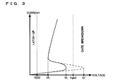
- FIG. 3 is a diagram showing the TLP curve that represents the switching characteristic of the electrostatic protection circuit used in the semiconductor device of the first embodiment
- FIGS. 4A and 4B are top views showing examples of the arrangement layout of the external resistor Rext;
- FIGS. 5A to 5C are vertical sectional views showing examples of the semiconductor device of a second embodiment of the invention.
- FIGS. 6A to 6C are vertical sectional views showing examples of the semiconductor device of a third embodiment of the invention.
- FIGS. 7A to 7C are vertical sectional views showing examples of the semiconductor device of a fourth embodiment of the invention.
- FIG. 8 is an equivalent circuit diagram of the semiconductor device of the fourth embodiment.
- FIGS. 9A to 9C are vertical sectional views showing examples of the semiconductor device of a fifth embodiment of the invention.
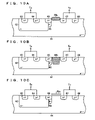
- FIGS. 10A to 10C are vertical sectional views showing examples of the semiconductor device of a sixth embodiment of the invention.
- FIGS. 11A and 11B are vertical sectional views of the structures formed in conventional semiconductor devices so as to function as an electrostatic protection circuit.
- FIGS. 1A to 1C are vertical sectional views showing the semiconductor device of the first embodiment of the invention.
- the semiconductor device of this embodiment is composed of: a p-type [p ⁇ ] semiconductor substrate 11 (hereinafter called the “p substrate 11 ”); a low-concentration n-type [n ⁇ ] semiconductor region 12 (hereinafter called the “n well 12 ”) formed in the p substrate 11 ; a first high-concentration p-type [p+] semiconductor region 13 (hereinafter called the “p+ region 13 ”) formed in the n well 12 and connected to an anode terminal Ta; a first high-concentration n-type [n+] semiconductor region 14 (hereinafter called the “n+ region 14 ”) formed likewise in the n well 12 and connected by way of an external resistor Rext to the anode terminal Ta; a low-concentration p-type [p ⁇ ] semiconductor region 15 (hereinafter called the “p ⁇
- the p substrate 11 , the n well 12 , and the p+ region 13 together form a pnp-type bipolar transistor Qa
- the n well 12 , the p substrate 11 , and the n+ region 16 together form an npn-type bipolar transistor Qb
- the n+ region 14 and the p ⁇ region 15 together form a trigger diode Da.
- the base width of the transistor Qb is controlled by controlling the element width of the element separator portion 18 a , 18 b , or 18 c.
- FIG. 2 is an equivalent circuit diagram of the semiconductor device of this embodiment.
- the emitter of the transistor Qa is connected to the anode terminal Ta.
- the collector of the transistor Qa is, on one hand, connected by way of a substrate resistor Rsub to the cathode terminal Tc and, on the other band, also connected to the anode of the trigger diode Da and to the base of the transistor Qb.
- the base of the transistor Qa is, on one hand, connected by way of the external resistor Rext to the anode terminal Ta and, on the other hand, also connected to the cathode of the trigger diode Da and to the collector of the transistor Qb.
- the emitter of the transistor Qb is connected to the cathode terminal Tc.
- the trigger diode Da when a positive ESD surge voltage is applied to the anode terminal Ta, the trigger diode Da is reversely biased by way of the external resistor Rext, and, if this reverse bias is higher than the breakdown voltage of the trigger diode Da, a breakdown current flows through the trigger diode Da from its anode to cathode.
- the cathode terminal Tc which is grounded
- the substrate resistor Rsub raises the base potential of the transistor Qb, and this turns the transistor Qb on.
- the external resistor Rext lowers the base potential of the transistor Qa, and this turns the transistor Qa on.
- the collector current of the transistor Qa is equal to the base current of the transistor Qb, and thus the whole operation described above is now under positive feedback control. In this way, the operation for achieving electrostatic protection (i.e., the operation for keeping a short-circuited path between the anode terminal Ta and the cathode terminal Tc) is maintained.
- FIG. 3 is a diagram showing the TLP (transmission line pulse) curve that represents the switching characteristic of the electrostatic protection circuit used in the semiconductor device of this embodiment.
- the TLP curve observed in this embodiment is indicated by a solid line, and, for comparison, the TLP curve observed in the conventional structures is indicated by a broken line.
- along the horizontal axis is taken the voltage, and along the vertical axis is taken the current.
- the supply voltage VDD i.e., the voltage needed to maintain the electrostatic protection operation
- the hold voltage Vh i.e., the voltage needed to maintain the electrostatic protection operation
- the gate breakdown voltage Vgbd i.e., the voltage at which the CMOS gate oxide film to be protected breaks down
- the trigger voltages Vt and Vt′ the voltage at which the operation for electrostatic protection is started).
- the p ⁇ /n+ junction surface of the trigger diode Da is formed, not by the combination of a p substrate and an n+ region (see FIG. 11A ) or by the combination of a p+ region and an n+ region formed at a predetermined interval from each other (see FIG. 11B ) as conventionally adopted, but by the n+ region 14 and the p ⁇ region 15 that are formed contiguously with each other.
- this structure simply by adjusting the impurity concentration in the p ⁇ region 15 , it is possible to set the trigger voltage Vt lower than the conventional trigger voltage Vt′ and simultaneously lower than the gate breakdown voltage Vgbd.
- the p+ and n+ regions of the trigger diode which are conventionally formed at a predetermined distance from each other, contiguously with each other results in making the trigger voltage Vt so low as to be lower than the supply voltage VDD, and this causes latch-up.
- triggering needs to be performed appropriately between the supply voltage VDD and the gate breakdown voltage Vgbd (for example, between 4 and 8 [V]), and, to achieve this, as in this embodiment, the p ⁇ region 15 , which is formed by the low-doped drain method or the like (and in which the impurity concentration is about 10 18 [cm ⁇ 3 ]), needs to be formed contiguously with the n+ region 14 .
- the cathode of the trigger diode Da is connected by way of the external resistor Rext directly to the anode terminal Ta.
- This structure in which the base resistor that is important for controlling the switching of the transistor Qa is provided as an external resistor Rext, permits the resistance thereof to be controlled easily, and thus makes it possible to surely give the base resistor of the transistor Qa the desired resistance. Accordingly, even as increasingly fine semiconductor production processes are used, it is easy to set the trigger voltage Vt and the hold voltage Vh, which determine the device characteristic. Thus, it is possible to enhance the switching characteristic, secure the optimum margins, and increase the yield rate.
- the semiconductor device of this embodiment can be produced by the common CMOS process and thus without any undue increase in the costs. Moreover, the semiconductor device of this embodiment, owing to its SCR structure, occupies a smaller area than do conventional protection devices of the ggnMOS (grounded-gate NMOS) type.
- FIGS. 4A and 4B are top views showing examples of the arrangement layout of the external resistor Rext.
- These figures both deal with cases in which the elements are arranged in the following order from left to right of the figures: the anode terminal Ta, the external resistor Rext, the p+ region 13 , the n+ region 14 , the p ⁇ region 15 , the n+ region 16 , the p+ region 17 , and the cathode terminal Tc.
- the terminals Ta and Tc may be formed as electrodes (pads).
- the external resistor Rext is arranged between the anode terminal Ta and the n+ region 14 perpendicularly to the direction that connects these two elements. Moreover, the external resistor Rext has, at one end thereof, a first contact Tx that is electrically connected by way of a conductor L 2 a to the anode terminal Ta, and has, at the other end thereof, a second contact Ty that is electrically connected by way of a conductor L 2 b to the n+ region 14 .
- the external resistor Rext is arranged between the anode terminal Ta and the n+ region 14 parallel to the direction that connects these two elements.
- the external resistor Rext has, at one end thereof, a first contact Tx that is electrically connected to the anode terminal Ta, and has, at the other end thereof, a second contact Ty that is electrically connected by way of a conductor L 2 to the n+ region 14 .
- the p+ region 13 is connected by way of a conductor L 1 to the anode terminal Ta, and the n+ region 16 and the p+ region 17 are connected by way of a conductor L 3 to the cathode terminal Tc.
- These arrangement layouts can be realized by a two-layer metal process, but, from the perspective of the area efficiency of the layouts, it is preferable to adopt a three-layer metal process.
- the external resistor Rext is realized by forming an n-well resistor or polysilicon resistor so as to have a resistance of several [k ⁇ ].
- FIGS. 5A to 5C are vertical sectional views showing the semiconductor device of the second embodiment of the invention.
- the semiconductor device of this embodiment is composed of: a p substrate 21 ; an n well.
- n+ region 22 formed in the p substrate 21 ; a p+ region 23 formed in the n well 22 and connected to an anode terminal Ta; an n+ region 24 formed so as to bridge between the p substrate 21 and the n well 22 and connected by way of an external resistor Rext to the anode terminal Ta; a p ⁇ region 25 formed in the p substrate 21 by the side of and contiguously with the n+ region 24 ; an n+ region 26 and a p+ region 27 formed in the p substrate 21 and connected to a cathode terminal Tc; and an element separator portion 28 a , 28 b , or 28 c for separating between the p ⁇ region 25 and the n+ region 26 .
- the equivalent circuit of the semiconductor device of this embodiment is the same as the one described earlier in connection with the first embodiment (see FIG. 2 ). Structured as described above, the semiconductor device can be produced, as in the first embodiment, by the common CMOS process. Thus, it is possible to obtain the same advantages as described earlier without any undue increase in the costs.
- FIGS. 6A to 6C are vertical sectional views showing the semiconductor device of the third embodiment of the invention.
- the semiconductor device of this embodiment is composed of: a p substrate 31 ; an n well 32 formed in the p substrate 31 ; a p+ region 33 formed in the n well 32 and connected to an anode terminal Ta; an n+ region 34 formed so as to bridge between the p substrate 31 and the n well 32 and connected by way of an external resistor Rext to the anode terminal Ta; a p ⁇ region 35 formed in the p substrate 31 below and contiguously with the n+ region 34 ; an n+ region 36 and a p+ region 37 formed in the p substrate 31 and connected to a cathode terminal Tc; and an element separator portion 38 a , 38 b , or 38 c for separating between the p ⁇ region 35 and the n+ region 36 .
- the equivalent circuit of the semiconductor device of this embodiment is the same as the one described earlier in connection with the first embodiment (see FIG. 2 ).
- FIGS. 7A to 7C are vertical sectional views showing the semiconductor device of the fourth embodiment of the invention.
- the p substrate 41 , the n well 42 , and the p+ region 44 together form a pnp-type bipolar transistor Qa
- the n well 42 , the p substrate 41 , and the n+ region 47 together form an npn-type bipolar transistor Qb
- the n+ region 45 and the p ⁇ region 46 together form a trigger diode Da.
- the base width of the transistor Qb is controlled by controlling the element width of the element separator portion 49 a , 49 b , or 49 c.
- FIG. 8 is an equivalent circuit diagram of the semiconductor device of this embodiment.
- the emitter of the transistor Qa is connected to the anode terminal Ta.
- the collector of the transistor Qa is, on one hand, connected by way of a substrate resistor Rsub to the cathode terminal Tc and, on the other band, also connected to the anode of the trigger diode Da and to the base of the transistor Qb.
- the base of the transistor Qa is, on one hand, connected by way of an n-well resistor Rnwell to the anode terminal Ta and, on the other hand, also connected to the cathode of the trigger diode Da and to the collector of the transistor Qb.
- the emitter of the transistor Qb is connected to the cathode terminal Tc.
- the trigger diode Da when a positive ESD surge voltage is applied to the anode terminal Ta, the trigger diode Da is reversely biased by way of the n-well resistor Rnwell, and, if this reverse bias is higher than the breakdown voltage of the trigger diode Da, a breakdown current flows through the trigger diode Da from its anode to cathode.
- the cathode terminal Tc which is grounded
- the substrate resistor Rsub raises the base potential of the transistor Qb, and this turns the transistor Qb on.
- the n-well resistor Rnwell lowers the base potential of the transistor Qa, and this turns the transistor Qa on.
- the collector current of the transistor Qa is equal to the base current of the transistor Qb, and thus the whole operation described above is now under positive feedback control. In this way, the operation for achieving electrostatic protection (i.e., the operation for keeping a short-circuited path between the anode terminal Ta and the cathode terminal Tc) is maintained.
- the p ⁇ /n+ junction surface of the trigger diode Da is formed, not by the combination of a p substrate and an n+ region (see FIG. 11A ) or by the combination of a p+ region and an n+ region formed at a predetermined interval from each other (see FIG. 11B ) as conventionally adopted, but by the n+ region 45 and the p ⁇ region 46 that are formed contiguously with each other.
- the trigger voltage Vt lower than the conventional trigger voltage Vt′ and simultaneously lower than the gate breakdown voltage Vgbd.
- the p+ and n+ regions of the trigger diode which are conventionally formed at a predetermined distance from each other, contiguously with each other results in making the trigger voltage Vt so low as to be lower than the supply voltage VDD, and this causes latch-up.
- triggering needs to be performed appropriately between the supply voltage VDD and the gate breakdown voltage Vgbd (for example, between 4 and 8 [V]), and, to achieve this, as in this embodiment, the p ⁇ region 46 , which is formed by the low-doped drain method or the like (and in which the impurity concentration is about 10 18 [cm ⁇ 3 ]), needs to be formed contiguously with the n+ region 45 .
- the n-well resistor Rnwell of which the resistance is adjusted to control the switching characteristic of the electrostatic protection circuit is inserted between the anode terminal Ta and the trigger diode Da.
- the n-well resistor Rnwell of which the resistance is adjusted to control the switching characteristic of the electrostatic protection circuit.
- the semiconductor device of this embodiment can be produced by the common CMOS process and thus without any undue increase in the costs. Moreover, the semiconductor device of this embodiment, owing to its SCR structure, occupies a smaller area than do conventional protection devices of the ggnMOS (grounded-gate nMOS) type.
- FIGS. 9A to 9C are vertical sectional views showing the semiconductor device of the fifth embodiment of the invention.
- the semiconductor device of this embodiment is composed of: a p substrate 51 ; an n well 52 formed in the p substrate 51 ; an n+ region 53 and a p+ region 54 formed in the n well 52 and connected to an anode terminal Ta; an n+ region 55 formed so as to bridge between the p substrate 51 and the n well 52 ; a p ⁇ region 56 formed in the p substrate 51 by the side of and contiguously with the n+ region 55 ; an n+ region 57 and a p+ region 58 formed in the p substrate 51 and connected to a cathode terminal Tc; and an element separator portion 59 a , 59 b , or 59 c for separating between the p ⁇ region 56 and the n+ region 57 .
- the equivalent circuit of the semiconductor device of this embodiment is the same as the one described earlier in connection with the fourth embodiment (see FIG. 8 ). Structured as described above, the semiconductor device can be produced, as in the first embodiment, by the common CMOS process. Thus, it is possible to obtain the same advantages as described earlier without any undue increase in the costs.
- FIGS. 10A to 10C are vertical sectional views showing the semiconductor device of the sixth embodiment of the invention.
- the semiconductor device of this embodiment is composed of: a p substrate 61 ; an n well 62 formed in the p substrate 61 ; an n+ region 63 and a p+ region 64 formed in the n well 62 and connected to an anode terminal Ta; an n+ region 65 formed so as to bridge between the p substrate 61 and the n well 62 ; a p ⁇ region 66 formed in the p substrate 61 below and contiguously with the n+ region 65 ; an n+ region 67 and a p+ region 68 formed in the p substrate 61 and connected to a cathode terminal Tc; and an element separator portion 69 a , 69 b , or 69 c for separating between the p ⁇ region 66 and the n+ region 67 .
- the equivalent circuit of the semiconductor device of this embodiment is the same as the one described earlier in connection with the fourth embodiment (see FIG. 8 ).
- a semiconductor device is provided with a p-type semiconductor substrate, a low-concentration n-type semiconductor region formed in the p-type semiconductor substrate, a first high-concentration p-type semiconductor region formed in the low-concentration n-type semiconductor region and connected to a first electrode, a first high-concentration n-type semiconductor region formed likewise in the low-concentration n-type semiconductor region and connected via a resistive element to the first electrode, a low-concentration p-type semiconductor region formed contiguously with the first high-concentration n-type semiconductor region, a second high-concentration n-type semiconductor region and a second high-concentration p-type semiconductor region formed in the p-type semiconductor substrate and connected to a second electrode, and an element separator portion formed between the low-concentration p-type semiconductor region and the second high-concentration n-type semiconductor region.
- the low-concentration p-type semiconductor region is formed so as to bridge between the p-type semiconductor substrate and the low-concentration n-type semiconductor region, and the resistive element is formed outside the p-type semiconductor substrate.
- the first high-concentration n-type semiconductor region is formed so as to bridge between the p-type semiconductor substrate and the low-concentration n-type semiconductor region, and the resistive element is formed outside the p-type semiconductor substrate.
- the low-concentration p-type semiconductor region is formed by the side of and contiguous with the first high-concentration n-type semiconductor region. Structured in this way, the semiconductor device can be produced by the common CMOS process and thus without any undue increase in the costs.
- the low-concentration p-type semiconductor region is formed below and contiguous with the first high-concentration n-type semiconductor region.
- the resistive element is formed between the first electrode and the first high-concentration n-type semiconductor region in such a way as to lie perpendicular or parallel to the direction that connects those two elements.
- the resistive element has at one end thereof a first contact that is electrically connected to the first electrode and having at the other end thereof a second contact that is electrically connected to the first high-concentration n-type semiconductor region.
- the low-concentration p-type semiconductor region is formed so as to bridge between the p-type semiconductor substrate and the low-concentration n-type semiconductor region, and the resistive element is formed inside the low-concentration n-type semiconductor region.
- the first high-concentration n-type semiconductor region is formed so as to bridge between the p-type semiconductor substrate and the low-concentration n-type semiconductor region, and the resistive element is formed inside the low-concentration n-type semiconductor region.
- the low-concentration p-type semiconductor region is formed by the side of and contiguous with the first high-concentration n-type semiconductor region. Structured in this way, the semiconductor device can be produced by the common CMOS process and thus without any undue increase in the costs.
- the low-concentration p-type semiconductor region is formed below and contiguous with the first high-concentration n-type semiconductor region.
- a semiconductor device produced under the rules of a 0.18- ⁇ m or below process is provided with, as a protection circuit for protecting a terminal of the semiconductor device, a thyristor circuit that conducts at an input voltage lower than the gate breakdown voltage.
- the thyristor circuit has, between the bases of the transistors of which the thyristor circuit is composed, a trigger diode of which the cathode is connected to the anode of the thyristor circuit and of which the anode is connected to the cathode of the thyristor circuit.
- a resistive element is formed between the cathode of the trigger diode and the anode of the thyristor circuit.
Applications Claiming Priority (2)
| Application Number | Priority Date | Filing Date | Title |
|---|---|---|---|
| JP2003-069044 | 2003-03-14 | ||
| JP2003069044A JP3810375B2 (ja) | 2003-03-14 | 2003-03-14 | 半導体装置 |
Publications (2)
| Publication Number | Publication Date |
|---|---|
| US20040178455A1 US20040178455A1 (en) | 2004-09-16 |
| US7154152B2 true US7154152B2 (en) | 2006-12-26 |
Family
ID=32959371
Family Applications (1)
| Application Number | Title | Priority Date | Filing Date |
|---|---|---|---|
| US10/792,812 Active 2024-09-08 US7154152B2 (en) | 2003-03-14 | 2004-03-05 | Semiconductor device |
Country Status (5)
| Country | Link |
|---|---|
| US (1) | US7154152B2 (ja) |
| JP (1) | JP3810375B2 (ja) |
| KR (1) | KR20040081055A (ja) |
| CN (1) | CN100481454C (ja) |
| TW (2) | TWI327775B (ja) |
Cited By (2)
| Publication number | Priority date | Publication date | Assignee | Title |
|---|---|---|---|---|
| US20070164310A1 (en) * | 2006-01-18 | 2007-07-19 | Eun-Kyoung Kwon | Electrostatic discharge element and diode having horizontal current paths, and method of manufacturing the same |
| WO2011137701A1 (zh) * | 2010-05-05 | 2011-11-10 | 北京大学 | 一种静电保护器件及其制备方法 |
Families Citing this family (25)
| Publication number | Priority date | Publication date | Assignee | Title |
|---|---|---|---|---|
| KR100679943B1 (ko) * | 2004-11-10 | 2007-02-08 | 주식회사 하이닉스반도체 | 낮은 촉발전압에서 동작이 가능한 실리콘제어정류기구조의 정전기방전 보호 회로 |
| DE102004062183B3 (de) * | 2004-12-23 | 2006-06-08 | eupec Europäische Gesellschaft für Leistungshalbleiter mbH | Thyristoranordnung mit integriertem Schutzwiderstand und Verfahren zu deren Herstellung |
| US7042028B1 (en) * | 2005-03-14 | 2006-05-09 | System General Corp. | Electrostatic discharge device |
| CN101154657B (zh) * | 2006-09-25 | 2010-04-07 | 联詠科技股份有限公司 | 静电放电防护电路的布局结构及其制造方法 |
| US7601990B2 (en) * | 2006-10-25 | 2009-10-13 | Delphi Technologies, Inc. | Method and apparatus for electrostatic discharge protection having a stable breakdown voltage and low snapback voltage |
| DE102007006853B4 (de) * | 2007-02-12 | 2018-05-09 | Infineon Technologies Ag | ESD-Schutzvorrichtung und elektrische Schaltung mit derselben |
| US20090026492A1 (en) * | 2007-07-25 | 2009-01-29 | Chatty Kiran V | Lateral junction breakdown triggered silicon controlled rectifier based electrostatic discharge protection device |
| JP4245644B1 (ja) * | 2007-11-21 | 2009-03-25 | シャープ株式会社 | 静電気放電保護装置及びこれを備えた半導体集積回路 |
| JP2010021412A (ja) * | 2008-07-11 | 2010-01-28 | Oki Semiconductor Co Ltd | 半導体サイリスタ装置 |
| JP2010067632A (ja) * | 2008-09-08 | 2010-03-25 | Sharp Corp | 静電気保護素子 |
| TWI399846B (zh) * | 2009-11-30 | 2013-06-21 | Inotera Memories Inc | 漏電流防止裝置 |
| US20110133247A1 (en) * | 2009-12-08 | 2011-06-09 | Hossein Sarbishaei | Zener-Triggered SCR-Based Electrostatic Discharge Protection Devices For CDM And HBM Stress Conditions |
| JP5864216B2 (ja) * | 2011-11-04 | 2016-02-17 | ルネサスエレクトロニクス株式会社 | 半導体装置 |
| TWI455274B (zh) * | 2011-11-09 | 2014-10-01 | Via Tech Inc | 靜電放電保護裝置 |
| CN103378087B (zh) * | 2012-04-28 | 2016-02-24 | 无锡华润上华半导体有限公司 | 静电释放保护结构及其制造方法 |
| JP6294125B2 (ja) * | 2014-03-31 | 2018-03-14 | 株式会社豊田中央研究所 | 静電気保護素子 |
| TWI566421B (zh) * | 2015-10-07 | 2017-01-11 | 世界先進積體電路股份有限公司 | 垂直式二極體及其製造方法 |
| US9502584B1 (en) | 2015-11-24 | 2016-11-22 | Vanguard International Semiconductor Corporation | Vertical diode and fabrication method thereof |
| CN107046022B (zh) * | 2016-02-05 | 2019-12-03 | 中芯国际集成电路制造(上海)有限公司 | 静电放电保护器件和集成电路 |
| CN107275324B (zh) * | 2016-04-08 | 2019-11-05 | 旺宏电子股份有限公司 | 静电放电保护装置及方法 |
| CN107481931B (zh) * | 2017-08-22 | 2021-01-29 | 上海先进半导体制造股份有限公司 | 晶闸管的制造方法 |
| CN108183101B (zh) * | 2017-12-28 | 2019-10-25 | 上海华力微电子有限公司 | 无回滞效应硅控整流器型esd保护结构及其实现方法 |
| CN108091650B (zh) * | 2017-12-28 | 2019-10-25 | 上海华力微电子有限公司 | 无回滞效应硅控整流器型esd保护结构及其实现方法 |
| KR102607326B1 (ko) * | 2018-10-26 | 2023-11-30 | 한국전자통신연구원 | 반도체 장치 |
| US10685954B1 (en) * | 2018-11-28 | 2020-06-16 | Amazing Microelectronic Corp. | Silicon controlled rectifier |
Citations (17)
| Publication number | Priority date | Publication date | Assignee | Title |
|---|---|---|---|---|
| JPH01114068A (ja) | 1987-10-27 | 1989-05-02 | Nec Ic Microcomput Syst Ltd | 半導体装置 |
| JPH0662529A (ja) | 1992-04-30 | 1994-03-04 | Sgs Thomson Microelectron Sa | 静電放電に対する集積回路の保護装置 |
| US5502317A (en) | 1993-07-14 | 1996-03-26 | Texas Instruments Incorporated | Silicon controlled rectifier and method for forming the same |
| JPH0945862A (ja) | 1995-07-28 | 1997-02-14 | Nec Corp | 半導体素子 |
| JPH09293881A (ja) | 1996-04-23 | 1997-11-11 | Kaho Denshi Kofun Yugenkoshi | 静電気放電保護回路の製造方法 |
| US5856214A (en) * | 1996-03-04 | 1999-01-05 | Winbond Electronics Corp. | Method of fabricating a low voltage zener-triggered SCR for ESD protection in integrated circuits |
| US5982601A (en) * | 1998-07-30 | 1999-11-09 | Winbond Electronics Corp. | Direct transient-triggered SCR for ESD protection |
| US6147369A (en) * | 1998-09-02 | 2000-11-14 | Winbond Electronics Corp. | SCR and current divider structure of electrostatic discharge protective circuit |
| JP2001085534A (ja) | 1999-09-09 | 2001-03-30 | Nec Corp | 半導体保護装置及び半導体保護装置の製造方法 |
| US6246079B1 (en) * | 1998-05-13 | 2001-06-12 | Winbond Electronics Corp. | SCR circuit with a high trigger current |
| JP2001185738A (ja) | 1999-12-24 | 2001-07-06 | Sharp Corp | 半導体装置とその製造方法 |
| US20010007521A1 (en) * | 2000-01-11 | 2001-07-12 | Winbond Electronics Corp. | Electrostatic discharge protection circuit with high triggering voltage |
| JP2001291836A (ja) | 2000-04-11 | 2001-10-19 | Seiko Epson Corp | 静電気保護用半導体装置 |
| US20020079538A1 (en) * | 2000-03-30 | 2002-06-27 | Yuan-Mou Su | Scr-type electrostatic discharge protection circuit |
| US20020089017A1 (en) * | 2001-01-05 | 2002-07-11 | Lai Chun Hsiang | Electostatic discharge protection circuit coupled on I/O pad |
| US6538266B2 (en) * | 2000-08-11 | 2003-03-25 | Samsung Electronics Co., Ltd. | Protection device with a silicon-controlled rectifier |
| US20040207020A1 (en) * | 1999-09-14 | 2004-10-21 | Shiao-Chien Chen | CMOS silicon-control-rectifier (SCR) structure for electrostatic discharge (ESD) protection |
-
2003
- 2003-03-14 JP JP2003069044A patent/JP3810375B2/ja not_active Expired - Lifetime
-
2004
- 2004-03-03 TW TW093105493A patent/TWI327775B/zh active
- 2004-03-03 TW TW099108647A patent/TW201030939A/zh unknown
- 2004-03-05 US US10/792,812 patent/US7154152B2/en active Active
- 2004-03-09 CN CNB2004100283647A patent/CN100481454C/zh not_active Expired - Lifetime
- 2004-03-12 KR KR1020040016791A patent/KR20040081055A/ko not_active Application Discontinuation
Patent Citations (17)
| Publication number | Priority date | Publication date | Assignee | Title |
|---|---|---|---|---|
| JPH01114068A (ja) | 1987-10-27 | 1989-05-02 | Nec Ic Microcomput Syst Ltd | 半導体装置 |
| JPH0662529A (ja) | 1992-04-30 | 1994-03-04 | Sgs Thomson Microelectron Sa | 静電放電に対する集積回路の保護装置 |
| US5502317A (en) | 1993-07-14 | 1996-03-26 | Texas Instruments Incorporated | Silicon controlled rectifier and method for forming the same |
| JPH0945862A (ja) | 1995-07-28 | 1997-02-14 | Nec Corp | 半導体素子 |
| US5856214A (en) * | 1996-03-04 | 1999-01-05 | Winbond Electronics Corp. | Method of fabricating a low voltage zener-triggered SCR for ESD protection in integrated circuits |
| JPH09293881A (ja) | 1996-04-23 | 1997-11-11 | Kaho Denshi Kofun Yugenkoshi | 静電気放電保護回路の製造方法 |
| US6246079B1 (en) * | 1998-05-13 | 2001-06-12 | Winbond Electronics Corp. | SCR circuit with a high trigger current |
| US5982601A (en) * | 1998-07-30 | 1999-11-09 | Winbond Electronics Corp. | Direct transient-triggered SCR for ESD protection |
| US6147369A (en) * | 1998-09-02 | 2000-11-14 | Winbond Electronics Corp. | SCR and current divider structure of electrostatic discharge protective circuit |
| JP2001085534A (ja) | 1999-09-09 | 2001-03-30 | Nec Corp | 半導体保護装置及び半導体保護装置の製造方法 |
| US20040207020A1 (en) * | 1999-09-14 | 2004-10-21 | Shiao-Chien Chen | CMOS silicon-control-rectifier (SCR) structure for electrostatic discharge (ESD) protection |
| JP2001185738A (ja) | 1999-12-24 | 2001-07-06 | Sharp Corp | 半導体装置とその製造方法 |
| US20010007521A1 (en) * | 2000-01-11 | 2001-07-12 | Winbond Electronics Corp. | Electrostatic discharge protection circuit with high triggering voltage |
| US20020079538A1 (en) * | 2000-03-30 | 2002-06-27 | Yuan-Mou Su | Scr-type electrostatic discharge protection circuit |
| JP2001291836A (ja) | 2000-04-11 | 2001-10-19 | Seiko Epson Corp | 静電気保護用半導体装置 |
| US6538266B2 (en) * | 2000-08-11 | 2003-03-25 | Samsung Electronics Co., Ltd. | Protection device with a silicon-controlled rectifier |
| US20020089017A1 (en) * | 2001-01-05 | 2002-07-11 | Lai Chun Hsiang | Electostatic discharge protection circuit coupled on I/O pad |
Cited By (3)
| Publication number | Priority date | Publication date | Assignee | Title |
|---|---|---|---|---|
| US20070164310A1 (en) * | 2006-01-18 | 2007-07-19 | Eun-Kyoung Kwon | Electrostatic discharge element and diode having horizontal current paths, and method of manufacturing the same |
| WO2011137701A1 (zh) * | 2010-05-05 | 2011-11-10 | 北京大学 | 一种静电保护器件及其制备方法 |
| US8476672B2 (en) | 2010-05-05 | 2013-07-02 | Peking University | Electrostatic discharge protection device and method for fabricating the same |
Also Published As
| Publication number | Publication date |
|---|---|
| CN1531094A (zh) | 2004-09-22 |
| TW200425469A (en) | 2004-11-16 |
| TWI327775B (en) | 2010-07-21 |
| CN100481454C (zh) | 2009-04-22 |
| JP3810375B2 (ja) | 2006-08-16 |
| KR20040081055A (ko) | 2004-09-20 |
| TW201030939A (en) | 2010-08-16 |
| JP2004281590A (ja) | 2004-10-07 |
| US20040178455A1 (en) | 2004-09-16 |
Similar Documents
| Publication | Publication Date | Title |
|---|---|---|
| US7154152B2 (en) | Semiconductor device | |
| KR101162124B1 (ko) | 감소된 트리거 전압을 갖는 적층형 esd 보호 회로 | |
| US7106562B2 (en) | Protection circuit section for semiconductor circuit system | |
| JP3237110B2 (ja) | 半導体装置 | |
| US7525779B2 (en) | Diode strings and electrostatic discharge protection circuits | |
| US8039899B2 (en) | Electrostatic discharge protection device | |
| US7183612B2 (en) | Semiconductor device having an electrostatic discharge protecting element | |
| US7495265B2 (en) | ESD protection circuit with SCR structure for semiconductor device | |
| KR100517770B1 (ko) | 정전기 방전 보호 소자 | |
| US20070069310A1 (en) | Semiconductor controlled rectifiers for electrostatic discharge protection | |
| US20150084117A1 (en) | Bottom source nmos triggered zener clamp for configuring an ultra-low voltage transient voltage suppressor (tvs) | |
| JP2006074012A (ja) | 双方向型静電気放電保護素子 | |
| EP0242383B1 (en) | Protection of igfet integrated circuits from electrostatic discharge | |
| JP4209433B2 (ja) | 静電破壊保護装置 | |
| US6215135B1 (en) | Integrated circuit provided with ESD protection means | |
| US6670678B2 (en) | Semiconductor device having ESD protective transistor | |
| JPH10189756A (ja) | 半導体装置 | |
| US8093683B2 (en) | Semiconductor device | |
| US20050224882A1 (en) | Low trigger voltage esd nmosfet triple-well cmos devices | |
| US20200303368A1 (en) | Silicon-controlled-rectifier electrostatic protection structure and fabrication method thereof | |
| JP3559075B2 (ja) | Cmos技術の集積電子回路用の極性反転保護装置 | |
| US7098522B2 (en) | High voltage device with ESD protection | |
| EP0292327A2 (en) | Electrostatic breakdown protection circuits | |
| JP4423466B2 (ja) | 半導体装置 | |
| US10181466B2 (en) | Electrostatic discharge protection apparatus and applications thereof |
Legal Events
| Date | Code | Title | Description |
|---|---|---|---|
| AS | Assignment |
Owner name: ROHM CO., LTD., JAPAN Free format text: ASSIGNMENT OF ASSIGNORS INTEREST;ASSIGNOR:KOJI, TOSHIAKI;REEL/FRAME:015048/0748 Effective date: 20040119 |
|
| AS | Assignment |
Owner name: ROHM CO., LTD., JAPAN Free format text: CORRECTIVE ASSIGNMENT TO CORRECT THE INVENTOR'S NAME AND TO CORRECT A TYPOGRAPHICAL ERROR IN THE ADDRESS OF THE ASSIGNEE PREVIOUSLY RECORDED ON REEL 015048 FRAME 0748;ASSIGNOR:KOJIMA, TOSHIAKI;REEL/FRAME:017676/0580 Effective date: 20040119 |
|
| STCF | Information on status: patent grant |
Free format text: PATENTED CASE |
|
| FPAY | Fee payment |
Year of fee payment: 4 |
|
| FPAY | Fee payment |
Year of fee payment: 8 |
|
| MAFP | Maintenance fee payment |
Free format text: PAYMENT OF MAINTENANCE FEE, 12TH YEAR, LARGE ENTITY (ORIGINAL EVENT CODE: M1553) Year of fee payment: 12 |