US6646300B2 - Semiconductor memory device - Google Patents
Semiconductor memory device Download PDFInfo
- Publication number
- US6646300B2 US6646300B2 US09/811,555 US81155501A US6646300B2 US 6646300 B2 US6646300 B2 US 6646300B2 US 81155501 A US81155501 A US 81155501A US 6646300 B2 US6646300 B2 US 6646300B2
- Authority
- US
- United States
- Prior art keywords
- region
- transistor
- source
- channel
- read
- Prior art date
- Legal status (The legal status is an assumption and is not a legal conclusion. Google has not performed a legal analysis and makes no representation as to the accuracy of the status listed.)
- Expired - Fee Related
Links
Images


Classifications
-
- G—PHYSICS
- G11—INFORMATION STORAGE
- G11C—STATIC STORES
- G11C11/00—Digital stores characterised by the use of particular electric or magnetic storage elements; Storage elements therefor
- G11C11/21—Digital stores characterised by the use of particular electric or magnetic storage elements; Storage elements therefor using electric elements
- G11C11/34—Digital stores characterised by the use of particular electric or magnetic storage elements; Storage elements therefor using electric elements using semiconductor devices
- G11C11/40—Digital stores characterised by the use of particular electric or magnetic storage elements; Storage elements therefor using electric elements using semiconductor devices using transistors
- G11C11/401—Digital stores characterised by the use of particular electric or magnetic storage elements; Storage elements therefor using electric elements using semiconductor devices using transistors forming cells needing refreshing or charge regeneration, i.e. dynamic cells
- G11C11/403—Digital stores characterised by the use of particular electric or magnetic storage elements; Storage elements therefor using electric elements using semiconductor devices using transistors forming cells needing refreshing or charge regeneration, i.e. dynamic cells with charge regeneration common to a multiplicity of memory cells, i.e. external refresh
- G11C11/405—Digital stores characterised by the use of particular electric or magnetic storage elements; Storage elements therefor using electric elements using semiconductor devices using transistors forming cells needing refreshing or charge regeneration, i.e. dynamic cells with charge regeneration common to a multiplicity of memory cells, i.e. external refresh with three charge-transfer gates, e.g. MOS transistors, per cell
-
- H—ELECTRICITY
- H10—SEMICONDUCTOR DEVICES; ELECTRIC SOLID-STATE DEVICES NOT OTHERWISE PROVIDED FOR
- H10D—INORGANIC ELECTRIC SEMICONDUCTOR DEVICES
- H10D84/00—Integrated devices formed in or on semiconductor substrates that comprise only semiconducting layers, e.g. on Si wafers or on GaAs-on-Si wafers
-
- G—PHYSICS
- G11—INFORMATION STORAGE
- G11C—STATIC STORES
- G11C11/00—Digital stores characterised by the use of particular electric or magnetic storage elements; Storage elements therefor
- G11C11/21—Digital stores characterised by the use of particular electric or magnetic storage elements; Storage elements therefor using electric elements
- G11C11/34—Digital stores characterised by the use of particular electric or magnetic storage elements; Storage elements therefor using electric elements using semiconductor devices
- G11C11/40—Digital stores characterised by the use of particular electric or magnetic storage elements; Storage elements therefor using electric elements using semiconductor devices using transistors
- G11C11/401—Digital stores characterised by the use of particular electric or magnetic storage elements; Storage elements therefor using electric elements using semiconductor devices using transistors forming cells needing refreshing or charge regeneration, i.e. dynamic cells
- G11C11/403—Digital stores characterised by the use of particular electric or magnetic storage elements; Storage elements therefor using electric elements using semiconductor devices using transistors forming cells needing refreshing or charge regeneration, i.e. dynamic cells with charge regeneration common to a multiplicity of memory cells, i.e. external refresh
- G11C11/404—Digital stores characterised by the use of particular electric or magnetic storage elements; Storage elements therefor using electric elements using semiconductor devices using transistors forming cells needing refreshing or charge regeneration, i.e. dynamic cells with charge regeneration common to a multiplicity of memory cells, i.e. external refresh with one charge-transfer gate, e.g. MOS transistor, per cell
-
- H—ELECTRICITY
- H10—SEMICONDUCTOR DEVICES; ELECTRIC SOLID-STATE DEVICES NOT OTHERWISE PROVIDED FOR
- H10B—ELECTRONIC MEMORY DEVICES
- H10B41/00—Electrically erasable-and-programmable ROM [EEPROM] devices comprising floating gates
- H10B41/20—Electrically erasable-and-programmable ROM [EEPROM] devices comprising floating gates characterised by three-dimensional arrangements, e.g. with cells on different height levels
-
- H—ELECTRICITY
- H10—SEMICONDUCTOR DEVICES; ELECTRIC SOLID-STATE DEVICES NOT OTHERWISE PROVIDED FOR
- H10B—ELECTRONIC MEMORY DEVICES
- H10B41/00—Electrically erasable-and-programmable ROM [EEPROM] devices comprising floating gates
- H10B41/70—Electrically erasable-and-programmable ROM [EEPROM] devices comprising floating gates the floating gate being an electrode shared by two or more components
-
- H—ELECTRICITY
- H10—SEMICONDUCTOR DEVICES; ELECTRIC SOLID-STATE DEVICES NOT OTHERWISE PROVIDED FOR
- H10B—ELECTRONIC MEMORY DEVICES
- H10B69/00—Erasable-and-programmable ROM [EPROM] devices not provided for in groups H10B41/00 - H10B63/00, e.g. ultraviolet erasable-and-programmable ROM [UVEPROM] devices
-
- H—ELECTRICITY
- H10—SEMICONDUCTOR DEVICES; ELECTRIC SOLID-STATE DEVICES NOT OTHERWISE PROVIDED FOR
- H10D—INORGANIC ELECTRIC SEMICONDUCTOR DEVICES
- H10D88/00—Three-dimensional [3D] integrated devices
Definitions
- the present invention relates to semiconductor devices including field effect transistors, and, particularly, semiconductor storage devices, and a method of fabricating the same.
- a DRAM embedded chip integrally provided with a logic circuit and a DRAM (dynamic random-access memory) on a single chip has been developed to solve the above-noted problem. Techniques relating to such a DRAM embedded chip are mentioned in H. Ishiuchi, et al., IEEE International Electron Devices Meeting, pp. 33-36 (1997).
- an SRAM static random-access memory
- memory cells of only logic transistors is preferable for use in a DRAM.
- each memory cell of SRAM consists of six transistors, the memory cell needs a large cell area, and high cost makes it difficult to form an SRAN of a large capacity.
- a proposed memory cell which is called a gain cell.
- This structure is capable of operating even if the number of stored charge of a DRAM cell is reduced. Charges are injected through a write transistor to a storage node and information can be read by virtue of the change of the threshold voltage of a read transistor caused by the stored charge for signal storage.
- Techniques relating to the present invention include a write transistor formed by polysilicon, mentioned in H. Shichijo, et al., Conference on Solid State Devices and Materials, pp. 265-268 (1984), a read transistor formed by polysilicon, mentioned in S. Shukuri, et al., IEEE International Electron Devices Meeting, pp.1006-1008 (1992), and single-electron memories formed by polysilicon, mentioned in K.
- the reduction of the power consumption of devices is an important problem.
- a semiconductor device consumes most of the power consumed by an apparatus including the semiconductor device, and, hence, the reduction of power consumption of the semiconductor device is required.
- the current of a transistor in an OFF status is called a leakage current. Since the leakage current is a matter that can affect all the circuit elements on a chip, the current is one of factors of increasing power consumption of a whole semiconductor chip without distinction in case of as to whether the leakage current exists in a logic circuit or a memory circuit. Therefore, the reduction of power consumption of the semiconductor device is required.
- a TFT structure which includes a polycrystalline silicon base having a thin channel region causes a leakage current in the range of 10 ⁇ 18 .
- the base height of a source and/or drain region is almost the same as the height of a channel thin film region.
- a gate insulator layer of this structure is deposited by CVD. Therefore, a step between a top surface of a source and/or a drain region and a top surface of a channel region causes a concentration of an electrical field at a top portion of the step. Therefore, a margin of dielectric strength is reduced when a gate insulation layer is thinner.
- Another object of the present invention is to provide a semiconductor device that operates at a low power consumption.
- a high-temperature process for forming capacitors of a DRAM entails a problem. Since a DRAM must keep a high S/N ratio, a DRAM must achieve a large storage charge even in the face of continued cell size miniaturization. Therefore, a dielectric film having a high dielectric constant must be employed to keep the capacity in an smaller area.
- the use of a conventional three-dimensional structure is costly, and, hence, is infeasible, and a dielectric film having a high dielectric constant is indispensable even if a three-dimensional structure is used.
- a high-temperature process is necessary for forming a dielectric film having a high dielectric constant. For example, when forming a Ta 2 Os film (tantalum pentoxide film), a high-temperature process is necessary that uses heat on the order of 750° C.
- the pn junction of a MOS transistor of the logic is formed in a very shallow diffusion layer for miniaturization.
- An impurity is diffused out in the diffusion layer by a heat treatment, the characteristic of the MOS transistor is deteriorated, and the MOS transistor malfunctions due to punch through.
- a silicide such as cobalt silicide, tends to aggregate when heated at a high temperature.
- capacitors can be formed before forming the MOS transistors of the logic.
- the trench must be very deep and the aspect ratio increases inevitably when the structure is produced by finer pattern.
- the present invention provides a large-scale memory capable of properly operating even if semiconductor devices are produced by more fine pattern.
- the present invention is characterized in reading a charge injection or charge emission through a write transistor by the change of the threshold voltage of a read transistor.
- a logic circuit can be easily combined because there is no need for any new material for securing capacitance for a DRAM.
- a transistor according to the present invention can be very effectively applied to such a semiconductor device.
- a semiconductor memory cell comprises a source region, a drain region, a channel region of a semiconductor material connecting the source region and the drain region, and a gate electrode for controlling the potential of the channel region, wherein the channel region is formed on an insulating film, and the channel region is disposed on a level corresponding to the upper surfaces of the source region and the drain region with respect to a surface of a substrate.
- the channel region is a thin semiconductor film of 5 nm or below in thickness. Since the channel region is a very thin semiconductor film, the leakage current is very small. This constitution will be understood by referring to FIG. 1 .
- a semiconductor memory cell comprises: a first transistor structure (M 2 ) including a source region of a metal or a semiconductor material, a drain region of a metal or a semiconductor material, a channel region of a semiconductor material formed on an insulating film and connecting the source region and the drain region, and a gate electrode of a metal or a semiconductor material for controlling the potential of the channel region; and a second transistor structure (M 1 ) including a source region of a metal or a semiconductor material, a drain region of a metal or a semiconductor material, a channel region of a semiconductor connecting the source region and the drain region, a gate electrode of a metal or a semiconductor material for controlling the potential of the channel region, and a charge storage region of a metal or a semiconductor material coupled with the channel region by electrostatic capacitance.
- the source region of the second transistor structure is connected to a source line
- the one end of the source or the drain region of the first transistor structure is connected to the charge storage region of the second transistor structure
- the other end of the source or the drain region of the first transistor structure is connected to a data line.
- a charge storage region ( 1 ) and a control electrode ( 5 ) of a read transistor are layered, and, hence, the cell can be formed in an area smaller than that of a three-transistor gain cell. Since the channel of a write transistor is a semiconductor thin film formed on an insulating film ( 134 ) and a charge leakage path in a channel ( 3 ) can be completely depleted, leakage current is far less than that in a device employing an MOS transistor formed on a bulk substrate as a write transistor.
- the storage region ( 1 ) or the channel ( 3 ) of the write transistor can be formed by a self-alignment process in alignment with a word line ( 5 ).
- the cells of the semiconductor device can be formed by simple processes in small area. Reference characters used in the foregoing description are those used in FIG. 1 .
- FIGS. 1 ( a ), 1 ( b ) and 1 ( c ) are, respectively, a typical fragmentary sectional view, a typical fragmentary plan view and a circuit diagram, respectively, of a semiconductor memory device in a first embodiment according to the present invention
- FIGS. 2 ( a ) and 2 ( b ) are views for explaining a method of fabricating the semiconductor memory device in the first embodiment
- FIGS. 3 ( a ) and 3 ( b ) are views for explaining a method of fabricating a write transistor included in the semiconductor memory device in the first embodiment
- FIGS. 4 ( a ) and 4 ( b ) are sectional views for explaining a method of processing a channel included in the semiconductor memory device in the first embodiment
- FIGS. 5 ( a ) and 5 ( b ) are views for explaining a method of fabricating the semiconductor memory device in the first embodiment
- FIGS. 6 ( a ) and 6 ( b ) are views for explaining a method of fabricating the semiconductor memory device in the first embodiment
- FIG. 7 is a circuit diagram of the array configuration of the semiconductor memory device in the first embodiment
- FIGS. 8 ( a ) and 8 ( b ) are views for explaining a method of fabricating the semiconductor memory 10 device in a second embodiment
- FIGS. 9 ( a ) and 9 ( b ) are sectional views for explaining a method of fabricating a memory cell included in the semiconductor memory device in the second embodiment
- FIGS. 10 ( a ), 10 ( b ) and 10 ( c ) are sectional views for explaining a method of fabricating the semiconductor memory device in the second embodiment
- FIGS. 11 ( a ), 11 ( b ) and 11 ( c ) are sectional views for explaining a method of fabricating the semiconductor memory device in the second embodiment
- FIGS. 12 ( a ), 12 ( b ) and 12 ( c ) are sectional views for explaining a method of fabricating the semiconductor memory device in the second embodiment
- FIGS. 13 ( a ) and 13 ( b ) are top views for explaining a method of fabricating the semiconductor memory device in the second embodiment
- FIGS. 14 ( a ) and 14 ( b ) are top views for explaining a method of fabricating the semiconductor memory device in the second embodiment
- FIGS. 15 ( a ) and 15 ( b ) are top views for explaining a method of fabricating the semiconductor memory device in the second embodiment
- FIG. 16 is a top view for explaining the construction of the memory cell array of the semiconductor memory device in the second embodiment
- FIG. 17 is a top view for explaining the construction of the memory cell array of the semiconductor memory device in the second embodiment
- FIG. 18 is a top view for explaining the construction of the memory cell array of the semiconductor memory device in the second embodiment
- FIG. 19 is an equivalent circuit diagram for explaining the construction of the memory cell array of the semiconductor memory device in the second embodiment.
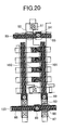
- FIG. 20 is a top view for explaining the construction of the memory cell array of a semiconductor memory device in a modification of the semiconductor memory device in the second embodiment
- FIG. 21 is a circuit diagram for explaining the construction of the memory cell array shown in FIG. 20;
- FIGS. 22 ( a ) and 22 ( b ) are typical sectional views of a semiconductor memory device in a third embodiment according to the present invention in different phases of the semiconductor memory device fabricating process;
- FIG. 23 is a top view of the memory cell array of the semiconductor memory device in the third embodiment.
- FIG. 24 is a circuit diagram of an equivalent circuit of the memory cell array of the semiconductor memory device in the third embodiment.
- FIG. 25 is a graph showing the current-voltage characteristic in a storage state of a memory cell included in a semiconductor memory device in a fourth embodiment is according to the present invention.
- FIG. 26 is a block diagram of a memory and peripheral circuits included in the semiconductor memory device in the fourth embodiment.
- FIG. 27 is a sectional view for explaining a method of fabricating the semiconductor memory device in the fourth embodiment.
- FIGS. 28 ( a ) and 28 ( b ) are views for explaining the basic composition of a transistor included in a semiconductor memory device in a fifth embodiment according to the present invention.
- FIGS. 29 ( a ) and 29 ( b ) are plan views for explaining the basic composition of a transistor included in the semiconductor memory device in the fifth embodiment
- FIGS. 30 ( a ) and 30 ( b ) are top views for explaining a method of fabricating a semiconductor memory device in a sixth embodiment according to the present invention.
- FIG. 31 is a top view for explaining a method of fabricating the semiconductor memory device in the sixth embodiment.
- a semiconductor memory cell comprises: a first transistor structure including a source region of a metal or a semiconductor material, a drain region of a metal or a semiconductor material, a channel region of a semiconductor material which is formed on an insulating film and connects the source region and the drain region, and a gate electrode of a metal or a semiconductor material which controls the potential of the channel region; and a second transistor structure including a source region of a metal or a semiconductor material, a drain region of a metal or a semiconductor material, a channel region of a semiconductor material connecting the source region and the drain region, a gate electrode of a metal or a semiconductor material which controls the potential of the channel region, and a charge storage region of a metal or a semiconductor material coupled with the channel region by electrostatic capacitance.
- the source region of the second transistor structure is connected to a source line
- one end of the source or drain region of the first transistor structure is connected to the charge storage region of the second transistor structure
- the other end of the source or drain region of the first transistor structure is connected to a data line.
- the distance between the source or drain region of the first transistor structure connected to the data line and the source region of the second transistor structure is shorter than the distance between the source or drain region of the first transistor structure connected to the data line and the drain region of the second transistor structure.
- the width of the gate electrode of the second transistor structure is substantially equal to that of the channel region of the first transistor structure.
- the semiconductor memory cell in the third mode of the present invention is featured by the use of a self-alignment process using the electrodes of the read transistors of the semiconductor memory cells.
- the width of the gate electrode of the second transistor structure is substantially equal to that of the charge storage region of the second transistor structure.
- a semiconductor memory cell comprises write and read transistors of a field effect type; wherein the channel of the write transistor is formed of a semiconductor material, the source and drain regions of the write transistor are formed of a metal layer or a laminated structure of a metal layer and a semiconductor layer, one end (region A) of either the source or the drain region of the write transistor does not have any conductive path other than the channel of the write transistor and is coupled with the channel of the read transistor by electrostatic capacitance, the other end (region B) of either the source or the drain region of the write transistor is connected to an external circuit, the amount of charge stored in the region A of the write transistor is changed in order to change the threshold voltage of the read transistor to store information, and the channel of the write transistor is connected to metallic parts of the source and drain regions of the write transistor.
- This semiconductor memory cell is applied to a semiconductor memory device.
- a semiconductor memory device which comprises: transistors including gate insulating films having at least two levels of thickness; a peripheral circuit including transistors having a gate insulating film which is not the thinnest gate insulating film among the gate insulating films; and a memory cell including memory which includes a write field-effect transistor and a read field-effect transistor on the same chip, a charge which is charged and discharged through the write field-effect transistor which is read through the change in threshold voltage of the read field-effect transistor.
- the thickness of the gate insulating film of the component transistors of the peripheral circuit is equal to that of the gate insulating film of the read transistors of the memory cell.
- the channel of the write transistor is formed on an insulating film.
- the channel of the write transistor is on a level corresponding with the upper end of the source or the drain region of the write transistor.
- the gate electrode of the write transistor serves also as the gate electrode of the read transistor.
- the thickness of the channel of the write transistor is 5 nm or below.
- a memory cell array is formed by arranging semiconductor memory cells identical to those described in any one of the first to the tenth modes of the present invention in a matrix, wherein isolation regions isolating memory cells of the memory cell array are arranged in substantially parallel rectangles, the word lines connected to the gate electrodes of the write or read transistors of the semiconductor memory cells are arranged in substantially parallel rectangles, the plurality of read transistors of the semiconductor memory cell are connected by diffusion layers, the diffusion layers are arranged in substantially parallel rectangles, the isolation regions arranged in substantially parallel rectangles and the diffused layers arranged in substantially parallel rectangles are substantially parallel to each other, and the parallel rectangular isolation regions and the parallel word lines are substantially perpendicular to each other.
- a memory cell array is formed by arranging semiconductor memory cells equivalent to those described in any one of the first to the tenth modes of the present invention in a matrix, wherein the isolation regions of the memory cell array are arranged in substantially parallel rectangles, the word lines connecting the gate electrodes of the write or the read transistors of the semiconductor memory cells are arranged in substantially parallel rectangles, a plurality of read transistors of the memory cell are connected to each other by lines made of the same material as that of a gate electrode, the parallel rectangular isolation regions and the parallel word lines are substantially perpendicular to each other, the lines connecting the plurality of write transistors are parallel to the parallel rectangular isolation regions, and lines connecting the plurality of write transistors are extended on the parallel rectangular isolation regions.
- a memory cell array is formed by arranging semiconductor memory cells identical to those described in any one of the first to the tenth modes of the present invention in a matrix, wherein isolation regions included in the memory cell array are arranged in substantially parallel rectangles, the word lines connected to the gate electrodes of the write or read transistors of the semiconductor memory cells are arranged in substantially parallel rectangles, each of the read transistors of the semiconductor memory cells shares the diffusion layer of the drain region with only one adjacent cell, the source lines of the read transistors of at least three cells of the plurality of read transistors are connected by the diffusion layer or a metal wiring line, the isolation regions arranged in substantially parallel rectangles and the diffused layers arranged in substantially parallel rectangles are substantially parallel to each other, and the parallel rectangular isolation regions and the parallel word lines are substantially perpendicular to each other.
- a memory cell array is formed by arranging semiconductor memory cells identical to those described stated in any one of the first to the thirteenth mode of the present invention in a matrix, wherein information of at least two bits is stored in one cell.
- a memory cell array is formed by arranging semiconductor memory cells identical to those described in any one of the first to the fourteenth modes of the present invention in a matrix, wherein a register that enables the storage of information of at least two bits is connected to a unit read data line.
- a memory cell array is formed by arranging semiconductor memory cells identical to those described in any one of the first to the fifteenth modes of the present invention in a matrix, wherein a register that enables the storage of information of at least two bits is connected to a unit write data line.
- a memory cell array is formed by arranging semiconductor memory cells identical to those described in any one of the first to the sixteenth modes of the present invention in a matrix, wherein a semiconductor memory device control method comprises a first read step and a second read step of driving the same word line and read data line as those driven in the first step, wherein the second read step changes the voltage of the word line according to the result of the read operation in the first read step.
- a memory cell array is formed by arranging semiconductor memory cells identical to those described in any one of the first to the seventeenth modes of the present invention in a matrix, wherein a semiconductor memory device control method comprises a first read step and a second read step of driving the same word line and read data line as those driven in the first step, wherein the potential of a write data line is set according to the combination of the result of the read operation in the first read step and the result of the read operation in the second read step.
- FIGS. 1 ( a ), 1 ( b ) and 1 ( c ) are, respectively, a sectional view, a top view and a circuit diagram of an equivalent circuit of a memory cell included in the semiconductor memory device in the first embodiment.
- FIG. 1 ( b ) some parts of the overlapping outlines of regions are shifted relative to each other to facilitate understanding, and components shown in FIGS. 1 ( a ) to 1 ( c ) correspond with each other.
- FIG. 1 ( b ) shows the positional relationship between the principal parts of the memory cell but does not accurately show layers.
- the memory cell is integrally provided with a write transistor M 2 for writing information and a read transistor M 1 for reading stored information.
- the memory cell is the so-called gain cell structure including thin-film FETs (field effect transistors).
- the write transistor M 2 is a thin-film FET.
- the concentration of impurities in the channel 3 of the FET is low, and the channel 3 is substantially intrinsic.
- Opposite end parts 1 and 2 of the channel 3 are connected to a laminated structure of an n-type polysilicon layer and a W layer (tungsten layer).
- the end part 1 is only connected to the channel 3 and is not connected to any other conductive path.
- the end part 1 serves as a charge storage region 4 .
- the end part 1 corresponds to a part 1 c in the equivalent circuit diagram shown in FIG. 1 ( c ).
- the other end part 2 is connected to a write data line 34 .
- the end part 2 corresponds to a part 2 c in the equivalent circuit diagram.
- the laminated layer of the polysilicon layer and the W layer is the one prevalently used in the field of semiconductor technology.
- the W layer of the laminated structure is in contact with the channel to utilize the low resistance of the W layer.
- the end part 2 connected to the write data line 34 overlies an isolation region 10 .
- the thickness of the channel 3 is, for example, 6 nm.
- a 7 nm thick gate insulating film 4 of SiO 2 is formed over the channel 3 , and a gate electrode 5 of a laminated structure consisting of a p-type polysilicon film and a W film is formed over the gate insulating film 4 .
- the gate insulating film 4 consists of a first SiO 2 layer and a second SiO 2 layer formed over the first SiO 2 layer. In FIG. 1 ( a ), a dotted line indicates the boundary between the first and the second SiO 2 layer.
- the gate insulating film 4 which actually has a laminated structure will be represented by a single insulating film for simplicity.
- reference numerals 1 and 2 respectively indicate a source region or a drain region
- reference numerals 3 indicates a channel region
- the read transistor M 1 uses the charge storage part 1 as the gate of an ordinary MOS transistor, and is provided with a self-aligned n-type source region 7 and a self-aligned n-type drain region 6 .
- the source region. 7 of the read transistor M 1 is grounded through a source line, as indicated at 7 c in the equivalent circuit diagram.
- the region 7 can be used as a drain region, it is preferable to use region 7 as a source for stable data retention.
- the drain region 6 of the read transistor M 1 is connected to a read data line 33 at a point 6 c in FIG. 1 ( c ).
- a 6 nm thick insulating film 9 is formed between a charge storage part 4 and a silicon substrate 8 .
- the insulating film 9 is an SiO 2 film with a nitride treatment.
- the gate electrode 5 of the read transistor M 1 also serves as the gate electrode of the write transistor M 2 .
- the gate electrode 5 is indicated at Sc in FIG. 1 ( c ).
- the read transistor M 1 is an n-channel transistor in this embodiment, it may be a p-channel transistor instead.
- the performance of the p-channel transistor is substantially the same as that of the n-channel transistor.
- the read transistors in this and other embodiments are n-channel transistors for simplicity, although p-channel transistors may be used instead.
- the threshold voltage of the write transistor M 2 is higher than that of the read transistor M 1 because the gate electrode of the write transistor M 2 is of a p-type, the channel film of the write transistor M 2 is thin, and the channel impurity of the read transistor M 1 is adjusted.
- the threshold voltage of the read transistor M 1 is dependent on the amount of charge stored in the charge storage region. Therefore, the threshold voltage of the write transistor M 2 is determined so as to be higher than the second high threshold voltage of the used storage state; that is, a threshold voltage which is higher than the threshold voltage for a low threshold voltage state of storage states when each cell stores one bit.
- the write data line 34 and the read data line 33 are driven individually.
- the read transistor is M 1 turned on. Therefore, a current flows through the read transistor M 1 when writing and reading share the data line.
- the current can be reduced by keeping the read data line open or equipotential with the source, so that the power consumption of the read transistor M 1 can be suppressed.
- the read transistor M 1 turns on, and the set potential of the write data line becomes equal to that of the drain 6 ( 6 c ) of the read transistor M 1 , and the potential of the channel of the read transistor M 1 approaches the potential of the drain 6 ( 6 c ) of the read transistor M 1 . Consequently, when a voltage corresponding to written data is set for the write data line, the potential difference between the charge storage part 4 and the channel of the read transistor M 1 increases because the potential difference between the charge storage part 4 and the channel of the read transistor M 1 increases when the data line is driven individually, and the potential of the write data line is fixed approximately at the potential of the source. Thus, the change of the signal amount in reading is increased and it is achieved to store information more stably.
- Two bits may be stored by setting four voltages for the data line, which reduces the cost per unit of storage capacity.
- the read transistor M 1 and the write transistor M 2 share the word line.
- the read transistor M 1 and the write transistor M 2 may use two individual word lines, respectively. Although the use of the two individual word lines increases the area, the potential of the word line of the write transistor M 2 can be fixed in the read operation, which ensures a more stable operation. Thus, a writing operation does not need to be performed immediately after a read operation. Since the write operation can be performed with the read transistor M 1 kept in an off-state, power consumption can be reduced.
- the threshold voltage of the read transistor M 1 varies according to the amount of stored charge and conductance changes when the read voltage is applied thereto. This is sensed as read information. As compared with a DRAM that supplies the stored charge to the data line and senses the potential change, the amount of stored charge changes the threshold voltage, the read transistor M 1 amplifies the amount of stored charge, and a signal is sent out from the memory cell. Thus, the amount of stored charge may be small.
- the potential of the source 7 of the read transistor M 1 is fixed, and the other end is used as the drain 6 for read precharge to suppress the variation of the potential of the channel 3 of the read transistor M 2 and to hold the stored charge stably.
- the write operation is performed again according to the read information.
- a voltage VWO lower than the read voltage VWR is applied to the gate electrode 5 .
- the write transistor M 2 turns off.
- the leakage current that flows between the source 1 and the drain 2 is smaller than that which flows in the ordinary MOS transistor because the channel 3 is thin and is completely depleted. If a bulk silicon substrate is employed, leakage current from a pn-junction flows through the substrate. In the memory cell in the first embodiment, there is no leakage path corresponding to this substrate, and, hence, leakage current is small.
- FIGS. 2, 5 and 6 sectional views are on the left side and top views are on the right side.
- the sectional view on the left side is taken on line A—A in the top view on the right side.
- Those top views only show principal components relevant to the corresponding steps of the process and are not accurate top views.
- Each of the sectional views only shows a structure above a semiconductor layer in which active regions of the semiconductor memory device are formed.
- the semiconductor layer is formed in a semiconductor substrate or a SOI substrate.
- the substrate is omitted for simplicity.
- FIGS. 3 ( b ), 4 , 5 and 6 impurity regions formed in the substrate are omitted. Those regions can be understood from FIG. 3 ( a ).
- a p-type silicon substrate is subjected to ion implantation and annealing to form a triple well structure of an n-type well and a p-type well.
- isolating grooves 12 filled with an insulating material are formed by using a masking pattern 11 , shown in FIG. 2 ( a ).
- the isolating grooves 12 are formed in regions that are not covered with the masking pattern 11 .
- the masking pattern 11 corresponds to a plurality of memory cells.
- a resist pattern is formed over the surface of the substrate and the surface of the substrate is doped with an impurity for threshold voltage adjustment.
- the surface of the silicon substrate is oxidized to form a 5 nm thick gate insulating film of SiO 2 for a peripheral circuit.
- a resist pattern having openings corresponding to regions for a logic circuit is formed on the substrate, and the gate insulating film of SiO 2 is etched through the resist pattern.
- the resist pattern is removed and the surface of the silicon substrate is oxidized to form a 3 nm thick gate insulating film for the logic circuit.
- the surface of this gate insulating film is nitrided to increase the dielectric constant of the gate insulating film, a polysilicon film for forming the gate electrodes is deposited, and the polysilicon film is doped with an impurity through a mask of a resist film.
- a W film and an SiO 2 film are deposited and gate electrodes 14 as shown in FIG. 2 ( b ), are formed by using a resist pattern 13 .
- the gate electrodes 14 are formed at substantially equal intervals to enable the use of resolution enhancement technology, such as phase-shift exposure.
- a low-energy impurity implantation using a resist pattern and gate electrodes as a mask is performed to form a shallow diffusion layer 16 in the semiconductor substrate 8 , as shown in FIG. 3 ( a ).
- an SiO 2 film or an Si 3N 4 film is deposited, and the SiO 2 film or the Si 3N 4 film is 10 subjected to anisotropic etching to form side walls 15 on the side surfaces of the gate electrodes 14 .
- an impurity implantation is performed by using a resist pattern and the gate electrodes 14 coated with the side walls 15 as a mask to form diffusion layers 17 , as shown in FIG. 3 ( a ).
- An oblique impurity implantation for implanting an impurity of a polarity opposite that of the diffusion layer may be performed before and after ion implantation to increase the well density of the end parts of the gate electrodes 14 in order to suppress the short channel effect.
- a silicidation process is performed to reduce the resistance of the diffusion layer by forming, for example, titanium silicide or cobalt suicide.
- FIG. 3 ( b ) portions of the SiO 2 film 300 remaining after the CMP process are shown.
- FIG. 3 ( c ) is a top view of the principal parts after CMP.
- the semiconductor substrate thus processed is then cleaned.
- an 8 nm thick amorphous silicon film 18 and a 5 nm thick SiO 2 film 19 are deposited in that order on the semiconductor substrate.
- the SiO 2 film 19 and the amorphous silicon film 18 are etched in a pattern shown in FIG. 4 ( b ) by dry etching, using a resist pattern 20 shown in FIG. 4 ( a ).
- the resist pattern 20 is formed by using a mask 23 of a pattern shown in FIG. 5 ( b ).
- an SiO 2 film 25 , a p-type polysilicon film, a W film and an SiO 2 film 27 are deposited. Dry etching using a resist pattern 23 is performed to form word lines 26 , as shown in FIG. 5 ( b ).
- the word lines 26 are formed by etching a laminated film consisting of the p-type polysilicon film and the W film.
- the p-type polysilicon film is used to create a positive threshold voltage in the write transistors.
- the word lines 26 serves also as the gate electrodes of the read and write transistors.
- the thickness of the SiO 2 film 27 overlying the word lines 26 is sufficiently thicker than the gate insulating film 25 of the transistors.
- the SiO 2 film is etched by dry etching using a mask of a resist having a pattern 28 of openings as shown in FIG. 6 ( b ). Even when the parts 29 of the SiO 2 film that are not overlapping the word lines 26 are etched as deeply as the gate electrodes 14 are exposed, the parts of the SiO 2 film 27 overlying the word lines remain. When etching the gate electrodes 14 thereafter, the etch selectivity between the parts of the SiO 2 film 27 overlying the word lines and the gate electrodes 14 is sufficiently large.
- FIG. 6 ( c ) is a sectional view of the parts not overlying the word lines 26 .
- Parts 29 and 32 of the gate electrodes 14 not overlying the word lines 26 are not etched, and charge storage regions 30 not having any discharging paths other than the channels 21 of the write transistors are formed.
- the adjacent gate electrodes 31 are not cut in this way, and they extend perpendicularly to the paper.
- the gate electrodes 31 serve as the data lines of the write transistors. Since the films are processed by self-alignment processes, the widths of the channels 21 of the write transistors and the charge storage regions 30 are substantially equal to that of the word lines 26 . Subsequently, a wiring process is performed to form desired wiring lines.
- This semiconductor memory device fabricating method 25 that uses a self-alignment process in its steps is able to form the word lines at minute pitches.
- the pitches are 2F, where F is the feature size of the technique employed.
- F is the feature size of the technique employed.
- the width of lines is F
- the width of spaces is F
- a line and a space are formed in a width of 2F.
- the data lines are arranged at pitches of about 4F because the data line is a set including a write data line and a charge storage part.
- the pitches increase further when a large allowance is provided for registering the write data lines to the isolation regions or when the read data lines are formed in a large width to reduce resistance.
- the unit cell has an area in the range of 8F 2 to 12F 2 , and the semiconductor memory device has a small area even though the transistors are arranged in a plane.
- FIG. 7 is a circuit diagram of an equivalent circuit 15 of a memory cell array comprising the memory cells according to the present invention.
- Table 1 tabulates set voltages for operations. Shown in FIG. 7 are four memory cells arranged in a matrix. In FIG. 7, MC 1 , MC 2 and MC 3 indicate three of the four memory cells.
- the memory cells are arranged in columns sharing write data lines DW 1 and DW 2 , read data lines DR 1 and DR 2 and source lines SL 1 and SL 2 , and also in rows sharing read/write word lines WL 1 and WL 2 .
- Table 1 is a voltage table showing voltages to be applied to the memory cells.
- a write operation writes data to the memory cells driven by the same word line, for example, the memory cells MC 1 and MC 2 .
- a voltage VD 1 or VD 2 representing write information “1” or “0” is applied to the write data line DR 1 with the word line WL 1 kept at a voltage that keeps the write transistors in a nonconductive state.
- the read transistor is of an n-type and VD 1 ⁇ VDO.
- a pulse voltage of a write voltage VWW of, for example, 3 V is applied to the word line WL 1 to turn on the write transistor.
- the write transistor is made to operate in a nonsaturation region and a current flows until the potential of the charge storage region becomes substantially equal to that of the voltage of the data line DR 1 .
- a small current which flows through the read transistor and the read data line is kept substantially at the precharge potential. This difference is sensed by a sense amplifier in order to read information from a selected memory cell.
- VPC positive precharge voltage
- the potential of the read data line is lower when the potential of the write data line is higher (VDO). Therefore, when rewriting the read information, a voltage representing the read information must be loaded on the write data line after inversion. Therefore, a data path is extended from the read data line through an inverter to the write data line.
- the word line voltage VW 1 of the nonselected memory cell in the write operation may be equal to the voltage VWO for retention.
- FIG. 8 ( a ) is a typical sectional view of a memory cell included in a semiconductor memory device in the second embodiment according to the present invention
- FIG. 8 ( b ) is a top view of the memory cell shown in FIG. 8 ( a ).
- the memory cell of the second embodiment is basically the same in configuration as the memory cell of the first embodiment, except that the memory cell of the second embodiment is formed on a SOI substrate (silicon-on-insulator substrate).
- SOI substrate silicon-on-insulator substrate
- the leakage current from the write transistor of the memory cell of the second embodiment is less than that from the write transistor of the memory cell of the first embodiment, and the storage device of the second embodiment has an excellent data retention characteristic.
- FIG. 8 Shown in FIG. 8 is a SOI substrate having a semiconductor substrate 400 and an insulating film 48 formed on the substrate 400 . Active regions of a semiconductor device are formed on the SOI substrate. Also shown in FIG. 8 are isolation regions 41 and 42 , a semiconductor region 43 , deep diffusion layers 44 and 45 , 10 shallow diffusion regions 47 , an insulating film 40 , which also serves as a gate insulating film of one of FET 5 , regions 35 , 36 and 38 for forming drain and source regions, a channel region 37 , an insulating film 300 , an insulating film 39 and a conductive layer 46 .
- the regions 35 , 36 and 38 for forming drain and source regions are laminated layers of a metal layer and a polysilicon layer, such as a laminated layer of a W layer and a polysilicon layer.
- the metal layer is preferably formed on the side of the channel layer.
- each of the laminated layers 35 , 36 and 38 is represented by a single layer. These laminated layers can be used in other embodiments.
- FIGS. 9 to 12 A method of fabricating the memory cell, and, particularly, steps different from those in the method of fabricating the memory cell of the first embodiment will be described with reference to FIGS. 9 to 12 .
- components not denoted by any reference characters are the same in geometrical shape as those shown in other drawings.
- the SOI substrate has the substrate 400 , the buried insulating film 48 formed on the substrate 400 , and a predetermined semiconductor layer formed on the buried insulating film 48 .
- a structure fabricated on the semiconductor layer will be described with reference to FIGS. 9 to 12 . In most of FIGS. 9 to 12 , the insulating substrate is omitted. The relation between the SOI substrate and the structure fabricated on the SOI substrate is shown in FIG. 8 .
- the isolation regions 41 and 42 are formed in the silicon layer 43 which is formed on the buried insulating film 48 , which is then formed on the SOI substrate 400 . Then, a gate insulating film 50 and dummy gate parts 49 of Si 3 N 4 having the shape of a dummy gate electrode are formed. The diffused regions 47 are formed by ion implantation using the dummy gate parts 49 . Side walls 51 are formed on the side surfaces of the dummy gate parts 49 . The source region 45 and the drain region 44 are formed by ion implantation. Thus, the structure shown in FIG. 8 ( a ) is fabricated. The side walls are formed by a process similar to that by which the side walls of the first embodiment are formed. FIG. 8 ( b ) corresponds to FIG.
- An insulating film 310 is deposited on the thus prepared workpiece, and the insulating film 310 is polished by a CMP process until the upper surfaces of the dummy gates 49 are exposed, as shown in FIG. 9 ( b ).
- FIG. 10 ( a ) The state shown in FIG. 10 ( a ) is the same as that shown in FIG. 9 ( b ).
- a region for the memory cells and peripheral circuits is shown on the left side and a region for a logic circuit is shown on the right side.
- doped regions in the substrate are omitted. Those regions can be well understood from FIG. 9 ( a ).
- FIGS. 10, 11 and 12 the region for the memory cells and the peripheral circuit are shown in sectional views on the left side, and the region for the logic circuit is shown on the right side.
- FIGS. 13, 14 and 15 the region for the memory cells and the peripheral circuit are shown in top views on the left side, and the region for the logic circuit is shown on the right side.
- FIGS. 16 to 19 are views that assist in explaining a method of establishing contact with diffused layers.
- FIGS. 16 to 18 are top views of four memory cells arranged in a column
- FIG. 19 is a circuit diagram of an equivalent circuit of the four memory cells.
- the dummy gates 49 are removed as shown in FIG. 10 ( b ), and a resist film 55 is formed in the region for the logic circuit as shown in FIG. 10 ( c ). Portions of the gate insulating film 50 for the read transistors of the memory cells and the transistors of the peripheral circuit are removed by etching, using the resist film 55 as a mask, as shown in FIG. 10 ( c ). Portions for the storage nodes of the memory cells and the gates of the MOS transistors of the peripheral circuit in the surface 53 of the semiconductor region 43 are exposed, while isolation regions are exposed in portions in which write data lines are to be formed.
- Another gate insulating film 57 for the peripheral circuit is formed and a resist film 56 is formed, over the region for the peripheral circuit. Dummy gate insulating film corresponding to a portion 58 for the transistors of the logic circuit is removed as shown in FIG. 11 ( a ).
- FIG. 12 ( a ) is a sectional view taken on line C—C′ in FIG. 13 ( a )
- FIG. 12 ( b ) is a sectional view taken on line D—D′ in FIG. 13 ( b ).
- FIG. 16 is a plan view of a region 74 in which contact holes for a diffused layer 73 for the sources of the read transistors are formed, and a region 72 in which contact holes for a diffused wiring line 71 for the drains of the read transistors are formed.
- a write data line 76 which is formed in the gate electrode layer and a line 75 that is parallel to the adjacent line 77 are processed later to form charge storage regions.
- a very thin amorphous silicon film (a-Si film) 61 of 20 a thickness on the order of 3 nm is deposited to form the channels of the write transistors, and then a 10 nm thick SiO 2 film 62 is deposited. Then, as shown in FIG. 12 ( b ) the SiO 2 film 62 and the a-Si film 61 are etched by an etching process using a mask 65 , shown in FIG. 13 ( b ), which is formed by patterning a resist film.
- the mask 65 does not cover the regions for the logic circuit and the peripheral circuit. Therefore, portions of the SiO 2 film 62 and the a-Si film 61 covering those uncovered regions are etched off. Leakage current in the second embodiment, similarly to that in the first embodiment, is small. In the second embodiment, potential in the film increases owing to quantum-mechanical confinement energy, which further reduces leakage current. In regions where the film is thin, even a slight change in the thickness can cause a potential change, and, hence, potential distribution in the film is not uniform and varies randomly. Even if the film has a plurality of low-potential parts in a nonconductive state, the low-potential parts are divided by high-potential parts, and the grain boundaries of the polysilicon film function as potential barriers. Consequently, leakage current is reduced.
- FIG. 14 ( a ) shows the arrangement of the contact holes 66 , the isolation regions 41 and 42 , and a region 72 in which the contact holes are formed.
- a metal film 64 is deposited so as to fill up the contact holes and an insulating film 64 a is formed over the metal film 64 .
- the insulating film 64 a and the metal film 64 are processed by using a mask which is formed by patterning a resist film to form word lines 67 a for the memory cell array and wiring lines 67 b for the logic circuit and the peripheral circuit. Source lines for the memory cell array are formed in this layer, as shown in FIG. 12 ( c ). Patterns thus formed are shown in FIG. 14 ( b ).
- an etching process using a patterned photoresist film as a mask for forming a hole pattern 68 and using the word lines 67 a of the memory cells as a mask is performed to form charge storage parts 69 and the channels 161 of the write transistors.
- the word lines 67 a are indicated by broken lines because the patterns of the word lines 67 a , channels and the charge storage regions overlap each other in a self-alignment process. Since the regions for the logic circuit and the peripheral circuit are masked, they are not etched.
- FIG. 17 is a plan view of a first wiring layer in the semiconductor memory device.
- a contact 83 for a diffused layer 73 for the source region of the read transistor and a contact 81 for the diffused wiring line 71 for the drain region of the read transistor are shown in FIG. 17 .
- the contact 81 for a write data line 77 for the adjacent column is shifted along the write data line relative to a contact 80 for a write data line 76 , and, hence, pitches along the column are small.
- a source line 78 is extended parallel to the word line to connect the columns.
- a separation region 79 for forming a charge storage region is formed in a sufficiently high dose to reduce the current leakage between the diffused layer 73 for the source region of the read transistor and the diffused wiring line 71 for the drain region of the read transistor to a satisfactorily low level.
- impurity ion implantation may be performed at this stage to raise the threshold voltage of the separation region 79 .
- an insulating film is deposited and flattened.
- This insulating film serves as a layer of insulating film between the first wiring layer and a second wiring layer.
- through holes 84 and 85 are formed by using a mask formed by patterning a resist film.
- a conductive film of a conductive material, such as a metal is deposited over the insulating film so as to fill up the through holes 84 and 85 , and the conductive film is processed by using a mask formed by patterning a resist film to form wiring lines of the second wiring layer.
- the conductive material filling up the through holes interconnects the first and the second wiring layer.
- the write data lines 86 and the read data lines 87 are wiring lines formed in the second wiring layer.
- the diffused wiring line 71 of the semiconductor base is used as a read data line.
- the diffused wiring line 71 is thin and narrow, and, hence, has a high resistance. Therefore, in the second embodiment, the diffused wiring line 71 is lined with a metal wiring line to form a laminated wiring line having a low resistance.
- FIG. 18 is a plan view of the second wiring layer of the semiconductor memory device
- FIG. 27 is a sectional view of the memory cell of the same semiconductor memory device. In the second wiring layer, write data lines 150 and a read data line 151 are extended parallel to each other.
- a wiring line 153 is shown in a sectional view of a logic circuit part shown on the right side in FIG. 27, the shape of the section is dependent on a wiring pattern.
- a similar wiring line 86 is formed for the write data line 76 in the second embodiment, the wiring line 86 may be omitted and only wiring lines of the gate electrode layer may be used to arrange the data lines of the second wiring layer at increased pitches and to form the memory cell array in a smaller area (FIG. 18 ).
- FIG. 28 when the write data lines 151 are omitted, the width and pitches of the read data line 151 can be increased accordingly.
- FIG. 19 is a circuit diagram of an equivalent circuit at this stage.
- a part 88 surrounded by continuous lines corresponds to the part shown in FIGS. 16 to 18 .
- Parts A, B and C shown in FIG. 18 correspond to parts a, b and c, respectively.
- Processes for depositing and flattening an insulating film, forming through holes in the insulating film, and depositing and processing a metal film are repeated to form a third and other wiring layers.
- FIGS. 20 and 21 show a modification of the semiconductor memory device in the second embodiment.
- FIG. 20 is a top view for explaining the construction of the memory cell array of the semiconductor memory device
- FIG. 21 is a circuit diagram for explaining the construction of the memory cell array of the same semiconductor memory device.
- FIGS. 20 and 21 correspond to FIGS. 17 and 19, respectively.
- This modification differs from the second embodiment in the employment of a selecting transistor 96 for a write data line 101 , and a selecting transistor 92 for a read data line 102 .
- Data lines are organized hierarchically to drive small-scale units of memory cells selectively instead of driving the memory cell array. Thus, capacity is reduced, operating speed is enhanced, and power consumption is reduced.
- the write data line (local write data line) 101 is connected through the selection transistor and a contact hole 91 to a global data line.
- the global data line corresponds to the data lines 86 and 87 of the second embodiment.
- Wiring lines 95 and 100 for driving the selection transistors for the local data lines are extended parallel to the word line.
- the drain regions of the plurality of read transistors are connected by the diffused layer.
- memory cells are connected to contacts 113 , respectively, and the contacts 113 are connected to a read data line 109 , included in an upper wiring layer.
- the two memory cells share the one contact 11 3 .
- source lines 114 having a small parasitic resistance and permitting quick access are connected by a diffused layer and are extended parallel to word lines 106 .
- FIGS. 22 to 24 are views for explaining the third embodiment.
- FIGS. 22 ( a ) and 22 ( b ) are typical sectional views
- FIG. 23 is a top view of the memory cell array of the third embodiment
- FIG. 24 is a circuit diagram of an equivalent circuit of the memory cell array of the third embodiment.
- FIG. 22 ( a ) is a sectional view taken on line L—L′ in FIG. 23, and
- FIG. 22 ( b ) is a sectional view taken on line M—M′ in FIG. 23 .
- FIG. 23 shows a part 115 enclosed by the continuous lines shown in FIG. 24 .
- a read transistor has a source 112 and a drain 111 .
- the drain 111 is connected through a contact 113 to a read data line 109 formed in an upper wiring layer.
- the contact 113 is connected to the doped regions of the two transistors. This state can be understood from the circuit diagram shown in FIG. 24.
- a charge storage region 105 for a write transistor is formed on an insulating film 107 , and a word line 106 is formed on another insulating film.
- isolating regions 108 are formed in a semiconductor substrate. FETs having channels of a polysilicon thin film are formed on the isolating regions 108 . Doped regions 104 and 105 underlie a polysilicon thin film 103 . Word lines 106 are formed on an insulating film covering the polysilicon thin film 103 . The polysilicon thin film 103 forms the channel regions of the transistors.
- a read data line 109 is formed in an upper wiring layer mentioned in connection with FIG. 22 ( b ). The read data line 109 is connected through a contact 113 to a doped semiconductor region.
- the operating principle of the memory cells of the third embodiment is the same as that of the memory cells of the first and second embodiments.
- a set voltage for the write data line is changed according to information to be written and a voltage is applied to the word line 106 to store a charge in the charge storage region 105 . This is read in a change in the threshold voltage of the read transistor including the word line 106 , the source 112 and the drain 111 .
- the fourth embodiment of the present invention is driven by a different driving method.
- the fourth embodiment is the same in cell configuration and memory cell array construction as the second embodiment.
- Table 2 shows voltages applied to the write data line, the read data line, the source line and the word line of the fourth embodiment for writing and reading.
- VD1(0,1) VD1(0,1) VDR VDR VDR VDR line 1 (DW1) VD2(1,1) VD2(1,0) VD3(0,0) VD3(0,0) VD4(1,0) VD4(1,0) Read data — Open VPC VPC- ⁇ VPC VPC- ⁇ line 1 VPC- ⁇ ⁇ VPC (DR1) ⁇ VPC VPC- ⁇ ⁇ VPC ⁇ VPC Source line 0 0 0 0 0 1 (SL1) Word line 1 VW0 VWW VW0 VWR1 VW0 VWR2 (WL1) VWR3 Non- Word line 2 VW0 VW1 VW0 VW0 VW0 VW0 selected (WL2)
- the fourth embodiment stores two bits in one memory cell.
- data sets ( 0 , 1 ), ( 1 , 1 ), ( 0 , 0 ) and ( 1 , 0 ) to be written to a write data line are represented by voltages VD 1 , VD 2 , VD 3 and VD 4 , respectively, where VD 1 , VD 2 , VD 3 ,VD 4 , the order of the threshold voltages of the read transistor is opposite to that of the set voltages for the write data line, as shown in FIG. 25 .
- FIG. 25 shows the relation between the word line voltage and the drain current of a read transistor.
- VDR, VPC, VWW, VWO, VW 1 , VWR 1 , VWR 2 and VWR 3 denote data line voltage, precharge voltage, write′ voltage, holding voltage, word line voltage of a nonselected memory cell, first read voltage, second read voltage and third read voltage, respectively.
- the fourth embodiment is similar to a flash memory in reading a change in the threshold voltage caused by charge storage.
- the fourth embodiment does not need a verifying operation when writing information, which must be performed by the flash memory for storing two bits in one memory cell, because charge is given through the write transistor, the amount of stored charge is accurately dependent on set voltage and capacitance, and write variation is small as compared with that in a flash memory. Therefore, more than two bits can be stored in one memory cell by using more set write data line voltages.
- a reading operation is the same as that for storing one bit.
- a read word line voltage VWR 1 is between threshold voltages for ( 1 , 1 ) and ( 0 , 0 ). Consequently, it is possible to decide whether it is ( 0 , 1 ) or ( 1 , 1 ), or whether it is ( 0 , 0 ) or ( 1 , 0 ).
- the result is stored in a register, and word line voltages are set to VWR 2 and VWR 3 for the second cycle of read operation. It is possible to decide whether it is ( 0 , 1 ) or ( 0 , 0 ), or whether it is ( 1 , 1 ) or ( 1 , 0 ) by the second cycle of read operation.
- a logic operation is performed by the result of the first cycle of the reading operation to provide read information.
- FIG. 26 shows the memory circuit and a peripheral circuit.
- An I/O interface generates a row address 117 , a column address 118 , and a high-order/low-order bit selection signal 135 for a requested address signal 116 .
- Two-bit information is stored in a memory cell specified by the given row address 117 and the given column address 118 . This is stored in registers 1 and 2 10 by the aforesaid read procedure.
- an up/down change circuit 133 performs selection according to the high-order/low-order bit selection signal 135 to provide output data 126 .
- a data storing operation for storing data in the memory circuit will now be described.
- the I/O interface generates a row address 117 , a column address 118 , and a high-order/low-order bit selection signal 135 according to a given address signal 116 .
- a row decoder 132 performs a read operation for reading a selected row. The result is stored in the registers 1 and 2 . Then, input data 124 is held by the register connected to a data line 129 selected by the row decoder 122 .
- the up/down change circuit 133 selects either the register 1 or the register 2 according to the high-order/low-order bit selection signal 135 .
- the register to which any information is written at this stage holds the information.
- a voltage for the write data line 130 is set on the basis of the information stored in the register 1 119 and the register 2 120 , and a write pulse is given to the word line 128 for writing. Thus, only one of the two bits stored in one memory cell 131 can be rewritten.
- a bit is read by the above-mentioned method and a write operation is possible.
- the upper-order bit and the lower-order bit can be simultaneously written and read, and the speed of operation can be enhanced.
- This can be achieved by a managing method that transfers one set of two bits between the memory and external devices and assigns one address to one set of two bits, or by a managing method that manages bits within the memory.
- the former method transfers data in sets each of two bits between a data I/O interface 127 and an I/O control circuit 121 .
- the upper-order bit and the lower-order bit can be simply stored in the register 1 119 and the register 2 120 , respectively.
- the up/down change circuit 133 allocates two-bit data of successive addresses to the register 1 and the register 2 of the same data line for a write operation, and the up/down change circuit 133 reads the data from the register 1 119 and the register 2 120 successively to send out output data 126 for a read operation.
- the functions of the up/down change circuit 133 may be performed by the I/O interface 127 .
- the aforesaid measures for the enhancement of operating speed are effective because an operation for the input and output of one bit is rarely performed, and an operation for the input and output of a plurality of bits or bytes is performed in most cases.
- the configuration of the hardware is substantially the same as that shown in FIG. 27, except that the high-order/low-order bit selection signal 135 is not necessary.
- a fifth embodiment according to the present invention employs transistors using a semiconductor thin film, such as polysilicon film.
- the transistor of the fifth embodiment is basically similar to the write transistors of the foregoing embodiments.
- the fifth embodiment is featured by the arrangement of a source 200 , a drain 201 and a channel layer.
- FIGS. 28 ( a ) and 28 ( b ) are, respectively, a typical sectional view and a top view of an essential part of a semiconductor memory device in the fifth embodiment.
- a transistor is formed on an insulating film 206 which is formed on, for example, an SOI substrate.
- a source region and a drain region are 60 nm thick polysilicon layers, and a channel 202 is a 5 nm thick intrinsic polysilicon thin film.
- a gate electrode is formed from a laminated structure of a p-type polysilicon layer and a W layer.
- a gate insulating film 204 is an 8 nm thick SiO 2 film.
- the polysilicon thin film is formed of intrinsic crystals. In most cases, the impurity concentration of the polysilicon thin film is 1 ⁇ 10 17 /cm 3 , and preferably, 1 ⁇ 10 15 /cm 3 .
- a gate electrode 203 is formed on a gate insulating film 204 .
- an insulating film 205 underlies the thin-film channel 202 , and the respective upper surfaces of the source 200 , the drain 201 and the channel 202 are flush with each other. Therefore, a part of the gate insulating film, underlying the gate, is formed on a substantially flat base. Field concentration does not occur because steps are not formed in the gate insulating film, and the thickness may be small because the dielectric strength is high. If steps are formed, the thickness of the parts of the gate insulating film corresponding to the steps increases. In the foregoing configuration, the gate insulating film is formed in a uniform thickness and is excellent in short channel effect. Since the gate is not formed on a step, overetching is unnecessary, the process has a margin, and THE yield is improved.
- the substrate does not need to be a silicon substrate but may be a glass substrate.
- the source and the drain region may be p-type semiconductor layers, laminated structure metal layers, or metal and semiconductor layers. Since such a laminated structure has a low resistance, the laminated structure can be used for forming wiring lines. Since the transistor is capable of intercepting channel current through the complete depletion of the channel thin film, a switching operation can be achieved without the need for using any pn-junction.
- the channel may be formed of a semiconductor other than Si, such as Ge or SiGe, which increases the degree of freedom of design in threshold voltage setting or mobility. According to the present invention, semiconductor films of a thickness not greater than 5 nm are particularly preferable.
- this transistor is similar to an ordinary n-channel MOS transistor in the dependence of the drain current on the gate voltage, the transistor has the very desirable feature of having a very small leakage current. It was confirmed through the trial manufacture of transistors and experiments conducted to evaluate the transistors that the very small leakage current is due to the effect of having no leakage path to a substrate because the transistor does not have any substrate, the effect of the complete depletion of the channel because the film is thin, and also due to the effect of a linear gray boundary that can be a leakage path. Since this semiconductor device can be formed on an insulating film and leakage current is small, the semiconductor device operates at a low power consumption and can be fabricated at a low cost.
- This semiconductor device may be applied when forming a logic circuit and may be applied when forming an SRAM.
- This semiconductor device may be applied only to a part of a logic circuit in which low leakage current is desirable, and may be applied to a resistance part of an SRAM.
- a memory having a long refresh cycle and which is capable of operating at a low power consumption can be realized by using the path transistor of a DRAM. Application of the transistor to other memories will be described in connection with other embodiments.
- An n-type polysilicon film for forming the source and the drain is deposited on an insulating film.
- the n-type polysilicon film is etched by using a mask formed by patterning a resist film to form source and drain regions of desired shapes.
- the gate electrode of a transistor using the surface of a substrate, and the source and the drain region of this device may be simultaneously formed.
- an insulting film is deposited.
- the insulating film is subject to a CMP process to expose the upper surfaces of the source and the drain region.
- a 5 nm thick nondoped amorphous silicon film for forming a channel thin film is deposited, and a t nm thick SiO 2 film is deposited on the nondoped amorphous silicon film. Unnecessary parts of the nondoped amorphous silicon film are etched by using a mask of a resist film. A film for forming the gate electrode is deposited and then etched by using a mask of a resist film to complete the basic structure of the device.
- FIGS. 29 to 31 are views for explaining a method of fabricating a memory cell array in a sixth embodiment according to the present invention, in which parts enclosed by broken lines are unit structures each including two memory cells of the memory cell array.
- the unit structures are arranged in rows parallel to an X-direction, and in columns parallel to a Y-direction. to form the large-scale memory cell array.
- the sixth embodiment is featured by a method forming channels and is effective in reducing the thickness of a gate insulating film and enhancing reliability.
- a p-type silicon substrate is used.
- a deep n-type well is formed by a high-energy ion implantation process or a long annealing process.
- a groove is formed in an isolating region 207 , an insulating film is deposited in the groove, and the insulating film is polished flat.
- an ion implantation process and an annealing process are performed to form p-type wells.
- the p-type wells are electrically separated from the p-type substrate by the n-type well.
- the p-type wells can be set at different potentials, respectively.
- the surface of the substrate is oxidized to form a gate insulating film for read transistors, and then an n-type polysilicon film is deposited.
- the source and the drain of a write transistor are formed by processing the n-type polysilicon film.
- the n-type polysilicon film is etched by using a mask of a resist film provided with an opening 208 in a pattern to remove parts of the n-type polysilicon film corresponding to the openings (FIG. 29 ( a )).
- the width of the groove determines the channel length of the transistor.
- an amorphous silicon thin film for forming channels is deposited.
- An insulating film that serves as the gate insulating film of the write transistors is deposited on the amorphous silicon thin film, a p-type polysilicon film for forming the gate electrodes of the write transistors is deposited, and the p-type polysilicon film is 5 subjected to activate the impurity.
- a pattern 210 of the gate electrodes of the write transistors is formed in a mask of a resist film.
- the p-type polysilicon film for forming the gate electrodes, the insulating film for insulating the gates of the write transistors, the amorphous silicon thin film, and the n-type polysilicon film are etched by using the mask (FIG. 29 ( b )). Channels for the write transistors are formed in parts 211 where the opening 208 of the mask and the pattern 210 of the mask overlap each other. An n-type impurity is implanted by using the gate pattern of the write transistors to form an extension region. Then, a Ti film (titanium film) is deposited on the surface of the substrate and the Ti film is annealed to reduce the resistance of the surface of the substrate.
- a Ti film titanium film
- the gate electrodes are etched partly by using a pattern 212 of an opening to separate the respective gate electrodes of the two adjacent memory cells, while the gate insulating film for the write transistors and the n-type polysilicon film are not etched. Processing the amorphous silicon thin film is not performed before depositing the gate insulating film for the write transistors. Therefore, an insulating film for protecting the amorphous silicon thin film may be omitted.
- the protective film is damaged by a channel processing process, and, hence, another gate insulating film is formed.
- the sixth embodiment only a single insulating film is necessary. Since the insulating film is not damaged, it can be thin, which is effective in reducing the write transistor operating voltage and improving performance. Then, an insulating film is deposited and flattened, and contact holes are formed in the insulating film by using a mask of a resist film (FIG. 30 ( a )).
- a contact hole 215 in the drain region of the read transistor shared by two memory cells, a contact hole 213 in the drain region of the write transistor shared by two memory cells, a contact hole 214 which opens to the gate for both the write and the read transistor, contact holes for a peripheral circuit, and the gates of a logic circuit a and diffused regions can be simultaneously formed.
- the read transistors of two memory cells have source regions 220 and 221 , respectively, and are wired in the X-direction by a diffused layer wiring line having a surface layer of titanium silicide.
- a metal film, such as a W film, is deposited and the metal film is processed by using a mask of a resist film to form metal wiring lines for a first layer (FIG. 30 ( b ).
- Word lines 216 are formed by the metal wiring lines, and a gate for both the write and the read transistor of each memory cell is extended in the X-direction.
- a pad 217 connected to the drain of the read transistor and a pad 222 connected to the drain of the write transistor are formed by processing the metal film.
- an insulating film is deposited and flattened, and a second metal film is deposited and processed by using a mask of a resist film provided with openings 218 and 224 to form wiring lines of a second wiring layer (FIG. 31 ).
- the second metal film is processed to form a read data line 219 and a write data line 223 in order to extend in the Y-direction.
- a small current flows through the write transistor for charging and discharging a small capacity.
- the write data line 223 may be thinner than the read data line 219 .
- the present invention provides the high-performance semiconductor memory device integrally provided with a memory and a logic circuit at a low manufacturing cost.
- the large-scale integrated memory according to the present invention or the semiconductor memory device provided with the large-scale integrated memory according to the present invention is capable of coping with further miniaturization.
Landscapes
- Engineering & Computer Science (AREA)
- Microelectronics & Electronic Packaging (AREA)
- Computer Hardware Design (AREA)
- Semiconductor Memories (AREA)
- Dram (AREA)
- Thin Film Transistor (AREA)
Priority Applications (2)
| Application Number | Priority Date | Filing Date | Title |
|---|---|---|---|
| US10/338,001 US6825525B2 (en) | 2000-09-14 | 2003-01-08 | Semiconductor memory device |
| US10/985,946 US7009243B2 (en) | 2000-09-14 | 2004-11-12 | Semiconductor memory device |
Applications Claiming Priority (2)
| Application Number | Priority Date | Filing Date | Title |
|---|---|---|---|
| JP2000279525A JP3749101B2 (ja) | 2000-09-14 | 2000-09-14 | 半導体装置 |
| JP2000-279525 | 2000-09-14 |
Related Child Applications (1)
| Application Number | Title | Priority Date | Filing Date |
|---|---|---|---|
| US10/338,001 Division US6825525B2 (en) | 2000-09-14 | 2003-01-08 | Semiconductor memory device |
Publications (2)
| Publication Number | Publication Date |
|---|---|
| US20020096702A1 US20020096702A1 (en) | 2002-07-25 |
| US6646300B2 true US6646300B2 (en) | 2003-11-11 |
Family
ID=18764520
Family Applications (3)
| Application Number | Title | Priority Date | Filing Date |
|---|---|---|---|
| US09/811,555 Expired - Fee Related US6646300B2 (en) | 2000-09-14 | 2001-03-20 | Semiconductor memory device |
| US10/338,001 Expired - Fee Related US6825525B2 (en) | 2000-09-14 | 2003-01-08 | Semiconductor memory device |
| US10/985,946 Expired - Fee Related US7009243B2 (en) | 2000-09-14 | 2004-11-12 | Semiconductor memory device |
Family Applications After (2)
| Application Number | Title | Priority Date | Filing Date |
|---|---|---|---|
| US10/338,001 Expired - Fee Related US6825525B2 (en) | 2000-09-14 | 2003-01-08 | Semiconductor memory device |
| US10/985,946 Expired - Fee Related US7009243B2 (en) | 2000-09-14 | 2004-11-12 | Semiconductor memory device |
Country Status (4)
| Country | Link |
|---|---|
| US (3) | US6646300B2 (enExample) |
| JP (1) | JP3749101B2 (enExample) |
| KR (1) | KR100724029B1 (enExample) |
| TW (1) | TW494575B (enExample) |
Cited By (20)
| Publication number | Priority date | Publication date | Assignee | Title |
|---|---|---|---|---|
| US20040124415A1 (en) * | 2002-12-31 | 2004-07-01 | Walker Andrew J. | Formation of thin channels for TFT devices to ensure low variability of threshold voltages |
| US20050041499A1 (en) * | 2003-08-08 | 2005-02-24 | Matsushita Electric Industrial Co., Ltd. | Semiconductor device and semiconductor memory device |
| US20060028858A1 (en) * | 2003-08-04 | 2006-02-09 | Hitachi, Ltd. | Semiconductor memory pipeline buffer |
| US20070063287A1 (en) * | 2005-09-16 | 2007-03-22 | Renesas Technology Corp. | Semiconductor device |
| US20070140016A1 (en) * | 2005-12-16 | 2007-06-21 | Teruhiko Kamei | System for reading non-volatile storage with efficient setup |
| US20070140011A1 (en) * | 2005-12-16 | 2007-06-21 | Teruhiko Kamei | Reading non-volatile storage with efficient setup |
| US20070291545A1 (en) * | 2006-06-19 | 2007-12-20 | Nima Mokhlesi | System for increasing programming speed for non-volatile memory by applying counter-transitioning waveforms to word lines |
| US20070291543A1 (en) * | 2006-06-19 | 2007-12-20 | Nima Mokhlesi | Method for increasing programming speed for non-volatile memory by applying counter-transitioning waveforms to word lines |
| US20110116310A1 (en) * | 2009-11-13 | 2011-05-19 | Semiconductor Energy Laboratory Co., Ltd. | Semiconductor device and driving method thereof |
| US20110227074A1 (en) * | 2010-03-19 | 2011-09-22 | Semiconductor Energy Laboratory Co., Ltd. | Semiconductor device |
| US9053969B2 (en) | 2009-12-28 | 2015-06-09 | Semiconductor Energy Laboratory Co., Ltd. | Semiconductor device |
| US9136280B2 (en) | 2010-01-15 | 2015-09-15 | Semiconductor Energy Laboratory Co., Ltd. | Semiconductor device and driving method thereof |
| US9153589B2 (en) | 2009-12-28 | 2015-10-06 | Semiconductor Energy Laboratory Co., Ltd. | Semiconductor device |
| US9437273B2 (en) | 2012-12-26 | 2016-09-06 | Semiconductor Energy Laboratory Co., Ltd. | Semiconductor device |
| US9799666B2 (en) | 2010-02-19 | 2017-10-24 | Semiconductor Energy Laboratory Co., Ltd. | Semiconductor device |
| US9905557B2 (en) | 2011-03-04 | 2018-02-27 | Semiconductor Energy Laboratory Co., Ltd. | Semiconductor device |
| US9954004B2 (en) | 2010-12-28 | 2018-04-24 | Semiconductor Energy Laboratory Co., Ltd. | Semiconductor device |
| US9978757B2 (en) | 2009-12-18 | 2018-05-22 | Semiconductor Energy Laboratory Co., Ltd. | Semiconductor device |
| US10319723B2 (en) | 2010-07-02 | 2019-06-11 | Semiconductor Energy Laboratory Co., Ltd. | Semiconductor device |
| US10720433B2 (en) | 2009-10-29 | 2020-07-21 | Semiconductor Energy Laboratory Co., Ltd. | Semiconductor device |
Families Citing this family (37)
| Publication number | Priority date | Publication date | Assignee | Title |
|---|---|---|---|---|
| JP3955409B2 (ja) * | 1999-03-17 | 2007-08-08 | 株式会社ルネサステクノロジ | 半導体記憶装置 |
| JP3749101B2 (ja) * | 2000-09-14 | 2006-02-22 | 株式会社ルネサステクノロジ | 半導体装置 |
| JP4927321B2 (ja) * | 2004-06-22 | 2012-05-09 | ルネサスエレクトロニクス株式会社 | 半導体記憶装置 |
| JP4849817B2 (ja) * | 2005-04-08 | 2012-01-11 | ルネサスエレクトロニクス株式会社 | 半導体記憶装置 |
| TWI257646B (en) * | 2005-09-05 | 2006-07-01 | Innolux Display Corp | Thin film transistor array substrate and method of manufacturing the same |
| JP4822791B2 (ja) * | 2005-10-04 | 2011-11-24 | ルネサスエレクトロニクス株式会社 | 半導体記憶装置 |
| US7697365B2 (en) * | 2007-07-13 | 2010-04-13 | Silicon Storage Technology, Inc. | Sub volt flash memory system |
| US8018773B2 (en) * | 2009-03-04 | 2011-09-13 | Silicon Storage Technology, Inc. | Array of non-volatile memory cells including embedded local and global reference cells and system |
| KR20220153647A (ko) * | 2009-10-29 | 2022-11-18 | 가부시키가이샤 한도오따이 에네루기 켄큐쇼 | 반도체 장치 |
| KR101803254B1 (ko) * | 2009-11-27 | 2017-11-30 | 가부시키가이샤 한도오따이 에네루기 켄큐쇼 | 반도체 장치 |
| WO2011086847A1 (en) * | 2010-01-15 | 2011-07-21 | Semiconductor Energy Laboratory Co., Ltd. | Semiconductor device |
| KR101921618B1 (ko) * | 2010-02-05 | 2018-11-26 | 가부시키가이샤 한도오따이 에네루기 켄큐쇼 | 반도체 장치 및 반도체 장치의 구동 방법 |
| KR101822962B1 (ko) | 2010-02-05 | 2018-01-31 | 가부시키가이샤 한도오따이 에네루기 켄큐쇼 | 반도체 장치 |
| CN102754163B (zh) * | 2010-02-19 | 2015-11-25 | 株式会社半导体能源研究所 | 半导体器件 |
| KR101932909B1 (ko) | 2010-03-04 | 2018-12-27 | 가부시키가이샤 한도오따이 에네루기 켄큐쇼 | 반도체 메모리 장치 및 반도체 장치 |
| KR101884031B1 (ko) | 2010-04-07 | 2018-07-31 | 가부시키가이샤 한도오따이 에네루기 켄큐쇼 | 반도체 기억 장치 |
| CN103003934B (zh) * | 2010-07-16 | 2015-07-01 | 株式会社半导体能源研究所 | 半导体器件 |
| WO2012008286A1 (en) * | 2010-07-16 | 2012-01-19 | Semiconductor Energy Laboratory Co., Ltd. | Semiconductor device |
| KR101989392B1 (ko) | 2010-10-20 | 2019-06-14 | 가부시키가이샤 한도오따이 에네루기 켄큐쇼 | 반도체 장치의 구동 방법 |
| CN103201831B (zh) * | 2010-11-05 | 2015-08-05 | 株式会社半导体能源研究所 | 半导体装置 |
| JP5973165B2 (ja) | 2010-12-28 | 2016-08-23 | 株式会社半導体エネルギー研究所 | 半導体装置 |
| KR102026718B1 (ko) * | 2011-01-14 | 2019-09-30 | 가부시키가이샤 한도오따이 에네루기 켄큐쇼 | 기억장치, 반도체 장치, 검출 방법 |
| US8772849B2 (en) * | 2011-03-10 | 2014-07-08 | Semiconductor Energy Laboratory Co., Ltd. | Semiconductor memory device |
| JP6023453B2 (ja) * | 2011-04-15 | 2016-11-09 | 株式会社半導体エネルギー研究所 | 記憶装置 |
| JP6250955B2 (ja) | 2012-05-25 | 2017-12-20 | 株式会社半導体エネルギー研究所 | 半導体装置の駆動方法 |
| JP2014195243A (ja) | 2013-02-28 | 2014-10-09 | Semiconductor Energy Lab Co Ltd | 半導体装置 |
| US9612795B2 (en) | 2013-03-14 | 2017-04-04 | Semiconductor Energy Laboratory Co., Ltd. | Data processing device, data processing method, and computer program |
| JP2015084418A (ja) | 2013-09-23 | 2015-04-30 | 株式会社半導体エネルギー研究所 | 半導体装置 |
| JP6570817B2 (ja) | 2013-09-23 | 2019-09-04 | 株式会社半導体エネルギー研究所 | 半導体装置 |
| US9349418B2 (en) | 2013-12-27 | 2016-05-24 | Semiconductor Energy Laboratory Co., Ltd. | Semiconductor device and method for driving the same |
| JP6689062B2 (ja) | 2014-12-10 | 2020-04-28 | 株式会社半導体エネルギー研究所 | 半導体装置 |
| US9773787B2 (en) | 2015-11-03 | 2017-09-26 | Semiconductor Energy Laboratory Co., Ltd. | Semiconductor device, memory device, electronic device, or method for driving the semiconductor device |
| US10008502B2 (en) | 2016-05-04 | 2018-06-26 | Semiconductor Energy Laboratory Co., Ltd. | Memory device |
| US11043260B2 (en) * | 2018-12-26 | 2021-06-22 | Micron Technology, Inc. | Single word line gain cell with complementary read write channel |
| JP7303006B2 (ja) * | 2019-03-29 | 2023-07-04 | ラピスセミコンダクタ株式会社 | 半導体装置及び半導体装置の製造方法 |
| DE102020119199B4 (de) * | 2019-10-23 | 2025-10-02 | Taiwan Semiconductor Manufacturing Co. Ltd. | 3d-ferroelektrikum-speicher |
| EP4557370A4 (en) * | 2022-08-10 | 2025-08-27 | Huawei Tech Co Ltd | THREE-DIMENSIONAL STORAGE NETWORK, MEMORY AND ELECTRONIC DEVICE |
Citations (4)
| Publication number | Priority date | Publication date | Assignee | Title |
|---|---|---|---|---|
| US5753946A (en) * | 1995-02-22 | 1998-05-19 | Sony Corporation | Ferroelectric memory |
| US6100954A (en) * | 1996-03-26 | 2000-08-08 | Lg Electronics Inc. | Liquid crystal display with planarizing organic gate insulator and organic planarization layer and method for manufacturing |
| US6218245B1 (en) * | 1998-11-24 | 2001-04-17 | Advanced Micro Devices, Inc. | Method for fabricating a high-density and high-reliability EEPROM device |
| US6376316B2 (en) * | 1997-12-09 | 2002-04-23 | Hitachi, Ltd. | Method for manufacturing semiconductor integrated circuit device having deposited layer for gate insulation |
Family Cites Families (6)
| Publication number | Priority date | Publication date | Assignee | Title |
|---|---|---|---|---|
| JP2918307B2 (ja) * | 1990-08-07 | 1999-07-12 | 沖電気工業株式会社 | 半導体記憶素子 |
| JP3075919B2 (ja) * | 1993-10-25 | 2000-08-14 | 株式会社東芝 | 半導体記憶装置及びその製造方法 |
| JPH08316343A (ja) * | 1995-05-17 | 1996-11-29 | Toshiba Corp | 不揮発性半導体記憶装置 |
| KR0161428B1 (ko) * | 1995-08-24 | 1998-12-01 | 김광호 | 비휘발성 반도체 메모리장치 및 그 제조방법 |
| JP2000279525A (ja) | 1999-03-30 | 2000-10-10 | Koji Horimoto | 狭窄部のアテロームを振動させて削り、吸い出すニューカテーテルバイブレーター針装置及びその製造方法。 |
| JP3749101B2 (ja) * | 2000-09-14 | 2006-02-22 | 株式会社ルネサステクノロジ | 半導体装置 |
-
2000
- 2000-09-14 JP JP2000279525A patent/JP3749101B2/ja not_active Expired - Fee Related
-
2001
- 2001-02-12 TW TW090103047A patent/TW494575B/zh not_active IP Right Cessation
- 2001-03-19 KR KR1020010014064A patent/KR100724029B1/ko not_active Expired - Fee Related
- 2001-03-20 US US09/811,555 patent/US6646300B2/en not_active Expired - Fee Related
-
2003
- 2003-01-08 US US10/338,001 patent/US6825525B2/en not_active Expired - Fee Related
-
2004
- 2004-11-12 US US10/985,946 patent/US7009243B2/en not_active Expired - Fee Related
Patent Citations (4)
| Publication number | Priority date | Publication date | Assignee | Title |
|---|---|---|---|---|
| US5753946A (en) * | 1995-02-22 | 1998-05-19 | Sony Corporation | Ferroelectric memory |
| US6100954A (en) * | 1996-03-26 | 2000-08-08 | Lg Electronics Inc. | Liquid crystal display with planarizing organic gate insulator and organic planarization layer and method for manufacturing |
| US6376316B2 (en) * | 1997-12-09 | 2002-04-23 | Hitachi, Ltd. | Method for manufacturing semiconductor integrated circuit device having deposited layer for gate insulation |
| US6218245B1 (en) * | 1998-11-24 | 2001-04-17 | Advanced Micro Devices, Inc. | Method for fabricating a high-density and high-reliability EEPROM device |
Cited By (40)
| Publication number | Priority date | Publication date | Assignee | Title |
|---|---|---|---|---|
| US6960794B2 (en) * | 2002-12-31 | 2005-11-01 | Matrix Semiconductor, Inc. | Formation of thin channels for TFT devices to ensure low variability of threshold voltages |
| US20040124415A1 (en) * | 2002-12-31 | 2004-07-01 | Walker Andrew J. | Formation of thin channels for TFT devices to ensure low variability of threshold voltages |
| US20060028858A1 (en) * | 2003-08-04 | 2006-02-09 | Hitachi, Ltd. | Semiconductor memory pipeline buffer |
| US20050041499A1 (en) * | 2003-08-08 | 2005-02-24 | Matsushita Electric Industrial Co., Ltd. | Semiconductor device and semiconductor memory device |
| US6920079B2 (en) * | 2003-08-08 | 2005-07-19 | Matsushita Electric Industrial Co., Ltd. | Semiconductor device and semiconductor memory device |
| US8106449B2 (en) | 2005-09-16 | 2012-01-31 | Renesas Electronics Corporation | Semiconductor device |
| US20070063287A1 (en) * | 2005-09-16 | 2007-03-22 | Renesas Technology Corp. | Semiconductor device |
| US20070140016A1 (en) * | 2005-12-16 | 2007-06-21 | Teruhiko Kamei | System for reading non-volatile storage with efficient setup |
| US20070140011A1 (en) * | 2005-12-16 | 2007-06-21 | Teruhiko Kamei | Reading non-volatile storage with efficient setup |
| US7733701B2 (en) | 2005-12-16 | 2010-06-08 | Sandisk Corporation | Reading non-volatile storage with efficient setup |
| US7545675B2 (en) | 2005-12-16 | 2009-06-09 | Sandisk Corporation | Reading non-volatile storage with efficient setup |
| US7369437B2 (en) | 2005-12-16 | 2008-05-06 | Sandisk Corporation | System for reading non-volatile storage with efficient setup |
| US20090213658A1 (en) * | 2005-12-16 | 2009-08-27 | Teruhiko Kamei | Reading non-volatile storage with efficient setup |
| US7349261B2 (en) | 2006-06-19 | 2008-03-25 | Sandisk Corporation | Method for increasing programming speed for non-volatile memory by applying counter-transitioning waveforms to word lines |
| US20070291545A1 (en) * | 2006-06-19 | 2007-12-20 | Nima Mokhlesi | System for increasing programming speed for non-volatile memory by applying counter-transitioning waveforms to word lines |
| US7468921B2 (en) | 2006-06-19 | 2008-12-23 | Sandisk Corporation | Method for increasing programming speed for non-volatile memory by applying direct-transitioning waveforms to word lines |
| US20080130370A1 (en) * | 2006-06-19 | 2008-06-05 | Nima Mokhlesi | Method for increasing programming speed for non-volatile memory by applying direct-transitioning waveforms to word lines |
| US20070291543A1 (en) * | 2006-06-19 | 2007-12-20 | Nima Mokhlesi | Method for increasing programming speed for non-volatile memory by applying counter-transitioning waveforms to word lines |
| US7492633B2 (en) | 2006-06-19 | 2009-02-17 | Sandisk Corporation | System for increasing programming speed for non-volatile memory by applying counter-transitioning waveforms to word lines |
| US10720433B2 (en) | 2009-10-29 | 2020-07-21 | Semiconductor Energy Laboratory Co., Ltd. | Semiconductor device |
| US20110116310A1 (en) * | 2009-11-13 | 2011-05-19 | Semiconductor Energy Laboratory Co., Ltd. | Semiconductor device and driving method thereof |
| US8576620B2 (en) | 2009-11-13 | 2013-11-05 | Semiconductor Energy Laboratory Co., Ltd. | Semiconductor device and driving method thereof |
| US9922685B2 (en) | 2009-11-13 | 2018-03-20 | Semiconductor Energy Laboratory Co., Ltd. | Semiconductor device and driving method thereof |
| US9978757B2 (en) | 2009-12-18 | 2018-05-22 | Semiconductor Energy Laboratory Co., Ltd. | Semiconductor device |
| US9053969B2 (en) | 2009-12-28 | 2015-06-09 | Semiconductor Energy Laboratory Co., Ltd. | Semiconductor device |
| US9153589B2 (en) | 2009-12-28 | 2015-10-06 | Semiconductor Energy Laboratory Co., Ltd. | Semiconductor device |
| US9490370B2 (en) | 2009-12-28 | 2016-11-08 | Semiconductor Energy Laboratory Co., Ltd. | Semiconductor device |
| US9136280B2 (en) | 2010-01-15 | 2015-09-15 | Semiconductor Energy Laboratory Co., Ltd. | Semiconductor device and driving method thereof |
| US10424582B2 (en) | 2010-02-19 | 2019-09-24 | Semiconductor Energy Laboratory Co., Ltd. | Semiconductor device |
| US10020309B2 (en) | 2010-02-19 | 2018-07-10 | Semiconductor Energy Laboratory Co., Ltd. | Semiconductor device |
| US9799666B2 (en) | 2010-02-19 | 2017-10-24 | Semiconductor Energy Laboratory Co., Ltd. | Semiconductor device |
| US9230970B2 (en) | 2010-03-19 | 2016-01-05 | Semiconductor Energy Laboratory Co., Ltd | Semiconductor device |
| US8946709B2 (en) | 2010-03-19 | 2015-02-03 | Semiconductor Energy Laboratory Co., Ltd. | Semiconductor device |
| US20110227074A1 (en) * | 2010-03-19 | 2011-09-22 | Semiconductor Energy Laboratory Co., Ltd. | Semiconductor device |
| US10319723B2 (en) | 2010-07-02 | 2019-06-11 | Semiconductor Energy Laboratory Co., Ltd. | Semiconductor device |
| US11233055B2 (en) | 2010-07-02 | 2022-01-25 | Semiconductor Energy Laboratory Co., Ltd. | Semiconductor device |
| US12160999B2 (en) | 2010-07-02 | 2024-12-03 | Semiconductor Energy Laboratory Co., Ltd. | Semiconductor device |
| US9954004B2 (en) | 2010-12-28 | 2018-04-24 | Semiconductor Energy Laboratory Co., Ltd. | Semiconductor device |
| US9905557B2 (en) | 2011-03-04 | 2018-02-27 | Semiconductor Energy Laboratory Co., Ltd. | Semiconductor device |
| US9437273B2 (en) | 2012-12-26 | 2016-09-06 | Semiconductor Energy Laboratory Co., Ltd. | Semiconductor device |
Also Published As
| Publication number | Publication date |
|---|---|
| US6825525B2 (en) | 2004-11-30 |
| US20030141556A1 (en) | 2003-07-31 |
| US7009243B2 (en) | 2006-03-07 |
| KR100724029B1 (ko) | 2007-06-04 |
| JP2002094029A (ja) | 2002-03-29 |
| TW494575B (en) | 2002-07-11 |
| US20020096702A1 (en) | 2002-07-25 |
| KR20020021310A (ko) | 2002-03-20 |
| JP3749101B2 (ja) | 2006-02-22 |
| US20050087797A1 (en) | 2005-04-28 |
Similar Documents
| Publication | Publication Date | Title |
|---|---|---|
| US6646300B2 (en) | Semiconductor memory device | |
| KR900003908B1 (ko) | 2층 구조의 다이나믹 랜덤 액세스 메모리(dram) 셀 | |
| US8278700B2 (en) | Semiconductor device | |
| US5266507A (en) | Method of fabricating an offset dual gate thin film field effect transistor | |
| US6630381B1 (en) | Preventing dielectric thickening over a floating gate area of a transistor | |
| US8089801B2 (en) | Semiconductor memory device and method of forming the same | |
| US20050255647A1 (en) | Vertical NROM having a storage density of 1 bit per 1F2 | |
| US8143656B2 (en) | High performance one-transistor DRAM cell device and manufacturing method thereof | |
| KR0179175B1 (ko) | 반도체 메모리 장치 및 제조방법 | |
| JP4383718B2 (ja) | 半導体メモリ装置及びその製造方法 | |
| JP2000269457A (ja) | 半導体素子及び半導体装置 | |
| JP2002203913A (ja) | 半導体記憶装置の製造方法および半導体記憶装置 | |
| US4972371A (en) | Semiconductor memory device | |
| JP2005537649A (ja) | 非コンタクト形態のトンネル分離pウェルを有する不揮発性メモリアレイの構造、製造方法及び操作方法 | |
| KR19990036748A (ko) | 반도체메모리장치 및 그 제조방법 | |
| JPH04282865A (ja) | 半導体記憶装置及びその製造方法 | |
| US20180040365A1 (en) | Semiconductor device and method for manufacturing the same | |
| US6362502B1 (en) | DRAM cell circuit | |
| JP3107442B2 (ja) | 不揮発性メモリ、その使用方法及びその製造方法 | |
| JPH0360079A (ja) | 不揮発性半導体記憶装置 | |
| JP2005094025A (ja) | 半導体装置及びトランジスタ | |
| JP3143180B2 (ja) | 半導体不揮発性記憶装置とその書き込み方法 | |
| JPH04253375A (ja) | 不揮発性半導体記憶装置およびその製造方法 | |
| JPS5928059B2 (ja) | 半導体メモリ | |
| JP2000183186A (ja) | 半導体記憶装置及びその製造方法 |
Legal Events
| Date | Code | Title | Description |
|---|---|---|---|
| AS | Assignment |
Owner name: HITACHI, LTD., JAPAN Free format text: ASSIGNMENT OF ASSIGNORS INTEREST;ASSIGNORS:ISHII, TOMOYUKI;YANO, KAZUO;REEL/FRAME:011915/0240;SIGNING DATES FROM 20010202 TO 20010213 |
|
| FEPP | Fee payment procedure |
Free format text: PAYOR NUMBER ASSIGNED (ORIGINAL EVENT CODE: ASPN); ENTITY STATUS OF PATENT OWNER: LARGE ENTITY |
|
| FPAY | Fee payment |
Year of fee payment: 4 |
|
| REMI | Maintenance fee reminder mailed | ||
| LAPS | Lapse for failure to pay maintenance fees | ||
| STCH | Information on status: patent discontinuation |
Free format text: PATENT EXPIRED DUE TO NONPAYMENT OF MAINTENANCE FEES UNDER 37 CFR 1.362 |
|
| FP | Lapsed due to failure to pay maintenance fee |
Effective date: 20111111 |