US6600676B2 - Nonvolatile semiconductor memory device with a ROM block settable in the write or erase inhibit mode - Google Patents
Nonvolatile semiconductor memory device with a ROM block settable in the write or erase inhibit mode Download PDFInfo
- Publication number
- US6600676B2 US6600676B2 US09/957,019 US95701901A US6600676B2 US 6600676 B2 US6600676 B2 US 6600676B2 US 95701901 A US95701901 A US 95701901A US 6600676 B2 US6600676 B2 US 6600676B2
- Authority
- US
- United States
- Prior art keywords
- data
- circuit
- storage area
- memory device
- semiconductor memory
- Prior art date
- Legal status (The legal status is an assumption and is not a legal conclusion. Google has not performed a legal analysis and makes no representation as to the accuracy of the status listed.)
- Expired - Lifetime, expires
Links
Images


Classifications
-
- G—PHYSICS
- G11—INFORMATION STORAGE
- G11C—STATIC STORES
- G11C16/00—Erasable programmable read-only memories
- G11C16/02—Erasable programmable read-only memories electrically programmable
-
- G—PHYSICS
- G11—INFORMATION STORAGE
- G11C—STATIC STORES
- G11C11/00—Digital stores characterised by the use of particular electric or magnetic storage elements; Storage elements therefor
- G11C11/56—Digital stores characterised by the use of particular electric or magnetic storage elements; Storage elements therefor using storage elements with more than two stable states represented by steps, e.g. of voltage, current, phase, frequency
- G11C11/5621—Digital stores characterised by the use of particular electric or magnetic storage elements; Storage elements therefor using storage elements with more than two stable states represented by steps, e.g. of voltage, current, phase, frequency using charge storage in a floating gate
- G11C11/5628—Programming or writing circuits; Data input circuits
-
- G—PHYSICS
- G11—INFORMATION STORAGE
- G11C—STATIC STORES
- G11C16/00—Erasable programmable read-only memories
- G11C16/02—Erasable programmable read-only memories electrically programmable
- G11C16/04—Erasable programmable read-only memories electrically programmable using variable threshold transistors, e.g. FAMOS
- G11C16/0483—Erasable programmable read-only memories electrically programmable using variable threshold transistors, e.g. FAMOS comprising cells having several storage transistors connected in series
-
- G—PHYSICS
- G11—INFORMATION STORAGE
- G11C—STATIC STORES
- G11C16/00—Erasable programmable read-only memories
- G11C16/02—Erasable programmable read-only memories electrically programmable
- G11C16/06—Auxiliary circuits, e.g. for writing into memory
- G11C16/08—Address circuits; Decoders; Word-line control circuits
-
- G—PHYSICS
- G11—INFORMATION STORAGE
- G11C—STATIC STORES
- G11C16/00—Erasable programmable read-only memories
- G11C16/02—Erasable programmable read-only memories electrically programmable
- G11C16/06—Auxiliary circuits, e.g. for writing into memory
- G11C16/10—Programming or data input circuits
-
- G—PHYSICS
- G11—INFORMATION STORAGE
- G11C—STATIC STORES
- G11C16/00—Erasable programmable read-only memories
- G11C16/02—Erasable programmable read-only memories electrically programmable
- G11C16/06—Auxiliary circuits, e.g. for writing into memory
- G11C16/22—Safety or protection circuits preventing unauthorised or accidental access to memory cells
-
- G—PHYSICS
- G11—INFORMATION STORAGE
- G11C—STATIC STORES
- G11C16/00—Erasable programmable read-only memories
- G11C16/02—Erasable programmable read-only memories electrically programmable
- G11C16/06—Auxiliary circuits, e.g. for writing into memory
- G11C16/34—Determination of programming status, e.g. threshold voltage, overprogramming or underprogramming, retention
- G11C16/3436—Arrangements for verifying correct programming or erasure
- G11C16/3454—Arrangements for verifying correct programming or for detecting overprogrammed cells
-
- G—PHYSICS
- G11—INFORMATION STORAGE
- G11C—STATIC STORES
- G11C29/00—Checking stores for correct operation ; Subsequent repair; Testing stores during standby or offline operation
- G11C29/70—Masking faults in memories by using spares or by reconfiguring
- G11C29/78—Masking faults in memories by using spares or by reconfiguring using programmable devices
- G11C29/83—Masking faults in memories by using spares or by reconfiguring using programmable devices with reduced power consumption
- G11C29/832—Masking faults in memories by using spares or by reconfiguring using programmable devices with reduced power consumption with disconnection of faulty elements
-
- G—PHYSICS
- G11—INFORMATION STORAGE
- G11C—STATIC STORES
- G11C16/00—Erasable programmable read-only memories
- G11C16/02—Erasable programmable read-only memories electrically programmable
- G11C16/06—Auxiliary circuits, e.g. for writing into memory
- G11C16/34—Determination of programming status, e.g. threshold voltage, overprogramming or underprogramming, retention
- G11C16/3436—Arrangements for verifying correct programming or erasure
-
- G—PHYSICS
- G11—INFORMATION STORAGE
- G11C—STATIC STORES
- G11C2211/00—Indexing scheme relating to digital stores characterized by the use of particular electric or magnetic storage elements; Storage elements therefor
- G11C2211/56—Indexing scheme relating to G11C11/56 and sub-groups for features not covered by these groups
- G11C2211/562—Multilevel memory programming aspects
- G11C2211/5621—Multilevel programming verification
-
- G—PHYSICS
- G11—INFORMATION STORAGE
- G11C—STATIC STORES
- G11C2211/00—Indexing scheme relating to digital stores characterized by the use of particular electric or magnetic storage elements; Storage elements therefor
- G11C2211/56—Indexing scheme relating to G11C11/56 and sub-groups for features not covered by these groups
- G11C2211/564—Miscellaneous aspects
- G11C2211/5641—Multilevel memory having cells with different number of storage levels
-
- G—PHYSICS
- G11—INFORMATION STORAGE
- G11C—STATIC STORES
- G11C29/00—Checking stores for correct operation ; Subsequent repair; Testing stores during standby or offline operation
- G11C29/70—Masking faults in memories by using spares or by reconfiguring
Definitions
- This invention relates to a semiconductor memory device, and more particularly to an electrically rewritable nonvolatile semiconductor memory device.
- a NAND flash memory using an EEPROM as an electrically rewritable nonvolatile semiconductor memory device has been proposed.
- the sources and drains of a plurality of memory cells arranged side by side are connected in series with one another.
- the plurality of memory cells connected in series are treated as a unit and connected to a bit line.
- the data is written into or read from all or half of the cells arranged in the direction of a row at the same time.
- a multivalued memory that enables a plurality of data items to be stored in a cell of the NAND flash memory has been developed.
- This type of nonvolatile semiconductor memory device has a memory element area called a ROM block (ROMBLOCK) in which a recognition code or the like for security is stored.
- the ROM block which is selected by a special command, is allocated to a part of the redundant cells for remedying faulty cells in the memory cell array. Consequently, when a part of the redundant cells are at fault, this causes a problem: the ROM block cannot be used.
- the ROM block since the ROM block uses a part of the redundant cells, it is difficult to set the ROM block in the write inhibit or erase inhibit mode, as the need arises.
- the NAND flash memory has a plurality of blocks.
- the data is erased in blocks.
- the faulty block which has a faulty cell is replaced with a redundancy block.
- the product is shipped as a partially good product, with the faulty block left.
- data “0” is written in the first several bits of the faulty block.
- data “0” is outputted.
- Data “0” is not always written into the cells in the faulty block. It might not be written into them. In this case, although most of the memory cells are good, the product must be discarded. As a result, this results in a decrease in the yield.
- a semiconductor memory device comprising: a memory cell array with a first and a second storage area, the first storage area having a plurality of memory elements selected by an address signal and the second storage area having a plurality of memory elements selected by a control signal; and a control circuit which has a fuse element and, when the fuse element has been blown, inhibits at least one of writing and erasing from being done on the second storage area.
- FIG. 1 shows the configuration of a semiconductor memory device according to a first embodiment of the present invention
- FIG. 2 is a circuit diagram of the memory cell array 1 and data storage section 2 shown in FIG. 1;
- FIGS. 3A and 3B are a sectional view of a memory cell and that of a select transistor, respectively;
- FIG. 4 is a sectional view of a NAND cell in the memory cell array
- FIG. 5 is a circuit diagram showing the configuration of the data storage circuit shown in FIG. 2;
- FIGS. 6A, 6 B, 6 C, and 6 D show the relationship between the addresses read in each mode and the I/O terminals
- FIGS. 7A and 7B are tables showing the operations of the predecoder and column RD decoder in FIG. 1;
- FIGS. 8A, 8 B, and 8 C are circuit diagrams of the CG driving circuit in FIG. 1 and FIG. 8D is a table showing the operation of the circuit in FIG. 8C;
- FIG. 9A is a table showing the operation of the array block circuit in FIG. 1 and FIG. 9B is a circuit diagram of a latch circuit;
- FIG. 10 is a diagram to help explain the operation of the block RD decode circuit in FIG. 1;
- FIG. 11 is a table showing the operation of the block decoder in FIG. 1;
- FIG. 12 is a circuit diagram of the block select circuit
- FIG. 13 is a waveform diagram showing the operation of the circuit in FIG. 12;
- FIG. 14 shows a physical mapping of the memory cell array
- FIG. 15A is a circuit diagram of the write inhibit circuit 15 a in FIG. 1 and FIG. 15B is a circuit diagram of the erase inhibit circuit 15 b;
- FIG. 16 shows a method of writing quadrual data
- FIG. 17A shows the relationship between the data in a memory cell and the written and read data and FIGS. 17B and 17C are tables to help explain the number of writes;
- FIG. 18 is a writing characteristic diagram for the step-up writing method
- FIG. 19 is a waveform diagram showing the sequence of a program operation
- FIG. 20 is a waveform diagram showing the sequence of a double-speed program operation
- FIG. 21 is a flowchart for the first-page program operation
- FIG. 22 is a flowchart for the first-page program operation
- FIG. 23 is a waveform diagram showing the sequence during the first-page program
- FIG. 24 is a table showing the operation of the first-page program verify read
- FIG. 25 is a waveform diagram showing the sequence of a program verify read
- FIGS. 26A, 26 B, and 26 C are tables showing the operation of the second-page program verify read
- FIG. 27 is a waveform diagram showing the sequence during an internal data load operation
- FIG. 28 is a waveform diagram showing the sequence during the second-page first verify read
- FIG. 29 is a waveform diagram showing the sequence for a read operation
- FIG. 30 is a waveform diagram showing the sequence for a double-speed read operation
- FIG. 31 is a flowchart schematically showing a read operation
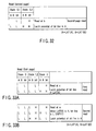
- FIG. 32 is a table showing the second-page read operation
- FIGS. 33A and 33B are tables showing the first-page read operation
- FIG. 34 is a waveform diagram showing the sequence for the second-page read operation
- FIG. 35 is a waveform diagram showing the sequence for the second-page read operation
- FIG. 36 is a waveform diagram showing the sequence for an erase operation
- FIG. 37 is a waveform diagram showing the sequence for a double-speed erase operation
- FIG. 38 is a flowchart schematically showing an autoerase operation
- FIG. 39 is a waveform diagram showing the sequence for an erase operation
- FIG. 40 is a waveform diagram showing the sequence for an erase verify operation
- FIG. 41 shows the configuration of a voltage setting circuit in the control voltage generating circuit of FIG. 1;
- FIG. 42 is a circuit diagram of a data storage circuit according to a second embodiment of the present invention.
- FIG. 43 is a waveform diagram showing the sequence for the operation of the first-page and second-page simultaneous program
- FIG. 44 is a table showing the operation of the first-page and second-page simultaneous program
- FIGS. 45A, 45 B, 45 C, and 45 D are tables showing the operation of the first-page and second-page simultaneous program
- FIG. 46 is a flowchart showing the operation of the first-page and second-page simultaneous program.
- FIG. 47 is a waveform diagram showing the sequence for the operation of the first-page and second-page double-speed simultaneous program.
- FIG. 1 shows the configuration of a semiconductor memory device according to a first embodiment of the present invention.
- the semiconductor memory device will be explained briefly by reference to FIG. 1 .
- a memory cell array 1 includes a plurality of bit lines (not shown), a plurality of word lines (not shown), and a common read line (not shown).
- electrically rewritable memory cells are arranged in a matrix.
- the inside of each memory cell array 1 is divided into a plurality of blocks and a plurality of redundancy blocks as explained later.
- a data storage section 2 is provided at one end of each memory cell array 1 in the direction of column.
- a block select section 6 is provided on each side of each memory cell array 1 in the direction of row.
- the data storage section 2 includes a plurality of data storage circuits as described later. Each data storage circuit has the following functions: (1) reading the data from a memory cell in the memory cell array via a bit line; (2) sensing the state of a memory cell in the memory cell array 1 via a bit line; and (3) applying a write control voltage to a memory cell in the memory cell array 1 via a bit line and writing data into the memory cell.
- a column decoder 3 , an input buffer 7 , and an output buffer 4 are connected to each data storage section 2 .
- the input buffer 7 and output buffer 4 are connected to an I/O terminal 5 .
- Each of the column decoders 3 selects a data storage circuit in the data storage section 2 .
- the data in the memory cell read by the data storage circuit selected by the column decoder 3 is outputted via the output buffer 4 from the I/O terminal 5 to the outside world.
- the write data inputted from the outside world to the I/O terminal 5 is supplied via the input buffer 7 to the data storage circuit 2 selected by the column decoder 3 .
- a control section 15 controls the output buffer 4 , input buffer 7 , an ECC code generating circuit 8 , a control circuit 13 , a command register 16 , a column address register 17 , and a row address register 18 .
- the control section 15 further includes a write inhibit circuit 15 a for inhibiting a ROM block explained later from being written into and an erase inhibit circuit 15 b for inhibiting the ROM block from being erased from.
- the control section 15 further includes a fuse for switching the setting mode of the semiconductor memory device as described later.
- the ECC code generating circuit 8 generates ECC (error correction code) under the control of the control section 15 and supplies the ECC to the input buffer 7 .
- the command register 16 supplies the command supplied from the input buffer 7 to the control circuit 13 . According to the command, the control circuit 13 controls each section.
- a control voltage generating circuit 14 is connected to the control circuit 13 .
- the control voltage generating circuit 14 which is composed of, for example, a charge pump circuit, generates the voltage necessary to write, read, or erase the data.
- the column address register 17 supplies the address supplied from the input buffer 7 to a column RD (redundancy) decoder and a column predecoder 10 .
- the column RD (redundancy) decoder and a column predecoder 10 not only decode a column redundancy address but also predecode a column address.
- the output signal of the column RD decoder and column predecoder 10 is supplied to each of the column decoders 3 .
- the row address register 18 supplies the address supplied from the input buffer 7 to the CG (control gate) driving circuit 9 and array block latch circuit 19 .
- the CG driving circuit 9 selects the potential of the word line generated by the control voltage generating circuit 14 according to the row address supplied from the row address register 18 and supplies the selected potential to the block select section 6 .
- a block decoder 12 is connected to the block select section 6 .
- a block RD (redundancy) decoder 11 and a ROM block specifying circuit 20 are connected to the block decoder 12 .
- the array block latch circuit 19 is connected to the block RD decoder 11 .
- the row address register 18 is connected to the array block latch circuit 19 .
- the block select section 6 selects a block in the memory cell array 1 according to the output signals of the array block latch circuit 19 , block RD decoder 11 , and block decoder 12 . Furthermore, the block select section 6 selects a transfer gate explained later according to the row address in reading, writing, or erasing the data and supplies the voltage supplied from the CG driving circuit 9 to a word line in the memory cell array 1 .
- the ROM block specifying circuit 20 specifies a redundancy block in the memory cell array as a ROM block. That is, in the first embodiment, any redundancy block in the memory cell array can be specified as a ROM block.
- a recognition code or the like for security is written during the manufacturing process. For this reason, the ROM block is so constructed that it is not selected in a test, such as simultaneous writing or simultaneous erasing.
- FIG. 2 shows the configuration of the memory cell array 1 and data storage section 2 of FIG. 1 .
- the data storage section 2 includes a plurality of data storage circuits 31 0 , 31 1 to 31 n/2 .
- the data storage circuits 31 0 , 31 1 to 31 n/2 which are connected to the input buffer 4 and output buffer 7 , are controlled by the column select signals CSL 0 , CSL 1 to CSLn/ 2 supplied from the column decoder 3 .
- bit lines BL 0 , BL 1 are connected to the data storage circuit 31 0
- bit lines BL 2 , BL 3 are connected to the data storage circuit 31 1
- bit lines BLn, BLn+1 are connected to the data storage circuit 31 n/2n .
- a NAND cell is composed of series-connected memory cells M 0 to M 15 made up of, for example, 16 EEPROMs, a first select gate S 1 connected to memory cell M 15 , and a second select gate S 2 connected to memory cell M 0 .
- the first select gate S 1 is connected to bit line BL 0 and second select gate S 2 is connected to source line CELSRC.
- the control gates of the memory cells M 0 to M 15 provided in each row are connected in common to the word lines WL 0 to WL 15 .
- the first select gate S 1 is connected in common to a select line SGD 1 .
- the second select gate S 2 is connected in common to a select line SGD 2 .
- one of the two bit lines (BLi, BLi+1) connected to the data storage circuit is selected by an externally specified address. Furthermore, one word line is selected by the external address. In the case of binary values, cells for one page are selected. In the case of quadrual data, cells for two pages shown in FIG. 2 by a dashed line are selected.
- the erase operation is carried out in blocks shown by a dotted line in FIG. 2 . That is, the data is erased in blocks.
- a block is composed of a plurality of NAND cells.
- the erase operation is performed simultaneously on the two bit lines (BLi, BLi+1) connected to the data storage circuit.
- a verify read operation is performed on one (BLi) of the two bit lines (BLi, BLi+1) connected to the data storage circuit in a single operation. Thereafter, a verify read operation is carried out on the other bit line (BLi+1).
- FIGS. 3A and 3B are sectional views of a memory cell and a select transistor.
- FIG. 3A shows a memory cell.
- n-type diffused layers 42 are formed as the source and drain of a memory cell.
- a floating gate 44 is formed via a gate insulating film 43 .
- a control gate 46 is formed via an insulating film 45 above the floating gate 44 .
- FIG. 3B shows a select transistor.
- n-type diffused layers 47 are formed as the source and drain of a select transistor.
- a control gate 49 is formed via a gate insulating film 48 .
- FIG. 4 is a sectional view of a NAND cell in the memory cell array.
- a NAND cell is composed of 16 memory cells M 0 to M 15 connected in series. Each memory cell is constructed as shown in FIG. 3 A.
- a first select gate S 1 and a second select gate S 2 are provided respectively.
- Each of the first select gate s 1 and second select gate s 2 has the configuration shown in FIG. 3 B.
- FIG. 5 is a circuit diagram showing the configuration of the data storage circuit 31 0 in FIG. 2 . Since all the data storage circuits have the same configuration, only the data storage circuit 31 0 will be explained.
- One end of the current path of an n-channel transistor 61 a is connected to bit line BLi.
- Signal BLTR is supplied to the gate of the transistor 61 a.
- the other end of the current path of the transistor 61 a is connected to one end of the current path of a transistor 61 b and one end of the current path of a transistor 61 c.
- the other end of the current path of the transistor 61 b is connected to a terminal 62 a.
- Voltage VBLA is supplied to the terminal 62 a.
- Signal PREA is supplied to the gate of the transistor 61 b.
- Signal BLSA is supplied to the gate of the transistor 61 c.
- One end of the current path of an n-channel transistor 61 d is connected to bit line BLi+1.
- the signal BLTR is supplied to the gate of the transistor 61 d.
- the other end of the current path of the transistor 61 d is connected to one end of the current path of a transistor 61 e and one end of the current path of a transistor 61 f.
- the other end of the current path of the transistor 61 e is connected to a terminal 62 b.
- Voltage VBLB is supplied to the terminal 62 b.
- Signal PREB is supplied to the gate of the transistor 61 e.
- Signal BLSB is supplied to the gate of the transistor 61 f.
- the transistors 61 b, 61 e precharge the unselected bit lines to the potentials VBLA, VBLB according to the signals PREA, PREB, respectively.
- the transistors 61 c, 61 f select a bit line according to the signals BLSA, BLSB, respectively.
- the other ends of the current paths of the transistors 61 c, 61 f are connected via a transistor 61 g to not only a terminal 62 c but also a node NE.
- Signal BIAS is supplied to the gate of the transistor 61 g.
- Voltage VCC is supplied to the terminal 62 c.
- the transistor 61 g precharges a bit line according to signal BIAS in reading the data.
- One end of the current path of a transistor 61 h is connected to the node NE.
- Signal BLC 1 is connected to the gate of the transistor 61 h.
- a terminal 62 d is connected via a p-channel MOS transistor 61 m to the other end of the current path of the transistor 61 h.
- Voltage VCC is supplied to the terminal 62 d.
- Signal PRSTB 1 is supplied to the gate of the transistor 61 m.
- a first latch circuit LAT(A) is connected to the other end of the current path of the transistor 61 h.
- the first latch circuit LAT(A) is composed of two clocked inverter circuits 61 i, 61 j.
- the clocked inverter circuit 61 i is controlled by signals SEN 1 , SEN 1 B (B means an inverted signal).
- the clocked inverter circuit 61 j is controlled by signals LAT 1 , LAT 1 B.
- the first latch circuit LAT(A) latches the writing data.
- One end of the current path of an n-channel MOS transistor 61 o is connected to the output node NB of the clocked inverter circuit 61 j and the junction node NC of the input terminal of the clocked inverter circuit 61 i.
- the other end IO of the current path of the transistor 61 o is connected to the input buffer 7 and output buffer 4 .
- One end of the current path of an n-channel MOS transistor 61 n is connected to the output node NA of the clocked inverter circuit 61 i and the junction node of the input terminal of the clocked inverter circuit 61 j.
- the other end IOB of the current path of the transistor 61 n is connected to the input buffer 7 and output buffer 4 .
- the column decoder 3 supplies a column select signal CSL to the gates of the transistors 61 o, 61 n.
- Transistors 61 k, 61 l are connected in series with the node NE.
- the gate of the transistor 61 k is connected to the node NC of the first latch circuit LAT(A).
- Signal VRFY 1 is supplied to the gate of the transistor 61 l.
- Signal VREG is supplied to the current path of the transistor 61 l.
- the transistors 61 k, 61 l set the potential of the bit line according to the data latched in the first latch circuit LAT(A).
- one end of the current path of a transistor 61 q is connected to the node NE.
- Signal BLC 2 is supplied to the gate of the transistor 61 q.
- a terminal 62 e is connected via a p-channel MOS transistor 61 p to the other end of the current path of the transistor 61 q.
- Voltage VCC is supplied to the terminal 62 e.
- Signal PRSTB 2 is supplied to the gate of the transistor 61 p.
- a second latch circuit LAT(B) is connected to the other end of the current path of the transistor 61 q.
- the second latch circuit LAT(B) is composed of two clocked inverter circuits 61 r, 61 s.
- the clocked inverter circuit 61 r is controlled by signals SEN 2 , SEN 2 B.
- the clocked inverter circuit 61 s is controlled by signals LAT 2 , LAT 2 B.
- the second latch circuit LAT(B) latches the data read from a memory cell.
- Transistors 61 t, 61 u are connected in series with the node NE.
- the gate of the transistor 61 t is connected to the node ND of the second latch circuit LAT(B).
- Signal VREY 2 is supplied to the gate of the transistor 61 u.
- Signal VREG is supplied to the current path of the transistor 61 u.
- the transistors 61 t, 61 u set the potential of the bit line according to the data latched in the second latch circuit LAT(B).
- FIGS. 6A, 6 B, 6 C, and 6 D show the relationship between the address read in each mode and the I/O terminal. It is assumed that the semiconductor memory device of the first embodiment enables the memory cell array to be switched between, for example, four modes. Switching between the four modes is realized by blowing, for example, a fuse (not shown) provided in the control section 15 .
- FIG. 6A shows a case where 1 G (giga) bits are stored using a quadrual data storing technique whereby two bits are stored in a cell in a 32-KB block size mode.
- FIG. 6B shows a case where 512 M (mega) bits are stored using a binary data storing technique whereby one bit is stored in a cell in a 16-KB block size mode.
- FIG. 6C shows a case where 1 G (giga) bits are stored using a quadrual data storing technique in a 128-KB block size mode.
- FIG. 6D shows a case where 512 M (mega) bits are stored using a binary data storing technique in a 64-KB block size mode.
- the read or program operation takes in a column address, block address, and the like in four cycles.
- the erase operation need not take in a column address, so that the first cycle is omitted and the address is inputted in three cycles, from the second cycle to the fourth cycle.
- Switching between the column addresses A 8 , A 8 E shown in FIG. 6A is effected by a command and the resulting column address is inputted.
- the signal ALE and signal CLE from the control section 15 of FIG. 1 are both made low, the data supplied to the I/O terminal 5 is taken in as data when the signal WE rises or falls.
- the data is supplied to the data storage circuit selected by the column decoder 3 . Toggling the signal WE consecutively causes the column address to be incremented, thereby taking in the data in the next address sequentially.
- the signal ALE and signal CLE from the control section 15 of FIG. 1 are both made low.
- the signal RE rises or falls, the data in the data storage circuit selected by the column decoder 3 is outputted at the I/O terminal 5 .
- Toggling the signal RE repeatedly causes the address to be incremented, thereby outputting the data in the next address sequentially.
- FIGS. 7A and 7B are tables to help explain the operation of the predecoder and column RD decoder 10 .
- the column address register 17 of FIG. 1 not only latches the addresses A 0 to A 8 , A 8 E externally specified but also increments the address in synchronization with signal WE and signal RE.
- ECC ECC
- 21 columns have to be added to the 528 columns of the column address to store an ECC code. That is, for example, to correct two bits, 21 bits of cells for a correction code are necessary for one page (528 bits). Of the 21 columns, four columns are shared with the column redundancies. As a result, the column address is increased by 17 columns.
- the column predecoder and column RD decoder 10 decode the column addresses A 0 to A 8 , A 8 E and output column predecode signals CA 0 to CA 7 , CB 0 to CB 7 , and CC 0 to CC 8 . In this way, 528+17 columns are selected.
- the column predecode signal is stopped and column redundancy select signals CSS 0 to CSS 7 are outputted.
- ECC error code code
- eight column redundancies are present for one array.
- ECC ECC is used, four redundancies are present for one array, 17 columns are selected by the signal CA 0 to CA 7 , CB 0 to CB 8 , and four columns are selected by the signals CSS 0 to CSS 3 .
- the column decoder 3 selects one from the 528 columns.
- the signals CSS 0 to CSS 7 select directly one column without being decoded.
- the row address register 18 of FIG. 1 latches the addresses A 9 to A 26 externally specified.
- FIGS. 8A, 8 B, and 8 C show the CG driving circuit 9 of FIG. 1 .
- the circuit of FIG. 8 A and that of FIG. 8B generate a select CG voltage Vcgsel and an unselect CG voltage Vcgusel respectively.
- the select CG voltage Vcgsel is set to a voltage Vcgrv in the read operation and to a voltage Vpgmh in the program operation.
- the unselect CG voltage Vcgusel is set to a voltage Vread in the read operation and to a voltage of Vpass in the program operation.
- FIG. 8A shows a circuit for generating the potential of the selected control gate line.
- the circuit is composed of boost circuits 81 a, 81 b and transistors 81 c, 81 d.
- a program voltage Vpgmh supplied from the control voltage generating circuit 14 is supplied to one end of the current path of the transistor 81 c.
- the output terminal of the boost circuit 81 a is connected to the gate of the transistor 81 c.
- the program voltage Vpgmh and signal VPGMEN are supplied to the boost circuit 81 a.
- the boost circuit 81 a generates a voltage Vpgmh+Vth according to the signal VPGMEN, which enables the transistor 81 c to output the voltage Vpgmh.
- the voltage Vcgrv supplied from the control voltage generating circuit 14 is supplied to one end of the current path of the transistor 81 d.
- the output terminal of the boost circuit 81 b is connected to the gate of the transistor 81 d.
- the voltage Vcgrv and signal VCGREN are supplied to the boost circuit 81 b.
- the boost circuit 81 b generates a voltage Vcgrv+Vth according to the signal VCGREN, which enables the transistor 81 d to output the voltage Vcgrv.
- the other ends of the current paths of the transistors 81 c, 81 d are connected to each other at the connection node. From the connection node, the select CG voltage Vcgsel made up of the voltage Vpgmh or voltage Vcgrv is outputted.
- FIG. 8B shows a circuit for generating the potential of the unselected control gate line.
- the circuit is composed of boost circuits 82 a, 82 b and transistors 82 c, 82 d.
- the voltage Vpass supplied from the control voltage generating circuit 14 is supplied to one end of the current path of the transistor 82 c.
- the output terminal of the boost circuit 82 a is connected to the gate of the transistor 82 c.
- the voltage Vpass and signal VPASSENB are supplied to the boost circuit 82 a.
- the boost circuit 82 a generates a voltage Vpass+Vth according to the signal VPASSENB, which enables the transistor 82 c to output the voltage Vpass.
- the voltage Vreadh supplied from the control voltage generating circuit 14 is supplied to one end of the current path of the transistor 82 d.
- the output terminal of the boost circuit 82 b is connected to the gate of the transistor 82 d.
- the voltage Vreadh and signal VREADEN are supplied to the boost circuit 82 b.
- the boost circuit 82 b generates a voltage Vreadh+Vth according to the signal VREADEN, which enables the transistor 82 d to output the voltage Vreadh.
- the other ends of the current paths of the transistors 82 c and 82 d are connected to each other at a connection node. From the connection node, an unselect CG voltage Vcgusel made up of the voltage Vpass or Vreadh is outputted.
- FIG. 8C shows a CG supply circuit for supplying a select CG voltage Vcgsel or an unselect CG voltage Vcgsel to a control gate. Sixteen units of the CG supply circuit are provided so as to correspond to the control gates. On the basis of address A 11 to address A 14 , one of them is brought into the selected state and the remaining 15 CG supply circuits are made unselected.
- the CG supply circuit is composed of a decode circuit 83 a, an inverter circuit 83 b, boost circuits 83 c, 83 d, and transistors 83 e, 83 f, 83 g.
- Address A 11 to address A 14 are supplied to the input terminal of the decode circuit 83 a.
- the boost circuit 83 c turns on the transistor 83 e, thereby outputting the select CG voltage Vcgsel as a control gate voltage VCGi.
- the boost circuit 83 d turns on the transistor 83 f, thereby outputting the unselect CG voltage Vcgsel as a control gate voltage VCGi.
- the signal ERASEEN is made high, thereby turning on the transistor 83 g, which forces all the control gate voltages VCG 0 to VCG 15 to the ground potential.
- FIG. 8D shows the relationship between address A 11 to address A 14 and the control gate voltage VCGi.
- FIG. 8D shows that one control gate voltage VCGi is outputted on the basis of address A 11 to address A 14 .
- control gate voltage VCGi is switched in two stages of the circuits shown in FIGS. 8A and 8B and that in FIG. 8 C.
- each of the CG supply circuits can output all the necessary potentials for read, program, and erase operations.
- using the two-stage circuit configuration makes the size of the circuit smaller.
- FIGS. 9A and 9B show one of the array block latch circuits 19 of FIG. 1 .
- the array block latch circuit 19 latches a block address (A 17 to A 26 ) for the corresponding memory cell array.
- the four memory cell arrays are selected using address A 15 and address A 16 .
- the latch signals PBLATPB 0 to PBLATPB 3 of the selected memory cell array go high.
- FIG. 9B is a latch circuit provided in the array block latch circuit 19 .
- the latch circuit is provided so as to correspond to each of block address A 17 to block address A 26 .
- the latch circuit is composed of an inverter circuit 91 a, a NAND circuit 91 b, and NAND circuits constituting a flip-flop circuit.
- the latch circuit latches block addresses A 17 to A 26 when the latch signals PBLATPB 0 To PBLATPB 3 go high.
- FIG. 10 shows the operation of the block RD decoder 11 of FIG. 1 .
- the block RD decoder 11 When the block addresses A 17 to A 26 supplied from the array block latch circuit 19 coincide with the block redundancy addresses APB 17 to APB 26 set by the fuse, the block RD decoder 11 outputs the addresses ATPB 17 to ATPB 26 and a signal ATPBD for selecting the redundancy area.
- the addresses ATPB 17 to ATPB 26 and signal ATPBD are used to select one of the block redundancies.
- FIG. 10 shows a case where the block addresses A 17 to A 26 have coincided with the block redundancy addresses APB 17 to APB 26 .
- the block RD decoder 11 brings block address ATPB 18 and the signal ATPBRD for selecting the redundancy area into the high level to select the block redundancy in, for example, ATPB 18 .
- FIG. 11 shows the operation of the block decoder 12 of FIG. 1 .
- the block decoder 12 decodes the block addresses ATPB 17 to ATPB 26 and ATPBRD supplied from the block RD decoder 11 and outputs row decode signals AROWA to AROWE and RDECPBLR as shown in FIG. 11 .
- the row decode signals AROWA to AROWE are for selecting a block in the memory cell array 1 .
- RDECPBLR is a signal for selecting one of the block select sections 6 provided on both sides (on the right and left sides) of the memory cell array 1 .
- the block decoder 12 decodes the block address supplied from the ROM block specifying circuit 20 as described above and generates row decode signals AROWA to AROWE for selecting a ROM block.
- FIG. 12 shows the configuration of the block select circuit 6 a in the block select section 6 of FIG. 1 .
- the block select circuit 6 a is provided for each block.
- the fuse state sensing circuit 6 b of FIG. 12 is provided for each memory cell array 1 .
- a power supply voltage VDD is supplied to a terminal 100 .
- a p-channel MOS transistor 101 and n-channel MOS transistors 102 to 108 are connected in series between the terminal 100 and a node to which signal ROWCOM is supplied.
- the signal RDECPBLR is supplied to the gate of the transistor 101 .
- the signal RDECPBLR is a signal for selecting either the right-side or left-side block select section 6 of the memory cell array 1 .
- the row decode signals AROWA to AROWE are supplied to the gates of the transistors 102 to 106 .
- Signal RDECPBLRD is supplied to the gate of the transistor 107 .
- Signal RDECPBL changes a little later than the signal RDECPBLRD as shown in FIG. 13 .
- a command signal CD_ROMBA for accessing a ROM block is supplied to the gate of the transistor 108 .
- a fuse 109 is connected in parallel with the transistor 108 . The fuse 109 is blown, when the block corresponding to the block select circuit 6 a is a faulty block.
- a series circuit of p-channel MOS transistors 117 , 118 is connected in parallel with the transistor 101 .
- the gate of the transistor 117 is grounded (in the figure, the downward arrow means grounding).
- the input terminal of an inverter circuit 119 is connected to the connection node of the transistors 101 , 102 , 118 .
- the output terminal of the inverter circuit 119 is connected not only to the gate of the transistor 118 but also to one input terminal of a level shifter 120 .
- a signal VRDEC is supplied to the other input terminal of the level shifter 120 .
- the signal VRDEC is a signal for controlling the level shifter 120 according to the operation of programming, reading, or erasing the data.
- the level shifter 120 When the block select circuit 6 a has been selected, the level shifter 120 generates a signal for driving the transfer gate TG according to the signal VRDEC.
- the transfer gate TG includes transfer gates TG 0 to TG 15 connected to the word lines of the memory cells and transfer gates TGS 1 , TGS 2 connected to first and second select gates S 1 , S 2 .
- Control gate lines CG 0 To CG 15 are connected to the one-end sides of the current paths of the transfer gates TG 0 To TG 15 , respectively.
- Word lines WL 0 To WL 15 are connected to the other ends of the current paths, respectively.
- the CG driving circuit 9 supplies the control gate voltage VCG to the control gate lines CG 0 To CG 15 .
- Select gate lines SGD, SGS are connected to the one-end sides of the current paths of transfer gates TGS 1 , TGS 2 , respectively.
- Select lines SGD 1 , SGD 2 are connected to the other ends of the current paths.
- the control voltage generating circuit 14 supplies a specific voltage to the select lines SGD 1 , SGD 2 .
- n-channel MOS transistors 121 , 122 are connected in series.
- Signal SGDSPBLR is supplied to one end of the current path of the transistor 121 .
- Signal RDECADin+1n is supplied to the gate of the transistor 121 .
- Further supplied via an inverter circuit 123 to the gate of the transistor 122 is the output signal RDECADn of the inverter circuit 119 .
- One end of the current path of an n-channel MOS transistor 124 is connected to the select line SGD 2 .
- the signal SGDSPBLR is supplied to the other end of the current path of the transistor 124 .
- the signal RDECADn is supplied to the gate of the transistor 124 .
- the node to which the signal ROWCOM is supplied is not only grounded via an n-channel MOS transistor 110 but also connected to the gate of an n-channel MOS transistor 111 .
- Signal ROWCOMVSS is supplied to the gate of the transistor 110 .
- One end of the current path of the transistor 110 is connected to the input terminal of an inverter circuit 112 and the output terminal of an inverter circuit 113 .
- the other end of the current path is grounded.
- the output terminal of the inverter circuit 112 and the input terminal of the inverter circuit 113 are connected to the input terminal of an inverter circuit 114 .
- the output terminal of the inverter circuit 114 outputs a signal FUSECUT for indicating whether or not the fuse has been blown.
- the signal FUSECUT is supplied to the control section 15 .
- the input terminal of the inverter circuit 114 is grounded via an n-channel MOS transistor 115 .
- Signal BUSY is supplied via an inverter circuit 116 to the gate of the transistor 115 .
- Signal RDECPBLR, signal RDECPBLRD, signal CMD_ROMBA, and signal ROWCOM are normally at the ground potential VSS, which makes the output signal RDECAD of the inverter circuit 119 low.
- the signal RDECPBLR corresponding to either the right side or the left side of the selected memory array goes high.
- all the row decode signals AROWA to AROWE go high, making the output signal RDECAD of the inverter circuit 119 high, which activates the level shifter 120 .
- the level shifter 120 outputs a program voltage of Vpgm+Vth (Vth is the threshold voltage of the transfer gate) in a program operation, a read voltage of Vread+Vth in a read operation, or a power-supply voltage of VDD in an erase operation.
- the level shifter 120 generates such voltages, thereby enabling the transfer gate to transfer the voltage from the CG driving circuit 9 as it is.
- any one of the row decode signals AROWA to AROWE goes low, which brings the block select circuit 6 a into the unselected state.
- the output voltage of the level shifter 120 goes to the ground voltage VSS. Therefore, in a read operation or program operation, the word lines WL 0 to WL 15 go to the floating state.
- the select lines SGD 1 , SGD 2 go to the ground potential VSS.
- the word lines WL 0 To WL 15 are brought into the floating state and the voltage SGDSPBLR is set at the power-supply voltage VDD.
- the potential of the select lines SGD 1 , SGD 2 becomes VDD-Vth.
- both the word lines WL 0 To WL 15 and select lines SGD 1 , SGD 2 go to potentials close to the erase voltage VERA.
- the fuse 109 of FIG. 12 is blown as described above.
- all the row decode signals AROWA to AROWE are made high. Since the fuse 109 has been blown, however, the output signal RDECAD of the inverter circuit 119 goes low, which prevents the faulty block from being selected.
- the faulty block in the partially good product has been accessed, when the fuse 109 has been blown, the faulty block is not selected.
- the cells are off.
- the read data becomes data “0” automatically.
- the read data becomes data “0” on the quadrual-data second page, whereas the read data becomes data “1” on the quadrual-data first page.
- the signal ROWCOWVSS is made low temporarily and ROWCOM is brought into the floating state.
- FIG. 13 shows a sequence for the operation of sensing the state of the fuse 109 of FIG. 12 .
- signal ROWCOMVSS and signal RDECPBLRD are made high.
- the latch circuit composed of the inverter circuits 112 , 113 remains in the latched state. As a result, when the fuse 109 has been blown, any block is not selected.
- FIG. 14 shows a physical mapping of the memory cell array, where the physical locations to be selected are indicated by addresses.
- Each memory cell array 1 includes blocks blk 0 To blk 23 and block redundancies blkRD 0 To blkRD 9 as redundancy blocks. Any of the block redundancies blkRD 0 To blkRD 9 can be used as a ROM block.
- the block redundancy blkRD 1 when the command signal CD_ROMBA for accessing the ROM block is inputted, the block RD decoder 11 of FIG. 1 does not output a signal.
- the ROM block specifying circuit 20 outputs signals A 16 to A 26 for selecting a block redundancy and signal ARD, and then outputs row decode signals AROWA to AROWE so as to select the first block redundancy.
- the fuse 109 of the ROM block is normally blown. The reason is that the data is written in the ROM block in a die sort test. Therefore, in a subsequent simultaneous program or simultaneous erase operation, the ROM block is prevented from being selected.
- the command signal CMD_ROMBA is made high in FIG. 12, turning on the transistor 108 , which brings the ROM block into the selected state, even when the fuse 109 has been blown.
- FIG. 15A shows the write inhibit circuit 15 a for a ROM block provided in the control section 15 of FIG. 1 .
- FIG. 15B shows the erase inhibit circuit 15 b for the ROM block 20 .
- the write inhibit circuit 15 a is composed of p-channel MOS transistors 151 a, 151 b, an n-channel MOS transistor 151 c, a fuse 151 d, inverter circuits 151 e, 115 f, 151 h, and a NOR circuit 151 g.
- the power supply voltage VDD is supplied to one end of the current path of each of the transistors 151 a, 151 b.
- the other ends of the current paths of them are connected to each other at a junction node.
- the transistor 151 c and fuse 151 d are connected.
- Signal LOWVDDn is supplied to the gates of the transistor 151 a and transistor 151 c.
- the junction node is connected via the inverter circuit 151 e to one input end of the NOR circuit 151 g.
- Command signal CMD_ROMBA is supplied via the inverter circuit 151 f to the other input terminal of the NOR circuit 151 g.
- the output terminal of the NOR circuit 151 g is connected to the input terminal of the inverter circuit 151 h.
- Signal PROENABL is outputted from the output terminal of the inverter circuit 151 h.
- the erase inhibit circuit 15 b of FIG. 15B has the same configuration as that of the write inhibit circuit 15 a. Specifically, the power supply voltage VDD is supplied to one end of the current path of each of the transistors 152 a, 152 b. The other ends of the current paths of them are connected to each other at a junction node. Between the junction node of the transistors and the ground, the transistor 152 c and fuse 152 d are connected. Signal LOWVDDn is supplied to the gates of the transistor 152 a and transistor 152 c. The junction node is connected via the inverter circuit 152 e to one input end of the NOR circuit 152 g.
- Command signal CMD_ROMBA is supplied via the inverter circuit 152 f to the other input terminal of the NOR circuit 152 g.
- the output terminal of the NOR circuit 152 g is connected to the input terminal of the inverter circuit 152 h.
- Signal ERAENABL is outputted from the output terminal of the inverter circuit 152 h.
- the signal LOWVDDn goes low temporarily when the power supply is turned on and thereafter is made high.
- output signal PROENABL and output signal ERAENABL are always high, which enables both a program operation and an erase operation.
- both of the output signals PROENABL, ERAENABL go low, which prevents the ROM block from being written into or erased from.
- the blowing of the fuse 151 d or 152 d can be set arbitrarily.
- the data in a memory cell and the threshold value of the memory cell are defined as shown in FIGS. 16 and 17A.
- the states “0” to “3” of the data in a memory cell have been defined in ascending order, from the lowest to the highest threshold value.
- the threshold voltage of the memory cell shifts toward a higher one.
- FIG. 16 shows a writing method according to the present invention.
- the data on the first page is first written into memory cells and then the data on the second page is written into memory cells.
- the threshold voltage of the memory cells do not change according to the write operation, with the result that the data in the memory cells remains unchanged. That is, no data is written into the memory cells.
- the threshold voltage of the memory cells is changed as a result of the write operation, with the result that the data in the memory cells is also changed. That is, the data is written into the memory cells.
- the data in a memory cell in the erased state is in state “0.” In this state, the data on the first page is first written into the memory cells. When the writing data is “1,” the data in the memory cells into which no data has not been written remain in state “0.” When the writing data is “0,” the data in the memory cells into which the data has been written is brought into state “1.”
- the data on the second page is written into the memory cells.
- the writing data “0” is supplied to the memory cells whose data is in state “1” in the first-page write operation
- the data in the memory cells is brought into state “2.”
- the writing data “0” is supplied to the memory cells whose data is in state “0” in the first-page write operation
- the data in the memory cells go to state “3.”
- the writing data “1” When the writing data “1” is externally supplied to the memory cells whose data is in state “1” in the first-page write operation, the data in the memory cells is allowed to remain in state “1.”
- the writing data “1” When the writing data “1” is externally supplied to the memory cells whose data is in state “0” in the first-page write operation, the data in the memory cells is allowed to remain in state “0.”
- the data on the first page and second page is set to “0,” “0” as shown in FIGS. 16 and 17A.
- the data on the first and second page is set to “1,” “0.”
- the data on the second page is first read and then the data on the first page is read.
- the reading of the data on the second page can be judged in only one operation that determines whether the data in the memory cells is in state “1” or less or in state “2” or more.
- the data on the first page when the data in the memory cells is in state “0” or state “3,” the read data is “1.” When the data in the memory cells is in state “1” or state “2,” the read data is “0.” Therefore, the data on the first page can be read on the basis of the judgment whether the data in the memory cells is in state “0” or state “1” or more and the judgment whether the data in the memory cells is in state “2” or less or state “3.” That is, the data on the first page can be read in a total of two operations.
- the data in the memory cells goes to state “0.” Even when any of the first and second pages is specified in an address, the read data is “1.”
- address A 9 Switching between the two bits (the first and second pages) is done by address A 9 . For example, when address A 9 is made low, this specifies the first page. When address A 9 is made high, this specifies the second page.
- the threshold voltage of the memory cells must be controlled accurately according to the writing data. Therefore, when the data is written into the memory cells, the voltage applied to the control gates of the memory cells is increased gradually.
- a writing method is called a step-up writing method.
- FIG. 18 shows a writing characteristic of the step-up writing method for the memory cells.
- the threshold voltage of a cell is shown on the ordinate axis and the write voltage (or program voltage) is shown on the abscissa axis.
- the threshold voltage of a cell after erasing (the data in a memory cell is in state “0”) is set at, for example, ⁇ 3.5 V.
- an initial program voltage of 16 V is applied to the control gate of the cell.
- the threshold voltage rises along the curve “0” ⁇ “3” in the figure.
- writing is started with an initial write voltage of 14 V.
- the threshold voltage of state “1” is 0.2 V. Therefore, when writing is started with the 16 V initial write voltage, the data reaches the threshold voltage of state “1” between the third step and fourth step, which might result in overprogram. To avoid this, the initial write voltage is set at 14 V.
- the data in the memory cell changes from state “0” to state “1.” Therefore, after writing is done 13 times, the data in the memory cell has reached state “1.”
- the data in the memory cell is changed as follows: state “0” to state “3” or “0” ⁇ “3” and state “1” to state “2” or “1” ⁇ “2.” At this time, the reason why the state is changed as “0” ⁇ “3” is that, because writing is done above “0” ⁇ “1,” the initial write voltage can be raised to 16 V.
- the initial write voltage is set at 14 V.
- the two consecutive pages can be written into at high speeds.
- the data input command “ 80 h” (h means a hexadecimal number) is first inputted as shown in FIG. 19, thereby setting data “1” (no writing is to be done) in the first latch circuits LAT(A) of all the data storage circuits 31 0 to 31 n/2 . Thereafter, an address and data are inputted according to the signal ALE and the toggling of the signal WE. As a result, the data is supplied serially to the data storage circuit specified by the column address.
- the node NC of the data storage circuit of FIG. 5 goes high.
- the node NC goes low. From this time on, the data in the first latch circuit LAT(A) is assumed to be at the potential of the node NC.
- the autoprogram execute command “10h” is inputted as shown in FIG. 19, thereby starting the autoprogram.
- the ECC code generating circuit 8 creates an ECC code automatically after the input of the command “10h,” and supplies the code to the data storage circuit. Thereafter, the autoprogram operation is started.
- the command “11h” is inputted to output a dummy Busy signal.
- This dummy program outputs a Busy signal for as short a time as 15 ⁇ s.
- ECC code is used, an ECC code is generated after the input of the command “11h.” The code is supplied to the data storage circuit. Therefore, the duration of the Busy signal is longer than 1.5 ⁇ s.
- the command “80h,” address, data, and command “11h” are inputted four times, while the array address (A 15 , A 16 ) is changed each time. Only in the last time, the command “10h” is inputted in place of the command “11h,” thereby executing the autoprogram. In the command “80h” in the second time or later, the first latch circuit LAT(A) is not reset.
- a given block address (A 17 to A 26 ) is inputted each time.
- the row address register 18 of FIG. 1 when the next address is inputted, the preceding address disappears. For this reason, each time a block address is inputted, the array block latch circuit 19 of FIG. 1 latches the block address for each array.
- a program operation is performed. Since the present memory is a multivalued memory, two bits of data are stored in a memory cell. The two bits are allocated to address A 9 as described above. Specifically, when address A 9 is low, the first page is specified. When address A 9 is high, the second page is specified.
- the first-page writing sequence and second-page writing sequence are shown in FIGS. 21 and 22, respectively. With the present memory, the data on the first page is first written and then the data on the second page is written. Using FIGS. 21 and 22, the first-page program and the second-page program will be explained briefly.
- the data set in the individual data storage circuits 31 0 to 31 n/2 is programmed in the memory cells (ST 1 ). Thereafter, a verify read is executed to see if writing is sufficient (ST 2 ). Specifically, the data in the memory cells is read and latched in the first latch circuit LAT(A) of each data storage circuit. Thereafter, in the test process before a faulty block is replaced with a block redundancy, the number of low level data items latched in the first latch circuits LAT(A), or the number of verify files, is counted.
- the count value is equal to or larger than a specified value (in the embodiment, when there are four column redundancies, the specified value is 4, and when there are eight column redundancies, the specified value is 8), the program verify is repeated again.
- the program operation is terminated (ST 4 ).
- step ST 3 and step ST 4 in FIG. 21 and step ST 15 and step ST 16 in FIG. 22 will be omitted.
- FIG. 23 shows a sequence for the operation of each section during the first-page program.
- signal BLC 1 supplied to the gate of the transistor 61 h in the data storage circuit is set to VCC+Vth, signal BLSA to Vpass, and signal BLTR to VCC.
- the potential on the bit line BL goes to VCC.
- the potential on the bit line goes to the ground potential VSS.
- the cells that are connected to the selected word line and belong to the unselected page (whose bit lines are not selected) must not be written into.
- the potential on the bit lines connected to these cells is set to the potential VCC as are the bit lines to which data “1” is supplied.
- the CG driving circuit 9 of FIG. 1 applies VCC to the select line SG 1 , VSS to the select line SG 2 , VPGM (20 V) to the select CG line, and Vpass (10 V) to the unselected word lines. Then, the select line SG 1 in the block (in double speed, each array has such a block) selected by the block select circuit 6 goes to VCC, the select word line to VPGM (20 V), and the unselected word lines to VPASS (10 V).
- VSS the select word line to VPGM (20 V)
- VPASS (10 V) the select word line to VPASS (10 V).
- the bit line is at VSS
- the channel of the cell is at VSS and the word line is at VPGM.
- the cell is programmed.
- the bit line is at VCC
- the channel of the cell is raised to VPGM, not VSS, the channel is set at VPGM/ 2 through charge coupling. Therefore, the cell is not programmed.
- FIG. 24 shows the operation of a program verify read.
- FIG. 25 shows the sequence of each section in the program verify read.
- a potential b′ higher than a potential b in reading is supplied to the selected word line as shown in FIG. 16 .
- ′ indicate a verify potential a little higher than the word line potential in reading.
- voltage Vread is supplied to the unselected word lines and the select line SG 1 in the selected block.
- Signal BIAS supplied to the gate of the transistor 61 g in the data storage circuit of FIG. 5 is made high (1.6 V), thereby precharging the bit line.
- the select line SG 2 on the source side of the memory cell is made high (Vread). Since the memory cell turns off when the threshold voltage of the memory cell is higher than the potential b′, the bit line remains high. When the threshold voltage of the memory cell has not reached the potential b′, the memory cell turns on, making the potential on the bit line low (VSS).
- the low level (data “0”) is latched at the node NA of the first latch circuit LAT(A) of FIG. 5 .
- the high level (data “1”) is latched at the node NA.
- signal VREG supplied to the current path of the transistor 611 is set to VCC and signal VREY 1 supplied to the gate is made high, the bit line is changed from the floating level to the high level and fixed there only when no writing is done.
- the potential on the bit line is read into the first latch circuit LAT(A). It is when the potential of the memory cell has reached the threshold voltage, or when no writing is done, that the high level is latched in the first latch circuit LAT(A). In addition, it is when the potential of the memory cells has not reached the threshold voltage that the low level is latched in the first latch circuit LAT(A).
- the data on the second page is externally supplied.
- the data is stored in the first latch circuit LAT(A) of each of the data storage circuits 31 0 to 31 n/2 .
- the operation of the second-page program differs greatly from the operation of the first-page program in internal data loading (ST 11 ).
- the operation of the second-page program varies according to the result of the operation of the first-page program.
- the operation of the second page varies according to the result of the operation of the first-page program. For this reason, before the data on the second page is written into the cells, it is necessary to check whether the data in the memory cells is in state “0,” or “1” and store the checked state. To achieve this, internal data loading is done (ST 11 ). In the internal data loading, the data in the memory cells is read and loaded into the second latch circuit LAT(B) of each data storage circuit in FIG. 5 . Furthermore, in the internal data loading, the potential a in FIG. 16 is supplied to the word lines, thereby performing a read operation. The result of the reading is stored in the second latch circuit LAT(B) of each data storage circuit.
- FIG. 26A is a table showing the operation in internal data loading.
- FIG. 27 shows the sequence of each section in internal data loading. The operation of internal data loading will be explained by reference to FIGS. 26A and 27.
- the unselected bit line is caused to store the data in the first latch circuit LAT(A) of the data storage circuit in FIG. 5 . Then, the potential a is applied to the word line, thereby carrying out a read operation. The result of the read operation is stored in the first latch circuit LAT(A).
- the data in the memory cell is “0,” data “0” is latched in the first latch circuit LAT(A).
- data “1” is stored in the first latch circuit LAT(A).
- a second-page verify includes a first verify read (ST 13 ) and a second verify read (ST 14 ).
- first verify read ST 13
- second verify read ST 14
- FIG. 26B is a table showing the operation of a second-page first verify read.
- FIG. 28 shows the sequence of each section in the second-page first verify read.
- the potential b′ is applied to the word line, thereby performing a read operation as shown in FIG. 16 .
- the bit line goes high.
- the threshold voltage of the memory cell has not reached b′, the bit line goes low.
- the cell that brings the data in the memory cell into state “3” is also turned off.
- “verify OK” is given.
- the potential on the bit line connected to the memory cell whose data is in state “0” without being written in the first-page writing operation is made low.
- the node ND of the second latch circuit LAT(B) is made high in the internal data loading.
- the signal VREG supplied to the current path of the transistor 61 u of FIG. 5 is set to the ground voltage VSS as shown in FIG. 28 and the signal VRFY 2 supplied to the gate is made high.
- the transistor 61 t turns on, forcing the bit line low.
- the signal VREG is set to the power-supply voltage VCC and the signal VRFY 1 supplied to the gate of the transistor 611 is made high. Then, when the high level is latched at the node NC of the first latch circuit LAT(A) (or when no writing is to be done), the transistor 61 k turns on. As a result, the bit line goes high. After the operation, the potential on the bit line is read into the first latch circuit LAT(A).
- FIG. 26C is a table showing the second-page second verify read operation.
- FIG. 25 shows the sequence for each section in the second-page second verify read operation.
- This verify is completely the same as the first-page verify operation.
- the reason is that cells whose potential is higher than the potential c′ in FIG. 16 do not exist except for the cell that brings the data into state “3.”
- the potential a′ has been applied to the word line to verify whether the data in the memory cell has become state “1.”
- the potential c′ is applied to the word line to verify whether the data in the memory cell has become state “3.”
- the first verify read and second verify read are carried out.
- the first verify read is performed when the data in the memory cell is brought into state “2.”
- the second verify read is performed when the data in the memory cell is brought into state “3.”
- the write operation is carried out again. In this way, the program operation and verify operation are repeated until the data in all the data storage circuits go high (ST 12 to ST 17 in FIG. 22 ).
- the threshold voltage is high. For this reason, it is difficult to write the data into this memory cell. For this reason, of the repeated program verify operations, the operation of verifying whether the data in the memory cell has reached state “3” can be omitted the first several times. After the verify operation has been repeated several times, the memory cell into which data on state “2” whose threshold voltage is lower than that of state “3” is written should have completed the writing. For this reason, the memory cell into which data on state “2” is written can omit the verify after the program verify file operation has been repeated several times.
- FIG. 29 shows the sequence of a read operation.
- a read operation is started by inputting the read command “00h” and an address as shown in FIG. 29 .
- the data in all the cells on the page specified by the address are read into the data storage circuits 31 0 to 31 n/2 .
- the data storage circuit outputs the data according to the toggling of the signal RE in the order specified by the column address.
- FIG. 30 shows the sequence for a double-speed read operation.
- the data in all the cells on the pages in the four memory cell arrays is read into each data storage circuit in one read operation. Thereafter, when the signal BUSY is canceled and returns to the ready state, the data storage circuits output the data according to the toggle of the signal RE in the order specified by the column address.
- a short signal BUSY 1.5 ⁇ s
- the data in the next memory cell array is outputted according to the toggling of the signal RE.
- Such operations are repeated, thereby outputting four pages of data sequentially in one read operation. Since the four pages are not consecutive, it is necessary to assign addresses to them as shown in FIGS. 6C and 6D.
- the memory of the first embodiment is a multivalued memory, where two bits of data are stored in one cell.
- the two bits of data are specified by address A 9 . That is, as described above, when address A 9 is at the high level, the second page is specified. When address A 9 is at the low level, the first page is specified.
- FIG. 31 is a flowchart schematically showing a read operation.
- a read operation is started by inputting the read command “00h” and then inputting an address (ST 21 ).
- address A 9 is high, the data on the second page is read (ST 25 ).
- the second-page read it is judged whether the data in the memory cells is equal to “2” or less as shown in FIGS. 16 and 17.
- the first-page read operation includes two read operations. In a first read operation (first-page read 1 ) (ST 22 ), it is judged whether the data in the memory cells is equal to “2” or less or equal to “3” as shown in FIGS. 16 and 17A. In a second read operation (first-page read 2 ) (ST 24 ), it is judged whether the data in the memory cell is equal to “1” or equal to “2” or more as shown in FIGS. 16 and 17A.
- the fuse 109 of the block select circuit corresponding to the faulty block of the partially good product has been blown.
- the faulty block is not selected and therefore no current flows. For this reason, data “0” is outputted automatically.
- the first page is read in the quadrual memory, data “1” is outputted as a result of the first and second read operations (the first-page reads 1 and 2 ).
- the potential c in reading is applied to the selected word line as shown in FIG. 16 .
- Vread (4.5 V) is applied to the unselected word lines and select line SG 1 in the selected block.
- the high BIAS is applied to the gate of the transistor 61 g of the data storage circuit in FIG. 5, thereby precharging the bit line.
- the select line SG 2 on the source side of the cell is made high.
- the threshold voltage of the cells is higher than the potential c, the cells are turned off, which allows the bit line to remain high.
- the threshold voltage of the cells has not reached the potential c, the cells are turned on, which causes the bit line to go to the ground potential VSS.
- the data in the memory cells and the threshold voltage of the memory cells have been defined as shown in FIG. 17 A. Therefore, when the data in the memory cell is in state “0” or “1,” the potential on the bit line goes low. When it is in state “2” or “3,” the potential on the bit line goes high.
- the potential on the bit line is read into the first latch circuit LAT(A).
- the node NA of the first latch circuit LAT(A) in FIG. 5 goes low.
- the node NA goes high.
- the node NB is at the opposite level to that of the node NA.
- the data on the first page is read.
- the data outputted in the first-page read is “1”
- the data in the memory cell is in state “0” or “3” as shown in FIG. 17 A.
- FIG. 33A is a table showing the first-page first read operation.
- the left half of FIG. 23 shows the sequence for the first-page first read operation.
- the sequence in FIG. 35 is the same as that of FIG. 34 .
- the potential c is applied to the word line, thereby reading the data in the memory cell.
- the data in the memory cell is in state “3” as shown in FIG. 33A that the high level is latched in the first latch circuit LAT(A).
- the data in the memory cell is in any one of state “0,” state “1,” and state “2” that the low level is latched in the first latch circuit LAT(A).
- FIG. 33B is a table showing the first-page second read operation.
- the right half of FIG. 35 shows the sequence for the first-page second read operation.
- the potential a is applied to the word line, thereby reading the data in the memory cell. As a result, it is only when the data in the memory cell is in state “0” that the low level is latched in the first latch circuit LAT(A). Moreover, it is when the data in the memory cell is in any one of state “1,” state “2,” and state “3” that the high level is latched in the first latch circuit LAT(A).
- signal VREG in FIG. 5 is set at the ground potential VSS and signal VREFY 1 supplied to the gate of the transistor 611 is made high.
- the bit line is forced to be low.
- the potential on the bit line goes to the low level.
- the potential on the bit line goes to the high level.
- the node NA of the first latch circuit LAT(A) goes low.
- the node NA goes high.
- the node NB is at the opposite level to that of the node NA.
- FIG. 36 shows an erase operation.
- an erase operation erasing is done in blocks.
- the block select command “60h” for selecting a block is inputted and then a block address is inputted. Thereafter, when the autoerase execute command “Doh” is inputted, autoerase is started.
- FIG. 37 shows a double-speed erase operation.
- the block select command “60h” and block address are inputted three times, while the array address (A 15 , A 16 ) is changed each time. Thereafter, the block select command “60h,” address, and autoerase execute command “D 0 h” are inputted, thereby starting a double-speed erase operation.
- a given address is inputted as a block address (A 17 to A 26 ) each time.
- the row address register 18 of FIG. 1 when the next address is inputted, the preceding address disappears. For this reason, each time an address is inputted, the array block latch circuit 19 of FIG. 1 latches the block address for each memory cell array.
- FIG. 38 is a flowchart for autoerase.
- the erase operation of the selected block is carried out (ST 31 ).
- one bit line (BLi) is subjected to an erase verify read operation.
- erasing is done again (ST 32 to ST 35 , ST 31 ).
- the other bit line (BLi) is subjected to an erase verify read operation (ST 36 ).
- ST 36 erase verify read operation
- the number of low-level data items latched in the first latch circuit LAT(A), that is, the number of verify files, is counted after the erase verify operations ST 33 , ST 36 .
- the count value is equal to or larger than a specified value (in this embodiment, when there are four column redundancies, the specified value is 4; and when there are eight column redundancies, the specified value is 8), erasing is done again (ST 34 , ST 38 ).
- the fuse 109 has been blown after the test. Therefore, when the faulty block is accessed, it is not selected. As a result, the data in the first latch circuit LAT(A) is at the low level, which prevents the erase verify from being OK.
- the signal FUSECUT outputted from the inverter circuit 114 of FIG. 12 it can be known whether the fuse 109 has been blown. Therefore, when the signal FUSECUT has shown that the fuse 109 has been blown, the verify is regarded as OK.
- FIG. 39 shows the sequence for an erase operation.
- the data in the memory cell goes to state “0.”
- data “1” is outputted.
- FIG. 40 shows the sequence for an erase verify operation.
- an erase verify operation one (BLi) of the two bit lines (BLi, BL+1) connected to the data storage circuit is subjected to an erase verify read operation. To do this, all the word lines in the block are forced to VSS in the selected state. After the source line SRC of the cell is forced to VDD and the select line SG 1 is forced to Vread, the select line SG 2 on the source side of the cell is set at Vread. The potential of ⁇ Vth of the shallowest one of the 16 cells is outputted to the drain side of the cell, or the bit line.
- the first latch circuit LAT(A) is made high and the signal BLC 1 is set at 1.6 V. In this state, when Vth is ⁇ 0.6 V or less (sufficient erasure), the first latch circuit LAT(A) remains high. When Vth is ⁇ 0.6 V or more (insufficient erasure), the data in the first latch circuit LAT(A) goes low. Therefore, when the data in all the first latch circuits goes high, the erase verify is considered to be OK.
- FIG. 41 shows a voltage setting circuit provided in the control voltage generating circuit 14 of FIG. 1 .
- the control voltage generating circuit 14 include a step-up circuit as described earlier.
- the step-up circuit generates a program voltage Vpgm, an erase voltage Vera, a voltage Vpass, and others.
- the program voltage Vpgm is raised stepwise as describe earlier.
- the characteristics of the memory cell vary with the change of the process and others. Each voltage generated by the step-up circuit also varies with the change of the process and others. Therefore, it is necessary to set the program voltage Vpgm, erase voltage Vera, and voltage Vpass according to the characteristics of the chip. For this reason, in a test before the replacement with the redundancy area, the autoprogram and autoerase are carried out. According to the result of this, the program start voltage is set and the erase start voltage is set.
- the voltage setting circuit of FIG. 41 can set the optimum program voltage Vpgm, voltage Vpass, and erase voltage Vera according to the characteristics of the chip.
- the voltage setting circuit is composed of an initial data memory fuse 161 and a counter 162 .
- the initial data memory fuse 161 the initial data for controlling the voltage Vpgm, voltage Vpass, and voltage Vera is set using fuses. These fuses are programmed according to the result of the autoprogram and autoerase. The autoprogram and autoerase are executed during the test before the replacement with the redundancy area.
- the initial data set in the fuses is preset in the counter 162 in generating the voltage Vpgm, voltage Vpass, and voltage Vera.
- the counter 162 is composed of, for example, a preset counter. Signals CT 1 , CT 2 are supplied to the counter 162 .
- the output signal of the counter 162 is connected to the limiter of, for example, the step-up circuit 163 and changes the limit value of the limiter.
- the signal CT 1 is supplied when, for example, one program or erase operation has been completed and the verify has failed (NG).
- the counter 162 is incremented by the signal CTl. According to the output signal from the counter 162 , the limiter is so controlled that the step-up circuit 163 outputs one-step higher voltage.
- the first embodiment is characterized by the signal CT 2 . Specifically, in the test mode, the program start voltage and erase start voltage whose data were read from the initial data memory fuse 161 are incremented by several steps.
- the counter 162 In an acceleration test when the program that makes the voltages Vpass and Vpgm lower than the data set in the initial data memory fuse 161 has not been selected, the counter 162 must be incremented in the minus direction.
- a counter capable of incrementing in the minus direction is complex. For this reason, the counter is incremented by (one round)—(several steps) using the signal CT 2 , thereby setting the voltage lower than the data set in the initial data memory fuse 161 . With this configuration, a specified value can be set easily without using a complex counter.
- the memory cell array 1 includes a plurality of blocks bk 10 To bk 123 and a plurality of block redundancies blkRD 0 To blkRD 9 .
- Each of blocks bk 10 To bk 123 and block redundancies blkRD 0 to blkRD 9 is provided with a block select circuit 6 a.
- Each block select circuit 6 a has a fuse 109 . By blowing the fuse 109 , any of the block redundancies blkRD 0 To blkRD 9 can be set as a ROM block for storing security information. Therefore, security information can be set in the ROM block.
- the faulty block can be made unselected reliably.
- the program (or double-speed autoprogram) operation or erase (or double-speed autoerase) operation it is possible to prevent the verify operation from being repeated up to the maximum number of times.
- the first embodiment can determine whether to use ECC by using the fuse provided in, for example, the control section 15 . Since 21 bits for ECC can be used as redundancies when ECC is not used, the faulty remedying efficiency can be improved.
- the autoprogram and autoerase are executed in the test process before the replacement with a redundancy, the presence of a faulty column would make the verify operation unsuccessful or NG. In the first embodiment, however, when the number of column redundancies is equal to or smaller than a specified value, the result of the verify operation is ignored. For this reason, in the test before the replacement with a redundancy, the autoprogram and autoerase can be executed, which makes it possible to set the program start voltage and erase start voltage.
- signal CT 2 is supplied to the counter 162 .
- Use of signal CT 2 realizes the function of increasing or decreasing the program start voltage and erase start voltage fixed in the initial data memory fuse 161 by several steps for an acceleration test. Therefore, the first embodiment has the advantage of being capable of applying a suitable voltage to each chip as compared with the case where a slightly high program start voltage and erase start voltage were applied uniformly in the prior art.
- the second embodiment enables one bit to be written in a one-page write operation and two bits to be written consecutively in a two-page simultaneous write operation. This achieves a high-speed write operation in writing the data on consecutive pages simultaneously.
- one threshold value is written in the first page program and two threshold values are written in the second page program. In contrast, three threshold values are written in the first-page and second-page simultaneous program.
- FIG. 42 shows the configuration of a data storage circuit applied to the second embodiment.
- the data storage circuit is assumed to have three latch circuits. (Two latch circuits may be used to write three threshold values at the same time.)
- the data storage circuit of FIG. 42 further includes a third latch circuit LAT(C).
- the node NE is connected to one end of the current path of a transistor 62 f.
- Signal BLC 3 is supplied to the gate of the transistor 62 f.
- a terminal 62 i is connected via a p-channel MOS transistor 62 j to the other end of the current path of the transistor 62 f.
- the voltage VCC is supplied to the terminal 61 i.
- Signal PRSTB 3 is supplied to the gate of the transistor 62 j.
- the third latch circuit LAT(C) is connected to the other end of the current path of the transistor 62 f.
- the third latch circuit LAT(C) is composed of two clocked inverter circuits 62 k, 62 l.
- the clocked inverter circuit 62 k is controlled by signals SEN 3 , SEN 3 B.
- the clocked inverter circuit 62 l are controlled by signals LAT 3 , LAT 3 B.
- the third latch circuit LAT(C) latches the data read from a memory cell.
- Transistors 62 q, 62 h are connected in series with the node NE.
- the gate of the transistor 62 q is connected to the node NF of the third latch circuit LAT(C).
- Signal VRFY 3 is supplied to the gate of the transistor 62 h.
- Signal VREG is supplied to the current path of the transistor 62 h.
- FIG. 43 shows the sequence for the operation of the first-page and second-page simultaneous program.
- FIGS. 44 and 45 are tables showing each section.
- FIG. 46 is a flowchart.
- the data input command “80h” is first inputted and then the address and the data are inputted as described in FIG. 19 .
- the node NC of the first latch circuit LAT(A) in FIG. 42 goes high.
- the node NC goes low.
- the data latched in the first latch circuit LAT(A) is moved to the second latch circuit LAT(B).
- the command “12h,” which is as short as 1.5 ⁇ s, is inputted as in the double-speed program.
- the contents of the first latch circuit LAT(A) are transferred to the second latch circuit LAT(B).
- the command “80h,” address, and data are inputted again.
- the address is the page address next to the previously inputted address (differs only in A 9 ).
- the data is latched in the first latch circuit LAT(A).
- the autoprogram execute command “10h” is inputted, the autoprogram is started.
- the memory cells into which state “2” and state “3” are written are also considered to be OK. For this reason, these cells are forced to be NG. To do this, the second latch circuit LAT(B) corresponding to the memory cells into which state “2” and state “3” are written is caused to have data “1.” When it is verified whether the data in the memory cell is in state “2,” the memory cell into which state “3” is written is also considered to be OK. For this reason, to force the cell to be NG, the third latch circuit LAT(B) corresponding to the memory cell into which state “3” is written is caused to have data “1.”
- the first latch circuit LAT(A) is brought into the writing state.
- the data in the second latch circuit LAT(B) is replaced with the data in the third latch circuit LAT(C).
- writing into state “3” brings the second latch circuit LAT(B) into the high level.
- Writing into state “2” and state “3” brings the third latch circuit LAT(C) into the high level (ST 41 ).
- FIGS. 45B, 45 C, and 45 D are tables showing a verify operation.
- the memory cell into which state “3” is written is also judged to be OK.
- state “3” is written by the aforementioned operation, the second latch circuit LAT(B) is at the high level. For this reason, the bit line is forced to be low, indicating NG (ST 44 ).
- the number of low level data items latched in the first latch circuits LAT(A), or the number of verify files is counted.
- the count value is equal to or larger than a specified value (in the second embodiment, when there are four column redundancies, the specified value is four; and when there are eight column redundancies, the specified value is eight)
- the program verify is repeated again.
- the count value is smaller than the specified value, the program operation is terminated (ST 46 , ST 47 ).
- FIG. 47 shows the operation of a first-page and second-page double-speed simultaneous program.
- the command “80h,” address, and data are inputted as described above.
- the data is latched in the first latch circuit LAT(A).
- the command “12h” is inputted, thereby outputting signal BUSY.
- the data in the first latch circuit LAT(A) is transferred to the second latch circuit LAT(B).
- the command “80h,” address (the page address next to the previously inputted address), data, and command “11h” are inputted, thereby outputting signal BUSY.
- This operation is carried out four times, while the array address (A 15 , A 16 ) is changed each time.
- the autoprogram execute command “10h” is inputted in place of the command “11h,” thereby starting the actual program.
- the first page and second page are programmed at the same time, which shortens the programming time.
- the block select circuit 6 a has the fuse 109 and the write inhibit circuit 15 a and erase inhibit circuit 15 b have the fuses 151 d and 152 d respectively
- the present invention is not limited to the fuses.
- nonvolatile memory such as EEPROM cells
- other types of fuses may be used.
Landscapes
- Engineering & Computer Science (AREA)
- Microelectronics & Electronic Packaging (AREA)
- Computer Hardware Design (AREA)
- Computer Security & Cryptography (AREA)
- Read Only Memory (AREA)
- For Increasing The Reliability Of Semiconductor Memories (AREA)
- Techniques For Improving Reliability Of Storages (AREA)
Priority Applications (7)
| Application Number | Priority Date | Filing Date | Title |
|---|---|---|---|
| US10/442,995 US6937512B2 (en) | 2000-09-28 | 2003-05-22 | Nonvolatile semiconductor memory device with a ROM block settable in the write or erase inhibit mode |
| US11/194,716 US7106627B2 (en) | 2000-09-28 | 2005-08-02 | Nonvolatile semiconductor memory device with redundancy and security information circuitry |
| US11/530,340 US7295469B2 (en) | 2000-09-28 | 2006-09-08 | Nonvolatile semiconductor memory device with a ROM block settable in a write/erase inhibit mode |
| US11/772,271 US7613046B2 (en) | 2000-09-28 | 2007-07-02 | Nonvolatile semiconductor memory device carrying out simultaneous programming of memory cells |
| US12/576,638 US7894259B2 (en) | 2000-09-28 | 2009-10-09 | Nonvolatile semiconductor memory device with first and second write sequences controlled by a command or an address |
| US13/012,030 US8189389B2 (en) | 2000-09-28 | 2011-01-24 | Nonvolatile semiconductor memory device with a voltage setting circuit for a step-up shift test |
| US13/471,143 US8885408B2 (en) | 2000-09-28 | 2012-05-14 | Nonvolatile semiconductor memory device for rendering the same in a busy state after inputting data therein |
Applications Claiming Priority (2)
| Application Number | Priority Date | Filing Date | Title |
|---|---|---|---|
| JP2000-297443 | 2000-09-28 | ||
| JP2000297443A JP4184586B2 (ja) | 2000-09-28 | 2000-09-28 | 半導体記憶装置 |
Related Child Applications (1)
| Application Number | Title | Priority Date | Filing Date |
|---|---|---|---|
| US10/442,995 Continuation US6937512B2 (en) | 2000-09-28 | 2003-05-22 | Nonvolatile semiconductor memory device with a ROM block settable in the write or erase inhibit mode |
Publications (2)
| Publication Number | Publication Date |
|---|---|
| US20020036930A1 US20020036930A1 (en) | 2002-03-28 |
| US6600676B2 true US6600676B2 (en) | 2003-07-29 |
Family
ID=18779560
Family Applications (8)
| Application Number | Title | Priority Date | Filing Date |
|---|---|---|---|
| US09/957,019 Expired - Lifetime US6600676B2 (en) | 2000-09-28 | 2001-09-21 | Nonvolatile semiconductor memory device with a ROM block settable in the write or erase inhibit mode |
| US10/442,995 Expired - Lifetime US6937512B2 (en) | 2000-09-28 | 2003-05-22 | Nonvolatile semiconductor memory device with a ROM block settable in the write or erase inhibit mode |
| US11/194,716 Expired - Lifetime US7106627B2 (en) | 2000-09-28 | 2005-08-02 | Nonvolatile semiconductor memory device with redundancy and security information circuitry |
| US11/530,340 Expired - Lifetime US7295469B2 (en) | 2000-09-28 | 2006-09-08 | Nonvolatile semiconductor memory device with a ROM block settable in a write/erase inhibit mode |
| US11/772,271 Expired - Lifetime US7613046B2 (en) | 2000-09-28 | 2007-07-02 | Nonvolatile semiconductor memory device carrying out simultaneous programming of memory cells |
| US12/576,638 Expired - Fee Related US7894259B2 (en) | 2000-09-28 | 2009-10-09 | Nonvolatile semiconductor memory device with first and second write sequences controlled by a command or an address |
| US13/012,030 Expired - Lifetime US8189389B2 (en) | 2000-09-28 | 2011-01-24 | Nonvolatile semiconductor memory device with a voltage setting circuit for a step-up shift test |
| US13/471,143 Expired - Fee Related US8885408B2 (en) | 2000-09-28 | 2012-05-14 | Nonvolatile semiconductor memory device for rendering the same in a busy state after inputting data therein |
Family Applications After (7)
| Application Number | Title | Priority Date | Filing Date |
|---|---|---|---|
| US10/442,995 Expired - Lifetime US6937512B2 (en) | 2000-09-28 | 2003-05-22 | Nonvolatile semiconductor memory device with a ROM block settable in the write or erase inhibit mode |
| US11/194,716 Expired - Lifetime US7106627B2 (en) | 2000-09-28 | 2005-08-02 | Nonvolatile semiconductor memory device with redundancy and security information circuitry |
| US11/530,340 Expired - Lifetime US7295469B2 (en) | 2000-09-28 | 2006-09-08 | Nonvolatile semiconductor memory device with a ROM block settable in a write/erase inhibit mode |
| US11/772,271 Expired - Lifetime US7613046B2 (en) | 2000-09-28 | 2007-07-02 | Nonvolatile semiconductor memory device carrying out simultaneous programming of memory cells |
| US12/576,638 Expired - Fee Related US7894259B2 (en) | 2000-09-28 | 2009-10-09 | Nonvolatile semiconductor memory device with first and second write sequences controlled by a command or an address |
| US13/012,030 Expired - Lifetime US8189389B2 (en) | 2000-09-28 | 2011-01-24 | Nonvolatile semiconductor memory device with a voltage setting circuit for a step-up shift test |
| US13/471,143 Expired - Fee Related US8885408B2 (en) | 2000-09-28 | 2012-05-14 | Nonvolatile semiconductor memory device for rendering the same in a busy state after inputting data therein |
Country Status (5)
| Country | Link |
|---|---|
| US (8) | US6600676B2 (ja) |
| JP (1) | JP4184586B2 (ja) |
| KR (1) | KR100458411B1 (ja) |
| CN (5) | CN101154461B (ja) |
| TW (1) | TW543200B (ja) |
Cited By (14)
| Publication number | Priority date | Publication date | Assignee | Title |
|---|---|---|---|---|
| US20030128583A1 (en) * | 2001-12-19 | 2003-07-10 | Detlef Mueller | Method and arrangement for controlling access to EEPROMs and a corresponding computer software product and a corresponding computer-readable storage medium |
| US20030182562A1 (en) * | 2000-06-19 | 2003-09-25 | Pierre-Yvan Liardet | Use detecting circuit |
| US20050265092A1 (en) * | 2000-09-28 | 2005-12-01 | Kabushiki Kaisha Toshiba | Nonvolatile semiconductor memory device |
| US20060164886A1 (en) * | 2003-09-26 | 2006-07-27 | Tomoharu Tanaka | Nonvolatile semiconductor memory device having protection function for each memory block |
| US20070035999A1 (en) * | 2005-08-09 | 2007-02-15 | Hynix Semiconductor, Inc. | Page buffer circuit of flash memory device with dual page program function and program operation method thereof |
| US20070035997A1 (en) * | 2005-08-12 | 2007-02-15 | Noboru Shibata | Semiconductor memory device which prevents destruction of data |
| US20070183245A1 (en) * | 2006-02-03 | 2007-08-09 | Hee-Won Lee | Voltage reset circuits for a semiconductor memory device using option fuse circuit and methods of resetting the same |
| KR100801394B1 (ko) | 2005-12-27 | 2008-02-11 | 가부시끼가이샤 도시바 | 전기적 재기입 가능한 불휘발성 반도체 기억 장치 |
| USRE40110E1 (en) * | 1999-09-20 | 2008-02-26 | Kabushiki Kaisha Toshiba | Nonvolatile semiconductor memory device for storing multivalued data |
| US20080068888A1 (en) * | 2004-07-13 | 2008-03-20 | Samsung Electronics Co., Ltd. | Non-Volatile Memory Devices Having Multi-Page Programming Capabilities and Related Methods of Operating Such Devices |
| US20080144370A1 (en) * | 2006-12-14 | 2008-06-19 | Samsung Electronics Co., Ltd. | Method of programming multi-level cells and non-volatile memory device including the same |
| US20080215930A1 (en) * | 2006-08-14 | 2008-09-04 | Micron Technology, Inc. | Flash memory with multi-bit read |
| US20090049253A1 (en) * | 2007-02-01 | 2009-02-19 | Kenji Shibata | Program and erase diabling control of WPCAM by double controls |
| US7990763B2 (en) | 2006-03-01 | 2011-08-02 | Micron Technology, Inc. | Memory with weighted multi-page read |
Families Citing this family (34)
| Publication number | Priority date | Publication date | Assignee | Title |
|---|---|---|---|---|
| US5362545A (en) * | 1993-03-24 | 1994-11-08 | Tingley Daniel A | Aligned fiber reinforcement panel for structural wood members |
| US7139864B2 (en) | 2003-12-30 | 2006-11-21 | Sandisk Corporation | Non-volatile memory and method with block management system |
| JP4170952B2 (ja) | 2004-01-30 | 2008-10-22 | 株式会社東芝 | 半導体記憶装置 |
| US7009889B2 (en) * | 2004-05-28 | 2006-03-07 | Sandisk Corporation | Comprehensive erase verification for non-volatile memory |
| US7336531B2 (en) | 2004-06-25 | 2008-02-26 | Micron Technology, Inc. | Multiple level cell memory device with single bit per cell, re-mappable memory block |
| US7272050B2 (en) * | 2004-08-10 | 2007-09-18 | Samsung Electronics Co., Ltd. | Non-volatile memory device and erase method of the same |
| US7145816B2 (en) * | 2004-08-16 | 2006-12-05 | Micron Technology, Inc. | Using redundant memory for extra features |
| US7298648B2 (en) * | 2004-11-19 | 2007-11-20 | Samsung Electronics Co., Ltd. | Page buffer and multi-state nonvolatile memory device including the same |
| KR100648281B1 (ko) * | 2005-01-14 | 2006-11-23 | 삼성전자주식회사 | 보안 리던던시 블록을 구비한 낸드 플래시 메모리 장치 |
| EP1750278B1 (en) * | 2005-07-28 | 2009-11-11 | STMicroelectronics S.r.l. | Method of programming a four-level flash memory device and a related page buffer |
| JP4647446B2 (ja) * | 2005-09-20 | 2011-03-09 | 富士通株式会社 | 半導体記憶装置 |
| JP4846314B2 (ja) * | 2005-09-22 | 2011-12-28 | 株式会社東芝 | 半導体記憶装置 |
| KR100660544B1 (ko) * | 2005-10-25 | 2006-12-22 | 삼성전자주식회사 | 신뢰성을 향상시킬 수 있는 플래시 메모리 장치 |
| JP4976764B2 (ja) * | 2006-07-05 | 2012-07-18 | 株式会社東芝 | 半導体記憶装置 |
| US7701770B2 (en) * | 2006-09-29 | 2010-04-20 | Hynix Semiconductor Inc. | Flash memory device and program method thereof |
| JP2008097696A (ja) * | 2006-10-11 | 2008-04-24 | Elpida Memory Inc | 半導体装置 |
| JP4871701B2 (ja) * | 2006-11-02 | 2012-02-08 | 株式会社日立製作所 | ストレージシステム |
| JP5032155B2 (ja) * | 2007-03-02 | 2012-09-26 | 株式会社東芝 | 不揮発性半導体記憶装置、及び不揮発性半導体記憶システム |
| US7916544B2 (en) | 2008-01-25 | 2011-03-29 | Micron Technology, Inc. | Random telegraph signal noise reduction scheme for semiconductor memories |
| US20100180183A1 (en) * | 2009-01-12 | 2010-07-15 | Macronix International Co., Ltd. | Circuit for reducing the read disturbance in memory |
| CN102081972B (zh) * | 2009-11-27 | 2015-05-20 | 上海华虹集成电路有限责任公司 | 一种eeprom器件测试电路及其测试方法 |
| JP2011138569A (ja) * | 2009-12-25 | 2011-07-14 | Toshiba Corp | 不揮発性半導体記憶装置 |
| JP2011150749A (ja) * | 2010-01-20 | 2011-08-04 | Toshiba Corp | 不揮発性半導体記憶装置 |
| CN105788638A (zh) * | 2011-03-04 | 2016-07-20 | 瑞萨电子株式会社 | 半导体器件 |
| JP2013229080A (ja) * | 2012-04-26 | 2013-11-07 | Toshiba Corp | 半導体記憶装置および半導体記憶装置のテスト方法 |
| US9111624B2 (en) * | 2013-03-22 | 2015-08-18 | Katsuyuki Fujita | Semiconductor memory device |
| US20150078178A1 (en) * | 2013-09-16 | 2015-03-19 | Tachyon Networks Incorporated | Software platform for implementation and control of satellite communication systems |
| KR102210520B1 (ko) * | 2013-12-19 | 2021-02-02 | 삼성전자주식회사 | 비휘발성 메모리 장치 및 그것의 소거 방법 |
| US9281027B1 (en) * | 2014-10-10 | 2016-03-08 | Arm Limited | Test techniques in memory devices |
| US9817593B1 (en) | 2016-07-11 | 2017-11-14 | Sandisk Technologies Llc | Block management in non-volatile memory system with non-blocking control sync system |
| CN106708592B (zh) * | 2017-01-25 | 2021-12-03 | 北京鸿智电通科技有限公司 | 一种微控制器以及用于微控制器的代码烧录方法 |
| KR20200016777A (ko) * | 2018-08-07 | 2020-02-17 | 삼성전자주식회사 | 안전 로직을 포함하는 장치 |
| US11093164B2 (en) * | 2019-08-27 | 2021-08-17 | Micron Technology, Inc. | Handling bad blocks generated during a block erase operation |
| CN115062352B (zh) * | 2022-08-16 | 2022-12-02 | 湖南进芯电子科技有限公司 | 加密区域动态调节的数据处理方法、系统及电路结构 |
Citations (2)
| Publication number | Priority date | Publication date | Assignee | Title |
|---|---|---|---|---|
| US5363334A (en) | 1993-04-10 | 1994-11-08 | Microchip Technology Incorporated | Write protection security for memory device |
| US5590086A (en) * | 1992-10-02 | 1996-12-31 | Samsung Electronics Co., Ltd. | Semiconductor memory having a plurality of I/O buses |
Family Cites Families (26)
| Publication number | Priority date | Publication date | Assignee | Title |
|---|---|---|---|---|
| US4571707A (en) * | 1984-02-23 | 1986-02-18 | Nec Corporation | Memory circuit with improved redundant structure |
| JPS6141192A (ja) * | 1984-07-31 | 1986-02-27 | 株式会社河合楽器製作所 | 楽音装置 |
| US4933898A (en) * | 1989-01-12 | 1990-06-12 | General Instrument Corporation | Secure integrated circuit chip with conductive shield |
| US5127041A (en) * | 1990-06-01 | 1992-06-30 | Spectrum Information Technologies, Inc. | System and method for interfacing computers to diverse telephone networks |
| US5394368A (en) * | 1991-08-28 | 1995-02-28 | Oki Electric Industry Co., Ltd. | Semiconductor memory device |
| US5406516A (en) * | 1992-01-17 | 1995-04-11 | Sharp Kabushiki Kaisha | Semiconductor memory device |
| US5379415A (en) * | 1992-09-29 | 1995-01-03 | Zitel Corporation | Fault tolerant memory system |
| JP2885597B2 (ja) * | 1993-03-10 | 1999-04-26 | 株式会社東芝 | 半導体メモリ |
| JPH07235198A (ja) | 1994-02-18 | 1995-09-05 | Fujitsu Ltd | 半導体記憶装置 |
| US6026052A (en) * | 1994-05-03 | 2000-02-15 | Fujitsu Limited | Programmable semiconductor memory device |
| US5661694A (en) * | 1993-05-14 | 1997-08-26 | Fujitsu Limited | Programmable semiconductor memory device |
| JP3476952B2 (ja) * | 1994-03-15 | 2003-12-10 | 株式会社東芝 | 不揮発性半導体記憶装置 |
| JP2914171B2 (ja) * | 1994-04-25 | 1999-06-28 | 松下電器産業株式会社 | 半導体メモリ装置およびその駆動方法 |
| JPH07335509A (ja) | 1994-06-03 | 1995-12-22 | Hitachi Ltd | 半導体集積回路装置 |
| JP3263259B2 (ja) | 1994-10-04 | 2002-03-04 | 株式会社東芝 | 半導体記憶装置 |
| JPH10143434A (ja) | 1996-11-11 | 1998-05-29 | Toshiba Corp | 半導体集積回路 |
| KR19990061992A (ko) * | 1997-12-31 | 1999-07-26 | 김영환 | 디램의 컬럼 리던던시 선택장치 |
| JPH11232884A (ja) | 1998-02-09 | 1999-08-27 | Hitachi Ltd | 不揮発性メモリ装置 |
| US6223290B1 (en) | 1998-05-07 | 2001-04-24 | Intel Corporation | Method and apparatus for preventing the fraudulent use of a cellular telephone |
| JPH11328990A (ja) | 1998-05-15 | 1999-11-30 | Hitachi Ltd | 半導体集積回路装置およびそれを用いたメモリカード |
| US6018483A (en) * | 1998-12-10 | 2000-01-25 | Siemens Aktiengesellschaft | Distributed block redundancy for memory devices |
| US20010014036A1 (en) * | 1998-12-21 | 2001-08-16 | Karl Rapp | Lock bit for an electrically erasable memory word |
| JP4463378B2 (ja) | 2000-05-02 | 2010-05-19 | 富士通マイクロエレクトロニクス株式会社 | 不揮発性半導体記憶装置 |
| JP4184586B2 (ja) * | 2000-09-28 | 2008-11-19 | 株式会社東芝 | 半導体記憶装置 |
| ITRM20030039A1 (it) * | 2003-01-30 | 2004-07-31 | Micron Technology Inc | Sblocco di registro di protezione per chip. |
| JP5196965B2 (ja) * | 2007-11-12 | 2013-05-15 | 株式会社東芝 | 不揮発性半導体記憶装置 |
-
2000
- 2000-09-28 JP JP2000297443A patent/JP4184586B2/ja not_active Expired - Lifetime
-
2001
- 2001-09-14 TW TW090122891A patent/TW543200B/zh not_active IP Right Cessation
- 2001-09-20 CN CN2007101802315A patent/CN101154461B/zh not_active Expired - Lifetime
- 2001-09-20 KR KR10-2001-0058271A patent/KR100458411B1/ko active IP Right Grant
- 2001-09-20 CN CNB2004100421793A patent/CN100431045C/zh not_active Expired - Lifetime
- 2001-09-20 CN CN2007101802300A patent/CN101154459B/zh not_active Expired - Lifetime
- 2001-09-20 CN CN200710180232XA patent/CN101154465B/zh not_active Expired - Lifetime
- 2001-09-20 CN CNB011372443A patent/CN1178228C/zh not_active Expired - Lifetime
- 2001-09-21 US US09/957,019 patent/US6600676B2/en not_active Expired - Lifetime
-
2003
- 2003-05-22 US US10/442,995 patent/US6937512B2/en not_active Expired - Lifetime
-
2005
- 2005-08-02 US US11/194,716 patent/US7106627B2/en not_active Expired - Lifetime
-
2006
- 2006-09-08 US US11/530,340 patent/US7295469B2/en not_active Expired - Lifetime
-
2007
- 2007-07-02 US US11/772,271 patent/US7613046B2/en not_active Expired - Lifetime
-
2009
- 2009-10-09 US US12/576,638 patent/US7894259B2/en not_active Expired - Fee Related
-
2011
- 2011-01-24 US US13/012,030 patent/US8189389B2/en not_active Expired - Lifetime
-
2012
- 2012-05-14 US US13/471,143 patent/US8885408B2/en not_active Expired - Fee Related
Patent Citations (3)
| Publication number | Priority date | Publication date | Assignee | Title |
|---|---|---|---|---|
| US5590086A (en) * | 1992-10-02 | 1996-12-31 | Samsung Electronics Co., Ltd. | Semiconductor memory having a plurality of I/O buses |
| US5631871A (en) * | 1992-10-02 | 1997-05-20 | Samsung Electronics Co., Ltd. | System for selecting one of a plurality of memory banks for use in an active cycle and all other banks for an inactive precharge cycle |
| US5363334A (en) | 1993-04-10 | 1994-11-08 | Microchip Technology Incorporated | Write protection security for memory device |
Cited By (44)
| Publication number | Priority date | Publication date | Assignee | Title |
|---|---|---|---|---|
| USRE40110E1 (en) * | 1999-09-20 | 2008-02-26 | Kabushiki Kaisha Toshiba | Nonvolatile semiconductor memory device for storing multivalued data |
| US7117474B2 (en) * | 2000-06-19 | 2006-10-03 | Stmicroelectronics Sa | Use detecting circuit |
| US20030182562A1 (en) * | 2000-06-19 | 2003-09-25 | Pierre-Yvan Liardet | Use detecting circuit |
| US20050265092A1 (en) * | 2000-09-28 | 2005-12-01 | Kabushiki Kaisha Toshiba | Nonvolatile semiconductor memory device |
| US8885408B2 (en) | 2000-09-28 | 2014-11-11 | Kabushiki Kaisha Toshiba | Nonvolatile semiconductor memory device for rendering the same in a busy state after inputting data therein |
| US7106627B2 (en) * | 2000-09-28 | 2006-09-12 | Kabushiki Kaisha Toshiba | Nonvolatile semiconductor memory device with redundancy and security information circuitry |
| US7613046B2 (en) | 2000-09-28 | 2009-11-03 | Kabushiki Kaisha Toshiba | Nonvolatile semiconductor memory device carrying out simultaneous programming of memory cells |
| US8189389B2 (en) | 2000-09-28 | 2012-05-29 | Kabushiki Kaisha Toshiba | Nonvolatile semiconductor memory device with a voltage setting circuit for a step-up shift test |
| US20110116315A1 (en) * | 2000-09-28 | 2011-05-19 | Kabushiki Kaisha Toshiba | Nonvolatile Semiconductor Memory Device |
| US7295469B2 (en) | 2000-09-28 | 2007-11-13 | Kabushiki Kaisha Toshiba | Nonvolatile semiconductor memory device with a ROM block settable in a write/erase inhibit mode |
| US20070280017A1 (en) * | 2000-09-28 | 2007-12-06 | Kabushiki Kaisha Toshiba | Nonvolatile Semiconductor Memory Device |
| US7894259B2 (en) | 2000-09-28 | 2011-02-22 | Kabushiki Kaisha Toshiba | Nonvolatile semiconductor memory device with first and second write sequences controlled by a command or an address |
| US20100027333A1 (en) * | 2000-09-28 | 2010-02-04 | Kabushiki Kaisha Toshiba | Nonvolatile Semiconductor Memory Device |
| US20030128583A1 (en) * | 2001-12-19 | 2003-07-10 | Detlef Mueller | Method and arrangement for controlling access to EEPROMs and a corresponding computer software product and a corresponding computer-readable storage medium |
| US6814297B2 (en) * | 2001-12-19 | 2004-11-09 | Koninklijke Philips Electronics N.V. | Method and arrangement for controlling access to EEPROMs and a corresponding computer software product and a corresponding computer-readable storage medium |
| US7952925B2 (en) | 2003-09-26 | 2011-05-31 | Kabushiki Kaisha Toshiba | Nonvolatile semiconductor memory device having protection function for each memory block |
| US8111551B2 (en) | 2003-09-26 | 2012-02-07 | Kabushiki Kaisha Toshiba | Nonvolatile semiconductor memory device having protection function for each memory block |
| US20060164886A1 (en) * | 2003-09-26 | 2006-07-27 | Tomoharu Tanaka | Nonvolatile semiconductor memory device having protection function for each memory block |
| US20080205143A1 (en) * | 2003-09-26 | 2008-08-28 | Tomoharu Tanaka | Nonvolatile semiconductor memory device having protection function for each memory block |
| US20110205794A1 (en) * | 2003-09-26 | 2011-08-25 | Tomoharu Tanaka | Nonvolatile semiconductor memory device having protection function for each memory block |
| US20100296339A1 (en) * | 2003-09-26 | 2010-11-25 | Tomoharu Tanaka | Nonvolatile semiconductor memory device having protection function for each memory block |
| US7787296B2 (en) | 2003-09-26 | 2010-08-31 | Kabushiki Kaisha Toshiba | Nonvolatile semiconductor memory device having protection function for each memory block |
| US7376010B2 (en) | 2003-09-26 | 2008-05-20 | Kabushiki Kaisha Toshiba | Nonvolatile semiconductor memory device having protection function for each memory block |
| US20080068888A1 (en) * | 2004-07-13 | 2008-03-20 | Samsung Electronics Co., Ltd. | Non-Volatile Memory Devices Having Multi-Page Programming Capabilities and Related Methods of Operating Such Devices |
| US7663924B2 (en) * | 2004-07-13 | 2010-02-16 | Samsung Electronics Co, Ltd. | Non-volatile memory devices having multi-page programming capabilities and related methods of operating such devices |
| US7433240B2 (en) * | 2005-08-09 | 2008-10-07 | Hynix Semiconductor Inc. | Page buffer circuit of flash memory device with dual page program function and program operation method thereof |
| US20070035999A1 (en) * | 2005-08-09 | 2007-02-15 | Hynix Semiconductor, Inc. | Page buffer circuit of flash memory device with dual page program function and program operation method thereof |
| US7394691B2 (en) * | 2005-08-12 | 2008-07-01 | Kabushiki Kaisha Toshiba | Semiconductor memory device which prevents destruction of data |
| US20070035997A1 (en) * | 2005-08-12 | 2007-02-15 | Noboru Shibata | Semiconductor memory device which prevents destruction of data |
| KR100801394B1 (ko) | 2005-12-27 | 2008-02-11 | 가부시끼가이샤 도시바 | 전기적 재기입 가능한 불휘발성 반도체 기억 장치 |
| US7505350B2 (en) * | 2006-02-03 | 2009-03-17 | Samsung Electronics Co., Ltd. | Voltage reset circuits for a semiconductor memory device using option fuse circuit |
| US20070183245A1 (en) * | 2006-02-03 | 2007-08-09 | Hee-Won Lee | Voltage reset circuits for a semiconductor memory device using option fuse circuit and methods of resetting the same |
| US7990763B2 (en) | 2006-03-01 | 2011-08-02 | Micron Technology, Inc. | Memory with weighted multi-page read |
| US8670272B2 (en) | 2006-03-01 | 2014-03-11 | Micron Technology, Inc. | Memory with weighted multi-page read |
| US8331143B2 (en) | 2006-03-01 | 2012-12-11 | Micron Technology, Inc. | Memory with multi-page read |
| US20100238726A1 (en) * | 2006-08-14 | 2010-09-23 | William Henry Radke | Flash memory with multi-bit read |
| US20080215930A1 (en) * | 2006-08-14 | 2008-09-04 | Micron Technology, Inc. | Flash memory with multi-bit read |
| US8189387B2 (en) | 2006-08-14 | 2012-05-29 | Micron Technology, Inc. | Flash memory with multi-bit read |
| US7738292B2 (en) * | 2006-08-14 | 2010-06-15 | Micron Technology, Inc. | Flash memory with multi-bit read |
| US20080144370A1 (en) * | 2006-12-14 | 2008-06-19 | Samsung Electronics Co., Ltd. | Method of programming multi-level cells and non-volatile memory device including the same |
| US20110173379A1 (en) * | 2007-02-01 | 2011-07-14 | Kenji Shibata | Semiconductor device with double program prohibition control |
| US8219743B2 (en) | 2007-02-01 | 2012-07-10 | Spansion Llc | Semiconductor device with double program prohibition control |
| US7934051B2 (en) | 2007-02-01 | 2011-04-26 | Spansion Llc | Program and erase disabling control of WPCAM by double controls |
| US20090049253A1 (en) * | 2007-02-01 | 2009-02-19 | Kenji Shibata | Program and erase diabling control of WPCAM by double controls |
Also Published As
| Publication number | Publication date |
|---|---|
| US7295469B2 (en) | 2007-11-13 |
| CN1346130A (zh) | 2002-04-24 |
| US20050265092A1 (en) | 2005-12-01 |
| CN101154459B (zh) | 2012-03-21 |
| JP4184586B2 (ja) | 2008-11-19 |
| CN101154465A (zh) | 2008-04-02 |
| KR100458411B1 (ko) | 2004-11-26 |
| US20070025149A1 (en) | 2007-02-01 |
| CN100431045C (zh) | 2008-11-05 |
| US8189389B2 (en) | 2012-05-29 |
| CN101154459A (zh) | 2008-04-02 |
| CN1540668A (zh) | 2004-10-27 |
| US7613046B2 (en) | 2009-11-03 |
| US20110116315A1 (en) | 2011-05-19 |
| US8885408B2 (en) | 2014-11-11 |
| US7894259B2 (en) | 2011-02-22 |
| TW543200B (en) | 2003-07-21 |
| CN101154465B (zh) | 2011-10-05 |
| KR20020025711A (ko) | 2002-04-04 |
| CN101154461B (zh) | 2011-10-19 |
| CN101154461A (zh) | 2008-04-02 |
| US20120224422A1 (en) | 2012-09-06 |
| US20070280017A1 (en) | 2007-12-06 |
| US20030206438A1 (en) | 2003-11-06 |
| US20100027333A1 (en) | 2010-02-04 |
| JP2002109893A (ja) | 2002-04-12 |
| CN1178228C (zh) | 2004-12-01 |
| US6937512B2 (en) | 2005-08-30 |
| US20020036930A1 (en) | 2002-03-28 |
| US7106627B2 (en) | 2006-09-12 |
Similar Documents
| Publication | Publication Date | Title |
|---|---|---|
| US6600676B2 (en) | Nonvolatile semiconductor memory device with a ROM block settable in the write or erase inhibit mode | |
| US6735116B2 (en) | NAND-type flash memory device with multi-page program, multi-page read, multi-block erase operations | |
| US7064986B2 (en) | Non-volatile semiconductor memory device using differential start programming voltage and programming method thereof | |
| US5768190A (en) | Electrically erasable and programmable non-volatile semiconductor memory with automatic write-verify controller | |
| US7697327B2 (en) | NAND flash memory device and programming method | |
| US8085595B2 (en) | Nonvolatile memory devices and methods of controlling the wordline voltage of the same | |
| US8369147B2 (en) | Non-volatile multilevel memory cell programming | |
| CN107045889B (zh) | 半导体存储装置、其擦除方法及编程方法 | |
| US20060171210A1 (en) | Nonvolatile semiconductor memory device which uses some memory blocks in multilevel memory as binary memory blocks | |
| US7630238B2 (en) | Page buffer for multi-level NAND electrically-programmable semiconductor memories | |
| JP2005267821A (ja) | 不揮発性半導体メモリ | |
| US20090225600A1 (en) | Flash memory device and program method thereof | |
| US5920508A (en) | Semiconductor memory device | |
| KR20010029857A (ko) | 비휘발성 반도체 메모리 장치 | |
| JP2006031871A (ja) | 半導体記憶装置 | |
| US8363479B2 (en) | Nonvolatile semiconductor memory device | |
| JPH11176175A (ja) | 不揮発性半導体記憶装置 | |
| CN116343877A (zh) | 存储装置 | |
| US20240153568A1 (en) | Memory device related to verifying memory cells in an erase state and method of operating the memory device | |
| JP4703624B2 (ja) | 半導体記憶装置 | |
| JP2022051369A (ja) | 半導体記憶装置 |
Legal Events
| Date | Code | Title | Description |
|---|---|---|---|
| AS | Assignment |
Owner name: KABUSHIKI KAISHA TOSHIBA, JAPAN Free format text: ASSIGNMENT OF ASSIGNORS INTEREST;ASSIGNORS:SHIBATA, NOBORU;TANAKA, TOMOHARU;REEL/FRAME:012200/0674 Effective date: 20010917 |
|
| STCF | Information on status: patent grant |
Free format text: PATENTED CASE |
|
| FEPP | Fee payment procedure |
Free format text: PAYOR NUMBER ASSIGNED (ORIGINAL EVENT CODE: ASPN); ENTITY STATUS OF PATENT OWNER: LARGE ENTITY |
|
| FPAY | Fee payment |
Year of fee payment: 4 |
|
| FPAY | Fee payment |
Year of fee payment: 8 |
|
| FPAY | Fee payment |
Year of fee payment: 12 |
|
| AS | Assignment |
Owner name: TOSHIBA MEMORY CORPORATION, JAPAN Free format text: ASSIGNMENT OF ASSIGNORS INTEREST;ASSIGNOR:KABUSHIKI KAISHA TOSHIBA;REEL/FRAME:043709/0035 Effective date: 20170706 |