KR20190000365A - Method for manufacturing semiconductor device - Google Patents
Method for manufacturing semiconductor device Download PDFInfo
- Publication number
- KR20190000365A KR20190000365A KR1020187036818A KR20187036818A KR20190000365A KR 20190000365 A KR20190000365 A KR 20190000365A KR 1020187036818 A KR1020187036818 A KR 1020187036818A KR 20187036818 A KR20187036818 A KR 20187036818A KR 20190000365 A KR20190000365 A KR 20190000365A
- Authority
- KR
- South Korea
- Prior art keywords
- oxide semiconductor
- transistor
- insulating layer
- semiconductor layer
- layer
- Prior art date
Links
- 239000004065 semiconductor Substances 0.000 title claims abstract description 634
- 238000000034 method Methods 0.000 title claims abstract description 134
- 238000004519 manufacturing process Methods 0.000 title abstract description 47
- 229910052760 oxygen Inorganic materials 0.000 claims abstract description 144
- 239000001301 oxygen Substances 0.000 claims abstract description 142
- 238000010438 heat treatment Methods 0.000 claims abstract description 139
- QVGXLLKOCUKJST-UHFFFAOYSA-N atomic oxygen Chemical compound [O] QVGXLLKOCUKJST-UHFFFAOYSA-N 0.000 claims abstract description 126
- -1 oxygen ions Chemical class 0.000 claims description 28
- 239000012535 impurity Substances 0.000 abstract description 89
- 238000005468 ion implantation Methods 0.000 abstract description 19
- 206010021143 Hypoxia Diseases 0.000 abstract description 12
- 239000010410 layer Substances 0.000 description 583
- 239000010408 film Substances 0.000 description 222
- 239000000758 substrate Substances 0.000 description 102
- 239000000463 material Substances 0.000 description 80
- 229910052739 hydrogen Inorganic materials 0.000 description 67
- 239000001257 hydrogen Substances 0.000 description 67
- 230000002829 reductive effect Effects 0.000 description 61
- 239000007789 gas Substances 0.000 description 60
- UFHFLCQGNIYNRP-UHFFFAOYSA-N Hydrogen Chemical compound [H][H] UFHFLCQGNIYNRP-UHFFFAOYSA-N 0.000 description 51
- 238000004544 sputter deposition Methods 0.000 description 47
- VYPSYNLAJGMNEJ-UHFFFAOYSA-N Silicium dioxide Chemical compound O=[Si]=O VYPSYNLAJGMNEJ-UHFFFAOYSA-N 0.000 description 41
- 230000015572 biosynthetic process Effects 0.000 description 40
- 229910052751 metal Inorganic materials 0.000 description 40
- 239000002184 metal Substances 0.000 description 39
- XUIMIQQOPSSXEZ-UHFFFAOYSA-N Silicon Chemical compound [Si] XUIMIQQOPSSXEZ-UHFFFAOYSA-N 0.000 description 36
- 229910052710 silicon Inorganic materials 0.000 description 36
- 239000010703 silicon Substances 0.000 description 36
- 229910052814 silicon oxide Inorganic materials 0.000 description 36
- XKRFYHLGVUSROY-UHFFFAOYSA-N Argon Chemical compound [Ar] XKRFYHLGVUSROY-UHFFFAOYSA-N 0.000 description 34
- 150000002500 ions Chemical class 0.000 description 34
- 239000012298 atmosphere Substances 0.000 description 33
- 238000005530 etching Methods 0.000 description 32
- XLYOFNOQVPJJNP-UHFFFAOYSA-N water Substances O XLYOFNOQVPJJNP-UHFFFAOYSA-N 0.000 description 30
- 229910001868 water Inorganic materials 0.000 description 30
- IJGRMHOSHXDMSA-UHFFFAOYSA-N Atomic nitrogen Chemical compound N#N IJGRMHOSHXDMSA-UHFFFAOYSA-N 0.000 description 29
- 229910052581 Si3N4 Inorganic materials 0.000 description 22
- XLOMVQKBTHCTTD-UHFFFAOYSA-N Zinc monoxide Chemical compound [Zn]=O XLOMVQKBTHCTTD-UHFFFAOYSA-N 0.000 description 22
- HQVNEWCFYHHQES-UHFFFAOYSA-N silicon nitride Chemical compound N12[Si]34N5[Si]62N3[Si]51N64 HQVNEWCFYHHQES-UHFFFAOYSA-N 0.000 description 22
- 230000001681 protective effect Effects 0.000 description 21
- 239000010936 titanium Substances 0.000 description 20
- 229910052782 aluminium Inorganic materials 0.000 description 19
- 238000000151 deposition Methods 0.000 description 19
- 229910052719 titanium Inorganic materials 0.000 description 19
- 229910052786 argon Inorganic materials 0.000 description 18
- 239000013078 crystal Substances 0.000 description 18
- 230000008021 deposition Effects 0.000 description 18
- 125000002887 hydroxy group Chemical group [H]O* 0.000 description 18
- 230000000052 comparative effect Effects 0.000 description 17
- RTAQQCXQSZGOHL-UHFFFAOYSA-N Titanium Chemical compound [Ti] RTAQQCXQSZGOHL-UHFFFAOYSA-N 0.000 description 16
- 229910007541 Zn O Inorganic materials 0.000 description 16
- 229910052757 nitrogen Inorganic materials 0.000 description 16
- 238000011282 treatment Methods 0.000 description 15
- 229910052721 tungsten Inorganic materials 0.000 description 15
- XAGFODPZIPBFFR-UHFFFAOYSA-N aluminium Chemical compound [Al] XAGFODPZIPBFFR-UHFFFAOYSA-N 0.000 description 13
- 239000003990 capacitor Substances 0.000 description 13
- 150000002736 metal compounds Chemical group 0.000 description 13
- 238000000206 photolithography Methods 0.000 description 13
- 229910052802 copper Inorganic materials 0.000 description 12
- 239000010949 copper Substances 0.000 description 12
- 239000011521 glass Substances 0.000 description 12
- 150000002431 hydrogen Chemical class 0.000 description 12
- 238000001004 secondary ion mass spectrometry Methods 0.000 description 12
- 239000010937 tungsten Substances 0.000 description 12
- 229910001882 dioxygen Inorganic materials 0.000 description 11
- 238000001312 dry etching Methods 0.000 description 11
- 239000011787 zinc oxide Substances 0.000 description 11
- MYMOFIZGZYHOMD-UHFFFAOYSA-N Dioxygen Chemical compound O=O MYMOFIZGZYHOMD-UHFFFAOYSA-N 0.000 description 10
- 230000006870 function Effects 0.000 description 10
- 238000005259 measurement Methods 0.000 description 10
- 239000000203 mixture Substances 0.000 description 10
- RYGMFSIKBFXOCR-UHFFFAOYSA-N Copper Chemical compound [Cu] RYGMFSIKBFXOCR-UHFFFAOYSA-N 0.000 description 9
- NRTOMJZYCJJWKI-UHFFFAOYSA-N Titanium nitride Chemical compound [Ti]#N NRTOMJZYCJJWKI-UHFFFAOYSA-N 0.000 description 9
- 238000010586 diagram Methods 0.000 description 9
- 229910052733 gallium Inorganic materials 0.000 description 9
- 230000008569 process Effects 0.000 description 9
- 238000001039 wet etching Methods 0.000 description 9
- QGZKDVFQNNGYKY-UHFFFAOYSA-N Ammonia Chemical compound N QGZKDVFQNNGYKY-UHFFFAOYSA-N 0.000 description 8
- 229910052734 helium Inorganic materials 0.000 description 8
- 150000004678 hydrides Chemical class 0.000 description 8
- 230000001965 increasing effect Effects 0.000 description 8
- 239000011810 insulating material Substances 0.000 description 8
- 239000007769 metal material Substances 0.000 description 8
- 239000012299 nitrogen atmosphere Substances 0.000 description 8
- 238000005498 polishing Methods 0.000 description 8
- 239000011734 sodium Substances 0.000 description 8
- 229910052715 tantalum Inorganic materials 0.000 description 8
- WFKWXMTUELFFGS-UHFFFAOYSA-N tungsten Chemical compound [W] WFKWXMTUELFFGS-UHFFFAOYSA-N 0.000 description 8
- 229910052783 alkali metal Inorganic materials 0.000 description 7
- 150000001340 alkali metals Chemical class 0.000 description 7
- 239000004020 conductor Substances 0.000 description 7
- 239000001307 helium Substances 0.000 description 7
- SWQJXJOGLNCZEY-UHFFFAOYSA-N helium atom Chemical compound [He] SWQJXJOGLNCZEY-UHFFFAOYSA-N 0.000 description 7
- 230000010354 integration Effects 0.000 description 7
- 229910052750 molybdenum Inorganic materials 0.000 description 7
- TWNQGVIAIRXVLR-UHFFFAOYSA-N oxo(oxoalumanyloxy)alumane Chemical compound O=[Al]O[Al]=O TWNQGVIAIRXVLR-UHFFFAOYSA-N 0.000 description 7
- 238000009832 plasma treatment Methods 0.000 description 7
- 238000004151 rapid thermal annealing Methods 0.000 description 7
- 239000002356 single layer Substances 0.000 description 7
- 239000011701 zinc Substances 0.000 description 7
- QTBSBXVTEAMEQO-UHFFFAOYSA-N Acetic acid Chemical compound CC(O)=O QTBSBXVTEAMEQO-UHFFFAOYSA-N 0.000 description 6
- 239000002585 base Substances 0.000 description 6
- 238000006243 chemical reaction Methods 0.000 description 6
- 229910052804 chromium Inorganic materials 0.000 description 6
- 239000011651 chromium Substances 0.000 description 6
- 238000002955 isolation Methods 0.000 description 6
- 239000004973 liquid crystal related substance Substances 0.000 description 6
- 239000011241 protective layer Substances 0.000 description 6
- 238000002425 crystallisation Methods 0.000 description 5
- 230000008025 crystallization Effects 0.000 description 5
- 230000007547 defect Effects 0.000 description 5
- 230000000694 effects Effects 0.000 description 5
- 230000005684 electric field Effects 0.000 description 5
- 238000011049 filling Methods 0.000 description 5
- 125000004435 hydrogen atom Chemical group [H]* 0.000 description 5
- 229910052738 indium Inorganic materials 0.000 description 5
- 239000011261 inert gas Substances 0.000 description 5
- 150000004767 nitrides Chemical class 0.000 description 5
- 239000010453 quartz Substances 0.000 description 5
- 229910052708 sodium Inorganic materials 0.000 description 5
- GUVRBAGPIYLISA-UHFFFAOYSA-N tantalum atom Chemical compound [Ta] GUVRBAGPIYLISA-UHFFFAOYSA-N 0.000 description 5
- 238000007669 thermal treatment Methods 0.000 description 5
- GYHNNYVSQQEPJS-UHFFFAOYSA-N Gallium Chemical compound [Ga] GYHNNYVSQQEPJS-UHFFFAOYSA-N 0.000 description 4
- 229910052779 Neodymium Inorganic materials 0.000 description 4
- NBIIXXVUZAFLBC-UHFFFAOYSA-N Phosphoric acid Chemical compound OP(O)(O)=O NBIIXXVUZAFLBC-UHFFFAOYSA-N 0.000 description 4
- 229910052784 alkaline earth metal Inorganic materials 0.000 description 4
- 150000001342 alkaline earth metals Chemical class 0.000 description 4
- 239000000956 alloy Substances 0.000 description 4
- 229910021529 ammonia Inorganic materials 0.000 description 4
- GPBUGPUPKAGMDK-UHFFFAOYSA-N azanylidynemolybdenum Chemical compound [Mo]#N GPBUGPUPKAGMDK-UHFFFAOYSA-N 0.000 description 4
- 230000015556 catabolic process Effects 0.000 description 4
- 238000005229 chemical vapour deposition Methods 0.000 description 4
- 238000006731 degradation reaction Methods 0.000 description 4
- 230000005669 field effect Effects 0.000 description 4
- 238000002513 implantation Methods 0.000 description 4
- 238000002347 injection Methods 0.000 description 4
- 239000007924 injection Substances 0.000 description 4
- 229910052744 lithium Inorganic materials 0.000 description 4
- 229910044991 metal oxide Inorganic materials 0.000 description 4
- 150000004706 metal oxides Chemical class 0.000 description 4
- 238000000628 photoluminescence spectroscopy Methods 0.000 description 4
- 229910021420 polycrystalline silicon Inorganic materials 0.000 description 4
- 238000001552 radio frequency sputter deposition Methods 0.000 description 4
- 239000003870 refractory metal Substances 0.000 description 4
- 230000002441 reversible effect Effects 0.000 description 4
- 229910052706 scandium Inorganic materials 0.000 description 4
- YCKRFDGAMUMZLT-UHFFFAOYSA-N Fluorine atom Chemical compound [F] YCKRFDGAMUMZLT-UHFFFAOYSA-N 0.000 description 3
- 229910005191 Ga 2 O 3 Inorganic materials 0.000 description 3
- ZOKXTWBITQBERF-UHFFFAOYSA-N Molybdenum Chemical compound [Mo] ZOKXTWBITQBERF-UHFFFAOYSA-N 0.000 description 3
- MWUXSHHQAYIFBG-UHFFFAOYSA-N Nitric oxide Chemical compound O=[N] MWUXSHHQAYIFBG-UHFFFAOYSA-N 0.000 description 3
- OAICVXFJPJFONN-UHFFFAOYSA-N Phosphorus Chemical compound [P] OAICVXFJPJFONN-UHFFFAOYSA-N 0.000 description 3
- 229910000577 Silicon-germanium Inorganic materials 0.000 description 3
- LEVVHYCKPQWKOP-UHFFFAOYSA-N [Si].[Ge] Chemical compound [Si].[Ge] LEVVHYCKPQWKOP-UHFFFAOYSA-N 0.000 description 3
- 238000004458 analytical method Methods 0.000 description 3
- 229910052785 arsenic Inorganic materials 0.000 description 3
- RQNWIZPPADIBDY-UHFFFAOYSA-N arsenic atom Chemical compound [As] RQNWIZPPADIBDY-UHFFFAOYSA-N 0.000 description 3
- 239000000460 chlorine Substances 0.000 description 3
- 150000001875 compounds Chemical class 0.000 description 3
- PMHQVHHXPFUNSP-UHFFFAOYSA-M copper(1+);methylsulfanylmethane;bromide Chemical compound Br[Cu].CSC PMHQVHHXPFUNSP-UHFFFAOYSA-M 0.000 description 3
- 230000018044 dehydration Effects 0.000 description 3
- 238000006297 dehydration reaction Methods 0.000 description 3
- 238000006356 dehydrogenation reaction Methods 0.000 description 3
- 238000009792 diffusion process Methods 0.000 description 3
- 238000000605 extraction Methods 0.000 description 3
- 229910052731 fluorine Inorganic materials 0.000 description 3
- 239000011737 fluorine Substances 0.000 description 3
- 229910000449 hafnium oxide Inorganic materials 0.000 description 3
- WIHZLLGSGQNAGK-UHFFFAOYSA-N hafnium(4+);oxygen(2-) Chemical compound [O-2].[O-2].[Hf+4] WIHZLLGSGQNAGK-UHFFFAOYSA-N 0.000 description 3
- APFVFJFRJDLVQX-UHFFFAOYSA-N indium atom Chemical compound [In] APFVFJFRJDLVQX-UHFFFAOYSA-N 0.000 description 3
- PJXISJQVUVHSOJ-UHFFFAOYSA-N indium(iii) oxide Chemical compound [O-2].[O-2].[O-2].[In+3].[In+3] PJXISJQVUVHSOJ-UHFFFAOYSA-N 0.000 description 3
- 238000009413 insulation Methods 0.000 description 3
- 239000011733 molybdenum Substances 0.000 description 3
- QEFYFXOXNSNQGX-UHFFFAOYSA-N neodymium atom Chemical compound [Nd] QEFYFXOXNSNQGX-UHFFFAOYSA-N 0.000 description 3
- 239000002245 particle Substances 0.000 description 3
- 229910052698 phosphorus Inorganic materials 0.000 description 3
- 239000011574 phosphorus Substances 0.000 description 3
- 238000005240 physical vapour deposition Methods 0.000 description 3
- 238000005268 plasma chemical vapour deposition Methods 0.000 description 3
- 230000000717 retained effect Effects 0.000 description 3
- SIXSYDAISGFNSX-UHFFFAOYSA-N scandium atom Chemical compound [Sc] SIXSYDAISGFNSX-UHFFFAOYSA-N 0.000 description 3
- HBMJWWWQQXIZIP-UHFFFAOYSA-N silicon carbide Chemical compound [Si+]#[C-] HBMJWWWQQXIZIP-UHFFFAOYSA-N 0.000 description 3
- 229910010271 silicon carbide Inorganic materials 0.000 description 3
- 238000001179 sorption measurement Methods 0.000 description 3
- 238000003860 storage Methods 0.000 description 3
- JBQYATWDVHIOAR-UHFFFAOYSA-N tellanylidenegermanium Chemical compound [Te]=[Ge] JBQYATWDVHIOAR-UHFFFAOYSA-N 0.000 description 3
- 239000010409 thin film Substances 0.000 description 3
- 230000005641 tunneling Effects 0.000 description 3
- JBRZTFJDHDCESZ-UHFFFAOYSA-N AsGa Chemical compound [As]#[Ga] JBRZTFJDHDCESZ-UHFFFAOYSA-N 0.000 description 2
- ZOXJGFHDIHLPTG-UHFFFAOYSA-N Boron Chemical compound [B] ZOXJGFHDIHLPTG-UHFFFAOYSA-N 0.000 description 2
- ZAMOUSCENKQFHK-UHFFFAOYSA-N Chlorine atom Chemical compound [Cl] ZAMOUSCENKQFHK-UHFFFAOYSA-N 0.000 description 2
- VYZAMTAEIAYCRO-UHFFFAOYSA-N Chromium Chemical compound [Cr] VYZAMTAEIAYCRO-UHFFFAOYSA-N 0.000 description 2
- 229910001218 Gallium arsenide Inorganic materials 0.000 description 2
- 229910000846 In alloy Inorganic materials 0.000 description 2
- 229910003023 Mg-Al Inorganic materials 0.000 description 2
- PXHVJJICTQNCMI-UHFFFAOYSA-N Nickel Chemical compound [Ni] PXHVJJICTQNCMI-UHFFFAOYSA-N 0.000 description 2
- GRYLNZFGIOXLOG-UHFFFAOYSA-N Nitric acid Chemical compound O[N+]([O-])=O GRYLNZFGIOXLOG-UHFFFAOYSA-N 0.000 description 2
- BPQQTUXANYXVAA-UHFFFAOYSA-N Orthosilicate Chemical compound [O-][Si]([O-])([O-])[O-] BPQQTUXANYXVAA-UHFFFAOYSA-N 0.000 description 2
- 230000001133 acceleration Effects 0.000 description 2
- 229910045601 alloy Inorganic materials 0.000 description 2
- 229910000147 aluminium phosphate Inorganic materials 0.000 description 2
- 229910021417 amorphous silicon Inorganic materials 0.000 description 2
- 239000012300 argon atmosphere Substances 0.000 description 2
- 230000004888 barrier function Effects 0.000 description 2
- 229910052796 boron Inorganic materials 0.000 description 2
- 229910052799 carbon Inorganic materials 0.000 description 2
- 239000000969 carrier Substances 0.000 description 2
- 230000001413 cellular effect Effects 0.000 description 2
- 230000008859 change Effects 0.000 description 2
- 229910052801 chlorine Inorganic materials 0.000 description 2
- 230000007797 corrosion Effects 0.000 description 2
- 238000005260 corrosion Methods 0.000 description 2
- 230000006866 deterioration Effects 0.000 description 2
- AJNVQOSZGJRYEI-UHFFFAOYSA-N digallium;oxygen(2-) Chemical compound [O-2].[O-2].[O-2].[Ga+3].[Ga+3] AJNVQOSZGJRYEI-UHFFFAOYSA-N 0.000 description 2
- 229910001195 gallium oxide Inorganic materials 0.000 description 2
- 229910052732 germanium Inorganic materials 0.000 description 2
- GNPVGFCGXDBREM-UHFFFAOYSA-N germanium atom Chemical compound [Ge] GNPVGFCGXDBREM-UHFFFAOYSA-N 0.000 description 2
- 229910052735 hafnium Inorganic materials 0.000 description 2
- VBJZVLUMGGDVMO-UHFFFAOYSA-N hafnium atom Chemical compound [Hf] VBJZVLUMGGDVMO-UHFFFAOYSA-N 0.000 description 2
- 230000006872 improvement Effects 0.000 description 2
- 239000007788 liquid Substances 0.000 description 2
- 229910052748 manganese Inorganic materials 0.000 description 2
- 150000002739 metals Chemical class 0.000 description 2
- 239000011259 mixed solution Substances 0.000 description 2
- 229910021421 monocrystalline silicon Inorganic materials 0.000 description 2
- 229910052754 neon Inorganic materials 0.000 description 2
- GKAOGPIIYCISHV-UHFFFAOYSA-N neon atom Chemical compound [Ne] GKAOGPIIYCISHV-UHFFFAOYSA-N 0.000 description 2
- 229910017604 nitric acid Inorganic materials 0.000 description 2
- BPUBBGLMJRNUCC-UHFFFAOYSA-N oxygen(2-);tantalum(5+) Chemical compound [O-2].[O-2].[O-2].[O-2].[O-2].[Ta+5].[Ta+5] BPUBBGLMJRNUCC-UHFFFAOYSA-N 0.000 description 2
- 230000003071 parasitic effect Effects 0.000 description 2
- 238000001020 plasma etching Methods 0.000 description 2
- BASFCYQUMIYNBI-UHFFFAOYSA-N platinum Chemical compound [Pt] BASFCYQUMIYNBI-UHFFFAOYSA-N 0.000 description 2
- 238000000926 separation method Methods 0.000 description 2
- LIVNPJMFVYWSIS-UHFFFAOYSA-N silicon monoxide Chemical compound [Si-]#[O+] LIVNPJMFVYWSIS-UHFFFAOYSA-N 0.000 description 2
- 238000004528 spin coating Methods 0.000 description 2
- 229910001936 tantalum oxide Inorganic materials 0.000 description 2
- VZGDMQKNWNREIO-UHFFFAOYSA-N tetrachloromethane Chemical compound ClC(Cl)(Cl)Cl VZGDMQKNWNREIO-UHFFFAOYSA-N 0.000 description 2
- XOLBLPGZBRYERU-UHFFFAOYSA-N tin dioxide Chemical compound O=[Sn]=O XOLBLPGZBRYERU-UHFFFAOYSA-N 0.000 description 2
- 229910001887 tin oxide Inorganic materials 0.000 description 2
- VXEGSRKPIUDPQT-UHFFFAOYSA-N 4-[4-(4-methoxyphenyl)piperazin-1-yl]aniline Chemical compound C1=CC(OC)=CC=C1N1CCN(C=2C=CC(N)=CC=2)CC1 VXEGSRKPIUDPQT-UHFFFAOYSA-N 0.000 description 1
- OKTJSMMVPCPJKN-UHFFFAOYSA-N Carbon Chemical compound [C] OKTJSMMVPCPJKN-UHFFFAOYSA-N 0.000 description 1
- KZBUYRJDOAKODT-UHFFFAOYSA-N Chlorine Chemical compound ClCl KZBUYRJDOAKODT-UHFFFAOYSA-N 0.000 description 1
- 108091006149 Electron carriers Proteins 0.000 description 1
- DGAQECJNVWCQMB-PUAWFVPOSA-M Ilexoside XXIX Chemical compound C[C@@H]1CC[C@@]2(CC[C@@]3(C(=CC[C@H]4[C@]3(CC[C@@H]5[C@@]4(CC[C@@H](C5(C)C)OS(=O)(=O)[O-])C)C)[C@@H]2[C@]1(C)O)C)C(=O)O[C@H]6[C@@H]([C@H]([C@@H]([C@H](O6)CO)O)O)O.[Na+] DGAQECJNVWCQMB-PUAWFVPOSA-M 0.000 description 1
- 108010083687 Ion Pumps Proteins 0.000 description 1
- 229910019092 Mg-O Inorganic materials 0.000 description 1
- 229910019395 Mg—O Inorganic materials 0.000 description 1
- 229910003902 SiCl 4 Inorganic materials 0.000 description 1
- 229910020923 Sn-O Inorganic materials 0.000 description 1
- VVTSZOCINPYFDP-UHFFFAOYSA-N [O].[Ar] Chemical compound [O].[Ar] VVTSZOCINPYFDP-UHFFFAOYSA-N 0.000 description 1
- 238000011276 addition treatment Methods 0.000 description 1
- 230000002411 adverse Effects 0.000 description 1
- 238000005513 bias potential Methods 0.000 description 1
- 150000001721 carbon Chemical group 0.000 description 1
- 229910017052 cobalt Inorganic materials 0.000 description 1
- 239000010941 cobalt Substances 0.000 description 1
- GUTLYIVDDKVIGB-UHFFFAOYSA-N cobalt atom Chemical compound [Co] GUTLYIVDDKVIGB-UHFFFAOYSA-N 0.000 description 1
- 238000011109 contamination Methods 0.000 description 1
- 230000006378 damage Effects 0.000 description 1
- 229910001873 dinitrogen Inorganic materials 0.000 description 1
- 238000009826 distribution Methods 0.000 description 1
- 239000000428 dust Substances 0.000 description 1
- 230000002708 enhancing effect Effects 0.000 description 1
- 230000005284 excitation Effects 0.000 description 1
- JEGUKCSWCFPDGT-UHFFFAOYSA-N h2o hydrate Chemical compound O.O JEGUKCSWCFPDGT-UHFFFAOYSA-N 0.000 description 1
- 229910052736 halogen Inorganic materials 0.000 description 1
- 150000002367 halogens Chemical class 0.000 description 1
- QOSATHPSBFQAML-UHFFFAOYSA-N hydrogen peroxide;hydrate Chemical compound O.OO QOSATHPSBFQAML-UHFFFAOYSA-N 0.000 description 1
- 229910003437 indium oxide Inorganic materials 0.000 description 1
- 238000009616 inductively coupled plasma Methods 0.000 description 1
- 230000002401 inhibitory effect Effects 0.000 description 1
- 239000012212 insulator Substances 0.000 description 1
- 238000010884 ion-beam technique Methods 0.000 description 1
- 229910052743 krypton Inorganic materials 0.000 description 1
- 238000010030 laminating Methods 0.000 description 1
- 238000003475 lamination Methods 0.000 description 1
- 238000005224 laser annealing Methods 0.000 description 1
- 238000001307 laser spectroscopy Methods 0.000 description 1
- 230000007774 longterm Effects 0.000 description 1
- 230000014759 maintenance of location Effects 0.000 description 1
- 230000003211 malignant effect Effects 0.000 description 1
- QSHDDOUJBYECFT-UHFFFAOYSA-N mercury Chemical compound [Hg] QSHDDOUJBYECFT-UHFFFAOYSA-N 0.000 description 1
- 229910052753 mercury Inorganic materials 0.000 description 1
- 229910001507 metal halide Inorganic materials 0.000 description 1
- 150000005309 metal halides Chemical class 0.000 description 1
- QKCGXXHCELUCKW-UHFFFAOYSA-N n-[4-[4-(dinaphthalen-2-ylamino)phenyl]phenyl]-n-naphthalen-2-ylnaphthalen-2-amine Chemical compound C1=CC=CC2=CC(N(C=3C=CC(=CC=3)C=3C=CC(=CC=3)N(C=3C=C4C=CC=CC4=CC=3)C=3C=C4C=CC=CC4=CC=3)C3=CC4=CC=CC=C4C=C3)=CC=C21 QKCGXXHCELUCKW-UHFFFAOYSA-N 0.000 description 1
- 229910052759 nickel Inorganic materials 0.000 description 1
- 238000005121 nitriding Methods 0.000 description 1
- 229910000510 noble metal Inorganic materials 0.000 description 1
- 230000003647 oxidation Effects 0.000 description 1
- 238000007254 oxidation reaction Methods 0.000 description 1
- SIWVEOZUMHYXCS-UHFFFAOYSA-N oxo(oxoyttriooxy)yttrium Chemical compound O=[Y]O[Y]=O SIWVEOZUMHYXCS-UHFFFAOYSA-N 0.000 description 1
- 125000004430 oxygen atom Chemical group O* 0.000 description 1
- 230000002093 peripheral effect Effects 0.000 description 1
- 238000005424 photoluminescence Methods 0.000 description 1
- 238000007747 plating Methods 0.000 description 1
- 229910052697 platinum Inorganic materials 0.000 description 1
- 229910052700 potassium Inorganic materials 0.000 description 1
- 239000000843 powder Substances 0.000 description 1
- 238000002203 pretreatment Methods 0.000 description 1
- 230000005855 radiation Effects 0.000 description 1
- 230000009467 reduction Effects 0.000 description 1
- 239000011347 resin Substances 0.000 description 1
- 229920005989 resin Polymers 0.000 description 1
- 239000005049 silicon tetrachloride Substances 0.000 description 1
- 238000010583 slow cooling Methods 0.000 description 1
- 239000000243 solution Substances 0.000 description 1
- 238000004611 spectroscopical analysis Methods 0.000 description 1
- 238000000859 sublimation Methods 0.000 description 1
- 230000008022 sublimation Effects 0.000 description 1
- 239000000126 substance Substances 0.000 description 1
- TXEYQDLBPFQVAA-UHFFFAOYSA-N tetrafluoromethane Chemical compound FC(F)(F)F TXEYQDLBPFQVAA-UHFFFAOYSA-N 0.000 description 1
- FAQYAMRNWDIXMY-UHFFFAOYSA-N trichloroborane Chemical compound ClB(Cl)Cl FAQYAMRNWDIXMY-UHFFFAOYSA-N 0.000 description 1
- 238000001771 vacuum deposition Methods 0.000 description 1
- 238000007740 vapor deposition Methods 0.000 description 1
- 229910052724 xenon Inorganic materials 0.000 description 1
- FHNFHKCVQCLJFQ-UHFFFAOYSA-N xenon atom Chemical compound [Xe] FHNFHKCVQCLJFQ-UHFFFAOYSA-N 0.000 description 1
- 229910052725 zinc Inorganic materials 0.000 description 1
Images


Classifications
-
- H—ELECTRICITY
- H01—ELECTRIC ELEMENTS
- H01L—SEMICONDUCTOR DEVICES NOT COVERED BY CLASS H10
- H01L21/00—Processes or apparatus adapted for the manufacture or treatment of semiconductor or solid state devices or of parts thereof
- H01L21/02—Manufacture or treatment of semiconductor devices or of parts thereof
- H01L21/02104—Forming layers
- H01L21/02365—Forming inorganic semiconducting materials on a substrate
- H01L21/02518—Deposited layers
- H01L21/02521—Materials
- H01L21/02551—Group 12/16 materials
- H01L21/02554—Oxides
-
- H—ELECTRICITY
- H01—ELECTRIC ELEMENTS
- H01L—SEMICONDUCTOR DEVICES NOT COVERED BY CLASS H10
- H01L21/00—Processes or apparatus adapted for the manufacture or treatment of semiconductor or solid state devices or of parts thereof
- H01L21/02—Manufacture or treatment of semiconductor devices or of parts thereof
- H01L21/02104—Forming layers
- H01L21/02365—Forming inorganic semiconducting materials on a substrate
- H01L21/02518—Deposited layers
- H01L21/02521—Materials
- H01L21/02565—Oxide semiconducting materials not being Group 12/16 materials, e.g. ternary compounds
-
- H—ELECTRICITY
- H01—ELECTRIC ELEMENTS
- H01L—SEMICONDUCTOR DEVICES NOT COVERED BY CLASS H10
- H01L21/00—Processes or apparatus adapted for the manufacture or treatment of semiconductor or solid state devices or of parts thereof
- H01L21/02—Manufacture or treatment of semiconductor devices or of parts thereof
- H01L21/04—Manufacture or treatment of semiconductor devices or of parts thereof the devices having at least one potential-jump barrier or surface barrier, e.g. PN junction, depletion layer or carrier concentration layer
- H01L21/18—Manufacture or treatment of semiconductor devices or of parts thereof the devices having at least one potential-jump barrier or surface barrier, e.g. PN junction, depletion layer or carrier concentration layer the devices having semiconductor bodies comprising elements of Group IV of the Periodic System or AIIIBV compounds with or without impurities, e.g. doping materials
- H01L21/30—Treatment of semiconductor bodies using processes or apparatus not provided for in groups H01L21/20 - H01L21/26
- H01L21/324—Thermal treatment for modifying the properties of semiconductor bodies, e.g. annealing, sintering
-
- H—ELECTRICITY
- H01—ELECTRIC ELEMENTS
- H01L—SEMICONDUCTOR DEVICES NOT COVERED BY CLASS H10
- H01L21/00—Processes or apparatus adapted for the manufacture or treatment of semiconductor or solid state devices or of parts thereof
- H01L21/02—Manufacture or treatment of semiconductor devices or of parts thereof
- H01L21/04—Manufacture or treatment of semiconductor devices or of parts thereof the devices having at least one potential-jump barrier or surface barrier, e.g. PN junction, depletion layer or carrier concentration layer
- H01L21/34—Manufacture or treatment of semiconductor devices or of parts thereof the devices having at least one potential-jump barrier or surface barrier, e.g. PN junction, depletion layer or carrier concentration layer the devices having semiconductor bodies not provided for in groups H01L21/0405, H01L21/0445, H01L21/06, H01L21/16 and H01L21/18 with or without impurities, e.g. doping materials
- H01L21/42—Bombardment with radiation
- H01L21/423—Bombardment with radiation with high-energy radiation
- H01L21/425—Bombardment with radiation with high-energy radiation producing ion implantation
-
- H—ELECTRICITY
- H01—ELECTRIC ELEMENTS
- H01L—SEMICONDUCTOR DEVICES NOT COVERED BY CLASS H10
- H01L27/00—Devices consisting of a plurality of semiconductor or other solid-state components formed in or on a common substrate
- H01L27/02—Devices consisting of a plurality of semiconductor or other solid-state components formed in or on a common substrate including semiconductor components specially adapted for rectifying, oscillating, amplifying or switching and having at least one potential-jump barrier or surface barrier; including integrated passive circuit elements with at least one potential-jump barrier or surface barrier
- H01L27/12—Devices consisting of a plurality of semiconductor or other solid-state components formed in or on a common substrate including semiconductor components specially adapted for rectifying, oscillating, amplifying or switching and having at least one potential-jump barrier or surface barrier; including integrated passive circuit elements with at least one potential-jump barrier or surface barrier the substrate being other than a semiconductor body, e.g. an insulating body
- H01L27/1214—Devices consisting of a plurality of semiconductor or other solid-state components formed in or on a common substrate including semiconductor components specially adapted for rectifying, oscillating, amplifying or switching and having at least one potential-jump barrier or surface barrier; including integrated passive circuit elements with at least one potential-jump barrier or surface barrier the substrate being other than a semiconductor body, e.g. an insulating body comprising a plurality of TFTs formed on a non-semiconducting substrate, e.g. driving circuits for AMLCDs
- H01L27/1222—Devices consisting of a plurality of semiconductor or other solid-state components formed in or on a common substrate including semiconductor components specially adapted for rectifying, oscillating, amplifying or switching and having at least one potential-jump barrier or surface barrier; including integrated passive circuit elements with at least one potential-jump barrier or surface barrier the substrate being other than a semiconductor body, e.g. an insulating body comprising a plurality of TFTs formed on a non-semiconducting substrate, e.g. driving circuits for AMLCDs with a particular composition, shape or crystalline structure of the active layer
- H01L27/1225—Devices consisting of a plurality of semiconductor or other solid-state components formed in or on a common substrate including semiconductor components specially adapted for rectifying, oscillating, amplifying or switching and having at least one potential-jump barrier or surface barrier; including integrated passive circuit elements with at least one potential-jump barrier or surface barrier the substrate being other than a semiconductor body, e.g. an insulating body comprising a plurality of TFTs formed on a non-semiconducting substrate, e.g. driving circuits for AMLCDs with a particular composition, shape or crystalline structure of the active layer with semiconductor materials not belonging to the group IV of the periodic table, e.g. InGaZnO
-
- H—ELECTRICITY
- H01—ELECTRIC ELEMENTS
- H01L—SEMICONDUCTOR DEVICES NOT COVERED BY CLASS H10
- H01L29/00—Semiconductor devices adapted for rectifying, amplifying, oscillating or switching, or capacitors or resistors with at least one potential-jump barrier or surface barrier, e.g. PN junction depletion layer or carrier concentration layer; Details of semiconductor bodies or of electrodes thereof ; Multistep manufacturing processes therefor
- H01L29/66—Types of semiconductor device ; Multistep manufacturing processes therefor
- H01L29/66007—Multistep manufacturing processes
- H01L29/66075—Multistep manufacturing processes of devices having semiconductor bodies comprising group 14 or group 13/15 materials
- H01L29/66227—Multistep manufacturing processes of devices having semiconductor bodies comprising group 14 or group 13/15 materials the devices being controllable only by the electric current supplied or the electric potential applied, to an electrode which does not carry the current to be rectified, amplified or switched, e.g. three-terminal devices
- H01L29/66409—Unipolar field-effect transistors
- H01L29/66477—Unipolar field-effect transistors with an insulated gate, i.e. MISFET
- H01L29/66742—Thin film unipolar transistors
-
- H—ELECTRICITY
- H01—ELECTRIC ELEMENTS
- H01L—SEMICONDUCTOR DEVICES NOT COVERED BY CLASS H10
- H01L29/00—Semiconductor devices adapted for rectifying, amplifying, oscillating or switching, or capacitors or resistors with at least one potential-jump barrier or surface barrier, e.g. PN junction depletion layer or carrier concentration layer; Details of semiconductor bodies or of electrodes thereof ; Multistep manufacturing processes therefor
- H01L29/66—Types of semiconductor device ; Multistep manufacturing processes therefor
- H01L29/68—Types of semiconductor device ; Multistep manufacturing processes therefor controllable by only the electric current supplied, or only the electric potential applied, to an electrode which does not carry the current to be rectified, amplified or switched
- H01L29/76—Unipolar devices, e.g. field effect transistors
- H01L29/772—Field effect transistors
- H01L29/78—Field effect transistors with field effect produced by an insulated gate
- H01L29/786—Thin film transistors, i.e. transistors with a channel being at least partly a thin film
- H01L29/7869—Thin film transistors, i.e. transistors with a channel being at least partly a thin film having a semiconductor body comprising an oxide semiconductor material, e.g. zinc oxide, copper aluminium oxide, cadmium stannate
Abstract
매우 신뢰성 있는 반도체 장치, 낮은 전력 소비를 가진 반도체 장치, 높은 생산성을 가진 반도체 장치, 및 이러한 반도체 장치를 제작하기 위한 방법을 제공하는 것이 목적이다. 산화물 반도체층에 남아있는 남겨진 불순물들이 산소 결손을 생성하지 않고 제거되며, 상기 산화물 반도체층은 매우 높은 순도를 갖도록 정제된다. 구체적으로, 상기 산소가 상기 산화물 반도체층에 첨가된 후, 열 처리가 상기 불순물들을 제거하기 위해 상기 산화물 반도체층 상에 수행된다. 산소를 첨가하기 위해, 높은 에너지를 가진 산소가 이온 주입법, 이온 도핑법 등에 의해 첨가되는 방법을 사용하는 것이 바람직하다.It is an object to provide a highly reliable semiconductor device, a semiconductor device with low power consumption, a semiconductor device with high productivity, and a method for manufacturing such a semiconductor device. The remaining impurities remaining in the oxide semiconductor layer are removed without generating oxygen deficiency, and the oxide semiconductor layer is refined to have a very high purity. Specifically, after the oxygen is added to the oxide semiconductor layer, a heat treatment is performed on the oxide semiconductor layer to remove the impurities. In order to add oxygen, it is preferable to use a method in which oxygen having a high energy is added by ion implantation, ion doping, or the like.

Description
본 발명은 산화물 반도체를 포함한 반도체 장치를 제작하기 위한 방법에 관한 것이다. 본 명세서에서, 반도체 장치는 일반적으로 반도체 특성들을 이용함으로써 기능하는 소자 또는 장치를 나타낸다.The present invention relates to a method for manufacturing a semiconductor device including an oxide semiconductor. In this specification, a semiconductor device generally refers to an element or device that functions by using semiconductor properties.
트랜지스터가 절연 표면을 가진 기판 위에 형성된 반도체층을 사용하여 형성되는 기술이 알려져 있다. 예를 들면, 트랜지스터가 실리콘계 반도체 재료를 포함한 박막을 사용한 유리 기판 위에 형성되고 액정 표시 장치 등에 응용되는 기술이 알려져 있다.A transistor is formed using a semiconductor layer formed on a substrate having an insulating surface. For example, a technique is known in which a transistor is formed on a glass substrate using a thin film containing a silicon-based semiconductor material and applied to a liquid crystal display device or the like.
액정 표시 장치를 위해 사용된 트랜지스터는 주로 비정질 실리콘 또는 다결정 실리콘과 같은 반도체 재료를 사용하여 형성된다. 비정질 실리콘을 사용하여 형성된 트랜지스터는 낮은 전계-효과 이동도를 갖지만, 그것은 보다 큰 유리 기판 위에 형성될 수 있다. 한편, 다결정 실리콘을 사용하여 형성된 트랜지스터는 높은 전계-효과 이동도를 갖지만; 그것은 레이저 어닐링과 같은 결정화 공정을 필요로 하며, 그것이 항상 보다 큰 유리 기판에 적절한 것은 아니다.The transistor used for the liquid crystal display is mainly formed by using a semiconductor material such as amorphous silicon or polycrystalline silicon. A transistor formed using amorphous silicon has low field-effect mobility, but it can be formed on a larger glass substrate. On the other hand, transistors formed using polycrystalline silicon have high field-effect mobility; It requires a crystallization process such as laser annealing, which is not always suitable for larger glass substrates.
산화물 반도체는 절연 표면을 가진 기판 위에 형성될 수 있고 트랜지스터를 형성하기 위해 사용되는 또 다른 재료로서 관심을 끌고 있다. 상기 산화물 반도체의 재료로서, 산화 아연 또는 구성요소로서 산화 아연을 포함한 재료가 알려져 있다. 1018 /㎤ 미만의 전자 캐리어 농도를 가진 비정질 산화물(산화물 반도체)을 사용하여 형성된 박막 트랜지스터들이 개시되고 있다(특허 문헌 1 내지 3을 참조).Oxide semiconductors have attracted attention as another material that can be formed on a substrate having an insulating surface and used to form a transistor. As the material of the oxide semiconductor, a material containing zinc oxide or zinc oxide as a component is known. Thin film transistors formed using an amorphous oxide (oxide semiconductor) having an electron carrier concentration of less than 10 < 18 > / cm < 3 > have been disclosed (see
[참조][Reference]
[특허 문헌 1] 일본 공개 특허 출원 번호 제2006-165527호[Patent Document 1] Japanese Laid-open Patent Application No. 2006-165527
[특허 문헌 2] 일본 공개 특허 출원 번호 제2006-165528호[Patent Document 2] Japanese Laid-open Patent Application No. 2006-165528
[특허 문헌 3] 일본 공개 특허 출원 번호 제2006-165529호[Patent Document 3] Japanese Laid-Open Patent Application No. 2006-165529
반도체 특성들을 이용하는 트랜지스터에서, 시간 열화에 의해 야기된 임계 전압에서의 변화는 작으며 오프-상태 전류는 작은 것이 바람직하다. 예를 들면, 그 임계 전압이 시간 열화로 인해 크게 변화하는 트랜지스터가 반도체 장치를 위해 사용될 때, 상기 반도체 장치의 신뢰성은 낮아진다. 또한, 오프 상태 전류가 큰 트랜지스터가 반도체 장치에 사용될 때, 반도체 장치의 전력 소비가 증가된다.In transistors utilizing semiconductor properties, the change in threshold voltage caused by the time degradation is small and the off-state current is preferably small. For example, when a transistor whose threshold voltage greatly changes due to time degradation is used for a semiconductor device, the reliability of the semiconductor device is lowered. Further, when a transistor having a large off-state current is used in the semiconductor device, the power consumption of the semiconductor device is increased.
본 발명의 일 실시예의 목적은 매우 신뢰성 있는 반도체 장치를 제공하는 것이다. 또한, 상기 매우 신뢰성 있는 상기 반도체 장치를 제작하기 위한 방법을 제공하는 것이 목적이다.An object of an embodiment of the present invention is to provide a highly reliable semiconductor device. It is also an object to provide a method for manufacturing the highly reliable semiconductor device.
또한, 낮은 전력 소비를 가진 반도체 장치를 제공하는 것이 목적이다. 또한, 낮은 전력 소비를 가진 상기 반도체 장치를 제작하기 위한 방법을 제공하는 것이 목적이다.It is also an object to provide a semiconductor device with low power consumption. It is also an object to provide a method for fabricating the semiconductor device with low power consumption.
또한, 높은 양산성을 가진 반도체 장치를 제공하는 것이 목적이다. 또한, 높은 양산성을 가진 상기 반도체 장치를 제작하기 위한 방법을 제공하는 것이 목적이다.It is also an object to provide a semiconductor device with high mass productivity. It is also an object to provide a method for manufacturing the semiconductor device having high mass productivity.
상기 목적을 달성하기 위해, 본 발명자들 등은 산화물 반도체가 반도체층을 위해 사용되는 반도체 장치에서, 상기 산화물 반도체층에 포함된 불순물들의 농도 및 상기 산화물 반도체층에서의 산소 결손량은 임계 전압에서의 변화 및 오프-상태 전류에서의 증가에 영향을 준다는 사실에 관심을 집중하였다. 상기 불순물들의 예들은 수소 및 물과 같은 수소 원자를 포함한 물질이다.In order to achieve the above object, the inventors of the present invention have found that, in a semiconductor device in which an oxide semiconductor is used for a semiconductor layer, the concentration of impurities contained in the oxide semiconductor layer and the oxygen deficiency amount in the oxide semiconductor layer, And the increase in the off-state current. Examples of such impurities are those containing hydrogen atoms such as hydrogen and water.
상기 산화물 반도체에 포함된 상기 불순물들은 상기 산화물 반도체가 성막된 후 수행되는 제 1 열 처리에 의해 실질적으로 제거될 수 있다. 그러나, 상기 산화물 반도체에 포함된 금속에 강하게 결합되는 불순물들(수소 및 수산기와 같은)은 강한 결합력으로 인해 상기 반도체층에 잔류한다. 상기 불순물들이 잔류하는 상기 산화물 반도체가 상기 반도체층을 위해 사용될 때, 장기간의 사용 및 광 조사로 인해 상기 반도체 장치의 임계 전압에서의 변동, 오프-상태 전류에서의 증가 등과 같은 결함들이 발생된다.The impurities contained in the oxide semiconductor can be substantially removed by the first heat treatment performed after the oxide semiconductor is formed. However, impurities (such as hydrogen and hydroxyl) strongly bonded to the metal contained in the oxide semiconductor remain in the semiconductor layer due to strong bonding force. When the oxide semiconductor in which the impurities remain is used for the semiconductor layer, defects such as a variation in the threshold voltage of the semiconductor device due to long-term use and light irradiation, an increase in an off-state current, and the like are generated.
또한, 상기 불순물들을 제거하는 단계를 통해, 상기 산화물 반도체의 주성분들 중 하나인 산소가 또한 제거되는 문제가 존재한다. 단지 소량의 산소가 제거될 때조차, 불순물 준위가 상기 산화물 반도체에 형성되며, 임계 전압에서의 변동, 오프-상태 전류에서의 증가 등과 같은 결함들이 발생된다.Also, through the step of removing the impurities, there is a problem that oxygen, one of the main components of the oxide semiconductor, is also removed. Even when only a small amount of oxygen is removed, impurity levels are formed in the oxide semiconductor, and defects such as variations in threshold voltage, increase in off-state current, and the like are generated.
그러므로, 상기 목적을 달성하기 위해, 상기 산화물 반도체층에 잔류하는 상기 불순물들은 산소 결손을 생성하지 않고 제거될 수 있으며 상기 산화물 반도체층은 매우 높은 순도를 갖도록 정제될 수 있다. 구체적으로, 산소가 상기 산화물 반도체층에 첨가된 후, 불순물들을 제거하기 위한 열 처리가 상기 산화물 반도체층 상에서 수행될 수 있다. 특히, 산소를 첨가하기 위해, 높은 에너지를 가진 산소가 이온 주입법, 이온 도핑법 등에 의해 첨가되는 방법을 사용하는 것이 바람직하다.Therefore, in order to achieve the above object, the impurities remaining in the oxide semiconductor layer can be removed without generating oxygen deficiency, and the oxide semiconductor layer can be purified to have a very high purity. Specifically, after oxygen is added to the oxide semiconductor layer, a heat treatment for removing impurities can be performed on the oxide semiconductor layer. Particularly, in order to add oxygen, it is preferable to use a method in which oxygen having a high energy is added by ion implantation, ion doping, or the like.
이온 주입법, 이온 도핑법 등에 의해 상기 산화물 반도체에 높은 에너지를 가진 산소를 첨가함으로써, 예를 들면, 상기 산화물 반도체에 포함된 금속 및 수소 간의 결합, 금속 및 수산기 간의 결합, 또는 금속에 결합된 수산기에서의 산소 및 수소 간의 결합이 절단될 수 있다. 또한, 금속으로부터 제거된 수산기 또는 수소는 첨가되는 상기 산소와 반응하며, 따라서 물이 생성된다. 그 후, 상기 산화물 반도체는 가열되며, 상기 반응에 의해 생성된 물은 제거될 수 있다.By adding oxygen having a high energy to the oxide semiconductor by ion implantation, ion doping, or the like, for example, a combination of a metal and a hydrogen contained in the oxide semiconductor, a bond between a metal and a hydroxyl group, The bond between oxygen and hydrogen can be broken. Further, the hydroxyl group or hydrogen removed from the metal reacts with the added oxygen, and thus water is produced. Thereafter, the oxide semiconductor is heated, and the water produced by the reaction can be removed.
첨가된 산소와의 반응에 의해 생성된 물이 가열에 의해 제거되는 방법은 상기 산화물 반도체에 포함된 금속에 강하게 결합된 수소 또는 수산기가 직접 제거되는 방법보다 쉽다. 또한, 상기 산화물 반도체층이 과잉 산소를 포함하도록 상기 열 처리 전에 산소가 상기 산화물 반도체층에 첨가되기 때문에, 다음 문제가 완화된다: 상기 산화물 반도체의 주성분들 중 하나인 산소가 열 처리에서 감소된다.The way in which the water produced by the reaction with the added oxygen is removed by heating is easier than the method in which the hydrogen or hydroxyl group strongly bonded to the metal contained in the oxide semiconductor is directly removed. Further, since oxygen is added to the oxide semiconductor layer before the heat treatment so that the oxide semiconductor layer contains excess oxygen, the following problem is alleviated: oxygen, one of the main components of the oxide semiconductor, is reduced in heat treatment.
즉, 본 발명의 일 실시예에 따르면, 반도체 장치를 제작하기 위한 방법은: 산화물 반도체층을 형성하는 단계, 상기 산화물 반도체층에 산소를 첨가하는 단계, 및 산소가 첨가되는 상기 산화물 반도체층 상에서 250℃ 이상 700℃ 이하로 열 처리를 수행하는 단계를 포함한다.That is, according to an embodiment of the present invention, a method for fabricating a semiconductor device includes the steps of: forming an oxide semiconductor layer, adding oxygen to the oxide semiconductor layer, and depositing oxygen on the oxide semiconductor layer Lt; RTI ID = 0.0 > 700 C < / RTI >
또한, 본 발명의 일 실시예에 따르면, 반도체 장치를 제작하기 위한 방법에 있어서: 절연 표면을 갖는 기판 위에 게이트 전극을 형성하는 단계, 상기 게이트 전극 위에 게이트 절연층을 형성하는 단계, 상기 게이트 절연층과 접하도록 상기 게이트 전극과 중첩하는 산화물 반도체층을 형성하는 단계, 상기 산화물 반도체층에 산소를 첨가하는 단계, 산소가 첨가되는 상기 산화물 반도체층 상에서 열 처리를 수행하는 단계, 상기 열 처리가 수행되는 상기 산화물 반도체층과 접하도록 그 단부들이 상기 게이트 전극과 중첩하는 소스 전극 및 드레인 전극을 형성하는 단계, 및 상기 산화물 반도체층의 채널 형성 영역과 중첩하고 상기 산화물 반도체층의 표면과 접하도록 제 1 절연층을 형성하는 단계를 포함한다.According to an embodiment of the present invention, there is provided a method for fabricating a semiconductor device, comprising: forming a gate electrode on a substrate having an insulating surface; forming a gate insulating layer on the gate electrode; Forming an oxide semiconductor layer overlying the gate electrode so as to be in contact with the oxide semiconductor layer, adding oxygen to the oxide semiconductor layer, performing heat treatment on the oxide semiconductor layer to which oxygen is added, Forming a source electrode and a drain electrode, the ends of the source electrode and the drain electrode overlapping with the oxide semiconductor layer, and forming a first insulation layer over the channel formation region of the oxide semiconductor layer and in contact with the surface of the oxide semiconductor layer, To form a layer.
또한, 본 발명의 일 실시예에 따르면, 반도체 장치를 제작하기 위한 방법에서, 산화 실리콘층은 스퍼터링법에 의해 상기 산화물 반도체층의 채널 형성 영역과 중첩하고 상기 산화물 반도체층의 표면과 접하는 제 1 절연층으로서 형성된다.According to an embodiment of the present invention, there is provided a method for fabricating a semiconductor device, wherein a silicon oxide layer is formed by a sputtering method to form a first insulation layer overlying a channel formation region of the oxide semiconductor layer, Layer.
또한, 본 발명의 일 실시예에 따르면, 반도체 장치를 제작하기 위한 방법에서, 산화 실리콘층 및 상기 산화 실리콘층 위의 질화 실리콘층은 스퍼터링법에 의해 상기 산화물 반도체층의 채널 형성 영역과 중첩하고 상기 산화물 반도체층의 표면과 접하는 제 1 절연층으로서 형성된다.According to an embodiment of the present invention, in the method for fabricating a semiconductor device, the silicon oxide layer and the silicon nitride layer on the silicon oxide layer overlap the channel formation region of the oxide semiconductor layer by sputtering, And is formed as a first insulating layer in contact with the surface of the oxide semiconductor layer.
또한, 본 발명의 일 실시예에 따르면, 반도체 장치를 제작하기 위한 방법에 있어서: 절연 표면을 가진 기판 위에 소스 전극 및 드레인 전극을 형성하는 단계, 상기 소스 전극의 단부 및 상기 드레인 전극의 단부를 커버하는 산화물 반도체층을 형성하는 단계, 상기 산화물 반도체층에 산소를 첨가하는 단계, 산소가 첨가되는 상기 산화물 반도체층 상에서 열 처리를 수행하는 단계, 상기 열 처리가 수행되는 상기 산화물 반도체층과 접하도록 상기 소스 전극의 상기 단부 및 상기 드레인 전극의 상기 단부와 중첩하는 게이트 절연층을 형성하는 단계, 및 상기 게이트 절연층과 접하도록 상기 소스 전극의 상기 단부 및 상기 드레인 전극의 상기 단부와 중첩하는 게이트 전극을 형성하는 단계를 포함한다.According to an embodiment of the present invention, there is provided a method of manufacturing a semiconductor device, comprising the steps of: forming a source electrode and a drain electrode on a substrate having an insulating surface; forming an end of the source electrode and an end of the drain electrode, A step of forming an oxide semiconductor layer on the oxide semiconductor layer to which oxygen is added, a step of adding oxygen to the oxide semiconductor layer, a step of performing heat treatment on the oxide semiconductor layer to which oxygen is added, Forming a gate insulating layer overlying the end of the source electrode and the end of the drain electrode; and forming a gate electrode overlapping the end of the source electrode and the end of the drain electrode so as to contact the gate insulating layer .
또한, 본 발명의 일 실시예에 따르면, 반도체 장치를 제작하기 위한 방법에서, 산화 실리콘층이 스퍼터링법에 의해 상기 산화물 반도체층과 접하는 상기 게이트 절연층으로서 형성된다.According to an embodiment of the present invention, in a method for fabricating a semiconductor device, a silicon oxide layer is formed as the gate insulating layer in contact with the oxide semiconductor layer by a sputtering method.
또한, 본 발명의 일 실시예에 따르면, 반도체 장치를 제작하기 위한 방법에서, 산화 실리콘층 및 상기 산화 실리콘층 위의 질화 실리콘 층이 스퍼터링법에 의해 상기 산화물 반도체층과 접하는 상기 게이트 절연층으로서 형성된다.According to an embodiment of the present invention, there is provided a method of manufacturing a semiconductor device, wherein a silicon oxide layer and a silicon nitride layer over the silicon oxide layer are formed as the gate insulating layer in contact with the oxide semiconductor layer by a sputtering method do.
또한, 본 발명의 일 실시예에 따르면, 반도체 장치를 제작하기 위한 방법은: 반도체 장치를 제작하기 위한 상기 방법에 의해, 제 1 트랜지스터 위에 형성된 절연막 위에, 제 2 트랜지스터를 형성하는 단계를 포함한다.According to an embodiment of the present invention, there is also provided a method for manufacturing a semiconductor device, comprising: forming a second transistor on an insulating film formed over a first transistor by the above method for manufacturing a semiconductor device.
또한, 본 발명의 일 실시예에 따르면, 반도체 장치를 제작하기 위한 방법에서, 산소가 이온 주입법 또는 이온 도핑법에 의해 첨가된다.Further, according to an embodiment of the present invention, in a method for manufacturing a semiconductor device, oxygen is added by ion implantation or ion doping.
본 발명의 반도체 장치를 제작하기 위한 상기 방법에 따르면, 산화물 반도체층에 잔류하는 불순물들이 저감될 수 있다. 상기 잔류하는 불순물들이 저감되는 상기 산화물 반도체층을 포함한 반도체 장치에서, 임계 전압에서의 변동은 억제되며 상기 반도체 장치의 신뢰성은 높다.According to the above method for manufacturing the semiconductor device of the present invention, the impurities remaining in the oxide semiconductor layer can be reduced. In the semiconductor device including the oxide semiconductor layer in which the residual impurities are reduced, the variation in the threshold voltage is suppressed and the reliability of the semiconductor device is high.
그러므로, 본 발명의 일 실시예에 따르면, 매우 신뢰성 있는 반도체 장치가 제공되며, 상기 매우 신뢰성 있는 반도체 장치를 제작하기 위한 방법이 제공될 수 있다.Therefore, according to one embodiment of the present invention, a highly reliable semiconductor device is provided, and a method for manufacturing the highly reliable semiconductor device can be provided.
본 발명의 반도체 장치를 제작하기 위한 상기 방법에 따르면, 산화물 반도체층에 잔류하는 불순물들이 저감될 수 있다. 상기 잔류하는 불순물들이 저감되는 상기 산화물 반도체층을 포함하는 반도체 장치에서, 상기 오프-상태 전류는 감소되며, 상기 반도체 장치의 전력 소비는 낮다.According to the above method for manufacturing the semiconductor device of the present invention, the impurities remaining in the oxide semiconductor layer can be reduced. In the semiconductor device including the oxide semiconductor layer in which the residual impurities are reduced, the off-state current is reduced, and the power consumption of the semiconductor device is low.
그러므로, 본 발명의 일 실시예에 따르면, 낮은 전력 소비를 가진 반도체 장치가 제공될 수 있으며, 낮은 전력 소비를 가진 상기 반도체 장치를 제작하기 위한 방법에 제공될 수 있다.Therefore, according to an embodiment of the present invention, a semiconductor device with low power consumption can be provided and can be provided in a method for manufacturing the semiconductor device with low power consumption.
본 발명의 반도체 장치를 제작하기 위한 상기 방법에 따르면, 산화물 반도체층에 잔류하는 불순물들이 저감될 수 있다. 상기 잔류하는 불순물들이 저감되는 상기 산화물 반도체층을 포함한 반도체 장치에서, 반도체 특성들에서의 변동은 작으며, 상기 반도체 장치의 양산성은 높다.According to the above method for manufacturing the semiconductor device of the present invention, the impurities remaining in the oxide semiconductor layer can be reduced. In the semiconductor device including the oxide semiconductor layer in which the residual impurities are reduced, variation in semiconductor characteristics is small, and the semiconductor device has high mass productivity.
그러므로, 본 발명의 일 실시예에 따르면, 높은 양산성을 가진 반도체 장치가 제공될 수 있으며, 높은 양산성을 가진 상기 반도체 장치를 제작하기 위한 방법에 제공될 수 있다.Therefore, according to an embodiment of the present invention, a semiconductor device having high mass productivity can be provided, and can be provided in a method for manufacturing the semiconductor device with high mass productivity.
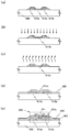
도 1a 및 도 1b는 일 실시예에 따른 반도체 장치의 구조를 설명하는 도면들.
도 2a 내지 도 2e는 일 실시예에 따른 반도체 장치를 제작하기 위한 방법을 설명하는 도면들.
도 3a 및 도 3b는 일 실시예에 따른 반도체 장치의 구조를 설명하는 도면들.
도 4a 내지 도 4e는 일 실시예에 따른 반도체 장치를 제작하기 위한 방법을 설명하는 도면들.
도 5a 및 도 5b는 일 실시예에 따른 반도체 장치의 구조를 설명하는 도면들.
도 6a 내지 도 6d는 일 실시예에 따른 반도체 장치를 제작하기 위한 방법을 설명하는 도면들.
도 7a 내지 도 7c는 일 실시예에 따른 반도체 장치를 제작하기 위한 방법을 설명하는 도면들.
도 8a 내지 도 8d는 일 실시예에 따른 반도체 장치를 제작하기 위한 방법을 설명하는 도면들.
도 9a 내지 도 9c는 일 실시예에 따른 반도체 장치를 제작하기 위한 방법을 설명하는 도면들.
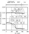
도 10a 내지 도 10e는 일 예에 따른 샘플을 제작하기 위한 방법을 설명하는 도면들.
도 11은 일 예에 따라 샘플 상에서 2차 이온 질량 분석법을 수행하는 결과를 도시하는 그래프.
도 12는 일 예에 따라 샘플 상에서 2차 이온 질량 분석법을 수행하는 결과를 도시하는 그래프.
도 13a-1 내지 도 13b는 일 실시예에 따른 반도체 장치의 회로도들.
도 14a 및 도 14b는 일 실시예에 따른 반도체 장치의 회로도들.
도 15a 내지 도 15c는 일 실시예에 따른 반도체 장치의 회로도들.
도 16a 내지 도 16f는 각각 일 실시예에 따른 반도체 장치를 포함한 전자 기기들을 설명하는 도면들.
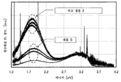
도 17은 일 예에 따라 샘플 상에서 저온 포토루미네선스 분광 측정법을 수행하는 결과를 도시하는 그래프.FIGS. 1A and 1B are views illustrating a structure of a semiconductor device according to an embodiment;
2A to 2E are views for explaining a method for manufacturing a semiconductor device according to an embodiment.
FIGS. 3A and 3B are views for explaining the structure of a semiconductor device according to an embodiment; FIG.
4A to 4E are views illustrating a method for manufacturing a semiconductor device according to an embodiment.
5A and 5B are diagrams for explaining a structure of a semiconductor device according to an embodiment.
6A to 6D are views illustrating a method for manufacturing a semiconductor device according to an embodiment.
7A to 7C are views illustrating a method for fabricating a semiconductor device according to an embodiment.
8A to 8D are views illustrating a method for manufacturing a semiconductor device according to an embodiment.
9A to 9C are views illustrating a method for fabricating a semiconductor device according to an embodiment.
Figures 10A through 10E are diagrams illustrating a method for fabricating a sample according to an example.
11 is a graph showing the results of performing secondary ion mass spectrometry on a sample according to one example.
12 is a graph showing the results of performing secondary ion mass spectrometry on a sample according to one example.
13A-1 to 13B are circuit diagrams of a semiconductor device according to an embodiment.
14A and 14B are circuit diagrams of a semiconductor device according to an embodiment.
15A to 15C are circuit diagrams of a semiconductor device according to an embodiment.
16A to 16F are diagrams for explaining electronic devices each including a semiconductor device according to an embodiment.
17 is a graph showing the results of performing a low temperature photoluminescence spectrometry on a sample according to one example.
실시예들 및 예들은 도면들을 참조하여 상세히 설명될 것이다. 본 발명은 다음 설명에 한정되지 않으며, 이 기술분야의 숙련자들에 의해 그 형태들 및 상세들이 본 발명의 취지 및 범위로부터 벗어나지 않고 다양하게 변경될 수 있다는 것이 이해될 것임을 주의하자. 그러므로, 본 발명은 다음 실시예들 및 예들에서의 설명에 한정되는 것으로서 해석되어서는 안 된다. 이하에 설명된 본 발명의 구조들에서, 동일한 부분들 또는 유사한 기능들을 가진 부분들은 도면들 전체에 걸쳐 동일한 참조 번호들로 표시되며, 이러한 부분들에 대한 설명은 반복되지 않는다.Embodiments and examples will be described in detail with reference to the drawings. It is to be understood that the present invention is not limited to the following description, and it is to be understood by those skilled in the art that various changes in form and details may be made therein without departing from the spirit and scope of the invention. Therefore, the present invention should not be construed as being limited to the description in the following embodiments and examples. In the structures of the present invention described below, portions having the same or similar functions are denoted by the same reference numerals throughout the drawings, and description of these portions is not repeated.
(실시예 1)(Example 1)
이 실시예에서, 보텀-게이트 트랜지스터를 제작하기 위한 방법이 도 1a와 도 1b 및 도 2a 내지 도 2e를 참조하여 설명될 것이다. 상기 방법에서, 산소가 산화물 반도체층에 첨가된 후, 불순물들을 제거하고 상기 산화물 반도체층을 고순도화하기 위해 상기 산화물 반도체층 상에서 열 처리가 수행된다.In this embodiment, a method for fabricating the bottom-gate transistor will be described with reference to Figs. 1A and 1B and Figs. 2A to 2E. In this method, after oxygen is added to the oxide semiconductor layer, heat treatment is performed on the oxide semiconductor layer to remove impurities and to purify the oxide semiconductor layer.
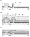
도 1a 및 도 1b는 이 실시예에서 제작된 보텀-게이트형인 트랜지스터(550)의 구조를 도시한다. 도 1a는 상기 트랜지스터(550)의 상면도이며 도 1b는 상기 트랜지스터(550)의 단면도이다. 도 1b는 도 1a에서의 선(P1-P2)을 따르는 단면을 도시한다.1A and 1B show the structure of a
상기 트랜지스터(550)에서, 게이트 전극(511) 및 상기 게이트 전극(511)을 커버하는 게이트 절연층(502)이 절연 표면을 가진 기판(500) 위에 제공된다. 고순도화되고 상기 게이트 전극(511)과 중첩하는 산화물 반도체층(513c)이 상기 게이트 절연층(502) 위에 제공된다. 또한, 상기 산화물 반도체층(513c)과 접하여, 상기 게이트 전극(511)과 중첩하는 단부들을 갖고, 소스 전극 및 드레인 전극으로서 작용하는 제 1 전극(515a) 및 제 2 전극(515b)이 제공된다. 또한, 상기 산화물 반도체층(513c)과 접하고 그것과 중첩하는 절연층(507), 및 상기 트랜지스터(550)를 커버하는 보호 절연층(508)이 제공된다.In the
다음으로, 상기 기판(500) 위에 상기 트랜지스터(550)를 제작하기 위한 방법이 도 2a 내지 도 2e를 참조하여 설명될 것이다.Next, a method for fabricating the
먼저, 도전막이 절연 표면을 가진 상기 기판(500) 위에 형성된 후, 상기 게이트 전극(511)을 포함하는 배선층이 제 1 포토리소그래피 단계에 의해 형성된다. 레지스트 마스크가 잉크젯법에 의해 형성될 수 있다는 것을 주의하자. 잉크젯법에 의한 상기 레지스트 마스크의 형성은 포토마스크를 필요로 하지 않으며; 따라서, 제작 비용이 감소될 수 있다.First, after a conductive film is formed on the
이 실시예에서, 절연 표면을 가진 상기 기판(500)으로서, 유리 기판이 사용된다.In this embodiment, as the
하지막(base film)으로서 작용하는 절연막이 상기 기판(500) 및 상기 게이트 전극(511) 사이에 제공될 수 있다. 상기 하지막은 상기 기판(500)으로부터 불순물 원소들(예로서, Li 또는 Na과 같은 알칼리 금속, Ca과 같은 알칼리 토금속 등)의 확산을 방지하는 기능을 가지며, 질화 실리콘막, 산화 실리콘막, 질화 산화 실리콘막, 산질화 실리콘막 등 중 하나 이상을 사용하는 단층 또는 적층 구조를 갖도록 형성될 수 있다.An insulating film serving as a base film may be provided between the
또한, 상기 게이트 전극(511)은 몰리브덴, 티타늄, 크롬, 탄탈, 텅스텐, 네오디뮴, 또는 스칸듐과 같은 금속 재료, 또는 이들 재료들 중 임의의 것을 주성분으로서 포함하는 합금 재료를 사용한 단층 또는 적층 구조를 갖고 형성될 수 있다. 알루미늄 또는 구리가 나중 단계에서 수행된 열 처리의 온도를 견딜 수 있다면, 알루미늄 또는 구리는 상기 금속 재료로서 사용될 수 있다는 것을 주의하자. 알루미늄 또는 구리는 바람직하게는 내열성 문제 및 부식성 문제를 방지하기 위해 고융점 금속 재료(refractory metal material)와 조합된다. 상기 고융점 금속 재료로서, 몰리브덴, 티타늄, 크롬, 탄탈, 텅스텐, 네오디뮴, 스칸듐 등이 사용될 수 있다. 구리를 사용하는 경우에, Cu-Mg-Al 합금이 하지로서 작용하는 층 위에 제공되고 구리가 그 위에 제공되는 구조가 바람직하다. 상기 Cu-Mg-Al 합금의 제공은 산화막과 같은 하지 및 구리 사이에서의 밀착성을 강화하는 효과를 가진다.The
다음으로, 상기 게이트 절연층(502)이 상기 게이트 전극(511) 위에 형성된다. 상기 게이트 절연층(502)은 CVD법, 스퍼터링법 등에 의해 형성될 수 있다. 또한, 상기 게이트 절연층(502)은 산화 실리콘층, 질화 실리콘층, 산질화 실리콘층, 질화 산화 실리콘층, 산화 알루미늄층, 질화 알루미늄층, 산질화 알루미늄층, 질화 산화 알루미늄층, 산화 하프늄층, 산화 탄탈층, 산화 갈륨층 등 중 하나 이상을 사용한 단층 구조 또는 적층 구조를 갖고 형성될 수 있다.Next, the
이 실시예에서 산화물 반도체로서, 불순물들을 제거함으로써 i-형 또는 실질적으로 i-형이 되는 산화물 반도체(고순도화된 산화물 반도체)가 사용된다. 이러한 고순도화된 산화물 반도체는 계면 준위 및 계면 전하에 매우 민감하며; 따라서 상기 산화물 반도체층 및 상기 게이트 절연층 사이의 계면이 중요하다. 이러한 이유로, 상기 고순도화된 산화물 반도체와 접하는 상기 게이트 절연층은 높은 품질을 가질 필요가 있다.In this embodiment, as oxide semiconductors, oxide semiconductors (high-purity oxide semiconductors) which are i-type or substantially i-type by removing impurities are used. Such high purity oxide semiconductors are very sensitive to interfacial levels and interface charge; Therefore, the interface between the oxide semiconductor layer and the gate insulating layer is important. For this reason, the gate insulating layer in contact with the high-purity oxide semiconductor needs to have a high quality.
예를 들면, 마이크로파들(예로서, 2.45 GHz의 주파수를 가진)을 사용한 고-밀도 플라즈마 CVD법이 바람직하게는 형성되는 절연층이 치밀할 수 있고 높은 내전압 및 고품질을 갖기 때문에 채택된다. 상기 고순도화된 산화물 반도체 및 상기 고-품질 게이트 절연층이 서로 밀착될 때, 상기 계면 준위 밀도는 양호한 계면 특성들을 획득하기 위해 감소될 수 있다.For example, a high-density plasma CVD method using microwaves (for example, with a frequency of 2.45 GHz) is preferably employed because the insulating layer to be formed is dense and has high withstand voltage and high quality. When the high-purity oxide semiconductor and the high-quality gate insulating layer are in close contact with each other, the interface level density can be reduced to obtain good interface characteristics.
말할 필요도 없이, 스퍼터링법 또는 플라즈마 CVD법과 같은 또 다른 막 형성 방법이, 상기 방법이 상기 게이트 절연층으로서 양호한-품질의 절연층의 형성을 가능하게 하는 한 이용될 수 있다. 또한, 상기 게이트 절연층으로서의 막 품질 및 상기 산화물 반도체층과의 상기 계면의 특성이 상기 절연층의 형성 후 수행되는 열 처리에 의해 개선되는 절연층이 사용될 수 있다. 어떠한 경우에도, 임의의 절연층이, 상기 게이트 절연층으로서의 양호한 막 품질을 가질 뿐만 아니라 상기 절연층이 상기 산화물 반도체와의 계면 준위 밀도를 저감시킬 수 있고 양호한 계면을 형성할 수 있는 한 사용될 수 있다.Needless to say, another film-forming method such as a sputtering method or a plasma CVD method can be used as long as the method enables formation of a good-quality insulating layer as the gate insulating layer. An insulating layer may be used in which the film quality as the gate insulating layer and the characteristics of the interface with the oxide semiconductor layer are improved by a heat treatment performed after formation of the insulating layer. In any case, any insulating layer can be used as long as it has a good film quality as the gate insulating layer, and the insulating layer can reduce the interface level density with the oxide semiconductor and form a good interface .
상기 게이트 절연층(502)은 나중에 형성되는 산화물 반도체막과 접한다는 것을 주의하자. 수소가 상기 산화물 반도체막에 포함될 때, 상기 트랜지스터의 특성들이 악영향을 받으며; 그러므로, 상기 게이트 절연층(502)은 수소, 수산기, 및 수분을 포함하지 않는 것이 바람직하다. 상기 게이트 절연층(502) 및 상기 산화물 반도체막이 가능한 한 적게 수소, 수산기, 및 수분을 포함하기 위해, 수소 또는 수분과 같이, 상기 기판(500)상에 흡수된 불순물들은 상기 산화물 반도체막의 형성을 위한 사전 처리로서, 스퍼터링 장치의 예열실(preheating chamber)에서, 상기 게이트 전극(511)까지 그것을 포함한 층들이 형성되는 상기 기판(500) 또는 상기 게이트 절연층(502)까지 그것을 포함한 층들이 형성되는 상기 기판(500)을 예열함으로써 제거 및 소거되는 것이 바람직하다. 상기 예열을 위한 온도는 100℃ 이상 400℃ 이하, 바람직하게는 150℃ 이상 300℃ 이하이다. 상기 예열실에 제공된 배기 수단으로서, 크라이오펌프가 바람직하다. 이러한 예열 처리는 생략될 수 있다는 것을 주의하자. 이러한 예열은 유사하게 상기 제 1 전극(515a) 및 상기 제 2 전극(515b)까지 이를 포함한 층들이 상기 절연층(507)의 형성 전에 형성되는 상기 기판(500) 상에서 수행될 수 있다.Note that the
다음으로, 상기 게이트 절연층(502) 위에, 2 nm 이상 200 nm 이하, 바람직하게는 5 nm 이상 30 nm 이하의 두께를 가진 상기 산화물 반도체막이 형성된다. 상기 산화물 반도체막은 타겟으로서 산화물 반도체를 사용하여 스퍼터링법에 의해 형성된다. 게다가, 상기 산화물 반도체막은 희가스(예를 들면, 아르곤) 분위기, 산소 분위기, 또는 희가스(예를 들면, 아르곤) 및 산소를 포함한 혼합 분위기에서 스퍼터링법에 의해 형성될 수 있다.Next, the oxide semiconductor film having a thickness of 2 nm or more and 200 nm or less, preferably 5 nm or more and 30 nm or less, is formed on the
상기 산화물 반도체막이 스퍼터링법에 의해 형성되기 전에, 상기 게이트 절연층(502)의 표면상에 부착된 가루 물질들(또한 입자들 또는 먼지들로서 불리우는)이 바람직하게는 아르곤 가스가 도입되고 플라즈마가 생성되는 역 스퍼터링에 의해 제거된다는 것을 주의하자. 상기 역 스퍼터링은 표면을 변경하기 위해 RF 전원이 아르곤 분위기에서 기판 측으로의 전압의 인가를 위해 사용되며 플라즈마가 상기 기판 주변에 생성되는 방법을 나타낸다. 아르곤 분위기 대신에, 질소 분위기, 헬륨 분위기, 산소 분위기 등이 사용될 수 있다는 것을 주의하자.Before the oxide semiconductor film is formed by the sputtering method, the powdery materials (also referred to as particles or dusts) adhered on the surface of the
상기 산화물 반도체막을 위해 사용된 상기 산화물 반도체로서, 다음의 산화물 반도체들이 사용될 수 있다: In-Sn-Ga-Zn-O계 산화물 반도체와 같은 4-원계 금속 산화물; In-Ga-Zn-O계 산화물 반도체, In-Sn-Zn-O계 산화물 반도체, In-Al-Zn-O계 산화물 반도체, Sn-Ga-Zn-O계 산화물 반도체, Al-Ga-Zn-O계 산화물 반도체, 또는 Sn-Al-Zn-O계 산화물 반도체와 같은 3-원계 금속 산화물; In-Zn-O계 산화물 반도체, Sn-Zn-O계 산화물 반도체, Al-Zn-O계 산화물 반도체, Zn-Mg-O계 산화물 반도체, Sn-Mg-O계 산화물 반도체, In-Mg-O계 산화물 반도체, 또는 In-Ga-O계 산화물 반도체와 같은 2-원계 금속 산화물; In-O계 산화물 반도체, Sn-O계 산화물 반도체, Zn-O계 산화물 반도체 등. 또한, 산화 실리콘이 상기 산화물 반도체막에 포함될 수 있다. 상기 산화물 반도체막으로의 결정화를 방해하는 산화 실리콘(SiOX (x>0))의 첨가는 상기 제작 공정에서 열 처리가 상기 산화물 반도체막의 형성 후 수행될 때 상기 산화물 반도체막의 결정화를 억제할 수 있다. 상기 산화물 반도체막은 바람직하게는 비정질 상태에 있지만; 상기 산화물 반도체막은 부분적으로 결정화될 수 있다. 본 명세서에서, 예를 들면, In-Ga-Zn-O계 산화물 반도체는 인듐(In), 갈륨(Ga), 및 아연(Zn)을 포함한 산화물 막을 의미하며, 조성비에 대한 특별한 제한은 없다. 또한, 상기 산화물 반도체막은 In, Ga, 및 Zn 이외의 원소를 포함할 수 있으며, 화학식, InMO3(ZnO)m(m>0, 및 m은 자연수가 아니다)에 의해 표현된 재료의 박막이 사용될 수 있다. 여기에서, M은 Ga, Al, Mn, 및 Co로부터 선택된 하나 이상의 금속 원소들을 나타낸다. 예를 들면, M은 Ga, Ga와 Al, Ga와 Mn, Ga와 Co 등일 수 있다. 상기 산화물 반도체는 바람직하게는 In을 포함하며, 보다 바람직하게는 In 및 Ga를 포함한다. i-형(진성) 산화물 반도체층을 획득하기 위해, 탈수화 또는 탈수소화가 효과적이다. 이 실시예에서, 상기 산화물 반도체막은 스퍼터링법에 의해 In-Ga-Zn-O계 산화물 타겟을 사용하여 형성된다.As the oxide semiconductor used for the oxide semiconductor film, the following oxide semiconductors can be used: a 4-element metal oxide such as an In-Sn-Ga-Zn-O-based oxide semiconductor; In-Zn-O-based oxide semiconductor, In-Sn-Zn-O-based oxide semiconductor, In-Sn-Zn- O-based oxide semiconductor, or a Sn-Al-Zn-O-based oxide semiconductor; Zn-O based oxide semiconductor, Sn-Zn-O based oxide semiconductor, Al-Zn-O based oxide semiconductor, Zn-Mg-O based oxide semiconductor, Based oxide such as In-Ga-O-based oxide semiconductors or In-Ga-O-based oxide semiconductors; In-O-based oxide semiconductors, Sn-O-based oxide semiconductors, and Zn-O-based oxide semiconductors. Further, silicon oxide may be included in the oxide semiconductor film. The addition of silicon oxide (SiO x (x > 0)) which inhibits crystallization to the oxide semiconductor film can suppress the crystallization of the oxide semiconductor film when the heat treatment is performed after the formation of the oxide semiconductor film in the manufacturing process . The oxide semiconductor film is preferably in an amorphous state; The oxide semiconductor film can be partially crystallized. In this specification, for example, the In-Ga-Zn-O-based oxide semiconductor means an oxide film containing indium (In), gallium (Ga), and zinc (Zn), and there is no particular limitation on the composition ratio. In addition, the oxide semiconductor film may include an element other than In, Ga, and Zn, and a thin film of a material represented by the formula InMO 3 (ZnO) m (m> 0, and m is not a natural number) . Here, M represents one or more metal elements selected from Ga, Al, Mn, and Co. For example, M may be Ga, Ga and Al, Ga and Mn, Ga and Co, and the like. The oxide semiconductor preferably includes In, and more preferably includes In and Ga. In order to obtain an i-type (intrinsic) oxide semiconductor layer, dehydration or dehydrogenation is effective. In this embodiment, the oxide semiconductor film is formed using an In-Ga-Zn-O-based oxide target by a sputtering method.
스퍼터링법에 의해 상기 산화물 반도체막을 형성하기 위한 타겟으로서, 예를 들면, In2O3:Ga2O3:ZnO = 1:1:1 [몰 비]의 조성비를 가진 산화물 타겟이 사용되며, In-Ga-Zn-O 막이 형성된다. 상기 재료 및 상기 타겟의 조성에 대한 제한 없이, 예를 들면, In2O3:Ga2O3:ZnO = 1:1:2 [몰 비] 또는 In2O3:Ga2O3:ZnO = 1:1:4 [몰 비]의 조성비를 가진 산화물 타겟이 사용될 수 있다.An oxide target having a composition ratio of, for example, In 2 O 3 : Ga 2 O 3 : ZnO = 1: 1: 1 [molar ratio] is used as a target for forming the oxide semiconductor film by a sputtering method, -Ga-Zn-O film is formed. The composition of the In 2 O 3 : Ga 2 O 3 : ZnO = 1: 1: 2 [molar ratio] or In 2 O 3 : Ga 2 O 3 : ZnO = An oxide target having a composition ratio of 1: 1: 4 [molar ratio] may be used.
In-Zn-O계 재료가 상기 산화물 반도체막을 위해 사용되는 경우에, 사용된 타겟의 조성비는 원자비(몰 비로 In2O3:ZnO = 25:1 내지 1:4)에서 In:Zn = 50:1 내지 1:2, 바람직하게는 원자비(몰 비로 In2O3:ZnO = 2:1 내지 10:1)에서 In:Zn = 1:1 내지 1:20, 보다 바람직하게는 원자비(몰 비로 In2O3:ZnO = 3:4 내지 15:2)에서 In:Zn = 1.5:1 내지 15:1이다. 예를 들면, In-Zn-O계 산화물 반도체의 형성을 위해 사용된 타겟은 In:Zn:O = 1:1:X(여기서, X>1, 바람직하게는 X>1.5)의 원자비를 가진다.When the In-Zn-O-based material is used for the oxide semiconductor film, the composition ratio of the target used is In: Zn = 50 (In 2 O 3 : ZnO = 25: 1 to 1: Zn is preferably 1: 1 to 1: 20, more preferably 1: 1 to 2: 1, more preferably 1: 2 to 1: 2 in an atomic ratio of 1: 1 to 1: 2, preferably an atomic ratio (In 2 O 3 : ZnO = In: Zn = 1.5: 1 to 15: 1 in In 2 O 3 : ZnO = 3: 4 to 15: 2 in terms of molar ratio. For example, a target used for forming an In-Zn-O-based oxide semiconductor has an atomic ratio of In: Zn: O = 1: 1: X (where X> 1, preferably X> 1.5) .
또한, 상기 산화물 타겟의 충전율은 90% 이상 100% 이하, 바람직하게는 95% 이상 99.9% 이하이다. 높은 충전율을 가진 상기 산화물 타겟의 사용으로, 치밀한 산화물 반도체막이 형성될 수 있다. 게다가, 상기 타겟의 순도는 바람직하게는 99.99% 이상이며, 여기서 불순물들, 예를 들면, Li 또는 Na과 같은 알칼리 금속 및 Ca과 같은 알칼리 토금속이 특히 감소되는 것이 바람직하다.The filling rate of the oxide target is 90% or more and 100% or less, preferably 95% or more and 99.9% or less. With the use of the oxide target having a high filling rate, a dense oxide semiconductor film can be formed. In addition, the purity of the target is preferably greater than or equal to 99.99%, wherein it is preferred that the impurities, for example alkali metals such as Li or Na and alkaline earth metals such as Ca, are particularly reduced.
수소, 물, 수산기, 또는 수소화물과 같은 불순물들이 제거되는 고-순도 가스가 상기 산화물 반도체막을 형성하기 위해 사용된 스퍼터링 가스로서 사용된다. 예를 들면, 불순물들이 약 10 ppm 이하, 바람직하게는 1 ppm 이하의 농도까지 제거되는 고-순도 가스가 사용되는 것이 바람직하다. 구체적으로, 이슬점이 -60℃ 이하인 고-순도 가스가 바람직하다.A high-purity gas in which impurities such as hydrogen, water, hydroxyl groups, or hydrides are removed is used as the sputtering gas used to form the oxide semiconductor film. For example, a high-purity gas is preferably used in which impurities are removed to a concentration of about 10 ppm or less, preferably 1 ppm or less. Specifically, a high-purity gas having a dew point of -60 캜 or lower is preferable.
상기 기판은 감소된 압력 하에서 성막실(deposition chamber)에 배치되며, 상기 기판 온도는 100℃ 이상 600℃ 이하, 바람직하게는 200℃ 이상 400℃ 이하로 설정된다. 상기 기판이 가열되는 상태에서 상기 산화물 반도체막을 형성함으로써, 상기 형성된 산화물 반도체막에 포함된 불순물들의 농도는 감소될 수 있다. 또한, 스퍼터링에 의한 손상이 감소될 수 있다. 그 후, 수소 및 수분이 제거되는 스퍼터링 가스가 상기 성막실에서의 잔여 수분 및 외부로부터 상기 성막실에 들어온 수소 및 수분(리크로 인해 들어온 수소 및 수분)이 배기 펌프를 사용하여 제거되는 동안 도입되며, 상기 산화물 반도체막은 상기 타겟을 사용하여 상기 기판(500) 위에 형성된다. 상기 성막실로부터 잔여 수분을 제거하기 위해, 흡착형 진공 펌프(entrapment vacuum pump), 예를 들면, 크라이오펌프, 이온 펌프, 또는 티타늄 승화 펌프(titanium sublimation pump)가 사용되는 것이 바람직하다. 상기 배기 수단은 콜드 트랩을 구비한 터보 펌프일 수 있다. 상기 크라이오펌프를 갖고 배기되는 상기 성막실에서, 예를 들면, 수소 원자, 물(H20)과 같이, 수소 원자를 포함한 화합물, (보다 바람직하게는, 또한 탄소 원자를 포함한 화합물) 등이 제거되며, 그에 의해 상기 성막실에 형성된 상기 산화물 반도체막에서의 불순물들의 농도는 저감될 수 있다.The substrate is placed in a deposition chamber under a reduced pressure, and the substrate temperature is set to 100 ° C or higher and 600 ° C or lower, preferably 200 ° C or higher and 400 ° C or lower. By forming the oxide semiconductor film with the substrate heated, the concentration of the impurities contained in the formed oxide semiconductor film can be reduced. In addition, damage due to sputtering can be reduced. Thereafter, hydrogen and water-removed sputtering gas are introduced while residual moisture in the deposition chamber and hydrogen and moisture (leaked hydrogen and moisture) entering the deposition chamber from the outside are removed using an exhaust pump , The oxide semiconductor film is formed on the
스퍼터링법을 위한 분위기는 희가스(대표적으로, 아르곤) 분위기, 산소 분위기, 또는 희가스 및 산소를 포함한 혼합 분위기일 수 있다.The atmosphere for the sputtering method may be a rare gas (typically, argon) atmosphere, an oxygen atmosphere, or a mixed atmosphere containing rare gas and oxygen.
상기 성막 조건들의 일 예로서, 상기 기판 및 상기 타겟 간의 거리는 100 mm이고, 압력은 0.6 Pa이고, 직류(DC) 전원의 전력은 0.5 kW이며, 상기 분위기는 산소 분위기(산소 유량 비율은 100%이다)이다. 성막시 생성된 가루 물질들(또한 입자들 또는 먼지들로서 불리는)이 감소될 수 있고 상기 막 두께가 균일할 수 있기 때문에 펄스 직류 전원이 바람직하다는 것을 주의하자. 게다가, 상기 스퍼터링 장치의 상기 처리실의 누설율(leakage rate)이 1×10⁻¹⁰ Paㆍm3/초 이하로 설정될 때, 스퍼터링법에 의해 형성되는 상기 산화물 반도체막으로의 알칼리 금속 또는 수소화물과 같은 불순물들의 진입은 감소될 수 있다. 또한, 배기 시스템으로서 흡착형 진공 펌프의 사용으로, 상기 배기 시스템으로부터 알칼리 금속, 수소 원자, 수소 분자, 물, 수산기, 또는 수소화물과 같은 불순물들의 역류가 감소될 수 있다. 바람직하게는 산화물 반도체층에 포함된 불순물들, 예를 들면, Li 또는 Na와 같은 알칼리 금속 및 Ca와 같은 알칼리 토금속이 감소된다는 것을 주의하자. 구체적으로, 상기 농도들이 SIMS를 사용하여 측정될 때, 상기 산화물 반도체층에 포함된 Li, Na, 및 K의 불순물 농도들은 각각 5×10¹⁵ ㎝-3, 바람직하게는 1×10¹⁵ ㎝- 3 이다. 알칼리 금속 및 알칼리 토금속은 상기 산화물 반도체에 대한 악성 불순물들이며, 가능한 한 적게 포함된다. 알칼리 금속, 특히, Na은 산화물로 확산되며 상기 산화물 반도체와 접하는 절연막이 산화물일 때 Na+가 된다. 또한, Na은 금속 및 산소 간의 결합을 분단시키거나 또는 상기 산화물 반도체에서의 결합에 들어간다. 그 결과, 트랜지스터 특성들이 열화한다(예로서, 상기 트랜지스터는 노멀리-온되거나(부측(negative side)으로의 임계 전압의 시프트) 또는 이동도가 감소된다). 게다가, 이것은 또한 상기 특성들에서의 변동을 야기한다. 이러한 문제점은 상기 산화물 반도체에서의 상기 수소 농도가 매우 낮은 경우에 특히 중요하다. 그러므로, 알칼리 금속의 농도는 상기 산화물 반도체에서의 상기 수소 농도가 5×10¹⁹ ㎝-3 이하, 특히 5×10¹⁸ ㎝-3 이하인 경우에 상기 값으로 설정되도록 강하게 요구된다.As an example of the deposition conditions, the distance between the substrate and the target is 100 mm, the pressure is 0.6 Pa, the power of the direct current (DC) power source is 0.5 kW, the atmosphere is oxygen atmosphere (oxygen flow rate is 100% )to be. It should be noted that pulsed direct current power is desirable because the powder materials (also referred to as particles or dust) produced during film formation can be reduced and the film thickness can be uniform. Moreover, when the leakage rate of the treatment chamber of the sputtering apparatus is set to 1 x 10 < -10 > Pa < 3 > / sec or less, the alkali metal or hydride of the oxide semiconductor film formed by the sputtering method Can be reduced. Further, by using an adsorption type vacuum pump as an exhaust system, backflow of impurities such as alkali metals, hydrogen atoms, hydrogen molecules, water, hydroxyl groups, or hydrides from the exhaust system can be reduced. Note that impurities contained in the oxide semiconductor layer, for example, alkaline metals such as Li or Na and alkaline earth metals such as Ca are reduced. Specifically, the concentrations are as measured using SIMS, the oxide impurity concentration of the Li, Na, and K included in the semiconductor layer are each 5 × 10 15 ㎝ -3, preferably 1 × 10 15 ㎝ - 3 to be. Alkali metal and alkaline earth metal are malignant impurities for the oxide semiconductor and are included as less as possible. Alkali metal, particularly Na, diffuses into the oxide and becomes Na + when the insulating film in contact with the oxide semiconductor is an oxide. Further, Na enters the bond between the metal and the oxygen or the bond in the oxide semiconductor. As a result, the transistor characteristics degrade (e.g., the transistor is normally on-off (shift of the threshold voltage to the negative side) or mobility is reduced). In addition, this also causes variations in these properties. This problem is particularly important when the hydrogen concentration in the oxide semiconductor is very low. Therefore, the concentration of the alkali metal is strongly required to be set to the above value when the hydrogen concentration in the oxide semiconductor is 5 x 10 19 cm -3 or less, particularly 5 x 10 18 cm -3 or less.
다음으로, 상기 산화물 반도체막은 제 2 포토리소그래피 단계에 의해 섬형상 산화물 반도체층(513a)으로 처리된다. 상기 섬형상 산화물 반도체층을 형성하기 위한 레지스트 마스크는 잉크젯법에 의해 형성될 수 있다. 잉크젯법에 의한 상기 레지스트 마스크의 형성은 포토마스크를 필요로 하지 않으며; 따라서 제작 비용은 감소될 수 있다.Next, the oxide semiconductor film is processed into an island-shaped
또한, 콘택트 홀(contact hole)이 상기 게이트 절연층(502)에 형성되는 경우에, 상기 콘택트 홀을 형성하는 단계가 상기 산화물 반도체막의 가공과 동시에 수행될 수 있다.In addition, when a contact hole is formed in the
여기에서 상기 산화물 반도체막의 에칭은 드라이 에칭, 웨트 에칭, 또는 드라이 에칭 및 웨트 에칭 둘 모두일 수 있다는 것을 주의하자. 상기 산화물 반도체막의 웨트 에칭을 위해 사용된 에칭액으로서, 예를 들면, 인산, 아세트산, 질산 등의 혼합액이 사용될 수 있다. 또한, ITO07N(칸토 케미컬 코., 인크.(KANTO CHEMICAL CO., INC.)에 의해 제조)이 사용될 수 있다. 드라이 에칭을 위해 사용된 에칭 가스로서, 염소를 포함한 가스(염소(Cl2), 삼염화 붕소(BCl3), 사염화 규소(SiCl4), 또는 사염화탄소(CCl4)와 같은 염소계 가스)가 바람직하다. 또한, 불소를 포함한 가스(사불화탄소(CF4), 육불화유황(SF6), 삼불화질소(NF3), 또는 트리플로루메탄(CHF3)과 같은 불소계 가스), 취화 수소(HBr), 산소(O2), 헬륨(He) 또는 아르곤(Ar)과 같은 희가스가 첨가되는 이들 가스들 중 임의의 것 등이 사용될 수 있다. 드라이 에칭 방법으로서, 평행 평판형 반응성 이온 에칭(RIE) 방법 또는 유도 결합 플라즈마(ICP) 에칭 방법이 사용될 수 있다. 상기 산화물 반도체막이 원하는 형상으로 에칭될 수 있도록 에칭 조건들(예로서, 코일-형상 전극에 인가된 전력의 양, 기판 측 상의 전극에 인가된 전력의 양, 및 기판 측 상의 전극 온도)이 적절하게 조정된다. 이 단계에서 상기 단면도는 도 2a에 도시된다는 것을 주의하자.Note that the etching of the oxide semiconductor film may be dry etching, wet etching, or both dry etching and wet etching. As an etchant used for wet etching the oxide semiconductor film, for example, a mixed solution of phosphoric acid, acetic acid, nitric acid, or the like can be used. Also, ITO07N (manufactured by KANTO CHEMICAL CO., INC.) May be used. As the etching gas used for dry etching, a gas containing chlorine (chlorine gas such as chlorine (Cl 2 ), boron trichloride (BCl 3 ), silicon tetrachloride (SiCl 4 ), or carbon tetrachloride (CCl 4 )) is preferable. The fluorine-containing gas (fluorine-based gas such as carbon tetrafluoride (CF 4 ), hexafluorosulfide (SF 6 ), nitrogen trifluoride (NF 3 ), or triflouromethane (CHF 3 ) , Oxygen (O 2 ), helium (He), or argon (Ar) may be used. As the dry etching method, a parallel plate type reactive ion etching (RIE) method or an inductively coupled plasma (ICP) etching method can be used. (For example, the amount of power applied to the coil-shaped electrode, the amount of power applied to the electrode on the substrate side, and the electrode temperature on the substrate side) so that the oxide semiconductor film can be etched to a desired shape . Note that the cross-sectional view at this stage is shown in Figure 2A.
다음으로, 산소가 상기 산화물 반도체층(513a)에 첨가된다. 이온 주입법, 이온 도핑법 등에 의해, 높은 에너지를 가진 산소가 첨가된다.Next, oxygen is added to the
이온 주입법에서, 소스 가스는 플라즈마로 만들어지며, 이 플라즈마에 포함된 이온종들은 추출되고 질량-분리되고, 미리 결정된 질량을 가진 이온종들이 가속되며, 피처리물이 이온 빔의 형태로 상기 가속된 이온종들을 갖고 조사된다. 이온 도핑법에서, 소스 가스는 플라즈마로 만들어지며, 이온종들은 미리 결정된 전계의 동작에 의해 이러한 플라즈마로부터 추출되고, 상기 추출된 이온종들은 질량 분리 없이 가속되며, 피처리물이 이온 빔의 형태로 상기 가속된 이온종들을 갖고 조사된다. 산소의 첨가는 질량 분리를 수반한 이온 주입법을 사용하여 수행될 때, 금속 원소와 같은 불순물이 산소와 함께, 상기 산화물 반도체막에 첨가되는 것으로부터 방지될 수 있다. 다른 한편으로, 이온 도핑법은 이온 주입법보다 큰 영역에 이온-빔 조사를 가능하게 하며, 그러므로, 산소의 첨가가 이온 도핑법을 사용하여 수행될 때, 택 타임(takt time)은 단축될 수 있다.In the ion implantation method, the source gas is made of a plasma, ion species contained in the plasma are extracted and mass-separated, ion species having a predetermined mass are accelerated, and the object to be processed is accelerated Ion species. In the ion doping method, the source gas is made of a plasma, ion species are extracted from this plasma by the operation of a predetermined electric field, the extracted ion species are accelerated without mass separation, and the object to be processed is ion- And irradiated with the accelerated ion species. When the addition of oxygen is performed using an ion implantation method accompanied by mass separation, an impurity such as a metal element can be prevented from being added to the oxide semiconductor film together with oxygen. On the other hand, the ion doping method enables ion-beam irradiation to a larger area than the ion implantation method, and therefore when the addition of oxygen is performed using ion doping, the takt time can be shortened .
산소 가스가 사용되고 산소가 이온 주입법에 의해 첨가되는 경우에, 상기 가속 전압은 5 keV 이상 100 keV 이하로 설정될 것이며, 산소 이온들의 주입량은 1×10¹⁴[이온/㎠] 이상 5×10¹⁷[이온/㎠] 이하로 설정될 것이다.When the oxygen gas used and oxygen is added by ion implantation to the accelerating voltage will be set to not more than 100 keV than 5 keV, dose of oxygen ion is 1 × 10 14 [ions / ㎠] more than 5 × 10 17 [ Ions / cm < 2 >] or less.
이온 주입법, 이온 도핑법 등에 의해 높은 에너지를 가진 산소를 상기 산화물 반도체에 첨가함으로써, 예를 들면, 상기 산화물 반도체에 포함된 금속 및 수소 간의 결합, 금속 및 수산기 간의 결합, 또는 금속에 결합된 수산기에서의 산소 및 수소 간의 결합이 절단될 수 있다. 상기 산화물 반도체층(513a)은 상기 금속으로부터 제거된 불순물들을 포함하는 산화물 반도체층(513b)으로 변경된다. 도 2b는 이 단계에서의 단면도를 도시한다.By adding oxygen having a high energy to the oxide semiconductor by ion implantation, ion doping, or the like, for example, it is possible to use a combination of a metal and hydrogen contained in the oxide semiconductor, a bond between a metal and a hydroxyl group, The bond between oxygen and hydrogen can be broken. The
그 후, 상기 금속으로부터 제거된 상기 불순물들을 포함하는 상기 산화물 반도체층(513b)은 제 1 열 처리된다. 이러한 제 1 열 처리를 통해, 상기 금속으로부터 제거된 상기 불순물들은 상기 산화물 반도체층으로부터 제거될 수 있다. 예를 들면, 상기 금속으로부터 제거된 수소 또는 수산기와의 첨가된 산소의 반응에 의해 생성된 물이 제거될 수 있다. 생성된 물이 가열에 의해 제거되는 상기 방법은 상기 금속에 강하게 결합된 수소 또는 수산기가 직접 제거되는 방법보다 더 용이하다.Thereafter, the
상기 제 1 열 처리는 250℃ 이상 700℃ 이하, 바람직하게는 450℃ 이상 650℃ 이하, 또는 450℃ 이상 및 상기 기판의 변형점(strain point) 미만에서 수행된다. 예를 들면, 상기 제 1 열 처리는 500℃에서 3분 이상 6분 이하 동안 수행될 수 있다. 상기 열 처리를 위한 급속 열 어닐링(RTA)을 사용함으로써, 탈수화 또는 탈수소화가 단시간에 수행될 수 있으며; 그러므로, 상기 처리는 유리 기판의 변형점보다 높은 온도에서조차 수행될 수 있다. 제 4-세대 유리 기판 정도만큼 큰 기판들이 250℃ 이상 750℃ 이하의 온도에서 열 처리될 수 있는 반면, 제 6 세대 유리 기판 내지 제 10 세대 유리 기판까지의 정도만큼 큰 기판들이 바람직하게는 250℃ 이상 450℃ 이하의 온도에서 열 처리된다. 여기에서, 상기 기판은 열 처리 장치들 중 하나인 전기로에 넣어지고, 열 처리가 질소 분위기에서 600℃로 1시간 동안 상기 산화물 반도체층 상에서 수행되며, 그 후 서냉(slow cooling)이 대기로의 노출 없이 200℃ 이하의 온도에서 상기 산화물 반도체층 상에서 수행되어, 상기 산화물 반도체층으로의 물 및 수소의 진입이 방지되도록 한다. 따라서, 산화물 반도체층(513c)이 획득된다(도 2c 참조). 상기 산화물 반도체층이 200℃ 이하로 냉각될 때, 고온 산화물 반도체층이 대기에서의 물 또는 수분과 접하는 것으로부터 방지될 수 있다. 상기 고온 산화물 반도체층이 상기 대기에서의 물 또는 수분과 접할 때, 몇몇 경우들에서, 상기 산화물 반도체는 수소 원자를 포함한 불순물로 오염된다.The first heat treatment is performed at a temperature of 250 ° C or more and 700 ° C or less, preferably 450 ° C or more and 650 ° C or less, or 450 ° C or more and less than the strain point of the substrate. For example, the first heat treatment may be performed at 500 DEG C for 3 minutes or more and 6 minutes or less. By using rapid thermal annealing (RTA) for the heat treatment, dehydration or dehydrogenation can be performed in a short time; Therefore, the above process can be performed even at a temperature higher than the strain point of the glass substrate. Substrates as large as the fourth-generation glass substrate can be heat-treated at a temperature of 250 ° C or higher and 750 ° C or lower, while substrates as large as the sixth-generation glass substrate to the tenth generation glass substrate can be heat- Lt; RTI ID = 0.0 > 450 C < / RTI > Here, the substrate is placed in an electric furnace, which is one of the heat treatment apparatuses, and heat treatment is performed on the oxide semiconductor layer at 600 DEG C for 1 hour in a nitrogen atmosphere, and then slow cooling is applied to the atmosphere At a temperature of less than or equal to 200 DEG C to prevent entry of water and hydrogen into the oxide semiconductor layer. Thus, an
상기 열 처리 장치는 전기로에 한정되지 않으며, 저항 발열체와 같은 발열체로부터 열 복사 또는 열 도전에 의해 피처리물을 가열하기 위한 장치가 사용될 수 있다. 예를 들면, 가스 급속 열 어닐링(GRTA) 장치 또는 램프 급속 열 어닐링(LRTA) 장치와 같은 급속 열 어닐링(RTA) 장치가 사용될 수 있다. LRTA 장치는 할로겐 램프, 메탈 할라이드 램프, 크세논 아크 램프, 탄소 아크 램프, 고압 나트륨 램프, 또는 고압 수은 램프와 같은 램프로부터 방출된 광의 조사(전자기파)에 의해 피처리물을 가열하기 위한 장치이다. GRTA 장치는 고온 가스를 사용한 열 처리를 위한 장치이다. 상기 고온 가스로서, 질소 또는 아르곤과 같은 희가스와 같이 열 처리에 의해 피처리물과 반응하지 않은 불활성 가스가 사용된다.The heat treatment apparatus is not limited to an electric furnace, and an apparatus for heating the article to be treated by heat radiation or heat conduction from a heating element such as a resistance heating element may be used. For example, a rapid thermal annealing (RTA) apparatus such as a gas rapid thermal annealing (GRTA) apparatus or a lamp rapid thermal annealing (LRTA) apparatus may be used. The LRTA apparatus is an apparatus for heating an article to be processed by irradiation (electromagnetic waves) of light emitted from a lamp such as a halogen lamp, a metal halide lamp, a xenon arc lamp, a carbon arc lamp, a high pressure sodium lamp, or a high pressure mercury lamp. The GRTA device is a device for heat treatment using hot gases. As the high-temperature gas, an inert gas which is not reacted with the object to be treated by heat treatment such as nitrogen or rare gas such as argon is used.
예를 들면, 상기 제 1 열 처리로서, 상기 기판이 650℃ 내지 700℃의 고온으로 가열되는 불활성 가스 안으로 넣어지고, 수 분 동안 가열된 후, 상기 고온으로 가열된 상기 불활성 가스로부터 꺼내어지는 GRTA가 수행될 수 있다.For example, as the first heat treatment, the substrate is put into an inert gas heated to a high temperature of 650 ° C to 700 ° C, and after heating for several minutes, the GRTA taken out from the inert gas heated at the high temperature .
상기 제 1 열 처리에서, 수분, 수소 등은 질소 또는 헬륨, 네온, 또는 아르곤과 같은 희가스에 포함되지 않는 것이 바람직하다는 것을 주의하자. 상기 열 처리 장치로 도입되는 질소 또는 헬륨, 네온, 또는 아르곤과 같은 희가스의 순도는 6N(99.9999%) 이상, 바람직하게는 7N(99.99999%) 이상(즉, 상기 불순물 농도는 1 ppm 이하, 바람직하게는 0.1 ppm 이하이다)으로 설정되는 것이 바람직하다.Note that in the first heat treatment, moisture, hydrogen, and the like are preferably not contained in the rare gas such as nitrogen or helium, neon, or argon. The purity of nitrogen or a rare gas such as helium, neon or argon introduced into the heat treatment apparatus is preferably 6N (99.9999%) or more, preferably 7N (99.99999%) or more (that is, the impurity concentration is 1 ppm or less Is not more than 0.1 ppm).
또한, 상기 산화물 반도체층이 상기 제 1 열 처리에 의해 가열된 후, 고-순도 산소 가스, 고순도 N20 가스, 또는 초건조 공기(측정이 캐비티 링 다운 레이저 분광법(cavity ring down laser spectroscopy; CRDS) 시스템의 노점계의 사용으로 수행되는 경우에, 수분량이 20 ppm(이슬점으로의 환산에 의해 -55℃) 이하, 바람직하게는 1 ppm 이하, 보다 바람직하게는 10 ppb 이하이다)가 동일한 노(furnace)로 도입될 수 있다. 상기 산소 가스 또는 상기 N2O 가스는 물, 수소 등을 포함하지 않는 것이 바람직하다. 대안적으로, 상기 열 처리 장치에 도입되는 상기 산소 가스 또는 상기 N2O 가스의 순도는 6N 이상, 바람직하게는 7N 이상(즉, 상기 산소 가스 또는 상기 N2O 가스의 불순물 농도는 1 ppm 이하, 바람직하게는 0.1 ppm 이하이다)이다. 상기 산소 가스 또는 상기 N2O 가스의 효과에 의해, 상기 산화물 반도체의 주성분이고 탈수화 또는 탈수소화에 의해 불순물들을 제거하기 위한 단계와 동시에 감소되는 산소가 공급되며, 따라서 상기 산화물 반도체층은 고-순도 및 전기적으로 i-형(진성) 산화물 반도체층일 수 있다.Further, after the oxide semiconductor layer is heated by the first heat treatment, a high-purity oxygen gas, a high-purity N 2 O gas, or a super-dry air (measurement is performed by a cavity ring down laser spectroscopy ) System, the water content is less than or equal to 20 ppm (-55 캜 in terms of dew point), preferably less than or equal to 1 ppm, and more preferably less than or equal to 10 ppb. furnace. It is preferable that the oxygen gas or the N 2 O gas does not contain water, hydrogen, or the like. Alternatively, the purity of the oxygen gas or the N 2 O gas introduced into the heat treatment apparatus is 6N or more, preferably 7N or more (that is, the impurity concentration of the oxygen gas or the N 2 O gas is 1 ppm or less , Preferably not more than 0.1 ppm). By the effect of the oxygen gas or the N 2 O gas, reduced oxygen is supplied simultaneously with the step of removing impurities by dehydration or dehydrogenation, which is the main component of the oxide semiconductor, Purity and electrically i-type (intrinsic) oxide semiconductor layer.
또한, 상기 제 1 열 처리는 그것이 산소가 첨가된 후 수행되는 한 상기 섬형상 산화물 반도체층으로 가공되기 전에 상기 산화물 반도체막 상에서 수행될 수 있다. 상기 경우에, 상기 기판은 상기 제 1 열 처리 후 상기 열 처리 장치로부터 꺼내어지며, 그 후 포토리소그래피 단계가 수행된다.Further, the first heat treatment may be performed on the oxide semiconductor film before it is processed into the island-shaped oxide semiconductor layer, as long as it is performed after oxygen is added. In this case, the substrate is taken out of the heat treatment apparatus after the first heat treatment, after which the photolithography step is carried out.
상기 제 1 열 처리는 상기 산화물 반도체층의 형성 후인 한 상기 타이밍 외에 다음 타이밍들 중 임의의 것에서 수행될 수 있다는 것을 주의하자: 상기 소스 전극 및 상기 드레인 전극이 상기 산화물 반도체층 위에 형성된 후, 및 상기 절연층이 상기 소스 전극 및 상기 드레인 전극 위에 형성된 후.Note that the first thermal treatment may be performed at any of the following timings other than the above timing after formation of the oxide semiconductor layer: after the source electrode and the drain electrode are formed over the oxide semiconductor layer, After the insulating layer is formed on the source electrode and the drain electrode.
또한, 상기 게이트 절연층(502)에 상기 콘택트 홀을 형성하는 경우에, 상기 단계는 상기 제 1 열 처리가 상기 산화물 반도체막 상에서 수행되기 전 또는 후에 수행될 수 있다. 상기 설명된 단계들을 통해, 상기 섬형상 산화물 반도체층에서의 수소의 농도는 저감될 수 있으며 상기 섬형상 산화물 반도체층은 고순도화될 수 있다. 따라서, 상기 산화물 반도체층은 안정화될 수 있다. 또한, 유리 기판의 변형점 이하의 온도에서의 열 처리는 캐리어 밀도가 매우 낮은 와이드 밴드갭을 가진 산화물 반도체막을 형성하는 것을 가능하게 한다. 그러므로, 상기 트랜지스터는 대형 기판을 사용하여 제작될 수 있으며, 따라서 양산성이 증가될 수 있다. 또한, 상기 수소 농도가 저감되고 상기 순도가 향상되는 상기 산화물 반도체막을 사용함으로써, 높은 내전압 및 매우 작은 오프-상태 전류를 가진 트랜지스터를 제작하는 것이 가능하다. 상기 열 처리는 그것이 상기 산화물 반도체층이 형성된 후 수행되는 한 언제든지 수행될 수 있다. 상기 산화물 반도체막이 가열되는 경우에, 상기 산화물 반도체막의 재료 또는 가열 조건들에 의존할지라도, 몇몇 경우들에서 판-형상 결정들이 상기 산화물 반도체막의 표면에 형성된다는 것을 주의하자. 상기 판-형상 결정들은 바람직하게는 상기 산화물 반도체막의 표면에 실질적으로 수직인 방향으로 c-축 배향된다.In addition, in the case of forming the contact hole in the
또한, 상기 산화물 반도체막으로서, 큰 두께를 가진 결정 영역들, 즉 상기 막의 표면에 수직으로 c-축 배향되는 결정 영역들을 가진 산화물 반도체막이 두 개의 단계들에 의한 막 형성 및 두 개의 단계들에 의한 열 처리를 수행함으로써 형성될 수 있으며, 이것은 산화물, 질화물, 금속 등과 같이 먼저 형성된 상기 산화물 반도체막이 접하는 하지 부재(base component)의 재료에 상관없이 형성될 수 있다. 예를 들면, 3 nm 이상 15 nm 이하의 두께를 가진 제 1 산화물 반도체막이 형성되고, 산소의 제 1 첨가가 수행되며, 결정화를 위한 제 1 열 처리가 450℃ 이상 850℃ 이하, 바람직하게는 550℃ 이상 750℃ 이하의 온도로 질소, 산소, 희가스, 또는 건조 공기 분위기에서 수행되며, 따라서 표면을 포함한 영역에서의 결정 영역(판-형 결정을 포함한)을 가진 제 1 산화물 반도체막이 형성된다. 그 후, 상기 제 1 산화물 반도체막보다 큰 두께를 가진 제 2 산화물 반도체막이 형성되고, 산소의 제 2 첨가가 수행되며, 결정화를 위한 제 2 열 처리가 450℃ 이상 850℃ 이하, 바람직하게는 600℃ 이상 700℃ 이하의 온도에서 수행되며, 따라서 결정 성장이 상기 결정 성장의 시드(seed)로서 상기 제 1 산화물 반도체막을 사용하여 위쪽으로 진행하며 전체 제 2 산화물 반도체막이 결정화된다. 이러한 방식으로, 큰 두께를 가진 결정 영역을 가진 상기 산화물 반도체층이 형성될 수 있다. 게다가, 상기 막의 표면에 수직으로 c-축 배향되는 결정 영역들을 가진 산화물 반도체막이 상기 산화물 반도체가 상기 산화물 반도체막이 형성될 때 c-축 배향되는 온도로 상기 기판이 가열되는 동안 막 형성을 수행함으로써 형성될 수 있다. 이러한 막 형성 방법을 갖고, 상기 공정은 단축될 수 있다. 상기 기판을 가열하기 위한 온도가 막 형성 장치에 의존하여 상이한 다른 막 형성 조건들에 따라 적절히 설정될 수 있으며; 예를 들면, 상기 막 형성이 스퍼터링 장치를 갖고 수행될 때, 상기 기판 온도는 250℃ 이상의 온도로 설정될 수 있다.Further, as the oxide semiconductor film, an oxide semiconductor film having crystallographic regions having a large thickness, that is, crystal regions oriented perpendicular to the surface of the film, is formed by film formation by two steps and film formation by two steps And it may be formed regardless of the material of the base component to which the oxide semiconductor film formed earlier such as oxide, nitride, metal, etc. is in contact. For example, a first oxide semiconductor film having a thickness of 3 nm or more and 15 nm or less is formed, a first addition of oxygen is performed, and a first heat treatment for crystallization is performed at 450 캜 or more and 850 캜 or less, preferably 550 Oxygen, rare gas, or dry air at a temperature of not lower than 750 캜 and not higher than 750 캜, thereby forming a first oxide semiconductor film having crystal regions (including plate-like crystals) in the region including the surface. Thereafter, a second oxide semiconductor film having a larger thickness than the first oxide semiconductor film is formed, a second addition of oxygen is performed, and a second thermal treatment for crystallization is performed at 450 캜 or higher and 850 캜 or lower, preferably 600 Deg.] C or more and 700 [deg.] C or less, so that crystal growth proceeds upward using the first oxide semiconductor film as a seed of the crystal growth, and the entire second oxide semiconductor film is crystallized. In this way, the oxide semiconductor layer having a crystal region with a large thickness can be formed. Further, an oxide semiconductor film having crystal regions that are vertically c-axis oriented on the surface of the film is formed by performing film formation while the substrate is heated to a temperature at which the oxide semiconductor is c-axis oriented when the oxide semiconductor film is formed . With such a film forming method, the above process can be shortened. The temperature for heating the substrate may be appropriately set according to different film formation conditions depending on the film formation apparatus; For example, when the film formation is performed with a sputtering apparatus, the substrate temperature may be set to a temperature of 250 ° C or higher.
다음으로, 제 1 및 제 2 전극들(상기 제 1 및 제 2 전극들과 동일한 층에 형성된 배선을 포함하여)을 형성하기 위한 도전막이 상기 게이트 절연층(502) 및 상기 산화물 반도체층(513c) 위에 형성된다. 상기 제 1 및 제 2 전극들을 형성하기 위한 상기 도전막을 위해, 예를 들면, Al, Cr, Cu, Ta, Ti, Mo, 및 W로부터 선택된 원소를 포함한 금속막, 이들 원소들 중 임의의 것을 성분으로서 포함하는 합금 막, 그 금속 질화물 막(질화 티타늄 막, 질화 몰리브덴 막, 또는 질화 텅스텐 막) 등이 사용될 수 있다. 또한, 내열성 문제 및 부식성 문제를 해결하기 위해, Al 또는 Cu와 같은 금속의 막이, 하측 또는 상측 중 하나 또는 둘 모두 상에, Ti, Mo, W, Cr, Ta, Nd, Sc, 또는 Y와 같은 고융점 금속(refractory metal)의 막, 또는 그 금속 질화물 막(질화 티타늄 막, 질화 몰리브덴 막, 또는 질화 텅스텐 막과 같은)을 가지는 구조가 사용될 수 있다. 상기 도전막은 단층 구조 또는 둘 이상의 층들의 적층 구조를 가질 수 있다. 예를 들면, 실리콘을 포함한 알루미늄 막의 단층 구조, 티타늄 막이 알루미늄 막 위에 적층되는 2-층 구조, 티타늄 막, 알루미늄 막, 및 티타늄 막이 이러한 순서로 적층되는 3-층 구조 등이 주어질 수 있다. 대안적으로, 상기 도전막은 도전성 금속 산화물을 사용하여 형성될 수 있다. 상기 도전성 금속 산화물로서, 산화 인듐, 산화 주석, 산화 아연, 산화 인듐 및 산화 주석의 합금, 산화 인듐 및 산화 아연의 합금, 또는 실리콘 또는 산화 실리콘을 포함한 도전성 금속 산화물 재료가 사용될 수 있다. 상기 도전막이 형성된 후 열 처리가 수행되는 경우에, 상기 도전막은 바람직하게는 상기 열 처리를 견디기에 충분히 높은 내열성을 가진다는 것을 주의하자.Next, a conductive film for forming first and second electrodes (including a wiring formed in the same layer as the first and second electrodes) is formed on the
레지스트 마스크가 제 3 포토리소그래피 단계를 통해 상기 도전막 위에 형성되며, 소스 전극 및 드레인 전극으로서 작용하는 상기 제 1 전극(515a) 및 상기 제 2 전극(515b)이 선택적 에칭에 의해 형성되고; 그 후 상기 레지스트 마스크가 제거된다(도 2d 참조).A resist mask is formed on the conductive film through a third photolithography step, and the
상기 제 3 포토리소그래피 단계에서 상기 레지스트 마스크의 형성시 노광은 자외선 광, KrF 레이저 광, 또는 ArF 레이저 광을 사용하여 수행될 수 있다. 나중에 형성될 상기 트랜지스터의 채널 길이(L)는 상기 산화물 반도체층(513c) 위에서 서로 인접하는 상기 제 1 전극의 하단부 및 상기 제 2 전극의 하단부 사이의 거리에 의존한다. 노광이 25 nm보다 짧은 채널 길이(L)의 경우에서 수행될 때, 상기 제 3 포토리소그래피 단계에서 상기 레지스트 마스크의 형성시 상기 노광은 수 나노미터들 내지 수십 나노미터들의 매우 짧은 파장을 가진 초자외선 광을 사용하여 수행될 수 있다. 초자외선 광을 사용한 상기 노광에서, 해상도는 높고 초점 심도는 크다. 이들 이유들로, 나중에 형성될 상기 트랜지스터의 상기 채널 길이(L)는 10 nm 이상 1000 nm 이하일 수 있으며, 상기 회로는 보다 고속으로 동작할 수 있다.The exposure in forming the resist mask in the third photolithography step may be performed using ultraviolet light, KrF laser light, or ArF laser light. The channel length L of the transistor to be formed later depends on the distance between the lower end of the first electrode and the lower end of the second electrode adjacent to each other on the
포토리소그래피에서 포토마스크들의 수 및 단계들의 수를 감소시키기 위해, 에칭 단계는 광이 복수의 강도들을 갖도록 투과되는 노광 마스크인 다계조 마스크(multi-tone mask)를 갖고 형성된 레지스트 마스크의 사용으로 수행될 수 있다. 다계조 마스크를 갖고 형성된 레지스트 마스크는 복수의 두께들을 가진 형상을 갖고 또한 에칭에 의해 형상이 변경될 수 있으며; 그러므로, 상기 레지스트 마스크는 상이한 패턴들로 가공하기 위한 복수의 에칭 단계들에서 사용될 수 있다. 적어도 두 종류들의 패턴들에 대응하는 레지스트 마스크가 하나의 다계조 마스크를 사용함으로써 형성될 수 있다. 따라서, 노광 마스크들의 수는 감소될 수 있고 대응하는 포토리소그래피 단계들의 수가 또한 감소될 수 있으며, 그에 의해 상기 공정의 간략화가 실현될 수 있다.To reduce the number of photomasks and the number of steps in photolithography, the etching step is performed with the use of a resist mask formed with a multi-tone mask, which is an exposure mask that is transmitted so that the light has a plurality of intensities . The resist mask formed with the multi-gradation mask has a shape having a plurality of thicknesses and can be changed in shape by etching; Therefore, the resist mask can be used in a plurality of etching steps for processing into different patterns. A resist mask corresponding to at least two types of patterns can be formed by using one multi-gradation mask. Thus, the number of exposure masks can be reduced and the number of corresponding photolithography steps can also be reduced, thereby simplifying the process can be realized.
상기 도전막이 에칭될 때 상기 산화물 반도체층(513c)을 에칭하고 분할하지 않도록 에칭 조건들이 최적화되는 것이 바람직하다는 것을 주의하자. 그러나, 단지 상기 도전막만이 에칭되고 상기 산화물 반도체층(513c)은 전혀 에칭되지 않는 에칭 조건들을 획득하는 것은 어렵다. 몇몇 경우들에서, 단지 상기 산화물 반도체층(513c)의 일부만이 상기 도전막이 에칭될 때 에칭되며, 그에 의해 상기 산화물 반도체층(513c)은 홈부(오목부)를 가진다.Note that it is preferable that the etching conditions are optimized such that the
이 실시예에서, Ti 막이 상기 도전막으로서 사용되며 In-Ga-Zn-O계 산화물 반도체가 상기 산화물 반도체층(513c)으로서 사용된다. 이러한 조합에서, 암모니아과수(암모니아, 물, 및 과산화수소수의 혼합액)가 바람직하게는 에천트로서 사용된다. 에천트로서 암모니아과수의 사용에 의해, 상기 도전막이 선택적으로 에칭될 수 있다.In this embodiment, a Ti film is used as the conductive film and an In-Ga-Zn-O-based oxide semiconductor is used as the
다음으로, N2O, N2, 또는 Ar과 같은 가스를 사용한 플라즈마 처리에 의해, 상기 산화물 반도체층의 노출된 부분의 표면에 흡수된 물 등이 제거될 수 있다. 플라즈마 처리는 산소 및 아르곤의 혼합 가스를 사용하여 수행될 수 있다. 상기 플라즈마 처리가 수행되고, 그 후, 상기 산화물 반도체층의 일부와 접하는 보호 절연막으로서 작용하는 상기 절연층(507)이 대기로의 노출 없이 형성된다.Next, by the plasma treatment using a gas such as N 2 O, N 2 , or Ar, water or the like absorbed on the surface of the exposed portion of the oxide semiconductor layer can be removed. The plasma treatment may be performed using a mixed gas of oxygen and argon. The plasma treatment is performed and then the insulating
상기 절연층(507)은 바람직하게는 수분 또는 수소와 같은 불순물들을 가능한 한 적게 포함하며, 단층 또는 적층된 복수의 절연막들의 절연막을 사용하여 형성될 수 있다. 또한, 상기 절연층(507)은 적절하게 스퍼터링 방법과 같이, 물 또는 수소와 같은 불순물이 상기 절연층(507)에 들어가지 않는 방법에 의해 적어도 1 nm의 두께로 형성될 수 있다. 수소가 상기 절연층(507)에 포함될 때, 상기 산화물 반도체층으로의 상기 수소의 진입 또는 상기 수소에 의한 상기 산화물 반도체층으로부터의 산소의 추출이 야기되며, 그에 의해 상기 산화물 반도체층의 백채널이 하부 저항을 갖도록(n-형 도전성을 갖도록) 하며, 따라서 기생 채널이 형성될 것이다. 그러므로, 수소를 가능한 한 적게 포함하는 상기 절연층(507)이 형성되도록 수소가 사용되지 않는 형성 방법이 이용되는 것이 중요하다. 예를 들면, 스퍼터링법에 의해 형성된 100 nm의 두께를 가진 산화 알루미늄 막이 스퍼터링법에 의해 형성된 200 nm의 두께를 가진 산화 갈륨막 위에 적층되는 구조를 가진 절연막이 형성될 수 있다. 상기 막 형성 동안 상기 기판 온도는 실온 이상 300℃ 이하일 것이다. 또한, 상기 절연막은 바람직하게는 화학량론적 비를 초과하는 많은 산소를 포함하고, 보다 바람직하게는 상기 화학량론적 비의 1배 이상 2배 미만의 산소를 포함한다. 따라서 상기 절연막이 과잉 산소를 포함할 때, 산소는 상기 섬형상 산화물 반도체막과의 계면에 공급되며; 따라서, 산소 결손이 감소될 수 있다.The insulating
이 실시예에서, 산화 실리콘 막은 스퍼터링법에 의해 상기 절연층(507)으로서 200 nm의 두께로 형성된다. 막 형성시 상기 기판 온도는 실온 이상 300℃ 이하이며, 이 실시예에서는 100℃이다. 상기 산화 실리콘 막은 희가스(대표적으로, 아르곤) 분위기, 산소 분위기, 또는 희가스 및 산소를 포함한 혼합 분위기에서 스퍼터링법에 의해 성막될 수 있다. 타겟으로서, 산화 실리콘 타겟 또는 실리콘 타겟이 사용될 수 있다. 예를 들면, 상기 산화 실리콘 막은 산소를 포함한 분위기에서 실리콘 타겟을 사용하여 스퍼터링법에 의해 형성될 수 있다. 상기 산화물 반도체층과 접하여 형성되는 상기 절연층(507)으로서, 수분, 수소 이온, 또는 OH-와 같은 불순물들을 포함하지 않고 외부로부터 이들의 진입을 차단하는 무기 절연막이 사용된다. 통상적으로, 산화 실리콘 막, 산질화 실리콘 막, 산화 알루미늄 막, 산질화 알루미늄 막 등이 사용된다.In this embodiment, a silicon oxide film is formed to a thickness of 200 nm as the insulating
상기 산화물 반도체막의 성막과 유사한 방식으로 상기 절연층(507)의 성막실(deposition chamber)로부터 잔여 수분을 제거하기 위해, 바람직하게는, 흡착형 진공 펌프(크라이오펌프와 같은)가 사용된다. 상기 절연층(507)이 크라이오펌프를 사용하여 배기된 상기 성막실에서 형성될 때, 상기 절연층(507)에서의 불순물 농도는 저감될 수 있다. 또한, 상기 절연층(507)의 상기 성막실로부터 상기 잔여 수분을 제거하기 위한 배기 수단으로서, 콜드 트랩을 구비한 터보 펌프가 사용될 수 있다.An adsorption type vacuum pump (such as a cryopump) is preferably used to remove residual moisture from the deposition chamber of the insulating
또한, 수소, 물, 수산기, 또는 수소화물과 같은 불순물들이 제거되는 고-순도 가스가 바람직하게는 상기 절연층(507)의 형성에 사용된 스퍼터링 가스로서 사용된다.Further, a high-purity gas from which impurities such as hydrogen, water, hydroxyl groups, or hydrides are removed is preferably used as the sputtering gas used in forming the insulating
상기 절연층(507)이 형성된 후, 제 2 열 처리(상기 산화물 반도체층의 막 형성 및 열 처리가 각각 2개의 단계들에 의해 수행되는 경우에서의 제 3 열 처리)가 수행될 수 있다. 상기 열 처리는 바람직하게는 200℃ 이상 400℃ 이하, 예를 들면, 250℃ 이상 350℃ 이하의 온도에서 질소, 초-건조 공기, 또는 희가스(아르곤, 헬륨 등)의 분위기에서 수행된다. 상기 가스에서의 물의 함유량은 20 ppm 이하, 보다 바람직하게는 1 ppm 이하, 훨씬 더 바람직하게는 10 ppb 이하인 것이 바람직하다. 대안적으로, RTA 처리가 상기 제 1 열 처리에서처럼 단시간 동안 고온에서 수행될 수 있다. 산소를 포함한 상기 절연층(507)이 제공된 후 열 처리를 수행함으로써, 산소 결손이 상기 제 1 열 처리에 의해, 상기 섬형상 산화물 반도체층에 생성될 때조차, 산소는 상기 절연층(507)으로부터 상기 섬형상 산화물 반도체층에 공급된다. 상기 섬형상 산화물 반도체층에 산소를 공급함으로써, 공여체(donor)로서 작용하는 산소 결손이 상기 섬형상 산화물 반도체층에서 감소되고 상기 화학량론적 비가 만족될 수 있다. 그 결과, 상기 섬형상 산화물 반도체층은 실질적으로 i-형이 되도록 만들어질 수 있고 산소 결손으로 인한 상기 트랜지스터의 전기적 특성들에서의 변동은 감소될 수 있으며, 이것은 전기적 특성들에서의 향상을 초래한다. 이러한 제 2 열 처리의 타이밍은 그것이 상기 절연층(507)의 형성 후인 한 특별히 제한되지 않으며, 이러한 제 2 열 처리는 수지 막의 형성시 열 처리 또는 투광성 도전막의 저항의 감소를 위한 열 처리와 같은 또 다른 단계로도 겸함으로써 단계들의 수를 증가시키지 않고 수행될 수 있으며, 그에 의해 상기 섬형상 산화물 반도체층은 실질적으로 i-형이 되도록 만들어질 수 있다. 게다가, 상기 섬형상 산화물 반도체층에서의 공여체로서 작용하는 상기 산소 결손은 산소가 상기 산화물 반도체에 첨가되도록 상기 섬형상 산화물 반도체층이 산소 분위기에서 열 처리되게 함으로써 감소될 수 있다. 상기 열 처리는 예를 들면, 100℃ 이상 350℃ 미만, 바람직하게는 150℃ 이상 250℃ 미만의 온도로 수행된다. 상기 산소 분위기에서 상기 열 처리를 위해 사용된 산소 가스는 물, 수소 등을 포함하지 않는 것이 바람직하다. 대안적으로, 상기 열 처리 장치에 도입되는 상기 산소 가스의 순도는 6N(99.9999%) 이상, 바람직하게는 7N(99.99999%)(즉, 상기 산소의 불순물 농도는 1 ppm 이하, 바람직하게는 0.1 ppm 이하이다)이다. 이 실시예에서, 상기 제 2 열 처리(200℃ 이상 400℃ 이하, 예를 들면, 250℃ 이상 350℃ 이하의 온도에서)는 불활성 가스 분위기 또는 산소 가스 분위기에서 수행된다. 예를 들면, 상기 제 2 열 처리는 질소 분위기에서 250℃로 1시간 동안 수행된다. 상기 제 2 열 처리에서, 열은 상기 산화물 반도체층의 일부(상기 채널 형성 영역)가 상기 절연층(507)과 접하는 동안 인가된다. 상기 제 2 열 처리는 다음의 효과를 가진다. 상기 제 1 열 처리에 의해, 몇몇 경우들에서, 수소, 수분, 수산기, 또는 수소화물(또한, 수소 화합물로서 불리는)과 같은 불순물이 상기 산화물 반도체층으로부터 의도적으로 제거되는 반면, 상기 산화물 반도체의 주성분들 중 하나인 산소는 감소되며; 상기 제 2 열 처리를 갖고, 산소가 상기 제 1 열 처리된 상기 산화물 반도체층에 공급되기 때문에, 상기 산화물 반도체층은 전기적으로 i-형(진성)이 되도록 고순도화된다. After the insulating
상술된 바와 같이, 산소가 상기 산화물 반도체막에 첨가되고 상기 제 1 열 처리는 산소가 상기 산화물 반도체막에 첨가된 후 수행되며, 그에 의해 수소, 수분, 수산기, 또는 수소화물(또한 수소 화합물로서 불리는)과 같은 불순물들이 상기 산화물 반도체층으로부터 의도적으로 제거될 수 있다. 또한, 산소가 상기 산화물 반도체층이 과잉 산소를 포함하도록 상기 열 처리 전에 상기 산화물 반도체층에 첨가되기 때문에, 다음 문제가 완화된다: 상기 산화물 반도체의 주성분들 중 하나인 산소가 열 처리에서 감소된다. 따라서, 상기 산화물 반도체층은 전기적으로 i-형(진성) 또는 실질적으로 i-형 반도체가 되도록 고순도화된다. 상기 공정을 통해, 상기 트랜지스터(550)가 형성된다.As described above, oxygen is added to the oxide semiconductor film and the first heat treatment is performed after oxygen is added to the oxide semiconductor film, whereby hydrogen, moisture, a hydroxyl group, or a hydride (also referred to as a hydrogen compound ) Can be intentionally removed from the oxide semiconductor layer. Further, since oxygen is added to the oxide semiconductor layer before the heat treatment so that the oxide semiconductor layer contains excess oxygen, the following problem is alleviated: oxygen, one of the main components of the oxide semiconductor, is reduced in heat treatment. Therefore, the oxide semiconductor layer is highly purified so as to be electrically i-type (intrinsic) or substantially i-type semiconductor. Through the above process, the
많은 결함들을 가진 산화 실리콘층이 상기 절연층(507)으로서 사용될 때, 상기 산화 실리콘층의 형성 후 수행되는 열 처리를 갖고, 상기 산화물 반도체층에 포함된 수소, 수분, 수산기, 또는 수소화물과 같은 불순물들은 상기 산화물 반도체층에서의 불순물들이 추가로 감소될 수 있도록 상기 산화 실리콘층으로 확산될 수 있다. 또한, 과잉 산소를 포함한 산화 실리콘층이 상기 절연층(507)으로서 사용될 때, 상기 절연층(507)의 형성 후 수행되는 열 처리는 상기 절연층(507)에서의 산소를 상기 산화물 반도체층(513c)에 이동시키고, 상기 산화물 반도체층(513c)에서의 상기 산소 농도를 향상시키며 상기 산화물 반도체층(513c)을 고순도화하는데 영향을 미친다. When a silicon oxide layer having a large number of defects is used as the insulating
상기 보호 절연층(508)은 상기 절연층(507) 위에 형성될 수 있다. 상기 보호 절연층(506)으로서, 예를 들면, 질화 실리콘 막이 RF 스퍼터링법에 의해 형성된다. RF 스퍼터링법은 높은 양산성을 가지기 때문에, 상기 보호 절연층의 막 형성 방법으로서 사용되는 것이 바람직하다. 상기 보호 절연층으로서, 질화 실리콘 막 또는 질화 알루미늄 막과 같이, 수분과 같은 불순물을 포함하지 않고 외부로부터 상기 불순물의 진입을 차단하는 무기 절연막이 사용된다. 이 실시예에서, 상기 보호 절연층(508)은 질화 실리콘 막을 사용하여 형성된다(도 2e 참조).The protective
이 실시예에서, 상기 보호 절연층(508)으로서, 질화 실리콘 막이 상기 절연층(507)까지 이를 포함하는 층들이 형성되는 상기 기판(500)을 100℃ 내지 400℃의 온도로 가열하고, 수소 및 수분이 제거되는 고-순도 질소를 포함한 스퍼터링 가스를 도입하며, 실리콘 반도체의 타겟을 사용함으로써 형성된다. 또한 이 경우에, 상기 보호 절연층(508)은 상기 절연층(507)의 것과 유사한 방식으로, 상기 처리실에서의 잔여 수분이 제거되는 동안 형성되는 것이 바람직하다. In this embodiment, as the protective insulating
상기 보호 절연층의 형성 후, 열 처리가 또한 대기에서 100℃ 이상 200℃ 이하로 1시간 이상 30 시간 이하 동안 수행될 수 있다. 이러한 열 처리는 고정된 가열 온도에서 수행될 수 있다. 대안적으로, 상기 가열 온도에서의 다음 변화가 반복적으로 다수 회 행해질 수 있다: 상기 가열 온도는 실온에서 100℃ 이상 200℃ 이하의 온도로 증가되며 그 후 실온으로 감소된다. After the formation of the protective insulating layer, the heat treatment may also be performed at a temperature of 100 ° C or more and 200 ° C or less for 1 hour or more and 30 hours or less in the air. This heat treatment can be performed at a fixed heating temperature. Alternatively, the following changes at the heating temperature can be repeated a plurality of times: the heating temperature is increased from room temperature to a temperature of from 100 ° C to 200 ° C, and then to room temperature.
이 실시예에 따라 형성되는 상기 고순도화된 산화물 반도체층을 포함한 상기 트랜지스터에서, 임계 전압에서의 변동은 작다. 그러므로, 이 실시예에 설명된 반도체 장치를 제작하기 위한 방법을 이용함으로써, 매우 신뢰성 있는 반도체 장치가 제공될 수 있다. 또한, 높은 양산성을 가진 반도체 장치가 제공될 수 있다.In the transistor including the highly-purified oxide semiconductor layer formed according to this embodiment, the variation in the threshold voltage is small. Therefore, by using the method for manufacturing the semiconductor device described in this embodiment, a highly reliable semiconductor device can be provided. In addition, a semiconductor device having high mass productivity can be provided.
또한, 상기 오프-상태 전류가 감소될 수 있기 때문에, 낮은 전력 소비를 가진 반도체 장치가 제공될 수 있다.In addition, since the off-state current can be reduced, a semiconductor device with low power consumption can be provided.
또한, 상기 고순도화된 산화물 반도체층을 포함한 상기 트랜지스터는 높은 전계-효과 이동도를 갖기 때문에, 고속 동작이 가능하다. 상기 고순도화된 산화물 반도체층을 포함한 상기 트랜지스터가 액정 표시 장치에서의 화소부에 사용될 때, 고-품질 이미지가 제공될 수 있다. 또한, 상기 고-순도화된 산화물 반도체층을 포함한 상기 트랜지스터를 사용함으로써, 구동 회로부 및 화소부가 하나의 기판 위에 형성될 수 있으며; 따라서, 상기 액정 표시 장치의 부품들의 수는 감소될 수 있다.In addition, since the transistor including the high-purity oxide semiconductor layer has a high field-effect mobility, high-speed operation is possible. When the transistor including the high-purity oxide semiconductor layer is used in a pixel portion in a liquid crystal display, a high-quality image can be provided. Further, by using the transistor including the high-purity oxide semiconductor layer, the driver circuit portion and the pixel portion can be formed on one substrate; Therefore, the number of parts of the liquid crystal display device can be reduced.
이 실시예는 본 명세서에서의 다른 실시예들 중 임의의 것과 적절하게 조합될 수 있다.This embodiment may be suitably combined with any of the other embodiments herein.
(실시예 2)(Example 2)
이 실시예에서, 탑-게이트 트랜지스터를 제작하기 위한 방법이 도 3a 및 도 3b와 도 4a 내지 도 4e를 참조하여 설명될 것이다. 상기 방법에서, 산화물 반도체층이 불순물들을 제거하기 위해 산소의 첨가 후 상기 산화물 반도체층 상에서 열 처리를 수행함으로써 고순도화되는 방법이 사용된다. In this embodiment, a method for fabricating a top-gate transistor will be described with reference to Figs. 3A and 3B and Figs. 4A to 4E. In the above method, a method is employed in which the oxide semiconductor layer is highly purified by performing heat treatment on the oxide semiconductor layer after addition of oxygen to remove impurities.
도 3a 및 도 3b는 이 실시예에서 제작된 탑-게이트형인 트랜지스터(650)의 구조를 도시한다. 도 3a는 상기 트랜지스터(650)의 상면도이고 도 3b는 상기 트랜지스터(650)의 단면도이다. 도 3b는 도 3a에서의 선(Q1-Q2)을 따르는 단면을 도시한다.3A and 3B show the structure of a
상기 트랜지스터(650)에서, 절연 표면을 가진 기판(600) 위에, 소스 전극 및 드레인 전극으로서 작용하는 제 1 전극(615a) 및 제 2 전극(615b)이 제공된다. 고순도화되고 상기 제 1 전극(615a) 및 상기 제 2 전극(615b)의 단부들을 커버하는 산화물 반도체층(613c), 및 상기 산화물 반도체층(613c)을 커버하는 게이트 절연층(602)이 제공된다. 또한, 상기 게이트 절연층(602)과 접하고 상기 제 1 전극(615a) 및 상기 제 2 전극(615b)의 단부들과 중첩하는 게이트 전극(611), 및 상기 게이트 전극(611)과 접하고 상기 트랜지스터(650)를 커버하는 보호 절연층(608)이 제공된다.In the
다음으로, 상기 기판(600) 위에 상기 트랜지스터(650)를 제작하기 위한 방법이 도 4a 내지 도 4e를 참조하여 설명될 것이다.Next, a method for fabricating the
먼저, 제 1 및 제 2 전극들(상기 제 1 및 제 2 전극들과 동일한 층에 형성된 배선을 포함하여)을 형성하기 위한 도전막이 절연 표면을 가진 상기 기판(600) 위에 형성된다. 상기 제 1 및 제 2 전극들을 형성하기 위한 도전막을 위해, 예를 들면, Al, Cr, Cu, Ta, Ti, Mo, 및 W로부터 선택된 원소를 포함한 금속막, 상기 원소들 중 임의의 것을 성분으로서 포함하는 금속 질화물 막(질화 티타늄 막, 질화 몰리브덴 막, 또는 질화 텅스텐 막) 등이 사용될 수 있다. 또한, Al 또는 Cr과 같은 금속의 막이, 하측 및 상측 중 하나 또는 둘 모두 상에서, Ti, Mo, 또는 W와 같은 고융점 금속의 막, 또는 그 금속 질화물 막(질화 티타늄 막, 질화 몰리브덴 막, 또는 질화 텅스텐 막)을 가지는 구조가 사용될 수 있다. 상기 산화물 반도체층과 접하는 측 상에 티타늄을 포함하는 도전막이 특히 바람직하다.First, a conductive film for forming the first and second electrodes (including the wiring formed in the same layer as the first and second electrodes) is formed on the
레지스트 마스크가 제 1 포토리소그래피 단계를 통해 상기 도전막 위에 형성되고, 소스 전극 및 드레인 전극으로서 작용하는 상기 제 1 전극(615a) 및 상기 제 2 전극(615b)이 선택적 에칭에 의해 형성되며; 그 후, 상기 레지스트 마스크가 제거된다. 상기 레지스트 마스크는 잉크젯법에 의해 형성될 수 있다는 것을 주의하자. 잉크젯법에 의한 상기 레지스트 마스크의 형성은 포토마스크를 필요로 하지 않으며; 따라서 제작 비용이 감소될 수 있다.A resist mask is formed on the conductive film through the first photolithography step, and the
이 실시예에서, 절연 표면을 가진 상기 기판(600)으로서, 유리 기판이 사용된다.In this embodiment, as the
하지막으로서 작용하는 절연막이 상기 기판(600) 및 상기 제 1 및 제 2 전극들(615a, 615b) 사이에 제공될 수 있다. 상기 하지막은 상기 기판(600)으로부터 불순물 원소들의 확산을 방지하는 기능을 가지며, 질화 실리콘 막, 산화 실리콘 막, 질화 산화 실리콘 막, 산질화 실리콘 막 등 중 하나 이상을 사용한 단층 또는 적층 구조를 갖도록 형성될 수 있다.An insulating film serving as a base film may be provided between the
그 후, 2 nm 이상 200 nm 이하, 바람직하게는 5 nm 이상 30 nm 이하의 두께를 가진 산화물 반도체막이 소스 전극 및 드레인 전극으로서 작용하는 상기 제 1 전극(615a) 및 상기 제 2 전극(615b) 위에 형성된다.Thereafter, an oxide semiconductor film having a thickness of 2 nm or more and 200 nm or less, preferably 5 nm or more and 30 nm or less, is formed on the
상기 산화물 반도체막이 스퍼터링법에 의해 형성되기 전에, 상기 제 1 전극(615a)의 표면, 상기 제 2 전극(615b)의 표면, 및 상기 기판(600)의 노출된 부분의 절연 표면상에 부착되는 가루 물질들(또한 입자들 또는 먼지들로서 불리는)이 바람직하게는 아르곤 가스가 도입되고 플라즈마가 생성되는 역 스퍼터링에 의해 제거된다.The surface of the
이 실시예에 설명된 상기 산화물 반도체막은 실시예 1에 설명된 상기 산화물 반도체막의 것들과 유사한 재료, 방법, 및 조건들을 사용하여 형성될 수 있다. 구체적으로, 실시예 1에서의 것들과 유사한 상기 산화물 반도체막을 위해 사용된 산화물 반도체, 성막법, 타겟 조성, 타겟 충전율, 스퍼터링 가스의 순도, 성막시 기판 온도, 스퍼터링 장치의 배기 수단, 상기 스퍼터링 가스의 조성 등이 사용될 수 있다. 그러므로, 실시예 1은 상기 상세들을 위해 참조될 수 있다.The oxide semiconductor film described in this embodiment can be formed using materials, methods, and conditions similar to those of the oxide semiconductor film described in
다음으로, 상기 산화물 반도체막은 제 2 포토리소그래피 단계를 통해 섬형상 산화물 반도체층(613a)으로 가공된다. 상기 섬형상 산화물 반도체층을 형성하기 위한 레지스트 마스크가 잉크젯법에 의해 형성될 수 있다. 잉크젯법에 의한 상기 레지스트 마스크의 형성은 포토마스크를 필요로 하지 않으며; 따라서, 제작 비용이 감소될 수 있다.Next, the oxide semiconductor film is processed into an island-shaped
상기 산화물 반도체막의 에칭은 드라이 에칭, 웨트 에칭, 또는 드라이 에칭 및 웨트 에칭 둘 모두일 수 있다는 것을 주의하자. 상기 산화물 반도체막의 웨트 에칭을 위해 사용된 에칭액으로서, 예를 들면, 인산, 아세트산, 및 질산의 혼합액 등이 사용될 수 있다. 또한, ITO07N(칸토, 케미컬 코., 인크.에 의해 제조)이 사용될 수 있다. 이 단계에서 상기 단면도는 도 4a에 도시된다는 것을 주의하자.Note that the etching of the oxide semiconductor film may be both dry etching, wet etching, or both dry etching and wet etching. As an etchant used for wet etching the oxide semiconductor film, for example, a mixed solution of phosphoric acid, acetic acid, and nitric acid may be used. In addition, ITO07N (manufactured by Kanto, Chemical Co., Inc.) may be used. Note that the cross-sectional view at this stage is shown in Figure 4a.
다음으로, 산소가 상기 산화물 반도체층에 첨가된다. 이온 주입법, 이온 도핑법 등에 의해, 높은 에너지를 가진 산소가 첨가된다. 이온 주입법, 이온 도핑법 등에 의해 산화물 반도체에 높은 에너지를 가진 산소를 첨가함으로써, 예를 들면, 상기 산화물 반도체에 포함된 금속 및 수소 간의 결합, 금속 및 수산기 간의 결합, 또는 수소 및 금속에 결합된 수산기에서의 산소 간의 결합이 절단될 수 있다. 상기 산화물 반도체층(613a)은 상기 금속으로부터 제거된 불순물들을 포함하는 산화물 반도체층(613b)으로 변경된다. 도 4b가 이 단계에서의 단면도를 도시한다.Next, oxygen is added to the oxide semiconductor layer. Oxygen having a high energy is added by ion implantation, ion doping, or the like. For example, by adding oxygen having high energy to the oxide semiconductor by ion implantation, ion doping, or the like, for example, a combination of a metal and hydrogen contained in the oxide semiconductor, a bond between a metal and a hydroxyl group, The bond between the oxygen atoms can be broken. The
그 후, 상기 금속으로부터 제거된 상기 불순물들을 포함하는 상기 산화물 반도체층(613b)이 제 1 열 처리된다. 이러한 제 1 열 처리를 통해, 상기 금속으로부터 제거된 상기 불순물들이 상기 산화물 반도체층으로부터 제거될 수 있다. 예를 들면, 상기 금속으로부터 제거된 수소 또는 수산기와 첨가된 산소의 반응에 의해 생성된 물이 제거될 수 있다. 생성된 물이 가열에 의해 제거되는 방법은 금속에 강하게 결합된 수소 또는 수산기가 직접 제거되는 방법보다 용이하다.Thereafter, the
상기 제 1 열 처리는 250℃ 이상 700℃ 이하, 바람직하게는 450℃ 이상 650℃ 이하, 또는 450℃ 이상 및 상기 기판의 변형점 미만에서 수행된다. 여기에서, 상기 기판은 열 처리 장치들 중 하나인 전기로에 넣어지고, 상기 열 처리는 질소 분위기에서 600℃로 1시간 동안 상기 산화물 반도체층 상에서 수행되며, 그 후 물 및 수소가 상기 대기로 노출되지 않는 상기 산화물 반도체층을 가진 상기 산화물 반도체층에 들어가는 것으로부터 방지되며; 따라서, 산화물 반도체층(613c)이 획득된다(도 4c 참조).The first heat treatment is performed at a temperature of 250 ° C or more and 700 ° C or less, preferably 450 ° C or more and 650 ° C or less, or 450 ° C or more and less than the strain point of the substrate. Here, the substrate is placed in an electric furnace, which is one of the heat treatment apparatuses, and the heat treatment is performed on the oxide semiconductor layer at 600 DEG C for 1 hour in a nitrogen atmosphere, after which water and hydrogen are not exposed to the atmosphere Is prevented from entering the oxide semiconductor layer having the oxide semiconductor layer; Thus, an
상기 열 처리 장치는 전기로에 한정되지 않으며, 실시예 1에 설명된 가열 수단, 가열 방법, 및 가열 조건들이 사용될 수 있다는 것을 주의하자. 구체적으로, 열 처리 장치, 가열 온도, 및 가열을 위해 사용된 가스의 종류, 순도 등이 실시예 1에서의 것들과 유사할 수 있다. 그러므로, 실시예 1은 상기 상세들을 위해 참조될 수 있다.Note that the heat treatment apparatus is not limited to an electric furnace, and the heating means, the heating method, and the heating conditions described in
또한, 상기 제 1 열 처리 장치는 그것이 산소가 첨가된 후 수행되는 한 상기 섬형상 산화물 반도체층으로 가공되기 전에 상기 산화물 반도체막 상에서 수행될 수 있다. 상기 경우에, 상기 기판은 상기 제 1 열 처리 후 상기 열 처리 장치로부터 꺼내어지며, 그 후 포토리소그래피 단계가 수행된다.Also, the first thermal processing apparatus may be performed on the oxide semiconductor film before it is processed into the island-shaped oxide semiconductor layer, as long as it is performed after oxygen is added. In this case, the substrate is taken out of the heat treatment apparatus after the first heat treatment, after which the photolithography step is carried out.
상기 제 1 열 처리 장치는 그것이 상기 산화물 반도체층의 형성 후 수행되는 한 상기 타이밍 외에 다음의 타이밍들 중 임의의 것에서 수행될 수 있다는 것을 주의하자: 상기 게이트 절연층이 상기 산화물 반도체층 위에 형성된 후, 및 상기 게이트 전극이 상기 게이트 절연층 위에 형성된 후.Note that the first thermal processing apparatus can be performed at any of the following timings in addition to the above timing as long as it is performed after the formation of the oxide semiconductor layer: after the gate insulating layer is formed on the oxide semiconductor layer, And after the gate electrode is formed on the gate insulating layer.
또한, 상기 산화물 반도체층으로서, 큰 두께를 가진 결정 영역들(단결정 영역들), 즉 상기 막의 표면에 수직으로 c-축 배향되는 결정 영역들을 가진 산화물 반도체층이 2 단계들에 의한 막 형성 및 2 단계들에 의한 열 처리를 수행함으로써 형성될 수 있으며, 이것은 산화물, 질화물, 금속 등과 같이, 먼저 형성된 상기 산화물 반도체층이 접하는 하지 부재의 재료에 상관없이 형성될 수 있다. 실시예 1에 설명된 상기 막 형성 조건은 결정 영역을 포함한 상기 산화물 반도체층을 형성하기 위해 사용될 수 있다는 것을 주의하자. 그러므로, 실시예 1은 상기 상세들을 위해 참조될 수 있다.Further, as the oxide semiconductor layer, an oxide semiconductor layer having crystalline regions (single crystal regions) having a large thickness, that is, crystal regions oriented in the c-axis direction perpendicular to the surface of the film, , And this can be formed irrespective of the material of the base member to which the oxide semiconductor layer previously formed, such as oxide, nitride, metal, etc., is in contact. Note that the film forming conditions described in
다음으로, N20, N2, 또는 Ar과 같은 가스를 사용한 플라즈마 처리에 의해, 상기 산화물 반도체층의 노출된 부분의 표면에 흡수된 물 등이 제거될 수 있다. 플라즈마 처리가 수행된 후, 상기 산화물 반도체층과 접하는 상기 게이트 절연층(602)이 상기 대기로 노출되지 않고 형성된다.Next, by the plasma treatment using a gas such as N 2 O, N 2 , or Ar, water or the like absorbed on the surface of the exposed portion of the oxide semiconductor layer can be removed. After the plasma treatment is performed, the
이 실시예에서의 상기 산화물 반도체층으로서, 불순물들을 제거함으로써 i-형 또는 실질적으로 i-형이 되도록 만들어지는 산화물 반도체가 사용된다. 이러한 고순도화된 산화물 반도체는 계면 준위 및 계면 전하에 매우 민감하며; 따라서, 상기 산화물 반도체층과 상기 게이트 절연층 간의 계면은 중요하다. 그러므로, 상기 고순도화된 산화물 반도체층과 접하는 상기 게이트 절연층은 고품질을 가져야 한다.As the oxide semiconductor layer in this embodiment, an oxide semiconductor which is made to be an i-type or substantially i-type by removing impurities is used. Such high purity oxide semiconductors are very sensitive to interfacial levels and interface charge; Therefore, the interface between the oxide semiconductor layer and the gate insulating layer is important. Therefore, the gate insulating layer in contact with the high-purity oxide semiconductor layer must have high quality.
상기 게이트 절연층(602)은 적어도 1 nm의 두께를 가지며 적절하게 스퍼터링 방법과 같이, 물 또는 수소와 같은 불순물이 상기 게이트 절연층(602)에 들어가지 않는 방법에 의해 형성될 수 있다. 수소가 상기 게이트 절연층(602)에 포함될 때, 상기 산화물 반도체층으로의 상기 수소의 진입 또는 상기 수소에 의한 상기 산화물 반도체층으로부터의 산소의 추출이 야기되며, 그에 의해 상기 산화물 반도체층의 백채널이 하부 저항을 갖게(n-형 도전성을 갖게) 하며, 따라서 기생 채널이 형성될 것이다. 그러므로, 수소를 가능한 한 적게 포함하는 상기 게이트 절연층(602)을 형성하도록 수소가 사용되지 않는 형성 방법이 이용되는 것이 중요하다.The
이 실시예에서, 상기 게이트 절연층(602)으로서, 산화 실리콘 막이 스퍼터링법에 의해 형성된다. 막 형성시 상기 기판 온도는 실온 이상 300℃ 이하일 수 있으며, 이 실시예에서는 100℃이다. 상기 산화 실리콘 막은 희가스(대표적으로, 아르곤) 분위기, 산소 분위기, 또는 희가스 및 산소를 포함한 혼합 분위기에서 스퍼터링법에 의해 성막될 수 있다. 타겟으로서, 산화 실리콘 타겟 또는 실리콘 타겟이 사용될 수 있다. 예를 들면, 상기 산화 실리콘 막은 산소를 포함한 분위기에서 실리콘 타겟을 사용하여 스퍼터링법에 의해 형성될 수 있다. 상기 산화물 반도체층과 접하여 형성되는 상기 게이트 절연층(602)으로서, 수분, 수소 이온, 또는 OH-와 같은 불순물들을 포함하지 않고 외부로부터 이들의 진입을 차단하는 무기 절연막이 사용된다. 통상적으로, 산화 실리콘 막, 산질화 실리콘 막, 산화 알루미늄 막, 산질화 알루미늄 막 등이 사용된다.In this embodiment, as the
상기 산화물 반도체막의 성막과 유사한 방식으로 상기 게이트 절연층(602)의 성막실로부터 잔여 수분을 제거하기 위해, 바람직하게는, 흡착형 진공 펌프(크라이오펌프와 같은)가 사용된다. 상기 게이트 절연층(602)이 크라이오펌프를 사용하여 배기된 상기 성막실에서 형성될 때, 상기 게이트 절연층(602)에서의 불순물 농도는 저감될 수 있다. 또한, 상기 게이트 절연층(602)의 상기 성막실로부터 상기 잔여 수분을 제거하기 위한 배기 수단으로서, 콜드 트랩을 구비한 터보 펌프가 사용될 수 있다.In order to remove the residual moisture from the deposition chamber of the
또한, 수소, 물, 수산기, 또는 수소화물과 같은 불순물들이 제거되는 고-순도 가스가 바람직하게는 상기 게이트 절연층(602)의 형성에 사용된 스퍼터링 가스로서 사용된다. 이 단계에서의 단면도는 도 4d에 도시된다는 것을 주의하자.Also, a high-purity gas from which impurities such as hydrogen, water, hydroxyl groups, or hydrides are removed is preferably used as the sputtering gas used in forming the
콘택트 홀이 상기 게이트 절연층(602)에 형성될 때, 상기 콘택트 홀은 제 3 포토리소그래피 단계에 의해 형성된다. 상기 콘택트 홀은 도 4d 및 도 4e에 도시되지 않는다는 것을 주의하자.When a contact hole is formed in the
그 후, 도전막이 상기 게이트 절연층(602) 위에 형성된 후, 상기 게이트 전극(611)을 포함한 배선 층이 제 4 포토리소그래피 단계에 의해 형성된다. 레지스트 마스크가 잉크젯법에 의해 형성될 수 있다는 것을 주의하자. 잉크젯법에 의한 상기 레지스트 마스크의 형성은 포토마스크를 필요로 하지 않으며; 따라서, 제작 비용이 감소될 수 있다.Thereafter, a conductive film is formed on the
상기 게이트 전극(611)은 몰리브덴, 티타늄, 탄탈, 텅스텐, 알루미늄, 구리, 네오디뮴, 또는 스칸듐과 같은 금속 재료 또는 이들 재료들 중 임의의 것을 주성분으로 포함하는 합금 재료를 사용한 단층 또는 적층 구조를 갖도록 형성될 수 있다.The
상기 보호 절연층(608)은 상기 게이트 전극(611) 위에 형성될 수 있다. 예를 들면, 질화 실리콘 막이 상기 보호 절연층(608)을 위해 RF 스퍼터링법에 의해 형성된다. RF 스퍼터링법이 높은 양산성을 가지기 때문에, 상기 보호 절연층의 막 형성 방법으로서 사용되는 것이 바람직하다. 상기 보호 절연층으로서, 질화 실리콘 막 또는 질화 알루미늄 막과 같이, 수분과 같은 불순물을 포함하지 않고 외부로부터 상기 불순물의 진입을 차단하는 무기 절연막이 사용된다. 이 실시예에서, 상기 보호 절연층(608)은 질화 실리콘 막을 사용하여 형성된다. 도 4e는 이 단계에서의 단면도이다.The protective
이 실시예에서, 상기 보호 절연층(608)으로서, 질화 실리콘 막이 상기 게이트 전극(611)까지 이를 포함한 층들이 형성되는 상기 기판(600)을 100℃ 내지 400℃의 온도로 가열하고, 수소 및 수분이 제거되는 고-순도 질소를 포함한 스퍼터링 가스를 도입하며 실리콘 반도체의 타겟을 사용함으로써 형성된다. 또한 상기 경우에, 상기 게이트 절연층(602)의 것과 유사한 방식으로, 상기 보호 절연층(608)이 바람직하게는 상기 처리실에 남아있는 수분이 제거되는 동안 형성된다.In this embodiment, as the protective insulating
상기 보호 절연층의 형성 후, 열 처리가 또한 대기에서 100℃ 이상 200℃ 이하의 온도에서 1시간 이상 30 시간 이하 동안 수행될 수 있다. 이러한 열 처리는 고정된 가열 온도에서 수행될 수 있다. 대안적으로, 상기 가열 온도에서의 다음 변화가 반복적으로 다수 회 행해질 수 있다: 상기 가열 온도는 실온에서 100℃ 이상 200℃ 이하의 온도로 증가되며 그 후 실온으로 감소된다. After the formation of the protective insulating layer, the heat treatment may also be performed at a temperature of 100 ° C or more and 200 ° C or less in the air for 1 hour to 30 hours or less. This heat treatment can be performed at a fixed heating temperature. Alternatively, the following changes at the heating temperature can be repeated a plurality of times: the heating temperature is increased from room temperature to a temperature of from 100 ° C to 200 ° C, and then to room temperature.
이 실시예에 따라 형성되는 상기 고순도화된 산화물 반도체층을 포함한 상기 트랜지스터에서, 임계 전압에서의 변동은 작다. 그러므로, 이 실시예에 설명된 반도체 장치를 제작하기 위한 방법을 이용함으로써, 매우 신뢰성 있는 반도체 장치 및 높은 양산성을 가진 반도체 장치가 제공될 수 있다.In the transistor including the highly-purified oxide semiconductor layer formed according to this embodiment, the variation in the threshold voltage is small. Therefore, by using the method for fabricating the semiconductor device described in this embodiment, a highly reliable semiconductor device and a semiconductor device with high mass productivity can be provided.
또한, 상기 오프-상태 전류가 감소될 수 있기 때문에, 낮은 전력 소비를 가진 반도체 장치가 제공될 수 있다.In addition, since the off-state current can be reduced, a semiconductor device with low power consumption can be provided.
또한, 상기 고순도화된 산화물 반도체층을 포함한 상기 트랜지스터는 높은 전계-효과 이동도를 갖기 때문에, 고속 동작이 가능하다. 상기 고순도화된 산화물 반도체층을 포함한 상기 트랜지스터가 액정 표시 장치에서의 화소부에 사용될 때, 고품질 이미지가 제공될 수 있다. 또한, 상기 고-순도화된 산화물 반도체층을 포함한 상기 트랜지스터를 사용함으로써, 구동 회로부 및 화소부가 하나의 기판 위에 형성될 수 있으며; 따라서, 상기 액정 표시 장치의 부품들의 수가 감소될 수 있다.In addition, since the transistor including the high-purity oxide semiconductor layer has a high field-effect mobility, high-speed operation is possible. When the transistor including the high-purity oxide semiconductor layer is used in a pixel portion in a liquid crystal display, a high-quality image can be provided. Further, by using the transistor including the high-purity oxide semiconductor layer, the driver circuit portion and the pixel portion can be formed on one substrate; Therefore, the number of parts of the liquid crystal display device can be reduced.
이 실시예는 본 명세서에서의 다른 실시예들 중 임의의 것과 적절하게 조합될 수 있다.This embodiment may be suitably combined with any of the other embodiments herein.
(실시예 3)(Example 3)
이 실시예에서, 본 발명의 일 실시예에 따른 반도체 장치의 구조 및 제작 방법이 도 5a 및 도 5b, 도 6a 내지 도 6d, 도 7a 내지 도 7c, 도 8a 내지 도 8d, 및 도 9a 내지 도 9c를 참조하여 설명될 것이다. 이 실시예에 설명된 상기 반도체 장치는 메모리 장치로서 사용될 수 있다.5A and 5B, 6A to 6D, 7A to 7C, 8A to 8D, and 9A to 9D in the structure and manufacturing method of the semiconductor device according to the embodiment of the present invention, 9c. The semiconductor device described in this embodiment can be used as a memory device.
도 5a 및 도 5b는 이 실시예에 설명된 상기 반도체 장치의 구조를 도시한다. 도 5a는 상기 반도체 장치의 단면도이고 도 5b는 상기 반도체 장치의 상면도이다. 도 5a는 도 5b에서의 선(A1-A2) 및 선(B1-B2)를 따르는 단면에 상응한다는 것을 주의하자.5A and 5B show the structure of the semiconductor device described in this embodiment. 5A is a cross-sectional view of the semiconductor device, and FIG. 5B is a top view of the semiconductor device. Note that Fig. 5A corresponds to the cross-section along the lines A1-A2 and B1-B2 in Fig. 5B.
이 실시예에 설명된 상기 반도체 장치는 하부에 제 1 반도체 재료를 사용하여 형성된 트랜지스터(260), 상부에 제 2 반도체 재료를 사용하여 형성된 트랜지스터(262), 및 용량 소자(264)를 포함한다. 상기 트랜지스터(260)의 게이트 전극(210)은 상기 트랜지스터(262)의 제 1 전극(242a)에 직접 접속된다. The semiconductor device described in this embodiment includes a
고 집적화가 상기 트랜지스터(262) 및 상기 트랜지스터(260)와 중첩하는 상기 용량 소자(264)를 제공함으로써 가능하다. 예를 들면, 최소 피처 크기가 F임을 고려해볼 때, 메모리 셀에 의해 점유된 영역은 배선 및 전극의 접속을 생각함으로써 15 F2 내지 25 F2일 수 있다.High integration is possible by providing the
상기 트랜지스터(260)에 포함된 제 1 반도체 재료 및 상기 트랜지스터(262)에 포함된 제 2 반도체 재료는 서로 상이한 재료들일 수 있다. 예를 들면, 상기 트랜지스터(260)가 고속으로 쉽게 동작될 수 있도록 단결정 반도체가 상기 제 1 반도체 재료로서 사용될 수 있으며, 상기 트랜지스터(262)의 오프-상태 전류가 충분히 감소될 수 있고 전하가 장시간 동안 보유될 수 있도록 산화물 반도체가 상기 제 2 반도체 재료로서 사용될 수 있다.The first semiconductor material included in the
상기 제 1 반도체 재료 또는 상기 제 2 반도체 재료로서, 예를 들면, 산화물 반도체 또는 상기 산화물 반도체 이외의 반도체 재료가 사용될 수 있다. 상기 산화물 반도체 이외의 상기 반도체 재료로서, 예를 들면, 실리콘, 게르마늄, 실리콘 게르마늄, 탄화 실리콘, 갈륨 비소 등이 사용될 수 있다. 게다가, 유기 반도체 재료 등이 사용될 수 있다.As the first semiconductor material or the second semiconductor material, for example, an oxide semiconductor or a semiconductor material other than the oxide semiconductor may be used. As the semiconductor material other than the oxide semiconductor, for example, silicon, germanium, silicon germanium, silicon carbide, gallium arsenide and the like can be used. In addition, an organic semiconductor material or the like can be used.
이 실시예에서, 고속으로 동작할 수 있는 상기 트랜지스터(260)가 상기 제 1 반도체 재료로서 단결정 실리콘을 사용하여 형성되고, 그 오프-상태 전류가 작은 상기 트랜지스터(262)가 상기 제 2 반도체 재료로서 산화물 반도체를 사용하여 형성되는 경우가 설명될 것이다.In this embodiment, the
상기 트랜지스터(260)의 상기 게이트 전극(210) 및 상기 트랜지스터(262)의 상기 제 1 전극(242a)이 서로 접속되는 상기 반도체 장치가 메모리 장치를 위해 적절하다는 것을 주의하자. 상기 트랜지스터(262)가 오프 상태에서 배치될 때, 상기 트랜지스터(260)의 상기 게이트 전극(210)의 전위는 매우 긴 시간 동안 유지될 수 있다. 또한, 상기 용량 소자(264)를 제공함으로써, 상기 트랜지스터(260)의 상기 게이트 전극(210)에 제공된 전하가 쉽게 보유될 수 있고 보유되는 데이터가 쉽게 판독될 수 있다. 고속 동작이 가능한 반도체 재료를 포함한 상기 트랜지스터(260)를 사용함으로써, 데이터가 고속으로 판독될 수 있다.Note that the semiconductor device in which the
이 실시예에 설명된 상기 반도체 장치에 포함된 상기 트랜지스터들이 둘 모두 n-채널 트랜지스터들인 경우에 대해 설명이 이루어졌지만, p-채널 트랜지스터들이 사용될 수 있다는 것은 말할 필요도 없다. 여기에 개시된 본 발명의 기술적 특징은 충분히 감소된 오프-상태 전류를 가진 산화물 반도체를 포함한 트랜지스터 및 충분히 고속 동작이 가능한 산화물 반도체 이외의 반도체 재료를 포함한 트랜지스터가 조합하여 제공된다는 것이며; 따라서, 상기 반도체 장치를 위해 사용된 재료 또는 상기 반도체 장치의 구조와 같이, 특정 조건들을 여기에 설명된 것들에 제한하는 것을 필요하지 않다.It is needless to say that p-channel transistors can be used although the description has been made on the case where the transistors included in the semiconductor device described in this embodiment are both n-channel transistors. A technical feature of the present invention disclosed herein is that a transistor including an oxide semiconductor having a sufficiently reduced off-state current and a transistor including a semiconductor material other than an oxide semiconductor capable of sufficiently high-speed operation are provided in combination; Therefore, it is not necessary to limit certain conditions to those described herein, such as the material used for the semiconductor device or the structure of the semiconductor device.
상기 트랜지스터(260)는 상기 제 1 반도체 재료를 포함한 기판(200)에 제공된 채널 형성 영역(216), 및 그 사이에 상기 채널 형성 영역(216)이 끼워지는 불순물 영역들(220)을 포함한다. 또한, 상기 트랜지스터(260)는 상기 불순물 영역들(220)과 접하는 금속 화합물 영역들(224), 상기 채널 형성 영역(216) 위에 제공된 게이트 절연층(208), 및 상기 게이트 절연층(208) 위에 제공된 상기 게이트 전극(210)을 포함한다. The
또한, 소자 분리 절연층(206)이 상기 트랜지스터(260)를 둘러싸도록 상기 기판(200) 상에 제공되며, 절연층(228) 및 절연층(230)이 상기 트랜지스터(260) 위에 제공된다. 비록 도시되지는 않았지만, 상기 트랜지스터(260)의 상기 금속 화합물 영역(224)의 일부는 소스 전극 또는 드레인 전극으로서 기능하는 전극을 통해 배선(256) 또는 또 다른 배선에 접속된다. 그 소스 전극 및 드레인 전극이 상기 도면에 도시되지 않는 트랜지스터가 또한 편리함을 위해 트랜지스터로서 참조될 수 있다는 것을 주의하자.An
고집적화를 획득하기 위해, 바람직하게는, 상기 트랜지스터(260)는 도 5a 및 도 5b에 도시된 바와 같이 측벽 절연층을 갖지 않는다는 것을 주의하자. 다른 한편으로, 상기 트랜지스터(260)의 특성들이 강조되는 경우에, 측벽 절연층은 상기 게이트 전극(210)의 측면 상에 제공될 수 있으며, 상기 불순물 영역들(220)은 상기 불순물 영역들(220)의 것과 상이한 불순물 농도를 갖고 상기 측벽 절연층과 중첩하는 영역에 제공되는 불순물 영역을 포함할 수 있다. Note that in order to obtain high integration, the
이 실시예에서, 상기 제 1 반도체 재료를 포함한 상기 기판(200)으로서, 실리콘 등의 단결정 반도체 기판이 사용된다. 상기 실리콘 등의 단결정 반도체 기판이 사용될 때, 상기 반도체 장치의 판독 동작이 고속으로 수행될 수 있다.In this embodiment, a single crystal semiconductor substrate such as silicon is used as the
상기 트랜지스터(262)는 제 2 반도체 재료로서 고순도화된 산화물 반도체층을 포함한다. 상기 트랜지스터(262)는 상기 절연층(230) 위에서 소스 전극 및 드레인 전극으로서 작용하는 제 1 전극(242a) 및 제 2 전극(242b), 및 상기 제 1 전극(242a) 및 상기 제 2 전극(242b)에 전기적으로 접속된 산화물 반도체층(244)을 포함한다. 또한, 상기 트랜지스터(262)는 상기 산화물 반도체층(244)을 커버하는 게이트 절연층(246), 및 상기 게이트 절연층(246) 위에 있고 상기 산화물 반도체층(244)과 중첩하는 게이트 전극(248a)을 포함한다. 절연층(243a)이 상기 게이트 전극(248a)과 중첩하도록 상기 제 1 전극(242a) 및 상기 산화물 반도체층(244) 사이에 제공되며, 절연층(243b)이 상기 게이트 전극(248a)과 중첩하도록 상기 제 2 전극(242b) 및 상기 산화물 반도체층(244) 사이에 제공된다.The
상기 절연층(243a) 및 상기 절연층(243b)을 갖고, 상기 소스 및 드레인 전극들과 상기 게이트 전극 사이에 생성된 용량은 감소된다. 그러나, 상기 절연층(243a) 및 상기 절연층(243b)이 제공되지 않는 구조를 이용하는 것이 또한 가능하다.The insulating
여기에서, 상기 산화물 반도체층(244)은 바람직하게는 수소와 같은 불순물들을 충분히 제거하거나 또는 산소를 충분히 공급함으로써 획득된 고순도화된 산화물 반도체층이다. 이 실시예에서, 다음 방법에 의해 고순도화되는 산화물 반도체층이 형성된다: 산소가 상기 산화물 반도체층에 첨가된 후, 불순물들을 제거하고 상기 산화물 반도체층을 고순도화하도록 열 처리가 수행된다. 이러한 방식으로, 고순도화된 산화물 반도체를 사용함으로써, 우수한 오프-상태 전류 특성들을 가진 상기 트랜지스터(262)가 획득될 수 있다. 실시예 2는 상기 산화물 반도체층(244)의 상세들을 위해 참조될 수 있다.Here, the
비록 섬 형상을 갖도록 가공되는 상기 산화물 반도체층(244)이 도 5a 및 도 5b에서의 상기 트랜지스터(262)에서의 미세화로 인해 소자들 사이에 생성된 리크 전류를 억제하기 위해 사용되지만, 섬 형상을 갖도록 가공되지 않는 상기 산화물 반도체층(244)을 포함한 구조가 이용될 수 있다. 상기 산화물 반도체층이 섬 형상을 갖도록 가공되지 않는 경우에, 상기 가공에서의 에칭으로 인해 상기 산화물 반도체층(244)의 오염이 방지될 수 있다.Although the
도 5a 및 도 5b에 도시된 상기 반도체 장치에서, 상기 트랜지스터(260)의 상기 게이트 전극(210)의 상면은 상기 절연층(230)에 의해 커버되지 않으며 상기 트랜지스터(262)의 소스 전극 또는 드레인 전극으로서 작용하는 상기 제 1 전극(242a)에 직접 접속된다. 비록 상기 게이트 전극(210) 및 상기 제 1 전극(242a)이 부가적으로 제공되는 접촉을 위한 전극 및 개구를 사용하여 서로 접속될 수 있지만, 상기 게이트 전극(210) 및 상기 제 1 전극(242a)을 직접 접속함으로써, 접촉 영역이 감소될 수 있고 상기 반도체 장치가 고집적화될 수 있다.5A and 5B, the upper surface of the
예를 들면, 이 실시예의 상기 반도체 장치가 메모리 장치로서 사용될 때, 단위 면적당 저장 용량을 증가시키기 위해 고집적화가 중요하다. 또한, 접촉을 위한 개구 및 전극을 부가적으로 제공하기 위해 필요한 단계가 생략될 수 있기 때문에, 상기 반도체 장치의 제작 공정은 간단해질 수 있다.For example, when the semiconductor device of this embodiment is used as a memory device, high integration is important to increase storage capacity per unit area. Further, since the steps necessary to additionally provide the opening and the electrode for contact can be omitted, the manufacturing process of the semiconductor device can be simplified.
도 5a 및 도 5b에서의 상기 용량 소자(264)는 소스 또는 드레인 전극으로서 기능하는 상기 제 1 전극(242a), 상기 산화물 반도체층(244), 상기 게이트 절연층(246), 및 전극(248b)을 포함한다. 즉, 상기 제 1 전극(242a)은 상기 용량 소자(264)의 일 전극으로서 기능하며, 상기 전극(248b)은 상기 용량 소자(264)의 다른 전극으로서 기능한다.The
도 5a 및 도 5b에 도시된 상기 용량 소자(264)는 상기 제 1 전극(242a) 및 상기 전극(248b) 사이에 상기 산화물 반도체층(244) 및 상기 게이트 절연층(246)을 포함한다. 그러나, 상기 용량 소자(264)는 큰 용량을 갖도록 상기 게이트 절연층(246)만을 포함할 수 있다. 또한, 상기 절연층(243a)의 것과 유사한 방식으로 형성된 절연층이 제공되는 구조를 이용하는 것이 또한 가능하다. 또한, 용량 소자가 요구되지 않는다면, 상기 용량 소자(264)가 제공되지 않는 구조가 이용될 수 있다.The
또한, 절연층(250)이 상기 트랜지스터(262) 및 상기 용량 소자(264) 위에 제공되며, 절연층(252)이 상기 절연층(250) 위에 제공된다. 전극(254)은 상기 게이트 절연층(246), 상기 절연층(250), 상기 절연층(252) 등에 형성된 개구에 제공된다. 배선(256)은 상기 절연층(252) 위에 제공되며, 상기 전극(254)을 통해 상기 제 2 전극(242b)에 전기적으로 접속된다. 상기 배선(256)은 상기 제 2 전극(242b)과 직접 접할 수 있다는 것을 주의하자.An insulating
또한, 상기 금속 화합물 영역(224)에 접속된 상기 전극(도시되지 않음)은 상기 제 2 전극(242b)에 접속될 수 있다. 이 경우에, 상기 금속 화합물 영역(224)에 접속된 전극이 상기 전극(254)과 중첩하도록 제공될 때, 상기 반도체 장치는 고집적화될 수 있다.In addition, the electrode (not shown) connected to the
<반도체 장치를 제작하기 위한 방법>≪ Method for manufacturing semiconductor device >
다음으로, 상기 반도체 장치를 제작하기 위한 방법의 일 예가 설명될 것이다. 먼저, 상기 하부에 상기 트랜지스터(260)를 제작하기 위한 방법이 도 6a 내지 도 6d 및 도 7a 내지 도 7c를 참조하여 설명될 것이며, 그 후 상기 상부에 상기 트랜지스터(262) 및 상기 용량 소자(264)를 제작하기 위한 방법이 도 8a 내지 도 8d 및 도 9a 내지 도 9c를 참조하여 설명될 것이다.Next, an example of a method for manufacturing the semiconductor device will be described. First, a method for fabricating the
<하부에 트랜지스터를 제작하기 위한 방법>≪ Method for fabricating a transistor at the bottom &
먼저, 반도체 재료를 포함한 상기 기판(200)이 준비된다(도 6a 참조). 실리콘, 탄화 실리콘 등의 단결정 반도체 기판 또는 다결정 반도체 기판, 실리콘 게르마늄 등의 화합물 반도체 기판, SOI 기판 등이 반도체 재료를 포함한 상기 기판(200)으로서 사용될 수 있다. 여기에서, 단결정 실리콘 기판이 반도체 재료를 포함한 상기 기판(200)으로서 사용되는 경우의 일 예가 설명된다.First, the
일반적으로, 용어 "SOI 기판"은 실리콘 반도체층이 절연 표면상에 제공되는 기판을 의미한다는 것을 주의하자. 본 명세서 등에서, 용어 "SOI 기판"은 또한 그것의 카테고리에 실리콘 이외의 재료를 사용하여 형성된 반도체층이 절연 표면상에 제공되는 기판을 포함한다. 즉, 상기 "SOI 기판"에 포함된 반도체층은 실리콘 반도체층에 한정되지 않는다. 상기 SOI 기판의 예들은 상기 반도체층과 상기 절연 기판 사이에 절연층을 갖고, 유리 기판과 같은 절연 기판 위에 반도체층을 갖는 기판을 포함한다.In general, the term " SOI substrate " refers to a substrate on which a silicon semiconductor layer is provided on an insulating surface. In this specification and the like, the term " SOI substrate " also includes a substrate in which a semiconductor layer formed on its category using a material other than silicon is provided on an insulating surface. That is, the semiconductor layer included in the " SOI substrate " is not limited to the silicon semiconductor layer. Examples of the SOI substrate include an insulating layer between the semiconductor layer and the insulating substrate, and a substrate having a semiconductor layer on an insulating substrate such as a glass substrate.
실리콘 등의 단결정 반도체 기판은 바람직하게는 상기 트랜지스터(260)가 보다 고속으로 동작될 수 있기 때문에 반도체 재료를 포함한 상기 기판(200)으로서 사용된다.A single crystal semiconductor substrate such as silicon is preferably used as the
상기 소자 분리 절연층을 형성하기 위한 마스크로서 작용하는 보호층(202)이 상기 기판(200) 위에 형성된다(도 6a 참조). 상기 보호층(202)으로서, 예를 들면, 산화 실리콘, 질화 실리콘, 산질화 실리콘 등을 사용하여 형성된 절연층이 사용될 수 있다. 이 단계 전 또는 후에, n-형 도전성을 부여하는 불순물 원소 또는 p-형 도전성을 부여하는 불순물 원소가 상기 트랜지스터의 임계 전압을 제어하기 위해 상기 기판(200)에 첨가될 수 있다는 것을 주의하자. 상기 반도체 재료가 실리콘일 때, 예를 들면, 인, 비소 등이 n-형 도전성을 부여하는 불순물 원소로서 사용될 수 있다. 또한, 예를 들면, 붕소, 알루미늄, 갈륨 등이 p-형 도전성을 부여하는 불순물 원소로서 사용될 수 있다.A
다음으로, 상기 보호층(202)으로 커버되지 않는 영역에서(즉, 노출된 영역에서)의 상기 기판(200)의 일부는 마스크로서 상기 보호층(202)을 사용하여 에칭에 의해 제거된다. 이러한 에칭에 의해, 다른 반도체 영역들로부터 분리되는 반도체 영역(204)이 형성된다(도 6b 참조). 상기 에칭으로서, 바람직하게는 드라이 에칭이 수행되지만, 웨트 에칭이 수행될 수 있다. 에칭 가스 및 에칭액이 에칭된 재료에 의존하여 적절하게 선택될 수 있다.Next, a portion of the
그 후, 절연층이 상기 반도체 영역(204)을 커버하기 위해 형성되며 상기 반도체 영역(204)과 중첩하는 영역에서의 절연층이 선택적으로 제거되어, 상기 소자 분리 절연층(206)이 형성되도록 한다(도 6c 참조). 상기 절연층은 산화 실리콘, 질화 실리콘, 산질화 실리콘 등을 사용하여 형성된다. 상기 절연층을 제거하기 위한 방법으로서, 에칭 처리, 화학적 기계적 연마(CMP) 처리와 같은 연마 처리 등이 있다. 그것들 중 임의의 것이 이용될 수 있거나, 또는 그것들 중 둘 이상이 조합될 수 있다. 상기 반도체 영역(204)이 형성된 후 또는 상기 소자 분리 절연층(206)이 형성된 후, 상기 보호층(202)이 제거된다.Thereafter, an insulating layer is formed to cover the
상기 소자 분리 절연층(206)의 형성 방법으로서, 절연층이 선택적으로 에칭되는 방법 이외에, 절연층이 산소의 도입 등에 의해 형성되는 방법이 사용될 수 있다.As a method for forming the element
다음으로, 절연층이 상기 반도체 영역(204)의 표면 위에 형성되며, 도전 재료를 포함한 층이 상기 절연층 위에 형성된다.Next, an insulating layer is formed on the surface of the
상기 절연층은 나중에 게이트 절연층이 되며 예를 들면, 상기 반도체 영역(204)의 표면상에 열 처리(예로서, 열 산화 처리 또는 열 질화 처리)를 수행함으로써 형성될 수 있다. 상기 열 처리 대신에, 고-밀도 플라즈마 처리가 이용될 수 있다. 상기 고-밀도 플라즈마 처리는 예를 들면, He, Ar, Kr, 또는 Xe와 같은 희가스, 질소, 산화 질소, 암모니아, 질소, 수소 등 중 임의의 것의 혼합 가스를 사용하여 수행될 수 있다. 말할 필요도 없이, 상기 절연층은 CVD법, 스퍼터링법 등에 의해 형성될 수 있다. 상기 절연층은 바람직하게는 산화 실리콘, 산질화 실리콘, 질화 실리콘, 산화 하프늄, 산화 알루미늄, 산화 탄탈, 산화 이트륨, 하프늄 실리케이트(HfSixOy(x>0 및 y>0)), 질소가 첨가되는 하프늄 실리케이트(HfSixOy(x>0 및 y>0)), 질소가 첨가되는 하프늄 알루미네이트(HfAlxOy(x>0 및 y>0)) 등 중 하나 이상을 사용한 단층 또는 적층 구조를 가진다. 상기 절연층은 예를 들면 1 nm 이상 100 nm 이하, 바람직하게는 10 nm 이상 50 nm 이하의 두께를 가질 수 있다.The insulating layer may later be a gate insulating layer and may be formed, for example, by performing a thermal treatment (e.g., thermal oxidation treatment or thermal nitriding treatment) on the surface of the
도전 재료를 포함한 층이 알루미늄, 구리, 티타늄, 탄탈, 또는 텅스텐과 같은 금속 재료를 사용하여 형성될 수 있다. 도전 재료를 포함한 상기 층은 다결정 실리콘과 같은 반도체 재료를 사용하여 형성될 수 있다. 도전 재료를 포함한 층을 형성하기 위한 방법에 대한 특별한 제한은 없으며, 증착법, CVD법, 스퍼터링법, 및 스핀 코팅법과 같은 다양한 막 형성 방법들 중 임의의 것이 이용될 수 있다. 이 실시예는 도전 재료를 포함한 층이 금속 재료를 사용하여 형성되는 경우의 일 예를 도시한다는 것을 주의하자.The layer containing the conductive material may be formed using a metal material such as aluminum, copper, titanium, tantalum, or tungsten. The layer containing the conductive material may be formed using a semiconductor material such as polycrystalline silicon. There is no particular limitation on the method for forming the layer including the conductive material, and any of various film forming methods such as a vapor deposition method, a CVD method, a sputtering method, and a spin coating method may be used. Note that this embodiment shows an example in which a layer including a conductive material is formed using a metal material.
그 후, 상기 절연층 및 상기 도전 재료를 포함한 층이 선택적으로 에칭되며, 그에 의해 상기 게이트 절연층(208) 및 상기 게이트 전극(210)을 형성한다(도 6c 참조).Thereafter, the insulating layer and the layer including the conductive material are selectively etched, thereby forming the
다음으로, 인(P), 비소(As) 등이 상기 산화물 반도체 영역(204)에 첨가되어, 상기 채널 형성 영역(216) 및 상기 불순물 영역들(220)이 형성되도록 한다(도 6d 참조). 인 또는 비소가 여기에서 n-채널 트랜지스터를 형성하기 위해 첨가되며; 붕소(B) 또는 알루미늄(Al)과 같은 불순물 원소가 p-채널 트랜지스터를 형성하는 경우에 첨가될 수 있다는 것을 주의하자. 여기에서, 상기 첨가된 불순물 원소의 농도는 적절하게 설정될 수 있으며; 상기 농도는 바람직하게는 상기 반도체 소자의 크기가 극도로 감소될 때 증가된다. Next, phosphorus (P), arsenic (As), etc. are added to the
측벽 절연층은 불순물 원소가 상이한 농도로 첨가되는 불순물 영역이 형성될 수 있도록 상기 게이트 전극(210)의 주변에 형성될 수 있다는 것을 주의하자.Note that the sidewall insulating layer can be formed around the
다음으로, 금속층(222)이 상기 게이트 전극(210), 상기 불순물 영역들(220) 등을 커버하기 위해 형성된다(도 7a 참조). 진공 증착법, 스퍼터링법, 및 스핀 코팅법과 같은 다양한 막 형성 방법들 중 임의의 것이 상기 금속층(222)의 형성에 적용가능하다. 상기 금속층(222)은 바람직하게는 저-저항 금속 화합물이 되도록 상기 반도체 영역(204)에 포함된 반도체 재료와 반응하는 금속 재료를 사용하여 형성된다. 이러한 금속 재료의 예들은 티타늄, 탄탈, 텅스텐, 니켈, 코발트, 및 백금을 포함한다.Next, a
다음으로, 열 처리가 수행되며, 그에 의해 상기 금속층(222)이 상기 반도체 재료와 반응한다. 따라서, 상기 불순물 영역들(220)과 접하는 상기 금속 화합물 영역들(224)이 형성된다(도 7a 참조). 상기 게이트 전극(210)이 다결정 실리콘 등을 사용하여 형성될 때, 금속 화합물 영역이 또한 상기 금속층(222)과 접하는 상기 게이트 전극(210)의 영역에 형성된다는 것을 주의하자.Next, a heat treatment is performed, whereby the
상기 열 처리로서, 예를 들면, 플래시 램프를 가진 조사가 이용될 수 있다. 또 다른 열 처리 방법이 사용될 수 있다는 것은 말할 필요도 없지만, 매우 짧은 시간 동안 열 처리가 달성될 수 있는 방법이 바람직하게는 상기 금속 화합물의 형성에서의 화학적 반응의 제어가능성을 향상시키기 위해 사용된다. 상기 금속 화합물 영역들은 상기 금속 재료 및 상기 반도체 재료의 반응에 의해 형성되며 충분히 높은 도전성을 가진다는 것을 주의하자. 상기 금속 화합물 영역들의 형성은 상기 전기 저항을 충분히 감소시킬 수 있으며 소자 특성들을 향상시킬 수 있다. 상기 금속층(222)은 상기 금속 화합물 영역들(224)이 형성된 후 제거된다는 것을 주의하자.As the heat treatment, irradiation with, for example, a flash lamp can be used. Needless to say, another heat treatment method can be used, but a method by which heat treatment can be achieved for a very short time is preferably used to improve the controllability of the chemical reaction in the formation of the metal compound. Note that the metal compound regions are formed by the reaction of the metal material and the semiconductor material and have sufficiently high conductivity. The formation of the metal compound regions can sufficiently reduce the electrical resistance and improve device characteristics. Note that the
그 후, 상기 절연층(228) 및 상기 절연층(230)은 상기 단계들에 형성된 구성요소들을 커버하기 위해 형성된다(도 7b 참조). 상기 절연층(228) 및 상기 절연층(230)은 산화 실리콘, 산질화 실리콘, 또는 산화 알루미늄과 같은 무기 절연 재료를 포함한 재료를 사용하여 형성될 수 있다. 특히, 상기 절연층(228) 및 상기 절연층(230)은 바람직하게는 낮은 유전율(로우-k(low-k)) 재료를 사용하여 형성되며, 그에 의해 전극들 또는 배선들의 중첩에 의해 야기된 용량이 충분히 감소될 수 있다. 이들 재료들을 포함한 다공성 절연층이 상기 절연층(228) 및 상기 절연층(230)을 위해 사용될 수 있다는 것을 주의하자. 상기 다공성 절연층은 치밀한 절연층과 비교하여 낮은 유전율을 가지기 때문에, 전극들 또는 배선들로 인한 용량이 추가로 감소될 수 있다.The insulating
또한, 질화 산화 실리콘 또는 질화 실리콘과 같이, 대량의 질소를 포함한 무기 절연 재료를 포함한 층이 상기 절연층(228) 및 상기 절연층(230)에 포함될 수 있다. 따라서, 하부에서의 상기 트랜지스터(260)에 포함된 상기 재료에 포함된 물 또는 수소와 같은 불순물들이 나중에 형성되는 상기 상부에서의 상기 트랜지스터(262)의 상기 산화물 반도체층(244)에 들어가는 것으로부터 방지될 수 있다. 이 경우에, 나중 단계에서 단지 CMP 처리에 의해서만 대량의 질소를 포함한 무기 절연 재료를 포함한 상기 층을 제거하는 것은 어려우며; 그러므로 CMP 처리 및 에칭 처리가 바람직하게는 조합하여 수행된다는 것을 주의하자.Further, a layer including an inorganic insulating material containing a large amount of nitrogen, such as silicon nitride oxide or silicon nitride, may be included in the insulating
예를 들면, 산질화 실리콘 및 산화 실리콘이 각각 상기 절연층(228) 및 상기 절연층(230)을 위해 사용될 수 있다. 단지 산질화 실리콘 또는 산화 실리콘과 같이, 대량의 산소를 포함한 무기 절연 재료만이 이러한 방식으로 상기 절연층(228) 및 상기 절연층(230)을 위해 사용될 때, CMP 처리가 나중 단계에서 상기 절연층(228) 및 상기 절연층(230) 상에서 쉽게 수행될 수 있다.For example, silicon oxynitride and silicon oxide may be used for the insulating
상기 절연층(228) 및 상기 절연층(230)의 적층 구조가 이 실시예에서 사용되지만; 여기에 개시된 본 발명의 일 실시예는 이 예에 한정되지 않는다는 것을 주의하자. 단층 구조 또는 3 이상의 층들을 포함한 적층 구조가 사용될 수 있다. 예를 들면, 다음 구조가 이용될 수 있다: 산질화 실리콘 및 산화 실리콘이 각각 상기 절연층(228) 및 상기 절연층(230)을 위해 사용되며, 질화 산화 실리콘 막이 상기 절연층(228)과 상기 절연층(230) 사이에 형성된다.The laminated structure of the insulating
그 후, 상기 트랜지스터(262)의 형성 전 처리로서, CMP 처리가 상기 절연층(228) 및 상기 절연층(230) 상에서 수행되며, 따라서 상기 절연층(228) 및 상기 절연층(230)의 표면들은 평탄화되고 상기 게이트 전극(210)의 상면은 노출된다(도 7c 참조).A CMP process is performed on the insulating
상기 CMP 처리는 한 번 또는 복수 회 수행될 수 있다. 상기 CMP 처리가 복수 회 수행될 때, 제 1 연마는 바람직하게는 낮은 연마율을 가진 최종 연마에 앞서 높은 연마율을 갖고 수행된다. 이러한 방식으로 상이한 연마율들을 가진 연마를 조합함으로써, 상기 절연층(228) 및 상기 절연층(230)의 표면들의 평탄성은 추가로 향상될 수 있다.The CMP process may be performed once or plural times. When the CMP treatment is performed a plurality of times, the first polishing is preferably performed with a high polishing rate prior to the final polishing with a low polishing rate. By combining polishing in this manner with different polishing rates, the flatness of the insulating
또한, 상기 절연층(228) 및 상기 절연층(230)의 적층 구조가 대량의 질소를 포함한 무기 절연 재료를 포함할 때, 단지 상기 CMP 처리에 의해서만 대량의 질소를 포함한 무기 절연 재료를 제거하는 것은 어렵기 때문에, CMP 처리 및 에칭 처리가 바람직하게는 조합하여 수행된다. 대량의 질소를 포함한 무기 절연 재료를 위한 상기 에칭 처리로서, 드라이 에칭 또는 웨트 에칭이 사용될 수 있다. 소자들의 미세화를 고려할 때, 바람직하게는 드라이 에칭이 사용된다. 또한, 에칭 조건들(에칭 가스, 에칭액, 에칭 시간, 온도 등)은 상기 절연층들의 에칭율들이 서로 동일하며 상기 게이트 전극(210)에 대하여 높은 에칭 선택도가 획득될 수 있도록 적절히 설정되는 것이 바람직하다. 또한, 드라이 에칭을 위한 에칭 가스로서, 예를 들면, 불소를 포함한 가스(트리플로루메탄(CHF3)과 같은), 헬륨(He) 또는 아르곤(Ar)과 같은 희가스가 첨가되는 불소를 포함한 가스 등이 사용될 수 있다.In addition, when the laminated structure of the insulating
또한, 상기 게이트 전극(210)의 상면이 상기 절연층(230)으로부터 노출될 때, 상기 게이트 전극(210)의 상면 및 상기 절연층(230)의 표면은 바람직하게는 동일한 면에 있다. When the upper surface of the
상기 단계들의 각각 전 또는 후에, 전극, 배선, 반도체층, 또는 절연층을 형성하기 위한 단계가 추가로 제공될 수 있다는 것을 주의하자. 예를 들면, 상기 금속 화합물 영역(224)의 일부에 접속되고 상기 트랜지스터(260)의 소스 또는 드레인 전극으로서 기능하는 전극이 형성될 수 있다. 또한, 상기 배선이 절연층 및 도전층을 적층함으로써 획득되는 다층 구조를 가질 때, 고집적화된 반도체 장치가 달성될 수 있다.Note that steps before or after each of the above steps may be further provided to form an electrode, a wiring, a semiconductor layer, or an insulating layer. For example, an electrode connected to a part of the
<상부에 트랜지스터를 제작하기 위한 방법>≪ Method for fabricating the transistor on the top &
그 후, 도전층이 상기 게이트 전극(210), 상기 절연층(228), 상기 절연층(230) 등 위에 형성되며, 상기 도전층이 선택적으로 에칭되어, 소스 및 드레인 전극들로서 기능하는 상기 제 1 전극(242a) 및 상기 제 2 전극(242b)이 형성되도록 한다(도 8a 참조). 상기 제 1 전극(242a) 및 상기 제 2 전극(242b)은 실시예 2에 설명된 소스 및 드레인 전극들로서 기능하는 상기 전극들의 것들과 유사한 재료 및 방법을 사용하여 형성될 수 있다. 그러므로, 실시예 2는 상기 상세들을 위해 참조될 수 있다.Thereafter, a conductive layer is formed over the
여기에서, 상기 제 1 전극(242a) 및 상기 제 2 전극(242b)은 테이퍼링된 단부들을 갖도록 에칭된다. 상기 제 1 전극(242a) 및 상기 제 2 전극(242b)의 상기 테이퍼링된 단부들을 갖고, 나중에 형성될 상기 산화물 반도체층은 상기 단부들을 쉽게 커버할 수 있으며 절단(disconnection)이 방지될 수 있다. 또한, 이후 형성될 게이트 절연층의 커버리지가 개선될 수 있고 접속 해제가 방지될 수 있다.Here, the
여기에서, 테이퍼 각은, 예를 들면 30°이상 60°이하이다. 상기 테이퍼 각은 상기 층이 단면(기판의 표면에 수직인 평면)에 수직인 방향으로부터 관찰되는 경우에 테이퍼링된 형상(예로서, 상기 제 1 전극(242a))을 가진 층의 측면 및 저면에 의해 형성된 경사각임을 주의하자.Here, the taper angle is, for example, not less than 30 degrees and not more than 60 degrees. The taper angle is determined by the side and bottom of the layer with the tapered shape (e.g., the
상기 상부에서의 상기 트랜지스터의 상기 채널 길이(L)는 상기 제 1 전극(242a)의 하단부와 상기 제 2 전극(242b)의 하단부 사이의 거리에 의해 결정된다. 25 nm보다 짧은 채널 길이(L)를 가진 트랜지스터가 형성되는 경우에 사용되는 마스크를 사용하기 위한 노광에서, 그 파장이 수 나노미터들 내지 수십 나노미터들만큼 짧은 초자외선 광을 사용하는 것이 바람직하다는 것을 주의하자. 초자외선 광에 의한 상기 노광에서, 상기 해상도는 높고 상기 초점 심도는 크다. 이들 이유들로, 나중에 형성될 상기 트랜지스터의 상기 채널 길이(L)는 10 nm 이상 1000 nm(1㎛) 이하일 수 있으며, 상기 회로는 보다 고속으로 동작할 수 있다. 게다가, 미세화가 상기 반도체 장치의 낮은 전력 소비를 이끌 수 있다.The channel length L of the transistor at the top is determined by the distance between the lower end of the
여기에서, 상기 트랜지스터(262)의 상기 제 1 전극(242a) 및 상기 트랜지스터(260)의 상기 게이트 전극(210)은 서로 직접 접속된다(도 8a 참조).Here, the
그 후, 상기 절연층(243a) 및 상기 절연층(243b)이 각각 상기 제 1 전극(242a) 및 상기 제 2 전극(242b) 위에 형성된다(도 8b 참조). 상기 절연층(243a) 및 상기 절연층(243b)은 상기 제 1 전극(242a) 및 상기 제 2 전극(242b)을 커버하는 절연층이 형성되는 방식으로 형성될 수 있으며, 그 후 상기 절연층이 선택적으로 에칭된다. 또한, 상기 절연층(243a) 및 상기 절연층(243b)은 나중에 형성된 상기 게이트 전극의 일부와 중첩하도록 형성된다. 이러한 절연층을 제공함으로써, 상기 게이트 전극 및 상기 소스 또는 드레인 전극 사이의 용량이 감소될 수 있다.Thereafter, the insulating
상기 절연층(243a) 및 상기 절연층(243b)은 산화 실리콘, 산질화 실리콘, 질화 실리콘, 또는 산화 알루미늄과 같은 무기 절연 재료를 사용하여 형성될 수 있다. 특히, 상기 절연층(243a) 및 상기 절연층(243b)은 낮은 유전율(로우-k) 재료를 사용하여 형성되는 것이 바람직한데, 이는 상기 게이트 전극과 상기 소스 또는 드레인 전극 사이의 용량이 충분히 감소될 수 있기 때문이다. 이들 재료들 중 임의의 것을 포함한 다공성 절연층은 상기 절연층(243a) 및 상기 절연층(243b)을 위해 사용될 수 있다는 것을 주의하자. 상기 다공성 절연층은 치밀한 절연층과 비교하여 낮은 유전율을 가지기 때문에, 상기 게이트 전극과 상기 소스 또는 드레인 전극 간의 용량이 추가로 감소될 수 있다.The insulating
상기 게이트 전극 및 상기 소스 또는 드레인 전극 간의 용량에서의 감소를 고려할 때, 바람직하게는 상기 절연층(243a) 및 상기 절연층(243b)이 형성되지만, 상기 절연층(243a) 및 상기 절연층(243b)이 없는 구조가 이용될 수 있다는 것을 주의하자.The insulating
다음으로, 산화물 반도체층이 상기 제 1 전극(242a) 및 상기 제 2 전극(242b)을 커버하도록 형성되며, 그 후 상기 산화물 반도체층이 선택적으로 에칭되어, 상기 산화물 반도체층(244)이 형성되도록 한다(도 8c 참조). 상기 산화물 반도체층(244)은 실시예 2에 설명된 상기 산화물 반도체층의 것들과 유사한 재료 및 방법을 사용하여 형성될 수 있다. 그러므로, 실시예 2는 상기 상세들을 위해 참조될 수 있다.Next, an oxide semiconductor layer is formed to cover the
실시예 2에 설명된 바와 같이, 상기 산화물 반도체층이 스퍼터링법에 의해 형성되기 전에, 상기 산화물 반도체층이 형성되는 표면(예로서, 상기 절연층(230)의 표면)에 부착된 물질이 바람직하게는 아르곤 가스가 도입되고 플라즈마가 생성되는 역 스퍼터링에 의해 제거된다는 것을 주의하자. As described in Embodiment 2, before the oxide semiconductor layer is formed by the sputtering method, a material attached to the surface (for example, the surface of the insulating layer 230) on which the oxide semiconductor layer is formed is preferably Is removed by reverse sputtering in which argon gas is introduced and plasma is generated.
산소가 상기 산화물 반도체층에 첨가되며, 그 후, 열 처리(제 1 열 처리)가 수행된다. 상기 산소 첨가 처리 및 상기 열 처리(상기 제 1 열 처리)를 위해, 실시예 2에 설명된 상기 장치 및 상기 방법이 이용될 수 있다. 그러므로, 실시예 2가 상기 상세들을 위해 참조될 수 있다.Oxygen is added to the oxide semiconductor layer, and then a heat treatment (first heat treatment) is performed. For the oxygen addition treatment and the heat treatment (the first heat treatment), the apparatus and the method described in Embodiment 2 can be used. Therefore, Embodiment 2 can be referred to for the details.
상기 산화물 반도체층에 산소를 첨가하고 상기 열 처리(상기 제 1 열 처리)를 수행함으로써, 상기 산화물 반도체층에서의 잔여 불순물들이 감소되고, 그에 의해 i-형(진성) 또는 실질적으로 i-형 산화물 반도체층이 형성될 수 있다. 상기 잔여 불순물들이 감소되는 상기 i-형(진성) 또는 실질적으로 i-형 산화물 반도체층을 포함한 상기 트랜지스터에서, 임계 전압에서의 변동이 억제될 수 있고 상기 오프-상태 전류가 감소될 수 있으며, 즉 우수한 특성들이 달성될 수 있다.By adding oxygen to the oxide semiconductor layer and performing the heat treatment (the first heat treatment), the residual impurities in the oxide semiconductor layer are reduced, whereby i-type (intrinsic) or substantially i-type oxide A semiconductor layer may be formed. In the transistor including the i-type (intrinsic) or substantially i-type oxide semiconductor layer in which the residual impurities are reduced, the variation in the threshold voltage can be suppressed and the off-state current can be reduced Excellent properties can be achieved.
상기 산화물 반도체층은 상기 열 처리(상기 제 1 열 처리) 전 또는 후에 에칭될 수 있다. 소자들의 미세화를 고려할 때, 바람직하게는 드라이 에칭이 사용되지만; 웨트 에칭이 사용될 수 있다. 에칭 가스 및 에칭액이 에칭된 재료에 의존하여 적절하게 선택될 수 있다. 하나의 소자에서 리크 전류가 문제를 야기하지 않는 경우에, 상기 산화물 반도체층은 섬 형상을 갖도록 가공되지 않고 사용될 수 있다는 것을 주의하자.The oxide semiconductor layer may be etched before or after the heat treatment (the first heat treatment). When considering the miniaturization of elements, dry etching is preferably used; Wet etching may be used. The etching gas and the etching liquid may be appropriately selected depending on the material to be etched. Note that, in the case where leakage current does not cause a problem in one element, the oxide semiconductor layer can be used without being processed to have an island shape.
다음으로, 상기 산화물 반도체층(244)과 접하는 상기 게이트 절연층(246)이 형성되며, 그 후 상기 게이트 전극(248a) 및 상기 전극(248b)이 상기 게이트 절연층(246) 위에, 각각 상기 산화물 반도체층(244) 및 상기 제 1 전극(242a)과 중첩하는 영역들에 형성된다(도 8d 참조). 상기 게이트 절연층(246)은 실시예 2에 설명된 상기 게이트 절연층의 것들과 유사한 재료 및 방법을 사용하여 형성될 수 있다.Next, the
상기 게이트 절연층(246)이 형성된 후, 제 2 열 처리가 바람직하게는 불활성 가스 분위기 또는 산소 분위기에서 수행된다. 상기 제 2 열 처리는 실시예 2에서의 것과 유사한 방식으로 수행될 수 있다. 상기 제 2 열 처리는 상기 트랜지스터의 전기적 특성들에서의 변동을 감소시킬 수 있다. 게다가, 상기 게이트 절연층(246)이 산소를 포함하는 경우에, 산소가 상기 산화물 반도체층(244)에서의 산소 결손을 보상하기 위해 상기 산화물 반도체층(244)에 공급되며, 그에 의해 i-형(진성) 또는 실질적으로 i-형 산화물 반도체층이 형성될 수 있다.After the
상기 제 2 열 처리는 상기 게이트 절연층(246)이 형성된 후 이 실시예에서 수행되지만, 상기 제 2 열 처리의 타이밍은 그것에 한정되지 않는다는 것을 주의하자. 예를 들면, 상기 제 2 열 처리는 상기 게이트 전극이 형성된 후 수행될 수 있다. 대안적으로, 상기 제 2 열 처리는 또한 상기 제 1 열 처리로서 작용할 수 있다.Note that the second heat treatment is performed in this embodiment after the
상술된 바와 같이, 산소의 첨가 후 상기 제 1 열 처리 및 상기 제 2 열 처리 중 적어도 하나를 수행함으로써, 상기 산화물 반도체층(244)은 그것의 주성분이 아닌 불순물을 가능한 한 많이 포함하지 않도록 고순도화될 수 있다.As described above, by performing at least one of the first heat treatment and the second heat treatment after the addition of oxygen, the
상기 게이트 전극(248a)은 실시예 2에 설명된 상기 게이트 전극(611)의 것들과 유사한 재료 및 방법을 사용하여 형성될 수 있다. 또한, 상기 전극(248b)은 상기 게이트 전극(248a)의 형성과 동시에, 상기 도전층을 선택적으로 에칭함으로써 형성될 수 있다. 실시예 2는 상기 상세들을 위해 참조될 수 있다. The
다음으로, 상기 절연층(250) 및 상기 절연층(252)은 상기 게이트 절연층(246), 상기 게이트 전극(248a), 및 상기 전극(248b) 위에 형성된다(도 9a 참조). 상기 절연층(250) 및 상기 절연층(252)은 실시예 1에 설명된 상기 절연층(507) 및 상기 보호 절연층(508)과 유사한 재료들 및 방법들을 사용하여 형성될 수 있다. 그러므로, 실시예 1이 상기 상세들을 위해 참조될 수 있다.Next, the insulating
다음으로, 상기 제 2 전극(242b)에 도달한 개구가 상기 게이트 절연층(246), 상기 절연층(250), 및 상기 절연층(252)에 형성된다(도 9b 참조). 상기 개구는 마스크 등의 사용으로 선택적 에칭에 의해 형성된다.Next, an opening reaching the
그 후, 상기 전극(254)이 상기 개구에 형성되며, 상기 전극(254)과 접하는 상기 배선(256)이 상기 절연층(252) 위에 형성된다(도 9c 참조).Thereafter, the
예를 들면, 상기 전극(254)은 다음 방식으로 형성될 수 있다: 도전층이 PVD 법, CVD법 등에 의해 상기 개구를 포함한 영역에 형성되며, 그 후, 상기 도전층은 에칭 처리 또는 CMP와 같은 방법에 의해 부분적으로 제거된다.For example, the
보다 구체적으로, 상기 개구를 포함하는 영역에서 얇은 티타늄 막이 PVD 법에 의해 형성되고 얇은 질화 티타늄 막이 CVD법에 의해 형성되며, 그 후 텅스텐 막이 상기 개구에 내장되도록 형성되는 방법을 이용하는 것이 가능하다. 여기에서, PVD 법에 의해 형성된 상기 티타늄 막은 하부 전극 등(예로서, 여기에서 상기 제 2 전극(242b))과의 접촉 저항을 감소시키기 위해, 상기 전극이 형성되는 표면 위에 산화막(예로서, 자연 산화막)을 감소시키는 기능을 가진다. 상기 티타늄 막의 형성 후 형성된 상기 질화 티타늄 막은 상기 도전 재료의 확산을 방지하는 배리어 기능을 가진다. 구리막이 티타늄, 질화 티타늄 등의 배리어 막의 형성 후 도금 방법에 의해 형성될 수 있다.More specifically, it is possible to use a method in which a thin titanium film is formed by PVD and a thin titanium nitride film is formed by a CVD method in the region including the opening, and then a tungsten film is formed so as to be embedded in the opening. Here, the titanium film formed by the PVD method has an oxide film (for example, a noble metal) on the surface on which the electrode is formed in order to reduce the contact resistance with the lower electrode or the like (for example, the
상기 전극(254)이 상기 도전층의 일부를 제거함으로써 형성되는 경우에, 그 표면은 평탄해지도록 가공되는 것이 바람직하다. 예를 들면, 상기 얇은 티타늄 막 및 상기 얇은 질화 티타늄 막이 상기 개구를 포함한 영역에 형성되고 그 후 상기 텅스텐 막이 상기 개구에 내장되도록 형성될 때, 나중의 CMP 처리에 의해, 과잉 텅스텐, 티타늄, 질화 티타늄 등이 제거될 수 있으며 상기 표면의 평탄성은 개선될 수 있다. 양호한 전극, 배선, 절연층, 반도체층 등이 상기 전극(254)을 포함한 상기 표면의 평탄화에서의 이러한 개선에 의해 나중 단계들에서 형성될 수 있다.When the
상기 배선(256)은 실시예 2에 설명된 상기 게이트 전극(611)을 포함한 상기 배선의 것들과 유사한 재료 및 방법을 사용하여 형성될 수 있다. 그러므로, 실시예 2가 상기 상세들을 위해 참조될 수 있다.The
상기 단계들을 통해, 상기 고순도화된 산화물 반도체층(244)을 포함한 상기 트랜지스터(262) 및 상기 용량 소자(264)가 완성된다(도 9c 참조).Through the above steps, the
상기 고순도화되고 진성의 산화물 반도체층(244)의 사용으로, 상기 트랜지스터의 상기 오프-상태 전류는 충분히 감소될 수 있다. 이러한 트랜지스터의 사용으로, 저장된 데이터가 매우 긴 시간 동안 보유될 수 있는 반도체 장치가 제공될 수 있다.With the use of the high purity, intrinsic
이 실시예에 설명된 상기 방법에 따르면, 상기 반도체 장치가 제공될 수 있으며, 이것은 상기 하부에서의 산화물 반도체 이외의 다른 반도체 재료를 포함한 상기 트랜지스터 및 상기 상부에서의 산화물 반도체를 포함한 상기 트랜지스터를 포함한다.According to the method described in this embodiment, the semiconductor device can be provided, which includes the transistor including the semiconductor material other than the oxide semiconductor at the bottom and the oxide semiconductor at the top .
상기 게이트 전극(210) 및 상기 제 1 전극(242a)이 서로 직접 접속될 때, 접촉 면적이 감소될 수 있기 때문에 상기 반도체 장치의 보다 높은 집적화가 달성될 수 있다. 따라서, 메모리 장치로서 사용될 수 있는 상기 반도체 장치의 단위 면적당 저장 용량은 증가될 수 있다.When the
이 실시예에 설명된 상기 구조들, 방법들 등은 다른 실시예들에 설명된 상기 구조들, 방법들 등 중 임의의 것과 적절하게 조합될 수 있다.The structures, methods, and the like described in this embodiment may be appropriately combined with any of the structures, methods, and the like described in the other embodiments.
(실시예 4)(Example 4)
이 실시예에서, 여기에 개시된 본 발명의 일 실시예에 따른 반도체 장치의 응용 예들이 도 13a-1 내지 도 13b를 참조하여 설명될 것이다. 여기에서, 메모리 장치의 일 예가 설명될 것이다. 몇몇 회로도들에서, "OS"는 상기 트랜지스터가 산화물 반도체를 포함한다는 것을 나타내기 위해 트랜지스터 옆에 기록된다.In this embodiment, examples of applications of the semiconductor device according to an embodiment of the present invention disclosed herein will be described with reference to Figs. 13A-1 to 13B. Here, an example of the memory device will be described. In some schematics, " OS " is written next to the transistor to indicate that the transistor includes an oxide semiconductor.
도 13a-1에 도시된 반도체 장치에서, 제 1 배선(제 1 라인)은 트랜지스터(700)의 소스 전극에 전기적으로 접속되며, 제 2 배선(제 2 라인)은 상기 트랜지스터(700)의 드레인 전극에 전기적으로 접속된다. 상기 트랜지스터(700)의 게이트 전극 및 트랜지스터(710)의 소스 전극 및 드레인 전극 중 하나는 용량 소자(720)의 하나의 전극에 전기적으로 접속된다. 제 5 배선(제 5 라인)은 상기 용량 소자(720)의 다른 전극에 전기적으로 접속된다. 제 3 배선(제 3 라인)은 상기 트랜지스터(710)의 상기 소스 전극 및 상기 드레인 전극 중 다른 하나에 전기적으로 접속되며, 제 4 배선(제 4 라인)은 상기 트랜지스터(710)의 게이트 전극에 전기적으로 접속된다.13A-1, the first wiring (first line) is electrically connected to the source electrode of the
여기에서, 산화물 반도체를 포함한 트랜지스터가 상기 트랜지스터(710)로서 사용된다. 이 실시예에서, 예를 들면, 상기 실시예에 설명된 상기 트랜지스터(262)가 산화물 반도체를 포함한 상기 트랜지스터로서 사용될 수 있다. 상기 산화물 반도체를 포함한 트랜지스터는 상당히 작은 오프-상태 전류의 특성을 가진다. 그러므로, 상기 트랜지스터(710)가 오프 상태로 배치될 때, 상기 트랜지스터(700)의 상기 게이트 전극의 전위는 매우 긴 시간 동안 보유될 수 있다. 상기 용량 소자(720)를 제공함으로써, 상기 트랜지스터(700)의 상기 게이트 전극에 공급된 전하가 쉽게 유지될 수 있으며 저장된 데이터가 쉽게 판독될 수 있다. 이 실시예에서, 예를 들면, 상기 실시예에 설명된 상기 용량 소자(264)가 상기 용량 소자(720)로서 사용될 수 있다.Here, a transistor including an oxide semiconductor is used as the
또한, 산화물 반도체 이외의 다른 반도체 재료를 포함한 트랜지스터가 상기 트랜지스터(700)를 위해 사용된다. 산화물 반도체 이외의 다른 상기 반도체 재료로서, 예를 들면, 실리콘, 게르마늄, 실리콘 게르마늄, 탄화 실리콘, 갈륨 비소 등이 사용될 수 있으며, 바람직하게는 단결정 반도체가 사용된다는 것을 주의하자. 게다가, 유기 반도체 재료 등이 사용될 수 있다. 이러한 반도체 재료를 포함한 트랜지스터는 쉽게 고속으로 동작할 수 있다. 이 실시예에서, 예를 들면, 상기 실시예에 설명된 상기 트랜지스터(260)는 산화물 반도체 이외의 다른 반도체 재료를 포함한 상기 트랜지스터로서 사용될 수 있다.In addition, a transistor including a semiconductor material other than an oxide semiconductor is used for the
대안적으로, 도 13b에 도시된 바와 같이 상기 용량 소자(720)가 없는 구조가 이용될 수 있다.Alternatively, a structure without the
도 13a-1에 도시된 상기 반도체 장치는 상기 트랜지스터(700)의 상기 게이트 전극의 상기 전위가 보유될 수 있는 특성을 이용하며, 그에 의해 데이터의 기록, 유지, 및 판독이 이하에 설명된 바와 같이 가능하다.The semiconductor device shown in FIG. 13A-1 utilizes the characteristic that the potential of the gate electrode of the
먼저, 데이터의 기록 및 보유가 설명될 것이다. 먼저, 상기 제 4 배선의 전위는 상기 트랜지스터(710)가 턴 온되는 전위로 설정되며, 따라서 상기 트랜지스터(710)는 턴 온된다. 따라서, 상기 제 3 배선의 전위는 상기 트랜지스터(700)의 상기 게이트 전극 및 상기 용량 소자(720)에 공급된다. 즉, 미리 결정된 전하가 상기 트랜지스터(700)의 상기 게이트 전극에 공급된다(기록). 여기에서, 상이한 전위들을 공급하기 위한 두 종류들의 전하(이후, 저 전위를 공급하기 위한 전하는 전하(QL)로서 불리고 고 전위를 공급하기 위한 전하는 전하(QH)로서 불린다) 중 하나가 상기 트랜지스터(700)의 상기 게이트 전극에 공급된다. 상이한 전위들을 공급하기 위한 3 이상의 종류들의 전하가 저장 용량을 향상시키기 위해 사용될 수 있다는 것을 주의하자. 그 후, 상기 제 4 배선의 전위는 상기 트랜지스터(710)가 턴 오프되는 전위로 설정되며, 따라서 상기 트랜지스터(710)는 턴 오프된다. 따라서, 상기 트랜지스터(700)의 상기 게이트 전극에 공급된 전하가 보유된다(보유).First, the recording and holding of data will be described. First, the potential of the fourth wiring is set to a potential at which the
상기 트랜지스터(710)의 상기 오프-상태 전류가 매우 작기 때문에, 상기 트랜지스터(700)의 상기 게이트 전극의 전하는 장시간 동안 보유된다.Because the off-state current of the
다음으로, 데이터의 판독이 설명될 것이다. 미리 결정된 전위(일정한 전위)가 상기 제 1 배선에 공급되는 동안 상기 제 5 배선에 적절한 전위(판독 전위)를 공급함으로써, 상기 제 2 배선의 전위는 상기 트랜지스터(700)의 상기 게이트 전극에 보유된 전하의 양에 의존하여 변화한다. 이것은 일반적으로, 상기 트랜지스터(700)가 n-채널 트랜지스터일 때, QH가 상기 트랜지스터(700)의 상기 게이트 전극에 공급되는 경우에서의 피상 임계 전압(Vth _H)은 QL이 상기 트랜지스터(700)의 상기 게이트 전극에 공급되는 경우에서의 피상 임계 전압(Vth _L)보다 낮기 때문이다. 여기에서, 피상 임계 전압은 상기 제 5 배선의 전위를 나타내며, 이것은 상기 트랜지스터(700)를 턴 온하도록 요구된다. 따라서, 상기 제 5 배선의 전위가 Vth _H 및 Vth _L 사이의 중간인 전위(V0)로 설정될 때, 상기 트랜지스터(700)의 상기 게이트 전극에 공급된 전하가 결정될 수 있다. 예를 들면, QH가 기록시 공급되는 경우에, 상기 제 5 배선의 전위가 VO(>Vth _H)로 설정될 때, 상기 트랜지스터(700)는 턴 온된다. QL이 기록시 공급되는 경우에, 상기 제 5 배선의 전위가 V0(<Vth _L)로 설정될 때조차, 상기 트랜지스터(700)는 오프 상태인 채로 있다. 그러므로, 보유된 상기 데이터는 상기 제 2 배선의 전위를 이용함으로써 판독될 수 있다.Next, the reading of the data will be explained. By supplying a proper potential (read potential) to the fifth wiring while a predetermined potential (constant potential) is supplied to the first wiring, the potential of the second wiring is held at the gate electrode of the
메모리 셀들이 배열되는 경우에, 단지 원하는 메모리 셀들의 데이터만을 판독하는 것이 필요하다는 것을 주의하자. 따라서, 미리 결정된 메모리 셀들의 데이터가 판독될 수 있고 다른 메모리 셀들의 데이터가 판독될 수 없도록, 상기 메모리 셀들의 상기 트랜지스터들(700)이 병렬로 서로 접속되는 경우에, 상기 트랜지스터(700)가 상기 게이트 전극의 상태에 상관없이 턴 오프되는 전위, 즉, Vth _H보다 낮은 전위가 그 데이터가 판독되지 않는 상기 메모리 셀들의 상기 제 5 배선에 공급될 수 있다. 또한, 상기 메모리 셀들의 상기 트랜지스터들(700)이 직렬로 서로 접속되는 경우에, 상기 트랜지스터(700)가 상기 게이트 전극의 상태에 상관없이 턴 온되는 전위, 즉 Vth _L보다 높은 전위가 데이터가 판독되지 않은 상기 메모리 셀들의 상기 제 5 배선들에 공급될 수 있다.Note that when the memory cells are arranged, it is necessary to read only the data of the desired memory cells. Thus, when the
그 후, 데이터의 재기록이 설명될 것이다. 데이터의 재기록은 상기 데이터의 기록 및 보유의 것과 유사한 방식으로 수행된다. 즉, 상기 제 4 배선의 전위는 상기 트랜지스터(710)가 턴 온되는 전위로 설정되며, 따라서 상기 트랜지스터(710)는 턴 온된다. 따라서, 상기 제 3 배선의 전위(새로운 데이터와 관련된 전위)는 상기 트랜지스터(700)의 상기 게이트 전극 및 상기 용량 소자(720)에 공급된다. 그 후, 상기 제 4 배선의 전위는 상기 트랜지스터(710)가 턴 오프되는 전위로 설정되며, 상기 트랜지스터(710)는 턴 오프된다. 따라서, 새로운 데이터와 관련된 전하가 상기 트랜지스터(700)의 상기 게이트 전극에 보유된다.Then, the rewriting of the data will be explained. Rewriting of data is performed in a manner similar to that of recording and holding of the data. That is, the potential of the fourth wiring is set to a potential at which the
여기에 개시된 본 발명에 따른 상기 반도체 장치에서, 데이터는 상술된 바와 같이 데이터의 또 다른 기록에 의해 직접 재기록될 수 있다. 그러므로, 플래시 메모리 등에 요구되는, 높은 전압을 사용한 플로팅 게이트로부터의 전하의 추출은 필요하지 않으며, 따라서 소거 동작에 기인하는 동작 속도의 저하가 억제될 수 있다. 달리 말하면, 상기 반도체 장치의 고속 동작이 실현될 수 있다.In the semiconductor device according to the present invention disclosed herein, the data can be directly rewritten by another write of the data as described above. Therefore, extraction of the charge from the floating gate using a high voltage required for the flash memory or the like is not necessary, and therefore, the degradation of the operation speed due to the erase operation can be suppressed. In other words, a high-speed operation of the semiconductor device can be realized.
상기 트랜지스터(710)의 상기 소스 전극 또는 상기 드레인 전극은 상기 트랜지스터(700)의 상기 게이트 전극에 전기적으로 접속되며, 그에 의해 불휘발성 메모리 소자를 위해 사용된 플로팅 게이트 트랜지스터의 플로팅 게이트의 것과 유사한 효과가 달성될 수 있다는 것을 주의하자. 그러므로, 상기 트랜지스터(710)의 상기 소스 전극 또는 상기 드레인 전극이 상기 트랜지스터(700)의 상기 게이트 전극에 전기적으로 접속되는 도면에서의 부분은 몇몇 경우들에서 플로팅 게이트부(FG)로 불린다. 상기 트랜지스터(710)가 오프일 때, 상기 플로팅 게이트부(FG)는 절연체에 내장되는 것으로서 간주될 수 있으며, 따라서 전하가 상기 플로팅 게이트부(FG)에 유지된다. 산화물 반도체를 포함한 상기 트랜지스터(710)의 상기 오프-상태 전류의 양은 실리콘 반도체 등을 포함한 트랜지스터의 상기 오프-상태 전류의 양의 십만분의 1 이하이며; 따라서, 상기 트랜지스터(710)의 리크 전류로 인한 상기 플로팅 게이트부(FG)에 축적된 전하의 손실은 무시해도 될 정도이다. 즉, 산화물 반도체를 포함한 상기 트랜지스터(710)의 사용으로, 전력이 공급되지 않을 때조차 데이터를 유지할 수 있는 불휘발성 메모리 장치가 실현될 수 있다.The source electrode or the drain electrode of the
예를 들면, 실온에서 상기 트랜지스터(710)의 오프-상태 전류가 10 zA(1zA(젭토암페어)는 1×10-21 A이다) 이하이고 상기 용량 소자(720)의 용량 값이 대략 10 fF일 때, 데이터는 적어도 104 초들 동안 보유될 수 있다. 상기 보유 시간은 트랜지스터 특성들 및 상기 용량 값에 의존한다는 것은 말할 필요도 없다.For example, if the off-state current of the
또한, 이 경우에, 종래의 플로팅 게이트 트랜지스터에서 지적되는, 게이트 절연막(터널 절연막)의 열화의 문제가 존재하지 않는다. 즉, 종래에 문제로서 간주되어 온 플로팅 게이트로의 전자의 주입으로 인한 게이트 절연막의 열화가 해결될 수 있다. 이것은 원칙적으로 기록의 횟수들에 대한 제한이 없음을 의미한다. 더욱이, 종래의 플로팅 게이트 트랜지스터에서의 기록 또는 소거를 위해 요구된 높은 전압은 필요하지 않다.In this case, there is no problem of deterioration of the gate insulating film (tunnel insulating film) pointed out in the conventional floating gate transistor. That is, deterioration of the gate insulating film due to injection of electrons into the floating gate, which has been regarded as a problem in the past, can be solved. This means, in principle, that there is no restriction on the number of records. Moreover, the high voltage required for writing or erasing in a conventional floating gate transistor is not required.
도 13a-1에서 상기 반도체 장치에서의 상기 트랜지스터들과 같은 구성요소들은 도 13a-2에 도시된 바와 같이 저항 소자(resistor) 및 용량 소자를 포함하는 것으로서 간주될 수 있다. 즉, 도 13a-2에서, 상기 트랜지스터(700) 및 상기 용량 소자(720)는 각각 저항 소자 및 용량 소자를 포함하는 것으로서 간주될 수 있다. R1 및 C1은 저항 값 및 상기 용량 소자(720)의 용량 값을 나타낸다. 상기 저항 값(R1)은 상기 용량 소자(720)에 포함된 절연층의 저항 값에 상응한다. 또한, R2 및 C2는 상기 트랜지스터(700)의 상기 저항 값 및 상기 용량 값을 나타낸다. 상기 저항 값(R2)은 상기 트랜지스터(700)가 온일 때 게이트 절연층의 상기 저항 값에 상응한다. 상기 용량 값(C2)은 소위 게이트 용량(게이트 전극 및 상기 소스 전극과 상기 드레인 전극의 각각 사이에 형성된 용량 및 상기 게이트 전극 및 채널 형성 영역 사이에 형성된 용량)의 용량 값에 상응한다.13A-1, components such as the transistors in the semiconductor device can be regarded as including a resistor and a capacitive element as shown in FIG. 13A-2. 13A-2, the
상기 트랜지스터(710)가 오프일 때 상기 소스 전극 및 상기 드레인 전극 사이의 상기 저항 값(또한 실효 저항으로서 불리는)은 ROS로 표시된다. R1 및 R2가 상기 트랜지스터(710)의 게이트 리크 전류가 충분히 작은 조건 하에서 R1≥ROS 및 R2≥ROS를 만족할 때, 전하를 유지하기 위한 기간(또한 데이터 유지 기간으로서 불리는)은 주로 상기 트랜지스터(710)의 상기 오프-상태 전류에 의해 결정된다.The resistance value (also referred to as the effective resistance) between the source electrode and the drain electrode when the
다른 한편으로, 상기 조건이 만족되지 않을 때, 상기 트랜지스터(710)의 상기 오프-상태 전류가 충분히 작을 때조차 충분한 보유 기간을 보장하는 것은 어렵다. 이것은 상기 트랜지스터(710)의 상기 오프-상태 전류 이외의 리크 전류(예로서, 상기 소스 전극 및 상기 게이트 전극 사이에 생성된 리크 전류)가 크기 때문이다. 따라서, 이 실시예에 개시된 상기 반도체 장치는 바람직하게는 상기 관계들을 만족한다고 말할 수 있다. On the other hand, when the above condition is not satisfied, it is difficult to guarantee a sufficient holding period even when the off-state current of the
한편, C1 및 C2는 C1≥C2의 관계를 만족하는 것이 바람직하다. 이것은 C1이 클 때, 상기 제 5 배선의 전위가 상기 제 5 배선에 의해 상기 플로팅 게이트부(FG)의 전위를 제어할 때 상기 플로팅 게이트부(FG)에 충분히 공급될 수 있고, 상기 제 5 배선에 공급된 전위들(예로서, 판독 전위 및 비-판독 전위) 간의 차가 감소될 수 있기 때문이다.On the other hand, it is preferable that C1 and C2 satisfy the relationship C1? C2. This can be sufficiently supplied to the floating gate portion (FG) when the potential of the fifth wiring is controlled by the fifth wiring to control the potential of the floating gate portion (FG) when C1 is large, (For example, the read potential and the non-read potential) supplied to the bit line BLl can be reduced.
상기 관계들이 만족될 때, 보다 바람직한 반도체 장치가 실현될 수 있다. R1 및 R2는 상기 용량 소자(720)의 상기 절연층 및 상기 트랜지스터(700)의 상기 게이트 절연층에 의해 제어된다는 것을 주의하자. C1 및 C2에도 동일하게 적용된다. 그러므로, 상기 게이트 절연층의 재료, 두께 등은 바람직하게는 상기 관계들을 만족시키기 위해 적절하게 설정된다.When the above relations are satisfied, a more preferable semiconductor device can be realized. Note that R1 and R2 are controlled by the insulating layer of the
이 실시예에 설명된 상기 반도체 장치에서, 상기 플로팅 게이트부(FG)는 플래시 메모리 등의 플로팅 게이트 트랜지스터의 플로팅 게이트의 것과 유사한 작용을 하지만, 이 실시예의 상기 플로팅 게이트부(FG)는 본질적으로 상기 플래시 메모리 등의 상기 플로팅 게이트의 것과 상이한 특징을 가진다. 플래시 메모리의 경우에, 제어 게이트에 인가된 전압이 높기 때문에, 높은 전압의 전위가 인접한 셀의 플로팅 게이트에 영향을 미치는 것을 방지하기 위해 셀들 사이에 적절한 거리를 유지하는 것이 필요하다. 이것은 상기 반도체 장치의 고 집적화를 위한 저해 요인들 중 하나이다. 상기 요인은 터널링 전류가 고 전계를 인가함으로써 흐르는 플래시 메모리의 근본적 원리에 기인한다. In the semiconductor device described in this embodiment, the floating gate portion FG has a function similar to that of a floating gate transistor of a floating gate transistor such as a flash memory, but the floating gate portion FG of this embodiment essentially has the above- Flash memory, and the like. In the case of a flash memory, since the voltage applied to the control gate is high, it is necessary to maintain a proper distance between the cells in order to prevent the high voltage potential from affecting the floating gate of the adjacent cell. This is one of the inhibiting factors for high integration of the semiconductor device. This factor is due to the fundamental principle of the flash memory that the tunneling current flows by applying a high electric field.
또한, 플래시 메모리의 상기 원리로 인해, 절연막이 열화하고 따라서 재기록 횟수들에 대한 한계(대략 104 내지 105회)와 같은 또 다른 문제가 발생한다. Further, due to the above-described principle of the flash memory, the insulating film deteriorates and thus another problem such as the limit (about 10 4 to 10 5 times) for the number of times of rewriting occurs.
여기에 개시된 본 발명에 따른 반도체 장치는 산화물 반도체를 포함한 트랜지스터의 스위칭에 의해 동작되며 상술된 터널링 전류에 의한 전하 주입의 원리를 사용하지 않는다. 즉, 전하 주입을 위한 높은 전계가 플래시 메모리와 달리 필요하지 않다. 따라서, 인접한 셀 상에서 제어 게이트로부터의 높은 전계의 영향을 고려하는 것이 필요하지 않으며, 이것은 고 집적화를 용이하게 한다.The semiconductor device according to the present invention disclosed herein is operated by switching of a transistor including an oxide semiconductor and does not use the principle of charge injection by the above-described tunneling current. That is, a high electric field for charge injection is not necessary unlike a flash memory. Therefore, it is not necessary to consider the effect of the high electric field from the control gate on the adjacent cell, which facilitates high integration.
또한, 터널링 전류에 의한 전하 주입은 이용되지 않으며, 이것은 메모리 셀의 열화에 대한 원인들이 존재하지 않는다는 것을 의미한다. 달리 말하면, 여기에 개시된 본 발명에 따른 상기 반도체 장치는 플래시 메모리의 것들보다 높은 내구성 및 신뢰성을 가진다. Also, charge injection by tunneling current is not used, which means that there are no causes for degradation of the memory cell. In other words, the semiconductor device according to the present invention disclosed herein has higher durability and reliability than those of the flash memory.
또한, 여기에 개시된 본 발명에 따른 상기 반도체 장치는 높은 전계가 불필요하고 큰 주변 회로(승압 회로와 같은)가 불필요하다는 점에서 플래시 메모리에 비해 이점들을 가진다.Further, the semiconductor device according to the present invention disclosed herein has advantages over a flash memory in that a high electric field is unnecessary and a large peripheral circuit (such as a boost circuit) is unnecessary.
상기 용량 소자(720)에 포함된 상기 절연층의 상대적인 유전율(εr1)이 상기 트랜지스터(700)에 포함된 상기 게이트 절연층의 상대적인 유전율(εr2)과 상이한 경우에, 2ㆍS2≥S1(바람직하게는, S2≥S1)을 만족하면서 C1≥C2를 만족시키는 것은 용이하며, 여기서 S1은 상기 용량 소자(720)에 포함된 상기 절연층의 면적이고 S2는 상기 트랜지스터(700)에서의 게이트 용량의 생성을 야기하는 상기 게이트 절연층의 면적이다. 달리 말하면, C1≥C2는 상기 용량 소자(720)에 포함된 상기 절연층의 면적이 작아지는 동안 쉽게 만족될 수 있다. 구체적으로, 예를 들면, 적층이 εr1이 10 이상, 바람직하게는 15 이상으로 설정될 수 있도록 산화 하프늄과 같은 하이-k 재료로 형성된 막 또는 산화 하프늄과 같은 하이-k 재료로 형성된 막 및 산화물 반도체로 형성된 막의 적층이 상기 용량 소자(720)에 포함된 상기 절연층을 위해 사용되며, εr2가 3 내지 4로 설정될 수 있도록 산화 실리콘이 게이트 용량의 생성을 야기하는 상기 게이트 절연층을 위해 사용된다.When the relative permittivity epsilon r1 of the insulating layer included in the
이러한 구조들의 조합은 여기에 개시된 본 발명에 따른 상기 반도체 장치의 보다 높은 집적화를 가능하게 한다.The combination of these structures enables higher integration of the semiconductor device according to the present invention disclosed herein.
전자들이 다수 캐리어들인 n 채널형 트랜지스터가 상기 설명에서 사용되지만, 정공들이 다수 캐리어들인 p채널형 트랜지스터가 n 채널형 트랜지스터 대신 사용될 수 있다는 것은 말할 필요도 없다는 것을 주의하자.It should be noted that although an n-channel transistor in which electrons are majority carriers is used in the above description, it is needless to say that a p-channel transistor in which holes are majority carriers can be used instead of an n-channel transistor.
상술된 바와 같이, 여기에 개시된 본 발명의 일 실시예에 따른 상기 반도체 장치는 오프 상태에서의 소스 및 드레인 사이의 리크 전류(오프-상태 전류)가 작은 기록 트랜지스터, 상기 기록 트랜지스터의 것과 상이한 반도체 재료로 형성된 판독 레지스터, 및 용량 소자를 포함한 불휘발성 메모리 셀을 가진다.As described above, the semiconductor device according to an embodiment of the present invention disclosed herein has a structure in which a leakage current (off-state current) between a source and a drain in an off state is small, And a nonvolatile memory cell including a capacitor.
상기 기록 트랜지스터의 상기 오프-상태 전류는 주위 온도(예로서, 25℃)에서 100 zA(1×10-19 A) 이하, 바람직하게는 10 zA(1×10-20 A) 이하, 보다 바람직하게는 1 zA(1×10-21 A) 이하이다. 일반적인 실리콘 반도체를 사용하는 경우에, 상술된바와 같이 작은 오프-상태 전류를 달성하는 것은 어렵다. 그러나, 적절한 조건 하에서 산화물 반도체를 가공함으로써 획득된 트랜지스터에서, 작은 오프-상태 전류가 달성될 수 있다. 그러므로, 산화물 반도체를 포함한 트랜지스터는 바람직하게는 상기 기록 트랜지스터로서 사용된다.The off-state current of the write transistor is preferably less than or equal to 100 zA (1 x 10 -19 A), preferably less than or equal to 10 zA (1 x 10 -20 A) at ambient temperature (e.g., 25 ° C) Is 1 zA (1 x 10 < -21 > A) or less. In the case of using a general silicon semiconductor, it is difficult to achieve a small off-state current as described above. However, in a transistor obtained by processing an oxide semiconductor under appropriate conditions, a small off-state current can be achieved. Therefore, a transistor including an oxide semiconductor is preferably used as the write transistor.
또한, 산화물 반도체를 포함한 트랜지스터가 작은 임계값 이하의 스윙(S 값)을 가지며, 따라서 상기 스위칭 속도는 이동도가 비교적 낮을지라도 충분히 높을 수 있다. 그러므로, 상기 기록 트랜지스터로서 상기 트랜지스터를 사용함으로써, 상기 플로팅 게이트부(FG)에 공급된 기록 펄스의 상승은 매우 가파를 수 있다. 또한, 상기 오프-상태 전류가 작기 때문에, 상기 플로팅 게이트부(FG)에 유지된 전하의 양은 감소될 수 있다. 즉, 상기 기록 트랜지스터로서 산화물 반도체를 포함한 상기 트랜지스터를 사용함으로써, 데이터의 재기록이 고속으로 수행될 수 있다.Further, the transistor including the oxide semiconductor has a swing (S value) of a small threshold value or less, and therefore, the switching speed can be sufficiently high even if the mobility is relatively low. Therefore, by using the transistor as the write transistor, the rise of the write pulse supplied to the floating gate portion FG can be very steep. Further, since the off-state current is small, the amount of the charge held in the floating gate portion FG can be reduced. That is, by using the transistor including the oxide semiconductor as the write transistor, data can be rewritten at a high speed.
상기 판독 트랜지스터에 관해, 오프-상태 전류에 대한 특별한 제한은 없지만, 판독률을 증가시키기 위해 고속으로 동작하는 트랜지스터를 사용하는 것이 바람직하다. 예를 들면, 1 나노초 이하의 스위칭 속도를 가진 트랜지스터가 상기 판독 트랜지스터로서 사용되는 것이 바람직하다.With respect to the read transistor, there is no particular limitation on the off-state current, but it is preferable to use a transistor that operates at high speed in order to increase the read rate. For example, a transistor having a switching speed of 1 nanosecond or less is preferably used as the read transistor.
이러한 방식으로, 산화물 반도체를 포함한 트랜지스터가 상기 기록 트랜지스터로서 사용되고, 산화물 반도체 이외의 다른 반도체 재료를 포함한 트랜지스터가 상기 기록 트랜지스터로서 사용될 때, 메모리 장치로서 사용될 수 있는, 장시간 동안 데이터를 보유하고 고속으로 데이터를 판독할 수 있는 반도체 장치가 획득될 수 있다.In this manner, when a transistor including an oxide semiconductor is used as the write transistor, and a transistor including a semiconductor material other than an oxide semiconductor is used as the write transistor, it can be used as a memory device, Can be obtained.
이 실시예에 설명된 상기 구조들, 방법들 등은 다른 실시예들에 설명된 상기 구조들, 방법들 등 중 임의의 것과 적절하게 조합될 수 있다.The structures, methods, and the like described in this embodiment may be appropriately combined with any of the structures, methods, and the like described in the other embodiments.
(실시예 5)(Example 5)
이 실시예에서, 여기에 개시된 본 발명의 일 실시예에 따른 반도체 장치의 응용 예들이 도 14a 및 도 14b 및 도 15a 내지 도 15c를 참조하여 설명될 것이다.In this embodiment, examples of applications of the semiconductor device according to an embodiment of the present invention disclosed herein will be described with reference to Figs. 14A and 14B and Figs. 15A to 15C.
도 14a 및 도 14b는 각각 도 13a-1에 도시된 복수의 상기 반도체 장치들(이하, 또한 메모리 셀들(750)로서 불리는)을 포함한 반도체 장치의 회로도이다. 도 14a는 상기 메모리 셀들(750)이 직렬로 접속되는 소위 NAND 반도체 장치의 회로도이고 도 14b는 상기 메모리 셀들(750)이 병렬로 접속되는 소위 NOR 반도체 장치의 회로도이다.14A and 14B are circuit diagrams of a semiconductor device including a plurality of the semiconductor devices (hereinafter also referred to as memory cells 750) shown in FIG. 13A-1, respectively. 14A is a circuit diagram of a so-called NAND semiconductor device in which the
도 14a에서의 상기 반도체 장치는 소스선(SL), 비트선(BL), 제 1 신호선(S1), 복수의 제 2 신호선들(S2), 복수의 워드선들(WL), 및 복수의 상기 메모리 셀들(750)을 포함한다. 도 14a에서, 하나의 소스선(SL) 및 하나의 비트선(BL)이 제공되지만, 이 실시예는 이에 한정되지 않는다. 복수의 소스선들(SL) 및 복수의 비트선들(BL)이 제공될 수 있다.The semiconductor device of FIG. 14A includes a source line SL, a bit line BL, a first signal line S1, a plurality of second signal lines S2, a plurality of word lines WL,
상기 메모리 셀들(750)의 각각에서, 트랜지스터(700)의 게이트 전극, 트랜지스터(710)의 소스 전극 및 드레인 전극 중 하나, 및 용량 소자(720)의 하나의 전극이 서로 전기적으로 접속된다. 상기 제 1 신호선(S1) 및 상기 트랜지스터(710)의 상기 소스 전극 및 상기 드레인 전극 중 다른 하나가 서로 전기적으로 접속되며, 상기 제 2 신호선(S2) 및 상기 트랜지스터(710)의 게이트 전극이 서로 전기적으로 접속된다. 상기 워드선(WL) 및 상기 용량 소자(720)의 다른 전극이 서로 전기적으로 접속된다.In each of the
또한, 상기 메모리 셀(750)에 포함된 상기 트랜지스터(700)의 소스 전극 및 인접한 메모리 셀(750)에 포함된 상기 트랜지스터(700)의 드레인 전극은 서로 전기적으로 접속된다. 상기 메모리 셀(750)에 포함된 상기 트랜지스터(700)의 상기 드레인 전극 및 상기 인접한 메모리 셀(750)에 포함된 상기 트랜지스터(700)의 상기 소스 전극은 서로 전기적으로 접속된다. 단들 중 하나에 제공되는, 직렬로 연결된 상기 복수의 메모리 셀들 중 상기 메모리 셀(750)에 포함된 상기 트랜지스터(700)의 상기 드레인 전극은 상기 비트선에 전기적으로 접속된다는 것을 주의하자. 또한, 다른 단에 제공되는, 직렬로 접속된 상기 복수의 메모리 셀들 중 상기 메모리 셀(750)에 포함된 상기 트랜지스터(700)의 상기 소스 전극은 상기 소스선에 전기적으로 접속된다.A source electrode of the
도 14a에서의 상기 반도체 장치에서, 기록 동작 및 판독 동작은 각각의 행에서 수행된다. 상기 기록 동작은 다음과 같이 수행된다. 상기 트랜지스터(710)가 턴 온되는 전위는 기록이 수행되는 행의 상기 제 2 신호선(S2)에 공급되며, 그에 의해 기록이 수행되는 상기 행의 상기 트랜지스터(710)는 턴 온된다. 따라서, 상기 제 1 신호선(S1)의 전위는 특정 행에서 상기 트랜지스터(700)의 상기 게이트 전극에 공급되며, 따라서 미리 결정된 전하가 상기 트랜지스터(700)의 상기 게이트 전극에 공급된다. 따라서, 데이터는 상기 특정 행의 상기 메모리 셀에 기록될 수 있다.In the semiconductor device in Fig. 14A, a write operation and a read operation are performed in respective rows. The recording operation is performed as follows. The potential at which the
또한, 상기 판독 동작이 다음과 같이 수행된다. 먼저, 그것의 상기 게이트 전극에 공급된 전하에 상관없이 상기 트랜지스터(700)가 턴 온되는 전위가 판독이 수행될 행이 아닌 다른 행들의 워드선들(WL)에 공급되며, 따라서, 판독이 수행될 상기 행이 아닌 다른 행들의 상기 트랜지스터(700)가 턴 온된다. 그 후, 상기 트랜지스터(700)의 온 상태 또는 오프 상태가 상기 트랜지스터(700)의 상기 게이트 전극에서의 전하에 의존하여 결정되는 전위(판독 전위)가 판독이 수행될 상기 행의 워드선(WL)에 공급된다. 그 후, 일정한 전위가 상기 소스선(SL)에 공급되며, 따라서 상기 비트선(BL)에 접속된 판독 회로(도시되지 않음)가 동작되도록 한다. 여기에서, 상기 소스선(SL) 및 상기 비트선(BL) 사이의 상기 복수의 트랜지스터들(700)은 판독이 수행될 상기 행의 상기 트랜지스터(700)를 제외하고 턴 온되며; 그러므로, 상기 소스선(SL) 및 상기 비트선(BL) 간의 컨덕턴스(conductance)가 판독이 수행될 상기 행의 상기 트랜지스터(700)의 상태(온 상태 또는 오프 상태)에 의해 결정된다. 상기 트랜지스터의 컨덕턴스가 판독이 수행될 상기 행의 상기 트랜지스터(700)의 상기 게이트 전극에서의 전하에 의존하여 변하기 때문에, 상기 비트선(BL)의 전위가 또한 그에 따라 변한다. 상기 판독 회로를 갖고 상기 비트선(BL)의 전위를 판독함으로써, 데이터가 상기 특정 행의 메모리 셀로부터 판독될 수 있다.Further, the read operation is performed as follows. First, regardless of the charge supplied to its gate electrode, the potential at which the
도 14b에서의 상기 반도체 장치는 복수의 소스선들(SL), 복수의 비트선들(BL), 복수의 제 1 신호선들(S1), 복수의 제 2 신호선들(S2), 복수의 워드선들(WL), 및 복수의 메모리 셀들(750)을 포함한다. 트랜지스터(700)의 게이트 전극, 트랜지스터(710)의 소스 전극 및 드레인 전극 중 하나, 및 용량 소자(720)의 하나의 전극이 서로 전기적으로 접속된다. 상기 소스선(SL) 및 상기 트랜지스터(700)의 상기 소스 전극은 서로 전기적으로 접속된다. 상기 비트선(BL) 및 상기 트랜지스터(700)의 상기 드레인 전극은 서로 전기적으로 접속된다. 상기 제 1 신호선(S1) 및 상기 트랜지스터(710)의 상기 소스 전극 및 상기 드레인 전극 중 다른 하나가 서로 전기적으로 접속되며, 상기 제 2 신호선(S2) 및 상기 트랜지스터(710)의 게이트 전극이 서로 전기적으로 접속된다. 상기 워드선(WL) 및 상기 용량 소자(720)의 다른 전극이 서로 전기적으로 접속된다.14B includes a plurality of source lines SL, a plurality of bit lines BL, a plurality of first signal lines S1, a plurality of second signal lines S2, a plurality of word lines WL ), And a plurality of
도 14b에서의 상기 반도체 장치에서, 기록 동작 및 판독 동작이 각각의 행에서 수행된다. 상기 기록 동작은 도 14a에서의 상기 반도체 장치의 것과 유사한 방식으로 수행된다. 상기 판독 동작은 다음과 같이 수행된다. 먼저, 그 게이트 전극에 공급된 전하에 상관없이 상기 트랜지스터(700)가 턴 오프되는 전위가 판독이 수행될 상기 행이 아닌 다른 행들의 워드선들(WL)에 공급되며, 따라서 판독이 수행될 상기 행이 아닌 다른 행들의 상기 트랜지스터들(700)이 턴 오프된다. 그 후, 상기 트랜지스터(700)의 상기 게이트 전극에서의 전하에 의존하여 상기 트랜지스터(700)의 온 상태 또는 오프 상태가 결정되는 전위(판독 전위)가 판독이 수행될 상기 행의 상기 워드선(WL)에 공급된다. 그 후, 일정한 전위가 상기 비트선(BL)에 접속된 판독 회로(도시되지 않음)가 동작되도록 상기 소스선(SL)에 공급된다. 여기에서, 상기 소스선(SL) 및 상기 비트선(BL) 간의 컨덕턴스는 판독이 수행될 상기 행의 상기 트랜지스터(700)의 상태(온 상태 또는 오프 상태)에 의해 결정된다. 즉, 상기 비트선(BL)의 전위는 판독이 수행될 상기 행의 상기 트랜지스터(700)의 상기 게이트 전극에서의 전하에 의존한다. 상기 판독 회로를 갖고 상기 비트선(BL)의 전위를 판독함으로써, 데이터가 특정 행의 메모리 셀로부터 판독될 수 있다.In the semiconductor device in Fig. 14B, a write operation and a read operation are performed in each row. The writing operation is performed in a manner similar to that of the semiconductor device in Fig. 14A. The read operation is performed as follows. First, the potential at which the
상기 메모리 셀들(750)의 각각에 저장될 수 있는 데이터의 양은 상기 설명에서 1 비트이지만, 이 실시예의 상기 메모리 장치의 구조는 이에 한정되지 않는다. 상기 메모리 셀들(750)의 각각에 유지되는 데이터의 양은 상기 트랜지스터(700)의 상기 게이트 전극에 공급될 3 이상의 종류들의 전위들을 준비함으로써 증가될 수 있다. 예를 들면, 4 종류들의 전위들이 상기 트랜지스터(700)의 상기 게이트 전극에 공급되는 경우에, 2 비트들의 데이터가 상기 메모리 셀들의 각각에 보유될 수 있다.The amount of data that can be stored in each of the
다음으로, 도 14a 및 도 14b에서의 상기 반도체 장치들을 위해 사용될 수 있는 상기 판독 회로의 예들이 도 15a 내지 도 15c를 참조하여 설명될 것이다.Next, examples of the readout circuit that can be used for the semiconductor devices in Figs. 14A and 14B will be described with reference to Figs. 15A to 15C.
도 15a는 개략적인 상기 판독 회로를 도시한다. 상기 판독 회로는 트랜지스터 및 감지 증폭기 회로를 포함한다.Fig. 15A shows the schematic readout circuit. The readout circuit includes a transistor and a sense amplifier circuit.
데이터를 판독할 때, 단자(A)는 데이터가 판독되는 메모리 셀이 접속되는 비트선에 접속된다. 또한, 바이어스 전위(Vbias)가 상기 단자(A)의 전위가 제어되도록 상기 트랜지스터의 게이트 전극에 인가된다. When data is read, the terminal A is connected to the bit line to which the memory cell from which the data is read is connected. Further, a bias potential Vbias is applied to the gate electrode of the transistor so that the potential of the terminal A is controlled.
상기 메모리 셀(750)의 저항은 저장될 데이터에 의존하여 변화한다. 구체적으로, 상기 선택된 메모리 셀(750)의 상기 트랜지스터(700)가 온일 때, 상기 메모리 셀(750)은 낮은 저항을 가지는 반면, 상기 선택된 메모리 셀(750)의 상기 트랜지스터(700)가 오프일 때, 상기 메모리 셀(750)은 높은 저항을 가진다.The resistance of the
상기 메모리 셀이 높은 저항을 가질 때, 상기 단자(A)의 전위는 기준 전위(Vref)보다 높으며, 상기 감지 증폭기 회로는 상기 단자(A)의 전위에 대응하는 전위를 출력한다. 다른 한편으로, 상기 메모리 셀이 낮은 저항을 가질 때, 상기 단자(A)의 전위는 기준 전위(Vref)보다 낮으며 상기 감지 증폭기 회로는 상기 단자(A)의 전위에 대응하는 전위를 출력한다.When the memory cell has a high resistance, the potential of the terminal (A) is higher than the reference potential (Vref), and the sense amplifier circuit outputs a potential corresponding to the potential of the terminal (A). On the other hand, when the memory cell has a low resistance, the potential of the terminal (A) is lower than the reference potential (Vref) and the sense amplifier circuit outputs a potential corresponding to the potential of the terminal (A).
따라서, 상기 판독 회로를 사용함으로써, 데이터가 상기 메모리 셀로부터 판독될 수 있다. 이 실시예의 상기 판독 회로는 예들 중 하나임을 주의하자. 또 다른 회로가 사용될 수 있다. 상기 판독 회로는 프리차지 회로(precharge circuit)를 더 포함할 수 있다. 상기 기준 전위(Vref) 대신에, 기준 비트선이 상기 감지 증폭기 회로에 접속될 수 있다.Thus, by using the read circuit, data can be read from the memory cell. Note that the readout circuit of this embodiment is one of the examples. Another circuit can be used. The readout circuit may further comprise a precharge circuit. Instead of the reference potential Vref, a reference bit line may be connected to the sense amplifier circuit.
도 15b는 상기 감지 증폭기 회로의 일 예인 차동 감지 증폭기를 도시한다. 상기 차동 감지 증폭기는 입력 단자(Vin(+)) 및 입력 단자(Vin(-)), 및 출력 단자(Vout)를 가지며, Vin(+) 및 Vin(-) 간의 차를 증폭시킨다. Vin(+)>Vin(-)일 때, Vout은 대략 높은 출력이며, Vin(+)<Vin(-)일 때 대략 낮은 출력이다. 상기 차동 감지 증폭기가 상기 판독 회로를 위해 사용되는 경우에, Vin(+) 및 Vin(-) 중 하나는 상기 입력 단자(A)에 접속되며, 상기 기준 전위(Vref)는 Vin(+) 및 Vin(-) 중 다른 하나에 공급된다.15B shows a differential sense amplifier which is an example of the sense amplifier circuit. The differential sense amplifier has an input terminal Vin (+) and an input terminal Vin (-), and an output terminal Vout, and amplifies the difference between Vin (+) and Vin (-). When Vin (+)> Vin (-), Vout is a substantially high output and is approximately low when Vin (+) < Vin (-). One of Vin (+) and Vin (-) is connected to the input terminal (A) when the differential sense amplifier is used for the readout circuit and the reference potential Vref is Vin (+) and Vin (-).
도 15c는 상기 감지 증폭기 회로의 일 예가 래치 감지 증폭기를 도시한다. 상기 래치 감지 증폭기는 입력/출력 단자들(V1, V2) 및 제어 신호들(Sp, Sn)의 입력 단자들을 가진다. 먼저, 상기 제어 신호들(Sp, Sn)은 각각 높고 낮게 설정되며, 전원 전위(Vdd)가 차단된다. 그 후, 비교될 전위들이 V1 및 V2로 공급된다. 그 후, 상기 신호들(Sp, Sn)은 각각 높고 낮게 설정되며, 전원 전위(Vdd)가 공급된다. 비교될 상기 전위들(V1in, V2in)이 V1in>V2in의 관계를 만족한다면, 상기 V1의 출력은 높고 상기 V2의 출력은 낮은 반면, 상기 전위들이 V1in<V2in의 관계를 만족한다면, V1의 출력은 낮고 V2의 출력은 높다. 이러한 관계들을 이용함으로써, V1in 및 V2in 사이의 차이가 증폭될 수 있다. 상기 래치 감지 증폭기가 상기 판독 회로를 위해 사용되는 경우에, V1 및 V2 중 하나가 스위치를 통해 상기 단자(A) 및 상기 출력 단자에 접속되며, 상기 기준 전위(Vref)는 V1 및 V2 중 다른 하나에 공급된다.FIG. 15C shows a latch sense amplifier as an example of the sense amplifier circuit. The latch sense amplifier has input terminals of input / output terminals (V1, V2) and control signals (Sp, Sn). First, the control signals Sp and Sn are set high and low, respectively, and the power source potential Vdd is cut off. Thereafter, the potentials to be compared are supplied to V1 and V2. Then, the signals Sp and Sn are set to high and low, respectively, and the power source potential Vdd is supplied. If the potentials V1in and V2in to be compared satisfy the relationship of V1in> V2in, if the output of V1 is high and the output of V2 is low while the potentials satisfy the relation V1in <V2in, Low and the output of V2 is high. Utilizing these relationships, the difference between V1in and V2in can be amplified. One of V1 and V2 is connected to the terminal (A) and the output terminal via a switch, and the reference potential (Vref) is connected to the other one of V1 and V2 .
이 실시예에 설명된 상기 방법들, 상기 구조들 등은 다른 실시예들에 설명된 상기 방법들, 상기 구조들 등 중 임의의 것과 적절하게 조합될 수 있다.The methods, structures, and the like described in this embodiment may be appropriately combined with any of the above-described methods, structures, and the like described in the other embodiments.
(실시예 6)(Example 6)
이 실시예에서, 상기 실시예들 중 임의의 것에 설명된 상기 반도체 장치가 적용되는 전자 기기의 예들이 도 16a 내지 도 16f를 참조하여 설명될 것이다. 이 실시예에서, 상기 실시예들 중 임의의 것에 설명된 상기 반도체 장치가 적용되는 상기 전자 기기의 예들은 컴퓨터, 휴대 전화기(또한 휴대 전화 또는 휴대 전화 장치로서 불림), 휴대 정보 단말(휴대용 게임기, 오디오 재생 장치 등을 포함), 디지털 카메라 또는 디지털 비디오 카메라와 같은 카메라, 전자 페이퍼, 및 텔레비전 장치(또한 텔레비전 또는 텔레비전 수신기로서 불림)를 포함한다.In this embodiment, examples of electronic devices to which the semiconductor device described in any of the above embodiments are applied will be described with reference to Figs. 16A to 16F. In this embodiment, examples of the electronic device to which the semiconductor device described in any of the above embodiments is applied include a computer, a mobile phone (also referred to as a mobile phone or a mobile phone device), a portable information terminal Audio players, etc.), cameras such as digital cameras or digital video cameras, electronic papers, and television devices (also referred to as televisions or television receivers).
도 16a는 하우징(housing)(601), 하우징(605), 표시부(603), 키보드(604) 등을 포함하는 랩탑 퍼스널 컴퓨터를 도시한다. 상기 하우징(601) 및 상기 하우징(605) 중 적어도 하나에서, 산화물 반도체를 포함한 트랜지스터 및 산화물 반도체 이외의 다른 반도체 재료를 포함한 트랜지스터의 조합을 구비한 상기 실시예의 반도체 장치가 제공된다. 그러므로, 장시간 동안 데이터를 보유하고 고속으로 데이터를 판독할 수 있는 랩탑 퍼스널 컴퓨터가 획득될 수 있다.16A shows a laptop personal computer including a
도 16b는 표시부(613), 외부 인터페이스(615), 조작 버튼들(614) 등을 구비한 본체(610)를 포함하는 휴대 정보 단말(PDA)을 도시한다. 또한, 상기 휴대 정보 단말 등을 제어하는 스타일러스(612)가 제공된다. 상기 본체(610)에서, 산화물 반도체를 포함한 트랜지스터 및 산화물 반도체 이외의 다른 반도체 재료를 포함한 트랜지스터의 조합을 갖춘 상기 실시예의 상기 반도체 장치가 제공된다. 그러므로, 장시간 동안 데이터를 유지하고 고속으로 데이터를 판독할 수 있는 휴대 정보 단말이 획득될 수 있다.16B shows a portable information terminal (PDA) including a
도 16c는 전자 페이퍼 및 두 개의 하우징들, 하우징(621) 및 하우징(623)을 포함하는 전자 서적 판독기(620)를 도시한다. 상기 하우징(621) 및 상기 하우징(623)은 각각 표시부(625) 및 표시부(627)를 갖춘다. 상기 하우징(621)은 축부(hinge)(637)에 의해 상기 하우징(623)과 조합되며, 따라서 상기 전자 서적 판독기(620)는 축으로서 상기 축부(637)를 사용하여 개폐될 수 있다. 상기 하우징(621)은 전원 버튼(631), 조작 키들(633), 스피커(635) 등을 갖춘다. 상기 하우징(621) 및 상기 하우징(633) 중 적어도 하나에서, 산화물 반도체를 포함한 트랜지스터 및 산화물 반도체 이외의 다른 반도체 재료를 포함한 트랜지스터의 조합을 갖춘 상기 실시예의 상기 반도체 장치가 제공된다. 그러므로, 장시간 동안 데이터를 보유하고 고속으로 데이터를 판독할 수 있는 전자 서적 판독기가 획득될 수 있다.16C illustrates an
도 16d는 두 개의 하우징들, 하우징(640) 및 하우징(641)을 포함하는 휴대 전화를 도시한다. 그것들이 도 16d에 도시된 바와 같이 개발되는 상태에서 상기 하우징(640) 및 상기 하우징(641)은 슬라이딩에 의해 하나가 다른 하나 위에 겹쳐지는 상태로 시프트할 수 있다. 그러므로, 상기 휴대 전화의 크기는 감소될 수 있으며, 이것은 상기 휴대 전화를 가지고 다니기에 적합하게 한다. 상기 하우징(641)은 표시 패널(642), 스피커(643), 마이크로폰(644), 포인팅 디바이스(646), 카메라 렌즈(647), 외부 연결 단자(648) 등을 포함한다. 상기 하우징(640)은 상기 휴대 전화를 충전하기 위한 태양 전지 셀(649), 외부 메모리 슬롯(651) 등을 포함한다. 상기 표시 패널(642)은 터치 패널 기능를 갖춘다. 이미지들로서 표시된 복수의 조작 키들(645)은 도 16d에서 점선들로 표시된다. 또한, 안테나가 상기 하우징(641)에 통합된다. 상기 하우징(640) 및 상기 하우징(641) 중 적어도 하나에서, 산화물 반도체를 포함한 트랜지스터 및 산화물 반도체 이외의 다른 반도체 재료를 포함한 트랜지스터의 조합을 갖춘 상기 실시예의 상기 반도체 장치가 제공된다. 그러므로, 장시간 동안 데이터를 보유하고 고속으로 데이터를 판독할 수 있는 휴대 전화가 획득될 수 있다.16D shows a cellular phone including two housings, a
도 16e는 본체(661), 표시부(667), 접안부(663), 조작 스위치(664), 표시부(665), 배터리(666) 등을 포함하는 디지털 카메라를 도시한다. 상기 본체(661)에서, 산화물 반도체를 포함한 트랜지스터 및 산화물 반도체 이외의 다른 반도체 재료를 포함한 트랜지스터의 조합을 갖춘 상기 실시예의 상기 반도체 장치가 제공된다. 그러므로, 장시간 동안 데이터를 보유하고 고속으로 데이터를 판독할 수 있는 디지털 카메라가 획득될 수 있다.16E shows a digital camera including a
도 16f는 하우징(671), 표시부(673), 지지대(675) 등을 포함하는 텔레비전 장치(670)를 도시한다. 상기 텔레비전 장치(670)는 상기 하우징(671)의 스위치 또는 원격 제어기(680)를 갖고 조작될 수 있다. 상기 하우징(671) 및 상기 원격 제어기(680) 중 적어도 하나에서, 산화물 반도체를 포함한 트랜지스터 및 산화물 반도체 이외의 다른 반도체 재료를 포함한 트랜지스터의 조합을 갖춘 상기 실시예의 상기 반도체 장치가 제공된다. 그러므로, 장시간 동안 데이터를 보유하고 고속으로 데이터를 판독할 수 있는 텔레비전 장치가 획득될 수 있다.16F shows a
상술된 바와 같이, 이 실시예에 설명된 상기 전자 기기는 상기 실시예들 중 임의의 것에 따라 상기 반도체 장치를 포함한다. 그러므로, 소형, 고속 동작, 및 저 전력 소비의 특성들을 가진 전자 기기가 실현될 수 있다.As described above, the electronic device described in this embodiment includes the semiconductor device according to any of the above embodiments. Therefore, an electronic device having characteristics of small size, high-speed operation, and low power consumption can be realized.
[예 1][Example 1]
이 예에서, 산화물 반도체층이 매우 높은 순도를 갖도록 정제되는 방법이 2차 이온 질량 분석법에 의해 획득된 분석 결과들에 따라 설명될 것이다. 상기 방법에서, 높은 에너지를 가진 산소가 이온 주입법에 의해 상기 산화물 반도체층에 첨가되며 그 후 열 처리가 상기 산화물 반도체층 상에서 수행된다.In this example, a method in which the oxide semiconductor layer is purified to have a very high purity will be described according to the analysis results obtained by secondary ion mass spectrometry. In this method, oxygen having a high energy is added to the oxide semiconductor layer by ion implantation, and then thermal treatment is performed on the oxide semiconductor layer.
이 예에서 제작되는 고순도화된 산화물 반도체층을 제작하기 위한 방법이 도 10a 내지 도 10e를 참조하여 설명될 것이다.A method for fabricating the highly-purified oxide semiconductor layer to be manufactured in this example will be described with reference to FIGS. 10A to 10E.
<샘플 1의 제작 방법><Production Method of
샘플 1은 고순도화되기 전의 산화물 반도체층(413a)을 포함한다. 샘플 1을 제작하기 위한 방법이 이하에 설명된다.
기판(400)으로서, 0.7 mm의 두께를 가진 유리가 사용된다. 상기 기판(400) 위에, 100 nm의 두께를 가진 산질화 실리콘(SiOxNy, x>y)의 막이 플라즈마 CVD법에 의해 절연막(401)으로서 형성된다(도 10a 참조).As the
그 후, 200 nm의 두께를 가진 상기 산화물 반도체층(413a)이 스퍼터링법에 의해 In-Ga-Zn-O계 산화물 타겟을 사용함으로써 상기 절연막(401) 위에 형성된다. 상기 타겟으로서, 인듐(In), 갈륨(Ga), 및 아연(Zn)을 포함한 산화물 타겟이 사용된다. 상기 산화물 타겟에 포함된 조성비는 In:Ga:Zn = 1:1:0.5 [원자비]이고, 상기 산화물 타겟의 충전율은 95% 이상 100% 이하이다.Thereafter, the
상기 산화물 반도체층(413a)은 배기 수단으로서 크라이오펌프를 갖춘 성막실에 형성된다. 상기 성막 조건들은 다음과 같다: 상기 기판 및 상기 타겟 간의 거리는 60 mm이고, 상기 압력은 0.4 Pa이고, 직류(DC) 전원의 전력은 0.5 kW이며, 30 sccm의 유량을 가진 아르곤 가스 및 15 sccm의 유량을 가진 산소 가스가 성막 가스로서 상기 성막실에 공급된다.The
상기 방법에 따르면, 상기 산화물 반도체층(413a)이 상기 기판(400) 위에 있는 상기 절연막(401) 위에 제공되는 샘플 1이 형성된다(도 10b 참조).According to the method, a
<샘플 2의 제작 방법><Production Method of Sample 2>
샘플 2는 산소가 첨가되는 산화물 반도체층(413b)을 포함한다. 샘플 2를 제작하기 위한 방법이 이하에 설명된다.Sample 2 includes an
산소 이온들은 이온 주입 장치의 사용으로, 샘플 1의 것과 유사한 방법에 의해 형성되는 상기 산화물 반도체층(413a)에 주입되며, 그에 의해 산소가 첨가되는 상기 산화물 반도체층(413b)이 형성된다. 산소 이온들의 주입량은 1×10¹⁶ [이온/㎠]로 설정되고, 상기 가속 에너지는 50 keV로 설정되며, 상기 샘플에 대하여 주입각은 7°로 설정된다(도 10c 참조). 이 예에서, 질량 수가 18(18O 이온들)인 산소의 이온들이 주입되지만, 상기 질량수는 18에 한정되지 않는다. 상기 산화물 반도체층에서 질량 수가 18(18O 이온들)인 산소의 이온들의 분포는 2차 이온 질량 분석법(SIMS)을 사용하여 측정될 수 있다.Oxygen ions are implanted into the
<샘플 3의 제작 방법><Production Method of Sample 3>
샘플 3은 산소의 첨가 후 열 처리를 수행함으로써 획득된 산화물 반도체층(413c)을 포함한다. 샘플 3을 제작하기 위한 방법이 이하에 설명된다.Sample 3 includes an
산소가 첨가되는 샘플 2의 것과 유사한 방법에 의해 형성된 상기 산화물 반도체층(413b)은 질소 분위기에서 600℃로 60분 동안 가열되며, 그에 의해 산소의 첨가 후 열 처리를 수행함으로써 획득된 상기 산화물 반도체층(413c)이 형성된다(도 10d 참조).The
<비교 샘플 1의 제작 방법><Production Method of
비교 샘플 1은 샘플 1로의 산소의 첨가 없이 열 처리를 수행함으로써 획득된 산화물 반도체층을 포함한다. 비교 샘플 1을 제작하기 위한 방법이 이하에 설명된다.
고순도화되기 전 상기 산화물 반도체층(413a)은 질소 분위기에서 600℃로 60분 동안 가열되며, 그에 의해 단지 열 처리만을 수행함으로써 획득된 산화물 반도체층(413d)이 형성된다(도 10e 참조).The
<2차 이온 질량 분석법에 의한 분석 결과 1>≪ Analysis result by secondary ion
샘플 1 내지 샘플 3 및 비교 샘플 1의 각각에서 상기 산화물 반도체층에서의 수소 농도는 2차 이온 질량 분석법에 의해 측정된다. 도 11은 상기 측정 결과들을 도시한다. 도 11에서, 수직 축은 수소 농도를 나타내며, 수평 축은 표면으로부터의 깊이(막 두께)를 나타낸다.The hydrogen concentration in the oxide semiconductor layer in each of
2차 이온 질량 분석법에 의한 상기 측정 결과들은 유효 범위를 가진다는 것을 주의하자. 2차 이온 질량 분석법의 측정 결과들의 유효 범위는 측정 조건들, 샘플들의 제작 조건들 등에 의존한다. 이 예에서, 상기 산화물 반도체층에서의 상기 수소 농도의 측정을 위한 하한은 약 2×10¹⁸ [이온/㎤]이다.Note that the above measurement results by secondary ion mass spectrometry have an effective range. The effective range of the measurement results of the secondary ion mass spectrometry depends on the measurement conditions, the production conditions of the samples, and the like. In this example, the lower limit for the measurement of the hydrogen concentration in the oxide semiconductor layer is about 2 x 10 18 [ions / cm 3].
도 11에 도시된 결과들에 관하여, 상기 산화물 반도체층의 표면(상기 표면으로부터 0 nm 이상 10 nm 미만의 깊이까지의 영역)에서 및 상기 산화물 반도체층 및 상기 절연막(401) 사이의 계면(165 nm 이상의 깊이로부터 185 nm 미만의 깊이까지의 영역)에서, 정확한 값들이 산출되는 것은 어렵다. 그러므로, 이 예의 경우에서, 2차 이온 질량 분석법의 측정 결과들의 유효 범위는 10 nm 이상의 깊이로부터 165 nm 미만의 깊이까지의 영역으로 설정된다.11, in the surface of the oxide semiconductor layer (a region from 0 nm to a depth of less than 10 nm from the surface) and an interface between the oxide semiconductor layer and the insulating film 401 (165 nm Or more to a depth of less than 185 nm), it is difficult for accurate values to be calculated. Therefore, in the case of this example, the effective range of the measurement results of the secondary ion mass spectrometry is set in the region from a depth of 10 nm or more to a depth of less than 165 nm.
샘플 1 내지 샘플 3 및 비교 샘플 1에서의 상기 산화물 반도체층들에서의 상기 수소 농도를 측정하는 결과들이 표 1에 도시된다.The results of measuring the hydrogen concentration in the oxide semiconductor layers in
[표 1][Table 1]

샘플 1의 상기 산화물 반도체층에서의 상기 수소 농도는 약 3×10¹⁹ [이온/㎤]이다. 샘플 1에서의 상기 산화물 반도체층에 산소를 첨가함으로써 획득되는 샘플 2의 상기 산화물 반도체층에서의 상기 수소 농도는 약 3×10¹⁹ [이온/㎤]이다. 샘플 2 상에서 열 처리를 수행함으로써 획득되는 샘플 3의 상기 산화물 반도체층에서의 상기 수소 농도는 측정을 위한 하한 이하인 약 1×10¹⁸ [이온/㎤] 이하이다. 샘플 1 상에서 열 처리를 수행함으로써 획득되는 비교 샘플 1의 상기 산화물 반도체층에서의 상기 수소 농도는 약 6×10¹⁸ [이온/㎤]이다.The hydrogen concentration in the oxide semiconductor layer of
이 예는 샘플 3에서의 상기 수소 농도가 비교 샘플 1에서의 것보다 낮다는 것을 도시한다.This example shows that the hydrogen concentration in Sample 3 is lower than that in
상기 결과들에 따르면, 산소가 상기 산화물 반도체층에 첨가되고 상기 산화물 반도체층이 열 처리되는 방법이 상기 산화물 반도체층이 단지 열 처리되는 방법과 비교하여 상기 산화물 반도체층에서의 수소 농도를 저감시키는데 보다 효과적이다.According to the above results, the method in which oxygen is added to the oxide semiconductor layer and the oxide semiconductor layer is subjected to heat treatment is compared with a method in which the oxide semiconductor layer is subjected to only heat treatment to reduce the concentration of hydrogen in the oxide semiconductor layer effective.
이 예에 설명된 상기 방법을 사용함으로써, 산소가 상기 산화물 반도체층에 첨가되고 그 후 상기 산화물 반도체층은 상기 산화물 반도체층에 남아있는 불순물들을 제거하기 위해 열 처리되며, 그에 의해 상기 산화물 반도체층은 매우 높은 순도를 갖도록 순도화될 수 있다.By using the method described in this example, oxygen is added to the oxide semiconductor layer, and then the oxide semiconductor layer is thermally treated to remove impurities remaining in the oxide semiconductor layer, whereby the oxide semiconductor layer It can be purity to have a very high purity.
<2차 이온 질량 분석법에 의한 분석 결과 2>≪ Analysis result by secondary ion mass spectrometry > 2 >
샘플 2 내지 샘플 4에서의 상기 산화물 반도체층들에서 질량수가 16인 산소 및 질량수가 18인 산소의 농도들이 2차 이온 질량 분석법에 의해 측정된다.The concentrations of oxygen having a mass number of 16 and oxygen having a mass number of 18 in the oxide semiconductor layers in samples 2 to 4 were measured by secondary ion mass spectrometry.
<샘플 4의 제작 방법><Production Method of Sample 4>
샘플 4는 산소의 첨가 후 열 처리를 수행함으로써 획득된 산화물 반도체층을 포함한다. 샘플 4를 제작하기 위한 방법이 이하에 설명된다.Sample 4 includes an oxide semiconductor layer obtained by performing heat treatment after the addition of oxygen. A method for producing Sample 4 is described below.
산소가 첨가되는 산화물 반도체층은 샘플 2의 것과 유사한 방법에 의해 형성되며 질소 분위기에서 650℃로 60분 동안 가열되고, 그에 의해 산소의 첨가 후 열 처리를 수행함으로써 획득된 상기 산화물 반도체층이 형성된다.The oxide semiconductor layer to which oxygen is added is formed by a method similar to that of Sample 2 and is heated at 650 DEG C for 60 minutes in a nitrogen atmosphere, whereby the obtained oxide semiconductor layer is formed by performing heat treatment after addition of oxygen .
상기 결과들이 도 12에 도시된다. 도 12에서, 수직 축은 상기 산화물 반도체층들에서의 산소 농도의 지표인 산소 이온들로부터 기인한 이차 이온 강도를 나타낸다. 상기 수평 축은 표면으로부터의 깊이(막 두께)를 나타낸다. 질량 수가 16인 산소는 In-Ga-Zn-O계 산화물 반도체층의 주성분이며 그것의 이차 이온 강도는 샘플 2 내지 샘플 4의 상기 산화물 반도체층들에서 강하다.The results are shown in Fig. 12, the vertical axis represents the secondary ion intensity due to oxygen ions, which is an index of oxygen concentration in the oxide semiconductor layers. The horizontal axis represents the depth from the surface (film thickness). Oxygen having a mass number of 16 is the main component of the In-Ga-Zn-O-based oxide semiconductor layer and its secondary ionic strength is strong in the oxide semiconductor layers of Sample 2 to Sample 4. [
질량 수가 18인 검출된 산소의 대부분은 이온 주입 장치에 의해 주입된 산소 이온들로부터 도출된다. 샘플 2에서, 상기 산화물 반도체층에 주입된 상기 산소 이온들은 약 50 nm의 깊이에서 피크를 가진다. 600℃에서 가열을 수행함으로써 획득된 샘플 3에서, 질량 수가 18인 산소가 광범위하게 분포된다. 또한, 650℃에서 가열을 수행함으로써 획득된 샘플 4에서, 질량수가 18인 산소가 보다 광범위하게 분포된다. 이들 결과들은 상기 주입된 산소 이온들이 가열에 의해 상기 산화물 반도체층에 확산됨을 도시한다.Most of the detected oxygen with a mass number of 18 is derived from the oxygen ions injected by the ion implanter. In Sample 2, the oxygen ions injected into the oxide semiconductor layer have peaks at a depth of about 50 nm. In sample 3 obtained by performing heating at 600 DEG C, oxygen having a mass number of 18 is widely distributed. Further, in Sample 4 obtained by performing heating at 650 占 폚, oxygen having a mass number of 18 is more widely distributed. These results show that the injected oxygen ions are diffused into the oxide semiconductor layer by heating.
또한, 상기 주입된 산소 이온들이 가열에 의해 상기 산화물 반도체층 전체에 걸쳐 확산되고 그것의 농도가 평균화되기 때문에, 상기 주입된 산소 이온들은 상기 산화물 반도체층에 안정되게 존재하며 상기 산화물 반도체층의 표면으로부터 방출되는 것이 어렵다는 것이 발견되었다.Since the implanted oxygen ions are diffused over the oxide semiconductor layer by heating and their concentrations are averaged, the injected oxygen ions are stably present in the oxide semiconductor layer, and the oxygen ions are injected from the surface of the oxide semiconductor layer It has been found that it is difficult to release.
그러므로, 이온 주입 장치 등의 사용으로 상기 산화물 반도체층에 첨가된 산소가 상기 산화물 반도체층에 생성된 산소 결손을 보상할 수 있다는 것이 확인되었다.Therefore, it has been confirmed that the oxygen added to the oxide semiconductor layer can compensate for the oxygen deficiency generated in the oxide semiconductor layer by using an ion implanting apparatus or the like.
[예 2][Example 2]
이 예에서, 산화물 반도체층이 매우 높은 순도를 갖기 위해 정제되는 방법이 설명될 것이다. 구체적으로, 높은 에너지를 가진 산소가 이온 주입법에 의해 상기 산화물 반도체층에 첨가되며, 그 후 상기 산화물 반도체층은 매우 높은 순도를 갖도록 정제되기 위해 열 처리된다. 그 결과들은 저온 포토루미네선스 분광 측정(low-temperature photoluminescence spectroscopy)에 의해 획득된 결과들에 따라 설명될 것이다.In this example, a method in which the oxide semiconductor layer is refined to have a very high purity will be described. Specifically, oxygen having a high energy is added to the oxide semiconductor layer by an ion implantation method, and then the oxide semiconductor layer is heat-treated to be purified to have a very high purity. The results will be described according to the results obtained by low-temperature photoluminescence spectroscopy.
<샘플 5의 제작 방법><Production method of sample 5>
이 예에 설명된 샘플 5는 석영 기판 위에 산화물 반도체층을 포함한다. 또한, 산소가 이온 주입 장치의 사용으로 상기 산화물 반도체층에 첨가되며, 또한 상기 산화물 반도체층이 열 처리된다. 샘플 5를 제작하기 위한 방법이 이하에 상세히 설명된다.Sample 5 described in this example includes an oxide semiconductor layer on a quartz substrate. Further, oxygen is added to the oxide semiconductor layer by using an ion implantation apparatus, and the oxide semiconductor layer is heat-treated. A method for producing Sample 5 is described in detail below.
100 nm의 두께를 가진 산화물 반도체층은 스퍼터링법에 의해 0.7 mm의 두께를 가진 석영 기판 위에 형성된다. 타겟으로서, 인듐(In), 갈륨(Ga), 및 아연(Zn)을 포함한 산화물 타겟이 사용된다. 상기 산화물 타겟에 포함된 금속들의 조성비는 In:Ga:Zn = 1:1:1 [원자비]이며, 상기 산화물 타겟의 상기 충전율은 95% 이상 100% 이하이다.An oxide semiconductor layer having a thickness of 100 nm is formed on a quartz substrate having a thickness of 0.7 mm by a sputtering method. As the target, an oxide target containing indium (In), gallium (Ga), and zinc (Zn) is used. The composition ratio of the metals contained in the oxide target is 1: 1: 1 [atomic ratio] of In: Ga: Zn, and the filling rate of the oxide target is 95% or more and 100% or less.
상기 산화물 반도체층은 다음 조건들 하에 형성된다: 상기 기판 및 상기 타겟 간의 거리는 60 mm이고, 상기 압력은 0.4 Pa이며, 직류(DC) 전원의 전력은 0.5 kW이다. 또한, 30 sccm의 유량을 가진 아르곤 가스 및 15 sccm의 유량을 가진 산소 가스가 배기 수단으로서 크라이오펌프를 갖춘 성막실에 성막 가스로서 공급된다.The oxide semiconductor layer is formed under the following conditions: the distance between the substrate and the target is 60 mm, the pressure is 0.4 Pa, and the power of the direct current (DC) power source is 0.5 kW. In addition, argon gas having a flow rate of 30 sccm and oxygen gas having a flow rate of 15 sccm are supplied as a deposition gas to a deposition chamber equipped with a cryo pump as exhaust means.
그 후, 산소 이온들이 상기 이온 주입 장치의 사용으로 상기 산화물 반도체층에 주입된다. 산소 이온들의 주입량은 1×10¹⁶ [이온/㎠]로 설정되고, 상기 가속 에너지는 50 keV로 설정되며, 상기 샘플에 대하여 주입각은 7°로 설정된다. 이 예에서, 질량수가 18(18O 이온들)인 산소의 이온들이 주입되지만, 상기 질량수는 18에 한정되지 않는다.Then, oxygen ions are implanted into the oxide semiconductor layer by use of the ion implantation apparatus. The implantation amount of oxygen ions is set to 1 x 10 16 [ions / cm 2], the acceleration energy is set to 50 keV, and the implantation angle to the sample is set to 7 °. In this example, ions of oxygen having a mass number of 18 ( 18 O ions) are implanted, but the mass number is not limited to 18.
상기 산소 이온들이 주입되는 상기 산화물 반도체층은 열 처리된다. 상기 열 처리는 수직로의 사용으로 질소 분위기에서 650℃로 1시간 동안 수행된다. 앞서 말한 단계들을 통해, 샘플 5가 제작된다.The oxide semiconductor layer into which the oxygen ions are implanted is heat-treated. The heat treatment is carried out at 650 DEG C for 1 hour in a nitrogen atmosphere with the use of a vertical furnace. Through the aforementioned steps, Sample 5 is produced.
<비교 샘플 2의 제작 방법><Production Method of Comparative Sample 2>
비교 샘플 2는 석영 기판 위에 산화물 반도체층을 포함하며, 이것은 단지 열 처리를 수행함으로써 획득된다. 비교 샘플 2를 제작하기 위한 방법이 이하에 설명된다.Comparative Sample 2 includes an oxide semiconductor layer on a quartz substrate, which is obtained by performing only a heat treatment. A method for producing Comparative Sample 2 is described below.
먼저, 100 nm의 두께를 가진 산화물 반도체층이 샘플 5의 것과 유사한 방식으로 스퍼터링법에 의해 0.7 mm의 두께를 가진 석영 기판 위에 형성된다.First, an oxide semiconductor layer having a thickness of 100 nm is formed on a quartz substrate having a thickness of 0.7 mm by a sputtering method in a manner similar to that of Sample 5.
그 후, 열 처리가 산소 이온들의 주입 없이 수행된다. 열 처리는 수직로의 사용으로 질소 가스 분위기에서 650℃로 1시간 동안 수행된다. 앞서 말한 단계들을 통해, 비교 샘플 2가 제작된다.Thereafter, heat treatment is performed without implanting oxygen ions. The heat treatment is carried out at 650 DEG C for 1 hour in a nitrogen gas atmosphere with the use of a vertical furnace. Through the aforementioned steps, the comparative sample 2 is produced.
<저온 포토루미네선스 분광 측정의 결과>≪ Results of Low Temperature Photoluminescence Spectroscopy >
저온 포토루미네선스 분광 측정이 샘플 5 및 비교 샘플 2의 각각의 3개의 영역들 상에서 수행된다. 10 K의 온도로 헬륨 가스에 배치된 샘플은 여기 광으로서 325 nm의 파장을 가진 광(He-Cd 레이저 광)을 갖고 조사되며, 그 후 포토루미네선스가 측정된다. 분광이 비교 샘플 2 또는 샘플 5로부터 방출된 광 상에서 수행되며, 그것의 강도는 광의 파장을 에너지로 변환함으로써 획득된 값을 사용하여 플로팅된다(plotted). 도 17은 각각의 샘플의 3개의 영역들 상에서 측정을 수행하는 결과를 도시한다.A low temperature photoluminescence spectroscopy measurement is performed on each of the three regions of Sample 5 and Comparative Sample 2. A sample placed in the helium gas at a temperature of 10 K is irradiated with excitation light having a wavelength of 325 nm (He-Cd laser light), after which the photoluminescence is measured. Spectroscopy is performed on the light emitted from Comparative Sample 2 or Sample 5, and its intensity is plotted using the value obtained by converting the wavelength of light into energy. Figure 17 shows the results of performing measurements on three regions of each sample.
약 1.8 eV의 에너지를 가진 발광이 샘플 5 및 비교 샘플 2로부터 획득된다. 샘플 5의 발광 강도는 비교 샘플 2의 것보다 낮다. 3.1 eV 근처의 완만한 피크는 상기 석영 기판으로부터 도출된 발광 피크이며 상기 산화물 반도체층으로부터의 발광이 아님이 확인되었다. 약 1.8 eV의 에너지를 가진 발광은 상기 산화물 반도체에서의 산소 결손으로 인해 형성된 트랩 준위로부터의 발광임을 주의하자. 즉, 샘플 5의 산소 결손으로 인한 트랩 준위로부터의 발광은 비교 샘플 2의 것보다 약하다.Emission with an energy of about 1.8 eV is obtained from Sample 5 and Comparative Sample 2. The emission intensity of Sample 5 is lower than that of Comparative Sample 2. It was confirmed that the gentle peak near 3.1 eV was an emission peak derived from the quartz substrate and not from the oxide semiconductor layer. Note that light emission having an energy of about 1.8 eV is emitted from the trap level formed due to oxygen deficiency in the oxide semiconductor. That is, the emission from the trap level due to the oxygen deficiency of Sample 5 is weaker than that of Comparative Sample 2.
따라서, 샘플 5의 산소 결손으로 인한 트랩 준위들의 수가 비교 샘플 2의 것보다 작다는 것이 확인되었다. 즉, 이온 주입 장치의 사용으로 산소가 첨가되고 열 처리되는 상기 산화물 반도체층에서, 산소 결손은 상기 이온 주입 장치를 사용하여 산소의 첨가 없이 열 처리되는 상기 산화물 반도체층과 비교하여 감소될 수 있다는 것이 확인되었다.Therefore, it was confirmed that the number of trap levels due to the oxygen deficiency of Sample 5 was smaller than that of Comparative Sample 2. That is, in the oxide semiconductor layer in which oxygen is added and heat-treated by the use of the ion implantation apparatus, the oxygen deficiency can be reduced by using the ion implantation apparatus as compared with the oxide semiconductor layer which is heat-treated without addition of oxygen .
본 출원은 전체 내용들이 참조로서 여기에 통합되는, 2010년 2월 26일에 일본 특허청에 출원된 일본 특허 출원 번호 제2010-043555호에 기초한다.This application is based on Japanese Patent Application No. 2010-043555, filed with the Japanese Patent Office on Feb. 26, 2010, the entire contents of which are incorporated herein by reference.
104: 반도체 영역
130: 절연층
148a: 게이트 전극
150, 152: 절연층
200: 기판
202: 보호층
204: 반도체 영역
206: 소자 분리 절연층
208: 게이트 절연층
210: 게이트 전극
216: 채널 형성 영역
220: 불순물 영역
222: 금속층
224: 금속 화합물 영역
228, 230: 절연층
242a, 242b: 전극
243a, 243b: 절연층
244: 산화물 반도체층
246: 게이트 절연층
248a: 게이트 전극
248b: 전극
250, 252: 절연층
254: 전극
256: 배선
260, 262: 트랜지스터
264: 용량 소자
400: 기판
401: 절연막
413a, 413b, 413c, 413d: 산화물 반도체층
500: 기판
502: 게이트 절연층
507: 절연층
508: 보호 절연층
511: 게이트 전극
513a, 513b, 513c: 산화물 반도체층
515a, 515b: 전극
550: 트랜지스터
600: 기판
601: 하우징
602: 게이트 절연층
605: 하우징
603: 표시부
604: 키보드
608: 보호 절연층
610: 본체
611: 게이트 전극
612: 스타일러스
613: 표시부
613a, 613b, 613c: 산화물 반도체층
614: 조작 버튼
615: 외부 인터페이스
615a, 615b: 전극
620: 전자 서적 판독기
621, 623: 하우징
625, 627: 표시부
631: 전원 버튼
633: 조작 키
635: 스피커
637: 축부
640, 641: 하우징
642: 표시 패널
643: 스피커
644: 마이크로폰
645: 조작 키
646: 포인팅 디바이스
647: 카메라 렌즈
648: 외부 연결 단자
649: 태양 전지 셀
650: 트랜지스터
651: 외부 메모리 슬롯
661: 본체
663: 접안부
664: 조작 스위치
665: 표시부
666: 배터리
667: 표시부
670: 텔레비전 장치
671: 하우징
673: 표시부
675: 지지대
680: 원격 제어기
700, 710: 트랜지스터
720: 용량 소자
750: 메모리 셀104: semiconductor region 130: insulating layer
148a: gate electrode 150, 152: insulating layer
200: substrate 202: protective layer
204: semiconductor region 206: element isolation insulating layer
208: gate insulating layer 210: gate electrode
216: channel forming region 220: impurity region
222: metal layer 224: metal compound region
228, 230: insulating
243a, 243b: insulating layer 244: oxide semiconductor layer
246:
248b:
254: electrode 256: wiring
260, 262: transistor 264:
400: substrate 401: insulating film
413a, 413b, 413c, 413d: an oxide semiconductor layer 500:
502: Gate insulating layer 507: Insulating layer
508: protective insulating layer 511: gate electrode
513a, 513b, and 513c:
550: transistor 600: substrate
601: Housing 602: Gate insulating layer
605: Housing 603:
604: keyboard 608: protective insulating layer
610: Body 611: Gate electrode
612: Stylus 613: Display
613a, 613b, 613c: oxide semiconductor layer 614: operation button
615:
620:
625, 627: display section 631: power button
633: Operation key 635: Speaker
637:
642: display panel 643: speaker
644: microphone 645: operation key
646: pointing device 647: camera lens
648: External connection terminal 649: Solar cell
650: Transistor 651: External memory slot
661: main body 663: eyepiece
664: Operation switch 665:
666: Battery 667: Display
670: Television device 671: Housing
673: Display portion 675: Support
680:
720: Capacitive device 750: Memory cell
Claims (1)
게이트 전극을 형성하는 단계;
상기 게이트 전극 위에 게이트 절연층을 형성하는 단계;
상기 게이트 절연층 위에 산화물 반도체층을 형성하는 단계로서, 상기 산화물 반도체층은 상기 게이트 전극과 중첩하는, 상기 산화물 반도체층 형성 단계;
상기 산화물 반도체층으로 산소 이온들을 도입하는 단계;
상기 산화물 반도체층에 산소 결함의 양을 줄이기 위하여 상기 산소 이온들을 도입한 후 상기 산화물 반도체층 상에 열 처리를 수행하는 단계로서, 상기 열 처리는 250℃ 이상 450℃ 이하로 수행되는, 상기 열 처리 수행 단계;
상기 열 처리를 수행한 후 상기 산화물 반도체층에 전기적으로 연결되는 소스 전극 및 드레인 전극을 형성하는 단계; 및
상기 산화물 반도체층, 상기 소스 전극, 및 상기 드레인 전극 위에 절연층을 형성하는 단계를 포함하는, 반도체 장치 제작 방법.A method for fabricating a semiconductor device,
Forming a gate electrode;
Forming a gate insulating layer on the gate electrode;
Forming an oxide semiconductor layer on the gate insulating layer, wherein the oxide semiconductor layer overlaps the gate electrode;
Introducing oxygen ions into the oxide semiconductor layer;
Introducing the oxygen ions to reduce the amount of oxygen vacancies in the oxide semiconductor layer, and then performing a heat treatment on the oxide semiconductor layer, wherein the heat treatment is performed at a temperature of 250 ° C or more and 450 ° C or less, Performing step;
Forming a source electrode and a drain electrode electrically connected to the oxide semiconductor layer after performing the heat treatment; And
And forming an insulating layer on the oxide semiconductor layer, the source electrode, and the drain electrode.
Applications Claiming Priority (3)
| Application Number | Priority Date | Filing Date | Title |
|---|---|---|---|
| JP2010043555 | 2010-02-26 | ||
| JPJP-P-2010-043555 | 2010-02-26 | ||
| PCT/JP2011/053311 WO2011105268A1 (en) | 2010-02-26 | 2011-02-09 | Method for manufacturing semiconductor device |
Related Parent Applications (1)
| Application Number | Title | Priority Date | Filing Date |
|---|---|---|---|
| KR1020177036496A Division KR20180001562A (en) | 2010-02-26 | 2011-02-09 | Method for manufacturing semiconductor device |
Publications (1)
| Publication Number | Publication Date |
|---|---|
| KR20190000365A true KR20190000365A (en) | 2019-01-02 |
Family
ID=44505506
Family Applications (3)
| Application Number | Title | Priority Date | Filing Date |
|---|---|---|---|
| KR1020127025102A KR20130025871A (en) | 2010-02-26 | 2011-02-09 | Method for manufacturing semiconductor device |
| KR1020177036496A KR20180001562A (en) | 2010-02-26 | 2011-02-09 | Method for manufacturing semiconductor device |
| KR1020187036818A KR20190000365A (en) | 2010-02-26 | 2011-02-09 | Method for manufacturing semiconductor device |
Family Applications Before (2)
| Application Number | Title | Priority Date | Filing Date |
|---|---|---|---|
| KR1020127025102A KR20130025871A (en) | 2010-02-26 | 2011-02-09 | Method for manufacturing semiconductor device |
| KR1020177036496A KR20180001562A (en) | 2010-02-26 | 2011-02-09 | Method for manufacturing semiconductor device |
Country Status (6)
| Country | Link |
|---|---|
| US (2) | US8518755B2 (en) |
| JP (3) | JP5727818B2 (en) |
| KR (3) | KR20130025871A (en) |
| CN (1) | CN102782859B (en) |
| TW (1) | TWI529812B (en) |
| WO (1) | WO2011105268A1 (en) |
Families Citing this family (53)
| Publication number | Priority date | Publication date | Assignee | Title |
|---|---|---|---|---|
| JP5111867B2 (en) * | 2007-01-16 | 2013-01-09 | 株式会社ジャパンディスプレイイースト | Display device |
| CN102652356B (en) | 2009-12-18 | 2016-02-17 | 株式会社半导体能源研究所 | Semiconductor device |
| TWI541904B (en) * | 2011-03-11 | 2016-07-11 | 半導體能源研究所股份有限公司 | Method of manufacturing semiconductor device |
| CN105931967B (en) | 2011-04-27 | 2019-05-03 | 株式会社半导体能源研究所 | The manufacturing method of semiconductor device |
| US8716073B2 (en) | 2011-07-22 | 2014-05-06 | Semiconductor Energy Laboratory Co., Ltd. | Method for processing oxide semiconductor film and method for manufacturing semiconductor device |
| US8643008B2 (en) | 2011-07-22 | 2014-02-04 | Semiconductor Energy Laboratory Co., Ltd. | Semiconductor device |
| US9431545B2 (en) | 2011-09-23 | 2016-08-30 | Semiconductor Energy Laboratory Co., Ltd. | Semiconductor device and method for manufacturing the same |
| US8637864B2 (en) | 2011-10-13 | 2014-01-28 | Semiconductor Energy Laboratory Co., Ltd. | Semiconductor device and method of manufacturing the same |
| JP5912394B2 (en) | 2011-10-13 | 2016-04-27 | 株式会社半導体エネルギー研究所 | Semiconductor device |
| DE112012007290B3 (en) * | 2011-10-14 | 2017-06-29 | Semiconductor Energy Laboratory Co., Ltd. | Semiconductor device |
| JP6082562B2 (en) * | 2011-10-27 | 2017-02-15 | 株式会社半導体エネルギー研究所 | Semiconductor device |
| JP6125211B2 (en) * | 2011-11-25 | 2017-05-10 | 株式会社半導体エネルギー研究所 | Method for manufacturing semiconductor device |
| KR102084274B1 (en) * | 2011-12-15 | 2020-03-03 | 가부시키가이샤 한도오따이 에네루기 켄큐쇼 | Semiconductor device and method for manufacturing the same |
| JP6053490B2 (en) | 2011-12-23 | 2016-12-27 | 株式会社半導体エネルギー研究所 | Method for manufacturing semiconductor device |
| KR102100425B1 (en) * | 2011-12-27 | 2020-04-13 | 가부시키가이샤 한도오따이 에네루기 켄큐쇼 | Semiconductor device and method for manufacturing the same |
| US8956912B2 (en) * | 2012-01-26 | 2015-02-17 | Semiconductor Energy Laboratory Co., Ltd. | Method for manufacturing semiconductor device |
| US8916424B2 (en) | 2012-02-07 | 2014-12-23 | Semiconductor Energy Laboratory Co., Ltd. | Method for manufacturing semiconductor device |
| JP6194140B2 (en) * | 2012-02-23 | 2017-09-06 | 株式会社半導体エネルギー研究所 | Method for manufacturing semiconductor device |
| JP5972614B2 (en) * | 2012-03-09 | 2016-08-17 | 株式会社半導体エネルギー研究所 | Doping apparatus, doping method, and manufacturing method of semiconductor device |
| US9006024B2 (en) * | 2012-04-25 | 2015-04-14 | Semiconductor Energy Laboratory Co., Ltd. | Method for manufacturing semiconductor device |
| US8860022B2 (en) * | 2012-04-27 | 2014-10-14 | Semiconductor Energy Laboratory Co., Ltd. | Oxide semiconductor film and semiconductor device |
| US9048265B2 (en) * | 2012-05-31 | 2015-06-02 | Semiconductor Energy Laboratory Co., Ltd. | Method for manufacturing semiconductor device comprising oxide semiconductor layer |
| KR102039424B1 (en) * | 2012-06-22 | 2019-11-01 | 엘지디스플레이 주식회사 | Method of fabricating oxide thin film transistor |
| US9059219B2 (en) * | 2012-06-27 | 2015-06-16 | Semiconductor Energy Laboratory Co., Ltd. | Semiconductor device and method for manufacturing semiconductor device |
| KR102213518B1 (en) * | 2012-06-29 | 2021-02-08 | 가부시키가이샤 한도오따이 에네루기 켄큐쇼 | Semiconductor device |
| KR102220279B1 (en) | 2012-10-19 | 2021-02-24 | 가부시키가이샤 한도오따이 에네루기 켄큐쇼 | Method for forming multilayer film including oxide semiconductor film and method for manufacturing semiconductor device |
| KR102279459B1 (en) | 2012-10-24 | 2021-07-19 | 가부시키가이샤 한도오따이 에네루기 켄큐쇼 | Semiconductor device and method for manufacturing the same |
| KR102238682B1 (en) | 2013-02-28 | 2021-04-08 | 가부시키가이샤 한도오따이 에네루기 켄큐쇼 | Semiconductor device and method for manufacturing the same |
| KR102153110B1 (en) | 2013-03-06 | 2020-09-07 | 가부시키가이샤 한도오따이 에네루기 켄큐쇼 | Semiconductor film and semiconductor device |
| KR102294507B1 (en) * | 2013-09-06 | 2021-08-30 | 가부시키가이샤 한도오따이 에네루기 켄큐쇼 | Semiconductor device |
| JP6444714B2 (en) | 2013-12-20 | 2018-12-26 | 株式会社半導体エネルギー研究所 | Method for manufacturing semiconductor device |
| CN105849929B (en) * | 2013-12-26 | 2018-03-02 | 国立研究开发法人科学技术振兴机构 | The film of metal oxide, the organic electroluminescent device for possessing the film, solar cell and organic solar batteries |
| US10096489B2 (en) * | 2014-03-06 | 2018-10-09 | Semiconductor Energy Laboratory Co., Ltd. | Method for manufacturing semiconductor device |
| US10361290B2 (en) | 2014-03-14 | 2019-07-23 | Semiconductor Energy Laboratory Co., Ltd. | Method for manufacturing semiconductor device comprising adding oxygen to buffer film and insulating film |
| TWI672804B (en) * | 2014-05-23 | 2019-09-21 | 日商半導體能源研究所股份有限公司 | Manufacturing method of semiconductor device |
| JP6436660B2 (en) | 2014-07-07 | 2018-12-12 | 三菱電機株式会社 | Thin film transistor substrate and manufacturing method thereof |
| US9722091B2 (en) * | 2014-09-12 | 2017-08-01 | Semiconductor Energy Laboratory Co., Ltd. | Method for manufacturing semiconductor device |
| US9768317B2 (en) | 2014-12-08 | 2017-09-19 | Semiconductor Energy Laboratory Co., Ltd. | Semiconductor device, manufacturing method of semiconductor device, and electronic device |
| CN104538364B (en) * | 2014-12-25 | 2018-01-26 | 上海华虹宏力半导体制造有限公司 | The method of stable flash cell wordline threshold voltage |
| US9685560B2 (en) | 2015-03-02 | 2017-06-20 | Semiconductor Energy Laboratory Co., Ltd. | Transistor, method for manufacturing transistor, semiconductor device, and electronic device |
| KR102549926B1 (en) | 2015-05-04 | 2023-06-29 | 가부시키가이샤 한도오따이 에네루기 켄큐쇼 | Semiconductor device, method for manufacturing the same, and electronic device |
| CN105405768A (en) * | 2015-12-14 | 2016-03-16 | 华南理工大学 | Thin film transistor and preparation method therefor |
| US10043917B2 (en) | 2016-03-03 | 2018-08-07 | United Microelectronics Corp. | Oxide semiconductor device and method of manufacturing the same |
| CN107403724A (en) * | 2016-05-20 | 2017-11-28 | 稳懋半导体股份有限公司 | The anti-moisture structure of compound semiconductor integrated circuit |
| CN105957872A (en) * | 2016-07-18 | 2016-09-21 | 京东方科技集团股份有限公司 | Array substrate manufacturing method, array substrate and display device |
| JP2017103479A (en) * | 2017-02-08 | 2017-06-08 | 株式会社半導体エネルギー研究所 | Storage device and manufacture method of the same |
| JP6844845B2 (en) | 2017-05-31 | 2021-03-17 | 三国電子有限会社 | Display device |
| CN107579077B (en) * | 2017-08-11 | 2020-01-07 | 上海天马有机发光显示技术有限公司 | Display panel, manufacturing method thereof and display device |
| JP2019087552A (en) * | 2017-11-01 | 2019-06-06 | シャープ株式会社 | Manufacturing method of thin film transistor, and thin film transistor |
| JP7246681B2 (en) | 2018-09-26 | 2023-03-28 | 三国電子有限会社 | TRANSISTOR, TRANSISTOR MANUFACTURING METHOD, AND DISPLAY DEVICE INCLUDING TRANSISTOR |
| JP7190740B2 (en) | 2019-02-22 | 2022-12-16 | 三国電子有限会社 | Display device having an electroluminescence element |
| JP7444436B2 (en) | 2020-02-05 | 2024-03-06 | 三国電子有限会社 | liquid crystal display device |
| KR102297581B1 (en) * | 2020-05-18 | 2021-09-06 | 충북대학교 산학협력단 | Method for manufacturing oxide thin film transistor according to gas flow rate and oxide thin film transistor manufactured by the manufacturing method |
Family Cites Families (121)
| Publication number | Priority date | Publication date | Assignee | Title |
|---|---|---|---|---|
| JPS60198861A (en) | 1984-03-23 | 1985-10-08 | Fujitsu Ltd | Thin film transistor |
| JPH0244256B2 (en) | 1987-01-28 | 1990-10-03 | Kagaku Gijutsucho Mukizaishitsu Kenkyushocho | INGAZN2O5DESHIMESARERUROTSUHOSHOKEINOSOJOKOZOOJUSURUKAGOBUTSUOYOBISONOSEIZOHO |
| JPH0244258B2 (en) | 1987-02-24 | 1990-10-03 | Kagaku Gijutsucho Mukizaishitsu Kenkyushocho | INGAZN3O6DESHIMESARERUROTSUHOSHOKEINOSOJOKOZOOJUSURUKAGOBUTSUOYOBISONOSEIZOHO |
| JPH0244260B2 (en) | 1987-02-24 | 1990-10-03 | Kagaku Gijutsucho Mukizaishitsu Kenkyushocho | INGAZN5O8DESHIMESARERUROTSUHOSHOKEINOSOJOKOZOOJUSURUKAGOBUTSUOYOBISONOSEIZOHO |
| JPS63210023A (en) | 1987-02-24 | 1988-08-31 | Natl Inst For Res In Inorg Mater | Compound having laminar structure of hexagonal crystal system expressed by ingazn4o7 and its production |
| JPH0244262B2 (en) | 1987-02-27 | 1990-10-03 | Kagaku Gijutsucho Mukizaishitsu Kenkyushocho | INGAZN6O9DESHIMESARERUROTSUHOSHOKEINOSOJOKOZOOJUSURUKAGOBUTSUOYOBISONOSEIZOHO |
| JPH0244263B2 (en) | 1987-04-22 | 1990-10-03 | Kagaku Gijutsucho Mukizaishitsu Kenkyushocho | INGAZN7O10DESHIMESARERUROTSUHOSHOKEINOSOJOKOZOOJUSURUKAGOBUTSUOYOBISONOSEIZOHO |
| JPH05251705A (en) | 1992-03-04 | 1993-09-28 | Fuji Xerox Co Ltd | Thin-film transistor |
| JP3479375B2 (en) | 1995-03-27 | 2003-12-15 | 科学技術振興事業団 | Metal oxide semiconductor device in which a pn junction is formed with a thin film transistor made of a metal oxide semiconductor such as cuprous oxide, and methods for manufacturing the same |
| JPH11505377A (en) | 1995-08-03 | 1999-05-18 | フィリップス エレクトロニクス ネムローゼ フェンノートシャップ | Semiconductor device |
| JP3625598B2 (en) | 1995-12-30 | 2005-03-02 | 三星電子株式会社 | Manufacturing method of liquid crystal display device |
| JP4170454B2 (en) | 1998-07-24 | 2008-10-22 | Hoya株式会社 | Article having transparent conductive oxide thin film and method for producing the same |
| JP2000150861A (en) | 1998-11-16 | 2000-05-30 | Tdk Corp | Oxide thin film |
| JP3276930B2 (en) | 1998-11-17 | 2002-04-22 | 科学技術振興事業団 | Transistor and semiconductor device |
| JP2001053164A (en) | 1999-08-04 | 2001-02-23 | Sony Corp | Semiconductor storage device |
| TW460731B (en) | 1999-09-03 | 2001-10-21 | Ind Tech Res Inst | Electrode structure and production method of wide viewing angle LCD |
| JP4089858B2 (en) | 2000-09-01 | 2008-05-28 | 国立大学法人東北大学 | Semiconductor device |
| KR20020038482A (en) | 2000-11-15 | 2002-05-23 | 모리시타 요이찌 | Thin film transistor array, method for producing the same, and display panel using the same |
| JP3997731B2 (en) | 2001-03-19 | 2007-10-24 | 富士ゼロックス株式会社 | Method for forming a crystalline semiconductor thin film on a substrate |
| JP2002289859A (en) | 2001-03-23 | 2002-10-04 | Minolta Co Ltd | Thin-film transistor |
| JP4090716B2 (en) | 2001-09-10 | 2008-05-28 | 雅司 川崎 | Thin film transistor and matrix display device |
| JP3925839B2 (en) | 2001-09-10 | 2007-06-06 | シャープ株式会社 | Semiconductor memory device and test method thereof |
| JP4164562B2 (en) | 2002-09-11 | 2008-10-15 | 独立行政法人科学技術振興機構 | Transparent thin film field effect transistor using homologous thin film as active layer |
| WO2003040441A1 (en) | 2001-11-05 | 2003-05-15 | Japan Science And Technology Agency | Natural superlattice homologous single crystal thin film, method for preparation thereof, and device using said single crystal thin film |
| JP4083486B2 (en) | 2002-02-21 | 2008-04-30 | 独立行政法人科学技術振興機構 | Method for producing LnCuO (S, Se, Te) single crystal thin film |
| US7049190B2 (en) | 2002-03-15 | 2006-05-23 | Sanyo Electric Co., Ltd. | Method for forming ZnO film, method for forming ZnO semiconductor layer, method for fabricating semiconductor device, and semiconductor device |
| JP3933591B2 (en) | 2002-03-26 | 2007-06-20 | 淳二 城戸 | Organic electroluminescent device |
| US7339187B2 (en) | 2002-05-21 | 2008-03-04 | State Of Oregon Acting By And Through The Oregon State Board Of Higher Education On Behalf Of Oregon State University | Transistor structures |
| JP2004022625A (en) | 2002-06-13 | 2004-01-22 | Murata Mfg Co Ltd | Manufacturing method of semiconductor device and its manufacturing method |
| US7105868B2 (en) | 2002-06-24 | 2006-09-12 | Cermet, Inc. | High-electron mobility transistor with zinc oxide |
| US7067843B2 (en) | 2002-10-11 | 2006-06-27 | E. I. Du Pont De Nemours And Company | Transparent oxide semiconductor thin film transistors |
| JP4166105B2 (en) | 2003-03-06 | 2008-10-15 | シャープ株式会社 | Semiconductor device and manufacturing method thereof |
| JP2004273732A (en) | 2003-03-07 | 2004-09-30 | Sharp Corp | Active matrix substrate and its producing process |
| JP4108633B2 (en) | 2003-06-20 | 2008-06-25 | シャープ株式会社 | THIN FILM TRANSISTOR, MANUFACTURING METHOD THEREOF, AND ELECTRONIC DEVICE |
| US7262463B2 (en) | 2003-07-25 | 2007-08-28 | Hewlett-Packard Development Company, L.P. | Transistor including a deposited channel region having a doped portion |
| US7282782B2 (en) | 2004-03-12 | 2007-10-16 | Hewlett-Packard Development Company, L.P. | Combined binary oxide semiconductor device |
| US7145174B2 (en) | 2004-03-12 | 2006-12-05 | Hewlett-Packard Development Company, Lp. | Semiconductor device |
| KR20070116889A (en) | 2004-03-12 | 2007-12-11 | 도꾸리쯔교세이호징 가가꾸 기쥬쯔 신꼬 기꼬 | Vapor deposition method of amorphous oxide thin film |
| US7297977B2 (en) | 2004-03-12 | 2007-11-20 | Hewlett-Packard Development Company, L.P. | Semiconductor device |
| US7211825B2 (en) | 2004-06-14 | 2007-05-01 | Yi-Chi Shih | Indium oxide-based thin film transistors and circuits |
| JP2006100760A (en) | 2004-09-02 | 2006-04-13 | Casio Comput Co Ltd | Thin-film transistor and its manufacturing method |
| US7285501B2 (en) | 2004-09-17 | 2007-10-23 | Hewlett-Packard Development Company, L.P. | Method of forming a solution processed device |
| US7298084B2 (en) | 2004-11-02 | 2007-11-20 | 3M Innovative Properties Company | Methods and displays utilizing integrated zinc oxide row and column drivers in conjunction with organic light emitting diodes |
| JP5126729B2 (en) | 2004-11-10 | 2013-01-23 | キヤノン株式会社 | Image display device |
| US7863611B2 (en) | 2004-11-10 | 2011-01-04 | Canon Kabushiki Kaisha | Integrated circuits utilizing amorphous oxides |
| JP5118810B2 (en) | 2004-11-10 | 2013-01-16 | キヤノン株式会社 | Field effect transistor |
| US7453065B2 (en) | 2004-11-10 | 2008-11-18 | Canon Kabushiki Kaisha | Sensor and image pickup device |
| US7829444B2 (en) | 2004-11-10 | 2010-11-09 | Canon Kabushiki Kaisha | Field effect transistor manufacturing method |
| JP5138163B2 (en) | 2004-11-10 | 2013-02-06 | キヤノン株式会社 | Field effect transistor |
| KR100889796B1 (en) | 2004-11-10 | 2009-03-20 | 캐논 가부시끼가이샤 | Field effect transistor employing an amorphous oxide |
| BRPI0517568B8 (en) | 2004-11-10 | 2022-03-03 | Canon Kk | field effect transistor |
| CN101057333B (en) | 2004-11-10 | 2011-11-16 | 佳能株式会社 | Light emitting device |
| US7791072B2 (en) | 2004-11-10 | 2010-09-07 | Canon Kabushiki Kaisha | Display |
| US7579224B2 (en) | 2005-01-21 | 2009-08-25 | Semiconductor Energy Laboratory Co., Ltd. | Method for manufacturing a thin film semiconductor device |
| TWI569441B (en) | 2005-01-28 | 2017-02-01 | 半導體能源研究所股份有限公司 | Semiconductor device, electronic device, and method of manufacturing semiconductor device |
| TWI562380B (en) | 2005-01-28 | 2016-12-11 | Semiconductor Energy Lab Co Ltd | Semiconductor device, electronic device, and method of manufacturing semiconductor device |
| US7858451B2 (en) | 2005-02-03 | 2010-12-28 | Semiconductor Energy Laboratory Co., Ltd. | Electronic device, semiconductor device and manufacturing method thereof |
| US7948171B2 (en) | 2005-02-18 | 2011-05-24 | Semiconductor Energy Laboratory Co., Ltd. | Light emitting device |
| US20060197092A1 (en) | 2005-03-03 | 2006-09-07 | Randy Hoffman | System and method for forming conductive material on a substrate |
| US8681077B2 (en) | 2005-03-18 | 2014-03-25 | Semiconductor Energy Laboratory Co., Ltd. | Semiconductor device, and display device, driving method and electronic apparatus thereof |
| US7544967B2 (en) | 2005-03-28 | 2009-06-09 | Massachusetts Institute Of Technology | Low voltage flexible organic/transparent transistor for selective gas sensing, photodetecting and CMOS device applications |
| US7645478B2 (en) | 2005-03-31 | 2010-01-12 | 3M Innovative Properties Company | Methods of making displays |
| US8300031B2 (en) | 2005-04-20 | 2012-10-30 | Semiconductor Energy Laboratory Co., Ltd. | Semiconductor device comprising transistor having gate and drain connected through a current-voltage conversion element |
| JP2006344849A (en) | 2005-06-10 | 2006-12-21 | Casio Comput Co Ltd | Thin film transistor |
| US7691666B2 (en) | 2005-06-16 | 2010-04-06 | Eastman Kodak Company | Methods of making thin film transistors comprising zinc-oxide-based semiconductor materials and transistors made thereby |
| US7402506B2 (en) | 2005-06-16 | 2008-07-22 | Eastman Kodak Company | Methods of making thin film transistors comprising zinc-oxide-based semiconductor materials and transistors made thereby |
| US7507618B2 (en) | 2005-06-27 | 2009-03-24 | 3M Innovative Properties Company | Method for making electronic devices using metal oxide nanoparticles |
| JP5036241B2 (en) * | 2005-07-27 | 2012-09-26 | 株式会社半導体エネルギー研究所 | Method for manufacturing semiconductor device |
| KR100711890B1 (en) | 2005-07-28 | 2007-04-25 | 삼성에스디아이 주식회사 | Organic Light Emitting Display and Fabrication Method for the same |
| JP2007059128A (en) | 2005-08-23 | 2007-03-08 | Canon Inc | Organic electroluminescent display device and manufacturing method thereof |
| JP4850457B2 (en) | 2005-09-06 | 2012-01-11 | キヤノン株式会社 | Thin film transistor and thin film diode |
| JP4280736B2 (en) | 2005-09-06 | 2009-06-17 | キヤノン株式会社 | Semiconductor element |
| JP5116225B2 (en) | 2005-09-06 | 2013-01-09 | キヤノン株式会社 | Manufacturing method of oxide semiconductor device |
| JP2007073705A (en) | 2005-09-06 | 2007-03-22 | Canon Inc | Oxide-semiconductor channel film transistor and its method of manufacturing same |
| EP3614442A3 (en) | 2005-09-29 | 2020-03-25 | Semiconductor Energy Laboratory Co., Ltd. | Semiconductor device having oxide semiconductor layer and manufactoring method thereof |
| JP5064747B2 (en) * | 2005-09-29 | 2012-10-31 | 株式会社半導体エネルギー研究所 | Semiconductor device, electrophoretic display device, display module, electronic device, and method for manufacturing semiconductor device |
| JP5037808B2 (en) | 2005-10-20 | 2012-10-03 | キヤノン株式会社 | Field effect transistor using amorphous oxide, and display device using the transistor |
| KR101397571B1 (en) | 2005-11-15 | 2014-05-22 | 가부시키가이샤 한도오따이 에네루기 켄큐쇼 | Semiconductor device and manufacturing method thereof |
| TWI292281B (en) | 2005-12-29 | 2008-01-01 | Ind Tech Res Inst | Pixel structure of active organic light emitting diode and method of fabricating the same |
| US7867636B2 (en) | 2006-01-11 | 2011-01-11 | Murata Manufacturing Co., Ltd. | Transparent conductive film and method for manufacturing the same |
| JP4977478B2 (en) | 2006-01-21 | 2012-07-18 | 三星電子株式会社 | ZnO film and method of manufacturing TFT using the same |
| US7576394B2 (en) | 2006-02-02 | 2009-08-18 | Kochi Industrial Promotion Center | Thin film transistor including low resistance conductive thin films and manufacturing method thereof |
| US7977169B2 (en) | 2006-02-15 | 2011-07-12 | Kochi Industrial Promotion Center | Semiconductor device including active layer made of zinc oxide with controlled orientations and manufacturing method thereof |
| KR20070101595A (en) | 2006-04-11 | 2007-10-17 | 삼성전자주식회사 | Zno thin film transistor |
| KR101206033B1 (en) * | 2006-04-18 | 2012-11-28 | 삼성전자주식회사 | Fabrication method of ZnO Thin Film and ZnO Transistor, and Thin Film Transistor adopting the same |
| US20070252928A1 (en) | 2006-04-28 | 2007-11-01 | Toppan Printing Co., Ltd. | Structure, transmission type liquid crystal display, reflection type display and manufacturing method thereof |
| JP5028033B2 (en) | 2006-06-13 | 2012-09-19 | キヤノン株式会社 | Oxide semiconductor film dry etching method |
| JP4999400B2 (en) | 2006-08-09 | 2012-08-15 | キヤノン株式会社 | Oxide semiconductor film dry etching method |
| JP4609797B2 (en) | 2006-08-09 | 2011-01-12 | Nec液晶テクノロジー株式会社 | Thin film device and manufacturing method thereof |
| JP5128792B2 (en) * | 2006-08-31 | 2013-01-23 | 財団法人高知県産業振興センター | Thin film transistor manufacturing method |
| JP4332545B2 (en) | 2006-09-15 | 2009-09-16 | キヤノン株式会社 | Field effect transistor and manufacturing method thereof |
| JP4274219B2 (en) | 2006-09-27 | 2009-06-03 | セイコーエプソン株式会社 | Electronic devices, organic electroluminescence devices, organic thin film semiconductor devices |
| JP5164357B2 (en) | 2006-09-27 | 2013-03-21 | キヤノン株式会社 | Semiconductor device and manufacturing method of semiconductor device |
| US7622371B2 (en) | 2006-10-10 | 2009-11-24 | Hewlett-Packard Development Company, L.P. | Fused nanocrystal thin film semiconductor and method |
| US7772021B2 (en) | 2006-11-29 | 2010-08-10 | Samsung Electronics Co., Ltd. | Flat panel displays comprising a thin-film transistor having a semiconductive oxide in its channel and methods of fabricating the same for use in flat panel displays |
| JP2008140684A (en) | 2006-12-04 | 2008-06-19 | Toppan Printing Co Ltd | Color el display, and its manufacturing method |
| KR101303578B1 (en) | 2007-01-05 | 2013-09-09 | 삼성전자주식회사 | Etching method of thin film |
| US8207063B2 (en) | 2007-01-26 | 2012-06-26 | Eastman Kodak Company | Process for atomic layer deposition |
| KR100851215B1 (en) | 2007-03-14 | 2008-08-07 | 삼성에스디아이 주식회사 | Thin film transistor and organic light-emitting dislplay device having the thin film transistor |
| JP5197058B2 (en) * | 2007-04-09 | 2013-05-15 | キヤノン株式会社 | Light emitting device and manufacturing method thereof |
| US7795613B2 (en) | 2007-04-17 | 2010-09-14 | Toppan Printing Co., Ltd. | Structure with transistor |
| KR101325053B1 (en) | 2007-04-18 | 2013-11-05 | 삼성디스플레이 주식회사 | Thin film transistor substrate and manufacturing method thereof |
| KR20080094300A (en) | 2007-04-19 | 2008-10-23 | 삼성전자주식회사 | Thin film transistor and method of manufacturing the same and flat panel display comprising the same |
| KR101334181B1 (en) | 2007-04-20 | 2013-11-28 | 삼성전자주식회사 | Thin Film Transistor having selectively crystallized channel layer and method of manufacturing the same |
| WO2008133345A1 (en) | 2007-04-25 | 2008-11-06 | Canon Kabushiki Kaisha | Oxynitride semiconductor |
| KR101345376B1 (en) | 2007-05-29 | 2013-12-24 | 삼성전자주식회사 | Fabrication method of ZnO family Thin film transistor |
| TW200903710A (en) * | 2007-07-11 | 2009-01-16 | Promos Technologies Inc | Manufacturing method for shallow trench isolation |
| KR101270174B1 (en) * | 2007-12-03 | 2013-05-31 | 삼성전자주식회사 | Method of manufacturing oxide semiconductor thin film transistor |
| JP5215158B2 (en) | 2007-12-17 | 2013-06-19 | 富士フイルム株式会社 | Inorganic crystalline alignment film, method for manufacturing the same, and semiconductor device |
| JP5319961B2 (en) | 2008-05-30 | 2013-10-16 | 富士フイルム株式会社 | Manufacturing method of semiconductor device |
| KR100963104B1 (en) | 2008-07-08 | 2010-06-14 | 삼성모바일디스플레이주식회사 | Thin film transistor, method of manufacturing the thin film transistor and flat panel display device having the thin film transistor |
| JP5345349B2 (en) * | 2008-07-24 | 2013-11-20 | 富士フイルム株式会社 | Thin film field effect transistor |
| JP5627071B2 (en) * | 2008-09-01 | 2014-11-19 | 株式会社半導体エネルギー研究所 | Method for manufacturing semiconductor device |
| JP4623179B2 (en) | 2008-09-18 | 2011-02-02 | ソニー株式会社 | Thin film transistor and manufacturing method thereof |
| CN101714546B (en) * | 2008-10-03 | 2014-05-14 | 株式会社半导体能源研究所 | Display device and method for producing same |
| JP5451280B2 (en) | 2008-10-09 | 2014-03-26 | キヤノン株式会社 | Wurtzite crystal growth substrate, manufacturing method thereof, and semiconductor device |
| KR101648927B1 (en) * | 2009-01-16 | 2016-08-17 | 가부시키가이샤 한도오따이 에네루기 켄큐쇼 | Semiconductor device and manufacturing method thereof |
| CN101840936B (en) * | 2009-02-13 | 2014-10-08 | 株式会社半导体能源研究所 | Semiconductor device including a transistor, and manufacturing method of the semiconductor device |
| US8247276B2 (en) | 2009-02-20 | 2012-08-21 | Semiconductor Energy Laboratory Co., Ltd. | Thin film transistor, method for manufacturing the same, and semiconductor device |
| KR102503687B1 (en) * | 2009-07-03 | 2023-02-27 | 가부시키가이샤 한도오따이 에네루기 켄큐쇼 | Method for manufacturing semiconductor device |
| KR101396102B1 (en) * | 2009-12-04 | 2014-05-15 | 가부시키가이샤 한도오따이 에네루기 켄큐쇼 | Semiconductor device |
-
2011
- 2011-02-09 WO PCT/JP2011/053311 patent/WO2011105268A1/en active Application Filing
- 2011-02-09 KR KR1020127025102A patent/KR20130025871A/en active Application Filing
- 2011-02-09 KR KR1020177036496A patent/KR20180001562A/en not_active Application Discontinuation
- 2011-02-09 CN CN201180010845.3A patent/CN102782859B/en active Active
- 2011-02-09 KR KR1020187036818A patent/KR20190000365A/en active Search and Examination
- 2011-02-17 US US13/029,173 patent/US8518755B2/en active Active
- 2011-02-22 TW TW100105794A patent/TWI529812B/en active
- 2011-02-24 JP JP2011037860A patent/JP5727818B2/en active Active
-
2012
- 2012-08-01 JP JP2012171016A patent/JP5122017B1/en active Active
-
2013
- 2013-08-01 US US13/956,659 patent/US9269571B2/en active Active
-
2015
- 2015-01-14 JP JP2015004789A patent/JP6001697B2/en active Active
Also Published As
| Publication number | Publication date |
|---|---|
| US8518755B2 (en) | 2013-08-27 |
| JP6001697B2 (en) | 2016-10-05 |
| KR20130025871A (en) | 2013-03-12 |
| JP5122017B1 (en) | 2013-01-16 |
| CN102782859B (en) | 2015-07-29 |
| JP2013016814A (en) | 2013-01-24 |
| JP2011199273A (en) | 2011-10-06 |
| TWI529812B (en) | 2016-04-11 |
| US20110212570A1 (en) | 2011-09-01 |
| KR20180001562A (en) | 2018-01-04 |
| TW201203380A (en) | 2012-01-16 |
| WO2011105268A1 (en) | 2011-09-01 |
| US9269571B2 (en) | 2016-02-23 |
| JP2015092621A (en) | 2015-05-14 |
| JP5727818B2 (en) | 2015-06-03 |
| CN102782859A (en) | 2012-11-14 |
| US20130316493A1 (en) | 2013-11-28 |
Similar Documents
| Publication | Publication Date | Title |
|---|---|---|
| JP6882575B2 (en) | Semiconductor device | |
| JP6001697B2 (en) | Method for manufacturing semiconductor device | |
| JP6907362B2 (en) | Semiconductor device | |
| JP6636591B2 (en) | Method for manufacturing semiconductor device | |
| US10720433B2 (en) | Semiconductor device | |
| JP2023126650A (en) | Semiconductor device and memory element | |
| US8314637B2 (en) | Non-volatile latch circuit and logic circuit, and semiconductor device using the same | |
| US8492840B2 (en) | Semiconductor device having an oxide semiconductor layer | |
| US8436403B2 (en) | Semiconductor device including transistor provided with sidewall and electronic appliance | |
| US8653520B2 (en) | Semiconductor device and method for manufacturing the same |
Legal Events
| Date | Code | Title | Description |
|---|---|---|---|
| A107 | Divisional application of patent | ||
| E902 | Notification of reason for refusal | ||
| AMND | Amendment | ||
| E601 | Decision to refuse application | ||
| AMND | Amendment | ||
| J201 | Request for trial against refusal decision | ||
| J301 | Trial decision |
Free format text: TRIAL NUMBER: 2020101000755; TRIAL DECISION FOR APPEAL AGAINST DECISION TO DECLINE REFUSAL REQUESTED 20200313 Effective date: 20201224 |