KR20180098336A - 장치, 텔레비전 시스템, 및 전자 기기 - Google Patents
장치, 텔레비전 시스템, 및 전자 기기 Download PDFInfo
- Publication number
- KR20180098336A KR20180098336A KR1020187021195A KR20187021195A KR20180098336A KR 20180098336 A KR20180098336 A KR 20180098336A KR 1020187021195 A KR1020187021195 A KR 1020187021195A KR 20187021195 A KR20187021195 A KR 20187021195A KR 20180098336 A KR20180098336 A KR 20180098336A
- Authority
- KR
- South Korea
- Prior art keywords
- transistor
- display panel
- signal
- display
- circuit
- Prior art date
- Legal status (The legal status is an assumption and is not a legal conclusion. Google has not performed a legal analysis and makes no representation as to the accuracy of the status listed.)
- Granted
Links
- 230000008859 change Effects 0.000 claims abstract description 32
- 239000004065 semiconductor Substances 0.000 claims description 522
- 238000000034 method Methods 0.000 claims description 72
- 230000033001 locomotion Effects 0.000 claims description 20
- 239000013598 vector Substances 0.000 claims description 19
- 238000012546 transfer Methods 0.000 claims description 4
- 239000010410 layer Substances 0.000 description 631
- 230000006870 function Effects 0.000 description 93
- 239000010408 film Substances 0.000 description 65
- 239000013078 crystal Substances 0.000 description 60
- 239000000463 material Substances 0.000 description 60
- 239000000758 substrate Substances 0.000 description 60
- 239000004973 liquid crystal related substance Substances 0.000 description 50
- 230000002829 reductive effect Effects 0.000 description 50
- 239000011701 zinc Substances 0.000 description 50
- 239000007789 gas Substances 0.000 description 45
- QVGXLLKOCUKJST-UHFFFAOYSA-N atomic oxygen Chemical compound [O] QVGXLLKOCUKJST-UHFFFAOYSA-N 0.000 description 40
- 239000012535 impurity Substances 0.000 description 40
- 229910052760 oxygen Inorganic materials 0.000 description 40
- 239000001301 oxygen Substances 0.000 description 40
- IJGRMHOSHXDMSA-UHFFFAOYSA-N Atomic nitrogen Chemical compound N#N IJGRMHOSHXDMSA-UHFFFAOYSA-N 0.000 description 34
- 125000004429 atom Chemical group 0.000 description 28
- 239000003990 capacitor Substances 0.000 description 28
- 238000012545 processing Methods 0.000 description 28
- XUIMIQQOPSSXEZ-UHFFFAOYSA-N Silicon Chemical compound [Si] XUIMIQQOPSSXEZ-UHFFFAOYSA-N 0.000 description 26
- 229910052710 silicon Inorganic materials 0.000 description 26
- 239000010703 silicon Substances 0.000 description 26
- 230000007547 defect Effects 0.000 description 24
- 238000010438 heat treatment Methods 0.000 description 22
- 238000004891 communication Methods 0.000 description 19
- 239000000523 sample Substances 0.000 description 19
- 230000007274 generation of a signal involved in cell-cell signaling Effects 0.000 description 18
- 239000008188 pellet Substances 0.000 description 18
- VYPSYNLAJGMNEJ-UHFFFAOYSA-N silicon dioxide Inorganic materials O=[Si]=O VYPSYNLAJGMNEJ-UHFFFAOYSA-N 0.000 description 18
- 230000015572 biosynthetic process Effects 0.000 description 17
- 239000000203 mixture Substances 0.000 description 17
- 229910052757 nitrogen Inorganic materials 0.000 description 17
- 229910052814 silicon oxide Inorganic materials 0.000 description 17
- 238000005229 chemical vapour deposition Methods 0.000 description 16
- 238000004544 sputter deposition Methods 0.000 description 16
- OKTJSMMVPCPJKN-UHFFFAOYSA-N Carbon Chemical compound [C] OKTJSMMVPCPJKN-UHFFFAOYSA-N 0.000 description 14
- 238000000151 deposition Methods 0.000 description 14
- 239000012298 atmosphere Substances 0.000 description 13
- 239000004020 conductor Substances 0.000 description 13
- 239000001257 hydrogen Substances 0.000 description 13
- 229910052739 hydrogen Inorganic materials 0.000 description 13
- 229910052738 indium Inorganic materials 0.000 description 13
- 229920005989 resin Polymers 0.000 description 13
- 239000011347 resin Substances 0.000 description 13
- 238000006243 chemical reaction Methods 0.000 description 12
- 230000000694 effects Effects 0.000 description 12
- 238000002173 high-resolution transmission electron microscopy Methods 0.000 description 12
- UFHFLCQGNIYNRP-UHFFFAOYSA-N Hydrogen Chemical compound [H][H] UFHFLCQGNIYNRP-UHFFFAOYSA-N 0.000 description 11
- 238000000231 atomic layer deposition Methods 0.000 description 11
- 229910052751 metal Inorganic materials 0.000 description 11
- 230000001590 oxidative effect Effects 0.000 description 11
- 206010021143 Hypoxia Diseases 0.000 description 10
- 238000003917 TEM image Methods 0.000 description 10
- 229910052782 aluminium Inorganic materials 0.000 description 10
- 238000004458 analytical method Methods 0.000 description 10
- 230000008021 deposition Effects 0.000 description 10
- 238000010894 electron beam technology Methods 0.000 description 10
- APFVFJFRJDLVQX-UHFFFAOYSA-N indium atom Chemical compound [In] APFVFJFRJDLVQX-UHFFFAOYSA-N 0.000 description 10
- 238000013139 quantization Methods 0.000 description 10
- 150000001875 compounds Chemical class 0.000 description 9
- 238000010586 diagram Methods 0.000 description 9
- 230000005684 electric field Effects 0.000 description 9
- 238000004519 manufacturing process Methods 0.000 description 9
- 239000002184 metal Substances 0.000 description 9
- 238000003860 storage Methods 0.000 description 9
- XLOMVQKBTHCTTD-UHFFFAOYSA-N Zinc monoxide Chemical compound [Zn]=O XLOMVQKBTHCTTD-UHFFFAOYSA-N 0.000 description 8
- XAGFODPZIPBFFR-UHFFFAOYSA-N aluminium Chemical compound [Al] XAGFODPZIPBFFR-UHFFFAOYSA-N 0.000 description 8
- 239000000872 buffer Substances 0.000 description 8
- 229910052735 hafnium Inorganic materials 0.000 description 8
- 239000011810 insulating material Substances 0.000 description 8
- -1 polyethylene terephthalate Polymers 0.000 description 8
- 239000000565 sealant Substances 0.000 description 8
- 229910052725 zinc Inorganic materials 0.000 description 8
- PXHVJJICTQNCMI-UHFFFAOYSA-N Nickel Chemical compound [Ni] PXHVJJICTQNCMI-UHFFFAOYSA-N 0.000 description 7
- HCHKCACWOHOZIP-UHFFFAOYSA-N Zinc Chemical compound [Zn] HCHKCACWOHOZIP-UHFFFAOYSA-N 0.000 description 7
- 230000005540 biological transmission Effects 0.000 description 7
- PMHQVHHXPFUNSP-UHFFFAOYSA-M copper(1+);methylsulfanylmethane;bromide Chemical compound Br[Cu].CSC PMHQVHHXPFUNSP-UHFFFAOYSA-M 0.000 description 7
- 239000002159 nanocrystal Substances 0.000 description 7
- 230000003287 optical effect Effects 0.000 description 7
- 238000001004 secondary ion mass spectrometry Methods 0.000 description 7
- XKRFYHLGVUSROY-UHFFFAOYSA-N Argon Chemical compound [Ar] XKRFYHLGVUSROY-UHFFFAOYSA-N 0.000 description 6
- 229910002601 GaN Inorganic materials 0.000 description 6
- 238000002524 electron diffraction data Methods 0.000 description 6
- 230000005669 field effect Effects 0.000 description 6
- VBJZVLUMGGDVMO-UHFFFAOYSA-N hafnium atom Chemical compound [Hf] VBJZVLUMGGDVMO-UHFFFAOYSA-N 0.000 description 6
- 230000008569 process Effects 0.000 description 6
- 238000004549 pulsed laser deposition Methods 0.000 description 6
- 238000012360 testing method Methods 0.000 description 6
- 229910052719 titanium Inorganic materials 0.000 description 6
- 239000010936 titanium Substances 0.000 description 6
- 230000009466 transformation Effects 0.000 description 6
- 239000007983 Tris buffer Substances 0.000 description 5
- 239000000969 carrier Substances 0.000 description 5
- 229920001940 conductive polymer Polymers 0.000 description 5
- 229910052802 copper Inorganic materials 0.000 description 5
- 239000010949 copper Substances 0.000 description 5
- 238000009792 diffusion process Methods 0.000 description 5
- 229910052733 gallium Inorganic materials 0.000 description 5
- 229910052732 germanium Inorganic materials 0.000 description 5
- GNPVGFCGXDBREM-UHFFFAOYSA-N germanium atom Chemical compound [Ge] GNPVGFCGXDBREM-UHFFFAOYSA-N 0.000 description 5
- 229910021389 graphene Inorganic materials 0.000 description 5
- 229910003437 indium oxide Inorganic materials 0.000 description 5
- PJXISJQVUVHSOJ-UHFFFAOYSA-N indium(iii) oxide Chemical compound [O-2].[O-2].[O-2].[In+3].[In+3] PJXISJQVUVHSOJ-UHFFFAOYSA-N 0.000 description 5
- AMGQUBHHOARCQH-UHFFFAOYSA-N indium;oxotin Chemical compound [In].[Sn]=O AMGQUBHHOARCQH-UHFFFAOYSA-N 0.000 description 5
- 239000011261 inert gas Substances 0.000 description 5
- 150000004767 nitrides Chemical class 0.000 description 5
- TWNQGVIAIRXVLR-UHFFFAOYSA-N oxo(oxoalumanyloxy)alumane Chemical compound O=[Al]O[Al]=O TWNQGVIAIRXVLR-UHFFFAOYSA-N 0.000 description 5
- 230000003071 parasitic effect Effects 0.000 description 5
- 239000002245 particle Substances 0.000 description 5
- WFKWXMTUELFFGS-UHFFFAOYSA-N tungsten Chemical compound [W] WFKWXMTUELFFGS-UHFFFAOYSA-N 0.000 description 5
- 229910052721 tungsten Inorganic materials 0.000 description 5
- 239000010937 tungsten Substances 0.000 description 5
- CURLTUGMZLYLDI-UHFFFAOYSA-N Carbon dioxide Chemical compound O=C=O CURLTUGMZLYLDI-UHFFFAOYSA-N 0.000 description 4
- RYGMFSIKBFXOCR-UHFFFAOYSA-N Copper Chemical compound [Cu] RYGMFSIKBFXOCR-UHFFFAOYSA-N 0.000 description 4
- GYHNNYVSQQEPJS-UHFFFAOYSA-N Gallium Chemical compound [Ga] GYHNNYVSQQEPJS-UHFFFAOYSA-N 0.000 description 4
- XEEYBQQBJWHFJM-UHFFFAOYSA-N Iron Chemical compound [Fe] XEEYBQQBJWHFJM-UHFFFAOYSA-N 0.000 description 4
- MWUXSHHQAYIFBG-UHFFFAOYSA-N Nitric oxide Chemical compound O=[N] MWUXSHHQAYIFBG-UHFFFAOYSA-N 0.000 description 4
- RTAQQCXQSZGOHL-UHFFFAOYSA-N Titanium Chemical compound [Ti] RTAQQCXQSZGOHL-UHFFFAOYSA-N 0.000 description 4
- 238000002441 X-ray diffraction Methods 0.000 description 4
- 230000004888 barrier function Effects 0.000 description 4
- 229910052799 carbon Inorganic materials 0.000 description 4
- 230000006866 deterioration Effects 0.000 description 4
- AJNVQOSZGJRYEI-UHFFFAOYSA-N digallium;oxygen(2-) Chemical compound [O-2].[O-2].[O-2].[Ga+3].[Ga+3] AJNVQOSZGJRYEI-UHFFFAOYSA-N 0.000 description 4
- KPUWHANPEXNPJT-UHFFFAOYSA-N disiloxane Chemical class [SiH3]O[SiH3] KPUWHANPEXNPJT-UHFFFAOYSA-N 0.000 description 4
- 239000000945 filler Substances 0.000 description 4
- 229910001195 gallium oxide Inorganic materials 0.000 description 4
- 239000011521 glass Substances 0.000 description 4
- 229910002804 graphite Inorganic materials 0.000 description 4
- 239000010439 graphite Substances 0.000 description 4
- 229910000449 hafnium oxide Inorganic materials 0.000 description 4
- WIHZLLGSGQNAGK-UHFFFAOYSA-N hafnium(4+);oxygen(2-) Chemical compound [O-2].[O-2].[Hf+4] WIHZLLGSGQNAGK-UHFFFAOYSA-N 0.000 description 4
- 238000003475 lamination Methods 0.000 description 4
- MRELNEQAGSRDBK-UHFFFAOYSA-N lanthanum(3+);oxygen(2-) Chemical compound [O-2].[O-2].[O-2].[La+3].[La+3] MRELNEQAGSRDBK-UHFFFAOYSA-N 0.000 description 4
- PLDDOISOJJCEMH-UHFFFAOYSA-N neodymium(3+);oxygen(2-) Chemical compound [O-2].[O-2].[O-2].[Nd+3].[Nd+3] PLDDOISOJJCEMH-UHFFFAOYSA-N 0.000 description 4
- 229910052759 nickel Inorganic materials 0.000 description 4
- QGLKJKCYBOYXKC-UHFFFAOYSA-N nonaoxidotritungsten Chemical compound O=[W]1(=O)O[W](=O)(=O)O[W](=O)(=O)O1 QGLKJKCYBOYXKC-UHFFFAOYSA-N 0.000 description 4
- 239000011368 organic material Substances 0.000 description 4
- 238000000623 plasma-assisted chemical vapour deposition Methods 0.000 description 4
- 238000004151 rapid thermal annealing Methods 0.000 description 4
- 229910052715 tantalum Inorganic materials 0.000 description 4
- 229910001930 tungsten oxide Inorganic materials 0.000 description 4
- 238000007740 vapor deposition Methods 0.000 description 4
- YVTHLONGBIQYBO-UHFFFAOYSA-N zinc indium(3+) oxygen(2-) Chemical compound [O--].[Zn++].[In+3] YVTHLONGBIQYBO-UHFFFAOYSA-N 0.000 description 4
- 239000011787 zinc oxide Substances 0.000 description 4
- 229910052726 zirconium Inorganic materials 0.000 description 4
- 239000004925 Acrylic resin Substances 0.000 description 3
- 229920000178 Acrylic resin Polymers 0.000 description 3
- JBRZTFJDHDCESZ-UHFFFAOYSA-N AsGa Chemical compound [As]#[Ga] JBRZTFJDHDCESZ-UHFFFAOYSA-N 0.000 description 3
- 229910001218 Gallium arsenide Inorganic materials 0.000 description 3
- 206010052128 Glare Diseases 0.000 description 3
- FYYHWMGAXLPEAU-UHFFFAOYSA-N Magnesium Chemical compound [Mg] FYYHWMGAXLPEAU-UHFFFAOYSA-N 0.000 description 3
- ZOKXTWBITQBERF-UHFFFAOYSA-N Molybdenum Chemical compound [Mo] ZOKXTWBITQBERF-UHFFFAOYSA-N 0.000 description 3
- 229910052779 Neodymium Inorganic materials 0.000 description 3
- GQPLMRYTRLFLPF-UHFFFAOYSA-N Nitrous Oxide Chemical compound [O-][N+]#N GQPLMRYTRLFLPF-UHFFFAOYSA-N 0.000 description 3
- CBENFWSGALASAD-UHFFFAOYSA-N Ozone Chemical compound [O-][O+]=O CBENFWSGALASAD-UHFFFAOYSA-N 0.000 description 3
- 239000004642 Polyimide Substances 0.000 description 3
- 229910052581 Si3N4 Inorganic materials 0.000 description 3
- 229910000577 Silicon-germanium Inorganic materials 0.000 description 3
- QCWXUUIWCKQGHC-UHFFFAOYSA-N Zirconium Chemical compound [Zr] QCWXUUIWCKQGHC-UHFFFAOYSA-N 0.000 description 3
- LEVVHYCKPQWKOP-UHFFFAOYSA-N [Si].[Ge] Chemical compound [Si].[Ge] LEVVHYCKPQWKOP-UHFFFAOYSA-N 0.000 description 3
- 230000001133 acceleration Effects 0.000 description 3
- 239000004760 aramid Substances 0.000 description 3
- 229910052786 argon Inorganic materials 0.000 description 3
- 229920003235 aromatic polyamide Polymers 0.000 description 3
- 230000015556 catabolic process Effects 0.000 description 3
- 229910021419 crystalline silicon Inorganic materials 0.000 description 3
- 230000001186 cumulative effect Effects 0.000 description 3
- 238000009826 distribution Methods 0.000 description 3
- 238000002003 electron diffraction Methods 0.000 description 3
- 239000003822 epoxy resin Substances 0.000 description 3
- 239000012212 insulator Substances 0.000 description 3
- 230000010354 integration Effects 0.000 description 3
- 229910052746 lanthanum Inorganic materials 0.000 description 3
- 239000007788 liquid Substances 0.000 description 3
- 229910052749 magnesium Inorganic materials 0.000 description 3
- 239000011777 magnesium Substances 0.000 description 3
- 239000011159 matrix material Substances 0.000 description 3
- 230000007246 mechanism Effects 0.000 description 3
- 229910052750 molybdenum Inorganic materials 0.000 description 3
- 239000011733 molybdenum Substances 0.000 description 3
- 238000005121 nitriding Methods 0.000 description 3
- 150000002894 organic compounds Chemical class 0.000 description 3
- 150000001282 organosilanes Chemical class 0.000 description 3
- SIWVEOZUMHYXCS-UHFFFAOYSA-N oxo(oxoyttriooxy)yttrium Chemical compound O=[Y]O[Y]=O SIWVEOZUMHYXCS-UHFFFAOYSA-N 0.000 description 3
- BPUBBGLMJRNUCC-UHFFFAOYSA-N oxygen(2-);tantalum(5+) Chemical compound [O-2].[O-2].[O-2].[O-2].[O-2].[Ta+5].[Ta+5] BPUBBGLMJRNUCC-UHFFFAOYSA-N 0.000 description 3
- 230000000737 periodic effect Effects 0.000 description 3
- BASFCYQUMIYNBI-UHFFFAOYSA-N platinum Chemical compound [Pt] BASFCYQUMIYNBI-UHFFFAOYSA-N 0.000 description 3
- 229920000647 polyepoxide Polymers 0.000 description 3
- 229920001721 polyimide Polymers 0.000 description 3
- 239000011241 protective layer Substances 0.000 description 3
- 239000002096 quantum dot Substances 0.000 description 3
- 239000002994 raw material Substances 0.000 description 3
- HBMJWWWQQXIZIP-UHFFFAOYSA-N silicon carbide Chemical compound [Si+]#[C-] HBMJWWWQQXIZIP-UHFFFAOYSA-N 0.000 description 3
- 229910010271 silicon carbide Inorganic materials 0.000 description 3
- HQVNEWCFYHHQES-UHFFFAOYSA-N silicon nitride Chemical compound N12[Si]34N5[Si]62N3[Si]51N64 HQVNEWCFYHHQES-UHFFFAOYSA-N 0.000 description 3
- 125000006850 spacer group Chemical group 0.000 description 3
- 230000001360 synchronised effect Effects 0.000 description 3
- GUVRBAGPIYLISA-UHFFFAOYSA-N tantalum atom Chemical compound [Ta] GUVRBAGPIYLISA-UHFFFAOYSA-N 0.000 description 3
- 229910001936 tantalum oxide Inorganic materials 0.000 description 3
- 238000002230 thermal chemical vapour deposition Methods 0.000 description 3
- 230000007704 transition Effects 0.000 description 3
- 238000002834 transmittance Methods 0.000 description 3
- JLTRXTDYQLMHGR-UHFFFAOYSA-N trimethylaluminium Chemical compound C[Al](C)C JLTRXTDYQLMHGR-UHFFFAOYSA-N 0.000 description 3
- 229910052727 yttrium Inorganic materials 0.000 description 3
- WZJUBBHODHNQPW-UHFFFAOYSA-N 2,4,6,8-tetramethyl-1,3,5,7,2$l^{3},4$l^{3},6$l^{3},8$l^{3}-tetraoxatetrasilocane Chemical compound C[Si]1O[Si](C)O[Si](C)O[Si](C)O1 WZJUBBHODHNQPW-UHFFFAOYSA-N 0.000 description 2
- VUFNLQXQSDUXKB-DOFZRALJSA-N 2-[4-[4-[bis(2-chloroethyl)amino]phenyl]butanoyloxy]ethyl (5z,8z,11z,14z)-icosa-5,8,11,14-tetraenoate Chemical compound CCCCC\C=C/C\C=C/C\C=C/C\C=C/CCCC(=O)OCCOC(=O)CCCC1=CC=C(N(CCCl)CCCl)C=C1 VUFNLQXQSDUXKB-DOFZRALJSA-N 0.000 description 2
- PAYRUJLWNCNPSJ-UHFFFAOYSA-N Aniline Chemical compound NC1=CC=CC=C1 PAYRUJLWNCNPSJ-UHFFFAOYSA-N 0.000 description 2
- ZOXJGFHDIHLPTG-UHFFFAOYSA-N Boron Chemical compound [B] ZOXJGFHDIHLPTG-UHFFFAOYSA-N 0.000 description 2
- 229910052684 Cerium Inorganic materials 0.000 description 2
- GPXJNWSHGFTCBW-UHFFFAOYSA-N Indium phosphide Chemical compound [In]#P GPXJNWSHGFTCBW-UHFFFAOYSA-N 0.000 description 2
- BPQQTUXANYXVAA-UHFFFAOYSA-N Orthosilicate Chemical compound [O-][Si]([O-])([O-])[O-] BPQQTUXANYXVAA-UHFFFAOYSA-N 0.000 description 2
- 239000004952 Polyamide Substances 0.000 description 2
- KAESVJOAVNADME-UHFFFAOYSA-N Pyrrole Chemical compound C=1C=CNC=1 KAESVJOAVNADME-UHFFFAOYSA-N 0.000 description 2
- BOTDANWDWHJENH-UHFFFAOYSA-N Tetraethyl orthosilicate Chemical compound CCO[Si](OCC)(OCC)OCC BOTDANWDWHJENH-UHFFFAOYSA-N 0.000 description 2
- YTPLMLYBLZKORZ-UHFFFAOYSA-N Thiophene Chemical compound C=1C=CSC=1 YTPLMLYBLZKORZ-UHFFFAOYSA-N 0.000 description 2
- ATJFFYVFTNAWJD-UHFFFAOYSA-N Tin Chemical compound [Sn] ATJFFYVFTNAWJD-UHFFFAOYSA-N 0.000 description 2
- NRTOMJZYCJJWKI-UHFFFAOYSA-N Titanium nitride Chemical compound [Ti]#N NRTOMJZYCJJWKI-UHFFFAOYSA-N 0.000 description 2
- YKTSYUJCYHOUJP-UHFFFAOYSA-N [O--].[Al+3].[Al+3].[O-][Si]([O-])([O-])[O-] Chemical compound [O--].[Al+3].[Al+3].[O-][Si]([O-])([O-])[O-] YKTSYUJCYHOUJP-UHFFFAOYSA-N 0.000 description 2
- 125000005595 acetylacetonate group Chemical group 0.000 description 2
- 230000004075 alteration Effects 0.000 description 2
- 125000003118 aryl group Chemical group 0.000 description 2
- 238000001505 atmospheric-pressure chemical vapour deposition Methods 0.000 description 2
- 230000000903 blocking effect Effects 0.000 description 2
- 229910052796 boron Inorganic materials 0.000 description 2
- 239000005380 borophosphosilicate glass Substances 0.000 description 2
- 239000001569 carbon dioxide Substances 0.000 description 2
- 229910002092 carbon dioxide Inorganic materials 0.000 description 2
- 239000000919 ceramic Substances 0.000 description 2
- 229910052804 chromium Inorganic materials 0.000 description 2
- 239000011651 chromium Substances 0.000 description 2
- 239000002131 composite material Substances 0.000 description 2
- 238000012937 correction Methods 0.000 description 2
- 239000002274 desiccant Substances 0.000 description 2
- AXAZMDOAUQTMOW-UHFFFAOYSA-N dimethylzinc Chemical compound C[Zn]C AXAZMDOAUQTMOW-UHFFFAOYSA-N 0.000 description 2
- 230000005611 electricity Effects 0.000 description 2
- 238000010893 electron trap Methods 0.000 description 2
- 230000005284 excitation Effects 0.000 description 2
- 238000011049 filling Methods 0.000 description 2
- 238000001914 filtration Methods 0.000 description 2
- 125000001153 fluoro group Chemical group F* 0.000 description 2
- YRBSWAUAPBXXMZ-UHFFFAOYSA-N gallium;pentane-2,4-dione Chemical compound [Ga].CC(=O)CC(C)=O.CC(=O)CC(C)=O.CC(=O)CC(C)=O YRBSWAUAPBXXMZ-UHFFFAOYSA-N 0.000 description 2
- YBMRDBCBODYGJE-UHFFFAOYSA-N germanium oxide Inorganic materials O=[Ge]=O YBMRDBCBODYGJE-UHFFFAOYSA-N 0.000 description 2
- 230000004313 glare Effects 0.000 description 2
- 150000002431 hydrogen Chemical class 0.000 description 2
- 229910010272 inorganic material Inorganic materials 0.000 description 2
- 238000007735 ion beam assisted deposition Methods 0.000 description 2
- 238000005468 ion implantation Methods 0.000 description 2
- 150000002500 ions Chemical class 0.000 description 2
- 229910052742 iron Inorganic materials 0.000 description 2
- FZLIPJUXYLNCLC-UHFFFAOYSA-N lanthanum atom Chemical compound [La] FZLIPJUXYLNCLC-UHFFFAOYSA-N 0.000 description 2
- 238000001451 molecular beam epitaxy Methods 0.000 description 2
- QEFYFXOXNSNQGX-UHFFFAOYSA-N neodymium atom Chemical compound [Nd] QEFYFXOXNSNQGX-UHFFFAOYSA-N 0.000 description 2
- 230000007935 neutral effect Effects 0.000 description 2
- 229910052758 niobium Inorganic materials 0.000 description 2
- 239000010955 niobium Substances 0.000 description 2
- GUCVJGMIXFAOAE-UHFFFAOYSA-N niobium atom Chemical compound [Nb] GUCVJGMIXFAOAE-UHFFFAOYSA-N 0.000 description 2
- HMMGMWAXVFQUOA-UHFFFAOYSA-N octamethylcyclotetrasiloxane Chemical compound C[Si]1(C)O[Si](C)(C)O[Si](C)(C)O[Si](C)(C)O1 HMMGMWAXVFQUOA-UHFFFAOYSA-N 0.000 description 2
- 125000000962 organic group Chemical group 0.000 description 2
- 230000001151 other effect Effects 0.000 description 2
- PVADDRMAFCOOPC-UHFFFAOYSA-N oxogermanium Chemical compound [Ge]=O PVADDRMAFCOOPC-UHFFFAOYSA-N 0.000 description 2
- RVTZCBVAJQQJTK-UHFFFAOYSA-N oxygen(2-);zirconium(4+) Chemical compound [O-2].[O-2].[Zr+4] RVTZCBVAJQQJTK-UHFFFAOYSA-N 0.000 description 2
- 230000036961 partial effect Effects 0.000 description 2
- 238000005192 partition Methods 0.000 description 2
- 239000005360 phosphosilicate glass Substances 0.000 description 2
- 238000009832 plasma treatment Methods 0.000 description 2
- 229910052697 platinum Inorganic materials 0.000 description 2
- 229920002037 poly(vinyl butyral) polymer Polymers 0.000 description 2
- 229910021420 polycrystalline silicon Inorganic materials 0.000 description 2
- 229920000139 polyethylene terephthalate Polymers 0.000 description 2
- 239000005020 polyethylene terephthalate Substances 0.000 description 2
- 229920001343 polytetrafluoroethylene Polymers 0.000 description 2
- 239000004810 polytetrafluoroethylene Substances 0.000 description 2
- 229920000123 polythiophene Polymers 0.000 description 2
- 239000004800 polyvinyl chloride Substances 0.000 description 2
- 239000000843 powder Substances 0.000 description 2
- 230000005855 radiation Effects 0.000 description 2
- 238000005001 rutherford backscattering spectroscopy Methods 0.000 description 2
- 229910052709 silver Inorganic materials 0.000 description 2
- 239000004332 silver Substances 0.000 description 2
- 239000002356 single layer Substances 0.000 description 2
- 230000003068 static effect Effects 0.000 description 2
- 238000012916 structural analysis Methods 0.000 description 2
- 229920001187 thermosetting polymer Polymers 0.000 description 2
- 239000010409 thin film Substances 0.000 description 2
- 229910052718 tin Inorganic materials 0.000 description 2
- XCZXGTMEAKBVPV-UHFFFAOYSA-N trimethylgallium Chemical compound C[Ga](C)C XCZXGTMEAKBVPV-UHFFFAOYSA-N 0.000 description 2
- 238000004402 ultra-violet photoelectron spectroscopy Methods 0.000 description 2
- XLYOFNOQVPJJNP-UHFFFAOYSA-N water Substances O XLYOFNOQVPJJNP-UHFFFAOYSA-N 0.000 description 2
- VWQVUPCCIRVNHF-UHFFFAOYSA-N yttrium atom Chemical compound [Y] VWQVUPCCIRVNHF-UHFFFAOYSA-N 0.000 description 2
- 229910001928 zirconium oxide Inorganic materials 0.000 description 2
- ZVYYAYJIGYODSD-LNTINUHCSA-K (z)-4-bis[[(z)-4-oxopent-2-en-2-yl]oxy]gallanyloxypent-3-en-2-one Chemical compound [Ga+3].C\C([O-])=C\C(C)=O.C\C([O-])=C\C(C)=O.C\C([O-])=C\C(C)=O ZVYYAYJIGYODSD-LNTINUHCSA-K 0.000 description 1
- TYNLGDBUJLVSMA-UHFFFAOYSA-N 4,5-diacetyloxy-9,10-dioxo-2-anthracenecarboxylic acid Chemical compound O=C1C2=CC(C(O)=O)=CC(OC(C)=O)=C2C(=O)C2=C1C=CC=C2OC(=O)C TYNLGDBUJLVSMA-UHFFFAOYSA-N 0.000 description 1
- MGWGWNFMUOTEHG-UHFFFAOYSA-N 4-(3,5-dimethylphenyl)-1,3-thiazol-2-amine Chemical compound CC1=CC(C)=CC(C=2N=C(N)SC=2)=C1 MGWGWNFMUOTEHG-UHFFFAOYSA-N 0.000 description 1
- ZAMOUSCENKQFHK-UHFFFAOYSA-N Chlorine atom Chemical compound [Cl] ZAMOUSCENKQFHK-UHFFFAOYSA-N 0.000 description 1
- VYZAMTAEIAYCRO-UHFFFAOYSA-N Chromium Chemical compound [Cr] VYZAMTAEIAYCRO-UHFFFAOYSA-N 0.000 description 1
- MYMOFIZGZYHOMD-UHFFFAOYSA-N Dioxygen Chemical compound O=O MYMOFIZGZYHOMD-UHFFFAOYSA-N 0.000 description 1
- PXGOKWXKJXAPGV-UHFFFAOYSA-N Fluorine Chemical compound FF PXGOKWXKJXAPGV-UHFFFAOYSA-N 0.000 description 1
- 229910005555 GaZnO Inorganic materials 0.000 description 1
- JMASRVWKEDWRBT-UHFFFAOYSA-N Gallium nitride Chemical compound [Ga]#N JMASRVWKEDWRBT-UHFFFAOYSA-N 0.000 description 1
- DGAQECJNVWCQMB-PUAWFVPOSA-M Ilexoside XXIX Chemical compound C[C@@H]1CC[C@@]2(CC[C@@]3(C(=CC[C@H]4[C@]3(CC[C@@H]5[C@@]4(CC[C@@H](C5(C)C)OS(=O)(=O)[O-])C)C)[C@@H]2[C@]1(C)O)C)C(=O)O[C@H]6[C@@H]([C@H]([C@@H]([C@H](O6)CO)O)O)O.[Na+] DGAQECJNVWCQMB-PUAWFVPOSA-M 0.000 description 1
- 239000004677 Nylon Substances 0.000 description 1
- 239000002033 PVDF binder Substances 0.000 description 1
- OAICVXFJPJFONN-UHFFFAOYSA-N Phosphorus Chemical compound [P] OAICVXFJPJFONN-UHFFFAOYSA-N 0.000 description 1
- 229920012266 Poly(ether sulfone) PES Polymers 0.000 description 1
- BLRPTPMANUNPDV-UHFFFAOYSA-N Silane Chemical compound [SiH4] BLRPTPMANUNPDV-UHFFFAOYSA-N 0.000 description 1
- BQCADISMDOOEFD-UHFFFAOYSA-N Silver Chemical compound [Ag] BQCADISMDOOEFD-UHFFFAOYSA-N 0.000 description 1
- 229910002808 Si–O–Si Inorganic materials 0.000 description 1
- 229910020994 Sn-Zn Inorganic materials 0.000 description 1
- 229910009069 Sn—Zn Inorganic materials 0.000 description 1
- XBDYBAVJXHJMNQ-UHFFFAOYSA-N Tetrahydroanthracene Natural products C1=CC=C2C=C(CCCC3)C3=CC2=C1 XBDYBAVJXHJMNQ-UHFFFAOYSA-N 0.000 description 1
- GWEVSGVZZGPLCZ-UHFFFAOYSA-N Titan oxide Chemical compound O=[Ti]=O GWEVSGVZZGPLCZ-UHFFFAOYSA-N 0.000 description 1
- 229910007541 Zn O Inorganic materials 0.000 description 1
- ZOIORXHNWRGPMV-UHFFFAOYSA-N acetic acid;zinc Chemical compound [Zn].CC(O)=O.CC(O)=O ZOIORXHNWRGPMV-UHFFFAOYSA-N 0.000 description 1
- CUJRVFIICFDLGR-UHFFFAOYSA-N acetylacetonate Chemical compound CC(=O)[CH-]C(C)=O CUJRVFIICFDLGR-UHFFFAOYSA-N 0.000 description 1
- 230000009471 action Effects 0.000 description 1
- 230000003044 adaptive effect Effects 0.000 description 1
- 125000000217 alkyl group Chemical group 0.000 description 1
- 229910045601 alloy Inorganic materials 0.000 description 1
- 239000000956 alloy Substances 0.000 description 1
- HSFWRNGVRCDJHI-UHFFFAOYSA-N alpha-acetylene Natural products C#C HSFWRNGVRCDJHI-UHFFFAOYSA-N 0.000 description 1
- FTWRSWRBSVXQPI-UHFFFAOYSA-N alumanylidynearsane;gallanylidynearsane Chemical compound [As]#[Al].[As]#[Ga] FTWRSWRBSVXQPI-UHFFFAOYSA-N 0.000 description 1
- 239000005407 aluminoborosilicate glass Substances 0.000 description 1
- 238000003491 array Methods 0.000 description 1
- 229910052788 barium Inorganic materials 0.000 description 1
- DSAJWYNOEDNPEQ-UHFFFAOYSA-N barium atom Chemical compound [Ba] DSAJWYNOEDNPEQ-UHFFFAOYSA-N 0.000 description 1
- UMIVXZPTRXBADB-UHFFFAOYSA-N benzocyclobutene Chemical compound C1=CC=C2CCC2=C1 UMIVXZPTRXBADB-UHFFFAOYSA-N 0.000 description 1
- 229910052790 beryllium Inorganic materials 0.000 description 1
- ATBAMAFKBVZNFJ-UHFFFAOYSA-N beryllium atom Chemical compound [Be] ATBAMAFKBVZNFJ-UHFFFAOYSA-N 0.000 description 1
- 239000011230 binding agent Substances 0.000 description 1
- 229910052795 boron group element Inorganic materials 0.000 description 1
- 239000005388 borosilicate glass Substances 0.000 description 1
- 230000005587 bubbling Effects 0.000 description 1
- 238000004364 calculation method Methods 0.000 description 1
- 239000002041 carbon nanotube Substances 0.000 description 1
- 229910021393 carbon nanotube Inorganic materials 0.000 description 1
- 230000001413 cellular effect Effects 0.000 description 1
- ZMIGMASIKSOYAM-UHFFFAOYSA-N cerium Chemical compound [Ce][Ce][Ce][Ce][Ce][Ce][Ce][Ce][Ce][Ce][Ce][Ce][Ce][Ce][Ce][Ce][Ce][Ce][Ce][Ce][Ce][Ce][Ce][Ce][Ce][Ce][Ce][Ce][Ce][Ce][Ce][Ce][Ce][Ce][Ce][Ce][Ce][Ce] ZMIGMASIKSOYAM-UHFFFAOYSA-N 0.000 description 1
- NCEXYHBECQHGNR-UHFFFAOYSA-N chembl421 Chemical compound C1=C(O)C(C(=O)O)=CC(N=NC=2C=CC(=CC=2)S(=O)(=O)NC=2N=CC=CC=2)=C1 NCEXYHBECQHGNR-UHFFFAOYSA-N 0.000 description 1
- 229910052801 chlorine Inorganic materials 0.000 description 1
- 239000000460 chlorine Substances 0.000 description 1
- 238000000576 coating method Methods 0.000 description 1
- 229920001577 copolymer Polymers 0.000 description 1
- 230000008878 coupling Effects 0.000 description 1
- 238000010168 coupling process Methods 0.000 description 1
- 238000005859 coupling reaction Methods 0.000 description 1
- 230000003247 decreasing effect Effects 0.000 description 1
- 238000007872 degassing Methods 0.000 description 1
- 229960004590 diacerein Drugs 0.000 description 1
- 238000003745 diagnosis Methods 0.000 description 1
- 229910003460 diamond Inorganic materials 0.000 description 1
- 239000010432 diamond Substances 0.000 description 1
- HQWPLXHWEZZGKY-UHFFFAOYSA-N diethylzinc Chemical compound CC[Zn]CC HQWPLXHWEZZGKY-UHFFFAOYSA-N 0.000 description 1
- AWFPGKLDLMAPMK-UHFFFAOYSA-N dimethylaminosilicon Chemical compound CN(C)[Si] AWFPGKLDLMAPMK-UHFFFAOYSA-N 0.000 description 1
- 229910001882 dioxygen Inorganic materials 0.000 description 1
- 238000007598 dipping method Methods 0.000 description 1
- 238000007599 discharging Methods 0.000 description 1
- 239000006185 dispersion Substances 0.000 description 1
- 230000009977 dual effect Effects 0.000 description 1
- 238000005401 electroluminescence Methods 0.000 description 1
- 238000000313 electron-beam-induced deposition Methods 0.000 description 1
- 238000005530 etching Methods 0.000 description 1
- RSIHJDGMBDPTIM-UHFFFAOYSA-N ethoxy(trimethyl)silane Chemical compound CCO[Si](C)(C)C RSIHJDGMBDPTIM-UHFFFAOYSA-N 0.000 description 1
- 239000005038 ethylene vinyl acetate Substances 0.000 description 1
- 230000005281 excited state Effects 0.000 description 1
- 239000000284 extract Substances 0.000 description 1
- 229910052731 fluorine Inorganic materials 0.000 description 1
- 239000011737 fluorine Substances 0.000 description 1
- YZZNJYQZJKSEER-UHFFFAOYSA-N gallium tin Chemical compound [Ga].[Sn] YZZNJYQZJKSEER-UHFFFAOYSA-N 0.000 description 1
- PCHJSUWPFVWCPO-UHFFFAOYSA-N gold Chemical compound [Au] PCHJSUWPFVWCPO-UHFFFAOYSA-N 0.000 description 1
- 229910052737 gold Inorganic materials 0.000 description 1
- 239000010931 gold Substances 0.000 description 1
- 230000005283 ground state Effects 0.000 description 1
- 229910052736 halogen Inorganic materials 0.000 description 1
- 150000002367 halogens Chemical class 0.000 description 1
- 229910001385 heavy metal Inorganic materials 0.000 description 1
- FFUAGWLWBBFQJT-UHFFFAOYSA-N hexamethyldisilazane Chemical compound C[Si](C)(C)N[Si](C)(C)C FFUAGWLWBBFQJT-UHFFFAOYSA-N 0.000 description 1
- BHEPBYXIRTUNPN-UHFFFAOYSA-N hydridophosphorus(.) (triplet) Chemical compound [PH] BHEPBYXIRTUNPN-UHFFFAOYSA-N 0.000 description 1
- HRHKULZDDYWVBE-UHFFFAOYSA-N indium;oxozinc;tin Chemical compound [In].[Sn].[Zn]=O HRHKULZDDYWVBE-UHFFFAOYSA-N 0.000 description 1
- 238000002347 injection Methods 0.000 description 1
- 239000007924 injection Substances 0.000 description 1
- 150000002484 inorganic compounds Chemical class 0.000 description 1
- 239000011147 inorganic material Substances 0.000 description 1
- 238000009413 insulation Methods 0.000 description 1
- 238000001659 ion-beam spectroscopy Methods 0.000 description 1
- 238000001307 laser spectroscopy Methods 0.000 description 1
- 230000007774 longterm Effects 0.000 description 1
- 239000000395 magnesium oxide Substances 0.000 description 1
- CPLXHLVBOLITMK-UHFFFAOYSA-N magnesium oxide Inorganic materials [Mg]=O CPLXHLVBOLITMK-UHFFFAOYSA-N 0.000 description 1
- AXZKOIWUVFPNLO-UHFFFAOYSA-N magnesium;oxygen(2-) Chemical compound [O-2].[Mg+2] AXZKOIWUVFPNLO-UHFFFAOYSA-N 0.000 description 1
- 238000001755 magnetron sputter deposition Methods 0.000 description 1
- WPBNNNQJVZRUHP-UHFFFAOYSA-L manganese(2+);methyl n-[[2-(methoxycarbonylcarbamothioylamino)phenyl]carbamothioyl]carbamate;n-[2-(sulfidocarbothioylamino)ethyl]carbamodithioate Chemical compound [Mn+2].[S-]C(=S)NCCNC([S-])=S.COC(=O)NC(=S)NC1=CC=CC=C1NC(=S)NC(=O)OC WPBNNNQJVZRUHP-UHFFFAOYSA-L 0.000 description 1
- 230000000873 masking effect Effects 0.000 description 1
- 238000005259 measurement Methods 0.000 description 1
- 229910001507 metal halide Inorganic materials 0.000 description 1
- 150000005309 metal halides Chemical class 0.000 description 1
- 229910021645 metal ion Inorganic materials 0.000 description 1
- 229910044991 metal oxide Inorganic materials 0.000 description 1
- 150000004706 metal oxides Chemical class 0.000 description 1
- 238000002156 mixing Methods 0.000 description 1
- RUFLMLWJRZAWLJ-UHFFFAOYSA-N nickel silicide Chemical compound [Ni]=[Si]=[Ni] RUFLMLWJRZAWLJ-UHFFFAOYSA-N 0.000 description 1
- 229910021334 nickel silicide Inorganic materials 0.000 description 1
- JCXJVPUVTGWSNB-UHFFFAOYSA-N nitrogen dioxide Inorganic materials O=[N]=O JCXJVPUVTGWSNB-UHFFFAOYSA-N 0.000 description 1
- QJGQUHMNIGDVPM-UHFFFAOYSA-N nitrogen group Chemical group [N] QJGQUHMNIGDVPM-UHFFFAOYSA-N 0.000 description 1
- 239000001272 nitrous oxide Substances 0.000 description 1
- 229920001778 nylon Polymers 0.000 description 1
- 238000007645 offset printing Methods 0.000 description 1
- 239000012788 optical film Substances 0.000 description 1
- 238000001579 optical reflectometry Methods 0.000 description 1
- 239000007800 oxidant agent Substances 0.000 description 1
- KYKLWYKWCAYAJY-UHFFFAOYSA-N oxotin;zinc Chemical compound [Zn].[Sn]=O KYKLWYKWCAYAJY-UHFFFAOYSA-N 0.000 description 1
- 230000035515 penetration Effects 0.000 description 1
- SLIUAWYAILUBJU-UHFFFAOYSA-N pentacene Chemical compound C1=CC=CC2=CC3=CC4=CC5=CC=CC=C5C=C4C=C3C=C21 SLIUAWYAILUBJU-UHFFFAOYSA-N 0.000 description 1
- KJOLVZJFMDVPGB-UHFFFAOYSA-N perylenediimide Chemical compound C=12C3=CC=C(C(NC4=O)=O)C2=C4C=CC=1C1=CC=C2C(=O)NC(=O)C4=CC=C3C1=C42 KJOLVZJFMDVPGB-UHFFFAOYSA-N 0.000 description 1
- 229910052698 phosphorus Inorganic materials 0.000 description 1
- 239000011574 phosphorus Substances 0.000 description 1
- 230000000704 physical effect Effects 0.000 description 1
- 238000005268 plasma chemical vapour deposition Methods 0.000 description 1
- 229910052696 pnictogen Inorganic materials 0.000 description 1
- 229920001197 polyacetylene Polymers 0.000 description 1
- 229920002647 polyamide Polymers 0.000 description 1
- 229920006122 polyamide resin Polymers 0.000 description 1
- 229920000767 polyaniline Polymers 0.000 description 1
- 239000004417 polycarbonate Substances 0.000 description 1
- 229920000515 polycarbonate Polymers 0.000 description 1
- 239000011112 polyethylene naphthalate Substances 0.000 description 1
- 229920000098 polyolefin Polymers 0.000 description 1
- 229920000128 polypyrrole Polymers 0.000 description 1
- 229920005591 polysilicon Polymers 0.000 description 1
- 229920000915 polyvinyl chloride Polymers 0.000 description 1
- 229920002620 polyvinyl fluoride Polymers 0.000 description 1
- 229920002981 polyvinylidene fluoride Polymers 0.000 description 1
- 239000002243 precursor Substances 0.000 description 1
- 238000007639 printing Methods 0.000 description 1
- 230000000750 progressive effect Effects 0.000 description 1
- 230000001681 protective effect Effects 0.000 description 1
- 239000010453 quartz Substances 0.000 description 1
- 238000001552 radio frequency sputter deposition Methods 0.000 description 1
- 230000002207 retinal effect Effects 0.000 description 1
- 230000000630 rising effect Effects 0.000 description 1
- YYMBJDOZVAITBP-UHFFFAOYSA-N rubrene Chemical compound C1=CC=CC=C1C(C1=C(C=2C=CC=CC=2)C2=CC=CC=C2C(C=2C=CC=CC=2)=C11)=C(C=CC=C2)C2=C1C1=CC=CC=C1 YYMBJDOZVAITBP-UHFFFAOYSA-N 0.000 description 1
- 229910052594 sapphire Inorganic materials 0.000 description 1
- 239000010980 sapphire Substances 0.000 description 1
- 238000007650 screen-printing Methods 0.000 description 1
- 238000007789 sealing Methods 0.000 description 1
- 239000013049 sediment Substances 0.000 description 1
- VSZWPYCFIRKVQL-UHFFFAOYSA-N selanylidenegallium;selenium Chemical compound [Se].[Se]=[Ga].[Se]=[Ga] VSZWPYCFIRKVQL-UHFFFAOYSA-N 0.000 description 1
- 238000000926 separation method Methods 0.000 description 1
- 238000004904 shortening Methods 0.000 description 1
- 229910000077 silane Inorganic materials 0.000 description 1
- 150000004756 silanes Chemical class 0.000 description 1
- 229910021332 silicide Inorganic materials 0.000 description 1
- FVBUAEGBCNSCDD-UHFFFAOYSA-N silicide(4-) Chemical compound [Si-4] FVBUAEGBCNSCDD-UHFFFAOYSA-N 0.000 description 1
- 229920002050 silicone resin Polymers 0.000 description 1
- 239000011734 sodium Substances 0.000 description 1
- 229910052708 sodium Inorganic materials 0.000 description 1
- 239000000243 solution Substances 0.000 description 1
- 239000002904 solvent Substances 0.000 description 1
- 238000004528 spin coating Methods 0.000 description 1
- 238000005507 spraying Methods 0.000 description 1
- 239000007858 starting material Substances 0.000 description 1
- 239000000126 substance Substances 0.000 description 1
- 125000001424 substituent group Chemical group 0.000 description 1
- 238000006467 substitution reaction Methods 0.000 description 1
- 230000000153 supplemental effect Effects 0.000 description 1
- 230000004083 survival effect Effects 0.000 description 1
- MZLGASXMSKOWSE-UHFFFAOYSA-N tantalum nitride Chemical compound [Ta]#N MZLGASXMSKOWSE-UHFFFAOYSA-N 0.000 description 1
- IFLREYGFSNHWGE-UHFFFAOYSA-N tetracene Chemical compound C1=CC=CC2=CC3=CC4=CC=CC=C4C=C3C=C21 IFLREYGFSNHWGE-UHFFFAOYSA-N 0.000 description 1
- PCCVSPMFGIFTHU-UHFFFAOYSA-N tetracyanoquinodimethane Chemical compound N#CC(C#N)=C1C=CC(=C(C#N)C#N)C=C1 PCCVSPMFGIFTHU-UHFFFAOYSA-N 0.000 description 1
- CZDYPVPMEAXLPK-UHFFFAOYSA-N tetramethylsilane Chemical compound C[Si](C)(C)C CZDYPVPMEAXLPK-UHFFFAOYSA-N 0.000 description 1
- 229930192474 thiophene Natural products 0.000 description 1
- 229910001887 tin oxide Inorganic materials 0.000 description 1
- OGIDPMRJRNCKJF-UHFFFAOYSA-N titanium oxide Inorganic materials [Ti]=O OGIDPMRJRNCKJF-UHFFFAOYSA-N 0.000 description 1
- 229910052723 transition metal Inorganic materials 0.000 description 1
- MCULRUJILOGHCJ-UHFFFAOYSA-N triisobutylaluminium Chemical compound CC(C)C[Al](CC(C)C)CC(C)C MCULRUJILOGHCJ-UHFFFAOYSA-N 0.000 description 1
- LENZDBCJOHFCAS-UHFFFAOYSA-N tris Chemical compound OCC(N)(CO)CO LENZDBCJOHFCAS-UHFFFAOYSA-N 0.000 description 1
- VEDJZFSRVVQBIL-UHFFFAOYSA-N trisilane Chemical compound [SiH3][SiH2][SiH3] VEDJZFSRVVQBIL-UHFFFAOYSA-N 0.000 description 1
- 238000001771 vacuum deposition Methods 0.000 description 1
- 229910052720 vanadium Inorganic materials 0.000 description 1
- GPPXJZIENCGNKB-UHFFFAOYSA-N vanadium Chemical compound [V]#[V] GPPXJZIENCGNKB-UHFFFAOYSA-N 0.000 description 1
- LEONUFNNVUYDNQ-UHFFFAOYSA-N vanadium atom Chemical compound [V] LEONUFNNVUYDNQ-UHFFFAOYSA-N 0.000 description 1
- 230000008016 vaporization Effects 0.000 description 1
- 239000011800 void material Substances 0.000 description 1
- 238000009736 wetting Methods 0.000 description 1
- 229910052724 xenon Inorganic materials 0.000 description 1
- FHNFHKCVQCLJFQ-UHFFFAOYSA-N xenon atom Chemical compound [Xe] FHNFHKCVQCLJFQ-UHFFFAOYSA-N 0.000 description 1
- 239000004246 zinc acetate Substances 0.000 description 1
Images


Classifications
-
- G—PHYSICS
- G09—EDUCATION; CRYPTOGRAPHY; DISPLAY; ADVERTISING; SEALS
- G09G—ARRANGEMENTS OR CIRCUITS FOR CONTROL OF INDICATING DEVICES USING STATIC MEANS TO PRESENT VARIABLE INFORMATION
- G09G3/00—Control arrangements or circuits, of interest only in connection with visual indicators other than cathode-ray tubes
- G09G3/20—Control arrangements or circuits, of interest only in connection with visual indicators other than cathode-ray tubes for presentation of an assembly of a number of characters, e.g. a page, by composing the assembly by combination of individual elements arranged in a matrix no fixed position being assigned to or needed to be assigned to the individual characters or partial characters
- G09G3/2092—Details of a display terminals using a flat panel, the details relating to the control arrangement of the display terminal and to the interfaces thereto
- G09G3/2096—Details of the interface to the display terminal specific for a flat panel
-
- G—PHYSICS
- G09—EDUCATION; CRYPTOGRAPHY; DISPLAY; ADVERTISING; SEALS
- G09G—ARRANGEMENTS OR CIRCUITS FOR CONTROL OF INDICATING DEVICES USING STATIC MEANS TO PRESENT VARIABLE INFORMATION
- G09G3/00—Control arrangements or circuits, of interest only in connection with visual indicators other than cathode-ray tubes
- G09G3/20—Control arrangements or circuits, of interest only in connection with visual indicators other than cathode-ray tubes for presentation of an assembly of a number of characters, e.g. a page, by composing the assembly by combination of individual elements arranged in a matrix no fixed position being assigned to or needed to be assigned to the individual characters or partial characters
- G09G3/22—Control arrangements or circuits, of interest only in connection with visual indicators other than cathode-ray tubes for presentation of an assembly of a number of characters, e.g. a page, by composing the assembly by combination of individual elements arranged in a matrix no fixed position being assigned to or needed to be assigned to the individual characters or partial characters using controlled light sources
- G09G3/30—Control arrangements or circuits, of interest only in connection with visual indicators other than cathode-ray tubes for presentation of an assembly of a number of characters, e.g. a page, by composing the assembly by combination of individual elements arranged in a matrix no fixed position being assigned to or needed to be assigned to the individual characters or partial characters using controlled light sources using electroluminescent panels
- G09G3/32—Control arrangements or circuits, of interest only in connection with visual indicators other than cathode-ray tubes for presentation of an assembly of a number of characters, e.g. a page, by composing the assembly by combination of individual elements arranged in a matrix no fixed position being assigned to or needed to be assigned to the individual characters or partial characters using controlled light sources using electroluminescent panels semiconductive, e.g. using light-emitting diodes [LED]
- G09G3/3208—Control arrangements or circuits, of interest only in connection with visual indicators other than cathode-ray tubes for presentation of an assembly of a number of characters, e.g. a page, by composing the assembly by combination of individual elements arranged in a matrix no fixed position being assigned to or needed to be assigned to the individual characters or partial characters using controlled light sources using electroluminescent panels semiconductive, e.g. using light-emitting diodes [LED] organic, e.g. using organic light-emitting diodes [OLED]
- G09G3/3225—Control arrangements or circuits, of interest only in connection with visual indicators other than cathode-ray tubes for presentation of an assembly of a number of characters, e.g. a page, by composing the assembly by combination of individual elements arranged in a matrix no fixed position being assigned to or needed to be assigned to the individual characters or partial characters using controlled light sources using electroluminescent panels semiconductive, e.g. using light-emitting diodes [LED] organic, e.g. using organic light-emitting diodes [OLED] using an active matrix
- G09G3/3233—Control arrangements or circuits, of interest only in connection with visual indicators other than cathode-ray tubes for presentation of an assembly of a number of characters, e.g. a page, by composing the assembly by combination of individual elements arranged in a matrix no fixed position being assigned to or needed to be assigned to the individual characters or partial characters using controlled light sources using electroluminescent panels semiconductive, e.g. using light-emitting diodes [LED] organic, e.g. using organic light-emitting diodes [OLED] using an active matrix with pixel circuitry controlling the current through the light-emitting element
-
- G—PHYSICS
- G09—EDUCATION; CRYPTOGRAPHY; DISPLAY; ADVERTISING; SEALS
- G09G—ARRANGEMENTS OR CIRCUITS FOR CONTROL OF INDICATING DEVICES USING STATIC MEANS TO PRESENT VARIABLE INFORMATION
- G09G3/00—Control arrangements or circuits, of interest only in connection with visual indicators other than cathode-ray tubes
- G09G3/20—Control arrangements or circuits, of interest only in connection with visual indicators other than cathode-ray tubes for presentation of an assembly of a number of characters, e.g. a page, by composing the assembly by combination of individual elements arranged in a matrix no fixed position being assigned to or needed to be assigned to the individual characters or partial characters
- G09G3/34—Control arrangements or circuits, of interest only in connection with visual indicators other than cathode-ray tubes for presentation of an assembly of a number of characters, e.g. a page, by composing the assembly by combination of individual elements arranged in a matrix no fixed position being assigned to or needed to be assigned to the individual characters or partial characters by control of light from an independent source
- G09G3/36—Control arrangements or circuits, of interest only in connection with visual indicators other than cathode-ray tubes for presentation of an assembly of a number of characters, e.g. a page, by composing the assembly by combination of individual elements arranged in a matrix no fixed position being assigned to or needed to be assigned to the individual characters or partial characters by control of light from an independent source using liquid crystals
- G09G3/3611—Control of matrices with row and column drivers
- G09G3/3648—Control of matrices with row and column drivers using an active matrix
-
- H—ELECTRICITY
- H04—ELECTRIC COMMUNICATION TECHNIQUE
- H04N—PICTORIAL COMMUNICATION, e.g. TELEVISION
- H04N19/00—Methods or arrangements for coding, decoding, compressing or decompressing digital video signals
- H04N19/10—Methods or arrangements for coding, decoding, compressing or decompressing digital video signals using adaptive coding
-
- H—ELECTRICITY
- H04—ELECTRIC COMMUNICATION TECHNIQUE
- H04N—PICTORIAL COMMUNICATION, e.g. TELEVISION
- H04N19/00—Methods or arrangements for coding, decoding, compressing or decompressing digital video signals
- H04N19/42—Methods or arrangements for coding, decoding, compressing or decompressing digital video signals characterised by implementation details or hardware specially adapted for video compression or decompression, e.g. dedicated software implementation
- H04N19/423—Methods or arrangements for coding, decoding, compressing or decompressing digital video signals characterised by implementation details or hardware specially adapted for video compression or decompression, e.g. dedicated software implementation characterised by memory arrangements
-
- H—ELECTRICITY
- H04—ELECTRIC COMMUNICATION TECHNIQUE
- H04N—PICTORIAL COMMUNICATION, e.g. TELEVISION
- H04N19/00—Methods or arrangements for coding, decoding, compressing or decompressing digital video signals
- H04N19/44—Decoders specially adapted therefor, e.g. video decoders which are asymmetric with respect to the encoder
-
- H—ELECTRICITY
- H04—ELECTRIC COMMUNICATION TECHNIQUE
- H04N—PICTORIAL COMMUNICATION, e.g. TELEVISION
- H04N19/00—Methods or arrangements for coding, decoding, compressing or decompressing digital video signals
- H04N19/50—Methods or arrangements for coding, decoding, compressing or decompressing digital video signals using predictive coding
- H04N19/503—Methods or arrangements for coding, decoding, compressing or decompressing digital video signals using predictive coding involving temporal prediction
- H04N19/51—Motion estimation or motion compensation
- H04N19/513—Processing of motion vectors
-
- H—ELECTRICITY
- H04—ELECTRIC COMMUNICATION TECHNIQUE
- H04N—PICTORIAL COMMUNICATION, e.g. TELEVISION
- H04N19/00—Methods or arrangements for coding, decoding, compressing or decompressing digital video signals
- H04N19/65—Methods or arrangements for coding, decoding, compressing or decompressing digital video signals using error resilience
-
- G—PHYSICS
- G09—EDUCATION; CRYPTOGRAPHY; DISPLAY; ADVERTISING; SEALS
- G09G—ARRANGEMENTS OR CIRCUITS FOR CONTROL OF INDICATING DEVICES USING STATIC MEANS TO PRESENT VARIABLE INFORMATION
- G09G2300/00—Aspects of the constitution of display devices
- G09G2300/02—Composition of display devices
- G09G2300/026—Video wall, i.e. juxtaposition of a plurality of screens to create a display screen of bigger dimensions
-
- G—PHYSICS
- G09—EDUCATION; CRYPTOGRAPHY; DISPLAY; ADVERTISING; SEALS
- G09G—ARRANGEMENTS OR CIRCUITS FOR CONTROL OF INDICATING DEVICES USING STATIC MEANS TO PRESENT VARIABLE INFORMATION
- G09G2300/00—Aspects of the constitution of display devices
- G09G2300/04—Structural and physical details of display devices
- G09G2300/0404—Matrix technologies
- G09G2300/0408—Integration of the drivers onto the display substrate
-
- G—PHYSICS
- G09—EDUCATION; CRYPTOGRAPHY; DISPLAY; ADVERTISING; SEALS
- G09G—ARRANGEMENTS OR CIRCUITS FOR CONTROL OF INDICATING DEVICES USING STATIC MEANS TO PRESENT VARIABLE INFORMATION
- G09G2300/00—Aspects of the constitution of display devices
- G09G2300/04—Structural and physical details of display devices
- G09G2300/0421—Structural details of the set of electrodes
- G09G2300/0426—Layout of electrodes and connections
-
- G—PHYSICS
- G09—EDUCATION; CRYPTOGRAPHY; DISPLAY; ADVERTISING; SEALS
- G09G—ARRANGEMENTS OR CIRCUITS FOR CONTROL OF INDICATING DEVICES USING STATIC MEANS TO PRESENT VARIABLE INFORMATION
- G09G2310/00—Command of the display device
- G09G2310/04—Partial updating of the display screen
-
- G—PHYSICS
- G09—EDUCATION; CRYPTOGRAPHY; DISPLAY; ADVERTISING; SEALS
- G09G—ARRANGEMENTS OR CIRCUITS FOR CONTROL OF INDICATING DEVICES USING STATIC MEANS TO PRESENT VARIABLE INFORMATION
- G09G2320/00—Control of display operating conditions
- G09G2320/10—Special adaptations of display systems for operation with variable images
- G09G2320/103—Detection of image changes, e.g. determination of an index representative of the image change
-
- G—PHYSICS
- G09—EDUCATION; CRYPTOGRAPHY; DISPLAY; ADVERTISING; SEALS
- G09G—ARRANGEMENTS OR CIRCUITS FOR CONTROL OF INDICATING DEVICES USING STATIC MEANS TO PRESENT VARIABLE INFORMATION
- G09G2330/00—Aspects of power supply; Aspects of display protection and defect management
- G09G2330/02—Details of power systems and of start or stop of display operation
- G09G2330/021—Power management, e.g. power saving
- G09G2330/022—Power management, e.g. power saving in absence of operation, e.g. no data being entered during a predetermined time
-
- H—ELECTRICITY
- H04—ELECTRIC COMMUNICATION TECHNIQUE
- H04N—PICTORIAL COMMUNICATION, e.g. TELEVISION
- H04N5/00—Details of television systems
- H04N5/44—Receiver circuitry for the reception of television signals according to analogue transmission standards
-
- H—ELECTRICITY
- H04—ELECTRIC COMMUNICATION TECHNIQUE
- H04N—PICTORIAL COMMUNICATION, e.g. TELEVISION
- H04N5/00—Details of television systems
- H04N5/63—Generation or supply of power specially adapted for television receivers
Landscapes
- Engineering & Computer Science (AREA)
- Signal Processing (AREA)
- Multimedia (AREA)
- Computer Hardware Design (AREA)
- General Physics & Mathematics (AREA)
- Theoretical Computer Science (AREA)
- Physics & Mathematics (AREA)
- Chemical & Material Sciences (AREA)
- Crystallography & Structural Chemistry (AREA)
- Control Of Indicators Other Than Cathode Ray Tubes (AREA)
- Liquid Crystal Display Device Control (AREA)
- Control Of El Displays (AREA)
- Thin Film Transistor (AREA)
- Liquid Crystal (AREA)
- Electroluminescent Light Sources (AREA)
- Devices For Indicating Variable Information By Combining Individual Elements (AREA)
Abstract
Description
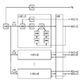
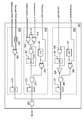
도 2는 디코더의 구성예를 나타내는 도면이다.
도 3은 CTU를 도시한 것이다.
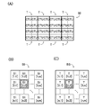
도 4의 (A) 내지 (C)는 타일을 도시한 것이다.
도 5는 유닛의 구성예를 나타낸 것이다.
도 6은 신호 생성 회로의 구성예를 나타낸 것이다.
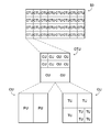
도 7은 CU의 분할을 도시한 것이다.
도 8은 판정 회로의 구성예를 도시한 것이다.
도 9는 신호 생성 회로의 구성예를 도시한 것이다.
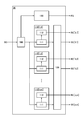
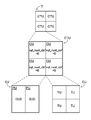
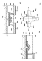
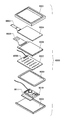
도 10의 (A) 내지 (C)는 표시 장치의 구성예를 도시한 것이다.
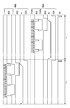
도 11은 타이밍 차트이다.
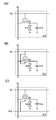
도 12의 (A) 내지 (C)는 화소의 구성예를 각각 도시한 것이다.
도 13의 (A) 내지 (C)는 화소의 구성예를 각각 도시한 것이다.
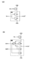
도 14의 (A) 내지 (C)는 회로의 구성예를 각각 도시한 것이다.
도 15의 (A) 내지 (F)는 회로의 구성예를 각각 도시한 것이다.
도 16의 (A) 및 (B)는 회로의 구성예를 각각 도시한 것이다.
도 17의 (A) 및 (B)는 회로의 구성예를 각각 도시한 것이다.
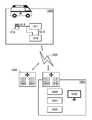
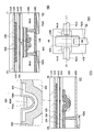
도 18은 방송 시스템의 예를 도시한 것이다.
도 19는 데이터 전송의 예를 도시한 것이다.
도 20은 응급 의료 시스템의 예를 도시한 것이다.
도 21의 (A) 내지 (D)는 수신 장치의 구성예를 각각 도시한 것이다.
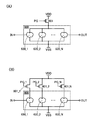
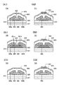
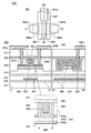
도 22의 (A1), (A2), (B1), (B2), (C1), 및 (C2)는 트랜지스터의 구성예를 도시한 것이다.
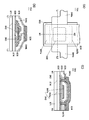
도 23의 (A1), (A2), (A3), (B1), 및 (B2)는 트랜지스터의 구성예를 도시한 것이다.
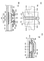
도 24의 (A1), (A2), (A3), (B1), (B2), (C1), 및 (C2)는 트랜지스터의 구성예를 도시한 것이다.
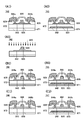
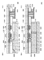
도 25의 (A) 내지 (C)는 트랜지스터의 구성예를 도시한 것이다.
도 26의 (A) 내지 (C)는 트랜지스터의 구성예를 도시한 것이다.
도 27의 (A) 내지 (C)는 트랜지스터의 구성예를 도시한 것이다.
도 28의 (A) 및 (B)는 트랜지스터의 구성예를 도시한 것이다.
도 29의 (A) 및 (B)는 트랜지스터의 구성예를 도시한 것이다.
도 30의 (A) 내지 (C)는 트랜지스터의 구성예를 도시한 것이다.
도 31의 (A) 내지 (C)는 트랜지스터의 구성예를 도시한 것이다.
도 32의 (A) 내지 (C)는 트랜지스터의 구성예를 도시한 것이다.
도 33의 (A) 및 (B)는 에너지 밴드 다이어그램이다.
도 34의 (A) 내지 (C)는 표시 장치의 구성예를 도시한 것이다.
도 35의 (A) 및 (B)는 표시 장치의 구성예를 도시한 것이다.
도 36의 (A) 및 (B)는 장치의 구성예를 도시한 것이다.
도 37은 표시 모듈의 구성예를 도시한 것이다.
도 38의 (A) 내지 (F)는 전자 기기의 구성예를 각각 도시한 것이다.
도 39의 (A) 및 (B)는 트랜지스터의 동작예를 도시한 것이다.
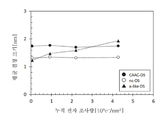
도 40의 (A) 내지 (E)는 XRD에 의한 CAAC-OS 및 단결정 산화물 반도체의 구조 분석, 및 CAAC-OS의 제한 시야 전자 회절 패턴을 나타낸 것이다.
도 41의 (A) 내지 (E)는 CAAC-OS의 단면 TEM 이미지 및 평면 TEM 이미지, 및 그 분석을 통하여 얻은 이미지이다.
도 42의 (A) 내지 (D)는 nc-OS의 전자 회절 패턴 및 단면 TEM 이미지를 나타낸 것이다.
도 43의 (A) 및 (B)는 a-like OS의 단면 TEM 이미지이다.
도 44는 전자 조사에 의하여 유발되는 In-Ga-Zn 산화물의 결정부에서의 변화를 나타낸 것이다.
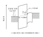
도 45는 채널 형성 영역에 산화물 반도체를 포함하는 트랜지스터의 에너지 밴드를 나타내는 도면이다.
본 출원은 2015년 12월 28일에 일본 특허청에 출원된 일련 번호 2015-255674의 일본 특허 출원에 기초하고, 본 명세서에 그 전문이 참조로 통합된다.
Claims (19)
- 장치로서,
디코더;
구동 회로; 및
제 1 표시 패널 및 제 2 표시 패널을 포함하는 표시부를 포함하고,
상기 디코더는 상기 표시부에 표시되는 화상에 대응하는 신호를 생성하고,
상기 디코더는 상기 제 1 표시 패널 및 상기 제 2 표시 패널 각각에서 화상의 변화를 더 검출하고, 상기 제 1 표시 패널 및 상기 제 2 표시 패널 각각에서 화상의 재기록이 필요할지 여부를 판정하고,
상기 구동 회로는 상기 제 1 표시 패널에 대하여 화상의 재기록이 필요하다고 판정된 경우, 상기 제 1 표시 패널에 상기 신호를 출력하고,
상기 구동 회로는 상기 제 1 표시 패널에 대하여 화상의 재기록이 필요 없다고 판정된 경우, 상기 제 1 표시 패널로의 상기 신호의 출력을 더 정지하는, 장치. - 제 1 항에 있어서,
상기 디코더는 상기 제 1 표시 패널에 표시되는 상기 화상의 움직임 벡터의 값 및 상기 제 1 표시 패널에 표시되는 상기 화상의 프레임 간 예측의 예측 오차에 기초하여 판정을 더 수행하는, 장치. - 제 1 항에 있어서,
상기 제 1 표시 패널 및 상기 제 2 표시 패널은 각각 화소를 포함하고,
상기 화소는 트랜지스터 및 표시 소자를 포함하고,
상기 트랜지스터의 소스 및 드레인 중 한쪽은 배선과 전기적으로 접속되고,
상기 트랜지스터의 상기 소스 및 상기 드레인 중 다른 쪽은 상기 표시 소자와 전기적으로 접속되고,
상기 배선은 상기 화소에 표시되는 그레이레벨에 대응하는 전위를 전달하고,
상기 트랜지스터는 채널 형성 영역에 산화물 반도체를 포함하는, 장치. - 제 1 항에 있어서,
상기 구동 회로는 상기 표시부의 내측에 배치되는, 장치. - 제 1 항에 따른 장치를 포함하는 텔레비전 시스템으로서,
상기 텔레비전 시스템은 방송 신호를 수신하여 비트스트림 데이터를 생성하고 상기 비트스트림 데이터에 기초하여 화상을 표시하는, 텔레비전 시스템. - 전자 기기로서,
제 1 항에 따른 장치; 및
마이크로폰, 스피커, 조작 스위치, 및 센서 중 어느 하나를 포함하는, 전자 기기. - 장치로서,
디코더;
구동 회로; 및
제 1 표시 패널 및 제 2 표시 패널을 포함하는 표시부를 포함하고,
상기 디코더는 상기 표시부에 표시되는 화상에 대응하는 제 1 신호를 생성하고,
상기 디코더는 상기 제 1 표시 패널 및 상기 제 2 표시 패널 각각에서 화상의 변화를 더 검출하고, 상기 제 1 표시 패널 및 상기 제 2 표시 패널 각각에서 화상의 재기록이 필요할지 여부를 판정하고,
상기 구동 회로는 상기 제 1 표시 패널에 대하여 화상의 재기록이 필요하다고 판정된 경우, 상기 제 1 표시 패널에 상기 제 1 신호를 출력하고,
상기 구동 회로는 상기 제 1 표시 패널에 대하여 화상의 재기록이 필요 없다고 판정된 경우, 상기 제 1 표시 패널로의 상기 제 1 신호의 출력을 더 정지하고,
상기 디코더는 상기 구동 회로로부터 상기 표시부로의 신호의 출력을 동기화시키는 제 2 신호를 더 생성하는, 장치. - 제 7 항에 있어서,
상기 디코더는 상기 제 1 표시 패널에 표시되는 상기 화상의 움직임 벡터의 값 및 상기 제 1 표시 패널에 표시되는 상기 화상의 프레임 간 예측의 예측 오차에 기초하여 판정을 더 수행하는, 장치. - 제 7 항에 있어서,
상기 제 1 표시 패널 및 상기 제 2 표시 패널은 각각 화소를 포함하고,
상기 화소는 트랜지스터 및 표시 소자를 포함하고,
상기 트랜지스터의 소스 및 드레인 중 한쪽은 배선과 전기적으로 접속되고,
상기 트랜지스터의 상기 소스 및 상기 드레인 중 다른 쪽은 상기 표시 소자와 전기적으로 접속되고,
상기 배선은 상기 화소에 표시되는 그레이레벨에 대응하는 전위를 전달하고,
상기 트랜지스터는 채널 형성 영역에 산화물 반도체를 포함하는, 장치. - 제 7 항에 있어서,
상기 구동 회로는 상기 표시부의 내측에 배치되는, 장치. - 제 7 항에 따른 장치를 포함하는 텔레비전 시스템으로서,
상기 텔레비전 시스템은 방송 신호를 수신하여 비트스트림 데이터를 생성하고 상기 비트스트림 데이터에 기초하여 화상을 표시하는, 텔레비전 시스템. - 전자 기기로서,
제 7 항에 따른 장치; 및
마이크로폰, 스피커, 조작 스위치, 및 센서 중 어느 하나를 포함하는, 전자 기기. - 장치로서,
디코더;
구동 회로; 및
제 1 표시 패널 및 제 2 표시 패널을 포함하는 표시부를 포함하고,
상기 디코더는 상기 표시부에 표시되는 화상에 대응하는 신호를 생성하고,
상기 디코더는 상기 제 1 표시 패널 및 상기 제 2 표시 패널 각각에서 화상의 변화를 더 검출하고, 상기 제 1 표시 패널 및 상기 제 2 표시 패널 각각에서 화상의 재기록이 필요할지 여부를 판정하는, 장치. - 제 13 항에 있어서,
상기 제 1 표시 패널 및 상기 제 2 표시 패널은 각각 복수의 화소를 포함하는, 장치. - 제 13 항에 있어서,
상기 디코더는 상기 제 1 표시 패널에 표시되는 상기 화상의 움직임 벡터의 값 및 상기 제 1 표시 패널에 표시되는 상기 화상의 프레임 간 예측의 예측 오차에 기초하여 판정을 더 수행하는, 장치. - 제 13 항에 있어서,
상기 제 1 표시 패널 및 상기 제 2 표시 패널은 각각 화소를 포함하고,
상기 화소는 트랜지스터 및 표시 소자를 포함하고,
상기 트랜지스터의 소스 및 드레인 중 한쪽은 배선과 전기적으로 접속되고,
상기 트랜지스터의 상기 소스 및 상기 드레인 중 다른 쪽은 상기 표시 소자와 전기적으로 접속되고,
상기 배선은 상기 화소에 표시되는 그레이레벨에 대응하는 전위를 전달하고,
상기 트랜지스터는 채널 형성 영역에 산화물 반도체를 포함하는, 장치. - 제 13 항에 있어서,
상기 구동 회로는 상기 표시부의 내측에 배치되는, 장치. - 제 13 항에 따른 장치를 포함하는 텔레비전 시스템으로서,
상기 텔레비전 시스템은 방송 신호를 수신하여 비트스트림 데이터를 생성하고 상기 비트스트림 데이터에 기초하여 화상을 표시하는, 텔레비전 시스템. - 전자 기기로서,
제 13 항에 따른 장치; 및
마이크로폰, 스피커, 조작 스위치, 및 센서 중 어느 하나를 포함하는, 전자 기기.
Applications Claiming Priority (3)
| Application Number | Priority Date | Filing Date | Title |
|---|---|---|---|
| JPJP-P-2015-255674 | 2015-12-28 | ||
| JP2015255674 | 2015-12-28 | ||
| PCT/IB2016/057756 WO2017115208A1 (en) | 2015-12-28 | 2016-12-19 | Device, television system, and electronic device |
Publications (2)
| Publication Number | Publication Date |
|---|---|
| KR20180098336A true KR20180098336A (ko) | 2018-09-03 |
| KR102617041B1 KR102617041B1 (ko) | 2023-12-26 |
Family
ID=59087926
Family Applications (1)
| Application Number | Title | Priority Date | Filing Date |
|---|---|---|---|
| KR1020187021195A Active KR102617041B1 (ko) | 2015-12-28 | 2016-12-19 | 장치, 텔레비전 시스템, 및 전자 기기 |
Country Status (4)
| Country | Link |
|---|---|
| US (1) | US10559249B2 (ko) |
| JP (2) | JP2017120412A (ko) |
| KR (1) | KR102617041B1 (ko) |
| WO (1) | WO2017115208A1 (ko) |
Cited By (1)
| Publication number | Priority date | Publication date | Assignee | Title |
|---|---|---|---|---|
| US11222583B2 (en) | 2017-12-25 | 2022-01-11 | Semiconductor Energy Laboratory Co., Ltd. | Display and electronic device including the display |
Families Citing this family (31)
| Publication number | Priority date | Publication date | Assignee | Title |
|---|---|---|---|---|
| JP2017099616A (ja) * | 2015-12-01 | 2017-06-08 | ソニー株式会社 | 手術用制御装置、手術用制御方法、およびプログラム、並びに手術システム |
| US10027896B2 (en) | 2016-01-15 | 2018-07-17 | Semiconductor Energy Laboratory Co., Ltd. | Image display system, operation method of the same, and electronic device |
| US10685614B2 (en) | 2016-03-17 | 2020-06-16 | Semiconductor Energy Laboratory Co., Ltd. | Display device, display module, and electronic device |
| JP2018013765A (ja) | 2016-04-28 | 2018-01-25 | 株式会社半導体エネルギー研究所 | 電子デバイス |
| JP7109887B2 (ja) | 2016-05-20 | 2022-08-01 | 株式会社半導体エネルギー研究所 | 表示システム |
| WO2018073706A1 (en) | 2016-10-21 | 2018-04-26 | Semiconductor Energy Laboratory Co., Ltd. | Display device and operating method thereof |
| JP2018072821A (ja) | 2016-10-26 | 2018-05-10 | 株式会社半導体エネルギー研究所 | 表示装置およびその動作方法 |
| CN108109592B (zh) | 2016-11-25 | 2022-01-25 | 株式会社半导体能源研究所 | 显示装置及其工作方法 |
| CN111033602B (zh) | 2017-08-25 | 2022-03-22 | 株式会社半导体能源研究所 | 显示面板及显示装置 |
| CN109494215A (zh) | 2017-09-11 | 2019-03-19 | 松下知识产权经营株式会社 | 电容元件、图像传感器以及电容元件的制造方法 |
| TWI902196B (zh) | 2017-11-30 | 2025-10-21 | 日商半導體能源研究所股份有限公司 | 顯示面板、顯示裝置、顯示模組、電子裝置及顯示面板的製造方法 |
| WO2019111105A1 (ja) * | 2017-12-06 | 2019-06-13 | 株式会社半導体エネルギー研究所 | 半導体装置、および半導体装置の作製方法 |
| WO2019145813A1 (ja) * | 2018-01-24 | 2019-08-01 | 株式会社半導体エネルギー研究所 | 半導体装置、および半導体装置の作製方法 |
| JP7084770B2 (ja) * | 2018-04-27 | 2022-06-15 | 株式会社ジャパンディスプレイ | 表示装置 |
| WO2020008299A1 (ja) * | 2018-07-05 | 2020-01-09 | 株式会社半導体エネルギー研究所 | 表示装置および電子機器 |
| CN112567446B (zh) | 2018-08-21 | 2024-09-20 | 株式会社半导体能源研究所 | 显示装置及电子设备 |
| US11908850B2 (en) | 2018-09-05 | 2024-02-20 | Semiconductor Energy Laboratory Co., Ltd. | Display device, display module, electronic device, and method for manufacturing display device |
| WO2020049397A1 (ja) | 2018-09-07 | 2020-03-12 | 株式会社半導体エネルギー研究所 | 表示装置、表示モジュール、及び電子機器 |
| CN113196366A (zh) | 2018-09-28 | 2021-07-30 | 株式会社半导体能源研究所 | 显示装置的制造方法、显示装置的制造装置 |
| KR102577240B1 (ko) | 2018-11-21 | 2023-09-12 | 삼성디스플레이 주식회사 | 타일드 표시 장치 |
| CN209345209U (zh) * | 2019-03-08 | 2019-09-03 | Oppo广东移动通信有限公司 | 电子设备 |
| CN109830179B (zh) * | 2019-03-29 | 2021-01-08 | 维沃移动通信有限公司 | 终端设备及用于终端设备的感光检测方法 |
| KR102697989B1 (ko) | 2019-04-15 | 2024-08-22 | 삼성전자주식회사 | 디스플레이 장치 및 그 제어 방법 |
| KR102948551B1 (ko) * | 2019-06-14 | 2026-04-03 | 가부시키가이샤 한도오따이 에네루기 켄큐쇼 | 반도체 장치 및 반도체 장치의 제작 방법 |
| JP7641724B2 (ja) | 2019-11-12 | 2025-03-07 | 株式会社半導体エネルギー研究所 | 機能パネル、表示装置、入出力装置、情報処理装置 |
| US11610877B2 (en) | 2019-11-21 | 2023-03-21 | Semiconductor Energy Laboratory Co., Ltd. | Functional panel, display device, input/output device, and data processing device |
| US10803833B1 (en) * | 2019-11-25 | 2020-10-13 | Himax Technologies Limited | Display systems and integrated source driver circuits |
| KR102767085B1 (ko) * | 2020-02-10 | 2025-02-13 | 주식회사 엘엑스세미콘 | 터치좌표 인식을 위해 발광소자의 발광을 제어하는 타이밍 컨트롤러 및 이를 포함하는 전자장치 |
| JP7450774B2 (ja) * | 2021-02-03 | 2024-03-15 | 三菱電機株式会社 | 表示装置 |
| US20230196979A1 (en) * | 2021-12-16 | 2023-06-22 | X Display Company Technology Limited | Displays with selective pixel control |
| US20250133238A1 (en) * | 2023-10-24 | 2025-04-24 | IKIN, Inc. | Network intermediary transcoding for diffusion-based compression |
Citations (6)
| Publication number | Priority date | Publication date | Assignee | Title |
|---|---|---|---|---|
| JP2002152678A (ja) * | 2000-11-07 | 2002-05-24 | Matsushita Electric Ind Co Ltd | Mpegストリーム再生方法 |
| JP2005070722A (ja) * | 2003-08-22 | 2005-03-17 | Ind Technol Res Inst | ディスプレイのゲートドライバ装置 |
| JP2007096055A (ja) | 2005-09-29 | 2007-04-12 | Semiconductor Energy Lab Co Ltd | 半導体装置、及び半導体装置の作製方法 |
| JP2007123861A (ja) | 2005-09-29 | 2007-05-17 | Semiconductor Energy Lab Co Ltd | 半導体装置及びその作製方法 |
| JP2011141539A (ja) * | 2009-12-10 | 2011-07-21 | Semiconductor Energy Lab Co Ltd | 表示装置の駆動方法、及び表示装置 |
| KR20130023206A (ko) * | 2010-04-01 | 2013-03-07 | 소니 주식회사 | 화상 처리 장치 및 방법 |
Family Cites Families (99)
| Publication number | Priority date | Publication date | Assignee | Title |
|---|---|---|---|---|
| JPS5713777A (en) | 1980-06-30 | 1982-01-23 | Shunpei Yamazaki | Semiconductor device and manufacture thereof |
| US5091334A (en) | 1980-03-03 | 1992-02-25 | Semiconductor Energy Laboratory Co., Ltd. | Semiconductor device |
| US5859443A (en) | 1980-06-30 | 1999-01-12 | Semiconductor Energy Laboratory Co., Ltd. | Semiconductor device |
| US5262350A (en) | 1980-06-30 | 1993-11-16 | Semiconductor Energy Laboratory Co., Ltd. | Forming a non single crystal semiconductor layer by using an electric current |
| US5849601A (en) | 1990-12-25 | 1998-12-15 | Semiconductor Energy Laboratory Co., Ltd. | Electro-optical device and method for manufacturing the same |
| JP2838318B2 (ja) | 1990-11-30 | 1998-12-16 | 株式会社半導体エネルギー研究所 | 感光装置及びその作製方法 |
| KR940008180B1 (ko) | 1990-12-27 | 1994-09-07 | 가부시끼가이샤 한도다이 에네르기 겐꾸쇼 | 액정 전기 광학 장치 및 그 구동 방법 |
| US5289030A (en) | 1991-03-06 | 1994-02-22 | Semiconductor Energy Laboratory Co., Ltd. | Semiconductor device with oxide layer |
| JP3476241B2 (ja) | 1994-02-25 | 2003-12-10 | 株式会社半導体エネルギー研究所 | アクティブマトリクス型表示装置の表示方法 |
| US6747627B1 (en) | 1994-04-22 | 2004-06-08 | Semiconductor Energy Laboratory Co., Ltd. | Redundancy shift register circuit for driver circuit in active matrix type liquid crystal display device |
| JP3402400B2 (ja) | 1994-04-22 | 2003-05-06 | 株式会社半導体エネルギー研究所 | 半導体集積回路の作製方法 |
| TW283230B (ko) | 1994-08-16 | 1996-08-11 | Handotai Energy Kenkyusho Kk | |
| JP2894229B2 (ja) | 1995-01-13 | 1999-05-24 | 株式会社デンソー | マトリクス型液晶表示装置 |
| JP3305946B2 (ja) | 1996-03-07 | 2002-07-24 | 株式会社東芝 | 液晶表示装置 |
| US5801797A (en) | 1996-03-18 | 1998-09-01 | Kabushiki Kaisha Toshiba | Image display apparatus includes an opposite board sandwiched by array boards with end portions of the array boards being offset |
| TW455725B (en) | 1996-11-08 | 2001-09-21 | Seiko Epson Corp | Driver of liquid crystal panel, liquid crystal device, and electronic equipment |
| JPH10174105A (ja) * | 1996-12-11 | 1998-06-26 | Toshiba Corp | 動き判定装置 |
| JP3883641B2 (ja) | 1997-03-27 | 2007-02-21 | 株式会社半導体エネルギー研究所 | コンタクト構造およびアクティブマトリクス型表示装置 |
| KR100265767B1 (ko) | 1998-04-20 | 2000-09-15 | 윤종용 | 저전력 구동회로 및 구동방법 |
| JP3846057B2 (ja) | 1998-09-03 | 2006-11-15 | セイコーエプソン株式会社 | 電気光学装置の駆動回路及び電気光学装置並びに電子機器 |
| JP3276930B2 (ja) | 1998-11-17 | 2002-04-22 | 科学技術振興事業団 | トランジスタ及び半導体装置 |
| JP2000268969A (ja) | 1999-03-17 | 2000-09-29 | Tdk Corp | 有機el素子 |
| JP4434411B2 (ja) | 2000-02-16 | 2010-03-17 | 出光興産株式会社 | アクティブ駆動型有機el発光装置およびその製造方法 |
| CN1220098C (zh) | 2000-04-28 | 2005-09-21 | 夏普株式会社 | 显示器件、显示器件驱动方法和装有显示器件的电子设备 |
| TWI267049B (en) | 2000-05-09 | 2006-11-21 | Sharp Kk | Image display device, and electronic apparatus using the same |
| US7053874B2 (en) | 2000-09-08 | 2006-05-30 | Semiconductor Energy Laboratory Co., Ltd. | Light emitting device and driving method thereof |
| TW525216B (en) | 2000-12-11 | 2003-03-21 | Semiconductor Energy Lab | Semiconductor device, and manufacturing method thereof |
| JP3730159B2 (ja) | 2001-01-12 | 2005-12-21 | シャープ株式会社 | 表示装置の駆動方法および表示装置 |
| SG118118A1 (en) | 2001-02-22 | 2006-01-27 | Semiconductor Energy Lab | Organic light emitting device and display using the same |
| US8415208B2 (en) | 2001-07-16 | 2013-04-09 | Semiconductor Energy Laboratory Co., Ltd. | Semiconductor device and peeling off method and method of manufacturing semiconductor device |
| JP4869516B2 (ja) | 2001-08-10 | 2012-02-08 | 株式会社半導体エネルギー研究所 | 半導体装置 |
| TW574529B (en) | 2001-09-28 | 2004-02-01 | Tokyo Shibaura Electric Co | Organic electro-luminescence display device |
| EP1443130B1 (en) | 2001-11-05 | 2011-09-28 | Japan Science and Technology Agency | Natural superlattice homologous single crystal thin film, method for preparation thereof, and device using said single crystal thin film |
| GB0127090D0 (en) | 2001-11-10 | 2002-01-02 | Image Portal Ltd | Display |
| JP4014895B2 (ja) | 2001-11-28 | 2007-11-28 | 東芝松下ディスプレイテクノロジー株式会社 | 表示装置およびその駆動方法 |
| KR20040077813A (ko) | 2002-02-19 | 2004-09-06 | 호야 가부시키가이샤 | 전계효과트랜지스터형 발광소자 |
| US7109961B2 (en) | 2002-03-13 | 2006-09-19 | Semiconductor Energy Laboratory Co., Ltd. | Electric circuit, latch circuit, display apparatus and electronic equipment |
| KR100945577B1 (ko) | 2003-03-11 | 2010-03-08 | 삼성전자주식회사 | 액정 표시 장치의 구동 장치 및 그 방법 |
| JP4480968B2 (ja) | 2003-07-18 | 2010-06-16 | 株式会社半導体エネルギー研究所 | 表示装置 |
| JP4393812B2 (ja) | 2003-07-18 | 2010-01-06 | 株式会社半導体エネルギー研究所 | 表示装置及び電子機器 |
| US7291967B2 (en) | 2003-08-29 | 2007-11-06 | Semiconductor Energy Laboratory Co., Ltd. | Light emitting element including a barrier layer and a manufacturing method thereof |
| JP2006010811A (ja) | 2004-06-23 | 2006-01-12 | Sony Corp | 表示装置 |
| US20060091794A1 (en) | 2004-11-04 | 2006-05-04 | Eastman Kodak Company | Passive matrix OLED display having increased size |
| US7791072B2 (en) | 2004-11-10 | 2010-09-07 | Canon Kabushiki Kaisha | Display |
| US8847861B2 (en) | 2005-05-20 | 2014-09-30 | Semiconductor Energy Laboratory Co., Ltd. | Active matrix display device, method for driving the same, and electronic device |
| JP4560502B2 (ja) | 2005-09-06 | 2010-10-13 | キヤノン株式会社 | 電界効果型トランジスタ |
| JP5395994B2 (ja) | 2005-11-18 | 2014-01-22 | 出光興産株式会社 | 半導体薄膜、及びその製造方法、並びに薄膜トランジスタ |
| US7998372B2 (en) | 2005-11-18 | 2011-08-16 | Idemitsu Kosan Co., Ltd. | Semiconductor thin film, method for manufacturing the same, thin film transistor, and active-matrix-driven display panel |
| JP2007206651A (ja) | 2006-02-06 | 2007-08-16 | Toshiba Corp | 画像表示装置及びその方法 |
| JP5110803B2 (ja) | 2006-03-17 | 2012-12-26 | キヤノン株式会社 | 酸化物膜をチャネルに用いた電界効果型トランジスタ及びその製造方法 |
| US7616179B2 (en) | 2006-03-31 | 2009-11-10 | Canon Kabushiki Kaisha | Organic EL display apparatus and driving method therefor |
| WO2007139009A1 (ja) | 2006-05-25 | 2007-12-06 | Fuji Electric Holdings Co., Ltd. | 酸化物半導体、薄膜トランジスタ、及びそれらの製造方法 |
| JP2008033066A (ja) | 2006-07-28 | 2008-02-14 | Sony Corp | 表示動作制御装置、表示装置、電子機器、表示動作制御方法及びコンピュータプログラム |
| JP4332545B2 (ja) | 2006-09-15 | 2009-09-16 | キヤノン株式会社 | 電界効果型トランジスタ及びその製造方法 |
| KR101146574B1 (ko) | 2006-12-05 | 2012-05-16 | 캐논 가부시끼가이샤 | 산화물 반도체를 이용한 박막 트랜지스터의 제조방법 및 표시장치 |
| JP5105842B2 (ja) | 2006-12-05 | 2012-12-26 | キヤノン株式会社 | 酸化物半導体を用いた表示装置及びその製造方法 |
| JP4181598B2 (ja) * | 2006-12-22 | 2008-11-19 | シャープ株式会社 | 画像表示装置及び方法、画像処理装置及び方法 |
| US8129714B2 (en) | 2007-02-16 | 2012-03-06 | Idemitsu Kosan Co., Ltd. | Semiconductor, semiconductor device, complementary transistor circuit device |
| WO2008133345A1 (en) | 2007-04-25 | 2008-11-06 | Canon Kabushiki Kaisha | Oxynitride semiconductor |
| US8325310B2 (en) | 2007-05-18 | 2012-12-04 | Semiconductor Energy Laboratory Co., Ltd. | Liquid crystal display device and manufacturing method thereof |
| JP4989309B2 (ja) | 2007-05-18 | 2012-08-01 | 株式会社半導体エネルギー研究所 | 液晶表示装置 |
| KR101563692B1 (ko) | 2007-10-19 | 2015-10-27 | 가부시키가이샤 한도오따이 에네루기 켄큐쇼 | 표시장치 및 그 구동 방법 |
| TW200949822A (en) | 2007-11-26 | 2009-12-01 | Tpo Displays Corp | Display system and method for reducing power consumption of same |
| JP2010103451A (ja) | 2007-11-26 | 2010-05-06 | Fujifilm Corp | 薄膜電界効果型トランジスタおよびそれを用いた電界発光装置 |
| US8202365B2 (en) | 2007-12-17 | 2012-06-19 | Fujifilm Corporation | Process for producing oriented inorganic crystalline film, and semiconductor device using the oriented inorganic crystalline film |
| CN101855703B (zh) | 2007-12-27 | 2013-03-13 | 夏普株式会社 | 半导体装置的制造方法 |
| US20100295042A1 (en) | 2008-01-23 | 2010-11-25 | Idemitsu Kosan Co., Ltd. | Field-effect transistor, method for manufacturing field-effect transistor, display device using field-effect transistor, and semiconductor device |
| KR100963003B1 (ko) | 2008-02-05 | 2010-06-10 | 삼성모바일디스플레이주식회사 | 박막 트랜지스터, 그의 제조 방법 및 박막 트랜지스터를구비하는 평판 표시 장치 |
| JP5305696B2 (ja) | 2008-03-06 | 2013-10-02 | キヤノン株式会社 | 半導体素子の処理方法 |
| JP5325446B2 (ja) | 2008-04-16 | 2013-10-23 | 株式会社日立製作所 | 半導体装置及びその製造方法 |
| KR101533741B1 (ko) | 2008-09-17 | 2015-07-03 | 삼성디스플레이 주식회사 | 표시패널의 구동방법 및 이를 이용한 표시장치 |
| KR101551882B1 (ko) | 2008-11-07 | 2015-09-10 | 삼성전자주식회사 | 멀티 디스플레이 장치 |
| JP4650703B2 (ja) | 2008-12-25 | 2011-03-16 | ソニー株式会社 | 表示パネルおよびモジュール並びに電子機器 |
| TWI394999B (zh) | 2009-01-09 | 2013-05-01 | Prime View Int Co Ltd | 多螢幕電子裝置 |
| JP5606682B2 (ja) | 2009-01-29 | 2014-10-15 | 富士フイルム株式会社 | 薄膜トランジスタ、多結晶酸化物半導体薄膜の製造方法、及び薄膜トランジスタの製造方法 |
| JP4415062B1 (ja) | 2009-06-22 | 2010-02-17 | 富士フイルム株式会社 | 薄膜トランジスタ及び薄膜トランジスタの製造方法 |
| JP4571221B1 (ja) | 2009-06-22 | 2010-10-27 | 富士フイルム株式会社 | Igzo系酸化物材料及びigzo系酸化物材料の製造方法 |
| CN101996535A (zh) | 2009-08-25 | 2011-03-30 | 精工爱普生株式会社 | 电光学装置和电子设备 |
| US8305294B2 (en) | 2009-09-08 | 2012-11-06 | Global Oled Technology Llc | Tiled display with overlapping flexible substrates |
| US9715845B2 (en) | 2009-09-16 | 2017-07-25 | Semiconductor Energy Laboratory Co., Ltd. | Semiconductor display device |
| CN106200185A (zh) | 2009-10-16 | 2016-12-07 | 株式会社半导体能源研究所 | 显示设备 |
| KR101426723B1 (ko) | 2009-10-16 | 2014-08-07 | 가부시키가이샤 한도오따이 에네루기 켄큐쇼 | 표시 장치 |
| WO2011052344A1 (en) | 2009-10-30 | 2011-05-05 | Semiconductor Energy Laboratory Co., Ltd. | Liquid crystal display device, driving method of the same, and electronic appliance including the same |
| WO2011058885A1 (en) | 2009-11-13 | 2011-05-19 | Semiconductor Energy Laboratory Co., Ltd. | Display device and electronic device including the same |
| JP5254469B2 (ja) | 2009-12-03 | 2013-08-07 | シャープ株式会社 | 画像表示装置、パネルおよびパネルの製造方法 |
| EP2529606A1 (en) | 2010-01-29 | 2012-12-05 | Nederlandse Organisatie voor toegepast- natuurwetenschappelijk onderzoek TNO | Tile, assembly of tiles with a carrier, method of manufacturing an assembly |
| JP5471728B2 (ja) | 2010-03-31 | 2014-04-16 | 凸版印刷株式会社 | 表示パネル、この表示パネルを利用した大型表示パネル |
| JP2012133165A (ja) * | 2010-12-22 | 2012-07-12 | Japan Display East Co Ltd | 発光素子表示装置 |
| JP5858367B2 (ja) | 2010-12-28 | 2016-02-10 | シャープ株式会社 | 有機el表示ユニット、有機el表示装置、及び有機el表示ユニットの製造方法 |
| WO2013128740A1 (ja) | 2012-02-29 | 2013-09-06 | コニカミノルタ株式会社 | 発光パネルおよびその製造方法 |
| JP5755592B2 (ja) * | 2012-03-22 | 2015-07-29 | 株式会社ジャパンディスプレイ | 表示装置および電子機器 |
| GB2511549B (en) | 2013-03-07 | 2020-04-22 | Plastic Logic Ltd | Tiled Displays |
| US9524676B2 (en) * | 2013-06-24 | 2016-12-20 | Apple Inc. | Organic light-emitting diode display with burn-in reduction capabilities |
| CN105981193B (zh) | 2014-02-11 | 2018-08-24 | 株式会社半导体能源研究所 | 显示设备及电子设备 |
| JP2016029464A (ja) | 2014-07-18 | 2016-03-03 | 株式会社半導体エネルギー研究所 | 表示装置 |
| KR102533396B1 (ko) | 2014-07-31 | 2023-05-26 | 가부시키가이샤 한도오따이 에네루기 켄큐쇼 | 표시 장치 및 전자 장치 |
| JP6602585B2 (ja) | 2014-08-08 | 2019-11-06 | 株式会社半導体エネルギー研究所 | 表示装置および電子機器 |
| KR102445185B1 (ko) | 2014-10-08 | 2022-09-19 | 가부시키가이샤 한도오따이 에네루기 켄큐쇼 | 표시 장치 |
| US9876946B2 (en) | 2015-08-03 | 2018-01-23 | Semiconductor Energy Laboratory Co., Ltd. | Imaging device and electronic device |
-
2016
- 2016-12-19 WO PCT/IB2016/057756 patent/WO2017115208A1/en not_active Ceased
- 2016-12-19 KR KR1020187021195A patent/KR102617041B1/ko active Active
- 2016-12-21 US US15/386,947 patent/US10559249B2/en active Active
- 2016-12-21 JP JP2016247376A patent/JP2017120412A/ja not_active Withdrawn
-
2021
- 2021-06-15 JP JP2021099278A patent/JP7177219B2/ja active Active
Patent Citations (6)
| Publication number | Priority date | Publication date | Assignee | Title |
|---|---|---|---|---|
| JP2002152678A (ja) * | 2000-11-07 | 2002-05-24 | Matsushita Electric Ind Co Ltd | Mpegストリーム再生方法 |
| JP2005070722A (ja) * | 2003-08-22 | 2005-03-17 | Ind Technol Res Inst | ディスプレイのゲートドライバ装置 |
| JP2007096055A (ja) | 2005-09-29 | 2007-04-12 | Semiconductor Energy Lab Co Ltd | 半導体装置、及び半導体装置の作製方法 |
| JP2007123861A (ja) | 2005-09-29 | 2007-05-17 | Semiconductor Energy Lab Co Ltd | 半導体装置及びその作製方法 |
| JP2011141539A (ja) * | 2009-12-10 | 2011-07-21 | Semiconductor Energy Lab Co Ltd | 表示装置の駆動方法、及び表示装置 |
| KR20130023206A (ko) * | 2010-04-01 | 2013-03-07 | 소니 주식회사 | 화상 처리 장치 및 방법 |
Non-Patent Citations (1)
| Title |
|---|
| S. Kawashima, et al., "13.3-In. 8K×4K 664-ppi OLED Display Using CAAC-OS FETs," SID 2014 DIGEST, pp.627-630 |
Cited By (3)
| Publication number | Priority date | Publication date | Assignee | Title |
|---|---|---|---|---|
| US11222583B2 (en) | 2017-12-25 | 2022-01-11 | Semiconductor Energy Laboratory Co., Ltd. | Display and electronic device including the display |
| US11783757B2 (en) | 2017-12-25 | 2023-10-10 | Semiconductor Energy Laboratory Co., Ltd. | Display and electronic device including the display |
| US12347364B2 (en) | 2017-12-25 | 2025-07-01 | Semiconductor Energy Laboratory Co., Ltd. | Display and electronic device including the display |
Also Published As
| Publication number | Publication date |
|---|---|
| US10559249B2 (en) | 2020-02-11 |
| KR102617041B1 (ko) | 2023-12-26 |
| WO2017115208A1 (en) | 2017-07-06 |
| JP7177219B2 (ja) | 2022-11-22 |
| US20170186365A1 (en) | 2017-06-29 |
| JP2017120412A (ja) | 2017-07-06 |
| JP2021167953A (ja) | 2021-10-21 |
Similar Documents
| Publication | Publication Date | Title |
|---|---|---|
| JP7177219B2 (ja) | 装置 | |
| US11232831B2 (en) | Semiconductor device for vector-matrix multiplication | |
| KR102345707B1 (ko) | 반도체 장치 | |
| US10609404B2 (en) | Decoder, receiver, and electronic device in broadcast system | |
| US10868045B2 (en) | Transistor, semiconductor device, and electronic device | |
| TWI757223B (zh) | 顯示裝置 | |
| US9953695B2 (en) | Semiconductor device, electronic device, and semiconductor wafer | |
| KR102253489B1 (ko) | 반도체 장치 | |
| JP6749212B2 (ja) | 半導体装置、電子機器 | |
| US20170063351A1 (en) | Semiconductor device or electronic device including the semiconductor device | |
| US9830997B2 (en) | Shift register, semiconductor device, and electronic device | |
| CN114695562A (zh) | 半导体装置以及包括该半导体装置的显示装置 | |
| JP6942845B2 (ja) | 半導体装置 | |
| JP2017112374A (ja) | トランジスタ、半導体装置、および電子機器 | |
| US9768174B2 (en) | Semiconductor device | |
| JP2017204637A (ja) | トランジスタおよびその作製方法 | |
| JP2017204636A (ja) | トランジスタ、およびその作製方法 |
Legal Events
| Date | Code | Title | Description |
|---|---|---|---|
| PA0105 | International application |
Patent event date: 20180723 Patent event code: PA01051R01D Comment text: International Patent Application |
|
| PG1501 | Laying open of application | ||
| PA0201 | Request for examination |
Patent event code: PA02012R01D Patent event date: 20211216 Comment text: Request for Examination of Application |
|
| E902 | Notification of reason for refusal | ||
| PE0902 | Notice of grounds for rejection |
Comment text: Notification of reason for refusal Patent event date: 20220825 Patent event code: PE09021S01D |
|
| E90F | Notification of reason for final refusal | ||
| PE0902 | Notice of grounds for rejection |
Comment text: Final Notice of Reason for Refusal Patent event date: 20230224 Patent event code: PE09021S02D |
|
| E701 | Decision to grant or registration of patent right | ||
| PE0701 | Decision of registration |
Patent event code: PE07011S01D Comment text: Decision to Grant Registration Patent event date: 20230922 |
|
| GRNT | Written decision to grant | ||
| PR0701 | Registration of establishment |
Comment text: Registration of Establishment Patent event date: 20231219 Patent event code: PR07011E01D |
|
| PR1002 | Payment of registration fee |
Payment date: 20231220 End annual number: 3 Start annual number: 1 |
|
| PG1601 | Publication of registration |